1
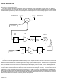
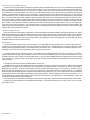
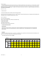
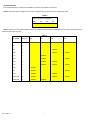
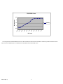
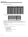
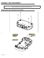
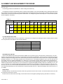
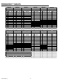
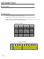
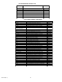
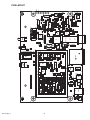
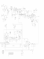
PG4 Wireless Reciever Service Manual
25A1104
PG4 WIRELESS RECEIVER
PRODUCT DESCRIPTION
The Shure Model PG4 is a dual conversion super heterodyne, predictive diversity, microprocessor-controlled UHF receiver, operating over the frequency range of 536 MHz to 865 MHz. Power is supplied to
the receiver by external dc supply with country specific approvals. The PG series is Shure's most basic,
lowest price tier, frequency agile wireless series. This product is intended for use in low cost entry-level
presentation and amateur performance markets.
FEATURES
Frequency agility across a wide range of frequencies (up to 12 MHz for USA models) allows flexibility
to the user to continue wireless operation as the wireless spectral landscape continues to change.
• ·Predictive Diversity provides RF reliability
• ·One seven-segment LED display on the receiver to display channel.
User interface operations include:
• ·Channel Select
Functions include:
• ·RF Ready Light (green LED)
• ·Bi-color LED for audio presence/peak
• ·Fixed volume audio outputs
• ·XLR and ¼" audio outputs
• ·Fixed internal Receiver Antennas
©2006 Shure Incorporated
25A1104(Rev.1)
DETAILED DESCRIPTION
Front Panel
1
1
audio LED
2
ready LED
3
4
LED screen
channel button
2
3
4
Indicates strength of incoming audio signal: green for normal, amber for strong, red for peak.
Green light indicates system is ready for use.
Back Panel
1
1
2
3
4
25A1104 (Rev.1)
2
3
AC adapter jack
Adapter cord tie-off
XLR balanced microphone output jack
1/4” unbalanced output jack
2
4
CIRCUIT DESCRIPTION
General block diagram description.
The receiver consists of the following components: Image filters, predictive diversity circuitry, down-converter, first IF strip, SAW filter,
second mixer, second IF strip, ceramic filter, detector, RSSI buffer, low pass filter, RMS detector and expander, mute circuit, balanced and
unbalanced audio outputs, tonekey detection circuit, noise squelch circuit, microprocessor and several voltage regulators. The PG4 receiver
has two internal antennas mounted to the circuit board via antenna connectors..
Internal Antenna A
Predictive Diversity
Internal Antenna B
A
PIN
Diode
Switch
From
microcontroller
Helical
Filter
1st
MIXER
LNA
LPF for
highside
injected
1st LO
HPF for
lowside
injected
1st LO
To SAW
filter
VCO
From µP
Controller
1st LO
Buffer
LPF
RF Strip
The receiver incorporates Shure's patented Predictive Diversity scheme. The microprocessor's A/D input is continuously monitoring buffered RSSI output from the TP_RSSI_A2D test point. It uses a dynamically adaptive threshold to control dual PIN diode D510, to switch
between the internal antennas. The received RF signal enters an image rejection helical filter (FL510). The filter FL510 in conjunction with
a discrete filter post LNA attenuates the 1st LO frequency from reaching the antenna ports. The RF signal is then down-converted with
IC520, an integrated receiver front-end chip that includes: LNA (low noise amplifier), a GaAs FET mixer, and an IF buffer stage. The 50Ohm impedance of the mixer output's buffer stage is matched to the SAW filter FL600. The signal enters the 1st first IF amplifier, which
consists of Q603, and then it is filtered via a secondary LC filter comprised of C533, L523, C607, and C608. The second mixer is part of
IC610, which also contains the 2nd IF amplifier, limiter, FM detector, and wide dynamic range RSSI circuitry. The second mixer down-converts the first IF signal (110.6 MHz) down to the second IF frequency of 10.7 MHz. The second IF signal is filtered with 10.7MHz ceramic
filters FL620 and FL625 and then demodulated with IC610 and quadrature coil L610. The audio output from the detector chip is injected to
an adjustable audio gain stage and also to the noise squelch stage. The RSSI output from the detector chip is connected to an input of the
A/D converter of the microprocessor for control of the predictive diversity circuit.
25A1104 (Rev.1)
3
The first, the second VCO's and PLL
The first VCO is a two-stage design composed of an oscillator stage and a buffer stage. Its frequency is controlled with the synthesizer
chip IC1. The first stage (Q724) is a common emitter Colpitts oscillator. The air wound resonator L720 is coupled to the transistor with C723,
and to the modulation varactor diode by C721. Inductor L720, capacitor C720, and trimmer CV720 form the resonant tank. Trimmer capacitor CV720 sets the VCO tuning voltage. It is used to tune out parts tolerances and process variances to insure adequate VCO frequency
coverage. The buffer stage Q712 is a common emitter stage. It has a resonant tank at the collector that consists of L710, C730, and part
of the capacitance of C729. The latter also forms an impedance matching network to match to the 50 Ohm input impedance of the low pass
filter. The local oscillator signal is then divided into the mixer injection path C522, and the synthesizer path R706, R717 and C716. The
second local oscillator consists of a single stage Colpitts oscillator (Q760). The second LO resonant tank consists of L756 and C756, and
is coupled via C755 to the varactor diode D755 that receives a control voltage from the phase locked loop. Capacitor C758 couples the tank
to the oscillator. The output tank and matching capacitors C762 and C763, provide 2nd LO output to the PLL chip, and via low pass filter
C763, L763, C765, to the second mixer. The synthesizer chip IC1 is a dual synthesizer that consists of two dual modulus prescalers, two
separate high-resolution synthesizers, a reference crystal divider, and charge pumps with selectable current levels. Y707 a 16 MHz crystal
maintains the frequency reference for the PLL.
DC Power Supply Section
The receiver works with a PS20 power supply that is connected to CON400. Diode D400 provides reverse polarity protection. RF chokes;
E398, E400, E399 and E401 provide RF isolation between the power supply and the receiver. IC400 is the first voltage regulator stepping
down the PS20's unregulated voltage to a constant, low ripple, 9V DC voltage used by the audio section of the receiver. The 9 V is then
down regulated to 5V with IC401, to be used in the RF sections. The regulated 5V is then down regulated to 3.3V with (IC430) and used for
the digital circuit blocks and pin diode switching.
Audio Section
The audio travels from the FM detector output (IC610 pin 7) to an adjustable gain stage (IC200-4) which is used to exactly match the
audio level seen by the expander to that seen by the compressor in the transmitter. In parallel with this, a second path enters a trim stage
(IC200-2) and a high-pass filter (IC200-3). This makes up the noise detection circuit. The filtered signal is rectified and averaged. The
resulting dc is sent to the micro-controller (NOISE_A2D, TP_N) for squelch control.
The output of IC200-4 is then split into two paths. The first path enters a crystal filter (Y285) used for tone key detection. The filtered
signal is rectified and averaged. The resulting dc is sent to the micro-controller (TONEKEY_A2D, TP_TK) for tone key detection. The second path (main audio path) connects to a low-pass filter (IC200-1), used to protect the RMS detector from high frequency tone-key and RF
noise. This filter is in combination with a secondary audio muting circuit (Q113) that increases the muting ability of the receiver with rail-torail noise present.
The audio then splits down two paths: the RMS detector and the VCA.
The RMS detector produces a DC voltage that varies 6mV per dB of input signal. The detector output is fed to the expansion threshold
stage (IC260-3). This stage provides the transition from compressed to uncompressed signal. At low levels, the audio is not expanded
because D134 is turned off. As the AC level increases, the output of IC260-3 decreases enough to turn the diode on. As D134 conducts,
the compression ratio changes from 1:1 to 1:5. Once D134 is turned fully on, the audio expansion ratio remains fixed at 1:5. An additional
diode in the bias network (D122) provides temperature compensation for changes in the Vy, or "cut-in" voltage of D134. After the expansion
threshold stage, the DC control signal is attenuated by a buffer stage (IC260-4). This DC voltage is fed to the VCA control port Ec+. Ec- is
fed the VREF voltage. Together these voltages determine the gain of the expander. The audio exiting the VCA is amplified by IC260-2, and
travels via the de-emphasis circuitry to the outputs.
The audio peak level is determined by comparing the DC level at the output of the expansion threshold stage (AUDIO_A2D) to VREF.
The signal then enters the balanced and unbalanced output stages. The balanced output is set for mic level, where mic level is 14dB
down from line level.
25A1104 (Rev.1)
4
RF & AUDIO BLOCK DIAGRAM
From
st
1 Mixer
110 MHz
SAW Filter
2nd
MIXER
Buffer
2nd IF/Detector
10.7 MHz
10.7 MHz
ceramic filters
Buffer and
DC gain
Sanyo
LA8662V
Audio
output
2nd LO
RSSI
output
VCO
LPF
RF – 1st and 2nd IF
2nd mixer and detector
LMX2335
LTM PLL
From µP Controller
Audio
Outputs
Unbalanced
Buffer
Audio Proc
Muting
18 kHz LPF
Balanced
Tone Key
Detector
To uP
Noise
Squelch
Detector
Buffer
Audio & Muting Circuitry
25A1104 (Rev.1)
5
To uP
To uP
Digital Section
The Freescale 8Kb FLASH microprocessor was chosen to maximize its benefits and to reduce system cost. The internal ADC converters
are utilized to sample DC voltages to handle switching diversity, audio metering, audio muting, noise squelching, and tone-key detection.
RF band detection uses four digital inputs. In addition, the Freescale microprocessor controls the 7-segment LED display and handles the
user interface channel selection.
Display Circuitry
1 Software Version
To verify which software version is loaded, use the following procedure:
Hold the select button while plugging in the device. While continuing to hold the select button down, the display should start flashing and
sequentially read out a repeating message similar to this one:
"b01-15-12c0-34c0"
This can be decoded as follows:
b:this is a receiver software load. (a indicates a transmitter load)
01-:major version number.
15-minor version number.
12c0-software audio trim level
34c0-software predictive diversity rssi trim level
ACCESSING DIFFERENT MODES
NORMAL MODE
UNDER USUAL USAGE CONDITIONS, THE DEVICE WILL POWER ON IN NORMAL MODE. BENCH TESTING SHOULD NOT BE DONE IN
NORMAL MODE. SINCE THE ATE MODE PROVIDES A SPECIAL FREQUENCY MAP, THE FREQUENCIES WILL BE DIFFERENT IN
NORMAL MODE.
ATE MODE
A Microwire serial bus using three pins, TP_ATELE, TP_ATEDATA, and TP_ATECLK will control the ATE mode. This interface can be
used to control and test all microprocessor-based functions of the board.
These ATE frequencies are shown in Table 1
Table 1
1, 2, 3
PG4
ATE Mode Test
Frequencies (MHz)
25A1104 (Rev.1)
b, c, d
H7
K7
M7
M10
P11
1 Flow b
536.000
589.500
662.000
674.000
702.000
740.000 799.700 770.000 794.000 806.000
854.000
2 Fmid c
542.000
594.500
668.000
681.500
708.000
746.000 806.000 777.000 799.700 808.000
859.500
3 Fhigh d 548.000
602.000
674.000
686.000
714.000
751.700 812.000 781.700 806.000 809.850
864.800
6
Q11
R10
R11
R12
JB
T10
RF BAND RESISTORS
Four resistors Ra, Rb, Rc, and Rd are responsible to start the microcontroller in a RF band.
Table 2 shows the reference designators and how the voltages at the test points reflect the operating RF band.
.
Table 2
PG4 Reference Designators
Rd
Rc
Rb
Ra
R316
R315
R314
R313
Table 3 shows the variant resistor installation options for each band. When a resistor is installed the microprocessor will read a logic low,
otherwise it will read a logic high..
Table 3
25A1104 (Rev.1)
RF BAND
Board ID
Rd
Rc
Rb
H7
A
K7
B
M7
C
Installed
M10
D
Installed
P11
E
Installed
Q11
F
Installed
R10
G
Installed
Installed
R11
H
Installed
Installed
R12
J
Installed
JB
K
Installed
T10
L
Installed
Installed
Reserved
M
Installed
Installed
Reserved
N
Installed
Ra
Installed
Installed
Installed
Installed
Installed
Installed
7
Installed
Microcontroller Netnames and Programming Testpoint List
Pin
Port
Name
Testpoint
TP_RST
1
RESETn
Reset
2
PTC0/TxD2
Seven Segment A
3
PTC1/RxD2
Seven Segment B
4
5
6
PTC2/SDA1
PTC3/SCL1
PTC4
Seven Segment C
Seven Segment D
Seven Segment E
7
PTC5
Seven Segment F
8
9
PTC6
PTC7
Seven Segment G
NC
10
PTE0/TxD1
Select Button
11
12
13
14
PTE1/RxD1
IRQ
PTE2/SS1n
PTE3/MISO1
NC
NC
Ra
Rb
15
16
17
18
19
20
21
22
PTE4/MOSI1
Rc
PTE5/SPSCK1
Rd
VSS1
EGND
VSS2
EGND
VDD
+3.3Vdd
PTD0/TPM1CH0
RF LED
PTD1/TPM1CH1 Red LED (Active High)
PTD2/TPM1CH2Green LED (Active High)
23 PTD3/TPM2CH0
ANT_A
24 PTD4/TPM2CH1
25 PTB0/AD1P0
26 PTB1/AD1P1
27 PTB2/AD1P2
28 PTB3/AD1P3
ANT_B
NOISE_A2D
TONEKEY_A2D
RSSI_A2D
AUDIO_A2D
29
PTB4/AD1P4
NC
30
PTB5/AD1P5
NC
31
PTB6/AD1P6
NC
32
33
PTB7/AD1P7
VREFH
NC
+3.3Vdd
34
VREFL
EGND
35 PTA0/nKBI1P0
36 PTA1/nKBI1P1
37 PTA2/nKBI1P2
CLOCK
DATA
LE
38 PTA3/nKBI1P3
AUDIO_MUTE
39 PTA4/nKBI1P4
NC
40 PTA5/nKBI1P5
TP_ATECLK
41 PTA6/nKBI1P6
42 PTA7/nKBI1P7
43
VDDAD
44
VSSAD
TP_ATEDATA
TP_ATELE
+3.3Vdd
EGND
45 PTG0/BKGD/MS
25A1104 (Rev.1)
TP_BKGD
46 PTG1/XTAL
47 PTG2/EXTAL
Crystal
Crystal
48
PLL_LD
PTG3
8
PG4 RSSI Curve
TP_RSSI Vdc
2.5
2
1.5
Series1
1
-2
0
-3
0
-4
0
-5
0
-6
0
-7
0
-8
0
-9
0
-1
20
-1
10
-1
00
0.5
RF Level
The microprocessor reads the RSSI level from an ADC several times a second when the PG4 is unmuted, to predict if a switch is necessary to avoid an audible dropout. Thresholds were calculated from the above RSSI curve.
25A1104 (Rev.1)
9
NOTES
25A1104 (Rev.1)
10
FUNCTIONAL TEST
GENERAL INFORMATION LOOKUP TABLE
Band
H7
K7
M7
M10
P11
Q11
R11
R12
R10
JB
T10
Fc (MHz)
Low
High
536
548
590
602
662
674
674
686
702
714
740
752
770
782
794
806
800
812
806
810
854
865
1st Image Band (MHz)
Low
High
757.2
769.2
811.2
823.2
883.2
895.2
895.2
907.2
480.8
492.8
518.8
530.8
548.8
560.8
572.8
584.8
578.8
590.8
584.8
588.8
632.8
643.8
Local oscillators
1st LO
2nd LO
Fc+110.6
99.9MHz
Fc+110.6
99.9MHz
Fc+110.6
99.9MHz
Fc+110.6
99.9MHz
Fc-110.6
121.3MHz
Fc-110.6
121.3MHz
Fc-110.6
121.3MHz
Fc-110.6
121.3MHz
Fc-110.6
121.3MHz
Fc-110.6
121.3MHz
Fc-110.6
121.3MHz
REQUIRED TEST EQUIPMENT (OR APPROVED EQUIVALENT OR SUPERIOR MODELS):
RF Signal Generator
Audio Analyzer
Power Supply
BNC (M) to BNC (M) cable (2)
BNC (F) to 1/4” adapter
Matching UA820 Antenna
Agilent E4420B
HP 8903B
PS20
Shure PT1838A
Shure PT1838C
Frequency
Dependent
LISTENING TEST
Before completely disassembling the receiver, operate it to determine whether it is functioning normally and try to duplicate
the reported malfunction. Refer to pages 2 and 3 for operating instructions, troubleshooting, and specifications.
Review any customer complaint or request, and focus the listening test on any reported problem. The following, more extensive, functional tests require partial disassembly.
FUNCTIONAL TEST
NOTE: for these tests a tonekey generator must be used. If none is available, the unit must be opened and the tone
key must be disabled.
1.
2.
3.
25A1104 (Rev.1)
Apply +12 Vdc to the power input of the receiver (PS20).
Set up the Audio Analyzer as follows:
• Engage A-weighting filter
• Engage 30kHz LPF filter
Set up RF signal generator as follows:
• Frequency = Fo (refer to the frequency tables on page 21)
• Amplitude = 0 dBm radiated
• FMrate = 1kHz
• Deviation = (see table next page)
11
Deviation
Q11
All other frequencies
27.5 kHz
37.5 kHz
TONE KEY INDICATOR
1.
Modulate the RF signal with 32.768 kHz tone key generator. (If using an HP E4400B RF Generator use the DualSine wave feature by pressing: more, FM Waveform (Sine), and Dual-Sine). Set the following:
• FM Tone 2 Rate = 32.768kHz
• FM Tone 2 Amplitude = (see table below)
FM Tone 2 Amplitude
2.
3.
Q11
All other frequencies
16%
12%
Connect an antenna to the RF signal generator output.
Verify that the 1kHz tone audio output is audible and the red "peak" LED is lit on the receiver.
AUDIO OUTPUT LEVEL AND DISTORTION
1.
2.
3.
4.
Attach audio analyzer to ¼" output and measure output level to be -3.3dBu +/- 2.5dB.
Measure Audio output of XLR to be -17.0dBu +/- 1.5dB.
Engage the A-weighting and 30 kHz LP filters on the HP8903.
Measure distortion to be less than 1%.
FREQUENCY RESPONSE USING AN RF GENERATOR.
1.
2.
3.
4.
5.
6.
7.
8.
Disengage all filters on the audio analyzer.
Set the audio analyzer to measure AC level in dB’s.
Connect the audio analyzer input to the ¼" output of the receiver.
Record this level by engaging the “ratio” button on the audio analyzer.
Change modulation to 20kHz on the RF generator.
Measure ¼" output to be -21dBu +/- 3dB.
Change modulated frequency on the RF generator to 400Hz.
The audio output level should be +5dB ± 1dB relative to the 1kHz level.
RF POWER AND SQUELCH LEVEL
1.
2.
3.
4.
Disengage the “ratio” button on the audio analyzer.
Change modulated frequency on the RF signal generator to 1kHz.
Engage the 400Hz filter and 30kHz filter on the audio analyzer.
Set RF level to -110 dBm. The Receiver should be squelched.
IF ALL TESTS PASSED, THIS MEANS THE UNIT IS PROPERLY FUNCTIONING, AND NO ALIGNMENT IS REQUIRED.
25A1104 (Rev.1)
12
ASSEMBLY AND DISASSEMBLY
!CAUTION!
Observe precautions when handling this static-sensitive device.
ASSEMBLY INSTRUCTIONS (REVERSE FOR DISASSEMBLY)
1.
2.
REF LOW BAND ANTENNA
(MORE TRIANGULAR SHAPED)
REF: ANTENNAS SHOWN
SUPERIMPOSED TO SHOW
DIFFERENT POSITIONS
AND GEOMETRIES.
ANTENNA SIDE CLIPS
NOTE 6
REF HIGH BAND ANTENNA
(MORE SQUARE SHAPED)
25A1104 (Rev.1)
13
3.
REF HIGH BAND
LEFT
REF LOW BAND
LEFT
REF LOW BAND, RIGHT
REF HIGH BAND, RIGHT
2-ISOMETRIC
25A1104 (Rev.1)
14
SERVICE PROCEDURES
MEASUREMENT REFERENCE
NOTE: Audio levels in dBu are marked as dBm on the HP8903.
dB Conversion Chart
0dBV = 2.2 dBu
0dBu = 0dBm assuming the load = 600 ohms
Be aware that dBu is a measure of voltage and dBm
is a measure of power. The HP8903, for example,
should be labeled dBu instead of dBm since it is a
voltage measurement. These two terms are often
used interchangeably even though they have
different meanings.
REQUIRED TEST EQUIPMENT (OR APPROVED EQUIVALENT OR SUPERIOR MODELS):
RF Generator
Digital multi-meter
Audio Analyzer
1 GHz Frequency Counter
Spectrum Analyzer
Power Supply
Shielded Test Lead
BNC (M) to BNC (M) cable (2)
BNC (F) to ¼" adapter
BNC (M) to unterminated
Matching PG1/PG2 Transmitter
XLR (F) to Banana Plug Adapter
Toray non-inductive tuning tool - White
Toray non-inductive tuning tool - Blue
Toray non-inductive tuning tool - Pink
Non-inductive hex tuning tool
Jumper wires
25A1104 (Rev.1)
Agilent E4400B
Fluke 87
HP 8903B
HP 53181A
HP 8591A
PS20
Shure PT1838F
Shure PT1838A
Shure PT1838C
Shure PT1824
PG1/PG2
Shure PT1841
Shure PT1838M
Shure PT1838K
Shure PT1838L
Shure PT1838N
15
ALIGNMENT AND MEASUREMENT PROCEDURE
General notes
The following procedures are intended for a "bench" testing environment only.
The alignment procedure is sequential and does not change unless specified. Use an RG-178/U BNC male to unterminated cable for all
RF connections to the antenna inputs. Keep the test cables as short as possible (less than 3 feet in length). Include the insertion loss of the
cables and the connectors when performing all RF measurements. DC voltages may present at RF test points. Use DC blocks to protect
the test equipment, if necessary.
.
Table 4
1, 2, 3
PG4
ATE Mode Test
Frequencies (MHz)
b, c, d
H7
K7
M7
M10
P11
Q11
R10
R11
R12
JB
T10
1 Flow b
536.000
589.500
662.000
674.000
702.000
740.000 799.700 770.000 794.000 806.000
854.000
2 Fmid c
542.000
594.500
668.000
681.500
708.000
746.000 806.000 777.000 799.700 808.000
859.500
3 Fhigh d 548.000
602.000
674.000
686.000
714.000
751.700 812.000 781.700 806.000 809.850
864.800
VOLTAGE REGULATION CHECK
With power applied properly, and the unit switched on, measure the DC voltages at the following test points. All test points are located
on the top side of the PCB. Refere to the component diagram.
Test Points
TP_9V
TP_5V
TP_5VPLL
TP_3.3V
TP_VREF
Voltages
+9.0 ± 0.2 Vdc
+5.0 ± 0.1 Vdc
+5.0 ± 0.2 Vdc
+3.3 ± 0.2 Vdc
+4.5 ± 0.2 Vdc
ATE MODE SETUP AND USE
There are three different ATE mode test frequencies available in every frequency group, which are Flow, Fmid and Fhigh. The Fmid
frequency may not be the center of the band. It is selected for the best tuning of FL510 filter. Set the receiver into ATE mode by shorting
"ATE LE" to GND and then apply power to the receiver's DC jack. Press the channel button until you observe the 7-segment LED display
providing a selection of 1, 2, 3 for frequency groups H7,K7, M7, M10 and b, C, d for frequency groups P11, Q11, R11, R12, R10, JB, T10.
For example, when the 7-segment LED display's a "1" this is Flow, "2" is Fmid and "3" Fhigh. When you depress the channel button for
approximately 3-seconds the receiver enters into a micro controller reference level programming mode. When a "C" is displayed, press and
release the channel button several times so you can observe the 7-segment LED display providing a selection of a blinking C, A or P. The
"C" is to cancel the micro controller reference level-programming mode (do not confuse this "C" for Fmid for groups P11, Q11, R11, R12,
R10, JB, T10). The "A" is to set the audio LED reference level. The "P" is to set the predictive no switch level. Once the respective C, A or
P is selected and left blinking, the micro will perform the respective operation when the 7-segment LED display returns to the previous 1, 2
or 3 display.
INITIAL SETUP
Disabling diversity: For Channel A to be active, short TP2 to ground and connect TP3 to 3.3Vdc. For Channel B to be active, short TP3
to ground and connect TP2 to 3.3Vdc.
Set the receiver into ATE mode and to Fhigh. This sets the receiver to the highest operating frequency.(see table 4 for reference)
25A1104 (Rev.1)
16
POWER TEST SECTION
1.
2.
3.
4.
5.
6.
Measure +9.0 Vdc + 0.2 /-0.2 Vdc at test point "TP_9V"
Measure +5.0 Vdc + 0.1 /-0.1 Vdc at test point "TP_5V"
Measure +5.0 Vdc + 0.2 /-0.2 Vdc at test point "TP_5VPLL"
Measure +3.3 Vdc + 0.2 /-0.2 Vdc at test point "TP3.3V"
Measure +4.5 Vdc + 0.2 /-0.2 Vdc at test point "TP_VREF"
The dc current drain should be 120 mA +/- 25 mA.
1ST LOCAL OSCILLATOR
1.
2.
Adjust CV720 to set voltage at TP1 to +3.75 Vdc ± 0.1 Vdc.
Attach a frequency counter to TP600. Verify frequency is:
(fo + 110.6 MHz) ± 5.0 kHz for frequency groups H7,K7, M7, M10
(fo - 110.6 MHz) ± 5.0 kHz for frequency groups P11, Q11, R11, R12, R10, JB, T10
2ND LOCAL OSCILLATOR
1.
Verify the voltage at TP750 is between +1Vdc and +4Vdc
FRONT END RF FILTERS
1.
2.
3.
4.
5.
6.
Connect the RF generator output via RF test cable to +CON500 and ground for Channel A input.
Set receiver to Fmid.
Connect TP2 to GND and TP3 to 3.3Vdc so as, to defeat diversity switching.
Set RF generator to the corresponding Fmid frequency and set the amplitude to -70 dBm with no modulation.
Connect DC voltmeter to TPRSSI_A2D (Pin 6 of IC610).
Measure the DC voltage at TPRSSI_A2D (Pin 6 of IC610) while tuning FL510 so as to achieve the maximum DC voltage level at
TPRSSI_A2D.
PREDICTIVE DIVERSITY THRESHOLD SETTING
1.
Set RF generator amplitude to -90 dBm. Enter into the micro controller reference level-programming mode. Sequence through the
three selections until the "P" is flashing. Let the "P" flash until it times out and the LED display returns to Fmid. This is to set the predictive no-switch level.
QUAD COIL TUNE-UP
1.
2.
3.
4.
Verify the receiver is set to ATE mode Fmid frequency.
For all groups except Q11 set the RF generator amplitude to -70 dBm with FM modulation at 1 kHz and deviation = 33 kHz with audio
analyzer HP8903B. Engage the A-weighting and 30 kHz LPF filters on the HP 8903B. Adjust L610 for maximum AC level at TPR (Pin
7 of IC610). Typically = 150mVrms. Low limit = 120mVrms. There is no high limit.
For Q11 only set the RF generator amplitude to -70 dBm with FM modulation at 1 kHz and deviation = 23 kHz with audio analyzer
HP8903B. Engage the A-weighting and 30 kHz LPF filters on the HP 8903B. Adjust L610 for maximum AC level at TPR (Pin 7 of
IC610). For the Q11 frequency band the low limit = 95mVrms. There is no high limit.
For all groups measure THD at TPR (Pin 7 of IC610). Typically = 0.5 %. If the THD is > 1.0%, adjust L610 again to minimize THD at
TPR.
CHANNEL A SENSITIVITY CHECK
1.
2.
3.
Set RF generator amplitude to -100 dBm. Measure SINAD (Sinad = signal + noise + distortion/ noise + distortion) at TPR (Pin 7 of
IC610) to be greater then 12 dB.
Set receiver to ATE mode Flow frequency. Set RF generator frequency to corresponding frequency and the amplitude to -95 dBm.
Measure SINAD at TPR (Pin 7 of IC610) to be greater than 12dB, if not, go back to previous Front-end RF filter alignment section and
repeat the procedure.
Set the receiver to ATE mode Fhigh frequency. Set RF generator frequency to corresponding frequency and the amplitude to -95
dBm. Measure SINAD at TPR (Pin 7 of IC610) to be greater then 12 dB, if not, go back to previous Front-end RF filter alignment section and repeat the procedure.
CHANNEL B SENSITIVITY CHECK
1.
2.
3.
Set the receiver to ATE mode Fmid frequency.
Connect the RF generator to Ch. B (CON505 and ground).
Connect TP2 to 3.3Vdc and TP3 to GND so as, to defeat diversity switching.
25A1104 (Rev.1)
17
4.
5.
6.
Set signal generator level= -100 dBm.
Set signal generator to corresponding frequency.
Measure SINAD at TPR (Pin 7 of IC610) to be equal to or greater than 12 dB.
TONEKEY LEVEL DETECTION
1.
2.
3.
Verify the receiver is set to ATE mode Fmid frequency.
Set the RF generator's amplitude to -70dBm and carrier frequency to ATE Fmid frequency.
Apply a dual-sine modulation function with FM rate1=1KHz and FM rate2=32.768KHz and ampl=12%. Set the deviation to 37.5KHz.
For the Q11 band Apply a dual-sine modulation function with FM rate1=1KHz and FM rate2=32.768KHz and ampl=16%. Set the deviation to 27.5KHz. Verify test point TP_TK measures between 1.00Vdc to 3.5 Vdc.
NOISE SQUELCH ALIGHNMENT
1.
2.
3.
4.
Verify the receiver is set to ATE mode Fmid frequency.
Verify RF generator is set to the ATE Fmid frequency a dual-sine modulation function with FM rate1 = 1KHz and FM rate2 =
32.768KHz and ampl=12%. Set the deviation to 37.5KHz. *For the Q11 band Apply a dual-sine modulation function with FM rate1 =
1KHz and FM rate2 = 32.768KHz and ampl=16%. Set the deviation to 27.5KHz. Set the RF signal generator amplitude to -95dBm.
Adjust the RF input level to find the 30dB SINAD point (A-weighted), measured at TPR. (note that the 30 dB SINAD at TPR corresponds to approximately 40 dB SINAD at ¼" or XLR outputs).
Adjust TR220 for 1 Vdc ± 0.2Vdc at TP_N (Noise_A2D).
AUDIO ALIGNMENT
1.
2.
3.
Verify RF generator is set to the ATE Fmid frequency a dual-sine modulation function with FM rate1 = 1KHz and FM rate2 = 32.768KHz and
ampl=12%. Set the deviation to 37.5KHz. *For the Q11 band Apply a dual-sine modulation function with FM rate1=1KHz and FM
rate2=32.768KHz and ampl=16%. Set the deviation to 27.5KHz.
Set the RF signal generator amplitude to -70dBm.
Adjust TR100 for -3.3dBu ± 0.25dBu at the ¼" output (TPUNBAL).
AUDIO PEAK LIGHT REFERENCE SETTING PROCEDURE
1.
2.
Apply a dual-sine modulation function with FM rate1 = 1KHz and FM rate2 = 32.768KHz and ampl=12%. Set the deviation to 47.0KHz.
Enter into the micro controller reference level-programming mode. Sequence through the three selections until the "A" is flashing. Let the "A"
flash until it times out and the LED display returns to Fmid. This is to set the audio LED peak light threshold.
The Alignment is now completed.
25A1104 (Rev.1)
18
NOTES
25A1104 (Rev.1)
19
AGENCY APPROVALS
FCC DD4 PG4 (Part 15 "Declaration of Conformity" filed)
IC RSS-123 (Canada # 616A-PG4) Professional Only
CE (Declaration of Conformity to latest version of ETSI EN 301-389)
ADDITIONAL PRODUCT PERFORMANCE CHARACTERISTICS (NOT TESTED IN PRODUCTION):
General notes: A-weighting filter, RF testing level = -70 dBm, 33kHz Deviation @ 1 kHz modulation frequency, unless otherwise specified.
Audio & RF tests at the detector output:
Audio level : 100 mV RMS min
S/N Ratio: 50 dB min. (60dB typical)
Frequency response: (100 Hz - 15 kHz) [+/-4.0 dB]
IF Bandwidth test at the detector output:
THD at fc+25 kHz: 2 % max.
THD at fc-25 kHz: 2 % max.
Image Response tests:
1st image rejection: 40 dB min. (50 dB typical)
2nd image rejection: 70 dB min.
½ first IF response test: 50 dB min.
2/3 first IF response test: 50 dB min.
½ 2nd IF test: 70 dB min.
2/3 2nd IF test: 70 dB min.
Response at Fo +/- digital clocks and their harmonics: 60 dB min.
Parasitic spurious: 50 dB min.
RF conductive tests:
First LO and its harmonics at the antenna port: -70 dBm max.
Second LO and its harmonics at the antenna port: -80 dBm max.
Overload test:
No receiver performance degradation should be observed at RF input levels up to -25 dBm. (THD, SINAD and S/N)
Intermodulation, THD, SINAD and S/N degradation is expected at RF input levels between
-20 to 6 dBm, however the receiver should receive the signal as expected.
Intermodulation tests:
Receiver's response to the 3rd and 5th order IM products outside of the bandwidth of the
second IF filters (e.g.: f (on channel) = 800MHz, F(IM1) = 801 MHz, F(IM2) = 802MHz) should be better than 50 dB.
Basic stability tests:
At the threshold of receiver's sensitivity, there should be no extraneous noises being generated within the receiver's circuitry. There should be no parasitic oscillations present during tests with a spectrum analyzer along receiver's signal path (RF
band, 1st mixer, 1st IF, Second Mixer, Second IF, Detector, audio and noise circuitry).
RSSI tests:
RSSI total dynamic range: -100 to -60 dBm
25A1104 (Rev.1)
20
FREQUENCY TABLES
Group A
Group B
N. & S. America N. & S. America
H7
CH
1
2
3
4
5
6
7
8
9
0
536 - 548
Freq
536.075
547.925
537.275
546.725
540.025
543.975
541.925
542.075
547.175
536.825
K7
CH
1
2
3
4
5
6
7
8
9
0
590 - 602
Freq
590.075
601.925
591.275
600.725
594.025
597.975
595.925
596.075
601.175
590.825
Group C
Group D
Group E
Group F
N. & S. America
Australia / France
China
China / Korea
M7
CH
1
2
3
4
5
6
7
8
9
0
662-674
Freq
662.075
673.925
663.275
672.725
666.025
669.975
667.925
668.075
673.175
662.825
M10
CH
1
2
3
4
5*
6
7
8
9
0**
674-686
Freq
674.025
677.900
682.775
684.700
685.900
674.225
676.500
680.025
684.500
685.700
P11
CH
1
2
3
4
A
b
C
d
702-714
Freq
702.075
703.275
706.025
707.925
708.075
709.975
712.725
713.925
Group G
Group H
Group J
Group K
Group L
Australia / EU
China
Thailand / Taiwan
Japan
T10
R10
CH
1
2
3
4
5*
6
7
8
9
0**
800-812
Freq
802.525
800.525
807.400
810.275
811.550
801.100
802.325
808.600
810.550
813.800
R11
CH
1
2
3
4
A
b
C
d
770-782
Freq
770.075
771.275
774.025
775.925
776.075
777.975
780.725
781.925
R12
CH
1
2
3
4
A
b
C
d
794-806
Freq
794.075
795.275
798.025
799.925
800.075
801.975
804.725
805.925
JB
CH
1
2
3
4
5
6
A
b
C
d
* Compatible with each of channels 1-4
** Compatible with each of channels 6-9
Highlighted Channels are compatible with each other
25A1104 (Rev.1)
21
806-810
Freq
806.125
806.375
807.125
807.750
809.000
809.500
806.250
807.500
809.625
808.625
T10
CH
1
2
3
4
5*
6
7
8
9
0**
Q11
CH
1
2
3
4
A
b
C
d
740-752
Freq
740.125
741.325
744.075
745.975
746.025
747.925
750.675
751.875
US
854 - 865 FCC ISM
Freq
CH
855.275
1
856.575
2
858.650
3
863.475
4
864.700
5
854.900
6
857.950
7
861.750
8
863.500
9
864.825
0
902 - 928
Freq
902.000
905.250
908.500
911.750
915.000
918.250
921.500
924.750
928.000
PRODUCT SPECIFICATIONS
System
Working Range
75m (250 ft.)
Note: actual range depends on RF signal absorption, reflection, and
interference
Audio Frequency Response
+/– 2 dB
Minimum: 45 Hz
Maximum: 15 kHz
(Overall system frequency depends on microphone element.)
Total Harmonic Distortion
0.5%, typical
Ref. +/– 33 kHz deviation, 1 kHz
tone
PG1
Dynamic Range
>100 dB A-weighted, typical
Operating Temperature
Range
–18°C (0°F) to +57°C (+135°F)
Transmitter Audio Polarity
Positive pressure on microphone diaphragm (or positive
voltage applied to tip of WA302 phone plug) produces positive
voltage on pin 2 (with respect to pin 3 of low impedance output)
and the tip of the high impedance 1/4-inch output.
Audio Input Level
-10 dBV maximum at "mic" gain position
+10 dBV maximum at 0dB gain position
+20 dBV maximum at -10dB gain position
Bodypack Transmitter
PG2
Note: battery characteristics may limit this range
Gain Adjustment Range
30 dB
Input Impedance
1 mΩ
RF Transmitter Output
10 mW maximum (dependent on applicable country
regulations)
Dimensions
110 mm H x 64 mm W x 21 mm D (4.3 in. x 2.5 in. x 0.8 in.)
Weight
75 grams (2.6 oz.) without battery
Housing
Molded ABS
Power Requirements
One 9V size alkaline or rechargeable battery
Battery Life
>8 hours (alkaline)
Audio Input Level
+2 dBV maximum at -10dB position
-8 dBV maximum at 0dB position
Handheld Transmitter
Gain Adjustment Range
10dB
RF Transmitter Output
10 mW maximum (dependent on applicable country
regulations)
Dimensions
224 mm L x 53 mm Dia. (8.8 in. x 2.10 in.)
including PG58 cartridge
Weight
218 grams (7.7 oz.) without battery
Housing
Molded ABS handle and battery cup
Power Requirements
One 9V size alkaline or rechargeable battery
Battery Life
>8 hours (alkaline)
PG4
Dimensions
189mm L x 105mm W x 40 mm D (7.45 in. x 4.15 in. x 1.59 in.)
Receiver
Weight
209.79 g (7.4 oz.)
Housing
Molded ABS Plastic
Audio Output Level
XLR connector (into 100 Ω load): –19 dBV, typical
1/4 inch connector (into 100 Ω load): –5 dBV, typical
Ref. +/– 33 kHz deviation with 1
kHz tone
25A1104 (Rev.1)
Output Impedance
XLR connector: 200 Ω
1/4 inch connector: 1kΩ
XLR output
Impedance balanced
Pin 1: Ground (cable shield)
Pin 2: Audio
Pin 3: No Audio
Sensitivity
–105 dBm for 12 dB SINAD, typical
Image Rejection
>50 dB, typical
Power Requirements
12–18 Vdc at 160 mA, supplied by external power supply
22
TROUBLESHOOTING
Current draw and DC regulator tests
1.
2.
3.
Connect the PS20 DC power supply to CON400.
Verify current draw is 120mA +/- 25mA.
If the current draw is above or below above specification disconnect the 9Vdc, 5Vdc and 3.3Vdc regulated power supply
feed points to each section of the receiver to deductively troubleshoot which section is causing the excessive current
drain.
DC regulated Power supply voltages
CHECK FOR 9.0VDC (±0.2 VDC) AT TP_9V (PIN 4 OF IC400):
1.
2.
3.
4.
5.
6.
If not, check for 12Vdc minimum at the output of CON400. If the output of CON400 is not 12Vdc minimum check the
external power supply for proper operation.
Check for 12Vdc minimum at the input of Pin 3 of IC400. If the input of Pin 3 of IC400 is not 12Vdc minimum verify the
electrolytic capacitor (C399 and/or C406) is not reversed.
Check D400 for proper placement and operation.
Check for solder bridges or shorted foil traces (defective PCB).
Disconnect the 9Vdc power supply feed points from each section of the receiver to deductively troubleshoot which section may be loading down the regulator output.
Lastly, replace IC400.
CHECK FOR 5.0VDC (±0.1 VDC) AT TP_5V (PIN 2&4 OF IC401):
1.
2.
3.
If 5.0Vdc is not measured at TP_5V, verify that the electrolytic capacitor C405 is not reversed.
Disconnect the 5Vdc-power supply feed points from each section of the receiver to deductively troubleshoot which section may be loading down the regulator output.
Lastly, replace IC401.
CHECK FOR 3.3VDC (±0.2 VDC) AT TP_3.3V (PIN 4 OF IC430):
1.
2.
3.
4.
If 3.3Vdc is not measured at TP_3.3V, verify that the electrolytic capacitors C430, 431,432 are not shorted out.
Disconnect the 3.3Vdc-power supply feed points from each section of the receiver to deductively troubleshoot which
section may be loading down the regulator output.
Lastly, replace IC430.
Initial Setup:
ATE mode setup & use:
There are three different ATE mode test frequencies available in every frequency group, which are Flow, Fmid and Fhigh.
The Fmid frequency may not be the center of the band. It is selected for the best tuning of FL510 filter. Set the receiver into
ATE mode by shorting "ATE LE" to GND and then apply power to the receiver's DC jack. Press the channel button until you
observe the 7-segment LED display providing a selection of 1, 2, 3 for frequency groups H7, K7, M7, M10, R10, and T10 and
b, C, d for frequency groups P11, Q11, R11, R12, and JB. For example, when the 7-segment LED display's a "1" this is Flow,
"2" is Fmid and "3" Fhigh. When you depress the channel button for approximately 3-seconds the receiver enters into a micro
controller reference level programming mode. When a "C" is displayed, press and release the channel button several times
so you can observe the 7-segment LED display providing a selection of a blinking C, A, or P. The "C" is to cancel the micro
controller reference level-programming mode (do not confuse this "C" for Fmid for groups P11, Q11, R11, R12, JB). The "A"
is to set the audio LED reference level. The "P" is to set the predictive no switch level. Once the respective C, A, or P is selected
and left blinking, the micro will perform the respective operation when the 7-segment LED display returns to the previous 1, 2,
or 3 display.
Disabling diversity:
For Channel A to be active, short TP2 to ground and connect TP3 to 3.3Vdc. For Channel B to be active, short TP3 to
ground and connect TP2 to 3.3Vdc.
·Use RG58, RG174 or any other low loss, 50 ohms cable for all RF input connections. Keep the test cables as short as
possible between the RF generator and receiver. Note: any external "ON Channel" interference in the frequency of operation
25A1104 (Rev.1)
23
under test can cause erratic and poor measurements. Verify using a spectrum analyzer that the frequency of operation under
test has no interference down to -90dBm.
·Remove both CH. A & B internal antennas from CON500 & CON505.
·Set the receiver into ATE mode and to “2” (Fmid). This sets the receiver to the center operating frequency and set the amplitude to -50dBm. Conductively inject the output of the RF generator to the respective antenna input under test. For CH. A
inject into TP4 and for CH. B inject into TP5. No modulation is required unless specified.
.
Use a high impedance probe (FET Probe) & Spectrum Analyzer for all RF power measurements.
RF Troubleshooting
RF FRONT-END TO FIRST MIXER INPUT TROUBLESHOOTING:
1.
2.
3.
The RF output at D510 should measure approximately -55dBm. If the RF amplitude is low check your signal path to the
input of D510. If the RF level is ok at the input of D510 verify that 3.3Vdc is present at pin 3. If so, replace D510.
The LNA input at pin 1 of IC520 should measure no less than approximately -55dBm. If so, check FL510 for proper tuning & soldering and verify that C510, C511 and L511/C51 are the correct values.
Pin 11 of IC520 should measure approximately 15dB greater than the LNA input at pin 1. If the RF amplitude is low first
verify that pins 3 and 4 of IC520 measure about 3.5Vdc. If so, check C540, L540, L520, L545, C545, and L519 for poor
soldering and validate for correct part values. Lastly, if the RF amplitude is not approximately 15dB greater at pin 16 of
IC520 (LNA output) as compared to pin 1 (LNA input) replace IC520.
First mixer output (1st IF) & 1st LO troubleshooting:
Note for:
(Fo + 110.6MHz) ± 5.0 kHz for frequency groups H7,K7, M7, M10
(Fo - 110.6MHz) ± 5.0 kHz for frequency groups P11, Q11, R11, R12, R10, JB, T10
1.
2.
3.
4.
First check pin 6 of IC520 (1st IF output) it should measure 110.6MHz at approximately
-35dBm. If the 1st IF output
amplitude is low verify that the 1st LO amplitude is no less than -5dBm at pin 8 of IC520.
If the 1st LO amplitude is low check the values and correct placement of all components leading back through the circuit
path to the collector of Q712. The 1st LO amplitude at the collector of Q712 should be no less than
0dBm(typ=+4.5dBm).
Verify that the 1st LO frequency is correct. If not, verify the correct channel setting. If channel setting is correct, measure
for 16 MHz +/- 160 Hz on pin 7 of IC1. If this frequency is deviated this can result in an offset in the 1st LO frequency. If
so, replace Y707.
If the 1st LO frequency is not present at pin 8 of IC520 verify that the tuning voltage of approximately 3.75Vdc is measured at TP1. If TP1 measures 0Vdc or near 5Vdc the VCO is not operating properly. Verify that pins 1 & 16 of IC1 measure approximately 4.5Vdc. If not, troubleshoot back through pins 2&4 of IC401 and verify that the electrolytic capacitor
C405 is not reversed. If none of the above is a problem possibly either IC1 is defective or IC300 is not properly programmed or defective.
2nd mixer input & 2nd LO output troubleshooting:
Note for:
Board groups H7, K7, M7, M10 the 2nd LO is low side injected (1st IF -99.9MHz).
Board groups P11, Q11, R11, R12, R10, JB, T10 the 2nd LO is high side injected (121.3MHz - 1stIF).
(Three sections to look at: 1st IF, 2nd LO and 2nd IF)
1.
2.
3.
25A1104 (Rev.1)
Verify that the 5Vdc supply is at pin 5 of IC610. If not, verify for correct placement and component values associated
with the 5Vdc supply to IC610.
Verify pin 12 of IC610 (2nd IF input into detector) measures 10.7MHz at approximately
-15dBm. If the 10.7MHz
amplitude is low or is not present check back through FL635 & FL620 to pin 14 of IC610 (2nd IF output from detector).
If the 10.7MHz signal at pin 14 of IC610 is very weak or not present proceed with 1stIF & 2ndLO troubleshooting sections. If the 1st IF and 2nd LO signals test fine at IC610 but the 10.7MHz signal at pin 14 of IC610 is very weak or not
present replace IC610.
Verify pin 16 of IC610 (1stIF input into detector) measures 110.6MHz at approximately
-10dBm. If not, verify the voltage on the collector of Q603 measures approximately 5Vdc. If not, troubleshoot back through the 5Vdc-supply circuit. If
the voltage was correct on the collector of Q603 verify the base measures approximately 3.2Vdc and the emitter measures approximately 1.08Vdc. If not check for correct component placement and values around Q603. If the base and
24
emitter dc measurements are not correct replace Q603. If the voltages on Q603 were correct troubleshoot for correct
component placement and values back through the SAW filter FL600.
Verify pin 4 of IC610 (2nd LO input) measures the respective 2nd LO frequency at approximately -12dBm. If the 2nd LO
amplitude is low check the values and correct placement of all components leading back through the circuit path to the
collector of Q760. The approximate dc voltage measurements for Q760 are collector=4.6Vdc, base=1.5Vdc and emitter=1Vdc. If any of these dc measurements are not correct verify all components are correctly placed around Q760.
Lastly replace Q760.
If the 2nd LO frequency is not present at pin 4 of IC610 verify that the tuning voltage of approximately 2.5Vdc is measured at TP750 in the 2nd LO VCO. If TP750 measures 0Vdc or near 5Vdc the 2nd LO VCO is not operating properly.
Verify that pins 1 & 16 of IC1 measure approximately 4.5Vdc. If not, troubleshoot back through Q430 and the 5Vdc-supply circuit. Verify the correct placement and values of all components leading back through the 2nd LO circuit path. If
none of the above is a problem possibly either IC1 is defective or IC300 is not properly programmed or defective.
4.
5.
Audio output troubleshooting from detector (IC610)
Set up:
Apply 1KHz modulation at 33Khz deviation to the external modulation input of the RF generator. Use A-weighting and
30Khz low pass filters for all audio measurements unless specified otherwise. Set the RF generator output to -50dBm.
Low audio out of detector output (pin7 of IC610):
1.
First verify that L610 is tuned for maximum audio output at pin7 of IC610. Tune the core of L610 from top to bottom of
the core shaft and back again for max audio output. This is to verify that a double audio peak is not detected. A maximum audio level at pin 7 of IC610 should only occur at one core rotation position within the shaft of L610. If more than
one audio peak is detected replace L610. If not, measure the 10.7Mhz 2ndIF signal at pin 12 of IC610 using a FET
probe and spectrum analyzer centered at 10.7MHz with a span set to 100KHz (10KHz/division). Observed on the spectrum analyzer, the 1Khz modulated 10.7Mhz signal should occupy approximately 6 1/2 divisions across the grid (each
division is equal to 10KHz) which represents +/-33KHz deviation. This measurement should also be the same when
measured at pin14 of IC610.
If the proper 10.7Mhz signal response as described above, is observed on the spectrum analyzer and the audio output
at pin7 of IC610 is very low or not present replace IC610. If the proper 10.7Mhz signal response is NOT observed refer
to the RF troubleshooting sections above.
2.
Poor THD measurement out of detector output (pin7 of IC610):
1.
First verify that L610 is tuned for maximum audio output at pin7 of IC610 by adjusting L610. Also, verify that the
10.7MHz 2nd IF signal is properly modulated as described in section above.
If the THD is still poor verify that the 1st LO has not deviated more than 12 Parts Per Million (PPM). As an example, a
1st LO of 600 MHz (600,000,000 cycles per second) with a tolerance of 12 PPM could vary in frequency by +/- 7.2KHz.
Since there are 600 "one million" units in 600MHz, the 600 units multiplied by the tolerance +/- 12 PPM equals 7.2KHz.
The exact frequency offset could be between 600,005,400Hz and 599,994,600Hz. This offset outside of the 12PPM tolerance would cause an increased distortion reading throughout the audio chain. If this is observed replace Y707. If this
is NOT the case replace IC610.
2.
Poor (SINAD) measurement out of detector output (pin7 of IC610):
Note: any external "ON Channel" interference in the frequency of operation under test can cause erratic and poor
SINAD measurements.
1.
Verify using a spectrum analyzer that frequency of operation under test has no interference down to -100dBm. Verify
that the unit under test has been properly tuned up by performing the RF alignment procedures.
Set the RF generator to -105dBm. Measure the SINAD out of the detector at pin7 of IC610. The SINAD measurement
should measure approximately equal to or greater than 12dB at this level. If not refer to the RF troubleshooting sections
above to isolate where signal degradation is occurring.
2.
TR100 trim does not change level
1.)
2.)
3.)
4.)
Confirm audio signal at TP_R.
Check for insufficient solder on the trimmer.
Confirm 4.5Vdc at IC200 pin 14.
Check that R100, R101, R102, C101 and C102 are placed and are the correct values.
Fails Audio at TPE
1.) Check IC200 pin 14 for audio
2.) Check for 9VDC supply at IC200 pin 4
3.) Check placement and values of R100, R110, R111, R112, R115, C111, C112, and C113.
25A1104 (Rev.1)
25
Fails/Weak Audio at TPBAL2/TPBAL3
1.)
2.)
3.)
4.)
5.)
Confirm audio at TPE
Confirm 4.5VDC at TP_Vref
Confirm tone key in RF signal or R280 is shorted to disable TK
Check and confirm values of C144, C150, R150, R153
Check other components in vicinity
Fails Tone Key at TP_TK
1.)
2.)
3.)
4.)
5.)
25A1104 (Rev.1)
Confirm 4.5VDC at IC232 pins 1,5, and 7.
Check RF signal for 32.768kHz tone key frequency
Check RF signal for -20dBc tone key level
Check placement of and values of C277, C278, R278, R279, R295, and R296
TP_TK should measure > 0.5VDC with tone key present in RF signal
26
NOTES
25A1104 (Rev.1)
27
REPLACEMENT PARTS
PRODUCT CHANGES
PARTS DESIGNATIONS
The following comments apply to the parts list and the schematics:
Resistors: Unless otherwise noted, all resistors are surface-mount with 1/10 W rating and 1% tolerance.
Capacitors: Unless otherwise noted, non-polarized capacitors are surface-mount NPO dielectric types with a 100 V capacity and a 5% tolerance, and polarized capacitors are tantalum types.
PG4 MODEL VARIATION
COUNTRY
CODE
FREQUENCY
RANGE
COUNTRY
DESIGNATION
PC BOARD
ASSEMBLY
200H710998
H7
536-548 MHz
N. & S. AMERICA
K7
590-602 MHz
N. & S. AMERICA
200K710998
M7
662-674 MHz
N. & S. AMERICA
200M710998
M10
674-686 MHz
FRANCE
200M1010998
P11
702-714 MHz
CHINA
200P1110998
Q11
740-752 MHz
CHINA / KOREA
200Q1110998
R10
800-812 MHz
EU
200R1010998
R11
770-782 MHz
CHINA
200R1110998
R12
794-806 MHz
THAILAND
200R1210998
JB
806-810 MHz
JAPAN
200JB10998
T10
854-865 MHz
UK
200T1010998
ANTENNA PART NUMBERS
Antenna
Part
Numbers
25A1104 (Rev.1)
H7
K7
M7
M10
P11
Q11
R10
R11
CH A
44Y8034
44Y8036
CH B
44Z8034
44Z8036
28
R12
JB
T10
PG4 HARDWARE REPLACEMENT PART
R e f e re nc e
D e s c r i p t io n
D e s ig n a t o r
A1
S hure
P a rt N um be r
P G4 R EC EIVER C A SE A SSEM B LY
95B 9138
M P1
SH IELD ,C OVER ,SM A LL,ST EEL,T IN N ED
53A 8602
M P2
F EN C E,SH IELD ,ST EEL,P LA T ED ,T IN
53C 8538
M P3
R o H S SC R EW,T H D -F R M ,H D ,P A N ,P H ,ST L,YWL
30A 1245B
PG4 PCB REPLACEMENT COMPONENTS
Reference
Designator
CON145
CON155
CON400
CON402
CON500 CON505
C121 C144 C228 C405
C406 C715 C775 C776
C145 C399
C150 C152 C504 C509
C277
C623
C714
C717 C752
C751
CV720
D122 D134 D162 D228 D278
D400
D510
D720
D755
DS300
DS320
DS322
E398 E399 E400 E401 E700
E515 E517 E600
FL510
FL600
FL620 FL625
L610
L720
Q113 Q160 Q161
Q162
Q712 Q724 Q760
Q603
TR100 TR220
IC1
IC100
IC200 IC260
IC232
IC300
IC400
IC401
IC430
IC520
IC610
SW310
Y285
Y707
25A1104 (Rev.1)
Description
JACK,PHONE,STEREO,RIGHT ANGLE,1/4"
CONNECTOR,MALE,RIGHT ANGLE,3 PIN
JACK,POWER,DC,.080 DIA.
HEADER,SHROUDED,TOP ENTRY,2 POSITION
CONNECTOR,ANTENNA,BRASS,PLATED
CAPACITOR,TANTALUM,SMD1411,10uF,16V,10%
Shure
Part Number
95A8329
95A8744
95A8328
95A8272
56B8104
151AD106KB
CAPACITOR,ELECTROLYTIC,SMD,1uF,50V,10%
CAPACITOR,ELECTROLYTIC,SMD,47uF,50V,20%
CAPACITOR,X5R,SMD 805,4.7uF,10V,10%
CAPACITOR,ELECTROLYTIC,SMD,100uF,35V,20%
CAPACITOR,TANTALUM,SMD1206,.47uF,16V,10%
CAPACITOR,TANTALUM,SMD1206,.1uF,35V,10%
CAPACITOR,TANTALUM,SMD1411,4.7uF,16V,10%
CAPACITOR,TRIM,SMD,.65-2.5pF
DIODE,SIGNAL,SWITCHING,SOT-23,100VDC
DIODE,SCHOTTKY,100V/1A,SMB
DIODE,ATTENUATOR,PIN,COMMON ANODE,SOT23
DIODE,CAPACITANCE,VARIABLE,SC79-2
DIODE,TUNING,RF,SOD-323,30VDC
LED, GREEN, DISPLAY, SING DIGIT NUA
LED,GREEN,T-1,RT ANG,REVERSE
LED,RED/GREEN,BI-COLOR,RT ANGLE
FERRITE,BEAD,SMD 805,600 OHM
BEAD,FERRITE,SMD 603,600 OHM
FILTER,HELICAL,HR-5W,PINS 4&9 GND,542MHz
FILTER,SAW,110.592MHz
FILTER,CERAMIC,10.7MHz
COIL,QUADRATURE,10.7MHz
INDUCTOR,SPRING,MICRO,AIR CORE,5.4nH
TRANSISTOR,TMOS,SOT-23,FET,2N7002
TRANSISTOR,LOW NOISE,SOT-23,NPN,5089
TRANSISTOR,HIGH FREQ,3 PIN MINI MOLD,NPN
TRANSISTOR,HIGH FREQ,NPN,SOT-343
P0TENTIOMETER,TRIM METAL-GLAZE,LINE,100K
SYNTHESIZER,DUAL,POWER,LOW,LMX2335LTM
COMPANDER,16 PIN QSOP
AMPLIFIER,OPERATIONAL,QUAD,SO-14,MC33179
AMPLIFIER,OPERATIONAL,DUAL,SO-8,SC79161
MICROCONTROLLER,16K FLASH,1K RAM,48QFN
REGULATOR,VOLT,POSITIVE,DPAK,MC33269DT
REGULATOR,LOW DROPOUT,5V,SOT23
REGULATOR,CMOS LDO,3.3V,SC-70-5
LNA/MIXER,LOW CURRENT,SO-14,RF2418
DETECTOR,FM IF,WIDE BAND,SSOP16
SWITCH,MOMENTARY,RT ANG,GRAY BUTTON,SPST
CRYSTAL,32.768KHz
CRYSTAL,QUARTZ,16MHz,5X3.2mm
151BG105KB
151BG476MF
150XB475KA
151BF107MF
151AD474KA
151AG104KA
151AD475KB
152A04
184A08
184A75
184A40
184A72
184A36
86A8448
86B8449
86C8452
162A77
162A46
86J9029
162A68
86A9021
82A8004
162D61
183A30
183A38
183A66
183A80
146E10
188B388
188A671
188A49
188A18
188A669
188A272
188D526
188A590
188A127
188A573
55D8105
40A8010
140A35
29
PG4 FREQUENCY DEPENDENT PARTS**
F requency
H7
K7
M7
M 10
P 11
Q 11
R 10
R 11
R 12
JB
T 10
C o de
25A1104 (Rev.1)
C1
2.7 pf
DNP
DNP
DNP
DNP
DNP
DNP
DNP
DNP
DNP
C10
DNP
DNP
DNP
DNP
DNP
DNP
DNP
DNP
DNP
2.7 pf
DNP
DNP
C11
DNP
DNP
DNP
DNP
DNP
DNP
DNP
DNP
DNP
DNP
2.7 pf
C2
DNP
2.7 pf
DNP
DNP
DNP
DNP
DNP
DNP
DNP
DNP
DNP
C3
DNP
DNP
2.7 pf
DNP
DNP
DNP
DNP
DNP
DNP
DNP
DNP
C346
DNP
DNP
DNP
DNP
DNP
DNP
DNP
DNP
DNP
DNP
DNP
C347
DNP
DNP
DNP
DNP
DNP
DNP
DNP
DNP
DNP
DNP
DNP
C4
DNP
DNP
DNP
2.7 pf
DNP
DNP
DNP
DNP
DNP
DNP
DNP
C5
DNP
DNP
DNP
DNP
2.7 pf
DNP
DNP
DNP
DNP
DNP
DNP
C51
DNP
DNP
100 pf
100 pf
DNP
DNP
DNP
DNP
DNP
DNP
DNP
C511
100 pf
100 pf
3.9 pf
2.7 pf
100.0 pf
100.0 pf
100.0 pf
100.0 pf
100.0 pf
100.0 pf
100.0 pf
C522
2.7 pf
2.7 pf
2.2 pf
2.2 pf
2.7 pf
2.7 pf
2.7 pf
2.7 pf
2.7 pf
2.7 pf
2.2 pf
C540
6.8 pf
6.8 pf
6.8 pf
6.8 pf
DNP
DNP
DNP
DNP
DNP
DNP
DNP
C545
6.8 pf
6.8 pf
6.8 pf
6.8 pf
DNP
DNP
DNP
DNP
DNP
DNP
DNP
C6
DNP
DNP
DNP
DNP
DNP
2.7 pf
DNP
DNP
DNP
DNP
DNP
C7
DNP
DNP
DNP
DNP
DNP
DNP
2.7 pf
DNP
DNP
DNP
DNP
C720
DNP
DNP
DNP
DNP
1.0 pf
1.8 pf
DNP
DNP
DNP
DNP
0.5 pf
C721
5.6 pf
4.7 pf
5.6 pf
4.7 pf
8.2 pf
4.7 pf
4.7 pf
5.6 pf
5.6 pf
4.7 pf
5.6 pf
C723
3.9 pf
2.7 pf
2.7 pf
2.7 pf
5.6 pf
3.9 pf
2.7 pf
3.9 pf
2.7 pf
2.7 pf
3.3 pf
C724
2.2 pf
2.7 pf
2.7 pf
2.7 pf
2.7 pf
2.7 pf
2.7 pf
2.7 pf
2.7 pf
2.7 pf
1.8 pf
C725
2.2 pf
2.7 pf
2.7 pf
2.7 pf
2.7 pf
2.7 pf
2.7 pf
2.7 pf
2.7 pf
2.7 pf
2.2 pf
C729
5.6 pf
5.6 pf
4.7 pf
4.7 pf
10.0 pf
5.6 pf
4.7 pf
5.6 pf
4.7 pf
4.7 pf
4.7 pf
C730
4.7 pf
4.7 pf
5.6 pf
5.6 pf
10.0 pf
5.6 pf
5.6 pf
4.7 pf
5.6 pf
5.6 pf
5.6 pf
C734
5.6 pf
5.6 pf
4.7 pf
4.7 pf
5.6 pf
4.7 pf
5.6 pf
4.7 pf
5.6 pf
5.6 pf
4.7 pf
C756
20.0 pf
20.0 pf
20.0 pf
20.0 pf
12.0 pf
12.0 pf
12.0 pf
12.0 pf
12.0 pf
12.0 pf
12.0 pf
C762
47.0 pf
47.0 pf
47.0 pf
47.0 pf
33.0 pf
33.0 pf
33.0 pf
33.0 pf
33.0 pf
33.0 pf
33.0 pf
C763
120.0 pf
120.0 pf
120.0 pf
120.0 pf
82.0 pf
82.0 pf
82.0 pf
82.0 pf
82.0 pf
82.0 pf
82.0 pf
C765
27.0 pf
27.0 pf
27.0 pf
27.0 pf
47.0 pf
47.0 pf
47.0 pf
47.0 pf
47.0 pf
47.0 pf
47.0 pf
C8
DNP
DNP
DNP
DNP
DNP
DNP
DNP
2.7 pf
DNP
DNP
DNP
C9
DNP
DNP
DNP
DNP
DNP
DNP
DNP
DNP
2.7 pf
DNP
DNP
FL510
86J9029
86K9029
86L9029
86L9029
86D9029
80H9029
80E9029
80M 9029 80G9029
80G9029
80F9029
L511
1.2 nH
1.2 nH
DNP
DNP
18 nH
18 nH
18 nH
18 nH
18 nH
18 nH
18 nH
L711
12 nH
12 nH
10 nH
10 nH
12 nH
12 nH
10 nH
12 nH
10 nH
10 nH
10 nH
L720
5.4 nH
5.4 nH
3.85 nH
3.85 nH
5.4 nH
5.4 nH
5.4 nH
5.4 nH
5.4 nH
5.4 nH
3.85 nH
L756
68 nH
68 nH
68 nH
68 nH
56 nH
56 nH
56 nH
56 nH
56 nH
56 nH
56 nH
R101
75 k
75 k
75 k
75 k
75 k
49.9 k
75 k
75 k
75 k
75 k
75 k
R219
15 k
15 k
15 k
15 k
15 k
8.25 k
15 k
15 k
15 k
15 k
15 k
R313
0k
DNP
0k
DNP
0k
DNP
0k
DNP
0k
DNP
0k
R314
DNP
DNP
0k
0k
DNP
DNP
0k
0k
DNP
DNP
0k
R315
DNP
DNP
DNP
DNP
0k
0k
0k
0k
DNP
DNP
DNP
R316
DNP
DNP
DNP
DNP
DNP
DNP
DNP
DNP
0k
0k
0k
R719
22.1
33.2
33.2
33.2
49.9
22.1
33.2
33.2
33.2
33.2
33.2
30
UNPLACED COMPONENT LIST**
C103
C114
C165
C346
C347
C520
C521
C600
C602
C611
C612
C622
CV703
FL610
IC360
L540
L545
Q168
R168
R280
R346
R347
R360
R400
R612
R613
R776
R790
SHLD2
Y347
NOTE: APPLIES TO ALL FREQUENCY CODES
25A1104 (Rev.1)
31
PCB LAYOUT
+3.3V
DGND
VREF
TPR
TP RSSI - A2D
TPN
TP2
TP3
TP600
TP5V
5VPLU
TP9V
TP750
TPI
32
25A1104 (Rev.1)
25A1104 (Rev.1)
33