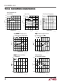
1
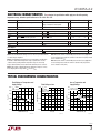
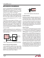
LTC4056-4.2 Linear Li-Ion Charger with Termination in ThinSOT U FEATURES ■ ■ ■ ■ ■ ■ ■ ■ ■ ■ ■ ■ ■ ■ ■ DESCRIPTIO Standalone Li-Ion Charger with Termination Programmable Termination Timer No Sense Resistor or Blocking Diode Required Suitable for USB-Powered Charging Undervoltage Charge Current Limiting Preset Charge Voltage with ±0.6% Accuracy Programmable Charge Current: 200mA to 700mA Automatic Recharge with Shortened Charge Cycle Self-Protection for Overcurrent/Overtemperature 40µA Supply Current in Shutdown Mode Negligible Battery Drain Current in Shutdown Low Battery Charge Conditioning (Trickle Charging) CHRG Status Output including AC Present PCB Total Solution Area only 75mm2 (700mA) Low Profile (1mm) SOT-23 Package U APPLICATIO S ■ ■ ■ ■ ■ Cellular Telephones Handheld Computers Digital Cameras Charging Docks and Cradles Low Cost and Small Size Chargers The LTC®4056 is a low cost, single-cell, constant-current/ constant-voltage Li-Ion battery charger controller with a programmable termination timer. When combined with a few external components, the LTC4056 forms a very small standalone charger for single cell lithium-ion batteries. Charge current and charge time are set externally with a single resistor and capacitor, respectively. The LTC4056 charges to a final float voltage accurate to ±0.6%. Manual shutdown is accomplished by grounding the TIMER/ SHDN pin, while removing input power automatically puts the LTC4056 into a sleep mode. Both the shutdown and sleep modes drain near zero current from the battery; the shutdown mode reduces supply current to 40µA. The output driver is both current limited and thermally protected to prevent operating outside of safe limits. No external blocking diode or sense resistor is required. The LTC4056 also includes low battery charge conditioning (trickle charging), undervoltage charge current limiting, automatic recharge and a charge status output. The LTC4056 is available in a low profile (1mm) 8-lead SOT-23 (ThinSOTTM) package. , LTC and LT are registered trademarks of Linear Technology Corporation. ThinSOT is a trademark of Linear Technology Corporation. U TYPICAL APPLICATIO VIN Undervoltage Charge Current Limiting 800 VCC CHARGE STATUS 700mA DRIVE ZXT1M322 CHRG TIMER/SHDN 1µF 1µF LTC4056 ISENSE + PROG 1.3k BAT GND 1-CELL 4.2V Li-Ion IBAT (mA) VIN 4.5V TO 6.5V VBAT = 4V 700 RPROG = 1.3k ICHG = 700mA INPUT Z = 100mΩ 600 500 UNDERVOLTAGE CHARGE CURRENT LIMITING 400 300 200 100 4056-4.2 TA01 CONSTANT CURRENT UNDERVOLTAGE LOCKOUT AT 4.35V 0 4.40 4.45 4.50 4.55 4.60 4.65 4.70 4.75 VIN (V) 4056 TA02 405642f 1 LTC4056-4.2 U W W W ABSOLUTE AXI U RATI GS U W U PACKAGE/ORDER I FOR ATIO (Note 1) Input Supply Voltage (VCC) ........................– 0.3V to 10V BAT, CHRG ................................................– 0.3V to 10V DRIVE, PROG, TIMER/SHDN ....... – 0.3V to (VCC + 0.3V) Output Current (ISENSE) ...................................... 900mA Short-Circuit Duration (BAT, ISENSE) ............Continuous Junction Temperature ........................................... 125°C Operating Ambient Temperature Range (Note 2) .............................................. – 40°C to 85°C Storage Temperature Range ................. – 65°C to 150°C Lead Temperature (Soldering, 10 sec).................. 300°C ORDER PART NUMBER TOP VIEW VCC 1 ISENSE 2 DRIVE 3 GND 4 8 CHRG TIMER/ 7 SHDN 6 BAT LTC4056ETS8-4.2 5 PROG TS8 PART MARKING TS8 PACKAGE 8-LEAD PLASTIC SOT-23 TJMAX = 125°C, θJA = 120°C/W TO 200°C/W DEPENDING ON PC BOARD LAYOUT LTG5 Consult LTC Marketing for parts specified with wider operating temperature ranges. ELECTRICAL CHARACTERISTICS The ● denotes the specifications which apply over the full operating temperature range, otherwise specifications are at TA = 25°C. VCC = 5V. SYMBOL PARAMETER CONDITIONS MIN TYP MAX UNITS 6.5 V 400 600 µA VCC Supply VCC Input Supply Voltage (Note 3) ICC Quiescent VCC Supply Current ● VBAT = 4.5V (Forces IDRIVE = 0) IPROG = 200µA (RPROG = 5k) 4.5 ● ISHDN VCC Supply Current in Manual Shutdown VTIMER/SHDN = 0V 40 60 µA IBMS Battery Drain Current in Manual Shutdown (Note 4) VTIMER/SHDN = 0V ● –1 0 1 µA IBSL Battery Drain Current in Sleep Mode (Note 5) VCC = 0V ● –1 0 1 µA VUVLOI Undervoltage Rising Threshold VCC Increasing ● 4.325 4.40 4.475 V VUVLOD Undervoltage Falling Threshold VCC Decreasing ● 4.275 4.35 4.425 VUVHYS Undervoltage Hysteresis VUVLOI-VUVLOD VUVCL Undervoltage Charge Current Limit Threshold 50 4.575 VUVCL-VUVLOI UV Charge Current to UVLO Threshold Margin V mV V ● 90 170 250 ● 4.175 4.158 4.200 4.200 4.225 4.242 mV Charging Performance VFLOAT IBAT Output Float Voltage in Constant Voltage Mode IBAT = 10mA IBAT = 10mA, 4.75V ≤ VCC ≤ 6.5V Output Full-Scale Current in Constant Current Mode RPROG = 5k, 4.75V ≤ VCC ≤ 6.5V, PNP Beta > 50, 0°C ≤ TA ≤ 85°C 137 183 228 mA RPROG = 1.43k, 4.75V ≤ VCC ≤ 6.5V, PNP Beta > 50, 0°C ≤ TA ≤ 85°C 590 640 690 mA IDSINK Drive Output Current VDRIVE = 3V ITRIKL Trickle Charge Current VBAT = 2V, RPROG = 5k VBAT = 2V, RPROG = 1.43k VTRIKL Trickle Charge Threshold Voltage VBAT Falling ∆VTRIKL Trickle Charge Hysteresis Voltage VPROG1 PROG Pin Voltage RPROG = 5k (IPROG = 200µA) VPROG2 PROG Pin Voltage RPROG = 1.43k (IPROG = 700µA) ● 30 V V mA 5 12 7 20 10 28 2.73 2.80 2.87 45 70 95 ● 0.98 1 1.02 V ● 0.98 1 1.02 V ● mA mA V mV 405642f 2 LTC4056-4.2 ELECTRICAL CHARACTERISTICS The ● denotes the specifications which apply over the full operating temperature range, otherwise specifications are at TA = 25°C. VCC = 5V. SYMBOL PARAMETER CONDITIONS MIN TYP MAX UNITS ∆VRECHRG Recharge Threshold Voltage VFLOAT – VRECHRG, VBAT > VTRIKL, Charge Termination Timer Expired 100 150 200 mV TTIMER TIMER/SHDN Accuracy CTIMER = 1µF RPROG = 1.43k ● 10 12 % ● 0.6 0.82 1 V Charger Manual Control VMSDT Manual Shutdown Threshold Voltage VTIMER/SHDN Increasing VMSHYS Manual Shutdown Hysteresis Voltage VTIMER/SHDN Decreasing 50 75 125 mV ISHDN TIMER/SHDN Pin Pull-up Current VTIMER/SHDN = 0V – 10 –7 –4 µA IDSHRT Drive Output Short-Circuit Current Limit VDRIVE = VCC 30 65 130 mA IPSHRT PROG Pin Short-Circuit Current Limit VPROG = 0V ICHRG CHRG Pin Weak Pull-Down Current VCHRG = 1V, VTIMER/SHDN = 0V VCHRG CHRG Output Low Voltage ICHRG = 10mA Protection ● 1.4 mA Status Output Note 1: Absolute Maximum Ratings are those values beyond which the life of a device may be impaired. Note 2: The LTC4056E is guaranteed to meet performance specifications from 0°C to 70°C ambient temperature range. Specifications over the – 40°C to 85°C operating ambient temperature range are assured by design, characterization and correlation with statistical process controls. Note 3: Although the LTC4056 will operate with input voltages as low as 4.5V, charging will not begin until VCC exceeds VUVCL. 6 ● 12 18 µA 0.2 0.4 V Note 4: Assumes that the external PNP pass transistor has negligible B-C reverse-leakage current when the collector is biased at 4.2V (VBAT) and the base is biased at 5V (VCC). Note 5: Assumes that the external PNP pass transistor has negligible B-E reverse-leakage current when the emitter is biased at 0V (VCC) and the base is biased at 4.2V (VBAT). U W TYPICAL PERFOR A CE CHARACTERISTICS Float Voltage vs Temperature and Supply Voltage 4.202 IBAT = 10mA PNP = FZT749 FLOAT VOLTAGE (V) 4.210 VFLOAT (V) 4.205 4.200 4.195 VCC = 4.75V 220 VCC = 5V TA = 25°C PNP = FZT749 4.201 RPROG = 1.30k VCC = 6.5V RPROG = 4.53k 215 PNP = FZT749 210 IBAT (mA) 4.215 IBAT vs Temperature and Supply Voltage Float Voltage vs IBAT 4.200 VCC = 6.5V 200 VCC = 4.75V 195 4.199 190 4.190 4.185 –50 –25 205 185 4.198 50 25 75 0 TEMPERATURE (°C) 100 125 4056-4.2 G01 0 100 200 300 400 IBAT (mA) 500 600 700 4056-4.2 G02 180 – 50 – 25 75 50 25 TEMPERATURE (°C) 0 100 125 4056-4.2 G03 405642f 3 LTC4056-4.2 U W TYPICAL PERFOR A CE CHARACTERISTICS IBAT vs Temperature and Supply Voltage RPROG = 1.30k PNP = FZT749 VCC = 6.5V IBAT (mA) VCC = 4.75V 700 BAT PIN MUST BE DISCONNECTED AND SET BETWEEN 2.9V AND 4.2V TO FORCE CC MODE IN THIS AREA 400 200 VCC = 5V RPROG = 1.43k 3 500 300 690 4 RPROG 1.30k 600 710 IBAT (mA) 5 VCC = 5V 700 TA = 25°C PNP = FZT749 720 RPROG 4.53k 2 1 0 –1 –2 –3 680 670 –50 Timer Error vs Temperature IBAT vs VBAT 800 TIMER ERROR (%) 730 100 –25 0 25 50 TEMPERATURE (°C) 75 100 0 –4 1 0 2 4 3 VBAT (V) 4056-4.2 G04 50 25 0 75 TEMPERATURE (°C) 4056-4.2 G05 TIMER/SHDN Pin Pull-Up Current vs Temperature and Supply Voltage 12 –5 –50 –25 5 100 125 4056-4.2 G06 CHRG Pin Weak Pull-Down Current vs Temperature and VCHRG 20 VTIMER/SHDN = 0V VTIMER/SHDN = 0V VCC = 5V 10 15 ICHRG (µA) ISHDN (µA) 8 VCC = 6.5V 6 VCC = 4.75V VCHRG = 6.5V VCHRG = 1V 10 4 2 0 –50 –25 50 25 75 0 TEMPERATURE (°C) 100 5 –50 125 –25 0 25 50 75 TEMPERATURE (°C) 125 4056-4.2 G08 4056-4.2 G07 CHRG Pin Output Low Voltage vs Temperature 0.40 100 PROG Pin Voltage vs Temperature and RPROG 1.0050 VBAT = 0V ICHRG = 10mA VCC = 5V 0.35 VCC = 5V 1.0025 VPROG (V) VCHRG (V) RPROG = 4.53k 0.30 1.0000 0.25 0.20 –50 RPROG = 1.30k 0.9975 –25 0 25 50 TEMPERATURE (°C) 75 100 4056-4.2 G09 0.9950 –50 –25 75 0 25 50 TEMPERATURE (°C) 100 125 4056-4.2 G10 405642f 4 LTC4056-4.2 U U U PI FU CTIO S VCC (Pin 1): Positive Input Supply Voltage. This pin supplies power to the internal control circuitry and external PNP transistor through the internal current sense resistor. This pin should be bypassed to ground with a capacitor in the range of 1µF to 10µF. ISENSE (Pin 2): Sense Node for Charge Current. Current from VCC passes through the internal current sense resistor and out of the ISENSE pin to supply current to the emitter of the external PNP transistor. The collector of the PNP provides charge current to the battery. DRIVE (Pin 3): Base Drive Output for the External PNP Pass Transistor. Provides a controlled sink current to drive the base of the PNP. This pin has current limiting protection. GND (Pin 4): Ground. Provides a reference for the internal voltage regulator and a return for all internal circuits. When in the constant voltage mode, the LTC4056 will precisely regulate the voltage between the BAT and GND pins. The battery ground should connect close to the GND pin to avoid voltage drop errors. PROG (Pin 5): Charge Current Programming Pin. Provides a virtual reference voltage of 1V for an external resistor (RPROG) connected between this pin and ground to program the battery charge current. In constant current mode the typical charge current is 915 times the current through this resistor (ICHG = 915V/RPROG). Current is limited to approximately 1.4mA (ICHG of approximately 1.4A). BAT (Pin 6): Battery Voltage Sense Input. A precision internal resistor divider sets the final float voltage on this pin. This divider is disconnected in the manual shutdown or sleep mode. No bypass capacitance is needed on this pin for stable operation when a battery is present. However, any low ESR capacitor exceeding 22µF on this pin should be decoupled with 0.2Ω to 1Ω resistor. Without a battery, a minimum bypass capacitance of 4.7µF with 0.5Ω series resistance is required. TIMER/SHDN (Pin 7): Programmable Charge Termination Timer and Shutdown Input. Pulling this pin below the shutdown threshold voltage will shut down the charger reducing the supply current to approximately 40µA and the battery drain current to near 0µA. A capacitor on this pin programs the charge termination timer. CHRG (Pin 8): Open-Drain Charge Status Output. When the battery is being charged, the CHRG pin is pulled low by an internal N-channel MOSFET. When the timer has timed out (terminating the charge cycle) or when the LTC4056 is in shutdown, but power is applied to the IC (i.e., VCC > VUVLOI), a 12µA current source is connected from the CHRG pin to ground. The CHRG pin is forced to a high impedance state when input power is not present (i.e., VCC < VUVLOD). 405642f 5 LTC4056-4.2 W BLOCK DIAGRA VCC 1 LTC4056-4.2 CHRG 8 100Ω 110mΩ UVLO 2 – 12µA + CA CHRG UV LOGIC SHDN ISENSE TEMPERATURE AND CURRENT LIMIT SHDN 20µA SHDN DRIVE OUTPUT DRIVER 3 ITRIKL 20 • IPROG COUNTER 7µA TIMER/SHDN BAT OSCILLATOR 7 1.2V VOLTAGE REFERENCE 6 C1 REF 1V + – + + IA + – 1.2V VA – IPROG SHDN 5 4 4056-4.2 BD PROG RPROG GND 405642f 6 LTC4056-4.2 U OPERATIO The LTC4056 is a linear battery charger controller with a programmable charge termination timer. Operation can be understood by referring to the Block Diagram. A charge cycle begins when VCC rises above the UVLO (undervoltage lockout) threshold VUVLOI (nominally 4.4V), an external current programming resistor is connected between the PROG pin and ground and the TIMER/SHDN pin is allowed to rise above the shutdown threshold VMSDT (nominally 0.82V). If the battery voltage is below VTRIKL (2.8V) at the beginning of the charge cycle, the charger goes into trickle charge mode to bring the cell voltage up to a safe level for charging at full current. In this mode, an internal current source provides approximately 2% of the programmed charge current to the BAT pin. The charger goes into the full charge constant current mode once the voltage on the BAT pin rises above VTRIKL + ∆VTRIKL (2.9V). During full current charging, the collector of the external PNP provides the charge current. The PNP emitter current flows through the ISENSE pin and through the internal 110mΩ current sense resistor. This current is close in magnitude, but slightly more than the collector current since it includes base current. Amplifier A1 forces 1V on the PROG pin. Therefore, a current equal to 1V/RPROG will flow through the internal 100Ω resistor. Amplifier CA will force the same voltage that appears across the 100Ω resistor to appear across the internal 110mΩ resistor. This amplifier ensures that the current flowing out of the ISENSE pin is equal to 915 times the current flowing out of the PROG pin. Therefore, neglecting base current, the charge current will be 915V/RPROG. This region of operation is referred to as constant current mode. As the battery accepts charge, its voltage rises. When it reaches the preset float voltage of 4.2V, a precisely divided down version of this voltage (1.2V) is compared to the 1.2V internal reference voltage by amplifier VA. If the battery voltage attempts to exceed 4.2V (1.2V at the input of amplifier VA), the amplifier will divert current away from the output driver thus limiting charge current to maintain 4.2V on the battery. This is the constant voltage mode. An external capacitor on the TIMER/SHDN pin and the resistance between the PROG pin and ground set the total charge time. When this time elapses, the charge cycle terminates and the CHRG pin transitions from a strong pull-down to a weak 12µA pull-down. To restart the charge cycle, simply remove the input voltage and reapply it or momentarily force the TIMER/SHDN pin to ground. The charge cycle will also restart if the BAT pin voltage falls below the recharge threshold (VRECHRG is nominally 4.05V). When VCC is applied, pulling the TIMER/SHDN pin to ground will manually shut down the charger and reset the timer. When this pin is released an internal 7µA current source pulls the TIMER/SHDN pin above the 0.82V shutdown threshold to resume charging. Fault conditions such as overheating of the die or excessive DRIVE pin or PROG pin current are monitored and limited. When input power is removed or manual shutdown is entered, the charger will drain only tiny leakage currents (<1µA) from the battery, thus maximizing battery standby time. With VCC removed the external PNP base is connected to the battery by the charger. In manual shutdown the base is connected to VCC by the charger. 405642f 7 LTC4056-4.2 U W U U APPLICATIO S I FOR ATIO Undervoltage Lockout An internal undervoltage lockout (UVLO) circuit monitors the input voltage and keeps the charger in shutdown mode until VCC rises above the UVLO threshold (VUVLOI is typically 4.4V). Approximately 50mV of hysteresis is built in to prevent oscillation around the threshold level. In undervoltage lockout, battery drain current is very low (<1µA) and supply current is approximately 40µA. Undervoltage Charge Current Limiting The LTC4056 includes undervoltage charge current limiting that prevents full charge current until the input supply voltage reaches a threshold value (VUVCL). This feature is particularly useful if the LTC4056 is powered from a supply with long leads (or any relatively high output impedance). For example, USB powered systems tend to have highly variable source impedances (due primarily to cable quality and length). A transient load combined with such an impedance can easily trip the UVLO threshold and turn the charger off unless undervoltage charge current limiting is implemented. Consider a situation where the LTC4056 is operating under normal conditions and the input supply voltage begins to sag (e.g. an external load drags the input supply down). If the input voltage reaches VUVCL (approximately 170mV above the rising undervoltage lockout threshold, VUVLOI), undervoltage charge current limiting will begin to reduce the charge current in an attempt to maintain VUVCL at the VCC input of the IC. The LTC4056 will continue to operate at the reduced charge current until the input supply voltage is increased or voltage mode reduces the charge current further. Trickle Charge and Defective Battery Detection At the beginning of a charge cycle, if the battery voltage is low (below VTRIKL of about 2.8V) the charger goes into trickle charge mode reducing the charge current to approximately 2% of the full-scale current. If the low battery voltage persists for one quarter of the total charge time, the battery is assumed to be defective, the charge cycle is terminated and the CHRG pin output transitions from a strong pull-down to a 12µA pull-down. To restart the charge cycle, remove the input voltage and reapply it or momentarily force the TIMER/SHDN pin to ground. Programming Charge Current When in constant current mode, the full-scale charge current is programmed using a single external resistor between the PROG pin and ground, RPROG. The current delivered to the ISENSE pin (flowing from VCC through the internal 110mΩ sense resistor) will be 915 times the current in RPROG. Because the LTC4056 provides a virtual 1V source at the PROG pin, the charge current is given by: 1V ICHG = (IPROG ) • 915 = • 915 or RPROG 1V RPROG = • 915 ICHG Under trickle charge conditions, this current is reduced to approximately 2% of the full-scale value. The actual battery charge current (IBAT) is slightly lower than the expected charge current because the charger forces the emitter current and the battery charge current will be reduced by the base current. In terms of β (IC/IB), IBAT can be calculated as follows: β 915V β IBAT A = 915 • IPROG • = β + 1 RPROG β + 1 () If β = 50, then IBAT is 2% low. If desired, reducing RPROG by 2% can compensate for the 2% drop. For example, if 700mA charge current is required, calculate: 1V RPROG = • 915 = 1.3k 700mA If a low β needs to be compensated for, say β = 50, calculate: RPROG = 915V 50 • = 1.27k 700mA 50 + 1 For best stability over temperature and time, 1% metalfilm resistors are recommended. 405642f 8 LTC4056-4.2 U W U U APPLICATIO S I FOR ATIO Termination Timer The programmable timer is used to terminate the charge cycle. The timer duration is programmed by an external capacitor at the TIMER/SHDN pin and the external PROG resistor. The total charge time is: the TIMER/SHDN pin is released. Given the low magnitude of this current, it is a simple matter for an external opendrain (or open-collector) output to pull the TIMER/SHDN pin to ground for shutdown and release the pin for normal operation. Time(Hours) = 1.935 • RPROG(k) • CTIMER(µF) or Sleep Mode CTIMER(µF) = Time(Hours)/1.935 • RPROG(k) When the input supply is disconnected, the IC enters the sleep mode. In this mode, the battery drain current (IBSL) is a negligible leakage current, allowing the battery to remain connected to the charger for an extended period of time without discharging the battery. The leakage current is due to the reverse-biased B-E junction of the external PNP transistor. Furthermore, the CHRG pin assumes a high impedance state. For example, to program a three hour timer with a 600mA charge current (i.e., RPROG = 1.54k), calculate: CTIMER = 3 = 1µF 1.935 • 1.54 The timer starts when an input voltage greater than the undervoltage lockout threshold level is applied, a program resistor is connected to ground and the TIMER/SHDN pin is allowed to rise above the shutdown threshold. After a time-out occurs, the charge current stops and the CHRG output transitions from a strong pull-down to a 12µA pulldown to indicate charging has stopped. As long as the input supply remains above VUVLOD and the battery voltage remains above VRECHRG the charger will remain in this standby mode. If the battery voltage remains below VTRIKL for 25% of the programmed time, the charger will enter standby mode. Furthermore, if the battery voltage is above the recharge threshold (VRECHRG is typically 4.05V) at the beginning of a charge cycle or if a falling battery voltage triggers a recharge cycle (following a previous time-out), the charge cycle will be shortened to 50% of the programmed time. This feature reduces the charge time for batteries that are near full capacity. Connecting the TIMER/SHDN pin to VCC disables the timer function. Manual Shutdown Pulling the TIMER/SHDN pin below VMSDT – VMSHYS (typically 0.745V) will put the charger into shutdown mode and reset the timer. In this mode, the LTC4056 consumes 40µA of supply current and drains a negligible leakage current from the battery (IBMS). A 7µA current source pulls up on the TIMER/SHDN pin while in shutdown to ensure that the IC will start up once CHRG Status Output Pin When the charge cycle starts, the CHRG pin is pulled to ground by an internal N-channel MOSFET capable of driving an LED. When the charge cycle ends, the strong pull-down transitions to a 12µA pull-down on the CHRG pin as long as the input supply remains above the UVLO threshold (VUVLOD) and the battery voltage remains above VRECHRG. If the input supply falls below VUVLOD, the CHRG pin assumes a high impedance state. Figure 1 shows a flow diagram for a typical charge cycle. This diagram indicates the status of the CHRG pin in each charger state. A microprocessor can be used to distinguish the three states of the CHRG pin (see Figure 2). To detect whether the LTC4056 is in trickle charge, charge, or short charge mode (i.e., strong pull-down), force the digital output pin (OUT) high and measure the voltage at the CHRG pin. The internal N-channel MOSFET will pull the pin voltage low even with the 2k pull-up resistor. Once the charge cycle terminates, the strong pull-down transitions to a 12µA pull-down. The IN pin will then be pulled high by the 2k pull-up resistor. To determine whether sufficient input voltage is present for charging (i.e., high impedance), the OUT pin should be forced to a high impedance state. If VCC␣ >␣ VUVLOI then the 12µA CHRG pull-down will pull the IN pin low through the 800k resistor; otherwise, the 800k resistor will pull the IN pin high, indicating that VCC␣ <␣ VUVLOD. 405642f 9 LTC4056-4.2 U U W U APPLICATIO S I FOR ATIO POWER ON BAT < 2.8V TIMER/SHDN RELEASED OR VCC > VUVLOI TRICKLE CHARGE MODE 2% FULL CURRENT CHRG: STRONG PULLDOWN 25% PROGRAMMED TIME ELAPSES BAT > 4.05V BAT > 2.9V SHUTDOWN MODE ICC DROPS TO < 40µA CHRG: Hi-Z if VCC < VUVLOD WEAK PULLDOWN OTHERWISE CHARGE MODE FULL CURRENT CHRG: STRONG PULLDOWN TIMER/SHDN GROUNDED OR VCC < VUVLOD 2.8V < BAT < 4.05V PROGRAMMED TIME ELAPSES STANDBY MODE NO CHARGE CURRENT CHRG: WEAK PULLDOWN 2.8V < BAT < 4.05V 50% PROGRAMMED TIME ELAPSES RECHARGE/SHORT CHARGE MODE CHRG: STRONG PULLDOWN 4056-4.2 F01 Figure 1. State Diagram for a Typical Charge Cycle V+ V DD External PNP Transistor 1 VCC 800k µPROCESSOR LTC4056 CHRG 8 2k OUT IN 4056-4.2 F02 Figure 2. Using a Microprocessor to Determine CHRG State Recharge If the battery voltage drops below VRECHRG (typically 4.05V) after a charge cycle has terminated, a new charge cycle will begin. The recharge circuit integrates the BAT pin voltage for approximately a millisecond to prevent a transient from restarting the charge cycle. During a recharge cycle the timer will terminate the charge cycle after one-half of the programmed time has elapsed. If the battery voltage remains below VTRIKL (typically 2.8V) during trickle charge for one-fourth of the programmed time, the battery may be defective and the charge cycle will end. In addition, the recharge comparator is disabled and a new charge cycle will not begin unless the input voltage is toggled off then on, or the TIMER/SHDN pin is momentarily pulled to ground. The external PNP pass transistor must have adequate beta, low saturation voltage and sufficient power dissipation capability (including any heat sinking, if required). To provide 700mA of charge current with the minimum available base drive of approximately 30mA requires a PNP beta greater than 23. If lower beta PNP transistors are used, more base current is required from the LTC4056. This can result in the output drive current limit being reached, or thermal shutdown due to excessive power dissipation. With low supply voltages, the PNP saturation voltage (VCESAT) becomes important. The VCESAT must be less than the minimum supply voltage minus the maximum voltage drop across the internal sense resistor and bond wires (0.20Ω) and battery float voltage. If the PNP transistor cannot achieve the low saturation voltage required, base current will dramatically increase. This is to be avoided for a number of reasons: output drive may reach current limit resulting in the charger characteristics to go out of specifications, excessive power dissipation may force the IC into thermal shutdown, or the battery could become discharged because some of the current from the 405642f 10 LTC4056-4.2 U W U U APPLICATIO S I FOR ATIO DRIVE pin could be pulled from the battery through the forward biased collector base junction. For example, to program a charge current of 500mA with a minimum supply voltage of 4.75V, the minimum operating VCE is: VCE(MIN)(V) = 4.75 – (0.5) • (0.2) – 4.2 = 0.45V Another important factor to consider when choosing the PNP pass transistor is the power handling capability. The transistor data sheet will usually give the maximum rated power dissipation at a given ambient temperature with a power derating for elevated temperature operation. The maximum power dissipation of the PNP when charging is: PD(MAX)(W) = IBAT • (VCC(MAX) – VBAT(MIN)) VCC(MAX) is the maximum supply voltage and VBAT(MIN) is the minimum battery voltage when discharged. Once the maximum power dissipation and VCE(MIN) are known, Table 1 can be used as a guide in selecting some PNPs to consider. In the table, very low VCESAT is less than 0.25V, low VCESAT is 0.25V to 0.5V and the others are 0.5V to 0.8V all depending on the current. See the manufacturer data sheet for details. All of the transistors are rated to carry at least 1A continuously as long as the power dissipation is within limits. In addition, the maximum supply voltage, minimum battery voltage and chosen charge current should be checked against the manufacturer’s data sheet to ensure that the PNP transistor is operating within its safe operating area. The Stability section addresses caution in the use of very high beta PNP transistors. Should overheating of the PNP transistor be a concern, protection can be achieved with a positive temperature coefficient (PTC) thermistor wired in series with the current programming resistor and thermally coupled to the transistor. The PTH9C chip series from Murata has a steep resistance increase at temperature thresholds from 85°C to 145°C making it behave somewhat like a thermostat switch. For example, the model PTH9C16TBA471Q thermistor is 470Ω at 25°C but abruptly increases its resistance to 4.7k at 125°C. Below 125°C, the device exhibits a small negative TC. The 470Ω thermistor can be added in series with a 976Ω resistor to form the current programming resistor for a 640mA charger. Should the thermistor reach 125°C, the charge current will drop to 160mA and inhibit any further increase in temperature. Stability The LTC4056 contains two control loops: constant voltage and constant current. The constant voltage loop is stable without any compensation when a battery is connected with low impedance leads. Excessive lead length, Table 1. PNP Pass Transistor Selection Guide MAXIMUM PD(W) MOUNTED ON BOARD PACKAGE STYLE ZETEX PART NUMBER AT TA = 25°C 3 ROHM PART NUMBER COMMENTS 2 x 2MLP ZXT1M322 Very Low VCESAT 0.5 SOT-23 FMMT549 Low VCESAT 0.625 SOT-23 FMMT720 Very Low VCESAT, High Beta 1 1.1 1 to 2 SOT-89 FCX589 or BCX69 SOT-23-6 ZXT13P12DE6 SOT-89 FCX717 Very Low VCESAT, High Beta Low VCESAT 2 SOT-223 FZT589 2 SOT-223 BCP69 or FZT549 0.75 Very Low VCESAT, High Beta, Small FTR 2SB822 Low VCESAT 1 ATV 2SB1443 Low VCESAT 2 SOT-89 2SA1797 Low VCESAT 10 (TC = 25°C) TO-252 2SB1182 Low VCESAT, High Beta 405642f 11 LTC4056-4.2 U U W U APPLICATIO S I FOR ATIO however, may add enough series inductance to require a bypass capacitor of at least 1µF from BAT to ground. Furthermore, a 4.7µF capacitor with a 0.2Ω to 1Ω series resistor from BAT to ground is required to keep ripple voltage low when the battery is disconnected. High value capacitors with very low ESRs (especially ceramic) reduce the constant voltage loop phase margin, possibly resulting in instability. Ceramic capacitors up to 22µF may be used in parallel with a battery, but larger ceramics should be decoupled with 0.2Ω to 1Ω of series resistance. In the constant current mode, the PROG pin is in the feedback loop, not the battery. Because of the additional pole created by PROG pin capacitance, any additional capacitance on this pin must be limited. Although higher charge current applications (i.e., lower program resistance) can tolerate more PROG capacitance, a good rule of thumb is to keep the capacitive loading on the PROG pin to less than 660pF. If additional capacitance on this pin is required (e.g., to provide an accurate, filtered low current 1V reference to external circuitry) a 1k to 10k decoupling resistor may be needed (see Figure 3). LTC4056 PROG GND ACCURATE, FILTERED 1V REFERENCE 10k 6 RPROG CFILTER 4 4056-4.2 F03 Figure 3. Isolating Capacitive Load on PROG Pin and Filtering Reverse Polarity Input Voltage Protection In some applications, protection from reverse polarity voltage on VCC is desired. If the supply voltage is high enough, a series blocking diode can be used. In other cases, where the voltage drop must be kept low, a P-channel MOSFET can be used (as shown in Figure 4). * LTC4056 VIN VCC 4056-4.2 F04 *DRAIN-BULK DIODE OF FET Figure 4. Low Loss Input Reverse Polarity Protection VCC Bypass Capacitor Many types of capacitors with values ranging from 1µF to 10µF located close to the LTC4056 will provide adequate input bypassing. However, caution must be exercised when using multilayer ceramic capacitors. Because of the self-resonant and high Q characteristics of some types of ceramic capacitors, high voltage transients can be generated under some start-up conditions, such as connecting the charger input to a hot power source. For more information refer to Application Note 88. Internal Protection Internal protection is provided to prevent excessive PROG pin currents (IPSHRT), excessive DRIVE pin currents (IDSHRT) and excessive self-heating of the LTC4056 during a fault condition. The faults can be generated from a shorted PROG pin, a shorted DRIVE pin or from excessive DRIVE pin current to the base of the external PNP transistor when it is in deep saturation from a very low VCE. This protection is not designed to prevent overheating of the external pass transistor. However, thermal coupling between the external PNP and the LTC4056 will allow the internal thermal limit to deprive the PNP of base current when the junction temperature of the IC rises above about 135°C. The temperature of the PNP at that point, however, will be well in excess of 135°C. The exact temperature of the PNP depends on the thermal coupling between the LTC4056 and the PNP and on the θJA of the transistor. See the section titled “External PNP Transistor” for information on protecting the transistor from overheating. 405642f 12 LTC4056-4.2 U TYPICAL APPLICATIO S USB Charging the input voltage does not drop below the undervoltage lockout threshold. The applications shown in Figures 5 and 6 are USB Li-Ion chargers with automatic PowerPathTM control. In order to comply with USB power specifications a Li-Ion battery charger must be able to limit the current draw from the USB power port to 500mA, operate at input voltages as low as 4.75V (ignoring resistive drops in the cable and connectors which further reduce this value to 4.4V), and have a low current standby mode. The TIMER/SHDN pin can be used to put the LTC4056 into a low current standby mode. By pulling TIMER/SHDN to GND, the LTC4056 and LTC4412 will draw about 50µA to 60µA combined from the USB power port. The LTC4056 actually regulates the current delivered to the ISENSE pin (rather than the BAT pin current). This fact allows the 500mA maximum USB power port consumption to be easily enforced by tying all system loads to the ISENSE pin and programming the charger to supply just under 500mA (Figures 5 and 6 are programmed for 490mA). The total impedance between the VCC pin and ISENSE pin is typically 0.2Ω, so the maximum drop is just 100mV (at 500mA). As described in Undervoltage Charge Current Limiting, the LTC4056 will automatically reduce charge current if the input supply voltage reaches VUVCL (typically 4.575V). This feature ideally solves the additional 350mV of resistive drop that the USB power specification requires. If an LTC4056 is connected to a particularly resistive USB cable, then charge current will be reduced to ensure that PowerPath is a trademark of Linear Technology Corporation. USB POWER R1 750Ω RED LTC4056 1 CHRG VCC 7 2 TIMER/SHDN ISENSE 6 3 BAT DRIVE 5 4 PROG GND 8 ON 0FF M1 2N7002 R2 1.87k M2B 1/2 IRF7329 Q1 ZXT1M322 SYSTEM LOAD C3 1µF C4 4.7µF R5 0.5Ω C1 1µF M2A 1/2 IRF7329 BAT + VIN SENSE LTC4412 GND GATE C2 0.1µF CTL Li-Ion R3 470k STAT 4056-4.2 F05 Figure 5. USB Charging and Automatic PowerPath Control with Auxiliary P-Channel MOSFET for Lowest Loss USB POWER R1 750Ω RED LTC4056 1 CHRG VCC 7 2 TIMER/SHDN ISENSE 6 3 BAT DRIVE 5 4 PROG GND 8 ON 0FF M1 2N7002 R2 1.87k C1 1µF C4 4.7µF R5 0.5Ω MBRS130LT3 Q1 ZXT1M322 M2 Si2315BDS BAT C3 1µF + C2 0.1µF Li-Ion VIN SENSE LTC4412 GND GATE CTL SYSTEM LOAD R4 750Ω R3 470k GREEN STAT M3 Si1301DL 4056-4.2 F06 Figure 6. USB Charging and Automatic PowerPath Control with LTC4412 in Comparator Mode 405642f 13 LTC4056-4.2 U TYPICAL APPLICATIO S It is important to keep in mind that the LTC4056 can only control charge current. If the system load is less than 500mA, then the LTC4056 can simply reduce the charge current by an amount equal to the system load current and the USB specification can be met. For instance, if the system load is 150mA, then the charge current will be reduced from 490mA to 340mA and the total USB input current will remain at 490mA, thereby meeting the specification. However, if the system load is increased beyond 500mA the LTC4056 will reduce the charge current to zero, and all of the system load will be provided by the USB input. This scenario will violate the USB power specification. In order to avoid this situation, it is important to ensure that the system load never exceeds 500mA. The LTC4412 provides automatic switchover of the system load between a battery and the USB input supply. This feature reduces the current drain on the battery to just a few microamps when a USB input is present. Figure 5 shows a dual FET solution to minimize voltage drop between the USB input voltage and the system load and Figure 6 uses a Schottky diode to simplify the design. Please refer to the LTC4412 data sheet for more information on the operation of the Ideal Diode Controller. In both designs all USB input current passes through the sense resistor of the LTC4056 to ensure that the maximum current drawn from the USB input supply is limited to less than 500mA (assuming the system load is less than 500mA). In Figure 6, P-channel MOSFET, M3, provides drive for the green LED that illuminates when the USB input supply is present. In both designs, the CHRG pin of the LTC4056 drives the red LED to indicate charging. Keep in mind that the Li-Ion battery will charge at a reduced rate if a significant system load is present. This is due to the fact that the 490mA charge current is split between the battery and the system load. Optional N-channel MOSFET, M1, can be used to shut down the LTC4056 thereby reducing its input supply current to about 40µA. This will automatically turn off the red LED. However, since voltage will still be present on the USB input (and therefore the ISENSE pin), Figure 6 will continue to draw power through the green LED. The green LED should not be used without additional control logic if a low current standby mode is required. NiCd or NiMH Charging The application circuit in Figure 7 shows how to use an LTC4056 to charge Nickel chemistry batteries with user termination. NiCd or NiMH batteries require constant current charging regardless of the battery voltage. To disable the voltage mode of the LTC4056 it is necessary to connect the BAT pin to a voltage between the trickle charge threshold and the final float voltage. Assuming a reasonably well controlled input voltage, this can be accomplished with a simple resistor divider connected between the input supply and the BAT pin. In Figure␣ 7, resistors R3 and R4 keep the BAT pin voltage between the required voltage levels provided the input voltage is between 4.5V and 6.1V (encompassing nearly the entire specified operating input supply range of 4.5V to 6.5V). The LTC4056 has an internal impedance of approximately 2MΩ to GND on the BAT pin, so it is important to keep the impedance of the resistor divider considerably below that value. Furthermore, a 0.1µF bypass capacitor may be required between the BAT pin and GND. If the input voltage rises above 6.1V then it is possible that the battery charge current will decrease due to the voltage mode amplifier of the LTC4056. The TIMER/SHDN manual shutdown threshold of the LTC4056 is typically 0.82V, allowing the I/O port of a microcontroller to drive this pin with standard logic levels to manually control termination. Holding the TIMER/SHDN pin high simultaneously enables the charger and disables the internal timer function. A programmed constant current will be provided to the battery until the I/O port pulls the TIMER/SHDN pin to GND. VIN 4.5V TO 6.1V R1 750Ω RED R3 31.6k 8 7 I/O µCONTROL TERM CHRG 6 5 R4 68.1k R2 1.3k LTC4056 CHRG VCC TIMER/SHDN ISENSE BAT PROG DRIVE GND 1 2 3 Q1 ZXT1M322 4 C3 1µF NiCd 4056-4.2 F07 Figure 7. Nickel Chemistry Battery Charging 405642f 14 LTC4056-4.2 U PACKAGE DESCRIPTIO TS8 Package 8-Lead Plastic TSOT-23 (Reference LTC DWG # 05-08-1637) 0.52 MAX 2.90 BSC (NOTE 4) 0.65 REF 1.22 REF 1.4 MIN 3.85 MAX 2.62 REF 2.80 BSC 1.50 – 1.75 (NOTE 4) PIN ONE ID RECOMMENDED SOLDER PAD LAYOUT PER IPC CALCULATOR 0.22 – 0.36 8 PLCS (NOTE 3) 0.65 BSC 0.80 – 0.90 0.20 BSC 0.01 – 0.10 1.00 MAX DATUM ‘A’ 0.30 – 0.50 REF 0.09 – 0.20 (NOTE 3) 1.95 BSC TS8 TSOT-23 0802 NOTE: 1. DIMENSIONS ARE IN MILLIMETERS 2. DRAWING NOT TO SCALE 3. DIMENSIONS ARE INCLUSIVE OF PLATING 4. DIMENSIONS ARE EXCLUSIVE OF MOLD FLASH AND METAL BURR 5. MOLD FLASH SHALL NOT EXCEED 0.254mm 6. JEDEC PACKAGE REFERENCE IS MO-193 405642f Information furnished by Linear Technology Corporation is believed to be accurate and reliable. However, no responsibility is assumed for its use. Linear Technology Corporation makes no representation that the interconnection of its circuits as described herein will not infringe on existing patent rights. 15 LTC4056-4.2 RELATED PARTS PART NUMBER DESCRIPTION COMMENTS LTC1732 Lithium-Ion Linear Battery Charger Controller Simple Charger uses External FET, Features Preset Voltages, C/10 Charger Detection and Programmable Timer, Input Power Good Indication LTC1733 Monolithic Lithium-Ion Linear Battery Charger Standalone charger with Programmable Timer, Up to 1.5A Charge Current, Thermal Regulation Prevents Overheating LTC1734 Lithium-Ion Linear Battery Charger in ThinSOT 200mA to 700mA, Simple ThinSOT Charger, No Blocking Diode, No Sense Resistor Needed LTC1734L Lithium-Ion Linear Battery Charger Controller 50mA to 180mA, No Blocking Diode, No Sense Resistor Needed LTC4002 Switch Mode Li-Ion Charger 4.7V ≤ VIN ≤ 24V, Up to 3A, 3Hr Timer, SO-8, DFN LTC4050 Lithium-Ion Linear Battery Charger Controller Simple Charger uses External FET, Thermistor Input for Battery Temperature Sensing LTC4052 Lithium-Ion Linear Battery Pulse Charger Fully Integrated, Standalone Pulse Charger, Minimal Heat Dissipation, Over Current Protection LTC4053 USB Compatible Lithium-Ion Battery Linear Monolithic Charger Fully Integrated, Standalone Charger, 10-Lead MSOP, Thermal Regulation Prevents Overheating when Powered from Wall Adapter and ≥1A Charge Current LTC4054 Standalone Lithium-Ion Linear Battery Charger in ThinSOT Programmable Charge Current Up to 800mA; C/10 Charge Termination, Complete Charger; No External MOSFET, Diode or Sense Resistor LTC4057 800mA Linear Li-Ion Charger Thermal Regulation, Charge Current Monitor Pin, SOT-23 LTC4058 950mA Linear Li-Ion Charger 3mm × 3mm DFN Package, C/10 Charge Termination, Standalone LTC4064 Back-Up Li-Ion Battery Charger Preset 4V Charge Voltage, Prolongs Battery Life Time, Standalone LTC4410 USB Power Manager Manages Total Power Between a USB Peripheral and Battery Charger; Ensures Simultaneous Charging and use of Peripheral, ThinSOT Package 405642f 16 Linear Technology Corporation LT/TP 1103 1K • PRINTED IN USA 1630 McCarthy Blvd., Milpitas, CA 95035-7417 (408) 432-1900 ● FAX: (408) 434-0507 ● www.linear.com LINEAR TECHNOLOGY CORPORATION 2003