1
0-75
DUAL-CHANNEL
POWER AMPLIFIER
SERVICE MANUAL
CROWN INTERNATIONAL, INC. 1718 W. MISHAWAKA RD. ELKHART, IN 46517· 4095
C 1989 Crown International. Inc.
K80186A6
3'89
FULL THREE-YEAR WARRANTY
SUMMARY OF WARRANTY
We, CROWN INTERNATIONAL. INC., 1718 West Mishawalca Road. Elkhart, Indiana46517-4095 ('Narrantor) warrant to you. the
ORIGINAL PURCHASER AND ANY SUBSEQUENT OWNER of each NEW Crown product, for a period of three (3) yeaTS from the
date of purchase by the original purchaser ( warranty period) lhal1hc product is free o f defects in materials or workmanship :md will mcet
or exceed all advcniscd specifications for such a product.
ITEMS EXCLUDED FROM WARRANTY
Weare not responsible forproducl failure !;8uscd by misu$(l, accidcntornegieci. This warran\ydoc$ not extend [0 any produl:lon whic h
the serial number has been defaced, altered. or removed. It does nol cover damage \0 loudspeakers or any other products resulting from
Crown product failure. It does nOI cover defcclS ordamagccauscd by your use OfWl8Uthoril.oo modifications, parts, or service. It also
e)(c lude$ batteries and damage caused by leaky or defective batteries.
WHAT WE WILL DO
We will remedy any defect in materials or workmanship by repair, replacement. o r refund. We may not elect refund unless yo u agree,
or ooless we are unable to provide replacement, and repair is not practical or cannot be timely made. If a rcfood iselccted, men you must
make me derective or malfunctioning component available 10 Crown free and cle ar of all liens or other encumbrances. The refund will
be equal to me actual purchase price, not including interest, insurance, closing costs, and other finance charges less a reasonable
depreciation on the product from the dateof original purchase. Warranty work c an only be performed at our authorized service centers
or at the Crown factory. We will remedy the defect and ship the product from the sCJvice center or Crown factory within a reasonable
time aftef receipt of the defective product at the aumoriz.cd service center or Crown factory. All e)(pcnses in remedying the defect.
including sUrfaceshippingcoslS in the United States. will be bome by Crown. (Purchaser must bear thee)(pensc of shipping (he product
between any foreign country and the port of entry in the United States and all tues, duties. and other custom's fee for suc h fo reign
shipments.)
HOW TO OBTAIN WARRANTY SERVICE
YOli must notify us of your need for warranty service not later than ninety (90) days after expiration of the warranty period. We will
give you written ootice ofthcdcaler scrvice center.> 10 whom you may dclivcrthe product. or we will give you an authorization 10 return
it for factory service. All components must be shipped in a factory pack, which, if needed, may beobtained from Crown frec of charge.
Corrcctive action will be taken within a reasonable time of the date of roceiptofthe defective product by us or our scrvicecentcr. If the
repairs made by Crown or the authori7.cd serviceecnter arc not satisfactory, notify Crown or the authorized service center immediately.
DISCLAIMER OF CONSEQUENTIAL AND INCIDENTAL DAMAGES
YOU ARE NOT EmTT'LED TO RECOVER FROM US ANY CONSEQUENTIAL OR INCIDENTAL DAMAGES RESULTING
FROM ANY DEFECT IN OUR PRODUCT. THIS INCLUDES ANY DAMAGE TO ANOTHER PRODUCT OR PRODUcrS
RESULTING FROM SUCH A DEFECT. SOME ST ATES 00 NOT ALLOW T HE EXCLUS ION O R LI MI T AT IONS OF
INC ro ENTA L OR CONSEQUENTIAL OA MAGES,SOT H E ABOVE LI M ITATION OR EXC L US ION MAY NO T AP PLY
TO YOU,
WARRANTY ALTERATIONS
NO PE RSON HAS T HE AUT HO RITY TO ENLARGE, AMEND, OR MODIFY THIS WARRANTY. TH E WARRANTY IS NOT
EXTENDED B Y THE LENGT H OF TIME WHI C H YOU ARE DEPRIVED OF THE USE OF TH E PRODUCT. REP AIRS AND
REPLACEMENT PART S PROVlDEDUNDE R THE TERMS OFT HIS WAR RANTY S HALL CARRY ONLY THE UNEXP IRED
PORTION OFTH IS WARRANTY.
DESIGN CHANGES
We reserve the right to change the design of any prodUCI from time to time without notice and with no obligation \0 make corrcsponding
changes in products previously manufactured.
LEGAL REMEDIES OF PURCHASER
T HIS WARRRANTY GIVES YOU SPECJFIC LEGAL RIGHTS, AND YOU MAY HA VEOTHER R1 GHTS WHIC H VAR Y FROM
STATE T O STATE. No action to enforce this Warranty shal1 be commenced latcrthan ninety {9O)days after e)(piratio n of the warranty
period.
CROWN INTERNATIONAL, INC.
1718 West Mishawaka Road, Elkhart, Indiana 46517·4095.
THIS STATEMENT OF WARRANTY SUPERSEDES ALL OTHERS CONTAINED IN THIS MANUAL
3/88
The infonnation furnished in this manual does nO( include all of the details of design. production,
or variations of theequipmenl. Nor does it cover every possible situation which may arise during
installation, operation or maintenance. If you need special assistance., beyond the scope of (his
manual, please contaCt the Cro ....'Tl Interr.ational Customer Services Dcpanment.
Crown International, Inc.
1716 West Mishawaka Road
Elkhart , Indiana 46517-4095
Phone : (219) 294-8000
Fax: (219) 294-6FAX
Twx; (610) 294-2160
WARNING
TO PREVENT SHOCK OR FIRE HAZARD,
DO NOT EXPOSE TO RAIN OR MOISTURE!
CAUTION
TO PREVENT SHOCK DO NOT USE THE POLARIZED AC
PLUG OF THIS UNIT WITH AN llliPOLARIZED EXTENSION
CORD, RECEPTACLE OR OTHER OUTLET WHERE THE
BLADES CANNOT BE FULLY INSERTED.
ATTENTION
POUR PREVENIR LES CHOCS ELECTRIQUES NE PAS UTILISER
cenE FICHE POLARISEE AVEC UN PROLONGATEUR. UNE
PRISE DE COURANT OU UNE AUTRIE SORTIE DE COURANT,
SAUF 51 LES LAMES PEUVENT ETRE INSEREES A FOND SANS
EN LAISSER AUCUNE PARTIE A DECOUVERT.
9
~(j'@llilllOll _____-"o-,--z"-,'-'PO:::WE=Rc:.A"M"-PL"'IFc:IE"'R-'----_ _ _ _ _ _ _ _ _---"'RE"'V'-".0
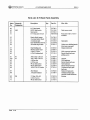
Table of Contents
1 Introduction ___ .___ .______ .___ ._._.__ .. _._..._... __ .____
I- I
7 Specifications ___ ......._. __ ._._._._._._. _____ ._. _____ 7- 1
1.1 TheD-75 ..................................................... 1-1
7.1 General ....................................................... 7-1
1.2 Warramy ................................ .. ................ ",1-,1
7.2 Monaural, ................................................... 7-1
2 Facilities .___ ._____ .... _._._ ... _.................. _._ ... _._ 2- 1
7.4 PcrfonnanceGraphs ...................................... 7-4
7.3 Stecoo ......................................................... 7-2
3 Required Test EquipmenL ... _..... _...... 3-1
4 Maintenance ........................................... 4·1
8
Schematics._ .. _._ ... _.. _.... __ .....___ .. ______ ._ ..._...
8-1
9 Parts. _.........._.... __ ........ _._._._ ... ___ ._._._ ... _... _... 9-1
4.5 Troubleshooting........................................... 4-2
9.1 General Infonnat.ion ..................................... . 9-1
9.2 Standard and Special Parts .............................. 9-\
9.3 Ordering PaIlS .............................................. 9-1
9.4 Shipment .................................................... 9-\
9.5 Tenns ......................................................... 9- \
9.6 lIluSU'atcd Parts Lists .................................... 9-2
5 Voltage Conversion ___ ._._ ._._._._ ... _. ___ .______ 5-1
Appendics A: Installallon.___ ._ .............. _.
4.1 Safety First ................................................. 4-1
4.2 Inspection ................................................... 4-1
4.3 Disassembly .. ............... .. .. .. .. ........ . ........ ..... 4-\
4.4 Reassembly ................................................. 4-2
6 Circuit Theory_.. _._._._. _________ .......... _._ ._._._._ 6- 1
Block Diagram Circuil Theory .......................
Balanced/Unbalanced Input Stage .... ......... .... ..
Input Operational Amplifier...........................
Signal Translator ............ _........................ .. ..
6.5 Final Voltage Amplifier.................. ........ ......
6.6 Bias ..........................................................
6.7 Output Stage...............................................
6.8 Protection Circuitry .. ........... .. .. ....................
6.9 I{)Cn.I (InputlOutpu(Comparator)..................
6.10 Signal Prcscnce Indicator .............................
6. 1
6.2
6.3
6.4
6· '
6-2
6-2
6-2
6-3
6-3
6·3
6-3
6-4
6-4
A-I
A. I Mounting ..... ... ........................ ...... ............ A·I
A .2 Wiring ....................................................... A·I
A.2.1 SLCrco ...... .. ............................................. A-I
A.2.2 Monaural ................................................ A-I
A.3 Input ......................................................... A·I
A.4 OutpUI. ...................................................... A-2
A.S Load Potcction .... .... ................................... A·3
Appendics B: Operation .......... _... ___ ._._ ...
8-1
B. I Precautions.... ....... ............. ......................... B-1
B.2 Controls ..................................................... B-1
B.3 PrOLCction .................................................. B· I
B.4 Fuse Rcplacemcnl .. ..................................... B-2
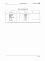
ill ustration
1.1 0·75 ...................................................... ..
2.1 Front Facilities (0.75) ................................ .
2.2 Rear Facilities (0·75)......... ... ..................... .
4.1 2 Ohm Load Wavefonn ............................. ..
4.2 10KHz Square Wave..................... ............. .
4.3 20KHz Sine Wave ............. ..... ................... .
4.4 1M Distortion Test Se(·up .. ..... ................... ..
4.5 Signal to Noise Test Set·up ........................ ..
5.1 AC Mains Voltage Conversion ... _...... ......... ..
6.1 0-75 Block Diagr$l........... ........ ............... .
6.2 Balanced Input Sta~e ................................. .
6.3 Input Operational Amplifier. ..... ........... ...... . ..
6.4 Signal Translator...................................... ..
6.5 Final Voltage.Amplifier.. ...... ............ .. ....... ..
6.6 Bias, Output and Protection Stages.. ....... ........
6.7 IOC ........................................................
6.8 Signal Presence Indicator..................... ....... .
7.1 Power Matrix ....... ..... .............................. ..
7.2 Nominal Frequency Responce... .......... ........ ..
7.3 Nominal Output Impzdance. ................... .... ..
7.4 Nominal Phase Responce ........................... ..
7.5 Nominal Power Efficiency .......................... .
7.6 Nominal Damping Factor .......................... ..
7.7 Nominal Output Phase Angle..... .................. .
7.8 Nominal Crosstalk. ..... ... ..... ....................... .
7.9 Nominal Noise Spectrum .................... .. ...... .
8.1 0-75 Schematic Diagrams.............. .. ........... .
9. 1 0-75 Main Modules.................................. ..
9.2 Output Module< ......................................... .
9.3 D-75 Front Panel Assernbly......................... .
9.4 0-75 Neon Bracket Assembly .................... ..
9.5 0·75 Back Panel Assembly ................ ......... .
9.6 D-75 Capacitor Bracket Assembly ...... ......... ..
9.7 D-75 Final Assembly ................................ ..
A.1 0-75 Mounting OimentiooS" ..................... ..
A.2 Input High Pass Filter..... .. .. ....................... .
A.3 InpUi Low Pass Filter ................................ .
A.4 Wire Gauge Nomograph ............................ .
A.5 Connection to an Inductive Load. ...... ... .. ..... ..
A.6 Fuse Nomograph .......................... ... ......... .
,.,
2· '
2·2
4·)
4-3
4·)
44
44
5·1
6- 1
6-2
6·2
6·2
6-3
6·3
64
64
7·)
74
74
7·5
7·5
7·6
7·6
7·7
7·7
g·l
9·2.3
9·9
9·11,
12, I3
9·16
9·17
9- 19
9·20
A· I
A·2
A·2
A·3
A·3
A4
This Page left Blank Intentionally
~RE~Vcc.O'---_ _ _ _ _ _ _ _ _-'O"'.7"',"-P"O".WE"R"A"'M"'P"'U"FI"'ER"-_ _ _ _ (SU'©JMDIfil9
Fig. 1. 1 0 -75
1.2 Warranty
1 Introduction
ProdUCt !.hal is covered by warranty must be Serviced by
an Authorized Crown Service Center or at the Crown
Factory Service Depanmenl. Any questions concerning
This manual contains complete service infonnation on Ihe
Crown D-75 power amplifier. It is designed 10 be used in
conjunction wi th the 0 -75 Insttuction Manual. However,
some imponam informaLion is duplicated in this Service
Manual in case the Instruction Manual is not readily
available.
Technical Service Depanment at:
warranly policy should be directed to the attention or
NOTE: THE INFORMA n ON IN THIS MANUAL IS
INTINDED FOR USE BY AN EXPERIENCED
TECl-II\'lClAN ONLY!
1.1 The 0 -75
The 0 -75 amplifier is a compact. audio JX)wer amplifier
designed for professional use. Providing medium power
amplification from 20Hz-20KHz with minimum
distortion , the unit features balanced inputs, signal
presence and i()C1'loi indicators, monophonic capability
and a means for iSOlating eleclrical ground from chassis
ground.
Crown International, Inc.
1718 W. Mishawaka Road
Elkhart, Indiana 465 17·4095
Phone; (219) 294-8000
FAX, (2191 294-8329
Twx: (810) 294-2160
Introduction
1-1
I · • .. •
F
crown
D75·
C DE E D C
B
•
I
A
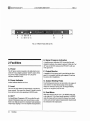
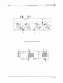
FIG. 2. J FRONT FAC/LlTfED (0-75)
E. Signal Presence Indication
2 Facilities
A. Power
A signal presence indication LED is provided for each
channel to indicate when signal is presenl Unlike the "onJ
orr' state orlhe IOC indicators the SP) LED's will vary
with signal Jcvcl
The AC power swilth, mounted at the right-hand comer
of the 0 -75 is a simple 2 position "on/orr' control. If the
AC power switch is positioned at "on", the power
irw:licator should be on (8).
A standard 1/4 inch stereo jack is provided on the fron t
panel. It is in parallel with the main outputs (0) and can
be used to dri ve headphones. -
B. Power Indicator
G. Output Binding Posts
Amber indicator thai the unit is on.
C. Level
The level of each channel is independently controlled by
these controls. The control for channel 2 should be turned
down and not used when operating in MONO mode.
D. IOC'"
An InputlOutpul Comparator LED is provided for each
channel. Illumination may occur at such Limes as when
there is too high an input level, improper load impedance,
output stage clipping or even an amplifier based problem.
2·1
Facilities
F. Output Monitor
Dual binding postconnectors arc provided at lhe output of
each channel . Use dual banana plugs on lhe speaker
cables for connection to thcjacks. In bridged· MONO,
only the twO top jacks (red) are used.
H. Dual-Mono
Slide this switch to the left (ch. I) for MONO mode and
10 lhe right (eh. 2) for Stereo mode operation. In MONO
mode the input and level control for cham'ICl two should
not be used and only balanced (ungrounded) loads should
be connected 10 the output jacks.
0·75 POWER AMPLIFIER
REV. 0
N
L
H
M
K J
G
J
K
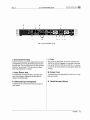
FIG. 2.2 Rear Facilities (D-75)
I. Ground Barrier Strip
L. Fuse
Isolation of chassis ground from signal ground is easily
accomplished by removing the shoning strap from this
tenninal strip. This may help remove any hum problems
caused by "ground loops." (Circuit ground is isolated
from chassis ground by 2.7 ohms.)
The AC line is safelYfused. If the unit is configured for
lOOVAC or 120YAC operation. a 2 amp fuse is used and
if SCI up for 200V AC. 220V AC or 240Y AC, a 1 amp fuse
is used. The use of any other fuse value will invalidatc the
warranty
J. Input Phone Jack
M. Power Cord
An unbalanced 1/4 inch phone jack is provided at the
inpul o( each channel. ~ use thc input jack for
channel 2 in MONO mode.
A standard three-wire (grounded) AC cord with a 15 amp
plug are provided
K. Balanced-Input Receptacle
N. Serial Number Sticker
A balanced XLR connector is provided at the input of
each channel.
Facilities
2-2
This Page l eft Blank Intentionally
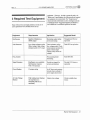
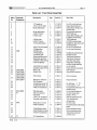
3 Required Test Equipment
Many of the service and repair problems with the D· 75
can be performed with a limited amount of test
equipment. However, in order 10 return the unit to its
"factory new" specifications. the fol lowing list ofrequircd
test equipment is recommended. The "Requirements"
column provides information to allow intelligent selcctin
of substituleS if the "Suggcsted Supplier and Mode'" is
not available or is considered impractical to obtain.
Equipment
Requi rements
Application
Suggested Model
Oscilloscope
Capable of displaying a
IOMHz signal
Monitoring output during
service and testing
Telequipmcnt D54A or
equivalent
Check resistance values
Auke 8024 or equivalent
Volt-Ohmmeter
Low-voltage resistance probe
lOOmv (range). High-voltage
resistance probe (I.5V range)
(low voltage probe). Check.
semiconductor junctions for
opens or shorts (high
voltage probe) Check DC
voltages
Frcq. Counter
For accurate general
monitoring
Heath SM I 18A
Wavctek 130 -Series or
equivalent
Signal Generator
Sine!Square wave available;
flat frequency responce.
TIlD .1% maximum
Provide teSt signals for
service and checkout
Circuit Breaker
15 ampere rating
In AC line to unit.; proteCtS
circuitry from overload if
power supply has shorted
AC Line Voltage
Monitor
Peak: reading meter (displays
rms equivalem to a
sinusoidal peak for any
waveform)
Monitor Line voltage
Circuit available from
Crown
R9qired Test Equipmefll
3·1
This Page Left Blank Intentionally
D-75 POWER AMPLfFIER
REV. 0
7
rem
4. Maintenance
Effective repair involves three basic steps: 10 Determine
the symptom(s) of the problem; 2) Identify the cause(s) of
me symptom(s); 3) Repair the unit 10 eliminalC the
caus.e(s), Before proceding through these steps it is highly
recommended that you first observe the safelY precautions
in the next section and conduct a visual inspection of the
unit.
4.1 Safety First!
To avoid risking electric shock, turn off and unplug the
D-75 from the AC power outlet before attempting to
disassemble or reassemble it
If the unit has been in recent usc, the large power supply
capacitors will probably have enough power stored within
them to present a shock hazard to you ana theamplii ler
circuitry. To safely discharge them, place a 10 ohm, 5
watt resistor across the + and - terminals of each capacitor
for several seconds. Usc caution when handling the
discharge resistor-particularly avoiding skin contact with
the leads while discharging me capacitors.
A void risk of fire hazard from shoned power supplies by
plugging the defective amplifier imo an AC oullet which
has a 15 amp circuit breakcr.
4.2 Inspection
A careful visual inspection is valuable for most problems
which you may encounter. To inspect the amplifier,
remove the cover panels as described in section 4.3.1
Begin the inspection by looking for anything which
appears abnormal. like broken wires and burnt or visibly
damaged components. Check wire and component solder
joints. Inspect the prinlCd circuit board(s) for broken
traces and loose connections. Be thorough- the lime you
spend visuaUy inspecting the amp is time well spent.
4.3 Disassembly
The eXlCnt of disassembly required will depend upon me
extent of inspection. service, testing, adjustment and
repair to be performed. Hlustrutions referred to in
parenthesis are located in the parts list (Section 9) of this
manual.
4.3.1. Cover Removal
A fairly complete visual inspection can be performed by
removing the top (91) and bottom (90) covers. To
remove Lhcsc pans, proceed as follows:
I . Remove lhe eight rfour per side) phillips hcad
mounting screws that secure tOp cover (91). Gently lift
covcr up and removc.
2. Remove the nine phillips hcad mounting screws that
secure bottom COver (90). COvcr will easily be removable
upon !;Crew eXlJ"action.
3. Remove each rack car (93) for easier a::cess to front
pa."lcl components.
4.3.2. MaIn Board Removal
The D-75 has been specially designed for ease of service.
Probably the best ex.ample of this is the modular layout of
the Main Board. Note that all connections are made
through eimer push-on terminals or through two 9 pin
arrays (with the exception of one ground wire which is
soldered).
To remove the Main Board proceed as follows:
I. Refer to the component side board layout, Fig. 6.7.
2. Unsolder and remove the black wire marked "ground".
3. Disconncct me 15 color-cooed push-on wires localed
throughout the underside of the main board. Their
locations arc marked by wire color.
4. Remove the four mounting screws and nylon spacers
(33) located on the top side of the board. Gently rock the
board up and down until it becomes free.
5. All work needed on this board may now be performed
effortlcssl y.
4_3.3. Output Module Replacement/Repair
The D-75 Output Module should not have to be removed
unles~ the t>oard il~lf is faulty and needs replacing. If this
is the case, refer to the disa'is.embly instructions listed
below. All other components on or around the Output
Module may be replaced without actual removal of the
boa:"d. This procedure is also listedbclow, after the
disassembly instru::tions.
I. Replacement
a. Remove the Main Board (See Main Board
Removal).
b. Unsolder and remove the fou r Ourput
transistors (25) by unscrewing the 8 mounting screws
(two on each). Note: In order to case replacement of
spacers located beneath each screw!nut combination,
leave the 0-75 in its normal/ying position-flat!!
c. Removc the four driver transistors (24) screws.
d. Gently lift ooard upward, being careful not 10
jar the position of spacers located beTICath.
c. Remove all external wiring to Output Module
and note location for future ie-connection.
f. Replace board.
Maintenance
4-1
2. Repair
All component parts localcd on the Output
Module may be removed by applying standard soldering!
desoldering methods (See Section 7) from the lOp of the
board. Use extra care when working with a pan localed
near the front panel so as not to mar the finish.
b. Front panel controls and LED's may be
replaced without removing the OutpUt Module Board (Sec
the following section).
3. Output transistor replacement-Output transistor (25)
can be replaced by removing two mounting screws (per
output) and unsoldering the twO main connecting pins.
Note as per e}{ploded view drawing insulating wafer (TO3,21), and its position in assembly.
fuse block.
3.
4.3.4. Front Panel Pans Replacement
As previously stated, all front panel componcm pans can
be replaced without Outp ut Mod ule removal.
Generally. this operation is performed by unsoldering all
or pan of obsuucting components. A detailed inslruCtion
format is listed below.
I . Input level control removal is accomplished by
removing the aluminum knobs (28) and related hardware
(20). Channel one pot can be pulled back and slid out the
left-hand side when the headphone jack (15) and
associaLed hardware is removed (10, 14) (rack ear (93)
should be removed). Channel tWO input level
pOlentiometer can be remove after the " right" lead of
R232 is disconnected and the grounding bus strip is
moved away from the working area. The potentiomeler
may need considerable, but gentle pressure in order for it
to come free.
2. 10C. Signal LED Replacement. When handling any
one of the four panel LED's (22, 23), e}{trcme care is
necessary in order 10 achieve a successful repair.
Unsolder leads of LED 10 be replaced. With a pair of
needle-nose pliers, remove the black suppon ring located
behind the LED. Next carefully extract the faulty LED by
pulling straight back and removing from the reat.
Replace the LED and reverse of above. Note: When
installing an LED always observe correct polariIY! It may
be helpful when inserting the rear black support ring to
apply pressure with a 1/4ft nut driver allowing the leads
to move up the middle of the driver (See Fig. 7.17).
3. On/Off Switch Replacement To replace the front
panel OfI/off switch (35) remove aluminum knob and
related hardware (27. 2,10, II ). With a small Oat-head
screwdriver, slowly pry orr fuse bkx:k holder from
adhesive. Push switch back until solder lugs are exposed.
Remove wire. and slide the switch to the right and out the
end. Replacement is the reverse of above. Note: It may be
necessary to replace the adhesive strip located beneath the
4-2
Maintenanc9
4. Neon "Orr-On" Indicator Replacement. Because of
the special mounting procedure used with the front panel
power indicator (42), Crown recommends factory
replacement only.
4.3.5. Back Panel Parts Replacement
All component parts located on the back panel of the 075 can be replaced with relatively littJe effort (see
exploded view drawing, rear panel assembly). Should
quc...tions arise eontact the Crown Technical Service
Department.
4.4 Reassembly
Reassembly is essentially the reverse of disassembly. If in
doubt about types and sizes of attaching pans, refer 10 the
appropriate illusuation in Section 9
4.5.Troubleshooting
The three steps to effective troubleshOOl.ing and repair
were mentioned earlier. They ean be summarized in the
three following questions: What is the problem (effec!)?
What is causing the problem (cause)? What can be done
10 eliminate the cause (repair)? The purpose of this
section is to help you answer these questions in an orderly
manner.
Finding and fixi ng the problem(s) is not the end of
maintenancc. The final step is to thoroughly test the
amplifier to be certain that it meets the faclOry
specifications after it ha.. been repaired. The test
procedures in section 4.5.3 will help you do this as well as
aid you in locating the cause of problem(s).
4.5.1 Identifying Symptoms
Why was the amplifier brought in for repair? Can you get
it 10 malfunction again? (Some problems can be
intcnniu.ant and difficuilLQ fmd.) If you don't observe
anything wrong with the amplifier, tactfully inquire how
the owner used it and try 10 detennine if it was misused or
some other component in their syStem could have been at
faull. (Appendices A and B contain the installation and
opcmtion instructions for the 0 -75.)
If you lack sufficient infonnation about the problem and
there isn'l anything obvious wrong skip to the next
section and procede dircctJy to the test procedures in
section 4.5.2. Using it can determine if the amplifier
meets factory specs.1f you have any questions regarding
warranty coverage, please cal l Crown's Technical Service
Departmcot.
"RE",V,,-"O"---_ _ _ _ _ _ __
_
LlcF.:'=ER"--_ _ _ _
--'D'-":.;:
'5"-P-"O"WE"'R.:.:A"'M:::.P.=
(£(j'@Qd1!)(flJ (3
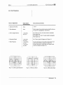
4.5.2 Test Procedures
Test or Adjustment
Input Signal
Characteristics
Instructions/Comments
I . Quiescent OC offset
None
±lOmV
2. Bias adjustment
None
Positive output, base-emiuer junction should be between
.3V and .35V. Adjustable by RIl2, R212.
3. Power (single channel)
Into 8 ohms, 20 vrms (SO watts) should be obtainable
before signal clip.
InlO 4 ohms, 11.5 vrms (75 walts) should be obtainable
before signal cJLp.
1 voit;IKHz
sine wave
4. Prot.ection Circuit
1 voit;lKHz
sine wave
Into 2 ohms, signal will appear as in Figure 4.1.
5. High Frequency
I volt; 10KHz
sq. wave
Into ar\ 8 ohm load, a 25 volt peak to peak: square wave
signal should exhibit no ringing (see figure 4.2)
Into an 8 ohm load, a 19vrms sine wave signal should
I voit;lKHz
sq. wave
exhibit no ringing (see Figure 4.3).
, ,
%
Rg. 4.1 2 Ohm Load Waveform
!
I.Il'
•
Fig. 4.2 10KHz Sq. Wave
Fig. 4.3 20KHz Sine Wave
Maintenance
4·3
9
(£(f'@(hMUll _____ --'O;:.."'75"PD="'' 'E"R."AM=PL"IF
"'E,,R' -_ _ _ _ _ _ _ _ _---'R'''E,.,V'-''
.0
Test or Adjustment
Input Signal
Characterist ics
Instructions/COmments
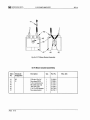
6. Inlcnnodulation Distortion
.SV +/·2%: 60Hz·
7KHz signal
summed in4:1
ratio
(See Fig. 4.4) When using the Crown IMA, typical
readings will be as follows:
2.5V peak.peak
7. IOC
5Hz sq. wave
OdB·.OO4%
-SdB lhrough -25dB=.03%
· 30dB·.03%
· 3SdB·.03%
IOC should illuminate once for every rise time and once
for every fal l time (twice every full cycle), Test
generator rise lime must be less man 1.0 microsecond.
8. Signal to Noise
(See Fig. 4.5) SignallO noise should be 1000B below
rated OUtput with meter bandwidth of 20Hz to 20KHz.
9. Quiesent AC Power
IS walts at idle as monitored by wattmeter on AC line;
120 watlS at full rated output.
'IO " ~T
I
~
I<. VOl NE rt ~
.-
I J:.~I
~
~
~
~'.
I
IIE!\IIM I,NlIICIUN()£()WlW'PED
AAO.INO QUl'NT CA&(
~ ~,
."
/'
r.::EL~TI\Ol
I , "","IOU"1
~.-:;:.
INPUTS D4$CQNN«:I(
O)
~
,-,
I~ I
...........
(l<AHHR
Fig. 4.4 1M Distortion Test Set-up
Fig. 4.5 Signal to Noise res l Sel-up
4-4
MaintBnanc9
••
OM
h
{~lTH(A
CIWI'<IE L
~ wm
A
~E",V"-."-O _ _ _ _ _ _ _ _ _ _--,,D-,.75=PO::."':.:;E",R.:.;Ao:M:::P-,L::..'F,,IE.:.;R_ _ _ _ _
(£[J@(1ill)1fil9
5 Voltage Conversion
Often Crown produCIS are purchased in one country and
later moved to another requiring an AC mains conversion.
For this reason the following chan/explanation as well as
a world-wide voltage map is provided.
100 VAC
The 0-75 power supply may be connected for any of five
voltages. Convening from one 1.0 another can be
accomplished with a soldering iron and a pair of wire
cutlers. Follow the fable shown with the schematic, and
the drawing below.
r~ ~ ¥~ ~ ~
CAUTION:Because there is a ris k of electric shock,
only a competent technic ian should attempt to alter
tbe line voltage config uration.
1. Remove the tOp cover of the D-75 (held on by 8
screws).
2. With the unit ri ght side up, a nd the front panel toward
you, locate lhe terminal strip o n the front in the near righthand comer.
3. Make the appropriate change in jumpers for the
200 VAC
II &~~~~
desired operating voHage. See Fig. 7.30.
4. RepIace the 2 amp line fuse with a I amp type 3AG
fuse. for all connections 200V and above.
5. Change the line cord tage 10 read !he correct voltage.
Note: Use only a 2 amp fuse for lOOVAC or 120VAC
operation. Use only a 1 amp fuse for 200VAC, 220VAC
or 240V AC operation.
220 VAC
~l~~~ w
z
tf
o
I-
~
240VAC
Rg. 5. 1 AC Mains Voltage Conversion
Ma intenance
5· t
This Page LeN Blank Intentionally
0-75 POWER AMPLIFIER
REV. 0
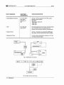
Thiscombincd signal is then fed to a stage of power
amplification where it is boosted to a level of sufficient
amplitude to drive an Output Load.
6 Circuit Theory
A ponion of the output signal is routed to the Signal
Presence cin:uilry. Provided the output signal has J!l
amplitude of at least one voll peal.: to peak, the green
signal presence indicators willlighl and vary in imensily
with Lilc OUlPULsignal.
6.1 Block Diagram Circuit Theory
The following cliscussioo refers lO the block diagram in
Fig. 6.1.
The output signai is fed back to a.'ld compared with Lile
input signal. Any nonlinearities existing between these
two signals will generate a correction signal to the
amplifier and the JOC indicators on the fronL panel.
When using the XLR Balanced Input.lwo signals, ISO°
out of phase, will be introduced 10 the Balanced Input
circuioy. Here, the two signals arc added together to
become the Unbalanced output of the Balanced input
circuitry,
~
In pbue. ,..;,t, 1M •
i9UI 00QUII1O
P:trz;
The Power Suppl)' supplies the proper voltages to the
various circuit componeOis within the amplifier.
UNBAl
INPUT
POWER
AMP
CH 1
CH,
3AlINPUT
r8
I
s~
POWER
AC LINE
MONO",
SWITCH
SUPPLY
I
,-d'
MONO
Lf\I
BAlINPUT
~ s~
UNBAl
INPUT
CH2
POWEM
AMP
CH2
Fig. 6.1 D·75 Block Diagram
Circuit Theory
5-1
~ If:::(f(g)(Id!!)(fj) _ _ _ _ _--'D'C-'-'75'-'PO~W!"E":'R~A""M":P,o,L1F':"=cER~_ _ __
The following explanation refers 10 schematic diagram
MI-270b located in the Instruction Manual as well as al
theend of Section 9. However, each circuil under
discussion is reprinted below in order to aid in circuit
familiarization. Only channell is shown for simplicity.
6.2. Balanced/Unbalanced Input Stage
In order to eliminate annoying RF interference, balanced
input (as well as unbalanced) stages ate iocorporalCd in
the 0-75. U2A and U2B are the balanced input op amps
which provide the correct phase inversion used in
balanced input design. As per definition of a balanced
input signaJ , an input from a balanced line is fed 10 the
inverting (-) and non-inverting (+) inputs of U2A (pins 2
and 3). This has the effect of driving the inputs J80
degrees out of phase. 1be output signal will now be
unbalanced and in phase with the signal applied 10 pin 3,
but without any annoying noise lIlal may have been
present at the input. The reason for this is because
unlike the audio input signal, the noise signal produced
(by some c:\temal source) will appear on both sides oflhe
balanced line and will cancel each other at the op amp
output Note the following diagram.
_ _ __ _ _~A!OEV~.0
357, it acts as an input voltage amplifier producing
emcme1y low distortion by means of several feedback
paths. The gai n dctcrmining components for this stage arc
two voltagc dividing resistors, RI03 and RIOS. Note that
lhcy act as a feedback palh from lhc output ofUlOO (pin
6) to lhc inverting input of U100 (pin 2). Both signals
cntering U 100 al pin 3 will be in phase with each othcr
because of lhis feedback path and will thus produce an
output (pin I) of almost zero. Thc small amount of
output signal that is prescnt is thcre because of the slight
diffcrence in ohmic value (with respect to gain) of
voltagc divider, RIDS and R103.
cIa,
25
N:; R102
0110 0109
- l. ~1O~'K±
*
Rl04
10K
200PFT
C~f
7
'"
'"
.5W
-1~V
"
R'03
:'f
~,
•
.~
_ RIS1
- 9.53K RI52
OPEN
'"
C'06
27PF
~
; i'
R'08
toK
.5W
Fig. 6.3 Input Operational Amplifier
IDa
The IC op amp will always try to keep a zero potential
difference between bolh inputs. Any type of non-linearity
will cause the OJ> amp to produce a large output, and
lhcrfore a substantial size correction signal in order to
retain the small output level.
6.4. Signal Translator
''''
el2S
82PF
I
9 .9K
9.9K
Balanced
The opcmtion of the D-75 front-end circuitry (IC op amp
through QI02) is to basically provide voltage
amplification. However, lhe signailfanslatOf transistor
(Q IOO) provides no voltage amplification itself, but
rather converts the ground referenced input signal to a
signal with a reference to the negative supply. The result
is highcr voltage swing capabilities from QI02 (Final
Voltage Amplifier).
3
Ul(l(l
"'"
>-,- --ka,co,,£!
"',,"'
Fig. 6.2 Balanced Input Stage
6.3. Input Operational Amplilier
The input op amp, UlOO is a low noise. large gain
bandwidlh integrated circuit. Under its formal name, LF
6-2
Circuit Theory
Fig. 6.4 Signal Translator
C"r
"
r
D-75 POWER AMPLIFIER
REV. 0
6.5. Final Voltage Amplifier
6.7. Output Stage
The Final Voltage Amplifier transistor (Q I02) is the main
voltage amplification stage. All signal voltage that
appears at the output is developed here. R 114 connected
to the base circuit ofQI02 serves twO purposes:
I) it provides collector CUiTent for Ql 00
2) it provides bias voltage as well as signal for Q 102
There are several categories or classes in ··/hich amplifiers
a.""e p!a::ed. <he mest common being class A, B or C. Each
class or combination thereof, has a sy;':cific amount of
bias current applied to tilc transistor which determines its
operating conditiOl!s. A class A amplifier, will be biased
such that a transistor operates always in the active region
(360 degrees) between saturation and cutoff. A class B
amplifier is biased at cutoff (1&0 degrees) and Class C
below cutoff. The D-75 output stage is designed in Class
AB+B mode of o~r.:!tion where the d,.-;ver L."2nsistors
(Q108, Ql11) C-.a.Tj the bias CUITen~ whiie the output
transistors (Ql09, Ql1 2) serve only as boosters. The
output transistors sense wilen the d.-iver transistors are
developing significant current draw from the load and
thus take over and deliver the needed current.
As me collector current of QlOO varies at the frequency
and amplitude of the incoming signal, this same variation
is placed across the Final Voltage Amplifier transistor
base bias resistor and is impressed upon th base ofQI02 .
",
"'"
'Cia
1.!.~( j!
~
!t!1
.
",, ". ".
Auf
,,,
,,~
0'>;> ,.. 1m
Fig. 6.5 Final Voltage Amplifier
'.
f~t
All'
0,0/ ..
0'.
0110
6.6. Bias
The output of the Final Voltage Amplifier provides the
signal drive to the predriver (Ql I0. Q 107), driver (Q I I 1,
QJ08) and output transistors (QI12, QI09) in orner to
amplify the current for fma l output power. The correct
bias supply (bias transistor Q103) voltage of2.IV DC is
distributed throughout the current amplification stages in
the following manner:
I) Base to Emitter junction ofQl07 positive predriver
(Q 107) is .6V
2) Base to Emitter junction ofQI08 positive driver is .6V
(negative driver Q III and output transistor QI 12 have
fixed base emitter bias)
3) Base to Emiuer junction ofQI09, positive output
transistor is .314 V (biased to sub turn-on slate).
As the ampli fier under loaded operating conditions
increases in temperature. the bias sensing transistor
(Q 103) IemperalW'e increases proportionally. This
condition reduces the base to emiucr bias voltage
produced by the bias supply which results in prevention
of the:mal runaway.
~
,.
"" ~ _01
~I\l
"
!'?
, R,22
f~ C".
• _'"
'.
p"'IO!
10'09
0'''' 'K
"
E.nl
~
w,.
0,,,
.
r~'Ol
,~
,
,,, 'fe",
•
S
I
Fig. 6.6 8ies, O!Jtput and Protection Stages
The O:.ltpl:t stage is of a quaskomplemcmary format
using ilO bi(;s cum;;nt inlO the output transistors
themselves. The result is rr:aximum efGciency willi
minimum crossover ooten distortion and idling ampliiier
heat. A!so, note tMt there is no bias current adjustment, as
the output stage is nO[ temperature-tolerance critical.
S.8. Protection Circuitry
The D-75 utilizes Voltage-Current limiting for protecting
the omput stages. V-I limiting is superior to most other
forms oi proteCtion ty....cause it directly senses tile overload
condition and instantly reacts to rel ieve the overload, and
acts only as long as t.1-te overioad exists.
Should the ompul W..come dangerousiy high, the voh.age
induced in the current limiting sense resistors (R 128,
R129) is fed to the limiting transistors (Q I04, QJ05). The
protection circuitry wi ll then "clamp" a limit on the signal
whenever it tr..-e<.tens to push the output stage beyond its
Circuif Theory
6·3
capabilities. The limit point is deltnnincd by a
combination of the predriver plus limiter current equaling
the available current source on the main board. In ollier
words, the signal drive that is fed to the predrivers is
limited or clamped.
6.10. Signal Presence Indicator
E 101 is lIIe green front panel indlcatorwhich illuminates
at any time lIIe output voltage reaches I volt peak-peak or
above. RI31, R132, 0107 and QI15 are Lhecomponents
directly involved in the above mentioned process.
6.9IOe'"
The front-panellOC display is actually a window
comparator circuit using two operationaJ amplifiers
(IC3C.D) and an LED md;cator (E 102).
Any small nonlinearity in the amplifier causes an error in
lIIe feedback loop to appear at lIIe inverted input of the
main ICop amp (UIOO). This means the main Ie output
(pin 6) will rise above its nonnal value in an attempt to
com:ct the problem . This signal is lhen responsible for
raising the bias voltage on IC3 and intwn activating QI14
which iUuminates E 102.
El01
GN
R132
""
2W
0115
''''
,"'"
,,,.
'N""
""
''''
,~
""
<~
Fig. 6.l /OC
Circuit Theory
· 10\1
0107
NF'
lDop
~
1-_+-_I:F1ROR sn.
>w
6·4
~
Rl31
3.3K
Fig. 6.8 Signal Presence Indicator
~RE~V~.O~__________________~~~75~PO~W~ER~A~M~P~L~W~~~R__________ ~~~~~ ~
heat conduction and minimum weighL
7. Specifications
7.1 General Specifications
Controls: Two inpm-level controls and a power switch
on the from panel. A mono-sl.Cll:O switch, located next to
the input jacks, on the rear panel.
Hum and Noise: From 20Hz-20KHz me hum and noise
level is below 175 microvolts and 1000B below the rated
output
Indicators: 210C indicators (red), 2 Signal-Presence
indicators (green), I Power indicator (amber).
Phase Response: + 10 degrees, -I 5 degrees 20Hz-20KHz
Connectors, Input: XLR 3 pin audio connector in which
pin 2 is positive. (for a positiveoulput signal), or 1/4~
at I walL
phon~jack.
Input Im pedance: (XLR balanced) 20,000 ohms ± 30%.
(XLR unbalanced) 10,000 ohms ±30%. (phone jack.
unbalanced) 25,000 ohms ±30%.
Amplifier Output Protection: Total protection against
shoned, mismatched or open outputs. VaIL-Ampere
limiting circuil.ry acts instantaneously with no annoying
thumps or cutouts.
Overall Protection: AC line fused. The controlled
slewing rate of the voltage amplifiers protects the overall
amplifier against RF burnout Input overload proteCtion is
furn ished by an internal resiSlanCCal the amplifier's
inputs.
Ground Link: A means for isolating or uniting chassisground from or with eleccrical ground is provided on the
rear panel. The grounds are always connected imemally
by 2.7 ohms.
Outputs: Color-coded binding POSlS wilh a
earphone jack on the front panel.
1/4~
stereo
Dimensions: 19" (48.26cm) long, 9" (22.86cm) deep.
3/4 ~ (4.45cm) high, 8 Ill" (2 1.59cm) deep from
mounting surface. A 19" West.em Electric standard rackmounting system is utilized.
and I
Weight: 10 pounds (4.54Kg) net weight.
DC Outpu t Offset: (shorted input) ±IO millivolts.
Finish : Satinized aluminum front panel with grey suede
Turn On: Instantaneous, with minimum bass thumps and
no program delay.
Circuit: A total of 42 transistors, 18 signal diodes, 2
zener diodes, 4 rectifiers and 3 linear Ies (dual op-amp)
are utilized in a wideband multiple feedback loop design.
Power Supply: A specially designed low profile
uansfonner, two regulated supplies for complete isolation
and stability plus computer grade filter capacitors serve to
power lhe D-75.
Power Requirements: AC VOltages of 100, 120,200,
220, and 240 volts ±10% ala line-frequency between 50
and 400Hz may be used.
Power Consumption: 15 watts while at idle, 120 walts at
Lcxan inscn.
7.2Monaural Specifications
Output Power (8 ohms): 95 walts minimum RMS into
an 8 ohm load over a bandwidth of 20Hz-20KHz at a
rated RMS sum IOtal harmonic distortion of 0.05% of the
fundamental output voltage.
Output Power (16 ohms): 70 watlS minimum RMS into
an 160hm load over a bandwidth of 20Hz-20KHz 3t a
rated RMS sum total hannonic distortion of 0.05% of the
fundamental output voltage.
Frequency Response: ±O.2dB 20Hz-20KHz, I watt, 8
ohms.
the full rated Output.
1KHz Power: 80 watlS RMS into 16 ohms; 110 waIlS
RMS into 8 ohms, (0.1% Total Harmonic Distortion).
Heat Sinking: The entire amplifier is used as a heat sink.
Front-panel extrusion acts as a heat sink along with the
chassis covers.
LM. Distortion: Less than 0.05% from om watts 100.25
walts, and less than 0.01% from 0.25 watlS to 70 watlS
into 16 ohm s.
Chassis: Aluminum-chassis construction for maximum
Specifications
7·1
~~~~~~ __________~~~7~5~PO~W~E~R~A=M~P~L~~~~R~__________________~A~E~V~.O
Slewing Rate: 12 volts per microsecond.
voltage.
Damping Factor: Greater than 400. DC-400Hz into 16
Frequency Response: ± 0. ld8 20Hz-20KHz at I watt
into 8 ohms; ± 1.2d8 5Hz-100KHz at I wau into 8 ohms.
ohms.
Dutpullmpedance: Less than 30 milliohms in series
with less than 6 microhenries.
Load Impedance: Rated for 8 and 16 ohm usage, safely
1KHz Power: 40 watts RMS inlO 8 ohms per channel,
both channels operating; 0.1 % total harmonic distortion;
55 wallS RMS into 4 ohms, per channel. both channels
operating, 0. 1% total harmonic distortion.
drives any load including completely reactive loads.
Voltage Gain: 41.2 ±2% (or 32.3 to.2dB) at maximum
gain.
Input Sensitivity: .812 volts ± 2% for 95 waiLS into 8
ohms.
Output Signal: Balanced. single channel. Channel I
controls are active. Channel 2 is inactive. but not disabled.
7.3 Stereo Specifications
Output Power (4 ohms): 45 walts per channel minimum
RMS (both channels operating) inlD a 4 ohm load over a
bandwidth of 20Hz-20KHz at a rated RMS sum total
hannonic distortion of 0.05% of the fundamental output
voltage.
Output Power (8 ohms): 35 watts per channel minimum
RMS (both channels operating) into an 8 ohm load over a
bandwidth of 20Hz-20KHz at a rated RMS sum total
harmonic distortion of .05% of the fundamental output
7-2
Specffications
I.M. Distortion (60Hz-7KHz 4:1): Less than 0.05% from
0.01 watts to 0.25 waus, and less than 0.01 % from 0.25
walts to 35 watts into 8 ohms per channel.
Slewing Rate: 6 vo11s per microsecond.
Damping Factor: Greater than 400. DC-4ooHz into 8
ohms.
Output Impedance: Less than IS milliohms in series
with less than 3 microhcnries.
Load Impedance: Rated for 8 and 4 ohm usage; safely
drives any load including completely reactive loads.
Voltage Gain: 20.6 ± 2% or 26.3 ± 0.2dB at maximum
gain.
Input Sensitivity: 0.812 volts ± 2% for 35 walts into 8
ohms.
Output Signal: Unbalanced. dual channel.
~
Test
Configurati on
& Loal ncr Ohm
4
8
Stereo per CH.
(both ch, powered) 16
Bridged Monaural 8
(Balanced Output) 16
20Hz-20KH z
45
35
25
95
70
40mS Tone Bursl
ElA WailS
Single Cycle Tooe
Burst WatlS at <0.05% THD
(See note 2)
Walts at <0.05% TIID
lIrn,
1KHz
l KH,
lKfu
55
115
70
45
25
105
90
55
40
25
FTC Continuous Average
Power al "> I% TIID
(See nOle 1)
40
60
25
110
I3S
80
130
30
(SeenOlc 3)
+/-JdB
I% THD
(See note-4)
75
Fig. 7. 1 Power Matrix
Power Specirlcatlons
Many manufac\UTClS publish power specifications ....ith a IOlermceof ± I dB or worse, That means their amplifier can deviate more than
20% in output! A 100 wan amp would mccltheir spec if il only produced 79.4 walts. Other manufacT\U'Cni qualify !.heir sJlCC5 by saying
they are "typical" Of "subject 10 mll1lufacruring toieranccs," thereby removing any perfOl1llmoe guarantee. We lake a different approach
at Crown - our published specifications aregllOl'an!eed for Ihree yean and can be proJected withSu\lice Plus for lI1l additional 3 years.
Further. because OUT "in-house" specs are more suingc:nt than our published specs, eye" Crown am plifier wj!l exceed iL~ published ~pec:$.
W.. beli~\'~ you should gel what yo'\! pay for.
No les:
I. ContinUOII$ powerin the context of Federal T1'3deCommission testinG is understood 10 bea minimum offivemioutes of opel'll1iOll. Harmoniedistonion
is measured at the R..VJS $Urn total as, ptTCellIage of the fundamcolll.l OUtput vot~e. This applies for all wat taees ~rthao 0.25 Wall S.
2.. /I. singleeycleof sine wa\le is ~rted 10 theami'lifierand monitored rornon-lineardi~ortion.. ~avemge power during the burst is n:pwted. Speakers
must be able 10 withstand thi$level iflhey are to be safely used ..... ith thi$ amplifier_
3. A 40 millisemncl bum or two cycles of line ..... a\le (wtlichever is 01 puttr du~on) is used and the power oompl.ltcd as the average P(w' a- durine \he
bvnl The duty cycle of this I.!:$l it 10 pen::enl. This powcr\eveJ is a ~u~ of 0011' loud an amplifietb as paceivtd by the hearing pmcus.
<I. ElA Jtandard RS-<l9Q (both chamels driven).
$pecffications
7-3
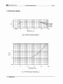
7.4 Performance Graphs
<TODe
10
100
lK
10K
lOOK
10K
lOOK
FREQUENCY (Hz)
Fig. 7.2 Nominal Frequency Response
.1
1101
(Ohms)
.01
.001
10
100
lK
FREQUENCY (Hz)
Fig. 7.3 Nominal Output Impedance (Z cJ
7-4 SpecHicatlons
+20
. 10
PHASE
SHIFT
(deg rees)
I
0
·1 0
·20
·30
10
~
"
jjjjJ:
11111
·40
I 1
I
1
lK
100
10K
ftm lfi '
lOOK
FREQUENCY (Hz)
Fig. 7.4 Nominal Phase Response
%
Efficiency
II
II
70
I IP~ .
60
•
50
I
=:~, ,
I
I
I
,
,
40
I
30
10
100
I
lK
10K
100K
FREQUENCY (Hz)
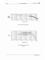
Fig. 7.5 Nominal Power Efficiency
( Bohrns)
specifications
7-5
~~~~~~ __________~~~7~5P~O~W~E~R~A~M~K~IF~IE~R~___________________R~E~V",
.O
10 0 _
O.F.
100" .
10 _
10
_
1K
100
10K
10 K
FREQUENCY (Hz)
Fig. 7.6 Nominal Damping Factor
90
80
70
&.
./
80
50
(DEGREES) 40
30
20
10
0
-10
V
1
10
100
1K
FREQUENCY (Hz)
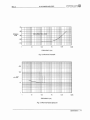
Fig. 7.7 Nominal Output Phase Angle
7-6
I
Specifications
10K
100K
·70
C¥2
dB below
30W
·90
VLL
IC'
/
100
110
I
10
100
10K
1K
100K
FREQUENCY (Hz)
Fig. 7.B Nominal Crosstalk
400
I
100
,, ,,
, ,
nV/ /Hz"
10
I
I
I
10
100
1K
10K
100K
FREQUENCY (Hz)
Fig. 7.9 Nominal Noise Spectrum
Specifications
7·7
ThiS Page Left Blank Intentionally
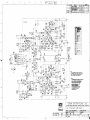
8 0-75 Schematic Diagrams
Fig. 8.1 0·75 Schematic Diagrams
For Amplifier SIN 24530 and below use schematic number MJ·270b
For Amplifier SIN 24531 and above use schematic number J 0 116-4
Schemafics
8-1
~RE~V~.O~___________________D~.~~~P~O~W~E~R~AM~P~L~IF~~~R~________ ~~~~fD~
9 Parts
ordered from Crown will assure an acceptable
replacement. Suucmral items. covers and panels are
available from Crown only.
9.1 General Information
9.3 Ordering Parts
Section 9 contains illustrations and partS lists for the D-75
power amplifier. This infonnation should be used with
When ordering pans. be sure to give the amplifier mode.!
and serial number and include \.he pan description and
Crown Part Number (epN) from the paru list. Price
quotes are available upon request.
the service, repair and adjustment procedure in Section 4.
Most of the mechanical and suuclUral type pans are
illustrated and index.ed on ex.plodcd view drawings.
Electrical and electronic parts on these illustrations are
also identified by the circuit reference designation next to
the illustration. Both the index number and the reference
designation are included in the parts list in separate
columns. The reference designations correspond to those
shown in schematic diagrams.
Electrical and electronic parts located on printed circuit
boards are illustrated by schematic ~ymbols on the trace
side and by component shape symbols on the component
side. Reference designations also appear on these
diagrams.
The quantity of each part used in each location is also
shown in the pans listing.
9.2 Standard and Special Parts
Many elecuical and electronic pans used in \.he D-75
are standard items stocked by and available from
electronic supply houses. However, some electronic parts
that appear to be standard, are actually special . A part
9.4 Shipment
1. Shipment will be made by UPS or best method unless
you specify a preferred method.
2. Shipments are made F.O.B. Elkhart, Indiana only.
3. Established Crown accounts will be freight prepaid and
billed unless shipped by uuck or air freight.
4. All others will be shipped freight collect.
9.S Terms
I. Normal tenns are C.O.D. unless the order is prepaid.
2. Net 30 days terms apply only to those finns who have
an established line of credit with Crown.
3. lfprepaying please add an amount for the freight
charge. S2.00 is average for an order under one pound.
NOTE: Part prices arc subject to change without notice.
4. New pans returned for credit are subject to a 10%
restocking charge.
5. You must receive authorization from the ParIS Dept.
before returning parts for credit.
6. We are not a general pans warehouse! Pans are
available for servicing Crown products only.
Parts
9-1
:e
00
•~
@
(fil
•
" ~ 'a~9
,101
I r:::::j
-
t..6 .. ' "
.........."'~"- a~
~
I
l-....-J
C1 15
-
"'<;>"
til
~
"
Q106 V
_ _ _Al46 Cl
5'
;::
~
"
~'40+
rlA3~
A119
0
lJAH'4r
R121~
A120
......--,
Cl21
0
R127
D!?
Cl0
C123
0105
<fED
000 0
iiO
l(l
+
R12. c:::J
,
C105 •
101
Cl04
10
0:), 03C lO
ell:\:,
.~. 5e
, 0:
Si~ Dl O3 ( C4
~ ~()jCl")
<;~.
<r .
;;
o"" R207
~D1'l
I. ~
U
....
~
A1"CJ~""
~I
I.
u·
0
o
::
~
c.c
."
01
_~
cO
0201
0206 CD
·
~(
C' 04)
g
i'ii
~ o·
~
+0
0
1:3'204
C202
0
°D'"
go
~ ci2i
N
0
<;>
O L'O'
~
A220
,C2"
C224
(
12
0203
C216
L201
0
N
~
•. . :
~
i
0
00,°'
0 A'"
0
)
DA'29
wDD~ :: loBN20ll~~·~?¥(jOQU Qa'"
--- -- -_ IC3
til
~
C215
_47
c : JR219
0
0 02080
L..J
0210
~
<6-
R~
0214
~
c.c
", .... C:§4' ..0
{]
' .... I~ .,;i::~.\
~n.
.. .:. ...
'" ~[J
'
I
n&U .-- tio-. B2.!.l.
c:J
'
,. q,;'Y'O
"' 14.L-J "':".1_ "" \'",
Q"
R143 CJ 1C2
A?,s{]C118 ~DQ.\3~ D5.~ IOI::
0108
A2as
C3t138 Cl
lJ~
~
dl
rr::::D C222 R246
~ £::>_ ~.
c:::J
R223
~
,
":<m
o
",RE",V.:o!-0_
D-""7:::.!.5PO~W~E~
R AM~P"'LlF~IE~R_ _ _ (£(j'@0l1D0ll 9
______
o
o
o
JT
,
. I'i
o
o
Fig. 9.1b 0 · 75 MainModule
9-3 Parts
~~~~~ __________~~~7~
5PV~W~E~R~A~M~K~IF~~~R~__________________~R~E~V~
.0
9.6 Illustrated Parts lists
Parts List : D-75 Main Board Module Q41944J1
Scbematic
Designation
Description
Qly.
Part No.
5pfmica
lOOpfmica
2
2
2
2
C2820-6
C2342· 1
C36274
C34IO·5
J20pfmica
6
C 3290- 1
200pfmica
.OO15mf200V filmalic
6
2
C34I1 -3
C30S9·7
.0082mf200V filmatic
4
C 3063·2
.O lmfdisc
C 1751-4
22mf 16v N·P vcn
100 mf/ 12V vert
14
2
I
2
2
2
IN 4003
4
C2851-1
IN4148
IN170
IN961 B IOVzener
12
2
2
C318 1·2
06212· )
C 3549-0
LF357 Opamp
RC4558 Dual Op amp
LM339N
I
I
I
C6527·3
C3919·5
C4345-2
capacito rs
CUI.C2Il
CI06. C206
C I24.C224
CI07.C207
ClOg. ClOS,
CI09.C209.
CII3.C213
CI02.C202
CI()4. C204
CI 10, C210
CI05.C205
27pfmica
82pfmica
C I 17.C217
CIIS.C2IS
C2. C4. C6. CII
C112.C212.
C115,C21S,
CII6.C216.
C122.C222,
C123.C223
CI20,C220
C7
Clll.C221
CI01. C201
C I03.C203
Diodes
0105.0205
0106.0206
0104.0204.
OIOB.02OB.
DI02, 0202.
.22mf IOOV filmatic
4.7mf63V vert
IOmf SOV vert
C3218-2
C 4253-8
C3728-O
C 5311·3
C3729·8
DIOI . 0201 ,
0109.0209.
0110, 0210
0103. 0203
DI.D2
Integrated Circuits
UlOO
U2
U3
Pat1s
.
94
Misc. Info
REV. 0
0-75 POWER AMPLIFIER
~~--------~~====~-----
[£!i'@lli!D!fil1el
0-75 Main Board Module Q41944J1 Continued ___
Schematic
Description
Qty_
Part No.
5MH Axial Gm
4
C3510-2
2N3859A NPN
MPSA06NPN
12
2
02961-7
C 3528-5
2N4 125PNP
PN4250A PNP
MPSA56PNP
4
2
2
C3625-8
C3786-8
C3954-2
56 ohm l/4w Sef
120 ohm 1/4w Sef
IOOohm 1/4w 5cf
1200hm l!2w 5cf
2
2
2
2
C3S11-0
C4723-0
C2872-6
C 3837-9
180 ohm 1/4W Scf
4
C 2873-5
470 ohm 1/4w Sef
4
2
2
2
2
C3304-0
C3803-J
C 3301-6
C2627-5
C 1076-6
C2628-3
C2630-9
Misc. Info
Designation
Coils
LlOl.LW l ,
L102.L202
Transistors
QIO I ,Q20 I ,
QI03,Q203,
QI05,Q205,
Q1I3, Q213,
QII4 ,Q214,
QI02,Q202
Q I07,Q207
QI04,Q204,
QI06,Q206
QlOO,Q200
QIIO,Q21O
Resistors
R115.R21S
R120, R220
R118,R218
Rl22, R222
RII7, R217,
Rl24.R224
RI25.R225,
R147, R247
RI03, R203
Rl13,R213
RI14,R214
RI.R2
RI07,R207.
510 ohm law IMP
750-ohm 1/4w Sef
820 ohm 1/4w 5cf
820 ohm I w 5 comp
C2626-7
C3648-O
R I46,R246,
RI02,R202
R145.R245
RlII,R211
IK ohm 1/4w 5cf
1.5K ohm I{lw 5cf
2.2K ohm 1/411,' Sef
RIIO.R21O
3.9K ohm l/4w Sef
6
2
2
2
R127,R227
RI16,R216,
4.7K ohm 1/211,' Sef
4
C 1640-9
R123,R223
RI04,R204
R143,R243
RJ06,R206
R138,R238
R140,R240
RI09, R209
R139, R239
R141. R242
RN 100. RN200
5.6Kohm lf2w 5cf
4
C 3299-2
10K ohm 1/4w 5cf
22K ohm 1/4w 5cf
4
2
C 263 1·7
C 3302-4
33K ohm 1/4w 5cf
56K ohm 1/4w 5cf
150Kohm 1/4w5cf
1M ohm 1/4w 5cf
Bai. inpul trimmer
4
2
2
2
2
C4346-0
C 2882-8
C4216-5
C3198-6
04669-4
RI26,R226,
9-5
ParTS
~~~~~~ __________~D~-Z~
5~PO~W~E~R~A~M~~~~~IE~R~___________________A~E~V"'
_O
0 -75 Main Board Module 041944J1 Continued •..
Schematic
Description
Qty.
'Selected bias resistor
2
Part No.
Misc. Info
Designation
R112,R212
Typically 92-240 ohms
R3 .
RI08, R208,
R119, R219
R1 21, R22 1
10K ohm l/2w I MF
R142. R242
RIOS. R205,
15Kohm 1/4wSd
7
2
C 2343-9
C 2632-5
RI44, R244
18K ohm 1/4w Sef
4
C 2633-3
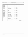
Parts list: 0-75 Main Board Module 042530-8
Capacitors
C I06. C206
C I24, C224
e125. C225
5pfmica
27pfmica
2
2
C 2820-6
C2342·1
82pfmica
2
C 3627-4
C108. C208.
C109. C209.
C1I3. C213
120pf mica
6
C 3290-1
200pfmica
.OO l mf disc
4
C 34 11 -3
CI17. C211
.OO82mf 200V filmalic
ellS, C218
C2.C4.C6.C II ,
C12. C13
.0027mf 200V filmatic
2
2
C 3063-2
C 348 1-6
.O l mf disc.
14
e 1751-4
.lmf 63vceramic
100 mf/ 12V vert
6
2
2
2
C 5639-7
C 3728'{)
C 53 11 -3
C 3729-8
IN 4003
4
C 2851-1
IN4148
IN270
8
2
C 31 81-2
06212-1
C I II , el ll
Cl02. C202
CIIO,OIO
C7
C II2 . C212,
CIIS . C2IS.
Cll6, C216.
C122. C222.
C223
C1I9. C2 19. CI20
C220. C123. C223
CI21.'C22 1
CI01.C201
C103. C203
cm.
Diodes
Dl 05 ,0205
0106.0206
0 102.0202.
0 104.0204.
0109. 0209.
0110, 0210
0103.0203
Parts 96
IOmf SOV yen
22mf 16V N·P vert
(not in current production)
REV. 0
0·75 POWER AMPLIFIER
~~------------~~~~~-----
(S(J@[1J1I)1fil9
0 -75 Main Board Module Q42530-8 Continued ...
Schem atic
Dtsignation
De~ription
Qty.
Part No.
Dl,02
IN961 B lOY zener
2
C 3549·0
Integrated Circuits
UJoo
U2
U3
LF357 Opamp
RC4558 Dual Op amp
LM339N Volt Comparator
2
1
1
C7621·3
C 3919·5
C 4345·2
Co ils
L101 . L201,
LI02 . L202
.5MH Axial Gm
4
C 3510-2
2N3859A NPN
MPSA06NPN
12
2
C 3528·5
2N4125PNP
PN4250A PNP
MPSA56PNP
4
2
2
C 3625·8
C 3786·8
C 3954-2
56 ohm 1/4w Sef
2
2
2
2
C 3511-0
Transistors
QIOI,Q20l,
QI03, Q203,
QI05, Q205,
QI13, Q213,
QI14, Q214,
Ql02, Q202
QI07,Q207
QI04, Q204,
QI06, Q206
Qloo, Q200
QIIO,Q210
Resistors
R115, R21S
RI20,R220
R118. R218
RI22, R222
120 ohm 1/4w Sef
100 ohm 1/4 w Scf
120 ohm Ww 5cf
Misc. Info
D 2961-7
C 4723-0
C2872·6
C 3837-9
Rl17. R217.
Rl24, R224
R125, R225
R147.R247
RI03, R203
RIl3.R213
RI 14.R2 14
Rl .R2
180 ohm 1/4W Sef
47 ohm 1/4 w 5 cf
470 ohm l/4w 5% cf
510 ohm l(2w IMP
4
C 2873-5
C 1011-3
C2626-7
750 ohm 1/4w 5cf
820 ohm 1/4w Sef
9 JO ohm 3w 5% cf
2
2
2
2
2
2
lKohm 1/4w5ef
1.5K ohm Illw Scf
2.2K ohm 1/4w Sef
3.9K ohm 1/4w Sef
6
2
2
2
C2627·5
C 1076-6
C 2628-3
C2630·9
4.7K ohm 1/lw Sef
4
C 1640·9
5.6 ohm Illw Sef
10K ohm 1/4w 5% ef
4.7K ohm 1/4w 5ef
22K ohm 1/4w Se f
4
2
C 3299·2
C2631 ·7
C 3939·3
C 3302-4
C 3304·0
C 3803·1
C 3301·6
C 7389·7
R146,R246,
RI02,R202
RI4S. R24S
RIll. R21l
RllO, R210
RI26.R226.
Rl27, R227
RI16.R216,
RJ23,R223
RI04,R204
R143.R243
RI06,R206
2
2
,
9. 7
Parts
9
(£(i'IQ)MDUll _____!:.D-~7::5P~O~W"EoCR"A""M,-PL"IF,-,IE"R,-_ _ __ _ _ _ _ _--,A",E"V"-,,
.0
0·75 Main Board Module Q42530-8 Continued
Schematic
Designation
Description
Qly.
Part No.
33K ohm 1/4w 5cf
56K ohm 1/4w 5cf
4
2
C4346·0
C2882·8
150K ohm 1/4w 5cf
Sal. input trimmer
500 ohm trimmer
4
2
2
C4216-5
04669-4
C6048·0
10K ohm Iflw 1MF
15K ohm 1/4w 5cf
7
2
C2343·9
C2632·5
13K l/4w 5% cf
9.53K l/4w 1% mf
4
2
C6161- 1
0-75 Board (without partS)
TOO2 healS ink
1
1
3
1
18
06248-5
C 3493·1
C345J-9
C3450·1
C473J-3
R1l8.R238
RI40,R240
RI09.R209
R1l9.R239
R141.R24 1
RN IOO. RN200
RII2, R212
R3
RI08.R208 .
RII9.R2J9
RI21, R221
R142. R242
R149, RI50
R249, R250
R I St , R251
C 4300-7
RI52, R252 (open)
Misc.
Ie Socket (8 pin)
Ie Socket ( 14 pin)
PC MntRCPT
Parts
.
98
...
Misc.lnro
~R~EV~.~O____________________~D~.7~5~PO~W~E~R~A~M~P~L~~~~R~________ ~~~~~~
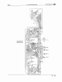
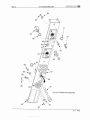
Fig. 9,20-75
Output Module
201
202
9-9
Parts
~~~~~ __________~
D-~~~PO~WE
~R~A~M~P~L~~~~~R~____________________~RE~V~.0
Parts List: 0-75 Output Module Q41945J8
Description
Qly.
Part No.
.O lmf disc
C 175 1-4
Smf 70V
3
2
2
IN4148
2
C 3181-1
2N3859A NPN
2
0296 1-7
R8
R148, R248
R I28. R228
R I29, R229
R!l2. R232
2.7 ohm .5W 5CF
2.7 ohm I w 10%
I
2
C 2857-8
C 1001-4
.I ohm 5 w 10% wire
560 ohm 2 w 5 camp
R131.R23 1
3.3K ohm 1/2 w 5CF
4
2
2
C 3291-9
C 4724-8
C 1051 -9
9 pin connector
D-75 Board (wilhout partS)
2
I
C4730-5
P 973QA4
Solder lug .144ft hole
I
01220-9
Schematic
Designation
Mise. Info
Capacitors
C I2
C II 6,C2 16
C1I9, C219
C I,C5
Diodes
0107,0207
. t m r 200V Fi ImatK:
C 2938-6
C 5050-7
Transistors
Q1I5,Q215
Resistors
Misc.
I
Located alone comer of the
output board
Parts
9-10
28
24
26
o
,,•
o
.....
--------- 2 1
13
,
4l---l- 19
27
7
16
~
40
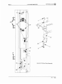
Fig. 9.30-75 Front Panel Assembly
9-11
Parts
~~~~~~ __________~D~-7~5~PO~W~E~R~A~M~P~L1~F/~ER~__________________~R~
EV~
.O
9
36
I
8\
\
o\
-@--
~ 29~
5
Fig. 9.3 D· 75 Front Panel Assembly
15
20
10
Note
.--18
Q "-14
Parts
9-12
~RE=-,V",.O'-_ _ _ _ _ _ _ _---'D-=75"=p~OW~E~R!CA~M'C'PL~/F:!"EO!:R'__ _ _ _ (£OOI1!1D[]l) 9
1111
i>
!!Jj,
III
" 28 /
f@J19~
o
~~
~;II
V
8
o
0
8
Fig. 9.3 D·75 Front Panel Assembly
40
9·13
Paris
9(S[j'©l[illDUll _____~D-:.c7'C5P~O=:W~EocR~A~M~P:=L!'_IF~IEc:R'__ _ _ _ _ _ _ _ __
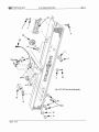
"A"-EV",,,.O
Parts list: Front Panel Assembly
Dtscriplion
Qly.
Pari No.
Misc. Info
2
3
4
.375 bright nut
.375x.l4lx.03 1 fiber
I
2
C 128SN7
C 1296-0
On-Off switch hardware
#6 star lockwashcr
II
C 5594-4
OUtput Ix>ard, bridge, and
5
6
7
#4 star lock washer
C 1824-9
Crossmember hardware
4-40x.375 screw
4
4
6-32 hex nuts
II
C 5561-5
C 1889-2
TlP47 hardware
Output board, bridge, and
4-40 hex nulS
4
2
2
C 1938-7
C3879- J
C 2188-8
TlP47 hardware
C 2189-6
C 2365-2
C3062-4
Index
No_
Sc bematk
Designation
OUlput board hard ware
lerminal strip
8
9
6·32x.375 screw
.375 star lockwashcr
10
.625x.375x.030 washer
.25 lockwashcr
o 3503-6 terminal Slfip
o 3503-6 1cnninal strip
Headphone jack and on-off
switch hardware
On-off switch hardware
Level CDOLTcl hardware
14
15
16
17
18
19
.375 knurled nut
3 conductor jack
Nylon transformer pin
Tinnerman speed nut
.6250D".375lD washer
6-32".625 phillips
I
2
I
I
I
2
2
I
9
20
21
22
23
24
.440x.26O".015 washer
Insulating wafer (TO-3)
Red LEO.
Green LEO.
2
4
2
2
C 4023-5
C4039-1
C4341-1
C4430AO
Transformer hardware
Transformer hardware
(On older amps only)
Output brd. and bridge
rectifier bridge hardware
Level controls
Output lransistor hardware
IOC indicator
Sig. presence indicator
TlP4 7 driver
4
C4647·\
Driver transistor
NPN power transistor
TO-3 insulator
.83 aluminum knob .25
.83 aluminum knob .12
4-40x.375 round head
4
C475 1-1
04071 -3
04075.4
04076-2
C5961-5
Output transistor
4
I
2
4
II
12
I3
25
DM!
0102,0202
DIOI ,D201
QIOS.Q208.
Q1I2.Q212
QI09.Q209.
Q112.Q212
26
27
28
29
VH 1486amp
C3495B2
C3507-8
D 3557-2
C 3558-1
C3628-2
C 3879-\
30
31
32
33
34
RlOl,R201
FI
25K ohm audio
AGC 2.5 amp fuse
Fuse block
.187".115".125 spacer
Terminal strip #/6 hole
2
I
I
4
I
04688-4
C 3775-1
C 3776-9
C 4759-4
D 3600-0
35
36
SW2
Rotary power switch
Cable rccepraclcs
I
15
0 3492-2
C3849-4
.5 transformer mOUn(
Nylon Shoulder washer
8-32x.875 round head
2
2
2
C 3556-5
C425J-2
C 4252-0
0-75 transformer
I
04668·6
Headphone jack hardware
Headphone jack
oS
On-Off knob
Level controls _, '1.c.,
Crossmembcr hardware,l J . ...
machine screw.
Level controls !.aper pot (In older amps on ly)
Holds C 3775-1
Main pc board hardware
Volt. modilicalion
terminal strip
On·Offswitch
For connoctions on the main
'"
bo",d
37
38
39
40
Pans
TI
9 -14
Power transformer assy.
Power lransformer assy.
Transformcrhardware
machine screw
This Page Left Blank Intentionally
9
(£;[j'(g)QJ11JIfil _ _ _ _ _-"D-'--'::.SPO'-"-'W-"Eo:;Rc.A:::;M"'PL"'IF:::;IE"'R'--_ _ _ _ _ _ _ _ _---'R"'Eo:v-,",_0
41
43
L:@:::....r@""-r-@"='-.j11L-- 45
46
47
44
42
Fig. 9.4 0-75 Neon Bracket Assembly
0-75 Neon bracket assembly
Index
No.
41
42
43
44
45
46
47
Parts
Schematic
Designation
Description
Qly-
Part No.
R5
11
27K ohm l(2.w 5cf
Neon lamp NE2H
3 AUA leonina! strip
5S module pipe clip
.093 steel cyelet
1.2x 1.2x.O I5 fish paper
Neon lamp bracket
1
1
1
C 1056-8
C2500-4
01242-3
C 1727-4
C 3529-2
D4756-9
04781-7
9-16
I
I
I
I
Misc. Inro
",AE",V-"
, O'--_
_ _-"D-:::.7""P-"O"'W""ER"'A"'M"-PL""IF-,oIE"'R_
_ __ __
_ __ _
(£(j'(gJl!DdlUll9
\
54
\
/~©:
./
68
.
71
\I
\\~\ I
70
'- 50-/l-~
49 -#--o~
51
\ \
\
o
()
59
67 -it''II11i
t?ef
66
\
\
@
55
6z., ~-j
@
65
\
\
56,,~~
t= 9 \
t
68
58
'\" ',/61
, ,\
,,
Fig. 9.50·75 Back Panel Assembly
,~\>, ~
\~,~
/ ),.-\'
52
60
9-17 Parts
9
("£(j'@l\illJ[R) _ _ _ _ _-"D:.:-7"--5PO="'"E"-R"'A"M'--PL'-'IF'--"E"R'-_ _ _ _ _ _ _ _ _ _R"'E'-'V~
-0
Parts List: 0-75 Back Panel Assembly
Index
Schematk
No_
Designation
48
49
50
51
SWI
52
53
54
55
56
57
58
59
60
Part No.
Description
Q ,y-
D-75 back panel
Steel eyelet
0-75 rear panel switch
1
1
2
I
Barrier block jumper
2 tenninal barrier block
2 conductor jack
HT A fu seholder with nut
505 solder lug #8 hole
I
I
2
I
I
C4726-3
Dual binding post
HEyeD strain relief
4-4Ox.375 screw
6-32x.5 binding head
2
1
4
4
C2823-O
C48%-4
C2247-2
C2176-3
3AG 2 amp 1.25x.25
3AG 1 amp 1.25x.25
C 5829-4
C 3065-7
C 1938-7
C 1889-2
C 1824-9
C 5594-4
C 7674-2
DPOT slide switch
Misc. Info
F 9734-9
C411O-0
C 3529-2
M20 103A2
C3489-9
C3423-8
C 5597A5
02935-\
Dual -monoswitch
Rear panel with C 4110-0
mounted
Input jacks
Under screw holding barrier
block onto rear panel
Output connectors
XLR connector hardware
Barrier block hardware
phillips screw
61
61,
62
63
64
65
66
.625x.375:\.015 washer
1
1
4
4
4
4
2
67
XLR female
.375 jack insulated
2
2
C4902-0
C 1306-7
2.7 ohm l!2w 5cf
8-32:\.25 screw
#8 star lock washer
I
2
2
C 2857-8
C 5962-3
C 195 1-0
FI
FI
4-40 hex nut
6-32 hex nut
#4 star lock was her
#6 Sial" lockwasher
68
69
70
71
Pal1s
R6
9-18
Ameron
XLR hardware
Barrier block hardware
XLR hardware
Barrier block hardware
Unbalanced input jock
hardware
Balanced input jacks
Unbalanced input jack
shoulder washer hardware
Resistor
R~E~VC!.O'---_________--'D~.'_'75'.CP~O~W:,oE~R~AM~P::=L!CJF_=JE.::!R_ _ _ _ _ ~(J@l[l£1l)Ull9
Fig. 9.6 D-75 Ci:1paCIIOr Bracket Assembly
Parts List: D-75 Capacitor Bracket Assembly
Index
Schematic
No.
Designation
72
L1D3
L203
73
74
75
76
77
78
79
80
81
82
83
84
85
Description
Qty.
Part No.
D· 7S output coil
1
1
1
1
1
2
4
M43209·2
M43208-4
C 4738·8
4
I
C 3575-9
D 3504·4
3/800x3/16lDxl/4"
#10 star lockwashcr
#8 type A plain washer
4
4
4
4
D 2934·4
C2762A8
lQ.-32x.5 truss head
4
D-75 output coil
D-75 Capacitor bracket
8-32x2.125 stud
3 AVA temlinal strip
C8.C9
lOOOOmf4QV
.8750Dx.1871D washer
.5000 Ox.19510x.0625
2ALUE tenninal strip
389 solder lug .218 hole
Misc. Info
FlOI04·2
D4725-4
C4250-4
D 3609- \
C 2279-5
C 1951·0
C 2049·2
Output coil hardware
Used with output coil
Power supply capacitors
Output coil hardware
Capacitor hardware
Output coil
Capacitor hard ware
Output coil hardware
Capacitor hardware
Capacitor hardware
CapacilOT hardware phillips
screw
86
87
88
8-32 hex nut
#8 star lockwashcr
.75 fiber washer
4
2
4
C 1986·6
C 1951·0
C 1648-2
Output coil hardware
Output coil hardware
Capacitor hardware
9-19
Parts
~~~~~fTI
__________~D~-7~5~PO~W~E~R~A~P~L~~~~R~
M
__________________~RE~V",
.0
•
8~
92
":><1]
-,.;$~\
90
•
•
I
Fig. 9.70-75 Final Assembly
Parts List: 0-75 Final Assembly
Index
Schematic:
No.
Designation
89
89,
89b
90
91
92
93
94
Description
Qly.
Part No.
From panel
Lcxan Overlay
AMCRON Overlay
Bottom cover assembly
Top cover assembly
Feel
I
I
I
I
I
I
M20162-O
FlI 023-3
Rack ear
6-32x3/4sockct head
2
4
scrcw4
Parts 9-20
FI 0953·2
M20073 K5
FlOO15K6
C3342-O
04800-5
C 1858·7
Masc. lnro
Parts List: Accessory Kit
Description
Q'l'
.Part No.
(Accessory Kit)
Panel screws
Washers
Dual banana plugs
Wire nuts
Fuseholder
Fuse 1.5 amp
Selfstick Feel
I
4
(M43204-3)
D 5263-6
4
2
2
2
2
041 37·2
C 298 1-4
4
Misc.
C 3069-9
C 3060-8
C29S7-6
Nonnally with fuseholder
C 3342-{)
9-21
Parts
This Page Left Blank Inlentionally
~RE~V"'.O~_ _ _ _ _ _ _ _ _ _D:,:.C'75'.CP:oO~"'~E!2R~AI~"P,-!L"-IF"IE,,R,-_ _ _ _ ~(j'@(!!lI](RJ 9
Appendix A: Installation
Before beginning Ihe installation of your amplifier, please
carefuUy note the following: It is always wise to remove
power from the unit and tum the input leve\ controls off
while making connections - especially if the load is a
loudspeaker system. This will elim inate any chance of
loud blasts or damage to the loudspeakers.
CAUTION : Never paraUellhe two outputS by directly
tying them ;ogelher or parallel them with the output of
any other amplifier. Such connection does not result in
increased power output and can possibly cause the unit to
fail.
A.2.2 MONO
Installing lhe amplifier in MONO mode is very different.
MONO mode is activated when the Stereo-Mono switch
is pushed upward. In this mode only the Channel I input
should be used. DO NOT USE THE CHANNEL 2
INPUT or signal leveL Keep the Level conlTOl of
Channel 2 tumed complelCly down.
A.l Mounting
The 0-75 can be mounted into a standard 19 inch wide
equipment rack or a custom cabinet of your own design.
It occupies 1.75 inches of vertical rack space.
,I: 1
• O'lY!'O
~:I:
l,J
o
0 I :1 ~5
I
"
•
•• I~
=
Fig. A. 1 0-75 Mounting Dimentions
A.2 Wiring
The input and output jacks arc located on the rear panel.
Please use care in making connections, selecting signal
sources and controlling the output level. The load you
save may be your ownl Crown is not liable for any
damage done LO loads due to careless amplifier usage and
deliberateovCI'pOwcring.
The D·75 may be operated in either STEREO (Dual or
two-channel) or MONO mode by switching the stereomono switch on the rear panel of the amplifier. There are
VERY IMPORTANT wiring differences between these
two modes which are discussed next.
A.2.1 STEREO
The instal lation is very intuitive in STEREO mode. The
input of Channell feeds the output of the same channel
as does the input of Channel 2. To put the amplifier in
stereo mode, slide the Stereo-Mono switch at the back of
the amplifier downward. Be very careful not to shan the
two Outputs together while in STEREO mode and observe
cOITCCtloudspeaker polarity. The load impedance should
not be less Ihan 4 ohms at either channel.
Note: The input jack and Level control of Channel 2 are
not defeated in MONO mode. Any signal fed into
Channel 2 will beat against the signal in Channel I.
The Output wiring is very different, too. The polarit}' of
the output of Channel 2 is inverted so it can be bridged
with ;he outpUl of Channel!. The OUlPLlts Qf both
channels receive the same signa! from the inpul of
Channel I.
The flfSt and mOSI common configuration connects the
positive lead from the loudspeaker 10 the red post or
positive temlinal of Channel I and the negative lead (0 the
red post or positive terminal of Channel 2 (the inner black
POSts are not used). This method, called "bridged·mono,"
produces lhe single highest-powered output and is the
configuration refClT"'...d to in section 7.2 of the
Spccifia;tions. The load impedance should not be less
tha.'! 8 ohms in this mode.
CAUTION: Be certain that all equipment (meters,
switches, ctc.) connected 10 the MONO output lines are
balanced. Both sides of the line must be totally isolated
from the input grounds. Ir this is not smctly observed.
severe oscill::ltion may result.
A.3 Input
The unbalanced inputs have a nom inal impedance of 25 K
ohms and will accept most line-level outputs. The XLR
inputs are 20 K ohms balanced and 10K ohms unbalanced
(pin 2 is noninverting). There are three precautions to
take when connecting to the inputs: I) Keep undesirable
signals off the inputs, 2) Avoid ground loops and 3)
Avoid feedback Ix:twcen an output and an inpuL
Large sabsonic (subaudible) frequen cies are sometimes
prCSCnt in tJle inpm signal and can overload, overheat or
oth~rwisc damage loudspeakers. To remove such
Appendix A
A·1
~~~~~~ __________~D~.7~5~PO~W~E~R~A~M~P~U~A~ER~__________________~
RE~V~.O
Input Wiring Tips
1. Useonly shieldcdcablc:. Thehlgherthedensity
of the shield (the oUler conductor). the better the
cable. Spiral wrapped shic:ld is not recommended.
The following filters arc recommended for such
silUations:
~"
_~ .L
- ..
I . ""'"
)@
2. Keep unbalanced cables as short as possible avoid cable lengths greater than 10 fcct. (Long
Wlba.lanced cables may have noticeable high frequency loss and an: at higher risk o f pick ing up
inte rference from othe r nearby componenlS.)
3. 00 not run signal cables together with highlevel wiring such as loudspeaker wires or AC
cords. (This greatly lessens the chance of hwn or
noise being induced or picked up from
asymmetrical groWld loops.)
4. Tum the enlires),stemoffbeforcchanging any
connections and tum the level controls all the way
down before powering the system back up. Crown
is not liable for damage incurred when any
transducer orcomponent is overdriven.
frequencies (and any unwanted DC Ihat may also be
present), place a capac itor in series in Ihe input signal
line. The graph in Figure A.2 shows how the value of the
capacitor affects the frequency response. Use only a low·
leakage paper, mylar or tantalum capacitor.
u_
~
~..;..
- ) .@
_ • .... .1.
,-
"I
II
-
,.
-
,-
. -
,-,
•
•
•
•
,
•
~ "
~..;..
.. " , l.
...
"1 " ...,
"";"@
-....-,...... _.......---...
~
•••
,. ~
"_
Fig. A.3 RFJ (Lowpass) Filter
Another problem to prevent is ground loops - undesirable
currents nowing in a grounded system, possibly causing
hum in the output. A common form of loop is a pair of
input cables whose area is subjected to a magnetic hum
field . To prevent ground loops causing magnetic
induction, lace both cables together along their length,
and away from the power transform er. DO NOT
CONNECT THE INPlIT AND OlITPUTGROUNDS
TOGETHER.
Yet another facet of this problem occurs when input and
output grounds, tied together as in testing or metering,
allow feedback oscillation from load current flowing in
the loop. In some systems, even the AC power line may
provide this feedback path. Proper grounding, isolation of
inputs and common AC·line devices is good practice.
A.4 Output
Fig. A.2lnpur High Pass Filter
If large amounts of ultrasonic or RF (radio frequcncy) are
found on lhe input, such as bias from tape recorders. etc .•
place a low· pass filter on lhe input. While the highest RF
levels Ihat can be reasonably expected may not damage
the amplifier, they can bum out tweeters or other sensitive
loads, activate the amplifier's prOicctive system or
overload the controlled-slewing-rate stage of the amp.
(This latter amp stage provides RF overload protection.)
A·2 Appendix A
Consider the power handling capacity of your load before
connecting it to the amplifier. Crown is not liable for
damage incurred at any transducer due LO its being
overpowered. The use of loudspeaker protection fuses is
highly recom mended (sec Section 3.3.4). Please also pay
dose auention to the Operating Prcxautions section
(SccLion4 .1).
Under nonnal stereo conditions, a load impedance less
than four ohms should not be used. The mon itor output is
parallel 10 the main outputs so any load connected to it,
such as headphones, will affect the load impedance. Be
careful when wiring multiple transducers to a channel.
(fwo g·ohm speakers in paral lel present an impedance of
4 ohms whi le the same two speakers in series have a 16
ohm impedance.)
Use speaker cables of sufficient gauge (thickness) fo; the.
length used. Otherwise, power is lost through cable
heating and the damping factor decreased due lO cable
resistance. Refer to !he nomograph below for
recommcnded wire sizes ~'Fi gure 3.6). If dynamic
moving-coilloudspcakers are used, find RL by mezsuring
the resistance of the voice coil with en ohmmeter. If
electrostatic loudspeakers arc used, use the rated nom inal
impedance of the manufacturer for RL.
•
0
,
---
-- --:-t_.
.--.--;f T, "
•
"
•
•
•
~
-,~
.::
~
o
•
':1
'1
I
•
•
•
~I
:1
•
I
---.-..
_
-"1-.',
- ...
-.
r--.--.
. -- ..
.
"I
.J
'\_...........'" ·o.,,_ ..,,!-.
o.•
c......,
loCO": _
To prevent high- frequency oscillations:
1. La~e the loudspeaker cables together.
2. K~ep lhe speaker cables well separated from
!.he input cables.
3. Never conncct the amplifier's input and output
grounds mgc!.her.
4. As a jast resort, install a lowpass filter on the
signal inpolline (sec preceding Input section).
~
-m
rr
r
I:
._-
-~
o
choice is: Every time you double the number of
c'::lnductors (of equal gauge) the resulting apparent gauge
is three less. For example. you detennine that you need
ilO AWO wire but this is tOO large, so you decide instead
to use two #13 AWG wires in place of each #10 wire and
ao:h.ieve the same affect. in this same example you could
also substitute four# 16 AWG wires.
_~
·
Fig. AA Wire ·Size Nomograph
Use lhc nomograph as follows:
I. Note the load resistance of !he speakers connecrcd to
each channel of the amplifier. f\1ark this value on the
nomograph "Load Resistancc" line.
2. Choose an acceptable system damping fa=EOr (50 is
typical). Mark this value on the "Damping Factor"li."e.
3. Draw a pencillinc through these two points,
intersecting the "Source Resistance" line.
4. On the "2-Cond. Cable'"1ine, mark the length of cable
run.
5. Draw a pencil line from the intersection point on the
"Source Resistance"line through the mark on the "2Condo Cable" line.
6. Note where the pencil line intersects the "Annealed
Copper Wire" line. The value is the required gauge of
speaker cable.
7. If the size of cable exceeds whGt yOt! wa'lt to U~, se:tJe
ror a lower damping fac tor and try again or use more man
one cable for each line. A "rule of thumb" for the Lalter
TRAN SF ORME R COUPLING
Loads that a...-e primarily inductive such as 70 V step-up
transformers and electrostatic loudspeakers require
special attention . To prevent large 10w-frcqur,[lCY
currem.s from da/rlaging the uansformcr (and prevcnt the
PS -200 fr:>m unnecessarily activating its protective
system) it may be necessary LO install a capacitor in series
with Ll:le ioad. If you are unsure whether this is necessary,
measure the DC resistance across the tenninals of each
load. with an ohmmeter. If the resistance you measure is
less th:m 3 ohrr.s either add the following parts as
illustr2.ted in Figure 3.7 or add an appropriate high-pass
filter.
Place an e:>;{emai non-polarized capacitor of 590 to 708
mfd and a 4 ohm power resistor in series wilh the positive
(+) iead as shown below:
..L
=
Fig. A.5 Connection to an Inductive Load
A.S Load Protection
We recommend thal you protecl your loudspeakers (or
other sensitive loads) from damage resulting from
excessive power. A common way to do !his is to put a
fuse in series wim!.he load. The fuse rna)' be single,
fUSing Lite overall speaker system or it may be mUltiple,
Appendix A A·3
9
~(j'(Q)(!J1!)Ull _ _ _ _ _'!.D:c-75:.;p~O:!W~E"R~A~Mc:PL~/F~/E"R~_
_ _ _ _ __ _ __'R"'E'_'V"'-0
with onc fuse on each driver.
Fuses help prevent damage due to prolonged overload.
but provide essentially no protection against damage from
large transients. To minimize this problem, use highspeed instrumem fuses such as the Liulcfuse 361000
series. Figure 3.8 is a nomograph showing fuse size
versus loudspeaker peak power ralings. If. on the other
hand, me loudspeaker is only susceptible to damage
caused by overheating, use a fuse or circuit breaker
having the same slow Lhennal response as the loudspeaker
itself (such as a slow-blow fuse).
....
•
"
"
"
2. ConncctOTS which mightacddentallyeausethe
twocharmels to be tied togetherduring making and
breaking of connections should not be used. (A
common example is the standard 3· wire l/4-inch
stereo phone plug.)
4. Connectors having low-current-carrying
capacity should nOI be used .
,,.--.
5. Connectors having any tendency to short, or
having shorted leads should n·e ver be used.
--- [
•
'. r
,.
~
: Z . .'_
__
7SW .
_
•
•
•
•
I•
• f
•
•
•
,"
<
: _ _ UA
"
"
"
"
"
•
I. Male connectors on speaker cables should not
be exposed 10 prevent possible short circuits.
3. Connectors which can be plugged into AC
power receptacles should never be used.
"
•
Use Good Connectors
"
II
!I
•
"
•I!
I
-,
•
•
Fig. A.6 Fuse Nomograph for
Loudspeaker Protection
A·4 Appendix A
.
I
I,
I,
••
~RE~V~.~O____________________~D~·7~5~P~O~W~E~R~A~M~PL~~~JE=R~_________ ~~~~~~
M'4
n
Appendix B: Operation
B.1 Precautions
Allhough your amplifier is well proteCted from any external
faults, we recommend the following precautions be taken ior
safe operation:
1. When using input sources of uncenain level or 2.-1y
2.
3.
4.
5.
6.
7.
8.
9.
audio components which have not previously been
used with your amplifier. always begin wilh the level
controls at a minimum and gradually increase them
while monitoring the audio output level to I!void
suddenly blasting !he loudspeakers.
Always tum lhe level conltOls down before insc.,"ting a
headphone sct into me output monitor jack on the
front panel. This will eliminate the risk of damaging
the headset or your cars willi high sound levels.
Tum the ampiifier off and unplug j! from the AC line
before replacing lhe fuse. (The unil must be totally
disccnn~led [;om Ii'll.! AC power source because tile
fuse socket is slill powered even when the unit is
turned off.)
Operate Ihe amp with the correct fuse (2 amp for 100
or 120 VAC; 1 amp for 200, 220 or 240 VAC).
Never drive a traflsformer-couplcd device (such as an
electrostatic loudspeaker) or any other device whicb
appears as a low-frequency short (less than 3 ohms)
without a series isolating capacitor. Such ~...ration
may damage tbe load and/or needlessly activate the
amplifier's VI limiting.
Operate lhe amplifier from AC mains of not more than
10% above lhe selected line voltage and only!h~
specified line frequency (50/60 Hz). F~ilu.e 10
comply with these limits will invalidate the warranty.
Never connect the output to a power supply output,
battery, or power main. Damage incurred by sucb a
hookup is not covered by me warranty.
Do not expose the amplifier to corrosive chemicals
such as soft drinks, lye, sall water, ete.
Do nOi tamper with lhecircuiuy. Circuit changes
made by unauthorized personnel, or unauthorized
circuit modifications, will invalidate the warranty.
B.2 Controls
Independent level controls and a power switch and power
indicator are located on the front panel. Bom level controls
are used in STEREO mode, but only theChanncll control
should be used in MONO mode. They areused to adjuSt the
desired output level (both the monilOr output and t.h~ main
outputs) and have thirty one detents for precise adjustment.
The openttion mode is switched between SlEREO and
MONO by the Stereo-Mono switch located on the back
panel. Also located on the back panel is an AC line fuse.
In addition to the above essential conrrols, your highperformance amplifier has an IOC (Input/Output
Compa.rilOr) indicator and a Signal ?resence indicalOr for
each channel.
The red iOC LEOs are located on the from panel above the
level comrois. They will flash or glow whenever the
distortion speciflC2.tions of the amplifier are being exceeded.
Note: The ICC indicators also double as STAND-BY
indicators and wiil glow every time this feature is active
(tum-on delay, Low-Frequency Imerrupt and temperature
overload). It is also normal for them to glow momentarily
when the AC power is turned off.
Tne ;;reen Signal Przscnce LEDs are located on the from
pane.:. retweeo the level controls. They blink or glow any
time !.b.e:-e is more !.h2.n 0.6 V RMS at the outDUlof the Q-7.'i.
(Ii JoesignaJ level is very low they may notilluminatc.) This
provides a eonvcnientmethod of observing whemer or nOt a
signal has been interrupted somewhere in bet.....een tbe input
and tile OUtpUL
B.3 Protection
Crown p::lwcr amplifiers are widely kno ..... n for their quality
construction, high reliability and extensive internal
protection circuitry. The D-75 is no e"ception. It is
prot.ected against all the common hazards which plague
high-powered amplifiers, inclueling: shorted, open and
mismatched loads (load impedance 100 low): overloaded
power supplies: er.cessive temperature; chain destruction
phenomena; inpm overload damage; and, high frequency
overiood blowups.
PrOl.ection against shoned and low impedance loads is
provided by a fast -acting limiter circui t wh ich
instanUlllcously limits the output power to a maximum safe
stress value. It functions automatically as a current limiter
at audio frequencies whose current limiting threshold is
depcndenl on the history of theoutput signal. Output current
causes the threshold to increase. The no-signal threshold is
high enough LO allow lOne bursting (even into 4 ohms)
without premature limiting, as is found in some recent
products or other manufacturers.
Since !.he Iimiler h2.S no instantaneous response to output
voltage. Oyback transients do not appear in the outpul when
limiting occurs on inductive loads. (Flyback transients are
a normal by-product of VI limiting, also called "Energy
Limiter," with an inductive load. The amplifier yields to the
Appendix 8 8-1
@ ~(j'(Q)(lMa=u _ _ _ _ _"D-.::75"'P--'O'-'W"'E"'R.::A:::M:.:PL:::'F.::'E::.R'---_ _ _ _ _ _ _ _ _--'-R"'E-"V-.::0
inductive load which causes the load to emanate a pulse.
This returned inductive energy has the opposite polarity or
the original pulse· hence lhe name "flyback" pulse. It results
in a rasping, popping distortion which is very irril.aling.)
Because the currcOl limiter of the D-75 will nOI yield to the
constant current demands of an inductive load but will
suSl.ain them, it is immune to flyback distortion.
Early amplifier designs frequently employed fixed current
limiters, reducing fiyback transients, but had serious
difficulty oblaining reliable low frequency output especially at full-voltage into 4 ohm loads. In addition.
many early designs used fragile cpi-base or triple-diffused
be inherently current-limited. Thereby, if any of the de vices
should fa il (which is extremely unlikely) no damage will
occur to the rest of the stages.
The AC line for IOO or 120 V is fused with a 2 A fuse. For
200,2200r240VAC,a I A fuse is used. Theuseofanyother
type or size fuse will invalidate the warranty.
The inpul stage is protected against excessive input signal
level (overdrive) by a series-limiting resistor.
The amplifier fcalUresa controlled slew rate which, coupled
with the prolCCtion circuilS, guards the amplifier from
blowups when fed large RF input signals.
outputs which mated poorly 10 the current limiting
protection schemes used and resuhcd in low pcrfonnancc.
The D-75 uses two multiple epitaxial silicon power
U"ansistors per channel. Their toughness allows the reliable
use ofa current limiler. And since limiting is adjusted to the
spectral content of the signal, much larger power outputs are
safely achieved.
At subsonic [rcquencies, it behaves as a VI limiter and
provides the increased proteCtion needed to prevent
destruction due to excessive heat build-up in the half of the
output stage that is being driven.
DC applied to the input should never cause accidental
loudspeaker damage because of a input coupling capacitor.
All the amplifier's voltage-amplifier circuitry is designed to
8-2 Appendix 8
6.4 Fuse Replacement
An AC linefuse is located next to the power cord on the back
panel of the amplifier. To replace the fuse. first TURN OFF
THE POWER SWITCH AND DISCONNECT THE
POWER PLUG FROM THE POWER SOURCE. Unscrew
the cap of the fuse holder and remove the fusc.
Replace the fuse with a 2 amp fuse for 100 or 120 VAC
operation and a 1 amp fuse for 200, 220 or 240 VAC
operation. Reassemble in reverse order.
IMPORT ANT: The fuse holder slill has power even when
the power switch is turned off. ALWA YS DISCONNECT
AC POWER BEFORE REPLACING FUSES_
OUTPUT
BOARD
9730
--_--_4' I J1'2
+ 3 0 v - - - -__
.
Q,O
QlO,
I
lEOlO1
Ll01
IGREENV
1. CIRCUIT SHOWN STARTS WITH SN 200S, AND APPLIES ONLY
TO PC BOARD #9750 (MAIN BOARD) AND PC BOARD #9730
(OUTPUT BOARD).
0105
~
rTc
NOTES:
Q109
R132
2. 0105, 0205, D10S AND D20S ARE LOCATED ON THE MAIN
BOARD (SHOWN ON OUTPUT BOARD FOR CLARITY).
560
2w
3. ALL RESISTORS ARE IN OHMS, ALL CAPACITORS ARE IN MI·
CROFARADS, UNLESS OTHERWISE NOTED.
4. OUTPUT PC BOARD #9730 CONTAINS COMPONENTS FOR
BOTH CH#1 AND CH#2, AND IT IS LOCATED ON THE FRONT
PANEL HEAT SINK ASSEMBLY.
\',~'.
R128
,I
Ql15
SW
5. LED 102 AND 202 ARE LOCATED ON THE OUTPUT PC BOARD.
S. SWI IS SHOWN IN STEREO POSITION.
7, THE BALANCED INPUT DOES NOT FUNCTION WHEN UNBAL·
ANCED INPUT IS USED.
R1A.6
2.7
IW
RI29
"
sw
C119
,I
TO HEADPHONE
JACk
D~
06
>--~JBc~
' j . _......
Qlt2~
~
.30v----~--~---~k
II
F2
2.5.0.
SWI
POWER
L
RED
FI
2.0.
RED
IREO! LEDIO}!]
I~
RED
BlK/WHT
I
~L
REo/YEl
o
~I
Dl01
120 VAC
O.s.E_-"B",lU",E.!.../W",He"T_-<
50-400Hz.
RED/VEL
01'5
1..51
1
WHT
R2
RED
I
TI
0"
III
QII'
2.7
....- - - - . 3 0 V
~----r-------_+-~>----+GNo
~------~-----+·30V
D-75 Power Supply Schematic
MI-270 sheet 1 of 3
I
I
L_
~O~50
_____
I>:
1127
'.71<
II'
cla).o
1126
4..7K
I
R2
.20
lW
~CJ~
-.TO
-'le
Ql06
124
!80
tl23
22K
CO~L
C122
.01
1146
5.6
Rl06
0104-
II
1K
R122
120
1,
QI05
18K
10.
1%
Ql00
, '''~l[j
~
It 107
1<
120
t
l nQl03~
470
~CT18
J
!tll1
2.2K
:b
TcIO.
100"
""
~
R112
SIL
lC113
200"
180
J
l
Ql0l
RIIS
56
1l1l6
C110.+
200pl'
5.6
-
.. 1
1501(
-1-
I
~
.....
14
bNPUT
JC3C
-
10K
PO.
11040
1143
10'
NP
1'-13
P-3
I"
1
...
0
'''r~
I
I
-10V
I
I
~
'-10
8AlANCE~
INPUT
I
9.9"
10.
200
---- ---- ----- -
"-
~
,....---,
,----
RIal
25K
LOG
1201
250
LOG
L~:2
~j
3 ; C2
----- - - -- ~---
wI
I
C120
.22
It
P-2
P-IS
~~
I
1139
.nn
• 15.
~~~\5
R3
10K
1%
• 11
10
::
1
33.
-
Rl
820
lW
~
R138
1(30
1202
1.
Rl02
lK
·IOV
13
020·
=
120pF
=: ~m5
N.
R1l4
.20
;----
+
100/12T
Cl08
Rl08
10K
1%
-"" 10
7
..: ,,01
P-I.4
It 1041
iMEG
C203
11
IC18
,...!.
~77
Ql02 .J
'1
R203
510 1'"1.
I·~
100112
~1O:F=
r
Il 117
m03
c
1
-IOV
01
R20"
10K
=
RIl3
750
CU3
~
"
;;Cl03
0101
200pF
0103
.0082
II
RIO'
10.
: = ~~~~
Cl07
:~CIJf
R119
10K
1%
RJ47
r
QI04
200pF
..-
510
.:;:• 1.~
(202
(102
200pF
.~byg~
2
• 5
=
=
:pC1l5
.01
R120
-
I
0102
R121
Cll6
.01
T
3.9K
RlaS
=
Rl09
56'
== C51~i
R110
... D2
1
9.9"
IP 11
P-,
-l
I
I
MI-270
I
I
L ____ ~
D-75 Main Schematic
MI-270 sheet 2 of 3
I
l
lIED 201
\\jGlEENI
~Q209
.------Y~Q206
1206
22K
020'(
~
020,
R22'(
110
IL
1232
560
2W
0223
R246
~.6
IK
II
0205
11K
U09
-
1210
3.9K
C211
~6K
~,F
Q20~
(l-
Jl-S
0202
C205
=
-I.OOl~
=
1
JI-.J 1
I
0207
IK
I
=;= C5:5
120
=;= C~:2
1211
22K
1219
10K
1%
~
L20'
.5vH
D203
T_
I1:
1
5W
I
0207
n
~21. LJ
R246
2.7
R229
lW
5~
100
e219
.1
II
o
J
r-_t-o
'----'
I
C218
OOS2
j =
I
II
II
IJ
l
J...----+-------.---f.,-r
1_
1m I J
...._..:J;...'-.:...t-<
I+--<_---"r..,
d~J
.01
1213
02~t
HE A DIttONE
JACK
7~0
10K
1%
C209
120pF
Q2IO
.J.
p"
C213
200"
Q202
021~
.J.-
J 1-9
Q211
I
C210
200pF
56
Ol!6,I
J
1
I
I
L_
Q212
D206
I
I
----------------------+--~----~----jL----jL----------------------------~--~J2~-~4~:~----lr~~----~--~___ -30V
---I
lCl
1
5170
Ll
·30V
;
~V
I
I
CH.2 INPUT
I
·IOV
1
10K
10K
9.tt<
200
9.91<
P-6
~
I
I
I
-IOV
3
SAL"NCEO
INPUT
.-J
I
I
.2~
1.5.
II
~----~Q2I4
P-7
-----------------------------------~l~p- •
=
"
1212
SEL
0247
470
YQ 215
.1
JI-7
Q204.-,
100"
1231
3.3K
122S
I
I
1220
C207
YQ203 [
C201
120pF
I I
:~C~\6
=
~'--------+-----~~--------~~Q200
*C20.
200pF
0222
120
1221
10K
1%
~-IVV'--..Y;"Q'213
0243
10K
L ___ _
-IOV
MI-270 sheet 3 of 3
=
I
_---1
5
6
7
8
C.P.H.
3
REV.
J0116-4
@
2
LC. N.
1
tf9RIYrI~
ZIH: I£V
])\1E
BY
2-18-1E
LCD
GWS
GWS
LCD
LCD
8-1-85
8-1-85
89-0500
89-0584
F
.3QV
'3OV
Rl • Fe WERE
seo· ()fl5
LtOl.102.201.202 WERE .6UH
910
~
I
-=
1
.Ot
E
L-_ _~
:i
lN961
Dl0l.iOB
D2\V.20B
El00
EEOO
EI02
EE02
LIDS
leOS
Nl00
' - - - _ - - ( I l -... L203
~
HE~S
5W2
SAL. II'Fl1T
.30'/
-30V
tIHL
E202
RIl
RIllY
14
RDlGN
P-1B
.3QV
.3QV
-=-
R1J/GN
Q107
-=-
'---------+ to. 000
Rl42
15K
RS39
15111<
40V
Rl49
RU!7
4.7t(
-30'1
.5\1
RHO
RI43
:D<
4.71(
-IOV
..-----.,~
~
'::'
CJJTPUTS
lOC
RS3i9
:D<
CtOt
-:::
UD2
R!D
RIllY
RlDl
01. 1
OUTPUT MODULE
R146
1.St<
.5W
P-2
P-t5
R3
tOK
P-l
•
Ri2B
4.71<
13K LiO!
471Ut
Ct21
to
SOV
.1
nill4 01,
.".
MC!3
Rt48
0(
5.6
'tHIS IS " ........sENTATIVE ~TIC M.Y Nom IUS
JOT I'£.C£SSMILY RiJ'LEC'T '1HE EXACT CIIDJITRY [F Y'IUI
LHlT. P\.EASE REI"£R TO '1HE AESPttTJV£ SERVICE
RI3e
SSG
ew
R124
180
twlW..
RIa!
CUl
D102
~
F'lfm£R TEDtaCAI.. IM'lR'\\TI[)oI.
GENERAL.
3.!!K
.511
ill:
tiN
~
RUO
Rl09
&BI<
'::"
El01
lN4004
0108
Cl&2
·IOV
Dt06
NOTE.
.$W
C12!O
c
SIGNAL
-=
- AU. AESISTtRS ARE IN 0f06 •• 2&W IX AU. CIoP~I1'(R;
ARE IN I1ICKFNWlS. t.K.£SIS O'THEAWISIE 1Cl'1O •
SPF
- ClIT'PU1' PC IDRD fS730 CDlTAlMI IXMIONEN1'S
~ acmt Ott NCJ De. /HI IT XS LlXAlED
Of n£ F'fOfT PANEL. H£AT SIMI ABHL y.
P-14
P-13
- tt:IIfl.. 5&07 corrAIMI EIC IMI'UT CK.Y.
KlDEL.S 14114 Nom D1Ii t'OITAIH
Ll03
Rl03
511
• 9/
8
D
R+
Ul00
U200
ICC
.5101
C3. CI0C7
C13
R7
-
R24S
1.St<
.3QV
Ul
U3
.511
RD
200
NCaa
lEU!
RI216
5.6
...100
D3
F1
T1
INPUT
c
E
[U1S
0215
lOV
D207
C9
..!!'~~-·
~.UJ5
~.2OEi.
C225
DUO
T1
F
i ..
0210
50-400HZ
..,"\
.AST~
'aW,WIH"IH""
R152
R252
C125
FE3 R22+
5.6 180
Di!
120 VAC
---'
~1
SIGNAL
.511
-4
~ t--.NY'.......- - - + -...........:!...-< +-I-----+-i
.511
l!A
O"F
• tOOv
·10Y
FJ
SR
4.7
C4
-=
swe
..F
..F
cs
R2
POWER
8-t-88
CG
CG
-30'/
MAIN MODULE
D
8-16-.
CG
J
..F
I.
~----+--~-----<I~--.~
CUI6
27PF
BH.NCED HI) lHW.NC1EI) IMI'UT.
n£ k N Q ] ) INVI' lID 1m' F1..tCTI[)oI
\K)I
CUlT
RlOB
10K
•sw
II'Fl1T
~
ltt=Ur IS USEII•
B
DnUMSE S'ttIFIED•
.J
IX
ll«
- Al,L DICIES /1M lN4l48 lK.£SS
RltS
RU4
5.8
aeo
.SW
CUI
.Ot
-3OV
-lOV
SAL • II'Fl1T
CROWN INTERNATIONAL/INC.
171S WEST MISHAWAKA ROAD ELKHART, INDIANA 46517 PI-D£
A
'HH!!
SC,
D75-5507 AND 8404
-19-85 APPROVED BY.
9-4-85
REl
F~
TOOLIJI(; BY
REL FCR PROD
BY
DATE
DATE
____
~--
--~
7
~.
!:,~,
j
"-
-'
;,1
00 I«JT SCALE PRINT
I'E
EE
SCALE
PfnJECT
0094- - -__-LPE
__
__- -___
__
NEXT ASSEM8L Y
8
1219)294-BOOO
jliMwllllll'_~~
E.C.N.
CG
~_-----
9-4-SS
C.P.N.
LJ0115-4
A