1
Shure Incorporated
222 Hartrey Avenue
Evanston IL 60202-3696 U.S.A.
T Wireless System
SERVICE MANUAL CHANGE NOTICE
T1/TC1 WIRELESS BODY-PACK TRANSMITTER
Changes and corrections have been made to the Service Manual for the T1 Body-Pack Transmitter. To update your Service Manual, remove the pages identified in the tables below and replace them with the pages
attached to this Change Notice. Note that there are no changes to pages not specifically identified in the
tables below.
T1 BODY-PACK TRANSMITTER SERVICE MANUAL REVISION HISTORY
Release
Part Number
Date Code
Color
Original
25A1016
QH
White
Revision 1
25B1016
SB
Pink
Revision 2
25C1016
SI
White
Revision 3
25C1016
TL
White
Revision 4
25C1016
AF
White
Revision 5
25C1016
BA
White
Revision 6
25C1016
CC
Red
CHANGES EFFECTIVE MARCH 17, 2003
REMOVE
these pages from the
T1 Service Manual
INSERT
these new Revision pages into the
T1 Service Manual
Page 22
Page 22
E1999, Shure Incorporated
25–1016–1 (CC)
Printed in U.S.A.
T1/TC1 Body-Pack Transmitters
25C1016 (CC)
Characteristics
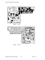
General
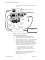
This section tells how to service and align the T1G, T1, TC1, and the
discontinued T1P Body-Pack Transmitters (Figure 1). These single-channel, crystal-controlled units operate in the 169 MHz to 216 MHz VHF
Band.
ÁÁÁÁÁ
Á
ÁÁ
ÁÁÁÁÁÁ
ÁÁÁÁÁ
ÁÁÁÁÁÁ
Á
ÁÁÁÁÁÁ
ÁÁÁÁÁÁ
Á
ÁÁÁÁÁÁ
ÁÁÁÁ
ÁÁÁÁÁ
Á
ÁÁÁÁÁÁ
Á
ÁÁÁÁÁÁ
ÁÁÁÁ
ÁÁÁÁÁ
ÁÁÁÁÁÁ
ÁÁ
Á
ÁÁÁ
ÁÁ
ÁÁÁÁÁÁ
ÁÁÁÁÁ
ÁÁÁÁÁÁ
ÁÁ
Á
ÁÁÁÁ
Á
ÁÁ
Á
Á
Á
ÁÁÁÁ
ÁÁ
Á
Á
ÁÁÁÁÁÁ
ÁÁÁÁÁ
ÁÁÁÁÁ
Á
Á
ÁÁÁÁ
Á
Á
ÁÁÁÁÁÁ
ÁÁÁÁÁ
ÁÁÁÁÁ
Á
Á
ÁÁÁÁ
Á
ÁÁÁÁÁÁ
ÁÁÁÁÁ
ÁÁÁÁÁ
Á
Á
Á
Á
ÁÁÁÁÁÁÁ
Á
ÁÁÁÁÁÁÁÁÁÁ
ÁÁ
Guitarist T1G
and TC1 Trans-
ÁÁ
ÁÁÁÁÁ
ÁÁÁÁÁÁ
Á
ÁÁÁÁÁÁ
Á
ÁÁÁÁÁÁ
ÁÁÁÁÁ
ÁÁÁÁÁÁ
Á
ÁÁÁÁÁÁ
ÁÁÁÁÁ
ÁÁÁÁÁÁ
ÁÁÁÁ
Á
ÁÁ
Á
Á
ÁÁÁÁÁÁ
ÁÁÁÁÁ
ÁÁÁÁÁÁ
ÁÁÁÁ
ÁÁ
Á
ÁÁÁÁÁ
Á
ÁÁ
Á
Á
ÁÁ
Á
ÁÁÁÁÁÁ
Á
ÁÁÁÁÁ
Á
ÁÁÁÁ
Á
ÁÁÁÁ
ÁÁÁÁÁ
Á
Á
Á
Á
ÁÁÁÁÁ
ÁÁÁÁ
Á
Á
Á
ÁÁÁÁÁÁ
ÁÁÁÁÁ
Á
ÁÁÁÁ
ÁÁÁÁÁ
Á
Á
Á
ÁÁÁÁÁÁ
ÁÁÁÁÁ
Á
ÁÁÁÁÁ
Á
Á
Á
ÁÁÁÁÁÁ
Á
ÁÁÁÁÁÁÁÁÁ
Á
ÁÁÁ
ÁÁÁÁ
Á
ÁÁ
Presenter T1P
Transmitter
(discontinued
model)
Presenter T1
Transmitter
mitter
1
2
Á
Á
ÁÁ
Á
Á
ÁÁ
Á
Á
Á
Á
Á
Á
Á
Á
Á
Á
Á
Á
Á
Á
Á
Á
ÁÁ
Á
ÁÁÁÁ
4
3
Figure 1.
1. Phone jack 1/4Ȃ (guitar or headset input)
2. Antenna
3. Tini “Q-G” (Lavalier, headset, WA302 input)
4. Lavalier microphone
Service Note: Shure recommends that all service procedures be
performed by a factory-authorized service center or returned directly
to Shure Brothers Inc.
Licensing: Operation may require a user license. Frequency or
power-output modifications may violate this product’s approvals.
Contact your country’s communications authorities.
E1999, Shure, Inc.
Printed in U.S.A.
25C1016 (CC)
1
Characteristics
Shure T1 Body-Pack Transmitters
Circuit Description
The T1 transmitter contains one circuit board which comprises an
audio and an RFsection. It is intended for use with the matching T3 and
T4 receivers.
Audio Section
Input: Audio signals enter via a 1/4-in. phone jack, with the signal on
the tip and the ground on the ring (T1G), an attached microphone (the
discontinued model T1P), or a four-pin, Tini Q-G, connector (T1):
S
Pin 1: Ground
S
Pin 2: Supplies regulated 5 Vdc bias for electret condenser microphones
S
Pin 3: Audio input
S
Pin 4: 20 kΩ load resistor connected to pin 3 for Shure electret
microphones
Preamplifier Stage: This is centered in one section of the operational amplifier (U102C). An externally accessible potentiometer (R125) adjusts the voltage gain of this stage over a 40 dB range.
Passive Pre-emphasis Network and Compandor: The network
(R145, C110, C111, R112, and R115) has a pole at 63 microseconds and
a zero at 1 microsecond. The NE571D integrated circuit compandor
(U101A) provides a 2:1 logarithmic compression of the audio signal.
Noise and Distortion: U102A lowers the noise floor, and an internal
potentiometer (R130) nulls the system audio distortion. Operational amplifier U102B, operating as a two-pole, active, low-pass filter, restricts the
bandwidth of the system to audio frequencies.
Limiting: PNP transistors Q103 and Q104 limit the level of the audio
signal leaving the audio section via U102B. Beginning in July 1995, this
section was removed from the “A,” “B,” and “C” boards but left in a newly
designated “T” board.
5 Vdc Bias and LED Drive Circuits: The NE571D’s identical second
channel (U101B) supplies regulated, low-noise 5 Vdc bias to various
audio and RF circuit points. Transistor Q105 provides “reverse battery
protection” to the circuit. Q106 drives LED D101 (“Power On”), and Q107
drives LED D102 (“Low Battery”).
RF Section
Audio Input: Processed audio enters R217, an internal potentiometer that is adjusted for 15 kHz deviation (100% modulation) when the
audio section provides a –2.2 dBV, 1 kHz tone.
Oscillation: The audio then goes to varactor diode D201, which is
part of the modulated oscillator-tripler stage (Q201). The latter’s baseemitter circuit operates as a crystal-controlled Colpitts oscillator in the
20 MHz region. Fundamental-mode crystal Y201 is tuned 10 kHz below
series resonance by the series combination of frequency-netting coil
Characteristics
2
25C1016 (CC)
Shure T1 Body-Pack Transmitters
L209, diode D201, capacitor C214, and capacitor divider C224 and
C230.
Frequency and Temperature Stability: To ensure frequency stability despite changes in the battery voltage, regulated 5 Vdc bias is applied to the varactor diode and to the base of Q201. Temperature compensation is provided by C224, C230, and C214.
Tuned Circuits
Stage 1: The collector circuit of Q201 is tuned to the third harmonic
of the oscillator frequency (approximately 60 MHz) by L205, C225, C234,
L202, C217, and C233. (The latter components also form a capacitivelytapped voltage divider for matching the signal to the base of Q203.) The
output is double-tuned to provide high-spectral purity. Regulated dc bias
is again employed to minimize changes in loading on the oscillator stage
and to stabilize the drive levels.
Stage 2: Q203 operates as a frequency tripler, with its collector circuit tuned to the output frequency (for example, 180 MHz). In this case,
L204, C215, C237, C236, L207, C235, and C222 perform tuning and
impedance-matching functions. As in the preceding stage, regulated dc
bias is applied to the base circuit to stabilize the drive level, and the
output is double-tuned to provide spectral purity.
Stage 3: Q204 operates as a tuned amplifier. Resistive loading on
the input provides stability. The output circuit consists of a resonant tank
circuit (L203 and C213) capacitively coupled to a low-pass filter (C219,
L206, and C218). C213 and C219 provide a capacitively tapped voltage
divider for matching into the low-pass filter.
Transmitter Output
Transmitter: This can deliver up to +17 dBm (50 mW) to the antenna. No user adjustment permits this value to be exceeded. The unit
should be powered exclusively by a 9 Vdc dry battery (an alkaline type,
such as a Duracell MN1604, is recommended).
Voltage Measurements: With 9 Vdc applied to the unit, the following voltages should appear at the terminals of the output transistor;
S
Vc = 8.88 Vdc
S
Vb = .450 Vdc
S
Ve = .473 Vdc.
S
Base current = .29 mAdc
S
Emitter current = 21.5 mAdc
S
Collector current = 21.8 mAdc
S
Power input = 183 mW
The output power is +16.5 dBm (44.7 mW) into a 50 Ω load, at a frequency of 169.445 MHz. At the minimum acceptable battery voltage of
6 Vdc, the final collector current drops to 15 mAdc and the output power
declines to +13.9 dBm (24.4 mW).
25C1016 (CC)
3
Characteristics
Shure T1 Body-Pack Transmitters
Antenna: This is a quarter-wavelength, permanently attached, flexible wire. The ground plane of the circuit serves as an untuned counterpoise capacitively coupled to the body of the user.
Spurious Emissions: To minimize the production and radiation of
spurious emissions and harmonic energy, and to promote stable operation, the collector of each RF stage is separately decoupled from the
9-volt supply by ferrite chokes, resistors, and bypass capacitors. The
base circuits are similarly decoupled except that they use resistor-capacitor (R-C) networks, whose higher-impedance levels are more appropriate.
Characteristics
4
25C1016 (CC)
Shure T1 Body-Pack Transmitters
Preliminary Tests
Listening Tests
Before disassembling the unit, operate it to determine whether it is
functioning normally.
Focused Testing: First and most important: Review any customer
complaint or request and focus your listening and functional tests on any
reported problem. For example, for “short range” and “drop-outs” complaints, perform only the RF tests in this section. If the unit passes these,
there is a strong indication that the customer is using the product incorrectly (e.g., not keeping the transmitter in the receiver’s line of sight, not
avoiding metal enclosures or TV interference). Return the unit to the customer together with an explanation of the proper set-up procedures.
For complaints of distortion or other audio problems, try a “standard”
lavalier or headset microphone (you should have one of each microphone on-hand for testing) and perform the audio tests in this section.
Functional Tests
RF Tests
1. Remove the case top, mute the audio, and apply 9 Vdc to the
battery terminals.
2. Measure the current drain: it should not exceed 35 mA.
3. Maximize the signal received on the spectrum analyzer by attaching a telescoping whip antenna to it. Then measure the
near-field output power: it should be 7 dBm.
(If you are unsure of the results you obtain here, measure the
output power conductively by soldering a 50 Ω cable to the output of the transmitter. Verify that the output power is 15 dBm,
2 dBm.)
4. Verify that the carrier frequency of the transmitter varies from its
nominal value by no more than "6 kHz.
5. Check for an intermittent problem by shaking the transmitter and
tapping on it. As you do so, try to keep it at a constant distance
from the spectrum analyzer. Verify that the output power on the
spectrum analyzer shows no large and sudden drops in power
level (it will, however, vary a few dB with hand position).
6. Turn off the transmitter.
If the transmitter passes the above tests, its RF circuits are
working as designed.
Audio Tests
A: Verify the Matching Receiver
1. Connect the signal generator to the receiver through a 50 Ω
cable. Tack-solder the center conductor to the antenna input and
ground the shield of the cable to pcb ground.
25C1016 (CC)
5
Preliminary Tests
Shure T1 Body-Pack Transmitters
2. Set the RF generator as follows:
Amplitude: –20 dBm
Modulation: 1 kHz
Deviation: 15 kHz
Frequency: T1 operating frequency
3. Connect the audio from the unbalanced output to the audio analyzer with a 3.3 kΩ load. Turn the Volume control all the way up.
4. For the associated T3 or T4, verify the following:
S
audio level is 400 mVrms ("90 mV)
S
thd = <0.75%
B: Check the Transmitter
1. Disconnect the signal generator from the receiver. Monitor the
receiver’s unbalanced audio output with a 3.3 kΩ load and the
audio analyzer. Check that the receiver’s Volume control is still
at its maximum setting.
2. Unmute the transmitter and turn its gain to the minimum setting.
Connect an input cable as follows:
T1 and T1G: Use adapter cables to input the audio to the bodypack input.
T1P: Disassemble the case, remove the microphone, and attach
the adapter cable to the four-pin header of the audio input.
3. Inject a 775 mV, 1 kHz signal from the audio analyzer into the
adapter cable and verify the following:
S
the amplitude from receiver’s unbalanced output equals
400 mVrms ("90 mV)
S
thd = <0.75%
4. Change the frequency of the audio generator to 100 Hz and disengage the 400 Hz high-pass filter from the audio analyzer.
Verify that the audio level is –1 dB ("0.7 dB) relative to the level
measured in step 3.
5. Change the frequency of the audio generator to 10 kHz and reengage the 400 Hz high-pass filter. Verify that the audio level,
relative to that measured in step 3, is 0 dB, "1 dB.
Units That Pass
If the system components pass these tests and the microphone is
good, then the system is functioning as expected and shouldn’t require
tuning and alignment. Inform the customer that the product has retested
within specifications.
Preliminary Tests
6
25C1016 (CC)
Shure T1 Body-Pack Transmitters
Disassembly and Assembly
To access the printed circuit (pc) board, disassemble the transmitter.
CAUTION
Observe precautions when handling this static-sensitive device.
Disassembly
1. Slide open the battery-compartment cover and remove the battery.
2. With a #1 Phillips screwdriver, remove the four screws securing
the back of the case, and set them aside.
3. Carefully separate the top and bottom halves of the case to expose and lift out the pc board. (If you have trouble separating the
case, carefully slit the label covering the case separation inside
the battery compartment.)
Reassembly
Reassemble the T1 Transmitter as follows:
1. Presenter T1P transmitter only: Plug the lavalier microphone
connector into J104.
2. Place the pc board in the bottom half of the case.
3. Slide the battery-compartment cover into its slot.
4. Align the rubber grommets (antenna, lavalier) while positioning
the top half of the case over the bottom half.
5. Make sure the two sections are properly seated before securing
them with the four Phillips screws.
25C1016 (CC)
7
Disassembly and Assembly
Shure T1 Body-Pack Transmitters
Converting a T1P to a T1
Because direct replacements for the lavalier microphones used in
the T1P are no longer available, the best way of replacing the microphones in these earlier units is to replace the lavalier header with a male
Tini Q-G connector, which will allow the unit to accept a WL93 or other
microphone that has a mating connector. Changing the connectors in
effect converts the T1P into a T1 unit.
Parts Needed
Microphone with a female Tini Q-G connector (e.g., Shure WL93).
Part order RPW262 for all the following items:
S
male Tini Q-G connector with a pcb assembly
S
spacer
S
nut
Conversion Procedures
1. After separating the two halves of the case, remove the pc board
and the microphone. Pull the female connector wired to the microphone from the pcb header, J104.
2. Remove the header by unsoldering its four pins from the bottom
of the pcb (the side with fewer components). Make sure the four
holes in the pcb are open.
3. Orient the pcb assembly with the top (major-component) side up,
the switches and LEDs to the left, and the antenna to the right.
4. Pull off the pre-cut insulation from the ends of the connector assembly’s ribbon cable. From the top of the transmitter board,
insert the cable wires into the four holes vacated by the header:
the black coded lead goes into the hole nearest the right edge of
the pcb (towards the pcb number).
5. Solder the wires to the bottom of the pcb and cut off the excessive leads.
6. After replacing the transmitter’s pcb in the bottom half of the
case, insert the connector into the front slot. Place the spacer
and start the nut on the part of the connector that protrudes from
the case.
7. After completing the reassembly, tighten the nut on the Tini Q-G
connector.
Disassembly and Assembly
8
25C1016 (CC)
Shure T1 Body-Pack Transmitters
Service Procedures
Reference Material
The Shure Wireless Systems: T Series User’s Guide provides a description, information on operation and troubleshooting, and technical
data.
Special Equipment
The Wireless Service Equipment manual covers the standard items
needed for servicing the transmitters. If you do not have the modified
SC4 receiver described there, you will need an appropriate receiver (usually T3 or T4) to verify that the transmitter is working properly.
System Operating Frequencies
Each transmitter circuit board is marked with a group letter (A, B, C,
or T) that identifies the range of frequencies on which the transmitter can
operate. Table 1 shows the Group Letter and its associated frequencies.
Note that this chart applies only to the T1 series.
Table 1
(90_8552F) Pc Board Groups
Group
Frequency Range
A 169.000–183.975 MHz
B 184.000–198.975 MHz
C 199.000–215.975 MHz
T “AC,” “V,” & “W” frequencies
Used with pcb assembly 90_8552F
(pcb marking 34A8459F)
Table 2 provides information for identifying the system frequency.
The Crystal Letter Code, when used with the appropriate Shure model
number, identifies a specific operating frequency for both transmitters
and receivers. Note that, although a Crystal Letter Code always designates a specific frequency, it may be used with different Group Letters on
other products.
Group T: Beginning in July 1995, “V” and “W” frequencies, formerly
assigned to the “A” board, were reassigned to a newly designated “T”
board (see the “Audio Alignment” subsection in “Service Procedures”).
25C1016 (CC)
9
Service Procedures
Shure T1 Body-Pack Transmitters
Table 2
T1 Series System Operating Frequencies
Group
Crystal Code
Freq. (MHz)
T
V
169.445
T
AC
170.245
T
W
171.845
A
CA
176.200
A
CC
177.600
A
CE
182.200
A
CF
183.600
B
CG
186.200
B
CL
192.200
C
CQ
202.200
C
CV
208.200
Changing the Frequency
The operating frequency of the T1 transmitter may be changed within a specific group by changing the crystal on the pc board. (For Group
information, see the preceding section.) Check the transmitter for proper
operation before attempting to change its operating frequency. After installing the new crystal, perform the alignment procedures. Then run an
operational test to ensure the transmitter is functioning properly. Finally,
update the label to show the new frequency and letter identification code.
Note: To ensure proper operation, obtain the crystal from Shure and
verify that it operates within the frequency range of the pc board.
Since crystals are marked with their nominal oscillating frequency,
not a letter code, you can use the following equation to determine
the frequency at which a transmitter will operate with a given crystal:
Carrier Frequency = (9 nominal crystal freq. in MHz) –.09
Alignment
The RF and audio alignments are generally done together, as a
single, continuous procedure. Before beginning, be sure to do the setup
described in the following subsection, “Test Conditions.”
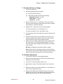
Test Conditions
The following test conditions apply unless otherwise specified (see
Figure 2):
Service Procedures
S
An external 9-volt supply is connected to the battery terminals
(J101 and J102).
S
The Power On/Off switch is off.
S
The Mute switch is set to “Mute.”
10
25C1016 (CC)
Shure T1 Body-Pack Transmitters
Pins
1
2
3
4
S
The Gain pot (R125) is preset to its midpoint.
S
The 400 Hz high-pass and the 30 kHz low-pass filters on the
audio analyzer are activated.
T1P (Connector J104)
3 4 1
L209
R217
T1G (1/4I
T1 (Tini “Q-G,” J201—solder side)
2
Y201 C217
Spectrum Analyzer
or
Frequency Counter
C215
phone jack,
J103)
O
ÊÊ
TP4
O
TP3
J101 –
Battery
terminals
J102 +
R125
R130
LED (red)
“Low Battery”
(D102)
M
O u
n t
e
Mute
switch
(S101)
“Power On”
LED (green)
(D101)
Power On/Off
switch (S102)
T1 (Tini “Q-G”) pins:
1: Ground
2: +5 V
3: Audio
4: 20 kΩ to ground (connected
to pin 3 in the microphone)
Figure 2. Pc Board: Key Parts Locations
Test Cable
Use a 50 Ω coaxial test cable to connect the pc board with various
test equipment (see Figure 2). To construct the 50 Ω test cable, see the
Wireless Service Equipment manual.
1. Unsolder the antenna lead from the pc board.
2. Attach the center conductor of the 50 Ω RG174 cable to the antenna
solder pad, and the shield to ground.
3. Turn on the T1.
25C1016 (CC)
11
Service Procedures
Shure T1 Body-Pack Transmitters
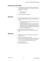
TP2
TP1
TP5
TP3
TP9 (–)
Limiter components
(not in all units)
TP6
TP8 (+)
TP7
TP4
Test Points
TP1
Audio In, J104, pin 3, Model T1-P.
TP2
Audio In, J103, center conductor
of 1/4-in. phone jack, Model T1-G.
TP3
Audio
TP4
Antenna Output
TP5
Intermediate Output
TP6
9 Vdc
TP7
5 Vdc
TP8
(+) Battery
TP9
(–) Battery
Figure 3. Pcb Side 1
Display Checks
1. Connect the 9 Vdc power supply: the green LED should glow.
2. Reduce the power supply voltage to 6 Vdc: the red LED should
glow.
3. Return the power supply voltage to 9 Vdc.
4. Verify that 9 Vdc 〈±0.35 Vdc) is present at TP6.
5. Verify that 5 Vdc 〈±0.25 Vdc) is present at TP7.
RF Alignment
A: RF Power and Frequency
1. Connect the 50 Ω output cable to the spectrum analyzer. Make
sure S101 is in the “Mute” position.
2. Set the spectrum analyzer as follows:
S
Center Frequency: transmitter’s
S
Span: 1 MHz
S
Reference Level: +20 dBm
S
Scale: 10 dB/div
3. The output power should measure 15 dBm ( ±2 dBm) taking into
account cable losses. If the power is within specification, skip to
step 6.
4. Adjust C217 for maximum (peak) output power on the spectrum
analyzer.
Note: Once the signal is close to its maximum, setting the spectrum analyzer scale (under the amplitude menu) to 2 dB/div may
make fine adjustments easier.
5. Adjust C215 for maximum output power on the spectrum analyzer. The output power should measure 15 dBm (±2 dBm) taking
into account cable losses.
Service Procedures
12
25C1016 (CC)
Shure T1 Body-Pack Transmitters
6. Connect the 50 Ω output cable to the frequency counter. If the
frequency is off by more than 5 kHz, adjust L209 to set the carrier frequency to FC ±1 kHz.
7. Reconnect the 50 Ω output cable to the spectrum analyzer. Confirm that the output power remains within specification. If necessary, readjust C217 and C215.
B: Spurious Emissions
1. Set the scale on the spectrum analyzer back to 10 dB/div.
2. Check the level of spurious emissions up to 1 GHz. Set the start
frequency of the spectrum analyzer to 10 MHz and the stop frequency to 1 GHz. All spurs must be at least 35 dB below the
carrier level. If necessary, adjust C217 and C215 until the power
and spurious response are both within specification.
C: Current Drain
1. Using a milliammeter, make sure that the transmitter’s current
drain is less than 35 mA. If it is too high, try detuning C215, taking care that the power and spurious response remain within
specification.
2. Disconnect the power supply from the T1.
3. Unsolder the 50 Ω RG174/U test cable, and resolder the antenna
lead to the RF board.
Audio Alignment
This section continues the procedures of the preceding subsections.
D: Gain
1. Reconnect the power supply to the T1, and set its Mute switch to
“On.”
Set the audio analyzer output as follows:
Frequency: 1 kHz
Amplitude: 70 mV
2. Connect the audio analyzer’s output to the transmitter’s microphone input. Select the cable with the proper termination:
(a)
T1: Tini Q-G (quick-ground) connector
(b)
T1G: 1/4-in. phone plug
(c)
T1P: cable’s unterminated center conductor to pin 3 of
J104; shield to ground
3. Adjust the Gain pot (R125) for 775 mVac, ±10 mVac (0 dB,
±0.1 dBu) at TP3 (turning counterclockwise increases the gain).
Record the voltage at this setting.
Note: At this point you may want to press the audio analyzer’s
Log/Lin button (to measure logarithmically) and activate the Ra-
25C1016 (CC)
13
Service Procedures
Shure T1 Body-Pack Transmitters
tio button to perform the relative measurement in the next subsection.
T1G (1/4I
Pins
1
2
3
4
T1P (connector J104)
3 4 1
T1 (Tini “Q-G,” J201—solder side)
2
R217 L209
phone jack,
J103)
Y201 C217
C215
O
TP4
O
TP3
J101 –
Battery
Terminals
J102 +
R125
R130
M
O u
n t
e
“Power On”
LED (green)
(D101)
LED (red)
“Low Battery” Mute
(D102)
Switch
(S101)
out
Power On/Off
Switch (S102)
Audio Analyzer
in
Receiver
Figure 4. Audio Test Configuration for T1
E: Audio Frequency Response
1. Change the frequency of the audio analyzer to 100 Hz.
2. Deactivate the audio analyzer’s 400 Hz high pass filter.
3. Check that the audio level is equal to –1 dB (0.5 dB) relative to
the level measured at TP3 in step 3 of subsection D (“Gain”).
4. Activate the 400 Hz high pass filter on the audio analyzer.
5. Change the frequency of the audio analyzer to 10 kHz. Because
the limiter circuitry was removed from most units made after
June 1995, the audio level will vary with the unit you have:
S
All “V” And “W” frequency units: +3.1 dB (±0.5 dB)
S
All units made through 6/95: +3.1 dB (±0.5 dB)
S
All non-“V” and “W” units made after 6/95: +4.85 dB
(±0.5 dB)
Note: pc boards with the limiter components (see Figure 3)
should have the lower (+3.1 dB) audio output level.
6. Disengage the ratio function.
Service Procedures
14
25C1016 (CC)
Shure T1 Body-Pack Transmitters
F: Deviation Reference Voltage
1. Turn off the transmitter.
2. Set the RF signal generator as follows:
(a)
Enter the carrier frequency.
(b)
Select FM modulation and enter the following:
Modulation Source: Int 1 kHz
FM Deviation: ±15 kHz
Amplitude: –38 dBm
3. Select a receiver for the T1, making sure it is set to the same
frequency as the transmitter. Disconnect the receiver’s antenna
(non-diversity) or antennas (diversity).
4. Solder the 50 Ω cable to the receiver’s antenna pads:
T3: Center conductor to TP1, and shield to TP2
T4: Center conductor to TPA1, and shield to TPA2
5. Connect the BNC end of this cable to the output of the RF signal
generator.
6. Set the Volume control on the front panel of the receiver to its
maximum position (fully clockwise). Then turn on the receiver
and set its Squelch control to the midpoint position.
7. Measure the rms voltage developed across the unbalanced output of the receiver. You should find approximately 775 mVac.
This is the audio output voltage that corresponds to a deviation
level of 15 kHz.
Record this voltage as the deviation reference voltage.
Note: At this point you may want to press the audio analyzer’s
Log/Lin button (to measure in dBm) and activate the Ratio button
to perform the relative measurement in the next subsection.
G: Deviation Adjustment
1. Turn off the RF switch on the RF signal generator.
2. Remove the test cable from the receiver and reconnect the antenna(s) to the receiver board.
3. Turn on the T1 and set its Mute switch to “On.”
4. Reconnect the output of the audio analyzer to the input of the
T1.
5. Reset the frequency of the audio analyzer to 1 kHz. Make sure
that 775 mV is still present at TP3.
6. Measure the voltage at the unbalanced output of the receiver.
Adjust R217 for 0 dB (±1 dB) relative to the deviation reference
voltage measured in step 7 of the preceding subsection.
25C1016 (CC)
15
Service Procedures
Shure T1 Body-Pack Transmitters
7. Set the audio analyzer to measure distortion. Verify that the audio distortion at the unbalanced output of the matching receiver
is less than 0.5%. If necessary, adjust R130 to obtain minimum
distortion.
Note: For T1G transmitters Only: After completing the alignment,
turn the audio Gain potentiometer (R125) all the way down (fully
clockwise as viewed from the top side of the circuit board).
Service Procedures
16
25C1016 (CC)
Shure T1 Body-Pack Transmitters
Bench Checks
Dc Power
n Verify that 9 Vdc (±0.35 Vdc) is present at TP6. If this voltage is
low, trace the circuitry back to the power supply to see where the
loss occurs. Check:
S
power switch
S
bias on Q105
S
L101
S
circuit-board ground for 0 V
n If you have a short to ground from 9 V, try isolating different parts
of the circuit. Narrow it down to the RF or audio section. Look for
foil shorts, solder bridges, and capacitors that have been
installed backwards.
n Check for 5 Vdc (±0.25 Vdc) at TP7 (pin 7 of U101). If the correct
voltage is not present, check:
S
pin 13 of U101 for 9 V
S
values of R133, R135, and R137
Audio
All the steps in this section comprise a methodical way of determining where the audio signal is being interrupted:
n Check for audio at pin 7 of U102. If it is not present, check that
the dc bias at pins 5, 6, and 7 of U102 is `4.5 Vdc (half the level of the supply voltage). If the correct voltage is not present:
S
Trace the circuitry: this bias derives from the 9 V line through
voltage divider R103 and R105, then through R106 to pin 5.
S
Look for foil shorts, incorrect parts, and bad connections.
n If there is audio at pin 7 of U102 but not at pin 14, check the dc
bias at pins 12 and 13 (`1.8 Vdc) and pin 1 (`3.7 Vdc). If the
correct voltage is not present:
S
Trace the circuitry: this dc bias proceeds from pin 9 of U101
through R107 to pin 12 of U102.
S
Check (a) the parts in the feedback path from pin 14 to
pin 13, (b) the parts connected to pin 7, and (c) the connections from U102 to U101.
n Check the connections from pin 14 of U102 to the next stage, to
the limiter (Q103), and to pin 15 of U101.
25C1016 (CC)
17
Bench Checks
Shure T1 Body-Pack Transmitters
n Check the bias voltage (`4 Vdc) on pins 8, 9, and 10 of U102. If
the correct voltage is not present:
S
Make sure the Mute switch is set to “On.”
S
Trace the bias circuit from the 5 V line through R104 to
pin 10 of U102.
S
Check the values in the feedback path from pin 8 to pin 9 of
U102, and the path to Q104 and pin 16 of U101.
Frequency Problem
n Make sure the RF carrier is at least 10 dB higher than the spurious emissions, to allow the frequency counter to lock on.
n Check L209 for the proper group and make sure its core is not
cracked.
n Make sure the crystal (Y201) has the correct frequency.
n Check the dc bias for Q201 against the readings of a unit known
to be operating correctly.
n Make sure that D201 is the correct varactor and has 5 Vdc on its
cathode.
n Check the parts and values of the oscillator circuit (from TP3 to
TP5).
n Look for shorts and opens.
Low Output Power
n Check the carrier output power after the oscillator stage (TP5). If
there is no signal, refer to the preceding subsection, “Frequency
Problem.”
The remaining steps perform basically similar diagnostics for each of
the three RF stages:
n Stage 1: Make sure that rotating C217 360 degrees in either direction produces two separate peaks in the carrier output amplitude. If there is only one peak, check the color (value) of C217
and the values of L205, C225, C234, L202, and C233. Check
the bias on Q201. Lastly, replace Q201.
n Stage 2: Make sure that rotating C215 360 degrees in either direction produces two separate peaks in the carrier output amplitude. If there is only one peak, check the color (value) of C215
and the values of L204, C237, C236, L207, C235, C222, and
C226. Check the bias on Q203. Lastly, replace Q203.
n Stage 3: Check the dc bias on Q204 and the values of all the
parts from the base of Q204 to TP4. Lastly, replace Q204.
n If the power is slightly low and the spurious levels are high,
check for wrong or open coils at L202, L207, and L206.
Bench Checks
18
25C1016 (CC)
Shure T1 Body-Pack Transmitters
Excessive Current Drain
n Try readjusting C215 for lower current drain while maintaining
output power to specification. If the current drain is still excessive, check for the following:
S
short
S
wrong resistor value
S
shorted capacitor
n As a last resort, try changing Q204.
Deviation
n If R217 cannot be adjusted to obtain a "15 kHz deviation, try to
isolate the problem to the audio or RF section by doing the following:
S
If TP3 does not measure –2.2 dBV (775 mV), refer to the
“Audio” subsection, above.
S
If TP3 has the right level, check R217, C220, C227, R208,
R216, D201, R209, L209, and C214. Also make sure that
the cathode of D201 is being supplied with a 5 Vdc bias from
the 5 V Line through R216 and R208. The value of C214 is
critical to the deviation sensitivity.
n As a last resort, try replacing D201 and Y201.
n Make sure the carrier is good: you need that to get any deviation.
Distortion
n Make sure the analyzer’s 400 Hz high-pass and 30 kHz lowpass filters are ”In.”
n Pin 9 of U101 should read about 1.8 Vdc.
n As you turn R130, the dc level on its wiper should change from
about 1.5 V to 3.5 V. If it does not, check R129, C125, R130,
R141, R140, R126, and the parts tied to pin 9 of U101.
n Check the audio level.
n Lastly, replace D201 and Y201.
25C1016 (CC)
19
Bench Checks
Shure T1 Body-Pack Transmitters
Notes:
Notes:
20
25C1016 (CC)
Shure T1 Body-Pack Transmitters
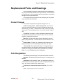
Replacement Parts and Drawings
On the next page, the parts are listed according to the designations
from the pc board and schematic (see Figures 5 and 6, and the schematic). Parts shown on the circuit diagram and not listed below are available
through electronic-parts distributors.
On the pages following the parts list are the drawings of the printed
circuit boards and the schematics.
Product Changes
This section briefly describes significant changes to the T1.
Limiter Circuitry and “V” and “W” Frequencies: The limiter circuitry was removed from Group A, B, and C boards (see Figure 3 and
the schematic). The older “A” board with the limiter circuitry (now designated as the “T” board) handles just the “V” and “W” “traveler” frequencies.
T1 and T1P: The Model T1P (with a permanently attached lavalier
microphone) was replaced by the model T1 (with a Tini Q-G connector
instead of an attached microphone).
Belt Clip: The older metal-plate clip was replaced by a wire-andplastic, spring-loaded clip. A new case bottom accommodates the new
clip.
Quad Op Amp: The older part (manufactured by Raytheon) was
replaced; the former value of associated resistor R107 was 100 kΩ.
“F” Assembly: This update added Group T, enlarged the hole for
the antenna bracket, and changed the following parts from the earlier
numbers or values given in parentheses: Q106 and Q107 (183A02)),
R228 (0 Ω), S101 (55A8020), and S102 (55B8020).
Parts Designations
The following comments apply to the parts lists and the schematic:
Resistors: All resistors are surface-mount with 1/10 W rating and 1%
tolerance.
Capacitors: Unless otherwise noted, non-polarized capacitors are
surface-mount NPO dielectric types with a 100 V capacity and a 5% tolerance, and polarized capacitors are tantalum types.
Temperature-Compensating Capacitors (N750): C214, C224,
C230.
Coils: These parts are rated in microhenries.
25C1016 (CC)
21
Replacement Parts and Drawings
Shure T1 Body-Pack Transmitters
Table 1
T1 Replacement Parts
Drawing
Designation Description
Source:
Shure Part No. (Commercial Alternate)
A1 Printed circuit board assembly T1G:
(Order the antenna, and 1/4-in phone
jack separately)
Printed circuit board assembly T1P:
(Discontinued, for modification see pg. 8)
Shure T90__8552 [See Table 2, to determine the Frequency Code in the underlined
space. e.g. T90CF8552].
Printed circuit board assembly T1:
(Order the antenna, and pcb with Tini
“Q-G” connector seperately)
A2 Wireless miniature omnidirectional
lavalier microphone
Shure 98A195 (no longer available)
To adapt a T1P transmitter to work with
other microphones, see “Converting a T1P
to a T1) on page 8.
C215 Capacitor, variable 3–10 pF
Shure 152C02
D101 Light-emitting diode, green (power)
Shure 86A8959
D102 Light-emitting diode, red (low battery)
Shure 86B8959
D103 Dual diode
Shure 184A08 (MMBD7000L)
E1 Antenna
Shure 70C8007
J101, J102 Battery terminals
J103 Phone jack,
1/
4-in
Shure 56A8043
(mounted on T1G)
Shure 95A8535
J104 Side entry shrouded header
(mounted on T1P)
Shure 95C8545 (no longer available)see
“Converting a T1P to a T1) on page 8.
J201 Mic Pcb and microphone receptacle
ass’y
Shure 95A8823
MP1 Battery door
Shure 65A8352
MP2 Compression pad, battery
Shure 38A185
MP3 Case (top, T1/T1G)
Shure 65B8203
MP4 Case (bottom, T1/T1G)
Shure 90A8706
MP5 Belt clip
Shure 90A4392
MP6 Phillips pan-head hi-lo screw #4 x 5/8I
Shure 30E1245
MP7 Nut for QG mic connector
Shure 31A8140A
MP8 Spacer
Shure 31A8039A
MP9 Case (top, TC1)
Shure 65B8203B
MP10 Case (bottom, TC1)
Shure 65A8270B
MP11 Contains: MP1, MP2, MP5, MP6, MP7,
MP8
RPW616
MP12 Mic connector / PCB assembly
RPW262
MP13 Battery polarity label
39A8092
Q103, Q104 PNP transistor (Group T only)
Replacement Parts and Drawings
Shure 183A01
22
25C1016 (CC)
Shure T1 Body-Pack Transmitters
Drawing
Designation Description
Source:
Shure Part No. (Commercial Alternate)
Q105 PNP transistor
Shure 183A07 (MMBT404AL)
Q106, Q107 NPN transistor
Shure 183A38 (MMBT5089LT1)
Q201, Q203, NPN transistor
Q204
Shure 183A03 (MMBTH10)
R125 Potentiometer, trim, 100 kΩ
Shure 46D8049
R130 Potentiometer, trim, 20 kΩ
Shure 146F02
R217 Potentiometer, trim, 10 kΩ
Shure 146E02
S101 Switch, Mute
Shure 55C8020
S102 Switch, Power
Shure 55C8055
U101 Integrated circuit, compandor
Shure 188A01 (Signetics NE571D)
U102 Quad op amp
Shure 188A49 (MC33179DR2)
Y201 Crystal
Shure 40_8006A (SeeTable 2, p. 10 in
“Service Procedures” to determine the letter in the blank space.)
Table 2
Frequency-Dependent Parts
A
B
C
T
Grp
Freq. 169.000–183.975 184.000–198.975 199.000–215.975 169.000–173.975
Not used
Not used
Not used
4.7 µF, 16 V
C118
Not used
Not used
Not used
4.7 µF, 16 V
C119
8.5–40 pF
4.5–20 (0.1 ) pF
4.5–20 pF
8.5–40 (0.1) pF
C217
27 pF
22 pF
18 pF
27 pF
C222
15 pF
12 pF
8.2 pF
15 pF
C225
100 pF
100 pF
82 pF
100 pF
C233
4.7 pF
3.3 pF
2.2 pF
4.7 pF
C237
22 pF
22 pF
18 pF
22 pF
C238
3.9 pF
2.7 pF
2.2 pF
3.9 pF
C239
162D06
162D06
162E06
162D06
L203
82A8015
82B8015
82C8015
82A8015
L209
Not used
Not used
Not used
1 kΩ, 1%
R122
Not used
Not used
Not used
1 kΩ, 1%
R123
Not used
Not used
Not used
1.5 kΩ, 1%
R127
Not
used
Not
used
Not
used
1.5 kΩ, 1%
R128
Not used
Not used
Not used
183A01
Q103
Not used
Not used
Not used
183A01
Q104
Note: See Tables 1 and 2 for information on the crystal.
25C1016 (CC)
23
Replacement Parts and Drawings
Shure T1 Body-Pack Transmitters
34AB8459F
Figure 5. Pcb Side 1
Figure 6. Pcb Side 2
Replacement Parts and Drawings
24
25C1016 (CC)
Shure T1 Body-Pack Transmitters
TP 5
TP 2 TP 1
TP 4
TP 3
TP 9 (–)
TP 6
TP 7
TP 8 (+)
TP – Test Points
TP 1 Audio In, J104, pin 3, Model T1–P.
TP 2 Audio In, J103, center conductor of
1/4 in. phone jack, Model T1–G.
TP 3 Audio
TP 4 Antenna Output
TP 5 Carrier Output
TP 6 9.0 Vdc
TP 7 5.0 Vdc
TP 8 (+) Battery
TP 9 (–) Battery
Figure 7. Earlier Version of T1 Pc Board (Side 1)
Figure 8. Earlier Version of T1 Pc Board (Side 2)
25C1016 (CC)
25
Replacement Parts and Drawings
Shure T1 Body-Pack Transmitters
[Insert:
Earlier Version of T1 schematic (81/2 11) as p. 26;
Current T1 schematic (11 17) attached]
Do not print this page!
Replacement Parts and Drawings
26
25C1016 (CC)
+5V
R106
TP2
N13
.022uF
C133
150pF
C134
150pF
D103
L102
C105
5
3
1
2
2
CW
R119
1K
3
C120
4.7 X 16V
N19
N82 C110
+
R145
GAIN
R112
1.0 X16V
C106
1.0 X
16V
N20
R115
16.5K
C111
1
R125
2.0K
100K
ANTI–LOG TAPER
1
+
N17
6
N23
FOR AUDIO INPUT:
T1G WILL HAVE J103 PRESENT ON
THE FINAL PRODUCT.
T1P WILL HAVE J104 PRESENT ON
THE FINAL PRODUCT.
100K
7
U102 C
188A120
C137
4
14 150pF
U102A
188A120
R117
24.9K
+
188A01
2
3
U101
2
L101
162A03
N35
C126
+
4.7 X
16V
16
C121
J102
GREEN
R136 D101
6.19K
J101
N43
3.01K
RED
R134
3.01K D102
0
R126
R123
Q103
183A01
N30
75K
R127
R128
1.5K
1.5K
N27
1K
N28
183A01
Q104
N33
N34
60.4K
10K
+
N42
+5V
2
CW
C125
1.0 X
16V
1
N80 R141
10K
7
Q106
183A02
100
188A01
U101
+5VA
+5V TO RF
N79
L104
RV5
C128
150pF
B
2
4
R139
1K
TP7
3
G
13
C129
150pF
Q107
183A02
R137
13.3K
49.9K
R130
+9V
N46
R133
5
3
20K
+5V
N36
6
N39
R135
TP9
1
+9VR
8
AUDIO
GROUND
GNDA
+9V
C119
4.7 X 16V +
+5V
N44
N45
R138
681
N75
C124
150pF
R132
N41
+
+9V
N32
R122
1K
N29
R140
R129 N38
R131
4.02K
TP8
R118
10K
+
N24
C117
+
1.0 X
16V
N25
9
C123+
1.0 X16V
C127
.001
C115
.0015
C118
4.7 X 16V
A
+9V
Q105
183A07
N37
N14
N21
*
R124
AUDIO
1
4.7 X16V
C112
14
15
S102
55B8055
R111
249
C107
+
330pF
C109
+
4.7 X
16V
11
–
12
.0039
+9V TO RF
N10
N12
9
7.5K
N18
G
N31
10K
8
U102 B
188A120
11
10
+9VA
AUDIO TO RF
10
402K
R114
R113
C108 N16
N15
4.7 X 16V
13
N22
2.0K
2 N26
1
+
TP6
N7
R109
PIN 9 OF U101
MC33179DR2
R107
N11 12
1M
C104 1
+
1.0 X
2
16V
C102
+
4.99K
47 X
10V +9V
6
1M
*AUDIO IN
N4
C101
+
47 X
10V
5
R105
+
R104
100K
R102
N3
10K
S101
55A8020
R101
4
C103
1.0 X16V
N81
.0039
J103 2
N9
4
R110
N8 C132
7
1
3
470pF 499
N5
R103
1M
N76
3
R144
20K
N6 C136
2
TP1
+9V
C131
150pF
1
J104
1
2
3
4
+5V
N1
+ C130
4.7 X
16V
499
184A08
R142
2.0K
R143
N2
RV9
C201
560pF
C202
.01
C203
560pF
+5V
C205
.01
R202
100
C240
560pF
R203
100
162A03
R204
30.1K
C207
C206
N49
R208
10K
R205
6.81K
N50
C212
C237*
4.7pF
L205
.470
.001
C225*
15pF
AUDIO
N60
TP3
N14
N750
C214
C220
R216
R217 3
N69
N68
N65
10K
2
49.9K
27pF
LIN
CW 4.7 X 16V
1
D201
C227
184A22
.001
NOTE 5
N70
Q201
C224
47pF
N750
R223
7.5K
TP5
22pF
C217*
N58
1pF
N66
Y201
R227
49.9K
C234
L204
.056
Q203
183A03
N63
N57
C215
3–10pF
C233*
100pF
C236
N52
0.5pF
L207
.056
8–40pF
L202
.220
C208
560pF
L203*
.180
C239*
TP4
C213
C238*
N71
R222
7.5K
C235
183A03
Q204
N53
N51
N59
3.3pF
C222*
27pF
3.9pF
L206
.068
C219
4.7pF
15pF
E201
R228
0
N54
C218
10pF
N67
R218
2.21K
R219
33
C226
560pF
R220
200
+5VR
N48
560pF
R206
20K
C204
560pF
L201
560pF
C223
560pF
GNDR
N73
L209
C230
68pF
N750
*
R226
402
FREQUENCY DEPENDENT PARTS BY GROUP AND COMPONENT NO.
VARIABLE
COMPONENTS
GROUP A
FREQUENCY RANGE
C237
PART NO.
169.000 – 184.000 MHz
150DA478CA
pF
C225
PART NO.
4.7
150DA150JA
pF
C233
PART NO.
pF
15
150DA101KA
100
C238
PART NO.
150DA220JA
pF
C239
PART NO.
22
150DA398CA
pF
L209
PART NO.
L203
PART NO.
µH
3.9
82A8015
162D06
.180
GROUP B
184.000 – 199.000 MHz
150DA338CA
3.3
150DA120JA
12
150DA101KA
100
150DA220JA
22
150DA278CA
2.7
82B8015
162D06
.180
GROUP C
199.000 – 216.000 MHz
150DA228CA
2.2
150DA828CA
8.2
150DA820JA
82
150DA180KA
18
150DA228CA
2.2
82C8015
162E06
.150
C222
PART NO.
pF
C217
PART NO.
150DA270JA
27
152F01
150DA220JA
22
152D01
150DA180KA
18
152D01
E 1999, Shure Brothers Inc.
27B1016 (SB)
NOT USED: L208, L102, L103
Q101, Q102, Q202
N5
T1 Earlier Version
+5V
*Audio In
J104
R103
1M
C136
4
.0039
N9
N8 C132
7
3
N5
N76
10K
R110
C105
N4
499
470pF
N13
1.0
X 16V
C133
150pF
C134
150pF
L102 TP2
Pin 9 of U101
R107
5
3
.022uF
1
U102C
188A49
6
2
1
R119
1K
2
C12
4.7
0 pF
16V
24.9K
7
2
CW
3 R125 1
100K
Anti-log Taper
R145
N82
C110
+
2.0K
R112
N19
N20
16.5K
1 pF
16 V
4.99K
C102
47 pF
10V
+9V
MC33179DR2
12
N22
12
4
14
11
2
N25
TP6
N37
L101
162A03
N35
Green
R136
6.19K
J101
D101
C126
4.7 X
16V
R132
N41
+9V
+
C127
.001
R134
3.01K
Q106
R138
681
CW
N38
+
1
330pF
R123*
R127*
R128*
1.5K
1.5K
+9V RF
N27
1K
Q104*
183A01
N80
3
R141
N39
R135
10K
6
5
7
49.9K
188A01
+9V
U101
C129
150pF
183A02
+5V to RF
13.3K
R137
TP7
3
G
13
Q107
+5V
R133
N79
100
+5V Aud.
L104
C128
150pF
B
2
4
R139
1K
1
Gnd Aud
C119*
4.7 pF
16 V
+
TP9
+9V
S10
55A8020
1
10K
N44
183A02
5
N28
D102
N46
6
4
N36
2
20K
R130
C125
1 pF
16V
+5V
3
N34
60.4K
10K
4.7 pF
16 V
1
1K
183A01
N14
2
+5V
N30
C107
+
C112
R118
R122*
Q103*
N10
249
9
C115
.0015
+
8
R111
N12
N33
R126
C124
150pF
Red
N43
N45
7.5K
N24
R140
75K
R124
0
N75
+
C123
1 pF
16V
N42
3.01K
10K
N29
N32
9
16
R129
R131
4.02K
TP8
*
Audio
183A07
R114
U102B
188A49
N18
C117
1 pF
16V
C121
+9V
Q105
1
R113
C118*
4.7 pF
16V
+
U101A
2
J102
+
C109
4.7 pF
16V
14
G
15
3
S102
55B8055
N16
188A01
N26
Audio to RF
10
N21
+
10
+
+1
N31
C108
N15
4.7 pF
16 V
-
R117
24.9K
.0039
+9 V to RF
N7
402K
C137
150pF
11
13
+
2
R109
U102A
188A49
C106
1 pF
16V
1
C104
1 pF
16V
R115
2.0K
C111
+
C101
47 pF
10V
N11
+
N17
Gain
N23
For Audio Input:
T1G will have J103 present on the final product.
T1P will have J104 present on on the final product.
T1 will have J201 present on the final product. The wires from the
mic jack board to the main board (W1-W4) are in the form of a
fourĆconductor ribbon cable.
+
R104
100K
R102
N3
+ C103
R106
1M
184A08
N81
R101
R105
1M
N6
J103
+5V
+9V
C131
150pF
C130
4.7 pF
16V
R144
20K
TP1
1
N1
+
499
1
2
3
4
W3
R142
2.0K
D10
3
J201
4
3 W2
1
2
W4
R143
N2
W1
8
Audio Ground
RV9
C201
560pF
Components C118, C119, R122, R123, R127, R128, Q103 and Q104
are only placed on Part 90 approved frequencies beginning 7/1/95.
Before that date, these components were place on all units.
C202
.01
C203
560pF
+5V
* FrequencyĆdependent parts: see the tables in the manual.
C205
.01
R206
20K
R208
10K
C212
.001
C234
N68
2
CW
C220
4.7 pF
16V
N65
R216
49.9K
N69
Y201*
N66
27pF
D201
184A22
C227
.001
N70
R227
49.9K
183A03
3
1
C225*
15pF
C224
47pF
R223
7.5K
1pF
Q201
N73
C230
68pF
N750
R226
402
22pF
C217*
N57
TP5
N63
C233*
100pF
183A03
C236
N52
L207
.056
N71
R220
200
C208
560pF
L203*
.180
C239*
TP4
3.9pF
C235
183A03
N59
C222*
27pF
N51
N67
R218
2.21K
C213
N53
3.3pF
Q204
15pF
0.5pF
Q203
R222
7.5K
+5V RF
C204
560pF
L201
C215
3-10pF
8-40pF
L202
.220
N750
L209 *
N58
C238*
RV5
N48
L204
.056
C237*
4.7pF
L205
.470
N14
R217
10K
LIN
N49
C207
560pF
R205
6.81K
N60
N750
C214
R204
30.1K
C206
560pF
N50
Audio
TP3
R202
100
C240
560pF
R203
100
162A03
R219
33
C219
4.7pF
C223
560pF
L206
R228
.068
0
E201
N54
C218
10pF
Gnd RF
C226
560pF
T1 PC Board
(from 90-8552E-11)
+5V
*Audio In
J104
R103
1M
C136
4
.0039
N8 C132
7
3
N5
N76
10K
R110
C105
N4
499
470pF
N13
1.0
X 16V
C133
150pF
C134
150pF
L102 TP2
162T06
Pin 9 of U101
R107
5
3
.022uF
1
U102C
188A49
6
2
1
R119
1K
2
C12
4.7
0 pF
16V
24.9K
7
2
CW
3 R125 1
100K
Anti-log Taper
R145
N82
C110
+
2.0K
R112
N19
N20
16.5K
4.99K
C102
47 pF
10V
+9V
MC33179DR2
12
4
14
12
11
2
14
N25
+
U101A
TP6
Q105
N37
L101
162A03
N35
Green
R136
6.19K
J101
D101
C126
4.7 X
16V
R132
N41
+9V
R134
3.01K
Q106
R138
681
7.5K
CW
N38
+
1
C125
1 pF
16V
+5V
6
2
5
1
S10
55C8020
1
4
R123*
N28
R127*
R128*
1.5K
1.5K
N27
1K
Q104*
183A01
N36
2
20K
R130
N80
3
R141
N39
R135
10K
6
5
7
49.9K
188A01
+9V
N44
U101
C129
150pF
183A38
+5V to RF
13.3K
R137
TP7
3
G
13
Q107
+5V
R133
N79
100
+5V Aud.
L104
C128
150pF
B
2
4
R139
1K
1
+9V RF
+9V
3
N34
60.4K
10K
183A01
4.7 pF
16 V
C119*
4.7 pF
16 V
+
+5V
N30
N14
10K
1K
Q103*
C107
+
C112
TP9
Gnd Aud
N10
249
R118
R122*
D102
183A38
R111
N12
N33
R126
C124
150pF
Red
N46
8
9
C115
.0015
+
N24
R140
75K
R124
0
N75
+
C123
1 pF
16V
N42
3.01K
10K
N29
N32
9
16
C127
.001
N43
N45
*
R129
R131
4.02K
TP8
+
R114
N18
C117
1 pF
16V
C121
+9V
Audio
183A07
R113
C118*
4.7 pF
16V
188A01
G
2
J102
+
C109
4.7 pF
16V
10
+
R117
24.9K
N26
1
N16
U102B
188A49
N21
+
15
3
S102
55C8055
C108
N15
4.7 pF
16 V
-
+1
N31
Audio to RF
10
330pF
N22
.0039
+9 V to RF
N7
402K
C137
150pF
11
13
+
2
R109
U102A
188A49
C106
1 pF
16V
1
C104
1 pF
16V
R115
2.0K
C111
1 pF
16 V
+
C101
47 pF
10V
N11
+
N17
Gain
N23
For Audio Input:
T1G will have J103 present on the final product.
T1P will have J104 present on on the final product.
T1 will have J201 present on the final product. The wires from the
mic jack board to the main board (W1-W4) are in the form of a
fourĆconductor ribbon cable.
+
R104
100K
R102
N3
+ C103
R106
1M
N9
184A08
N81
R101
R105
1M
N6
J103
+5V
+9V
C131
150pF
C130
4.7 pF
16V
R144
20K
TP1
1
N1
+
499
1
2
3
4
W3
R142
2.0K
D10
3
J201
4
3 W2
1
2
W4
R143
N2
W1
8
Audio Ground
RV9
C201
560pF
Components C118, C119, R122, R123, R127, R128, Q103 and Q104
are only placed on Part 90 approved frequencies beginning 7/1/95.
Before that date, these components were place on all units.
C202
.01
C203
560pF
+5V
* FrequencyĆdependent parts: see the tables in the manual.
C205
.01
R206
20K
R208
10K
C212
.001
C234
N68
2
CW
C220
4.7 pF
16V
N65
R216
49.9K
N69
Y201*
N66
27pF
D201
184A22
C227
.001
N70
R227
49.9K
183A03
3
1
C225*
15pF
C224
47pF
R223
7.5K
1pF
Q201
N73
C230
68pF
N750
R226
402
22pF
C217*
N57
TP5
N63
C233*
100pF
183A03
C236
N52
L207
.056
N71
R220
200
C208
560pF
L203*
.180
C239*
TP4
3.9pF
C235
183A03
N59
C222*
27pF
N51
N67
R218
2.21K
C213
N53
3.3pF
Q204
15pF
0.5pF
Q203
R222
7.5K
+5V RF
C204
560pF
L201
C215
3-10pF
8-40pF
L202
.220
N750
L209 *
N58
C238*
RV5
N48
L204
.056
C237*
4.7pF
L205
.470
N14
R217
10K
LIN
N49
C207
560pF
R205
6.81K
N60
N750
C214
R204
30.1K
C206
560pF
N50
Audio
TP3
R202
100
C240
560pF
R203
100
162A03
R219
33
C219
4.7pF
C223
560pF
L206
.068
E201
R228
22.1
N54
C218
10pF
Gnd RF
C226
560pF
T1 “F” PC Board
(from 90-8552F-11)