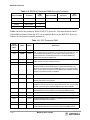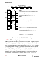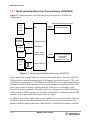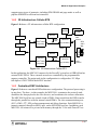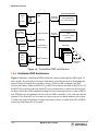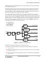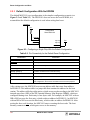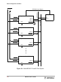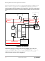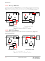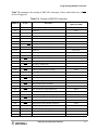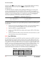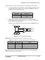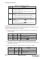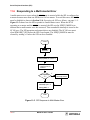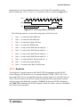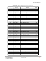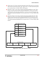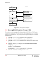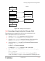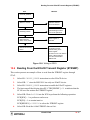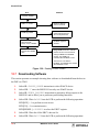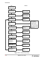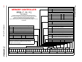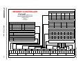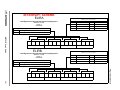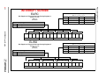
1
MSC8101 USER’S GUIDE 16-Bit Digital Signal Processor MSC8101UG/D Revision 1, June 2001 EOnCE is a registered trademark of Motorola, Inc. StarCore, PowerQUICC II, Motorola, and the Motorola logo are trademarks of Motorola, Inc. The PowerPC name is a trademark of International Business Machines Corporation used by Motorola under license from International Business Machines Corporation. Motorola reserves the right to make changes without further notice to any products herein. Motorola makes no warranty, representation, or guarantee regarding the suitability of its products for any particular purpose, nor does Motorola assume any liability arising out of the application or use of any product or circuit, and specifically disclaims any and all liability, including without limitation consequential or incidental damages. “Typical” parameters that may be provided in Motorola data sheets and/or specifications can and do vary in different applications and actual performance may vary over time. All operating parameters, including “Typicals” must be validated for each customer application by customer’s technical experts. Motorola does not convey any license under its patent rights nor the rights of others. Motorola products are not designed, intended, or authorized for use as components in systems intended for surgical implant into the body, or other applications intended to support or sustain life, or for any other application in which the failure of the Motorola product could create a situation where personal injury or death may occur. Should Buyer purchase or use Motorola products for any such unintended or unauthorized application, Buyer shall indemnify and hold Motorola and its officers, employees, subsidiaries, affiliates, and distributors harmless against all claims, costs, damages, and expenses, and reasonable attorney fees arising out of, directly or indirectly, any claim of personal injury or death associated with such unintended or unauthorized use, even if such claim alleges that Motorola was negligent regarding the design or manufacture of the part. Motorola and are registered trademarks of Motorola, Inc. Motorola, Inc. is an Equal Opportunity/Affirmative Action Employer. How to reach us: USA/EUROPE Motorola Literature Distribution P.O. Box 5405 Denver, Colorado 80217 1-303-675-2140 1-800-441-2447 Technical InformationCenter 1-800-521-6274 JAPAN Motorola Japan Ltd. SPS, Technical Information Center 3-20-1, Minami-Azabu, Minato-ku Tokyo 106-8573 Japan 81-3-3440-3569 Home Page http://www.mot.com/SPS DSP Helpline www.motorola-dsp.com/contact email: [email protected] ASIA/PACIFIC Motorola Semiconductors H.K. Ltd. Silicon Harbour Centre 2 Dai King Street Tai Po Industrial Estate Tai Po, N.T., Hong Kong 852-26668334 © 2001, Motorola Inc. All rights reserved. MSC8101 Overview 1 Reset Configuration and Boot 2 Optimizing Memory on the SC140 Core 3 Connecting External Memories and Memory-Mapped Devices 4 Balancing Between the PowerPC System and Local Buses 5 DMA Channels 6 Interrupts and Interrupt Priorities 7 Host Interface (HDI16) 8 Enhanced Filter Coprocessor (EFCOP) 9 Multi-Channel Controllers (MCCs) 10 Serial Peripheral Interface (SPI) 11 EOnCE/JTAG 12 Programming Reference A Glossary B Bootloader Program C Acronyms and Abbreviations D Index IND 1 MSC8101 Overview 2 Reset Configuration and Boot 3 Optimizing Memory on the SC140 Core 4 Connecting External Memories and Memory-Mapped Devices 5 Balancing Between the PowerPC System and Local Buses 6 DMA Channels 7 Interrupts and Interrupt Priorities 8 Host Interface (HDI16) 9 Enhanced Filter Coprocessor (EFCOP) 10 Multi-Channel Controllers (MCCs) 11 Serial Peripheral Interface (SPI) 12 EOnCE/JTAG A Programming Reference B Glossary C Bootloader Program D Acronyms and Abbreviations IND Index Contents Preface Before Using This Manual—Important Note . . . . . . . . . . . . . . . . . . . . . . . . . . . . . . . xx Audience and Helpful Hints . . . . . . . . . . . . . . . . . . . . . . . . . . . . . . . . . . . . . . . . . . . . xx Notational Conventions and Definitions . . . . . . . . . . . . . . . . . . . . . . . . . . . . . . . . . . . xx Organization. . . . . . . . . . . . . . . . . . . . . . . . . . . . . . . . . . . . . . . . . . . . . . . . . . . . . . . . . xxi Other MSC8101 Documentation . . . . . . . . . . . . . . . . . . . . . . . . . . . . . . . . . . . . . . . . xxiii Further Reading . . . . . . . . . . . . . . . . . . . . . . . . . . . . . . . . . . . . . . . . . . . . . . . . . . . . . xxiii Chapter 1 MSC8101 Overview 1.1 1.2 1.2.1 1.2.2 1.2.3 1.2.4 1.2.5 1.2.6 1.2.7 1.2.8 1.2.9 1.2.10 1.2.11 1.2.12 1.2.13 1.3 1.3.1 1.3.2 1.3.3 1.3.4 1.3.5 1.3.6 1.3.7 1.3.7.1 1.3.7.2 1.3.7.3 1.3.7.4 1.3.7.5 Target Markets. . . . . . . . . . . . . . . . . . . . . . . . . . . . . . . . . . . . . . . . . . . . . . . . . . . . . . . 1-1 Features . . . . . . . . . . . . . . . . . . . . . . . . . . . . . . . . . . . . . . . . . . . . . . . . . . . . . . . . . . . . 1-2 High-performance StarCore SC140 Core . . . . . . . . . . . . . . . . . . . . . . . . . . . . . . . 1-2 On-Device Memories. . . . . . . . . . . . . . . . . . . . . . . . . . . . . . . . . . . . . . . . . . . . . . . 1-3 100 MHz PowerPC System Bus . . . . . . . . . . . . . . . . . . . . . . . . . . . . . . . . . . . . . . 1-3 Eight-bank Memory Controller . . . . . . . . . . . . . . . . . . . . . . . . . . . . . . . . . . . . . . . 1-3 System Interface Unit . . . . . . . . . . . . . . . . . . . . . . . . . . . . . . . . . . . . . . . . . . . . . . 1-3 On-Device Peripherals . . . . . . . . . . . . . . . . . . . . . . . . . . . . . . . . . . . . . . . . . . . . . . 1-4 DMA Engine . . . . . . . . . . . . . . . . . . . . . . . . . . . . . . . . . . . . . . . . . . . . . . . . . . . . . 1-4 Communications Processor Module (CPM) . . . . . . . . . . . . . . . . . . . . . . . . . . . . . 1-4 Separate PLLs for SC140 Core, PowerPC Bus, and CPM . . . . . . . . . . . . . . . . . . 1-5 Reduced Power Dissipation . . . . . . . . . . . . . . . . . . . . . . . . . . . . . . . . . . . . . . . . . . 1-5 Packaging. . . . . . . . . . . . . . . . . . . . . . . . . . . . . . . . . . . . . . . . . . . . . . . . . . . . . . . . 1-6 Software Development Tools . . . . . . . . . . . . . . . . . . . . . . . . . . . . . . . . . . . . . . . . 1-6 Hardware Development Tools . . . . . . . . . . . . . . . . . . . . . . . . . . . . . . . . . . . . . . . . 1-6 Architecture . . . . . . . . . . . . . . . . . . . . . . . . . . . . . . . . . . . . . . . . . . . . . . . . . . . . . . . . . 1-6 SC140 Core . . . . . . . . . . . . . . . . . . . . . . . . . . . . . . . . . . . . . . . . . . . . . . . . . . . . . . 1-6 SRAM . . . . . . . . . . . . . . . . . . . . . . . . . . . . . . . . . . . . . . . . . . . . . . . . . . . . . . . . . . 1-7 System Interface Unit (SIU) . . . . . . . . . . . . . . . . . . . . . . . . . . . . . . . . . . . . . . . . . 1-8 DMA Controller. . . . . . . . . . . . . . . . . . . . . . . . . . . . . . . . . . . . . . . . . . . . . . . . . . . 1-9 Host Interface (HDI16) . . . . . . . . . . . . . . . . . . . . . . . . . . . . . . . . . . . . . . . . . . . . . 1-9 Enhanced Filter Coprocessor (EFCOP) . . . . . . . . . . . . . . . . . . . . . . . . . . . . . . . . 1-10 Communications Processor Module (CPM) . . . . . . . . . . . . . . . . . . . . . . . . . . . . 1-10 Serial Protocol . . . . . . . . . . . . . . . . . . . . . . . . . . . . . . . . . . . . . . . . . . . . . . . . . 1-11 CPM Configurations . . . . . . . . . . . . . . . . . . . . . . . . . . . . . . . . . . . . . . . . . . . . 1-12 Buffer Descriptors . . . . . . . . . . . . . . . . . . . . . . . . . . . . . . . . . . . . . . . . . . . . . . 1-13 Parameter RAM . . . . . . . . . . . . . . . . . . . . . . . . . . . . . . . . . . . . . . . . . . . . . . . . 1-14 BD and Buffer Memory Structure . . . . . . . . . . . . . . . . . . . . . . . . . . . . . . . . . . 1-17 MSC8101 User’s Guide v Contents 1.3.7.6 1.3.7.7 1.4 1.4.1 1.4.2 1.4.3 1.4.4 1.5 RxBD Processing Example . . . . . . . . . . . . . . . . . . . . . . . . . . . . . . . . . . . . . . . TxBD Processing Example . . . . . . . . . . . . . . . . . . . . . . . . . . . . . . . . . . . . . . . MSC8101 Application Examples . . . . . . . . . . . . . . . . . . . . . . . . . . . . . . . . . . . . . . . Media (Voice/Fax/Data) Over Packet Gateway (ATM/FR/IP) . . . . . . . . . . . . . . 3G Infrastructure Cellular BTS . . . . . . . . . . . . . . . . . . . . . . . . . . . . . . . . . . . . . . Centralized DSP Architecture . . . . . . . . . . . . . . . . . . . . . . . . . . . . . . . . . . . . . . . Distributed DSP Architecture . . . . . . . . . . . . . . . . . . . . . . . . . . . . . . . . . . . . . . . Software Development . . . . . . . . . . . . . . . . . . . . . . . . . . . . . . . . . . . . . . . . . . . . . . . 1-18 1-20 1-21 1-22 1-23 1-23 1-24 1-26 Chapter 2 Reset Configuration and Boot 2.1 2.1.1 2.1.2 2.2 2.2.1 2.2.2 2.2.3 2.3 2.3.1 2.3.2 2.3.3 2.4 2.4.1 2.4.1.1 2.4.2 2.4.3 2.4.4 2.5 Reset Configuration and Boot Basics . . . . . . . . . . . . . . . . . . . . . . . . . . . . . . . . . . . . . 2-1 Bootloader Program . . . . . . . . . . . . . . . . . . . . . . . . . . . . . . . . . . . . . . . . . . . . . . . . 2-2 Clocks . . . . . . . . . . . . . . . . . . . . . . . . . . . . . . . . . . . . . . . . . . . . . . . . . . . . . . . . . . 2-2 Configuring a Single MSC8101 . . . . . . . . . . . . . . . . . . . . . . . . . . . . . . . . . . . . . . . . . 2-4 Master Mode With EPROM . . . . . . . . . . . . . . . . . . . . . . . . . . . . . . . . . . . . . . . . . 2-4 Slave Mode With No EPROM. . . . . . . . . . . . . . . . . . . . . . . . . . . . . . . . . . . . . . . . 2-5 Default Configuration With No EPROM . . . . . . . . . . . . . . . . . . . . . . . . . . . . . . . 2-6 Configuring a Multi-MSC8101 System, PowerPC Bus Connected . . . . . . . . . . . . . . 2-7 Reset Configuration Sequence. . . . . . . . . . . . . . . . . . . . . . . . . . . . . . . . . . . . . . . . 2-9 Reset Configuration Word Values . . . . . . . . . . . . . . . . . . . . . . . . . . . . . . . . . . . . 2-10 Boot in a Multi-MSC8101 PowerPC Bus System . . . . . . . . . . . . . . . . . . . . . . . . 2-11 Configuring a Multi-MSC8101 System Connected Via the Host Port . . . . . . . . . . . 2-12 Host Reset Configuration Sequence . . . . . . . . . . . . . . . . . . . . . . . . . . . . . . . . . . 2-14 Reset Configuration Word Value . . . . . . . . . . . . . . . . . . . . . . . . . . . . . . . . . . . 2-14 Boot Through Host Port. . . . . . . . . . . . . . . . . . . . . . . . . . . . . . . . . . . . . . . . . . . . 2-15 Source Program Data Stream Structure . . . . . . . . . . . . . . . . . . . . . . . . . . . . . . . . 2-15 Host Interface Load Procedure . . . . . . . . . . . . . . . . . . . . . . . . . . . . . . . . . . . . . . 2-16 Related Reading. . . . . . . . . . . . . . . . . . . . . . . . . . . . . . . . . . . . . . . . . . . . . . . . . . . . . 2-17 Chapter 3 Optimizing Memory on the SC140 Core 3.1 3.2 3.3 3.4 3.5 Memory Requirements . . . . . . . . . . . . . . . . . . . . . . . . . . . . . . . . . . . . . . . . . . . . . . . . Partitioning Memory . . . . . . . . . . . . . . . . . . . . . . . . . . . . . . . . . . . . . . . . . . . . . . . . . . Allocating Memory . . . . . . . . . . . . . . . . . . . . . . . . . . . . . . . . . . . . . . . . . . . . . . . . . . . Avoiding Memory Contentions . . . . . . . . . . . . . . . . . . . . . . . . . . . . . . . . . . . . . . . . . . Related Reading. . . . . . . . . . . . . . . . . . . . . . . . . . . . . . . . . . . . . . . . . . . . . . . . . . . . . . 3-1 3-2 3-2 3-4 3-5 Chapter 4 Connecting External Memories and Memory-Mapped Devices 4.1 4.2 4.3 vi Memory Controller Basics. . . . . . . . . . . . . . . . . . . . . . . . . . . . . . . . . . . . . . . . . . . . . . 4-1 External Bus Basics . . . . . . . . . . . . . . . . . . . . . . . . . . . . . . . . . . . . . . . . . . . . . . . . . . . 4-2 Connecting the Bus to the Flash Memory Interface . . . . . . . . . . . . . . . . . . . . . . . . . . 4-4 MSC8101 User’s Guide Contents 4.3.1 4.3.2 4.4 4.4.1 4.4.2 4.4.3 4.4.4 4.4.5 4.5 4.5.1 4.5.2 4.6 GPCM Hardware Interconnection . . . . . . . . . . . . . . . . . . . . . . . . . . . . . . . . . . . . . 4-4 Single-Bus Mode GPCM-Based Timings . . . . . . . . . . . . . . . . . . . . . . . . . . . . . . . 4-5 Connecting the Bus to the SDRAM Memory Interface. . . . . . . . . . . . . . . . . . . . . . . . 4-7 Single-Bus Mode SDRAM Hardware Interconnect . . . . . . . . . . . . . . . . . . . . . . . 4-8 Single-Bus Mode SDRAM Pin Control Settings. . . . . . . . . . . . . . . . . . . . . . . . . . 4-8 Single-Bus Mode SDRAM Timing Control Settings . . . . . . . . . . . . . . . . . . . . . 4-10 SDRAM Mode Register Settings. . . . . . . . . . . . . . . . . . . . . . . . . . . . . . . . . . . . . 4-12 PowerPC 60x Bus Mode SDRAM Hardware Interconnection . . . . . . . . . . . . . . 4-13 Connecting the Bus to the HDI16 Memory Interface . . . . . . . . . . . . . . . . . . . . . . . . 4-14 HDI16 Hardware Interconnection . . . . . . . . . . . . . . . . . . . . . . . . . . . . . . . . . . . . 4-15 Single-Bus Mode HDI16 Timing Settings. . . . . . . . . . . . . . . . . . . . . . . . . . . . . . 4-17 Related Reading. . . . . . . . . . . . . . . . . . . . . . . . . . . . . . . . . . . . . . . . . . . . . . . . . . . . . 4-19 Chapter 5 Balancing Between the PowerPC System and Local Buses 5.1 5.2 5.3 5.3.1 5.3.1.1 5.3.1.2 5.3.1.3 5.3.1.4 5.3.2 5.3.2.1 5.3.2.2 5.4 PowerPC System Bus . . . . . . . . . . . . . . . . . . . . . . . . . . . . . . . . . . . . . . . . . . . . . . . . . 5-2 PowerPC Local Bus . . . . . . . . . . . . . . . . . . . . . . . . . . . . . . . . . . . . . . . . . . . . . . . . . . . 5-4 Bus Interaction. . . . . . . . . . . . . . . . . . . . . . . . . . . . . . . . . . . . . . . . . . . . . . . . . . . . . . . 5-5 DMA Controller. . . . . . . . . . . . . . . . . . . . . . . . . . . . . . . . . . . . . . . . . . . . . . . . . . . 5-8 Selecting a Bus . . . . . . . . . . . . . . . . . . . . . . . . . . . . . . . . . . . . . . . . . . . . . . . . . . 5-8 DMA FIFO . . . . . . . . . . . . . . . . . . . . . . . . . . . . . . . . . . . . . . . . . . . . . . . . . . . . . 5-8 Chained Buffers . . . . . . . . . . . . . . . . . . . . . . . . . . . . . . . . . . . . . . . . . . . . . . . . . 5-8 Bus Errors. . . . . . . . . . . . . . . . . . . . . . . . . . . . . . . . . . . . . . . . . . . . . . . . . . . . . . 5-9 SDMA Channels . . . . . . . . . . . . . . . . . . . . . . . . . . . . . . . . . . . . . . . . . . . . . . . . . . 5-9 Bus Errors from SDMA access . . . . . . . . . . . . . . . . . . . . . . . . . . . . . . . . . . . . 5-10 SDMA Bus Arbitration and Bus Transfers . . . . . . . . . . . . . . . . . . . . . . . . . . . 5-11 Related Reading. . . . . . . . . . . . . . . . . . . . . . . . . . . . . . . . . . . . . . . . . . . . . . . . . . . . . 5-11 Chapter 6 DMA Channels 6.1 6.1.1 6.1.1.1 6.1.1.2 6.1.2 6.1.2.1 6.1.2.2 6.1.2.3 6.1.2.4 6.1.2.5 6.2 6.2.1 6.2.2 6.2.3 DMA Programming Basics . . . . . . . . . . . . . . . . . . . . . . . . . . . . . . . . . . . . . . . . . . . . . Operating Modes . . . . . . . . . . . . . . . . . . . . . . . . . . . . . . . . . . . . . . . . . . . . . . . . . . Normal Mode (Dual Access) . . . . . . . . . . . . . . . . . . . . . . . . . . . . . . . . . . . . . . . Flyby Mode (Single Access) . . . . . . . . . . . . . . . . . . . . . . . . . . . . . . . . . . . . . . . Transfer Types . . . . . . . . . . . . . . . . . . . . . . . . . . . . . . . . . . . . . . . . . . . . . . . . . . . . Memory to DMA FIFO . . . . . . . . . . . . . . . . . . . . . . . . . . . . . . . . . . . . . . . . . . . DMA FIFO to Memory . . . . . . . . . . . . . . . . . . . . . . . . . . . . . . . . . . . . . . . . . . . Peripheral to DMA FIFO . . . . . . . . . . . . . . . . . . . . . . . . . . . . . . . . . . . . . . . . . . DMA FIFO to Peripheral . . . . . . . . . . . . . . . . . . . . . . . . . . . . . . . . . . . . . . . . . . Memory to Peripheral, Flyby Mode . . . . . . . . . . . . . . . . . . . . . . . . . . . . . . . . . . Initializing the DMA . . . . . . . . . . . . . . . . . . . . . . . . . . . . . . . . . . . . . . . . . . . . . . . . . . DMA Channel Configuration Registers (DCHRx) . . . . . . . . . . . . . . . . . . . . . . . . DMA Pin Configuration Register (DPCR) . . . . . . . . . . . . . . . . . . . . . . . . . . . . . . DMA Status Register (DSTR) . . . . . . . . . . . . . . . . . . . . . . . . . . . . . . . . . . . . . . . . MSC8101 User’s Guide 6-1 6-2 6-2 6-3 6-3 6-4 6-4 6-5 6-5 6-6 6-7 6-8 6-8 6-9 vii Contents 6.2.4 6.2.5 6.2.6 6.2.7 6.2.8 6.2.9 6.3 6.4 6.4.1 6.4.2 6.4.3 6.4.4 6.5 6.6 DMA Internal/External Mask Registers (DIMR/DEMR) . . . . . . . . . . . . . . . . . . . 6-9 DMA Channel Parameters RAM (DCPRAM) . . . . . . . . . . . . . . . . . . . . . . . . . . . 6-9 FIFO Requests . . . . . . . . . . . . . . . . . . . . . . . . . . . . . . . . . . . . . . . . . . . . . . . . . . . 6-12 Multiple Pending DMA Requests . . . . . . . . . . . . . . . . . . . . . . . . . . . . . . . . . . . . 6-12 Buffering and Bursting . . . . . . . . . . . . . . . . . . . . . . . . . . . . . . . . . . . . . . . . . . . . 6-13 Interrupts . . . . . . . . . . . . . . . . . . . . . . . . . . . . . . . . . . . . . . . . . . . . . . . . . . . . . . . 6-13 Using DMA Signals to Initiate and Control DMA Transfers . . . . . . . . . . . . . . . . . . 6-14 DMA Programming Examples . . . . . . . . . . . . . . . . . . . . . . . . . . . . . . . . . . . . . . . . . 6-15 Internal to External Dual Access, Simple Buffer . . . . . . . . . . . . . . . . . . . . . . . . 6-15 External to External Dual-Access Burst Transfer, Cyclic Buffer . . . . . . . . . . . . 6-17 Internal Peripheral to External Dual Access, Simple Buffer . . . . . . . . . . . . . . . . 6-19 External to External Dual Access, Chained with Interrupts . . . . . . . . . . . . . . . . 6-21 Avoiding DMA and SC140 Core Contentions . . . . . . . . . . . . . . . . . . . . . . . . . . . . . 6-25 Related Reading. . . . . . . . . . . . . . . . . . . . . . . . . . . . . . . . . . . . . . . . . . . . . . . . . . . . . 6-26 Chapter 7 Interrupts and Interrupt Priorities 7.1 7.2 7.3 7.3.1 7.3.2 7.3.3 7.3.4 7.4 7.4.1 7.4.2 7.4.3 7.4.4 7.4.4.1 7.4.4.2 Interrupt Basics . . . . . . . . . . . . . . . . . . . . . . . . . . . . . . . . . . . . . . . . . . . . . . . . . . . . . . 7-1 Programmable Interrupt Controller (PIC) . . . . . . . . . . . . . . . . . . . . . . . . . . . . . . . . . . 7-2 Programming MSC8101 Interrupts . . . . . . . . . . . . . . . . . . . . . . . . . . . . . . . . . . . . . . . 7-4 Setting the Interrupt Table Base Address . . . . . . . . . . . . . . . . . . . . . . . . . . . . . . . 7-4 Setting the Interrupt Priority Level and Trigger Mode . . . . . . . . . . . . . . . . . . . . . 7-4 Monitoring the Status of Pending Interrupts . . . . . . . . . . . . . . . . . . . . . . . . . . . . . 7-5 Routing Interrupts . . . . . . . . . . . . . . . . . . . . . . . . . . . . . . . . . . . . . . . . . . . . . . . . . 7-6 Interrupt Programming Examples . . . . . . . . . . . . . . . . . . . . . . . . . . . . . . . . . . . . . . . . 7-8 PIC Programming . . . . . . . . . . . . . . . . . . . . . . . . . . . . . . . . . . . . . . . . . . . . . . . . . 7-9 Clearing Pending Requests . . . . . . . . . . . . . . . . . . . . . . . . . . . . . . . . . . . . . . . . . . 7-9 EFCOP Programming Examples . . . . . . . . . . . . . . . . . . . . . . . . . . . . . . . . . . . . . 7-10 PIC Macros . . . . . . . . . . . . . . . . . . . . . . . . . . . . . . . . . . . . . . . . . . . . . . . . . . . . . 7-13 Examples of SIC Interrupts . . . . . . . . . . . . . . . . . . . . . . . . . . . . . . . . . . . . . . . 7-14 Examples of SIC Interrupts . . . . . . . . . . . . . . . . . . . . . . . . . . . . . . . . . . . . . . . 7-16 Chapter 8 Host Interface (HDI16) 8.1 8.1.1 8.1.2 8.2 8.2.1 8.2.2 8.3 8.3.1 8.3.1.1 8.3.1.2 viii HDI16 Programming Basics . . . . . . . . . . . . . . . . . . . . . . . . . . . . . . . . . . . . . . . . . . . . 8-1 Host-Side Model . . . . . . . . . . . . . . . . . . . . . . . . . . . . . . . . . . . . . . . . . . . . . . . . . . 8-2 DSP-Side Model . . . . . . . . . . . . . . . . . . . . . . . . . . . . . . . . . . . . . . . . . . . . . . . . . . 8-3 Operating in Different Data Transfer Modes. . . . . . . . . . . . . . . . . . . . . . . . . . . . . . . . 8-3 Normal Mode . . . . . . . . . . . . . . . . . . . . . . . . . . . . . . . . . . . . . . . . . . . . . . . . . . . . . 8-5 Host DMA Mode . . . . . . . . . . . . . . . . . . . . . . . . . . . . . . . . . . . . . . . . . . . . . . . . . . 8-8 Managing Data Transfers Via Handshaking Protocols . . . . . . . . . . . . . . . . . . . . . . . 8-12 Software Polling . . . . . . . . . . . . . . . . . . . . . . . . . . . . . . . . . . . . . . . . . . . . . . . . . 8-13 DSP Polling . . . . . . . . . . . . . . . . . . . . . . . . . . . . . . . . . . . . . . . . . . . . . . . . . . . 8-13 Host Polling . . . . . . . . . . . . . . . . . . . . . . . . . . . . . . . . . . . . . . . . . . . . . . . . . . . 8-15 MSC8101 User’s Guide Contents 8.3.1.3 8.3.1.4 8.3.2 8.3.3 8.3.4 8.4 8.5 Host Flags. . . . . . . . . . . . . . . . . . . . . . . . . . . . . . . . . . . . . . . . . . . . . . . . . . . . . Transmit Ready bit . . . . . . . . . . . . . . . . . . . . . . . . . . . . . . . . . . . . . . . . . . . . . . DSP Interrupts . . . . . . . . . . . . . . . . . . . . . . . . . . . . . . . . . . . . . . . . . . . . . . . . . . . Host Requests . . . . . . . . . . . . . . . . . . . . . . . . . . . . . . . . . . . . . . . . . . . . . . . . . . . Direct Memory Access (DMA) . . . . . . . . . . . . . . . . . . . . . . . . . . . . . . . . . . . . . . Issuing Host Commands and Non-Maskable Interrupts . . . . . . . . . . . . . . . . . . . . . . Related Reading. . . . . . . . . . . . . . . . . . . . . . . . . . . . . . . . . . . . . . . . . . . . . . . . . . . . . 8-15 8-15 8-15 8-18 8-20 8-23 8-24 Chapter 9 Enhanced Filter Coprocessor (EFCOP) 9.1 9.2 9.2.1 9.2.1.1 9.2.1.2 9.2.2 9.2.3 9.2.4 9.2.5 9.2.6 9.3 9.4 9.4.1 9.4.2 9.5 9.5.1 9.5.2 9.5.3 9.6 9.6.1 9.6.2 9.6.3 9.7 Programming the Control Registers . . . . . . . . . . . . . . . . . . . . . . . . . . . . . . . . . . . . . . 9-1 Specifying the Operating Modes for the FIR Filter Type . . . . . . . . . . . . . . . . . . . . . . 9-3 Real Mode . . . . . . . . . . . . . . . . . . . . . . . . . . . . . . . . . . . . . . . . . . . . . . . . . . . . . . . 9-4 Adaptive Mode . . . . . . . . . . . . . . . . . . . . . . . . . . . . . . . . . . . . . . . . . . . . . . . . . . 9-4 Multichannel Mode . . . . . . . . . . . . . . . . . . . . . . . . . . . . . . . . . . . . . . . . . . . . . . 9-4 Complex Mode . . . . . . . . . . . . . . . . . . . . . . . . . . . . . . . . . . . . . . . . . . . . . . . . . . . 9-5 Alternating Complex Mode . . . . . . . . . . . . . . . . . . . . . . . . . . . . . . . . . . . . . . . . . . 9-6 Magnitude Mode . . . . . . . . . . . . . . . . . . . . . . . . . . . . . . . . . . . . . . . . . . . . . . . . . . 9-6 Data and Coefficient Initialization. . . . . . . . . . . . . . . . . . . . . . . . . . . . . . . . . . . . . 9-6 Decimation. . . . . . . . . . . . . . . . . . . . . . . . . . . . . . . . . . . . . . . . . . . . . . . . . . . . . . . 9-7 Specifying the Operating Modes for the IIR Filter Type. . . . . . . . . . . . . . . . . . . . . . . 9-8 Specifying the ALU Modes . . . . . . . . . . . . . . . . . . . . . . . . . . . . . . . . . . . . . . . . . . . . . 9-9 Rounding . . . . . . . . . . . . . . . . . . . . . . . . . . . . . . . . . . . . . . . . . . . . . . . . . . . . . . . . 9-9 Input Scaling . . . . . . . . . . . . . . . . . . . . . . . . . . . . . . . . . . . . . . . . . . . . . . . . . . . . 9-10 Transferring Data In and Out of the EFCOP . . . . . . . . . . . . . . . . . . . . . . . . . . . . . . . 9-11 Polling . . . . . . . . . . . . . . . . . . . . . . . . . . . . . . . . . . . . . . . . . . . . . . . . . . . . . . . . . 9-11 Interrupts . . . . . . . . . . . . . . . . . . . . . . . . . . . . . . . . . . . . . . . . . . . . . . . . . . . . . . . 9-12 DMA . . . . . . . . . . . . . . . . . . . . . . . . . . . . . . . . . . . . . . . . . . . . . . . . . . . . . . . . . . 9-13 Programming Examples. . . . . . . . . . . . . . . . . . . . . . . . . . . . . . . . . . . . . . . . . . . . . . . 9-14 Complex FIR Filter with Polling . . . . . . . . . . . . . . . . . . . . . . . . . . . . . . . . . . . . . 9-14 Adaptive Filter With Interrupts . . . . . . . . . . . . . . . . . . . . . . . . . . . . . . . . . . . . . . 9-16 Real IIR Filter with DMA . . . . . . . . . . . . . . . . . . . . . . . . . . . . . . . . . . . . . . . . . . 9-19 Related Reading. . . . . . . . . . . . . . . . . . . . . . . . . . . . . . . . . . . . . . . . . . . . . . . . . . . . . 9-25 Chapter 10 Multi-Channel Controllers (MCCs) 10.1 10.1.1 10.1.2 10.1.3 10.2 10.2.1 10.2.2 10.3 MCC Configuration Basics . . . . . . . . . . . . . . . . . . . . . . . . . . . . . . . . . . . . . . . . . . . . 10-1 Procedure for Initializing the MCC Resources . . . . . . . . . . . . . . . . . . . . . . . . . . 10-2 Driver Memory Map . . . . . . . . . . . . . . . . . . . . . . . . . . . . . . . . . . . . . . . . . . . . . . 10-4 Memory Usage. . . . . . . . . . . . . . . . . . . . . . . . . . . . . . . . . . . . . . . . . . . . . . . . . . . 10-5 Connect the TDM Interface to T1/E1 . . . . . . . . . . . . . . . . . . . . . . . . . . . . . . . . . . . . 10-6 Provide Appropriate Signal Polarity and Timing . . . . . . . . . . . . . . . . . . . . . . . . 10-8 Perform a Phased Test of the Transceiver Interface . . . . . . . . . . . . . . . . . . . . . . 10-8 Configure the Channels . . . . . . . . . . . . . . . . . . . . . . . . . . . . . . . . . . . . . . . . . . . . . . 10-10 MSC8101 User’s Guide ix Contents 10.3.1 10.3.2 10.3.3 10.3.4 10.3.5 10.4 10.4.1 10.4.2 10.5 10.6 Set Up the Global MCC Parameters . . . . . . . . . . . . . . . . . . . . . . . . . . . . . . . . . Set Up the MCC Configuration and Control Registers . . . . . . . . . . . . . . . . . . . Set Up Channel-Specific Parameters . . . . . . . . . . . . . . . . . . . . . . . . . . . . . . . . . Set Up the Channel Extra Parameters . . . . . . . . . . . . . . . . . . . . . . . . . . . . . . . . Initialize Circular Interrupt Queues . . . . . . . . . . . . . . . . . . . . . . . . . . . . . . . . . . Select the TSA Channel Route to a TDM Timeslot . . . . . . . . . . . . . . . . . . . . . . . . Define the Serial Interface Entries in SIRAM . . . . . . . . . . . . . . . . . . . . . . . . . . Set up Clocks, Baud Rate Generators (BRG), and Timers . . . . . . . . . . . . . . . . Set Up the External Interface. . . . . . . . . . . . . . . . . . . . . . . . . . . . . . . . . . . . . . . . . . Related Reading. . . . . . . . . . . . . . . . . . . . . . . . . . . . . . . . . . . . . . . . . . . . . . . . . . . . 10-10 10-11 10-12 10-13 10-13 10-13 10-14 10-15 10-16 10-16 Chapter 11 Serial Peripheral Interface (SPI) 11.1 11.2 11.3 11.4 11.5 11.6 11.7 Configuring the SPI for Use . . . . . . . . . . . . . . . . . . . . . . . . . . . . . . . . . . . . . . . . . . . 11-1 Setting the Clock . . . . . . . . . . . . . . . . . . . . . . . . . . . . . . . . . . . . . . . . . . . . . . . . . . . . 11-3 Specifying the Receive and Transmit Buffer Descriptors . . . . . . . . . . . . . . . . . . . . . 11-3 Operating the SPI as a Master . . . . . . . . . . . . . . . . . . . . . . . . . . . . . . . . . . . . . . . . . . 11-5 Operating the SPI as a Slave . . . . . . . . . . . . . . . . . . . . . . . . . . . . . . . . . . . . . . . . . . . 11-9 Responding to a Multi-master Error . . . . . . . . . . . . . . . . . . . . . . . . . . . . . . . . . . . . 11-12 Related Reading. . . . . . . . . . . . . . . . . . . . . . . . . . . . . . . . . . . . . . . . . . . . . . . . . . . . 11-13 Chapter 12 EOnCE/JTAG 12.1 12.1.1 12.1.2 12.1.3 12.1.3.1 12.1.3.2 12.1.3.3 12.1.3.4 12.2 12.3 12.4 12.5 12.6 12.7 12.8 12.9 12.10 12.11 x EOnCE/JTAG Basics. . . . . . . . . . . . . . . . . . . . . . . . . . . . . . . . . . . . . . . . . . . . . . . . . 12-1 Instructions. . . . . . . . . . . . . . . . . . . . . . . . . . . . . . . . . . . . . . . . . . . . . . . . . . . . . . 12-3 Executing a JTAG Instruction . . . . . . . . . . . . . . . . . . . . . . . . . . . . . . . . . . . . . . . 12-4 Registers. . . . . . . . . . . . . . . . . . . . . . . . . . . . . . . . . . . . . . . . . . . . . . . . . . . . . . . . 12-5 CORE_CMD Example 1 . . . . . . . . . . . . . . . . . . . . . . . . . . . . . . . . . . . . . . . . 12-10 CORE_CMD Example 2 . . . . . . . . . . . . . . . . . . . . . . . . . . . . . . . . . . . . . . . . 12-10 CORE_CMD Example 3 . . . . . . . . . . . . . . . . . . . . . . . . . . . . . . . . . . . . . . . . 12-10 CORE_CMD Example 4 . . . . . . . . . . . . . . . . . . . . . . . . . . . . . . . . . . . . . . . . 12-11 Writing EOnCE Registers Through JTAG . . . . . . . . . . . . . . . . . . . . . . . . . . . . . . . 12-11 Reading EOnCE Registers Through JTAG . . . . . . . . . . . . . . . . . . . . . . . . . . . . . . . 12-12 Executing a Single Instruction Through JTAG . . . . . . . . . . . . . . . . . . . . . . . . . . . . 12-13 Writing to the EOnCE Receive Register (ERCV) . . . . . . . . . . . . . . . . . . . . . . . . . . 12-14 Reading From the EOnCE Transmit Register (ETRSMT) . . . . . . . . . . . . . . . . . . . 12-15 Downloading Software . . . . . . . . . . . . . . . . . . . . . . . . . . . . . . . . . . . . . . . . . . . . . . 12-16 Writing and Reading the Trace Buffer . . . . . . . . . . . . . . . . . . . . . . . . . . . . . . . . . . 12-19 Using EE0 to Enter Debug Mode . . . . . . . . . . . . . . . . . . . . . . . . . . . . . . . . . . . . . . 12-20 Counting Core Cycles . . . . . . . . . . . . . . . . . . . . . . . . . . . . . . . . . . . . . . . . . . . . . . . 12-20 Related Reading. . . . . . . . . . . . . . . . . . . . . . . . . . . . . . . . . . . . . . . . . . . . . . . . . . . . 12-22 MSC8101 User’s Guide Contents APPENDIXES: Appendix A Programming Reference A.1 A.2 Interrupt Sources and Priorities . . . . . . . . . . . . . . . . . . . . . . . . . . . . . . . . . . . . . . . . . A-2 Programming Sheets . . . . . . . . . . . . . . . . . . . . . . . . . . . . . . . . . . . . . . . . . . . . . . . . . A-7 Appendix B Glossary Appendix C Bootloader Program Appendix D Acronyms and Abbreviations INDEX MSC8101 User’s Guide xi Contents xii MSC8101 User’s Guide Figures Figure 1-1. Figure 1-2. Figure 1-3. Figure 1-4. Figure 1-5. Figure 1-6. Figure 1-7. Figure 1-8. Figure 1-9. Figure 1-10. Figure 1-11. Figure 1-12. Figure 2-1. Figure 2-2. Figure 2-3. Figure 2-4. Figure 2-5. Figure 2-6. Figure 3-1. Figure 3-2. Figure 4-1. Figure 4-2. Figure 4-3. Figure 4-4. Figure 4-5. Figure 4-6. Figure 4-7. Figure 4-8. Figure 4-9. Figure 4-10. Figure 4-11. Figure 4-12. Figure 4-13. MSC8101 Block Diagram . . . . . . . . . . . . . . . . . . . . . . . . . . . . . . . . . . . . . . . . 1-8 Buffer Descriptor Structure . . . . . . . . . . . . . . . . . . . . . . . . . . . . . . . . . . . . . . 1-13 Example SCC2 BD and Buffer Memory Structure . . . . . . . . . . . . . . . . . . . . 1-18 Example SPI BD and Buffer Memory Structure . . . . . . . . . . . . . . . . . . . . . . 1-19 Example SCC UART RxBD Processing . . . . . . . . . . . . . . . . . . . . . . . . . . . . 1-20 Example SCC UART TxBD Processing . . . . . . . . . . . . . . . . . . . . . . . . . . . . 1-21 Media (Voice/Fax/Data) Over Packet (ATM/FR/IP) . . . . . . . . . . . . . . . . . . 1-22 3G Infrastructure Cellular BTS . . . . . . . . . . . . . . . . . . . . . . . . . . . . . . . . . . . 1-23 Centralized DSP Architecture . . . . . . . . . . . . . . . . . . . . . . . . . . . . . . . . . . . . 1-24 Distributed DSP Architecture Connected Through the HDI16 Port . . . . . . . 1-25 Distributed DSP Architecture Connected Through a Shared PowerPC Bus . 1-25 Software Development Flow . . . . . . . . . . . . . . . . . . . . . . . . . . . . . . . . . . . . . 1-26 MSC8101 Clocking Structure . . . . . . . . . . . . . . . . . . . . . . . . . . . . . . . . . . . . . 2-3 Configuring a Single Device From EPROM . . . . . . . . . . . . . . . . . . . . . . . . . . 2-4 Configuring a Single Chip With the Default Configuration . . . . . . . . . . . . . . 2-6 Multi-MSC8101 PowerPC Bus System. . . . . . . . . . . . . . . . . . . . . . . . . . . . . . 2-8 Multiple MSC8101s Connected Via the Host Port . . . . . . . . . . . . . . . . . . . . 2-13 Boot Code Stream Structure . . . . . . . . . . . . . . . . . . . . . . . . . . . . . . . . . . . . . 2-15 Memory Organization . . . . . . . . . . . . . . . . . . . . . . . . . . . . . . . . . . . . . . . . . . . 3-3 Memory Structure . . . . . . . . . . . . . . . . . . . . . . . . . . . . . . . . . . . . . . . . . . . . . . 3-4 Memory Controller Overview . . . . . . . . . . . . . . . . . . . . . . . . . . . . . . . . . . . . . 4-3 MSC8101-to-Flash Interconnect in Single-Master Bus Mode . . . . . . . . . . . . 4-4 Flash Memory Read, Single Master. . . . . . . . . . . . . . . . . . . . . . . . . . . . . . . . . 4-5 Flash Memory Write, Single Master . . . . . . . . . . . . . . . . . . . . . . . . . . . . . . . . 4-6 MSC8101-To-SDRAM Interconnect in Single-Bus Master Mode . . . . . . . . . 4-8 MSC8101 SDRAM Address Multiplexing . . . . . . . . . . . . . . . . . . . . . . . . . . . 4-9 SDRAM Burst Read Page Miss, Single Master. . . . . . . . . . . . . . . . . . . . . . . 4-11 SDRAM Burst Write Page Miss, Single Master . . . . . . . . . . . . . . . . . . . . . . 4-11 SDRAM Mode Register Configuration . . . . . . . . . . . . . . . . . . . . . . . . . . . . . 4-12 MSC8101-To-SDRAM Interconnection in PowerPC 60x Multi-Master Bus Mode . . . . . . . . . . . . . . . . . . . . . . . . . . . . . . . . . . . . . . . . . . . . . . . . . . 4-13 Single-Master MSC8101 Bus to HDI16 Interface. . . . . . . . . . . . . . . . . . . . . 4-16 Multi-Master PowerPC System Bus to Buffered HDI16 Interface . . . . . . . . 4-17 HDI16 UPM Read, Single Master . . . . . . . . . . . . . . . . . . . . . . . . . . . . . . . . . 4-18 MSC8101 User’s Guide xiii Figures Figure 4-14. Figure 5-1. Figure 5-2. Figure 5-3. Figure 5-4. Figure 5-5. Figure 5-6. Figure 5-7. Figure 5-8. Figure 6-1. Figure 6-2. Figure 6-3. Figure 6-4. Figure 6-5. Figure 6-6. Figure 6-7. Figure 6-8. Figure 6-9. Figure 7-1. Figure 7-2. Figure 8-1. Figure 8-2. Figure 8-3. Figure 8-4. Figure 8-5. Figure 9-1. Figure 9-2. Figure 10-1. Figure 10-2. Figure 10-3. Figure 10-4. Figure 10-5. Figure 10-6. Figure 10-7. Figure 10-8. Figure 10-9. Figure 11-1. Figure 11-2. xiv HDI16 UPM Write, Single Master . . . . . . . . . . . . . . . . . . . . . . . . . . . . . . . . 4-18 MSC8101 Block Diagram . . . . . . . . . . . . . . . . . . . . . . . . . . . . . . . . . . . . . . . . 5-2 PowerPC System Bus External Memory Access Example . . . . . . . . . . . . . . . 5-3 QBus-to-PowerPC System Bus Interface . . . . . . . . . . . . . . . . . . . . . . . . . . . . 5-3 Interface From PowerPC Local bus to Extended Core . . . . . . . . . . . . . . . . . . 5-4 SIU Block Diagram . . . . . . . . . . . . . . . . . . . . . . . . . . . . . . . . . . . . . . . . . . . . . 5-5 Bus Architecture . . . . . . . . . . . . . . . . . . . . . . . . . . . . . . . . . . . . . . . . . . . . . . . 5-6 Memory Controller Machine Selection . . . . . . . . . . . . . . . . . . . . . . . . . . . . . . 5-7 SDMA Data Paths . . . . . . . . . . . . . . . . . . . . . . . . . . . . . . . . . . . . . . . . . . . . . 5-10 DMA Engine Interfaces . . . . . . . . . . . . . . . . . . . . . . . . . . . . . . . . . . . . . . . . . . 6-2 Normal Mode Example . . . . . . . . . . . . . . . . . . . . . . . . . . . . . . . . . . . . . . . . . . 6-3 Memory to DMA FIFO Transfers . . . . . . . . . . . . . . . . . . . . . . . . . . . . . . . . . . 6-4 DMA FIFO to Memory Transfers . . . . . . . . . . . . . . . . . . . . . . . . . . . . . . . . . . 6-4 Peripheral to DMA FIFO Transfers. . . . . . . . . . . . . . . . . . . . . . . . . . . . . . . . . 6-5 DMA FIFO to Peripheral Transfers. . . . . . . . . . . . . . . . . . . . . . . . . . . . . . . . . 6-6 Memory to Peripheral, Flyby Mode Data Transfer . . . . . . . . . . . . . . . . . . . . . 6-6 Peripheral to Memory, Flyby Mode Data Transfer . . . . . . . . . . . . . . . . . . . . . 6-7 DMA Buffer Types . . . . . . . . . . . . . . . . . . . . . . . . . . . . . . . . . . . . . . . . . . . . 6-14 MSC8101 Interrupt Structure . . . . . . . . . . . . . . . . . . . . . . . . . . . . . . . . . . . . . 7-2 PIC Block Diagram . . . . . . . . . . . . . . . . . . . . . . . . . . . . . . . . . . . . . . . . . . . . . 7-3 HDI16 Programmer’s Model . . . . . . . . . . . . . . . . . . . . . . . . . . . . . . . . . . . . . . 8-2 Example Hardware Set-up for Normal Mode Transfers . . . . . . . . . . . . . . . . . 8-7 HDI16 Hardware set-up for DMA Mode Transfer . . . . . . . . . . . . . . . . . . . . 8-10 HDI16 DSP-Side Interrupt Operation . . . . . . . . . . . . . . . . . . . . . . . . . . . . . . 8-17 HDI16 Host Request Operation . . . . . . . . . . . . . . . . . . . . . . . . . . . . . . . . . . . 8-19 FIR Filter Block Diagram . . . . . . . . . . . . . . . . . . . . . . . . . . . . . . . . . . . . . . . . 9-3 IIR Filter Block Diagram . . . . . . . . . . . . . . . . . . . . . . . . . . . . . . . . . . . . . . . . . 9-9 MCC Resource Usage . . . . . . . . . . . . . . . . . . . . . . . . . . . . . . . . . . . . . . . . . . 10-2 Driver Functions . . . . . . . . . . . . . . . . . . . . . . . . . . . . . . . . . . . . . . . . . . . . . . 10-3 Driver Memory Map . . . . . . . . . . . . . . . . . . . . . . . . . . . . . . . . . . . . . . . . . . . 10-4 Internal and External Memory Usage . . . . . . . . . . . . . . . . . . . . . . . . . . . . . . 10-5 T1/E1 Transceiver Interface Example . . . . . . . . . . . . . . . . . . . . . . . . . . . . . . 10-7 T1/E1 Data Frame . . . . . . . . . . . . . . . . . . . . . . . . . . . . . . . . . . . . . . . . . . . . . 10-8 Loopback Modes . . . . . . . . . . . . . . . . . . . . . . . . . . . . . . . . . . . . . . . . . . . . . . 10-9 Serial Interface . . . . . . . . . . . . . . . . . . . . . . . . . . . . . . . . . . . . . . . . . . . . . . . 10-14 Serial Interface Entry Definitions for Driver Example . . . . . . . . . . . . . . . . 10-15 SPI BRG Block Diagram . . . . . . . . . . . . . . . . . . . . . . . . . . . . . . . . . . . . . . . . 11-3 SPI BD and Buffer Memory Structure . . . . . . . . . . . . . . . . . . . . . . . . . . . . . 11-5 MSC8101 User’s Guide Figures Figure 11-3. Figure 11-4. Figure 11-5. Figure 12-1. Figure 12-2. Figure 12-3. Figure 12-4. Figure 12-5. Figure 12-6. Figure 12-7. Figure 12-8. Figure 12-9. Figure 12-10. SPI as a Master . . . . . . . . . . . . . . . . . . . . . . . . . . . . . . . . . . . . . . . . . . . . . . . 11-6 SPI as Slave . . . . . . . . . . . . . . . . . . . . . . . . . . . . . . . . . . . . . . . . . . . . . . . . . . 11-9 SPI Response to Multi-Master Error . . . . . . . . . . . . . . . . . . . . . . . . . . . . . . 11-12 TAP Controller State Machine . . . . . . . . . . . . . . . . . . . . . . . . . . . . . . . . . . . 12-2 Test Logic Diagram Showing the Five-Bit Instruction Register. . . . . . . . . . 12-3 Executing DEBUG_REQUEST . . . . . . . . . . . . . . . . . . . . . . . . . . . . . . . . . . 12-5 CORE_CMD Instruction Format. . . . . . . . . . . . . . . . . . . . . . . . . . . . . . . . . . 12-9 Writing EOnCE Registers . . . . . . . . . . . . . . . . . . . . . . . . . . . . . . . . . . . . . . 12-12 Reading EOnCE Registers. . . . . . . . . . . . . . . . . . . . . . . . . . . . . . . . . . . . . . 12-13 Executing a Single Instruction Through JTAG . . . . . . . . . . . . . . . . . . . . . . 12-14 Writing to ERCV . . . . . . . . . . . . . . . . . . . . . . . . . . . . . . . . . . . . . . . . . . . . . 12-15 Reading From ETRSMT . . . . . . . . . . . . . . . . . . . . . . . . . . . . . . . . . . . . . . . 12-16 Software Downloading . . . . . . . . . . . . . . . . . . . . . . . . . . . . . . . . . . . . . . . . 12-18 MSC8101 User’s Guide xv Figures xvi MSC8101 User’s Guide Tables Table 1-1. Table 1-2. Table 1-3. Table 1-4. Table 1-5. Table 1-6. Table 2-1. Table 2-2. Table 2-3. Table 2-4. Table 2-5. Table 2-6. Table 2-7. Table 2-8. Table 2-9. Table 2-10. Table 2-11. Table 2-12. Table 4-1. Table 4-2. Table 4-3. Table 5-1. Table 6-1. Table 6-2. Table 6-3. Table 6-4. Table 7-1. Table 7-2. Table 7-3. Table 7-4. Table 8-1. Table 8-2. Table 8-3. Table 8-4. Table 8-5. Table 8-6. MSC8101 Serial Protocols . . . . . . . . . . . . . . . . . . . . . . . . . . . . . . . . . . . . . . . . 1-11 MSC8101 Serial Performance Example . . . . . . . . . . . . . . . . . . . . . . . . . . . . . . 1-12 Buffer Descriptor Naming Conventions . . . . . . . . . . . . . . . . . . . . . . . . . . . . . . 1-14 Dual-Port RAM Memory Map . . . . . . . . . . . . . . . . . . . . . . . . . . . . . . . . . . . . . 1-15 MSC8101 Parameter RAM Structure . . . . . . . . . . . . . . . . . . . . . . . . . . . . . . . . 1-15 SCC Parameter RAM . . . . . . . . . . . . . . . . . . . . . . . . . . . . . . . . . . . . . . . . . . . . 1-16 Pin Connectivity for a Reset Configuration From Boot EPROM . . . . . . . . . . . . 2-5 Pin Connectivity for a Reset Configuration With No Boot EPROM . . . . . . . . . 2-5 Pin Connectivity for the Default Reset Configuration . . . . . . . . . . . . . . . . . . . . 2-6 Pin Connectivity for a Multi-MSC8101 System, PowerPC Bus Connected. . . . 2-7 RSTCONF Connections in a Multiple-MSC8101 System . . . . . . . . . . . . . . . . . 2-9 Configuration EPROM Addresses . . . . . . . . . . . . . . . . . . . . . . . . . . . . . . . . . . 2-10 Hard Reset Configuration Word Values . . . . . . . . . . . . . . . . . . . . . . . . . . . . . . 2-11 Host MSC8101 of a Multi-MSC8101 System Connected Via Host Port . . . . . 2-12 Multi-MSC8101 System Connected Via Host Port . . . . . . . . . . . . . . . . . . . . . 2-12 Reset Configuration Word Values for Host Reset Configuration . . . . . . . . . . 2-14 Data Stream Source Program Block Structure . . . . . . . . . . . . . . . . . . . . . . . . . 2-16 Structure of the Boot End Block . . . . . . . . . . . . . . . . . . . . . . . . . . . . . . . . . . . . 2-16 GPCM ORx Settings . . . . . . . . . . . . . . . . . . . . . . . . . . . . . . . . . . . . . . . . . . . . . . 4-7 SDRAM Control Settings . . . . . . . . . . . . . . . . . . . . . . . . . . . . . . . . . . . . . . . . . 4-10 SDRAM Timing Control Values. . . . . . . . . . . . . . . . . . . . . . . . . . . . . . . . . . . . 4-12 Features of the PowerPC System Bus and PowerPC Local Bus. . . . . . . . . . . . . 5-1 DMA Registers . . . . . . . . . . . . . . . . . . . . . . . . . . . . . . . . . . . . . . . . . . . . . . . . . . 6-7 DCHCRx Bits . . . . . . . . . . . . . . . . . . . . . . . . . . . . . . . . . . . . . . . . . . . . . . . . . . . 6-8 DCPRAM Addressing . . . . . . . . . . . . . . . . . . . . . . . . . . . . . . . . . . . . . . . . . . . . 6-9 Buffer Descriptor Parameters . . . . . . . . . . . . . . . . . . . . . . . . . . . . . . . . . . . . . . 6-10 Edge-Triggered/Level-Triggered Interrupt Priority Registers . . . . . . . . . . . . . . 7-4 Interrupt Priority Level Bit Settings . . . . . . . . . . . . . . . . . . . . . . . . . . . . . . . . . . 7-5 Interrupt Pending Sources . . . . . . . . . . . . . . . . . . . . . . . . . . . . . . . . . . . . . . . . . . 7-6 Routing of MSC8101 Interrupts . . . . . . . . . . . . . . . . . . . . . . . . . . . . . . . . . . . . . 7-7 Host-Side Programmer’s Model . . . . . . . . . . . . . . . . . . . . . . . . . . . . . . . . . . . . . 8-3 DSP-Side Programmer’s Model . . . . . . . . . . . . . . . . . . . . . . . . . . . . . . . . . . . . . 8-3 Normal and DMA Mode Selection . . . . . . . . . . . . . . . . . . . . . . . . . . . . . . . . . . . 8-4 Normal and DMA Mode Pin Functions . . . . . . . . . . . . . . . . . . . . . . . . . . . . . . . 8-4 Single- and Dual-Strobe Bus Pin Functionality . . . . . . . . . . . . . . . . . . . . . . . . . 8-5 Single and Dual Host Request Lines . . . . . . . . . . . . . . . . . . . . . . . . . . . . . . . . . . 8-5 MSC8101 User’s Guide xvii Tables Table 8-7. Table 8-8. Table 8-9. Table 8-10. Table 8-11. Table 8-12. Table 8-13. Table 8-14. Table 8-15. Table 8-16. Table 8-17. Table 8-18. Table 8-19. Table 8-20. Table 8-21. Table 9-1. Table 9-2. Table 10-1. Table 10-2. Table 10-3. Table 10-4. Table 11-1. Table 11-2. Table 12-1. Table 12-2. Table 12-3. Table 12-4. Table 12-5. Table 12-6. Table A-1. Table A-2. Table A-3. Table A-4. xviii Transfer Control in Normal Mode . . . . . . . . . . . . . . . . . . . . . . . . . . . . . . . . . . . 8-5 Host-Defined Normal Mode Data Size . . . . . . . . . . . . . . . . . . . . . . . . . . . . . . . . 8-6 DSP-Defined Normal Mode Data Size . . . . . . . . . . . . . . . . . . . . . . . . . . . . . . . . 8-6 Transfer Control in Host DMA Mode. . . . . . . . . . . . . . . . . . . . . . . . . . . . . . . . . 8-8 Host-Defined DMA Transfer Direction . . . . . . . . . . . . . . . . . . . . . . . . . . . . . . . 8-9 Host-Defined DMA Data Size . . . . . . . . . . . . . . . . . . . . . . . . . . . . . . . . . . . . . . 8-9 DSP-Defined DMA Data Size and Direction . . . . . . . . . . . . . . . . . . . . . . . . . . . 8-9 DMA Valid Data Acknowledgment . . . . . . . . . . . . . . . . . . . . . . . . . . . . . . . . . 8-10 HDI16 Interrupt Sources . . . . . . . . . . . . . . . . . . . . . . . . . . . . . . . . . . . . . . . . . 8-16 PIC Interrupts . . . . . . . . . . . . . . . . . . . . . . . . . . . . . . . . . . . . . . . . . . . . . . . . . . 8-16 Single or Double Request Configuration . . . . . . . . . . . . . . . . . . . . . . . . . . . . . 8-19 HREQ Pin In Single Request Mode (ICR[13]:HDRQ=0) . . . . . . . . . . . . . . . . 8-19 HTRQ and HRRQ Pins In Double Request Mode (ICR[13]:HDRQ=1) . . . . . 8-20 DMA Request Sources . . . . . . . . . . . . . . . . . . . . . . . . . . . . . . . . . . . . . . . . . . . 8-21 DMA Single and Burst Mode Access . . . . . . . . . . . . . . . . . . . . . . . . . . . . . . . . 8-21 EFCOP Control Registers . . . . . . . . . . . . . . . . . . . . . . . . . . . . . . . . . . . . . . . . . . 9-2 EFCOP Interrupts . . . . . . . . . . . . . . . . . . . . . . . . . . . . . . . . . . . . . . . . . . . . . . . 9-12 Interrupt Handler Functions . . . . . . . . . . . . . . . . . . . . . . . . . . . . . . . . . . . . . . . 10-3 Memory Utilization for MCC Parameters and Resources . . . . . . . . . . . . . . . . 10-6 MSC8101 SI Mode Register Settings . . . . . . . . . . . . . . . . . . . . . . . . . . . . . . . . 10-8 MCC TDM Usage in MSC8101 . . . . . . . . . . . . . . . . . . . . . . . . . . . . . . . . . . . 10-11 SPI Signals . . . . . . . . . . . . . . . . . . . . . . . . . . . . . . . . . . . . . . . . . . . . . . . . . . . . 11-1 SPI Parameter Table . . . . . . . . . . . . . . . . . . . . . . . . . . . . . . . . . . . . . . . . . . . . . 11-4 JTAG Scan Paths. . . . . . . . . . . . . . . . . . . . . . . . . . . . . . . . . . . . . . . . . . . . . . . . 12-3 JTAG Instructions . . . . . . . . . . . . . . . . . . . . . . . . . . . . . . . . . . . . . . . . . . . . . . 12-4 EOnce Control Register (ECR) Bits . . . . . . . . . . . . . . . . . . . . . . . . . . . . . . . . . 12-6 EOnce Register Summary . . . . . . . . . . . . . . . . . . . . . . . . . . . . . . . . . . . . . . . . 12-6 Trace Buffer Register Set . . . . . . . . . . . . . . . . . . . . . . . . . . . . . . . . . . . . . . . . 12-19 Event Register Sets . . . . . . . . . . . . . . . . . . . . . . . . . . . . . . . . . . . . . . . . . . . . . 12-20 Guide to MSC8101 Programming Sheets . . . . . . . . . . . . . . . . . . . . . . . . . . . . . A-1 PIC Interrupt Vectors . . . . . . . . . . . . . . . . . . . . . . . . . . . . . . . . . . . . . . . . . . . . . A-2 SIC and SIC_EXT Interrupt Source Priority . . . . . . . . . . . . . . . . . . . . . . . . . . . A-4 SIC and SIC_EXT Interrupt Vectors . . . . . . . . . . . . . . . . . . . . . . . . . . . . . . . . . A-6 MSC8101 User’s Guide About This Book The MSC8101 device is the first Motorola product based on the SC140 DSP core introduced by the StarCoreTM Alliance. It addresses the challenges of the networking market. The benefits of the MSC8101 include not only a very high level of performance but also a product design that enables effective software development and integration. The StarCore/MSC8101 tool suite provides a full-featured development environment for C/ C++ and assembly languages as well as ease of integration with third-party software, such as off-the-shelf libraries and a real-time operating system. The MSC8101 device is logically partitioned into three distinct blocks: an extended core, a system interface unit (SIU), and a communications processor module (CPM): Serial I/O CPM SIU Extended Core Extended Core Contains the SC140 core and internal memory for data and program storage, peripherals, and the MSC8101 interrupt controller. The 512 KB zero wait state, on-device SRAM is organized as a unified program and data memory space. Minimum code density is achieved using a 16-bit instruction set that is grouped into execution sets by the compiler (or by the programmer) for high instruction parallelism. The core also contains an Enhanced Filter Coprocessor (EFCOP) and Host Interface (HDI16). The EFCOP can be programmed in multiple modes to perform filtering functions, freeing the DSP core to perform other tasks. The HDI16 interface provides a glueless interface to a host processor for data and command communication. The program interrupt controller (PIC) processes all interrupt requests, notifying the core, or an external device, of an interrupt event. System Bus Host Interface SIU CPM Supports on-board and external system-related functions. The SIU includes a direct memory access (DMA) controller, clocks, and reset circuitry. It also includes memory controllers that provide a glueless interface between external memory devices and/or other devices, such as a system host or other DSPs, and the MSC8101. Implements communications protocols. This user-programmable RISC controller with an I/O interface enables direct connection to high-speed backbone networks using such protocols as Asynchronous Transfer Mode (ATM), fast Ethernet, and Pulse Code Modulation (PCM) highways such as E1/T1 and E3/T3. The communications processor, dual port RAM, baud rate generators, CPM multiplexing, and parallel I/O ports are required in most implementations and must be understood, regardless of the protocol implemented. The communication processors themselves (FCCs, SCCs, SMCs, I2C, SPI and MCCs) implement the specifics of each protocol and thus are presented in terms of specific protocols. Timers, DMA, and the serial Interfaces give additional functionality and flexibility. MSC8101 User’s Guide xix Before Using This Manual—Important Note Before Using This Manual—Important Note This manual explains how to program the MSC8101. The information in this manual is subject to change without notice, as described in the disclaimers on the title page of this manual. Before using this manual, determine whether it is the latest revision and whether there are errata or addenda. To locate any published errata or updates associated with this manual or this product, refer to the world-wide web site listed on the back cover of this manual or call your local distributor or sales representative. Audience and Helpful Hints This manual is for software and hardware developers and applications programmers who are developing products using the MSC8101. It assumes that you have a working knowledge of DSP technology. This user’s guide tells you how to program the different parts of the MSC8101 device. It begins with a system overview and then covers specific programming topics. For your convenience, the chapters of this manual are organized to make the information flow as predictable as possible. Most chapters begin with a quick review of basics for the topic MSC8101 module and then present programming procedures, typically illustrated with examples. Each chapter ends with a “Related Reading” section that summarizes other relevant parts of the documentation. Notational Conventions and Definitions This manual uses the following notational conventions: mnemonics Instruction mnemonics appear in lowercase bold. COMMAND NAMES Command names are set in small caps, as follows: GRACEFUL STOP TRANSMIT or ENTER HUNT MODE. italics Book titles in text are set in italics. Also, italics are used for emphasis and to highlight the main items in bulleted lists. 0x Prefix to denote a hexadecimal number. 0b Prefix to denote a binary number. REG[#]:FIELD Abbreviations or acronyms for registers or buffer descriptors appear in uppercase text. Following the register name is the bit number or field number range in brackets, and then the bit or field name. For example, ICR[8]:INIT refers to the Force Initialization bit (bit 8) in the host Interface Control Register. Active high signals xx Names of active high signals appear in small caps, sans serif, as follows: TT[0– and DP[0–7]. 4], TSIZ[0–3], MSC8101 User’s Guide Organization Active low signals Signal names of active low signals appear in small capital letters in a sans serif typeface, with an overbar: DBG, AACK, and EXT_BG[2]. x A lowercase italicized x in a register or signal name indicates that there are multiple registers or signals with this name. For example, BRCGx refers to BRCG[1–8], and MxMR refers to the MAMR/MBMR/MCMR registers. On the MSC8101, the SC140 core is a 16-bit DSP processor and the CPM contains a 32bit RISC processor. The following table shows how the data types compare. Table 1. SC140 and CPM Data Types Name SC140 CPM Byte 8 bits 8 bits Half Word 8 bits 16 bits Word 16 bits 32 bits Double Word 32 bits 64 bits Quad Word 64 bits — Table 1. Data Type Sizes Name Size char 8 bits unsigned char 8 bits short 16 bits unsigned short 16 bits long 32 bits unsigned long 32 bits Organization Following is a summary and a brief description of the chapters of this manual: ■ Chapter 1, MSC8101 Overview. Features, descriptive overview of main modules, configurations, and application examples. ■ Chapter 2, Reset Configuration and Boot. The MSC8101 reset and boot process and examples of this process in different system configurations. ■ Chapter 3, Optimizing Memory on the SC140 Core. Features of SC140 core memory usage; how to allocate memory efficiently on an SC140 core-based device and avoid memory contentions. MSC8101 User’s Guide xxi Organization ■ Chapter 4, Connecting External Memories and Memory-Mapped Devices. Memory interconnection options for the bus and memory controller; hardware connections and memory register settings for the MSC8101 when the PowerPC system bus is connected to Flash EPROM, Synchronous DRAM, or an MSC8101 HDI16 slave ■ Chapter 5, Balancing Between the MSC8101 PowerPC System and Local Buses. The functions of these two buses and the interaction of these buses. ■ Chapter 6, DMA Channels. Purpose and use of DMA on the MSC8101, illustrated with numerous programming examples ■ Chapter 7, Interrupts and Interrupt Priorities. Interrupt basics and how to program interrupts in the following steps: set the interrupt table base address, set the interrupt priority level and the trigger mode of interrupt requests, monitor the status of pending interrupts, and route the interrupts. ■ Chapter 8, Host Port (HDI16). The operating modes and when and how to use them, the different handshaking protocols for managing data transfers and the pros and cons of each, using the host command and non-maskable interrupt features. Illustrated with examples. ■ Chapter 9, Enhanced Filter Coprocessor (EFCOP). How to program the EFCOP to operate in different modes and to use the different methods for transferring data into and out of the EFCOP. Code examples demonstrate how the EFCOP can be programmed to complete a variety of tasks. ■ Chapter 10, Multi-Channel Controllers (MCCs). A step-by-step procedure for setting up a 32-channel E1 link using one of the MSC8101 multi-channel controllers (MCCs). The main steps in this procedure are three software configuration phases for setting up MCC and CPM parameters. An example driver implementation illustrates both hardware and software configuration for connecting to an industry-standard E1 line transceiver. ■ Chapter 11, Serial Peripheral Interface (SPI). How to configure port D for SPI operation and how to configure the SPI baud-rate generator in master mode. Gives examples of the SPI operating as a master and as a slave. ■ Chapter 12, EOnCE/JTAG. Examples of how the EOnCE port can be used for system-level debugging of real-time systems. ■ Appendixes: — Appendix A, Programming Sheets. — Appendix B, Glossary. — Appendix C, Bootloader Program. — Appendix D, Acronyms and Abbreviations. xxii MSC8101 User’s Guide Other MSC8101 Documentation Other MSC8101 Documentation ■ MSC8101 Programmer’s Quick Reference. A hands-on reference to the pins, registers, and instructions of the MSC8101; includes a memory-map table, interrupt flow diagram, and port error exceptions. ■ MSC8101 Programmer’s Reference Manual. Describes the MSC8101 architecture and functionality in detail, with a chapter on each of the MSC8101 blocks. ■ MSC8101 Data Sheet. Details the signals, AC/DC characteristics, PLL/DLL performance issues, package and pinout, and electrical design considerations of the MSC8101 device. ■ Application notes. Cover various programming topics related to StarCore and the MSC8101 are available at the Web site listed on the back of this manual. Further Reading ■ SC140 DSP Core Reference Manual (MNSC140CORE/D), Revision 1, June 2000. Covers the SC140 core architecture, instruction set, PLL and clock generator, and EOnCE. ■ MPC8260 User’s Manual: PowerQUICC II (MPC8260UM/D). Revision 0, May 1999. ■ Tools-related documentation is as follows: — SC100 Application Binary Interface Reference Manual. — SC100 Assembly Language Tools User’s Manual. — SC100 C/C++ Compiler User’s Manual. MSC8101 User’s Guide xxiii Further Reading xxiv MSC8101 User’s Guide Chapter 1 MSC8101 Overview The Motorola MSC8101 is a versatile, one-chip integration of a high-performance StarCore SC140 core, large on-device memory (0.5 MB), a communications processor module (CPM), a very flexible system interface unit (SIU), and a 16-channel DMA controller. The MSC8101 is the first member of the family of programmable digital signal processors (DSPs) based on the SC100 DSP cores. The SC140 core is the four-ALU flavor of the StarCore SC100 DSP core family. It features high performance, low cost, low power, and superscalar architecture. It performs at 1200 DSP MIPS using an internal 300 MHz clock at 1.5 V core voltage. The large on-device memory (0.5 MB) minimizes the penalty of off-chip program and data access. The SC140 core accesses this memory at full speed using a 128-bit wide program bus and two 64-bit wide data buses. The SIU user-defined memory controller interfaces with almost any memory system and external peripherals. The CPM is based on the PowerQUICC II™ (MPC8260) CPM. It supports a wide variety of serial interfaces and protocols including new emerging protocols such as 155-Mbps Asynchronous Transfer Mode (ATM) and 100-Mbps Fast Ethernet. The MSC8101 targets third-generation wireless infrastructure systems as well as wireline multi-channel applications, such as media over packet. 1.1 Target Markets The MSC8101 target markets include: ■ Wireless infrastructure systems. The computational power of the MSC8101 can be used in both 2.5G (EDGE) and 3G (3GPP) systems. In the base station (BTS), the MSC8101 performs functions such as channel coding. In the base station controller and the transcoder unit, the MSC8101 performs speech coding and echo cancellation. Many wireless infrastructure applications are based around a packetized network, so network connectivity is a key attribute. The MSC8101 performs not only the traditional digital signal processing tasks but also network interface tasks, such as linking to the packetized ATM AAL2 network. ■ Media (Voice/Fax/Data) over Packet gateways. In these systems, media streams (voice, fax, or data) are packetized and transmitted over a packetized network MSC8101 User’s Guide 1-1 MSC8101 Overview (ATM, Ethernet, IP). The MSC8101 performs digital signal processing tasks such as speech compression, echo cancellation, fax or modem data pump, error correction/data compression (ECDC), or even real-time protocol (RTP). Furthermore, the MSC8101 performs the network interface task (using the CPM), thus removing bottlenecks in these systems. 1.2 Features The following sections give an overview of MSC8101 features. 1.2.1 High-performance StarCore SC140 Core 1-2 ■ Up to 1200 true DSP MIPS or 3000 RISC MIPS with a 300 MHz clock at 1.5 V core voltage, where a true DSP MIPS is a multiply-accumulate (MAC) operation plus the associated MOVEs and pointers update ■ Estimated power dissipation of 0.13 mA/DSP MIPS @ 1.5 V (234 mW) for core running from internal memory ■ Four 16-bit arithmetic logic units (ALUs), each with a 40-bit parallel barrel shifter ■ Two address arithmetic units (AAUs) with integer arithmetic capabilities and unique DSP addressing modes ■ 32-bit data and program address space ■ Sixteen 40-bit wide data registers ■ Eight 32-bit wide address pointer registers, eight 32-bit wide bus address registers, four 32-bit wide offset registers, and four 32-bit wide modifier registers ■ Two 32-bit wide stack pointers: user stack pointer and supervisor stack pointer ■ Hardware support for fractional and integer data types ■ Very rich 16-bit wide orthogonal instruction set ■ Up to 6 instructions executed in a single clock cycle ■ Variable-Length Execution Set (VLES) execution model, optimized for performance and code density ■ Zero overhead hardware DO loops ■ Single unified memory space with byte addressability ■ Position independent code (PIC) support ■ IEEE 1149.1-compatible JTAG port ■ Enhanced On-Chip Emulation (EOnCE) module with real-time debugging capability MSC8101 User’s Guide Features 1.2.2 On-Device Memories ■ Total of 512 KB (256 K × 16-bit words) unified on-device RAM ■ 2 KB bootstrap ROM 1.2.3 100 MHz PowerPC System Bus ■ 64/32-bit data and 32-bit address 60x-compatible bus ■ Data width selectable at reset: 64-bit mode without the host interface (HDI16) or 32-bit mode, with the HDI16 ■ Bus supports multiple master designs ■ Four-beat burst transfers (eight beat in 32-bit wide mode) ■ Port size of 64, 32, 16, and 8 bits wide controlled by on-device memory controller ■ Support for data parity ■ Bus can access off-device memory expansion and off-device peripherals or enable an external host device to access internal resources 1.2.4 Eight-bank Memory Controller ■ Glueless interface to SRAM, 100 MHz page mode SDRAM, DRAM, EPROM, FLASH and other user-definable peripherals ■ Byte write enables and selectable parity generation ■ 32-bit address decodes with programmable bank size ■ User-programmable machines (UPMs); general-purpose chip-select machine (GPCM); and a page-mode, pipelined SDRAM machine ■ Byte selects for 64-bit bus width and byte selects for 32-bit bus width 1.2.5 System Interface Unit ■ Clock synthesizer ■ Reset controller ■ Two interrupt controllers ■ Real-time clock register ■ Periodic interrupt timer ■ Hardware bus monitor and software watchdog timer MSC8101 Overview 1-3 MSC8101 Overview 1.2.6 On-Device Peripherals ■ Enhanced 16-bit parallel host interface (HDI16) supports a variety of buses and provides glueless connection to a number of industry-standard microcomputers, microprocessors, and DSPs ■ Enhanced filter coprocessor (EFCOP) is a 300 MHz 32 x 32 bit filtering and echo-cancellation coprocessor that runs in parallel to the SC140 core 1.2.7 DMA Engine ■ 16 independent unidirectional channels (each one is either read or write) ■ Priority based time multiplexing between channels using 16 internal priority levels between channels ■ Support for four external peripherals ■ Support for misaligned addresses in source and destination ■ Efficient bus usage via bursts and packing/unpacking ■ Support for either dual address or single address (flyby) transfers ■ Flexible buffer configuration; support for simple buffer, cyclic buffers, single address buffers (I/O devices), multi buffers and chained buffers 1.2.8 Communications Processor Module (CPM) ■ Embedded 32-bit RISC controller architecture for flexible communication peripherals ■ Interface to the SC140 core through dual-port RAM and serial DMA controllers ■ Two serial DMA (SDMA) channels for receive and transmit on all serial channels ■ Parallel I/O registers with open-drain and interrupt capability ■ Three full-duplex fast serial communication controllers (FCCs) support IEEE 802.3 and Fast Ethernet protocols, HDLC up to E3 rates (45 Mbps), and totally transparent operation. Each FCC can be configured to transmit in fully transparent mode and receive in HDLC mode or vice versa. FCC1 can also support the ATM (155 Mbps) protocol through the UTOPIA2 interface. Two FCCs have dedicated pins; the third one operates only in TDM mode. ■ Two multi-channel controllers (MCCs) — Two 128-serial full-duplex data channels (a total of 256 64-Kbps channels); each MCC can be split into four subgroups of 32 channels each — Almost any combination of subgroups can be multiplexed to single or multiple TDM interfaces 1-4 MSC8101 User’s Guide Features ■ Four full-duplex serial communication controllers (SCCs) supporting IEEE 802.3/Ethernet, high-level synchronous data link control, HDLC, local talk, UART, Synchronous UART, BISYNC, and transparent operations. Two SCCs have dedicated pins; the other two can operate only in TDM mode. ■ Two full-duplex serial management controllers (SMCs) supporting GCI, UART, and transparent operation ■ One serial peripheral interface (SPI) ■ One inter-integrated circuit (I2C) controller (microwire-compatible) with multimaster, master, and slave modes ■ Up to four time-division multiplex (TDM) interfaces (one of which can be T3/E3) — Support for two groups of TDM channels for a total of four TDMs — Support for T1, CEPT, T1/E1,T3/E3, pulse code modulation highway, ISDN basic rate, ISDN primary rate, Motorola interchip digital link (IDL), general circuit interface (GCI), and user-defined TDM serial interfaces — Up to 256 entries in SI RAM for each TDM interface — Bit or byte resolution — Independent transmit and receive routing, frame synchronization ■ Eight independent baud-rate generators and 10 input clock pins for supplying clocks to FCC, SCC, and SMC serial channels ■ Four independent 16-bit timers that can interconnect as two 32-bit timers 1.2.9 Separate PLLs for SC140 Core, PowerPC Bus, and CPM ■ SC140 core, CPM, and PowerPC bus can run at different frequencies for power/performance optimization ■ Phase-lock loop (PLL) values at reset are based on configuration pin values 1.2.10 Reduced Power Dissipation ■ Very low power CMOS design ■ MSC8101 power dissipation is estimated at 500 mW, of which half is the SC140 core and the other half is the system blocks (SIU, CPM) ■ Separate power supply for internal logic (1.5 V) and for I/O (3.3 V) ■ Wait and Stop low-power standby modes ■ Fully-static logic, operation frequency down to 0 Hz (DC) ■ Optimized power management circuitry (instruction-dependent, peripheral-dependent, and mode-dependent) MSC8101 Overview 1-5 MSC8101 Overview 1.2.11 Packaging ■ 332-pin 0.8 mm pitch ■ 17 × 17 mm flip chip plastic ball grid array (FCPBGA) 1.2.12 Software Development Tools ■ Highly efficient C and C++ compilers, which enable development of DSP algorithms and control-oriented code in a high-level language ■ Debug environments, which support non-intrusive real-time tracing and profiling ■ Device simulation models integrated into leading system simulation environments enable design and simulation of systems around SC140-based devices 1.2.13 Hardware Development Tools ■ MSC8101 application development system (ADS) ■ MSC8101 evaluation module (EVM) 1.3 Architecture The MSC8101 is composed of the following major functional blocks: ■ SC140 core ■ SRAM block ■ System interface unit (SIU) ■ DMA controller ■ Host Interface (HDI16) ■ Enhanced filter coprocessor (EFCOP) ■ Communications processor module (CPM) In addition to these major blocks, the MSC8101 features an enhanced filter coprocessor (EFCOP) and a 16-bit parallel host interface (HDI16). Figure 1-1 shows a functional block diagram of the MSC8101. 1.3.1 SC140 Core The 16-bit SC140 core packs four data arithmetic-logic execution units (ALUs), each consisting of a MAC unit, a logic unit, and a bit field unit (BFU), which also serves as a barrel shifter. This number of MAC units delivers very high performance in such essential DSP tasks as finite impulse response (FIR) and infinite impulse response (IIR) filters and fast Fourier transforms (FFTs). In addition to the four data execution units, the core 1-6 MSC8101 User’s Guide Architecture contains two address arithmetic units (AAUs), one bit mask unit (BMU), and one branch unit. Overall, the SC140 can issue and execute up to six instructions per clock—for example, four independent arithmetic instructions and two pointer-related instructions (such as moves or other operations on addresses). At its initial clock speed of 300 MHz, the SC140 can therefore execute 1200 true DSP MIPS—1.2 billion MAC operations per second, together with associated data movement functions and pointer updates. Note that one such DSP MIPS is the equivalent of several RISC MIPS, the performance measure used by some other DSPs. For purposes of comparison, the SC140 can be said to perform 3000 RISC MIPS—ten RISC operations per cycle at 300 MHz. The SC140 core can sustain this high level of performance over time because its four data execution units can operate simultaneously in any combination. For example, the SC140 core could execute four MAC operations in a single clock, or one MAC, two arithmetic/logical operations, and one bit field operation. All four data ALUs are identical. This permits great flexibility in the assignment and execution of instructions, increasing the likelihood that four execution units can be kept busy on any given cycle and enabling programs to take better advantage of the core’s parallel architecture. For details on the SC140 core, consult the SC140 Core Reference Manual. 1.3.2 SRAM The 512 KB of SRAM is arranged as a 256K × 16 bit unified memory. The on-device memory provides zero-wait-state access to as many as 256 bits (128 program bits and 128 data bits) per 300 MHz cycle. It also provides access of 64 bit per PowerPC clock cycle on the PowerPC local bus. At the same time, the DMA engine can perform its own 64-bit wide access. The SRAM has sufficient storage capacity to hold all the program code and data the MSC8101 needs for many target applications, thus eliminating the cost, space, and performance penalties of off-device memory. When memory requirements exceed the internal storage capacity, the MSC8101 can address up to 4 GB of external memory via the PowerPC bus interface. MSC8101 Overview 1-7 MSC8101 Overview • • • Other Peripherals ‘MCC’ / UART / HDLC / Transparent / Ethernet / FastEthernet / ATM / SCCs TDMs Serial Interface and TSA UTOPIA Interface MII PowerPC™ System 64-bit Bus CPM Interrupt Controller 3 x FCC MEMC Timers Parallel I/O 2 x MCC DMA Engine Baud Rate Generators 4 x SCC PIT System Protection Reset Control Clock Control PowerPC 64/32-bit System Bus Dual Ported RAM 2 x SMC Bridge SPI SIU 2 x SDMA I2 C ® RISC Extended Core Address Register File Program Sequencer Local PowerPC 64-bit Bus Q2PPC 128-bit Qbus Bridge Data ALU Register File MEMC EFCOP HDI16 Boot ROM Host Interface 8/16-bit PIC SC140 Core Address ALU JTAG EOnCE™ Data ALU SRAM 512 KB Interrupts L1 I/F 128-bit P-Bus Power Management Clock / PLL 64-bit XA Data Bus 64-bit XB Data Bus Figure 1-1. MSC8101 Block Diagram 1.3.3 System Interface Unit (SIU) The SIU consists of the following: 1-8 ■ A PowerPC 60x-compatible parallel system bus configurable at reset to either 64-bit or 32-bit data width. Port sizes can be 64, 32, 16, and 8 bits wide. The MSC8101 on-device arbiter can support the external PowerPC bus. External bus-request pins allows external masters to acquire the PowerPC bus. The MSC8101 internal arbiter arbitrates between internal masters (SC140 core, CPM, DMA, and three external masters). You can disable this arbiter and use an external arbiter if necessary. ■ An internal local 64-bit data, 32-bit address PowerPC bus. The PowerPC local bus is synchronous to the PowerPC system bus and runs at the same frequency. MSC8101 User’s Guide Architecture ■ A memory controller supporting eight external memory banks. The memory controller, which is based on the MPC8260 memory controller, supports UPMs as well as an SDRAM machine with page mode and address data pipeline. ■ A bus monitor that prevents PowerPC system bus lock-ups, a real-time clock, a periodic interrupt timer, and other system functions useful in embedded applications. 1.3.4 DMA Controller The 16 independent unidirectional channels of the DMA controller move data among internal and external memories and internal and external peripherals without the involvement of the SC140 core. Transfers occur on the internal (local) PowerPC bus, the external PowerPC bus, or between the two buses. The DMA engine handles full 64-bit transfers and bursting to take maximum advantage of available bus bandwidth. Non-aligned transfers are also handled. Dual address transfers require two DMA channels. Bus usage is further improved by the DMA unit’s first-in/first-out buffers (FIFOs), which store data temporarily between read and write operations. For example, if the DMA is transferring data from an external memory to internal memory, it need not wait until the PowerPC local bus is free to begin reading the data. Instead, it fetches the data over the system bus, storing it temporarily in a FIFO until the PowerPC local bus is available, and then it completes the transfer by writing the data to internal memory. The DMA also runs in a “flyby” mode in which data is transferred directly from a source to a destination in a single cycle (from an internal peripheral to internal memory or from an external peripheral to external memory). In flyby mode, the source and destination are of equal width and aligned. The DMA controller supports complex addressing such as circular buffers, dual buffers, and multiple buffers. Buffer type is configured in the DMA parameter RAM. 1.3.5 Host Interface (HDI16) In addition to its PowerPC bus interface, the MSC8101 features an enhanced HDI16, supporting a variety of standard buses and providing glueless connection to industry-standard microcontrollers, microprocessors and DSPs. The host interface can be used concurrently with the PowerPC interface operating in 32-bit mode. The combination of bus interfaces provides a great deal of system design flexibility. For example, in systems where a large amount of data is passed between a host processor (for example, a PowerPC or PowerQUICC II) and a bank of MSC8101s, the DSPs can communicate with the host via the PowerPC bus interface in 64-bit mode. In systems with a smaller amount of host-DSP traffic, the MSC8101s could communicate via their 16-bit HDI16 interfaces, while simultaneously connecting to private or shared memory via 32-bit PowerPC buses. MSC8101 Overview 1-9 MSC8101 Overview 1.3.6 Enhanced Filter Coprocessor (EFCOP) The EFCOP performs filtering operations vital to such DSP tasks as echo cancellation. These filtering operations include both adaptive and non-adaptive FIR and IIR filtering with 32-bit precision (the EFCOP contains a 32-bit × 32-bit multiply unit and 72-bit accumulator). The EFCOP’s hardwired circuitry performs one FIR filter tap per clock cycle, drawing very little power. The EFCOP can also update coefficients in an adaptive filter. The coprocessor operates independently and in parallel with the core processor. This allows the MSC8101 to perform such operations as echo cancellation in parallel with such operations as voice compression, boosting overall performance in applications such as Internet telephony. At a 70-percent usage rate—a typical average for EFCOP utilization in DSP applications—the coprocessor provides 210 MIPS above the SC140 core’s 1,200-MIPS performance. 1.3.7 Communications Processor Module (CPM) The CPM allows the MSC8101 to excel in a variety of applications mainly targeted for the networking and the telecommunication markets. The CPM, based on the PowerQUICC II, is a superset of the MPC860 PowerQUICC CPM. It is enhanced with RISC performance and additional hardware and microcode routines that handle high bit rate protocols, such as ATM (up to 155-Mbps full-duplex) and Fast Ethernet (up to 100-Mbps full-duplex). The CPM consists of the following functional blocks: ■ An embedded 32-bit RISC controller, also called the communications processor (CP), that handles the lower-layer tasks and serial DMA control activities, freeing the SC140 core to handle higher-layer activities as well as DSP tasks. The RISC controller has an instruction set optimized for communication, but it can also handle general-purpose applications, relieving the SC140 core of small, often repeated tasks. ■ Two serial DMA (SDMA) controllers that can perform simultaneous transfers, optimized for burst transfers to the PowerPC bus and to the PowerPC local bus. ■ Three full-duplex fast serial communication controllers (FCCs) support IEEE 802.3 and Fast Ethernet protocols, HDLC up to E3 rates (45Mbps), and totally transparent operation. Each FCC can be configured to transmit in transparent mode and receive in HDLC mode or vice versa. FCC1 can also support the ATM (155 Mbps) protocol through the UTOPIA2 interface. Two FCCs have dedicated pins; the third one operates only in TDM mode. ■ Two multi-channel controllers (MCCs) that can handle an aggregate of 256 × 64-Kbps HDLC or transparent channels, multiplexed on up to four TDM interfaces. 1-10 MSC8101 User’s Guide Architecture The MCC also supports super channels of rates higher than 64 Kbps and subchanneling of the 64 Kbps channels. ■ Four full-duplex serial communication controllers (SCCs) supporting IEEE802.3/Ethernet, synchronous data link control, high-level data link control protocol (HDLC), local talk, UART, Synchronous UART, BISYNC, and transparent mode. Two SCCs have dedicated pins; the other two can operate only in TDM mode. ■ Two full-duplex SMCs supporting general circuit interface (GCI), UART, and transparent operation. ■ SPI and I2C bus controllers. ■ Two serial interfaces (SIs) with time-slot assigners (TSAs) that support multiplexing of data from any of the three FCCs, two MCCs, four SCCs, and two SMCs. ■ A time-slot assigner (TSA) that supports multiplexing of data from any of the four SCCs, three FCCS, and two SMCs. The CPM includes many other functions; the preceding list is an overview of major features. 1.3.7.1 Serial Protocol Table 1-1 summarizes the available protocols for each serial port. Table 1-1. Available Protocol FCC MSC8101 Serial Protocols SCC ATM (UTOPIA) + ATM (serial) + 100BaseT + 10BaseT + + HDLC + + HDLC_BUS TRANSPARENT MCC SMC + + + + UART + + DPLL + Multiple channel + MSC8101 Overview 1-11 MSC8101 Overview 1.3.7.2 CPM Configurations The CPM comprises many different functional blocks and offers flexibility in configuring the device for specific applications. The functions described in the preceding sections are all available in the device, but not all of them can be used at the same time. This does not mean that the device is not fully activated in any given implementation. The CPM architecture uses common hardware resources for many different protocols and applications. Two physical factors limit the functionality in any given system: pinout and performance. To fit into a small pin count package, some pins have multiple functions. In some cases, choosing a function may preclude the use of another function. The CPM handles an aggregate rate of 750 Mbps on the communication channels at 150 MHz CPM clock and 100 MHz system bus clock. Performance depends on the following factors: ■ Serial rate versus CPM clock frequency for adequate sampling on serial channels ■ Serial rate and protocol versus CPM clock frequency for CPM RISC protocol handling ■ Serial rate and protocol versus bus bandwidth ■ Serial rate and protocol versus core clock for adequate protocol handling Table 1-2 describes a few options to configure the fast communication channels on the MSC8101. The frequency specified is the minimum CPM frequency necessary to run the mentioned protocols concurrently at full-duplex. Table 1-2. FCC 1 FCC 2 MSC8101 Serial Performance Example MCC CPM Clock PowerPC System Bus Clock 155-Mbps ATM 100 BaseT 150 MHz 100 MHz 100-BaseT 100 BaseT 150 MHz 100 MHz 128 64-Kbps channels 150 MHz 100 MHz 128 64-Kbps channels 150 MHz 100 MHz 155-Mbps ATM 256 64-Kbps channels 150 MHz 100 MHz 100-BaseT 256 64-Kbps channels 150 MHz 100 MHz 45-Mbps HDLC 256 64-Kbps 150 MHz 100 MHz 256 64-Kbps 150 MHz 100 MHz 16 576-Kbps 150 MHz 100 MHz 155-Mbps ATM 100-BaseT 45-hbps HDLC 100 BaseT 100 BaseT 100 BaseT The FCCs run not only in high-speed mode but also in slower modes, such as HDLC or 10BaseT. The CPM RISC architecture has the advantage of using common hardware resources for all FCCs. 1-12 MSC8101 User’s Guide Architecture 1.3.7.3 Buffer Descriptors If you are programming the CPM serial controllers, you need to know how the serial controllers use buffer descriptors to define buffer allocation. A buffer descriptor (BD) contains the essential information about each buffer in memory. Each buffer is referenced by a BD that can reside anywhere in dual-port RAM. These BDs are shared among all serial controllers, including: ■ SCCs in UART, HDLC, BISYNC, Transparent, Ethernet, and AppleTalk modes ■ FCCs in HDLC, Fast Ethernet, and Transparent modes ■ SMCs in UART, Transparent, and GCI modes ■ MCCs in HDLC and Transparent modes ■ SPI ■ I 2C Each 64-bit BD has the structure shown in Figure 1-2. This structure is common to all communications controllers. A receive buffer descriptor (RxBD) table and a transmit buffer descriptor (TxBD) table are associated with each serial controller. Each table can have multiple BDs. Offset 0 1 2 3 4 5 6 7 8 9 0x0 Status and Control 0x2 Data Length 0x4 High-Order Buffer Pointer 0x6 Low-Order Buffer Pointer 10 11 12 13 14 15 Figure 1-2. Buffer Descriptor Structure In this discussion, the BD and field values use the following convention: BD.field Table 1-3 shows the possible BD and field naming conventions. Bit names in RxBD.bd_cstat and TxBD.bd_cstat use the following convention: MSC8101 Overview 1-13 MSC8101 Overview BD.bd_cstat.bit Table 1-3. Buffer Descriptor Naming Conventions BD RxBD/TxBD Field Example bd_cstat TxBD.bd_cstat. R refers to the ready bit in the TxBD’s status and control field. Refer to the MSC8101 Reference Manual for the protocol’s status and control field bit definition. bd_length RxBD.bd_length refers to RxBD’s data length field. bd_addr RxBD.bd_addr refers to RxBD’s buffer pointer field. The structural elements of a buffer descriptor are defined as follows: ■ Status and control. The 16-bit value at offset+0x0, which contains status and control bits that control and report status information on the data transfer. The CPM updates the status bits after the buffer is sent or received. Only this field differs for each protocol. Refer to the MSC8101 Reference Manual for each protocol’s RxBD.bd_cstat and TxBD.bd_cstat bit description. ■ Data length. The 16-bit value at offset+0x2, which contains the number of bytes sent or received. ■ RxBD data length. The number of bytes the CP writes into the RxBD buffer once the BD closes. The communications processor (CP) updates this field after the received data is placed into the buffer and the buffer is closed. You do not need to initialize this field. In frame-based protocols, except for the SCC transparent mode, RxBD.bd_length contains the total frame length including CRC bytes. If a received frame’s length, including CRC, is an exact multiple of the parameter RAM maximum receive buffer length MRBLR, the last buffer holds no actual data but the associated BD contains the total frame length. ■ TxBD data length. The number of data bytes the controller needs to transmit from its buffer. The CP never modifies this field, which is initialized by the user. ■ Buffer pointer. The 32-bit data at offset+0x4, which points to the beginning of the buffer in internal or external memory. ■ RxBD buffer pointer. The buffer pointer value must be a multiple of four to be word-aligned. ■ TxBD buffer pointer. The buffer pointer value can be even or odd. 1.3.7.4 Parameter RAM In the dual-port RAM memory map (see Table 1-4), Banks 9–10 (IMM+$8000:IMM+$8FFF) store parameters associated with the SCCs, FCCs, MCCs, SMCs, SPI, and I2C controllers. The parameter RAM contains parameters for operating 1-14 MSC8101 User’s Guide Architecture these channels. The exact definition of the parameter RAM, which differs for each protocol, is provided in the MSC8101 Reference Manual. Table 1-5 shows the MSC8101 parameter RAM structure. The parameters for the SCCs, FCCs, and MCCs are stored in the parameter RAM. The parameters for the SMCs, SPI, and I2C are stored in locations to which the user-programmable values in the parameter RAM point. For example, IMM+$8200 contains the SCC3 parameters. However, IMM+$8AFC contains a pointer to the I2C parameters, which can be placed in Banks 1–8 in the dual-port RAM. Table 1-4. Dual-Port RAM Memory Map IMM+0x0000 Bank 1 BD/Data/Code 2 KB IMM+0x0800 Bank 2 BD/Data/Code 2 KB IMM+0x1000 Bank 3 BD/Data/Code 2 KB IMM+0x1800 Bank 4 BD/Data/Code 2 KB IMM+0x2000 Bank 5 BD/Data/Code 2 KB IMM+0x2800 Bank 6 BD/Data/Code 2 KB IMM+0x3000 Bank 7 BD/Data/Code 2 KB IMM+0x3800 Bank 8 BD/Data/Code 2 KB IMM+0x4000 Reserved 16 KB IMM+0x8000 Bank 9 Parameter RAM 2 KB IMM+0x8800 Bank 10 Parameter RAM 2 KB IMM+0x9000 Reserved 8 KB IMM+0xB000 Bank 11 FCC Data 2 KB IMM+0xB800 Bank 12 FCC Data 2 KB Table 1-5. MSC8101 Parameter RAM Structure Offset from IMM Peripheral Size (Bytes) Offset from IMM Peripheral Size (Bytes) 0x8000 SCC1 256 0x8900 Reserved 224 0x8100 SCC2 256 0x89FC SPI_BASE 2 0x8200 SCC3 256 0x89FE Reserved 2 0x8300 SCC4 256 0x8A00 Reserved 224 0x8400 FCC1 256 0x8AE0 RISC Timers 16 0x8500 FCC2 256 0x8AF0 REV_NUM 2 0x8600 FCC3 256 0x8AF2 Reserved 2 0x8700 MCC1 128 0x8AF4 Reserved 4 0x8780 Reserved 124 0x8AF8 RAND 4 0x87FC SMC1_BASE 2 0x8AFC I2C_BASE 2 0x87FE Reserved 2 0x8AFE Reserved 2 MSC8101 Overview 1-15 MSC8101 Overview Table 1-5. MSC8101 Parameter RAM Structure (Continued) Offset from IMM Peripheral Size (Bytes) Offset from IMM Peripheral Size (Bytes) 0x8800 MCC2 128 0x8B00 Reserved 1280 0x8880 Reserved 124 0x88FC SMC2_BASE 2 0x88FE Reserved 2 Table 1-6 shows the parameter RAM for all SCC protocols. You must initialize entries with boldfaced names before the SCC can be enabled. Refer to the MSC8101 Reference Manual for the protocol-specific parameters. Table 1-6. SCC Parameter RAM Offset from SCC Base1 Name Width Description 0x00 RBASE 16-bits 0x02 TBASE 16-bits RxBD/TxBD table base address. Offset from the beginning of dual-port RAM. The BD tables can be placed in any unused portion of Banks 1–8. The CP starts BD processing at the top of the table. These values must be initialized before the corresponding channels are enabled. RBASE and TBASE values should be multiples of 8. 0x04 RFCR 8-bits 0x05 TFCR 8-bits 0x06 MRBLR 16-bits Maximum receive buffer length. Defines the maximum number of bytes the MSC8101 writes to a receive buffer before it goes to the next buffer. The MSC8101 can write fewer bytes than MRBLR if an error or an end-of-frame occurs. It never writes more bytes than the MRBLR value. MRBLR should be changed only while the receiver is disabled. 0x08 RSTATE 32-bits Rx internal state. For CP use only. 0x0C — 32-bits Rx internal buffer pointer. Updated by the SDMA channels to show the next address in the buffer to be accessed. 0x10 RBPTR 16-bits Current RxBD pointer. Points to the current BD being processed or to the next BD the receiver uses when it is idling. After reset or when the end of the BD table is reached, the CP initializes RBPTR to the value in RBASE. 0x12 — 16-bits Rx internal byte count. Down-count value initialized with MRBLR and decremented with each byte written by the supporting SDMA channel. 0x14 — 32-bits Rx temp. For CP use only. 0x18 TSTATE 32-bits Tx internal state. For CP use only. 0x1C — 32-bits Tx internal buffer pointer. Updated by the SDMA channels to show the next address in the buffer to be accessed. 0x20 TBPTR 16-bits Current TxBD pointer. 0x22 — 16-bits Tx internal byte count. Down-count value initialized with TxBD.bd_length and decremented with each byte read by the supporting SDMA channel. 1-16 Rx/Tx function code. Contains the transaction specification associated with SDMA channel accesses to external memory. MSC8101 User’s Guide Architecture Table 1-6. SCC Parameter RAM (Continued) Offset from SCC Base1 Name Width 0x24 — 32-bits Tx temp. For CP use only. 0x28 RCRC 32-bits 0x2C TCRC 32-bits Temp receive/transmit cyclic redundancy check (CRC). Does not need to be accessed for normal operation but may be helpful for debugging. 0x30 — NOTES: 1. Description Protocol-specific area. SCC base is IMM+0x8000. Refer to Table 1-5 1.3.7.5 BD and Buffer Memory Structure The BDs of all protocols can point to data buffers that are located in the internal dual-port RAM. Banks 1–8 (IMM+0x0:IMM+0x4FFF) are available for storing BDs and their buffers. However, if the data buffers are large, they can be located in external memory. In the SCC2 example shown in Figure 1-3, the SCC2 RxBD and the TxBD parameters are located in the dual-port RAM, and the buffers are located in external memory. RxBD.bd_addr contains a pointer to the receive buffer in external memory, and TxBD.bd_addr contains a pointer to the transmit buffer in external memory. The 256-byte SCC2 parameter RAM is located at IMM+0x8100. In the SPI example shown in Figure 1-4, the SPI RxBD and TxBD tables are located in the dual-port RAM, and the buffers are located in external memory. RxBD.bd_addr contains a pointer to the receive buffer in external memory, and TxBD.bd_addr contains a pointer to the transmit buffer in external memory. The two-byte SPI_BASE parameter RAM is located at IMM+0x89FC, which contains a pointer to the SPI parameter table. The SPI parameter table can be placed at any 64-byte aligned address in the dual-port RAM’s general-purpose area or in Banks 1–8. MSC8101 Overview 1-17 MSC8101 Overview RxBDs IMM+0x0000 Dual-Port RAM SCC2 RxBD Table RxBD.bd_cstat SCC2 TxBD Table RxBD.bd_length External Memory RxBD.bd_addr TxBDs Rx Buffer TxBD.bd_cstat TxBD.bd_length SCC2 Parameters TxBD.bd_addr Tx Buffer RBASE IMM+0x8100 SCC2 Parameter RAM TBASE RFCR TFCR MRBLR RSTATE RBPTR TSTATE TBPTR RCRC TCRC protocolspecific Figure 1-3. Example SCC2 BD and Buffer Memory Structure 1.3.7.6 RxBD Processing Example Figure 1-5 shows how the RxBD is processed in SCC UART mode. This example assumes that the maximum receive buffer length (MRBLR) is 80 bytes. The MRBLR is the number of bytes the MSC8101 writes to a receive buffer before it moves to the next buffer. However, the MSC8101 can write fewer bytes than the MRBLR value if an error or end-of-frame (for frame-based protocols) occurs. It never writes more bytes than the MRBLR value, so the receive buffers cannot be smaller than the MRBLR. When data arrives, the CP moves the data to the buffer to which the first RxBD in the table is pointing. The CP continues to move data until the buffer is full or an error occurs. Then the buffer is closed. Subsequent data uses the next BD. 1-18 MSC8101 User’s Guide Architecture RxBDs Dual-Port RAM IMM+0x0000 SPI RxBD Table RxBD.bd_cstat SPI TxBD Table RxBD.bd_length External Memory RxBD.bd_addr TxBDs SPI Parameter Table Rx Buffer TxBD.bd_cstat TxBD.bd_length SPI Parameters TxBD.bd_addr Tx Buffer RBASE IMM+0x8100 TBASE SPI_BASE RFCR TFCR MRBLR RSTATE RBPTR TSTATE TBPTR Figure 1-4. Example SPI BD and Buffer Memory Structure If RxBD.bd_cstat.E is cleared, the current buffer is not empty, and it reports a busy error. The CP does not move from the current BD until the SC140 core sets RxBD.bd_cstat.E to indicate that the buffer is empty. After using a descriptor, the CP clears RxBD.bd_cstat.E and does not reuse a BD until the core processes it. However, in continuous mode when RxBD.bd_cstat.CM is set, RxBD.bd_cstat.E remains set so the buffer can be overwritten when the CP accesses this BD again. When the CP discovers a descriptor’s RxBD.bd_cstat.W (wrap) is set, which indicates that it is the last BD in the circular BD table, it returns to the beginning of the table when it is time to move to the next BD. When the UART receives idle characters (all ones), the channel begins counting consecutive idle characters received. If the maximum idle characters (MAX_IDL) is reached, RxBD.bd_cstat.ID is set, the buffer is closed, and an interrupt is generated if not masked. When the UART receives no stop bit, it reports framing errors. The channel writes the received character to the buffer, closes it, sets RxBD.bd_cstat.FR, generates an interrupt if not masked, and increments the received characters with the framing error counter (FRMEC). A new receive buffer receives subsequent data. MSC8101 Overview 1-19 MSC8101 Overview SCC UART RxBD.bd_cstat MRBLR=8 bytes 0 E 1 2 3 4 5 W I C A Byte 1 8000 xxxx RxBD 1 0001 2020 RxBD 2 xxxx Idle time-out occurred 0055 4750 8000 RxBD 3 xxxx FF07 F000 RxBD n 8 CM ID AM 9 10 11 12 13 14 BR FR PR 15 OV CD 2. Clears RxBD.bd_cstat.E after buffer is full (8 bytes received). Byte 8 3. Writes 0x08 to RxBD.bd_length. Byte 1 4. Proceeds to next RxBD since RxBD.bd_cstat.W=0. Byte 2 RxBD 2 1. Receives characters and stores them in the buffer at 0x554750. Empty Byte 4 has framing error RxBD 1 1. Receives characters and stores them in the buffer at 0x12020. Byte 2 ... Byte 1 ... Byte 4 Error 2. Sets RxBD.bd_cstat.ID because a programmable number of consecutive idle sequences (MAX_IDL) was received. 3. Writes 0x02 to RxBD.bd_length. (Two bytes received before idle time-out occurred). 4. Proceeds to next RxBD since RxBD.bd_cstat.W=0. Empty A000 Byte 1 xxxx Byte 2 ... 0089 C000 7 CPM Action: RxBD Table 8000 6 Byte 8 RxBD 3 1. Receives characters and stores them in the buffer at 0xFF07F000. 2. Sets RxBD.bd_cstat.FR because byte 4 contains a frame error. 3. Writes 0x04 to RxBD.bd_length. 4. Proceeds to the next RxBD since RxBD.bd_cstat.W=0. RxBDx 1. Receives characters and stores them in the buffer at 0x89C000. 2. Clears RxBD.bd_cstat.E after buffer is full. 3. Proceeds to RxBD 1 since RxBD.bd_cstat.W=1. Figure 1-5. Example SCC UART RxBD Processing 1.3.7.7 TxBD Processing Example Figure 1-6 shows how the TxBD is processed in SCC UART mode. When the CP detects that the TxBD.bd_cstat.R (ready) is set, it starts transmitting the buffer. After the buffer is transmitted, the CP waits for the next descriptor’s TxBD.bd_cstat.R to be set before proceeding. When the CP detects that a descriptor’s TxBD.bd_cstat.W (wrap) is set, indicating that this BD is last in the BD table, it returns to the start of the BD table after this last BD is processed. The CP clears TxBD.bd_cstat.R (not ready) after using a TxBD, which keeps it from being retransmitted before the SC140 core confirms it. However, some protocols support a continuous mode for which TxBD.bd_cstat.R remains set after the buffer is closed to allow the buffer to be resent next time the CP accesses this BD. Continuous mode is enabled by setting TxBD.bd_cstat.CM. 1-20 MSC8101 User’s Guide MSC8101 Application Examples SCC UART TxBD.bd_cstat 0 R 1 2 3 W I 4 5 CR A 6 7 CM P 8 9 10 11 12 13 14 NS 15 CT CPM Action: TxBD Table TxBD 1 TxBD 1 TxBD.bd_cstat 8000 TxBD.bd_length 0027 1. Transmits 0x27 characters from the buffer at 0x12020. TxBD.bd_addr 0001 2020 2. Clears TxBD.bd_cstat.R after the buffer is sent. 9000 TxBD 2 TxBD 2 0104 1. Transmits 0x104 characters from the buffer at 0x554750. 0055 4750 8200 3. Proceeds to the next TxBD since TxBD.bd_cstat.W=0. TxBD 3 2. Clears TxBD.bd_cstat.R after buffer is sent. 0035 3. Sets SCCE[TX] after the CP processes the buffer, which can cause an interrupt since TxBD.bd_cstat.I=1. FF07 F000 4. Proceeds to next TxBD since TxBD.bd_cstat.W=0. . . . A000 TxBD 3 TxBD n 0018 1. Transmits 0x35 characters from the buffer at 0xFF07F000. 2. TxBD.bd_cstat.R remains set since TxBD.bd_cstat.CM=1 3. Proceeds to next TxBD since TxBD.bd_cstat.W=0. 0089 C000 TxBD n 1. Transmits 0x18 characters from the buffer at 0x89C000. 2. Clears TxBD.bd_cstat.R after buffer is sent. 3. Proceeds to TxBD 1 since TxBD.bd_cstat.W=1. Figure 1-6. Example SCC UART TxBD Processing 1.4 MSC8101 Application Examples The MSC8101 can be configured to meet many system application needs. Example applications include: ■ Media (voice/fax/data) over packet gateway ■ 3G infrastructure BTS ■ Centralized DSP architecture ■ Distributed DSP architecture In all the examples, the SCCs, SMCs, I2C, SPI ports can be used for management. MSC8101 Overview 1-21 MSC8101 Overview 1.4.1 Media (Voice/Fax/Data) Over Packet Gateway (ATM/FR/IP) Figure 1-7 shows the media (voice/fax/data) over packet gateway (ATM/FR/IP) configuration. MSC8101 Quad System Bus TDM T1/E1 SDRAM/DRAM/SRAM (optional) Channelized Data Framer 155 Mbps ATM PHY UTOPIA Multi PHY or MII Transceiver 10/100BaseT or Framer E3 clear channel (takes one TDM) HDI16 Interface / Control from External Host (MPC860, MPC8260, and so on) Comm PHY SMC/I2C/SPI/SCC Figure 1-7. Media (Voice/Fax/Data) Over Packet (ATM/FR/IP) In this application, a single TDM port connects to an external framer. Up to four MSC8101 TDM interfaces can handle an aggregate of 256 channels (one of which can be T3/E3). One TDM interface can support 32–128 channels. The MSC8101 receives and transmits data in transparent or HDLC mode and stores or retrieves the channelized data from memory. The data is stored either in memory residing internally in the device or externally via the PowerPC system bus (optional). The main trunk can be configured as 155 Mbps full-duplex ATM using the UTOPIA interface, as 100 Mbps 10/100 BaseT Fast Ethernet with the MII interface, or as a high-speed serial channel (up to 45 Mbps). The HDI16 can interface with/control a bank of MSC8101s via a host controller. Through the HDI16, the host controller downloads the code via a bootstrap routine at reset and handles scheduling and overall control of the MSC8101. The MSC8101 memory controller 1-22 MSC8101 User’s Guide MSC8101 Application Examples supports many types of memories, including EDO DRAM and page-mode as well as pipeline SDRAM for efficient burst transfers. 1.4.2 3G Infrastructure Cellular BTS Figure 1-8 shows a 3G infrastructure cellular BTS configuration. SDRAM MPC860 FLASH SDRAM RF/IF System Bus MSC8101 ATM AAL2 IMA (Symbol Rate) HDI16 DDC/DUC SDRAM MSC8101 + ASIC / FPGA (Chip Rate) CPM UTOPIA System Bus Network Driver A/D/A MSC8101 + ASIC / FPGA (Chip Rate) MSC8101 (Symbol Rate) CPM UTOPIA Figure 1-8. 3G Infrastructure Cellular BTS In this application, the MSC8101 connects by the PowerPC system bus to SDRAM and an external ASIC/FPGA. These external accesses are controlled by the programmable memory controller. The main trunk in this configuration is configured as 155 Mbps full-duplex ATM UTOPIA Multi-PHY interface. 1.4.3 Centralized DSP Architecture Figure 1-9 shows a centralized DSP architecture configuration. The protocol processing is in one place. The host—in this example, the MPC8260—terminates the protocol stack, distributes the data payload to the slave devices, and coordinates the resource allocation. The MPC8260 local bus can control a bank of DSPs. Data to and from the DSPs transfer through the parallel bus with the internal virtual IDMA. The slow communication ports (SCCs, SMCs, I2C, SPI) perform management and debug functions. Each MSC8101 is memory-mapped, through its HDI16 port, on the MPC8260 local bus. In addition, each MSC8101 can connect to a private local memory through the 32-bit wide PowerPC bus. MSC8101 Overview 1-23 MSC8101 Overview SDRAM/DRAM/SRAM MPC8260 Quad TDM0 T1 Framer PowerPC System Bus Channelized Data (up to 256 channels) TDM7 SDRAM/DRAM/SRAM 155 Mbps ATM PHY UTOPIA Multi PHY PowerPC Local Bus or MII Transceiver ATM Connection Tables (optional) 10/100BaseT or Framer E3 clear channel (takes one TDM) MSC8101 Slaves Slow Comm DSP Bank SMC/I2C/SPI/SCC Optional Distributed Comms PHY Figure 1-9. Centralized DSP Architecture 1.4.4 Distributed DSP Architecture Figure 1-10 shows a distributed DSP architecture connected through the HDI16 port. In this example, the protocol processing is distributed, spreading the task of terminating the protocol stack to both the host and slave devices. The host still coordinates the DSP resource allocation. Either an MSC8101 or MPC8260 controls the bank of MSC8101s. If an MPC8260 is the host, then the PowerPC bus system memory is split from the PowerPC local bus. Each slave DSP completely manages its own subsystem resources, that is, HDI16 and TDM accesses are managed via the on-device DMA controller. Also, each slave has an optional 32-bit PowerPC bus to connect to either a private or shared memory sub-system. You have the option of whether to connect the host to slaves via either PowerPC to HDI16 or directly from PowerPC to PowerPC. 1-24 MSC8101 User’s Guide MSC8101 Application Examples Serial Backplane(s) (TDM, Ethernet, ATM) DSP Bank MSC8101 or MPC8260 PowerPC System Bus or Local Bus on MPC8260 16 PPC PowerPC bus HI16 CPM CPM MSC8101 32 Optional SRAM/ SDRAM SDRAM Flash Figure 1-10. Distributed DSP Architecture Connected Through the HDI16 Port In the configuration depicted in Figure 1-11, the PowerPC bus port can be used in both master and slave mode, eliminating the need for a separate HDI16 connection. The PowerPC bus operates in either 32- or 64-bit wide mode, and each of the DSPs can access the shared SDRAM, eliminating the need for private memories. The connection to the serial backplane is a combination of TDMs, Ethernet, or ATM. When connected to an ATM backbone, all devices connect to a shared UTOPIA bus. One of the device is the UTOPIA master, and all others (including the PHY device) are UTOPIA slaves. Serial Backplane MSC8101 or MPC8260 PowerPC System Bus or Local Bus on MPC8260 TDM0 DSP Bank PowerPC MSC8101s SDRAM Flash Figure 1-11. Distributed DSP Architecture Connected Through a Shared PowerPC Bus MSC8101 Overview 1-25 MSC8101 Overview 1.5 Software Development Figure 1-12 shows the typical software development flow for the MSC8101. C Source Code Optimizing C/C++ compiler generates extremely efficient C/C++ Compiler control and DSP codes Integrated Development Environment (IDE) Integrates all tools Assembler Assembly Code In-line Assembly RTOS Libraries Scalable small footprint RTOS from third parties enables multi-tasking Linker Most of the optimization is done in C Debugger Simulator and Profiler Evaluation Board Real-time debug capability gives multiple views of the code and enables debugging of highly optimized DSP loops. Target Hardware Figure 1-12. Software Development Flow Software development starts at the C level. The architecture of the SC140 DSP core is very C friendly, so much of the code is written, optimized, and debugged in C. Most code development time is spent optimizing the C code. The software development flow also supports code optimization in assembly, either by linking assembly modules or by in-line assembly embedded within the C code. The linker links C files, assembly files, application software libraries, and real-time operating system (RTOS) files. The code generated can then be debugged either on the software simulator or on the hardware. The debugger is 1-26 MSC8101 User’s Guide Software Development window-based and provides multiple views of the code. You can use it to debug C source code, assembly code, or mixed code. It provides effective debug capabilities even within tight DSP loops that have undergone significant optimization by the compiler. The MSC8101 hardware provides non-intrusive real-time tracing for use by the profiler. Another key element of the tool chain, the profiler provides detailed information on deficiencies and hot spots in the code. The programmer can focus optimization efforts on these critical code sections, either by modifying the C code or by optimizing code segments in assembly. A variety of optimization techniques can be implemented either in C code or assembly code. Optimization focuses mainly on exposing the parallelism that is embedded in the algorithm so that the compiler can place as many instructions as possible into the same execution set. This is mainly true for the DSP routines in which the parallelism is not always visible to the compiler. It is less true for the control code routines in which the compiler can expose the potential parallelism (where it exists) by itself. Example optimization techniques are split summation, multisample, loop unrolling, and loop merging. These techniques are described in detail in an application note entitled Introduction to the StarCore Tools: An Approach in Nine Exercises (AN2009/D), which is available with accompanying code at the Website listed on the back cover of this manual. All tools are integrated under a comprehensive integrated development environment (IDE), which increases developer productivity by tying together code generation and system debug tools with project management and editing tools. Motorola also provides an MSC8101 application development module (ADM). This board has an MSC8101 device surrounded by hardware that enables the customer to test most of the device networking and connectivity capabilities. The board includes a memory sub-system (SDRAM and Flash memory), various network transceivers (155 Mbps ATM, 100 Mbps Ethernet, Quad E1/T1, RS232), Stereo CODEC, and a JTAG debug interface to the MSC8101. It links to the host via a variety of interfaces (parallel, serial, and PCI). MSC8101 Overview 1-27 MSC8101 Overview 1-28 MSC8101 User’s Guide Chapter 2 Reset Configuration and Boot This chapter describes the MSC8101 reset and boot process illustrated with examples of different system configurations. It also describes the device clocking system, as it pertains to the reset and boot process. The MSC8101 communicates with other devices in a system either through the PowerPC system bus or the host port (HDI16). The chosen f communication mode defines the reset configuration and the boot method. 2.1 Reset Configuration and Boot Basics Reset configuration sets the basic mode of operation for the MSC8101, including the operating frequency, arbitration, boot port size, memory controller functionality, and bus behavior. These are the minimal parameters that must be set for correct operation. The system configuration (memory controller, system protection logic, interrupt controller, parallel I/O, and clocks) do not change. There are three kinds of reset in the MSC8101 system: ■ Soft reset. Invoked externally by asserting the SRESET signal or internally by events. The soft reset initializes the core and internal logic, but system configuration and clocks do not change. ■ Hard reset. Invoked externally by asserting the HRESET signal or internally by events. The hard reset initializes the core internal logic and system configuration. The phased-lock loop (PLL) and delay-lock loop (DLL) are not affected. ■ Power-on reset. Invoked only externally by asserting the PORESET signal. Power-on reset initializes the core internal logic, the system configuration, and the clocks. Asserting PORESET input also asserts the HRESET and SRESET signals internally. During power-on reset, several configuration pins are sampled to set the boot mode, the source of the reset configuration values, and the basic clocking mode. The configuration pins are sampled at the rising edge of PORESET, and then the reset configuration process starts. During reset configuration, a reset configuration word that determines basic parameter settings is written to the MSC8101, and a PLL and DLL locking process starts. The HRESET and SRESET pins remain asserted for a time after the PLL and DLL locking. MSC8101 User’s Guide 2-1 Reset Configuration and Boot 2.1.1 Bootloader Program The MSC8101 bootloader program resides in the on-device ROM, starting at location 0xF80000, and executes after reset. This bootloader program loads and executes the source code that initializes the MSC8101 after the device completes a reset sequence. It also programs the MSC8101 registers for the required mode of operation. The bootloader program can receive the source program from either a host processor or an external standard memory device. The boot source is chosen during power-on reset according to the settings of the configuration pins. The system does not support interrupt handling during bootloader operation in either mode, and you must plan for any interrupts that occur while the boot procedure is in progress.You should load code that handles any interrupts and change the location of the table as soon as possible during the boot procedure. No non-maskable interrupt (NMI) should occur before the interrupt handler is loaded. 2.1.2 Clocks The MSC8101 clocking architecture includes two PLLs: the system PLL (SPLL) and the core PLL (CPLL). The SPLL provides the following: ■ Internal clocks for all blocks in the device except core blocks. ■ The internal PowerPC system bus clock in the device, which is the input clock to the CPLL. ■ A DLL to eliminate possible clock skews in the system, thus allowing multiple MSC8101s to be connected on the same board synchronously, as well as SRAM. Each CPLL has the following: ■ A predivider that can divide by any integer number between 1 and 16. ■ The capability to multiply the input frequency by any integer number between 5 and 15, with a phase-locking mechanism for skew elimination. ■ The capability to multiply the input frequency by non-integer numbers, but without the phase-locking mechanism. The main timing reference for the MSC8101 is the CLKIN signal. CLKIN is the input to the SPLL/DLL, which is fed to several internal clock modules providing several system clocks. To generate the 2xCPM frequency, the CLKIN frequency is divided by the SPLL pre-division factor, if necessary, and then multiplied by the SPLL multiplication factor. The CPM post division factor has a constant value of two; therefore, the CPM 2-2 MSC8101 User’s Guide Reset Configuration and Boot Basics multiplication factor is determined by the values of the SPLL pre-division factor and the SPLL multiplication factor. The SPLL provides the input clock to the frequency divider for the PowerPC 60x buses. The bus multiplication factor is therefore determined by the combination of the SPLL pre-division factor, the SPLL multiplication factor, and the bus post-division factor. The bus clock is the input reference clock to the CPLL predivider. The serial communications controller (SCC) clock post-division factor has a constant value of four. The value of the baud-rate generator (BRG) clock post-division factor is set using the System Clock Control Register (SCCR), as described in the clocks chapter of the MSC8101 Reference Manual. The DLL performs clock skew elimination, as described in detail in the clocks chapter of the MSC8101 Reference Manual. Figure 2-1 shows the block diagram of the MSC8101 clocking structure. PDF: Pre-division factor MF: Multiplication factor DF: Post-division factor PREDIV: Predivider POSTDIV: Postdivider BCLK, BCLK_90 Bus POSTDIV (DF) SCLK, SCLK_90 SCC, BRG POSTDIV (DF) = 4 CLKIN SPLL (PDF) SPLL (MF) 2xfCPM 2xf DLL CPM CPM POSTDIV (DF) = 2 CPMCLK, CPMCLK_90 SCC, BRG, POSTDIV (DF) CKO POSTDIV (DF) BRGCLK CLKOUT Figure 2-1. MSC8101 Clocking Structure The MSC8101 supports the following set of frequency ratios: ■ Ratios between the PowerPC system bus clock and the CPM clock—limited to 1:1.5, 1:2, 1:2.5. ■ Ratios between the PowerPC system bus clock and the SC140 core clock—limited to 1:3, 1:4, 1:5, 1:6. ■ The phase lock between the PowerPC system bus clock and CLKIN is guaranteed for ratio 1:1 only. Reset Configuration and Boot 2-3 Reset Configuration and Boot Six bits map the MSC8101 clocks to one of 64 configuration mode options. Each option determines the CLKIN, PowerPC system bus, SC140 core, and CPM frequency ratios. The six bits comprise three dedicated pins (MOSCK[1-3]) and three bits from the reset configuration word (MODCK_H). For information on clock configuration modes and examples, see the clocks chapter in the MSC8101 Reference Manual. 2.2 Configuring a Single MSC8101 This section describes the configuration for a system that consists of a single MSC8101 and external memories. The input clock operates at 10 MHz, and the required system clocks are the CPM clock at 150 MHz, the PowerPC system bus clock at 100 MHz, and the SC140 core clock at 300 MHz. There are three possible ways to apply the hard reset configuration word in such a system. ■ The MSC8101 is a reset configuration master and reads its own reset configuration word from EPROM. ■ The MSC8101 is a reset configuration slave and the system has no boot EPROM. ■ The default configuration is used, and the system does not access the boot EPROM. 2.2.1 Master Mode With EPROM In the configuration described in Figure 2-2 and Table 2-1, the MSC8101 works as a reset configuration master and reads its own reset configuration word from external EPROM. The MSC8101 performs the first part of the reset configuration process described in Section 2.3.1, Reset Configuration Sequence. . PORESET EPROM Control Signals HRESET Configuration Master MSC8101 Address Bus VCC Boot EPROM CS A[..] D[0–7] CS0 A[0–31] HPE, RSTCONF Data Bus PORESET D[0–31] Figure 2-2. Configuring a Single Device From EPROM 2-4 MSC8101 User’s Guide Configuring a Single MSC8101 Table 2-1. Pin Connectivity for a Reset Configuration From Boot EPROM Pin/Function Connection PORESET External reset HRESET Pulled up DBREQ/EE0 To GND for normal operation of the SC140 core HPE/EE1 To GND to disable the host port BTM[0–1]/EE[4–5] To GND to enable boot from external memory MODCK[1–3] To GND to enable the desired clock frequency RSTCONF To GND Boot EPROM To the address (A[0–31]) and data (D[0–63]) buses 2.2.2 Slave Mode With No EPROM For a system with no boot EPROM, you can configure the MSC8101 as a configuration slave by deasserting RSTCONF during PORESET assertion and then asserting RSTCONF while driving an appropriate configuration word on D[0–31] (seeTable 2-2). In such a system, asserting HRESET in the middle of an operation causes the MSC8101 to return to the configuration programmed after PORESET assertion. The reset configuration word should be applied to D[0–31] using pull-ups and pull-downs on each signal of the bus. Table 2-2. Pin Connectivity for a Reset Configuration With No Boot EPROM Pin/Function Connection External reset To PORESET HRESET Pulled up DBREQ/EE0 To GND for normal operation of the SC140 core HPE/EE1 To GND to disable the host port BTM[0–1]/EE[4–5] To GND to enable boot from external memory MODCK[1–3] To GND to enable the desired clock frequency RSTCONF To VCC during PORESET; is driven to GND when the configuration word is applied Boot EPROM Any external memory connected to address and data bus is not accessed for reset configuration, but it can be accessed for boot and other purposes. D[0–31] Pull each line up to VCC or down to ground as appropriate to generate the correct reset configuration word Reset Configuration and Boot 2-5 Reset Configuration and Boot 2.2.3 Default Configuration With No EPROM The default MSC8101 reset configuration is the simplest configuration scenario (see Figure 2-3 and Table 2-3). The MSC8101 does not access the boot EPROM; it is assumed that the default configuration is used when exiting hard reset. PORESET Vcc Configuration Slave MSC8101 HRESET A[0–31] Vcc D[0–31] PORESET RSTCONF Figure 2-3. Configuring a Single Chip With the Default Configuration Table 2-3. Pin Connectivity for the Default Reset Configuration Pin/Function Connection PORESET External reset HRESET Pulled up DBREQ/EE0 To GND for normal operation of the core HPE/EE[1] To GND to disable the host port BTM[0–1]/EE[4–5] To GND to enable boot from external memory MODCK[1–3] To GND to enable the desired clock frequency RSTCONF To VCC during PORESET Boot EPROM Any external memory connected to address and data bus is not accessed for reset configuration, but it can be accessed for boot and other purposes. After exiting reset, the MSC8101 accesses an address table that starts from address 0xFE000110. This address table is a jump table that contains the address for the boot routine. The address table has eight entries, which are accessed according to the MSC8101 internal space base (ISB) of the SIU Internal Memory Map Register (IMMR), which are configured during reset. Each entry is four bytes wide. For example, an MSC8101 with an ISB of 000 accesses the first entry, which resides at address 0xFE000110. An MSC8101 with an ISB of 010 accesses the third entry, which resides at address 0xFE000118. After getting the boot code location, the MSC8101 starts executing the boot code. The boot memory connects to CS0, which gates access to the memory. 2-6 MSC8101 User’s Guide Configuring a Multi-MSC8101 System, PowerPC Bus Connected 2.3 Configuring a Multi-MSC8101 System, PowerPC Bus Connected This section describes a system of up to eight MSC8101s that connect to a PowerPC bus. The reset configuration and boot process occur via the PowerPC bus. In such a system, an EPROM or other standard memory device usually serves the reset and the boot process. This memory device also connects to the PowerPC bus. The input clock operates at 10 MHz, and the required system clocks are the CPM clock at 150 MHz, the PowerPC bus clock at 100 MHz, and the SC140 core clock at 300 MHz. One of the MSC8101 devices acts as a reset configuration master for the reset configuration process, and the rest are slaves. A reset configuration word for each MSC8101 in the system is stored at a known address in the memory device. The reset configuration master reads the first reset configuration word, configures itself, and then reads the other configuration words to configure the rest of MSC8101s. This process is described in detail in the following sections. After exiting reset, each MSC8101 boots from a different address in order to provide maximum system flexibility. After reset, the MSC8101 accesses the external memory device to perform the boot routine. Each MSC8101 can access a unique address to perform its own boot routine. Table 2-4 and Figure 2-4 describe the MSC8101 pins and system connectivity. Table 2-4. Pin Connectivity for a Multi-MSC8101 System, PowerPC Bus Connected Pin/Function Connection All PORESET External reset HRESET Connected among themselves and pulled up, if a simultaneous out of reset is required. As long as one of the chips is still in the reset condition, HRESET is asserted and does not allow the others to exit reset. DBREQ/EE0 To GND for normal operation of the core HPE/EE1 To GND to disable the host port BTM[0–1]/EE[4–5] To GND to enable boot from external memory or to VCC to enable boot from the HDI16 RSTCONF Configuration master MSC8101: To GND Configuration slave MSC8101s: To one of A[0–6] Reset Configuration and Boot 2-7 Reset Configuration and Boot PORESET Configuration Master MSC8101 HRESET Boot EPROM A[..] A[0–31] D[0–31] HPE D[0–7] RSTCONF Data Bus PORESET HRESET Address Bus EPROM Control Signals VCC Configuration Slave MSC81011 HPE D[0–31] PORESET HPE HRESET RSTCONF A0 Configuration Slave MSC8101 2 D[0–31] PORESET HPE RSTCONF A1 Configuration Slave MSC8101 7 HRESET PORESET D[0–31] HPE RSTCONF A6 Figure 2-4. Multi-MSC8101 PowerPC Bus System 2-8 MSC8101 User’s Guide Configuring a Multi-MSC8101 System, PowerPC Bus Connected 2.3.1 Reset Configuration Sequence The reset configuration sequence supports a system with up to eight MSC8101 devices, each configured differently. It needs no additional glue logic for reset configuration. In a typical multi-MSC8101 system, one MSC8101 acts as the configuration master while all other MSC8101s act as configuration slaves. The configuration master reads eight configuration words from EPROM in the system and uses them to configure itself as well as the configuration slaves. The way that the MSC8101 acts during hardware reset configuration is determined by the value of the RSTCONF input during the period in which PORESET is asserted and deasserted. If RSTCONF is asserted (0) while PORESET changes state, the MSC8101 is a configuration master; otherwise, it is a slave. In a typical multiple-MSC8101 system, the RSTCONF input to the configuration master is hardwired to ground, while the RSTCONF inputs of other devices connect to the high-order address bits of the configuration master, as described in Table 2-5. Table 2-5. RSTCONF Connections in a Multiple-MSC8101 System Configured Device RSTCONF Connection Configuration master GND First configuration slave A0 Second configuration slave A1 Third configuration slave A2 Fourth configuration slave A3 Fifth configuration slave A4 Sixth configuration slave A5 Seventh configuration slave A6 The configuration words for all MSC8101s reside in an EPROM connected to CS0 of the configuration master. Because the port size of this EPROM is not known to the configuration master, the configuration master must read all the hard reset configuration words byte-by-byte from locations that are port size independent before reading the configuration words. Table 2-6 shows the addresses used to configure the various MSC8101s. Byte addresses that are not listed in this table have no effect on the configuration of the MSC8101 devices. The values of the bytes in Table 2-6 are always read on byte lane D[0–7], regardless of the port size. Reset Configuration and Boot 2-9 Reset Configuration and Boot Table 2-6. Configuration EPROM Addresses Configured Device Byte 0 Address Byte 1 Address Byte 2 Address Byte 3 Address Configuration master 0x00 0x08 0x10 0x18 First configuration slave 0x20 0x28 0x30 0x38 Second configuration slave 0x40 0x48 0x50 0x58 Third configuration slave 0x60 0x68 0x70 0x78 Fourth configuration slave 0x80 0x88 0x90 0x98 Fifth configuration slave 0xA0 0xA8 0xB0 0xB8 Sixth configuration slave 0xC0 0xC8 0xD0 0xD8 Seventh configuration slave 0xE0 0xE8 0xF0 0xF8 The configuration master first reads a value from address 0x00 and then reads a value from addresses 0x08, 0x10, and 0x18. These four bytes form the configuration word of the configuration master, which then proceeds reading the bytes that form the configuration word of the first slave device. The configuration master drives the whole configuration word on D[0–31] and toggles its A0 address line. Each configuration slave uses its RSTCONF input as a strobe for latching the hard reset configuration word during HRESET assertion time. Thus, the first configuration slave whose RSTCONF input connects to the configuration master’s A0 output latches the word driven on D[0–31] as its configuration word. The configuration master continues to configure all MSC8101 devices in the system. The configuration master always reads eight configuration words, regardless of the number of MSC8101 devices in the system. 2.3.2 Reset Configuration Word Values In the system described in Figure 2-4, one arbiter handles the system bus arbitration and one memory controller controls the signals and attributes of all memory accesses. Any MSC8101 in the system can handle the roles of system arbiter and memory controller. The MSC8101 that serves as a system arbiter uses its internal arbiter, and the rest of the MSC8101s are configured to work in an external arbitration mode. The MSC8101 that serves as the memory controller for the system uses its memory controller, and the remaining MSC8101s are configured to work with an external memory controller. The arbitration mode and memory controller mode are set in the hard reset configuration word. Each MSC8101 in the system must have a unique value in the IMMR. In the reset configuration word, there can be up to eight different values for the first three bits of the IMMR (ISB[0–2]). Each MSC8101 in the system must be configured to one of these values. These values can be changed during boot. MODCK is also configured in reset configuration to choose the desired clock frequency. 2-10 MSC8101 User’s Guide Configuring a Multi-MSC8101 System, PowerPC Bus Connected Table 2-7. Hard Reset Configuration Word Values Master MSC8101 Value Slave MSC8101 Devices Description Value Description EARB = 0 Internal arbitration EARB = 1 External arbitration EXMC = 0 Internal memory controller EXMC = 1 External memory controller EBM = 1 PowerPC system bus-compatible mode EBM = 1 PowerPC system bus-compatible mode BPS = 01 8-bit boot port size according to the example in Figure 2-4 BPS = 01 8-bit boot port size according to the example in Figure 2-4 SCDIS = 0 SC140 core enabled SCDIS = 0 SC140 core enabled DLLDIS = 0 No DLL bypass for normal operation DLLDIS = 0 No DLL bypass for normal operation ISB = 000 IMMR value is 0xf000_0000 ISB = xxx IMMR value is different for each MSC8101 MODCK_H = xxx To enable the desired clock MODCK_H = xxx To enable the desired clock The rest of the fields should be configured according to system requirements: IRQ7INT, ISPS, IRPC, DPPC, NMI OUT, BBD, TCPC, BC1PC. Assume they are all equal to zero. 2.3.3 Boot in a Multi-MSC8101 PowerPC Bus System The MSC8101 executes commands directly from external memory when BTM[0–1]/EE[4–5] are both pulled low. If required, a boot sequence can be loaded into internal RAM as part of the boot routine. There are no restrictions on the format of the boot sequence. The MSC8101 on-device memory controller supports specific boot functionality. The boot chip-select operation allows address decoding prior to system initialization for the external memory boot operation. CS0 is the boot chip-select output, and the external boot memory should connect to it. The MSC8101 boot chip-select operation also provides a programmable port size during system reset, if the BPS bits in the reset configuration word are written. The bootloader program accesses an address table that resides at address 0xFE000110. This table holds the address of the boot routine as a 32-bit entry. This address is user-programmable, and the routine can be placed at any address in the space controlled by the chip-select. The MSC8101 retrieves the boot address from the table according to the ISBs in first three IMMR[0–2], which are configured during reset. Each entry is four bytes wide. For example, a device with an ISB cleared to 000 accesses the first entry, which resides at address 0xFE000110. A device with an ISB of 010 accesses the third entry, which resides at address 0xFE000118. After getting the boot code location, the MSC8101 begins executing the boot. Therefore, each device can have its own boot routine. Reset Configuration and Boot 2-11 Reset Configuration and Boot 2.4 Configuring a Multi-MSC8101 System Connected Via the Host Port This section presents an example of a system with three MSC8101s controlled by one MSC8101 that serves as a host. The host exits reset and boots, and then it writes the reset configuration word to each of the other two MSC8101 devices. After the last MSC8101 hard reset configuration word is written, the MSC8101s exit reset and the boot process starts. The host loads the hard reset configuration word into each MSC8101, which then executes its boot code. The host MSC8101 can be configured in any of the ways described for a single device, and it exits reset as a single device. In the example discussed here, it is configured by reading a hard reset configuration word from external memory. Then it executes its boot code, which resides in the external EPROM. The host MSC8101 is ready to configure the rest of the system. It executes code from the EPROM or other external memory, or it downloads the code to its internal SRAM. This code contains the hard reset configuration words and the boot code for each MSC8101 device in the system. Table 2-8 and Table 2-9 show the pin connectivity for the host and for the multi-MSC8101 system. Figure 2-5 describes the MSC8101 pins and basic system connectivity. Table 2-8. Host MSC8101 of a Multi-MSC8101 System Connected Via Host Port Pin/Function Connection External reset To all PORESET HRESET Does not connect to the HRESET of the other MSC8101s DBREQ/EE0 To GND for normal operation of the SC140 core. HPE/EE1 Connected to GND to disable the host port BTM[0–1]/EE[4–5] Connected to GND to enable boot from external memory RSTCONF Connected to GND Table 2-9. Multi-MSC8101 System Connected Via Host Port Pin/Function Connection External reset To all PORESET HRESET Connected among themselves and pulled up, if a simultaneous out of reset is required. As long as one of the devices is still in the reset condition, HRESET is asserted and does not allow the others to exit reset. DBREQ/EE0 To GND for normal operation of the SC140 core. HPE/EE1] To VCC to enable the host port BTM[0–1]/EE[4–5] All BTM0s connect to GND and BTM1s connect to VCC to enable boot loading through host port 2-12 MSC8101 User’s Guide Configuring a Multi-MSC8101 System Connected Via the Host Port Table 2-9. Multi-MSC8101 System Connected Via Host Port (Continued) Pin/Function RSTCONF Connection Connects to VCC NOTE: Ensure that the ISPS bit 7 of the hard reset configuration word is set (1) when the Host Port (HDI16) is in use. This changes the PowerPC data bus from 64 to 32 bits wide. Failure to set this bit results in data bus conflicts and errors. VCC VCC PORESET MSC8101 Configuration Slave PORESET HRESET RSTCONF 8-bit EPROM VCC HA[0–3] HDI[0–15] HPE D[0–7] A[..] VCC PORESET RSTCONF HRESET MSC8101 Configuration Slave PORESET Address Bus MSC8101 Configuration Master PORESET HRESET VCC RSTCONF HA[0–3] HDI[0–15] A[0–31] HPE Data Bus D[0–63] HPE VCC MSC8101 Configuration Slave PORESET RSTCONF HRESET VCC HA[0–3] HDI[0–15] HPE Figure 2-5. Multiple MSC8101s Connected Via the Host Port Reset Configuration and Boot 2-13 Reset Configuration and Boot 2.4.1 Host Reset Configuration Sequence This section describes how the reset configuration word is applied to a host-controlled MSC8101. Host reset configuration allows the host to program the reset configuration word via the host port after PORESET is deasserted. If HPE is sampled high at the rising edge of PORESET, the host port is enabled. In this mode the RSTCONF pin must be pulled up deasserted. The device extends the internal PORESET until the host programs the reset configuration word register. The host must write four 8-bit half-words to the host reset configuration register address to program the reset configuration word, which is 32-bits wide.1 This register is programmed before the internal PLL and DLL in the MSC8101 are locked. The host must program this register after the rising edge of PORESET input. The host has its own clock and does not depend on the MSC8101 clock. After the PLL and DLL are locked, HRESET remains asserted for another 512 bus clocks and is then released. The SRESET is released three bus clocks later. 2.4.1.1 Reset Configuration Word Value In the system depicted in Figure 2-5, the host MSC8101 transfers data and control to/from the other MSC8101s through the host port. The host uses its address and data buses for data transfers. Only the host can initiate transactions, so there is no need for a system arbiter. The host accesses external memory via its PowerPC system bus. The other MSC8101s connect to their own external memory, a memory for each MSC8101, so there is no need for a system memory controller. Table 2-10. Reset Configuration Word Values for Host Reset Configuration Master MSC8101 Value Slave MSC8101 Devices Description Value Description EARB = 0 Internal arbitration EARB = 0 Internal arbitration EXMC = 0 Internal memory controller EXMC = 0 Internal memory controller EBM = 0 Single-chip mode EBM = 0 Single-chip mode BPS = 01 8-bit boot port size according to the example in Figure 2-5 BPS = 00 Boot occurs via the host port; this value has no effect SCDIS = 0 SC140 core enabled SCDIS = 0 SC140 core enabled DLLDIS = 0 No DLL bypass for normal operation DLLDIS = 0 No DLL bypass for normal operation ISB = 000 IMMR value is 0xF000_0000 ISB = 010 Each MSC8101 can have any IMMR value; can be changed by boot ISPS = 1 Select 32-bit PowerPC data bus ISPS = 1 Selects 32-bit PowerPC data bus The rest of the fields should be configured according to system requirements: IRQ7INT, ISPS, IRPC, DPPC, NMI OUT, BBD, TCPC, BC1PC. Assume they are all equal to zero. 1. For details on the host port registers, refer to the HDI16 chapter in the MSC8101 Reference Manual. 2-14 MSC8101 User’s Guide Configuring a Multi-MSC8101 System Connected Via the Host Port 2.4.2 Boot Through Host Port The MSC8101 host interface supports bootloading from hosts with 8-bit or 16-bit ports. The system in the example discussed here uses a 16-bit port. The MSC8101 host treats all accesses as address accesses. Single-data strobe or dual-data strobe access and data strobe polarity are configured via external pins. The MSC8101 host interacts with the host port of the MSC8101 slave in polling mode. The MSC8101 host accesses the host port registers to determine the status of the host port—for example, whether the host port can receive more data. 2.4.3 Source Program Data Stream Structure The source program can be organized into several blocks. Each block is either a data block or an instruction block, and it can be loaded to a different specified destination. The checksum method ensures correct data loading. Each block specifies its size and destination address, and it ends with a checksum and a CHECKSUM. Figure 2-6 summarizes the structure of the source program data stream. Block 1 Block 2 . . . Block n Boot End Block Figure 2-6. Boot Code Stream Structure The data stream source programs must be structured in the format shown in Table 2-11. Reset Configuration and Boot 2-15 Reset Configuration and Boot Table 2-11. Data Stream Source Program Block Structure Word Description 1 Block size in 16 bits of the first program block to be loaded, most significant part 2 Block size in 16 bits of the first program block to be loaded, least significant part 3 Address where the first block of the source program is to be loaded, most significant part 4 Address where the first block of the source program is to be loaded, least significant part 5 0x0000 6 0x0000 7 Checksum—xor 8 Checksum—xor The bootloader routine expects at least one code block. When more than one block is included in the source program data stream, word n+5 contains the address of the second block, as shown in Table 2-11. The sequence repeats for subsequent blocks until the final block in the data stream is reached. A special boot end block indicates the end of the boot code stream (see Table 2-12). Table 2-12. Structure of the Boot End Block Word Description 1 0x0000 2 0x0000 3 Boot start address, most significant part 4 Boot start address, least significant part 5 Checksum, XOR 6 Checksum, XOR The first two words indicate the end of the source blocks. At least one block of source code is loaded when the bootloader is invoked. 2.4.4 Host Interface Load Procedure The host interface load procedure includes: 1. Loading the source code blocks 2. Storing the blocks in a given address 3. Performing checks The host MSC8101 writes the source code word after word to the host interface registers of the MSC8101 slave. For each code word that is loaded, the routine calculates a 2-16 MSC8101 User’s Guide Related Reading checksum. The checksum is calculated by XORing the current word bit by bit with the result of XORing previous words. The value of bit i of the current result is equal to XORing bit i of the current word with bit i of the previous result. After the entire block is loaded, the calculated checksum is compared to the loaded checksum to verify that the code loading completed correctly. Note that the checksum is calculated on all the block words, starting from the address. A handshaking mechanism between the host and the slave indicates the status of the code loading. The handshake mechanism uses one flag of the Interface Control Register (ICR) and two flags in the Host Control Register (HCR). The host can set a flag in the ICR to ignore the checksum comparison. If the flag is set, the checksum should be compared. The SC140 core of the slave MSC8101 sets a flag in the HCR to indicate the completion of code loading. It sets a different flag to indicate the occurrence of an error during the checksum checks. The host MSC8101 ignores this flag if it does not need the checksum checks. 2.5 Related Reading C MSC8101 User’s Guide (This manual) Chapter 5, Balancing Between the PowerPC System and Local Buses Chapter 8, Host Interface (HDI16) Appendix C, Bootloader Program MSC8101 Reference Manual Chapter 3, External Signals Chapter 4, System Interface Unit (SIU) Chapter 5, Reset Chapter 6, Boot Chapter 12, PowerPC System Bus Reset Configuration and Boot 2-17 Reset Configuration and Boot 2-18 MSC8101 User’s Guide Chapter 3 Optimizing Memory on the SC140 Core This chapter describes the memory mechanism of the SC140 core and explains how to allocate the memory efficiently for an application running on the MSC8101. The recommended SC140 application development methodology involves significant use of a C compiler, which reduces development time and results in high-performance code. Most of the memory allocation tasks are relegated to the compiler, and the recommendations presented here complement the default memory allocation it performs. 3.1 Memory Requirements Any memory used by the SC140 core must conform to the following system requirements: ■ The SC140 core supports only unified memory, meaning that memory is regarded as a single space. There is no distinction between program memory locations and data memory locations, and each memory location possesses a unique address. For example, memory address 0x1000 can hold either data or program information. ■ Data must be byte-addressable and accessible to both memory data buses. ■ The memory must support all data width accesses used by the SC140 core, namely half-word (8 bits), word (16 bits), double-word (32 bits), or quad-word (64 bits). ■ Memory must be accessed cycle by cycle so that all accesses on a given cycle are identified and resolved before proceeding to accesses in the next cycle. ■ Multiple access rules in a given cycle are as follows: — Multiple read or write accesses to different memory locations execute without any predetermined sequence. — When multiple accesses to the same memory location occur, the access sequence is as follows: program fetch, data read, and data write. — If two write operations access overlapping bytes in memory in the same cycle, there is a memory contention. The memory subsystem detects these cases and issues an interrupt to the SC140 core. MSC8101 User’s Guide 3-1 Optimizing Memory on the SC140 Core ■ The SC140 core does not support accesses to a non-existent memory location. If required, the memory subsystem detects these occurrences and generates non-maskable interrupts (NMIs) to the SC140 core. 3.2 Partitioning Memory The SC140 core is flexible in its support for various memory structures, including different division into submemories. The example in Figure 3-1 presents a general structure that partitions the memory as follows: ■ The memory is made up of a number of 32 KB groups. ■ Each group consists of eight 4 KB modules. ■ Each module includes 128 rows. Addresses are interleaved over the modules within a group, in row boundaries. This organization enables consecutive addressing across more than one module in a group. 3.3 Allocating Memory The compiler allocates program memory and data RAM. By default, the program memory is allocated to the subroutines sequentially. In the data memory, a sophisticated algorithm efficiently allocates the various arrays and variables. For each variable or array, a time period analysis is performed in which the living time of the array or variable is examined, and the option to share other variables on the same physical memory locations is tested. If there is no overlap in the living times of two variables, they can share the same memory location. The algorithm generally finds the most efficient way to allocate the variables. Therefore, it is recommended that you allow the compiler to allocate the data RAM. However, for flexibility, the option to allocate memory manually still exists. In memory-critical applications, a more optimized allocation may be achieved by manual allocation. 3-2 MSC8101 User’s Guide Memory Configuration . . . . . . . . . . . . . . . . Row 127 . . . . . . MODULE 9 4 KB Module . . MODULE 8 4 KB Module MODULE 15 4 KB Module . Row 1 . . . . . . . . . Row 0 32K . . . . . . . . . . . . . . . . 32543 32512 . 32575 32544 MODULE 0 MODULE 1 4 KB Module 4 KB Module . . 32767 32736 GROUP 0 . . . . . . . . Row 127 . Optimizing Memory on the SC140 Core Figure 3-1. Memory Organization 64 K-1 GROUP 1 MODULE 7 4 KB Module . . 286 287 288 289 290 . . . 318 319 480 481 482 . . . 510 511 . . . 30 32 . . . 62 224 225 226 . . . 254 255 Row 0 0 1 2 31 33 34 63 3-3 Allocating Memory Row 1 256 257 258 . Optimizing Memory on the SC140 Core 3.4 Avoiding Memory Contentions Contentions occur when there are multiple requests for access to a memory group in the same cycle. A contention event is followed by a stall cycle per conflict in which the contention is resolved. The following guidelines apply: ■ There can be up to three core memory accesses per clock cycle: — Two data accesses — One program access ■ Only one program access, or one or two data accesses, can refer to a specific group in the same clock cycle. ■ Two conflicting accesses to a group (program and data) stall the core for one cycle. ■ Two data accesses cause a one-cycle stall if the accesses are to two different rows in the same module. ■ Two data accesses to the same group do not cause a stall in the following cases: — Accesses to different modules — Accesses to the same row of the same module ■ The address interleaving structure, in which consecutive addresses are interleaved over the eight modules within a group, implies that two data accesses to different memory locations do not cause a stall if the addresses of these locations fall within a range of 224 bytes (7 rows). As Figure 3-2 shows, the SC140 memory space is divided into 32 KB groups, each divided into eight 4 KB modules. The modules are divided into 32-byte lines. GROUP 0 Module 1 256 0 1 ....... Module 2 30 31 32 33 ....... Module 8 ..... 62 63 224 ....... 255 Figure 3-2. Memory Structure Memory contentions between program memory and data memory occur when the program bus and the data bus attempt to access the memory within the same group. To prevent memory contentions, keep the data and program memory in different groups. For example 3-4 MSC8101 User’s Guide Related Reading use the addresses 0..0x7FFF (group0) for data storage and addresses 0x8000..0xFFF for program memory. A memory contention is also caused if the DMA and data bus attempt to access the memory within the same group. For information on how to avoid this type of contention, see Section 6.5, Avoiding DMA and SC140 Core Contentions, on page 6-25. Data memory contentions are caused when the two address generation unit (AGU) instructions in the execution set attempt to access two different lines in the same memory module. This causes the execution set to take one more cycle. To avoid data memory contentions, you can do the following: ■ If possible, write each memory access in a different execution set. ■ If not, analyze the code to find what combination of memory transfers may cause a contention, and then separate them. ■ If possible, change the start addresses to avoid contention. The analysis and contention checks can be done using the simulator, through the display on stall option. 3.5 Related Reading MSC8101 User’s Guide (This manual) Chapter 1, MSC8101 Overview Chapter 6, DMA Channels MSC8101 Reference Manual Chapter 8, Memory Map Chapter 9, Internal Memory System and Reservation Operation Chapter 10, Memory Controller Chapter 11, QBus Optimizing Memory on the SC140 Core 3-5 Optimizing Memory on the SC140 Core 3-6 MSC8101 User’s Guide Chapter 4 Connecting External Memories and Memory-Mapped Devices This chapter illustrates several memory interconnection options for the MSC8101 bus and memory controller. It outlines the hardware connections and memory register settings for the MSC8101 when the PowerPC system bus connects to EPROM, Flash memory, Synchronous DRAM (SDRAM), or an MSC8101 HDI16 slave. 4.1 Memory Controller Basics The MSC8101 has three integrated memory controllers tailored to suit a variety of bus control profiles. This chapter discusses all of these memory controllers and illustrates them with examples: ■ General-purpose chip-select machine (GPCM). A baseline controller for simple non-multiplexed interfaces such as EPROM, Flash memory, and SRAM. A GPCM-derived chip select interfaces simple, non-bursting devices over a selection of port sizes (8-, 16-, 32- and 64-bit) and a wide range of speed grades. To illustrate its use, the timing of a Flash EPROM interface example is discussed. ■ Dedicated SDRAM controller. Gluelessly connects to a variety of JEDEC-compatible SDRAMs of varying size and number of banks. The SDRAM controller generates the row address strobe (RAS), column address strobe (CAS), chip select (CS), and control signal combinations. The programmable address multiplexing and timing characteristics enable you to control the size of the SDRAM, row to column address latch timing, page-mode burst operation, and bank interleaving. To illustrate SDRAM controller operation, this chapter discusses the interface to a 100-125 MHz SDRAM on the 100 MHz Bus. ■ User-programmable machine (UPM). A flexible alternative controller by which users can define a fully programmable bus cycle profile for a range of such standard or proprietary interfaces as SRAM, EDO DRAM, and ASICs. The UPM offers much more flexibility in timing to target a broader range of system devices than the GPCM. Through the UPM-controlled interface, software can define the chip selects and control strobes on each bus clock to a one quarter of one clock MSC8101 User’s Guide 4-1 Connecting External Memories and Memory-Mapped Devices granularity. Developers commonly use this flexibility for user-defined interfaces to ASICs or DSPs. Any or all of the eight external chip selects (CS[0–7) can use the same UPM timing. To illustrate the UPM’s capabilities, this chapter discusses a UPM-defined interface that gives a programmable port size and strobe generation matching that of the MSC8101 HDI16 host port. For each chip select (CS[0–7], 10–11]) and associated memory bank, the associated memory controller (that is, GPMC, SDRAM, or UPM) must be programmed in the Machine Select field of the respective Base Register (BRx[MSEL]). Four of the total chip selects are allocated internally on the PowerPC local bus (for peripherals and memory control). The remaining eight chip selects are available for the external system PowerPC system bus. For these chip selects, only one set of SDRAM settings and up to two separate UPM settings are possible, although multiple chip selects can use the same configurations for several different memory regions. Any remaining chip selects can be programmed in the General-Purpose Chip Select mode with individual timing settings per chip select. Whatever memory controller mode is selected, the following parameters must be programmed: ■ base address ■ addressable memory window size ■ target bus (PowerPC system bus or PowerPC local bus) ■ port width (8, 16, 32, or 64 bit) On the basis of the address decoded for an internal transaction, the bus operation is mapped onto the selected bus. If the data is larger than the corresponding port size, the memory controller automatically splits the data into multiple bus cycles of a data width up to the programmed maximum—for example, a 64-bit transaction to a 16-bit port generates four bus cycles back-to-back). 4.2 External Bus Basics All memory controller types use exactly the same external 64-bit (or 32-bit) PowerPC system bus, with the distinction that each memory controller offers differing additional strobe signals. This system bus has two completely separate configurable bus modes, Single-Master MSC8101 Bus mode and PowerPC Multi-Master Bus mode. The Single-Master MSC8101 Bus mode is selected when the Bus Configuration Register BCR[EBM] bit is cleared, and multimaster mode selected when this bit is set. The Flash, SDRAM, and HDI16 examples in this chapter focus on the Single-Master MSC8101 Bus mode. 4-2 MSC8101 User’s Guide External Bus Basics Bank 0 MSEL Bank 1 MSEL Bank 2 MxMR[BS] User-Programmable Machine MSEL 60x SDRAM Machine Bank 7 PowerPC System Bus Internal DSP SRAM PowerPC System Bus MSEL Banks 8 and 9 are reserved for future expansion. This bank is used for internal DSP SRAM. Bank 10 MSEL This bank is used for internal DSP peripherals. Bank 11 MSEL 60x General-Purpose Chip-Select Machine Internal Local General-Purpose Chip-Select Machine PowerPC System Bus Internal DSP Peripheral Figure 4-1. Memory Controller Overview The Single-Master MSC8101 Bus mode gives the simplest interconnection to external peripherals. In this mode, there is no external arbitration, so the MSC8101 is the only master on the bus. The MSC8101 drives the address and data for the duration of every bus access so that external memories can connect directly to the MSC8101 address/data if the capacitive load of the connected devices allows. This direct interconnect occurs across all memory controller options, including GPCM-controlled Flash memory, UPM-controlled HDI16 interfaces, and direct SDRAM interfacing in which all the signalling, and even row and column address multiplexing, is handled internally. The PowerPC system bus operating in multi-master mode has one or more bus masters arbitrating access to the shared bus resource. The advantage of multi-master mode is that several PowerPC 60x-compatible bus masters can interconnect directly and make full use of the bus pipelining potential. To achieve full bandwidth performance, the separate address and data tenures are pipelined. Therefore, the address and associated address controls lines can be ready for the next access before the data phase for the current access is complete. The interface to memory devices requires the use of external address latches to register the address and maintain it to the memory for the full duration of the memory access. Meanwhile, the processor can overlap the next arbitration and address phase in readiness for a subsequent access. The MSC8101 simplifies external address latching through an address latch signal, and for SDRAM usage, it also provides an address multiplex signal for row and column multiplexing. Connecting External Memories and Memory-Mapped Devices 4-3 Connecting External Memories and Memory-Mapped Devices 4.3 Connecting the Bus to the Flash Memory Interface In most embedded systems, Flash memory is the standard way to store the non-volatile bootstrap code for the system at power-up. In a DSP environment, typically at least one device connects to flash to configure the system and then bootload real-time firmware code into other devices. The MSC8101 supports such a Flash memory boot operation, as follows: 1. Use Chip-Select 0 (CS0) programmed as a GPCM. 2. Set timings to the most conservative timing mode (relaxed timing and 30 wait states). 3. Use the Flash memory chip select (CS0) to determine the 32-bit reset configuration word that enables the many different MSC8101 modes during the reset procedure. 4. When HRESET is deasserted and code is fetched from memory as determined by the Reset Vector pointer address. Refer to Chapter 2, Reset Configuration and Boot for details on the reset configuration and booting procedures. The following subsections present a typical MSC8101-to-flash memory interconnection example, together with the primary GPCM register configuration and timing assumptions. 4.3.1 GPCM Hardware Interconnection GPCM The GPCM timing can interface with any industry-standard Flash memory device directly. The example discussed here illustrates the use of an AMD AM29LV160D 1M bit × 16 flash memory. The chip select (CS0), Output Enable (OE), and Write Enable (WE) signals can connect directly to the Flash memory device, with appropriate register settings in software (see Figure 4-2). CS0 OE WE CE OE WE PowerPC 60x bus MSC8101 D[0-15] D[15-0] A[12-31] A[19-0] AM29LV160D 2MB Flash Memory Single-Master MSC8101 Bus mode Figure 4-2. MSC8101-to-Flash Interconnect in Single-Master Bus Mode 4-4 MSC8101 User’s Guide Connecting the Bus to the Flash Memory Interface 4.3.2 Single-Bus Mode GPCM-Based Timings The timing characteristics of the MSC8101 chip select must meet the worst-case timing needs of the selected Flash memory device to assure operation over full temperature and voltage range. Valid data is driven from the Flash memory on a read access based on the combined address and CE and OE timings. During a write, such data is latched into the memory on the rising WE (or CE) edge. The key timings to assure data transfer integrity are therefore the set-up and hold times around these two data latch points. To maintain data integrity, it is very important that only one device drive the data bus at any given time, so data bus timing around the beginning and end of bus cycles is of great interest. Typically, on a write cycle, the data is driven on the first clock edge of the access. To prevent data bus contention, sufficient time should be allotted at the end of a read access to ensure that the data bus is appropriately tri-stated before the next cycle. The example illustrated in Figure 4-3 and Figure 4-4 uses unbuffered data, so the situation is relatively simple. However, if data is buffered, the BCTLx signals that control the buffer direction (BCTL0) and output enable (BCTL1) timing are asserted on the first memory controller clock and deasserted on the clock of the TA assertion. Therefore, if data buffering is used for a GPCM Flash memory (or UPM) access, allot time at the end of read accesses to ensure that data is tri-stated. Also, allot time at the beginning of read accesses to ensure that OE timing does not contend with buffer write data. 8101:sp12 MSC8101:sp10 CLKin 0 1 2 3 4 5 6 7 8 9 EHTR 0 A[0-31] 29lv160:tRC CSx=HCS MSC8101:sp34 OE 29lv160:tOE 29lv160:tCE 29lv160:tOH D[0-16] PSDVAL Figure 4-3. Flash Memory Read, Single Master Connecting External Memories and Memory-Mapped Devices 4-5 Connecting External Memories and Memory-Mapped Devices CLKin 0 1 2 3 4 5 6 7 8 9 10 0 ~CLK A[0-31] 29lv160:tCS CSx 29lv160:tDS 29lv160:tWP 8101:sp34 29lv160:tWPH 29lv160:tDH WE MSC8101:sp33 D[0-16] PSDVAL Figure 4-4. Flash Memory Write, Single Master For the AMD AM29LV160D-70ns device, the 70 ns access timing implies that around seven to eight 10 ns clock accesses should be possible. Taking into account the full timing requirements of the interdependent signals in the real timing examples of Figure 4-3 and Figure 4-4, both read and write accesses actually use eleven 100 MHz clock accesses. To achieve this, the Option Register (ORx) settings of ACS[0–1]) = 00, TRLX = 1, SCY = 4 wait states, CSNT = 1 are assumed for the eleven-clock read and write accesses.1 The memory controller timing options are set so that write accesses achieve the CS hold time after deassertion of the WE latches the data. The relaxed timing (TRLX = 1) helps prevent data contention on the data bus when reads and writes are alternated. In particular, the extended hold time capability on reads ORx[EHTR] ensures that the troublesome case of write data after a read does not cause data contention with the next cycle. The one disadvantage of these timings is that for back-to-back write accesses, the WE deassertion time (tWPH) requirements of the Flash memory device are not met directly. This is not usually a problem because the Flash memory programming is infrequent and typically involves a read (poll) access between each write. Close inspection of the timings reveals that it is not essential to set TRLX when no buffering is used. Therefore, the same timing settings can be altered so that TRLX = 0 and SCY = 7 wait states to get a more aggressive 10-clock access with a 70 ns Flash memory device. However, the case detailed here is more general because the relaxed timing allows 1. For details on the ORx, consult the “Memory Controller Programming Model” section of the Memory Controller chapter in the MSC8101 Reference Manual. 4-6 MSC8101 User’s Guide Connecting the Bus to the SDRAM Memory Interface more time at the beginning and end of cycles, so a buffered solution can use exactly the same settings. See the Option Register settings of Table 4-1. Table 4-1. GPCM ORx Settings Register Setting Description OR[BCTLD] = 1 Buffering disabled OR[CSNT] = 1 Early WE negation relative to address negation (and chip select with ACS = 00) OR[ACS] = 00 CS asserted with new address OR[RSV] = 0 Reserved OR[SCY] = 100 4 x 2 = 8 wait states. Multiply by two because relaxed mode is enabled. OR[SETA] = 0 Internal TA termination OR[TRLX] = 1 Relaxed timing enabled OR[EHTR] = 01 Extended hold time of one clock after a read 4.4 Connecting the Bus to the SDRAM Memory Interface SDRAMs are the most cost effective, high capacity read/write memories on the market, offering high-performance throughput with the cost benefits of a commodity item. The synchronous nature of the SDRAM allows precise access timing control, with data transactions possible on every clock cycle. SDRAMs are thus ideal for high-bandwidth memory systems. The SDRAM machine within the MSC8101 memory controller provides all the necessary control functions and signals for interfacing to JEDEC-compliant SDRAMs. During the initialization phase, configure the SDRAM memory controller registers appropriately and then execute the following SDRAM power-up initialization sequence through software: 1. Issue PRECHARGE-ALL-BANKS commands. 2. Issue eight Auto-Refresh (REF) commands. 3. Issue the MODE SET command to initialize the SDRAM modes. The following subsections describe the hardware connection of a 32-bit SDRAM to the MSC8101 in detail using the SDRAM controller in both Single-Master MSC8101 Bus and PowerPC Multi-Master Bus modes. Notice that the hardware timings differ for both modes. In Single-Master MSC8101 Bus mode, the memory controller uses memory timings and is completely glueless. In Multi-master mode, the memory controller allows pipelined PowerPC system bus accesses and requires the external address latch and multiplexor. Connecting External Memories and Memory-Mapped Devices 4-7 Connecting External Memories and Memory-Mapped Devices 4.4.1 Single-Bus Mode SDRAM Hardware Interconnect When the MSC8101 operates in Single-Master MSC8101 Bus mode, the MSC8101 is the only master on the bus and typically connects directly to memory and/or slave peripherals. The MSC8101 SDRAM controller provides the address, data, and control signals for a direct, glueless interconnect to the SDRAM. All the address multiplexing is performed internally within the MSC8101, so there is no need for the address latches or multiplexors typically required for SDRAM control. For the SDRAM control commands, the SDRAM needs a chip select together with Row and Column Address Strobes, Write Enable (WE), byte lane selects, and a multiplexed A10/AP bank select pin. Figure 4-5 shows the interconnect between the MSC8101 memory controller and a 32-bit Samsung K4S643232C that can use page-based interleaving for optimal performance. CS MSC8101 MSC8101 SDRAM CS2 PSDRAS RAS PSDCAS CAS PSDWE WE PSDDQM[0–3] DQM[0–3] A[18–29] A[0–9] PSDA10 A10/AP BNKSEL[2–1] BA[0–1] D[0–31] D[0–31] CLKOUT K4S643232C SDRAM CLK DLLIN CLKIN Figure 4-5. MSC8101-To-SDRAM Interconnect in Single-Bus Master Mode 4.4.2 Single-Bus Mode SDRAM Pin Control Settings This section presents an example 8-MB Samsung SDRAM with the following characteristics: ■ an internal 512 KB x 32-bit x 4 bank structure ■ 8 column, 11 row addresses ■ two bank address pins (BA[1–0]). Figure 4-6 shows how the PowerPC bus address is split into equivalent row and column addresses of a page-based interleaved configuration (PSDMR[PBI]=1). In page interleaving, the least significant addresses (immediately below the row address lines) are used for bank select addresses so that interleaving is possible on every page boundary. The 4-8 MSC8101 User’s Guide Connecting the Bus to the SDRAM Memory Interface two least significant addresses from the MSC8101 are not connected to the SDRAM because of the 32-bit port size. Two registers configure the main SDRAM. The 60x-Bus SDRAM Mode Register (PSDMR) defines the timing and control related parameters, and the Option Register (OR) defines size parameters for the SDRAM. The ORx fields2 are programmed as follows: ■ The SDRAM mask OR[SDAM] is set to 0xFF8 and OR[LSDAM] = 00000 to select 8 MB of addressable space for the chip select. ■ OR[BPD] = 01 for four internal banks ■ OR[NUMR] = 010 for 11 row addresses. ■ For the page-based interleaving example discussed here, Page Mode Select OR[PMSEL] and OR[IBID] are both set to 0. ■ Figure 4-6 indicates that the appropriate row start address is A9 using OR[ROWST] = 0110. . A10 A9 A8 A7 A6 A5 A4 A3 A2 A1 A0 /AP A9 A10 A11 A12 A13 A14 A15 A16 A17 A18 A19 SDRAM Address Lines Row A22 A23 A24 A25 A26 A27A28 A29 Column A0 ---- ---- A7 A8 A9 A10 A11 A12 A13 A14 A15 A16 A17 A18 A19 A20 A21 A22 A23 A24 A25 A26 A27 A28 A29 A30 A31 PowerPC Row BNKSEL Column LSB Address Figure 4-6. MSC8101 SDRAM Address Multiplexing The PSDMR fields are set as follows: ■ The address multiplexing control parameters of the PSDMR register indicate that row addresses A[9–19] are output on the physical address pins A[19–29] during the ACTIVATE command cycle using PSDMR[SDAM] = 010. ■ The MSC8101 BNKSEL pins BNKSEL[1–2] output A20/A21, so PSDMR[BSMA] = 111. The A10/AP pin on the SDRAM functions as AP for READ, WRITE, and PRECHARGE commands while it acts as A10 during an ACTIVATE command. ■ As Figure 4-6 shows, the row address A9 must be output on the PSDA10 pin by programming PSDMR[SDA10] = 001. 2. For details on the Option Register and the 60x SDRAM Protocol-Specific Mode Register, consult the “Memory Controller Programming Model” section of the MSC8101 Reference Manual. Connecting External Memories and Memory-Mapped Devices 4-9 Connecting External Memories and Memory-Mapped Devices Table 4-2 summarizes the control settings of the MSC8101 SDRAM controller. Table 4-2. SDRAM Control Settings Register Setting Description PSDMR[PBI] = 0b1 Page-based interleaving is used. PSDMR[SDAM] = 0b010 Addresses A[5–21] are multiplexed on the physical address pins A[15–31]. PSDMR[BSMA] = 0b111 Addresses A[19–21] are output on BNKSEL[0–2] PSDMR[SDA10] = 0b001 Address A9 connects to SDA10 OR[SDAM] = 0xFF8 OR[LSDAM] = 0b00000 8 MB size of SDRAM OR[BPD] = 0b01 4 banks per device OR[ROWST] = 0b0110 A9 is Row Start Address line OR[NUMR] = 0b010 11 row address lines OR[PMSEL] = 0 Page-based interleaving only OR[IBID] = 0 Page-based interleaving only NOTE: These settings are for a 32-bit Samsung K4S643232C SDRAM memory. For other memory types and 64-bit wide options, these values differ. 4.4.3 Single-Bus Mode SDRAM Timing Control Settings The timing parameters for accessing an SDRAM device must be carefully selected based on a timing analysis between the MSC8101 and the SDRAM that includes any external glue logic required. For Single-Master MSC8101 Bus mode, you can connect the devices directly and verify one set of AC timing characteristics against another. Several programmable timing parameters are available within the MSC8101 SDRAM controller. Typically, these parameters vary according to the associated timing of the SDRAM. When an access misses an 8 ns K4S643232C SDRAM page, the read access profile is 5-1-1-1. The write access profile is 3-1-1-1 clocks. The Single-Master MSC8101 Bus mode read access is shown in Figure 4-7 and the write access in Figure 4-8, respectively. For the read access, the SDRAM controller assumptions are CAS latency = 2, Last Data Out to Precharge = –1, and Precharge to Activate = 2 clocks. The underlying assumption here is that the 30 pF output timing is used in Single-Master MSC8101 Bus mode to meet the SDRAM address set-up time. Also, an 8 ns (125 MHz) SDRAM is used for aggressive set-up and hold times to meet the MSC8101 specifications. This particular SDRAM at 125 MHz also has the advantage that a CAS latency of 2 is possible compared to a CAS latency of 3 with a 100 MHz SDRAM. 4-10 MSC8101 User’s Guide Connecting the Bus to the SDRAM Memory Interface MSC8101:sp12 MSC8101:sp10 ACT READ PRE ACT CLKIN A[0–31] Row Column Row CS DQM[0–7] SDA10 Row Row SDRAS SDCAS SDWE TA SDRAM:Trac D[0 - 31] Figure 4-7. SDRAM Burst Read Page Miss, Single Master SDRAM:Tras SDRAM:Tsh SDRAM:Tss SDRAM:Tsh ACT WRITE PRE ACT CLKin A[0–31] Row Col Row CS DQM[0–7] SDA10 Row Row SDRAS SDCAS SDWE TA MSC8101:sp31 D[0–31] Figure 4-8. SDRAM Burst Write Page Miss, Single Master Connecting External Memories and Memory-Mapped Devices 4-11 Connecting External Memories and Memory-Mapped Devices For write accesses, the SDRAM controller Activate to R/W = 2 and Write Recovery = 3 clocks. The write recovery period defines the earliest time a precharge can occur after the last data output in a write cycle. For a single-cycle access, this write recovery period must be three cycles to meet the overall SDRAM cycle time needs, assuming an Activate to R/W of 2. Table 4-3 lists the SDRAM timing control values. Table 4-3. SDRAM Timing Control Values Register Setting Description PSDMR[RFRC] = 001 3-clock refresh recovery period PSDMR[PRETOACT] = 010 2-clock precharge to activate period PSDMR[ACTTORW] = 010 2-clock activate to read/write period PSDMR[BL] = 1 8-beat burst length (for 32-bit memory) PSDMR[LDOTOPRE] = 01 –1 clock last data out to precharge period PSDMR[WRC] = 11 3-cycle write recovery period (Last data in to Precharge) OR[EAMUX] = 0 No external address multiplexing OR[BUFCMD] = 0 No external buffered control lines OR[CL] = 10 2-clock CAS latency For operation in Single-Master MSC8101 Bus mode, the Burst Length (BL) of 8 and CAS latency of 2 cycles should be used for compatibility with the specified 32-bit, 8ns device. The corresponding settings must also be made in the SDRAM itself. 4.4.4 SDRAM Mode Register Settings In addition to the MSC8101 SDRAM pin settings, there are mode options available in the JEDEC-compatible SDRAM. During the initialization sequence for the SDRAM, the mode register in the SDRAM must be set. Figure 4-9 illustrates the Samsung K4S643232C mode register settings used. To issue the Mode Register Set (MRS) command, set the PSDMR[OPCODE] field to 011 and then access the SDRAM. The hexadecimal word to be written into this SDRAM register is 0x23, which means that a mode register write operation to address Base+0x8C must be made. A10 /AP A9 A8 A7 A6 A5 A4 A3 A2 A1 A0 — — TM CAS LAT BT BL SDRAM Address Lines 0 0 0 0 0 1 0 0 0. 1 1 Burst Read and Write CAS Latency 2 Burst Type Sequential Burst Length 8 0x23 A19 A20 A21A22 A23 A24 A25 A26 A27 A28 A29 A30 A31 MSC8101 Address Lines 0 0 0 0 0 1 0 0 0. 1 1 0 0 0x8C SDRAM sees only this part of the bus. N/C Figure 4-9. SDRAM Mode Register Configuration 4-12 MSC8101 User’s Guide Connecting the Bus to the SDRAM Memory Interface 4.4.5 PowerPC 60x Bus Mode SDRAM Hardware Interconnection In PowerPC Multi-Master Bus mode, there are separate address and data tenure phases in which the address is not driven for the entire bus transaction, so internal address multiplexing is not used. Therefore, external logic must latch the address and multiplex the column and row addresses to the SDRAM at the appropriate time. The MSC8101 memory controller provides an Address Latch Enable (ALE) and Select pin (SDAMUX) to control these functions. Figure 4-10 shows the interconnection between the MSC8101 and the 32-bit Samsung K4S643232C using page-based interleaving and PowerPC Multi-Master Bus mode. MSC8101 MSC8101 SDRAM The interface signals are essentially the same as for Single-Master MSC8101 Bus mode, apart from the address portion. While separate latch and multiplexor devices could be used, this example uses a 74LVT16260, which has an integrated latch and 24:12 multiplexor. As Figure 4-6, MSC8101 SDRAM Address Multiplexing, on page 4-9 shows, addresses A[22–29] are used during column accesses and A[9–19] are used for row accesses. As A9 is output on the SDA10 pin, the connection to the multiplexor is A[10–19] and A[22–29], respectively. The bank address lines are output on the BNKSEL lines. The LE pin latches the 1B and 2B inputs on the falling edge of the ALE signal; the output of the multiplexor is determined by the MSC8101 PSDAMUX pin. CS CS2 PSDRAS PSDCAS PSDWE PSDDQM[0–3] PSDA10 BNKSEL[2–1] D[0–31] CLKOUT DLLIN CLKIN PSDAMUX ALE RAS CAS WE DQM[0–3] A10/AP BA[0–1] D[0–31] CLK K4S643232C SDRAM LE1B LE2B SEL A[19–10] 1B[1–10] OEA LEA1B LEA2B OE1B OE2B Multiplex +3.3V Latch A[29–22] 2B[1-8] A[1–10] A[0–9] 74LVT16260 Figure 4-10. MSC8101-To-SDRAM Interconnection in PowerPC 60x Multi-Master Bus Mode Connecting External Memories and Memory-Mapped Devices 4-13 Connecting External Memories and Memory-Mapped Devices 4.5 Connecting the Bus to the HDI16 Memory Interface The HDI16 host port is a programmable 8-bit or 16-bit wide parallel port that gives an external host device an access window for data transactions. A parallel interface between the PowerPC system bus of an MSC8101 host and a target HDI16 slave port is often used as a control and data path. One use of the HDI16 interface is to download bootstrap code at start-up. The MSC8101 is a RAM-based device, so at power-up the an external ROM must directly provide DSP initialization instructions or the code must be downloaded into the on-device RAM ready for execution. The MSC8101 can use either approach, based on the mode selected on two input pins (BTM[0–1]/EE[4–5]) at reset. This discussion focuses on a bootstrap download over the HDI16 that places code/data into internal DSP RAM under complete control of an external host BTM[0–1]/EE[4–5] = 01). Once the HDI16 initialization code is downloaded, a branch is made to the start of the downloaded initialization code, and execution begins. When the DSP is initialized, the external host uses the same HDI16 host port to control and schedule the ongoing DSP tasks. Note: To enable the host port, you must pull up the HPE/EE1 bit at reset. In addition to enabling the HDI16, you must set the ISPS bit in the Bus Control Register (BCR) to disable the upper 32 bits of the PowerPC data bus and enable their use with the HDI16. Then set the HEN bit in the Host Port Control Register (HPCR). The HDI16 offers various programmable options for chip selects and data strobe modes. When the HDI16 interface downloads initialization bootstrap code, it is important to select a strobe implementation that the HDI16 interface supports straight from reset. Therefore, you select the dual-strobe, 16-bit bus mode by setting the H8BIT pin = 0 and HDDS pin = 1 at reset release. One of the most important HDI16 host port hardware features is that it is an asynchronous interface, which reduces concerns over clock skew between an external bus master such as the PowerPC system bus and the HDI16 host port. Since all the host-side registers are accessed by asserting a single chip select and four address lines, the HDI16 DSP host port can be regarded an asynchronous memory-mapped region. In dual-strobe mode, the MSC8101 bus master simply asserts a chip select and a data read (or write) strobe to validate an HDI16 access. The hosts read or write strobe is the data latch control to complete the bus transactions, eliminating the need for any handshake signal back from the HDI16 target. Selecting the appropriate modes, an MSC8101 host can fully support the HDI16 feature set through the UPM-controlled signals. The UPM-defined interface can be used with any (or all) of the MSC8101 chip selects to give an 8-bit or 16-bit port size and strobe generation matching that of the HDI16 host port. 4-14 MSC8101 User’s Guide Connecting the Bus to the HDI16 Memory Interface Note: The standard MSC8101 GPCM can gluelessly meet the timings required by the HDI16 where ACS = 00 and CSNT = 1. However, this ACS setting requires that the address and chip select be driven active on the first rising clock edge of the bus cycle. This requirement may cause an issue in some systems that use data buffering, in that slower devices may not have stopped driving data from the one access before the next. Therefore, while a GPCM chip select is a potential solution, the UPM is described here as a more general solution. 4.5.1 HDI16 Hardware Interconnection The interconnection of the MSC8101 UPM-controlled PowerPC system bus operating in Single-Master MSC8101 Bus mode with the MSC8101 HDI16 port is completely glueless. See Figure 4-11. Each HDI16 slave interface demands at least one chip select from the MSC8101 PowerPC host in order to access the memory map of each device separately. During start-up, a second common chip select can enable all HDI16 slaves to receive a broadcast bootstrap codes. Regardless of the chip select used, the MSC8101 Byte Strobe 0 [BS0] generates the HDI16 Write Data strobe (HWR), which must be asserted every 16-bit write transaction. The General-Purpose Line GPL2 is programmed high in a UPM write cycle and low for a UPM read cycle to generate the MSC8101 HDI16 read strobe line (HRD). These pins correspond to the GPCM-equivalent memory control pins so that the same pins can use either GPCM- or UPM-derived memory control. Operating in dual strobe mode and with active low signal polarity, the HDI16 can be accessed directly by the MSC8101 host-controlled PowerPC system bus. The timing of the single-master interface permits 5-cycle read and write accesses between a PowerPC system bus operating in Single-Master MSC8101 Bus mode and an HDI16 slave. When the PowerPC system bus operates in Multi-Master Bus mode, arbitration is demanded between the multiple masters to determine which one gains access to the bus. As part of this multi-master bus protocol, the bus must be idle between separate transactions, adding at least one clock cycle of latency. Since the pipelined PowerPC address must be latched, an external address latch device is required. Connecting External Memories and Memory-Mapped Devices 4-15 Connecting External Memories and Memory-Mapped Devices IRQy HREQ IRQx CS4 HCS1 CS5 HCS2 GPL2 HRD BS0 HWR HDI16 UPM CS3 MSC8101 DSP1 HA[0–3] HD[0–15] D[0–15] HREQ HCS1 HCS2 A[27–30] HWR HA[0–3] HDDS = VCC for Dual Data Strobe mode HDSP = GND for active low data strobes HCSP = GND for active low chip selects H8BIT = GND for 16-bit mode MSC8101 DSP2 HRD HDI16 PowerPC System Bus MSC8101 HD[0–15] Single-Master MSC8101 Bus Figure 4-11. Single-Master MSC8101 Bus to HDI16 Interface See Figure 4-12 for an example of a PowerPC system bus operating in Multi-Master mode interconnected to a buffered HDI16 interface. For a few DSPs, the MSC8101 data bus can connect directly to the DSP host port without any glue logic. However, because many applications deal with a multi-DSP concept, appropriate buffering must be added to meet the capacitive loading requirements and make the solution more scalable to a larger bank of DSP devices. The same UPM programming can be used for both buffered and unbuffered systems. The MSC8101 Buffer Control lines (BCTL[0–1]) control the direction and output enable of the 74LCX245 bidirectional buffer. To enable the buffer control lines, SIUMCR[BC1PC]=00; for an active low output enable, SIUMCR[BCTLC]=00 (or 01). Again, the BCTL[0–1] lines are used so that the same PowerPC system bus-to-HDI16 interconnect can also be controlled via a GPCM machine. 4-16 MSC8101 User’s Guide Connecting the Bus to the HDI16 Memory Interface IRQx CS3 CS4 HREQ CS5 GPL2 HCS2 HRD MC74LCX244 HWR HA[0-3] HD[0-15] BS0 OE BCTL1 BCTL0 MSC8101 HDI16 HCS1 MSC8101 DSP1 HDI16 UPM IRQy MSC8101 DSP2 ALE DIR OE 60x bus D[0–15] MC74LCX245 HREQ HCS1 HCS2 HRD A[27–30] LE HWR MC74LCX373 HA[0–3] HDDS = VCC for Dual Data Strobe mode HDSP = GND for active low data strobes HCSP = GND for active low chip selects H8BIT = GND for 16-bit mode HD[0–15] Multi-master 60x Bus Figure 4-12. Multi-Master PowerPC System Bus to Buffered HDI16 Interface 4.5.2 Single-Bus Mode HDI16 Timing Settings The UPM offers some extremely flexible memory control options by which the memory control signals can be controlled to one quarter of one clock resolution. However, depending upon the CPM:Bus clock ratio, the relative phases of this one quarter of one clock granularity may vary. There may be cases where the timing needs change with different clock ratios. To ensure that the timing recommendations developed here hold true at any clock speed or ratio, the analysis is performed using the maximum bus clock of 100 MHz and using only the invariable one half of one clock boundaries (T1 and T3) to change signals. Therefore, the recommendations hold true for anything less than a 100 MHz bus clock. The UPM-controlled HDI16 read access is illustrated in Figure 4-13 and the write access in Figure 4-14. Both the read and write accesses on the PowerPC system bus operating in Single-Master MSC8101 mode can be accessed within five clocks. During a read access, the data into the MSC8101 is latched on the falling edge rather than on the usual rising clock edge. The advantage of this change is a sufficient timing margin to incorporate a further data buffer data delay with these same timing settings still in Connecting External Memories and Memory-Mapped Devices 4-17 Connecting External Memories and Memory-Mapped Devices effect. The DLT3 bit must be set in the corresponding UPM word to indicate the data latch point on the falling clock, and MxMR[GPL4DIS] must be set to enable this mode. Furthermore, the read and write strobe deassertion times are readily met with the illustrated UPM configuration, and this is difficult to achieve with a competitive memory access profile in the alternative GPCM-controlled case. CLKIN 0 1 MSC8101:sp12 MSC8101:sp10 3 4 0 2 T1 T3 hdi16:t336R hdi16:t337 A[0–31] hdi16:t330 hdi16:t333 CSx = HCS hdi16:t317 hdi16:t319 GPL2_OE = HRD hdi16:t327 hdi16:t332 D[0–16] PSDVAL Figure 4-13. HDI16 UPM Read, Single Master CLKIN 0 1 2 3 4 0 T1 T3 hdi16:t336W hdi16:t337 A[0–31] hdi16:t333 CS = HCS hdi16:t324 hdi16:t320 hdi16:t321 hdi16:t325 BS = HWR MSC8101:sp33 D[0–15] PSDVAL Figure 4-14. HDI16 UPM Write, Single Master 4-18 MSC8101 User’s Guide Related Reading 4.6 Related Reading CChC MSC8101 User’s Guide (This manual) Chapter 2, Reset Configuration and Boot Appendix C, Bootloader Program Chapter 5, Balancing Between the PowerPC System and Local Buses Chapter 8, Host Interface (HDI16) MSC8101 Reference Manual Chapter 4, System Interface Unit (SIU) Chapter 5, Reset Chapter 6, Boot Chapter 12, PowerPC System Bus Chapter 13, PowerPC System Bus Signals Chapter 14, Host Interface (HDI16) Connecting External Memories and Memory-Mapped Devices 4-19 Connecting External Memories and Memory-Mapped Devices 4-20 MSC8101 User’s Guide Chapter 5 Balancing Between the PowerPC System and Local Buses The MSC8101 combines the SC140 core with the PowerPC bus and the PowerQUICC II Communications Processor Module (CPM). The PowerPC system bus (a 60x-compatible bus) makes it possible to place an MSC8101 device directly on an existing system PowerPC bus. The MSC8101 has two 64-bit PowerPC buses: the PowerPC system bus and the PowerPC local bus. The PowerPC system bus accesses external memory and any external PowerPC bus resources. The PowerPC local bus provides efficient communication between the MSC8101 extended core and the SIU and CPM. This chapter describes the functions of these two buses and their interaction. Table 5-1 compares the features of the PowerPC system bus and the PowerPC local bus. Figure 5-1 shows the MSC8101 block diagram. Notice the PowerPC system and PowerPC local buses in the SIU portion of the diagram. Table 5-1. Features of the PowerPC System Bus and PowerPC Local Bus PowerPC System Bus 64/32-bit data and 32-bit address PowerPC Local Bus 64-bit data and 32-bit address Data width selectable in software: 64-bit mode or 32-bit mode Support for multiple-master designs Support for four-beat burst transfers Support for four-beat burst transfers Port size of 64, 32, 16, and 8 bits controlled by on-chip memory controller Port size of 64, 32, 16, and 8 bits Support for data and address parity Support for data and address parity Can access off-chip memory expansion or off-chip peripherals, or can enable an external host device to access internal resources No external access MSC8101 User’s Guide 5-1 Balancing Between the PowerPC System and Local Buses MII TDMs • • • Other Peripherals Serial Interface and TSA UTOPIA Interface ‘MCC’ / UART / HDLC / Transparent / Enet / FastEnet / ATM / SCCs CPM 2 x FCC 2 x MCC 2 x SCC 2 x SMC PowerPC™ System Bus (64-bit) MEMC Interrupt Controller Timers DMA Engine Parallel I/O Baud Rate Generators PIT System Protection Reset Control Clock Control Dual Ported RAM Internal BIU 2 x SDMA Bridge PowerPC 64/32-bit System Bus SIU SPI I2 C ® RISC PowerPC Local Bus (64-bit) Extended Core Address Register File Program Sequencer SC140 Core Address ALU JTAG EOnCE™ Data ALU Register File L1 I/F QIU Q2PPC Data ALU MEMC Host Interface HDI16 SRAM 512 KB PIC Interrupts EFCOP 128-bit P-Bus Power Management Clock / PLL 64-bit XA Data Bus 64-bit XB Data Bus Figure 5-1. MSC8101 Block Diagram 5.1 PowerPC System Bus Because the PowerPC system bus has external access from the device, the MSC8101 can be part of a system communication via the PowerPC system bus. The MSC8101 can act as a master on a PowerPC system bus, directing other system devices for a given application. Also, the MSC8101 can act as a slave on a PowerPC system bus so that another device on the bus acts as a master. The PowerPC system bus master can gain access to the MSC8101 memory map and direct MSC8101 functions as needed for a given application. The MSC8101 memory controller uses the PowerPC system bus to access external memories. Figure 5-2 shows one example of an interface to external memories that uses the general-purpose chip-select machine (GPCM) and user-programmable machine 5-2 MSC8101 User’s Guide PowerPC System Bus (UPM) memory controllers. Since the PowerPC local bus does not have access external to the MSC8101, any external memory accesses must use the PowerPC system bus. MSC8101 GPCM EPROM Address CE OE WE Data CS0 PGPL2 PBS/PWE[0–7] Address Data DRAM Address RAS CAS[0–7] W Data CS1 UPMA PGPLx Figure 5-2. PowerPC System Bus External Memory Access Example In addition to the PowerPC system bus and the PowerPC local bus, the MSC8101 contains the QBus, which is the SC140 extended core interface. It handles all communication between the SC140 core and the peripherals in the extended core: boot ROM, PIC, EFCOP, and the HDI16 host interface. It also connects to the PowerPC system external bus interface via a PowerPC interface called the QIU. Figure 5-3 shows the QBus interface. Notice that the QBus does not have access to the PowerPC local bus. PowerPC System Bus PowerPC Interface Boot ROM PIC EFCOP Host Interface QBus QBus Switch SC140 Extended core Figure 5-3. QBus-to-PowerPC System Bus Interface Balancing Between the PowerPC System and Local Buses 5-3 Balancing Between the PowerPC System and Local Buses Access from the SC140 core to the QBus goes through a QBus switch. Since the QBus is part of the extended core and is clocked at the same speed as the core, accesses to banks on the QBus are fast. However, there is some latency inherent in accessing the QBus banks. For example, it takes three DSP core clocks to access an EFCOP register from the SC140 core. When the SC140 core initiates an access, any transaction that does not match the SC140 core internal address space or the QBus banks is routed to the PowerPC system bus. This routing occurs through the PowerPC interface on the QBus. Accesses to the PowerPC system bus can take 16–18 core clock cycles. For example, if the SC140 core needs to access a DMA register on the PowerPC system bus, it requires 2–4 core clocks to get through the QBus switch and PowerPC interface to the PowerPC system bus, 4 bus clocks (12 core clocks assuming a 3:1 core/bus clock ratio) for a fast transaction on the PowerPC system bus, and 2 core clocks to complete the transaction. Although the QBus PowerPC interface enables the SC140 core to access information external to the SC140 core, such QBus access are costly because each access through the PowerPC interface requires a significant number of cycles to complete. You should use PowerPC system bus accesses from the QBus sparingly so that the focus of the SC140 core remains on DSP data processing tasks. 5.2 PowerPC Local Bus The MSC8101 PowerPC local bus is the interface between the extended SC140 core and the SIU and CPM blocks. DMA data exchanges between the extended core peripherals (HDI16 and EFCOP), SRAM, and other modules of the MSC8101 occur through the PowerPC local bus. As the MSC8101 block diagram in Figure 5-1 shows, the PowerPC local bus does not have direct access to the SC140 core. Figure 5-4 shows the PowerPC local bus interface to the extended core. PowerPC Local 64-bit Bus MEMC L1 I/F HDI16 SRAM 512 KB PIC EFCOP Figure 5-4. Interface From PowerPC Local bus to Extended Core 5-4 MSC8101 User’s Guide Bus Interaction 5.3 Bus Interaction The PowerPC buses reside in the SIU portion of the MSC8101. The PowerPC local bus is synchronous to the PowerPC system bus and runs at the same frequency as the PowerPC system bus. Three SIU components interact with the two buses: the PowerPC bridge, the memory controllers for each bus, and the DMA engine. Figure 5-5 shows a block diagram of the SIU. PowerPC System Bus (32-Bit Address/64-Bit Data) Memory Controller PowerPC bus Configuration Registers DMA Counters Control Bridge Interrupt Controller Memory Control Controller PowerPC local bus PowerPC Local Bus (32-Bit Address/64-Bit Data) DSP SRAM Q2PPCbridge DSP Peripherals Figure 5-5. SIU Block Diagram The bridge between the PowerPC system bus and PowerPC local bus allows a master on the PowerPC system bus access to memory-mapped devices residing on the PowerPC local bus. An external master can send information to the extended core HDI16 port or EFCOP through the PowerPC system external bus interface. Assuming bus mastership, it takes five bus clocks for a host to transmit data through the bus bridge to the PowerPC local bus. Since this bridge is unidirectional, the extended core modules cannot send data to the PowerPC system bus through the bus bridge. The extended SC140 core must use the DMA channels to transmit data back to the PowerPC system bus. Figure 5-6 shows the interaction between the PowerPC system bus and PowerPC local bus through the memory controller. No data flows between the buses through the memory controller. The external PowerPC system bus has eight memory banks (Bank 0–7); the internal PowerPC local bus has two memory banks (Bank 10 and Bank 11). Banks 0–7 are Balancing Between the PowerPC System and Local Buses 5-5 Balancing Between the PowerPC System and Local Buses allocated to the PowerPC system bus. User-Programmable Machine C (UPMC) controls Bank 10, which is assigned for the internal DSP RAM. The GPCM controls Bank 11 which is assigned to the DSP peripherals EFCOP and HDI16. The GPCM can also control external memories on the PowerPC system bus. Bank 8 and Bank 9 are reserved for future use. MSC8101 External Master SC140 Core 60x Address [0–31] 60x Address Bus Interface A[0–31] 60x Data[0–63] 60x Data Bus Interface D[0–63] / D[0:32] SDRAM Local Slave CS[0–7} Address Decoders 60x Slave 60x Memory Control Signals 60x Memory Devices 60x Memory Controller 2 UPM Arrays GPCM 1 UPM CS[10:11] Local Address [0–31] SC140 Extended Core External Memory and Peripherals Local Data [0–63] Figure 5-6. Bus Architecture Each memory bank can be assigned to any one of the SDRAM, GPCM, and UPM machines via BRx[MSEL]. For UPM machines, the MxMR[BSEL] bit is configured to assign banks to the PowerPC system bus or the PowerPC local bus. The memory controller machine selection is shown in Figure 5-7. 5-6 MSC8101 User’s Guide Bus Interaction External PowerPC System bus BRx[MSEL] = 100 Bank 0 BRx[MSEL] = 101 Bank 1 Bank 2 UPMA MxMR[BSEL]=0 PowerPC System Bus UPMB MxMR[BSEL]=0 PowerPC System Bus SDRAM PowerPC System Bus External 60x GPCM PowerPC System Bus UPMC MxMR[BSEL]=1 Internal DSP SRAM Internal Local GPCM Internal DSP Peripheral BRx[MSEL] = 010 BRxMSEL] = 000 Bank 7 Internal PowerPC local bus BRx[MSEL] = 110 Bank 10 BRx[MSEL] = 001 Bank 11 Figure 5-7. Memory Controller Machine Selection Addresses are decoded by comparing the values on the address pins A[0–16] with the following values: ■ Base address. Specified by BRx[BA]. The base address indicates the start address of the bank in memory; it specifies the upper 17 bits of the base address register. ■ Address mask. Specified by ORx[AM] or ORx[SDAM]. The address mask determines the bank size. In the UPM or GPCM mode, ORx[AM] specifies the 17-bit address mask. Any set bit causes the corresponding bit to be used in comparison with the address pins. Any cleared bit masks the corresponding address bit. In SDRAM mode, ORx[SDAM] specifies the SDRAM address mask and ORx[LSDAM] specifies the lower SDRAM address mask. If an address match occurs in multiple banks, the lowest-numbered bank has priority. If the PowerPC system bus attempts to access a bank allocated to the PowerPC local bus, the access is transferred to the PowerPC local bus. PowerPC local bus access attempts to PowerPC system assigned banks are ignored. Balancing Between the PowerPC System and Local Buses 5-7 Balancing Between the PowerPC System and Local Buses 5.3.1 DMA Controller The multi-channel DMA controller connects to both the PowerPC system bus and the PowerPC local bus. Data from the extended core transfers from the PowerPC local bus to the PowerPC system bus and vice versa. 5.3.1.1 Selecting a Bus The DMA Channel Configuration Register DCHCRx[PPC] bit selects the PowerPC bus associated with the channel. Clearing this bit assigns the channel to the PowerPC local bus, and setting this bit assigns the channel to the PowerPC system bus. For example, when data is transferred from an external peripheral on the PowerPC system bus to the DMA FIFO, the DCHCRx[PPC] bit is set to select the PowerPC system bus. When data is transferred from an internal peripheral such as the EFCOP, which is located on the PowerPC local bus to internal SRAM, the DCHCRx[PPC] is cleared to select the PowerPC local bus. 5.3.1.2 DMA FIFO The DMA uses a FIFO for its data transfers. Therefore, one bus can transfer its data to the DMA FIFO and be free of the data transaction instead of waiting with the data until the other bus is free. For example, in a transfer from the EFCOP data output register to memory on the PowerPC system bus, the data is transferred on the PowerPC local bus to the DMA FIFO, and the PowerPC local bus is released. Subsequently, the DMA arbitrates for access to the PowerPC system bus. When access is granted, the DMA transfers the data from the DMA FIFO to external memory, completing the transfer. The PowerPC local bus does not have to wait for access to the PowerPC system bus before it can execute a second transfer, which could be from the CPM to internal SRAM, for example. 5.3.1.3 Chained Buffers A chained buffer is a type of buffer that jumps to the address of the next buffer when its size reaches zero. If the buffers use different buses—for example, one buffer maps to the PowerPC system bus while the other maps to the PowerPC local bus—the flush option should be used to prevent out-of-sequence transactions from crossing the buses. When data in the FIFO is flushed, data is transferred to the destination. The Buffer Attributes BD_ATTR[FLS] bit configures the behavior of the DMA FIFO when BD_SIZE reaches zero. Clearing this bit does not flush the FIFO, and setting this bit flushes the FIFO. 5-8 MSC8101 User’s Guide Bus Interaction 5.3.1.4 Bus Errors A non-maskable interrupt is generated and the DMA TEA Status Register (DTEAR) is updated whenever a PowerPC system bus or a PowerPC local bus error occurs on a DMA access. The DTEAR[DBER_P] bit is set when a PowerPC system bus error occurs. The DMA transfer error address is read from the PowerPC DMA Transfer Error Address (PDMTEA) Register. The channel that caused the error is read from the PowerPC DMA Transfer Error Requestor Number Register, PDMTER[RQNUM]. The DTEAR[DBER_L] bit is set when a PowerPC local bus error occurs. The DMA transfer error address is read from the Local DMA Transfer Error Address (LDMTEA) Register. The channel that caused the error is read from the Local DMA Transfer Error Requestor Number Register, LDMTER[RQNUM]. 5.3.2 SDMA Channels The CPM uses its own SDMA channels to transfer data to and from the CPM and the rest of the MSC8101. The CPM SDMA channels are separate from the DMA channels in the SIU. Each SDMA channel has access to a PowerPC bus. SDMA1 accesses the PowerPC system bus so that a master on the PowerPC system bus can send information to the CPM regarding incoming data on a CPM port. Data from the CPM can be sent directly to the extended core for processing using the SDMA2 channel and the PowerPC local bus. Figure 5-8 shows the interaction of the SDMA module with the system and PowerPC local buses. Although the CPM has only two physical SDMA channels, the communications processor (CP) within the CPM can implement many dedicated virtual SDMA channels for each FCC, MCC, SCC, SMC, SPI, and I2C. Each channel is permanently assigned to service either the receive or transmit operation of an FCC, MCC, SCC, SMC, SPI, or I2C. As Figure 5-8 shows, data from the peripheral controllers can be routed to external RAM using the PowerPC system bus (path 1). To route data to internal SRAM, the PowerPC local bus (path 2) must be used. Balancing Between the PowerPC System and Local Buses 5-9 Balancing Between the PowerPC System and Local Buses External RAM 1 Dual-Port RAM CP System External ROM SDMA 2 Local 2 MCCs 3 FCCs 4 SCCs 2 SMCs 1 PowerPC system bus = Path 1 2 PowerPC local bus = Path 2 SPI I2C Internal SRAM Figure 5-8. SDMA Data Paths On a path 1 access, the SDMA channel must acquire the PowerPC system bus. On a path 2 access, the PowerPC local bus is acquired and the access is not seen on the external system bus. Thus, the PowerPC local bus transfer occurs at the same time as other operations on the external system bus. SDMA access times to memory on the buses varies depending on the memory used. One example of transfer time is from the CPM to internal SRAM. A single access to internal SRAM from the CPM using the PowerPC local bus requires 4 bus clocks. 5.3.2.1 Bus Errors from SDMA access If a PowerPC system bus or PowerPC local bus error occurs during a CP-related access by the SDMA, the CP generates a unique interrupt in the SDMA Status Register (SDSR). The interrupt service routine then reads the appropriate DMA transfer error address register (PDTEA for the PowerPC system bus or LDTEA for the PowerPC local bus) to determine the address at which the bus error occurred.1 The channel that caused the bus error is determined by reading the channel number from the SDMA Transfer Error MSNUM 1. For details on the SDMA Transfer Error Address Registers (PDTEA and LDTEA), consult the “SDMA Programming Model” section of the chapter on SDMA Channels in the MSC8101 Reference Manual. 5-10 MSC8101 User’s Guide Related Reading Registers, PDTEM and LDTEM. If an SDMA bus error occurs on a CP-related transaction, all CPM activity stops and the entire CPM must be reset in the CP Command Register (CPCR). 5.3.2.2 SDMA Bus Arbitration and Bus Transfers On the MSC8101, the SC140 core and SDMA can become external bus masters. Therefore, any SDMA channel can arbitrate for the bus against the other internal devices and any external devices present. Once an SDMA channel becomes system bus master, it remains bus master for one transaction (which can be a byte, half-word, word, burst, or extended special burst) before it releases the bus. 5.4 Related Reading MSC8101 User’s Guide (This manual) Chapter 4, Connecting External Memories and Memory-Mapped Devices Details on connecting the PowerPC system bus to the flash memory interface, SDRAM memory interface, and the host interface. Chapter 8, Host Interface (HDI16) Section 8.3.4, Direct Memory Access (DMA), on page 8-20 describes the use of the PowerPC system bus for external DMA. MSC8101 Reference Manual Chapter 4, System Interface Unit (SIU) Details on the bus monitors for the PowerPC system bus and PowerPC local bus Chapter 10, Memory Controller Especially the sections on the user-programmable machines (UPMs), two of which are allocated to the PowerPC system and PowerPC local buses Chapter 11, QBus Chapter 12, PowerPC System Bus Chapter 13, PowerPC System Bus Signals Chapter 24, SDMA Channels Balancing Between the PowerPC System and Local Buses 5-11 Balancing Between the PowerPC System and Local Buses 5-12 MSC8101 User’s Guide Chapter 6 DMA Channels The on-device direct memory access (DMA) controller channels transport data between the various modules of the MSC8101 so that the data is available for processing when needed. The DMA controller can transfer data to and from memory or enable communication between peripherals directly without passing through memory. The DMA requestors can be accessed by one of the following: ■ Host interface (HDI16), internal peripheral ■ Enhanced filter coprocessor (EFCOP), internal peripheral ■ External Peripherals (up to 4) ■ DMA FIFO (each channel is a requestor) This chapter describes the purpose and use of DMA on the MSC8101 and provides numerous programming examples. 6.1 DMA Programming Basics The MSC8101 DMA controller is located in the system interface unit (SIU) between the PowerPC system and PowerPC local buses (see Figure 6-1). The DMA controller transfers data to and from the PowerPC system bus, the PowerPC local bus, or between the two buses, so it is a highly flexible data transfer mechanism. The MSC8101 DMA controller handles hot swap operation, so it can service one channel in the current clock cycle and service a different channel in the following clock cycle with no addition of wait states or delay between the two. Hot swap thus increases the efficiency of the DMA transfers. MSC8101 User’s Guide 6-1 DMA Channels PowerPC System 64-bit MEMC PowerPC bus 64/32-bit DMA Engine SIU MEMC PowerPC Local 64-bit Host I/F 16-bit HDI16 EFCOP SRAM 512 KB Figure 6-1. DMA Engine Interfaces 6.1.1 Operating Modes The DMA controller operates in two modes: Normal (dual-access) mode and Flyby (single-access) mode. 6.1.1.1 Normal Mode (Dual Access) In Normal mode, data is read from the source and written to the destination through the DMA FIFO. Two DMA channels are required in this mode (as illustrated in Figure 6-2), so it is called a “dual-access.” The even-numbered channel is always the read path, and the odd-numbered channel defines the transaction write path. For example, if channel 4 were selected to read data from external memory to the DMA FIFO, then channel 9 could not be used to write the data from the DMA FIFO to the EFCOP. Instead, DMA channel 5 must be used. 6-2 MSC8101 User’s Guide DMA Programming Basics PowerPC System 64-bit PowerPC bus 64/32-bit MEMC DMA Transfer Steps, Normal Mode DMA Controller 1) Read from source, write to DMA FIFO SIU 2) Read from DMA FIFO, write to Destination MEMC PowerPC Local 64-bit Host I/F 16-bit HDI16 EFCOP SRAM 512 KB Figure 6-2. Normal Mode Example 6.1.1.2 Flyby Mode (Single Access) Flyby mode does not require two DMA channels to complete a data transfer between a peripheral and a memory module. In this mode, the transaction occurs between two resources with the same port size1 on the same bus so that it can be executed by a single channel without going through the DMA FIFO. The read cycle data is transferred directly “on the fly” to its destination. There are constraints on which DMA channels can be used during a flyby transaction. If the transaction is a read transaction from memory, then an even-numbered DMA channel must be programmed for the transfer. If a write transaction to memory is required, an odd-numbered DMA channel must be programmed. The channel must be programmed to external request mode by clearing the (DCHCRx[25]:INT) bit, and the corresponding BD_ADDR field is programmed to the memory address. The DCHCR requestor number field points to the peripheral. 6.1.2 Transfer Types Each DMA channel is configured in one of six possible ways. This section describes each configuration. 1. Port size is programmed in the BRx registers. It can be 8, 16, 32, or 64 bits. DMA Channels 6-3 DMA Channels 6.1.2.1 Memory to DMA FIFO A memory transfer to the DMA FIFO can occur from either external or internal memory. Figure 6-3 shows both possibilities. Note that in memory/DMA FIFO transactions, both directions, the channel is programmed to internal request mode (DCHCRx[25]:INT=1). PowerPC System PowerPC System MEMC MEMC DMA DMA FIFO FIFO SIU External Memory SIU MEMC MEMC PowerPC Local PowerPC Local SRAM 512 KB Internal Memory Transfer External Memory Transfer Figure 6-3. Memory to DMA FIFO Transfers 6.1.2.2 DMA FIFO to Memory A DMA FIFO to memory can access either external or internal memory. Figure 6-4 shows both possibilities. PowerPC System PowerPC System MEMC MEMC DMA DMA FIFO SIU FIFO MEMC MEMC PowerPC Local SIU PowerPC Local SRAM 512 KB Internal Memory Transfer External Memory Transfer Figure 6-4. DMA FIFO to Memory Transfers 6-4 MSC8101 User’s Guide External Memory DMA Programming Basics 6.1.2.3 Peripheral to DMA FIFO The DMA controller transfers data from the internal peripherals HDI16 and EFCOP, which reside on the PowerPC local bus, to the DMA FIFO. It also transfers data from peripherals on the external PowerPC system bus to the DMA FIFO. Figure 6-5 shows both of these options. The relevant DMA channel can be programmed either to external or internal request mode, depending on the peripheral type. PowerPC System MEMC DMA FIFO SIU PowerPC System MEMC DMA FIFO MEMC PowerPC Local External Peripheral SIU MEMC PowerPC Local HDI16 EFCOP Internal Peripheral Transfer External Peripheral Transfer Figure 6-5. Peripheral to DMA FIFO Transfers 6.1.2.4 DMA FIFO to Peripheral The DMA controller transfers data from the DMA FIFO to such internal peripherals as the HDI16 and EFCOP. It also transfers data from the DMA FIFO to external peripherals on the PowerPC system bus. Figure 6-6 shows both of these options. DMA Channels 6-5 DMA Channels PowerPC System PowerPC System MEMC DMA FIFO DMA SIU SIU FIFO MEMC PowerPC Local External Peripheral MEMC MEMC PowerPC Local HDI16 EFCOP Internal Peripheral Transfer External Peripheral Transfer Figure 6-6. DMA FIFO to Peripheral Transfers 6.1.2.5 Memory to Peripheral, Flyby Mode Flyby transactions can be executed from memory connected to the PowerPC system bus to a peripheral connected to the same bus and to the DMA request/acknowledge lines. They can also be executed from the SRAM connected to the PowerPC local bus, to the HDI16, or to the EFCOP. Figure 6-7 shows DMA transfers from memory to a peripheral on the same bus, and Figure 6-8 shows a DMA transfer from a peripheral to memory. PowerPC System External Peripheral MEMC PowerPC System DMA FIFO SIU MEMC PowerPC Local MEMC DMA FIFO SIU External Memory MEMC HDI16 PowerPC Local EFCOP SRAM 512 KB Internal Memory to Internal Peripheral External Memory to External Peripheral Figure 6-7. Memory to Peripheral, Flyby Mode Data Transfer 6-6 MSC8101 User’s Guide Initializing the DMA PowerPC System External Peripheral MEMC PowerPC System DMA FIFO SIU MEMC DMA FIFO MEMC PowerPC Local SIU External Memory MEMC HDI16 PowerPC Local EFCOP SRAM 512 KB Internal Memory to Internal Peripheral External Memory to External Peripheral Figure 6-8. Peripheral to Memory, Flyby Mode Data Transfer 6.2 Initializing the DMA The DMA controller uses registers and DMA Channel Parameters RAM (DCPRAM) to configure each DMA channel. Table 6-1 summarizes the DMA registers involved in initializing the DMA. For details on programming the DMA registers, consult the DMA chapter of the MSC8101 Reference Manual. Table 6-1. DMA Registers Mnemonic Name Description DCHCRx DMA Channel Configuration Registers Configures the connection between a DMA requestor and the corresponding DMA channel. There is one register per channel. DCPRAM DMA Channel Parameters RAM Holds the buffer parameters for all the channels DPCR DMA Pin Configuration Register Selects the functionality of the DONE/DRACK pins. DSTR DMA Status Register Reflects the interrupt requests of the various channels DIMR DMA Internal Mask Register Enables interrupt requests of the corresponding channel on the PIC. DEMR DMA External Mask Register Enables interrupt requests of the corresponding channel to the SIC_EXT. DMA Channels 6-7 DMA Channels 6.2.1 DMA Channel Configuration Registers (DCHRx) Each DMA channel has a DCHCR that defines whether the channel is active (ACTV), the active bus (PPC), settings of the DMA request/acknowledge signals, Flyby mode (FLY), active requestor (INT, RQNUM), and channel priority (PRIO). Since bit 0 of this register activates the DMA channel, it should be set to 1 only after all registers are programmed. Bit 0 1 ACTV PPC 2 3 4 5 — 6 EXP TYPE RESET 8 9 DRS DPL 10 11 12 13 14 15 BDPTR R/W 0 0 0 0 0 0 0 0 0 0 0 0 0 0 0 0 16 17 18 19 20 21 22 23 24 25 26 27 28 29 30 31 FRZ INT 0 0 DRACK FLY — RQNUM TYPE RESET 7 — PRIO R/W 0 0 0 0 0 0 0 0 0 0 0 0 0 0 Table 6-2. DCHCRx Bits Four DCHCRx bit groupings control DMA signal usage: ■ EXP defines the number of cycles to ignore asserted level DREQ after DRACK or DACK signal is asserted. ■ DRS defines the type of trigger used with the DREQ signal. It can be either edge-triggered or level-triggered. ■ DPL defines the polarity of the DREQ signal. ■ is used to acknowledge a request before its execution. The external peripheral must support the DRACK protocol. DRACK These bits do not affect DMA transactions involving internal peripherals. They are for use in programming a DMA interface to external devices. See Section 6.3 for further discussion of the DMA signals. When a flyby transaction (FLY = 1) is implemented, the DMA cannot initiate the data transfer. Instead, the INT bit must be cleared so that a peripheral initiates the request. The specific peripheral requesting the transfer is defined by RQNUM. If INT is set to 1, the transaction does not start. 6.2.2 DMA Pin Configuration Register (DPCR) The DPCR is an 8-bit register with two programmable bits. This register selects between the DRACK/DONE signals, which are available only for external requestors 1 or 2. When an external DMA requestor is in use and an external peripheral requires the DMA to notify it when a transfer completes, the DMA activates a DONE signal to alert the peripheral that it 6-8 MSC8101 User’s Guide Initializing the DMA will not be serviced further. On the other hand, if the peripheral requires the DMA channel to terminate before the DMA transfer completes, the peripheral generates the DONE signal to alert the DMA that the channel must be terminated. Instead of using the DONE signal, an external peripheral can use the DRACK signal. In this case, it receives acknowledgment when the DMA samples its DMA request, and the peripheral either asserts a new request or resumes other processes. 6.2.3 DMA Status Register (DSTR) The bits in the DSTR indicate whether an interrupt request is pending for the associated DMA channel. If the bit is set, the channel has requested service from the core processor. 6.2.4 DMA Internal/External Mask Registers (DIMR/DEMR) The DIMR/DEMR enable generation of interrupt requests to their associated interrupt controllers. The DIMR enables an interrupt to the Peripheral Interrupt Controller (PIC). The DEMR enables an interrupt to the SIU-CPM Interrupt Controller (SIC_EXT). Interrupts from the SIC_EXT generate interrupt requests to an external host on the PowerPC system bus. Note: For each DMA channel, the respective bits in the DIMR and DEMR should have different values. For example, if DIMR[Mx] = 0, ensure that the corresponding DEMR[Mx] = 1 to avoid undefined system behavior. Enable each channel for an internal or an external interrupt only. 6.2.5 DMA Channel Parameters RAM (DCPRAM) The DCPRAM\) holds 64 buffer descriptors. Each buffer descriptor includes buffer address, transfer size down counter, buffer base size, and buffer attributes. Each buffer descriptor is allocated four 32-bit fields for these transaction parameters. Table 6-3 shows addresses for the BD_ADDR, BD_SIZE, and BD_ATTR for 17 of the 64 buffer descriptors. Note that there are 64 buffer descriptors that can be programmed but only 16 DMA channels. Table 6-3. DCPRAM Addressing Memory Map DMA Channel Address* Channel Buffer Address Memory Map Address* Channel Transfer Size Memory Map Address* Channel Attributes Memory Map Address* Channel Transfer Base Size 0 0xF0010800 BD_ADDR0 0xF0010804 BD_SIZE0 0xF0010808 BD_ATTR0 0xF001080C BD_BSIZE0 1 0xF0010810 BD_ADDR1 0xF0010814 BD_SIZE1 0xF0010818 BD_ATTR1 0xF001081C BD_BSIZE1 * These addresses assume that the PowerPC Bus memory map is based at 0xF0000000. This is the default value for the Internal Memory Map Register (IMMR) at reset. DMA Channels 6-9 DMA Channels Table 6-3. DCPRAM Addressing (Continued) Channel Buffer Address Memory Map DMA Channel Address* Memory Map Address* Channel Transfer Size Memory Map Address* Channel Attributes Memory Map Address* Channel Transfer Base Size 2 0xF0010820 BD_ADDR2 0xF0010824 BD_SIZE2 0xF0010828 BD_ATTR2 0xF001082C BD_BSIZE2 3 0xF0010830 BD_ADDR3 0xF0010834 BD_SIZE3 0xF0010838 BD_ATTR3 0xF001083C BD_BSIZE3 4 0xF0010840 BD_ADDR4 0xF0010844 BD_SIZE4 0xF0010848 BD_ATTR4 0xF001084C BD_BSIZE4 5 0xF0010850 BD_ADDR5 0xF0010854 BD_SIZE5 0xF0010858 BD_ATTR5 0xF001085C BD_BSIZE5 6 0xF0010860 BD_ADDR6 0xF0010864 BD_SIZE6 0xF0010868 BD_ATTR6 0xF001086C BD_BSIZE6 7 0xF0010870 BD_ADDR7 0xF0010874 BD_SIZE7 0xF0010878 BD_ATTR7 0xF001087C BD_BSIZE7 8 0xF0010880 BD_ADDR8 0xF0010884 BD_SIZE8 0xF0010888 BD_ATTR8 0xF001088C BD_BSIZE8 9 0xF0010890 BD_ADDR9 0xF0010894 BD_SIZE9 0xF0010898 BD_ATTR9 0xF001089C BD_BSIZE9 10 0xF00108A0 BD_ADDR10 0xF00108A4 BD_SIZE10 0xF00108A8 BD_ATTR10 0xF00108AC BD_BSIZE10 11 0xF00108B0 BD_ADDR11 0xF00108B4 BD_SIZE11 0xF00108B8 BD_ATTR11 0xF00108BC BD_BSIZE11 12 0xF00108C0 BD_ADDR12 0xF00108C4 BD_SIZE12 0xF00108C8 BD_ATTR12 0xF00108CC BD_BSIZE12 13 0xF00108D0 BD_ADDR13 0xF00108D4 BD_SIZE13 0xF00108D8 BD_ATTR13 0xF00108DC BD_BSIZE13 14 0xF00108E0 BD_ADDR14 0xF00108E4 BD_SIZE14 0xF00108E8 BD_ATTR14 0xF00108EC BD_BSIZE14 15 0xF00108F0 BD_ADDR15 0xF00108F4 BD_SIZE15 0xF00108F8 BD_ATTR15 0xF00108FC BD_BSIZE15 ... ... 64 0xF0010BF0 BD_ADDR15 0xF0010BF4 BD_SIZE15 0xF0010BF8 BD_ATTR15 0xF0010BFC BD_BSIZE15 ... ... ... ... ... ... ... * These addresses assume that the PowerPC Bus memory map is based at 0xF0000000. This is the default value for the Internal Memory Map Register (IMMR) at reset. Each DMA channel uses buffer descriptors in the DCPRAM to point to a buffer and characterize it. The buffer descriptor contains four distinct parameters: address (BD_ADDRn), size (BD_SIZEn), base size (BD_BSIZEn), and attributes (BD_ATTRn). Each DMA channel selects the buffer descriptor by setting DCHCRx[10–15]:BDPTR. Therefore, DMA channel 15 and DMA channel 3 can both use the same buffer descriptor if the parameters for both transfers are the same, but these channels can be requested by different sources. Table 6-4 describes the four types of buffer descriptor parameters for DMA data transactions. Table 6-4. Buffer Descriptor Parameters Parameter BD_ADDR 6-10 Description Address Describes either the source or destination of the DMA data transfer. For a read cycle, BD_ADDR describes the source address of the DMA transfer. For a write cycle, BD_ADDR describes the destination address of the transfer. The BD_ADDR for a flyby request must be programmed to the memory address. MSC8101 User’s Guide Initializing the DMA Table 6-4. Buffer Descriptor Parameters (Continued) Parameter Description BD_SIZE Size A transfer byte size down counter. BD_SIZE is always the number of bytes left to transfer even though the transfer size parameter may vary between eight bits to one burst. BD_BSIZE Base Size Required only for programming continuous buffers. When the DMA transfer size reaches zero (the complete buffer is transferred), BD_SIZE is updated with the value of the BD_BSIZE parameter, and the transfer can resume. BD_ATTR Attributes Defines the buffer characteristics. The BD_ATTR bits are as follows. BD_ATTR Bit 0 Buffer Attributes Parameter 1 2 INTRPT CYC CONT 3 4 — NO_INC 5 6 7 BP 8 — R/W RESET Undefined 17 18 19 20 21 — 22 23 10 11 12 NBUS TYPE 16 9 24 TSZ TYPE R/W RESET Undefined 13 14 15 NBD 25 26 27 28 29 30 31 — FLS RD — TC — GBL Some of the bit functions are straightforward: ■ INTRPT defines whether the DMA issues an interrupt when BD_SIZE reaches zero. ■ NO_INC defines the constant address for port access applications. ■ TSZ determines the transfer size. ■ FLS indicates whether the FIFO is flushed when BD_SIZE reaches zero. ■ RD must be set if data should be read from the buffer. Other BD_ATTR bits work together in a particular mode. CYC, NBUS, and NBD must be considered if CONT is set. CONT defines whether the buffer is closed when the transfer is complete or whether the DMA transaction continues when BD_SIZE reaches zero. If a continuous buffer is chosen (CONT=1), then BD_SIZE is reloaded with a BD_BSIZE value. CYC defines whether BD_ADDR is a cyclic address. NBUS defines which bus is used for the next transaction, and NBD defines the next buffer to be used. DMA Channels 6-11 DMA Channels Another grouping of bits that relate to each other are the BP, TC, and GBL bits. These bits all regulate bus action for the DMA transfer. BP defines the priority for a given transfer on the bus. This priority value goes into effect when the DMA arbitrates for mastership of the bus. DMA bus priority 0 corresponds to BP = 00. This is the highest bus priority level. BP=10 is DMA bus priority 2, the lowest DMA bus priority level. The transfer code bits (TC) give the bus extra information about the source of a DMA transaction. Both settings tell the bus that the transfer is a DMA transfer. Additional bus signals, TT[0–4], TSIZE[0–3], and TBST, are used to define the bus transaction. These signals are described in detail in the chapter on the PowerPC system bus in the MSC8101 Reference Manual. When GBL is set, the bus transaction is global. This bit is set only when the DMA transfer accesses a memory shared by multiple devices. Otherwise, the GBL bit is cleared. For details, consult the chapter on the PowerPC system bus in the MSC8101 Reference Manual. 6.2.6 FIFO Requests The DMA FIFO issues two types of requests that are generated by hardware within the MSC8101: watermark requests and hungry requests. The DMA FIFO generates a watermark request to notify the channel that the FIFO contains data to be transferred to a destination by the DMA channel. Therefore, the DMA channel should write the data in the FIFO to the destination. If the DMA FIFO has room for more data, it generates a hungry request to notify the channel that it can accept more data. The watermark request is asserted when the FIFO holds 32 bytes or more to notify the destination DMA channel that the FIFO contains data to be transferred to the destination. A hungry request is asserted when the FIFO contains less than 56 bytes of data to notify the source DMA channel that the FIFO can receive more data. Both watermark and hungry requests can be generated simultaneously to alert both DMA channels associated with a given FIFO that there is room for more data and that data is ready to be transferred. 6.2.7 Multiple Pending DMA Requests If multiple channels are needed, you can program the order in which each channel executes by assigning each channel a priority by the DCHCRx[28–31]:PRIO bits. If all channels are given the same priority, the channels are prioritized based on their number. The lower channel number has priority over a higher channel number. For example, if channels 0, 1, 14, and 15 are active, channel 0 has the highest priority and channel 15 has the lowest. Correct multiple-channel prioritization enables smooth operation. Lower-bandwidth channels should be assigned a higher priority, and the same rules goes for lower-latency channels, such as voice channels. 6-12 MSC8101 User’s Guide Initializing the DMA 6.2.8 Buffering and Bursting The MSC8101 DMA module supports five types of buffering: simple, cyclic, chained, incremental, and dual cyclic. For details regarding these buffer types, consult the DMA chapter in the MSC8101 Reference Manual. For programming examples of cyclic and chained buffers, refer to Example 6-2, External Memory to External Memory, Burst Mode, Cyclic Buffer, on page 6-18 and Example 6-4, External Flash Memory to External SDRAM Memory, Dual Access Mode, on page 6-22. Figure 6-9 shows a diagram of all five buffer types for quick reference. The MSC8101 DMA module can execute burst data transfers of up to 32 bytes per burst. Timing of the transfer depends on the setting of the memory controller. Burst transfers can be programmed to external devices as long as they are burst-capable controlled by either the SDRAM controller or the UPM. The GPCM is not burst-capable. If a peripheral or memory device is controlled by the GPCM and programmed for a burst transfer, the burst is split into a single-beat transfer, and the address is incremented. 6.2.9 Interrupts The DMA module controls the IRQ18 input to the Programmable Interrupt Controller (PIC). Perform the following steps to initialize interrupts: 1. Set up the interrupt routine by placing code to handle the interrupt at the appropriate interrupt vector address. The location of the vector address for IRQ18 is 0xC80 offset from VBA. 2. Enable the interrupts by setting bits in various control registers: a. To enable interrupts by a buffer, when BD_SIZE reaches zero, set the INTRPT (bit 0) bit in the BD_ATTR field. b. To specify which interrupt priority levels are allowed, set the interrupt mask bits (I0–2) of the Status Register (SR) in the SC140 core. For details, refer to the SC140 Core Reference Manual. c. To define the priority level for each enabled interrupt, set the PIC Edge/Level-Triggered Interrupt Priority Register E (ELIRE) Interrupt Priority Level (PILxx) bits. d. To set the interrupt trigger mode, set the PED18 bits of the ELIRE registers. IRQ18 interrupts are edge-triggered. e. To enable the transaction complete interrupt, set the mask bit in the DIMR register corresponding to the DMA channel. f. To enable interrupts, issue an ei (enable interrupts) instruction. For an example of DMA programming with interrupts, see Example 6-4. DMA Channels 6-13 DMA Channels BDx 0x1000 0x1000 0x11F8 Interrupt BDx Interrupt 0x11F8 Cyclic Buffer Simple Buffer BDx 0x1000 0x1000 BDx 0x2000 0x1018 BDx 0x10F8 0x1100 Interrupt 0x11F8 0x1200 Interrupt 0x12F8 Interrupt 0x21F8 Interrupt Chained Buffer 0x1000 BDx 0x2000 0x11F8 BDx 0x21F8 Interrupt Interrupt Dual Cyclic Buffer Incremental Buffer Figure 6-9. DMA Buffer Types 6.3 Using DMA Signals to Initiate and Control DMA Transfers DMA has four signal types to initiate and control DMA transfers by external peripherals. These signals are: ■ DREQ[1–4] (DMA request) ■ DACK[1–4] (DMA acknowledge) ■ DONE[1–2] 6-14 (DMA done)/DRACK[1–2] (DMA request acknowledge) MSC8101 User’s Guide DMA Programming Examples DREQ[3–4] and DACK[3–4] are multiplexed with IRQ lines on the MSC8101 pins, as shown in the external signals chapter of the MSC8101 Reference Manual. The remaining DMA signals are multiplexed on the CPM ports C and D. Since there are four groupings of DMA signals, up to four external devices can request DMA service via DMA request lines. However, only two of the devices can use the DONE/DRACK protocol. Also, if a system requires use of the DONE/DRACK signals, then the SCC1:RXD and SCC1:TXD signals are not available due to multiplexing on the CPM ports. Also, the DREQ and DACK signals use the same pins as BRG7, BRG8, and CLK[7–10]. Therefore, a system designer must use other baud-rate generators or clocks for the application design. 6.4 DMA Programming Examples The code examples in this section illustrate how to program the DMA controller in various modes: ■ A simple buffer to transfer data from internal memory to external memory. ■ Burst mode transactions between two external memory locations. It also uses a cyclic buffer. ■ A simple buffer to transfer data from an internal peripheral (HDI16) to external memory. ■ A data transfer between external flash memory, external memory, and internal memory. The two transfers are chained. This example also shows how interrupts are used. For an example of a flyby data transfer with an internal peripheral, see Chapter 9, Enhanced Filter Coprocessor (EFCOP). The examples in this section use equate labels for the location of the DMA registers and buffer descriptors. It is assumed that these equates are declared before the example code. Equate labels include the register or field name preceded with “M_”. 6.4.1 Internal to External Dual Access, Simple Buffer Example 6-1 uses a DMA channel to transfer data from internal to external memory with a simple buffer. Since data is transferred from internal memory to external SDRAM, the DMA transfer is a dual transaction. A transaction transfers SIZE bytes of data 32-bits at a time. Bank 2 and bank 10 of the memory controller are configured to allow the DMA channel to access external memory through the SDRAM and the internal DSP SRAM through the UPMC, respectively. The memory buffer to which the OUT_ADDR equate points must be within the memory range of bank 2; the memory buffer to which the IN_ADDR equate points must be within the memory range of bank 10. DMA Channels 6-15 DMA Channels 1. Channel 0 reads data from internal memory to the DMA FIFO. The DMA control registers for channel 0 are programmed as follows: a. The address location of the data, IN_ADDR, is written to the DMA buffer address pointer field (BD_ADDR0). Note that the buffer descriptor is associated to the channel by the DCHCR[10–15]:BDPTR bits. 2. b. The total number of bytes to transfer, SIZE, is written to the DMA buffer size field (BD_SIZE0). The DMA buffer base size (BD_BSIZE0) does not need to be programmed since this is not a continuous buffer. c. To configure DMA channel 0 for 32-bit read transactions, flush mode, the value 0x000001b0 is written to the DMA attribute field (BD_ATTR0). d. To enable channel 0 as a dual transaction initiated by the DMA controller, the value 0x80000040 is written to the DCHCR0. Channel 1 writes data from the DMA FIFO to external SDRAM. The DMA control registers for channel 1 are programmed as follows: a. The address location of output data, OUT_ADDR, is written to the DMA buffer address pointer field (BD_ADDR1). 3. b. The total number of bytes to transfer, SIZE, is written to the DMA buffer size field (BD_SIZE1). The DMA buffer base size (BD_BSIZE1) does not need to be programmed since this is not a continuous buffer. c. To configure channel 1 for 32-bit write transactions, the value 0x00000180 is written to the DMA attribute field (BD_ATTR1). Note that the flush bit should be set, if desired, only for the read channel. d. To enable channel 1 as a dual transaction initiated by the DMA controller, the value 0xc0010040 is written to DCHRC1. The DMA Status register is polled to see if channels 0 and 1 have completed their transactions. Bits 0 and 1 are checked in the DSTR. If bits 0 and 1 are clear, then the code continues to run. If bits 0 and 1 are set, then DMA channels 0 and 1 have completed their transactions. Once the DMA channels are programmed, the data is transferred without intervention of the SC140 core. 6-16 MSC8101 User’s Guide DMA Programming Examples Example 6-1. Internal Memory to External Memory, Simple Buffer ;DMA0 init to input DATA to DMA Buffer move.l #IN_ADDR,d0 ;Init source address move.l d0,M_BDADDR0 move.l #SIZE,d0 ;Init transfer size move.l d0,M_BDSIZE0 move.l #ATTR0,d0 ;Init channel 0 attrib move.l d0,M_BDATTR0 ;DMA1 init to output DATA from DMA Buffer move.l move.l move.l move.l move.l #OUT_ADDR,d0 d0,M_BDADDR1 #SIZE,d0 d0,M_BDSIZE1 #ATTR1,d0 DMA_START move.l d0,M_BDATTR1 moveu.l #dchcr0,d0 move.l d0,M_DCHCR0 moveu.l #dchcr1,d0 move.l d0,M_DCHCR1 CONT move.l M_DSTR,d5 bmtstc #0xc000,d5.h jt CONT ;Init destination address ;Init transfer size ;Init channel 1 attrib ;Init channel 0 config ;Init channel 1 config ;Wait until output done 6.4.2 External to External Dual-Access Burst Transfer, Cyclic Buffer Example 6-2 transfers data from external memory to external memory. Data is transferred from SDRAM to SDRAM, so this is a dual access transaction with a cyclic buffer in burst mode. Channel 0 reads data from external memory to the DMA FIFO; channel 1 writes the 64 bytes of data from the DMA FIFO to external memory. Thus, the first 32 bytes from the source address are transferred to the destination twice. Bank 2 of the memory controller is configured to allow the DMA channel to access external memory through the SDRAM. The memory buffer to which the IN_ADDR and OUT_ADDR equates point must be within the memory range of bank 2. 1. Channel 0 reads data from cyclic buffer external SDRAM to the DMA FIFO. The DMA control registers for channel 0 are programmed as follows: a. The address location of the data, IN_ADDR, is written to the DMA buffer address pointer field (BD_ADDR0). b. The total number of bytes to transfer, SIZE0, is written to the DMA buffer size field (BD_SIZE0). DMA Channels 6-17 DMA Channels 2. c. The buffer is a continuous cyclic buffer. The buffer size to be reloaded, BSIZE0, is written to the DMA buffer base size field (BD_BSIZE0) d. To configure channel 0 for burst cyclic read transactions, the value 0xe0400210 is written to the DMA attribute field (BD_ATTR0). e. To enable channel 0 as a dual transaction initiated by the DMA, the value 0xc0000040 is written to the DCHCR0. Channel 1 writes data from the DMA FIFO to external SDRAM. The DMA control registers for channel 1 are programmed as follows: a. The address location of output data, OUT_ADDR, is written to the DMA buffer address pointer field (BD_ADDR1). 3. b. The total number of bytes to transfer, SIZE1, is written to the DMA buffer size field (BD_SIZE1). The DMA buffer base size (BD_BSIZE1) does not need to be programmed since this is not a continuous buffer. c. To configure channel 1 for burst write transactions, the value 0x00000200 is written to the DMA attribute field (BD_ATTR1). d. To enable channel 1 as a dual transaction initiated by the DMA controller, the value 0xc0010040 is written to DCHRC1. The DMA Status register is polled to see if channels 0 and 1 have completed their transactions. Bits 0 and 1 are checked in the DSTR. If bits 0 and 1 are clear, then the code continues to run. If bits 0 and 1 are set, then DMA channels 0 and 1 have completed their transactions. Once the DMA channels are programmed, the data is transferred without intervention of the SC140 core. Example 6-2. External Memory to External Memory, Burst Mode, Cyclic Buffer ;DMA0 init to input DATA to DMA Buffer move.l move.l move.l move.l move.l move.l move.l move.l #IN_ADDR,d0 d0,M_BDADDR0 #BSIZE0,d0 d0,M_BDBSIZE0 #SIZE0,d0 d0,M_BDSIZE0 #ATTR0,d0 d0,M_BDATTR0 ;Init source address ;Init base size ;Init transfer size ;Init channel 0 attrib ;DMA1 init to output DATA from DMA Buffer move.l #OUT_ADDR,d0 move.l d0,M_BDADDR1 6-18 ;Init destination address MSC8101 User’s Guide DMA Programming Examples move.l move.l move.l move.l #SIZE1,d0 d0,M_BDSIZE1 #ATTR1,d0 d0,M_BDATTR1 DMA_START moveu.l #dchcr0,d0 move.l d0,M_DCHCR0 moveu.l #dchcr1,d0 move.l d0,M_DCHCR1 CONT move.l M_DSTR,d5 bmtsts #0xc000,d5.h jf CONT ;Init transfer size ;Init channel 1 attrib ;Init channel 0 config ;Init channel 1 config 6.4.3 Internal Peripheral to External Dual Access, Simple Buffer Example 6-3 transfers 16-bit data from an internal peripheral to external memory as a dual transaction with a simple buffer. The data is read from the host via the HDI16 interface to the DMA FIFO. The DMA FIFO writes the data to external SDRAM. Bank 2 and bank 11 of the memory controller are configured to allow the DMA channel to access external memory through the SDRAM and to the HDI16 through the GPCM, respectively. The memory buffer to which the BUFF_START equate points must be within the memory range of bank 2. 1. The HDI16 control registers are initialized in the following manner: a. The Host Control Register (HCR) is programmed for Host DMA mode by the value (INIT_HCR). 2. b. The Host Port Control Register (HPCR) is programmed for 16-bit mode by the value (INIT_HPCR). c. After the control registers are programmed, the HDI16 is enabled as a host interface by setting bit 8 of the HPCR. Channel 0 reads data from the Host Receive Data Register (HORX) as a simple buffer to the DMA FIFO. The DMA control registers for channel 0 are programmed in the following manner: a. The address location of the data, M_HORX, is written to the DMA buffer address pointer field (BD_ADDR0). b. The total number of bytes to transfer, PATT_SIZE, is written to the DMA buffer size field (BD_SIZE0). The DMA buffer base size (BD_BSIZE0) does not need to be programmed since this is a simple buffer. DMA Channels 6-19 DMA Channels 3. c. To configure channel 0 to perform 16-bit read transactions with no increment of the address and a flush of the FIFO, the value 0x08000130 is written to the DMA attribute field (BD_ATTR0). d. To enable channel 0 as a dual transaction initiated by an HDI16 read request, the value 0x81800005 is written to DCHCR0. Channel 1 writes data from the DMA FIFO to external SDRAM. The DMA control registers for channel 1 are programmed as follows: a. The address location of output data, BUFF_START, is written to the DMA buffer address pointer field (BD_ADDR1). 4. b. The total number of bytes to transfer, PATT_SIZE, is written to the DMA buffer size field (BD_SIZE1). The DMA buffer base size (BD_BSIZE1) does not need to be programmed since this is a simple buffer. c. To configure channel 1 for 16-bit write transactions, the value 0x80000120 is written to the DMA attribute field (BD_ATTR1). d. To enable channel 1 as a dual transaction initiated by the DMA, the value 0xc0010045 is written to DCHRC1. The DMA Status register is polled to see if the channels 0 and 1 have completed their transactions. Bits 0 and 1 are checked in the DSTR. If bits 0 and 1 are clear, then the code continues to run. If bits 0 and 1 are set, then DMA channels 0 and 1 have completed their transactions. Example 6-3. Internal Peripheral to External Memory, Simple Buffer ;setup HDI16 registers move.w #INIT_HCR,r0 move.w r0,M_HCR move.w #INIT_HPCR,r0 move.w r0,M_HPCR bmset.w #0x80,M_HPCR ; Init HDI16 host control ; register ; Init HDI16 host port control ; register ;Enable HDI16 ;DMA0 init to input DATA from HDI16 to DMA Buffer move.l move.l move.l move.l move.l move.l 6-20 #M_HORX,d0 d0,M_BDADDR0 #PATT_SIZE,d0 d0,M_BDSIZE0 #ATTR0,d0 d0,M_BDATTR0 ;Init source address ;Init transfer size ;Init channel 0 attrib MSC8101 User’s Guide DMA Programming Examples ;DMA1 init to output DATA from DMA Buffer move.l move.l move.l move.l move.l move.l #BUFF_START,d0 d0,M_BDADDR1 #PATT_SIZE,d0 d0,M_BDSIZE1 #ATTR1,d0 d0,M_BDATTR1 DMA_START moveu.l #dchcr0,d0 move.l d0,M_DCHCR0 moveu.l #dchcr1,d0 move.l d0,M_DCHCR1 CONT move.l M_DSTR,d5 bmtsts #0xc000,d5.h jf CONT ;Init destination address ;Init transfer size ;Init channel 1 attrib ;Init channel 0 config ;Init channel 1 config 6.4.4 External to External Dual Access, Chained with Interrupts Example 6-4 uses a dual access to transfer 100 bytes of data from external SDRAM memory to a second external SDRAM memory location. DMA channel 2 reads data from the first external SDRAM memory address controlled by the SDRAM controller. Then DMA channel 3 reads data from the DMA FIFO and writes it to the second external SDRAM memory location under control of the SDRAM controller. This first transfer is chained to a second transfer that moves the data from the second external SDRAM address to the DMA FIFO using DMA channel 2. DMA channel 3 then transfers the data from the DMA FIFO to internal SRAM and generates an interrupt when the transfer is complete. The code implements the DMA transfer as follows: Note: 1. This code does not show initialization of the external and internal memory banks. It assumes that this is already complete. The code begins with initialization of interrupts, as follows: a. The interrupt mask bits (I0-2) of the Status Register (SR) are cleared. This permits all interrupt priority levels. 2. b. ELIRE is programmed with IRQ18 at priority level 5 level-triggered mode. c. To allow a DMA Channel 3 interrupt, the associated mask bit in the DIMR is set. d. To enable interrupts, an ei instruction is issued. The first DMA transaction is initialized. Since it is a dual access transaction, both DMA channel 2 and DMA channel 3 must be programmed. BD_BSIZE is not DMA Channels 6-21 DMA Channels initialized for any of the transfers because the code is not implementing cyclic buffers. a. The DMA buffer descriptor 2 address is initialized to an SDRAM memory location for a 32-bit transfer size, transferring a total of 100 bytes. Once the buffer descriptor 2 read transfer is complete, it invokes the buffer descriptor 8 transfer. 3. b. The DMA buffer descriptor 3 address is initialized to another SDRAM memory location for a 32-bit transfer size, transferring a total of 100 bytes. Also, BD_ATTR3 must include the next buffer pointer since this is a chained buffer. DMA channel 3 invokes DMA buffer descriptor 9 once its transfer is complete. The second DMA transaction is initialized. Since it is a dual-access transaction, both buffer descriptor 8 and buffer descriptor 9 must be programmed. a. The buffer descriptor 8 address is initialized to the second SDRAM memory location for a 32-bit transfer size, reading a total of 100 bytes. 4. 5. b. The buffer descriptor 9 address is initialized to an internal SRAM memory location for a 32-bit transfer size, writing a total of 100 bytes. BD_ATTR9 must also enable interrupts so that the SC140 core is notified when the entire transaction is complete. The DCHCRx for each channel must be initialized. Each DCHCRx value defines which bus the transaction is occurring on (PowerPC System or PowerPC local bus), which buffer descriptor is associated with the channel, and the priority level of the DMA transfer. All of these transactions are internal requests, so none of them are requested by a peripheral. The DCHCRx registers are programmed for the first transfer buffer descriptors. Once the first transfer is complete, the channel remains open, and the second two buffer descriptors define the remainder of the transfer. Processing begins as soon as the activate channel bit is set in DCHCR2. Example 6-4. External Flash Memory to External SDRAM Memory, Dual Access Mode ; Memory Map Base Value SDRAM_LOC equ $20000000 ; SDRAM Base Address SRAM_LOC equ $02000000 ; SRAM base address on local bus ; Data Addresses SDRAM_DATA1 equ SDRAM_LOC+$300 ; Location of first SDRAM data SDRAM_DATA2 equ SDRAM_LOC+$400 ; Location of second SDRAM data SRAM_DATA equ SRAM_LOC+$4000 ; Location of final data in SRAM ;-----------------------------------------------------MAIN ; Initialize 16 MB SDRAM at address $20000000 INIT_INTER 6-22 MSC8101 User’s Guide DMA Programming Examples ; initialize interrupts bmclr #$00e0,sr.h move.l #M_ELIRE,r7 nop move.w #$0500,(r7) move.l move.l ei INIT_DMA1 move.l move.l move.l #$10000000,d7 d7,M_DIMR ; allow all interrupt levels ; set IRQ18 interrupt to ; level 5 ; enable DMA channel 3 interrupt to PIC ; enable interrupts #SDRAM_DATA1,d0 d0,BD_ADDR2 #$204801B0,d0 move.l d0,BD_ATTR2 move.l #100,d0 move.l d0,BD_SIZE2 move.l #SDRAM_DATA2,d0 move.l d0,BD_ADDR3 move.l #$200901A0,d0 move.l move.l move.l INIT_DMA2 move.l move.l move.l move.l move.l move.l d0,BD_ATTR3 #100,d0 d0,BD_SIZE3 move.l move.l move.l move.l move.l move.l DMA_XFER move.l move.l move.l move.l LOOP bra * END debug #SRAM_DATA,d0 d0,BD_ADDR9 #$80000180,d0 d0,BD_ATTR9 #100,d0 d0,BD_SIZE9 #SDRAM_DATA2,d0 d0,BD_ADDR8 #$00000190,d0 d0,BD_ATTR8 #100,d0 d0,BD_SIZE8 #$C0020045,d0 d0,M_DCHCR2 #$C0030045,d0 d0,M_DCHCR3 ; continuous next bus 60x, ; xfer 32 bits, chained to BD8 ; transfer 100 bytes ; continuous,next local,next buff ; 9,xfer 32, write bits ; transfer 100 bytes ; 32-bit xfer ; transfer 100 bytes ; enable interrupt, 32-bit xfer ; transfer 100 bytes ; activate DMA2,60x,BD2,int req, prio 5 ; activate DMA3,60x,BD3,int req, prio 5 ; Stay here until the interrupt The SC140 core can run other application code while the DMA channel completes its data transfer. When the transfer is complete, DMA channel 3 triggers an interrupt to the SC140 DMA Channels 6-23 DMA Channels core using IRQ18. Once this interrupt is triggered, the processor jumps to the appropriate interrupt vector address and begins processing. The interrupt vector code, shown in Example 6-5, uses an equate level, I_IRQ18, to define the offset from the vector base address for the interrupt request. All DMA interrupts generate an IRQ18 interrupt trigger. The interrupt service routine must determine which DMA channel triggered the interrupt and respond accordingly. Before a jump to the DMA interrupt service routine, all interrupts are disabled so that the DMA service routine can operate without interruption by any other resource on the device. The interrupts are re-enabled when the service routine completes. Example 6-5. Interrupt Vector Code org p:I_IRQ18 di jsr DMAHANDLER ei jmp END ; ; ; ; ; ; DMA interrupt disable interrupts jump to subroutine to handle the interrupt enable interrupts return from interrupt The interrupt service routine shown in Example 6-6 completes the program as follows: 1. The code gets the value of the DSTR and tests it to see if DMA channel 3 triggered the interrupt. 2. If the interrupt is triggered by DMA channel 3, then the code operates as follows: a. To notify the SC140 core that the interrupt has been serviced, the pending IRQ18 interrupt is cleared in Interrupt Pending Register B (IPRB). 3. b. The interrupt service bit in the DSTR is cleared. Service of the interrupt is complete, so the code returns from the interrupt. If the interrupt is not triggered by the DMA channel 3, then the code returns from the interrupt and continues to process. Example 6-6. Interrupt Service Routine DMAHANDLER move.l (M_DSTR),d7 move.l #I_IPRB,r7 bmtset #$0040,d7.h bmset.w #$4,(r7) jf DMA_END ; move dma status reg ; contents to d7 ; test if dma3 int ; clear pending EMA interrupt ; if not dma3 int then return ; if dma3 was pending clear interrupt and finish move.l d7,(M_DSTR) ; clear dma3 interrupt DMA_END rts 6-24 MSC8101 User’s Guide Avoiding DMA and SC140 Core Contentions 6.5 Avoiding DMA and SC140 Core Contentions The DMA and the SC140 core can access internal memory and peripheral registers independently of each other. Thus, potential contention between the DMA controller and the SC140 core can occur if both are trying to access the same memory location or peripheral register at the same time. Here are some helpful hints to avoid contention: ■ Internal Memory. Both the DMA channel and the SC140 core interface with the internal SRAM through the UPMC. The L1 bus has the highest priority over the P and X buses. The DMA channel connects to internal SRAM on the L1 bus; the SC140 core connects to internal SRAM on the P and X buses. Therefore, if the DMA channel and SC140 core try to access the same memory location, the DMA channel has priority over the SC140 core. To ensure that both the DMA controller and SC140 core can access internal SRAM without interfering with each other, the DMA controller and core should access different memory locations. ■ Peripheral Registers. The DMA controller and the SC140 core have access to the HDI16 and EFCOP registers via the GPCM. If the DMA controller and SC140 core both try to access the same peripheral register, the DMA controller has priority over the SC140 core. To ensure that the correct value is written to or read from a peripheral register, the DMA controller and SC140 core should not access the same peripheral register at the same time ■ External Access. In the BP field of the BD_ATTR register, each DMA channel indicates which bus mastership request will be initiated. The PRKM field of the PowerPC System Bus Arbiter Configuration Register (PPC_ACR) and the PowerPC Local Bus Arbiter Configuration Register (LCL_ACR) defines the parked master on the PowerPC System bus and PowerPC local bus, respectively. For the PowerPC System bus, the PowerPC system Bus Arbitration-Level Register (PPC_ALRH and PPC_ALRL) define the arbitration priority for the PowerPC system bus master. The bus master programmed in priority field 0 has the highest priority. For example, 01 (arbitrate for bus mastership with request 1011) is programmed in the BP field of the BD_ATTR register. 1011 (DMA priority 1) is programmed in priority field 0, and 0101 (SC140 core interface) is programmed in priority field 1. The DMA has priority over the SC140 core on the PowerPC system bus. For the local bus, the PowerPC Local Bus Arbitration Level Register (LCL_ALRH and LCL_ALRL) define the arbitration priority for the local bus master. These registers are programmed the same way as the PPC_ALRH and PPC_ALRL. ■ DMA Access. The SC140 core can access the DMA in mid-operation. The DCHCR[INT, PRIO, FRZ, PPC, ACTV] bits can be modified while the DMA DMA Channels 6-25 DMA Channels channel is active. The DMA can also change the BDPTR and ACTV fields. To prevent the SC140 core from conflicting with the DMA logic and overwriting the DMA modifications, use byte access to the fields when the channel is active. Modifying fields other than the DCHCR[INT, PRIO, FRZ, PPC, ACTV] bits may result in erroneous results. For a chained buffer, if the DCHCR[BDPTR] bits are written while the PRIO field is modified, the incorrect buffer may be selected. 6.6 Related Reading MSC8101 User’s Guide (This manual) Chapter 1, MSC8101 Overview Section 1.3.7.3, Buffer Descriptors, on page 1-13 Chapter 5, Balancing Between the PowerPC System and Local Buses Section 5.3.1, DMA Controller, on page 5-8 Chapter 8, Host Interface (HDI16) Section 8.3.4, Direct Memory Access (DMA), on page 8-20 (for information on programming a DMA channel for access of the HDI16 in flyby mode) Chapter 9, Enhanced Filter Coprocessor (EFCOP) Section 9.6.3, Real IIR Filter with DMA, on page 9-19 (for an example of a flyby data transaction) MSC8101 Reference Manual Chapter 4, System Interface Unit (SIU) Chapter 10, Memory Controller Chapter 12, PowerPC System Bus Chapter 13, PowerPC System Bus Signals Chapter 15, Direct Memory Access (DMA) Chapter 16, Interrupt Scheme Chapter 41, Parallel I/O Ports 6-26 MSC8101 User’s Guide Chapter 7 Interrupts and Interrupt Priorities This chapter describes a step-by-step procedure for handling MSC8101 interrupts. The main steps in this procedure are the software configuration phases for setting up the information in the interrupt controller registers and the interrupt subroutines to be executed. An example driver implementation illustrates both the hardware and software configurations for connecting to a peripheral (the EFCOP) and interrupting it. Refer to the MSC8101 Reference Manual for information on features not implemented by the driver. 7.1 Interrupt Basics The MSC8101 interrupt scheme consists of three different interrupt controllers: ■ Programmable interrupt controller (PIC), which operates in the SC140 core. The PIC receives interrupts from DSP peripherals, DMA, external IRQ[2–3], and the SIC. When the PIC detects an interrupt request (IRQ) on one or more of its inputs, it arbitrates each IR according to its priority level. ■ SIU-CPM interrupt controller (SIC), which generates interrupt requests to the PIC. The SIC receives interrupts from internal sources, such as the Periodic Interrupt Timer (PIT) or Time Counter Register (TMCNT), from the CPM, and from external sources such as port C parallel I/O pins or IRQs. The SIC generates interrupt requests to the PIC to be handled by the SC140 core. ■ External SIU-CPM interrupt controller (SIC_EXT), which generates interrupt requests to an external host CPU. The SIC_EXT receives interrupts from the same sources as the SIC with additional IRQs from external IRQ[2–3] and DMA, but it generates interrupts externally for handling by an external processor. The use of two SICs increases flexibility since each SIC can handle different interrupt sources. For example, the SC140 core can handle DSP-related interrupts while another processor, such as the MSC8101 device or the PowerQUICC II, handles communication-related interrupts. This configuration provides maximum flexibility so that interrupts can be handled internally by the SC140 core, by an external host, or by a combination of the two. Figure 7-1 shows the MSC8101 interrupt structure. MSC8101 User’s Guide 7-1 Interrupts and Interrupt Priorities External IRQ[2–3] SDMA + CPM Peripherals INT_OUT SIC_EXT NMI_OUT SIU External NMI SIC SIC Port C Pins External IRQ[1,4–7] DMA HOST QBC EFCOP Q2PPC Bridge EOnCE SC140 Core PIC PIC IRQ[0–23] and PIC NMI[0–7] Figure 7-1. MSC8101 Interrupt Structure 7.2 Programmable Interrupt Controller (PIC) The MSC8101 PIC is a peripheral module that serves all the IRQs and non-maskable interrupts (NMIs) received from MSC8101 peripherals and I/O pins. NMIs handled by the SIC can be routed to the SC140 core through the PIC or to an external host. The NMI handler is determined according to the NMI OUT bit in the hard reset configuration word. Routing NMIs to an external host makes it possible to build a system in which a single host handles all NMIs. The PIC is memory-mapped to the SC140 core and can be accessed via the SC140 core QBus. Key features of the PIC include the following: ■ 32 inputs for IRQs and NMIs, consisting of: — 8 asynchronous edge-triggered NMI inputs. — 24 asynchronous edge-triggered/level-triggered IRQ inputs. ■ 7-2 Auto-vector interrupt generation enable and disable. MSC8101 User’s Guide Programmable Interrupt Controller (PIC) ■ Support for software acknowledgment of all edge-triggered IRQ and NMI. ■ Visibility to all pending IRQ. ■ Support for nine priority levels: — Interrupt disabled (level 0). — Interrupt enabled (levels 1-7, where 7 is the highest priority). — NMI level (8 inputs only). ■ Support for location-dependent priority for equi-level IRQ and NMI. ■ Ability to work with slow peripherals in edge-triggered/level-triggered modes. Control Priority and Location Filter RIPL[0–2] VAB_EN Interface Unit VAB[0–5] VAB GEN VAB NMI ELIRA REGISTER ELIRB REGISTER ELIRC REGISTER ELIRD REGISTER ELIRE REGISTER ELIRF REGISTER IPRA REGISTER IPRB REGISTER IPR Pending Register REMAIN_INT IRQ SC140 Core IR0 Control NMIR PERIPH_IR IR23 NMI_0 NMI_IR NMI_7 16-bit QBus Interface QBus DATA[0–15] 64-bit NOTE: Bolded lines are bus lines; the thinner lines are control and data lines. Figure 7-2. PIC Block Diagram Interrupts and Interrupt Priorities 7-3 Interrupts and Interrupt Priorities 7.3 Programming MSC8101 Interrupts When the PIC detects an IRQ on one or more of its inputs, it arbitrates each IRQ according to its priority level and location and then generates the following: ■ An IRQ signal to the SC140 core, indicating that an IR input has requested interrupt service from the SC140 core. ■ An RIPL[2–0] signal indicating the priority of the IRQ. ■ An entry in the predefined Vector Address Bus (VAB), determined by the location of the IR. Programming MSC8101interrupts consists of the following overall steps: 1. Set the interrupt table base address in the Vector Base Address (VBA) register. 2. Program the PIC ELIRx registers to set the interrupt priority level (IPL) and trigger mode of the interrupt requests. 3. Monitor the status of pending interrupts. 4. Route the interrupts. 7.3.1 Setting the Interrupt Table Base Address You determine the base address for the interrupt vector table by writing it to the VBA register in the SC140 core. At reset the value of the 20-bit wide VBA register is set to zero. The offset for each exception vector is predefined. There are 64 possible exception vector locations. The spacing between two exception vectors is 32 words (four full execution sets). 7.3.2 Setting the Interrupt Priority Level and Trigger Mode The SC140 core uses six edge-triggered/level-triggered interrupt priority registers (16-bit read/write registers) to determine the interrupt priority level (IPL) and trigger mode of the interrupt requests received at each of the 24 maskable PIC inputs. These registers are software programmable. Each of the six edge-triggered/level-triggered interrupt priority registers, ELIRA through ELIRF, defines a bank of four maskable IR inputs. . Table 7-1. Edge-Triggered/Level-Triggered Interrupt Priority Registers Register Name Description Bank IR Inputs ELIRA PIC Edge/Level-Triggered Interrupt Priority Register A A 0–3 ELIRB PIC Edge/Level-Triggered Interrupt Priority Register B B 4–7 ELIRC PIC Edge/Level-Triggered Interrupt Priority Register C C 8–11 ELIRD PIC Edge/Level-Triggered Interrupt Priority Register D D 12–15 7-4 MSC8101 User’s Guide Programming MSC8101 Interrupts Table 7-1. Edge-Triggered/Level-Triggered Interrupt Priority Registers (Continued) Register Name Description Bank IR Inputs ELIRE PIC Edge/Level-Triggered Interrupt Priority Register E E 16–19 ELIRF PIC Edge/Level-Triggered Interrupt Priority Register F F 20–23 Each register defines the interrupt trigger mode and IPL for four inputs. For each input, three bits define the priority level, and one bit specifies the trigger mode for the interrupt. Of the 32 PIC inputs, eight are non-maskable interrupts (NMI) and cannot be programmed. The NMI are always assigned the highest priority, regardless of their source. Each of the remaining 24 inputs can be programmed to one of seven maskable priority levels, IPL 0 through IPL 6, with a corresponding numeric value of 1 through 7. The highest maskable priority is IPL 6. Table 7-2 lists the possible settings for the three interrupt priority level bits, with their corresponding value and IPL. A value of zero in these three bits indicates that interrupts are disabled on this input. Table 7-2. Interrupt Priority Level Bit Settings PILxx0 PILxx1 PILxx2 Enabled Value IPL 0 0 0 No 0 ---- 0 0 1 Yes 1 0 0 1 0 Yes 2 1 0 1 1 Yes 3 2 1 0 0 Yes 4 3 1 0 1 Yes 5 4 1 1 0 Yes 6 5 1 1 1 Yes 7 6 7.3.3 Monitoring the Status of Pending Interrupts The PIC interrupt pending registers, IPRA and IPRB, are 16-bit read/write registers used by the SC140 core for two purposes: ■ Monitoring pending interrupts. ■ Resetting edge-triggered interrupts. Reading the two interrupt pending registers, you can view the status of all current IRQ and NMI. Each bit in the registers represents one of the 32 inputs. If an IRQ is configured as level-triggered, its corresponding interrupt pending (IP) bit reflects the status of the IRQ signal. The IP bit is set if at least one IRQ is pending and reset if there are no IRs pending. Interrupts and Interrupt Priorities 7-5 Interrupts and Interrupt Priorities When the corresponding IR is configured as edge-triggered, its IP bit is set for every new negative edge detected on the IR. A value of “1” written to the IP bit indicates that the corresponding IR has been acknowledged. This feature is used for both IRs and NMIs to indicate to the PIC that the SC140 core has acknowledged the corresponding edge-triggered interrupt source and that the PIC should ignore any request from the corresponding interrupt source until its next negative edge. Each bit in the interrupt pending registers corresponds to an interrupt source, as shown in Table 7-3. Interrupt pending register A (IPRA) defines the status of the first 16 programmable IRs, while interrupt pending register B (IPRB) defines the remaining eight programmable IRs and the eight NMIs. Table 7-3. Interrupt Pending Sources Register Name Description Bank Inputs IRQ/NMI IPRA PIC Interrupt Pending Register A A 0–15 IRQ IPRB PIC Interrupt Pending Register B B 16–23 24–31 IRQ NMI 7.3.4 Routing Interrupts The MSC8101 PIC can serve a total of 24 IRQ and 8 NMI. Each IRQ is configured as edge-triggered or level-triggered and can be assigned a priority in the range 0 through 7, where priority 0 masks the interrupt. On reset, all IRQ are masked (set to priority 0) and configured as level-triggered. On bootstrap, IRQ[19–20] are configured as edge-triggered. The NMI relative priority is fixed, with NMI0 assigned the lowest priority and NMI7 the highest. NMI are always edge-triggered. To ensure that specific sets are executed in sequence, mask all interrupts using the di (disable interrupts) instruction and unmask them using the ei (enable interrupts) instruction. You can also mask interrupts up to a specified priority level by setting the selected priority level in the SC140 core status register I[2–0] (SR[23–21]). The SC140 core handles only NMI or interrupts with an IPL higher than the current interrupt mask value. At reset these bits are set, and all interrupts are disabled. The interrupt mask bits, I2, I1, and I0, reflect the current IPL of the SC140 core. The memory allocation for each interrupt routine is 64 bytes, which constitutes four program fetches. SC140 core instructions are encoded as two to four bytes, with a minimum instruction size of one word. An average of 20 instructions can be held in the allocated memory area. The address calculation is based on the VBA and VAB registers, as follows: ADDR[0:31] = {VBA[0:19],VAB[0:5],6’b0} 7-6 MSC8101 User’s Guide Programming MSC8101 Interrupts Table 7-4 summarizes the routing of MSC8101 interrupts. Unless stated otherwise, all IRQ are level-triggered. Table 7-4. Routing of MSC8101 Interrupts VAB[0–5] Signal 0x0 TRAP 0x1 – 0x2 Description Service Routine Address (Offset from VBA) Internal exception (generated by trap instruction) 0x0 Reserved 0x40 ILLEGAL Illegal instruction or set 0x80 0x3 DEBUG Debug exception (EOnCE) 0xC0 0x4 – Reserved 0x100 0x5 OVERFLOW Overflow exception (DALU) 0x140 0x6 DEFAULT NMI In VAB disabled mode only 0x180 0x7 DEFAULT IRQ In VAB disabled mode only 0x1C0 0x8-0x1F – 0x20 IRQ0 EFCOP (0): Input FIFO not full 0x800 0x21 IRQ1 EFCOP (1): Input FIFO empty 0x840 0x22 IRQ2 EFCOP (2): Output FIFO full 0x880 0x23 IRQ3 EFCOP (3): Output FIFO not empty 0x8C0 0x24 IRQ4 EFCOP (4): Update done 0x900 0x25 IRQ5 HDI16 (0): Receive FIFO full 0x940 0x26 IRQ6 HDI16 (1): Receive FIFO not empty 0x980 0x27 IRQ7 HDI16 (2): Transmit FIFO empty 0x9C0 0x28 IRQ8 HDI16 (3): Transmit FIFO not full 0xA00 0x29 IRQ9 HDI16 (4): External HOST command 0xA40 0x2A IRQ10 Bus controller (x-y contention) 0xA80 0x2B IRQ11 Bus controller (level1 contention) 0xAC0 0x2C IRQ12 Bus controller (p-x contention) 0xB00 0x2D IRQ13 Bus controller (non-aligned data error) 0xB40 0x2E IRQ14 Reserved 0xB80 0x2F IRQ15 External IRQ2 (edge/level configurable) 0xBC0 0x30 IRQ16 SIC interrupt 0xC00 0x31 IRQ17 External IRQ3 (edge/level configurable) 0xC40 0x32 IRQ18 DMA interrupt (channel/buffer terminated) 0xC80 0x33 IRQ19 SMI (TEA) (edge-triggered) 0xCC0 0x34 IRQ20 EOnCE interrupt (edge-triggered) 0xD00 0x35 IRQ21 Reserved 0xD40 0x36 IRQ22 Reserved 0xD80 Reserved Interrupts and Interrupt Priorities 0x200-0x7FF 7-7 Interrupts and Interrupt Priorities Table 7-4. Routing of MSC8101 Interrupts (Continued) Description Service Routine Address (Offset from VBA) VAB[0–5] Signal 0x37 IRQ23 Reserved 0xDC0 0x38 NMI0 HDI16: External Host NMI 0xE00 0x39 NMI1 Reserved 0xE40 0x3A NMI2 Bus controller (memory write error) 0xE80 0x3B NMI3 Bus controller (non-aligned error) 0xEC0 0x3C NMI4 Reserved 0xF00 0x3D NMI5 Reserved 0xF40 0x3E NMI6 Reserved 0xF80 0x3F NMI7 SIC NMI, for example, S/W watchdog, external NMI, parity error 0xFC0 7.4 Interrupt Programming Examples This section describes how to use the PIC programming model for IRs and NMIs. The programming examples include the following functionality: ■ Setting the interrupt base address in the VBA register. ■ Initializing the stack pointer. ■ Masking interrupts in the MSC8101 status register. ■ Masking, unmasking, and programming IR properties in the ELIRx registers. ■ Clearing a pending IRQ in the IPRx register. ■ Using interrupt service routines longer than 64 bytes The VBA holds the 20 MSB of the interrupt table base address. Consequently, the 12 LSB of this register must be cleared. At bootstrap, the VBA is initialized to the ROM base address (0x00F80000), and the stack pointer is initialized to 0x68000. You can change this value before issuing a call to any subroutine, since, depending on the specific software, this address may not be available for the stack. At reset, the SC140 core disables all interrupts. When an IR occurs, the status register is pushed onto the stack and the interrupt priority level (IPL) of the current IR is written to SR[23–21]. All IRs with a priority level less than or equal to the IPL of the current IR are masked. The following example programs the interrupt base address in the VBA, initializes the stack pointer, and enables interrupts with priority levels of 6 or 7 only. All interrupts with priority level 5 or less are masked. 7-8 MSC8101 User’s Guide Interrupt Programming Examples ... ;Programming the VBA register to address 0x5000 move.l #$5000,vba ;Initializing the stack pointer to address 0x68000 move.l #$68000,r0 nop tfra r0,sp ... ... ; Masking interrupts of priority 0,1,2. bmclr #$00a0,sr.h ... 7.4.1 PIC Programming In the PIC ELIRA–ELIRF registers, you can configure the priority level and select the trigger mode for each interrupt. On reset, all IRs are masked (set to priority 0) and configured as level-triggered. The following example shows how to assign priority 5 to the SIC interrupt, priority 4 to the DMA interrupt, and priority 6 to the SMI interrupt. This example also configures the SMI interrupt as edge-triggered, and the other two interrupts as level-triggered. ... ; BASE0 is 0x00f00000 ELIRE equ $00f01c20 IRQ16 equ $50c00 IRQ18 equ $50c80 IRQ19 equ $50cc0 ; VBA is set to 0x50000 move.l #$50000,vba ; assign priority 5 to SIC (irq 16) and priority 4 to DMA (irq 18) ; assign priority 6 to SMI (irq 19) and set to edge trigger. move.w #$e405,ELIRE ... org p:IRQ16 ; interrupt routine for SIC rte org p:IRQ18 ; interrupt routine for DMA rte org p:IRQ19 ; interrupt routine for SMI rte 7.4.2 Clearing Pending Requests The first task that an interrupt routine normally handles is to clear pending requests by writing to IPRx. If the size of the interrupt routine is larger then 64 bytes, you can use Interrupts and Interrupt Priorities 7-9 Interrupts and Interrupt Priorities service routines to accommodate unlimited code size. The following example illustrates a typical interrupt routine that uses a service routine. This example also demonstrates the use of the ei and di instructions, which enable and disable IRs, respectively. IPRB equ $00f01c38 ... org p:IRQ16 ; interrupt routine for SIC di ; disable any IR jsr SIC_IRQ nop ei ; enable IR rte ... org p:SIC_IRQ ; clear pending interrupt in IRPB move.w #$1,IPRB ; interrupt service routine to handle SIC ... rts 7.4.3 EFCOP Programming Examples ;;~~~~~~~~~~~~~~~~~~~~~~~~~~~~~~~~~~~~~~~~~~~~~~~~~~~~~~~~~~~~~~~~~~~~~~ ; Interrupt Initialization ; ; ELIR_A equ $7007 ; enable IRQ0 - IRQ3 ; ELIR_B equ $0000 ; ; IRQ0_SUB equ INIT ; IRQ1_SUB equ INIT+$100 ; IRQ2_SUB equ INIT+$200 ; IRQ3_SUB equ INIT+$300 ; IRQ4_SUB equ INIT+$400 ; ;;~~~~~~~~~~~~~~~~~~~~~~~~~~~~~~~~~~~~~~~~~~~~~~~~~~~~~~~~~~~~~~~~~~~~~~; ;;~~~~~~~~~~~~~~~~~~~~~~~~~~~~~~~~~~~~~~~~~~~~~~~~~~~~~~~~~~~~~~~~~~~~~~; ;; NM interrupt handle subroutine (SIC NMI vector) ; ;; ---------------------------------------------------------------; ; org p:NMI7 ; NMI nmis 7 ; rte ; ;;~~~~~~~~~~~~~~~~~~~~~~~~~~~~~~~~~~~~~~~~~~~~~~~~~~~~~~~~~~~~~~~~~~~~~~; ;;~~~~~~~~~~~~~~~~~~~~~~~~~~~~~~~~~~~~~~~~~~~~~~~~~~~~~~~~~~~~~~~~~~~~~~; ;; interrupt handle subroutine (input buffer not full) ; ; org p:IRQ0 ; irqs 0 ; jsr IRQ0_SUB ; 7-10 MSC8101 User’s Guide Interrupt Programming Examples rte ;; ---------------------------------------------------------------;; interrupt handle subroutine (input buffer empty) ;; ---------------------------------------------------------------org p:IRQ1 irqs 1 jsr IRQ1_SUB rte ;; ---------------------------------------------------------------;; interrupt handle subroutine (output buffer full) ;; ---------------------------------------------------------------org p:IRQ2 irqs 2 jsr IRQ2_SUB rte ;; ---------------------------------------------------------------;; interrupt handle subroutine (output buffer not empty) ;; ---------------------------------------------------------------org p:IRQ3 irqs 3 jsr IRQ3_SUB rte ;; ---------------------------------------------------------------;; interrupt handle subroutine (update coefficient done) ;; ---------------------------------------------------------------org p:IRQ4 irqs 4 jsr IRQ4_SUB rte ;; ; ; ; ; ; ; ;; ; ; ; ; ; ; ;; ; ; ; ; ; ; ;; ; ; ; ; ; ; ; ; ;;~~~~~~~~~~~~~~~~~~~~~~~~~~~~~~~~~~~~~~~~~~~~~~~~~~~~~~~~~~~~~~~~~~~~~~; ;;~~~~~~~~~~~~~~~~~~~~~~~~~~~~~~~~~~~~~~~~~~~~~~; ;; PIC init ; ; enable VAB in PIC-SR ; write_w #$0000,PICSR ; ; write_w #ELIR_A,ELIRA ; irq3 enable ; write_w #ELIR_B,ELIRB ; write_w #$0000,ELIRC ; write_w #$0000,ELIRD ; write_w #$0000,ELIRE ; write_w #$0000,ELIRF ; ;;~~~~~~~~~~~~~~~~~~~~~~~~~~~~~~~~~~~~~~~~~~~~~~; ;;~~~~~~~~~~~~~~~~~~~~~~~~~~~~~~~~~~~~~~~~~~~~~~; ;; enable interupts bmclr #$00e0,sr.h ; ;;~~~~~~~~~~~~~~~~~~~~~~~~~~~~~~~~~~~~~~~~~~~~~~; ;;~~~~~~~~~~~~~~~~~~~~~~~~~~~~~~~~~~~~~~~~~~~~~~~~~~~~~~~~~~~~~~~~~~~~~~; ;; interrupt handle subroutine ; Interrupts and Interrupt Priorities 7-11 Interrupts and Interrupt Priorities ;; ---------------------------------------------------------------;; interrupt handle subroutine (input buffer not full) ;; ---------------------------------------------------------------org p:IRQ0_SUB write_l (r8)+,(r5) nop deceq d3 jf IBNF move.l EFCTL,d5 nop bmclr #$0800,d5.l nop move.l d5,EFCTL ; write long ( 32 bit ) to FDIR ; clear FINFIE bit IBNF rts ;; ---------------------------------------------------------------;; interrupt handle subroutine (input buffer empty) ;; ---------------------------------------------------------------org p:IRQ1_SUB dosetup0 loop0 doen0 #4 nop nop loopstart0 loop0 write_l (r8)+,(r5) deceq d3 ; decrement the SRC_COUNT nop nop nop nop loopend0 cmpeq.w #0,d3 jf IBE move.l EFCTL,d5 ; clear FIEIE bit bmclr #$0400,d5.l move.l d5,EFCTL IBE rts ;; ---------------------------------------------------------------;; interrupt handle subroutine (output buffer full) ;; ---------------------------------------------------------------org p:IRQ2_SUB dosetup1 loop1 doen1 #4 nop nop loopstart1 7-12 ; ; ; ; ; MSC8101 User’s Guide ; ; ; ; ; ; ; ; ; ; ; ; ; ; ; ; ; ; ; ; ; ; ; ; ; ; ; ; ; ; ; ; ; ; ; ; ; ; ; ; ; ; ; ; ; Interrupt Programming Examples loop1 ; ; ; decrement the DST_COUNT ; ; ; ; ; ; ; ; ; clear FOFIE bit ; ; ; OBF ; rts ; ; ;; ---------------------------------------------------------------; ;; interrupt handle subroutine (output buffer not empty) ; ;; ---------------------------------------------------------------; org p:IRQ3_SUB ; write_l EFDOR,(r6)+ ; read single word from FDOR ; deceq d4 ; jf OBNE ; move.l EFCTL,d5 ; clear FONEIE bit ; bmclr #$2000,d5.l ; move.l d5,EFCTL ; OBNE ; rts ; ; ;; ---------------------------------------------------------------; ;; interrupt handle subroutine (update coefficient done) ; ;; ---------------------------------------------------------------; org p:IRQ4_SUB ; irqs 4 ; write_l EFDOR,(r6)+ ;read single word from FDOR ; write_l (r8)+,EFDIR ;write single word to FDIR after UCD ; deceq d4 ; jf UPD ; move.l EFCTL,d5 ; clear FUDIE bit ; bmclr #$0200,d5.l ; move.l d5,EFCTL ; UPD ; rts ; ;~~~~~~~~~~~~~~~~~~~~~~~~~~~~~~~~~~~~~~~~~~~~~~~~~~~~~~~~~~~~~~~~~~~~~~~; write_l (r4),(r6)+ deceq d4 nop nop nop nop loopend1 cmpeq.w #0,d4 jf OBF move.l EFCTL,d5 bmclr #$1000,d5.l move.l d5,EFCTL 7.4.4 PIC Macros Following is an irqs macro to clear an edge-triggered interrupt request: irqs MACRO irq_num Interrupts and Interrupt Priorities 7-13 Interrupts and Interrupt Priorities ;; irq num from 0-23 nop if irq_num<16 move.l #irq_num,d6 move.l #1,d7 lsll d6,d7 nop move.w d7,IPRA else move.l #irq_num-16,d6 move.l #1,d7 lsll d6,d7 nop move.w d7,IPRB endif nop ENDM Following is an nmis macro to clear the edge-triggered interrupt request: nmis MACRO nmi_num ;; nmi num from 0-7 nop move.w PICSR,d6 nop move.l #nmi_num+8,d6 move.l #1,d7 lsll d6,d7 nop move.w d7,IPRB nop ENDM 7.4.4.1 Examples of SIC Interrupts #include"Sic.h" Sic_Branch SIC_BranchTable[64]; main () { ...... M A I N - P R O G R A M ...... } 7-14 MSC8101 User’s Guide Interrupt Programming Examples void SPI_InitInterrupt() { //create entry in SIC branch table: SIC_BranchTable[SIC_SPI].Interrupt = SPI_Interrupt; //the interrupt routine for the SPI must be called SPI_Interrupt SIC_BranchTable[SIC_SPI].Serial=NULL; //temp //Configure SPI: IMM->spi_spie = 0xFF; //clear any previous SPI interrupt events in SPI-reg. IMM->spi_spim = 0x01; //enable only Rx interrupt! Although we only use the //Tx line, we need the Rx interrupt to make sure that //we get an interrupt after all bits have been sent. //The Tx Irq is useless here because it appears too //early. All this is neccessary to set CS back to 1. //Configure the SIU_CPM interrupt controller (SIC): //When a SPI interrupt occurs, bit17 of the SIPNR_L will be //set. Furthermore the corresponding interrupt code (SPI=2) //0x08000000 is visible in SIVEC (dependent on priority //level). IMM->ic_sipnr_l |= 0x00004000; //clear any previous SPI interrupt IMM->ic_simr_l |= 0x00004000; //enable SPI interrupt return; } // end SPI_InitInterrupt() /**************/ /* SPI_Interrupt */ /**************/ void SPI_Interrupt(void *spi) { /* This function is called only when a SIC/SPI interrupt occurs. */ QMM->Iprb = 0x0001; //clear SIC interrupt flag in Irq Pending Register B: IMM->ic_sipnr_l |= 0x00004000; //clear SPI interrupt flag in SIC-reg. IMM->spi_spie |= 0xFF; //clear all SPI irq flags in SPIE-reg. } typedef struct sicbrancht Sic_Branch; struct sicbrancht { void (*Interrupt)(void*); void *Serial; }; /* --------------------------------------------------------------- */ /* Interrupt codes used for SIVEC and SIC branch table */ /* --------------------------------------------------------------- */ enum SIC_IRQ_CODE { SIC_ERROR, SIC_I2C, SIC_SPI, SIC_RISC, SIC_SMC1, SIC_SMC2, SIC_IDMA1, SIC_IDMA2, SIC_IDMA3, SIC_IDMA4, SIC_SDMA, SIC_RESV01, SIC_TIMER1, SIC_TIMER2, SIC_TIMER3, SIC_TIMER4, SIC_TMCNT, SIC_PIT, S IC_RESV02, SIC_IRQ1, SIC_IRQ2, SIC_IRQ3, SIC_IRQ4, SIC_IRQ5, SIC_IRQ6, SIC_IRQ7, SIC_RESV03, SIC_RESV04, Interrupts and Interrupt Priorities 7-15 Interrupts and Interrupt Priorities SIC_RESV05, SIC_FCC1, SIC_MCC1, SIC_SCC1, SIC_RESV12, SIC_PC15, SIC_PC11, SIC_PC07, SIC_PC03, }; void SIC_InitInterrupt(); void PIC_Code(); void SIC_IrqHandler(); SIC_RESV06, SIC_FCC2, SIC_MCC2, SIC_SCC2, SIC_RESV13, SIC_PC14, SIC_PC10, SIC_PC06, SIC_PC02, SIC_RESV07, SIC_FCC3, SIC_RESV10, SIC_SCC3, SIC_RESV14, SIC_PC13, SIC_PC09, SIC_PC05, SIC_PC01, SIC_RESV08, SIC_RESV09, SIC_RESV11, SIC_SCC4, SIC_RESV15, SIC_PC12, SIC_PC08, SIC_PC04, SIC_PC00 7.4.4.2 Examples of SIC Interrupts #define VBA 0x00000000 //Value for Vector Base Address Register (VBA) #define SET_VBA asm("move.l #$00000000,vba") //macro to set vba register #include "netcomm.h" //Global defines #include "msc8101.h" #include "MM.h" #include "Sic.h" #include"segmentor.h" extern BasePtrIMM *IMM; //Internal Memory Map base pointer extern QMMBank0 *QMM; //This table contains all SIC interrupt function addresses. extern Sic_Branch SIC_BranchTable[64]; //64 entries, each 4 bytes => 256 bytes of memory /***********************************************/ /* SIC_InitInterrupt */ /***********************************************/ void SIC_InitInterrupt() { /* Note! The SIU Interrupt Vector Register (SIVEC) is not used here, so the ’SIC_IrqHandler’ must find out the reason for every SIC interrupt. */ /* Establish relevant pointers and registers for SIC-Irq usage in PIC */ SET_VBA; // macro to set vba register //Configure the Programmable Irq Controller (PIC) to enable SIC Irqs: //Make sure that the Vector Base Address Reg. (VBA) is set correctly! //At a SIC-Irq the core jumps into the PIC Irq routing table (base is VBA) //to the offset 0x0C00. //Create a PIC Irq routing table entry for SIC-Irq; that is, copy assembly code //to the provided location of the PIC Irq Routing table. (Note! Here the maximum //number of bytes per entry are copied, although maybe less are used. The //rationale is that the number of bytes does not need to be changed when //the assembly code changes.) //SIC_BranchTable=(Sic_Branch*)get_seg(DATA,64*sizeof(Sic_Branch)); 7-16 MSC8101 User’s Guide Interrupt Programming Examples memcpy((void*)(VBA + 0x0c00), &PIC_Code,0x50); //clear whole SIC branch table memset(SIC_BranchTable, 0 , sizeof(SIC_BranchTable)); //clear any previous SIC interrupt in Irq Pending Register B: QMM->Iprb = 0x0001; //Configure Edge/Level-Triggered Irq Priority Register E to enable IRQ16: //Irq16 (SIC), level-triggered, Irq priority level=3 QMM->Elire = (QMM->Elire & 0xFFF0) | 0x0003; IMM->ic_sipnr_l IMM->ic_simr_l = 0xFFFFFFFF; //clear any previous interrupts in SIC-reg. = 0x00000000; //disable all interrupts asm("ei"); //enable interrupts } #pragma interrupt PIC_Code void PIC_Code() { /* This function must be copied to the location ’VBA+0x0C00’ within the PIC Irq routing table. Ensure that max. 50 bytes (64-(6+6+2)) of assembly code are included into this function. */ //asm("jsr _QCtxtSave"); //6 bytes for JSR, created by #pragma to push registers into stack asm("di"); SIC_IrqHandler(); asm("ei"); //asm("jsr _QCtxtRestore"); //6 bytes for JSR, created by #pragma to pop //registers from stack //asm("rte"); //2 bytes, created by #pragma to return from //interrupt } /************************************************/ /* SIC_IrqHandler */ /************************************************/ void SIC_IrqHandler() { /*Ensure that the SIC interrupt branch table is allocated (global) with ’UWORD SIC_BranchTable[64]’.*/ UBYTE sivec; sivec=(IMM->ic_sivec>>26);//IMM->ic_sivec bits 0-31 wheras only bits 0-5 matters SIC_BranchTable[ sivec].Interrupt(SIC_BranchTable[ sivec].Serial); } /* asm("move.l _IMM,r0"); asm("move.l #$00010C04,r1"); //IMM base address //SIVEC offset Interrupts and Interrupt Priorities 7-17 Interrupts and Interrupt Priorities asm("nop"); asm("adda r1,r0"); asm("nop"); asm("moveu.b (r0),r1"); source asm("move.l #_SIC_BranchTable,r0"); asm("nop"); asm("adda r0,r1"); asm("nop"); asm("move.l (r1),r0"); asm("nop"); asm("jsr r0"); 7-18 //SIVEC address //get SIVEC to figure out the irq //get branch table base //add sivec to branch table base //get address of irq function from //branch //table //call interrupt function MSC8101 User’s Guide Chapter 8 Host Interface (HDI16) The HDI16 host port is a Motorola MSC8101 DSP peripheral featuring a 16-bit-wide parallel port for communication with a host processor. This parallel port is a full-duplex and double-buffered slave interface. It transfers data between a host or DMA controller and the DSP, and it transfers commands from the host to the DSP. The 16-bit-wide HDI16 data bus handles 16-bit, 32-bit, 48-bit, and 64-bit data transfers. In addition, an 8-bit data mode handles 8-bit, 16-bit, 24-bit, and 32-bit data transfers on an 8-bit-wide data bus. Programmable options provide a glueless connection between the DSP and other MSC8101 devices or MPC860 and MPC8260 host processors. Minimal glue logic is required to interface the HDI16 port to several industry-standard processors and buses, such as the PowerPC 603-750, ISA bus, and the Motorola 68K family. This chapter tells you how and why to operate the HDI16 in different modes, discusses the various handshaking protocols for managing data transfers and the pros and cons of each, and examines how you can use the innovative host command feature of the host interface. For information on the HDI16 and power-on reset, see Section 2.4, Configuring a Multi-MSC8101 System Connected Via the Host Port, on page 2-12. For a detailed discussion of the HDI16 registers and programming model, consult the MSC8101 Reference Manual. 8.1 HDI16 Programming Basics Note: The HDI16 interface is multiplexed with the upper 32 bits of the PowerPC system data bus. To use the HDI16, you must configure the PowerPC data bus as 32 bits to release the upper 32 bits for use by the HDI16. To do this, pull the HPE/EE1 line up at reset and set the ISPS bit in the Hard Reset Configuration Word or, after reset, set BCR[ISPS] and then set HPCR[HEN]. The HDI16 interface is a “slave” peripheral, which means that a “master” performs all the external read and write accesses necessary to communicate with the HDI16 port. In this chapter, the master is called the “host.” The internal MSC8101 resources that manipulate the HDI16 interface are referred to as the “DSP.” MSC8101 User’s Guide 8-1 Host Interface (HDI16) As Figure 8-1 shows, the HDI16 peripheral has two register banks: ■ Host-side register bank. Accessible only to the host from the external HDI16 bus. ■ DSP-side register bank. Accessible only to the DSP internal resources. For host-to-DSP transfers, the host writes the host-side registers and the DSP reads the DSP-side registers; for DSP-to-host transfers, the DSP writes the DSP-side registers and the host reads the host-side registers. The separate receive and transmit data paths are double buffered for efficient, high-speed asynchronous transfers. On the DSP side, the Host Transmit Data Register (HOTX) and the Host Receive Data Register (HORX) are FIFOs of four 64-bit words. The host-side transmit data path (used for transfers from the host to the DSP) is also the DSP-side receive path. The host-side receive data path (used for transfers from the DSP to the host) is also the DSP-side transmit path. Internal DSP Data Bus DSP Side Host Side HCR ISR HSR HCVR HPCR ICR CVR IVR HOTX RX0 RX1 RX2 Receive and transmit data paths RX3 TX0 HORX TX1 TX2 TX3 External Host Bus Figure 8-1. HDI16 Programmer’s Model 8.1.1 Host-Side Model To the host, the HDI16 appears as eleven 16-byte-wide locations mapped in its external address space, as indicated in Table 8-1. The control registers provide the host with control and status information and allow the use of host commands. The data registers enable data transfers. Finally, the reset configuration registers are used only during reset to configure the MSC8101 hardware. 8-2 MSC8101 User’s Guide Operating in Different Data Transfer Modes Table 8-1. Host-Side Programmer’s Model Type Control Data Reset Configuration Host Address Host-Side Register Mnemonic 0x0 Interface Control Register ICR 0x1 Command Vector Register CVR 0x2 Interface Status Register ISR 0x3 Reserved 0x4 Transmit/Receive Register 3 TX3/RX3 0x5 Transmit/Receive Register 2 TX2/RX2 0x6 Transmit/Receive Register 1 TX1/RX1 0x7 Transmit/Receive Register 0 TX0/RX0 0x8 Reset Configuration Register 0 RSCFG0 0x9 Reset Configuration Register 1 RSCFG1 0xA Reset Configuration Register 2 RSCFG2 0xB Reset Configuration Register 3 RSCFG3 0xC–0xF — Reserved — 8.1.2 DSP-Side Model To the SC140 core, the DSP-side registers appear as six registers mapped in the QBus memory space, as indicated in Table 8-2, allowing MSC8101 instructions and addressing modes to access these registers. Four 16-bit control registers provide the SC140 core control of the HDI16 functionality, and two 64-bit data registers transfer the data. Table 8-2. DSP-Side Programmer’s Model Type Control Host Address (HA[0–3]) Host-Side Register Mnemonic 0x0000 Host Control Register HCR 0x0040 Host Status Register HSR 0x0060 Host Command Vector Register HCVR — 0x0020 Host Port Control Register HPCR Data 0x0080 Host Transmit Data FIFO HOTX 0x00A0 Host Receive Data FIFO HORX 8.2 Operating in Different Data Transfer Modes The HDI16 offers two modes for transferring data between the host and the DSP. Normal mode refers to non-DMA transfers, and DMA mode refers to transfers using an external DMA controller (not be confused with the operation of the on-device DMA controller). Host Interface (HDI16) 8-3 Host Interface (HDI16) The Host DMA Mode Enable bit in the Host Port Control Register, HPCR[14]:DMA, defines the mode of operation as shown in Table 8-3. The hardware can be set up so that both transfer modes, Normal and DMA, can be used on the same bus, though not simultaneously. In Normal mode, the host transfers data one access at a time, with each access requiring an address and data transaction on the host bus. In host DMA mode, the data is transferred on the host bus without requiring address transactions, thus giving faster data access. Table 8-3. Normal and DMA Mode Selection HPCR[14]:DMA Mode 0 Normal 1 DMA To accommodate these modes, each HDI16 pin serves multiple purposes, as Table 8-4, Table 8-5, and Table 8-6 show. Table 8-4. Normal and DMA Mode Pin Functions Pin Normal Mode DMA Mode HD[15–0] HD[15–0] HD[15–0] HA[3–0] HA[3–0] — HCS1 HCS1 — HCS2 HCS2 — The Host Port Control Register (HPCR) and the HDDS, HDSP, and H8BIT pins are used to set the following options: 8-4 ■ Width of the data bus. The HDI16 is programmed to use the 8-bit-wide or 16-bit-wide host data bus as indicated by setting the HPCR[9]:H8BIT bit or by driving the H8BIT pin low to select 16-bit mode. The functionality of the HD[15–0] data pins (indicated in Table 8-4) applies to a 16-bit wide host data bus. For an 8-bit host data bus width, only the HD[7–0] data pins are used. ■ Use of single or dual read/write strobes (signals). An OR of the HPCR[3]:HDDS bit and the HDDS pin indicate a single or dual strobe. In a single-strobe bus, the Host Data Strobe pin (HDS) indicates that valid data is present on the bus. The Host Read/Write pin (HRW) indicates the type of transaction in process (read or write). In dual-strobe mode, the Host Read (HRD) and the Host Write (HWR) lines each indicate data validity and transaction type. MSC8101 User’s Guide Operating in Different Data Transfer Modes Table 8-5. Single- and Dual-Strobe Bus Pin Functionality ■ HDI16 Pin Single-Strobe Bus Dual-Strobe Bus HRW/HRD HRW HRD/HRD HDS/HWR HDS/HDS HWR/HWR Polarity of the read/write strobes. Signals can be programmed as active high or active low, as indicated by an ORing of the HPCR[6]:HDSP bit and the HDSP pin. The HDI16 can be programmed to use a single host request line or dual host request lines. Table 8-6. Single and Dual Host Request Lines Pin Single Request Dual Request HREQ/HTRQ HREQ/HREQ HTRQ/HTRQ HACK/HRRQ HACK/HACK HRRQ/HRRQ Refer to Section 8.3.3, Host Requests for information on the host request lines. 8.2.1 Normal Mode In Normal mode, the HDI16 port appears to the host as eleven 16-bit wide registers mapped to its external memory, much as a 16-bit SRAM would appear. To enable Normal mode, the DSP core must clear the Host Port Control Register’s DMA bit (HPCR[14]:DMA) and set the Host Enable bit (HPCR[8]:HEN). Once Normal mode is enabled, the HCR[4]:HICR bit determines whether the DSP-side Host Control Register (HCR) or the host-side Interface Control Register (ICR) defines the size of the data transferred (see Table 8-7). Table 8-7. Transfer Control in Normal Mode HCR[4]:HICR Defines Transfer Register 0 DSP HCR[5–7]:HDM[0–2] 1 Host ICR[9–10]:HDM[0–1] If the host defines the Normal mode transfer (HCR[4]:HICR=1), the host-side Interface Control Register’s HDM[0–1] bits define the size as indicated in Table 8-8. The ICR HDM[0–1] bits are reflected on the DSP-side’s HCR[6–7]:HM bits, allowing the DSP-side to determine the data transfer size. Host Interface (HDI16) 8-5 Host Interface (HDI16) Table 8-8. Host-Defined Normal Mode Data Size ICR[9]:HDM0 ICR[10]:HDM1 Data Size Last Address 0 0 64-bit 0x7 0 1 48-bit 0x6 1 0 32-bit 0x5 1 1 16-bit 0x4 Conversely, if the DSP defines the data size of the Normal mode transfer (HCR[4]:HICR=0), the DSP-side HCR[6–7]: HDM bits select the data size, as indicated in Table 8-9. The HCR[6–7]:HDM bits are reflected on the host-side ICR[9–10]:HDM bits, allowing the host side to determine the DMA data transfer size. Table 8-9. DSP-Defined Normal Mode Data Size HCR[6]:HDM1 HCR[7]:HDM2 DMA Data Size Last Address 0 0 16-bit 0x7 0 1 32-bit 0x6 1 0 48-bit 0x5 1 1 64-bit 0x4 Recall that the host can read only the HDI16 host-side Receive Data Registers (RX[0–3]) or write the HDI16 host-side Transmit Data Registers (TX[0–3]). In DSP-to-host transfers, the DSP first writes data to the DSP-side Transmit Data Register (HOTX) FIFO. This data is automatically transferred to the host-side RX[0–3] when these registers are empty. To access this data, the host first reads RX0/TX0 at address offset 0x7 and continues, depending on the data size being used, with reads to RX1/TX1 at address 0x6, RX2/TX2 at address 0x7, and finally RX3/TX3 at address 0x4. The final 16-bit portion of the data is read from the corresponding “last address” register (see Table 8-8 and Table 8-9), automatically causing the transfer of any data available in the DSP-side HOTX FIFO to the host-side RX[0–3] registers. Similarly, in host-to-DSP transfers, the host begins by writing the host-side RX0/TX0 at address offset 0x7 and continues, depending on the data size being used, with writes to RX1/TX1 at address 0x6, RX2/TX2 at address 0x5, and finally RX3/TX3 at address 0x6. The final 16-bit portion of the data is written to the corresponding “last address” register (see Table 8-8 and Table 8-9), automatically causing the transfer of the entire datum from the host-side TX[0–3] registers to the DSP-side HORX FIFO. Thus, the HDI16 supports 16-bit, 32-bit, 48-bit, and 64-bit transfers. 8-6 MSC8101 User’s Guide Operating in Different Data Transfer Modes The minimum hardware set-up necessary for using the HDI16 port in Normal mode is a chip select, four address lines to access the eleven HDI16 host-side registers, sixteen data lines (in 16-bit mode), and two data strobe lines. Figure 8-2 shows a simple hardware set-up that supports Normal mode. The host bus performs the following actions: 1. Selects the HDI16 device (HCS1). 2. Indicates the direction of the transfer (HRD or HWR) 3. Asserts the address of the HDI16 register to be accessed (HA[0–3]). 4. Accesses the data (HD[0-15]). Host MSC8101 HDI16 Port HD[0–15] Data HA[0–3] Address HCS1 Chip Select HRD Read Strobe Host Port Write Strobe HWR Figure 8-2. Example Hardware Set-up for Normal Mode Transfers The assembly language equate listed in Example 8-1 defines the initial values of the Host Port Control Register (HPCR) to set up the HDI16 for the hardware set-up represented in Figure 8-2. Example 8-1. HPCR Values for Example in Figure 8-2 INIT_HPCR EQU 0x1000 ; [0] = HAP = 0 => Not used. Write to 0 ; [1] = HRP = 0 -> Not used. Write to 0 ; [2] = HCSP = 0 -> HCS1 active low ; [3] = HDDS = 1 -> Dual strobe ; [4:5] = reserved = 00 ; [6] = HDSP = 0-> HRD & HWR active low ; [7] = reserved = 0 ; [8] = HEN = 0 -> Host interface disabled ; [9] = H8BIT = 0 -> 16-bit mode used ; [10:13] = reserved = 0000 ; [14] = DMA = 0 -> normal mode ; [15] = OAD = 0 -> Not used. Write to 0 This initialization configures the HDI16 for 16-bit Normal mode transfers by clearing the HPCR[9]:H8BIT and HPCR[14]:DMA bits. Bus transactions are programmed to use dual, Host Interface (HDI16) 8-7 Host Interface (HDI16) active low, read (HRD) and write (HWR) strobes by setting HPCR[3]:HDDS and clearing HPCR[6]:HDSP. Active low Chip Select (HCS1) is programmed by clearing HPCR[2]:HCSP. The HPCR[8]:HEN bit is initially cleared, disabling the HDI16 port. To assure proper operation, the HPCR[HAP, HRP, HCSP, HDDS, HDSP, and H8BIT] bits should be set only when HPCR[8]:HEN is cleared. After these bits are set as required, the HDI16 port is enabled by setting the HPCR[8]:HEN bit. The MSC8101 code listed in Example 8-2 meets these requirements and initializes and enables the HDI16 port. Example 8-2. Initializing the HDI16 Port move.l #HPCR_ADDR,r1 move.w #INIT_HPCR,(r1) bmset.w #$80,(r1) ; r1 = HPCR address ; initialize HPCR ; enable HDI16 The following list summarizes the steps the DSP performs to initialize the HDI16 port in Normal mode: 1. Initialize the Host Port Control Register (HPCR), ensuring that HPCR[8]:HEN is clear and setting the HPCR[3]:HDDS bit to select the dual-strobe mode. 2. Enable the HDI16 by setting HPCR[8]:HEN. 3. Initialize the HCR[4]:HICR bit to indicate which register (HCR or ICR) defines the data size. 4. Initialize the DSP-side HCR or the host-side ICR for the desired data size (recall that only the host can access host-side registers) 8.2.2 Host DMA Mode Host DMA mode supports external DMA controllers connected to the HDI16 on the host bus and should not be confused with the operation of the (on-chip) DMA internal to the MSC8101 DSP. In Host DMA mode, data is transferred in bursts without the need to drive a new address on the host bus address lines for every transfer. To enable Host DMA mode, the DSP core must set the Host Port Control Register DMA bit (HPCR[14]:DMA). Once DMA mode is enabled, the HCR[HICR] bit determines whether the DSP-side Host Control Register (HCR) or the host-side Interface Control Register (ICR) defines the characteristics (direction and data size) of the DMA transfer (see Table 8-10). Table 8-10. Transfer Control in Host DMA Mode 8-8 HCR[4]:HICR Defines DMA Register 0 DSP HCR[5–7]:HDM[0–2] 1 Host ICR[9–10]:HDM[0–1] MSC8101 User’s Guide Operating in Different Data Transfer Modes If the host (external DMA controller) defines the DMA (HCR[4]:HICR=1), the host-side ICR[RREQ] bit defines the direction of the DMA transfers (see Table 8-11) and the ICR[9–10]:HM[0–1] bits select the DMA data size (see Table 8-12). The HM[0–1] bits are reflected on the DSP-side HCR[6–7]:HM bits, allowing the DSP side to determine the DMA data transfer size. The RREQ bit is reflected in the HCR[5]:RREQ bit, so the DSP side can determine the DMA direction. Table 8-11. Host-Defined DMA Transfer Direction ICR[15]:RREQ DMA Direction 0 Host-to-DSP 1 DSP-to-host Table 8-12. Host-Defined DMA Data Size ICR[9]:HM0 ICR[10]:HM1 DMA Data Size Last Address 0 0 16-bit 0x7 0 1 32-bit 0x6 1 0 48-bit 0x5 1 1 64-bit 0x4 If the DSP defines the characteristics of the DMA (HCR[4]:HICR=0), the DSP-side HCR HDM[0–2] bits select the DMA data size and direction as indicated in Table 8-13. HDM0 is reflected in ICR[14]:HDM0 when read, and the HDM[1–2] bits are reflected on the host-side ICR[9-10]:HDM bits, allowing the host-side to determine the DMA data transfer size and direction. Table 8-13. DSP-Defined DMA Data Size and Direction HCR[5]:HDM0 HCR[6]:HDM1 HCR[7]:HDM2 DMA Direction DMA Data Size 0 0 0 Host-to-DSP 64-bit 0 0 1 48-bit 0 1 0 32-bit 0 1 1 16-bit 1 0 0 1 0 1 48-bit 1 1 0 32-bit 1 1 1 16-bit Host Interface (HDI16) DSP-to-host 64-bit 8-9 Host Interface (HDI16) There are two ways to set up the hardware connection for DMA transfers, depending on the method of acknowledging that valid data is on the host bus. Data always transfers over the HD[0–15] data lines (HD[0–7] in 8-bit mode). The HREQ output pin is always used to request DMA transfers from the host or DMA controller. However, valid data on the host bus can be acknowledged in two different ways, using the HACK input pin or the host address 0x4, as defined in Table 8-14. Table 8-14. DMA Valid Data Acknowledgment HPCR[15]:OAD Data Valid 0 HACK pin is asserted 1 Host address 0x4 is asserted Consider the hardware set-up shown in Figure 8-3. In this example, the hardware set-up uses sixteen data lines, the HREQ pin for DMA data transfer requests to the host, and the HACK pin for valid data acknowledgment. No address lines are required. An internal 2-bit address counter preloaded with the values in ICR[9–10] determines which host-side data register is selected during the DMA transfer. The address counter is initialized using (ICR[7] = INIT). After each DMA transfer on the host data bus, the address counter is incremented to the next data register. When the address counter reaches the highest register, the counter is reloaded with the value in ICR[9–10]. Reloading the counter allows 16-bit, 32-bit, 48-bit, and 64-bit circular data transfers and eliminates the need for the host or DMA controller to supply an address transaction for each data transfer. The HREQ pin is asserted to indicate a request for a data transfer (receive or transmit). The HACK input pin is used as a DMA acknowledge. For DSP-to-host transfers, the HDI16 writes data on the bus when HACK is asserted; for host-to-DSP transfers, the data is valid on the bus when HACK is asserted. The same principle would hold true if host address 0x4 were used for DMA data valid acknowledgment instead of HACK. Host or DMA Controller MSC8101 HDI16 Port HD[0–15] HREQ HACK Data DMA Request Host Port DMA Acknowledge Figure 8-3. HDI16 Hardware set-up for DMA Mode Transfer 8-10 MSC8101 User’s Guide Operating in Different Data Transfer Modes The assembly language equate listed in Example 8-3 defines the initial register values to set up the HDI16 for the hardware set-up represented in Figure 8-3. Example 8-3. Register Values for Example Shown in Figure 8-3 INIT_HPCR EQU 0xC002 ; [0] = HAP = 1 -> HACK pin active high ; [1] = HRP = 1-> HREQ pin active high ; [2] = HCSP = 0 -> Not used. Write to 0 ; [3] = HDDS = 0-> Not used. Write to 0 ; [4:5] = reserved = 00 ; [6] = HDSP = 0 -> Not used. Write to 0 ; [7] = reserved = 0 ; [8] = HEN = 0 -> Host interface disabled ; [9] = H8BIT = 0 -> 16-bit mode used ; [10:13] = reserved = 0000 ; [14] = DMA = 1-> DMA mode ; [15] = OAD = 0 -> HACK pin for DMA acknowledge INIT_HCR EQU 0x0600 ; [0] = HF4 = 0 -> Not used. Write to 0 ; [1] = HF5 = 0 -> Not used. Write to 0 ; [2] = HF6 = 0 -> Not used. Write to 0 ; [3] = HF7 = 0 -> Not used. Write to 0 ; [4] = HICR = 0 -> HCR defines DMA direction and size ; [5-7] = HDM[0-2] = 110 -> DSP-to-host DMA,32-bit data ; [8] = reserved = 0 ; [9] = DBTE = 0 -> DMA transmit burst disabled ; [10] = DBRE = 0 -> DMA receive burst disabled ; [11] = HCIE = 0 -> Host command interrupt disabled ; [12] = HFTIE = 0 -> Host transmit not full interrupt disabled ; [13] = HTEIE = 0 -> Host transmit empty interrupt disabled ; [14] = HRFIE = 0 -> Host receive full interrupt disabled ; [15] = HREIE= 0 -> Host receive not empty interrupt disabled This initialization configures the HDI16 for a 16-bit bus and DMA mode transfers by clearing HPCR[9]:H8BIT and setting HPCR[14]:DMA. Bus transactions are programmed to use active high HACK and HREQ signals by setting HPCR[0]:HAP and HPCR[1]:HRP. The HPCR[8]:HEN bit is initially cleared, disabling the HDI16 port. To assure proper operation, the HPCR[HAP, HRP, HCSP, HDDS, HDSP] bits should be set only when HPCR[8]:HEN is cleared. After these bits are set as appropriate, then enable the HDI16 by setting the HPCR[8]:HEN bit. The MSC8101 code listed in Example 8-4 meets these requirements and initializes and enables the HDI16 port. The HCR[4]:HICR bit is cleared, indicating that the HCR[5–7]:HDM[0–2] bits determine the DMA direction to be DSP-to-host and the data size to be 32 bits. Host Interface (HDI16) 8-11 Host Interface (HDI16) Example 8-4. Initializing the HDI16 Port move.w #HPCR_ADDR,r1 ; r1 = HPCR address move.l #HCR_ADDR,r2 ; r2 = HCR address move.w #INIT_HPCR,(r1) ; initialize HPCR bmset.w #8,(r1) ; enable HDI16 move.w #INIT_HCR,(r2) ; initialize HCR The following list summarizes the steps the DSP follows to initialize the HDI16 port in DMA mode: 1. Initialize the Host Port Control Register (HPCR), ensuring that the HPCR[8]:HEN bit is clear. 2. Enable the HDI16 by setting HPCR[8]:HEN. 3. Initialize the HCR[4]:HICR bit to indicate which register (HCR or ICR) defines the DMA direction and data size 4. Initialize the DSP-side HCR or the host-side ICR for the desired DMA direction and data size (recall that only the host can access host-side registers) 8.3 Managing Data Transfers Via Handshaking Protocols The HDI16 interface port is slave-only, so the host is the master of all bus transfers. In host-to-DSP transfers, the host writes data to the Transmit Word Registers (TX[0–3]). In DSP-to-host transfers, the host reads data from the Receive Word Registers (RX[0–3]). The DSP side has access only to the Host Receive Data Register (HORX) and the Host Transmit Data Register (HOTX). Available data automatically moves between the host-side data registers and the DSP-side data registers. This double-buffered mechanism allows for fast data transfers, but it creates a “pipeline” that can stall (if the pipeline is either full or empty) or cause erroneous data transfers (overwriting new data or reading old data). Several HDI16 port handshaking mechanisms are available to reduce the possible occurrence of such stalls and erroneous transfers. For example, a host writing several pieces of data to the HDI16 port should first determine whether any data previously written to the Transmit Word Registers (TX[0–3]) has successfully transferred to the DSP side. A handshaking protocol makes this possible. If the host-side Transmit Word Registers (TX[0–3]) are empty, the host writes the data to these registers. The transfer to the DSP-side Host Receive Data Register (HORX) occurs only if HORX is not full (recall that the HORX is a FIFO of four 64-bit words). Similarly, the DSP core uses an appropriate handshaking protocol to move data from HORX to the receiving memory buffer or register. If the handshaking protocol were not used, the host might overwrite data not yet transferred to the DSP side, or the DSP might receive bogus data. 8-12 MSC8101 User’s Guide Managing Data Transfers Via Handshaking Protocols A similar situation occurs when the host performs multiple reads from the HDI16 port Receive Word Registers (RX[0–3]). The DSP side uses an appropriate handshaking protocol to determine whether the 64-bit Host Transmit Register (HOTX) FIFO is not full. If HOTX is not full, the DSP writes the data to this register. Data is transferred to the host-side Receive Word Registers (RX[0–3]) only if they are empty (that is, the host has previously read them). The host can then use any of the available handshaking protocols to determine when data is ready to be read. The MSC8101 HDI16 port offers the following handshaking protocols for data transfers with the host: ■ Software polling (DSP and host) ■ DSP interrupts ■ Host requests ■ Direct Memory Access (MSC8101 on-device DMA and host DMA) The following sections discuss several factors that determine which protocol to use, including: ■ The amount of data to be transferred ■ The timing requirements for the transfer ■ The availability of resources such as processing bandwidth and DMA channels Recall that the transfers described here occur between the host and the DSP asynchronously. Each side transfers data at its own pace. However, using an appropriate handshaking protocol allows data to be transferred at optimal rates. Furthermore, the DSP and the host can use different handshaking techniques. 8.3.1 Software Polling Software polling is the simplest handshaking protocol, but it can consume the most processing power. In software polling, the host or the DSP core reads status bits to determine the state of the HDI16 registers. While polling these status bits, the DSP or host consumes processing clocks. 8.3.1.1 DSP Polling On the DSP-side, four bits are available for polling. In DSP-to-host transfers (host reads), the DSP core can determine whether the HOTX is empty, partially empty/full, or full. To determine whether HOTX is empty, the DSP core polls the Host Transmit Empty bit in the Host Status Register (HSR[13]:HTFE): Host Interface (HDI16) 8-13 Host Interface (HDI16) ■ If HTFE is clear, the HOTX FIFO is not empty (it is either partially empty or full). ■ If HTFE is set, the HOTX FIFO is empty. To determine whether HOTX is full, the DSP core polls the Host Transmit Not Full bit in the Host Status Register (HSR[12]:HTFNF): ■ If HTFNF is clear, the HOTX FIFO is full, and the core should not write to it. ■ If HTFNF is set, the HOTX FIFO is not full (it is either partially full or empty). The MSC8101 assembly code in Example 8-5 implements the polling and transfer of 16-bit data from a buffer in memory to the HOTX register: Example 8-5. Implementing Polling and Data Transfer to HOTX move.l #HSR_ADDR,r2 ; r2 = HSR address move.l #BUFF_ADDR,r3 ; r3 = buffer start address label1 bmtstc.w#4,(r2) bt ; test HSR[13]:HTFE label1 ; loop if HSR[13]:HTFE=0 move.w p:(r3),d1 ; d1 = data from buffer in memory move.w d1,p:HOTX_ADDR ; move d1 to HOTX For host-to-DSP transfers (host writes), the DSP side should determine whether the HORX is full, partially full/empty, or empty. To determine whether HORX is full, the DSP core polls the Host Receive Full bit in the Host Status Register (HSR[14]:HRFF): ■ If HRFF is clear, the HORX FIFO is not full (it is either partially full or empty) ■ If HRFF is set, the HORX FIFO is full and the DSP core should read it. To determine whether HORX is empty, the DSP core polls the Host Receive Not Empty bit in the Host Status Register (HSR[15]:HRFNE): ■ If HRFNE is clear, the HORX FIFO is empty. ■ If HRFNE is set, the HOTX FIFO is not empty (it is either partially empty or full). The MSC8101 assembly code in Example 8-6 implements the polling and transfer of 16-bit data from the HORX register to a buffer in memory: Example 8-6. Implementing Polling and Data Transfer From HORX move.l #HSR_ADDR,r2 ; r2 = HSR address move.l #BUFF_ADDR,r3 ; r3 = buffer start address label1 bmtstc.w#1,(r2) bf 8-14 ; test HSR[0]:HRFNE label1 ; loop if HSR[13]:HRFNE=0 move.w p:HORX_ADDR,d1 ; d1 = HORX data move.w d1,p:(r3) ; move d1 to buffer in memory MSC8101 User’s Guide Managing Data Transfers Via Handshaking Protocols 8.3.1.2 Host Polling A polling mechanism similar to that for the DSP is available for host use. When data is transferred to the DSP (host writes), the host polls the Transmit Data Empty bit in the Interface Status Register (ISR[14]:TXDE). If TXDE is set, the Transmit Data Registers (TX[0–3]) are empty, and the host can write to them. Otherwise, it must wait until the data in these registers is transferred to the DSP-side HORX. In DSP-to-host transfers, (host reads), the host can poll the Receive Data Full bit in the Interface Status register (ISR[15]:RXDF). When RXDF is set, there is valid data in the Receive Data registers (RX[0–3]). 8.3.1.3 Host Flags The HDI16 control registers, HCR on the DSP-side and ICR on the host-side, each have four general-purpose flags for communication between the host and the DSP: ■ DSP side. The HCR Host Flag bits (HCR[0–3]:HF[4–7]) can pass application-specific information to the host. The host-side ISR Host Flag bits (ISR[9–12]:HF[4–7]) reflect the status of HCR Host Flag bits. ■ Host side. The ICR Host Flag bits (ICR[5–6]:HF[0-1] and ICR[11-12]:HF[2-3]) can pass application-specific information to the DSP. The DSP-side HSR Host Flag bits (HSR[0–3]:HF[0–3]) reflect the status of the ICR Host Flag bits. 8.3.1.4 Transmit Ready bit The ISR[13]:TRDY bit allows the host to determine whether the Transmit Data Registers (TX[0–3]) and the HORX FIFO are empty. When TRDY is set, the TX[0–3] and HORX are empty, so any information written from the host to the TX[0–3] immediately transfers to the DSP side, thus ensuring that the DSP receives this data. 8.3.2 DSP Interrupts HDI16 interrupts allow the DSP core to perform other processing tasks while waiting for HDI16 resources to become ready. An enabled interrupt automatically occurs when the HDI16 data resources are available for transfer. The interrupt routine can then transfer the data to and from the HDI16 host port. Table 8-15 lists all the HDI16 sources that can be used to interrupt the SC140 core. Notice that the interrupt sources associated with HORX and HOTX are triggered by the same status bits the SC140 core reads when polling techniques are used. The DSP uses these interrupts to move data to or from the HOTX and HORX data registers. The host command interrupt and the non-maskable interrupt allow the host to force execution of a DSP interrupt routine. (NMI and host commands are addressed in Section 8.4, Issuing Host Commands and Non-Maskable Interrupts, on page 8-23). Host Interface (HDI16) 8-15 Host Interface (HDI16) Table 8-15. HDI16 Interrupt Sources Interrupt Source HCR Masking Bit Host Command (HCVR[8]:HCP) Host Command Interrupt Enable (HCR[11]:HCIE) HOTX transmit FIFO not full (HSR[12]:HTFNF) Host Transmit Not Full Interrupt Enable (HCR[12]:HTFIE) HOTX transmit FIFO empty (HSR[13]:HTFE) Host Transmit Empty Interrupt Enable (HCR[13]:HTEIE) HORX receive FIFO full (HSR[14]:HRFF) Host Receive Full Interrupt Enable (HCR[14]:HRFIE) HORX receive FIFO not empty (HSR[15]:HRFNE) Host Receive Not Empty Interrupt Enable (HCR[15]:HREIE) Host non-maskable interrupt (NMI) None Figure 8-4 depicts how the interrupt source status bits and the masking bits operate to generate an interrupt. When the appropriate interrupt mask bit in the HCR is set, the interrupt is enabled. An event that causes the corresponding status bit in the HSR to be set therefore generates an interrupt request to the Program Interrupt Controller (PIC). For each interrupt service routine (ISR), the MSC8101 PIC must be programmed. Each HDI16 interrupt source can cause an ISR to execute at a distinct offset from the vector base address (VBA). The PIC Edge/Level triggered Interrupt Priority Registers (ELIRx) enable you to mask and define the relative priority level of the interrupt, as Table 8-16 shows. Refer to the chapter on interrupts for a further discussion of the PIC and MSC8101 interrupt service routines. Table 8-16. PIC Interrupts ISR Address (VBA offset) PIC Priority Level Bits PIC Interrupt Source PIC Trigger Mode Bits PIC Interrupt Pending Bits 0x940 IRQ5–HDI16: Receive FIFO full ELIRB[9–11] ELIRB[8] IPRA[10] 0x980 IRQ6–HDI16: Receive FIFO not empty ELIRB[5–7] ELIRB[4] IPRA[9] 0x9C0 IRQ7–HDI16: Transmit FIFO empty ELIRB[1–3] ELIRB[0] IPRA[8] 0xA00 IRQ8–HDI16: Transmit FIFO not full ELIRC[13–15] ELIRC[12] IPRA[7] 0xA40 IRQ9Q–HDI16: External host command ELIRC[9–11] ELIRC[8] IPRA[6] 0xE00 NMI0–HDI16: External host NMI - - IPRB[7] To clear the interrupt, the SC140 core interrupt service routine must read or write the appropriate HORX or HOTX register or, for host commands and NMI interrupts, the pending interrupt condition is cleared when the HCVR is read. Furthermore, the interrupt service routine must also clear the interrupt request in the PIC Interrupt Pending Registers (IPRx) if the PIC Trigger Mode is set to Edge Triggered. The exception routine may also need to determine whether the current data is the last data to be transferred, since this is a good place to decide whether to disable the interrupt. 8-16 MSC8101 User’s Guide Managing Data Transfers Via Handshaking Protocols Enable 15 0 HCIE HTFIE HTEIE HRFIE HREIE HCR Core Interrupts IRQ5: Receive FIFO Full IRQ6: Receive FIFO Not Empty IRQ7: Transmit FIFO Empty IRQ8: Transfer FIFO Not Full IRQ9: External Host Command NMI0: HDI16 External Host NMIHost N 0 15 HTFNF HTFE HRFF HRFNE HSR Status 0 15 HCVR HCP Status 0 7 NMI 8 15 HC CVR Figure 8-4. HDI16 DSP-Side Interrupt Operation Example 8-7 shows the set-up code for a simple interrupt that receives 16-bit data from the HDI16 HORX and places it into a buffer in memory. For simplicity, the r3 register used as a pointer into memory is assumed to retain its state throughout. Host Interface (HDI16) 8-17 Host Interface (HDI16) Example 8-7. Receive Interrupt Set-up Code ; setup HI16 registers move.l #M_HPCR,r1 ; r1 = HPCR address move.l #M_HCR,r0 ; r0 = HCR address move.w #INIT_HPCR,(r1) ; init HI16 HPCR bmset.w #M_HEN,(r1) ; enable HI16 move.w #INIT_HCR,(r0) ; init HI16 HCR move.w #BUFF,r3 ; r3 = pointer to buffer in memory ; set-up and enable interrupt di move.l #I_ELIRB,r1 bmclr #$00e0,sr.h ; enable all IPLs move.w #INIT_ELIRB,(r1) ; set hi16 rxne IPL bmset.w #M_HREIE,(r0) ei ; enable HI16 RX interrupt ; enable interrupts Example 8-8 shows code for a simple interrupt service routine that receives 16-bit data from the HDI16 HORX into a buffer in memory. For simplicity, the initialization of buffer pointer r3 and the saving of the SC140 core’s context are not shown. Example 8-8. Receive Interrupt Service Routine org p:#VBA_INIT+0x980 ; Receive FIFO not empty vector address jsr hi16_rxne ; jump to ISR rte org ; return from interrupt p:HDI16_ISR ; ISR program code hi16_rxne move.w p:HORX_ADDR,d1 ; d1 = HORX data move.w d1,p:(r3)+ ; move d1 to buffer in memory rts ; return form ISR 8.3.3 Host Requests The host request mechanism provides a set of signal lines by which the DSP can request data transfers from the host. The request signal lines from the DSP normally connect to the host’s interrupt request pins (IRQx) and indicate to the host when a HDI16 port requires service. The DSP side can be configured to use either a single request line (HREQ) for both receive and transmit requests or two signal lines, a Host Transmit Request (HTRQ) and a Host Receive Request (HRRQ), one for each direction of transfer. 8-18 MSC8101 User’s Guide Managing Data Transfers Via Handshaking Protocols The host enables host requests using the Interface Control Register (ICR) as follows: 1. Configure the HDI16 for single (HREQ) or double (HRRQ and HTRQ) requests using the ICR Host Double Request bit as indicated in Table 8-17. This bit is available only in Normal transfer modes. Table 8-17. Single or Double Request Configuration 2. ICR[13]:HDRQ Host Request 0 Single 1 Double Enable receive requests by setting the ICR Receive Request Enable bit (ICR[15]:RREQ) and/or enable transmit requests by setting the ICR Transmit Request Enable bit (ICR[14]:TREQ). With host requests enabled, the host request pins operate as Figure 8-5 shows. 14 ISR: TXDE 15 RXDF HRRQ pin HREQ pin HTRQ pin ICR: TREQ RREQ 1 0 Figure 8-5. HDI16 Host Request Operation Table 8-18 shows how the HREQ pin operates in single request mode. Table 8-18. HREQ Pin In Single Request Mode (ICR[13]:HDRQ=0) ICR[14]:TREQ ICR[15]:RREQ HREQ Pin 0 0 No host requests enabled 0 1 ISR[15]:RXDF request enabled 1 0 ISR[14]:TXDE request enabled 1 1 ISR[15]:RXDF and ISR[14]:TXDE request enabled Table 8-19 shows how the transmit request (HTRQ) and receive request (HRRQ) lines operate with double host requests enabled. Host Interface (HDI16) 8-19 Host Interface (HDI16) Table 8-19. HTRQ and HRRQ Pins In Double Request Mode (ICR[13]:HDRQ=1) ICR[14]=TREQ ICR[15]=RREQ HTRQ Pin HRRQ Pin 0 0 No interrupts No interrupts 0 1 No interrupts ISR[15]:RXDF request enabled 1 0 ISR[14]:TXDE Request enabled No interrupts 1 1 ISR[14]:TXDE Request enabled ISR[15]:RXDF request enabled The request signal lines from the DSP normally connect to the host’s interrupt request pins (IRQx), which generate an interrupt in the host. Generally, the host interrupt service routine must test the status bits in the HDI16 host-side ISR to determine the interrupt source. To clear the interrupt request, the host must read or write the appropriate HDI16 host-side data registers, TX[0–3] and RX[0–3]. 8.3.4 Direct Memory Access (DMA) Two distinct DMA mechanisms are associated with the HDI16: external DMA and internal DMA. Externally, the host or an external DMA controller connected to the HDI16 host bus can transfer data between itself and the HDI16 port. External DMA operation is described in Section 8.2.2, Host DMA Mode, on page 8-8. The DMA controller that is internal to the DSP is the subject of this section. The MSC8101 DMA controller performs data transfers between memory (either external on the PowerPC system bus or internal) and the HDI16 HORX and HOTX data registers with no SC140 core intervention. The DMA controller frees the core to use its processing power on functions other than polling or interrupt routines associated with the HDI16. DMA may well be the most efficient and least costly method to use for data transfers, but it requires available DMA channels. If the HDI16 DMA controller transfers data to and from the on-device SRAM, a single DMA channel can be used in flyby mode.1 If the source or destination is on the PowerPC system bus, two DMA channels are required, one to transfer data between the PowerPC memory and the DMA FIFO and the other to transfer the data between the HDI16 data register and the DMA FIFO. 1. A flyby transfer is also known as a “single access data transaction.” The data path is between a peripheral and memory with the same port size, located on the same bus. On the MSC8101, flyby transactions can occur only between external peripherals and external memories located on the PowerPC bus, or between internal peripherals and internal SRAM located on the local bus. Flyby operations do not require access to the DMA FIFO. 8-20 MSC8101 User’s Guide Managing Data Transfers Via Handshaking Protocols The details of the MSC8101 internal DMA are beyond the scope of this chapter. The overall steps involved in programming a DMA channel for access of the HDI16 in flyby mode are as follows: 1. Initialize a DMA Channel Configuration Register (DCHCRx) for the selected DMA. In flyby mode, the DCHCRx describes the HDI16 peripheral; thus, the Request Number bits (DCHCRx[19-23]:RQNUM) identify the HDI16 as indicated in Table 8-20 (this field is valid only when an internal requestor is defined by setting DCHCRx[25]:INT). The flyby transaction bit is asserted to enable flyby mode and the DMA Active Channel bit is negated until later. Table 8-20. DMA Request Sources Requesting Device 2. DCHCRx[19-23]=RQNUM HDI16 read request 00000 HDI16 write request 00001 Configure the DMA Channel Parameter RAM (DCPRAM) for the buffer descriptor to which the Buffer Pointer bits in the DCHCRx point. In flyby mode the DCPRAM parameters describe the memory, so the BD_ADDR parameter is initialized with the address in SRAM to be used as a source/destination of the DMA. The BD_SIZE and BD_BSIZE parameters are initialized with the size of the DMA transfer. The BD_ATTR parameter is initialized with the characteristics of the access of the buffer in SRAM (simple, cyclic, incremental, chained, or a combination of these). 3. Activate the DMA by setting the Active DMA Channel bit, DCHCRx[0]=ACTV. You can also specify whether to transfer the data in bursts or single accesses via the DMA Transmit Burst Enable (DBTE) and the DMA Receive Burst Enable (DBRE) in the Host Control Register (HCR). These bits define what condition associated with the HOTX and HORX registers requests a DMA access, thus indicating to the DMA controller whether to use burst for the data access. Table 8-21 shows the behavior of the DBTE and DBRE bits. Table 8-21. DMA Single and Burst Mode Access ICR[9]=DBTE ICR[10]=DBRE DMA Request Condition 0 n/a HSR[12]:HTFNF Single access to HOTX 1 n/a HSR[13]:HTFE Burst access to HOTX n/a 0 HSR[15]:HRFNE Single access from HORX n/a 1 HSR[14]:HRFF Burst access from HORX Host Interface (HDI16) DMA Transfer Type 8-21 Host Interface (HDI16) Example 8-9 shows the code necessary to set up a dual DMA to receive BUFF_SIZE 16-bit data elements from the HDI16 and place them into a buffer in the internal SRAM located at BUFF_START. An interrupt is generated when the DMA is finished. Example 8-9. Receive Interrupt Service Routine INIT_ATTR0 EQU $08000010 INIT_ATTR1 EQU $80000000 INIT_DCHCR0 EQU $80000005 INIT_DCHCR1 EQU $80010045 INIT_DIMR EQU $40000000 INIT_ELIRE EQU $0c00 ; setup source DMA DCPRAM move.l #BD_ADDR0,r1 moveu.l #I_GPCM+HORX,d0 move.l d0,(r1) move.l #BD_SIZE0,r1 moveu.l #BUFF_SIZE,d0 move.l d0,(r1) move.l #BD_BSIZ0,r1 moveu.l #$00000000,d0 move.l d0,(r1) move.l #BD_ATTR0,r1 moveu.l #INIT_ATTR0,d0 move.l d0,(r1) ; set source address base ; set size of source transfer ; set source base size ; set source channel attributes ; setup dstination DMA DCPRAM move.l #BD_ADDR1,r0 moveu.l #BUFF_START,d0 move.l d0,(r0) move.l #BD_SIZE1,r0 moveu.l #PATT_SIZE,d0 move.l d0,(r0) move.l #BD_BSIZ1,r0 moveu.l #$00000000,d0 move.l d0,(r0) move.l #BD_ATTR1,r0 moveu.l #INIT_ATTR1,d0 move.l d0,(r0) ; set destination address base ; set size of destination transfer ; set destination base size ; set destination channel attributes ; setup DMA internal mask register move.l #M_DIMR,r1 ; set DIMR moveu.l #INIT_DIMR,d0 move.l d0,(r1) ; setup DMA channel configuration and activate 8-22 move.l #M_DCHCR0,r1 moveu.l #INIT_DCHCR0,d0 move.l d0,(r1) ; set DCHCR0 MSC8101 User’s Guide Issuing Host Commands and Non-Maskable Interrupts move.l #M_DCHCR1,r0 moveu.l #INIT_DCHCR1,d0 move.l d0,(r0) ; set DCHCR1 ; setup PIC registers move.l bmclr move.w #M_ELIRE,r3 #$00a0,sr.h #INIT_ELIRE,(r3) ; mask priorities < 2 ; init PIC ELIRE reg The internal MSC8101 DMA controller does not access the host bus, so the host must determine when data is available in the host-side data registers using an appropriate polling mechanism. 8.4 Issuing Host Commands and Non-Maskable Interrupts The innovative host command feature of the HDI16 host interface allows the host to issue any of 128 pre-programmed functions for the DSP to execute. For example, the host can issue a host command that sets up and enables a DMA data transfer. This flexibility is independent of the data transfer mechanisms in the HDI16; it enables the host processor to read or write DSP registers or memory locations, perform control status or debugging operations, and start DMA transfers, among other functions. To enable host command interrupts, set the Host Command Interrupt Enable bit (HCR[11]:HCIE) on the DSP-side Host Control Register (HCR). The MSC8101 PIC must be programmed accordingly (refer to Section 8.3.2, DSP Interrupts, on page 8-15). The PIC Edge/Level triggered Interrupt Priority Registers (ELIRx) allow you to mask and define the relative priority level of the host command interrupts, as shown in Table 8-16. The host can then issue a host command by writing the CVR[9-15]:HV bits with the pointer to the interrupt service routine to execute and setting the Host Command (CVR[8]:HC) to request the interrupt. The host can write the HC and HV bits simultaneously. When the MSC8101 Programmable Interrupt Controller (PIC) on the extended core recognizes the host command interrupt request, the External Host Command interrupt service routine at VBA offset 0xA40 is executed. This interrupt service routine must then read the Host Vector bits of the DSP-side Host Command Vector Register (HCVR[9–15]:HV), which reflect the CVR[HV] bits, to determine which command to execute. The Host Command Pending bit, HCVR[8]:HCP, reflects the status of the CVR[HC] bit. HCVR[8]:HCP and CVR[8]:HC are cleared when the interrupt service routine reads the HCVR. The host must not clear CVR[HC] (which clears HCVR[HCP]) until the interrupt service routine clears them. However, the host can poll this bit to Host Interface (HDI16) 8-23 Host Interface (HDI16) determine when the PIC accepts this command. The ISR must also clear the interrupt request in the PIC Interrupt Pending Registers (IPRx). The operation is very similar for non-maskable interrupts (NMIs), except that the ISR cannot be masked in the HCR. Typically, the host writes the CVR[HV] bits with the pointer to the pre-programmed function and also sets the HC and NMI bits. This causes the PIC on the MSC8101 extended core to execute the External Host NMI ISR at VBA offset 0xE00. The pending interrupt condition is cleared when the interrupt service routine reads the HCVR. As with host command interrupt service routines, the host NMI ISR must also clear the interrupt request in the PIC Interrupt Pending Registers (IPRx). 8.5 Related Reading MSC8101 User’s Guide (This manual) Chapter 6, DMA Channels Chapter 7, Interrupts and Interrupt Priorities MSC8101 Reference Manual Chapter 5, Reset Chapter 14, Host Interface (HDI16) Chapter 15, Direct Memory Access (DMA) Chapter 16, Interrupt Scheme 8-24 Especially the section on the Programmable Interrupt Controller (PIC) MSC8101 User’s Guide Chapter 9 Enhanced Filter Coprocessor (EFCOP) The MSC8101 EFCOP module is a general-purpose, fully programmable filter with 32-bit resolution. It has optimized modes of operation to perform real and complex finite impulse response (FIR) filtering, infinite impulse response (IIR) filtering, adaptive FIR filtering, and multichannel FIR filtering. EFCOP filter operations complete concurrently with SC140 core operations, with minimal CPU intervention. For optimal performance, the EFCOP has one dedicated filter multiplier accumulator (FMAC) unit. As a result, the SC140 core/EFCOP combination offers multiple multiply-accumulate (MAC) filtering capabilities. Its dedicated modes make the EFCOP a very flexible filtering coprocessor with operations optimized for cellular base station applications. In a transceiver base station, the EFCOP performs complex matched filtering to maximize the signal-to-noise ratio (SNR) in an equalizer. The coefficients of the matched filter can be determined by a cross-correlation filtering process between a received training sequence and a known reference sequence. In a transcoder base station or a mobile switching center, the EFCOP can perform all types of FIR and IIR filtering within a vocoder, as well as LMS-type echo cancellation. This chapter discusses how to program the EFCOP to operate in different modes and how to use the different methods for transferring data into and out of the EFCOP. Code examples demonstrate how the EFCOP can be programmed to complete a variety of tasks. The focus is on programming the EFCOP internally from the SC140 core. The EFCOP can also be programmed from an external device on the PowerPC system bus, and all the programming issues discussed here still apply. 9.1 Programming the Control Registers The EFCOP is programmed by writing the desired settings to the memory-mapped control registers. Table 9-1 summarizes the EFCOP control registers. MSC8101 User’s Guide 9-1 Enhanced Filter Coprocessor (EFCOP) : Table 9-1. EFCOP Control Registers Register Name Description Filter Count Register (FCNT) A 16-bit read/write register that specifies the number of filter taps. The count stored in the FCNT register is used by the EFCOP address generation logic to generate correct addressing to the filter data memory (FDM) and filter coefficient memory (FCM). EFCOP Control Register (FCTL) A 16-bit read/write register used by the SC140 core to program the EFCOP. EFCOP ALU Control Register (FACR) A 16-bit read/write register used by the SC140 core to program the EFCOP data ALU operating modes. EFCOP Data Base Address Register (FDBA) A 16-bit read/write register used by the SC140 core to indicate the EFCOP data buffer base start address pointer in FDM RAM. EFCOP Coefficient Base Address Register (FCBA) A 16-bit read/write register by which the SC140 core indicates the EFCOP coefficient buffer base start address pointer in FCM RAM. EFCOP Decimation/Channel Count Register (FDCH) A 16-bit read/write register that sets the number of channels in multichannel mode and the filter decimation ratio. The EFCOP address generation logic uses this information to supply the correct addressing to the FDM and FCM. EFCOP Status Register (FSTR) A 16-bit read-only register used by the SC140 core to examine the status of the EFCOP module. Filter Data Input Register (FDIR) An 8-word deep 32-bit wide FIFO used for core-to-EFCOP and DMA data transfers. Data from the FDIR is transferred to the FDM for filter processing. Filter Data Output Register (FDOR) An 8-word deep 32-bit wide FIFO used for EFCOP-to-core and DMA data transfers. Data is transferred to FDOR after processing of all filter taps is completed for a specific set of input samples. Filter K-Constant Input Register (FKIR) A 32-bit read/write register for core-to-EFCOP constant transfers. The EFCOP operates in many different modes based on the settings of these control registers. However, the EFCOP performs only two basic modes of processing, FIR filter type and IIR filter type processing. Various operating modes are available for each filter type. The following sections discuss the two basic operating modes. 9-2 MSC8101 User’s Guide Specifying the Operating Modes for the FIR Filter Type 9.2 Specifying the Operating Modes for the FIR Filter Type This section discusses the various operating modes that are available for the FIR filter type. The FIR filter type is selected by clearing the FCTL[14]:FLT bit, and it performs the processing shown in Figure 9-1 using the following equation: N ∑ Bi x ( n – i ) w( n ) = i=0 For each sample to be filtered, the EFCOP completes the following steps: 1. Take an input, x(n), from the FDIR. 2. Save the input while shifting the previous inputs down in the FDM. The shifting down of the previous inputs is accomplished by incrementing the value in the FDBA register by one. 3. Multiply each input in the FDM by the corresponding coefficient, Bi, stored in the FCM. 4. Accumulate the multiplication results. 5. Place accumulation result, w(n), into the FDOR. FDIR FDM FCM x(n) B0 x(n-1) B1 x(n-2) B2 x(n-N) BN w(n) FDOR Figure 9-1. FIR Filter Block Diagram Four operating modes are available for the FIR filter type: real, complex, alternating complex, and magnitude mode. Enhanced Filter Coprocessor (EFCOP) 9-3 Enhanced Filter Coprocessor (EFCOP) 9.2.1 Real Mode Real mode performs FIR type filtering with real data and is selected by clearing both FCTL[10–11]:FOM bits. For each sample (the real input) written to the FDIR, one sample (the real output) is read from the FDOR. In Real mode, the number written to the FCNT register should be one minus the number of filter coefficients. Two other options are available with the real FIR filter type: Adaptive and Multichannel modes. These modes can be used singly or together. 9.2.1.1 Adaptive Mode The Adaptive mode provides a way to update the coefficients based on filter input, x(n), using the following equation: h n + 1 ( i ) = h n ( i ) + K e ( n )x ( n – i ) where hn(i) is the ith coefficient at time n. The coefficients are updated when the FCTL[12]:FUPD bit is set. When this bit is set, the EFCOP checks to see if a value has been written to the FKIR. If no value is written, the EFCOP halts processing until a value is written to the FKIR. When a value is written to the FKIR, the EFCOP updates all the coefficients based on the preceding equation using the value in the FKIR for Ke(n). The EFCOP automatically clears the FCTL[12]:FUPD bit when the coefficient update completes. If the coefficients are to be updated after every input sample, Adaptive mode is enabled by setting the FCTL[13]:FADP bit. In Adaptive mode, the EFCOP automatically sets the FCTL[12]:FUPD bit after each input sample is processed. This allows for continuous processing using interrupts that includes a filter session and a coefficient update session with minimal core intervention. Additionally, the EFCOP can generate an interrupt request to the SC140 core when the coefficient update is complete. This interrupt is controlled by the FCTL[6]:FUDIE bit. If this bit is clear, the interrupt is disabled. If this bit is set, the interrupt is enabled. When the interrupt is enabled, it is triggered by the FSTR[13]:FUDN bit. The EFCOP sets FSTR[13]:FUDN when the coefficient update session completes. Thus, when both FSTR[13]:FUDN and FCTL[6]:FUDIE are set, the EFCOP requests the coefficient update complete interrupt from the SC140 core. 9.2.1.2 Multichannel Mode In Multichannel mode, several channels of data are processed concurrently. This mode is selected by setting the FCTL[9]:FMLC bit. The number of channels to process is one plus the number in the FDCH[10–15]:FCHL bits. The number of channels can be programmed 9-4 MSC8101 User’s Guide Specifying the Operating Modes for the FIR Filter Type to be from 1 to 64. For each time period, the EFCOP expects to receive the samples for each channel sequentially. This process repeats for consecutive time periods. Filtering is performed with the same filter or different filters for each channel using the FACR[8]:FSCO bit. If this bit is set, the same set of coefficients is used for all channels. If FACR[8]:FSCO is clear, the coefficients for each channel are stored sequentially in memory with the beginning address of each coefficient buffer at the next 2k address (where 2k-1 ≤ filter length ≤ 2k). If the filter length is less than 2k there is a space between the sequential buffers of 2k minus the filter length. 9.2.2 Complex Mode Complex mode performs FIR type filtering with complex data based on the following equations, in which Re is the real part and Im is the imaginary part: N–1 Re ( F ( n ) ) = ∑ Re ( H ( i ) ) ⋅ Re ( D ( n – i ) ) – Im ( H ( i ) ) ⋅ Im ( D ( n – i ) ) i=0 N–1 Im ( F ( n ) ) = ∑ Re ( H ( i ) ) ⋅ Im ( D ( n – i ) ) + Im ( H ( i ) ) ⋅ Re ( D ( n – i ) ) i=0 where H(n) is the coefficients, D(n) is the input data, and F(n) is the output data at time n. For every two samples written to the FDIR (the real part followed by the imaginary part of the input), two samples (the real part followed by the imaginary part of the output) are read from the FDOR. Complex mode is selected by writing 01 to the FCTL[10–11]:FOM bits. When Complex mode is used, the number written to the FCNT register should be twice the number of filter coefficients minus one, (2*filter length) –1. Also, the coefficients should be stored in the FCM with the real part of the coefficient in the memory location preceding the location holding the imaginary part. Enhanced Filter Coprocessor (EFCOP) 9-5 Enhanced Filter Coprocessor (EFCOP) 9.2.3 Alternating Complex Mode Alternating Complex mode performs FIR type filtering with complex data providing alternating real and complex results based on the following equations: N–1 Re ( F ( n even )) = ∑ Re ( H ( i ) ) ⋅ Re ( D ( n – i ) ) – Im ( H ( i ) ) ⋅ Im ( D ( n – i ) ) i=0 N–1 Im ( F ( n odd )) = ∑ Re ( H ( i ) ) ⋅ Im ( D ( n – i ) ) + Im ( H ( i ) ) ⋅ Re ( D ( n – i ) ) i=0 where H(n) is the coefficients, D(n) is the input data, and F(n) is the output data at time n. For every two samples (the real part followed by the imaginary part of the input) written to the FDIR, one sample (alternating between the real part and the imaginary part of the output) is read from the FDOR. Alternating Complex mode is selected by writing 10 to FCTL[10–11]:FOM bits. When Alternating Complex mode is used, the number written to the FCNT register should be twice the number of filter coefficients minus one, (2*filter length) –1. Also, the coefficients should be stored in the FCM with the real part of the coefficient in the memory location preceding the location holding the imaginary part. 9.2.4 Magnitude Mode Magnitude mode calculates the magnitude of an input signal using the following equation: N–1 F( n) = ∑ D(n – i) 2 i=0 where D(n) is the input data and F(n) is the output data at time n. For each sample (the real input) written to the FDIR, one sample (the real magnitude of the input signal) is read from the FDOR. Magnitude mode is selected by setting both FCTL[10–11]:FOM bits. In Magnitude mode, the number written to the FCNT register should be the number of data samples to compute the magnitude of minus one, and the value in the FCBA register is ignored. 9.2.5 Data and Coefficient Initialization Before the first sample can be processed, the filter must be initialized, meaning that the input samples for times before n = 0 (assuming that time starts at 0) must be loaded into the FDM. The number of samples needed to initialize the filter is the number of filter coefficients. 9-6 MSC8101 User’s Guide Specifying the Operating Modes for the FIR Filter Type The Data Initialization mode is selected via the FCTL[8]:FPRC bit: ■ If FCTL[8]:FPRC is set, initialization is disabled and the EFCOP assumes that the SC140 core wrote the initial input values to the FDM before the EFCOP was enabled. Thus, the first value written to FDIR is the first sample to be filtered. ■ If FCTL[8]:FPRC is clear, initialization mode is enabled and the EFCOP initializes the FDM by receiving the number of coefficient data samples through the FDIR. These samples are loaded into the FDM buffer and after the last value is loaded the EFCOP begins processing the first result. The EFCOP also allows the coefficient buffer to be initialized before processing begins. The Coefficient Initialization mode is selected via FCTL[7]:FCIM: ■ If FCTL[7]:FCIM is clear, Coefficient Initialization mode is disabled and processing completes as described earlier, depending on how the FCTL[8]:FPRC bit is set. ■ If FCTL[7]:FCIM is set, the coefficients are initialized by a coefficient update session with the original coefficients equal to zero, as in the following equation: h ( i ) = Kx ( i ) The data buffer, x(i), should be initialized first, either by the SC140 core or the EFCOP with data initialization. Then, K should be written to FKIR, and the EFCOP initializes the coefficient buffer accordingly. If data and coefficient initialization are both enabled, data initialization completes first but the EFCOP does not begin processing the first result. After FKIR is written, the EFCOP initializes the coefficients and then another input sample must be written to FDIR to begin processing. Coefficient initialization is usually used with Adaptive mode or can be used to clear the coefficients by writing zero to FKIR. 9.2.6 Decimation Decimation is another option that can be used with any of the four FIR filter type modes. However, decimation cannot be used in conjunction with the Adaptive or Multichannel modes. Decimation, also known as “downsampling,” decreases the sampling rate. The decimation ratio defines the number of input samples per output sample. The decimation ratio is one plus the number in the FDCH[4–7]:FDCM bits. The decimation ratio can be programmed from 1 to 16. For Real and Magnitude modes, the decimation ratio number of the sample must be written to the FDIR before an output sample can be read from the FDOR. For Complex Enhanced Filter Coprocessor (EFCOP) 9-7 Enhanced Filter Coprocessor (EFCOP) mode, two times the decimation ratio number of samples must be written to the FDIR (one for the real part and one for the imaginary part of the input) before two output samples (one for the real part and one for the imaginary part of the output) can be read from the FDOR. For Alternating Complex mode, two times the decimation ratio number of samples must be written to the FDIR (one for the real part and one for the imaginary part of the input) before one output sample (alternating between the real part and the imaginary part of the output) can be read from the FDOR. 9.3 Specifying the Operating Modes for the IIR Filter Type This section discusses the various operating modes that are available for the IIR filter type. To process a complete IIR filter, a FIR filter type session followed by an IIR filter type session is needed. The IIR filter type is selected by setting the FCTL[14]:FLT bit, and it performs the processing shown in Figure 9-2 using the following equation:. M y( n) = w(n ) + ∑ Aj y ( n – j ) j=1 For each sample input to the FDIR, the EFCOP completes the following steps: 1. Multiply each previous output value in the FDM by the corresponding coefficient, A, stored in the FCM. 2. Accumulate the multiplication results. 3. Add the input, w(n), from the FDIR. 4. Place the accumulation result, y(n), in the FDOR. 5. Save the output while shifting the previous outputs down in the FDM. The shifting down of the previous outputs is accomplished by incrementing the value in the FDBA register by one. Only the Real and the Multichannel Operation modes are available for the IIR filter type. Thus, the FCTL[10–11]:FOM bits are ignored when the IIR filter type is used. The Real Operation mode performs IIR type filtering with real data. For each sample (the real input) written to the FDIR, one sample (the real output) is read from the FDOR. In Real mode, the number written to the FCNT register should be the number of filter coefficients minus one. 9-8 MSC8101 User’s Guide Specifying the ALU Modes FDM FCM y(n-1) A0 y(n-2) A1 y(n-3) A2 Scale here if FISL = 1 Scale here if FISL = 0 FDOR FDIR w(n) y(n-N) AN Figure 9-2. IIR Filter Block Diagram Multichannel mode for the IIR filter type works exactly the same way as for FIR filter type as explained in Section 9.2.1.2, Multichannel Mode, on page 9-4. Decimation and Adaptive modes are not available with the IIR filter type. Initialization is always disabled with the IIR filter type, and the FCTL[8]:FPRC bit is ignored. Thus, the SC140 core must write the initial input values to the FDM before the EFCOP is enabled. The first value written to the FDIR is always the first sample to be filtered. 9.4 Specifying the ALU Modes Two modes that affect the arithmetic operation of the EFCOP are rounding and input scaling. These ALU modes are independent of the filter type. 9.4.1 Rounding Rounding mode is selected via the FACR[12–13]:FRM bits. These bits select the type of rounding performed by the EFCOP data ALU (DALU) during arithmetic operations. The EFCOP DALU performs the following types of rounding: ■ Convergent rounding (FACR[12–13]:FRM = 00) ■ Twos complement rounding (FACR[12–13]:FRM = 01) ■ No rounding, that is, truncation (FACR[12–13]:FRM = 10) Enhanced Filter Coprocessor (EFCOP) 9-9 Enhanced Filter Coprocessor (EFCOP) 9.4.2 Input Scaling The Input Scaling mode affects only IIR filtering and the coefficient update session of adaptive FIR filtering. The FACR[9]:FISL and FACR[14–15]:FSCL bits, determine how the outputs are scaled. The result can be scaled up by the following values: ■ One, that is, no scaling (FACR[14–15]:FSCL = 00) ■ Eight (FACR[14–15]:FSCL = 01) ■ Sixteen (FACR[14–15]:FSCL = 10) For IIR type filtering, FACR[9]:FISL determines whether the IIR input is scaled. When FACR[9]:FISL is set, the IIR feedback terms are scaled, but the IIR input, w(n) is not scaled. This case is represented by the following equation: M y ( n ) = w ( n ) + S ∑ Aj y ( n – j ) j=1 where S is the scaling factor. When FACR[9]:FISL is clear, the EFCOP ALU scales both the IIR feedback terms and the IIR input. This case is represented by the following equation: M y ( n ) = S w ( n ) + ∑ A j y ( n – j ) j=1 Figure 9-2 also shows where the scaling occurs, depending on the value of FISL. For coefficient update sessions, FACR[9]:FISL determines whether the original coefficients are scaled. When FACR[9]:FISL is set, the EFCOP ALU scales only the input/constant term and not the original coefficients. This is represented by the following equation: h n + 1 ( i ) = h n ( i ) + SK e ( n )x ( n – i ) When FACR[9]:FISL is clear, both the input/constant term and the original coefficients are scaled. This is represented by the following equation:. h n + 1 ( i ) = S ( h n ( i ) + K e ( n )x ( n – i ) ) 9-10 MSC8101 User’s Guide Transferring Data In and Out of the EFCOP 9.5 Transferring Data In and Out of the EFCOP When the EFCOP is programmed and enabled, it waits until input data is written to the Filter Data Input Register (FDIR). The FDIR is an 8-element deep FIFO, so up to eight 32-bit wide data samples can be written into FDIR at the same address. When the EFCOP finishes processing the input data from the FDIR, it sends the results to the FDOR. The FDOR is an 8-element deep read-only FIFO, so up to eight 32-bit wide data samples can be read from FDOR at the same address. There are three methods for transferring data to or from the EFCOP data registers: ■ Polling. The easiest method, but it demands a large amount of the core processing power. The SC140 core cannot be involved in other processing activities while it is polling the input and output buffer bits. ■ Interrupts. This method requires more code, but the core can process other routines while the EFCOP is computing. ■ DMA. This method requires even less core intervention and the set-up code is minimal, but the DMA channels must be available. The following sections describe each transfer method. 9.5.1 Polling The EFCOP Status Register (FSTR) contains bits that notify when data is ready for transfer to or from the EFCOP. These bits determine when to interact with the EFCOP. For proper operation, the SC140 core must write to the FDIR only when it is empty or not full and read from the FDOR only when it is full or not empty. FSTR[11]:FIBNF and FSTR[12]:FDIBE determine when to write to the FDIR: ■ FSTR[11]:FIBNF is set when the FDIR is not full (that is, at least one of the locations is empty). Thus, when FSTR[11]:FIBNF is set, the SC140 core can write only one sample of data to the FDIR. ■ FSTR[12]:FDIBE is set when the FDIR is empty (that is, all eight of the locations are empty). Thus, when FSTR[12]:FDIBE is set, the core can write up to eight samples of data to FDIR. This bit is set immediately after the EFCOP is enabled by setting FCTL[15]:FEN. FSTR[9]:FOBNE and FSTR[10]:FDOBF determine when to read from the FDOR: ■ FSTR[9]:FOBNE is set when the FDOR is not empty (that is, at least one of the locations is full). Thus, when this bit is set, the SC140 core can read only one sample of data from the FDOR. Enhanced Filter Coprocessor (EFCOP) 9-11 Enhanced Filter Coprocessor (EFCOP) ■ FSTR[10]:FDOBF is set when the FDOR is full (that is, all eight of the locations are full). Thus, when this bit is set, the SC140 core can read up to eight samples of data from the FDOR. For an example of EFCOP programming with polling, see Section 9.6.1, Complex FIR Filter with Polling, on page 9-14. 9.5.2 Interrupts The EFCOP provides five interrupts. Table 9-2 describes these interrupts, including how they are enabled and triggered and the location of the vector address. Table 9-2. EFCOP Interrupts Signal Description Enabled by Setting Triggered When Vector Address (Offset from VBA) IRQ0 Data Input FIFO Not Full FCTL[4]:FINFIE FSTR[11]:FIBNF and FCTL[4]:FINFIE are set simultaneously 0x800 IRQ1 Data Input FIFO Empty FCTL[5]:FIEIE FSTR[12]:FDIBE and FCTL[5]:FIEIE are set simultaneously 0x840 IRQ2 Data Output FIFO Full FCTL[3]:FOFIE FSTR[10]:FDOBF and FCTL[3]:FOFIE are set simultaneously 0x880 IRQ3 Data Output FIFO Not Empty FCTL[2]:FONEIE FSTR[9]:FOBNE and FCTL[2]:FONEIE are set simultaneously 0x8C0 IRQ4 Coefficient Update Done FCTL[6]:FUDIE FSTR[13]:FUDN and FCTL[6]:FUDIE are set simultaneously 0x900 In general, configuring interrupts requires two steps: 1. Set up the interrupt routine by placing the code to be run during the interrupt at the appropriate interrupt vector address. The location of the vector address is shown in Table 9-2 and depends on the setting of the Vector Base Address (VBA) Register. The memory allocation for each interrupt is 64 bytes. To extend the interrupt code size further, service routines can be used. 2. Enable the interrupts by setting bits in various control registers: a. To enable the desired interrupts, set the appropriate bits in the FCTL. b. To determine the interrupt priority level of the core, set the interrupt mask bits (I0–2) bits of the Status Register (SR). c. To determine the priority level for each enabled interrupt, set the PIC Edge/Level-Triggered Interrupt Priority Registers A and B (ELIRA and ELIRB) Interrupt Priority Level (PILxx) bits. 9-12 MSC8101 User’s Guide Transferring Data In and Out of the EFCOP d. Clear the Interrupt Trigger Mode (PEDxx) bits of the ELIRx registers because all peripheral interrupts are level triggered. e. Enable the interrupts by issuing an ei (enable interrupts) instruction. For an example of EFCOP programming with interrupts, see Section 9.6.2, Adaptive Filter With Interrupts, on page 9-16. 9.5.3 DMA The Direct Memory Access (DMA) controller is an on-chip device that permits data transfers to and from the EFCOP without intervention of the SC140 core. The DMA can move data to the EFCOP input register and from the EFCOP output register. The DMA allows dual access and flyby transactions to the EFCOP. Flyby transactions occur directly between the EFCOP and internal SRAM, and they do not require access to the DMA FIFO. The DMA request source is controlled by the requestor number bits (RQNUM, bits 19-23) in the DMA Channel Configuration Register (DCHCRx). If these bits are equal to 00010, the DMA is triggered by an EFCOP read request (the FDOR needs to be read because it is full or not empty). If these bits are equal to 00011, the DMA is triggered by an EFCOP write request (when the FDIR needs to be written because it is empty or not full). On the EFCOP side, DMA transfers are controlled by the FCTL[1]:FDIM and FCTL[0]:FDOM bits. ■ FCTL[1]:FDIM controls the data input mode: — When FCTL[1]:FDIM is clear, the EFCOP issues a transfer request from the DMA when the input buffer is not full (when FSTR[FIBNF] is set). Use this mode when the DMA is programmed to transfer single 32-bit long samples to the FDIR (DMA BD_ATTR field TSZ bits equal to 011). Burst or single transfers of more than 32-bits cause an error when the FCTL[1]:FDIM is clear. — When FCTL[1]:FDIM is set, the EFCOP issues a transfer request from the DMA when the input buffer is empty (when FSTR[FDIBE] is set). Use this mode when the DMA is programmed to transfer more than one 32-bit long sample to the FDIR. For example, to use the PowerPC local bus most efficiently, 64-bits can be transferred to the FDIR with this mode and the DMA TSZ bits equal to 000. Also, the complete FDIR buffer can be written using DMA burst mode (TSZ equal to 100) with FCTL[1]:FDIM set. ■ FCTL[0]:FDOM controls the data output mode: — When FCTL[0]:FDOM is clear, the EFCOP issues a transfer request from the DMA when the output buffer is not empty (when FSTR[9]:FOBNE is set). Use Enhanced Filter Coprocessor (EFCOP) 9-13 Enhanced Filter Coprocessor (EFCOP) this mode when the DMA is programmed to transfer single 32-bit long samples from the FDOR (DMA BD_ATTR field TSZ bits equal to 011). Burst or single transfers of more than 32-bits cause an error when FCTL[0]:FDOM is clear. — When FCTL[0]:FDOM is set, the EFCOP issues transfer request from the DMA when the output buffer is full (when FSTR[9]:FOBNE is set). Use this mode when the DMA is programmed to transfer more than one 32-bit long sample from the FDOR. For example, to use the PowerPC local bus most efficiently, 64-bits can be transferred from the FDOR with this mode and the DMA TSZ bits equal to 000. Also, the complete FDOR buffer can be read using DMA burst mode (TSZ equal to 100) and FCTL[0]:FDOM set. For an example of EFCOP programming with DMA, see Section 9.6.3, Real IIR Filter with DMA, on page 9-19. 9.6 Programming Examples The code examples in this section illustrate how to program the EFCOP to complete three basic EFCOP operations: FIR filtering, IIR filtering, and adaptive filtering. These examples also illustrate the three EFCOP data transfer methods. The examples use equate labels for the location of the EFCOP registers and assume that these equates are declared prior to the example code. These labels include the register name preceded with “M_”. 9.6.1 Complex FIR Filter with Polling The code in Example 9-1 exhibits a simple way to program the EFCOP using polling to transfer complex data in and out of the EFCOP data registers. In Complex mode, each filter operation begins with a write of two data samples to the FDIR: one for the real part followed by one for the imaginary part of the input data. Two 32-bit data samples are written to the FDIR register using two move.l instructions. More efficiently, two 32-bit data samples (the real and the imaginary part) can be written to the FDIR with one move.2l instruction. This code programs the EFCOP to implement a complex FIR filter based on the equation from Section 9.2.2, as follows: 1. The address register pointers are initialized for the filter input and output data (INPUT and OUTPUT) and for the EFCOP input and output registers. 2. EFCOP control parameters are written to the appropriate memory-mapped control registers as follows: a. The FDBA and FCBA registers are written with 0x400. To determine where the FDM and FCM are located in memory based on these register settings, recall that these registers contain the offset of the FDM and FCM from their base addresses (0x70000 for the FDM and 0x78000 for the FCM) in four-byte 9-14 MSC8101 User’s Guide Programming Examples resolution and that memory is addressed in one byte resolution. Therefore, the FDM and FCM are located at 0x400 multiplied by four plus the base address, which is memory location 0x71000 for the FDM and 0x79000 for the FCM. b. The FCNT constant defines the filter length and is equal to twice the number of complex filter coefficients (that is, if there are five complex filter coefficients, FCNT should be 10). FCNT –1 is written to the filter count register. c. The value 0x0011 is written to FCTL to enable the EFCOP in complex FIR filter mode with data initialization enabled. 3. Before the first filter operation, the FDM buffer must be initialized because the FPRC bit is clear. To initialize the FDM buffer for complex data, FCNT/2 complex samples must be written to the FDM through the FDIR. The code uses a short loop to write the first FCNT/2 complex samples of the input data to the FDIR using move.2l instructions. 4. The code waits until an output is available in the FDOR register by polling the FSTR[9]:FOBNE bit. The code tests the FSTR[9]:FOBNE bit and jumps back to the test if the bit is not set. When this bit is set, the output of the filter operation is ready and the code continues. 5. The FDOR is read using a move.2l instruction, and the complex value is placed into the output data buffer. 6. The next complex input data sample is written to the FDIR, and the process continues until all the input data values are written to the FDIR. 7. The last output value is read, and the filter is complete. Example 9-1. Complex FIR Filter Code move.w #INPUT,r0 move.l #M_FDIR,r2 move.l #M_FDOR,r3 move.w move.w move.w move.w move.w move.w move.w move.w #$400,d0 d0,M_FDBA #$400,d0 d0,M_FCBA #FCNT-1,d0 d0,M_FCNT #$0011,d0 d0,M_FCTL doensh0 #FCNT/2 move.2l (r0)+,d0:d1 loopstart0 move.2l d0:d1,(r2) move.2l (r0)+,d0:d1 loopend0 move.w #OUTPUT,r1 ;Init data pointers ;Init FDBA ;Init FCBA ;Init FCNT ;Init FCTL ;Init data taps Enhanced Filter Coprocessor (EFCOP) 9-15 Enhanced Filter Coprocessor (EFCOP) empty dosetup0 empty loopstart0 move.w M_FSTR,d4 bmtstc #$0040,d4.l jt empty doen0 #NSAMP ;Wait until out not empty move.2l (r3),d2:d3 move.2l d2:d3,(r1)+ move.2l d0:d1,(r2) move.2l (r0)+,d0:d1 loopend0 ;Read output ;Write input endempty move.w M_FSTR,d4 bmtstc #$0040,d4.l jt endempty move.2l (r3),d2:d3 move.2l d2:d3,(r1) ;Wait until out not empty ;Read last output Before this code can run, the SC140 core must initialize the coefficient buffer because EFCOP coefficient initialization is disabled for this example. Example 9-2 shows an easy way to do this. Here the coefficients are positioned, with org and dcl directives, at the location of the FCM (which is memory location 0x79000 as described earlier). For each complex coefficient, the real and imaginary parts are stored in memory separately with the real part first. The coefficients are stored in reverse order so that the coefficient with the largest index is stored first and the coefficient with the smallest index is stored last. Example 9-2. Coefficient Initialization org P:$00079000 dcl [Re H(FCNT-1)] dcl [Im H(FCNT-1)] ;Init coefficients . . . dcl [Im H(0)] dcl [Im H(0)] Code such as shown in Example 9-1 and Example 9-2 may not appear in an actual application, but this code shows how the EFCOP works in a very simple way. The next example shows a more sophisticated way to use the EFCOP. 9.6.2 Adaptive Filter With Interrupts The code in Example 9-3 shows how to program the EFCOP to implement a real FIR filter using interrupts as the transfer method. In Real mode, each filter operation begins by writing one 32-bit data sample to the FDIR register using a move.l instruction. This code 9-16 MSC8101 User’s Guide Programming Examples uses Adaptive mode and the data output not empty interrupt (IRQ3) to update the coefficients as shown in Section 9.2.1.1, as follows: 1. Address register pointers are initialized for the filter input and output data (INPUT and OUTPUT). 2. The EFCOP control parameters are written to the appropriate memory mapped control registers as follows: a. FDM and FCM are located at the beginning of the shared memory, so the FDBA and FCBA registers are written with zero. b. The FCNT constant defines the filter length and is equal to the number of real filter coefficients. FCNT - 1 is written to the filter count register. c. The value 0x2105 is written to the control register to enable the EFCOP in real FIR filter mode with Adaptive mode enabled and data and coefficient initialization enabled. This value also enables the Data Output Not Empty (IRQ3) interrupt. 3. The code enables interrupts as follows: a. The appropriate bits in the core control registers are set. The interrupt mask bits (I0–2) of the SR are cleared to permit all interrupt priority levels. b. The value 0x7000 is written to the ELIRA. This value sets the PIL[30–32] bits to assign IRQ3 with a priority level a six. This value also clears the PED3 bit to assign IRQ3 to be level triggered. c. Interrupts are enabled by issuing an ei instruction. 4. The FDM buffer must be initialized because the FPRC bit is clear. To initialize the FDM buffer, FCNT samples are written to the FDM through the FDIR. The code uses a short loop to write the first FCNT input samples to the FDIR using a move.l instruction. 5. The FCM buffer must be initialized because the FCTL[7]:FCIM bit is set. After the FKIR value is written to the K-constant input register, the EFCOP initializes the FCM buffer using a coefficient update session with the original coefficients equal to zero (so it does not matter what the values are in the FCM buffer memory locations before the code begins). 6. Processing begins with the write of the first input data sample to the FDIR. Enhanced Filter Coprocessor (EFCOP) 9-17 Enhanced Filter Coprocessor (EFCOP) Example 9-3. Adaptive Filter Code move.w #INPUT,r0 move.w move.w move.w move.w move.w move.w move.w move.w move.w #OUTPUT,r1 #0,d0 d0,M_FDBA #0,d0 d0,M_FCBA #FCNT-1,d0 d0,M_FCNT #$2105,d0 d0,M_FCTL ;Init data pointers ;Init FDBA ;Init FCBA ;Init FCNT ;Init FCTL bmclr #$00E0,sr.h move.w #$7000,d0 move.w d0,M_ELIRA ei ;Enable all IPL ;Out not empty IPL 6 ;Enable interrupts doensh0 #FCNT loopstart0 move.l (r0)+,d0 move.l d0,M_FDIR loopend0 ;Init data taps move.l #FKIR,d0 move.l d0,M_FKIR ;Init coeffs move.l (r0)+,d0 ;Write first input move.l d0,M_FDIR The main code is now complete and the SC140 core can run other application code while the EFCOP completes the filter operation. When the EFCOP completes the filter operation, it places the result in the FDOR, which triggers the data output not empty interrupt. The processor jumps to the appropriate interrupt vector address. The interrupt vector code, shown in Example 9-4, uses an equate label, I_IRQ3, for the location of the EFCOP data output not empty interrupt vector address. The example assumes that this equate is declared prior to the example code. The interrupt vector code includes the command to jump to the interrupt service routine. Example 9-4. Interrupt Vector Code org P:I_IRQ3 jsr OBNE_ISR rte 9-18 ;Output not empty vector MSC8101 User’s Guide Programming Examples The interrupt service routine code, shown in Example 9-5, completes the processing as follows: 1. The code moves the filter output from FDOR to the output data buffer. 2. The step parameter is loaded into FKIR. Once FKIR is loaded, the EFCOP performs the coefficient update session, as discussed in Section 9.2.1.1, and replaces the filter coefficients with the updated coefficients. 3. The next input sample is written from the input data buffer to the FDIR to begin the next filter operation, and the process begins again. Example 9-5. Interrupt Service Routine Code OBNE_ISR move.l move.l move.l move.l move.l move.l rts M_FDOR,d0 d0,(r1)+ #FKIR,d0 d0,M_FKIR (r0)+,d0 d0,M_FDIR ;Output not empty ISR ;Read output ;Write coef update param ;Write input Example 9-5 shows the basics of adaptive filtering. The transfer method of this example is more complex than in the polling example, but the SC140 core can process other routines while the EFCOP is computing. Code similar to this example may be seen in an actual application. This example is not complete, because it does not contain code to determine how many samples to process. This example also uses a simple constant for the coefficient update parameter. Other applications may calculate a value to update the coefficients. 9.6.3 Real IIR Filter with DMA The code in Example 9-6 and Example 9-7 shows how to program the EFCOP to implement a real IIR filter using DMA to transfer data into and out of the EFCOP data registers. Processing a complete IIR filter requires two sessions: a FIR filter session (see Section 9.2) followed by an IIR filter session (see Section 9.3). This example uses dual-access DMA transactions for the FIR session and flyby DMA transactions for the IIR session. Each DMA transaction transfers NSAMP bytes, so the EFCOP processes NSAMP/4 32-bit samples. Example 9-6 and Example 9-7 use equate labels for the location of the DMA channel configuration registers and DMA Channel Parameter RAM fields. The code assumes that these equates are declared prior to the example code. These labels include the register or field name preceded with “M_”. This code also assumes that banks 10 and 11 of the memory controller are configured to allow the DMA to access the internal DSP SRAM Enhanced Filter Coprocessor (EFCOP) 9-19 Enhanced Filter Coprocessor (EFCOP) through the UPMC and to access the EFCOP registers through the GPCM, respectively. The memory buffers to which the IN_ADDR, TMP_ADDR, and OUT_ADDR equates point must be within the memory range of bank 10. The FDIR_ADDR and FDOR_ADDR equates must point to the EFCOP input and output register locations in bank 11. The code in Example 9-6 shows the code for the FIR session using dual-access DMA transactions. Four DMA channels are used for the FIR session: two channels (0 and 1) to transfer the data to the FDIR and two channels (2 and 3) to transfer the data from the FDOR. The DMA transfers occur in single transfer mode, that is, the DMA transfers one 32-bit sample to the FDIR whenever the FDIR is not full, and the DMA transfers one 32-bit sample from the FDOR whenever the FDOR is not empty. The FIR session proceeds as follows: 1. The following control parameters are written to the EFCOP control registers: a. The FDM and FCM are located at an offset from the beginning of the shared memory defined by the FIR_FDBA and FIR_FCBA constants. b. The FIR_FCNT constant defines the FIR filter length and is equal to the number of real filter coefficients. FIR_FCNT – 1 is written to the Filter Count Register. c. The value 0x0081 is written to FCTL to enable the EFCOP in real FIR filter mode with data initialization disabled. This value also sets the input and output data modes to single-transfer. 2. DMA Channel 0 transfers the data from memory to the DMA FIFO. The channel 0 DMA control registers are programmed as follows: a. The address location of the input data, IN_ADDR, is written to the DMA buffer address pointer field (BD_ADDR0). b. The total number of bytes to transfer, NSAMP, is written to the DMA buffer size field (BD_SIZE0). c. To configure channel 0 for 32-bit read transactions, the value 0x00000190 is written to the DMA attribute field (BD_ATTR0). d. To enable channel 0 as dual access transaction initiated by the DMA, the value 0x80000045 is written to the DMA Channel Configuration Register (DCHCR0). 3. DMA Channel 1 transfers the data from the DMA FIFO to the FDIR. The channel 1 DMA control registers are programmed as follows: a. The address location of the FDIR in bank 11, FDIR_ADDR, is written to the DMA buffer address pointer field (BD_ADDR1). b. The total number of bytes to transfer, NSAMP, is written to the DMA buffer size field (BD_SIZE1). 9-20 MSC8101 User’s Guide Programming Examples c. To configure channel 1 for 32-bit write transactions without incrementing the buffer address (always transfers to the FDIR), the value 0x08000180 is written to the DMA attribute field (BD_ATTR1). d. To enable channel 1 in dual access mode triggered by an EFCOP write request, the value 0x80010305 is written to the DMA Channel Configuration Register (DCHCR1). 4. DMA Channel 2 transfers the data from the FDOR to the DMA FIFO. The channel 2 DMA control registers are programmed as follows: a. The address location of the FDOR in bank 11, FDOR_ADDR, is written to the DMA buffer address pointer field (BD_ADDR2). b. The total number of bytes to transfer, NSAMP, is written to the DMA buffer size field (BD_SIZE2). c. The value 0x08000190 is written to the DMA attribute field (BD_ATTR2). This value configures channel 2 for 32-bit read transactions without incrementing the buffer address (always transfers from the FDOR). d. The value 0x80020205 is written to the DMA Channel Configuration Register (DCHCR2). This value enables channel 2 in dual access mode triggered by an EFCOP read request. 5. DMA Channel 3 transfers the data from the DMA FIFO to memory. The channel 3 DMA control registers are programmed as follows: a. The address location of the FIR output data, TMP_ADDR, is written to the DMA buffer address pointer field (BD_ADDR3). b. The total number of bytes to transfer, NSAMP, is written to the DMA buffer size field (BD_SIZE3). c. To configure channel 3 for a 32-bit write transaction, the value 0x00000180 is written to the DMA attribute field (BD_ATTR3). d. To enable channel 3 as dual access transaction initiated by the DMA, the value 0x80030045 is written to the DMA Channel Configuration Register (DCHCR3). Once the DMAs and EFCOP are programmed, they work together requesting and sending data without intervention of the SC140 core. After all NSAMP/4 data samples are processed, the IIR session begins. Enhanced Filter Coprocessor (EFCOP) 9-21 Enhanced Filter Coprocessor (EFCOP) Example 9-6. FIR Filter Session move.w move.w move.w move.w move.w move.w move.w move.w #FIR_FDBA,d0 d0,M_FDBA #FIR_FCBA,d0 d0,M_FCBA #FIR_FCNT-1,d0 d0,M_FCNT #$0081,d0 d0,M_FCTL ;DMA0 init to transfer Memory to DMA FIFO move.l #IN_ADDR,d0 move.l d0,M_BDADDR0 move.l #NSAMP,d0 move.l d0,M_BDSIZE0 move.l #$00000190,d0 move.l d0,M_BDATTR0 move.l #$80000045,d0 move.l d0,M_DCHCR0 ;DMA1 init to transfer DMA FIFO to FDIR move.l #FDIR_ADDR,d0 move.l d0,M_BDADDR1 move.l #NSAMP,d0 move.l d0,M_BDSIZE1 move.l #$08000180,d0 move.l d0,M_BDATTR1 move.l #$80010305,d0 move.l d0,M_DCHCR1 ;DMA2 init to transfer FDOR to DMA FIFO move.l #FDOR_ADDR,d0 move.l d0,M_BDADDR2 move.l #NSAMP,d0 move.l d0,M_BDSIZE2 move.l #$08000190,d0 move.l d0,M_BDATTR2 move.l #$80020205,d0 move.l d0,M_DCHCR2 ;DMA3 init to transfer DMA FIFO to Memory move.l #TMP_ADDR,d0 move.l d0,M_BDADDR3 move.l #NSAMP,d0 move.l d0,M_BDSIZE3 move.l #$00000180,d0 move.l d0,M_BDATTR3 move.l #$80030045,d0 move.l d0,M_DCHCR3 ;Init FDBA ;Init FCBA ;Init FCNT ;Init FCTL ;Init source address ;Init transfer size ;Init channel 0 attrib ;Init channel 0 config ;Init destination address ;Init transfer size ;Init channel 1 attrib ;Init channel 1 config ;Init source address ;Init transfer size ;Init channel 2 attrib ;Init channel 2 config ;Init destination address ;Init transfer size ;Init channel 3 attrib ;Init channel 3 config Example 9-7 shows the code for the IIR session using flyby DMA transactions. Two DMA channels are used for the IIR session: channel 0 to transfer the data to the FDIR and channel 1 to transfer the data from the FDOR. The DMA transfers occur in burst transfer mode, that is, channel 0 transfers eight 32-bit samples to the FDIR whenever the FDIR is 9-22 MSC8101 User’s Guide Programming Examples empty and channel 1 transfers eight 32-bit samples from the FDOR whenever the FDOR is full. The IIR session proceeds as follows: 1. The EFCOP is disabled by clearing the FCTL before the IIR session parameters are programmed into the FCTL. 2. The following control parameters are written to the EFCOP control registers: a. The FDM and FCM are located at an offset from the beginning of the shared memory defined by the IIR_FDBA and IIR_FCBA constants. b. The IIR_FCNT constant defines the IIR filter length and is equal to the number of real filter coefficients. IIR_FCNT – 1 is written to the Filter Count Register. c. The IIR_FACR constant is written to the Filter ALU Control Register. This constant can be used to enable scaling for the IIR output if necessary. d. The value 0xC083 is written to FCTL to enable the EFCOP in IIR filter mode. This value also sets the input and output data modes to burst transfer. 3. DMA Channel 0 of the DMA is used in flyby mode to transfer the input data from memory to the FDIR in burst mode; that is, the DMA transfers eight 32-bit samples to the FDIR whenever the FDIR is empty. The DMA control registers are programmed as follows: a. The address location of the input data (the FIR session output), TMP_ADDR, is written to the DMA buffer address pointer field (BD_ADDR0). b. The total number of bytes to transfer, NSAMP, is written to the DMA buffer size field (BD_SIZE0). c. To configure the DMA for a burst read transaction, the value 0x00000210 is written to the DMA attribute field (BD_ATTR0). d. To enable DMA channel 0 in flyby mode triggered by an EFCOP write request, the value 0x80004305 is written to the DMA Channel Configuration Register (DCHCR0). 4. DMA Channel 1 of the DMA is used in flyby mode to transfer the output data from the FDOR to memory in burst mode; that is, the DMA transfers eight 32-bit samples from the FDOR whenever the FDOR is full. The DMA control registers are programmed as follows: a. The address location of the output data, OUT_ADDR, is written to the DMA buffer address pointer field (BD_ADDR1). b. The total number of bytes to transfer, NSAMP, is written to the DMA buffer size field (BD_SIZE1). c. The value 0x00000200 is written to the DMA attribute field (BD_ATTR1). This value configures the DMA for a burst write transaction. Enhanced Filter Coprocessor (EFCOP) 9-23 Enhanced Filter Coprocessor (EFCOP) d. The value 0x80014204 is written to the DMA Channel Configuration Register (DCHCR1). This value enables DMA channel 1 in flyby mode triggered by an EFCOP read request. Example 9-7. IIR Filter Session move.w #0,d0 move.w d0,M_FCTL ;Disable EFCOP move.w move.w move.w move.w move.w move.w move.w move.w move.w move.w ;Init FDBA #IIR_FDBA,d0 d0,M_FDBA #IIR_FCBA,d0 d0,M_FCBA #IIR_FCNT-1,d0 d0,M_FCNT #IIR_FACR,d0 d0,M_FACR #$C083,d0 d0,M_FCTL ;DMA0 init to input DATA to EFCOP move.l #TMP_ADDR,d0 move.l d0,M_BDADDR0 move.l #NSAMP,d0 move.l d0,M_BDSIZE0 move.l #$00000210,d0 move.l d0,M_BDATTR0 move.l #$80004305,d0 move.l d0,M_DCHCR0 ;Init FCBA ;Init FCNT ;Init FACR ;Init FCTL ;Init source address ;Init transfer size ;Init channel 0 attrib ;Init channel 0 config ;DMA1 init to output DATA from EFCOP move.l #OUT_ADDR,d0 move.l d0,M_BDADDR1 move.l #NSAMP,d0 move.l d0,M_BDSIZE1 move.l #$00000200,d0 move.l d0,M_BDATTR1 move.l #$80014204,d0 move.l d0,M_DCHCR1 ;Init destination address ;Init transfer size ;Init channel 1 attrib ;Init channel 1 config Once the DMAs and EFCOP are programmed, they work together requesting and sending data without intervention of the SC140 core. When all NSAMP/4 data samples are processed, the filter is complete. Example 9-6 and Example 9-7 show the basics of IIR filtering and DMA transactions with the EFCOP. The transfer method of this example requires the least core intervention once the EFCOP and DMAs are programmed and requires no address registers. Code similar to this may appear in an actual application. However, this example is not complete because it does not contain code to initialize the FDM and FCM. This example also does not contain code to determine when the DMA transfers of each session are complete, which can be done with DMA interrupts or polling. 9-24 MSC8101 User’s Guide Related Reading 9.7 Related Reading MSC8101 User’s Guide (This manual) Chapter 1, MSC8101 Overview Section 1.3.7.3, Buffer Descriptors, on page 1-13 Chapter 6, DMA Channels MSC8101 Reference Manual Chapter 15, Direct Memory Access (DMA) Chapter 18, Enhanced Filter Coprocessor (EFCOP) Enhanced Filter Coprocessor (EFCOP) 9-25 Enhanced Filter Coprocessor (EFCOP) 9-26 MSC8101 User’s Guide Chapter 10 Multi-Channel Controllers (MCCs) This chapter describes a step-by-step procedure for setting up a 32-channel T1/E1 link using one of the MSC8101 multi-channel controllers (MCCs). The main steps in this procedure are three software configuration phases for setting up MCC and CPM parameters. An example driver implementation illustrates both hardware and software configuration for connecting to an industry-standard T1/E1 line transceiver. The physical interface between the MSC8101 and the PMC PM6388 T1/E1 transceiver is described. The procedure for global parameter set-up and channel-specific initialization exemplifies the basic CPM concepts in use throughout the other CPM-supported protocols. This basic procedure can be used for applications with varying numbers of channels and protocols. Refer to the MSC8101 Reference Manual for information on features not implemented by the driver discussed here. 10.1 MCC Configuration Basics The MSC8101 communications processor module (CPM) contains two MCC blocks, each capable of providing up to 128 full-duplex serial data channels routed through the programmable time-slot assigner (TSA) in the serial interface blocks, SI1 and SI2. Target applications of the MCC are mainly time-division multiplexing (TDM) interfaces such as TDM backplanes/interconnects and WAN networks. The SI1 has one TDM interface, and the SI2 has three. MCC channels are individually configured to handle either transparent or HDLC protocols. For each channel, the serial interface (SI) and its associated RAM (SIRAM) control the routing of time-division multiplexing data through each of the four TDM interfaces to the external network. The channels can be spread across the four TDMs, and a single TDM can handle all 128 channels. The MCC operates in both normal mode, in which a single logical channel is assigned to a single time slot, and a superchannel mode, in which multiple MCC channel slots are assigned to a logical channel. The example implementation illustrates only normal mode channels; for details on super channels, refer to the MSC8101 Reference Manual. MSC8101 User’s Guide 10-1 Multi-Channel Controllers (MCCs) Communications Processor Module (CPM) PowerPC 64-bit Bus . Serial Interface and TSA 2xFCC 2xMCC 2xSCC 2xSMC MEMC Interrupt Controller Timers Parallel I/O Baud Rate Generators PowerPC 64-bit System Bus SIU Dual-Port RAM SPI I2C SDMA RISC CP Other Peripherals 4 x TDMs MII UTOPIA I/F The main MCC configuration is through MCC-specific parameters in the on-device Dual Port RAM (DPRAM). The MCC utilizes several other CPM resources, as the white boxes in Figure 10-1 show. MEMC Local PowerPC 64-bit Bus SRAM 512 KB SC140 Core MSC8101 Figure 10-1. MCC Resource Usage 10.1.1 Procedure for Initializing the MCC Resources The steps for initializing the MCC resources are as follows: 1. Configure the channels: a. Initialize the buffer descriptors (BDs). b. Set up the global parameters. c. Set up the MCC control registers. d. Set up the channel-specific parameters. e. Initialize the interrupt queues. 2. Select the TSA channel route to a TDM timeslot: a. Program the serial interface RAM (SIRAM). b. Set up the baud-rate generators (BRGs). 10-2 MSC8101 User’s Guide MCC Configuration Basics 3. Configure the external interface: a. Set up the parallel I/O pins. b. Enable the TDM. These steps map to the functionality flow of the software driver discussed in this chapter. See Figure 10-2 for a listing of the driver functions. main() Load Tx Buffers() InitBDs() SIInit() MCC Global Init() InitTxRx Params() MCC ExChan SpecInit() ClockingInit() MCCChan SpecInit() InitParallel Ports() Interrupt ControlInit() Init_PHY() ExtIntHandler() BDRxError() LastBD() BDEmpty() GP01ed() GP11ed() FlashGP1Led() Figure 10-2. Driver Functions ExtIntHandler() provides an example interrupt handler. The handler checks the event that causes the interrupt and, in the HDLC loopback modes, enables a memory check to ensure that the received data is identical to the transmitted data. Table 10-1 shows examples of functions that are useful in handling interrupts. Table 10-1. Interrupt Handler Functions Function Name Function Details BDRxError() Identifies the reason for the Rx interrupt. LastBD() Indicates whether this is the last buffer descriptor in the ring. BDEmpty() Determines whether the buffer descriptor is empty. Multi-Channel Controllers (MCCs) 10-3 Multi-Channel Controllers (MCCs) 10.1.2 Driver Memory Map All values in the driver memory map are set up as offsets to the Internal Memory Map Register (IMMR), indicated in Figure 10-3 as the DPRAM Base. These values are changed via the mcc.h header file, with these exceptions: the MCC2 parameter RAM, in which the global parameters are stored, and the channel-specific parameters, which both have fixed locations. When writing to the parameter RAM, you must ensure that other parameters are not inadvertently overwritten. External memory refers either to the on-chip SRAM or off-chip memory. The software driver uses only the DPRAM and the 512 KB on-chip SRAM, shown as external memory in Figure 10-4. Figure 10-3 shows a detailed memory map for the specific driver example. DPRAM External Memory DPRAM Base MCCBASE = 0x00100000 0x2800 0x100000 MCC2 Channel 160–191 specific parameters 0x3000 Buffer Descriptors XTRABASE = 0x3800 MCC2 Channel 160 - 191 extra channel parameters Buffers 0x8800 TINTBASE MCC2 Global Parameters RINTBASE Tx Interrupt Table 0x200100 0x8880 Rx Interrupt Table Offset to DPRAM Base Offset to MCCBASE Figure 10-3. Driver Memory Map 10-4 0x20000 MSC8101 User’s Guide MCC Configuration Basics MCCBASE DPRAM Base MCC1 ChannelSpecific Parameters Buffer Descriptors MCC2 Channel-extra parameters MCC1 XTRABASE MCC2 Buffers MCC1 MCC global parameters MCC2 DPRAM TINTBASE RINTBASE Circular Interrupt Tables External Memory (512 KB) Figure 10-4. Internal and External Memory Usage 10.1.3 Memory Usage Memory resources can become scarce as the number of MCC channels increases. The size of the BD ring should be varied to suit the protocol being run and the amount of other CPM activity. To avoid a receive overrun or transmit underrun, the circular BD table should be sized to provide enough valid buffers for the available SC140 core servicing rate. See Section 1.3.7.5, BD and Buffer Memory Structure, on page 1-17. Table 10-2 details the potential memory usage for the MCC in two cases: (1) maximum number of channels (256) supported; (2) the specific driver example code. It indicates whether the parameters are stored in DPRAM or external memory. The interrupt circular tables are shown in external memory; however they can also be stored in DPRAM memory, space permitting. Multi-Channel Controllers (MCCs) 10-5 Multi-Channel Controllers (MCCs) Table 10-2. Memory Utilization for MCC Parameters and Resources Parameters DPRAM External Memory Maximum Driver Maximum Driver MCC global parameters 2 × 128 bytes 128 bytes N/A N/A Channel-extra parameters 256 × 8 bytes 32 × 8 bytes N/A N/A Channel-specific parameters 256 × 64 bytes 32 × 64 bytes N/A N/A Buffer descriptors N/A N/A (256 × 8 × 8) × 2 bytes (32 × 8 × 8) × 2 bytes Buffers N/A N/A (256 × 8 × 64) × 2 bytes (32 × 8 × 64) × 2 bytes (4 × 64) × 5 bytes (4 × 64) × 2 bytes 296192 bytes 37376 bytes Circular interrupt tables Total memory used NOTES: 1. 18688 bytes 2432 bytes External memory utilization assumptions: 8 Tx/Rx buffers per channel, 64 bytes each; 2 INTQs, 64 entries each. To simplify the relocation, all BDs for each MCC start from a fixed base in external memory, with the restriction that all BDs for a specific MCC are located within the same 512 KB block. Rx and Tx BDs have the same structure, consisting of status, length and data buffer address fields. The Empty and Ready status field bits of the Rx and Tx BDs, respectively, are set by the core prior to channel start-up. These fields indicate to the CPM that each buffer is ready to be processed. For the final BD in the ring, the wrap bit is set, indicating to the CPM that the next BD entry wraps back to the first BD in the ring. 10.2 Connect the TDM Interface to T1/E1 This section details the interconnection of the MSC8101 to one port on the PM6388 Octal T1/E1 line transceiver and outlines the loopback configurations available to aid in software driver development. The standardized TDM lines used for inter-hub backbones or trunks are T1/E1 (CEPT) lines in Europe and T1 lines in the US. An T1/E1 interface implements 32 × 64 Kbps slots, giving a 2.048 Mbps bandwidth. T1 implements 24 × 64 Kbps time slots for a 1.544 Mbps line bandwidth link. Both time-division, multiplexed interfaces can be implemented using the TSA capability of the serial interface in conjunction with an MCC of the MSC8101 CPM. The TDM pins must be carefully selected so that there are no conflicts with other CPM functions multiplexed on the same pins. Figure 10-5 shows MCC2 on the MSC8101 connected to port 6 on the PM6388 Octal T1/E1 transceiver through TDMB. T1 applications can use the same interconnect, with the PM4388 transceiver as a drop-in alternative. 10-6 MSC8101 User’s Guide Connect the TDM Interface to T1/E1 MSC8101 Memory Controller MCC2 L1TSYNCB L1RSYNCB L1RXDB L1TXDB L1RCLKB L1TCLKB PM6388 Microprocessor Interface EFP[6] IFP[6] ID[6] ED[6] ICLK[6] RLCLK[6] RLD[6] TLCLK[6] TLD[6] Receive PMC Line Interface Unit PM4314 Transformer RJ45 Figure 10-5. T1/E1 Transceiver Interface Example The TDM interface connection is relatively simple, consisting of a transmit and receive clock, synchronization signals, and data signals. The MSC8101 expects L1RCLKB and L1RSYNCB synchronization to be generated by an external device—in this case, the T1/E1 line transceiver. The T1/E1 frame is delimited by the transceiver synchronization signal (EFP/IFP) that marks the start of the first time slot in the frame and by a clock (ICLK/TLCLK) that controls the line bit rate. The T1/E1 frame is split into multiple time slots, each designated for a different logical channel. Figure 10-6 illustrates an T1/E1 frame consisting of thirty-two 8-bit logical channels (with common L1RSYNC/L1TSYNC and L1RCLK/L1TCLK used). Multi-Channel Controllers (MCCs) 10-7 Data Frame 1 L1RSYNCB Multi-Channel Controllers (MCCs) 32 Time Slots slot 4 slot 5 ------- ------- ------- MCC MCC MCC MCC MCC MCC MCC Ch160 Ch161 Ch162 Ch163 Ch164 Ch165 Ch--- MCC Ch--- MCC Ch--- slot 0 slot 1 slot 2 slot 3 ------- slot29 slot30 slot31 MCC MCC MCC MCC Ch--- Ch189 Ch190 Ch191 L1RCLKB L1RSYNCB (RFSYNC) L1TXDB bit 7 bit 6 bit 5 bit 4 bit 3 bit 2 bit 1 bit 0 L1RXDB bit 7 bit 6 bit 5 bit 4 bit 3 bit 2 bit 1 bit 0 8 Bit Slot Figure 10-6. T1/E1 Data Frame 10.2.1 Provide Appropriate Signal Polarity and Timing Table 10-3 defines the SI Mode Register bit settings required on the MSC8101 to provide appropriate signal polarity and timing to the PM6388 line transceiver. Table 10-3. MSC8101 SI Mode Register Settings Register Setting Description SIxMR[RFSDx] = 00 SIxMR[TFSDx] = 00 L1RSYNCB/L1TSYNC have no L1RCLK/L1TCLK delay from synchronization to data. SIxMR[FEx] = 0 L1TSYNCB and L1RSYNCB pulses are sampled at the falling edge of TCLK/RCLK. SIxMR[SLx] = 0 L1TSYNCB and L1RSYNCB are active high signals. SIxMR[CEx] = 0 SIxMR[DSCx] = 0 Rx Data is latched in on the falling edge, Tx data on the rising edge of L1TCLK/L1RCLK. The double-speed TDM clock is not used. 10.2.2 Perform a Phased Test of the Transceiver Interface During the development process, several loopback options can aid in a phased test of the PHY interface. ■ SIRAM loopback. Allows verification of the MCC and serial interface programming with loopback at the serial interface. ■ TDM loopback. Tests the time-slot assigner (TSA) programming with L1TXDB connected internally to L1RXDB. 10-8 MSC8101 User’s Guide Connect the TDM Interface to T1/E1 ■ External PHY loopback. The full external Transmit-to-Receive path tests the physical interface between the MSC8101 and the physical (PHY) device. Figure 10-7 summarizes the three system-level loopback options: (1) SI-level internal loopback, (2) TDM-level internal loopback, and (3) external PHY loopback. MSC8101 L1TSYNC MCC2 SI2 TDMB L1RSYNC L1TXD L1TSYNC L1RSYNC L1TXD 2 PM6388 TFSYNC RFSYNC TSER L1RXD L1TCLK L1RCLK 1 BRG5 L1RXD L1TCLK L1RCLK RSER BRGx TCLK RCLK 3 TINy TOUTy Internal connections TOUTy External pin connections Figure 10-7. Loopback Modes In the absence of an external PHY, loopback modes (1) and (2) can be used, with clocks and synchronizing signals generated by the MSC8101. The transmit and receive clocks for TDMB are selected through the CMX SI2 Clock Route Register (CMXSI2CR); the selected clock input pin is sourced from one of the flexible internal baud rate generator (BRG) outputs. Frame synchronization is generated from one of the internal timers: the timer registers are programmed to divide the BRGCLK by (32 × 8), thus creating a positive, bit-wide pulse every 32 timeslots. The MSC8101 has independent receive and transmit clock signals and synchronization signals; however, making these signals common can simplify the interconnection and synchronization. The internal loopback configurations use this concept: setting the SI2MR[CRTx] bit internally connects the transmit clock (L1TCLK) and synchronization (L1TSYNC) to the respective receive clock (L1RCLK) and synchronization (L1RSYNC). In external PHY loopback mode (3), the PM6388 PHY is used. It generates separate transmit and receive frame syncs, so the physical connection between the timer output (TOUT) and the L1RSYNC is not used. Instead, the Ingress Frame Pulse (IFP) from the PM6388 connects directly to the L1RSYNC in the receive direction, and the Egress Frame Pulse (EFP) sources L1TSYNC for the transmit side. The TDM clocks between the MSC8101 and the T1/E1 transceiver are also generated by the PM6388 with the Transmit Multi-Channel Controllers (MCCs) 10-9 Multi-Channel Controllers (MCCs) Line Clock (TLCLK) sourcing L1TCLK and the Ingress Clock (ICLK) connected to L1RCLK (see Figure 10-5). The PM6388 T1/E1 PHY transceiver is initialized in software through the Init_PHY() function. The driver code sets up the PHY to be in internal loopback mode to enable external PHY loopback. 10.3 Configure the Channels Channel configuration proceeds in two steps: ■ Configure the global MCC resources applicable to all the channels supported by the MCC. ■ Configure the individual, channel-specific parameters for the assigned protocol. The main data structures for programming the MCC are held in the CPM DPRAM. However, several other structures must reside in memory external to the CPM, either in the on-device SRAM or in a memory device connected to the PowerPC system bus. The next sections describe the global and channel-specific data structures for configuring MCC resources. 10.3.1 Set Up the Global MCC Parameters Each MCC has a set of global parameters that are held in DPRAM and are common to all channels within that MCC. The global parameters define a base for the Transmit (Tx) and Receive (Rx) circular buffer descriptor (BD) tables, the maximum buffer size, the number of receive frame interrupts that cause an interrupt to the SC140 core, and the interrupt queue addresses. The buffer descriptor tables, which are stored in on-chip SRAM, define the Tx and Rx data buffer locations and maintain status information on received and transmitted data frames. The global parameters provide the common functionality for all active channels on each MCC. The following parameters must be set up before the channel-specific parameters are assigned: ■ MCCBASE. Defines the starting address of the 512 KB BD segment. In this case, it is set to 0x1000000 via the variable BDRING_BASE in the header file. ■ MCCSTATE. Set to all zeros to define the initial MCC state. ■ MRBLR. Defines the maximum number of bytes written to a receive buffer before a move to the next buffer. For transparent mode, the MRBLR should be assigned the same length as the buffers, 64 bytes in this example. 10-10 MSC8101 User’s Guide Configure the Channels ■ GRFTHR and GRFCNT. Two parameters relating to the reception of frames. GRFTHR is a threshold value after which an interrupt is generated. ■ XTRABASE. Defines the offset in the dual-port RAM (DPRAM) that points to the location holding the extra channel-specific parameters. Each channel’s extra parameters are stored in order contiguously from this offset. (Offset 0x3800 is used in this example.) The following parameters relate to interrupt queue set-up and handling: ■ TINTBASE. Defines the Tx circular interrupt table location. In this driver example, the interrupt tables are held in external memory; however, they can be held in DPRAM. ■ RINTBASE. Points to the receive circular table location. This example uses RINT Table 0. Before the interrupts are enabled, the Rx and Tx temporary interrupt queue locations should be initialized to zero, with the wrap bit set in the last entry. 10.3.2 Set Up the MCC Configuration and Control Registers Part of the global setup is to initialize the three main MCC control registers: ■ MCCFx. Defines the mapping of MCC channel blocks to a TDM pin interface. Table 10-4 shows the TDM-to-MCC usage available for the MSC8101. The 128 channels on each MCC are split into four subgroups, each of which can be routed to a particular TDM. All MCC1 channels must be routed through TDMA. The MCC2 subgroups are routed to one of three TDMs (TDMB, TDMC, or TDMD). All channels within a subgroup must be routed to the same TDM, though different subgroups can be routed to the same or different TDMs (see Table 10-4 for details). The transmit and receive data flow is controlled by the programmable SIRAM and the respective MCCF2[0-7] register, which routes the data to the specified channels. The TDM group channel assignments made in the respective MCCF register must be coherent with the SI register programming. The example driver code configures 32 MCC2 channels in the range 160–191 for TDMB by setting the MCCF2 register to 0x10. . Table 10-4. MCC TDM Usage in MSC8101 SIRAM1 (MCC1) MCC Subgroup SIRAM2 (MCC2) A B C D MCC Channel 0–31 32–63 64–95 96–127 Usable TDM Yes No No No A B C D 128–159 160–191 192–231 231–256 No Multi-Channel Controllers (MCCs) Yes Yes Yes 10-11 Multi-Channel Controllers (MCCs) ■ MCCM. The Interrupt Mask Register filters interrupt event requests to the core. In this example, setting MCCM = 0x4004 enables the RINT0 and TINT interrupts. ■ MCCE. The Interrupt Event Register reports receive and transmit events. This register is cleared by writing all ones (MCCE = 0xFFFF) at initialization. During interrupt handling, only events serviced at that time should be cleared by writing a one to the relevant register bit; otherwise interrupt events could be lost. Writing all zeros has no effect on the register. 10.3.3 Set Up Channel-Specific Parameters The main channel-specific characteristics include maximum receive frame size, allowable core interrupts, start-up parameters for a channel, and the transparent or HDLC protocol to be supported by an individual channel. In addition, the RISC CP uses areas of this parameter RAM as temporary variable space. Both HDLC and transparent protocols have parameters that the user must initialize. Most of these parameters are initialized to predefined values. However, INTMSK, CHAMR, TSTATE and RSTATE are user-configurable. In the example discussed here, you can configure all 32 channels to handle either transparent or HDLC protocols by setting the MODE variable appropriately in the driver. ■ INTMSK. Determines which non-masked events are passed to the interrupt queue assigned to the channel. The driver code enables interrupts by setting INTMSK to 0x0105 when an RX frame is received (RXF event) or when buffers are transmitted or received (TXB and RXB events). ■ CHAMR. Selects transparent or HDLC mode for the channel. The bit format of the register varies depending on the protocol and enables receive interrupt queue configuration for a respective channel. For the HDLC protocol, the CHAMR register is programmed to 0xE080 so that no timestamp is added to the data buffers and receive interrupt queue 0 is used. For transparent mode, this register is programmed to 0x7000. ■ RSTATE/TSTATE. Provides the SDMA transactional details and starts the channel. Bits 0–7 of the RSTATE/TSTATE registers are set to 0x18 to select the byte ordering, the transfer code used during the SDMA channel memory access, and the bus used for data BDs and interrupt queues. In the driver, all the channels are set up in big-endian mode, with all data transactions on the local PowerPC bus for access to the on-chip SRAM. 10-12 MSC8101 User’s Guide Select the TSA Channel Route to a TDM Timeslot 10.3.4 Set Up the Channel Extra Parameters Each MCC channel has an 8-byte allocation for parameters defining the actual address of the Tx and Rx BDs for a specific channel. These extra parameters are located at an offset from the base address of the DPRAM, defined by XTRABASE, in the global parameters. The driver sets up all channel-extra parameters for MCC2 from the [XTRABASE+(channel number × 8)] address. The TBASE/RBASE parameters define the base address of the Tx and Rx BDs for a particular channel. For example, for channel 160, the RBASE offset is 0x0500 and the TBASE offset is 0x0600. All channel BDs are contiguous in memory. 10.3.5 Initialize Circular Interrupt Queues Each unmasked channel interrupt generated during the transmission and reception of data creates an entry in an interrupt queue. The receive and transmit entries are held in separate tables, with four receive interrupt tables and one transmit table that can be allocated to the MCC. The global MCC parameters define the MCC interrupt queue allocation; the queues are stored in on-chip SRAM. The interrupt circular queue is initialized to be stored in external memory. Each MCC can be allocated up to five interrupt queues (one transmit and four receive). Each queue’s length is user-definable in the global parameters. The final entry in the table is indicated with a set wrap bit to indicate that the next entry to be used is the first in the table. In the example discussed here, RINT0 and TINT are used for the receive and transmit interrupts respectively, as set up in the global parameters. The Tx and Rx BDs of all channels that use a particular interrupt table must reside on the same bus. 10.4 Select the TSA Channel Route to a TDM Timeslot Once the MCC is configured to support 32 channels, the channel route to a particular timeslot on the TDM interface must be selected based on the SIRAM entry and the CPM multiplexing settings. Multi-Channel Controllers (MCCs) 10-13 Multi-Channel Controllers (MCCs) 10.4.1 Define the Serial Interface Entries in SIRAM Internal MSC8101 External MSC8101 TDMA Channels MCC1 SIRAM1 TDMA pins Time-Slot Assigner SIRAM2 MCC2 TDMB pins TDMC pins TDMD pins TDMB channels TDMC channels TDMD channels Figure 10-8. Serial Interface The SIRAM is a block of memory internal to the CPM that routes data from the TDM pins to the MCC. The SIRAM consists of a series of entries, one set for the Tx and one for the Rx flow. Figure 10-9 shows an example of the bit definitions for the Tx and Rx entries of channel 160 through the last entry for channel 191. To set the Tx and Rx entries, we perform the following steps: 1. For the Rx entry of channel 191, enable SI loopback mode by setting the Loop/Echo bit in the RX entry, thereby looping the transmit back to the receive. Note that the Loop/Echo bit should be set for either the Tx or Rx entry, but not both. 2. Define the MCC channel number in the MCSEL field. 3. Indicate the number of bytes routed using the CNT and BYT fields. A CNT of 000 represents “1,” and BYT indicates whether the CNT is measured in bits or bytes. 4. Set LST to indicate the last entry in the frame. The TSA set-up is independent of the protocol in use; it simply routes programmed portions of the received data frame from the TDM pins to the MCC. See Section 10.2, Connect the TDM Interface to T1/E1, on page 10-6 for details on the TSA configuration. 10-14 MSC8101 User’s Guide Select the TSA Channel Route to a TDM Timeslot Loop/ Super echo MCSEL CNT BYT LST Channel 160 Rx entry 1 0 10100000 000 1 0 Channel 160 Tx entry 0 0 10100000 000 1 0 Channel 191 Rx entry 1 0 10111111 000 1 1 Channel 191 Tx entry 0 0 10111111 000 1 1 Figure 10-9. Serial Interface Entry Definitions for Driver Example 10.4.2 Set up Clocks, Baud Rate Generators (BRG), and Timers The TDMB clocks (L1RCLKB, L1TCLKB) are always driven from an external source. In our example, they are configured to be driven from the CLK[15–16] pins (the CMX SI2 Clock Route Register [CMXSI2CR] is cleared to 0x0). The reference clock input to these pins is either from the T1/E1 framer, in external PHY loopback, or from the BRG in internal (SI or TDM) loopback. The driver implements internal loopback clock generation via BRG5. The BRG5 output is a fraction of the CPM BRGCLK clock and is determined by the division factors programmed in the BRG Configuration (BRGC) registers. To give a clock rate of ~2.048 MHz from a 150 MHz CPM, BRGC5 is set to 0x00010048. The BRG is set for normal operation, with no prescaler and a clock divider of 37. The clocks produced by the BRGs are sent to the bank-of-clocks logic, where they are either routed to the serial controllers or to the external pins, as in this case. The BRG50 pin must be externally connected to the CLK15 pin. To provide the synchronization signals, the following CPM timer registers require configuration: 1. Timer Global Configuration Register (TGCR). TGCR must be configured prior to the TMR or erratic behavior can occur. Setting TGCR1 = 0x09 enables Timer1 with normal gate mode. 2. Timer Mode Register (TMR). Next, the TMR1 register is configured with the timer prescaler set to 1, the capture event disabled and the timer counter is reset immediately after the reference value is reached. The input source for the timer is TIN1 (fed by BRG5); therefore TIMR1 is set to 0x000E. Multi-Channel Controllers (MCCs) 10-15 Multi-Channel Controllers (MCCs) 3. Timer Reference Register (TRR). Finally, the TRR1 register is set to contain the timeout reference value, resulting in a configuration of 0x00FF. The timer output TOUT1 must be externally connected to L1RSYNC. 10.5 Set Up the External Interface The CPM interface is essentially a set of I/O pins that can be configured for either a peripheral or a general-purpose function. The multiplexed peripheral pins for TDMB are configured through the parallel I/O port registers (PPAR, PSOR, PDIR). The driver function InitParallelPorts() details the appropriate port registers assignment. Note: All the CPM I/O pins default to general-purpose inputs. Enabling the TDM involves configuring the serial interface registers. The SI Global Mode Register (SIGMR), which is the last register to be set up in the driver before the driver is started, defines the activation of the TDM channels for each SI. Because TDMB is used, this register is set at 0x02. 10.6 Related Reading MSC8101 User’s Guide (This manual) Chapter 1, MSC8101 Overview Section 1.3.7, Communications Processor Module (CPM), on page 1-10 Section 1.3.7.3, Buffer Descriptors, on page 1-13 MSC8101 Reference Manual Chapter 19, Communications Processor Module Overview Chapter 20, Serial Interface With Time-Slot Assigner Chapter 22, Baud-Rate Generators Chapter 33, Multi-Channel Controllers (MCCs) 10-16 MSC8101 User’s Guide Chapter 11 Serial Peripheral Interface (SPI) The serial peripheral interface (SPI) is a synchronous serial data protocol that is standard across many Motorola processors and other SPI-compatible devices, including EEPROMs and analog-to-digital A/D converters. It is essentially a shift register that transmits and receives data serially to and from other devices with an SPI. The MSC8101 SPI includes the following features: ■ Four-wire interface (SPIMOSI, SPIMISO, SPICLK, SPISEL) ■ Full-duplex operation ■ Double-buffered receiver and transmitter ■ Independent programmable baud-rate generator ■ Master or slave mode ■ Multi-master environment support This chapter describes how the MSC8101 exchanges data between other devices via the SPI. It tells you how to configure port D for SPI operation and how to configure the SPI baud-rate generator in master mode. It gives examples of the SPI operating as a master and as a slave. 11.1 Configuring the SPI for Use The first phase of SPI programming is to configure the MSC8101 to use the SPI signals on port D pins, select the SPI peripheral function for port D, and select the pin direction. Table 11-1 describes the functions of the SPI signals. Table 11-1. SPI Signals Signal SPIMOSI Description SPI Master Out Slave In When the SPI is configured as a master, SPIMOSI is the output signal that transmits data to the slave device. When the SPI is configured as a slave, SPIMOSI is the input signal that receives data from the master device. MSC8101 User’s Guide 11-1 Serial Peripheral Interface (SPI) Table 11-1. SPI Signals (Continued) Signal SPIMISO Description SPI Master In Slave Out When the SPI is configured as a master, SPIMISO is the input signal that receives data from the slave device. When the SPI is configured as a slave, SPIMISO is the output signal that transmits data to the master device. SPICLK SPI Clock When the SPI is configured as a master, SPICLK is the output signal that shifts received data in from SPIMISO and transmitted data out to SPIMOSI. When the SPI is configured as a slave, SPICLK is the input signal that shifts received data in from SPIMOSI and transmitted data out to SPIMISO. SPISEL SPI Select When the SPI is configured as a master, SPISEL should be disabled to prevent a multi-master error. When the SPI is configured as a slave, SPISEL is the input signal that the master device asserts to select the slave device. The SPI signals are multiplexed with the port D pins, PD[16–19]. These pins can be configured as general-purpose pins or as dedicated peripheral pins. To configure PD[16–19] for SPI, the following registers must be initialized: ■ Port Pin Assignment Register D (PPARD). Assigns PD[16–19] as dedicated SPI peripheral signals: Bit Name Value Description 16 DD16 1 PD16 is assigned to SPIMISO 17 DD17 1 PD17 is assigned to SPIMOSI 18 DD18 1 PD18 is assigned to SPICLK 19 DD19 1 PD19 is assigned to SPISEL ■ Special Options Register D (PSORD). Selects the SPI peripheral function by assigning PD[16–19] to use the option 2 function. The SO[16–19] bits of this register are all set to a value of one. ■ Data Direction Register D (PDIRD). Selects the pin direction, as follows: 11-2 PDIRD Bits Name Value Description 16 DR16 0 SPIMISO is bidirectional. 17 DR17 0 SPIMOSI is bidirectional. 18 DR18 0 SPICLK is bidirectional. 19 DR19 0 SPISEL is input. MSC8101 User’s Guide Setting the Clock 11.2 Setting the Clock In the master mode, the baud rate is determined by the divide by 16 option and the prescale modulus. The SPI baud rate generator (SPI BRG) takes its input from BRGCLK and generates the SPICLK. The SPI BRG provides a divide-by 16 option and a prescale divider option. Figure 11-1 shows the SPI BRG block diagram. BRGCLK Prescale Modulus Divide by 1 or 16 SPICLK SPI BRG Figure 11-1. SPI BRG Block Diagram Note: The BRGCLK is an internally derived signal generated from CLKIN. There is no separate BRGCLK input. See the MSC8101 Technical Data sheet for details. To divide the BRGCLK input to the SPI BRG by 16, set the DIV16 bit in the SPI Mode Register (SPMODE). The SPMODE[4]:DIV16 bit description is as follows. SPMODE Bit Name 4 DIV16 Description Selects the clock source for the SPI BRG. 0 BRGCLK is input to the SPI BRG. 1 BRGCLK/16 is input to the SPI BRG. To divide the BRGCLK input to the SPI BRG by a value other than 16, configure the PM bits in the SPMODE register. The SPMODE[12–15]:PM bits select the prescale modulus for the SPI BRG. BRGCLK is divided by 4 × (PM[0–3])+1. The prescale modulus range is 4 to 64. The synchronous baud rate is calculated by dividing the BRGCLK input to the BRG by the DIV16 and PM options: Sync Baud Rate = BRGCLK / [DIV16 × (4 × PM+1)] For this calculation, use 1 or 16 for the meaning of DIV16, instead of 0 or 1. 11.3 Specifying the Receive and Transmit Buffer Descriptors The SPI parameter table (see Table 11-2) can be placed at any 64-byte aligned address in Banks 1–8 in the dual-port RAM. The SPI parameters specify the receive and transmit buffer descriptors. You must initialize the parameters shown in bold-face. They should be Serial Peripheral Interface (SPI) 11-3 Serial Peripheral Interface (SPI) changed only when the SPI is disabled. The remaining parameters are for communications processor (CP) use only, so you do not need to initialize them. Table 11-2. SPI Parameter Table IMM + 0x Value in 0x89FC Name Width 0x00 RBASE 16-bits 0x02 TBASE 16-bits 0x04 RFCR 8-bits 0x05 TFCR 8-bits 0x06 MRBLR 16-bits Maximum receive buffer length Defines the maximum number of bytes the MSC8101 writes to a receive buffer before moving to the next buffer. The MSC8101 can write fewer bytes than MRBLR if an error or an end-of-frame occurs. It never writes more bytes than the MRBLR value. MRBLR should be changed only while the receiver is disabled. 0x08 RSTATE 32-bits Rx internal state For CP use only. 0x0C — 32-bits Rx internal data pointer Updated by the SDMA channels to show the next address in the buffer to be accessed. 0x10 RBPTR 16-bits Current RxBD pointer Points to the RxBD being processed or to the next BD to be serviced when idle. After reset or at the end of the RxBD table, the CP initializes RBPTR to RBASE. 0x12 — 16-bits Rx internal byte count. Down-count value initialized with MRBLR and decremented with each byte written by the supporting SDMA channel. 0x14 — 32-bits Rx temp For CP use only. 0x18 TSTATE 32-bits Tx internal state For CP use only. 0x1C — 32-bits Tx internal data pointer Updated by the SDMA channels to show the next address in the buffer to be accessed. 0x20 TBPTR 16-bits Current TxBD pointer Points to the TxBD being processed or to the next BD to be serviced when idle. After reset or at the end of the TxBD table, the CP initializes TBPTR to TBASE. 0x22 — 16-bits Tx internal byte count. Down-count value initialized with TxBD.bd_length and decremented with each byte read by the supporting SDMA channel. 0x24 — 32-bits Tx temp. For CP use only. 0x34 — 32-bits SDMA temp. Description RxBD/TxBD table base address Indicates where the BD tables begin in the dual-port RAM. BD tables can be placed in any unused portion of Banks 1–8. RBASE and TBASE must be initialized before the SPI is enabled. These values should be multiples of 8. Rx/Tx function code Contains the transaction specification associated with SDMA channel accesses to external memory. Figure 11-2 shows an example of the memory structure of the SPI BDs and buffers. SPI_BASE points to the beginning of the parameter table at location IMM + 0x89FC in the dual-port RAM. For example, if the value at location IMM + 0x89FC were 0x3800, 11-4 MSC8101 User’s Guide Operating the SPI as a Master then the SPI parameter table would begin at IMM + 0x3800. The RxBDs reside in the dual-port RAM, starting at the address in RBASE. The TxBDs also reside in the dual-port RAM, starting at the address in TBASE. For example, if one RxBD is followed by one TxBD, RBASE contains 0x0000, and TBASE contains 0x0008, then the RxBD is located at IMM + 0x0000 and the TxBD is located at IMM + 0x0008. The data buffers can reside in the internal dual-port RAM. However, if the data buffers are large, they can reside in external memory. The receive buffer starts at the location to which RxBD.bd_addr points, and the transmit buffer starts at location to which TxBD.bd_addr points. RxBD.bd_addr and TxBD.bd_addr are the address fields in the receive and transmit buffer descriptors. RxBDs Dual-Port RAM External Memory or Dual-Port RAM IMM + 0x0000 SPI RxBD Table RxBD.bd_cstat SPI TxBD Table RxBD.bd_length RxBD.bd_addr TxBDs SPI Parameter Table Rx Buffer TxBD.bd_cstat TxBD.bd_length SPI Parameters TxBD.bd_addr Tx Buffer RBASE IMM + 0x89FC TBASE SPI_BASE RFCR TFCR MRBLR Figure 11-2. SPI BD and Buffer Memory Structure 11.4 Operating the SPI as a Master The state diagram in Figure 11-3 shows how the SPI transmits and receives characters as a master. The SPI is enabled by setting SPMODE[7]:EN=1. 1. Once the SPI is enabled, the start of data transfer is enabled by setting SPCOM[STR]=1. 2. TxBD[R] is set to indicate that the buffer is ready for transmission. As a master, the SPI generates clock pulses on SPICLK for each character and simultaneously Serial Peripheral Interface (SPI) 11-5 Serial Peripheral Interface (SPI) shifts transmit data out on SPIMOSI and receive data in on SPIMISO. Received data is written into a receive buffer using the next available RxBD. 3. The SPI transmits and receives data until the entire buffer is sent or an error occurs. The CP clears TxBD[R] after the buffer is sent and clears RxBD[E] to indicate that the buffer is full. 4. If the current TxBD[L] is cleared, indicating that the current buffer does not contain the last character of the message, the next TxBD is processed after data from the current buffer is sent. The next TxBD[R] is set to indicate that the next buffer is ready for transmission. 5. If the current TxBD[L] is set, indicating that the current buffer contains the last character of the message, transmission stops after the current buffer is sent. The RxBD is closed after transmission stops even if the receive buffer is not full. 6. To resume transmission, SPCOM[STR] is set. 7. An error occurs when SPISEL is asserted while the SPI is master. To avoid this error, SPISEL must be disabled. 8. The SPI must be initialized after an error occurs by setting the SPCOM[STR] bit. SPMODE[7]:EN=1 SPI Enabled 1 Transmit Start 2 3 8 6 5 Transmit and Receive Full Buffer 4 Close Buffer 7 Error Figure 11-3. SPI as a Master 11-6 MSC8101 User’s Guide Operating the SPI as a Master The following example shows the steps required to initialize the SPI as a master. The master SPI drives the SCLK signal. The assumptions underlying this example are: ■ IMM is a pointer to the MSC8101 registers in the PowerPC system bus address spaces and is initialized to 0xF0000000. ■ SPIPRAM is a pointer to the SPI parameter RAM. ■ RxTxBD is a pointer to the buffer descriptors RxBD and TxBD. ■ One RxBD and one TxBD are used. The steps in initializing the SPI as a master are as follows: 1. Configure port D for SPI. In the master mode, SPISEL is disabled while SPIMOSI, SPIMISO, and SPICLK are enabled. SPISEL must be configured as a GPIO. The PPARD, PDIRD, and PSORD registers are configured as follows: IMM->io_regs[PORT_D].ppar = 0x0000E000; IMM->io_regs[PORT_D].pdir = 0x00001000; IMM->io_regs[PORT_D].psor = 0x0000F000; 2. Assign a pointer to the SPI parameter RAM. At location IMM + 0x89FC, SPI_BASE points to the SPI parameter RAM area, which can be placed at any 64-byte aligned address in the dual-port RAM’s general-purpose area (Banks 1–8 are located at IMM + 0x0 through IMM + 0x3FFF). In this example, assume that the SPI parameter RAM area resides in Bank 8 at IMM + 0x3800. IMM->pram.standard.spi[0] = 0x38; IMM->pram.standard.spi[1] = 0x00; 3. Configure RBASE and TBASE. Assume that there is one RxBD followed by one TxBD at the beginning of the dual-port RAM and the RxBD starts at IMM+0. Since each buffer descriptor is 8-bytes, the TxBD starts at IMM+8. SPIPRAM->rbase = 0x0000; SPIPRAM->tbase = 0x0008; 4. Configure RFCR and TFCR. SPIRAM->rfcr = 0x10; SPIRAM->tfcr = 0x10; 5. Configure MRBLR. Assume the maximum bytes per receive buffer is 16 bytes. SPIRAM->mrblr = 0x0010; Serial Peripheral Interface (SPI) 11-7 Serial Peripheral Interface (SPI) a. Configure the RxBD and TxBD. Since there is only one RxBD, it is the last BD in the table. Assume the buffer is empty and an interrupt is generated after the buffer is filled. RxTxBD->RxBD[0].bd_cstatus = 0xB000; Since there is only one TxBD, it is the last BD in the table. Assuming the buffer is ready, an interrupt is generated after the buffer is filled and the buffer contains the last character of the message. RxTxBD->TxBD[0].bd_cstatus = 0xB800; Assume that five 8-bit characters must be transmitted. RxTxBD->TxBD[0].bd_length = 0x0005; RxTxBD->RxBD[0].bd_length = 0x0000; (optional) Assume that the receive buffer is located at IMM + 0x1000 and the transmit buffer is located at IMM + 0x2000. RxTxBD->RxBD[0].bd_addr = 0xF0001000; RxTxBD->TxBD[0].bd_addr = 0xF0002000; b. Execute the INIT RX AND TX PARAMETERS opcode. This opcode operates on the SPI sub-block code 10 to initialize the transmit and receive parameters. IMM->cpm_cpcr = 0x25410000; c. Clear any previous events. Write a 1 to clear SPI Event Register (SPIE) bits to clear previous events. IMM->spi_spie = 0xFF; d. Enable all possible interrupts. Setting SPI Mask Register (SPIM) bits enables the corresponding interrupt. IMM->spi_spim = 0x37; e. Configure the SPI Mode Register (SPMODE). Assume normal operation, master mode, SPI enabled, 8-bits per character, and the fastest speed possible. IMM->spi_spmode = 0x0370; f. Start the transfer. Setting the SPCOM[0]:STR bit causes the SPI to start transferring data to and from the Tx/Rx buffers. IMM->spi_spcom = 0x80; 11-8 MSC8101 User’s Guide Operating the SPI as a Slave 11.5 Operating the SPI as a Slave The state diagram in Figure 11-4 shows how the SPI transmits and receives characters as a master. The SPI is enabled by setting SPMODE[7]:EN=1. 1. Once the SPI is enabled, the start of data transfer is enabled: SPCOM[0]:STR=1. 2. TxBD[R] is set to indicate that the buffer is ready for transmission. Once SPISEL is asserted, the slave shifts data out on SPIMISO and shifts data in on SPIMOSI. 3. The SPI transmits and receives data until the entire buffer is sent. 4. If the current TxBD[L] is cleared, indicating that the current buffer does not contain the last character of the message, the next TxBD is processed after data from the current buffer is sent. The next TxBD[R] is set to indicate that the next buffer is ready for transmission. 5. If the current TxBD[L] is set, the current buffer contains the last character of the message and transmission stops after the current buffer is sent. Then the SPI sends ones as long as SPISEL remains asserted. 6. Transmission resumes when SPCOM[0]:STR is set. 7. Transmission stops when SPISEL is deasserted. 8. Transmission resumes when SPISEL is reasserted. SPI Enabled SPMODE[7]:EN=1 1 Transmit Start 2 7 3 6 Transmit Close Buffer and Receive 5 4 8 Transmit Stop No Transmit Data Figure 11-4. SPI as Slave Serial Peripheral Interface (SPI) 11-9 Serial Peripheral Interface (SPI) The following example shows the steps required to initialize the SPI as a slave. The assumptions underlying this example are: ■ IMM is a pointer to the MSC8101 registers in the PowerPC system bus and PowerPC local bus address spaces. ■ SPIPRAM is a pointer to the SPI parameter RAM. ■ RxTxBD is a pointer to the buffer descriptors RxBD and TxBD. ■ One RxBD and one TxBD are used. The steps in initializing the SPI as a slave are as follows: 1. Configure Port D for SPI. In the slave mode, SPISEL, SPIMOSI, SPIMISO, and SPICLK are enabled. The PPARD and PDIRD and PSORD are configured as follows: IMM->io_regs[PORT_D].ppar = 0x0000F000; IMM->io_regs[PORT_D].pdir = 0x00000000; IMM->io_regs[PORT_D].psor = 0x0000F000; 2. Assign a pointer to the SPI Parameter RAM. At location IMM+0x89FC, SPI_BASE points to the SPI Parameter RAM area which can be placed at any 64-byte aligned address in the dual-port RAM’s general-purpose area (Banks 1-8 located at IMM+0x0 through IMM+0x3FFF). In this example, assume that the SPI Parameter RAM area is located in Bank 8 at IMM+0x3800. IMM->pram.standard.spi[0] = 0x38; IMM->pram.standard.spi[1] = 0x00; 3. Configure RBASE and TBASE. Assume that there is one RxBD followed by one TxBD at the beginning of the dual-port RAM and the RxBD starts at IMM+0. Since each buffer descriptor is 8-bytes, the TxBD starts at IMM+8. SPIPRAM->rbase = 0x0000; SPIPRAM->tbase = 0x0008; 4. Configure RFCR and TFCR. Assume big-endian byte ordering is used. SPIRAM->rfcr = 0x10; SPIRAM->tfcr = 0x10; 11-10 MSC8101 User’s Guide Operating the SPI as a Slave 5. Configure MRBLR. Assume the maximum bytes per receive buffer is 16 bytes. SPIRAM->mrblr = 0x0010; 6. Configure the RxBD and TxBD. Since there is only one RxBD, it is the last BD in the table. Assume the buffer is empty and an interrupt is generated after the buffer is filled. RxTxBD->RxBD[0].bd_cstatus = 0xB000; Since there is only one TxBD, it is the last BD in the table. Assume the buffer is ready, an interrupt is generated after the buffer is filled and the buffer contains the last character of the message. RxTxBD->TxBD[0].bd_cstatus = 0xB800; Assume five 8-bit characters need to be transmitted. RxTxBD->TxBD[0].bd_length = 0x0005; RxTxBD->RxBD[0].bd_length = 0x0000; (optional) Assume the receive buffer is located at IMM+0x1000 and the transmit buffer is located at IMM+0x2000. RxTxBD->RxBD[0].bd_addr = 0xF0001000; RxTxBD->TxBD[0].bd_addr = 0xF0002000; 7. Execute the INIT RX AND TX PARAMETERS opcode. This opcode operates on the SPI sub-block code 10 and page 9 to initialize the transmit and receive parameters. IMM->cpm_cpcr = 0x25410000; 8. Clear any previous events. Write a 1 to clear bits to clear previous events. IMM->spi_spie = 0xFF; 9. Enable all possible interrupts. Setting SPIM bits enables the corresponding interrupt. IMM->spi_spim = 0x37; 10. Configure SPMODE. Assume normal operation, slave mode, SPI enabled, 8-bits per character, and the fastest speed possible. IMM->spi_spmode = 0x0170; 11. Start the data transfer to and from the Tx/Rx buffers by setting the SPCOM[0]:STR bit. IMM->spi_spcom = 0x80; Serial Peripheral Interface (SPI) 11-11 Serial Peripheral Interface (SPI) 11.6 Responding to a Multi-master Error A multi-master error occurs when the SPISEL pin is asserted while the SPI is configured as a master because more than one SPI device is a bus master. To avoid this error, the SPISEL must be disabled as shown in Section 11.4, Operating the SPI as a Master, on page 11-5. Figure 11-5 shows how the SPI responds to a multi-master error. When the SPI is operating as a master and the SPISEL is asserted, the SPI sets the SPIE[2]:MME bit to indicate that a multi-master error has occurred. Then a maskable interrupt is issued to the SC140 core. The SPI operation and output drivers are disabled. The SC140 core must clear SPMODE[7]:EN before the SPI is used again. The SPIE[2]:MME bit must be cleared by writing a 1 before the SPI can be re-enabled. START SPISEL is asserted SPIE[2]:MME bit is set to 1 SPI operation and output drivers are disabled. Y SPIM[MME] =1? N Interrupt occurs Enable SPI: SPMODE[7]:EN = 0 SPIE[2]:MME = 1 END Figure 11-5. SPI Response to Multi-Master Error 11-12 MSC8101 User’s Guide Related Reading 11.7 Related Reading MSC8101 User’s Guide (This manual) Chapter 1, MSC8101 Overview Section 1.3.7, Communications Processor Module (CPM), on page 1-10 MSC8101 Reference Manual Chapter 7, Clocks Chapter 19, Communications Processor Module Overview Chapter 22, Baud-Rate Generators (BRGs) Chapter 39, Serial Peripheral Interface (SPI) Serial Peripheral Interface (SPI) 11-13 Serial Peripheral Interface (SPI) 11-14 MSC8101 User’s Guide Chapter 12 EOnCE/JTAG This chapter presents examples of how the EOnCE port can be used for system-level debugging of real-time systems. The following examples are presented: ■ Reading/writing EOnCE registers through JTAG ■ Executing a single instruction through JTAG ■ Writing to the EOnCE Receive Register (ERCV) ■ Reading from the EOnCE Transmit Register (ETRSMT) ■ Downloading software ■ Reading/writing the trace buffer ■ Using the EOnCE to perform profiling functions 12.1 EOnCE/JTAG Basics In order to access the EOnCE through JTAG, you need to know about the JTAG scan paths, the JTAG instructions, the EOnCE control register value, and the CORE_CMD value. This section gives you these basics, starting with the scan paths. The host controller transitions from one Test Access Port (TAP) controller state to another by taking one of the following scan paths: ■ Select-IR JTAG scan path. Used when the host sends the JTAG instructions shown in Table 12-2 to the MSC8101. ■ Select-DR JTAG scan path. Used when the host sends data to the MSC8101 or receives status information from the MSC8101. Figure 12-1 shows the TAP controller state machine, and Table 12-1 shows the states associated with each scan path. The Test Mode Select (TMS) pin determines whether an instruction register scan or a data register scan is performed. At power-up or during normal operation of the host, the TAP is forced into the Test-Logic-Reset state by driving TMS high for five or more Test Clock (TCK) cycles. When test access is required, TMS is set low to cause the TAP to exit the Test-Logic-Reset and move through the appropriate states. From the Run-Test/Idle state, an instruction register scan or a data register scan can MSC8101 User’s Guide 12-1 EOnCE/JTAG be issued to transition through the appropriate states. The first action that occurs when either block is entered is a Capture operation. The Capture-DR state captures the data into the selected serial data path, and the Capture-IR state captures status information into the instruction register. The Exit state follows the Shift state when shifting of instructions or data is complete. The Shift and Exit states follow the Capture state so that test data or status information can be shifted out and new data shifted in. Latches in the selected scan path hold their present state during the Capture and Shift operations. The Update state causes the latches to update with the new data that is shifted into the selected scan path. TMS=1 Test-Logic-Reset TMS=0 TMS=0 TMS=1 Select-DR-Scan Run-Test/Idle TMS=1 Select-IR-Scan TMS=0 TMS=1 TMS=0 TMS=1 Capture-DR TMS=0 Capture-IR TMS=0 TMS=0 Shift-DR TMS=1 Exit1-DR Exit1-IR TMS=0 TMS=0 Pause-DR TMS=0 TMS=0 Pause-IR TMS=1 TMS=1 TMS=0 Exit2-DR TMS=1 Exit2-IR TMS=1 Update-DR TMS=1 TMS=1 Update-IR TMS=1 TMS=0 Figure 12-1. TAP Controller State Machine 12-2 TMS=0 Shift-IR TMS=1 TMS=0 TMS=1 MSC8101 User’s Guide TMS=0 TMS=1 EOnCE/JTAG Basics Table 12-1. JTAG Scan Paths Select-DR Scan Path Select-IR Scan Path Select-DR_SCAN Select-IR_SCAN Capture-DR Capture-IR Shift-DR Shift-IR Exit1-DR Exit1-IR Update-DR Update-IR 12.1.1 Instructions The host sends JTAG instructions to the MSC8101 least significant bit first. As Figure 12-2 shows, the TDI pin inputs the instruction into the MSC8101 and is sampled on the rising edge of TCK. Boundary Scan Register Bypass Register TDI Identification Register M U X EOnCE Logic M U X TDO M Instruction Apply and Decode Register 4 TRST 3 2 1 MU UX X 0 5–Bit Instruction Register TMS TCK TAP Controller Figure 12-2. Test Logic Diagram Showing the Five-Bit Instruction Register Table 12-2 describes the JTAG instructions and lists the bit values of the five-bit instruction register for each instruction (B0–B4, with B0 as the least significant bit). In the MSC8101, there is only one EOnCE module. EOnCE/JTAG 12-3 EOnCE/JTAG Table 12-2. JTAG Instructions B4 B3 B2 B1 B0 Instruction Description 0 0 0 0 0 EXTEST Selects the Boundary Scan Register. Forces a predictable internal state while performing external boundary scan operations. 0 0 0 0 1 SAMPLE/PRELOAD Selects the Boundary Scan Register. Provides a snapshot of system data and control signals on the rising edge of TCK in the Capture-DR controller state. Initializes the BSR output cells prior to selection of EXTEST or CLAMP. 0 0 0 1 0 IDCODE Selects the ID Register. Allows the manufacturer, part number and version of a component to be identified. 0 0 0 1 1 CLAMP Selects the Bypass Register. Allows signals driven from the component pins to be determined from the Boundary Scan Register. 0 0 1 0 0 HIGHZ Selects the Bypass Register. Disables all device output drivers and forces the output to high impedance (tri-state) as per the IEEE specification. 0 0 1 1 0 ENABLE_EONCE Selects the EOnCE registers. Allows you to perform system debug functions. Before this instruction is selected, the CHOOSE_EONCE instruction is activated to define which EOnCE is going to be activated. 0 0 1 1 1 DEBUG_REQUEST Selects the EOnCE registers. Forces the MSC8101 into the debug mode of operation. In addition, ENABLE_EONCE is active to allow system debug functions to be performed. Before this instruction is selected, the CHOOSE_EONCE instruction is activated to define which EOnCE is going to request debug mode in a system with multiple MSC8101 devices. 0 1 0 0 0 RUNBIST Selects the BIST registers. Allows you to generate a built-in self-test for checking the system circuitry. 0 1 0 0 1 CHOOSE_EONCE Selects the EOnCE registers. Allows you to operate multiple devices. This instruction is activated before the ENABLE_EONCE and DEBUG_REQUEST instructions. 0 1 1 0 0 ENABLE_SCAN Selects the DFT registers. Allows the DFT chain registers to be loaded by a known value or examined in the Shift_DR controller state. 0 1 1 0 1 LOAD_GPR Allows the component manufacturer to gain access to test features of the device. 0 1 1 1 0 LOAD_SPR Allows the component manufacturer to gain access to test features of the device. 1 1 1 1 1 BYPASS Selects the Bypass register. Creates a shift register path from TDI to the Bypass Register and to TDO. Enhances test efficiency when a component other than the MSC8101 becomes the device under test. 12.1.2 Executing a JTAG Instruction This section presents an example of how the host takes the instruction register scan path to send the JTAG instruction DEBUG_REQUEST (00111) to the MSC8101. JTAG 12-4 MSC8101 User’s Guide EOnCE/JTAG Basics instructions are sent least significant bit first on TDI. If the TAP controller is in the Run-Test/Idle state, DEBUG_REQUEST is issued via JTAG, as shown in Figure 12-3. 1 2 3 4 5 6 7 8 9 10 11 TCK TMS TDI 1 1 1 0 0 Figure 12-3. Executing DEBUG_REQUEST The following sequence occurs at the rising edge of each TCK cycle: 1. TMS = 1 to enter the Select-DR state. 2. TMS = 1 to enter the Select-IR state. 3. TMS = 0 to enter the Capture-IR state. 4. TMS = 0 to enter the Shift-IR state. 5. TMS = 0 to stay in the Shift-IR state and TDI = 1. 6. TMS = 0 to stay in the Shift-IR state and TDI = 1. 7. TMS = 0 to stay in the Shift-IR state and TDI = 1. 8. TMS = 0 to stay in the Shift-IR state and TDI = 0. 9. TMS = 1 to enter the Exit1-IR state and TDI = 0. 10. TMS = 1 to enter the Update-IR state. 11. TMS = 0 to return to the Run-Test/Idle state. 12.1.3 Registers Two registers of special concern to the EOnCE/JTAG programmer are the EOnCE Control Register (ECR) and the Core Command Register (CORE_CMD). The 16-bit write-only ECR receives its serial data from the TDI input signal. It is accessible only via JTAG. The host writes to the ECR to specify the direction of the data transfer with the selected register and additional control bits. Table 12-3 shows the ECR bit definitions, and Table 12-4 summarizes the EOnCE registers, which are either a source or destination for a read or write operation. EOnCE/JTAG 12-5 EOnCE/JTAG Table 12-3. EOnce Control Register (ECR) Bits Name 15–10 Settings Description Reserved. Write to zero for future compatibility. 9 R/W 8 GO Specifies the direction of a data transfer. 0 Write the data into the register specified by REGSEL 1 Read the data in the register specified by REGSEL 0 Inactive 1 Execute one instruction When EX is set, the SC140 core leaves Debug mode and resumes normal operation after executing the read or write command. 0 Remain in debug mode 1 Exit debug mode Defines which register is the source or destination for the read or write operation. See Table 12-4 for a the EOnCE registers’ address offsets. An instruction written to the CORE_CMD register executes and the core remains in Debug mode unless the EX bit is set. If EX is set, the system exits Debug mode after the instruction executes. When a register other than the CORE_CMD register is written or read, the next instruction in the pipeline executes. 7 6–0 EX REGSEL All the EOnCE registers are accessible from the core and are memory-mapped. Therefore, each register has its own address in the memory space. The memory address of an EOnCE register is defined by adding four times the register address offset from the address offset shown in Table 12-4 to the EOnCE register base address defined for each SOC derivative. The address offset is from the EOnCE base address 0x00EFFE00. For example, the memory address for the LSB part of register ERCV is 58 + rba_via, where rba_via is the derivative dependent register base address. For details, consult the SC140 DSP Core Reference Manual. Table 12-4. EOnce Register Summary Address Offset Mnemonic Width 00 ESR EOnCE Status Register 32 01 EMCR EOnCE Monitor and Control Register 32 02 ERCV EOnCE Receive Register LSB 64 03 04 EOnCE Receive Register MSB ETRSMT 05 12-6 Register EOnCE Transmit Register LSB 64 EOnCE Transmit Register MSB 06 EE_CTRL EOnCE Pins Control Register 16 07 PC_EXCP Exception PC Register 32 08 PC_NEXT PC of next execution set 32 09 PC_LAST PC of last execution set 32 MSC8101 User’s Guide EOnCE/JTAG Basics Table 12-4. EOnce Register Summary (Continued) Address Offset Mnemonic 0A PC_DETECT ... Reserved 10 Register Width PC Breakpoint Detection Register 32 EDCA0_CTRL EDCA 0 Control Register 16 11 EDCA1_CTRL EDCA 1 Control Register 16 12 EDCA2_CTRL EDCA 2 Control Register 16 13 EDCA3_CTRL EDCA 3 Control Register 16 14 EDCA4_CTRL EDCA 4 Control Register 16 15 EDCA5_CTRL EDCA 5 Control Register 16 ... Reserved 18 EDCA0_REFA EDCA 0 Reference Value A 32 19 EDCA1_REFA EDCA 1 Reference Value A 32 1A EDCA2_REFA EDCA 2 Reference Value A 32 1B EDCA3_REFA EDCA 3 Reference Value A 32 1C EDCA4_REFA EDCA 4 Reference Value A 32 1D EDCA5_REFA EDCA 5 Reference Value A 32 ... Reserved 20 EDCA0_REFB EDCA 0 Reference Value B 32 21 EDCA0_REFB EDCA 0 Reference Value B 32 22 EDCA0_REFB EDCA 0 Reference Value B 32 23 EDCA0_REFB EDCA 0 Reference Value B 32 24 EDCA0_REFB EDCA 0 Reference Value B 32 25 EDCA0_REFB EDCA 0 Reference Value B 32 ... Reserved 30 EDCA0_MASK EDCA 0 Mask Register 32 31 EDCA0_MASK EDCA 1 Mask Register 32 32 EDCA0_MASK EDCA 2 Mask Register 32 33 EDCA0_MASK EDCA 3 Mask Register 32 34 EDCA0_MASK EDCA 4 Mask Register 32 35 EDCA0_MASK EDCA 5 Mask Register 32 ... Reserved 38 EDCD_CTRL EDCD Control Register 16 39 EDCD_REF EDCD Reference Value 32 3A EDCD_MASK EDCD Mask Register 32 ... Reserved 40 ECNT_CNTRL Counter Control Register 16 EOnCE/JTAG 12-7 EOnCE/JTAG Table 12-4. EOnce Register Summary (Continued) Address Offset Mnemonic Register Width 41 ECNT_VAL Counter Value Register 32 42 ECNT_EXT Extension Counter Value 32 ... Reserved 48 ESEL_CTRL Selector Control Register 8 49 ESEL_DM Selector DM Mask 16 4A ESEL_DI Selector DI Mask 16 4B Reserved 4C ESEL_ETB Selector Enable TB Mask 16 4D ESEL_DTB Selector Disable TB Mask 16 ... Reserved 50 TB_CTRL Trace Buffer Control Register 8 51 TB_RD Trace Buffer Read Pointer 16 52 TB_WR Trace Buffer Write Pointer 16 53 TB_BUFF Trace Buffer 32 ... Reserved 7E CORE_CMD Core Command Register 48 7F NOREG No register selected The external host writes the instruction to be executed by the SC140 core into the CORE_CMD register. The SC140 core executes the instruction without leaving Debug mode unless ECR[EXIT] = 1, in which case the SC140 core exits Debug mode after the instruction executes. Figure 12-4 shows the instruction format of the 48-bit CORE_CMD register. The bits in this format are defined as follows: ■ Word Length (bits 1–0). Specify the instruction word length. Valid CORE_CMD word lengths are one, two, or three words, as shown here: Word Length Bits ■ 12-8 Description 0 0 Not supported 0 1 One-word instruction 1 0 Two-word instruction 1 1 Three-word instruction Prefix Bits (bits 3–2). Derive from bits 5 and 7 of the Prefix1 word. The CORE_CMD register does not use the other bits of the Prefix1 word. MSC8101 User’s Guide EOnCE/JTAG Basics ■ Opcode (bits 19–4). Derive from the instruction opcode. These bits are reversed in order from the instruction opcode value. That is, bits 15–0 of the instruction opcode are reversed as bits 0–15 of the CORE_CMD register. ■ Immediate A (bits 33–20). Derive from the instruction immediate A value. These bits are reversed in order from the instruction immediate A value. The two most significant bits of the instruction immediate A value are not used. Therefore, bits 15–0 of the instruction immediate A are reversed as bits 0–13 of the CORE_CMD register. ■ Immediate B (bits 47–34). Derive from the instruction immediate B value. These bits are reversed in order from the instruction immediate B value. The two most significant bits of the instruction immediate B value are not used. Therefore, bits 15–0 of the instruction immediate B are reversed as bits 0–13 of the CORE_CMD register. CORE_CMD Instruction Format Bit Description 47–34 ImmB[0–13] 33–20 ImmA[0–13] 19–4 Opcode[0–15] 3–2 Prefix1[5, 7] 1–0 Length Control Instruction Format Prefix1[15–0] Prefix2[15–0] Opcode[15–0] ImmB[15–0] ImmA[15–0] Figure 12-4. CORE_CMD Instruction Format EOnCE/JTAG 12-9 EOnCE/JTAG 12.1.3.1 CORE_CMD Example 1 Instruction: move.l #0xdead,d0 Opcode: 0x30C0 3EAD 8000 CORE_CMD: 0x0002 D5F0 30C3 ImmA ImmB Opcode Prefix1[5, 7] Length 3 words 0x8000 0x3EAD 0x30C0 ImmA[15:0] 1000 0000 0000 0000 ImmB[15–0] 0011 1110 1010 1101 Opcode[15–0] 0011 0000 1100 0000 ImmA[0:13] 0000 0000 0000 00 ImmB[0–13] 1011 0101 0111 11 Opcode[0–15] 0000 0011 0000 1100 00 11 Prefix1[5, 7] Length Note: The 48-bit CORE_CMD register is the concatenation of the bits in boldface. 12.1.3.2 CORE_CMD Example 2 Instruction: move.l (r1)+,d1 Opcode: 0x5199 CORE_CMD: 0x0000 0009 98A1 ImmA ImmB Opcode 0x5199 1 word Opcode[15–0] 0101 0001 1001 1001 ImmA[0–13] 0000 0000 0000 00 ImmB[0–13] 0000 0000 0000 00 Opcode[0–15] 1001 1001 1000 1010 00 01 Prefix1[5, 7] Length Note: The 48-bit CORE_CMD register is the concatenation of the bits in boldface. 12.1.3.3 CORE_CMD Example 3 Instruction: move.2l d0:d1,(r0)+ Opcode: 0xC018 CORE_CMD: 0x0000 0001 8031 ImmA ImmB Opcode 0xC018 1 word Opcode[15–0] 1100 0000 0001 1000 ImmA[0–13] 0000 0000 0000 00 ImmB[0–13] 0000 0000 0000 00 Opcode[0–15] 0001 1000 0000 0011 Note: The 48-bit CORE_CMD register is the concatenation of the bits in boldface. 12-10 MSC8101 User’s Guide 00 01 Writing EOnCE Registers Through JTAG 12.1.3.4 CORE_CMD Example 4 Instruction: move.l #$c0ffee,d8 Opcode: 0x3820 A000 30E0 3FEE 80C0 CORE_CMD: 0x0301 DFF0 70CB ImmA ImmB Opcode Prefix1 Length 0x3820 3 words 0x80C0 0x3FEE 0x30E0 ImmA[15–0] 1000 0000 1100 0000 ImmB[15–0] 0011 1111 1110 1110 Opcode[15–0] 0011 0000 1110 0000 Prefix1[5] 1 Prefix1[7] 0 ImmA[0–13] 0000 0011 0000 00 ImmB[0–13] 0111 0111 1111 11 Opcode[0–15] 0000 0111 0000 1100 Prefix1[5, [7] 10 11 Note: The 48-bit CORE_CMD register is the concatenation of the bits in boldface. 12.2 Writing EOnCE Registers Through JTAG This section presents an example of how the host writes to the SC140 core 32-bit Event Counter Value Register (ECNT_VAL) via JTAG. This example shows how an EOnCE register can be written via JTAG. This general procedure applies to writing all the writable EOnCE registers: 1. Select-IR: CHOOSE_EONCE instruction to select EOnCE device. 2. Select-DR: ‘1’ since the MSC8101 has only one EOnCE device. 3. Select-IR: ENABLE_EONCE instruction to allow you to perform system debug functions. 4. Select-DR: Write 0x0041 into the ECR to perform the following operation: ECR[R/W] = 0 to perform a write access. ECR[GO] = 0 to remain inactive. ECR[REGSEL] = 1000001 to select the ECNT_VAL register. 5. Select-DR: Write the 32-bit ECNT_VAL data on TDI. EOnCE/JTAG 12-11 EOnCE/JTAG Host MSC8101 CHOOSE_EONCE Shift in ‘1’ on TDI MSC8101 EOnCE device is selected. ENABLE_EONCE EOnCE is enabled and system debug functions can now be performed. Write into ECR: Write, no Go, ECNT_VAL ECNT_VAL register is selected. Write 32-bit data into ECNT_VAL Figure 12-5. Writing EOnCE Registers 12.3 Reading EOnCE Registers Through JTAG This section presents an example of the host reads from the SC140 core 32-bit Event Counter Value Register (ECNT_VAL) via JTAG. This example shows how an EOnCE register is read through JTAG. This general procedure applies to reading all the readable EOnCE registers: 1. Select-IR: CHOOSE_EONCE instruction to select EOnCE device. 2. Select-DR: ‘1’ since the MSC8101 has only one EOnCE device. 3. Select-IR: ENABLE_EONCE instruction to allow you to perform system debug functions. 4. Select-DR: Write 0x0241 into the ECR to perform the following operation: ECR[R/W] = 1 to perform a read access. ECR[GO] = 0 to remain inactive. ECR[REGSEL] = 1000001 to select the ECNT_VAL register. 5. 12-12 Select-DR: Read the 32-bit ECNT_VAL data on TDO. MSC8101 User’s Guide Executing a Single Instruction Through JTAG Host MSC8101 CHOOSE_EONCE MSC8101’s EOnCE device is selected. Shift in ‘1’ on TDI EOnCE is enabled and system debug functions can now be performed. ENABLE_EONCE ECNT_VAL register is selected. Write into ECR: Read, no Go, ECNT_VAL Read 32-bit data from ECNT_VAL Figure 12-6. Reading EOnCE Registers 12.4 Executing a Single Instruction Through JTAG This section presents an example of how the host writes an instruction into the CORE_CMD register for the SC140 core to execute. 1. Select-IR: CHOOSE_EONCE instruction to select EOnCE device. 2. Select-DR: ‘1’ since the MSC8101 has only one EOnCE device. 3. Select-IR: DEBUG_REQUEST instruction to generate a debug request to the MSC8101 and to allow the user to perform system debug functions. 4. Select-DR: Write 0x017E into the ECR to perform the following operation: ECR[R/W] = 0 to perform a write access. ECR[GO] = 1 to execute the instruction. ECR[REGSEL] = 1111110 to select the CORE_CMD register. 5. Select-DR: Write 48-bit CORE_CMD data to move 0xdead into data register d0. move.l #$dead,d0 The CORE_CMD value is 0x0002 D5F0 30C3. See Section 12.1.3.1, CORE_CMD Example 1, on page 12-10 for information on calculating this value. EOnCE/JTAG 12-13 EOnCE/JTAG Host MSC8101 CHOOSE_EONCE Shift in ‘1’ on TDI MSC8101’s EOnCE device is selected. DEBUG_REQUEST Debug request is granted and system debug functions can now be performed. Write into ECR: Write, Go, CORE_CMD CORE_CMD register is selected. Write 48-bit data into CORE_CMD The core executes the instruction written into the CORE_CMD register. Figure 12-7. Executing a Single Instruction Through JTAG 12.5 Writing to the EOnCE Receive Register (ERCV) This section presents an example of how to write to the ERCV register through JTAG. 1. Select-IR: CHOOSE_EONCE instruction to select EOnCE device. 2. Select-DR: ‘1’ since the MSC8101 has only one EOnCE device. 3. Select-IR: ENABLE_EONCE instruction to enable the EOnCE registers. 4. Select-DR: Write 0x0002 into the ECR to perform the following operation: ECR[R/W] = 0 to perform a write access. ECR[GO] = 0 to remain inactive. ECR[REGSEL] = 0000010 to select the ERCV register. 5. Select-DR: Write the 64-bit ERCV data on TDI. After the most significant bit of the ERCV is written, the ESR[RCV] bit is set to indicate that the host has finished writing to the ERCV. The MSC8101 can now access the ERCV. The ESR[RCV] bit is cleared when the MSC8101 reads the most significant bit. 6. The host can poll the EE3 pin when EE_CTRL[EE3DEF] = 01 to indicate that the SC140 core has read the ERCV register. 12-14 MSC8101 User’s Guide Reading From the EOnCE Transmit Register (ETRSMT) Host MSC8101 CHOOSE_EONCE Shift in ‘1’ on TDI MSC8101 EOnCE device is selected. ENABLE_EONCE EOnCE is enabled and system debug functions can now be performed. Write into ECR: Write, no Go, ERCV ERCV register is selected. Write 64-bit data into ERCV RCV bit in ESR is set to indicate host has finished writing to the ERCV register. SC140 core can now read the ERCV. LSB is read first. RCV bit is cleared after MSB is read. Figure 12-8. Writing to ERCV 12.6 Reading From the EOnCE Transmit Register (ETRSMT) This section presents an example of how to read from the ETRSMT register through JTAG. 1. Select-IR: CHOOSE_EONCE instruction to select EOnCE device. 2. Select-DR: ‘1’ since the MSC8101 has only one EOnCE device. 3. Select-IR: ENABLE_EONCE instruction to enable the EOnCE registers. 4. The host can poll the EE4 pin when EE_CTRL[EE4DEF] = 01 to indicate that the SC140 core has written the ETRSMT register. 5. Select-DR: Write 0x0204 into the ECR to perform the following operation: ECR[R/W] = 1 to perform a read access. ECR[GO] = 0 to remain inactive. ECR[REGSEL] = 0000100 to select the ETRSMT register. 6. Select-DR: Read the 64-bit ETRSMT data on TDO. EOnCE/JTAG 12-15 EOnCE/JTAG Host MSC8101 CHOOSE_EONCE Shift in ‘1’ on TDI MSC8101 EOnCE device is selected. ENABLE_EONCE EOnCE is enabled and system debug functions can now be performed. Write into ECR: Read, no Go, ETRSMT ETRSMT register is selected. Read 64-bit ETRSMT data ESR[]:TRSMT bit is set to indicate that the SC140 core has finished writing the MSB of the ETRSMT register. The TRSMT bit is cleared after ETRSMT is read. The host can now read the ETRSMT. The TRSMT bit is cleared after ETRSMT is read. Figure 12-9. Reading From ETRSMT 12.7 Downloading Software This section presents an example showing how software is downloaded from the host to the DSP via JTAG. 1. Select-IR: CHOOSE_EONCE instruction to select EOnCE device. 2. Select-DR: ‘1’ since the MSC8101 has only one EOnCE device. 3. Select-IR: DEBUG_REQUEST instruction to generate a debug request to the MSC8101 and to allow you to perform system debug functions. 4. Select-DR: Write 0x0002 into the ECR to perform the following operation: ECR[R/W] = 0 to perform a write access. ECR[GO] = 0 to remain inactive. ECR[REGSEL] = 0000010 to select the ERCV register. 5. Select-DR: Write the 64-bit ERCV data on TDI. 6. Select-DR: Write 0x017E into the ECR to perform the following operation: 12-16 MSC8101 User’s Guide Downloading Software ECR[R/W] = 0 to perform a write access. ECR[GO] = 1 to execute the instruction. ECR[REGSEL] = 1111110 to select the CORE_CMD register. 7. Select-DR: Write 48-bit CORE_CMD data to move data from the lower 32-bits of the ERCV to an internal register. Assuming that address register r1 points to 0xEFFE08, the ERCV address, the following command moves the ERCV data into data register d1: move.l (r1)+,d1 The CORE_CMD value is 0x0000 0009 98A1. See Section 12.1.3.2, CORE_CMD Example 2, on page 12-10 for information on calculating this value. 8. Select-DR: Write 0x017E into the ECR to perform the following operation: ECR[R/W] = 0 to perform a write access. ECR[GO] = 1 to execute the instruction. ECR[REGSEL] = 1111110 to select the CORE_CMD register. 9. Select-DR: Write 48-bit CORE_CMD data to move data from the upper 32-bits of the ERCV to an internal register. The following command moves the upper 32-bits of ERCV data into data register d0: move.l (r1)+,d0 The CORE_CMD value is 0x0000 0009 90A1. After the move operation executes, the r1 pointer must be reinitialized to 0xEFFE08 so that it points to ERCV before the next iteration. 10. Select-DR: Write 0x017E into the ECR to perform the following operation: ECR[R/W] = 0 to perform a write access. ECR[GO] = 1 to execute the instruction. ECR[REGSEL] = 1111110 to select the CORE_CMD register. 11. Select-DR: Write 48-bit CORE_CMD data to move data from address registers d0 and d1 to memory. Assuming that address register r0 points to the starting memory address, the following command moves the ERCV data into memory: move.2l d0:d1,(r0)+ The CORE_CMD value is 0x0000 0001 8031. See Section 12.1.3.3, CORE_CMD Example 3, on page 12-10 for information on calculating this value. 12. Repeat steps 4 – 11 until all data and code are downloaded. EOnCE/JTAG 12-17 EOnCE/JTAG Host MSC8101 CHOOSE_EONCE Shift in ‘1’ on TDI MSC8101 EOnCE device is selected. DEBUG_REQUEST Debug request is granted and system debug functions can now be performed. Write into ECR: Write, no Go, ERCV ERCV register is selected. RCV bit in ESR is set to indicate host has finished writing to the ERCV register. Write 64-bit data into ERCV Write into ECR: Write, Go, CORE_CMD CORE_CMD register is selected. Write 48-bit data into CORE_CMD move.l (r1)+,d1 The lower portion of ERCV is moved to register d1. Write into ECR: Write, Go, CORE_CMD CORE_CMD register is selected. Write 48-bit data into CORE_CMD move.l (r1)+,d0 Reinitialize r1 The upper portion of ERCV is moved to register d0. Write into ECR: Write, Go, CORE_CMD CORE_CMD register is selected. Write 48-bit data into CORE_CMD move.2l d0:d1,(r0)+ ERCV is moved to memory. Figure 12-10. Software Downloading 12-18 MSC8101 User’s Guide Core can now read the ERCV. LSB is read first. RCV bit is cleared after MSB is read. Writing and Reading the Trace Buffer 12.8 Writing and Reading the Trace Buffer This section presents an example that shows how the trace buffer is written and read. Table 12-5 shows the trace buffer register set: Table 12-5. Trace Buffer Register Set Register Description TB_CTRL Trace Buffer Control Register TB_RD Trace Buffer Read Pointer TB_WR Trace Buffer Write Pointer TB_BUFF Trace Buffer Virtual Register 1. Enable the trace buffer by setting TB_CTRL[TEN] = 1. Both TB_WR and TB_RD are cleared when the trace buffer is enabled. 2. Select trace mode. Possible trace modes are: • trace change-of-flow instructions • trace addresses of interrupt vectors • trace issue of execution sets • trace MARK instruction • trace hardware loops For this example, setting TB_CTRL[TEXEC] = 1 traces any execution set. 3. The trace buffer is written. The addresses of every issued execution set is written to TB_BUFF, and TB_WR increments after every trace. 4. Read TB_BUFF when the trace is buffer is full or disabled. The ESR[TBFULL] flag is set when the trace buffer is full or when 2033 entries (2 KB entry size minus 15) are written. Each entry is 32-bits long. When the end of memory is reached, the trace buffer wraps around to address zero and continues unless EMCR[TBFDM] is set. When this bit is set, the system enters Debug mode when the trace buffer is full. Disabling the trace buffer by clearing TB_CTRL[TEN] allows you to read the contents of the TB_BUFF. 5. Wait three cycles before reading the trace buffer. EOnCE/JTAG 12-19 EOnCE/JTAG Because of the pre-fetch mechanism, a three-cycle delay must occur from the time the trace buffer is disabled until the first read access to the trace buffer is issued. 12.9 Using EE0 to Enter Debug Mode In the previous examples, the JTAG instruction DEBUG_REQUEST is used to enter Debug mode. Another method of entering Debug mode is to program the EE0 pin to cause the SC140 core to enter Debug mode after core reset. Holding EE0 at logic 1 during and after core reset forces the SC140 core to enter Debug mode. 12.10 Counting Core Cycles Core cycles are counted using the event counter, event detection unit, and event selector. This example shows how you can use the EOnCE port to perform program profiling. The program executes and when the start address is detected, the counter is enabled and the core clocks are counted. When the final address is detected, a debug exception is generated. The interrupt service routine disables the counter and calculates the number of clocks between the start and final addresses. The event counter, event detection, and event selector register sets are shown in Table 12-6. Table 12-6. Event Register Sets Name Event Counter Event Detection Channel Address Event Selector Description ECNT_CTRL Event Counter Register ECNT_VAL Event Counter Value Register ECNT_EXT Extension Counter Value Register EDCAi_CTRL EDCA Control Register EDCAi_REFA EDCA Reference Value Register A EDCAi_REFB EDCA Reference Value Register B EDCAi_MASK EDCA Mask Register ESEL_CTRL Event Selector Control Register ESEL_DM Event Selector Mask Debug Mode Register ESEL_DI Event Selector Mask Debug Exception Register ESEL_ETBL Event Selector Mask Enable Trace Register ESEL_DTB Event Selector Mask Disable Trace Register 1. Initialize the event counter value. Set ECNT_VAL to an initial value of 0xFFFFFFFF. 2. Specify what needs to be counted. Configure the event counter to count core clocks by setting ECNT_CTRL[ECNTWHAT] = 1100. 12-20 MSC8101 User’s Guide Counting Core Cycles 3. Enable the event counter. The event counter is disabled but hardware enables it when EDCA #0 detects an event because ECNT_CTRL[ECNTEN] = 0001. In this example, the event counter is enabled when EDCA #0 detects the starting address. 4. Enable the event detection channels. Set EDCA0_CTRL[EDCAEN] = 1111 and EDCA1_CTRL[EDCAEN] = 1111 to enable the EDCA. 5. Set the reference values to be compared by the event detection channel comparators. Set EDCA0_REFA to the start address and EDCA1_REFA to the final address of the program. 6. Specify which condition generates an event detection. Set EDCA0_CTRL[CS] = 00 so only comparator A condition is detected and EDCA0_CTRL[CACS] = 00 to select equal to EDCA0_REFA. Set EDCA1_CTRL[CS] = 00 so only the comparator A condition is detected and EDCA1_CTRL[CACS] = 00 to select equal to EDCA1_REFA. 7. Specify the access type and the bus to be sampled for comparison by comparator A. Read accesses are detected by setting EDCA0_CTRL[ATS] = 00 and EDCA1_CTRL[ATS] = 00. When EDCA0_CTRL[BS] = 11 and EDCA1_CTRL[BS] = 11, the program counter is compared to reference registers at every execution of an execution set. 8. Specify which source causes a debug exception. Set ESEL_DI[EDCA1] = 1 so that the detection of the final address causes a debug exception. 9. Configure the event selector for debug exception. A debug exception is reached upon detection of the event by any one of the sources selected on the ESEL_DI register by setting ESEL_CTRL[SELDI] = 0. In this example, a debug exception is reached when EDCA #1 reads the final address of the program. 10. Service the debug exception. The interrupt service routine for the debug exception disables the event counter by setting ECNT_CTRL[ECNTEN] = 0000, reads the ECNT_VAL register, and subtracts the number of cycles of the interrupt service routine overhead. EOnCE/JTAG 12-21 EOnCE/JTAG When the event counter counts the core clock, the memory contention and external wait state clocks are not counted. 12.11 Related Reading StarCore SC140 Core Reference Manual Chapter 4, Emulation and Debug (EOnCE) MSC8101 Reference Manual Chapter 17, JTAG and IEEE 1149.1 Test Access Port 12-22 MSC8101 User’s Guide Appendix A Programming Reference This reference for programmers includes a table summarizing the routing of programmable interrupt controller (PIC) interrupts, a table showing interrupt source priority levels for the internal and external SIU-CPM interrupt controllers (SIC and SIC_EXT), a table showing the SIC and SIC_EXT interrupt vectors, and programming sheets for key programmable MSC8101 registers, excluding the CPM registers. For information on the MSC8101 interrupt controllers, refer to the chapter on the interrupt scheme in the MSC8101 Programmer’s Reference Manual. The programming sheets are grouped in the order shown in Table A-1. Each sheet has space to write in the value of each bit and the hexadecimal value for each register. You can photocopy these sheets and reuse them for each application development project. For details on the instruction set of the SC140 core, see the SC140 Core Reference Manual, which is available at the web site listed on the back cover of this manual. ■ See Table A-2, PIC Interrupt Vectors, on page A-2 ■ See Table A-3, SIC and SIC_EXT Interrupt Source Priority, on page A-4. ■ See Table A-4, SIC and SIC_EXT Interrupt Vectors, on page A-6. Table A-1. Guide to MSC8101 Programming Sheets Module System Interface Unit (SIU) Memory Controller Programming Sheet Page Bus Configuration Register (BCR) page A-8 Periodic Interrupt Status and Control Register (PISCR) page A-9 SIU Module Configuration Register (SIUMCR), Sheet 1 page A-10 SIU Module Configuration Register (SIUMCR), Sheet 2 page A-11 System Protection Control Register (SYPCR) page A-12 Timer Counter Status and Control Register (TMCNTSC) page A-13 Base Registers (BR[0–7, 10, 11]) page A-14 Option Registers (OR[0–7, 10, 11]), GPCM mode page A-15 Option Registers (OR[0–7, 10, 11]), SDRAM mode page A-16 Option Registers (OR[0–7, 10, 11]), UPM mode page A-17 Machine A/B/C Mode Registers (MAMR, MBMR, MCMR) page A-18 60x Bus SDRAM Mode Register (PSDMR), Sheet 1 page A-19 60x Bus SDRAM Mode Register (PSDMR), Sheet 2 page A-20 MSC8101 User’s Guide A-1 Programming Reference Table A-1. Guide to MSC8101 Programming Sheets (Continued) Module Programming Sheet Interrupt Scheme Direct Memory Access (DMA) Enhanced Filter Coprocessor (EFCOP) Host Interface (HDI16) Page PIC Edge/Level-Triggered Interrupt Priority Register A (ELIRA) PIC Edge/Level-Triggered Interrupt Priority Register B (ELIRB) page A-21 PIC Edge/Level-Triggered Interrupt Priority Register C (ELIRC) PIC Edge/Level-Triggered Interrupt Priority Register D (ELIRD) page A-22 PIC Edge/Level-Triggered Interrupt Priority Register E (ELIRE) PIC Edge/Level-Triggered Interrupt Priority Register F (ELIRF) page A-23 SIU Interrupt Configuration Register (SICR/SICR_EXT) SIU External Interrupt Control Register (SIEXR/SIEXR_EXT) page A-24 Buffer Attributes Parameter (BD_ATTR), Sheet 1 page A-25 Buffer Attributes Parameter (BD_ATTR), Sheet 2 page A-26 DMA Channel Configuration Register (DCHCR[0–15]), Sheet 1 page A-27 DMA Channel Configuration Register (DCHCR[0–15]), Sheet 2 page A-27 EFCOP ALU Control Register (FACR) EFCOP Decimation/Channel Count Register (FDCH) page A-29 EFCOP Control Register (FCTL), Sheet 1 page A-30 EFCOP Control Register (FCTL), Sheet 2 page A-31 Host Control Register (HCR) (HICR = 0) page A-32 Host Control Register (HCR) (HICR = 1) page A-33 Host Port Control Register (HPCR) page A-34 Interface Control Register (ICR) (DMA = 0, DMA = 1, HCR = 0) page A-35 Interface Control Register (ICR) (DMA = 0, DMA = 1, HCR = 1) page A-35 A.1 Interrupt Sources and Priorities Table A-2. PIC Interrupt Vectors VAB[0–5] Signal 0x0 TRAP 0x1 — 0x2 Description Service Routine Address (Offset from VBA) Internal exception (generated by trap instruction) 0x0 Reserved 0x40 ILLEGAL Illegal instruction or set 0x80 0x3 DEBUG Debug exception (EOnCE) 0xC0 0x4 — Reserved 0x100 0x5 OVERFLOW Overflow exception (DALU) 0x140 0x6 DEFAULT NMI In VAB disabled mode only *Not supported in the MSC8101 0x180 0x7 DEFAULT IRQ In VAB disabled mode only *Not supported in the MSC8101 0x1C0 0x8-0x1F — 0x20 IRQ0 A-2 Reserved 0x200–0x7FF EFCOP (0): Input FIFO not full MSC8101 User’s Guide 0x800 Interrupt Sources and Priorities Table A-2. PIC Interrupt Vectors (Continued) Description Service Routine Address (Offset from VBA) VAB[0–5] Signal 0x21 IRQ1 EFCOP (1): Input FIFO empty 0x840 0x22 IRQ2 EFCOP (2): Output FIFO full 0x880 0x23 IRQ3 EFCOP (3): Output FIFO not empty 0x8C0 0x24 IRQ4 EFCOP (4): Update done 0x900 0x25 IRQ5 HDI16 (0): Receive FIFO full 0x940 0x26 IRQ6 HDI16 (1): Receive FIFO not empty 0x980 0x27 IRQ7 HDI16 (2): Transmit FIFO empty 0x9C0 0x28 IRQ8 HDI16 (3): Transmit FIFO not full 0xA00 0x29 IRQ9 HDI16 (4): External HOST command 0xA40 0x2A IRQ10 Bus controller (x-y contention) 0xA80 0x2B IRQ11 Bus controller (level1 contention) 0xAC0 0x2C IRQ12 Bus controller (p-x contention) 0xB00 0x2D IRQ13 Bus controller (non-aligned data error) 0xB40 0x2E IRQ14 PIT interrupt request 0xB80 0x2F IRQ15 External IRQ2 (edge/level configurable) 0xBC0 0x30 IRQ16 SIC interrupt 0xC00 0x31 IRQ17 External IRQ3 (edge/level configurable) 0xC40 0x32 IRQ18 DMA interrupt (channel/buffer terminated) 0xC80 0x33 IRQ19 Reserved 0xCC0 0x34 IRQ20 EOnCE interrupt (edge-triggered) 0xD00 0x35 IRQ21 Reserved 0xD40 0x36 IRQ22 Reserved 0xD80 0x37 IRQ23 Reserved 0xDC0 0x38 NMI0 HDI16: External Host NMI 0xE00 0x39 NMI1 Reserved 0xE40 0x3A NMI2 Bus controller (memory write error) 0xE80 0x3B NMI3 Bus controller (non-aligned error) 0xEC0 0x3C NMI4 Bus controller (bus error) 0xF00 0x3D NMI5 Reserved 0xF40 0x3E NMI6 Reserved 0xF80 0x3F NMI7 SIC NMI, for example, S/W watchdog, external NMI, parity error 0xFC0 MSC8101 User’s Guide A-3 Programming Reference Table A-3. SIC and SIC_EXT Interrupt Source Priority A-4 Priority Level (Highest to Lowest) Description Multiple Events 1 Highest — 2 XSIU1 No (TMCNT,PIT = Yes) 3 XSIU2 (GSIU = 0) No (TMCNT,PIT = Yes) 4 XSIU3 (GSIU = 0) No (TMCNT,PIT = Yes) 5 XSIU4 (GSIU = 0) No (TMCNT,PIT = Yes) 6 XCC1 Yes 7 XCC2 Yes 8 XCC3 Yes 9 XCC4 Yes 10 XSIU2 (GSIU = 1) No (TMCNT,PIT = Yes) 11 XCC5 Yes 12 XCC6 Yes 13 XCC7 Yes 14 XCC8 Yes 15 XSIU5 (GSIU = 0) No (TMCNT,PIT = Yes) 16 XSIU6 (GSU = 0) No (TMCNT,PIT = Yes) 17 XSIU7 (GSU = 0) No (TMCNT,PIT = Yes) 18 XSIU8 (GSU = 0) No (TMCNT,PIT = Yes) 19 XSIU3 (GSIU = 1) No (TMCNT,PIT = Yes) 20 YCC1 (Grouped) Yes 21 YCC2 (Grouped) Yes 22 YCC3 (Grouped) Yes 23 YCC4 (Grouped) Yes 24 YCC5 (Grouped) Yes 25 YCC6 (Grouped) Yes 26 YCC7 (Grouped) Yes 27 YCC8 (Grouped) Yes 28 XSIU4 (GSIU = 1) No (TMCNT,PIT = Yes) 29 Parallel I/O–PC15 Yes 30 Timer 1 Yes 31 Parallel I/O–PC14 Yes 32 YCC1 (Spread) Yes 33 Parallel I/O–PC13 Yes 34 SDMA Bus Error Yes 35 Reserved No 36 YCC2 (Spread) Yes MSC8101 User’s Guide Interrupt Sources and Priorities Table A-3. SIC and SIC_EXT Interrupt Source Priority (Continued) Priority Level (Highest to Lowest) Description Multiple Events 37 Parallel I/O–PC12 No 38 Reserved No 39 Reserved No 40 Timer 2 Yes 41 Reserved No 42 XSIU5 (GSIU = 1) No (TMCNT,PIT = Yes) 43 YCC3 (Spread) Yes 44 RISC Timer Table Yes 45 I2C Yes 46 YCC4 (Spread) Yes 47 Reserved No 48 Reserved No 49 IRQ6 No 50 Reserved No 51 IRQ7 No 52 Timer 3 Yes 53 XSIU6 (GSIU = 1) No (TMCNT,PIT = Yes) 54 YCC5 (Spread) Yes 55 Parallel I/O–PC7 No 56 Parallel I/O–PC6 No 57 Parallel I/O–PC5 No 58 Timer 4 Yes 59 YCC6 (Spread) Yes 60 Parallel I/O–PC4 No 61 XSIU7 (GSIU = 1) No (TMCNT,PIT = Yes) 62 Reserved No 63 SPI Yes 64 Reserved No 65 Reserved No 66 SMC1 Yes 67 YCC7 (Spread) Yes 68 SMC2 Yes 69 Reserved No 70 Reserved No 71 XSIU8 (GSIU = 1) No (TMCNT,PIT = Yes) MSC8101 User’s Guide A-5 Programming Reference Table A-3. SIC and SIC_EXT Interrupt Source Priority (Continued) Priority Level (Highest to Lowest) Description Multiple Events 72 YCC8 (Spread) Yes 73 Reserved — Pending unmasked interrupts are presented to the core in order of priority. The core reads SIVEC to get the interrupt vector. The interrupt vector gives the location of the interrupt service routine. The interrupt controller passes an interrupt vector corresponding to the highest-priority, unmasked, pending interrupt. Table A-4 lists encodings for the six low-order bits of the SIC and SIC_EXT interrupt vectors. Table A-4. A-6 SIC and SIC_EXT Interrupt Vectors Interrupt Number Interrupt Source Description Interrupt Vector 0 Error (No interrupt) 0b000000 1 I2C 0b000001 2 SPI 0b000010 3 RISC Timers 0b000011 4 SMC1 0b000100 5 SMC2 0b000101 6–9 Reserved 0b000110–0b001001 10 SDMA 0b001010 11 Reserved 0b001011 12 Timer1 0b001100 13 Timer2 0b001101 14 Timer3 0b001110 15 Timer4 0b001111 16 TMCNT 0b010000 17 PIT 0b010001 18 Reserved 0b010010 19 IRQ1 0b010011 20 IRQ2 0b010100 21 IRQ3 0b010101 22 IRQ4 0b010110 MSC8101 User’s Guide Programming Sheets Table A-4. SIC and SIC_EXT Interrupt Vectors (Continued) Interrupt Number Interrupt Source Description Interrupt Vector 23 IRQ5 0b010111 24 IRQ6 0b011000 25 IRQ7 0b011001 26–31 Reserved 0b011010–0b011111 32 FCC1 0b100000 33 FCC2 0b100001 34 FCC3 0b100010 35 Reserved 0b100011 36 MCC1 0b100100 37 MCC2 0b100101 38 Reserved 0b100110 39 Reserved 0b100111 40 SCC1 0b101000 41 SCC2 0b101001 42 SCC3 0b101010 43 SCC4 0b101011 44–47 Reserved 0b101100–0b101111 48 PC15 0b110000 49 PC14 0b110001 50 PC13 0b110010 51 PC12 0b110011 52–55 Reserved 0b110100–0b110111 56 PC7 0b111000 57 PC6 0b111001 58 PC5 0b111010 59 PC4 0b111011 60–63 Reserved 0b111100–0b111111 A.2 Programming Sheets The programming sheets are presented in the order shown in Table A-1 on page A-1. MSC8101 User’s Guide A-7 ETM – Compatibility Mode Enable, Bit 12 0 Strict PowerPC system bus mode. Extended transfer mode is disabled 1 Extended transfer mode is enabled LETM – Local Bus Compatibility Mode Enable, Bit 13 BCR Bus Configuration Register Address: 0x10024 Reset: Depends on reset configuration sequence Read/Write 0 Extended transfer mode is disabled in the PowerPC local bus 1 Extended transfer mode is enabled on the PowerPC local bus EPAR – Even Parity, Bit 14 EAV – Enable Address Visibility, Bit 11 0 0 Odd parity 1 Even parity Bank select signals are driven on PowerPC system bus address lines. There is no full address visibility MSC8101 User’s Guide 1 NPQM[0–2] – Non-MSC8101 Master, Bits 16–18 Bank select signals are not driven on address bus. During READ and WRITE commands to SDRAM devices, the full address is driven on PowerPC system bus address lines 0 The bus master connected to the arbitration lines is an MSC8101 1 The bus master connected to the arbitration lines is not an MSC8101 PLDP – Pipeline Maximum Depth, Bit 8 0 Pipeline maximum depth is one 1 Pipeline maximum depth is zero EXDD – External Master Delay Disable, Bit 21 0 The memory controller inserts one wait state between the assertion of TS and the assertion of CS when external master accesses an address space controlled by the memory controller 1 The memory controller asserts CS on the cycle following the assertion of TS by external master accessing an address space controlled by the memory controller APD[0–2] – Address Phase Delay, Bits 1–3 Specifies the minimum number of address tenure wait states for address operations initiated by a PowerPC system bus master EBM – External Bus Mode, Bit 0 0 0 Single-master bus mode 1 Multi-master bus mode 1 2 3 EBM APD0 APD1 APD2 ISPS – Internal Space Port Size, Bit 27 4 5 6 7 8 9 10 * 0 * 0 * 0 * 0 PLDP * 0 * 0 11 EAV 12 13 14 ETM LETM EPAR 15 * 0 16 17 18 NPQM0 NPQM1 NPQM2 0 MSC8101 acts as a 64-bit slave to external master accesses to its internal space 1 MSC8101 acts as a 32-bit slave to external master accesses to its internal space 19 20 21 22 23 24 25 26 27 28 29 30 31 * 0 * 0 EXDD * 0 * 0 * 0 * 0 * 0 ISPS * 0 * 0 * 0 * 0 * = Reserved. Write to 0 for future compatibility Programming Reference A-8 SYSTEM INTERFACE UNIT (SIU) BCR PISCR SYSTEM INTERFACE UNIT (SIU) PISCR PTF – Periodic Interrupt Frequency, Bit 14 Periodic Interrupt Status and Control Register Address: 0x10240 Reset: 0 Read/Write 0 The input clock to the periodic interrupt timer is 4 MHz 1 The input clock to the periodic interrupt timer is 32 KHz MSC8101 User’s Guide PIE – Periodic Interrupt Enable, Bit 13 0 The periodic interrupt timer does not generate an interrupt 1 The periodic interrupt timer generates an interrupt when PS = 1 PTE – Periodic Timer Enable, Bit 15 0 Disable counter 1 Enable counter PS – Periodic Interrupt Status, Bit 8 0 No effect on PS 1 Deasserts PS * 0 1 * 0 2 * 0 3 * 0 4 * 0 5 * 0 6 * 0 7 8 * 0 PS 9 * 0 10 * 0 A-9 * = Reserved. Write to 0 for future compatibility 11 * 0 12 13 14 15 * 0 PIE PTF PTE Programming Sheets 0 SIUMCR Programming Reference A-10 SYSTEM INTERFACE UNIT (SIU) SIUMCR PBSE – Parity Byte Select Enable, Bit 2 0 Parity byte select is disabled 1 Parity byte select is enabled IRQ7INT – IRQ7 or INT_OUT Selection, Bit 3 SIU Module Configuration Register (page 1 of 2) Address: 0x10000 Reset: 0 Read/Write: Depends on reset configuration sequence 0 IRQ7/INT_OUT pin is IRQ7 1 IRQ7/INT_OUT pin is INT_OUT DPPC[0–1] – Data Parity Pin Configuration, Bits 4–5 MSC8101 User’s Guide ESE – External Snoop Enable, Bit 1 Pin 00 01 10 11 0 External snooping disabled (GBL/IRQ1 pin is IRQ1) RES/DP0/EXT_BR2 RES DP0 RES EXT_BR2 1 External snooping enabled (GBL/IRQ1 pin is GBL) DP1/IRQ1/EXT_BG2 IRQ1 DP1 IRQ1 EXT_BG2 DP2/IRQ2/EXT_DBG2 IRQ2 DP2 RES EXT_DBG2 DP3/IRQ3/EXT_BR3 IRQ3 DP3 RES EXT_BR3 BBD – Bus Busy Disable, Bit 0 DP4/IRQ4/EXT_BG3/DREQ3 IRQ4 DP4 DREQ3 EXT_BG3 0 ABB/IRQ2 pin is ABB, DBB/IRQ3 pin is DBB DP5/IRQ5/EXT_DBG3/DREQ4 IRQ5 DP5 DREQ4 EXT_DBG3 1 ABB/IRQ2 pin is IRQ2, DBB/IRQ3 pin is IRQ3 DP6/IRQ6/DACK3 IRQ6 DP6 DACK3 IRQ6 DP7/IRQ7/DACK4 IRQ7 DP7 DACK4 IRQ7 See Sheet 2 – System Interface Unit – SIUMCR 0 BBD 1 2 3 4 5 6 7 ESE PBSE IRQ7INT DPPC0 DPPC1 IRPC0 IRPC1 8 9 * 0 * 0 10 11 12 13 14 15 16 17 TCPC0 TCPC1 BC1PC0 BC1PC1 BCTLC0 BCTLC1 MMR0 MMR1 18 19 20 21 22 23 24 25 26 27 28 29 30 31 * 0 * 0 * 0 * 0 * 0 * 0 * 0 * 0 * 0 * 0 * 0 * 0 * 0 * 0 * = Reserved. Write to 0 for future compatibility. RES = Configuration is reserved. TCPC[0–1] – Transfer Code Pin Configuration, Bits 10–11 SIUMCR SYSTEM INTERFACE UNIT (SIU) SIUMCR Pin 00 01 10 11 MODCK1/BNKSEL0/TC0 TC0 RES BNKSEL0 RES MODCK2/BNKSEL1/TC1 TC1 RES BNKSEL1 RES MODCK3/BNKSEL2/TC2 TC2 RES BNKSEL2 RES SIU Module Configuration Register (page 2 of 2) Address: 0x10000 Reset: 0 Read/Write: Depends on reset configuration sequence BC1PC[0–1] – Buffer Control 1-Pin Configuration, Bits 12–13 Pin 00 MSC8101 User’s Guide BCTL1 01 BCTL1 BCTL1 10 11 RES RES IRPC[0–1] – Interrupt Pin Configuration (Multiplexing), Bits 6–7 Pin Reserved/BADDR29/IRQ2 Reserved/BADDR30/IRQ3 00 01 10 11 RES IRQ2 BADDR29 RES RES IRQ3 BADDR30 RES IRQ5 BADDR31 RES Reserved/BADDR31/IRQ5 BCTLC[0–1] – Buffer Control Configuration, Bits 14–15 RES 00 BCTL0: W/R – BCTL1: OE 01 BCTL0: W/R – BCTL1: OE 10 BCTL0: WE – BCTL1: RE 11 Reserved See Sheet 1 – System Interface Unit – SIUMCR MMR[0–1] – Mask Masters Requests, Bits 16–17 1 2 3 4 5 6 7 ESE PBSE IRQ7INT DPPC0 DPPC1 IRPC0 IRPC1 8 9 * 0 * 0 10 11 12 13 14 15 16 17 TCPC0 TCPC1 BC1PC0 BC1PC1 BCTLC0 BCTLC1 MMR0 MMR1 No masking on bus request lines 01 Reserved 10 Reserved 11 All external bus requests masked 18 19 20 21 22 23 24 25 26 27 28 29 30 31 * 0 * 0 * 0 * 0 * 0 * 0 * 0 * 0 * 0 * 0 * 0 * 0 * 0 * 0 A-11 * = Reserved. Write to 0 for future compatibility. RES = Configuration is reserved. Programming Sheets 0 BBD 00 LBME – Local Bus Monitor Enable, Bit 25 0 PowerPC local bus monitor is disabled 1 PowerPC local bus monitor is enabled sypcr System Protection Control Register SWE – Software Watchdog Enable, Bit 29 Address: 0x10004 Reset: 0–15 1111_1111_1111_1111, 16–31 1111_1111_0000_0111 Read/Write MSC8101 User’s Guide PowerPC system bus monitor is disabled 1 PowerPC system bus monitor is enabled 0 Software watchdog timer is disabled 1 Software watchdog timer is enabled SWRI – Software Watchdog Reset/Interrupt Select, Bit 30 PBME – 60x Bus Monitor Enable, Bit 24 0 Programming Reference A-12 SYSTEM INTERFACE UNIT (SIU) SYPCR 0 Software watchdog timer and bus monitor time-out cause a machine check interrupt to the core 1 Software watchdog timer and bus monitor time-out cause a hard reset BMT[0–7] – Bus Monitor Timing, Bits 16–23 SWP – Software Watchdog Prescale, Bit 31 Defines the time-out period for the bus monitor. The granularity of this field is eight bus clocks 0 Software watchdog timer is not prescaled 1 Software watchdog timer clock is prescaled SWTC[0–15] – Software Watchdog Timer Count, Bits 0–15 Contains the count value for the software watchdog timer 0 1 2 3 4 5 6 7 8 9 10 11 12 13 14 15 16 17 18 19 20 21 22 23 24 25 SWTC0 SWTC1 SWTC2 SWTC3 SWTC4 SWTC5 SWTC6 SWTC7 SWTC8 SWTC9 SWTC10 SWTC11 SWTC12 SWTC13 SWTC14 SWTC15 BMT0 BMT1 BMT2 BMT3 BMT4 BMT5 BMT6 BMT7 PBME LBME * = Reserved. Write to 0 for future compatibility 26 27 28 29 30 31 * 0 * 0 * 0 SWE SWRI SWP TMCNTSC SYSTEM INTERFACE UNIT (SIU) TMCNTSC ALE – Alarm Interrupt Enable, Bit 13 0 No alarm interrupt 1 The time counter generates an interrupt when ALR is set Timer Counter Status and Control Register Address: 0x10220 Reset: 0 Read/Write TCF – Time Counter Frequency, Bit 14 MSC8101 User’s Guide SIE – Once per Second Interrupt Enable, Bit 12 0 The time counter does not generate an interrupt when SEC is set 1 The time counter generates an interrupt when SEC is set 0 The input clock to the time counter is 4 MHz 1 The input clock to the time counter is 32 kHz TCE – Time Counter Enable, Bit 15 ALR – Alarm Interrupt, Bit 9 0 TMCNT value ≠ TMCNTAL value 1 TMCNT value = TMCNTAL value 0 The time counter is disabled 1 The time counter is enabled SEC – Once Per Second Interrupt, Bit 8 This status bit is set every second and should be cleared by software * 0 1 * 0 2 * 0 3 * 0 4 * 0 5 * 0 6 * 0 7 8 9 * 0 SEC ALR 10 * 0 A-13 * = Reserved. Write to 0 for future compatibility 11 12 13 14 15 * 0 SIE ALE TCF TCE Programming Sheets 0 Programming Reference A-14 WP – Write Protect, Bit 23 BR MEMORY CONTROLLER BR[0–7, 10, 11] 0 Read and write accesses are allowed 1 Only read access is allowed MSEL[0–2] – Machine Select, Bits 24–26 Base Register 000 Address: BR0 (0x10100), BR1 (0x10108), BR2 (0x10110), BR3 (0x10118), BR4 (0x10120), BR5 (0x10128), BR6 (0x10130), BR7 (0x10138), BR10 (0x10150), BR11 (0x10158) Reset: 0–31 depends on reset configuration sequence, After a system reset, the V bit is set in BR0 and reset in BR[1–7, 10, 11] Read/Write 001 GPCM-PowerPC system bus 100 UPMA 101 UPMB 010 GPCM-PowerPC local bus SDRAM-PowerPC system bus 110 UPMC 011 Reserved Reserved 111 EMEMC – External MEMC Enable, Bit 27 0 Accesses are handled by the memory controller 1 Accesses are handled by an external memory controller MSC8101 User’s Guide ATOM[0–1] – Atomic Operation, Bits 28–29 DECC[0–1] – Data Error Correction and Checking, Bits 21–22 00 Address space controlled by the memory controller bank is not used for atomic operations Normal parity checking 01 Read-after-write-atomic (RAWA) 10 Read-modify-write parity checking 10 Write-after-read-atomic (WARA) 11 ECC correction and checking 11 Reserved 00 Data errors checking disabled 01 DR – Data Pipelining, Bit 30 PS[0–1] – Port Size, Bits 19–20 01 8-bit 11 32-bit 10 16-bit 00 64-bit 0 No data pipelining is done 1 Data beats of accesses to the address space controlled by the memory controller bank are delayed by 1 cycle V – Valid Bit, Bit 31 BA[0–16] – Base Address, Bits 0–16 0 Upper 17 bits of each base address register are compared to the address on the address bus to determine if the bus master is accessing a memory bank controlled by the memory controller. BRx[BA] is used with ORx[AM] 0 1 2 3 4 5 6 7 8 9 BA0 BA1 BA2 BA3 BA4 BA5 BA6 BA7 BA8 BA9 10 11 12 13 14 15 16 BA10 BA11 BA12 BA13 BA14 BA15 BA16 Bank is invalid 17 18 19 20 * 0 * 0 PS0 PS1 DECC0 DECC1 * = Reserved. Write to 0 for future compatibility 21 22 23 WP 24 1 25 26 Bank is valid 27 28 29 MSEL0 MSEL1 MSEL2 EMEMC ATOM0 ATOM1 30 31 DR V ACS[0–1] – Address to Chip-Select Setup, Bits 21–22 OR/GPCM MEMORY CONTROLLER OR[0–7, 10, 11] 00 CS is output at the same time as the address lines 01 Reserved 10 CS is output a quarter of a clock after the address lines 11 CS is output half a clock after the address lines GPCM Mode SCY[0–3] – Cycle Length in Clocks, Bits 24–27 Option Register Address: OR0 (0x10104), OR1 (0x1010C), OR2 (0x10114), OR3 (0x1011C), OR4 (0x10124), OR5 (0x1012C), OR6 (0x10134), OR7 (0x1013C), OR10 (0x10154), OR11 (0x1015C) Reset: 0–15 1111_1110_0000_0000, 16–31 0000_1110_1111_0100 Read/Write 0000 0 clock cycle wait states 1111 15 clock cycles wait states •••••• SETA – External Access Termination, Bit 28 MSC8101 User’s Guide 0 PSDVAL generated internally unless GTA is asserted externally 1 PSDVAL is generated after external logic asserts GTA CSNT – Chip-Select Negation Time, Bit 20 TRLX – Timing Relaxed, Bit 29 0 CS/PWE is deasserted normally 1 CS/PWE is deasserted a quarter of a clock earlier BCTLD – Data Buffer Control Disable, Bit 19 EHTR[0–1] – Extended Hold Time on Read Accesses, Bits 30–31 0 BCTLx is asserted upon access to the memory bank 1 BCTLx is not asserted upon access to the memory bank AM[0–16] – Address Mask, Bits 0–16 0 Corresponding address bits are masked 1 Corresponding address bits are used in comparison with address pins. Address mask bits can be set or cleared in any order in the field 1 2 3 4 5 6 7 8 AM1 AM2 AM3 AM4 AM5 AM6 AM7 AM8 9 10 11 12 13 14 15 16 AM9 AM10 AM11 AM12 AM13 AM14 AM15 AM16 17 18 * 0 * 0 19 No additional cycles are inserted, normal timing generated 01 One idle clock cycle is inserted 10 Four idle clock cycles are inserted (default) 11 Eight idle clock cycles are inserted 20 21 22 BCTLD CSNT ACS0 ACS1 A-15 * = Reserved. Write to 0 for future compatibility 23 * 0 24 25 26 27 28 29 30 31 SCY0 SCY1 SCY2 SCY3 SETA TRLX EHTR0 EHTR1 Programming Sheets 0 AM0 00 OR/SDRAM Programming Reference A-16 ROWST[0–3] – Row Start Address Bit, Bits 19–22 MEMORY CONTROLLER OR[0–7, 10, 11] PSDMR[PBI] = 0 0010 A7 1010 A11 0100 A8 1100 A12 SDRAM Mode 0110 A9 1110 A13 Option Register 1000 A10 Address: OR0 (0x10104), OR1 (0x1010C), OR2 (0x10114), OR3 (0x1011C), OR4 (0x10124), OR5 (0x1012C), OR6 (0x10134), OR7 (0x1013C), OR10 (0x10154), OR11 (0x1015C) Reset: 0 Read/Write 0000 A0 1100 A12 Other values are reserved PSDMR[PBI] = 1 0001 A1 1101–1111 Reserved •••••• NUMR[0–2] – Number of Row Address Lines, Bits 23–25 MSC8101 User’s Guide BPD[0–1] – Banks Per Device, Bits 17–18 000 9 row address lines 100 13 row address lines 00 2 internal banks per device 001 10 row address lines 101 14 row address lines 01 4 internal banks per device 010 11 row address lines 110 15 row address lines 10 8 internal banks per device (not valid for 128-Mb SDRAMs) 011 12 row address lines 111 16 row address lines 11 Reserved PMSEL – Page Mode Select, Bit 26 LSDAM[0–4] – Lower SDRAM Address Mask, Bits 12–16 0 Page is closed when the bus becomes idle 1 Page is kept open until a page miss or refresh occurs Reset LSDAM to 0x0 to implement a minimum size of 1 Mb IBID – Internal Bank Interleaving Within Same Device Disable, Bit 27 SDAM[0–11] – SDRAM Address Mask, Bits 0–11 Clearing bits masks the corresponding address bit. Setting bits causes the corresponding address bit to be compared with the address pins 0 1 2 3 4 5 6 7 8 9 10 11 12 13 14 15 16 17 18 19 0 Enables bank interleaving 1 Disables bank interleaving 20 21 22 23 24 25 26 27 SDAM0 SDAM1 SDAM2 SDAM3 SDAM4 SDAM5 SDAM6 SDAM7 SDAM8 SDAM9 SDAM10 SDAM11 LSDAM0 LSDAM1 LSDAM2 LSDAM3 LSDAM4 BPD0 BPD1 ROWST0 ROWST1 ROWST2 ROWST3 NUMR0 NUMR1 NUMR2 PMSEL IBID * = Reserved. Write to 0 for future compatibility 28 29 30 31 * 0 * 0 * 0 * 0 OR/UPM MEMORY CONTROLLER OR[0–7, 10, 11] UPM Mode BI – Burst Inhibit, Bit 23 Option Register 0 Bank supports burst accesses Address: OR0 (0x10104), OR1 (0x1010C), OR2 (0x10114), OR3 (0x1011C), OR4 (0x10124), OR5 (0x1012C), OR6 (0x10134), OR7 (0x1013C), OR10 (0x10154), OR11 (0x1015C) Reset: 0 Read/Write 1 Bank does not support burst accesses. UPMx executes burst accesses as series of single accesses MSC8101 User’s Guide EHTR[0–1] – Extended Hold Time on Read Accesses, Bits 29–30 BCTLD – Data Buffer Control Disable, Bit 19 0 BCTLx is asserted upon access to the memory bank 1 BCTLx is not asserted upon access to the memory bank 00 No additional cycles are inserted, normal timing generated 01 One idle clock cycle is inserted 10 Four idle clock cycles are inserted 11 Eight idle clock cycles are inserted AM[0–16] – Address Mask, Bits 0–16 0 Corresponding address bits are masked 1 Corresponding address bits are used in comparison with address pins. Address mask bits can be set or cleared in any order in the field 1 2 3 4 5 6 7 8 AM1 AM2 AM3 AM4 AM5 AM6 AM7 AM8 9 10 11 12 13 14 15 16 AM9 AM10 AM11 AM12 AM13 AM14 AM15 AM16 17 18 19 20 21 22 23 24 25 26 27 28 * 0 * 0 BCTLD * 0 * 0 * 0 BI * 0 * 0 * 0 * 0 * 0 A-17 * = Reserved. Write to 0 for future compatibility 29 30 EHTR0 EHTR1 31 * 0 Programming Sheets 0 AM0 DSx[0–1] – Disable Timer Period, Bits 8–9 00 1 cycle disable period 10 3 cycle disable period 01 2 cycle disable period 11 4 cycle disable period G0CLx[0–2] – General Line 0 Control, Bits 10–12 Machine A/B/C Mode Registers Address: MAMR (0x10170), MBMR (0x10174), MCMR (0x10178) Reset: 0–15 0000_0000_0000_0100, 16–31 0000_0000_0000_0000 Read/Write 000 A12 010 A10 100 A8 110 A6 001 A11 011 A9 101 A7 111 A5 GPL_x4DIS – GPL_A4 Output Line Disable, Bit 13 AMx[0–2] – Address Multiplex Size, Bits 5–7 AMx External Signal PPC Bus Driven on Address Pin External Pin External Signal PPC Bus Driven on Address Pin External Pin AMx MSC8101 User’s Guide 000 A[16–31] A[8–23] 011 A[16–31] A[5–20] 001 A[16–31] A[7–22] 100 A[17–31] A[5–19] 010 A[16–31] A[6–21] 101 A[18–31] A[5–18] Normal Operation 10 Read from array Write to array 11 Run pattern 1111 Loop executes 1 time 0010 Loop executes 2 times Loop executes 15 times 0000 Loop executes 16 times WLFx[0–3] – Write Loop Field, Bits 18–21 RFEN – Refresh Enable, Bit 1 Refresh services are required PGTA/PUPMWAIT/PGPL4/PPBS behaves asPUPMWAIT UPMx[G4T4/DLT3] is interpreted as DLT3 UPMx[G4T3/WAEN] is interpreted as WAEN •••• 01 1 1 0001 00 Refresh services are not required PGTA/PUPMWAIT/PGPL4/PPBS behaves as PGPL4 UPMx[G4T4/DLT3] is interpreted as G4T4 UPMx[G4T3/WAEN] is interpreted as G4T3 RLFx[0–3] – Read Loop Field, Bits 14–17 OP[0–1] – Command Opcode, Bits 2–3 0 0 0001 Loop executes 1 time 0010 Loop executes 2 times •••• 1111 Loop executes 15 times 0000 Loop executes 16 times TLFx[0–3] – Refresh Loop Field, Bits 22–25 BSEL – Bus Select, Bit 0 0 Banks that select UPMx are assigned to the PowerPC system bus 1 Banks that select UPMx are assigned to the PowerPC local bus 0001 Loop executes 1 time 0010 Loop executes 2 times •••• 1111 Loop executes 15 times 0000 Loop executes 16 times MAD[0–5] – Machine Address, Bits 26–31 RAM address pointer for the command executed 0 1 2 BSEL RFEN OP0 3 OP1 4 * 0 5 6 7 8 9 10 11 12 13 14 15 16 17 18 19 20 21 22 23 24 25 26 27 28 29 30 31 AMx0 AMx1 AMx2 DSx0 DSx1 G0CLx0 G0CLx1 G0CLx2 GPL_x4- RLFx0 RLFx1 RLFx2 RLFx3 WLFx0 WLFx1 WLFx2 WLFx3 TLFx0 TLFx1 TLFx2 TLFx3 MAD0 MAD1 MAD2 MAD3 MAD4 MAD5 DIS * = Reserved. Write to 0 for future compatibility Programming Reference MAMR A-18 MEMORY CONTROLLER MAMR, MBMR, MCMR PSDMR MEMORY CONTROLLER PSDMR (page 1 of 2) SDAM[0–2] – Address Multiplex Size, Bits 5–7 External Signal External Signal SDAM PowerPC Bus Driven on SDAM PowerPC Bus Driven on Address Pin External Pin Address Pin External Pin 60x Bus SDRAM Mode Register Address: 0x10190 Reset: 0 Read/Write 000 A[13–31] A[5–23] 011 A[16–31] A[5–20] 001 A[14–31] A[5–22] 100 A[17–31] A[5–19] 010 A[15–31] A[5–21] 101 A[18–31] A[5–18] BSMA[0–2] – Bank Select Multiplexed Address Line, Bits 8–10 OP[0–2] – SDRAM Operation, Bits 2–4 000 A1[2–14] 100 A[16–18] A[13–15] 101 A[17–19] MSC8101 User’s Guide 000 Normal operation 100 Precharge bank (debug) 001 001 CBR refresh (SDRAM) 101 Precharge all banks (SDRAM) 010 A[14–16] 110 A[18–20] Activate bank (debug) 011 A[15–17] 111 A[19–21] 010 Self refresh (debug) 110 011 Mode register write (SDRAM) 111 Read/write (debug) SDA10[0–2] – A10 Control, Bits 11–13 PBI = 0 RFEN – Refresh Enable, Bit 1 0 Refresh services are not required 1 Refresh services are required 000 A12 010 A10 100 A8 110 A6 001 A11 011 A9 101 A7 111 A5 PBI = 1 PBI – Page-Based Interleaving, Bit 0 0 Bank-based interleaving 1 Page-based interleaving (normal operation) 000 A10 010 A8 100 A6 110 A4 001 A9 011 A7 101 A5 111 A3 See Sheet 2 – Memory Controller – PSDMR 1 2 RFEN OP0 3 OP1 4 5 6 7 8 9 10 11 12 13 14 15 16 17 18 19 20 21 22 OP2 SDAM0 SDAM1 SDAM2 BSMA0 BSMA1 BSMA2 SDA100 SDA101 SDA102 RFRC0 RFRC1 RFRC2 PRETO- PRETO- PRETO- ACTTO- ACTTO- ACTTOACT0 ACT1 ACT2 RW0 RW1 RW2 23 BL 30 31 LDOTO- LDOTO- WRC0 WRC1 EAMUX BUFCMD CL0 PRE0 PRE1 24 25 26 27 28 29 CL1 A-19 Programming Sheets 0 PBI PSCMR/2 MEMORY CONTROLLER PSDMR (page 2 of 2) 001 1 clock cycle 111 7 clock cycles 010 2 clock cycles 000 8 clock cycles •••• 60x Bus SDRAM Mode Register BL – Burst Length, Bit 23 Address: 0x10190 Reset: 0 Read/Write 0 SDRAM burst length is 4 1 SDRAM burst length is 8 LDOTOPRE[0–1] – Last Data Out to Precharge, Bits 24–25 00 0 cycles 01 -1 cycle 10 -2 cycles 11 Reserved PRETOACT[0–2] – Precharge to Activate Interval, Bits 17–19 001 1 clock-cycle wait states 010 WRC[0–1] – Write Recovery Time, Bits 26–27 2 clock-cycle wait states 01 •••• MSC8101 User’s Guide 111 7 clock-cycle wait states 000 8 clock-cycle wait states Reserved 100 6 clock cycles 001 3 clock cycles 101 7 clock cycles 010 4 clock cycles 110 8 clock cycles 011 5 clock cycles 111 16 clock cycles 1 2 RFEN OP0 3 OP1 4 5 6 7 8 9 11 3 cycles 00 4 cycles No external address multiplexing. Fastest timing 1 Memory controller asserts SDAMUX for an extra cycle before issuing an ACTIVATE command to the SDRAM BUFCMD – Command Buffer, Bit 29 0 Normal timing for control lines 1 All control lines except CS are asserted for 2 cycles CL[0–1] – CAS Latency, Bits 30–31 00 0 2 cycles 0 See Sheet 1 – Memory Controller – PSDMR PBI 10 EAMUX – External Address Multiplexing Enable/Disable, Bit 28 RFRC[0–2] – Refresh Recovery, Bits 14–16 000 1 cycle 10 11 12 13 14 15 16 17 18 19 20 Reserved 21 22 OP2 SDAM0 SDAM1 SDAM2 BSMA0 BSMA1 BSMA2 SDA100 SDA101 SDA102 RFRC0 RFRC1 RFRC2 PRETO- PRETO- PRETO- ACTTO- ACTTO- ACTTOACT0 ACT1 ACT2 RW0 RW1 RW2 01 23 1 24 25 10 26 2 27 28 11 29 3 30 31 BL LDOTO-LDOTO-WRC0WRC1EAMUXBUFCMD CL0 CL1 PRE0 PRE1 Programming Reference A-20 ACTTORW[0–2] – Activate to Read/Write Interval, Bits 20–22 ELIRA INTERRUPT SCHEME ELIRA PIL[30–32, 20–22, 10–12, 0–2] – Priority Level for IRQ Input xx, Bits 1–3, 5–7, 9–11, 13–15 PIC Edge/Level-Triggered Interrupt Priority Register A Address: 0x1C00 Reset: 0 Read/Write PED[3, 2, 1, 0] – Trigger Mode for IRQ Input xx, Bits 0, 4, 8, 12 0 Level-triggered mode 1 Edge-triggered mode MSC8101 User’s Guide 0 1 2 3 4 5 6 7 8 9 10 Address: 0x1C08 Reset: 0 Read/Write PED[7, 6, 5, 4] – Trigger Mode for IRQ Input xx, Bits 0, 4, 8, 12 Level-triggered mode 1 Edge-triggered mode 1 2 3 4 5 6 IPL4 101 IPL5 010 IPL1 110 IPL6 011 IPL2/IPL3 111 IPL7 (highest priority) 12 13 14 15 PIL12 PED0 PIL00 PIL01 PIL02 7 8 9 10 000 Interrupts disabled 100 IPL4 001 IPL0 (lowest priority) 101 IPL5 010 IPL1 110 IPL6 011 IPL2/IPL3 111 IPL7 (highest priority) 11 12 13 14 15 PED7 PIL70 PIL71 PIL72 PED6 PIL60 PIL61 PIL62 PED5 PIL50 PIL51 PIL52 PED4 PIL40 PIL41 PIL42 A-21 Programming Sheets 0 100 IPL0 (lowest priority) PIL[70–72, 60–62, 50–52, 40–42] – Priority Level for IRQ Input xx, Bits 1–3, 5–7, 9–11, 13–15 PIC Edge/Level-Triggered Interrupt Priority Register B 0 Interrupts disabled 001 11 PED3 PIL30 PIL31 PIL32 PED2 PIL20 PIL21 PIL22 PED1 PIL10 PIL11 ELIRB 000 ELIRC PIL[110–112, 100–102, 90–92, 80–82] – Priority Level for IRQ Input xx, Bits 1–3, 5–7, 9–11, 13–15 PIC Edge/Level-Triggered Interrupt Priority Register C 000 Address: 0x1C10 Reset: 0 Read/Write PED[11, 10, 9, 8] – Trigger Mode for IRQ Input xx, Bits 0, 4, 8, 12 0 Level-triggered mode 1 Edge-triggered mode MSC8101 User’s Guide 0 1 2 3 4 5 6 7 8 9 10 Interrupts disabled 100 IPL4 001 IPL0 (lowest priority) 101 IPL5 010 IPL1 110 IPL6 011 IPL2/IPL3 111 IPL7 (highest priority) 11 PED11 PIL110 PIL111 PIL112 PED10 PIL100 PIL101 PIL102 PED9 PIL90 PIL91 PIL92 ELIRD Address: 0x1C18 Reset: 0 Read/Write PED[15, 14, 13, 12] – Trigger Mode for IRQ Input xx, Bits 0, 4, 8, 12 Level-triggered mode 1 Edge-triggered mode 0 1 2 3 4 5 6 13 14 15 PIL[150–152, 140–142, 130–132, 120–122] – Priority Level for IRQ Input xx, Bits 1–3, 5–7, 9–11, 13–15 PIC Edge/Level-Triggered Interrupt Priority Register D 0 12 PED8 PIL80 PIL81 PIL82 7 8 9 10 000 Interrupts disabled 100 IPL4 001 IPL0 (lowest priority) 101 IPL5 010 IPL1 110 IPL6 011 IPL2/IPL3 111 IPL7 (highest priority) 11 12 13 14 15 PED15 PIL150 PIL151 PIL152 PED14 PIL140 PIL141 PIL142 PED13 PIL130 PIL131 PIL132 PED12 PIL120 PIL121 PIL122 Programming Reference A-22 INTERRUPT SCHEME ELIRC ELIRE INTERRUPT SCHEME ELIRE PIL[190–192, 180–182, 170–172, 160–162] – Priority Level for IRQ Input xx, Bits 1–3, 5–7, 9–11, 13–15 PIC Edge/Level-Triggered Interrupt Priority Register E Address: 0x1C20 Reset: 1000_0000_0000_0000 Read/Write PED[19, 18, 17, 16] – Trigger Mode for IRQ Input xx, Bits 0, 4, 8, 12 0 Level-triggered mode 1 Edge-triggered mode MSC8101 User’s Guide 0 1 2 3 4 5 6 7 8 9 10 000 Interrupts disabled 100 IPL4 001 IPL0 (lowest priority) 101 IPL5 010 IPL1 110 IPL6 011 IPL2/IPL3 111 IPL7 (highest priority) 11 12 13 14 15 PED19 PIL190 PIL191 PIL192 PED18 PIL180 PIL181 PIL182 PED17 PIL170 PIL171 PIL172 PED16 PIL160 PIL161 PIL162 ELIRF PIL[230–232, 220–222, 210–212, 200–202] – Priority Level for IRQ Input xx, Bits 1–3, 5–7, 9–11, 13–15 PIC Edge/Level-Triggered Interrupt Priority Register F Address: 0x1C28 Reset: 0000_0000_0000_1000 Read/Write PED[23, 22, 21, 20] – Trigger Mode for IRQ Input xx, Bits 0, 4, 8, 12 0 Level-triggered mode 1 Edge-triggered mode 1 2 3 4 5 6 7 8 9 10 Interrupts disabled 100 IPL4 001 IPL0 (lowest priority) 101 IPL5 010 IPL1 110 IPL6 011 IPL2/IPL3 111 IPL7 (highest priority) 11 12 13 14 15 PED23 PIL230 PIL231 PIL232 PED22 PIL220 PIL221 PIL222 PED21 PIL210 PIL211 PIL212 PED20 PIL200 PIL201 PIL202 A-23 Programming Sheets 0 000 SICR/SICR_E XT Programming Reference A-24 INTERRUPT SCHEME SICR/SICR_EXT GSIU – Group SIU, Bit 14 SIU Interrupt Configuration Register 0 Grouped. The XSIUs are grouped by priority at the top of the table 1 Spread. The XSIUs are spread by priority in the table Address: SICR (0x10C00), SICR_EXT (0x10C40) Reset: 0 Read/Write SPS – Spread Priority Scheme, Bit 15 HP[0–5] – Highest Priority, Bits 2–7 To retain the original priority, program HP to the interrupt number assigned to XSIU1 0 Grouped. The YCCs are grouped by priority at the top of the table 1 Spread. The YCCs are spread by priority in the table MSC8101 User’s Guide 0 1 2 3 4 5 6 7 8 9 10 11 12 13 14 15 * 0 * 0 HP0 HP1 HP2 HP3 HP4 HP5 * 0 * 0 * 0 * 0 * 0 * 0 GSIU SPS * = Reserved. Write to 0 for future compatibility EDPC[4–7, 12–15] – Edge Detect Mode for Port Cx, Bits 4–7, 12–15 SIEXR/SIEXR_EXT 0 Any change on PCx generates an interrupt request 1 High-to-low change on PCx generates an interrupt request SIU External Interrupt Control Register Address: SIEXR (0x10C24), SIEXR_EXT (0x10C64) Reset: 0 Read/Write 0 1 2 3 * 0 * 0 * 0 * 0 4 5 6 7 EDPC4 EDPC5 EDPC6 EDPC7 8 9 10 11 * 0 * 0 * 0 * 0 12 13 EDI[1–7] – Edge Detect Mode for IRQx, Bits 17–23 14 15 EDPC12 EDPC13 EDPC14 EDPC15 0 Low assertion on IRQx generates an interrupt request 1 High-to-low change on IRQx generates an interrupt request 16 17 18 19 20 21 22 23 24 25 26 27 28 29 30 31 * 0 EDI1 EDI2 EDI3 EDI4 EDI5 EDI6 EDI7 * 0 * 0 * 0 * 0 * 0 * 0 * 0 * 0 * = Reserved. Write to 0 for future compatibility CONT – Continuous Buffer Mode, Bit 2 BD_ATTR DIRECT MEMORY ACCESS (DMA) BD_ATTR 0 Buffer is closed when BD_SIZE reaches zero 1 Buffer continues operating when BD_SIZE reaches zero Buffer Attributes Parameter (page 1 of 2) 0 Increment address after request is serviced Reset: Undefined Read/Write 1 Do not increment address after request is serviced NO_INC – Increments Address, Bit 4 BP[0–1] – Bus Priority, Bits 5–6 MSC8101 User’s Guide 0 1 CYC – Cyclic Address, Bit 1 00 Sequential address. BD_ADDR is incremented 01 Arbitrate for bus mastership with request 1010 Arbitrate for bus mastership with request 1011 Cyclic address. BD_ADDR is restored to original value 10 Arbitrate for bus mastership with request 1100 11 Reserved INTRPT – Interrupt, Bit 0 0 Do not issue interrupt 1 Issue interrupt when size reaches zero NBUS – Next Bus, Bit 9 0 PowerPC local bus 1 PowerPC system bus See Sheet 2 – Direct Memory Access – BD_ATTR 1 2 3 * 0 4 5 NO_INC BP0 6 7 8 BP1 * 0 * 0 9 10 11 12 13 14 15 NBUS NBD0 NBD1 NBD2 NBD3 NBD4 NBD5 16 17 18 19 20 21 * 0 * 0 * 0 * 0 * 0 * 0 A-25 * = Reserved. Write to 0 for future compatibility 22 23 24 TSZ0 TSZ1 TSZ2 25 26 27 28 29 30 31 * 0 FLS RD * 0 TC * 0 GBL Programming Sheets 0 INTRPT CYC CONT BD_ATTR 2 Programming Reference A-26 FLS – Flush FIFO, Bit 26 DIRECT MEMORY ACCESS (DMA) BD_ATTR 0 Do not flush FIFO 1 Flush FIFO 0 Write transaction 1 Read transaction RD – Read Channel, Bit 27 Buffer Attributes Parameter (page 2 of 2) Reset: Undefined Read/Write TSZ[0–2] – Transfer Size, Bits 22-24 MSC8101 User’s Guide 100 TC – Transfer Code, Bit 29 Max transfer size is one burst 001 Max transfer size is 8 bits 010 Max transfer size is 16 bits 011 Max transfer size is 32 bits 101 Reserved 000 Max transfer size is 64 bits 11x Reserved 0 TC[0–2] value is 110 1 TC[0–2] value is 111 GBL – Global Transaction, Bit 31 NBD[0–5] – Next Buffer, Bits 10–15 When size reaches zero and CONT is set, the next request will call the buffer pointed to by NBD 0 Non global transaction 1 Global transaction See Sheet 1 – Direct Memory Access – BD_ATTR 0 1 2 INTRPT CYC CONT 3 * 0 4 5 NO_INC BP0 6 7 8 BP1 * 0 * 0 9 10 11 12 13 14 15 NBUS NBD0 NBD1 NBD2 NBD3 NBD4 NBD5 16 17 18 19 20 21 * 0 * 0 * 0 * 0 * 0 * 0 * = Reserved. Write to 0 for future compatibility 22 23 24 TSZ0 TSZ1 TSZ2 25 26 27 28 29 30 31 * 0 FLS RD * 0 TC * 0 GBL DCHCR DIRECT MEMORY ACCESS (DMA) DCHCR[0–15] EXP[0–2] – Expiration Timer, Bits 5–7 The channel will ignore level request to ‘EXP+1’ bus cycles after the assertion of DRACK or DACK signal, as defined by DRACK bit DMA Channel Configuration Register (page 1 of 2) DRS – DREQ Sensitivity Mode, Bit 8 MSC8101 User’s Guide Address: DCHCR0 (0x10700), DCHCR1 (0x10704), DCHCR2 (0x10708), DCHCR3 (0x1070C), DCHCR4 (0x10710), DCHCR5 (0x10714), DCHCR6 (0x10718), DCHCR7 (0x1071C), DCHCR8 (0x10720), DCHCR9 (0x10724), DCHCR10 (0x10728), DCHCR11 (0x1072C), DCHCR12 (0x10730), DCHCR13 (0x10734), DCHCR14 (0x10738), DCHCR15 (0x1073C) Reset: 0 Read/Write 0 DREQ is edge-triggered 1 DREQ is level-triggered DPL – DREQ Polarity, Bit 9 0 DREQ is active high or rising edge-triggered, according to DRS value 1 DREQ is active low or falling edge-triggered, according to DRS value PPC – PowerPC Bus, Bit 1 0 Channel is assigned to the PowerPC local bus 1 Channel is assigned to the PowerPC system bus BDPTR[0–5] – Buffer Pointer, Bits 10–15 ACTV – Active DMA Channel x, Bit 0 0 Channel is disabled 1 Channel is enabled Pointer to the line in the DCPRAM assigned to this channel See Sheet 2 – Direct Memory Access – DCHCR[0–15] 1 2 3 4 * 0 * 0 * 0 5 6 7 8 EXP0 EXP1 EXP2 DRS 9 DPL 10 11 12 13 14 15 16 BDBDBDBDBDBD- DRACK PTR0 PTR1 PTR2 PTR3 PTR4 PTR5 17 18 FLY * 0 19 20 21 22 23 RQRQRQRQRQNUM0 NUM1 NUM2 NUM3 NUM4 A-27 * = Reserved. Write to 0 for future compatibility 24 25 26 27 FRZ INT * 0 * 0 28 29 30 31 PRIO0 PRIO1 PRIO2 PRIO3 Programming Sheets 0 ACTV PPC RQNUM[0–4] – Requestor Number, Bits 19–23 DCHCR DMA Channel Configuration Register (page 2 of 2) Address: DCHCR0 (0x10700), DCHCR1 (0x10704), DCHCR2 (0x10708), DCHCR3 (0x1070C), DCHCR4 (0x10710), DCHCR5 (0x10714), DCHCR6 (0x10718), DCHCR7 (0x1071C), DCHCR8 (0x10720), DCHCR9 (0x10724), DCHCR10 (0x10728), DCHCR11 (0x1072C), DCHCR12 (0x10730), DCHCR13 (0x10734), DCHCR14 (0x10738), DCHCR15 (0x1073C) Reset: 0 Read/Write 00000 HDI16 read request 01000 External request 1, DREQ1 00001 HDI16 write request 01001 External request 2, DREQ2 00010 EFCOP read request 01010 External request 3, DREQ3 00011 EFCOP write request 01011 External request 4, DREQ4 001xx Reserved 011xx Reserved 1xxxx Reserved FRZ – Freezes Channel, Bit 24 MSC8101 User’s Guide 0 Channel operates normally 1 Channel is frozen FLY – Flyby Transaction, Bit 17 0 Dual access transaction 1 Flyby mode. Single access transaction INT – Internal Requestor, Bit 25 DRACK – DRACK Protocol, Bit 16 0 Channel does not use DRACK. Expiration timer starts counting after DACKassertion 1 Channel uses DRACK. Expiration timer starts counting after DRACK assertion 0 External request. Transaction is initiated by a peripheral 1 Internal request. Transaction between memory and DMA is initiated by DMA PRIO[0–3] – Channel Priority, Bits 28–31 0000 Highest priority 1111 Lowest priority See Sheet 1 – Direct Memory Access – DCHCR[0–15] 0 1 ACTV PPC 2 3 4 * 0 * 0 * 0 5 6 7 8 EXP0 EXP1 EXP2 DRS 9 DPL 10 11 12 13 14 15 16 BDBDBDBDBDBD- DRACK PTR0 PTR1 PTR2 PTR3 PTR4 PTR5 17 18 FLY * 0 19 20 21 22 23 RQRQRQRQRQNUM0 NUM1 NUM2 NUM3 NUM4 * = Reserved. Write to 0 for future compatibility 24 25 26 27 FRZ INT * 0 * 0 28 29 30 31 PRIO0 PRIO1 PRIO2 PRIO3 Programming Reference A-28 DIRECT MEMORY ACCESS (DMA) DCHCR[0–15] FISL – Filter Input Scale, Bit 9 FACR ENHANCED FILTER COPROCESSOR (EFCOP) FACR MSC8101 User’s Guide Shared Convergent rounding 01 Two’s complement rounding 10 Truncation (no rounding) 11 Reserved FSCL[0–1] – Filter Scaling, Bits 14–15 00 FSCO – Filter Shared Coefficients Mode, Bit 8 1 Scales IIR feedback terms only FRM[0–1] – Filter Rounding Mode, Bits 12–13 Address: 0x0CA0 Reset: 0 Read/Write Not shared Scales both IIR feedback terms and IIR input 1 00 EFCOP ALU Control Register 0 0 Scaling factor = 1 (no shift) 01 Scaling factor = 8 (3-bit arithmetic left shift) 10 Scaling factor = 16 (4-bit arithmetic left shift) 11 Reserved 0 1 2 3 4 5 6 7 8 9 10 11 12 13 14 15 * 0 * 0 * 0 * 0 * 0 * 0 * 0 * 0 FSCO FISL * 0 * 0 FRM0 FRM1 FSCL0 FSCL1 FDCM[0–3] Filter Decimation, Bits 4–7 FDCH Select decimation factor options (from 1 to 16) FCHL[0–5] - Filter Channels, Bits 10–15 EFCOP Decimation/Channel Count Register Set number of filter channels to process simultaneously (1 to 64) in multichannel mode. Set FCHL to number of channels to process minus one 0 1 2 3 4 5 6 7 8 9 10 11 12 13 14 * 0 * 0 * 0 * 0 FDCM0 FDCM1 FDCM2 FDCM3 * 0 * 0 FCHL0 FCHL1 FCHL2 FCHL3 FCHL4 A-29 * = Reserved. Write to 0 for future compatibility 15 Programming Sheets Address: 0x0D00 Reset: 0 Read/Write FCTL FOFIE – Data Output Full Interrupt Enable, Bit 3 Address: 0x0C80 Reset: 0 Read/Write Data output buffer full interrupt enabled 0 Data input buffer not full interrupt disabled 1 Data input buffer not full interrupt enabled FIEIE – Data Input Empty Interrupt Enable, Bit 5 FONEIE – Data Output Not Empty Interrupt Enable, Bit 2 MSC8101 User’s Guide 0 Data output buffer not empty interrupt disabled 1 Data output buffer not empty interrupt enabled 0 Data input buffer empty interrupt disabled 1 Data input buffer empty interrupt enabled FUDIE – Coefficients Update Done Interrupt Enable, Bit 6 FDIM – Data Input Mode, Bit 1 1 Data output buffer full interrupt disabled 1 FINFIE – Data Input Not Full Interrupt Enable, Bit 4 EFCOP Control Register (page 1 of 2) 0 0 DMA triggered on input buffer not full 0 Coefficients update done interrupt disabled DMA triggered on input buffer empty 1 Coefficients update done interrupt enabled FDOM – Data Output Mode, Bit 0 0 DMA triggered on output buffer not empty 1 DMA triggered on output buffer full FCIM – Coefficients Initialization Mode, Bit 7 0 Coefficients initialization mode disabled 1 Coefficients initialization mode enabled See Sheet 2 – Enhanced Filter Coprocessor – FCTL 0 FDOM 1 2 3 4 FDIM FONEIE FOFIE FINFIE 5 6 7 8 9 10 11 12 13 14 15 FIEIE FUDIE FCIM FPRC FMLC FOM0 FOM1 FUPD FADP FLT FEN Programming Reference A-30 ENHANCED FILTER COPROCESSOR (EFCOP) FCTL FOM[0–1] – Filter Operation Mode, Bits 10–11 FCTL ENHANCED FILTER COPROCESSOR (EFCOP) FCTL 00 Mode 0: Real FIR filter 01 Mode 1: Full complex FIR filter 10 Mode 2: Complex FIR filter with alternate real and imaginary outputs 11 Mode 3: Magnitude FUPD – Filter Update, Bit 12 MSC8101 User’s Guide EFCOP Control Register (page 2 of 2) 0 Update mode disabled Address: 0x0C80 Reset: 0 Read/Write 1 Update mode enabled FADP – Filter Adaptive Mode, Bit 13 FMLC – Filter Multichannel Mode, Bit 9 0 Multichannel mode disabled 1 Multichannel mode enabled 0 Adaptive mode disabled 1 Adaptive mode enabled FLT – Filter Type, Bit 14 0 FIR filter 1 IIR filter FPRC – Filter Processing State Initialization Mode, Bit 8 0 EFCOP processing starts after state initialization 1 EFCOP processing starts with no state initialization FEN – Filter Enable, Bit 15 0 EFCOP operation disabled 1 EFCOP operation enabled See Sheet 1 – Enhanced Filter Coprocessor – FCTL 1 2 3 4 FDIM FONEIE FOFIE FINFIE 5 6 7 8 9 10 11 12 13 14 15 FIEIE FUDIE FCIM FPRC FMLC FOM0 FOM1 FUPD FADP FLT FEN A-31 Programming Sheets 0 FDOM HCR DBTE – DMA Transmit Burst Enable, Bit 9 0 DMA transmit burst mode disabled 1 DMA transmit burst mode enabled DBRE – DMA Receive Burst Enable, Bit 10 Host Control Register Address: 0x0000 Hardware Reset: 0, Individual Reset: All bit values are indeterminate after reset Read/Write 0 DMA receive burst mode disabled 1 DMA receive burst mode enabled HCIE – Host Command Interrupt Enable, Bit 11 HDM[0–2] – Host DMA/Last Address Mode, Bits 5–7 0 Host command interrupt disabled 1 Host command interrupt enabled MSC8101 User’s Guide 0 1 2 Transfer Data Size DMA Non-DMA/Last Address 0 0 0 64-bit Output 0x4 0 0 1 48-bit Output 0x5 0 1 0 32-bit Output 0x6 0 1 1 16-bit Output 0x7 0 Host transmit FIFO empty interrupt disabled 1 0 0 64-bit Input 0x4 1 Host transmit FIFO empty interrupt enabled 1 0 1 48-bit Input 0x5 1 1 0 32-bit Input 0x6 1 1 1 16-bit Input 0x7 HTFIE – Host Transmit Not Full Interrupt Enable, Bit 12 0 Host transmit FIFO not full interrupt disabled 1 Host transmit FIFO not full interrupt enabled HTEIE – Host Transmit Empty Interrupt Enable, Bit 13 HRFIE – Host Receive Full Interrupt Enable, Bit 14 0 Host receive FIFO full interrupt disabled 1 Host receive FIFO full interrupt enabled HICR – ICR/HCR Register Priority for DMA/Last Address Mode, Bit 4 0 DMA/last address mode defined in HCR 1 DMA/last address mode defined in ICR HREIE – Host Receive Not Empty Interrupt Enable, Bit 15 0 Host receive FIFO not empty interrupt disabled 1 Host receive FIFO not empty interrupt enabled HF[4–7] – Host Flags 4–7, Bits 0–3 These bits are reflected in the ISR[HF] bits 0 1 2 3 HF4 HF5 HF6 HF7 4 5 6 7 HICR HDM0 HDM1 HDM2 8 * 0 9 10 11 12 13 14 15 DBTE DBRE HCIE HTFIE HTEIE HRFIE HREIE * = Reserved. Write to 0 for future compatibility Programming Reference A-32 HOST INTERFACE (HDI16) HCR (HICR=0) DBTE – DMA Transmit Burst Enable, Bit 9 HCR/2 HOST INTERFACE (HDI16) HCR (HICR=1) 0 DMA transmit burst mode disabled 1 DMA transmit burst mode enabled DBRE – DMA Receive Burst Enable, Bit 10 Host Control Register Address: 0x0000 Hardware Reset: 0, Individual Reset: All bit values are indeterminate after reset Read/Write: 0–4, 8–15 Read Only: 5–7 0 DMA receive burst mode disabled 1 DMA receive burst mode enabled HCIE – Host Command Interrupt Enable, Bit 11 0 Host command interrupt disabled 1 Host command interrupt enabled HTFIE – Host Transmit Not Full Interrupt Enable, Bit 12 MSC8101 User’s Guide HM[0–1] – HM Status, Bits 6–7 These bits reflect the status of the ICR[HM] bits, which indicate the transfer data size 0 Host transmit FIFO not full interrupt disabled 1 Host transmit FIFO not full interrupt enabled HTEIE – Host Transmit Empty Interrupt Enable, Bit 13 RREQ – RREQ Status, Bit 5 When HPCR[DMA] = 1, this bit reflects the status of ICR[RREQ], which indicates the direction of the DMA transfer selected by the host When HPCR[DMA] = 0, this bit is invalid DMA/last address mode defined in HCR 1 DMA/last address mode defined in ICR Host transmit FIFO empty interrupt disabled 1 Host transmit FIFO empty interrupt enabled HRFIE – Host Receive Full Interrupt Enable, Bit 14 HICR – ICR/HCR Priority for DMA/Last Address Mode, Bit 4 0 0 0 Host receive FIFO full interrupt disabled 1 Host receive FIFO full interrupt enabled HREIE – Host Receive Not Empty Interrupt Enable, Bit 15 HF[4–7] – Host Flags 4–7, Bits 0–3 0 Host receive FIFO not empty interrupt disabled 1 Host receive FIFO not empty interrupt enabled These bits are reflected in the ISR[HF] bits 1 2 3 HF5 HF6 HF7 4 5 HICR RREQ 6 7 HM0 HM1 8 * 0 9 10 DBTE DBRE A-33 * = Reserved. Write to 0 for future compatibility 11 12 13 14 15 HCIE HTFIE HTEIE HRFIE HREIE Programming Sheets 0 HF4 HPC1 HDDS – Host Dual Data Strobe, Bit 3 0 HDI16 operates in single-strobe bus mode 1 HDI16 operates in dual-strobe bus mode HDSP – Host Data Strobe Polarity, Bit 6 Host Port Control Register Address: 0x0020 Hardware Reset: 0, Individual Reset: All bit values are indeterminate after reset Read/Write 0 Data strobe signals are configured as active low inputs 1 Data strobe signals are configured as active high inputs HEN – Host Enable, Bit 8 0 HDI16 host interface disabled MSC8101 User’s Guide 1 HDI16 operates as the host interface Note 1: Before setting this bit, ensure that BCR[ISPS] is set to 1 HRP – Host Request Polarity, Bit 1 H8BIT – H8-Bit Mode, Bit 9 Single host request mode (HDRQ cleared in ICR) 0 HREQ signal is an active low output 1 HREQ signal is an active high output 0 16-bit mode is enabled (default) 1 8-bit mode is enabled DMA – Host DMA Mode Enable, Bit 14 In double host request mode (HDRQ set in ICR) 0 HTRQ and HRRQ signals are active low outputs 0 Host DMA mode is disabled 1 HTRQ and HRRQ signals are active high outputs 1 Host DMA mode is enabled OAD – One-Address Host DMA Mode Enable, Bit 15 HAP – Host Acknowledge Polarity, Bit 0 0 HACK signal is configured as an active low input 1 HACK signal is configured as an active high input 1 HRP 2 * 0 HAP 0 3 HDDS 4 * 0 5 6 * 0 HDSP 7 8 9 * 0 HEN H8BIT 10 * 0 * = Reserved. Write to 0 for future compatibility 0 HACK input pin is used as a DMA transfer acknowledge input 1 Host address 0x4 is used as a host DMA transfer acknowledge input 11 * 0 12 * 0 13 14 15 * 0 DMA OAD Programming Reference A-34 HOST INTERFACE (HDI16) HPCR HOST INTERFACE (HDI16) ICR (DMA=0, DMA=1, HICR=0) HDRQ – HREQ/HTRQ and HACK/HRRQ Pin Control, Bit 13 ICR (DMA=0, HICR=0) Interface Control Register 0 HREQ/HTRQ and HACK/HRRQ pins function as HREQ and HACK, respectively 1 HREQ/HTRQ and HACK/HRRQ pins function as HTRQ and HRRQ, respectively Note 1: If ICR (DMA=0, HICR=0) then this pin functions as HDRQ; otherwise, this bit is reserved and should be written to zero Address: 0x0 Hardware Reset: 0, Individual Reset: All bit values are indeterminate after reset Read/Write: 0–8, 11–15 Read Only: 9–10 TREQ – HREQ and HTREQ Pin Control, Bit 14 HPCR[DMA] 0 MSC8101 User’s Guide HF[2–3] – Host Flags 2–3, Bits 11–12 1 Reflects the status of HCR[HDM0] Reserved These bits are reflected in the HSR[HF] bits Note 2: TREQ when written, HDM0 when read HDM[0–1] – Host DMA Mode, Bits 9–10 These bits reflect the status of the HCR[HDM] bits, which indicate the transfer data size RREQ – HREQ and HRREQ Pin Control, Bit 15 HPCR[DMA] 0 1 INIT – Force Initialization, Bit 8 Reserved Reflects the status off When the host sets the INIT bit, the HDI16 hardware executes the INIT command. The interface hardware clears the INIT bit after the command executes HCR[HDM0] Note 3: RREQ when written, HDM0 when read HF[0–1] – Host Flags 0–1, Bits 5–6 These bits are reflected in the HSR[HF] bits * 0 1 * 0 2 * 0 3 * 0 4 5 6 * 0 HF0 HF1 7 8 * 0 INIT 9 10 HDM0 HDM1 A-35 * = Reserved. Write to 0 for future compatibility 11 12 HF2 HF3 13 14 15 HDRQ TREQ RREQ (Note 1) (Note 2) (Note 3) Programming Sheets ICR1 0 ICR2 ICR (DMA=0, HICR=1) Interface Control Register 0 HREQ/HTRQ and HACK/HRRQ pins function as HREQ and HACK, respectively 1 HREQ/HTRQ and HACK/HRRQ pins function as HTRQ and HRRQ, respectively Note 1: If ICR (DMA=0, HICR=1) then this pin functions as HDRQ; otherwise, this bit is reserved and should be written to zero Address: 0x0 Hardware Reset: 0, Individual Reset: All bit values are indeterminate after reset Read/Write TREQ – HREQ and HTREQ Pin Control, Bit 14 HPCR[DMA] 0 HF[2–3] – Host Flags 2–3, Bits 11–12 These bits are reflected in the HSR[HF] bits MSC8101 User’s Guide HM[0–1] – Host Mode, Bits 9–10 0 1 Transfer Data Size Non-DMA/Last Address 0 0 64-bit 0x4 0 1 48-bit 0x5 1 0 32-bit 0x6 1 1 16-bit 0x7 1 0 TXDE interrupt disabled 0 DMA transfers are DSP-to-host 1 TXDE interrupt enabled 1 DMA transfers are host-to-DSP • TREQ and RREQ should not be set at the same time RREQ – HREQ and HRREQ Pin Control, Bit 15 HPCR[DMA] 0 1 0 RXDF interrupt disabled 0 DMA transfers are host-to-DSP 1 RXDF interrupt enabled 1 DMA transfers are DSP-to-host INIT – Force Initialization, Bit 8 When the host sets the INIT bit, the HDI16 hardware executes the INIT command. The interface hardware clears the INIT bit after the command executes • RREQ and TREQ should not be set at the same time HF[0–1] – Host Flags 0–1, Bits 5–6 These bits are reflected in the HSR[HF] bits 0 * 0 1 * 0 2 * 0 3 * 0 4 5 6 * 0 HF3 HF2 7 8 9 10 11 12 * 0 INIT HM0 HM1 HF1 HF0 * = Reserved. Write to 0 for future compatibility 13 14 15 HDRQ TREQ RREQ (Note 1) Programming Reference A-36 HDRQ – HREQ/HTRQ and HACK/HRRQ Pin Control, Bit 13 HOST INTERFACE (HDI16) ICR (DMA=0, DMA=1, HICR=1) Appendix B Glossary This glossary presents an alphabetical list of terms, phrases, and abbreviations that are used in this manual. Many of the terms are defined in the context of how they are used in this manual—that is, in the context of the MSC8101. Some of the definitions are derived from Newton’s Telecom Dictionary: The Official Dictionary of Telecommunications, © 1998 by Harry Newton. AAL ATM adaptation layer. This layer of the ATM Protocol Reference Model is divided into the convergence sublayer (CS) and the segmentation and reassembly (SAR) sublayer. The AAL accomplishes conversion from the higher-layer, native data format and service specifications of the user data into the ATM layer. AAU Address arithmetic unit. On the SC140 core, there are two identical AAUs. Each contains a 32-bit full adder called an offset adder that can add or subtract two AGU registers, add immediate value, increment or decrement an AGU register, add PC, or add with reverse-carry. The offset adder also performs compare or test operations and arithmetic and logical shifts. The offset values added in this adder are pre-shifted by 1, 2, or 3, according to the access width. In reverse-carry mode, the carry propagates in the opposite direction. A second full adder, called a modulo adder, adds the summed result of the first full adder to a modulo value, M or minus M, where M is stored in the selected modifier register. In modulo mode, the modulo comparator tests whether the result is inside the buffer, by comparing the results to the B register, and chooses the correct result from between the offset adder and the modulo adder. ABI Application binary interface. MSC8101 User’s Guide Appendix B-1 Glossary AGU Address generation unit. One of the execution units in the MSC8101. The AGU performs effective address calculations using the integer arithmetic necessary to address data operands in memory, and it contains the registers to generate the addresses. It performs four types of arithmetic: linear, modulo, multiple wrap-around modulo, and reverse-carry. The AGU operates in parallel with other chip resources to minimize address generation overhead. The AGU also generates change-of-flow program addresses and updates the stack pointers (SP) as needed. ALU Arithmetic logic unit. The part of the CPU that performs the arithmetic and logical operations. The SC140 core is the four-ALU version of the StarCore SC100 DSP core family. anti-aliasing filter Band limits the input, eliminating out-of-band signals that can be aliased back into the pass band due to the sampling filter. The output of the line driver probably has a low pass filter to remove the effects of digitizing. ASIC Application-specific integrated circuit. An integrated circuit that performs a particular function by defining the interconnection of a set of basic circuit building blocks taken from a library provided by a circuit manufacturer. ATM Asynchronous transfer mode. A very high-speed transmission technology. ATM is a high bandwidth, low-delay connection-oriented, packet-like switching and multiplexing technique. atomic A bus access that attempts to be part of a read-write operation to the same address uninterrupted by any other access to that address. The MSC8101 initiates the read and write separately, but it signals the memory system that it is attempting an atomic operation. If the operation fails, status is kept so that MSC8101 can try again. bandwidth A measure of the carrying capacity, or size, of a communications channel. For an analog circuit, the bandwidth is the difference between the highest and lowest frequencies that a medium can transmit and is expressed in hertz (Hz). Hz is equal to one cycle per second. Appendix B-2 MSC8101 User’s Guide baseband The original band of frequencies of a signal before it is modulated for transmission at a higher frequency. The signal is typically multiplexed and sent on a carrier with other signals at the same time. See also broadband. beat A single state on the MSC8101 interface that may extend across multiple bus cycles. An MSC8101 transaction can be composed of multiple address or data beats. big-endian For big-endian scalars, the most significant byte (MSB) is stored at the lowest, or starting, address while the least significant byte (LSB) is stored at the highest, or ending, address. This memory structure is called “big-endian” because the big end of the scalar comes first in memory. The MSC8101 supports both big-endian. See also little-endian. bootloader Loads and executes source code that initializes the MSC8101 after it completes a reset sequence and programs its registers for the required mode of operation. The bootloader program, which is provided in the on-chip ROM of the MSC8101, loads and executes source programs received from a host processor, an EPROM, or a standard memory device. BMU Bit mask unit. On the SC140 core, performs bit mask operations, such as setting, clearing, changing, or testing a destination, according to an immediate mask operand. All bit mask instructions typically execute in two cycles and work on 16-bit data. This data can be a memory location, or a portion (high or low) of a register. Only a single bit mask instruction is allowed in any single execution set, since only one execution unit exists for these instructions. BRG Baud rate generator. The CPM contains eight independent, identical BRGs for use with the FCCs, SCCs, and SMCs. The clocks produced by the BRGs are sent to the bank-of-clocks selection logic, where they can be routed to the controllers. In addition, the output of a BRG can be routed to a pin for external use. See also FCC, SCC, SMC. Glossary Appendix B-3 Glossary broadband Also called wideband. A type of data transmission in which a single medium (wire) can carry several channels at once. Cable TV, for example, uses broadband transmission. In contrast, baseband transmission allows only one signal at a time. Most communications between computers, including the majority of local-area networks, use baseband communications. An exception is B-ISDN networks, which employ broadband transmission. See also baseband. buffer descriptor (BD) Data associated with each communications controller channel is stored in buffers and each buffer is referenced by a BD that can reside anywhere in dual-port RAM. The total number of 8-byte BDs is limited only by the size of the dual-port RAM. These BDs are shared among all communications controllers—FCCs, SCCs, SMCs, SPI, and I2C. The user defines how the BDs are allocated among the controllers. For frame-oriented protocols, a message can reside in as many buffers as necessary. Each buffer has a maximum length of 65,535 bytes. The CPM does not assume that all buffers of a single frame are currently linked to the BD table. The CPM does assume, however, that the core provides the unlinked buffers in time for them to be sent or received; otherwise, an error condition is reported—an underrun error during transmission and a busy error during reception. burst A multiple-beat data transfer whose total size is typically equal to a cache sector size (in MSC8101: 32 bytes, or 4 data beats at 8 bytes per beat). The MPC860 is a bursting device. It works best when the memory to which it connects can burst. CD Carrier detect. CDMA Code division multiple access. A spread spectrum method of allowing multiple users to share the radio frequency spectrum by assigning each active user an individual code. In a CDMA system, each voice circuit is labeled with a unique code and transmitted on a single channel simultaneously along with many other coded voice circuits. The only distinctions between the multiple voice circuits are the assigned codes. The channel is typically very wide with each voice circuit occupying the entire channel bandwidth. CP Communications processor. See CPM. Appendix B-4 MSC8101 User’s Guide CPM Communications processor module. One of three internal modules in the MSC8101: CPM, SIU, and SC140 extended core. The CPM consists of much more than PIO ports. The brains of the CPM is the communications processor (CP), a 32-bit RISC microcontroller that resides on a separate bus from the SC140 core and performs tasks independently of the SC140 core. The CP handles lower-layer communications tasks and DMA control, freeing the SC140 core to handle higher-layer activities. The CP works with the peripheral controllers, serial DMA (SDMA) channels, IDMA (independent DMA) channels, timers, baud rate generators, and PIO ports. CTS Clear to send. DALU Data ALU. Performs arithmetic and logical operations on data operands in the MSC8101. The source operands for the Data ALU, which may be 16, 32, or 40 bits, originate either from data registers or from immediate data. The results of all Data ALU operations are stored in the data registers. All Data ALU operations are performed in one clock cycle. Up to four parallel arithmetic operations can be performed in each cycle. The destination of every arithmetic operation can be used as a source operand for the operation immediately following, without any time penalty. double word The MSC8101 is a 16-bit processor, so a double word is 32 bits. Debug mode On the MSC8101, the JTAG and IEEE 1149.1 Test Access Port gives entry to the Debug mode of operation. With EOnce’s real-time debugging capability, users can read the chip’s internal resources without having to first stop the device and go into Debug mode. The benefits range from faster debugging to reduced system development costs and improved field diagnostics. The SC140 core has a debug mode that is enabled at reset by pulling up the DBREG/EE0 pin. See also EOnCE. Glossary Appendix B-5 Glossary DMA Direct memory access. A fast method of moving data from a storage device to RAM, which speeds up processing. The MSC8101 multi-channel DMA controller supports up to 16 time-multiplexed channels and buffer alignment by hardware. The DMA controller connects to both the PowerPC system bus and the local PowerPC bus and can function as a bridge between both buses. The MSC8101 DMA controller supports flyby transactions to either bus. The DMA controller enables hot swap between channels, by time-multiplexed channels with no cost in clock cycles. Sixteen priority levels support synchronous and asynchronous transfers on the bus and give a varying bus bandwidth per channel. The DMA controller can service multiple requestors. A requestor can be any one of four external peripherals, two internal peripherals, or sixteen internal requests generated by the DMA FIFO itself. See also flyby transfer. DRAM Dynamic random-access memory. Dynamic memory is solid-state memory in which the stored information decays over a period of time. The decay time can range from milliseconds to seconds depending on the device and its physical environment. The memory cells must undergo refresh operations often enough to maintain the integrity of the stored information. The dynamic nature of the circuits for DRAM require data to be written back after being read, hence the difference between access time and cycle time. DRAM memory is organized as a rectangular matrix addressed by rows and columns. Every DRAM must have every row refreshed within a certain time window, such as 2 milliseconds, or the information in the DRAM can be lost. DSP MIPs At its initial clock speed of 300 MHz, the SC140 core can execute 1,200 true DSP MIPS—1.2 billion multiply-accumulate operations, together with associated data movement functions and pointer updates—per second. One such DSP MIPS is the equivalent of several RISC MIPS, the performance measure used by some other DSPs. For purposes of comparison, the SC140 core can be said to perform 3000 RISC MIPS—ten RISC operations per cycle at 300 MHz. Moreover, the MSC8101 enhanced filter coprocessor (EFCOP) performs filtering operations at a 70 percent usage rate—a typical average for EFCOP utilization in DSP applications—the coprocessor provides 210 MIPS above the SC140 core’s 1,200-MIPS performance. Appendix B-6 MSC8101 User’s Guide E1 The European equivalent of the North American T1, except that E1 carries information at the rate of 2.048 Mbps. This is a telephony standard. Its size is based on the number of channels, each of which carries 64 Kbps. See also T1. EFCOP Enhanced filter coprocessor. A peripheral MSC8101 module that functions as a general-purpose, fully programmable complex filter. Its optimized modes of operation perform complex finite impulse response (FIR) filtering, infinite impulse response (IIR) filtering, adaptive FIR filtering, and multichannel filtering. The EFCOP allows filter operations to be completed concurrently with the SC140 core operations with minimal CPU intervention. It has dedicated modes of operation optimized for cellular base station applications. In a transceiver base station, the EFCOP can be used for complex matched filtering to maximize the signal-to-noise ratio (SNR) within an equalizer. In a transcoder base station or a mobile switching center, the EFCOP can be used for all types of FIR and IIR filtering within a vocoder, as well as for LMS-type echo cancellation. EOnCE Enhanced on-chip emulation. Allows nonintrusive interaction with the MSC8101 and its peripherals so that a user can examine registers, memory, or on-chip peripherals, define various breakpoints, and read the trace-FIFO. These interactions facilitate hardware and software development on the MSC8101 processor. The EOnCE module interfaces with the debugging system through on-chip JTAG TAP controller pins. Glossary Appendix B-7 Glossary FCC Fast communications controllers. A type of serial communications controller (SCC) optimized for synchronous high-rate protocols. MSC8101 FCCs can be configured independently to implement different protocols. Together, they can implement bridging functions, routers, and gateways; they can interface with a wide variety of standard WANs, LANs, and proprietary networks. FCCs have many physical interface options, such as interfacing to TDM buses, ISDN buses, standard modem interfaces, fast Ethernet interface (MII), and ATM interfaces (UTOPIA). The FCCs are independent from the physical interface, but FCC logic formats and manipulates data from the physical interface. That is why the interfaces are described separately. The FCC is described in terms of the protocol that it runs. When an FCC is programmed to a certain protocol, it implements a certain level of functionality associated with that protocol. For most protocols, this corresponds to portions of the link layer (layer 2 of the seven-layer OSI model). Many FCC functions are common to all protocols. FC-PBGA package Flip Chip-Plastic Ball Grid Array. The MSC8101 FC-PBGA package has 332 pins. FDMA Frequency division multiple access. A method of allowing multiple users to share the radio frequency spectrum by assigning each active user an individual frequency channel. In this practice, users are dynamically allocated a group of frequencies so that the apparent availability is greater than the number of channels. Appendix B-8 MSC8101 User’s Guide FIR Finite impulse response. A type of filter. FIR filters are characterized by transfer functions that are polynomials, where the coefficients are directly the impulse response of the filter. The most common implementation of an FIR filter is the direct form with the recursive section removed. The form of an FIR filter gives rise to the terminology of tapped delay line and the coefficients as tap weights. The length of an FIR filter is the number of taps, N, and thus the convention of using indices from 0 through (N–1) for the coefficients. FIR filters have two main advantages: they are inherently stable and the finite length of the impulse response guarantees that the output will go to zero within N samples from the epoch the input goes to zero. Another advantage is that filters with a precisely linear-phase characteristic can be designed and implemented. The disadvantage of FIR filters is their computational complexity; for each output sample, N multiply-accumulate (MAC) operations must be performed. For the most part a target (magnitude) frequency response can be approximated using IIR filters of less computational complexity, expressed in MACs per input sample, than FIR filters. However, if there is a sampling rate change, then FIR filters can be constructed to compute only those output samples that are really necessary, thus reducing the computational burden. If we allow the FIR filter to operate on data in blocks, rather than sequentially on a sample-by-sample basis, there are other techniques to reduce the number of MACS per output sample. flyby transfer Also known as a “single access transaction.” The data path is between a peripheral and memory with the same port size, located on the same bus. On the MSC8101, flyby transactions can occur only between external peripherals and external memories located on the PowerPC bus, or between internal peripherals and internal SRAM located on the local bus. Flyby operations do not require access to the DMA FIFO. See also DMA. full duplex Transmission in two directions simultaneously—that is, simultaneous two-way communications. Such communications occur on four-wire circuits. In contrast, half duplex communications occur in only one direction at one time. Two-wire circuits are a compromise between full duplex and half duplex. Glossary Appendix B-9 Glossary GPCM General-purpose chip-select machine. Part of the MSC8101 memory controller. The GPCM provides interfacing for simpler, lower-performance memory resources and memory-mapped devices. The GPCM has inherently lower performance because it does not support bursting. For this reason, GPCM-controlled banks are used primarily for boot-loading and access to low-performance memory-mapped peripherals. The MSC8101 GPCM controls Bank 11, which is assigned for DSP peripherals. Banks 0–7 can be assigned to the GPCM as well. half-word The MSC8101 is a 16-bit processor, so a half-word is 8 bits. HDLC High-level data link control. An ITU-TSS link layer protocol standard for point-to-point and multi-point communications. In HDLC, control information is always placed in the same position. Specific bit patterns used for control differ dramatically from those used in representing data so that errors are less likely to occur. On the MSC8101, the SCCs can run in HDLC mode. See also SCC. I2 C Inter-integrated circuit, a simple and low-cost mechanism for connecting multiple devices. I2C is more flexible than SPI for multi-masters in handling collisions. I2C has a synchronous two-wire interface (clock and data). It features bidirectional operation, master/slave modes, and multi-master modes. Clock rates run up to 520 kHz@25 MHz system clock. Developed by Phillips. IIR Infinite impulse response. A type of filter. See FIR. ISR Interrupt service routine. In the MSC8101, the SC140 core handles pending unmasked interrupts in order of priority. The interrupt controller passes an interrupt vector corresponding to the highest-priority, unmasked, pending interrupt. lane A sub-grouping of signals within a bus. An 8-bit section of the address or data bus may be referred to as a byte lane for that bus. little-endian For little-endian scalars, the least-significant byte (LSB) is stored at the lowest (or starting) address. This is called “little-endian” because the little end of the scalar comes first in memory. See also big-endian. Appendix B-10 MSC8101 User’s Guide MAC Multiply and accumulate. On the SC140 core, the MAC unit is the main arithmetic processing unit. It performs all the calculations on data operands. The MAC unit outputs one 40-bit result in the form of [Extension:Most Significant Portion:Least Significant Portion] (EXT:MSP:LSP). The multiplier executes 16-bit x 16-bit fractional or integer multiplication between two’s complement signed, unsigned, or mixed operands. The 32-bit product is right-justified and added to the 40-bit contents of one of the 16 data registers. maskable interrupt A hardware interrupt that can be enabled or disabled through software. master The device that owns the address or data bus, the device that initiates or requests the transaction. MCC Multi-channel controller. The two MSC8101 MCCs (MCC1 and MCC2) each handle up to 128 serial, full-duplex data channels. The 128 channels are divided into four subgroups (of 32 channels each). One or more subgroups can be multiplexed through corresponding SIx time-division multiplexing (TDM) channels. Multiplexed in this way, the MCCs can support a total of four T1 or E1 lines. MCC1 connects through SI1, and MCC2 uses SI2. Each channel can be programmed separately either to perform high-level data link control (HDLC) formatting/deformatting or to act as a transparent channel. See also SI, TDM, T1, and E1. memory controller A unit whose main function is to control the external bus memories and I/O devices. The MSC8101 memory controller is located on the external PowerPC system bus. It controls a maximum of eight memory banks shared by a high-performance SDRAM machine, a general-purpose chip-select machine (GPCM), and two user-programmable machines (UPMs). It supports a glueless interface to synchronous DRAM (SDRAM), SRAM, EPROM, Flash memory, burstable RAM, regular DRAM devices, extended data output DRAM devices, and other peripherals. Glossary Appendix B-11 Glossary MII Media independent interface. Part of the Fast Ethernet specification, the MII replaces 10BaseT AUI (Attachment Unit Interface) and connects the MAC layer to the physical layer. The MII is the standard for all three 100Base-T specifications: 100Base-TX, 100Base-T4, and 100Base0Fx. The MII interface can be used for both 100Base-T and 10Base-T. MSC8101 MII support includes four bits of data for transmit and four bits of data for receive. If data is transmitted/ received at 100 MBPS, the clock rate must be at least 25 MHz (100 MBPS/4 bits). MIPS Millions of instructions per second. A rough measure of processor performance, measuring the number of instructions that can be executed in one second. However, different instructions require more or less time than others, and performance can be limited by other factors, such as memory and I/O speed. modulo An arithmetic term to designate an operation that uses the remainder value from a division operation. MPU Microprocessor Unit. NSP Normal stack pointer. operation code Also known as “opcode.” The command part of a machine instruction. That is, in most cases, the first byte of the machine code that describes the type of operation and combination of operands to the central processing unit (CPU). parameter RAM The CPM maintains a section of RAM called the parameter RAM, which contains many parameters for the operation of the FCCs, SCCs, SMCs, SPI, I2C, and IDMA channels. The exact definition of the parameter RAM is contained in each protocol subsection describing a device that uses a parameter RAM. For example, the Ethernet parameter RAM is defined differently in some locations from the HDLC-specific parameter RAM. parking Granting potential bus mastership without requiring a prior bus request from that device. This eliminates the arbitration delay associated with the bus request. Appendix B-12 MSC8101 User’s Guide PIC Program interrupt controller. A peripheral module to serve all the interrupt requests (IRs) and non-maskable interrupts (NMIs) received from MSC8101 peripherals and I/O pins. The PIC is memory mapped to the SC140 core and is accessed via the SC140 core QBus. The PIC not only handles incoming interrupts from internal and external devices, but also generates interrupts to other devices. This capability enables the MSC8101 to be used as a companion chip complementing an external CPU such as a PowerPC processor. For example, the MSC8101 might be used to provide protocol handling services, sending an interrupt to notify the central processor each time it finishes processing a batch of data. pipelining Initiating a bus transaction before the current one finishes. This involves running an address tenure for a new bus transaction before the data tenure for a current bus transaction completes. PLL Phase lock loop. An electronic circuit that controls an oscillator so that it maintains a constant phase angle relative to a reference signal. A PLL can be used to multiply or divide an input clock frequency to generate a different output frequency. quad word The MSC8101 is a 16-bit processor, so a quad word is 64-bits. reset A means to bring a device and its components to a known state by setting the registers and control bits to predetermined values and signaling execution to start at a specified address. RS-232 with modem controls An ANSI standard specifying three interfaces: electrical, functional, and mechanical. The RS-232 standard is typically used to communicate between computers, terminals, and modems. All PCs support RS-232, typically through a DB9 connector, as specified by ANSI. The MSC8101 supports TXD, RXD, RTS, CTS, and CD signals. RS-232 with no modem controls The MSC8101 SMC1-2 interface supports TXD, RXD, and SMSYN signals. The SMC interface does not support modem control signals, and the data rates are not as fast as those of the SCC interface. Glossary Appendix B-13 Glossary SCC Serial communications controller. The MSC8101 has four SCCs, which can be configured independently to implement different protocols for bridging functions, routers, and gateways and to interface with a wide variety of standard WANs, LANs, and proprietary networks. An SCC offers many physical interface options, such as interfacing to TDM buses, ISDN buses, and standard modem interfaces. The SCCs are independent from the physical interface, but SCC logic formats and manipulates data from the physical interface. Furthermore, the choice of protocol is independent from the choice of interface. An SCC is described in terms of the protocol it runs. When an SCC is programmed to a certain protocol or mode, it implements functionality that corresponds to parts of the protocol’s link layer (layer 2 of the OSI reference model). See also CPM and FCC. SDMA Serial DMA. The MSC8101 has two physical SDMA channels. The CP implements many dedicated virtual SDMA channels for each FCC, MCC, SCC, SMC, SPI, and I2C—one for each transmitter and receiver. Each channel is permanently assigned to service either the receive or transmit operation of an FCC, MCC, SCC, SMC, SPI, or I2C. On the MSC8101, the SDMA makes it possible for local PowerPC bus transfers to occur at the same time as other operations on the external PowerPC system bus. The SDMA channel can be assigned a big-endian (Motorola) or little-endian format for accessing buffer data. These features are programmed in the receive and transmit registers associated with the FCCs, MCCs, SCCs, SMCs, SPI, and I2C. See also CPM and IDMA. SDRAM A type of DRAM that can deliver bursts of data at very high speeds using a synchronous interface. set To write a non-zero value to a bit or bit field; the opposite of clear. The term set can also more generally describe the updating of a bit or bit field. SI Serial interface. On the MSC8101, there are actually two serial interfaces (SI1 and SI2).The “1” and “2” at the end of the TDM names indicates which serial interface (SI) they belong to: SI1 or SI2. The MSC8101 has one TDM from SI1 (TDMA1) and three from SI2 (TDMB2, TDMC2, TDMD2). The MSC8101 TDM interfaces are split up between SI1 and SI2 to allow for higher system performance. See also TDM. Appendix B-14 MSC8101 User’s Guide SIU System interface unit. Controls system start-up and initialization, as well as operation, protection, and the external system bus. The system configuration and protection functions provide various monitors and timers, including the bus monitor, software watchdog timer, periodic interrupt timer, and time counter. The clock synthesizer generates the clock signals for the SIU and other MSC8101 modules. slave The device addressed by the master. The slave is identified in the address tenure and is responsible for sourcing or sinking the requested data for the master during the data tenure. SMC Serial management controller. The CPM has two SMCs, which are full-duplex ports that can be configured independently to support one of three protocols or modes: UART mode, transparent mode, and General-Circuit Interface (CGI) mode. UART operation provides a debug/monitor port in an application, freeing the SCCs for other uses. In totally transparent mode, the SMC can connect to a TDM channel (for example, to support an E1 line) or directly to its own set of signals. This mode can be used for a fast connection between MSC8101s. In GCI mode, each SMC supports the C/I and monitor channels of the GCI bus in ISDN applications, for which the SMC connects to a time-division multiplex (TDM) channel in a serial interface (SIx). snooping Monitoring addresses driven by a bus master to detect the need for coherency actions. SPI Serial peripheral interface. A full-duplex, synchronous, character-oriented channel that supports a four-wire interface (receive, transmit, clock, and slave select). SPI supports master/slave and multi-master modes. Character size is programmable. Developed by Motorola. splittransaction A transaction with separate request and response tenures. Glossary Appendix B-15 Glossary SRAM Static random access memory. Contrast with dynamic random access memory (DRAM). The dynamic nature of the circuits for DRAM require data to be written back after being read, hence the difference between the access time and the cycle time and also the need to refresh. SRAMs use more circuits per bit to prevent the information from being disturbed when read. Thus, unlike DRAMs, there is no difference between access time and cycle time, and there is no need to refresh SRAM. In DRAM designs, the emphasis is on capacity, while SRAM designs are concerned with both capacity and speed. For memories designed in comparable technologies, the capacity of SRAMs is roughly 8 to 16 times faster than DRAMs. Most main memory is composed of semiconductor DRAMS, and virtually all caches use SRAM. super channel The super channel table entry redirects an MCC slot to a different channel number. Therefore, the transmitter super channel uses more FIFO in the MCC hardware (2 bytes—half of a single-channel transmitter FIFO—multiplied by the number of the channels in the super channel). On the transmitter side, super channels must be defined in the SI RAM, and a super-channel table must be created. On the receiver side, the transparent super channels that require slot synchronization must be programmed in the SI RAM as super channels. The slot synchronization ensures that the data is aligned in the receiver buffer starting from the first time slot after a sync pulse. One byte of FIFO is allocated for each super channel. Transparent super channels that do not require slot synchronization and HDLC super channels can be programmed in the SI RAM as regular channels pointing to the same MCC channel. In this case, the FIFO allocated for each super channel is 2 bytes (and the CP load is lower). See also MCC, HDLC, and SI. T1 Digital transmission link with a capacity of 1.544 Mbps. See also E1. TDM Time-division multiplexing. The external interface to the MSC8101 and the MSC8101 time-slot assigner (TSA) block. The MSC8101 supports four TDM interfaces: TDMA1, TDMB2, TDMC2, and TDMD2. tenure The period of bus mastership. For MSC8101, there can be separate address bus tenures and data bus tenures. Appendix B-16 MSC8101 User’s Guide transaction A complete exchange between two bus devices. A typical transaction is composed of an address tenure and a data tenure, which may overlap or occur separately from the address tenure. A transaction can minimally consist of an address tenure alone. TSA Time-slot assigner. A functional block within the MSC8101 CPM that connects the time-division multiplexing (TDM) interfaces to selected communications controllers inside the MSC8101. If the TSA is not used as intended, it can generate complex wave forms on dedicated output pins. For instance, it can program these pins to implement stepper motor control or variable-duty cycle and period control on-the-fly. UART Universal asynchronous receiver/transmitter. A serial communications interface. UPM User-programmable machine. The MSC8101 memory controller has two UPMs. The UPMs support address multiplexing of the external PowerPC bus, refresh timers, and generation of programmable control signals for row address and column address strobes to allow for a glueless interface to DRAMs, burstable SRAMs, and almost any other kind of peripheral. The refresh timers allow refresh cycles to be initiated. The UPM can generate different timing patterns for the control signals that govern a memory device. These patterns define how the external control signals behave during a read, write, burst-read, or burst-write access request. Refresh timers are also available to periodically generate user-defined refresh cycles. UTOPIA Universal Test and Operations Interface for ATM. UTOPIA is the interface to an ATM network. It is defined by the ATM Forum in the UTOPIA Specification Level 1 and UTOPIA Specification Level 2 documents. The Level 2 specification is a continuation of the Level 1 document. The MSC8101 is Level-1 and Level-2 compliant. wait state A period of time when a processor does nothing but wait. Wait states are used to synchronize circuitry or devices operating at different speeds so that they seem to be operating at the same speed. word The MSC8101 is a 16-bit processor, so a word is 16 bits. . Glossary Appendix B-17 Glossary Appendix B-18 MSC8101 User’s Guide Appendix C Bootloader Program This appendix lists the boot program for the MSC8101. ;;/****************************************************************/ ;;/* */ ;;/* File : boot_code_rev0.asm */ ;;/* */ ;;/* (C) Copyright Motorola Inc, 2000. */ ;;/* All rights reserved */ ;;/* */ ;;/* Author: Yair toaff */ ;;/* */ ;;/* Description: */ ;;/* This file contains the Q001 boot code acording to what */ ;;/* is specified in the boot section of the MSC8101 */ ;;/* reference manual */ ;;/* */ ;;/* */ ;;/****************************************************************/ ;;definitions of addresses STACK_ADDR equ $68000 ;; BANKS MASK0_A equ BASE0_A equ BASE0_D equ BASE1_A equ $00f0ff00 $00f0ff02 $00f00000 $00f0ff06 BASE_ROM_ADDRESS equ $00f80000 BASE_exception_TABLE equ $00f80000 EXTERNAL_MEM_BOOT_TABLE equ $fe000110 MSC8101 User’s Guide C-1 Bootloader Program ;; HOST registers addresses definitions ;; dsp side HCR equ BASE0_D+$0000 HPCR equ BASE0_D+$0020 HSR equ BASE0_D+$0040 HCVR equ BASE0_D+$0060 HOTX equ BASE0_D+$0080 HORX equ BASE0_D+$00a0 ELIRE equ BASE0_D+$1c20 ELIRF equ BASE0_D+$1c28 Fmain ;---------- illegal exception offset 0x80 ---------section illegal_exception org p:$0080+BASE_exception_TABLE illegal_exception rte endsec ;---------- trap exception offset 0xc0 ---------section debug_exception org p:$00c0+BASE_exception_TABLE debug_exception rte endsec ;---------- overflow exception offset 0x100 ---------section overflow_exception org p:$0100+BASE_exception_TABLE overflow_exception rte endsec ;---------- auto nmi exception offset 0x180 ---------section auto_nmi_exception org p:$0180+BASE_exception_TABLE auto_nmi_exception rte C-2 MSC8101 User’s Guide endsec ;---------- auto ir exception offset 0x1c0 ---------section auto_ir_exception org p:$01c0+BASE_exception_TABLE auto_ir_exception rte endsec ;---------- in address 0 goto 0x200 ------------section start org p:$0000+BASE_ROM_ADDRESS start ;; exception stack pointer initialization move.l #BASE_exception_TABLE,vba move.l #STACK_ADDR,r0 nop tfra r0,sp ; init ESP ; init vba ;; stack initialization move.l #0,d3 move.l d3,(r0) jmp $200+BASE_ROM_ADDRESS endsec ;----------------------section boot org p:$200+BASE_ROM_ADDRESS ;the registers to be used are : ; d4,d5 for reading from the host fifo ; r3 for holding the block address ; d6 for holding the size ; d7 for holding the checksum ; d2 for holding the ~checksum ; d1,r6 for holding the IMMR ; r5 for holding the SRAM BASE MEM Bootloader Program C-3 Bootloader Program ;; calculating the checksum ; during the loading process the check sum is calculated for the whole ; long and at the end of the block the two words in the calculated ; checksum are xored with each other to get the real checksum Fmain move.l emr,d1 extractu #3,#19,d1,d3 ; d3 xor 3’b100 to recover original isb eor #$4,d3.l nop jmp find_siubase return_find_siu ; SRAM INIT jmp sram_init return_sram_init ; initialize ELIRE move.w #$8000,d0 nop move.w d0,ELIRE ; initialize ELIRF move.w #$0008,d0 nop move.w d0,ELIRF ;;check the scmr to see which upm routine to load move.l (r6+$c88),d1 ;;scmr,d1 ;; extract the busdf from scmr extractu #4,#20,d1,d3 jmp upmc_init check_boot move.l emr,d1 ;get EE4,EE5 -> d3 extractu #2,#17,d1,d3 nop ; cmpeq.w #$0,d3 jt external_memory cmpeq.w #$1,d3 jt from_host ;if the value of [EE4,EE5] is not 00 or 01 stop stop external_memory ;d3 <- isb[0,1,2] extractu #3,#19,d1,d3 C-4 MSC8101 User’s Guide ; d3 xor 3’b100 to recover original isb eor #$4,d3.l ;r3 <- d3 move.l d3,r3 nop ; FIND IMMR FROM ISB ;r3 *= 4 so the offset will be in long instead of bytes ;r3 = r3<<2 asl2a r3 ;put the address of the external memory boot table in r4 move.l #EXTERNAL_MEM_BOOT_TABLE,r4 nop adda r4,r3 nop ;move the address from the table into r3 move.l (r3),r3 nop ;jump to that address jmp r3 from_host ;disables software watchdog move.l (r6+$4),d1 ;;sypcr,d1 and #$fffffffb,d1,d1 move.l d1,(r6+$4) ;;sypcr ;set the HEN bit in hpcr move.w HPCR,d3 or #$0080,d3.l move.w d3,HPCR ;get the 8bit bit from hpcr ( which is in d3 ) ;if (8bit ) goto load_8bit else goto load_16bit bmtsts #$0040,d3.l jt load_8bit jmp load_16bit load_last_long_2_16 ;if the size left to load is only 2 words (4 bytes) ;and the mode is 16 bit (so every load action is of 4 words) ;the load action already loaded the checksum ;and the ~checksum, so it is a special case which needs handling ;by itself jsr load_from_fifo ;move the last 2 words to there address (which is kept in r3) move.l d4,(r3) adda #$4,r3 Bootloader Program C-5 Bootloader Program ;write checksum , ~checksum at the and of the block move.l d5,(r3) ;calculate the checksum of these words eor d4,d7 ;calculate ~checksum -> d2 ;get the real checksum from d7 and ;get it into d7.l as explained in the beginning of the file ;d2 = (0xffff0000 & d7)>>16 extractu #16,#16,d7,d2 ;d2 = d2 & 0x0000ffff and #$0000ffff,d2,d2 ;d7 = d7 & 0x0000ffff and #$0000ffff,d7,d7 ;d7 = d7 ^ d2 = checksum eor d2,d7 ;d2 = (~d7 & 0x0000ffff) = ~checksum not d7,d2 and #$0000ffff,d2,d2 ;get loaded checksum , ~checksum from d5 ;get ~checksum into d4 extractu #16,#16,d5,d4 and #$0000ffff,d4,d4 ;delete the ~checksum from d5 and #$0000ffff,d5,d5 ;if ( checksum_loaded |= Checksum_calculated ) goto set sticky bit cmpeq d5,d7 iff jsr set_sticky_bit ;if ( ~checksum_loaded |= ~Checksum_calculated ) goto set sticky bit cmpeq d4,d2 iff jsr set_sticky_bit ;goto loading the next block ;goto load_16bit load_16bit ;d7 = checksm =0 , clear the calculated checksum register ;clr d7 ;load the size and address ;clr d7 move.l #0,d7 ;load the size and address jsr load_from_fifo C-6 MSC8101 User’s Guide ;move the size into d6 move.l d4,d6 ;move the address into r3 move.l d5,r3 ;; check if the finished bit is set ,if it is set clear it ;; and the sticky bit . ( it means there was an error and ;; the blocks are being loaded for the second time) move.w HCR,d4 bmtsts.w #$8000,d4.l jf continue_loading_16 move.w HCR,d4 and #$6fff,d4.l move.w d4,HCR continue_loading_16 ;if (size == 0 ) in the beginning of a block it means no more blocks ;then jump to the address loaded in r3 (from d5 ) tsteq d6 jt end_of_loading_16 load_loop_16 ;if (size ==2 ) it is a special case so goto load_last_long_2_16 move.l #$00000002,d4 cmpeq d4,d6 jt load_last_long_2_16 ;load 2 data words jsr load_from_fifo ;load the first 2 data words (4 bytes) to the address move.l d4,(r3) ;increment the address by 4 bytes adda #$4,r3 ;load the second 2 data words (4 bytes) to the address move.l d5,(r3) ;increment the address by 4 bytes adda #$4,r3 ;CALCULATE_CHECKSUM eor d4,d7 eor d5,d7 ;decrease the size by 4 words sub #$4,d6 ;jump to loading the next words jmp load_loop_16 Bootloader Program C-7 Bootloader Program load_8bit ;d7 = 0 , checksm =0 clr d7 ;load the size into d6 jsr load_from_fifo ;; check if the finished bit is set ,if it is set clear it ;; and the sticky bit .( it means there was an error and ;; the blocks are being loaded for the second time move.w HCR,d6 bmtsts.w #$8000,d6.l jf continue_loading_8 move.w HCR,d6 and #$6fff,d6.l move.w d6,HCR continue_loading_8 move.l d5,d6 ;if (size == 0) it means the last block was loaded ;so goto end_of_loading tsteq d6 jt end_of_loading ;load the address jsr load_from_fifo move.l d5,r3 load_loop_8 ;load data word jsr load_from_fifo move.l d5,(r3) ;add 4 bytes to the address adda #$4,r3 ;CALCULATE_CHECKSUM d7 = d7 ^ d5 eor d5,d7 ;subtract 2 words from the size sub #$2,d6 ;if ( size | = 0) go to load_loop_8 tsteq d6 jf load_loop_8 ;get the checksum into d7.l ;d2 = (0xffff0000 & d7)>>16 extractu #16,#16,d7,d2 ;d2 = d2 & 0x0000ffff and #$0000ffff,d2,d2 ;d7 = d7 & 0x0000ffff C-8 MSC8101 User’s Guide and #$0000ffff,d7,d7 ;d7 = d7 ^ d2 eor d2,d7 ;d2 = (~d7 & 0x0000ffff) = ~checksum not d7,d2 and #$0000ffff,d2,d2 ;load the checksum ,~checksum jsr load_from_fifo ;get ~checksum into d4 extractu #16,#16,d5,d4 ;delete the ~checksum from d4 and #$0000ffff,d5,d5 ;if ( checksum_loaded |= Checksum_calculated ) goto set sticky bit cmpeq d5,d7 iff jsr set_sticky_bit ;if ( ~checksum_loaded |= ~Checksum_calculated ) goto set sticky bit ;clean d5.h and #$0000ffff,d5,d5 cmpeq d4,d2 iff jsr set_sticky_bit ;goto load the next block jmp load_8bit end_of_loading_16 ;d7 = 0 , checksm =0 clr d7 eor d6,d7 eor d5,d7 jsr load_from_fifo ;get the checksum into d7.l ;d2 = (0xffff0000 & d7)>>16 extractu #16,#16,d7,d2 ;d2 = d2 & 0x0000ffff and #$0000ffff,d2,d2 ;d7 = d7 & 0x0000ffff and #$0000ffff,d7,d7 ;d7 = d7 ^ d2 eor d2,d7 ;d2 = (~d7 & 0x0000ffff) = ~checksum not d7,d2 and #$0000ffff,d2,d2 ;get ~checksum into d5 extractu #16,#16,d4,d5 ;delete the ~checksum from d4 Bootloader Program C-9 Bootloader Program and #$0000ffff,d4,d4 ;if ( checksum_loaded |= Checksum_calculated ) goto set sticky bit cmpeq d4,d7 iff jsr set_sticky_bit ;clean d5.h and #$0000ffff,d5,d5 ;if ( ~checksum_loaded |= ~Checksum_calculated ) goto set sticky bit cmpeq d5,d2 iff jsr set_sticky_bit ;set hf7 bit in HCR to show that loading is finished move.w HCR,d6 or #$00008000,d6.l move.w d6,HCR ;check if the check sticky bit is set ( hf0 in HSR (HSR[12] ) move.w HSR,d6 and #$00001000,d6,d6 ;check if the sticky bit is set ( hf4 in HCR (HCR[12]) ) move.w HCR,d4 and #$00001000,d4,d4 ;if both of the flags are set start the loading again and d4,d6 tsteq d6 jf from_host ;if everything is OK jump to the address in r3 jmp r3 end_of_loading ;d7 = 0 , checksm =0 clr d7 eor d6,d7 ;load the destination address into r3 jsr load_from_fifo move.l d5,r3 eor d5,d7 jsr load_from_fifo ;get the checksum into d7.l ;d2 = (0xffff0000 & d7)>>16 extractu #16,#16,d7,d2 ;d2 = d2 & 0x0000ffff and #$0000ffff,d2,d2 ;d7 = d7 & 0x0000ffff and #$0000ffff,d7,d7 C-10 MSC8101 User’s Guide ;d7 eor ;d2 not and = d7 ^ d2 d2,d7 = (~d7 & 0x0000ffff) = ~checksum d7,d2 #$0000ffff,d2,d2 ;get ~checksum into d4 extractu #16,#16,d5,d4 ;delete the ~checksum from d5 and #$0000ffff,d5,d5 ;if ( checksum_loaded |= Checksum_calculated ) goto set sticky bit cmpeq d5,d7 iff jsr set_sticky_bit ;clean d4.h and #$0000ffff,d4,d4 ;if ( ~checksum_loaded |= ~Checksum_calculated ) goto set sticky bit cmpeq d4,d2 iff jsr set_sticky_bit ;set hf7 bit in HCR to show that loading is finished move.w HCR,d6 or #$8000,d6.l move.w d6,HCR ;check the check sticky bit is set ( hf0 in HSR (HSR[12) ) move.w HSR,d6 and #$00001000,d6,d6 ;check if the sticky bit is set ( hf4 in HCR (HCR[12]) ) move.w HCR,d4 and #$00001000,d4,d4 ;if both of the flags are set start the loading again and d4,d6 tsteq d6 jf from_host ; jump to the destination address jmp r3 load_from_fifo ;if the host is empty wait for it to fill move.w HSR,d4 bmtsts.w #$0001,d4.l jf load_from_fifo ;; the host is not empty so load 8 bytes from it move.l #HORX,r0 nop Bootloader Program C-11 Bootloader Program move.2l (r0),d4:d5 rts set_sticky_bit ;set the hf6 bit in HCR move.w HCR,d6 or #$00001000,d6.l move.w d6,HCR rts find_siubase cmpeq.w #$0,d3 nop ift move.l #$f0000000,d1 isb1 cmpeq.w #$1,d3 nop ift move.l #$f0f00000,d1 isb2 cmpeq.w #$2,d3 nop ift move.l #$ff000000,d1 isb3 cmpeq.w #$3,d3 nop ift move.l #$fff00000,d1 isb5 cmpeq.w #$5,d3 nop ift move.l #$00f00000,d1 isb6 cmpeq.w #$6,d3 nop ift move.l #$0f000000,d1 isb7 cmpeq.w #$7,d3 nop ift move.l #$0ff00000,d1 isb4 cmpeq.w #$4,d3 nop ift stop move.l #$10000,d0 iadd d0,d1 jmp return_find_siu sram_init C-12 MSC8101 User’s Guide move.l d1,r6 move.l #$02000000,d1 move.l d1,r5 ; bmset #$00c1,d1.l move.l #$fff80000,d7 move.l d7,(r6+$154) move.l d1,(r6+$150) ; gpcm_init move.l #$ffff0000,d1 move.l #$01f00021,d0 move.l d1,(r6+$15c) move.l d0,(r6+$158) jmp return_sram_init ; base address for sram is 0x0200_0000 ; SET OR10 ; SET BR10 ; ; ; ; SET SET SET SET OR11 BR11 OR11 BR11 MASK 64 KB TO $01f0_0000 MASK 64 KB TO $01f0_0000 upmc_init ;; -------------- READ SINGLE ------------------------------------move.l #$90051240,d7 move.l d7,(r6+$178) ; move.l #$00030040,d7 move.l d7,(r6+$188) ; cmpeq.w #$2,d3 jf continue_upmc1 move.w #$0,(r5) move.l #$00030040,d7 move.l d7,(r6+$188) continue_upmc1 move.w #$0,(r5) move.l #$00030045,d7 move.l d7,(r6+$188) ; ; ; ; move.w #$0,(r5) ; ;; -------------- READ BURST ------------------------------------move.l #$90051248,d7 move.l d7,(r6+$178) ; move.l #$00030c48,d7 move.l d7,(r6+$188) ; move.w #$0,(r5) move.l #$00030c4c,d7 move.l d7,(r6+$188) ; move.w #$0,(r5) move.l #$00030c4c,d7 move.l d7,(r6+$188) ; ; ; Bootloader Program C-13 Bootloader Program move.w #$0,(r5) move.l #$00030044,d7 move.l d7,(r6+$188) ; move.w #$0,(r5) move.l #$00030045,d7 move.l d7,(r6+$188) ; ; ; move.w #$0,(r5) ; ;; -------------- WRITE SINGLE ------------------------------------move.l #$90051258,d7 move.l d7,(r6+$178) ; move.l #$00000040,d7 move.l d7,(r6+$188) ; cmpeq.w #$2,d3 jf continue_upmc2 move.w #$0,(r5) move.l #$00000040,d7 move.l d7,(r6+$188) continue_upmc2 move.w #$0,(r5) move.l #$00000045,d7 move.l d7,(r6+$188) ; ; ; ; move.w #$0,(r5) ; ;; -------------- WRITE BURST ------------------------------------move.l #$90051260,d7 move.l d7,(r6+$178) ; move.l #$00000c48,d7 move.l d7,(r6+$188) ; C-14 move.w #$0,(r5) move.l #$00000c4c,d7 move.l d7,(r6+$188) ; move.w #$0,(r5) move.l #$00000c4c,d7 move.l d7,(r6+$188) ; move.w #$0,(r5) move.l #$00000044,d7 move.l d7,(r6+$188) ; ; ; ; MSC8101 User’s Guide move.w #$0,(r5) move.l #$00000045,d7 move.l d7,(r6+$188) ; ; move.w #$0,(r5) ; ;; -------------- EXCEPTION ------------------------------------move.l #$9005127c,d7 move.l d7,(r6+$178) ; move.l #$ff000001,d7 move.l d7,(r6+$188) ; move.w #$0,(r5) ; ;; -------------- RESUME NORMAL OPERATION ------------------------move.l #$80011240,d7 move.l d7,(r6+$178) ; jmp check_boot endsec Bootloader Program C-15 Bootloader Program C-16 MSC8101 User’s Guide Appendix D Acronyms and Abbreviations A A AACK AAL AAU ABB ABI ABR ACR ADM ADSL ADTF AGU ALE ALU AM APC ARTRY ASIC ATM ATOM1 address bus signal (A[0–31]) address acknowledge signal ATM adaptation layer address arithmetic unit address bus busy signal application binary interface available bit rate allowed cell rate application development module asymmetric digital subscriber line ACR decrease time factor address generation unit address latch enable signal arithmetic logic unit address mode ATM pace control address retry signal application-specific integrated circuit Asynchronous Transfer mode ATM over T1/E1 BG BIST BISYNC BLER BMU BNKSEL BPU BR BR BRC BRG BRGC BRGCLK BRI BRKEC B-RM BS BSR bus grant signal built-in self test 16-bit sync block error result bit mask unit bank select signal branch processing unit Base Register bus request signal backward reporting cell baud-rate generator BRG Configuration Register BRG clock basic rate interface break error counter backward-RM byte-select signal MSC8101 Boundary Scan Register BSYNC BISYNC SYNC Register BT burst tolerance BTM block transfer module BUFCMD command buffers BUID bus unit ID BUS DF BUS post-division factor B BADDR BBW BCC BCR BCS BCTL BD BDLE BEDC BFU burst address bus bandwidth block check code Bus Configuration Register block check sequence buffer control signal buffer descriptor SCC BISYNC DLE Register block error detection code bit-field unit C CAM CAS CBR CCR CD CDF CDMA CDV CES MSC8101 User’s Guide content-addressable memory channel-associated signaling contant bit rate current cell rate carrier detect cutoff decrease factor code division muliple access cell delay variation circuit emulation service D-1 CHAMR Channel Mode Register C/I command/indication (channel) CI congestion indication CLP cell loss priority CLSN collision signal CM continuous mode CMX CPM multiplexing logic CMXFCR CMX FCC Clock Route Register CMXSCR CMX SCC Clock Route Register CMXSIxCR CMX SI[1–2] Clock Route Registers CMXSMR CMX SMC Clock Route Register CMXUAR CMX UTOPIA Address Register COL collision detect CP communications processor, also called the RISC microcontroller CPCR CP Command Register CP-CS common parts of the convergence sublayer CPLL core PLL CPLL MF CPLL multiplication factor CPLL PDF CPLL pre-division factor CPM communications processor module CPMCLK CPM general system clock CPS cells per slot CR condition register CRC cyclic redundancy check CRCEC CRC error counter CRS carrier sense output signal CS chip select signal CSMA/CD carrier sense multiple access/collision detect CTR count register CTS clear to send CVR Command Vector Register (host-side) D D DABR DACK DALU DAR DBB data signal (D[0–31]) data address breakpoint register DMA data acknowledge signal data ALU Data Address Register data bus busy signal DBG DCHCR data bus grant signal DMA Channel Configuration Register DCM IDMA Channel Mode Parameters DCPRAM DMA Channel Parameter RAM DEC decrementer register DEMR DMA External Mask Register DIMR DMA Internal Mask Register DLL data link layer DLL delay-locked loop DMA direct memory access DP data parity signal DPCR DMA Pin Configuration Register DPLL digital phase-locked loop DPR dual-port RAM DPRAM dual-port RAM DRACK data request acknowledge signal DRAM dynamic random-access memory DREQ DMA request signal DS data strobe signal DSISR DSI Exception Source Register DSP digital signal processor DSPRAM Internal DSP RAM DSR Data Synchronization Registers[1–4] DSTR DMA Status Register DTEAR DMA Transfer Error Address Status Register DTLB data translation lookaside buffer E E1 EA ECC EE EED EEST EFCI EFCOP ELIR EMR D-2 MSC8101 User’s Guide European standard TDM interface line effective address error checking and correction EOnCE event signal EOnCE event detection signal enhanced Ethernet serial transceiver explicit forward congestion indication enhanced filter coprocessor PIC Edge/Level-Triggered Interrupt Priority Register[A–F] Exception and Mode Register ENQ EOB EOnCE EPD EPROM enquiry character end-of-burst (data) Enhanced On-Chip Emulation early packet discard erasable programmable read-only memory ER explicit rate ESP exception stack pointer ETB end-of-block ETX end-of-text character EVM evaluation module EXT_BG external bus grant signal EXT_BR external bus request signal EXT_DBG external data bus grant signal FMAC FMC FPR FPSCR FPSMR FPU F-RM FSB FSTR FTIRR FTODR F FACR FCBA EFCOP ALU Control Register EFCOP Coefficient Base Address Register FC-PBGA Flip Chip-Plastic Ball Grid Array package FCC FCCE FCCM FCCS FCM FCNT FCPBGA FCR FCS FCTL FDBA fast communications controller FCC Event register FCC Mask register FCC Status register filter coefficient memory EFCOP Filter Count Register flip chip plastic ball grid array FCC Function Code Registers frame-check sequence EFCOP Control Register EFCOP Data Base Address Register FDCH EFCOP Decimation/Channel Count Register FDIR EFCOP Data Input Register FDM filter data memory FDMA frequency division multiple access FDOR EFCOP Data Output Register FDSR FCC Data Synchronization Registers[1–3] FEPROM flash EPROM FIR finite impulse response (filtering) FKIR EFCOP K-Constant Register flyby Also known as “single access transaction” filter multiplier accumulator forward monitoring cell Floating-Point Register Floating-Point Status and Control Register FCC Protocol-Specifc Mode Register floating-point unit forward-RM fractional stop bits EFCOP Status Register FCC Transmit Internal Rate Registers FCC Transmit-on-Demand Registers[1–3] G GB GBL GBps GCI GCRA GFMR GMODE GPCM GPR GSMR GTA GUI Gigabyte global signal Gigabyte per second general-circuit interface generic cell rate algorithm (also known as the leaky bucket algorithm) FCC General Mode Registers[1–3] global mode entry general-purpose chip-select machine General-Purpose Register SCC General Mode Registers[1–4] external access termination signal graphical user interface H H HA HACK HCR HCS HCSP HCVR MSC8101 User’s Guide host data signal host address line signal host acknowledge signal Host Control Register (core-side) host chip-select signal host chip-select polarity signal Host Command Vector Register D-3 HD HDDS HDI16 HDLC HDS HDSP H8BIT HORX HOTX HPCR HRD HREQ HRESET HRRQ HRW HSR HTRQ HW HWR Hz (core-side) host data bus signal host dual data strobe signal host interface (enhanced 16-bit parallel host interface) high-level data link control protocol host data strobe host data strobe polarity signal 8-bit mode control signal Host Receive Data Register (core-side) Host Transmit Data Register (core-side) Host Port Control Register (core-side) host read strobe signal host request signal hard resest signal host receive request signal host write select signal Host Status Register (core-side) host transmit request signal hardware reset host write data strobe signal hertz IDSRx IEEE IDMA Event Registers[1–4] Institute of Electrical and Electronics Engineers IFG interframe gap IIR infinite impulse response (filtering) IMMR Internal Memory Map Register INTMSK interrupt mask INT_OUT interrupt output signal I/O input/output IPL interrupt priority level IPR PIC Interrupt Pending Register IR individual reset IR interrupt request IR Instruction Register IrDA Infrared Data Association IRQ interrupt request signal ISDN integrated services digital network ISR Interface Status Register (host-side) ISR interrupt service routine ITLB instruction translation look-aside buffer IU integer unit interworking function IWF J I I2ADD I2BRG I2C I2CER I2CMR I2COM I2MOD ICR ICR ID IDE IDG IDL IDLC IDMA IDMRx D-4 I2C Address Register I2C BRG Register inter-integrated circuit I2C Event Register I2C Mask Register I2C Command Register I2C Mode Register initial cell rate Interface Control Register (host-side) Identification Register Integrated Development Environment interdialog gap interchip digital link internal idle counter independent DMA IDMA Mask Registers[1–4] JTAG joint test action group K KB Kb Kbps KHz kilobyte kilobit kilobits per second kilohertz L LAPD layer 2 protocol LC Loop Counter Register LCL_ACR Local Bus Arbiter Configuration Register LCL_ACRLLocal Bus Arbitration Level Register LCL_ALRHLocal Bus Arbitration Level Register MSC8101 User’s Guide LDMTEA Local PowerPC Bus DMA Transfer Error Address Register LDMTER Local PowerPC Bus DMA Transfer Error Requestor Number Register LDTEA Local PowerPC Bus SDMA Transfer Error Address Register LDTEM Local PowerPC Bus SDMA Transfer Error MSNUM LIFO last-in/first-out LR Link Register LRC longitudinal redundancy checking LRU least recently used lsb least-significant bit LSB least-significant byte LSU load/store unit L_TESCR Local Bus Transfer Error Status and Control Register M MAC MAC MAMR MAR Mb MB MBMR MBS MCC MCCE MCCF MCCM MCMR MCP MCR MCSN MCTL MDA MDC MDIO MDR MFLR MHz MII MINFLR MIPS media access control multiply-accumulate Machine A Mode Register Memory Address Register megabit megabyte Machine B Mode Register maximum burst size multi-channel controller MCC Event register MCC Configuration register MCC Mask register Machine C Mode Register machine check interrupt signal minimum cell rate monitoring cell sequence number Modifier Control Register maximum delay allowed management data clock signal management data I/O signal Memory Data Register maximum flow rate megahertz media-independent interface Minimum Frame Length Register million instructions per second MMU MODCK MPTPR MPU msb MSB MSNUM MSR mux MxMR memory management unit clock mode signal Memory Refresh Timer Prescaler Register microprocessor unit most-significant bit most-significant byte module serial number Machine State Register multiplexing logic Machine A/B/C Mode Registers N Nan NI NIA NIC NIU NMI NMSI NNI No-op NOSEC NSP not a number no increase next instruction address network interface card network interface unit non-maskable interrupt non-multiplexed serial interface network-node interface no operation noise error counter normal stack pointer O OAM OE OEA opcode OR OSI operations and maintenance output enable signal operating environment architecture operation code Option Register open systems interconnection P PA PAG PAREC PB PBS PBSE PC PC PCI MSC8101 User’s Guide general-purpose I/O port A signal program address generator parity error counter general-purpose I/O port B signal byte select signal parity byte select signal port C general-purpose I/O signal Program Counter Register peripheral component interconnect D-5 PCM PCMCIA pulse-code modulation Personal Computer Memory Card International Association PCR peak cell rate PCU program control unit PD general-purpose I/O port D signal PDAT Port A–D Data Register PDIR Port A–D Data Direction Register PDMTER PPC 60x Bus DMA Transfer Error Requestor Number Register PDTEA PPC 60x Bus SDMA Transfer Error Address Register PDTEM PPC 60x Bus SDMA Transfer Error MSNUM Register PDU program dispatch unit PGPL PPC 60x Bus UPM general-purpose signal PGTA 60x GPCM TA signal PHY physical layer PIC position independent code PIC programmable interrupt controller PIO parallel I/O PIR Processor Identification Register PISCR Periodic Interrupt Status and Control Register PIT periodic interrupt timer PITC Periodic Interrupt Timer Count Register PITR Periodic Interrupt Timer Register PLL phase-locked loop PODR Port[A–D] Open-Drain Register POE PPC 60x Bus output enable signal POR power-on reset PORESET power-on reset signal PPAR Port[A–D] Pin Assignment Register PPBS PPC 60x Bus parity byte select signal PPC_ACR PPC 60x Bus Arbiter Configuration Register PPC_ALRHPPC 60x Bus Arbitration-Level Register PPC_ALRLPPC 60x Bus Arbitration-Level Register PRI primary rate interface PS port size D-6 PSDA PPC 60x Bus SDRAM signal PSDCAS PPC 60x Bus SDRAM CAS PSDDQM PPC 60x Bus SDRAM DQM signal PSDMR SDRAM Mode Register PSDRAS PPC 60x Bus SDRAM RAS signal PSDVAL port size data valid signal PSDWE PPC 60x Bus SDRAM write enable signal PSEQ program sequencer PSMR Protocol-Specific Mode Registers PSOR Port Special Options Registers PSRT PPC 60x Bus-Assigned SDRAM Refresh Timer Register PURT UPM Refresh Timer Register PVR Processor Version Register PWE PPC 60x Bus write enable signal Q QBC QBDG QBS Qbus QBUSBR QBUSMR QFP bus control unit qualified data bus grant Qbus bus switch peripheral bus Qbus Base Address Register Qbus Mask Register quad flat pack R RAWA RCCM RCCR RCCR RCLK RCT RDF RENA RFCR RFTHR RISC RM RMW MSC8101 User’s Guide read-after-write atomic bus operation received control character mask Received Control Character Register RISC (CP) Configuration Register receive clock receive connection table rate decrease factor receive enable signal Receive Function Code Register received frames threshold parameter reduced instruction set computing resource management read-modify-write RQNUM RSCFG requestor number Reset Configuration Registers (host-side) RSR Reset Status Register RSTATE receiver state RSTCONF reset configuration signal RSTRT receive start signal RTER RISC (CP) Timer Event Register RTMR RISC (CP) Timer Mask Register RTOS real-time operating system RTSCR RISC Time-Stamp Control Register RTSR RISC (CP) Time-Stamp Register RWITM read with intent to modify Rx receive RX Receive Word Registers (host-side) RxBD receive buffer descriptor RxCLAV receive cell available signal RX_CLK receive clock signal RXD receive data signal RX_DV receive data valid signal RX_ER receive error signal S SA SAR SC SC140 SCC SCCE SCCM SCCR SCCS SCL SCLK SCMR SCP SCPRR SCR SDA SDLC SDMA SDMR SDRAM SDSR Start Address Register segmentation and reassembly stop-completed event StarCore 140 serial communications controller SCC Event register SCC Mask register System Clock Control Register SCC Status register serial clock SCC clock System Clock Mode Register serial control port CPM Interrupt Priority Register sustain cell rate serial data synchronous data link control serial DMA SDMA Mask Register synchronous DRAM SDMA Status Register SFD SI SIA SIC SIC_EXT start frame delimiter serial interface serial interface adaptor SIU-CPM interrupt controller external SIU-CPM interrupt controller SICR SIU Interrupt Configuration Register SICR_EXT External SIU Interrupt Configuration Register SIEXR SIU External Interrupt Control Register SIMM signed immediate value SIMR SIU Interrupt Mask Register SIPNR SIU Interrupt Pending Register SIPRR SIU Interrupt Priority Register SIRAM serial interface RAM SI2BMR SI2 TDMB2 Mode Register SI2CMR SI2 TDMC2 Mode Register SI2DMR SI2 TDMD2 Mode Register SIU system interface unit SIUMCR SIU Module Configuration Register SIVEC SIU Interrupt Vector Register SIxAMR SI1 TDMA1 Mode Register SIxCMDR SI[1–2] Command Register SIxGMR SI[1–2] Global Mode Register SIxRSR SI[1–2] RAM Shadow Address Register SIxRxRAMSI[1–2] Receive Routing RAM SIxSTR SI[1–2] Status RegisterSIxAMR SI1 TDMA1 Mode Register SIxTxRAM SI[1–2] Transmit Routing RAM Register SMC serial management controller SMCE SMC Event register SMCM SMC Mask register SMCMR SMC Mode Register SN sequence number SNA systems network architecture SNP sequence number protection SNR signal-to-noise ratio SP stack pointer SPCOM SPI Command register SPI serial peripheral interface SPIE SPI Event Register MSC8101 User’s Guide D-7 SPIM SPLL SPLL MF SPLL PDF SPMODE SPR SR SRAM SRESET SRR SRTS SS7 SWR SWSR SYNC SYPCR SPI Mask Register system PLL SPLL multiplication factor SPLL pre-division factor SPI Mode register Special-Purpose Register Status Register static random access memory soft reset signal machine status save/restore registers[0–1] synchronous residual time stamp Signaling System 7 Software Watchdog Register Software Service Register synchronization character System Protection Control Register T T1 TA TAP TB TBST TC TCC TCK TCLK TCN TCN TCR TCR TCT TCTE TDI TDM TDO TEA TEA TENA TER TESCR D-8 U.S. standard TDM interface lines transfer acknowledge signal test access port time base register transfer burst signal transfer code signal transmitted cell count test clock (JTAG) signal transmit clock timer counter Timer Counter Registers[1–4] tag cell rate Timer Capture Registers[1–4] transmit connection table transmit connection table extension test data in (JTAG) signal time-division multiplex test data out (JTAG) signal transfer error acknowledge signal transfer error address transmit enable signal Timer Event Registers[1–4] PPC 60x Bus Transfer Error Status and Control Register TFCR TGCR Transmit Function Code Register Timer Global Configuration Register[1–2] TLB translation look-aside buffer TM_CMD RISC Timer Command Register TMCNT time counter TMCNT Time Counter Register TMCNTAL Time Counter Alarm Register TMCNTSC Time Counter Status and Control Register TMR Timer Mode Registers[1–4] TMS test mode select (JTAG) signal TODR Transmit-on-Demand Registers[1–4] TODT disable timer control signal T1 U.S. standard TDM interface lines TOSEQ Transmit Out-of-Sequence Register TRCC total received cell count TRR Timer Reference Registers[1–4] TRST test reset (JTAG) signal TS transfer start signal TSA time-slot assigner TSIZ transfer size signal TSTATE transmitter state TSTP time stamp TT transfer type signal TUC total user cell Tx transmit TX Transmit Word Registers (host-side) TxBD transmit buffer descriptor TX_CLK transmit clock signal TXD transmit data signal TX_EN transmit enable signal TX_ER transmit error signal U UART UBR UDC UEAD UIMM UISA MSC8101 User’s Guide universal asynchronous receiver/ transmitter protocol unspecified bit rate user-defined cells user-defined extended address unsigned immediate value user instruction set architecture UNI UPM UPM USART USB UTOPIA user-network interface user-programmable machine user-programmable machine universal synchronous/asynchronous receiver/transmitter universal serial bus universal test and operations physical layer interface V VA VAB VBA VBR VC VCIF VCLT VEA VLES VPLT VRC virtual address vector address bus Vector Base Address Register variable bit rate virtual channel VCI Filtering VC-level table virtual environment architecture variable-length execution set VP-level address compression table vertical redundancy checking W WARA WE write-after-read atomic bus operation write enable signal X xDTEA xDTEM SDMA Transfer Error Address Registers (LDTEA and PDTEA) SDMA Transfer Error MSNUM Registers (LDTEM and PDTEM) MSC8101 User’s Guide D-9 D-10 MSC8101 User’s Guide Index Numerics 300 MHz clock at 1.5 V core voltage 1-2 3G infrastructure cellular BTS configuration 1-23 60x SDRAM Protocol-Specific Mode Register (PSDMR) 4-9 60x-compatible PowerPC parallel system bus 1-8 A address 60x bus 1-3 address and data tenure phases 4-13 Address Arithmetic Units 1-2 address decoding prior to system initialization 2-11 address for the boot routine 2-6 Address Latch Enable (ALE) 4-13 address latches or multiplexors 4-8 address mask 5-7 address match occurs in multiple banks 5-7 address multiplexing 4-8 address pointer registers 1-2 addressable memory window size 4-2 addressing modes 1-2 ADM (Application Development Module) 1-6 advantage of multi-master mode 4-3 AMD AM29LV160D-70ns device 4-6 application examples 3G infrastructure BTS 1-21 Centralized DSP architecture 1-21 distributed DSP architecture 1-21 Media (Voice/FAX/Data) over packet 1-21 applications 1-5, 1-6 arbitration mode 2-10 arithmetic and logical shifts B-1 ASICs 4-1 assure operation over full temperature and voltage range 4-5 Auto-Refresh (REF) command 4-7 B base address 5-7 baud-rate generators (BRGs) bank-of-clocks selection logic B-3 BD_ADDR 6-11 bit 5-6 bit mask operations B-3 boot address for boot routine 2-6 checksum 2-17 completion of code loading 2-17 initialize MSC8101 after it completes a reset sequence B-3 load and execute source programs B-3 program MSC8101 registers for required mode of operation B-3 boot operation, flash 4-4 boot port size memory controller functionality 2-1 boot process starts 2-12 boot ROM 5-3 boot routine address 2-11 booting through the host port 2-15 bootloader program 2-2, B-3 bootloader routine 2-16 Bootstrap ROM 1-3 BRGCLK 10-9 bridge between the PowerPC system bus and PowerPC local bus 5-5 MxMR 5-6 buffer control lines, enabling 4-16 buffer descriptors BD is last in the BD table 1-20 buffer pointer 1-14 busy error 1-19 continuous mode 1-20 data length 1-14 dual-port RAM 1-13 dual-port RAM memory map 1-14 framing error counter FRMEC 1-19 how serial controllers use buffer descriptors to define buffer allocation 1-13 how the RxBD is processed in SCC UART mode 1-18 interrupt generated 1-19 maximum idle characters (MAX_IDL) 1-19 maximum receive buffer length (MRBLR) 1-14, 1-18 MSC8101 parameter RAM structure 1-15 name convention 1-14 number of bytes MSC8101 writes to a receive buffer before it moves to next buffer 1-18 number of bytes the CP writes into the RxBD buffer once the BD closes 1-14 parameter RAM for all SCC protocols 1-16 parameter RAM structure 1-15 possible BD and field values 1-13 MSC8101 User’s Guide Index-1 receive buffer descriptor (RxBD) table 1-13 RxBD buffer pointer 1-14 RxBD data length 1-14 RxBD processing example 1-18 status and control 1-14 structure common to all serial controllers 1-13 transmit buffer descriptor (TxBD) table 1-13 TxBD buffer pointer 1-14 TxBD data length 1-14 TxBD data length. 1-14 TxBD processing example 1-20 bursts transfer 1-3 bus address registers 1-2 Bus Configuration Register (BCR) 4-2 bus monitor 1-9 bus pipelining potential, making use of 4-3 byte addressability 1-2 C C compiler 3-1 CAS latency 4-10 cellular base station 9-1 centralized DSP architecture configuration 1-23 chained buffer 5-8 chip select 4-2, 4-8 timing characteristics 4-5 circular buffer, dual buffer, and multi buffer (DMA) 1-9 CLKIN signal. 2-2 clock synthesizer 1-3 clocking structure diagram 2-3 clocks phase-locked loops 2-2 clocks to FCC, SCC, and SMC serial channels 1-5 CMOS design 1-5 code density 1-2 communication between SC140 core and peripherals in extended core 5-3 communications processor (CP) 11-6 communications processor (CP) within the CPM 5-9 communications processor module (CPM) 1-1, 1-4, 1-6, 1-10 32-bit RISC controller 1-10 architecture 1-12 full-duplex SMCs 1-11 multi-channel controllers (MCCs) 1-10 super channel table B-16 SDMA channels bus arbitration 5-11 bus transfers 5-11 serial communication controllers (SCCs) 1-11 serial DMA (SDMA) 1-10 SPI and I2C bus controllers 1-11 compare or test operations B-1 Index-2 configuring a multi-MSC1801 system 2-7 configuring the MSC8101 as a configuration master 2-9 connecting to an industry-standard E1 line transceiver 10-1 Core Command Register (CORE_CMD) 12-5, 12-8 CP 1-18 CP Command Register (CPCR). 5-11 CPLL 2-2 CPM SDMA channels 5-9 time-slot assigner (TSA) 1-11 cross-correlation filtering 9-1 cyclic buffers 1-4 D data address space 1-2 data bus contention, preventing 4-5 Data Direction Register D (PDIRD) 11-2 data parity 1-3 DCHCRx PPC bit is cleared to select PowerPC local bus 5-8 debug capabilities 1-2 decimation 9-2 dedicated SDRAM controller 4-1 delay-locked loop (DLL) 2-2 Direct Memory Access (DMA) bit groupings control DMA signal usage 6-8 buffer descriptor parameters 6-10 buffer descriptors 6-10 burst data transfers of up to 32 bytes per burst 6-13 chained data transfers 6-21 constraints on which DMA channels can be used during flyby transaction 6-3 continuous buffer 6-11 cyclic buffer 6-15 data transfer between external flash, external memory, and internal memory 6-15 define channel priority 6-8 define how address is updated 6-11 define priority for a given transfer on bus 6-12 define priority level for each enabled interrupt 6-13 define settings of the DMA signals 6-8 define whether a channel is active 6-8 define whether BD_ADDR is a cyclic address 6-11 define whether the DMA issues an interrupt when it is complete 6-11 defines whether buffer is closed when the transfer is complete 6-11 determine transfer size 6-11 DMA Channel Configuration Register (DCHCR) 6-7 DMA Channel Parameters RAM (DCPRAM) 6-7 DMA External Mask Register (DEMR) 6-7 MSC8101 User’s Guide DMA FIFO peripheral data transfers 6-5 DMA FIFO to memory data transfers 6-4 DMA Internal Mask Register (DIMR) 6-7 DMA Pin Configuration Register (DPCR) 6-7 DMA Status Register (DSTR) 6-7 dual access to transfer 16 bytes of data from external flash memory to external SDRAM 6-21 dual-access transaction 6-2 enable generation of interrupt requests to their associated interrupt controllers 6-9 enable interrupts 6-13 enable the interrupts 6-13 equate labels 6-15 example of flyby data transfer with an internal peripheral 6-15 five types of buffering 6-13 Flyby mode 6-3 four signals to initiate and control DMA transfers by external devices 6-14 helpful hints to avoid contention between DMA and SC140 core 6-25 hot swap operation 6-1 hungry requests 6-12 indicate whether the FIFO is flushed when BD_SIZE reaches zero 6-11 interrupt service routine 6-24 interrupt vector code 6-24 interrupts 6-13 interrupts from the SIC_EXT 6-9 location on MSC8101 6-1 memory controller 6-13 memory to DMA FIFO transfers 6-4 Normal (dual-access) mode and Flyby (single-access) mode 6-2 notify channel that FIFO contains data to be emptied by DMA channel 6-12 notify the channel that FIFO can accept more data 6-12 peripheral to DMA FIFO data transfers 6-5 peripheral-initiated data transfers 6-8 PowerPC system bus 6-12 program order in which each channel executes 6-12 programming a DMA interface to external devices 6-8 regulate bus action for the DMA transfer 6-12 SC140 core 6-23 select Flyby mode 6-8 set interrupt trigger mode 6-13 set up interrupt routine 6-13 simple buffer to transfer data from internal memory to external memory 6-15 six possible ways to configure DMA channels 6-3 specify which interrupt priority levels are allowed 6-13 terminating DMA data transfers 6-9 timing of burst transfer 6-13 transfer 16-bit data from internal peripheral to external memory as a dual transaction with a simple buffer. 6-19 transfer data from external memory to external memory 6-17 transfer data from internal to external memory with a simple buffer. 6-15 two transfers chained 6-15 two types of FIFO requests 6-12 watermark requests 6-12 whether the DMA buffer continues when BD_SIZE reaches zero 6-11 distributed DSP Architecture 1-24 divide the BRGCLK input to the SPI BRG 11-3 DMA Flyby mode 8-20 DMA and complex buffers 1-9 DMA Channel Configuration Register (DCHCR) 5-8, 6-8 DMA Channel Configuration Register (DCHCRx) 8-21 DMA Channel Parameter RAM (DCPRAM) 8-21 DMA Channel Parameters RAM (DCPRAM) 6-9 DMA data exchanges between extended core peripherals (HDI16 and EFCOP), SRAM, and other modules 5-4 DMA engine 1-4, 1-6 DMA FIFO 5-8 DMA Pin Configuration Register (DPCR) 6-8 DMA Receive Burst Enable (DBRE) 8-21 DMA Status Register (DSTR) 6-9 DMA TEA Status Register (DTEAR) 5-9 DMA Transmit Burst Enable (DBTE) 8-21 DMA, activating 8-21 DMA, external 8-20 DMA, internal 8-20 DO loops 1-2 DSP-to-host data transfers 8-2 dual address transfers 1-9 dual-port RAM memory map 1-14 E earliest time a precharge can occur after last data output in write cycle 4-12 echo cancellation 9-1 EDO DRAM 4-1 EFCOP 5-3, 5-5 EFCOP Status Register (FSTR) 9-11 efficient communication between the MSC8101 extended core and the SIU and CPM 5-1 MSC8101 User’s Guide Index-3 eliminate clock skews 2-2 enhanced filter coprocessor (EFCOP) 1-4 Adaptive and Multichannel modes 9-4 Adaptive mode 9-4 Adaptive or Multichannel modes and decimation 9-7 Alternating Complex mode 9-6, 9-8 basics of adaptive filtering. 9-19 basics of IIR filtering and DMA transactions with the EFCOP 9-24 calculate the magnitude of an input signal 9-6 code examples that illustrate how to program EFCOP 9-14 code for the IIR session using flyby DMA transactions 9-22 coefficient update complete interrupt from the SC140 core 9-4 Complex mode 9-5, 9-7 configuring interrupts 9-12 control the data input mode 9-13 control the data output mode 9-13 Convergent rounding (FRM = 00) 9-9 decimation 9-7 determine when to read from the FDOR 9-11 determine when to write to the FDIR 9-11 Direct Memory Access (DMA) controller 9-13 DMA 9-11 DMA Channel Configuration Register (DCHCRx) 9-13 DMA Channel Parameter RAM fields 9-19 downsampling 9-7 dual access and flyby transactions 9-13 dual-access DMA transactions 9-20 enabling Adaptive mode 9-4 enabling and disabling data and coefficient initialization 9-7 equate labels for the location of the DMA channel configuration registers 9-19 equate labels for the location of the EFCOP registers 9-14 filter multiplier accumulator (FMAC) unit 9-1 FIR filter type Real mode 9-4 generate an interrupt request to SC140 core 9-4 initializing the filter 9-6 Input Scaling mod 9-10 Interrupts 9-11 interrupts 9-12 least core intervention 9-24 Magnitude mode 9-6 memory-mapped control registers 9-1 Multichannel mode for the IIR filter type 9-9 notify when data is ready for transfer to or from the EFCOP 9-11 Index-4 operating modes available for FIR filter type 9-3 operating modes available for the FIR filter type 9-3 operating modes available for the IIR filter type 9-8 Polling 9-11 program the EFCOP to implement a complex FIR filter 9-14 program the EFCOP to implement a real FIR filter using interrupts as the transfer method 9-16 program the EFCOP to implement a real IIR filter using DMA to transfer data 9-19 program the EFCOP using polling to transfer complex data 9-14 Real and Magnitude modes and decimation 9-7 Real and the Multichannel Operation modes 9-8 real FIR filter type Adaptive and Multichannel modes 9-4 Real mode Multichannel mode 9-4 rounding and input scaling 9-9 selecting Alternating Complex mode 9-6 selecting Coefficient Initialization mode 9-7 selecting Complex mode 9-5 selecting IIR filter type 9-8 selecting Magnitude mode 9-6 selecting Multichannel mode 9-4 selecting Rounding mode 9-9 selecting the FIR filter type 9-3 transferring data to or from EFCOP data registers 9-11 truncation (FRM = 10) 9-9 two modes that affect the arithmetic operation of EFCOP 9-9 Twos complement rounding (FRM = 01) 9-9 update coefficients based on filter input 9-4 EOnCE 1-2 EOnCE Control Register (ECR) 12-5 EOnCE Transmit Register (ETRSMT) 12-15 EOnCE/JTAG capture data into the selected serial data path 12-2 Capture operation 12-2 capture status information into the instruction register 12-2 cause latches to update with the new data that is shifted into the selected scan path 12-2 Core Command Register (CORE_CMD) 12-5 CORE_CMD 12-8 CORE_CMD examples 12-10 counting core cycles 12-20 debug exception is generated 12-20 debug exception is reached 12-21 DEBUG_REQUEST 12-4, 12-20 determine whether an instruction register scan or a data register scan is performed 12-1 MSC8101 User’s Guide downloading software 12-1 entering Debug mode 12-20 EOnCE Control Register (ECR) 12-5 EOnCE registers 12-5 event counter, event detection, and event selector register sets 12-20 executing a JTAG instruction 12-4 executing a single instruction through JTAG 12-1, 12-13 Exit state 12-2 host sends data to the MSC8101 or receives status information from the MSC8101 12-1 host sends JTAG instructions to MSC8101 12-1 how software is downloaded from the host to the DSP via JTAG 12-16 how the host writes an instruction into the CORE_CMD register for the SC140 core to execute 12-13 instruction format of the 48-bit CORE_CMD register 12-8 JTAG instructions 12-3 reading EOnCE registers through JTAG 12-12 reading from the EOnCE Transmit Register (ETRSMT) 12-1, 12-15 reading/writing EOnCE registers through JTAG 12-1 reading/writing the trace buffer 12-1 registers of special concern to the EOnCE/JTAG programmer 12-5 Run-Test/Idle state 12-1 SC140 core exits Debug mode after the instruction executes. 12-8 scan paths 12-1 Select-DR JTAG scan path 12-1 Select-IR JTAG scan path 12-1 software downloading 12-16 specify the direction of the data transfer 12-5 specify the instruction word length 12-8 states associated with each scan path 12-1 TAP controller in the Run-Test/Idle state 12-5 TAP controller state machine 12-1 TAP is forced into the Test-Logic-Reset state 12-1 TDI input signal 12-5 transition from one Test Access Port (TAP) controller state to another 12-1 Update state 12-2 using EEO to enter Debug mode 12-20 using the EOnCE to perform profiling functions 12-1 write to SC140 core’s 32-bit Event Counter Value Register (ECNT_VAL) 12-11 writing and reading the trace buffer 12-19 writing EOnce registers through JTAG 12-11 writing to EOnCE Receive Register (ERCV 12-14 writing to the EOnCE Receive Register (ERCV) 12-1 EPROM 2-9, 2-10 EPROM or other external memory 2-12 equalization 9-1 EVM (evaluation module) 1-6 execute commands directly from external memory 2-11 external bus basics 4-2 external memory, execute commands directly from 2-11 external PHY loopback 10-9 external SIU-CPM interrupt controller (SIC_EXT) 7-1 F features of the MSC8101 1-2 field 4-12 filter cross-correlation 9-1 FIR 9-1 IIR 9-1 finite impulse response (FIR) filter 9-1 FIR filter 9-1 flash EPROM 4-4 flash EPROM interface example 4-1 flash memory interface 4-4 flush option 5-8 fractional and integer data types 1-2 from EFCOP data output register to memory on PowerPC system bus 5-8 from SC140 core to Qbus 5-4 G general circuit interface (GCI) 1-5 General-Purpose Chip Select Machine (GPCM) 5-6 General-Purpose Chip Select mode 4-2 general-purpose chip-select machine (GPCM) 1-3, 4-1 GPCM 4-1 GPCM and UPM memory controllers 5-2 GPCM machine 4-16 GPCM timing 4-4 GPCM-controlled flash memory 4-3 H handshaking mechanism between host and slave 2-17 handshaking protocols HDI16 host interface 8-12 hard reset 2-1 hardware connection of a 32-bit SDRAM to the MSC8101 4-7 HDI16 1-3, 1-4, 1-22, 4-2, 5-3 access memory map of each device separately 4-15 MSC8101 User’s Guide Index-5 activate the DMA 8-21 as asynchronous interface 4-14 broadcast bootstrap code to all devices 4-15 clearing an interrupt 8-16 define the size of the data transferred 8-5 determine the data transfer size 8-5 determine when the PIC accepts command 8-24 determine whether current data is last data to be transferred 8-16 DMA mode 8-3 DMA permits data transfers between memory (external on PowerPC system bus or internal) 8-20 double host requests enabled 8-19 downloads initialization bootstrap code 4-14 DSP-side control and data registers 8-3 DSP-to-host transfers 8-2 dual-strobe, 16-bit bus mode 4-14 eliminating the need for handshake signal 4-14 enable host requests 8-19 enable Normal mode 8-5 enable receive requests 8-19 executing External Host Command interrupt service routine 8-23 generate an interrupt in the host 8-20 GPCM chip select 4-15 host command feature 8-23 Host Command Interrupt Enable bit 8-23 host commands and NMI interrupts 8-16 Host Data Strobe pin 8-4 host interrupt service routine determines interrupt source 8-20 host issues any of 128 pre-programmed functions for the DSP to execute 8-23 Host Port Control Register (HPCR) 8-4 Host Receive Data Register (HORX) 8-2 host request line 8-5 host request mechanism 8-18 Host Transmit Data Register (HOTX) 8-2 host-to-DSP transfers 8-2 indicate that valid data is present on the bus 8-4 indicate the type of transaction in process 8-4 interrupt service routine (ISR) 8-16 issue a host command 8-23 mask and define relative priority level of host command interrupts 8-23 mask and define the relative priority level of the interrupt 8-16 modes for transferring data between the host and the DSP 8-3 most efficient and least costly method to use for data transfers 8-20 pending interrupt condition cleared 8-24 PIC Interrupt Pending Registers (IPRx) 8-16 Index-6 PowerPC system bus operating in Multi-Master mode interconnect 4-16 reset configuration registers 8-2 set up and enable a DMA data transfer 8-23 set use of single or dual read/write strobes (signals) 8-4 set-up code for a simple interrupt 8-17 signal lines by which the DSP can request data transfers from the host 8-18 single-strobe bus 8-4 steps in programming a DMA channel for access of HDI16 in flyby mode 8-21 UPM-controlled PowerPC system bus operating in Single-Master MSC8101 Bus mode 4-15 UPM-controlled signals 4-14 whether to use burst for the data access 8-21 Write Data strobe (HWR) 4-15 HDI16 host interface allow host to determine whether Transmit Data Registers (TX) and the HORX FIFO are empty 8-15 configure the HDI16 for 16-bit Normal mode transfers 8-7 define the mode of operation 8-4 determine the DMA data transfer size 8-6, 8-9 determine when data is ready to be read 8-13 determine whether data has successfully transferred from host to DSP 8-12 determine whether HORX is full 8-14 determine whether the 64-bit Host Transmit Register (HOTX) FIFO is not full 8-13 disabling the HDI16 port 8-8 double-buffered mechanism allows for fast data transfers 8-12 DSP-side Transmit Data Register (HOTX) 8-6 enable the HDI16 8-8 general-purpose flags for communication between the host and the DSP 8-15 handshaking mechanisms to counter pipeline stalls 8-12 handshaking protocols 8-12 Direct Memory Access (MSC8101 on-device DMA and host DMA) 8-13 DSP interrupts 8-13 host requests 8-13 software polling (DSP and host) 8-13 HDI16 sources that can be used to interrupt the SC140 core 8-15 host command interrupt 8-15 host control registers 8-2 Host DMA mode 8-8 host performs multiple reads from the HDI16 port Receive Word Registers (RX) 8-13 host polling mechanism 8-15 MSC8101 User’s Guide Host Transmit Not Full bit in the Host Status Register 8-14 host-side Receive Data Registers (RX) 8-6 host-side Transmit Data Registers (TX) 8-6 how interrupt source status bits and masking bits operate to generate an interrupt 8-16 indicate a request for a data transfer (receive or transmit) 8-10 indicate which register (HCR or ICR) defines the data size 8-8 initialize and enable the HDI16 port 8-11 initialize the HDI16 port in DMA mode 8-12 interrupts 8-15 minimum hardware set-up necessary for use in Normal mode 8-7 move data from HORX to the receiving memory buffer or register 8-12 non-maskable interrupt 8-15 non-maskable interrupts (NMIs) 8-24 Normal mode 8-3 pass application-specific information to the DSP 8-15 pass application-specific information to the host 8-15 perform processing tasks while waiting for HDI16 resources to become ready 8-15 polling example 8-14 Receive Word Registers 8-12 request DMA transfers from the host or DMA controller 8-10 select the DMA data size and direction 8-9 set up the hardware connection for DMA transfers 8-10 set up the HDI16 for the hardware set-up 8-7 set width of the data bus 8-4 simplest handshaking protocol 8-13 slave interface 4-15 transfer data in bursts 8-8 transfer to the DSP-side Host Receive Data Register (HORX) 8-12 Transmit Data Empty bit in the Interface Status Register 8-15 Transmit Word Registers 8-12 TRDY 8-15 UPM-controlled read access 4-17 HDI16 polling mode 2-15 HDII6 chip selects and data strobe modes 4-14 Host Command Interrupt Enable 8-16, 8-23 Host Command Pending bit 8-23 host commands and NMI interrupts 8-16 Host Control Register (HCR) 2-17 host control registers 8-2 Host Data Strobe pin 8-4 host interface load procedure 2-16 host port (HDI16) 2-1, 2-12 Host Port Control Register (HPCR) 8-4, 8-7 Host Read/Write pin (HRW) 8-4 Host Receive Data Register (HORX) 8-2, 8-12 Host Receive Full Interrupt Enable 8-16 Host Receive Not Empty Interrupt Enable 8-16 Host Receive Request (HRRQ) 8-18 Host Transmit Data Register (HOTX) 8-2, 8-12 Host Transmit Empty Interrupt Enable 8-16 Host Transmit Not Full Interrupt Enable 8-16 Host Transmit Request (HTRQ) 8-18 host-to-DSP data transfers 8-2 how 1-18 HRESET 2-1, 2-10, 2-14 I I2C bus controller 1-11 I2C controller (microwire-compatible) 1-5 IIR filter 9-1 indicate the completion of code loading 2-17 indicate whether interrupt service is required for associated DMA Direct Memory Access (DMA) channel 6-9 infinite impulse response (IIR) filter 9-1 initialize MSC8101 after it completes a reset sequence B-3 initializing the MSC8101 2-2 input clock to the CPLL 2-2 input clock to the frequency divider for the PowerPC system bus 2-3 instruction set 1-2 integer arithmetic capabilities 1-2 integrated latch 4-13 interaction between PowerPC system bus and PowerPC local bus through memory controller 5-5 interface between extended SC140 core and SIU and CPM blocks 5-4 Interface Control Register (ICR) 2-17 internal address multiplexing 4-13 internal local 64-bit data, 32-bit address PowerPC bus 1-8 Internal Memory Map Register (IMMR) 2-6 interrupt controllers 1-3 interrupt handling 2-2 interrupt handling during bootloader operation 2-2 interrupt priority level (IPL) 7-4 Interrupt Programming Examples 7-8 Interrupt requests 7-2, B-13 interrupt service routine (ISR) 8-16 interrupt vector code 6-24 interrupts MSC8101 User’s Guide Index-7 assign priority 5 to the SIC interrupt 7-9 clear an edge-triggered interrupt request 7-13 clear pending requests 7-9 disable interrupts instruction 7-6 edge-triggered IRs and NMIs 7-3 edge-triggered/level-triggered interrupt priority registers 7-4 edge-triggered/level-triggered modes 7-3 enable interrupts instruction 7-6 encoding the interrupt vector A-6 external SIU-CPM interrupt controller (SIC_EXT) 7-1 interrupt pending registers 7-6 interrupt vector A-6, B-10 non-maskable interrupts (NMIs) 7-5 pending interrupts 7-4 PIC ELIRA–ELIRF registers 7-9 PIC interrupt pending registers 7-5 PIC programming model for IRs and NMIs 7-8 priority levels 7-3 procedure for handling 7-1 Programmable interrupt controller (PIC) 7-1 QBus 7-2 routing 7-6 routing of MSC8101 interrupts 7-7 SC140 core status register 7-6 SIU-CPM interrupt controller (SIC) 7-1 trigger mode 7-5 Vector Address Bus (VAB) 7-4 IRs 7-2, B-13 ISDN primary rate 1-5 J JEDEC-compliant SDRAMs 4-7 L load and execute source programs B-3 M Media (Voice/Fax/Data) over packet (ATM/FR/IP) configuration 1-22 memory accesses to a non-existent memory location 3-2 address interleaving 3-2, 3-4 allocate program memory and data RAM 3-2 avoid data memory contentions 3-5 compiler and allocation of variables 3-2 contentions 3-4 contentions between program memory and data memory 3-4 cycle by cycle accesses 3-1 Index-8 data memory buses 3-1 data memory contentions 3-5 data width accesses 3-1 distinction between program memory locations and data memory locations 3-1 DMA and data bus attempt to access the memory within the same group 3-5 guidelines for handling contentions 3-4 multiple access rules 3-1 multiple accesses to the same memory location 3-1 multiple read or write accesses to different memory locations 3-1 support for various memory structures 3-2 two write operations access overlapping bytes in memory in same cycle 3-1 unified memory 3-1 memory controller 1-3, 1-9, 1-22, 2-10 memory controller connection options 4-1 memory controller timing options 4-6 memory controller use of PowerPC system bus 5-2 memory controllers and the PowerPC 60x system bus 4-2 memory controllers, three integrated Dedicated SDRAM controller 4-1 general-purpose chip-select machine (GPCM) 4-1 user-programmable machine (UPM) 4-1 memory interconnection options for the MSC8101 bus and memory controller 4-1 memory mechanism of the SC140 core 3-1 mobile switching center 9-1 MODE SET command 4-7 modifier registers 1-2 Modulo adder B-1 modulo comparator B-1 modulo mode B-1 Motorola interchip digital link (IDL) 1-5 MSC8101 features 1-2 multi-channel controllers (MCCs) 10-1 absence of an external PHY 10-9 aid in a phased test of the PHY interface 10-8 baud rate generator (BRG) outputs 10-9 BRGCLK 10-9 BRGs setup 10-2 buffer descriptor tables 10-10 buffer descriptors 10-2 channel configuration 10-10 channel-specific parameters 10-2 common L1RSYNC/L1TSYNC and L1RCLK/L1TCLK 10-7 configure global MCC resources 10-10 configure individual, channel-specific parameters 10-10 control registers 10-2 CPM DPRAM 10-10 MSC8101 User’s Guide define a base for the Transmit (Tx) and Receive (Rx) buffer descriptor (BD) rings 10-10 define interrupt queue addresses 10-10 define mapping of MCC channel blocks to a TDM pin interface 10-11 define number of receive frame interrupts that cause an interrupt to the core 10-10 define the activation of the TDM channels for each SI 10-16 define the initial MCC state 10-10 define the maximum buffer size 10-10 determine which non-masked events are passed to the interrupt queue assigned to the channel. 10-12 E1/T1 line transceiver 10-7 enable external PHY loopback 10-10 enable TDM 10-3 enabling the TDM 10-16 external PHY loopback 10-9, 10-15 external PHY loopback mode 10-9 frame synchronization 10-9 global parameters 10-2 HDLC loopback modes 10-3 initializing the MCC resources 10-2 internal (SI or TDM) loopback 10-15 Internal Memory Map Register (IMMR) 10-4 interrupt circular queue 10-13 interrupt circular tables 10-5 Interrupt Event Register 10-12 interrupt handler. 10-3 interrupt handling 10-12 Interrupt Mask Register 10-12 interrupt queues 10-2 L1RCLKB and L1RSYNCB synchronization 10-7 lines used for inter-hub backbones or trunks 10-6 loopback options 10-8 main data structures for programming the MCC 10-10 maximum number of bytes written to a receive buffer 10-10 memory usage 10-5 MODE variable 10-12 offset in DPRAM that points to location holding the extra channel-specific parameters 10-11 on-device Dual Port RAM (DPRAM) 10-2 operating modes 10-1 parallel I/O pins 10-3 parallel I/O port registers (PPAR, PSOR, PDIR) 10-16 parameter RAM 10-4 provide appropriate signal polarity and timing 10-8 provide SDMA transactional details and starts the channel 10-12 provide the synchronization signals 10-15 receive circular table location 10-11 route data from the TDM pins to the MCC 10-14 routing of time-division multiplexing data 10-1 Rx and Tx BDs 10-6 select channel route to a particular timeslot on the TDM interface 10-13 select transparent or HDLC mode for the channel 10-12 serial interface (SI) and its associated RAM (SIRAM 10-1 set up all channel-extra parameters 10-13 SI Global Mode Register (SIGMR) 10-16 SI Mode Register bit settings 10-8 simplify the interconnection and synchronization 10-9 SIRAM 10-2, 10-14 SIRAM loopback 10-8 starting address of BD segment 10-10 super channel table B-16 TDM interface connection 10-7 TDM loopback 10-8 TDMB clocks (L1RCLKB, L1TCLKB) 10-15 Timer Global Configuration Register (TGCR) 10-15 Timer Mode Register (TMR) 10-15 time-slot assigner (TSA) programming 10-8 TSA capability of the serial interface 10-6 Tx circular interrupt table location 10-11 multichannel controllers (MCCs) 1-4 multi-DSP concept 4-16 multi-master PowerPC bus system 2-8 multi-MSC8101 system connected via host port 2-12 multi-MSC8101 System, configuring 2-7 multiple master designs 1-3 multiplexed A10/AP bank select pin 4-8 N NMIs 7-2, B-13 non-maskable interrupt 5-9 non-maskable interrupt (NMI) 2-2 Non-maskable interrupts 7-2, B-13 non-maskable interrupts (NMIs) 8-24 non-volatile bootstrap code 4-4 Normal mode 8-3 O off-chip memory expansion 1-3 offset adder B-1 offset registers 1-2 PSDMR 4-12 operation frequency 1-5 Option Register (OR) 4-9 MSC8101 User’s Guide Index-9 P packaging 1-6 page-based interleaved configuration (PSDMR PBI bit = 1) 4-8 page-based interleaving 4-8, 4-13 parallel arithmetic operations B-5 parameter RAM for all SCC protocols 1-16 periodic interrupt timer 1-3 Peripheral Interrupt Controller (PIC) 6-9 phase lock between the PowerPC system bus clock and CLKIN 2-3 phase-locked loops (PLLs) 2-2 phase-locking mechanism for skew elimination 2-2 PIC 5-3, 7-2 Edge/Level triggered Interrupt Priority Registers (ELIRx) 8-16, 8-23 Interrupt Pending Registers (IPRx) 8-16 Trigger Mode is set to Edge Triggered 8-16 pipelined PowerPC system bus accesses 4-7 plastic ball grid array (PBGA) 1-6 PLL and DLL locking process 2-1 PLL predivider 2-2 PLLs for SC140 core and for PowerPC bus 1-5 PORESET 2-1, 2-5, 2-9, 2-14 Port Pin Assignment Register D (PPARD) 11-2 port width 4-2 Position Independent Code (PIC) 1-2 power dissipation 1-2, 1-5 power management 1-5, 1-6 power management circuitry 1-5 power supply for internal logic 1-5 power-on reset 2-1 PowerPC 60x system bus and memory controllers 4-2 PowerPC bus 1-5, 2-7, 5-1 PowerPC local bus 5-4 PowerPC local bus error occurs on a DMA access 5-9 PowerPC system bus and local bus 6-1 PowerPC system bus and local bus features 5-1 PowerPC system bus clock and the CPM clock, ratios between 2-3 PowerPC system bus clock and the SC140 core clock, ratios between 2-3 PowerPC system bus connected to flash EPROM 4-1 PowerPC system bus connected to MSC8101 HDI16 slave 4-1 PowerPC system bus connected to Synchronous DRAM 4-1 PowerPC system bus error 5-9 PowerPC system bus operating in multi-master mode 4-3 PowerPC system bus operating in Multi-Master mode interconnected to a buffered HDI16 interface 4-16 Index-10 PowerPC system bus or PowerPC local bus error during communications processor (CP)-related access by SDMA 5-10 PowerPC system bus, frequency divider 2-3 PowerPC system bus, pipelined accesses 4-7 PowerPC system bus-to-HDI16 interconnect 4-16 PowerQUICC II 1-10 PowerQUICC II (MPC8260) CPM 1-1 PowerQUICC II Communications Processor Module 5-1 PPC DMA Transfer Error Address Register (PDMTEA) 5-9 PPC DMA Transfer Error RQNUM Register (PDMTER) 5-9 PRECHARGE-ALL-BANKS command 4-7 prevent out-of-sequence transactions from crossing buses 5-8 program address space 1-2 Programmable Interrupt Controller (PIC) 8-23 programmable interrupt controller (PIC) 7-1 programmable port size during system reset 2-11 R real-time clock register 1-3 Receive Word Registers (RX) 8-12 reset and boot address of the boot routine 2-11 bus behavior 2-1 bus post-division factor 2-3 completion of code loading 2-17 configuring a single MSC8101 device 2-4 default MSC8101 reset configuration 2-6 hard reset 2-1 host port (HDI16) 2-1 MSC8101 as a configuration slave 2-5 non-maskable interrupt (NMI) 2-2 PLL and DLL locking 2-1 port size memory controller functionality 2-1 power-on reset 2-1 process 2-1 programmable port size during system reset 2-11 reset configuration sequence 2-9 reset configuration word 2-1, 2-7, 2-10, 2-11 reset configuration word applied to a host-controlled MSC8101 2-14 reset configuration, default 2-6 RSTCONF 2-5 reset configuration registers, HDI16 8-2 reset controller 1-3 reverse-carry mode B-1 route data to internal SRAM 5-9 routing to PowerPC system bus 5-4 Row and Column address strobes 4-8 MSC8101 User’s Guide RSTCONF 2-5, 2-9, 2-10, 2-14 RxBD buffer pointer 1-14 S SC100 DSP cores 1-1 SC140 application development methodology 3-1 SC140 core 1-6, 5-1 SCC UART mode 1-18 SDMA channels bus arbitration 5-11 bus transfers 5-11 SDMA Status Register (SDSR) 5-10 SDRAM address mask 5-7 address mask, lower 5-7 advantages 4-7 control commands 4-8 controller control settings 4-10 controller operation illustrated 4-1 controller, programmable timing parameters 4-10 in Single-Master MSC8101 Bus mode 4-7 JEDEC-compliant 4-7 SDRAM controller 4-8 SDRAM machine 1-3 SDRAM machine in the MSC8101 memory controller 4-7 timing control values 4-12 timing parameters for accessing an SDRAM device 4-10 timing parameters for accessing SDRAM device 4-10 SDRAM, DRAM, EPROM, FLASH 1-3 Select pin (SDAMUX) 4-13 selectable parity generation 1-3 serial interface (SI) 10-1 serial management controllers (SMCs) 1-5 serial peripheral interface (SPI) 1-5, 11-1 big-endian byte ordering 11-10 configure the MSC8101 to use the SPI signals on port D pins 11-1 current buffer contains the last character of the message 11-6, 11-9 current buffer does not contain the last character of the message 11-6, 11-9 Data Direction Register D (PDIRD) 11-2 disabling SPISEL 11-12 enabling the SPI 11-5 error 11-6 how the SPI responds to a multi-master error 11-12 indicate that the buffer is ready for transmission 11-5, 11-9 indicate that the next buffer is ready for transmission 11-6 initializing the SPI after an error 11-6 maskable interrupt 11-12 multi-master error 11-12 operating the SPI as a master 11-5 operating the SPI as a slave 11-9 pointer to the SPI parameter RAM 11-7 Port Pin Assignment Register D (PPARD) 11-2 resume transmission 11-6 select the pin direction 11-2 select the prescale modulus for the SPI BRG 11-3 signals 11-2 Special Options Register D (PSORD). 11-2 specify the receive and transmit buffer descriptors 11-3 SPI baud rate generator (SPI BRG) 11-3 SPI Mode Register (SPMODE) 11-3 SPI parameter table 11-3 steps in initializing the SPI as a master 11-7 steps in initializing the SPI as a slave 11-10 SI RAM 1-5 single address (flyby) transfers 1-4 single-data strobe or dual-data strobe access 2-15 Single-Master MSC8101 Bus mode 4-2, 4-3, 4-8, 4-10, 4-13 single-strobe bus 8-4 SIRAM loopback 10-8 SIU 1-6, 1-8, 2-6 SIU Internal Memory Map Register (IMMR) 2-6 SIU-CPM interrupt controller (SIC) 7-1 SIUMCR 4-16 slow communication ports (SCCs, SMCs, I2C, SPI) 1-23 software configuration phases for setting up MCC and CPM parameters 10-1 software watchdog timer 1-3 source program organized into several blocks 2-15 Special Options Register D (PSORD) 11-2 SPI baud-rate generator 11-1 SPI BRG 11-3 SPI Mode Register (SPMODE) 11-3 SPISEL 11-12 SPLL multiplication factor 2-2 SPLL predivision factor 2-2 SRAM 1-6 SRESET 2-14 SRESET pin 2-1 SSRAM 4-1 stack pointer 1-2 StarCore SC140 core 1-1 Stop mode 1-5, 1-6 strobe access 2-15 supervisor stack pointer 1-2 system communication via PowerPC system bus 5-2 System Interface Unit (SIU) 6-1 MSC8101 User’s Guide Index-11 system-level debugging of real-time systems 12-1 T T1, CEPT, T1/E1,T3/E3, pulse code modulation highway, ISDN basic rate 1-5 target applications 1-5, 1-6 target markets media (voice/FAX/date) over packet gateways 1-1 wireless infrastructure systems 1-1 TDM backplanes/interconnects and WAN networks 10-1 TDM interfaces 1-5 TDM loopback 10-8 Test Mode Select (TMS) pin 12-1 time-division multiplexing (TDM) interfaces 10-1 time-slot assigner (TSA) 1-11, 10-1, 10-8 trace buffer 12-19 transcoder basestation 9-1 Transmit Word Registers (TX)) 8-12 TRDY 8-15 true DSP MIPS 1-2 TxBD buffer pointer 1-14 TxBD data length 1-14 U unified memory 3-1 UPM programming for both buffered and unbuffered systems 4-16 UPM-controlled HDI16 interfaces 4-3 UPM-controlled HDI16 read access 4-17 UPM-controlled PowerPC system bus operating in Single-Master MSC8101 Bus mode 4-15 user stack pointer 1-2 user-defined interfaces to ASICs 4-2 user-programmable machine (UPM) 4-1 User-Programmable Machine C (UPMC) 5-6 user-programmable machines (UPMs) 1-3 V Variable-Length Execution Set (VLES) 1-2 Vector Base Address (VBA) register 7-4 vocoder 9-1 W Wait and Doze low power standby modes 1-5 Wait mode 1-5, 1-6 write recovery period 4-12 Index-12 MSC8101 User’s Guide