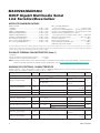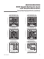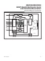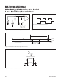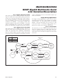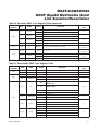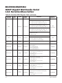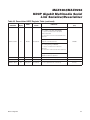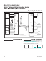
1
EVALUATION KIT AVAILABLE
MAX9263/MAX9264
HDCP Gigabit Multimedia Serial
Link Serializer/Deserializer
General Description
The MAX9263/MAX9264 chipset extends Maxim’s gigabit
multimedia serial link (GMSL) technology to include highbandwidth digital content protection (HDCP) encryption
of video and audio data. The MAX9263 serializer, or
any HDCP-GMSL serializer, pairs with the MAX9264
deserializer, or any HDCP-GMSL deserializer, for the
transmission of control data and HDCP encrypted video
and audio data.
The parallel interface operates with a pixel clock up to
104MHz. Three inputs are for I2S audio, supporting a
sampling frequency to 192kHz and a sample depth to
32 bits. The embedded control channel forms a fullduplex differential 9.6kbps to 1Mbps UART link between
the serializer and deserializer. A microcontroller (FC),
can be located on the serializer side of the link, on the
deserializer side of the link, or on both sides. The control
channel enables FC control of peripherals on the remote
side, such as backlight control, touch screen, and perform HDCP-related operations.
For driving longer cables, the serializer has programmable pre/deemphasis, and the deserializer has a programmable channel equalizer. The GMSL devices have
programmable spread spectrum on the serial (serializer)
and parallel (deserializer) output. The serial link input
and output meet ISO 10605 and IEC 61000-4-2 ESD
standards. The serializer core supply is 1.8V and the
deserializer core supply is 3.3V. The I/O supply is 1.8V to
3.3V. Both devices are available in a 64-pin TQFP package with an exposed pad and are specified over the
-40NC to +105NC automotive temperature range.
Applications
High-Resolution Automotive Navigation
Rear-Seat Infotainment
Megapixel Camera Systems
Benefits and Features
S Ideal for HDCP Video Applications
Supports Up to XGA (1280 x 768) or Dual-View
WVGA (2x 854 x 480)
Pre/Deemphasis and Equalization Allows 15m
Cable at Full Speed
Up to 192kHz, 32-Bit/Sample I2S
S Multiple Data Rates for System Flexibility
Up to 3.12Gbps Serial-Bit Rate
6.25MHz to 104MHz Pixel Clock
100kbps to 1Mbps UART and UART-to-I2C
Control Channel
S Reduces EMI and Shielding Requirements
Serial Output Programmable for 100mV to
400mV
Programmable Spread Spectrum Reduces EMI
Bypassable Input PLL for Jitter Attenuation
S Peripheral Features for System Power-Up and
Verification
Built-In PRBS Tester for BER Testing of the
Serial Link
Interrupt Transmission from Deserializer to
Serializer
S Meets Rigorous Automotive and Industrial
Requirements
-40°C to +105°C Operating Temperature
ISO 10605 and IEC 61000-4-2 ESD Tolerance
Ordering Information
PART
TEMP RANGE
MAX9263GCB/V+
MAX9263GCB/V+T
MAX9264GCB/V+
MAX9264GCB/V+T
-40NC to +105NC
-40NC to +105NC
-40NC to +105NC
-40NC to +105NC
PIN-PACKAGE
64 TQFP-EP*
64 TQFP-EP*
64 TQFP-EP*
64 TQFP-EP*
/V denotes an automotive qualified product.
+Denotes a lead(Pb)-free/RoHS-compliant package.
*EP = Exposed pad.
T = Tape and reel.
Blu-ray is a trademark of Blu-ray Disc Association.
For pricing, delivery, and ordering information, please contact Maxim Direct
at 1-888-629-4642, or visit Maxim’s website at www.maximintegrated.com.
19-5644; Rev 2; 9/14
MAX9263/MAX9264
HDCP Gigabit Multimedia Serial
Link Serializer/Deserializer
ABSOLUTE MAXIMUM RATINGS
AVDD to AGND
MAX9263.............................................................-0.5V
MAX9264.............................................................-0.5V
DVDD to GND (MAX9263)....................................-0.5V
DVDD to DGND (MAX9264)..................................-0.5V
IOVDD to GND (MAX9263)...................................-0.5V
IOVDD to IOGND (MAX9264)...............................-0.5V
Any Ground to Any Ground..................................-0.5V
OUT+, OUT- to AGND (MAX9263).......................-0.5V
IN+, IN- to AGND (MAX9264)...............................-0.5V
to
to
to
to
to
to
to
to
to
LMN_ to AGND (MAX9263)
(15mA current limit)...........................................-0.5V to +3.9V
All Other Pins to GND (MAX9263)....... -0.5V to (VIOVDD + 0.5V)
All Other Pins to IOGND (MAX9264).... -0.5V to (VIOVDD + 0.5V)
Continuous Power Dissipation (TA = +70NC )
64-Pin TQFP (derate 31.3mW/NC above +70NC)......2507.8mW
Operating Temperature Range......................... -40NC to +105NC
Junction Temperature......................................................+150NC
Storage Temperature Range............................. -65NC to +150NC
Lead Temperature (soldering, 10s).................................+300NC
Soldering Temperature (reflow).......................................+260NC
+1.9V
+3.9V
+1.9V
+3.9V
+3.9V
+3.9V
+0.5V
+1.9V
+1.9V
Stresses beyond those listed under “Absolute Maximum Ratings” may cause permanent damage to the device. These are stress ratings only, and functional
operation of the device at these or any other conditions beyond those indicated in the operational sections of the specifications is not implied. Exposure to absolute
maximum rating conditions for extended periods may affect device reliability.
PACKAGE THERMAL CHARACTERISTICS (Note 1)
64 TQFP-EP
Junction-to-Ambient Thermal Resistance (BJA)............31.9NC/W
Junction-to-Case Thermal Resistance (BJC)......................1NC/W
Note 1: Package thermal resistances were obtained using the method described in JEDEC specification JESD51-7, using a four-layer
board. For detailed information on package thermal considerations, refer to www.maximintegrated.com/thermal-tutorial.
MAX9263 DC ELECTRICAL CHARACTERISTICS
(VAVDD = VDVDD = 1.7V to 1.9V, VIOVDD = 1.7V to 3.6V, RL = 100I Q1% (differential), TA = -40NC to +105NC, unless otherwise noted.
Typical values are at VAVDD = VDVDD = VIOVDD = 1.8V, TA = +25NC.)
PARAMETER
SYMBOL
CONDITIONS
MIN
TYP
MAX
UNITS
SINGLE-ENDED INPUTS (DIN_, PCLKIN, SD, SCK, WS, AUTOS, MS, CDS, PWDN, SSEN, DRS, ES, BWS)
High-Level Input Voltage
Low-Level Input Voltage
VIH1
DIN_, PCLKIN, AUTOS, MS, CDS, SSEN,
DRS, ES, BWS
0.65 x
VIOVDD
SD, SCK, WS
0.7 x
VIOVDD
V
VIL1
Input Current
IIN1
VIN = 0 to VIOVDD
Input Clamp Voltage
VCL
ICL = -18mA
High-Level Output Voltage
VOH1
IOUT = -2mA
Low-Level Output Voltage
VOL1
IOUT = 2mA
IOS
VO = VGND
-10
0.35 x
VIOVDD
V
+10
FA
-1.5
V
SINGLE-ENDED OUTPUT (INT)
OUTPUT Short-Circuit Current
VIOVDD
- 0.2
V
0.2
VIOVDD = 3.0V to 3.6V
16
35
64
VIOVDD = 1.7V to 1.9V
3
12
21
V
mA
I2C/UART, I/O, AND OPEN-DRAIN OUTPUTS (RX/SDA, TX/SCL, LFLT)
High-Level Input Voltage
VIH2
Low-Level Input Voltage
VIL2
2 0.7 x
VIOVDD
V
0.3 x
VIOVDD
V
Maxim Integrated
MAX9263/MAX9264
HDCP Gigabit Multimedia Serial
Link Serializer/Deserializer
MAX9263 DC ELECTRICAL CHARACTERISTICS (continued)
(VAVDD = VDVDD = 1.7V to 1.9V, VIOVDD = 1.7V to 3.6V, RL = 100I Q1% (differential), TA = -40NC to +105NC, unless otherwise noted.
Typical values are at VAVDD = VDVDD = VIOVDD = 1.8V, TA = +25NC.)
PARAMETER
Input Current
Low-Level Output Voltage
SYMBOL
IIN2
VOL2
CONDITIONS
MIN
TYP
MAX
UNITS
+5
FA
VIN = 0 to VIOVDD (Note 2)
VIOVDD = 1.7V to 1.9V
IOUT = 3mA
VIOVDD = 3.0V to 3.6V
-110
Preemphasis off (Figure 1)
300
3.3dB preemphasis setting (Figure 2)
350
610
3.3dB deemphasis setting (Figure 2)
240
425
0.4
0.3
V
DIFFERENTIAL OUTPUT (OUT+, OUT-)
Differential Output Voltage
Change in VOD Between
Complementary Output States
Output Offset Voltage (VOUT+ +
VOUT-)/2 = VOS
Change in VOS Between
Complementary Output States
Output Short-Circuit Current
VOD
400
DVOD
VOS
Preemphasis off
1.1
1.4
DVOS
IOS
Magnitude of Differential Output
Short-Circuit Current
IOSD
Output Termination Resistance
(Internal)
RO
VOUT+ or VOUT- = 0V
VOUT+ or VOUT- = 1.9V
mV
1.56
V
15
mV
25
45
54
mV
15
-60
VOD = 0V
From OUT+, OUT- to VAVDD
500
mA
25
mA
63
I
27
mV
REVERSE CONTROL-CHANNEL RECEIVER (OUT+, OUT-)
High Switching Threshold
VCHR
Low Switching Threshold
VCLR
-27
mV
LINE-FAULT-DETECTION INPUTS (LMN_)
Short-to-GND Threshold
VTG
Figure 3
Normal Thresholds
VTN
Figure 3
0.3
V
0.57
1.07
V
V
V
VTO
Figure 3
1.45
VIO +
60mV
Open Input Voltage
VIO
Figure 3
1.47
1.75
Short-to-Battery Threshold
VTE
Figure 3
2.47
Open Thresholds
V
POWER SUPPLY
Worst-Case Supply Current
(Figure 4, Note 3)
IWCS
Sleep Mode Supply Current
ICCS
Power-Down Supply Current
ICCZ
Maxim Integrated
BWS = GND
PWDN = GND
fPCLKIN = 16.6MHz
105
132
fPCLKIN = 33.3MHz
110
152
fPCLKIN = 66.6MHz
120
160
fPCLKIN = 104MHz
145
188
45
225
FA
7
180
FA
mA
3
MAX9263/MAX9264
HDCP Gigabit Multimedia Serial
Link Serializer/Deserializer
MAX9263 DC ELECTRICAL CHARACTERISTICS (continued)
(VAVDD = VDVDD = 1.7V to 1.9V, VIOVDD = 1.7V to 3.6V, RL = 100I Q1% (differential), TA = -40NC to +105NC, unless otherwise noted.
Typical values are at VAVDD = VDVDD = VIOVDD = 1.8V, TA = +25NC.)
PARAMETER
SYMBOL
CONDITIONS
MIN
TYP
MAX
UNITS
ESD PROTECTION
Human Body Model, RD = 1.5kI,
CS = 100pF (Note 4)
OUT+, OUT-
All Other Pins
VESD
VESD
Q8
IEC 61000-4-2,
RD = 330I,
CS = 150pF (Note 5)
Contact discharge
Q10
Air discharge
Q12
ISO 10605,
RD = 2kI,
CS = 330pF (Note 5)
Contact discharge
Q10
Air discharge
Q25
Human Body Model, RD = 1.5kI,
CS = 100pF (Note 4)
kV
kV
Q4
MAX9263 AC ELECTRICAL CHARACTERISTICS
(VDVDD = VAVDD = 1.7V to 1.9V, VIOVDD = 1.7V to 3.6V, RL = 100I Q1% (differential), TA = -40NC to +105NC, unless otherwise noted.
Typical values are at VDVDD = VAVDD = VIOVDD = 1.8V, TA = +25NC.)
PARAMETER
SYMBOL
CONDITIONS
MIN
TYP
MAX
UNITS
CLOCK INPUT TIMING (PCLKIN)
Clock Frequency
fPCLKIN
Clock Duty Cycle
DC
Clock Transition Time
Clock Jitter
tR, tF
BWS = GND, VDRS = VIOVDD
8.33
16.66
BWS = GND, DRS = GND
16.66
104
VBWS = VIOVDD, VDRS = VIOVDD
6.25
12.5
VBWS = VIOVDD, DRS = GND
12.5
tHIGH/tT or tLOW/tT (Figure 5, Note 6)
35
MHz
78
50
(Figure 5, Note 6)
65
%
4
ns
800
ps(P-P)
tJ
3.125Gbps, 300kHz sinusoidal jitter (Note 6)
9.6
1000
kbps
Output Rise Time
tR
30% to 70%, CL = 10pF to 100pF,
1kI pullup to VIOVDD
20
150
ns
Output Fall Time
tF
70% to 30%, CL = 10pF to 100pF,
1kI pullup to VIOVDD
20
150
ns
I2C/UART PORT TIMING
I2C/UART Bit Rate
Input Setup Time
tSET
I2C only (Figure 6, Note 6)
100
ns
Input Hold Time
tHOLD
I2C only (Figure 6, Note 6)
0
ns
tR, tF
20% to 80%, VOD ≥ 400mV, RL = 100I,
serial-bit rate = 3.125Gbps (Note 6)
SWITCHING CHARACTERISTICS
Differential Output Rise/Fall Time
Total Serial Output Jitter
4 tTSOJ1
3.125Gbps PRBS signal, measured at
VOD = 0V differential, preemphasis
disabled (Figure 7)
90
0.25
150
ps
UI
Maxim Integrated
MAX9263/MAX9264
HDCP Gigabit Multimedia Serial
Link Serializer/Deserializer
MAX9263 AC ELECTRICAL CHARACTERISTICS
(VDVDD = VAVDD = 1.7V to 1.9V, VIOVDD = 1.7V to 3.6V, RL = 100I Q1% (differential), TA = -40NC to +105NC, unless otherwise noted.
Typical values are at VDVDD = VAVDD = VIOVDD = 1.8V, TA = +25NC.)
PARAMETER
SYMBOL
Deterministic Serial Output Jitter
tDSOJ2
CONDITIONS
MIN
3.125Gbps PRBS signal
Parallel Data Input Setup Time
tSET
(Figure 8, Note 6)
1
Parallel Data Input Hold Time
tHOLD
(Figure 8, Note 6)
1.5
Serializer Delay (Notes 6, 7)
(Figure 1)
TYP
MAX
0.15
UNITS
UI
ns
ns
Spread spectrum enabled
2830
Spread spectrum disabled
270
tSD
(Figure 9)
Bits
Link Start Time
tLOCK
(Figure 10)
3.5
ms
Power-Up Time
tPU
(Figure 11)
6
ms
WS Frequency
fWS
See Table 2
192
kHz
Sample Word Length
nWS
See Table 2
4
32
bits
(192 x
32) x 2
kHz
I2S INPUT TIMING
8
SCK Frequency
fSCK
fSCK = fWS x nWS x 2
(8 x
4) x 2
SCK Clock High Time
tHC
VSCK R VIH, tSCK = 1/fSCK
0.35 x
tSCK
ns
SCK Clock Low Time
tLC
VSCK P VIL, tSCK = 1/fSCK
0.35 x
tSCK
ns
SD, WS Setup Time
tSET
(Figure 12)
2
ns
SD, WS Hold Time
tHOLD
(Figure 12)
2
ns
MAX9264 DC ELECTRICAL CHARACTERISTICS
(VAVDD = VDVDD = 3.0V to 3.6V, VIOVDD = 1.7V to 3.6V, RL = 100I Q1% (differential), TA = -40NC to +105NC, unless otherwise noted.
Typical values are at VAVDD = VDVDD = VIOVDD = 3.3V, TA = +25NC.)
PARAMETER
SYMBOL
CONDITIONS
MIN
TYP
MAX
UNITS
SINGLE-ENDED INPUTS (ENABLE, BWS, INT, CDS, ES, EQS, DCS, MS, PWDN, SSEN, DRS)
High-Level Input Voltage
VIH1
Low-Level Input Voltage
VIL1
Input Current
Input Clamp Voltage
IIN1
VCL
0.65 x
VIOVDD
VIN = 0 to VIOVDD
ICL = -18mA
-10
V
0.35 x
VIOVDD
V
+10
-1.5
FA
V
SINGLE-ENDED OUTPUTS (WS, SCK, SD, DOUT_, PCLKOUT)
High-Level Output Voltage
Low-Level Output Voltage
Maxim Integrated
VOH1
VOL1
DCS = IOGND
VIOVDD
- 0.3
VDCS = VIOVDD
VIOVDD
- 0.2
IOUT = -2mA
IOUT = 2mA
V
DCS = IOGND
0.3
VDCS = VIOVDD
0.2
V
5
MAX9263/MAX9264
HDCP Gigabit Multimedia Serial
Link Serializer/Deserializer
MAX9264 DC ELECTRICAL CHARACTERISTICS (continued)
(VAVDD = VDVDD = 3.0V to 3.6V, VIOVDD = 1.7V to 3.6V, RL = 100I Q1% (differential), TA = -40NC to +105NC, unless otherwise noted.
Typical values are at VAVDD = VDVDD = VIOVDD = 3.3V, TA = +25NC.)
PARAMETER
SYMBOL
CONDITIONS
WS, SCK,
SD, DOUT_
OUTPUT Short-Circuit Current
VO = 0V,
DCS =
IOGND
VO = 0V,
VDCS =
VIOVDD
IOS
VO = 0V,
DCS =
IOGND
PCLKOUT
VO = 0V,
VDCS =
VIOVDD
MIN
TYP
MAX
VIOVDD =
3.0V to 3.6V
14
25
39
VIOVDD =
1.7V to 1.9V
3
7
13
VIOVDD =
3.0V to 3.6V
20
35
63
VIOVDD =
1.7V to 1.9V
5
10
21
VIOVDD =
3.0V to 3.6V
15
33
50
VIOVDD =
1.7V to 1.9V
4
10
17
VIOVDD =
3.0V to 3.6V
30
54
97
VIOVDD =
1.7V to 1.9V
9
16
32
UNITS
mA
I2C/UART, I/O, AND OPEN-DRAIN OUTPUTS (GPIO_, RX/SDA, TX/SCL, ERR, LOCK)
High-Level Input Voltage
VIH2
Low-Level Input Voltage
VIL2
Input Current
IIN2
0.7 x
VIOVDD
V
0.3 x
VIOVDD
VIN = 0 to
VIOVDD (Note 2)
RX/SDA, TX/SCL
-100
+1
LOCK, ERR, GPIO_
VIOVDD = 1.7V to 1.9V
-80
+1
0.4
V
FA
Low-Level Output Voltage
VOL2
IOUT = 3mA
Differential High Output Peak
Voltage, (VIN+) - (VIN-)
VROH
No high-speed data transmission
(Figure 13)
30
60
mV
Differential Low Output Peak
Voltage, (VIN+) - (VIN-)
VROL
No high-speed data transmission
(Figure 13)
-60
-30
mV
90
mV
VIOVDD = 3.0V to 3.6V
DIFFERENTIAL OUTPUT FOR REVERSE CONTROL CHANNEL (IN+, IN-)
0.3
V
DIFFERENTIAL INPUTS (IN+, IN-)
Differential High Input Threshold
(Peak) Voltage, (VIN+) - (VIN-)
VIDH(P)
Figure 14
Differential Low Input Threshold
(Peak) Voltage, (VIN+) - (VIN-)
VIDL(P)
Figure 14
Input Common-Mode Voltage
((VIN+) + (VIN-))/2
Differential Input Resistance
(Internal)
6 40
-90
-40
mV
VCMR
1
1.3
1.6
V
RI
80
100
130
I
Maxim Integrated
MAX9263/MAX9264
HDCP Gigabit Multimedia Serial
Link Serializer/Deserializer
MAX9264 DC ELECTRICAL CHARACTERISTICS (continued)
(VAVDD = VDVDD = 3.0V to 3.6V, VIOVDD = 1.7V to 3.6V, RL = 100I Q1% (differential), TA = -40NC to +105NC, unless otherwise noted.
Typical values are at VAVDD = VDVDD = VIOVDD = 3.3V, TA = +25NC.)
PARAMETER
POWER SUPPLY
SYMBOL
CONDITIONS
BWS = IOGND,
fPCLKOUT = 16.6MHz
BWS = IOGND,
fPCLKOUT = 33.3MHz
Worst-Case Supply Current
(Figure 15, Note 3)
IWCS
BWS = IOGND,
fPCLKOUT = 66.6MHz
BWS = IOGND,
fPCLKOUT = 104MHz
Sleep Mode Supply Current
Power-Down Current
ESD PROTECTION
ICCS
ICCZ
TYP
MAX
2% spread
spectrum active
132
186
Spread spectrum
disabled
125
175
2% spread
spectrum active
145
204
Spread spectrum
disabled
133
188
2% spread
spectrum active
174
241
Spread spectrum
disabled
157
220
2% spread
spectrum active
210
275
Spread spectrum
disabled
186
242
80
25
230
156
PWDN = IOGND
Human Body Model, RD = 1.5kI,
CS = 100pF (Note 4)
IN+, IN-
All Other Pins
Maxim Integrated
VESD
VESD
MIN
mA
FA
FA
Q8
IEC 61000-4-2,
RD = 330I,
CS = 150pF (Note 5)
Contact discharge
Q10
Air discharge
Q12
ISO 10605,
RD = 2kI,
CS = 330pF (Note 5)
Contact discharge
Q8
Air discharge
Q20
Human Body Model, RD = 1.5kI,
CS = 100pF (Note 4)
UNITS
Q4
kV
kV
7
MAX9263/MAX9264
HDCP Gigabit Multimedia Serial
Link Serializer/Deserializer
MAX9264 AC ELECTRICAL CHARACTERISTICS
(VAVDD = VDVDD = 3.0V to 3.6V, VIOVDD = 1.7V to 3.6V, RL = 100I Q1% (differential), TA = -40NC to +105NC, unless otherwise noted.
Typical values are at VAVDD = VDVDD = VIOVDD = 3.3V, TA = +25NC.)
PARAMETER
SYMBOL
CONDITIONS
MIN
TYP
MAX
UNITS
PARALLEL CLOCK OUTPUT (PCLKOUT)
Clock Frequency
Clock Duty Cycle
Clock Jitter
fPCLKOUT
DC
tJ
BWS = IOGND, VDRS = VIOVDD
8.33
BWS = IOGND, DRS = IOGND
16.66
104
VBWS = VIOVDD, VDRS = VIOVDD
6.25
12.5
VBWS = VIOVDD, DRS = IOGND
tHIGH/tT or tLOW/tT (Figure 16, Note 6)
12.5
78
40
Period jitter, RMS, spread off, 3.125Gbps,
PRBS pattern, UI = 1/fPCLKOUT (Note 6)
16.66
50
60
0.05
MHz
%
UI
I2C/UART PORT TIMING
I2C/UART Bit Rate
9.6
1000
kbps
Output Rise Time
tR
30% to 70%, CL = 10pF to 100pF,
1kI pullup to VIOVDD
20
150
ns
Output Fall Time
tF
70% to 30%, CL = 10pF to 100pF,
1kI pullup to VIOVDD
20
150
ns
Input Setup Time
tSET
I2C only (Figure 6, Note 6)
100
ns
Input Hold Time
tHOLD
I2C only (Figure 6, Note 6)
0
ns
SWITCHING CHARACTERISTICS (NOTE 6)
20% to 80%,
VIOVDD = 1.7V to 1.9V
PCLKOUT Rise-and-Fall Time
tR, tF
20% to 80%,
VIOVDD = 3.0V to 3.6V
20% to 80%,
VIOVDD = 1.7V to 1.9V
Parallel Data Rise-and-Fall Time
(Figure 17)
tR, tF
20% to 80%,
VIOVDD = 3.0V to 3.6V
Deserializer Delay
tSD
(Figure 18, Note 7)
VDCS = VIOVDD,
CL = 10pf
0.4
2.2
DCS = IOGND,
CL = 5pF
0.5
2.8
VDCS = VIOVDD,
CL = 10pF
0.25
1.7
DCS = IOGND,
CL = 5pF
0.3
2.0
VDCS = VIOVDD,
CL = 10pf
0.5
3.1
DCS = IOGND,
CL = 5pF
0.6
3.8
VDCS = VIOVDD,
CL = 10pF
0.3
2.2
DCS = IOGND,
CL = 5pF
0.4
2.4
ns
ns
Spread spectrum
enabled
2880
Spread spectrum
disabled
750
Bits
Reverse Control-Channel Output
Rise Time
tR
No forward channel data transmission
(Figure 13)
180
400
ns
Reverse Control-Channel Output
Fall Time
tF
No forward channel data transmission
(Figure 13)
180
400
ns
8 Maxim Integrated
MAX9263/MAX9264
HDCP Gigabit Multimedia Serial
Link Serializer/Deserializer
MAX9264 AC ELECTRICAL CHARACTERISTICS (continued)
(VAVDD = VDVDD = 3.0V to 3.6V, VIOVDD = 1.7V to 3.6V, RL = 100I Q1% (differential), TA = -40NC to +105NC, unless otherwise noted.
Typical values are at VAVDD = VDVDD = VIOVDD = 3.3V, TA = +25NC.)
PARAMETER
Lock Time
Power-Up Time
SYMBOL
tLOCK
tPU
CONDITIONS
Figure 19
MIN
TYP
MAX
Spread spectrum
enabled
1.5
Spread spectrum
disabled
1
UNITS
ms
Figure 20
2.5
ms
I2S OUTPUT TIMING (NOTE 6)
WS Jitter
SCK Jitter
Audio Skew Relative to Video
SCK, SD, WS Rise-and-Fall Time
tAJ-WS
tAJ-SCK
tASK
tR, tF
tWS = 1/fWS, rising
(falling) edge to
falling (rising) edge
tSCK = 1/fSCK, rising
edge to rising edge
fWS = 48kHz or
44.1kHz
0.4e - 3 0.5e - 3
x tWS
x tWS
fWS = 96kHz
0.8e - 3
x tWS
1e - 3
x tWS
fWS = 192kHz
1.6e - 3
x tWS
2e - 3
x tWS
nWS = 16 bits,
fWS = 48kHz or
44.1kHz
13e - 3 16e - 3
x tSCK x tSCK
nWS = 24 bits,
fWS = 96kHz
39e - 3 48e - 3
x tSCK x tSCK
nWS = 32 bits,
fWS = 192kHz
0.1
x tSCK
Video and audio synchronized
20% to 80%,
CL = 10pF
ns
ns
0.13
x tSCK
3 x tWS 4 x tWS
VDCS = VIOVDD,
CL = 10pF
0.3
3.1
DCS = IOGND,
CL = 5pF
0.4
3.8
Fs
ns
SD, WS Valid Time Before SCK
tDVB
tSCK = 1/fSCK (Figure 21)
0.35
x tSCK
0.5
x tSCK
ns
SD, WS Valid Time After SCK
tDVA
tSCK = 1/fSCK (Figure 21)
0.35
x tSCK
0.5
x tSCK
ns
Note 2: Minimum IIN due to voltage drop across the internal pullup resistor.
Note 3: HDCP enabled.
Note 4: Tested terminal to all grounds.
Note 5: Tested terminal to AGND.
Note 6: Guaranteed by design and not production tested.
Note 7: Measured in CML bit times. Bit time = 1/(30 x fPCLKOUT) for BWS = GND. Bit time = 1/(40 x fPCLKOUT) for VBWS = VIOVDD.
Maxim Integrated
9
MAX9263/MAX9264
HDCP Gigabit Multimedia Serial
Link Serializer/Deserializer
Typical Operating Characteristics
(VAVDD = VDVDD = VIOVDD = 1.8V (MAX9263), VAVDD = VDVDD = VIOVDD = 3.3V (MAX9264), TA = +25NC, unless otherwise noted.)
MAX9263 toc01
160
PRBS ON, HDCP ON
SUPPLY CURRENT (mA)
PREEMPHASIS = 0x0B TO 0x0F
130
120
PREEMPHASIS = 0x00
100
5
25
45
65
120
PREEMPHASIS = 0x01 TO 0x04
PREEMPHASIS = 0x00
5
20
35
50
65
80
PCLK FREQUENCY (MHz)
PCLK FREQUENCY (MHz)
MAX9264 SUPPLY CURRENT
vs. PCLK FREQUENCY (24-BIT MODE)
MAX9264 SUPPLY CURRENT
vs. PCLK FREQUENCY (32-BIT MODE)
MAX9263 toc03
150
140
130
PRBS ON, HDCP ON, SS OFF
ALL EQ SETTINGS
160
SUPPLY CURRENT (mA)
ALL EQ SETTINGS
150
140
130
120
120
110
110
5
25
45
65
85
20
35
50
65
80
PCLK FREQUENCY (MHz)
MAX9264 SUPPLY CURRENT
vs. PCLK FREQUENCY (24-BIT MODE)
MAX9264 SUPPLY CURRENT
vs. PCLK FREQUENCY (32-BIT MODE)
2%, 4% SPREAD
160
150
140
130
170
2%, 4% SPREAD
160
150
140
130
0% SPREAD
120
0% SPREAD
120
PRBS ON, HDCP ON
180
SUPPLY CURRENT (mA)
180
170
190
MAX9263 toc05
PRBS ON, HDCP ON
190
5
105
PCLK FREQUENCY (MHz)
200
SUPPLY CURRENT (mA)
130
105
PRBS ON, HDCP ON, SS OFF
110
110
5
25
45
65
PCLK FREQUENCY (MHz)
10 PREEMPHASIS = 0x0B TO 0x0F
100
85
170
160
140
110
PREEMPHASIS = 0x01 TO 0x04
110
PRBS ON, HDCP ON
MAX9263 toc04
140
150
MAX9263 toc06
SUPPLY CURRENT (mA)
150
SUPPLY CURRENT (mA)
MAX9263 SUPPLY CURRENT
vs. PCLK FREQUENCY (32-BIT MODE)
MAX9263 toc02
MAX9263 SUPPLY CURRENT
vs. PCLK FREQUENCY (24-BIT MODE)
85
105
5
20
35
50
65
80
PCLK FREQUENCY (MHz)
Maxim Integrated
MAX9263/MAX9264
HDCP Gigabit Multimedia Serial
Link Serializer/Deserializer
Typical Operating Characteristics (continued)
(VAVDD = VDVDD = VIOVDD = 1.8V (MAX9263), VAVDD = VDVDD = VIOVDD = 3.3V (MAX9264), TA = +25NC, unless otherwise noted.)
0.5% SPREAD
0% SPREAD
-20
-30
-40
-50
-60
-70
-80
2% SPREAD
-90
30
31
32
33
34
35
-30
-40
-50
-60
-70
2% SPREAD
-90
36
30
31
32
4% SPREAD
33
34
35
36
PCLK FREQUENCY (MHz)
OUTPUT POWER SPECTRUM vs. PCLK
FREQUENCY (VARIOUS MAX9263 SPREAD)
OUTPUT POWER SPECTRUM vs. PCLK
FREQUENCY (VARIOUS MAX9264 SPREAD)
0% SPREAD
-30
-40
-50
-60
-70
-80
2% SPREAD
-90
61
63
65
fPCLK = 66MHz
-10
0% SPREAD
-20
-30
4%
SPREAD
-40
-50
-60
-70
-80
4% SPREAD
67
69
2% SPREAD
-90
61
71
65
67
69
71
PCLK FREQUENCY (MHz)
MAXIMUM PCLK FREQUENCY
vs. STP CABLE LENGTH (BER < 10-9)
MAXIMUM PCLK FREQUENCY vs.
ADDITIONAL DIFFERENTIAL CL (BER < 10-9)
MAX9263 toc11
120
100
80
OPTIMUM
PE/EQ SETTINGS
60
NO PE, 10.7dB
EQUALIZATION
40
NO PE, 5.2dB
EQUALIZATION
20
BER CAN BE AS LOW AS 10-12 FOR
CABLE LENGTHS LESS THAN 10m
0
120
10m STP CABLE
100
OPTIMUM
PE/EQ SETTINGS
80
60
NO PE, 10.7dB
EQUALIZATION
40
NO PE, 5.2dB EQUALIZATION
20
BER CAN BE AS LOW AS 10-12 FOR CL < 4pF
FOR OPTIMUM PE/EQ SETTINGS
0
0
63
PCLK FREQUENCY (MHz)
5
10
15
STP CABLE LENGTH (m)
20
MAX9263 toc12
-20
MAX9263 toc10
0.5% SPREAD
0
OUTPUT POWER SPECTRUM (dBm)
fPCLK = 66MHz
MAXIMUM PCLK FREQUENCY (MHz)
OUTPUT POWER SPECTRUM (dBm)
0% SPREAD
-20
PCLK FREQUENCY (MHz)
0
MAXIMUM PCLK FREQUENCY (MHz)
fPCLK = 33MHz
-10
-80
4% SPREAD
-10
Maxim Integrated
0
MAX9263 toc08
-10
OUTPUT POWER SPECTRUM vs. PCLK
FREQUENCY (VARIOUS MAX9264 SPREAD)
OUTPUT POWER SPECTRUM (dBm)
fPCLK = 33MHz
MAX9263 toc09
OUTPUT POWER SPECTRUM (dBm)
0
MAX9263 toc07
OUTPUT POWER SPECTRUM vs. PCLK
FREQUENCY (VARIOUS MAX9263 SPREAD)
0
2
4
6
8
10
ADDITIONAL DIFFERENTIAL LOAD CAPACITANCE (pF)
11
MAX9263/MAX9264
HDCP Gigabit Multimedia Serial
Link Serializer/Deserializer
Pin Configurations
CDS
PWDN
RX/SDA
SSEN
TX/SCL
LMN1
AGND
OUT-
OUT+
AVDD
LMN0
LFLT
INT
DRS
BWS
ES
TOP VIEW
48 47 46 45 44 43 42 41 40 39 38 37 36 35 34 33
DIN0 49
32 MS
GND 50
31 GND
IOVDD 51
30 IOVDD
DIN1 52
29 AUTOS
DIN2 53
28 WS
DIN3 54
27 SCK
DIN4 55
26 SD
DIN5 56
25 DIN28
MAX9263
DIN6 57
24 DIN27
DIN7 58
23 DIN26
DIN8 59
22 DIN25
DIN9 60
21 DIN24
GND 61
20 GND
DVDD 62
19 DVDD
EP*
DIN10 63
18 AGND
+
TQFP
DIN22
DIN21
DIN20
10 11 12 13 14 15 16
DIN19/VS
9
DIN18/HS
8
DIN17
7
AVDD
DIN15
6
AGND
DIN14
5
GND
4
IOVDD
3
PCLKIN
2
DIN16
1
DIN13
17 DIN23
DIN12
DIN11 64
*CONNECT EXPOSED PAD TO AGND
12 Maxim Integrated
MAX9263/MAX9264
HDCP Gigabit Multimedia Serial
Link Serializer/Deserializer
DOUT23
DOUT22
DOUT21
DOUT20
DOUT19/VS
DOUT18/HS
DOUT17
DOUT16
DOUT15
DOUT14
DOUT13
DOUT12
DOUT11
DOUT10
DOUT9
TOP VIEW
PCLKOUT
Pin Configurations (continued)
48 47 46 45 44 43 42 41 40 39 38 37 36 35 34 33
DOUT8 49
32 DOUT24
IOGND 50
31 IOGND
IOVDD 51
30 IOVDD
DOUT7 52
29 DOUT25
DOUT6 53
28 DOUT26
DOUT5 54
27 DOUT27
DOUT4 55
26 DOUT28/MCLK
DOUT3 56
25 SD
MAX9264
DOUT2 57
24 SCK
DOUT1 58
23 WS
DOUT0 59
22 LOCK
IOGND 60
21 IOGND
20 ERR
SSEN 61
DRS 62
19 PWDN
EP*
AVDD 63
18 TX/SCL
+
DGND
DVDD
MS
10 11 12 13 14 15 16
DCS
9
GPIO1
8
EQS
7
AGND
CDS
6
IN-
INT
5
IN+
4
AVDD
3
ES
2
GPIO0
1
BWS
17 RX/SDA
ENABLE
AGND 64
TQFP
*CONNECT EXPOSED PAD TO AGND
Maxim Integrated
13
MAX9263/MAX9264
HDCP Gigabit Multimedia Serial
Link Serializer/Deserializer
MAX9263 Pin Description
PIN
NAME
FUNCTION
1–5
DIN[12:16]
Data Input [12:16]. Parallel data inputs with internal pulldown to GND. Encrypted when HDCP
is enabled (see Table 1).
6
PCLKIN
Parallel Clock Input. Latches parallel data inputs and provides the PLL reference clock.
7, 30, 51
IOVDD
I/O Supply Voltage. 1.8V to 3.3V logic I/O power supply. Bypass IOVDD to GND with 0.1FF
and 0.001FF capacitors as close as possible to the device with the smaller capacitor closest
to IOVDD.
8, 20, 31, 50,
61
GND
9, 18, 39
AGND
Analog Ground
10, 42
AVDD
1.8V Analog Power Supply. Bypass AVDD to AGND with 0.1FF and 0.001FF capacitors as
close as possible to the device with the smaller capacitor closest to AVDD.
11
DIN17
Data Input 17. Parallel data input with internal pulldown to GND. Encrypted when HDCP is
enabled (see Table 1).
12
DIN18/HS
Data Input 18/HSYNC. Parallel data input with internal pulldown to GND. Use DIN18/HS for
HSYNC when HDCP is enabled (Table 1).
13
DIN19/VS
Data Input 19/VSYNC. Parallel data input with internal pulldown to GND. Use DIN19/VS for
VSYNC when HDCP is enabled (Table 1).
14
DIN20
15, 16, 17
DIN[21:23]
19, 62
DVDD
21, 22, 23
DIN[24:26]
Data Input [24:26]. Parallel data inputs with internal pulldown to GND. DIN[24:26] are not
used in 24-bit mode. Set BWS = high (32-bit mode) to use [DIN24:26]. Encrypted when
HDCP is enabled (see Table 1).
24, 25
DIN[27:28]
Data Input [27:28]. Parallel data inputs with internal pulldown to GND. DIN[27:28] are not
used in 24-bit mode. Set BWS = high (32-bit mode) to use [DIN27:28]. DIN[27:28] are not
encrypted when HDCP is enabled (see Table 1).
26
SD
27
SCK
I2S Serial-Clock Input with Internal Pulldown to GND
28
WS
I2S Word-Select Input with Internal Pulldown to GND
29
AUTOS
32
MS
33
CDS
14 Digital and I/O Ground
Data Input 20. Parallel data input with internal pulldown to GND. DIN20 is not encrypted when
HDCP is enabled (see Table 1).
Data Input [21:23]. Parallel data inputs with internal pulldown to GND. DIN[21:23] are not
used in 24-bit mode. Set BWS = high (32-bit mode) to use [DIN21:23]. Encrypted when
HDCP is enabled (Table 1).
1.8V Digital Power Supply. Bypass DVDD to GND with 0.1FF and 0.001FF capacitors as close
as possible to the device with the smaller capacitor closest to DVDD.
I2S Serial-Data Input with Internal Pulldown to GND. Disable I2S to use SD as an additional
control/data input latched on the selected edge of PCLKIN. Encrypted when HDCP is enabled.
Active-Low Autostart Setting. AUTOS requires an external pulldown or pullup resistor. Set
AUTOS = high to power up the device with no link active. Set AUTOS = low to have the
serializer power up the serial link with autorange detection (see Tables 11 and 12).
Mode Select. Control link mode-selection input requires an external pulldown or pullup
resistor. Set MS = low to select base mode. Set MS = high to select the bypass mode.
Control Direction Selection. Control link direct selection input requires external pulldown or
pullup resistor. Set CDS = low for UART connection of a FC as a control master. Set CDS =
high for peripheral connection as a control-channel I2C or UART slave.
Maxim Integrated
MAX9263/MAX9264
HDCP Gigabit Multimedia Serial
Link Serializer/Deserializer
MAX9263 Pin Description (continued)
PIN
NAME
34
PWDN
35
36
37
FUNCTION
Active-Low, Power-Down Input. PWDN requires external pulldown or pullup resistor.
RX/SDA
Receive/Serial Data. UART receive or I2C serial-data input/output with internal 30kI pullup to
IOVDD. In UART mode, RX/SDA is the Rx input of the serializer’s UART. In I2C mode,
RX/SDA is the SDA input/output of the serializer’s I2C master. RX/SDA has an open-drain
driver and requires a pullup resistor.
TX/SCL
Transmit/Serial Clock. UART transmit or I2C serial-clock output with internal 30kI pullup to
IOVDD. In UART mode, TX/SCL is the Tx output of the serializer’s UART. In I2C mode,
TX/SCL is the SCL output of the serializer’s I2C master. TX/SCL is an open-drain driver and
requires a pullup resistor.
SSEN
Spread-Spectrum Enable. Serial link spread-spectrum enable input requires external
pulldown or pullup resistor. The state of SSEN latches upon power-up or when resuming from
power-down mode (PWDN = low). Set SSEN = high for Q0.5% spread spectrum on the serial
link. Set SSEN = low to use the serial link without spread spectrum.
Line-Fault Monitor Input 1. See Figure 3 for details.
38
LMN1
40, 41
OUT-, OUT+
43
LMN0
Line-Fault Monitor Input 0. See Figure 3 for details.
44
LFLT
Line Fault, Active-Low Open-Drain Line-Fault Output. LFLT has a 60kI internal pullup
resistor. LFLT = low indicates a line fault. LFLT is output high when PWDN = low.
45
INT
Interrupt Output. Indicates remote-side interrupt requests. INT = low upon power-up and when
PWDN = low. A transition on the INT input of the deserializer toggles the serializer’s INT output.
46
DRS
Data-Rate Select. Data-rate range-selection input requires external pulldown or pullup
resistor. The state of DRS latches upon power-up or when resuming from power-down mode
(PWDN = low). Set DRS = high for PCLKIN frequencies of 8.33MHz to 16.66MHz
(24-bit mode) or 6.25MHz to 12.5MHz (32-bit mode). Set DRS = low for PCLKIN frequencies
of 16.66MHz to 104MHz (24-bit mode) or 12.5MHz to 78MHz (32-bit mode).
47
ES
Edge Select. PCLKIN trigger edge selection requires external pulldown or pullup resistor. Set
ES = low to trigger on the rising edge of PCLKIN. Set ES = high to trigger on the falling edge
of PCLKIN.
48
BWS
Bus-Width Select. BWS requires external pulldown or pullup resistor. Set BWS = low for 24-bit
mode. Set BWS = high for 32-bit mode.
49
DIN0
Data Input 0. Parallel data input with internal pulldown to GND. Encrypted when HDCP is
enabled (Table 1).
52–60
DIN[1:9]
Data Input [1:9]. Parallel data inputs with internal pulldown to GND. Encrypted when HDCP is
enabled (Table 1).
63, 64
DIN[10:11]
Data Input [10:11]. Parallel data inputs with internal pulldown to GND. Encrypted when HDCP
is enabled (Table 1).
—
EP
Exposed Pad. EP is internally connected to AGND. MUST externally connect EP to the AGND
plane for proper thermal and electrical performance.
Maxim Integrated
Differential CML Output Q. Differential outputs of the serial link.
15
MAX9263/MAX9264
HDCP Gigabit Multimedia Serial
Link Serializer/Deserializer
MAX9264 Pin Description
PIN
NAME
FUNCTION
1
ENABLE
Active-Low Parallel Output-Enable Input. Requires an external pulldown or pullup resistor. Set
ENABLE = low to enable PCLKOUT, SD, SCK, WS, and DOUT_. Set ENABLE = high to put
PCLKOUT, SD, SCK, WS, and DOUT_ into high impedance.
2
BWS
3
INT
Interrupt Input. INT requires an external pullup or pulldown resistor. A transition on the
deserializer’s INT input toggles the serializer’s INT output.
4
CDS
Control Direction Selection. Control link direction selection input requires external pulldown or
pullup resistor. Set CDS = high for UART connection of a FC as control-channel master. Set
CDS = low for peripheral connection as a control-channel I2C or UART slave.
5
GPIO0
6
ES
7, 63
AVDD
8, 9
IN+, IN-
10, 64
AGND
11
EQS
12
GPIO1
GPIO0. Open-drain general-purpose input/output with an internal 60kI pullup resistor to
IOVDD. GPIO0 is high impedance during power-up and when PWDN = low.
Edge Select. PCLKOUT edge-selection input requires an external pulldown or pullup resistor.
Set ES = low for a rising-edge trigger. Set ES = high for a falling-edge trigger.
3.3V Analog Power Supply. Bypass AVDD to AGND with 0.1FF and 0.001FF capacitors as
close as possible to the device with the smaller capacitor closest to AVDD.
Differential CML Input Q. Differential inputs of the serial link.
Analog Ground
Equalizer Select Input Requires an External Pulldown or Pullup Resistor. The state of EQS
latches upon power-up or when resuming from power-down mode (PWDN = low). Set EQS =
low for 10.7dB equalizer boost (EQTUNE = 1001). Set EQS = high for 5.2dB equalizer boost
(EQTUNE = 0100).
GPIO1. Open-drain general-purpose input/output with an internal 60kI pullup resistor to
IOVDD. GPIO1 is high impedance during power-up and when PWDN = low.
Drive Current Select. Driver current-selection input requires an external pulldown or
pullup resistor to IOVDD. Set DCS = high for stronger parallel data and clock output drivers.
Set DCS = low for normal parallel data and clock drivers. See the MAX9264 DC Electrical
Characteristics table.
13
DCS
14
MS
15
DVDD
3.3V Digital Power Supply. Bypass DVDD to DGND with 0.1FF and 0.001FF capacitors as
close as possible to the device with the smaller capacitor closest to DVDD.
16
DGND
Digital Ground
17
18
16 Bus-Width Select. BWS requires an external pulldown or pullup resistor. Set BWS = low for
24-bit mode. Set BWS = high for 32-bit mode.
Mode Select. Control-channel mode selection input requires an external pulldown or
pullup resistor. MS sets the control-link mode when CDS = high. See the Control-Channel and
Register Programming section. MS sets autostart mode when CDS = low. See Table 11.
RX/SDA
Receive/Serial Data. UART receive or I2C serial-data input/output with internal 30kI pullup to
IOVDD. In UART mode, RX/SDA is the Rx input of the deserializer’s UART. In I2C mode,
RX/SDA is the SDA input/output of the deserializer’s I2C master. RX/SDA has an open-drain
driver and requires a pullup resistor.
TX/SCL
Transmit/Serial Clock. UART transmit or I2C serial-clock output with internal 30kI pullup to
IOVDD. In UART mode, TX/SCL is the Tx output of the deserializer’s UART. In I2C mode,
TX/SCL is the SCL output of the deserializer’s I2C master. TX/SCL is an open-drain driver and
requires a pullup resistor.
Maxim Integrated
MAX9263/MAX9264
HDCP Gigabit Multimedia Serial
Link Serializer/Deserializer
MAX9264 Pin Description (continued)
PIN
NAME
19
PWDN
FUNCTION
Active-Low, Power-Down Input. PWDN requires an external pulldown or pullup resistor.
Active-Low Open-Drain Video Data Error Output with Internal 60kI Pullup to IOVDD.
ERR goes low when the number of decoding errors during normal operation exceed a
programmed error threshold or when at least one PRBS error is detected during PRBS test.
ERR is output high when PWDN = low.
20
ERR
21, 31, 50, 60
IOGND
Input/Output Ground
LOCK
Open-Drain Lock Output with Internal 60kI Pullup to IOVDD. LOCK = high indicates PLLs
are locked with correct serial-word-boundary alignment. LOCK = low indicates PLLs are not
locked or incorrect serial-word-boundary alignment. LOCK remains low when the
configuration link is active. LOCK is output high when PWDN = low.
22
23
WS
I2S Word-Select Output
24
SCK
I2S Serial-Clock Output
25
SD
I2S Serial-Data Output. Disable I2S to use SD as an additional control output latched on the
selected edge of PCLKOUT. Encrypted when HDCP is enabled.
26
DOUT28/
MCLK
Data Output 28/MCLK. Parallel data or master clock output. Output data can be strobed on
the selected edge of PCLKOUT. DOUT28 is not used in 24-bit mode and remains low. Set
BWS = high (32-bit mode) to use DOUT28. DOUT28/MCLK is not encrypted when HDCP is
enabled (Table 1). DOUT28/MCLK can be used to output MCLK. See the Additional MCLK
Output for Audio Applications section.
27
DOUT27
Data Output 27. Parallel data output. Output data can be strobed on the selected edge of
PCLKOUT. DOUT27 is not used in 24-bit mode and remains low. Set BWS = high (32-bit
mode) to use DOUT27. DOUT27 is not encrypted when HDCP is enabled. See Table 1.
28, 29
DOUT[26:25]
Data Output [26:25]. Parallel data outputs. Output data can be strobed on the selected edge
of PCLKOUT. DOUT[26:25] are not used in 24-bit mode and remain output low. Set BWS =
high (32-bit mode) to use DOUT[26:25]. Encrypted when HDCP is enabled. See Table 1.
30, 51
IOVDD
I/O Supply Voltage. 1.8V to 3.3V logic I/O power supply. Bypass IOVDD to IOGND with 0.1FF
and 0.001FF capacitors as close as possible to the device with the smaller capacitor closest
to IOVDD.
32–35
DOUT[24:21]
Data Output [24:21]. Parallel data outputs. Output data can be strobed on the selected edge
of PCLKOUT. DOUT[24:21] are not used in 24-bit mode and remain low. Set BWS = high
(32-bit mode) to use DOUT[24:21]. Encrypted when HDCP is enabled. See Table 1.
36
DOUT20
Data Output 20. Parallel data output. Output data can be strobed on the selected edge of
PCLKOUT. DOUT20 is not encrypted when HDCP is enabled. See Table 1.
37
DOUT19/VS
Data Output 19/VSYNC. Parallel data output. Output data can be strobed on the selected
edge of PCLKOUT. Use DOUT19/VS for VSYNC when HDCP is enabled. See Table 1.
38
DOUT18/HS
Data Output 18/HSYNC. Parallel data output. Output data can be strobed on the selected
edge of PCLKOUT. Use DOUT18/HS for HSYNC when HDCP is enabled. See Table 1.
39, 40
DOUT[17:16]
Data Output [17:16]. Parallel data outputs. Output data can be strobed on the selected edge
of PCLKOUT. Encrypted when HDCP is enabled. See Table 1.
41
PCLKOUT
42–49
DOUT[15:8]
Maxim Integrated
Parallel Clock Output. Used for DOUT[28:0].
Data Output [15:8]. Parallel data outputs. Output data can be strobed on the selected edge
of PCLKOUT. Encrypted when HDCP is enabled. See Table 1.
17
MAX9263/MAX9264
HDCP Gigabit Multimedia Serial
Link Serializer/Deserializer
MAX9264 Pin Description (continued)
PIN
NAME
FUNCTION
52–59
DOUT[7:0]
Data Output [7:0]. Parallel data outputs. Output data can be strobed on the selected edge of
PCLKOUT. Encrypted when HDCP is enabled. See Table 1.
SSEN
Spread-Spectrum Enable Input. Serial link spread-spectrum enable input requires an external
pulldown or pullup resistor. The state of SSEN latches upon power-up or when resuming from
power-down mode (PWDN = low). Set SSEN = high for Q2% spread spectrum on parallel
outputs. Set SSEN = low to use the parallel outputs without spread spectrum.
62
DRS
Data-Rate Select. Data-rate range-selection input requires an external pulldown or pullup
resistor. The state of DRS latches upon power-up or when resuming from power-down mode
(PWDN = low). Set DRS = high for PCLKOUT frequencies of 8.33MHz to 16.66MHz (24-bit
mode) or 6.25MHz to 12.5MHz (32-bit mode). Set DRS = low for PCLKOUT frequencies of
16.66MHz to 104MHz (24-bit mode) or 12.5MHz to 78MHz (32-bit mode).
—
EP
Exposed Pad. EP is internally connected to AGND. MUST externally connect EP to the AGND
plane for proper thermal and electrical performance.
61
Functional Diagrams
LEFT
SSPLL
PCLKIN
FILTER
PLL
LINE
FAULT
DETECT
CLKDIV
DIN[17:0]
RGB[17:0]
DIN18/HS
HS
DIN19/VS
VS
DIN20
DE
DIN[26:21]
(4-CH)
RGB[23:18]
(4-CH)
DIN[28:27]
(4-CH)
RGB
HDCP
ENCRYPT
LMN1
OUT+
PARALLEL
TO
SERIAL
HS
VIDEO
LMN0
VS
OUT-
DE
HDCP
KEYS
FIFO
HDCP
CONTROL
CML Tx
SCRAMBLE/
PARITY/
8b/10b
ENCODE
DIN[28:27]
(4-CH)
ACB
AUDIO
Rx
REVERSE
CONTROL
CHANNEL
HDCP
ENCRYPT
FCC
MAX9263
UART/I2C
SD SCK WS
18 TX/SCL
RX/SDA
Maxim Integrated
MAX9263/MAX9264
HDCP Gigabit Multimedia Serial
Link Serializer/Deserializer
Functional Diagrams (continued)
PCLKOUT
DOUT[17:0]
SSPLL
RGB[17:0]
DOUT18/HS
HS
DOUT19/VS
VS
DOUT20
DE
DOUT[26:21]
(4-CH)
RGB[23:18]
(4-CH)
DOUT27
(4-CH)
CDRPLL
CLKDIV
RGB
HDCP
DECRYPT
IN+
SERIAL
TO
PARALLEL
HS
VIDEO
VS
IN-
DE
HDCP
KEYS
FIFO
HDCP
CONTROL
DIN[28:27]
(4-CH)
Tx
DOUT28/MCLK
(4-CH)
AUDIO
CML Rx
AND EQ
8b/10b
DECODE/
UNSCRAMBLE
ACB
HDCP
DECRYPT
REVERSE
CONTROL
CHANNEL
FCC
MAX9264
UART/I2C
SD SCK WS
Maxim Integrated
TX/SCL
RX/SDA
19
MAX9263/MAX9264
HDCP Gigabit Multimedia Serial
Link Serializer/Deserializer
RL/2
OUT+
VOD
VOS
OUT-
RL/2
GND
((OUT+) + (OUT-))/2
OUTVOS(+)
VOS(-)
VOS(-)
OUT+
DVOS = |VOS(+) - VOS(-)|
VOD(+)
VOD = 0V
VOD(-)
VOD(-)
DVOD = |VOD(+) - VOD(-)|
(OUT+) - (OUT-)
Figure 1. Serializer Serial-Output Parameters
OUT+
VOD(P)
VOS
VOD(D)
OUT-
SERIAL-BIT
TIME
Figure 2. Serializer Output Waveforms at OUT+, OUT-
20 Maxim Integrated
MAX9263/MAX9264
HDCP Gigabit Multimedia Serial
Link Serializer/Deserializer
1.7V TO 1.9V
MAX9263
45.3kI*
45.3kI*
LMN0
LMN1
4.99kI*
OUTPUT
LOGIC
(OUT+)
4.99kI*
TWISTED PAIR
OUT+
OUT-
49.9kI*
49.9kI*
CONNECTORS
LFLT
REFERENCE
VOLTAGE
GENERATOR
OUTPUT
LOGIC
(OUT-)
*Q1% TOLERANCE
Figure 3. Line-Fault Detector Circuit
PCLKIN
DIN_
NOTE: PCLKIN PROGRAMMED FOR RISING LATCH EDGE.
Figure 4. Serializer Worst-Case Pattern Input
Maxim Integrated
21
MAX9263/MAX9264
HDCP Gigabit Multimedia Serial
Link Serializer/Deserializer
tT
VIH MIN
tHIGH
PCLKIN
VIL MAX
tR
tF
tLOW
Figure 5. Serializer Parallel Input Clock Requirements
START
CONDITION
(S)
PROTOCOL
BIT 7
MSB
(A7)
tLOW
tSU;STA
BIT 6
(A6)
tHIGH
BIT 0
(R/W)
ACKNOWLEDGE
(A)
STOP
CONDITION
(P)
1/fSCL
VIOVDD x 0.7
SCL
VIOVDD x 0.3
tBUF
tSP
tf
tr
VIOVDD x 0.7
SDA
VIOVDD x 0.3
tHD;STA
tSU;DAT
tHD;DAT
tVD;DAT
tVD;ACK
tSU;STO
Figure 6. I2C Timing Parameters
800mVP-P
t TSOJ1
2
t TSOJ1
2
Figure 7. Serializer Differential Output Template
22 Maxim Integrated
MAX9263/MAX9264
HDCP Gigabit Multimedia Serial
Link Serializer/Deserializer
VIH MIN
PCLKIN
VIL MAX
tSET
tHOLD
VIH MIN
VIH MIN
VIL MAX
VIL MAX
DIN_
NOTE: PCLKIN PROGRAMMED FOR RISING LATCHING EDGE.
Figure 8. Serializer Input Setup and Hold Times
EXPANDED TIME SCALE
DIN_
N
N+1
N+3
N+2
N+4
PCLKIN
N-1
N
OUT+/tSD
FIRST BIT
LAST BIT
Figure 9. Serializer Delay
Maxim Integrated
23
MAX9263/MAX9264
HDCP Gigabit Multimedia Serial
Link Serializer/Deserializer
PCLKIN
tLOCK
350Fs
SERIAL LINK INACTIVE
SERIAL LINK ACTIVE
REVERSE CONTROL CHANNEL
AVAILABLE
CHANNEL
DISABLED
REVERSE CONTROL CHANNEL
ENABLED
PWDN MUST BE HIGH
Figure 10. Serializer Link Startup Time
PCLKIN
PWDN
VIH1
tPU
POWERED DOWN
POWERED UP,
SERIAL LINK INACTIVE
POWERED UP, SERIAL LINK ACTIVE
350µs
REVERSE CONTROL
CHANNEL DISABLED
REVERSE CONTROL
CHANNEL ENABLED
REVERSE CONTROL
CHANNEL DISABLED
REVERSE CONTROL
CHANNEL ENABLED
Figure 11. Serializer Power-Up Delay
24 Maxim Integrated
MAX9263/MAX9264
HDCP Gigabit Multimedia Serial
Link Serializer/Deserializer
WS
tHOLD
tSCK
tSET
tLC
SCK
tHOLD
tSET
tHC
SD
Figure 12. Input I2S Timing Parameters
RL/2
IN+
MAX9264
VOD
REVERSE
CONTROL-CHANNEL
TRANSMITTER
IN-
VCMR
RL/2
IN+
IN-
IN-
IN+
VCMR
VROH
0.9 x VROH
(IN+) - (IN-)
0.1 x VROH
0.1 x VROL
tR
0.9 x VROL
VROL
tF
Figure 13. Reverse Control-Channel Output Parameters
Maxim Integrated
25
MAX9263/MAX9264
HDCP Gigabit Multimedia Serial
Link Serializer/Deserializer
RL/2
IN+
VIN+
PCLKOUT
VID(P)
RL/2
IN-
_
+
_
VIN-
+
_
CIN
CIN
DOUT_
NOTE: PCLKOUT PROGRAMMED FOR RISING LATCH EDGE.
VID(P) = | VIN+ - VIN- |
VCMR = (VIN+ + VIN-)/2
Figure 14. Test Circuit for Differential Input Measurement
Figure 15. Deserializer Worst-Case Pattern Output
tT
VOH MIN
tHIGH
PCLKOUT
VOL MAX
tLOW
Figure 16. Deserializer Clock Output High and Low Times
CL
MAX9264
SINGLE-ENDED OUTPUT LOAD
0.8 x VI0VDD
0.2 x VI0VDD
tR
tF
Figure 17. Deserializer Output Rise and Fall Times
26 Maxim Integrated
MAX9263/MAX9264
HDCP Gigabit Multimedia Serial
Link Serializer/Deserializer
SERIAL-WORD LENGTH
SERIAL WORD N
SERIAL WORD N+1
SERIAL WORD N+2
IN+/LAST BIT
FIRST BIT
DOUT_
PARALLEL WORD N-1
PARALLEL WORD N-2
PARALLEL WORD N
PCLKOUT
tSD
NOTE: PCLKOUT PROGRAMMED FOR RISING LATCHING EDGE.
Figure 18. Deserializer Delay
IN+/-
IN+ - IN-
PWDN
tLOCK
LOCK
VIH1
tPU
VOH
LOCK
VOH
PWDN MUST BE HIGH
Figure 19. Deserializer Lock Time
Maxim Integrated
Figure 20. Deserializer Power-Up Delay
27
MAX9263/MAX9264
HDCP Gigabit Multimedia Serial
Link Serializer/Deserializer
WS
tDVA
tR
tDVB
SCK
tDVB
tDVA
tF
SD
Figure 21. Deserializer Output I2S Timing Parameters
Detailed Description
The MAX9263/MAX9264 serializer/deserializer chipset
utilizes Maxim’s GMSL technology and HDCP. When
HDCP is enabled, the serializer/deserializer encrypt
video and audio data on the serial link. The serializer/
deserializer are backward compatible with the MAX9259/
MAX9260 serializer/deserializer.
The serializer/deserializer have a maximum serial payload data rate of 2.5Gbps for 15m or more of STP cable.
The serializer/deserializer pair operates up to a maximum pixel clock of 104MHz for 24-bit mode, or 78MHz
for 32-bit mode, respectively. This serial link supports a
wide range of display panels, from QVGA (320 x 240) to
WXGA (1280 x 800) and higher with 24-bit color.
The 24-bit mode handles 21 bits of high-speed data,
UART control signals, and three audio signals. The 32-bit
mode handles 29 bits of high-speed data, UART control
signals, and three audio signals. The three audio signals
are a standard I2S interface, supporting sample rates
from 8kHz to 192kHz and audio word lengths of 4 bits
to 32 bits. The embedded control channel forms a fullduplex, differential 9.6kbps to 1Mbps UART link between
the serializer and deserializer for HDCP-related control
28 operations. In addition, the control channel enables
electronic control unit (ECU), or microcontroller (FC) control of peripherals in the remote side, such as backlight
control, grayscale gamma correction, camera module,
and touch screen. An ECU/FC, can be located on the
serializer side of the link (typical for video display), on
the deserializer side of the link (typical for image sensing), or on both sides. Base-mode communication with
peripherals uses either I2C or the GMSL UART format. A
bypass mode enables full-duplex communication using
a user-defined UART format.
The serializer pre/deemphasis, along with the deserializer channel equalizer, extends the link length and
enhances the link reliability. Spread spectrum is available to reduce EMI on the serial and parallel outputs. The
serial link connections comply with ISO 10605 and IEC
61000-4-2 ESD protection standards.
Register Mapping
The FC configures various operating conditions of the
serializer and the deserializer through internal registers.
The default device address of the serializer is 0x80 and
default device address of the deserializer is 0x90. Write
to registers 0x00 or 0x01 in both devices to change the
device address of the serializer or the deserializer.
Maxim Integrated
MAX9263/MAX9264
HDCP Gigabit Multimedia Serial
Link Serializer/Deserializer
HDCP Bitmapping and Bus-Width Selection
Serial Link Signaling and Data Format
The parallel input/outputs have two selectable modes,
24-bit mode and 32-bit mode. In 24-bit mode, DIN[28:21]
are not available. For both modes, the SD, SCK, and WS
pins are for I2S audio. The serializer/deserializer use
pixel clock rates from 8.33MHz to 104MHz for 24-bit
mode and 6.25MHz to 78MHz for 32-bit mode.
The serializer uses CML signaling with programmable
pre/deemphasis and AC-coupling. The deserializer uses
AC-coupling and programmable channel equalization.
Together, the GMSL link can operate at full speed over
STP cable lengths to 15m or more.
The serializer scrambles and encodes the input data and
sends the 8b/10b coded signal through the serial link.
The deserializer recovers the embedded serial clock and
then samples, decodes, and descrambles before outputting the data. Figures 22 and 23 show the serial-data
packet format after unscrambling and 8b/10b decoding.
In 24-bit or 32-bit mode, 21 or 29 bits map to the parallel outputs. The audio channel bit (ACB) contains an
encoded audio signal derived from the three I2S signals
(SD, SCK, and WS). The forward control channel (FCC)
Table 1 lists the HDCP bit mapping for the parallel inputs.
DIN18/HS and DIN19/VS are reserved for HSYNC and
VSYNC, respectively. The serializer/deserializer have
HDCP encryption on DIN[17:0] and the I2S input. 32-bit
mode has additional HDCP encryption on DIN[26:21].
DIN[28:27] and DIN20 do not have HDCP encryption. SD,
when used as an additional data input (AUDIOEN = 0),
also does not have HDCP encryption.
Table 1. HDCP Mapping and Bus Width Selection
24-BIT MODE (BWS = LOW)
INPUT BITS
32-BIT MODE (BWS = HIGH)
HDCP MAPPING*
HDCP ENCRYPTION
CAPABILITY
HDCP MAPPING*
HDCP ENCRYPTION
CAPABILITY
DIN[17:0]
RGB
Yes
RGB
Yes
DIN18/HS
HS
No
HS
No
DIN19/VS
VS
No
VS
No
DIN20
DE
No
DE
No
DIN[26:21]
Not Available
—
RGB
Yes
DIN[28:27]
Not Available
—
CNTL
No
SD
I2S**
SD
I2S**
SD
*Bit assignments of DIN[28:0] are interchangeable if HDCP is not used.
**HDCP encryption on SD when used as an I2S signal.
24 BITS
DIN0
DIN1
R0
R1
DIN17 DIN18 DIN19 DIN20
B5
RGB DATA
HS
VS
FCC
PCB
DE
CONTROL BITS
NOTE: LOCATIONS OF THE RGB DATA ARE INTERCHANGABLE
ACCORDINGLY ON BOTH SIDES OF THE LINK.
ONLY DIN[17:0], AND ACB HAVE HDCP ENCRYPTION.
ACB
AUDIO
CHANNEL
BIT
FORWARD
CONTROLCHANNEL BIT
PACKET
PARITY
CHECK BIT
Figure 22. 24-Bit Mode Serial Link Data Format
Maxim Integrated
29
MAX9263/MAX9264
HDCP Gigabit Multimedia Serial
Link Serializer/Deserializer
32 BITS
DIN0
DIN1
R0
R1
DIN17 DIN18 DIN19 DIN20 DIN21 DIN22 DIN23 DIN24 DIN25 DIN26 DIN27 DIN28
B5
HS
RGB DATA
VS
DE
R6
R7
G6
CONTROL BITS
G7
B6
ACB
FCC
PCB
B7
ADDITIONAL AUDIO
VIDEO DATA/ CHANNEL
BIT
CONTROL BITS
FORWARD
CONTROLCHANNEL BIT
RGB DATA
NOTE: LOCATIONS OF THE RGB DATA ARE INTERCHANGABLE
ACCORDINGLY ON BOTH SIDES OF THE LINK.
ONLY DIN[17:0], DIN[26:21] AND ACB HAVE HDCP ENCRYPTION.
PACKET
PARITY
CHECK BIT
Figure 23. 32-Bit Mode Serial Link Data Format
Table 2. Maximum Audio WS Frequency (kHz) for Various PCLKIN Frequencies
PCLKIN FREQUENCY
(DRS = LOW) (MHz)
PCLKIN FREQUENCY
(DRS = HIGH) (MHz)
WORD
LENGTH
(bits)
12.5
15
16.6
> 20
6.25
7.5
8.33
> 10
8
> 192
> 192
> 192
> 192
> 192
> 192
> 192
> 192
16
> 192
> 192
> 192
> 192
> 192
> 192
> 192
> 192
18
185.5
> 192
> 192
> 192
185.5
> 192
> 192
> 192
20
174.6
> 192
> 192
> 192
174.6
> 192
> 192
> 192
24
152.2
182.7
> 192
> 192
152.2
182.7
> 192
> 192
32
123.7
148.4
164.3
> 192
123.7
148.4
164.3
> 192
bit carries the forward control data. The last bit (PCB) is
the parity bit of the previous 23 or 31 bits.
Reverse Control Channel
The serializer uses the reverse control channel to receive
I2C/UART and interrupt signals from the deserializer in
the opposite direction of the video stream. The reverse
control channel and forward video data coexist on
the same twisted pair forming a bidirectional link. The
reverse control channel operates independently from the
forward control channel. The reverse control channel is
available 500Fs after power-up. The serializer temporarily disables the reverse control channel for 350Fs after
starting/stopping the forward serial link.
Data-Rate Selection
The serializer/deserializer use the DRS input to set the
PCLKIN frequency range. Set DRS high for a PCLKIN
frequency range of 6.25MHz to 12.5MHz (32-bit mode)
or 8.33MHz to 16.66MHz (24-bit mode). Set DRS low
for normal operation with a PCLKIN frequency range
30 of 12.5MHz to 78MHz (32-bit mode) or 16.66MHz to
104MHz (24-bit mode).
Audio Channel
The I2S audio channel supports audio sampling rates
from 8kHz to 192kHz and audio word lengths from 4 bits
to 32 bits. The audio bit clock (SCK) does not have to be
synchronized with PCLKIN. The serializer automatically
encodes audio data into a single bit stream synchronous
with PCLKIN. The deserializer decodes the audio stream
and stores audio words in a FIFO. Audio rate detection
uses an internal oscillator to continuously determine the
audio data rate and output the audio in I2S format. The
audio channel is enabled by default. When the audio
channel is disabled, the audio data on the serializer and
deserializer are treated as an additional parallel signal
(DIN_/DOUT_).
Since the audio data sent through the serial link is
synchronized with PCLKIN, low PCLKIN frequencies
limit the maximum audio sampling rate. Table 2 lists
Maxim Integrated
MAX9263/MAX9264
HDCP Gigabit Multimedia Serial
Link Serializer/Deserializer
the maximum audio sampling rate for various PCLKIN
frequencies. Spread-spectrum settings do not affect
the I2S data rate or WS clock frequency.
Additional MCLK Output for
Audio Applications
Some audio DACs, such as the MAX9850, do not require
a synchronous main clock (MCLK), while other DACs
require MCLK to be a specific multiple of WS. If an audio
DAC chip needs the MCLK to be a multiple of WS, use
an external PLL to regenerate the required MCLK from
PCLKOUT or SCK.
For audio applications that cannot directly use PCLKOUT,
the MAX9264 provides a divided MCLK output on
DOUT28/MCLK at the expense of one less control line
in 32-bit mode (24-bit mode is not affected). By default,
DOUT28/MCLK operates as a parallel data output, and
MCLK is turned off. Set MCLKDIV (MAX9264 register
0x12, D[6:0]) to a non-zero value to enable the MCLK
output. Set MCLKDIV to 0x00 to disable MCLK and set
DOUT28/MCLK as a parallel data output.
The output MCLK frequency is:
fMCLK =
fSRC
MCLKDIV
where fSRC is the MCLK source frequency (Table 3)
MCLKDIV is the divider ratio from 1 to 127
Choose MCLKDIV values so that fMCLK is not greater
than 60MHz. MCLK frequencies derived from PCLKIN
(MCLKSRC = 0) are not affected by spread-spectrum
settings in the deserializer. Enabling spread spectrum
in the serializer, however, introduces spread spectrum
into MCLK. Spread-spectrum settings of either device
do not affect MCLK frequencies derived from the internal
oscillator. The internal oscillator frequency ranges from
100MHz to 150MHz over all process corners and operating conditions.
Control Channel and Register Programming
The control channel is available for the FC to send and
receive control data over the serial link simultaneously
with the high-speed data. Configuring the CDS pin allows
the FC to control the link from either the serializer or the
deserializer side to support video-display or imagesensing applications. The control channel between the
FC and serializer or deserializer runs in base mode or
bypass mode according to the mode selection (MS)
input of the device connected to the FC. Base mode is
a half-duplex control channel and the bypass mode is a
full-duplex control channel.
Base Mode
In base mode, the FC is the host and can access the
core and HDCP registers of both the serializer and
deserializer from either side of the link by using the
GMSL UART protocol. The FC can also program the
peripherals on the remote side by sending the UART
packets to the serializer or deserializer, with the UART
packets converted to I2C by the device on the remote
side of the link (deserializer for LCD or serializer for
image-sensing applications). The FC communicates
with a UART peripheral in base mode (through INTTYPE
register settings), using the half-duplex default GMSL
UART protocol of the serializer/deserializer. The device
addresses of the serializer and deserializer in base
mode are programmable. The default value is 0x80 for
the serializer and 0x90 for the deserializer.
When the peripheral interface uses I2C (default), the
serializer/deserializer convert packets to I2C that have
device addresses different from those of the serializer or
deserializer. The converted I2C bit rate is the same as
the original UART bit rate.
The deserializer uses a proprietary differential line coding to send signals back towards the serializer. The
speed of the control channel ranges from 9.6kbps to
Table 3. Deserializer fSRC Settings
MCLKSRC SETTING
(REGISTER 0x12, D7)
DATA RATE SETTING
High speed
0
Low speed
1
Maxim Integrated
—
BIT WIDTH SETTING
MCLK SOURCE
FREQUENCY (fSRC)
24-bit mode
3 x fPCLKIN
32-bit mode
4 x fPCLKIN
24-bit mode
6 x fPCLKIN
32-bit mode
8 x fPCLKIN
—
Internal oscillator
(120MHz typ)
31
MAX9263/MAX9264
HDCP Gigabit Multimedia Serial
Link Serializer/Deserializer
1Mbps in both directions. The serializer and deserializer automatically detect the control-channel bit rate in
base mode. Packet bit rates can vary up to 3.5x from the
previous bit rate. See the Changing the Clock Frequency
section.
SYNC byte and ACK byte, respectively. Events such
as device wake-up and interrupt generate transitions
on the control channel that should be ignored by the
FC. Data written to the serializer/deserializer registers
do not take effect until after the acknowledge byte
is sent. This allows the FC to verify write commands
received without error, even if the result of the write
command directly affects the serial link. The slave uses
the SYNC byte to synchronize with the host UART data
rate automatically. If the INT or MS inputs of the deserializer toggle while there is control-channel communication,
the control-channel communication can be corrupted.
Figure 24 shows the UART protocol for writing and reading in base mode between the µC and the serializer/
deserializer.
Figure 25 shows the UART data format. Even parity is used. Figures 26 and 27 detail the formats of
the SYNC byte (0x79) and the ACK byte (0xC3).
The FC and the connected slave chip generate the
WRITE DATA FORMAT
SYNC
DEV ADDR + R/W
REG ADDR
NUMBER OF BYTES
BYTE 1
BYTE N
ACK
MASTER WRITES TO SLAVE
MASTER READS FROM SLAVE
READ DATA FORMAT
SYNC
DEV ADDR + R/W
REG ADDR
NUMBER OF BYTES
MASTER WRITES TO SLAVE
ACK
BYTE 1
BYTE N
MASTER READS FROM SLAVE
Figure 24. GMSL UART Protocol for Base Mode
1 UART FRAME
START
D0
D1
D2
D3
FRAME 1
D4
D5
D6
D7
PARITY
STOP
FRAME 2
STOP
FRAME 3
START
STOP
START
GMSL USES EVEN PARITY
Figure 25. GMSL UART Data Format for Base Mode
START
D0
D1
D2
D3
D4
D5
D6
D7
1
0
0
1
1
1
1
0
Figure 26. SYNC Byte (0x79)
32 PARITY STOP
START
D0
D1
D2
D3
D4
D5
D6
D7
1
1
0
0
0
0
1
1
PARITY STOP
Figure 27. ACK Byte (0xC3)
Maxim Integrated
MAX9263/MAX9264
HDCP Gigabit Multimedia Serial
Link Serializer/Deserializer
UART-TO-I2C CONVERSION OF WRITE PACKET (I2CMETHOD = 0)
FC
SERIALIZER/DESERIALIZER
11
SYNC FRAME
SERIALIZER/DESERIALIZER
11
DEVICE ID + WR
11
REGISTER ADDRESS
11
NUMBER OF BYTES
11
DATA 0
11
DATA N
11
ACK FRAME
PERIPHERAL
1
S
7
DEV ID
1 1
W A
8
REG ADDR
8
DATA 0
1
A
1
A
8
DATA N
1 1
A P
UART-TO-I2C CONVERSION OF READ PACKET (I2CMETHOD = 0)
FC
SERIALIZER/DESERIALIZER
11
SYNC FRAME
SERIALIZER/DESERIALIZER
11
DEVICE ID + RD
11
REGISTER ADDRESS
11
NUMBER OF BYTES
11
ACK FRAME
11
DATA 0
11
DATA N
PERIPHERAL
1
S
7
DEV ID
: MASTER TO SLAVE
1 1
W A
8
REG ADDR
1 1
A S
: SLAVE TO MASTER
7
DEV ID
S: START
1 1
R A
8
DATA 0
P: STOP
1
A
8
DATA N
1 1
A P
A: ACKNOWLEDGE
Figure 28. Format Conversion Between GMSL UART and I2C with Register Address (I2CMETHOD = 0)
In the event of a missed acknowledge, the FC should
assume there was an error in the packet transmission or
response. In base mode, the FC must keep the UART Tx/
Rx lines high no more than four bit times between bytes
in a packet. Keep the UART Tx/Rx lines high for 16 bittimes before starting to send a new packet.
As shown in Figure 28, the remote-side device converts
the packets going to or coming from the peripherals from
the UART format to the I2C format and vice versa. The
remote device removes the byte number count and adds
or receives the ACK between the data bytes of I2C. The
I2C’s data rate is the same as the UART data rate.
Interfacing Command-Byte-Only I2C Devices
The serializer and deserializer UART-to-I2C conversion interfaces with devices that do not require register
addresses, such as the MAX7324 GPIO expander. In
this mode, the I2C master ignores the register address
byte and directly reads/writes the subsequent data bytes
(Figure 29). Change the communication method of the
I2C master using the I2CMETHOD bit. I2CMETHOD = 1
sets command-byte-only mode, while I2CMETHOD = 0
sets normal mode where the first byte in the data stream
is the register address.
Maxim Integrated
Bypass Mode
In bypass mode, the serializer/deserializer ignore UART
commands from the FC and the FC communicates with
the peripherals directly using its own defined UART protocol. The FC cannot access the serializer/deserializer’s
registers in this mode. Peripherals accessed through the
forward control channel using the UART interface need
to handle at least one PCLKIN period ±10ns of jitter due
to the asynchronous sampling of the UART signal by
PCLKIN. Set MS = high to put the control channel into
bypass mode. For applications with the FC connected to
the deserializer, (CDS is high) there is a 1ms wait time
between setting MS high and the bypass control channel
being active. There is no delay time when switching to
bypass mode when the FC is connected to the serializer (CDS = low). Do not send a logic-low value longer
than 100Fs to ensure proper interrupt functionality.
Bypass mode accepts bit rates down to 10kbps in either
direction. See the Interrupt Control section for interrupt
functionality limitations. The control-channel data pattern
should not be held low longer than 100Fs if interrupt
control is used.
33
MAX9263/MAX9264
HDCP Gigabit Multimedia Serial
Link Serializer/Deserializer
UART-TO-I2C CONVERSION OF WRITE PACKET (I2CMETHOD = 1)
FC
11
SYNC FRAME
SERIALIZER/DESERIALIZER
11
DEVICE ID + WR
SERIALIZER/DESERIALIZER
FC
11
REGISTER ADDRESS
PERIPHERAL
1
7
S DEV ID
11
NUMBER OF BYTES
11
DATA N
1 1
W A
8
DATA 0
UART-TO-I2C CONVERSION OF READ PACKET (I2CMETHOD = 1)
SERIALIZER/DESERIALIZER
11
11
11
SYNC FRAME
DEVICE ID + RD
REGISTER ADDRESS
SERIALIZER/DESERIALIZER
11
DATA 0
11
NUMBER OF BYTES
11
ACK FRAME
11
ACK FRAME
1
A
8
DATA N
11
DATA 0
1 1
A P
11
DATA N
PERIPHERAL
1
S
: MASTER TO SLAVE
: SLAVE TO MASTER
7
DEV ID
S: START
1 1
R A
8
DATA 0
P: STOP
1
A
8
DATA N
1 1
A P
A: ACKNOWLEDGE
Figure 29. Format Conversion Between GMSL UART and I2C with Register Address (I2CMETHOD = 1)
Interrupt Control
The INT pin of the serializer is the interrupt output and
the INT pin of the deserializer is the interrupt input. The
interrupt output on the serializer follows the transitions
at the interrupt input. This interrupt function supports
remote-side functions such as touch-screen peripherals,
remote power-up, or remote monitoring. Interrupts that
occur during periods where the reverse control channel
is disabled, such as link startup/shutdown, are automatically resent once the reverse control channel becomes
available again. Bit D4 of register 0x06 in the deserializer
also stores the interrupt input state. The INT output of
the serializer is low after power-up. In addition, the FC
can set the INT output of the serializer by writing to the
SETINT register bit. In normal operation, the state of the
interrupt output changes when the interrupt input on the
deserializer toggles. Do not send a logic-low value longer than 100Fs in either base or bypass mode to ensure
proper interrupt functionality.
34 Pre/Deemphasis Driver
The serial line driver in the serializer employs currentmode logic (CML) signaling. The driver can generate
an adjustable waveform according to the cable length
and characteristics. There are 13 preemphasis settings
as shown in Table 4. Negative preemphasis levels are
deemphasis levels in which the preemphasized swing
level is the same as normal swing, but the no-transition
data is deemphasized. Program the preemphasis levels through register 0x05 D[3:0] of the serializer. This
preemphasis function compensates the high frequency
loss of the cable and enables reliable transmission over
longer link distances. Additionally, a lower power drive
mode can be entered by programming CMLLVL bits
(0x05, D[5:4]) to reduce the driver strength down to
75% (CMLLVL = 10) or 50% (CMLLVL = 01) from 100%
(CMLLVL = 11, default).
Maxim Integrated
MAX9263/MAX9264
HDCP Gigabit Multimedia Serial
Link Serializer/Deserializer
Table 4. Serializer CML Driver Strength (Default Level, CMLLVL = 11)
SINGLE-ENDED VOLTAGE SWING
PREEMPHASIS LEVEL (dB)*
PREEMPHASIS SETTING
(0x05, D[3:0])
ICML
(mA)
IPRE
(mA)
MAX (mV)
MIN (mV)
-6.0
0100
12
4
400
200
-4.1
0011
13
3
400
250
-2.5
0010
14
2
400
300
-1.2
0001
15
1
400
350
0
0000
16
0
400
400
1.1
1000
16
1
425
375
2.2
1001
16
2
450
350
3.3
1010
16
3
475
325
4.4
1011
16
4
500
300
6.0
1100
15
5
500
250
8.0
1101
14
6
500
200
10.5
1110
13
7
500
150
14.0
1111
12
8
500
100
*Negative preemphasis levels denote deemphasis.
Table 5. Deserializer Cable Equalizer Boost Levels
BOOST SETTING (0x05 D[3:0])
TYPICAL BOOST GAIN (dB)
0000
2.1
0001
2.8
0010
3.4
0011
4.2
0100
5.2
Power-Up Default
(EQS = high)
0101
6.2
0110
7
0111
8.2
1000
9.4
1001
10.7
Power-Up Default
(EQS = low)
1010
11.7
1011
13
Line Equalizer
The deserializer includes an adjustable line equalizer to
further compensate cable attenuation at high frequencies. The cable equalizer has 11 selectable levels of
compensation from 2.1dB to 13dB (Table 5). The EQS
input selects the default equalization level at power-up.
Maxim Integrated
The state of EQS is latched upon power-up or when
resuming from power-down mode. To select other
equalization levels, set the corresponding register bits
in the deserializer (0x05 D[3:0]). Use equalization in the
deserializer, together with preemphasis in the serializer,
to create the most reliable link for a given cable.
35
MAX9263/MAX9264
HDCP Gigabit Multimedia Serial
Link Serializer/Deserializer
Spread Spectrum
To reduce the EMI generated by the transitions on
the serial link and parallel outputs, both the serializer and deserializer support spread spectrum. Turning
on spread spectrum on the deserializer spreads the
parallel video outputs. Turning on spread spectrum
on the serializer spreads the serial link, along with the
deserializer parallel outputs. Do not enable spread for
both the serializer and deserializer. The six selectable
spread-spectrum rates at the serializer serial output are
Q0.5%, Q1%, Q1.5%, Q2%, Q3%, and Q4% (Table 6).
Some spread-spectrum rates can only be used at lower
PCLK_ frequencies (Table 7). There is no PCLK_ frequency limit for the 0.5% spread rate. The two selectable
spread-spectrum rates at the deserializer parallel output
are Q2% and Q4% (Table 8).
Set the serializer SSEN input high to select 0.5% spread
at power-up and SSEN input low to select no spread at
power-up. Set the deserializer SSEN input high to select
2% spread at power-up and SSEN input low to select no
spread at power-up. The state of SSEN is latched upon
power-up or when resuming from power-down mode.
Whenever the serializer spread spectrum is turned on
or off, the serial link automatically restarts and remains
unavailable while the deserializer relocks to the serial
data. Turning on spread spectrum on the serializer
or deserializer does not affect the audio data stream.
Changes in the serializer spread settings only affect
the deserializer MCLK output if it is derived from PCLK_
(MCLKSRC = 0).
The serializer/deserializer include a sawtooth divider to
control the spread-modulation rate. Auto detection or
manual programming of the PCLKIN operation range
guarantees a spread-spectrum modulation frequency
within 20kHz to 40kHz. Additionally, manual configuration of the sawtooth divider (SDIV: 0x03, D[5:0]) allows
the user to set a modulation frequency according to
the PCLKIN frequency. Always keep the modulation
frequency between 20kHz to 40kHz to ensure proper
operation.
Table 6. Serializer Serial Output Spread
SS
SPREAD (%)
000
No spread spectrum. Power-up default when SSEN = low.
001
Q0.5% spread spectrum. Power-up default when SSEN = high.
010
Q1.5% spread spectrum.
011
Q2% spread spectrum.
100
No spread spectrum.
101
Q1% spread spectrum.
110
Q3% spread spectrum.
111
Q4% spread spectrum.
Table 7. Serializer Spread Rate Limitations
24-BIT MODE PCLK_
FREQUENCY (MHz)
32-BIT MODE PCLK_
FREQUENCY (MHz)
SERIAL LINK BIT-RATE
(Mbps)
AVAILABLE SPREAD
RATES
< 33.3
< 25
< 1000
All rates available
33.3 to < 66.7
20 to < 50
1000 to < 2000
1.5%, 1.0%, 0.5%
66.7+
50+
2000+
0.5%
Table 8. Deserializer Parallel Output Spread
SS
36 SPREAD (%)
00
No spread spectrum. Power-up default when SSEN = low.
01
Q2% spread spectrum. Power-up default when SSEN = high.
10
No spread spectrum.
11
Q4% spread spectrum.
Maxim Integrated
MAX9263/MAX9264
HDCP Gigabit Multimedia Serial
Link Serializer/Deserializer
Manual Programming of the
Spread-Spectrum Divider
Sleep Mode
The serializer/deserializer include a low-power sleep
mode to reduce power consumption on the device not
attached to the FC (the deserializer in LCD applications
and the serializer in camera applications). Set the corresponding remote IC’s SLEEP bit to 1 to initiate sleep
mode. The serializer sleeps immediately after setting
its SLEEP = 1. The deserializer sleeps after serial link
inactivity or 8ms (whichever arrives first) after setting
its SLEEP = 1. See the Link Startup Procedure section
for details on waking up the device for different FC and
starting conditions.
The modulation rate for the serializer/deserializer relates
to the PCLK_ frequency as follows:
fM= (1 + DRS)
fPCLK_
MOD × SDIV
where:
fM = Modulation frequency
DRS = DRS pin input value (0 or 1)
fPCLK_ = PCLK_ frequency
The FC side device cannot enter into sleep mode. If
an attempt is made to program the FC side device for
sleep, the SLEEP bit remains 0. Use the PWDN input
pin to bring the FC side device into a low-power state.
Entering sleep mode resets the HDCP registers, but not
the configuration registers.
MOD = Modulation coefficient given in Table 9 or 10
SDIV = 6- or 5-bit SDIV setting, manually programmed
by the FC
To program the SDIV setting, first look up the modulation
coefficient according to the part number and desired
bus-width and spread-spectrum settings. Solve the
above equation for SDIV using the desired pixel clock
and modulation frequencies. If the calculated SDIV
value is larger than the maximum allowed SDIV value in
Table 9 or 10, set SDIV to the maximum value.
Power-Down Mode
The serializer/deserializer include a power-down mode
to further reduce power consumption. Set PWDN low to
enter power-down mode. While in power-down mode, the
Table 9. Serializer Modulation Coefficients and Maximum SDIV Settings
BIT-WIDTH MODE
SPREAD-SPECTRUM
SETTING (%)
MODULATION
COEFFICIENT MOD (dec)
SDIV UPPER LIMIT (dec)
1
104
40
0.5
104
63
3
152
27
1.5
152
54
4
204
15
2
204
30
32 bit
24 bit
1
80
52
0.5
80
63
3
112
37
1.5
112
63
4
152
21
2
152
42
Table 10. Deserializer Modulation Coefficients and Maximum SDIV Settings
SPREAD-SPECTRUM SETTING (%)
MODULATION COEFFICIENT (dec)
SDIV UPPER LIMIT (dec)
4
208
15
2
208
30
Maxim Integrated
37
MAX9263/MAX9264
HDCP Gigabit Multimedia Serial
Link Serializer/Deserializer
outputs of the device remain high impedance. Entering
power-down mode resets the internal registers of the
device. In addition, upon exiting power-down mode, the
serializer/deserializer relatch the state of external pins
SSEN, DRS, AUTOS, and EQS.
Configuration Link Mode
The GMSL includes a low-speed configuration link to
allow control-data connection between the two devices
in the absence of a valid clock input. In either display or
camera applications, the configuration link can be used
to program equalizer/preemphasis or other registers
before establishing the video link. An internal oscillator
provides PCLKIN for establishing the serial configuration
link between the serializer and deserializer. Set CLINKEN
= 1 on the serializer to turn on the configuration link. The
configuration link remains active as long as the video
link has not been enabled. The video link overrides the
configuration link and attempts to lock when SEREN = 1.
Link Startup Procedure
Table 11 lists four startup cases for video-display
applications. Table 12 lists two startup cases for imagesensing applications. In either video-display or imagesensing applications, the control link is always available
after the high-speed data link or the configuration link is
established and the serializer/deserializer registers or
the peripherals are ready for programming.
Video-Display Applications
For the video-display application, with a remote display
unit, connect the FC to the serializer and set CDS = low
for both the serializer and deserializer. Table 11 summarizes the four startup cases based on the settings of
AUTOS and MS.
Case 1: Autostart Mode
After power-up or when PWDN transitions from low to
high for both the serializer and deserializer, the serial
link establishes if a stable clock is present. The serializer locks to the clock and sends the serial data to the
deserializer. The deserializer then detects activity on the
serial link and locks to the input serial data.
Case 2: Standby Start Mode
After power-up or when PWDN transitions from low to
high for both the serializer and deserializer, the deserializer starts up in sleep mode, and the serializer stays in
standby mode (does not send serial data). Use the FC
and program the serializer to set SEREN = 1 to establish
a video link or CLINKEN = 1 to establish the configuration link. After locking to a stable clock (for SEREN = 1)
or the internal oscillator (for CLINKEN = 1), the serializer
sends a wake-up signal to the deserializer. The deserializer exits sleep mode after locking to the serial data and
sets SLEEP = 0. If after 8ms the deserializer does not
lock to the input serial data, the deserializer goes back to
sleep, and the internal sleep bit remains set (SLEEP = 1).
Table 11. Start Mode Selection for Display Applications (CDS = Low)
CASE
AUTOS
(SERIALIZER)
SERIALIZER
POWER-UP STATE
MS
(DESERIALIZER)
DESERIALIZER
POWER-UP STATE
LINK STARTUP MODE
1
Low
Serialization
enabled
Low
Normal
(SLEEP = 0)
Both devices power up with serial
link active (autostart).
High
Sleep mode
(SLEEP = 1)
Serial link is disabled and the
deserializer powers up in
sleep mode. Set SEREN = 1 or
CLINKEN = 1 in the serializer to
start the serial link and wake up
the deserializer.
Low
Normal
(SLEEP = 0)
Both devices power up in normal
mode with the serial link disabled.
Set SEREN = 1 or CLINKEN = 1 in
the serializer to start the serial link.
In sleep mode
(SLEEP = 1)
The deserializer starts in sleep
mode. Link autostarts upon
serializer power-up. Use this case
when the deserializer powers up
before the serializer.
2
3
4
38 High
Serialization
disabled
High
Serialization
disabled
Low
Serialization
enabled
High
Maxim Integrated
MAX9263/MAX9264
HDCP Gigabit Multimedia Serial
Link Serializer/Deserializer
Case 3: Remote Side Autostart Mode
After power-up or when PWDN transitions from low to
high, the remote device (deserializer) starts up and tries
to lock to an incoming serial signal with sufficient power.
The host side (serializer) is in standby mode and does
not try to establish a link. Use the FC and program the
serializer to set SEREN = 1 (and apply a stable clock
signal) to establish a video link or CLINKEN = 1 to establish the configuration link. In this case, the deserializer
ignores the short wake-up signal sent from the serializer.
Case 4: Remote Side in Sleep Mode
After power-up or when PWDN transitions from low to
high, the remote device (deserializer) starts up in sleep
mode. The high-speed link establishes automatically
after the serializer powers up with a stable clock signal
and sends a wake-up signal to the deserializer. Use this
AUTOS PIN
SETTING
LOW
HIGH
mode in applications where the deserializer powers up
before the serializer.
Image-Sensing Applications
For image-sensing applications, connect the FC to the
deserializer and set CDS = high for both the serializer
and deserializer. The deserializer powers up normally
(SLEEP = 0) and continuously tries to lock to a valid
serial input. Table 12 summarizes both startup cases,
based on the state of the serializer’s AUTOS pin.
Case 1: Autostart Mode
After power-up, or when PWDN transitions from low to
high, the serializer locks to a stable input clock and
sends the high-speed data to the deserializer. The deserializer locks to the serial data and outputs the video data
and clock.
SEREN BIT
POWER-UP VALUE
CLINKEN = 0 OR
SEREN = 1
1
0
POWER-DOWN
OR POWER-OFF
PWDN = HIGH,
POWER-ON
AUTOS = LOW
CLINKEN = 0 OR
SEREN = 1
POWER-ON
IDLE
CLINKEN = 1
CONFIG
LINK STARTING
CONFIG LINK
UNLOCKED
CONFIG LINK
OPERATING
CONFIG LINK
PROGRAM
REGISTERS
LOCKED
PWDN = LOW OR
POWER-OFF
ALL STATES
PWDN = HIGH
POWER-ON,
AUTOS = LOW
SEREN = 0,
NO PCLKIN
SEREN = 1,
PCLKIN RUNNING
SEREN = 0, OR
NO PCLKIN
VIDEO
LINK LOCKING
VIDEO LINK
LOCKED
PRBSEN = 0
VIDEO LINK
OPERATING
PRBSEN = 1
VIDEO LINK
PRBS TEST
VIDEO LINK
UNLOCKED
Figure 30. Serializer State Diagram, CDS = Low (LCD Application)
Maxim Integrated
39
MAX9263/MAX9264
HDCP Gigabit Multimedia Serial
Link Serializer/Deserializer
SLEEP = 1, VIDEO LINK OR CONFIG
LINK NOT LOCKED AFTER 8ms
MS PIN
SETTING
SLEEP BIT
POWER-UP VALUE
LOW
HIGH
0
1
SLEEP
WAKE-UP
SIGNAL
POWER-ON
IDLE
SERIAL LINK ACTIVITY STOPS OR 8ms ELAPSES AFTER
FC SETS SLEEP = 1
SEND INT TO
PWDN = HIGH,
POWER-ON
INT CHANGES FROM
LOW TO HIGH OR
HIGH TO LOW
SIGNAL
DETECTED
CONFIG LINK
UNLOCKED
SERIAL PORT
LOCKING
CONFIG LINK
OPERATING
PROGRAM
REGISTERS
CONFIG LINK
LOCKED
VIDEO LINK
LOCKED
VIDEO LINK
UNLOCKED
0
SLEEP
PRBSEN = 0
ALL STATES
POWER-DOWN
OR
POWER-OFF
PWDN = LOW OR
MAX9263
POWER-OFF
VIDEO LINK
OPERATING
0
PRBSEN = 1
VIDEO LINK
PRBS TEST
SLEEP
Figure 31. Deserializer State Diagram, CDS = Low (LCD Application)
Table 12. Start Mode Selection for Image-Sensing Application (CDS = High)
CASE
AUTOS
(SERIALIZER)
SERIALIZER
POWER-UP STATE
DESERIALIZER
POWER-UP STATE
1
Low
Serialization
enabled
Normal
(SLEEP = 0)
Autostart
2
High
Sleep mode
(SLEEP = 1)
Normal
(SLEEP = 0)
The serializer is in sleep mode. Wake up
the serializer through the control channel
(FC attached to deserializer).
Case 2: Sleep Mode
After power-up or when PWDN transitions from low to
high, the serializer starts up in sleep mode. To wake up
the serializer, use the FC to send a GMSL protocol UART
frame containing at least three rising edges (e.g., 0x66),
at a bit rate no greater than 1Mbps. The low-power wakeup receiver of the serializer detects the wake-up frame
40 LINK STARTUP MODE
over the reverse control channel and powers up. Reset
the sleep bit (SLEEP = 0) of the serializer using a regular
control-channel write packet to power up the device fully.
Send the sleep bit write packet at least 500Fs after the
wake-up frame. The serializer goes back to sleep mode
if its sleep bit is not cleared within 5ms (min) after detecting a wake-up frame.
Maxim Integrated
MAX9263/MAX9264
HDCP Gigabit Multimedia Serial
Link Serializer/Deserializer
AUTOS PIN
SETTING
LOW
HIGH
POWER-UP VALUE
SEREN
SLEEP
1
0
0
1
SLEEP
CLINKEN = 0 OR
SEREN = 1
CLINKEN = 0 OR
SEREN = 1
SLEEP = 1
FOR > 8ms
SLEEP = 0,
WAKE-UP
REVERSE LINK
POWER-ON
IDLE
SEREN = 0
CONFIG
LINK STARTED
CLINKEN = 1
WAKE-UP SIGNAL
PWDN = HIGH,
POWER-ON,
AUTOS = HIGH
SLEEP = 1
ALL STATES
PWDN = LOW OR
POWER-OFF
POWER-DOWN
OR
POWER-OFF
SLEEP = 0,
SLEEP = 1
SEREN = 1,
PCLKIN RUNNING
PWDN = HIGH,
POWER-ON
AUTOS = LOW
CONFIG LINK
LOCKED
CONFIG LINK
OPERATING
PROGRAM
REGISTERS
SEREN = 0 OR
NO PCLKIN
SEREN = 0 OR
NO PCLKIN
VIDEO
LINK LOCKING
CONFIG LINK
UNLOCKED
VIDEO LINK
LOCKED
VIDEO LINK
OPERATING
PRBSEN = 0
PRBSEN = 1
VIDEO LINK
PRBS TEST
VIDEO LINK
UNLOCKED
Figure 32. Serializer State Diagram, CDS = High (Camera Application)
POWER-ON
IDLE
(REVERSE
CHANNEL
ACTIVE)
NO SIGNAL
DETECTED
ALL STATES
SIGNAL
DETECTED
PWDN = HIGH,
POWER-ON
PWDN = LOW OR
POWER-OFF
SERIAL PORT
LOCKING
VIDEO LINK
LOCKED
CONFIG LINK
UNLOCKED
CONFIG
LINK OPERATING
CONFIG LINK
LOCKED
PROGRAM
REGISTERS
VIDEO LINK
UNLOCKED
POWER-DOWN
OR
POWER-OFF
PRBSEN = 0
VIDEO LINK
OPERATING
PRBSEN = 1
VIDEO LINK
PRBS TEST
Figure 33. Deserializer State Diagram, CDS = High (Camera Application)
High-Bandwidth Digital
Content Protection (HDCP)
Note: The explanation of HDCP operation in this data
sheet is given as a guide for general understanding.
Implementation of HDCP in a product must meet the
requirements given in the HDCP System v1.3 Amendment
for GMSL available from DCP, LLC.
Maxim Integrated
HDCP uses two main phases of operation: authentication
and the link integrity check. The FC starts authentication by writing to the START_AUTHENTICATION bit in
the serializer. The serializer generates a 64-bit random
number. The host FC first reads the 64-bit random number from the serializer and writes it to the deserializer.
The FC then reads the serializer public key selection
vector (AKSV) and writes it to the deserializer. The FC
41
MAX9263/MAX9264
HDCP Gigabit Multimedia Serial
Link Serializer/Deserializer
then reads the deserializer KSV (BKSV) and writes it to
the serializer. The FC begins checking BKSV against the
revocation list. Using the cipher, the serializer and deserializer calculate a 16-bit response value, R0 and R0’,
respectively. The GMSL amendment for HDCP reduces
the 100ms minimum wait time allowed for the receiver
to generate R0’ (specified in HDCP rev 1.3) to 128 pixel
clock cycles in the GMSL amendment.
There are two response value comparison modes: internal comparison and FC comparison. Set EN_INT_COMP = 1
to select internal comparison mode. Set EN_INT_COMP
= 0 to select FC comparison mode. In internal comparison mode, the FC reads the deserializer response R0’
and writes it to the serializer. The serializer compares
R0’ to its internally generated response value R0, and
sets R0_RI_MATCHED. In FC comparison mode, the FC
reads and compares the R0/R0’ values from the serializer/deserializer.
During response value generation and comparison, the
host FC checks for a valid BKSV (having 20 1’s and 20
0’s, which is also reported in BKSV_INVALID) and checks
BKSV against the revocation list. If BKSV is not on the list,
and the response values match, the host authenticates
the link. If the response values do not match, the FC
resamples the response values (as described in HDCP
rev 1.3 Appendix C). If resampling fails, the FC restarts
authentication by setting the RESET_HDCP bit in the
serializer. If BKSV appears on the revocation list, the
host cannot transmit data that requires protection. The
host knows when the link is authenticated and decides
when to output data requiring protection. The FC performs a link integrity check every 128 frames or every 2
seconds Q0.5 seconds. The serializer/deserializer generate response values every 128 frames. These values are
compared internally (internal comparison mode) or can
be compared in the host FC.
In addition, the serializer/deserializer provide response
values for the enhanced link verification. Enchanced
link verification is an optional method of link verification
for faster detection of loss of synchronization. For this
option, the serializer and deserializer generate 8-bit
enhanced link verification response values, PJ and PJ’,
every 16 frames. The host must detect three consecutive
PJ/PJ’ mismatches before resampling.
Encryption Enable
The GMSL link transfers either encrypted or nonencrypted data. To encrypt data, the host FC sets the
encryption enable (ENCRYPTION_ENABLE) bit in
both the serializer and deserializer. The FC must set
42 ENCRYPTION_ENABLE in the same VSYNC cycle in
both the serializer and deserializer (no internal VSYNC
falling edges between the two writes). The same timing
applies when clearing ENCRYPTION_ENABLE to disable
encryption.
Note: ENCRYPTION_ENABLE enables/disables encryption on the GMSL irrespective of the content. To comply
with HDCP, the FC must not allow content requiring
encryption to cross the GMSL unencrypted. See the
Force Video/Force Audio Data section.
The FC must complete the authentication process before
enabling encryption. In addition, encryption must be
disabled before starting a new authentication session.
VSYNC Detection
If the FC cannot detect the VSYNC falling edge, it can
use the serializer’s VSYNC_DET register bit. The host
FC first writes 0 to the VSYNC_DET bit. The serializer
then sets VSYNC_DET = 1 once it detects an internal
VSYNC falling edge (which may correspond to an external VSYNC rising edge if INVVSYNC of the serializer is
set). The FC continuously reads VSYNC_DET and waits
for the next internal VSYNC falling edge before setting
ENCRYPTION_ENABLE. Poll VSYNC_DET fast enough
to allow time to set ENCRYPTION_ENABLE in both the
serializer/deserializer within the same VSYNC cycle.
Synchronization of Encryption
The video vertical sync (VSYNC) synchronizes the start
of encryption. Once encryption has started, the GMSL
generates a new encryption key for each frame and each
line, with the internal falling edge of VSYNC and HSYNC.
Rekeying is transparent to data and does not disrupt the
encryption of video or audio data.
Repeater Support
The serializer/deserializer have features to build an
HDCP repeater. An HDCP repeater receives and
decrypts HDCP content and then encrypts and transmits
on one or more downstream links. A repeater can also
use decrypted HDCP content (for example to display
on a screen). To support HDCP repeater authentication
protocol, the deserializer has a REPEATER register bit.
This register bit must be set to 1 by a FC (most likely on
repeater module). Both the serializer and deserializer use
SHA-1 hash value calculation over the assembled KSV
lists. HDCP GMSL links support a maximum 15 receivers
(total number including the ones in repeater modules). If
the total number of downstream receivers exceeds 14,
the FC must set the MAX_DEVS_EXCEEDED register bit
when it assembles the KSV list.
Maxim Integrated
MAX9263/MAX9264
HDCP Gigabit Multimedia Serial
Link Serializer/Deserializer
Force Video/Force Audio Data
HDCP Authentication Procedures
authentication procedure. The serializer and deserializer
generate HDCP authentication response values for the
verification of authentication. Use the following procedures to authenticate the HDCP-GMSL encryption. Refer
to the HDCP 1.3 Amendment for GMSL for details. The
FC must perform link integrity checks while encryption is
enabled. See the Link Integrity Check section. Any event
that indicates that the deserializer has lost link synchronization should retrigger authentication. The FC must
first write 1 to RESET_HDCP bit in the serializer before
starting a new authentication attempt.
The serializer generates a 64-bit random number
exceeding the HDCP requirement. The serializer/deserializer internal one-time programmable (OTP) memories contain unique HDCP keyset programmed at the
factory. The host FC initiates and controls the HDCP
Tables 13, 14, and 15 list the summaries of the HDCP
protocol. These tables serve as an implementation guide
only. Meet the requirements in the GMSL amendment for
HDCP to be in full compliance.
The serializer masks audio and video data through two
control bits: FORCE_AUDIO and FORCE_VIDEO. Set
FORCE_VIDEO = 1 to transmit the 24-bit data word in
the DFORCE register instead of the video data received
at the serializer video inputs. Set FORCE_AUDIO = 1 to
transmit 0 instead of the SD input (SCK and WS continue
to be output from the deserializer). Use these features to
blank out the screen and mute the audio.
HDCP Protocol Summary
Table 13. Startup, HDCP Authentication, and Normal Operation (Deserializer is Not a
Repeater)—First Part of the HDCP Authentication Protocol
NO.
µC
SERIALIZER
DESERIALIZER
1
Initial state after power-up.
Powers up waiting for
HDCP authentication.
2
Makes sure that A/V data not requiring protection (low-value
content) is available at the serializer inputs (such as blue or
informative screen). Alternatively, uses the FORCE_VIDEO
and FORCE_AUDIO bits of the serializer to mask A/V data at
the input of the serializer. Starts the link by writing SEREN =
H or the link starts automatically if AUTOS is low.
—
—
3
—
Starts serialization and
transmits low-value content
A/V data.
Locks to incoming data
stream and outputs lowvalue content A/V data.
4
Reads the locked bit of the deserializer and ensures that the
link is established.
—
—
5
Optionally writes a random-number seed to the serializer.
Combines the seed with
an internally generated
random number. If no seed
is provided, only internal
random number is used.
—
6
If HDCP encryption is required, starts authentication by
writing 1 to the START_AUTHENTICATION bit of the
serializer.
Generates (stores) AN
and resets the
START_AUTHENTICATION
bit to 0.
—
7
Reads AN and AKSV from the serializer and writes to the
deserializer.
—
Generates R0’ triggered by
the FC’s write of AKSV.
Maxim Integrated
Powers up waiting for
HDCP authentication.
43
MAX9263/MAX9264
HDCP Gigabit Multimedia Serial
Link Serializer/Deserializer
Table 13. Startup, HDCP Authentication, and Normal Operation (Deserializer is not a
Repeater)—First Part of the HDCP Authentication Protocol (continued)
NO.
µC
SERIALIZER
DESERIALIZER
8
Reads the BKSV and REPEATER bit from the deserializer
and writes to the serializer.
Generates R0, triggered by
the FC’s write of BKSV.
—
9
Reads the INVALID_BKSV bit of the serializer and
continues with authentication if it is 0. Authentication can be
restarted if it fails (set RESET_HDCP = 1 before restarting
authentication).
—
—
10
Reads R0’ from the deserializer and reads R0 from the
serializer. If they match, continues with authentication;
otherwise, retries up to two more times (optionally, the
serializer comparison can be used to detect if R0/R0’
match). Authentication can be restarted if it fails (set the
RESET_HDCP = 1 before restarting authentication).
—
—
11
Waits for the VSYNC falling edge (internal to the serializer)
and then sets the ENCRYPTION_ENABLE bit to 1 in the
deserializer and the serializer (if the FC is not able to
monitor VSYNC, it can utilize the VSYNC_DET bit in the
deserializer).
Encryption is enabled after
the next VSYNC falling
edge.
Decryption is enabled after
the next VSYNC falling
edge.
12
Checks that BKSV is not in the Key Revocation list and
continues if it is not. Authentication can be restarted if it fails.
Note: Revocation list check can start after BKSV is read in
step 8.
—
—
13
Starts transmission of A/V content that needs protection.
Performs HDCP encryption
on high-value content A/V
data.
Performs HDCP decryption
on high-value content A/V
data.
Table 14. Link Integrity Check (Normal)—Performed Every 128 Frames After Encryption
is Enabled
µC
NO.
SERIALIZER
DESERIALIZER
1
—
Generates Ri and updates
the RI register every 128
VSYNC cycles.
Generates Ri’ and updates
the RI’ register every 128
VSYNC cycles.
2
—
Continues to encrypt and
transmit A/V data.
Continues to receive, decrypt,
and output A/V data.
3
Every 128 video frames (VSYNC cycles) or every 2s.
—
—
4
Reads RI from the serializer.
—
—
5
Reads RI’ from the deserializer.
—
—
6
Reads RI again from the serializer and ensures it is
stable (matches the previous RI that it has read from the
serializer). If RI is not stable, go back to step 5.
—
—
7
If RI matches RI’, link integrity check is successful, go
back to step 3.
—
—
44 Maxim Integrated
MAX9263/MAX9264
HDCP Gigabit Multimedia Serial
Link Serializer/Deserializer
Table 14. Link Integrity Check (Normal)—Performed Every 128 Frames After Encryption
is Enabled (continued)
NO.
µC
8
If RI does not match RI’, link integrity check fails. After the
detection of failure of link integrity check, the FC ensures
that A/V data not requiring protection (low-value content)
is available at the serializer inputs (such as blue or
informative screen). Alternatively, the FORCE_VIDEO and
FORCE_AUDIO bits of the serializer can be used to mask
the A/V data input of the serializer.
SERIALIZER
DESERIALIZER
—
—
9
Writes 0 to the ENCRYPTION_ENABLE bit of the
serializer and deserializer.
Disables encryption and
transmits low-value content
A/V data.
Disables decryption and
outputs low-value content
A/V data.
10
Restarts authentication by writing 1 to the
RESET_HDCP bit followed by writing 1 to the
START_AUTHENTICATION bit in the serializer.
—
—
Table 15. Optional Enhanced Link Integrity Check—Performed Every 16 Frames After
Encryption is Enabled
NO.
µC
SERIALIZER
DESERIALIZER
1
—
Generates Pj and updates
PJ register every 16
VSYNC cycles.
Generates Pj’ and updates
PJ’ register every 16
VSYNC cycles.
2
—
Continues to encrypt and
transmit A/V data.
Continues to receive,
decrypt, and output A/V
data.
3
Every 16 video frames: Reads PJ from the serializer and PJ’
from the deserializer.
—
—
4
If PJ matches PJ’, the enhanced link integrity check is
successful, go back to step 3.
—
—
5
If there is a mismatch, retry up to two more times from step
3. Enhanced link integrity check fails after three mismatches.
After the detection of failure of enhanced link integrity
check, the FC ensures that the A/V data not requiring
protection (low-value content) is available at the serializer
inputs (such as blue or informative screen). Alternatively, the
FORCE_VIDEO and FORCE_AUDIO bits of the serializer can
be used to mask the A/V data input of the serializer.
—
—
6
Writes 0 to the ENCRYPTION_ENABLE bit of the serializer
and the deserializer.
Disables encryption and
transmits low-value content
A/V data.
Disables decryption and
outputs low-value content
A/V data.
7
Restarts authentication by writing 1 to the RESET_HDCP bit
followed by writing 1 to the START_AUTHENTICATION bit in
the serializer.
—
—
Maxim Integrated
45
MAX9263/MAX9264
HDCP Gigabit Multimedia Serial
Link Serializer/Deserializer
Example Repeater Network—Two µCs
The following example has one repeater and two FCs
(Figure 34). Table 16 summarizes the authentication
operation.
BD-DRIVE
TX_B1
REPEATER
DISPLAY 1
RX_R1
TX_R1
RX_D1
VIDEO
ROUTING
µC_B
MEMORY
WITH SRM
RX_R2
µC_R
DISPLAY 2
RX_D2
TX_R2
VIDEO CONNECTION
CONTROL CONNECTION 1 (µC_B IN BD-DRIVE IS MASTER)
CONTROL CONNECTION 2 (µC_R IN REPEATER IS MASTER)
Figure 34. Example Network with One Repeater and Two µCs—TXs are for the Serializer, RXs are for the Deserializer
Table 16. HDCP Authenticaion and Normal Operation (One Repeater, Two µCs)—First
and Second Parts of the HDCP Authentication Protocol
NO.
1
2
46 µC_B
µC_R
SERIALIZER
(TX_B1, TX_R1,
TX_R2)
DESERIALIZER
(RX_R1, RX_D1,
RX_D2)
TX_B1 CDS = 0
TX_R1 CDS = 0
TX_R2 CDS = 0
RX_R1 CDS = 1
RX_D1 CDS = 0
RX_D2 CDS = 0
Initial state after power-up.
Initial state after power-up.
All: Power-up
waiting for HDCP
authentication.
All: Power-up
waiting for HDCP
authentication.
—
Writes REPEATER = 1 in RX_R1.
Retries until proper acknowledge
frame is received.
Note: This step must be
completed before the first part of
authentication is started between
TX_B1 and RX_R1 by FC_B (step
7). To satisfy this requirement, for
example: RX_R1 can be held at
power-down until FC_R is ready to
write the REPEATER bit.
Or, the FC_B can poll FC_R before
starting authentication.
—
—
Maxim Integrated
MAX9263/MAX9264
HDCP Gigabit Multimedia Serial
Link Serializer/Deserializer
Table 16. HDCP Authenticaion and Normal Operation (One Repeater, Two µCs)—First
and Second Parts of the HDCP Authentication Protocol (continued)
NO.
µC_B
3
Makes sure that the A/V data not
requiring protection (low-value
content) is available at the TX_B1
inputs (such as blue or informative
screen). Alternatively, the FORCE_
VIDEO and FORCE_AUDIO bits of
TX_B1 can be used to mask the
A/V data input of TX_B1. Starts the
link between TX_B1 and RX_R1 by
writing SEREN = H to TX_B1, or link
starts automatically if AUTOS is low.
µC_R
SERIALIZER
(TX_B1, TX_R1,
TX_R2)
DESERIALIZER
(RX_R1, RX_D1,
RX_D2)
TX_B1 CDS = 0
TX_R1 CDS = 0
TX_R2 CDS = 0
RX_R1 CDS = 1
RX_D1 CDS = 0
RX_D2 CDS = 0
—
TX_B1: Starts
serialization and
transmits low-value
content A/V data.
RX_R1: Locks to
incoming data
stream and outputs
low-value content
A/V data.
—
Starts all downstream links by
writing SEREN = H to TX_R1,
TX_R2, or links start automatically if
AUTOS of transmitters are low.
TX_R1, TX_R2:
Starts serialization
and transmits lowvalue content A/V
data.
RX_D1, RX_D2:
Locks to incoming
data stream and
outputs low-value
content A/V data.
Reads the locked bit of RX_R1 and
ensures that link between TX_B1
and RX_R1 is established.
Reads the locked bit of RX_D1
and makes sure that link between
TX_R1 and RX_D1 is established.
Reads the locked bit of RX_D2 and
ensures that link between TX_R2
and RX_D2 is established.
—
—
6
Optionally, writes a random-number
seed to TX_B1.
Writes 1 to the GPIO_0_FUNCTION
and GPIO_1_FUNCTION bits in
RX_R1 to change the GPIO
functionality to be used for HDCP
purpose. Optionally, writes a
random-number seed to TX_R1
and TX_R2.
—
—
7
Starts and completes the first
part of the authentication protocol
between TX_B1, RX_R1. See steps
6–10 in Table 13.
—
TX_B1: According to
the commands from
FC_B, generates
AN, computes R0.
RX_R1: According
to the commands
from FC_B,
computes R0’.
—
When GPIO_1 = 1 is detected, starts
and completes the first part of the
authentication protocol between
(TX_R1, RX_D1) and (TX_R2, RX_D2)
links. See steps 6–10 in Table 13.
TX_R1, TX_R2:
According to the
commands from
FC_R, generates
AN, computes R0.
RX_D1, RX_D2:
According to the
commands from
FC_R, computes
R0’.
4
5
8
Maxim Integrated
47
MAX9263/MAX9264
HDCP Gigabit Multimedia Serial
Link Serializer/Deserializer
Table 16. HDCP Authenticaion and Normal Operation (One Repeater, Two µCs)—First
and Second Parts of the HDCP Authentication Protocol (continued)
NO.
µC_B
9
Waits for the VSYNC falling edge
and then enables encryption on the
(TX_B1, RX_R1) link. Full
authentication is not yet complete,
so it ensures that A/V content that
needs protection is not transmitted.
Since REPEATER = 1 was read
from RX_R1, the second part of
authentication is required.
—
10
13
48 Waits for some time to allow FC_R
to make the KSV list ready in
RX_R1. Then polls (reads) the
KSV_LIST_READY bit of RX_R1
regularly until the proper
acknowledge frame is received and
the bit is read as 1.
DESERIALIZER
(RX_R1, RX_D1,
RX_D2)
TX_B1 CDS = 0
TX_R1 CDS = 0
TX_R2 CDS = 0
RX_R1 CDS = 1
RX_D1 CDS = 0
RX_D2 CDS = 0
—
TX_B1: Encryption
is enabled after the
next VSYNC falling
edge.
RX_R1: Decryption
is enabled after the
next VSYNC falling
edge.
When GPIO_0 = 1 is detected,
enables encryption on the (TX_R1,
RX_D1) and (TX_R2, RX_D2) links.
TX_R1, TX_R2:
Encryption is
enabled after the
next VSYNC falling
edge.
RX_D1, RX_D2:
Decryption is
enabled after the
next VSYNC falling
edge.
—
RX_R1: Control
channel from the
serializer side
(TX_B1) is blocked
after FWDCCEN =
REVCCEN = 0 is
written.
—
RX_R1: Triggered
by FC_R’s write of
BINFO, calculates
the hash-value,
V’, on the KSV list,
BINFO, and the
secret-value M0’.
—
RX_R1: Control
channel from the
serializer side (TX_
B1) is unblocked
after FWDCCEN =
REVCCEN = 1 is
written.
Blocks the control channel from the
FC_B side by setting REVCCEN =
FWDCCEN = 0 in RX_R1. Retries
until the proper acknowledge frame
is received.
11
12
µC_R
SERIALIZER
(TX_B1, TX_R1,
TX_R2)
Writes BKSVs of RX_D1 and RX_D2
to the KSV list in RX_R1. Then
calculates and writes the BINFO
register of RX_R1.
Writes 1 to the KSV_LIST_READY
bit of RX_R1 and then unblocks the
control channel from the FC_B side
by setting REVCCEN = FWDCCEN
= 1 in RX_R1.
Maxim Integrated
MAX9263/MAX9264
HDCP Gigabit Multimedia Serial
Link Serializer/Deserializer
Table 16. HDCP Authenticaion and Normal Operation (One Repeater, Two µCs)—First
and Second Parts of the HDCP Authentication Protocol (continued)
NO.
µC_B
14
Reads the KSV list and BINFO from
RX_R1 and writes them to TX_B1. If
any of the MAX_DEVS_EXCEEDED
or MAX_CASCADE_EXCEEDED
bits is 1, then authentication fails.
Note: BINFO must be written after
the KSV list.
µC_R
SERIALIZER
(TX_B1, TX_R1,
TX_R2)
DESERIALIZER
(RX_R1, RX_D1,
RX_D2)
TX_B1 CDS = 0
TX_R1 CDS = 0
TX_R2 CDS = 0
RX_R1 CDS = 1
RX_D1 CDS = 0
RX_D2 CDS = 0
—
TX_B1: Triggered
by FC_B’s write of
BINFO, calculates
hash-value V on the
KSV list, BINFO, and
the secret-value M0.
—
15
Reads V from TX_B1 and V’ from
RX_R1. If they match, continues
with authentication; otherwise,
retries up to two more times.
—
—
—
16
Searches for each KSV in the KSV
list and BKSV of RX_R1 in the Key
Revocation list.
—
—
—
17
If keys are not revoked, the second
part of the authentication protocol is
completed.
—
—
—
18
Starts transmission of A/V content
that needs protection.
—
All: Perform HDCP
encryption on highvalue A/V data.
All: Perform HDCP
decryption on highvalue A/V data.
Detection and Action Upon
New Device Connection
When a new device is connected to the system, the
device must be authenticated and the device’s KSV
checked against the revocation list. The downstream
FCs can set the NEW_DEV_CONN bit of the upstream
receiver and invoke an interrupt to notify upstream FCs.
Notification of Start of Authentication and
Enable of Encryption to Downstream Links
HDCP repeaters do not immediately begin authentication
upon startup or detection of a new device, but instead
wait for an authentication request from the upstream
transmitter/repeaters.
Use the following procedure to notify downstream links of
the start of a new authentication request:
Maxim Integrated
1)Host FC begins authentication with the HDCP repeater’s input receiver.
2)When AKSV is written to HDCP repeater’s input
receiver, its AUTH_STARTED bit is automatically set
and its GPIO1 goes high (if GPIO1_FUNCTION is set
to high).
3) HDCP repeater’s FC waits for a low to high transition
on HDCP repeater input receiver’s AUTH_STARTED
bit and/or GPIO1 (if configured) and starts authentication downstream.
4) HDCP repeater’s FC resets AUTH_STARTED bit.
Set GPIO0_FUNCTION to high to have GPIO0 follow the
ENCRYPTION_ENABLE bit of the receiver. The repeater
FC can use this function to be notified when encryption
is enabled/disabled by an upstream FC.
49
MAX9263/MAX9264
HDCP Gigabit Multimedia Serial
Link Serializer/Deserializer
Applications Information
Error Checking
The deserializer checks the serial link for errors and
stores the number of detected decoding errors in the
8-bit register DECERR (0x0D). If a large number of
8b/10b decoding or parity errors are detected within a
short duration (error rate R 1/4), the deserializer loses
lock and stops the error counter. The deserializer then
attempts to relock to the serial data. DECERR resets
upon successful video link lock, successful readout of
DECERR (through UART), or whenever auto error reset
is enabled. The deserializer does not check for decoding or parity errors during the internal PRBS test, and
DECERR is reset to 0x00.
ERR Output
The deserializer has an open-drain ERR output. This
output asserts low whenever the number of decoding
errors exceeds the error threshold ERRTHR (0x0C)
during normal operation, or when at least 1 PRBS error
is detected during PRBS test. ERR reasserts high whenever DECERR (0x0D) resets, due to DECERR readout,
video link lock, or auto error reset.
Auto Error Reset
The default method to reset errors is to read the respective error registers in the deserializer (0x0D, 0x0E). Auto
error reset clears the decoding error counter DECERR
and the ERR output ~1Fs after ERR goes low. Auto error
reset is disabled on power-up. Enable auto error reset
through AUTORST (0x06, D6). Auto error reset does not
run when the device is in PRBS test mode.
PRBS Self-Test
The serializer/deserializer link includes a PRBS pattern
generator and bit-error verification function. First, disable the glitch filters (set DISVSFILT, DISHSFILT to 1)
in the deserializer. Next, disable VSYNC/HSYNC inversion, if used, in both the serializer and deserializer (set
INVVSYNC, INVHSYNC to 0). Then, set PRBSEN = 1
(0x04, D5) in the serializer and then the deserializer to
start the PRBS test. Set PRBSEN = 0 (0x04, D5) first in
the deserializer and then the serializer to exit the PRBS
self-test. The deserializer uses an 8-bit register (0x0E)
to count the number of detected errors. The control link
also controls the start and stop of the error counting.
During PRBS mode, the device does not count decoding
errors and the deserializer’s ERR output reflects PRBS
errors only.
50 Microcontrollers on Both Sides
of the GMSL Link (Dual µC Control)
Usually the microcontroller is either on the serializer side
for video-display applications or on the deserializer side
for image-sensing applications. For the former case,
both the CDS pins of the serializer/deserializer are set to
low, and for the later case, the CDS pins are set to high.
However, if the CDS pin of the serializer is low and the
same pin of the deserializer is high, then the serializer/
deserializer connect to both FCs simultaneously. In such
a case, the FCs on either side can communicate with the
serializer and deserializer.
Contentions of the control link can happen if the FCs
on both sides are using the link at the same time. The
serializer/deserializer do not provide the solution for
contention avoidance. The serializer/deserializer do not
send an acknowledge frame when communication fails
due to contention. Users can always implement a
higher layer protocol to avoid the contention. In addition, if UART communication across the serial link is not
required, the FCs can disable the forward and reverse
control channel through the FWDCCEN and REVCCEN
bits (0x04, D[1:0]) in the serializer/deserializer. UART
communication across the serial link is stopped and
contention between FCs no longer occurs. During dual
FCs operation, if one of the CDS pins on either side
changes state, the link resumes the corresponding state
described in the Link Startup Procedure section.
As an example of dual FC use in an image-sensing
application, the serializer can be in sleep mode and
waiting for wake-up by the deserializer. After wake-up,
the serializer-side FC sets the serializer’s CDS pin low
and assumes master control of the serializer’s registers.
HSYNC/VSYNC Glitch Filter
The deserializer contains one-cycle glitch filters on
HSYNC and VSYNC. This eliminates single-cycle glitches in HSYNC and VSYNC that can cause a loss of HDCP
synchronization between the serializer and deserializer
while encryption is enabled. The glitch filters are on by
default. Write to D[1:0] of register 0x08 in the deserializer
to disable the glitch filters for HSYNC or VSYNC.
The glitch filter, when active, suppresses all single-cycle
wide pulses sent. Disable the glitch filter before running
PRBS BER tests. The internal BER checker assumes that
the incoming bit stream is unaltered PRBS data.
Maxim Integrated
MAX9263/MAX9264
HDCP Gigabit Multimedia Serial
Link Serializer/Deserializer
Jitter-Filtering PLL
In some applications, the parallel bus input clock to the
serializer (PCLKIN) includes noise, which reduces link
reliability. The serializer has a narrowband jitter-filtering
PLL to attenuate frequency components outside the
PLL’s bandwidth (< 100kHz typ). Enable the jitter-filtering
PLL by setting DISFPLL = 0 (0x05, D6).
Changing the Clock Frequency
Both the video clock rate (fPCLK_) and the controlchannel clock rate (fUART) can be changed on-the-fly
to support applications with multiple clock speeds. It is
recommended to enable the serial link after the video
clock stabilizes. Stop the video clock for 5Fs and restart
the serial link or toggle SEREN after each change in
the video clock frequency to recalibrate any automatic
settings if a clean frequency change cannot be guaranteed. The reverse control channel remains unavailable
for 350Fs after serial link start or stop. Limit on-the-fly
changes in fUART to factors of less than 3.5 at a time to
ensure that the device recognizes the UART sync pattern. For example, when lowering the UART frequency
from 1Mbps to 100kbps, first send data at 333kbps and
then at 100kbps to have reduction ratios of 3 and 3.333,
respectively.
Do not interrupt PCLKIN or change its frequency while
encryption is enabled. Otherwise HDCP synchronization
is lost and authentication must be repeated. To change
the PCLK frequency, stop the high value content A/V
data. Then disable encryption in the serializer/deserializer within the same VSYNC cycle—encryption stops
at the next VSYNC falling edge. PCLKIN can now be
changed/stopped. Reenable encryption before sending
any high value content A/V data.
Fast Detection of Loss-of-Synchronization
A measure of link quality is the recovery time from loss
of HDCP synchronization. With the GMSL, it is likely that
HDCP synchronization will not be lost unless the GMSL
synchronization is lost. The host can be quickly notified
of loss-of-lock by connecting the deserializer’s LOCK
output to the INT input. If other sources use the interrupt
input, such as a touch-screen controller, the FC can
implement a routine to distinguish between interrupts
from loss-of-sync and normal interrupts. Reverse control-channel communication does not require an active
forward link to operate and accurately tracks the LOCK
status of the GMSL link. LOCK asserts for video link only
and not for the configuration link.
Maxim Integrated
Programming the Device Addresses
Both the serializer and the deserializer have programmable device addresses. This allows multiple GMSL devices, along with I2C peripherals, to coexist on the same
control channel. The serializer device address is stored
in register 0x00 of each device, while the deserializer
device address is stored in register 0x01 of each device.
To change the device address, first write to the device
whose address changes (register 0x00 of the serializer
for serializer device address change, or register 0x01 of
the deserializer for deserializer device address change).
Then write the same address into the corresponding register on the other device (register 0x00 of the deserializer
for serializer device address change, or register 0x01 of
the serializer for deserializer device address change).
Configuration Blocking
The serializer/deserializer can block changes to their
non-HDCP registers. Set CFGBLOCK to make all nonHDCP registers as read only. Once set, the registers
remain blocked until the supplies are removed or until
PWDN is low.
Backward Compatibility
The serializer and deserializer are backward compatible
with the non-HDCP MAX9259 and MAX9260. The pinouts and packages are the same for both devices. See
Table 1 and the Pin Description section for backwardcompatible pin mapping.
Key Memory
Each device has a unique HDCP key set that is stored
in secure on-chip nonvolatile memory (NVM). The HDCP
key set consists of forty 56-bit private keys and one
40-bit public key. The NVM is qualified for automotive
applications.
GPIOs
The deserializer has two open-drain GPIOs available.
When not used for HDCP purposes, GPIO1OUT and
GPIO0OUT (0x06, D3 and D1) set the output state of the
GPIOs. See the Notification of Start of Authentication and
Enable of Encryption to Downstream Links section. The
GPIO input buffers are always enabled. The input states
are stored in GPIO1 and GPIO0 (0x06, D2 and D0). Set
GPIO1OUT/GPIO0OUT to 1 when using GPIO1/GPIO0
as an input.
Line-Fault Detection
The line-fault detector in the serializer monitors for line
failures such as short to ground, short to battery, and
open link for system fault diagnosis. Figure 3 shows the
51
MAX9263/MAX9264
HDCP Gigabit Multimedia Serial
Link Serializer/Deserializer
required external resistor connections. LFLT = low when
a line fault is detected and LFLT goes high when the line
returns to normal. The line-fault type is stored in 0x08,
D[3:0] of the serializer. Filter LFLT with the FC to reduce
the detector’s susceptibility to brief ground shifts. The
fault detector threshold voltages are referenced to the
serializer ground. Additional passive components set
the DC level of the cable (Figure 3). If the serializer and
deserializer grounds are different, the link DC voltage
during normal operation can vary and cross one of the
fault detection thresholds. For the fault detection circuit,
select the resistor’s power rating to handle a short to the
battery.
To detect the short-together case, refer to Application
Note 4709: GMSL line-fault detection. Table 17 lists the
mapping for line-fault types.
Staggered Parallel Data Outputs
The deserializer staggers the parallel data outputs to
reduce EMI and noise. Staggering outputs also reduces
the power-supply transient requirements. By default,
the deserializer staggers outputs according to Table 18
Disable output staggering through the DISSTAG bit
(0x06, D7).
Internal Input Pulldowns
The control and configuration inputs on the serializer/deserializer include a pulldown resistor to GND.
Pulldowns are disabled when the device is shut down
(PWDN = low) or put into sleep mode. Keep all inputs
driven or use external pullup/pulldown resistors to prevent additional current consumption and undesired configuration due to undefined inputs.
Choosing I2C/UART Pullup Resistors
2
Both I C/UART open-drain lines require pullup resistors
to provide a logic-high level. There are tradeoffs between
power dissipation and speed, and a compromise made
in choosing pullup resistor values. Every device connected to the bus introduces some capacitance even when
the device is not in operation. I2C specifies 300ns rise
times to go from low to high (30% to 70%) for fast mode,
which is defined for data rates up to 400kbps (see the
I2C specifications in the Electrical Characteristics table
for details). To meet the fast-mode rise-time requirement,
choose the pullup resistors so that rise time tR = 0.85 x
RPULLUP x CBUS < 300ns. The waveforms are not recognized if the transition time becomes too slow. The serializer/deserializer support I2C/UART rates up to 1Mbps.
Table 17. Serializer Line-Fault Mapping*
REGISTER
ADDRESS
BITS
NAME
D[3:2]
LFNEG
0x08
D[1:0]
LFPOS
VALUE
LINE-FAULT TYPE
00
Negative cable wire shorted to supply voltage.
01
Negative cable wire shorted to ground.
10
Normal operation.
11
Negative cable wire disconnected.
00
Positive cable wire shorted to supply voltage.
01
Positive cable wire shorted to ground.
10
Normal operation.
11
Positive cable wire disconnected.
*For the short-together case, refer to Application Note 4709: MAX9259 GMSL line-fault detection.
Table 18. Staggered Output Delay
OUTPUT
52 OUTPUT DELAY RELATIVE TO DOUT0 (ns)
DISSTAG = 0
DISSTAG = 1
DOUT0–DOUT5, DOUT21, DOUT22
0
0
DOUT6–DOUT10, DOUT23, DOUT24
0.5
0
DOUT11–DOUT15, DOUT25, DOUT26
1
0
DOUT16–DOUT20, DOUT27, DOUT28
1.5
0
PCLKOUT
0.75
0
Maxim Integrated
MAX9263/MAX9264
HDCP Gigabit Multimedia Serial
Link Serializer/Deserializer
AC-Coupling
matched differential impedance to minimize impedance
discontinuities. Twisted-pair and shielded twisted-pair
cables tend to generate less EMI due to magnetic-field
canceling effects. Balanced cables pick up noise as
common-mode rejected by the CML receiver. Table 19
lists the suggested cables and connectors used in the
GMSL link.
Selection of AC-Coupling Capacitors
Separate the digital signals and CML high-speed signals to prevent crosstalk. Use a four-layer PCB with
separate layers for power, ground, CML, and digital signals. Layout PCB traces close to each other for a 100I
differential characteristic impedance. The trace dimensions depend on the type of trace used (microstrip
or stripline). Note that two 50I PCB traces do not
have 100I differential impedance when brought close
together—the impedance goes down when the traces
are brought closer.
AC-coupling isolates the receiver from DC voltages up to
the voltage rating of the capacitor. Four capacitors—two
at the serializer output and two at the deserializer input—
are needed for proper link operation and to provide
protection if either end of the cable is shorted to a high
voltage. AC-coupling blocks low-frequency ground shifts
and low-frequency common-mode noise.
Voltage droop and the digital sum variation (DSV) of
transmitted symbols cause signal transitions to start
from different voltage levels. Because the transition time
is finite, starting the signal transition from different voltage levels causes timing jitter. The time constant for an
AC-coupled link needs to be chosen to reduce droop
and jitter to an acceptable level. The RC network for an
AC-coupled link consists of the CML receiver termination
resistor (RTR), the CML driver termination resistor (RTD),
and the series AC-coupling capacitors (C). The RC time
constant for four equal-value series capacitors is (C x
(RTD + RTR))/4. RTD and RTR are required to match the
transmission line impedance (usually 100I). This leaves
the capacitor selection to change the system time constant. Use at least 0.22FF high-frequency surface-mount
ceramic capacitors, with sufficient voltage rating to withstand a short to battery, to pass the lower speed reverse
control-channel signal. Use capacitors with a case size
less than 3.2mm x 1.6mm to have lower parasitic effects
to the high-speed signal.
Power-Supply Circuits and Bypassing
The serializer uses an AVDD and DVDD of 1.7V to 1.9V,
while the deserializer uses an AVDD and DVDD of 3.0V
to 3.6V. All single-ended inputs and outputs on the
serializer/deserializer derive power from an IOVDD of
1.7V to 3.6V, which scale with IOVDD. Proper voltagesupply bypassing is essential for high-frequency circuit
stability.
Board Layout
Route the PCB traces for a CML channel (there are two
conductors per CML channel) in parallel to maintain the
differential characteristic impedance. Avoid vias. Keep
PCB traces that make up a differential pair equal length
to avoid skew within the differential pair.
ESD Protection
The serializer/deserializer ESD tolerance is rated for
Human Body Model, IEC 61000-4-2, and ISO 10605. The
ISO 10605 and IEC 61000-4-2 standards specify ESD
tolerance for electronic systems. The serial link I/O are
tested for ISO 10605 ESD protection and IEC 61000-4-2
ESD protection. All pins are tested for the Human Body
Model. The Human Body Model discharge components
are CS = 100pF and RD = 1.5kI (Figure 35). The IEC
61000-4-2 discharge components are CS = 150pF and
RD = 330I (Figure 36). The ISO 10605 discharge components are CS = 330pF and RD = 2kI (Figure 37).
Cables and Connectors
1MI
Interconnect for CML typically has a differential impedance of 100I. Use cables and connectors that have
Table 19. Suggested Connectors and
Cables for GMSL
VENDOR
CONNECTOR
CABLE
JAE
MX38-FF
A-BW-Lxxxxx
Nissei
GT11L-2S
F-2WME AWG28
Rosenberger
D4S10A-40ML5-Z
Dacar 538
Maxim Integrated
HIGHVOLTAGE
DC
SOURCE
CHARGE-CURRENTLIMIT RESISTOR
CS
100pF
RD
1.5kI
DISCHARGE
RESISTANCE
STORAGE
CAPACITOR
DEVICE
UNDER
TEST
Figure 35. Human Body Model ESD Test Circuit
53
MAX9263/MAX9264
HDCP Gigabit Multimedia Serial
Link Serializer/Deserializer
RD
330I
HIGHVOLTAGE
DC
SOURCE
CHARGE-CURRENTLIMIT RESISTOR
CS
150pF
RD
2kI
DISCHARGE
RESISTANCE
HIGHVOLTAGE
DC
SOURCE
DEVICE
UNDER
TEST
STORAGE
CAPACITOR
Figure 36. IEC 61000-4-2 Contact Discharge ESD Test Circuit
CHARGE-CURRENTLIMIT RESISTOR
CS
330pF
DISCHARGE
RESISTANCE
STORAGE
CAPACITOR
DEVICE
UNDER
TEST
Figure 37. ISO 10605 Contact Discharge ESD Test Circuit
Table 20. Serializer GMSL Core Register Table
REGISTER
ADDRESS
0x00
0x01
BITS
NAME
VALUE
D[7:1]
SERID
XXXXXXX
1
Registers 0x00 to 0x1F are read only.
D[7:1]
DESID
XXXXXXX
D0
—
0
0x02
D4
D[3:2]
D[1:0]
54 Normal operation.
CFGBLOCK
SS
AUDIOEN
PRNG
SRNG
Serializer device address.
0
D0
D[7:5]
FUNCTION
Deserializer device address.
Reserved.
000
No spread spectrum. Power-up default when SSEN
= low.
001
Q0.5% spread spectrum. Power-up default when
SSEN = high.
010
Q1.5% spread spectrum.
011
Q2% spread spectrum.
100
No spread spectrum.
101
Q1% spread spectrum.
110
Q3% spread spectrum.
111
Q4% spread spectrum.
0
Disable I2S channel.
1
Enable I2S channel.
00
12.5MHz to 25MHz pixel clock.
01
25MHz to 50MHz pixel clock.
10
50MHz to 104MHz pixel clock.
11
Automatically detect the pixel clock range.
00
0.5Gbps to 1Gbps serial-bit rate.
01
1Gbps to 2Gbps serial-bit rate.
10
2Gbps to 3.125Gbps serial-bit rate.
11
Automatically detect serial-bit rate.
DEFAULT
VALUE
1000000
0
1001000
0
000, 001
1
11
11
Maxim Integrated
MAX9263/MAX9264
HDCP Gigabit Multimedia Serial
Link Serializer/Deserializer
Table 20. Serializer GMSL Core Register Table (continued)
REGISTER
ADDRESS
BITS
D[7:6]
NAME
D7
SDIV
CLINKEN
D5
PRBSEN
0x04
D[3:2]
Calibrate spread-modulation rate only once after
locking.
01
Calibrate spread-modulation rate every 2ms after
locking.
10
Calibrate spread-modulation rate every 16ms after
locking.
11
Calibrate spread-modulation rate every 256ms after
locking.
000000
Autocalibrate sawtooth divider.
XXXXXX
Manual SDIV setting. See the Manual Programming of
Spread-Spectrum Divider section.
0
Disable serial link. Power-up default when AUTOS =
high. Reverse control-channel communication remains
unavailable for 350Fs after the serializer starts/stops
the serial link.
SEREN
D6
D4
1
Enable serial link. Power-up default when AUTOS =
low. Reverse control-channel communication remains
unavailable for 350Fs after the serializer starts/stops
the serial link.
0
Disable configuration link.
1
Enable configuration link.
0
Disable PRBS test.
1
Enable PRBS test.
0
Normal mode (default value depends on CDS and
AUTOS pin values at power-up).
1
Activate sleep mode (default value depends on CDS
and AUTOS pin values at power-up).
00
Base mode uses I2C peripheral interface.
01
Base mode uses UART peripheral interface.
SLEEP
INTTYPE
D0
Maxim Integrated
DEFAULT
VALUE
00
000000
0, 1
10, 11
D1
FUNCTION
00
AUTOFM
0x03
D[5:0]
VALUE
Disable reverse control channel from deserializer
(receiving).
1
Enable reverse control channel from deserializer
(receiving).
0
Disable forward control channel to deserializer
(sending).
1
Enable forward control channel to deserializer
(sending).
FWDCCEN
0
0, 1
00
Base mode peripheral interface disabled.
0
REVCCEN
0
1
1
55
MAX9263/MAX9264
HDCP Gigabit Multimedia Serial
Link Serializer/Deserializer
Table 20. Serializer GMSL Core Register Table (continued)
REGISTER
ADDRESS
BITS
NAME
D7
I2CMETHOD
D6
DISFPLL
D[5:4]
CMLLVL
0x05
D[3:0]
PREEMP
FUNCTION
0
I2C conversion sends the register address.
1
Disable sending of I2C register address
(command-byte-only mode).
0
Filter PLL active.
1
Filter PLL disabled.
00
Do not use.
01
200mV CML signal level.
10
300mV CML signal level.
11
400mV CML signal level.
0000
Preemphasis off.
0001
-1.2dB preemphasis.
0010
-2.5dB preemphasis.
0011
-4.1dB preemphasis.
0100
-6.0dB preemphasis.
0101
Do not use.
0110
Do not use.
0111
Do not use.
1000
1.1dB preemphasis.
1001
2.2dB preemphasis.
1010
3.3dB preemphasis.
1011
4.4dB preemphasis.
1100
6.0dB preemphasis.
1101
8.0dB preemphasis.
1110
10.5dB preemphasis.
1111
14.0dB preemphasis.
DEFAULT
VALUE
0
1
11
0000
0x06
D[7:0]
—
01000000
Reserved.
01000000
0x07
D[7:0]
—
00100010
Reserved.
00100010
D[7:4]
—
0000
Reserved.
0000
(read only)
D[3:2]
LFNEG
0x08
0x0C
56 VALUE
D[1:0]
LFPOS
D[7:0]
—
00
Negative cable wire shorted to supply voltage.
01
Negative cable wire shorted to ground.
10
Normal operation.
11
Negative cable wire disconnected.
00
Positive cable wire shorted to supply voltage.
01
Positive cable wire shorted to ground.
10
Normal operation.
11
Positive cable wire disconnected.
01110000
Reserved.
10
(read only)
10
(read only)
01110000
Maxim Integrated
MAX9263/MAX9264
HDCP Gigabit Multimedia Serial
Link Serializer/Deserializer
Table 20. Serializer GMSL Core Register Table (continued)
REGISTER
ADDRESS
0x0D
0x1E
0x1F
BITS
NAME
VALUE
D7
SETINT
D6
INVVSYNC
D5
INVHSYNC
D[4:0]
—
00000
D[7:0]
ID
00000101
D[7:5]
—
000
D4
CAPS
D[3:0]
REVISION
FUNCTION
0
Set INT low when SETINT transitions from 1 to 0.
1
Set INT high when SETINT transitions from 0 to 1.
0
Serializer does not invert DIN19/VS.
1
Serializer inverts DIN19/VS.
0
Serializer does not invert DIN18/HS.
1
Serializer inverts DIN18/HS.
Reserved.
DEFAULT
VALUE
0
0
0
00000
Device identifier (MAX9263 = 0x05).
00000101
(read only)
Reserved.
000
(read only)
0
Not HDCP capable.
1
HDCP capable.
1
(read only)
XXXX
Device revision.
(read only)
Table 21. Deserializer GMSL Core Register Table
REGISTER
ADDRESS
0x00
0x01
BITS
NAME
VALUE
D[7:1]
SERID
XXXXXXX
D0
—
0
D[7:1]
DESID
XXXXXXX
D0
CFGBLOCK
D[7:6]
D5
0x02
D4
D[3:2]
D[1:0]
Maxim Integrated
SS
—
AUDIOEN
PRNG
SRNG
FUNCTION
Serializer device address.
Reserved.
Deserializer device address.
0
Normal operation.
1
Registers 0x00 to 0x1F are read only.
00
No spread spectrum. Power-up default when
SSEN = low.
01
Q2% spread spectrum. Power-up default when
SSEN = high.
10
No spread spectrum.
11
Q4% spread spectrum.
0
Reserved.
0
Disable I2S channel.
1
Enable I2S channel.
00
12.5MHz to 25MHz pixel clock.
01
25MHz to 50MHz pixel clock.
10
50MHz to 104MHz pixel clock.
11
Automatically detect the pixel clock range.
00
0.5Gbps to 1Gbps serial-data rate.
01
1Gbps to 2Gbps serial-data rate.
10
2Gbps to 3.125Gbps serial-data rate.
11
Automatically detect serial-data rate.
DEFAULT
VALUE
1000000
0
1001000
0
00, 01
0
1
11
11
57
MAX9263/MAX9264
HDCP Gigabit Multimedia Serial
Link Serializer/Deserializer
Table 21. Deserializer GMSL Core Register Table (continued)
REGISTER
ADDRESS
BITS
D[7:6]
NAME
VALUE
00
Calibrate spread-modulation rate only once after
locking.
01
Calibrate spread-modulation rate every 2ms after
locking.
10
Calibrate spread-modulation rate every 16ms after
locking.
11
Calibrate spread-modulation rate every 256ms
after locking.
0
Reserved.
AUTOFM
0x03
D5
—
D[4:0]
SDIV
D7
LOCKED
D6
OUTENB
D5
PRBSEN
D4
D[3:2]
00000
Autocalibrate sawtooth divider.
XXXXX
Manual SDIV setting. See the Manual Programming
of Spread-Spectrum Divider section.
0
LOCK output is low.
1
LOCK output is high.
0
Enable outputs.
1
Disable outputs.
0
Disable PRBS test.
1
Enable PRBS test.
0
Normal mode. Default value depends on CDS and
MS pin values at power-up.
1
Activate sleep mode. Default value depends on
CDS and MS pin values at power-up.
00
Base mode uses I2C peripheral interface.
01
Base mode uses UART peripheral interface.
SLEEP
0x04
INTTYPE
10, 11
D1
D0
58 FUNCTION
Disable reverse control channel to serializer
(sending).
1
Enable reverse control channel to serializer
(sending).
0
Disable forward control channel from serializer
(receiving).
1
Enable forward control channel from serializer
(receiving).
FWDCCEN
00
0
00000
0
(read only)
0
0
0, 1
00
Base mode peripheral interface disabled.
0
REVCCEN
DEFAULT
VALUE
1
1
Maxim Integrated
MAX9263/MAX9264
HDCP Gigabit Multimedia Serial
Link Serializer/Deserializer
Table 21. Deserializer GMSL Core Register Table (continued)
REGISTER
ADDRESS
BITS
D7
D[6:5]
D4
NAME
I2CMETHOD
HPFTUNE
PDHF
0x05
D[3:0]
0x06
Maxim Integrated
EQTUNE
D7
DISSTAG
D6
AUTORST
D5
DISINT
D4
INT
D3
GPIO1OUT
D2
GPIO1
D1
GPIO0OUT
D0
GPIO0
VALUE
FUNCTION
0
I2C conversion sends the register address.
1
Disable sending of I2C register address
(command-byte-only mode).
00
7.5MHz equalizer highpass cutoff frequency.
01
3.75MHz cutoff frequency.
10
2.5MHz cutoff frequency.
11
1.87MHz cutoff frequency.
0
High-frequency boosting enabled.
1
High-frequency boosting disabled.
0000
2.1dB equalizer boost gain.
0001
2.8dB equalizer boost gain.
0010
3.4dB equalizer boost gain.
0011
4.2dB equalizer boost gain.
0100
5.2dB equalizer boost gain. Power-up default
when EQS = high.
0101
6.2dB equalizer boost gain.
0110
7dB equalizer boost gain.
0111
8.2dB equalizer boost gain.
1000
9.4dB equalizer boost gain.
1001
10.7dB equalizer boost gain. Power-up default
when EQS = low.
1010
11.7dB equalizer boost gain.
1011
13dB equalizer boost gain.
11XX
Do not use.
0
Enable staggered outputs.
1
Disable staggered outputs.
0
Do not automatically reset error registers and
outputs.
1
Automatically reset error registers and outputs.
0
Enable interrupt transmission to serializer.
1
Disable interrupt transmission to serializer.
0
INT input = low (read only).
1
INT input = high (read only).
0
Output low to GPIO1.
1
Output high to GPIO1.
0
GPIO1 is low.
1
GPIO1 is high.
0
Output low to GPIO0.
1
Output high to GPIO0.
0
GPIO0 is low.
1
GPIO0 is high.
DEFAULT
VALUE
0
01
0
0100, 1001
0
0
0
0
(read only)
1
1
(read only)
1
1
(read only)
59
MAX9263/MAX9264
HDCP Gigabit Multimedia Serial
Link Serializer/Deserializer
Table 21. Deserializer GMSL Core Register Table (continued)
REGISTER
ADDRESS
BITS
NAME
VALUE
0x07
D[7:0]
—
01010100
Reserved.
01010100
D[7:2]
—
001100
Reserved.
001100
FUNCTION
0
VSYNC glitch filter active.
1
VSYNC glitch filter disabled.
0
HSYNC glitch filter active.
1
HSYNC glitch filter disabled.
DEFAULT
VALUE
D1
DISVSFILT
D0
DISHSFILT
0x09
D[7:0]
—
11001000
Reserved.
11001000
0x0A
D[7:0]
—
00010010
Reserved.
00010010
0x0B
D[7:0]
—
00100000
Reserved.
00100000
0x0C
D[7:0]
ERRTHR
XXXXXXXX
Error threshold for decoding errors. ERR = low
when DECERR > ERRTHR.
00000000
0x0D
D[7:0]
DECERR
XXXXXXXX
Decoding error counter. This counter remains zero
while the device is in PRBS test mode.
00000000
(read only)
0x0E
D[7:0]
PRBSERR
XXXXXXXX
PRBS error counter.
00000000
(read only)
D7
MCLKSRC
D[6:0]
MCLKDIV
D[7:0]
—
0x08
0x12
0x13
0x14
0x1E
0x1F
D7
INVVSYNC
D6
INVHSYNC
D[5:0]
—
0
MCLK derived from PCLK. See Table 3.
1
MCLK derived from internal oscillator.
0000000
MCLK disabled.
XXXXXXX
MCLK divider.
00010000
Reserved.
0
Deserializer does not invert DOUT19/VS.
1
Deserializer inverts DOUT19/VS.
0
Deserializer does not invert DOUT18/HS.
1
Deserializer inverts DOUT18/HS.
001001
D[7:0]
ID
00000110
D[7:5]
—
000
D4
CAPS
D[3:0]
REVISION
Reserved.
0
0
0
0000000
00010000
0
0
001001
Device identifier (MAX9264 = 0x06).
00000110
(read only)
Reserved.
000
(read only)
0
Not HDCP capable.
1
HDCP capable.
1
(read only)
XXXX
Device revision.
(read only)
X = Don’t care.
60 Maxim Integrated
MAX9263/MAX9264
HDCP Gigabit Multimedia Serial
Link Serializer/Deserializer
Table 22. Serializer HDCP Register Table
REGISTER
ADDRESS
SIZE
(Bytes)
NAME
READ/
WRITE
0x80 to 0x84
5
BKSV
Read/write
HDCP receiver KSV
Read/write
RI (read only) of the transmitter when
EN_INT_COMP = 0
RI’ (read/write) of the receiver when
EN_INT_COMP = 1
0x0000
PJ/PJ’
Read/write
PJ (read only) of the transmitter when
EN_INT_COMP = 0
PJ’ (read/write) of the receiver when
EN_INT_COMP = 1
0x00
0x85 to 0x86
2
RI/RI’
FUNCTION
DEFAULT
VALUE (hex)
0x0000000000
0x87
1
0x88 to 0x8F
8
AN
Read only
Session random number
(Read only)
0x90 to 0x94
5
AKSV
Read only
HDCP transmitter KSV
(Read only)
D7 = PD_HDCP
1 = Power down HDCP circuits
0 = HDCP circuits normal
D6 = EN_INT_COMP
1 = Internal comparison mode
0 = FC comparison mode
D5 = FORCE_AUDIO
1 = Force audio data to 0
0 = Normal operation
D4 = FORCE_VIDEO
1 = Force video data DFORCE value
0 = Normal operation
0x95
1
ACTRL
Read/write
D3 = RESET_HDCP
1 = Reset HDCP circuits, automatically set to 0
upon completion
0 = Normal operation
0x00
D2 = START_AUTHENTICATION
1 = Start authentication, automatically set to 0
once authentication starts
0 = Normal operation
D1 = VSYNC_DET
1 = Internal falling edge on DIN19/VS detected
0 = No falling edge detected
D0 = ENCRYPTION_ENABLE
1 = Enable encryption
0 = Disable encryption
Maxim Integrated
61
MAX9263/MAX9264
HDCP Gigabit Multimedia Serial
Link Serializer/Deserializer
Table 22. Serializer HDCP Register Table (continued)
REGISTER
ADDRESS
SIZE
(Bytes)
NAME
READ/
WRITE
FUNCTION
DEFAULT
VALUE (hex)
D[7:4] = Reserved
D3 = V_MATCHED
1 = V matches V’ (when EN_INT_COMP = 1)
0 = V does not match V’ or EN_INT_COMP = 0
0x96
1
ASTATUS
Read only
D2 = PJ_MATCHED
1 = PJ matches PJ’ (when EN_INT_COMP = 1)
0 = PJ does not match PJ’ or EN_INT_COMP = 0
D1 = R0_RI_MATCHED
1 = RI matches RI’ (when EN_INT_COMP = 1)
0 = RI does not match RI’ or EN_INT_COMP = 0
0x00
(read only)
D0 = BKSV_INVALID
1 = BKSV is not valid
0 = BKSV is valid
D[7:1] = Reserved
D0 = REPEATER
1 = Set to 1 if device is a repeater
0 = Set to 0 if device is not a repeater
0x97
1
BCAPS
Read/write
0x98 to 0x9C
5
ASEED
Read/write
Internal random-number generator optional seed
value
Read/write
Forced video data transmitted when
FORCE_VIDEO = 1
R[7:0] = DFORCE[7:0]
G[7:0] = DFORCE[15:8]
B[7:0] = DFORCE[23:16]
0x000000
Read/write
H0 part of SHA-1 hash value
V (read only) of the transmitter when
EN_INT_COMP = 0
V’ (read/write) of the receiver when
EN_INT_COMP = 1
0x00000000
Read/write
H1 part of SHA-1 hash value
V (read only) of the transmitter when
EN_INT_COMP = 0
V’ (read/write) of the receiver when
EN_INT_COMP = 1
0x00000000
Read/write
H2 part of SHA-1 hash value
V (read only) of the transmitter when
EN_INT_COMP = 0
V’ (read/write) of the receiver when
EN_INT_COMP = 1
0x00000000
Read/write
H3 part of SHA-1 hash value
V (read only) of the transmitter when EN_INT_
COMP = 0
V’ (read/write) of the receiver when
EN_INT_COMP = 1
0x00000000
0x9D to 0x9F
0xA0 to 0xA3
0xA4 to 0xA7
0xA8 to 0xAB
0xAC to 0xAF
62 3
4
4
4
4
DFORCE
V.H0,
V’.H0
V.H1,
V’.H1
V.H2,
V’.H2
V.H3,
V’.H3
0x00
0x0000000000
Maxim Integrated
MAX9263/MAX9264
HDCP Gigabit Multimedia Serial
Link Serializer/Deserializer
Table 22. Serializer HDCP Register Table (continued)
REGISTER
ADDRESS
0xB0 to 0xB3
SIZE
(Bytes)
4
NAME
V.H4,
V’.H4
READ/
WRITE
Read/write
FUNCTION
H4 part of SHA-1 hash value
V (read only) of the transmitter when
EN_INT_COMP = 0
V’ (read/write) of the receiver when
EN_INT_COMP = 1
DEFAULT
VALUE (hex)
0x00000000
D[15:12] = Reserved
D11 = MAX_CASCADE_EXCEEDED
1 = Set to 1 if more than 7 cascaded devices
attached
0 = Set to 0 if 7 or fewer cascaded devices
attached
0xB4 to 0xB5
2
BINFO
Read/write
D[10:8] = DEPTH
Depth of cascaded devices
0x0000
D7 = MAX_DEVS_EXCEEDED
1 = Set to 1 if more than 14 devices attached
0 = Set to 0 if 14 or fewer devices attached
D[6:0] = DEVICE_COUNT
Number of devices attached
0xB6
1
GPMEM
Read/write
General-purpose memory byte
0xB7 to 0xB9
3
—
Read only
Reserved
Read/write
List of KSV’s downstream repeaters and receivers
(maximum of 14 devices)
0xBA to 0xFF
Maxim Integrated
70
KSV_LIST
0x00
0x000000
All zero
63
MAX9263/MAX9264
HDCP Gigabit Multimedia Serial
Link Serializer/Deserializer
Table 23. Deserializer HDCP Register Table
REGISTER
ADDRESS
SIZE
(Bytes)
NAME
READ/
WRITE
0x80 to 0x84
5
BKSV
Read only
HDCP receiver KSV
(Read only)
0x85 to 0x86
2
RI’
Read only
Link verification response
(Read only)
0x87
1
PJ’
Read only
Enhanced link verification response
(Read only)
0x88 to 0x8F
8
AN
Read/write
Session random number
0x90 to 0x94
5
AKSV
Read/write
HDCP transmitter KSV
FUNCTION
DEFAULT VALUE
(hex)
0x0000000000000000
0x0000000000
D7 = PD_HDCP
1 = Power down HDCP circuits
0 = HDCP circuits normal
D[6:4] = Reserved
D3 = GPIO1_FUNCTION
1 = GPIO1 mirrors AUTH_STARTED
0 = Normal GPIO1 operation
0x95
1
BCTRL
Read/write
D2 = GPIO0_FUNCTION
1 = GPIO0 mirrors ENCRYPTION_ENABLE
0 = Normal GPIO0 operation
0x00
D1 = AUTH_STARTED
1 = Authentication started (triggered by
write to AKSV)
0 = Authentication not started
D0 = ENCRYPTION_ENABLE
1 = Enable encryption
0 = Disable encryption
D[7:2] = Reserved
0x96
1
BSTATUS
Read/write
D1 = NEW_DEV_CONN
1 = Set to 1 if a new connected device is
detected
0 = Set to 0 if no new device is connected
0x00
D0 = KSV_LIST_READY
1 = Set to 1 if KSV list and BINFO is ready
0 = Set to 0 if KSV list or BINFO is not ready
D[7:1] = Reserved
D0 = REPEATER
1 = Set to 1 if device is a repeater
0 = Set to 0 if device is not a repeater
0x97
1
BCAPS
Read/write
0x98 to 0x9F
8
—
Read only
Reserved
0xA0 to 0xA3
4
V’.H0
Read/write
H0 part of SHA-1 hash value
0x00000000
0xA4 to 0xA7
4
V’.H1
Read/write
H1 part of SHA-1 hash value
0x00000000
0xA8 to 0xAB
4
V’.H2
Read/write
H2 part of SHA-1 hash value
0x00000000
0xAC to 0xAF
4
V’.H3
Read/write
H3 part of SHA-1 hash value
0x00000000
0xB0 to 0xB3
4
V’.H4
Read/write
H4 part of SHA-1 hash value
0x00000000
64 0x00
0x0000000000000000
(read only)
Maxim Integrated
MAX9263/MAX9264
HDCP Gigabit Multimedia Serial
Link Serializer/Deserializer
Table 23. Deserializer HDCP Register Table (continued)
REGISTER
ADDRESS
SIZE
(Bytes)
NAME
READ/
WRITE
FUNCTION
DEFAULT VALUE
(hex)
D[15:12] = Reserved
D11 = MAX_CASCADE_EXCEEDED
1 = Set to 1 if more than 7 cascaded
devices attached
0 = Set to 0 if 7 or fewer cascaded devices
attached
0xB4 to 0xB5
2
BINFO
Read/write
D[10:8] = DEPTH
Depth of cascaded devices
0x0000
D7 = MAX_DEVS_EXCEEDED
1 = Set to 1 if more than 14 devices
attached
0 = Set to 0 if 14 or fewer devices attached
D[6:0] = DEVICE_COUNT
Number of devices attached
0xB6
1
GPMEM
Read/write
General-purpose memory byte
0xB7 to 0xB9
3
—
Read only
Reserved
0xBA to 0xFF
70
KSV_LIST
Read/write
List of KSV’s downstream repeaters and
receivers (maximum of 14 devices)
Maxim Integrated
0x00
0x000000
All zero
65
MAX9263/MAX9264
HDCP Gigabit Multimedia Serial
Link Serializer/Deserializer
Typical Application Circuit
PCLK
RGB
HS
VS
DE
GPU
PCLKIN
DIN[17:0]
DIN18/HS
DIN19/VS
DIN20
PCLK
RGB
HSYNC
VSYNC
DE
PCLKOUT
DOUT[17:0]
DOUT18/HS
DOUT19/VS
DOUT20
CDS
45.3kI
45.3kI
4.99kI
4.99kI
CDS
AUTOS
LMN1
LMN0
ECU
MAX9263
UART
TX
RX
LFLT
INT
MS
RX/SDA
TX/SCL
MAX9264
DISPLAY
OUT+
IN+
OUT-
IN49.9kI
LFLT
INT
MS
TO PERIPHERALS
INT
RX/SDA
TX/SCL
49.9kI
SCL
SDA
WS
LOCK
WS
SCK
AUDIO
WS
SCK
SD
SD
WS
SCK
SD
SD
PLL
NOTE: NOT ALL PULLUP/PULLDOWN RESISTORS ARE SHOWN. SEE PIN DESCRIPTION FOR DETAILS.
VIDEO DISPLAY APPLICATION
Chip Information
PROCESS: CMOS
66 MAX9850
SCK
IN
MCLK
OUT
Package Information
For the latest package outline information and land patterns, go
to www.maximintegrated.com/packages. Note that a “+”, “#”,
or “-” in the package code indicates RoHS status only. Package
drawings may show a different suffix character, but the drawing
pertains to the package regardless of RoHS status.
PACKAGE
TYPE
PACKAGE
CODE
OUTLINE
NO.
LAND
PATTERN NO.
64 TQFP-EP
C64E+10
21-0084
90-0329
Maxim Integrated
MAX9263/MAX9264
HDCP Gigabit Multimedia Serial
Link Serializer/Deserializer
Revision History
REVISION
NUMBER
REVISION
DATE
0
12/10
Initial release
—
1
3/11
Updated the MAX9263 SCK and WS pin descriptions
14
DESCRIPTION
Updated General Description and Features sections, Figure 6, and Typical
2
9/14
Application Circuit, clarified function, removed Tables 1 and 2, and renumbered
subsequent tables
PAGES
CHANGED
1, 5, 14–18,
22, 24, 29–31,
33–38, 40,
43–49, 52–66
Maxim Integrated cannot assume responsibility for use of any circuitry other than circuitry entirely embodied in a Maxim Integrated product. No circuit patent
licenses are implied. Maxim Integrated reserves the right to change the circuitry and specifications without notice at any time. The parametric values (min and
max limits) shown in the Electrical Characteristics table are guaranteed. Other parametric values quoted in this data sheet are provided for guidance.
Maxim Integrated 160 Rio Robles, San Jose, CA 95134 USA 1-408-601-1000
© 2014
Maxim Integrated
67
Maxim Integrated and the Maxim Integrated logo are trademarks of Maxim Integrated Products, Inc.