1
about.book Page 1 Monday, June 7, 1999 10:17 AM
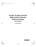
Am186™CC/CH/CU Microcontroller
Customer Development Platform
User’s Manual
Order #22002B
about.book Page ii Monday, June 7, 1999 10:17 AM
$P&&&+&80LFURFRQWUROOHU&XVWRPHU'HYHORSPHQW3ODWIRUP8VHU¶V0DQXDO
&RS\ULJKW$GYDQFHG0LFUR'HYLFHV,QF$OOULJKWVUHVHUYHG
7KH FRQWHQWV RI WKLV GRFXPHQW DUH SURYLGHG LQ FRQQHFWLRQ ZLWK $GYDQFHG 0LFUR 'HYLFHV ,QF $0' SURGXFWV $0'
PDNHVQRUHSUHVHQWDWLRQVRUZDUUDQWLHVZLWKUHVSHFWWRWKHDFFXUDF\RUFRPSOHWHQHVVRIWKHFRQWHQWVRIWKLVSXEOLFDWLRQDQG
UHVHUYHVWKHULJKWWRPDNHFKDQJHVWRVSHFLILFDWLRQVDQGSURGXFWGHVFULSWLRQVDWDQ\WLPHZLWKRXWQRWLFH1ROLFHQVHZKHWKHU
H[SUHVVLPSOLHGDULVLQJE\HVWRSSHORURWKHUZLVHWRDQ\LQWHOOHFWXDOSURSHUW\ULJKWVLVJUDQWHGE\WKLVSXEOLFDWLRQ([FHSWDV
VHWIRUWKLQ$0'
V6WDQGDUG7HUPVDQG&RQGLWLRQVRI6DOH$0'DVVXPHVQROLDELOLW\ZKDWVRHYHUDQGGLVFODLPVDQ\H[SUHVV
RULPSOLHGZDUUDQW\UHODWLQJWRLWVSURGXFWVLQFOXGLQJEXWQRWOLPLWHGWRWKHLPSOLHGZDUUDQW\RIPHUFKDQWDELOLW\ILWQHVVIRU
DSDUWLFXODUSXUSRVHRULQIULQJHPHQWRIDQ\LQWHOOHFWXDOSURSHUW\ULJKW
$0'
VSURGXFWVDUHQRWGHVLJQHGLQWHQGHGDXWKRUL]HGRUZDUUDQWHGIRUXVHDVFRPSRQHQWVLQV\VWHPVLQWHQGHGIRUVXUJLFDO
LPSODQW LQWR WKH ERG\ RU LQ RWKHU DSSOLFDWLRQV LQWHQGHG WR VXSSRUW RU VXVWDLQ OLIH RU LQ DQ\ RWKHU DSSOLFDWLRQ LQ ZKLFKWKH
IDLOXUHRI$0'
VSURGXFWFRXOGFUHDWHDVLWXDWLRQZKHUHSHUVRQDOLQMXU\GHDWKRUVHYHUHSURSHUW\RUHQYLURQPHQWDOGDPDJH
PD\RFFXU$0'UHVHUYHVWKHULJKWWRGLVFRQWLQXHRUPDNHFKDQJHVWRLWVSURGXFWVDWDQ\WLPHZLWKRXWQRWLFH
$0'WKH$0'ORJRFRPELQDWLRQVWKHUHRI$P$P&RPP'6/$&((0213&QHWDQG6PDUW'0$
DUHWUDGHPDUNVRI$GYDQFHG0LFUR'HYLFHV,QF
)XVLRQ(LVDVHUYLFHPDUNRI$GYDQFHG0LFUR'HYLFHV,QF
0LFURVRIWDQG:LQGRZVDUHUHJLVWHUHGWUDGHPDUNVRI0LFURVRIW&RUS
2WKHUSURGXFWRUEUDQGQDPHVDUHXVHGVROHO\IRULGHQWLILFDWLRQDQGPD\EHWKHWUDGHPDUNVRUUHJLVWHUHGWUDGHPDUNVRIWKHLU
UHVSHFWLYHFRPSDQLHV
about.book Page iii Monday, June 7, 1999 10:17 AM
IF YOU HAVE QUESTIONS, WE’RE HERE TO HELP YOU.
7KH$0'FXVWRPHUVHUYLFHQHWZRUNLQFOXGHV86RIILFHVLQWHUQDWLRQDORIILFHVDQGDFXVWRPHU
WUDLQLQJFHQWHU([SHUWWHFKQLFDODVVLVWDQFHLVDYDLODEOHIURPWKH$0'ZRUOGZLGHVWDIIRIILHOG
DSSOLFDWLRQHQJLQHHUVDQGIDFWRU\VXSSRUWVWDIIWRDQVZHU(IDPLO\KDUGZDUHDQGVRIWZDUH
GHYHORSPHQWTXHVWLRQV
)UHTXHQWO\DFFHVVHGQXPEHUVDUHOLVWHGEHORZ$GGLWLRQDOFRQWDFWLQIRUPDWLRQLVOLVWHGRQWKHEDFN
RIWKLVPDQXDO$0'¶V:::VLWHOLVWVWKHODWHVWSKRQHQXPEHUV
Technical Support
$QVZHUVWRWHFKQLFDOTXHVWLRQVDUHDYDLODEOHRQOLQHWKURXJKHPDLODQGE\WHOHSKRQH
*RWR$0'¶VKRPHSDJHDWZZZDPGFRPDQGIROORZWKH6HUYLFHOLQNIRUWKHODWHVW$0'WHFKQLFDO
VXSSRUWSKRQHQXPEHUVVRIWZDUHDQG)UHTXHQWO\$VNHG4XHVWLRQV
)RUWHFKQLFDOVXSSRUWTXHVWLRQVRQDOO(SURGXFWVVHQGHPDLOWRHSGVXSSRUW#DPGFRPLQWKH
86DQG&DQDGDRUHXURWHFK#DPGFRPLQ(XURSHDQGWKH8.
<RXFDQDOVRFDOOWKH$0'&RUSRUDWH$SSOLFDWLRQV+RWOLQHDW
7ROOIUHHIRU86DQG&DQDGD
8.DQG(XURSHKRWOLQH
WWW Support
)RUVSHFLILFLQIRUPDWLRQRQ(SURGXFWVDFFHVVWKH$0'KRPHSDJHDWZZZDPGFRPDQGIROORZ
WKH(PEHGGHG3URFHVVRUVOLQN7KHVHSDJHVSURYLGHLQIRUPDWLRQRQXSFRPLQJSURGXFWUHOHDVHV
RYHUYLHZVRIH[LVWLQJSURGXFWVLQIRUPDWLRQRQSURGXFWVXSSRUWDQGWRROVDQGDOLVWRIWHFKQLFDO
GRFXPHQWDWLRQ6XSSRUWWRROVLQFOXGHRQOLQHEHQFKPDUNLQJWRROVDQG&RGH.LWVRIWZDUH²WHVWHG
VRXUFHFRGHH[DPSOHDSSOLFDWLRQV0DQ\RIWKHWHFKQLFDOGRFXPHQWVDUHDYDLODEOHRQOLQHLQ3')IRUP
4XHVWLRQVUHTXHVWVDQGLQSXWFRQFHUQLQJ$0'¶V:::SDJHVFDQEHVHQWYLDHPDLOWR
ZHEPDVWHU#DPGFRP
Documentation and Literature Support
'DWDERRNVXVHU¶VPDQXDOVGDWDVKHHWVDSSOLFDWLRQQRWHVDQGSURGXFW&'VDUHIUHHZLWKDVLPSOH
SKRQHFDOO,QWHUQDWLRQDOO\FRQWDFW\RXUORFDO$0'VDOHVRIILFHIRUSURGXFWOLWHUDWXUH
7RRUGHUOLWHUDWXUHFDOO
7ROOIUHHIRU86DQG&DQDGD
'LUHFWGLDOZRUOGZLGH
)D[
Third-Party Support
$0')XVLRQ(60SDUWQHUVSURYLGHDQDUUD\RISURGXFWVGHVLJQHGWRPHHWFULWLFDOWLPHWRPDUNHWQHHGV
3URGXFWVDQGVROXWLRQVDYDLODEOHLQFOXGHHPXODWRUVKDUGZDUHDQGVRIWZDUHGHEXJJHUVERDUGOHYHOSURGXFWV
DQGVRIWZDUHGHYHORSPHQWWRROVDPRQJRWKHUV7KH:::VLWHDQGWKH()DPLO\3URGXFWV
'HYHORSPHQW7RROV&'RUGHU GHVFULEHWKHVHVROXWLRQV,QDGGLWLRQPDWXUHGHYHORSPHQW
WRROVDQGDSSOLFDWLRQVIRUWKH[SODWIRUPDUHZLGHO\DYDLODEOHLQWKHJHQHUDOPDUNHWSODFH
about.book Page iv Monday, June 7, 1999 10:17 AM
about.book Page v Monday, June 7, 1999 10:17 AM
Contents
About the Am186™CC/CH/CU Microcontroller
Customer Development Platform
0DLQ%RDUG%ORFN'LDJUDP [Y
'HYHORSPHQW0RGXOH%ORFN'LDJUDP [YL
7KHRU\RI2SHUDWLRQ [YLL
)HDWXUHV [YLL
0DLQ%RDUG [YLL
'HYHORSPHQW0RGXOH [YLLL
'RFXPHQWDWLRQ [L[
$ERXW7KLV0DQXDO [L[
6XJJHVWHG5HIHUHQFH0DWHULDO[[
'RFXPHQWDWLRQ&RQYHQWLRQV[[
Chapter 1
Quick Start
&RQQHFWLQJWRD3&YLDD6HULDO3RUW ,QVWDOODWLRQ5HTXLUHPHQWV 0DLQ%RDUG,QVWDOODWLRQ &RQQHFWLQJWRD3&YLDD86%SRUW &RQQHFWLQJWKH'HYHORSPHQW0RGXOHWRWKH0DLQ%RDUG &RQQHFWLQJD7,3WRWKH0DLQ%RDUG &RQQHFWLQJD520,&(WRWKH0DLQ%RDUG $P&&&+&80LFURFRQWUROOHU&'38VHU¶V0DQXDO
v
about.book Page vi Monday, June 7, 1999 10:17 AM
7URXEOHVKRRWLQJ,QVWDOODWLRQ3UREOHPV )RU0RUH,QIRUPDWLRQ Chapter 2
Main Board Functional Description
0DLQ%RDUG/D\RXW 0DLQ%RDUG)HDWXUHV $P&&&+&80LFURFRQWUROOHU- 3RZHU6XSSO\$ 0HPRU\,QWHUIDFHV &RPPXQLFDWLRQ,QWHUIDFHV 'HEXJDQG&RQILJXUDWLRQ&LUFXLWU\ ([SDQVLRQ,QWHUIDFHV Chapter 3
Development Module Functional Description
'HYHORSPHQW0RGXOH/D\RXW &XVWRPHU'HYHORSPHQW3ODWIRUP'HYHORSPHQW0RGXOH)HDWXUHV 0DLQ%RDUG,QWHUIDFH %DVH7(WKHUQHW,QWHUIDFH ,6'1,QWHUIDFH 3276,QWHUIDFH vi
$P&&&+&80LFURFRQWUROOHU&'38VHU¶V0DQXDO
about.book Page vii Monday, June 7, 1999 10:17 AM
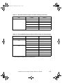
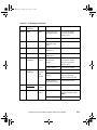
Appendix A
Default Jumper and Switch Settings
'HIDXOW-XPSHUDQG6ZLWFK6HWWLQJV $
Appendix B
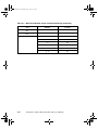
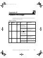
Platform Pin Usage
3ODWIRUP3LQ8VDJH%
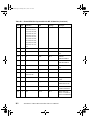
Appendix C
Main Board Bill of Materials
0DLQ%RDUG%LOORI0DWHULDOV &
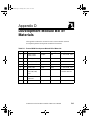
Appendix D
Development Module Bill of Materials
'HYHORSPHQW0RGXOH%LOORI0DWHULDOV '
Appendix E
PLD Equations
3/'8(TXDWLRQV (
3/'8(TXDWLRQV6%33&00RGH (
3/'(TXDWLRQV,20*&,0RGH(
3/'8(TXDWLRQV (
Index
,QGH[ ,QGH[
$P&&&+&80LFURFRQWUROOHU&'38VHU¶V0DQXDO
vii
about.book Page viii Monday, June 7, 1999 10:17 AM
List of Figures
)LJXUH 0DLQ%RDUG%ORFN'LDJUDP [Y
)LJXUH 5RXWHU,6'1'HYHORSPHQW0RGXOH%ORFN'LDJUDP [YL
)LJXUH 0DLQ%RDUG%ORFN'LDJUDP6DPHDV)LJXUH )LJXUH 0DLQ%RDUG/D\RXW )LJXUH $P&&&RPPXQLFDWLRQV&RQWUROOHU%ORFN'LDJUDP )LJXUH $P&++'/&0LFURFRQWUROOHU%ORFN'LDJUDP )LJXUH $P&886%0LFURFRQWUROOHU%ORFN'LDJUDP )LJXUH $P&&&+&80LFURFRQWUROOHU6\VWHP&ORFN )LJXUH $P&&RU$P&80LFURFRQWUROOHU86%&ORFN )LJXUH 0DLQ%RDUG5HVHW&LUFXLWU\ )LJXUH 93RZHU6XSSO\ )LJXUH 93RZHU6XSSO\ )LJXUH ±93RZHU6XSSO\ )LJXUH ±9DQG±93RZHU6XSSOLHV )LJXUH '5$0RU65$06\VWHP0HPRU\DQG)ODVK0HPRU\0DS )LJXUH 0DLQ0HPRU\'5$0&LUFXLW )LJXUH )ODVK0HPRU\&LUFXLW )LJXUH ',365$06RFNHWV )LJXUH 566HULDO3RUW5RXWLQJ )LJXUH +'/&&LUFXLW )LJXUH 8QLYHUVDO6HULDO%XV&LUFXLW )LJXUH 7HVW,QWHUIDFH3RUW&RQQHFWRU )LJXUH +3+HDGHU*URXSLQJ )LJXUH 'HEXJ+HDGHU&LUFXLW )LJXUH 5(6&215HJLVWHU%LWV )LJXUH 5HVHW&RQILJXUDWLRQ6ZLWFKHV )LJXUH &383//3LQVWUDS&LUFXLW )LJXUH 0LVFHOODQHRXV3LQVWUDS&LUFXLW viii
$P&&&+&80LFURFRQWUROOHU&'38VHU¶V0DQXDO
about.book Page ix Monday, June 7, 1999 10:17 AM
)LJXUH $P3URFHVVRU([SDQVLRQ,QWHUIDFH )LJXUH 5RXWHU,6'1'HYHORSPHQW0RGXOH,QWHUIDFH )LJXUH 5RXWHU,6'1'HYHORSPHQW0RGXOH%ORFN'LDJUDPVDPHDV)LJXUH )LJXUH 5RXWHU,6'1'HYHORSPHQW0RGXOH/D\RXW'LDJUDP )LJXUH 0DLQ%RDUGDQG'HYHORSPHQW0RGXOH&RQQHFWLRQ )LJXUH 5RXWHU,6'1'HYHORSPHQW0RGXOH&RQQHFWRU/D\RXW'LDJUDP )LJXUH )URQW9LHZRIWKH5-&RQQHFWRU )LJXUH %DVH7(WKHUQHW,QWHUIDFH )LJXUH (WKHUQHW&RQWUROOHU6FKHPDWLF )LJXUH ,6'15HIHUHQFH3RLQW%ORFN'LDJUDP )LJXUH ,6'167,QWHUIDFH )LJXUH ,6'18,QWHUIDFH )LJXUH '6/$&'HYLFH&LUFXLWU\ )LJXUH '6/$&WR56/,&&LUFXLW,QWHUIDFH )LJXUH '70),QWHUIDFH&LUFXLW $P&&&+&80LFURFRQWUROOHU&'38VHU¶V0DQXDO
ix
about.book Page x Monday, June 7, 1999 10:17 AM
List of Tables
7DEOH
1RWDWLRQDO&RQYHQWLRQV [[
7DEOH
520,&(&RQILJXUDWLRQ 7DEOH
,QVWDOODWLRQ7URXEOHVKRRWLQJ 7DEOH
-XPSHUV6ZLWFKHVDQG$GMXVWPHQWV 7DEOH
&38DQG86%&ORFN2SWLRQV 7DEOH
3RZHU(VWLPDWHVIRUWKH&'30DLQ%RDUG 7DEOH
3RZHU(VWLPDWHVIRUWKH&'3'HYHORSPHQW0RGXOH 7DEOH
7RWDO3RZHU(VWLPDWHVIRUWKH&'3 7DEOH
',3[[65$0520,&('HYLFH6HOHFWLRQ 7DEOH
65$0DQG5203LQRXWV 7DEOH
6ZLWFK2SWLRQVWR(QDEOH5'&(&ORFNLQJ 7DEOH
6ZLWFK2SWLRQVWR6HW5'&(&ORFNLQJ)UHTXHQF\ 7DEOH 6ZLWFK2SWLRQVWR(QDEOH53&0&ORFNLQJ 7DEOH 6ZLWFK2SWLRQVWR6HW53&0&ORFNLQJ)UHTXHQF\ 7DEOH 6ZLWFK2SWLRQVWR6HW53&0)UDPH6\QF 7DEOH +'/&'&(3&0&ORFN5RXWLQJ2SWLRQV 7DEOH 6\VWHPDQG86%&ORFN0RGHV 7DEOH &38DQG86%&ORFNLQJ2SWLRQV 7DEOH
5-&RQQHFWRU3LQ)XQFWLRQV 7DEOH
3&QHW,6$,,(WKHUQHW&RQWUROOHU/('6WDWXV,QIRUPDWLRQ 7DEOH
8,QWHUIDFH&RQILJXUDWLRQ 7DEOH
8,QWHUIDFH/('6WDWXV 7DEOH
$P&'6/$&'HYLFH3&/.)60&/.&RQILJXUDWLRQ 7DEOH
$P&&&RPPXQLFDWLRQV&RQWUROOHU$P&'6/$&
&RPPXQLFDWLRQ&RQILJXUDWLRQ 7DEOH$
0DLQ%RDUG'HIDXOW-XPSHUDQG6ZLWFK6HWWLQJV $
7DEOH$
5RXWHU,6'1'HYHORSPHQW0RGXOH'HIDXOW-XPSHUDQG6ZLWFK6HWWLQJV $
7DEOH%
3,28VDJH %
x
$P&&&+&80LFURFRQWUROOHU&'38VHU¶V0DQXDO
about.book Page xi Monday, June 7, 1999 10:17 AM
7DEOH%
&KLS6HOHFW8VDJH%
7DEOH%
3ODWIRUP,QWHUUXSWV3LQ8VDJH %
7DEOH&
0DLQ%RDUG%LOORI0DWHULDOV &
7DEOH'
5RXWHU,6'1'HYHORSPHQW0RGXOH%LOORI0DWHULDOV '
$P&&&+&80LFURFRQWUROOHU&'38VHU¶V0DQXDO
xi
about.book Page xii Monday, June 7, 1999 10:17 AM
xii
$P&&&+&80LFURFRQWUROOHU&'38VHU¶V0DQXDO
about.book Page xiii Monday, June 7, 1999 10:17 AM
About the Am186™CC/CH/CU
Microcontroller Customer
Development Platform
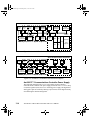
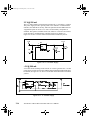
The AMD Am186™CC/CH/CU microcontroller customer development platform
(CDP) is a system used for customer evaluation and development for the
Am186CC/CH/CU microcontrollers. The platform provides access to the major
microcontroller interfaces and is an ideal tool for developing customer-specific
applications by using the development module interface.
The CDP consists of two boards—a main board that contains the Am186CC
communications controller and interfaces (shown in Figure 0-1), and the
development module, which can be used for the development of various
communications applications such as ISDN TAs and routers (shown in Figure 0-2).
The main board consists of a power supply that provides the necessary voltages
for typical system applications of the Am186CC/CH/CU microcontroller. The
main board also provides a glueless interface to Flash memory and DRAM or
SRAM system main memory, communication interfaces such as a universal
asynchronous receiver/transmitter (UART) and High-Speed UART, universal serial
bus (USB), and four synchronous serial DCE connections. Other features include
the debug interfaces that allow connection to the following:
• ROM-ICE
• Optional Test Interface Port (TIP) debug board
• HP logic analyzer headers to provide access to the Am186CC communications
controller signals
• Expansion interface through the development module or the 104-pin Am186
processor expansion interface
$P&&&+&80LFURFRQWUROOHU&'38VHU¶V0DQXDO
[LLL
about.book Page xiv Monday, June 7, 1999 10:17 AM
The development module consists of an Am79C961A PCnet™-ISA II Ethernet
Controller for 10BaseT Ethernet, an Am79C32A ISDN digital subscriber
controller (DSC) circuit for an ISDN S/T connection, an ISDN U connection, and
two POTS connections featuring the Am79C031 DSLAC™ device and two
Am79R79 Ringing SLICs.
NOTE: Although the customer development board provides an Am186CC
microcontroller, you can also use the board to develop Am186CH HDLC
microcontroller applications and Am186CU USB microcontroller applications.
The Am186CH and Am186CU microcontrollers support subsets of the Am186CC
microcontroller features. The Am186CH HDLC microcontroller provides two
HDLC channels and does not support USB or GCI. The Am186CU USB
microcontroller does not support HDLC.
For more information about the Am186CC/CH/CU microcontrollers, refer to
• Am186™CC/CH/CU Microcontroller User’s Manual, order #21914
• Am186™CC Communications Controller Data Sheet, order #21915
• Am186™CH HDLC Microcontroller Data Sheet, order #22024
• Am186™CU USB Microcontroller Data Sheet, order #22025
• Am186™CC/CH/CU Microcontroller Register Set Manual, order #21916
For more information about the CDP board features, refer to “Features” on
page xvii, and Chapter 2, “Main Board Functional Description”.
[LY
$P&&&+&80LFURFRQWUROOHU&'38VHU¶V0DQXDO
about.book Page xv Monday, June 7, 1999 10:17 AM
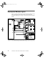
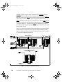
Main Board Block Diagram
Figure 0-1 shows the block diagram for the main board on the CDP.
Memory Interface
Expansion Interface
256K x 16 SRAM
SRAM/ICE Socket
Am186 Expansion
Bank 1
256K x 16 DRAM
SRAM/ICE Socket
Bank 0
256K x 16 DRAM
1 MByte Flash Memory
Am186 Expansion
Development Module
TIP Connector
Development Module
Control Bus
Address Bus
AD Bus
HDLC A–D
UART
Clocks
Communication Interface
HDLC A
Am186CC
Controller
System
USB
RS422 XCVR
RS530 DB25
RS422 XCVR
RS530 DB25
RS422 XCVR
RS530 DB25
RS422 XCVR
RS530 DB25
HDLC B
HDLC C
UART
HDLC D
160-PQFP
DCE CLK Gen.
HP Hdrs
Reset Cfg
DAQ Hdrs
Pinstrap Cfg
Debug/
Config.
Interface
PIO
HDLC
/68$57
RS232 XCVR
RS232 DB9
RS232 XCVR
RS232 DB9
+68$57
9
9
9
UART
9 9
%DQDQD3OXJV
USB
USB XCVR
USB Type B
Main Supply
DC Plug
POTS Supply
Power Supply
XCVR Bypass
USB
PIO
SSI
Figure 0-1. Main Board Block Diagram
$P&&&+&80LFURFRQWUROOHU&'38VHU¶V0DQXDO
[Y
about.book Page xvi Monday, June 7, 1999 10:17 AM
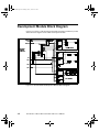
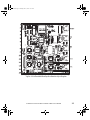
Development Module Block Diagram
Figure 0-2 (or sheet 2 of the development module schematics included in your kit)
shows the block diagram for the CDP’s development module.
$GGUHVV%XV
$'%XV
&RQWURO%XV
%XIIHUHG$GGUHVV%XV
$
%XIIHUV
$'
/('
V
(WKHUQHW&RQWUROOHU
$P&$
%XIIHUHG$'%XV
7UDQVIRUPHU
5-
%XIIHUHG&RQWURO%XV
&RQWURO%XV
3/'
((3520
%XIIHU&WUO
(WKHUQHW&WUO
%DVH7(WKHUQHW
3DFNHW65$0
,6'1&WUO
66,&WUO
0DLQ%RDUG
,QWHUIDFH
&RQQHFWRUV
3276&WUO
&&7;''
7;''
677UDQVFHLYHU
$P&$
&&76&'
&&7;'$
,6'167,QWHUIDFH
7;'$
7UDQVIRUPHU
5-
7UDQVIRUPHU
5-
'676&
66,
87UDQVFHLYHU
/XFHQW7$
+'/&$
+'/&'
,6'18,QWHUIDFH
5;''
/('
V
+'/&&
&/.&)6&&
&RGHF
$P&
'676&
56/,&
$P5
&LUFXLW
3URWHFWLRQ
5-
56/,&
$P5
&LUFXLW
3URWHFWLRQ
5-
'70)5HFHLYHU
7HOWRQH
0
3276,QWHUIDFH
'70)5HFHLYHU
7HOWRQH
0
Figure 0-2. Router/ISDN Development Module Block Diagram
[YL
$P&&&+&80LFURFRQWUROOHU&'38VHU¶V0DQXDO
about.book Page xvii Monday, June 7, 1999 10:17 AM
Theory of Operation
The Am186CC/CH/CU microcontroller CDP provides a comprehensive evaluation
system to support Am186CC/CH/CU microcontroller-based designs. The
combined features of the Am186CC/CH/CU microcontroller CDP offer designers
a complete tool for hardware and software development with the Am186CC/CH/
CU microcontrollers.
NOTE: If you are evaluating the Am186CH or Am186CU microcontroller, all of
the features on the CDP are not available. The Am186CH and Am186CU
microcontrollers support subsets of the Am186CC microcontroller features. The
Am186CH HDLC microcontroller provides two HDLC channels and does not
support USB or GCI. The Am186CU USB microcontroller does not support
HDLC.
Features
The Am186CC/CH/CU microcontroller CDP provides the features described in
the following sections.
Main Board
• Am186CC 3.3-V, 50-MHz Microcontroller
• Power Supply (generates 3.3 V, 5.0 V, -5.0 V, -24 V, and -70 V from a 12-V DC
source)
• Memory Interfaces
– Main system memory
4-Mbit, 256K x 16, 40-ns EDO DRAM
Two 1-Mbit 128K x 8, 35-ns SRAMs configured as 128K x 16
– 8-Mbit configurable 512K x 16, or 1M x 8, 55-ns Flash memory
$P&&&+&80LFURFRQWUROOHU&'38VHU¶V0DQXDO
[YLL
about.book Page xviii Monday, June 7, 1999 10:17 AM
• Communication Interfaces
– HDLC synchronous communications
Four RS-422, DB-25 DCE/PCM connections clocked by the main board clock
generator (Am186CH HDLC microcontroller supports only two connections)
Dedicated 2 x 5 header for GCI (supported on Am186CC microcontroller
only)
– Peripheral USB port (supported on Am186CC and Am186CU
microcontrollers only)
– UARTs
One 460-Kbaud, RS-232, DB-9 DCE connection
One 120-Kbaud, RS-232, DB-9 DCE connection
• Debug and Configuration
– 60-pin connector interface to the optional test interface port (TIP) debug board
– Two 32-pin DIP sockets for use with a x16 ROM-ICE
– Eight 2 x 10 shrouded headers to directly connect Am186CC/CH/CU
microcontroller signals to HP analyzers
– Two 4-segment switches to allow pinstrap configuration
– Two 8-segment switches to allow system-specific configuration
Development Module
• 10BaseT Ethernet port
• ISDN interface
– S/T interface
– U interface
• Two POTS Interfaces
[YLLL
$P&&&+&80LFURFRQWUROOHU&'38VHU¶V0DQXDO
about.book Page xix Monday, June 7, 1999 10:17 AM
Documentation
The Am186™CC/CH/CU Microcontroller Customer Development Platform
User’s Manual provides information on the design and function of the Am186CC/
CH/CU microcontroller CDP.
About This Manual
Chapter 1, “Quick Start” helps you quickly set up and start using the Am186CC/
CH/CU microcontroller CDP.
Chapter 2, “Main Board Functional Description” describes the basic sections of
the platform: layout, jumper and switch settings, microcontroller, power supply,
memory interfaces, communication interfaces, debug and configuration, and
development module.
Chapter 3, “Development Module Functional Description” describes the features
and components on the development module, including a 10BaseT Ethernet port,
ISDN interface, and POTS interfaces.
Appendix A, “Default Jumper and Switch Settings” provides a table with the
default jumper and switch settings.
Appendix B, “Platform Pin Usage” provides tables describing the CDP’s PIO, chip
select, and interrupt pin usage.
Appendix C, “Main Board Bill of Materials” contains the bill of materials for the
Am186CC/CH/CU microcontroller CDP main board.
Appendix D, “Development Module Bill of Materials” contains the bill of materials
for the Am186CC/CH/CU microcontroller CDP module.
Appendix E, “PLD Equations” contains PLD code for the PLDs at locations U13,
U20, and U24.
A standard index is also included.
$P&&&+&80LFURFRQWUROOHU&'38VHU¶V0DQXDO
[L[
about.book Page xx Monday, June 7, 1999 10:17 AM
Suggested Reference Material
• Am186™CC/CH/CU Microcontroller User’s Manual
Advanced Micro Devices, order #21914
• Am186™CC Communications Controller Data Sheet
Advanced Micro Devices, order #21915
• Am186™CH HDLC Microcontroller Data Sheet
Advanced Micro Devices, order #22024
• Am186™CU USB Microcontroller Data Sheet
Advanced Micro Devices, order #22025
• Am186™CC/CH/CU Microcontroller Register Set Manual
Advanced Micro Devices, order #21916
• Am186™ and Am188™ Family Instruction Set Manual
Advanced Micro Devices, order #21076
• E86MON™ Software User’s Manual
Advanced Micro Devices, order #21891
• E86™ Family Products and Development Tools CD
Advanced Micro Devices, order #21508
Documentation Conventions
Table 0-1. Notational Conventions
[[
6\PERO
8VDJH
%ROGIDFH
,QGLFDWHVWKDWFKDUDFWHUVPXVWEHHQWHUHG
H[DFWO\DVVKRZQH[FHSWWKDWWKHDOSKDEHWLFFDVHLV
RQO\VLJQLILFDQWZKHQLQGLFDWHG
Typewriter face
,QGLFDWHVFRPSXWHUWH[WLQSXWRURXWSXWLQDQH[DPSOH
RUOLVWLQJ
$P&&&+&80LFURFRQWUROOHU&'38VHU¶V0DQXDO
about.book Page 1 Monday, June 7, 1999 10:17 AM
Chapter 1
Quick Start
This chapter provides information that will help you quickly set up and start using
the Am186™CC/CH/CU Microcontroller CDP.
The CDP is supported by the E86MON™ board-resident debugger. The E86MON
boot monitor software enables you to load, run, and debug programs on the CDP.
For detailed information on using the E86MON software, refer to the E86MON™
Software User’s Manual included in your kit.
For information on how to:
• Connect the CDP to a PC via a serial port, see page 1-2
• Connect the CDP to a PC via a USB port, see page 1-5
• Connect the development module to the main board, see page 1-5
• Connect the TIP to the main board, see page 1-6
• Connect the ROM-ICE to the main board, see page 1-7
• Invoke the E86MON software, see step 5 on page 1-4
• Troubleshoot installation problems, see page 1-8
• Locate related sources of information, see page 1-9
$P&&&+&80LFURFRQWUROOHU&'38VHU¶V0DQXDO
about.book Page 2 Monday, June 7, 1999 10:17 AM
Connecting to a PC via a Serial Port
Follow the steps below to connect the Am186CC/CH/CU microcontroller customer
development platform to your PC via your PC’s serial port.
Installation Requirements
The items listed below are necessary to install and run the CDP:
• PC with an available COM port
• Terminal emulation software (such as Microsoft® Windows®Terminal or
ProComm Plus) that supports ASCII file transfers, software flow control (Xon/
Xoff), and send break capability.
• Power source for universal power supply
Main Board Installation
CAUTION: As with all computer equipment, the Am186CC/
CH/CU microcontroller CDP’s main board may be damaged by
electrostatic discharge (ESD). Please take proper precautions
when handling any board.
1. Remove the board from the shipping carton. Visually inspect the board to verify
that it was not damaged during shipment.
$P&&&+&80LFURFRQWUROOHU&'38VHU¶V0DQXDO
about.book Page 3 Monday, June 7, 1999 10:17 AM
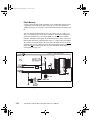
2. Connect either of the CDP main board’s DB-9 serial ports to an available COM
port. Use the serial cable included in the Am186CC/CH/CU microcontroller
CDP kit and note that a DB-9 to DB-25 serial connector adapter is provided if
your host system requires it.
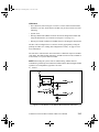
&20
&20
VHULDO
FDEOH
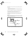
3. Connect the power supply to the barrel connector (see P31 at location A-1 in
Figure 2-2 on page 2-3) on the CDP’s main board.
$P&&&+&80LFURFRQWUROOHU&'38VHU¶V0DQXDO
about.book Page 4 Monday, June 7, 1999 10:17 AM
4. Apply power to the board by connecting the power supply to an electrical outlet.
When the board is powered up, the LEDs (see CR12–CR8 at locations C-2–
F-2 in Figure 2-2 on page 2-3) should be illuminated.
If all of the LEDs are not illuminated, remove the power supply immediately
and contact AMD technical support. See “If You Have Questions, We’re Here
to Help You.” on page iii.
CAUTION: If using your own power supply, ensure that it is a
12-V supply and is capable of providing at least 2 A.
5. Invoke the terminal emulation program at 19200 baud, no parity, 8 data bits,
and 1 stop bit; enable the software flow control (Xon/Xoff), if supported.
6. Reset the board by depressing and releasing the RESET switch (see SW1 at
location T-23 in Figure 2-2 on page 2-3).
Type an a in the terminal window within three seconds of reset to ensure that
the E86MON software uses the correct baud rate. When the E86MON software
receives an a, it adjusts its baud rate (if necessary) and displays the welcome
message and prompt.
NOTE: If you type a character other than an a, or type no character at all, the
E86MON software still displays the welcome message and prompt, but may be
using an incorrect baud rate. Depressing and releasing the RESET switch (SW1 at
location T-23) gives you another opportunity to type an a.
7. To display the version of the monitor and the commands available, type ? and
press Enter.
For detailed information about using the E86MON software, refer to the
E86MON™ Software User’s Manual included in your kit.
$P&&&+&80LFURFRQWUROOHU&'38VHU¶V0DQXDO
about.book Page 5 Monday, June 7, 1999 10:17 AM
Connecting to a PC via a USB port
NOTE: USB is not supported on the Am186CH HDLC microcontroller.
Follow the steps below to connect the Am186CC/CH/CU microcontroller customer
development platform to your PC via your PC’s USB port.
1. Insert the flat end of your USB cable into the USB port that is connected to
your PC.
2. Connect the other end of the USB cable into the CDP’s main board USB
connector (see P18 at location I-1 in Figure 2-2 on page 2-3) that is located on
the edge of the board near the power supply (see P31 at location A-1).
To drive the USB, download the USB driver CodeKit software from the AMD
website. The CodeKit software package includes installation instructions for the
USB host driver and the USB driver on the CDP.
Go to www.amd.com, then click on Embedded Processors to get to the Codekit
software packages.
Connecting the Development Module to the
Main Board
Follow the steps below to connect the router/ISDN development module to the
Am186CC/CH/CU microcontroller CDP main board (see Figure 3-3 on page 3-5).
1. Orient the main board such that the AMD logo is in the lower right-hand corner,
facing you. Orient the development module such that the AMD logo is in the
lower leviathan corner, facing you.
2. Position the development module above the development module connectors
(see P12 and P19 at locations M-22 and F-22, respectively, in Figure 2-2 on
page 2-3) on the main board.
3. Carefully press the development module down onto the connectors on the main
board.
$P&&&+&80LFURFRQWUROOHU&'38VHU¶V0DQXDO
about.book Page 6 Monday, June 7, 1999 10:17 AM
Connecting a TIP to the Main Board
Follow the steps below to connect the test interface port (TIP) debug board to the
Am186CC/CH/CU microcontroller CDP main board:
1. Orient the main board such that the AMD logo is in the lower righthand corner,
facing you.
2. Place the TIP board to the left of the main board with the LCD display toward
you.
3. Plug the TIP connector into the TIP board with the tab facing toward the left.
4. Plug the other end of the connector into the CDP’s main board TIP (see P30 at
location A-19 in Figure 2-2 on page 2-3) with the tab facing up.
$P&&&+&80LFURFRQWUROOHU&'38VHU¶V0DQXDO
about.book Page 7 Monday, June 7, 1999 10:17 AM
Connecting a ROM-ICE to the Main Board
Follow the steps below to connect a ROM-ICE to the Am186CC/CH/CU
microcontroller customer development platform main board:
1. Orient the main board such that the AMD logo is in the lower righthand corner,
facing you.
2. Set the jumpers according to the configuration shown in Table 1-1 on page 1-7,
and jumper your chip select on JP10 (see location F-9 in Figure 2-2 on
page 2-3).
3. Position the ROM-ICE to the left of the main board.
4. Connect the ROM-ICE Low into the left DIP socket (see U28 at location B-12),
which is labeled SRAM/ROM LOW.
5. Connect the ROM-ICE High into the right DIP socket (see U25 at location
D-12), which is labeled SRAM/ROM HIGH.
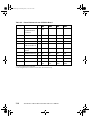
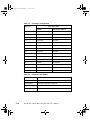
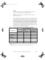
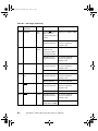
Table 1-1. ROM-ICE Configuration
'HYLFH
520
-3
-3
3/%
36(/
36(/
36(/
36(/
3+%
1&
1&
1&
.[
520
.[
1&
9LVXDO'HWDLO
3
/
%
3
6
(
/
3
6
(
/
3
/
%
3
6
(
/
3
6
(
/
$P&&&+&80LFURFRQWUROOHU&'38VHU¶V0DQXDO
-3
-3
-3 -3
3
6
(
/
3
6
(
/
3
+
%
3
6
(
/
3
6
(
/
3
+
%
about.book Page 8 Monday, June 7, 1999 10:17 AM
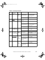
Troubleshooting Installation Problems
Table 1-2. Installation Troubleshooting
3UREOHP
6ROXWLRQ
1RWKLQJKDSSHQVZKHQ
SXVKLQJWKH5(6(7
EXWWRQ
6RPHWLPHVLWLVGLIILFXOWWRPDNHDJRRGFRQQHFWLRQ
ZKHQSXVKLQJWKHVPDOO5(6(7EXWWRQ,IDOOHOVH
IDLOVUHPRYHWKHSRZHUVXSSO\IURPWKH$&
HOHFWULFDORXWOHWDQGGLVFRQQHFWDQGUHFRQQHFWWKH
SRZHUVXSSO\7KH/('VZLOOOLJKWXSZKHQWKH
UHVHWLVVXFFHVVIXO
7KHFRPSXWHUGRHVQRW
5HVHWWKHERDUGE\SUHVVLQJWKH5(6(7VZLWFKDQG
UHVSRQGZLWKWKH(021 W\SLQJDQDLPPHGLDWHO\DIWHUSRZHUXS,IWKLVGRHV
VRIWZDUHSURPSW
QRWZRUNYHULI\WKHSRZHUFKHFNWKHFDEOHVHWF
DQGYHULI\WKDWWKHWHUPLQDOSURJUDPLVFRQILJXUHG
FRUUHFWO\
$IWHUW\SLQJDGXULQJUHVHW
WKHWHUPLQDOHPXODWLRQ
VRIWZDUHGLVSOD\V
XQUHDGDEOHFKDUDFWHUV
&KHFNWKHEDXGUDWHVHWWLQJIRUWKHWHUPLQDO
HPXODWLRQVRIWZDUH,WVKRXOGEHVHWWR$OVR
FKHFNWKHZRUGOHQJWKVWRSELWVDQG
SDULW\ 1DQGWXUQRIIDQ\KDUGZDUHIORZFRQWURO
7KHWHUPLQDOHPXODWLRQ
SURJUDPORFNVXSWKH
VRIWZDUHRU3&
&KHFNWKH&20SRUWFRQQHFWLRQZLWKWKHWDUJHW
ERDUG0DNHVXUHWKDWWKHVDPH&20SRUWLV
VHOHFWHGLQWKHWHUPLQDOHPXODWLRQVRIWZDUH,Q
VRPH3&VLIWKHFRUUHFW&20SRUWLVQRWVSHFLILHG
WKHVRIWZDUHZLOOIDLOWRIXQFWLRQ²LWZLOOORFNLQD
FRQWLQXRXVORRSZDLWLQJIRUDQDQVZHUIURPWKH
LQFRUUHFWVHULDOSRUW
7KHSRZHU/('GRHVQRW
WXUQRQZLWKSRZHU
,PPHGLDWHO\GLVFRQQHFWWKHSRZHUVXSSO\(QVXUH
WKDWWKHSRODULW\RIWKHSRZHUFRQQHFWRULVFRUUHFW
7KLVLVDYHU\VHULRXVIDLOXUHRIWKHKDUGZDUH,IWKH
SRZHUVRXUFHLVFRQQHFWHGLQFRUUHFWO\WKHERDUG
ZLOOEHSHUPDQHQWO\GDPDJHG
7KHUHLVDSUREOHP\RX
FDQQRWUHVROYH
&RQWDFWWKH$0'&RUSRUDWH$SSOLFDWLRQV
WHFKQLFDOVXSSRUWVHUYLFHVVHHSDJHLLLIRUSKRQH
QXPEHUVDQGPRUHLQIRUPDWLRQ
$P&&&+&80LFURFRQWUROOHU&'38VHU¶V0DQXDO
about.book Page 9 Monday, June 7, 1999 10:17 AM
For More Information...
If you need more information about:
• Am186CC/CH/CU microcontroller CDP hardware,
see Chapter 2 and Chapter 3.
• E86MON software,
see the E86MON™ Software User’s Manual included in your kit.
• Problems with the platform or the E86MON software,
see the customer support information on page iii.
• The Am186CC/CH/CU microcontroller CDP’s main board layout,
see Chapter 2.
• The Am186CC/CH/CU microcontroller CDP’s module layout,
see Chapter 3.
• The Am186CC/CH/CU microcontroller CDP’s main board schematics,
see the schematics document included in your kit.
• The Am186CC/CH/CU microcontroller CDP’s module schematics,
see the schematics document included in your kit.
• The Am186CC/CH/CU microcontrollers,
see the following documents, which are included in your kit:
– Am186™CC Communications Controller Data Sheet
– Am186™CH HDLC Microcontroller Data Sheet
– Am186™CU USB Microcontroller Data Sheet
– Am186™CC/CH/CU Microcontrollers User’s Manual
– Am186™CC/CH/CU Microcontrollers Register Set Manual
$P&&&+&80LFURFRQWUROOHU&'38VHU¶V0DQXDO
about.book Page 10 Monday, June 7, 1999 10:17 AM
$P&&&+&80LFURFRQWUROOHU&'38VHU¶V0DQXDO
about.book Page 1 Monday, June 7, 1999 10:17 AM
Chapter 2
Main Board Functional Description
The Am186CC/CH/CU microcontroller customer development platform (CDP)
consists of two boards: a main board that contains an Am186CC communications
controller and interfaces, and the development module, which you can use to
develop ISDN and router applications. This chapter describes the main board. The
development module is described in Chapter 3, “Development Module Functional
Description”.
Read the following sections to learn more about the main board:
• “Main Board Layout” on page 2-2
• “Main Board Features” on page 2-8
$P&&&+&80LFURFRQWUROOHU&'38VHU¶V0DQXDO
about.book Page 2 Monday, June 7, 1999 10:17 AM
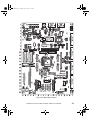
Main Board Layout
The Am186CC/CH/CU microcontroller customer development platform is easy to
configure to fit your design requirements. Figure 2-1 shows the main board block
diagram; Figure 2-2 shows the main board layout and component placement; and
Table 2-1 lists the jumpers and switches. Note that the schematics referenced are
in the separate schematic manual in your board kit.
Memory Interface
Expansion Interface
256K x 16 SRAM
SRAM/ICE Socket
Am186 Expansion
Bank 1
256K x 16 DRAM
SRAM/ICE Socket
Bank 0
256K x 16 DRAM
1 MByte Flash Memory
Am186 Expansion
Development Module
TIP Connector
Development Module
Control Bus
Address Bus
AD Bus
HDLC A–D
UART
Clocks
Communication Interface
HDLC A
Am186CC
Controller
System
USB
RS422 XCVR
RS530 DB25
RS422 XCVR
RS530 DB25
RS422 XCVR
RS530 DB25
RS422 XCVR
RS530 DB25
HDLC B
HP Hdrs
Reset Cfg
DAQ Hdrs
Pinstrap Cfg
Debug/
Config.
Interface
HDLC C
UART
HDLC D
160-PQFP
DCE CLK Gen.
PIO
HDLC
/68$57
RS232 XCVR
RS232 DB9
RS232 XCVR
RS232 DB9
+68$57
9
9
9
UART
9 9
%DQDQD3OXJV
USB
USB XCVR
USB Type B
Main Supply
DC Plug
POTS Supply
Power Supply
XCVR Bypass
USB
PIO
SSI
Figure 2-1. Main Board Block Diagram (Same as Figure 0-1)
$P&&&+&80LFURFRQWUROOHU&'38VHU¶V0DQXDO
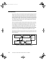
about.book Page 3 Monday, June 7, 1999 10:17 AM
Figure 2-2. Main Board Layout
$P&&&+&80LFURFRQWUROOHU&'38VHU¶V0DQXDO
about.book Page 4 Monday, June 7, 1999 10:17 AM
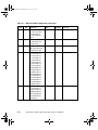
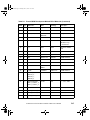
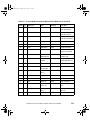
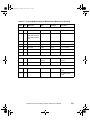
Table 2-1. Jumpers, Switches, and Adjustments
3DUW
)XQFWLRQ
'HVFULSWLRQ
5HIHUHQFHLQ
)LJXUH 6FKHPDWLF
5HIHUHQFH
6KHHW
-3
+'/&
&KDQQHO 'DQG
FORFNVHOHFW
8VHGWRURXWH'&(FORFNVIRU
+'/&&KDQQHO'
3
0DLQERDUG
6KHHW
-3
+'/&
&KDQQHO &DQG
FORFNVHOHFW
8VHGWRURXWH'&(FORFNVIRU
+'/&&KDQQHO&
2
0DLQERDUG
6KHHW
-3
8$57IORZ
FRQWURORXWSXW
VHOHFW
8VHGWRSURYLGH3,2RXWSXWIRU
DGGLWLRQDO56IORZFRQWURO
2
0DLQERDUG
6KHHW
-3
+'/&
&KDQQHO %DQG
FORFNVHOHFW
8VHGWRURXWH'&(FORFNVIRU
+'/&&KDQQHO%
1
0DLQERDUG
6KHHW
-3
8$57IORZ
FRQWUROLQSXW
VHOHFW
8VHGWRSURYLGH3,2LQSXWIRU
DGGLWLRQDO56IORZFRQWURO
0
0DLQERDUG
6KHHW
-3
+'/&
&KDQQHO $DQG
FORFNVHOHFW
8VHGWRURXWH'&(FORFNVIRU
+'/&&KDQQHO$
/
0DLQERDUG
6KHHW
-3
+LJK6SHHG
8$57IORZ
FRQWURO
3URYLGHVLVRODWLRQWR+LJK
/
6SHHG8$57IORZFRQWURO
VLJQDOVRUDOWHUQDWH3,2VIRUIORZ
FRQWURO
0DLQERDUG
6KHHW
-3
&KLSVHOHFWIRU
)ODVKPHPRU\
8VHGWRVHOHFW8&6RU0&6IRU +
)ODVKPHPRU\
0DLQERDUG
6KHHW
-3
/RJLFDQDO\]HU
FORFNVHOHFW
8VHGDVDFORFNLQSXWRQWKHORJLF *
DQDO\]HUKHDGHU
0DLQERDUG
6KHHW
-3
65$0520
8VHGWRVHOHFW/&68&65RU
,&(GHYLFHVHOHFW 0&6IRU65$0520,&(
)
0DLQERDUG
6KHHW
-3
65$0520
8VHGWRVHOHFWYDULRXV65$0
,&(GHYLFHVHOHFW DQG520FRQILJXUDWLRQV
'
0DLQERDUG
6KHHW
$P&&&+&80LFURFRQWUROOHU&'38VHU¶V0DQXDO
about.book Page 5 Monday, June 7, 1999 10:17 AM
Table 2-1. Jumpers, Switches, and Adjustments (Continued)
3DUW
)XQFWLRQ
-3
'HVFULSWLRQ
5HIHUHQFHLQ
)LJXUH 6FKHPDWLF
5HIHUHQFH
6KHHW
65$0520
8VHGWRVHOHFWYDULRXV65$0
,&(GHYLFHVHOHFW DQG520FRQILJXUDWLRQV
%
0DLQERDUG
6KHHW
6:
5HVHWVZLWFK
7
0DLQERDUG
6KHHW
6:
+'/&'&(SRUW 8VHGWRHQDEOHPXOWLGURSPRGH 4
$PXOWLGURS
IRUSRUW$
VHOHFW
0DLQERDUG
6KHHW
6:
3,2LVRODWLRQ
VHOHFW
8VHGWRLVRODWH3,2VIURPRWKHU 3
XVDJHRQ&'3
0DLQERDUG
6KHHW
6:
+'/&'&(SRUW 8VHGWRHQDEOHPXOWLGURSPRGH 3
%PXOWLGURS
IRUSRUW%
VHOHFW
0DLQERDUG
6KHHW
6:
+'/&'&(SRUW 8VHGWRHQDEOHPXOWLGURSPRGH 2
&PXOWLGURS
IRUSRUW&
VHOHFW
0DLQERDUG
6KHHW
6:
+'/&'&(SRUW 8VHGWRHQDEOHPXOWLGURSPRGH 1
'PXOWLGURS
IRUSRUW'
VHOHFW
0DLQERDUG
6KHHW
6:
+'/&FORFN
FRQILJXUDWLRQ
VHOHFW
6HOHFWV+'/&SRUWV$±'
IUHTXHQF\RSWLRQV
/
0DLQERDUG
6KHHW
6:
6HULDOLQWHUIDFH
WUDQVFHLYHU
VHOHFW
8VHGWRGLVDEOH+'/&SRUW$±
'DQG8$57WUDQVFHLYHUV
'HIDXOW+'/&$±'RIIDQG
8$576RQ
,
0DLQERDUG
6KHHW
6:
+'/&FORFN
FRQILJXUDWLRQ
VHOHFW
6HOHFWV+'/&SRUWV$±'IRU
3&0IUDPHV\QFKURQL]DWLRQ
RSWLRQV
-
0DLQERDUG
6KHHW
8VHGWRUHVHWWKH&'3
$P&&&+&80LFURFRQWUROOHU&'38VHU¶V0DQXDO
about.book Page 6 Monday, June 7, 1999 10:17 AM
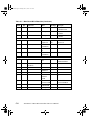
Table 2-1. Jumpers, Switches, and Adjustments (Continued)
3DUW
)XQFWLRQ
'HVFULSWLRQ
5HIHUHQFHLQ
)LJXUH 6FKHPDWLF
5HIHUHQFH
6KHHW
6:
)ODVKPHPRU\
GDWDEXVZLGWK
VHOHFW
8VHGWRGHWHUPLQH)ODVK
PHPRU\ZLGWKDVRUELWV
'HIDXOWELWV
-
0DLQERDUG
6KHHW
6:
+'/&FORFN
FRQILJXUDWLRQ
VHOHFW
6HOHFWV+'/&SRUWV$±'IRU
'&(RU3&0FORFNV
,
0DLQERDUG
6KHHW
6:
5HVHW
FRQILJXUDWLRQ
VHOHFW
3ODWIRUPXVHUVSHFLILFV\VWHP
FRQILJXUDWLRQ
'
0DLQERDUG
6KHHW
6:
86%FORFN
SLQVWUDSVHOHFW
8VHGWRVHOHFW$'DGGUHVV
HQDEOH8&6GDWDZLGWKDQG
H[WHUQDO86%WUDQVFHLYHU
&
0DLQERDUG
6KHHW
6:
5HVHW
FRQILJXUDWLRQ
VHOHFW
3ODWIRUPXVHUVSHFLILFV\VWHP
FRQILJXUDWLRQ
%
0DLQERDUG
6KHHW
6:
&38DQG86%
FORFNSLQVWUDS
VHOHFW
8VHGWRVHOHFWV\VWHPDQG86% $
FORFN3//PRGHSLQVWUDS
RSWLRQV
0DLQERDUG
6KHHW
*3
*URXQG
*URXQGSRVW
5
0DLQERDUG
6KHHW
*3
*URXQG
*URXQGSRVW
5
0DLQERDUG
6KHHW
*3
*URXQG
*URXQGSRVW
5
0DLQERDUG
6KHHW
*3
*URXQG
*URXQGSRVW
0
0DLQERDUG
6KHHW
*3
*URXQG
*URXQGSRVW
'
0DLQERDUG
6KHHW
*3
*URXQG
*URXQGSRVW
$
0DLQERDUG
6KHHW
$P&&&+&80LFURFRQWUROOHU&'38VHU¶V0DQXDO
about.book Page 7 Monday, June 7, 1999 10:17 AM
Table 2-1. Jumpers, Switches, and Adjustments (Continued)
3DUW
)XQFWLRQ
'HVFULSWLRQ
5HIHUHQFHLQ
)LJXUH 73
7HVWSRLQW
7HVWSRLQWIRU86%'IURP86% ,
FRQQHFWRU3
0DLQERDUG
6KHHW
73
7HVWSRLQW
7HVWSRLQWIRU86%'±IURP86% ,
FRQQHFWRU3
0DLQERDUG
6KHHW
73
7HVWSRLQW
7HVWSRLQWIRU&/.287
0DLQERDUG
6KHHW
+
6FKHPDWLF
5HIHUHQFH
6KHHW
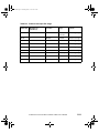
1. HDLC channels C and D supported on the Am186CC communications controller only.
2. HDLC channels A and B supported on the Am186CC and Am186CH microcontrollers only.
3. USB is supported on the Am186CC and Am186CU microcontrollers only.
$P&&&+&80LFURFRQWUROOHU&'38VHU¶V0DQXDO
about.book Page 8 Monday, June 7, 1999 10:17 AM
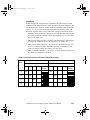
Main Board Features
The main board is a single-sided, 9- x 12-inch, printed circuit board that integrates
the Am186CC communications controller, a power supply, memory interfaces, and
I/O interfaces onto one board, enabling you to develop specific applications using
the development module interface.
The main board contains debug and status features, and enables you to evaluate
and develop different configurations of memory and I/O by using on-board
configuration switches, jumper blocks, and expansion interfaces.
The following features are described in this section:
• Am186CC/CH/CU microcontroller, page 2-8
• Power supply, page 2-15
• Memory interfaces, page 2-20
• Communications interfaces, page 2-27
• Debug and configuration circuitry, page 2-39
• Expansion interfaces, page 2-49
Am186™CC/CH/CU Microcontroller (J14)
The Am186CC/CH/CU microcontroller customer development platform supports
a 160-pin PQFP Am186CC communications controller operating at 25, 40, or
50 MHz. The integrated features of the Am186CC communications controller
provide a glueless interface to DRAM or SRAM system memory and Flash
memory. The microcontroller also integrates UART and High-Speed UART (which
require only external transceivers), a high-speed (12 Mbit/s) USB peripheral
controller with internal transceiver (Am186CC and Am186CU microcontrollers
only), and HDLC channels (Am186CC and Am186CH microcontrollers only) that
provide external interfaces to gluelessly connect to communications peripherals.
NOTE: Although the CDP supports an Am186CC communications controller, you
can also use this platform to evaluate the Am186CH and Am186CU
microcontrollers. These microcontrollers support subsets of the Am186CC
communications controller’s features. Refer to the device data sheets for more
information.
$P&&&+&80LFURFRQWUROOHU&'38VHU¶V0DQXDO
about.book Page 9 Monday, June 7, 1999 10:17 AM
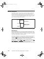
The Am186CC communications controller is designed as a cost-effective, highperformance microcontroller solution for communication applications. The
Am186CC communications controller offers the advantages of the x86
development environment’s widely available native development tools,
applications, and system software. For detailed information about the specific
features of the Am186CC/CH/CU microcontroller, refer to the corresponding data
sheet and user’s manual included in your kit. Figure 2-3 shows the Am186CC
communications controller block diagram; Figure 2-4 on page 2-10 shows the
Am186CH HDLC microcontroller block diagram; and Figure 2-5 on page 2-10
shows the Am186CU USB microcontroller block diagram.
Serial Communications Peripherals
Am186
CPU
Chip
Selects
(14)
PIOs
(48)
Watchdog
Timer
Interrupt
Controller
(17 Ext.
Sources)
UART
High-Speed
UART with
Autobaud
USB
Synchronous
Serial
Interface (SSI)
Physical
Interface
Glueless
Interface
to RAM/ROM
DRAM
Controller
Timers
(3)
GeneralPurpose
DMA (4)
SmartDMA
(8)
Controller
HDLC TSA
Raw DCE
HDLC TSA
Memory Peripherals
System Peripherals
Muxing
PCM
Highway
HDLC TSA
HDLC TSA
GCI
(IOM-2)
Figure 2-3. Am186CC™ Communications Controller Block Diagram
$P&&&+&80LFURFRQWUROOHU&'38VHU¶V0DQXDO
about.book Page 10 Monday, June 7, 1999 10:17 AM
Serial Communications Peripherals
Am186
CPU
Chip
Selects
(14)
PIOs
(48)
Watchdog
Timer
Interrupt
Controller
(17 Ext.
Sources)
UART
High-Speed
UART with
Autobaud
Synchronous
Serial
Interface (SSI)
Physical
Interface
Glueless
Interface
to RAM/ROM
DRAM
Controller
Memory Peripherals
Timers
(3)
GeneralPurpose
DMA (4)
SmartDMA
Channels
(4)
HDLC
TSA
System Peripherals
Raw DCE
Muxing
HDLC
PCM
Highway
TSA
Figure 2-4. Am186CH™ HDLC Microcontroller Block Diagram
Serial Communications Peripherals
Am186
CPU
Chip
Selects
(14)
Glueless
Interface
to RAM/ROM
PIOs
(48)
DRAM
Controller
Memory Peripherals
Watchdog
Timer
Timers
(3)
Interrupt
Controller
(17 Ext.
Sources)
GeneralPurpose
DMA (4)
SmartDMA
Channels
(4)
USB
UART
Synchronous
Serial
Interface (SSI)
High-Speed
UART with
Autobaud
System Peripherals
Figure 2-5. Am186CU™ USB Microcontroller Block Diagram
Am186CC™ Communications Controller Power Supply
The CDP main board provides a 3.3-V power supply for the Am186CC
communications controller. The power supply is sourced from a 3.3-V low drop
out (LDO) regulator (U29) from a 5-V switching power supply. The digital and
analog power pins are isolated by filtering to prevent noise on the digital circuitry
from affecting the internal analog block.
$P&&&+&80LFURFRQWUROOHU&'38VHU¶V0DQXDO
about.book Page 11 Monday, June 7, 1999 10:17 AM
Am186™CC/CH/CU Microcontroller Clocking
Four types of input clocks are used on the main board: the system clock, USB clock
(Am186CC and Am186CU microcontrollers only), UART clock, and HDLC
clocks (Am186CC and Am186CH microcontrollers only).
The system and USB clocks, shown in Figure 2-6 and Figure 2-7, respectively, use
internal oscillators and PLLs that enable the use of slower, less costly, fundamental
mode crystals for providing system clock frequencies from 16 to 50 MHz, and a
USB frequency of 48 MHz. The UART clock can be derived from the system clock
frequency, or from the UCLK input by using an external oscillator. The on-board
MACH device can be used for the DCE or PCM HDLC clocks at various
frequencies and frame syncs (PCM mode only); or if you are using the development
module interface, you can drive the HDLC clocks from a specific DCE, PCM, or
GCI peripheral. For the available clock options, see Table 2-2.
Table 2-2. CPU and USB Clock Options
3//0RGH
&ORFN
[
[
[
3//%\SDVV
2VFLOODWRU
6\VWHPFORFN
±0+] ±0+]
±0+]
±0+]
±0+]
86%FORFN
²
0K]
0+]
²
0+]
6KDUHG
V\VWHP86%
FORFN
²
0K]
0+]
²
0+]
8$57FORFN
²
²
²
²
±0+]
1. The USB clock is supported on the Am186CC and Am186CU microcontrollers only.
2. UCLK is limited to the maximum frequency of the system clock.
System Clock
The system clock, shown in Figure 2-6 on page 2-12 (or sheet 3 of the main board
schematics included in your kit), can be derived from a fundamental mode crystal
by doing one of the following:
• Driving X1 and X2 at location X1 into the integrated oscillator and using the
internal PLL (see locations H16 and J16 in Figure 2-2 on page 2-3)
• Driving X1 and X2 at location X1 into the integrated oscillator and bypassing
the internal PLL
$P&&&+&80LFURFRQWUROOHU&'38VHU¶V0DQXDO
about.book Page 12 Monday, June 7, 1999 10:17 AM
The system clock can also be derived from an external oscillator by doing one of
the following:
• Driving an external oscillator from Y5 into X1 and using the internal PLL (see
location H16 in Figure 2-2 on page 2-3)
• Driving an external oscillator from Y5 into X1 and bypassing the internal PLL
The PLL can be configured in 1x, 2x (default), or 4x PLL mode or PLL bypass
mode by appropriately setting the pinstraps on SW16. See “Debug and
Configuration Circuitry” on page 2-39 for more information.
The maximum crystal input and oscillator frequencies are 40 MHz. The CDP
provides pin sockets, allowing the designer to easily attain multiple clock
configurations.
NOTE: When using an external oscillator or clock source to drive the system, USB,
or UART clock, you must drive the clock with a source that does not exceed the
Am186CC/CH/CU microcontroller’s VCC.
9&&$
<
2(
9&&
*1'
287
26&S
Ecliptek EC1300HS-XX ;
&5<67$/7+
Ecliptek EC2-24.000M-CL150
&38;
&
S)
&38;
&
S)
Figure 2-6. Am186™CC/CH/CU Microcontroller System Clock
$P&&&+&80LFURFRQWUROOHU&'38VHU¶V0DQXDO
about.book Page 13 Monday, June 7, 1999 10:17 AM
USB Clock
• The USB clock (shown in Figure 2-7or sheet 3 of the main board schematics
included in your kit), which must be 48 MHz, may be derived from one of the
following:
• System clock
• Driving USBX1 and USBX2 at location X2 into the integrated oscillator and
using the internal PLL (see location J16 in Figure 2-2 on page 2-3)
• Driving an external oscillator into USBX1 from Y3 and using the internal PLL
The PLL can be configured in 2x or 4x PLL mode by appropriately setting the
pinstraps on SW16. See “Debug and Configuration Circuitry” on page 2-39 for
more information.
The Am186CC and Am186CU microcontrollers’ USB block requires a 48-MHz
clock input. The USB clocking options are 12 MHz in 4x PLL mode, 24 MHz in
2x PLL mode, or a system clock of 48 MHz.
NOTE: When using the system clock for USB clocking, USBX1 must be
terminated to ground to prevent unwanted oscillation in the unused integrated USB
oscillator. To accomplish this, populate C42 with a
0-Ω resistor.
9&&$
<
2(
9&&
*1'
287
26&S
86%;
&
(FOLSWHN(&+6;;
;
&5<67$/7+
S)
(FOLSWHN(&0&/
86%;
&
S)
Figure 2-7. Am186CC or Am186CU Microcontroller USB Clock
$P&&&+&80LFURFRQWUROOHU&'38VHU¶V0DQXDO
about.book Page 14 Monday, June 7, 1999 10:17 AM
The UCLK input at location Y4 (see location J11 in Figure 2-2 on page 2-3) is
used to drive the UART or High-Speed UART with a unique clock source that is
not derived from the system clock. The CDP provides oscillator pin sockets,
enabling the use of standard 3.3-V half-can oscillators.
Am186CC™ Communications Controller Reset
The Am186CC communications controller requires the RES input to be asserted
for at least 1 ms to allow the internal circuitry to stabilize. The CDP main board
uses an external device that monitors the 3.3-V VCC to provide a reset output with
an internal 21-ms RC delay to drive the 3.3-V RES input to the Am186CC
communications controller. Depressing the reset switch (SW1) causes a system
reset without cycling power. Figure 2-8 (or sheet 3 of the main board schematics
included in your kit) shows the reset circuitry.
9&&
.
9&&
5
3$+
6:
5(6(7
&
X)
9&&
8
9&&
567
6(16(
5(6,1
&7
*1'
567
5()
5(6
3$+
7/&,'
9
$&$6(
55(6
Figure 2-8. Main Board Reset Circuitry
$P&&&+&80LFURFRQWUROOHU&'38VHU¶V0DQXDO
&
X)
about.book Page 15 Monday, June 7, 1999 10:17 AM
Power Supply (A1)
The CDP is powered by a universal power supply that converts 100–200 VAC power
to 12 VDC, 2.5 A. The 12 V enters the CDP main board through a 5.5-mm barrel
connector, where the center post is VCC and the outer ring is GND. From the
12-VDC input, the CDP on-board power supply provides 5 V, 3.3 V, –5 V,
–24 V, and –70 V. The CDP provides power indicators for these voltages at CR8–
CR12. The CDP also provides test jacks that enable you to monitor the VCC voltages
at P22–P25, P28–P29. The following sections provide details about the power
supply. Table 2-3 through Table 2-5, beginning on page 2-18, contain power
estimates for the CDP main board, development module, and CDP totals.
5V@3A
A 5-V buck switching circuit from the 12-V source generates the 5 V, which
provides power to a majority of the components on the CDP main board including
the DRAM, SRAM, and Flash memory components; the DCE and UART
transceivers; the HDLC clock generator; and the 3.3-V LDO regulator. This power
supply is also routed to the CDP development module, TIP connector, and Am186
processor expansion interface connectors. For details, see Figure 2-9 or sheet 14
of the main board schematics included in your kit.
9&&
8
&
X)
9,1
6:
9'
*5281'
9&&
X+
'
6+'1
0,&
/
)%
6&+277.<5(&7,),(5
&
&
&
X)
X)
X)
9
9
9
(&$6(
(&$6(
(&$6(
Figure 2-9. 5-V Power Supply
$P&&&+&80LFURFRQWUROOHU&'38VHU¶V0DQXDO
about.book Page 16 Monday, June 7, 1999 10:17 AM
3.3 V @ 500 mA
The 3.3-V LDO regulator at location U29 generates the 3.3 V from the 5-V output.
This power supply is used to provide power to the Am186CC communications
controller, the USB detect circuitry, and to the optional external USB transceiver.
A population option to use the 3.3-V source for the memory components is
available. This option is available for the case where no 5-V devices are located
on the Am186CC communications controller local bus. For details, see
Figure 2-10 or sheet 14 of the main board schematics included in your kit.
9&&
9&&
8
,1
287
*1'
/'2
&
0LFUHO0,&%6
&
X)
&
X)
9
&&$6(
X)
Figure 2-10. 3.3-V Power Supply
–5 V @ 200 mA
A 5-V buck-boost switching circuit from the 12-V source generates the –5 V. This
power supply provides power to the CDP development module and POTS interface.
For details, see Figure 2-11 or sheet 14 of the main board schematics included in
your kit.
9&&
&
X)
8
9,1
6:
/
)%
095(*8/$725
0LFUHO0,&%8
&RLOWURQLFV&7;
&
X)
'
',2'(
6+'1
*5281'
09
X+
5(*B6:
52+05%/
&
X)
9
9
(&$6(
(&$6(
092
$9;736(0
.-
Figure 2-11. –5-V Power Supply
$P&&&+&80LFURFRQWUROOHU&'38VHU¶V0DQXDO
5
.2$50=%:
about.book Page 17 Monday, June 7, 1999 10:17 AM
–24 V @ 50 mA and –70 V @ 60 mA
A switching flyback circuit from the 12-V source generates the –24 V and the –
70 V. These outputs are routed to the CDP development module and are used in
the POTS interface. For details, see Figure 2-12 or sheet 14 of the main board
schematics included in your kit.
09
09
5
.2$50=%:
7
09'
0
9
&
$
3
&
7
5
7
$
3
'
;
9
(&$6(
$9;736(05
&
X)
9
&203
(&$6(
$9;736(05
6:
9
&
X)
5
.
'
0
5
5
*HQHUDO6HPL(6'
095
'
&
X)
5
.
9
(&$6(
&203
*1'
)%
)%
5
%HFNPDQ+0
$9;&0$70$
5
.
09)%
23$03
0LFUHO0,&%0
8
&
X)
)O\EDFN7UDQVIRUPHU
9&&
5
.
&
2
0
3
5
$9;736(05
$9;736(05
6/,&5(*8/$725
$9;&0$70$
09'
*HQHUDO6HPL(6'
7%
9&&6:
0LFUHO0,&%8
&
S)
7$
*HQHUDO6HPL(6'
8
,1
'
',2'(
9&&'
&
X)
(&$6(
$9;736(05
52+056=%
9
(&$6(
9
&
&
'
',2'(=(1(5
.2$50=%:
&
X)
9
*HQHUDO6HPL60=-%
095
7&
'
',2'(=(1(5
5
*HQHUDO6HPL(6'
7'
9&&
'
&
S)
9
$9;&0$70$
Figure 2-12. –24-V and –70-V Power Supplies
$P&&&+&80LFURFRQWUROOHU&'38VHU¶V0DQXDO
about.book Page 18 Monday, June 7, 1999 10:17 AM
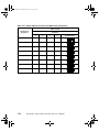
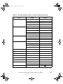
Table 2-3. Power Estimates for the CDP Main Board
9ROWDJH9
'HYLFH
4W\ ,W\SP$
,PD[P$
3W\SP: 3PD[P:
$P&&
FRPPXQLFDWLRQV
FRQWUROOHU
86%WUDQVFHLYHU
'5$0.[
65$0.[
)ODVKPHPRU\
0[.[
&/.JHQHUDWRU
3/'
8$57WUDQVFHLYHU
'&(GULYHU
'&(UHFHLYHU
0DLQERDUGWRWDO
1. Average operating current at 50 MHz.
2. USB is supported on the Am186CC and Am186CU microcontrollers only.
$P&&&+&80LFURFRQWUROOHU&'38VHU¶V0DQXDO
about.book Page 19 Monday, June 7, 1999 10:17 AM
Table 2-4. Power Estimates for the CDP Development Module
9ROWDJH9 'HYLFH
4W\
,W\SP$ ,PD[P$
3W\SP:
3PD[P:
(WKHUQHWFRQWUROOHU
,6'167
WUDQVFHLYHU
,6'18
WUDQVFHLYHU
'70)
±
'6/$&
±
±
±
56/,&
±
±
±
&'3GHYHORSPHQW
PRGXOHWRWDO
1. USB is supported on the Am186CC and Am186CU microcontrollers only.
Table 2-5. Total Power Estimates for the CDP
9ROWDJH9
,W\SPD
,PD[PD
3W\SPZ
3PD[PZ
±
±
±
$P&&&+&80LFURFRQWUROOHU&'38VHU¶V0DQXDO
about.book Page 20 Monday, June 7, 1999 10:17 AM
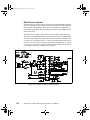
Memory Interfaces
The Am186CC/CH/CU microcontroller customer development platform main
board supports DRAM or SRAM system main memory and Flash memory.
Figure 2-13 shows the DRAM or SRAM system and Flash memory map, Figure
2-14 on page 2-21 shows the DRAM and SRAM circuitry, and Figure 2-15 on
page 2-22 shows the Flash memory circuitry.
FFFFFh
Flash Memory
7FFFFh
DRAM or SRAM
System Memory
00000h
Figure 2-13. DRAM or SRAM System Memory and Flash Memory Map
Main Memory
The main board allows the use of two banks of DRAM, or SRAM as the main
memory for the system. The default configuration is one bank of 256K x 16 EDO
DRAM in an SOJ package, located at U21. See Figure 2-14 on page 2-21 or sheet 4
of the main board schematics included in your kit.
In the default configuration, one bank of 256K x 16 EDO, 40-ns DRAM allows
zero wait state operation at up to 50 MHz. The DRAM resides in the lower
512 Kbyte of LCS memory space (0h–7FFFFh). The Am186CC communications
controller provides the DRAM memory address on the odd Am186CC
communications controller addresses A1–A17 to provide a direct connection to
the DRAM device. The DRAM RAS and CAS signaling is provided on the LCS0/
RAS0, MCS1/CAS1, and MCS2/CAS0 signals from the Am186CC
communications controller when DRAM is selected as the main system memory.
$P&&&+&80LFURFRQWUROOHU&'38VHU¶V0DQXDO
about.book Page 21 Monday, June 7, 1999 10:17 AM
An unpopulated component location, U18, is available for a 256K x 16 device for
DRAM bank 1 to be used in the upper 512K of memory space (UCS space). This
enables you to boot from Flash memory located in UCS space, and then remap
UCS to DRAM bank 1. In this case, the MCS3/RAS1 signal becomes the RAS for
bank 1 and the CAS signals remain the same.
To use SRAM as main system memory, a 256K x 16 SOJ SRAM can be populated
at location U15. R89 must be depopulated, and R90 must be populated with a
10-kΩ resistor.
Another option for using SRAM as main system memory is to use two 32-pin DIP
sockets at U25 and U28 for SRAM devices. The SRAM is configurable to be used
as 128K x 8/512K x 8, or 128K x 16/512K x 16 via configuration jumper blocks
JP11 and JP12. A jumper block, JP10, is also used to route either LCS, UCS, or
MCS0 to the SRAM sockets.
The CDP main board is populated with 128K x 8, 35-ns DIP SRAM devices as the
optional system memory.
NOTE: The SRAM sockets are also used for the x16 ROM-ICE interface. Because
of this, LCS, UCS, or MCS0 can be used, allowing flexibility of chip selects
between the ROM-ICE and on-board Flash memory (see Table 2-6 on page 2-24).
0$>@
0$'>@
0$
0$
0$
0$
0$
0$
0$
0$
0$
9&&0 (0
127(3RSXODWH5DQG
GHSRSXODWH5LI
XVLQJ65$0UDWKHUWKDQ
'5$0DVPDLQV\VWHP
PHPRU\
5
0&6
/&6
0&6
0&6
5'
:53
8
$
$
$
$
$
$
$
$
$
1&
1&
1&
5
.
1&
5$6
0&6
0&6
5 '
:53
>&$6@
>&$6@
5$6
/&$6
8&$6
2(
'4
'4
'4
'4
'4
'4
'4
'4
'4
'4
'4
'4
'4
'4
'4
'4
:5
'5$0;
62-
50$' 5
50$' 5
50$' 5
50$' 5
50$' 5
50$' 5
50$' 5
50$' 5
50$' 5
50$' 5
50$' 5
50$' 5
50$' 5
50$' 5
50$' 5
50$' 5
0$'
0$'
0$'
0$'
0$'
0$'
0$'
0$'
0$'
0$'
0$'
0$'
0$'
0$'
0$'
0$'
9&& 9&& 9&& 966 966 966
9&&0(0
0$
0$
0$
0$
0$
0$
0$
0$
0$
8
$
$
$
$
$
$
$
$
$
1&
1&
1&
1&
0&6 >5 $6@
0&6 >&$6@
0&6 >&$6@
5'
:53
5$6
/&$6
8&$6
2(
:5
'4
'4
'4
'4
'4
'4
'4
'4
'4
'4
'4
'4
'4
'4
'4
'4
9&& 9&& 9&& 966 966 966
0$'
0$'
0$'
0$'
0$'
0$'
0$'
0$'
0$'
0$'
0$'
0$'
0$'
0$'
0$'
0$'
0$
0$
0$
0$
0$
0$
0$
0$
0$
0$
0$
0$
0$
0$
0$
0$
0$
0$
9&&0(0
'5$0;
62-
%+(
0$
8
$
$
$
$
$
$
$
$
$
$
$
$
$
$
$
$
$
$
&(
%/(
%+(
2(
:(
'4
'4
'4
'4
'4
'4
'4
'4
'4
'4
'4
'4
'4
'4
'4
'4
9FF
9FF
0$'
0$'
0$'
0$'
0$'
0$'
0$'
0$'
0$'
0$'
0$'
0$'
0$'
0$'
0$'
0$'
9&&0(0
9VV 9VV
65$0.[
62-
>5$6@
>5$6@
>&$6@
>&$6@
Figure 2-14. Main Memory DRAM Circuit
$P&&&+&80LFURFRQWUROOHU&'38VHU¶V0DQXDO
about.book Page 22 Monday, June 7, 1999 10:17 AM
Flash Memory
A single, surface-mount, TSOP Am29F800, 55-ns, 8-Mbit Flash memory device
is populated on the CDP main board to allow for zero wait state operation at
50 MHz. See Figure 2-15 or sheet 4 of the main board schematics included in your
kit.
You can configure the Flash memory device as 512K x 16 or as a 1-Mbyte x 8
device via configuration switches SW11 and SW14. The default configuration
defines the Flash memory as 512 Kbyte (256K x 16) in UCS space (80000h–
FFFFFh). The highest order address bit of the Flash memory can be connected to
PIO35 rather than A19 by populating R93 with a 0-Ω resistor and removing R92.
This enables you to bank down to the lower half of the Flash memory to extend
available code space to 1 Mbyte. You can also map the Flash memory to MCS0
rather than UCS via jumper block JP8. For more information about jumper
configuration, see page 2-23.
Figure 2-15. Flash Memory Circuit
$P&&&+&80LFURFRQWUROOHU&'38VHU¶V0DQXDO
about.book Page 23 Monday, June 7, 1999 10:17 AM
Configuration Overview
This section describes the options associated with Flash memory and main system
memory interfaces.
Flash Memory
• Flash memory banking select
Populating R92 enables the highest order address bit to the Flash memory to be
routed from A19 (default). Populate R93 to use PIO35 as the Flash memory
banking select. To operate the Flash memory in a banking scheme, PIO35 (which
is normally High) should be configured to be driven Low when accessing the
lower half of the Flash memory.
• JP8: Flash memory chip select
Jumper block JP8 enables you to route UCS (default) or MCS0 as the Flash
memory chip select.
• SW11: Flash memory data bus width select
Switch SW11 is used to determine the Flash memory device data width as x8
or x16 (default). When configuring the Flash data width to 8 bits, the pinstrap
UCSX8 at SW14 segment 2 must be set to the ON position during reset to
configure the Am186CC communications controller to do 8-bit accesses.
SRAM Main Memory
• JP10: SRAM/ROM-ICE chip select
Jumper block JP10 enables you to route LCS, UCS, or MCS0 to the SRAM
socket’s chip select.
• JP11: SRAM/ROM-ICE device select
Jumper block JP11 is used along with JP12 to select the different SRAM and
ROM configurations.
• JP12: SRAM/ROM-ICE device select
Jumper block JP12 is used along with JP11 to select the different SRAM and
ROM configurations.
Table 2-6 on page 2-24 shows the jumper selections for the various SRAM and
ROM options. Figure 2-16 on page 2-25 (or sheet 5 of the main board schematics
included in your kit) shows the SRAM sockets. Table 2-7 on page 2-26 lists the
SRAM and ROM pinouts.
$P&&&+&80LFURFRQWUROOHU&'38VHU¶V0DQXDO
about.book Page 24 Monday, June 7, 1999 10:17 AM
Table 2-6. DIP x8/x16 SRAM, ROM-ICE Device Selection
'HYLFH
65$0
.[
-3
3/% 36(/
36(/
36(/
-3
36(/
3+%
1&
9LVXDO'HWDLO
JP12
JP11
1
1
2
2
65$0
.[
1&
1
65$0
.[
1
1
2
2
1
1
2
65$0
.[
520
.[
520
.[
1
2
1&
1&
1&
1&
$P&&&+&80LFURFRQWUROOHU&'38VHU¶V0DQXDO
2
2
1
1
2
2
1
1
2
2
about.book Page 25 Monday, June 7, 1999 10:17 AM
[[65$0'HYLFH520,&(
5$'>@
5$>@
5$
5$
5$
5$
5$
5$
5$
5$
5$
5$
5$
5$
5$
5$
5$
36(/
36(/
36(/
36(/
8
$
$
$
$
$
$
$
$
$
$
$
$
$
$
$
$
$
$
$
'4
'4
'4
'4
'4
'4
'4
'4
2(
&6
:(
9&&
*1'
5
5
5
5
5
5
5
5
55$'
55$'
55$'
55$'
55$'
55$'
55$'
55$'
5$'
5$'
5$'
5$'
5$'
5$'
5$'
5$'
5$
5$
5$
5$
5$
5$
5$
5$
5$
5$
5$
5$
5$
5$
5$
5'5
65$0&6
3/%
36(/
5$
9&&
36(/
36(/
65$0
8
$
$
$
$
$
$
$
$
$
$
$
$
$
$
$
$
$
$
$
'4
'4
'4
'4
'4
'4
'4
'4
2(
&6
:(
9&&
*1'
55$'
55$'
55$'
55$'
55$'
55$'
55$'
55$'
5
5
5
5
5
5
5
5
5$'
5$'
5$'
5$'
5$'
5$'
5$'
5$'
5'5
65$0&6
3+%
9&&
65$0
5'5
9&&
.
5
-3
/&6
8&65
0&6
+($'(5;
65$0
-3
5$
5$
5$
:/%
5$
36(/
3/%
+($'(5;
-3
9&&
5$
:+%
5
.
5$
&6
5$
5$
-3
36(/
3+%
36(/
36(/
36(/
3/%
3+%
36(/
36(/
1&
.[
1&
.[
.[
1&
1&
1&
1&
65$0.[
520.[
.[
65$0
9&&
-3
36(/
&
X)
9
&&$6(
&
X)
&
X)
+($'(5;
Figure 2-16. DIP SRAM Sockets
$P&&&+&80LFURFRQWUROOHU&'38VHU¶V0DQXDO
about.book Page 26 Monday, June 7, 1999 10:17 AM
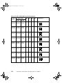
Table 2-7. SRAM and ROM Pinouts
3LQ
65$0
.[
1&
65$0
.[
$
520
.[
933
520
.[
933
520
.[
933
$
$
$
$
$
$
$
$
$
$
$
$
$
$
$
$
$
$
$
$
$
$
$
$
$
$
$
$
$
$
$
$
$
$
$
$
$
$
$
$
$
$
$
$
$
$
$
$
$
$
$
$
$
$
$
'
'
'
'
'
'
'
'
'
'
'
'
'
'
'
*1'
*1'
*1'
*1'
*1'
'
'
'
'
'
'
'
'
'
'
'
'
'
'
'
'
'
'
'
'
'
'
'
'
'
&(
&(
&(
&(
&(
$
$
$
$
$
2(
2(
2(
2(
2(
$
$
$
$
$
$
$
$
$
$
$
$
$
$
$
$
$
$
$
$
:(
:(
$
$
$
&6
$
1&
$
$
$
$
3*0
3*0
$
9&&
9&&
9&&
9&&
9&&
$P&&&+&80LFURFRQWUROOHU&'38VHU¶V0DQXDO
about.book Page 27 Monday, June 7, 1999 10:17 AM
Communication Interfaces
This section describes the communication interfaces available on the Am186CC/
CH/CU microcontroller customer development platform’s main board.
The communication interface I/O ports include two RS-232 DB-9 interfaces for
the low- and high-speed serial ports derived from the integrated Am186CC
communications controller UARTs, four RS-530 DB-25 DCE/PCM ports derived
from the integrated Am186CC or Am186CH microcontroller HDLC interface, and
a peripheral USB port derived from the integrated Am186CC or Am186CU
microcontroller USB peripheral controller.
NOTE: The Am186CH HDLC microcontroller provides only two external HDLC
interfaces and does not support USB; the Am186CU USB microcontroller provides
a USB interface but does not support HDLC.
RS-232 Serial Ports
Two RS-232 serial ports (see Figure 2-17 on page 2-29 or sheet 9 of the main board
schematics included in your kit) are configured as data communication equipment
(DCE) ports to provide direct connection to a typical data terminal equipment
(DTE) port on a PC. This enables you to use a straight serial cable (no null-modem)
when connecting to a PC. The Am186CC communications controller High-Speed
UART is connected to the DB-9 connector at P15 through an RS-232 transceiver
and is capable of a data rate of up to 460 Kbit/s. The low-speed UART is connected
to the DB-9 connector at P7 through an RS-232 transceiver and is capable of a data
rate of up to 120 Kbit/s.
The CDP main board provides individual status LEDs for the high- and low-speed
serial ports (CR6 and CR5, respectively), which illuminate green when data is
being transmitted and red when data is being received by the Am186CC
communications controller UARTs.
$P&&&+&80LFURFRQWUROOHU&'38VHU¶V0DQXDO
about.book Page 28 Monday, June 7, 1999 10:17 AM
The high- or low-speed serial ports can also be configured to use up to four
additional PIOs as additional hardware flow control at JP5 for the high-speed port,
and JP3 for the low-speed port. The PIOs are defined in an RS232 serial port
configuration as follows:
• PIO0 is used as an output for DCD (Data Carrier Detect).
• PIO1 is used as an input for DTR (Data Terminal Ready).
• PIO27 is used as an output for RI (Ring Indicate).
• PIO28 is used as an output for DSR (Data Set Ready).
Hardware flow control pins RTRHU and CTSHU can be isolated from the highspeed serial port at JP7, so you can use them as their alternate functions and use
the serial port without hardware flow control. An alternative is to use PIO45 and
PIO44 as the high-speed serial port RTRHU and CTSHU functions. Use this
alternative when hardware control is required, and the standard flow control pins
RTRHU and CTSHU are used as an alternate function.
You can shut down the serial port RS-232 transceivers by setting SW9 segment 5
(high speed) and 6 (low speed) to the ON position. This feature is used when the
Am186CC communications controller UART signals are used for their alternate
function.
NOTE: If HDLC Channel D pins are being used as DCE or PCM rather than the
UART, SW9 segment 6 must be set to the ON position to prevent contention
between the RS-232 transceiver and the desired function.
$P&&&+&80LFURFRQWUROOHU&'38VHU¶V0DQXDO
about.book Page 29 Monday, June 7, 1999 10:17 AM
Figure 2-17. RS-232 Serial Port Routing
$P&&&+&80LFURFRQWUROOHU&'38VHU¶V0DQXDO
about.book Page 30 Monday, June 7, 1999 10:17 AM
RS-530 DCE/PCM HDLC Ports
Four HDLC DCE/PCM ports are available on the Am186CC microcontroller (two
for the Am186CH microcontroller) via RS-530 DB-25 connectors configured as
DCE devices from the integrated HDLC controllers in the two microcontrollers.
Figure 2-18 (or sheet 6 of the main board schematics included in your kit) shows
a single HDLC RS-530 circuit.
The Am186CH HDLC microcontroller only provides external HDLC interfaces A
and B and does not support USB; the Am186CU USB microcontroller provides a
USB interface but does not support HDLC.
The RS-530 ports use RS-422 differential transceivers to support up to 10-Mbit/s
data transfers. The actual pinout of the four DB-25 connectors allow an RS-530
device to directly connect to the CDP without using a null-modem-like cable
adapter. The four RS-530 ports have individual transceiver shutdown switches, a
clock generator for DCE and PCM modes, status indicators, and DCE multidrop
mode.
5753$
5;'$
7;'$
5&/.$
7&/.$
&76$
575$
+'/&$(1
7;'$
5&/.$
7&/.$
575$
+'/&$(1
$%&21
&'&21
$2870
$2873
%2870
%2873
&2870
&2873
'2870
'2873
7;'0$
7;'3$
5&/.0$
5&/.3$
7&/.0$
7&/.3$
5750$
5753$
'&/.0$
'&/.3$
)6&0$'&/.0$
)6&3$'&/.3$
7256
3257$
9&&
+&/.$3
+&/.$0
'6&7623
+/('7;$
5
5
.
8$
$&7
9&&
$,1
%,1
&,1
',1
9&&
*1'
9&&
8
+&/.$3
+&/.$0
3$+
3$+
5
&5
*5((1
&$7+
5('
/('627
5;'$
5;'%
&76$
&76%
+'/&$(1 +'/&%(1 $&(1
%'(1
8%
$&7
+/('5;$
'&/.0$
*1'
7&/.0$
)6&0$
5&/.0$
'&/.0$
7&/.3$
)6&3$
*1'
&763$
5750$
5&/.3$
&760$
7;'3$
7;'0$
7&/.3$
5;'0$
5;'3$
*1'
'&/.3$
'&/.3$
3
&763$
5
+&/.$3
5
&760$
+&/.$0
+&/.$3
5;'0$
5
+&/.$0
5
5;'3$
&211(&725'%
8
$287
%287
&287
'287
7&/.0$
$,10
$,13
%,10
%,13
&,10
&,13
',10
',13
9&&
*1'
5;'0$
5;'3$
5;'0%
5;'3%
&760$
&763$
&760%
&763%
9&&
7256
3257$
7256
3257%
'6&7623
5
.
Figure 2-18. HDLC Circuit
You can shut down HDLC ports A–D by setting SW9 segments 1–4, respectively,
to the ON position. This enables you to use an alternate function without affecting
the board operation. For example, if you want to use GCI mode, set SW9, segment
1 to the ON position. Now you can use GCI mode as an alternate function on the
development module.
$P&&&+&80LFURFRQWUROOHU&'38VHU¶V0DQXDO
about.book Page 31 Monday, June 7, 1999 10:17 AM
NOTE: An HDLC interface being used as another function on the CDP must have
that function’s RS-530 port transceiver shut down to prevent contention between
the RS-530 port and the desired HDLC function.
The CDP main board provides individual status LEDs for the four RS-530 DCE/
PCM ports A–D, at CR1–CR4, respectively. The status LEDs illuminate green
when data is being transmitted, and red when data is being received by the
Am186CC or Am186CH microcontroller HDLC RS-530 ports.
The clocking of the DCE or PCM interface is derived from the HDLC clock
generator at U11. SW12, SW10, and SW8 are used to define the clocking mode
(DCE or PCM) and frequency. JP6, JP4, JP2, and JP1 define how the clocks are
routed to each Am186CC or Am186CH microcontroller HDLC RS-530 port. See
Table 2-13 on page 2-36. If the HDLC clocks are being generated by a peripheral
on the development module, you must remove the appropriate jumper from JP6,
JP4, JP2, and JP1.
DCE Mode
The DCE transmit and receive clock to the Am186CC or Am186CH
microcontroller can be varied from 78.125 kHz to 10 MHz and can be routed to
external devices through the RS-530 ports via a set of four jumper blocks. Three
sets of switches define the DCE clocking. The DCE clock is achieved by setting
the switches as follows:
• SW9: The HDLC clock generator does not operate for a particular HDLC
RS-530 port (A–D) unless that port’s shutdown switch SW9 segments 1–4 are
in the OFF position. See Table 2-8 on page 2-32.
• SW12: Switch SW12 segments 1–4 must be in the OFF position to indicate DCE
clocking mode for RS-530 ports A–D, respectively. See Table 2-8 on page 2-32.
• SW8: Switch SW8 segments 1–3 are used to vary the DCE clock frequency in
increments from 78.125 kHz to 10 MHz. See Table 2-9 on page 2-32.
$P&&&+&80LFURFRQWUROOHU&'38VHU¶V0DQXDO
about.book Page 32 Monday, June 7, 1999 10:17 AM
Table 2-8. Switch Options to Enable R-530 DCE Clocking
+'/&
3RUW
6:6ZLWFK
6:6ZLWFK
6HJPHQW
6HJPHQW
$
2))
±
±
±
%
±
2))
±
±
&
±
±
2))
±
'
±
±
±
2))
9LVXDO
'HWDLO
On
2))
±
±
±
±
2))
±
±
±
±
2))
±
±
±
±
2))
On
On
On
9LVXDO
'HWDLO
On
On
On
On
Table 2-9. Switch Options to Set R-530 DCE Clocking Frequency
'&(&ORFN
)UHTXHQF\
6:6ZLWFK
6HJPHQW
N+]
21
21
21
±
N+]
2))
21
21
±
N+]
21
2))
21
±
N+]
2))
2))
21
±
0+]
21
21
2))
±
0+]
2))
21
2))
±
0+]
21
2))
2))
±
0+]
2))
2))
2))
±
$P&&&+&80LFURFRQWUROOHU&'38VHU¶V0DQXDO
9LVXDO'HWDLO
On
On
On
On
On
On
On
On
about.book Page 33 Monday, June 7, 1999 10:17 AM
PCM Mode
PCM clocking mode configuration is controlled by the same switches as DCE
clocking with the addition of SW10, which provides a variable PCM frame sync.
The PCM data clock can be varied from 64 kHz to 8.192 MHz, and the frame sync
can be 1, 2, 4, 8, or 16 data clocks wide with positive or negative polarity. The
PCM data clock and frame sync are achieved by setting the switches as follows:
• The HDLC clock generator does not operate for a particular HDLC RS-530 port
(A–D) unless that port’s shutdown switch SW9 segments 1–4 are in the OFF
position. See Table 2-10.
• SW12: Switch SW12 segments 1–4 must be in the ON position to indicate PCM
clocking mode for RS-530 ports A–D, respectively. See Table 2-10.
• SW10: Switch SW10 segments 1–3 are used to vary the PCM frame sync to 1,
2, 4, 8, or 16 data clock widths (dependent upon data clock frequency) and
positive or negative polarity. See Table 2-12 on page 2-35.
• SW8: Switch SW8 segments 1–3 are used to vary the PCM clock frequency in
increments from 64 kHz to 8.192 MHz.
Table 2-10. Switch Options to Enable R-530 PCM Clocking
+'/&
3RUW
6:6ZLWFK
6:6ZLWFK
6HJPHQW
6HJPHQW
$
2))
±
±
±
%
±
2))
±
±
&
±
±
2))
±
'
±
±
±
2))
9LVXDO
'HWDLO
On
On
On
On
21
±
±
±
±
21
±
±
9LVXDO
'HWDLO
On
On
±
±
21
±
±
±
±
21
$P&&&+&80LFURFRQWUROOHU&'38VHU¶V0DQXDO
On
On
about.book Page 34 Monday, June 7, 1999 10:17 AM
Table 2-11. Switch Options to Set R-530 PCM Clocking Frequency
6:6ZLWFK
3&0&ORFN
)UHTXHQF\
6HJPHQW
N+]
21
21
21
±
N+]
2))
21
21
±
N+]
21
2))
21
±
N+]
2))
2))
21
±
0+]
21
21
2))
±
0+]
2))
21
2))
±
0+]
21
2))
2))
±
0+]
2))
2))
2))
±
$P&&&+&80LFURFRQWUROOHU&'38VHU¶V0DQXDO
9LVXDO'HWDLO
On
On
On
On
On
On
On
On
about.book Page 35 Monday, June 7, 1999 10:17 AM
Table 2-12. Switch Options to Set R-530 PCM Frame Sync
'DWD
&ORFN
:LGWK
6:6ZLWFK
3RODULW\
6HJPHQW
21
21
21
±
9LVXDO'HWDLO
On
2))
21
21
±
2))
21
21
±
21
2))
21
±
21
2))
21
±
2))
2))
21
±
2))
2))
21
±
21
21
2))
±
On
On
On
On
On
On
On
2))
21
2))
±
2))
21
2))
±
21
2))
2))
±
On
On
On
21
2))
2))
±
On
1.
2.
3.
4.
5.
2))
2))
2))
±
On
2))
2))
2))
±
On
·
Frame sync width = Width Data Clock Period.
Only available at 64 kHz and 128 kHz data clocks.
At 64 kHz and 128 kHz data clocks only.
At 128 kHz data clock only.
Only available at 256 kHz–8.192 MHz data clocks.
$P&&&+&80LFURFRQWUROOHU&'38VHU¶V0DQXDO
about.book Page 36 Monday, June 7, 1999 10:17 AM
Table 2-13. HDLC DCE/PCM Clock Routing Options
&ORFN
6RXUFH
+'/&0RGH
-3
-3
-3
²
²
([WHUQDO
([WHUQDO
7&/.$
5&/.$
)6&$
&/.$
±
±
²
,QWHUQDO
,QWHUQDO
7&/.%
5&/.%
)6&%
&/.%
²
±
±
²
([WHUQDO
([WHUQDO
7&/.%
5&/.%
)6&%
&/.%
²
±
±
²
,QWHUQDO
,QWHUQDO
7&/.&
5&/.&
)6&&
&/.&
²
²
±
±
²
([WHUQDO
([WHUQDO
7&/.&
5&/.&
)6&&
&/.&
²
±
±
²
,QWHUQDO
,QWHUQDO
7&/.'
5&/.'
)6&'
&/.'
²
²
±
±
([WHUQDO
([WHUQDO
7&/.'
5&/.'
)6&'
&/.'
²
INT
INT
INT
INT
INT
JP2
INT
EXT
TCLKC
RCLKC
TCLKC
JP1
INT
EXT
TCLKD
RCLKD
TCLKD
JP1
±
±
EXT
TCLKC
RCLKC
TCLKC
²
TCLKB
JP2
²
EXT
RCLKB
TCLKB
²
TCLKB
JP4
²
EXT
RCLKB
TCLKB
²
TCLKA
JP4
²
EXT
RCLKA
TCLKA
INT
RCLKD
$P&&&+&80LFURFRQWUROOHU&'38VHU¶V0DQXDO
EXT
TCLKD
RCLKD
TCLKD
TCLKA
JP6
²
RCLKA
TCLKA
²
EXT
RCLKD
²
RCLKC
±
±
RCLKC
)6&$
&/.$
RCLKB
7&/.$
5&/.$
RCLKA
,QWHUQDO
,QWHUQDO
RCLKA
3&0
RCLKB
'&(
9LVXDO'HWDLO
JP6
-3
about.book Page 37 Monday, June 7, 1999 10:17 AM
DCE Multidrop Mode
Another feature of the CDP main board is the ability of the HDLC ports to operate
in multidrop mode by using SW3, SW5, SW6, and SW7. When any of these
switches are in the ON position, the transmit (TXD), receive (RXD), and CTS are
shorted together.
NOTE: When operating in DCE multidrop mode, the Am186CC communications
controller DCE interface TXD pins must be configured as open drain.
Peripheral USB Port
NOTE: USB is supported only on the Am186CC and Am186CU microcontrollers.
The CDP provides a full-speed (12 Mbps) peripheral USB port that enables the
CDP to be used as a self-powered USB peripheral.
You can configure the CDP to use the Am186CC or Am186CU microcontroller
full-speed (12 Mbps) USB peripheral controller’s integrated USB transceiver, or
an external transceiver. Using the internal USB transceiver enables the USB
differential signaling (USBD+ and USBD–) to directly connect to the USB
connector and to a USB host or hub through a standard USB full-speed cable.
When the USB port on the CDP is active, the Am186CC or Am186CU
microcontroller’s PIO8 signal is driven Low, which illuminates LED CR7.
Configure the optional external USB transceiver by doing the following:
• Remove R49 and R50.
• Populate R42 and R43 with 0-Ω resistors.
• Populate R55 and R56 with 24-Ω resistors.
• Set pinstrap (USBXCVR) at SW14, segment 3, to the ON position during reset.
Refer to Figure 2-19 on page 2-38 (or sheet 10 of the main board schematics
included in your kit) for the USB circuit diagram.
The Am186CC or Am186CU microcontroller can be used only as a self-powered
USB peripheral because of the power requirements needed in the typical TA/
modem applications. Because of the USB electrical requirements of self-powered
USB peripherals, there is a small amount of glue logic needed to meet the USB
specifications. The attach/detach scenarios addressed with this logic are described
in the following paragraphs.
$P&&&+&80LFURFRQWUROOHU&'38VHU¶V0DQXDO
about.book Page 38 Monday, June 7, 1999 10:17 AM
Attach
1. The Am186CC or Am186CU microcontroller polls PIO42 for logic High level
to detect an active host/hub upstream connection (USBVCC is on). In the case
where an active USB host/hub is connected to the CDP USB port and power is
not applied to the CDP, Q2 isolates the USBVCC from the CDP to prevent
damage to the Am186CC communications controller.
2. The Am186CC or Am186CU microcontroller drives PIO43 High to enable Q1,
which pulls R58 up to 3.3 V. This pulls up the USBD+ signal to indicate to the
host that a full-speed USB device is present.
Detach
1. Am186CC or Am186CU microcontroller polls PIO42 for a logic Low level to
detect a disconnect condition from the host/hub.
2. The Am186CC or Am186CU microcontroller three states USBD+ and USBD–
in response to the disconnect.
3. The Am186CC or Am186CU microcontroller drives PIO43 to a logic Low
level, which disables Q1 and removes the pullup (R58) from USBD+.
Figure 2-19. Universal Serial Bus Circuit
$P&&&+&80LFURFRQWUROOHU&'38VHU¶V0DQXDO
about.book Page 39 Monday, June 7, 1999 10:17 AM
Debug and Configuration Circuitry
Several debug and configuration options make the Am186CC/CH/CU
microcontroller customer development platform a useful tool for the development
of specific applications. The CDP offers an interface to the Test Interface Port (TIP)
debug card (not included in your kit) that provides status indicators and debug
peripherals, debug headers to provide access to most critical pins on the
microcontroller, a reset configuration switch to define specific system parameters,
and a pinstrap configuration switch to define particular pin functions.
TIP Interface
The TIP is a small debug card to aid in testing, debug, and software development
of system applications based on the Am186CC communications controller. The
TIP provides the following features:
• An 8-bit on-board Flash device that you can select as the default boot device
• A 2-line x 20-character LCD to provide status information
• Eight hexadecimal LED displays to use for status codes
• Eight readable and writable LEDs for status indication
• Two RS-232 DCE serial ports to enable direct connection to a PC
• A PC-compatible parallel port
• A secondary reset button for the CDP
• A 10BaseT Ethernet port
The interface between the CDP and TIP is set up so it does not use many
microcontroller resources. Refer to Figure 2-20 on page 2-41 (or sheet 13 of the
main board schematics included in your kit) for a schematic of the TIP connector.
The general interface between the CDP and TIP is as follows:
• A19–A0, AD7–AD0, RD, and WLB on the Am186CC communications
controller are used to provide communication between the TIP peripherals and
the CDP.
• The UCS signal on the Am186CC communications controller provides a specific
chip select to the 8-bit Flash memory on the TIP. When selecting the TIP as a
boot device, the UCS signal must be routed to the TIP Flash memory by setting
jumper JP1, 1–2 on the TIP and removing the jumper on JP7 of the CDP.
$P&&&+&80LFURFRQWUROOHU&'38VHU¶V0DQXDO
about.book Page 40 Monday, June 7, 1999 10:17 AM
• INT0 on the Am186CC communications controller is used as the TIP Ethernet
interrupt signal.
• INT7 on the Am186CC communications controller is used as the TIP serial port
1 interrupt signal.
• INT8 on the Am186CC communications controller is used as the TIP serial port
0 interrupt signal.
• PCS3 on the Am186CC communications controller is used as a chip select
(AEN) for the TIP Ethernet controller.
• ARDY can be used to add wait states for the TIP Ethernet controller.
NOTE: AD7 is also individually interfaced to the TIP card to identify the TIP
being attached through the Am186CC/CH/CU microcontroller RESCON register.
NOTE: To share all TIP interrupts on the INT0 microcontroller input, populate
R279, remove R294, and configure the TIP appropriately.
$P&&&+&80LFURFRQWUROOHU&'38VHU¶V0DQXDO
about.book Page 41 Monday, June 7, 1999 10:17 AM
Figure 2-20. Test Interface Port Connector
$P&&&+&80LFURFRQWUROOHU&'38VHU¶V0DQXDO
about.book Page 42 Monday, June 7, 1999 10:17 AM
Debug Headers
Eight 2 x 10 shrouded headers are used to directly interface to the HP 165xx series
logic analyzer through HP series termination adapter to the CDP. Figure 2-21 on
page 2-43 shows the header layout. Figure 2-22 on page 2-44 (or sheet 11 of the
main board schematics included in your kit) shows the header circuit. A majority
of the Am186CC communications controller signals are available from these
headers with several clocking options for state mode triggering.
The headers are grouped as follows:
• P9: HDLC Ports A and B (Am186CC and Am186CH microcontrollers only),
DRQ1–DRQ0
• P10: HDLC Ports C and D (Am186CC communications controller only), UCLK
as clock input
• P13: INT8–INT0, NMI, TMRIN1–TMRIN0, TMROUT1–TMROUT0, HOLD,
HLDA
• P14: PCS7–PCS0, SSI port
• P16: UCS, LCS, MCS3–MCS0, RD, WR, WLB, WHB, RD as clock input
• P17: RESOUT, S2–S0, S6, BHE, ALE, DEN, DT/R, SRDY, ARDY, QS1–QS0,
BSIZE8
• P20: A15–A0, WR as clock input
• P21: AD15–AD0, jumper option for CLKOUT as clock input
Two additional 2 x 25 shrouded headers at locations P8 and P11 are available to
enable additional access to all PIOs, interrupt pins, chip selects, and to provide the
ability to control (via software) the transceiver shutdown signaling for the UART
and HDLC transceivers.
$P&&&+&80LFURFRQWUROOHU&'38VHU¶V0DQXDO
about.book Page 43 Monday, June 7, 1999 10:17 AM
.
RESOUT,S6,S2–S0,DT/R,
DEN,ALE,BHE,ARDY,
SRDY
PCS7–PCS0,
SDEN,SCLK,SDATA
P10
P9
P14
P13
Am186CC/CH/CU
Controller
P17
P16
P21
AD0–AD15
P20
INT8–INT0,TMRIN1–TMRIN0,
TMROUT1–TMROUT0,
NMI,HOLD,HLDA
HDLC_A,HDLC_B,
DRQ1–DRQ0
MA16–MA19,UCS,LCS,
MCS3–MCS0,WR,WHB,WLB,RD
HDLC_C,HDLC_D,
RXD_HU, TXD_HU, UCLK
MA0–MA15
Figure 2-21. HP Header Grouping
$P&&&+&80LFURFRQWUROOHU&'38VHU¶V0DQXDO
about.book Page 44 Monday, June 7, 1999 10:17 AM
32'
+3&RQQ
32'
32
'
32
'
$P&&
)LJXUHS
32
'
32
'
32'
32'
7RS9LHZ
3&6>@
3
&/. 9
3&6
' &/.
3&6
3&6
'
'
3&6
3&6
' '
3&6
3&6
' '
3&6
' 6'$7$
'
6&/.
6'(1
' '
' '
' '
'
*1'
+3
&211
3
&/. 5(6287
9
' &/.
6
6
' '
6
6
' '
%+( $/(
' '
'(1 '75
'
'
65'<
$5'<
'
'
46
%6,=(
'
'
46
' '
'
*1'
+3
&211
3
-3
&/.287
&/. 5$'
9
3$+
' 5$'
5$' &/.
' 5$'
+($'(5
5$' '
' 5$'
5$' '
;
' 5$'
5$' '
' 5$'
5$' '
' 5$'
5$' '
'
' 5$'
5$'
'
' 5$'
'
*1'
+3
&211
5$
5$
,17
,17
,17
,17
5' /&6 0&6 0&6 :/% :+% 5$>@
5$>@
5$
5$
5$
5$
5$
5$
5$
5$
3
9
&/.
'
'
'
'
'
'
'
'
+3
&211
&/.
'
'
'
'
'
'
'
'
*1'
5$
5$
5$
5$
5$
5$
5$
5$
&/.
'
'
'
'
'
'
'
'
*1'
10,
705287
705287
+/'$
7;'% 5&/.% &76% 7;'$ 5&/.$ &76$ '54 8&/.
7;'8
&768
7;'+8
&76+8
7;'&
5&/.&
&76&
3
9
&/.
'
'
'
'
'
'
'
'
+3
&211
3
9
&/.
'
'
'
'
'
'
'
'
+3
&211
3
9
&/.
'
'
'
'
'
'
'
'
+3
&211
&/.
'
'
'
'
'
'
'
'
*1'
&/.
'
'
'
'
'
'
'
'
*1'
&/.
'
'
'
'
'
'
'
'
*1'
Figure 2-22. Debug Header Circuit
8&6
0&6
0&6
5'
:5
5$
5$
,17>@
5$'>@
:5
3
9
&/.
'
'
'
'
'
'
'
'
+3
&211
$P&&&+&80LFURFRQWUROOHU&'38VHU¶V0DQXDO
,17
,17
,17
,17
,17
705,1
705,1
+2/'
5;'%
7&/.%
575%
5;'$
7&/.$
575$
'54
5;'8
5758
5;'+8
575+8
5;'&
7&/.&
575&
about.book Page 45 Monday, June 7, 1999 10:17 AM
Reset Configuration
SW13 and SW15 are used to define the state of the RESCON register bits AD15–
AD0. The RESCON register identifies a bit as a logic High when a switch segment
is in the ON position. For details, see Figure 2-24 on page 2-46 or sheet 3 of the
main board schematics included in your kit.
The RESCON register provides a way to make design-specific hardware
configuration information available to software. This information is latched into
the RESCON register from the state of AD[0..15] during reset. The Am186CC/
CH/CU microcontroller’s weak internal pulldowns default AD[0..15] Low during
reset. SW13 and SW15 can be used to set individual bits AD[0..15] High by setting
the appropriate switch segment to the ON position. Figure 2-23 shows the RESCON
register bits.
3DQLF%LW
&XVWRPHU
'HYHORSPHQW
%RDUG&RQILJXUDWLRQ
%RDUG5HYLVLRQ
3ODWIRUP
%RDUG,'
7HVW,QWHUIDFH3RUW7,3
Figure 2-23. RESCON Register Bits
• Customer Development Platform: Identifies if the board is a CDP.
• Board ID: Unique board identifier that is used to determine what features are
available to the software.
• 0: Bits are reserved for future use.
• Panic Bit: Used by E86MON software to boot in a “safe mode”.
• TIP: Identifies the TIP board as being present in the system.
• Board Configuration: Identifies particular population option for the board.
$P&&&+&80LFURFRQWUROOHU&'38VHU¶V0DQXDO
about.book Page 46 Monday, June 7, 1999 10:17 AM
9&&
127(8VHGWRGHILQH
.
.
.
.
.
.
.
.
.
.
.
.
.
.
.
.
5
5
5
5
5
5
5
5
5
5
5
5
5
5
5
+
$ 5 3
3$+
3$+
3$+
3$+
3$+
3$+
3$+
3$+
3$+
3$+
3$+
3$+
3$+
3$+
3$+
NOTE: Used
to define system options.
GDXJKWHUERDUG
RSWLRQV
5$'>@
6:
6:',3
6:
5$'
5$'
5$'
5$'
5$'
5$'
5$'
5$'
5$'
5$'
5$'
5$'
5$'
5$'
5$'
5$'
6:',3
21
Figure 2-24. Reset Configuration Switches
Pinstrap Configuration
Pinstrap configuration is used to define a particular Am186CC communications
controller function of a pin or interface at power up. All pinstraps have a logic High
state during reset as the default. The pinstrap switches SW14 and SW16 enable
you to define and vary system configuration as needed. The following options are
available:
System and USB PLL clocking modes
SW16 segments 1 and 2 are used for the pinstraps controlling the system clock
PLL mode on the CDP. The default setting for the system PLL is 2x PLL mode to
attain a 40-MHz system frequency with the 20-MHz crystal input. Setting a
segment of SW16 to the ON position during system reset indicates a logic 0, and
setting a segment of SW16 to the OFF position indicates a logic 1.
$P&&&+&80LFURFRQWUROOHU&'38VHU¶V0DQXDO
about.book Page 47 Monday, June 7, 1999 10:17 AM
SW16 segments 3 and 4 are used for the pinstraps controlling the USB clock PLL
mode on the CDP. The default setting for the USB PLL is 2x PLL mode to attain
a 48-MHz USB frequency with the 24-MHz crystal input. Setting a segment of
SW16 to the ON position during system reset indicates a logic 0; setting a segment
of SW16 to the OFF position indicates a logic 1. See Figure 2-25 (or sheet 3 of the
main board schematics included in your kit), Table 2-14, and Table 2-15 for more
information.
Table 2-14. System and USB Clock Modes1
3//0RGH
&38
6:
6HJPHQW
6:
6HJPHQW
6:
6HJPHQW
6:
6HJPHQW
[
21
2))
;
;
[
2))
2))
;
;
[
2))
21
;
;
%\SDVV
21
21
;
;
3//0RGH
86%
6:
6HJPHQW
6:
6HJPHQW
6:
6HJPHQW
6:
6HJPHQW
6\VWHP&ORFN
;
;
2))
2))
[
;
;
21
2))
[
;
;
2))
21
1. If you do not want to use the USB PLL or you are using the Am186CH HDLC microcontroller, which does not
support USB, the USBX1 input must be tied to VSS.To do this, install a 0-Ω resistor at location C42.
3$+
3$+
3$+
.
.
.
.
3$+
6:
+/'$
3&6
3&6
3&6
>&38&/.6@
>&38&/.6@
>86%&/.6@
>86%&/.6@
6:',3
21
5
5
5
5
Figure 2-25. CPU/PLL Pinstrap Circuit
$P&&&+&80LFURFRQWUROOHU&'38VHU¶V0DQXDO
about.book Page 48 Monday, June 7, 1999 10:17 AM
Table 2-15. CPU and USB Clocking Options
3//0RGH
&ORFN
3//%\SDVV
2VFLOODWRU
±0+]
±0+]
±0+]
0+]
±
0+]
0K]
0+]
±
0+]
±
±
±
±0+]
[
[
[
6\VWHPFORFN
±0+]
±0+]
86%FORFN
±
0K]
6KDUHGV\VWHP
86%FORFN
±
8$57FORFN
±
1. The USB clock is supported on the Am186CC and Am186CU microcontrollers only.
2. UCLK is limited to the maximum frequency of the system clock.
Flash memory boot width
SW14 segment 2 is used to define the Flash memory boot width as x8 or x16. The
default setting is 16 bits and is set when SW14 segment 2 is in the OFF position.
Setting SW14 segment 2 to the ON position during reset defines the boot width as
8 bits. Refer to Figure 2-26 on page 2-49 (or sheet 3 of the main board schematics
included in your kit).
NOTE: If booting from the CDP Flash memory in 8-bit mode, SW14 segment 2
must be in the ON position, and SW11 must be set to the x8 position.
Turn off address phase of the AD bus
You can turn off the address phase of the AD bus by setting SW14 segment 1 to
the ON position during reset and setting the appropriate Am186CC
communications controller registers. Refer to Figure 2-26 on page 2-49 (or sheet 3
of the main board schematics included in your kit).
Use an external USB transceiver
To use an external USB transceiver, move resistors R49 and R50 to locations R42
and R43, populate R55 and R56 with 24-Ω resistors, and set SW14 segment 3 to
the ON position. Refer to Figure 2-19 on page 2-38 (or sheet 10 of the main board
schematics included in your kit) and Figure 2-26 on page 2-49 (or sheet 3 of the
main board schematics included in your kit).
$P&&&+&80LFURFRQWUROOHU&'38VHU¶V0DQXDO
about.book Page 49 Monday, June 7, 1999 10:17 AM
Figure 2-26. Miscellaneous Pinstrap Circuit
Expansion Interfaces
The Am186CC/CH/CU microcontroller customer development platform supports
two expansion interfaces: the Am186 processor local bus expansion interface,
which is electrically and physically compatible to the existing Am186 family
demonstration boards, and the development module interface, which can be used
for the ISDN/router development module.
Am186™ Processor Expansion Interface
The Am186 processor local bus expansion interface, located at P26 and P27,
supports the PC/104 form-factor expansion connector for additional prototyping
and testing. The traditional PC/104 signals are not present on the board; however,
the Am186 processor expansion interface enables you to attach wirewrap or
prototype boards that have the same standard physical interface. The electrical
interface is similar to the PC104, but is not fully compatible to the PC104 electrical
standard. The physical orientation and pinouts are shown in Figure 2-27 or sheet 12
of the main board schematics included in your kit.
$P&&&+&80LFURFRQWUROOHU&'38VHU¶V0DQXDO
about.book Page 50 Monday, June 7, 1999 10:17 AM
A B
DC
GND
HOLD
S6
INT2
INT6
INT0
NC
NC
DRQ1
DRQ0
CLKOUT
NC
S2
S1
S0
DT/R
VCC5
DEN
GND
GND
0
1
2
3
4
5
6
7
8
9
10
11
12
13
14
15
16
17
18
19
0
1
2
3
4
5
6
7
8
9
10
11
12
13
14
15
16
17
18
19
GND
BHE
PCS6
PCS5
PCS3
PCS2
PCS1
PCS0
NC
NC
NC
AD8
AD9
AD10
AD11
AD12
AD13
AD14
AD15
NC
NC
AD7
AD6
AD5
AD4
AD3
AD2
AD1
AD0
ARDY
SRDY
MA19
MA18
MA17
MA16
MA15
MA14
MA13
MA12
MA11
MA10
MA9
MA8
MA7
MA6
MA5
MA4
MA3
MA2
MA1
MA0
GND
1
2
3
4
5
6
7
8
9
10
11
12
13
14
15
16
17
18
19
20
21
22
23
24
25
26
27
28
29
30
31
32
1 GND
2 RESOUT
3 VCC5
4 TMROUT0
5 NC
6 TMRIN0
7 TMRIN1
8 TMROUT1
9 UCS
10 LCS
11 WR
12 RD
13 NC
14 MCS3
15 MCS2
16 MCS1
17 MCS0
18 NC
19 RTRU
20 TXDU
21 RXDU
22 CTSU
23 NMI
24 INT4
25 INT3
26 HLDA
27 WLB
28 ALE
29 VCC5
30 WHB
31 GND
32 GND
Figure 2-27. Am186™ Processor Expansion Interface
$P&&&+&80LFURFRQWUROOHU&'38VHU¶V0DQXDO
about.book Page 51 Monday, June 7, 1999 10:17 AM
Development Module Interface
The development module interface, located at P19 and P12, is primarily used to
provide an interface to the ISDN/router development module. This module enables
the CDP to be used as a specific system application. The module connectors contain
all the signals needed to develop particular applications based on the Am186CC
communications controller. See Figure 2-28 on page 2-52 (or sheet 13 of the main
board schematics included in your kit) for the development module interface.
Interfaces provided include the following:
• 3.3 V, 5 V, –5 V, –24 V, and –70 V power
• Full address and data buses
• All 14 memory and peripheral chip selects
• Nine external interrupt pins
• Full control and status pins
• Four full HDLC interfaces (HDLC Channels A and B supported on the
Am186CC and Am186CH microcontrollers only. HDLC Channels C and D
supported on the Am186CC communications controller only.)
• SSI interface
$P&&&+&80LFURFRQWUROOHU&'38VHU¶V0DQXDO
about.book Page 52 Monday, June 7, 1999 10:17 AM
3&6>@
3
3&6 3&6 3&6 3&6 9&&
8&6
65'<
$5'<
%+(
:/%
:+%
9&&
9&&
0$'
0$'
0$'
0$'
0$'
0$'
0$'
0$'
0$
0$
0$
0$
0$
0$
0$
0$
0$
0$
3&6 3&6 3&6 3&6 5'
:5
/&6
5(6287
+/'$
+2/'
9&&
5'
:5
9&&
9&&
0$'
0$'
0$'
0$'
0$'
0$'
0$'
0$'
0$
0$
0$
0$
0$
0$
0$
0$
0$
0$
&21'
$03
0$>@
0$'>@
09
09
09
3
6'$7$
575&
&76&
7&/.&
5&/.&
7;'&
5;'&
575$
&76$
7&/.$
5&/.$
7;'$
5;'$
6
6
6
0&6
0&6
'(1
'75
,17
,17
,17
,17
,17
9&&
>575'@
>&76'@
>7&/.'@
>5&/.'@
>7;''@
>5;''@
6&/.
6'(1
575+8
&76+8
&768
5758
7;'8
5;'8
575%
&76%
7&/.%
5&/.%
7;'%
5;'%
10,
'54
'54
0&6
0&6
$/(
&/.287
,17
,17
,17
,17
&21'
,17>@
$03
Figure 2-28. Router/ISDN Development Module Interface
$P&&&+&80LFURFRQWUROOHU&'38VHU¶V0DQXDO
&
X)
9
&&$6(
&
X)
9
&&$6(
about.book Page 1 Monday, June 7, 1999 10:17 AM
Chapter 3
Development Module Functional
Description
The Am186CC/CH/CU microcontroller customer development platform (CDP)
consists of two boards: a main board that contains an Am186CC communications
controller and interfaces, and the development module, which you can use to
develop ISDN and router applications. This chapter describes the development
module. The main board is described in Chapter 2, “Main Board Functional
Description”.
Read the following sections to learn more about the development module:
• “Development Module Layout” on page 3-2
• “Customer Development Platform Development Module Features” on page 3-4
$P&&&+&80LFURFRQWUROOHU&'38VHU¶V0DQXDO
about.book Page 2 Monday, June 7, 1999 10:17 AM
Development Module Layout
Figure 3-1 (or sheet 2 of the development module schematics included in your kit)
shows a block diagram of the Am186CC/CH/CU microcontroller CDP
development module; Figure 3-2 on page 3-3 shows the layout of the development
module.
$GGUHVV%XV
$'%XV
&RQWURO%XV
$
%XIIHUHG$GGUHVV%XV
%XIIHUV
$'
&RQWURO%XV
/('
V
(WKHUQHW&RQWUROOHU
$P&$
%XIIHUHG$'%XV
7UDQVIRUPHU
5-
%XIIHUHG&RQWURO%XV
3/'
((3520
%XIIHU&WUO
(WKHUQHW&WUO
,6'1&WUO
%DVH7(WKHUQHW
3DFNHW65$0
66,&WUO
0DLQ%RDUG
,QWHUIDFH
&RQQHFWRUV
3276&WUO
&&7;''
7;''
&&76&'
&&7;'$
677UDQVFHLYHU
$P&$
,6'167,QWHUIDFH
7;'$
7UDQVIRUPHU
5-
7UDQVIRUPHU
5-
'676&
66,
87UDQVFHLYHU
/XFHQW7$
+'/&$
+'/&'
,6'18,QWHUIDFH
5;''
/('
V
+'/&&
&/.&)6&&
&RGHF
$P&
'676&
56/,&
$P5
&LUFXLW
3URWHFWLRQ
5-
56/,&
$P5
&LUFXLW
3URWHFWLRQ
5-
'70)5HFHLYHU
7HOWRQH
0
3276,QWHUIDFH
'70)5HFHLYHU
7HOWRQH
0
Figure 3-1. Router/ISDN Development Module Block Diagram (same as Figure 0-2)
$P&&&+&80LFURFRQWUROOHU&'38VHU¶V0DQXDO
about.book Page 3 Monday, June 7, 1999 10:17 AM
Figure 3-2. Router/ISDN Development Module Layout Diagram
$P&&&+&80LFURFRQWUROOHU&'38VHU¶V0DQXDO
about.book Page 4 Monday, June 7, 1999 10:17 AM
Customer Development Platform
Development Module Features
The development module is a 6-layer, 6- x 6-inch printed circuit board used to
target specific communication-based system applications using the Am186CC
communications controller. The development module interfaces to the CDP main
board through two 2 x 35 pin connectors. This interface enables you to use the
CDP development module and provides you with a vehicle to develop specific
applications.
The development module contains the system components used in developing
ISDN terminal adapter/modem and low-end router applications that use many
AMD-specific devices.
This section describes the following development module features:
• Main board interface on page 3-4
• 10BaseT Ethernet interface on page 3-7
• ISDN interface on page 3-12
• POTS interface on page 3-18
Main Board Interface
The development module is a printed circuit board that attaches to the Am186CC/
CH/CU microcontroller CDP main board through two 2 x 35, surface-mount, keyed
connectors (AMP104693-7). The connectors are three inches apart and have a 390mil mated height clearance between the main board and the development module.
Figure 3-3 on page 3-5 shows the connection between the main board and the
development module. Figure 3-4 on page 3-6 (or sheet 3 of the development module
schematics included in your kit) shows the connector layout.
$P&&&+&80LFURFRQWUROOHU&'38VHU¶V0DQXDO
about.book Page 5 Monday, June 7, 1999 10:17 AM
Figure 3-3. Main Board and Development Module Connection
$P&&&+&80LFURFRQWUROOHU&'38VHU¶V0DQXDO
about.book Page 6 Monday, June 7, 1999 10:17 AM
Figure 3-4. Router/ISDN Development Module Connector Layout Diagram
The interface between the Am186CC/CH/CU microcontroller CDP main board
and development module incorporates the full Am186CC communications
controller local bus address, data, and most control signals. The interface also
supports the four external HDLC interfaces (see note), SSI, and the 3.3-V, 5-V, –
5-V, –24-V, and –70-V power supplies.
NOTE: The Am186CC communications controller provides four HDLC channels.
The Am186CH HDLC microcontroller provides two HDLC channels. The
Am186CU USB microcontroller does not support HDLC. HDLC channel A, and
optionally, HDLC channel D, are the only HDLC channels used on the ISDN
development module.
$P&&&+&80LFURFRQWUROOHU&'38VHU¶V0DQXDO
about.book Page 7 Monday, June 7, 1999 10:17 AM
The two module connectors separate the high-speed Am186CC communications
controller local bus interface from the communications-specific interfaces such as
the HDLC interfaces, SSI, and the power supply.
Because of the large number of devices connected to the Am186CC
communications controller local bus on the CDP main board and development
module, the full address bus, AD bus, and heavily loaded control signals are
buffered. The buffering prevents excess loading, which can affect timing and
possibly cause functional errors at higher bus frequencies.
The development module uses three 74ACT16245 16-bit transceivers to buffer the
signals previously described. Typically, bidirectional buffering is not required for
the address and control buses; however, because the module incorporates a bus
mastering Ethernet controller (AMD Am79C961A), control of these buses is given
to the bus mastering device. Control logic for the buffers is incorporated in a
programmable logic device (PLD), U13, used on the development module (see
Figure 3-4 on page 3-6).
10BaseT Ethernet Interface
The Am186CC/CH/CU microcontroller CDP development module uses an AMD
Am79C961A PCnet™-ISA II Ethernet controller configured in bus master mode
for its Ethernet interface. The Ethernet interface consists of a connection between
the PCnet-ISA II twisted pair interface to an RJ45 connector, a 20-MHz crystal,
an optional EEPROM for Plug-n-Play (PnP) capability, three status LEDs, SRAM
used to transfer Ethernet packet data, and a small amount of glue logic required to
interface the Am186CC communications controller to the PCnet-ISA II Ethernet
controller.
The development module provides Ethernet through the PCnet-ISA II twisted pair
interface with the addition of a single 10BaseT transformer (U5) to the RJ-45
connector at P1. To link the Ethernet station to a network, connect the straightthrough cable provided in your kit to a hub that sits on the network.
Figure 3-5 on page 3-8 and Table 3-1 on page 3-8 show the pin assignment and pin
functions for the RJ-45 connector.
$P&&&+&80LFURFRQWUROOHU&'38VHU¶V0DQXDO
about.book Page 8 Monday, June 7, 1999 10:17 AM
7;
7;
5;
1&
1&
5;
1&
1&
Figure 3-5. Front View of the RJ-45 Connector
Table 3-1. RJ-45 Connector Pin Functions
3LQ1XPEHU
)XQFWLRQ
7;
7;
5;
1RWXVHG
1RWXVHG
5;±
1RWXVHG
1RWXVHG
$P&&&+&80LFURFRQWUROOHU&'38VHU¶V0DQXDO
about.book Page 9 Monday, June 7, 1999 10:17 AM
Three LEDs (CR1–CR3) on the Ethernet controller interface provide status
information for the port. The function of these LEDs is controlled by the ISA bus
configuration registers on the PCnet-ISA II Ethernet controller and can be modified
through software or the EEPROM. The default functions of the LEDs are shown
in Table 3-2.
Table 3-2. PCnet™-ISA II Ethernet Controller LED Status Information
/('
(WKHUQHW&RQWUROOHU /(')XQFWLRQ
6LJQDO1DPH
&5
/('
,QGLFDWHVDJRRG%DVH7FRQQHFWLRQ
&5
/('
,QGLFDWHVUHFHLYHDFWLYLW\IURPWKHQHWZRUN
&5
/('
,QGLFDWHVWUDQVPLWDFWLYLW\IURPWKHQHWZRUN
The module can be configured to use the 64K x 16 on-board SRAM or main system
memory as the Ethernet packet SRAM. When the main system memory is DRAM,
the development module’s 64K x 16 SRAM must be used as packet memory
because the Ethernet controller DMAs directly to the SRAM and cannot bus master
to DRAM.
The default configuration of the CDP uses DRAM as main system memory and
the 64K x 16 SRAM as the Ethernet packet memory. In this configuration, the
DRAM resides in the lower 512 Kbytes of memory space from 00000h–7FFFFh,
and the 128 Kbytes of Ethernet packet SRAM uses MCS0 space located from
80000h–9FFFFh.
When SRAM is used as main system memory, the Ethernet packet SRAM and the
system memory both reside in LCS space from 00000h–7FFFFh. The packet
SRAM configuration is selected by setting jumper JP1 at the appropriate position:
LCS or MCS0.
A small amount of glue logic is required to interface the PCnet-ISA II Ethernet
controller to the Am186CC communications controller because the PCnet-ISA II
Ethernet controller is an ISA peripheral device. The required logic is achieved
through an Am22V10 PLD at location U13. Refer to location C8 in Figure 3-2 on
page 3-3. The PLD controls three signals between the Ethernet controller and the
Am186CC communications controller: SRAMCS, SBHE, and BHLDA.
$P&&&+&80LFURFRQWUROOHU&'38VHU¶V0DQXDO
about.book Page 10 Monday, June 7, 1999 10:17 AM
The PLD creates the Ethernet packet SRAM chip select, SRAMCS, from the
MASTER output when the PCnet-ISA II Ethernet controller is the bus master.
When the Am186CC communications controller is the bus master, the SRAMCS
output is three-stated and MCS0 is used as the packet SRAM chip select.
SBHE is modified from the Am186CC communications controller BHE signal to
meet ISA specifications required by the PCnet-ISA II Ethernet controller. BHLDA
is an inverted Am186CC communications controller HLDA and becomes the
PCnet-ISA II DMA acknowledge input (DACK). Refer to Appendix G for a full
listing of PLD equations.
Figure 3-6 (or sheet 4 of the main board schematics and sheet 5 of the development
module schematics included in your kit) show the 10BaseT Ethernet interface.
Figure 3-7 on page 3-11 (or sheet 4 of the development module schematics included
in your kit) shows the Ethernet controller.
.['5$0'HYLFHV
0$>@
0$
0$
0$
0$
0$
0$
0$
0$
0$
9&&0(0
127(3RSXODWH5DQG
GHSRSXODWH5LI
XVLQJ65$0UDWKHUWKDQ
'5$0DVPDLQV\VWHP
PHPRU\
5
.[65$0'HYLFH
0$'>@
0 &6
/&6
0 &6
0 &6
5 '
:53
8
$
$
$
$
$
$
$
$
$
1&
1&
1&
5
.
1&
5 $6
0 &6
0&6
5'
:53
>&$6@
>&$6@
5$6
/&$6
8&$6
2(
'4
'4
'4
'4
'4
'4
'4
'4
'4
'4
'4
'4
'4
'4
'4
'4
:5
'5$0;
9&&
9&&
9&&
966
966
966
50$' 5
50$' 5
50$' 5
50$' 5
50$' 5
50$' 5
50$' 5
50$' 5
50$' 5
50$' 5
50$' 5
50$' 5
50$' 5
50$' 5
50$' 5
50$' 5
0$'
0$'
0$'
0$'
0$'
0$'
0$'
0$'
0$'
0$'
0$'
0$'
0$'
0$'
0$'
0$'
0$
0$
0$
0$
0$
0$
0$
0$
0$
8
$
$
$
$
$
$
$
$
$
1&
1&
1&
1&
5$6
/&$6
8&$6
2(
0&6 >5$6@
0&6 >&$6@
0&6 >&$6@
5'
:53
9&&0(0
:5
'4
'4
'4
'4
'4
'4
'4
'4
'4
'4
'4
'4
'4
'4
'4
'4
9&&
9&&
9&&
966
966
966
0$'
0$'
0$'
0$'
0$'
0$'
0$'
0$'
0$'
0$'
0$'
0$'
0$'
0$'
0$'
0$'
0$
0$
0$
0$
0$
0$
0$
0$
0$
0$
0$
0$
0$
0$
0$
0$
0$
0$
9&&0(0
%+(
'5$0;
%$'>@
%$>@
8
%$
%$
%$
%$
%$
%$
%$
%$
%$
%$
%$
%$
%$
%$
%$
%$
$
'4
$
'4
$
'4
$
'4
$
'4
$
'4
$
'4
$
'4
$
'4
$
'4
$
'4
$
'4
$
'4
$
'4
$
'4
$
'4
%$'
%$'
%$'
%$'
%$'
%$'
%$'
%$'
%$'
%$'
%$'
%$'
%$'
%$'
%$'
%$'
9&&
0&6
%5'
%:5
%$
%+(
&17/
&17/
&(
9FF
%/(
9FF
%+(
2(
9VV
:(
9VV
.[65$0
&17/>@
Figure 3-6. 10BaseT Ethernet Interface
8
$
$
$
$
$
$
$
$
$
$
$
$
$
$
$
$
$
$
&(
%/(
%+(
2(
:(
'4
'4
'4
'4
'4
'4
'4
'4
'4
'4
'4
'4
'4
'4
'4
'4
9FF
9FF
9VV
9VV
65$0.[
>5 $6@
>5 $6@
>&$6@
>&$6@
3&1HW,6$65$03DFNHW%XIIHU
.[
0$
$P&&&+&80LFURFRQWUROOHU&'38VHU¶V0DQXDO
0$'
0$'
0$'
0$'
0$'
0$'
0$'
0$'
0$'
0$'
0$'
0$'
0$'
0$'
0$'
0$'
9&&0(0
about.book Page 11 Monday, June 7, 1999 10:17 AM
9&&
,VRODWHIURP9&&SODQH
&RQQHFWDWVLQJOHSRLQW
ZLWKPLOWUDFH
9&&$(
(FOLSWHN(&0,75
;
0+]
&
&
S)
S)
8
&17/>@
(1(7;
(1(7;
5(6287
&17/
3&6 6%+(
&17/
%:5
&17/
&17/
%5'
%:5
%+/'$
%5'
5()
6/((3
'$&.
%$>@
%$
%$
%$
%$
%$
%$
%$
%$
%$
%$
%$
%$
%$
%$
%$
%$
%$
%$
%$
%$
%$'>@
%$'
%$'
%$'
%$'
%$'
%$'
%$'
%$'
%$'
%$'
%$'
%$'
%$'
%$'
%$'
%$'
;7$/
;7$/
' ' ' ' ' ' ' ' ' ' '
'''''''''''
99999999
99
'''''''$9
$$$
5(6(7
,54
$(1
,54
%$/(
,54
6%+(
,54
,25
,54
,2:
,54
0(05
,54
0(0:
,54$3&6
5()
6/((3
,2&6
,2&+5'<
'$&.
0$67(5
'$&.
'$&.
'54
'$&.
'54
'54
6$
'54
6$
6$
';&95
6$
%3&6
6$
/('
6$
/('
6$
/('
6$
/('
6$
6$
&,
6$
6$
6$
&,
',
$P&$
',
6$
'2
6$
'2
6$
6$
7;'
6$
7;'
6$
7;3'
6$
7;3'
5;'
/$
5;'
/$
/$
6+)%86<
/$
((&6
/$
(('2
/$
((',
/$
((6.
6'
35'%
6'
35'%
6'
35'%
6'
35'%
6'
35'%
6'
6'
7'2
6'
706
6'
7',
6'
7&.
,17
9&&
9&&
5
5
5
.
.
.
,2&6
,2&+5'<
5
5
5
0$67(5
+2/'
&5
5('
&$7+
*5((1
6277RS9LHZ
/('
(17/(';
/('627
&5
(17/('
(17/('
5('
&$7+
*5((1
(17/('
(17/(';
/('627
&,6+7
&5
',6+7
5('
&$7+
*5((1
(17/(';
8
/('627
7;'0
7;'3
7;3'0
7;3'3
5;'0
5;'3
9&&
8
6+)%86<
((&6
(('2
((',
((6.
&6
9&&
'2
1&
',
1&
6.
966
3
7';
7';
7'
7'
7'3
7'0
5'3
7;3
5'
5;'
5'
5;'
/$175$16)250(5
7;3
5'0
*1'
*1'
5-$
6(5,$/(3520',3
9&&
5
.
(1(7
6'
6'
6'
6'
6'
6'
666666666666666
666666666666666
999999999999999
'''''''''''''$$
9&&$(
&
X)
&
X)
,VRODWHIURP9&&SODQH
&RQQHFWDWVLQJOHSRLQW
ZLWKPLOWUDFH
)URQW9LHZ
5-&RQQHFWRU
&RPSRQHQW6LGH9LHZ
0RXQWLQJ+ROH/D\RXW
9
966$(
127(&RQQHFWEHWZHHQ
$9663LQDQG
$9''3LQ
&&$6(
5
3,16
1302817,1*+2/(6
6+,(/'02817,1*+2/(6
%RDUG(GJH
Figure 3-7. Ethernet Controller Schematic
$P&&&+&80LFURFRQWUROOHU&'38VHU¶V0DQXDO
about.book Page 12 Monday, June 7, 1999 10:17 AM
ISDN Interface
The Am186CC/CH/CU microcontroller CDP development module provides both
ISDN S/T and U interfaces. You must use these interfaces independently unless
you have physically configured the module as a network termination (NT1) device
through a population option. The four-wire 2B+D S/T interface connects through
an RJ-45 connection at P2 by using the Am186CC communications controller with
the AMD Am79C32A DSC circuit. This connection provides the path between a
TE (terminal equipment) and NT1 device, and is the ISDN interface commonly
used in businesses and in Europe.
The two-wire 2B+D U interface uses the Lucent T7256A NT1 device. The NT1
device provides the termination point at the RJ-45 connection at P3 between the
local exchange (LE) and ISDN Terminal Equipment (TE1), and between the
terminal adapter (TA) and non-ISDN terminal equipment (TE2). The U interface
is the main ISDN interface provided in North America and Asia. The default
configuration of the NT1 in this design is to provide a connection between a TA
interface to a PC and a TE2 interface to two plain old telephone service (POTS)
phones. Refer to Figure 3-8 for an illustration of the ISDN reference points.
Three LEDs (CR4–CR6) are used to indicate activity on the ISDN B1, B2, and D
channels using Am186CC communications controller signals PIO18, PIO39, and
PIO32, respectively.
Network
Termination Type 2
(NT2)
S
ISDN Terminal
Equipment
(TE1)
or
T Network
U
Termination Type 1
(NT1)
S/T
Terminal
Adapter
(TA)
ISDN
Local
Exchange
(LE)
R Non-ISDN
Terminal
Equipment (TE2)
Figure 3-8. ISDN Reference Point Block Diagram
$P&&&+&80LFURFRQWUROOHU&'38VHU¶V0DQXDO
about.book Page 13 Monday, June 7, 1999 10:17 AM
ISDN S/T Interface
The glueless connection between the Am186CC communications controller and
the Am79C32A ISDN DSC circuit provides the four-wire 2B+D S/T interface. The
DSC serial interface is capable of being configured as an IOM-2 or SBP serial
microprocessor interface. This interface is used to transfer data to and from the
Am186CC communications controller using the microcontroller’s integrated
HDLC in GCI or PCM mode; the Am186CC communications controller x86
microprocessor interface is used for configuration.
The Am186CC communications controller provides a full-duplex path between
the TE and NT device or the PABX linecard. It processes the ISDN BRI bit stream,
which consists of two 64-Kbit/s B channels and a single 16-Kbit/s D channel. The
four-wire ISDN S/T interface is first directed through an S transformer and line
filtering devices, which isolate and protect the modem from the outside lines. The
schematic for the S/T interface block is shown in Figure 3-9 on page 3-14 (or
sheet 6 of the development module schematics included in your kit).
In the default S/T configuration, the Am79C32A DSC circuit is operating in SBP
mode. The Am79C32A DSC circuit is also providing the clock and frame sync to
the Am186CC communications controller across the integrated HDLC A interface,
which is configured in PCM mode, and to the Am79C031dual channel codec
(DSLAC) device (PCM Codec) used for the POTS interface.
In a second configuration, the Am79C32A DSC circuit is operating in IOM-2
mode; the Am186CC communications controller is in GCI mode; and the DSLAC
device is in PCM mode. In this configuration, the data clock for the DSLAC is
generated by the BCLK output from the Am79C32A DSC circuit.
A third configuration uses the Am79C2A DSC circuit in an IOM-2 mode. The
Am186CC communications controller provides a GCI-to-PCM conversion of the
data clock and frame sync to enable the Am79C031 DSLAC device (PCM Codec),
to communicate directly between the Am79C32A DSC circuit and the Am79C031
DSLAC device for the POTS interface. Refer to “POTS Interface” on page 3-18
for more information about this configuration.
$P&&&+&80LFURFRQWUROOHU&'38VHU¶V0DQXDO
about.book Page 14 Monday, June 7, 1999 10:17 AM
The Am79C32A DSC circuit uses the PCS1 (peripheral chip select 1) signal, which
asserts between addresses 100h and 1FFh, and the INT6 (interrupt 6) signal is edge
triggered as an active Low interrupt. The Am79C32A DSC circuit’s MCLK output
is programmed to be 4.096 MHz and is used to drive the MCLK input to the
Am79C031 DSLAC device on the POTS interface through JP2.
A fourth configuration uses the Am79C32A DSC circuit with the T7256A
U transceiver. In this mode, the data clock and frame sync are generated by the
Am79C32A DSC circuit. Data is passed from the Am186CC communications
controller or POTS interface through the Am79C32A DSC circuit to the T7256A
U transceiver through the S/T interface. For configuration details, refer to “ISDN
U Interface” on page 3-15.
/,1
/,1
/287
/287
$0&,6'16,QWHUIDFH
/D\RXW1RWH
.HHSRXW$UHD1R3RZHURU*1'SODQHV
6LJQDO7UDFH PLOVURXWHDOOWUDFHV
RQWRSVLJQDOOD\HU
;
6,17;
&
5(9$GGHG
6,17;
&
0+]
S)
5HY$GGHGFDSVDQGFRUUHFWHGSLQRXW
5
S)
8
.
&17/>@
8
5(6287
&17/
3&6 %5'
&17/
%:5
&17/
%$>@
,17
5(9&KDQJHGIURP,17
%$'>@
%$
%$
%$
5(9$GGHG
3&0>@
%$'
%$'
%$'
%$'
%$'
%$'
%$'
%$'
&/.$
3&0
)6&$
3&0
7;'$
3&0
5;'$
3&0
%&/.
;7$/
;7$/
5(6(7
/,1
&6
/,1
5'
/287
:5
/287
,17
$
+6:
0&/.
$
5659'
$
5659'
5659'
'
5659'
'
5659'
'
5659'
'
5659'
'
5659'
'
5659'
'
5659'
'
$9&&
6&/.
'7 '9&&
6)6
$966
6%,1
'966
6%287
'966
%&/&67
$0&$3/&&
5
/,1
.
/287
'7
.
7357;)5;
8
67;)5/
'7
'7
67;)5
/&
67;)5
5
&
/287
0&/.
S)
.
5
7157;)5;
5357;)5;
67;)5/
5
:
8
5
'7
9&&6
67;)5/
/5-
/5-
/5-
3(
'7
67;)5
67;)5
&
&
5
'7
S)
S)
S)
/&
5
&
&
S)
S)
5
'7
:
:
5157;)5;
*1'
*1'
5-$
&
67;)5/
3XOVH3(
Figure 3-9. ISDN S/T Interface
/5-
:
8
3
/,1
5
$P&&&+&80LFURFRQWUROOHU&'38VHU¶V0DQXDO
about.book Page 15 Monday, June 7, 1999 10:17 AM
ISDN U Interface
The Lucent T7256A NT1 device provides the two-wire 2B+D U interface to
provide two-wire network termination. The NT1 device processes the ISDN BRI
bit stream that consists of two 64-Kbit/s B channels and a single 16-Kbit/s
D channel. The U interface circuit includes a line fuse, U transformer, DC
termination IC, and opto-isolation circuitry.
The U interface default configuration uses the Am186CC or Am186CH
microcontroller SSI interface to configure the NT1; the NT1 TDM bus is used to
transfer data between the NT1 device and either the microcontroller’s integrated
HDLC in PCM mode, or the POTS interface.
The microcontroller’s SSI interface to the NT1 microprocessor’s serial interface is
controlled by the PLD (U13). The PLD is required to select the NT1
microprocessor’s serial interface because the NT1 device does not have an SSI chip
enable, and the development module’s POTS interface DSLAC device also has an
SSI interface. The PLD uses the Am186CC or Am186CH microcontroller’s PIO38
signal asserted Low to pass the SSI clock to the NT1 device during NT1
configuration.
The NT1 TDM bus is the PCM clock master and the upstream device to the
Am186CC or Am186CH microcontroller and the DSLAC device in the POTS
interface. In this configuration, the TDM bus drives the PCM data clock and frame
sync, and transmits data directly to and from the Am186CC or Am186CH
microcontroller and the DSLAC device in the POTS interface.
An alternate configuration option uses the Am79C32A DSC circuit and T7256A
device together on the module. In this configuration, data is transferred between
the Am186CC or Am186CH microcontroller’s integrated HDLC and the
Am79C32A DSC circuit. The T7256A NT1 device communicates with the
Am79C32A DSC circuit through its S/T interface. See Table 3-3 on page 3-16 for
configuration information.
CR7 is used for NT1 device status. The four states of the LED are off, on, 1 Hz,
and 8 Hz. Table 3-4 on page 3-16 shows the U interface LED status. The schematic
for the U interface block is shown in Figure 3-10 on page 3-17 (or sheet 7 of the
development module schematics included in your kit).
$P&&&+&80LFURFRQWUROOHU&'38VHU¶V0DQXDO
about.book Page 16 Monday, June 7, 1999 10:17 AM
Table 3-3. U Interface Configuration
5HIHUHQFH
8,QWHUIDFH0RGH
7$
$P&$7$
&
'HSRSXODWH
3RSXODWH
&
'HSRSXODWH
3RSXODWH
&
'HSRSXODWH
3RSXODWH
&
'HSRSXODWH
3RSXODWH
5
'HSRSXODWH
3RSXODWH
5
'HSRSXODWH
3RSXODWH
5
'HSRSXODWH
3RSXODWH
5
'HSRSXODWH
3RSXODWH
5
'HSRSXODWH
3RSXODWH
5
3RSXODWH
'HSRSXODWH
5
'HSRSXODWH
3RSXODWH
5
3RSXODWH
'HSRSXODWH
5
3RSXODWH
'HSRSXODWH
5
3RSXODWH
'HSRSXODWH
5
3RSXODWH
'HSRSXODWH
Table 3-4. U Interface LED Status
&56WDWH
&5)XQFWLRQ
2))
8DQG67LQWHUIDFHQRWDFWLYH
+])ODVKLQJ
8LQWHUIDFHDFWLYDWLRQLQSURJUHVV
+])ODVKLQJ
8LQWHUIDFHDFWLYH67QRWIXOO\DFWLYH
21
8DQG67LQWHUIDFHIXOO\DFWLYH
$P&&&+&80LFURFRQWUROOHU&'38VHU¶V0DQXDO
about.book Page 17 Monday, June 7, 1999 10:17 AM
9 &&
& X)
7&&
5
5
.
.
5
5
5655
5
.
353
8
/+55
8
5(6(7
2379'5
9&5
9&&
*1'
1&
92
&DWKRGH
9%
$QRGH
9FF
1&
83'$ 12'
8&20&$ 7+
7&
35
56
7
3'
5
&20
35
5
.
350
&5
5
*5((1
&$7+
5
67/(';
67/('
0
1
/+$%
9%5
9&&$8
5('
/('627
&
X)
&
X)
9&&
3&0>@
)6&$
9&&$8
5)6&$
3&0
5
&
X)
8
&
,/2
)66723
9'
*1
*1
9 '*1
+, 5(
66''
/(72,
6('$'$'$
''
*+
' 1
S)
=7
)
9&&
&
7; '$
3&0
5; '$
3&0
&/.$
3&0
X)
,17
6'$7$
9&&
9''$
7'0',
7'0'
6',13
7'0&/.
6',11
+3
*1''
7$3/&&
,17
6',
/21
*1'$
9''$
9 '''
6'2
/23
6&.
+1
*1''
951
&.287
953
&
+3
/21
%6&/.
)86(
8
5
87;)55
5
+1
951
953
7,3
5,1*
87
/'3
87;)55
;)
&
55
& X)
6079&$
36%
&
9 &&$8
3XOVH7
X)
95&0
*1'
*1'
5-$
:LGWKRI7LSDQG5LQJWUDFHVVKRXOG
PLOV
EH
3
77;)5'
8
5
95
*1
9'
5153
7173
&0
'2
'$
'2
'$
;; 5 5
5 5
.
8
6',11
*1
9'
5
S)
6',13
&
S)
&
9 &&
8,17;
X)
;
8,17; &
&
&
X)
X)
X)
0+]
%6&/.)URP3$/Y3,2LVXVHG
WRWULVWDWHZLWKSXOOXS6&/.
ZKHQ7LVQRWDFFHVVHGE\&&
6DURQL[65;
9&&$8
&/.B8GULYHV0&/.B'6/$&ZKHQ,6'18
,QWHUIDFHLVIXQFWLRQDO$OWHUQDWHVRXUFH
IRU0&/.B'6/$&LVWKH&8,QWHUIDFH
1RWH0&/.B&LVFRQWUROOHGE\WKH
3$/Y
&
X)
)URQW9LHZ
5-&RQQHFWRU
&RPSRQHQW6LGH9LHZ
0RXQWLQJ+ROH/D\RXW
&
/,1
5
/,1&
715
3,16
1302817,1*+2/(6
6+,(/'02817,1*
+2/(6
%RDUG(GJH
5
X)
&
/,1
/,1&
735
5
5
.
X)
&
/287
/287&
X)
515
5
&
/287
/287&
535
5
.
X)
Figure 3-10. ISDN U Interface
In the ISDN U configuration, the Am186CC communications controller uses the
SSI and INT2 as an edge-triggered, active Low interrupt to configure the T7256A
device through its serial microprocessor interface. The T7256A 2B+D channel
communication is performed across the T7256A time-division multiplex (TDM)
bus, which is directly connected to Am186CC communications controller HDLC
channel A, configured in PCM mode. The T7256A device provides a 2.048-MHz
clock and frame sync to transfer data between the TDM and the Am186CC
communications controller PCM interface, and the Am79C031 codec PCM bus
for the POTS interface.
$P&&&+&80LFURFRQWUROOHU&'38VHU¶V0DQXDO
about.book Page 18 Monday, June 7, 1999 10:17 AM
POTS Interface
The Am186CC/CH/CU microcontroller CDP development module provides two
POTS connections on RJ-11 connectors at P5 and P4. These POTS connections
are used to plug standard POTS telephones in an ISDN terminal adapter or router
application.
To accomplish this, the development module’s Am79R79 ringing SLIC (RSLIC)
device and one half of an Am79C031 DSLAC device provide an interface to plug
in a POTS telephone to communicate across an ISDN B channel.
The basic premise of this type of application is to bring all the functions normally
performed at a central office on a normal POTS line to the user’s home or office.
The Am79R79 RSLIC device provides the DC power, ringing, and supervisory
functions to the phone. The Am79C031 DSLAC device provides the analog voiceto-digital conversion to allow communication to the ISDN interface transceivers.
The development module also provides the appropriate voltages needed for the
DSLAC and RSLIC devices, signaling for ring generation to the Am79R79 RSLIC
device, and DTMF decoders that detect dial tone pairs from the POTS telephone,
and transfer that information to the Am186CC communications controller. In
addition, a low noise board (LNB) interface enables the user to disable the DSLAC
and RSLIC used on the development module and use the LNB boards for the POTS
interface.
DSLAC™ Device PCM Interface
The DSLAC device PCM interface connects directly to the following:
• Am79C32A DSC circuit S/T transceiver peripheral port bus, configured in serial
bus port (SBP) or IOM-2 mode
• T7256A U transceiver TDM bus
• Am186CC communications controller HDLC channel A interface in PCM or
GCI mode; channel D interface in PCM mode
Figure 3-11 on page 3-19 (or sheet 10 of the development module schematics
included in your kit) shows the DSLAC device circuitry.
$P&&&+&80LFURFRQWUROOHU&'38VHU¶V0DQXDO
about.book Page 19 Monday, June 7, 1999 10:17 AM
Figure 3-11. DSLAC™ Device Circuitry
In the default configuration, the S/T or U transceiver provides the clock and frame
sync for the PCM interface and transfers data directly between the ISDN interface
and the POTS interface.
Six DSLAC device clocking configurations are available for use on the CDP
development module, as listed below. See Table 3-5 on page 3-21 for jumper
settings of each mode.
$P&&&+&80LFURFRQWUROOHU&'38VHU¶V0DQXDO
about.book Page 20 Monday, June 7, 1999 10:17 AM
S/T SBP Mode
The DSLAC device’s PCLK and MCLK can be generated from the Am79C32A
DSC circuit’s CLKA and FSCA outputs. In this case, PCLK is a 192-kHz data
clock, and MCLK is configured as a 4.096-MHz master clock driven directly into
the DSLAC device.
S/T SBP mode with PLD (module_20_u20_pcm_00)
U20 is used to modify the PCLK and MCLK inputs to the DSLAC device to address
a potential Am79C32A DSC circuit-to-DSLAC jitter anomaly. Contact customer
support for more information. In this case, the MCLK output from the Am79C32A
DSC circuit is configured as 12.288 MHz, and the PLD generates the DSLAC
device’s 768-kHz PCLK and 4.096-MHz MCLK from the 12.288-MHz source.
S/T IOM-2
The DSLAC device’s PCLK and MCLK are generated from the Am79C32A DSC
circuit’s 768-kHz BCLK and programmable 4.096-MHz MCLK outputs,
respectively.
S/T IOM-2 with PLD (module_20_u20_gci_00)
U20 is used to modify the PCLK and MCLK inputs to the DSLAC to address a
potential Am79C32A DSC circuit-to-DSLAC device jitter anomaly. Contact
customer support for more information. In this case, the MCLK output from the
Am79C32A DSC circuit is configured as 12.288 MHz, and the PLD generates the
DSLAC device’s 768-kHz PCLK and 4.096-MHz MCLK from the 12.288-MHz
source.
S/T IOM-2 with GCI-to-PCM Conversion
The DSLAC device’s PCLK and FS are generated by the Am186CC
communications controller CLKC and FSCC outputs, respectively. The DSLAC
device’s MCLK is generated by the Am79C32A DSC circuit’s MCLK output. In
this case, the Am79C32A DSC circuit generates the master data clock and frame
sync. The Am186CC communications controller receives the master clocks from
the Am79C32A DSC circuit and generates a 768-kHz PCM data clock and an
8-kHz frame sync to be used by the DSLAC device.
$P&&&+&80LFURFRQWUROOHU&'38VHU¶V0DQXDO
about.book Page 21 Monday, June 7, 1999 10:17 AM
U PCM
The T7256 U transceiver generates a 2.048-MHz PCLK that can be directly
connected to the DSLAC device’s PCLK and MCLK inputs.
NOTE: HDLC channel C and GCI are supported only on the Am186CC
communications controller.
MCLK is the master clock used to drive the DSLAC device’s internal DSP. MCLK
must be 2.048 MHz or 4.096 MHz and can be asynchronous to the DSLAC device’s
PCLK input. The MCLK input is derived from whichever ISDN transceiver is being
used as the upstream ISDN device. If the U interface is selected using the T7256
as the clock master, MCLK is derived directly from the 2.048-MHz CLKA output
from the T7256A. If the S/T interface is selected as the clock master, PCLK is
derived from the Am79C32A DSC circuit MCLK output (MCLK_C32) or from
the output and PLD U20, which synchronizes the DSLAC MCLK input to its PCLK
input. Table 3-5 shows MCLK jumper configuration.
Table 3-5. Am79C031 DSLAC™ Device PCLK/FS/MCLK Configuration
'6/$&'HYLFH&ORFNLQJ
-36HWWLQJV
,6'10DVWHU0RGH
-36HWWLQJV
3&/.'6/$&
)6'6/$&
0&/.'6/$&
676%3
676%33$/
67,20
67,203$/
67,20*&,3&0
&RQYHUVLRQ
83&0
1. U20 is used to modify the clocks to properly synchronize to the DSLAC device’s PCM timing.
2. Requires PAL at U20 to use PLD code module_20_u20_gci_00 for IOM-2 mode, and module_20_u20_PCM_00
for SBP mode.
3. PCLK and FS for the DSLAC device are generated by the Am186CC communications controller.
$P&&&+&80LFURFRQWUROOHU&'38VHU¶V0DQXDO
about.book Page 22 Monday, June 7, 1999 10:17 AM
Because the Am186CC communications controller and the Am79C031 DSLAC
device are both downstream devices to the ISDN controller, the PCM/GCI data is
driven from the ISDN device transmit pin (TXD) to the Am186CC communications
controller and the DSLAC receive pins (RXD) and vice-versa. This configuration
causes a problem when the Am186CC communications controller needs to
communicate directly with the DSLAC device on the PCM bus (e.g., for PABX
applications).
To solve this problem, the development module has a configuration option to use
Am186CC communications controller HDLC interface D to transmit directly to
the DSLAC device on the PCM bus. This is achieved by using the Am186CC
communications controller PCM time-slot control (TSCD) pin and the DSLAC
device time-slot control (TSC) to transmit only PCM data on the appropriate time
slot. PLD U24 controls these functions on the development module. Table 3-6 on
page 3-23 shows configuration options.
NOTE: Using HDLC channel D on the development module causes the CDP main
board UART to be nonfunctional because the HDLC channel D pins are
multiplexed with the UART. The High-Speed UART flow control is also
unavailable because the HDLC channel D time-slot control is multiplexed with
one of these pins.
The Am186CC communications controller SSI interfaces to the DSLAC device’s
microprocessor interface for programming and control of the DSLAC device. The
default configuration uses PIO17 for the SSI enable for POTS channel 1, and the
SDEN signal is used for the SSI enable for POTS channel 2. This allows the two
channels to be individually configured. An optional configuration allows the two
DSLAC channels to be identically programmed by using SDEN as the SSI enable
for both channels. This is achieved by populating R72 and configuring PIO17 as
a PIO input.
$P&&&+&80LFURFRQWUROOHU&'38VHU¶V0DQXDO
about.book Page 23 Monday, June 7, 1999 10:17 AM
Table 3-6. Am186™CC Communications Controller/Am79C031 DSLAC™
Communication Configuration
$P&&&RPPXQLFDWLRQV&RQWUROOHU$P&'6/$&&RPPXQLFDWLRQ
&RPSRQHQW
0RGH
5HIHUHQFH
9DOXH
3&0$
3&0'
*&,$
5
'HSRSXODWH
3RSXODWH
'HSRSXODWH
5
.
3RSXODWH
3RSXODWH
3RSXODWH
5
'HSRSXODWH
3RSXODWH
'HSRSXODWH
5
'HSRSXODWH
3RSXODWH
'HSRSXODWH
5
'HSRSXODWH
3RSXODWH
'HSRSXODWH
5
.
'HSRSXODWH
3RSXODWH
'HSRSXODWH
5
'HSRSXODWH
3RSXODWH
'HSRSXODWH
5
.
3RSXODWH
3RSXODWH
3RSXODWH
5
'HSRSXODWH
'HSRSXODWH
3RSXODWH
5
3RSXODWH
3RSXODWH
'HSRSXODWH
5
.
3RSXODWH
3RSXODWH
3RSXODWH
$P&&&+&80LFURFRQWUROOHU&'38VHU¶V0DQXDO
about.book Page 24 Monday, June 7, 1999 10:17 AM
RSLIC Device Interface
The DSLAC device provides a direct connection to the Am79R79 RSLIC through
two sets of data and control I/O signals used for each channel. The data signals are
analog signals from the RSLIC device. These analog signals are digitized and
transmitted to the PCM bus. The control signals are used to control telephone states
and to detect status.
The RSLIC device ringing is generated via a 20-Hz, CMOS-compatible signal.
The signal is created through the PLD at U24 from the Am186CC communications
controller’s PIO40 and PIO41 signals, which correspond to POTS channels 1 and
2, respectively. The PLD takes the 3.3-V, peak-to-peak PIO outputs and converts
them to 5-V peak-to-peak to satisfy the requirements for the RSLIC device. Figure
3-12 on page 3-24 (or sheet 8 of the development module schematics included in
your kit) show the DSLAC-to-RSLIC circuit interface.
5-&RQQHFWRU
&RPSRQHQW6LGH9LHZ
0RXQWLQJ+ROH/D\RXW
)URQW9LHZ
3,16
1302817,1*+2/(6
6+,(/'02817,1*+2/(6
56/575,3
8
&57
%RDUG(GJH
557B
575,3
5'
5'
56/5'55
56/56*+
.
.
X)
557B
56*+
.
56*+
56/,&$>@
.
56/575,3
3URWHFWLRQ
)5$
5-)5
56/$7,3
&LUFXLW
&7
575,3
$7,3
7,63
56*/
97;
56*/B
56/56*/
&$;
)86(5(6,6725
3
*1'
*1'
5-
7,637,3
&
X)
7,635,1*
7,3
.
*
$*1'
1&
$*1'
5,1*
.
56/,&$
57%
56/55&
56/+3$
.
+3$
561
&+3
55;B
.
56/561
9287
5'&B
X)
56/,&$
.
56/5&*
5'&5B
56/+3%
&%;
5'&B
.
+3%
S)
7,63
)5%
5-)5 9,1
57$
S)
8
S)
5'&
.
56/5'&
&'&B
X)
.
)86(5(6,6725
56/%5,1*
5'&5B
%5,1*
5'&5
56/5'&5
&'&5B
X)
56/5'&5;
.
09
&
X)
%$9$
%(1
5<287
&
5<287
&
5<(
'
'
'
1&
(
'(7
>9%$7@
56/9%$7
9ROWV
&
9%$7
5,1*,1
56/,&B&
56/,&B&
56/,&$
56/,&B&
56/,&$
56/,&B&
56/51*,1
9&&$3
',2'(%$9$
5,1*,1B
09
.
&6/(:
X)
'
>9%$7@
9ROWV
56/9%$7
9%$7 $*1''*1'
9&&
',2'(%$9$
%*1'
91(*
&
$P5
X)
&
&
X)
X)
'
',2'(=(1(5
52+056=%
Figure 3-12. DSLAC-to-RSLIC Circuit Interface
56/,&$
56/,&B&
56/(:
09
56/,&$
$P&&&+&80LFURFRQWUROOHU&'38VHU¶V0DQXDO
56/,&$
about.book Page 25 Monday, June 7, 1999 10:17 AM
Dual Tone Multiple Frequency (DTMF) Interface
The two DTMF receivers are used to detect valid tone pairs from each POTS
telephone interface, and then translate them into digital signaling. The digital
signaling is used by the Am186CC communications controller to set up and place
a call. When a DTMF detects a valid tone pair from the RSLIC device, the DTMF
sends an active High interrupt (INT4 for POTS channel 1 and INT5 for POTS
channel 2) to the Am186CC communications controller. The DTMF becomes
available on the AD3–AD0 after the Am186CC communications controller issues
an active High output enable to the corresponding DTMF OE pin. The output
enables are generated by inverting PCS5 and PCS4 for POTS channels 1 and 2,
respectively, in the PLD device at U24. Figure 3-13 (or sheet 10 of the development
module schematics included in your kit) shows the DTMF circuit.
Figure 3-13. DTMF Interface Circuit
$P&&&+&80LFURFRQWUROOHU&'38VHU¶V0DQXDO
about.book Page 26 Monday, June 7, 1999 10:17 AM
Low Noise Board (LNB) Interface
The LNB interface can be used to connect Low Noise Boards developed in AMD’s
Communication Products Division (CPD). The LNB’s are evaluation boards which
contain different AMD SLAC and SLIC devices. This feature allows the user to
disable the DSLAC and RSLIC used on the development module and use the LNB
boards for the POTS interface.
To use the LNB interface, plug the LNB SLAC board into P6. This may be a direct
connection if the LNB board contains a DB-25 male connector or may require an
adapter cable to interface to the LNB 50-pin male connector. All jumpers from JP3
and R71 must be removed to disable the DSLAC on the development module. In
this configuration, the LNB uses the HDLC channel A interface from the
development module. The clock and frame sync are driven directly from the PCM
or GCI clock master on HDLC channel A and MCLK is driven from the JP3 source.
$P&&&+&80LFURFRQWUROOHU&'38VHU¶V0DQXDO
about.book Page 1 Monday, June 7, 1999 10:17 AM
Appendix A
Default Jumper and Switch
Settings
This appendix contains the default jumper and switch settings for the main board
and development module.
Table A-1. Main Board Default Jumper and Switch Settings
3DUW
1XPEHU
3RVLWLRQ
6:
2II
6:
2Q
2Q
6:
2II
6:
2II
6:
2II
6:
2II
2II
2II
2II
$P&&&+&80LFURFRQWUROOHU&'38VHU¶V0DQXDO
$
about.book Page 2 Monday, June 7, 1999 10:17 AM
Table A-1. Main Board Default Jumper and Switch Settings (Continued)
3DUW
1XPEHU
3RVLWLRQ
6:
2Q
2Q
2Q
2Q
2II
2II
2II
2II
2II
2II
2II
2II
6:
[
6:
2II
2II
2II
2II
2II
2II
2II
2II
2II
2II
2II
2Q
6:
6:
$
$P&&&+&80LFURFRQWUROOHU&'38VHU¶V0DQXDO
about.book Page 3 Monday, June 7, 1999 10:17 AM
Table A-1. Main Board Default Jumper and Switch Settings (Continued)
3DUW
1XPEHU
3RVLWLRQ
6:
2II
2II
2II
2II
2II
2II
2II
2II
2II
2II
2II
2II
2II
2II
2Q
2II
-3
$OO
1&
-3
$OO
1&
-3
$OO
1&
-3
$OO
1&
-3
$OO
1&
-3
$OO
1&
-3
575+8
&76+8
8&6
6:
6:
6:
-3
$P&&&+&80LFURFRQWUROOHU&'38VHU¶V0DQXDO
$
about.book Page 4 Monday, June 7, 1999 10:17 AM
Table A-1. Main Board Default Jumper and Switch Settings (Continued)
$
3DUW
1XPEHU
3RVLWLRQ
-3
$OO
1&
-3
$OO
1&
-3
1&
&RQQHFWHG
1&
&RQQHFWHG
&RQQHFWHG
1&
$P&&&+&80LFURFRQWUROOHU&'38VHU¶V0DQXDO
about.book Page 5 Monday, June 7, 1999 10:17 AM
Table A-1. Main Board Default Jumper and Switch Settings (Continued)
1.
3DUW
1XPEHU
3RVLWLRQ
-3
1&
1&
&RQQHFWHG
1&
&RQQHFWHG
1&
Insert jumper on a signal pin for a no connect (NC).
Table A-2. Router/ISDN Development Module Default Jumper and Switch Settings
3DUW
1XPEHU
3RVLWLRQ
6:
0&6
-3
1&
&RQQHFWHG
1&
&RQQHFWHG
1&
1&
1&
&RQQHFWHG
1&
-3
1.
Insert jumper on a signal pin for a no connect (NC).
$P&&&+&80LFURFRQWUROOHU&'38VHU¶V0DQXDO
$
about.book Page 6 Monday, June 7, 1999 10:17 AM
$
$P&&&+&80LFURFRQWUROOHU&'38VHU¶V0DQXDO
about.book Page 1 Monday, June 7, 1999 10:17 AM
Appendix B
Platform Pin Usage
This appendix provides the Am186CC/CH/CU microcontroller CDP pin usage
information in the following tables.
Table B-1. PIO Usage
3,2
0XOWLSOH[HG
)XQFWLRQV
/RFDWLRQ
8VDJH
,VRODWLRQ0HWKRG
3,2
705,1
0DLQ
ERDUG
2SWLRQDO'&'
KDUGZDUHIORZ
FRQWUROIRU8$57RU
+LJK6SHHG8$57
-XPSHUEORFN-3DQG-3
$PSURFHVVRU
H[SDQVLRQLQWHUIDFH
'RQRWDWWDFK$P
SURFHVVRUH[SDQVLRQ
LQWHUIDFHFDUG
2SWLRQDO'75
KDUGZDUHIORZ
FRQWUROIRU8$57RU
+LJK6SHHG8$57
-XPSHUEORFN-3DQG-3
$PSURFHVVRU
H[SDQVLRQLQWHUIDFH
'RQRWDWWDFK$P
SURFHVVRUH[SDQVLRQ
LQWHUIDFHFDUG
$PSURFHVVRU
H[SDQVLRQLQWHUIDFH
'RQRWDWWDFKORFDOEXV
H[SDQVLRQLQWHUIDFHFDUG
0RGXOHLQWHUIDFH
'70)82(
'RQRWDWWDFKPRGXOH
3,2
3,2
705287
3&6
0DLQ
ERDUG
0RGXOH
$P&&&+&80LFURFRQWUROOHU&'38VHU¶V0DQXDO
%
about.book Page 2 Monday, June 7, 1999 10:17 AM
Table B-1. PIO Usage (Continued)
3,2
0XOWLSOH[HG
)XQFWLRQV
/RFDWLRQ
8VDJH
,VRODWLRQ0HWKRG
3,2
3&6
^&/.6(/`
0RGXOH
&38&/.SLQVWUDS
3LQVWUDSVZLWFK6:
$PSURFHVVRU
H[SDQVLRQLQWHUIDFH
'RQRWDWWDFK$P
SURFHVVRUH[SDQVLRQ
LQWHUIDFHFDUG
0RGXOHLQWHUIDFH
'70)82(
'RQRWDWWDFKPRGXOH
)ODVKPHPRU\ZLGWK
SLQVWUDS
3LQVWUDSVZLWFK6:
)ODVKPHPRU\FKLS
VHOHFW
-XPSHUEORFN-3
65$0FKLSVHOHFW
-XPSHUEORFN-3
$PSURFHVVRU
H[SDQVLRQLQWHUIDFH
'RQRWDWWDFK$P
SURFHVVRUH[SDQVLRQ
LQWHUIDFHFDUG
0RGXOHLQWHUIDFH
'RQRWDWWDFKPRGXOH
'5$0EDQN5$6
1REDQN'5$08
$PSURFHVVRU
H[SDQVLRQLQWHUIDFH
'RQRWDWWDFK$P
SURFHVVRUH[SDQVLRQ
LQWHUIDFHFDUG
0RGXOHLQWHUIDFH
'RQRWDWWDFKPRGXOH
3,2
3,2
3,2
3,2
3,2
%
0&6
^8&6;`
0&6
5$6
0RGXOH
0DLQ
ERDUG
,17
3:'
0DLQ
ERDUG
0RGXOHLQWHUIDFH
'RQRWDWWDFKPRGXOH
7,3LQWHUIDFH
5HPRYH5
,17
0DLQ
ERDUG
0RGXOHLQWHUIDFH
'RQRWDWWDFKPRGXOH
7,3LQWHUIDFH
5HPRYH5
0RGXOH
0RGXOHLQWHUIDFH
/(',6'1
GLDJQRVWLFV
'RQRWDWWDFKPRGXOH
7,3LQWHUIDFH
3,2LVRODWLRQVZLWFK6:
$5'<
$P&&&+&80LFURFRQWUROOHU&'38VHU¶V0DQXDO
about.book Page 3 Monday, June 7, 1999 10:17 AM
Table B-1. PIO Usage (Continued)
3,2
0XOWLSOH[HG
)XQFWLRQV
/RFDWLRQ
8VDJH
,VRODWLRQ0HWKRG
3,2
'54
1RQH
$PSURFHVVRU
H[SDQVLRQLQWHUIDFH
'RQRWDWWDFK$P
SURFHVVRUH[SDQVLRQ
LQWHUIDFHFDUG
0RGXOHLQWHUIDFH
'RQRWDWWDFKPRGXOH
3,2 6'(1
0RGXOH
0RGXOHLQWHUIDFH
66,6/$&FKLS
VHOHFW
'RQRWDWWDFKPRGXOH
3,2
0RGXOH
0RGXOHLQWHUIDFH
66,6/$&
'RQRWDWWDFKPRGXOH
3,2 6'$7$
0RGXOH
0RGXOHLQWHUIDFH
66,6/$&
'RQRWDWWDFKPRGXOH
3,2 3&6
^86%6(/`
0DLQ
ERDUG
86%&/.SLQVWUDS
ORFDOEXV
LQWHUIDFH
3LQVWUDSVZLWFK6:
'RQRWDWWDFK$P
SURFHVVRUH[SDQVLRQ
LQWHUIDFHFDUG
0RGXOHLQWHUIDFH
'RQRWDWWDFKPRGXOH
86%&/.SLQVWUDS
3LQVWUDSVZLWFK6:
ORFDOEXV
LQWHUIDFH
'RQRWDWWDFK$P
SURFHVVRUH[SDQVLRQ
LQWHUIDFHH[SDQVLRQFDUG
0RGXOHLQWHUIDFH
&FKLSVHOHFW
'RQRWDWWDFKPRGXOH
6&/.
3,2 3&6
^86%6(/`
0DLQ
ERDUG
DQG
PRGXOH
3,2 :5
^352'767`
0DLQ
ERDUG
'5$0:5
3,2LVRODWLRQVZLWFK6:
3,2 5;'B+8
0DLQ
ERDUG
+LJK6SHHG8$57
+LJK6SHHG8$57
WUDQVFHLYHUHQDEOHVZLWFK
6:
86%GDWD/('
3,2LVRODWLRQVZLWFK6:
$P&&&+&80LFURFRQWUROOHU&'38VHU¶V0DQXDO
%
about.book Page 4 Monday, June 7, 1999 10:17 AM
Table B-1. PIO Usage (Continued)
3,2
0XOWLSOH[HG
)XQFWLRQV
/RFDWLRQ
8VDJH
,VRODWLRQ0HWKRG
3,2 '&(B&76B$
3&0B76&B$
0RGXOH
56SRUW$
+'/&$WUDQVFHLYHUHQDEOH
VZLWFK6:
0RGXOHLQWHUIDFH
'6/$&FKLSVHOHFW
'RQRWDWWDFKPRGXOH
3,2 '&(B575B$
0RGXOH
56SRUW$
+'/&$WUDQVFHLYHUHQDEOH
VZLWFK6:
0RGXOHLQWHUIDFH
/(',6'1%
&5
'RQRWDWWDFKPRGXOH
$PSURFHVVRU
H[SDQVLRQLQWHUIDFH
'RQRWDWWDFK$P
SURFHVVRUH[SDQVLRQ
LQWHUIDFHFDUG
0RGXOHLQWHUIDFH
'RQRWDWWDFKPRGXOH
8$57
8$57WUDQVFHLYHUHQDEOH
VZLWFK6:
56SRUW'
+'/&'WUDQVFHLYHUHQDEOH
VZLWFK6:
0RGXOHLQWHUIDFH
'RQRWDWWDFKPRGXOH
3,2 ,17
3,2 7;'B8
'&(B7;'B'
3&0B7;'B'
1RQH
0DLQ
ERDUG
3,2 8&/.
86%62)
86%6&,
0DLQ
ERDUG
([WHUQDO8$57FORFN 5HPRYH8$57FORFN
RVFLOODWRU<
3,2 '&(B5&/.B&
3&0B&/.B&
0RGXOH
56SRUW&
+'/&&WUDQVFHLYHUHQDEOH
VZLWFK6:
+'/&FORFNURXWLQJ
+'/&FORFNURXWLQJMXPSHU
-3
0RGXOHLQWHUIDFH
'6/$&FORFN
'RQRWDWWDFKPRGXOH
%
$P&&&+&80LFURFRQWUROOHU&'38VHU¶V0DQXDO
about.book Page 5 Monday, June 7, 1999 10:17 AM
Table B-1. PIO Usage (Continued)
3,2
0XOWLSOH[HG
)XQFWLRQV
3,2 '&(B7&/.B&
3&0B)6&B&
3,2 &768
'&(B7&/.B'
3&0B)6&B'
/RFDWLRQ
8VDJH
,VRODWLRQ0HWKRG
0RGXOH
56SRUW&
+'/&&WUDQVFHLYHUHQDEOH
VZLWFK6:
+'/&FORFNURXWLQJ
+'/&FORFNURXWLQJMXPSHU
-3
0RGXOHLQWHUIDFH
'6/$&)6&
'RQRWDWWDFKPRGXOH
8$57
8$57WUDQVFHLYHUHQDEOH
VZLWFK6:
56SRUW'
+'/&'WUDQVFHLYHUHQDEOH
VZLWFK6:
+'/&FORFNURXWLQJ
+'/&FORFNURXWLQJMXPSHU
-3
0RGXOHLQWHUIDFH
'RQRWDWWDFKPRGXOH
8$57
/68$57WUDQVFHLYHUHQDEOH
VZLWFK6:
56SRUW'
+'/&'WUDQVFHLYHUHQDEOH
VZLWFK6:
+'/&FORFNURXWLQJ
+'/&FORFNURXWLQJMXPSHU
-3
0RGXOHLQWHUIDFH
'RQRWDWWDFKPRGXOH
8$57
8$57WUDQVFHLYHUHQDEOH
VZLWFK6:
56SRUW'
+'/&'WUDQVFHLYHUHQDEOH
VZLWFK6:
0RGXOHLQWHUIDFH
'RQRWDWWDFKPRGXOH
0DLQ
ERDUG
0DLQ
3,2 575B8
'&(B5&/.B' ERDUG
3&0B&/.B'
3,2 5;'B8
'&(B5;'B'
3&0B5;'B'
0DLQ
ERDUG
$P&&&+&80LFURFRQWUROOHU&'38VHU¶V0DQXDO
%
about.book Page 6 Monday, June 7, 1999 10:17 AM
Table B-1. PIO Usage (Continued)
3,2
0XOWLSOH[HG
)XQFWLRQV
3,2 705,1
3,2 705287
3,2 '75
3,2 '(1
'6
3,2 3&6
3,2 3&6
%
/RFDWLRQ
8VDJH
0DLQ
ERDUG
2SWLRQDO5,KDUGZDUH -XPSHUEORFN-3DQG-3
IORZFRQWUROIRU
8$57RU+LJK6SHHG
8$57
0DLQ
ERDUG
1RQH
1RQH
1RQH
0RGXOH
,VRODWLRQ0HWKRG
$PSURFHVVRU
H[SDQVLRQLQWHUIDFH
'RQRWDWWDFK$P
SURFHVVRUH[SDQVLRQ
LQWHUIDFHFDUG
2SWLRQDO'65
KDUGZDUHIORZ
FRQWUROIRU8$57RU
+LJK6SHHG8$57
-XPSHUEORFN-3DQG-3
$PSURFHVVRU
H[SDQVLRQLQWHUIDFH
'RQRWDWWDFK$P
SURFHVVRUH[SDQVLRQ
LQWHUIDFHFDUG
$PSURFHVVRU
H[SDQVLRQLQWHUIDFH
'RQRWDWWDFK$P
SURFHVVRUH[SDQVLRQ
LQWHUIDFHFDUG
0RGXOHLQWHUIDFH
'RQRWDWWDFKPRGXOH
$PSURFHVVRU
H[SDQVLRQLQWHUIDFH
'RQRWDWWDFK$P
SURFHVVRUH[SDQVLRQ
LQWHUIDFHFDUG
0RGXOHLQWHUIDFH
'RQRWDWWDFKPRGXOH
$PSURFHVVRU
H[SDQVLRQLQWHUIDFH
'RQRWDWWDFK$P
SURFHVVRUH[SDQVLRQ
LQWHUIDFHFDUG
0RGXOHLQWHUIDFH
'RQRWDWWDFKPRGXOH
$PSURFHVVRU
H[SDQVLRQLQWHUIDFH
'RQRWDWWDFK$P
SURFHVVRUH[SDQVLRQ
LQWHUIDFHFDUG
0RGXOHLQWHUIDFH
/(',6'1'&5
'RQRWDWWDFKPRGXOH
$P&&&+&80LFURFRQWUROOHU&'38VHU¶V0DQXDO
about.book Page 7 Monday, June 7, 1999 10:17 AM
Table B-1. PIO Usage (Continued)
3,2
0XOWLSOH[HG
)XQFWLRQV
3,2 $/(
/RFDWLRQ
8VDJH
,VRODWLRQ0HWKRG
0DLQ
ERDUG
$PSURFHVVRU
H[SDQVLRQLQWHUIDFH
'RQRWDWWDFK$P
SURFHVVRUH[SDQVLRQ
LQWHUIDFHFDUG
0RGXOHLQWHUIDFH
'RQRWDWWDFKPRGXOH
3,2 %+(
^$'(1`
0DLQ
ERDUG
$GGUHVVHQDEOH
SLQVWUDS
3LQVWUDSVZLWFK6:
3,2 65'<
1RQH
)ODVKPHPRU\3,2
EDQNLQJ
-XPSHUEORFN-3
$PSURFHVVRU
H[SDQVLRQLQWHUIDFH
'RQRWDWWDFK$P
SURFHVVRUH[SDQVLRQ
LQWHUIDFHFDUG
0RGXOHLQWHUIDFH
'RQRWDWWDFKPRGXOH
56SRUW%
+'/&%WUDQVFHLYHUHQDEOH
VZLWFK6:
0RGXOHLQWHUIDFH
'RQRWDWWDFKPRGXOH
56SRUW%
+'/&%WUDQVFHLYHUHQDEOH
VZLWFK6:
0RGXOHLQWHUIDFH
'RQRWDWWDFKPRGXOH
56SRUW%
+'/&%WUDQVFHLYHUHQDEOH
VZLWFK6:
0RGXOHLQWHUIDFH
7$6&/.
FRQWURO
'RQRWDWWDFKPRGXOH
56SRUW%
+'/&%WUDQVFHLYHUHQDEOH
VZLWFK6:
0RGXOHLQWHUIDFH
/(',6'1%
&5
'RQRWDWWDFKPRGXOH
3,2 '&(B5;'B%
3&0B5;'B%
0DLQ
ERDUG
3,2 '&(B7;'B%
3&0B7;'B%
0DLQ
ERDUG
3,2 '&(B&76B%
3&0B76&B%
0DLQ
ERDUG
DQG
PRGXOH
3,2 '&(B575B%
0DLQ
ERDUG
DQG
PRGXOH
$P&&&+&80LFURFRQWUROOHU&'38VHU¶V0DQXDO
%
about.book Page 8 Monday, June 7, 1999 10:17 AM
Table B-1. PIO Usage (Continued)
3,2
0XOWLSOH[HG
)XQFWLRQV
3,2 '&(B5&/.B%
3&0B&/.B%
3,2 '&(B7&/.B%
3&0B)6&B%
3,2 '&(B5;'B&
3&0B5;'B&
3,2 '&(B7;'B&
3&0B7;'B&
3,2 '&(B&76B&
3&0B76&B&
/RFDWLRQ
8VDJH
,VRODWLRQ0HWKRG
0DLQ
ERDUG
DQG
PRGXOH
56SRUW%
+'/&%WUDQVFHLYHUHQDEOH
VZLWFK6:
+'/&FORFNURXWLQJ
+'/&FORFNURXWLQJMXPSHU
0RGXOHLQWHUIDFH
32765LQJ
'RQRWDWWDFKPRGXOH
56SRUW%
+'/&%WUDQVFHLYHUHQDEOH
VZLWFK6:
+'/&FORFNURXWLQJ
+'/&FORFNURXWLQJMXPSHU
0RGXOHLQWHUIDFH
3276ULQJ
'RQRWDWWDFKPRGXOH
86%9&&GHWHFW
3,2LVRODWLRQVZLWFK6:
56SRUW&
+'/&&WUDQVFHLYHUHQDEOH
VZLWFK6:
0RGXOHLQWHUIDFH
'RQRWDWWDFKPRGXOH
86%/'2HQDEOH
3,2LVRODWLRQVZLWFK6:
56SRUW&
+'/&&WUDQVFHLYHUHQDEOH
VZLWFK6:
0RGXOHLQWHUIDFH
'RQRWDWWDFKPRGXOH
0DLQ
ERDUG
DQG
PRGXOH
0DLQ
ERDUG
0DLQ
ERDUG
0DLQ
ERDUG
2SWLRQDOKDUGZDUH
+'/&&WUDQVFHLYHUHQDEOH
IORZFRQWUROIRU+LJK VZLWFK6:
6SHHG8$57
0RGXOHLQWHUIDFH
3,2 '&(B575B&
0DLQ
ERDUG
2SWLRQDOKDUGZDUH
+'/&&WUDQVFHLYHUHQDEOH
IORZFRQWUROIRU+LJK VZLWFK6:
6SHHG8$57
0RGXOHLQWHUIDFH
%
'RQRWDWWDFKPRGXOH
'RQRWDWWDFKPRGXOH
$P&&&+&80LFURFRQWUROOHU&'38VHU¶V0DQXDO
about.book Page 9 Monday, June 7, 1999 10:17 AM
Table B-1. PIO Usage (Continued)
3,2
0XOWLSOH[HG
)XQFWLRQV
3,2 &76B+8
'&(B&76B'
3&0B76&B'
3,2 575B+8
'&(B575B'
1.
2.
3.
/RFDWLRQ
8VDJH
,VRODWLRQ0HWKRG
0DLQ
ERDUG
56SRUW'
+'/&'WUDQVFHLYHUHQDEOH
VZLWFK6:
+LJK6SHHG8$57
+LJK6SHHG8$57
WUDQVFHLYHUHQDEOHVZLWFK
6:
0RGXOHLQWHUIDFH
'RQRWDWWDFKPRGXOH
56SRUW'
+'/&'WUDQVFHLYHUHQDEOH
VZLWFK6:
+LJK6SHHG8$57
+LJK6SHHG8$57
WUDQVFHLYHUHQDEOHVZLWFK
6:
0RGXOHLQWHUIDFH
'RQRWDWWDFKPRGXOH
0DLQ
ERDUG
Am186CC and Am186CH microcontrollers only.
Am186CC communications controller only.
Am186CC and Am186CU microcontrollers only.
$P&&&+&80LFURFRQWUROOHU&'38VHU¶V0DQXDO
%
about.book Page 10 Monday, June 7, 1999 10:17 AM
Table B-2. Chip Select Usage
&KLS
6HOHFW
0XOWLSOH[HG
)XQFWLRQ
/RFDWLRQ
8VDJH
/&6
5$6
0DLQERDUG
'5$0ORZHUEDQN5$6
0&6
3,2^8&6;`
0DLQERDUG
65$0DOWHUQDWHFKLSVHOHFW
0&6
&$6
0DLQERDUG
'5$0XSSHU&$6
0&6
&$6
0DLQERDUG
'5$0ORZHU&$6
0&6
5$63,2
0DLQERDUG
'5$0XSSHUEDQN5$6
3&6
3,2^86%6(/`
1RQH
1RWXVHG
3&6
3,2^86%6(/`
0RGXOH
&FKLSVHOHFW
3&6
²
0RGXOH
3&QHW,6$FKLSVHOHFW
3&6
²
7,3
(WKHUQHWFRQWUROOHUFKLSVHOHFW
3&6
3,2^&/.6(/`
0RGXOH
'70)RXWSXWHQDEOH
3&6
3,2
0RGXOH
'70)RXWSXWHQDEOH
3&6
3,2
0RGXOH
,6'1'/('3,2
3&6
3,2
²
8&6
^21&(`
0DLQERDUG
1.
)ODVKPHPRU\FKLSVHOHFW
Am186CC and Am186CU microcontrollers only.
%
$P&&&+&80LFURFRQWUROOHU&'38VHU¶V0DQXDO
about.book Page 11 Monday, June 7, 1999 10:17 AM
Table B-3. Platform Interrupts Pin Usage
,QWHUUXSW
0XOWLSOH[HG
)XQFWLRQV
/RFDWLRQ
8VDJH
,17
²
7,3
7,3(WKHUQHW $FWLYH+LJKHGJH
FRQWUROOHU
,17
²
0RGXOH
7$
$FWLYH/RZHGJH
,17
²
0RGXOH
3&QHW,6$
$FWLYH+LJKHGJH
,17
²
0RGXOH
'70)
$FWLYH+LJKHGJH
,17
²
0RGXOH
'70)
$FWLYH+LJKHGJH
,17
²
0RGXOH
$P&
$FWLYH/RZHGJH
,17
3,2
7,3
3DUDOOHOSRUW
$FWLYH+LJKHGJH
,17
3,2
7,3
6HULDO
$FWLYH+LJKHGJH
,17
3,23:'
7,3
6HULDO
$FWLYH+LJKHGJH
$P&&&+&80LFURFRQWUROOHU&'38VHU¶V0DQXDO
3RODULW\
%
about.book Page 12 Monday, June 7, 1999 10:17 AM
%
$P&&&+&80LFURFRQWUROOHU&'38VHU¶V0DQXDO
about.book Page 1 Monday, June 7, 1999 10:17 AM
Appendix C
Main Board Bill of Materials
This appendix provides the Am186CC/CH/CU microcontroller customer
development platform bill of materials.
Table C-1. Main Board Bill of Materials
,WHP
1
4W\
7
3DUW
3DFNDJH 3DUW6SHF
/('627 627 /80(;66/
/;,*&5375
/('607
607
/80(;
&&/&565
µ)
;5 9
1
5HIHUHQFH
&5&5&5&5
&5&5&5
&5&5&5
&5&5
&&&&&&
&&&&&
&&&&
&&&&
&&&&
&&&&
&&&&
&&&&
&&&&
&&&&
&&&
&&&
&&&
&&&
&&
&&&&
&&&&
&&&&
&
2
5
3
55
4
12
5
6
7
2
4
&&
&&&&
µ)
&&$6(
7DQWDOXP&&$6(
9
µ)
$&$6(
S)
µ)
7DQWDOXP$&$6(
9
;5 9
;5 9
$P&&&+&80LFURFRQWUROOHU&'38VHU¶V0DQXDO
&
about.book Page 2 Monday, June 7, 1999 10:17 AM
Table C-1. Main Board Bill of Materials (Continued)
,WHP
8
4W\
1
5HIHUHQFH
&
3DUW
µ)
S)
µ)
(&$6(
1
&&&&
&&&
&
&&&&
&&
&
3DFNDJH 3DUW6SHF
&&$6( 7DQWDOXP&&$6(
9
;5 9
9
8
10
6
S)
12
1
&
µ)
13
1
&
S)
14
15
2
5
µ)
µ)
(&$6(
16
16
S)
17
18
1
1
&&
&&&&
&
&&&&
&&&&
&&&&
&&&&
'
'
$9;
736(05
$9;
&0$70$
$9;
&0$70$
$9;
&0$70$
<9 9
$9;
736(0
;5 9
11
627
627
52+05%'
52+056=%
19
1
'
20
4
''''
'LRGH
'LRGH
=(1(5
'LRGH
=(1(5
'LRGH
*HQHUDO6HPL
60=-%
*HQHUDO6HPL(6'
21
22
1
1
'
'
23
3
)%)%)%
'LRGH
6FKRWWN\
5HFWLILHU
)%
'2
$$
'2
$$
60$
607
24
2
)%)%
)%
25
1
)
$
607
&
52+05%/
,QWHUQDWLRQDO5HFWLILHU
%4
085$7$
%/0363%
085$7$
%/0$63%
%XVVPDQQ))
$
$P&&&+&80LFURFRQWUROOHU&'38VHU¶V0DQXDO
about.book Page 3 Monday, June 7, 1999 10:17 AM
Table C-1. Main Board Bill of Materials (Continued)
,WHP
26
4W\
6
27
7
28
29
30
31
2
1
2
1
5HIHUHQFH
*3*3*3*3
*3*3
-3-3-3-3-3
-3-3
-3-3
-3
-3-3
/
32
33
1
4
/
3333
34
2
33
35
2
33
36
2
33
37
8
38
2
33333
333
33
39
1
3
40
41
42
43
44
45
3
2
1
1
1
1
333
33
3
3
3
3
46
1
3
47
2
44
3DUW
*1'37
3DFNDJH 3DUW6SHF
7+
$03
+HDGHU[
7+[
$03
+HDGHU[
+HDGHU[
+HDGHU[
µ+
7+[
7+[
7+[
607
µ+
&RQQHFWRU
'%
+HDGHU[
607
7+
$03
$03
$03
&RLOWURQLFV&7;
&RLOWURQLFV83%
$03
&RQQHFWRU
'%
'$4
&RQQHFWRU
+3
&RQQHFWRU
&21'
86%
&RQQHFWRU
%DQDQD-DFN
%DQDQD-DFN
+HDGHU[
+HDGHU[
%DQDQD-DFN
&21'
%DUUHO
&RQQHFWRU
717
7+[
6+5'
7+
7+[
6+5'
7+[
6+5'
607
[
7+
7+
7+
7+[
7+[
7+
607
[
7+
627
$03
$03
$03
$03
$03
$03
-RKQVRQ
-RKQVRQ
$03
$03
-RKQVRQ
$03
.<&21./'
%&
7HPLF717
$P&&&+&80LFURFRQWUROOHU&'38VHU¶V0DQXDO
&
about.book Page 4 Monday, June 7, 1999 10:17 AM
Table C-1. Main Board Bill of Materials (Continued)
,WHP
48
4W\
16
49
12
50
13
51
51
52
20
&
5HIHUHQFH
55555
5555
555
555
5
55555
5555
555
55555
5555
5555
5555
555
555
555
555
555
555
555
555
555
555
555
555
555
555
555
555
555
555
555
555
555
555
55
3DUW
.
3DFNDJH 3DUW6SHF
:
:
:
.
:
.
:
$P&&&+&80LFURFRQWUROOHU&'38VHU¶V0DQXDO
about.book Page 5 Monday, June 7, 1999 10:17 AM
Table C-1. Main Board Bill of Materials (Continued)
,WHP
53
4W\
109
54
55
2
2
5HIHUHQFH
5555
5555
5555
5555
5555
5555
5555
5555
5555
5555
555
555
555
555
555
555
555
555
555
555
555
555
555
555
555
555
555
555
555
555
555
555
555
55
55
3DUW
3DFNDJH 3DUW6SHF
³:´
:
:
$P&&&+&80LFURFRQWUROOHU&'38VHU¶V0DQXDO
&
about.book Page 6 Monday, June 7, 1999 10:17 AM
Table C-1. Main Board Bill of Materials (Continued)
,WHP
56
4W\
16
5HIHUHQFH
5555
555
555
555
555
5
5
5
5
5
555
3DUW
3DFNDJH 3DUW6SHF
:
57
58
59
60
61
62
16
1
1
1
1
3
.
.
.
63
64
2
17
.
1
55
555
555
555
555
555
55
555
555
555
555
555
5
65
16
66
.
67
1
5
.
68
69
70
71
72
73
2
1
1
2
4
1
55
5
6:
6:6:
6:6:6:6:
6:
607
7+
',3
',3
74
5
6:6:6:
6:6:
5(6(7
6:'3'7
',3367
',3367
'8$/
6:',3
.2$50%$
:
.2$50%$
:
: 9
: 9
&..7360
*UD\KLOO6'
*UD\KLOO*
*UD\KLOO+
7+
&.%'
&
:
:
: 9
: 9
: 9
.2$50=%
:
: 9
:
$P&&&+&80LFURFRQWUROOHU&'38VHU¶V0DQXDO
about.book Page 7 Monday, June 7, 1999 10:17 AM
Table C-1. Main Board Bill of Materials (Continued)
,WHP
75
76
77
4W\
3
3
1
5HIHUHQFH
6:6:6:
737373
7
78
4
8888
79
4
8888
80
81
2
1
88
8
82
83
84
85
1
1
1
1
8
8
8
8
86
87
1
1
8
8
88
89
1
1
8
8
90
91
92
93
1
1
1
2
8
8
8
88
94
1
8
95
1
8
96
1
8
97
98
1
1
8
;
3DUW
6:',3
7(6737
)O\EDFN
7UDQVIRUPHU
'6&7
623
'6&7
623
$&7
0
<&
63%
7/&,'
$&7
$P&&
PLFURFRQWUROOHU
63+%
$0)
7623
86%;&95
'5$0
[62$&7
23$PS
6/,&5HJXODWRU
65$0
3DFNDJH 3DUW6SHF
7+
&.%'
607
6LQJOH3LQ
607
%HFNPDQ+0
623
1DWLRQDO'6&70
623
1DWLRQDO'6&70
62,&
34)3
62,&
62,&
62,&
34)3
62,&
7623
$&7
9DQWLV0
<&
6LSH[63%&7
7,7/&,'
$&7
6LSH[63+%&7
$0)%7(&
6623 3KLOLSV3',86%3'%
62-
0RVHO9LWHOLF
9&+.
62,& $&7
627 0LFUHO0,&%0
72 0LFUHO0,&%8
',3
6DPVXQJ
.0&/3
095HJXODWRU 72 0LFUHO0,&
%8
0,&
72 0LFUHO0,&
%7
/'2
627 0LFUHO0,&
%6
$&
62,& $&
&U\VWDO7+ 7+
(FOLSWHN(&
0&/
$P&&&+&80LFURFRQWUROOHU&'38VHU¶V0DQXDO
&
about.book Page 8 Monday, June 7, 1999 10:17 AM
Table C-1. Main Board Bill of Materials (Continued)
,WHP
99
4W\
1
5HIHUHQFH
;
100
1
<
101
1
<
0LVFHOODQHRXV3DUWV
1
1
68
2
12
6<6<6<
3
2
6868
4
4
6;6;
5
18
8QSRSXODWHG3DUWV
1
1
)%
2
6
3
1
5555
55
5
4
1
5
1
6
3DUW
3DFNDJH 3DUW6SHF
&U\VWDO7+ 7+
(FOLSWHN(&
0&/
26&S
607
(FOLSWHN(&
0
26&S
607
(FOLSWHN(&
0
6RFNHW
34)3
3LQ6RFNHWV
3(568
6RFNHW',3
3LQ6RFNHWV
3(568
%HUJ-XPSHUV
34)3
7+
<$0$,&+,,&
6
0&.(1=,(%
',3
$03
7+
0&.(1=,(%
2SHQWRS%HUJMXPSHUV
)%
085$7$
%/0363%
:
:
.
63
63$5(
62,&
63
63$5(
62,&
1
8
7
1
8
65$0
62-
.[
62-
'5$0
62-
;62-
8
1
8
86%;&95
9
3
<<<
26&S
&
7+
&\SUHVV&9&
0RVHO9LWHOLF
9&+.
(FOLSWHN(&+6;;
$P&&&+&80LFURFRQWUROOHU&'38VHU¶V0DQXDO
about.book Page 9 Monday, June 7, 1999 10:17 AM
Table C-1. Main Board Bill of Materials (Continued)
,WHP
4W\
.LW3DUWV
1
1
2
1
3
4
1
1
5HIHUHQFH
3DUW
9 $
3RZHU6XSSO\
0HWHU86%
&DEOH
56&DEOH
IW0DOHWR
)HPDOH'%
56&DEOH
3DFNDJH
3DUW6SHF
6SHFWUH36$3
1HZQH[8)
6DPHDV[[
$03
1. Not required for standard kit.
$P&&&+&80LFURFRQWUROOHU&'38VHU¶V0DQXDO
&
about.book Page 10 Monday, June 7, 1999 10:17 AM
&
$P&&&+&80LFURFRQWUROOHU&'38VHU¶V0DQXDO
about.book Page 1 Monday, June 7, 1999 10:17 AM
Appendix D
Development Module Bill of
Materials
This appendix contains the Am186CC/CH/CU microcontroller customer
development platform development module bill of materials.
Table D-1. Router/ISDN Development Module Bill of Materials
,WHP
4W\
5HIHUHQFH
3DUW
3DFNDJH
3DUW6SHF
&%;&$;
&%;&$;
S)
;5 9
&'&5B&'&5B
µ)
;5 9
&'&B&'&B
µ)
;5 9
&+3&+3
µ)
;5 9
&57&57
µ)
;5 9
&5&5&5
&5&5&5
&5
/('627
627
/XPH[66/
/;,*&5375
&6/(:
&6/(:
µ)
;5 9
&7&7
S)
;5 9
$P&&&+&80LFURFRQWUROOHU&'38VHU¶V0DQXDO
'
about.book Page 2 Monday, June 7, 1999 10:17 AM
Table D-1. Router/ISDN Development Module Bill of Materials (Continued)
,WHP
4W\
5HIHUHQFH
3DUW
3DFNDJH
3DUW6SHF
&&&&&
&&&&
&&&&
&&&&
&&&&
&&&&
&&&&
&&&&
&&&&
&&&&
&
µ)
;5 9
&&&&
S)
&2* 9
&&
µ)
&&$6(
7DQWDOXP&&$6(
9
&
µ)
7+
1LFKLFRQ
895$0($
&
µ)
7+
1LFKLFRQ
895+0'$
&&&&
µ)
&&$6(
7DQWDOXP&&$6(
9
&&
S)
;5 9
&&&&
&&&
µ)
;5 9
&
µ)
7+
3KLOLSV
&
S)
.HPHW
&&-*$&
&&
S)
.HPHW
&&)5$&
&
µ)
7+
3KLOLSV
RU9LWUDPRQ
9-<.;30
'
$P&&&+&80LFURFRQWUROOHU&'38VHU¶V0DQXDO
about.book Page 3 Monday, June 7, 1999 10:17 AM
Table D-1. Router/ISDN Development Module Bill of Materials (Continued)
,WHP
4W\
5HIHUHQFH
3DUW
3DFNDJH
3DUW6SHF
&
S)
&2* 9
&&&&
S)
;5 9
''''
'LRGH
%$9$
627
3KLOLSV%$9$
''
'LRGH=(1(5 627
52+056=%
)5)5
)XVH5HVLVWRU
7+
0LFURHOHFWURQLF
0RGXOHV&RUS
/$$$
)
)XVH
7+
5D\FKHP75
*3
*URXQG3RVW7
7+
$03
-3
+HDGHU[
7+
$03
-3
+HDGHU[
7+[
$03
333
5-$
7+
$03
33
5-
7+
$03
3
&RQQHFWRU
'%
7+
$03
33
&21'
607[
$03
5'&5B
5'&5B
5'&5B
5'&5B
.
:
56*+56*+
5'&B5'&B
5'&B5'&B
.
:
5'5'
.
:
557B557B
.
:
557B557B
.
:
55;B55;B
.
:
$P&&&+&80LFURFRQWUROOHU&'38VHU¶V0DQXDO
'
about.book Page 4 Monday, June 7, 1999 10:17 AM
Table D-1. Router/ISDN Development Module Bill of Materials (Continued)
,WHP
4W\
5HIHUHQFH
3DUW
3DFNDJH
3DUW6SHF
56/(:
56/(:
.
:
57%57$57
%57$
.
:
55555
5555
5555
5555
5555
5555
55
.
:
555
:
55
.
:
5
:
5555
55
.
:
55
:
55
.
:
55
.
:
5555
:
555
:
55
.
607
'DOH:6&
5
:
55
'DOH
&5&:)
5
.
'DOH
&5&:)
5
:
'
$P&&&+&80LFURFRQWUROOHU&'38VHU¶V0DQXDO
about.book Page 5 Monday, June 7, 1999 10:17 AM
Table D-1. Router/ISDN Development Module Bill of Materials (Continued)
,WHP
4W\
5HIHUHQFH
3DUW
3DFNDJH
3DUW6SHF
5
0
'DOH
&5&:-
5
.
'DOH
&5&:-
55
'DOH
&5&:5))
55
.
:
55
:
6:
6:'3'7
7+
*UD\KLOO6'
888
$&7
76623
7,
$&7'**
8
6HULDO
(3520',3
',3
1DWLRQDO
10&1
8
.[
65$0
7623,,
6DPVXQJ
.0%/7/
8
$P&$
34)3
$P&$.&
8
/$1
7UDQVIRUPHU
607
3XOVH(
8
$0&$
3/&&
3/&&
$P&$-&
88
/&
62
6HPWHFK/&
8
67UDQVIRUPHU 607
3XOVH3(
8
3(
7+
3XOVH3(
888
3$/9
3/&&
3/&&
9DQWLV3$/9+
-&
8
7$
3/&&
3/&&
/XFHQW7$
0/'7
8
1
',3
6LHPHQV1
$P&&&+&80LFURFRQWUROOHU&'38VHU¶V0DQXDO
'
about.book Page 6 Monday, June 7, 1999 10:17 AM
Table D-1. Router/ISDN Development Module Bill of Materials (Continued)
,WHP
4W\
5HIHUHQFH
3DUW
3DFNDJH
3DUW6SHF
8
6079&$
60%
6*67KRPVRQ
6079&$
8
8
7UDQVIRUPHU
7+
3XOVH7
8
/+$%
',3
/XFHQW/+$%
8
36%
'2
7HFFRU36%RU
6*67KRPVRQ
603
88
'70)0
62,&
7HOWRQH0
60
88
$P5
3/&&
$P5-&
88
7,63
62,&
3RZHU,QQRYDWLRQV
7,63
8
$P&
3/&&
$P&-&
;
0+]
+&
(FOLSWHN(&
0,75
;
0+]
+&
(FOLSWHN(&
0,75
;
0+] +&
6DURQL[65;
;
0+]
(FOLSWHN(&
0,75
'
+&
$P&&&+&80LFURFRQWUROOHU&'38VHU¶V0DQXDO
about.book Page 7 Monday, June 7, 1999 10:17 AM
Table D-1. Router/ISDN Development Module Bill of Materials (Continued)
,WHP
4W\
5HIHUHQFH
3DUW
3DFNDJH
3DUW6SHF
8QSRSXODWHG3DUWV
&&&&
µ)
;5 9
56*/B56*/B
5555
5555
5
:
55
:
55
:
55
.
:
5
.
:
63
63$5(
62,&
0LVFHOODQHRXV3DUWV
686868
3/&&
6RFNHW
607
6073/&&
6RFNHW
68
',36RFNHW
',3
',3
.LW3DUWV
)W5-3KRQH
&RUG
)W5-&$7
&DEOH
$P&&&+&80LFURFRQWUROOHU&'38VHU¶V0DQXDO
'
about.book Page 8 Monday, June 7, 1999 10:17 AM
'
$P&&&+&80LFURFRQWUROOHU&'38VHU¶V0DQXDO
about.book Page 1 Monday, June 7, 1999 10:17 AM
Appendix E
PLD Equations
This appendix contains a listing of PLD equations for the PLDs located at U13,
U20, and U24 on the Am186CC/CH/CU microcontroller CDP.
NO SUPPORT OBLIGATION: AMD is not obligated to furnish, support, or
make any further information, software, technical information, know-how, or
show-how available to you.
NO WARRANTIES, LIMITATIONS OF LIABILITY: AMD is providing these
materials to you "as is, with all faults." AMD makes no warranty whatsoever,
express, implied, statutory, contractual or otherwise with respect to the materials,
and expressly disclaims any implied warranty of merchantability, fitness for a
particular purpose, title or non-infringement and any warranties arising by virtue
of custom of trade or course of dealing. AMD also advises you that the materials
specify components not manufactured or sold by AMD in the normal course of its
business.
In no event shall AMD be liable for any indirect, punitive, special, incidental or
consequential damages in connection with or arising out of your use of or inability
to use the materials, including but not limited to loss of profits, use, data or other
economic advantage. If there shall, notwithstanding the above provisions, at any
time be or arise any liability on the part of AMD by virtue of this agreement and/
or the materials furnished by AMD to you, you agree that in no event will the total
aggregate liability of AMD for any claims, losses, or damages exceed $5,000. The
foregoing limitation of liability is complete and exclusive, shall apply even if AMD
has been advised of the possibility of claims, losses, or damages exceeding such
limit, and shall apply regardless of the success or effectiveness of any other
remedies possessed by you or third parties. This limitation of liability reflects an
allocation of risk between AMD and you in view of the fact that AMD has not
charged you for the materials or their use.
$P&&&+&80LFURFRQWUROOHU&'38VHU¶V0DQXDO
(
about.book Page 2 Monday, June 7, 1999 10:17 AM
PLD (U13) Equations
““““““““““““““““““““““““““““““““““““““““““““““““““““““““““““““““““““““““““““““““““““““““““““““
“ U13 PLD code for the Am186CC CDP Development Module Revision 2.1
“
“ An AMD PLCC-28 PAL22V10 provides glue logic needed between the Am186CC and the“
“ PCNETISAII ethernet controller and ISDN devices.
“
“
“
“ Written: Oct. 1998
“ For : Advanced Micro Devices - Austin EPD
“ By : LDB - System Engineering
“ Revision 00
10/98
Original Code
“
11/98
Added DTMF data buffer direction support
“
01/99
Added more defined data buffer control
“
“
“
“
“
“
““““““““““““““““““““““““““““““““““““““““““““““““““““““““““““““““““““““““““““““““““““““““““““““
“
“
Declarations
“
““““““““““““““““““““““““““““““““““““““““““““““““““““““““““““““““““““““““““““““““““““““““““““““
INPUT
clkout;
“PIN 2: Am186CC CLKOUT
INPUT
/master;
“PIN 3: Am79C961A active low MASTER# output
INPUT
resout;
“PIN 4: Am186CC Active High Reset output
INPUT
/brd;
“PIN 6: Am186CC or Am79C961A Active low RD# signal
INPUT
/bwr;
“PIN 10: Am186CC or Am79C961A Active low WR#
“signal
INPUT
hlda;
“PIN 7: Am186CC Active high Hold Acknowledge
INPUT
/pio38;
“PIN 11: Am186CC Active low PIO38
INPUT
sclk;
“PIN 12: Am186CC SSI Clock
INPUT
/pcs1;
“PIN 13: Am186CC Active low PCS1# output
INPUT
/pcs2;
“PIN 16: Am186CC Active low PCS2# output
INPUT
/pcs4;
“PIN 5: Am186CC active low chip select
INPUT
/pcs5;
“PIN 9: Am186CC active low chip select
INPUT
/main;
“PIN 20: Selects location of packet SRAM (main or
“module)
BIPUT
BIPUT
BIPUT
OUTPUT
OUTPUT
OUTPUT
OUTPUT
OUTPUT
/bhe ENABLED_BY /master;
/sbhe ENABLED_BY /master;
/sramcs ENABLED_BY master;
/reset;
/bhlda;
bsclk ENABLED_BY pio38;
/dbufdir;
/dbufg
“PIN 21: Am186CC Active low BHE# output
“PIN 18: Am79C961A Active low SBHE# output
“PIN 24: Packet SRAM Chip Select
“PIN 27: Active low RESET used for the U transceiver
“PIN 23: Active low DACK# used for the Am79C961A
“PIN 19: SSI clock used for the U transceiver
“PIN 17: Active low direction control for the buffers
“PIN 25: Active low Gate enable for data buffer
NODE
/dbhe CLOCKED_BY clkout;
“Internal node used to delay SBHE# by a 1/2 clock
(
$P&&&+&80LFURFRQWUROOHU&'38VHU¶V0DQXDO
about.book Page 3 Monday, June 7, 1999 10:17 AM
PLD (U13) Equations (continued)
“““““““““““““““““““““““““““““““““““““““““““““““““““““““““““““““““““““““““““““
“
Equations
“
“““““““““““““““““““““““““““““““““““““““““““““““““““““““““““““““““““““““““““““
reset
= resout;
“Inverted RESOUT driven to a 5V level for the
“T7256A (U transceiver)
bhlda
= hlda + master;
“Inverted Am186CC HLDA to the Am79C961A
“DACK# that is latched to the end of the cycle
bsclk
= sclk;
“SCLK is transmitted to T7256 U transceiver only
“when PIO38 is LOW
dbufg
= [pcs1 + pcs2 + pcs4 + pcs5]
+ [master * sramcs * main]
+[/master * sramcs * /main];
“Data buffer is enabled only when data is being
“transferred between the CDP main and module
dbufdir
= [master * bwr]
+ /master * brd;
“PCNETISA has bus:Point DATA buffer toward
“main on writes. Am186CC has bus: Point DATA
“buffer toward main on reads
sramcs
= 1;
“SRAMCS is three-state when Am186CC has the
bus “and active when Am79C961A has the bus
bhe
= sbhe;
“BHE# is three-stated when the Am186CC is
“master and the Am79C961A SBHE# output when
“it is master
sbhe
= bhe + dbhe;
“SBHE# is the Am186CC BHE# extended by 1/2
“clock to remain active after the deassertion of RD#
“or WR# to adhere to the ISA spec.
dbhe
= bhe;
“Internal node used to delay BHE# by 1/2
“CLKOUT
$P&&&+&80LFURFRQWUROOHU&'38VHU¶V0DQXDO
(
about.book Page 4 Monday, June 7, 1999 10:17 AM
PLD (U20) Equations (SBP/PCM Mode)
““““““““““““““““““““““““““““““““““““““““““““““““““““““““““““““““““““““““““““““““““““““““““““““
“ U20 PLD code for the Am186CC CDP Development Module Revision 2.1
“
“ An AMD PLCC-28 PAL22V10 provides synchronization of clocks between the Am79C031 DSLAC “
“ and the Am79C32A when running in SBP/PCM mode.
“ Written:
“
Feb. 1999
“
“
For :
Advanced Micro Devices - Austin EPD
“
“
By :
LDB - System Engineering
“
“
“
“ Revision 00
2/99
Original Code
“
“““““““““““““““““““““““““““““““““““““““““““““““““““““““““““““““““““““““““““““““““““““
“
Declarations
“
““““““““““““““““““““““““““““““““““““““““““““““““““““““““““““““““““““““““““““““““““““““““““““““
INPUT
mclk_c32;
“PIN 2: Am79C32A 12.288 MHz MCLK output
INPUT
bclk_c32;
“PIN 3: Am79C32A BCLK output
INPUT
resout;
“PIN 4: Am186CC Active High Reset output
INPUT
pclk_c32
“PIN 5: CLKA output from the Am79C32A
OUTPUT
mclk4;
“PIN 18: 4.096 MHz Am79C031 MCLK input
OUTPUT
pclk;
“PIN 25: modified BCLK signal
(
$P&&&+&80LFURFRQWUROOHU&'38VHU¶V0DQXDO
about.book Page 5 Monday, June 7, 1999 10:17 AM
PLD (U20) Equations (continued)
““““““““““““““““““““““““““““““““““““““““““““““““““““““““““““““““““““““““““““““““““““““““““““““
“
“
Equations
“
“““““““““““““““““““““““““““““““““““““““““““““““““““““““““““““““““““““““““““““““““““““
STATE_MACHINE divider CLOCKED_BY mclk_c32 RESET_BY resout;
“ This state machine generates 4.096MHz clock signal for the DSLAC.
STATE one:
mclk4=0;
goto two;
STATE two:
mclk4=0;
goto three;
STATE three:
mclk4=1;
goto one;
END divider;
STATE_MACHINE DPLL CLOCKED_BY mclk_c32 RESET_BY resout;
“ Jitter reduction circuit, implemented as free running up-counter, that counts 15, 16 or 17
“ clock cycles to form a window. The entire circuit can be viewed as a DPLL
STATE one:
pclk=1;
“ set the PCLK output to one
goto two;
“ on the next rising edge of the CLK signal go to the next
“state !
STATE two:
pclk=1;
goto three;
STATE three:
pclk=1;
goto four;
STATE four:
pclk=1;
goto five;
STATE five:
pclk=1;
goto six;
$P&&&+&80LFURFRQWUROOHU&'38VHU¶V0DQXDO
(
about.book Page 6 Monday, June 7, 1999 10:17 AM
PLD (U20) Equations (continued)
STATE six:
pclk=1;
goto seven;
STATE seven:
pclk=1;
goto eight;
STATE eight:
pclk=1;
goto nine;
STATE nine:
pclk=1;
goto ten;
STATE ten:
pclk=1;
goto eleven;
STATE eleven:
pclk=1;
goto twelve;
STATE twelve:
pclk=1;
goto thirteen;
STATE thirteen:
pclk=1;
goto fourteen;
STATE fourteen:
pclk=1;
goto fifteen;
STATE fifteen:
pclk=1;
goto sixteen;
STATE sixteen:
pclk=1;
goto seventeen;
(
$P&&&+&80LFURFRQWUROOHU&'38VHU¶V0DQXDO
about.book Page 7 Monday, June 7, 1999 10:17 AM
PLD (U20) Equations (continued)
STATE seventeen:
pclk=0;
goto eighteen;
STATE eighteen:
pclk=0;
goto nineteen;
STATE nineteen:
pclk=0;
goto twenty;
STATE twenty:
pclk=0;
goto twentyone;
STATE twentyone:
pclk=0;
goto twentytwo;
STATE twentytwo:
pclk=0;
goto twentythree;
STATE twentythree:
pclk=0;
goto twentyfour;
STATE twentyfour:
pclk=0;
goto twentyfive;
STATE twentyfive:
pclk=0;
goto twentysix;
STATE twentysix:
pclk=0;
goto twentyseven;
$P&&&+&80LFURFRQWUROOHU&'38VHU¶V0DQXDO
(
about.book Page 8 Monday, June 7, 1999 10:17 AM
PLD (U20) Equations (continued)
STATE twentyseven:
pclk=0;
goto twentyeight;
STATE twentyeight:
pclk=0;
goto twentynine;
STATE twentynine:
pclk=0;
goto thirty;
STATE thirty:
pclk=0;
goto thirtyone;
STATE thirtyone:
pclk=0;
goto thirtytwo;
STATE thirtytwo:
pclk=0;
goto thirtythree;
STATE thirtythree:
pclk=0;
goto thirtyfour;
STATE thirtyfour:
pclk=0;
goto thirtyfive;
STATE thirtyfive:
pclk=0;
goto thirtysix;
STATE thirtysix:
pclk=0;
goto thirtyseven;
(
$P&&&+&80LFURFRQWUROOHU&'38VHU¶V0DQXDO
about.book Page 9 Monday, June 7, 1999 10:17 AM
PLD (U20) Equations (continued)
STATE thirtyseven:
pclk=0;
goto thirtyeight;
STATE thirtyeight:
pclk=0;
goto thirtynine;
STATE thirtynine:
pclk=0;
goto forty;
STATE forty:
pclk=0;
goto fortyone;
STATE fortyone:
pclk=0;
goto fortytwo;
STATE fortytwo:
pclk=0;
goto fortythree;
STATE fortythree:
pclk=0;
goto fortyfour;
STATE fortyfour:
pclk=0;
goto fortyfive;
STATE fortyfive:
pclk=0;
goto fortysix;
STATE fortysix:
pclk=0;
goto fortyseven;
$P&&&+&80LFURFRQWUROOHU&'38VHU¶V0DQXDO
(
about.book Page 10 Monday, June 7, 1999 10:17 AM
PLD (U20) Equations (continued)
STATE fortyseven:
pclk=0;
goto fortyeight;
STATE fortyeight:
pclk=0;
goto fortynine;
STATE fortynine:
pclk=0;
goto fifty;
STATE fifty:
pclk=0;
goto fiftyone;
STATE fiftyone:
pclk=0;
goto fiftytwo;
STATE fiftytwo:
pclk=0;
goto fiftythree;
STATE fiftythree:
pclk=0;
goto fiftyfour;
STATE fiftyfour:
pclk=0;
goto fiftyfive;
STATE fiftyfive:
pclk=0;
goto fiftysix;
STATE fiftysix:
pclk=0;
goto fiftyseven;
(
$P&&&+&80LFURFRQWUROOHU&'38VHU¶V0DQXDO
about.book Page 11 Monday, June 7, 1999 10:17 AM
PLD (U20) Equations (continued)
STATE fiftyseven:
pclk=0;
goto fiftyeight;
STATE fiftyeight:
pclk=0;
goto fiftynine;
STATE fiftynine:
pclk=0;
goto sixty;
STATE sixty:
pclk=0;
goto sixtyone;
STATE sixtyone:
pclk=0;
goto sixtytwo;
STATE sixtytwo:
pclk=0;
goto sixtythree;
“ States 63 to 65 form a window to catch the PCLK signal
STATE sixtythree:
“ max. frequency
IF pclk_c32=1 THEN
pclk=0;
goto sixtyfour;
ELSE
pclk=1;
goto one;
“ return to state one if BCLK is high
END IF;
$P&&&+&80LFURFRQWUROOHU&'38VHU¶V0DQXDO
(
about.book Page 12 Monday, June 7, 1999 10:17 AM
PLD (U20) Equations (continued)
STATE sixtyfour:
“ If the DPLL is synchronized, the state machine is reset to state one in this stage.
IF pclk_c32=1 THEN
pclk=0;
goto sixtyfive;
ELSE
pclk=1;
goto one;
END IF;
STATE sixtyfive:
“ min. frequency
“ forces reset to state one
IF bclk_c32=1 THEN
pclk=0;
ELSE
pclk=1;
END IF;
goto one;
“ force reset to stage one
END DPLL;
(
$P&&&+&80LFURFRQWUROOHU&'38VHU¶V0DQXDO
about.book Page 13 Monday, June 7, 1999 10:17 AM
PLD (20) Equations (IOM-2/GCI Mode)
““““““““““““““““““““““““““““““““““““““““““““““““““““““““““““““““““““““““““““““““““““““““““““““
“ U20 PLD code for the Am186CC CDP Development Module Revision 2.1
“
“ An AMD PLCC-28 PAL22V10 provides clock synchronization between the Am79C031 DSLAC “
“ and the Am79C32A when running in IOM-2/GCI mode
“ Written:
“
Feb. 1999
“
“
For :
Advanced Micro Devices - Austin EPD
“
“
By :
LDB - System Engineering
“
“
“
“ Revision 00
2/99
Original Code
“
“““““““““““““““““““““““““““““““““““““““““““““““““““““““““““““““““““““““““““““““““““““
“
Declarations
“
““““““““““““““““““““““““““““““““““““““““““““““““““““““““““““““““““““““““““““““““““““““““““““““
INPUT
mclk_c32;
“PIN 2: Am79C32A 12.288 MHz MCLK output
INPUT
bclk_c32;
“PIN 3: Am79C32A BCLK output
INPUT
resout;
“PIN 4: Am186CC Active High Reset output
INPUT
pclk_c32
“PIN 5: CLKA output from the Am79C32A
OUTPUT
mclk4;
“PIN 18: 4.096 MHz Am79C031 MCLK input
OUTPUT
pclk;
“PIN 25: modified BCLK signal
““““““““““““““““““““““““““““““““““““““““““““““““““““““““““““““““““““““““““““““““““““““““““““““
“
“
Equations
“
“““““““““““““““““““““““““““““““““““““““““““““““““““““““““““““““““““““““““““““““““““““
STATE_MACHINE divider CLOCKED_BY mclk_c32 RESET_BY resout;
“ This state machine generates 4.096MHz clock signal for the DSLAC.
STATE one:
mclk4=0;
goto two;
STATE two:
mclk4=0;
goto three;
$P&&&+&80LFURFRQWUROOHU&'38VHU¶V0DQXDO
(
about.book Page 14 Monday, June 7, 1999 10:17 AM
PLD (20) Equations (Continued)
STATE three:
mclk4=1;
goto one;
END divider;
STATE_MACHINE DPLL CLOCKED_BY mclk_c32 RESET_BY resout;
“ Jitter reduction circuit, implemented as free running up-counter, that counts 15, 16 or 17
“ clock cycles to form a window. The entire circuit can be viewed as a DPLL
STATE one:
pclk=1;
“ set the PCLK output to one
goto two;
“ on the next rising edge of the CLK signal go to the next
“state !
STATE two:
pclk=1;
goto three;
STATE three:
pclk=1;
goto four;
STATE four:
pclk=1;
goto five;
STATE five:
pclk=1;
goto six;
STATE six:
pclk=1;
goto seven;
STATE seven:
pclk=0;
goto eight;
STATE eight:
pclk=0;
goto nine;
(
$P&&&+&80LFURFRQWUROOHU&'38VHU¶V0DQXDO
about.book Page 15 Monday, June 7, 1999 10:17 AM
PLD (20) Equations (Continued)
STATE nine:
pclk=0;
goto ten;
STATE ten:
pclk=0;
goto eleven;
STATE eleven:
pclk=0;
goto twelve;
STATE twelve:
pclk=0;
goto thirteen;
STATE thirteen:
pclk=0;
goto fourteen;
STATE fourteen:
pclk=0;
goto fifteen;
“ States 15 to 17 form a window to catch the BCLK signal.
STATE fifteen:
“ max. frequency
IF bclk_c32=1 THEN
pclk=0;
goto sixteen;
ELSE
pclk=1;
goto one;
“ return to state one if BCLK is high
END IF;
$P&&&+&80LFURFRQWUROOHU&'38VHU¶V0DQXDO
(
about.book Page 16 Monday, June 7, 1999 10:17 AM
PLD (20) Equations (Continued)
STATE sixteen:
“If the DPLL is synchronized, the state machine is reset to state one in this stage.
IF bclk_c32=1 THEN
pclk=0;
goto seventeen;
ELSE
pclk=1;
goto one;
“ return to state one if BCLK is high
END IF;
STATE seventeen:
“min. frequency
“forces reset to state one
IF bclk_c32=1 THEN
pclk=0;
ELSE
pclk=1;
goto one;
END IF;
goto one;
“force reset to stage one
END DPLL;
(
$P&&&+&80LFURFRQWUROOHU&'38VHU¶V0DQXDO
about.book Page 17 Monday, June 7, 1999 10:17 AM
PLD (U24) Equations
““““““““““““““““““““““““““““““““““““““““““““““““““““““““““““““““““““““““““““““““““““““““““““““
“ U24 PLD code for the Am186CC CDP Development Module Revision 2.1
“
“
“
“ An AMD PLCC-28 PAL22V10 provides glue logic needed for the POTS interface
“
“
“
“ Written:
Oct. 1998
“
“
For :
Advanced Micro Devices - Austin EPD
“
“
By :
LDB - System Engineering
“
“
“
“ Revision 00
10/98
Original Code
“
“
02/99
Removed SLIC RING-IN Ctrl
“
01
“
“
“““““““““““““““““““““““““““““““““““““““““““““““““““““““““““““““““““““““““““““““““““““
“
Declarations
“
““““““““““““““““““““““““““““““““““““““““““““““““““““““““““““““““““““““““““““““““““““““““““““““
INPUT
/pcs4;
“PIN 9: Am186CC active low PCS4# output
INPUT
/pcs5;
“PIN 10: Am186CC active low PCS5# output
INPUT
cctxda;
“PIN 6: Am186CC HDLC channel A transmit data output
INPUT
dstsc;
“PIN 5: Am79C031 active low time slot control output
INPUT
txdd;
“PIN 11: Am186CC HDLC channel D transmit data output
INPUT
/tscd;
“PIN 7: Am186CC active low time slot control output
OUTPUT
dtmf2oe;
“PIN 24: Output enable for the DTMF for POTs channel 2
OUTPUT
dtmf1oe;
“PIN 23: Output enable for the DTMF for POTs channel 2
OUTPUT
txda ENABLED_BY dstsc;
“PIN 17: Am186CC TXDA controlled by DSLAC timeslot
“control
OUTPUT
rxda ENABLED_BY tscd;
“PIN 18: Am186CC TXDD controlled by Am186CC
“timeslot control
$P&&&+&80LFURFRQWUROOHU&'38VHU¶V0DQXDO
(
about.book Page 18 Monday, June 7, 1999 10:17 AM
PLD (U24) Equations (continued)
“““““““““““““““““““““““““““““““““““““““““““““““““““““““““““““““““““““““““““““““““““““
“
Equations
“
“““““““““““““““““““““““““““““““““““““““““““““““““““““““““““““““““““““““““““““““““““““
dtmf2oe = pcs5;
“Inverted pcs5# to create active high output enable for
“the DTMF on POTS channel 2
dtmf1oe = pcs4;
“Inverted pcs4# to create active high output enable for
“the DTMF on POTS channel 1
txda
= cctxda;
“Equals the Am186CC TXDA output when the DSLAC
“is NOT transmitting on the PCM bus. This is needed
“in case the HDLC TSA’s are configured in muxed mode
“and a POTS line is needed. The Am186CC TXDA
“output will be three-stated when the POTS interface is
“transmitting
rxda
= txdd;
“Equals the Am186CC TXDD output when PCM
“channel D is transmitting. This is used if the Am186CC
“is required to transmit data directly to the DSLAC.
(
$P&&&+&80LFURFRQWUROOHU&'38VHU¶V0DQXDO
about.book Page 1 Monday, June 7, 1999 10:17 AM
Index
Numerics
10BaseT Ethernet, 3-7
A
AD bus, 2-48
Am186CC/CH/CU CDP
about, xiii
connecting to a PC via serial port, 1-2
connecting to a PC via USB port, 1-5
description, xiii
development module, 3-1
development module block diagram, xvi,
3-2
development module BOM, D-1
development module layout, 3-3
documentation, xix
documentation conventions, xx
features, xvii
ID, 2-45
jumper settings, 2-4
main board, 2-1, 2-8
main board block diagram, xv, 2-2
main board BOM, C-1
overview, xiii
pin usage, B-1
PLD equations, E-1
population options, 2-45
quick start, 1-1
suggested reference material, xx
theory of operation, xvii
troubleshooting, 1-8
Am186CC/CH/CU microcontroller, xvii
block diagram, 2-9, 2-10
clocking, 2-11, 2-48
description, 2-8
power supply, 2-10
reset, 2-14
Am79C32A DSC circuit, 3-18
B
bill of materials
development module, D-1
main board, C-1
block diagram
Am186CC communications controller,
2-9
Am186CH HDLC microcontroller, 2-10
Am186CU USB microcontroller, 2-10
CDP main board, xv, 2-2
CDP main board layout, 2-3
development module, xvi, 3-2
main board, xv, 2-2
board. See main board or development
module.
BOM. See bill of materials.
$P&&&+&80LFURFRQWUROOHU&'38VHU¶V0DQXDO
,QGH[
about.book Page 2 Monday, June 7, 1999 10:17 AM
C
CDP. See Am186CC/CH/CU CDP.
chip select
jumper settings, 2-4
pin usage, B-10
clocks
Am186CC/CU/CU microcontrollers,
2-11
clock options, 2-11
CodeKit software, iii
communication interface
overview, 2-27
peripheral USB port, 2-37
RS-232 serial ports, 2-27
RS-530 DCE/PCM HDLC ports, 2-30
configuration circuitry, 2-39
CPU. See Am186CC/CH/CU
microcontroller.
CPU/PLL circuitry, 2-47
CR4–CR6, 3-12
D
DCE, 2-31
multidrop mode, 2-37
debug and configuration circuitry, 2-39
debug circuitry, 2-44
debug headers, 2-42
development module
10BaseT Ethernet, 3-7
block diagram, 3-2
BOM, D-1
connecting to main board, 1-5
connector layout, 3-6
DSLAC PCM interface, 3-18
DTMF interface, 3-25
expansion interface, 2-51
features, 3-4
functional description, 3-1
,QGH[
interface to main board, 3-4
ISDN interface, 3-12
layout diagram, 3-3
LEDs, 3-9, 3-12
main board interface, 3-5
PCnet-ISA II, 3-9
POTS interface, 3-18
power estimates, 2-19
RSLIC interface, 3-24
documentation
conventions, xx
manual contents, xix
suggested reference material, xx
support, iii
DRAM
main memory DRAM circuit, 2-21
DSLAC device
circuitry, 3-19
PCM interface, 3-18
DTMF interface, 3-25
E
E86MON utility
invoking, 1-4
Ethernet
10BaseT, 3-7
PCnet-ISA II, 3-9
expansion interfaces
Am186, 2-49
development module, 2-51
F
features
Am186CC/CH/CU CDP, xvii
development module, xviii, 3-4
main board, xvii, 2-8
Flash memory
boot width, 2-48
data bus width, 2-6
$P&&&+&80LFURFRQWUROOHU&'38VHU¶V0DQXDO
about.book Page 3 Monday, June 7, 1999 10:17 AM
jumper settings, 2-4
on CDP, 2-22
G
getting started, 1-1
GP1–GP6, 2-6
ground post, 2-6
H
HDLC
circuit, 2-30
clocking, 2-36
jumper settings, 2-4
ports on controller, 2-30
help, iii
High-Speed UART jumper settings, 2-4
I
installation
main board, 1-2
quick start, 1-1
troubleshooting, 1-8
interface
Am186, 2-49
development module, 2-51
DSLAC, 3-18
DTMF, 3-25
expansion, 2-49
HDLC, 2-30
LNB, 3-26
memory, 2-20
RSLIC, 3-24
S/T, 3-13
serial, 2-27
TIP, 2-39
U, 3-15
USB, 2-37
interrupts
pin usage, B-11
ISDN, 3-12
S/T interface, 3-13
U interface, 3-15
J
JP1, 2-4, 2-36
JP10, 2-4
JP11, 2-4
JP12, 2-5
JP2, 2-4, 2-36
JP3, 2-4
JP4, 2-4, 2-36
JP5, 2-4
JP6, 2-4, 2-36
JP7, 2-4
JP8, 2-4
JP9, 2-4
jumpers
default settings, A-1
on main board, 2-4
L
layout
development module, 3-3
main board, 2-2
main board diagram, 2-3
LED
U interface status, 3-16
literature support, iii
LNB interface, 3-26
logic analyzer jumper settings, 2-4
$P&&&+&80LFURFRQWUROOHU&'38VHU¶V0DQXDO
,QGH[
about.book Page 4 Monday, June 7, 1999 10:17 AM
M
main board
block diagram, xv, 2-2
BOM, C-1
communication interface, 2-27
connecting a TIP, 1-6
connecting to a ROM-ICE, 1-7
connecting to the development module,
1-5
debug and configuration, 2-39
debug headers, 2-42
development module interface, 2-51, 3-5
expansion interface, 2-49
features, 2-8
Flash memory, 2-22
functional description, 2-1
jumper settings, 2-4
layout, 2-2
layout diagram, 2-3
main memory, 2-20
memory configuration, 2-23
memory interfaces, 2-20
microcontroller, 2-8
peripheral USB port, 2-37
pinstrap configuration, 2-46
power estimates, 2-18
power supply, 2-15
reset configuration, 2-45
RS-232 serial ports, 2-27
RS-530 DCE/PCM HDLC ports, 2-30
SRAM, 2-20
TIP, 2-39
MCLK, 3-21
memory
configuration overview, 2-23
DRAM, 2-20
Flash, 2-22
interface, 2-20
,QGH[
main, 2-20
SRAM, 2-20
microcontroller. See Am186CC/CH/CU
microcontroller.
N
notational conventions, xx
P
panic bit, 2-45
PC
connecting board to via serial port, 1-2
connecting board to via USB port, 1-5
PCLK, 3-21
PCM mode, 2-33
PCnet-ISA II, 3-9
pin usage, B-1
pinstrap
configuration, 2-46
miscellaneous, 2-49
PIO
jumper settings, 2-5
pin usage, B-1
PLD equations, E-1
POTS interface
DSLAC PCM interface, 3-18
DTMF interface, 3-25
LNB interface, 3-26
overview, 3-18
RSLIC interface, 3-24
power supply
-24 V @ 50 mA, 2-17
3.3 V @ 500 mA, 2-16
-5 V @ 200 mA, 2-16
5 V @ 3 A, 2-15
-70 V @ 60 mA, 2-17
main board, 2-15
microcontroller, 2-10
power estimates, 2-18
$P&&&+&80LFURFRQWUROOHU&'38VHU¶V0DQXDO
about.book Page 5 Monday, June 7, 1999 10:17 AM
Q
quick start, 1-1
R
R530
DCE clocking, 2-32
PCM clocking, 2-33
reference material, xx
RESCON, 2-45
reset
Am186CC communications controller,
2-14
configuration, 2-45
main board, 2-45
switch, 2-5, 2-46
RJ-45 connector, 3-8
ROM-ICE
configuration, 1-7
connecting to the main board, 1-7
device selection, 2-24
jumper settings, 2-4
RS-232 serial ports
on main board, 2-27
using to connect to PC, 1-2
RS-530 DCE/PCM HDLC ports, 2-30
RSLIC interface, 3-24
S
SW11, 2-6
SW12, 2-6, 2-32, 2-33
SW13, 2-6, 2-45
SW14, 2-6
SW15, 2-6, 2-45
SW16, 2-6
SW3, 2-5
SW4, 2-5
SW5, 2-5
SW6, 2-5
SW7, 2-5
SW8, 2-5, 2-32
SW9, 2-5, 2-32, 2-33
switches
default settings, A-1
on main board, 2-4
system clock modes, 2-47
T
T7256A device, 3-17
T7256A U transceiver, 3-18
technical support, iii
test point, 2-7
third-party support, iii
TIP
connecting to the main board, 1-6
interface, 2-39
TP1-TP3, 2-7
troubleshooting
installation, 1-8
S/T interface, 3-13
S/T IOM-2, 3-20
S/T SBP mode, 3-20
serial port. See RS-232 serial ports.
SRAM jumper settings, 2-4
support, iii
SW1, 2-5
SW10, 2-5
$P&&&+&80LFURFRQWUROOHU&'38VHU¶V0DQXDO
,QGH[
about.book Page 6 Monday, June 7, 1999 10:17 AM
U
U interface, 3-15
LED status, 3-16
U20, 3-20
UART jumper settings, 2-4
UART. See RS-232 serial ports.
USB
circuit, 2-38
clock, 2-13
clock modes, 2-47
clocking, 2-48
external transceiver, 2-48
peripheral USB port, 2-37
pinstrap select, 2-6
using to connect to PC, 1-5
W
WWW support, iii
,QGH[
$P&&&+&80LFURFRQWUROOHU&'38VHU¶V0DQXDO