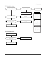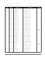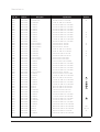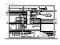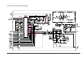
1
COLOR MONITOR
DP15HS/HT
DP17LS/LT
SERVICE
Manual
COLOR MONITOR
CONTENTS
1. Precautions
2. Product Specifications
3. Disassembly & Reassembly
4. Alignment & Adjustments
5. Troubleshooting
6. Exploded View & Parts List
7. Electrical Parts List
8. Block Diagram
EXIT
MENU
9. Wiring Diagram
10. Schematic Diagrams
Copyright
Trademarks
© 1999 by Samsung Electronics Co., Ltd.
Samsung is a registered trademark and
DP15H*/DP17L* and MacMaster Cable Adapter
are trademarks of Samsung Electronics Co., Ltd.
All rights reserved.
This manual may not, in whole or in part, be
copied, photocopied, reproduced, translated, or
converted to any electronic or machine readable
form without prior written permission of
Samsung Electronics Co., Ltd.
DP15H*/DP17L* Service Manual
First edition May 1999.
Macintosh, Centris, Quadra, Duo Dock, and
Power Macintosh are trademarks of Apple
Computer, Inc.
All other trademarks are the property of their
respective owners.
Printed in Korea.
ii
DP15H*/DP17L*
1 Precautions
1-1 Safety Precautions
WARNINGS
1. For continued safety, do not attempt to modify the
circuit board.
2.
Disconnect the AC power before servicing.
3.
When the chassis is operating, semiconductor
heatsinks are potential shock hazards.
1-1-1
2.
Inspect all protective devices such as nonmetallic
control knobs, insulating materials, cabinet backs,
adjustment and compartment covers or shields,
isolation resistor-capacitor networks, mechanical
insulators, etc.
3.
Leakage Current Hot Check (Figure 1-1):
WARNING: Do not use an isolation transformer during
this test.
Use a leakage current tester or a metering system
that complies with American National Standards
Institute (ANSI C101.1, Leakage Current for
Appliances), and Underwriters Laboratories (UL
Publication UL1410, 59.7).
4.
With the unit completely reassembled, plug the AC
line cord directly into a 120V AC outlet. With the
unitÕs AC switch first in the ON position and then
OFF, measure the current between a known earth
ground (metal water pipe, conduit, etc.) and all
exposed metal parts, including: metal cabinets,
screwheads and control shafts. The current
measured should not exceed 0.5 milliamp. Reverse
the power-plug prongs in the AC outlet and repeat
the test.
Servicing the High Voltage VR
and CRT :
WARNING:A high voltage VR replaced in the wrong
direction may cause excessive X-ray
emissions.
Caution: When replacing the high voltage
adjustment VR, it must be fixed by a
soldering iron after it is properly set.
1.
When servicing the high voltage system, remove
the static charge by connecting a 10 kohm resistor
in series with an insulated wire (such as a test
probe) between the chassis and the anode lead.
2.
If the HV VR requires adjustment, (a) Replace the
VR and adjust the high voltage to the specification.
(b) Use a soldering iron to melt the adjustment cap
on the HV VR to prevent any movement.
3.
When troubleshooting a monitor with excessively
HV, avoid being unnecessarily close to the monitor.
Do not operate the monitor for longer than is
necessary to locate the cause of excessive voltage.
4.
5.
6.
High voltage should always be kept at the rated
value, no higher. Only when high voltage is
excessive are X-rays capable of penetrating the shell
of the CRT, including the lead in glass material.
Operation at high voltages may also cause failure of
the CRT or high voltage circuitry.
When the HV regulator is operating properly, there
is no possibility of an X-ray problem. Make sure the
HV does not exceed its specified value and that it is
regulating correctly.
The CRT is especially designed to prohibit
X-ray emissions. To ensure continued X-ray
protection, replace the CRT only with one that is
the same or equivalent type as the original.
7.
Handle the CRT only when wearing shatterproof
goggles and after completely discharging the high
voltage anode.
8.
Do not lift the CRT by the neck.
1-1-2
Fire and Shock Hazard :
Before returning the monitor to the user, perform the
following safety checks:
1.
Inspect each lead dress to make certain that the
leads are not pinched or that hardware is not
lodged between the chassis and other metal parts in
the monitor.
DP15H*/DP17L*
(READING SHOULD
NOT BE ABOVE 0.5mA)
LEAKAGE
CURRENT
TESTER
DEVICE
UNDER
TEST
TEST ALL
EXPOSED METAL
SURFACES
2-WIRE CORD
ALSO TEST WITH
PLUG REVERSED
(USING AC ADAPTER
PLUG AS REQUIRED)
EARTH
GROUND
Figure 1-1. Leakage Current Test Circuit
1-1-4 Product Safety Notices
Some electrical and mechanical parts have special
safety-related characteristics which are often not
evident from visual inspection. The protection they give
may not be obtained by replacing them with
components rated for higher voltage, wattage, etc. Parts
that have special safety characteristics are identified by
! on schematics and parts lists. A substitute
replacement that does not have the same safety
characteristics as the recommended replacement part
might create shock, fire and / or other hazards. Product
safety is under review continuously and new
instructions are issued whenever appropriate.
Components identified by
on schematics and parts
lists must be sealed by a soldering iron after
replacement and adjustment.
1-1
1 Precautions
1-2 Servicing Precautions
WARNING1: First read the “Safety Precautions” section of this manual. If unforeseen circumstances
create conflict between the servicing precautions and safety precautions, always
follow the safety precautions.
WARNING2: A high voltage VR replaced in the wrong direction may cause excessive X-ray
emissions.
WARNING3: An electrolytic capacitor installed with the wrong polarity might explode.
1.
Servicing precautions are printed on the cabinet,
and should be followed closely.
2.
Always unplug the unitÕs AC power cord from the
AC power source before attempting to: (a) remove
or reinstall any component or assembly, (b)
disconnect PCB plugs or connectors, (c) connect all
test components in parallel with an electrolytic
capacitor.
3.
4.
Some components are raised above the printed
circuit board for safety. An insulation tube or tape
is sometimes used. The internal wiring is
sometimes clamped to prevent contact with
thermally hot components. Reinstall all such
elements to their original position.
After servicing, always check that the screws,
components and wiring have been correctly
reinstalled. Make sure that the area around the
serviced part has not been damaged.
5.
Check the insulation between the blades of the AC
plug and accessible conductive parts (examples:
metal panels, input terminals and earphone jacks).
6.
Insulation Checking Procedure: Disconnect the
power cord from the AC source and turn the power
switch ON. Connect an insulation resistance meter
(500 V) to the blades of the AC plug.
The insulation resistance between each blade of the
AC plug and accessible conductive parts (see
above) should be greater than 1 megohm.
7.
Never defeat any of the +B voltage interlocks. Do
not apply AC power to the unit (or any of its
assemblies) unless all solid-state heat sinks are
correctly installed.
8.
Always connect a test instrumentÕs ground lead to
the instrument chassis ground before connecting the
positive lead; always remove the instrumentÕs
ground lead last.
1-3 Electrostatically Sensitive Devices (ESD) Precautions
Some semiconductor (solid state) devices can be easily damaged by static electricity. Such components are commonly
called Electrostatically Sensitive Devices (ESD). Examples of typical ESD devices are integrated circuits and some fieldeffect transistors. The following techniques will reduce the incidence of component damage caused by static electricity.
1.
Immediately before handling any semiconductor
components or assemblies, drain the electrostatic
charge from your body by touching a known earth
ground. Alternatively, wear a discharging wriststrap device. To avoid a shock hazard, be sure to
remove the wrist strap before applying power to
the monitor.
6.
Do not remove a replacement ESD from its
protective package until you are ready to install it.
Most replacement ESDs are packaged with leads
that are electrically shorted together by conductive
foam, aluminum foil or other conductive materials.
7.
2.
After removing an ESD-equipped assembly, place it
on a conductive surface such as aluminum foil to
prevent accumulation of an electrostatic charge.
Immediately before removing the protective
material from the leads of a replacement ESD,
touch the protective material to the chassis or
circuit assembly into which the device will be
installed.
3.
Do not use freon-propelled chemicals. These can
generate electrical charges sufficient to damage
ESDs.
Caution: Be sure no power is applied to the
chassis or circuit and observe all
other safety precautions.
4.
Use only a grounded-tip soldering iron to solder or
desolder ESDs.
5.
Use only an anti-static solder removal device. Some
solder removal devices not classified as Òanti-staticÓ
can generate electrical charges sufficient to damage
ESDs.
1-2
8.
Minimize body motions when handling
unpackaged replacement ESDs. Motions such as
brushing clothes together, or lifting your foot from
a carpeted floor can generate enough static
electricity to damage an ESD.
9.
Indicates ESDs on the Schematic Diagram in
this manual.
DP15H*/DP17L*
2 Product Specifications
2-1 Specifications
Item
Description
Picture Tube:
15-Inch (38 cm): 13.8-inch (35 cm) viewable, 17-Inch (43 cm): 16-inch (40.6 cm) viewable,
Full-square flat-face tube, 90˚ Deflection, Semi- tint, Non-glare, Invar shadow mask,
Anti-static silica coating, 0.28 mm Dot pitch
Scanning Frequency
Horizontal : 30 kHz to 70 kHz (Automatic)
Vertical : 50 Hz to 160 Hz (Automatic)
Display Colors
Unlimited colors
Maximum Resolution
Horizontal : 1280 Dots
Input Video Signal
Analog, 0.7 Vp-p positive at 75 Ω, internally terminated
Input Sync Signal
Separate Sync: TTL level positive/negative
Maximum Pixel Clock rate
110 MHz
Active Display
15” ; Horizontal : 267 mm ± 4 mm, Vertical : 200.5 mm ± 4 mm
17” ; Horizontal : 306 mm ± 4 mm (4:3 ratio), Vertical : 230.5 mm ± 4 mm
Input Voltage
AC 90 to 264 Volts, 60 Hz or 50 Hz ± 3 Hz
Power Consumption
80 Watt (max) : 15”, 90 Watt (max) : 17”
Dimensions
(W x D x H)
Unit ;
15” : 14.25 x 15.11 x 15.11 Inches (362 x 384 x 384 mm)
17” : 16.22 x 16.54 x 16.36 Inches (412 x 420 x 415.5 mm)
Carton ; 15” : 17.87 x 19.57 x 17.52 Inches (454 x 497 x 445 mm)
17” : 21.02 x 21.73 x 18.39 Inches (534 x 552 x 467 mm)
Weight
(Net/Gross)
15” : 26.5 lbs (12.0 kg) / 31.5 lbs (14.3 kg)
17” : 33.1 lbs (15.0 kg) / 38.6 lbs (17.5 kg)
Environmental Considerations
Operating Temperature :
32°F to 104°F (0°C to 40°C)
Humidity : 10 % to 80 %
Storage Temperature
: -4°F to 113°F (-20°C to 45°C)
Humidity : 5 % to 95 %
Vertical : 1024 Lines
• Above models comply with SWEDAC (MPR II) recommendations for reduced electromagnetic fields.
• Designs and specifications are subject to change without prior notice.
DP15H*/DP17L*
2-1
2 Product Specifications
2-2 Pin Assignments
Sync
Type
Separate
Macintosh
Pin No.
1
Red
GND-R
2
Green
Red
3
Blue
H/V Sync
4
N-C
Sense 0
5
DDC Return
Green
6
GND-R
GND-G
7
GND-G
Sense 1
8
GND-B
Reserved
9
N-C
Blue
10
GND-Sync/Self-raster
Sense 2
11
N-C
GND
12
DDC Data
V-Sync
13
H-Sync
GND-B
14
V-Sync
GND
15
DDC Clock
H-Sync
5
15
Figure 2-1. Male Type
2-2
Figure 2-2. Male Type
DP15H*/DP17L*
2 Product Specifications
2-3 Timing Chart
This section of the service manual describes the timing that the computer industry recognizes as standard
for computer-generated video signals.
Table 2-1. Timing Chart
Mode
IBM
VESA
VGA2/70 Hz VGA3/60 Hz
720 x 400
640 x 480
Timing
640/75 Hz
640 x 480
640/85 Hz
640 x 480
800/75 Hz
800 x 600
800/85 Hz
800 x 600
1024/75 Hz
1024 x 768
1024/85 Hz
1024 x 768
fH (kHz)
31.469
31.469
37.500
43.269
46.875
53.674
60.023
68.677
A µsec
31.777
31.778
26.667
23.111
21.333
18.631
16.660
14.561
B µsec
3.813
3.813
2.032
1.556
1.616
1.138
1.219
1.016
C µsec
1.907
1.907
3.810
2.222
3.232
2.702
2.235
2.201
D µsec
25.422
25.422
20.317
17.778
16.162
14.222
13.003
10.836
E µsec
0.636
0.636
0.508
1.556
0.323
0.569
0.203
0.508
fV (Hz)
70.087
59.940
75.000
85.008
75.000
85.061
75.029
84.997
O msec
14.268
16.683
13.333
11.764
13.333
11.756
13.328
11.765
P msec
0.064
0.064
0.080
0.671
0.064
0.056
0.050
0.044
Q msec
1.080
1.048
0.427
0.578
0.448
0.503
0.466
0.524
R msec
12.711
15.253
12.800
11.093
12.800
11.179
12.795
11.183
S msec
0.413
0.318
0.027
0.023
0.021
0.019
0.017
0.015
28.322
25.175
31.500
49.500
36.000
56.250
78.750
94.500
Polarity
H.Sync
Negative
Negative
Negative
Negative
Positive
Positive
Positive
Positive
V.Sync
Positive
Negative
Negative
Negative
Positive
Positive
Positive
Positive
Remark
Separate
Separate
Separate
Separate
Separate
Separate
Separate
Separate
Clock
Frequency
(MHz)
Separate Sync
Horizontal
Vertical
Video
Video
Video
Video
CC
DD
E E
Q
RR
Q
S S
Sync
Sync
Sync
Sync
BB
PP
AA
O O
A : Line time total
B : Horizontal sync width
O : Frame time total
P : Vertical sync width
C : Back porch
D : Active time
Q : Back porch
R : Active time
E : Front porch
DP15H*/DP17L*
S : Front porch
2-3
2 Product Specifications
Memo
2-4
DP15H*/DP17L*
4 Alignment and Adjustments
This section of the service manual explains how to make permanent adjustments to the monitor. Directions
are given for adjustments using the monitor Interface Board Ver. 2.0 and software (Softjig).
4-1 Adjustment Conditions
Caution: Changes made without the Softjig are saved only to the user mode settings. As such, the
settings are not permanently stored and may be inadvertently deleted by the user.
4-1-1 Before Making Adjustments
.4-1-2 Required Equipment
4-1-1 (a) ORIENTATION
When servicing, always face the monitor to the
east.
The following equipment may be necessary for
adjustment procedures:
4-1-1 (b) MAGNETIC FIELDS
Whenever possible, use magnetic field isolation
equipment such as a Helmholtz field to surround
the monitor. If a Helmholtz field is not available,
frequently degauss the unit under test.
Caution: Other electrical equipment may cause
external magnetic fields which may
interfere with monitor performance.
Use an external degaussing coil to limit magnetic
build up on the monitor. If an external degaussing
coil is not available, use the internal degaussing
circuit. However, do not use the internal
degaussing circuit more than once per 30 minutes.
4-1-1 (c) WARM-UP TIME
The monitor must be on for 30 minutes before
starting alignment. Warm-up time is especially
critical in color temperature and white balance
adjustments.
4-1-1 (d) SIGNAL
Analog, 0.7 Vp-p positive at 75 ohm, internal
termination
Sync: Separate
(TTL level negative/positive)
4-1-1 (e) SCANNING FREQUENCY
Horizontal: 30 kHz to 70 kHz (Automatic)
Vertical:
50 Hz to 160 Hz (Automatic)
4-1-2 (a) DISPLAY CONTROL ADJUSTMENT
1. Non-metallic (Ð) screwdriver:
1.5, 2.5, 3 mm
2. Non-metallic (+) screwdriver:
1.5, 2.5, 3 mm
3. Digital Multimeter (DMM), or
Digital Voltmeter
4. Signal generator, or
DM200 software
5. Software: Softjig or DM200
6. Interface Board Ver. 2.0 Code No.
BH81-90001K
7. Parallel communications cable (25-pin to
25-pin); Code No. BH81-90001H
8. Signal cable (15-pin to 15-pin cable with
additional 3-pin connector); Code No.
BH81-90001J
9. 5 V DC adapter, not supplied
10. Personal computer
Note: Softjig AssÕy (includes items 6, 7 and 9)
Code No. BH81-90001L
4-1-2 (b) COLOR ADJUSTMENTS
1. All equipment listed in 4-1-2 (a), above
2. Color analyzer, or any luminance
measurement equipment
Unless otherwise specified, adjust at the
17Ó: 1024 x 768 mode (68 kHz/85 Hz),
15Ó: 800 x 600 mode (54 kHz/85 Hz) signals.
Refer to Table 2-1 on page 2-3.
DP15H*/DP17L*
4-1
4 Alignment and Adjustments
4-1-3 Connecting the SoftJig
Connect the monitor to the signal generator and/
or PC as illustrated in Figures 4-1 and 4-2.
Note: The signal cable connector which includes
the 3-wire cable must connect to the
monitor. If you use Setup 2 (PC only, no
signal generator) you can only make
adjustments to the signal timing available
on that computer system. To make
corrections to all factory timings requires
the use of an additional signal generator.
MONITOR
INTERFACE
BOARD VER. 2.0
3-WIRE CABLE
5V DC
ADAPTOR
SIGNAL CABLE
PARALLEL CABLE
PC
D-SUB
CONNECTOR
MONITOR
INTERFACE
BOARD VER. 2.0
5V DC
ADAPTOR
SIGNAL CABLE
Figure 4-2. Setup 2, Without Signal Generator
3-WIRE
CABLE
PARALLEL CABLE
PC
SIGNAL
GENERATOR
Figure 4-1. Setup 1, With Signal Generator
4-2
DP15H*/DP17L*
4 Alignment and Adjustments
4-2 Display Control Adjustments
4-2-1 HIGH VOLTAGE ADJUSTMENT
Signal:
Table 4-1
CRT type
1024 x 768 (68 kHz/85 Hz) (17Ó)
800 x 600 (54 kHz/85 Hz) (15Ó)
Display image: DonÕt care
Contrast:
Minimum
Brightness:
Minimum
Limit:
26.5 kV ± 0.2 kV (17Ó)
25 kV ± 0.2 kV (15Ó)
exception) 26.0 kV ± 0.2 kV for 17Ó SDD CRT that
the DY type is DMX-1791AT
Measure the hight voltage level at the anode cap.
High voltage should be within the limit as above.
If the high voltage needs adjustment use the
following procedure.
PROCEDURE
1. Turn the power off and disconnect the AC line
cord from the power source.
2. Turn the power on after connecting high
voltage Probe.
3. Using the jig, adjust the high voltage to the
specification.
* High Voltage Adjustment PROCEDURE using Softjig
① Select matching model name in ÒModelÓ field.
➁ Select Ò @7: Zero BeamÓ in menu after
selecting ÒExtra 1Ó
17”
15”
Screen Voltage
M41QAR361X11*(*)
M41QAQ261X11*(*)
M41LFQ903X28(L), etc
M41EHN325X160/3F**U
M41EHN323X160/3F**U
M41LLJ507XX43*(F5), (F5W3)
M41LLH507XX43*(F5)
M36QAM351X11*(*)
M36LGE128X2**(*)
M36KUK35X02(*/LP), etc
480V ± 10V
500V ± 10V
630V ± 10V
560V ± 10V
600V ± 10V
520V ± 10V
4-2-3 CENTER RASTER
Adjust SW401 so that the back raster comes to the
center when you apply each basic mode for 15Ó
and 17Ó.
4-2-4 Centering
Centering means to position the center point of
the display in the middle of the display area.
Horizontal size and position and vertical size and
position control the centering of the display.
Adjust the horizontal size and vertical size to their
optimal settings: 306 mm (H) x 230 mm (V) for
17Ó, 267 mm (H) x 200 mm (V) for 15Ó.
➂ Adjust high voltage using control bar after
selecting ÒHV MINÓ
Adjust the horizontal position and vertical
position to ² 4.0 mm of the center point of the
screen.
➃ Turn the power off/on after adjustment
finished.
|A-B| ² 4.0 mm.
C
➄ Check the high voltage has been fixed with
adjusted value after reselecting Ò@7: Zero BeamÓ.
4-2-2 SCREEN VOLTAGE ADJUSTMENT
CONDITIONS
Signal:
Display image:
Contrast:
Brightness:
Limit:
Screen Voltage adjustment procedure using softjig
is all the same as 4-2-1 but selecting ÒG2 CONTÓ
on the contrary to ÒHV MINÓ.
DP15H*/DP17L*
DISPLAY AREA
A
B
EDGE OF BEZEL
D
1024 x 768 (68 kHz/85 Hz) (17Ó)
800 x 600 (54 kHz/85 Hz) (15Ó)
DonÕt care
Minimum
Minimum
26.5 kV ± 0.2 kV (17Ó)
25 kV ± 0.2 kV (15Ó)
|C-D| ² 4.0 mm.
Figure 4-3. Centering
* In Softjig window, ÒGeometryÓ has to be
selected for GD adjustment.
4-2-4 (a) HORIZONTAL SIZE ADJUSTMENT
CONDITIONS
Scanning frequency:
Display image:
Brightness:
Contrast:
68 kHz/85 Hz (17Ó)
54 kHz/85 Hz (15Ó)
Crosshatch pattern
Maximum
Maximum
4-3
4 Alignment and Adjustments
Use control bar after selecting ÒH-SIZEÓ in left
menu to adjust the horizontal size of the display
pattern to 306 mm (17Ó) and 267 mm (15Ó).
(Tolerance: ± 3 mm.)
Table 4-2. Standard Modes Linearity: 640x480/75Hz,
800x600/85Hz and 1024x768/85Hz
Figure 4-5. Pinbalance
Standard Modes Linearity
If ÒH-SIZEÓ is not enough to adjust it, select
ÒSIZE B+Ó by turns.
4-2-4 (b) VERTICAL SIZE ADJUSTMENT
CONDITIONS
Scanning frequency:
Display image:
Brightness:
Contrast:
68 kHz/85 Hz (17Ó)
54 kHz/85 Hz (15Ó)
Crosshatch pattern
Maximum
Maximum
Each block (10 %)
4:3
5:4
CONDITIONS
Scanning frequency:
Display image:
68 kHz/85 Hz (17Ó)
54 kHz/85 Hz (15Ó)
Crosshatch pattern
Use control bar after selecting ÒH-POSITIONÓ in
left menu to center the horizontal image on the
raster.
4-2-4 (d) VERTICAL POSITION ADJUSTMENT
CONDITIONS
Scanning frequency:
Display image:
68 kHz/85 Hz (17Ó)
54 kHz/85 Hz (15Ó)
Crosshatch pattern
Use control bar after selecting ÒV-POSITIONÓ in
left menu to center the vertical image on the
raster.
4-2-5 Linearity
Linearity affects the symmetry of images as they
appear on the screen. Unless each row or column
of blocks in a crosshatch pattern is of equal size,
or within the tolerances shown in Tables 4-2 and
4-3, an image appears distorted, elongated or
squashed.
4-4
Horizontal: 18.2~20.1 Horizontal: Less than 0.77 mm
Vertical : 18.2~20.1 Vertical : Less than 0.77 mm
Horizontal: 17.1~18.9 Horizontal: Less than 0.72 mm
Vertical : 18.2~20.1 Vertical : Less than 0.77 mm
Table 4-3. Other Modes Linearity: VGA, SVGA, XGA,
MAC, etc.
Use control bar after selecting ÒV-SIZEÓ in left
menu to adjust the vertical size of the display
pattern to 230 mm (17Ó) and 200 mm (15Ó).
(Tolerance: ± 3 mm.)
4-2-4 (c) HORIZONTAL POSITION ADJUSTMENT
Difference between
adjacent blocks (4 %)
Supported Timing Mode
Each block (10 %)
4:3
5:4
Difference between
adjacent blocks (5 %)
Horizontal: 17.8~20.5
Horizontal: Less than 0.96 mm
Vertical : 17.8~20.5
Vertical : Less than 0.96 mm
Horizontal: 16.7~19.2
Horizontal: Less than 0.90 mm
Vertical : 17.8~20.5
Vertical : Less than 0.96 mm
4-2-5 (a) HORIZONTAL LINEARITY ADJUSTMENT
CONDITIONS
Scanning frequency:
68 kHz/85 Hz (17Ó)
54 kHz/85 Hz (15Ó)
Display image:
Crosshatch pattern
Brightness:
Maximum
Contrast:
Maximum
To adjust the Horizontal Linearity, refer to Tables
4-2 and 4-3 for the tolerance range.
Increase or decrease H_LIN to optimize the
image.
4-2-5 (b) VERTICAL LINEARITY ADJUSTMENT
CONDITIONS
Scanning frequency:
68 kHz/85 Hz (17Ó)
54 kHz/85 Hz (15Ó)
Display image:
Crosshatch pattern
Brightness:
Maximum
Contrast:
Maximum
To adjust the Vertical Linearity, refer to Tables 4-2
and 4-3 for the tolerance range.
Use control bar after selecting ÒV-LINEARITY
BALÓ in left menu to optimize the image.
DP15H*/DP17L*
4 Alignment and Adjustments
4-2-6 Trapezoid Adjustment
4-2-9 Side Pincushion Adjustment
CONDITIONS
Scanning frequency:
CONDITIONS
Scanning frequency:
Display image:
Brightness:
Contrast:
68 kHz/85 Hz (17Ó)
54 kHz/85 Hz (15Ó)
Crosshatch pattern
Maximum
Maximum
Display image:
Use control bar after selecting ÒTRAPEZOIDÓ in
left menu to make the image area rectangular.
68 kHz/85 Hz (17Ó)
54 kHz/85 Hz (15Ó)
Crosshatch pattern
Use control bar after selecting ÒPINCUSHIONÓ in
left menu to straighten the sides of the image area.
| C1 |, | C2 | ≤ 2.0 mm, | D1 |, | D2 | ≤ 2.0 mm.
C2
| A - B | < 4 mm
A
A
D1
B
D2
B
Figure 4-4. Trapezoid
C1
4-2-7 Pinbalance Adjustment
CONDITIONS
Scanning frequency:
Display image:
Brightness:
Contrast:
D1
Figure 4-7. Pincushion
4-2-10 Tilt Adjustment
68 kHz/85 Hz (17Ó)
54 kHz/85 Hz (15Ó)
Crosshatch pattern
Maximum
Maximum
D2
CONDITIONS
Scanning Frequency:
Display image:
Brightness:
Contrast:
D1
Figure 4-5. Pinbalance
Use control bar after selecting ÒPINBALANCEÓ in
left menu to optimize the image.
4-2-8 Parallelogram Adjustment
CONDITIONS
Scanning Frequency:
Display image:
Brightness:
Contrast:
68 kHz/85 Hz (17Ó)
54 kHz/85 Hz (15Ó)
Crosshatch pattern
Maximum
Maximum
Use control bar after selecting ÒROTATIONÓ in
left menu to correct the tilt of the display.
4-2-11 Degauss
No adjustments are available for the degaussing
circuit. The degaussing circuit can effectively
function only once per 30 minutes.
4-2-12 To Delete the User Mode Data
68 kHz/85 Hz (17Ó)
54 kHz/85 Hz (15Ó)
Crosshatch pattern
Maximum
Maximum
Use control bar after selecting ÒPARALLELÓ in
left menu to make the image area rectangular.
To delete the adjustment data from the user
modes, click Ò@4: USER DELETEÓ in right ment.
4-2-13 Save the Data
To save the adjustment data for a mode, press
Ò@3: ALL MODE SAVEÓ in right ment.
4 mm
Figure 4-6. Parallelogram
DP15H*/DP17L*
4-5
4 Alignment and Adjustments
4-3 Color Adjustments
CAUTION:Check below condition before color
adjustment
Video signal : Analog 0.7 Vp-p (at 75 Ω)
Sync : TTL level (H, V seperate signal)
* Select ÒColorÓ in Softjig menu for color adjustment.
4-3-1 Color Coordinates (Temperature)
Color temperature is a measurement of the
radiant energy transmitted by a color. For
computer monitors, the color temperature refers
to the radiant energy transmitted by white. Color
coordinates are the X and Y coordinates on the
chromaticity diagram of wavelengths for the
visible spectrum.
CONDITIONS
Measurement instrument: Color analyzer
Scanning frequency: 68 kHz/85 Hz (17Ó)
54 kHz/85 Hz (15Ó)
Display image:
White flat field at
center of display area
Luminance:
Maximum
PROCEDURE
Use the directions in sections 4-3-2 through 4-3-3
to adjust the color coordinates for:
9300K to x = 0.283 ± 0.02, y = 0.298 ± 0.02
6500K to x = 0.313 ± 0.02, y = 0.329 ± 0.02
4-3-2 Color Adjustments for 9300K
4-3-2 (a) BACK RASTER COLOR ADJUSTMENT
CONDITIONS
Scanning frequency:
Display image:
Brightness:
Contrast:
68 kHz/85 Hz (17Ó)
54 kHz/85 Hz (15Ó)
Back raster pattern
Maximum
Maximum
1. Select Ò@1: CHANNEL 1Ó in right menu to
control the color for 9300K.
4-3-2 (b) WHITE BALANCE ADJUSTMENT
CONDITIONS
Scanning frequency:
68 kHz/85 Hz (17Ó)
54 kHz/85 Hz (15Ó)
Display image:
White box pattern
Brightness:
0.06ft-L at Back Raster
Pattern Display
Contrast:
Maximum
1/3H-1/2H
FRONT BEZEL OPENING
BACK RASTER
1/3V-1/2V
WHITE WINDOW
Figure 4-8. White Box Pattern
1. Use control bar after selecting ÒRED GAINÓ,
ÒGREEN GAINÓ and ÒBLUE GAINÓ to adjust
the luminance to 45 ft-L (15Ó) and 46 ft-L
(17Ó) with the color coordinates ranged for
9300K to x = 0.283 ± 0.02, y = 0.298 ± 0.02.
exception) 17Ó SDD CRT type-named
(*/S-2) : 42ft-L.
4-3-2 (c) ABL ADJUSTMENT
CONDITIONS
Scanning frequency:
Display image:
Brightness:
Contrast:
68 kHz/85 Hz (17Ó)
54 kHz/85 Hz (15Ó)
Full white pattern
Maximum
Maximum
FRONT BEZEL OPENING
BACK RASTER
WHITE WINDOW
Figure 4-9. Full White Pattern
2. Adjust the luminance of the back raster to
between 0.5 to 0.7 ft-L using contron bar after
selecting ÒGREEN CUTOFFÓ in the menu.
1. Check the ABL. If it is not within the
specifications, use the ABL controls to adjust
it. (15Ó: 33 ± 1 ft-L, 17Ó: 36 ± 1 ft-L )
3. Use control bar after selecting ÒBLUE
CUTOFFÓ in left menu to set the ÒyÓ
coordinate to 0.298 ± 0.02.
3. Select Ò@6: ALL COLOR SAVEÓ to save the
CH2.
2. Select Ò@4: COLOR SAVEÓ to save the data.
4. Use control bar after selecting ÒRED
CUTOFFÓ in left menu to 0.283 ± 0.02.
* If color values would not be matched desirable
values, repeat sequence 3 and 4 after readjusting
ÒGREEN CUTOFFÓ control a little different.
4-6
DP15H*/DP17L*
4 Alignment and Adjustments
4-3-2 (d) WHITE BALANCE ADJUSTMENT VERIFICATION
CONDITIONS
Scanning frequency:
Display image:
X-Y Coordinates:
ABL Luminance
Brightness:
Contrast:
68 kHz/85 Hz (17Ó)
54 kHz/85 Hz (15Ó)
Back raster pattern
Full White Pattern
x = 0.283 ± 0.02,
y = 0.298 ± 0.02
Refer to 4-3-2(c)
Maximum
5 ft-L, 24 ft-L
1. Check whether the color coordinates of the
back raster satisfy the above spec.
If they do not, return to 4-3-2 (a) and readjust
all settings.
PROCEDURE
Measure luminance at nine points on the display
screen (see figure below).
Figure 4-10. Luminance Uniformity Check Locations
4-3-4 Focus Adjustment
CONDITIONS
Scanning frequency:
2. Display a full white pattern.
3. Select ÒGeometryÓ in softjig menu.
4. Select Ò@7: 5-ft Ò in right menu.
5. Check whether the white coordinates of the
video meet the above coordinates spec.
6. Select Ò@8: 24-ft Ò in right menu.
7. Check whether the white coordinates of the
video satisfies the above spec.
If they do not, return to 4-3-2 (a) and readjust
all settings.
Select ÒColorÓ and click Ò@2: CHANNEL 2Ó
for color ajdustment for 6500K
Repeat the sequence of 9300K adjustment.
The luminance values the same as 9300K, but
the color coordinated of back raster and white
box are : x = 0.313 ± 0.02 y = 0.329 ± 0.02
4-3-3 Luminance Uniformity Check
Display image:
Brightness:
Contrast:
68 kHz/85 Hz (17Ó)
54 kHz/85 Hz (15Ó)
(1024 x 768)
ÒHÓ character pattern
Cut off point
Maximum
PROCEDURE
1. Adjust the Focus VR on the FBT to display the
sharpest image possible.
2. Use Locktite to seal the Focus VR in position.
4-3-5 Color Purity Adjustment
Color purity is the absence of undesired color.
Conspicuous mislanding (unexpected color in a
uniform field) within the display area shall not be
visible at a distance of 50 cm from the CRT
surface.
CONDITIONS
Orientation:
Scanning frequency:
Monitor facing east
68 kHz/85 Hz (17Ó)
54 kHz/85 Hz (15Ó)
White flat field
Cut off point at the center
of the display area
Luminance is considered uniform only if the ratio
of lowest to highest brightness areas on the screen
is not less than 7.5:10.
Display image:
Luminance:
CONDITIONS
Scanning frequency:
Note: Color purity adjustments should only be
attempted by qualified personnel.
Display image:
Brightness:
Contrast:
DP15H*/DP17L*
68 kHz/85 Hz (17Ó)
54 kHz/85 Hz (15Ó)
(1024 x 768)
White flat field
Cut off point at 24 ft-L
Maximum
4-7
4 Alignment and Adjustments
PROCEDURE
For trained and experienced service technicians
only.
Use the following procedure to correct minor
color purity problems:
1. Make sure the display is not affected by
external magnetic fields.
2. Very carefully break the glue seal between the
2-pole purity convergence magnets (PCM), the
band and the spacer (see Figures 4-12).
3. Make sure the spacing between the PCM
assembly and the CRT stem is 29 mm ± 1 mm.
4. Display a green pattern over the entire display
area.
5. Adjust the purity magnet rings on the PCM
assembly to display a pure green pattern.
(Optimum setting: x = 0.295 ± 0.015,
y = 0.594 ± 0.015)
6. Repeat steps 4 and 5 using a red pattern and
then again, using a blue pattern.
Table 4-4. Color Purity Tolerances
Red:
x = 0.640 ± 0.015
y = 0.323 ± 0.015
Green:
x = 0.295 ± 0.015
y = 0.594 ± 0.015
Blue:
x = 0.142 ± 0.015
y = 0.066 ± 0.015
(For 9300K color adjustment: x = 0.283 ± 0.02, y = 0.298 ± 0.02)
7. When you have the PCMs properly adjusted,
carefully glue them together to prevent their
movement during shipping.
4-8
DP15H*/DP17L*
5 Troubleshooting
5-1 Parts Level Troubleshooting
Notes: 1. If a picture does not appear, fully rotate the brightness and contrast controls clockwise and reinspect.
2. Check the following circuits.
• No raster appears: Power circuit, Horizontal output circuit.
• High voltage develops but no raster appears: Video output circuits.
• High voltage does not develop: Horizontal output circuits.
5-1-1 No Power Supply
WAVEFORMS
Check and replace D601, FH1
1 100 V (IC601, #1)
Chirping noise exists?
Yes
Check and replace IC601.
No
Repeating start?
CH1 P-P = 100 V
Yes
CH1 RMS = 350.2 V
Check and replace D606.
No
1
IC601 Pin 1 waveform is right?
No
Check and replace D614, IC601,
Q602, ZD601.
No
Check and replace IC201, IC301,
IC401, Q402, Q404.
Yes
C622 Voltage is 13 V ± 0.5V?
Yes
Normal operation
No
Replace Main board.
Yes
Verify voltages.
Yes
Done.
DP15H*/DP17L*
5-1
5 Troubleshooting
5-1-2 DPMS Failure
WAVEFORMS
Check signal source
H/V sync video level.
2 100V (IC601, #1)
Make No H/V sync (power off
mode)
CH1 P-P = 100V
LED blinks
No
CH1 RMS = 325.8 V
Check IC201 Pin 40.
Yes
+12 V line off
No
Check IC201 Pin 5.
Yes
IC602 Pin 4
voltage exists?
Yes
Check IC201 Pin 6.
Check and replace IC602.
No
2
IC601 Pin 1 output
voltage exists?
No
Refer to 5-1-1 No Power Supply.
Yes
Done
5-2
DP15H*/DP17L*
5 Troubleshooting
5-1-3 H_Deflection Failure
3
Does PWM output signal appear
at Pin 6 (H_out) of IC401?
No
Yes
Does DC 12V appear at
Pin 10 of IC401?
No
Check 12 V line.
Yes
WAVEFORMS
Check IC401.
4
Does Horizontal paluse signal
appear at at Pin 8 of IC401?
No
3 2.00 V (IC401, #6)
Check IC401.
CH1 P-P = 2.00V
Yes
CH1 RMS = 5.868V
4 1.00V (IC401, #8)
Does 110 Vp-p signal appear
5
at Collector of Q403?
No
Check Q443.
No
CH1 P-P = 1.00V
Check Q402, Q404, T401.
CH1 RMS = 1.298V
5 20.0 V (Q403, Collector)
7-1-4 S Correction Failure
CH1 P-P = 20.0 V
CH1 RMS = 46.80V
Check S1 ~ S3 signal.
S1~S3 signals are right at each
frequency block?
No
Check and replace IC201.
Yes
Check and replace Q404, Q409, Q410,
Q414, Q415, Q416
DP15H*/DP17L*
5-3
5 Troubleshooting
5-1-5 H_Lin. Failure
IC201 Pin 21 voltage varies with
different H_Lin. DAC values?
No
Replace IC201.
Yes
IC603 Pin 9 voltage varies with
different H_Lin. DAC values?
No
Check +12 V, –10 V line.
Check some parts around IC603.
Yes
Check Q412, Q413, T402.
5-1-6 Invariable H_Size
IC401 Pin 6 voltage varies with
different B_Out DAC values?
No
Check and replace IC401.
Yes
Q402 Gate output duty varies with
different B_Out DAC values?
No
Check some parts around Q402,
IC401 Pin 3 ~ 6.
5-1-7 Abnormal H_Size
IC401 Pin 11 output duty
varies with different B+ offset
DAC values?
No
WAVEFORMS
Check and replace IC201.
6 200 V (Q408, Collector)
Yes
6
Q408 Collector waveform is
right?
No
Check and replace Q405, Q406, Q407,
Q408.
CH1 P-P = 200V
CH1 RMS = 387.2V
Yes
Check some parts around D409, L401.
5-4
DP15H*/DP17L*
5 Troubleshooting
5-1-8 Side Pin or Trap Failure
7
IC401 Pin 11 output exists?
No
WAVEFORMS
Check and replace IC401.
7 1.00 V (IC401, #11)
Yes
Refer to 5-1-7 Abnormal H_Size.
CH1 P-P = 1.00V
CH1 RMS = 3.008 V
5-1-9 Para. or Pin Balance Failure
IC401 Pin 11 output varies with
different DAC values?
Yes
Refer to 5-1-7 Abnormal H_Size.
No
Replace IC401.
5-1-10 Tilt Failure
Check tilt connector connection
IC201 Pin 20 output duty varies
with different DAC values?
No
Check and replace IC201.
Yes
IC603 Pin 13 output varies with
different DAC values?
No
Check and replace IC603.
Yes
Check and replace Q301, Q302.
DP15H*/DP17L*
5-5
5 Troubleshooting
5-1-11 V Deflection Failure
13 V, –10 V line is on?
No
WAVEFORMS
Refer to 5-1-1 No Power Supply
8 500 V (IC401, #12)
Yes
8
IC401 Pin 12 output exists?
No
Check and replace IC401.
CH1 P-P = 500 V
9 10.0 V (IC301, #6)
Yes
9
IC301 Pin 6 output exists?
CH1 RMS = 1.425 V
No
Check and replace some parts
around IC301.
Yes
CH1 P-P = 10.0 V
CH1 RMS = 5.06 V
Check DY connector connection.
5-1-12 V Size or Pos. Variation Failure
IC401 Pin 12 output varies with
different DAC values?
No
Check and replace IC201, IC401.
Yes
Check and replace IC301.
5-6
DP15H*/DP17L*
5 Troubleshooting
5-1-13 High Voltage Failure
3
IC401 Pin 6 OSC pulse exists?
No
WAVEFORMS
Check and replace IC401
and +12 V line.
3 2.00 V (IC401, #6)
Yes
10
Q402 Gate driving pulse exists?
No
Check and replace Q401.
CH1 P-P = 2.00 V
11 2.00 V (Q402, Gate)
Yes
11
Q402 Drain pulse exists?
CH1 RMS = 5.868 V
No
Check and replace Q403,
L402.
Yes
CH1 P-P = 2.00 V
CH1 RMS = 7.692V
11 50.0 V (Q402, Drain)
Done
5-1-14 ABL Failure
CH1 P-P = 50.0 V
CH1 RMS = 73.7V
Input full white pattern to monitor.
IC101 Pin 12 input exists and
varies with different patterns?
Yes
Check and replace IC101.
No
Check CN102.
No
T501 Pin 8 output exists?
No
Check and replace T501.
Yes
IC201 Pin 26 output exists and
varies with different patterns?
No
Check and replace IC201.
Yes
Done
DP15H*/DP17L*
5-7
5 Troubleshooting
5-1-15 Dynamic Focus Failure
12
IC401 Pin 32 output is right?
No
WAVEFORMS
Replace the IC401.
12 2.00 V (IC401, #32)
Yes
Some parts around Q551 are right?
No
Replace failed part.
CH1 P-P = 2.00V
Yes
13
T502 Pin 6 input is right?
CH1 RMS = 6.124V
13 50.0 V (T502, #6)
No
Check and replace C432.
Yes
CH1 P-P = 50.0V
14
T502 Pin 1 output is right?
No
Replace the T502.
CH1 RMS = 75.6V
14 100 V (T502, #1)
No
Check the connection between FBT
Focus pin, CRT Socket PCB.
5-8
CH1 P-P = 100V
CH1 RMS = 124.0V
DP15H*/DP17L*
5 Troubleshooting
5-1-16 No Video
WAVEFORMS
Check signal cable and connection.
15 1.00 V (IC101, #5, 8, 10)
15
IC101 Pins 5, 8 and 10 inputs
are right?
No
Check the signal cable connection.
Yes
16
IC101 Pins 21, 24 and 26
outputs are right?
CH1 P-P = 1.00V
No
CH1 RMS = 2.452V
16 1.00 V (IC101, #21,24,26)
Check I2C bus and +12 V line.
Yes
17
IC103 Pins 1, 2 and 3 outputs
are right?
No
Check +12 V, +72 V line.
Check and replace IC103.
CH1 P-P = 1.00V
CH1 RMS = 2.792V
17 20.0 V (IC103, #1, 2, 3)
Yes
Cathode DC levels are right?
No
Check +72 V line.
Check and replace QR01, QR02,
QG01, QG02, QB01, QB02.
CH1 P-P = 20.0V
CH1 RMS = 40.52V
Yes
G2 voltage is right?
No
Check G2 wire, CRT Socket board,
and FBT.
Yes
Change CRT.
Done.
DP15H*/DP17L*
5-9
5 Troubleshooting
5-1-17 Micom Failure
IC201 Pin 11 input voltage is 5V?
No
WAVEFORMS
Check IC604.
18 1.00 V (IC201, #13, 14)
Yes
18
IC201 Pins 13 and 14 inputs
are right?
No
Check C202, C203, X201.
CH1 P-P = 1.00 V
CH1 RMS = 2.108V
Yes
IC201 Pin 18 input is right?
No
Check IC605.
Yes
All in/output values are right?
No
Replace IC201.
No
Done
5-10
DP15H*/DP17L*
5 Troubleshooting
5-1-18 OSD Failure
WAVEFORMS
Check CN104 and connector Ass’y.
19 1.00 V (IC104, #6)
19
IC104 Pin 6 input is right?
No
Check and replace Q102.
Check CN102 Pin 14.
Yes
20
IC104 Pin 17 input is right?
CH1 P-P = 1.00V
No
Check and replace Q101.
Check CN102 Pin 8.
CH1 RMS = 4.516V
20 1.00 V (IC104, #17)
Yes
IC104 Pins 7 and 8 inputs are
right?
No
Check IC201 Pins 41 and 42.
CH1 P-P = 1.00V
CH1 RMS = 5.024V
21 1.00 V (IC101, #21.24.26)
Yes
IC104 Pins 12, 13 and 14
outputs are right?
No
Check and replace IC104.
CH1 P-P = 1.00V
CH1 RMS = 2.580V
No
21
IC101 Pins 21, 24 and 26
outputs are right?
No
Check and replace IC101.
Yes
Check and replace IC103.
Done
DP15H*/DP17L*
5-11
5 Troubleshooting
5-1-19 User Control Failure
Does the DC level change at
Pin 36 of IC201 when you push the
button S/W?
No
Check the button.
(SW201 ~ SW204)
Yes
Check IC201.
5-1-20 Degaussing Failure
Check degaussing connector.
RL601 operation is right?
Yes
Check D-coil and TH601.
No
Q601 base input is right?
Yes
Check and replace Q601.
No
IC201 Pin 4 output is right?
No
Check and replace IC201.
Yes
Done
5-12
DP15H*/DP17L*
5 Troubleshooting
5-2 General Troubleshooting
5-2-1 No Picture
LED blinks?
Yes
Refer to 5-2-2 Shut down.
No
LED is green color?
No
Check Micom.
Yes
Check G2 voltage, high voltage,
R, G, B cathode voltage.
5-2-2 Shut Down
Blinking LED’s?
No
Check power supply.
Yes
Scan failure
Yes
Check horizontal, vertical deflection
system and check power supply
secondary voltages.
No
Video failure?
Yes
Check Video board.
No
Check and replace IC201.
Done
DP15H*/DP17L*
5-13
5 Troubleshooting
5-2-3 Missing Color
WAVEFORMS
Are proper Video levels
on CN101 (D-Sub) Pins 1, 3 and 5?
No
Check signal generator.
22 10.0 V (R,G,B, Video)
Yes
22
Are proper Video signal on all
cathodes?
No
Refer to 5-1-16 No Video.
CH1 P-P = 10.0V
CH1 RMS = 17.02V
Yes
Are proper DC voltage on all
cathodes?
No
Check IC101 Pins 15, 16 and 17.
Check QR01, QR02, QG01, QG02,
QB01 and QB02.
Yes
Is G2 voltage right?
No
Check D502, D503, Q501.
Yes
Is Heater voltage right?
No
Check D608, Q604, T601.
Yes
Is G1 voltage right?
No
Check D504, Q602, T501.
Yes
Replace CRT.
Yes
Done
5-14
DP15H*/DP17L*
5 Troubleshooting
5-2-4 Visible Retrace
Check white balance adjustment.
Is G2 voltage right?
No
Check D502, D503, Q501 and Adjust
G2.
Yes
Is blank pulse on Pin 17 of IC401?
No
Check IC401.
WAVEFORMS
Yes
23
Is V_FLB pulse on
Collector of Q303?
23 5.00 V (Q303, Collector)
No
Check Q303.
Yes
24
Does approve the Vertical pulse
on the CRT Socket G1?
No
CH1 P-P = 5.00V
Check CN102, CN201.
CH1 RMS = 28.33V
24 20.00 V (CRT, G1)
Yes
Done
CH1 P-P = 20.0V
DP15H*/DP17L*
CH1 RMS = 66.68V
5-15
5 Troubleshooting
5-2-5 Unsynchronized Image
Check input signals Pins 2
and 3 of CN202.
Are signals right?
No
Check Video Cable
Yes
Signals at Pins 28 and 29 of
IC201 are right?
No
Check IC201.
Yes
Signals at Pins 14 and 15 of
IC401 are right?
No
Check IC401
Yes
Check circuits on Main board.
Done
5-16
DP15H*/DP17L*
5 Troubleshooting
5-2-6 Misconvergence
Try readjusting convergence.
Is the convergence now
within spec?
Yes
Done
No
Readjust convergence.
Is the convergence now
within spec?
Yes
Done
No
Change CRT and readjust
convergence.
Done
DP15H*/DP17L*
5-17
5 Troubleshooting
5-2-7 Poor Focus
Adjust focus VR of FBT.
Improved focus?
Yes
Aging monitor and check for focus
change.
No
Refer to 5-1-15 Dynamic
Focus Failure.
No
Check focus leads from FBT
to CRT Socket.
Check the CRT Socket.
Is dynamic focus circuit right?
Yes
Replace the CRT and verify focus.
5-2-8 Purity Failure
Degaussing
Purity is right?
Yes
Done
No
Degaussing circuit is right?
No
Refer to 5-1-20 Degaussing Failure.
Yes
Replace CRT and verify purity.
5-18
DP15H*/DP17L*
6 Exploded View and Parts List
6-1 DP15HS
DP15H*/DP17L*
6-1
6 Exploded View & Parts List
6-2 DP17LS
6-2
DP15H*/DP17L*
6 Exploded View & Parts List
6-1-1 Front Cover & CRT Ass’y (DP15HS)
DP15H*/DP17L*
6-3
6 Exploded View & Parts List
6-1-2 Chassis & Stand Ass’y (DP15HS)
6-4
DP15H*/DP17L*
8 Exploded View & Parts List
6-1-3 Rear Cover Ass’y (DP15HS)
DP15H*/DP17L*
6-5
6 Exploded View & Parts List
6-2-1 Front Cover & CRT Ass’y (DP17LS)
6-6
DP15H*/DP17L*
6 Exploded View & Parts List
6-2-2 Chassis & Stand Ass’y (DP17LS)
DP15H*/DP17L*
6-7
6 Exploded View & Parts List
6-2-3 Rear Cover Ass’y (DP17LS)
6-8
DP15H*/DP17L*
7 Electrical Parts List
7 Electrical Parts List
7-1 Main PCB Parts
Loc. No.
BD301
BD401
BD402
BD402
BD601
BD602
BD603
C201
C202
C203
C204
C205
C206
C207
C209
C210
C211
C212
C213
C214
C215
C216
C217
C220
C301
C302
C305
C306
C307
C308
C309
C311
C312
C401
C402
C403
C404
C405
C406
C407
C408
C409
C410
C411
C412
Code No.
3301-000011
3301-000011
3301-000011
BH39-40305U
3301-000011
3301-000011
3301-000011
2401-000025
2201-000389
2201-000389
2401-002075
2401-000603
2401-000050
2401-002075
2401-002075
2401-002075
2201-000146
2201-000017
2401-000029
2401-000025
2201-000146
2401-000603
2202-002009
2401-000025
2301-000010
2305-000291
2401-000037
2401-000856
2305-000237
2301-000013
2202-002008
2301-001027
2401-001016
2301-000312
2201-000021
2301-000148
2301-000148
2201-000823
2301-000231
2401-000540
2201-000469
2306-000147
2401-000025
2301-000005
2301-000148
DP15H*/DP17L*
Description
CORE-FERRITEBEAD
CORE-FERRITEBEAD
CORE-FERRITEBEAD
CBF-HARNESS
CORE-FERRITEBEAD
CORE-FERRITEBEAD
CORE-FERRITEBEAD
C-AL
C-CERAMIC,DISC
C-CERAMIC,DISC
C-AL
C-AL
C-AL
C-AL
C-AL
C-AL
C-CERAMIC,DISC
C-CERAMIC,DISC
C-AL
C-AL
C-CERAMIC,DISC
C-AL
C-CERAMIC,MLC-AXIAL
C-AL
C-FILM,PEF
C-FILM,MPEF
C-AL
C-AL
C-FILM,MPEF
C-FILM,PEF
C-CERAMIC,MLC-AXIAL
C-FILM,PEF
C-AL
C-FILM,PEF
C-CERAMIC,DISC
C-FILM,PEF
C-FILM,PEF
C-CERAMIC,DISC
C-FILM,PEF
C-AL
C-CERAMIC,DISC
C-FILM,MPPF
C-AL
C-FILM,PEF
C-FILM,PEF
Specification
AA,3.5x1.0x5.7mm,1500
AA,3.5x1.0x5.7mm,1500
AA,3.5x1.0x5.7mm,1500
52MM,AWG22(0.6PI)
AA,3.5x1.0x5.7mm,1500
AA,3.5x1.0x5.7mm,1500
AA,3.5x1.0x5.7mm,1500
100uF,20%,16V,GP,TP,6.3x11,5
22pF,5%,50V,CH,TP,5.0*3.0
22pF,5%,50V,CH,TP,5.0*3.0
4.7uF,20%,50V,GP,TP,5x11,5
1uF,20%,50V,GP,TP,5x11,5
10uF,20%,16V,GP,TP,5x11,2.5
4.7uF,20%,50V,GP,TP,5x11,5
4.7uF,20%,50V,GP,TP,5x11,5
4.7uF,20%,50V,GP,TP,5x11,5
100pF,5%,50V,SL,TP,5x3,5
1nF,10%,50V,Y5P,TP,4x3.5,
10uF,20%,100V,GP,TP,6.3x11,5
100uF,20%,16V,GP,TP,6.3x11,5
100pF,5%,50V,SL,TP,5x3,5
1uF,20%,50V,GP,TP,5x11,5
100nF,+80-20%,50V,Y5
100uF,20%,16V,GP,TP,6.3x11,5
100nF,5%,100V,TP,11.5x12.5mm
220nF,5%,63V,TP,7.5x13.5mm,5
470uF,20%,16V,GP,TP,8x11.5,5
220uF,20%,35V,WT,TP,10x20,5
1uF,5%,63V,TP,7.5x15.5mm,5mm
4.7nF,5%,100V,TP,10.5x12.5x6
10nF,+80-20%,50V,Y5V
15nF,10%,250V,TP,9.5x12x4.5,5
3.3UF,20%,50V,BP,TP,5X11,5
8.2nF,5%,100V,TP,6x12.5mm,5mm
100nF,+80-20%,50V,Y5V,TP
10nF,5%,100V,TP,7x3.2x7mm,5mm
10nF,5%,100V,TP,7x3.2x7mm,5mm
270pF,5%,50V,SL,TP,5x3,5
3.3nF,5%,100V,TP,5.8x12.5mm,5
150uF,20%,63V,LZ,TP,10x25,5
330pF,10%,500V,Y5P,TP,6x4
1uF,5%,250V,BK,26x24x15,22.5
100uF,20%,16V,GP,TP,6.3x11,5
33nF,5%,100V,TP,5.8x12.5x3,5
10nF,5%,100V,TP,7x3.2x7mm,5mm
Remarks
17”
15”
7-1
7 Electrical Parts List
Loc. No.
C413
C414
C415
C415
C416
C417
C419
C420
C420
C421
C423
C425
C425
C426
C427
C427
C429
C430
C431
C431
C432
C433
C434
C435
C436
C501
C502
C503
C504
C504
C505
C506
C507
C508
C509
C510
C511
C512
C513
C514
C515
C551
C552
C601
C602
C603
7-2
Code No.
2401-001012
2401-001334
2401-001218
2401-000043
2301-000010
2301-000148
2309-000106
2309-000107
2309-000106
2303-001029
2401-000603
2306-000119
2306-000131
2401-000603
2306-000164
2306-000179
2401-000603
2306-000249
2306-000179
2306-000171
2305-001033
2305-001003
2401-001016
2201-000469
2201-000012
2301-000016
2301-000016
2401-000050
2301-000004
2301-000004
2401-000059
2201-000019
2201-000291
2401-002267
2401-002267
2301-000005
2301-000231
2201-000020
2201-000291
2401-001334
2301-000148
2401-000050
2201-000132
2301-001195
2301-001195
2201-000023
Description
C-AL
C-AL
C-AL
C-AL
C-FILM,PEF
C-FILM,PEF
C-FILM,MPE-PPF
C-FILM,MPE-PPF
C-FILM,MPE-PPF
C-FILM,PPF
C-AL
C-FILM,MPPF
C-FILM,MPPF
C-AL
C-FILM,MPPF
C-FILM,MPPF
C-AL
C-FILM,MPPF
C-FILM,MPPF
C-FILM,MPPF
C-FILM,MPEF
C-FILM,MPEF
C-AL
C-CERAMIC,DISC
C-CERAMIC,DISC
C-FILM,PEF
C-FILM,PEF
C-AL
C-FILM,PEF
C-FILM,PEF
C-AL
C-CERAMIC,DISC
C-CERAMIC,DISC
C-AL
C-AL
C-FILM,PEF
C-FILM,PEF
C-CERAMIC,DISC
C-CERAMIC,DISC
C-AL
C-FILM,PEF
C-AL
C-CERAMIC,DISC
C-FILM,MPPF
C-FILM,MPPF
C-CERAMIC,DISC
Specification
3.3UF,20%,50V,BP,TP,16X25,7.5
470nF,20%,50V,GP,TP,5x11,2.5
4.7uF,20%,100V,WT,TP,5x11,5
1uF,20%,160V,GP,TP,6.3x11,5
100nF,5%,100V,TP,11.5x12.5mm
10nF,5%,100V,TP,7x3.2x7mm,5mm
2.2nF,5%,1.6KV,TP,23x16x9
2.5nF,5%,1.6KV,BK,23x17x1
2.2nF,5%,1.6KV,TP,23x16x9
5.2nF,5%,630V,TP,19x7x13,7.5
1uF,20%,50V,GP,TP,5x11,5
100nF,5%,250V,TP,19x14.5x6.5
150nF,5%,250V,TP,19x16x7.5,7
1uF,20%,50V,GP,TP,5x11,5
220nF,5%,250V,TP,19x22x10,7
300nF,5%,250V,TP,20x18.5x10
1uF,20%,50V,GP,TP,5x11,5
680nF,5%,250V,TP,26x20.5x12
300nF,5%,250V,TP,20x18.5x10
270nF,5%,250V,TP,20x18.5x10
15nF,10%,250V,TP,13X9.0X4.5m
10nF,5%,250V,TP,13x4.5x9mm,7
3.3UF,20%,50V,BP,TP,5X11,5
330pF,10%,500V,Y5P,TP,6x4
220pF,10%,1KV,Y5P,TP,6x5
22nF,5%,100V,TP,7.2x4.5x9.0mm
22nF,5%,100V,TP,7.2x4.5x9.0mm
10uF,20%,16V,GP,TP,5x11,2.5
2.2nF,5%,100V,TP,5.5X10X2.9,5
2.2nF,5%,100V,TP,5.5X10X2.9,5
220nF,20%,50V,GP,5x11,5
10nF,+80-20%,500V,Y5V,TP
1nF,10%,500V,Y5P,TP,8.5x5
2.2uF,20%,250V,GP,TP,8x11.5,5
2.2uF,20%,250V,GP,TP,8x11.5,5
33nF,5%,100V,TP,5.8x12.5x3,5
3.3nF,5%,100V,TP,5.8x12.5mm,5
10nF,10%,1KV,Y5P,BK,20x5,
1nF,10%,500V,Y5P,TP,8.5x5
470nF,20%,50V,GP,TP,5x11,2.5
10nF,5%,100V,TP,7x3.2x7mm,5mm
10uF,20%,16V,GP,TP,5x11,2.5
100pF,10%,500V,Y5P,TP,6x4
150nF,10%,275VAC,BK,26x16.5x
150nF,10%,275VAC,BK,26x16.5
2.2nF,20%,125V,Y5U,TP,11
Remarks
17”
15”
!
!
17”
15”
!
17”
15”
17”
15”
SDD,TSB
PHS
15”
17”
15”
17”
17”
15”
17”
17”
17”
!
!
!
DP15H*/DP17L*
7 Electrical Parts List
Loc. No.
C604
C607
C608
C609
C610
C611
C612
C613
C614
C615
C616
C617
C618
C619
C620
C621
C621
C622
C623
C626
C627
C630
C631
CIS
CIS
CLAMP
CN201
CN202
CN301
CN302
CN303
CN304
CN401
CN402
CN501
CN501+G2Y
CN502
CN502
CN601
D301
D401
D402
D403
D404
D405
D406
Code No.
2201-000023
2202-002009
2401-003367
2401-000971
2301-000284
2401-000613
2401-000613
2201-000012
2201-000019
2201-000291
2201-000023
2201-000023
2401-000039
2201-000469
2401-000540
2401-001551
2401-001551
2401-000039
2401-000039
2401-000025
2401-000292
2401-001561
2202-002009
BH39-00016A
0402-001257
6502-000001
3711-003895
3711-003873
3711-001483
BH71-40300A
BH71-40300A
3711-000197
BH71-40300A
BH71-40300A
BH71-40300A
BH39-00014A
3711-001483
3711-000024
3721-001027
0402-000274
0402-000274
0402-000006
0402-000006
0402-000006
0402-000274
0402-001025
DP15H*/DP17L*
Description
C-CERAMIC,DISC
C-CERAMIC,MLC-AXIAL
C-AL
C-AL
C-FILM,PEF
C-AL
C-AL
C-CERAMIC,DISC
C-CERAMIC,DISC
C-CERAMIC,DISC
C-CERAMIC,DISC
C-CERAMIC,DISC
C-AL
C-CERAMIC,DISC
C-AL
C-AL
C-AL
C-AL
C-AL
C-AL
C-AL
C-AL
C-CERAMIC,MLC-AXIAL
CBF-SIGNAL
DIODE-RECTIFIER
CABLECLAMP
CONNECTOR-HEADER
CONNECTOR-HEADER
CONNECTOR-HEADER
PIN-HINGE
PIN-HINGE
CONNECTOR-HEADER
PIN-HINGE
PIN-HINGE
PIN-HINGE
CBF-HARNESS
CONNECTOR-HEADER
CONNECTOR-HEADER
PLUG-ACPOWER
DIODE-RECTIFIER
DIODE-RECTIFIER
DIODE-RECTIFIER
DIODE-RECTIFIER
DIODE-RECTIFIER
DIODE-RECTIFIER
DIODE-RECTIFIER
Specification
2.2nF,20%,125V,Y5U,TP,11
100nF,+80-20%,50V,Y5
180uF,20%,400V,GP,BK,25x35mm,1
22uF,20%,50V,WT,TP,6x11mm,5mm
47nF,5%,100V,TP,8.5x12.5mm,5m
1uF,20%,50V,WT,TP,5x11,5
1uF,20%,50V,WT,TP,5x11,5
220pF,10%,1KV,Y5P,TP,6x5
10nF,+80-20%,500V,Y5V,TP
1nF,10%,500V,Y5P,TP,8.5x5
2.2nF,20%,125V,Y5U,TP,11x
2.2nF,20%,125V,Y5U,TP,11x
1000uF,20%,16V,GP,TP,10x16,5
330pF,10%,500V,Y5P,TP,6x4
150uF,20%,63V,LZ,TP,10x25,5
47uF,20%,35V,GP,TP,6.3x11,5
47uF,20%,35V,GP,TP,6.3x11,5
1000uF,20%,16V,GP,TP,10x16,5
1000uF,20%,16V,GP,TP,10x16,5
100uF,20%,16V,GP,TP,6.3x11,5
100uF,20%,16V,WT,TP,8x11.5mm,5
47uF,20%,35V,WT,TP,8x11.5,5
100nF,+80-20%,50V,Y5
-,1550MM,-,IVORY(IV01),2990
DTV32F,1500V,15A,TO-220A
DAWH-5NB,D15,L35,NTR,NYLON66
BOX,13P,1R,2mm,STRAIGHT
BOX,7P,1R,2mm,STRAIGHT
NOWALL,3P,1R,5.0mm,STRA
-,BRASS,D2.36,SN,HEAT/SINK
-,BRASS,D2.36,SN,HEAT/SINK
1WALL,3P,1R,2.5mm,STRAI
-,BRASS,D2.36,SN,HEAT/SINK
-,BRASS,D2.36,SN,HEAT/SINK
-,BRASS,D2.36,SN,HEAT/SINK
1P,280MM,RED,UL1032,AWG22,YF
NOWALL,3P,1R,5.0mm,STRA
BOX,3P,1R,2.5mm,STRAIGH
3P,NI
UF4004,400V,1A,DO-41,TP
UF4004,400V,1A,DO-41,TP
1N4007GP,1000V,1A,DO-41
1N4007GP,1000V,1A,DO-41
1N4007GP,1000V,1A,DO-41
UF4004,400V,1A,DO-41,TP
ERD07-15,1500V,1.5A
Remarks
!
!
!
17”
15”
15”
17”
!
17”
15”
!
7-3
7 Electrical Parts List
Loc. No.
D407
D408
D409
D410
D411
D412
D413
D420
D421
D422
D501
D502
D503
D504
D505
D506
D507
D508
D509
D510
D511
D512
D513
D601
D602
D604
D605
D606
D607
D608
D609
D610
D611
D612
D614
D615
D616
FBT
FH1
FUSE
GT601
GT602
GT603
GT604
HS301
HS401
HS402
7-4
Code No.
0402-001118
0402-001255
0402-001256
0402-000546
0402-000546
0402-000546
0402-000546
0401-000005
0401-000005
0401-000005
0401-000005
0402-000012
0402-000546
0402-000546
0401-000004
0402-000546
0401-000005
0401-000005
0401-000005
0401-000005
0401-000005
0401-000005
0401-000005
0402-000103
0401-000005
0402-000012
0402-000012
0402-000546
0401-000005
0402-000274
0402-000005
0402-000012
0402-001118
0402-000546
0402-000546
0401-000005
0401-000005
6502-000001
3602-000001
3601-000004
BH71-40300A
BH71-40300A
BH71-40300A
BH71-40300A
BH99-00002A
BH99-00006A
BH99-00005A
Description
DIODE-RECTIFIER
DIODE-RECTIFIER
DIODE-RECTIFIER
DIODE-RECTIFIER
DIODE-RECTIFIER
DIODE-RECTIFIER
DIODE-RECTIFIER
DIODE-SWITCHING
DIODE-SWITCHING
DIODE-SWITCHING
DIODE-SWITCHING
DIODE-RECTIFIER
DIODE-RECTIFIER
DIODE-RECTIFIER
DIODE-SWITCHING
DIODE-RECTIFIER
DIODE-SWITCHING
DIODE-SWITCHING
DIODE-SWITCHING
DIODE-SWITCHING
DIODE-SWITCHING
DIODE-SWITCHING
DIODE-SWITCHING
DIODE-BRIDGE
DIODE-SWITCHING
DIODE-RECTIFIER
DIODE-RECTIFIER
DIODE-RECTIFIER
DIODE-SWITCHING
DIODE-RECTIFIER
DIODE-RECTIFIER
DIODE-RECTIFIER
DIODE-RECTIFIER
DIODE-RECTIFIER
DIODE-RECTIFIER
DIODE-SWITCHING
DIODE-SWITCHING
CABLECLAMP
FUSE-CLIP
FUSE-FERRULE
PIN-HINGE
PIN-HINGE
PIN-HINGE
PIN-HINGE
ASSY,HEAT/SINK
ASSY,HEAT/SINK
ASSY,HEAT/SINK
Specification
UF1G,400V,1.2A,DO-204AL
DTV56F,1500V,10A,TO-220A
SUF30JL,600V,3A,P600,BK
TVR10G,400V,1.0A,DO-41,T
TVR10G,400V,1.0A,DO-41,T
TVR10G,400V,1.0A,DO-41,T
TVR10G,400V,1.0A,DO-41,T
1N4148,75V,200MA,DO-35,T
1N4148,75V,200MA,DO-35,T
1N4148,75V,200MA,DO-35,T
1N4148,75V,200MA,DO-35,T
UF4007,1KV,1A,DO-41,TP
TVR10G,400V,1.0A,DO-41,T
TVR10G,400V,1.0A,DO-41,T
1SS244,250V,200mA,DO-34
TVR10G,400V,1.0A,DO-41,T
1N4148,75V,200MA,DO-35,T
1N4148,75V,200MA,DO-35,T
1N4148,75V,200MA,DO-35,T
1N4148,75V,200MA,DO-35,T
1N4148,75V,200MA,DO-35,T
1N4148,75V,200MA,DO-35,T
1N4148,75V,200MA,DO-35,T
D2SBA60,600V,1.5A,SIP-4,ST
1N4148,75V,200MA,DO-35,T
UF4007,1KV,1A,DO-41,TP
UF4007,1KV,1A,DO-41,TP
TVR10G,400V,1.0A,DO-41,T
1N4148,75V,200MA,DO-35,T
UF4004,400V,1A,DO-41,TP
31DF4,400V,3A,DO-201AD,B
UF4007,1KV,1A,DO-41,TP
UF1G,400V,1.2A,DO-204AL,
TVR10G,400V,1.0A,DO-41,T
TVR10G,400V,1.0A,DO-41,T
1N4148,75V,200MA,DO-35,T
1N4148,75V,200MA,DO-35,T
DAWH-5NB,D15,L35,NTR,NYLON66
30mohm
250V,3.15A,SB,CERAMIC,5x20m
BRASS,D2.36,SN,HEAT/SINK
BRASS,D2.36,SN,HEAT/SINK
BRASS,D2.36,SN,HEAT/SINK
BRASS,D2.36,SN,HEAT/SINK
H/SV.IC,SCREW+NUT,KA2142
H/S,SCREW+NUT,IRF630
H/S,SCREW+NUT,IRF630
Remarks
17”
17”
!
15”
!
DP15H*/DP17L*
7 Electrical Parts List
Loc. No.
HS501
HS501
HS601
IC201
IC201_SOCK
IC202
IC301
IC401
IC601
IC602
IC603
IC604
IC605
L401
L402
L403
L601
OP201
Q301
Q302
Q303
Q401
Q402
Q403
Q404
Q405
Q406
Q407
Q408
Q409
Q410
Q412
Q413
Q414
Q415
Q416
Q501
Q502
Q503
Q551
Q601
Q602
Q604
Q608
Q609
Q610
R200
Code No.
BH99-00001B
BH99-00001A
BH99-00003A
BH09-00006A
3704-001071
1103-001149
1204-001508
1204-001509
BH13-00004A
1203-000165
1201-000229
1203-000001
1203-000495
BH27-20345B
BH27-00005A
BH27-20343H
BH27-00007A
0601-001147
0501-000586
0501-000303
0501-000586
0501-000122
0505-001309
0501-000372
0502-001129
0501-000303
0501-000303
0501-000586
0502-000465
0505-001309
0505-001309
0501-000404
0501-000321
0501-000586
0501-000586
0501-000586
0501-000416
0501-000143
0501-000303
0501-000413
0501-000586
0501-000122
0501-000404
0501-000586
0501-002228
0501-000586
2001-000869
DP15H*/DP17L*
Description
ASSY,HEAT/SINK
ASSY,HEAT/SINK
ASSY,HEAT/SINK
MICOM MASKING
SOCKET-IC
IC-EEPROM
IC-VERTICALDEF.
IC-HOR./VER.PROCESSO
IC-HYBRID
IC-POSI.ADJUSTREG.
IC-OPAMP
IC-POSI.FIXEDREG.
IC-RESET
COIL-CHOKE
COIL-CHOKE
COIL-PEAKING
COIL-LINEFILTER
LED
TR-SMALLSIGNAL
TR-SMALLSIGNAL
TR-SMALLSIGNAL
TR-SMALLSIGNAL
FET-SILICON
TR-SMALLSIGNAL
TR-POWER
TR-SMALLSIGNAL
TR-SMALLSIGNAL
TR-SMALLSIGNAL
TR-POWER
FET-SILICON
FET-SILICON
TR-SMALLSIGNAL
TR-SMALLSIGNAL
TR-SMALLSIGNAL
TR-SMALLSIGNAL
TR-SMALLSIGNAL
TR-SMALLSIGNAL
TR-SMALLSIGNAL
TR-SMALLSIGNAL
TR-SMALLSIGNAL
TR-SMALLSIGNAL
TR-SMALLSIGNAL
TR-SMALLSIGNAL
TR-SMALLSIGNAL
TR-SMALLSIGNAL
TR-SMALLSIGNAL
R-CARBON
Specification
H/SFBT,SPRING,KA5802,DTV5
H/SFBT,SPRING,KA5802,DTV3
H/SPOWER,SPRING,DP104
DM024, 42P
42P,DIP,SN,1.778mm
24C041,4KBIT,DIP,8P,300MIL,10M
KA2142,SIP,10P,-,PLASTIC
TDA4859,DIP,32P,400
DP104S,T0-220-52,5P,POWER SW
78R12,TO-220,3P,1
324,DIP,14P,300MIL,QUAD,100V/m
7805,TO-220,3P,-,PLAST
7045,T0-92,3P,-,PLASTIC,4.3/4
150uH,10%,DR1415(L-81,C:8.0)
120UH,10%,AR-06*30,BULK
2.7MH,10%,DR8*8,TP
25MHMIN,-,SQE2424,BUL
ROUND,GRN,4.75mm,565nm
KSC945,NPN,250mW,TO-92,TP
KSA733,PNP,250mW,TO-92,TP
KSC945,NPN,250mW,TO-92,TP
2N3904,NPN,625mW,TO-92,TP
IRF630,N,200V,10A,0.4OHM,100
KSC2383-Y,NPN,900mW,TO-92
KSC5802,NPN,70W,TO-3PF,ST,5
KSA733,PNP,250mW,TO-92,TP
KSA733,PNP,250mW,TO-92,TP
KSC945,NPN,250mW,TO-92,TP
KTD2058-Y,NPN,25W,TO-220IS,ST
IRF630,N,200V,10A,0.4OHM,100
IRF630,N,200V,10A,0.4OHM,100
KSD1616-Y,NPN,750mW,TO-92
KSB1116-Y,PNP,0.75W,TO-92
KSC945,NPN,250mW,TO-92,TP
KSC945,NPN,250mW,TO-92,TP
KSC945,NPN,250mW,TO-92,TP
KSP92,PNP,625mW,TO-92,TP
2N6520,PNP,625mW,TO-92
KSA733,PNP,250mW,TO-92,TP
KSP44,NPN,625mW,TO-92,5
KSC945,NPN,250mW,TO-92,TP
2N3904,NPN,625mW,TO-92,TP
KSD1616-Y,NPN,750mW,TO-92
KSC945,NPN,250mW,TO-92,TP
KTA1281,PNP,1000MW,TO-92
KSC945,NPN,250mW,TO-92,TP
56OHM,5%,1/8W,AA,TP,1.8X3.2MM
Remarks
17”
15”
!
!
17”
7-5
7 Electrical Parts List
Loc. No.
R201
R202
R203
R204
R206
R207
R208
R209
R210
R211
R211
R212
R213
R214
R215
R216
R217
R218
R219
R220
R221
R222
R223
R224
R225
R229
R230
R231
R232
R233
R234
R235
R236
R301
R302
R303
R304
R306
R307
R308
R309
R309
R310
R311
R312
R315
R315
7-6
Code No.
2001-000786
2001-000290
2001-000786
2001-000786
2001-000515
2001-000869
2001-000869
2001-000734
2001-000472
2001-000904
2001-000924
2001-000613
2001-000429
2001-000429
2001-000281
2001-000281
2001-000281
2001-000281
2001-000290
2001-000281
2001-000734
2001-000734
2001-000038
2001-000869
2001-000869
2001-000281
2001-000290
2001-000241
2001-000812
2001-000331
2001-000563
2001-000734
2001-000290
2001-000869
2004-000580
2001-000890
2001-000890
2004-001022
2001-001053
2001-001088
2004-004014
2004-004424
2004-001136
2001-000890
2001-000812
2004-004014
2004-001816
Description
R-CARBON
R-CARBON
R-CARBON
R-CARBON
R-CARBON
R-CARBON
R-CARBON
R-CARBON
R-CARBON
R-CARBON
R-CARBON
R-CARBON
R-CARBON
R-CARBON
R-CARBON
R-CARBON
R-CARBON
R-CARBON
R-CARBON
R-CARBON
R-CARBON
R-CARBON
R-CARBON
R-CARBON
R-CARBON
R-CARBON
R-CARBON
R-CARBON
R-CARBON
R-CARBON
R-CARBON
R-CARBON
R-CARBON
R-CARBON
R-METAL
R-CARBON
R-CARBON
R-METAL
R-CARBON(S)
R-CARBON(S)
R-METAL
R-METAL
R-METAL
R-CARBON
R-CARBON
R-METAL
R-METAL
Specification
47KOHM,5%,1/8W,AA,TP,1.8X3.2MM
10KOHM,5%,1/8W,AA,TP,1.8X3.2MM
47KOHM,5%,1/8W,AA,TP,1.8X3.2MM
47KOHM,5%,1/8W,AA,TP,1.8X3.2MM
220OHM,5%,1/8W,AA,TP,1.8X3.2MM
56OHM,5%,1/8W,AA,TP,1.8X3.2MM
56OHM,5%,1/8W,AA,TP,1.8X3.2MM
4.7KOHM,5%,1/8W,AA,TP,1.8X3.2MM
2.7KOHM,5%,1/8W,AA,TP,1.8X3.2MM
620OHM,5%,1/8W,AA,TP,1.8X3.2MM
680OHM,5%,1/8W,AA,TP,1.8X3.2MM
3.9KOHM,5%,1/8W,AA,TP,1.8X3.2MM
1KOHM,5%,1/8W,AA,TP,1.8X3.2MM
1KOHM,5%,1/8W,AA,TP,1.8X3.2MM
100OHM,5%,1/8W,AA,TP,1.8X3.2MM
100OHM,5%,1/8W,AA,TP,1.8X3.2MM
100OHM,5%,1/8W,AA,TP,1.8X3.2MM
100OHM,5%,1/8W,AA,TP,1.8X3.2MM
10KOHM,5%,1/8W,AA,TP,1.8X3.2MM
100OHM,5%,1/8W,AA,TP,1.8X3.2MM
4.7KOHM,5%,1/8W,AA,TP,1.8X3.2MM
4.7KOHM,5%,1/8W,AA,TP,1.8X3.2MM
390OHM,5%,1/4W,AA,TP,2.4X6.4MM
56OHM,5%,1/8W,AA,TP,1.8X3.2MM
56OHM,5%,1/8W,AA,TP,1.8X3.2MM
100OHM,5%,1/8W,AA,TP,1.8X3.2MM
10KOHM,5%,1/8W,AA,TP,1.8X3.2MM
1.5KOHM,5%,1/8W,AA,TP,1.8X3.2MM
5.6KOHM,5%,1/8W,AA,TP,1.8X3.2MM
12KOHM,5%,1/8W,AA,TP,1.8X3.2MM
27KOHM,5%,1/8W,AA,TP,1.8X3.2MM
4.7KOHM,5%,1/8W,AA,TP,1.8X3.2MM
10KOHM,5%,1/8W,AA,TP,1.8X3.2MM
56OHM,5%,1/8W,AA,TP,1.8X3.2MM
22Kohm,1%,1/4W,AA,TP,2.4x6.4mm
6.8KOHM,5%,1/8W,AA,TP,1.8X3.2MM
6.8KOHM,5%,1/8W,AA,TP,1.8X3.2MM
5.6Kohm,1%,1/4W,AA,TP,2.4x6.4m
1.5OHM,5%,1/2W,AA,TP,2.4X6.4
1KOHM,5%,1/2W,AA,TP,2.4X6.4M
2.4ohm,1%,1/4W,AA,TP,2.4x6.4mm
3.0ohm,1%,1/4W,AA,TP,2.4x6.4mm
6.8Kohm,1%,1/4W,AA,TP,2.4x6.4m
6.8KOHM,5%,1/8W,AA,TP,1.8X3.2MM
5.6KOHM,5%,1/8W,AA,TP,1.8X3.2MM
2.4ohm,1%,1/4W,AA,TP,2.4x6.4mm
3.3ohm,1%,1/4W,AA,TP,2.4x7mm
Remarks
17”
15”
17”
15”
17” SDD,TSB
15” PHS
DP15H*/DP17L*
7 Electrical Parts List
Loc. No.
R316
R317
R318
R319
R320
R321
R322
R323
R324
R325
R326
R402
R403
R404
R405
R406
R407
R408
R409
R410
R411
R412
R413
R414
R415
R416
R417
R417
R418
R418
R419
R420
R420
R422
R423
R423
R424
R425
R425
R426
R427
R428
R428
R429
R430
R431
Code No.
2001-000281
2001-000561
2001-000766
2001-000947
2001-000331
2001-000591
2001-000890
2001-000022
2001-000660
2003-000805
2003-000805
2001-000869
2004-001226
2004-000498
2001-000591
2001-000522
2001-000109
2001-000429
2001-000812
2003-000650
2001-001096
2001-000290
2001-001038
2001-001038
2003-000429
2001-000107
2001-000290
2001-000890
2001-000221
2001-000449
2001-000397
2001-000354
2004-000327
2001-001006
2001-000258
2001-000472
2004-000284
2001-000044
2001-000042
2001-000110
2001-000429
2003-000653
2003-000608
2001-000052
2001-001078
2003-000407
DP15H*/DP17L*
Description
R-CARBON
R-CARBON
R-CARBON
R-CARBON
R-CARBON
R-CARBON
R-CARBON
R-CARBON(S)
R-CARBON
R-METALOXIDE(S)
R-METALOXIDE(S)
R-CARBON
R-METAL
R-METAL
R-CARBON
R-CARBON
R-CARBON(S)
R-CARBON
R-CARBON
R-METALOXIDE(S)
R-CARBON(S)
R-CARBON
R-CARBON(S)
R-CARBON(S)
R-METALOXIDE(S)
R-CARBON(S)
R-CARBON
R-CARBON
R-CARBON
R-CARBON
R-CARBON
R-CARBON
R-METAL
R-CARBON
R-CARBON
R-CARBON
R-METAL
R-CARBON
R-CARBON
R-CARBON
R-CARBON
R-METALOXIDE(S)
R-METALOXIDE(S)
R-CARBON(S)
R-CARBON(S)
R-METALOXIDE(S)
Specification
100OHM,5%,1/8W,AA,TP,1.8X3.2MM
27KOHM,5%,1/4W,AA,TP,2.4X6.4MM
43KOHM,5%,1/8W,AA,TP,1.8X3.2MM
7.5KOHM,5%,1/8W,AA,TP,1.8X3.2MM
12KOHM,5%,1/8W,AA,TP,1.8X3.2MM
3.3KOHM,5%,1/8W,AA,TP,1.8X3.2MM
6.8KOHM,5%,1/8W,AA,TP,1.8X3.2MM
33OHM,5%,1/2W,AA,TP,2.4X6.4M
33KOHM,5%,1/8W,AA,TP,1.8X3.2MM
82ohm,5%,1W,AA,TP,3.3x9m
82ohm,5%,1W,AA,TP,3.3x9m
56OHM,5%,1/8W,AA,TP,1.8X3.2MM
750ohm,1%,1/4W,AA,TP,2.4x6.4mm
2.7Kohm,1%,1/4W,AA,TP,2.4x6.4m
3.3KOHM,5%,1/8W,AA,TP,1.8X3.2MM
22KOHM,5%,1/8W,AA,TP,1.8X3.2MM
470OHM,5%,1/2W,AA,TP,2.4X6.4
1KOHM,5%,1/8W,AA,TP,1.8X3.2MM
5.6KOHM,5%,1/8W,AA,TP,1.8X3.2MM
330ohm,5%,2W,AA,TP,4x12m
2.2OHM,5%,1/2W,AA,TP,2.4X6.4
10KOHM,5%,1/8W,AA,TP,1.8X3.2MM
0.56OHM,5%,1/2W,AA,TP,2.4X6
0.56OHM,5%,1/2W,AA,TP,2.4X6
1.5Kohm,5%,2W,AA,TP,4x12
150KOHM,5%,1/2W,AA,TP,2.4X6.
10KOHM,5%,1/8W,AA,TP,1.8X3.2MM
62KOHM,5%,1/8W,AA,TP,1.8X3.2MM
1.2KOHM,5%,1/8W,AA,TP,1.8X3.2MM
2.2KOHM,5%,1/8W,AA,TP,1.8X3.2MM
180KOHM,5%,1/8W,AA,TP,1.8X3.2MM
150KOHM,5%,1/4W,AA,TP,2.4X6.4MM
150Kohm,1%,1/4W,AA,TP,2.4x6.4m
82OHM,5%,1/8W,AA,TP,1.8X3.2MM
1.8KOHM,5%,1/8W,AA,TP,1.8X3.2MM
2.7KOHM,5%,1/8W,AA,TP,1.8X3.2MM
12Kohm,1%,1/4W,AA,TP,2.4x6.4mm
1.2KOHM,5%,1/4W,AA,TP,2.4X6.4MM
1KOHM,5%,1/4W,AA,TP,2.4X6.4MM
10OHM,5%,1/4W,AA,TP,2.4X6.4MM
1KOHM,5%,1/8W,AA,TP,1.8X3.2MM
330ohm,5%,3W,AA,TP,6x16m
270ohm,5%,3W,AA,TP,6x16m
3.3KOHM,5%,1/2W,AA,TP,2.4X6
15KOHM,5%,1/2W,AA,TP,2.4X6.4
0.6ohm,5%,2W,AA,TP,4x12m
Remarks
!
!
SDD
TSB, PHS
15”
17”
15”
15”
17”
15”
17”
15”
17”
7-7
7 Electrical Parts List
Loc. No.
R431
R432
R434
R435
R436
R437
R438
R438
R439
R440
R441
R443
R443
R444
R445
R446
R446
R446
R447
R448
R449
R450
R451
R452
R453
R454
R500
R501
R502
R503
R504
R505
R506
R507
R508
R509
R510
R511
R512
R513
R514
R515
R516
R516
R516
R517
7-8
Code No.
2005-001071
2001-000020
2001-000290
2001-000786
2001-000290
2001-000786
2001-000290
2001-000290
2001-000786
2001-000947
2001-000411
2003-000502
2003-000578
2003-000767
2001-000019
2001-000117
2001-000114
2001-000028
2003-000777
2003-000777
2001-000211
2001-000522
2001-000290
2001-000290
2001-000290
2003-000650
2001-000435
2001-000472
2004-000979
2001-000449
2001-000008
2001-000241
2004-000657
2004-000216
2001-001052
2001-001052
2001-000837
2001-000478
2001-000786
2001-001115
2001-000837
2001-000546
2004-000368
2004-000398
2004-000327
2001-000987
Description
R-WIREWOUND
R-CARBON(S)
R-CARBON
R-CARBON
R-CARBON
R-CARBON
R-CARBON
R-CARBON
R-CARBON
R-CARBON
R-CARBON
R-METALOXIDE(S)
R-METALOXIDE(S)
R-METALOXIDE(S)
R-CARBON(S)
R-CARBON(S)
R-CARBON(S)
R-CARBON(S)
R-METALOXIDE(S)
R-METALOXIDE(S)
R-CARBON
R-CARBON
R-CARBON
R-CARBON
R-CARBON
R-METALOXIDE(S)
R-CARBON
R-CARBON
R-METAL
R-CARBON
R-CARBON
R-CARBON
R-METAL
R-METAL
R-CARBON(S)
R-CARBON(S)
R-CARBON
R-CARBON
R-CARBON
R-CARBON(S)
R-CARBON
R-CARBON
R-METAL
R-METAL
R-METAL
R-CARBON
Specification
0.82OHM,5%,3W,AA,TP,5.5X15M
22OHM,5%,1/2W,AA,TP,2.4X6.4M
10KOHM,5%,1/8W,AA,TP,1.8X3.2MM
47KOHM,5%,1/8W,AA,TP,1.8X3.2MM
10KOHM,5%,1/8W,AA,TP,1.8X3.2MM
47KOHM,5%,1/8W,AA,TP,1.8X3.2MM
10KOHM,5%,1/8W,AA,TP,1.8X3.2MM
10KOHM,5%,1/8W,AA,TP,1.8X3.2MM
47KOHM,5%,1/8W,AA,TP,1.8X3.2MM
7.5KOHM,5%,1/8W,AA,TP,1.8X3.2MM
18KOHM,5%,1/8W,AA,TP,1.8X3.2MM
150ohm,5%,2W,AA,TP,4x12m
220ohm,5%,2W,AA,TP,4x12m
680ohm,5%,2W,AA,TP,4x12m
10OHM,5%,1/2W,AA,TP,2.4X6.4M
68OHM,5%,1/2W,AA,TP,2.4X6.4M
180KOHM,5%,1/2W,AA,TP,2.4X6
100OHM,5%,1/2W,AA,TP,2.4X6.4
68ohm,5%,2W,AA,TP,4x12mm
68ohm,5%,2W,AA,TP,4x12mm
1OHM,5%,1/4W,AA,TP,2.4X6.4MM
22KOHM,5%,1/8W,AA,TP,1.8X3.2MM
10KOHM,5%,1/8W,AA,TP,1.8X3.2MM
10KOHM,5%,1/8W,AA,TP,1.8X3.2MM
10KOHM,5%,1/8W,AA,TP,1.8X3.2MM
330ohm,5%,2W,AA,TP,4x12m
1MOHM,5%,1/8W,AA,TP,1.8X3.2MM
2.7KOHM,5%,1/8W,AA,TP,1.8X3.2MM
47Kohm,1%,1/4W,AA,TP,2.4x6.4mm
2.2KOHM,5%,1/8W,AA,TP,1.8X3.2MM
15KOHM,5%,1/8W,AA,TP,1.8X3.2MM
1.5KOHM,5%,1/8W,AA,TP,1.8X3.2MM
27Kohm,1%,1/4W,AA,TP,2.4x6.4mm
10Kohm,1%,1/4W,AA,TP,2.4x6.4mm
1.5MOHM,5%,1/2W,AA,TP,2.4X6
1.5MOHM,5%,1/2W,AA,TP,2.4X6
51KOHM,5%,1/8W,AA,TP,1.8X3.2MM
2.7OHM,5%,1/4W,AA,TP,2.4X6.4MM
47KOHM,5%,1/8W,AA,TP,1.8X3.2MM
27KOHM,5%,1/2W,AA,TP,2.4X6.4
51KOHM,5%,1/8W,AA,TP,1.8X3.2MM
270KOHM,5%,1/4W,AA,TP,2.4X6.4MM
160KOHM,5%,1/4W,AA,TP,2.4X6.4MM
180KOHM,5%,1/4W,AA,TP,2.4X6.4MM
150Kohm,1%,1/4W,AA,TP,2.4x6.4m
820KOHM,5%,1/4W,AA,TP,2.4X6.4MM
Remarks
15”
17”
15”
17”
17”
15”
17”
15”
15”
!
17”
!
!
!
!
!
SDD
TSB, PHS
15”
DP15H*/DP17L*
7 Electrical Parts List
Loc. No.
R518
R519
R520
R520
R521
R524
R525
R526
R526
R527
R527
R527
R527
R528
R529
R551
R552
R553
R554
R555
R556
R600
R601
R602
R603
R604
R605
R606
R607
R608
R609
R610
R611
R612
R614
R615
R617
R617
R618
R619
R620
R621
R622
R625
R630
R631
R632
Code No.
2001-001031
2001-000356
2001-000241
2001-000472
2008-001085
2001-000660
2001-000273
2001-000273
2001-000908
2001-000864
2001-000563
2001-000837
2001-000908
2001-000262
2001-000429
2001-000530
2001-000537
2001-001129
2001-001110
2001-000042
2001-000890
2001-001129
2001-001129
2001-000023
2001-000290
2001-000857
2001-000734
2003-000225
2003-000225
2001-000281
2001-000114
2001-000114
2001-001079
2003-000738
2001-001107
2001-001088
2001-001037
2001-001038
2001-000429
2003-000471
2001-000354
2001-000989
2001-000211
2001-000786
2001-000786
2001-000429
2001-000290
DP15H*/DP17L*
Description
R-CARBON
R-CARBON
R-CARBON
R-CARBON
R-FUSIBLE
R-CARBON
R-CARBON
R-CARBON
R-CARBON
R-CARBON
R-CARBON
R-CARBON
R-CARBON
R-CARBON
R-CARBON
R-CARBON
R-CARBON
R-CARBON(S)
R-CARBON(S)
R-CARBON
R-CARBON
R-CARBON(S)
R-CARBON(S)
R-CARBON
R-CARBON
R-CARBON
R-CARBON
R-METALOXIDE
R-METALOXIDE
R-CARBON
R-CARBON(S)
R-CARBON(S)
R-CARBON(S)
R-METALOXIDE(S)
R-CARBON(S)
R-CARBON(S)
R-CARBON(S)
R-CARBON(S)
R-CARBON
R-METALOXIDE(S)
R-CARBON
R-CARBON
R-CARBON
R-CARBON
R-CARBON
R-CARBON
R-CARBON
Specification
91KOHM,5%,1/8W,AA,TP,1.8X3.2MM
150KOHM,5%,1/8W,AA,TP,1.8X3.2MM
1.5KOHM,5%,1/8W,AA,TP,1.8X3.2MM
2.7KOHM,5%,1/8W,AA,TP,1.8X3.2MM
4.7KOHM,5%,1/4W,AA,TP,2.4X6MM
33KOHM,5%,1/8W,AA,TP,1.8X3.2MM
100KOHM,5%,1/8W,AA,TP,1.8X3.2MM
100KOHM,5%,1/8W,AA,TP,1.8X3.2MM
62KOHM,5%,1/8W,AA,TP,1.8X3.2MM
56KOHM,5%,1/8W,AA,TP,1.8X3.2MM
27KOHM,5%,1/8W,AA,TP,1.8X3.2MM
62KOHM,5%,1/8W,AA,TP,1.8X3.2MM
51KOHM,5%,1/8W,AA,TP,1.8X3.2MM
1.8MOHM,5%,1/8W,AA,TP,1.8X3.2MM
1KOHM,5%,1/8W,AA,TP,1.8X3.2MM
240KOHM,5%,1/4W,AA,TP,2.4X6.4MM
24KOHM,5%,1/4W,AA,TP,2.4X6.4MM
330KOHM,5%,1/2W,AA,TP,2.4X6
240KOHM,5%,1/2W,AA,TP,2.4X6
1KOHM,5%,1/4W,AA,TP,2.4X6.4MM
6.8KOHM,5%,1/8W,AA,TP,1.8X3.2MM
330KOHM,5%,1/2W,AA,TP,2.4X6
330KOHM,5%,1/2W,AA,TP,2.4X6
47OHM,5%,1/4W,AA,TP,2.4X6.4MM
10KOHM,5%,1/8W,AA,TP,1.8X3.2MM
560OHM,5%,1/8W,AA,TP,1.8X3.2MM
4.7KOHM,5%,1/8W,AA,TP,1.8X3.2MM
22Kohm,5%,1W,AA,TP,4.3x12m
22Kohm,5%,1W,AA,TP,4.3x12m
100OHM,5%,1/8W,AA,TP,1.8X3.2MM
180KOHM,5%,1/2W,AA,TP,2.4X6
180KOHM,5%,1/2W,AA,TP,2.4X6
15OHM,5%,1/2W,AA,TP,2.4X6.4M
56Kohm,5%,2W,AA,TP,4x12m
220ohm,5%,1/2W,AA,TP,2.4x6.4
1KOHM,5%,1/2W,AA,TP,2.4X6.4M
0.39OHM,5%,1/2W,AA,TP,2.4X6.
0.56OHM,5%,1/2W,AA,TP,2.4X6
1KOHM,5%,1/8W,AA,TP,1.8X3.2MM
10ohm,5%,2W,AA,TP,4x12mm
150KOHM,5%,1/4W,AA,TP,2.4X6.4MM
820KOHM,5%,1/8W,AA,TP,1.8X3.2MM
1OHM,5%,1/4W,AA,TP,2.4X6.4MM
47KOHM,5%,1/8W,AA,TP,1.8X3.2MM
47KOHM,5%,1/8W,AA,TP,1.8X3.2MM
1KOHM,5%,1/8W,AA,TP,1.8X3.2MM
10KOHM,5%,1/8W,AA,TP,1.8X3.2MM
Remarks
15”
17”
17”
15”
TSB, PHS
SDD
17”
17”
17”
17”
17”
17”
!
!
!
SDD, TSB
PHS
7-9
7 Electrical Parts List
Loc. No.
R633
RL601
SK501
SW201
SW202
SW203
SW204
SW401
SW601
T401
T402
T402
T501
T501
T502
T502
T601
T601
T602
TH601
TH602
TP501
X201
ZD201
ZD202
ZD203
ZD204
ZD205
ZD502
ZD601
7-10
Code No.
2001-000211
3501-001111
4715-000001
3404-000244
3404-000244
3404-000244
3404-000244
3406-000002
3403-001050
BH26-00027A
BH26-00028A
BH26-00029A
BH26-00035A
BH26-00025A
BH26-00022A
BH26-00023A
BH26-00033A
BH26-00032A
BH26-30302S
1404-000002
1404-001020
4715-000001
2801-000005
0403-000355
0403-000355
0403-000355
0403-000355
0403-000361
0403-001068
0403-000361
Description
R-CARBON
RELAY-POWER
SURGEABSORBER
SWITCH-TACT
SWITCH-TACT
SWITCH-TACT
SWITCH-TACT
SWITCH-ROTARY
SWITCH-PUSH
TRANS-HOR.DRIVE
TRANS-H.LINEARITY
TRANS-H.LINEARITY
TRANS-FBT
TRANS-FBT
TRANS-FOCUS
TRANS-FOCUS
TRANS-SWITCHING
TRANS-SWITCHING
TRANS-SYNC.
THERMISTOR-PTC
THERMISTOR-NTC
SURGEABSORBER
CRYSTAL-UNIT
DIODE-ZENER
DIODE-ZENER
DIODE-ZENER
DIODE-ZENER
DIODE-ZENER
DIODE-ZENER
DIODE-ZENER
Specification
1OHM,5%,1/4W,AA,TP,2.4X6.4MM
12Vdc,250mW,5A,1FormA,15mS,5
1KV,+50-10%,
15V,20mA,90-170gf,7.5x7mm,SP
15V,20mA,90-170gf,7.5x7mm,SP
15V,20mA,90-170gf,7.5x7mm,SP
15V,20mA,90-170gf,7.5x7mm,SP
36Vdc,200mA,SP3T
30V,0.3A,SPDT,ON-OFF,PCBORD
35.0MH,-,EI1916,PL-3
5.2UH,6P,DR1425(C:5.0)
6.5UH,-,DR1425(C:5.0),
1.0MH,13P,FUR3658,HV45,FM1
1.0MH,13P,3763SU,SM9C,FQA3.0MH,6P,EI2218,SB-5S,3.0MH
5.0MH,6P,EI2218,SB-5S,5.0MH
390UH,16P,EER3538,PL3,P
390UH/83UH,16P,EER3538S
3-1(250UH),SB-5S,UU1116
9ohm,20%,TR,RECT
8ohm,15%,17mW/C,BK
1KV,+50-10%
8MHz,50ppm,28-AAM,S,35ohm,T
UZ5.1BSB,5.1V,4.97-5.18V,500
UZ5.1BSB,5.1V,4.97-5.18V,500
UZ5.1BSB,5.1V,4.97-5.18V,500
UZ5.1BSB,5.1V,4.97-5.18V,500
UZ6.2BSB,6.2V,5.99-6.24V,500
UZ4.7BSA,4.7V,4.47-4.65V,500
UZ6.2BSB,6.2V,5.99-6.24V,500
Remarks
!
!
!
17”
15”
17”
15”
17”
15”
17”
15”
!
!
!
!
!
!
!
!
DP15H*/DP17L*
7 Electrical Parts List
7-2 Video PCB Parts
Loc. No.
BD102
BD103
C101
C102
C103
C104
C105
C106
C107
C108
C109
C110
C111
C112
C113
C114
C116
C117
C118
C119
C120
C121
C123
C124
C125
CB01
CB02
CB04
CB05
CB06
CG01
CG02
CG03
CG04
CG05
CG06
CN101
CN102
CR01
CR02
CR04
CR05
CR06
D101
D102
DB01
DB02
Code No.
3301-000011
3301-000011
2202-002009
2401-001334
2401-000037
2202-002008
2202-002009
2202-002009
2401-000010
2401-001459
2202-002008
2401-000025
2401-000031
2401-000050
2202-002009
2301-000231
2301-000188
2301-000188
2201-000471
2201-000291
2201-000285
2301-000010
2301-000148
2301-000148
2401-000010
2202-002009
2202-002009
2301-000010
2301-000010
2202-002009
2202-002009
2202-002009
2201-000483
2301-000010
2301-000010
2202-002009
3711-004228
BH39-00015A
2202-002009
2202-002009
2301-000010
2301-000010
2202-002009
0401-000005
0401-000005
0401-000005
0401-000005
DP15H*/DP17L*
Description
CORE-FERRITE BEAD
CORE-FERRITE BEAD
C-CERAMIC,MLC-AXIAL
C-AL
C-AL
C-CERAMIC,MLC-AXIAL
C-CERAMIC,MLC-AXIAL
C-CERAMIC,MLC-AXIAL
C-AL
C-AL
C-CERAMIC,MLC-AXIAL
C-AL
C-AL
C-AL
C-CERAMIC,MLC-AXIAL
C-FILM,PEF
C-FILM,PEF
C-FILM,PEF
C-CERAMIC,DISC
C-CERAMIC,DISC
C-CERAMIC,DISC
C-FILM,PEF
C-FILM,PEF
C-FILM,PEF
C-AL
C-CERAMIC,MLC-AXIAL
C-CERAMIC,MLC-AXIAL
C-FILM,PEF
C-FILM,PEF
C-CERAMIC,MLC-AXIAL
C-CERAMIC,MLC-AXIAL
C-CERAMIC,MLC-AXIAL
C-CERAMIC,DISC
C-FILM,PEF
C-FILM,PEF
C-CERAMIC,MLC-AXIAL
CONNECTOR-HEADER
CBF-HARNESS
C-CERAMIC,MLC-AXIAL
C-CERAMIC,MLC-AXIAL
C-FILM,PEF
C-FILM,PEF
C-CERAMIC,MLC-AXIAL
DIODE-SWITCHING
DIODE-SWITCHING
DIODE-SWITCHING
DIODE-SWITCHING
Specification
Remarks
AA,3.5x1.0x5.7mm,1500
AA,3.5x1.0x5.7mm,1500
100nF,+80-20%,50V,Y5
470nF,20%,50V,GP,TP,5x11,2.5
470uF,20%,16V,GP,TP,8x11.5,5
10nF,+80-20%,50V,Y5V
100nF,+80-20%,50V,Y5
100nF,+80-20%,50V,Y5
220uF,20%,16V,GP,6.3x11mm,2
47uF,20%,100V,GP,TP,10x16.5,5
10nF,+80-20%,50V,Y5V
100uF,20%,16V,GP,TP,6.3x11,5
47uF,20%,16V,GP,TP,5x11,5
10uF,20%,16V,GP,TP,5x11,2.5
100nF,+80-20%,50V,Y5
3.3nF,5%,100V,TP,5.8x12.5mm,5
1nF,5%,100V,TP,10.5x12.5x6.5
1nF,5%,100V,TP,10.5x12.5x6.5
.33NF,10%,50V,Y5P,TP,4X3M
1nF,10%,500V,Y5P,TP,8.5x5
1nF,10%,1KV,Y5P,TP,10x5,5
100nF,5%,100V,TP,11.5x12.5mm
10nF,5%,100V,TP,7x3.2x7mm,5mm
10nF,5%,100V,TP,7x3.2x7mm,5mm
220uF,20%,16V,GP,6.3x11mm,2
100nF,+80-20%,50V,Y5
100nF,+80-20%,50V,Y5
100nF,5%,100V,TP,11.5x12.5mm
100nF,5%,100V,TP,11.5x12.5mm
100nF,+80-20%,50V,Y5
100nF,+80-20%,50V,Y5
100nF,+80-20%,50V,Y5
33pF,5%,50V,CH,TP,5x3,5
100nF,5%,100V,TP,11.5x12.5mm
100nF,5%,100V,TP,11.5x12.5mm
100nF,+80-20%,50V,Y5
BOX,6P,1R,2MM,ANGLE,SN
13P/14P,200MM,WHT/BLK/RED/BL
100nF,+80-20%,50V,Y5
100nF,+80-20%,50V,Y5
100nF,5%,100V,TP,11.5x12.5mm
100nF,5%,100V,TP,11.5x12.5mm
100nF,+80-20%,50V,Y5
1N4148,75V,200MA,DO-35,T
1N4148,75V,200MA,DO-35,T
1N4148,75V,200MA,DO-35,T
1N4148,75V,200MA,DO-35,T
7-11
7 Electrical Parts List
Loc. No.
DB03
DB04
DB05
DG01
DG02
DG03
DG04
DG05
DR01
DR02
DR03
DR04
DR05
HS103
IC101
IC103
IC104
LB01
LG01
LJP1
LR01
Q101
Q102
QB01
QB02
QG01
QG02
QR01
QR02
R101
R102
R103
R104
R105
R106
R107
R108
R109
R110
R111
R113
R114
R115
R116
R117
R118
R119
7-12
Code No.
0401-000004
0401-000004
0401-000005
0401-000005
0401-000005
0401-000004
0401-000004
0401-000005
0401-000005
0401-000005
0401-000004
0401-000004
0401-000005
BH99-00004B
1201-001332
BH13-00003A
1204-001529
2701-000190
2701-000190
BH39-40306D
2701-000190
0501-000122
0501-000122
0501-000140
0501-000138
0501-000140
0501-000138
0501-000140
0501-000138
2001-000290
2001-000281
2001-001138
2001-001138
2001-000290
2001-000429
2001-000429
2001-000857
2001-000857
2001-000812
2001-000563
2001-000429
2001-000780
2001-000001
2001-000290
2001-000591
2001-000281
2001-000281
Description
DIODE-SWITCHING
DIODE-SWITCHING
DIODE-SWITCHING
DIODE-SWITCHING
DIODE-SWITCHING
DIODE-SWITCHING
DIODE-SWITCHING
DIODE-SWITCHING
DIODE-SWITCHING
DIODE-SWITCHING
DIODE-SWITCHING
DIODE-SWITCHING
DIODE-SWITCHING
ASSY,HEAT/SINK
IC-VIDEO AMP
IC-HYBRID
IC-OSD PROCESSOR
INDUCTOR-AXIAL
INDUCTOR-AXIAL
CBF-HARNESS
INDUCTOR-AXIAL
TR-SMALL SIGNAL
TR-SMALL SIGNAL
TR-SMALL SIGNAL
TR-SMALL SIGNAL
TR-SMALL SIGNAL
TR-SMALL SIGNAL
TR-SMALL SIGNAL
TR-SMALL SIGNAL
R-CARBON
R-CARBON
R-CARBON(S)
R-CARBON(S)
R-CARBON
R-CARBON
R-CARBON
R-CARBON
R-CARBON
R-CARBON
R-CARBON
R-CARBON
R-CARBON
R-CARBON
R-CARBON
R-CARBON
R-CARBON
R-CARBON
Specification
Remarks
1SS244,250V,200mA,DO-34
1SS244,250V,200mA,DO-34
1N4148,75V,200MA,DO-35,T
1N4148,75V,200MA,DO-35,T
1N4148,75V,200MA,DO-35,T
1SS244,250V,200mA,DO-34
1SS244,250V,200mA,DO-34
1N4148,75V,200MA,DO-35,T
1N4148,75V,200MA,DO-35,T
1N4148,75V,200MA,DO-35,T
1SS244,250V,200mA,DO-34
1SS244,250V,200mA,DO-34
1N4148,75V,200MA,DO-35,T
H/S VIDEO,SCREW+NUT,LM243
2506,DIP,28P,600MIL,SINGLE
LM2437,TO-220,9P,CRT DRIVER
KS2501-09,DIP,24P,300MI
470nH,20%,4x9.8mm
470nH,20%,4x9.8mm
80MM,BLK,1015,AWG22
470nH,20%,4x9.8mm
2N3904,NPN,625mW,TO-92,T
2N3904,NPN,625mW,TO-92,T
2N5551,NPN,625mW,TO-92
2N5401,PNP,625mW,TO-92,T
2N5551,NPN,625mW,TO-92
2N5401,PNP,625mW,TO-92,T
2N5551,NPN,625mW,TO-92
2N5401,PNP,625mW,TO-92,T
10KOHM,5%,1/8W,AA,TP,1.8X3.2MM
100OHM,5%,1/8W,AA,TP,1.8X3.2MM
390OHM,5%,1/2W,AA,TP,2.4X6.4
390OHM,5%,1/2W,AA,TP,2.4X6.4
10KOHM,5%,1/8W,AA,TP,1.8X3.2MM
1KOHM,5%,1/8W,AA,TP,1.8X3.2MM
1KOHM,5%,1/8W,AA,TP,1.8X3.2MM
560OHM,5%,1/8W,AA,TP,1.8X3.2MM
560OHM,5%,1/8W,AA,TP,1.8X3.2MM
5.6KOHM,5%,1/8W,AA,TP,1.8X3.2MM
27KOHM,5%,1/8W,AA,TP,1.8X3.2MM
1KOHM,5%,1/8W,AA,TP,1.8X3.2MM
470OHM,5%,1/8W,AA,TP,1.8X3.2MM
2Kohm,5%,1/8W,AA,TP,1.8x3.2mm
10KOHM,5%,1/8W,AA,TP,1.8X3.2MM
3.3KOHM,5%,1/8W,AA,TP,1.8X3.2MM
100OHM,5%,1/8W,AA,TP,1.8X3.2MM
100OHM,5%,1/8W,AA,TP,1.8X3.2MM
DP15H*/DP17L*
7 Electrical Parts List
Loc. No.
Code No.
R141
R142
R143
R144
RB01
RB02
RB03
RB04
RB08
RB09
RB10
RB11
RB12
RB13
RG01
RG02
RG03
RG04
RG05
RG08
RG09
RG10
RG11
RG12
RG13
RR01
RR02
RR03
RR04
RR08
RR09
RR10
RR11
RR12
RR13
S/VID
S/VID+H/S
SK01
SK101
SK102
SKB01
SKG01
SKR01
2001-000005
2001-000005
2001-000005
2001-000005
2001-000969
2001-000969
2001-000005
2001-000302
2001-000027
2001-000962
2001-000705
2001-000281
2001-000449
2001-001000
2001-000969
2001-000969
2001-000005
2001-000302
2001-000004
2001-000027
2001-000962
2001-000705
2001-000281
2001-000449
2001-001000
2001-000969
2001-000969
2001-000005
2001-000302
2001-000027
2001-000962
2001-000705
2001-000281
2001-000449
2001-001000
6502-000001
6003-000010
3704-001088
1405-001064
4715-000001
4715-000102
4715-000102
4715-000102
DP15H*/DP17L*
Description
R-CARBON
R-CARBON
R-CARBON
R-CARBON
R-CARBON
R-CARBON
R-CARBON
R-CARBON
R-CARBON
R-CARBON
R-CARBON
R-CARBON
R-CARBON
R-CARBON
R-CARBON
R-CARBON
R-CARBON
R-CARBON
R-CARBON
R-CARBON
R-CARBON
R-CARBON
R-CARBON
R-CARBON
R-CARBON
R-CARBON
R-CARBON
R-CARBON
R-CARBON
R-CARBON
R-CARBON
R-CARBON
R-CARBON
R-CARBON
R-CARBON
CABLE CLAMP
SCREW-TAPTITE
SOCKET-CRT
SURGE ABSORBER
SURGE ABSORBER
SURGE ABSORBER
SURGE ABSORBER
SURGE ABSORBER
Specification
Remarks
390OHM,5%,1/8W,AA,TP,1.8X3.2MM
390OHM,5%,1/8W,AA,TP,1.8X3.2MM
390OHM,5%,1/8W,AA,TP,1.8X3.2MM
390OHM,5%,1/8W,AA,TP,1.8X3.2MM
75OHM,5%,1/8W,AA,TP,1.8X3.2MM
75OHM,5%,1/8W,AA,TP,1.8X3.2MM
390OHM,5%,1/8W,AA,TP,1.8X3.2MM
10OHM,5%,1/8W,AA,TP,1.8X3.2MM
100OHM,5%,1/4W,AA,TP,2.4X6.4MM
75KOHM,5%,1/4W,AA,TP,2.4X6.4MM
39OHM,5%,1/2W,AA,TP,3.3X9MM
100OHM,5%,1/8W,AA,TP,1.8X3.2MM
2.2KOHM,5%,1/8W,AA,TP,1.8X3.2MM
82KOHM,5%,1/8W,AA,TP,1.8X3.2MM
75OHM,5%,1/8W,AA,TP,1.8X3.2MM
75OHM,5%,1/8W,AA,TP,1.8X3.2MM
390OHM,5%,1/8W,AA,TP,1.8X3.2MM
10OHM,5%,1/8W,AA,TP,1.8X3.2MM
200KOHM,5%,1/8W,AA,TP,1.8X3.2MM
100OHM,5%,1/4W,AA,TP,2.4X6.4MM
75KOHM,5%,1/4W,AA,TP,2.4X6.4MM
39OHM,5%,1/2W,AA,TP,3.3X9MM
100OHM,5%,1/8W,AA,TP,1.8X3.2MM
2.2KOHM,5%,1/8W,AA,TP,1.8X3.2MM
82KOHM,5%,1/8W,AA,TP,1.8X3.2MM
75OHM,5%,1/8W,AA,TP,1.8X3.2MM
75OHM,5%,1/8W,AA,TP,1.8X3.2MM
390OHM,5%,1/8W,AA,TP,1.8X3.2MM
10OHM,5%,1/8W,AA,TP,1.8X3.2MM
100OHM,5%,1/4W,AA,TP,2.4X6.4MM
75KOHM,5%,1/4W,AA,TP,2.4X6.4MM
39OHM,5%,1/2W,AA,TP,3.3X9MM
100OHM,5%,1/8W,AA,TP,1.8X3.2MM
2.2KOHM,5%,1/8W,AA,TP,1.8X3.2MM
82KOHM,5%,1/8W,AA,TP,1.8X3.2MM
DAWH-5NB,D15,L35,NTR,NYLON66
BWH,+,B,M3,L10,ZPC(YEL),SW
13P,22.5PI,25.6PI,SN
400V,20%,AXIAL
1KV,+50-10%
200V,20%,1000A,RADIAL
200V,20%,1000A,RADIAL
200V,20%,1000A,RADIAL
7-13
7 Electrical Parts List
Others
Loc. No.
!
Code No.
CRT
PBA UNIT
B/D ASS’Y CODE
S/CABLE
MAGNET
D/COIL
P/CORD
DP15H*/DP17L*
BH03-00005A
BH03-10341F
BH03-00015A
BH03-10342B
BH94-00048B
BH94-00048C
BH98-00036B
BH98-00037B
BH98-00036C1
BH98-00037C
BH39-00016A
3302-000006
BH27-00014A
BH27-00015A
BH39-10007A
BH39-10339E
Description
CRT-COLOR
CRT-COLOR
CRT-COLOR
CRT-COLOR
ASSY,PCB
ASSY,PCB
ASSY,PCB/MAIN
ASSY,PCB/VIDEO
ASSY,PCB/MAIN
ASSY,PCB/VIDEO
CBF-SIGNAL
MAGNET-RUBBER
COIL DEGAUSSING-ASS’Y
COIL DEGAUSSING-ASS’Y
CBF POWER/CORD
CBF POWER/CORD
Specification
0.28,M36LGE128X208(F1M1),SINGLE
0.28,M36LGE128X206,SINGLE
0.28,M41QAR361X114(T4/S-2),DYNA
0.28,M41QAR361X111(A/S2),D
DP15H*
DP17L*
DP15H*
DP15H*
DP17L*
DP17L*
1550MM,IVORY(IV01),2990
AF,14G,1620-1980G,0.58-0.9
290*225*1020MM,6.9
290*265*1100MM,9.6
DET,H05VV-F,250V/6A,IVY,1830MM
DET,SVT,125V 7A/10A,IVY,1830MM
Remarks
15”
15”
17”
17”
15”
17”
7-14
7 Electrical Parts List
7-3 Different Parts List (CDT)
7-15
DP15H*/DP17L*
7 Electrical Parts List
Memo
DP15H*/DP17L*
7-16
DP15H*/DP17L*
AC INPUT
SOCKET
CN601
ON THE CRT
TO D-COIL
LINE
FILTER
L601
DEGAUSSING
BLOCK
RL601
24LC04
EPROM
IC202
MCU
IC201
H/V SYNC
VIDEO INPUT
FRONT CONTROL
BOARD
LED
POWER
UP, DOWN
BRIGHTNISS
CONTRASTER
PIN, TRAP
SIZE, POSI,
DEGA.
SIGNAL
RETIFIER
BRIDGE
POWER
PWM CONTROL
IC601C
TILT
V-MUTE
S-CORRECTION
PS-1(SUSPEND)
PS-2(POWER OFF)
HOR. LINEARITY
REG.
12C DATA
12C CLK
H-SYNC1
V-SYNC1
E/W_OUT
H-SYNC, V-SYNC
MAIN BOARD
SWITCHING
TRANS
T601
KSC945
VER. BLANKING
Q303
HOR./VER.
PROCESSOR
IC401
TDA4859
VIDEO PRE-AMP
+ OSD
IC101(KA2506)
IC104(KA2501)
VIDEO BOARD
+12V
HOR. OUT
Q404
HEATER VOLTAGE CONTROL
+6.3V
POWER-OFF MODE CONTROL
Q607
VER.OUT & TILT CONTORL
+12V REGULATOR
TO VIDEO
S-COR.
KSC5802
H. D. T
T401
VER. DY
CN401
SOCKET
-12V
+13V
+56V
+70V
FROM MCU
HOR. DRIVE
Q403
VER. OUTPUT
IC301
KA2142
HEATER
G1
RGB - CUTOFF
QR, G,B01,02
VIDEO OUTPUT
IC103(LM2437)
PS-2
CRT HEATER
PS-1, PS-2(From MCU)
G1
DYNAMIC FOCUS
T502
HOR. DY
CN401
VERTICAL
FOCUS
FROM IC401
H/V SIZE
REG.
RGB
ACL
CIRCUIT
B(+)
FBT
T501
S
C
R
E
E
N
-210V
(FROM FBT)
BRIGHTNESS
CONTROL
CONTRAST
CONTROL
F
O
C
U
S
CONTROL
BRIGHTNESS
CONTROL
CONTRAST
+12V
+30V
-210V
H/V
8 Block Diagrams
8-1
8 Block Diagrams
Memo
8-2
DP15H*/DP17L*
9 Wiring Diagram
MAIN PCB
CRT SOCKET PCB
CRT SOCKET
FOCUS1 (WHT)
FOCUS2 (RED)
G2
2 x 3p DY 15"/17"
H+ (RED) H+
NC (BLUE) H(YEL) V+
H–
NC (BROWN)V-
1
1
2
3
4
2
3
4
(YEL)V+ 1
NC 2
(Brown)V – 3
1
2 x 3p DY
15"/17"
H + H + CN401
H– NC CN402
V + H– CN302
V–
NC CN303
1
2
V +
NC
V–
2
3
CN301
1
1
2
2
AC INPUT
AC
AC
1
AC INPUT
2
NC
3
AC INPUT
V+
V–
GT601
GT602
FOCUS
(WHT)
CN102
CN201
70 V
GND
6.3 V
G1
GND
12 V
V-SYNC
ACL
IICDATA
IICCLK
CLAMP
5V
AFC
DEGAUSSING COIL
AC
AC
CN501
FBT
1
1
2
3
4
5
6
7
8
9
2
3
4
5
6
7
8
9
10
11
12
13
10
11
12
13
14
CN601
70 V
GND
6.3 V
BLANK
G1
GND
12 V
V-SYNC
ACL
IICDATA
IICCLK
CLAMP
5V
AFC
15" TSB CDT
15"/17" PHS CDT
CN502
CN202
1
SIGNAL CABLE
1
GND
H-IN
V-IN
DDC DATA
DDC CLK
S-RASTER
DDC 5V
1 R_IN
2 GND_R
3 G_IN
4 GND_G
5 B_IN
6 GND_B
1
2
3
4
2
3
4
5
6
2
3
4
5
6
7
1 TILT+(WHT)
2 NC
3 TILT–(BLK)
5
6
7
TILT
CN101
CN304
R
GND
G
GND
B
GND
GND
H-IN
V-IN
DDC DATA
DDC CLK
S-RASTER
DDC 5V
TCO +
NC
TCO – (GND)
TILT + 1
NC 2
TILT – 3
TCO +
NC
TCO – (GND)
15 PIN
D-SUB
refer to pin
assignment
of
product spec.
DP15H*/DP17L*
9-1
10 Schematic Diagrams
10-1 SMPS Part Schematic Diagram
10-1
DP15H*/DP17L*
10 Schematic Diagrams
1
2
3
4
5
MODES
1024 x 768 / 85 Hz 640 x 480 / 60 Hz
285 V
0.8 mV
18.1 V
1.51 V
4.98 V
286 V
0.6 mV
18.0 V
2.01 V
4.98
Table 10-2. IC602 (78R12)
pin #
pin #
Table 10-1. IC601 (DP104C)
1
2
3
4
1 100V (IC601, #1)
2 100V (IC601, #1)
CH1 P-P = 100V
CH1 P-P = 100V
MODES
1024 x 768 / 85 Hz 640 x 480 / 60 Hz
13.57 V
12.05
-17.0 mV
4.99 V
13.50
12.05
-15.5 mV
4.99 V
CH1 RMS = 350.2 V
CH1 RMS = 325.8V
Unit: Vrms
Unit: Vrms
DP15H*/DP17L*
10-2
10 Schematic Diagrams
10-2 Micom Part Schematic Diagram
10-3
DP15H*/DP17L*
10 Schematic Diagrams
18 1.00 V (IC201, #13, 14)
1
2
3
4
5
6
7
8
9
10
11
12
13
14
15
16
17
18
19
20
21
MODES
1024 x 768 / 85 Hz 640 x 480 / 60 Hz
5.01 V
5.01 V
5.01 V
-4.9 mV
5.00 V
4.9 V
31.2 mV
7.96 mV
9.1 mV
9.9 mV
5.12 V
15.3 mV
1.13 V
1.68 V
15.5 mV
4.13 mV ~ 3.9 V
3.66 V
4.99 V
4.31 V
2.49 V
2.44
0.47 mV
-2.0 mV
-3.2 mV
-4.4 mV
5.00 V
4.90 V
30.8 mV
-7.4 mV
-8.5 mV
-9.4 mV
5.12 V
-14.5 mV
1.13 V
1.70 V
-14 mV
41.3 V ~ 3.9 V
3.67 V
4.99 V
4.34 V
2.49 V
0.6 V
pin #
pin #
Table 10-3. IC201 (KS88C623IN)
22
23
24
25
26
27
28
29
30
31
32
33
34
35
36
37
38
39
40
41
42
MODES
1024 x 768 / 85 Hz 640 x 480 / 60 Hz
1.02 V
2.91 V
1.14 V
7.5 mV
3.99 V
4.93 V
4.73 V
11.3 mV
4.5 mV
0.314 V
15.3 mV
15.6 mV
5.12 V
5.11 V
5.11 V
5.11 V
5.11 V
5.11 V
0.145 V
5.12 V
5.12
1.02 V
0.31 V
1.04 V
-8.7 mV
3.99 V
5.0 V
4.49 V
-11.4 mV
4.49 V
3.98 V
-14.6 mV
-14.8 mV
5.12 V
5.11 V
5.11 V
5.11 V
5.11 V
5.11 V
0.146 V
5.12 V
5.12 V
CH1 P-P = 1.00 V
CH1 RMS = 2.108 V
Unit: Vrms
DP15H*/DP17L*
10-4
10 Schematic Diagrams
10-3 H/V OSC & Vertical Part Schematic Diagram
10-5
DP15H*/DP17L*
10 Schematic Diagrams
1
2
3
4
5
6
7
8
9
10
Table 10-6. IC603 (LM324N)
MODES
pin #
pin #
Table 10-5. IC301 (KA2142)
800 x 600 / 85 Hz 640 x 480 / 60 Hz
0.64
13.2
1.5 mV
-10.5
-11.0
-3.9 mV
0 mV
0.1 mV
12.9 V
0.64 V
0.64
13.0
0.1 mV
-10.6
-10.9
-1.6 mV
0.1 mV
0.1 mV
12.6 V
0.64 V
4 1.00 V (IC401, #8)
7 1.00 V (IC401, #11)
MODES
1024 x 768 / 85 Hz 640 x 480 / 60 Hz
1
2
3
4
5
6
7
8
9
10
11
12
13
14
Unit: Vrms
3 2.00 V(IC401, #6)
12.01
3.06
5.12
13.5
5.12
5.12
6.51
0.66
1.63
1.63
11.19
1.63
1.63
0.70
11.8
3.60
5.12
13.3
5.11
5.12
6.43
3.96
1.63
1.63
-11.1
1.63
1.63
-0.68
CH1 P-P = 2.00 V
CH1 RMS = 5.868 V
8 500 V (IC401, #12)
CH1 P-P = 500 V
CH1 RMS = 1.425 V
CH1 P-P = 1.00 V
CH1 RMS = 1.298 V
9 10.0 V (IC301, #6)
CH1 P-P = 10.0 V
CH1 RMS = 5.06 V
CH1 P-P = 1.00 V
CH1 RMS = 3.008 V
12 2.00 V (IC401, #32)
CH1 P-P = 2.00 V
CH1 RMS = 6.124 V
Unit: Vrms
1
2
3
4
5
6
7
8
9
10
11
12
13
14
15
16
MODES
1024 x 768 85 Hz 640 x 480 / 60 Hz
0.33 V
5.64 V
4.45 V
2.15 V
2.48 V
3.54 V
-15.4 mV
0.964 V
2.01 V
11.7 V
2.73 V
1.38 V
1.29 V
-11.3 mV
4.73 V
0.76 V
-0.15 V
5.68 V
3.89 V
1.39 V
2.48 V
6.48 V
-14.5 mV
0.93 V
2.02 V
11.7 V
1.86 V
1.38 V
1.29 V
-11.4 mV
4.49 V
0.64 V
pin #
pin #
Table 10-7 IC401 (TDA4859)
17
18
19
20
21
22
23
24
25
26
27
28
29
30
31
32
MODES
1024 x 768 85 Hz 640 x 480 / 60 Hz
24.7 mV
5.12 V
5.12 V
4.02 V
5.01 V
2.69 V
3.02 V
2.66
-15.4 mV
3.86 V
1.54 V
2.57 V
4.54 V
5.47 V
5.47 V
6.11 V
23.9 mV
5.12 V
5.12 V
4.04 V
5.01 V
3.17 V
3.03 V
2.67 V
-14.7 mV
3.86 V
2.51 V
2.56V
4.51 V
5.00 V
4.99
6.08
Unit: Vrms
DP15H*/DP17L*
10-6
10 Schematic Diagrams
10-4 Deflection Part Schematic Diagram
10-7
DP15H*/DP17L*
10 Schematic Diagrams
5 20.0 V (Q403, Collector)
CH1 P-P = 20.0 V
DP15H*/DP17L*
CH1 RMS = 46.80 V
6 200 V (Q408, Collector)
CH1 P-P = 200 V
CH1 RMS = 387.2 V
10 2.00 V (Q402, Gate)
11 50.0 V (Q402, Drain)
CH1 P-P = 2.00 V
CH1 P-P = 50.0 V
CH1 RMS = 7.692 V
CH1 RMS = 73.7 V
13 50.0 V (T502, #6)
14 100 V (T502, #1)
23 5.00 V (Q303, Collector)
CH1 P-P = 50.0 V
CH1 P-P = 100 V
CH1 P-P = 5.00 V
CH1 RMS = 75.6 V
CH1 RMS = 124.0 V
CH1 RMS = 28.33 V
10-8
10 Schematic Diagrams
10-5 Video Part Schematic Diagram
10-9
DP15H*/DP17L*
10 Schematic Diagrams
1
2
3
4
5
6
7
8
9
10
11
12
13
14
MODES
1024 x 768 / 85 Hz 640 x 480 / 60 Hz
4.6 mV
4.5 mV
4.4 mV
4.0 mV
2.42 V
11.8 V
1.06 mV
2.42 V
11.85 V
2.41 V
1.44 mV
4.22 V
5.11 V
5.11 V
3.2 mV
3.2 mV
3.0 mV
2.8 mV
2.45 V
11.8 V
1.0 mV
2.44 V
11.8 V
2.43 V
1.39 mV
4.15 V
5.11 V
5.11 V
pin #
pin #
Table 10-8. IC101 (KA2506)
15
16
17
18
19
20
21
22
23
24
25
26
27
28
15 1.00 V (IC101, #5, 8, 10)
16 1.00 V (IC101, #21,24,26)
17 20.0 V (IC103, #1, 2, 3)
19 1.00 V (IC104, #6)
CH1 P-P = 1.00 V
CH1 P-P = 1.00 V
CH1 P-P = 20.0 V
CH1 P-P = 1.00 V
MODES
1024 x 768 / 85 Hz 640 x 480 / 60 Hz
11.2 V
11.2 V
11.2 V
4.73 V
4.01 V
4.35 V
2.42
1.6 mV
11.8 V
2.40
4.29
2.55
4.31
99.1 mV
11.2 V
11.2 V
11.2 V
4.49 V
4.55 V
4.34 V
2.56 V
1.5 mV
11.8 V
2.53 V
4.27 V
2.68 V
4.29 V
99.5 mV
CH1 RMS = 2.452 V
CH1 RMS = 2.792 V
CH1 RMS = 40.52 V
CH1 RMS = 4.516 V
20 1.00 V (IC104, #17)
21 1.00 V (IC101, #21. 24. 26)
22 10.0 V ( R, G, B, Video )
24 20.00 V (CRT, G1)
CH1 P-P = 1.00 V
CH1 P-P = 1.00 V
CH1 P-P = 10.0 V
CH1 P-P = 20.0 V
CH1 RMS = 5.024 V
CH1 RMS = 2.580 V
CH1 RMS = 17.02 V
CH1 RMS = 66.68 V
Unit: Vrms
MODES
800 x 600 / 85 Hz 640 x 480 / 60 Hz
1
2
3
4
5
6
7
8
9
38.5
39.9
GND
2.4 V
2.55
11.8
2.4 V
72.8
42.5
Unit: Vrms
36.9
38.1
GND
2.53
2.68
11.8
2.4 V
73.2
40.2
Table 13-10. IC104 (KS2501 ~ 09)
pin #
pin #
Table 10-9. IC103 (LM2437)
1
2
3
4
5
6
7
8
9
10
11
12
MODES
1024 x 768 / 85 Hz 640 x 480 / 60 Hz
1.3 mV
2.24 V
1.26 V
1.27 V
4.93
3.99
5.11
5.11
NC
NC
NC
NC
NC
NC
NC
NC
4.91
1.9 mV
4.9
5.3 V
5.5 V
5.6 V
NC
4.93
Unit: Vrms
DP15H*/DP17L*
10-10
10 Schematic Diagrams
Memo
10-11
DP15H*/DP17L*
Samsung Electronics Co., Ltd. May 1999
Printed in Korea
Code No.: BH68-00129A