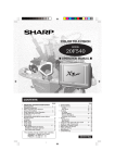
1
SERVICE MANUAL
COLOR TELEVISION
Chassis No. GA-2
MODELS
20F540
In the interests of user-safety (Required by safety regulations in some countries ) the set should be restored to its
original condition and only parts identical to those specified should be used.
CONTENTS
Page
» ELECTRICAL SPECIFICATIONS ......................................................................................................... 1
» IMPORTANT SERVICE SAFETY PRECAUTION ................................................................................. 2
» LOCATION OF USER'S CONTROL ..................................................................................................... 4
» INSTALLATION AND SERVICE INSTRUCTIONS ................................................................................5
» SERVICE MODE ................................................................................................................................... 6
» ADJUSTMENT METHOD ..................................................................................................................... 7
» CHASSIS LAYOUT ............................................................................................................................. 11
» BLOCK DIAGRAM .............................................................................................................................. 12
» DESCRIPTION OF SCHEMATIC DIAGRAM ...................................................................................... 17
» WAVEFORMS ..................................................................................................................................... 18
» SCHEMATIC DIAGRAMS ................................................................................................................... 19
» PRINTED WIRING BOARD ASSEMBLIES ........................................................................................ 24
» REPLACEMENT PARTS LIST ............................................................................................................ 27
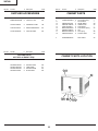
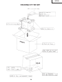
» PACKING OF THE SET ...................................................................................................................... 34
ELECTRICAL SPECIFICATIONS
POWER INPUT ..................................................... AC 120 V, 60 Hz
POWER RATING .................................................................... 90W
PICTURE SIZE .......................................... 1,239 cm2 (192sq inch)
CONVERGENCE ............................................................. Magnetic
SWEEP DEFLECTION .................................................... Magnetic
FOCUS ................................................................................. Uni-Bi
INTERMEDIATE FREQUENCIES
Picture IF Carrier Frequency ..................................... 45.75 MHz
Sound IF Carrier Frequency ...................................... 41.25 MHz
Color Sub-Carrier Frequency .................................... 42.17 MHz
(Nominal)
AUDIO POWER
OUTPUT RATING ........................................ 2.5 W(RMS) x 2pcs
SHARP CORPORATION
SPEAKER
SIZE ................................................................... 5 x 12 cm, 2pcs
VOICE COIL IMPEDANCE ............................ 16 ohm at 400 Hz
ANTENNA INPUT IMPEDANCE
VHF/UHF ..................................................... 75 ohm Unbalanced
TUNING RANGES
VHF-Channels ............................................................... 2 thru 13
UHF-Channels ............................................................ 14 thru 69
CATV Channels ........................................................... 1 thru 125
(EIA, Channel Plan U.S.A.)
Specifications are subject to change without
prior notice.
This document has been published to be used for after
sales service only.
The contents are subject to change without notice.
20F540
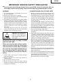
IMPORTANT SERVICE SAFETY PRECAUTION
Ë
Service work should be performed only by qualified service technicians who are
thoroughly familiar with all safety checks and the servicing guidelines which follow:
WARNING
X-RADIATION AND HIGH VOLTAGE LIMITS
1. For continued safety, no modification of any circuit
should be attempted.
2. Disconnect AC power before servicing.
3. Semiconductor heat sinks are potential shock hazards
when the chassis is operating.
4. The chassis in this receiver has two ground systems
which are separated by insulating material. The nonisolated (hot) ground system is for the B+ voltage
regulator circuit and the horizontal output circuit. The
isolated ground system is for the low B+ DC voltages
and the secondary circuit of the high voltage
transformer.
To prevent electrical shock use an isolation
transformer between the line cord and power
receptacle, when servicing this chassis.
1. Be sure all service personnel are aware of the
procedures and instructions covering X-radiation. The
only potential source of X-ray in current solid state
TV receivers is the picture tube. However, the picture
tube does not emit measurable X-Ray radiation, if
the high voltage is as specified in the "High Voltage
Check" instructions.
It is only when high voltage is excessive that Xradiation is capable of penetrating the shell of the
picture tube including the lead in the glass material.
The important precaution is to keep the high voltage
below the maximum level specified.
2. It is essential that servicemen have available at all
times an accurate high voltage meter.
The calibration of this meter should be checked
periodically.
3. High voltage should always be kept at the rated value
−no higher. Operation at higher voltages may cause
a failure of the picture tube or high voltage circuitry
and;also, under certain conditions, may produce
radiation in exceeding of desirable levels.
4. When the high voltage regulator is operating properly
there is no possibility of an X-radiation problem. Every
time a color chassis is serviced, the brightness should
be tested while monitoring the high voltage with a
meter to be certain that the high voltage does not
exceed the specified value and that it is regulating
correctly.
5. Do not use a picture tube other than that specified or
make unrecommended circuit modifications to the
high voltage circuitry.
6. When trouble shooting and taking test measurements
on a receiver with excessive high voltage, avoid being
unnecessarily close to the receiver.
Do not operate the receiver longer than is necessary
to locate the cause of excessive voltage.
4A 125V
CAUTION: FOR CONTINUED
PROTECTION AGAINST A
RISK OF FIRE, REPLACE
ONLY WITH SAME TYPE 4A125V FUSE.
SERVICING OF HIGH VOLTAGE SYSTEM
AND PICTURE TUBE
When servicing the high voltage system,
remove the static charge by connecting a
10k ohm resistor in series with an insulated
wire (such as a test probe) between the picture tube ground and the anode lead. (AC
line cord should be disconnected from AC
outlet.)
1. Picture tube in this receiver employs integral
implosion protection.
2. Replace with tube of the same type number for
continued safety.
3. Do not lift picture tube by the neck.
4. Handle the picture tube only when wearing
shatterproof goggles and after discharging the high
voltage anode completely.
2
20F540
IMPORTANT SERVICE SAFETY PRECAUTION
(Continued)
BEFORE RETURNING THE RECEIVER
(Fire & Shock Hazard)
Before returning the receiver to the user, perform
the following safety checks.
1. Inspect all lead dress to make certain that leads are
not pinched or that hardware is not lodged between
the chassis and other metal parts in the receiver.
2. Inspect all protective devices such as non-metallic
control knobs, insulating materials, cabinet backs,
adjustment and compartment covers or shields,
isolation resistor-capacity networks, mechanical
insulators, etc.
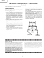
3. To be sure that no shock hazard exists, check for
leakage current in the following manner.
• Plug the AC cord directly into a 120 volt AC outlet,
(Do not use an isolation transformer for this test).
• Using two clip leads, connect a 1.5k ohm, 10 watt
resistor paralleled by a 0.15µF capacitor in series with
all exposed metal cabinet parts and a known earth
ground, such as electrical conduit or electrical ground
connected to earth ground.
• Use an AC voltmeter having with 5000 ohm per volt,
or higher, sensitivity to measure the AC voltage drop
across the resistor.
• Connect the resistor connection to all exposed metal
parts having a return to the chassis (antenna, metal
cabinet, screw heads, knobs and control shafts,
escutcheon, etc.) and measure the AC voltage drop
across the resistor.
AII checks must be repeated with the AC line cord
plug connection reversed. (If necessary, a nonpolarized adapter plug must be used only for the
purpose of completing these check.)
Any current measured must not exceed 0.5 milliamp.
Any measurements not within the limits outlined
above indicate of a potential shock hazard and
corrective action must be taken before returning the
instrument to the customer.
1.5k ohm
10W
0.15 F
TEST PROBE
TO EXPOSED
METAL PARTS
CONNECT TO
KNOWN EARTH
GROUND
12345678901234567890123456789012123456789012345678901234567890121234567890123456789012345678901212
12345678901234567890123456789012123456789012345678901234567890121234567890123456789012345678901212
12345678901234567890123456789012123456789012345678901234567890121234567890123456789012345678901212
SAFETY NOTICE
Many electrical and mechanical parts in television
receivers have special safety-related characteristics.
These characteristics are often not evident from visual
inspection, nor can protection afforded by them be
necessarily increased by using replacement components
rated for higher voltage, wattage, etc.
Replacement parts which have these special safety
characteristics are identified in this manual; electrical
components having such features are identified by "å"
and shaded areas in the Replacement Parts Lists and
Schematic Diagrams.
For continued protection, replacement parts must be
identical to those used in the original circuit. The use of
substitute replacement parts which do not have the same
safety characteristics as the factory recommended
replacement parts shown in this service manual, may
create shock, fire, X-radiation or other hazards.
12345678901234567890123456789012123456789012345678901234567890121234567890123456789012345678901212
12345678901234567890123456789012123456789012345678901234567890121234567890123456789012345678901212
12345678901234567890123456789012123456789012345678901234567890121234567890123456789012345678901212
3
20F540
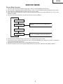
LOCATION OF USER'S CONTROL
Front Panel
VIDEO IN 2 L-AUDIO-R
POWER
Press → On.
Press again → Off.
SENSOR AREA FOR
REMOTE CONTROL
(INSIDE DOOR)
MENU
Press → Accesses MAIN MENU.
Press again → Exits MAIN MENU.
VOLUME UP/DOWN
(+) Increases sound.
( ) Decreases sound.
CHANNEL UP/DOWN
(') Selects next higher channel.
(") Selects next lower channel.
Basic Remote Control Functions
Infrared Transmitter Window
POWER
Press
On.
Press again
Off.
DVD
VCR
TV
REMOTE KEYPAD
Accesses any channel from keypad.
FLASHB ACK
Returns to previous channel.
PERSONAL PREFERENCE
With the Personal Preference buttons,
you can prog ram your favor ite
programs by using the 4 categories A,
B, C and D. The channels can be
accessed quic kly by using these
buttons.
DISPLAY
Press Displays receiving channel for
four seconds.
Press again
Removes display.
• Tempor ar ily displa ys receiving
channel when in Closed Caption
mode.
POWER
DISPLAY
INPUT
1
2
3
4
5
6
7
8
9
INPUT
Press
Switch to exter nal video
INPUT 1 mode.
Press 2 times Switch to external video
INPUT 2 mode.
Press 3 times Switch to external video
INPUT 3 mode or COMPONENT mode.
Press 4 times
Switch back to the
original TV mode.
ENTER
FLASHBACK
0
100
PERSONAL PREFERENCE
A
B
C
D
CH
VOL
—
VOL
+
CH
VOLUME UP/DOWN
(+) Increases sound.
(–) Decreases sound.
• In menu mode, changes or selects
the TV adjustments.
MENU
Press
Accesses MAIN MENU.
Press again
Exits MAIN MENU.
CATV/DVD-TV/VCR MODE
SELECT SWITCH
In TV/VCR position, sends power and
channel select commands (Channel
up/down and Random Access buttons)
to the TV and VCR control.
In CATV/DVD position, sends power
and channel select commands to a
cable TV converter and DVD control.
MENU
MUTE
CATV
TV
DVD
VCR
REW
PLAY
FF
PAUSE
STOP
REC
ENTER
Used in some instances where a Cable
Con ver ter Box requires an “enter”
command after selecting channels ,
when using the REMOTE KEYPAD
button.
CH/SKIP
TV • CATV • VCR • DVD
CHANNEL UP/DOWN
(8 ) Selects next higher channel.
(9 ) Selects next lower channel.
• See pages 28 ~ 30 for channel
presetting.
• Moves the “ [ ” mark of the MENU
screens.
MUTE
Press
Mutes sound.
Press again
Restores sound.
• CLOSED CAPTION appears when
sound is muted.
DVD/VCR CONTROL
Note:
• The above shaded buttons on the Remote Control glow in the dark. To use the glow-in-the-dark display on the
remote control, place it under a fluorescent light or other lighting.
• The phosphorescent material contains no radioactive or toxic material, so it is safe to use.
• The degree of illumination will var y depending on the strength of lighting used.
• The degree of illumination will decrease with time and depending on the temperature.
• The time needed to charge the phosphorescent display will vary depending on the surrounding lighting.
• Sunlight and fluorescent lighting are the most effective when charging the display.
4
20F540
INSTALLATION AND SERVICE INSTRUCTIONS
Note:
(1) When performing any adjustments to resistor controls and transformers use non-metallic
screwdrivers or TV alignment tools.
(2) Before performing adjustments, the TV set must be on at least 15 minutes.
CIRCUIT PROTECTION
HIGH VOLTAGE CHECK
The receiver is protected by a 4.0A fuse (F701),
mounted on PWB-A, wired into one side of the AC
line input.
High voltage is not adjustable but must be checked
to verify that the receiver is operating within safe
and efficient design limitations as specified checks
should be as follows:
X-RADIATION PROTECTOR CIRCUIT TEST
After service has been performed on the horizontal
deflection system, high voltage system, B+ system,
test the X-Radiation protection circuit to ascertain
proper operation as follows:
1. Apply 120V AC using a variac transformer for accurate
input voltage.
2. Allow for warm up and adjust all customer controls
for normal picture and sound.
3. Receive a good local channel.
4. Connect a digital voltmeter to P603 Pin3 and make
sure that the voltmeter reads 18.9 ±1.1V.
5. Apply external 24.5V DC at P603 Pin3 by using an
external DC supply, TV must be shut off.
6. To reset the protector, unplug the AC cord at least 4
second before plugging in again. Now make sure that
normal picture appears on the screen.
7. If the operation of the horizontal oscillator does not
stop in step 5, the circuit must be repaired before the
set is returned to the customer.
5
1. Connect an accurate high voltage meter between
ground and anode of picture tube.
2. Operate receiver for at least 15 minutes at 120V AC
line voltage, with a strong air signal or a properly tuned
in test signal.
3. Enter the service mode and set Y-mute ON by using
Service R/C.
4. The voltage should be approximately 28.6kV (at zero
beam).
If a correct reading cannot be obtained, check circuitry
for malfunctioning components. After the voltage test,
make Y-mute off to the normal mode.
20F540
SERVICE MODE
Service Mode Overview
1.
2.
3.
4.
Service mode is entered by SERVICE key input or CH-UP +VOL-DOWN input during reset.
Service mode is cleared by entering SERVICE key or CH-UP +VOL-DOWN key command during service mode.
If key input port (SERVICE) input is LOW, then it is in service mode.
During key input port (SERVICE) input is LOW, clearing service mode by key input SERVICE or CH-UP + VOLDOWN is disabled.
5. Service mode can be switched to 4 modes as follows by key input MENU;
Option mode
Adjustment mode
First mode of service mode when SERVICE key is
pressed.
Setting mode
Check mode
First mode of service mode when local key
CH-UP + VOL-DOWN is pressed after MCU reset.
6. AFT processing is disabled during service mode. PLL setting data is set to fo data.
7. All user data are set to default during service mode. FAO and SPEAKER user settings are off and on respectively
in service mode. Energy Save is off.
8. Sleep timer, View timer and Off timer are inactivated in Service mode.
9. Sound is muting in service mode except at Adjustment Items V20, M01, M02, M03, M04, M05, and M06.
6
20F540
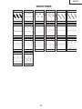
Adjustment Mode Items
ADJUSTMENT METHOD
Caution: to get into the service mode, one of the ways is press direct key for service items. the other ways
is short the main chassis JA309 and JA402
There is three stage of Service Mode data
First stage data from V01 ~ M06
to go into second stage of service mode data, press MENU key
Second stage data from F01 ~ F51
to go into third stage of service mode data, press MENU key
Third stage data from 001 ~ 020
Below is the contents of these data
First Stage
No.
V01
V02
Item Name
SUB-PICTURE
SUB-TINT
IC
1 Chip
1 Chip
Register
CONTRAST
TINT
Range
0~127
0~127
Default
127
64
V03
V04
V05
V06
V07
V08
V09
V10
V11
V12
V13
SUB-COLOR
SUB-BRIGHT
SUB-SHARP
V-SHIFT
H-SHIFT
RF-AGC
V-SIZE
PIF-VCO
R-CUTOFF
G-CUTOFF
B-CUTOFF
1 Chip
1 Chip
1 Chip
1 Chip
1 Chip
1 Chip
1 Chip
1 Chip
1 Chip
1 Chip
1 Chip
COLOR
BRIGHT
VIDEO-TONE
V-SHIFT
H-PHASE
RF-Delay
V-SIZE
VIF-VCO
R-CUTOFF
G-CUTOFF
B-CUTOFF
0~127
0~255
0~63
0~7
0~31
0~127
0~63
0~63
0~255
0~255
0~255
64
128
32
4
16
127
32
32
127
127
127
V14
V15
V16
V17
V18
V19
V20
V21
M01
M02
M03
M04
M05
M06
R-DRIVE
B-DRIVE
SUB-COLOR(YUV)
SUB-TINT(YUV)
CC-POS
(Vertical mode)
SUB-VOL
H-VCO
MTS-ATT
MTS-VCO
MTS-FILTER
MTS-WIDEBAND
MTS-SPECTRAL
SUB-VOL
1 Chip
1 Chip
1 Chip
1 Chip
Micron
1 Chip
1 Chip
1 Chip
MTS
MTS
MTS
MTS
MTS
MTS
R-DRIVE
B-DRIVE
COLOR
BASEBAND-TINT
0~127
0~127
0~127
0~127
0~255
0, 1, 2
0~127
0~7
0~15
0~63
0~63
0~63
0~63
0~63
64
64
64
64
32
0
127
4
10
32
28
27
32
63
V-MUTE,SERVICE
A-ATT
H-VCO
ATT
VCO
FILTER
WIDEBAND
SPECTRAL
VOL
Auto Adjustment Item
1. H-VCO (Currently need manual adj)
2. RF-AGC
3. PIF-VCO
4. MTS-FILTER
7
20F540
Ë SELF ADJUSTMENT
H-VCO
1.
2.
3.
4.
5.
6.
7.
When there is H-VCO self-adjustment key input for adjustment item H-VCO, self-adjustment is performed.
H-FREE(1chip) is set to 1.
H-OUT is set by intelligent monitor output.
IM input is set as TIM input.
H-VCO(1chip) data is changed so that the number of input pulse is 125 inside 8ms interval.
When adjustment completed, OSD display and H-VCO self-adjustment status data of EEPROM are updated.
H-FREE(1chip), intelligent monitor output and IM input mode are recovered.
RF-AGC
1.
2.
3.
4.
When there is RF-AGC self-adjustment key input for adjustment item RF-AGC, self-adjustment is performed.
AGC-OUT is set by intelligent monitor output.
IM input is set as AD input.
By decreasing RF-AGC (1chip) data from current RF-AGC adjustment value to 0, AFT input voltage becomes the
maximum setting value.
5. Increase RF-AGC(1chip) data, when AFT input voltage is at (max. 0.3V) point, adjustment is completed.
6. When adjustment completed, OSD display and RF-AGC self-adjustment status data of EEPROM are updated.
7. Intelligent monitor output and IM input mode are recovered.
PIF-VCO
1.
2.
3.
4.
5.
6.
7.
When there is PIF-VCO self-adjustment key input for adjustment item PIF-VCO, self-adjustment is performed.
VIF-DEF(1chip) is set to 1.
AFC is set by intelligent monitor output.
IM input is set as AD input.
VIF-VCO(1chip) data is changed so that input voltage becomes 2.5V.
When adjustment completed, OSD display and PIF-VCO self-adjustment status data of EEPROM are updated.
VIF-DEF(1chip), intelligent monitor output and IM input mode are recovered.
MTS-FILTER
Adjustment is performed in the center of the range when FILTER status is OK.
1. If data is changed from 0 to 63, point where NG → OK is A and point where OK → NG is B.
2. If data is changed from 63 to 0, point where NG → OK is C and point where OK → NG is D.
3. (A+B+C+D)/4 is the adjustment point.
8
20F540
Setting Mode Items
Second Stage
No.
F01
F02
F03
F04
F05
F06
F07
F08
F09
F10
F11
F12
F13
F14
F15
F16
F17
F18
F19
F20
F21
F22
F23
F24
F25
F26
F27
F28
F29
F30
F31
F32
F33
F34
F35
F36
F37
F38
F39
F40
F41
F42
F43
F44
F45
F46
F47
F48
F49
F50
F51
F52
F53
F54
Item Name
VideoTone-Gain (TV)
VideoTone-Gain (AV)
VideoTone-Gain(YUV)
ABCL
BS
ABCL-G
SHP-AV
SHP-YUV
RGB-CLIP
E-SAVE
FAO-VOL
PIF-G
Y-DELAY(TV)
Y-DELAY(AV)
Y-DELAY(YUV)
TINT-AV
COL-AV
R-DRI(R2)
R-DRI(R)
R-DRI(B)
B-DRI(R2)
B-DRI(R)
B-DRI(B)
V-FREE
GAMMA
TRAP(TV)
TRAP(AV)
H-FREE
1W(TV)
1W(AV)
YLPF
BS-D
BS-C
SL(TV)
SL(AV)
SL(YUV)
AFC2
VD(TV)
VD(AV)
AS(TV)
AS(AV)
AS(YUV)
FBP(TV)
FBP(AV)
FBP(YUV)
C.Clip Level
PSW
FAO-VOL
CP
CC LEVEL
OSD POS
OFFSET-ADJ-COL
OFFSET-ADJ-TINT
OFFSET-ADJ-TINT-YUV
IC
1chip
1chip
1chip
1chip
1chip
1chip
OFFSET
OFFSET
1chip
OFFSET
1chip
1chip
1chip
1chip
1chip
OFFSET
OFFSET
OFFSET
OFFSET
OFFSET
OFFSET
OFFSET
OFFSET
1chip
1chip
1chip
1chip
1chip
1chip
1chip
1chip
1chip
1chip
1chip
1chip
1chip
1chip
1chip
1chip
1chip
1chip
1chip
1chip
1chip
1chip
1chip
MTS
MTS
PLL
MICRON
MICRON
1 chip
1 chip
1 chip
Register
V-TONE
V-TONE
V-TONE
ABCL
BS-OFF
ABCL-G
VIDEO-TONE(OFFSET)
VIDEO-TONE(OFFSET)
ExtRGB-Clip
CONTRAST(OFFSET)
A-ATT
VIF-GAIN
Y-Delay
Y-Delay
Y-Delay
TINT(OFFSET)
COLOR(OFFSET)
R-DRI(OFFSET)
R-DRI(OFFSET)
R-DRI(OFFSET)
B-DRI(OFFSET)
B-DRI(OFFSET)
B-DRI(OFFSET)
V-FREE
GAMMA
TRAP-FINE
TRAP-FINE
H-FREE
V.Window
V.Window
YSW-LPF
BS-DISCHARGE
BS-CHARGE
S-SLICE DOWN
S-SLICE DOWN
S-SLICE DOWN
AFC2-G
Vsync-Det
Vsync-Det
Auto-Slice
Auto-Slice
Auto-Slice
FBP Vth
FBP Vth
FBP Vth
C.Clip Level
PSW
VOL
CP
COLOR
TINT
BASEBAND-TINT
9
Range
0/1
0/1
0/1
0/1
0/1
0/1
-16~+16
-16~+16
0/1
0~63
0~127
0~7
0~7
0~7
0~7
-32~+32
-32~+32
-32~+32
-32~+32
-32 ~+32
-32~+32
-32~+32
-32~+32
0/1
0~3
0~3
0~3
0/1
0/1
0/1
0/1
0~3
0~3
0~3
0~3
0~3
0/1
0/1
0/1
0/1
0/1
0/1
0/1
0/1
0/1
0/1
0/1
0~63
0/1
-32~32
-32~32
-32~32
Default
0
0
0
0
0
0
0
0
0
30
120
4
0
0
0
0
0
0
0
0
0
0
0
0
0
2
2
0
0
0
1
0
0
0
0
0
0
0
0
0
0
0
0
0
0
0
0
60
0
0
0
0
0
0
20F540
Option Mode Items
Third Stage
No ITEM
O01 DEM0
O02 DOWNLOAD
O03 V-CHIP
O04 SPEAKER
O05 FAO
O06 P.PREF
O07 UNIV+
O08 VIEW TIMER
O09 EZ-SETUP
O10 PON-CH
O11 FAV-COL
O12 COMPONENT
O13 AV
O14 AV2
O15 MTS
O16 TONE-CTRL
O17 AUTO-OFF
O18 INIT-LANG
O19 SETUP-FLAG
O20
FR.AV (Front,
Rear AV)
0
1
Without DEMO
With DEMO
Without V-CHIP OP
With V-CHIP OP
Without V-CHIP
With V-CHIP
Without SPEAKER
With SPEAKER
Without FAO
With FAO
Without P.PREF
With P.PREF
Without UNIV+
With INIV+
Without VIEW TIMER
With VIEW TIMER
EZ-SETUP
AUTO PRESET
Without POWER-ON
With POWER-ON
FAV-COL
COL-TEMP
Without COMPONENT With COMPONENT
Without AV
With AV
AV1 system
AV2 system
Without MTS
With MTS
Without S-ADJ
With S-ADJ
Without AUTO-OFF
With AUTO-OFF
ENGLISH
SPANISH
NO SETUP
AUTO SETUP
3: Display "FRONT A/V INPUTS" and
"REAR A/V INPUTS" in DEMO mode.
2: Display "FRONT A/V INPUTS" only in
DEMO mode.
1: Display "REAR A/V INPUTS" only in
DEMO mode.
0: No display of above lines in DEMO mode.
DEFAULT
1
1
1
1
1
1
1
1
1
1
1
1
1
1
1
1
1
1
1
3
Check Mode
Micron mask version, software version and ROM correction function status are displayed in check mode.
10
20F540
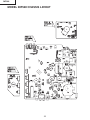
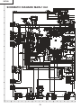
MODEL 20F540 CHASSIS LAYOUT
11
20F540
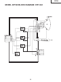
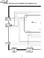
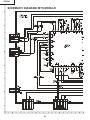
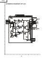
MODEL 20F540 BLOCK DIAGRAM: CRT Unit
12
20F540
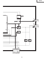
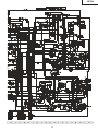
MODEL 20F540 BLOCK DIAGRAM: MAIN Unit
13
20F540
14
20F540
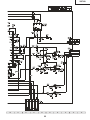
MODEL 20F540 BLOCK DIAGRAM: MTS MODULE Unit
15
20F540
16
20F540
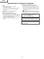
DESCRIPTION OF SCHEMATIC DIAGRAM
NOTES:
WAVEFORM MEASUREMENT CONDITIONS:
1. The unit of resistance "ohm" is omitted.
(K=kΩ=1000Ω, M=MΩ)
2. All resistors are 1/16 watt, unless otherwise noted.
3. All capacitors are µ F, unless otherwise noted.
(P=pF=µµF)
4. (G) indicates ±2% tolerance may be used.
5.
indicates line isolated ground.
1. Photographs taken on a standard gated color bar
signal, the tint setting adjusted for proper color. The
wave shapes at the red, green and blue cathodes of
the picture tube depend on the tint, color level and
picture control.
2.
indicates waveform check points (See chart,
waveforms are measured from point indicated to
chassis ground.)
VOLTAGE MEASUREMENT CONDITIONS:
1. All DC voltages are measured with DVM connected
between points indicated and chassis ground, line
voltage set at 120V AC and all controls set for normal
picture unless otherwise indicated.
2. All voltages measured with 1000µ V B & W or Color
signal.
å
ç
AND SHADED (
) COMPONENTS
= SAFETY RELATED PARTS.
MARK= X-RAY RELATED PARTS.
DRGANNES MARQUES åET HACHRES (
):
PIECES RELATIVES A LA SECURITE.
MARQUE ç : PIECS RELATIVE AUX RAYONS X.
This circuit diagram is a standard one, printed circuits
may be subject to change for product improvement
without prior notice.
17
20F540
WAVEFORMS
1 1.024 Vp-p
2 5.69 Vp-p
3 5.69 Vp-p
4 5.84 Vp-p
5 2.00 Vp-p
6 2.08 Vp-p
Horiz.Rate
Horiz.Rate
Horiz.Rate
Horiz.Rate
Vert.Rate
Vert.Rate
7 6.56 Vp-p
8 6.40 Vp-p
9 4.88 Vp-p
0 158 Vp-p
q 1140 Vp-p
Horiz.Rate
Horiz.Rate
Horiz.Rate
Horiz.Rate
Horiz.Rate
Vert.Rate
e 3.8 Vp-p
r 118 Vp-p
t 440 Vp-p
y 5.04 Vp-p
u 5.12 Vp-p
i 112.8 Vp-p
Vert.Rate
Horiz.Rate
Horiz.Rate
Horiz.Rate
Vert.Rate
Horiz.Rate
o 94.4 Vp-p
p 109.6 Vp-p
Horiz.Rate
Horiz.Rate
18
w 48 Vp-p
20F540
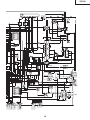
SCHEMATIC DIAGRAM: MAIN-1 Unit
H
G
F
E
D
C
B
A
1
2
3
4
5
6
19
7
8
9
10
20F540
10
11
12
13
14
15
17
16
17
18
19
20F540
SCHEMATIC DIAGRAM: MTS MODULE
H
G
F
E
D
C
B
A
1
2
3
4
6
5
21
7
8
9
10
20F540
10
11
12
13
14
15
22
16
17
18
19
20F540
SCHEMATIC DIAGRAM: CRT Unit
H
G
F
E
D
C
B
A
1
2
3
4
23
5
6
20F540
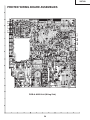
PRINTED WIRING BOARD ASSEMBLIES
H
G
F
E
D
C
B
PWB-A: MAIN Unit (Wiring Side)
A
1
2
3
4
24
5
6
1
2
25
3
4
5
6
A
PWB-A: MAIN Unit (Chip Parts Side)
B2
F DC2
B
RJ 7 1
RJ 7 0
Z2
A2
R3 8 2
R3 1 3
R3 8 1
RJ 4 8
R3 1 7
RJ 6 3
D5 0 1
R3 1 5
R1 0 2 4
R8 0 1
R3 1 4
RJ 2 3
RJ 1 5
C3 1 3
R3 2 1
C3 1 9
R3 1 2
R2 0 5
C8 0 6
C7 5 9
RJ 1 1
R3 8 4
RJ 3 0
R3 8 3
RJ
R3 1
00
1
R3 0 8
RJ 2 2
R7 6 8
R1 0 5 9
RJ 6 0
C3 2 0
RJ 2 1
RJ 5 9
C3 0 8
R4 3 1
R3 0 7
R7 4 3
R1 0 3 8
C2 1 1
R2 1 1
R2 0 6
RJ 3
R1 0 2 1
C2 1 0
C2 1 2
D8 1 5
R8 3 0
R8 2 9
R8 3 3
R8 0 4
R1 8 5 1
R8 3 4
RJ 4 2
R1 8 5 2
C1 0 1 5
R1 0 7 0
R8 0 6
R1 8 5 3
R1 0 6 8
R3 1 6
R8 2 5
R3 0 5
RJ 1 4
R1 0 6 9
R4 3 4
R1 8 6 1
R1 8 5 0
C8 1 1
C8 1 2
R1 0 6 7
C8 1 3
R1 0 6 6
R1 0 3 3
Q8 0 5
R3 0 6
C8
R8 3
40
4
R8
C8 4
35
2
RJ 7 7
R1 8 6 2
R8 3 1
R8 3 8
R8 0 7
R8 2 8
Q3 0 1
C2 0 3
C2 0 5
C8 4 6
D8 1 0
R1 0 3 2
R8 0 5
R1 0 7 5
R1 0 3 6
R1 0 3 7
R7 4 4
R1 0 6 4
RJ 7
R1 0 2 2
C8 0 2
D8 1 3
C8 0 9
R1 0 3 1
C8 1 0
R1 0 3 4
D1 0 0 4
R4 3 2
D1 0 9 0
RJ 7 6
RJ 9
RJ 8
R3 1 0
Q3 0 2
RJ 6 9
R2 1 3
C8 0 4
R1 0 3 9
R8 4 0
Q7 4 0
Q7 4 1
R1 0 7 3
D1 0 8 8
R1 0 6 5
RJ 3 3
R1 0 7 1
I C8 0 1
D8 1 2
R3 0 3
C1 0 0 4
I C1 0 0 3
R1 0 7 4
RJ 3 5
R1 0 7 2
R8 0 3
C8 0 8
D8 1 4
D8 1 1
C8 3 6
Q7 5 5
Q1 0 0 1
R8 0 2
R8 3 5
C8 4 5
C8 4 4
C8 4 1
C8 4 7
C8 4 0
RJ 1 3
R7 6 6
R8 4 3
RJ 6 2
R8 3 9
R2 1 2
D2 0 2
Q2 0 2
C2 0 8
R2 2 0
R2 0 7
C8 3 9
F DC4
RJ 5 3
C1 8 6 4
C1 8 6 3
C1 8 6 2
C1 8 6 1
R8 1 0
R1 0 7 6
R4 3 5
R4 3 3
R3 1 8
R1 0 2 5
C2 1 3
R2
RJ120
RJ 2 6
C2 0 7
R2 0 9
C2 0 9
R2 0 8
Q2 0 1
R2 0 1
R2 0 2
C
C1 8 5 6
C8 1 4
RJ 6 4
RJ 2 4
C8 1 6
R8 4 2
F DC3
R1 0 6 2
R1 0 6 0
R1 0 4 9
R1 0 4 8
R1 0 4 6
R1 0 5 1
RJ 1 7
R1 0 5 3
R4
RJ 6 2
1
R3 6 5
R3 6 4
R1 0 6 1
RJ 7 4
R1 0 0 2
R1 8 5 4
C8 1 5
C1 8 5 5
R1 0 4 7
R1 0 4 3
R4 5 4
R1 0 5 2
D1 0 8 5
C1 0 0 9
C1 0 1 0
C1 0 1 1
R1 0 5 4
R3 6 2
R8 1 4
C1 0 0 8
D1 0 8 7
C8 2 3
RJ 3 7
C8 2 1
R8 3 2
R8 1 9
C1 0 1 3
R4 6 1
D1 0 8 6
Q8 0 3
C8 1 9
RJ 1 6
I C1 0 0 1
R1 0 6 3
R8 1 3
R8 1 1
R8 1 2
R8 2 7
R1
RJ82459
R3 6 3
D
R8 2 1
RJ 3 6
R1 0 5 7
R1 0 5 5
RJ 3 9
RJ 4 4
R8 1 6
Q8 0 4
Q1 0 0 2
R1 0 5 6
R8 2 2
C8 3 1
R8 2 0
C8 3 3
I C4 0 1
RJ 7 3
R4 3 7
RJ 4 7
R8 1 5
RJ 1 9
C4 3 6
R8 1 7
R4 5 8
R1 0 0 9
R1 0 0 3
RJ 3 2
R6 6 2
R6 6 1
R1 0 0 8
R1 0 0 7
Q6 0 4
RJ 6 5
R1 0 8 1
RJ 7 5
R5 2 2
R1 0 0 6
RJ 1
R5 2 1
C5 1 8
RJ 3 8
RJ 1 2
C5 1 9
R1 0 2 6
R6 1 9
C7 3 5
R5 1 6
RJ 5 0
R5 2 0
C5 1 7
R6 2 0
R5 0 4
E
RJ 4 9
RJ 5 1
RJ 3 4
R6 1 7
RJ 4 0
R5 2 7
R5 2 8
R1 0 2 7
RJ 7 2
RJ 5 2
R6 1 8
R6 1 3
RJ 4 1
RJ 4 6
R6 5 4
RJ 4 3
RJ 4 5
F
R7 1 4
C7 8 4
B1
F DC1
Z1
A1
G
H
20F540
20F540
H
G
F
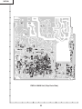
PWB-B: CRT Unit (Wiring Side)
E
D
PWB-E: MTS MODULE Unit (Wiring Side)
C
R3 0 2 4
R3 0 2 5
RJ 1 0
R3 0 8 0
RJ 4
R3 0 8 1
Q3 0 0 7
R3 0 1 6
R3 0 0 4
R3 0 0 3
C3 0 0 2
I C3 0 0 2
R3 0 0 5
C3 0 0 8
R3 0 8 5
RJ 1 3
R3 0 8 4
C3 0 8 2
RJ
76
R3
03
RJ 2
B
Q3 0 0 6
RJ 6
I C3 0 0 1
R3 0 0 7
R3 0 1 9
R3 0 0 8
R3 0 8 2
RJ 1 4
R3 0 0 1
R3 0 0 2
RJ 3
R3 0 1 0
C3 0 1 3
R3 0 1 8
R3 0 8 3
R3 0 2 6
C3 0 3 1
C3 0 3 2
R3 0 2 9
C3 0 2 6
Q3 0 0 4
C3 0 2 8
C3 0 4 3
R3 0 1 1
Q3 0 0 1
R3 0 2 7
R3 0 3 4
C3 0 2 3
R3 0 1 3
R3 0 3 5
C3 0 3 5
C3 0 3 6
C3 0 2 4
C3 0 2 7
C3 0 2 5
R3 0 1 2
C3 0 3 3
Q3 0 0 2
R3 0 3 0
R3 0 2 8
C3 0 4 2
R3 0 2 1
Q3 0 0 5
R3
RJ
03
83
R3 0 3 2
R3 0 1 4
RJ 9
R3 0 3 1
RJ 1 5
RJ 1 7
RJ 1 6
A
PWB-E: MTS MODULE Unit (Chip Parts Side)
1
2
3
4
26
5
6
20F540
«
Ref. No. Part No.
PARTS LIST
MAIN UNIT
TUNER
Replacement parts which have these special safety characteristics
identified in this manual; electrical components having such features
are identified by å and shaded areas in the Replacement Parts Lists
and Schematic Diagrams. The use of a substitute replacement part
which dose no have the same safety characteristic as the factory
recommended replacement parts shown in this service manual may
create shock, fire or other hazards.
NOTE:THE PARTS HERE SHOWN ARE SUPPLIED AS AN
ASSEMBLY BUT NOT INDEPENDETLY
U
U
U
U
U
To have your order filled promptly and correctly, please furnish the
following informations.
2. REF. NO.
4. DESCRIPTION
TU201
VTUVT1T5UF202
X
Tuner
AP
INTEGRATED CIRCUITS
"HOW TO ORDER REPLACEMENT PARTS"
3. PART NO.
Code
PWB-A: DUNTKB989WEA0
PARTS REPLACEMENT
1. MODEL NUMBER
Description
IC301
IC401
IC501
IC601
IC701
IC702
IC703
IC801
IC1001
IC1003
VHIAN7522++-1
VHIMM1501XN-1Y
VHITDA9302H-1
VHIKA7809AP-1
VHITEA1507/-1
RH-FXA003WJZZ
VHISE130N++-F
VHIM61251AF1EQ
RH-IXA155WJN4
VHIBR24L16F-1Y
Q201
Q302
Q601
Q602
Q603
Q604
Q701
Q703
Q740
Q741
Q751
Q752
Q753
Q755
Q804
Q805
Q1001
VS2SC2735//1EY
VS2SD601AR/-1Y
VS2SC2482//-1+
VS2SD2539//1E
VS2SC3198-G-1+
VS2SD601AR/-1Y
VSSTP6NC80Z1E
VS2SC3198-Y-1+
VS2SD601AR/-1Y
VS2SD601AR/-1Y
VS2SC2236Y/-1+
VS2SC2236Y/-1+
VS2SC3198-G-1+
VS2SD601AR/-1Y
VS2SB709AR/-1Y
VS2SD601AR/-1Y
VS2SD601AR/-1Y
D201
D203
D393
D501
D502
D503
D504
D505
D510
D601
D602
D603
D606
D608
D701
D703
D704
D708
D710
D750
D751
D752
D755
D756
D801
D806
D807
D808
D810
D811
D812
RH-EX0676GEZZY
RH-DX0048GEZZY
RH-DX0247CEZZY
RH-EX1393CEZZY
RH-EX0652GEZZY
RH-EX0612GEZZY
RH-EX0654CEZZY
RH-DX0441CEZZY
RH-DX0131CEZZY
RH-DX0048GEZZY
VHD1SS244//-1Y
RH-EX0662GEZZY
RH-DX0131CEZZY
RH-DX0131CEZZY
RH-DX0111PEZZ
RH-DX0048GEZZY
RH-EX0650GEZZY
RH-DX0048GEZZY
RH-DX0048GEZZY
RH-EX0647CEZZY
RH-DXA006WJZZ
RH-DX0131CEZZY
RH-DX0048GEZZY
RH-DX0441CEZZY
RH-EX0613GEZZY
RH-DX0048GEZZY
RH-EX0625GEZZY
RH-DX0048GEZZY
RH-EX0263TAZZY
RH-EX0263TAZZY
RH-EX0263TAZZY
X
X
X
X
X
X
X
X
X
X
AN7522++
MM1501XN
TDA9302H
KA7809AP
TEA1507
PC123Y82
SE130N
M61251AFP
IXA155WJ
BR24L16F
AF
AC
AE
AC
AE
AB
AD
AN
AP
AC
TRANSISTORS
in USA:
Contact your nearest SHARP Parts Distributor to order.
For location of SHARP Parts Distributor, Please call TollFree; 1-800-BE-SHARP
« MARK: SPARE PARTS-DELIVERY SECTION
p MARK: X-RAY RELATED PARTS
Ref. No.
«
Part No.
Description
U
Code
PICTURE TUBE
L706
VB51QDK190X1E
RCILGA032WJZZ
QEARCA012WJZZ
X
X
X
Picture Tube
Degaussing Coil
Grounding Strap
BW
AK
AC
(NOT REPLACEMENT ITEM)
DUNTKB989WEA0
DUNTKA599WEB4
DUNTKB271WEA3
–
–
–
MAIN Unit
CRT Unit
MTS MODULE Unit
2SC2735
2SD601AR
2SC2482
2SD2539
2SC3198-G
2SD601AR
STP6NC80Z
2SC3198-Y
2SD601AR
2SD601AR
2SC2236Y
2SC2236Y
2SC3198-G
2SD601AR
2SB709AR
2SD601AR
2SD601AR
AB
AB
AB
AG
AB
AB
AF
AB
AB
AB
AB
AB
AB
AB
AB
AB
AB
DIODES
PRINTED WIRING BOARD ASSEMBLIES
PWB-A
PWB-B
PWB-E
X
X
X
X
X
X
X
X
X
X
X
X
X
X
X
X
X
–
–
–
U
27
X
X
X
X
X
X
X
X
X
X
X
X
X
X
X
X
X
X
X
X
X
X
X
X
X
X
X
X
X
X
X
Zener
DX0048GE
DX0247CE
EX1393CE
EX0652GE
EX0612GE
EX0654CE
Diode
Diode
DX0048GE
Diode
EX0662GE
Diode
Diode
Zener
DX0048GE
Zener
DX0048GE
DX0048GE
EX0647CE
Diode
Diode
DX0048GE
Diode
EX0613GE
DX0048GE
EX0625GE
DX0048GE
EX0263TA
EX0263TA
EX0263TA
Diode 32V
Diode
Diode 16V
AB
AB
AB
AB
AB
AB
AC
AB
AB
AB
AB
AB
AB
AB
AC
AB
AB
AB
AB
AE
AB
AB
AB
AB
AB
AB
AB
AB
AB
AB
AB
20F540
« Description
Ref. No. Part No.
Code
PWB-A: DUNTKB989WEA0
MAIN UNIT (Continued)
D813
D815
D1004
D1081
D1085
D1086
D1087
D1088
D1089
D1090
D1091
DIODES
RH-EX1393CEZZY X EX1393CE
RH-EX0263TAZZY
X EX0263TA
RH-EX1393CEZZY X EX1393CE
RH-DX0048GEZZY X DX0048GE
RH-EX1393CEZZY X EX1393CE
RH-EX1393CEZZY X EX1393CE
RH-EX1393CEZZY X EX1393CE
RH-EX1393CEZZY X EX1393CE
RH-EX0613GEZZY X EX0613GE
RH-EX1393CEZZY X EX1393CE
RH-DX0048GEZZY X DX0048GE
PR702
X801
RMPTP0092CEZZ
RCRSAA010WJZZ
CF201
CF802
SF201
RFILC0447CEZZ
RFILC0446CEZZ
RFILC0405CEZZ
L202
L203
L204
L602
L603
L701
L703
L751
L801
L802
L803
L804
L806
L807
L1861
L1862
VP-CF270K0000Y
VP-DF270K0000Y
VP-XF1R2K0000Y
RCILP0223CEZZ
RCILZA006WJZZ
RCILF0078PEZZ
RCILF0078PEZZ
RCILP0225CEZZ
VP-DF100K0000Y
VP-DF100K0000Y
VP-DF100K0000Y
VP-XF150K0000Y
VP-DF100K0000Y
VP-XF1R2K0000Y
VP-XF8R2K0000Y
VP-XF8R2K0000Y
X
X
X
X
X
X
X
X
X
X
X
X
X
X
X
X
Peaking,
Peaking,
Peaking
Coil,
Coil,
Coil
Coil
Coil,
Peaking,
Peaking,
Peaking,
Peaking
Peaking,
Peaking
Peaking,
Peaking,
T601
T602
T701
RTRNZ0026PEZZ
RTRNFA012WJZZ
RTRNWA036WJZZ
X
X
X
Transformer
H-Volt Transformer
Transformer
AB
AB
AB
AB
AB
AB
AB
AB
AB
AB
AB
PACKAGED CIRCUITS
X
X
Packaged Circuit
CRYSTAL
AD
AB
FILTERS
X
X
X
FiLC0447CE
FiLC0446CE
Filter
(4.5MHZ)
AB
AB
AD
U
COILS
U
U
U
pU
U
TRANSFORMERS
27mH
27mH
1.2mH
AB
AB
AB
AB
AD
AC
AC
AB
AB
AB
AB
AB
AB
AB
AB
AB
10mH
10mH
10mH
15mH
10mH
1.2mH
8.2mH
8.2mH
U
U
AD
AT
AF
CAPACITORS
[EL.··· Electrolytic, M-Poly.··· Metalized Polypro Film]
C201
C202
C203
C204
C205
C206
C207
C208
C209
C210
C211
C213
C301
C304
C307
C308
C310
C311
C312
C313
C321
C322
C377
C391
VCEA0A1CW476M+
VCEA0A0JW477M+
VCKYCY1HF103ZY
VCEA0A0JW477M+
VCKYCY1HF103ZY
VCEA0A1HW106M+
VCKYCY1HF103ZY
VCKYCY1HF103ZY
VCKYCY1HF103ZY
VCKYCY1HF103ZY
VRS-CY1JF000JY
VCKYCY1HB102KY
VCEA0A1CW477M+
VCEA0A1CW106M+
VCEA0A1HW474M+
VCKYCY1HF153ZY
VCEA0A1HW225M+
VCEA0A1HW474M+
VCEA0A1HW335M+
VCKYCY1HF153ZY
VCEA0A1HW335M+
VCEA0A1HW105M+
VCEA0A1CW107M+
VCKYPA1HB102K+
X
X
X
X
X
X
X
X
X
X
X
X
X
X
X
X
X
X
X
X
X
X
X
X
47
470
0.01
470
0.01
10
0.01
0.01
0.01
0.01
00
1000p
470
10
0.47
0.015
2.2
0.47
3.3
0.015
3.3
1
100
1000p
16V
6.3V
50V
6.3V
50V
50V
50V
50V
50V
50V
1/16W
50V
16V
16V
50V
50V
50V
50V
50V
50V
50V
50V
16V
50V
EL.
EL.
Ceramic
EL.
Ceramic
EL.
Ceramic
Ceramic
Ceramic
Ceramic
M-Ox.
Ceramic
EL.
EL.
EL.
Ceramic
EL.
EL.
EL.
Ceramic
EL.
EL.
EL.
Ceramic
AB
AB
AA
AB
AA
AB
AA
AA
AA
AA
AA
AA
AB
AB
AB
AA
AB
AB
AB
AA
AB
AB
AB
AA
28
Ref. No. Part No.
« Description
C392
C393
C434
C435
C436
C452
C4XX
C505
C508
C509
C511
C512
C513
C514
C515
C518
C519
C601
C602
C603
C604
C605
C606
C607
C608
C610
C611
C641
C642
C643
C650
C701
C702
C703
C705
C706
C711
C713
C718
C737
C738
C743
C744
C751
C752
C753
C754
C755
C756
C758
C759
C784
C801
C802
C803
C804
C805
C806
C807
C808
C809
C810
C811
C812
C813
C814
C815
C816
C817
X
X
X
X
X
X
X
X
X
X
X
X
X
X
X
X
X
X
X
X
X
X
X
X
X
X
X
X
X
X
X
X
X
X
X
X
X
X
X
X
X
X
X
X
X
X
X
X
X
X
X
X
X
X
X
X
X
X
X
X
X
X
X
X
X
X
X
X
X
VCQYTA1HM103J+
VCEA0A1EW108M+
VCEA0A1CW106M+
VCE9GA1CW106M+
VCKYCY1HF103ZY
VCEA9M1CW106M+
VCKYPA1HF103Z+
VCEA0A1HW107M+
VCFYAA2AA224J+
VCKYD41CY103NY
VCEA0A1VW477M+
VCKYPA2HB102K+
RC-EZA332WJZZ+
VCFYSA1JB273J+
VCEACA1HC335J+
VCKYCY1HF103ZY
VCKYCY1HB102KY
VCQYTA1HM563J+
VCEA0A1HW475M+
VCEA0A1HW105M+
VCEA0A2EW336M+
VCKYPA2HB102K+
VCKYPA2HB102K+
VCFPVC3ZA902H
VCKYPA2HB561K+
VCFYSB2EB823J
VCFPVC2DB244J
VCEA0A1EW108M+
VCEA0A1EW476M+
VCEA0A1CW477M+
VCKYPA2HB101K+
RC-FZ029SCEZZ
RC-KZ0029CEZZ+
RC-KZ0029CEZZ+
RC-EZA070WJZZ
VCQYTA1HM103J+
VCFYFA1HA334J+
RC-KZ016SCEZZ
VCKYPA2HB472K+
VCEA0A1EW226M+
RC-KZ0040CEZZ
VCKYPH3DB561K
VCQYTA1HM104J+
RC-KZ0106GEZZ
VCKYPH3DB561K
RC-EZ0724CEZZ
RC-EZ0638CEZZ
VCQYTA1HM103J+
VCEA0A1EW108M+
VCEA0A1HW225M+
VCKYCY1HB102KY
VCKYCY1HB103KY
VCFYFA1HA105J+
VCKYCY1HF103ZY
VCEA0A1AW476M+
VCKYCY1HF103ZY
VCEA0A1HW105M+
VCKYCY1HF103ZY
VCEA0A1CW337M+
VCKYCY1HF103ZY
VCKYCY1HF103ZY
VCKYCY1HF103ZY
VCKYCY1EF104ZY
VCKYCY1EF104ZY
VCKYCY1EF104ZY
VCKYCY1HF103ZY
VCKYCY1HF103ZY
VCKYCY1EF104ZY
VCEA0A1AW107M+
0.01
1000
10
10
0.01
10
0.01
100
0.22
0.01
470
1000p
1000
0.027
3.3
0.01
1000p
0.056
4.7
1
33
1000p
1000p
9000p
560p
0.082
0.24
1000
47
470
100p
0.22
0.01
0.01
470
0.01
0.33
470p
4700p
22
820p
560p
0.1
3300p
560p
100
33
0.01
1000
2.2
1000p
0.01
1
0.01
47
0.01
1
0.01
330
0.01
0.01
0.01
0.1
0.1
0.1
0.01
0.01
0.1
100
50V
25V
16V
16V
50V
16V
50V
50V
100V
16V
35V
500V
35V
63V
50V
50V
50V
50V
50V
50V
250V
500V
500V
1800V
500V
250V
200V
25V
25V
16V
500V
250V
AC250V
AC250V
200V
50V
50V
250V
500V
25V
2kV
2kV
50V
AC250V
2kV
160V
160V
50V
25V
50V
50V
50V
50V
50V
10V
50V
50V
50V
16V
50V
50V
50V
25V
25V
25V
50V
50V
25V
10V
Code
Mylar
EL.
EL.
EL.
Ceramic
EL.
Ceramic
EL.
M-Poly.
Ceramic
EL.
Ceramic
EL.
M-Poly.
EL.
Ceramic
Ceramic
Mylar
EL.
EL.
EL.
Ceramic
Ceramic
M-Poly.
Ceramic
M.Poly..
M-Poly.
EL.
EL.
EL.
Ceramic
Ceramic
Ceramic
Ceramic
EL.
Mylar
Mylar
Ceramic
Ceramic
EL.
Ceramic
Ceramic
Mylar
Ceramic
Ceramic
EL.
EL.
Mylar
EL.
EL.
Ceramic
Ceramic
M-Poly.
Ceramic
EL.
Ceramic
EL.
Ceramic
EL.
Ceramic
Ceramic
Ceramic
Ceramic
Ceramic
Ceramic
Ceramic
Ceramic
Ceramic
EL.
AB
AB
AB
AB
AA
AB
AA
AB
AB
AB
AB
AB
AB
AB
AB
AA
AA
AB
AB
AB
AB
AB
AB
AB
AB
AB
AB
AB
AB
AB
AB
AB
AB
AB
AE
AB
AB
AB
AB
AB
AB
AB
AB
AB
AB
AC
AC
AB
AB
AB
AA
AA
AB
AA
AB
AA
AB
AA
AB
AA
AA
AA
AA
AA
AA
AA
AA
AA
AB
20F540
Ref. No. Part No.
« Description
Code
PWB-A: DUNTKB989WEA0
MAIN UNIT
CAPACITORS
[EL.··· Electrolytic, M-Poly.··· Metalized Polypro Film]
C818
C819
C820
C821
C822
C823
C824
C825
C826
C827
C828
C829
C831
C833
C834
C835
C836
C837
C839
C840
C841
C842
C843
C845
C846
C847
C848
C1001
C1003
C1004
C1006
C1007
C1008
C1009
C1011
C1012
C1013
C1014
C1015
C1081
C1849
C1855
C1856
C1861
C1862
C1863
C1864
VCEA0A1HW475M+
VCCCCY1HH220JY
VCEA0A1HW474M+
VCKYCY1HF153ZY
VCE9GA1HW105M+
VCKYCY1HF103ZY
VCEA0A1CW337M+
VCE9EM1HW105M+
VCKYPA1HF103Z+
VCEA9M1CW476M+
VCKYPA1HB103K+
VCEA0A1CW476M+
VCKYCY1EF104ZY
VCKYCY1EF104ZY
VCEA0A1CW107M+
VCEA0A1CW106M+
VCKYCY1HF103ZY
VCEA0A1HW105M+
VCCCCY1HH680JY
VCKYCY1CF474ZY
VCCCCY1HH101JY
VCEA9M1HW474M+
VCEA9M1HW105M+
VCKYCY1CF224ZY
VCKYCY1HF103ZY
VCCCCY1HH220JY
VCEA0A1HW105M+
VCEA0A0JW107M+
VCEA0A1CW106M+
VCKYCY1CF474ZY
VCEA0A1HW225M+
VCEA0A1CW107M+
VCKYCY1HF103ZY
VCKYCY1HF103ZY
VCKYCY1HB221KY
VCEA0A1HW105M+
VCKYCY1HB102KY
VCEA0A1HW475M+
VCCCCY1HH101JY
VCEA0A1HW104M+
VCFYFA1HA223J+
VCKYCY1HB561KY
VCKYCY1HB102KY
VCCCCY1HH221JY
VCKYCY1HB102KY
VCCCCY1HH221JY
VCKYCY1HB102KY
X
X
X
X
X
X
X
X
X
X
X
X
X
X
X
X
X
X
X
X
X
X
X
X
X
X
X
X
X
X
X
X
X
X
X
X
X
X
X
X
X
X
X
X
X
X
X
4.7
22p
0.47
0.015
1
0.01
330
1
0.01
47
0.01
47
0.1
0.1
100
10
0.01
1
68p
0.47
100p
0.47
1
0.22
0.01
22p
1
100
10
0.47
2.2
100
0.01
0.01
220p
1
1000p
4.7
100p
0.1
0.022
560p
1000p
220p
1000p
220p
1000p
50V
50V
50V
50V
50V
50V
16V
50V
50V
16V
50V
16V
25V
25V
16V
16V
50V
50V
50V
16V
50V
50V
50V
16V
50V
50V
50V
6.3V
16V
16V
50V
16V
50V
50V
50V
50V
50V
50V
50V
50V
50V
50V
50V
50V
50V
50V
50V
EL.
Ceramic
EL.
Ceramic
EL.
Ceramic
EL.
EL.
Ceramic
EL.
Ceramic
EL.
Ceramic
Ceramic
EL.
EL.
Ceramic
EL.
Ceramic
Ceramic
Ceramic
EL.
EL.
Ceramic
Ceramic
Ceramic
EL.
EL.
EL.
Ceramic
EL.
EL.
Ceramic
Ceramic
Ceramic
EL.
Ceramic
EL.
Ceramic
EL.
Mylar
Ceramic
Ceramic
Ceramic
Ceramic
Ceramic
Ceramic
AB
AA
AB
AA
AB
AA
AB
AB
AA
AB
AB
AB
AA
AA
AB
AB
AA
AB
AA
AB
AA
AB
AB
AA
AA
AA
AB
AB
AB
AB
AB
AB
AA
AA
AA
AB
AA
AB
AA
AB
AB
AA
AA
AA
AA
AA
AA
RESISTORS
[M-Ox.··· Metal Oxide, M-Film ··· Metal Film]
RJ1
RJ7
RJ9
RJ11
RJ19
RJ22
RJ23
RJ33
RJ35
RJ37
RJ39
RJ41
RJ42
VRS-CY1JF000JY
VRS-CY1JF000JY
VRS-CY1JF000JY
VRS-CY1JF000JY
VRS-CY1JF000JY
VRS-CY1JF000JY
VRS-CY1JF000JY
VRS-CY1JF000JY
VRS-CY1JF000JY
VRS-CY1JF000JY
VRS-CY1JF000JY
VRS-CY1JF000JY
VRS-CY1JF000JY
X
X
X
X
X
X
X
X
X
X
X
X
X
00
00
00
00
00
00
00
00
00
00
00
00
00
1/16W
1/16W
1/16W
1/16W
1/16W
1/16W
1/16W
1/16W
1/16W
1/16W
1/16W
1/16W
1/16W
M-Ox.
M-Ox.
M-Ox.
M-Ox.
M-Ox.
M-Ox.
M-Ox.
M-Ox.
M-Ox.
M-Ox.
M-Ox.
M-Ox.
M-Ox.
AA
AA
AA
AA
AA
AA
AA
AA
AA
AA
AA
AA
AA
29
Ref. No. Part No.
« Description
RJ43
RJ47
RJ50
RJ51
RJ52
RJ53
RJ60
RJ62
RJ63
RJ65
RJ69
RJ70
RJ71
RJ72
RJ75
RJ76
R201
R202
R205
R206
R207
R208
R209
R216
R220
R301
R302
R303
R304
R305
R307
R308
R310
R311
R314
R315
R362
R363
R364
R365
R381
R382
R383
R384
R431
R432
R433
R434
R435
R437
R461
R462
R502
R503
R504
R506
R507
R513
R514
R520
R522
R523
R524
R525
R526
R528
R602
R603
R604
X
X
X
X
X
X
X
X
X
X
X
X
X
X
X
X
X
X
X
X
X
X
X
X
X
X
X
X
X
X
X
X
X
X
X
X
X
X
X
X
X
X
X
X
X
X
X
X
X
X
X
X
X
X
X
X
X
X
X
X
X
X
X
X
X
X
X
X
X
VRS-CY1JF000JY
VRS-CY1JF000JY
VRS-CY1JF000JY
VRS-CY1JF000JY
VRS-CY1JF000JY
VRS-CY1JF000JY
VRS-CY1JF000JY
VRS-CY1JF000JY
VRS-CY1JF000JY
VRS-CY1JF000JY
VRS-CY1JF000JY
VRS-CY1JF000JY
VRS-CY1JF000JY
VRS-CY1JF000JY
VRS-CY1JF000JY
VRS-CY1JF000JY
VRS-CY1JF101JY
VRS-CY1JF101JY
VRS-CY1JF680JY
VRS-CY1JF122JY
VRS-CY1JF221JY
VRS-CY1JF331JY
VRS-CY1JF392JY
VRS-VV3LB333J
VRS-CY1JF221JY
VRS-CY1JF102JY
VRN-VV3DB1R2J
VRS-CY1JF103JY
VRD-RA2BE683JY
VRS-CY1JF274JY
VRS-CY1JF222JY
VRS-CY1JF392JY
VRS-CY1JF473JY
VRD-RA2BE272JY
VRS-CY1JF392JY
VRS-CY1JF222JY
VRS-CY1JF332JY
VRS-CY1JF564JY
VRS-CY1JF332JY
VRS-CY1JF564JY
VRS-CY1JF564JY
VRS-CY1JF332JY
VRS-CY1JF564JY
VRS-CY1JF332JY
VRS-CY1JF101JY
VRS-CY1JF750JY
VRS-CY1JF750JY
VRS-CY1JF750JY
VRS-CY1JF750JY
VRS-CY1JF101JY
VRS-CY1JF750JY
VRS-CY1JF101JY
VRS-RG3AB102J+
VRN-RL3DB1R2J+
VRS-CY1JF222JY
VRS-RG3AB331J+
VRD-RM2HD1R0JY
VRD-RM2HD333JY
VRD-RM2HD682JY
VRS-CY1JF123JY
VRS-CY1JF101JY
VRD-RA2BE101JY
VRD-RA2BE103JY
VRD-RA2BE122JY
VRD-RA2BE101JY
VRS-CY1JF683JY
VRD-RA2BE393JY
VRD-RA2BE273JY
VRD-RA2BE473JY
00
00
00
00
00
00
00
00
00
00
00
00
00
00
00
00
100
100
68
1.2k
220
330
3.9k
33k
220
1k
1.2
10k
68k
270k
2.2k
3.9k
47k
2.7k
3.9k
2.2k
3.3k
560k
3.3k
560k
560k
3.3k
560k
3.3k
100
75
75
75
75
100
75
100
1k
1.2
2.2k
330
1
33k
6.8k
12k
100
100
10k
1.2k
100
68k
39k
27k
47k
1/16W
1/16W
1/16W
1/16W
1/16W
1/16W
1/16W
1/16W
1/16W
1/16W
1/16W
1/16W
1/16W
1/16W
1/16W
1/16W
1/16W
1/16W
1/16W
1/16W
1/16W
1/16W
1/16W
3W
1/16W
1/16W
2W
1/16W
1/8W
1/16W
1/16W
1/16W
1/16W
1/8W
1/16W
1/16W
1/16W
1/16W
1/16W
1/16W
1/16W
1/16W
1/16W
1/16W
1/16W
1/16W
1/16W
1/16W
1/16W
1/16W
1/16W
1/16W
1W
2W
1/16W
1W
1/2W
1/2W
1/2W
1/16W
1/16W
1/8W
1/8W
1/8W
1/8W
1/16W
1/8W
1/8W
1/8W
Code
M-Ox.
M-Ox.
M-Ox.
M-Ox.
M-Ox.
M-Ox.
M-Ox.
M-Ox.
M-Ox.
M-Ox.
M-Ox.
M-Ox.
M-Ox.
M-Ox.
M-Ox.
M-Ox.
M-Ox.
M-Ox.
M-Ox.
M-Ox.
M-Ox.
M-Ox.
M-Ox.
M-Ox.
M-Ox.
M-Ox.
M-Film
M-Ox.
Carbon
M-Ox.
M-Ox.
M-Ox.
M-Ox.
Carbon
M-Ox.
M-Ox.
M-Ox.
M-Ox.
M-Ox.
M-Ox.
M-Ox.
M-Ox.
M-Ox.
M-Ox.
M-Ox.
M-Ox.
M-Ox.
M-Ox.
M-Ox.
M-Ox.
M-Ox.
M-Ox.
M-Ox.
M-Film
M-Ox.
M-Ox.
Carbon
Carbon
Carbon
M-Ox.
M-Ox.
Carbon
Carbon
Carbon
Carbon
M-Ox.
Carbon
Carbon
Carbon
AA
AA
AA
AA
AA
AA
AA
AA
AA
AA
AA
AA
AA
AA
AA
AA
AA
AA
AA
AA
AA
AA
AA
AB
AA
AA
AB
AA
AA
AA
AA
AA
AA
AA
AA
AA
AA
AA
AA
AA
AA
AA
AA
AA
AA
AA
AA
AA
AA
AA
AA
AA
AB
AB
AA
AB
AA
AA
AA
AA
AA
AA
AA
AA
AA
AA
AA
AA
AA
20F540
Ref. No. Part No.
« Description
Code
Ref. No.
R817
R818
R823
R824
R826
R827
R828
R829
R830
R831
R832
R833
R835
R836
R838
R839
R840
R841
R842
R843
R844
R845
R1002
R1003
R1006
R1007
R1008
R1009
R1021
R1022
R1023
R1024
R1026
R1027
R1031
R1032
R1034
R1035
R1036
R1037
R1038
R1039
R1040
R1041
R1042
R1043
R1045
R1046
R1047
R1048
R1049
R1051
R1052
R1053
R1054
R1059
R1061
R1062
R1063
R1064
R1065
R1066
R1067
R1068
R1069
R1070
R1071
R1072
R1073
PWB-A: DUNTKB989WEA0
MAIN UNIT
RESISTORS
[M-Ox.··· Metal Oxide, M-Film ··· Metal Film]
U
U
U
U
U
R605
R606
R608
R611
R612
R613
R614
R615
R616
R617
R618
R621
R622
R631
R632
R633
R637
R638
R639
R642
R643
R661
R662
R701
R702
R705
R706
R707
R708
R710
R711
R713
R715
R716
R717
R725
R726
R742
R743
R744
R745
R746
R753
R754
R755
R756
R759
R766
R767
R768
R802
R803
R804
R805
R806
R807
R808
R810
R812
R814
R815
R816
VRD-RM2HD104JY
VRN-RL3LBR27J+
VRD-RM2HD102JY
VRN-RL3ABR27J+
VRD-RM2HD270JY
VRS-CY1JF000JY
VRD-RA2BE154JY
VRD-RA2BE102JY
VRD-RA2BE102JY
VRS-CY1JF123JY
VRS-CY1JF103JY
VRN-RL2HC4R7J+
VRS-VV3DB682J
VRS-KT3LB391J
VRS-RG3LB122J+
VRS-KA3NG3R3K
VRD-RA2BE331JY
VRD-RA2BE331JY
VRD-RM2HD562JY
VRD-RM2HD470JY
VRS-KA3HG912J
VRS-CY1JF102JY
VRS-CY1JF103JY
VRW-KQ3NC1R5K
VRD-RM2HD100JY
VRN-VV3DBR33J
VRN-VV3DBR33J
VRD-RM2HD270JY
VRD-RA2BE102JY
VRS-RG2HC103J+
VRD-RA2BE394JY
VRD-RM2HD122JY
VRD-RA2BE150JY
VRD-RA2BE223JY
RR-DZ0049CEZZY
VRD-RM2HD821JY
VRN-RL2HCR47J+
VRD-RA2BE183JY
VRS-CY1JF332JY
VRS-CY1JF332JY
VRD-RA2BE472JY
VRD-RA2BE223JY
VRD-RM2HD124JY
VRN-RL3DB8R2J+
VRS-RG3DB150J+
VRS-RG3DB121J+
VRS-RG3DB101J+
VRS-CY1JF333JY
VRD-RA2BE103JY
VRS-CY1JF332JY
VRS-CY1JF682JY
VRS-CY1JF103JY
VRS-CY1JF222JY
VRS-CY1JF222JY
VRS-CY1JF222JY
VRS-CY1JF222JY
VRD-RA2BE273JY
VRS-CY1JF101JY
VRS-CY1JF101JY
VRS-CY1JF473JY
VRS-CY1JF473JY
VRS-CY1JF223JY
X
X
X
X
X
X
X
X
X
X
X
X
X
X
X
X
X
X
X
X
X
X
X
X
X
X
X
X
X
X
X
X
X
X
X
X
X
X
X
X
X
X
X
X
X
X
X
X
X
X
X
X
X
X
X
X
X
X
X
X
X
X
100k
0.27
1.0k
0.27
27
00
150k
1k
1k
12k
10k
4.7
6.8k
390
1.2k
3.3
330
330
5.6k
47
9.1k
1k
10k
1.5
10
0.33
0.33
27
1k
10k
390k
1.2k
15
22k
3.9M
820
0.47
18k
3.3k
3.3k
4.7k
22k
120k
8.2
15
120
100
33k
10k
3.3k
6.8k
10k
2.2k
2.2k
2.2k
2.2k
27k
100
100
47k
47k
22k
1/2W
3W
1/2W
1W
1/2W
1/16W
1/8W
1/8W
1/8W
1/16W
1/16W
1/2W
2W
3W
3W
7.0W
1/8W
1/8W
1/2W
1/2W
5W
1/16W
1/16W
7W
1/2W
2W
2W
1/2W
1/8W
1/2W
1/8W
1/2W
1/8W
1/8W
1/2W
1/2W
1/2W
1/8W
1/16W
1/16W
1/8W
1/8W
1/2W
2W
2W
2W
2W
1/16W
1/8W
1/16W
1/16W
1/16W
1/16W
1/16W
1/16W
1/16W
1/8W
1/16W
1/16W
1/16W
1/16W
1/16W
Carbon
M-Film
Carbon
M-Film
Carbon
M-Ox.
Carbon
Carbon
Carbon
M-Ox.
M-Ox.
M-Film
M-Ox.
M-Ox.
M-Ox.
M-Ox.
Carbon
Carbon
Carbon
Carbon
M-Ox.
M-Ox.
M-Ox.
Cement
Carbon
M-Film
M-Film
Carbon
Carbon
M-Ox.
Carbon
Carbon
Carbon
Carbon
Solid
Carbon
M-Film
Carbon
M-Ox.
M-Ox.
Carbon
Carbon
Carbon
M-Film
M-Ox.
M-Ox.
M-Ox.
M-Ox.
Carbon
M-Ox.
M-Ox.
M-Ox.
M-Ox.
M-Ox.
M-Ox.
M-Ox.
Carbon
M-Ox.
M-Ox.
M-Ox.
M-Ox.
M-Ox.
AA
AB
AA
AB
AA
AA
AA
AA
AA
AA
AA
AB
AB
AB
AB
AB
AA
AA
AA
AA
AB
AA
AA
AB
AA
AB
AB
AA
AA
AB
AA
AA
AA
AA
AB
AA
AB
AA
AA
AA
AA
AA
AA
AB
AB
AB
AB
AA
AA
AA
AA
AA
AA
AA
AA
AA
AA
AA
AA
AA
AA
AA
30
Part No.
VRS-CY1JF473JY
VRS-RG3AB151J+
VRD-RA2BE101JY
VRD-RA2BE101JY
VRD-RA2BE101JY
VRS-CY1JF102JY
VRS-CY1JF471JY
VRS-CY1JF472JY
VRS-CY1JF393JY
VRS-CY1JF271JY
VRS-CY1JF822JY
VRS-CY1JF101JY
VRS-CY1JF332JY
VRD-RA2BE470JY
VRS-CY1JF105JY
VRS-CY1JF101JY
VRS-CY1JF124JY
VRD-RA2BE821JY
VRS-CY1JF471JY
VRS-CY1JF103JY
VRS-CY1JF185JY
VRS-CY1JF185JY
VRS-CY1JF183JY
VRS-CY1JF822JY
VRS-CY1JF822JY
VRS-CY1JF103JY
VRS-CY1JF183JY
VRS-CY1JF103JY
VRS-CY1JF101JY
VRS-CY1JF101JY
VRD-RA2BE271JY
VRS-CY1JF101JY
VRS-CY1JF000JY
VRS-CY1JF104JY
VRS-CY1JF101JY
VRS-CY1JF103JY
VRS-CY1JF103JY
VRD-RA2BE101JY
VRS-CY1JF103JY
VRS-CY1JF103JY
VRS-CY1JF562JY
VRS-CY1JF102JY
VRD-RA2BE273JY
VRD-RA2BE103JY
VRD-RA2BE101JY
VRS-CY1JF104JY
VRD-RA2BE101JY
VRS-CY1JF101JY
VRS-CY1JF183JY
VRS-CY1JF101JY
VRS-CY1JF183JY
VRS-CY1JF101JY
VRS-CY1JF104JY
VRS-CY1JF101JY
VRS-CY1JF101JY
VRS-CY1JF103JY
VRS-CY1JF102JY
VRS-CY1JF105JY
VRS-CY1JF103JY
VRS-CY1JF103JY
VRS-CY1JF103JY
VRS-CY1JF561JY
VRS-CY1JF152JY
VRS-CY1JF331JY
VRS-CY1JF152JY
VRS-CY1JF331JY
VRS-CY1JF152JY
VRS-CY1JF221JY
VRS-CY1JF101JY
«
X
X
X
X
X
X
X
X
X
X
X
X
X
X
X
X
X
X
X
X
X
X
X
X
X
X
X
X
X
X
X
X
X
X
X
X
X
X
X
X
X
X
X
X
X
X
X
X
X
X
X
X
X
X
X
X
X
X
X
X
X
X
X
X
X
X
X
X
X
Description
47k
1/16W
150
1W
100
1/8W
100
1/8W
100
1/8W
1k
1/16W
470
1/16W
4.7k
1/16W
39k
1/16W
270
1/16W
8.2k
1/16W
100
1/16W
3.3k
1/16W
47
1/8W
1M
1/16W
100
1/16W
120k
1/16W
820
1/8W
470
1/16W
10k
1/16W
1.8M
1/16W
1.8M
1/16W
18k
1/16W
8.2k
1/16W
8.2k
1/16W
10k
1/16W
18k
1/16W
10k
1/16W
100
1/16W
100
1/16W
270
1/8W
100
1/16W
00
1/16W
100k
1/16W
100
1/16W
10k
1/16W
10k
1/16W
100
1/8W
10k
1/16W
10k
1/16W
5.6k
1/16W
1k
1/16W
27k
1/8W
10k
1/8W
100
1/8W
100k
1/16W
100
1/8W
100
1/16W
18k
1/16W
100
1/16W
18k
1/16W
100
1/16W
100k
1/16W
100
1/16W
100
1/16W
10k
1/16W
1k
1/16W
1M
1/16W
10k
1/16W
10k
1/16W
10k
1/16W
560
1/16W
1.5k
1/16W
330
1/16W
1.5k
1/16W
330
1/16W
1.5k
1/16W
220
1/16W
100
1/16W
M-Ox.
M-Ox.
Carbon
Carbon
Carbon
M-Ox.
M-Ox.
M-Ox.
M-Ox.
M-Ox.
M-Ox.
M-Ox.
M-Ox.
Carbon
M-Ox.
M-Ox.
M-Ox.
Carbon
M-Ox.
M-Ox.
M-Ox.
M-Ox.
M-Ox.
M-Ox.
M-Ox.
M-Ox.
M-Ox.
M-Ox.
M-Ox.
M-Ox.
Carbon
M-Ox.
M-Ox.
M-Ox.
M-Ox.
M-Ox.
M-Ox.
Carbon
M-Ox.
M-Ox.
M-Ox.
M-Ox.
Carbon
Carbon
Carbon
M-Ox.
Carbon
M-Ox.
M-Ox.
M-Ox.
M-Ox.
M-Ox.
M-Ox.
M-Ox.
M-Ox.
M-Ox.
M-Ox.
M-Ox.
M-Ox.
M-Ox.
M-Ox.
M-Ox.
M-Ox.
M-Ox.
M-Ox.
M-Ox.
M-Ox.
M-Ox.
M-Ox.
Code
AA
AB
AA
AA
AA
AA
AA
AA
AA
AA
AA
AA
AA
AA
AA
AA
AA
AA
AA
AA
AA
AA
AA
AA
AA
AA
AA
AA
AA
AA
AA
AA
AA
AA
AA
AA
AA
AA
AA
AA
AA
AA
AA
AA
AA
AA
AA
AA
AA
AA
AA
AA
AA
AA
AA
AA
AA
AA
AA
AA
AA
AA
AA
AA
AA
AA
AA
AA
AA
20F540
Ref. No.
« Description
Part No.
Code
PWB-A: DUNTKB989WEA0
MAIN UNIT
RESISTORS
[M-Ox.··· Metal Oxide, M-Film ··· Metal Film]
U
U
U
R1074
R1075
R1076
R1081
R1849
R1850
R1851
R1852
R1853
R1854
R1855
R1861
R1862
VRS-CY1JF103JY
VRS-CY1JF331JY
VRS-CY1JF102JY
VRS-CY1JF103JY
VRS-CY1JF222JY
VRS-CY1JF472JY
VRS-CY1JF221JY
VRS-CY1JF221JY
VRS-CY1JF221JY
VRS-CY1JF103JY
VRD-RA2BE102JY
VRS-CY1JF121JY
VRS-CY1JF121JY
X
X
X
X
X
X
X
X
X
X
X
X
X
10k
330
1k
10k
2.2k
4.7k
220
220
220
10k
1k
120
120
S1001
S1002
S1003
S1004
S1005
S1006
QSW-K0202PEZZ+
QSW-K0202PEZZ+
QSW-K0202PEZZ+
QSW-K0202PEZZ+
QSW-K0202PEZZ+
QSW-K0114CEZZ
X
X
X
X
X
X
Switch,
Switch,
Switch,
Switch,
Switch,
Switch,
FB701
RBLN-0020CEZZ+
X Ferrite
ACC701
F701
FH701
FH702
J1
J3
J50
J401
J402
J403
J404
J405
J406
P302
P407
P601
P602
P603
P701
P705
P1001
P1002
P1007
P1008
P1011
P1012
VA701
RMC1001
RY701
QACCDA015WJPZ
QFS-B4023CEZZ
QFSHD1013CEZZ+
QFSHD1014CEZZ+
VW7UGB3-240KK
VW7UGB0-090KK
VW7UGB7-070KK
QJAKGA015WJZZ
QJAKE0108CEZZ
QJAKE0183CEZZ
QJAKE0184CEZZ
QJAKG0093CEZZ
QJAKFA008WJZZ
QPLGN0461CEZZA
QPLGN0361CEZZA
QPLGN0660CEZZ
QPLGN0461CEZZA
QPLGN0361CEZZA
QPLGN0260CEZZ
QTIPM0083CEZZ
QPLGN0561CEZZA
QPLGN0561CEZZ
QPLGN0461CEZZA
QPLGN0461CEZZA
QPLGN0361CEZZA
QPLGN0361CEZZA
RH-VXA009WJZZ
RRMCU0222CEZZ
RRLYJ0093CEZZ
PRDAR0224PEFW
PRDARA010WJFW
PRDARA026WJFW
X
X
X
X
X
X
X
X
X
X
X
X
X
X
X
X
X
X
X
X
X
X
X
X
X
X
X
X
X
X
X
X
SWITCHES
1/16W
1/16W
1/16W
1/16W
1/16W
1/16W
1/16W
1/16W
1/16W
1/16W
1/8W
1/16W
1/16W
M-Ox.
M-Ox.
M-Ox.
M-Ox.
M-Ox.
M-Ox.
M-Ox.
M-Ox.
M-Ox.
M-Ox.
Carbon
M-Ox.
M-Ox.
Bead
AA
AA
AA
AA
AA
AA
AA
AA
AA
AA
AA
AA
AA
AC-Cord
FUSE - 4A
FUSE
CLIP
FUSE
CLIP
Jumper Cable
Wire
(Black
Wire
(Purple
Jack,
9Pin
Jack,
3Pin
Jack,
3Pin
Jack,
3Pin
Rear
AV In
Jack
Plug,
4pin
Plug,
3pin
Plug,
(6 Pins)
Plug,
4pin
Plug,
3pin
Plug,
2pin
Tip
Plug,
5Pin
Plug,
(5 Pins)
Plug,
4pin
Plug,
4pin
Plug,
3pin
Plug,
3pin
VARISTOR
R/C RECEIVER
Relay
Heat
Sink
Heat
Sink
Heat
Sink
125V
(240MM)
90MM)
70MM)
Jack
(S1-4)
(TP651-3)
(S1-4)
(TP651-3)
(M1-2)
(KA)
(S1-4)
(S1-4)
(TP651-3)
(TP651-3)
for Q602
for IC501
for Q701
AE
AB
AB
AB
AB
AA
AA
AD
AB
AB
AB
AD
AC
AB
AB
AB
AB
AB
AB
AB
AB
AB
AB
AB
AB
AB
AB
AD
AD
AB
AB
AC
VHD1SS119//-1Y
VHD1SS119//-1Y
Q853
VS2SC3789//2E
DIODE
X Diode
X Diode
AA
AA
X 2SC3789
AB
TRANSISTORS
Description
2SC3789
2SC3789
2SA1015Y
L851
VP-MK820K0000+
X
Peaking
C851
C852
C853
C880
C893
VCKYPA1HB221K+
VCKYPA1HB221K+
VCKYPA1HB221K+
RC-KZ0153CEZZ
VCEA0A1CW336M+
X
X
X
X
X
220p
220p
220p
1000p
33
Code
AB
AB
AB
FILTERS
82mH
AB
50V
50V
50V
3kV
16V
Ceramic
Ceramic
Ceramic
Ceramic
EL.
AA
AA
AA
AB
AB
R849
R850
R851
R852
R854
R855
R859
R861
R863
R864
R876
R877
R878
R880
R881
R882
R889
R891
R892
R894
R895
VRD-RA2BE271JY
VRD-RA2BE470JY
VRD-RA2BE470JY
VRD-RA2BE470JY
VRD-RA2BE331JY
VRD-RA2BE331JY
VRS-VV3DB123J
VRS-VV3DB123J
VRS-VV3DB123J
VRD-RA2BE470JY
VRD-RA2BE121JY
VRD-RA2BE121JY
VRD-RA2BE121JY
VRD-RM2HD332JY
VRD-RM2HD332JY
VRD-RM2HD332JY
VRD-RA2BE821JY
VRD-RA2BE561JY
VRD-RA2BE391JY
VRD-RA2BE152JY
VRD-RA2BE561JY
P860
P880
SC851
QPLGN0461CEZZ
QPLGN0561CEZZ
QSOCV0933CEZZ
X
X
X
X
X
X
X
X
X
X
X
X
X
X
X
X
X
X
X
X
X
270
47
47
47
330
330
12k
12k
12k
47
120
120
120
3.3k
3.3k
3.3k
820
560
390
1.5k
560
1/8W
1/8W
1/8W
1/8W
1/8W
1/8W
2W
2W
2W
1/8W
1/8W
1/8W
1/8W
1/2W
1/2W
1/2W
1/8W
1/8W
1/8W
1/8W
1/8W
Carbon
Carbon
Carbon
Carbon
Carbon
Carbon
M-Ox.
M-Ox.
M-Ox.
Carbon
Carbon
Carbon
Carbon
Carbon
Carbon
Carbon
Carbon
Carbon
Carbon
Carbon
Carbon
AA
AA
AA
AA
AA
AA
AB
AB
AB
AA
AA
AA
AA
AA
AA
AA
AA
AA
AA
AA
AA
MISCELLANEOUS PARTS
X
X
X
Plug,
4pin (S1-4)
Plug, (5 Pins)
SOCKET (CRT)
AB
AB
AC
PWB-E: DUNTKB271WEA3
MTS MODULE Unit
INTEGRATED CIRCUITS
IC3001
IC3002
VHICXA2074Q-1S
VHIMM1501XN-1Y
Q3001
Q3002
Q3004
Q3005
Q3006
Q3007
VS2SD601AR/-1Y
VS2SD601AR/-1Y
VS2SD601AR/-1Y
VS2SD601AR/-1Y
VS2SD601AR/-1Y
VS2SD601AR/-1Y
X
X
CXA2074Q_A1_
MM1501XN
AP
AC
TRANSISTOR
X
X
X
X
X
X
2SD601AR
2SD601AR
2SD601AR
2SD601AR
2SD601AR
2SD601AR
AB
AB
AB
AB
AB
AB
CAPACITORS
[EL.··· Electrolytic, M-Poly.··· Metalized Polypro Film]
C3001
C3002
C3003
C3004
C3005
C3006
C3007
C3008
C3009
C3010
C3011
C3012
C3013
C3014
C3015
C3016
C3017
PWB-B: DUNTKA599WEB4
CRT Unit
D859
D898
«
X
X
X
RESISTORS
[M-Ox.··· Metal Oxide, M-Film ··· Metal Film]
AB
MISCELLANEOUS PARTS
Part No.
VS2SC3789//2E
VS2SC3789//2E
VS2SA1015Y/1E+
CAPACITORS
[EL.··· Electrolytic, M-Poly.··· Metalized Polypro Film]
AB
AB
AB
AB
AB
AC
FERRITE BEAD
Ref. No.
Q854
Q855
Q894
31
VCE9GA1HW475M+
VCKYCY1HB562KY
VCQYTA1HM123J+
VCEA0A1HW105M+
VCEA0A1HW475M+
VCEA0A1CW106M+
VCEA0A1HW475M+
VCKYCY1HF103ZY
VCEA0A1CW227M+
VCE9GA1HW475M+
VCEA0A1HW475M+
VCE9GA1HW475M+
VCKYCY1HB272KY
VCQYTA1HM473J+
VCEACA1HC335K+
VCE9GA1HW475M+
VCEACA1CC106K+
X
X
X
X
X
X
X
X
X
X
X
X
X
X
X
X
X
4.7
5600p
0.012
1
4.7
10
4.7
0.01
220
4.7
4.7
4.7
2700p
0.047
3.3
4.7
10
50V
50V
50V
50V
50V
16V
50V
50V
16V
50V
50V
50V
50V
50V
50V
50V
16V
EL.
Ceramic
Mylar
EL.
EL.
EL.
EL.
Ceramic
EL.
EL.
EL.
EL.
Ceramic
Mylar
EL.
EL.
EL.
AB
AA
AB
AB
AB
AB
AB
AA
AB
AB
AB
AB
AA
AB
AB
AB
AB
20F540
Ref. No.
Part No.
«
Description
Code
PWB-E: DUNTKB271WEA3
MTS MODULE Unit
CAPACITORS
[EL.··· Electrolytic, M-Poly.··· Metalized Polypro Film]
C3018
C3019
C3020
C3021
C3022
C3023
C3024
C3025
C3026
C3030
C3031
C3034
C3037
C3038
C3039
C3042
C3043
C3044
C3045
C3046
C3047
C3048
C3080
C3081
C3082
C3083
VCEA0A1HW105M+
VCEA0A1CW106M+
VCEA0A1CW106M+
VCEA0A1CW106M+
VCEA0A1CW106M+
VCKYCY1HF103ZY
VCKYCY1HF103ZY
VCKYCY1HF473ZY
VCKYCY1HF473ZY
VCQYTA1HM682J+
VCKYCY1HF682ZY
VCEA0A1HW224M+
VCEA0A1HW335M+
VCEA0A1HW335M+
VCEA0A1HW224M+
VCKYCY1HB681KY
VCKYCY1HB681KY
VCEA0A1EW476M+
VCEA0A1HW335M+
VCEA0A1HW335M+
VCEA0A1HW335M+
VCEA0A1HW335M+
VCEA0A1CW106M+
VCEA0A1CW106M+
VCKYCY1HF103ZY
VCEAKA1CW106M+
X
X
X
X
X
X
X
X
X
X
X
X
X
X
X
X
X
X
X
X
X
X
X
X
X
X
1
10
10
10
10
0.01
0.01
0.047
0.047
6800P
6800p
0.22
3.3
3.3
0.22
680p
680p
47
3.3
3.3
3.3
3.3
10
10
0.01
10
50V
16V
16V
16V
16V
50V
50V
50V
50V
50V
50V
50V
50V
50V
50V
50V
50V
25V
50V
50V
50V
50V
16V
16V
50V
16V
EL.
EL.
EL.
EL.
EL.
Ceramic
Ceramic
Ceramic
Ceramic
Mylar
Ceramic
EL.
EL.
EL.
EL.
Ceramic
Ceramic
EL.
EL.
EL.
EL.
EL.
EL.
EL.
Ceramic
EL.
AB
AB
AB
AB
AB
AA
AA
AB
AB
AB
AA
AB
AB
AB
AB
AA
AA
AB
AB
AB
AB
AB
AB
AB
AA
AB
Ref. No.
R3033
R3034
R3035
R3036
R3080
R3081
R3082
R3083
R3084
R3085
Part No.
VRS-CY1JF102JY
VRS-CY1JF182JY
VRS-CY1JF223JY
VRS-CY1JF102JY
VRS-CY1JF101JY
VRS-CY1JF101JY
VRS-CY1JF103JY
VRS-CY1JF103JY
VRS-CY1JF103JY
VRS-CY1JF103JY
«
X
X
X
X
X
X
X
X
X
X
Description
1k
1/16W
1.8k
1/16W
22k
1/16W
1k
1/16W
100
1/16W
100
1/16W
10k
1/16W
10k
1/16W
10k
1/16W
10k
1/16W
P3001
P3002
P3003
P3004
P3008
P3009
P3012
P3013
QPLGZ0810CEZZ
QPLGN0441CEZZ
QPLGN0441CEZZ
QPLGN0361CEZZ
QPLGZ0810CEZZ
QPLGZ0610CEZZ
QPLGN0241CEZZ
QPLGN0241CEZZ
X
X
X
X
X
X
X
X
Plug,
Plug,
Plug,
Plug,
Plug,
Plug,
Plug,
Plug,
RESISTORS
[M-Ox.··· Metal Oxide, M-Film ··· Metal Film]
RJ2
RJ3
RJ4
RJ10
RJ13
RJ14
RJ15
RJ16
RJ17
R3001
R3002
R3003
R3004
R3005
R3007
R3008
R3010
R3011
R3012
R3013
R3014
R3016
R3018
R3019
R3021
R3024
R3025
R3026
R3027
R3028
R3029
R3030
R3031
R3032
VRS-CY1JF000JY
VRS-CY1JF000JY
VRS-CY1JF000JY
VRS-CY1JF000JY
VRS-CY1JF000JY
VRS-CY1JF000JY
VRS-CY1JF000JY
VRS-CY1JF000JY
VRS-CY1JF000JY
VRS-CY1JF221JY
VRS-CY1JF221JY
VRS-CY1JF105JY
VRS-CY1JF104JY
VRS-CY1JF623JY
VRS-CY1JF332JY
VRS-CY1JF302JY
VRS-CY1JF392JY
VRS-CY1JF102JY
VRS-CY1JF102JY
VRS-CY1JF102JY
VRS-CY1JF102JY
VRS-CY1JF102JY
VRS-CY1JF102JY
VRS-CY1JF102JY
VRS-CY1JF102JY
VRS-CY1JF000JY
VRS-CY1JF272JY
VRS-CY1JF331JY
VRS-CY1JF392JY
VRS-CY1JF683JY
VRS-CY1JF392JY
VRS-CY1JF683JY
VRS-CY1JF182JY
VRS-CY1JF223JY
X
X
X
X
X
X
X
X
X
X
X
X
X
X
X
X
X
X
X
X
X
X
X
X
X
X
X
X
X
X
X
X
X
X
00
00
00
00
00
00
00
00
00
220
220
1M
100k
62k
3.3k
3k
3.9k
1k
1k
1k
1k
1k
1k
1k
1k
00
2.7k
330
3.9k
68k
3.9k
68k
1.8k
22k
1/16W
1/16W
1/16W
1/16W
1/16W
1/16W
1/16W
1/16W
1/16W
1/16W
1/16W
1/16W
1/16W
1/16W
1/16W
1/16W
1/16W
1/16W
1/16W
1/16W
1/16W
1/16W
1/16W
1/16W
1/16W
1/16W
1/16W
1/16W
1/16W
1/16W
1/16W
1/16W
1/16W
1/16W
M-Ox.
M-Ox.
M-Ox.
M-Ox.
M-Ox.
M-Ox.
M-Ox.
M-Ox.
M-Ox.
M-Ox.
M-Ox.
M-Ox.
M-Ox.
M-Ox.
M-Ox.
M-Ox.
M-Ox.
M-Ox.
M-Ox.
M-Ox.
M-Ox.
M-Ox.
M-Ox.
M-Ox.
M-Ox.
M-Ox.
M-Ox.
M-Ox.
M-Ox.
M-Ox.
M-Ox.
M-Ox.
M-Ox.
M-Ox.
MISCELLANEOUS PARTS
M-Ox.
M-Ox.
M-Ox.
M-Ox.
M-Ox.
M-Ox.
M-Ox.
M-Ox.
M-Ox.
M-Ox.
32"
4Pin
(RAV)
4Pin
(RAV)
3Pin
(WF)
32"
6Pin
(2 Pins)
(2 Pins)
Code
AA
AA
AA
AA
AA
AA
AA
AA
AA
AA
AB
AB
AB
AB
AB
AB
AB
AB
MISCELLANEOUS PARTS
AA
AA
AA
AA
AA
AA
AA
AA
AA
AA
AA
AA
AA
AA
AA
AA
AA
AA
AA
AA
AA
AA
AA
AA
AA
AA
AA
AA
AA
AA
AA
AA
AA
AA
SP301
SP302
32
VSP1205PB09WA
VSP1205PB09WA
LHLDK0014PEZZ
LHLDW0102GJKZ
LHLDW1033PEZZ
LHLDZ0063PEZZ
QCNW-A299WJZZ
QCNW-A482WJZZ
QCNW-A529WJZZ
QCNW-A530WJN1
QCNW-A531WJN1
QCNW-A532WJN1
QCNW-A534WJN1
QCNW-A625WJZZ
QCNW-A871WJZZ
QCNW-A872WJZZ
QCNW-A873WJZZ
X
X
X
X
X
X
X
X
X
X
X
X
X
X
X
X
X
SPEAKER ( L )
SPEAKER ( R )
AC CORD HOLDER
WIRE TIE (20.32 CM)
WIRE TIE (10.4 CM)
Holder (Insulator Ring)
WIRE FOR MTS
WIRE (DY) 21FL
WIRE (YUV) MAIN
WIRE (AN) MTS
WIRE (FAV) MTS
WIRE (RAV) MTS
WIRE (MTS)
WIRE (THUNDER)
WIRE (H) 5 PIN
WIRE (K) 4 PIN
WIRE (SPEAKER)
AK
AK
AB
AB
AA
AB
20F540
Ref. No.
«
Part No.
Description
Code
Ref. No.
SUPPLIED ACCESSORIES
«
Part No.
Description
Code
CABINET PARTS
ACCESSORIES
Ref. No.
RRMCGA035WJSB
X
Infrared R-C Unit
AR
TGAN-A216WJN1
X
WARRANTY CARD
AB
TINS-B191WJZZ
X
OPERATION MANUAL
AD
TCAUH3045GJZZ
X
CAUTION CARD
AB
Part No.
«
Description
X
X
X
X
PACKING CASE
LAMIN FOAM
PACKING FOAM
PLASTIC BAG
CCABAA323WEH9
HBDGB3155CESA
HDECQA119WJSA
JBTN-A070WJKC
MSPRC0005PEFW
GDORFA015WJKC
MSPRPA012WJFW
HINDPA194WJSA
2
GCABBA088WJKA
X
—
X
X
X
X
X
X
X
Front Cabinet Ass’y
Front Cabinet
SHARP Badge
LED/RC Cover
Power Button
Power Button Spring
door
Door Spring
Indication Plate
—
—
AD
AC
—
AA
—
AB
AC
Rear Cabinet
AX
Code
PACKING PARTS
NOT REPLACEMENT ITEM)
SPAKCB251WJZZ
SPAKPA125WJZZ
SPAKXA145WJZZ
SSAKA0101GJZZ
1
1-1
1-2
1-3
1-4
1-5
1-6
1-7
1-8
CABINET PARTS LOCATION
AR
AF
AK
AB
1 1-1
2
1-2
1-4 1-5 1-3
1-6 1-7 1-8
33
20F540
PACKING OF THE SET
34
20F540
35
20F540
COPYRIGHT © 2004 BY SHARP CORPORATION
ALL RIGHTS RESERVED.
No part of this publication may be reproduced,
stored in a retrieval system, or transmitted in
any form or by any means, electronic, mechanical,
photocopying, recording, or otherwise, without
prior written permission of the publisher.
QRC0014-U
March. 2004
Modify : SEMEX
Design and Production Information
Design
: SEM
Production : SEMEX
JB
SHARP ELECTRONICA MEXICO S. A. DE C. V.
Quality & Reliability Control Center
Blvd. SHARP No. 3510 Parque Industrial Rosarito
Playas de Rosarito, México B. C. 22710