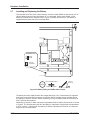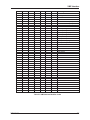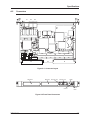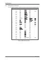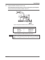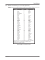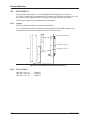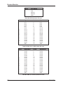
1
Technical Reference Manual
for VP 110/01x
VME Pentium® III-M Single
Board Computer
Manual Order Code 550 0014 Rev 02
Concurrent Technologies Inc
3840 Packard Road
Suite 130
Ann Arbor, MI 48108
USA
Tel: (734) 971 6309
Fax: (734) 971 6350
E-mail: [email protected]
August 2002
Concurrent Technologies Plc
4 Gilberd Court
Newcomen Way
Colchester, Essex CO4 9WN
United Kingdom
Tel: (+44) 1206 752626
Fax: (+44) 1206 751116
http://www.gocct.com
NOTES
Information furnished by Concurrent Technologies is believed to be accurate and reliable.
However, Concurrent Technologies assumes no responsibility for any errors contained in this
document and makes no commitment to update or to keep current the information contained in
this document. Concurrent Technologies reserves the right to change specifications at any time
without notice.
Concurrent Technologies assumes no responsibility either for the use of this document or for any
infringements of the patent or other rights of third parties which may result from its use. In
particular, no license is either granted or implied under any patent or patent rights belonging to
Concurrent Technologies.
Some parts of this document are reproduced with the permission of and remain copyright
Phoenix Technologies Ltd, 1997.
No part of this document may be copied or reproduced in any form or by any means without the
prior written consent of Concurrent Technologies.
All companies and product names are trademarks of their respective companies.
CONVENTIONS
Throughout this manual the following conventions will apply:
# or * or
over a name represents an active low signal. e.g. INIT* or INIT or INIT#
h denotes a hexadecimal number. e.g. FF45h
byte represents 8-bits
word represents 16-bits
dword represents 32-bits
ii
VP 110/01x
GLOSSARY OF TERMS
BIOS · · · · · Basic Input Output System
BIST · · · · · Built In Self Test
BSB· · · · · · Back Side Bus
CCT· · · · · · Concurrent Technologies
CPU · · · · · Central Processing Unit
CRT· · · · · · Cathode Ray Tube
DDC · · · · · Display Data Channel
DIB · · · · · · Dual Independent Bus
DFP· · · · · · Digital Flat Panel
DMA · · · · · Direct Memory Access
ECC · · · · · Error Checking and Correcting
ECP· · · · · · Extended Capabilities Port
EIDE · · · · · Enhanced Integrated Drive Electronics
EPP· · · · · · Enhanced Parallel Port
EPROM· · · Electrically Programmable Read Only Memory
FSB · · · · · · Front Side Bus
ISA · · · · · · Industry Standard Architecture
LDT · · · · · · Long Duration Timer
LFM· · · · · · Linear Feet per Minute
LPC · · · · · · Low Pin Count
NMI · · · · · · Non Maskable Interrupt
PCI · · · · · · Peripheral Component Interconnect
PIT · · · · · · Programmable Interval Timer
PMC · · · · · PCI Mezzanine Card
POST · · · · Power-on Self Test
RFU· · · · · · Reserved for Future Use
RTC· · · · · · Real Time Clock
SCC · · · · · Serial Communications Controller
SCSI · · · · · Small Computer Systems Interface
SDRAM · · · Synchronous Dynamic Random Access Memory
SODIMM · · Small Outline Dual Inline Memory Module
TTL · · · · · · Transistor-Transistor Logic
UART · · · · Universal Asynchronous Receiver Transmitter
USB· · · · · · Universal Serial Bus
VP 110/01x
iii
NOTATIONAL CONVENTIONS
NOTE Notes provide general additional information.
WARNING Warnings provide indication of board malfunction if they are not observed.
CAUTION Cautions provide indications of board or system damage if they are not observed.
iv
VP 110/01x
Revision
Revision History
Date
01
Initial Release
July 2002
02
Added clarifications to several sections
August 2002
VP 110/01x
v
Table of Contents
1.
Introduction and Overview
1.1
1.2
1.2.1
1.2.2
1.2.3
1.2.4
1.2.5
1.2.6
1.2.7
1.2.8
1.2.9
1.2.10
1.2.11
1.2.12
1.2.13
1.2.14
1.2.15
1.2.16
1.2.17
1.3
2.
2.1
2.2
2.3
2.4
2.4.1
2.4.2
2.4.3
2.4.4
2.4.5
2.4.6
2.4.7
2.5
2.5.1
2.5.2
2.6
2.7
2.8
2.9
2.9.1
2.9.2
3.
·
·
General · · · · · · · ·
The VP 110/01x - Main Features ·
Central Processor · · · · ·
Cache Memories· · · · · ·
Chipset· · · · · · · · ·
SDRAM · · · · · · · ·
PCI Busses · · · · · · ·
EPROM · · · · · · · ·
Battery Backed SRAM · · · ·
Application Flash EPROM · · ·
EIDE Controllers · · · · · ·
USB· · · · · · · · · ·
PMC Interface · · · · · ·
Ethernet Controllers · · · · ·
VME Interface · · · · · ·
Floppy Disk · · · · · · ·
Serial Communication · · · ·
Keyboard & Mouse · · · · ·
Real Time Clock (RTC)· · · ·
Additional Board Options · · ·
·
·
·
·
·
·
·
·
·
·
·
·
·
·
·
·
·
·
·
·
·
·
·
·
·
·
·
·
·
·
·
·
·
·
·
·
·
·
·
·
·
·
·
·
vi
·
·
·
·
·
·
·
·
·
·
·
·
·
·
·
·
·
·
·
·
·
·
·
·
·
·
·
·
·
·
Starting up for the first time · ·
Bootloading from CD-ROM · ·
Installing Windows NT® 4.0 · ·
Installing Windows® 2000 · · ·
Installing RedHat® Linux® 7.2 · ·
Using VxWorks 5.4 with Tornado 2
Mass Storage Interfaces
4.1
4.2
·
·
·
·
·
·
·
·
·
·
·
·
·
·
·
·
·
·
·
·
·
·
·
·
Floppy Disk Interface
EIDE Interfaces · ·
·
·
·
·
·
·
·
·
·
·
·
·
·
·
·
·
·
·
·
·
·
·
·
·
·
·
·
·
·
·
General · · · · · · · · · · ·
Unpacking and Inspection · · · · · ·
Default Jumper Settings
· · · · ·
Front Panel Indicators and Controls · · ·
Run LED (R) Green · · · · · · · ·
POST LED (P) Yellow · · · · · · ·
Ethernet Speed LEDs (Speed) Yellow · ·
Link/Activity LEDs (LK/ACT) Green · · ·
Battery Status LED (B) Yellow (optional) ·
Reset/NMI Switch · · · · · · · ·
External Reset · · · · · · · · ·
Installation of On-Board Mass Storage · ·
Hard Disk Storage Kit (AD CP1/DR1) · ·
CompactFlash Storage Kit (AD 200/001) ·
Adding or Replacing DRAM Modules · ·
Installing and Replacing the Battery · ·
Installing or Removing a PMC Module· ·
Installing the Board in a VME Backplane ·
Installing the board· · · · · · · ·
Removing the board · · · · · · ·
Software Installation
3.1
3.2
3.3
3.4
3.5
3.6
4.
·
Hardware Installation
·
·
·
·
·
·
·
·
·
·
·
·
·
·
·
·
·
·
·
·
·
·
·
·
·
·
·
·
·
·
·
·
·
·
·
·
·
·
·
·
·
·
·
·
·
·
·
·
·
·
·
·
·
·
·
·
·
·
·
·
·
·
·
·
·
·
·
·
·
·
·
·
·
·
·
·
·
·
·
·
·
·
·
·
·
·
·
·
·
·
·
·
·
·
·
·
·
·
·
·
·
·
·
·
·
·
·
·
·
·
·
·
·
·
·
·
·
·
·
·
·
·
·
·
·
·
·
·
·
·
·
·
·
·
·
·
·
·
·
·
·
·
·
·
·
·
·
·
·
·
·
·
·
·
·
·
·
·
·
·
·
·
·
·
·
·
·
·
·
·
·
·
·
·
·
·
·
·
·
·
·
·
·
·
·
·
·
·
·
·
·
·
·
·
·
·
·
·
·
·
·
·
·
·
·
·
·
·
·
·
·
·
·
·
·
·
·
·
·
·
·
·
·
·
·
·
·
·
·
·
·
·
·
·
·
·
·
·
·
·
·
·
·
·
·
·
·
·
·
·
·
·
·
·
·
·
·
·
·
·
·
·
·
·
·
·
·
·
·
·
·
·
·
·
·
·
·
·
·
·
·
·
·
·
·
·
·
·
·
·
·
·
·
·
·
·
·
·
·
·
·
·
·
·
·
·
·
·
·
·
·
·
·
·
·
·
·
·
·
·
·
·
·
·
·
·
·
·
·
·
·
·
·
·
·
·
·
·
·
·
·
·
·
·
·
·
·
·
·
·
·
·
·
·
·
·
·
·
·
·
·
·
·
·
·
·
·
·
·
·
·
·
·
·
·
·
·
·
·
·
·
·
·
·
·
·
·
·
·
·
·
·
·
·
·
·
·
·
·
·
·
·
·
·
·
·
·
·
·
·
·
·
·
·
·
·
·
·
·
·
·
·
·
·
·
·
·
·
·
·
·
·
·
·
·
·
·
·
·
·
·
·
·
·
·
·
·
·
·
·
·
·
·
·
·
·
·
·
·
·
·
·
·
·
·
·
·
·
·
·
·
·
·
·
·
·
·
·
·
·
·
·
·
·
·
·
·
·
·
·
·
·
·
·
·
·
·
·
·
·
·
·
·
·
·
·
·
·
·
·
·
·
·
·
·
·
·
·
·
·
·
·
·
·
·
·
·
·
·
·
·
·
·
·
·
·
·
·
·
·
·
·
·
·
·
·
·
·
·
·
·
·
·
·
·
·
·
·
·
·
·
·
·
·
·
·
·
·
·
·
·
·
·
·
·
·
·
·
·
·
·
·
·
·
·
·
·
·
·
·
·
·
·
·
·
·
·
·
·
·
·
·
·
·
·
·
·
·
·
·
·
·
·
·
·
·
·
·
·
·
·
·
·
·
·
·
·
·
·
·
·
·
·
·
·
·
·
·
·
·
·
·
·
·
·
·
·
·
·
·
·
·
·
·
·
·
·
·
·
·
·
·
·
2-1
2-2
2-3
2-4
2-4
2-4
2-4
2-4
2-4
2-4
2-5
2-6
2-7
2-8
2-9
2-10
2-12
2-14
2-14
2-14
3-1
·
·
·
·
·
·
·
·
·
1-1
1-2
1-2
1-2
1-2
1-3
1-3
1-3
1-3
1-3
1-3
1-3
1-3
1-3
1-3
1-4
1-4
1-4
1-4
1-5
2-1
·
·
·
·
·
·
·
·
·
·
·
·
·
·
·
·
·
·
·
·
·
·
·
·
·
·
·
·
·
·
·
·
1-1
3-1
3-2
3-3
3-4
3-5
3-6
4-1
·
·
4-1
4-2
VP 110/01x
4.3
4.4
5.
·
·
VME Bus Interface Features · · · · · · · ·
VME Byte Swapping · · · · · · · · · ·
VME Bus Error Interrupt · · · · · · · · ·
VME Address Capture · · · · · · · · · ·
VME Address Capture Read Register (Read Only) ·
VME Address Capture Control Register (Write Only)
·
·
·
·
·
·
·
·
·
·
·
·
·
·
·
·
·
·
·
·
·
·
·
·
·
·
·
·
·
·
·
·
·
·
·
·
·
·
·
·
·
·
·
·
·
·
·
·
·
·
·
·
·
·
·
·
·
·
·
·
·
·
·
·
·
·
·
·
·
·
·
·
·
·
·
·
·
·
·
·
·
·
·
·
·
·
·
·
·
·
·
·
·
·
·
·
·
·
·
·
·
·
·
·
Serial Port · · · · · · · ·
Keyboard and Mouse Ports · ·
Ethernet Controllers · · · · ·
Real-Time Clock · · · · · ·
Universal Serial Bus (USB) · ·
Power On Self Test LED/Speaker
·
·
·
·
·
·
·
·
·
·
·
·
·
·
·
·
·
SDRAM · · · · · ·
Flash EPROM · · · ·
Application Flash EPROM ·
Battery backed SRAM · ·
·
·
·
·
·
·
·
·
·
·
·
·
·
·
·
·
·
·
·
·
·
·
·
·
·
·
·
·
·
·
·
·
·
·
·
·
·
·
·
·
·
·
·
·
·
·
·
·
·
·
·
·
·
·
·
·
·
Entering the PC BIOS · · · ·
The PC BIOS Startup Sequence ·
Boot device selection · · · ·
PCI Bus Resource Management ·
PCI Resource Allocation · · ·
PCI Device IDs · · · · · ·
·
·
·
·
·
·
·
·
·
·
·
·
·
VME System Architecture Test Handler ·
10.1
10.2
·
·
·
·
Introduction · · · ·
The VSA Environment
VP 110/01x
·
·
·
·
·
·
·
·
·
·
·
·
·
·
·
·
·
·
·
·
·
·
·
·
·
·
·
·
·
·
·
·
·
·
·
·
·
·
·
·
·
·
·
·
·
·
·
·
·
·
·
·
·
·
·
·
·
·
·
·
·
·
·
·
·
·
·
·
·
·
·
·
·
·
·
·
·
·
·
·
·
·
·
·
·
·
·
·
·
·
·
·
·
·
·
·
·
·
·
·
·
·
·
·
·
·
·
·
·
·
·
·
·
·
·
·
·
·
·
·
·
·
·
·
·
·
·
·
·
·
·
·
·
·
·
·
·
·
·
·
·
·
·
·
·
·
·
·
·
·
·
·
·
·
·
·
·
·
·
·
·
·
·
·
·
·
·
·
·
·
·
·
·
·
·
·
·
·
·
·
·
·
·
·
·
·
·
·
·
·
·
·
·
·
·
·
·
·
·
·
·
·
·
·
·
·
·
·
·
·
·
·
·
·
·
·
·
·
·
·
·
·
·
·
·
·
·
·
·
·
·
·
·
·
·
·
·
·
·
·
·
·
·
·
·
·
·
·
·
·
·
·
·
·
·
·
·
·
·
·
·
·
·
·
·
·
·
·
·
·
·
·
·
·
·
·
·
·
·
·
·
·
·
·
·
·
Status & Control Register 0 (I/O address 210h) · · · · ·
Status & Control Register 2 (I/O address 211h) · · · · ·
Status & Control Register 1(I/O address 212h) · · · · ·
Watchdog Timer · · · · · · · · · · · · · · ·
Watchdog Status & Control Register (I/O address 214h) · ·
Watchdog Configuration · · · · · · · · · · · ·
Using the Watchdog· · · · · · · · · · · · · ·
Programming the Watchdog · · · · · · · · · · ·
Status & Control Register 4 (I/O address 215h) · · · · ·
Memory Page and Status Register (I/O address 216h) · ·
Status & Control Register 3 (I/O address 217h) · · · · ·
Long Duration Timer/Periodic Interrupt Timer · · · · ·
Long Duration Timer/Periodic Interrupt Timer Low Byte · ·
Long Duration Timer/Periodic Interrupt Timer Mid-low Byte ·
Long Duration Timer/Periodic Interrupt Timer Mid-high Byte ·
Long Duration Timer/Periodic Interrupt Timer High Byte · ·
LDT/PIT Status & Control Register · · · · · · · · ·
Programming the LDT/PIT · · · · · · · · · · ·
Port 80 · · · · · · · · · · · · · · · · ·
PC BIOS·
9.1
9.2
9.3
9.4
9.4.1
9.4.2
10.
·
·
·
·
Additional Local I/O Functions ·
8.1
8.2
8.3
8.4
8.4.1
8.4.2
8.4.3
8.4.4
8.5
8.6
8.7
8.8
8.8.1
8.8.2
8.8.3
8.8.4
8.8.5
8.8.6
8.9
9.
·
·
Memory ·
7.1
7.2
7.3
7.4
8.
·
·
Other Interfaces ·
6.1
6.2
6.3
6.4
6.5
6.6
7.
·
·
VME Interface ·
5.1
5.2
5.3
5.4
5.4.1
5.4.2
6.
ROM Disk ·
RAM Disk ·
·
·
·
·
·
·
·
·
·
·
·
·
·
·
·
·
·
·
·
·
·
·
·
·
·
·
·
·
·
·
·
·
·
·
·
·
·
·
·
·
·
·
·
·
·
·
·
·
·
·
·
·
·
·
·
·
·
·
·
·
·
·
·
·
·
·
·
·
·
·
·
·
·
·
·
·
·
·
·
·
·
·
·
·
·
·
·
·
·
·
·
·
·
·
·
·
·
·
·
·
·
·
·
·
·
·
·
·
·
·
·
·
·
·
·
·
7-2
7-3
7-4
7-5
8-1
·
·
·
·
·
·
·
·
·
·
·
·
·
·
·
·
·
·
·
·
·
·
·
·
·
·
·
·
·
·
·
·
6-1
6-2
6-3
6-4
6-5
6-6
7-1
·
·
·
·
·
·
·
·
·
·
·
·
·
·
5-1
5-2
5-3
5-3
5-4
5-6
6-1
·
·
·
·
·
·
·
·
·
·
·
·
·
·
·
·
·
·
·
·
·
·
·
·
·
4-3
4-4
5-1
·
·
·
·
·
·
·
·
·
·
·
·
8-3
8-4
8-5
8-6
8-7
8-8
8-8
8-9
8-11
8-12
8-13
8-14
8-15
8-15
8-15
8-15
8-16
8-17
8-20
9-1
·
·
·
·
·
·
9-1
9-3
9-4
9-5
9-5
9-7
10-1
·
·
10-1
10-1
vii
10.2.1
10.2.2
10.2.3
10.2.4
10.2.5
10.2.6
10.3
10.3.1
10.3.2
10.3.3
11.
Slot Numbering · · · · · · · · ·
VSA Console Devices· · · · · · ·
Starting the Master Test Handler · · ·
Remote Testing from the System Controller
Bootloading the BIOS · · · · · · ·
BIST Execution · · · · · · · · ·
MTH Command Reference · · · · ·
Help Screens · · · · · · · · ·
General Commands · · · · · · ·
Utility Commands · · · · · · · ·
·
·
·
·
·
·
·
·
·
·
·
·
·
·
·
·
·
·
·
·
·
·
Initialization Checks · · · · · · · · · · ·
Check 16: CPU Alive Check · · · · · · · · ·
Check 18: Scratchpad RAM Check · · · · · ·
BIST Descriptions · · · · · · · · · · · ·
Test 1: Test Initialization Routine · · · · · · ·
Test 2: PROM Check · · · · · · · · · · ·
Test 4: Numeric Coprocessor Test · · · · · · ·
Test 6: Interconnect Image Check · · · · · · ·
Test 7: Off-board Interconnect Access · · · · ·
Test 9: 8254 PIT Test · · · · · · · · · · ·
Test 10: 8259A PIC Test · · · · · · · · · ·
Test 12: Local RAM Fixed Pattern Test · · · · ·
Test 13: SCC Access Test · · · · · · · · ·
Test 19: NMI Test · · · · · · · · · · · ·
Test 20: Universe NMI Test · · · · · · · · ·
Test 22: RAM Data and Address Bus Test · · · ·
Test 23: Local RAM Read/Write Test · · · · · ·
Test 25: Local RAM Dual Address Test · · · · ·
Test 27: Local RAM Execution Test · · · · · ·
Test 28: SCC Interrupt Test · · · · · · · · ·
Test 29: SCC Internal Loopback Test · · · · · ·
Test 30: SCC External Loopback · · · · · · ·
Test 33: Universe PCI−>VME Test · · · · · · ·
Test 34: Universe PCI Config Utility · · · · · ·
Test 35: Universe VME Config Utility · · · · · ·
Test 36: VME Bus Byte Swapping · · · · · · ·
Test 37: Bus Error Detection Test · · · · · · ·
Sub-Test 1: VME Bus Error Detection [by polling] · ·
Sub-Test 2: VME Bus Error Detection [by interrupt] ·
Sub-Test 3: VME Bus Error Address Capture · · ·
Test 39: Watchdog Test· · · · · · · · · ·
Sub-Test 1: Watchdog NMI Test · · · · · · ·
Sub-Test 2: Watchdog Reset Test · · · · · ·
Test 40: LDT and PIT Test · · · · · · · · ·
Sub-Test 1: Standard LDT / PIT Functional Test · ·
Sub-Test 2: Enhanced LDT / PIT Functional Test · ·
Test 41: StrataFlash Test · · · · · · · · ·
Test 42: Non-Volatile RAM Test · · · · · · ·
Sub-test 1: Non-destructive NVRAM Read/Write Test
Sub-test 2: NVRAM Data retention Pattern, Setup ·
Sub-test 3: NVRAM Data Retention Pattern Check ·
Test 56: IDE Controller Test · · · · · · · ·
Register Access Test · · · · · · · · · ·
Controller Diagnostics Test· · · · · · · · ·
Identify Disk Drive · · · · · · · · · · ·
Test 58: IDE Fixture Test · · · · · · · · ·
Test 63: PS/2 Mouse Test · · · · · · · · ·
·
·
·
·
·
·
·
·
·
·
·
·
·
·
·
·
·
·
·
·
·
·
·
·
·
·
·
·
·
·
VSA Mode Diagnostics
11.1
11.1.1
11.1.2
11.2
11.2.1
11.2.2
11.2.3
11.2.4
11.2.5
11.2.6
11.2.7
11.2.8
11.2.9
11.2.10
11.2.11
11.2.12
11.2.13
11.2.14
11.2.15
11.2.16
11.2.17
11.2.18
11.2.19
11.2.20
11.2.21
11.2.22
11.2.23
11.2.23.1
11.2.23.2
11.2.23.3
11.2.24
11.2.24.1
11.2.24.2
11.2.25
11.2.26
11.2.27
11.2.28
11.2.29
11.2.29.1
11.2.29.2
11.2.29.3
11.2.30
11.2.30.1
11.2.30.2
11.2.30.3
11.2.31
11.2.32
viii
·
·
·
·
·
·
·
·
·
·
·
·
·
·
·
·
·
·
·
·
·
·
·
·
·
·
·
·
·
·
·
·
·
·
·
·
·
·
·
·
·
·
·
·
·
·
·
·
·
·
·
·
·
·
·
·
·
·
·
·
·
·
·
·
·
·
·
·
·
·
·
·
·
·
·
·
·
·
·
·
·
·
·
·
·
·
·
·
·
·
·
·
·
·
·
·
·
·
·
·
·
·
·
·
·
·
·
·
·
·
·
·
·
·
·
·
·
·
·
·
·
·
·
·
·
·
·
·
·
·
·
·
·
·
·
·
·
·
·
·
·
·
·
·
·
·
·
·
·
·
·
·
·
·
·
·
·
·
·
·
·
·
·
·
·
·
·
·
·
·
·
·
·
·
·
·
·
·
·
·
·
·
·
·
·
·
·
·
·
·
·
·
·
·
·
·
·
·
·
·
·
·
·
·
·
·
·
·
·
·
·
·
·
·
·
·
·
·
·
·
·
·
·
·
·
·
·
·
·
·
·
·
·
·
·
·
·
·
·
·
·
·
·
·
·
·
·
·
·
·
·
·
·
·
·
·
·
·
·
·
·
·
·
·
·
·
·
·
·
·
·
·
·
·
·
·
·
·
·
·
·
·
·
·
·
·
·
·
·
·
·
·
·
·
·
·
·
·
·
·
·
·
·
·
·
·
·
·
·
·
·
·
·
·
·
·
·
·
·
·
·
·
·
·
·
·
·
·
·
·
·
·
·
·
·
·
·
·
·
·
·
·
·
·
·
·
·
·
·
·
·
·
·
·
·
·
·
·
·
·
·
·
·
·
·
·
·
·
·
·
·
·
·
·
·
·
·
·
·
·
·
·
·
·
·
·
·
·
·
·
·
·
·
·
·
·
·
·
·
·
·
·
·
·
·
·
·
·
·
·
·
·
·
·
·
·
·
·
·
·
·
·
·
·
·
·
·
·
·
·
·
·
·
·
·
·
·
·
·
·
·
·
·
·
·
·
·
·
·
·
·
·
·
·
·
·
·
·
·
·
·
·
·
·
·
·
·
·
·
·
·
·
·
·
·
·
·
·
·
·
·
·
·
·
·
·
·
·
·
·
·
·
·
·
·
·
·
·
·
·
·
·
·
·
·
·
·
·
·
·
·
·
·
·
·
·
·
·
·
·
·
·
·
·
·
·
·
·
·
·
·
·
·
·
·
·
·
·
·
·
·
·
·
·
·
·
10-1
10-1
10-2
10-2
10-2
10-3
10-4
10-4
10-4
10-6
11-1
·
·
·
·
·
·
·
·
·
·
·
·
·
·
·
·
·
·
·
·
·
·
·
·
·
·
·
·
·
·
11-1
11-1
11-1
11-2
11-2
11-2
11-2
11-3
11-3
11-3
11-3
11-4
11-4
11-4
11-5
11-5
11-5
11-6
11-6
11-7
11-7
11-7
11-7
11-8
11-8
11-8
11-9
11-9
11-9
11-9
11-10
11-10
11-10
11-11
11-11
11-11
11-12
11-13
11-13
11-13
11-13
11-14
11-14
11-14
11-14
11-15
11-16
VP 110/01x
11.2.33
11.2.34
11.2.35
11.2.35.1
11.2.35.2
11.2.35.3
11.2.35.4
11.2.35.5
11.2.35.6
11.2.36
11.2.36.1
11.2.36.2
11.2.36.3
11.2.36.4
11.2.36.5
11.2.37
11.2.38
11.2.39
11.2.39.1
11.2.39.2
11.2.39.3
11.2.40
11.2.41
11.2.42
11.2.43
11.2.44
11.2.45
11.2.46
11.2.47
11.2.48
11.2.49
11.2.50
11.2.51
A.
Specifications·
A.1
A.2
A.2.1
A.2.2
A.3
A.4
A.4.1
A.5
A.5.1
A.5.2
A.5.3
A.5.4
A.5.5
A.5.6
A.5.7
A.5.8
A.5.9
A.5.10
A.5.11
B.
Test 64: PC Keyboard Test· · · · · · · · ·
Test 68: Real Time Clock Test· · · · · · · ·
Test 69: 82559ER Test · · · · · · · · · ·
Sub-Test 0 – Default Tests · · · · · · · · ·
Sub-Test 1 – Device Checks · · · · · · · ·
Sub-Test 2 – Internal Loopback · · · · · · ·
Sub-Test 3 – External Loopback @ 10Mb/sec · · ·
Sub-Test 4 – External Loopback @ 100Mb/sec · ·
Sub-Test 5 – Display Programmed Ethernet Address
Test 70: Maxim 1617 Thermal Sensor Test· · · ·
Basic Functionality · · · · · · · · · · ·
Temperature Readout · · · · · · · · · ·
Set Alarms · · · · · · · · · · · · · ·
Change Update Frequency · · · · · · · ·
Full Readout · · · · · · · · · · · · ·
Test 71: 82559ER Interface Test · · · · · · ·
Test 80: SCSI Based PMC Site Test · · · · · ·
Test 85: Floppy Disk Drive Test · · · · · · ·
Controller Access Test · · · · · · · · · ·
Diskette Access Test · · · · · · · · · ·
Disk Checksum Test · · · · · · · · · · ·
Test 101: Display Memory Utility · · · · · · ·
Test 102: Fill Memory Utility · · · · · · · ·
Test 103: I/O Read Utility · · · · · · · · ·
Test 104: I/O Write Utility · · · · · · · · ·
Test 105: Interconnect Read Utility · · · · · ·
Test 106: Interconnect Write Utility · · · · · ·
Test 107: Cache Control Utility · · · · · · ·
Test 120: PCI Configuration Utility · · · · · ·
Test 121: PCI Read Utility · · · · · · · · ·
Test 122: PCI Write Utility · · · · · · · · ·
Test 126: Display Board Configuration · · · · ·
Test 127: Retrieve BIST Information · · · · · ·
·
·
·
·
·
·
·
·
·
·
·
·
·
·
·
·
·
·
·
·
·
·
·
·
·
·
·
·
·
·
·
·
·
·
·
·
·
·
·
·
·
·
·
·
·
·
·
·
·
·
·
·
·
·
·
·
·
·
·
·
·
·
·
·
·
·
·
·
·
·
·
·
·
·
·
·
·
·
·
·
Functional Specification · · · · · · · · · · ·
Environmental Specification · · · · · · · · · ·
Temperature Range · · · · · · · · · · · ·
Humidity · · · · · · · · · · · · · · · ·
Dimensions · · · · · · · · · · · · · · ·
Electrical Specification · · · · · · · · · · · ·
Power Supply Requirements · · · · · · · · · ·
Connectors
· · · · · · · · · · · · · ·
VME Interface (P1) Pin-outs · · · · · · · · · ·
Auxiliary Connector (P2) Pin-outs · · · · · · · ·
PMC I/O Connector (P0) Pin-outs · · · · · · · ·
Keyboard and Mouse Header (LK1) Pin-outs · · · · ·
Serial Interface (J9) Pin-outs · · · · · · · · · ·
Ethernet Interface (J15 and J16) Pin-outs · · · · · ·
On-Board Mass Storage Option Connector (S1) Pin-outs·
PMC Site 1 Connectors (J11, J12, J13 and J14) Pin-outs
PMC Site 2 Connectors (J21, J22, J23 and J24) Pin-outs
Processor Debug Port (J1) Pin-outs · · · · · · ·
Port 80 (J3) Pin-outs
· · · · · · · · · · ·
Breakout Modules ·
B.1
B.2
B.3
·
·
·
·
·
·
·
·
·
·
·
·
·
·
·
·
·
·
·
·
·
·
·
·
·
·
·
·
·
·
·
·
·
·
·
·
Introduction · · · ·
Breakout Modules List ·
AD VP2/004-10 · · ·
VP 110/01x
·
·
·
·
·
·
·
·
·
·
·
·
·
·
·
·
·
·
·
·
·
·
·
·
·
·
·
·
·
·
·
·
·
·
·
·
·
·
·
·
·
·
·
·
·
·
·
·
·
·
·
·
·
·
·
·
·
·
·
·
·
·
·
·
·
·
·
·
·
·
·
·
·
·
·
·
·
·
·
·
·
·
·
·
·
·
·
·
·
·
·
·
·
·
·
·
·
·
·
·
·
·
·
·
·
·
·
·
·
·
·
·
·
·
·
·
·
·
·
·
·
·
·
·
·
·
·
·
·
·
·
·
·
·
·
·
·
·
·
·
·
·
·
·
·
·
·
·
·
·
·
·
·
·
·
·
·
·
·
·
·
·
·
·
·
·
·
·
·
·
·
·
·
·
·
·
·
·
·
·
·
·
·
·
·
·
·
·
·
·
·
·
·
·
·
·
·
·
·
·
·
·
·
·
·
·
·
·
·
·
·
·
·
·
·
·
·
·
·
·
·
·
·
·
·
·
·
·
·
·
·
·
·
·
·
·
·
·
·
·
·
·
·
·
·
·
·
·
·
·
·
·
·
·
·
·
·
·
·
·
·
·
·
·
·
·
·
·
·
·
·
·
·
·
·
·
·
·
·
·
·
·
·
·
·
·
·
·
·
·
·
·
·
·
·
·
·
·
·
·
·
·
·
·
·
·
·
·
·
·
·
·
·
·
·
·
·
·
·
·
·
·
·
·
·
·
·
·
·
·
·
·
·
·
·
·
·
·
·
·
·
·
·
·
·
·
·
·
·
·
·
·
·
·
·
·
·
·
·
·
·
·
·
·
·
·
·
·
·
·
·
·
·
·
·
·
·
·
·
·
·
·
·
·
·
·
·
·
·
·
·
·
·
·
·
·
·
·
·
·
·
·
·
·
·
·
·
·
·
·
·
·
·
·
·
·
·
·
·
·
·
·
·
·
·
·
·
·
·
·
·
·
·
·
·
·
·
·
·
·
·
·
·
·
·
·
·
·
·
·
·
·
·
·
·
·
·
·
·
11-17
11-18
11-19
11-19
11-19
11-19
11-19
11-19
11-19
11-20
11-20
11-20
11-20
11-21
11-22
11-23
11-23
11-23
11-23
11-23
11-23
11-24
11-24
11-24
11-25
11-25
11-25
11-26
11-26
11-27
11-27
11-27
11-27
·
·
·
·
·
A-1
·
·
·
·
·
·
·
·
·
·
·
·
·
·
·
·
·
·
A-1
A-2
A-2
A-2
A-2
A-2
A-2
A-3
A-4
A-5
A-6
A-7
A-8
A-9
A-10
A-11
A-15
A-19
A-20
B-1
·
·
·
B-1
B-1
B-2
ix
B.3.1
B.3.2
B.4
B.4.1
B.4.2
B.5
B.5.1
B.5.2
B.6
x
Layout · · · · · · · · · · ·
Pin-out Tables · · · · · · · ·
AD VP2/004-20 · · · · · · · ·
Layout · · · · · · · · · · ·
Pin-out Tables · · · · · · · ·
AD VP2/005-00 · · · · · · · ·
Layout · · · · · · · · · · ·
Pin-out Tables · · · · · · · ·
Header/Connector Configuration Tables
·
·
·
·
·
·
·
·
·
·
·
·
·
·
·
·
·
·
·
·
·
·
·
·
·
·
·
·
·
·
·
·
·
·
·
·
·
·
·
·
·
·
·
·
·
·
·
·
·
·
·
·
·
·
·
·
·
·
·
·
·
·
·
·
·
·
·
·
·
·
·
·
·
·
·
·
·
·
·
·
·
·
·
·
·
·
·
·
·
·
·
·
·
·
·
·
·
·
·
·
·
·
·
·
·
·
·
·
·
·
·
·
·
·
·
·
·
·
·
·
·
·
·
·
·
·
·
·
·
·
·
·
·
·
·
B-2
B-2
B-3
B-3
B-3
B-4
B-4
B-4
B-5
VP 110/01x
Table of Figures
Figure 1-1
Figure 2-1
Figure 2-2
Figure 2-3
Figure 2-4
Figure 2-5
Figure 2-6
Figure 2-7
Figure 2-8
Figure 2-9
Figure 2-10
Figure 6-1
Figure 7-1
Figure 7-2
Figure 7-3
Figure 8-1
Figure 9-1
Figure A-1
Figure A-2
Figure A-3
Figure A-4
Figure A-5
Figure A-6
Figure B-1
Figure B-2
Figure B-3
VP 110/01x
Overview · · · · · · · · · · · ·
Default Jumper and Switch Settings · · · ·
Front Panel Indicators and Controls · · · ·
Front Panel Reset and NMI Switch · · · ·
Mass Storage Connector and Fixing Holes · ·
Disk Drive Cable Installation · · · · · ·
CompactFlash Carrier Module Installation · ·
DRAM Module Replacement · · · · · ·
Battery Fitting and CMOS Clear Jumper · ·
PMC Installation Diagram · · · · · · ·
PMC V(I/O) Jumper · · · · · · · · ·
Console Mode Switch· · · · · · · · ·
Memory Map · · · · · · · · · · ·
Flash Program Jumper · · · · · · · ·
SRAM Backup Power Jumper · · · · · ·
Watchdog Timer Switch · · · · · · · ·
Mode Switch · · · · · · · · · · ·
Connector Layout · · · · · · · · · ·
Front Panel Connectors · · · · · · · ·
Keyboard and Mouse Header LK1 Polarization·
Serial Port RJ45 Connector (Front View)· · ·
Ethernet RJ-45 Connector (Front View) · · ·
Port 80 Connector · · · · · · · · ·
AD VP2/004-10 P2 Breakout Connectors · ·
AD VP2/004-20 P2 Breakout Connectors · ·
AD VP2/005-00 P2 Breakout Connectors · ·
·
·
·
·
·
·
·
·
·
·
·
·
·
·
·
·
·
·
·
·
·
·
·
·
·
·
·
·
·
·
·
·
·
·
·
·
·
·
·
·
·
·
·
·
·
·
·
·
·
·
·
·
·
·
·
·
·
·
·
·
·
·
·
·
·
·
·
·
·
·
·
·
·
·
·
·
·
·
·
·
·
·
·
·
·
·
·
·
·
·
·
·
·
·
·
·
·
·
·
·
·
·
·
·
·
·
·
·
·
·
·
·
·
·
·
·
·
·
·
·
·
·
·
·
·
·
·
·
·
·
·
·
·
·
·
·
·
·
·
·
·
·
·
·
·
·
·
·
·
·
·
·
·
·
·
·
·
·
·
·
·
·
·
·
·
·
·
·
·
·
·
·
·
·
·
·
·
·
·
·
·
·
·
·
·
·
·
·
·
·
·
·
·
·
·
·
·
·
·
·
·
·
·
·
·
·
·
·
·
·
·
·
·
·
·
·
·
·
·
·
·
·
·
·
·
·
·
·
·
·
·
·
·
·
·
·
·
·
·
·
·
·
·
·
·
·
·
·
·
·
·
·
·
·
·
·
·
·
·
·
·
·
·
·
·
·
·
·
·
·
·
·
·
·
·
·
·
·
·
·
·
·
·
·
·
·
·
·
·
·
·
·
·
·
·
·
·
·
·
·
·
·
·
·
·
·
·
·
·
·
·
·
1-1
2-3
2-4
2-5
2-6
2-7
2-8
2-9
2-10
2-12
2-13
6-1
7-1
7-4
7-5
8-6
9-1
A-3
A-3
A-7
A-8
A-9
A-20
B-2
B-3
B-4
xi
Table of Tables
Table 1-1
Table 5-1
Table 5-2
Table 5-2
Table 8-1
Table 9-1
Table 9-2
Table A-1
Table A-2
Table A-3
Table A-4
Table A-5
Table A-6
Table A-7
Table A-8
Table A-9
Table A-10
Table A-11
Table A-12
Table A-13
Table A-14
Table A-15
Table A-16
Table A-17
Table A-18
Table B-1
Table B-2
Table B-3
Table B-4
Table B-5
Table B-6
Table B-7
xii
VME P2 Breakout Interfaces · · · · · · ·
VME Address Capture Read Register· · · · ·
VME Address Modifier Codes · · · · · · ·
VME Address Modifier Codes (Continued) · · ·
I/O Address Map · · · · · · · · · · ·
Configurable PCI Bus Interrupts · · · · · ·
PCI Device Numbers · · · · · · · · · ·
VME Interface Pin-outs · · · · · · · · ·
P2 Connector Pin-outs (64 PMC I/O Signals) · ·
PMC I/O Connector (P0) Pin-outs · · · · · ·
Keyboard and Mouse Header (LK1) Pin-outs · ·
Serial Port Cable Connections · · · · · · ·
Serial Port Cable Connections · · · · · · ·
Ethernet RJ-45 Connector Pin-outs · · · · ·
On-Board Mass Storage Option Interface Pin-outs
PMC J11 Connector Pin-outs · · · · · · ·
PMC J12 Connector Pin-outs · · · · · · ·
PMC J13 Connector Pin-outs · · · · · · ·
PMC J14 Connector Pin-outs · · · · · · ·
PMC J21 Connector Pin-outs · · · · · · ·
PMC J22 Connector Pin-outs · · · · · · ·
PMC J23 Connector Pin-outs · · · · · · ·
PMC J24 Connector Pin-outs · · · · · · ·
30-way Debug Connector Pin-outs · · · · ·
Port 80 Connector Pin-outs · · · · · · ·
Breakout Modules List · · · · · · · · ·
Floppy 34-way IDC Header · · · · · · · ·
EIDE 40-way IDC Header · · · · · · · ·
USB Connector Pin-outs· · · · · · · · ·
PMC I/O 1-32 IDC Header Pin-outs · · · · ·
PMC I/O 33-64 IDC Header Pin-outs · · · · ·
P5 68-way D-type Connector Pin-outs · · · ·
·
·
·
·
·
·
·
·
·
·
·
·
·
·
·
·
·
·
·
·
·
·
·
·
·
·
·
·
·
·
·
·
·
·
·
·
·
·
·
·
·
·
·
·
·
·
·
·
·
·
·
·
·
·
·
·
·
·
·
·
·
·
·
·
·
·
·
·
·
·
·
·
·
·
·
·
·
·
·
·
·
·
·
·
·
·
·
·
·
·
·
·
·
·
·
·
·
·
·
·
·
·
·
·
·
·
·
·
·
·
·
·
·
·
·
·
·
·
·
·
·
·
·
·
·
·
·
·
·
·
·
·
·
·
·
·
·
·
·
·
·
·
·
·
·
·
·
·
·
·
·
·
·
·
·
·
·
·
·
·
·
·
·
·
·
·
·
·
·
·
·
·
·
·
·
·
·
·
·
·
·
·
·
·
·
·
·
·
·
·
·
·
·
·
·
·
·
·
·
·
·
·
·
·
·
·
·
·
·
·
·
·
·
·
·
·
·
·
·
·
·
·
·
·
·
·
·
·
·
·
·
·
·
·
·
·
·
·
·
·
·
·
·
·
·
·
·
·
·
·
·
·
·
·
·
·
·
·
·
·
·
·
·
·
·
·
·
·
·
·
·
·
·
·
·
·
·
·
·
·
·
·
·
·
·
·
·
·
·
·
·
·
·
·
·
·
·
·
·
·
·
·
·
·
·
·
·
·
·
·
·
·
·
·
·
·
·
·
·
·
·
·
·
·
·
·
·
·
·
·
·
·
·
·
·
·
·
·
·
·
·
·
·
·
·
·
·
·
·
·
·
·
1-5
5-4
5-5
5-6
8-1
9-6
9-7
A-4
A-5
A-6
A-7
A-8
A-8
A-9
A-10
A-11
A-12
A-13
A-14
A-15
A-16
A-17
A-18
A-19
A-20
B-1
B-5
B-5
B-6
B-6
B-6
B-7
VP 110/01x
Introduction and Overview
1.1
General
This manual is a guide and reference handbook for engineers and system integrators who wish
to use the Concurrent Technologies’ VP 110/01x ultra high-performance Pentium III
Processor-M (Pentium III-M) single board computer. The board has been designed for
high-speed multiprocessing applications using a PC-AT™ architecture operating in a VME Bus
environment.
The VP 110/01x board is available in several different variants which differ by the amount of
fitted memory and processor configuration. Currently the board is available with either an
800MHz or a 1.2GHz Pentium III-M processor, designated by VP 110/010 and VP 110/012
respectively. The boards may be supplied with one of a range of SDRAM sizes, as specified by
a two-digit suffix to the board name; refer to the product data sheet for further details. Further
details of other board options are given in Section 1.3. References to the board in this document
will use the name VP 110/01x unless they apply only to a specific variant, in which case the full
name will be used.
The information contained in this manual has been written to provide users with all the
information necessary to configure, install and use the VP 110/01x as part of a system. It
assumes that the user is familiar with the VME bus and PC-AT bus architectures and features.
Mouse
Interface
Serial
Interface
Real-Time
Clock
BIOS
Flash
EPROM
Bridge
PMC
Expansion
32-bit PCI Bus
3V
Battery
Backed
SRAM
2x
Intel
82559ER
PMC
64-bit PCI Bus
Header
PMC Module
Header
Keyboard
Interface
PMC
PMC Module
2 x Ethernet
10/100Mbps
1 x RS232
Application
Flash
EPROM
Floppy
Disk
Interface
Low Power
Pentium III
Processor
EIDE
Interfaces
or
CPU
Bus
USB
ServerWorks
ServerSet™ III LE
Universe II
S-DRAM
Byte
Swap
CF
TM
Universal
Serial Bus
EIDE
P2 Optional
P0
VME
P2
Figure 1-1 Overview
VP 110/01x
1-1
Introduction and Overview
1.2
The VP 110/01x - Main Features
The VP 110/01x is a member of the Concurrent Technologies range of single-board computers
for the VME bus architecture. It has been designed as a powerful single board computer based
upon the Pentium III Processor-M (Pentium III-M) incorporating the following features:
l
up to 1 Gbyte 133MHz SDRAM
l
two IEEE P1386.1 PMC sites
l
two 82559ER 10/100 Ethernet controllers
l
up to 2 Mbytes of Battery backed SRAM
l
up to 64 Mbytes of Intel® StrataFlash®
l
on-board mass storage
l
VME 8/16/32/64bit with data Endian translation
and standard PC-AT based peripherals.
1.2.1
Central Processor
The central processor used on this board is an ultra high performance low power Intel Pentium
III-M 32-bit microprocessor, operating internally at 800MHz or 1.2GHz. The processor supports
the Dual Independent Bus (DIB) architecture with the backside bus connected to the on die
Level 2 cache and the frontside bus connected to the memory controller at 133MHz. The
processor is capable of addressing 4 Gbytes of physical memory all of which is cacheable, and
64 Terabytes of virtual memory. The Pentium III-M is upwardly code-compatible with the other
members of the x86 family of microprocessors.
The processor has an in-built floating point coprocessor for compatibility with 486 and 386/387
designs.
The processor features Data Prefetch Logic that speculatively fetches data to the Level 2 cache
before a Level 1 cache request occurs. This reduces latency resulting in improved performance.
1.2.2
Cache Memories
The Level 1 and Level 2 caches are both implemented on the processor die for maximum
performance. The Level 1 cache is 32 Kbytes in size and the Level 2 cache is 512 Kbytes.
The Level 1 cache is organized as 4-way set associative with a 32-byte line size. It is split into a
16 Kbyte instruction cache and a 16 Kbyte write-back data cache.
The Level 2 cache is organized as 8-way set associative with a 32-byte line size. It operates at
the core frequency and is based on Intel’s Advanced Transfer Cache architecture. The Level 2
cache data is ECC protected.
1.2.3
Chipset
The VP 110/01x uses the ServerWorks ServerSet™ III LE chipset. This is comprised of the
CNB30LE North Bridge and the CSB5 South Bridge.
The CNB30LE interfaces to the CPU host bus. It provides an SDRAM memory controller and two
PCI bus bridges. It supports concurrent CPU and PCI bus operations. Pentium III burst and
pipelining modes are supported to achieve a transfer rate of up to 425 Mbytes/s from SDRAM.
The CSB5 South Bridge provides a variety of peripheral functions including EIDE controllers,
USB controller, LPC (Low Pin Count) Bus bridge, interrupt controller and other legacy PC-AT
architectural functions. It is connected to the CNB30LE primary PCI bus.
The LPC Bus is used to connect to the PC87417 Super I/O Controller. This device implements
the floppy disk controller, the serial port, keyboard and mouse controller and the real-time clock.
1-2
VP 110/01x
Introduction and Overview
1.2.4
SDRAM
The on-board SDRAM operates at 133MHz and features ECC data protection. The board is
fitted with 512 Mbytes of soldered-on SDRAM. A 144-pin SODIMM socket is provided for
memory expansion. This accepts a standard PC133 SDRAM module having a capacity up to
512 Mbytes. Hence a maximum of 1 Gbyte of SDRAM may be fitted to the board.
1.2.5
PCI Busses
There are two on-board PCI busses supported by the CNB30LE North Bridge. The secondary
PCI bus is 64-bits wide and provides a high performance, up to 528 Mbytes/s, connection
between the CNB30LE controller, the PMC sites and PMC expansion carrier board. The
Primary PCI bus is 32-bits wide and provides a lower performance, up to 132 Mbytes/s,
connection between the CNB30LE, PC-AT peripherals, VME bus, and Ethernet controllers.
1.2.6
EPROM
The board contains two 512 Kbyte Flash EPROMs, one for the BIOS firmware and the other for
the factory test (VSA) firmware. The EPROMs have 8-bit data paths and are connected to the
CSB5 X-Bus interface.
1.2.7
Battery Backed SRAM
The board can be fitted with 512 Kbytes to 2 Mbytes of Static RAM. This SRAM is non volatile as
data is automatically retained via on board battery when the board is not powered. The memory
is connected to the CSB5 X-Bus interface and is accessible via two memory windows; a paged
512 Kbyte window and a full 2 Mbyte window. The 512 Kbyte window is shared with the
StrataFlash, both the page and memory type are selected via dedicated registers.
1.2.8
Application Flash EPROM
Intel StrataFlash memory is provided for use by application software, and has capacities from 16
Mbytes to 64 Mbytes. The memory is connected to the CSB5 X-Bus interface and is accessible
via a paged 512 Kbyte window. This window is shared with the battery backed SRAM, the page
and memory type being selected via dedicated registers.
1.2.9
EIDE Controllers
The VP 110/01x has two EIDE/Ultra ATA100 interfaces. One EIDE interface is available via the
P2 connector, the other via an on-board connector for use by the optional on-board disk drive or
CompactFlash™ module.
1.2.10 USB
A USB 1.0 channel is provided via the P2 interface, and associated Breakout Module.
1.2.11 PMC Interface
Two IEEE P1361.1 standard PMC sites are available supporting 64 or 32-bit operation at 66 or
33MHz. A 3.3V or 5V PCI signaling environment is supported.
The PMC interface will also accept dual function PMC modules and Processor PMC modules.
The latter will operate in non-Monarch modes.
1.2.12 Ethernet Controllers
Two independent Intel 82559ER 10/100 Mbit Ethernet controllers are used to provide high
performance PCI to Ethernet interfaces. Both controllers support 10 and 100 Mbits/s operation.
Those interfaces are made available on RJ45 connectors on the front panel.
1.2.13 VME Interface
The VP 110/01x VME interface is provided by a Tundra® Universe II™ VME to PCI bridge. The
VME interface supports transfers up to 64-bits wide. Hardware Endian swapping is configurable
under software control.
VP 110/01x
1-3
Introduction and Overview
1.2.14 Floppy Disk
A floppy disk interface is provided by the Super I/O Controller for up to two floppy drives and is
connected via the P2 connector.
1.2.15 Serial Communication
The VP 110/01x has one RS232 serial data communication channel, accessible via a front panel
mounted RJ45 connector. This connects to channel 1 of the Super I/O Controller providing a
16550 compatible Serial Communications Controller.
The baud rate clock is generated internally by the Super I/O Controller.
1.2.16 Keyboard & Mouse
PS/2™ type keyboard and mouse interfaces are available via an on board header. See Section
6.2 for more information about these ports.
1.2.17 Real Time Clock (RTC)
A battery backed RTC device provides PC-AT clock, calendar and configuration RAM functions.
The RTC and BIOS are year 2000 compliant.
1-4
VP 110/01x
Introduction and Overview
1.3
Additional Board Options
Two on-board mass storage options are available, namely;
l
A 2.5” EIDE hard disk drive of at least 10 Gbyte capacity.
l
A CompactFlash carrier that supports the IBM® Microdrive™.
Only one of these mass storage options may be fitted at a time. Refer to the VP 110/01x
datasheet for ordering information.
The VP 110/01x board may be ordered with one of a few different VME P2 and P0 connector
breakout or adapter modules. Appendix B gives details of all these breakout modules.
AD VP2/004-10
96
AD VP2/004-20
160
4
4
4
4
AD VP2/005-00
160
4
4
4
4
PMC Site 2 Rear I/O (P0)
PMC Site 1 Rear I/O (P2)
USB
Floppy
EIDE
Breakout
VME P2 Connector Pins
Table 1-1 summarizes the interfaces available using each of these VME P2 breakouts.
4
4
Table 1-1 VME P2 Breakout Interfaces
VP 110/01x
1-5
Introduction and Overview
This page has been left intentionally blank
1-6
VP 110/01x
Hardware Installation
2.1
General
This chapter contains general information on unpacking and inspecting the VP 110/01x after
shipment, and information on how to configure board options and install the board into a VME
chassis.
CAUTION It is strongly advised that, when handling the VP 110/01x and its associated
components, the user should at all times wear an earthing strap to prevent
damage to the board as a result of electrostatic discharge.
The list below outlines the steps necessary to configure and install the board. Each entry in the
list refers to a section in this chapter which will provide more details of that stage of the
procedure.
1)
Unpack the board - see Section 2.2.
2)
Check the board jumper and switch settings match the required operating mode - see
Section 2.3.
3)
Locate the board’s indicators and switches - see Section 2.4.
4)
Fit any optional mass storage or SDRAM modules - see Sections 2.5 and 2.6.
5)
Fit the battery if required - see Section 2.7.
6)
Fit PMC modules if required - see Section 2.8.
7)
Install the board - see Section 2.9.
VP 110/01x
2-1
Hardware Installation
2.2
Unpacking and Inspection
Immediately after the board is delivered to the user’s premises the user should carry out a
thorough inspection of the package for any damage caused by negligent handling in transit.
CAUTION If the packaging is badly damaged or water-stained the user must insist on the
carrier’s agent being present when the board is unpacked.
Once unpacked, the board should be inspected carefully for physical damage, loose
components etc. In the event of the board arriving at the customer’s premises in an obviously
damaged condition, Concurrent Technologies or its authorized agent should be notified
immediately.
2-2
VP 110/01x
Hardware Installation
2.3
Default Jumper Settings
1
2
3
4
Not Used
Front Panel Switch Function - Reset
1
2
3
4
VGA Console Mode
Mode - BIOS
User Switch - ‘1’
Watchdog - Disabled
Section 6.1 & 6.2
Section 9.1
Section 8.1
Section 8.4
Section 2.4.6
LK4 PMC V(I/O)
5V
Section 2.8
LK5 CMOS Clear
Normal
Section 2.7
LK2 Flash Program
Enabled
Section 7.3
LK3 SRAM
Backup Power
Battery
Section 7.4
Figure 2-1 Default Jumper and Switch Settings
VP 110/01x
2-3
Hardware Installation
2.4
Front Panel Indicators and Controls
When installing or removing the board for the first time, or when checking it’s operation, it can be
very useful to note the behavior of the LEDs on the front panel. Figure 2-2 shows the location of
the LEDs, and their purpose is outlined below.
PMC Site 2
Battery (Yellow) Run (Green)
Ethernet CH1
LED
LED
COM1
PMC Site 1 Ethernet CH0
Ground
External Reset/NMI POST (Yellow)
LED
Switch
Reset
Figure 2-2 Front Panel Indicators and Controls
2.4.1
Run LED (R) Green
The run LED indicates that activity is occurring on the primary internal PCI bus. This allows the
user to quickly assess how active the PCI bus is.
2.4.2
POST LED (P) Yellow
The POST LED is used to indicate that a power on self test has failed. This LED will also flash
when outputting sound on the speaker.
2.4.3
Ethernet Speed LEDs (Speed) Yellow
These LEDs indicate the operating speed of the corresponding front panel Ethernet interfaces,
as follows:
2.4.4
l
Off = 10 Mbits/s.
l
Steady On = 100 Mbits/s.
Link/Activity LEDs (LK/ACT) Green
These LEDs light when connection has been made on the corresponding Ethernet interface.
They will flash to indicate link activity, and during periods of high Ethernet activity the LEDs may
switch off for several seconds.
2.4.5
Battery Status LED (B) Yellow (optional)
This LED lights if the on board battery voltage has fallen below the level required for data
retention and must be replaced.
2.4.6
Reset/NMI Switch
The front panel switch may be configured to generate a local NMI or board reset.
The reset or NMI function is selected by the setting of the Front Panel Reset and NMI Switch DIL
switches shown in Figure 2-3.
2-4
VP 110/01x
Hardware Installation
OFF
1
2
3
4
ON
Switch 3 - Front Panel Switch Function
ON - Reset (Default)
OFF - No Action
Switch 4 - Front Panel Switch Function
ON - NMI
OFF - No Action (Default)
Figure 2-3 Front Panel Reset and NMI Switch
Selecting the Reset jumper position will cause the board to be reset when the front panel switch
is operated. If the board is in the System Controller Slot, it will also assert RST# on the VME
backplane and hence reset the other boards in the chassis. If the board is operating in any other
slot, it will respond to front panel resets and also to the assertion of the VME SYSRST signal.
Selecting the NMI jumper position configures the switch to generate NMI when operated. No
reset is generated in this case. The board will still be reset by the VME backplane SYSRST or
EXTRST signals if they are asserted.
2.4.7
External Reset
The External Reset input is also available on a front panel connector. This will cause a board
reset in the same way as the front panel switch. This input consists of two small sockets one for
connection of the reset input and the other ground reference. This input can be driven from an
open collector TTL output (or discrete transistor) or normally open switch/relay contacts. To
initiate the reset connect these inputs. This input is filtered, and protected from polarity and
overshoots/undershoots so no external contact debouncing is required.
VP 110/01x
2-5
Hardware Installation
2.5
Installation of On-Board Mass Storage
If an on-board mass storage option has been ordered, it will be necessary to install the option at
this time.
The mass storage option plugs into the 44-way header S1 and is secured via screws and
spacers using the four mounting holes as shown in Figure 2-4 below.
Mass Storage
Option Mounting Holes
Mass Storage
Option Connector
EIDE Header S1
Outline of Mass
Storage Option
Figure 2-4 Mass Storage Connector and Fixing Holes
2-6
VP 110/01x
Hardware Installation
2.5.1
Hard Disk Storage Kit (AD CP1/DR1)
The option kit comprises:
l
A 2.5” EIDE disk drive.
l
A ribbon cable assembly.
l
Four M3 x 10mm screws.
l
Four M3 x 5mm spacers.
The ribbon cable assembly has a 50-way connector at one end and a 44-way connector at the
other end. The 50-way connector plugs into the disk drive and the 44-way plugs into S1 on the
VP 110/01x.
1)
Plug the 50-way connector into the disk drive as shown in Figure 2-5 below, note the
orientation.
50-way Connector
Stripe
44-way Connector
Pin 1
S1
Figure 2-5 Disk Drive Cable Installation
2)
Plug the 44-way header S1, note the orientation.
3)
Fix the disk drive into position using the four screws and spacers provided. Do not over
tighten the screws.
NOTE If the board is likely to be subjected to mechanical vibration a suitable thread lock
compound applied to the screws should be considered.
VP 110/01x
2-7
Hardware Installation
2.5.2
CompactFlash Storage Kit (AD 200/001)
The option kit comprises:
l
A CompactFlash carrier module.
l
Four M3 panhead screws.
CompactFlash Carrier Module
CompactFlash Sites
Site 2
Site 1
Pillars
S1
Figure 2-6 CompactFlash Carrier Module Installation
1)
The M3 panhead screws may be loosely screwed into the end of the pillars, if so unscrew
them.
NOTE Do not unscrew the countersunk screws attaching the pillars to the circuit board.
2)
Position the connector of the CompactFlash carrier module over P2. Ensure that the pins
are correctly aligned, then press the module down on to the pins of S1 until the four pillars
are touching the VP 110/01x circuit board.
3)
Fix the module into position using the four panhead screws referred to earlier. Do not over
tighten the screws.
NOTE If the board is likely to be subjected to mechanical vibration a suitable thread lock
compound applied to the screws should be considered.
The CompactFlash sites are labeled CompactFlash 1 and CompactFlash 2.
If a single CompactFlash card is fitted, it should always go into site 1. Site 2 should be used only
when two CompactFlash cards are fitted.
The CompactFlash card(s) may be retained in position by fitting short M3 screws and spacers
into the holes near the long edge of the carrier. This will protect against accidental removal due
to vibration or deliberate but unauthorized removal.
NOTE If more than one CompactFlash module is fitted, the module in the CompactFlash
2 site must support operation as a Slave device.
2-8
VP 110/01x
Hardware Installation
2.6
Adding or Replacing DRAM Modules
The VP 110/01x accepts standard 144-pin SODIMM modules fitted with 3.3V PC133 DRAM.
One socket is provided and will accommodate SODIMMs of 256 Mbytes and 512 Mbytes
capacities.
NOTE SODIMMs using 256Mbit DRAMs with 8K refresh are required.
Figure 2-7 shows shows the way in which SODIMMs are fitted or removed. No other changes
are necessary when a SODIMM is added or removed.
SODIMM
SODIMM
Figure 2-7 DRAM Module Replacement
VP 110/01x
2-9
Hardware Installation
2.7
Installing and Replacing the Battery
The on-board Real-Time Clock, CMOS memory and Non-volatile SRAM are powered by a 3.3V
Lithium battery when the board is powered off. It is advisable, though not essential, for the
battery to be fitted prior to using the board. Figure 2-8 shows how to do this. One battery is
supplied with the board, but it is not normally fitted.
LK5 CMOS Clear
Clear
RAM
Normal
Operation
+
Top is marked positive
snap in /
lever out
BR2032
Bottom is negative
Figure 2-8 Battery Fitting and CMOS Clear Jumper
The battery should be replaced when the voltage falls below 2.6V. If data retention is important
during this process the board must have at least the VME 5V Standby supply available during
the change. In order to reset the battery monitoring circuitry the battery must be removed for at
least 7 seconds and replaced.
Depending on the way in which the board is operated and stored, battery life should be in excess
of 2 years. The life expectancy will fall if the battery is subjected to long periods at temperatures
of 45oC or above. It will also fall if the battery is fitted to a board that is stored in it’s conductive
bag even at room temperature.
2-10
VP 110/01x
Hardware Installation
CAUTION When replacing the battery, proper anti-static precautions must be observed.
WARNING Dispose of battery properly. DO NOT BURN.
If the battery is disconnected with out any other power, the date and time settings will need to be
initialized and SRAM data will be lost.
If the BIOS setup screens have been used to set up the board for an invalid configuration, or in
other fault conditions, it may be useful to be able to reset the contents of the CMOS RAM and
Real-Time Clock. In this case, the CMOS Clear Jumper can be used.
To clear the CMOS RAM to a known state, fit the CMOS Clear jumper and apply power. When
the board is next powered down remove the jumper, otherwise CMOS RAM will again be reset.
See Section 7.4 for additional information regarding the battery powered SRAM also fitted to this
board.
VP 110/01x
2-11
Hardware Installation
2.8
Installing or Removing a PMC Module
Before installing a PMC module, check that the VP 110/01x board PMC V(I/O) voltage is
configured to match the requirements of the PMC module. If two PMC modules are fitted, their
V(I/O) requirements must be the same.
CAUTION If the VP 110/01x is not correctly configured to match the PMC module V(I/O)
requirements, it may result in damage to the module or the VP 110/01x.
Setting the the correct PMC V(I/O) voltage on the VP 110/01x requires the positioning of a
detachable polarizing key for each PMC site, and the setting of a board jumper. Figure 2-9
shows the location of the key for both 5V and 3.3V V(I/O) configurations, and how to fit the PMC
module to the VP 110/01x board. Figure 2-10 shows the location and settings for the PMC
V(I/O) jumper.
NOTE The PMC V(I/O) voltage is determined by a combination of the PMC polarizing key
position and the V(I/O) Jumper. The PMC V(I/O) will be set for which ever gives
the highest voltage setting. It is recommended that the polarizing keys and the
jumper are set for the same voltage.
NOTE It is not possible to fit the polarizing key in the 3.3V position for PMC site 2. When
a PMC module requiring 3.3V V(I/O) is fitted to PMC site 2, the V(I/O) setting is
determined only by the V(I/O) Jumper setting.
PMC Module
VP 110/01x
Front Panel
2
1
3.3 Volt Key
CMC Bezel
3
10mm
Standoff
5 Volt Key
Only one key
must be fitted
4 x M2.5 x 6mm
Screws
Figure 2-9 PMC Installation Diagram
2-12
VP 110/01x
Hardware Installation
3.3V V(I/O) Key
LK4 PMC V(I/O)
5V =
or 5V keys
3.3V =
or 3.3V key
5V V(I/O) Key
Figure 2-10 PMC V(I/O) Jumper
VP 110/01x
2-13
Hardware Installation
2.9
Installing the Board in a VME Backplane
Before the board is installed in a VME chassis, check the following points:
For backplanes that do not have P0 fitted:l
If you have a variant of the VP 110/01x fitted with a P0 connector, then check to see that
no strengthening bars or other tall objects are present on the backplane before inserting
the board. If bars or other objects are present then verify that the P0 connector and/or
the backplane will not be damaged when the board is fully seated in the slot.
l
The Power Supply Unit current capabilities. The board draws current primarily from the
+5V rail, and the details are provided in Section A.4.
l
If your system requires the use of the EMC spring contact strips provided, fit strips into
the slots on the long edges of the front panel.
The board can be installed in any standard VME slot. When installed in the first occupied slot
the board will become the system controller.
2.9.1
Installing the board
The board is installed and powered up as follows:
1)
Make sure that system power is turned OFF.
2)
Slide the board into the designated slot, making sure that the board fits neatly into the
runners.
3)
Push the board into the card-cage until the P0, P1 and P2 connectors are firmly located.
Use the ejector handles for the final push.
4)
Screw the ejector handle retaining bolts into the holes in the chassis.
5)
Connect the I/O cables to the connectors on the board’s front panel and fix in place with the
connectors’ retaining screws.
6)
If using a Breakout Module, install it at the rear of the backplane and connect the I/O
cables.
7)
Power-up the system. The following sequence of events should then occur:
l
The green “RUN” LED and the yellow “POST” LED on the front panel will light.
l
The yellow “POST” LED will switch OFF.
If power-up does not follow the sequence described above this will indicate that the board is not
operational.
NOTE This sequence of events assumes the VP 110/01x has Concurrent Technologies
standard BIOS firmware and that the board is configured to the factory setting
described in Section 2.3.
2.9.2
Removing the board
To remove the board, shut down the application and operating system software before powering
down the system, unscrewing the ejector handle retaining bolts, opening the ejector handles and
extracting the board.
NOTE The VP 110/01x is not hot swappable. The system power must be off before
attempting to install or remove the board.
2-14
VP 110/01x
Software Installation
In most cases, installing operating system software on the VP 110/01x board follows the same
sequence as installing on a PC. However, there are some additional points to note. The sections
below summarize the special actions required for a few common operating systems. All but
VxWorks require that a PMC VGA adapter is fitted for the duration of the installation process.
3.1
Starting up for the first time
Many operating systems running on the board will want to use the standard Real-Time Clock
hardware. To maintain the date and time settings, and several other settings recorded by the
PC BIOS, the battery must be fitted. When the board is first powered up, or at the first power-up
after changing the battery, carry out the following steps to set up the board.
1)
Fit a battery as shown in Section 2.7.
2)
Make sure that the Console Mode switch is set to the correct state for the console device
which will be used (VGA monitor and keyboard, or serial terminal). Most operating systems
which install on the target hardware will require a monitor and keyboard during installation,
even if they can subsequently be re-configured to use only a serial terminal. See Section
6.1 for details of how to configure the board for this option.
3)
Connect any additional modules and peripherals especially any mass storage devices.
4)
Connect the console device and power up the board. Wait for the PC BIOS to sign on and
run its memory test.
5)
When the test finishes, the BIOS may report a setup or date/time setting error. If this
occurs, press the <F2> key as soon as possible after the error is reported, and carry out the
following:
a) Set the time and date by using the cursor keys to move around the screen and reading
the help information in the right-hand screen panel.
b) When the time and date have been set, move the cursor to any other field on the same
screen, then press the <F4> key to exit.
c) Press the ‘y’ key to accept the changes and restart.
The BIOS will then completely restart and re-run its memory test. This time it should complete
and begin bootloading. To proceed with software installation, check that all necessary mass
storage devices are connected before continuing with one of the sequences below.
VP 110/01x
3-1
Software Installation
3.2
Bootloading from CD-ROM
Operating systems which install on the target hardware will generally install from CD-ROM, or
may require both a CD-ROM and floppy disk. Bootloading from floppy disk requires no special
steps other than to connect the drive using an appropriate cable. To bootload from CD-ROM,
use the following procedure:
3-2
1)
While the BIOS is running its memory test, press the <ESC> key.
2)
Wait for the pop-up boot device menu to be displayed.
3)
Select the CD-ROM drive using the cursor keys, then press the <Enter> key.
VP 110/01x
Software Installation
3.3
Installing Windows NT® 4.0
To install Windows NT from CD-ROM, set up the board initially using the steps outlined in
Sections 3.1 and 3.2 above, ensuring that all the necessary drives are connected. Then follow
the procedure below.
1)
Obtain the Ethernet driver from the Intel web site, starting from the following address:
http://developer.intel.com/design/network/drivers
and selecting the 82551ER and 82559ER NDIS4 drivers. Download the driver file and run
it to extract the contents to a diskette.
2)
Power up the system and insert the Windows NT CD.
3)
Allow Windows to boot and wait for the “Welcome to Setup” screen to appear. When
prompted, press S to skip automatic detection of mass storage controllers and select “IDE
CD-ROM (ATAPI 1.2)/PCI IDE Controller”. Press <Enter> to continue.
4)
Setup will continue and report that it is loading drivers for the appropriate mass storage
devices. Press <Enter> again to resume the normal Windows Setup sequence.
5)
Allow Windows Setup to continue with the normal setup procedure up to the point where
Windows prompts to know if “the computer will participate on a network”.
6)
Select “this computer will participate on a network” then click the “Next” button.
7)
When the Network Adapter screen is displayed click the “Select From List” button.
8)
On the Select Network Adapter screen click the “Have Disk” button.
9)
Insert the floppy disk containing the Intel 82559ER driver and click the “OK” button.
10) When the Select OEM Options screen is displayed select the “Intel GD82559ER Fast
Ethernet Adapter” from the list then click the “OK” button.
11) When returned to the Network Adapter screen click the “Next” button.
12) Continue with the installation of Windows NT in the normal way.
VP 110/01x
3-3
Software Installation
3.4
Installing Windows® 2000
To install Windows 2000 from CD-ROM, set up the board initially using the steps outlined in
Sections 3.1 and 3.2 above, ensuring that all the necessary drives are connected. Then follow
the procedure below.
1)
Obtain the Ethernet driver from the Intel web site, starting from the following address:
http://developer.intel.com/design/network/drivers
and selecting the 82551ER and 82559ER NDIS4 drivers. Download the driver file and run
it to extract the contents to a diskette.
2)
Power up the system and insert the Windows 2000 CD.
3)
Start the Windows 2000 installation by booting from the CD-ROM, and continue with the
normal setup procedure up to the point where Windows restarts.
4)
Logon, right-click “My Computer” and select “Properties”.
5)
Select the “Hardware” tab and click the “Device Manager” button.
6)
On the Device Manager tree view, double-click the first Ethernet device located in the
“Other Devices” branch.
7)
Click “Reinstall Driver” to start the Device Driver Wizard.
8)
Click the “Next” button when the Welcome screen is displayed.
9)
Choose the “Search” option and click the “Next” button.
10) Select the Floppy disk drive option on the Locate Driver screen and click the “Next” button.
11) When prompted, insert the floppy disk containing the Intel 82559ER driver, then click
the“OK” button.
12) The necessary files will be installed and the Device Driver Wizard will display a
“Completed” message. Click the “Finish” button.
13) Repeat the above procedure for the second Ethernet device.
14) Restart Windows 2000.
15) When Windows 2000 has restarted, open the Device Manager again and test that the Intel
82559ER Ethernet devices, now located in the “Network adapter” branch, are operational.
3-4
VP 110/01x
Software Installation
3.5
Installing RedHat® Linux® 7.2
To install RedHat Linux 7.2 from CD-ROM, set up the board initially using the steps outlined in
Sections 3.1 and 3.2 above, ensuring that all the necessary drives are connected. Then follow
the procedure below.
1)
Follow the standard RedHat installation instructions, but at the screen following the
selection of monitor type, ensure that a “Text” login type is selected. This prevents the
system from automatically starting the X11 window software.
2)
Proceed through the remaining installation sequence. The installer will not allow
configuration of the network adapters at this stage.
3)
After the installation is complete and the board has been rebooted, login as the super user
(login name root).
4)
At the command prompt type netconfig, and fill in the forms for network parameters
appropriately for the network being used. When this is complete, reboot the operating
system to enable the new settings.
5)
For full control of the system configuration use the linuxconf utility. This is not installed
by the RedHat installer but can be manually installed from the RedHat CD.
NOTE It is not essential to install the linuxconf utility.
To install the linuxconf utility, insert CD 2 of 2 into the CD-ROM drive and enter the
following commands:
mount /dev/cdrom
cd /mnt/cdrom/RedHat/RPMS
rpm -i linuxconf-1*
When the linuxconf installation is complete, the CD can be unmounted and removed
from the drive:
umount /mnt/cdrom
Type linuxconf and follow the on screen forms and help for system configuration.
VP 110/01x
3-5
Software Installation
3.6
Using VxWorks 5.4 with Tornado 2
Applications using this operating system are not developed on the target hardware. Concurrent
Technologies can supply on request a separate Board Support Package (BSP) for this board
and many others. Read the “readme” file provided with this package for details of how to
configure and run VxWorks on the VP 110/01x board.
3-6
VP 110/01x
Mass Storage Interfaces
The VP 110/01x board has three interfaces which can be used to attach mass storage devices:
l
a floppy disk interface is accessible via the VME P2 connector.
l
a Primary EIDE (ATA100) interface is accessible via the VME P2 connector.
l
a Secondary EIDE (ATA100) interface supporting on-board Mass Storage option kits.
In addition, the Application Flash EPROM may be configured to operate as a ROM disk and the
Battery Backed SRAM configured to operate as a RAM disk.
The order in which the PC BIOS firmware tries to bootload from these drives can be changed via
the BIOS Setup screen for Boot.
4.1
Floppy Disk Interface
The floppy disk interface supports up to two drives of 360 Kbytes, 720 Kbytes, 1.2 Mbytes or
1.44 Mbytes capacities. It connects via the VME P2 connector of the VP 110/01x board or
through the Breakout Module.
VP 110/01x
4-1
Mass Storage Interfaces
4.2
EIDE Interfaces
The board supports two EIDE (ATA100) interfaces.
The Primary EIDE interface connects via the CompactPCI J5 connector of the PP 110/01x
board, or through the Transition Module. Up to two EIDE peripherals may be connected to this
interface. The BIOS Setup screens, for Main | Primary Master and Main | Primary
Slave allow the user to see what is connected to this interface, and to select some
characteristics of the drives manually. Normally the PC BIOS firmware will automatically
determine the drive characteristics from the drives themselves.
The Secondary EIDE interface connects only to the optional Hard Disk or CompactFlash Storage
Kits. The Hard Disk kit will appear as the Secondary Master drive, and the CompactFlash cards
on the CompactFlash kit will appear as the Secondary Master and Secondary Slave drives. The
BIOS Setup screens for Main | Secondary Master and Main | Secondary Slave
allow the user to see what is connected to this interface, and to select some characteristics of
the drives manually.
Note that when using faster EIDE drives the overall cable length from the PP 110/01x board to
the drive furthest from the board must be kept as low as possible, and in any case no more than
18 inches or 450 mm. If this is not practical, it may be necessary to reduce the interface
performance using the UltraDMA Mode and Transfer Mode fields of the BIOS Setup screens
indicated above.
To achieve the faster speeds (above ATA33) via the Primary EIDE Interface it will also be
necessary to use the correct (80-way) type of EIDE cable, and to manually select the User and
UDMA 4 or UDMA 5 speeds for the drive using the BIOS Setup screens for Main|Primary
Master and Main|Primary Slave as appropriate. Selection of the fastest speed for the
Secondary (on-board) EIDE interface is automatic.
4-2
VP 110/01x
Mass Storage Interfaces
4.3
ROM Disk
The BIOS can optionally provide a ROM disk, which uses the Application Flash Memory to store
user code and data in a robust, but easily accessible format.
Either Drive A: or B: may be configured as a ROM disk via the BIOS Setup screen:
Main|ROM/RAM Disk (A:) or Main|ROM/RAM Disk (B:).
When Drive A: is configured as a ROM disk it may also be configured as a boot device using the
Boot Device Selection menu (see Section 9.3), the original floppy Drive A: will be promoted to
Drive B: but will no longer be bootable. If Drive B: has been configured as a RAM disk, the
original floppy Drive A: will be further promoted to Drive C: provided that there are no hard disk
drives attached.
Software for generating and programming ROM disk images is available from Concurrent
Technologies as a board support package.
VP 110/01x
4-3
Mass Storage Interfaces
4.4
RAM Disk
The BIOS can optionally provide a RAM disk, which uses the Battery-Backed SRAM to store
user code and data in a robust, but easily accessible format that is also writeable without the
need to erase and program flash memory.
Drive B: may be configured as a RAM disk via the BIOS Setup screen: Main|ROM/RAM Disk
(B:). The original floppy Drive B: will no longer be accessible.
4-4
VP 110/01x
VME Interface
The VP 110/01x board is fitted with a Tundra Universe II PCI-to-VME bus bridge device together
with additional support logic. This hardware implements a flexible interface to and from the VME
bus with the following key characteristics.
5.1
VME Bus Interface Features
The VP 110/01x can be programmed as a VME master supporting off-board VME memory
addressing accessible by any PCI bus master.
The VP 110/01x can also be programmed as a VME slave allowing other VME masters to
access any PCI bus slave.
This access is achieved by programming the appropriate Universe II device register. “PCI slave”
registers are used for VP 110/01x master accesses and “VME slave” registers for VME accesses
to the VP 110/01x.
The VME interface supports A32/A24/A16/MBLT64 addressing modes and D64/D32/D16/D08
(EO) data widths in both user and supervisor address space.
The VME interface performs auto-syscon detect at power up to provide system controller
functionality, if the board is located in the first VME slot. As system controller the Universe II will
arbitrate VME mastership of the bus using DEMAND request mode.
The VP 110/01x can act as an interrupt controller for any combination of VME interrupts and can
be an interrupter generating either a software interrupt or any of the Universe’s internal interrupt
sources on any IRQ level. All VME interrupts are directly mapped between the Universe II
registers and the VME bus backplane. Of the PCI LINT lines only LINT0 is mapped into the PCI
interrupt and with LINT1 mapped to NMI.
The Universe II device uses the linear incrementing mode when being accessed by a PCI
master.
The Universe II supports VME mailbox interrupts. See Universe II data sheet for further details.
WARNING VME bus access is allowed to the full VP 110/01x memory map. Care must be
taken to ensure that no accesses are made to areas that will corrupt the system
memory or the configuration of any of the interfaces.
The PC BIOS firmware fitted to this board includes up to 4 setup screens which allow up to 4
PCI Slave and VME Slave access windows to be configured. The configuration is retained in
Flash EPROM and is programmed automatically into the Universe II chip when the board starts
up. This allows basic access to or from the VME bus to be established without the need to write
any operating software for the board, or for the Universe II chip.
For further details, refer to the BIOS setup screens for the Universe, Universe II | PCI
Slave and Universe II | VME Slave options.
VP 110/01x
5-1
VME Interface
5.2
VME Byte Swapping
The VP 110/01x provides hardware that performs fast byte swapping for aligned D16, D32 and
D64 VME transfers. Byte swapping can be enabled separately for master and slave transfers
under software control, using Status & Control Register 0 (see Section 9.1 for further details).
Swapping is performed as follows:D16 (Double Byte 2 - 3):
D[31...24]
D[23...16]
< - >
< - >
D[23...16]
D[31...24
< - >
< - >
D[7.....0]
D[15....8]
<
<
<
<
-
>
>
>
>
D[7....0]
D[15....8]
D[23...16]
D[31...24]
<
<
<
<
<
<
<
<
-
>
>
>
>
>
>
>
>
D[39...32]
D[47...40]
D[55...48]
D[63...56]
D[7.....0]
D[15....8]
D[23...16]
D[31...24]
D16 (Double Byte 0 - 1):
D[15....8]
D[7.....0]
D32 (Quad Byte 0 - 3):
D[31...24]
D[23...16]
D[15....8]
D[7.....0]
D64 (Octal Byte 0 - 7):
D[63...56]
D[55...48]
D[47...40]
D[39...32]
D[31...24]
D[23...16]
D[15....8]
D[7.....0]
The hardware decodes the VME transfer taking place to see if it is swappable, checks to see if
swapping is enabled and then configures a set of multiplexors to perform the required data
swap. For master and slave read cycles the byte swap hardware imposes negligible delay on
the VME bus cycle since the decode and configuration occur before the data is valid. For write
cycles the hardware imposes an approximate delay of 50ns in order to provide the required
setup time before the data strobes are asserted. The delay applies to single cycle transfers and
the first cycle of block transfers.
NOTE The delay can be turned off under software control, but only if the user can
guarantee that only swappable cycles will be run across the VME interface.
5-2
VP 110/01x
VME Interface
5.3
VME Bus Error Interrupt
The VP 110/01x contains hardware to detect bus errors for VME bus cycles in which the
Universe is the bus master. The hardware is controlled by Status and Control Register 1 (see
Section 8.3). The bus error interrupt is connected to the Universe LINT0 interrupt, so software to
deal with the VME bus error interrupt can be added to the normal Universe interrupt handler.
5.4
VME Address Capture
The VP 110/01x provides hardware that captures the VME address and upon a VME Bus Error
cycle. The captured data consists of the A31-A0, DS1-0, AM5-0, LWord and WR signal states.
A single I/O register controls this function. The register provides access to the captured
information via a series of read cycles as shown in Table 5-1. Three control bits are also
defined, which permit the capture mode to be enabled, the read sequence to be reset and a
capture to be aborted.
The Bus Error event may be detected by means of the Bus Error Interrupt or by polling the VME
Address Capture status bit. When using the Bus Error Interrupt with the VME Address Capture,
these functions must be enabled together and outside the monitored transfer. This will permit
both functions to detect the Bus Error event.
The VME Bus Error Interrupt does not have to be enabled for the VME Address Capture to
operate. The VME Address Capture Function must be enabled via bit 0 of the VME Address
Capture Control register.
To ensure the VME address information is read from the start following a capture, the read data
sequence must be reset back to the start prior to the read activity. The internal read sequence
counter is advanced for every read of the VME Address Capture Status register. To reset the
read sequence a write of 0x02 is performed to the control register.
The VME address information is valid when the Capture Status bits indicates Idle following a
Bus Error event. A read of the VME address at any other time or following a capture abort is
invalid.
VP 110/01x
5-3
VME Interface
5.4.1
VME Address Capture Read Register (Read Only)
7
6
5
4
3
2
1
0
|________|________|_________|________|_________|_________|_________|_________|
|
|
|
|
|
|
|
|
CAPTURE
RFU
RFU
RFU
SD3
SD2
SD1
SD0
STATUS
Bit 3-0: Captured Address
The VME address is sequentially read as follows following a captured bus error event.
SD3
A31
A27
A23
A19
A15
A11
A07
A03
DS1
AM03
WR
XX
XX
XX
XX
XX
SD2
A30
A26
A22
A18
A14
A10
A06
A02
DS0
AM02
XX
XX
XX
XX
XX
XX
SD1
A29
A25
A21
A17
A13
A09
A05
A01
AM05
AM01
XX
XX
XX
XX
XX
XX
SD0
A28
A24
A20
A16
A12
A08
A04
LWORD
AM04
AM00
XX
XX
XX
XX
XX
XX
Read Cycle
1
2
3
4
5
6
7
8
9
10
11
12
13
14
15
16
Table 5-1 VME Address Capture Read Register
The sequence will repeat for subsequent read accesses and is only readable after a bus error
address capture.
The sequence will repeat for subsequent read accesses and is only readable after a bus error
address capture.
Bits A31 - A01 form the most significant 31 bits of the address which caused the bus error. All
these bits are valid even for A24 or A16 bus cycles. Bits DS0 and DS1 indicate the state of the
high and low byte enables on the VME bus. In conjunction with the LWORD bit these bits
identify which of the four byte lanes of the VME data bus were used in the faulty cycle.
Bits AM05 to AM00 form the address modifier code and are decoded as shown in Table 5-2.
Bits 6-4: Reserved
Bit 7: Capture Status
0 = idle
1 = capture in progress
5-4
VP 110/01x
VME Interface
AM05
0
0
0
0
0
0
0
0
0
0
0
0
0
0
0
0
0
0
0
0
0
0
0
0
0
0
0
0
0
0
0
0
1
1
1
1
1
1
1
1
1
AM04
0
0
0
0
0
0
0
0
0
0
0
0
0
0
0
0
1
1
1
1
1
1
1
1
1
1
1
1
1
1
1
1
0
0
0
0
0
0
0
0
0
AM03
0
0
0
0
0
0
0
0
1
1
1
1
1
1
1
1
0
0
0
0
0
0
0
0
1
1
1
1
1
1
1
1
0
0
0
0
0
0
0
0
1
AM02
0
0
0
0
1
1
1
1
0
0
0
0
1
1
1
1
0
0
0
0
1
1
1
1
0
0
0
0
1
1
1
1
0
0
0
0
1
1
1
1
0
AM01
0
0
1
1
0
0
1
1
0
0
1
1
0
0
1
1
0
0
1
1
0
0
1
1
0
0
1
1
0
0
1
1
0
0
1
1
0
0
1
1
0
AM00
0
1
0
1
0
1
0
1
0
1
0
1
0
1
0
1
0
1
0
1
0
1
0
1
0
1
0
1
0
1
0
1
0
1
0
1
0
1
0
1
0
Hex
00
01
02
03
04
05
06
07
08
09
0A
0B
0C
0D
0E
0F
10
11
12
13
14
15
16
17
18
19
1A
1B
1C
1D
1E
1F
20
21
22
23
24
25
26
27
28
Access Type
A64 64-bit MBLT
A64 single transfer
RFU
A64 BLT
A64 lock command (LCK)
A32 lock command (LCK)
RFU
RFU
A32 non-privileged 64-bit MBLT
A32 non-privileged data
A32 non-privilege program
A32 non-privileged BLT
A32 supervisory 64-bit MBLT
A32 supervisory data
A32 supervisory program
A32 supervisory BLT
User-defined
User-defined
User-defined
User-defined
User-defined
User-defined
User-defined
User-defined
User-defined
User-defined
User-defined
User-defined
User-defined
User-defined
User-defined
User-defined
RFU
RFU
RFU
RFU
RFU
RFU
RFU
RFU
RFU
Table 5-2 VME Address Modifier Codes
VP 110/01x
5-5
VME Interface
AM05
1
1
1
1
1
1
1
1
1
1
1
1
1
1
1
1
1
1
1
1
1
1
1
AM04
0
0
0
0
0
0
0
1
1
1
1
1
1
1
1
1
1
1
1
1
1
1
1
AM03
1
1
1
1
1
1
1
0
0
0
0
0
0
0
0
1
1
1
1
1
1
1
1
AM02
0
0
0
1
1
1
1
0
0
0
0
1
1
1
1
0
0
0
0
1
1
1
1
AM01
0
0
0
1
1
1
1
0
0
1
1
0
0
1
1
0
0
1
1
0
0
1
1
AM00
1
0
1
0
1
0
1
0
1
0
1
0
1
0
1
0
1
0
1
0
1
0
1
Hex
29
2A
2B
2C
2D
2E
2F
30
31
32
33
34
35
36
37
38
39
3A
3B
3C
3D
3E
3F
Access Type
A16 non-privileged
RFU
RFU
A16 lock command (LCK)
A16 supervisory
RFU
Control/Status register
RFU
RFU
A24 lock command (LCK)
RFU
RFU
RFU
RFU
RFU
A24 non-privileged 64-bit MBLT
A24 non-privileged data
A24 non-privileged program
A24 non-privileged BLT
A24 supervisory 64-bit MBLT
A24 supervisory data
A24 supervisory program
A24 supervisory BLT
Table 5-2 VME Address Modifier Codes (Continued)
5.4.2
VME Address Capture Control Register (Write Only)
7
6
5
4
3
2
1
0
|________|________|_________|________|_________|_________|_________|_________|
|
|
|
|
|
|
|
|
RFU
RFU
RFU
RFU
RFU
ABORT
RESET
ENABLE
CAPTURE
READ
CAPTURE
SEQUENCE
Bit 0: Enable Capture
0 = no action
1 = enable capture for a subsequent VME bus error
NOTE It is recommended that the bus error interrupt is used to give notification of the bus
error event.
Bit 1: Reset Read Sequence
0 = no action
1 = reset captured address read access sequence to entry 1
Bit 2: Abort Capture
0 = no action
1 = Abort Current Capture (following this action all VME address information is invalid)
Bits 7- 3: Reserved
5-6
VP 110/01x
Other Interfaces
Many additional standard interfaces are provided on the VP 110/01x board. These interfaces
consist primarily of those found in a regular desktop or mobile PC, and are outlined below.
6.1
Serial Port
A single RS232 serial interface is provided, and connects via the front panel The front panel
connector is an RJ45 type, and an adapter cable is required to convert to a D-type connector of
the appropriate size and gender. There are several commercial types available, but the wiring
required for one typical cable is detailed in Section A.5.5. The serial port is implemented in the
PC chipset used on the board, using a standard 16550 style device. The serial line may be
configured for speeds up to 115kbaud.
With some operating systems, or in some applications, it is preferable to use a serial terminal as
an operator console device for the board. In this case, it will be necessary to configure the board
for operation with a Serial Console. When configured in this mode, the PC BIOS firmware will
re-direct its output to the COM1 port, and similarly will take its input from this port, rather than
using a VGA PMC adapter and PC keyboard. A board DIL switch must be set to select this
mode. The state of the switch can be read from Status & Control register 0 (see Section 8.1).
The serial line speed used for the Serial Console mode may be selected from the BIOS Setup
screen for Main configuration.
OFF
1
2
3
4
ON
Switch 1 - Console Mode
ON - Serial (Default)
OFF - KBD & VGA
Figure 6-1 Console Mode Switch
VP 110/01x
6-1
Other Interfaces
6.2
Keyboard and Mouse Ports
A single 8-way x 0.1 inch, board mounted header provides connections for a PC keyboard and a
PS/2 mouse. The pin-out of the front panel connector is detailed in Section A.5.4.
Power for the keyboard and mouse interfaces is protected by a 0.75A self-resetting current
limiting circuit. To reset this circuit power the board off, remove and replace the faulty keyboard
or mouse device, then power up again.
NOTE External devices that derive power from the keyboard/mouse interface may be
used provided that the total current taken by all devices is less than 0.75A.
6-2
VP 110/01x
Other Interfaces
6.3
Ethernet Controllers
The VP 110/01x supports two 10/100Mbits Ethernet interfaces via two RJ45 connectors on the
front panel. The interfaces are provided by two Intel 82559ER devices. These interfaces are
pre-configured in the factory with unique IEEE addresses which are identified by two labels fixed
to the board. Two LEDs are associated with each interface to indicate connection speed (yellow
LED) and link activity (green LED). 100Mbit/s connection is indicated by the speed LED lighting
and link connection/activity is denoted by the green LED lighting/flashing. See Section 2.4 for
the location of these connectors and LEDs, and further details of the LED indications.
VP 110/01x
6-3
Other Interfaces
6.4
Real-Time Clock
A conventional PC Real-Time Clock is included on this board. This is Year 2000 compliant and
can be powered by an additional Lithium battery when main power to the board is removed. See
Section 2.7 for more details of how to fit or replace the battery. The Clock device also provides
256 bytes of CMOS RAM, in which the PC BIOS keeps much of its setup screen data and other
information.
6-4
VP 110/01x
Other Interfaces
6.5
Universal Serial Bus (USB)
A single USB 1.0 interface is provided on this board, and is accessed via the VME P2 connector
or a Breakout Module. This channel can operate at 1.5Mbits/s or 12Mbits/s.
VP 110/01x
6-5
Other Interfaces
6.6
Power On Self Test LED/Speaker
The Power On Self Test (POST) LED is connected to the PC Speaker port. The LED will light
when the speaker port is driven. The VP 110/01x is not fitted with an audio/speaker output.
6-6
VP 110/01x
Memory
The board supports several combinations of the following memory:
l
SDRAM
l
BIOS/VSA Flash EPROM
l
StrataFlash EPROM
l
Battery backed SRAM
The specific memory provision is determined by suffixes to the part number.
FFFFFFFFh
FFF80000h
512K BIOS/VSA
Flash EPROM
512K SRAM/Strata
Flash EPROM
FFF00000h
Unused
FFE00000h
2 Mbyte SRAM
FFC00000h
PCI Free Memory
Top of DRAM
512 to 1024
Mbytes
SDRAM
up to 1024 Mbytes
00100000h
PC Shadow area and
Graphics Memory
000A0000h
SDRAM
00000000h
Figure 7-1 Memory Map
VP 110/01x
7-1
Memory
7.1
SDRAM
The VP 110/01x board supports a large amount of ECC SDRAM. 512 Mbytes is soldered onto
the board, and a single 144-pin SODIMM site allows an additional 256 Mbytes or 512 Mbytes to
be fitted either at the factory or in the field, giving a maximum size of 1 Gbyte. Section 2.6
describes how to fit this SODIMM, and details the types supported. The SDRAM can be
accessed from both the local PCI bus and the VME backplane.
7-2
VP 110/01x
Memory
7.2
Flash EPROM
The VP 110/01x has two Flash EPROM parts: the first is installed in a socket and is programmed
at the factory with PC BIOS firmware. This EPROM will not normally be reprogrammed by the
user, but Concurrent Technologies has programming software which allows BIOS updates to be
carried out in the field when necessary, perhaps to add new features. Contact Concurrent
Technologies for a copy of this software, and for the BIOS reprogramming information, if you
believe that such an update is required.
The second Flash EPROM part is soldered to the board and is used at the factory for test
purposes. It is currently reserved for future use by Concurrent Technologies.
The BIOS and Test Firmware EPROMs are co-resident, that is they occupy the same CPU
address range. A special-purpose control bit is used to select which of the EPROMs is
addressed at any given time. The state of this bit is controlled by the VSA Mode switch (see
Section 9.1) and can be read from a bit in Status & Control Register 2 (see Section 8.2).
VP 110/01x
7-3
Memory
7.3
Application Flash EPROM
The board is fitted with between 16 and 64 Mbytes of Intel StrataFlash EPROM which is free for
use by application software. The memory is connected to the CSB5 X-Bus interface and is
accessible in protected mode via a paged 512 Kbyte window (refer to Figure 7-1). This window is
shared with the battery backed SRAM. Memory allocated to the window is selected via a
combination of device and page within that device. Two dedicated I/O registers provide these
functions. The page memory and type are selected via the Memory Page and Status register.
The specific device is selected via Status & Control Register 4. The device selection gives
access to each of up to four 16 Mbyte devices, thus the first 16 Mbyte is device 0, and so forth.
The Application Flash EPROM may be write-protected using a jumper, shown in Figure 7-2.
Write and erase cycles are permitted only when the jumper is in the Enabled position.
If required, the Application Flash Memory can be programmed with a disk image and configured
via BIOS Setup screens to operate as a ROM disk, replacing either Drive A: or B:. Refer to
Section 4.3 for further details.
LK2 Flash Program
Enabled
Disabled
Figure 7-2 Flash Program Jumper
7-4
VP 110/01x
Memory
7.4
Battery backed SRAM
The board can be fitted with 512K to 2 Mbytes of Static RAM. This SRAM is non volatile as data
can be automatically retained via the on-board battery when the board is not powered. The
memory is connected to the CSB5 X-Bus interface and is accessible via a paged 512 Kbyte
window (refer to Figure 7-1). Memory allocated to the window is selected via a combination of
device and page within that device. Two dedicated registers provide these functions. The page
memory and type are selected via the Memory Page and Status register. The specific device is
selected via Status & Control Register 4. The device selection gives access to each of up to four
16 Mbyte devices, thus the first 16MB is device 0, and so forth. An additional 2 Mbyte window is
also provided specifically for SRAM to permit easy access to the entire 2 Mbytes space. Refer to
Figure 7-1.
A jumper is provided (see Figure 7-3) to disconnect the backup supply to the SRAM to extend
the battery life for CMOS settings. The jumper must be fitted to permit data retention. When the
board is installed in a VME backplane which provides power via the 5V STANDBY pin, this
supply will be used in place of the on-board battery supply. However, the jumper must still be
fitted to enable this supply.
If required, the Battery Backed SRAM can be programmed with a disk image and configured via
BIOS Setup screens to operate as a RAM disk, replacing drive B:. Refer to section 4.4 for further
details.
LK3 SRAM
Backup Power
Battery
None
Figure 7-3 SRAM Backup Power Jumper
VP 110/01x
7-5
Memory
This page has been left intentionally blank
7-6
VP 110/01x
Additional Local I/O Functions
The VP 110/01x supports a variety of I/O functions whose addresses are summarized in Table
8-1.
I/O Address Range
0000-000Fh
0020-0021h
002E-002Fh
0040-0043h
0060h
0061h
0064h
0070h
0078-007Bh
0080h
0092h
00A0-00A1h
00C0-00DFh
00F0h
0210-021Ch
03F0-03F7h
03F8-03FFh
04D0-04D1h
0C00-0C01h
0C06-0C08h
0C14h
0C6Fh
0C50-0C51h
0CD6-0CD7h
0CF8-0CFFh
0F50-0F58h
0D00-FFFFh
Description
Master DMA Controller (CSB5 LPC host)
Master Interrupt Controller (CSB5)
Configuration Index & Data Registers (Super I/O)
Timers 0-2 (CSB5)
Keyboard Controller (Super I/O)
NMI Status (CSB5)
Keyboard Controller (Super I/O)
NMI Enable/RTC Address (CSB5)
BIOS Timer (CSB5)
Debug Port
Port 92 (CSB5)
Slave Interrupt Controller (CSB5)
Slave DMA Controller (CSB5 LPC host)
Math Coprocessor Error
Control & Status Registers & LDT
Floppy Controller (Super I/O)
COM1 Serial (Super I/O)
Interrupt Control (CSB5)
Interrupt Address Index & Redirection (CSB5)
Black Box (CSB5)
PCI Error Status (CSB5)
Flash EPROM Write Protect (CSB5)
Client Management & Security (CSB5)
Power Management Index & Data Port (CSB5)
PCI Configuration Registers (CNB30LE)
General Purpose Chip Selects (CSB5)
PCI Free I/O Space
Table 8-1 I/O Address Map
Most of the addresses are standard PC-AT compatible values, but at addresses 0210-021Ch the
board provides custom Status & Control registers for the board specific features.
VP 110/01x
8-1
Additional Local I/O Functions
There are 13 byte wide status and control registers. They are accessed at the following I/O
addresses:
l
210h for Status & Control Register 0;
l
211h for Status & Control Register 2;
l
212h for Status & Control Register 1;
l
213h for VME Address Capture Data & Control Registers; (refer to note)
l
214h for Watchdog Status & Control Register;
l
215h for Control and Status Register 4;
l
216h for Memory Page and Status Register;
l
217h for Status & Control Register 3;
l
218h for Long Duration Timer LS byte;
l
219h for Long Duration Timer Mid Low byte;
l
21Ah for Long Duration Timer Mid High byte;
l
21Bh for Long Duration Timer MS byte;
l
21Ch for Long Duration Timer Status & Control Register;
NOTE The functions provided by the VME Address Capture Data & Control registers are
described in Chapter 5. The functions of the remaining registers in this block are
detailed in the following sections.
8-2
VP 110/01x
Additional Local I/O Functions
8.1
Status & Control Register 0 (I/O address 210h)
7
6
5
4
3
2
1
0
|________|________|_________|________|_________|_________|_________|_________|
|
|
|
|
|
|
|
|
CONSOLE
USER
BYTE
BYTE
BYTE
BOARD
BOARD
BOARD
SWITCH
SWITCH
SWAP
SWAP
SWAP
REV 2
REV 1
REV 0
Bits 2 - 0: Hardware Revision Strapping (Read Only)
000 = Rev A
001 = Rev B Etc...
Bits 5 - 3: VME Hardware Byte Swapping (Read/Write)
Bit 3: VME Byte Swapping for Master (0=off, 1=on)
Bit 4: VME Byte Swapping for Slave (0=off, 1=on)
Bit 5: VME Fast Byte Swapping i.e Partial Cycle Type Decode (0=off, 1=on)
Byte swapping is only supported for aligned transfers. When swapping is enabled, the hardware
will normally decode the VME cycle type as it takes place to determine if swapping is possible. It
then configures a set of multiplexors to perform the swap. To meet the VME bus timing
specifications for write cycles it is necessary to delay the cycle while the multiplexors are
configured. Setting bit 5 of this register turns off the delay, but should only be done if all VME
cycles are guaranteed swappable.
Bit 6: User Switch (Read Only)
Available for user defined purposes in BIOS mode. In VSA mode this switch is used for factory
test.
0 = Switch off
1 = Switch on
Bit 7: Console Switch (Read Only)
Used to define the BIOS default standard input/output mode. This bit indicates the setting of the
Console Mode switch (see Section 6.1).
0 = Input/output via COM 1
1 = Input via keyboard/output via VGA PMC adapter
VP 110/01x
8-3
Additional Local I/O Functions
8.2
Status & Control Register 2 (I/O address 211h)
NOTE Bit 4 of this register is device locked.
7
6
5
4
3
2
1
0
|________|________|_________|________|_________|_________|_________|_________|
|
|
|
|
|
|
|
|
PC BUS
BIOS
THERM
SPEED
DEV
DEV
DEV
DEV
CLOCK
VSA
ALERT
STEP
UNLOCK
UNLOCK
UNLOCK
UNLOCK
SELECT
ENABLE
3
2
1
0
Bits 3 - 0: Device Lock (Write Only)
These bits control the Device Lock function. The device lock forces various Status and Control
Register bits to the clear (i.e. Zero) state following a power-on or reset. To unlock the device,
software should write 0X5h then 0XAh to this register.
Bit 4: SpeedStep (Read/Write Once)
0 = Low speed (battery optimized mode)
1 = High speed (performance mode)
This bit controls the logic that changes the processor operating frequency and voltage. This bit
will only respond to the first write to this register following a power-on or reset. Subsequent
writes to this register will not affect this bit.
NOTE This feature is reserved for use by the BIOS only. User software may read this bit
(to determine the operating frequency) but may not change it.
Bit 5: Therm Alert Enable (Read/Write once)
0 = Therm Alert Disabled (Default)
1 = Therm Alert Enabled
This bit controls the logic that will turn the processor off if an over temperature condition occurs
in the processor chip. The MAX1617 which monitors the processor temperature is preset by the
BIOS to trip at a safe maximum level. The trip level should not be changed.
Bit 6: BIOS/VSA Select (Read/Write )
0 = BIOS ROM selected
1 = VSA ROM selected
This bit controls the selection of the BIOS or VSA ROMs. Normal operation requires that the
BIOS ROM be selected. VSA ROM selection is used for factory test.
Bit 7: P2 PCI Bus Speed (Read Only).
0 = 33MHz operation (VIO=5V)
1 = 66MHz operation (VIO=3.3V)
This bit directly reflects status of the P2_M66EN pin of the PMC PCI bus (bus 1).
8-4
VP 110/01x
Additional Local I/O Functions
8.3
Status & Control Register 1(I/O address 212h)
7
6
5
4
3
2
1
0
|________|________|_________|________|_________|_________|_________|_________|
|
|
|
|
|
|
|
|
FRONT
UNIVERSE VME BUS
VME BUS
PCI
PCI
PMC
PMC
PANEL
LINT1
ERROR
ERROR
EXP’N
EXP’N
SITE 2
SITE 1
NMI
NMI
FLAG
INTERRUPT SLOT 2
SLOT 1
ENABLE
Bits 3 - 0: PMC Mode 1 Status of PMC Modules (Read Only)
Bit 0 and 1 = On Board PMC Site 1 & 2; Bits 3 and 2 = Expansion PMC Sites
0 = PCI compliant module not fitted
1 = PCI compliant module fitted
Bit 4: VME Bus Error Interrupt Enable (Read/Write)
0 = VME bus error interrupt disabled
1 = VME bus error interrupt enabled
Bit 5: VME Bus Error Flag (Read/Clear)
The flag is set by a bus error occurring during a cycle in which the Universe is the VME bus
master. The bit can be cleared by writing to the register with a zero in this bit position. This
should be done as part of the VME bus error interrupt routine.
0 = VME bus error has not occurred
1 = VME bus error has occurred
Bit 6: LINT1 from the Universe is the cause of NMI (Read Only)
This bit is set by the Universe and should be cleared by writing to the appropriate Universe
register.
0 = LINT1 has not occurred
1 = LINT1 has occurred
Bit 7: Front Panel Switch is the cause of NMI (Read/Clear)
This bit can be cleared by writing to the register with a zero in this bit position.
0 = FP Switch NMI has not occurred
1 = FP Switch NMI has occurred
VP 110/01x
8-5
Additional Local I/O Functions
8.4
Watchdog Timer
The VP 110/01x board includes a hardware Watchdog timer which can be used by the operating
software to monitor the normal operation of the system. The timer is enabled by a board switch
(see Figure 8-1) and controlled by software. Once enabled it must be restarted at regular
intervals. If it is not restarted for a period of approximately 1 second, the timer will expire and
cause a Non-Maskable Interrupt or reset to the local processor. See Section 8.4.3 for further
details of watchdog timer operation.
OFF
1
2
3
4
ON
Switch 4 - Watchdog Timer
OFF - Enabled
ON - Disabled
Figure 8-1 Watchdog Timer Switch
The watchdog timer facility is provided by a Maxim MAX705 power-on reset supervisor chip and
additional hardware.
8-6
VP 110/01x
Additional Local I/O Functions
8.4.1
Watchdog Status & Control Register (I/O address 214h)
7
6
5
4
3
2
1
0
|________|________|_________|________|_________|_________|_________|_________|
|
|
|
|
|
|
|
|
RFU
SYSTEM
S/W
ENABLE
STATUS
NMI
PAT
PAT
RESET
ENABLE
LINK
RESET
1
2
ENABLE
Bits 1- 0: Watchdog Restart Bits (Read/Write)
Refer to the following description on watchdog configuration.
Bit 2: Select Watchdog Action (Read/Write)
This bit selects the following actions when the watchdog times out.
0 = Generate an NMI (default)
1 = Generate a board reset
Bit 3: Watchdog Status (Read Only)
0 = Watchdog timed out
1 = Watchdog OK
This bit can be used to determine if the watchdog was the source of an NMI or reset.
A valid watchdog restart will set this bit to ‘Watchdog OK’ if the watchdog had previously timed
out.
Bit 4: Watchdog Enable Jumper Status (Read Only)
0 = Watchdog is under software control
1 = Watchdog disabled in hardware
Bit 5: Watchdog Software Enable (Read/Write)
0 = Watchdog disabled (default)
1 = Watchdog enabled
Bit 6: Watchdog System Reset Enable (Read/Write)
0 = Local reset only (Default)
1 = Local and system reset
Watchdog action (Bit 2) must be set to ‘1’ for this bit to have any effect.
Bit 7: Reserved, Read as ‘0’
VP 110/01x
8-7
Additional Local I/O Functions
8.4.2
Watchdog Configuration
The watchdog circuitry contains features to safeguard against accidental use through faulty or
unintended software actions. To enable the watchdog the following sequence of events needs
to be performed.
1)
Read the watchdog register. Check the status of the watchdog enable jumper (bit 4). If it
reads ‘low’ then proceed to step 2. If it reads ‘high’ then the watchdog cannot be enabled in
software.
2)
Set bits 1 & 0 to the complement of each other (i.e. 0,1 or 1,0) and at the same time set bit
5 ‘high’.
3)
Write the new value back.
4)
Complement bits 1 & 0. Write the new value to the watchdog register
5)
Repeat step 4.
Once the watchdog has been enabled, it can be disabled by repeating the above procedure with
bit 5 set ‘low’.
8.4.3
Using the Watchdog
Once enabled, the watchdog timer must be restarted at regular intervals to prevent it expiring.
The maximum interval is pre-set to 1 second. This is a function of the watchdog chip and cannot
be changed. If the watchdog timer is not restarted within this time it will time out and cause a
reset or NMI depending on the state of bit 2 of the Watchdog Status & Control register. To
restart the watchdog the complement of the lower two bits needs to be written into the Watchdog
Status & Control register. These two bits must also be the complement of each other i.e. 0,1 or
1,0. Writing any other value or the same value will not restart the watchdog.
If the watchdog time-out is configured to generate a board reset and a time-out occurs the
watchdog circuit will also be reset. The watchdog must be enabled to be re-enabled after a reset
has occurred. This has been done to allow operating systems software to boot after a reset
without having to keep the watchdog from timing out during this period. The watchdog status bit
will not be cleared; this must to be done by enabling and restarting the watchdog. The reason
for this is to preserve the status of the watchdog timeout to allow software to determine the
source of an NMI or if a reset was caused by the watchdog.
NOTE Once an erroneous value has been written into the watchdog register it will take
two further writes using the correct values to restart the watchdog again.
Therefore, when changing any bit in the register when the watchdog has been
enabled, bits 1 & 0 should be complemented.
NOTE The actual time-out of the watchdog chip can vary between 1s and 2.25s. To
guarantee correct operation on all boards the restart interval should be less than
1s.
8-8
VP 110/01x
Additional Local I/O Functions
8.4.4
Programming the Watchdog
The following functions show how to use the watchdog facility available through the Status and
Control registers.
It is worth noting that the Software Enable bit in the Watchdog Status and Control register does
not read back the value last written; it is the output from the error checking logic, so it will not
read back as enabled until two watchdog restarts have been performed (equally it will not display
disabled until two further restarts have been performed).
/* Status and control registers */
#define STATCTL_BASE
0x0210
#define WATCHDOG_STATCTL
#define
WD_PAT_MASK
#define
WD_PAT_1
#define
WD_PAT_2
#define
WD_ACTION_MASK
#define
WD_ACTION_NMI
#define
WD_ACTION_RST
#define
WD_STATUS
#define
WD_HW_DISABLE
#define
WD_SW_ENABLE
(STATCTL_BASE + 4)
0x03
0x02
0x01
0x04
0x00
0x04
0x08
0x10
0x20
/*****************************************************************************
* vEnableWatchdog: configure the watchdog for NMI or RESET on timeout
*
* RETURNS: none
*/
void vEnableWatchdog
(
UINT8
bTimeoutAction
)
{
UINT8
bTemp;
/* action on timeout: NMI or Reset */
bTemp = inbyte (WATCHDOG_STATCTL);
bTemp &= ~WD_ACTION_MASK;
bTemp |= bTimeoutAction;
/* set watchdog timeout action */
bTemp |= WD_SW_ENABLE;
bTemp &= ~WD_PAT_MASK;
/* software enable of watchdog */
/* clear the pat bits */
outbyte (WATCHDOG_STATCTL, bTemp | WD_PAT_1);
outbyte (WATCHDOG_STATCTL, bTemp | WD_PAT_2);
outbyte (WATCHDOG_STATCTL, bTemp | WD_PAT_1);
/* set and pat twice */
} /* vEnableWatchdog () */
/*****************************************************************************
* vDisableWatchdog: de-configure the watchdog and disable
*
* RETURNS: none
*/
void vDisableWatchdog (void)
{
UINT8
bTemp;
VP 110/01x
8-9
Additional Local I/O Functions
bTemp = inbyte (WATCHDOG_STATCTL);
bTemp &= ~WD_ACTION_MASK;
bTemp |= WD_ACTION_NMI;
/* set watchdog action to NMI */
bTemp &= ~WD_SW_ENABLE;
/* software disable the watchdog */
outbyte (WATCHDOG_STATCTL, bTemp | WD_PAT_1);
outbyte (WATCHDOG_STATCTL, bTemp | WD_PAT_2);
outbyte (WATCHDOG_STATCTL, bTemp | WD_PAT_1);
/* set and pat twice */
} /* vDisableWatchdog () */
/*****************************************************************************
* vPatWatchdog: restart the watchdog to prevent timeout
*
* Bits 1:0 of the Watchdog status / control register are inverted before
* writing back.
*
* RETURNS: none
*/
void vPatWatchdog (void)
{
UINT8
bTemp;
UINT8
bPat;
bTemp = inbyte (WATCHDOG_STATCTL);
bPat = (~bTemp) & WD_PAT_MASK;
bTemp &= ~WD_PAT_MASK;
bTemp |= bPat;
outbyte
/* get complement of bits 1:0 */
/* clear the bits 1:0 in data */
/* set new bits */
(WATCHDOG_STATCTL, bTemp);
} /* vPatWatchdog () */
8-10
VP 110/01x
Additional Local I/O Functions
8.5
Status & Control Register 4 (I/O address 215h)
7
6
5
4
3
2
1
0
|________|________|_________|________|_________|_________|_________|_________|
|
|
|
|
|
|
|
|
PMC SITE PMC SITE
RFU
RFU
RFU
BATTERY
BANK
BANK
2
1
STATUS
SELECT 1 SELECT 0
EREADY
EREADY
Bits 0,1: Select Flash Bank (Read/Write)
Bit 1
Bit 0
Bank/Device
0
0
0
0
1
1
1
0
2
1
1
3
Bit 2: Backup Battery Status (Read Only)
0 = Backup battery power is normal
1 = Backup battery is below level for data retention
Bits 5 - 3: Reserved
Bit 6 PMC Site 1 Non Monarch Boot Status
0 = Not ready,
1 = Ready
Bit 7 PMC Site 2 Non Monarch Boot Status
0 = Not ready,
1 = Ready
VP 110/01x
8-11
Additional Local I/O Functions
8.6
Memory Page and Status Register (I/O address 216h)
7
6
5
4
3
2
1
0
|________|________|_________|________|_________|_________|_________|_________|
|
|
|
|
|
|
|
|
FLASH
MEMORY
PAGE 5
PAGE 4
PAGE 3
PAGE 2
PAGE 1
PAGE 0
PROG/EN SELECT
STATUS
Bits 5 - 0: Application Flash and SRAM page select (read/write)
NOTE The Flash devices used are 128 Mbits (16 Mbytes), using page bits 0 to 4. Up to
four 16 Mbyte devices can be fitted and are selected via the bank select bits of
Control and Status Register 4. Page bit 5 is unused.
Bit 6: Memory Select (Read/Write)
0 = Application Flash
1 = Non Volatile SRAM
Bit 7: Application Flash Program Status (Read Only)
0 = Device ready
1 = Device busy
8-12
VP 110/01x
Additional Local I/O Functions
8.7
Status & Control Register 3 (I/O address 217h)
7
6
5
4
3
2
1
0
|________|________|_________|________|_________|_________|_________|_________|
|
|
|
|
|
|
|
|
MODE
VME
GAP
VID4
VID3
VID2
VID1
VID0
JUMPER
SYSTEM
RESET
ENABLE
Bits 4 - 0: VME64x slot number (Read Only)
These bits indicate the state of the VME Geographic Address pins (GA4-GA0) of the VME P1
connector. They will read as ‘1’ if the board is installed in a backplane which does not support
these signals.
Bit 5: VME64x slot number parity (Read Only)
These bits indicate the state of the VME Geographic Address parity pin (GAP) of the VME P1
connector. It will read as ‘1’ if the board is installed in a backplane which does not support this
signal.
Bit 6: VME System Reset Enable (Read Only)
This bit controls the SYSRST# input from the VME Bus.
0 = System Reset is disabled (default)
1 = System Reset is enabled
Bit 7: Mode Switch (Read Only)
This bit is used to select the operating mode for the board firmware as determined by the setting
of the MODE switch (see Section 9.1). See Chapter 9 for more information about the BIOS
operating mode, and Chapters 10 and 11 for further details of the VSA operating mode.
0 = BIOS mode
1 = VSA mode
VP 110/01x
8-13
Additional Local I/O Functions
8.8
Long Duration Timer/Periodic Interrupt Timer
The Long Duration Timer (LDT) consists of a 32-bit free running counter with a 32-bit holding
register and a Status & Control register. The counter bytes are laid out in little-endian format to
permit multi-byte read/write operations. The Status & Control register controls the operation of
the LDT.
A 32-bit holding register is provided to ensure stable count values are read. Read operations
return the holding register byte values. A read operation on the low byte of the counter causes
the count value to be transferred to the holding register. Hence, the low byte should be read first
to ensure a stable count value.
The counter may be preset by writing to the registers. The counter bytes may be written
independently. The counter should be stopped before writing to it or the outcome may be
indeterminate. The counter registers are cleared at power-on, but not by subsequent reset
operations. If necessary, the LDT can be cleared by writing zero to all four counter bytes.
The LDT clock frequency is selectable from 2 sources: 1) SIO HF clock and 2) SIO LF clock.
The SIO (PC87417) HF clock frequency is selectable from an internally generated 48MHz clock
via a programmable divider. It is further divided by 4 in the LDT before being used. The LF
clock is derived from the 32kHz RTC clock. The following clock frequencies are available:HF Clock/4: 12, 6, 4, 3, 2, 1.5, 1, 0.75MHz
LF Clock: 32.768kHz
NOTE 1 1MHz is selected by the BIOS as the default clock frequency (SIO set to 4MHz) as
this is the clock frequency used on other Concurrent Technologies boards.
NOTE 2 Although the LFCLK can be configured to 1Hz it also drives other circuitry. It is
recommended that the LFCLK be left at 32.768kHz for future compatibility.
The clock mark/space ratio can be any value that meets the minimum high /low pulse widths of
40ns.
An interrupt may be generated when the counter rolls over (from FFFFFFFFh to zero). This
occurs approximately every 72 minutes (1MHz clock).
The LDT doubles as a simple Periodic Interrupt Timer (PIT). It offers 7 fixed interrupt rates,
namely: 100, 200, 500, 1,000, 2,000, 5,000 and 10,000Hz (1MHz clock). The mode/ interrupt
rate is set by three bits in the LDT Status & Control register. Scale the rates accordingly
depending on the chosen clock frequency with respect to a clock of 1MHz e.g. for a 2MHz clock
the interrupt rates will be: 200, 400, 1,000, 2,000, 4,000, 10,000 and 20,000Hz.
In PIT mode, the counter counts up to a pre-determined maximum value and then goes back to
zero. To ensure a full first interval, the low and mid-low bytes of the counter should be cleared
before the counter is started.
The LDT interrupt is always enabled when the timer is running. If this is not convenient, the
interrupt can be masked externally in the South Bridge PIC. The LDT/PIT interrupt service
routine must clear the interrupt flag using a read/modify/write sequence of accesses to the LDT
Status & Control register.
8-14
VP 110/01x
Additional Local I/O Functions
8.8.1
Long Duration Timer/Periodic Interrupt Timer Low Byte
7
6
5
4
3
2
1
0
|________|________|_________|________|_________|_________|_________|_________|
|
|
|
|
|
|
|
|
LDT7
LDT6
LDT5
LDT4
LDT3
LDT2
LDT1
LDT0
Bits 7 - 0: Low Byte of LDT/PIT (Read/Write)
Reading this register causes the current value of the LDT to be transferred to a holding register.
This allows a stable 4-byte count to be read. The low byte of the holding register is returned by
the read.
Writing to this register loads a value into the low byte of the LDT/PIT counter. The counter
should be stopped when writing or the result will be indeterminate.
8.8.2
Long Duration Timer/Periodic Interrupt Timer Mid-low Byte
7
6
5
4
3
2
1
0
|________|________|_________|________|_________|_________|_________|_________|
|
|
|
|
|
|
|
|
LDT15
LDT14
LDT13
LDT12
LDT11
LDT10
LDT9
LDT8
Bits 7 - 0: Mid-low Byte of LDT/PIT (Read/Write)
Reading this register returns the mid-low byte of the holding register.
Writing this register loads a value into the mid-low byte of the LDT/PIT counter.
The counter should be stopped when writing or the result will be indeterminate.
8.8.3
Long Duration Timer/Periodic Interrupt Timer Mid-high Byte
7
6
5
4
3
2
1
0
|________|________|_________|________|_________|_________|_________|_________|
|
|
|
|
|
|
|
|
LDT23
LDT22
LDT21
LDT20
LDT19
LDT18
LDT17
LDT16
Bits 7 - 0: Mid-high Byte of LDT (Read/Write)
Reading this register returns the mid-high byte of the holding register.
Writing to this register loads a value into the mid-high byte of the LDT counter. The counter
should be stopped when writing or the result will be indeterminate.
8.8.4
Long Duration Timer/Periodic Interrupt Timer High Byte
7
6
5
4
3
2
1
0
|________|________|_________|________|_________|_________|_________|_________|
|
|
|
|
|
|
|
|
LDT31
LDT30
LDT29
LDT28
LDT27
LDT26
LDT25
LDT24
Bits 7 - 0: High Byte of LDT (Read/Write)
Reading this register returns the high byte of the holding register.
Writing to this register loads a value into the high byte of the LDT counter. The counter should
be stopped when writing or the result will be indeterminate.
VP 110/01x
8-15
Additional Local I/O Functions
8.8.5
LDT/PIT Status & Control Register
7
6
5
4
3
2
1
0
|________|________|_________|________|_________|_________|_________|_________|
|
|
|
|
|
|
|
|
RFU
RFU
CLOCK
INTERRUPT
MODE
MODE
MODE
RUN
SELECT
FLAG
2
1
0
Bit 0: LDT/PIT Run (Read/Write)
This bit controls whether the LDT/PIT runs or is stopped.
0 = stop (default)
1 = run
Bits 3 - 1: LDT/PIT Mode (Read/Write)
These bits set the mode of the timer as follows:
000 = LDT
001 = PIT 100Hz
010 = PIT 200Hz
011 = PIT 500Hz
100 = PIT 1,000Hz
101 = PIT 2,000Hz
110 = PIT 5,000Hz
111 = PIT 10,000Hz
All frequencies are with a 1MHz clock source selected via bits 6 and 5.
Bit 4: LDT/PIT Interrupt Flag (Read/Clear)
This bit is set if the LDT RUN bit is set AND either the LDT rolls over or the PIT interval expires.
This bit can be cleared by writing to the register with a zero in its bit position. This should be
done in the LDT/PIT interrupt service routine.
0 = LDT/PIT interrupt has not occurred
1 = LDT/PIT interrupt has occurred
Bits 5: Clock Source Select (Read/Write)
These bits select the clock source for the LDT/PIT as follows:
0 = HFCLK/4
1 = LFCLK
Bit 6-7: Reserved
8-16
VP 110/01x
Additional Local I/O Functions
8.8.6
Programming the LDT/PIT
The following code fragments illustrate how the system software, by using the on-board
hardware, can create accurate time delays and measure elapsed times, accurate to 1µs,
irrespective of the CPU’s operating frequency.
The LDT and PIT control registers and operational modes are defined thus:
#define
#define
#define
#define
#define
TIMER_BYTE_0
TIMER_BYTE_1
TIMER_BYTE_2
TIMER_BYTE_3
CONTROL_STATUS
#define
#define
#define
#define
#define
INTERRUPT_MASK
INTERRUPT_ENABLE
INTERRUPT_DISABLE
INTERRUPT_SET
INTERRUPT_RESET
(0x0218U)
(0x0219U)
(0x021AU)
(0x021BU)
(0x021CU)
(0x10U)
(0x10U)
(0x00U)
(0x10U)
(0x00U)
#define TIMER_ROLLOVER
(0x10U)
#define
#define
#define
#define
#define
#define
#define
#define
#define
(0x0EU)
(0x0EU)
(0x0CU)
(0x0AU)
(0x08U)
(0x06U)
(0x04U)
(0x02U)
(0x00U)
MODE_MASK
MODE_PIT_10000Hz
MODE_PIT_5000Hz
MODE_PIT_2000Hz
MODE_PIT_1000Hz
MODE_PIT_500Hz
MODE_PIT_200Hz
MODE_PIT_100Hz
MODE_LDT
#define MODE_RUN_MASK
#define MODE_RUN_GO
#define MODE_RUN_STOP
(0x01U)
(0x01U)
(0x00U)
The following code fragment illustrates how a simple delay of 10ms is implemented.
outbyte
outbyte
outbyte
outbyte
outbyte
outbyte
(CONTROL_STATUS, MODE_RUN_STOP);
(TIMER_BYTE_0, 0);
(TIMER_BYTE_1, 0);
(TIMER_BYTE_2, 0);
(TIMER_BYTE_3, 0);
(CONTROL_STATUS, MODE_PIT_100Hz | MODE_RUN_GO);
/* wait until the PIT rolls over ... */
while (inbyte (CONTROL_STATUS) & TIMER_ROLLOVER) == 0)
; /* do nothing ... */
/* reset the PIT "rollover" flag ... */
outbyte (CONTROL_STATUS, MODE_RUN_STOP);
VP 110/01x
8-17
Additional Local I/O Functions
It is possible to implement delays of 5ms, 2ms, 1ms, 500µs, 200µs and 100µs by utilizing other
PIT modes.
The PIT can generate an interrupt whenever the PIT rolls over. The system programmer must
initialize the interrupt vector, enable PIC interrupts, etc. The following code fragment shows the
basic interrupt handling function.
static volatile signed long int dCounter;
#pragma interrupt (vInterruptHandler)
static void far vInterruptHandler (void)
{
/*
* clear the source of the interrupt by resetting the rollover
* flag, thus:
*/
outbyte (CONTROL_STATUS, inbyte (CONTROL_STATUS) & ~INTERRUPT_MASK);
/*
* perform the relevant actions to acknowledge the interrupt
* in the PIC, etc ...
*/
}
dCounter--;
The following code fragment used in conjunction with the previous code fragment illustrates
another method of implementing a timed delay. The dCounter variable is declared to be volatile
which prevents any C compilers, which conform to the ANSI standard, from optimizing accesses
to the dCounter variable.
outbyte (CONTROL_STATUS, MODE_RUN_STOP);
outbyte (TIMER_BYTE_0, 0);
outbyte (TIMER_BYTE_1, 0);
outbyte (TIMER_BYTE_2, 0);
outbyte (TIMER_BYTE_3, 0);
outbyte (CONTROL_STATUS, MODE_PIT_100Hz | MODE_RUN_GO);
dCounter = 500; /* 500 * (1 / 100) == 5 seconds */
/*
* install the interrupt for the PIT counter, modify the
* PIC settings, etc. and ensure interrupts are enabled.
*/
while (dCounter > 0)
; /* do nothing ... */
outbyte (CONTROL_STATUS, MODE_RUN_STOP);
The following code fragment uses the LDT to measure the elapsed time to a resolution of 1µs.
In this example, the LDT is zeroed at the start of the test and so there is no need to subtract the
LDT’s initial value from its final value.
static UINT32 dElapsedTime;
outbyte
outbyte
outbyte
outbyte
outbyte
outbyte
(CONTROL_STATUS, MODE_RUN_STOP);
(TIMER_BYTE_0, 0);
(TIMER_BYTE_1, 0);
(TIMER_BYTE_2, 0);
(TIMER_BYTE_3, 0);
(CONTROL_STATUS, MODE_LDT | MODE_RUN_GO);
/*
* perform action to be timed ...
*/
8-18
VP 110/01x
Additional Local I/O Functions
outbyte (CONTROL_STATUS, MODE_STOP);
dElapsedTime = (UINT32) inbyte (TIMER_BYTE_0);
dElapsedTime |= ((UINT32) inbyte (TIMER_BYTE_1))
dElapsedTime |= ((UINT32) inbyte (TIMER_BYTE_2))
dElapsedTime |= ((UINT32) inbyte (TIMER_BYTE_3))
printf ("Elapsed time = %u.%06u seconds\n",
dElapsedTime / 1000000U, dElapsedTime %
<< 8;
<< 16;
<< 24;
1000000U);
The TIMER_BYTE_0, TIMER_BYTE_1, TIMER_BYTE_2 and TIMER_BYTE_3 control
registers are at successive addresses and form a 32-bit register in “little endian” format. It is
possible to read and write the timer’s value in a single 32-bit I/O operation. For example, to read
the timer’s value, the following C statement suffices.
DCounterValue = inlong (TIMER_BYTE_0);
VP 110/01x
8-19
Additional Local I/O Functions
8.9
Port 80
A header has been provided for monitoring data written to I/O Port 80. The PC BIOS writes
status bytes to Port 80 that indicate a boot progress status and/or highlight any faults found.
Data written to this port can be monitored using a Logic State Analyzer (LSA) or seven segment
hexadecimal displays. See Section A.5.11 for details of the connector used for this port.
After boot-up this port can be used to monitor other status bytes written to Port 80, which can be
useful for debug purposes.
8-20
VP 110/01x
PC BIOS
The VP 110/01x board is fitted with PC BIOS firmware that performs many of the functions of a
standard desktop PC. It also includes additional features specifically tailored for the VME bus
environment. In addition to the core BIOS firmware, the board is fitted with BIOS Extensions for
remote bootload capability via either of the on-board Ethernet channels. To improve the
flexibility of the board, some of these features may be selectively enabled or disabled by an
operator using BIOS setup menus. Many of the features provided by the PC BIOS are unlikely
to be adjusted by the user, but there are several options which many users will find helpful.
Some of these are already referenced in other sections of this manual, but the remainder of this
chapter will describe some other commonly-used options. More information about each of the
options available is provided in the Help box of the BIOS setup menus.
9.1
Entering the PC BIOS
The startup mode of the board may be selected using the MODE switch, but can be either of the
following: PC BIOS mode (the factory default setting), which generally follows the behavior of a
desktop PC, and VSA mode (a more flexible and comprehensive testing mode), which can be
used for system or board testing. VSA mode operation and features are described in more detail
in Chapters 10 and 11 of this manual. Figure 9-1 shows the location of the switch on the board
and its settings.
OFF
1
2
3
4
ON
Switch 2 - Mode
OFF - BIOS
ON - VSA
Figure 9-1 Mode Switch
VSA mode may be exited either by operator command, or by allowing the board to proceed
through the VSA startup sequence without intervention. In either case, the board will enter PC
BIOS mode and continue as if this mode had been selected with the switch. When the board is
reset, it will generally restart in the switch-selected operating mode. However, a reset caused by
a keyboard <CTRL-ALT-DEL> keystroke combination, or by a programmed reset using one of
several different I/O access sequences, will only cause a PC BIOS restart. A complete board or
system reset (using the front panel switch or through the VME bus EXTRST signal) will cause
the board to restart in the mode selected by the MODE switch setting.
Operator communication with the PC BIOS is usually through a VGA display connected to a
PMC module and a separate keyboard. This can be reconfigured with a board switch to use a
serial terminal connected to the COM1 port. Section 6.1 describes the location and settings for
VP 110/01x
9-1
PC BIOS
this switch. A VT100-compatible serial terminal or emulator program should be used. By default
the serial line is programmed to operate at 9600 Baud with 8 data bits, 1 stop bit and no parity
(8N1). There is no flow control. For fast terminals, the baud rate can be increased via the
Serial Console Baud Rate field of the Main Setup menu.
9-2
VP 110/01x
PC BIOS
9.2
The PC BIOS Startup Sequence
When the board starts up without operator intervention, it will run a basic Power-On Self-Test
(POST) sequence, including ECC DRAM initialization and a DRAM test. The full DRAM test will
be omitted on subsequent restarts if the BIOS configuration settings have not been changed.
Once the DRAM test has completed, the board will try to bootload application software from any
attached mass storage medium or through one or both of the Ethernet interfaces.
When the PC BIOS starts after changing the battery, losing battery power or after using the
CMOS CLEAR jumper, it may report a CMOS Checksum Error or some other problem. This will
be following by a prompt to the operator to press <F1> to continue or <F2> to enter Setup mode.
If no key is pressed within approximately five seconds, the PC BIOS will continue with its normal
startup sequence. It will also re-calculate the CMOS Checksum to prevent this error occurring
again at a subsequent restart.
Pressing the <F2> key at any time during the PC BIOS startup sequence will result in the BIOS
Setup menu being entered. The Setup menu is quite extensive, and is provided with
context-sensitive help information which is displayed in the right-hand panel on screen.
NOTE When the <F2> key is pressed, a few seconds may elapse before the BIOS Setup
menu appears. The PC BIOS will always run BIOS Extensions for any PMC
modules it detects before responding to the keypress.
VP 110/01x
9-3
PC BIOS
9.3
Boot device selection
The order in which the PC BIOS searches for a bootable medium is pre-configured but may be
altered by the operator using the Boot setup menu. When the order is changed using this menu
it will be retained in non-volatile memory so that the order is maintained after a restart. It is also
possible to specify a one-time override of the boot device when the board starts, by pressing the
<ESC> key. This will result in a pop-up menu appearing. The appropriate boot device may be
selected from a list by using the cursor keys and pressing <ENTER>, but this is not retained in
non-volatile memory, so the correct device must be re-selected if necessary at a subsequent
restart.
NOTE When the <ESC> key is pressed, a few seconds may elapse before the boot
device selection menu appears. The PC BIOS will always run BIOS Extensions
for any PMC modules it detects before responding to the keypress.
The on-board PMC Sites and Ethernet channels require their BIOS Extension firmware to be
enabled before they can be used as boot devices. BIOS setup options are provided to control
whether or not the board runs the BIOS Extensions for the Ethernet channels or the on-board
PMC sites. The Option ROM Scan field of the appropriate device menu must be used to
enable or disable the BIOS Extension. The device menus are accessible from:
Ethernet channel 0
Advanced | PCI Device Configuration | Ethernet Channel 0
Ethernet channel 1
Advanced | PCI Device Configuration | Ethernet Channel 1
On-board PMC site 1
Advanced | PCI Device Configuration | PMC Site 1
On-board PMC site 2
Advanced | PCI Device Configuration | PMC Site 2
The Ethernet boot firmware allows remote booting using BOOTP and TFTP, and is based on the
“Etherboot” software available from http://etherboot.sourceforge.net. Further information on the
capabilities of this software is available at this site.
NOTE The BIOS has limited space available for Extension ROMs. If a PMC module
containing extension firmware is fitted to the board, it may be necessary to disable
one or more of the on-board firmware extensions before the PMC firmware can be
loaded.
9-4
VP 110/01x
PC BIOS
9.4
PCI Bus Resource Management
The local bus structure of the VP 110/01x is quite complex, and is based around two
independent PCI busses. In some cases the user may need to understand this structure and in
particular how the PC BIOS firmware allocates addresses and interrupt signals to the available
hardware resources. The following sections outline this allocation process and provide further
details of the PCI bus configuration.
There are two on-board PCI busses: a 64-bit bus which connects to the PMC site and the PMC
expansion sockets, and a second 32-bit bus which connects to the remaining on-board
peripherals (Ethernet, VME). Associated with these busses are a number of interrupt lines. The
64-bit bus is configurable for 5V or 3.3V switching levels (see Section 2.8) and can support
33MHz or 66MHz devices. The 32-bit bus operates at 33MHz only.
9.4.1
PCI Resource Allocation
The PC BIOS initializes all devices on the local PCI bus, and allocates appropriate memory
address ranges, I/O address ranges, and interrupt routings for all these devices. This process is
automatic as part of the BIOS “Plug-and-play” setup. Devices on the VME bus may also have
memory, I/O or interrupt resources, but these are not configured by the PC BIOS. Only four PCI
bus interrupt request lines are available, and must be shared between both the on-board PCI
bus devices and any Universe II VME bus interrupts. The ServerWorks chipset allows for a
flexible allocation of many PCI bus interrupts to the available interrupt inputs on the
PC-compatible interrupt controllers provided on the board. The PC BIOS uses this feature to
program default settings which it considers appropriate for the combination of on-board devices
and any device fitted to the PMC site. In some configurations, depending on the operating
system being used and the capability of the relevant device drivers, it may be necessary for the
user to modify this default configuration, to minimize the sharing of interrupt lines. The PC BIOS
Setup screen for Advanced | PCI Device Configuration allows this.
This screen allows the user to override the PC BIOS default selections for interrupt allocation,
but care must be taken when doing this to avoid conflicts which may result in operating system
or even BIOS “crashes”. To allow maximum flexibility of choice for the user, the PC BIOS
performs limited checks on the user’s interrupt allocation. In the event that there is a problem, it
may be necessary to clear the CMOS memory (see Section 2.7), or even to reset the Extended
System Configuration Data via the Reset Configuration Data field of the BIOS Setup
screen for Advanced configuration settings. The PC BIOS does not allow the user to override
the allocation of memory and I/O address ranges.
NOTE When reallocating interrupts using the BIOS Setup screens, try to avoid allocating
the PMC interrupts to ones also allocated to other devices. This sharing of
interrupts can cause problems with some operating systems where device drivers
do not correctly handle shared interrupts.
VP 110/01x
9-5
PC BIOS
Table 9-1 lists the configurable interrupts for this board. The actual allocation of PCI bus
interrupts to available interrupt controller inputs will depend on both the default “Plug-and-play”
settings programmed by the PC BIOS, and the way in which the user has overridden them using
the Setup screens. When more than one PCI bus interrupt is routed to the same interrupt
controller input, that input will remain active while any of the sources connected to it are active.
PMC Expansion INTA
PMC Expansion INTB
PMC Expansion INTC
PMC Expansion INTD
PMC 1 INTA
PMC 1 INTB
PMC 1 INTC
PMC 1 INTD
PMC 2 INTA
PMC 2 INTB
PMC 2 INTC
PMC 2 INTD
Ethernet Channel 0
Ethernet Channel 1
Universe II LINT0#/VME BERR
Table 9-1 Configurable PCI Bus Interrupts
9-6
VP 110/01x
PC BIOS
9.4.2
PCI Device IDs
Each PCI bus, and each device on an individual PCI bus, has a unique ID. For the VP 110/01x,
the bus and device IDs are listed in Table 9-2. The ServerWorks chipset includes two PCI bus
bridges to interface to the 64-bit and 32-bit on-board PCI busses, and these bridges are
identified by the same PCI device ID but with different function codes.
PCI Bus Number PCI Device ID
PCI Function Code
Device Description
0
0
0
Bridge to PCI bus 0 (32-bits)
0
0
1
Bridge to PCI bus 1 (64-bits)
0
4
0
Universe II
0
6
0
Ethernet channel 0
0
7
0
Ethernet channel 1
0
15
0
South Bridge
0
15
1
EIDE controller
0
15
2
USB controller
0
15
3
LPC bus controller
0
15
4
XIOAPIC0 (interrupt controller)
0
15
5
XIOAPIC1 (interrupt controller)
0
15
6
XIOAPIC2 (interrupt controller)
1
8
0
PMC site 1 primary function
1
9
0
PMC site 1 secondary function
1
10
0
PMC site 2 primary function
1
11
0
PMC site 2 secondary function
1
14
0
PMC Expansion Carrier
Table 9-2 PCI Device Numbers
VP 110/01x
9-7
PC BIOS
This page has been left intentionally blank
9-8
VP 110/01x
VME System Architecture Test Handler
10.1
Introduction
The VME System Architecture (VSA) Test Handler firmware provides an environment where
interactive testing may be performed on one or more Concurrent Technologies’ VME CPU
boards.
The level of testing provided by VSA is more comprehensive than that provided by the BIOS
POST, and testing can also be looped to aid diagnosis of intermittent faults. Failing tests provide
diagnostic information that can be used to identify the cause of the problem.
VSA mode also provides an interactive command-line interface, with a range of commands and
tests through which memory and I/O may be examined or modified. PCI devices can also be
identified and their configuration registers displayed and changed.
VSA allows all Concurrent Technologies’ boards in a system to be tested from a single console
connected to the System Controller. This console can be a standard VGA screen connected via
a PMC module and a keyboard, or a serial terminal connected to COM1.
10.2
The VSA Environment
Boards configured for VSA mode of operation can be installed in any slots in the VME chassis.
When the system starts up, those boards running in VSA mode will carry out an arbitration
sequence on the VME backplane using shared memory on each board involved. One board,
normally the board in the slot nearest to or in the System Controller slot, will win this arbitration
and act as the Master Test Handler. Other boards which lost the arbitration sequence will
operate in a Slave Test Handler mode.
10.2.1 Slot Numbering
Throughout the VSA firmware, boards are identified by their logical slot number. This number
does not represent the physical backplane slot. The logical slot number is assigned by the
Master Test Handler when it detects a board capable of participating in system testing.
Therefore boards from other manufacturers, boards not configured for VSA mode and boards
that are seriously damaged will not be detected and included in the numbering scheme. The
board which will act as the Master Test Handler will be assigned slot number zero.
In a system containing a faulty board, which is unable to enter its Slave Test Handler, the logical
slot numbers will not match the board positions in the rack. The faulty board can be isolated by
executing a short BIST (e.g. BIST 126) on each board in turn. The USER LED is illuminated
while the BIST is executing allowing the faulty board to be quickly identified.
10.2.2 VSA Console Devices
VSA can use a VGA compatible display interface and keyboard for the console device, or a
serial terminal may be used connected to COM1. VSA automatically detects the users choice of
console when the attention, “U” keystroke is entered at the prompt.
For serial consoles VSA will auto-detect the baud rate, though it is recommended that 19,200
Baud or 9,600 Baud be used. The auto-baud function may require the attention key to be
pressed more than once in noisy environments, or when lower rates than the recommended
ones are used.
Console I/O will only be provided by the Master Test Handler.
VP 110/01x
10-1
VME System Architecture Test Handler
10.2.3 Starting the Master Test Handler
VSA mode is selected by setting the Mode switch to the VSA position as indicated in Figure 9-1.
The board will enter VSA mode before the BIOS starts displaying sign-on text, so the first
console output will be the VSA user attention prompt.
When VSA starts, it outputs attention characters to all possible console devices simultaneously;
i.e. a video adapter and the COM1 port. On the video adapter this will appear as a series of
asterisks “*”, on a serial console the appearance of the character will depend on the console’s
baud rate.
Only the board in the system controller slot can provide console output. This is the Master Test
Handler (MTH); if other boards are present they will automatically enter their Slave Test
Handlers (STH) and await test execution requests from the Master.
When the attention prompt is displayed, pressing “U” (uppercase ”u”) on the desired console
device will display an option menu. From here the Master Test Handler can be entered, or the
board booted back to BIOS mode.
The tests available in VSA mode are described as Built-In Self-Tests (BISTs).
10.2.4 Remote Testing from the System Controller
In a system comprising more than one Concurrent Technologies’ CPU board, only the system
controller board will provide a console interface; however, this board can be used to test the
other VSA configured boards through their Slave Test Handlers.
During system startup, the VSA configured system controller will detect all other functional, VSA
configured boards. These boards will be identified via the VSA startup screen, together with their
logical slot ID.
The default test slot is initially set as slot zero (the system controller). This can be changed using
the SLOT command to any valid logical slot. When the default slot is changed, all tests will run
on the slave board and the TESTMENU command will return the list of valid BISTs for that
board.
10.2.5 Bootloading the BIOS
The board can be booted to BIOS mode from VSA mode using the BPHASE command. Once in
BIOS mode, warm boots will confine execution to the BIOS firmware; however, if a cold boot is
generated without changing the VSA switch, the board will re-enter VSA mode.
If the system controller board is booted to VSA mode and the “U” command is not entered, the
firmware will proceed to boot the board back to BIOS mode.
10-2
VP 110/01x
VME System Architecture Test Handler
10.2.6 BIST Execution
BIST execution is started using the TEST command. While a test is executing, no further
commands may be entered.
It is possible to specify more than one BIST for execution using the “;” separator, for example:
T14;T15;T20,4
Execute Test 14, Test 15 and Test 20. Test 20 has a command
parameter.
BISTs may be executed more than once, automatically, using the iteration count. Using an
iteration count of zero will execute the BIST until the break “Ctrl-C” command is pressed, for
example:
10<T14>
Execute T14 ten times.
0<T5>
Execute T5 “forever”.
The iteration counter can also be used to execute a sequence of tests more than once, for
example:
5<T14;T15;T16>
VP 110/01x
Execute T14, T15 and T16 five times.
10-3
VME System Architecture Test Handler
10.3
MTH Command Reference
This section details all of the commands available from the MTH (Master Test Handler) prompt.
Commands are divided into General and Utility sections. The list below shows the commands in
uppercase letters only, but lowercase letters may also be used.
Where numbers are entered decimal notation is assumed unless the value ends in ‘H’ or ‘h’ In
this case the value is assumed to use hexadecimal notation.
10.3.1 Help Screens
Typing HELP at the MTH prompt will give general help for the MTH commands. Help for the
utility commands is available with the UTILHELP command.
10.3.2 General Commands
The general commands control BIST execution on the local or a remote test slot.
BPHASE
[Short command B]
Boot the BIOS firmware on the default slot.
BPHASE #
#
[Short command B]
- slot number
Boot the BIOS firmware on the specified slot.
CLEARSUM
[Short command C]
Clears the pass and fail counts for all BISTs on the default slot.
ID
[No short command]
Displays a list of boards in the system, their status and the active default slot number. Boards
are identified by logical slot number. Only Concurrent Technologies boards, configured for VSA
mode will be identified by this command.
PRINT
[Short command PR]
Toggles the BIST printing flag. When PRINT is off BIST diagnostic messages are not displayed
during testing, only the pass or fail and error code are displayed.
RESET
[Short command R]
This command can only be applied to a slave board, which can be made to reset and reboot into
its Slave Test Handler.
SLOT
[Short command S]
Displays the default test slot, i.e. the slot on which BISTs will execute. The slot number does not
relate to the physical backplane slot, it is a logical slot number assigned by the test handler.
SLOT #
#
[Short command S]
- slot number
Changes the default slot number. The slot number does not relate to the physical backplane slot,
it is a logical slot number assigned by the test handler.
It is possible to specify an unoccupied slot number with this command; however, a warning
message will be displayed and confirmation of the change requested.
10-4
VP 110/01x
VME System Architecture Test Handler
SUM
[No short command]
Prints the pass and fail counts for all BISTs available on the default slot.
SUM #
#
[No short command]
- test number, in the range 0-255
Prints the pass and fail count, for the BIST indicated, on the default slot.
TEST #
[Short command T]
#
- test number, in the range 0-255
Starts BIST execution on the default slot. The test is run without parameters. Further command
input is prevented until the BIST completes (or a BIST time-out is generated for a remote slot).
TEST #,p1,p2,… [Short command T]
#
- test number, in the range 0-255
p1,p2
- test parameters (see individual BIST descriptions for details)
Starts test execution on the default slot, the supplied parameters are passed to the BIST
TESTMENU
[Short command TM]
Displays a list of available BISTs for the default slot, together with their associated test number.
UTILHELP
[Short command U]
Displays the help screen for the utility commands, described below.
VERSION
[Short command V]
Prints the firmware version number on the default slot.
VP 110/01x
10-5
VME System Architecture Test Handler
10.3.3 Utility Commands
IRO, IRR, ICR, ICW
These commands are reserved for factory testing. They report and modify the state of the VSA
board communication data structures.
INB port_address
read a byte from the specified I/O address
INW port_address
read a word from the specified I/O address
IND port_address
read a dword from the specified I/O address
OUTB port_address,data
write a byte to the specified I/O address
OUTW port_address,data write a word to the specified I/O address
OUTD port_address,data
write a dword to the specified I/O address
DB address,length
read a byte from the specified memory address
DW address,length
read a word from the specified memory address
DD address,length
read a dword from the specified memory address
DQ address,length
read a qword (64-bits) from the specified memory address
SB address,data
write a byte to the specified memory address
SW address,data
write a word to the specified memory address
SD address,data
write a dword to the specified memory address
NOTE The I/O and memory read and write functions only operate on the local slot, i.e.
the Test Master. To read or write I/O and memory on the slave boards: change the
default slot number and use the equivalent BIST functions TEST 101 through
TEST 104.
TEA
toggle Test Error Action flag between QUIT and CONTINUE
SEA
toggle Sequence Error Action flag between QUIT and CONTINUE
The last two commands prevent looped BIST execution from halting if an error occurs.
10-6
VP 110/01x
VSA Mode Diagnostics
This chapter describes the board’s initialization into VSA mode and the Tests that can be run
from VSA mode. For details of the VSA command line interface, refer to Chapter 10.
Some of these tests are described to be run when the board is fitted with additional test
hardware at the factory, or in conjunction with other boards. When these tests are run by the
user, they may fail simply because this additional hardware is not available.
Some of the text descriptions below refer to “interconnect” registers. These are locations in
shared memory on the Concurrent Technologies boards operating in VSA mode, and are used
extensively for inter-board communication and control.
Several of the descriptions refer to a Soak Test Master board, which is a specialized product
used in factory testing of the boards. Tests requiring this board will not usually produce valid
results when they are run in the application systems.
11.1
Initialization Checks
The board will always start executing PC BIOS firmware; however, if the MODE switch is set to
the VSA position the BIOS will transfer control to the VSA firmware once it has completed
chipset initialization, cache and memory sizing.
The VSA firmware performs additional hardware initialization and some basic functional checks
before switching to Protected Mode and entering its master or slave test handler. These
functional checks are described below.
11.1.1 Check 16: CPU Alive Check
To test the basic CPU-interconnect access path, the CPU writes the ID of this test to the BIST
TEST ID Interconnect register, then reads it back to verify that it was correctly written.
The test fails if the value read is not the same as the value written.
11.1.2 Check 18: Scratchpad RAM Check
The first 192 Kbytes of RAM, the scratchpad, are used by the BIST firmware. This memory area
is tested by writing and verifying two rotating test patterns across the scratchpad address range.
The first pattern is 0AA55h, the second 055AAh. Each pattern is rotated left two bit positions for
each increment of the address; this ensures that consecutive addresses have unique data
patterns whether they use 16-, 32- or 64-bit bus fetches.
NOTE This is the only test carried out on this area of RAM - all other BISTs test only the
remaining RAM area.
VP 110/01x
11-1
VSA Mode Diagnostics
11.2
BIST Descriptions
The following is a list of the tests that are available in the firmware set installed on this board,
together with an overview of the function of each test.
A description of each possible error condition, with its code, is given for each test.
11.2.1 Test 1: Test Initialization Routine
This pseudo-test performs no actual testing of the board. It sets up in RAM several data values,
such as RAM size, that are used by later tests. This BIST should always be run at the start of a
test session before any other tests are run.
This test will be executed at power-up, and may be invoked thereafter by a Master Test Handler.
11.2.2 Test 2: PROM Check
This BIST performs a checksum test over the VSA firmware EPROM. By default, the range
tested is from 0FFF80100h to 0FFFF7FFFh.
The test range is configurable by the user of the board: the parameters that control the test are
stored in three consecutive 32-bit words at the start of the VSA firmware, i.e. starting at address
0FFF80000h. The parameters are as follows:
0FFF80000h: Checksum Area Start Address
0FFF80004h: Checksum Area Length (in bytes)
0FFF80008h: Expected Checksum Value
A feature of the test is that if the expected checksum value is set to a value of 0FFFFFFFFh
(-1 in decimal) then the test will always pass, but will report the actual checksum value to the test
master. This is useful for discovering the new checksum value of a modified range.
Note that if the checksum area is defined to cover the three words that control the test, it will not
be possible to calculate an expected checksum value.
Error codes:
0300h: The checksum test failed.
11.2.3 Test 4: Numeric Coprocessor Test
This BIST performs checks on the functions of the numeric coprocessor component of the CPU.
At the start of the test, the coprocessor is re-initialized using an FINIT instruction and the
required operating mode set up. Basic arithmetic functions are checked and a deliberate division
by zero is attempted in order to generate an exception condition and the associated interrupt.
If the results of the arithmetic operations are incorrect or result in an exception, or if no divide by
zero exception is generated the test fails.
Error codes:
0401h - Error in re-initializing floating-point processor
0402h - Computation generated an exception or incorrect result
0403h - Exception occurred in floating-point comparison
0404h - Divide by zero failed to generate the correct exception status
11-2
VP 110/01x
VSA Mode Diagnostics
11.2.4 Test 6: Interconnect Image Check
This BIST reads and verifies the vendor ID and the board name from the Header Record of the
local Interconnect Template. The interconnect template is a data structure used by VSA to
communicate between boards.
Error codes:
0300h - Image check failed
11.2.5 Test 7: Off-board Interconnect Access
This BIST searches for a known interconnect record in the interconnect template of the System
Controller board. The interconnect template is a data structure used by VSA to communicate
between boards.
Error codes:
0300h - Test failed
11.2.6 Test 9: 8254 PIT Test
This BIST checks the PC compatible, Programmable Interval Timers within the CSB5. To test
the secondary PIT (PIT2) see Test 40.
Each timer in turn is initialized with a start count value, then monitored to make sure that it
counts successfully.
Error codes:
0401h - Timer 0 failed to count
0402h - Timer 1 failed to count
0403h - Timer 2 failed to count
11.2.7 Test 10: 8259A PIC Test
This BIST checks the functionality of the PC compatible Programmable Interrupt Controllers on
the board.
Error codes:
0402h - Interrupt did not occur
0412h - Incorrect interrupt occurred
VP 110/01x
11-3
VSA Mode Diagnostics
11.2.8 Test 12: Local RAM Fixed Pattern Test
This BIST performs a short test on local RAM. The range of memory to be tested depends upon
the test handler from which the BIST was invoked.
When the test is executed from the power-up test handler, it is necessary to limit execution time;
therefore the test range is limited to the block of RAM before the video memory hole, i.e. 30000H
to 9FFFFH.
When the test is executed from the slave test handler, e.g. during soak testing, the test range is
limited to 64 Mbytes; however, each time the BIST is executed it tests a different block.
Therefore, over the duration of a soak-test run, the whole of memory will be tested a number of
times, but the overall test coverage will be improved for large memory capacity boards.
When the test is executed from the master test handler, the test range is from 1 Mbyte to the top
of fitted memory. However, BIST parameters can be used to specify a different test range. Note
that the video memory hole between A0000h and BFFFFh must be avoided.
First, the memory under test is initialized to 00000000. Then two “marches” are made through
memory with patterns as follows:
pass 1
pass 2
new=FFFFFFFF
new=00000000
old=00000000
old=FFFFFFFF
During the march through the memory range, for every 32-bit word location, first the old pattern
is verified, then the new pattern is written and verified.
To reduce execution time this BIST runs from DRAM; however, the area of memory from which
the test code executes is first tested by the ROM-based version of the routine.
Error codes:
0300h - Test failed. For details see accompanying message.
11.2.9 Test 13: SCC Access Test
This BIST performs a read-after-write test on the serial channel of the board.
The serial controller’s scratch register is used for this test. A write-then-read of a shifting one
value is used to test access to the device. The value is written then read and verified.
Error codes:
0480h - Failure on channel. Accompanying message gives further details
11.2.10 Test 19: NMI Test
This test checks NMI interrupt from front panel switch. The switch “Front Panel Switch Function”
on the board must be set to NMI position.
Error codes:
0401h - no interrupt
0402h - wrong interrupt
0403h - wrong interrupt source.
11-4
VP 110/01x
VSA Mode Diagnostics
11.2.11 Test 20: Universe NMI Test
This BIST checks the ability of the universe to generate a NMI to the processor using the
software generated interrupt via LINT1.
Error codes:
0406h - no interrupt generated or spurious interrupt
11.2.12 Test 22: RAM Data and Address Bus Test
This BIST checks RAMs data and address bus.
First part of the BIST checks data bus wiring for each memory row in specified memory range. It
tests each bit of data bus with walking ones and zeros.
Second part of BIST checks address bus wiring.
Default memory range is from 1 Mbyte to the top of fitted memory.
Error codes:
0401h - Error on data bus
0402h - Error on address bus
0403h - Memory was not filled with zeros
11.2.13 Test 23: Local RAM Read/Write Test
This BIST is a simple non-destructive read-complement-write test. The range of memory to be
tested depends upon the test handler from which the BIST was invoked.
When the test is executed from the slave test handler, e.g. during soak testing, the test range is
limited to 64 Mbytes; however, each time the BIST is executed it tests a different block.
Therefore, over the duration of a soak-test run the whole of memory will be tested a number of
times, but the overall test coverage will be improved for large memory capacity boards.
When the test is executed from the master test handler, the test range is from 1 Mbyte to the top
of fitted memory. However, BIST parameters can be used to specify a different test range. Note
that the video memory hole between A0000h and BFFFFh must be avoided.
The test operates on double words throughout the range selected. During the test, PCI Bus Error
interrupts are enabled. If one of these should occur the test is aborted and a diagnostic message
displayed.
To reduce execution time this BIST runs from DRAM; however, the area of memory from which
the test code executes is first tested by the ROM-based version of the routine.
Error codes:
0300h - Test failed. For details see accompanying message
0402h - PCI bus error occurred
0403h - PSB Error occurred
VP 110/01x
11-5
VSA Mode Diagnostics
11.2.14 Test 25: Local RAM Dual Address Test
This BIST checks for Dual Addressing in the RAM. The range of memory to be tested depends
upon the test handler from which the BIST was invoked.
When the test is executed from the slave test handler, e.g. during soak testing, the test range is
limited to 64 Mbytes; however, each time the BIST is executed it tests a different block.
Therefore, over the duration of a soak-test run the whole of memory will be tested a number of
times, but the overall test coverage will be improved for large memory capacity boards.
When the test is executed from the master test handler, the test range is from 1 Mbyte to the top
of fitted memory. However, BIST parameters can be used to specify a different test range. Note
that the video memory hole between A0000h and BFFFFh must be avoided.
The BIST proceeds to write the memory address, rotated two bit positions, to each Dword
location. When the whole test region has been written, the memory is read back and compared
against the expected value. By using the memory address as test data, any incorrect values will
identify the dual-addressed memory location.
During the test, the PCI Bus Error interrupts are enabled. If one of these should occur, the test is
aborted and a diagnostic message displayed.
To reduce execution time this BIST runs from DRAM; however, the area of memory from which
the test code executes is first tested by the ROM-based version of the routine.
Error codes:
0300h - Test failed; associated message gives details
0402h - PCI bus error occurred
0403h - PSB Error occurred
11.2.15 Test 27: Local RAM Execution Test
This BIST executes code from RAM in the selected test region. The range of memory to be
tested depends upon the test handler from which the BIST was invoked.
When the test is executed from the slave test handler, e.g. during soak testing, the test range is
limited to 64 Mbytes; however, each time the BIST is executed it tests a different block.
Therefore, over the duration of a soak-test run the whole of memory will be tested a number of
times, but the overall test coverage will be improved for large memory capacity boards.
When the test is executed from the master test handler, the test range is from 1 Mbyte to the top
of fitted memory. However, BIST parameters can be used to specify a different test range. Note
that the video memory hole between A0000h and BFFFFh must be avoided.
This test copies a small string of code into the selected RAM area and executes out of that RAM.
The buffer is first filled with INT3 opcodes, and then the sequence of instructions is copied to the
beginning of the buffer. A jump is made to the code, which copies itself to the next available
location in the buffer, then overwrites the old copy with INT3 instructions once more. If an error
occurs such that it the code jumps into a location outside the instruction sequence, this is
trapped via the INT3 instructions.
When the test code reaches the end of the buffer, it returns to the caller and the test has passed.
During the test, the PCI Bus Error interrupts are enabled. If one of these should occur, the test is
aborted and a diagnostic message displayed.
Error codes:
0300h - Test failed: for details see accompanying message
0402h - PCI bus error occurred
0403h - PSB Error occurred
11-6
VP 110/01x
VSA Mode Diagnostics
11.2.16 Test 28: SCC Interrupt Test
This BIST checks that the serial channel on the board is capable of generating an interrupt.
A null character is transmitted on the channel to generate a transmit interrupt from that channel.
If the interrupt occurs, checks are made to ensure that there is a transmit interrupt pending on
the serial device. A channel specific interrupt is generated.
Error codes:
0401h - No interrupt
0402h - Wrong interrupt
0403h - No interrupt pending indicated
0404h - No TX interrupt pending
11.2.17 Test 29: SCC Internal Loopback Test
This BIST performs an Internal Loopback Test on the serial channel of the board.
The channel is switched into Internal Loopback Mode, and 255 characters are transmitted and
received. The data received is checked against the data sent (ascending byte values, 0..254).
The test runs in asynchronous mode at 9600 baud.
Error codes:
0481h - timed out waiting for TxRDY
0482h - timed out waiting for RxRDY
0483h - data mismatch on compare after write
11.2.18 Test 30: SCC External Loopback
This BIST performs an External Loopback Test on the serial channel of the board.
Channel A should be looped back externally by connecting TxDA to RxDB, RxDA to TxDB, DSR
and RI to DTR, RTS to CTS and CD, and TxCA, TxCB, RxCA and RxCB together.
The test sequence is identical to the Internal Loopback Test described above, followed by a test
in which the modem signals are manipulated independently to check their functionality.
Error codes:
0401h - timed out waiting for TxRDY
0402h - timed out waiting for RxRDY,
0403h - data mismatch on compare after write
0404h - RTS Active, message gives details
0405h - RTS Inactive, message gives details
0406h - DTR Active, message gives details
0407h - DTR Inactive, message gives details.
11.2.19 Test 33: Universe PCI VME Test
This BIST performs a basic functional check on the Universe II. First, a write-then-read test is
performed on PCI3 slave BS register. Then interrupt generation is tested by performing a posted
write to non-existent VME address.
Error codes:
0402h - error in read/write test
0406h - no interrupt or spurious interrupt during test
VP 110/01x
11-7
VSA Mode Diagnostics
11.2.20 Test 34: Universe PCI Config Utility
This pseudo test configures a Universe PCI slave image register for off-board VME accesses.
The following parameters are required:
Slave to program
(Default = 3),
Lower Address
(Default = 90000000h),
Upper Address
(Default = 91000000h),
Translation Offset
(Default = 0),
Control Register Value (Default = 80820000h).
This test does not fail.
11.2.21 Test 35: Universe VME Config Utility
This pseudo test configures a Universe VME slave image register so the board responds to VME
accesses.
The following parameters are required:
Slave to program
(Default = 3),
Lower Address
(Default = 90000000h),
Upper Address
(Default = 91000000h),
Translation Offset
(Default = 0),
Control Register Value (Default = 80520000h).
This test does not fail.
11.2.22 Test 36: VME Bus Byte Swapping
This BIST is used to test the Hardware Byte Swapping Features when reading / writing the VME
bus. The test requires another board in the VME rack to test with.
The test works by configuring a Universe PCI slave image for VME bus access, writing known
Byte, Word and Double word values to the slave VME board then enabling Byte Swapping in the
control register. Quad word values are written and read by 64-bit DMA transfer.
The data is read back and compared with expected values, any discrepancies are reported
along with the error codes.
The Universe slave image and Byte swapping is disabled at the end of the test.
When testing is performed using a Concurrent Technologies soak master, this test will operate
as a co-operating BIST where two boards perform the Byte Swapping test on each others
memory simultaneously.
Error Codes:
0410h - Error comparing byte 0
0411h - Error comparing byte 1
0412h - Error comparing byte 2
0413h - Error comparing byte 3
0420h - Error comparing word 0
0421h - Error comparing word 1
0430h - Error comparing double word
0440h - Error comparing quad word
0441h - Error in 64-bit DMA transfer
11-8
VP 110/01x
VSA Mode Diagnostics
11.2.23 Test 37: Bus Error Detection Test
This BIST checks the operation of the VME Bus Error Detection facilities available on the
VP 100/01x board. This BIST is composed of a series of sub-tests. The sub-test number is
selected by a BIST parameter; when run without parameters, all sub-tests are performed.
The available sub-tests are listed below, a (D) against the test indicates that it is executed by
default when no parameters are supplied.
0 - Perform all default (D) tests
1 - VME Bus Error Detection [by polling] (D)
2 - VME Bus Error Detection [by interrupt] (D)
3 - VME Bus Error Address Capture (D)
Error codes are detailed at the end of this section.
11.2.23.1 Sub-Test 1: VME Bus Error Detection [by polling]
This sub-test checks the operation of the VME Bus Error Detection facility. The Universe is
configured, for the duration of the sub-test, to map free PCI memory to a non-existent 64k block
of VME memory starting at address 0E0000000h. The sub-test reads the VME memory and
checks that a VME bus error is detected within 1 ms.
11.2.23.2 Sub-Test 2: VME Bus Error Detection [by interrupt]
This sub-test checks the operation of the VME Bus Error Detection facility. The Universe is
configured, for the duration of the sub-test, to map free PCI memory to a non-existent 64k block
of VME memory starting at address 0E0000000h. The sub-test reads the VME memory and
checks that the VME bus error generates an interrupt within 1 ms.
11.2.23.3 Sub-Test 3: VME Bus Error Address Capture
This sub-test checks the operation of the VME Bus Error Address Capture facility. The Universe
is configured, for the duration of the sub-test, to map free PCI memory to a non-existent 64K
block of VME starting at address 0E0000000h. The sub-test reads the VME memory and
checks that the VME Address Capture Read Register contains same value as the address of the
accessed VME memory.
Error codes:
0400h - sub-test does not exist
0410h - the Universe peripheral was not found
0411h - the South Bridge peripheral was not found
0420h - unable to clear the “VME Bus Error Detected” flag
0421h - unable to reset the “VME Bus Error Detected” flag
0422h - no VME Bus Error was detected
0423h - the VME Bus Error did not generate an interrupt
0424h - the VME Bus Error generated the wrong interrupt
0430h - timeout during address capture
0431h - wrong captured address
VP 110/01x
11-9
VSA Mode Diagnostics
11.2.24 Test 39: Watchdog Test
This BIST checks the watchdog facilities available on the VP 110/01x board. The BIST is
composed of a series of sub-tests. The sub-test number is selected by a BIST parameter; when
run without parameters, a default series of sub-tests is performed.
The available sub-tests are listed below, a (D) against the test indicates that it is executed by
default when no parameters are supplied.
1 - Perform all Default (D) Tests
2 - Watchdog NMI Test (D)
3 - Watchdog Reset Test
Error codes are detailed at the end of this section.
11.2.24.1 Sub-Test 1: Watchdog NMI Test
This sub-tests verifies that in normal operation no NMI (or reset) is generated by the watchdog.
The test also verifies the ability of the watchdog to generate an NMI when its time-out expires.
11.2.24.2 Sub-Test 2: Watchdog Reset Test
This sub-test checks the ability of the watchdog to reset the board when the time-out counter
expires. The test first checks that the watchdog can operate without generating a reset or NMI
while being patted.
NOTE The successful completion of this BIST will result in the board being reset.
Error codes:
0400h - sub-test does not exist
0410h - the watchdog is not hardware enabled
0420h - restarting failed to prevent watchdog time-out
0421h - a spurious interrupt was generated while restarting the watchdog
0422h - no NMI was generated restarting when the watchdog was not restarted
0423h - a spurious interrupt was generated when the watchdog was not restarted
0424h - reset was expected, but an NMI was received
0425h - the board did not reset when the watchdog was not restarted
11-10
VP 110/01x
VSA Mode Diagnostics
11.2.25 Test 40: LDT and PIT Test
This BIST checks the operation of the LDT (Long Duration Timer) and the PIT (Periodic Interrupt
Timer) facilities available on the VP 110/01x board. This BIST is composed of a series of
sub-tests. The sub-test number is selected by a BIST parameter; when run without parameters,
all sub-tests are performed.
The available sub-tests are listed below, a (D) against the test indicates that it is executed by
default when no parameters are supplied.
0 - Perform all default (D) tests
1 - Standard LDT / PIT Functional Test (D)
2 - Enhanced LDT / PIT Functional Test (D)
Error codes are detailed at the end of this section.
11.2.26 Sub-Test 1: Standard LDT / PIT Functional Test
This sub-test checks the operation of the LDT and all the frequencies of the PIT. The LDT’s
holding register is set to an appropriate value and the LDT is started. The sub-test checks that a
“roll-over” is generated within an appropriate time. This sub-test is then repeated for all the
frequencies of the PIT.
11.2.27 Sub-Test 2: Enhanced LDT / PIT Functional Test
This sub-test checks the operation of the LDT and all the frequencies of the PIT. The LDT’s
holding register is set to an appropriate value and the LDT is started. The sub-test checks that a
“roll-over” is generated causing an interrupt within an appropriate time. This sub-test is then
repeated for all the frequencies of the PIT.
Error codes:
0400h - sub-test does not exist
0410h - LDT failed standard test
0411h - PIT failed standard test when programmed frequency = 100Hz
0412h - PIT failed standard test when programmed frequency = 200Hz
0413h - PIT failed standard test when programmed frequency = 500Hz
0414h - PIT failed standard test when programmed frequency = 1kHz
0415h - PIT failed standard test when programmed frequency = 2kHz
0416h - PIT failed standard test when programmed frequency = 5kHz
0417h - PIT failed standard test when programmed frequency = 10kHz
0420h - LDT failed enhanced test
0421h - PIT failed enhanced test when programmed frequency = 100Hz
0422h - PIT failed enhanced test when programmed frequency = 200Hz
0423h - PIT failed enhanced test when programmed frequency = 500Hz
0424h - PIT failed enhanced test when programmed frequency = 1kHz
0425h - PIT failed enhanced test when programmed frequency = 2kHz
0426h - PIT failed enhanced test when programmed frequency = 5kHz
0427h - PIT failed enhanced test when programmed frequency = 10kHz
VP 110/01x
11-11
VSA Mode Diagnostics
11.2.28 Test 41: StrataFlash Test
This BIST checks the programmability of each StrataFlash device on the board. Each sub-test
first identifies the device and reports the part number, then an erase/program/verify test is
performed for all sectors in the StrataFlash.
The original contents of the device are preserved and restored on successful completion.
The sub-tests options are:
0 - Test all sectors in all StrataFlash devices. Default test
1 - Test one sector. Followed by:
Device (from 0)
Sector in device (from 0)
Error codes:
0401h - error during sector erase
0402h - error during sector write
0403h - error during sector verify
0404h - sector locked error
0405h - unknown StrataFlash device
11-12
VP 110/01x
VSA Mode Diagnostics
11.2.29 Test 42: Non-Volatile RAM Test
This BIST checks the operation of the non-volatile SRAM on the VP 110/01x board. The BIST is
composed of a series of sub-tests. The sub-test number is selected by a BIST parameter; when
run without parameters, a default series of sub-tests is performed.
The available sub-tests are listed below, a (D) against the test indicates that it is executed by
default when no parameters are supplied.
0 - Perform all Default (D) Tests
1 - Non-destructive NVRAM Read/Write Test (D)
2 - NVRAM Data Retention Pattern, setup
3 - NVRAM Data Retention Pattern, check
Error codes are detailed at the end of this section.
At the start of the test, the SRAM size is detected and reported via an autosizing algorithm.
11.2.29.1 Sub-test 1: Non-destructive NVRAM Read/Write Test
This sub-test verifies write-then-read operations across the NVRAM. The original contents of the
memory is saved and restored on successful completion of the sub-test. A marching I/0 pattern
is used during the test.
11.2.29.2 Sub-test 2: NVRAM Data retention Pattern, Setup
This sub-test performs a destructive write-then-read test on the NVRAM. The test uses the
absolute NVRAM offset as a pattern. The pattern remains in memory on successful completion
of the BIST, as this will be used by the Data Retention Check.
NOTE The original content of the memory is destroyed by this test.
11.2.29.3 Sub-test 3: NVRAM Data Retention Pattern Check
This sub-test checks the NVRAM for the data written by the Pattern Test, above. This BIST is
intended to be run after a power-cycle, to ensure that the NVRAM retains its contents.
Error codes:
0410h - sub-test does not exist
0411h - error occurred verifying NVRAM data (0x5A based pattern)
0420h - error occurred verifying NVRAM data (0xA5 based pattern)
0430h - error occurred verifying NVRAM pattern write
VP 110/01x
11-13
VSA Mode Diagnostics
11.2.30 Test 56: IDE Controller Test
This BIST checks the operation of the embedded IDE controller that forms part of the CSB5
south bridge.
This test consists of a number of sub-tests, which can be selected via a command line
parameter. If the BIST is invoked without parameters, only those tests that exercise the
controller are performed. The following sub-tests are available, (D) indicates a test run by
default:
0 - Run default tests (D)
1 - Register access test (D)
2 - Controller diagnostics test (D)
3 - Identify disk drive
11.2.30.1 Register Access Test
This sub-test performs a write-then-read check on the controllers internal registers. The
sectors-per-track, sector-number and low-cylinder-count registers are tested.
11.2.30.2 Controller Diagnostics Test
This sub-test invokes the IDE controller’s internal diagnostic check. If the check fails, the
diagnostic error code is displayed.
11.2.30.3 Identify Disk Drive
This sub-test uses the ‘Identify Drive’ command to interrogate the controller on the disk drive.
The manufacturers model name, the physical geometry and the highest supported PIO, DMA
and UDMA modes are displayed.
Error codes:
0400h - register test miscompare
0401h - controller diagnostics error
0402h - drive identify generated an error
04FFh - disk controller not found.
NOTE An IDE disk drive must be connected for the BIST to operate.
11-14
VP 110/01x
VSA Mode Diagnostics
11.2.31 Test 58: IDE Fixture Test
This BIST checks the operation of the on-board IDE controller by means of an external test
fixture. This fixture is identified as “TF0169”.
There are no sub-commands or parameters relevant to this test.
This fixture tests the following features of the IDE interface:
l
Register Address Lines
l
Chip Select Lines
l
Data Lines
l
DMA Channels
Error codes:
The error codes for this BIST are returned as a range of error codes, the least significant digital
representing the point at which it failed in the test sequence. For example, 0436h identifies that
DMA failed during the transfer of byte 6.
040yh - Register Test Failed on Byte y
041yh - Chip Select Failed on Byte y
042yh - Data Test Failed on Byte y
043yh -DMA Failed on Byte y
04FFh - Test Fixture Not Found
VP 110/01x
11-15
VSA Mode Diagnostics
11.2.32 Test 63: PS/2 Mouse Test
This BIST tests the PS/2 port and PS/2 mouse (if connected). The PS/2 port test includes
opening the auxiliary port on keyboard controller, sending an echo to the auxiliary port and
testing the auxiliary bus.
The PS/2 mouse test resets the mouse, reads the device identity and echo from the PS/2 mouse
and tests the mouse buttons and movement.
The sub-test can be selected by command line parameter. Sub-test 1 will be started if the
parameter is not supplied.
The sub-test options are:
0 Test mouse without error time-out. This option checks PS/2 port and PS/2 mouse. It
displays mouse buttons and moving action for 10s.
1 Test mouse action. This is the default option. Like option 0, it does a PS/2 port test and
mouse test. Every mouse action (press left or right button, move up, down, left and right)
is tested separately. Time-out is 5s for every action.
2 Test only the PS/2 port.
Error codes:
0401 - Time-out trying to flush keyboard controller buffer
0402 - Keyboard controller did not read auxiliary enable command
0403 - Keyboard controller did not read mode command
0404 - Keyboard controller did not read mode command data
0405 - No echo from auxiliary port
0406 - Wrong echo from auxiliary port
0407 - PS/2 mouse did not find.
0408 - PS/2 mouse report error after reset
0409 - No identify from PS/2 mouse
040A - Wrong identify from PS/2 mouse
040B - No echo from PS/2 mouse
040C - Wrong echo from PS/2 mouse
040D - No ACK from PS/2 mouse
040E - Received byte from PS/2 mouse is not ACK
040F - No data byte from PS/2 mouse
0410 - No data packet from PS/2 mouse
0411 - Time-out waiting for test mouse buttons and mouse moving
0412 - Auxiliary interface test command not read
0413 - Time-out waiting for auxiliary interface test result
0414 - Interface test fail. Auxiliary clock line stuck high
0415 - Interface test fail. Auxiliary clock line stuck low
0416 - Interface test fail. Auxiliary data line stuck high
0417 - Interface test fail. Auxiliary data line stuck low
11-16
VP 110/01x
VSA Mode Diagnostics
11.2.33 Test 64: PC Keyboard Test
This BIST performs checks on the keyboard controller, the test also determines whether a
keyboard is present.
First, the keyboard controller’s output buffer is flushed and a ‘keyboard present’ test is
performed. The keyboard controller is then enabled and initialized and if successful, the
keyboard controller’s self test and interface test are performed. Finally a keyboard interrupt is
generated and verified.
Error codes:
0401h - Time-out trying to flush keyboard controller buffer
0402h - Keyboard controller did not read keyboard enable command
0403h - Keyboard controller did not read mode command
0404h - Keyboard controller did not read mode command data
0405h - Self test command not read.
0406h - Time-out waiting for self test result
0407h - Self test fail
0408h - Keyboard controller not ready after self test
0409h - Interface test command not read
040Ah - Time-out waiting for interface test result
040Bh - Interface test fail. Keyboard clock line stuck high
040Ch - Interface test fail. Keyboard clock line stuck low
040Dh - Interface test fail. Keyboard data line stuck high
040Eh - Interface test fail. Keyboard data line stuck low
0410h - Error while trying to cause an interrupt
0411h - No keyboard interrupt
0412h - Wrong interrupt received
VP 110/01x
11-17
VSA Mode Diagnostics
11.2.34 Test 68: Real Time Clock Test
This BIST tests the PC compatible, real time clock. The BIST provides a number of sub-tests,
which are selected by a command parameter. If no parameter is supplied the current time and
date is displayed, the interrupt signal is tested and the non-destructive NVRAM test performed.
The sub-tests options are:
0 - Set date and time. Followed by:
Hour (0 - 23),
Minute (0 - 59),
Day (1 - 31),
Month (1 - 12),
Year (0 - 99).
1 - Display time and date, then do interrupt test,
2 - Clear contents of NVRAM,
3 - Display contents of NVRAM,
4 - Non-destructive read/write test of NVRAM.
The RTC periodic interrupt is allowed to interrupt twice to test that the interrupt is acknowledged
correctly.
The read/write test checks each location of NVRAM (excluding the RTC registers). Each address
is tested first with 0x55, then with 0xAA. The contents of NVRAM is saved and restored around
the test.
Error codes:
0300h = Fail. Message will describe failure in some detail
04xyh = Fail, where;
x - 0 = No interrupt occurred
1 = Wrong interrupt occurred
y - Test numbers:
2 = Timer 0 interrupt
4 = Timer 2 interrupt
5 = First RTC periodic interrupt
6 = Second RTC periodic interrupt
11-18
VP 110/01x
VSA Mode Diagnostics
11.2.35 Test 69: 82559ER Test
This BIST tests the operation of both 82559ER Ethernet controllers on the baseboard. The BIST
is split into a series of sub-tests. By default, only the device checks and internal loopback tests
are performed, however the other sub-tests can be selected from the MTH command line using
BIST parameters. Each sub-test is described in the following sections.
This test can be executed at power-up, and may be invoked thereafter by a Master Test Handler.
Error codes:
0400h - Internal BIST error
0401h - Marching ‘1’ test failed
0402h - Marching ‘0’ test failed
0403h - Controller self-test failed, unable to determine cause
0404h - Controller failed self-test, see error message for further details
11.2.35.1 Sub-Test 0 – Default Tests
This sub-test automatically calls sub-tests 1 and 2 if no sub-test number is specified on the
command line.
11.2.35.2 Sub-Test 1 – Device Checks
This sub-test performs a series of checks on the 82559ER internal functions: a rolling bit tests on
the chip’s pointer register, reset tests (selective and software), internal self tests, single and
multiple command execution and interrupt generation.
11.2.35.3 Sub-Test 2 – Internal Loopback
This sub-test verifies the transfer of Ethernet frames using the internal loopback path of the
controller.
11.2.35.4 Sub-Test 3 – External Loopback @ 10Mb/sec
This sub-test verifies the transfer of Ethernet frames via the physical interface. A data rate of 10
Mbits per second is used. This sub-test requires a network connection, or loopback cable to
function.
11.2.35.5 Sub-Test 4 – External Loopback @ 100Mb/sec
This sub-test verifies the transfer of Ethernet frames via the physical interface. A data rate of 100
Mbits per second is used. This sub-test requires a network connection, or loopback cable to
function.
11.2.35.6 Sub-Test 5 – Display Programmed Ethernet Address
This sub-test displays the Ethernet station address stored in the serial configuration EEPROM
connected to the controller.
VP 110/01x
11-19
VSA Mode Diagnostics
11.2.36 Test 70: Maxim 1617 Thermal Sensor Test
This BIST checks the operation of the Maxim 1617 Thermal Sensor.
This test consists of a number of sub-tests, which can be selected via a command line
parameter. If the BIST is invoked without parameters, only basic diagnostics and CPU over-heat
are checked. The CPU over-heat temperature is preset to 95°C. The following sub-tests are
available; (D) indicates a test run by default; (B) indicates a test which performs a basic
functionality test first.
0 Temperature readout (B) (D)
1 Set alarms (B)
2 Change update frequency (B)
3 Full readout
11.2.36.1 Basic Functionality
The basic functionality tests perform the following checks on the Maxim 1617 Thermal Sensor:
The CPU sensor is not open-circuit.
The CPU sensor is not short-circuit. Should this error occur, the CPU sensor will always read
0°C.
The CPU sensor is not connected to Vcc. Should this error occur both the ambient and CPU
sensors will always read 127°C.
11.2.36.2 Temperature Readout
This sub-test will perform a basic functionality test, display the current temperature readings and
finally check that the CPU has not breached the 95°C alarm. Should this alarm be triggered or
basic diagnostics fail, the BIST will report an error.
11.2.36.3 Set Alarms
This option allows the user to program the four alarms: Ambient Low; Ambient High, CPU Low
and CPU high. The range on each alarm is –65°C to 127°C. These temperatures may be
specified as BIST parameters in the order above.
As BISTs do not provide support for the minus sign, negative numbers should be entered by
replacing the “-“ symbol with a “9” (I.e. “-34” becomes “934”). 0°C is valid but, for the CPU
sensor, may be confused with a short-circuit. 127°C is valid but, on both sensors, may be
confused with a short to Vcc.
11-20
VP 110/01x
VSA Mode Diagnostics
11.2.36.4 Change Update Frequency
This option allows the user to change the update frequency of the Maxim 1617 Thermal Sensor.
All possible options are listed below:
Value
Update Frequency (Hz)
0
0.0625
1
0.125
2
0.25
3
0.5
4
1
5
2
6
4
7
8
Alarms will only trigger when an update occurs. Should there be a temperature spike between
readings it will not trigger an alarm. If this is a problem raise the update frequency to 8Hz.
VP 110/01x
11-21
VSA Mode Diagnostics
11.2.36.5 Full Readout
This option reads and displays the data currently available from the Maxim 1617 Thermal
Sensor. The display is in the following format.
!ALERT mask : 1
S/w standby
Conv. rate
: 0.0625Hz
Chip busy
CPU OPEN
: 0
CPU SHORT
Temp. Amb.
: xxx^C
Temp. CPU
Triggered alarms:
*** Ambient High Threshold ***
*** Ambient Low Threshold ***
*** CPU High Threshold ***
*** CPU Low Threshold ***
:
:
:
:
0
0
?
xxx^C
CPU VCC
: ?
!ALERT mask
Hardware alarm mask. 1=enabled, 0=disabled
S/w standby
Software standby mode, 1=enabled, 0=disabled
Conv. Rate
Frequency (Hz) at which the temperature readings are updated.
Chip busy
The Maxim 1617 is currently updating.
CPU OPEN
The CPUs thermal sensor is currently showing as an open circuit.
CPU SHORT
The CPUs thermal sensor is currently reading 0°C.
CPU VCC
Both the CPU and Maxim thermal sensors are currently reading 127°C.
Temp. Amb.
Reading in degrees centigrade (°C) of the Maxim 1617 Thermal Sensor chip.
Temp. CPU
Reading in degrees centigrade (°C) of the CPU.
Triggered alarms This is a list of which alarms have activated since the last check.
There are four alarms which may be triggered. Every pair of readings taken by the Maxim 1617
Thermal Sensor are compared against the thresholds and will flag any relevant alarms.
Error codes:
040Ah
040Bh
040Ch
040Dh
0411h
0412h
0414h
0418h
0421h
0422h
0423h
04FFh
11-22
- Read or write request to an invalid device
- Bad data type requested.
- Multiple termination conditions exist.
- Invalid command line parameter.
- Process was KILLed by another program.
- Bus collision.
- Transaction error. This is caused by any of:
Illegal Command
Unclaimed cycle (Host initiated)
Host device time-out
- The device failed to respond in the preset time. The preset time-out is 10 seconds
per command.
- The CPUs thermal sensor is currently showing as an open circuit.
- The CPUs thermal sensor is currently reading 0°C. A reading of 0°C is unlikely for
this motherboard, therefore it is assumed to be the error condition which causes this
reading.
- Both the CPU and Maxim thermal sensors are currently reading 127°C. This
reading is unlikely for this motherboard, therefore it is assumed to be the error
condition which causes this reading.
- The CPU has breached the 95°C safety check.
VP 110/01x
VSA Mode Diagnostics
11.2.37 Test 71: 82559ER Interface Test
This BIST verifies the operation of the external Ethernet interface of both 82559ER controllers,
when communicating with a second Ethernet equipped board. The test will only run in
conjunction with a Concurrent Technologies Soak Test Master.
The test exchanges data packets between two boards. One board is designated ‘master’ by the
test controller and will transmit first. The received data is checked against expected results.
Error codes:
0300h - see error message for details.
11.2.38 Test 80: SCSI Based PMC Site Test
This BIST uses a Concurrent Technologies SC PMC/825 or SC PMC/875 PMC SCSI module to
verify the operation of any PMC sites connected to the board. Both baseboard and carrier-based
PMC sites are tested.
Error codes:
0401h - could not find a SC PMC/825 or SC PMC/875 PMC SCSI module to conduct the test
0402h - a module failed the test. The associated error message identifies the module and
reason
11.2.39 Test 85: Floppy Disk Drive Test
This BIST checks the operation of the PC compatible floppy disk controller and associated
hardware. The BIST comprises a number of sub-tests, of which only the Floppy Controller test is
run by default. The BIST operates on drive A: by default, however drive B: can be specified by a
BIST parameter.
11.2.39.1 Controller Access Test
This sub-test checks access to the floppy disk controller hardware. No disk drive is required for
this test.
11.2.39.2 Diskette Access Test
This sub-test checks access to a floppy disk drive by reading a single sector from a floppy disk.
The content of the disk is not important; the first 256 bytes of the sector will be displayed on
screen.
11.2.39.3 Disk Checksum Test
This sub-test reads the entire contents of a floppy disk and computes the byte checksum (32-bit
sum-of-bytes). The computed checksum value is displayed allowing different test disks to be
used.
Error codes:
0420h - Failure during Floppy Controller test
0440h - Failure during Disk Access test
0480h - Failure during Disk Verify test
04FFh - Invalid BIST parameter supplied
These values are modified by adding the following sub-codes to identify the cause of the error.
01h - Error during controller command phase
02h - Error writing data to the controller
04h - Error reading data from the controller
05h - Wrong interrupt received
06h - No interrupt received
VP 110/01x
11-23
VSA Mode Diagnostics
11.2.40 Test 101: Display Memory Utility
This BIST allows any area of the target board’s local memory to be examined and displayed by
the test master. This utility requires command-line parameters to function correctly, so it should
only be run in an interactive manner by a local or remote test master.
The parameters are:
start address of memory area (default 0),
length of memory area in bytes (default 10h),
data type (1 for byte, 2 for word, and 4 for dword)(default 1).
The results are displayed as hexadecimal values.
This is not a true BIST, but merely provides a utility function, and so always returns a PASS
status.
11.2.41 Test 102: Fill Memory Utility
This BIST allows any area of the target board’s local RAM to be filled with a constant value by
the test master. This utility requires command-line parameters to function correctly, so it should
only be run in an interactive manner by a local or remote test master.
The parameters are:
start address of memory area (default 0),
data type (1 for byte, 2 for word, and 4 for dword) (default 1),
length of RAM area in bytes (default 1),
constant value with which to fill the area (default 0).
This is not a true BIST, but merely provides a utility function, and so always returns a PASS
status.
11.2.42 Test 103: I/O Read Utility
This BIST allows examination of any I/O register on the target board. This utility requires
command-line parameters to function correctly, so it should only be run in an interactive manner
by a local or remote test master.
The parameters are:
16-bit I/O address (default 0),
data type (1 for byte, 2 for word, and 4 for dword) (default 1),
increment value for the port address (default 1),
number of times to perform an I/O read (default 1),
The result is displayed as a hexadecimal value.
This is not a true BIST, but merely provides a utility function, and so always returns a PASS
status.
11-24
VP 110/01x
VSA Mode Diagnostics
11.2.43 Test 104: I/O Write Utility
This BIST allows modification of any I/O register on the target board. This utility requires
command-line parameters to function correctly, so it should only be run in an interactive manner
by a local or remote test master.
The parameters are:
16-bit I/O address (default 0),
value to write to register (default 0),
data type (1 for byte, 2 for word, and 4 for dword) (default 1),
increment value for the port address (default 1),
number of times to perform an I/O write (default 1).
This is not a true BIST, but merely provides a utility function, and so always returns a PASS
status.
11.2.44 Test 105: Interconnect Read Utility
This BIST allows a local interconnect read to be performed on the target board. This utility
requires command-line parameters to function correctly, so it should only be run in an interactive
manner by a local or remote test master.
The parameter is:
interconnect register number (16-bit value).
The result is displayed as a hexadecimal value.
This is not a true BIST, but merely provides a utility function, and so always returns a PASS
status.
11.2.45 Test 106: Interconnect Write Utility
This BIST allows a local interconnect write to be performed on the target board. This utility
requires command-line parameters to function correctly, so it should only be run in an interactive
manner by a local or remote test master.
Because this operation is carried out as a local access on the target board, it allows a remote
agent to write to interconnect registers for which it would normally have read-only access.
The parameters are:
interconnect register number (16-bit value),
new register value (8-bit value).
This is not a true BIST, but merely provides a utility function, and so always returns a PASS
status.
VP 110/01x
11-25
VSA Mode Diagnostics
11.2.46 Test 107: Cache Control Utility
This BIST allows the status of DRAM and EPROM caching on the target board to be
interrogated or configured. If the utility is invoked without parameters, the default action is to
display the state of DRAM and EPROM caching.
The available options are:
1)
disable DRAM caching,
2)
enable DRAM and EPROM caching,
3)
toggle DRAM caching state,
4)
report DRAM and EPROM caching state (default),
5)
disable EPROM caching.
NOTE In normal operation, EPROM Caching should not be disabled. When EPROM
caching is disabled, ROM-based timing loops are disrupted, which can cause
BISTs to time-out or fail.
11.2.47 Test 120: PCI Configuration Utility
This BIST will display, for each device on the PCI bus, the vendor identification number, device
identification number and the device revision number. For example:
Bus
Dev
Func
Vendor ID
Device ID
Revision
00
00
00
1166
0009
06
00
00
01
1166
0009
06
00
01
00
1000
0012
01
00
03
00
102C
0130
61
..
..
..
....
....
..
NOTE The revision numbers may change.
This is not a true BIST, but merely provides a utility function, and so always returns a PASS
status.
11-26
VP 110/01x
VSA Mode Diagnostics
11.2.48 Test 121: PCI Read Utility
This BIST allows PCI configuration registers to be examined on the target board. This utility
requires command-line parameters to function correctly, so it should only be run in an interactive
manner by a local or remote test master.
The parameters are:
Device number
= 0 to 31 - default = 0
Register Offset
= 0 to 255 - default = 0
Data Type
= 1 (Byte), 2 (Word) or 4 (Dword) - default = 2
Length
= number of bytes, words, Dwords
Bus Number
= 0 to 255 - default = 0
Function Number = 0 to 7 - default = 0.
The result is displayed as a hexadecimal value.
This is not a true BIST, but merely provides a utility function, and so always returns a PASS
status.
11.2.49 Test 122: PCI Write Utility
This BIST allows PCI configuration registers to be modified on the target board. This utility
requires command-line parameters to function correctly, so it should only be run in an interactive
manner by a local or remote test master.
The parameters are:
Device number
= 0 to 31 - default = 0
Register Offset
= 0 to 255 - default = 0
Value to write
= ? (Default 0)
Data Type
= 1 (Byte), 2 (Word) or 4 (Dword) - default = 2
Length
= number of bytes, words, Dwords
Bus Number
= 0 to 255 - default = 0
Function Number = 0 to 7 - default = 0.
Verify
= 0 (no verify), 1 (verify by reading back) - default = 0
11.2.50 Test 126: Display Board Configuration
This pseudo-test displays the board configuration as seen by the processor. It performs no
actual testing, and assumes a basic level of operation by the board. The test does not fail.
The test does not run at power-up, though it can be invoked thereafter by a Master Test Handler.
11.2.51 Test 127: Retrieve BIST Information
This BIST is intended to provide information only for factory testing of the board. It does not fail,
but returns information in an encoded form for use during automatic testing prior to shipment.
The test is normally run only by a Test Master.
VP 110/01x
11-27
VSA Mode Diagnostics
This page has been left intentionally blank
11-28
VP 110/01x
Specifications
A.1
Functional Specification
Processor:
• 800MHz or 1.2GHz Pentium III-M with 32 Kbyte Level 1 cache.
Level 2 Cache: • 512 Kbytes on-die RAM operating at core frequency.
Memory:
• 512 Kbytes Flash EPROM for PC BIOS using socketed 28SF040 device.
• 512 Kbytes Flash EPROM for factory test firmware.
• SDRAM 512 Mbytes to 1 Gbyte defined by order number. Processor burst
and cache support.
• Battery backed SRAM 512 Kbytes or 2 Mbytes defined by order number
• StrataFlash 16,32,48,or 64 Mbytes defined by order number
Interfaces:
• 64-bit VME interface utilizing the Tundra® Universe II™VME PCI bridge, with
•
•
•
•
•
•
•
•
•
•
Peripherals:
hardware Endian byte swapping.
One RS232 serial channel using a 16550 compatible UART.
EIDE/Ultra ATA100 interface via P2 and on-board mass storage option interface.
Floppy disk interface via P2, supporting up to 1 Mbits/s transfer rates and 2
floppy disk drives.
A USB interface via connector P2. Both 1.5 and 12 Mbits/s interfaces supported.
Two single or one double-width PMC sites supporting a 64/32-bit 66/33MHz
PCI interface with 5V or 3.3V signaling. Both 5V and 3.3V power rails are
provided.
Expansion to a PMC carrier board. 64/32-bit, 33MHz PCI interface with 5V
or 3.3V signaling supported.
PS/2 compatible keyboard interface (via header).
PS/2 compatible mouse interface (via header).
Ethernet interfaces using 82559ER PCI to Ethernet devices. 10/100 Mbit/s
RJ45 connection via front panel.
External Reset input via 2 front panel mounted sockets.
• ServerWorks CSB5 device provides standard PC-AT architecture peripherals.
• PC AT Real Time Clock
VP 110/01x
A-1
Specifications
A.2
Environmental Specification
A.2.1
Temperature Range
Operating .
Storage . .
.
.
.
.
.
.
.
.
.
.
.
.
.
.
0 to +55ºC @ 400LFM air flow
-40 to +70ºC
NOTE If the on-board hard disk drive option is fitted, the operating temperature range will
be restricted to +5 to +55ºC and the storage temperature range will be restricted to
-40 to +65ºC.
NOTE If the battery is fitted, the storage temperature range will be restricted to 0 to
+70ºC. This is because the Super I/O device is partially operational when the
battery is connected. The battery life will be reduced by storage at high
temperatures due to increased self-discharge. It is therefore recommended that
the battery be removed during storage.
A.2.2
Humidity
Operating .
Storage . .
A.3
.
.
.
.
.
.
.
.
.
.
.
.
.
.
10% to 90% non-condensing
10% to 90% non-condensing
.
.
.
.
.
.
.
.
.
.
.
.
.
.
.
.
.
.
.
.
.
.
.
.
.
.
.
.
23.3cm
16.0cm
2.0cm
500g (without Mass Storage Kit fitted)
Dimensions
Height
Depth
Width
Weight
.
.
.
.
.
.
.
.
A.4
Electrical Specification
A.4.1
Power Supply Requirements
VOLTAGE (V)
+5.0V
+5.0V
+12.0V
-12.0V
PROCESSOR
SPEED
1.2GHz
800MHz
ALL
ALL
REGULATION
+5%, -3%
+5%, -3%
+/-5%
+/-10%
CURRENT
(Typical)
8.0A
6.1A
0.0A
0.0A
NOTE This is for a Pentium III-M CPU with 1 Gbyte SDRAM and no Mass Storage Kit
fitted.
NOTE +/- 12V supplies are provided for the PMC interface. These supplies do not need
to be present if the PMC module does not require them. Current requirements will
be those of the fitted PMC module.
A-2
VP 110/01x
Specifications
A.5
Connectors
J9
J15
J16
J3
J6
S1
J13
J1
P2
J14
J11
J23
J21
J12
J24
J22
P0
P1
Figure A-1 Connector Layout
PMC Site 2
PMC Site 1 Ethernet CH0
Ethernet CH1
Ground
COM1
External
Reset
Figure A-2 Front Panel Connectors
VP 110/01x
A-3
Specifications
A.5.1
VME Interface (P1) Pin-outs
The VME interface connector P1 consists of a 160-pin connector with pins assigned as follows:
Pin No.
Row Z
Row A
Row B
Row C
1
2
3
4
5
6
7
8
9
10
11
12
13
14
15
16
17
18
19
20
21
22
23
24
25
26
27
28
29
30
31
32
GND
GND
GND
GND
GND
GND
GND
GND
GND
GND
GND
GND
GND
GND
GND
GND
D00
D01
D02
D03
D04
D05
D06
D07
GND
SYSCLK
GND
DS1
DS0
WRITE
GND
DTACK
GND
AS
GND
IACK
IACKIN
IACKOUT
AM4
A07
A06
A05
A04
A03
A02
A01
-12V
+5V
BBSY
D08
BCLR
D09
ACFAIL
D10
BG0IN
D11
BG0OUT
D12
BG1IN
D13
BG1OUT
D14
BG2IN
D15
GND
BG2OUT
BG3IN
SYSFAIL
BG3OUT
BERR
BR0
SYSRESET
BR1
LWORD
BR2
AM5
BR3
A23
AM0
A22
AM1
A21
AM2
A20
AM3
A19
GND
A18
A17
A16
GND
A15
IRQ7
A14
IRQ6
A13
IRQ5
A12
IRQ4
A11
IRQ3
A10
IRQ2
A09
IRQ1
A08
5V STANDBY +12V
+5V
+5V
Row D
GND
GAP
GA0
GA1
GA2
GA3
GA4
GND
-
Table A-1 VME Interface Pin-outs
A-4
VP 110/01x
Specifications
A.5.2
Auxiliary Connector (P2) Pin-outs
The auxiliary connection P2 consists of a 160-pin connector. The pin assignments are as shown
in Table A-2.
Pin No. Row Z
Row A
Row B
Row C
Row D
1
2
3
4
5
6
7
8
9
10
11
12
13
14
15
16
17
18
19
20
21
22
23
24
25
26
27
28
29
30
31
32
PMC Slot 1 I/O 2
PMC Slot 1 I/O 4
PMC Slot 1 I/O 6
PMC Slot 1 I/O 8
PMC Slot 1 I/O 10
PMC Slot 1 I/O 12
PMC Slot 1 I/O 14
PMC Slot 1 I/O 16
PMC Slot 1 I/O 18
PMC Slot 1 I/O 20
PMC Slot 1 I/O 22
PMC Slot 1 I/O 24
PMC Slot 1 I/O 26
PMC Slot 1 I/O 28
PMC Slot 1 I/O 30
PMC Slot 1 I/O 32
PMC Slot 1 I/O 34
PMC Slot 1 I/O 36
PMC Slot 1 I/O 38
PMC Slot 1 I/O 40
PMC Slot 1 I/O 42
PMC Slot 1 I/O 44
PMC Slot 1 I/O 46
PMC Slot 1 I/O 48
PMC Slot 1 I/O 50
PMC Slot 1 I/O 52
PMC Slot 1 I/O 54
PMC Slot 1 I/O 56
PMC Slot 1 I/O 58
PMC Slot 1 I/O 60
PMC Slot 1 I/O 62
PMC Slot 1 I/O 64
+5V
GND
RETRY
A24
A25
A26
A27
A28
A29
A30
A31
GND
+5V
D16
D17
D18
D19
D20
D21
D22
D23
GND
D24
D25
D26
D27
D28
D29
D30
D31
GND
+5V
PMC Slot 1 I/O 1
PMC Slot 1 I/O 3
PMC Slot 1 I/O 5
PMC Slot 1 I/O 7
PMC Slot 1 I/O 9
PMC Slot 1 I/O 11
PMC Slot 1 I/O 13
PMC Slot 1 I/O 15
PMC Slot 1 I/O 17
PMC Slot 1 I/O 19
PMC Slot 1 I/O 21
PMC Slot 1 I/O 23
PMC Slot 1 I/O 25
PMC Slot 1 I/O 27
PMC Slot 1 I/O 29
PMC Slot 1 I/O 31
PMC Slot 1 I/O 33
PMC Slot 1 I/O 35
PMC Slot 1 I/O 37
PMC Slot 1 I/O 39
PMC Slot 1 I/O 41
PMC Slot 1 I/O 43
PMC Slot 1 I/O 45
PMC Slot 1 I/O 47
PMC Slot 1 I/O 49
PMC Slot 1 I/O 51
PMC Slot 1 I/O 53
PMC Slot 1 I/O 55
PMC Slot 1 I/O 57
PMC Slot 1 I/O 59
PMC Slot 1 I/O 61
PMC Slot 1 I/O 63
IDERST
IDED8
IDED7
IDED9
IDED6
IDED10
IDED5
IDED11
IDED4
IDED12
IDED3
IDED13
IDED2
IDED14
IDED1
IDED15
IDED0
IDEDRQ
IDEIOW
IDEIOR
IDEDRDY
IDEDACK
IDEIRQ
IDEA1
IDEA2
IDEA0
IDECS1
IDECS0
USB DATA
USB DATA
GND
+5V
DRVDEN0
GND
DRVDEN1
GND
INDX
GND
FDME0
GND
FDS1
GND
FDS0
GND
FDME1
GND
DIR
GND
STEP
GND
WRDATA
GND
WE
GND
TRK0
GND
WP
GND
RDDATA
GND
HDSEL
GND
DSKCHG
GND
Table A-2 P2 Connector Pin-outs (64 PMC I/O Signals)
VP 110/01x
A-5
Specifications
A.5.3
PMC I/O Connector (P0) Pin-outs
Some VP 110/01x variants are fitted with a P0 connector. This is a 95-way (5-row x 19-position)
IEC 61076-4-101 2mm pitch connector. It carries all 64 I/O signals from PMC Site 2. The pin
assignments conform to the P4V0-64 mapping defined in the ANSI/VITA 35-2000 standard and
are shown below.
Position Row F
Row E
Row D
Row C
Row B
Row A
1
2
3
4
5
6
7
8
9
10
11
12
13
14
15
16
17
18
19
I/O 1
I/O 6
I/O 11
I/O 16
I/O 21
I/O 26
I/O 31
I/O 36
I/O 41
I/O 46
I/O 51
I/O 56
I/O 61
I/O 2
I/O 7
I/O 12
I/O 17
I/O 22
I/O 27
I/O 32
I/O 37
I/O 42
I/O 47
I/O 52
I/O 57
I/O 62
I/O 3
I/O 8
I/O 13
I/O 18
I/O 23
I/O 28
I/O 33
I/O 38
I/O 43
I/O 48
I/O 53
I/O 58
I/O 63
I/O 4
I/O 9
I/O 14
I/O 19
I/O 24
I/O 29
I/O 34
I/O 39
I/O 44
I/O 49
I/O 54
I/O 59
I/O 64
I/O 5
I/O 10
I/O 15
I/O 20
I/O 25
I/O 30
I/O 35
I/O 40
I/O 45
I/O 50
I/O 55
I/O 60
-
GND
GND
GND
GND
GND
GND
GND
GND
GND
GND
GND
GND
GND
GND
GND
GND
GND
GND
GND
Table A-3 PMC I/O Connector (P0) Pin-outs
NOTE This connector is a build time option and is not available on all variants
A-6
VP 110/01x
Specifications
A.5.4
Keyboard and Mouse Header (LK1) Pin-outs
The keyboard and mouse interface signals are routed to a 2 row x 4-way 0.1 inch pitch header,
which is located behind the serial port connector. The pin assignments are shown in Table A-4.
Connector location and pin orientation is detailed in Figure A-3.
Pin 4
Pin 1
Pin 4
Pin 1
Figure A-3 Keyboard and Mouse Header LK1 Polarization
Pin No.
Signal Name
Pin No.
Signal Name
1
2
3
4
KBD VCC
KBD DATA
KBD CLOCK
KBD GND
5
6
7
8
MOUSE GND
MOUSE CLOCK
MOUSE DATA
MOUSE VCC
Table A-4 Keyboard and Mouse Header (LK1) Pin-outs
CAUTION The header is not polarized so care should be taken to ensure the cable socket is
plugged in correctly. The header pin-out has been chosen to ensure damage will
not occur to the keyboard or mouse if the cable is inadvertently connected in
reverse.
VP 110/01x
A-7
Specifications
A.5.5
Serial Interface (J9) Pin-outs
The COM1 RS232 serial interfaces use 8-way RJ45 connectors with the following pinouts.
1 2 3 4 5 6 7 8
Figure A-4 Serial Port RJ45 Connector (Front View)
Pin No.
Signal Name
Direction
1
2
3
4
5
6
7
8
RTS - Request To Send
DTR - Data Terminal Ready
GND
TX - Tx Data
RX - Rx Data
CD - Carrier Detect
DSR - Data Set Ready
CTS - Clear To Send
Output from board
Output from board
Output from board
Input to board
Input to board
Input to board
Input to board
Table A-5 Serial Port Cable Connections
The standard PC-AT serial port connector is a 9-way Male Sub-miniature D-type. The
correspondence between the VP 110/01x RJ45 serial connector pin-out and the PC-AT serial
connector pin-out is defined in the table below.
Signal Name
RJ45 Pin
PC-AT Pin
RTS - Request To Send
DTR - Data Terminal Ready
GND
TX - Tx Data
RX - Rx Data
CD - Carrier Detect
DSR - Data Set Ready
CTS - Clear To Send
RI - Indicator
1
2
3
4
5
6
7
8
-
7
4
5
3
2
1
6
8
9
Table A-6 Serial Port Cable Connections
A-8
VP 110/01x
Specifications
A.5.6
Ethernet Interface (J15 and J16) Pin-outs
The Ethernet Interfaces use 8-way RJ45 connectors with the following pin-out:
1 2 3 4 5 6 7 8
Figure A-5 Ethernet RJ-45 Connector (Front View)
Pin No.
Signal Name
1
2
3
4
5
6
7
8
Transmit (+)
Transmit (-)
Receive (+)
Not used
Not used
Receive (-)
Not used
Not used
Table A-7 Ethernet RJ-45 Connector Pin-outs
NOTE Ethernet channel 0 connects to J16.
VP 110/01x
A-9
Specifications
A.5.7
On-Board Mass Storage Option Connector (S1) Pin-outs
Pin No.
Signal Name
Pin No.
Signal Name
1
3
5
7
9
11
13
15
17
19
21
23
25
27
29
31
33
35
37
39
41
43
IDE_RST
SDD7
SDD6
SDD5
SDD4
SDD3
SDD2
SDD1
SDD0
GND
SDREQ
SDIOW
SDIOR
SIORDY
SDDACK
INT15
SDA1
SDA0
SDCS1
ACTIVITY
+5V
GND
2
4
6
8
10
12
14
16
18
20
22
24
26
28
30
32
34
36
38
40
42
44
GND
SDD8
SDD9
SDD10
SDD11
SDD12
SDD13
SDD14
SDD15
+3.3
GND
GND
GND
NC
GND
NC
PDIAG
SDA2
SDCS3
GND
+5V MOTOR
NC
Table A-8 On-Board Mass Storage Option Interface Pin-outs
A-10
VP 110/01x
Specifications
A.5.8
PMC Site 1 Connectors (J11, J12, J13 and J14) Pin-outs
Signal assignments on the PMC connectors for PMC Site 1 are shown in Tables A-9, A-10, A-11
and A12.
Pin No.
Signal Name
Pin No.
Signal Name
1
3
5
7
9
11
13
15
17
19
21
23
25
27
29
31
33
35
37
39
41
43
45
47
49
51
53
55
57
59
61
63
GND
INTC#
BUSMODE#1
INTA#
GND
CLK
GND
REQ#
V (I/O)
AD(28)
AD(25)
GND
AD(22)
AD(19)
V (I/O)
FRAME#
GND
DEVSEL#
GND
SDONE#†
PAR
V (I/O)
AD(12)
AD(09)
GND
AD(06)
AD(04)
V (I/O)
AD(02)
AD(00)
GND
2
4
6
8
10
12
14
16
18
20
22
24
26
28
30
32
34
36
38
40
42
44
46
48
50
52
54
56
58
60
62
64
-12V
INTB#
INTD#
+5V
+3.3V††
GND
GNT#
+5V
AD(31)
AD(27)
GND
C/BE(3)#
AD(21)
+5V
AD(17)
GND
IRDY#
+5V
LOCK#
SBO#†
GND
AD(15)
AD(11)
+5V
C/BE(0)#
AD(05)
GND
AD(03)
AD(01)
+5V
REQ64#†
V (I/O) can be +5V or +3.3 V depending on board configuration,
# denotes active low, † pulled high via 1KOhm resistor,
†† pulled high via 10KOhm resistor.
Table A-9 PMC J11 Connector Pin-outs
VP 110/01x
A-11
Specifications
Pin No.
Signal Name
Pin No.
Signal Name
1
3
5
7
9
11
13
15
17
19
21
23
25
27
29
31
33
35
37
39
41
43
45
47
49
51
53
55
57
59
61
63
+12V
GND
+3.3V††
RST#
+3.3V
AD(30)
GND
AD(24)
IDSEL
+3.3V
AD(18)
AD(16)
GND
TRDY#
GND
PERR#
+3.3V
C/BE(1)#
AD(14)
M66EN
AD(08)
AD(07)
+3.3V
PMC-RSVD
PMC-RSVD
GND
ACK64#†
GND
2
4
6
8
10
12
14
16
18
20
22
24
26
28
30
32
34
36
38
40
42
44
46
48
50
52
54
56
58
60
62
64
GND
+3.3V
GND
GND
GND
AD(29)
AD(26)
+3.3V
AD(23)
AD(20)
GND
C/BE(2)#
IDSEL B
+3.3V
STOP#
GND
SERR#
GND
AD(13)
AD(10)
+3.3V
REQ B#
GNT B#
GND
PMC1_EREADY††
+3.3V
+3.3V††
# denotes active low, † pulled high via 1KOhm resistor,
†† pulled high via 10KOhm resistor.
Table A-10 PMC J12 Connector Pin-outs
NOTE IDSEL B, REQ B# and GNT B# are provided for use by dual function PMC
modules or Processor-PMC modules.
NOTE Pins 58 and 64 are pulled high to suit Processor-PMC modules.
A-12
VP 110/01x
Specifications
Pin No.
Signal Name
Pin No.
Signal Name
1
3
5
7
9
11
13
15
17
19
21
23
25
27
29
31
33
35
37
39
41
43
45
47
49
51
53
55
57
59
61
63
GND
C/BE(6)#
C/BE(4)#
V(I/O)
AD(63)
AD(61)
GND
AD(59)
AD(57)
V(I/O)
AD(55)
AD(53)
GND
AD(51)
AD(49)
GND
AD(47)
AD(45)
V(I/O)
AD(43)
AD(41)
GND
AD(39)
AD(37)
GND
AD(35)
AD(33)
V(I/O)
GND
2
4
6
8
10
12
14
16
18
20
22
24
26
28
30
32
34
36
38
40
42
44
46
48
50
52
54
56
58
60
62
64
GND
C/BE(7)#
C/BE(5)#
GND
PAR64
AD(62)
GND
AD(60)
AD(58)
GND
AD(56)
AD(54)
GND
AD(52)
AD(50)
GND
AD(48)
AD(46)
GND
AD(44)
AD(42)
GND
AD(40)
AD(38)
GND
AD(36)
AD(34)
GND
AD(32)
GND
-
Table A-11 PMC J13 Connector Pin-outs
VP 110/01x
A-13
Specifications
Pin No.
Signal Name
Pin No.
Signal Name
1
3
5
7
9
11
13
15
17
19
21
23
25
27
29
31
33
35
37
39
41
43
45
47
49
51
53
55
57
59
61
63
I/O 1
I/O 3
I/O 5
I/O 7
I/O 9
I/O 11
I/O 13
I/O 15
I/O 17
I/O 19
I/O 21
I/O 23
I/O 25
I/O 27
I/O 29
I/O 31
I/O 33
I/O 35
I/O 37
I/O 39
I/O 41
I/O 43
I/O 45
I/O 47
I/O 49
I/O 51
I/O 53
I/O 55
I/O 57
I/O 59
I/O 61
I/O 63
2
4
6
8
10
12
14
16
18
20
22
24
26
28
30
32
34
36
38
40
42
44
46
48
50
52
54
56
58
60
62
64
I/O 2
I/O 4
I/O 6
I/O 8
I/O 10
I/O 12
I/O 14
I/O 16
I/O 18
I/O 20
I/O 22
I/O 24
I/O 26
I/O 28
I/O 30
I/O 32
I/O 34
I/O 36
I/O 38
I/O 40
I/O 42
I/O 44
I/O 46
I/O 48
I/O 50
I/O 52
I/O 54
I/O 56
I/O 58
I/O 60
I/O 62
I/O 64
Table A-12 PMC J14 Connector Pin-outs
A-14
VP 110/01x
Specifications
A.5.9
PMC Site 2 Connectors (J21, J22, J23 and J24) Pin-outs
Signal assignments on the PMC connectors for PMC Site 2 are shown in Tables A-13, A-14,
A-15 and A-16.
Pin No.
Signal Name
Pin No.
Signal Name
1
3
5
7
9
11
13
15
17
19
21
23
25
27
29
31
33
35
37
39
41
43
45
47
49
51
53
55
57
59
61
63
GND
INTD#
BUSMODE#1
INTB#
GND
CLK
GND
REQC#
V (I/O)
AD(28)
AD(25)
GND
AD(22)
AD(19)
V (I/O)
FRAME#
GND
DEVSEL#
GND
SDONE#†
PAR
V (I/O)
AD(12)
AD(09)
GND
AD(06)
AD(04)
V (I/O)
AD(02)
AD(00)
GND
2
4
6
8
10
12
14
16
18
20
22
24
26
28
30
32
34
36
38
40
42
44
46
48
50
52
54
56
58
60
62
64
-12V
INTC#
INTA#
+5V
+3.3V††
GND
GNTC#
+5V
AD(31)
AD(27)
GND
C/BE(3)#
AD(21)
+5V
AD(17)
GND
IRDY#
+5V
LOCK#
SBO#†
GND
AD(15)
AD(11)
+5V
C/BE(0)#
AD(05)
GND
AD(03)
AD(01)
+5V
REQ64#†
V (I/O) can be +5V or +3.3 V depending on board configuration,
# denotes active low, † pulled high via 1KOhm resistor,
†† pulled high via 10KOhm resistor.
Table A-13 PMC J21 Connector Pin-outs
VP 110/01x
A-15
Specifications
Pin No.
Signal Name
Pin No.
Signal Name
1
3
5
7
9
11
13
15
17
19
21
23
25
27
29
31
33
35
37
39
41
43
45
47
49
51
53
55
57
59
61
63
+12V
GND
+3.3V††
RST#
+3.3V
AD(30)
GND
AD(24)
IDSELC
+3.3V
AD(18)
AD(16)
GND
TRDY#
GND
PERR#
+3.3V
C/BE(1)#
AD(14)
M66EN
AD(08)
AD(07)
+3.3V
PMC-RSVD
PMC-RSVD
GND
ACK64#†
GND
2
4
6
8
10
12
14
16
18
20
22
24
26
28
30
32
34
36
38
40
42
44
46
48
50
52
54
56
58
60
62
64
GND
+3.3V
GND
GND
GND
AD(29)
AD(26)
+3.3V
AD(23)
AD(20)
GND
C/BE(2)#
IDSEL D
+3.3V
STOP#
GND
SERR#
GND
AD(13)
AD(10)
+3.3V
REQ D#
GNT D#
GND
PMC2_EREADY††
+3.3V
+3.3V††
# denotes active low, † pulled high via 1KOhm resistor,
†† pulled high via 10KOhm resistor.
Table A-14 PMC J22 Connector Pin-outs
NOTE IDSEL D, REQ D# and GNT D# are provided for use by dual function PMC
modules or Processor-PMC modules.
NOTE Pins 58 and 64 are pulled high to suit Processor-PMC modules.
A-16
VP 110/01x
Specifications
Pin No.
Signal Name
Pin No.
Signal Name
1
3
5
7
9
11
13
15
17
19
21
23
25
27
29
31
33
35
37
39
41
43
45
47
49
51
53
55
57
59
61
63
GND
C/BE(6)#
C/BE(4)#
V(I/O)
AD(63)
AD(61)
GND
AD(59)
AD(57)
V(I/O)
AD(55)
AD(53)
GND
AD(51)
AD(49)
GND
AD(47)
AD(45)
V(I/O)
AD(43)
AD(41)
GND
AD(39)
AD(37)
GND
AD(35)
AD(33)
V(I/O)
GND
2
4
6
8
10
12
14
16
18
20
22
24
26
28
30
32
34
36
38
40
42
44
46
48
50
52
54
56
58
60
62
64
GND
C/BE(7)#
C/BE(5)#
GND
PAR64
AD(62)
GND
AD(60)
AD(58)
GND
AD(56)
AD(54)
GND
AD(52)
AD(50)
GND
AD(48)
AD(46)
GND
AD(44)
AD(42)
GND
AD(40)
AD(38)
GND
AD(36)
AD(34)
GND
AD(32)
GND
-
Table A-15 PMC J23 Connector Pin-outs
VP 110/01x
A-17
Specifications
Pin No.
Signal Name
Pin No.
Signal Name
1
3
5
7
9
11
13
15
17
19
21
23
25
27
29
31
33
35
37
39
41
43
45
47
49
51
53
55
57
59
61
63
I/O 1
I/O 3
I/O 5
I/O 7
I/O 9
I/O 11
I/O 13
I/O 15
I/O 17
I/O 19
I/O 21
I/O 23
I/O 25
I/O 27
I/O 29
I/O 31
I/O 33
I/O 35
I/O 37
I/O 39
I/O 41
I/O 43
I/O 45
I/O 47
I/O 49
I/O 51
I/O 53
I/O 55
I/O 57
I/O 59
I/O 61
I/O 63
2
4
6
8
10
12
14
16
18
20
22
24
26
28
30
32
34
36
38
40
42
44
46
48
50
52
54
56
58
60
62
64
I/O 2
I/O 4
I/O 6
I/O 8
I/O 10
I/O 12
I/O 14
I/O 16
I/O 18
I/O 20
I/O 22
I/O 24
I/O 26
I/O 28
I/O 30
I/O 32
I/O 34
I/O 36
I/O 38
I/O 40
I/O 42
I/O 44
I/O 46
I/O 48
I/O 50
I/O 52
I/O 54
I/O 56
I/O 58
I/O 60
I/O 62
I/O 64
Table A-16 PMC J24 Connector Pin-outs
A-18
VP 110/01x
Specifications
A.5.10 Processor Debug Port (J1) Pin-outs
The processor debug port, which is supported by a number of emulator devices, is accessible
via an Intel specified 30-way receptacle connector with the following pin-out.
Pin No.
Signal Name
1
2
3
4
5
6
7
8
9
10
11
12
13
14
15
16
17
18
19
20
21
22
23
24
25
26
27
28
29
30
GND
CPU Reset
GND
Debug Reset
GND
CPU TCK
CPU TDI
CPU TMS
CPU TDO
Pull Up
CPU TRST
NC
NC
GND
CPU REQ
GND
CPU RDY
GND
NC
GND
Pull Up
GND
NC
GND
Pull Up
NC
NC
GND
Pull Up
GND
Table A-17 30-way Debug Connector Pin-outs
VP 110/01x
A-19
Specifications
A.5.11 Port 80 (J3) Pin-outs
1
3
5
7
9
11
13
2
4
6
8
10
12
14
Figure A-6 Port 80 Connector
Pin No.
Signal Name
1
2
3
4
5
6
7
8
9
10
11
12
13
14
GND
Not Connected
Port 80 Select
Not Connected
D3
D7
D2
D6
D1
D5
D0
D4
+5 Volts
GND
Table A-18 Port 80 Connector Pin-outs
A-20
VP 110/01x
Breakout Modules
B.1
Introduction
This section details all the available breakout modules available for use with the VP 110/01x.
Each breakout module provides a means of connecting interface cables to the rear I/O of the
VP 110/01x.
An overview of each breakout module is given with a reference to a pin-out table for each of the
connectors identified.
B.2
Breakout Modules List
The following breakout modules are suitable for use with the VP 110/01x:Sales Part No.
Board number (as marked on PCB)
AD VP2/004-10
720-6123-00
AD VP2/004-20
720-6123-01
AD VP2/005-00
720-6119-00
Table B-1 Breakout Modules List
VP 110/01x
B-1
Breakout Modules
B.3
AD VP2/004-10
The AD VP2/004-10 product is a 3-row P2 breakout board designed for use with the
VP 110/01x-1x VME board. It provides two IDC connectors for the PMC I/O signals on P2, and
also makes all these signals available via a single 68-way high-density D-type socket.
This breakout requires one slot width behind the backplane.
B.3.1
Layout
Figure B-1 shows the position of connectors and headers.
The AD VP2/004-10 requires a minimum of 75mm depth behind the VME backplane. This
measurement is taken from the mating face of the rear P2 connector.
PMC Site 1 I/O 33-64
P2
P5
VME
PMC Site 1 I/O 1-64
PMC Site 1 I/O 1-32
P1
Figure B-1 AD VP2/004-10 P2 Breakout Connectors
B.3.2
Pin-out Tables
PMC Site 1 I/O 1-32
PMC Site 1 I/O 33-64 PMC Site 1 I/O 1-64
-
B-2
Table B-5
Table B-6
Table B-7
VP 110/01x
Breakout Modules
B.4
AD VP2/004-20
The AD VP2/004-20 product is a 5-row P2 breakout board designed for use with the
VP 110/01x-3x VME board. It provides two IDC connectors for the PMC I/O signals on P2, and
also makes all these signals available via a single 68-way high density D-type socket. It also
provides IDC connectors for the EIDE and floppy disk interfaces, and provides a USB connector.
This breakout requires one slot width behind the backplane.
B.4.1
Layout
Figure B-2 shows the position of connectors and headers.
The AD VP2/004-20 requires a minimum of 75mm depth behind the VME backplane. This
measurement is taken from the mating face of the rear P2 connector.
PMC Site 1 I/O 1-32
EIDE
P2
P3
Floppy Disk
P4
P5
VME
PMC Site 1 I/O 1-64
PMC Site 1 I/O 33-64
P1
USB
P6
Figure B-2 AD VP2/004-20 P2 Breakout Connectors
B.4.2
Pin-out Tables
Floppy
EIDE
USB
PMC Site 1 I/O 1-32
PMC Site 1 I/O 33-64
PMC Site 1 I/O 1-64
VP 110/01x
-
Table B-2
Table B-3
Table B-4
Table B-5
Table B-6
Table B-7
B-3
Breakout Modules
B.5
AD VP2/005-00
The AD VP2/005-00 product is a P0 and 5-row P2 breakout board designed for use with the
VP 110/01x-2x VME board. It provides IDC connectors for the PMC I/O signals on P0 and P2
and standard PC connectors for the EIDE, floppy disk and USB interfaces on P2.
B.5.1
Layout
Figure B-3 shows the position of connectors and headers.
The AD VP2/005-00 requires a minimum of 70mm depth behind the VME backplane. This
measurement is taken from the mating face of the rear P2 connector.
.
PMC Site 1 I/O 1-32
PMC Site 2 I/O 33-64
P4
P5
P1
PMC Site 2 I/O 1-32
P6
USB
IDE Activity LED
VME
P7
P2
P3
Floppy Disk
PMC Site 1 I/O 33-64
EIDE
Figure B-3 AD VP2/005-00 P2 Breakout Connectors
B.5.2
Pin-out Tables
Floppy
EIDE
USB
PMC Site 1 I/O 1-32
PMC Site 1 I/O 33-64
PMC Site 2 I/O 1-32
PMC Site 2 I/O 33-64
B-4
-
Table B-2
Table B-3
Table B-4
Table B-5
Table B-6
Table B-5
Table B-6
VP 110/01x
Breakout Modules
B.6
Header/Connector Configuration Tables
The headers and connectors are designed to enable use of standard P.C. Interface cables
wherever possible. Detailed below are the pin-outs of the headers and connectors used on the
breakout modules.
Pin No.
Signal Name
Pin No.
Signal Name
1
3
5
7
9
11
13
15
17
19
21
23
25
27
29
31
33
GND
GND
GND
GND
GND
GND
GND
GND
GND
GND
GND
GND
GND
GND
GND
GND
GND
2
4
6
8
10
12
14
16
18
20
22
24
26
28
30
32
34
DRVDEN0
NC
DRVDEN1
INDX
FDME0
FDS1
FDS0
FDME1
DIR
STEP
WRDATA
WE
TRK0
WP
RDDATA
HDSEL
DSKCHG
Table B-2 Floppy 34-way IDC Header
Pin No.
Signal Name
Pin No.
Signal Name
1
3
5
7
9
11
13
15
17
19
21
23
25
27
29
31
33
35
37
39
IDERST
IDEDD7
IDEDD6
IDEDD5
IDEDD4
IDEDD3
IDEDD2
IDEDD1
IDEDD0
GND
IDEDRQ
IDEIOW
IDEOR
IDEDRDY
IDEDACK
IDEIRQ
IDEA1
IDEA0
IDECS1
IDEACT
2
4
6
8
10
12
14
16
18
20
22
24
26
28
30
32
34
36
38
40
GND
IDEDD8
IDEDD9
IDEDD10
IDEDD11
IDEDD12
IDEDD13
IDEDD14
IDEDD15
NC
GND
GND
GND
NC
GND
NC
NC
IDEA2
IDECS0
GND
Table B-3 EIDE 40-way IDC Header
VP 110/01x
B-5
Breakout Modules
Pin No.
Signal Name
1
2
3
4
+5V
DATA (-)
DATA(+)
GND
Table B-4 USB Connector Pin-outs
Pin No.
Signal Name
Pin No.
Signal Name
1
3
5
7
9
11
13
15
17
19
21
23
25
27
29
31
33
I/O 1
I/O 3
I/O 5
I/O 7
I/O 9
I/O 11
I/O 13
I/O 15
I/O 17
I/O 19
I/O 21
I/O 23
I/O 25
I/O 27
I/O 29
I/O 31
GND
2
4
6
8
10
12
14
16
18
20
22
24
26
28
30
32
34
I/O 2
I/O 4
I/O 6
I/O 8
I/O 10
I/O 12
I/O 14
I/O 16
I/O 18
I/O 20
I/O 22
I/O 24
I/O 26
I/O 28
I/O 30
I/O 32
GND
Table B-5 PMC I/O 1-32 IDC Header Pin-outs
Pin No.
Signal Name
Pin No.
Signal Name
1
3
5
7
9
11
13
15
17
19
21
23
25
27
29
31
33
I/O 33
I/O 35
I/O 37
I/O 39
I/O 41
I/O 43
I/O 45
I/O 47
I/O 49
I/O 51
I/O 53
I/O 55
I/O 57
I/O 59
I/O 61
I/O 63
GND
2
4
6
8
10
12
14
16
18
20
22
24
26
28
30
32
34
I/O 34
I/O 36
I/O 38
I/O 40
I/O 42
I/O 44
I/O 46
I/O 48
I/O 50
I/O 52
I/O 54
I/O 56
I/O 58
I/O 60
I/O 62
I/O 64
GND
Table B-6 PMC I/O 33-64 IDC Header Pin-outs
B-6
VP 110/01x
Breakout Modules
Pin No.
Signal Name
Pin No.
Signal Name
1
2
3
4
5
6
7
8
9
10
11
12
13
14
15
16
17
18
19
20
21
22
23
24
25
26
27
28
29
30
31
32
33
34
I/O 1
I/O 3
I/O 5
I/O 7
I/O 9
I/O 11
I/O 13
I/O 15
I/O 17
I/O 19
I/O 21
I/O 23
I/O 25
I/O 27
I/O 29
I/O 31
I/O 33
NC
NC
I/O 35
I/O 37
I/O 39
I/O 41
I/O 43
I/O 45
I/O 47
I/O 49
I/O 51
I/O 53
I/O 55
I/O 57
I/O 59
I/O 61
I/O 63
35
36
37
38
39
40
41
42
43
44
45
46
47
48
49
50
51
52
53
54
55
56
57
58
59
60
61
62
63
64
65
66
67
68
I/O 2
I/O 4
I/O 6
I/O 8
I/O 10
I/O 12
I/O 14
I/O 16
I/O 18
I/O 20
I/O 22
I/O 24
I/O 26
I/O 28
I/O 30
I/O 32
I/O 34
NC
NC
I/O 36
I/O 38
I/O 40
I/O 42
I/O 44
I/O 46
I/O 48
I/O 50
I/O 52
I/O 54
I/O 56
I/O 58
I/O 60
I/O 62
I/O 64
Table B-7 P5 68-way D-type Connector Pin-outs
VP 110/01x
B-7
Breakout Modules
This page has been left intentionally blank
B-8
VP 110/01x