1
XL-3000/3000C
SERVICE MANUAL
No. S4122XL3000U/
COMPACT AUDIO SYSTEM
MODEL
XL-3000
XL-3000 Compact Audio System consisting of XL-3000 (main
unit) and CP-XL3000U (speaker system).
MODEL
XL-3000C
XL-3000C Compact Audio System consisting of XL-3000C
(main unit) and CP-XL3000U (speaker system).
• In the interests of user-safety the set should be restored to its original
condition and only parts identical to those specified should be used.
CONTENTS
Page
IMPORTANT SERVICE NOTES (FOR U.S.A. ONLY) ..................................................................................................... 2
SPECIFICATIONS ............................................................................................................................................................ 2
NAMES OF PARTS .......................................................................................................................................................... 3
OPERATION MANUAL ..................................................................................................................................................... 5
DISASSEMBLY ................................................................................................................................................................. 7
REMOVING AND REINSTALLING THE MAIN PARTS .................................................................................................... 9
ADJUSTMENT ................................................................................................................................................................ 10
TEST MODE ................................................................................................................................................................... 11
NOTES ON SCHEMATIC DIAGRAM ............................................................................................................................. 20
TYPES OF TRANSISTOR AND LED .............................................................................................................................. 20
WAVEFORMS OF CD CIRCUIT ..................................................................................................................................... 21
BLOCK DIAGRAM .......................................................................................................................................................... 22
SCHEMATIC DIAGRAM ................................................................................................................................................. 26
WIRING SIDE OF P.W.BOARD ...................................................................................................................................... 34
TROUBLESHOOTING .................................................................................................................................................... 38
FUNCTION TABLE OF IC .............................................................................................................................................. 44
LCD SEGMENT .............................................................................................................................................................. 53
PARTS GUIDE/EXPLODED VIEW
PACKING OF THE SET (FOR U.S.A. ONLY)
SHARP CORPORATION
–1–
This document has been published to be used
for after sales service only.
The contents are subject to change without notice.
XL-3000/3000C
FOR A COMPLETE DESCRIPTION OF THE OPERATION OF THIS UNIT, PLEASE REFER
TO THE OPERATION MANUAL.
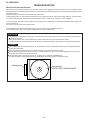
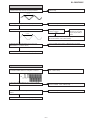
IMPORTANT SERVICE NOTES (FOR U.S.A. ONLY)
BEFORE RETURNING THE AUDIO PRODUCT
(Fire & Shock Hazard)
Before returning the audio product to the user, perform the following
safety checks.
1. Inspect all lead dress to make certain that leads are not pinched
or that hardware is not lodged between the chassis and other metal
parts in the audio product.
2. Inspect all protective devices such as insulating materials, cabinet,
terminal board, adjustment and compartment covers or shields,
mechanical insulators etc.
3. To be sure that no shock hazard exists, check for leakage current
in the following manner.
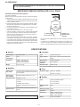
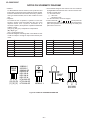
* Plug the AC line cord directly into a 120 volt AC outlet.
* Using two clip leads, connect a 1.5k ohm, 10 watt resistor paralleled
by a 0.15µF capacitor in series with all exposed metal cabinet
parts and a known earth ground, such as conduit or electrical
ground connected to earth ground.
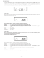
* Use a VTVM or VOM with 1000 ohm per volt, or higher, sensitivity
to measure the AC voltage drop across the resistor (See diagram).
* Connect the resistor connection to all exposed metal parts having
a return path to the chassis (antenna, metal cabinet, screw heads,
knobs and control shafts, escutcheon, etc.) and measure the AC
voltage drop across the resistor.
VTVM
AC SCALE
1.5k ohms
10W
0.15 µ F
TO EXPOSED
METAL PARTS
TEST PROBE
CONNECT TO
KNOWN EARTH
GROUND
All check must be repeated with the AC line cord plug connection
reversed.
Any reading of 0.3 volt RMS (this corresponds to 0.2 milliamp. AC.)
or more is excessive and indicates a potential shock hazard which
must be corrected before returning the audio product to the owner.
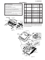
SPECIFICATIONS
■ General
■ CD player
Power source
AC 120 V, 60 Hz
Type
Compact disc player
Power
consumption
45 W
Signal readout
Non-contact, 3-beam semiconductor laser
pickup
Dimensions
Width: 9-1/16" (230 mm)
Height: 5-1/16" (128 mm)
Depth: 11-9/16" (293 mm)
D/A converter
1-bit D/A converter
Frequency
response
20 - 20,000 Hz
Dynamic range
90 dB (1 kHz)
Weight
6.6 lbs. (3.0 kg)
■ Amplifier
■ Tuner
Output power
(For U.S.A)
16 watts minimum RMS per channel into 6
ohms from 100 Hz to 20 kHz, 10% total harmonic distortion
Output power
(For CANADA)
RMS: 40W (20W + 20W) (10% T.H.D.)
Output terminals
Speakers: 6 ohms
Headphones: 16 - 50 ohms (recommended:
32 ohms)
Frequency range
AM: 530 - 1,720 kHz
■ Speaker
Type
2-way type speaker system
2" (5 cm) Tweeter
CD digital output (optical)
Input terminals
FM: 87.5 - 108 MHz
4" (10 cm) Woofer
Subwoofer (Audio signal): 500 mV/47 kohms
Maximum input
power
40 W
Video/Auxiliary (audio signal): 500 mV/47
kohms
Rated input power
20 W
Impedance
6 ohms
Dimensions
Width: 5-9/16" (140 mm)
Height: 11-3/8" (288 mm)
Depth: 7-3/8" (187 mm)
Weight
4.9 lbs. (2.2 kg)/each
Specifications for this model are subject to change without prior
notice
–2–
XL-3000/3000C
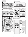
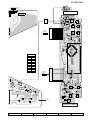
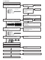
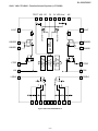
NAMES OF PARTS
■ Front panel
7
1. CD Compartment
2. Volume Up and Down Buttons
3. Power Button
4. Function Selector Button
5. Memory/Set Button
6. Bass/Treble Selector Button
7. CD Play or Pause, Tuning Up Button
8. CD Stop, Tuning Down Button
9. CD Track Down or Fast Reverse,
Tuner Preset Down Button
10. CD Open/Close Button
11. CD Track Up or Fast Forward,
Tuner Preset Up Button
10
8
1
11
9
2
■ Display
3
5
4
1. Timer Play Indicator
2. Sleep Indicator
3. CD Random Play Indicator
4. Memory Indicator
5. FM Stereo Mode Indicator
6. CD Play Indicator
7. CD Repeat Play Indicator
8. FM Stereo Receiving Indicator
9. Surround Indicator
6
1
2
3
4
5
8
6
7
9
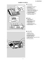
■ Rear panel
5
1
6
2
7
8
9
3
4
–3–
1. Headphone Jack
2. AM Antenna Terminal
3. Antenna Earth Terminal
4. FM 75 Ohms Antenna Jack
5. CD Digital Output Jack
6. Subwoofer Output Jack
7. Video/Auxiliary (Audio Signal) Input Jacks
8. Speaker Terminals
9. AC Power Input Jack
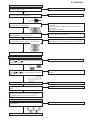
XL-3000/3000C
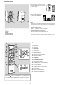
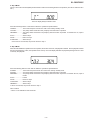
Speaker grilles are removable:
Make sure nothing comes into contact with
the speaker diaphragms when you remove
the speaker grilles.
Placing the speaker system: Left speaker
There is no distinction between
the right and the left speakers.
1
Right speaker
2
4
3
Notes:
● The speakers are magnetically shield.
Therefore, they do not affect the display even if you use them near
the TV. However, some color variation may occur, depending on
the type of TV used.
If color variation occurs...
Turn off the TV (from the power switch).
After 15 - 30 minutes, turn the TV on again.
■ Speaker system
If the color variation is still present...
Move the speakers further away from the TV.
1. Tweeter
2. Woofer
3. Bass Reflex Duct
4. Speaker Terminals
● If any kind of magnet or an electromagnet is placed too close to
the TV and the system, irregular colors may appear on the TV
screen.
■ Remote control
1
2
3
4
5
6
7
8
11
1. Remote Control Transmitter
2. Power Button
3. CD Button
4. Tuner Button
5. Timer Button
6. Clock Button
7. Memory Button
8. Dimmer Button
9. Surround Button
10. Volume Up and Down Buttons
11. Video/Auxiliary Button
12. Band Selector Button
13. Clear Button
14. Sleep Button
15. Random/Repeat Button
16. CD Open/Close Button
17. Tuner Preset Up Button
18. CD Track Down Button
19. CD Fast Reverse, Tuning Down Button
20. CD Play Button
21. CD Track Up Button
22. CD Fast Forward, Tuning Up Button
23. CD Pause Button
24. CD Stop Button
25. Tuner Preset Down Button
26. Bass Up and Down Buttons
27. Treble Up and Down Buttons
12
13
14
15
16
17
18
21
19
22
20
23
24 25
9
10
26
27
Buttons with " " mark in the illustration can be operated on the remote control only.
Other buttons can be operated both on the main unit and the remote control.
–4–
XL-3000/3000C
OPERATION MANUAL
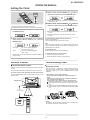
Setting the Clock
3
Within 1 minute, press the PRESET ( or ) button to
adjust the hour and then press the MEMORY button.
● When the 12-hour display is selected, "AM" will change automatically to "PM".
4
This may be operated only with the remote control.
In this example, the clock is set for the 12-hour (AM 12:00) display.
1
Press the CLOCK button and within 3 seconds, press
the MEMORY button.
Within 1 minute, press the PRESET ( or ) button to
adjust the minutes and then press the MEMORY button.
● The hour will not advance even if minutes advance from "59"
to "00".
● The clock starts from "0" second. (Seconds are not displayed.)
2
Within 1 minute, press the PRESET ( or ) button to
select 12-hour or 24-hour display and then press the
MEMORY button.
To confirm the time display when the power is on:
Press the CLOCK button.
The time display will appear for about 5 seconds.
"AM 12:00"
Note:
The time will flash at the push of the CLOCK button when the AC
power supply is restored after a power failure or unplugging the unit.
Readjust the clock as follows.
The 12-hour display will appear.
(AM 12:00 - PM 11:59)
"0:00"
The 24-hour display will appear.
(0:00 - 23:59)
Note that this can only be set when the unit is first installed or it
has been reset.
To readjust the clock:
Perform "Setting the Clock" from the beginning.
To change the 12-hour or 24-hour display:
1 Clear all the programmed contents.
2 Perform "Setting the Clock" from the beginning.
Remote Control
Troubleshooting Chart
■ Test of the remote control
■ If trouble occurs
Check the remote control after checking all connections have been
correctly.
Face the remote control directly to the remote sensor on the unit.
When this product is subjected to strong external interference
(mechanical shock, excessive static electricity, abnormal supply
voltage due to lightning, etc.) or if it is operated incorrectly, it may
malfunction.
The remote control can be used within the range shown below:
Press the POWER button. Does the power turn on? Now, you can
enjoy the music.
Remote sensor
If such a problem occurs, do the following:
1 Set the unit to the stand-by mode and turn the power on
again.
2 If the unit is not restored in step 1, unplug and plug in the
unit, and then turn the power on.
3 If neither step 1 nor 2 restores the unit, do the following:
Press the POWER button to enter the power stand-by mode.
Unplug the AC power cord from the AC INPUT jack on the
unit.
While pressing down the MEMORY/SET button and the
button, plug the AC power cord into the AC INPUT jack on the
unit.
8" - 20'
(0.2 m - 6 m )
AC INPUT
Caution:
This operation will erase all data stored in memory including clock,
timer settings, tuner preset, and CD program.
–5–
XL-3000/3000C
1
Accessories
Accesorios
4
Turn on your system
Conexión de la alimentación de su sistema
Press the POWER button to turn the power on.
Pulse el botón POWER para conectar la alimentación.
AC power cord × 1
Cable de alimentación de CA × 1
Remote control × 1
Controlador remoto × 1
Listening to a CD
Audición de un disco CD
Speaker wire × 2
Cable del altavoz × 2
FM antenna × 1
Antena de FM × 1
2
AM loop antenna × 1
Antena de cuadro de AM × 1
Battery installation of remote control
Instalación de las pilas del controlador remoto
Use 2 “AAA” size batteries (UM-4, R03, HP-16 or similar).
Use dos pilas del tamaño “AAA” (UM-4, R03, HP-16 o
equivalentes).
5" (12 cm)
12 cm
Batteries are not included.
Las pilas no están incluidas.
1
Press the FUNCTION button
until “CD STOP” or “NO DISC”
appears on the display.
Pulse el botón FUNCTION hasta
que “CD STOP” o “NO DISC”
aparezca en el visualizador.
2
Press the 7 button to open
the CD compartment.
3" (8 cm)
8 cm
Pulse el botón 7 para abrir el
compartimiento del CD.
the battery
1 Remove
cover.
the batteries
2 Insert
as shown.
Extraiga la cubierta de
las pilas.
Inserte las pilas como
se muestra.
3
3 Replace the cover.
Vuelva a colocar la
cubierta.
3
Place a CD on the spindle,
label side up.
Ponga un CD sobre el eje, con
la cara de la etiqueta arriba.
4
Press the 7 button to close
the CD compartment.
Pulse el botón 7 para cerrar
el compartimiento del CD.
System connections
Conexiones del sistema
Total number of tracks Total playing time
Número total de pistas
Tiempo total de
reproducción
TV
TV
MD recorder
Grabadora de MD
FM antenna
Antena de FM
To the optical line
input jack
Para la toma de
entrada de línea óptica
AM loop antenna
Antena de cuadro
de AM
5
Speaker with a built-in
amplifier
Altavoz con amplificador
incorporado
Listening to the radio
Audición de la radio
VCR, DVD, etc.
Videograbadora, DVD, etc.
Connection cable
for digital recording
(not supplied)
Cable de conexión
para grabación digital
(no suministrado)
To the line
output jack
A la toma de
salida de línea
RCA cord
(not supplied)
Cable RCA
(no suministrado)
Left speaker
Altavoz izquierdo
AC outlet
(AC 120 V, 60 Hz)
A un tomacorriente de
CA (120 V de CA, 60 Hz)
Right speaker
Altavoz derecho
Right speaker
Altavoz derecho
Press the J button to start
playback from track 1.
Pulse el botón J para iniciar la
reproducción desde la pista 1.
1
Press the FUNCTION button
until “FM” or “AM” appears
on the display.
Pulse el botón FUNCTION
hasta que “FM” o “AM”
aparezca en el visualizador.
2
Press the TUNING (X
X or W )
button to tune in to the desired station.
When the TUNING button is
pressed for more than 0.5
seconds, scanning will start
automatically and the tuner
will stop at the first receivable broadcast station.
Pulse el botón TUNING (X o
W) para sintonizar la emisora
deseada.
Cuando se pulse el botón
TUNING durante más de 0,5
segundos, la exploración se
iniciará automáticamente y el
sintonizador se parará en la
primera emisora difusora que
pueda recibirse.
To receive an FM stereo transmission:
Press the FUNCTION button to
display the “ST” indicator.
j” will appear when an FM
● “j
broadcast is in stereo.
Para recibir una transmisión de
FM en estéreo:
Pulse el botón FUNCTION para
visualizar el indicador “ST”.
● “j ” aparecerá cuando una
difusión de FM sea en estéreo.
Left speaker
Altavoz izquierdo
Headphones
Auriculares
White line
Línea blanca
Black
Negro
FM stereo mode indicator
Indicador del modo de FM en estéreo
FM stereo receiving indicator
Indicador de recepción de FM en estéreo
–6–
XL-3000/3000C
DISASSEMBLY
STEP
Caution on Disassembly
Follow the below-mentioned notes when disassembling
the unit and reassembling it, to keep it safe and ensure
excellent performance:
1. Take compact disc out of the unit.
2. Be sure to remove the power supply plug from the wall
outlet before starting to disassemble the unit.
3. Take off nylon bands or wire holders where they need to
be removed when disassembling the unit. After servicing
the unit, be sure to rearrange the leads where they were
before disassembling.
4. Take sufficient care on static electricity of integrated
circuits and other circuits when servicing.
(A1) x2
ø3 x10mm
Top Cabinet
PROCEDURE
REMOVAL
Rear Panel/Terminal PWB 1. Screw .................. (A1) x7
2. Socket ................. (A2) x3
3. Screw .................. (A3) x4
7-1
2
Top Cabinet
1. Screw .................. (B1) x2
2. Hook .................... (B2) x5
3. Flat Cable ............ (B3) x1
4. Socket ................. (B4) x7
7-2
3
Tuner PWB
1. Screw .................. (C1) x2
2. Socket ................. (C2) x1
8-1
4
Power PWB
1. Socket ................. (D1) x1
2. Hook .................... (D2) x1
8-1
5
Main PWB
1. Socket ................. (E1) x1
2. Screw .................. (E2) x8
8-1
6
Display PWB
1. Screw .................. (F1) x4
2. Hook .................... (F2) x4
8-2
7
CD Mechanism
1. Screw .................. (G1) x4
8-2
8
Gear Box
1. Screw .................. (H1) x1
2. Holder .................. (H2) x1
3. Lever ................... (H3) x1
4. Screw .................. (H4) x2
5. Lever ................... (H5) x1
8-2
9
LED PWB
1. Screw .................. (J1) x1
8-2
Rear Panel
(A3) x3
ø3 x10mm
7-1,2
Note:
After removing the connector for the optical pickup from the
connector, wrap the conductive aluminium foil around the
front end of connector remove to protect the optical pickup
from electrostatic damage.
(A2) x3
(A1) x3
ø3 x10mm
(A1) x2
ø3 x10mm
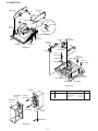
FIGURE
1
Rear Panel
Terminal PWB
Figure 7-1
Top Cabinet
HOOK
(B2) x2
(B4) x1
CD Mechanism
Hook
(B2) x3
Top Cabinet
(B4) x4
Up
(B3) x1
Slide
Hook
Power PWB
(B4) x2
Bottom Cabinet
(A3) x1
ø3 x8mm
Lug
Bottom Cabinet
(B1) x2
ø2.5 x8mm
Main PWB
Figure 7-2
–7–
XL-3000/3000C
Power PWB
(D1) x1
Tuner PWB
(C1) x1
ø3 x8mm
(E1) x1
Holder PWB
(C2) x1
(C2) x1
Tuner PWB
(E2) x7
ø3 x8mm
Main PWB
Bottom Cabinet
(C1) x1
ø3 x6mm
Hook
(D2) x1
Main PWB
Gear Box
(H4) x2
ø2.5 x10mm
(H1) x1
ø3 x8mm
(E2) x1
ø3 x14mm
(H5) x1
(H3) x1
Figure 8-1
Switch PWB
(H2) x1
(J1) x1
ø2.5 x10mm
Bracket
(G1) x4
ø2.5 x10mm
Holder PWB
(F1) x4
ø2.5 x10mm
LED PWB
Hook
(F2) x4
CD Mechanism
Display PWB
Top Cabinet
Figure 8-2
Tweeter
STEP
1
Front Panel
( A2 ) x1
( A3 ) x2
ø4 x12mm
Net Frame
( A1 ) x1
( A3 ) x4
ø4 x12mm
Woofer
Screwdriver
Figure 8-3
–8–
REMOVAL
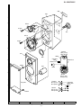
Speaker
PROCEDURE
FIGURE
1. Net Frame ........... (A1) x1
2. Front Panel ......... (A2) x1
3. Screw .................. (A3) x6
8-3
XL-3000/3000C
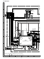
REMOVING AND REINSTALLING THE MAIN PARTS
How to remove the CD lid (See Fig. 9-1.)
Perform steps 1,2 and 8 of the disassembly method to remove
the gear box.(See page 7,8)
1. Remove the switch PWB.
2. Remove the screws (A1) x 4 pcs., to remove the gear box
lid.
3. Remove the gears (A2) x 1 pc. and (A3) x 1 pc.
4. Remove the screws (A4) x 2 pcs., to remove the motor.
Caution:
Be careful so that the gear is not damaged.
(The damage gear emits noise during searching.)
CD Lid Motor
(A2) x1
(A1) x3
ø2.5 x12mm
(A4) x2
ø2 x5mm (A3) x1
Switch PWB
(A1) x1
ø2.5 x10mm
Figure 9-1
CD MECHANISM SECTION (See Fig. 9-2.)
Perform steps 1,2 and 7 of the disassembly method to remove
the CD mechanism.
1. Remove the mechanism cover, paying attention to the
pawls (A1)x 4 pcs.
2. Remove the screws (A2) x 2 pcs., to remove the shaft (A3)
x 1 pc.
3. Remove the stop washer (A4) x 1 pc., to remove the gear
(A5) x 1 pc.
4. Remove the pickup.
Note:
After removing the connector for the optical pickup from the
connector, wrap the conductive aluminium foil around the
front end of connector remove to pretect the optical pickup
from electrostatic damage.
(A1) x4
Mechanism Cover
(A2) x2
ø2.6 x6mm
CD Mechanism
Shaft
(A3) x1
Gear
(A5) x1
Stop Washer
(A4) x1
Pickup unit
Figure 9-2
–9–
XL-3000/3000C
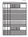
ADJUSTMENT
TUNER SECTION
fL: Low-range frequency
fH: High-range frequency
• AM IF/RF
Signal generator: 400 Hz, 30%, AM modulated
Frequency Frequency
Display
• FM Mute Level
Signal generator: 1 kHz, 40 kHz dev., FM modulated
Setting/ Instrument
Adjusting Connection
Parts
T351
*1
AM IF
450 kHz
1,620 kHz
AM Band
Coverage
—
522 kHz
(fL): T306 *2
1.1 ± 0.1 V
AM
Tracking
990 kHz
990 kHz
(fL): T302
Display
Frequency
98.00 MHz
(30 dBµV)
98.00 MHz
Adjusting
Parts
VR351*1
Instrument
Connection
Input: SO301
Output: Speaker
Terminal
*1. Adjust so that an output signal appears.
*1
• FM Detection
Signal generator: 10.7 MHz, FM sweep generator
*1. Input: Antenna, Output: Speaker Terminal
*2. Input: Input is not connected, Output: TP301
Test
Stage
• FM RF
Signal generator: 1 kHz, 75 kHz dev., FM modulated
Test Stage Frequency
Frequency
Display
FM Band
Coverage
—
87.5 MHz
FM RF
98.00 MHz
(10~30 db)
98.0 MHz
FM IF
Setting/ Instrument
Adjusting Connection
Parts
(fL): L303 *1
3.4 ± 0.1 V
L302
TP301
20
Preset No.
1
2
3
4
5
TUNER PWB-A2
GND
AM
FM ANT.
FM RF
IC301
1
IC302
L302
FM OSC. L303
FM Band
Coverage fL
T302
AM
Tracking fL
T304
FM IF
VR351
FM Mute
Level
T351
AM IF
10.7 MHz
IC303
Frequency
Display
Setting/
Adjusting
Parts
98.0 MHz
Instrument
Connection
T304(Turn Input: Pin 1 of
the core of IC301
T304 fully
counterclockwise.)
• Setting the Test Mode
Keeping the FF/FWD button and MEMORY/SET button
pressed, turn on POWER. Then, the frequency is initially set
in the memory as shown in Table. Call it with the VOLUME UP/
DOWN button to use it for adjustment and check of tuner
circuit.
*2
*1. Input: Antenna, Output: TP301
*2. Input: Antenna, Output: Speaker Terminal
FM
75
SO301 OHMS
ANTENNA
TERMINAL
Frequency
T306
AM Band
Coverage fL
Figure 10-1 ADJUSTMENT POINTS
– 10 –
FM
87.5 MHz
108.0 MHz
98.0 MHz
90.0 MHz
106.0 MHz
Preset No.
6
7
8
9
10
AM
530 kHz
1,720 kHz
990 kHz
600 kHz
1,400 kHz
XL-3000/3000C
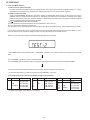
TEST MODE
The test mode applied to this microcomputer has three modes, namely the ordinary test mode for adjustment or measurement,
the aging test mode, and the self-diagnosis test mode for self-judgment in case of final product inspection.
1. Turning on the test mode
For obtaining each test mode, press the POWER button, while keeping pressing the following two buttons in the ordinary standby mode (power off ). In this case, the main unit buttons are valid. When turning the POWER on with remote control buttons,
test modes are not obtained.
[Ordinary test mode]
1. CD Test Mode (TEST 1)....................................
REW/PRESET DOWN + VOLUME UP
2. Tuner Test Mode (TEST 2).................................REW/PRESET DOWN + CD PLAY
3. Electronic Volume Test Mode (TEST 3).............
REW/PRESET DOWN + FF/PRESET UP
4. Timer Test Mode (TEST 4).................................
FUNCTION + VOLUME UP
5. LCD Test Mode (TEST 5)...................................
FUNCTION + FF/PRESET UP
6. Electric CD Lid Aging Test Mode (TEST 8)........
FUNCTION + CD PLAY
[Self-diagnosis Test Mode]
1. Button input diagnosis test mode (TEST6)........ FUNCTION + VOLUME
Processes are different depending on destinations at initial settings.
2. CD Test Mode (TEST 1)
In the CD test mode the operation of each step is possible even if the LID-SW is off. If focus cannot be taken in step 3 or any
error is processed, it is impossible to proceed to the next step. During error processing, end the test mode by pressing the
POWER button or return to the step 1 by pressing the CD STOP button. Any other operations are inhibited.
1. Step 1 Mode
When the CD test mode is obtained, the following display lights up. Then CD initialization operation flow proceeds up to CD
STB off to wait for the following buttons to be pressed.
One second after display lights up
Press the following buttons in this state to obtain the operations specified below.
"POWER" ................. Test mode and power turned off to shift to the ordinary standby mode.
"FF/FWD" ................. After the pickup returns to the innermost periphery, it slides toward the outer periphery while this button
is pressed.
"REW/REV" .............. After the pickup returns to the innermost periphery, it slides toward the inner periphery while this button
is pressed. If PICKUP IN is on, input is invalid.
"PLAY" ..................... Shift to step 2
"STOP" ..................... Invalid
"FUNCTION" ............ Shift to step 5
– 11 –
XL-3000/3000C
* In case of initialization, the pickup is moved toward the inner periphery. Any buttons other than "POWER" button are not
accepted until the shift of pickup to the inner periphery is completed at this time. If PICKUP IN SW ON cannot be detected
within 10 seconds, the slide motor stops, and the following error display appears. Press the POWER button to end the test
mode, or press the CD STOP button to return to step 1. Any other operations are inhibited.
2. Step 2 Mode
Press the "CD PLAY" button in this mode to transmit the laser lighting command LDON (8400) and turn on the laser. Any other
operations are not performed in this case.
Press the following buttons in this state to obtain the operations specified below.
"POWER" ................ Test mode and power turned off to shift to the ordinary standby mode.
"FF/FWD" ................ The pickup slides toward the outer periphery while this button is pressed.
"REW/REV" ............. The pickup slides toward the inner periphery while this button is pressed. If PICKUP IN is on, input is
invalid.
"PLAY" ..................... Shift to step 3
"STOP" .................... Return to step 1
"FUNCTION" ........... Shift to step 5
3. Step 3 Mode
While the laser keeps lighting, CD initialization operation flow proceeds up to 'CLV servo ON' to wait for the following buttons
to be pressed.(Focus servo turned on for focus search)
The focus search is repeated to take focus.
Press the following buttons in this state to obtain the operations specified below.
"POWER" ................ Test mode and power turned off to shift to the ordinary standby mode.
"FF/FWD" ................ The pickup slides toward the outer periphery while this button is pressed.
"REW/REV" ............. The pickup slides toward the inner periphery while this button is pressed. If PICKUP IN is on, input is
invalid.
"PLAY" ..................... If focus has been taken, shift to step 4 is executed. If not, acceptance is inhibited.
"STOP" .................... Return to step 1
"FUNCTION" ........... Shift to step 5
*If the focus is not received after it has been taken, the process returns to step 1.
– 12 –
XL-3000/3000C
4. Step 4 Mode
The CLV servo ON command (8600) is transmitted to wait for the following buttons to be pressed. (The disc is rotated for CLV
lock.)
The time display always indicates "0:00".
Press the following buttons in this state to obtain the operations specified below.
"POWER" ................ Test mode and power turned off to shift to the ordinary standby mode.
"FF/FWD" ................ The pickup slides toward the outer periphery while this button is pressed.
"REW/REV" ............. The pickup slides toward the inner periphery while this button is pressed. If PICKUP IN is on, input is
invalid.
"PLAY" ..................... Shift to step 5
"STOP" .................... Return to step 1
"FUNCTION" ........... Shift to step 5
*If the focus is not received, the process returns to step 1.
5. Step 5 Mode
When the CD initialization operation flow is completed, the mute is turned off, and playback is started. Even if playback reaches
the outermost periphery of disc, the operation does not stop. The LCD display indicates the playback passage time as in case
of ordinary CD playback.
Press the following buttons in this state to obtain the operations specified below.
"POWER" ................. Test mode and power turned off to shift to the ordinary standby mode.
"FF/FWD" ................. The pickup slides toward the outer periphery while this button is pressed.
"REW/REV" .............. The pickup slides toward the inner periphery while this button is pressed. If PICKUP IN is on, input is
invalid.
"PLAY" ..................... Invalid
"STOP" ..................... Return to step 1
"FUNCTION" ........... Shift to step 6
"MEMORY" .............. Shift to step 7
*If the is not received, the process returns to step 1.
Other cautions
• TOC IL is not available for this test mode.
– 13 –
XL-3000/3000C
6. Step 6 Mode
Press the FUNCTION button during step 5 operation to set EC/FC bit to "H" by PROSET command (9188 transmission) and
to monitor BUS2 (QDRE) during idle mode. The number of errors for 1 frame (1 sub-code block in IC data) is read by read
command SRC6 during "H". The number of errors accumulated in 750 frames for 10 seconds is displayed on LCD. During the
display, music signal is played back.
Press the following buttons in this state to obtain the operations specified below.
"POWER" ................. Test mode and power turned off to shift to the ordinary standby mode.
"FF/FWD" ................. The pickup slides toward the outer periphery while this button is pressed.
"REW/REV" .............. The pickup slides toward the inner periphery while this button is pressed. If PICKUP IN is on, input is
invalid.
"PLAY" ..................... Invalid
"STOP" ..................... Return to step 1
"FUNCTION" ........... Shift to step 5
"MEMORY" .............. Shift to step 7
Press FF/PRESET UP or REW/PRESET DOWN button to slide the pickup. The number of errors accumulated up to that time
is cleared and addition is restarted after shift.
*If the focus is not received, the process returns to step 1.
– 14 –
XL-3000/3000C
7. Step 7 Mode
Press "MEMORY" key during step 6 operation to display automatically adjusted values on LCD in the order as below. Item
names are displayed by left alignment, and adjusted values by right alignment in hexadecimal numbers. Operations other than
display are as same as those for step 5.
a) "Fb" is displayed on the left of LCD. FTBAST command (D480) is transmitted to designate focus balance adjusting
register. Then data read by read command SRC2 (2) are displayed in hexadecimal numbers. After waiting 2 seconds,
operation is shifted to (b).
b) "FG" is displayed on the left of LCD. FTBAST command (D481) is transmitted to designate focus gain adjusting register.
Then data read by read command SRC2 (2) are displayed in hexadecimal numbers. The upper two bits, which are invalid,
are displayed as "00". After waiting two seconds, operation is shifted to (c).
c) "Tb" is displayed on the left of LCD. FTBAST command (D482) is transmitted to designate tracking balance adjusting
register. Then data read by read command SRC2 (2) are displayed in hexadecimal numbers. After waiting 2 seconds,
operation is shifted to (d).
d) "TG" is displayed on the left of LCD. FTBAST command (D483) is transmitted to designate tracking gain adjusting register.
Then data read by read command SRC2 (2) are displayed in hexadecimal numbers. The upper two bits, which are invalid,
are displayed as "00". After waiting 2 seconds, operation is shifted to (e).
e) "FO" is displayed on the left of LCD. FTBAST command (D484) is transmitted to designate focus offset adjusting register.
Then data read by read command SRC2 (2) are displayed in hexadecimal numbers. After waiting 2 seconds, operation
is shifted to (f).
f) "TO" is displayed on the left of LCD. FTBAST command (D485) is transmitted to designate tracking offset adjusting
register. Then data read by read command SRC2 (2) are displayed in hexadecimal numbers. After waiting 2 seconds,
operation is shifted to (g).
g) "FF" is displayed on the left of LCD. FTBAST command (D486) is transmitted to designate RF amplitude adjusting register.
Then data read by read command SRC2 (2) are displayed in hexadecimal numbers. After waiting 2 seconds, operation
is shifted to (a).
Press the following buttons in this state to obtain the operations specified below.
"POWER" ................. Test mode and power turned off to shift to the ordinary standby mode.
"FF/FWD" ................. The pickup slides toward the outer periphery while this button is pressed.
"REW/REV" .............. The pickup slides toward the inner periphery while this button is pressed. If PICKUP IN is on, input is
invalid.
"PLAY" ..................... Invalid
"STOP" ..................... Return to step 1
"FUNCTION" ........... Shift to step 6
"MEMORY" .............. Shift to step 5
*If the focus is not received, the process returns to step 1.
– 15 –
XL-3000/3000C
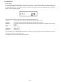
3. Tuner Test Mode (TEST 2)
1. Outline of tuner (radio) test mode
The tuner test mode is intended to store the adjustment and measurement frequencies in the preset memory CH. When
adjusting the tuner section in the production line, adjusting personnel are not required to set frequency.
2. Details of tuner test mode
Press the "REW/PRESET DOWN" and "CD PLAY" buttons in POWER OFF state and turn on the power by the use of
"POWER" button to preset and store frequency for adjustment and measurement of destination specified by the AREA
terminal in the preset memory CH. However, Ordinary 1 and Ordinary 2 are stored in the destinations (selected by SPAN
switching operation) when the test mode is obtained.
("FF " + "MEMORY/SET" KEY SPAN CHANGE)
(As for frequencies to be preset and stored for each destination, refer to item 3.)
The tuner test mode is started from preset No.1.
The operations of test mode are identical with the ordinary operations of TUNER function. FUNCTION switching is invalid.
It is necessary to discard the content of preset memory when the tuner test mode is ended; be sure to write "0000" or "1111"
bits in the memory to be checked for judging memory error at initial setting and to initialize memory.
When the tuner test mode is obtained, the following display lights for one second.
• The TUNER TEST2 mode is obtained with >> + MEMORY + POWER. ->Turn off AC in the TEST2 mode to restore the initial
state.
Turn off POWER to protect the memory of TEST2 mode.
Turn off POWER again to obtain the ordinary operation while the data is stored in the memory (besides TUNER).
If AC OFF state is maintained in this state for about 1/2 day, start is executed in the initial state.
• To clear the whole memory, insert the AC cord, pressing MEMORY + CD PLAY.
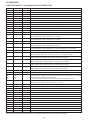
3. Preset frequencies for various destinations (random preset memory)
CH
1
2
3
4
5
BAND
FM
STEREO
FM
FM 87.5 MHz
FM108.0 MHz
FM 98.0 MHz
FM 90.0 MHz
FM106.0 MHz
CH
6
7
8
9
10
BAND
AM
AM
AM 530 kHz
AM1,720 kHz
AM 990 kHz
AM 600 kHz
AM1,400 kHz
• The slant line sections of the table store no memory.
– 16 –
CH
16-25
26
27
28
29
30
BAND
FM
MONO
FM
FM106.0 MHz
FM 90.0 MHz
FM 98.0 MHz
FM108.0 MHz
FM 87.5 MHz
XL-3000/3000C
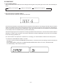
4. Electronic volume Test Mode (TEST 3)
When this test mode is obtained, the following display lights for one second.
In this mode, volume is -14 dB (STEP28), BASS/TREBLE is set to 0 (0 dB) and SURROUND mode to OFF, and start-up function
to CD, respectively. The button operations in the test mode are the same as those of ordinary operation except volume UP/
DOWN.
(1) The display is the same as that of ordinary operation except test mode setting.
(2) Unlike the ordinary state, the volume is controlled with the volume UP/DOWN button in accordance with the following three
steps.
Volume- ∞ (STEP 0) <-> Volume-14 dB (STEP 23) <-> Volume-0 (STEP 30)
(3) BASS/TREBLE and SURROUND are switched when button is pressed..
5. Timer test Mode (TEST 4)
When this test mode is obtained, the following display lights for one second.
Set the current time and timer time according to the following procedure to reproduce the timer.
1.Set the current time to 1:00, the timer to ON time 1:05, the function to CD, and volume to STEP 12, respectively. One minute
is counted as one second, and the timer is reproduced. The fade-in (when playback is started) is executed at a rate of one
step for 1 sec. After completion of fade-in, the fade-out is executed at a rate of one step for 1 sec (WAIT 1 sec inserted).
After completion of fade-out, the power is turned off (after WAIT 1 sec), and the mode is shifted to the standby.
The display during operation is the same as that of ordinary timer operation.
– 17 –
XL-3000/3000C
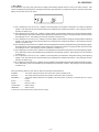
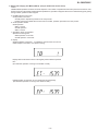
6. LCD Test Mode (TEST 5)
When the LCD test mode is obtained, all the LCD segments are lighted. Then pressing the "PLAY" button switches display as
below.
Lighting of all segments
Lighting of odd segments
Lighting of even segments
7. Key input diagnosis Test Mode (TEST 6)
When the test mode is obtained, the following is displayed.
This test mode is intended to check whether all the main unit buttons can be detected. Accordingly, in this test mode, it is checked
whether the "POWER" button was pressed after all the buttons shown below were pressed. If the result is OK, OK is displayed.
If any one of keys was not pressed, an error is displayed. In both cases of OK termination or error termination, the mode is shifted
to the standby mode if the "POWER" button is pressed subsequently.
All models using this type of microcomputer are not always provided with the same buttons. Since the buttons used are different
depending on models, types of buttons to be used are determined by whether SURROUND, and an electric lid are available
at the initial setting by MODEL port.
The order of buttons to be pressed is not determined. Accordingly, it is checked whether all buttons have been pressed.
1. PU-IN buttons: REW/PRESET DOWN + CD STOP
Since this model is provided with SURROUND (HAVE OR NOT), and electric CD lid, the following 10 buttons are detected
as all buttons.
PLAY, BASS/TREBLE, FUNCTION, VOLUME UP/DOWN, MEMORY/SET, REW, FF, STOP, CD-OPEN/CLOSE
The OK/NG display of test result is as follows.
– 18 –
XL-3000/3000C
8. Electric CD lid Aging Test Mode (TEST 8) (Only for model with electric CD lid)
Outline
OPEN/CLOSE operations of electric CD lid are repeated. The number of repeated times and time period are monitored. If the
lid does not move to the regular position after the specified time, operation is stopped. When an error is detected by [CLID_PRO]
during CLOSE, operation is also stopped.
a. POWER ON for function AUX
CD lid position is checked.
CLOSE position: Operation proceeds to the next process.
Position other than CLOSE: After the lid moves to CLOSE, operation proceeds to the next process.
b. CD lid operation started
OPEN operation
WAIT 1 second
CLOSE operation
WAIT 1 second
c. Operations above are repeated.
Specified monitoring time
OPEN operation: 5 seconds
CLOSE operation: 5 seconds
d. Display
OPEN>CLOSE is counted as 1. I to 59999 are counted; if the count is over
59999, display is returned to 0 to repeat counting.
Display when the lid does not move to the regular position after the specified
time
(Ex: Defective operation occurring in the middle of 1538.)
Highlight display of stop when an error is detected by [CLID-PRO]
(Ex: Defective operation occurring in the middle of 1538.)
– 19 –
XL-3000/3000C
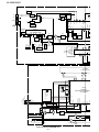
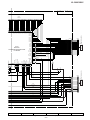
NOTES ON SCHEMATIC DIAGRAM
• Resistor:
To differentiate the units of resistors, such symbol as K and
M are used: the symbol K means 1000 ohm and the symbol
M means 1000 kohm and the resistor without any symbol is
ohm-type resistor. Besides, the one with “Fusible” is a fuse
type.
• Capacitor:
To indicate the unit of capacitor, a symbol P is used: this
symbol P means micro-micro-farad and the unit of the
capacitor without such a symbol is microfarad. As to
electrolytic capacitor, the expression “capacitance/withstand
voltage” is used.
(CH), (TH), (RH), (UJ): Temperature compensation
(ML): Mylar type
(P.P.): Polypropylene type
• Schematic diagram and Wiring Side of P.W.Board for this
model are subject to change for improvement without prior
notice.
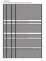
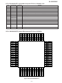
REF. NO
DESCRIPTION
• The indicated voltage in each section is the one measured
by Digital Multimeter between such a section and the chassis with no signal given.
1. In the tuner section,
( ) : AM mode
: FM stereo mode
2. In the CD section, the CD is stopped.
• Parts marked with “
”(
) are important for
maintaining the safety of the set. Be sure to replace these
parts with specified ones for maintaining the safety and
performance of the set.
POSITION
REF. NO
NSW801
PICKUP IN
ON—OFF
SW721
BASS/TREBLE
ON—OFF
SW709
POWER
ON—OFF
SW722
MEMORY SET
ON—OFF
SW710
CD LID OPEN/CLOSE
ON—OFF
SW725
CD STOP/TUNING DOWN
ON—OFF
SW711
FF/PRESET UP
ON—OFF
SW726
REW/PRESET DOWN
ON—OFF
FUNCTION
ON—OFF
CD LID
ON—OFF
SW712
CD PLAY/PAUSE/TUNING UP
ON—OFF
SW727
SW713
VOLUME UP
ON—OFF
SW802
SW718
VOLUME DOWN
ON—OFF
FRONT
VIEW
E C B
(S) (G) (D)
(1) (2) (3)
2SB562 C
2SC535 C
2SK246 GR
KRA102 M
KRC102 M
KRC104 M
KRC107 M
KTA1266 GR
KTC3199 GR
KTC3200 GR
FRONT
VIEW
DESCRIPTION
POSITION
FRONT
VIEW
B C E
2SD2012 Y
DB5306X
1
2
3
SVC348S
KDV147B
Figure 20 TYPES OF TRANSISTOR AND LED
– 20 –
XL-3000/3000C
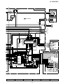
WAVEFORMS OF CD CIRCUIT
NO DISC FOCUS SEARCH
1
STOP
12
1
FOO
FO+
13
2
IC804 26pin
3
FO-
14
3
SEL
5
6
1
11
2
TEI
15
3
6
SBAD
11
2
3
TEI
1
TRO
2
IC802 49pin
RFO
15
3
FMO
3
IC802 53pin
IC801 22pin
STOP
PLAY
REVIEW
6
1
FEI
TEI
1
TRO
2
IC802 46pin
IC802 43pin
RFGO
11
2
IC801 19pin
IC802 49pin
RFRP
15
3
IC801 17pin
3
FMO
IC802 53pin
STOP
TEI
PLAY
TCD-782 TNO-02 PLAYBACK
16
1
IC802 46pin
TRO
SBAD
LO
1
RO
2
IC802 85pin
2
IC802 49pin
7
FMO
IC802 46pin
IC802 44pin
11
2
CUE
1
FEI
6
TRO
PLAY
IC802 43pin
10
1
IC802 53pin
STOP
5
TEI
IC802 49pin
IC802 46pin
5
PLAY
IC802 46pin
FEI
6
3
STOP
IC802 43pin
9
2
DMO
TOC IL
IC802 57pin
8
SBOK
IC802 55pin
FOCUS SEARCH
7
1
IC802 12pin
IC804 25pin
4
TMAX
IC802 30pin
IC802 48pin
2
PLAY
17
IC802 82pin
3
IC802 44pin
– 21 –
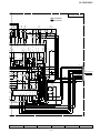
XL-3000/3000C
FROM
DISPLAY PWB
TO
TUNER PWB
11 10 9 8
1 2 3 4 5 6 7 8 9 10 11 12 13 14 15
SD
FM ST
DO
CL
CE
DI
A_12V
D_GND
TUN L
TUN R
A GND
LIGHT
DIMMER
CLID_DW
CLID_UP
CLID_PRO
CLID_SW
CD_RES
CCE
BUCK
BUS3
BUS2
BUS1
BUS0
CD_STB
PU_IN
Q901
7 6 5 4 3 2
CNP307
LED PWB
CNP702
Q902
M_GND
Q908
Q907
SWITCH PWB
+B4
+B6
SW802
CD LID
OPEN/CLOSE
Q802
M_GND
1 9 5
IC805
TA7291S
CD LID
MOTOR DRIVER
2
SUB
WOOFER
OUT
8
3
6
R-CH
SO401
VIDEO/AUX
INPUT
M801
CD LID
OPEN/CLOSE
MOTOR
7
L-CH
+B4
M
CD_6R2V
5V
+B7
Q861
NM802
SPINDLE
MOTOR
+B2
+
SP+
SP–
SP+
SL–
PU-IN
GND
GND
MUTE
BIAS REG O
VG4
TRB
VIN4
VG1
VIN1
VO4+
VO4VO1+
GND
VO1-
VO3+
VIN3
VG3
VCC
VCC
OPO
GND
VO2VO2+
VIN2
VG2
PO1+
VO3-
PO153
DMO
FMO
J801
DIGITAL
OUT
1
2
3
+B7
TERMINAL
PWB
CD MOTOR PWB
TR
DOUT 9
BUS0
BUS1
BUS2
BUS3
BUCK
/CCE
RO 82
LO 85
IC802
SEL
2VREF
TC9462F
SERVO/SIGNAL CONTROL
57
56
TEBC
RFGC
VREF
TRO
52
51
50
49
48
47
46
45
44
43
78 XI
79 XO
FOO
TEZI
TEI
TSIN
SBAD
FEI
CD PICKUP UNI
FOCUS COIL
TRACKING COIL
13
14
15
16
17
18
19
20
21
22
23
24
14 VDD
23 VDD
RFRP 42
RFCT 40
RFI 38
39 AVDD
62 VDD
76 VDD
80 XVDD
VCOREV
PVREV
LPFO
LPFN
94 VDD
34
33
32
31
DVSR
DVSL
M_GND
XVSS
81 86
PXI
6 15 24 63 71 72 73 74 77 95
VSS
VSS
TESI01
VSS
TESIN
36
VSS
D_GND
P2VREF 25
VSS
TESIOO
TMAX 30
PDO 28
D_GND
NM801
SLED
MOTOR
FO
AVSS
+B7
M
21 22 23 24 25 26 27 28
100 /RST
X801
16.93MHz
–
NSW801
PICKUP IN
IC804
MM1469XH
FOCUS/TRACKING/
SPIN/SLED DRIVER
+B2
90
91
92
93
96
97
55
+
M
M_GND
13 12 11 10 9 8 7 6 5 4 3 2 1
16 17 18 19
–
SBAD
FEO
FEN
VRO
RFRP
RFIS
RFGO
RFGC
AGCI
RFO
GND
RFN
TEO
TEN
2VRO
TEB
SEL
LDO
MDI
TN1
TPI
FPI
FNI
VCC
12
11
10
9
8
7
6
5
4
3
2
1
IC801
TA2109F
SERVO PRE AMP.
A_GND
+B7
SWITCHING
LD
Q801
E
F
B
A
MON
+B7
C
1/2V
+B7
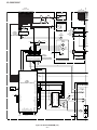
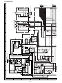
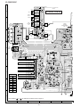
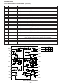
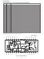
Figure 22 BLOCK DIAGRAM (1/4)
– 22 –
5V
XL-3000/3000C
FROM
DISPLAY PWB
5 4 3 2 1
1
2
3
4
5
6
7
8
9 10 11 12 13
R-CH IN
5V
P_STB
A_24V
D_GND
P_MUTE
DI
CD +B
CL
CE
DO
SD
STEREO
_
D_GND
TUN L
TUN R
A_GND
CNP703
R-CH OUT
SURROUND
ON/OFF
SURROUND
Q203
5
6
7
8
4
3
2
1
+B6
A_12V
Q201
+B5
+B1
+B3
+B6
L-CH OUT
L-CH IN
IC201
KIA4558P
SURROUND CONTROL
B
R-CH OUT
AUX R
14
13
10
11
12
8
9
7
6
4
5
3
2
1
VSS
15
DI
CE
TUN R
CD R
NC
VDD
LOGIC
16
19
18
20
21
23
22
24
26
25
27
29
28
IC401
LC75342M
FUNCTION/VOLUME
EQUALIZER
L-CH OUT
+B6 A_12V
SO601
SPEAKER TERMINAL
AUX L
30
CL
17
CD L
TUN L
+B7
PRE
–VCC
8
9
12
GND
–VCC
4
+VE2
–VE2
+VCC
L-CH 1 15 R-CH
PRE
+VCC
IN2
IN1
Q601
Q602
+VE1
–VE1
IC601
STK40202
POWER AMP.
MUTE
6 7 10 11
L-CH R-CH
13
+
L-CH
R-CH
+
+B
–B
J601
HEADPHONES
Q101
Q104
F651
F652
3.15A/125V
A_24V
A_GND
F653
1.6A/125V
Q904
P UNIT
CNP801
–B
+B1
4
5
9
10
3.15A/125V
D651~D654
VOLTAGE
REGURATOR
3
2
1
Q103
Q102
1
2
3
4
5
1
2
3
4
5
TF
D_GND
T651
POWER
TRANSFORMER(MAIN)
D657~D660
1
3
1
3
POWER PWB
CNP651
Q608
Q609
VOLTAGE
REGURATOR
M_12V
+B4
+B5
5V
+B6
Q605
3
2
1
IC681
AN78L05
VOLTAGE
REGULATOR
3
1
D_GND
Q681
2
VOLTAGE
REGURATOR
D688
1N4004
CD +B
USWD_5R6V
+B3
Q606
Q607
CNP707
CD_6R2V
+B2
FROM
DISPLAY PWB
L
RLY601
P_CONT
Q683
Q903
A_12V
Q603
Q604
D681~D684
MAIN PWB
AC 120V,60Hz
Figure 23 BLOCK DIAGRAM (2/4)
– 23 –
T681
POWER
TRANSFORMER
(SUB)
AC POWER SUPPLY CORD
SO655
AC INPUT
SOCKET
AC120V,60Hz
XL-3000/3000C
AM
Tracking fL
FM MUTE
LEVEL
T302
AM
X3
456
GND
BF301
2
2
1
3
3
4
5
6
7
8
FM IF
9
FM IF
Q306
CF303
2
18
3
4
FM IF
AM IF
AM IF
CF302
T351
CF352
5
6
FM DET
STEREO
AM LOW
CUT
FM/AM
OUT
19
7
8
FM +B
T304
TP301
+5V
Q302
VT
L303
FM OSC.
+5V
VD302
DI
CL
DO
FM
1
17 1
PD
AIN
18
3
4
5
6
7
VDD
MUTE FM IN
19
CE
X352
4.5MHz
22 21 20
AOUT
FM +B
VSS
FM Band
Coverage fL
X IN X OUT
VD303
L302
FM ANT.
FM RF
IC302
LC72131
PLL(TUNER)
FM +B
8
LCD701
LCD DISPLAY
1
6 VLC2
38
100
67
SEG0
COM0
4
5 VLC3
5
SEG33
4
COM3
1
7 VLC1
8 VDD
9 OSC2
10 OSC1
X701
IC701
IX0039SJ
SYSTEM MICROCOMPUT
FL DRIVER
11 VSS
8MHz
X702
12 XI
13 XO
32.768kHz
37 38 39
25 26 27 28
SURR
32
CE
47 P–CONT
USWD_5R6V
CL
3
18 KEY2
P_CONT
DI
3
17 KEY1
D_GND
DO
2
16 CLID_SW
SW710
REMOCON
2
24 VREF+
SW709
POWER
1
15 VREF
RESET
1
14 MMOD
SYS_STOP
CNW707
CNS707
SW711~713
SW718
SW721,722
SW725~727
TO
POWER PWB
1
1
20
SD
IC301
TA7358AP
FM FRONT END
BAD PASS
FILTER
21
AM IF
IN
GND
FM IF AM OSC
IN
OUT
AM MIX
OUT
AM OSC
IN
REG
AM Band
Coverage fL
SO301
ANTENNA
TERMINAL
22
VSM
24 23
VR351
T306
+5V
AM RF
IN
FM
75ohms
FM AFC
+5V
VD301
4
RESET
Q702
Q703
Q701
RX701
REMOTE
SENSOR
LAMP PWB
Q708
A_24V
LMP701
SWITCHING
5V
Q707
GND
Q706
SWITCHING
Figure 24 BLOCK DIAGRAM (3/4)
– 24 –
Q709
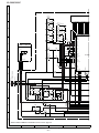
XL-3000/3000C
TUNER PWB
SWITCHING
Q351
9
AM IF
MO/ST
MPX VCO
VCC
8
13
10 11
12
IC303
LA1832S
FM IF DET/
FM MPX/AM IF
7
15 14
PHASE
(AM/FM)
6
CF351
5
FM DET
STEREO
SD
VSM
AM IF
IN
GND
4
16
R-CH
OUT
L-CH
OUT
17
PHASE
18
IF OUT
19
AM LOW
CUT
FM/AM
OUT
20
AM RF
IN
21
MPX IN
X351
456kHz
+5V
CF352
6
7
8
AM IN
IF REQ IF IN
5
MO/ST
4
14 13 12
FM
3
VDD
MUTE FM IN
PD
FM
AIN
DO
17 16 15
CL
18
DI
19
CE
20
AOUT
ZD351
9
10
11
DO
VOLTAGE
REGURATOR
CL
+5V
CE
DI
FM +B
Q360
A_12V
+B
D_GND
TUN_L
TUN_R
A_GND
CNS307
DISPLAY PWB
38
100
67
SEG33
CNW702
CLID_DW
CLID_UP
CLID_PRO
CLID_SW
CD_RES
CLID_DW 57
CLID_UP 56
CLID_PRO 20
CD_RES 59
CCE 66
BUCK 65
BUS3 64
BUS2 63
BUS1 62
BUS0 61
CD_STB 60
PU-IN 58
LIGHT 53
DIMMER 54
IC701
IX0039SJ
STEM MICROCOMPUTER/
FL DRIVER
CNS702
1
2
3
4
5
6
7
8
9
10
11
12
13
14
15
CCE
BUCK
BUS3
BUS2
BUS1
BUS0
CD_STB
PU-IN
LIGHT
DIMMER
1
2
3
4
5
6
7
8
9
10
11
12
13
14
15
TO
MAIN PWB
5
SEG0
COM3
LCD701
LCD DISPLAY
CD+B
SD
STEREO
P–MUTE
P–STB
SURR
CE
CL
DI
25 26 27 28
CLE 40
DATA 48
VSM 23
CNS703
43 44 45 46 49 50
SD
STEREO
DO
CL
CE
DI
CD+B
P_MUTE
P_STB
A_24V
D_GND
A_24V
HING
Q709
SURROUND
5V
5V
CNW703
Figure 25 BLOCK DIAGRAM (4/4)
– 25 –
1
1
2
2
3
3
4
4
5
5
6
6
7
7
8
8
9
9
10
11
12
13
10
11
12
13
TO
MAIN PWB
37 38 39
DO
REMOCON
SYS_STOP
POWER
B-LIGHT 51
11
10
9
8
7
6
5
4
3
2
1
TO
MAIN PWB
SD
FM ST
+5V
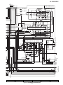
XL-3000/3000C
C851
100/10
1
2
3
J801
DIGITAL OUT
L802 CNP805
0.82µH
C852
0.0022
C853
0.0047
3
2
1
FROM
CNS805 MAIN PWB-A1(2/2)
P28 1-G
11 10 9 8
7 6 5 4 3 2 1
1
2
3
4
5
6
7
DI
CD +B
TO CHASSIS GND
LUG(205)
SO401
R410
1K
SUB
WOOFER
OUT
CNP704
1
2
C410
0.0047
C412
330P
R405
27K
AUX IN
C411
330P
L-CH
C413
0.0047
CNW704
CNS704
1
2
1
2
CFW452
TO CHASSIS GND
LUG(205)
R408 R407
2.7K 2.7K
R-CH
C
R411
1K
C414
0.45/50
CNP607
1
2
3
R406
27K
1
2
3
CNS607
1
2
3
CNW607 R402
1K
R401
1K
CFW451
TO CHASSIS GND CHASSIS
GND
LUG(205)
+B
+B
F651
C654
0.1
3.15A/125V
F652
3.15A/125V
+B
D653
1N5402M
+B
D652
1N5402M
D651
1N5402M
C651
0.1
D
D654
1N5402M
CNP801
+B1
C125
2200/35
3
1
3
D658
1N4004
–B
C126
2200/35
D901
1N4004
D659
1N4004
D660
1N4004
Q904
KTC3200 GR
38.9V
24.4V
D902
1N4004
R910
2.7K
C901
220/50 C902
220/50
R911
100
C903
10/50
24.9V
C660
0.1
1
+B
–B1
D657
1N4004
C658
0.1
F653
1.6A/125V
T651
POWER
TRANSFORMER(MAIN)
C659
0.1
E
1
2
3
4
5
C657
0.1
1
2
3
4
5
TF
C904
10/50
R688
1K
R689
1K
0V
Q683
KTC3199 GR
P_CONT
RLY601
R686
47K
12.2V
0V
R685
10K
R652
4.7M
(1/2W)
C624
0.022
11.7V
20V
0.72V
G
20V
Q605
2SD2012 Y
R623
R619
22K
47
Q604
2SD2012 Y
C628
10/16
C627
0.022
D604
1N4148
R621
22K
7.9V
+B
7.1V
R614
47
Q606
KTC3200 GR
20V
R612
820
9.4V
Q609
1
KRC107 M
7.7V
4.8V
9.3V
2 3
2 9.4V
3
C630
0V
R613
R611
4700/25
33K
100
0V 1 Q608
KRA102 M
ZD602
C629
C626
470/25 DZ8.2BSC
100/25
D685
1N4004
D689
1N4004
Q607
2SD2012 Y
+B
+BGND
9.2V
0.7V
R687
2.7K
0.11V
ZD684
MTZJ16C
Q681
KTC3199 GR
2
C688
0.047
D_GND
1
0.6V
3
9.2V
5.7V
ZD683
C689
0.47/50 MTZJ16C
+B2
POWER PWB-B
IC681
AN78L05
VOLTAGE
REGULATOR
C665
0.047
D688
1N4004
USWD_5R6V
3
2
1
CNP707
F
P32 1-E,F
FROM
CNS707 DISPLAY PWB-A3
ZD901
DZ24BSD
CNP651
+B
C625
10/16
+B
11.7V
C683
2200/16
D683
1N4004
D684
1N4004
T681
POWER
TRANSFORMER
(SUB)
SO655
Q603
R624
KTC3200 GR 22K
R628 13V
100
C620
470/25
R629
820
NOT
CONNECT
12.3V
20V
C661
0.001
D602
1N4148
Q903
KTC3199 GR
4.9V
11.2V
C622
0.022
R913
10
R617
33K
R912
470
ZD601
DZ130BSA
C621
100/25
+B
C905
100/10
ZD902
DZ5.6BSB
AC INPUT SOCKET
AC 120V,60Hz
H
5.6V
C906
100/10
D681
1N4004
R620
47
+B
D682
1N4004
AC 120V,60Hz
AC POWER SUPPLY CORD
• NOTES ON SCHEMATIC DIAGRAM can be found on page 20.
1
2
3
4
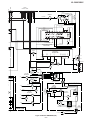
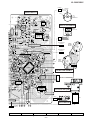
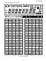
Figure 26 SCHEMATIC DIAGRAM (1/8)
– 26 –
5
6
+B
+B
P_MUTE
CL
CE
DO
SD
STEREO
CFW852
B
8
CNP307
SD
FM ST
DO
CL
CE
DI
A_12V
D_GND
TUN L
TUN R
A_GND
TERMINAL PWB-A4
A
P33 12-F,G
FRO
CNS703 DIS
P31 12-E
CNS307 TO
TUNER PWB-A2
XL-3000/3000C
P33 12-F,G
FROM
CNS703 DISPLAY PWB-A3
1
2
3
4
5
6
7
8
MAIN PWB-A1(1/2)
9 10 11 12 13
5.1V
C201
0.0056
C209
47/16
R201
8.2K
CE
DI
28
29
4.8V
D403
1N4004
C431
220P
C430
100/16
D402
1N4004
D401
1N4004
+B
SO601
SPEAKER TERMINAL
CL
DI
CE
C432
220P
30
C429
33/16
R439
3.9K
1K
1K
1K
C433
220P
CL
1
VREF VSS
0.14V
0.14V
2
4.8V
27
0V
26
C425 4.8V
10/16
RBS2 LBS2
C423
0.1(ML) 4.8V
25
3
TEST
4
ROUT LOUT
4.8V
5
0V
C426
10/16
0V
4.8V
C424
0.1(ML)
C419
0.0027
4.8V
RBS1 LBS1
4.8V
6
L
IN2
14
15
R115
56K
R106
470
R113
100
C111 C112
10/50 10/50
R114
100
C107
100/50
R604
10K
Q602 0V
KTC3199 GR
21.8V
+B
Q102
KTA1268 GR
0.6V
R636
27K
C616
0.1
R638
4.7
L602
3µH
C102
10/50
C110
0.001
CHASSIS
GND
Q103 20.2V
KTC3200 GR
Q104
KTC3200 GR 0.6V
1.2V
0.6V
C120
220/16
R102
39K
R124
47K –21.7V
R123
10K
0.6V
0.6V
R121
10K
C628
10/16
C627
0.022
+
R104
56K
R122
1K
R119
33K
0.6V
Q101
KTC3200 GR
0V
R120
1K
L603
10µH
R662
330
J601
HEADPHONES
3
2
1
4
5
9
10
+B
–B
8
+B
+B
5.6V
C905
100/10
C906
100/10
903
99 GR
4.9V
+B
+B
+B
+B
CD_L
A_GND
CD_R
M_GND
M_12V
CD_GND
CD_6R2V
D902
6BSB
7
8
L-CH
C109
3P
+B
R118
47K
+
C614
0.1
C104
3P
A GND
04
50
R635
27K
R-CH
R110
1K
C106
10/50
R101
39K
0.6V
L601
3µH
R637
4.7
C615
0.1
C613
0.1
0.1V
NF2
13
C108
R108 0.0015
1K
0.1V
GND
12
C114
100/50
0V
PRE
–VCC
10 11
20.2V
C113 9
0.022
+VE2
–VE2
8
–VCC
–21.7V
+VCC
21.8V
6 7
R109
22K
C116
0.022
+VE1
–VE1
BIAS
–18.9V
PRE
+VCC
N.C. 0V
NF1
20.6V
IN1
0.1V
0V
5
IC601
STK40202
POWER AMP.
R661
330
–B
4
C103 R105
10/50 470
0.6V
R103 1K
Q601
KTC3199 GR 0V
R603
10K 0V
R607
6.8K
2
3
R111
1K
C101
10/50
C603
33/16
+B
1
0.1V
R634
3.3K
C105
0.0015
R608
1K
R609
1K
R
9
10
Figure 27 SCHEMATIC DIAGRAM (2/8)
– 27 –
11
12
1
2
3
4
5
6
7
P29 11-C,D P28 1-F
TO
MAIN PWB-A1(2/2)
+B
C208
100/16
1 C215 R217
1/50 12K
R215
12K
R203
100K
C213
4.7/50
R205
10K
C422
0.1(ML)
4.8V
4.8V
24
C421
0.1(ML)
C417
2.2/50
23
R437
6.8K
R423
R424
R425
7
RTRE LTRE
RIN
4.8V
LIN
4.8V
8
22
8
C203
1/50
R440
3.9K
C420
0.0027
R438
6.8K
C416
10/16
4.8V
RSL0 LSL0
R422
1K
L4
0V
R4
0V
R421
1K
R417
1K
21
4.8V
20
9
10
C415
10/16
R418
1K
19
4.8V
18
11
L3
L2
4.8V
L1
4.8V
17
C407
10/16
+B
12
R2
R1
4.8V 4.8V
13
4.8V
C401
CD L 10/16
TUN L
C403
10/16
AUX L
14
16
5V
IC401
LC75342M
FUNCTION/
VOLUME
EQUALIZER
AUX L
15
R3
R416
1K
C402
10/16
0V
AUX R
R415
1K
TUN R
CD R
+B
C418
2.2/50
C408
10/16
R204
100K
2
5.1V
3
C211
0.0033
C404
10/16
R209
10K
R214
12K
R212
2.7K
4
VDD
S
Q201
2SK246 GR 5V
0V
9.6V
1
7
R210
10K
5.1V
D201
1N4148
6
R218 R208
12K
330
C216
1/50
R213
12K
4.44V
5
IC201
KIA4558P
SURROUND
CONTROL
0V
0V
D 5V
0V G
R202
8.2K
C202
0.0056
R216
12K
R211
2.7K
R207
47K
2
5.1V
Q203
KRC107 M
SURROUND 3
5.1V
R206
10K
5.1V
FM SIGNAL
C204
1/50
C214
4.7/50
C212
0.0033
10.2V
CD SIGNAL
5V
P_STB
A_24V
D_GND
DI
CD +B
P_MUTE
CL
CE
DO
SD
STEREO
CNP703
XL-3000/3000C
A
Q
KR
3
4.1V
15
14
13
12
R836
11
1K
10
R834
9
1K
8
R832
7
1K
6
R830
5
1K
4
3
2
1
CNP702
0V
11.6V
0.57V
0V
0V
11.6V
6.1V
4.6V
4.8V
1
2
3
4
5
6
7
8
9
DIMMER
LIGHT
PU_IN
R837 CD_STB
1K
C871
47/16
B
P33 12-C,D
FROM
CNS702
DISPLAY PWB-A3
0
IC805
TA7291S
CD LID
MOTOR DRIVER
R873
3.3K
R90
47
0V
1
R879
3.3K
R835
1K
R874
2.2K
R833
1K
4.9V
2 R
2
Q908
KRC102 M
Q802
KRC102 M
3
R831
1K
0V
3
2
0V
4.5V
0V 1
CLID_SW
CLID_PRO
CLID_UP
CLID_DW
C872
0.1
+B
BUS0
BUS1
BUS2
BUS3
BUCK
CCE
CD_RES
C
R813
10
+B
+B
+B
+B
C834
470P
L806
10µH
C887
0.0027
R814
3.3K
C824
0.056
R812 C819
3.3K
0.1
C822
220/10
C818
0.1
15
0V
2.6V
2.2V
0V
5V
5V
0V
0V
0V
0V
0V
5V
0V
0V
0V
0V
5V
0V
5V
0V
0V
5V
0V
2.5V
4.3V
2.2V
0V
TO MAIN PWB-A1(1/2)
P27 12-G
R820
1K
R811
2.2K
CNS805
11
50 VREF
49 TRO
6
16
IC802
TC9462F
SERVO/SIGNAL CONTROL
FOO
TEZI
TEI
TSIN
SBAD
FEI
RFRP
RFZI
RFCT
AVDD
RFI
SLCO
AVSS
VCOF
VCOREV
PVREV
1
7
5
99 /TSMOD
100 /RST
R851
330
2.1V
2.1V
2.1V
0V
2.1V
13
C820
0.01
+B
0V
2.4V
0V
0V
0.6V
1.7V
0V
5V
0V
4.3V
0V
0V
5V
1 2 3 4 5 6 7 8 9 10 11 12 13 14 15 16 17 18 19 20 21 22 23 24 25 26 27 28 29 30
R801
10K
C829
100/10
R810
3.3K
50
49
48
47
46
45
44
43
42
41
40
39
38
37
36
35
34
33
32
31
C810
0.001
2.1V
2.1V
R809
10K
2.2V
2.2V R808
C809
0.0047
2.2V 3.3K
2.1V
2.1V
2.2V
2.1V
C807
0.033
2.1V
R807
2.1V
10K
5V
C806
0.0047
2.1V
2.1V
C805
0.0027
0V
C804
1.4V
0.01
2.1V
2.1V
C803
47/10
LPFO 2.1V
LPFN
2.1V
R806 C802
15K
0.015
C811
47/10
+B
C863
470P
12
R804
100K
R802
47K
C801
100P
C838
47/10
3
2
1
14
17
1.2V
5V
0V
C837A
100/10
3
2
1
4
81 DVSR
82 RO
TESTO
/HSO
UHSO
EMPH
LRCK
VSS
BCK
AOUT
DOUT
MBOV
IFP
SBOK
CLCK
VDD
VSS
DATA
SFSY
SBSY
SPCK
SPDA
COFS
MONIT
VDD
TESIO0
P2VREF
HSSW
ZDET
PDO
TMAXS
TMAX
R852
100K
R853
100K
R855
100K
P26 3-A,B
TO
CNP805 TERMINAL PWB-A4
R854
100K
DVDD
DVR
LO
DVSL
TEST1
TEST2
TEST3
BUS0
BUS1
BUS2
BUS3
VDD
VSS
BUCK
/CCE
TEST4
5V
5V
5V
0V
1.4V
0V
2.5V
0V
2.5V
BUS0
BUS1
BUS2
BUS3
BUCK
CCE
CD_RES
L808
2.2µH
C836
100/10
8
0V
81
2.4V
C830
C828
82
0.056
100/10
0V
83
2.3V
84
2.4V
85
0V
86
5V
C840
87
100/10 C862
5V
C869
88
0.001
220P
R819
5V
89
220
4.3V
C868
90
220P
4.3V
91
4.3V
C867
92
220P
4.3V
C866
93
220P
5V
94
0V
+B
95
4V
96
3.3V
C865
97
C835 220P
5V 98
0.056
5V 99
100
C864
C837
4.9V
220P
470P
XVDD
XO
XI
XVSS
VDD
PXO
PXI
VSS
TESIO1
TESIN
/DACT
/CKSE
/DMOUT
IO3
IO2
IO1
IO0
VSS
VDD
FLGD
FLGC
FLGB
FLGA
SEL
2VREF
DMO
FVO
FMO
TEBC
RFGC
80 79 78 77 76 75 74 73 72 71 70 69 68 67 66 65 64 63 62 61 60 59 58 57 56 55 54 53 52 51
F
G
C823
0.01
2.1V
2.1V
1.8V
C831
10/16
C832
10/16
C826
15P(CH)
E
R816
10K
X801
16.93MHz
R815
10K
C827
15P(CH)
C825
0.056
C850
C833
470P
C812
0.01
C813
100/10
R818
1K
C821
0.1
R817
1K
C817
0.1
D
L801
10µH
L803
10µH
CNW805
+B
H
• NOTES ON SCHEMATIC DIAGRAM can be found on page 20.
• The numbers 1 to 17 are waveform numbers shown in page 21.
1
2
3
4
Figure 28 SCHEMATIC DIAGRAM (3/8)
– 28 –
5
6
XL-3000/3000C
10.7V
3
MAIN PWB-A1(2/2)
11.4V
Q902
KTA1266 GR
Q901
KRC102 M
R902
47K
LED PWB-A6
11.4V
2
0V
4.1V
0V 1
CNS701
R901
2.2K
1
1
2
CNP701
2
2
11.4V
2 R904
2.2K
Q908
KRC102 M
1
1
1
2
2
2
3
3
3
CNW806
R877
68K
R876
150K
CNP804
+B
+B
CNS804
2
2
1
1
CNW804
M
+B
+B
+B
1
2
3
4
5
6
7
R861
2.2K
R862
2.2K
6.4V
L803
10µH
CD_L
A_GND
CD_R
M_GND
M_12V
D_GND
CD_6R2V
C870
0.001
Q861
2SB562 C
6.3V
5V
+B
M801
CD LID
OPEN/CLOSE
MOTOR
P27 12-G,H
TO
MAIN PWB-A1(1/2)
0V
3
4.9V
CD SIGNAL
Q907
KTA1266 GR
SW802
CD LID
OPEN/CLOSE
CNS806
CNP806
10.7V
1
D801
DB5306X
SWITCH PWB-A5
10.6V
R905
47K
0V
R914
470
CNW701
1
R843
1K
3.2V
3.1V
2.1V
2.1V
0V
4.8V
5V
6.4V
2.1V
2.3V
4.4V
1.9V
CNW803
C859
470/10
C860
0.1
3
3.2V
2.1V
7.0V
7.0V
2.1V
2.1V
2.1V
3.2V
15 16 17 18 19 20 21 22 23 24 25 26 27 28
SP+
SP–
SL+
SL–
PU-IN
GND
0V
GND
MUTE
REG O
TRB
VIN4
VG1
VIN1
VO4+
VO4VO1+
GND
VO1BIAS
VG4
VO3+
VIN3
VG3
VCC
VCC
CD MOTOR PWB-C
+B
+B
R823
1K
C812
0.01
C813
100/10
C850
220/10
C849
0.056
C855
100/10
10
9
8
2.2V
2.1V
4.3V
2.1V
2.5V
3.4V
0V
2.1V
2.1V
2.1V
2.1V
5V
R824
27K
12
11
10
9
8
7
6
5
4
3
2
1
C842
47/10
R821
150
R822
33
4.1V
Q801
KTA1266 GR
3.4V
6
5
4
3
2
1
–
+
–
M
NM802
SPINDLE
MOTOR
M
NM801
SLED
MOTOR
CD PICKUP UNIT(308)
CNP802
FO16
TR+
15
TR14
FO+
13
PD
12
VR
11
LD
10
GND
9
F
8
C
7
B
6
A
5
C
4
E
3
+5V
2
1
R80B
68K
2V
2.1V
2.2V
2.1V
2.1V
2.1V
2.1V
2.1V
2.1V
2.1V
1.7V
0V
2.1V
C841
100/10
13
R825
82K 14
C845
15
100/10
16
C846
17
0.1
18
19
C847
20
0.1
21
C848 R826
2.7K
39P
22
23
R828
1.2K
24
R829 R827 C839
39K 2P
68K
C863
470P
6
5
4
3
2
1
6
5
4
3
2
1
+
SP+
SP–
SP+
SL–
PU-IN
GND
NSW801
PICKUP IN
C811
47/10
+B
CNS803
2
R863
2.2K
C844
0.0068
CNP803
6.5V
0V
PO1+
VO3-
PO1-
OPO
GND
VO2VO2+
VIN2
VG2
14 13 12 11 10 9 8 7 6 5 4 3 2 1
0.8V
1V
3.2V
3.2V
2.1V
IC804
MM1469XH
FOCUS/TRACKING/
SPIN/SLED DRIVER
C857
47/16
C858
0.01
L801
10µH
+B
C843
0.1
IC801
TA2109F
SERVO PRE AMP.
R80E
82K
CNW3
16
15
14
13
12
11
10
9
8
7
6
5
4
3
2
1
FO-
FO–
TR+
TR–
TR+
TR-
FO+
PD
VR
LD
GND
F
C
B
A
C
E
+5V
PO+
ACTUATOR
1/2VCC
1/2V
R80A
R80C 82K
82K
R80F
82K
+B
+
-
B
+
-
A
+
-
E
VREF
R80G
68K
F
C
GND
+B
MON
VCC
7
8
9
10
Figure 29 SCHEMATIC DIAGRAM (4/8)
– 29 –
11
LD
12
+
+
-
XL-3000/3000C
A
C362
3.3/50
C329
0.022
C343
33P
VR351
10K(B)
VD301
SVC348S
C332
0.022
C331
0.047
C330
12P(CH)
C302
0.001
R358
8.2K
FM Mute
Level
B
D301
1N4148
C360
T302
AM
Tracking
L353
1mH
+B
1.5V
0V
5.2V
4.4V
3.8V
5.2V
5
6
7
8
9
R308
10K
5.2V
R305
680
0V
0V
R315
33
C315
100P
R382
330
R386
330
TP301
C316
10/16
SO301
ANTENNA
TERMINAL
F
2.6
C381
12P(CH)
R310
4.7K
X352
4.5MHz
R309
470
C301
0.012
CHASSIS
GND
C382
15P(CH)
C349
0.001
C384
0.001
+B
G
H
• NOTES ON SCHEMATIC DIAGRAM can be found on page 20.
1
2
3
2 1V
2.1V
C351
0.022
+B
Q306
2SC535 C
2.1V
C314
22P
(CH)
C317
0.022
D306
1N4148
2 CF302
2
R304
47K
C309
0.001
C308
0.022
FM
75ohms
C307
0.0047
C305
0.0047
GND
C312
33P
R314 0V
C310 33
0.022
C311
10P(CH)
AM
R312
2.2K
2
3
0V
R301
22
R316
330
CF303
1
3
R313
680
R303
33K
L303
FM OSC.
C313
6P(UJ)
D305
1N4148
E
C306
9P(UJ)
FM RF
R307
47
Q302
2SC535 C
L302
FM ANT.
R302
100K
C303
0.001
C304
0.01
1
R306
10
FM IF
T304
VD302
KDV147B
C318
5P
1
C352
10/16
1.5V
5.2V
4
Coverage
3
3
FM Band
2
2
VD303
KDV147B
1
1
C319
18P(CH)
BF301
BAND PASS
FILTER
D
0.8V
IC301
TA7358AP
FM FRONT END
24 23
5V
AM Band
Coverage
R351
5.6K
C337
0.022
C
5V
2.5V
R336
5.6K
T306
FM IF AM OSC
OUT
IN
AM MIX
OUT
AM OSC
IN
REG
R323
68K
IC303
LA1832S
FM IF DET/
FM MPX/AM IF
D302
1N4148
C334
27P(UJ)
C335
560P
4
Figure 30 SCHEMATIC DIAGRAM (5/8)
– 30 –
5
6
IC
LC
PLL
IC302
84 LC72131
01
PLL(TUNER)
7
3
4
5
6
7
8
C386
330P
L351
100µH
R387
5.6K
R393
1K
9
10
11
C370
1/50
C356
0.001
R376
10K
C355
22P
C357
2.2/50
R355
3.3K
3.8V
(1.9V)
C358
1/50
3.8V
(1.2V)
4V
(2.2V)
MPX IN
R-CH
OUT
L-CH
OUT
PHASE
(AM/FM)
MO/ST
1.3V
13
1.3V
2.1V
15 14
IF OUT
VCC
2.3V (0V)
16
MPX VCO
FM DET
17
PHASE
9
C383
0.022
R395
47K
8
C365
0.022
C363
0.022
C362
3.3/50
C369
56P
C368 R356
1/50 1K
X351
456kHz
C371 R361
1/50 5.6K
10 11
12
+B
R377
5.6K
14 13 12
9
4.7V
(0V) 2
R391
390
R383
5.6K
R384
6.8K
C391
47/16
17 16 15
0V
2
C399
0.022
STEREO
AM LOW
CUT
FM/AM
OUT
0V (0.9V)
2.3V
18
R365
10K
IF REQ IF IN
8
MO/ST
C385
0.01
CF352
AM IN
5V
7
FM
+B
2.9V
R353 (4.3V)
270
5V
C398
100/10
0V
CF351
6
0V
(2.6V)
SD
VSM
C367
1/50
0V
18
5.2V
5V
0V
AM IF
IN
GND
0.6V
2.1V (2.7V)
2.1V (2.7V)
5V
R350
2.7K
3.5V
(0V)
19
2.6V (0V)
C353
0.022
C354
0.022
3
C387
0.022
C380
10/16
5
VDD
MUTE FM IN
R379
2.2K
1
0.9V
4
3.7V
(0V)
3.9V
FM
22 21 20
PD
R352
1K 2.1V
AM RF
IN
19
1.7V
(11.4V)
DO
0.9V
3
AIN
FM AFC
20
5.1V
CL
T351
AM IF
4.8V
DI
2
C392
0.001
C394
47/16
C350
0.022
0.1V
R381
10K
21
R373
1K
R372
1K
R371
1K
0V
2.1V
22
CE
2.6V
0.1V
386
30
AOUT
VSS
82
(CH)
1
0V
52
MHz
C397
0.022
R382
30
0V
IN
OUT
AM MIX
OUT
AM OSC
IN
REG
24 23
R374
1K
1
(CH)
X IN X OUT
5V
2
2.6V
C352
10/16
R363
3.3K
R364
3.3K
C373
0.027
R357
470K
C374
0.027
C366
0.001
C364
10/16
C360
0.022
C361
0.022
XL-3000/3000C
TUNER PWB-A2
AM SIGNAL
FM SIGNAL
Q351
KRC104 M
1 0V
3.7V
(0V)
3
C372 R362
1/50 5.6K
+B
R366
2.2K
ZD351
DZ5.1BSB
FM ST
SD
DO
L352
100µH
C396
100/10
CL
CE
DI
C395
0.022
+B
D_GND
R392
390
C393 R380
1/50 1.5K
Figure 31 SCHEMATIC DIAGRAM (6/8)
– 31 –
10
11
A_12V
TUN_L
TUN_R
A_GND
11
10
9
8
7
6
5
TO
MAIN PWB-A1(1/2)
CNP307
P26 5-A
4
3
2
CNS307
1
Q360
KTA1266 GR
+B 11.7V
10.8V
10.9V
+B
R385
5.6K
R359
1.8K
R360
4.7K
D308
1N4148
12
XL-3000/3000C
A
SW727
FUNCTION
SW726
REW
PRESET DOWN
R706
3.9K
1
2
3
4
5
6
7
8
9 10 11 12 13 1
SW718
VOLUME DOWN
SW721
BASS/TREBLE
2.47V
R727
47K
R729
47K
+B
LAMP PWB-A7
R723 47K
SW709
POWER
1.7V
R702
10K
X701
C701
22P(CH)
SW710
CD LID
OPEN/CLOSE
LMP701
C702
22P
32.768kHz X702
GND
R724
8.2K
R795
47K
R731 1K
5V
R732 1K
5V
2.5V
2.5V
2.5V
2.5V
2.5V
2.5V
2.5V
SEG9
SEG8
SEG7
SEG6
SEG5
5 VLC3
6 VLC2
0V 14
0V
SEG4
4 COM0
7
5V 8
2.49V
9
2.47V
10
0V
11
2.24V
12
2.47V 13
8MHz
5V
3 COM1
3.25V
+B
R728 1K
C703
0.1
24V
VLC1
VDD
OSC2
OSC1
VSS
XI
XO
MMOD
SYSTE
15 VREF–
16 CLID_SW
17 KEY1
5V 18 KEY2
5V 19
MODEL
0V
20 CLID_PRO
R735 0V 21
1K
R733 1K
CE
DO
+B
CFW701A
CL
4.9V 22
0V
23 VSM
4.9V
24 VREF+
0V
25 DI
3
3
USWD_5R6V
+B
D722
1N4148
D723
1N4148
+B
+B
4.8V
3
2
0V
1
0V
C710
0.01
R7A7
1K
Q701
KRC102 M
+B
0.4V
Q702
KTC3199 GR
0.4V
C712
0.01
R7A6
1K
R7A0
1K R7A5
10K
C711
3.3/50
R7A9
3.3K
D721
1N4148
F
0.4V
R7A2
100K
D720
1N4148
5V
Q708
KTA1266 GR
5V
5V
G
4.2V
R796
1K
Q707
KTA1266 GR
24.5V
+B
24.5V
RX701
REMOTE
SENSOR
R7A4
120
1
R7A1
1K
R7A3
100
C714
560P
2
3
+B
5V
5V
R798
4.7K
Q709
KRC102 M
R778 47K
R779
47K
3
2
4.5V
R797 0.1V
2.2K
1 0V
R780 47K
R781
47K
R783
33K
+B
Q706
KRC102 M
3
2
0.1V
4.1V
1 0V
R792
47K
23.7V
0.4V
1.1V
Q703
KTC3199 GR
R7A8
82
+B
R7B0
10K
R793
10K
C704
0.022
+B
H
• NOTES ON SCHEMATIC DIAGRAM can be found on page 20.
1
2
3
4
Figure 32 SCHEMATIC DIAGRAM (7/8)
– 32 –
5
6
0V
4.9V
4.9V
4.9V
4.9V
D_GND
P_CONT
C715
100/10
2
C713
10/16
1
2
ZD701
DZ3.3BSB
1
0V
R744 1K 5V
R738 1K
1K
R740 1K 0V
R741 1K 0V
5V 26 27 28 29 30 31 32 33 34 3
L702
2.2µH
CNW707
CNS707
R799
P26 1-F,G TO
CNP707 POWER PWB-B
3 2 1
R722
10K
R721
10K
RESET
R734 1K
R739 1K
3 2 1
CFW701B
R725
10K
D
E
0V
(CH)
C
2 COM2
2.47V
R720B
1.2K
100 99 98 97 96 95 94 93 92 9
1 COM3
SEG3
R720A
SW711 1.2K
FF
PRESET UP
R711
1.2K
2.47V
R719
1.2K
SW712
CD PLAY/ PAUSE
TUNING UP
R710
2.7K
2.47V
SW722
MEMORY/SET
2.5V
R708
2.2K
2.5V
R718
1.5K
SW713
VOLUME UP
SEG0 2.5V
R707
2.7K
SEG1
SEG2
SW725
CD STOP
TUNING DOWN
B
C705
0.01
XL-3000/3000C
DISPLAY PWB-A3
LCD701
FL DISPLAY
73
SEG28
72
SEG29
71
SEG30
70
SEG31
69
SEG32
68
SEG33
67
2.5V
2.5V
2.5V
2.5V
CLID_DW
CLID_UP
CLID_PRO
CLID_SW
CD_RES
2.5V
2.5V
5V
R761 1K
5V
R774 1K
5V
R762 1K
5V
R763 1K
5V
R764 1K
4.8V
R765 1K
4.8V
R766 1K
CD_STB
4.8V
R767 1K
CD_RES
4.9V
R768 1K
PU-IN
0V
R769 1K
CLID_DW
4.9V
R770 1K
CLID_UP
66
65
BUS3
64
BUS2
63
BUS1
62
BUS0
61
CD_STB
60
CD_RES
59
PU–IN
58
CLID_DW
57
CLID_UP
56
DIMMER
LIGHT
55 0V
4.72V
54
4.76V
53
52 4.8V
4.8V
51
B-LIGHT
0V
0V
R777 1K
R776 1K
R760 1K 4.9V
R758 1K 4.8V
R759 1K 4.8V
R757 1K 4.8V
4.9V
R755 1K 4.8V
R742 1K 4.8V
4.9V
5V
R752 1K
R751 1K 4.9V
5V
R750 1K
0V
R749 1K 5V
0V
4.9V
4.9V
R744 1K 5V
CCE
BUCK
BUS3
BUS2
BUS1
BUS0
CD_STB
PU-IN
LIGHT
DIMMER
1
2
3
4
5
6
7
8
8
10
11
12
13
14
15
R772 1K
R773 1K
R785
1K
R784
47K
32 33 34 35 36 37 38 39 40 41 42 43 44 45 46 47 48 49 50
C705
0.01
CNS702
1
2
3
4
5
6
7
8
8
10
11
12
13
14
15
+B
R786
47K
R789
47K
CLE
DATA
P_CONT
VSM
CNS703
SD
SD
STEREO
STEREO
DO
CL
CE
DI
+B
CD+B
+B
CD+B
CLID_PRO
P_MUTE
P_STB
P_STB
P_MUTE
A_24V
D_GND
SURROUND
SURROUND
5V
+B
CE
1
1
2
2
3
3
4
4
5
5
6
6
7
7
8
8
9
9
10
11
12
13
10
11
12
13
CNW703
CL
DO
DI
+B
CLID_SW
B-LIGHT
+B
7
8
9
10
Figure 33 SCHEMATIC DIAGRAM (8/8)
– 33 –
11
12
TO
CNP703 MAIN PWB-A1(1/2)
P26,27 6,7-A
SD
CNW702
2.5V
TO
CNP702 MAIN PWB-A1(2/2)
P28 1-B,C
74
SEG27
CCE
DATA
P–CONT
CD+B
P–MUTE
P–STB
SURR
CLE
REMOCON
SYS_STOP
POWER
75
SEG26
BUCK
IC701
IX0039SJ
SYSTEM MICROCOMPUTER/
FL DRIVER
RESET
SEG25
STEREO
SEG22
SEG21
SEG20
SEG19
SEG18
SEG17
SEG16
SEG15
SEG14
SEG13
SEG12
SEG11
SEG10
SEG9
SEG8
SEG7
SEG6
94 93 92 91 90 89 88 87 86 85 84 83 82 81 80 79 78 77 76
2.5V
2.5V
SEG24
2.5V
2.5V
SEG23 2.5V
2.5V
2.5V
2.5V
2.5V
2.5V
2.5V
2.5V
2.5V
2.5V
2.5V
2.5V
2.5V
2.5V
2.5V
2.5V
2.5V
11 12 13 14 15 16 17 18 19 20 21 22 23 24 25 26 27 28 29 30 31 32 33 34 35 36 37 38
XL-3000/3000C
CFW451
TO CHASSIS GND
LUG(205)
C411
C413
SO401
A
TERMINAL PWB-A4
R408
LEFT
R406
VIDEO/
AUX IN
RIGHT
R407
R405
B
SUB
WOOFER
OUT
R636
CNW704
2
1
GY
BK
C410
R411
C414
R635
C
1 2
C659
D660
C851
C852
J801
DIGTAL
OUT
L802
C853
R637
CNS805
3
2
1
CNP805
3
2
1
C660
WH
D657
C657 D901
C658
RD
D658
CFW852
C901
CNS704
C65
C126
12
C614
CHASSIS
GND
C616
C615
D
1
2
3
4
5
C630 F653
1.6A/125V
TO CHASSIS GND
LUG(205)
R638
CN
D659
2
1
CNP704
3
2
1
L601
L602
FROM
POWER
TRANSFORMER
P36 4-C
R410
CFW452
LEFT
RIGHT
CNS607
WH
3
2
1
RD
3
2
1
CNP607
C412
SO601
SPEAKER
TERMINAL
C613
C
D902
C902
J601
HEAD
PHONES
C125
CHASSIS
GND
LUG
(205)
C109
C101
R104
R115
R103
C104
16 14 12 10 8 6 4 2
15 13 11 9 7 5 3 1
D651
D653
R105
L603
R661
R662
R111
R101
D652
R873
CNP802
Q908
D654
C103
C903
R910
C107
C111
IC601
G
ORANGE
YL
YELLOW
GR
GREEN
BL
BLUE
VL
VIOLET
GY
GRAY
WH(W)
WHITE
BK
BLACK
PK
PINK
R108
Q102
Q602
E C B
E
C
B
E C B
C102
R607
Q607
R122 R121
Q101
R119
B C E
Q103
R120
C621
ZD601
R617
R9
ZD602
R80F
C627
C628
C603 C626
1 2 3
1 2 3
R612
R634
Q609
Q608
R124
E C B
Q104
R613
D604
C120
3
R80E
RED
OR
R118
R123
1 2 3 4 5 6 7 8
5
7
CNS30
P36,37 6,
H
• The numbers 1 to 17 are waveform numbers shown in page 21.
1
2
1
Q901 2
R80C
BROWN
R609
BR
RD(R)
R821
C904
C625
C622
COLOR TABLE
R603
C110
R604
F
Q904
1
2
ZD901
C113
3
R109
4
5
R620
6
R113
7
C620
C112
C116
8
B
9
D602
10
E C B Q603
R114 Q604 C
R629
11
E
C108
12
R628
E
C114
13
R619
C Q903
14 R106
R912
R608
C106
15
B
C905
B
R110
R913 C906
Q605 C
Q606
Q601
R102
E
E
ZD902
R611
E C B
C
C629
R621
R614
B
E C B
C624
R623
CHASSIS
GND
B C E
R911
R80A
C105
R624
E
3
4
Figure 34 WIRING SIDE OF P.W.BOARD (1/4)
– 34 –
5
6
XL-3000/3000C
CNS804
1 BK
2 RD
CNW804
MAIN PWB-A1
RED
R217
59
C660
3
CNW607
C408
C402
C403
R417 R415
C421
25
D403
D402
F651
3.15A/125V
C872
2 1
CNP804
CNP702
R811
R812
50 51
C817
R816
C818
R817
17
R843
R823
C842
C841
R80B
B C E
R80G
Q801
4
L806
1
WH
GY
GY
GY
GY
GY
L803
C819
R861
6
CNW803
R824
CD MOTOR PWB-C
C870
X801
B
C
E
CNP803
1 23 45 6
Q861
C811
NM801
SLED
MOTOR
16
C825
C887
C826
R814
C821
13
R819
R820
C823
R810
R80A
R80C
R80E
L801
12
C822
C857
IC801
60
55
C859
1
10
C827
1
2
3
4
5
6
CNS803
14
C858
1
14
10
R862
5
IC804
R822
C843
C849
5
C845
C847
C844
R827 R826 R828
C846
C839
R825
13
24
R829
20
15
75
C860
C848
45
C810
C807
R813
81
80
70
NSW801
PICKUP IN
R818
C862
C830
C832
65
40
C804
R807
C813
C834
R852
R854
R815
C868
C835
C831
R855 R853
C840
C828
C866
L808
90
85
IC802
R837
C869
C867 R836
5 95
35
R808
R809
CNP701
C803
C850
C806
C855
R834 R835
R833
C824
20
25
C809
1 2
R801
R804
R902
R901
10
15
R802 R806 30
Q902
31
C801
C802
C805
3
B C E
C864
1100
RD
C812
Q901 2
C871
C838
E
C
B
3
R904
1
Q908 2
C837
WH R851
3
C863
1
CNW805
Q907 C829 C820
R905
R873
R879
1 2 3
R874
R831
3 2 1
C836
R877
CNP806
C837A
Q802
R830
C865 R832
R876
9 8 7 6 5 4 3 2 1
NM802
SPINDLE
MOTOR
FROM DISPLAY
PWB-A3
CNS702
P37 10-E,F
C833
1 2 3 4 5 6 7 8 9 10 11 12 13 14 15
IC805
GY
GY
BK
FROM DISPLAY
PWB-A3
CNS703
P37 10-B,C
CNP703
13 12 11 10 9 8 7 6 5 4 3 2 1
C654
1
3
2
1
CNS806
30
C431
R423
R439
C430
D401
1
CNW806
C419
R421
C417
C429
3
C420
IC401
16
C423
901
C651
5
20
C401
Q203
C432
C433
1
10
C425
C901
3 2 1
R422
R418
15
R416
C426
C415
SW802
CD LID
OPEN/CLOSE
R207
C422
C404
F652
3.15A/125V
R212
R216
R214
C424
C407
SWITCH PWB-A5
8 7 6 5
F3895AF
WH
1
2
3
4
5
D201
R440
R201
CNP801
R210
IC201
S G D
R424
R202
1
1 2 3 4
R215
Q201
R218
C216
C418
R438
C416
R209
C212
C211
R206
R203
C204
R401
R204
RD
R213
R211
R205
C213
C203
C214
R402
R208
C201
C209
R437
C202
M801
CD LID
OPEN/CLOSE
MOTOR
C215
R425
C208
20
CD PICKUP UNIT(308)
25
R863
3
2
CNS307 TO TUNER
PWB-A2
P36,37 6,7-A
7
8 10 9 6
D801
CNW701
1
4 5 6 7 8 9 10 11
2
CNW3
R914
LED PWB-A6
1
1
16
CNS701
1 WH
BK
2
CNP307
1
16
28
15
1
16
11 15
8
9
10
Figure 35 WIRING SIDE OF P.W.BOARD (2/4)
– 35 –
11
12
XL-3000/3000C
R377
R366
R395
L352
R364
R361
R362
C372
R357
C354
R393
C366 C363
C369 R363
C373
C371
C374
C368
R383
C364
C353
R376
3 2 1
C358 Q351
X351
C352
C351
CF302 R352 R353
C399
1 2 3
1 2 3 4 5 6 7 8 9 10 1112
R313
R351 C360
B
IC303
C
C350 C361
E
24 23 22 21 20 19 18 17 16 15 14 13
Q306
R355
R350
T306
C356
C310
R336
R314
R312
C335
VD301
C329
C386
C385
R310
R301
R306
C312
L302
D302
C
CF303
1 2 3
R307
R302
VD303
C332
C357
C355
CF351
C396
ZD351
C398
C367
C349
VR351
R303
C307
C303
C306
R385
R384
C365
CHASSIS
GND
C302
D301
1
2
3
C308
C309
CF352
R358
C319
C314
C395
C370
T351
C362
3
VD302
R308
C313
C391
R391
R392
R382
L353
R309
L303
C343
2
D306
R387
L351
C337
BF301 1
9
8
7
6
5
4
3 C305
2
1
E
C
B
R386
C330
C331
C334
R323
AM
IC301 C318
R305
C317
B
Q302 C
R304
E
R315
C304
B
C311
C393
C315
C316
GND
Q360
D308
C384
IC302
D305
R316
C383
C301
CNS307 1 2 3 4 5 6 7 8 9 1011
X352
R373
R372
R371
T304
SO301
ANTENNA
TERMINAL
CNP307 TO
PW
P34,35 6,7-H
R374
1
2
3
4
5
6
7
8
9
10
11
R359
R360
TP301
22
21
C397
R379 20
C380
19 C392
18
R365
17
C394 R380 16
15 C387
14
13
R381 12
A
FM
75
OHMS
C382
C381
TUNER PWB-A2
R356
T302
BR
BR
YL
BK
YL
5
4
3
2
1
TO MAIN
PWB-A1
CNP801
P35 7-B,C
D
BL
E
RD
T651
POWER TRANSFORMER
(MAIN)
3
AC POWER SUPPLY CORD
2
1
AC 120V,60Hz
POWER PWB-B
RLY601
3
D689
1
D685
F
CNP651
R685
Q683
B C E
C
E C B
R652
Q681
R686
G
T681
SO655
AC INPUT SOCKET
AC 120V,60Hz
POWER TRANSFORMER
(SUB)
H
1
2
3
4
Figure 36 WIRING SIDE OF P.W.BOARD (3/4)
– 36 –
5
6
XL-3000/3000C
LMP701
1
CFW701B
3
SW709 POWER
R760
RX701
REMOTE
SENSOR
R786
26
R789
R759
25
35
R785
55
5
C705
CNS702
WHITE
BK
BLACK
PK
PINK
15
14
13
12
11
10
9
8
7
6
5
4
3
2
1
TO MAIN
PWB-A1
CNP702
P35 8,9-D
689
685
15
GY
GY
GY
GY
GY
GY
GY
GY
GY
GY
GY
GY
GY
GY
BK
C711
Q703
3 2 1
SW710
NOT
CONNECT
R720A
SW712
CD PLAY/PAUSE
TUNING
UP
CD LID
OPEN/CLOSE
D683
D682
DISPLAY PWB-A3
7
8
9
10
Figure 37 WIRING SIDE OF P.W.BOARD (4/4)
– 37 –
11
12
MEMORY/
SET
SW722 R706
R710
R711
R707
Q701
R7A9
D722
C661
D681
D684
R7B0
C715
D688
C688
C683
E C B Q702
C704
R7A8
C712
C710
R7A7
R7A6
C689
R687
IC681
R686
3
2
1
C665
ZD684
R688
R7A5
ZD683
R689
R7A0
E C B
R7A2
D721
CNP707
E C B
Q681
R7A1
1
D720
2
ZD701
D723
3
B C E
R767
R766
R765
R764
R763
R762
R774
R761
R735
R731
R783
1
R685
Q683
BASS/
TREBLE
R768
1
2
3
4
5
6
7
8
9
10
11
12
13
14
15
16
17
18
19
20
21
22
23
24
25
26
27
28
29
30
31
32
33
34
35
36
37
38
LCD701
FL DISPLAY
GRAY
WH(W)
L702
VIOLET
GY
SW726
REW
PRESET
DOWN
VL
R772
SW711
FF
PRESET
UP
BLUE
R795
GREEN
BL
R770
R769
YELLOW
GR
R784
ORANGE
YL
SW725
CD STOP
TUNING
DOWN
OR
76
75
R773
RED
R750
CNW702
RD(R)
85
70 80
R7A4
BROWN
1
100
95
90
65
BR
R702
10
IC701
60
COLOR TABLE
R723
R727
R729
15
40
45
50
51
R724
30 20
R752
R744
R725
C703
C701
1
2
3
R777
C713
R776
1
VOLUME
DOWN
R741
R739
R751
R720B
SW713
R755
R742
R757
R758
R719
R722 VOLUME
UP
R721
R749
R7A3
SW721
R781
X702
3
R779
R780
Q708
SW718
R728 X701
R798 R797 Q709
R799
R793
Q707
1
R708
R734
R733
R732
C702
CFW701A
E C B
R778
CNW707
GY
GY
GY
GY
GY
GY
GY
GY
GY
GY
GY
GY
BK
13
R792
R718
CNP703
P35 8,9-C
2
B
C
E
3
C714
C373
1
CNS703
13
12
11
10
9
8
7
9
5
4
3
2
1
1
2
3
R738
TO MAIN
PWB-A1
WH
BK
BK
CNW703
1
2
3
Q706
3 2 1
R796
CNS707
SW727
FUNCTION
LAMP PWB-A7
3 4 5 6 7 8 9 1011
R740
CNP307
P34,35 6,7-H
TO MAIN
PWB-A1
XL-3000/3000C
TROUBLESHOOTING
When the CD does not function
When the CD section does not operate when the objective lens of the optical pickup is dirty, this section may not operate. Clean
the objective lens, and check the playback operation. When this section does not operate even after the above step is taken,check
the following items.
Remove the cabinet and follow the troubleshooting instructions.
"Track skipping and/or no TOC (Table Of Contents) may be caused by build up of dust other foreign matter on the laser pickup
lens. Before attempting any adjustment make certain that the lens is clean. If not, clean it as mentioned below."
Turn off the power, and wipe the lens softly using a cleaning paper moistened with commercially available cleaning solution so
as not to damage it.
Be careful not to touch the lens with bare hands.
Dust gradually accumulates on the objective lens during use, and it may degrade performance.
To avoid this problem, use a cleaning disc designed for CD optical pickup lenses.
HOW TO USE
1. Using the brush in the cleaner cap, apply 1 or 2 drops of the cleaning fluid to the brush on the CD cleaner disc which has
the mark next to it.
2. Place the CD cleaner disc onto the CD disc tray with the brush side down, then press the play button.
3. You will hear music for about 20 seconds and the CD player will automatically stop. If it continues to turn, press the stop button.
CAUTION
The CD lens cleaner should be effective for 30 - 50 operations, however if the brushes become worn out earlier then please
replace the cleaner disc.
If the CD cleaner brushes become very wet then wipe off any excess fluid with a soft cloth.
Do not drink the cleaner fluid or allow it to come in contact with the eyes. In the event of this happening then drink and / or
rinse with clean water and seek medical advice.
The CD cleaner disc must not be used on car CD player or on computer CD ROM drives.
All rights reserved. Unauthorized duplicating, broadcasting and renting product is prohibited by law.
Cleaner Liquid
Cleaning Disc
PARTS CODE: UDSKA0004AFZZ
– 38 –
XL-3000/3000C
Make sure that the disc is normal, and set the CD TEST MODE (STEP 1).
Is the measured voltage as specified in circuit diagram?
Check the main unit power supply circuit.
No
Yes
Is "Er-CD01" displayed"?
No
Yes
Move the pickup to most internal circumference side of disc.
Turn the power off and reset the CD TEST MODE (STEP 1).
Is "PU ERROR " not displayed?
No
Check the pattern between pin 58 (PU_IN) of IC701 and
CNW803/CNS803.
Check the between CNW803/CNS803 and PU-IN switch.
Yes
Is +5V applied to pin 100 (/RST) of IC802?
No
Check the PWB pattern between pin 59 (CD_RES) of IC701 and
pin 100 (/RST) of IC802.
No
Is CD Lid switch SW802
ON condition ?
Yes
Does the CD TEST MODE advance from "STEP 2"?
Yes
No
Set ON condition the CD
Lid switch.
Yes
Check the between pattern IC701 and SW802 If OK.
Check the main unit power supply circuit.
Does the laser come on in CD TEST MODE "STEP 2"?
No
Check the procedure in "LASER FAILURE".
Yes
Does the CD TEST MODE advance from "STEP 3" to "STEP
4"?
Yes
No
Does the spindle motor rotate normally when the CD TEST
MODE changes from "STEP 4" to "STEP 3"?
No
Check the procedure in "FOCUS FAILURE".
Check the procedure in "SPINDLE MOTOR CLV SERVO
FAILURE".
Yes
Is the HF output on pin 38 of IC802 in CD TEST MODE "STEP 5"?
No
Check the procedure "HF ERROR".
Yes
Does the sound heard when the optical pickup move to the
selected play by the FF
/REW
key.
No
Does the sled motor
move ?
No
Yes
Check the procedure in
"SLED MOTOR
OPERATING FAILURE ".
Yes
Check the procedure "NO SOUND"
Does the LCD track number and time indicator work properly ?
No
Check the pattern between IC701 and LCD701.
Yes
Turn the power off and then back on.
Does the unit initialize properly and start playback when PLAY
key is pressed?
No
Is "Er-CD01 "
displayed ?
No
Is "Er-CD01" displayed?
Yes
Yes
Check the pattern between pin 58 (PU_IN) of IC701
and CNW803/CNS803. Check the between CNW803/
CNS803 and PU-IN switch.
Check the procedure in "HF ERROR".
Does the unit play in order in the FF mode?
No
Check the procedure in "TRACK SEARCH FAILUR".
Yes
Does playback continue for 30 seconds after the start of
playback ?
No
Yes
Normal
– 39 –
Check the procedure in "SLED SERVO FAILURE".
Yes
XL-3000/3000C
• Laser failure.
Is +6.2V applied to the emiter of Q861 ?
No
Check the PWB pattern between emiter of Q607 and emiter of
Q861.
Yes
Check the peripheral parts of IC804 and Q861.
Is +5V applied to the collector of Q861 ?
No
Yes
No
Check the PWB pattern between collector of Q861 and pin 62 of
IC802.
No
Check the PWB pattern between collector of Q861 and pin 1 of
IC801.
No
Does the laser come on when pattern cut between pin 8 (SEL) of
IC801 and pin 57 (SEL) of IC802 ?
Is +5V applied to the pin 62 (VDD) of IC802 ?
Yes
Is +5V applied to the pin 1 (VCC) of IC801 ?
Yes
Is 0V applied to the pin 57 (SEL) of IC802 ?
Yes
Yes
No
Check the PWB pattern between IC701 and IC802 (BUCK/CCE/
BUS0~3)
Is approx. 2V applied to the collector of Q801.
No
Check the peripheral parts of IC801 and Q801. If it is normal, the
optical pickup is faulty.
No
Check as stated in item "FOCUS SERVO SAWTOOTH WAVE
FAILURE".
Yes
Check CNP802/CNW3. If it is normal, the optical pickup is
faulty.
• Focus failure.
Does the optical pickup move up and down when the disc is
removed?
Yes
Is the following waveform ouput at the pin 43 (FEI) of IC802
when the disc is set?
Check the periphery of IC801 and CNP802/CNW3. Is it normal?
No
Yes
Yes
pin 43
The optical pickup is faulty.
(FEI)
pin 48
(FOO)
pin 44
(SBAD)
Is the waveform shown above input at the pin 44 (SBAD) of
IC802?
No
Yes
IC801 is faulty.
– 40 –
Check the pattern between pin 13 of IC801 and pin 44 of IC802.
Check the periphery of IC801 and CNP802/CNW3.
XL-3000/3000C
• Focus servo sawtooth wave failure.
Is sawtooh wave output to the pin 48 (FOO) of IC802 ?
No
IC802 is faulty.
Yes
1.5~2.5sec
Check the PWB pattern between emiter of Q607 and IC804.
Is +6.2V applied to the pins 21 and 22 (VCC) of IC804 ?
No
Yes
Is sawtooth wave obtained between pins 26 and 27 of IC804 ?
No
Yes
Is +5V applied to the pin 7
(MUTE) of IC804 ?
No
Yes
1.5~2.5sec
Check the PWB pattern
between pin 7 of IC804
and pin 60 (CD STB) of
IC701.
Check the PWB pattern between pin 48 (FOO) of IC802 and pins
24 and 25 of IC804. If OK. IC804 is faulty.
Is sawtooth wave obtained between pins 13 and 16 of
CNP802/CNW3 ? (as shown above)
Check the PWB pattern between CNP802/CNW3 and IC804.
No
Yes
CNP802/CNW3 connection failure or optical pickup failure.
• Spindle motor clv servo failure.
Is following wave output to the pin 55 (DMO) of IC802 when
the CD TEST MODE "STEP 3" is changed to " STEP 4" ?
No
Check the procedure in "HF ERROR".
If OK. IC802 is faulty.
No
Check the PWB pattern between pin 55 (DMO) of IC802 and pins
9 and 10 of IC804. If OK. IC804 is faulty.
Yes
DMO
Is above wave obtained between pins 11 and 12 of IC804 ?
Yes
Is above wave obtained between pins 9 and 12 of CNP802/
CNW3 ?
Check the PWB pattern between CNP802/CNW3 and IC804.
No
Yes
CNP802/CNW3 connection failure or optical pickup failure.
– 41 –
XL-3000/3000C
• HF error.
Is output (tracking error signal) obtained at the pins 46 (TEI)
and 47 (TEZI) of IC802 the CD TEST MODE "STEP 4" is
changed to "STEP 5"?
No
Is output obtained at the pins 3 and
No
8 of CNP802/CNW3.
Optical pickup failure.
Yes
Yes
test mode "step 4"
Check the periphery of IC801.
Check the PWB pattern between
pin 12 (TEO) of IC801 and pins 46
and 47 of IC802.
Is it normal ?
test mode "step 5"
TEI
TEZI
IC801 is faulty.
No
Yes
Check the PWB pattern between pin 49 (TRO) of IC802 and pin 19
of IC804.
Check the periphery of IC804 and CNP802/CNW3.
If OK. Optical pickup failure.
Is output (HF signal) obtained at the pin 38 (RFI) of IC802
when the CD TEST MODE "STEP 4" is changed to "STEP 5"?
No
Optical pickup failure.
Yes
Yes
test mode "step 4"
test mode "step 5"
Check the periphery of IC801.
Check the PWB pattern between pin 19 (RFGO) of IC801 and pins
38 (RFI) of IC802.
If OK. IC801 is faulty
RFI
Is output (HF signal) obtained at the pins 41 (RFZI) and 42
(RFRP) of IC802 when the CD TEST MODE "STEP 4" is
changed to "STEP 5"?
Yes
Is output obtained at the pins 4 and
5,6 of CNP802/CNW3.
No
test mode "step 4"
No
Check the periphery of IC801.
Check the PWB pattern between pin17 (RFRP) of IC801 and pins
41 (RFZI) and 42 (RFRP) of IC802.
If OK. IC801 is faulty.
test mode "step 5"
RFZI
RFRP
Is the following wave output to the pin 55 (DMO) of IC802
when the CD TEST MODE "STEP 4" or "STEP 5"?
Yes
test mode "step 4"
No
Check the periphery pins 28~32 of IC802.
If OK. IC802 failure.
No
Check the interval between the pins 82 or 85 of IC802 and the pins
1 or 15 of IC601.
test mode "step 5"
DMO
Normal.
• No sound.
No sound from both L and R-ch?
Yes
Check the PWB pattern between R819 and Q861.
Is +4.5V applied to pin 83 (DVDD) of IC802?
Yes
No
Is signal of pins 82 and 85 of IC802 output?
Yes
Check the peripheral parts of IC802. If OK, IC802 is faulty.
No
The main PWB is faulty.
– 42 –
XL-3000/3000C
• Track search failure
Does the sled motor run in FF/REW state when the SERVO
TEST MODE "STEP1" is set?
No
Check as stated in item "SLED MOTOR OPERATION FAILURE".
Yes
Is the following wave output to the pin 49 (TRO) of IC802
during track search in normal playback?
No
IC802 failure.
Yes
TRO
Is the following wave output to the pins 12 (TEO) of IC801
during track search in normal playback?
No
Yes
TEO
TEI
Check the PWB pattern between pin 49 (TRO) of IC802 and pin
19 of IC804.
Check the PWB pattern between pins 17 and 18 of IC804 and
Optical pickup.
If OK. Optical pickup failure.
TEZI
Is the above wave output to the pins 46 (TEI) and 47 (TEZI) of
IC802 during track serch in normal playback?
No
Check the PWB pattern between pin 12 (TEO) of IC801 and pins 46
and 47 of IC802. If OK. IC801 failure.
No
Check the PWB pattern between pin 17 (RFO) and 18 (RFIS), 19
(RFRP) of IC801 and pins 41 and 42 of IC802. If OK. IC801 failure.
Yes
Is the following wave output to the pin 41 (RFZI) and 42
(RFRP) of IC802 during track search in normal playback?
Yes
RFRP
RFZI
Normal.
• Sled motor operation failure.
Is following sled feed signal output the pin 53 (FMO) of IC802
when FF
/REW
key is pressed after the CD TEST
MODE "STEP 1" is seted?
FF
REW
Yes
C801 is faulty.
No
FMO
Is following sled feed signal output the pins 3 and 4 of IC804
when FF
/REW
key is pressed after the CD TEST
MODE "STEP 1" is seted?
FF
Yes
No
Check the PWB pattern between pin 53 of IC802 and pins 3 and 4
of IC804.
REW
SL ±
Is sled feed signal output the pins 1 and 2 of IC804?
No
Check the peripheral parts of IC804. If OK, IC804 is faulty.
Yes
Is sled feed voltage applied between both terminals of sled
motor?
Yes
No
Check the CNW803/CNS803.
Check the CD mechanism (periphery of sled motor).
If the sled motor does not run when DC2.0V is applied to
both terminals of sled motor, the sled motor is faulty.
• Sled servo failure.
Is following sled signal output the pin 53 (FMO) of IC802
during playback?
IC802 is faulty.
No
Yes
FMO
Normal.
– 43 –
XL-3000/3000C
FUNCTION TABLE OF IC
IC401 VHiLC75342M-1: Function/Volume Equalizer (LC75342M)
Pin No.
Port Name
Function
1
DI
Serial data and clock input pin for control.
2
CE
Chip enable pin. Data written into an internal latch in a timing of [H] -> [L]. Each analog switch is activated.
Data transfer enabled at [H] level.
3
VSS
Ground pin.
4
TEST
Electronic volume control pin. To be set to the VSS potential.
5
LOUT
Volume + equalizer output pin.
6
LBASS2
Bass-band filter comprising capacitor and resistor connection pin.
7
LBASS1
Bass-band filter comprising capacitor and resistor connection pin.
8
LTRE
Capacitor connection pin comprising treble band filter.
9
LIN
Volume + equalizer input pin.
10
LSEL0
Input selector output pin.
11
L4
Input signal pin.
12*
L3
Input signal pin.
13
L2
Input signal pin.
14
L1
Input signal pin.
15*
NC
No CONNECT pin. To be open or connected to VSS.
16*
NC
No CONNECT pin. To be open or connected to VSS.
17
R1
Input signal pin.
18
R2
Input signal pin.
19*
R3
Input signal pin.
20
R4
Input signal pin.
21
RSEL0
Input selector output pin.
22
RIN
Volume + equalizer input pin.
23
RTRE
Capacitor connection pin comprising treble band filter.
24
RBASS1
Bass-band filter comprising capacitor and resistor connection pin.
25
RBASS2
Bass-band filter comprising capacitor and resistor connection pin.
26
ROUT
Volume + equalizer output pin.
27*
NC
No CONNECT pin. To be open or connected to VSS.
28
Vref
0.5 x VDD voltage generation block for analog ground. Capacitor of several 10µF to be connected between
Vref and AWSS (VSS) as a counter measure against power ripple.
29
VDD
Supply pin.
30
CL
Serial data and clock input pin for control.
In this unit, the terminal with asterisk mark (*) is (open) terminal which is not connected to the outside.
– 44 –
XL-3000/3000C
IC401 VHiLC75342M-1: Function/Volume Equalizer (LC75342M)
TEST VSS CE
4
3
2
DI
CL VDD Vref
NC
1
30
29
27
28
LOUT 5
CONTROL
CIRCUIT
LBASS1 7
LTRE 8
RVref
25 RBASS2
24 RBASS1
CONTROL
CIRCUIT
LBASS2 6
LOGIC
CIRCUIT
CCB
INTERFACE
LVref
26 ROUT
23 RTRE
22 RIN
LIN 9
21 RSEL0
LSEL0 10
11
12
13
14 15 16 17
18
19
20
L4
L3
L2
L1 NC NC R1
R2
R3
R4
Figure 45 BLOCK DIAGRAM OF IC
– 45 –
XL-3000/3000C
IC701 RH-iX0039SJZZ: System Microcomputer/FL Driver (IX0039SJ) (1/2)
Pin No.
Terminal Name Input/Output
1-4
COM3-COM0
5-7
VLC3-VLC1
8
VDD
Output
—
Input
Function
LCD common output terminal.
LCD power supply terminal.
Microcomputer power supply +5V.
9
OSC2
Output
Oscillator ground terminal for main clock. f=8MHz
10
OSC1
Input
Oscillator ground terminal for main clock. f=8MHz
11
VSS
12
XI
Input
Oscillator ground terminal for sub clock. f=32.768kHz
13
XO
Output
Oscillator ground terminal for sub clock. f=32.768kHz
14
MMOD
15
VREF–
16
KEY0 AN0/PA0
Input
CD lid status detection input.
17
KEY1 AN0/PA1
Input
Operation button input, Max-8 buttons.
18
KEY2 AN0/PA2
Input
Operation button input, Max-8 buttons.
19
KEY3 AN0/PA3
Input
MODEL/TUNER destination input.
20
KEY4 AN0/PA4
Input
Current detection of CD lid control motor.
Used to decide the CD lid drive error to control it.
21*
KEY5 AN0/PA5
Input
CD servo auto adjustment mode selection input.
22*
KEY6 AN0/PA6
Input
Tape mechanism operating status detection input.
Decides the F.P/CAM-SW status with A/D value.
—
Input
—
Microcomputer power supply GND.
Memory mode selection terminal.
Power supply GND for AD converter.
23*
KEY7 AN7/PA7
Input
Tuner signal meter (S meter) voltage input terminal.
24
VREF+
Input
Power supply for A/D converter +5V.
25
TXD SBO0/P00
Output
26
RXD SBI0/P01
Input
27
SBT0/P02
Output
Synchronous clock output with TUNER PLL IC
28
SBO1/P03
Output
Enable output of TUNER PLL IC. "L" = OFF "H" = ON
29*
SBI1/P04
Output
Tape mechanism solenoid drive control output.
30*
SBT1/P05
Output
Tape mechanism motor drive control output.
31*
DK/BZER P06
Output
Recording/playback selection output of tape circuit.
"H" = Recording mode, "L" = Playback mode
32
RST/P27
Input
Reset signal input
33*
RMOUT P10
Input
CLOCK/TIMER/SLEEP button input.
34*
P11
Input
Tape run/END detection input. Decided as tape run if pulse is input.
35*
TM2IO P12
Output
36*
TM3IO P13
Output
37
TM4IO P14
Input
38
IRQ0 P20
Input
Switches to the HALT mode when changing to . "L" at power failure detection input.
39
SENS IRQ1/P21
Input
Remote control signal input.
40
IRQ2 P22
Input
Synchronous clock input with RDS IC.
41*
IRQ3 P23
Input
Jog dial UP pulse input.
42*
IRQ4 P24
Input
Jog dial DOWN pulse input.
43
P30
Output
SURROUND control output.
44
P31
Output
POWER IC STAND-BY terminal CONTROL.
45
P32
Output
Power mute output. "H" = MUTE ON "L" = MUTE OFF
46
LED0 WE/P50
Output
CD servo power supply circuit control output. "H" = CD power ON "L" = CD power OFF
47
LED1 RE/P51
Output
Main TRANS RELAY CONTROL. "H" = ON "L" = OFF
48
LED2 CS/P52
Input
Data input from RDS IC.
49
LDE3/S51 A16/P53
Input
Radio stereo broadcast reception detection input. "L" = During stereo broadcast reception
50
LED4/S50 A17/P54
Input
Broadcast reception status detection input. "L" = During broadcasting signal reception
51
SEG49 P60/A0
Output
52*
SEG48 P61/A1
Output
53
SEG47 P62/A2
Output
Data output terminal to TUNER PLL IC.
Data input from TUNER PLL IC
Recording bias oscillation circuit control output.
"H" = Bias oscillation, "L" = oscillation stop.
Recording bias oscillation frequency selection control output.
Power (POWER) button input detection.
LCD backlight control signal output. "H" = Backlight ON, "L" = Backlight OFF
LED illumination control of electric JOG dial. "H" = ON "L" = OFF
In this unit, the terminal with asterisk mark (*) is (open) terminal which is not connected to the outside.
– 46 –
XL-3000/3000C
IC701 RH-iX0039SJZZ: System Microcomputer/FL Driver (IX0039SJ) (2/2)
Pin No.
Terminal Name Input/Output
Function
54
SEG46 P63/A3
Output
55*
SEG45 P64/A4
Output
Electric JOG dial UP.
Electric JOG dial DOWN.
56
SEG44 P65/A5
Output
Electric CD lid OPEN.
57
SEG43 P66/A6
Output
58
SEG42 P67/A7
Input
59
SEG41 P70/A8
Output
Reset signal output for TC9462F
60
SEG40 P71/A9
Output
ON/OFF output terminal of CD servo control IC. "H" = Servo ON "L" = Servo stand-by
61-64
SEG39 P72/A10- Input/Output
SEG36 P75/A13
65
SEG35 P76/A14
Output
Data synchronous clock output for TC9462F.
66
SEG34 P77/A15
Output
Chip enable terminal for TC9462F. "L" = BUS terminal active
67
SEG33 P87/D7
Output
LCD segment output.
68
SEG32 P86/D6
Output
LCD segment output.
69-74
SEG31 P85/D5SEG26 P80/D0
Output
LCD segment output
75-100
SEG25-SEG0
Output
LCD segment output
Electric CD lid CLOSE.
CD pickup position detection SW input. "L" = Innerst periphery
Data input/output terminal for TC9462F control.
100
99
98
97
96
95
94
93
92
91
90
89
88
87
86
85
84
83
82
81
80
79
78
77
76
S
S
S
S
S
S
S
S
S
S
S
S
S
S
S
S
S
S
S
S
S
S
S
S
S
SEG0
SEG1
SEG2
SEG3
SEG4
SEG5
SEG6
SEG7
SEG8
SEG9
SEG10
SEG11
SEG12
SEG13
SEG14
SEG15
SEG16
SEG17
SEG18
SEG19
SEG20
SEG21
SEG22
SEG23
SEG24
IC701 RH-iX0039SJZZ: System Microcomputer/FL Driver (IX0039SJ)
I
O
I
I
I
I
I
I
I
I
I
O
26
27
28
29
30
31
32
33
34
35
36
37
38
39
40
41
42
43
44
45
46
47
48
49
50
O
I
75
74
73
72
71
70
69
68
67
66
65
64
63
62
61
60
59
58
57
56
55
54
53
52
51
1
2
3
4
5
6
7
8
9
10
11
12
13
14
15
16
17
18
19
20
21
22
23
24
25
I
O
O
O
O
O
I
I
I
O
O
I
I
I
I
I
I
O
O
O
O
O
O
O
I
O
O
O
O
DO
CL
CE
NC
NC
NC
RESET
NC
NC
NC
NC
POWER
SYS_STOP
REMOCON
CLE
NC
NC
SURR
P-STB
P-MUTE
CD+B
P-CONT
DATA
STEREO
SD
COM3
COM2
COM1
COM0
VLC3
VLC2
VLC1
VDD
OSC2
OSC1
VSS
XI
XO
MMOD
VREF–
CLID_SW
KEY1
KEY2
MODEL
CLID_PRO
NC
NC
NC
VREF+
DI
Figure 47 BLOCK DIAGRAM OF IC
– 47 –
S
S
S
S
S
S
S
S
S
O
O
I/O
I/O
I/O
I/O
O
O
I
O
O
O
O
O
O
SEG25
SEG26
SEG27
SEG28
SEG29
SEG30
SEG31
SEG32
SEG33
CCE
BUCK
BUS3
BUS2
BUS1
BUS0
CD_STB
CD_RES
PU-IN
CLID_DW
CLID_UP
NC
DIMMER
LIGHT
NC
B-LIGHT
XL-3000/3000C
IC801 VHiTA2109F/-1:Servo Pre Amp. (TA2109F)
Pin No.
Function
Input/Output
Terminal Name
1
VCC
—
2
FNI
Input
Main beam amp input terminal
3
FPI
Input
Main beam amp input terminal
4
TPI
Input
Sub-beam amp input terminal
5
TNI
Input
Sub-beam amp input terminal
6
MDI
Input
Monitor photodiode amp input terminal
7
LDO
Output
8
SEL
Input
Laser diode control signal input and APC circuit ON/OFF signal input terminal
9
TEB
Input
Tracking error balance adjustment signal input terminal
To be controlled by 3-value PWM signal. (PWM carrier = 88.2 kHz)
10
2VRO
11
TEN
Input
12
TEO
Output
13
SBAD
Output
Sub-beam addition signal output terminal
14
FEO
Output
Focus error signal generation amp output terminal
15
FEN
Input
16
VRO
Output
Standard voltage (VR) output terminal. When Vcc = 5V, VR = 2.1V.
17
RFRP
Output
Track count signal generation amp output terminal
18
RFIS
19
RFGO
Output
20
RFGC
Input
RF amplitude adjustment control signal input terminal
The amplitude of RF signal can be controlled by using the 3-value PWM signal (PWM
carrier = 88.2 kHz) which is output from the RFGC terminal of TC9432F.
21
AGCI
Input
RF signal amplitude adjustment amp input terminal
22
RFO
Output
23
GND
—
24
RFN
Input
Output
Input
Power voltage terminal
Laser diode amp output terminal
Standard voltage (2VR) output terminal. When Vcc = 5V, 2VR = 4.2V.
Tracking error signal generation amp reversed phase input terminal
Tracking error signal generation amp output terminal
Focus error signal generation amp reversed phase input terminal
RFRP detection circuit input terminal
RF signal output terminal
RF signal generation amp output terminal
GND terminal
RF reversed phase input terminal
IC801 VHiTA2109F/-1:Servo Pre Amp. (TA2109F)
15kΩ
15kΩ
SBAD 13
7.67kΩ
12 TEO
30kΩ
20µA
50kΩ
10pF
20pF
10kΩ
10kΩ
36pF
21kΩ
29kΩ
24kΩ
24kΩ
11 TEN
7.96kΩ
10 2VRO
10kΩ
VRO 16
21kΩ
RFRP 17
20kΩ
50µA
47kΩ SW1
12kΩ
LDC
1kΩ
SW2
65µA
SW3
PEAK
BOTTOM
RFGO 19
8 SEL
1.74kΩ
20kΩ
20kΩ
9 TEB
3 STATE
DET.
21kΩ
12kΩ
RFIS 18
SEL
10kΩ
FEO 14
FEN 15
30kΩ
10kΩ
7 LDO
680kΩ
180kΩ
13kΩ
20pF
RFGC 20
2.12kΩ
6 MDI
I.I
5 TNI
I.I
4 TPI
180kΩ
12kΩ
AGCI 21
20pF
23.5kΩ
re = 130Ω
20kΩ
180kΩ
RFO 22
40pF
20kΩ
60kΩ
3 FPI
20kΩ
2 FNI
40pF
20kΩ
1 VCC
3.3kΩ
3.3kΩ
RFN 24
1.53kΩ
180kΩ
60kΩ
GND 23
Figure 48 BLOCK DIAGRAM OF IC
– 48 –
L
HiZ
H
LDC
SW1 SW2
ON OFF
OFF ON
OFF ON
SW3
OFF
ON
ON
XL-3000/3000C
IC802 VHiTC9462F/-1: Servo/Signal Control (TC9462F) (1/3)
Pin No.
Port Name
Function
Input/Output
1*
TEST0
Input
Test mode terminal. To be opened usually.
2*
3*
/HSO
/UHSO
Output
Output
Playback speed mode flag output terminal.
/UHSO
/HSO
Playback speed
H
H
x1 speed playback
H
L
x2 speed playback
L
H
x4 speed playback
L
L
—
4*
EMPH
Output
Sub-code Q data emphasis flag output terminal. "H": Emphasis ON "L": Emphasis OFF
The output polarity can be inverted by command.
5*
LRCK
Output
Channel clock (44.1 kHz) output terminal. "L": L channel "H": R channel
The output polarity can be inverted by command.
6
VSS
—
7*
BCK
Output
Bit clock (1.4122 MHz) output terminal.
8*
AOUT
Output
Audio data output terminal.
9
DOUT
Output
Digital out output terminal.
10*
MBOV
Output
Buffer memory over signal output terminal. "H": Over
11*
IPF
Output
Correction flag output terminal.
"H": When AOUT output is correction-disabled symbol in case of C2 correction output.
12*
SBOK
Output
13*
CLCK
Input/Output
14
VDD
Input
Digital + power terminal.
15
VSS
—
Digital ground terminal.
16*
DATA
Output
Sub-code P-W data output terminal.
17*
SFSY
Output
Playback system frame sync signal output terminal.
18*
SBSY
Output
Sub-code block sync output terminal. "H": On S1 position when the sub-code sync is detected.
19*
SPCK
Output
Processor status signal read clock (176.4 kHz) output terminal.
20*
SPDA
Output
Processor status signal output terminal.
21*
COFS
Output
Correction system frame clock (7.35 kHz) output terminal.
22*
MONIT
Output
LSI internal signal monitor terminal.
It is possible to monitor the DSP internal flag and PLL system clock with the microcomputer
command. Terminal for serial output of text data according to command .
23
VDD
Input
Digital + power terminal.
24
TESIO0
Input
Test input/output terminal. To be fixed to "L" usually.
Terminal to input the text data read clock according to command.
—
Digital ground terminal.
Sub-code Q data CRCC judgment result output terminal. "H": When judgment result is OK.
Sub-code P-W data read clock output/input terminal. Selectable with command bit.
25
P2VREF
26*
HSSW
27*
ZDET
Output
1-bit DAC zero detection flag output terminal.
28
PDO
Output
Terminal to output the phase difference between EFM signal and PLCK signal.
29*
TMAXS
Output
TMAX detection result output terminal. To be selected with command bit TMPS.
30
TMAX
Output
TMAX detection result output terminal. To be selected with command bit TMPS.
Output
2VREF terminal for PLL system.
VREF voltage in case of x2 speed/x4 speed.
TMAX detection result
TMAX output
Longer than specific period
"P2VREF"
Shorter than specific period
"VSS"
Within specific period
"HIZ"
31
LPFN
Input
32
LPFO
Output
33
PVREF
Input
VREF terminal for PLL system.
34
VCOREF
Input
VCO center frequency standard level terminal. To be fixed to PVref usually.
35
VCOF
36
AVSS
—
37
SLCO
Output
38
RFI
Output
Input
Low-pass filter amp inverted input terminal.
Low-pass filter amp output terminal.
VCO filter terminal.
Analog system ground terminal.
Data slice level generation DAC output terminal.
RF signal input terminal.
In this unit, the terminal with asterisk mark (*) is (open) terminal which is not connected to the outside.
– 49 –
XL-3000/3000C
IC802 VHiTC9462F/-1: Servo/Signal Control (TC9462F) (2/3)
Pin No.
Port Name
Function
Input/Output
39
AVDD
Input
Analog system power terminal.
40
RFCT
Input
RFRP signal center level input terminal.
41
RFZI
Input
RFRP zero cross input terminal.
42
RFRP
Input
RF ripple signal input terminal.
43
FEI
Input
Focus error signal input terminal.
44
SBAD
Input
Sub-beam addition signal input terminal.
45
TSIN
Input
Test input terminal. To be fixed to Vref usually.
46
TEI
Input
Tacking error input terminal. (Tracking servo ON: Taking-in).
47
TEZI
Input
48
FOO
Output
49
TRO
Output
50
VREF
Input
51
RFGC
Output
RF amplitude adjustment control signal output terminal.
3-value PWM signal is output. (PWM carrier = 88.2 kHz)
52
TEBC
Output
Tracking balance control signal output terminal.
3-value PWM signal is output. (PWM carrier = 88.2 kHz)
53
FMO
Output
Feed equalizer output terminal. 3-value PWM signal is output. (PWM carrier = 88.2 kHz)
54*
FVO
Output
Speed error signal or feed search EQ output terminal.
3-value PWM signal is output. (PWM carrier = 88.2 kHz)
55
DMO
Output
Disc equalizer output terminal.
3-value PWM signal is output. (PWM carrier = DSP system 88.2 kHz, sync with PXO)
56
2VREF
57
SEL
Output
APC circuit ON/OFF signal output terminal.
When laser is ON and UHS = L, "Hi-Z". When UHS = H, "H" output is obtained.
58*
FLGA
Output
Internal signal monitor external flag output terminal.
TEZC, FOON, FOK and RFZC signals can be selected with command.
59*
FLGB
Output
Internal signal monitor external flag output terminal.
DFCT, FOON, FMON and RFZC signals can be selected with command.
60*
FLGC
Output
Internal signal monitor external flag output terminal.
TRON, TRSR, FOK, and SRCH signals can be selected with command.
61*
FLGD
Output
Internal signal monitor external flag output terminal.
TRON, DMON, HYS and SHC signals can be selected with command.
62
VDD
Input
Input
Tracking error, zero cross input termina.l
Focus equalizer output terminal.
Tracking equalizer output terminal.
Analog standard power terminal.
Analog standard power terminal (2xVREF)
Digital + power terminal.
63
VSS
—
64*
65*
66*
67*
IO0
IO1
IO2
IO3
Input/Output
68*
/DMOUT
Input
Terminal to set the mode to output 2-value PWM of feed equalizer from IO0,1 terminal and 2value PWM of disc equalizer from IO2,3 terminal. "L" active
69*
/CKSE
Input
To be opened usually.
70*
/DACT
Input
DAC test mode terminal. To be opened usually.
71
TESIN
Input
Test input terminal (externally provided VCO clock input terminal). To be fixed to "L" usually.
72
TESIO1
Input
Test input/output terminal. To be fixed to "L" usually.
73
VSS
—
74
PXI
Input
75*
PXO
Output
76
VDD
Input
77
XVSS
—
78
XI
Input
79
XO
Output
80
XVDD
Input
System clock oscillation circuit + power terminal.
81
DVSR
Input
R channel D/A converting section power terminal.
82
RO
Output
Digital ground terminal.
General-use I/O port.
The input port and output port can be selected with command. In case of input port the terminal
state (H/L) can be read with the read command.
In case of output port the terminal state (H/L/HiZ) can be controlled with command.
Digital ground terminal.
DSP system clock oscillation circuit input terminal. To be fixed to "L" usually.
DSP system clock oscillation circuit output terminal.
Digital + power terminal.
System clock oscillation circuit ground terminal.
System clock oscillation input terminal.
System clock oscillation circuit output terminal.
R channel data forward rotation output terminal.
In this unit, the terminal with asterisk mark (*) is (open) terminal which is not connected to the outside.
– 50 –
XL-3000/3000C
IC802 VHiTC9462F/-1: Servo/Signal Control (TC9462F) (3/3)
Function
Input/Output
Port Name
Pin No.
83
DVDD
Input
D/A converting section power terminal.
84
DVR
Input
Reference voltage terminal.
85
LO
86
DVSL
Input
L channel D/A converting section power terminal.
87*
TEST1
Input
Test mode terminal. To be opened usually.
88*
TEST2
Input
Test mode terminal. To be opened usually.
89*
TEST3
90-93
BUS0-BUS3
94
VDD
Input
Digital + power terminal.
95
VSS
—
Digital ground terminal.
96
BUCK
Input
Microcomputer interface clock input terminal.
97
/CCE
Input
Microcomputer interface chip enable signal input terminal. "L": BUS0 to 3 is active.
98*
TEST4
Input
Test mode termina. To be opened usually.
Output
L channel data forward rotation output terminal.
Input
Test mode terminal. To be opened usually.
Input/Output
Microcomputer interface data input/output terminal.
99*
/TSMOD
Input
Local test mode selection terminal.
100
/RST
Input
Reset signal input terminal. "L": Reset.
In this unit, the terminal with asterisk mark (*) is (open) terminal which is not connected to the outside.
Figure 51 BLOCK DIAGRAM OF IC
– 51 –
XO 79
XVDD 80
99 100
98
97
/CCE
96
BUCK
95
VSS
94
VDD
93
BUS3
92
BUS2
91
BUS1
90
BUS0
89
TEST3
88
TEST2
87
TEST1
86
DVSL
85
LO
84
DVR
83
LPF
XI 78
VDD 76
PXI 74
VSS 73
TESIN 71
TESIO1 72
/DACT 70
/CKSE 69
/DMOUT 68
IO3 67
IO2 66
IO1 65
IO0 64
VSS 63
VDD 62
FLGD 61
FLGC 60
FLGB 59
SEL 57
PWM
XVSS 77
1Bit
DAC
PXO 75
D/A
Microcomputer
interface
RAM
ROM
Address
circuit
TEST4
DVDD
82
Synchronizing
signal guarantee
EFM demodulation
Correction
circuit
/RST
RO
81
1 TEST0
2 /HSO
3 /UHSO
4 EMPH
5 LRCK
6 VSS
7 BCK
8 AOUT
9 DOUT
10 MBOV
11 IPF
12 SBOK
13 CLCK
14 VDD
15 VSS
16 DATA
17 SFSY
18 SBSY
19 SPCK
20 SPDA
21 COFS
22 MONIT
23 VDD
25 P2VREF
24 TESIO0
Digital equalizer
adjustment circuit
FLGA 58
VREF
16KRAM
Servo control
2VREF 56
TRO
Audio output
circuit
Clock
generator
FVO 54
FOO
CLV
servo
A/D
DMO 55
TEZI
Data
slicer
FMO 53
TEI
Digital
out
VCO
TEBC 52
TSIN
Sub-code
demodulation
circuit
Status
RFGC 51
SBAD
26 HSSW
27 ZDET
28 PDO
PLL
TMAX
31
32
34
35
36
37
38
41
FEI
49
RFRP
50
RFZI
42
RFCT
43
AVDD
44
RFI
45
SLCO
46
AVSS
47
VCOF
48
VCOREF
39
PVREF
40
LPFO
33
LPFN
29 TMAXS
30 TMAX
IC802 VHiTC9462F/-1: Servo/Signal Control (TC9462F)
DVSR
/TSMOD
XL-3000/3000C
IC804 VHiMM1469XH-1: Focus/Tracking/Spin/Sled Driver (MM1469XH)
Pin No.
Port Name
Function
1
CH1-OUT-A
Driver CH1 negative output
2
CH1-OUT-B
Driver CH1 positive output
3
CH1-IN-A
Driver CH1 input
4
CH1-IN-B
Driver CH1 input, gain adjustment pin
5
Tr-B
Connect to external transistor base
6
VREG-OUT
Constant voltage output, connects to external transistor collector
7
MUTE
Driver mute control input
8
GND
GND
9
CH2-IN-B
Driver CH2 input, gain adjustment pin
10
CH2-IN-A
Driver CH2 input
11
CH2-OUT-B
Driver CH2 positive output
12
CH2-OUT-A
Driver CH2 negative output
13
Substrate GND
Substrate GND
14*
OP-OUT
Operational amplifier output
15*
OP-IN(–)
Operational amplifier input, negative
16*
OP-IN(+)
Operational amplifier input, positive
17
CH3-OUT-A
Driver CH3 negative output
18
CH3-OUT-B
Driver CH3 positive output
19
CH3-IN-A
Driver CH3 input
20*
CH3-IN-B
Driver CH3 input, gain adjustment pin
21
Vcc
Vcc
22
Vcc
Vcc
23
BIAS-IN
Bias amplifier input
24
CH4-IN-B
Driver CH4 input, gain adjustment pin
25
CH4-IN-A
Driver CH4 input
26
CH4-OUT-B
Driver CH4 positive output
27
CH4-OUT-A
Driver CH4 negative output
28
Substrate GND
Substrate GND
In this unit, the terminal with asterisk mark (*) is (open) terminal which is not connected to the outside.
GND (lowest potential) is connected to the frame of pin center.
CH3-IN-A
19
10kΩ
18
17
D.BUF D.BUF
14
Level shift
DRIVER MUTE
50kΩ
10kΩ
10kΩ
VREG-OUT
MUTE
10
CH2-OUT-A
Tr-B
9
Figure 52 BLOCK DIAGRAM OF IC
– 52 –
D.BUF D.BUF
11
12
8
CH2-OUT-B
7
CH2-IN-A
6
CH2-IN-B
5
GND
4
CH1-IN-B
CH1-IN-A
13
50kΩ
10kΩ
Level shift
CH1-OUT-B
15
10kΩ
VCC
10kΩ
CH1-OUT-A
16
Level shift
T.S.D
D.BUF D.BUF
1
2
3
OP-IN(–)
CH3-IN-B
20
OP-OUT
Vcc
21
VCC
OP-IN(+)
Vcc
22
SUBGND
BIAS-IN
23
CH3-OUT-A
CH4-IN-B
24
CH3-OUT-B
CH4-IN-A
CH4-OUT-B
26
25
27
D.BUF D.BUF
Level shift
28
CH4-OUT-A
SUBGND
T.S.D : Thermal Shut Down
D.BUF : Driver Buffer
XL-3000/3000C
LCD701: RV-LX0012SJZZ LCD Display
z1
z4
z2
r
z3
q
1 2 3 4 5 6 7 8 9 10 11 12 13 14 15 16 17 18 19 20 21 22 23 24 25 26 27 28 29 30 31 32 33 34 35 36 37 38 39 40 41 42
PinNo
com1
1
com1
2
com2
com3
PinNo
com1
com2
com3
com4
22
h5
j5
l5
k5
23
g5
n5
m5
d5
24
a5
p5
f5
e5
com4
25
RDS
b6
c6
ST
com4
com2
3
com3
4
5
z1
b1
c1
z2
26
h6
j6
l6
k6
6
h1
j1
l1
k1
27
g6
n6
m6
d6
7
g1
n1
m1
d1
28
a6
p6
f6
e6
8
a1
p1
f1
e1
29
r
b7
c7
q
9
REC
b2
c2
z3
30
h7
j7
l7
k7
10
h2
j2
l2
k2
31
g7
n7
m7
d7
11
g2
n2
m2
d2
32
a7
p7
f7
e7
12
a2
p2
f2
e2
33
TP
b8
c8
13
SLEEP
b3
c3
MHz
34
h8
j8
l8
k8
14
h3
j3
l3
k3
35
g8
n8
m8
d8
15
g3
n3
m3
d3
36
a8
p8
f8
e8
16
a3
p3
f3
e3
37
EON
PTY
TI
TA
17
RANDOM
b4
c4
kHz
38
SRS(0)
18
h4
j4
l4
k4
39
com4
19
g4
n4
m4
d4
40
20
a4
p4
f4
e4
41
21
MEMORY
b5
c5
z4
42
Figure 53 LCD SEGMENT
– 53 –
com3
com2
com1
XL-3000/3000C
–MEMO–
– 54 –
XL-3000/3000C
PARTS GUIDE
COMPACT AUDIO SYSTEM
MODEL
XL-3000
XL-3000 Compact Audio System consisting of XL-3000 (main
unit) and CP-XL3000U (speaker system).
MODEL
XL-3000C
XL-3000C Compact Audio System consisting of XL-3000C
(main unit) and CP-XL3000U (speaker system).
“HOW TO ORDER REPLACEMENT PARTS”
To have your order filled promptly and correctly, please furnish the
following information.
1. MODEL NUMBER
2. REF. No.
3. PART NO.
4. DESCRIPTION
For U.S.A. only
Contact your nearest SHARP Parts Distributor to order.
For location of SHARP Parts Distributor,
Please call Toll-Free;
1-800-BE-SHARP
MARK: SPARE PARTS-DELIVERY SECTION
Explanation of capacitors/resistors parts codes
Capacitors
Resistors
VCC ....................... Ceramic type
VCK ........................ Ceramic type
VCT ........................ Semiconductor type
VC • • MF ............... Cylindrical type (without lead wire)
VC • • MN ............... Cylindrical type (without lead wire)
VC • • TV ................ Square type (without lead wire)
VC • • TQ ............... Square type (without lead wire)
VC • • CY ............... Square type (without lead wire)
VC • • CZ ............... Square type (without lead wire)
VC • • • • • • • • • J .. The 13th character represents capacity difference.
("J" ±5%, "K" ±10%, "M" ±20%, "N" ±30%,
"C" ±0.25 pF, "D" ±0.5 pF, "Z" +80-20%.)
VRD ....................... Carbon-film type
VRS ........................ Carbon-film type
VRN ....................... Metal-film type
VR • • MF ............... Cylindrical type (without lead wire)
VR • • MN ............... Cylindrical type (without lead wire)
VR • • TV ................ Square type (without lead wire)
VR • • TQ ............... Square type (without lead wire)
VR • • CY ............... Square type (without lead wire)
VR • • CZ ............... Square type (without lead wire)
VR • • • • • • • • • J .. The 13th character represents error.
("J" ±5%, "F" ±1%, "D" ±0.5%.)
If there are no indications for the electrolytic capacitors, error is ±20%.
If there are no indications for other parts, the resistors are ±5%
carbon-film type.
For Canada only
CAUTION:FOR CONTINUED
PROTECTION AGAINST FIRE
HAZARD, REPLACE ONLY WITH
SAME TYPE F651,F652 3.15A, 125V/
F653 1.6A, 125V FUSES.
CAUTION: FOR CONTINUED SAFETY, REPLACE
THE FUSE COVER OF F653 AFTER SERVICING.
ATTENTION:POUR ASSURER
UNE LONGUE PROTECTION CONTRE
UN INCENDIE, REMPLACER SEULEMENT
PAR UN FUSIBLE DE
TYPE F651,F652 3.15A, 125V/
F653 1.6A, 125V.
ATTENTION: AFIN DE NE PAS COMPROMETTRE LA
SÉCURITÉ DE L'APPAREIL, REMETTRE LE COUVERCLE
DE FUSIBLE DE F653 EN PLACE APRÈS LE DÉPANNAGE.
NOTE:
Parts marked with “
” are important for maintaining the safety of the set.
Be sure to replace parts with specified ones for maintaining the safety and performance of the set.
XL-3000/3000C
NO.
PRICE
RANK
PARTS CODE
DESCRIPTION
INTEGRATED CIRCUITS
VHIKIA4558P-1
VHITA7358AP-1
VHILC72131/-1
VHILA1832S/-1
J
J
J
J
AC
AG
AP
AN
IC401
VHILC75342M-1
J
AN
IC601
IC681
VHISTK40202-1
VHIAN78L05/-1
J
J
AW
AE
IC701
RH-IX0039SJZZ
J
IC801
IC802
IC804
VHITA2109F/-1
VHITC9462F/-1
VHIMM1469XH-1
J
J
J
AL
AZ
AN
IC805
VHITA7291S/-1
J
AH
Surround Control,KIA4558P
FM Front End,TA7358AP
PLL (Tuner),LC72131
FM IF Det./FM Mpx./AM IF,
LA1832S
Function/Volume Equalizer,
LC75342M
Power AMP.,STK40202
Constant Voltage Regulator,
AN78L05
System Microcomputer/FL Driver,
IX0039SJ
Servo Pre Amp.,TA2109F
Servo/Signal Control,TC9462F
Focus/Tracking/Spin/Sled Driver,
MM1469XH
CD Lid Motor Driver,TA7291S
VSKTC3200GR-1
VSKTA1268GR-1
VSKTC3200GR-1
VS2SK246GR/-1
VSKRC107M//-1
VS2SC535-C/-1
VS2SC535-C/-1
VSKRC104M//-1
VSKTA1266GR-1
VSKTC3199GR-1
VSKTC3200GR-1
VS2SD2012Y/-1
VSKTC3200GR-1
VS2SD2012Y/-1
VSKRA102M//-1
VSKRC107M//-1
VSKTC3199GR-1
VSKTC3199GR-1
VSKRC102M//-1
VSKTC3199GR-1
VSKRC102M//-1
VSKTA1266GR-1
VSKRC102M//-1
VSKTA1266GR-1
VSKRC102M//-1
VS2SB562-C/-1
VSKRC102M//-1
VSKTA1266GR-1
VSKTC3199GR-1
VSKTC3200GR-1
VSKTA1266GR-1
VSKRC102M//-1
J
J
J
J
J
J
J
J
J
J
J
J
J
J
J
J
J
J
J
J
J
J
J
J
J
J
J
J
J
J
J
J
AC
AC
AC
AB
AC
AC
AC
AC
AB
AB
AC
AF
AC
AF
AC
AC
AB
AB
AC
AB
AC
AB
AC
AB
AC
AD
AC
AB
AB
AC
AB
AC
Silicon,NPN,KTC3200 GR
Silicon,PNP,KTA1268 GR
Silicon,NPN,KTC3200 GR
FET,2SK246 GR
Digital,NPN,KRC107 M
Silicon,NPN,2SC535 C
Silicon,NPN,2SC535 C
Digital,NPN,KRC104 M
Silicon,PNP,KTA1266 GR
Silicon,NPN,KTC3199 GR
Silicon,NPN,KTC3200 GR
Silicon,NPN,2SD2012 Y
Silicon,NPN,KTC3200 GR
Silicon,NPN,2SD2012 Y
Digital,PNP,KRA102 M
Digital,NPN,KRC107 M
Silicon,NPN,KTC3199 GR
Silicon,NPN,KTC3199 GR
Digital,NPN,KRC102 M
Silicon,NPN,KTC3199 GR
Digital,NPN,KRC102 M
Silicon,PNP,KTA1266 GR
Digital,NPN,KRC102 M
Silicon,PNP,KTA1266 GR
Digital,NPN,KRC102 M
Silicon,PNP,2SB562 C
Digital,NPN,KRC102 M
Silicon,PNP,KTA1266 GR
Silicon,NPN,KTC3199 GR
Silicon,NPN,KTC3200 GR
Silicon,PNP,KTA1266 GR
Digital,NPN,KRC102 M
VHD1N4148//-1
VHD1N4148//-1
VHD1N4148//-1
VHD1N4148//-1
VHD1N4148//-1
VHD1N4004//-1
VHD1N4148//-1
VHD1N4148//-1
VHD1N5402M/-1
VHD1N4004//-1
VHD1N4004//-1
VHD1N4004//-1
VHD1N4148//-1
VHPDB5306X+-1
VHD1N4004//-1
VHEDZ5R1BSB-1
VHEDZ130BSA-1
VHEDZ8R2BSC-1
VHEMTZJ160C-1
VHEDZ3R3BSB-1
VHEDZ240BSD-1
VHEDZ5R6BSB-1
J
J
J
J
J
J
J
J
J
J
J
J
J
J
J
J
J
J
J
J
J
J
AA
AA
AA
AA
AA
AB
AA
AA
AE
AB
AB
AB
AA
AR
AB
AC
AC
AB
AB
AB
AB
AC
Silicon,1N4148
Silicon,1N4148
Silicon,1N4148
Silicon,1N4148
Silicon,1N4148
Silicon,1N4004
Silicon,1N4148
Silicon,1N4148
Silicon,1N5402M
Silicon,1N4004
Silicon,1N4004
Silicon,1N4004
Silicon,1N4148
LED,DB5306X
Silicon,1N4004
Zener,5.1V,DZ5.1BSB
Zener,13V,DZ13BSA
Zener,8.2V,DZ8.2BSC
Zener,16V,MTZJ16C
Zener,3.3V,DZ3.3BSB
Zener,24V,DZ24BSD
Zener,5.6V,DZ5.6BSB
TRANSISTORS
DIODES
D201
D301,302
D305
D306
D308
D401~403
D602
D604
1 D651~654
1 D657~660
D681~685
D688,689
D720~723
D801
D901,902
ZD351
ZD601
ZD602
ZD683,684
ZD701
ZD901
ZD902
PRICE
RANK
PARTS CODE
DESCRIPTION
FILTERS
IC201
IC301
IC302
IC303
Q101
Q102
Q103,104
Q201
Q203
Q302
Q306
Q351
Q360
Q601,602
Q603
Q604,605
Q606
Q607
Q608
Q609
Q681
Q683
Q701
Q702,703
Q706
Q707,708
Q709
Q801
Q802
Q861
Q901
Q902
Q903
Q904
Q907
Q908
NO.
BF301
CF302,303
CF351
CF352
RFILR0008AWZZ
RFILF0004SJZZ
RFILF0003AWZZ
RFILA0003SJZZ
J
J
J
J
AE
AG
AK
AF
Band Pass Filter
FM RF,10.7 MHz
FM IF
AM IF
RCILA0007SJZZ
RCILI0005SJZZ
RCILB0009SJZZ
RCILI0004SJZZ
RTRNP0055SJZZ
RTRNP0056SJZZ
J
J
J
J
J
J
AG
AF
AG
AF
AM Tracking
FM IF
AM Band Coverage
AM IF
Power Transformer (Main)
AM Power Transformer (Sub)
RCILR0003SJZZ
RCILB0010SJZZ
VP-DH101K0000
VP-DH102K0000
RCILZ0024AWZZ
VP-DH100K0000
VP-DH2R2K0000
VP-DH100K0000
VP-XHR82K0000
VP-DH100K0000
VP-DH100K0000
VP-DH2R2K0000
J
J
J
J
J
J
J
J
J
J
J
J
AD
AG
AB
AB
AC
AB
AB
AB
AC
AB
AB
AB
J
AB 10 kohm (B),Semi-VR
[FM Mute Level]
TRANSFORMERS
T302
T304
T306
T351
1 T651
1 T681
COILS
L302
L303
L351,352
L353
L601,602
L603
L702
L801
L802
L803
L806
L808
FM ANT. [FM RF]
FM OSC. [FM Band Coverage]
100 µH,Choke
1 mH,Choke
3 µH,Choke
10 µH,Choke
2.2 µH,Peaking
10 µH,Choke
0.82 µH
10 µH,Choke
10 µH,Choke
2.2 µH,Peaking
VARIABLE RESISTOR
VR351
RVR-M0999AFZZ
VARIABLE CAPACITORS
VD301
VD302,303
VHCSVC348S/-1
VHCKDV147B/-1
J
J
AK Variable Capacitance,SVC348S
AH Variable Capacitance,KDV147B
J
J
J
J
J
AG
AF
AG
AC
AL
J
J
J
J
J
J
J
J
J
J
J
J
J
J
J
J
J
J
J
J
J
J
J
J
J
J
J
J
J
J
J
AB 10 µF,50V,Electrolytic
10 µF,50V,Electrolytic
3 pF,50V
AA 0.0015 µF,50V
10 µF,50V,Electrolytic
100 µF,50V
AA 0.0015 µF,50V
3 pF,50V
AA 0.001 µF,50V
10 µF,50V,Electrolytic
AB 0.022 µF,50V
100 µF,50V,Electrolytic
AB 0.022 µF,50V
AB 220 µF,16V,Electrolytic
AF 2200 µF,35V,Electrolytic
AA 0.0056 µF,50V
AB 1 µF,50V,Electrolytic
AB 100 µF,16V,Electrolytic
AB 47 µF,16V,Electrolytic
AA 0.0033 µF,50V
AB 4.7 µF,50V,Electrolytic
AB 1 µF,50V,Electrolytic
0.012 µF,50V
AA 0.001 µF,50V
AA 0.01 µF,25V
AA 0.0047 µF,50V
AB 9 pF(UJ),50V
AA 0.0047 µF,50V
AB 0.022 µF,25V
AA 1000 pF,50V
AB 0.022 µF,25V
VIBRATORS
X351
X352
X701
X702
X801
RCRM-0007SJZZ
RCRSP0006SJZZ
RCRM-0008SJZZ
RCRSP0011AWZZ
RCRSP0002SJZZ
VCO,456 kHz
Crystal,4.5 MHz
Ceramic,8 MHz
Crystal,32.768 kHz
Crystal,16.93 MHz
CAPACITORS
C101,102
C103
C104
C105
C106
C107
C108
C109
C110
C111,112
C113
C114
C116
C120
C125,126
C201,202
C203,204
C208
C209
C211,212
C213,214
C215,216
C301
C302,303
C304
C305
C306
C307
C308
C309
C310
–1–
RC-GZA106AF1H
RC-EZ0002SJZZ
VCCSCY1HL3R0C
VCKYPA1HB152K
RC-EZ0002SJZZ
RC-EZ0003SJZZ
VCKYPA1HB152K
VCCSCY1HL3R0C
VCKYPA1HB102K
RC-EZ0002SJZZ
VCKYPA1HF223Z
RC-EZ0003SJZZ
VCKYPA1HF223Z
RC-GZA227AF1C
RC-GZW228AF1V
VCKYCY1HB562K
RC-GZA105AF1H
RC-GZA107AF1C
RC-GZA476AF1C
VCKYCY1HB332K
RC-GZA475AF1H
RC-GZA105AF1H
VCKYPA1HF123Z
VCKYCY1HB102K
VCKYCY1EF103Z
VCKYCY1HB472K
VCCUCY1HJ9R0D
VCKYCY1HB472K
VCKYCY1EF223Z
VCKYCY1HB102K
VCKYCY1EF223Z
XL-3000/3000C
NO.
C311
C312
C313
C314
C315
C316
C317
C318
C319
C329
C330
C331
C332
C334
C335
C337
C343
C349
C350,351
C352
C353,354
C355
C356
C357
C358
C360,361
C362
C363
C364
C365
C366
C367,368
C369
C370
C371,372
C373,374
C380
C381
C382
C383
C384
C385
C386
C387
C391
C392
C393
C394
C395
C396
C397
C398
C399
C401~404
C407,408
C410
C411,412
C413
C414
C415,416
C417,418
C419,420
C421~424
C425,426
C429
C430
C431~433
C603
C613~616
C620
C621
C622
C624
C625
C626
C627
C628
C629
C630
C651
C654
C657~660
PRICE
RANK
PARTS CODE
VCCCCY1HH100J
VCCSCY1HL330J
VCCUCY1HJ6R0D
VCCCCY1HH220J
VCKYPA1HB101K
RC-GZA106AF1C
VCKYCY1EF223Z
VCCSCY1HL5R0C
VCCCCY1HH180J
VCKYCY1EF223Z
VCCCPA1HH120J
VCKYCY1EF473Z
VCKYPA1HF223Z
VCCUPA1HJ270J
VCKYCY1HB561K
VCKYPA1HF223Z
VCCSCY1HL330J
VCKYCY1HB102K
VCKYCY1EF223Z
RC-GZA106AF1C
VCKYCY1EF223Z
VCCSCY1HL220J
VCKYCY1HB102K
RC-GZA225AF1H
RC-GZA105AF1H
VCKYCY1EF223Z
RC-GZA335AF1H
VCKYCY1EF223Z
RC-GZA106AF1C
VCKYCY1EF223Z
VCKYCY1HB102K
RC-EZD105AF1H
VCCSCY1HL560J
RC-GZA105AF1H
RC-EZD105AF1H
VCTYPA1CX273K
RC-GZA106AF1C
VCCCCY1HH120J
VCCCCY1HH150J
VCKYCY1EF223Z
VCKYCY1HB102K
VCKYPA1HF103Z
VCKYPA1HB331K
VCKYCY1EF223Z
RC-GZA476AF1C
VCKYCY1HB102K
RC-GZA105AF1H
RC-GZA476AF1C
VCKYCY1EF223Z
RC-GZA107AF1A
VCKYCY1EF223Z
RC-GZA107AF1A
VCKYPA1HF223Z
RC-GZA106AF1C
RC-GZA106AF1C
VCKYPA1HB472K
VCKYPA1HB331K
VCKYPA1HB472K
RC-GZA474AF1H
RC-GZA106AF1C
RC-GZA225AF1H
VCKYCY1HB272K
RC-QZA104AFYJ
RC-GZA106AF1C
RC-GZA336AF1C
RC-GZA107AF1C
VCKYCY1HB221K
RC-GZA336AF1C
VCFYFA1HA104J
RC-GZV477AF1E
RC-GZA107AF1E
VCKYPA1HF223Z
VCKYPA1HF223Z
RC-GZA106AF1C
RC-GZA107AF1E
VCKYPA1HF223Z
RC-GZA106AF1C
RC-GZV477AF1E
RC-GZW478AF1E
VCFYFA1HA104J
VCFYFA1HA104J
VCFYFA1HA104J
J
J
J
J
J
J
J
J
J
J
J
J
J
J
J
J
J
J
J
J
J
J
J
J
J
J
J
J
J
J
J
J
J
J
J
J
J
J
J
J
J
J
J
J
J
J
J
J
J
J
J
J
J
J
J
J
J
J
J
J
J
J
J
J
J
J
J
J
J
J
J
J
J
J
J
J
J
J
J
J
J
J
DESCRIPTION
NO.
AA 10 pF(CH),50V
12 pF,50V
AB 6 pF(UJ),50V
AA 22 pF (CH),50V
AA 100 pF,50V
AB 10 µF,16V,Electrolytic
AB 0.022 µF,25V
5 pF,50V
AA 18 pF (CH),50V
AB 0.022 µF,25V
AA 12 pF (CH),50V
AB 0.047 µF,25V
AB 0.022 µF,50V
AA 27 pF (UJ),50V
AA 560 pF,50V
AB 0.022 µF,50V
33 pF,50V
AA 0.001 µF,50V
AB 0.022 µF,25V
AB 10 µF,16V,Electrolytic
AB 0.022 µF,25V
22 pF,50V
AA 0.001 µF,50V
AB 2.2 µF,50V,Electrolytic
AB 1 µF,50V,Electrolytic
AB 0.022 µF,25V
AB 3.3 µF,50V,Electrolytic
AB 0.022 µF,25V
AB 10 µF,16V,Electrolytic
AB 0.022 µF,25V
AA 0.001 µF,50V
AB 1 µF,50V,Electrolytic
56 pF,50V
AB 1 µF,50V,Electrolytic
AB 1 µF,50V,Electrolytic
AA 0.027 µF,16V
AB 10 µF,16V,Electrolytic
AA 12 pF (CH),50V
AA 15 pF (CH),50V
AB 0.022 µF,25V
AA 0.001 µF,50V
AB 0.01 µF,16V
AA 330 pF,50V
AB 0.022 µF,25V
AB 47 µF,16V,Electrolytic
AA 0.001 µF,50V
AB 1 µF,50V,Electrolytic
AB 47 µF,16V,Electrolytic
AB 0.022 µF,25V
AB 100 µF,10V,Electrolytic
AB 0.022 µF,25V
AB 100 µF,10V,Electrolytic
AB 0.022 µF,50V
AB 10 µF,16V,Electrolytic
AB 10 µF,16V,Electrolytic
AB 0.0047 µF,50V
AA 330 pF,50V
AB 0.0047 µF,50V
AA 0.47 µF,50V,Electrolytic
AB 10 µF,16V,Electrolytic
AB 2.2 µF,50V,Electrolytic
AA 0.0027 µF,50V
AC 0.1 µF,50V,Mylar
AB 10 µF,16V,Electrolytic
AB 33 µF,16V,Electrolytic
AB 100 µF,16V,Electrolytic
AA 220 pF,50V
AB 33 µF,16V,Electrolytic
AC 0.1 µF,50V,Thin Film
AC 470 µF,25V,Electrolytic
AB 100 µF,25V,Electrolytic
AB 0.022 µF,50V
AB 0.022 µF,50V
AB 10 µF,16V,Electrolytic
AB 100 µF,25V,Electrolytic
AB 0.022 µF,50V
AB 10 µF,16V,Electrolytic
AC 470 µF,25V,Electrolytic
AG 4700 µF,25V,Electrolytic
AC 0.1 µF,50V,Thin Film
AC 0.1 µF,50V,Thin Film
AC 0.1 µF,50V,Thin Film
C661
C665
C683
C688
C689
C701,702
C703
C704
C705
C710
C711
C712
C713
C714
C715
C801
C802
C803
C804
C805
C806
C807
C809
C810
C811
C812
C813
C817~819
C820
C821
C822
C823
C824,825
C826,827
C828
C829
C830
C831,832
C833,834
C835
C836
C837
C837A
C838
C839
C840,841
C842
C843
C844
C845
C846,847
C848
C849
C850
C851
C852
C853
C855
C857
C858
C859
C860
C862
C863
C864~869
C870
C871
C872
C887
C901,902
C903,904
C905,906
PRICE
RANK
PARTS CODE
VCKYPA1HB102K
VCFYFA1HA473J
RC-GZV228AF1C
VCFYFA1HA473J
RC-GZA474AF1H
VCCCCY1HH220J
VCKYCY1EF104Z
VCKYCY1EF223Z
VCKYPA1HF103Z
VCKYCY1EB103K
RC-GZA335AF1H
VCKYCY1EB103K
RC-GZA106AF1C
VCKYCY1HB561K
RC-GZA107AF1A
VCCSCY1HL101J
VCKYCY1EB153K
RC-EZD476AF1A
VCKYCY1EB103K
VCKYCY1HB272K
VCKYCY1HB472K
VCKYCY1EB333K
VCKYCY1HB472K
VCKYCY1HB102K
RC-GZA476AF1A
VCKYCY1EF103Z
RC-EZD107AF1A
VCKYCY1EB104K
VCKYCY1EF103Z
VCKYCY1EB104K
RC-GZA227AF1A
VCKYCY1EF103Z
VCKYCY1EB563K
VCCCCY1HH150J
RC-GZA107AF1A
RC-EZD107AF1A
VCKYCY1EB563K
RC-GZA106AF1C
VCKYCY1HB471K
VCKYCY1EB563K
RC-GZA107AF1A
VCKYCY1HB471K
RC-GZA107AF1A
RC-EZD476AF1A
VCCSCY1HL2R0C
RC-GZA107AF1A
RC-GZA476AF1A
VCKYCY1EF104Z
VCKYCY1HB682K
RC-GZA107AF1A
VCKYCY1EF104Z
VCCSCY1HL390J
VCKYCY1EB563K
RC-GZA227AF1A
RC-GZA107AF1A
VCQYKA1HM222J
VCKYPA1HB472K
RC-GZA107AF1A
RC-GZA476AF1C
VCKYCY1EF103Z
RC-GZA477AF1A
VCKYCY1EF104Z
VCKYPA1HB102K
VCKYCY1HB471K
VCKYCY1HB221K
VCKYPA1HB102J
RC-EZD476AF1C
VCKYCY1EB104K
VCKYCY1HB272K
RC-GZV227AF1H
RC-EZ0002SJZZ
RC-GZA107AF1A
DESCRIPTION
J
J
J
J
J
J
J
J
J
J
J
J
J
J
J
J
J
J
J
J
J
J
J
J
J
J
J
J
J
J
J
J
J
J
J
J
J
J
J
J
J
J
J
J
J
J
J
J
J
J
J
J
J
J
J
J
J
J
J
J
J
J
J
J
J
J
J
J
J
J
J
J
AA
AB
AG
AB
AA
AA
AA
AB
AB
AA
AB
AA
AB
AA
AB
AA
AA
AC
AA
AA
AA
AC
AA
AA
AB
AA
AB
AB
0.001 µF,50V
0.047 µF,50V,Thin Film
2200 µF,16V,Electrolytic
0.047 µF,50V,Thin Film
0.47 µF,50V,Electrolytic
22 pF (CH),50V
0.1 µF,25V
0.022 µF,25V
0.01 µF,16V
0.01 µF,25V
3.3 µF,50V,Electrolytic
0.01 µF,25V
10 µF,16V,Electrolytic
560 pF,50V
100 µF,10V,Electrolytic
100 pF,50V
0.015 µF,25V
47 µF,10V,Electrolytic
0.01 µF,25V
0.0027 µF,50V
0.0047 µF,50V
0.033 µF,25V
0.0047 µF,50V
0.001 µF,50V
47 µF,10V,Electrolytic
0.01 µF,25V
100 µF,10V,Electrolytic
0.1 µF,25V
0.01 µF,25V
0.1 µF,25V
220 µF,10V,Electrolytic
0.01 µF,25V
0.056 µF,25V
15 pF (CH),50V
100 µF,10V,Electrolytic
100 µF,10V,Electrolytic
0.056 µF,25V
10 µF,16V,Electrolytic
470 pF,50V
0.056 µF,25V
100 µF,10V,Electrolytic
470 pF,50V
100 µF,10V,Electrolytic
47 µF,10V,Electrolytic
2 pF,50V
100 µF,10V,Electrolytic
47 µF,10V,Electrolytic
0.1 µF,25V
0.0068 µF,50V
100 µF,10V,Electrolytic
0.1 µF,25V
39 pF,50V
0.056 µF,25V
220 µF,10V,Electrolytic
100 µF,10V,Electrolytic
0.0022 µF,50V,Mylar
0.0047 µF,50V
100 µF,10V,Electrolytic
47 µF,16V,Electrolytic
0.01 µF,25V
470 µF,10V,Electrolytic
0.1 µF,25V
0.001 µF,50V
470 pF,50V
220 pF,50V
0.001 µF,50V
47 µF,16V,Electrolytic
0.1 µF,25V
0.0027 µF,50V
220 µF,50V,Electrolytic
10 µF,50V,Electrolytic
100 µF,10V,Electrolytic
J
J
J
J
J
J
J
AA
AA
AA
AA
AA
AA
AA
0 ohm,Jumper,0.8×1.55mm,Green
1 kohm,1/16W
1 kohm,1/16W
100 kohm,1/16W
100 ohm,1/4W
120 ohms,1/16W
10 kohm,1/16W
AA
AB
AA
AA
AB
AB
AB
AA
AB
AA
AB
AC
AB
AB
AA
AA
AB
AA
AB
AB
AB
AB
AB
AB
AA
AC
AA
AA
AA
AA
AA
AC
AA
AC
RESISTORS
R7A0
R7A1
R7A2
R7A3
R7A4
R7A5
–2–
VRS-CY1JB000J
VRS-CY1JB102J
VRS-CY1JB102J
VRS-CY1JB104J
VRD-ST2EE101J
VRS-CY1JB121J
VRS-CY1JB103J
XL-3000/3000C
NO.
R7A6
R7A7
R7A8
R7A9
R7B0
R80A
R80B
R80C
R80E
R80F
R80G
R101,102
R103
R104
R105,106
R108
R109
R110
R111
1 R113,114
R115
R118
R119
R120
R121
R122
R123
R124
R201
R202
R203,204
R205,206
R207
R208
R209
R210
R211
R212
R213~216
R217
R218
R301
R302
R303
R304
R305
R306
R307
R308
R309
R310
R312
R313
R314,315
R316
R323
R336
R350
R351
R352
R353
R355
R356
R357
R358
R359
R360
R361,362
R363
R364
R365
R366
R371~374
R376
R377
R379
R380
R381
R382
R383
R384
R385
PRICE
RANK
PARTS CODE
VRS-CY1JB102J
VRS-CY1JB102J
VRS-CY1JB820J
VRD-ST2CD332J
VRS-CY1JB103J
VRS-CY1JB823J
VRS-CY1JB683J
VRS-CY1JB823J
VRS-CY1JB823J
VRS-CY1JB823J
VRD-ST2CD683J
VRS-CY1JB393J
VRS-CY1JB102J
VRD-ST2CD563J
VRD-ST2EE471J
VRD-ST2CD102J
VRD-ST2CD223J
VRS-CY1JB102J
VRD-ST2CD102J
VRG-ST2EC101J
VRD-ST2CD563J
VRD-ST2EE473J
VRS-CY1JB333J
VRS-CY1JB102J
VRS-CY1JB103J
VRS-CY1JB102J
VRD-ST2EE103J
VRS-CY1JB473J
VRD-ST2CD822J
VRS-CY1JB822J
VRS-CY1JB104J
VRS-CY1JB103J
VRD-ST2CD473J
VRD-ST2EE331J
VRS-CY1JB103J
VRD-ST2CD103J
VRS-CY1JB272J
VRD-ST2CD272J
VRS-CY1JB123J
VRD-ST2CD123J
VRS-CY1JB123J
VRD-ST2EE220J
VRS-CY1JB104J
VRD-ST2CD333J
VRD-ST2CD473J
VRD-ST2CD681J
VRS-CY1JB100J
VRD-ST2EE470J
VRS-CY1JB103J
VRD-ST2EE471J
VRS-CY1JB472J
VRS-CY1JB222J
VRS-CY1JB681J
VRS-CY1JB330J
VRS-CY1JB331J
VRS-CY1JB683J
VRD-ST2CD562J
VRS-CY1JB272J
VRS-CY1JB562J
VRS-CY1JB102J
VRS-CY1JB271J
VRS-CY1JB332J
VRS-CY1JB102J
VRS-CY1JB474J
VRS-CY1JB822J
VRS-CY1JB182J
VRS-CY1JB472J
VRS-CY1JB562J
VRD-ST2CD332J
VRS-CY1JB332J
VRS-CY1JB103J
VRS-CY1JB222J
VRS-CY1JB102J
VRD-ST2CD103J
VRD-ST2CD562J
VRS-CY1JB222J
VRD-ST2CD152J
VRS-CY1JB103J
VRD-ST2EE331J
VRS-CY1JB562J
VRD-ST2CD682J
VRD-ST2CD562J
J
J
J
J
J
J
J
J
J
J
J
J
J
J
J
J
J
J
J
J
J
J
J
J
J
J
J
J
J
J
J
J
J
J
J
J
J
J
J
J
J
J
J
J
J
J
J
J
J
J
J
J
J
J
J
J
J
J
J
J
J
J
J
J
J
J
J
J
J
J
J
J
J
J
J
J
J
J
J
J
J
J
AA
AA
AA
AA
AA
AA
AA
AA
AA
AA
AA
AA
AA
AA
AA
AA
AA
AA
AA
AB
AA
AA
AA
AA
AA
AA
AA
AA
AA
AA
AA
AA
AA
AA
AA
AA
AA
AA
AA
AA
AA
AA
AA
AA
AA
AA
AA
AA
AA
AA
AA
AA
AA
AA
AA
AA
AA
AA
AA
AA
AA
AA
AA
AA
AA
AA
AA
AA
AA
AA
AA
AA
AA
AA
AA
AA
AA
AA
AA
AA
AA
AA
DESCRIPTION
1 kohm,1/16W
1 kohm,1/16W
82 ohms,1/16W
3.3 kohms,1/6W
10 kohm,1/16W
82 kohms,1/16W
68 kohms,1/16W
82 kohms,1/16W
82 kohms,1/16W
82 kohms,1/16W
68 kohms,1/6W
39 kohms,1/16W
1 kohm,1/16W
56 kohms,1/6W
470 ohms,1/4W
1 kohm,1/6W
22 kohms,1/6W
1 kohm,1/16W
1 kohm,1/6W
100 ohm,1/4W,Fusible
56 kohms,1/6W
47 kohms,1/4W
33 kohms,1/16W
1 kohm,1/16W
10 kohm,1/16W
1 kohm,1/16W
10 kohm,1/4W
47 kohms,1/16W
8.2 kohms,1/6W
8.2 kohms,1/16W
100 kohm,1/16W
10 kohm,1/16W
47 kohms,1/6W
330 ohms,1/4W
10 kohm,1/16W
10 kohm,1/6W
2.7 kohms,1/16W
2.7 kohms,1/6W
12 kohms,1/16W
12 kohms,1/6W
12 kohms,1/16W
22 ohms,1/4W
100 kohm,1/16W
33 kohms,1/6W
47 kohms,1/6W
680 ohms,1/6W
10 ohm,1/16W
47 ohms,1/4W
10 kohm,1/16W
470 ohms,1/4W
4.7 kohms,1/16W
2.2 kohms,1/16W
680 ohms,1/16W
33 ohms,1/16W
330 ohms,1/16W
68 kohms,1/16W
5.6 kohms,1/6W
2.7 kohms,1/16W
5.6 kohms,1/16W
1 kohm,1/16W
270 ohms,1/16W
3.3 kohms,1/16W
1 kohm,1/16W
470 kohms,1/16W
8.2 kohms,1/16W
1.8 kohms,1/16W
4.7 kohms,1/16W
5.6 kohms,1/16W
3.3 kohms,1/6W
3.3 kohms,1/16W
10 kohm,1/16W
2.2 kohms,1/16W
1 kohm,1/16W
10 kohm,1/6W
5.6 kohms,1/6W
2.2 kohms,1/16W
1.5 kohms,1/6W
10 kohm,1/16W
330 ohms,1/4W
5.6 kohms,1/16W
6.8 kohms,1/6W
5.6 kohms,1/6W
NO.
R386
R387
R391,392
R393
R395
R401,402
R405,406
R407,408
R410
R411
R415~418
R421,422
R423~425
R437,438
R439,440
R603,604
R607
R608,609
R611
R612
R613
R614
R617
R619,620
R621
R623,624
R628
R629
R634
R635,636
R637,638
1 R652
R661,662
R685
R686
R687
R688
R689
R702
R706
R707
R708
R710
R711
R718
R719
R720A,B
R721,722
R723
R724
R725
R727
R728
R729
R731~735
R738~742
R744
R749,750
R751
R752
R755
R757,758
R759
R760~770
R772~774
R776,777
R778~781
R783
R784
R785
R786
R789
R792
R793
R795
R796
R797
R798
R799
R801
R802
R804
–3–
PRICE
RANK
PARTS CODE
VRD-ST2EE331J
VRD-ST2CD562J
VRD-ST2EE391J
VRS-CY1JB102J
VRD-ST2CD473J
VRD-ST2CD102J
VRD-ST2CD273J
VRD-ST2CD272J
VRD-ST2CD102J
VRD-ST2CD102J
VRS-CY1JB102J
VRS-CY1JB102J
VRD-ST2CD102J
VRS-CY1JB682J
VRS-CY1JB392J
VRS-CY1JB103J
VRS-CY1JB682J
VRS-CY1JB102J
VRD-ST2EE101J
VRD-ST2EE821J
VRS-CY1JB333J
VRD-ST2EE470J
VRD-ST2CD333J
VRD-ST2EE470J
VRS-CY1JB223J
VRS-CY1JB223J
VRD-ST2EE101J
VRD-ST2EE821J
VRD-ST2EE332J
VRD-ST2CD273J
VRD-ST2EE4R7J
RR-HZ0001AWZZ
VRD-ST2EE331J
VRD-ST2CD103J
VRD-ST2CD473J
VRD-RT2HD272J
VRD-ST2CD102J
VRD-ST2EE102J
VRS-CY1JB103J
VRS-CY1JB392J
VRS-CY1JB272J
VRS-CY1JB222J
VRS-CY1JB272J
VRS-CY1JB122J
VRS-CY1JB152J
VRS-CY1JB122J
VRS-CY1JB122J
VRS-CY1JB103J
VRS-CY1JB473J
VRS-CY1JB822J
VRS-CY1JB103J
VRS-CY1JB473J
VRS-CY1JB102J
VRS-CY1JB473J
VRS-CY1JB102J
VRS-CY1JB102J
VRD-ST2CD102J
VRS-CY1JB102J
VRD-ST2CD102J
VRS-CY1JB102J
VRS-CY1JB102J
VRS-CY1JB102J
VRD-ST2CD102J
VRS-CY1JB102J
VRS-CY1JB102J
VRS-CY1JB102J
VRS-CY1JB473J
VRS-CY1JB333J
VRD-ST2CD473J
VRS-CY1JB102J
VRD-ST2CD473J
VRS-CY1JB473J
VRS-CY1JB473J
VRS-CY1JB103J
VRS-CY1JB473J
VRD-ST2EE102J
VRS-CY1JB222J
VRS-CY1JB472J
VRD-ST2EE102J
VRD-ST2CD103J
VRS-CY1JB473J
VRS-CY1JB104J
J
J
J
J
J
J
J
J
J
J
J
J
J
J
J
J
J
J
J
J
J
J
J
J
J
J
J
J
J
J
J
J
J
J
J
J
J
J
J
J
J
J
J
J
J
J
J
J
J
J
J
J
J
J
J
J
J
J
J
J
J
J
J
J
J
J
J
J
J
J
J
J
J
J
J
J
J
J
J
J
J
J
AA
AA
AA
AA
AA
AA
AA
AA
AA
AA
AA
AA
AA
AA
AA
AA
AA
AA
AA
AA
AA
AA
AA
AA
AA
AA
AA
AA
AA
AA
AA
AE
AA
AA
AA
AA
AA
AA
AA
AA
AA
AA
AA
AA
AA
AA
AA
AA
AA
AA
AA
AA
AA
AA
AA
AA
AA
AA
AA
AA
AA
AA
AA
AA
AA
AA
AA
AA
AA
AA
AA
AA
AA
AA
AA
AA
AA
AA
AA
AA
AA
AA
DESCRIPTION
330 ohms,1/4W
5.6 kohms,1/6W
390 ohms,1/4W
1 kohm,1/16W
47 kohms,1/6W
1 kohm,1/6W
27 kohms,1/6W
2.7 kohms,1/6W
1 kohm,1/6W
1 kohm,1/6W
1 kohm,1/16W
1 kohm,1/16W
1 kohm,1/6W
6.8 kohms,1/16W
3.9 kohms,1/16W
10 kohm,1/16W
6.8 kohms,1/16W
1 kohm,1/16W
100 ohm,1/4W
820 ohms,1/4W
33 kohms,1/16W
47 ohms,1/4W
33 kohms,1/6W
47 ohms,1/4W
22 kohms,1/16W
22 kohms,1/16W
100 ohm,1/4W
820 ohms,1/4W
3.3 kohms,1/4W
27 kohms,1/6W
4.7 ohms,1/4W
4.7 Mohms,1/2W
330 ohms,1/4W
10 kohm,1/6W
47 kohms,1/6W
2.7 kohms,1/2W
1 kohm,1/6W
1 kohm,1/4W
10 kohm,1/16W
3.9 kohms,1/16W
2.7 kohms,1/16W
2.2 kohms,1/16W
2.7 kohms,1/16W
1.2 kohms,1/16W
1.5 kohms,1/16W
1.2 kohms,1/16W
1.2 kohms,1/16W
10 kohm,1/16W
47 kohms,1/16W
8.2 kohms,1/16W
10 kohm,1/16W
47 kohms,1/16W
1 kohm,1/16W
47 kohms,1/16W
1 kohm,1/16W
1 kohm,1/16W
1 kohm,1/6W
1 kohm,1/16W
1 kohm,1/6W
1 kohm,1/16W
1 kohm,1/16W
1 kohm,1/16W
1 kohm,1/6W
1 kohm,1/16W
1 kohm,1/16W
1 kohm,1/16W
47 kohms,1/16W
33 kohms,1/16W
47 kohms,1/6W
1 kohm,1/16W
47 kohms,1/6W
47 kohms,1/16W
47 kohms,1/16W
10 kohm,1/16W
47 kohms,1/16W
1 kohm,1/4W
2.2 kohms,1/16W
4.7 kohms,1/16W
1 kohm,1/4W
10 kohm,1/6W
47 kohms,1/16W
100 kohm,1/16W
XL-3000/3000C
NO.
R806
R807
R808
R809
R810
R811
R812
R813
R814
R815,816
R817,818
R819
R820
R821
R822
R823
R824
R825
R826
R827
R828
R829
R830~837
R843
R851
R852~855
R861~863
R873
R874
R876
R877
R879
R901
R902
R904
R905
R910
R911
R912
R913
R914
PRICE
RANK
PARTS CODE
VRS-CY1JB153J
VRS-CY1JB103J
VRS-CY1JB332J
VRS-CY1JB103J
VRS-CY1JB332J
VRS-CY1JB222J
VRS-CY1JB332J
VRD-ST2EE100J
VRS-CY1JB332J
VRD-ST2CD103J
VRS-CY1JB122J
VRD-ST2CD221J
VRS-CY1JB102J
VRD-ST2CD151J
VRD-ST2EE330J
VRD-ST2CD102J
VRS-CY1JB273J
VRS-CY1JB823J
VRS-CY1JB272J
VRS-CY1JB393J
VRS-CY1JB122J
VRD-ST2CD683J
VRS-CY1JB102J
VRD-ST2CD102J
VRS-CY1JB331J
VRS-CY1JB104J
VRS-CY1JB222J
VRD-ST2CD332J
VRS-CY1JB222J
VRS-CY1JB154J
VRS-CY1JB683J
VRS-CY1JB332J
VRS-CY1JB222J
VRS-CY1JB473J
VRS-CY1JB222J
VRS-CY1JB473J
VRD-ST2EE272J
VRD-ST2EE101J
VRD-ST2EE471J
VRD-ST2EE100J
VRD-ST2CD471J
J
J
J
J
J
J
J
J
J
J
J
J
J
J
J
J
J
J
J
J
J
J
J
J
J
J
J
J
J
J
J
J
J
J
J
J
J
J
J
J
J
AA
AA
AA
AA
AA
AA
AA
AA
AA
AA
AA
AA
AA
AA
AA
AA
AA
AA
AA
AA
AA
AA
AA
AA
AA
AA
AA
AA
AA
AA
AA
AA
AA
AA
AA
AA
AA
AA
AA
AA
AA
DESCRIPTION
NO.
15 kohms,1/16W
10 kohm,1/16W
3.3 kohms,1/16W
10 kohm,1/16W
3.3 kohms,1/16W
2.2 kohms,1/16W
3.3 kohms,1/16W
10 ohm,1/4W
3.3 kohms,1/16W
10 kohm,1/6W
1.2 kohms,1/16W
220 ohms,1/6W
1 kohm,1/16W
150 ohms,1/6W
33 ohms,1/4W
1 kohm,1/6W
27 kohms,1/16W
82 kohms,1/16W
2.7 kohms,1/16W
39 kohms,1/16W
1.2 kohms,1/16W
68 kohms,1/6W
1 kohm,1/16W
1 kohm,1/6W
330 ohms,1/16W
100 kohm,1/16W
2.2 kohms,1/16W
3.3 kohms,1/6W
2.2 kohms,1/16W
150 kohms,1/16W
68 kohms,1/16W
3.3 kohms,1/16W
2.2 kohms,1/16W
47 kohms,1/16W
2.2 kohms,1/16W
47 kohms,1/16W
2.7 kohms,1/4W
100 ohm,1/4W
470 ohms,1/4W
10 ohm,1/4W
470 ohms,1/6W
QCNWN0308SJZZ
QCNWN0292SJZZ
QCNWN0303SJZZ
QCNCM010LAWZZ
QCNCM999CAFZZ
QCNCM017BSJZZ
QCNCM999BAFZZ
QCNCM999QAFZZ
QCNCM999NAFZZ
QCNCM004BAFZZ
QCNCM998CAFZZ
QCNCM037ESJZZ
QCNCW007RSJZZ
QCNCM035FSJZZ
QCNCM038BSJZZ
QCNCM004CAFZZ
QCNCM004CAFZZ
QCNCW010LAWZZ
QCNWN0288SJZZ
QCNWN0291SJZZ
QCNWN0271SJZZ
QCNWN0269SJZZ
QCNWN0293SJZZ
QCNWN0297SJZZ
QCNWN0125SJZZ
QCNWN0252SJZZ
QCNWN0290SJZZ
QCNWN0296SJZZ
QCNWN0270SJZZ
QFS-D322BSJNI
QFS-D162BSJNI
QJAKM0001SJZZ
VHPPLT130T2-1
RV-LX0012SJZZ
RLMPP0001SJZZ
RMOTV0004SJM1
RMOTV0409AFM1
RMOTV0408SJM1
J
J
J
J
J
J
J
J
J
J
J
J
J
J
J
J
J
J
J
J
J
J
J
J
J
J
J
J
J
J
J
J
J
J
J
J
J
J
DESCRIPTION
NSW801
1 RLY601
RX701
SO301
SO401
QSW-F9001AWZZ
RRLYD0004SJZZ
VHLN61V380A-1
QTANC9003SJZZ
QSOCJ0301SJZZ
J
J
J
J
J
AE
AG
AN
AF
AG
Switch,Push Type [Pickup In]
Relay
Remote Sensor
Terminal,Antenna
Socket,Video/AUX Input/Sub
Woofer Out
Terminal,Speaker
Socket AC Input
Switch,Key Type [POWER]
Switch,Key Type
[CD Lid Open/Close]
Switch,Key Type [FF/Preset Up]
Switch,Key Type
[CD Play/Pause/Tuning Up]
Switch,Key Type [Volume Up]
Switch,Key Type [Volume Down]
Switch,Key Type [Bass/Treble]
Switch,Key Type [Memory/Set]
Switch,Key Type
[CD Stop/Tuning Down]
Switch,Key Type
[REW/Preset Down]
Switch,Key Type [Function]
Switch,Lever Type [CD Lid]
SO601
1 SO655
SW709
SW710
QTANA0007SJZZ
QSOCA0214AWZZ
QSW-K0004SJZZ
QSW-K0004SJZZ
J
J
J
J
AF
AD
AD
AD
SW711
SW712
QSW-K0004SJZZ
QSW-K0004SJZZ
J
J
AD
AD
SW713
SW718
SW721
SW722
SW725
QSW-K0004SJZZ
QSW-K0004SJZZ
QSW-K0004SJZZ
QSW-K0004SJZZ
QSW-K0004SJZZ
J
J
J
J
J
AD
AD
AD
AD
AD
SW726
QSW-K0004SJZZ
J
AD
SW727
SW802
QSW-K0004SJZZ
QSW-B0001SJZZ
J
J
AD
AG
NGERH0586AFZZ
NGERH0587AFZZ
MLEVP0010AFZZ
NSFTM0291AFFW
PCOVP1333AFSA
PCUSG0001AWSA
PCUSG0004AWSA
DCTRH8005SJ01
————
J
J
J
J
J
J
J
J
NGERR0043AFZZ
NSPRC0961AFZZ
LX-WZ1070AFZZ
XBBSD20P03000
XBSSD26P06000
XHBSD20P05000
RMOTV0409AFM1
RMOTV0408SJM1
QSW-F9001AWZZ
J
J
J
J
J
J
J
J
J
AC Gear,Middle
AC Gear,Drive
Rail,Guide
AD Shaft,Guide
AF Cover,Mechanism
AD Cushion (Green)
AD Cushion (Red-Brown)
BA Pickup Unit Ass’y
— Pickup Unit
(Not Replacement Item)
AC Gear,Rack
Spring,Rack
AA Washer,ø1.5×ø3.8×0.25mm
AA Screw,ø2×3mm
AA Screw,ø2.6×6mm
AA Screw,ø2×5mm
AN Motor with Gear [Sled]
AR Motor with Chassis [Spindle]
AE Switch,Push Type [Pickup In]
J
J
J
J
J
J
J
J
J
J
J
J
J
J
J
J
J
J
J
J
J
J
J
J
J
J
J
J
J
J
J
J
J
AM Front Cabinet
AL Bottom Cabinet [XL-3000]
Bottom Cabinet [XL-3000C]
AK Rear Panel [XL-3000]
Rear Panel [XL-3000C]
AE Cover,Remote Sensor
AN CD Lid
Lug
AM Clear Panel,CD Lid
AE Clear Panel,Display
AF Knob,Operation A
AF Knob,Operation B
Bracket,Main PWB
Bracket,Tuner PWB
Bracket,Gear Box
AE Bracket,Tuner PWB
Cover,Lamp
AH Chassis
AD Nylon Band
AD LCD Holder,A
AD LED Holder
AE Gear Box
AE Lid,Gear Box
AE Cam Plate
AE Rotate Lever,CD Lid,Left
AE Rotate Lever,CD Lid,Right
AE Drive Gear,A
AE Drive Gear,B
AG Drive Gear,C
Fuse Cover [XL-3000C Only]
AB Felt,CD Lid Cover
AE Indicator Panel
AC Cushion,Leg
CD MECHANISM PARTS
301
302
303
304
305
306
307
1 308
308- 1
308- 2
308- 3
701
702
703
704
NM801
NM802
NSW801
OTHER CIRCUITRY PARTS
CFW451,452
CFW701A,B
CFW852
CNP307
CNP607
CNP651
CNP701
CNP702
CNP703
CNP704
CNP707
CNP801
CNP802
CNP803
CNP804
CNP805
CNP806
CNS307
CNW3
CNW607/CNS607
CNW701/CNS701
CNW702/CNS702
CNW703/CNS703
CNW704/CNS704
CNW707/CNS707
CNW803/CNS803
CNW804/CNS804
CNW805/CNS805
CNW806/CNS806
1 F651,652
1 F653
J601
J801
LCD701
LMP701
M801
NM801
NM802
PRICE
RANK
PARTS CODE
Lead Wire
AD Flat Wire,3Pin
Lead Wire
AC Plug,11Pin
AG Plug,3Pin
AD Plug,3Pin
AD Plug,2Pin
Plug,15Pin
Plug,13Pin
Plug,2Pin
AE Plug,3Pin
AD Plug,5Pin
AF Socket,16Pin
AD Plug,6Pin
Plug,2Pin
Plug,3Pin
Plug,3Pin
AD Socket,11Pin
AE Flat Cable,16Pin
AE Connector Ass’y,3/3Pin
AD Connector Ass’y,2/2Pin
AG Connector Ass’y,15/15Pin
AG Connector Ass’y,13/13Pin
Connector Ass’y,2/2Pin
AE Connector Ass’y,3/3Pin
AE Connector Ass’y,6/6Pin
AD Connector Ass’y,2Pin
AE Connector Ass’y,3/3Pin
AE Connector Ass’y,3/3Pin
AC Fuse,3.15A/125V
AE Fuse,1.6A/125V
AG Jack,Headphones
AM Jack,CD Degital Output
AR LCD Display
AT Lamp
AM Motor with Gear [CD Lid]
AN Motor with Gear [Sled]
AR Motor with Chassis [Spindle]
CABINET PARTS
200
201
201
202
202
203
204
205
206
207
208
209
210
211
212
213
214
215
216
217
218
219
220
221
222
223
224
225
226
1 227
228
229
230
–4–
GCABA1062SJSA
GCABB1062SJSA
GCABB1066SJSA
GCOVA1006SJSA
GCOVA1010SJSA
GCOVA1005SJSA
GFTAT1008SJSA
LANGQ0002SJFW
HDECQ0050SJSA
HDECQ0051SJSA
JKNBZ0055SJSA
JKNBZ0056SJSA
LANGF0033SJFW
LANGF0034SJFW
LANGF0035SJFW
LANGK0025SJFW
LANGK0026SJFW
LCHSM0014SJFW
LHLDW1001SJZZ
LHLDZ1033SJSA
LHLDZ1034SJSA
LHLDZ1035SJSA
LHLDZ1036SJSA
LPLTP0001SJSA
MLEVP0006SJSA
MLEVP0007SJSA
NGERW0004SJSA
NGERW0005SJSA
NGERW0006SJSA
PCOVW1014SJZZ
PCOVU9002SJZZ
PCOVZ1005SJSA
PCUSG0003SJZZ
XL-3000/3000C
NO.
231
232
233
234
235
236
237
238
239
240
240
241
242
243
244
601
602
603
604
605
606
607
608
609
610
611
612
613
614
615
616
PRICE
RANK
PARTS CODE
PGUMS0002SJZZ
PRDAR0044SJFW
PRDAR0038SJFW
PREFL0001SJSA
PSHEP0003SJZZ
PSHEP0004SJZZ
QFSHD0001AWZZ
TLABS0004SJZZ
TLABS0036SJZZ
TSPC-0229SJZZ
TSPC-0243SJZZ
PCOVS3005SJFW
PSHEP0005SJZZ
LANGJ0002SJFG
PCOVQ1001SJSA
LX-EZ0001SJFN
LX-WZ7094AFZZ
XEBSD25P08000
XEBSD25P10000
XEBSD25P12000
XEBSF25P08000
XHBSD20P05000
XHBSD30P06000
XHBSD40P08000
XJBSD30P06000
XJBSD30P08000
XJBSD30P10000
XJBSD30P14000
XJBSF30P08000
XJBSF30P10000
XJBSD30P18000
J
J
J
J
J
J
J
J
J
J
J
J
J
J
J
J
J
J
J
J
J
J
J
J
J
J
J
J
J
J
J
AE
AD
AB
AC
AB
AA
AA
AA
AA
AA
AA
AA
AA
AA
AA
AA
AA
AA
AA
AA
NO.
DESCRIPTION
Cushion,CD Lid
Radiator,Main
Radiator,Transistor
LCD Diffusion Plate
Sheet,LCD
LCD Reflect Paper
Holder,Fuse
Label,Laser
Label,Class 3A
Label,Specification [XL-3000C]
Label,Specification [XL-3000]
Plate,Shield
Sheet,Shield
Connection Boss
Cover,Radiator
Screw,ø2.5×10mm
Screw,Special Type
Screw,ø2.5×8mm
Screw,ø2.5×10mm
Screw,ø2.5×12mm
Screw,ø2.5×8mm
Screw,ø2×5mm
Screw,ø3×6mm
Screw,ø4×8mm
Screw,ø3×6mm
Screw,ø3×8mm
Screw,ø3×10mm
Screw,ø3×14mm
Screw,ø3×8mm
Screw,ø3×10mm
Screw,ø3×18mm
CPNLS1006SJ01
GBOXS0009SJSA
GWAKP1016SJ01
PDUC-0001SJZZ
PGUMM0003SJSA
PSPAG0002SJZZ
QTANA9011SJZZ
TSPC-0225SJZZ
92LHSY042SPK07
XTBSF40P12000
RSPA00006SJZZ
RSPA00004SJ6T
J
J
J
J
J
J
J
J
J
J
J
J
PWB-A1~8
1 PWB-B
PWB-C
PACKING PARTS [Except for U.S.A.]
SPAKC0166SJZZ
SPAKS0001SJZZ
SPAKZ0008SJZZ
SPAKZ0030SJZZ
SPAKZ0064SJZZ
SSAKA0002SJZZ
TLABE0080SJZZ
TLABN0125SJZZ
TLABZ0015SJZZ
TLABZ0038SJZZ
J
J
J
J
J
J
J
J
J
J
Packing Add.,Left
Packing Add.,Right
Packing Add.,Speaker
[Top/Bottom]
Packing Case
Sleeve Carton,Speaker
Polyethylene Bag,Speaker
Pad,Accessories
Polyethylene Bag,Unit
AE Polyethylene Bag,Accessories
Label,Bar Code [XL-3000C]
Label,Serial No.
AC Label,VJ No.
AC Label,Energy
J
J
J
J
J
J
J
J
J
J
J
AQ AC Power Supply Cord
AK AM Loop Antenna
AH FM Antenna
Speaker Cord
Cushion Leg
AS Remote Control
Battery Lid,Remote Control
AE Operation Manual [XL-3000]
Operation Manual [XL-3000C]
Quick Guide [XL-3000]
Caution Sheet
ACCESSORIES
1
QACCD0001SJ00
QANTL0001SJZZ
QANTW0002SJZZ
QCNWH0005SJ01
PCUSG0009SJZZ
RRMCG0029SJSA
GCABB1064SJSA
TINSE0060SJZZ
TINSK0028SJZZ
TINSZ0096SJZZ
TINSZ0112SJZZ
J
DCEKJV025SJ03
QPWBF3895AFZZ
J
J
Main/Tuner/Display/Terminal/
Switch/Led/Lamp/Holder
Power
AC CD Motor (PWB Only)
J
AZ
UDSKA0004AFZZ
Front Panel Ass’y
Box Ass’y
Net Flame Ass’y
Duct Pipe
Net Catcher
Gsket
Terminal
Label,Specification
Capacitor,3.3 µF,50V (N.P.)
AA Screw,ø4×12mm
Woofer
AK Tweeter
J
J
J
DCEKLV025SJ03
OTHER SERVICE PART
AS
AZ
AM
AE
AD
AD
AE
AD
SPAKA0058SJZZ
SPAKA0059SJZZ
SPAKA0068SJZZ
DESCRIPTION
P.W.B. ASSEMBLY (Not Replacement Item)
SPEAKER BOX PARTS
901
902
903
904
905
906
907
908
909
910
SP1,2
SP3,4
PRICE
RANK
PARTS CODE
–5–
CD Pickup Lens Cleaner Disc
XL-3000/3000C
A
305
B
703
308
308-2
703
304
308-1
C
308-3
701
302
704x2
D
301
303
E
702x2
F
NM802
307x2
306x2
NM801
G
NSW801
H
PWB-C
1
2
3
4
Figure 6 CD MECHANISM EXPLODED VIEW
–6–
5
6
XL-3000/3000C
601x2
A
222
206
219 604
228
207
M801
200
225
224
231x2
229
B
604 226
607
x2
PWB-A6 223
605x3
220
204
C
208
239
203 209
221
212
214
234
PWB-A5
604x1
218
238
PWB-A7
604
611
PWB-A3
235
236
D
603
z||y,y,{
z
|
{ z||y,{
217 616x2
Silicon
Grease
602x4
PWB-B
244
233
242
PWB-A2
609x4
612x2
611
T651
612 Silicon
Grease
613x2
603
241
612
210
612
211
215
615x2
615x3
232
XL-3000C Only
F
213
PWB-A8
243
x2
E
PWB-A8
604x4
604x4
615x2
205
611x8 237x6
227
615x3
PWB-A4
614x2
202
201
G
PWB-A1
216
610
606x2
240
H
1
2
3
613
608x8
230x2
4
Figure 7 CABINET EXPLODED VIEW
–7–
5
6
XL-3000/3000C
A
908
902
B
SP3,4
910x2
907
909
SP1,2
C
910x4
D
Tweeter
SP3 (L-CH)
SP4 (R-CH)
901
Black
906
Capacitor
909
E
White Line
White Line
905x2
904
Black
F
Woofer
SP1 (L-CH)
SP2 (R-CH)
Tweeter
SP3 (L-CH)
SP4 (R-CH)
903
G
Capacitor
3.3µF,50V
(N.P)
909
Woofer
SP1 (L-CH)
SP2 (R-CH)
905x2
H
1
2
3
4
Figure 8 SPEAKER EXPLODED VIEW
–8–
5
6
XL-3000/3000C
PACKING OF THE SET (FOR U.S.A. ONLY)
Setting position of switches and knobs
CD Lid
CLOSE
AC Power Supply Cord
Speaker Cord
Remote Control
FM Antenna
AM Loop
Antenna
Bag,Polyethylene
SPAKZ0008SJZZ
Quick Guide
Caution Sheet
Cushion Leg.
Operation Manual
Bag,Polyethylene
SPAKA0002SJZZ
Packing Add.,Top/Bottom
SPAKA0068SJZZ
Label,Energy
TLABZ0038SJZZ
Pad,Accessories
SPAKZ0030SJZZ
Bag,Polyethylene
SPAKZ0064SJZZ
Label,SeriAl
TLABN0125SJZZ
Packing Add.,Left
SPAKA0058SJZZ
Sleeve Carton
SPAKS0001SJZZ
Packing Add.,Right
SPAKA0059SJZZ
Label,VJ No.
TLABZ0015SJZZ
Packing Case
SPAKC0166SJZZ
: Not Replacement Item
COPYRIGHT
©
2001 BY SHARP CORPORATION
ALL RIGHTS RESERVED.
No part of this publication may be reproduced,
stored in a retrieval system, or transmitted in
any from or by any means, electronic, mechanical,
photocopying, recording, or otherwise, without
prior written permission of the publisher.
SHARP CORPORATION
Communication Systems Group
Quality & Reliability Control Center
Higashihiroshima, Hiroshima 739-0192, Japan
Printed in Japan
A0104-2467SS•HA•C
SC • SL• LAG