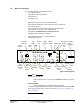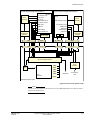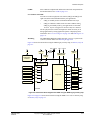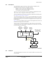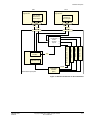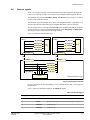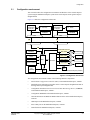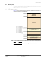
1
ARM Motherboard Express µATX
®
V2M-P1
Technical Reference Manual
Copyright © 2009-2014, ARM. All rights reserved.
ARM DUI 0447J (ID052914)
ARM Motherboard Express µATX
Technical Reference Manual
Copyright © 2009-2014, ARM. All rights reserved.
Release Information
Change History
Date
Issue
Confidentiality
Change
27 November 2009
A
Non-Confidential
First release for V2M-P1
26 March 2010
B
Non-Confidential
Second release for V2M-P1
27 August 2010
C
Non-Confidential
Third release for V2M-P1
15 October 2010
D
Non-Confidential
Fourth release for V2M-P1
28 March 2011
E
Non-Confidential
Fifth release for V2M-P1
22 June 2012
F
Non-Confidential
Sixth release for V2M-P1
12 October 2012
G
Non-Confidential
Seventh release for V2M-P1
31 March 2013
H
Non-Confidential
Eighth release for V2M-P1
12 August 2013
I
Non-Confidential
Ninth release for V2M-P1
26 May 2014
J
Non-Confidential
Tenth release for V2M-P1
Proprietary Notice
Words and logos marked with ® or ™ are registered trademarks or trademarks of ARM in the EU and other countries,
except as otherwise stated below in this proprietary notice. Other brands and names mentioned herein may be the
trademarks of their respective owners.
Neither the whole nor any part of the information contained in, or the product described in, this document may be
adapted or reproduced in any material form except with the prior written permission of the copyright holder.
The product described in this document is subject to continuous developments and improvements. All particulars of the
product and its use contained in this document are given by ARM in good faith. However, all warranties implied or
expressed, including but not limited to implied warranties of merchantability, or fitness for purpose, are excluded.
This document is intended only to assist the reader in the use of the product. ARM shall not be liable for any loss or
damage arising from the use of any information in this document, or any error or omission in such information, or any
incorrect use of the product.
Where the term ARM is used it means “ARM or any of its subsidiaries as appropriate”.
Confidentiality Status
This document is Non-Confidential. The right to use, copy and disclose this document may be subject to license
restrictions in accordance with the terms of the agreement entered into by ARM and the party that ARM delivered this
document to.
Product Status
The information in this document is final, that is for a developed product.
Web Address
http://www.arm.com
ARM DUI 0447J
ID052914
Copyright © 2009-2014, ARM. All rights reserved.
Non-Confidential
ii
Conformance Notices
This section contains conformance notices.
Federal Communications Commission Notice
This device is test equipment and consequently is exempt from part 15 of the FCC Rules under section 15.103 (c).
CE Declaration of Conformity
The system should be powered down when not in use.
The Motherboard Express µATX generates, uses, and can radiate radio frequency energy and may cause harmful
interference to radio communications. However, there is no guarantee that interference will not occur in a particular
installation. If this equipment causes harmful interference to radio or television reception, which can be determined by
turning the equipment off or on, you are encouraged to try to correct the interference by one or more of the following
measures:
•
ensure attached cables do not lie across the card
•
reorient the receiving antenna
•
increase the distance between the equipment and the receiver
•
connect the equipment into an outlet on a circuit different from that to which the receiver is connected
•
consult the dealer or an experienced radio/TV technician for help.
Note
It is recommended that wherever possible shielded interface cables be used.
ARM DUI 0447J
ID052914
Copyright © 2009-2014, ARM. All rights reserved.
Non-Confidential
iii
Contents
ARM Motherboard Express µATX Technical
Reference Manual
Preface
About this book .......................................................................................................... vii
Feedback .................................................................................................................... xi
Chapter 1
Introduction
1.1
1.2
Chapter 2
Hardware Description
2.1
2.2
2.3
2.4
2.5
2.6
2.7
2.8
Chapter 3
Configuration environment ....................................................................................... 3-2
Programmers Model
4.1
4.2
4.3
4.4
ARM DUI 0447J
ID052914
Motherboard architecture and buses ....................................................................... 2-2
Power up, on/off and reset signals .......................................................................... 2-6
Clock architecture .................................................................................................... 2-9
Power ..................................................................................................................... 2-11
Peripherals and interfaces on the motherboard ..................................................... 2-12
Interrupt signals ..................................................................................................... 2-18
DMA signals ........................................................................................................... 2-20
JTAG and test connectors ..................................................................................... 2-21
Configuration
3.1
Chapter 4
About the Motherboard Express µATX .................................................................... 1-2
Precautions .............................................................................................................. 1-5
About this programmers model ................................................................................ 4-2
Memory maps .......................................................................................................... 4-3
Register summary .................................................................................................... 4-8
Register descriptions ............................................................................................. 4-10
Copyright © 2009-2014, ARM. All rights reserved.
Non-Confidential
iv
4.5
Appendix A
Signal Descriptions
A.1
A.2
Appendix B
ARM DUI 0447J
ID052914
Audio CODEC interface ........................................................................................... A-2
UART interface ........................................................................................................ A-3
Specifications
B.1
B.2
Appendix C
IO Peripherals and interfaces ................................................................................ 4-26
Timing specifications ............................................................................................... B-2
Electrical Specification ............................................................................................. B-7
Revisions
Copyright © 2009-2014, ARM. All rights reserved.
Non-Confidential
v
Preface
This Technical Reference Manual (TRM) is for the Motherboard Express µATX. It contains the
following sections:
•
About this book on page vii
•
Feedback on page xi.
ARM DUI 0447J
ID052914
Copyright © 2009-2014, ARM. All rights reserved.
Non-Confidential
vi
Preface
About this book
This book describes how to set up and use the Motherboard Express µAdvanced Technology
Extended (ATX).
The Motherboard Express µATX is part of the Versatile™ Express family of boards that includes
the ARM® CoreTile Express and ARM® LogicTile Express daughterboards.
Product revision status
The rnpn identifier indicates the revision status of the product described in this book, where:
rn
Identifies the major revision of the product.
pn
Identifies the minor revision or modification status of the product.
Intended audience
This document is written for experienced hardware and software developers to aid the
development of ARM-based products using the Motherboard Express µATX board as part of a
development system. It does not describe how to build new daughterboards for use with this
motherboard.
Using this book
This book is organized into the following chapters:
Chapter 1 Introduction
Read this for an overview of the motherboard.
Chapter 2 Hardware Description
Read this for a description of the hardware present on the motherboard.
Chapter 3 Configuration
Read this for a description of the configuration process.
Chapter 4 Programmers Model
Read this for a description of the peripheral registers on the motherboard.
Appendix A Signal Descriptions
Read this for a description of motherboard signals.
Appendix B Specifications
Read this for a description of the technical specifications for the motherboard.
Appendix C Revisions
Read this for a description of the technical changes between released issues of this
book.
Glossary
The ARM Glossary is a list of terms used in ARM documentation, together with definitions for
those terms. The ARM Glossary does not contain terms that are industry standard unless the
ARM meaning differs from the generally accepted meaning.
See ARM Glossary, http://infocenter.arm.com/help/topic/com.arm.doc.aeg0014-/index.html.
ARM DUI 0447J
ID052914
Copyright © 2009-2014, ARM. All rights reserved.
Non-Confidential
vii
Preface
Typographical Conventions
Conventions that this book can use are described in:
•
Typographical
•
Timing diagrams
•
Signals on page ix.
Typographical
The typographical conventions are:
italic
Highlights important notes, introduces special terminology, denotes
internal cross-references, and citations.
bold
Highlights interface elements, such as menu names. Denotes signal
names. Also used for terms in descriptive lists, where appropriate.
monospace
Denotes text that you can enter at the keyboard, such as commands, file
and program names, and source code.
monospace
Denotes a permitted abbreviation for a command or option. You can enter
the underlined text instead of the full command or option name.
monospace italic
Denotes arguments to monospace text where the argument is to be
replaced by a specific value.
monospace bold
Denotes language keywords when used outside example code.
< and >
Enclose replaceable terms for assembler syntax where they appear in code
or code fragments. For example:
MRC p15, 0 <Rd>, <CRn>, <CRm>, <Opcode_2>
Timing diagrams
The figure named Key to timing diagram conventions explains the components used in timing
diagrams. Variations, when they occur, have clear labels. You must not assume any timing
information that is not explicit in the diagrams.
Shaded bus and signal areas are undefined, so the bus or signal can assume any value within the
shaded area at that time. The actual level is unimportant and does not affect normal operation.
Clock
HIGH to LOW
Transient
HIGH/LOW to HIGH
Bus stable
Bus to high impedance
Bus change
High impedance to stable bus
Key to timing diagram conventions
ARM DUI 0447J
ID052914
Copyright © 2009-2014, ARM. All rights reserved.
Non-Confidential
viii
Preface
Timing diagrams sometimes show single-bit signals as HIGH and LOW at the same time and
they look similar to the bus change shown in Key to timing diagram conventions on page viii.
If a timing diagram shows a single-bit signal in this way then its value does not affect the
accompanying description.
Signals
The signal conventions are:
Signal level
The level of an asserted signal depends on whether the signal is
active-HIGH or active-LOW. Asserted means:
•
HIGH for active-HIGH signals.
•
LOW for active-LOW signals.
Lower-case n
At the start or end of a signal name denotes an active-LOW signal.
Additional reading
This section lists publications by ARM and by third parties.
See Infocenter, http://infocenter.arm.com, for access to ARM documentation.
See on ARM, http://onarm.com, for embedded software development resources including the
Cortex® Microcontroller Software Interface Standard (CMSIS).
ARM publications
This book contains information that is specific to this product.
The following publications are open access documents that provide information about ARM
Systems IP peripherals and controllers used in the motherboard:
•
ARM® PrimeCell PS2 Keyboard/Mouse Interface (PL050) Technical Reference Manual
(ARM DDI 0143)
•
ARM® PrimeCell Color LCD Controller (PL111) Technical Reference Manual
(ARM DDI 0293)
•
ARM® PrimeCell Multimedia Card Interface (PL180) Technical Reference Manual
(ARM DDI 0172)
•
ARM® PrimeCell Advanced Audio CODEC Interface (PL041) Technical Reference
Manual
(ARM DDI 0173)
•
ARM® PrimeCell UART (PL011) Technical Reference Manual (ARM DDI 0183)
•
ARM® PrimeCell Real Time Clock (PL031) Technical Reference Manual
(ARM DDI 0224)
•
ARM® PrimeCell System Controller (SP810) Technical Reference Manual
(ARM DDI 0254)
ARM DUI 0447J
ID052914
•
ARM® Dual-Timer Module (SP804) Technical Reference Manual (ARM DDI 0271)
•
ARM® Watchdog Module (SP805) Technical Reference Manual (ARM DDI 0270).
Copyright © 2009-2014, ARM. All rights reserved.
Non-Confidential
ix
Preface
The following publications provide information about related ARM products and toolkits:
•
ARM® CoreTile Express A9x4 Technical Reference Manual (ARM DUI 0448)
•
ARM® CoreTile Express A5x2 Technical Reference Manual (ARM DUI 0541)
•
ARM® CoreTile Express A15x2 Technical Reference Manual (ARM DUI 0604)
•
ARM® CoreTile Express A15x2 A7x3 Technical Reference Manual (ARM DDI 0503)
•
ARM® LogicTile Express 3MG Technical Reference Manual (ARM DUI 0449)
•
ARM® LogicTile Express 13MG Technical Reference Manual (ARM DUI 0556)
•
ARM® LogicTile Express 20MG Technical Reference Manual (ARM DDI 0498)
•
ARM® Versatile™ Express Configuration Technical Reference Manual (ARM DDI 0496)
•
ARM® Versatile™ Express Boot Monitor Reference Manual (ARM DUI 0465)
•
RealView Debugger User Guide (ARM DUI 0153)
•
RealView ICE and RealView Trace User Guide (ARM DUI 0155)
•
RealView Compilation Tools Developer Guide (ARM DUI 0203)
•
RealView Compilation Tools Compilers and Libraries Guide (ARM DUI 0205)
•
RealView Compilation Tools Linker and Utilities Guide (ARM DUI 0206)
Other publications
This section lists relevant documents published by third parties:
ARM DUI 0447J
ID052914
•
IEEE Standard Test Access Port and Boundary Scan Architecture (IEEE Std. 1149.1)
•
PCI-Express External Cable 1.0 Specification
•
VESA DDC Specification. Version 3.0
•
ISP1761 Hi-Speed Universal Serial Bus On-The-Go controller data sheet
•
National Semiconductor LM4549 data sheet.
Copyright © 2009-2014, ARM. All rights reserved.
Non-Confidential
x
Preface
Feedback
ARM welcomes feedback on this product and its documentation.
Feedback on this product
If you have any comments or suggestions about this product, contact your supplier and give:
•
The product name.
•
The product revision or version.
•
An explanation with as much information as you can provide. Include symptoms and
diagnostic procedures if appropriate.
Feedback on content
If you have comments on content then send an e-mail to [email protected]. Give:
•
the title
•
the number, ARM DUI 0447J
•
the page numbers to which your comments apply
•
a concise explanation of your comments.
ARM also welcomes general suggestions for additions and improvements.
ARM DUI 0447J
ID052914
Copyright © 2009-2014, ARM. All rights reserved.
Non-Confidential
xi
Chapter 1
Introduction
This chapter introduces the Motherboard Express µATX. It contains the following sections:
•
About the Motherboard Express µATX on page 1-2
•
Precautions on page 1-5.
ARM DUI 0447J
ID052914
Copyright © 2009-2014, ARM. All rights reserved.
Non-Confidential
1-1
Introduction
1.1
About the Motherboard Express µATX
The Motherboard Express µATX is the basis for a highly integrated software and hardware
development system based on the ARM SMP architecture.
The motherboard provides the following features:
•
Peripherals for multimedia or networking environments.
•
All motherboard peripherals and functions are accessed through a static memory bus to
simplify access from daughterboards.
•
High-performance PCI-Express slots for expansion cards.
•
Consistent memory maps with different CoreTile daughterboards simplify software
development and porting.
•
Automatic detection and configuration of attached CoreTile Express and LogicTile
Express daughterboards.
•
Automatic shutdown for over-temperature or power supply failure.
•
System is unable to power up if the daughterboards cannot be configured.
•
Power sequencing of system.
•
Supports drag and drop file update of configuration files.
•
Uses either a 12V power-supply unit or an external ATX power supply.
•
Supports LogicTile and CoreTile daughterboards to provide custom peripherals, or early
access to ARM core or cluster designs, or production test chips. Supports test chips with
an IO voltage range of 0.8-3.3 volts.
Figure 1-1 on page 1-3 shows the layout of the motherboard with the JTAG cable to the CoreTile
Express JTAG connector and the enclosure power cable to the ATX connector.
ARM DUI 0447J
ID052914
Copyright © 2009-2014, ARM. All rights reserved.
Non-Confidential
1-2
Introduction
PCI Express slots
Debug JTAG
(to Core Tile Express)
Back panel connectors
Case fan
(12V)
User LEDs
D0
D7
Manufacturing
Test
USB status
LEDs
OTGON
USB2ON
USB3ON
Test (ILA)
ILA
Voltage status
LEDs
5VOK
3.3VOK
SB
Micro SDCard
(configuration
memory)
Battery
(MCC
RTCC)
CoreTile Express LogicTile Express
daughterboard
daughterboard
ATX PSU connector
(with plug from
enclosure connector)
Figure 1-1 Motherboard layout
ARM DUI 0447J
ID052914
Copyright © 2009-2014, ARM. All rights reserved.
Non-Confidential
1-3
Introduction
1.1.1
Back panel connectors
Figure 1-2 shows the ATX rear panel that provides:
•
Power supply connector.
•
Keyboard and mouse interface, PS/2.
•
Ethernet interface.
•
Two USB 2.0 ports.
•
One USB OTG port.
•
USB-B device connector for loading configuration files.
•
Audio interface, containing analog microphone-in, line-in, and line-out.
•
Four RS232 serial ports.
•
Video interface, DVI-I supports analog and digital, and digital audio.
•
JTAG connector, to CoreTile Express JTAG connector.
•
Configuration, ON/OFF/Soft Reset and Hardware Reset
•
SD/MMC memory card interface connector.
•
Status LEDs for ready, power on, and USB-B activity.
•
Compact Flash connector.
•
Compact
Flash slot
USB-B
activity LED
Power
(to external
12V power
supply)
OTG
(USB 1)
Power on
LED
PS2
Mouse
PS2
Keyboard
SD card
slot
ON/OFF/ Hardware
Soft Reset RESET
SW[0]
Ready
LED
10/100
Ethernet
USB-A (2)
Boot option ARM JTAG
debug
SW[1] switches
(to Core Tile)
Case
fan
Audio
line out
DVI-I/VGA
UART 2
UART 3
UART 0
UART 1
USB-A (3)
USB-B configuration
Flash Drive
(to PC)
Audio
line in
Audio
microphone
Figure 1-2 ATX back panel
Note
There are two reset buttons:
ON/OFF/Soft Reset
This is colored red and is a system power ON/OFF and Software Reset push
button.
Hardware RESET
This is colored black and is a Hardware Reset push button.
You can use both push buttons to put the system into Standby State, but only the ON/OFF
button can power up the system. For more information, see Power up, on/off and reset
signals on page 2-6.
ARM DUI 0447J
ID052914
Copyright © 2009-2014, ARM. All rights reserved.
Non-Confidential
1-4
Introduction
1.2
Precautions
This section contains safety information and advice on how to avoid damage to the
motherboard.
1.2.1
Ensuring safety
The motherboard is powered from an ATX power supply unit within the ATX enclosure.
Warning
To avoid a safety hazard:
1.2.2
•
To use the motherboard in its supplied plastic enclosure, only use the supplied 12V power
supply unit to provide power to the connector on the enclosure.
•
To use an ATX power supply, remove the top cover from the enclosure and use an ATX
power supply to provide power to the motherboard ATX connector. This option is
typically used to provide access to the PCI-Express sites.
Preventing damage
The motherboard is intended for use in a laboratory or engineering development environment.
If removed from its enclosure, the board becomes more sensitive to electrostatic discharges and
generates increased electromagnetic emissions. Removing the board from the enclosure also
results in flexing that fractures the printed-circuit board connections to the components.
Caution
To avoid damage, observe the following precautions:
•
Never subject the board to high electrostatic potentials.
•
Always wear a grounding strap when touching the board in or away from its enclosure.
•
Avoid touching the component pins or any other metallic element.
•
Always power down the board when connecting daughterboards, memory expansion
boards, or making external connections.
•
Do not remove the board from its enclosure.
Caution
Do not use near equipment that is:
•
Sensitive to electromagnetic emissions, for example medical equipment.
•
A transmitter of electromagnetic emissions.
ARM DUI 0447J
ID052914
Copyright © 2009-2014, ARM. All rights reserved.
Non-Confidential
1-5
Chapter 2
Hardware Description
This chapter describes the hardware on the Motherboard Express µATX. It contains the
following sections:
•
Motherboard architecture and buses on page 2-2
•
Power up, on/off and reset signals on page 2-6
•
Clock architecture on page 2-9
•
Power on page 2-11
•
Peripherals and interfaces on the motherboard on page 2-12
•
Interrupt signals on page 2-18
•
DMA signals on page 2-20
•
JTAG and test connectors on page 2-21.
ARM DUI 0447J
ID052914
Copyright © 2009-2014, ARM. All rights reserved.
Non-Confidential
2-1
Hardware Description
2.1
Motherboard architecture and buses
Figure 2-1 shows a motherboard with attached Tile Express and LogicTile Express
daughterboards.
CoreTile Express
(daughterboard site 1)
LogicTile Express
(daughterboard site 2)
DDR2
memory
Daughterboard
Configuration
Controller
HDRX
HDRX
SB
PCIe
HSB (M)
SMB
HSB (S)
MMB
CB
HDRY1
Daughterboard
Configuration
Controller
FPGA
Test chip
HDRY
ZBT
memory
HSB (M)
HSB (S)
HDRX1
HDRY
SB
SMB
PCIe
MMB
HDRX2
CB
HDRY2
MMB2
MMB1
CB
SMB1
Motherboard
Configuration
Controller
(MCC)
PCIe1
SMB2
SB
PCIe2
PCI-Express
Switch
Motherboard IO FPGA
Configuration
USB
flash memory
(configuration)
(USBMSD)
Motherboard Express μATX
NOR Video User
flash SRAM SRAM
LAN
USB
Peripheral connectors
(LAN, USB, OTG, UARTs, CF,
SD/MMC, KMI, AACI)
Multiplexer
FPGA
DVI
PCIe
Slots
Figure 2-1 System architecture block diagram
The major system components and interfaces that the motherboard provides are:
ARM DUI 0447J
ID052914
•
A dedicated Motherboard Configuration Controller (MCC) configures the motherboard
and all attached daughterboards.
•
IO FPGA that uses a static memory interface to access standard peripherals.
•
Multiplex FPGA that selects the source for the audio and video signals to the DVI
connector.
•
Two daughterboard slots, one for a CoreTile Express board and one for LogicTile Express
board.
Copyright © 2009-2014, ARM. All rights reserved.
Non-Confidential
2-2
Hardware Description
ARM DUI 0447J
ID052914
•
High-speed bus interconnect between daughterboards with support for Low-Voltage
Differential Signalling (LVDS).
•
Bus interfaces between motherboard and daughterboards for PCIe, Static Memory,
MultiMedia, and System Bus, interrupts.
•
Power circuitry with (VIO) voltage from 0.8V-3.3V to enable interfacing with a wide
range of devices.
•
Four PCI Express Gen 1 slots, each supporting four lanes.
•
MMC/SD card slot.
•
Compact Flash slot.
•
Four UARTs.
•
Three USB interfaces providing one OTG slave and two standard USB 2.0 host ports.
•
DVI connector with analogue and digital video support at 1080p, I2S, SPDIF digital audio
support for HDMI.
•
Ethernet interface.
•
PS2 Keyboard and Mouse.
•
AC97 Audio CODEC with Audio in, Audio out, and MIC in.
•
USB-B configuration port that accesses the motherboard configuration flash memory and
emulates it as a USB Mass Storage Device (USBMSD).
•
ON/OFF/Soft Reset and Hardware RESET push buttons and Power and Status LEDs.
•
2 x 64MB of user NOR Flash.
•
32MB of user SRAM.
•
8MB of local Video SRAM.
Copyright © 2009-2014, ARM. All rights reserved.
Non-Confidential
2-3
Hardware Description
2.1.1
Motherboard buses
The motherboard architecture uses the following buses:
•
Configuration Bus
•
Static Memory Bus
•
System Bus
•
MultiMedia Bus
•
High-Speed Bus on page 2-5
•
PCIe Bus on page 2-5.
Figure 2-1 on page 2-2 shows how these buses interconnect.
Configuration Bus
The Motherboard Configuration Controller (MCC) and Daughterboard Configuration
Controller use the Configuration Bus (CB) to determine the functionality and capabilities of the
daughterboards before powering up and releasing the resets. This minimizes the chance of
damage to the boards. The CB controls the power and reset sequence. It also updates the FPGA
images and software on the daughterboards.
Static Memory Bus
The underlying architecture uses the Static Memory Bus (SMB) for all peripheral and memory
accesses from the daughterboards to the motherboard. A Static Memory Controller in the
daughterboard outputs chip select signals to access memory and peripherals on the
motherboard. The memory controller determines the base address for each chip select. See IO
Peripherals and interfaces on page 4-26.
•
•
Note
Site 2 has limited access to the motherboard.
Site 2 can only access the motherboard using chip select nCS7, peripherals, and nCS3,
Video SRAM only.
System Bus
The System Bus connects interrupts and DMAs:
•
From the motherboard peripherals to the daughterboards.
•
Between the daughterboards.
MultiMedia Bus
The MultiMedia Bus (MMB) enables the motherboard or either daughterboard to drive audio
and video data to the DVI connector. A dedicated FPGA manages multiplexing the sources and
driving the outputs to the HDMI transmitter.
The motherboard supports:
ARM DUI 0447J
ID052914
•
Video with 25 to 165MHz pixel clock, DTV 480p to 1080p, or PC 640x480 to 1600x1200,
VGA to UXGA
•
Audio S/PDIF interface with 2 channels at 192kHz or I2S interface with eight channels at
96kHz.
Copyright © 2009-2014, ARM. All rights reserved.
Non-Confidential
2-4
Hardware Description
High-Speed Bus
The motherboard connects the two daughterboards with two High-Speed Buses (HSB). The bus
interconnect can provide up to:
•
360 single-ended signals.
•
160 Low Voltage Differential Signalling (LVDS) signal pairs.
•
•
Note
The HSB typically implements a multiplexed AXI bus.
There is no connection from the HSB to devices on the motherboard. See the
documentation for your daughterboard.
PCIe Bus
The motherboard supports four PCI-Express (PCIe) slots, x4, x4, x8, and x16 connector sizes,
each with a lane width of four. A PCI-Express switch connects these slots to the daughterboards
over the PCIe bus that has eight lanes to each daughterboard. See Figure 2-1 on page 2-2 for
more information.
Note
The V2M-P1 motherboard supports a root complex either on the daughterboard in Site 1 or the
daughterboard in Site 2. By default the daughterboard in Site 1 is the root complex.
The V2M-P1 motherboard does not support an endpoint on either daughterboard.
See PCI-Express on page 2-15.
ARM DUI 0447J
ID052914
Copyright © 2009-2014, ARM. All rights reserved.
Non-Confidential
2-5
Hardware Description
2.2
Power up, on/off and reset signals
You can use either of the push buttons to reset the system, but only the ON/OFF push button
can power up the system. The motherboard drives two reset signals to each daughterboard and
receives a reset-request signal from each daughterboard.
Figure 2-2 shows the power up ON/OFF/Soft Reset push button and Hardware RESET
push-button signals in the system.
CoreTile Express
(daughterboard site 1)
CB_nPOR
CB_nRST
Reset and start
code execution
LogicTile Express
(daughterboard site 2)
CB_nPOR
Daughterboard
Configuration
Controller
CB_nRST
CB_RSTREQ
Load FPGA
image and
reset
Daughterboard
Configuration
Controller
CB_RSTREQ
Test chip
HDRY
FPGA
HDRY
CB
CB
HDRY1
HDRY2
ON/OFF/Soft Reset
pushbutton
Motherboard Configuration
Controller (MCC)
Hardware RESET
pushbutton
Motherboard Express μATX
Figure 2-2 Reset signals
Note
To completely power down the system, you must turn off the external 12V power supply.
See also the ARM® Versatile™ Express Configuration Technical Reference Manual for an
overview of the startup sequence and the operation of the ON/OFF/Soft Reset and Hardware
Reset push-button switches.
ARM DUI 0447J
ID052914
Copyright © 2009-2014, ARM. All rights reserved.
Non-Confidential
2-6
Hardware Description
2.2.1
Power up reset
A full system configuration is performed at power up. See the ARM® Versatile™ Express
Configuration Technical Reference Manual.
2.2.2
ON/OFF/Soft Reset push button briefly pressed
You can reset the system by briefly pressing the ON/OFF/Soft Reset switch on the back panel.
This performs a software reset of the ARM test chip on the CoreTile daughterboard. The MCC
and Daughterboard Configuration Controller reset the devices in the system, but do not perform
a full re-initialization:
1.
The reset switch is briefly pressed and the MCC starts a reset sequence.
Caution
If the ON/OFF/Soft Reset switch is pressed and held for more than two seconds, the
system enters the Standby State, in the same way as pressing the black Hardware RESET
push button.
2.
The MCC asserts the CB_nRST reset signal. Depending on the setting of ASSERTNPOR in
the generic configuration file config.txt, CB_nPOR might also be asserted.
3.
The daughterboards and IO FPGA are reset.
4.
The MCC also releases CB_nPOR if it was specified in the configuration file.
MCC releases CB_nRST.
5.
The daughterboards enter the run state.
Note
No daughterboard configuration files are read as a result of an external reset. No daughterboard
re-configuration is performed.
2.2.3
Hardware RESET push button
You can change the operation of the board from ON to Standby by briefly pressing this button.
This switches off the power to the daughterboards and resets the system to the default values.
ARM DUI 0447J
ID052914
Copyright © 2009-2014, ARM. All rights reserved.
Non-Confidential
2-7
Hardware Description
2.2.4
External reset requests from the daughterboards
Either daughterboard can issue an external reset request to the motherboard:
1.
An external reset is received from the JTAG connector, nSRST, on the CoreTile Express
daughterboard.
2.
The Daughterboard Configuration Controller asserts CB_RSTREQ to the MCC on the
motherboard. See Figure 2-2 on page 2-6.
3.
The MCC asserts the CB_nRST reset signal. Depending on the setting of ASSERTNPOR in
the generic configuration file config.txt, CB_nPOR might also be asserted.
•
•
Note
If only CB_nRST is asserted, a soft reset is performed. The MCC and
Daughterboard Configuration Controller reset the devices in the system, but do not
perform a full re-initialization.
If only CB_nPOR is also asserted, a hard reset is performed. The MCC and
Daughterboard Configuration Controller perform a full re-initialization.
4.
The daughterboards and IO FPGA are reset.
5.
The MCC also releases CB_nPOR if it was specified in the configuration file.
MCC releases CB_nRST.
6.
The daughterboards enter the run state.
Note
No daughterboard configuration files are read as a result of an external JTAG reset. No
daughterboard re-configuration is performed.
ARM DUI 0447J
ID052914
Copyright © 2009-2014, ARM. All rights reserved.
Non-Confidential
2-8
Hardware Description
2.3
Clock architecture
Table 2-1 shows the motherboard clock sources.
Table 2-1 Motherboard clocks
Oscillator
Default
Description
Range
OSC0
50MHz
MCC static memory clock. The MCC uses this clock for accesses to the SMB
before control of the SMB buses is passed to the daughterboards.
After configuration, each daughterboard outputs its own SMB clock to the IO
FPGA. In run mode, the SMB clock is switched to the daughterboards and the IO
FPGA returns the delayed SMB clocks to the daughterboards. This enables the
daughterboard memory controllers to adjust the frequency for optimum
operation.
25MHz-60MHz
OSC1
23.75MHz
CLCD clock to the IO FPGA.
23.75MHz-63.5MHz
OSC2
24MHz
IO FPGA peripheral clock. This is the reference clock for peripherals such as, for
example, the UARTs.
This clock is used directly by the peripheral or as the reference to a clock
generator in the peripheral.
24MHz
OSC3
24MHz
IO FPGA. Reserved.
2MHz-230MHz
OSC4
24MHz
System bus global clock. A divide by two block inside the MUX FPGA derives
the 12MHz system bus global clock. This drives the attached CoreTile and
LogicTile daughterboards. See Figure 2-3 on page 2-10.
2MHz-230MHz
OSC5
24MHz
IO FPGA. Reserved.
2MHz-230MHz
PCI-E
-
A dedicated PCI-Express clock generator provides the clocks to the PCI-Express
slots and the daughterboards. You cannot configure this clock.
100MHz
On power up, the MCC sets OSC[5:0] to the values specified in the board.txt configuration file
in the USBMSD. See the ARM® Versatile™ Express Configuration Technical Reference Manual.
The daughterboards have their own clock generators that are independent of the motherboard
clocks. These clocks are set by the values in the board.txt file for the daughterboards. See the
documentation supplied with your daughterboard.
Caution
Ensure that the clock settings are within the permitted range.
You can configure the motherboard OSC clocks in the following ways:
1.
By editing the board.txt file. ARM recommends that you perform this method first.
2.
By using of the CFG W command from the DEBUG submenu of the MCC command line
in run mode. See the ARM® Versatile™ Express Configuration Technical Reference
Manual.
3.
By writing application code to the SYS_CFG registers. See System Configuration
registers on page 4-21 and the pseudo code Example 4-1 on page 4-24.
4.
By using the CONFIGURE submenu from the Boot Monitor command line.
Methods 2, 3, and 4 permit clock switching in run mode. Method 1 requires a reset to become
effective.
Figure 2-3 on page 2-10 shows an overview of the clocks in a typical Versatile Express system.
ARM DUI 0447J
ID052914
Copyright © 2009-2014, ARM. All rights reserved.
Non-Confidential
2-9
Hardware Description
CoreTile Express daughterboard (Site 1)
Test chip
TC reference clock
CLCD clock
Clock
generators
SB_GCLK
External AXIS clock
PCI reference clock
LogicTile Express daughterboard (Site 2)
FPGA
PCI reference clock
MMB clocks
MMB clocks
SMB clock
SMB feedback
SB_GCLK
SMB clock
SMB feedback
External AXIM clock
Daughterboard
Configuration
Controller
Clock
generators
FPGA reference clocks
HSB (S)
AXI clock logic
M
S
Daughterboard
Configuration
Controller
HDRY
HDRX
HDRX
HDRY
HDRY1
HDRX1
HDRX2
HDRY2
I/O and multiplexer FPGAs
PCI-Express
clock
generator
OSC0
MCC
OSC1
OSC2
To
peripherals
OSC3
Clock
generators
OSC4
To
PCI-Express
slots
OSC5
Motherboard Express μATX
Figure 2-3 Overview of system clocks
Note
A divide by two block inside the MUX FPGA derives the 12MHz SB_GCLK for the attached CoreTile
and LogicTile daughterboards.
ARM DUI 0447J
ID052914
Copyright © 2009-2014, ARM. All rights reserved.
Non-Confidential
2-10
Hardware Description
2.4
Power
Power to the board is provided by either:
An external 12V power supply
The output goes to the power connector on the back panel. The 12V, 5A,
supply from the back-panel connector goes through an adaptor and
connects to the ATX connector on the motherboard.
An ATX power supply
The output goes to the ATX power connector on the motherboard. The
ATX supply is required for PCI-Express cards.
The voltage regulators on the motherboard supply:
Fixed voltages
There are several voltage regulators on the motherboard that supply fixed
voltages to the motherboard and attached daughterboards.
All daughterboards are supplied with 5V for internal supply generation. If
the daughterboard requires additional supply voltages, a separate power
supply connector must supply them.
VIO
The SMB, SB, and MMB buses operate over the range 0.8-3.3 volts. These
buses must operate at the same voltage that is supplied from the
motherboard. To avoid damage, the daughterboard that has the lowest
operating voltage specification determines the voltage.
PCI-Express connector voltages
The ATX connector directly supplies 12V and 3.3V to cards connected to
the PCI-Express slots.
Note
When power is applied, the system is reconfigured based on the contents of the USBMSD flash
memory. See the ARM® Versatile™ Express Configuration Technical Reference Manual.
ARM DUI 0447J
ID052914
Copyright © 2009-2014, ARM. All rights reserved.
Non-Confidential
2-11
Hardware Description
2.5
Peripherals and interfaces on the motherboard
This section introduces the peripherals and interfaces located on the motherboard. It contains
the following:
•
IO FPGA peripherals
•
Ethernet on page 2-14
•
USB on page 2-14
•
DVI multiplexer on page 2-15
•
PCI-Express on page 2-15.
For more information about the programming interface to the IO peripherals and interfaces, see
IO Peripherals and interfaces on page 4-26.
2.5.1
IO FPGA peripherals
The motherboard IO FPGA connects the static memory buses from the motherboard and
daughterboards to the motherboard peripherals and memories.
The IO FPGA contains the following peripherals and controllers:
AACI controller
The FPGA contains an ARM PrimeCell PL041 Advanced Audio CODEC
Interface (AACI) that provides communication with a CODEC using the
AC-link protocol. See Advanced Audio CODEC Interface on page 4-26.
The AACI on the baseboard connects to a National Semiconductor
LM4549 audio CODEC.
CLCD controller
A PL111 PrimeCell CLCD controller is present in the FPGA.
You can implement a separate CLCD controller in an attached Logic Tile.
The Multiplexer FPGA selects between the FPGA CLCD controller and
the CLCD signals from the daughterboards. See DVI multiplexer on
page 2-15 and Color LCD Controller on page 4-27.
Compact Flash
The IO FPGA contains a custom CompactFlash interface that is developed
by ARM. See Compact Flash interface on page 4-29.
Keyboard and Mouse Interfaces (KMI)
The Keyboard and Mouse Interfaces (KMI) are implemented with two
PL050 PrimeCells incorporated into the FPGA. See Keyboard and Mouse
Interface, KMI on page 4-32.
SD/MMC memory cards
An ARM PL180 PrimeCell MCI provides the interface to a MultiMedia
Card (MMC) or Secure Digital (SD) card. See MultiMedia Card Interface,
MCI on page 4-32.
You can drive the interface as either an MMC or SD interface.
Two-wire interface ports
You can use the two-wire serial bus interface to:
•
Configure the PCI-Express switch.
•
Communicate with displays attached to the DVI-I connector.
See Two-wire serial bus interface, SBCon on page 4-34.
Timers
ARM DUI 0447J
ID052914
The IO FPGA contains two ARM SP804 Dual-Timer modules. See Timers
on page 4-36.
Copyright © 2009-2014, ARM. All rights reserved.
Non-Confidential
2-12
Hardware Description
UARTs
Four UARTs are implemented with PL011 PrimeCells incorporated into
the baseboard FPGA. See UART on page 4-37.
User Switches and LEDs
You can access the two physical user switches, SW[1] and SW[2], and
eight user LEDs on the motherboard from your applications.
•
SW[1] is normally used to run the Boot Monitor boot script.
•
SW[2] is a hardware enable switch for remote UART0 control.
SW[2] is not normally used by your application. See the ARM®
Versatile™ Express Configuration Technical Reference Manual.
The two physical user switches and eight user LEDs can assist you to
debug applications by setting application options or displaying status
information. See User Switch Register on page 4-10 and LED Register on
page 4-11.
Watchdog
The ARM SP805 Watchdog module can apply a reset to a system in the
event of a software failure. See Watchdog on page 4-40.
Figure 2-4 shows the IO interfaces using the ARM Legacy memory map, see Memory maps on
page 4-3.
Site 1 Site 2
SMB1 to
Site 1
CB
MMB1 to
Site 1
SB_GCLK
SMB1 to
Site 2
Motherboard
Configuration
Controller
Site 1 Site 2
Interrupts and
DMA control
MMB2 to
Site 2
Matrix, multiplexers,
and bridges
NOR FLASH 0
CS0
NOR FLASH 1
CS1
User SRAM
CS2
Ethernet
CS3
USB
CS3
Video SRAM
CS3
MMB
MMB Mux
DVI
AACI
Peripherals
Compact
Flash
2 x KMI
CS7
SD/MMC
4 x UART
User LEDS
PCIe I2C
I/O FPGA
Figure 2-4 Architectural block diagram of IO FPGA using the ARM Legacy memory map
Figure 2-5 on page 2-14 shows the IO interfaces using the ARM Cortex-A Series memory map,
see Memory maps on page 4-3.
ARM DUI 0447J
ID052914
Copyright © 2009-2014, ARM. All rights reserved.
Non-Confidential
2-13
Hardware Description
Site 1 Site 2
CB
SMB1 to
Site 1
Motherboard
Configuration
Controller
SB_GCLK
SMB2 to
Site 2
Site 1 Site 2
MMB1 to
Site 1
Interrupts and
DMA control
MMB2 to
Site 2
Matrix, multiplexers,
and bridges
NOR FLASH 0
CS0
NOR FLASH 1
CS4
User SRAM
CS1
Ethernet
CS2
USB
CS2
Video SRAM
CS2
MMB
MMB Mux
DVI
AACI
Peripherals
Compact
Flash
2 x KMI
CS3
SD/MMC
4 x UART
User LEDS
PCIe I2C
I/O FPGA
Figure 2-5 Architectural block diagram of IO FPGA using the ARM Cortex-A Series memory map
2.5.2
Ethernet
The Ethernet interface is implemented using a SMCS LAN9118 10/100 Ethernet controller. The
LAN9118 incorporates a Media ACcess (MAC) Layer, a PHYsical (PHY) layer, Host Bus
Interface (HBI), receive and transmit FIFOs, power management controls, and a serial
configuration EEPROM interface. The board models an asynchronous SRAM and interfaces
directly to the SMB.
When manufactured, an ARM value for the Ethernet MAC address is loaded into the
motherboard configuration EEPROM that is copied to the Ethernet controller on power on. You
can overwrite this by a value in the generic motherboard configuration file config.txt.
2.5.3
USB
The motherboard provides an SMC bus interface to an external Philips ISP1761 USB 2.0
controller. Three USB interfaces are provided on the motherboard.
USB port 1 provides an OTG device interface and connects to the mini USB connector on the
back panel of the enclosure.
USB port 2 and USB port 3 can function in either master or slave mode and connect to the dual
A-Type connector on the rear panel of the enclosure, USB port 2 is the top connector.
Note
The configuration interface has a separate dedicated USB controller that connects to the USB
B-Type connector on the back panel of the enclosure for loading configuration files to the
USBMSD. See the ARM® Versatile™ Express Configuration Technical Reference Manual.
ARM DUI 0447J
ID052914
Copyright © 2009-2014, ARM. All rights reserved.
Non-Confidential
2-14
Hardware Description
2.5.4
DVI multiplexer
The motherboard has a Digital Visual Interface (DVI) connector. A multiplexer on the
motherboard selects the source for the video output as either the:
•
MMB bus from the CoreTile Express daughterboard in Site 1.
•
MMB bus from the LogicTile Express daughterboard in Site 2.
•
CLCD controller in the motherboard IO FPGA.
The source for the DVI is determined by the generic motherboard configuration file. See the
ARM® Versatile™ Express Configuration Technical Reference Manual.
You can also change the source for the DVI in run mode by using the SYS-CFGCTRL register.
See Configuration Control Register on page 4-22.
The motherboard Multiplexer FPGA connects one of the three MultiMediaBus video and audio
interfaces from the motherboard and two daughterboards respectively to the DVI connector on
the back panel. This means you can select either of the daughterboards or the IO FPGA to drive
the DVI connector.
Figure 2-6 shows how the Multiplexer FPGA interfaces with the daughterboards, IO FPGA, and
the Motherboard Configuration Controller (MCC).
The DVI controller is an Sil9022 and supports up to 1080p resolution. The actual resolution
available depends on the CLCD controller in the daughterboard, or motherboard if you are using
the CLCD controller in the motherboard.
MMB from
CoreTile Express
daughterboard
in Site 1
MMB from
LogicTile Express
daughterboard
in Site 2
MMB from
motherboard
I/O FPGA
MMB selection signals
from Motherboard
Configuration Controller
3:1 Multiplexer
Multiplexer FPGA
Digital video
Digital audio
HDMI
DAC
DVI-I connector
Figure 2-6 MMB multiplexer block diagram
2.5.5
PCI-Express
The motherboard supports four PCI-Express slots, of connector widths x4, x4, x8, and x16, each
of lane width four.
ARM DUI 0447J
ID052914
Copyright © 2009-2014, ARM. All rights reserved.
Non-Confidential
2-15
Hardware Description
These are connected through a IDT89PES32H8 PCI Express switch to the PCIe buses from the
two daughterboards.
You can configure the PCIe switch to work with CoreTile Express or LogicTile Express
daughterboards configured as an integrated PCI-Express root complex.
Note
The V2M-P1 motherboard supports a root complex either on the daughterboard in Site 1 or on
the daughterboard in Site 2. You select which site contains the root complex by editing the
config.txt file. By default, the daughterboard in Site 1 is the root complex.
The V2M-P1 motherboard does not support an endpoint either on the daughterboard in Site 1
or the daughterboard in Site 2.
The PCIe slots are the only endpoints and conform to the PCI-Express 1.0 specification. There
is no PCIe endpoint in the motherboard IO FPGA. Because there are no PCIe lanes connected
to the motherboard, peripherals in the IO FPGA cannot be accessed from the PCIe bus.
The MCC on the motherboard controls the following PCIe features:
•
Configuring PCIe eeprom settings.
•
RESETS to each connector and daughterboard.
The IO FPGA provides the I2C bus to the PCIe switch.
Figure 2-7 on page 2-17 shows the PCIe block diagram. See also Clock architecture on
page 2-9.
ARM DUI 0447J
ID052914
Copyright © 2009-2014, ARM. All rights reserved.
Non-Confidential
2-16
Hardware Description
Site 1
Site 2
CoreTile Express
daughterboard
LogicTile Express
daughterboard
Test chip with
End Point or
Root Complex
FPGA with
End Point or
Root Complex
HDRY
HDRY
SMB2
PCIe2
SMB1
PCIe1
HDRY1
HDRY2
x4
x8
x8
PCI-Express
Switch
32 lanes
6 ports
x4
x4
I2C
Reset and
configuration logic
Motherboard Express μATX
Motherboard
Configuration
Controller
(MCC)
Slot x4, 4 lanes
Serial bus
interface
Slot x 4, 4 lanes
IO FPGA
Slot x 8, 4 lanes
PCI-Express slot x16, 4 lanes
x4
Resets
Figure 2-7 PCIe bus architecture on the motherboard
ARM DUI 0447J
ID052914
Copyright © 2009-2014, ARM. All rights reserved.
Non-Confidential
2-17
Hardware Description
2.6
Interrupt signals
There is no interrupt controller on the motherboard. The IO FPGA peripheral interrupts can
connect to an interrupt controller in a CoreTile Express daughterboard through the SB bus.
The IO FPGA also generates CPUIRQ, CPUFIQ, and nEvent for use by legacy cores that do
not have a GIC interrupt controller.
The IO FPGA peripheral interrupts also connect to the daughterboard Site 2 and enable a core
and interrupt controller implemented in the daughterboard FPGA to process interrupts.
You can generate the four interrupt signals INT[3:0] by the daughterboards and are input to the
IO FPGA. These are returned to the daughterboards on signals IRQ[39:36] and IRQ[35:32].
The function of these is determined by the daughterboard.
Figure 2-8 shows the interrupt architecture.
CoreTile Express daughterboard
(in Site 1)
SB _INT[3:0]
SB_IRQ[47:0]
SB_nCPUIRQ
LogicTile Express daughterboard
(in Site 2)
SB _INT[3:0]
SB_IRQ[47:0]
Test
chip
SB_nCPUIRQ
SB_nCPUFIQ
SB_nCPUFIQ
SB_nEvent
SB_nEvent
HDRY
FPGA
HDRY
SB1
SB2
HDRY1
HDRY2
SB_IRQ[47:0]
SB_nCPUIRQ
SB_nCPUFIQ
SB_nEvent
SB1_INT[3:0]
SB2_INT[3:0]
IO FPGA
Motherboard Express μATX
Figure 2-8 Interrupt architecture
For more information on interrupt handling, see the documentation for your CoreTile Express
daughterboard.
Table 2-2 shows the interrupt mapping for the IRQ[47:0] signals.
Table 2-2 Interrupt signals
ARM DUI 0447J
ID052914
SB_IRQ[ ] interrupt
Interrupt signal
Description
0
WDOG0INT
Watchdog timer
1
SWINT
Software interrupt, see Miscellaneous Flags Register on page 4-16
2
TIM01INT
Timer interrupt
3
TIM23INT
Timer interrupt
Copyright © 2009-2014, ARM. All rights reserved.
Non-Confidential
2-18
Hardware Description
Table 2-2 Interrupt signals (continued)
ARM DUI 0447J
ID052914
SB_IRQ[ ] interrupt
Interrupt signal
Description
4
RTCINTR
Timer interrupt
5
UART0INTR
UART interrupt
6
UART1INTR
UART interrupt
7
UART2INTR
UART interrupt
8
UART3INTR
UART interrupt
9
MCI_INTR[0]
MultiMedia card interrupt
10
MCI_INTR[1]
MultiMedia card interrupt
11
AACI_INTR
Audio CODEC interrupt
12
KMI0_INTR
Keyboard/Mouse interrupt
13
KMI1_INTR
Keyboard/Mouse interrupt
14
CLCDINTR
Display interrupt
15
ETH_INTR
Ethernet interrupt
16
USB_INT
USB interrupt
17
PCIE_GPEN
PCI-Express interrupt
21:18
SB1_INT[3:0]
Copy of interrupts SB_IRQ[35:32]
25:22
SB2_INT[3:0]
Copy of interrupts SB_IRQ[39:36]
[31:26]
-
Reserved
[35:32]
SB1_INT[3:0]
Reserved, interrupts INT[3:0] from Site 1 daughterboard
[39:36]
SB2_INT[3:0]
Reserved, interrupts INT[3:0] from Site 2 daughterboard
[47:40]
-
Reserved
Copyright © 2009-2014, ARM. All rights reserved.
Non-Confidential
2-19
Hardware Description
2.7
DMA signals
The motherboard does not contain a DMA Controller (DMAC). However, it does enable routing
of two DMA ACK/REQ handshake signal pairs from selected IO FPGA peripherals to CoreTile
Express or LogicTile Express daughterboards. These daughterboards might contain a DMAC.
See your daughterboard documentation or application note for more information.
There are eight DMA handshake signal pairs that run between the daughterboard tile sites
through the System Bus. Six of these pairs, SB_nDRQ[7:2] and SB_nDACK[7:2], have no
connection to the motherboard IO FPGA. You can use a DMAC in one daughterboard site to
communicate with peripherals in the other daughterboard site. Two of the eight pairs,
SB_nDRQ[1:0] and SB_nDACK[1:0], also connect to the motherboard IO FPGA. These are
only used for handshaking between the two selected peripherals in the IO FPGA and a DMAC
in one of the daughterboard sites. See Figure 2-9.
The motherboard IO FPGA implements a DMA router that selects two DMAC-capable
motherboard peripherals for connection to the DMAC pins on one of the daughterboard sites.
You must ensure that only one daughterboard makes active connections to these signals.
You can route the following combinations of motherboard peripherals to a daughterboard site
DMAC:
•
AACI RX + AACI TX
•
AACI RX + MCI
•
AACI TX + MCI
•
UART0 RX + UART0 TX.
See DMA Channel Selection Register on page 4-17 for the routers SYS_DMA register bit
definitions.
LogicTile Express daughterboard
(in Site 2)
CoreTile Express daughterboard
(in Site 1)
SB_nDRQ[7:2]
SB_nDACK[7:2]
SB_nDRQ[7:2]
SB_nDACK[7:2]
Test chip
SB_nDRQ[1:0]
FPGA
SB_nDRQ[1:0]
SB_nDACK[1:0]
SB_nDACK[1:0]
HDRY
HDRY
SB1
SB2
HDRY2
HDRY1
6
6
SB_nDRQ[1:0]
SB_nDACK[1:0]
2
2
IO FPGA
Motherboard Express μATX
Figure 2-9 DMA architecture
ARM DUI 0447J
ID052914
Copyright © 2009-2014, ARM. All rights reserved.
Non-Confidential
2-20
Hardware Description
2.8
JTAG and test connectors
The motherboard is not equipped with an ARM debug JTAG connector. To debug the
application code, connect a debugger to the JTAG connector on the CoreTile Express
daughterboard.
Note
For convenience, you can connect the JTAG connector on the CoreTile Express daughterboard
to the JTAG connector on the back panel.
•
•
ARM DUI 0447J
ID052914
Caution
The Motherboard Express µATX contains several connectors used for manufacturing test.
The manufacturing test connectors must not be used. Connecting to them might damage
the motherboard.
Copyright © 2009-2014, ARM. All rights reserved.
Non-Confidential
2-21
Chapter 3
Configuration
This chapter describes the configuration sequence for the Motherboard Express µATX and any
attached daughterboards. It contains the following section:
•
Configuration environment on page 3-2.
ARM DUI 0447J
ID052914
Copyright © 2009-2014, ARM. All rights reserved.
Non-Confidential
3-1
Configuration
3.1
Configuration environment
This section describes the configuration environment and hardware of the Versatile Express
system using the Motherboard Express μATX and CoreTile Express and LogicTile Express
daughterboards.
Figure 3-1 shows the configuration architecture.
CoreTile Daughterboard in site 1
Daughterboard
Configuration
Controller
SCC Test Chip
LogicTile Daughterboard in site 2
Daughterboard
Configuration
Controller
SCC
Configuration
EEPROM
FPGA
Configuration
EEPROM
HDRY
HDRY
CB
CB
HDRY1
HDRY2
CB
UART0 DSR and CTS
Configuration
EEPROM
MCC UART
MCC UART
ON/OFF/Soft
Reset
Hardware RESET
DCC1 UART
MCC
IO FPGA
Power-on detect
microSD
card
(USBMSD)
DCC2 UART
UART0 Port
UART1 Port
UART2 Port
UART3 Port
NOR
flash
USB-B
port
Motherboard Express (V2M-P1)
Figure 3-1 Configuration architecture
The configuration environment consists of the following hardware components:
ARM DUI 0447J
ID052914
•
Motherboard Configuration Controller (MCC) on the Motherboard Express, V2M-P1.
•
Daughterboard Configuration Controller on the CoreTile Express daughterboard and on
the LogicTile Express daughterboard.
•
Configuration microSD card or Universal Serial Bus Mass Storage Device (USBMSD)
on the Motherboard Express, V2M-P1.
•
Configuration EEPROM on the Motherboard Express, V2M-P1.
•
ON/OFF/Soft Reset and Hardware RESET buttons on the on the Motherboard Express,
V2M-P1.
•
USB-B port on the Motherboard Express, V2M-P1.
•
Four UART ports on the Motherboard Express, V2M-P1.
•
NOR flash on the Motherboard Express, V2M-P1.
Copyright © 2009-2014, ARM. All rights reserved.
Non-Confidential
3-2
Configuration
•
Power-on detect on the Motherboard Express, V2M-P1.
•
Configuration EEPROM on the CoreTile Express daughterboard and on the LogicTile
Express daughterboard.
•
HDRY headers on the Motherboard Express, V2M-P1, CoreTile Express and LogicTile
Express daughterboards.
See the ARM® Versatile™ Express Configuration Technical Reference Manual and the Technical
Reference Manuals for the attached daughterboards for specific information on the
configuration environment of your Versatile Express system and also for information on:
•
Power-on sequence.
•
Push-button and remote resets.
•
Configuration files.
•
Updating motherboard firmware.
•
MCC command-line interface.
ARM DUI 0447J
ID052914
Copyright © 2009-2014, ARM. All rights reserved.
Non-Confidential
3-3
Chapter 4
Programmers Model
This chapter describes the memory map and the configuration registers for the peripherals on
the motherboard. It contains the following sections:
•
About this programmers model on page 4-2
•
Memory maps on page 4-3
•
Register summary on page 4-8
•
Register descriptions on page 4-10
•
IO Peripherals and interfaces on page 4-26.
ARM DUI 0447J
ID052914
Copyright © 2009-2014, ARM. All rights reserved.
Non-Confidential
4-1
Programmers Model
4.1
About this programmers model
The following information applies to the Motherboard Express µATX registers:
ARM DUI 0447J
ID052914
•
The base address is not fixed, and can be different for any particular system
implementation. The offset of each register from the base address is fixed.
•
Do not attempt to access reserved or unused address locations. Attempting to access these
locations can result in Unpredictable behavior.
•
Unless otherwise stated in the accompanying text:
— Do not modify undefined register bits.
— Ignore undefined register bits on reads.
— All register bits are reset to a logic 0 by a system or power-on reset.
•
Access type in Table 4-3 on page 4-8 is described as follows:
RW
Read and write.
RO
Read only.
WO
Write only.
Copyright © 2009-2014, ARM. All rights reserved.
Non-Confidential
4-2
Programmers Model
4.2
Memory maps
The memory map details depend on whether the daughterboard uses the ARM Legacy memory
map or the ARM Cortex-A Series memory map.
4.2.1
ARM Legacy memory map
Figure 4-1 shows an example of the Legacy system memory map when the motherboard is used
with the CoreTile Express A9x4 daughterboard.
0xFFFFFFFF
Daughterboard
(HSB AXI buses)
0xE0000000
Daughterboard
CS6 = 0x58000000
CS5 = 0x54000000
0x60000000
CS4 = 0x50000000
Motherboard memory and peripherals
(SMB CS0 to CS6)
CS3 = 0x4C000000
CS2 = 0x48000000
CS1 = 0x44000000
0x40000000
CS0 = 0x40000000
0x20000000
0x10020000
Daughterboard
0x10000000
Motherboard peripherals (SMB CS7)
0x00000000
Daughterboard local memory
(aliased from 0x80000000)
Figure 4-1 Legacy system memory map as viewed from a CoreTile Express A9x4 daughterboard
Caution
The attached daughterboard defines the address ranges for the SMB chip selects.
ARM DUI 0447J
ID052914
Copyright © 2009-2014, ARM. All rights reserved.
Non-Confidential
4-3
Programmers Model
Table 4-1 shows the peripherals and memory on the motherboard using the ARM legacy
memory map. The addresses are offsets from the base addresses of the SMB chip selects.
Table 4-1 Motherboard peripheral ARM legacy memory map
ARM DUI 0447J
ID052914
Peripheral
Interface logic
SMB chip select
Address offset
System registers
Custom
CS7
0x00000000-0x00000FFF
System control
ARM SP810
CS7
0x00001000-0x00001FFF
Serial Bus PCI
Custom
CS7
0x00002000-0x00002FFF
Reserved
-
CS7
0x00003000-0x00003FFF
AACI
ARM PL041
CS7
0x00004000-0x00004FFF
MMCI
ARM PL180
CS7
0x00005000-0x00005FFF
KMI0
ARM PL050
CS7
0x00006000-0x00006FFF
KMI1
ARM PL050
CS7
0x00007000-0x00007FFF
Reserved
-
CS7
0x00008000-0x00008FFF
UART0
ARM PL011
CS7
0x00009000-0x00009FFF
UART1
ARM PL011
CS7
0x0000A000-0x0000AFFF
UART2
ARM PL011
CS7
0x0000B000-0x0000BFFF
UART3
ARM PL011
CS7
0x0000C000-0x0000CFFF
Reserved
-
CS7
0x0000D000-0x0000EFFF
WDT
SP805
CS7
0x0000F000-0x0000FFFF
Reserved
-
CS7
0x00010000-0x00010FFF
TIMER0/1
ARM SP804
CS7
0x00011000-0x00011FFF
TIMER2/3
ARM SP804
CS7
0x00012000-0x00012FFF
Reserved
-
CS7
0x00013000-0x00015FFF
Serial Bus DVI
Custom
CS7
0x00016000-0x00016FFF
RTC
ARM PL031
CS7
0x00017000-0x00017FFF
Reserved
-
CS7
0x00018000-0x00019FFF
Compact Flash
Custom
CS7
0x0001A000-0x0001AFFF
Reserved
-
CS7
0x0001B000-0x0001EFFF
CLCD control
ARM PL111
CS7
0x0001F000-0x0001FFFF
NOR Flash 0
-
CS0
0x00000000-0x03FFFFFF
NOR Flash 1
-
CS1
0x00000000-0x03FFFFFF
User SRAM
-
CS2
0x00000000-0x01FFFFFF
Reserved
-
CS2
0x02000000-0x03FFFFFF
Video SRAM
-
CS3
0x00000000-0x007FFFFF
Copyright © 2009-2014, ARM. All rights reserved.
Non-Confidential
4-4
Programmers Model
Table 4-1 Motherboard peripheral ARM legacy memory map (continued)
4.2.2
Peripheral
Interface logic
SMB chip select
Address offset
Reserved
-
CS3
0x00800000-0x01FFFFFF
Ethernet
SMSC LAN9118
CS3
0x02000000-0x02FFFFFF
USB
Philips ISP1761
CS3
0x03000000-0x03FFFFFF
ARM Cortex-A Series memory map
Figure 4-2 shows an example of the ARM Cortex-A Series memory map when the motherboard
is used with the CoreTile Express A5x2 daughterboard.
0xFFFFFFFF
Daughterboard
memory
0x80000000
Daughterboard
(HSB AXI buses)
0x1C000000 = CS3
0x18000000 = CS2
0x40000000
0x14000000 = CS1
Daughterboard
test chip peripherals
0x10000000 = CS5
0x0C000000 = CS4
0x20000000
0x08000000 = CS0
Motherboard memory and peripherals
(SMB CS0 to CS6)
0x04000000 = Reserved
0x00000000 = CS0
0x00000000
Figure 4-2 ARM Cortex-A Series system memory map as viewed from a CoreTile Express A5x2 daughterboard
Caution
The attached daughterboard defines the address ranges for the SMB chip selects.
ARM DUI 0447J
ID052914
Copyright © 2009-2014, ARM. All rights reserved.
Non-Confidential
4-5
Programmers Model
Table 4-2 shows the peripherals and memory on the motherboard when using the ARM
Cortex-A Series memory map. The addresses are offsets are from the base addresses of the SMB
chip selects.
Table 4-2 Motherboard peripheral ARM Cortex-A Series memory map
ARM DUI 0447J
ID052914
Peripheral
Interface logic
SMB chip select
Address offset
NOR Flash 0
-
CS0
0x00000000-0x03FFFFFF
Reserved
-
-
0x04000000-0x07FFFFFF
NOR Flash 0
-
CS0
0x08000000-0x0BFFFFFF
NOR Flash 1
-
CS4
0x00000000-0x03FFFFFF
Reserved
-
CS5
0x00000000-0x03FFFFFF
User SRAM
-
CS1
0x00000000-0x03FFFFFF
Video SRAM
CS2
0x00000000-0x01FFFFFF
Ethernet
CS2
0x02000000-0x02FFFFFF
USB
CS2
0x03000000-0x03FFFFFF
Local DAP ROM
CS3
0x00000000-0x0000FFFF
System registers
Custom
CS3
0x00010000-0x0001FFFF
System control
ARM SP810
CS3
0x00020000-0x0002FFFF
Serial Bus PCI
Custom
CS3
0x00030000-0x0003FFFF
AACI
ARM PL041
CS3
0x00040000-0x0004FFFF
MMCI
ARM PL180
CS3
0x00050000-0x0005FFFF
KMI0
ARM PL050
CS3
0x00060000-0x0006FFFF
KMI0
ARM PL050
CS3
0x00070000-0x0007FFFF
Reserved
-
CS3
0x00080000-0x0008FFFF
UART0
ARM PL011
CS3
0x00090000-0x0009FFFF
UART1
ARM PL011
CS3
0x000A0000-0x000AFFFF
UART2
ARM PL011
CS3
0x000B0000-0x000BFFFF
UART3
ARM PL011
CS3
0x000C0000-0x000CFFFF
Reserved
-
CS3
0x000D0000-0x000DFFFF
Reserved
-
CS3
0x000E0000-0x000EFFFF
WDT
ARM SP805
CS3
0x000F0000-0x000FFFFF
Reserved
-
CS3
0x00100000-0x0010FFFF
TIMER0/1
ARM SP804
CS3
0x00110000-0x0011FFFF
TIMER2/3
ARM SP804
CS3
0x00120000-0x0012FFFF
Reserved
-
CS3
0x00130000-0x0013FFFF
Reserved
-
CS3
0x00140000-0x0014FFFF
Copyright © 2009-2014, ARM. All rights reserved.
Non-Confidential
4-6
Programmers Model
Table 4-2 Motherboard peripheral ARM Cortex-A Series memory map (continued)
•
•
ARM DUI 0447J
ID052914
Peripheral
Interface logic
SMB chip select
Address offset
Reserved
-
CS3
0x00150000-0x0015FFFF
Serial Bus DVI
Custom
CS3
0x00160000-0x0016FFFF
RTC
ARM PL031
CS3
0x00170000-0x0017FFFF
Reserved
-
CS3
0x00180000-0x0018FFFF
Reserved
-
CS3
0x00190000-0x0019FFFF
Compact Flash
Custom
CS3
0x001A0000-0x001AFFFF
UART4
ARM PL011
CS3
0x001B0000-0x001BFFFF
Reserved
-
CS3
0x001C0000-0x001CFFFF
Reserved
-
CS3
0x001D0000-0x001DFFFF
Reserved
-
CS3
0x001E0000-0x001EFFFF
CLCD control
ARM PL111
CS3
0x001F0000-0x001FFFFF
Reserved
-
CS3
0x00200000-0x03FFFFFF
Note
The actual address for the peripheral depends on the chip select mapping in the static
memory controller in the CoreTile Express or LogicTile Express daughterboard. See the
documentation for the daughterboard.
The daughterboards typically have additional peripherals. See the documentation for the
daughterboard.
Copyright © 2009-2014, ARM. All rights reserved.
Non-Confidential
4-7
Programmers Model
4.3
Register summary
This section describes the system registers on the motherboard.
Note
All registers are 32 bits wide and do not support byte writes. Write operations must be
word-wide and bits marked as reserved must be preserved using read-modify-write.
The following information applies to the Motherboard Express uATX registers:
•
If your daughterboard uses the ARM Legacy memory map, the system register addresses
are offsets from the SMB CS7 base address and this depends on the mapping in the
daughterboard. See the Technical Reference Manual for your daughterboard.
•
If your daughterboard uses the ARM Cortex-A Series memory map, the system register
addresses are offsets from the SMB CS3 base address and this depends on the mapping in
the daughterboard. See the Technical Reference Manual for your daughterboard.
•
Do not attempt to access reserved or unused address locations. Attempting to access these
locations can result in Unpredictable behavior.
Table 4-3 shows the registers in offset order from the base memory address.
Table 4-3 Register map for status and system registers
Offset
Value
Register
Type
Reset
Description
0x0000
SYS_ID
RO/RWa
0xX190XXXXb
System Identifier. See ID Register on page 4-10.
0x0004
SYS_SW
RO/RWa
0xX00000XXb
Bits [7:0] are the soft user switches. See User Switch Register on
page 4-10.
0x0008
SYS_LED
RO/RWa
0x000000XXb
Bits [7:0] map to user LEDs. See LED Register on page 4-11.
0x000C–
0x0020
Reserved
RO
0x00000000
-
0x0024
SYS_100HZ
RO
0xXXXXXXXXb
100Hz counter. See 100Hz Counter Register on page 4-12.
0x0030
SYS_FLAGS
RO
0x00000000
See Flag Registers on page 4-12.
0x0030
SYS_FLAGSSET
WO
-
See Flag Registers on page 4-12.
0x0034
SYS_FLAGSCLR
WO
-
See Flag Registers on page 4-12.
0x0038
SYS_NVFLAGS
RO
0x00000000
See Flag Registers on page 4-12.
0x0038
SYS_NVFLAGSSET
WO
-
See Flag Registers on page 4-12.
0x003C
SYS_NVFLAGSCLR
WO
-
See Flag Registers on page 4-12.
0x0040–
0x0044
Reserved
RO
0x00000000
-
0x0048
SYS_MCI
RO
0x00000002
MCI status and control register. See MCI Register on page 4-13.
0x004C
SYS_FLASH
RW
0x00000000
Controls write protection of flash devices. See Flash Control
Register on page 4-14.
0x0050–
0x0054
Reserved
RO
0x00000000
-
ARM DUI 0447J
ID052914
Copyright © 2009-2014, ARM. All rights reserved.
Non-Confidential
4-8
Programmers Model
Table 4-3 Register map for status and system registers (continued)
Offset
Value
Register
Type
Reset
Description
0x0058
SYS_CFGSW
RO/RWa
0x000000XXb
Bits [7:0] are the soft configuration switches. See Config Switch
Register on page 4-15.
0x005C
SYS_24MHZ
RO
0xXXXXXXXXb
32-bit counter clocked at 24MHz. See 24MHz Counter Register on
page 4-16.
0x0060
SYS_MISC
RO/RWa
0xXX0X0000b
Miscellaneous control flags. See Miscellaneous Flags Register on
page 4-16.
0x0064
SYS_DMA
RW
0x00000000
See DMA Channel Selection Register on page 4-17.
0x0068–
0x0080
Reserved
RO
0x00000000
-
0x0084
SYS_PROCID0
RW
0x0X000XXXb
See SYS_ PROCID0 Register on page 4-18.
0x0088
SYS_PROCID1
RW
0x0X000XXXb
See SYS_PRODCID1 Register on page 4-19.
0x008C–
0x009C
Reserved
RW
0x00000000
-
0x00A0
SYS_CFGDATA
RW
0x00000000
See System Configuration registers on page 4-21.
0x00A4
SYS_CFGCTRL
RW
0x00000000
See Configuration Control Register on page 4-22.
0x00A8
SYS_CFGSTAT
RW
0x00000000
See Configuration Status Register on page 4-24
0x00AC–
0x0FFF
Reserved
RW
0x00000000
-
a. Where the register contains both Read Only and Read Write bits, see register.
b. Where X = unknown at reset, or depending on build, see register.
ARM DUI 0447J
ID052914
Copyright © 2009-2014, ARM. All rights reserved.
Non-Confidential
4-9
Programmers Model
4.4
Register descriptions
This section describes Motherboard Express µATX registers. Table 4-3 on page 4-8 provides
cross references to individual registers.
4.4.1
ID Register
The SYS_ID Register characteristics are:
Purpose
Identifies the board and FPGA.
Usage constraints See Table 4-4.
Configurations
See Table 4-4.
Attributes
See Table 4-3 on page 4-8.
Figure 4-3 shows the bit assignments.
31
28 27
16 15
Rev
HBI
12 11
Build
8 7
Arch
0
FPGA
Figure 4-3 SYS_ID Register bit assignments
Table 4-4 shows the bit assignments. The register value depends on the image loaded into the
FPGA.
Table 4-4 SYS_ID Register bit assignments
Bits
Access
Name
Reset
Description
[31:28]
Read-write
Rev
0x1
Board revision:
0x0
0x1
0x2
0x3
4.4.2
Rev A.
Rev B.
Rev C.
Rev D.
[27:16]
Read-only
HBI
0x190
HBI board number in BCD
[15:12]
Read-only
Build
0xF
Build variant of board, from BOM:
0xF
All builds.
[11:8]
Read-only
Arch
0x5
Bus architecture:
0x4
AHB.
0x5
AXI.
[7:0]
Read-only
FPGA
0xXX
FPGA build, BCD coded
The actual value read depends on the FPGA build.
User Switch Register
The SYS_SW Register characteristics are:
Purpose
Reads the USERSWITCH entry in the config.txt file. A value of 1 indicates
that the switch is on.
Usage constraints See Table 4-5 on page 4-11.
ARM DUI 0447J
ID052914
Copyright © 2009-2014, ARM. All rights reserved.
Non-Confidential
4-10
Programmers Model
Configurations
See Table 4-5.
Attributes
See Table 4-3 on page 4-8.
Figure 4-4 shows the bit assignments.
31 30 29 28 27
8 7
Undefined
0
Soft user switch
SW[1]
SW[0]
nUART0CTS
nUART0DSR
Figure 4-4 SYS_SW Register bit assignments
Table 4-5 shows the bit assignments.
Table 4-5 SYS_SW Register bit assignments
4.4.3
Bits
Access
Name
Reset
Description
31
Read-only
SW[1]
Indicates the value of physical
configuration switch SW[1].
See the ARM® Versatile™ Express
Configuration Technical Reference
Manual.
30
Read-only
SW[0]
Indicates the value of physical
configuration switch SW[0].
See the ARM® Versatile™ Express
Configuration Technical Reference
Manual.
29
Read-only
nUART0CTS
-
UART0 control signal. See the ARM®
Versatile™ Express Configuration
Technical Reference Manual.
28
Read-only
nUART0DSR
-
UART0 control signal. See the ARM®
Versatile™ Express Configuration
Technical Reference Manual
[27:8]
Read-only
Undefined
-
-
[7:0]
Read-write
Soft user switch
Set to value of USERSWITCH in the
config.txt file.
User applications can read these switch
settings.
If SYS_SW[0] is set, the Boot Monitor
runs its boot script.
See the ARM® Versatile™ Express Boot
Monitor Reference Manual for more
switch settings.
LED Register
The SYS_LED Register characteristics are:
Purpose
Controls the user LEDs on the motherboard. At reset, all LEDs are turned
off. The Boot Monitor updates the LED value.
Usage constraints There are no usage constraints.
ARM DUI 0447J
ID052914
Configurations
Available in all configurations.
Attributes
See Table 4-3 on page 4-8.
Copyright © 2009-2014, ARM. All rights reserved.
Non-Confidential
4-11
Programmers Model
Figure 4-5 shows the bit assignments.
31
8 7
Undefined
0
LED[7:0]
Figure 4-5 SYS_LED Register bit assignments
Table 4-6 shows the bit assignments.
Table 4-6 SYS_LED Register bit assignments
4.4.4
Bits
Access
Name
Reset
Description
[31:8]
Read-only
-
-
Reserved
[7:0]
Read-write
LED[7:0]
0xXX
Set the corresponding register bit to 1 to light the LED.
100Hz Counter Register
The SYS_100HZ Register characteristics are:
Purpose
A 32-bit counter incremented at 100Hz. The 100Hz reference is derived
from the on-board 32.768kHz crystal oscillator. The register is set to zero
by a CB_nRST reset, and when read, returns the count since the last reset.
Usage constraints There are no usage constraints.
Configurations
Available in all configurations.
Attributes
See Table 4-3 on page 4-8.
Table 4-7 shows the bit assignments.
Table 4-7 SYS_100HZ Register bit assignments
4.4.5
Bits
Name
Reset
Description
[31:0]
SYS_100HZ
0xXXXXXXXX
100Hz counter
Flag Registers
The SYS_* Registers characteristics are:
Purpose
Provides two 32-bit register locations containing general-purpose flags.
You can assign any meaning to the flags.
Usage constraints There are no usage constraints.
ARM DUI 0447J
ID052914
Configurations
Available in all configurations.
Attributes
See Table 4-3 on page 4-8.
Copyright © 2009-2014, ARM. All rights reserved.
Non-Confidential
4-12
Programmers Model
Table 4-8 shows the Flag registers.
Table 4-8 Flag registers
Register
Address offset
Access
Reset by
Description
SYS_FLAGS
0x0030
Read
Reset
Flag register
SYS_FLAGSSET
0x0030
Write
Reset
Flag Set register
SYS_FLAGSCLR
0x0034
Write
Reset
Flag Clear register
SYS_NVFLAGS
0x0038
Read
POR
Nonvolatile Flag register
SYS_NVFLAGSSET
0x0038
Write
POR
Nonvolatile Flag Set register
SYS_NVFLAGSCLR
0x003C
Write
POR
Nonvolatile Flag Clear register
The board provides the following distinct types of flag register:
•
The SYS_FLAGS Register is cleared by a normal reset, such as a reset caused by pressing
the reset button.
•
The SYS_NVFLAGS Register retains its contents after a normal reset and is only cleared
by a Power-On Reset (POR).
Flag and Nonvolatile Flag Registers
The SYS_FLAGS and SYS_NVFLAGS registers contain the current state of the flags.
Flag and Nonvolatile Flag Set Registers
The SYS_FLAGSSET and SYS_NVFLAGSSET registers set bits in the SYS_FLAGS and
SYS_NVFLAGS registers:
•
Write 1 to SET the associated flag.
•
Write 0 to leave the associated flag unchanged.
Flag and Nonvolatile Flag Clear Registers
Use the SYS_FLAGSCLR and SYS_NVFLAGSCLR registers to clear bits in the SYS_FLAGS
and SYS_NVFLAGS registers:
•
Write 1 to CLEAR the associated flag.
•
Write 0 to leave the associated flag unchanged.
4.4.6
MCI Register
The SYS_MCI Register characteristics are:
Purpose
Provides status information on the MultiMedia card socket
Usage constraints There are no usage constraints.
Configurations
Available in all configurations.
Attributes
See Table 4-3 on page 4-8.
Figure 4-6 on page 4-14 shows the bit assignments.
ARM DUI 0447J
ID052914
Copyright © 2009-2014, ARM. All rights reserved.
Non-Confidential
4-13
Programmers Model
31
2 1 0
Undefined
WPROT
CARDIN
Figure 4-6 SYS_MCI Register bit assignments
Table 4-9 shows the bit assignments.
Table 4-9 SYS_MCI Register bit assignments
Bits
Name
Reset
Description
[31:2]
-
0x0000000
Undefined, write ignored, read as zero.
[1]
WPROT
bx
Status of the Write Protect switch from the MCI connector, WPROT.
[0]
CARDIN
bx
Card detect:
b0
b1
4.4.7
No card detected.
Card detected.
Flash Control Register
The SYS_FLASH Register characteristics are:
Purpose
Enables and disables the hardware-controlled security commands to the
NOR Flash memory devices.
Usage constraints There are no usage constraints.
Configurations
Available in all configurations.
Attributes
See Table 4-3 on page 4-8.
Figure 4-7 shows the bit assignments.
31
1 0
Undefined
FLASHWPn
Figure 4-7 SYS_FLASH Register bit assignments
ARM DUI 0447J
ID052914
Copyright © 2009-2014, ARM. All rights reserved.
Non-Confidential
4-14
Programmers Model
Table 4-10 shows the bit assignments.
Table 4-10 SYS_FLASH Register bit assignments
Bits
Name
Reset
Description
[31:1]
-
0x0000000
Undefined, write ignored, read as zero
[0]
FLASHWPn
b0
b0
Enables the Lock-Down mechanism.
The Lock-Down Block command puts
the NOR Flash memory blocks into
read-only state. The blocks cannot be
reprogrammed, erased or unlocked.
Overrides the Lock-Down mechanism.
The Unlock Block command can
unlock previously locked down NOR
Flash memory blocks.
b1
Note
Power on reset state is b0. The boot monitor software
sets the bit to b1.
All blocks revert to locked state during powerdown or
reset to prevent data corruption.
4.4.8
Config Switch Register
The SYS_CFGSW Register characteristics are:
Purpose
Contains the value for the CONFSWITCH entry in the config.txt file. The
register contents are not used for system configuration, but you can read
the value from your user application.
Usage constraints There are no usage constraints.
Configurations
Available in all configurations.
Attributes
See Table 4-3 on page 4-8.
Figure 4-8 shows the bit assignments.
31
8 7
0
Soft configswitch
Undefined
Figure 4-8 SYS_CFGSW Register bit assignments
Table 4-11 shows the bit assignments.
Table 4-11 SYS_CFGSW Register bit assignments
Bits
Access
Name
Reset
Description
[31:8]
Read-only
-
-
-
[7:0]
Read-write
Soft config switch
Set to value of CONFIGSWITCH
in the config.txt file.
User applications can read these switch settings.
See the ARM® Versatile™ Express Boot Monitor
Reference Manual for more switch settings.
ARM DUI 0447J
ID052914
Copyright © 2009-2014, ARM. All rights reserved.
Non-Confidential
4-15
Programmers Model
4.4.9
24MHz Counter Register
The SYS_24MHz Register characteristics are:
Purpose
Provides a 32-bit count value.
Usage constraints There are no usage constraints.
Configurations
Available in all configurations.
Attributes
See Table 4-3 on page 4-8.
Table 4-12 shows the bit assignments.
Table 4-12 SYS_24MHz Register bit assignments
Bits
Name
Reset
Description
[31:0]
SYS_24MHz
The register is set to zero by a
CB_nRST reset then continues to count.
The count increments at 24MHz frequency from the 24MHz
crystal reference output REFCLK24MHZ from OSC0.
4.4.10
Miscellaneous Flags Register
The SYS_MISC Register characteristics are:
Purpose
Returns the value of the detect signal of miscellaneous flags related to
communication.
Usage constraints See Table 4-13 on page 4-17.
Configurations
See Table 4-13 on page 4-17.
Attributes
See Table 4-3 on page 4-8.
Figure 4-3 on page 4-10 shows the bit assignments.
31
28 27 26 25 24 23 22 21 20 19 18
Undefined
15 14 13 12 11
Undefined
0
Undefined
nDBDET1 for site1
nDBDET2 for site2
MASTERSITE
SB_EVENTI
USBnOEN[1:0]
USB_SUSPEND[1:0]
NOR select
SB1/SB2_EVENTO [1:0]
SWINT
Figure 4-9 SYS_MISC Register bit assignments
ARM DUI 0447J
ID052914
Copyright © 2009-2014, ARM. All rights reserved.
Non-Confidential
4-16
Programmers Model
Table 4-13 shows the bit assignments.
Table 4-13 SYS_MISC Register bit assignment
Bits
Access
Name
Reset
Description
[31:28]
Write ignored,
read as zero
-
b0000
Undefined.
[27]
Read-write
SB_EVENTI
bX
Event input from daughterboards. See your daughterboard
documentation for more information specific to your board.
[26:25]
Read-write
USBnOEN[1:0]
bXX
Setting these bits LOW enables control of ISP1761
DC/HC_SUSPEND signals from USB_SUSPEND[1:0].
Setting these bit HIGH disables control of ISP1761
DC/HC_SUSPEND and the signals are pulled-high on the device.
[24:23]
Read-write
USB_SUSPEND[1:0]
bXX
USB_SUSPEND0 controls ISP1761 DC_SUSPEND.
USB_SUSPEND1 controls ISP1761 HC_SUSPEND.
See USB interface on page 4-39 for more information about the
ISP1761 USB controller.
[22]
Read-write
NOR select
b0
Only used by the MCC. Leave set to 0.
[21:20]
Read-write
SB1/SB2_EVENTO[1:0]
bXX
Event output to daughterboard. See your daughterboard
documentation for more information specific to your board.
[19]
Read-write
SWINT
b0
Direct control of the SWINT interrupt. Setting this bit sets a
SWINT interrupt. Clearing this bit clears the SWINT interrupt.
[18:15]
Write ignored,
read as zero
-
b00000
Undefined.
[14]
Read-only
MASTERSITE
b0
Boot master select:
b0
Site 1 boot master.
b1
Site 2 boot master.
[13]
Read-only
nDBDET2
bX
Daughterboard detect for site 2:
b0
Board present.
b1
Board not present.
[12]
Read-only
nDBDET1
bX
Daughterboard detect for site 1:
b0
Board present.
b1
Board not present.
[11:0]
Write ignored,
read as zero
-
0x000
Undefined.
4.4.11
DMA Channel Selection Register
The SYS-DMA Peripheral Map Register characteristics are:
Purpose
Permits the mapping of the two motherboard DMA channels signals to
external interfaces. The register is set to zero by a CB_nRST reset. The
DMA mapping is disabled by default. There is no DMA controller in the
motherboard. See Figure 2-9 on page 2-20.
Usage constraints There are no usage constraints.
ARM DUI 0447J
ID052914
Configurations
Available in all configurations.
Attributes
See Table 4-3 on page 4-8.
Copyright © 2009-2014, ARM. All rights reserved.
Non-Confidential
4-17
Programmers Model
Figure 4-3 on page 4-10 shows the bit assignments.
31
2 1 0
Undefined
DMA select
Figure 4-10 SYS_DMA Register bit assignments
Table 4-14 shows the bit assignments.
Table 4-14 SYS_DMA Register bit assignments
4.4.12
Bits
Name
Reset
Description
[31:2]
-
0x0000
Undefined
[1:0]
DMA select
DMA ACK/REQ pair select:
00
AACI RX (SB_nDRQ/nDACK[0])
AACI TX (SB_nDRQ/nDACK[1])
01
AACI RX (SB_nDRQ/nDACK[0])
MCI (SB_nDRQ/nDACK[1])
10
AACI TX (SB_nDRQ/nDACK[0])
MCI (SB_nDRQ/nDACK[1])
11
UART0 RX (SB_nDRQ/nDACK[0])
UART0 TX (SB_nDRQ/nDACK[1])
SYS_ PROCID0 Register
The SYS_PROCID0 Register characteristics are:
Purpose
Indicates the core or cluster type at the CoreTile Express Site 1.
Usage constraints See Table 4-15 on page 4-19.
Configurations
See Table 4-15 on page 4-19.
Attributes
See Table 4-3 on page 4-8.
Figure 4-11 shows the bit assignments.
31
24 23
PROC_ID0
20 19
BOARD
REVISION
16 15
BOARD
VARIANT
12 11
Undefined
0
HBI number
Figure 4-11 SYS_PROCID0 Register bit assignments
ARM DUI 0447J
ID052914
Copyright © 2009-2014, ARM. All rights reserved.
Non-Confidential
4-18
Programmers Model
Table 4-15 shows the bit assignments.
Table 4-15 SYS_PROCID0 Register bit assignments
Bits
Name
Reset
Description
[31:24]
PROC_ID0
Depends on
daughterboard
Returns the ARM core or cluster type:
0x00
ARM7TDMI.
0x02
ARM9xx.
0x04
ARM1136.
0x06
ARM11MPCore.
0x08
ARM1156.
0x0A
ARM1176.
0x0C
Cortex-A9.
0x0E
Cortex-A8.
0x10
Cortex-R4.
0x12
Cortex-A5.
0x14
Cortex-A15.
0x18
Cortex-A7.
0x16
Cortex-R5.
0x1A
Cortex-R7.
0xFF
CoreTile not supported. Also used to indicate a
LogicTile Express image.
[23:20]
BOARD_REVISION
Depends on
daughterboard
Returns the board revision. Examples are:
0x0
A.
0x1
B.
0x2
C.
[19:16]
BOARD_VARIANT
Depends on
daughterboard
Returns the board variant:
0x0
A.
0x1
B.
0xE
O.
0xF
P.
[15:12]
-
0x0
Reserved
[11:0]
HBI number
Depends on
daughterboard
Returns the HBI number:
0x191
CoreTile Express A9x4 (V2P-CA9).
0x192
LogicTile Express 3MG (V2F-1XV5).
0x217
LogicTile Express 13MG (V2F-1XV5).
0x225
CoreTile Express A5x2 (V2P-CA5s).
0x237
CoreTile Express A15x2 (V2P-CA15).
0x249
CoreTile Express A15x2 A7x3 (V2P-CA15_A7).
Note
As an example, the CoreTile Express daughterboard has a reset value of 0x0C000191.
4.4.13
SYS_PRODCID1 Register
The SYS_PRODCID1 Register characteristics are:
Purpose
ARM DUI 0447J
ID052914
Indicates the ARM core or cluster type at the LogicTile Express Site 2.
Copyright © 2009-2014, ARM. All rights reserved.
Non-Confidential
4-19
Programmers Model
Usage constraints See Table 4-16.
Configurations
See Table 4-16.
Attributes
See Table 4-3 on page 4-8.
Figure 4-3 on page 4-10 shows the bit assignments.
31
24 23
PROC_ID1
20 19
BOARD
REVISION
16 15
BOARD
VARIANT
12 11
Undefined
0
HBI number
Figure 4-12 SYS-PRODCID1 Register bit assignments
Table 4-16 shows the bit assignments.
Table 4-16 SYS_PROCID1 Register bit assignments
Bits
Name
Reset
Description
[31:24]
PROC_ID
Depends on
daughterboard
0x00
Returns the core or cluster type:
ARM7TDMI.
0x02
ARM9xx.
0x04
ARM1136.
0x06
ARM11MPCore.
0x08
ARM1156.
0x0A
ARM1176.
0x0C
Cortex-A9.
0x0E
Cortex-A8.
0x10
Cortex-R4.
0x12
Cortex-A5.
0x14
Cortex-A15.
0x18
Cortex-A7.
0x16
Cortex-R5.
0x1A
Cortex-R7.
0xFF
CoreTile not supported. Also used to indicate a
LogicTile Express image.
[23:20]
BOARD_REVISION
Depends on
daughterboard
[19:16]
BOARD_VARIANT
Depends on
daughterboard
0x0
Depends on
daughterboard
0x191
[11:0]
ARM DUI 0447J
ID052914
HBI number
Returns the board revision. Examples are:
0x0
A.
0x1
B.
0x2
C.
Returns the board variant. Examples are:
A.
0x1
B.
0x2
C.
Returns the HBI number:
CoreTile Express A9x4 (V2P-CA9).
0x192
LogicTile Express 3MG (V2F-1XV5).
0x217
LogicTile Express 13MG (V2F-1XV5).
0x225
CoreTile Express A5x2 (V2P-CA5s).
0x237
CoreTile Express A15x2 (V2P-CA15).
0x249
CoreTile Express A15x2 A7x3 (V2P-CA15_A7).
Copyright © 2009-2014, ARM. All rights reserved.
Non-Confidential
4-20
Programmers Model
4.4.14
System Configuration registers
The following System configuration registers, SYS_CF, exist:
•
SYS_CFGDATA.
•
SYS_CFGCTRL.
•
SYS_CFGSTAT.
The registers are collectively referred to as SYS_CFG registers.
The registers enable communication between the MCC and Daughterboard Configuration
Controller to read and write a variety of system parameters, for example:
•
Oscillators.
•
Voltage.
•
Current.
•
Power.
To complete a CFG transfer in your application code, implement the following pseudo code:
•
Clear the SYS_CFGSTAT Complete bit.
•
For writes, set the SYS_CFGDATA value with your data value. For example, to set an
oscillator to 50MHz, write 50000000 to this register.
•
Set the SYS_CFGCTRL register with the correct function and destination value. For
example, to read from the Motherboard oscillator 1, set the SYS_CFGCTRL register to
0x80100001:
— Start = 1
— Write = 1
— DCC = 0
— Function = 1 (OSC)
— Site = 0 (MB)
— Position = 0
— Device = 1, oscillator 1.
•
Wait for the SYS_CFGSTAT Complete bit to be set to indicate that the read or write
transfer has completed.
•
For reads, you must read the SYS_CFGDATA register to read the returned data.
Config SYS_CFGDATA
The SYS_CFGDATA Register characteristics are:
Purpose
Holds the data value to be written or read during communication across
the SPI interface between the MCC and a Daughterboard Configuration
Controller.
Usage constraints There are no usage constraints.
Configurations
Available in all configurations.
Attributes
See Table 4-3 on page 4-8.
Table 4-17 shows the register bit assignments.
Table 4-17 SYS_CFGDATA Register bit assignments
ARM DUI 0447J
ID052914
Bits
Name
Description
[31:0]
CFG data
32-bit configuration data register
Copyright © 2009-2014, ARM. All rights reserved.
Non-Confidential
4-21
Programmers Model
Note
The same interface is accessible from the MCC command line. See the ARM® Versatile™ Express
Configuration Technical Reference Manual CFG command.
Configuration Control Register
The SYS_CFGCTRL Register characteristics are:
Purpose
Controls the transfer of data across the SPI interface between the MCC
and a Daughterboard Configuration Controller.
Usage constraints See Table 4-18 and Table 4-19 on page 4-23.
Configurations
Available in all configurations.
Attributes
See Table 4-3 on page 4-8.
Figure 4-13 shows the register bit assignments.
31 30 29
20 19 18 17 16 15
26 25
DCC
Function
Position
Write
Start
0
12 11
Device
Site
Undefined
Figure 4-13 SYS_CFGCTRL Register bit assignments
Table 4-18 shows the register bit assignments.
Table 4-18 SYS_CFGCTRL Register bit assignments
Bits
Name
Description
[31]
Start
Initiates the transfer.
[30]
Write
Read or write data:
b1
Write.
b0
Read.
[29:26]
DCC
Daughterboard Configuration Controllers. This is a 4-bit number for the
particular Daughterboard Configuration Controller on a board to access.
Examples are:
b0000
b0001
ARM DUI 0447J
ID052914
DCC 0.
DCC 1.
[25:20]
Function
6-bit value that describes the function of the device being written to. See
SYS_CFGCTRL function values on page 4-23.
[19:18]
-
Undefined.
Copyright © 2009-2014, ARM. All rights reserved.
Non-Confidential
4-22
Programmers Model
Table 4-18 SYS_CFGCTRL Register bit assignments (continued)
Bits
Name
Description
[17:16]
Site
Describes the board site location of the device written to:
b00
Motherboard.
b01
Daughterboard 1.
b10
Daughterboard 2.
b11
Not used.
[15:12]
Position
Describes the board stack position:
4-bit number for the position of the daughterboard in the stack 0-15 on a particular
site. 0 represents the bottom of the stack. Set to 0 for the motherboard.
[11:0]
Device
12-bit number that describes the device number. For example, oscillator 1 would be
device 1.
SYS_CFGCTRL function values
Table 4-19 shows the different function values with their range of data values that the
SYS_CFGDATA represents.
Table 4-19 SYS_CFGCTRL function values
Value
Name
Format
Range
Function
1
SYS_CFG_OSC
Frequency, Hz
1Hz-4.3GHz
Oscillator value
2
SYS_CFG_VOLT
Voltage, µV
1µV-4.3kV
Voltage value
3
SYS_CFG_AMP
Current, µA
1µA-4.3kA
Current value
4
SYS_CFG_TEMP
Temperature, µC
1µC-4.3kC
Temperature value
5
SYS_CFG_RESET
-
-
DB reset register
6
SYS_CFG_SCC
32-bit register value
32-bit value
SCC configuration register
7
SYS_CFG_MUXFPGA
2-bit board value to select as
the DVI source for the
Multiplexer FPGA.
MB/DB1/DB2
Multiplexer FPGA select:
Motherboard.
b01
Daughterboard 1.
b10
Daughterboard 2.
b11
Not used.
b00
8
SYS_CFG_SHUTDOWN
-
-
Shutdown system
9
SYS_CFG_REBOOT
-
-
Reboot system
10
-
-
-
Reserved
11
SYS_CFG_DVIMODE
3-bit DVI mode value
VGA-UXGA
b000
b001
b010
b011
b100
VGA.
SVGA.
XGA.
SXGA.
UXGA.
12
SYS_CFG_POWER
Power, µW
1µW-4.3kW
Power value
13
SYS_CFG_ENERGY
Energy, µJ
1µJ-2^64µJ
On-board energy meter
ARM DUI 0447J
ID052914
Copyright © 2009-2014, ARM. All rights reserved.
Non-Confidential
4-23
Programmers Model
Configuration Status Register
The SYS_CFGSTAT Register characteristics are:
Purpose
Describes if the transfer between the MCC and a Daughterboard
Configuration Controller completes, or if there is an error during the
transfer.
Usage constraints There are no usage constraints.
Configurations
Available in all configurations.
Attributes
See Table 4-3 on page 4-8.
Figure 4-14 shows the register bit assignments.
2 1 0
31
Undefined
Error
Complete
Figure 4-14 SYS_CFGSTAT Register bit assignments
Table 4-20 shows the register bit assignments.
Table 4-20 SYS_CFGSTAT Register bit assignments
Bits
Name
Description
[31:2]
−
Undefined
[1]
Error
1: configuration error. This bit is cleared when bit S of SYS_CFGCTRL is set.
[0]
Complete
1: configuration complete. This bit is cleared when bit S of SYS_CFGCTRL is set.
Example 4-1 shows pseudo code for changing the SYS_CFG registers.
Example 4-1 Pseudo code for changing the SYS_CFG registers
Sys_cfg ( write, function, site, position, dcc, device, data)
// check if busy
if (SYS_CFGCTRL & SYS_CFG_START)
return FAILURE
// clear the complete bit in the SYS_CFGSTAT status register
SYS_CFGSTAT = 0
if (write)
// write data
SYS_CFGDATA = data
// set control register
SYS_CFGCTRL = SYS_CFG_START | SYS_CFG_WRITE | dcc | function | site | position | device
// wait for complete flag to be set
while (!(SYS_CFGSTAT & SYS_CFG_COMPLETE)
// check error status and return error flag if set
if (SYS_CFGSTAT & SYS_CFG_ERROR)
return FAILURE
ARM DUI 0447J
ID052914
Copyright © 2009-2014, ARM. All rights reserved.
Non-Confidential
4-24
Programmers Model
else
// set control register
SYS_CFGCTRL = SYS_CFG_START | dcc | function | site | position | device
// wait for complete flag to be set
while (!(SYS_CFGSTAT & SYS_CFG_COMPLETE))
// check error status flag and return error flag if set
if (SYS_CFGSTAT & SYS_CFG_ERROR)
return FAILURE
else
// read data
data = SYS_CFGDATA
return SUCCESS
ARM DUI 0447J
ID052914
Copyright © 2009-2014, ARM. All rights reserved.
Non-Confidential
4-25
Programmers Model
4.5
IO Peripherals and interfaces
This section describes the following peripherals and interfaces in the memory map:
•
Advanced Audio CODEC Interface
•
Color LCD Controller on page 4-27
•
Compact Flash interface on page 4-29
•
Ethernet on page 4-30
•
Keyboard and Mouse Interface, KMI on page 4-32
•
MultiMedia Card Interface, MCI on page 4-32
•
Real Time Clock, RTC on page 4-33
•
Two-wire serial bus interface, SBCon on page 4-34
•
Timers on page 4-36
•
UART on page 4-37
•
USB interface on page 4-39
•
Watchdog on page 4-40.
4.5.1
Advanced Audio CODEC Interface
The PL041 PrimeCell Advanced Audio CODEC Interface (AACI) is an AMBA®-compliant SoC
peripheral that is developed, tested, and licensed by ARM. Table 4-21 shows the AACI
implementation.
Table 4-21 AACI implementation
Property
Value
Location
Motherboard IO FPGA
Memory base address
•
•
ARM Legacy memory map:
—
SMB CS7 base address + 0x4000
ARM Cortex-A Series memory map:
—
SMB CS3 base address + Ox40000
Interrupt
11
DMA mapping
See Table 4-14 on page 4-18.
Release version
ARM AACI PL041 r0p0, modified to one channel and 256 FIFO depth in compact mode, and 512 FIFO
depth in non-compact mode.
Platform Library support
No support provided.
Reference documentation
ARM® PrimeCell Advanced Audio CODEC Interface (PL041) Technical Reference Manual and National
Semiconductor LM4549 Data Sheet. See also the Modified AACI PeriphID3 register Table 4-22 on
page 4-27.
PrimeCell Modifications
The AACI PrimeCell in the motherboard FPGA has a different FIFO depth than the standard
PL041. Figure 4-15 on page 4-27 shows the register bit assignments.
ARM DUI 0447J
ID052914
Copyright © 2009-2014, ARM. All rights reserved.
Non-Confidential
4-26
Programmers Model
31
8 7 6 5
3 2
0
Undefined
Reserved
FIFO depth
Number of channels
Figure 4-15 AACI ID Register bit assignments
Table 4-22 shows the register bit assignments.
Table 4-22 Modified AACI PeriphID3 Register bit assignments
Bit
Access
Name
Description
[31:8]
Write as zeros, read is undefined
-
Undefined
[7:6]
Read-modify-write to preserve value
Reserved
Reserved
[5:3]
Read-only
FIFO depth
FIFO depth in compact mode:
b000
4.
b001
16.
b010
32.
b011
64.
b100
128.
b101
256, default.
b110
512.
b111
1024.
[2:0]
Read-only
Number of channels
Number of channels:
4.
b001
1, default.
b010
2.
b011
3.
b100
4.
b101
5.
b110
6.
b111
7.
b000
4.5.2
Color LCD Controller
The motherboard PL111 PrimeCell Color LCD Controller (CLCDC) is an AMBA-compliant
SoC peripheral that is developed, tested, and licensed by ARM.
The CoreTile Express daughterboard typically has a higher-performance CLCD controller. This
controller is in the IO FPGA and is intended for use with daughterboards that do not contain
their own CLCD controller.
ARM DUI 0447J
ID052914
Copyright © 2009-2014, ARM. All rights reserved.
Non-Confidential
4-27
Programmers Model
Table 4-23 provides information for the CLCDC.
Table 4-23 CLCDC implementation
Property
Value
Location
Motherboard IO FPGA
Memory base address
•
•
ARM Legacy memory map:
—
SMB CS7 base address + 0x1F000.
ARM Cortex-A Series memory map:
—
SMB CS3 base address + Ox1F0000.
Interrupt
14
DMA
-
Release version
ARM CLCDC PL111, version r0p2.
Reference documentation
ARM® PrimeCell Color LCD Controller (PL111) Technical Reference Manual.
The following locations are reserved, and must not be used during normal operation:
•
Locations at offsets 0x030 to 0x1FE are reserved for possible future extensions.
•
Locations at offsets 0x400 to 0x7FF are reserved for test purposes.
•
•
Note
Different display resolutions require different data and synchronization timing.
OSCCLK1, 23.75MHz default, is assigned as CLCDCLK for the LCD controller. The
Post Screen has a 640x480 VGA 8-bit color pallet. Default display resolution is 1024x768
at a 60Hz frame rate. The default color depth is 16-bit. See the ARM® PrimeCell Color
LCD Controller (PL111) Technical Reference Manual for a description of the LCD timing
registers.
The DVI controller display settings are configured with DVIMODE in the config.txt file.
See the ARM® Versatile™ Express Configuration Technical Reference Manual or System
Configuration registers on page 4-21.
Display resolutions and display memory organization
Different display resolutions require different data and synchronization timing. Use registers
CLCD_TIM0, CLCD_TIM1, CLCD_TIM2, and OSCCLK1 to define the display timings.
The mapping of the 32 bits of pixel data in memory to the RGB display signals depends on the
resolution and the display mode.
For information on setting the red, green, and blue brightness for direct, non-palettized, 24-bit
and 16-bit color modes, see the ARM® PrimeCell Color LCD (PL111) Technical Reference
Manual. Self-test example code, that displays 24-bit and 16-bit VGA images, is also provided
on the accompanying DVD.
Note
For resolutions based on one to 16 bits per pixel, multiple pixels are encoded into each 32-bit
word.
All monochrome modes, and color modes using eight or fewer bits per pixel, use the palette to
encode the color value from the data bits. See the ARM® PrimeCell Color LCD (PL111)
Technical Reference Manual for information.
ARM DUI 0447J
ID052914
Copyright © 2009-2014, ARM. All rights reserved.
Non-Confidential
4-28
Programmers Model
The motherboard has been tested at 800 x 600 x 16-bit with a static color chart. However,
practical resolution and color depth depend on available bus bandwidth. If a CLCDC in a
daughterboard is the video source, the actual resolution range depends on the daughterboard
CLCDC.
4.5.3
Compact Flash interface
The Compact Flash interface is a custom AMBA AHB-compliant SoC peripheral that is
developed, tested, and licensed by ARM.
The module is an AMBA slave module and connects to the Advanced High-performance Bus
(AHB). The interface supports:
•
True IDE Mode, 16-bit.
•
IO Mode, data and task file register read and write access only.
Table 4-24 provides information about the CompactFlash interface.
Table 4-24 CompactFlash implementation
Property
Value
Location
Motherboard IO FPGA
Memory base address
Access
Control
Interrupt
-
DMA
-
Release version
Custom logic
Platform Library support
yes
Reference documentation
CF+ and CompactFlash Specification Revision 4.1
SMB CS7 base address + 0x1A000
SMB CS7 base address + 0x1A300
CompactFlash Control Register
The CF_CTRL Register characteristics are:
Purpose
The CompactFlash control register 0x0001A300 provides control and status
information for the inserted CF card.
If your daughterboard uses the ARM Legacy memory map the
CompactFlash control register is at SMB CS7 base address + 0x1A000.
If your daughterboard uses the ARM Cortex-A Series memory map the
CompactFlash control register is at SMB CS3 base address + 0x1A0000.
Note
See the Technical Reference Manual for your daughterboard.
Usage constraints There are no usage constraints.
Configurations
Available in all configurations.
Figure 4-16 on page 4-30 the register bit assignments.
ARM DUI 0447J
ID052914
Copyright © 2009-2014, ARM. All rights reserved.
Non-Confidential
4-29
Programmers Model
20 19
31
Undefined
16 15
Pulse
10 9 8 7
Undefined
3 2 1 0
Reserved
CF_nCD2
CF_nCD1
CF_PWR_CONTROL
CF_RESETn
CFPOWER
Figure 4-16 CF_CTRL Register bit assignments
Table 4-25 shows the register bit assignments.
Table 4-25 CF_CTRL Register bit assignments
Bits
Access
Name
Reset
Description
[31:20]
Write ignored, read as zero
-
0x00000
Undefined.
[19:16]
Read-write
Pulse
0x00000
Pulse width.
[15:10]
Write ignored, read as zero
-
0x00000
Undefined.
[9]
Read-only
CF_nCD2
b1
Card detection:
[8]
Read-only
CF_nCD1
b1
b00
bx1
b1x
[7:3]
Write ignored, read as zero
-
b00000
Reserved.
[2]
Read-write
CF_PWR_CONTROL
b0
Power control:
b0
b1
Card inserted.
Card not inserted.
Card not inserted.
Determined by CFPOWER, bit 0.
Determined by chip detect, CF card.
[1]
Read-write
CF_RESETn
b0
Card reset, active LOW.
[0]
Read-write
CFPOWER
b0
Card power:
b0
b1
4.5.4
No power applied to card.
3.3V applied to card.
Ethernet
The Ethernet interface is implemented in an external SMCS LAN9118 10/100 Ethernet
single-chip MAC and PHY. The internal registers of the LAN9118 are memory-mapped onto a
static memory bus chip select. The chip select that they map onto depends on the memory map
your daughterboard is using as follows:
•
ARM legacy memory map:
—
•
The registers map onto the CS7 chip select.
Cortex-A Series memory map:
—
The registers map onto the CS3 chip select.
Note
See the Technical Reference Manual for your daughterboard.
ARM DUI 0447J
ID052914
Copyright © 2009-2014, ARM. All rights reserved.
Non-Confidential
4-30
Programmers Model
Table 4-26 provides information about the Ethernet interface.
Table 4-26 Ethernet implementation
Property
Value
Location
Motherboard IO FPGA.
Memory base address
•
•
ARM Legacy memory map:
—
SMB CS3 base address + 0x2000000.
ARM Cortex-A Series memory map:
—
SMB CS2 base address + Ox2000000.
Interrupt
15.
DMA
None. Use memory to memory DMA to access the
FIFO buffers in the LAN9118 Host Bus Interface.
Release version
Custom interface to external controller.
Reference documentation
LAN9118 Data Sheet.
See the LAN9118 data sheet or the self-test program supplied on the Versatile Express DVD for
additional information.
When manufactured, ARM values for the Ethernet MAC address and the register base address
are loaded into the EEPROM. The register base address is 0 and the unique MAC address is
displayed on a sticker on the motherboard. The default MAC address can be temporarily
overwritten by the value in the config.txt file. See the ARM® Versatile™ Express Configuration
Technical Reference Manual.
ARM DUI 0447J
ID052914
Copyright © 2009-2014, ARM. All rights reserved.
Non-Confidential
4-31
Programmers Model
4.5.5
Keyboard and Mouse Interface, KMI
The PL050 PrimeCell PS2 Keyboard/Mouse Interface (KMI) is an AMBA-compliant SoC
peripheral that is developed, tested, and licensed by ARM. Two KMIs are present on the
motherboard:
KMI0
Used for keyboard input.
KMI1
Used for mouse input.
The internal registers of the KMI interface are memory-mapped onto a static memory bus chip
select. The chip select that they map onto depends on the memory map your daughterboard is
using as follows:
•
ARM legacy memory map:
—
•
The registers map onto the CS7 chip select.
Cortex-A Series memory map:
—
The registers map onto the CS3 chip select.
Note
See the Technical Reference Manual for your daughterboard.
Table 4-27 provides information about the KMI interface.
Table 4-27 KMI implementation
Property
Value
Location
Motherboard IO FPGA
Memory base address
•
•
4.5.6
ARM Legacy memory map:
—
SMB CS7 base address + 0x6000 KMI 0, keyboard.
—
SMB CS7 base address + 0x7000 KMI 1, mouse.
Cortex-A Series:
—
SMB CS3 base address + 0x60000 KMI 0, keyboard.
—
SMB CS3 base address + 0x70000 KMI 1, mouse.
Interrupt
12 KMI0
13 KMI1
DMA
-
Release version
ARM KMI PL050 r1p0
Reference documentation
ARM® PrimeCell PS2 Keyboard/Mouse Interface (PL050) Technical Reference Manual
MultiMedia Card Interface, MCI
The PL180 PrimeCell Multimedia Card Interface (MCI) is an AMBA-compliant SoC peripheral
that is developed, tested, and licensed by ARM. The interface supports both Multimedia Cards
and Secure Digital cards.
The internal registers of the MCI interface are memory-mapped onto a static memory bus chip
select. The chip select that they map onto depends on the memory map your daughterboard is
using as follows:
•
ARM legacy memory map:
—
ARM DUI 0447J
ID052914
The registers map onto the CS7 chip select.
Copyright © 2009-2014, ARM. All rights reserved.
Non-Confidential
4-32
Programmers Model
•
Cortex-A Series memory map:
—
The registers map onto the CS3 chip select.
Note
See the Technical Reference Manual for your daughterboard.
Table 4-28 provides information about the MCI interface.
Table 4-28 MCI implementation
Property
Value
Location
Motherboard IOFPGA
Memory base address
•
•
4.5.7
ARM Legacy memory map:
—
SMB CS7 base address + 0x5000
Cortex-A Series memory map:
—
SMB CS3 base address + 0x50000
Interrupt
9 for MCI0
10 for MCI1
DMA
See Table 4-14 on page 4-18
Release version
ARM MCI PL180 r1p0
Reference documentation
ARM® PrimeCell Multimedia Card Interface (PL180) Technical Reference Manual
Real Time Clock, RTC
The PL031 PrimeCell Real Time Clock Controller (RTC) is an AMBA-compliant SoC
peripheral that is developed, tested, and licensed by ARM.
A counter in the RTC is incremented every second. The RTC can therefore be used as a basic
alarm function or long time-base counter.
You can read the current value of the clock at any time, or you can program the RTC to generate
an interrupt after counting for a programmed number of seconds. You can mask the interrupt by
writing to the interrupt match set or clear register.
The internal registers of the RTC are memory-mapped onto a static memory bus chip select. The
chip select that they map onto depends on the memory map your daughterboard is using as
follows:
•
ARM legacy memory map:
—
•
The registers map onto the CS7 chip select.
Cortex-A Series memory map:
—
The registers map onto the CS3 chip select.
Note
See the Technical Reference Manual for your daughterboard.
ARM DUI 0447J
ID052914
Copyright © 2009-2014, ARM. All rights reserved.
Non-Confidential
4-33
Programmers Model
Table 4-29 provides information about the RTC.
Table 4-29 RTC implementation
Property
Value
Location
Motherboard IO FPGA
Memory base address
•
•
ARM Legacy memory map:
—
SMB CS7 base address + 0x17000
Cortex-A Series:
—
SMB CS3 base address + 0x17000
Interrupt
4
DMA
-
Release version
ARM RTC PL031 r1p0
Reference documentation
ARM® PrimeCell Real Time Clock (PL031) Technical Reference Manual
Note
The motherboard Time-of-Year (TOY) clock updates the RTC on power-up. Any writes to the
RTC also update the TOY clock.
4.5.8
Two-wire serial bus interface, SBCon
The IO FPGA implements two custom two-wire serial bus interfaces, SBCon 0 and SBCon 1.
SBCon 0 provides access to the PCIe interface on the motherboard.
SBCon 1 provides access to the Digital Data Channel (DDC) of the external display connected
to the DVI connector on the rear panel.
The internal registers of the two-wire serial bus interface are memory-mapped onto a static
memory bus chip select. The chip select that they map onto depends on the memory map your
daughterboard is using as follows:
•
ARM legacy memory map:
—
•
The registers map onto the CS7 chip select.
Cortex-A Series memory map:
—
The registers map onto the CS3 chip select.
Note
See the Technical Reference Manual for your daughterboard.
ARM DUI 0447J
ID052914
Copyright © 2009-2014, ARM. All rights reserved.
Non-Confidential
4-34
Programmers Model
Table 4-30 provides information about the serial bus interface.
Table 4-30 Serial bus implementation
Property
Value
Location
Motherboard IO FPGA
Memory base address
•
ARM Legacy memory map:
—
SMB CS7 base address + 0x2000 - PCIe.
—
SMB CS7 base address + 0x16000 - DVI.
Cortex-A Series memory map:
—
SMB CS3 base address + 0x30000 - PCIe.
—
SMB CS3 base address + 0x16000 - DVI.
•
Interrupt
-
DMA
-
Release version
Custom logic
Reference documentation
VESA DDC Specification Version 3.0
Table 4-31 shows the registered device addresses.
Table 4-31 Serial interface device addresses
Device
Write address
Read address
Description
PCIe
0xD0
0xD1
PCIe switch configuration
DVI, external display
Display dependant
Display dependant
The DVI serial bus configures the DVI controller for the current
screen resolution. The MCC initializes the DVI controller on
power-up to the value set by the configuration file. You can also
configure the serial bus to bypass the DVI controller and
communicate directly with the video monitor to determine the
monitor type.
Table 4-32 shows the registers that control the serial bus interface.
Table 4-32 SBCon 0 serial bus register
Address
Name
Access
Description
•
ARM Legacy memory map:
—
CS7 +0x00002000
Cortex-A Series memory map:
—
C3 +0x00002000
SB_CONTROL
Read
Read serial control bits:
Bit [0] is SCL
Bit [1] is SDA
ARM Legacy memory map:
—
CS7 +0x00002000
Cortex-A Series memory map:
—
CS3 +0x00002000
SB_CONTROLS
Write
Set serial control bits:
Bit [0] is SCL
Bit [1] is SDA
ARM Legacy memory map:
—
CS7 +0x00002004
Cortex-A Series memory map:
—
CS3 +0x00002004
SB_CONTROLC
Write
Clear serial control bits:
Bit [0] is SCL
Bit [1] is SDA
•
•
•
•
•
ARM DUI 0447J
ID052914
Copyright © 2009-2014, ARM. All rights reserved.
Non-Confidential
4-35
Programmers Model
Table 4-33 show the registers that control the serial bus interface.
Table 4-33 SBCon 1 serial bus register
Address
Name
Access
Description
•
ARM Legacy memory map:
—
CS7 +0x00016000
Cortex-A Series memory map:
—
C3 +0x00016000
SB_CONTROL
Read
Read serial control bits:
Bit [0] is SCL
Bit [1] is SDA
ARM Legacy memory map:
—
CS7 +0x00016000
Cortex-A Series memory map:
—
C3 +0x00016000
SB_CONTROLS
Write
Set serial control bits:
Bit [0] is SCL
Bit [1] is SDA
ARM Legacy memory map:
—
CS7 +0x00016004
Cortex-A Series memory map:
—
C3 +0x00016004
SB_CONTROLC
Write
Clear serial control bits:
Bit [0] is SCL
Bit [1] is SDA
•
•
•
•
•
Note
Software must manipulate the SCL and SDA bits directly to access the data in the devices. SDA
is an open-collector signal that is used for sending and receiving data. Set the output, sending,
value HIGH before reading the current value.
4.5.9
Timers
The SP804 Dual-Timer module is an AMBA-compliant SoC peripheral that is developed,
tested, and licensed by ARM.
The Dual-Timer module consists of two programmable 32/16-bit down counters that can
generate interrupts when they reach zero.
The internal registers of the Dual-Timer module are memory-mapped onto a static memory bus
chip select. The chip select that they map onto depends on the memory map your daughterboard
is using as follows:
•
ARM legacy memory map:
—
•
The registers map onto the CS7 chip select.
Cortex-A Series memory map:
—
The registers map onto the CS3 chip select.
Note
See the Technical Reference Manual for your daughterboard.
ARM DUI 0447J
ID052914
Copyright © 2009-2014, ARM. All rights reserved.
Non-Confidential
4-36
Programmers Model
Table 4-34 provides information on the timers.
Table 4-34 Timer implementation
Property
Value
Location
Motherboard IO FPGA
Memory base address
•
•
ARM Legacy memory map:
—
Timer 0, 1: SMB CS7 base address + 0x11000
—
Timer 2, 3: SMB CS7 base address + 0x12000
ARM Cortex-A Series memory map:
—
Timer 0, 1: SMB CS3 base address + 0x11000
—
Timer 2, 3: SMB CS3 base address + 0x12000
Interrupt
•
•
•
•
Timer 0: TIM01INT[2]
Timer 1: TIM01INT[2]
Timer 2: TIM23INT[3]
Timer 3: TIM23INT[3]
DMA
None
Release version
ARM Dual-Timer SP804 r1p2
Platform Library support
timer_enable
Enables a timer with a given period and mode.
timer_disable
Disables the defined timer.
timer_interrupt_clear Clears the timer interrupt.
Reference documentation
ARM® Dual-Timer Module (SP804) Technical Reference Manual
At reset, the timers are clocked by a 32.768kHz reference from an external oscillator module.
You can, however, use the System Controller to change the timer reference from 32.768kHz to
1MHz.
4.5.10
UART
The PL011 PrimeCell UART is an AMBA-compliant SoC peripheral that is developed, tested,
and licensed by ARM. The 24MHz reference clock to the UARTs is from the crystal oscillator
that is part of OSCCLK2.
The internal registers of the UART peripheral are memory-mapped onto a static memory bus
chip select. The chip select that they map onto depends on the memory map your daughterboard
is using as follows:
•
ARM legacy memory map:
—
•
The registers map onto the CS7 chip select.
Cortex-A Series memory map:
—
The registers map onto the CS3 chip select.
Note
See the Technical Reference Manual for your daughterboard.
ARM DUI 0447J
ID052914
Copyright © 2009-2014, ARM. All rights reserved.
Non-Confidential
4-37
Programmers Model
Table 4-35 provides information about the UART interfaces.
Table 4-35 UART implementation
Property
Value
Location
Motherboard IO FPGA
Memory base address
•
•
ARM Legacy memory map:
UART 0
SMB CS7 base address + 0x9000
UART 1
SMB CS7 base address + 0xA000
UART 2
SMB CS7 base address + 0xB000
UART 3
SMB CS7 base address + 0xC000.
Cortex-A Series memory map:
UART 0
SMB CS3 base address + 0x90000
UART 1
SMB CS3 base address + 0xA0000
UART 2
SMB CS3 base address + 0xB0000
UART 3
SMB CS3 base address + 0xC0000
UART 4
SMB CS3 base address + 0x1B0000.
Interrupt
•
•
•
•
UART 0: 5
UART 1: 6
UART 2: 7
UART 3: 8.
DMA mapping
See Table 4-14 on page 4-18.
Note
You must set DMAPSR = b01 in the SYS_DMAPSR register to select this peripheral for
DMA access.
Release version
ARM UART PL011 r1p3.
Platform Library support
_platform_uart_entry
Handles all channel operations for the UART channels, reading characters, writing
characters, and opening the channel.
Reference documentation
PrimeCell UART (PL011) Technical Reference Manual.
The PrimeCell UART varies from the industry-standard 16C550 UART device as follows:
ARM DUI 0447J
ID052914
•
UART0 has full handshaking signals, RTS, CTS, DSR, DTR, DCD, and RI, but DSR and
CTS are used for remote operation. See the ARM® Versatile™ Express Configuration
Technical Reference Manual.
•
Handshaking signals for UART1-3 consist of RTS and CTS.
•
Receive FIFO trigger levels are 1/8, 1/4, 1/2, 3/4, and 7/8.
•
The internal register map address space, and the bit function of each register differ.
•
Information relating to the modem status signals are not available.
•
1.5 stop bits not available, 1 or 2 stop bits only are supported.
•
No independent receive clock.
Copyright © 2009-2014, ARM. All rights reserved.
Non-Confidential
4-38
Programmers Model
Enabling UARTs
You must set the variables MBLOG and DBLOG in the config.txt file to FALSE to enable you
to use the UARTs.
Example 4-2 shows the lines in the config.txt file that you must edit to enable the UARTs.
Example 4-2 Example code in config.txt file to enable UARTs
MBLOG: FALSE
DBLOG: FALSE
;LOG MB MICRO TO UART1 in run mode
;LOG DB MICRO TO UART2/3 in run mode
See the ARM® Versatile™ Express Configuration Technical Reference Manual for information
on how to edit the config.txt file.
4.5.11
USB interface
The USB interface is provided by a Philips ISP1761 controller that provides a standard USB
host controller and an On-The-Go (OTG) dual role device controller. The USB host has two
downstream ports. The OTG can function as either a host or slave device.
The internal registers of the USB interface are memory-mapped onto a static memory bus chip
select. The chip select that they map onto depends on the memory map your daughterboard is
using as follows:
•
ARM legacy memory map:
—
•
The registers map onto the CS3 chip select.
Cortex-A Series memory map:
—
The registers map onto the CS2 chip select.
Note
See the Technical Reference Manual for your daughterboard.
Table 4-36 provides information about the USB interface.
Table 4-36 USB implementation
Property
Value
Location
Motherboard IO FPGA
Memory base address
•
•
ARM DUI 0447J
ID052914
ARM Legacy memory map:
—
SMB CS3 base address + 0x03000000
ARM Cortex-A Series memory map:
—
SMB CS2 base address + 0x03000000
Interrupt
16
DMA
None
Release version
Custom interface to external controller
Reference documentation
ISP1761 Hi-Speed Universal Serial Bus On-The-Go controller Product data sheet
Copyright © 2009-2014, ARM. All rights reserved.
Non-Confidential
4-39
Programmers Model
The ISP1761 has the following features:
•
Includes high-performance USB peripheral controller with integrated Serial Interface
Engine, FIFO memory, and transceiver.
•
Configurable number of downstream and upstream hosts or functions.
•
USB host supports 480Mb/s, 12Mb/s, and 1.5Mb/s.
•
Programmable interrupts and DMA.
•
FIFO and 63KB on-chip RAM for USB.
Table 4-37 shows the ISP1761 register address offsets from the CS3 base address.
Table 4-37 USB controller base address
Address
Description
•
Host controller EHCI registers
•
•
•
•
•
•
•
4.5.12
ARM Legacy memory map:
—
SMB CS3 base address + 0x03000000
ARM Cortex-A Series memory map:
—
SMB CS2 base address + 0x03000000
ARM Legacy memory map:
—
SMB CS3 base address + 0x03002000
—
SMB CS3 base address + 0x03003000
ARM Cortex-A Series memory map:
—
SMB CS2 base address + 0x03002000
—
SMB CS3 base address + 0x03003000
Peripheral controller registers
Host controller configuration registers
Peripheral controller registers
Host controller configuration registers
ARM Legacy memory map:
—
SMB CS3 base address + 0x03000370
ARM Cortex-A Series memory map:
—
SMB CS2 base address + 0x03000370
OTG controller registers
ARM Legacy memory map:
—
SMB CS3 base address + 0x03000400
ARM Cortex-A Series memory map:
—
SMB CS2 base address + 0x03000400
Host controller buffer memory, 63KB
Watchdog
The SP805 Watchdog module is an AMBA-compliant SoC peripheral that is developed, tested,
and licensed by ARM.
The Watchdog module consists of a 32-bit down counter with a programmable time-out interval
that has the capability to generate an interrupt and a reset signal on timing out. You can use this
to apply a reset to a system in the event of a software failure.
The internal registers of the Watchdog module are memory-mapped onto a static memory bus
chip select. The chip select that they map onto depends on the memory map your daughterboard
is using as follows:
•
ARM legacy memory map:
—
ARM DUI 0447J
ID052914
The registers map onto the CS7 chip select.
Copyright © 2009-2014, ARM. All rights reserved.
Non-Confidential
4-40
Programmers Model
•
Cortex-A Series memory map:
—
The registers map onto the CS3 chip select.
Note
See the Technical Reference Manual for your daughterboard.
Table 4-38 provides information about the Watchdog.
Table 4-38 Watchdog implementation
Property
Value
Location
Motherboard IO FPGA
Memory base address
•
•
ARM Legacy memory map:
—
SMB CS7 base address + 0xF000
ARM Cortex-A Series memory map:
—
SMB CS2 base address + 0xF0000
Interrupt
0
DMA
-
Release version
ARM WDOG SP805 r2p0.
Platform Library support
No support provided.
Reference documentation
ARM® Watchdog Module (SP805) Technical Reference Manual.
Note
The Watchdog counter is disabled if the core is in debug state.
ARM DUI 0447J
ID052914
Copyright © 2009-2014, ARM. All rights reserved.
Non-Confidential
4-41
Appendix A
Signal Descriptions
This appendix provides a summary of signals present on the motherboard connectors. It contains
the following sections:
•
Audio CODEC interface on page A-2
•
UART interface on page A-3.
Note
This appendix only covers non-standard connectors or non-standard signal connections to an
industry-standard connector.
ARM DUI 0447J
ID052914
Copyright © 2009-2014, ARM. All rights reserved.
Non-Confidential
A-1
Signal Descriptions
A.1
Audio CODEC interface
The motherboard provides three stacked 3.5mm jack connectors on the rear panel that enable
you to connect to the analog microphone and auxiliary line level input and output on the
CODEC. If no jack plug is inserted, the tip and sleeve of both the Mic In and Line In jack sockets
are connected to analog ground to help prevent noise pickup. Figure A-1 shows the pinouts of
the sockets.
Note
A link, LK1, on the motherboard enables a 5V bias voltage to be applied to the microphone.
The available link options are:
•
Fit A-B For BIAS at the tip, standard active microphone.
•
Fit B-C For BIAS at the middle sleeve.
•
Omit For no BIAS, passive microphone.
When no plug is inserted, both the Microphone and Line In jack sockets tip and sleeve are
connected to analog ground to avoid noise pickup.
J12
Line in
AGND
CODEC_LINE_IN_L
AGND
AGND
CODEC_LINE_IN_R
AGND
AMP_L
Line out
AMP_R
Mic in
AGND
CODEC_MIC2
AGND
AGND
CODEC_MIC1
Figure A-1 Audio connectors
ARM DUI 0447J
ID052914
Copyright © 2009-2014, ARM. All rights reserved.
Non-Confidential
A-2
Signal Descriptions
A.2
UART interface
The motherboard provides four serial transceivers on the rear panel of the enclosure.
Figure A-2 shows the pin numbering for the 9-pin D-type male connector used on the V2M-P1
and Table A-1 shows the signal assignment for the connectors.
Figure A-2 shows the pinout that is configured as a Data Communications Equipment (DCE)
device.
1
6
2
7
3
8
4
9
5
Figure A-2 Serial connector
Table A-1 Serial plug signal assignment
Pin
UART0 J24A, top
UART1 J24B, bottom
UART2 J25A, top
UART3 J25B, bottom
1
SER0_DCD
NC
NC
NC
2
SER0_RX
SER1_RX
SER2_RX
SER3_RX
3
SER0_TX
SER1_TX
SER2_TX
SER3_TX
4
SER0_DTR
SER1_DTRa
SER2_DTRa
SER3_DTRa
5
SER0_GND
SER1_GND
SER2_GND
SER3_GND
6
SER0_DSR
SER1_DSRa
SER2_DSRa
SER3_DSRa
7
SER0_RTS
SER1_RTS
SER2_RTS
SER3_RTS
8
SER0_CTS
SER1_CTS
SER2_CTS
SER3_CTS
9
SER0_RI
NC
NC
NC
a. The SER1_DTR, SER2_DTR, and SER3_DTR signals are connected to the corresponding SER1_DSR,
SER2_DSR, and SER3_DSR signals. These signals cannot be set or read under program control.
Note
Depending on system configuration, UART0 and UART1 are used for remote control, the
interface to the MCC, log file output, or Boot Monitor interface. See Chapter 3 Configuration.
ARM DUI 0447J
ID052914
Copyright © 2009-2014, ARM. All rights reserved.
Non-Confidential
A-3
Appendix B
Specifications
This appendix contains the specification for the motherboard. It contains the following sections:
•
Timing specifications on page B-2
•
Electrical Specification on page B-7.
ARM DUI 0447J
ID052914
Copyright © 2009-2014, ARM. All rights reserved.
Non-Confidential
B-1
Specifications
B.1
Timing specifications
This section provides the timing specifications for the SMB bus. These timing specifications are
required if you implement an SMB interface in a LogicTile Express daughterboard. All CoreTile
Express daughterboards correctly implement the timing requirements in this section.
B.1.1
SMB synchronous read
Figure B-1 shows the synchronous read timing.
SMB_CLKO
SMB_CLKI
Tsmbis
SMB_ADDR
ADDR
SMB_nADV
Trc
SMB_nCS
Tsmbis
SMB_nOE
Toe_n
Tsmboh
SMB_DATA
RDATA
Tperiod
Tsmbov
Tsmbov
SMB_nWAIT
Wait_req_SMB_CLKI
Wait_req_SMB_CLKO
Figure B-1 Synchronous read timing
The intervals are:
•
Tsmbis = 6ns.
•
Tsmbov = 7.5ns.
•
Tsmboh = Tperiod/2.
•
Toe_n = 1 cycle, minimum.
•
Trc_ncs7 = 5 cycles, minimum.
•
Trc_ncs3 = 7 cycles, minimum.
All signals are clocked off SMB_CLKO.
SMB_CLKI is transmitted by the IO FPGA, but it does not clock any data.
ARM DUI 0447J
ID052914
Copyright © 2009-2014, ARM. All rights reserved.
Non-Confidential
B-2
Specifications
B.1.2
SMB synchronous write
Figure B-2 shows the synchronous write timing.
SMB_CLKO
SMB_CLKI
Tsmbis
SMB_ADDR
ADDR
SMB_nADV
Trc
SMB_nCS
Twp
SMB_nWE
Tsmbfih
SMB_DATA
RDATA
Tperiod
Tsmbov
SMB_nWAIT
Wait_req_SMB_CLKI
Wait_req_SMB_CLKO
Figure B-2 Synchronous write timing
The intervals are:
•
Tsmbis = 6ns.
•
Tsmbov = 7.5ns.
•
Tsmbih = 0ns.
•
Twp = 2 cycles, minimum.
•
Trc_ncs7 = 5 cycles, minimum.
•
Trc_ncs3 = 7 cycles, minimum.
All signals are clocked off SMB_CLKO.
SMB_CLKI is transmitted by the IO FPGA, but it does not clock any data.
ARM DUI 0447J
ID052914
Copyright © 2009-2014, ARM. All rights reserved.
Non-Confidential
B-3
Specifications
B.1.3
SMB asynchronous read
Figure B-3 shows the asynchronous read timing.
SMB_CLKO
Tsmbis
SMB_ADDR
ADDR
Trc
SMB_nCS
Tsmbis
SMB_nOE
Tsmbov
SMB_DATA
Tsmboh
RDATA
SMB_nCSreg_in
Tsmbov
SMBF_nCS
Tsmbov
SMBF_nOE
Tsmbfis
SMBF_DATA
RDATA
SMBF_DATAreg_in
RDATA
SMB_DATAinternal
RDATA
Figure B-3 Asynchronous read timing
The intervals are as follows:
•
Tsmbis = 6ns
•
Tsmbov = 7.5ns
•
Tsmboh = Tperiod/2
•
Tsmbfov = 6ns
•
Tsmbfis = 6ns
All SMB input signals are registered on the rising edge of SMB_CLKO. They are then
registered a second time before being output on the IOFPGA SMB bus. This adds 1.5 clock
cycles of latency.
All IOFPGA SMB input signals are registered on the rising edge of SMB_CLKO. They are
then registered a second time before being output to the SMB bus. This adds 2 clock cycles of
latency.
An asynchronous read has a penalty of 1.5 clock cycles for the control signals to leave the IO
FPGA and an additional 2 clocks for the read data to be passed back. The total delay is 3.5 clock
cycles.
B.1.4
SMB asynchronous write
Figure B-4 on page B-5 shows the asynchronous write timing.
ARM DUI 0447J
ID052914
Copyright © 2009-2014, ARM. All rights reserved.
Non-Confidential
B-4
Specifications
SMB_CLKO
Tsmbis
SMB_ADDR
ADDR
Trc
SMB_nCS
Tsmbis
SMB_nWE
SMB_DATA
WDATA
SMB_nCSreg_in
Tsmbov
SMBF_nCS
Tsmbov
Tsmbov
SMBF_nWE
SMBF_DATA
SMBF_DATAreg_in
WDATA
SMBF_DATA
WDATA
Tsmbov
Figure B-4 Asynchronous write timing
The intervals are as follows:
•
Tsmbis = 6ns
•
Tsmbov = 7.5ns
•
Tsmbfis = 6ns
•
Tsmbfov = 6ns
•
Tsmboh = Tperiod/2
All SMB input signals are registered on the rising edge of SMB_CLKO. They are then
registered a second time before being output on the IOFPGA SMB bus. This adds 1.5 clock
cycles of latency.
All IOFPGA SMB input signals are registered on the rising edge of SMB_CLKO. They are
then registered a second time before being output to the SMB bus. This adds 2 clock cycles of
latency.
An asynchronous write therefore has a penalty of 1.5 clock cycles because of going though the
IO FPGA.
B.1.5
Video multiplexer FPGA timing
Figure B-5 on page B-6 shows the video multiplexer FPGA timing.
ARM DUI 0447J
ID052914
Copyright © 2009-2014, ARM. All rights reserved.
Non-Confidential
B-5
Specifications
Site 1 Site 2
CB
SMB1 to
Site 1
Motherboard
Configuration
Controller
SB_GCLK
SMB2 to
Site 2
Site 1 Site 2
MMB1 to
Site 1
Interrupts and
DMA control
MMB2 to
Site 2
Matrix, multiplexers,
and bridges
NOR FLASH 0
CS0
NOR FLASH 1
CS4
User SRAM
CS1
Ethernet
CS2
USB
CS2
Video SRAM
CS2
MMB
MMB Mux
DVI
AACI
Peripherals
Compact
Flash
2 x KMI
SD/MMC
CS3
4 x UART
User LEDS
PCIe I2C
I/O FPGA
Figure B-5 Video multiplexer FPGA timing
The timing intervals are as follows:
ARM DUI 0447J
ID052914
•
Video data, clocked by MMB_IDCLK:
— Tis = 6.00ns.
— Tih = 0.00ns.
•
Audio data, clocked by MMB_MCLK:
— Tis = 5.30ns.
— Tih = 0.00ns.
•
Audio data, clocked by MMB_SCLK:
— Tis = 2.65ns.
— Tih = 0.00ns.
Copyright © 2009-2014, ARM. All rights reserved.
Non-Confidential
B-6
Specifications
B.2
Electrical Specification
This section provides information about the voltage and current characteristics for the
motherboard.
B.2.1
Power supply loading
Table B-1 shows the current loading for the ATX power supply by the motherboard.
Table B-1 Motherboard electrical characteristics
Symbol
Description
Min
Max
Peak
Unit
12V
12V from ATX power supply
0
10
10
A
5V
5V from ATX power supply
0
10
10
A
3.3V
3.3V from ATX power supply
0
10
10
A
–12V
–12V from ATX power supply
0
0
-
A
5V
standby 5V from ATX power supply
0.1
1
1
A
Table B-2 shows the maximum current loading for the motherboard voltage regulators by the
CoreTile Express or LogicTile Express daughterboards.
Table B-2 Daughterboard electrical characteristics
Symbol
Description
Current for each
motherboard site.
Unit
5V
Main daughterboard supply
5
A
3V3
For configuration logic only
1
A
VIO, 0.8-3V3
IO voltage to motherboard
5
A
Note
You can stack up to eight daughterboards in each site of the V2M-P1 motherboard. Although
the 3V3 voltage regulator can supply 1A to each stack, ARM recommends that each
daughterboard draws only 100mA to give each stack a 200mA safety margin.
These values represent the motherboard PCB tracking and regulator component limits.
ARM DUI 0447J
ID052914
Copyright © 2009-2014, ARM. All rights reserved.
Non-Confidential
B-7
Appendix C
Revisions
This appendix describes the technical changes between released issues of this book.
Table C-1 Issue A
Change
Location
Affects
No changes, first release
-
-
Table C-2 Differences between Issue A and Issue B
ARM DUI 0447J
ID052914
Change
Location
Affects
Remove USB and LAN from the Note about nCS3.
Static Memory Bus on page 2-4.
All versions.
Clarified the location of the SB_GLCK signal.
Figure 2-4 on page 2-13.
All versions.
Clarified the address offsets for peripherals, NOR Flash,
SRAM, Ethernet and USB, in the motherboard memory map.
Table 4-1 on page 4-4.
All versions.
Added description of the SYS_CFGSW register.
Table 4-11 on page 4-15.
Version B.
Copyright © 2009-2014, ARM. All rights reserved.
Non-Confidential
C-1
Revisions
Table C-3 Differences between Issue B and Issue C
Change
Location
Affects
Switch names changed from:
•
Power on/off and reset push button to ON/OFF/Soft
Reset push button
•
Standby push button to Hardware RESET push button
See Figure 1-2 on page 1-4 and
throughout the document.
All versions.
Title changed for ease of understanding to Power-on, on/off,
and reset signals and section updated.
Power up, on/off and reset signals
on page 2-6.
All versions.
First sentence updated below Motherboard clocks table to
reflect that you use the board.txt file to configure the
motherboard.
Table 2-1 on page 2-9.
All versions.
Caution updated below Motherboard clocks table to reflect
that you use the board.txt file to configure the motherboard.
Table 2-1 on page 2-9.
All versions.
Additional bullet added to explain the location of the board.txt
file and Application note. SITE2 directory bullet updated to
reflect daughterboard Site 2. These bullets are located after the
Typical USBUMB directory example.
Figure 3-6 on page 3-15.
All versions.
AUTORUN, WDTRESET, and PCIMASTER added to Example
config.txt file and CONFIGURATION section below the
Figure 3-6 on page 3-15.
All versions.
Information on image.txt file updated with more user
information.
Contents of the directory for
CoreTile Express boards on page
3-19.
All versions.
Example Typical motherboard board.txt file updated to show
additional range information for OSC1 and OSC2 and that
OSC3 has a value of 24MHz.
Example 3-4 on page 3-18.
All versions.
Headings changed to reflect CoreTile Express boards.
Contents of the directory for
CoreTile Express boards on page
3-19.
All versions.
FxMODE explained in FPGAS section.
List entry FPGAs section in
Contents of the directory for
CoreTile Express boards on page
3-19.
All versions.
Heading changed to reflect LogicTile Express boards.
Contents of the directory for
LogicTile Express boards on page
3-23.
All versions.
System memory map as viewed from a CoreTile Express
daughterboard figure changed to reflect that the daughterboard
is aliased from 0x80000000.
Figure 4-1 on page 4-3.
All versions.
Table added to 100Hz Counter Register.
Table 4-7 on page 4-12.
All versions.
SYS_PROCID0 and SYS_PROCID1 Register bit assignments
figures updated.
Figure 4-11 on page 4-18
Figure 4-12 on page 4-20.
All versions.
example.
ARM DUI 0447J
ID052914
Copyright © 2009-2014, ARM. All rights reserved.
Non-Confidential
C-2
Revisions
Table C-4 Differences between Issue C and Issue D
Change
Location
Affects
Reference to ARM PrimeCell Multimedia Card Interface
(Pl180) Technical Reference Manual added.
ARM publications on page ix.
All versions.
SB_IRQ[] Interrupt signals table updated to reflect
MultiMedia card interrupts in interrupts 9 and 10.
Table 2-2 on page 2-18.
All versions.
The four methods to configure the motherboard OSC clocks
are described beneath the Motherboard clocks table.
Clock architecture on page 2-9.
All versions.
MASTERSITE generic setting added to example config.txt file
Example 3-3 on page 3-16.
CONFIGURATION section on page
3-16.
All versions.
Example board.txt file for Site 2 with more than one
Daughterboard Configuration Controller added.
Example 3-10 on page 3-24.
All versions.
Note added to Debug menu section.
Debug menu on page 3-28.
All versions.
Debug commands table updated for more than one
Daughterboard Configuration Controller device.
Table 3-4 on page 3-18.
All versions.
MMCI interface logic description corrected to ARM PL180 in
table.
Table 4-1 on page 4-4.
All versions.
SYS_MISC Register bit assignments figure and table updated
to include MASTERSITE bit.
Figure 4-9 on page 4-16
Table 4-13 on page 4-17.
All versions.
Multiple values added to Configuration Control Register
section.
Configuration Control Register on
page 4-22.
All versions.
Pseudo code for changing the SYS_CFG registers example
provided.
Example 4-1 on page 4-24.
All versions.
and description provided in CONFIGURATION section.
ARM DUI 0447J
ID052914
Copyright © 2009-2014, ARM. All rights reserved.
Non-Confidential
C-3
Revisions
Table C-5 Differences between Issue D and Issue E
ARM DUI 0447J
ID052914
Change
Location
Affects
Programmers Model updated to reflect the latest template.
Chapter 4 Programmers Model.
All versions.
Text references, diagrams, and new diagrams added to
include the new memory map, the ARM Cortex-A Series
memory map. Existing references to existing memory
map changed to ARM legacy memory map.
Figure 2-4 on page 2-13
Figure 2-5 on page 2-14
Memory maps on page 4-3
Figure 4-1 on page 4-3
Figure 4-2 on page 4-5
Table 4-2 on page 4-6
Register summary on page 4-8
Advanced Audio CODEC Interface on
page 4-26
Color LCD Controller on page 4-27
Compact Flash interface on page 4-29
Compact Flash interface on page 4-29
Keyboard and Mouse Interface, KMI
on page 4-32
MultiMedia Card Interface, MCI on
page 4-32
Real Time Clock, RTC on page 4-33
Two-wire serial bus interface, SBCon
on page 4-34
Timers on page 4-36
UART on page 4-37
USB interface on page 4-39
Watchdog on page 4-40.
All versions.
Text references, diagrams, and new diagrams added to
include the new memory map, the ARM Cortex-A Series
memory map. Existing references to existing memory
map changed to ARM legacy memory map.
config.txt generic motherboard
configuration file on page 3-16.
Example 3-3 on page 3-16.
Contents of the motherboard directory
on page 3-18.
Example 3-4 on page 3-18.
All versions.
Names of interrupt signals updated. Text updated to reflect
new interrupt signal names.
Interrupt signals on page 2-18
Figure 2-8 on page 2-18
Table 2-2 on page 2-18.
All versions.
New USB remote commands described
Configuration environment on
page 3-2.
All versions.
Styles of diagrams updated and connector names
corrected.
Figure 2-1 on page 2-2
Figure 2-2 on page 2-6
Figure 2-3 on page 2-10
Figure 2-6 on page 2-15
Figure 2-7 on page 2-17
Figure 2-8 on page 2-18
Figure 2-9 on page 2-20
Figure 3-1 on page 3-2.
All versions.
Copyright © 2009-2014, ARM. All rights reserved.
Non-Confidential
C-4
Revisions
Table C-5 Differences between Issue D and Issue E (continued)
Change
Location
Affects
Example USBMSD directory structure updated to include
images.txt in SITE1 directory. svf file updated to be
isps_1v.svf. Section text updated to include references to
images.txt file.
Configuration files on page 3-14.
Figure 3-6 on page 3-15.
All versions.
IMAGES section removed from example config.txt file
to become example images.txt file in section on contents
of directory for CoreTile Express boards. Text of section
on contents of directory for CoreTile Express boards
updated to include references to images.txt file.
Example 3-3 on page 3-16.
Example 3-6 on page 3-21.
Contents of the motherboard directory
for CoreTile Express boards on page
3-19.
All versions.
Example config.txt file updated to include new USB
remote command. Text of section updated.
Example 3-3 on page 3-16.
config.txt generic motherboard
configuration file on page 3-16.
All versions.
New section added to describe Hardware RESET and Soft
reset transitions.
Push-button and remote resets on
page 3-9.
All versions.
Debug commands table updated to include PCI read and
write commands. Other updates made to Debug
commands table.
Table 3-4 on page 3-28.
All versions.
EEPROM commands table updated to include new
commands.
Table 3-5 on page 3-30.
All versions.
New section added to describe how to update motherboard
firmware.
Updating motherboard firmware on
page 3-26.
All versions.
Clocks updated in example motherboard board.txt file.
Example 3-4 on page 3-18.
All versions.
Clocks updated in example motherboard board.txt file.
Table 2-1 on page 2-9.
All versions.
Table C-6 Differences between Issue E and Issue F
ARM DUI 0447J
ID052914
Change
Location
Affects
Updates to Advanced Audio CODEC Interface description.
Table 4-21 on page 4-26
Table 4-22 on page 4-27.
All versions.
Glossary removed. Reference and link to ARM Glossary added
to Preface.
Glossary on page vii
All versions.
Copyright © 2009-2014, ARM. All rights reserved.
Non-Confidential
C-5
Revisions
Table C-6 Differences between Issue E and Issue F (continued)
Change
Location
Affects
Configuration chapter shortened.
Information is now in a new document the ARM® Versatile™
Express Configuration Technical Reference Manual.
Chapter 3 Configuration
All versions.
Changes cross-references to configuration and reset
information inside this document to references to new
document ARM® Versatile™ Express Configuration Technical
Reference Manual.
Chapter 2 Hardware Description
Chapter 3 Configuration
Chapter 4 Programmers Model.
All versions.
Add new ARM documents to Additional Reading section of
Preface:
•
ARM® CoreTile Express A5x2 Technical Reference
Manual
•
ARM® CoreTile Express A15x2 Technical Reference
Manual
•
ARM® LogicTile Express 13MG Technical Reference
Manual
•
ARM® Versatile™ Express Configuration Technical
Reference Manual.
Additional reading on page ix.
All versions.
Table C-7 Differences between Issue F and Issue G
Change
Location
Affects
Updated SYS_PROCID0 and SYS_PROCID1
register descriptions.
SYS_ PROCID0 Register on page 4-18
SYS_PRODCID1 Register on page 4-19.
All versions
Added energy meter to list of SYS_CFGCTRL
function values.
Table 4-19 on page 4-23.
All versions.
Clarified references to RAM. Terms user SRAM or
video SRAM used instead of previous terminology.
Figure 2-1 on page 2-2
Static Memory Bus on page 2-4
Figure 2-4 on page 2-13
Figure 2-5 on page 2-14
Table 4-1 on page 4-4
Table 4-2 on page 4-6.
All versions.
Clarified register, SYS_FLASH[0], FLASHWPn
bit definition.
Table 4-3 on page 4-8
Flash Control Register on page 4-14.
All versions.
Added instructions on how to enable UARTs.
Enabling UARTs on page 4-39
All versions.
Clarified description of system bus global clock.
Clock architecture on page 2-9
Table 2-1 on page 2-9.
All versions.
Table C-8 Differences between Issue G and Issue H
ARM DUI 0447J
ID052914
Change
Location
Affects
Corrected description of MultiMedia Card
Interface. Deleted KMI and substituted MCI in text.
MultiMedia Card Interface, MCI on
page 4-32
All versions
Updated interrupt descriptions. Added copies of
interrupts SB_IRQ[35:32] and SB_IRQ[39:36].
Table 2-2 on page 2-18
All versions
Copyright © 2009-2014, ARM. All rights reserved.
Non-Confidential
C-6
Revisions
Table C-9 Differences between Issue H and Issue I
Change
Location
Affects
Added Address Valid (nADV) signal to SMB
timing diagrams.
Figure B-1 on page B-2
Figure B-2 on page B-3
All versions
Clarified maximum current loading of motherboard
voltage regulators by CoreTile Express or LogicTile
Express daughterboards.
Table B-2 on page B-7
All versions
Table C-10 Differences between Issue I and Issue J
ARM DUI 0447J
ID052914
Change
Location
Affects
Updated description of PCI-Express daughterboard
root complex. Motherboard supports a root complex
on either daughterboard, but not both. By default,
the root complex is on the daughterboard in Site 1.
The motherboard does not support an endpoint on
either daughterboard.
PCIe Bus on page 2-5
PCI-Express on page 2-15
All versions
Copyright © 2009-2014, ARM. All rights reserved.
Non-Confidential
C-7