1
MD-MS200W/MD-MS200/MD-MS200H
SERVICE MANUAL
No. S4724MDMS200W
MD-MS200W
MD-MS200
MD-MS200H
• In the interests of user-safety the set should be restored to its
original condition and only parts identical to those specified should
be used.
CONTENTS
Page
SAFETY PRECAUTION FOR SERVICE MANUAL (MD-MS200H ONLY) ............................................................................ 2
BATTERY DISPOSAL (FOR MD-MS200 ONLY) .................................................................................................................. 3
SPECIFICATIONS ................................................................................................................................................................. 3
NAMES OF PARTS ............................................................................................................................................................... 4
OPERATION MANUAL .......................................................................................................................................................... 4
DISASSEMBLY ...................................................................................................................................................................... 7
REMOVING AND REINSTALLING THE MAIN PARTS ......................................................................................................... 8
ADJUSTMENT ....................................................................................................................................................................... 9
EXPLANATION OF ERROR DISPLAY ................................................................................................................................ 25
NOTES ON SCHEMATIC DIAGRAM .................................................................................................................................. 26
BLOCK DIAGRAM ............................................................................................................................................................... 27
SCHEMATIC DIAGRAM/WIRING SIDE OF P.W.BOARD ................................................................................................... 28
WAVEFORMS OF CD CIRCUIT .......................................................................................................................................... 36
TROUBLE SHOOTING ........................................................................................................................................................ 38
FUNCTION TABLE OF IC .................................................................................................................................................... 44
PARTS GUIDE/EXPLODED VIEW
PACKING OF THE SET (MD-MS200 ONLY)
PACKING METHOD (MD-MS200H FOR UK ONLY)
SHARP CORPORATION
SHARP ELECTRONICS
CORPORATION
–1–
Service Headquarters:
1300 Naperville Drive Romeoville, IL 60441
MD-MS200W/MD-MS200/MD-MS200H
SAFETY PRECAUTION FOR SERVICE MANUAL (MD-MS200H ONLY)
Precaution to be taken when replacing and servicing the
Laser Pickup.
The AEL (Accessible Emission Level) of Laser Power Output for
this model is specified to be lower than Class I Requirements.
However, the following precautions must be observed during
servicing to protect your eyes against exposure to the Laser:(1) When the cabinet has been removed, the power is turned
on without a compact disc, and the Pickup is on a
position outer than the lead-in position, the Laser will
light for several seconds to detect a disc. Do not look into
the Pickup Lens.
(2) The Laser Power Output of the Pickup inside the unit and
replacement service parts have already been adjusted
prior to shipping.
(3) No adjustment to the Laser Power should be attempted
when replacing or servicing the Pickup.
(4) Under no circumstances look directly into the Pickup
Lens at any time.
(5) CAUTION - Use of controls or adjustments, or performance
of procedures other than those specified herein may
result in hazardous radiation exposure.
LASER KLASSE 1
LUOKAN 1 LASERLAITE
KLASS 1 LASERAPPARAT
Laser Diode Properties
Material: GaAIAs
Wavelength: 785 nm
Pulse time:
Read mode: 0.8 mW Continuous
Write mode: max 10 mW 0.5
min cycle 1.5S
Repetition
CAUTION - INVISIBLE LASER RADIATION WHEN OPEN AND INTERLOCKS DEFEATED
AVOID EXPOSURE TO BEAM .
VARNING - OSYNLIG LASERSTRÅLNING NÄR DENNA DEL ÄR ÖPPNAD OCH
SPÄRRAR ÄR URKOPPLADE. STRÅLEN ÄR FARLIG.
ADVARSEL - USYNLIG LASERSTRÅLING NÅR DEKSEL ÅPNES OG SIKKERHEDSLÅS
BRYTES. UNNGÅ EKSPONERING FOR STRÅLEN.
VARO! AVATTAESSA JA SUOJALUKITUS OHITETTAESSA OLET ALTTIINA
NÄKYMÄTÖN LASERSÄTEILYLLE. ÄLÄ KATSO SÄTEESEN.
VARNING - OSYNLIG LASERSTRÅLING NÄR DENNA DEL ÄR ÖPPNAD OCH SPÄRREN
ÄR URKOPPLAD. BETRAKTA EJ STRÅLEN.
ADVARSEL - USYNLIG LASERSTRÅLING VED ÅBNING NÅR SIKKERHEDSAFBRYDERE
ER UDE AF FUNKTION. UNDGÅ UDSETTELSE FOR STRÅLING.
VAROITUS! LAITTEEN KÄYTTÄMINEN MUULLA KUIN TÄSSÄ
KÄYTTÖOHJEESSA MAINITULLA TAVALLA SAATTAA ALTISTAA
KÄYTTÄJÄN TURVALLISUUSLUOKAN 1 YLITTÄVÄLLE
NÄKYMÄTTÖMÄLLE LASERSÄTEILYLLE.
VARNING - OM APPARATEN ANVÄNDS PÅ ANNAT SÄTT ÄN I DENNA
BRUKSANVISNING SPECIFICERAS. KAN ANVÄNDAREN UTSÄTTAS
FÖR OSYNLIG LASERSTRÅLNING, SOM ÖVERSKRIDER GRÄNSEN
FÖR LASERKLASS 1.
VARO! Avattaessa ja suojalukitus ohitettaessa olet alttiina näkymättömälle lasersäteilylle. Älä katso säteesee.
VARNING! Osynling laserstralning när denna del är öppnad och sp¨årren är urkopplad. Betrakta ej strälen.
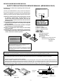
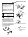
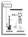
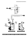
Precaution to be taken when replacing and servicing th laser pickup.
The following precautions must be observed during servicing to protect your eyesagainst exposure to the laser.
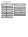
Warning of possible eye damage when repairing:
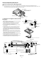
If the AC adaptor or batteries are connected when the top housing (disc cover) of the unit is removed, and the PLAY key is
pressed, the laser will light up during docus access (2-3 seconds). (Fig. 2-1)During the operation, the laser will lesk from the
opening between the magnetic head and the mechanical chassis (Fig. 2-2). In order to protect your eyes, you most not look at
the laser durnd repaor. Before repaoring, be sure to disconnect the AC adaptor and remove the batteries.
Lift motor
Magnet Head
Magnet head
Lasar Beam
Mechanism
Chassis
Display PWB
Optical pick-up
Main PWB
Disc cover
Disc motor
Optical Pick-Up
Figu re 2-2
Figu re 2-1
–2–
MD-MS200W/MD-MS200/MD-MS200H
BATTERY DISPOSAL (FOR MD-MS200 ONLY)
Contains nickel cadmium (or sealed lead) battery. Must be recycled
or disposed of properly. Remove the battery from the product and
contact federal or state environmental agencies for information on
recycling and disposal options.
FOR A COMPLETE DESCRIPTION OF THE OPERATION OF THIS UNIT, PLEASE REFER
TO THE OPERATION MANUAL.
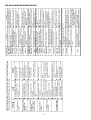
SPECIFICATIONS
General
Power source:
Power consumption:
Output power:
Rechargeable battery
performance:
(Fully charged)
Input sensitivity:
Recording
level
Reference input
level
Input jack:
Output jack:
0.25 mV
10k ohms
MIC L
2.5 mV
10k ohms
LINE
100 mV
20k ohms
LINE
—
10 mW +
10 mW
16 ohms
350mV
(-12dB)
—
50 kohms
Audio channels:
Frequency response:
Rotation speed:
Error correction:
Coding:
Recording method:
Load
Specified Maximum
output output level impedance
Headphones
275 g (0.6 lbs.) with rechargeable
battery
Line/Mic/Optical
Headphones
MiniDisc Recorder
Type:
Signal readout:
Input
inpedance
MIC H
Output level:
Dimensions:
Weight:
DC 3.6 V (rechargeable lithium-ion
battery x 1)
DC 5 V (AC adaptor)
AC 110 - 240V, 50/60 Hz
0.15 A (AC adaptor)
4W
RMS; 20mW (10 mW + 10mW)
(0.2% T.H.D.)
Approx. 9.5 hours (continuous play)
Approx. 7.0 hours (continuous
recording)
A/D,D/A converter:
Sampling frequency:
Modulation system:
Wow and flutter:
Portable MiniDisc recorder
Non-contact, semi-coductor laser
pick-up
2
20 to 20,000 Hz ± 3 dB
Approximately 400 to 900 rpm
ACIRC (Advanced Cross Interleave
Reed-Solomon Code)
ATRAC (Adaptive TRansform
Acoustic Coding)
Magnetic modulation overwrite
method
1-bit
44.1 kHz
EFM (Eight to Fourteen Modulation)
Unmeasurable (less than ±0.001%
W.peek)
Headphones
Width: 4-5/16" (109.2 mm)
Height: 1-7/32" (30.5 mm)
Depth: 3-7/32" (81.3 mm)
Type:
Impedance:
Inner-ear dynamic
16 ohms
Specifications for this model are subject to change without
prior notice.
–3–
–4–
Notes:
After charging has been completed, the
AC adaptor may be left connected.
(Charging at night.)
The battery will not be charged whilst
the main unit is operating.
If the AC adaptor is removed from the
main unit or from the AC socket whilst
charging, “
” will not disappear for
about 1 minute. This is normal.
ing.
“
” will appear, and the battery will
begin charging.
Battery charging will be complete in 3
hours. When battery charging begins,
“
” will be displayed. When the
charging is complete, it will go out.
5 Press the n OFF button to begin charg-
the AC adaptor into the AC
socket, and then insert the plug on the
AC adaptor lead into the DC IN 5V
socket.
4 Plug
partment cover.
3 Close the rechargeable battery com-
Insert the side with the arrow first.
2 Insert the rechargeable battery.
the rechargeable battery compartment cover.
1 Open
When the rechargeable battery is used for
the first time or when you want to use it
after a long period of disuse, be sure to
charge it fully.
Rechargeable battery
power
A rechargeable lithium-ion battery is
the only kind that can be used.
Even if the battery supplied with the
unit is not used, you should charge it at
least once every three months because
of the special quality of this battery.
The rechargeable battery can be
charged approximately 300 times.
Do not use any battery other than that
specified. Use of other batteries may
cause malfunctions.
When the operating time is reduced to
about half the normal amount of time,
even after a full charge is performed,
replace the battery with a new one.
When charging or when using the rechargeable battery, use it within an ambient temperature range of 5°C to
35°C.
Notes about the
rechargeable battery
As the battery charge is reduced, the bars
in the indicator will go out one by one.
When the battery is almost completely exhausted, the whole battery indicator will
flash.
At this point you should recharge the battery.
When the battery has run completely out,
“BATT EMPTY” will be displayed, and the
power will be disconnected automatically.
When the AC adaptor is used, the battery indicator will light up in the fully
charged condition.
Note:
If the battery indicator is flashing, it will be
impossible to start recording or editing.
How to determine the remaining
battery time:
Approx. 7 hours (fully charged, analogue input, volume level: VOL 0)
Continuous recording:
Approx. 9.5 hours (fully charged, volume level: VOL 20)
After charging is complete, the unit can be
used continuously as follows:
Continuous playback:
Rechargeable battery
operating time
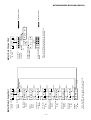
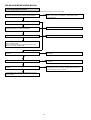
OPERATION MANUAL
1. Volume Buttons:
2. Stop/Power Off Button
3. Track Mark/Extra Bass Button
4. Play/Pause Button:
5. Fast Reverse/Fast Forward/Cursor Buttons:
6. Hold Switch
Remote Control Unit
/
dB
VOL.
9
4
3
4
5
6
0 OVER
21
20
19
18
17
3
4
27
2
1
BASS
26
23
25
12
16
40
2
22
24
8
RANDOM 1
TOC SYNC MONO
REC
1
15
14
13
12
11
10
6
7
5
NAME OF PARTS
1. Synchro Recording Indicator
2. Level Meter
3. Battery Indicator
4. Character Information Display
5. Disc Status Indicator
6. TOC Indicator
7. Random Indicator
8. Repeat Indicator:
9. Monaural Long-Play Mode Indicator
10. Play/Pause Button:
11. Stop/Power Off/Charge Button:
12. Fast Reverse/Fast Forward/Recording Level Control/
Cursor Button:
/
13. Microphone Input Socket
14. Hold Switch
15. Eject Lever
16. Enter/Synchro/Fast Play Button
17. Character/Symbol Select/Time Button
18. Display/Lowercase Letter Button
19. Record/Track Mark Button
20. Edit/Auto Mark/Time Mark Button
21. Mode/Space Button
22. Extra Bass/Delete Button
23. Volume/Name Select Buttons:
24. 5V DC IN Socket
25. Headphones Socket
26. Optical/Line Input Socket
27. Rechargeable Lithium-Ion Battery Compartment
Main Unit
MD-MS200W/MD-MS200/MD-MS200H
For MiniDiscs on which repeated
recording and editing were performed,
some sounds may be skipped whilst
cueing and reviewing.
If there are scratches or dust on a
MiniDisc, the track numbers following
that track will be increased by one.
A track number can be created in the
middle of a track.
For MiniDiscs on which repeated
recording and editing operations were
performed, the COMBINE function
may not work.
Two tracks may not be combined in
editing.
When recorded tracks are played back
using the cue and review operations,
some sounds may be skipped.
When the remaining recording time of
a disc is displayed, short tracks less
than 8 seconds long may not be
included in the total.
Even if several short tracks are
erased, the remaining recording time
may not show an increase.
A cluster (about 2 seconds) is
normally the minimum unit of
recording. So, even if a track is less
than 2 seconds long, it will use about
2 seconds of space on the disc.
Therefore, the time actually available
for recording may be less than the
remaining time displayed.
If there are scratches on discs, those
sections will be automatically avoided
(no recording will be placed in those
sections). Therefore, the recording
time will be reduced.
If there are scratches on a disc, the
unit will automatically avoid recording
in those areas. The recording time will
be reduced.
Even if the number of tracks and the
recording time have not reached the
limit, “DISC FULL” may be displayed.
The total of the recorded time and
time remaining on a disc may not add
up to the maximum possible recording
time.
When the number of tracks used
reaches the limit, regardless of the
remaining recording time, further
recording will be impossible.
(Maximum number of tracks: 254)
Even if the maximum recording time of
a MiniDisc has not been reached,
“DISC FULL” or “TOC FULL” may be
displayed.
MINIDISC SYSTEM LIMITATIONS
Digital cable
Recording
so that only
copies can
copies are
(Serial Copy
a new digital
was digitally
–5–
Digital cable
Recording
Analogue recording is
possible.
Playback
Digitally recorded MiniDisc
CD player, MD
player, etc.
Playback
When you attempt to make
recording from a track that
recorded on a MiniDisc
MiniDiscs are designed
first generation digital
made, further digital
prevented by the SCMS
Management System).
In the following cases digital recording is
impossible, even if you are using digital
cables.
There are cases where digital
recording may be impossible.
Note:
When this product is subjected to strong
external interference (mechanical shock,
excessive static electricity, abnormal supply voltage due to lightning, etc.) or if it is
operated incorrectly, it may malfunction. If
such trouble occurs, proceed as follows:
1. Unplug the AC adaptor from the AC
socket.
2. Remove the rechargeable battery.
3. Leave the unit completely unpowered
for approximately 30 seconds.
4. Reconnect the AC adaptor to the AC
socket and retry the operation.
If strange sounds, smell or smoke come
out of the unit or an object is dropped into
the unit, remove the AC adaptor from the
AC socket and contact an authorised
Sharp service centre.
If trouble occurs
When the unit has condensation inside,
the disc signals cannot be read, and the
product may not function properly.
If this happens, remove the disc. The
condensation should evaporate in approximately 1 hour. The unit will then
function properly.
Shortly after turning on a heater.
When the unit is placed in a room
where there is excessive steam or
moisture.
When the unit is moved from a cool
place to a warm place.
In the following cases, condensation
may form inside the unit.
Moisture condensation
TROUBLESHOOTING
MD-MS200W/MD-MS200/MD-MS200H
Press the n OFF button to turn
off the power (which will finish
writing the information on the
disc).
Slide the accidental erase
prevention tab back to its original
position.
Connect the unit properly to the
other equipment.
Plug in the AC adaptor.
Move the HOLD switch to turn
off the safety mode.
The track number or character
information has not been written
on the disc.
The unit is in the recording or
editing mode.
Is the MiniDisc protected against
accidental erasure?
Is the unit connected properly to
the other equipment?
Is the AC adaptor unplugged or
did a power failure occur whilst
recording or editing?
Is the unit in the safety mode?
The MiniDisc cannot
be ejected.
Recording and editing are impossible.
Place the unit in a vibration-free
place.
Some sounds are
skipped.
Recharge the battery.
Insert the remote control unit
plug or headphone plug securely.
Move the HOLD switch to turn
off the safety mode.
Recharge the battery.
The unit is in the safety mode.
The rechargeable battery is
exhausted.
The remote control unit plug or
headphone plug is not inserted
firmly.
Increase the volume.
Plug the remote control unit or
headphones in securely.
Move the HOLD switch to turn
off the safety mode.
Plug in the AC adaptor.
Recharge the battery.
REMEDY
The volume is set too low.
The remote control unit or
headphones are not plugged in.
The AC adaptor is disconnected.
The rechargeable battery is
exhausted.
The unit is in the safety mode.
CAUSE
The rechargeable battery is
exhausted.
The unit is receiving excessive
vibration.
When the operation
buttons are
pressed, the unit
does not respond.
No sound is heard
from the headphones.
The unit does not
turn on.
PROBLEM
Many potential “problems” can be resolved by the owner without calling a service technician. If something seems to be wrong with this product, check the following before
calling your authorised SHARP dealer or service centre.
Nothing is recorded.
Music is not being recorded.
No copy can be made because of
the SCMS copyright system.
A track cannot be edited.
BLANK DISC
00Tr 0:00
–6–
? DISC
UTOC ERROR
Tr. Protect
TOC FULL
TOC ERROR
TEMP OVER
SYSTEM ERR
SORRY
PROTECTED
POWER ?
PB DISC
LOCKED
LOCK ERROR
NO DISC
HOLD
DISC FULL
Din UNLOCK
DISC ERROR
DEFECT
Can't WRITE
Can't REC
Can't EDIT
Can't COPY
A disc which contains data other
than music was played.
There is an error in the signal from
the disc.
A large portion of the disc has been
damaged.
There is no space left for recording
character information (track names,
disc names, etc.).
The track has been protected from
being erased.
A large portion of the disc has been
damaged.
There is an error in the recorded
signal.
The temperature is too high.
Since a track number is currently
being located or written to, the unit
cannot accept your command.
You have come to the conclusion
that the unit is out of order.
The disc is write protected.
The unit is in the malfunction
prevention state.
The EJECT lever was moved
during recording or editing.
A disc has not been loaded.
You tried to record on a playbackonly disc.
Improper power is being supplied.
Recording cannot be performed
correctly due to vibration or shock
in the unit.
Editing is impossible.
Since this disc has scratches on it,
the recording operation was
skipped.
Poor connection of the digital cable.
The disc is damaged.
The disc is out of recording space.
Meaning
The rechargeable battery run down.
BATT EMPTY
Error messages
Edit the track with the device on
which it was recorded.
Replace it with another recorded
disc.
Replace it with another recordable
disc or use the ALL ERASE function
(page 27), to erase the signal error
and then try recording again.
A disc which contains non-music
data cannot be played.
Replace it with another recorded
disc.
To have it repaired, go to the
distributor where you purchased the
unit.
Turn off the power, and wait for a
while.
Replace it with another recorded
disc.
Replace it with another recordable
disc.
Use one of the specified power
sources.
Move the write protection knob
back to its original position.
Wait for a while and try the
operation again.
Check the number of tracks.
If the sound you hear is not right,
replace the disc with another
recordable disc.
Connect the digital cable securely.
Reload the disc or replace it.
Replace it with another recordable
disc.
Return the HOLD switch to its
original position.
Turn off the power and remove the
MiniDisc.
Load a disc.
Replace it with a recordable disc.
Change the stop position of the
track and then try editing it.
Re-record or replace it.
Record using the analogue cable.
Remedy
Charge the rechargeable battery (or
use the AC adaptor for power.)
Replace the disc with a recorded
disc.
MD-MS200W/MD-MS200/MD-MS200H
MD-MS200W/MD-MS200/MD-MS200H
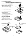
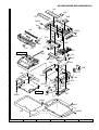
DISASSEMBLY
(A1) x2
Ø2x2mm
Caution on Disassembly
Follow the below-mentioned notes when disassembling
the unit and reassembling it, to keep it safe and ensure
excellent performance:
1. Take the battery and minidisc out of the unit.
2. When disassembling the machine, be sure to withdraw
the power plug from the socket in advance.
3. When disassemble the parts, remove the nylon band or
wire holder as necessary.
To assemble after repair, be sure to arrange the wires as
they were.
If a screw of different length is fitted to the MD mechanism (the screw of the part to be fitted to the MD
mechanism chassis), it may contact the optical pickup,
resulting in malfunction.
4. When repairing, pay due attention to electrostatic charges
of IC.
Bottom Cover
(B1) x2
Ø2x2mm
(A1) x2
Ø2x2mm
(B2) x1
(A1) x1
Ø2x2mm
Disc Cover
(B1) x2
Ø2x2mm
Figu re 7-1
(C1) x3
(C2) x2
Ø2x2.5mm
Main PWB
STEP
REMOVAL
PROCEDURE
FIGURE
1
Bottom Cover
1. Screw ..................... (A1) x5
7-1
2
Disc Cover
(Note)
1. Screw ..................... (B1) x4
2. Flexible PWB ......... (B2) x1
7-1
3
Main PWB
1. Screw ..................... (C1) x3
2. Flexible PWB ......... (C2) x4
3. Soldering ............... (C3) x2
7-2
4
Front Cabinet
1. Screw ..................... (D1) x1
2. Remove the front cabinet in
the arrow direction.
7-2
(C3) x1
Front Cabinet
(C2) x2
(C3) x1
(D1) x1
Ø2x2.5mm
Figure 7-2
Note:
When removing the upper lid, at first turn the operation knob
side in the arrow direction to remove.
Installing the front cabinet (See Fig. 7-3.)
Eject knob lever
1. Make sure that the lid opening and closing spring has been
engaged at the upper side as shown in Figure < A > .
2. Fit the MD lid right pin into the lid opening and closing lever
to install it.
Note:
• Take care since the antivibration rubber may come off.
• If the main PWB has been installed previously, fit the knob to
the HOLD switch shown in Figure < B > .
• If the mechanism has been installed, the antivibration rubber
may come off from the center cabinet fitting part when the
front part of center cabinet is widened.
Lid opening and closing lever
Eject lever
<A>
Lid opening and closing spring
Figure <A>
Lid opening and closing lever
Center Cabinet
Lid opening and closing spring
Engage the spring
at the upper side.
Lid opening and closing lever
<A>
MD lid right pin
Figure 7-3
Antivibration rubber
MD lid
HOLD knob
SW
<B>
Front Cabinet
Figure 7-4
–7–
MD-MS200W/MD-MS200/MD-MS200H
REMOVING AND REINSTALLING THE MAIN PARTS
(A2) x 3
Ø1.4 x 4.5mm
Remove the mechanism according to the disassembling methods 1 to 4. (See Page 7.)
How to remove the disc motor (See Fig. 8-1.)
1. Remove the solder joint (A1) x 1 of flex PWB.
2. Remove the screws (A2) x 3 pcs. and remove the disc
motor.
Take care so that the turnrable is not damaged.
How to remove the slide motor (See Fig. 8-2.)
1. Remove the solder joint (B1) x 1 of slide motor lead wire.
2. Remove the screw (B2) x 1, and remove the slide motor.
Note:
Take care so that the motor gear is not damaged.
(If the gear is damaged, noise is raised in search mode.)
Disc Motor
Flexible PWB
solder joint
(A1) x1
Motor Spacer
Mechanism PWB
How to reinstall the optical pickup unit
(See Fig. 8-3.)
1. Remove the screws (C1) x 5 pcs.
2. Remove the magnetic fielt arm block from the pickup, and
move the magnetic field arm block outwards.
Note:
Take due care so that the magnetic head is not damaged.
3. Withdraw a little the slide motor side shaft (C2) x 1 pcs., and
slowly raise the optical pickup.
Mechanism
Figure 8-1
(B2) x2
Ø1.4x2.2mm
How to remove the magnetic head
(See Fig. 8-4.)
Slide Motor
1. Remove the screw (D1) x 1 pc.
2. Remove the unsolder (D2) x 2 pcs. which connects the
magnetic head and the head hookup flex.
Note:
Mount carefully so as not to damage the magnetic head.
(B1) x2
Remove the solder joint.
Figure 8-2
(C1) x 2
Ø1.4 x 3mm
(D1) x1
Ø1.4x2mm
Magnetic field arm block
Head intervening flexible PWB
(C1) x 1
Ø1.4 x 2.5mm
(C1) x 1
Ø2 x4.5mm
Magnetic head
Unsolder
(D2) x2
Pickup Unit
Shaft (C2) x 1
Figure 8-4
Figure 8-3
–8–
MD-MS200W/MD-MS200/MD-MS200H
ADJUSTMENT
Test disc
MD adjustment needs two types of disc, namely recording disc (low reflection disc) and playback-only disc (high
reflection disc).
Type
Parts No.
Price Code
UDSKM0001AFZZ
AZ
Test disc
1
High reflection disc ESYA 1014 (SONY)
2
Low reflection disc
Recording minidisc
Note: Use the low reflection disc on which music has been recorded.
Entering the TEST mode
1. Setting at port (in standby state, disc-free state or power nonconnected state)
(1) Set the port as follows.
TEST1 : "Low"
TEST0 : "High"
(2) Press the PLAY button in the standby state (it is allowed to insert the disc or to connect the power supply).
(3) Test Mode STOP [ _ T E S T _ ]
2. Setting by special button operation (in standby state)
(1) Holding down the DISP button and ENTER button, press the PLAY button.
(2) Normal mode setting initialization (BASS setting, VOL setting, etc.)
(3) Indication of microcomputer version for one second [
]
Destination
Microcomputer version
EEPROM version
(4) Whole LCD lighting for 2 seconds
(5) Test Mode STOP [ _ T E S T _ ]
*When the PLAY button is pressed during indication (3) and (4), the process proceeds to (5).
Leaving the TEST mode
(1) Press the STOP button in the TEST mode stop state or version indicating state or whole LCD lighting state.
(2) EEPROM rewrite-enable area updating, adjustment error setting (so as to adjust all the items when the power supply is turned
on in the normal mode)
(3) Change to standby state
Test Mode
1. AUTO Mode
• Automatic adjustment is performed. (After adjustment the grating adjustment mode is set.)
• Continuous playback is performed (Error rate indication, jump test).
• The temperature correction is performed only when servo start is performed, but the
posture correction is not performed.
2. MANUAL Mode
• Temperature is displayed. (Updating in real time)
• Seeing the displayed measurement value/set value, make manualadjustment to set values
within the allowable range.
• Continuous playback is performed (error rate display, jump test).
• The temperature correction is performed only when servo start is performed, but the
posture correction is not performed.
3. RESULT Mode
• Adjustment value is indicted.
• Adjustment value is changed manually. (in servo OFF state).
4. TEST-PLAY Mode
• Continuous playback from the specified address is performed.
• 1 line, 10 lines or 400 lines manual jump is performed.
• C1 error rate display (pit section), ADIP error rate display (groove section)
• The temperature correction is performed only when servo start is performed, but the
posture correction is not performed during continuous playback.
5. TEST-REC Mode
• Continuous record from the specified address is performed.
• Change of record laser output(servo gain is also changed according to laser output).
• The temperature correction is performed only when servo start is performed, but the
posture correction is not performed during continuous recording.
6. INNER Mode
• Determine the position where the INNER switch is turned on.(only high reflection disc).
• The temperature correction is performed only when servo start is performed, but the
posture correction is not performed.
7. NORMAL Mode
• The mode is changed from the TEST mode to the normal mode without adjustment.
• In the normal mode the internal operation mode, memory capacity, etc. areindicated.
• In the normal mode both temperature correction and posture correction are performed.
8. Digital input display Mode
• Digital input information is displayed.
9. Error data display Mode
• Error information is displayed.
• Error information is initialized.
10. E2-PROM setting mode
• Factors of digital servo are changed manually. (Each servo is turned on individually.)
• Cut-off frequency of BASS1, BASS2 and BASS3 is selected manually.
• Temperature detection terminal voltage is measured, and the reference value is set.
• Defaults are selected and set.
• Setting of EEPROM protect area is updated. (In case of protect releasing)
–9–
MD-MS200W/MD-MS200/MD-MS200H
Operation in each TEST mode
1. AUTO Mode
Step No.
• When the STOP button is pressed while the AUTO menu
appears or during automatic adjustment, the mode changes to
the TEST mode stop state. At this time the adjustment value is
not output.
• As for operation during continuous playback refer to [Explanation
of TEST-PLAY mode].
• Adjustment NG: If the measurement value of adjustment FEO is
out of range,focus ON failure occurs or adjustment error or TZC
error occurs.
• When the high reflection disc is used,
changes as follows.
TEO — FEO — Hf — Hg — Hb — Hf
• When the low reflection disc is used,
changes as follows.
TEO — FEO — If — Lg — Lb — Lf — Gl — Gg — Gb — Lf
• Grating adjustment: When the focus servo and spin servo are
ON.
Step 1
Test mode STOP state
Step 2
BASS button.
Step 3
AUTO menu.
Step 4
PLAY button -->
Slide shift to innermost periphery
Step 5
Automatic adjustment
Step 6
End of adjustment
Step 7
When adjustment is OK, the
process proceeds to (8).
When adjustment is NG, the
process proceeds to (13).
Step 8
Grating adjustment, adjustment
value output
•
•
•
•
Step 9
When the PLAY button is pressed,
the process proceeds to (10).
When the STOP button is pressed,
the process proceeds to (12).
Step 10
Continuous playback (pit section)
Continuous playback (groove section)
: Adjustment name
: Measurement value
: Set value
: Address
Display
Operation and state
[
TEST
]
[
AUTO
]
[
]
[ A D J . O K
]
[ S Q
[ A P
]
]
]
Step 11
STOP button
Step 12
Test mode STOP state
[
Step 13
Adjustment value output
[ A D J . N G
]
[
]
Step 14
STOP button
Step 15
Test mode STOP state
TEST
TEST
2. MAMUAL Mode
Step No.
Display
Operation and state
Step 1
Test mode STOP state
Step 2
BASS button
Step 3
AUTO menu
Step 4
SKIP UP button x 1 times
(Or SKIP DOWN button x 9 times)
Step 5
MANUAL menu
Step 6
PLAY button
Step 7
Temperature measurement
Step 8
SKIP UP button
Step 9
Tracking error offset measurement
Step 10
SKIP UP button
Step 11
Step No.
[
TEST
]
Step 21
Step (24) when SKIP UP button,
Step (22) when PLAY button.
[
AUTO
]
Step 22
Pit section continuous playback
Step 23
When the P-MODE button is pressed,
the process proceeds to (20-a) or (20-b).
[ M A N U A L ]
Step 24
The high reflection disc is not accepted.
When the low reflection disc is used, the
process proceeds to (25).
[TMP:
Step 25
TOTAL signal level adjustment
Step 26
SKIP UP button
Step 27
Groove: Tracking gain adjustment
]
[TEO:
]
Step 28
SKIP UP button
Focus error offset measurement
[FEO:
]
Step 29
Groove: Tracking balance adjustment
Step 12
SKIP UP button—Laser lighting
[LON:
]
Step 30
SKIP UP button
Step 13
SKIP UP button—
Slide shift to innermost periphery
Step 31
Focus gain adjustment
_ _
Step 14-a Focus gain rough adjustment (high reflection) [ H f
]
Step 14-b Focus gain rough adjustment (low reflection) [ L f
]
Step 15
SKIP UP button
Step 16-a Pit:Tracking gain adjustment (high reflection) [ H g
]
Step 16-b Pit:Tracking gain adjustment (low reflection)
[Lg
]
Step 18-a Pit:
[Hb
Tracking balance adjustment (high reflection)
]
Step 18-b Pit:
[Lb
Tracking balance adjustment (low reflection)
]
Step 17
Step 19
SKIP UP button
[Hf
]
Step 20-b Pit:
Focus gain adjustment (low reflection)
[Lf
]
Step 32
PLAY button
Step 33
Groove section continuous playback
Step 34
When the P-MODE button is pressed,
the process to (31).
[ S Q
]
[ G l
]
[ G g
]
[ G b
]
[ L f
]
[A P
]
• Reversing when the SKIP DOWN button is pressed.
• When the VOL UP button is pressed during adjustment, the set value
increases, and the new set value is output.
• When the VOL DOWN button is pressed during adjustment, the set
value reduces, and the new set value is output.
• When the VOL UP/DOWN button is held down, the setting changes
continuously, one cycle being 100 ms.
• When the STOP button is pressed while the MANUAL menu
appears, or during measurement or adjustment, the mode changes
to the TEST mode stop state.
• As for operation during continuous playback refer to [Explanation of
TEST-PLAY mode].
SKIP UP button
Step 20-a Pit:
Focus gain adjustment (high reflection)
Display
Operation and state
•
•
•
•
– 10 –
: Measurement value
: Set value
: Address
: Temperature code
MD-MS200W/MD-MS200/MD-MS200H
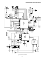
3. RESULT Mode
Step No.
Operation and state
Step 1
Test mode STOP state
Step 2
BASS button
Step 3
AUTO menu
Step 4
SKIP UP button x 2 times
(Or SKIP DOWN button x 8 times)
Step 5
RESULT menu
Step 6
PLAY button
Step 7
Indication of measurement value:
Tracking error offset
Step 8
SKIP UP button
Step 9
Indication of measurement value:
Focus error offset
Step 10
SKIP UP button
Step 11
Indication of measurement value:
High reflection focus gain
Step 12
SKIP UP button
Step 13
Indication of measurement value:
High reflection pit tracking gain
Step 14
SKIP UP button
Step 15
Indication of measurement value:
High reflection pit tracking balance
Step 16
SKIP UP button
Step No.
Display
Operation and state
[
TEST
]
Step 17
Indication of measurement value:
Low reflection focus gain
[
AUTO
]
Step 18
SKIP UP button
Step 19
Indication of measurement value:
Low reflection tracking gain
Step 20
SKIP UP button
Step 21
Indication of measurement value:
Low reflection pit tracking balance
Step 22
SKIP UP button
Step 23
Indication of measurement value:
Low reflection TOTAL signal level
Step 24
SKIP UP button
Step 25
Indication of measurement value:
Low reflection groove tracking gain
[
RESULT
]
[TEO:
]
[FEO:
]
[ Hf _ _
]
[ Hg _ _
]
[ Hb _ _
Display
[ Lf _ _
]
[ Lg _ _
]
[ Lb _ _
]
[ Gl _ _
]
[ Gg_ _
]
Step 26
SKIP UP button
Step 27
Indication of measurement value:
[ Gb _ _
Low reflection groove tracking balance
]
Step 28
STOP button
Step 29
Test mode STOP state
[
TEST
]
• Reversing when the SKIP DOWN button is pressed
• When the VOL UP button is pressed during set value indication, the set value increases, and the new set value is stored in RAM.
• When the VOL DOWN button is pressed during set value indication, the set value decreases, and the new set value is stored in RAM.
• When the VOL UP/DOWN button is held down, the setting changes continuously, one cycle being 100 ms.
• When the STOP button is pressed while the RESULT menu appears, or during measurement value or set value indication, the mode
changes to the TEST mode stop state.
•
: Measurement value
•
: Set value
7. TEST/PLAY Mode
Step No.
Display
Operation and state
Step 1
Test mode STOP state
Step 2
BASS button
Step 3
AUTO menu
Step 4
SKIP UP button x 3times
(Or SKIP DOWN button x 7 times)
Step 5
TEST-PLAY menu
Step 6
When the DISP button is pressed, the
process proceeds to (7).
When the PLAY button is pressed, the
process proceeds to (9).
Step 7
TEST-PLAY mode
Step 8
PLAY button
Step 9
Continuous playback (pit section)
Continuous playback (groove section)
Step 10
STOP button
Step 11
Test mode STOP state
[
TEST
]
[
AUTO
]
[ T _ P L A Y
]
[ A d 0 0 5 0
]
[ S Q
[ A P
]
]
[
]
TEST
– 11 –
]
MD-MS200W/MD-MS200/MD-MS200H
•When the STOP button is pressed while the TEST-PLAY menu appears, or in TEST-PLAY or continuous playback mode, the mode changes
to the TEST mode stop state.
• When the PLAY button is pressed while the TEST-PLAY menu appears,continuous playback is initiated from the current pickup position.
• Whenever the DISP button is pressed in the TEST-PLAY mode, the address changes as follows.
0050 — 03C0 — 0700 — 08A0 — 0050 —
• Whenever the BASS key is pressed in the TEST-PLAY mode, the digit which is changed by the SKIP UP/DOWN button changes as follows.
0050 — 0050 — 0050 — 0050 — 0050 —
• When the SKIP UP button is pressed in the TEST-PLAY mode, the digit of address specified by the BASS button is set to +1h. (0 to F)
• When the SKIP DOWN button is pressed in the TEST-PLAY mode, the digit of address specified by the BASS button is set to -1h. (0 to F)
* When the SKIP UP/DOWN button is held down, the setting changes continuously, one cycle being 100 ms.
• When the BASS button is pressed in the continuous playback mode, the number of jump lines changes as follows.
1 — 10 — 400 — 1
* After the number of jump lines is indicated for one second, the address indication is restored.
[
T R _ ]
• When the SKIP UP button is pressed in the continuous playback mode, the specified number of lines is jumped in the FWD direction.
• When the SKIP DOWN button is pressed in the continuous playback mode, the specified number of lines is jumped in the REV direction.
* When the SKIP UP/DOWN button is held down, jump is repeated every approx. 100 ms.
•Whenever the DISP button is pressed in the continuous playback mode, the indication changes as follows.
* Pit section
Continuous playback (SUBQ address indication)
[ S Q
]
|
Continuous playback (C1 error indication)
[ C E
]
|
Continuous playback (SUBQ address indication)
[ S Q
]
* Groove section
Continuous playback (ADIP address indication)
[ A P
]
|
Continuous playback (C1 error indication)
[ C E
]
|
Continuous playback (ADIP error indication)
[ A E
]
|
Continuous playback (ADIP address indication)
[ A P
]
•
: Address
•
: C1 Error rate
•
: ADIP Error rate
•
: JUMP lines
Mechanism Adjustment
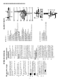
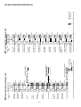
1. Optical pickup grating inspecting method
TP141
GND
TP132
EOUT
OSCILLOSCOPE
a
100Kohm
470p
GND CH1 CH2
470p
TP133
FOUT
X
Y
b
100Kohm
LISSAJOUS'S WAVEFORM
LESS THAN A:B = 3:1
3
Figure 12-1 OPTICAL PICKUP GRATING DEVIATION
MEASURING METHOD
2
After the automatic adjustment is performed in the AUTO mode
(test mode) with the aid of high refection MD disc ("COMPLATE" is
displayed), the Lissajous's waveform (x-y) is adjusted.
1. Slightly loosen the 3 screws of spin motor, and make an
adjustment, observing the Lissajous's wavefor.
2. After adjustment tighten the screws in arder of<1> , <2> ,< 3> .
3. It confirms Lissajous's wavwform ripple mark once again.
1
Shifting the spin motor installation
position, check the Lissajous's
waveform.
Figure 12-2
– 12 –
MD-MS200W/MD-MS200/MD-MS200H
5. TEST-REC Mode
Step No.
Display
Setting Method
Step 1
Test mode STOP state
Step 2
BASS button
Step 3
AUTO menu
Step 4
SKIP UP button x 4times (Or SKIP DOWN button x 6 times)
Step 5
TEST-REC menu
Step 6
When the DISP button is pressed, the process proceeds to (7).
When the PLAY button is pressed, the process proceeds to (9).
Step 7
TEST-REC mode
Step 8
PLAY button
Step 9
Continuous playback mode (groove)
Step 10
STOP button
Step 11
Test mode STOP state
[
T E S T
]
[
A U T O
]
R E C
]
[ T
[ A d 0 0 5 0
]
[ A P
]
[
]
T E S T
• When the STOP button is pressed while the TEST-REC menu appears, or in the TEST-REC mode or continuous record mode, the mode
changes to the TEST mode stop state.
• When the PLAY button is pressed while the TEST-REC menu appears, the continuous record is initiated from the current pickup position.
• Whenever the DISP button is pressed in the TEST-REC mode, the address changes as follows.
0050 — 03C0 — 0700 — 08A0 — 0050 —
• Whenever the BASS button is pressed in the TEST-REC mode, the digit which is changed by the SKIP UP/DOWN button changes as
follows.
0050 — 0050 — 0050 — 0050 — 0050 —
• When the SKIP UP button s pressed in the TEST-REC mode, the digit of address specified by the BASS button is set to +1h.(0 to F)
• When the SKIP DOWN button is pressed in the TEST-REC mode, the digit of address specified by the BASS button is set to -1h. (0 to F)
* When the SKIP UP/DOWN button is held down, the setting changes continuously, one cycle being 100 ms.
• When the VOL UP/DOWN button is pressed in the TEST-REC mode or continuous record mode, the laser record power changes.
(Servo gain changes also according to record power.)
* After the laser record power is indicated for one second, the address indication is restored.
[ R P W
]
•
: Address
•
: Laser power cord
• Operation is disabled if the premastered disc or disc is in miserase-protected state.
6. INNER Mode
Step No.
Step 1
Display
Setting Method
Test mode STOP state
Step 2
BASS button
Step 3
AUTO menu
Step 4
SKIP UP button x 5 times
(Or SKIP DOWN button x 5 times)
Step 5
INNER menu
Step No.
[
T E S T
]
[
A U T O
]
[
I N N E R
Setting Method
Step 6
PLAY button
Step 7
INNER switch position measurement
Step 8
STOP button
Step 9
Test mode STOP state
]
• When the STOP button is pressed while the INNER menu appears, the mode changes to TEST mode stop state.
•
: Address
– 13 –
Display
[ S Q
]
[
]
T E S T
MD-MS200W/MD-MS200/MD-MS200H
7. NORMAL Mode
Step No.
Setting Method
Step 1
Test mode STOP state
Step 2
BASS button
Step 3
AUTO menu
Step 4
SKIP UP button x 6times
(Or SKIP DOWN button x 4 times)
Display
[
[
Step No.
T E S T
]
A U T O
]
Setting Method
Step 5
NORMAL menu
Step 6
PLAY button
Step 7
TOC read
Step 8
Hereafter operation in normal mode
Display
[ N O R M A L ]
[Refer to the
following description.]
• When the STOP button is pressed while the NORMAl menu appears, the mode changes to the TEST mode stop state.
• Indication during operation
Indication of memory capacity on main unit LCD [
] + Level meter
: TNO
: Internal mode
: Servo state (#3: Slide, #2: Tracking, #1: Spin, #0: Focus)
: Address
LCD remote control [
] + TNO indication
: Internal mode
: Servo state (#3: Slide, #2: Tracking, #1: Spin, #0: Focus)
: Address
: Memory capacity (graphic indication)
• Selection of sound volume, BASS, etc. is possible (without indication)
• Recording is also possible.
8. Digital input display mode
Step No.
Display
Setting Method
Step 1
Test mode STOP state
Step 2
BASS button
Step 3
AUTO menu
Step 4
SKIP UP button x 7times
(Or SKIP DOWN button x 3 times)
Step 5
Digital input indication menu
Step 6
PLAY button
[
[
T E S T
A U T O
Step No.
]
]
[ D I N M O N ]
Display
Setting Method
Step 7
FS code, channel status indication
Step 8
SKIP UP button
Step 9
U bit indication 1
Step 10
SKIP UP button
Step 11
U bit indication 2
Step 12
STOP button
Step 13
Test mode STOP state
[ C
ƒ ƒ ƒƒ ƒƒ
[ U 1
]
[ U 2
† † ‡ ‡ ]
[
T E S T
• When the STOP button is pressed while the digital input indication menu appears or during digital input information indication, the mode
changes to the TEST mode stop state.
• In case of analog input or digital input unlocking the indication data is _.
• ƒ ƒ : Control Code
• ƒƒƒƒ : Category code
•
: TNO
: INDEX
•
• † † : TIME(min.)
• ‡ ‡ : TIME(Sec.)
– 14 –
]
]
MD-MS200W/MD-MS200/MD-MS200H
9. Error data display Mode
Step No.
Step 1
Display
Setting Method
Test mode STOP state
[
A U T O
]
Contents
Automatic adjustment
Out of allowable range
13
Automatic adjustment
adjustment
Servo retry error (4 times) during
]
16
Automatic adjustment
TZC error in TG, TB adjustment
(TG, TB measurement value does not change.)
[ E 0
]
17
Automatic adjustment
21
Focus setting disabled
[ E 1
]
23
Track search time-over
SKIP UP button
32
P-TOC read disabled
Indication of error data 2
42
U-TOC read disabled
44
U-TOC write disabled
52
Music data write disabled
71
Pickup position initialization error (Inner switch ON failure)
72
EEPROM read error
73
Record head drive disabled (EJECT operation)
82
Overvoltage detection
91
TEMP over
Step 4
SKIP UP button x 8times
(Or SKIP DOWN button x 2 times)
Step 5
Error data indication menu
Step 6
PLAY button
Step 7
Indication of error data 0
Step 8
SKIP UP button
Step 9
Indication of error data 1
Step 12
SKIP UP button
Step 13
Indication of error data 3
Step 15
]
12
BASS button
AUTO menu
Step 14
T E S T
Automatic adjustment
Gain maximum or error
adjustment judgment NG during adjustment retry in TG, FG
adjustment.
Step 3
Step 11
Error Code
[
11
Step 2
Step 10
Error data list
[ E
D A T A
[ E 2
]
[ E 3
]
SKIP UP button
Indication of error data 4
Step 16
SKIP UP button
Step 17
Indication of error data 5
Step 18
SKIP UP button
Step 19
Indication of error data 6
Step 20
SKIP UP button
Step 21
Indication of error data 7
Step 22
SKIP UP button
Step 23
Indication of error data 8
Step 24
SKIP UP button
Step 25
Indication of error data 9
Step 26
STOP button
Step 27
Test mode STOP state
[ E 4
]
[ E 5
]
[ E6
]
[ E 7
]
[ E 8
]
[ E 9
]
[
T E S T
TEO, FEO allowable range error
]
• Reversing when SKIP DOWN button is pressed
• When the STOP button is pressed while the error data indication menu appears or during error data indication, the mode changes to the
TEST mode stop state.
• Error data 0 is the latest error.
• Error which occurred in the TEST mode is also stored in the memory.
• When the DISP button is pressed while the error data indication menu appears, the error data is initialized. [ C L E A R _ ]
•
: Error Code
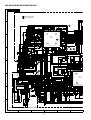
Jitter checking method
Tr: 2SC1815
2SC1740
IC701 20 PIN
+3V
JITTER MATER
100 ohm
0.33
TP145
(EFM)
560 ohms
TP141
(GND)
IC101
7 PIN
-3V
IC701 17 PIN
Figure 15
After automatic adjustment is performed in the AUTO mode (low
reflection MD disc use TEST mode), jitter must be less than 32 ns.
– 15 –
MD-MS200W/MD-MS200/MD-MS200H
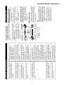
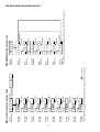
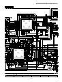
Lead-in switch position adjusting method
Note: Measure the position of lead-in switch in the INNER mode, and fix the position of lead-in switch at SUBQ FF85 to FF02.
After retightening the screw, pressing the mechanism PWB in the arrow direction, measure again the position of lead-in switch. If the
removed screw cannot be fit after position adjustment, fix with two screws.
Lead In Switch
Remove yhe screw when
adjustment is made.
Mechanism PWB
Loosen two screws
Figure 16-1
Adjustment of magnetic head mounting
position
• When the magnetic head and optical pickup have been replaced,
be sure to adjust the mounting position.
• For easier adjustment of mounting position move the optical
pickup to the center position, and then adjust the position.
1. Set the transparent disc 3 for adjustment.(*1)
2. Turn off the power supply, turn the head drive gear by hand to
lower the head.
3. Viewing the set from above, make an adjustment so that the
magnetic head aligns with the optical pickup objective lens.
• Circumferential direction: Slightly loosen the head fixing screw
(A), and shift the magnetic head fitting to align the head with the
pickup abjective lens.
• Radial direction:Turn the magnetic head circumferential adjustment nut (B), and adjust to align the head with the objective lens.
*1: Before setting the disc remove the decoration plate from the
disc lid, and fix it as shown in Figure 16-2.
4. Make sure that there is a clearance as shown in Figure 16-2 and
that the magnetic head moves up and down smoothly.
5. After adjustment apply Screw Lock to the head fixing screw (A)
and adjusted magnetic head radial adjusting screw (B).
Magnetic
head
Radial
Direction
Radial Direction
(Align the magnetic head
Objective
with the upper end of lens)
lens Circumferential direction
Clearance
(Align the magnetic head
A
approximately with the
B
lens center)
(B)
(A)
Apply a screw lack for
head fixing.
Circumferential
direction
Magnetic head
Slightly loosen the head
fixing screw.
Lift Motor
The lift pin is moved in the arrow direction
Figure 16-2
QCNWK0089AFZZ (6 Pin)
QCNWK0090AFZZ (7 Pin)
CNS601
Headdrive flexible PWB
LCD Flexible PWB
CNS201
Mechanism
Flexible PWB
QCNWK0091AFZZ (13 Pin)
CNS401
CNS402
QCNWK0092AFZZ (14Pin)
Flexible PWB
CNS101
QCNWK0093AFZZ (26 Pin)
Pickup Flexible PWB
Extension PWB for servicing
RUNTK0400AFZZ
Main PWB
Figure 16-3
– 16 –
MD-MS200W/MD-MS200/MD-MS200H
E2-PROM (IC402) writing procedure
1. Procedure to replace E2-PROM and write initial value of microcomputer in E2-PROM
(1)
(2)
(3)
(4)
(5)
(6)
(7)
(8)
(9)
(10)
(11)
(12)
(13)
(14)
(15)
Replace E2-PROM.
Deprive E2-PROM of protection (connect the pins 8 and 2 of IC402).
Refer to the latest E2-PROM data list.
Press the Display/Lower-case Character button, Enter/Synchro button and Play/Pause button to start the test mode.
Version display
[Ver.
]
E2-PROM version (C ~ Z)
Microcomputer ROM version
The whole LCD lights.
Test mode stop state
[ T E S T ]
Press the Enter/Synchro button.
[ E E P R O M ]
Perform the operation to display "E2-PROM SETTING MODE CHART", compare the E2-PROM DATA LIST with the
display, and set according to the E2-PROM DATA LIST with the VOL UP or VOL DOWN key.
Set the temperature reference. (Refer to the Temperature Reference Setting Method.)
Set according to the E2-PROM DATA LIST.
Press the Stop button.
[ T E S T ]
Press the Stop button.
After data is written in E2-PROM, turn off power .
Restore protection of E2-PROM (Disconnect connection made in Step (2) above).
2. Temperature reference setting method (to be performed at room temperature 21 to 29°C)
(1) Test mode stop state
[TEST MODE ]
(2) Measure voltage of TEMP terminal (pin 3, IC401) of microcomputer.
(3) Calculate the temperature reference, using the following formula.
Measured voltage x 256
Temperature reference =
2.8
(4) Round down decimal fractions of calculated temperature reference, and convert it to hexadecimal value.
(5) Correct the temperature according to the table below depending on ambient temperature.
Ambient temperature
21 - 23
24 - 26
27 - 29
Temperature correction
+1
±0
- 1
An example: Environmental temperature is 22°C and set voltage is 1.25V.
Temperature reference =
(6)
(7)
(8)
(9)
(10)
1.25 x 256
2.8
= 114.286
= 114
(Decimal fraction is rounded down.)
= 72 H
(Conversion to hexadecimal value)
Press the BASS button, and press the SKIP DOWN button.
[ E E P R O M ]
Press the PLAY button, and press the SKIP button.
[
Temp
]
Press the PLAY button.
[TEMP
]
: Temperature reference
Set the temperature standard value to the value obtained above with the VOL UP and VOL DOWN buttons.
Press the STOP button.
[ T E S T ]
– 17 –
MD-MS200W/MD-MS200/MD-MS200H
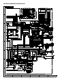
E2-PROM DATA LIST
Focus setting
Slide setting
Item display
F G _ _
Item display
Set values
6C
Set values
H
S L G _
80
H
1C
H
F F 1 _
70
H
S L 2 _
F F 2 _
F0
H
S L M _
7F
H
F F 3 _
FEH
S L V _
20
H
F F 4 _
00
S K k _
78
H
F Z H _
ED
S K t _
50
H
S K m _
78
H
H
H
F L n _
F6
H
F L f _
7F
H
Control setting
F P n _
00
H
Item display
F P f _
88
H
T BA _
A8H
C 2 4 _
1F
H
F L V _
28
H
C T 1 _
13
H
C 2 5 _
23
H
W T f _
90
H
C T 2 _
A8H
C 2 6 _
25
H
F S S _
06
H
C T 3 _
02
H
C 2 7 _
31
H
Spin setting
Item display
S P G _
S P i
00
H
C 2 8 _
2C
H
C 0 1 _
90
H
C 2 9 _
21
H
1A
C 0 2 _
83
H
C 3 0 _
1E
H
C 0 3 _
05
H
C 3 1 _
14
H
C 0 4 _
13
H
C 3 2 _
85
H
C 0 5 _
08
H
C 3 3 _
86
H
C 0 6 _
26
H
C 3 4 _
85
H
C 0 7 _
20
H
C 3 5 _
87
H
C 0 8 _
80
H
C 3 6 _
05
H
C 0 9 _
00
H
C 3 7 _
C0
H
C 1 0 _
10
H
C 3 8 _
07
H
C 1 1 _
00
H
C 3 9 _
70
H
C 1 2 _
1E
H
C 4 0 _
09
H
C 1 3 _
08
H
C 4 1 _
40
H
C 1 4 _
5CH
C 4 2 _
0B
H
C 1 5 _
1DH
C 4 3 _
20
H
C 1 6 _
1F
H
C 4 4 _
0D
H
C 1 7 _
1F
H
C 4 5 _
10
H
Set values
C 1 8 _
20
H
C 4 6 _
65
H
Calculate values
C 1 9 _
23
H
C 4 7 _
50
H
C 2 0 _
24
H
C 4 8 _
50
H
C 2 1 _
1DH
C 4 9 _
15
H
C 2 2 _
1E
H
C 5 0 _
D4
H
C 2 3 _
1E
H
H
D0
H
A0
H
S P o _
68
H
10
60
H
H
S P 3 _
F2
H
S P 4 _
F2
H
S P 5 _
10
H
BASS setting
Item display
Set values
B S 1 _
00
H
B S 2 _
00
H
B S 3 _
00
H
TEMP setting
Item display
T M _ _
Tracking setting
Item display
T G _ _
Set values
C 0 0 _
_
S P 2 _
Item display
Set values
S P m _
S P 1 _
Set values
Set values
40
H
T F 1 _
E0
H
T F 2 _
E8
H
T F S _
00
H
T B o _
40
H
T B t _
60
H
T K o _
48
H
T K t _
28
H
T D o _
75
H
T D t _
1A
H
S C o _
00
H
S C t _
40
H
S C m _
53
H
D B O _
00
H
C H p _
10
H
C L p _
F0
H
C H r _
20
H
C L r _
E0
H
W T m _
90
H
– 18 –
– 19 –
SKIP UP
T
SKIP UP
T
SKIP UP
SKIP DOWN
SKIP DOWN
SKIP DOWN
DATA
SKIP DOWN
EEPROM
SKIP UP
E
SKIP UP
DinMon
SKIP UP
NORMAL
NER
SKIP DOWN
REC
SKIP DOWN
PLAY
SKIP DOWN
SKIP UP
• When the STOP key is pressed in the specific mode,
the mode changes to the TEST mode stop state.
EEPROM
setting
MENU
Error data
indication
MENU
Digital input
indication
MENU
Normal mode
MENU
SKIP DOWN
RESULT
SKIP UP
MANUAL
SKIP UP
SKIP DOWN
SKIP DOWN
AUTO
BASS
TEST
INNER position
IN
measurement
MENU
SKIP UP
Continuous
record
MENU
Continuous
playback
MENU
RESULT
DISP
MENU
MANUAL
ADJUST
MENU
TEST AUTO
MEN U
TEST MODE
STOP
Test Mode Change Chart
SQ
AP
. N G
• When the STOP key is pressed in the specific mode,
the mode changes to the TEST mode stop state.
Continuous playback
MODE
PLAY
A D J . O K
PLAY
AUTO
ADJUST
ADJUST NG
OK
Adjustment
A D J
value
output
Adjustment value output
Grating adjustment
Execution of
automatic
adjustment
TEST AUTO
MENU
Test Auto Change Chart
: Address indication
: Adjustment indication
MD-MS200W/MD-MS200/MD-MS200H
– 20 –
TEO:
Lf
SKIP UP
Gb
SKIP UP
Gg
SKIP UP
Gl
SKIP UP
H f
L f
SKIP UP
Hb
Lb
SKIP UP
Hg
Lg
SKIP UP
h f
l f
SKIP UP
LON:
SKIP UP
FEO:
SKIP UP
SKIP DOWN
SKIP DOWN
SKIP DOWN
SKIP DOWN
SKIP DOWN
SKIP DOWN
SKIP DOWN
SKIP DOWN
P-MODE
PLAY
P-MODE
PLAY
BASS
SQ
Pit section continuous playback
RPW:
Record power laser ON
AP
: measurement value
: Adjustment value
: Addres
Groove section continuous playback
BASS 2 sec.
SKIP DOWN
SKIP DOWN
SKIP DOWN
• When the STOP key is pressed in the specified mode, the mode changes tothe TEST mode stop state.
FG fine adjustment
Groove section
TB adjustment
Groove section
TG adjustment
TOTAL signal
adjustment
FG fine adjustment
Pit section
TB adjustment
Pit section
TG adjustment
FG rough
adjustment
Laser ON
Focus Error Offset
measurement
TMP:
PLAY
MANUAL
SKIP UP
Tracking Error Offset
measurement
Temperature
measurement
MANUAL ADJUST
MENU
Manual Adjustment Change Chart
L b
SKIP UP
L g
SKIP UP
L f
SKIP UP
H b
b
SKIP DOWN
SKIP DOWN
SKIP DOWN
SKIP DOWN
SKIP DOWN
SKIP DOWN
SKIP DOWN
SKIP DOWN
SKIP DOWN
SKIP DOWN
SKIP DOWN
: measurement value
: Adjustment value
• When the STOP key is pressed in the specified mode, the mode changes tothe TEST mode stop state.
SKIP UP
Low reflection groove
section TB set value G
SKIP UP
Low reflection groove
G l
section TOTAL
set value
SKIP UP
Low reflection groove
section TG set value G g
Low reflection
TB set value
Low reflection
TG set value
H g
SKIP UP
High reflection pit
section TB set value
Low reflection
FG set value
H f
SKIP UP
High reflection pit
section TG set value
High reflection
FG set value
FEO
SKIP UP
Focus error offset
measurement value
P:
TEO
SKIP UP
Tracking error offset
measurement value
Temperature
TM
measurement value
SKIP UP
PLAY
RESULT
Result Indication Change Chart
RESULT DISP
MENU
MD-MS200W/MD-MS200/MD-MS200H
– 21 –
A D 0 8 A 0
DISP
A D 0 7 0 0
DISP
A D 0 3 C 0
DISP
PLAY
PLAY
PLAY
PLAY
PLAY
SQ
AP
: Address
Continuous playback
Start address
indication 4
Start address
indication 3
Start address
indication 2
Start address
indication 1
Continuous
record menu
DISP
R E C
A D 0 8 A 0
DISP
A D 0 7 0 0
DISP
A D 0 3 C 0
DISP
A D 0 0 5 0
T
PLAY
PLAY
PLAY
PLAY
PLAY
Continuous Record Change Chart
AP
: Address
Continuous record
• When the STOP key is pressed in the specified mode, the mode changes to the TEST mode stop state.
• When the SKIP UP/DOWN key is pressed in the start address indication state, the address of specific
digit changes.
• When the BASS key is pressed in the start address indication state, the digit of address which is changed
by the SKIP UP/DOWN key is changed.
Start address
indication 4
Start address
indication 3
Start address
indication 2
DISP
P L A Y
A D 0 0 5 0
T
• When the STOP key is pressed in the specified mode, the mode changes to the TEST mode stop state.
• When the SKIP UP/DOWN key is pressed in the start address indication state, the address of specific digit changes.
• When the BASS key is pressed in the start address indication state, the digit of address which is changed by the
SKIP UP/DOWN key is changed.
• When the VOL UP/DOWN key is pressed in the start address indication state or continuous record state,
the record laser power changes.
DISP
DISP
Start address
indication 1
Continuous
playback menu
Continuous Playback Change Chart
SQ
PLAY
INNER
######
PLAY
NORMAL
U2
SKIP UP
U1
SKIP UP
C
PLAY
SKIP DOWN
SKIP DOWN
DinMon
: FS Code
: Control Code
: Category Code
:TNO
: INDEX
: TIME (min)
: TIME (sec)
• When the STOP key is pressed in the specified mode, the mode changes to the
TEST mode stop state.
U bit 2 data
indication
U bit 1 data
indication
FS code
C bit data indication
Digital input
indication menu
Digital Input Indication Change Chart
• When the STOP key is pressed in the specified mode, the mode changes to the
TEST mode stop state.
Normal mode
Normal mode
change menu
Normal Mode Change Chart
• When the STOP key is pressed in the specified mode, the mode changes to the
TEST mode stop state.
Position
measurement
Inner position
measurement menu
Inner Position Measurement Change Chart
MD-MS200W/MD-MS200/MD-MS200H
– 22 –
E9
SKIP UP
E8
SKIP UP
E7
SKIP UP
E6
SKIP UP
E5
SKIP UP
E4
SKIP UP
E3
SKIP UP
E2
SKIP UP
E1
SKIP UP
E0
E
PLAY
SKIP DOWN
SKIP DOWN
SKIP DOWN
SKIP DOWN
SKIP DOWN
SKIP DOWN
SKIP DOWN
SKIP DOWN
After 2 seconds
DISP
SKIP DOWN
DATA
CLEAR
: Error Code
• When the STOP key is pressed in the specified mode, the mode changes to the TEST mode stop state.
Error data
9 indication
Error data
8 indication
Error data
7 indication
Error data
6 indication
Error data
5 indication
Error data
4 indication
Error data
3 indication
Error data
2 indication
Error data
1 indication
Error data
0 indication
Error data
indication menu
Error Data Indication Change Chart
SKIP DOWN
SKIP DOWN
SKIP DOWN
S p i n
SKIP DOWN
S l e d
SKIP DOWN
SKIP DOWN
SKIP UP
SKIP DOWN
T e m p
SKIP UP
B a s s
SKIP UP
SKIP UP
T r a c k
SKIP UP
SKIP UP
F o c u s
PLAY
EEPROM
SKIP UP
CONTROL
C T R L
setting menu
• When the STOP key is pressed in the specified mode, the mode changes to the TEST mode stop state.
TEMP
setting menu
BASS
setting menu
SLIDE
setting menu
TRACKING
setting menu
SPIN
setting menu
FOCUS
setting menu
EEPROM
setting menu
EEPROM Setting Change Chart
MD-MS200W/MD-MS200/MD-MS200H
SLG
SL 2
SKIP DOWN
SKIP DOWN
SKIP DOWN
SKIP DOWN
SKIP DOWN
SKIP DOWN
– 23 –
SKIP DOWN
SKIP DOWN
Control setting
menu
C 0 0
SKIP UP
C 4 9
SKIP UP
C 0 1
SKIP UP
PLAY
CTRL
SKIP DOWN
SKIP DOWN
C02
SKIP DOWN
~C48
EEPROM Control Setting Change Chart
TM
PLAY
TEMP
: Temperature code
: Normal setting value
• When the STOP key is pressed in the specified mode, the mode changes to the TEST mode stop state.
TEMP setting menu
EEPROM TEMP Setting Change Chart
BS 3
C 5 0
: measurement value
: measurement value
• When the STOP key is pressed in the specified mode, the mode changes to the TEST mode stop state.
• When the STOP key is pressed in the specified mode, the mode changes to the TEST mode stop state.
SKIP UP
BS 2
PLAY
BASS
BS 1
SKIP UP
BASS setting menu
EEPROM BASS Setting Change Chart
: measurement value
• When the STOP key is pressed in the specified mode, the mode changes to the TEST mode stop state.
SLm
SKIP UP
SK t
SKIP UP
SK k
SKIP UP
SLV
SKIP UP
SLM
SKIP UP
PLAY
S l e d
SKIP UP
Slide setting menu
EEPROM Slide Setting Change Chart
MD-MS200W/MD-MS200/MD-MS200H
– 24 –
FSS
SKIP UP
WT f
SKIP UP
FLV
SKIP UP
FP f
SKIP UP
FPn
SKIP UP
FL f
SKIP UP
FL n
SKIP UP
FZH
SKIP UP
FF4
SKIP UP
FF3
SKIP UP
FF2
SKIP UP
FF1
SKIP UP
FG
PLAY
SKIP DOWN
SKIP DOWN
SKIP DOWN
SKIP DOWN
SKIP DOWN
SKIP DOWN
SKIP DOWN
SKIP DOWN
SKIP DOWN
SKIP DOWN
SKIP DOWN
SKIP DOWN
F o c u s
: measurement value
SKIP DOWN
SKIP DOWN
SKIP DOWN
SKIP DOWN
SKIP DOWN
SKIP DOWN
SKIP DOWN
SKIP DOWN
: measurement value
• When the STOP key is pressed in the specified mode, the mode changes tothe TEST mode stop state.
SP 5
SKIP UP
SP 4
SKIP UP
SP 3
SKIP UP
SP 2
SKIP UP
SP 1
SKIP UP
SP o
SKIP UP
SPm
SKIP UP
SP i
SKIP UP
SPG
PLAY
S p i n
EEPROM Spin Setting Change Chart
Spin setting
menu
• When the STOP key is pressed in the specified mode, the mode changes tothe TEST mode stop state.
Focus setting
menu
EEPROM Focus Setting Change Chart
TG
SKIP DOWN
SKIP DOWN
SKIP DOWN
SKIP DOWN
SKIP DOWN
SKIP DOWN
SKIP DOWN
SKIP DOWN
SKIP DOWN
SKIP DOWN
SKIP DOWN
SKIP DOWN
SKIP DOWN
SKIP DOWN
SKIP DOWN
SKIP DOWN
SKIP DOWN
: measurement value
• When the STOP key is pressed in the specified mode, the mode changes tothe TEST mode stop state.
WTm
SKIP UP
CL r
SKIP UP
CH r
SKIP UP
CL p
SKIP UP
CH p
SKIP UP
DBO
SKIP UP
SC t
SKIP UP
SC o
SKIP UP
TD t
SKIP UP
TD o
SKIP UP
TK t
SKIP UP
TK o
SKIP UP
TB t
SKIP UP
TB o
SKIP UP
TFS
SKIP UP
TF 2
SKIP UP
TF 1
PLAY
T r a c k
SKIP UP
Tracking setting
menu
EEPROM Tracking Setting Change Chart
MD-MS200W/MD-MS200/MD-MS200H
MD-MS200W/MD-MS200/MD-MS200H
EXPLANATION OF ERROR DISPLAY
Errors
Corrective action
Can't REC
Error display
• Defect occurred 10 times successively during REC-PLAY.
• During REC-PLAY, the break that full, high temperature
memory taped occurred.
• When reads it, and impossibility tries it again, and an
address doesn't hire you in REC state repeatedly for 20
seconds either.
• Check that disc is free from flaws, dust,
fingerprint, black spots, etc. Check for
significant disalignment and runout of disc.
Can't COPY
• The following judgment was made based on the channel
status of digital signal which was input from D-IN during
REC-PAUSE or REC-PLAY significant disalignment and
runout of disc.
(1) Other than audio uses
(2) Other than home-uses
(3) SCNS revealed that copy is impossible.
• Record, using the analog cable.
Din UNLOCK
• The following result occurred when the digital signal was
input from D-IN during REC-PAUSE or RECD-PLAY.
(1) PLL of digital IN was unlocked.
• Check for troubles in D-IN signal line.
TOC FULL
• The domain that music turn and character information
(title of a musical composition, disk names) was registered
during REC-PLAY.
• Replace disc with another record/playback
disc having a sufficient area to write UTOC.
UTOC ERROR
• UTOC recorded in the disc could not be read.
• Data of UTOC 0 to 4 was looped.
• Record, using the analog cable.
• UTOC data has error. Replace disc with
another disc
? DISC
• "MINI" data of system ID written with ASCII code in TOC is
not correct.
• The disc type written in TOC is not for premastered MD,
recording MD or hybrid MD.
• The disc is nonstandard disc. Replace disc
with another disc, and check.
DISC FULL
• When an attempt to set REC-PAUSE was made, there was
no record-enable area in the disc.
• Replace the disc with another record disc
having record-enable area.
PB DISC
• An attempt to set REC-PAUSE or to edit was made on the
playback-only disc.
• Replace the playback-only disc with record
disc.
PROTECTED
• An attempt to record or edit was made on the record/
playback disc whose safety lug has been set to careless
protected. Redo on another track.
• Release the safety lug, and try again.
TR. PROTECT
• An attempt was made to edit the write-protected track
according to information written in UTOC.
• The track which you want to edit is writeerase preventing position.
TOC FULL
• When an attempt to enter REC-PAUSE or DIVIDE mode or
to write the character information was made, the UTOC
writing area was full of data.
• Replace disc with another record/playback
disc having a sufficient area to write UTOC.
Can't EDIT
• The specific editing conditions were not satisfied in editing.
• Operation procedure is not proper. Redo,
following the correct operation procedure.
TEMP OVER
• Because any abnormality occurred, temperature in a set
(MD unit) became too high.
• It checks it by troubleshooting.
• It uses it at a place of high temperature, and
is there not it?
DISC ERROR
• Data weren't right or didn't just understand it as a result
of having read data.
• Abnormality occurred during a record of music data, and
wasn't able to do a record justly.
• Data has error or the disc has flaw. Replace
the disc.
TOC ERROR
• An attempt to read TOC was made, but it could not be read. • Because it isn't in MD standard, TOC
• It was going to read TOC, but wasn't able to read it.
information recorded in DISC tries to turn it
• The servo automatic adjustment was not made correctly.
into other disk.
• Because there is wound on a disk, it tries to
turn it into a disk else.
UTOC ERROR
• Error occurred during UTOC rewriting, resulting in UTOC
rewriting failure.
• As a result of reading of UTOC it has been revealed that
the total TNO number is 0.
• Because there is wound on a disk, it tries to
turn it into a disk else.
• Check whether disc is record-enable disc by
attempting record.
• Data cannot be written in the target address data due to
track deviation during REC-PLAY.
• Check that disc is free from dust, fingerprint
and black spot. Check for disalignment and
runout of disc.
BLANK DISC
OCTr 0:00
DEFECT
– 25 –
MD-MS200W/MD-MS200/MD-MS200H
NOTES ON SCHEMATIC DIAGRAM
(CH), (TH), (RH), (UJ): Temperature compensation
(ML): Mylar type
• The indicated voltage in each section is the one measured
by Digital Multimeter between such a section and the chassis with no signal given.
• Parts marked with “
”(
) are important for
maintaining the safety of the set. Be sure to replace these
parts with specified ones for maintaining the safety and
performance of the set.
• Resistor:
To differentiate the units of resistors, such symbol as K and
M are used: the symbol K means 1000 ohm and the symbol
M means 1000 kohm and the resistor without any symbol is
ohm-type resistor. Besides, the one with “Fusible” is a fuse
type.
• Capacitor:
To indicate the unit of capacitor, a symbol P is used: this
symbol P means micro-micro-farad and the unit of the
capacitor without such a symbol is microfarad. As to electrolytic capacitor, the expression “capacitance/withstand voltage” is used.
DESCRIPTION
REF. NO
POSITION
SW401
DISC COVER OPEN/CLOSE
DELECTION
SW402
HOLD
OFF—ON
SW901
LEAD IN
OFF—ON
SW902,904
DISC MEDIA
OFF—ON
SW903
DISC PROGRAM
OFF—ON
FRONT
VIEW
(G) (D) (S)
1 2 3
2SA1314 C
2SA2982 C
OFF—ON
B
(D)
(3)
TOP
VIEW
E
(G)
(1)
DTA114 TE
DTC144 TE
DTC323 TK
DTC144B EE
2SA1745
2SC4213 B
2SK2909
2SK2911
TOP VIEW
TOP VIEW
SB00703Q
SB0209CP
DA221
1SS373
Figure 26 TYPES OF TRANSISTORS AND DIODES
– 26 –
C
(S)
(2)
– 27 –
M
A
B
E
F
Figure 27 BLOCK DIAGRAM
21
16
21
10 12 25 27
IC202
D-RAM
MOTOR
DRIVER
IC601
BH6512FS
45
19
65
64
36
39
11
9
26
18
20
3
4
14
15
20
28
29
~
4 ~9
51
~ 58
59
3
70
76
23 ~ 25 21
9 30 32 34 38
41 53 54 56
ENDEC
IC201
LR37646
21 10 ~ 22
21 ~ 23
79
SW402
HOLD SW
SW904
DISC IN
SW901
READ IN
SW903
DISC PROGRAM
SW902
DISC MEDIA
SW401
EJECT
86 89
66
~ 100
MOTOR DRIVE
IC851
RF SIGNAL PROCESSOR
IC101
IR3R50
60
Q351~Q354
HEAD DRIVER
IC351
10 11 14
71 72
1
Q102
Q103
POWER SAVE
DRIVE
Q101
LASER POWER
CONTROL
RF1~RF4 SIGNAL 1 2
10 11
E-F SIGNAL
~
9
6 8
MONITOR
TRACKING
LASER DIODE
RF4
RF3
RF2
RF1
14 15
A-B SIGNAL
~
3-PHASE
MOTOR DRIVER
IC901
SN761031
10 13 15 20
SLIDE MOTOR
M
FOR LIGHT
RECEIVING
FOR LIGHT SECTION
RECEIVING
ERROR
SECTION RF SIGNAL
OPTICAL
PICKUP UNIT
FOUCOS
FEAD MOTOR
M903
M
~
LIFT MOTOR
M902
~
27
11
1 2
23
~
25 13
~ 15
64
76
RF SIGUNAL
PIC UP
MICROCOMPUTER
26 50 48 47 46 49
LASER
ENDEC/ATRAC
D-RAM
AUDIO
AD/DA
DRIVER CONT
MOTOR DRIVER
HEAD CONT
HEAD DRIVER
SUPIN DRIVER
DIGITAL IN
MOTOR DRIVER CONT
MIC
~ 39
62
51
52
Q804
Q171
IC406
REALTIME
CLOCK
17 ~ 20
POWER
DRIVE
IC821, IC822
IC802, IC841
IC861, IC702
IC842
VOLTAGE
REGULATOR
2.8V
IC805
VOLTAGE
REGULATOR
3.3V
IC806
58
59
69
70
68
22
100
71
3
73 ~ 75
80
SYSTEM
MICROCOMPUTER
IC401
9
4
6
67 83 86
IC402
E2PROM
KEY EPC
LCD UNIT
LCD, LCD DRIVER
54
56
57
IC403
INVERTER
IC404
NAND GATE
~
~
13
11
11
15
~
IC703
IR3R52N
13
24
15
17
R-CH
L-CH
MIC L-CH
MIC R-CH
19
18
VARISTOR/SURGE
ABSORBER
IC800
Q801, D801
D803
Q711
LINE L-CH
5
LINE R-CH
6
22
OPT ON/OFF
IC801
POWER
SELECT
D401
15
AUDIO IC
IC701
IR3R52N
24
(WITH PLAYBACK VR)
AUDIO IC
AD/DA
CONVERTER
IC501
16
AK452004VF
23
~
~
~
8
9
J701
OPTICAL/
LIVE IN
7
6
3
4
5
1
J801
DC IN
+2.8V
J702
MIC IN
2
4
3
1
3
5
4
2
1
6
J703
HEADPHONES
MD-MS200W/MD-MS200/MD-MS200H
MD-MS200W/MD-MS200/MD-MS200H
P28 P29 P30
A
PLAYBACK SIGNAL
RECORD SIGNAL
RFI2
RFEQ
RFO1
EFMAI
RFO2
GND2
RFO3
56
RFBP2 51
ADI2 50
IC101
IR3R50
C122
1
C121
ADI1 46
1
ADO1 45 C119 C120
0.0033 330P
HPFO 44
CK104
LPFI 43
12 FOUT
119
20
35
36
LPFO 42
WBO 41
D
R140
47K
C118
CK103 330P
CK102
RFENV 40
R139
47K
TEOUT
TENF
FENF
FEOUT
TOTAL
VCC1
TONF
GND1
DFCTO
DFCTI
TCGAV
DISC
LDVAR
LDON
TCRSP 39
TCRSO 38
C164
0.047
R145
3.3M
R132
39K
R160
100K
R131
100K
C114
10/6.3
C115
220P
CK101
C160
390P
R134
10K
TP136 18 LVV
TCRSG/ 37
R124
180K
19 20 21 22 23 24 25 26 27 28 29 30 31 32 33 34 35 36
R126
470
R125
180K
Q103
DTC144TE
1
3
R138
68K
ADO2 47
11 FIN
C112
1
C111
1
R154
1.2K
R130
1
R128
1K
C161
1
C163
1
C204
0.1
ADAGC 48
TP133
17 FBAL
R122
18K
R127
390
R129
2
2 1K
+2.5V
Q101
2SA1314C
1
3
Q102
DTA114TE
C124
0.022
55
16 AOUT
TP139
C125
0.0068
EFMI 53
ADI2/ 49
R113 TP134
13 BOUT
12K
14 BIN
C108 C109
8P
8P
15 AIN
TP135
R121
220K
R120
47K
55
EFMI/ 54
C123
0.022
RF3
56
EFM
71
ASLO
72
RF4
4 VREFC
C107
12P
TP145
C128
1
57
RFAGC
C130
1
58
RFI3/
RFI3
59
C205
33P
R117
220K
61 60
TCRSG
R119
47K
62
TCGF
R112
120K
R116
18K
63
LDOUT
C
64
R137
22K
R136
120K
R102
12K
R107
120K
65
RFBP1 52
RFADD
C103 5
0.47 6 TCGI
C104
3P
7 TCGO
R101
100K
R144
220
C126
0.0068
66
APC
R104
3.9K
R109
27K
67
8 TBAL
R105
4.7K TP132
9 EOUT
C106
12P
10 EIN
R106
12K
R111
27K
68
C150
2P
C127 C133
10P
0.1
3 VREFO
R151
10K
C105
0.0022
69
RF2
2
TP131
C102
0.22
C101
1
70
RF12
71
RF34
72
1 RF1
C131
1
RF1234
B
C129
10/6.3
R141
2.2K
R142
15K
VCC2
C132
6P
R143
10K
R133
150K
TP144
TP141
TP143
C100
1
C116
100P
CK105
TP100
L100
0.47µH
9 8 7 6 5 4 3 2 1
26 25 24 23 22 21 20 19 18 17 16 15 14 13 12 11 10
9 8 7 6 5 4 3 2 1
FLEXIBLE PWB
R404
100K
TP433 TP432
6
R405
100K
5
TP436
R415
1K
DSPSCK
DSPDAT
DSPSTB
7
STOP
REC
PLAY
8
R412
10K
TP107
TP110
TP109
TP115
TP114
TP113
TP118
TP117
TP120
TP122
TP126
TP125
TP124
26 25 24 23 22 21 20 19 18 17 16 15 14 13 12 11 10
CNS101
1 NC PRTCT
R411
VCC GND
100K TP434 2
DO
3 CS
TP435
DI
4 SK
R414
R413
1K
1K
TP104
TP106
TP103
TP101
TP123
TP431
C162
10/6.3
XRT
R161
1.2K PBGAIN
C165
IC402 0.033
S29294A
TP105
R406
100K
FLEXIBLE PWB
4 3 2 1
H
3
W
L603
47µH
SLDRF
SLDRR
C603
1
C614
0.01
RPLAY
P80
RTCCK
RTCDT
RTCWR
RTCCE
DSPSEL
DSPSCK
DSPDAT
DSPSTB
VSS
EEPK
EEPD
CS
C612
0.1
STOP
REC
PLAY
51 52 53 54 55 56 57 58 59 60 61 62 63 64 65 66 6
R435
33K
R445
10K
FODRR
FODRF
9
TP615
8
7
6
5
4 TRDRF
3 TRDRR
2
1
C615
0.01
M1
SPIN
MOTOR
MICOM 2.8V
L612
0.47µH
C408
0.01
L605
100µH
L606
100µH
L602
100µH
L601
100µH
C605
1
SW401
EJECT
SW402
HOLD
TP442
TP441
R423
10K
R424
100K
R433
100K
MICOM 2.8V
C600
3.3
L600
47µH
NOTES
ON SCHEMATIC DIAGRAM can be found on page 26.
MD-MS200W
MAIN
1
2
3
4
Figure 28 SCHEMATIC DIAGRAM (1/4)
– 28 –
HFON
51 52 53
5
6
R446
10K
BEEP
16
15
14
13
12
11
10
C601
1
L607
47µH
L604
47µH
CLK
PSB
VG
IN3R
IN1R
IN3F
IN1F
PGND3
OUT1F OUT3F
VM1
VM3
OUT1R OUT3R
PGND21PGND34
OUT2R OUT4R
VM2
VM4
OUT2F OUT4F
IN2F
PGND4
IN2R
IN4F
VDD
IN4R
C1M
C2P
C2M
C1P
IC401
IX2596AF
DISC
LDON
R437
10K
R429
10K
R441
1K
25 24 23
R601
10K
17
18
19
20
21
22
23
24
25
26
27
28
29
30
31
32
TP600
1
4
T+
T–
F–
F+
L882
0.47µH
HOLD
XRT
PBGAIN
SYSD0
SYSD1
SYSD2
SYSD3
SYSD4
SYSD5
SYSD6
SYSD7
SYWRX
SYRDX
SYCS
SWPUP
TEST0
TEST1
VSS
P56
MODE1
DISCID
DISCPRO
INNSW
EJECT
DISCIN
2.5V
U
M
2.5V
C606
1
1 2 3 4
V
2
R473
12K
R444
1K
R443
1K
R442
1K
L881
0.47µH
C882
1
C602
1
SL–
M902
LIFT MOTOR
TP611
SL+
TP610 SL–
TP921
TP922
TP923
TP924
R904
1
R903
1
C613
0.01
C604
1
C903
0.047
X176K
SPDRF
SL+
R472
2.2K
25 24 23 22 21 20 19 18 17 16 15 14 13 12 11 10
26
XRT
27
PBGAIN
28
SYSD0
29
SYSD1
30
SYSD2
31
SYSD3
32
SYSD4
33
SYSD5
34
SYSD6
35
SYSD7
36
SYWRX
37
SYRDX
38
SYCS
39
TP439 40
41
42
R438
43
10K
44
45
TP440
46
47
48
49
50
IC601
BH6512FS
C607
1
1 2 3
5
4
3
2
1
–
+
M903
FEAD MOTOR
M
POWER
TRANSISTOR
6 5 4
C904 DUAL
0.022
IC902
HN1CO1FU
G
C902
0.022
ICOM
V
STAT
GND
BRK–
BRK+
COM
WIN
VIN
UIN
VS
U
R902
330
R901
56K
M
TP472
3.3V
R421
10K
R422
100K
R434
100K
NC
G
O2
I2
VS VCC
O1
I1
G
10 NC
6
7
8
9
IC851
LB1638M
FG
STBY
SLP1
SLP2
IB
IBSET
IBS
VCC
VS
W
ICOM
NC
1 2 3 4 5 6 7 8 9 10 11 12
R471
470
BAT401
C881
0.1
1
4
C911
0.1
TP471
TP473
10
11
12
13
13
18
17
16
15
14
13
12
11
10
HDON
(T06)
LDCNT1
LDCNT2
INPCNT
EXPCNT
DPCNT1
DPCNT2
LDPCNT
RFPCNT
BEEP
SPCNT1
SPCNT2
TP601
TP602
TP603
TP604
TP605
TP606
TP607
TP608
TP609
NC
NC
NC
NC
VDD
NC
CLK
DATA
FOUT
TP612
TP613
TP912
TP913
R905
10K
1
2
3
4
5
6
7
8
9
24 23 22 21 20 19 18 17 16 15 14 13
IC901
SN761031
3-PHASE BRUSHLEESS
MOTOR DRIVER
C908
0.1
C909
0.1
1
TP901
TP902
TP903
TP904
TP905
TP906
TP907
TP908
TP909
TP910
TP911
C910
1
R907
150K
F
R906
150K
C907
0.0033
C906
0.0033
C905
0.0033
SW904
DISC IN
SW903
DISC PROGRAM
SW902
DISC MEDIA
SW901
LEAD IN
FLEXIBEL
PWB
CNS601
OPTICAL PICK UP UNIT
NC
NC
NC
NC
FOE
WR
FSEL
CE
GND
R436
33K
1
2
3
4
5
6
TP474
7
8
9
R474
47K
D471
SB00703Q
IC406
RTC4543B
C471
1
I/V
E
I/V
I/V
2.8V
I/V
MD-MS200W/MD-MS200/MD-MS200H
P28 P29 P30
C118
CK103 330P
40
CK102
R139
47K
TP201
RAD2
RAD3
RAA9
RARASX
RAWEX
RAD1
RAD0
TP205
1
2
3
4
5
I/O1
I/O2
WE
RAS
A9
GND
I/O4
I/O3
CAS
OE
20
19
18
17
16
RAD3
RAD2
RACASX
RAOEX
15
14
13
12
11
C354
15 16 17 18 19 20 21 22 23 24 25 26 27
RAA8
RAA7
RAA6
RAA5
RAA4
C507
10/6.3
A0
A1
A2
A3
10 VCC
9 8 7 6 5 4 3 2
R500
4.7
C511
1
C202
106.3
A8
A7
A6
A5
A4
6
7
8
9
L202
0.47µH
TP202
CK105
VCC
C357
0.1
14 13 12 11 10
RAD0
RAD1
RAWEX
RARASX
RAA9
RAA0
RAA1
RAA2
RAA3
L100
0.47µH
R
2
C501
470P
CK514
L201
0.47µH
C201
1
RAA3
RAA2
RAA1
RAA0
RAA4
RAA5
RAA6
RAA7
RAA8
TP143
C100
1
TP100
R501
2.2K
C500
10/6.3
TP209
R133
150K
TP144
GND
R222
1M
DFCK
BCLK
LRCK
SYSD7
HEAD DRIVER
IC351
74ACT02F
C207
33P
SYSD6
SYSD5
SYSD4
SYSD3
SYSD2
SYSD1
SYSD0
RP(RFLCT)
DGND
VDD1
XRT(RSTX)
DINTX
MCCK
COUT
SENSE
FOK
DADATA
ADDATA
CK101
C160
390P
R134
10K
37
TP204
TP200
TP210 C211
5P
XL201
33.868MHz
C212
5P
TP206
SPDRF
SLDRR
SLDRF
TRDRR
TRDRF
FODRR
FODRF
X176K
TP203
RAOEX
RACASX
38
75
74
73
72
71
70
69
68
67
66
65
64
63
62
61
60
59
58
57
56
55
54
53
52
51
26 27 28 29 30 31 32 33 34 35 36 37 38 39 40 41 42 43 44 45 46 47 48 49 50
39
1
2
3
4
5
6
C503
33
41
R137
22K
R136
120K
42
48 49 50
10 11 12 13 14
C504
3.3
CK104
43
R140
47K
26 27 28
8 9
CK512
CK511
44
C205
33P
46
45
R138
68K
C122
1
C121
1
C119 C120
0.0033 330P
47
IC201
LR37646
DOUT
DIN
X1O
X1I
DGND
VDD1
X700KO
EFMO
SPDRR
SPDRF
SLDRR
SLDRF
TRDRR
TRDRF
FODRR
FODRF
X176KO
7 6 5 4 3 2 1
MCLK
SDTO
DEM0
SDTI
DEM1
SCLK
TST3
LRCK
TST2
DIF1
TST1
DIF0
VD
AGND
DGND
VA
VRADL
PWDA
AINL
PWAD
CMODE VRADR
AINR
AOUTL
AOUTR VREFL
C204
0.1
48
78 77 76
EX7
EX6
EX5
EX4
EX3
EMPH1
EX1
ACRCER
1
2
3
4
5
6
CK515
49
10
11
12
13
14
15
16
17
18
19
20
21
22
23
24
25
99 98 97
TEST0
TEST1
TEST2
51
50
C123
0.022
C124
0.022
52
100
SYRS
SYRDX
SYWRX
53
99 98 97 96 95 94 93 92 91 90 89 88 87 86 85 84 83 82 81 80 79 78 77 76
RAA0
RAA4
RAA5
RAA6
RAA7
RAA8
RAOEX
RACASX
VDD2
DGND
RAD2
RAD3
RAA9
RARASX
RAWEX
RAD1
RAD0
EX0
PLCK
TP145
C125
0.0068
54
TP211
TP212
TP213
TP214
TP215
RAA3
RAA2
RAA1
100
LKMADX
VDD1
DGND
WBI
TCRS
AUX
TE
FE
TOTAL
AGAIN
AGAINS
AVCC
AGND
BGAINS
BGAIN
FGAIN
FGAINS
EGAINS
EGAIN
TBAL
TCGAIN
VREF
EFMI
ASYX
ASY
1
2
3
4
5
6
7
8
9
CNS201
C206
0.18
SYCS
SYRDX
SYWRX
SYSD7
SYSD6
SYSD5
SYSD4
SYSD3
SYSD2
SYSD1
SYSD0
PBGAIN
C203
0.1
XRT
R204 DINT
1K
CK202
CIN
TP208 SENSE
TP207
FOK
R144
220
26
068
CNS351
HEAD DRIVE P
IC202
IX2567AF
(RF GND)
XRT
6
7
8
R417
100K
C405
10P
C407
1
MD-MS200W:39K
MD-MS200H:68K
MD-MS200:150K
L721
0.47µH
EMPH
DAPON
ADPON
5
1
C730
10/6.3
TP471
RESET
R401
330K
C865
1
C863
1
AUDIO 3.1V
3
1
C867
220/4
2
D861
SB10015C
OSC
OSCIN
OSC
OUT
ROSC
PWM
STATE
EAIN+
EAIN–
EAOUT
VCC
OUT
GND
C846
1
L8
4
D841
SB10015C
L842
10
C847
3.3
C
Q84
LM
MICOM 2.8V
IC806
62FP3302
VCC
2
3
1
C813
1
2
5
C809
10/6.3
PCNT1
4
C811
0.33
R812
10K
R813
MICOM 2.8V
R829
470K
R811
180K
L822
4.7µH
10
– 29 –
11
1
2
R823
3.3M
R826
10K
R828 C822
330K 2P
C826
3.3
The numbers 1 to 19 are waveform numbers shown in page 36.
9
2
R821
470K
R822
680K
LASER 2.5V
C827
220/4
Figure 29 SCHEMATIC DIAGRAM (2/4)
3
IC82
IR3M
TP807
R810
200K
Q804
2SA1745
IC8
62F
1
MICOM 2.8V
X700K
GND
IC802
TC7S00FU
R433
100K
C812
0.18
3
12
R827
470K
L821
4.7µH
D821
SB10015C
R446
10K
BEEP
DB
C861
1
3
2
1
8
2
R847
390K
IC861
62FP2802
2.5V
7
VREF
3
C825
5P
R424
100K
C841
TP808
1
4
C842
27P
5
R848
270K
6
R843
100K
C845
12P
L863
4.7
TP442
TP441
R423
10K
D862
SB10015C
C866
1
R841 R846
100K 10K
L861
47
R852
C728
0.1
L862
47
C850
0.001
D/A 2.8V
C862
0.18
RCPCNT
5
IC702
TK71350M
AUDIO –3V TP809
4
IC405
61AC2102
1
C401
0.047
3 2 1
C868
1
C171
1
Q171
A1745
D402
DAN222
TP465
R435
33K
C408
0.01
SW402
HOLD
R402
1K
51 52 53 54 55 56 57 58 59 60 61 62 63 64 65 66 67 68 69 70 71 72 73 74 75
R445
10K
SW401
EJECT
FOK
SENSE
DINT
CK489
CIN
AUSCLK
AUDATA
RCAULT
PBAULT
PBMUTE
IC841
IR3M09N
R849
30K
C869
220/4
73 74 75
R448
39K
R171
10K
51 52 53
99
98
97
96
95
94
93
92
91
90
89
88
87
86
85
84
83
82
81
80
79
78
77
76
R403
2.7K
TEMP
KEY2
KEY1
IC401
IX2596AF
AVDD
NC
NC
FOK
SENSE
DINT
SPIN
CIN
RESET
XT1
XT2
VDD
X1
X2
IC
AUSCLK
AUDATA
RCAULT
PBAULT
PBMUTE
100
C404
1
RPLAY
P80
RTCCK
RTCDT
RTCWR
RTCCE
DSPSEL
DSPSCK
DSPDAT
DSPSTB
VSS
EEPK
EEPD
EPCS
AVREF1
MDOUT
LDVAR
AVSS
TCG
3 2 1
RKEY
MODE0
BATEXT
BATINN
AVREF0
C810
0.33
R441
1K
R436
33K
R421
10K
R422
100K
R434
100K
R444
1K
R443
1K
R442
1K
25 24 23
EMPH0
DAPON
ADPON
R437
10K
R429
10K
TP473
9 8 7 6 5 4 3 2 1
MCPGIN
INPGIN
INPGCK
OPTCNT
RCPCNT
EMPH
DAPON
ADPON
R473
12K
HOLD
XRT
PBGAIN
SYSD0
SYSD1
SYSD2
SYSD3
SYSD4
SYSD5
SYSD6
SYSD7
SYWRX
SYRDX
SYCS
SWPUP
TEST0
TEST1
VSS
P56
MODE1
DISCID
DISCPRO
INNSW
EJECT
DISCIN
HFON
R472
2.2K
25 24 23 22 21 20 19 18 17 16 15 14 13 12 11 10
26
XRT
27
PBGAIN
28
SYSD0
29
SYSD1
30
SYSD2
31
SYSD3
32
SYSD4
33
SYSD5
34
SYSD6
35
SYSD7
36
SYWRX
37
SYRDX
38
SYCS
39
TP439 40
41
42
R438
43
10K
44
45
TP440
46
47
48
49
50
STOP
REC
PLAY
TP472
3.3V
DISC
LDON
R471
470
BAT401
HDON
(T06)
LDCNT1
LDCNT2
INPCNT
EXPCNT
DPCNT1
DPCNT2
LDPCNT
RFPCNT
BEEP
SPCNT1
SPCNT2
CKSTP
MCPGIN
INPGIN
INPGCK
OPTCNT
RCPCNT
D471
SB00703Q
18
17
16
15
14
13
12
11
10
C471
1
6
43B
C406
680P
R418
39K
DA221
2
MICOM 2.8V
R428
15K
4
D401
DA221
3
2.5V
R406
100K
GND
TP437
R415
1K
NC
NC
NC
NC
VDD
NC
CLK
ATA
OUT
R405
100K
4
IC403
TC7W14FU
TP436
R449
22K
5
R416
12K
5
R447
22K
6
DI
KEY2
KEY1
DO
VCC
R425
22K
CS
4 SK
R413
1K
IC404
7SH00FU
1
2
3
R426
22K
3
TP431
5
R404
100K
TP433 TP432
TP438
7
DSPSCK
DSPDAT
DSPSTB
8
VCC GND
STOP
REC
PLAY
NC PRTCT
2
R412
10K
1
P434
L5
4.7
R161
1.2K PBGAIN
C165
IC402 0.033
S29294A
3
4
5
6
VREF
DB
EAIN+
EAIN–
EAOUT
GND
IC
LM
1
2
3
MD-MS200W/MD-MS200/MD-MS200H
P28 P29 P30
R361
8.2
BUTTON
FLEXIBLE PWB
C-MODE
REC
EDIT
DISPLY
PLAY
P-MODE
SKIP UP
BASS
VOL UP
ENTER
STOP
SKIP DOWN
VOL DOWN
R458
56K
TP401
TP403
REC
PLAY
C734
0.1
19
24
IC701
IR3R54N
17
5
RI
19
20
L861
47
R852
3
1
C867
220/4
2
D861
SB10015C
OUT
C846
1
R847
390K
C861
1
2
3 GND
C812
0.18
C809
10/6.3
3
4
2
TP807
R829
470K
R810
200K
Q804
2SA1745
C811
0.33
R812
10K
R813
C810
0.33
IC802
TC7S00FU
R811
180K
C827
220/4
L822
4.7µH
2.5V
R821
470K
R822
680K
R828 C822
330K 2P
C826
3.3
5
DB
OSCIN 12
OSC
OUT
11
ROSC
PWM
STATE
BEEP
RCAULT
AUSCLK
AUDATA
PBAULT
R804
100K
1
22
C729
1/10
1
23
(CHASSIS GND)
24
IC801
HAT1025R
2
7
3
6
4
5
TP723
TP725
TP724
TP722
TP721
TP726
L491
0.47µH
R766
18
R751
82
8
TP727
R765
18
C755
0.01
R753
150K
L751
47µH
1
J702
MIC IN
3
1
3
5
4
2
1
6
J703
HEADPHONES
IC800 L800
CPS18 Ceramic
Core
SurgeAbsorber
TP801
C801
D803
DAN222
1
J801
DC IN
3
TP802
2
C802
1
D802
SB10015C
TP803
R805
470K
TP805
TP806
C807
0.1
R806
680K
TP804
EAOUT
6 GND
C823
100P
C824
100P
IC804
CPS07
SurgeAbsorber
10
9
VCC
8
OUT
7
IC822
LM6702
R827
470K
2
2
TP711
C808
0.18
IC821
IR3M09N
1 VREF
2
C806
3.3
D842
1SS373
3
R823 EAIN+
3.3M EAIN–
4
R826
10K
LASER 2.5V
Q841
LML2402
3
X700K
PCNT1
C849
0.01
3
TP712
IC805
62FP2802
1
MICOM 2.8V
L821
4.7µH
D821
SB10015C
G
1
C813
1
2
5
C825
5P
VCC
1
IC803
CPS05
SurgeAbsorber
R851
100K
OSC
IC806
62FP3302
1
7
L841
4.7
D841
SB10015C
L842
10
C847
3.3
IC861
62FP2802
Q802
DTC144EE
CK802 3
2
C848
1
21
Q803
DTC144EE
C863
1
AUDIO 3.1V
R844
15K
VCC 8
CK803
EAIN–
2
J701
OPTICAL/
LINE IN
1
6
2
5
3
4
R824
15K
C828
1
D862
SB10015C
ROSC 10
PWM
STATE 9
4
C842
27P
5 EAOUT
R848
270K
6 GND
R843
100K
C845
12P
L863
4.7
3 EAIN+
3
9
5
3
4
6
7
R830
22
C865
1
C866
1
DB
2
R841 R846
100K 10K
C841
TP808
D/A 2.8V
C862
0.18
RCPCNT
IC702
TK71350M
5
C728
0.1
L862
47
C868
1
AUDIO –3V TP809
4
C869
220/4
F
3 2 1
C850
0.001
4
VCC
18
L752
47µH
C804 R803
1 100K
TP713
R-CH
LI
C753
1
L801
1
C843
100P
C844
100P
OSCIN
12
OSC
OUT
11
1 VREF
C764
C763
6
8
10
4
L-CH
C722
3.3
C752
0.015
16
R724
6.8K
TP714
C723
0.001
C724
0.001
7
VEE
15
C805
100/6.3
IC841
IR3M09N
R849
30K
OSC
C730
10/6.3
RESET
PBMUTE
EMPH
DAPON
ADPON
MICOM 2.8V
L721
0.47µH
C731
0.22
C721
3.3
C754
1
E
MCPGIN
D801
015AZ7.5Y
14
R728
1K
IC703
IR3R54N
8
R726
39K
C727
1
R801
R802
680K
390K
C803
0.1
Q801
2SC2982C
TP751
23
R752
82
ROUT
C759
0.056
9
10
RIHP
LOUT
LIHP
R757
27K
11
DGND
13
22
R761
3.3K
C757
1
R756
27K
12
20
R762
3.3K
R754
330K
L500
4.7µH
21
LI
C758
3.3
(RF GND)
1
VCC
18
C762
1
C761
1
2
R727
10K
R723
6.8K
C726
3.3
17
3
C715
0.1
Q711
DTC323TK
2
OPTCNT
3
C701
R701 10/6.3
100
R703
C703 150K
0.01
16
4
CNS402
TP708
TP710
TP709
R713
10K
C713
TP705
1
1
L-CH
TP703
R-CH
TP704
R715
INPGCK 100K
TP706
C711
C712
100P
TP707
100P
R714
R716
10K
INPGIN
100K
C714
R725
1
100
R711
4.7K
C733
0.1
5
RI
AGND
LIHP
LOUT
ROUT
IC501
AK4520VF
15
TP500
R500
4.7
6
C756
1
IC202
IX2567AF
D
14
7
VEE
DGND
13
C508
1
RAA8
RAA7
RAA6
RAA5
RAA4
8
AGND
15
14
13
12
11
15 16 17 18 19 20 21 22 23 24 25 26 27 28
9
10
C702
10/6.3
A0
A1
A2
A3
10 VCC
RAD3
RAD2
RACASX
RAOEX
11
R712
4.7K
R702
100
A8
A7
A6
A5
A4
6
7
8
9
20
19
18
17
16
R719
10K
C507
10/6.3
GND
I/O4
I/O3
CAS
OE
C505
0.1
12
MCLK
DEM0
DEM1
TST3
TST2
TST1
VD
DGND
PWDA
PWAD
CMODE
AOUTL
AOUTR
VCOM
I/O1
I/O2
WE
RAS
A9
C511
1
RAA0
RAA1
RAA2
RAA3
1
2
3
4
5
CK515
RAD0
RAD1
RAWEX
RARASX
RAA9
R720
10K
9 8 7 6 5 4 3 2 1
SDTO
SDTI
SCLK
LRCK
DIF1
DIF0
AGND
VA
VRADL
AINL
VRADR
AINR
VREFL
VREFH
14 13 12 11 10
R717
1K
C510
1
RIHP
C504
3.3
C503
3.3
C502
470P
C501
470P
C500
10/6.3
CK512
CK511
CK514
C
R502
2.2K
R462
18K
STOP
C509
1
C751
0.015
D491
015Z5.1Y
R222
1M
KEY2
TP402
R501
2.2K
TP414
R451
5.6K
R452
8.2K
R453
18K
R454
56K
C725
3.3
R457
18K
7 6 5 4 3 2 1
Q721
2SC4213B
R456
8.2K
1 2 3 4 5 6 7
1 2 3 4 5 6 7 8 9 10 11 12 13 14
C491
0.1
R455
5.6K
1 2 3 4 5 6 7 8 9 10 11 12 13 14
DSPSTB
DSPSCK
DSPDAT
CNS401
TP427
TP426
TP425
TP424
C461 TP423
0.1 TP422
TP421
B
KEY1
R461
36K
C351
150P
(CH)
Q354
2SK2911
TP404
TP405
TP406
TP407
TP408
TP409
TP410
TP411
TP412
TP413
D352
SB0209CP
Q351
2SK2909
Q351~Q354:HEAD DRIVER
TP204
TP200
TP210 C211
5P
XL201
33.868MHz
C212
TP206 5P
LCD
DRIVER
LCD
D351
SB0209CP
Q352
2SK2911
1
2
3
4
5
6
1
2
3
4
5
6
MAGNETIC
HEAD
(11)
2
1
C353
10/6.3
Q353
2SK2909
C361
0.039
C354
0.1
GND
8 9 10 11 12 13 14
C357
0.1
TP211
TP212
TP213
TP214
TP215
7 6 5 4 3 2 1
VCC
CNS351
CNS201
C206
0.18
HEAD DRIVER
IC351
74ACT02F
A
FLEXIBLE PWB UNIT(202)
CW301
HEAD DRIVE PWB-B2
H
NOTES ON SCHEMATIC DIAGRAM can be found on page 26.
1
2
3
4
Figure 30 SCHEMATIC DIAGRAM (3/4)
– 30 –
5
6
MD-MS200W/MD-MS200/MD-MS200H
PIN
NO.
1
2
3
4
5
6
7
8
9
10
11
12
13
14
15
16
17
18
19
20
21
22
23
24
25
26
27
28
29
30
31
32
33
34
35
36
IC101
VOLTAGE PIN
NO. VOLTAGE
0.7V
37 1.3V
0.7V
38 0V
1.37V
39 1.48V
1.37V
40 1.25V
1.12V
41 0.7V
1.37V
42 1.35V
1.37V
43 1.37V
1.37V
44 1.3V
1.37V
45 1.36V
1.37V
46 1.37V
1.37V
47 1.34V
1.37V
48 0.03V
1.37V
49 1.18V
1.37V
50 1.16V
1.37V
51 0.67V
1.37V
52 0.67V
1.37V
53 1.35V
1.37V
54 1.36V
1.34V
55 1.67V
2.36V
56 1.16V
0V
57 1.37V
0.02V
58 1.37V
0V
59 0V
0.08V
60 1.18V
1.37V
61 1.37V
1.37V
62 1.34V
0V
63 0.2V
2.75V
64 0V
1.37V
65 2.75V
0.9V
66 1.2V
1.37V
67 1.17V
1.34V
68 0.42V
1.37V
69 0.03V
1.37V
70 0.3V
1.37V
71 0.7V
1.37V
72 0.7V
PIN
NO.
1
2
3
4
5
6
7
8
9
10
11
12
13
14
15
16
17
18
19
20
21
22
23
24
25
26
27
28
29
30
31
32
33
34
35
36
37
38
39
40
41
42
43
44
45
46
47
48
49
50
IC201
VOLTAGE PIN
NO. VOLTAGE
0V
51 1.27V
2.56V
52 0V
0V
53 0V
0.7V
54 0V
0V
55 0V
1.38V
56 0V
1.36V
57 0V
1.34V
58 0V
0.9V
59 0V
1.4V
60 1.16V
1.4V
61 1.26V
2.75V
62 2.56V
0V
63 0V
1.4V
64 1.24V
1.4V
65 1.24V
1.4V
66 2.28V
1.4V
67 1.23V
1.4V
68 2.48V
1.4V
69 0V
1.4V
70 0V
1.4V
71 0V
1.4V
72 0V
1.15V
73 0V
1.3V
74 0V
1.3V
75 0V
0.8V
76 1.27V
0.8V
77 1.23V
0.65V
78 1.13V
1.89V
79 0V
0.8V
80 0V
1.36V
81 2.55V
1.11V
82 0V
1.36V
83 2.55V
1.36V
84 1.05V
2.59V
85 2.55V
2.88V
86 2.8V
3.6V
87 2.56V
0V
88 0V
1.5V
89 0V
2.06V
90 0.2V
1.28V
91 0.4V
2.48V
92 0.3V
3.42V
93 1.75V
2.22V
94 2.09V
1.3V
95 1.7V
0V
96 1.9V
1.11V
97 0.3V
0V
98 2.74V
0V
99 2.8V
0V
100 0.2V
PIN
NO.
1
2
3
4
5
6
7
8
9
10
11
12
IC701
VOLTAGE PIN
NO.
–
13
0V
14
–
15
0V
16
0V
17
0V
18
0V
19
0V
20
0V
21
0V
22
0V
23
0V
24
IC901
VOLTAGE PIN
NO.
2.75V
13
2.73V
14
2.75V
15
2.75V
16
0.61V
17
0V
18
0V
19
2.8V
20
0V
21
0V
22
0V
23
0V
24
PIN
NO.
1
2
3
4
5
6
7
8
9
10
11
12
VOLTAGE
0V
0V
0V
0.35V
0V
0V
0V
0V
0V
1.4V
0V
0V
IC601
PIN VOLTAGE PIN VOLTAGE
NO.
NO.
1 0V
17 1.29V
2 2.37V
18 8.34V
3 0V
19 0V
4 0V
20 0V
5 0V
21 0V
6 0V
22 2.62V
7 2.62V
23 0V
0V
8
24 0V
9 0V
25 0V
10 0V
26 2.62V
11 2.62V
27 0V
12 0V
28 0V
13 0V
29 0V
14 0V
30 2.8V
15 0V
31 0V
16 2.73V
32 4.1V
VOLTAGE
2.8V
0V
2.8V
0V
–3.24V
0V
0V
3.08V
0.86V
0V
0V
0V
IC703
PIN VOLTAGE PIN VOLTAGE
NO.
NO.
1 0V
13 2.8V
2 0V
14 0V
3 0V
15 2.8V
4 0V
16 0V
5 0V
17 –3.27V
6 0V
18 0V
7 0V
19 0V
8 1.0V
20 3.12V
9 0V
21 0.85V
10 0V
22 0V
11 0V
23 0V
12 0V
24 0V
IC851
PIN
NO.
1
2
3
4
5
6
7
8
9
10
VOLTAGE
0V
0V
2.8V
0V
0V
–
–
2.6V
–
–
IC861
IC406
IC404
PIN
NO.
1
2
3
4
5
VOLTAGE
2.15V
0.28V
0V
2.5V
2.8V
IC405
PIN
NO.
1
2
3
VOLTAGE
2.8V
0V
2.8V
IC702
PIN
NO.
1
2
3
4
5
VOLTAGE
0V
0V
0V
5V
8.17V
VOLTAGE
1.05V
1.35V
1.33V
0V
1.33V
1.35V
1.45V
2.8V
VOLTAGE
1.2V
1.8V
2.47V
1.75V
1.14V
1.39V
0.57V
0.6V
0.6V
2.62V
0.5V
0.98V
0.98V
0.98V
0.98V
1.85V
1.91V
1.3V
1.6V
0V
PIN
NO.
1
2
3
4
5
6
7
8
9
10
11
12
13
14
15
16
17
18
IC802
PIN VOLTAGE
NO.
1 1.3V
2 2.8V
3 0V
4 1.4V
5 2.8V
VOLTAGE
–
–
–
–
0V
0V
0V
0V
0V
0.34V
0V
0V
–
3.1V
–
–
–
–
IC804
PIN
NO.
1
2
3
VOLTAGE
0V
5.15V
0.77V
IC805
PIN VOLTAGE
NO.
1 0V
2 2.8V
3 4.9V
IC801
IC202
PIN
NO.
1
2
3
4
5
6
7
8
9
10
11
12
13
14
15
16
17
18
19
20
IC403
PIN
NO.
1
2
3
4
5
6
7
8
IC501
PIN VOLTAGE PIN VOLTAGE
NO.
NO.
1 2.75V
15 1.68V
2 0V
16 2.8V
2.74V
3
17 0V
4 2.74V
18 0V
5 2.74V
19 0V
6 2.74V
20 0V
7 2.75V
21 2.74V
8 0V
22 0V
9 0V
23 2.8V
10 0V
24 0V
11 1.3V
25 0V
12 1.3V
26 1.37V
13 0V
27 1.37V
14 0V
28 1.37V
IC401
PIN VOLTAGE PIN VOLTAGE
NO.
NO.
1 2.8V
51 0V
2 2.8V
52 0V
3 1.4V
53 0V
4 0V
54 2.8V
5 0V
55 1.66V
6 0V
56 0V
7 2.27V
57 0V
8 2.8V
58 2.8V
9 2.8V
59 2.8V
10 –
60 2.72V
11 0V
61 0V
12 0V
62 2.76V
13 2.65V
63 0V
14 2.8V
64 2.8V
15 1.66V
65 2.8V
16 2.15V
66 0.77V
17 0V
67 1.36V
18 0V
68 2.62V
19 0V
69 2.74V
20 0V
70 2.76V
21 0V
71 0V
22 2.8V
72 0V
23 2.8V
73 2.8V
24 2.8V
74 2.8V
25 2.8V
75 0V
26 2.8V
76 2.8V
27 2.8V
77 2.8V
28 0V
78 2.8V
29 0.28V
79 2.8V
30 0.43V
80 0V
31 0.3V
81 0V
32 1.5V
82 1.66V
33 1.5V
83 1.34V
34 1.6V
84 2.8V
35 1.8V
85 1.55V
36 0.2V
86 1.36V
37 2.8V
87 2.7V
38 2.8V
88 2.6V
39 0.1V
89 –
40 2.8V
90 2.6V
41 2.8V
91 0V
42 2.8V
92 2.6V
43 0V
93 0V
44 0V
94 0V
45 0V
95 2.8V
46 2.8V
96 2.8V
47 0V
97 2.88V
48 2.8V
98 1.78V
0V
49
99 2.8V
50 0V
100 2.8V
PIN VOLTAGE
NO.
4.83V
1
0V
2
4.89V
3
0V
4
4.9V
5
4.9V
6
4.9V
7
4.9V
8
IC806
PIN
NO.
1
2
3
–
2.8V
2.8V
0V
0V
0V
0V
0V
VOLTAGE
1.27V
1.23V
1.01V
1.08V
0.86V
0V
4.2V
4.9V
2.5V
0.41V
1V
1V
VOLTAGE
0V
2.8V
3.12V
IC822
PIN
NO.
1
2
3
4
5
6
VOLTAGE
2.74V
2.74V
4.16V
4.96V
2.74V
2.74V
IC841
0V
3.3V
5.0V
IC902
PIN VOLTAGE
NO.
2.75V
1
2.75V
2
2.8V
3
2.75V
4
2.75V
5
2.8V
6
VOLTAGE
IC821
PIN
NO.
1
2
3
4
5
6
7
8
9
10
11
12
VOLTAGE
IC402
PIN
NO.
1
2
3
4
5
6
7
8
PIN
NO.
1
2
3
PIN
NO.
1
2
3
4
5
6
7
8
9
10
11
12
VOLTAGE
1.22V
0.92V
1.3V
1.27V
1.15V
0V
0.52V
4.9V
0V
0.4V
1V
1V
The numbers 1 to 19 are waveform numbers shown in page 36.
7
8
9
10
Figure 31 SCHEMATIC DIAGRAM (4/4)
– 31 –
11
12
MD-MS200W/MD-MS200/MD-MS200H
A
B
6
7
R222
C212
C211
55
76
C207
R415
R414
R413
IC802
70
65
50
80
45
85
30
IC405
10
C401
L841
R401
R140
R139
C725
C123
R144
C103
R101
C105
C127
C120
C119
R138
R137
R134
55
50
54
C121
C128
C101
60
45
C126
R132
C130
65
37
R136
C129
IC101
40
C160
C131
70
1
C124
C122
C133
C150
C727
R762
R761
R754
Q721
R725
R701
R703
C701
F
C703
R726
12
R143
C132
P34 3 D
1
R424
10
C756
5
C757
IC703
36
72
5
C125
C164
R756
20
R160
13 C759
24
10
30
C115
15
R753
C869
25
C116
C755
C112 R131
L751
R757
R751
R423
R765
R133
C753
OPTICAL/
LIVE IN
J701
L752 C754
C118
C728
C730
R766
1
18
19
15
20
C114
R752
R102
R104
R151
R141
R142
E
R105
C106
R106
R117
R111
R119
C108
C109
R122
IC702
C102
L721
L202
C104
C107
R126
L861
R145
C867
R112
R120
R121
D841
J703
R116
C404
D842
R851
C849
L842
C847
R109
D862
C202
C846
C866
+
L822
5
C205
D402
HEADPHONES
26
25
1
Q841
C827
20
R402
C806
C805
15
R107
–
100
J801
D
95
IC803
L801
35
90
R113
C804
DC IN
40
IC201
R204
C203
13
51
60
IC202
C
C761
C758
C762
C724
C723
R723
R724
C726
SW402
HOLD
4 8 3 2
J702
MIC IN
G
MAIN PWB-A(BOTTOM VIEW)
H
The numbers 1 to 19 are waveform numbers shown in page 36.
1
2
3
4
Figure 32 WIRING OF P.W.BOARD (1/4)
– 32 –
5
6
MD-MS200W/MD-MS200/MD-MS200H
P34 2 - D
TO FLEXIBLE
PWB (227)
P35 12 - D
P34 2 - G
TO FLEXIBLE
TO LCD FLEXIBLE
PWB (7)
PWB (227)
BATTERY( )
C471
R471
C715
C824
R824
C828
C751
Q711
TP704
R727
C731
R711
R712
13
12
15
10
20
10
14
IC701 5
TP712
C509
C500
C733
TP711
24
TP713
1
C721
5
R719
TP714
CK515
C702
R720
TP710
R702
R717
IC501
1
C501
L500
15
25
TP500
C161
TP705
TP210
R500
20
C502
C711
C712
28
R502
TP709
C713
TP131
C510
L491
C752
TP708
TP703
R715
C507
TP126
TP122
C491
TP721
TP723
TP706
R713
C508
CK101
Q804
C511
Q103
R830
C823
C822
R825
R826
C802
C844
L862
TP808
R728
C811
CK511
CK512
IC804
R813
R811
C825
R828
R827
D801
C808
R844
IC861
C868
TP751
Q102
L821
C812
IC406
TP474
R806
C807
C861
TP809
C714
CK105 TP141
TP722
TP707
C503
C163
L863
D491
TP727
TP724
C863
D861
TP465
TP144
TP125
TP139
C862
TP725
7
C865
TP433
TP143
CK102
CNS101
R154
R127
TP726
C809
C848
R812
CK514
R129
Q101
R128
TP803
R130
P34 3 - D
TO PICK UP UNIT
TP145
C111
6
R716
TP110
TP132
TP124
TP123
C843
12
R714
TP117
CK104
CK103
TP118 TP120
C162
IC800
C734
TP431
L800
TP801
IC805
R843
TP113
TP109
D803
C729
TP134
TP100
TP802
R804
5IC841
R403
6
7
C722
TP807
TP103
Q171
6
Q801
R803
IC822
4
5
4
10
C842
C405
C171
TP422 R171
R446
R125
1 TP101
26
R802
R418
R124
L100
TP136
26
76
75
C165
1
70
51
TP114
TP135
TP115
TP133
65
R417
R421
TP602
60
10
IC821
R823
IC801
R841
R846
C845
R416
C406
80
55
R161
R437
R438
R429
R435
TP104
R422
R434
45
5
TP806 C850
1
R849
85
40
50
R433
TP107
R443
SW401
OPEN/
CLOSE
TP601
TP603
R442
TP608
TP442
R436
R451
R444
TP413
90
IC401
R847
TP439 TP440
TP412
R452
R449
R448
12 3D821 1
1
R821
C821
R462
R447
TP208
35
R441
R454
R453
95
R461
C461
20
R406
TP409
TP410
8
Q803 Q802
26
R405
R810
R822
CK803
R805
TP441 25
R404
TP423
C407 IC403
C603
C204
R468
TP405
C810
CK802
R428
TP207
CNS402
R425
D401
1
R426
CK202
7
1
10 TP437
TP427
1 TP414
TP425 TP424
5
100
15
TP426
IC404
C826
R829
R801
TP805
30
TP408
R473
C100
14
R456
8
R472
TP610
TP472
D471
10
C813
TP473
C803
R848
TP411 R455
TP407
14
R458
TP202
TP404
TP406
9
TP421
TP438
TP611
IC806
TP211
IC402
5
BAT401
15
C206
R501
TP402
L603
L604
TP403
1
R457
C604
1
5
TP212
1
32
TP600
TP203
C613
TP471
18
1
R474
C882
C408
TP607
C614
1
TP432
1
13
C612 L612
17
TP604
TP606
TP605
30
25
6
R411
4
C505
L607
C607
12
5
IC601
20
CNS401
P35 8 - B
TO FLEXIBLE PWB
TP401
15
TP206
TP434
L882
CK489
TP436
CNS601
TP609
10
TP213
6
TP204 TP612
L201
R601
1 TP201
6
CNS201
TP209
5
TP435
C201
C615
TP205
16
IC851 10
1
TP215 TP214
L600
TP615
C600
TP200
1 1
1 6
R412
L601
L602
L606
XL201
TP613
C602
C606
TP105 TP106
L605
C605
C601
L881 C881
TP804
13
D802
10 9
R445
11
C504
5
15 14
18 17 16 19
BATTERY( )
MAIN PWB-A(TOP VIEW)
COLOR
BR
TABLE BROWN
7
RD(R)
RED
8
OR
YL
GR
ORANGE YELLOW GREEN
BL
VL
GY
WH(W)
BK
PK
BLUE
VIOLET
GRAY
WHITE
BLACK
PINK
9
10
Figure 33 WIRING OF P.W.BOARD (2/4)
– 33 –
11
12
MD-MS200W/MD-MS200/MD-MS200H
A
LCD UNIT(220)
B
COLOR
BR
RD(R)
TABLE BROWN
RED
OR
YL
GR
ORANGE YELLOW GREEN
BL
VL
GY
WH(W)
BK
PK
BLUE
VIOLET
GRAY
WHITE
BLACK
PINK
PICK UP UNIT(3)
C
TO MAIN PWB
CNS101
P33 7 - F
P33 10 - B
TO MAIN PWB
CNS201
D
HEAD DRIVE
FLEXIBLE PWB(227)
E
C354
P33 10 - B
TO MAIN PWB
C353
F
+
14
C357
CNS402
8
CN351
Q351 Q353
IC351
Q354
HEAD JOINT FLEXIBLE PWB(6)
7
Q352
1
D351
C351
G
D352
R361
C361
HEAD DRIVE PWB-B1(TOP VIEW)
HEAD DRIVE PWB-B1(BOTTOM VIEW)
H
1
2
3
4
Figure 34 WIRING OF P.W.BOARD (3/4)
– 34 –
5
6
MD-MS200W/MD-MS200/MD-MS200H
REC
CHARACTER
/TIME
EDIT/
AUTO MARK/
TIME MARK
TO MAIN PWB
DISPLAY
CNS401
OFF
P33 7 - D
FLEXIBLE PWB UNIT
(202)
MODE/INS
REC LEVEL
BASS/DEL
VOLUME
NAME
ENTER/F.PLAY
TO MAIN PWB
CNS601
P33 10 - B
MECHANISM FLEXIBLE PWB(7)
M902
FEED MOTOR
BL
YL
M903
LIFT MOTOR
SW901
LEAD IN
SW901
BK
M1
SPIN MOTOR
C910
C911
RD
SW904
DISC IN
R905
C907
C909
20
13
15
IC901
5
1
R904
10
SW902
DISC MEDIA
R903
IC902
12
R901C903C904
R902
SW903
DISC PROGRAM
C902
24
R906
C908 R907
C905
C906
MECHANISM PWB-B1(TOP VIEW)
7
8
9
MECHANISM PWB-B1(BOTTOM VIEW)
10
Figure 35 WIRING OF P.W.BOARD (4/4)
– 35 –
11
12
MD-MS200W/MD-MS200/MD-MS200H
WAVEFORMS OF CD CIRCUIT
PLAY Condition
CH1=500mV
DC P *10
1
CH1=2V
DC 10:1
CH2=2V
DC 10:1
CH3=2V
DC 10:1
CH4=2V
DC 10:1
1s/div
(1s/div)
ENV
500s/d
TP145
(EFM)
4
TP143
(FEOUT)
7
TP144
(TEOUT)
11
TP605
(SPDRR)
12
TP604
(VS)
1.8V P-P
CH4
Position
-2.71 div
CH Position To
CH3=2V
DC 10:1
CH4=2V
DC 10:1
50ms/div
(50ms/div)
ENV
PLAY Codition (MO DISC)
CH1=2V
DC P *10
2
CH2=500mV
DC P *10
20µs/d
CK104
(HPFO)
11
TP605
(SPDRR)
12
TP604
(VS)
CH3
Position
-2.71 div
CH Position To
3
CK102
(WBO)
CH1=2V
DC 10:1
CH2=2V
DC 10:1
2ms/div
(2ms/div)
ENV
CH3=1V
DC 10:1
1
STAND-BY
CH2=500mV CH3=5V
DC P *10
DC P *10
CH1=2V
DC P *10
4
TP143
(FEOUT)
5
TP107
(F+)
PLAY
CH4=2V
DC P *10
100ms/d
7
13
CK105
(TOTAL)
CH2
Position
-2.71 div
CH Position To
6
7
TP206
(SENSE)
Groove
CH1=2V
DC 10:1
TP207
(FOK)
FOCUS START
1
TP605
(EFM)
7
TP144
(TEOUT)
13
CK105
(TOTAL)
PLAY MODE
PIT
CH2=2V
DC 10:1
2ms/div
(2ms/div)
ENV
CH3=1V
DC 10:1
FOCUS ON
STAND-BY MODE
CH1=1V
DC 10:1
CH2=2V
DC 10:1
CH3=2V
DC 10:1
CH4=2V
DC 10:1
1s/div
(16/div)
ENV
CH2
Position
-2.71 div
CH Position To
4
TP143
(FEOUT)
8
TP144
(TEOUT)
1
TP145
(EFM)
9
TP610
(SL+)
7
TP144
(TEOUT)
10
TP611
(SL-)
14
TP104
(T+)
15
TP106
(T-)
CH1=2V
DC 10:1
Bandwidth
FULL
20MHz
Smooth
OFF ON
CH2=2V
DC 10:1
CH3=2V
DC 10:1
CH4=2V
DC 10:1
1s/div
(1s/div)
ENV
CH2=2V
DC 10:1
CH3=1V
DC 10:1
500µs/div
CH4=1V
DC 10:1 (500µs/div)
ENV
CH2
Position
-2.71 div
CH Position To
7
AD/DA Converter Input
TP144
(TEOUT)
9
TP611
(SL+)
10
TP610
(SL-)
CH1=2V
DC 10:1
-3div
-1div
CH Position To
0div
+1div
+3div
CH4
Position
-2.71 div
16
SDTI
17
SCLK
(1.4M)
18
LRCK
19
MCLK
CH2=2V
DC 10:1
CH3=2V
DC 10:1
CH Position To
– 36 –
CH4=2V
DC 10:1
5µs/div
(5µs/div)
ENV
CH2
Position
-2.71 div
MD-MS200W/MD-MS200/MD-MS200H
TROUBLESHOOTING
It is advisable to use the TEST mode (refer to Error Data Display Mode, P15) indicating the causes of troubles before
starting repair. Causes of operation errors (up to 10 errors) are recorded as error codes. This information is useful
for repair.
When does not function
When the CD section does not operate When the objective lens of the optical pickup is dirty,this section may not operate.Clean
the objective lens,and check the playback operation.When this section does not operate even after the above step is taken,check
the following items.
Remove the cabinet and follow the troubleshooting instructions.
"Track skipping and/or no TOC(Table Of Contents) may be caused by build up of dust other foreign matter on the laser pickup lens.
Before attempting any adjustment make certain that the lens is clean. If not, clean it as mentioned below."
Turn the power off.
Gently clean the lens with a lens cleaning tissue and a small amount of isopropyl alcohol.
Do not touch the lens with the bare hand.
Is the power supply turned on when the remote control
button or main unit
button is pressed?
No
Perform the check stated in item "Power is not turned on
when the PLAY button is pressed".
Yes
Does the display operate normally?
Perform the check stated in item "Abnormal display".
No
Yes
Is playback state set?
No
Yes
Perform the check stated in item "Playback state connot be
set".
Perform the check stated in item "Audio playback circuit".
Is audio output normal?
No
Yes
Is recording/playback operation normal?
• Power is not turned on when the
is pressed.
/
Is power turned on when the remote control
pressed?
No
Perform the check stated in item "Recording/playback
operation".
Yes
Check the periphery of remote controller and main unit
headphone terminal (J703) and IC401.
button
button is
No
Is operation normal when the main body button is pressed?
No
Is the pin 26 of IC401 in H state?
Check the position of Hold switch.
No
Yes
Are IC401 pin 50 set to "L"?
No
Check the DISC IN (SW904) switch of mechanism PWB.
Yes
Is clock supplied to the pins 83 and 86 of IC401?
No
Check that voltage is applied to the periphery of IC403.
Yes
Is 2.5V applied to TP201?
No
– 37 –
Check whether there is solder touch of part connected to
the +2.5V line.
MD-MS200W/MD-MS200/MD-MS200H
• Abnormal display
Is waveform output from CNS 402 pins 1 to 3?
Are the pin7 (VCC) and pin 6 (GND) normal?
Is waveform output from IC 401 pins 13 to 15?
No
Yes
Check between IC401 and
CNS402.
No
Check the periphery of IC401.
Yes
Check for pattern breakage of flexible PWB, check for
defects of display microcomputer (replace the display unit).
• Playback state cannot be set
Is playback state unsettable for high reflection disc and low
reflection disc?
Yes
Proceed to "Test mode check".
No
Only the high reflection disc cannot be played back.
Yes
Is the pin 46 of IC401 in L state when the high reflection disc
is inserted?
Is the pin 51 of IC401 and pin 23 of IC101 in L state?
No
Check SW902, mechanism flexible PWB and CN601.
Yes
Proceed to "Test mode check".
Only the low reflection disc cannot be played back.
Yes
Is the pin 46 of IC401 in L state when the high reflection disc
is inserted?
Is the pin 51 of IC401 and pin 23 of IC101 in L state?
No
Yes
Proceed to "Test mode check".
– 38 –
Check SW902, mechanism flexible PWB and CN601.
MD-MS200W/MD-MS200/MD-MS200H
• Test mode check
Insert a high reflection (low reflection) disc, and once perform automatic adjustment in AUTO mode, and then check in MANUAL mode.
Simultaneously observe waveforms of EFM(TP145), FEOUT(TP143), and TEOUT(TP144).
Does the optical pickup move to outer/inner periphery when
the
/
button is pressed?
No
Yes
Is tracking error offset measurement within allowable range?
Yes
Check the pins 56 and 57 of IC201, the pins 25, 27, 29 and 30
of IC601, the pins 10 and 11 of CNS601, and the slide motor
terminal.
Check Vref values of pins 3 and 4 of IC101 and pin 22 of IC201.
No
Is focus error offset measurement within allowable range?
Check Vref values of pins 3 and 4 of IC101 and pin 22 of IC201.
No
Yes
Is laser power normal when laser lights?
No
Check the pins 21 and 22 of IC101, the pins 6 and 52 of IC401,
the periphery of Q101, Q102, and Q103, CNS101, and pickup
flexible PWB insertion.
No
Check the pins 52 and 53 of IC201, the pins 10, 12, 14, and 15
of IC601,and the pins 5 and 7 of CNS101.
No
Check whether values of pins 10, 11, 14, and 15 of IC201, pins
30 and 32 of (IC101) (TP143) change when the
/
button
is pressed.
Yes
Does focus access occur in focus gain rough adjustment
step?
Yes
Is adjustment out of allowable range?
Yes
Does the disc motor rotate in the same step?
Yes
Check as stated in item "The disc motor does not rotate".
No
Is focus servo applied in tracking gain adjustment step?
Yes
Check timing of pins 91 and 92 of IC401 and TP144(TEOUT).
No
Doesn't the disc motor rotate at high speed in the same step?
No
Check EFM waveform of pin 23 of IC201 in case of high
reflection.
Check ADIP waveform of pin 4 of IC201 in case of low reflection.
No
Check whether values of pins 16 to 19 of IC201 and
TP144(TEOUT) change when the
/
button is pressed.
No
Check whether value of pin 20 of IC201 and TP144(TEOUT)
changes or DC shift occurs when the
/
button is
pressed.
Yes
Is tracking gain adjustment within allowable range in the
same step?
Yes
Is adjustment within allowable range in tracking error
balance adjustment step?
Yes
Is tracking servo applied in focus gain fine adjustment step?
Yes
No
Is slide servo applied in continuous playback step?
Yes
Check waveforms of pins 54 and 55 of IC201, pins 18, 19, 21,
and 23 of IC601, pins 4 and 6 of CNS101.
Replace IC201.
No
Is cluster address counted up continuously in the same step?
No
Yes
Continued on the next page.
– 39 –
Check waveforms of pins 53 to 56 of IC101 and pins 23 to 25 of
IC201. (In case of low reflection check also the waveform of pin
4 of IC201.)
MD-MS200W/MD-MS200/MD-MS200H
Continued from the preceding page
In case of high reflection disc, proceed to the item "normal
playback".In case of low reflection disc, check whether
adjustment is within allowable range in the TOTAL level
adjustment step.
No
Check whether values of pins 10, 11, 14, and 15 of IC201 and
pins 30 and 32 of IC101 (TP143) change when the
/
button is pressed.
Yes
Doesn't the disc motor run at high speed in the same step?
Yes
Is tracking gain adjustment within allowable range in the
same step?
Check ADIP waveform of pin 4 of IC201.
No
No
Check whether values of pins 16 to 19 of IC201 and TP144
(TEOUT) change when the
/
button is pressed.
Yes
Is adjustment within allowable range in tracking error
balance adjustment step?
No
Check whether value of pin 20 of IC201 and TP144(TEOUT)
changes or DC shift occurs when the
/
button is
pressed.
No
Check waveforms of pins 54 and 55 of IC201, pins 18, 19, 21,
and 23 of IC601, pins 4 and 6 of CNS101.
Yes
Is tracking servo applied in focus gain fine adjustment step?
Yes
Is slide servo applied in continuous playback step?
Replace IC201.
No
Yes
Check item "Normal Playback".
– 40 –
MD-MS200W/MD-MS200/MD-MS200H
• Normal playback
When the address up to the sector address has been proved to be normal in the test mode.
Is initialization performed normally in case of high reflection
disc normal playback?
Does the playback time display act?
Yes
No
Check IC201 and IC202 connection line.
No
Is the read-in switch turned on when the optical pickup is
moved to the innermost periphery in NORMAL mode?
(Is the pin 48 of IC401 on L level?)
No
Check the lead-in switch SW901, solder joint of mechanism
PWB, and the pin 8 of CNS601.
Yes
Is an attempt tp read repeatebly the TOC section of low
reflection disc made?
Check whether the disc is new one.
No
Yes
Position check in INNER mode
• Audio playback circuit
Although the playback time display is acting, no sound is given during playback in the normal mode.
Is audio waveform output from IC501 pins 26 and 27?
No
Check IC201 pins 76 to 78, pin 80 and IC501 pins 11, 12, 13, 15.
Yes
Is audio waveform output from IC703 pins 18 and 19.
No
Check the pins 5 and 6 of IC703.
Yes
Is audio waveform output from J703 pins 4 and 5.
No
Check whether there is defective solder joint of audio signal line
between IC703 and J703.
Yes
Check headphones jack,and periphery of headphone.
• The disc motor fails to rotate.
Is waveform observed on the pins 58 and 59 of IC201 in
focus gain rough adjustment step?Is audio waveform Is
No
Check the periphery of IC201.
Yes
waveform observed on the pins 21 of IC601?
No
Replace IC601.
No
Check solder joints of L607, IC201, IC901, CNS601, and flexible
PWB.
Yes
Do the pins 16 and 21 of IC901 waveform observe?
Yes
Replace the disc motor.
– 41 –
MD-MS200W/MD-MS200/MD-MS200H
• Recording/playback operation
Insert a low reflection disc, and ascertain audio output by normal playback, and then set TEST REC mode.
Does the head move down, failing to start record even
when the continuous record mode is set after address?
Yes
Check voltage of pins 56 and 57 of IC401, pins 2, 4, 7, and 9 of
IC851, pins 12 and 13 of CNS601. Check whether disc is
record-inhibited.
No
Is RF waveform output TP145 in recording/playback mode?
Yes
No
Does level of pins 6 and 54 of IC401 and pin 22 of IC101
change depending on record and playback?
No
Check periphery of IC401 and IC101.
Yes
Is RF pattern output from IC201 pin 60 and CNS201 pin 2?
No
Check for soldering failure of IC201 and CNS201.
Yes
Check whether there is any damage in IC101, periphery of
Q101, and laser diode.
Check for defects of IC351 in head drive flexible PWB,
Q351 to 354, head, flexible PWB.
Is audio monitor output given in normal mode LINE IN
record?
Yes
Check waveforms of pins 111, 12, 14, 15 of IC501, pins 76 to
79 of IC201.
Yes
Check whether the pin 24 of IC501 and the pin 75 of IC401 are
in H state.
No
Is waveform obtained on IC501 pins 3 and 5?
No
Is audio waveform observed on the pins 18 and 19 of
IC703?
No
Yes
Check whether input waveform is observed on the pins 5
and 6 of IC703.
– 42 –
Check whether the pin 8 of IC701 is in H state. Check whether
voltage of pins 13 to 15 of IC701 changes when the Record
Volume Up/Down button is pressed
MD-MS200W/MD-MS200/MD-MS200H
FUNCTION TABLE OF IC
IC401 RH-iX2596AF02(IX2596AF):System Microcomputer (1/2)
Pin No.
Port Name
Terminal Name Input/Output
Function
1
ANI4
KEY1
Input
Main unit key input detection input 1
2
ANI5
KEY2
Input
Main unit key input detection input 2
3
ANI6
TEMP
Input
Temperature detection input
4
ANI7
TCG
Input
TOTAL signal level detection input
5
AVSS
AVSS
Input
A/D converter ground potential
6
ANO0
LDVAR
Output
Laser power set output
7
ANO1
MDOUT
Output
Internal operation monitor output
8
AVREF1
AVREF1
Input
9
P70
EPCS
Output
10
P71
EEPD
In/Output
11
P72
EEPK
Output
12
VSS
VSS
13
P20
DSPSTB
Output
14
SO1
DSPDAT
Outout
15
SCK1
DSPSCK
In/Output
16
P23
DSPSEL
Output
17
P24
RTCCE
Output
Chip enable output for RTC
18
P25
RTCWR
Output
Read/write output for RTC
19
P26
RTCDT
In/Output
20
P27
RTCCK
Output
Serial clock output for RTC
21*
P80
P80
Output
Not used
22
P81
RPLAY
Input
Remote control PLAY key input
23
P82
PLAY
Input
Main unit PLAY key input
24
P83
REC
Input
Main unit REC key input
25
P84
STOP
Input
Main unit STOP key input
26
P85
HOLD
Input
27
P86
XRST
Output
LSI reset signal output
28
P87
PBGAIN
Output
Playback gain selection output
Input
Input/Output
D/A converter reference voltage input
EEPROM chip selection output
EEPROM serial data input/output
EEPROM serial clock output
Ground potential
Strobe output for main unit indication
Indication data output
Serial clock input/output for indication
Indication data selection output
Serial data input/output for RTC
Main unit HOLD key input
29-36
P40-47
SYSD0-SYSD7
37
P50
SYWRX
Output
LSI register write pulse signal output
38
P51
SYRDX
Output
LSI register read pulse signal output
39
P52
SYCS
Output
LSI register selection signal output
40
P53
SWPUP
Output
Output for pull-up (*Terminal pull-up)
41
P54
TEST0
Input
Tset Mode set input 0
42
P55
TEST1
Input
Tset Mode set input 0
43
VSS
VSS
Input
44
P56
P56
Output
45
P57
MODE1
46
P60
DISC ID
Input
Disc type detection switch input
47
P61
DISC PRO
Input
Record enable/disable detection switch input
48
P62
INNSW
Input
Innermost periphery position detection switch input
49
P63
EJECT
Input
Eject operation detection switch input
50
P64
DISC IN
Input
51
P65
DISC
52
P66
LDON
Output
Laser control output
53
P67
HFON
Output
Pickup high frequency superposition control output
54
P100
HDON
Output
Magnetic head current control output
55
T06
T06
Output
Serial clock output for remote control
56
P102
LDCNT1
Output
Magnetic head arm control output 1
57
P103
LDCNT2
Output
Magnetic head arm control output 2
Input
Output
LSI parallel data bus
Ground potential
Not used
Operation mode setting input 1
Disc insertion detection switch input
Tracking signal polarity selection output
In this unit, the terminal with asterisk mark (*) is (open) terminal which is not connected to the outside.
– 43 –
MD-MS200W/MD-MS200/MD-MS200H
IC401 RH-iX2596AF02(IX2596AF):System Microcomputer (2/2)
Pin No.
Port Name
Terminal Name Input/Output
Function
58
P30
INPCNT
Output
Internal power control output
59
P31
EXPCNT
Output
External power control output
60
P32
DPCNT1
Output
Mechanism driver power control output 1
61
P33
DPCNT2
Output
Mechanism driver power control output 2
62
P34
LDPCNT
Output
Power control output for laser
63
P35
RFPCNT
Output
Power control output for RF circuit
64
BUZ
BEEP
Output
Beep output
65
P37
SPCNT1
Output
System power control output 1
66
P90
SPCNT2
Output
System power control output 2
67
P91
CLKSTP
Output
68
P92
MCPGIN
Input
Mic plug detection input
69
P93
INPGIN
Input
INPUT plug detection input
70
P94
INPGCK
Input
71
P95
OPTCNT
Output
Optical input circuit control output
72
P96
RCPCNT
Output
Record circuit power control output
73
P120
EMPHO
Output
Emphasis control output 0
74
P121
DAPON
Ouput
DA converter control output
75
P122
ADPON
Output
AD converter control output
76
P123
PBMUTE
Output
Playback audio IC control output
77
P124
PBAULT
Ouput
Data latch output for playback audio IC control
78
P125
RCAULT
Output
Data latch output for record audio IC control
79
P126
AUDATA
Output
Serial data output for audio IC control
80
P127
AUSCLK
Output
81
IC
IC
2 MHz clock control output
INPUT plug discrimination signal input
Serial clock output for audio IC control
Input
Internal connection
Not used
82*
X2
X2
Inout
83
X1
X1
Input
Main system clock input
84
VDD
VDD
Input
Positive power supply
85*
XT2
XT2
Input
Not used
86
XT1
XT1
IInput
Sub-system clock input
87
RESET
RESET
Input
System reset input
88
T100
CIN
Input
Track cross signal input
89
T101
SPIN
Input
Spin motor rotational speed input
90
INTP2
DINT
Input
LSI interruption request signal
91
P03/INTP3
SENSE
Input
Servo status detection signal input
92
P04
FOK
Input
Focus OK signal input
93*,94*
P05,06
P05,06
Output
95
AVDD
AVDD
Input
96
AVREF0
AVREF0
Input
A/D converter reference voltage input
97
ANI0
BATINN
Input
Built-in battery voltage detection input
98
ANI1
BATEXT
Input
External battery voltage detection input
99
ANI2
MODE0
Input
Destination setting voltage detection input
100
ANI3
RKEY
Input
Remote control key input detection input
Not used
A/D converter analog power
In this unit, the terminal with asterisk mark (*) is (open) terminal which is not connected to the outside.
– 44 –
MD-MS200W/MD-MS200/MD-MS200H
IC406 VHiRTC4543B-1 (RTC4543B):Rialtime Clock
Pin No.
Terminal Name
Function
Input/Output
1*-4*
NC
—
Be sure to use this terminal in OPEN state so as to get more stable connected inside,
and is the low truth line drawing oscillation.
5
FOE
Input
When this terminal is on H level, frequency selected by the FSEL terminal is output from
the FOUT terminal. When this terminal is on L level, the FOUT terminal is set to highimpedance.
6
WR
Input
DATA terminal input/output selection terminal
H level: Data input (RTC write)
L level: Data output (RTC read)
7
FSEL
Input
Frequency to be output from the FOUT terminal is selected.
H level: 1 Hz
L level: 32.768 kHz
8
CE
Input
Chip enable input terminal
H level: Enable
When this terminal is on L level, the DATA terminal is set to high-impedance state, and
the CLK, DATA, and WR terminals are set to input reception disabled state. When this
terminal is on L level, TM bit is cleared.
9
GND
—
10
FOUT
Output
To be connected to the negative (ground) side of power supply.
11
DATA
In/Output
12
CLK
Input
13*
NC
—
Be sure to use this terminal in OPEN state so as to get more stable connected inside,
and is the low truth line drawing oscillation.
14
VDD
—
To be connected to the positive side of power supply.
15*-18*
NC
—
Be sure to use this terminal in OPEN state so as to get more stable connected inside,
and is the low truth line drawing oscillation.
Frequency selected by the FSEL terminal is output. 1 Hz output is synchronized with
internal 1 sec signal. This terminal is not affected by the CE terminal.
Input/output terminal to be used for data writing and reading
Serial clock input terminal.
At the rise edge data is input in write mode but in read mode data is output.
In this unit, the terminal with asterisk mark (*) is (open) terminal which is not connected to the outside.
– 45 –
MD-MS200W/MD-MS200/MD-MS200H
—MEMO—
– 46 –
MD-MS200W/MD-MS200/MD-MS200H
PARTS GUIDE
MODEL
MD-MS200W
MD-MS200
MD-MS200H
“HOW TO ORDER REPLACEMENT PARTS”
To have your order filled promptly and correctly, please furnish the
following information.
1. MODEL NUMBER
2. REF. No.
3. PART NO.
4. DESCRIPTION
For U.S.A. only
Contact your nearest SHARP Parts Distributor to order.
For location of SHARP Parts Distributor,
Please call Toll-Free;
1-800-BE-SHARP
MARK: SPARE PARTS-DELIVERY SECTION
Explanation of capacitors/resistors parts codes
Capacitors
Resistors
VCC ....................... Ceramic type
VCK ........................ Ceramic type
VCT ........................ Semiconductor type
VC • • MF ............... Cylindrical type (without lead wire)
VC • • MN ............... Cylindrical type (without lead wire)
VC • • TV ................ Square type (without lead wire)
VC • • TQ ............... Square type (without lead wire)
VC • • CY ............... Square type (without lead wire)
VC • • CZ ................ Square type (without lead wire)
VC • • • • • • • • • J .. The 13th character represents capacity difference.
("J" ±5%, "K" ±10%, "M" ±20%, "N" ±30%,
"C" ±0.25 pF, "D" ±0.5 pF, "Z" +80-20%.)
VRD ....................... Carbon-film type
VRS ........................ Carbon-film type
VRN ....................... Metal-film type
VR • • MF ............... Cylindrical type (without lead wire)
VR • • MN ............... Cylindrical type (without lead wire)
VR • • TV ................ Square type (without lead wire)
VR • • TQ ............... Square type (without lead wire)
VR • • CY ............... Square type (without lead wire)
VR • • CZ ................ Square type (without lead wire)
VR • • • • • • • • • J .. The 13th character represents error.
("J" ±5%, "F" ±1%, "D" ±0.5%.)
If there are no indications for the electrolytic capacitors, error is ±20%.
If there are no indications for other parts, the resistors are ±5%
carbon-film type.
NOTE:
Parts marked with “
” are important for maintaining the safety of the set.
Be sure to replace parts with specified ones for maintaining the safety and performance of the set.
– 47 –
MD-MS200W/MD-MS200/MD-MS200H
NO.
PRICE
RANK
PART CODE
DESCRIPTION
INTEGRATED CIRCUITS
IC101
IC201
IC202
IC351
IC401
VHIIR3R50//-1
VHILR37646/-1
RH-IX2567AFZZ
VHI74ACT02F-1
RH-IX2596AF02
J
J
J
J
J
AV
BF
BA
AF
AX
RF Signal Processor,IR3R50
ENDEC,LR37646
4bit D-RAM,IX2567AF
Head Driver,74ACT02F
System Microcomputer,
IX2596AF
E2 -PROM,S29294A
Inverter,TC7W14FU
NAND Gate,7SH00FU
Reset,61AC2102
Realtime Clock,RTC4543B
AD/DA Converter,AK4520VF
Motor Driver,BH6512FS
Audio Amp.,IR3R54N
Power Drive,
Audio Amp.,IR3R54N
Varistor/Surge Absorber,CPS18
Power Select,HAT1025R
Charge Drive,TC7S00FU
Varistor/Sarge Absorber,CPS05
Varistor/Sarge Absorber,CPS07
Voltage Regulator,62FP2802
Voltage Regulator,62FP3302
Power Drive,IR3M09N
Power Drive,LM6702
Power Drive,IR3M09N
Motor Drive,LB1638M
Voltage Regulator,62FP2802
3-Phase Brushleess Motor
Driver,SN761031
Dua Power Transistor,
HN1C01FU
IC402
IC403
IC404
IC405
IC406
IC501
IC601
IC701
IC702
IC703
IC800
IC801
IC802
IC803
IC804
IC805
IC806
IC821
IC822
IC841
IC851
IC861
IC901
VHIS29294A/-1
VHITC7W14FU-1
VHI7SH00FU/-1
VHI61AC2102-1
VHIRTC4543B-1
VHIAK4520VF-1
VHIBH6512FS-1
VHIIR3R54N/-1
VHITK71350M-1
VHIIR3R54N/-1
VHVICPS18//-1
VHIHAT1025R-1
VHITC7S00FU-1
VHVICPS05//-1
VHVICPS07//-1
VHI62FP2802-1
VHI62FP3302-1
VHIIR3M09N/-1
VHILMS6702/-1
VHIIR3M09N/-1
VHILB1638M/-1
VHI62FP2802-1
VHISN761031-1
J
J
J
J
J
J
J
J
J
J
J
J
J
J
J
J
J
J
J
J
J
J
J
AH
AF
AE
AE
AM
AV
AR
AQ
AF
AQ
AE
AK
AD
AF
AF
AF
AE
AL
AG
AL
AH
AF
AP
IC902
VHIHN1C01FU-1
J
AD
VS2SA1314C/-1
VSDTA114TE/-1
VSDTC144TE/-1
VS2SA1745//-1
VS2SK2909//-1
VS2SK2911//-1
VS2SK2909//-1
VS2SK2911//-1
VSDTC323TK/-1
VS2SC4213B/-1
VS2SC2982C/-1
VSDTC144EE/-1
VS2SA1745//-1
VHILML2402/-1
J
J
J
J
J
J
J
J
J
J
J
J
J
J
AD
AB
AC
AC
AE
AE
AE
AE
AB
AC
AC
AB
AC
AF
Silicon,PNP,2SA1314 C
Digital,PNP,DTA114 TE
Digital,NPN,DTC144 TE
Silicon,PNP,2SA1745
FET,2SK2909
FET,2SK2911
FET,2SK2909
FET,2SK2911
Digital,NPN,DTC323 TK
Silicon,NPN,2SC4213 B
Silicon,NPN,2SC2982 C
Digital,NPN,DTC144 EE
Silicon,PNP,2SA1745
Power Drive,LML2402
VHDSB0209CP-1
VHDDA221///-1
VHDDAN222//-1
VHDSB00703Q-1
VHE015Z5R1Y-1
VHE15AZ7R5Y-1
VHDSB10015C-1
VHDDAN222//-1
VHDSB10015C-1
VHDSB10015C-1
VHD1SS373//-1
VHDSB10015C-1
J
J
J
J
J
J
J
J
J
J
J
J
AC
AB
AA
AB
AD
AC
AD
AA
AD
AD
AD
AD
Silicon,SB0209CP
Silicon,DA221
Silicon,DAN222
Silicon,SB00703Q
Zener,5.1V,015Z5.1Y
Zener,7.5V,15AZ7.5Y
Silicon,SB10015C
Silicon,DAN222
Silicon,SB10015C
Silicon,SB10015C
Silicon,1SS373
Silicon,SB10015C
RCILC0230AFZZ
RCILC0230AFZZ
RCILC0230AFZZ
VPANM4R7J0000
RCILR0559AFZZ
RCILC0246AFZZ
RCILR0559AFZZ
RCILC0246AFZZ
RCILR0559AFZZ
RCILC0230AFZZ
RCILC0230AFZZ
RCILR0559AFZZ
RCORF0112AFZZ
J
J
J
J
J
J
J
J
J
J
J
J
J
AC
AC
AC
AC
AC
AC
AC
AC
AC
AC
AC
AC
AC
Choke,0.47 µH
Choke,0.47 µH
Choke,0.47 µH
4.7 µH
47 µH
100 µH,Choke
47 µH
100 µH,Choke
47 µH
Choke,0.47 µH
Choke,0.47 µH
47 µH
Ceramic Core
TRANSISTORS
Q101
Q102
Q103
Q171
Q351
Q352
Q353
Q354
Q711
Q721
Q801
Q802,803
Q804
Q841
DIODES
D351,352
D401
D402
D471
D491
D801
D802
D803
D821
D841
D842
D861,862
COILS
L100
L201,202
L491
L500
L600
L601,602
L603,604
L605,606
L607
L612
L721
L751,752
L800
NO.
PARTS CODE
L801
L821,822
L841
L842
L861,862
L863
L881,882
RCILC0330AFZZ
RCILC0332AFZZ
RCILC0332AFZZ
RCILC0333AFZZ
RCILR0559AFZZ
RCILC0332AFZZ
RCILC0230AFZZ
PRICE
RANK
DESCRIPTION
1 µH,Choke
4.7 µH,Choke
4.7 µH,Choke
10 µH,Choke
47 µH
4.7 µH,Choke
Choke,0.47 µH
J
J
J
J
J
J
J
AC
AC
AC
AC
AC
AC
AC
J
AK Crystal,33.868MHz
J
J
J
J
J
J
J
J
J
J
J
J
J
J
J
J
J
J
J
J
J
J
J
J
J
J
J
J
J
J
J
J
J
J
J
J
J
J
J
J
J
J
J
J
J
J
J
J
J
J
J
J
J
J
J
J
J
J
J
J
J
J
J
J
J
J
J
J
AD
AB
AC
AA
AA
AA
AA
AD
AD
AA
AA
AA
AA
AA
AD
AB
AA
AA
AD
AD
AD
AA
AA
AA
AA
AD
AD
AD
AA
AA
AD
AB
AD
AA
AA
AC
AA
AA
AA
AD
AC
AB
AB
AA
AB
AA
AA
AB
AA
AA
AB
AA
AD
AA
AD
AA
AD
AD
AD
AF
AB
AA
AA
AD
AA
AA
AD
AA
VIBRATOR
XL201
RCRSC0010AFZZ
CAPACITORS
C100,101
C102
C103
C104
C105
C106,107
C108,109
C111,112
C114
C115
C116
C118
C119
C120
C121,122
C123,124
C125,126
C127
C128
C129
C130,131
C132
C133
C150
C160
C161
C162
C163
C164
C165
C171
C201
C202
C203,204
C205
C206
C207
C211,212
C351
C353
C354
C357
C361
C401
C404
C405
C406
C407
C408
C461
C471
C491
C500
C501,502
C503,504
C505
C507
C508~510
C511
C600
C601~607
C612
C613~615
C701,702
C703
C711,712
C713,714
C715
–1–
VCKYTV0JB105K
VCKYTV1CB224K
VCKYTV1CB474K
VCCCCY1HH3R0C
VCKYCY1HB222K
VCCCCY1HH120J
VCCCCY1HH8R0D
VCKYTV0JB105K
VCSAFA0JJ106M
VCCCCY1HH221J
VCCCCY1HH101J
VCKYCY1HB331K
VCKYCY1HB332K
VCKYCY1HB331K
VCKYTV0JB105K
VCKYCY1EB223K
VCKYCY1HB682K
VCKYTV1CB104K
VCKYTV0JB105K
VCSAFA0JJ106M
VCKYTV0JB105K
VCCCCY1HH6R0C
VCCCCY1HH100D
VCCCCY1HH2R0C
VCCSCY1HL391J
VCKYTQ1CB105K
VCSAFA0JJ106M
VCKYTV0JB105K
VCKYCY1CB473K
VCKYCY1CB333K
VCKYTV0JB105K
VCKYTV1CF105Z
VCSAFA0JJ106M
VCKYCY1EF104Z
VCCCCY1HH330J
VCKYTV1CB184K
VCCCCY1HH330J
VCCCCY1HH5R0C
VCCCCY1HH151J
VCSAFA0JJ106M
VCKYTQ1EB104K
VCKYCY1CF104Z
VCKYTV1HB393K
VCKYCY1CB473K
VCKYTV1CF105Z
VCCCCY1HH100D
VCKYCY1HB681K
VCKYTV1CF105Z
VCKYCY1EB103K
VCKYCY1EF104Z
VCKYTV1CF105Z
VCKYCY1EF104Z
VCSAFA0JJ106M
VCKYCY1HB471K
VCSAFA1AJ335M
VCKYTV1CB104K
VCSAFA0JJ106M
VCKYTV0JB105K
VCKYTQ1CB105K
RC-KZ1170AFZZ
VCKYTV1CF105Z
VCKYTV1CB104K
VCKYCY1EB103K
VCSAFA0JJ106M
VCKYCY1EB103K
VCCCCY1HH101J
VCKYTV0JB105K
VCKYCY1EF104Z
1 µF,6.3V
0.22 µF,16V
0.47 µF,16V
3 pF (CH),50V
0.0022 µF,50V
12 pF (CH),50V
8 pF (CH),50V
1 µF,6.3V
10 µF,6.3V,Electrolytic,Tantalum
220 pF (CH),50V
100 pF (CH),50V
330 pF,50V
0.0033 µF,50V
330 pF,50V
1 µF,6.3V
0.022 µF,25V
0.0068 µF,50V
0.1 µF,16V
1 µF,6.3V
10 µF,6.3V,Electrolytic,Tantalum
1 µF,6.3V
6 pF (CH),50V
10 pF (CH),50V
2 pF (CH),50V
390 pF,50V
1 µF,16V
10 µF,6.3V,Electrolytic,Tantalum
1 µF,6.3V
0.047 µF,16V
0.033 µF,16V
1 µF,6.3V
1 µF,16V
10 µF,6.3V,Electrolytic,Tantalum
0.1 µF,25V
33 pF (CH),50V
0.18 µF,16V
33 pF (CH),50V
5 pF (CH),50V
150 pF (CH),50V
10 µF,6.3V,Electrolytic,Tantalum
0.1 µF,25V
0.1 µF,16V
0.039 µF,50V
0.047 µF,16V
1 µF,16V
10 pF (CH),50V
680 pF,50V
1 µF,16V
0.01 µF,25V
0.1 µF,25V
1 µF,16V
0.1 µF,25V
10 µF,6.3V,Electrolytic,Tantalum
470 pF,50V
3.3 µF,10V
0.1 µF,16V
10 µF,6.3V,Electrolytic,Tantalum
1 µF,6.3V
1 µF,16V
3.3 µF,6.3V
1 µF,16V
0.1 µF,16V
0.01 µF,25V
10 µF,6.3V,Electrolytic,Tantalum
0.01 µF,25V
100 pF (CH),50V
1 µF,6.3V
0.1 µF,25V
MD-MS200W/MD-MS200/MD-MS200H
NO.
C721,722
C723,724
C725,726
C727
C728
C729
C730
C731
C733,734
C751,752
C753,754
C755
C756,757
C758
C759
C761,762
C802
C803
C804
C805
C806
C807
C808
C809
C810,811
C812
C813
C822
C823,824
C825
C826
C827
C828
C842
C843,844
C845
C846
C847
C848
C849
C850
C861
C862
C863
C865,866
C867
C868
C869
C881
C882
C902
C903
C904
C905~907
C908,909
C910
C911
PRICE
RANK
PART CODE
VCSAFA1AJ335M
VCKYCY1HB102K
VCSAFA1AJ335M
VCKYTV1CF105Z
VCKYCY1EF104Z
RC-KZ1168AFZZ
VCSAFA0JJ106M
VCKYCY1CF224Z
VCKYTV1CB104K
VCKYCY1EB153K
VCKYTV1CF105Z
VCKYCY1EB103K
VCKYTV1CF105Z
VCSAFA1AJ335M
VCKRCY1CS563K
VCKYTV0JB105K
VCKYTV1CF105Z
VCKYTV1CB104K
VCKYTV1CF105Z
VCEAPS107AF0J
RC-KZ1170AFZZ
VCKYTV1CB104K
VCKYTV1CB184K
VCSAFA0JJ106M
VCKYTV1CB334K
VCKYTV1CB184K
VCKYTV1CF105Z
VCCCCY1HH2R0C
VCCCCY1HH101J
VCCCCY1HH5R0C
RC-KZ1170AFZZ
VCEAPS227AF0G
VCKYTV0JB105K
VCCCCY1HH270J
VCCCCY1HH101J
VCCCCY1HH120J
VCKYTQ1CB105K
RC-KZ1170AFZZ
VCKYTV0JB105K
VCKYCY1EB103K
VCKYCY1HB102K
VCKYTV1CF105Z
VCKYTV1CB184K
VCKYTQ1CB105K
VCKYTQ1CB105K
VCEAPS227AF0G
VCKYTV1CF105Z
VCEAPS227AF0G
VCKYTV1CB104K
VCKYTV1CF105Z
VCKYCY1EB223K
VCKYCY1CB473K
VCKYCY1EB223K
VCKYCY1HB332K
VCKYTV1CB104K
VCKYTV1CF105Z
VCKYCY1CF104Z
DESCRIPTION
NO.
3.3 µF,10V
1000 pF,50V
3.3 µF,10V
1 µF,16V
0.1 µF,25V
1 µF,10V,Electrolytic
10 µF,6.3V,Electrolytic,Tantalum
0.22 µF,16V
0.1 µF,16V
0.015 µF,25V
1 µF,16V
0.01 µF,25V
1 µF,16V
3.3 µF,10V
0.056 µF,16V
1 µF,6.3V
1 µF,16V
0.1 µF,16V
1 µF,16V
100 µF,6.3V,Electrolytic
3.3 µF,6.3V
0.1 µF,16V
0.18 µF,16V
10 µF,6.3V,Electrolytic,Tantalum
0.33 µF,16V
0.18 µF,16V
1 µF,16V
2 pF (CH),50V
100 pF (CH),50V
5 pF (CH),50V
3.3 µF,6.3V
220 µF,4V,Electrolytic
1 µF,6.3V
27 pF (CH),50V
100 pF (CH),50V
12 pF (CH),50V
1 µF,16V
3.3 µF,6.3V
1 µF,6.3V
0.01 µF,25V
1000 pF,50V
1 µF,16V
0.18 µF,16V
1 µF,16V
1 µF,16V
220 µF,4V,Electrolytic
1 µF,16V
220 µF,4V,Electrolytic
0.1 µF,16V
1 µF,16V
0.022 µF,25V
0.047 µF,16V
0.022 µF,25V
0.0033 µF,50V
0.1 µF,16V
1 µF,16V
0.1 µF,16V
J
J
J
J
J
J
J
J
J
J
J
J
J
J
J
J
J
J
J
J
J
J
J
J
J
J
J
J
J
J
J
J
J
J
J
J
J
J
J
J
J
J
J
J
J
J
J
J
J
J
J
J
J
J
J
J
J
AD
AA
AD
AB
AA
AC
AD
AB
AA
AA
AB
AA
AB
AD
AB
AD
AB
AA
AB
AC
AF
AA
AC
AD
AC
AC
AB
AA
AA
AA
AF
AC
AD
AA
AA
AA
AD
AF
AD
AA
AA
AB
AC
AD
AD
AC
AB
AC
AA
AB
AB
AA
AB
AA
AA
AB
AB
VRS-CY1JB000J
J
VRS-CY1JB104J
VRS-CY1JB123J
VRS-CY1JB392J
VRS-CY1JB472J
VRS-CY1JB123J
VRS-CY1JB124D
VRS-CY1JB273D
VRS-CY1JB273D
VRS-CY1JB124D
VRS-CY1JB123J
VRS-CY1JB183J
VRS-CY1JB224D
VRS-CY1JB473D
VRS-CY1JB224D
VRS-CY1JB183J
VRS-CY1JB184J
VRS-CY1JB471J
VRS-CY1JB391J
VRS-CY1JB102J
VRS-CY1JB1R0J
J
J
J
J
J
J
J
J
J
J
J
J
J
J
J
J
J
J
J
J
AA 0 ohm,Jumper,0.8x1.55mm,
Green
AA 100 kohm,1/16W
AA 12 kohms,1/16W
AA 3.9 kohms,1/16W
AA 4.7 kohms,1/16W
AA 12 kohms,1/16W
AA 120 kohms,1/16W
AA 27 kohms,1/16W
AA 27 kohms,1/16W
AA 120 kohms,1/16W
AA 12 kohms,1/16W
AA 18 kohms,1/16W
AA 220 kohms,1/16W
AA 47 kohms,1/16W
AA 220 kohms,1/16W
AA 18 kohms,1/16W
AA 180 kohms,1/16W
AA 470 ohms,1/16W
AA 390 ohms,1/16W
AA 1 kohm,1/16W
AA 1 ohm,1/16W
RESISTORS
R101
R102
R104
R105
R106
R107
R109
R111
R112
R113
R116
R117
R119,120
R121
R122
R124,125
R126
R127
R128,129
R130
–2–
R131
R132
R133
R134
R136
R137
R138
R139,140
R141
R142
R143
R144
R145
R151
R154
R160
R161
R171
R204
R222
R361
R401
R402
R403
R404~406
R411
R412
R413~415
R416
R417
R418
R421
R422
R423
R424
R425,426
R428
R429
R433,434
R435,436
R437,438
R441~444
R445,446
R447
R448
R448
R448
R449
R451
R452
R453
R454
R455
R456
R457
R458
R461
R462
R471
R472
R473
R474
R500
R501,502
R601
R701,702
R703
R711,712
R713,714
R715,716
R717
R719,720
R723,724
R725
R726
R727
R728
R751,752
R753
R754
R756,757
R761,762
PRICE
RANK
PARTS CODE
VRS-CY1JB104J
VRS-CY1JB393J
VRS-CY1JB154J
VRS-CY1JB103J
VRS-CY1JB124J
VRS-CY1JB223J
VRS-CY1JB683J
VRS-CY1JB473J
VRS-CY1JB222J
VRS-CY1JB153J
VRS-CY1JB103J
VRS-CY1JB221J
VRS-CY1JB335J
VRS-CY1JB103J
VRS-CY1JB122J
VRS-CY1JB104J
VRS-CY1JB122J
VRS-CY1JB103J
VRS-CY1JB102J
VRS-CY1JB105J
VRS-TQ2BB8R2J
VRS-CY1JB334J
VRS-CY1JB102J
VRS-CY1JB272J
VRS-CY1JB104J
VRS-CY1JB104J
VRS-CY1JB103J
VRS-CY1JB102J
VRS-CY1JB123J
VRS-CY1JB104J
VRS-CY1JB393J
VRS-CY1JB103J
VRS-CY1JB104J
VRS-CY1JB103J
VRS-CY1JB104J
VRS-CY1JB223J
VRS-CY1JB153J
VRS-CY1JB103J
VRS-CY1JB104J
VRS-CY1JB333J
VRS-CY1JB103J
VRS-CY1JB102J
VRS-CY1JB103J
VRS-CY1JB223J
VRS-CY1JB154J
VRS-CY1JB393J
VRS-CY1JB683J
VRS-CY1JB223D
VRS-CY1JB562J
VRS-CY1JB822J
VRS-CY1JB183J
VRS-CY1JB563J
VRS-CY1JB562J
VRS-CY1JB822J
VRS-CY1JB183J
VRS-CY1JB563J
VRS-CY1JB363D
VRS-CY1JB183D
VRS-CY1JB471J
VRS-CY1JB222J
VRS-CY1JB123J
VRS-CY1JB473J
VRS-CY1JB4R7J
VRS-CY1JB222J
VRS-CY1JB103J
VRS-CY1JB101J
VRS-CY1JB154J
VRS-CY1JB472J
VRS-CY1JB103J
VRS-CY1JB104J
VRS-CY1JB102J
VRS-CY1JB103J
VRS-CY1JB682J
VRS-CY1JB101J
VRS-CY1JB393J
VRS-CY1JB103J
VRS-CY1JB102J
VRS-CY1JB820J
VRS-CY1JB154J
VRS-CY1JB334J
VRS-CY1JB273J
VRS-CY1JB332J
J
J
J
J
J
J
J
J
J
J
J
J
J
J
J
J
J
J
J
J
J
J
J
J
J
J
J
J
J
J
J
J
J
J
J
J
J
J
J
J
J
J
J
J
J
J
J
J
J
J
J
J
J
J
J
J
J
J
J
J
J
J
J
J
J
J
J
J
J
J
J
J
J
J
J
J
J
J
J
J
J
J
AA
AA
AA
AA
AA
AA
AA
AA
AA
AA
AA
AA
AA
AA
AA
AA
AA
AA
AA
AA
AB
AA
AA
AA
AA
AA
AA
AA
AA
AA
AA
AA
AA
AA
AA
AA
AA
AA
AA
AA
AA
AA
AA
AA
AA
AA
AA
AA
AA
AA
AA
AA
AA
AA
AA
AA
AA
AA
AA
AA
AA
AA
AA
AA
AA
AA
AA
AA
AA
AA
AA
AA
AA
AA
AA
AA
AA
AA
AA
AA
AA
AA
DESCRIPTION
100 kohm,1/16W
39 kohms,1/16W
150 kohms,1/16W
10 kohm,1/16W
120 kohms,1/16W
22 kohms,1/16W
68 kohms,1/16W
47 kohms,1/16W
2.2 kohms,1/16W
15 kohms,1/16W
10 kohm,1/16W
220 ohms,1/16W
3.3 Mohms,1/16W
10 kohm,1/16W
1.2 kohms,1/16W
100 kohm,1/16W
1.2 kohms,1/16W
10 kohm,1/16W
1 kohm,1/16W
1 Mohm,1/16W
8.2 ohms,1/8W
330 kohms,1/16W
1 kohm,1/16W
2.7 kohms,1/16W
100 kohm,1/16W
100 kohm,1/16W
10 kohm,1/16W
1 kohm,1/16W
12 kohms,1/16W
100 kohm,1/16W
39 kohms,1/16W
10 kohm,1/16W
100 kohm,1/16W
10 kohm,1/16W
100 kohm,1/16W
22 kohms,1/16W
15 kohms,1/16W
10 kohm,1/16W
100 kohm,1/16W
33 kohms,1/16W
10 kohm,1/16W
1 kohm,1/16W
10 kohm,1/16W
22 kohms,1/16W
150 kohms,1/16W [MD-MS200]
39 kohms,1/16W [MD-MS200W]
68 kohms,1/16W [MD-MS200H]
22 kohms,1/16W
5.6 kohms,1/16W
8.2 kohms,1/16W
18 kohms,1/16W
56 kohms,1/16W
5.6 kohms,1/16W
8.2 kohms,1/16W
18 kohms,1/16W
56 kohms,1/16W
36 kohms,1/16W
18 kohms,1/16W
470 ohms,1/16W
2.2 kohms,1/16W
12 kohms,1/16W
47 kohms,1/16W
4.7 ohms,1/16W
2.2 kohms,1/16W
10 kohm,1/16W
100 ohm,1/16W
150 kohms,1/16W
4.7 kohms,1/16W
10 kohm,1/16W
100 kohm,1/16W
1 kohm,1/16W
10 kohm,1/16W
6.8 kohms,1/16W
100 ohm,1/16W
39 kohms,1/16W
10 kohm,1/16W
1 kohm,1/16W
82 ohms,1/16W
150 kohms,1/16W
330 kohms,1/16W
27 kohms,1/16W
3.3 kohms,1/16W
MD-MS200W/MD-MS200/MD-MS200H
NO.
R765,766
R801
R802
R803,804
R805
R806
R810
R811
R812
R821
R822
R823
R824
R826
R827
R828
R829
R830
R841
R843
R844
R846
R847
R848
R849
R851
R901
R902
R903,904
R905
R906,907
PRICE
RANK
PART CODE
VRS-CY1JB180J
VRS-CY1JB684D
VRS-CY1JB394D
VRS-CY1JB104J
VRS-CY1JB474D
VRS-CY1JB684D
VRS-CY1JB204D
VRS-CY1JB184D
VRS-CY1JB103J
VRS-CY1JB474J
VRS-CY1JB684J
VRS-CY1JB335J
VRS-CY1JB153J
VRS-CY1JB103J
VRS-CY1JB474D
VRS-CY1JB334D
VRS-CY1JB474J
VRS-CY1JB220J
VRS-CY1JB104J
VRS-CY1JB104J
VRS-CY1JB153J
VRS-CY1JB103J
VRS-CY1JB394D
VRS-CY1JB274D
VRS-CY1JB303J
VRS-CY1JB104J
VRS-CY1JB563J
VRS-CY1JB331J
VRS-CY1JB1R0J
VRS-CY1JB103J
VRS-CY1JB154J
J
J
J
J
J
J
J
J
J
J
J
J
J
J
J
J
J
J
J
J
J
J
J
J
J
J
J
J
J
J
J
AA
AA
AA
AA
AA
AA
AA
AA
AA
AA
AA
AA
AA
AA
AA
AA
AA
AA
AA
AA
AA
AA
AA
AA
AA
AA
AA
AA
AA
AA
AA
DESCRIPTION
18 ohms,1/16W
680 kohms,1/16W
390 kohms,1/16W
100 kohm,1/16W
470 kohms,1/16W
680 kohms,1/16W
200 kohms,1/16W
180 kohms,1/16W
10 kohm,1/16W
470 kohms,1/16W
680 kohms,1/16W
3.3 Mohms,1/16W
15 kohms,1/16W
10 kohm,1/16W
470 kohms,1/16W
330 kohms,1/16W
470 kohms,1/16W
22 ohms,1/16W
100 kohm,1/16W
100 kohm,1/16W
15 kohms,1/16W
10 kohm,1/16W
390 kohms,1/16W
270 kohms,1/16W
30 kohms,1/16W
100 kohm,1/16W
56 kohms,1/16W
330 ohms,1/16W
1 ohm,1/16W
10 kohm,1/16W
150 kohms,1/16W
OTHER CIRCUITRY PARTS
CNS101
CNS201
CNS351
CNS401
CNS402
CNS601
J701
J702
J703
J801
M1
M902
M903
SW401
QCNCWXX26AFZZ
QCNCW764FAFZZ
QCNCW764FAFZZ
QCNCW749PAFZZ
QCNCW764GAFZZ
QCNCW764NAFZZ
QJAKZ0254AFZZ
QJAKM0189AFZZ
QJAKM0200AFZZ
QJAKC0123AFZZ
RMOTV0480AFZZ
RMOTV0473AFM1
RMOTV0474AFM1
QSW-M0158AFZZ
J
J
J
J
J
J
J
J
J
J
J
J
J
J
AF
AD
AD
AE
AD
AE
AR
AE
AF
AE
AS
AS
AS
AD
SW402
SW901
SW902
SW903
QSW-S0910AFZZ
QSW-M0158AFZZ
QSW-M0160AFZZ
QSW-M0161AFZZ
J
J
J
J
AD
AD
AE
AE
SW904
QSW-M0160AFZZ
J
AE
Socket,26Pin
Socket,6Pin
Socket,6Pin
Socket,14Pin
Socket,7Pin
Socket,13Pin
Jack,OPTICAL/LIVE IN
Jack,MIC IN
Jack,Headphones
Jack,DC IN
Motor Ass’y [Spin]
Motor Ass’y [Fead]
Motor Ass’y [Lift]
Switch,Push Type
[Disc Cover Open/Close
Detection]
Switch,Push Type [Hold]
Switch,Push Type [Lead In]
Switch,Push Type [Disc Media]
Switch,Push Type
[Disc Program]
Switch,Push Type [Disc Media]
NO.
24
30
31
32
33
34
105
106
107
108
109
110
111
112
114
115
116
117
118
119
M1
M902
M903
SW901
SW902
SW903
PCUSG0517AFZZ
LANGF1586AFFW
LANGF1556AFFW
MSPRD1351AFFJ
LX-WZ9274AFZZ
LX-BZ0900AFZZ
LX-BZ0800AFZZ
LX-BZ0860AFZZ
LX-BZ0825AFZZ
LX-SZ0041AFZZ
XWSSD14-05000
XAPSN14P02200
LX-BZ0804AFFF
LX-BZ0907AFZZ
LX-BZ0830AFZZ
LX-BZ0946AFZZ
LX-BZ0824AFZZ
LX-BZ0928AFZZ
PCUSG0625AFZZ
PSHET0353AFZZ
RMOTV0480AFZZ
RMOTV0473AFM1
RMOTV0474AFM1
QSW-M0158AFZZ
QSW-M0160AFZZ
QSW-M0161AFZZ
J
J
J
J
J
J
J
J
J
J
J
J
J
J
J
J
J
J
J
J
J
J
J
J
J
J
AA
AD
AD
AB
AA
AB
AA
AB
AA
AB
AA
AA
AA
AB
AB
AB
AA
AB
SW904
QSW-M0160AFZZ
J
AE
AH
AN
AC
AC
AC
AC
1
2
3
LANGF1552AFM1
LANGF1575AFZZ
RCTRH8158AF10
J
J
J
3
4
5
6
7
8
9
11
13
14
15
16
17
18
19
20
21
22
23
RCTRH8158AF30
MSPRP0726AFFJ
LCHSM0926AFM1
QPWBH0286AFZZ
QPWBH0249AFZZ
LANGF1554AFZZ
NSFTM0270AFFW
RCILH0107AFZZ
LHLDX3129AFM2
MLEVF2591AFM1
MSPRD1341AFFJ
NGERH0547AFZZ
MSPRP0800AFFJ
MLEVF2553AFFW
LANGF1555AFZZ
NSFTM0288AFFW
MLEVF2551AFFW
MSPRT1572AFFJ
MSPRT1573AFFJ
J
J
J
J
J
J
J
J
J
J
J
J
J
J
J
J
J
J
J
AG Screw Drive Ass’y
AD Spacer,Motor
BR Optical Pickup Unit
[MD-MS200W/H]
Optical Pickup Unit [MD-MS200]
AA Spring,Shaft
AK Main Chassis Ass’y
AG Head Joint Flexible PWB
AG Mechanism Flexible PWB
AC Bracket,Shaft Guide
AB Shaft (S)
Magnetic Head
AK Cartridge Holder Ass’y
AF Lift Lever Ass’y
AB Spring,Lift Lever
AB Rack,Grip
AB Spring,Grip
AD Lever,Lift
AB Bracket,Lift Lever
AC Shaft,Pickup Slide
AD Lever,Eject
AB Spring,Eject Lever
AB Spring,Cancel Lever
AS
AS
AS
AD
AE
AE
DESCRIPTION
Cushion,Mechanism
Bracket,Head
Bracket,Pickup
Spring Head
Washer,ø1.5×0.2mm
Screw,Special
Screw,ø1.4×2.5mm
Screw,ø1.4×5.0mm
Screw,ø1.4×1.5mm
Screw,ø1.7×4.2mm
Washer,ø1.4×0.5mm
Screw,ø1.4×2.2mm
Screw,ø1.4×2.2mm
Screw,ø1.4×3.5mm
Screw,ø1.4×4.5mm
Screw,ø1.4×2.0mm
Screw,ø1.4×3mm
Screw,ø2×4.5mm
Cushion
Sheet,Head
Motor Ass’y [Spin]
Motor Ass’y [Fead]
Motor Ass’y [Lift]
Switch,Push Type [Lead In]
Switch,Push Type [Disc Media]
Switch,Push Type
[Disc Program]
Switch,Push Type [Disc Media]
CABINET PARTS
201
202
203
204
205
206
207
208
209
210
211
212
213
214
215
216
217
219
220
221
GCABA2795AFSA
RUNTK0419AFZZ
LANGF1560AFFW
PCUSG0610AFSA
QTANZ9131AFFQ
QTANZ9132AFFQ
LHLDF3233AFM1
GFTAB1309AFSI
LANGK0903AFFW
LANGZ0302AFM1
GCABB2795AFSA
GFTAC1931AFSA
JKNBZ1908AFSA
GCABC4316AFSA
LHLDZ3178AFFW
HDECQ0508AFSA
JKNBZ1986AFM1
JKNBZ1911AFSF
RUNTZ0552AFZZ
CCABD4323AF01
J
J
J
J
J
J
J
J
J
J
J
J
J
J
J
J
J
J
J
J
221
CCABD4325AF01
J
221
CCABD4326AF01
J
221- 1
MECHANICAL PARTS
PRICE
RANK
PARTS CODE
221- 2
224
225
226
227
229
230
231
233
234
235
236
237
239
240
241
242
243
244
245
246
247
–3–
————
PSHET0330AFZZ
JKNBK0523AFZZ
LANGZ0328AFFW
PSHEZ0746AFZZ
QPWBH0250AFZZ
PSHEZ0640AFZZ
LANGZ0304AFFW
PCUSG0586AFZZ
PCUSG0583AFZZ
PCUSG0585AFZZ
PCUSG0587AFZZ
PCUSG0624AFZZ
PSHEZ0745AFZZ
PSLDC3336AFZZ
HDECQ0507AFSA
PCUSG0611AFZZ
PSHET0356AFZZ
PSHET0355AFZZ
PCUSG0621AFZZ
PCUSG0622AFZZ
PCUSG0626AFZZ
TLABS0465AFZZ
AE
AG
AE
AG
AD
AS
AD
AK
AH
AD
BA
—
J
J
J
J
J
J
J
J
J
J
J
J
J
J
J
J
J
J
J
J
J
J
AC
AC
AB
AE
AC
AC
AB
AB
AB
AB
AC
AC
AF
AB
AB
AB
AB
AB
Center Cabinet
Flexible PWB Ass’y
Bracket,Cabinet
Rubber Preventive Vibration
Terminal,Battery,+
Terminal,Battery,Frame Ass’y
Cover,Battery
Bracket,PWB
Battery Cover Bracket Ass’y
Front Cabinet
Cover,MD
Knob,Hold
Disc Cover
Holder,LCD
Decoration Plate
Operation Knob Ass’y
Knob,Operation
LCD
Bottom Cabinet Ass’y
[MD-MS200W]
Bottom Cabinet Ass’y
[MD-MS200]
Bottom Cabinet Ass’y
[MD-MS200H]
Bottom Cabinet
(Not Replacement Item)
Sheet,Bottom Cover
Knob,Eject
Bracket,Eject Knob
Sheet,Eject Knob
Flexible PWB,Head Drive
Cover,Terminal
Bracket,MD Guide
Cushion,MD Guide Bracket
Cushion,Mechanism
Cushion,Mechanism
Cushion,Mechanism
Cushion,Mechanism
Sheet,Decoration Plate
Shield
Decoration Plate
Cushion,Mechanism
LCD Sheet
Sheet,
Cushion,Head
Cushion,Mechanism
Cushion,Battery Cover
Label,Laser Mark
[MD-MS200W/H]
MD-MS200W/MD-MS200/MD-MS200H
NO.
PRICE
RANK
PART CODE
248
TLABM0562AFZZ
J
249
TLABS0472AFZZ
J
250
601
603
604
605
606
TLABM0563AFZZ
LX-BZ0903AFFN
LX-BZ0856AFFD
LX-BZ0805AFFN
LX-BZ0908AFFN
LX-BZ0910AFFN
J
J
J
J
J
J
DESCRIPTION
NO.
AD Label,Specifications
[MD-MS200W for Taiwan Only]
AC Label,Laser Caution
[MD-MS200W/H]
Label,Feature [MD-MS200H]
AA Screw,ø1.4×3.0mm
AC Screw,ø1.8×7.7mm
AB Screw,ø1.7×2.5mm
AA Screw,ø1.4×2.0mm
AC Screw,ø1.7×2.5mm with Spring
Washer
ACCESSORIES/PACKING PARTS
!
QCNWG0382AFZZ J
RADPA3406AFZZ J
RADPA5402AFZZ J
!
RADPA5403AFZZ
J
RADPA7407AFZZ
J
!
RADPA8404AFZZ
J
!
RADPA8404AFZZ
J
RPHOH0167AFZZ
J
RPHOH0168AFZZ
J
!
RRMCW0020AFSA J
SPAKA2624AFZZ J
SPAKC6377AFZZ
SPAKC6386AFZZ
SPAKZ0379AFZZ
J
J
J
SPAKZ0422AFZZ
J
SPAKZ0423AFZZ
J
SPAKZ0449AFZZ
J
SSAKH0289AFZZ
J
TCADS0085AFZZ
J
TCAUH0341AFZZ
J
TGANE1220AFZZ
J
TGANE1223AFZZ
J
TINSZ1320AFZZ
J
TINSZ1321AFZZ
J
TINSZ1323AFZZ
TINSZ1324AFZZ
J
J
UBAGC0060AFSA
UBATI0035AFSA
J
J
UBATI0055AFSA
J
UDSKM0001AFZZ
J
AK Connecting Cord,RCA Type
BE AC Adaptor [MD-MS200]
BF AC Adapter
[MD-MS200W Except for
Taiwan/Hong Kong]
BF AC Adaptor
[MD-MS200W for Taiwan]
BF AC Adaptor
[MD-MS200H for Europe]
BK AC Adaptor
[MD-MS200W for Hong Kong]
BK AC Adaptor
[MD-MS200H for UK]
AY Stereo Headphones Unit
[MD-MS200W/H]
BB Stereo Headphones Unit
[MD-MS200]
AV Remote Control
AE Packing Add.
[MD-MS200W/H Only]
AL Case [MD-MS200W]
AL Case [MD-MS200H]
AF Packing Case
[MD-MS200W/H Only]
AE Case,AC Adaptor
[MD-MS200W/H Only]
AD Pad,AC Adaptor
[MD-MS200W/H Only]
Spacer,Operation Manual
[MD-MS200W for Koria Only]
AD Polyethylene Bag,Unit
[MD-MS200W/H Only]
AD Service Card
[MD-MS200H for UK Only]
AD Caution,Headphones
[MD-MS200 Only]
AB Warranty Card
[MD-MS200W for Australia
Only]
AK Warranty Card
[MD-MS200H for UK Only]
Operation Manual
[MD-MS200W/H]
Operation Manual,Illust
[MD-MS200W/H]
Operation Manual [MD-MS200]
Quick Guide,Spanish
[MD-MS200 Only]
AK Carrying Bag
BE Rechargeable,Battery
[MD-MS200W/H]
Rechargeable,Battery
[MD-MS200]
AZ Recording Mini Disc
P.W.B. ASSEMBLY (Not Replacement Item)
PWB-A
PWB-B1,2
DCYO-2990AF93
DCEKZ0773AF03
J
J
—
—
Main
Mechanism/Headdrive
(Combined Ass’y)
–4–
PARTS CODE
PRICE
RANK
DESCRIPTION
MD-MS200W/MD-MS200/MD-MS200H
107
PWB-B2
21
A
115
6
11
23
B
119
a
20
13
22
30
3
C
33
16
7
4
D
31
109x2
17
105
15
118
34
19
112
32
14
105 116x2
18
5
24
E
M903
106
1
a'
2
F
117
106
M1
109
105
114
110
G
105
8
PWB-B1
114
105
114
M902
108
H
9
108
111
111
1
2
3
4
Figure 5 MD MECHANISM EXPLODED VIEW
–5–
5
6
MD-MS200W/MD-MS200/MD-MS200H
216
250
A
237
240
605x2
243
212
B
214
236
605x2
249
219
215
231
247
C
230
213
241
211
244
Mechanism
217
227
D
242
601x2
220
233
245
201
202
208
E
210
209
204x4
246
234
235
203
603x4
225
F
205
239
229
203
226 606
PWB-A
604x3
206
207
224
605x2
G
605
221-2
221
221-1
605x2
H
1
2
3
4
Figure 6 CABINET EXPLODED VIEW
–6–
5
6
MD-MS200W/MD-MS200/MD-MS200H
PACKING METHOD (MD-MS200H FOR UK ONLY)
1. Case
2. Packing Case
3. Packing Add.
4. Carrying Bag
5. Warranty Card
6. Service Card
7. Operation Manual,Illust
8. Operation Manual
9. Case, AC Adaptor
10. Pad, AC Adaptor
11. Pecording Mini Disc
12. Rechageble, Battery
13. Connecting Cord, RCA Type
14. Stereo Headphones Unit
15. Remote Control
16. AC Adaptor
17. Polyethylene Bag, Unit
SETTING POSITION OF SWITCHES AND KNOBS
UNIT
Disc Cover
HOLD
CLOSE
OFF
Remote
Control
HOLD
Volume
CANCEL
CENTER
15
SPAKC6386AFZZ
SPAKZ0379AFZZ
SPAKA2624AFZZ
UBAGC0060AFSA
TGANE1223AFZZ
TCADS0085AFZZ
TiNSZ1321AFZZ
TiNSZ1320AFZZ
SPAKZ0422AFZZ
SPAKZ0423AFZZ
UDSKM0001AFZZ
UBATi 0035AFSA
QCNWG0382AFZZ
RPHoH0167AFZZ
RRMCW0020AFSA
RADPA8404AFZZ
SSAKH0289AFZZ
16
14
10
13
12
11
8
7
6
9
5
1
i
in
M isc
D
S
P
R
A
H
4
3
2
–7–
MD-MS200W/MD-MS200/MD-MS200H
PACKING OF THE SET (MD-MS200 ONLY)
SETTING POSITION OF SWITCHES AND KNOBS
UNIT
Disc Cover
HOLD
CLOSE
OFF
Remote
Control
HOLD
Volume
CANCEL
CENTER
Remote Control
Rechargeable Battery
AC Adaptor
Recording Mini Disc
SPAKZ0424AFZZ
Pad,AC Adaptor
Connecting Cord,
RCA Type
Stereo Headphones Unit
Operation Manual
Quick Guide,
Spanish
Caution Headphones
SPAKF0110AFZZ
Case,AC Adaptor
SSAKH0289AFZZ
Polyetylene Bag,Unit
i
in
M isc
D
P
R
A
H
S
Carrying Bag
SPAKA2624AFZZ
Packing Add.
SPAKZ0421AFZZ
Spacer, Operation Manual
SPAKC6385AFZZ
Case
SPAKZ0379AFZZ
Packing Case
: Not Replacement Item
–8–
MD-MS200W/MD-MS200/MD-MS200H
Writer and Editor: Quality & Reliability Control Center of Communication & Audio Systems Group, Sharp Corp.
A9705-2273NS•HA•M
Printed in Japan
EX • SA • STCL • SC
SG • SK