1
THE MEGATEL QUARK~100 SINGLE BOARD COMPUTER
ENTIRE CONTENTS COPYRIGHT
MEGATEL COMPUTER TECHNOLOGIES
150 TURBINE DRIVE
WESTON, ONTARIO, CANADA M9L 2S2
MA-223010-RO
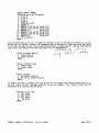
TABLE OF CONTENTS
HARDWARE
HIW PAGE MIllER
Introduction to the QUARK famiLy of singLe board computers
1
Recommended drives for the MegateL QUARK
Recommended monitors for the MegateL QUARK
Recommended keyboards for the QUARK
Required power suppLy for the QUARK
1
1
MegateL QUARK CPU Overview
CPU Memory Management
QUARK Boot Mode Memory Mapping
QUARK Video DispLay Memory
Programming the SAM Registers
QUARK Interrupt System
~~
3
3
5
6
7
7
The QUARK Video DispLay Interfaces
Video DispLay Memory
ALphanumeric Mode
Bit-mapped Graphics Mode
Loading the Programmable Character Generator
12
14
PeripheraL Interfaces
ParaLleL Printer Interface
ParaLLel Keyboard Interface
Full-Duplex Serial Interface
Simplex Serial Interface
Parallel I/O lines
Serial Keyboard Interface
Special I/O Functions
Floppy Disk Interface
Expansion of the Megatel QUARK
15
15
15
16
17
19
20
21
21
22
MisceLlaneous hardware notes for the QUARK
23
9
10
11
SIW PAGE tIllER
SOFTWARE
Software for the QUARK
1
The QUARK Operating System
2
The Megatel QUARK Software Package
CP/M Commands and Utilities
Megatel Utilities and Files
CP/M Users' Group Utilities
4
4
Installing the Customized CP/M System
Operation of a one-drive system
Temporary enabling of the second drive on a two-drive system
Formatting diskettes to make copies
Making backup copies of the Distribution Diskettes
Running the
Selection
Selection
Selection
QINSTALL procedure
"A"-Disk drive hardware specifications
''S''-Diskette formatting specifications
"C"-other peripherals configuration
Final steps in the Installation procedure
New disk format and new CP/M system
6
8
9
9
10
10
11
12
13
~~
--,?
19 - -z.,/
19 __ 2-2--
SlY PAGE MIllER
SOFTWARE
Formatting a diskette under the new format
Writing the new system on a diskette
Booting the new system
Transferring files from the Work Diskette
Mixed Drive Installations
QCERT.COM-The diskette formatting utility
Operation of QCERT
Standard diskette format
QCERT error messages
QCERT parameters
Interlace Tables
QSYSGEN.COM-The System Generation Utility
Standard Disk format
Configuration of CPIM Modules
QSYSGEN Parameters
Parameters for the Source and Destination Drives
Parameters for the Source Drive only
Parameters for the Destination Drive only
Translate Tables
QSYSGEN Parameter Summary
Dpc GA. , c·uv"1
Software for the Video DispLay Interface
CHRLD.COM-The Character Generator Loader
CHRED.COM-The Character Set Editor
GRFLD.COM - The Graphics Mode alphanumeric video utiLity
Loading a Character Set other than the default for GRFLD
Changing the default Graphics-mode Character Set
QTCONFIG.COM - Terminal Code Configuration UtiLity
Floppy disk interface error messages
~l
33
)
/
~r; Z-~
34
~K
1[r
37
38
APPEN>IX PAGE tUl3ER
APPENDIX
ELectrical Specifications
Table I
Table II
Table III
.-
~~~
29
30
30
30
- 1/0 Addresses and functions for the QUARK 64K SBC
-Timer-1 Baud Rates for Full-Duplex Interface
-Timer-2 Baud Rates for Full-Duplex Receiver in
in SpLit Baud Mode
-Simplex Serial Port Baud Rate Selection
Table IV
-Synchronous Address Multiplexer Address Assignments
Table V
-Suggested Values for the Sam Control Register
Table VI
Table VII -Quark Pin Connections and Functions
Table VIII -Quark Peripheral Connections
-Jumper Options
Table IX
Table X
-TerminaL ControL Codes
1
2
4
6
7
8
9
9
12
15
16
Limited Warranty
----------------,
---------------------------All products sold (including software) are under LIMITED WARRANTY on a return to factory
basis against defects in workmanship and material for a period of 90 days from the date of
shipment.
WARRANTY is cont i ngent l4'on proper use of the Product. WARRANTY will not app ly if any
repairs are necessary due to accident, unusuaL physicaL, electrical or eLectro-magnetic stress,
neglect, misuse, or causes other than ordinary use. WARRANTY wiLL aLso not appLy if the
product has been modified by BUYER, or if the product has been disassembled by BUYER.
Disassembly incLudes the removal of the seriaL number labeL on the Product without prior
written approvaL from MEGATEL.
Customer attempted repairs wiLL void the WARRANTY. Any tips suggested in the manual which
involve physical changes to the board or a reconfiguration of the software, if attempted, will
void the WARRANTY.
Copyright Notice and Trademarks
----,---
No part of this document may be copied or reproduced in any form or by any means without
the prior written consent of Megatel Computer TechnoLogies.
Entire contents copyright Megatel Computer Technologies, Toronto, Canada 1985. Printed in
Canada.
"MegateL Quark" is a registered Canadian trademark of Megatel Computer TechnoLogies.
"CP/M" is a registered trademark of Digital Research, Inc.
"Digita L Research", "CP/M Plus", "DDT", "LIB-80", "LINK-80", "ASM", "MAC", "MP/M II", "RMAC",
and "SID" are registered trademarks of Digital Research, Inc.
"Microsoft" is a registered trademark of Microsoft Corporation.
"ZSO" is a registered trademark of Zilog Inc.
"PAL" is a registered trademark of MonoLithic Memories Inc.
"Apple" and "AppLe III" are registered trademarks of Apple Computer Inc.
"Corvus OMNINET" is a trademark of Corvus Systems, Inc.
"IBM" is a tradename of InternationaL Business Machines, Inc.
"Centroni cs" is a registered trademark of Centroni cs Data Computer Corporation.
Disclaimer
MegateL makes no representations nor warranties with respect to any circuitry not embodied
within a MegateL product. MegateL specifically disclaims any implied warranties of
merchantability or fitness for any particular purpose of any Megatel product. MegateL assumes
no responsibility for errors which may appear in this document, and reserves the right to
revise this document without notice.
-------
Service Information
. Should a QUARK board require service please contact the Megatel Engineering office at 416745-7214 for instructions.
Introduction to the QUARK family of single board microcomputers
The QUARK family of microcomputer products comprises a number of high-performance single
board computers and support software, all designed and manufactured by Megatel. Quarks are
designed to provide a II the work ing funct ions of a basic computer on a single, compact board
for the end user, computer OEM and controller markets. The QUARK hardware and software systems
are created as flexible and complete components which allow their users to skip most of the
expensive and time-consuming steps in their systems design, programming and testing.
QUARK hardware is designed to minimize space requirements and parts count, while
si multaneously maximizing processing power, speed, and flexibi l ity. The architecture of the
QUARK/100 serves as the "template" for the enti re fami LYe ALL of the QUARKs share its wide
range of CPU, memory, video, disk and I/O features. The QUARK/100 is avai lable in 3 models,
64K, 1281< or 2S6K of RAM. The QUARK/1S0 adds RGB color capabi l ity to the QUARK/100's list of
features. The QUARK/200 includes an intelligent local area network interface as weLL as every
feature of the QUARK/100. The QUARK/300 extends the QUARK/100's floppy disk capabi l ity by
providing direct control of ST-S06-type Winchester hard disk drives. The Quark/400 combines
all of the features of the forementioned boards and adds real a time clock with battery backup,
EPROM and EEPROM support, yet you need choose onLy the features that you require. Each of the
models is available with various memory and I/O options. Hardware accessories available from
Megatel include connectors, and transition boards for quick connections to drives, monitors and
other I/O devi ces.
QUARK software consists of configurable operating systems, compLete device drivers,
utiLity programs, an instaLLation procedure, and source code on disk. QUARK software is
distributed on fLoppy disk and in a form which aLLows it to boot up immediateLy assuming the
"lowest common denominator" in user hardware.
An SBC package purchased from the factory shouLd include the foLLowing items:
-Quark 64K SBC single board computer (or which ever modeL was ordered)
-GTB-3 Quark Transition Board
-Megatel's hardware and software manual which includes a QTB-3 manual
-Software on either 5.25" or 8" diskettes
------.------------------------------------------.--------------------------------
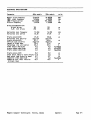
Recommended drives for the Megatel QUARK
The QUARK is designed to interface easi ly with most 8-, 5.25-, and 3.S-inch floppy disk
drives. You shouLd be aware, however, that disk drive specifications vary widely from
manufacturer to manufacturer.
Megatel has tried and tested a variety of floppy disk drives and the foLLowing is a list
of drives which we recommend as being particularLy well-suited for use with the QUARK.
Manufacturer
Shugart
Shugart
Sony
Shugart
Shugart
Shugart
Model#
SA-300
SA-3S0
OA-D30V
SA-400
SA-4SS
SA-46S
Size
3.5"
3.5"
3.5"
5.25"
5.25"
5.25"
Megatel Computer Technologies Toronto, Canada
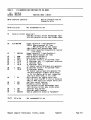
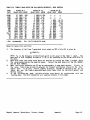
Manufacturer
Model#
Size
Tandon
Tandon
Tandon
Tandon
Teac
Shugart
Tandon
TM100-1A
TM1(x)-2
TM100-3
TM100-4
FD-S5F
SA8S0/8S1
TM848-2
5.25"
5.25"
5.25"
5.25"
5.25"
8"
8"
Page H/W-1
On the QTB-3 there is a 34-pin header denoted by J3. A standard 5.25 inch floppy disk
cable will plug into this board in this area and connect directly to the edge connectors of
your floppy disk drives. This same 34-pin header is used for connecting 8 inch drives. This
can be done by taking a regular 50 pin ribbon cable and replacing the 50-pin female header with
a 34-pin female header. Strip away lines 48 through 50 and 1 through 13 to give you the
required 34 position cable. Either set of cable can be purchased from Megatel.
To allow a mixed 5.25 and 8 inch system Megatel can supply a cable which provides both a
34-pin and a 50-pin connector. Assembl ing your own mixed drive cable, although possible, is
difficult due to the difference between 8 and 5.25 inch drive interfaces.
The next step, for a mixed drive system, is to wire wrap from the floppy disk data
transfer rate (pin 8-17 on the 96-pin DIN connector) to the drive select line (see appendix for
pinout) you have chosen for your 8 inch drive. This allows the data transfer rate to switch
automatically with drive selection.
Notes regarding Floppy Disk Drives:
Megatel Quarks do not provide a MOTOR ON signal. Most 5.25 inch drives wi II provide a
jumper option on the drive motor control board to have the motor come on with the selection of
the drive. Please consult your drive manual to insure this is done before you try to boot up
the system.
Some 5.25 inch drives have a READY signaL. If you are using such a drive, you must
isolate the READY line in a mixed drive installation. If you are using an 8 and 5.25 inch
drive system the READY line should be taken directly from the QTB-3 to the 8 inch drive, while
bypassing the 5.25 inch drive.
MegateL Quarks do not provide a HEAD LOAD signal for 8 inch drives. Most 8 inch drives
wiLL have a HEAD LOAD with drive select jumper option on the drive motor control board. Please
consult your drive manual to ensure this is done.
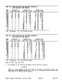
Recommended Monitors for the Megatel QUARK
Many direct-drive and composite monitors can be used successfuLly with the QUARK. The
user should beware, however, that some of the cheaper composite monitors on the market could
operate poorly. The most common difficulty with such monitors is their inability to display a
full 80 characters. This is because they do not meet the tight timing requirements of the
Quark composite signal's horizontal retrace time.
These monitors can sti II be used if the
number of characters per row is reduced through software modifi cations.(only on SBC's with
graph i cs opt ions)
Before purchasing any monitor check with the vendor to see if you wi II be allowed an
evaluation period. This is the best way to avoid possible disappointment.
The following is a list of recommended monitors that display a full 80 characters per row:
Manufacturer
Zenith*
Electrohome
ELectrohome
Model#
ZVM-121
EVM 1220
EVM 1519
Input Type
Composite
Composite
Composite
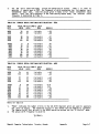
Manufacturer
Model#
Input Type
Electrohome
Electrohome
EVM 1719
EVM 2319
Composite
Composite
*Note - The Zenith ZVM-121 is a widely excepted monitor which works well with the Megatel
QUARK. The Zenith ZVM-121 is avai lable at most retai l chains and sells for approximately
$100.00.
Megatel Computer Technologies Toronto, Canada
Page H/W-2
-------,----------------.--------------------------,
Using the Megatel QUARK with a television
....-----------------------------_.------..-.-----------------Using a commercially available RF converter the Megatel QUARK can use a black and white
televsion as a monitor.
As with some of the cheaper composite monitors, this method does not allow the display of
a full 80 characters.
Recommended keyboards for the QUARK
Any ASCII-encoded 7- or 8-bit parallel-output keyboard with active-high DATA outputs and
an active-low STROBE output will work with the QUARK.
Note that a computer terminal (or its equivalent) with a full-duplex RS-232C asynchronous
serial interface capable of operating at 1200 baud can be used instead of a monitor and
keyboard.
If using a, terminal simply connect it to the 25-pin D-shell connector at location J5 on
the QTB-3 making sure it is set at 1200 baud. Adjacent to the 25-pin D-shell is a dual row 26pin header at location J4. This too is the full duplex RS-232C port.
You wi II notice that two pairs of headers have been wire wrapped together. If you are
using a terminal they may be cut only if your terminal supports the protocol involved (CTS to
RTS, DTR to DSR).
--_.. -----------------------.------
Required power supply for the QUARK
The Megatel QUARK requires a regulated +5 and +12 volt supply with a common ground. These
are the same voltages requi red by 5.25-inch floppy disk drives. The current drawn by a QUARK
128K SBC at +5 volts is 2A. The current requi red at +12 volts is about 100mA. If this supply
must also supply power to operate the floppy disk drives, a monitor, and a keyboard, then the
power requi rements of these devi ces must be a llowed for.
The color scheme for the DC power cable enclosed with the package is:
RED •••••••••••• +5
BLACK •••••••••• GRD
ORANGE •• ~ •••••• +12
The -12V required by the RS-232C drivers on the QUARK is developed by an on-card charge
pump, so no negative power supply is necessary.
If a QUARK-based system fails to operate properly, the power supply connections and
voltage levels in the system should be one of the first things to be checked. Be aware that
reversed or incorrect polarities may cause damage to the QUARK which is not covered by
Megatel's limited warranty.
The power supply chosen for a system must be able to handle normal current surges. Some
QUARK users have experienced video display or CPU problems because their power supply was not
able to maintain +12 and +5 volts during periods of disk drive activity. Since the QUARK is
largely TTL logic, the +5V supply must never fall below +4.7SV.
Megatel Computer Technologies Toronto, Canada
Page H/W-3
Megatel QUARK CPU Overview
------------------------------------ -----,-------------------The Megatel QUARK uses the I80B microprocessor, manufactured by lilog Inc. The 180B clock
frequency is 5.97MHz (6.2MHz on 50 Hz models), leading to an execution time of 667ns (645ns on
50 Hz models) for a typical 4-cycle instruction, such as a register-to-register ADD.
The main memory of the QUARK is either 64/128/256kbytes in size. A memory-management
scheme employing the 18OB's I-register is used to provide simple yet flexible bank-switching to
allow the full use of the extended physical memory. The Synchronous Address Multiplexer (SAM)
also participates in the memory-mapping process, and permits the use of some special mapping
modes.
To accomodate the Video Display Interface, the main memory of the QUARK operates as a
dual-ported RAM. One of the ports is a bidirectional input/output port to the CPU, while the
other port is essentially an unidirectional output-only port for the Video Display Interface.
Through the programmable registers of the SAM, the size and location of the area of main memory
used as the Video Display Memory can be set under software control.
As a consequence of the operation of this dual-ported memory, all 180B memory cycles have
wait states added to extend them to a multiple of 4 T-states. Thus an instruction which would
execute in, say, 7 T-states if no wait states were added wi II have one wait state added, to
extend the instruction to 8 cycles. The insertion of these wait states is fundamental to the
synchronization of memory accesses by the Video Display Interface and by the cpu.
Input/output instructions are also extended to modulo-4 cycles, but then have four
additional wait states added. For instance, an 11-state IN A,r type of instruction will have a
total of five wait states added, extending it to 16T-states. The addition of the extra four
cycles relaxes the speed requirements for the peripheral controller devices, both those on the
board as well as user-added external controllers.
CPU Memory Management
The I80B processor used on the QUARK has a sixteen-bit address bus, and is therefore able
to di rect ly address 65536 (64k) locat ions in memory. However, the QUARK has 128k of memory,
and therefore a process is required whereby the 64k possible addresses generated by the CPU are
"mapped" into the 128k of main memory provided. In this discussion, the addresses generated by
the CPU on its Address Bus wi II be called "logical addresses", whereas the actual locations in
memory where data is stored will be called '~hysical addresses'~ Logical addresses are
therefore the hexidecimal values normally used in programming.
The ISO's I-register and the Synchronous Address Multiplexer (SAM) are used in the mapping
process between the logical and physical address spaces. The I-register is used to control
bank-switching between bank A and bank B of the main memory, and to determine in which bank the
Video Display Memory is located. The SAM determines the location of the Video Display Memory
within a 64k address space, and controls the mapping of the upper and lower halves of the
logical address space.
The most-significant three bits (bits 5, 6, and 7) of the I-register are used to define an
8k address boundary within the CPU's 64k logical address space. Any logical address appearing
on the Address Bus is compared to the address boundary as determined by these bits. The result
of this comparison determines in which memory bank the physical address is to be found.
If the value of the logical address is greater than or equal to the specified address
boundary, the logical address wi II be mapped onto a physical address (that is, a memory
location) in memory bank A. Conversely, if the value of the logical address is less than this
boundary, then the logical address wi II be mapped onto a physical address in memory bank B.
For example, if bits 5, 6, and 7 of the I-register were all zero, then the address boundary
Megatel Computer Technologies Toronto, Canada
Page H/W-4
specified would be 0000. Since all logical addresses are greater than or equal to 0000, then
the CPU's entire logical address space would be mapped into the physical address space of bank
A. If bits 6 and 7 were set and bit 5 were clear (I-register = C0), then logical addresses
between gggg and BFFF would be mapped onto physical addresses in bank B, whiLe logicaL
addresses equal to or above C000 wouLd be mapped onto physical addresses in bank A.
To read or write the contents of the I-register the ZSO's LD A,I and LD I,A instructions
are used. After changing the vaLue in the I-register, the new boundary wi Ll take effect after
the next opcode fetch. Consider the following code sequence:
LD A,BDYVAL
LD I,A
RET
iLOAD A WITH NEW BOUNDARY VALUE
iLOAD I WITH VALUE
iRETURN
The return address used for the RET instruction wiLL be popped off the stack in the memory
bank determined by the new boundary vaLue in the I-register, whereas the opcode for the RET
instruction wiLL be fetched from the memory bank in effect prior to loading the new value into
the I-register.
Note that the use of the ZSO I-register for seLecting bank-switching boundaries precludes
its usuaL use in the ZSO Mode 2 (vectored) interrupt.
It might appear that a difficulty with this method of bank-switching is that there is no
logi cal address which maps onto any physi cal address above E000 in bank B, that is, that the
top 8k of bank B cannot be directly accessed by the CPU. This would seem to be the case
because the highest 8k address boundary which can be specified by bits 5, 6, and 7 of the 1register is E000, so that logical addresses above E000 wi II always be mapped onto physical
addresses in bank A, and never in bank a This probLem can be overcome through the use of the
MPA TYPE and PAGE MODE bits of the SAM, as expLained beLow.
The MAP TYPE bit in the SAM (designated '7Y'~ aLlows addresses in either the upper of the
Lower halves of the 64k logical address space to be effectively translated into the other half
of the logicaL address space. In the "normal" mode of operation (the mode which is initial ized
at power-up) the TY bit is set. In this mode, each logical address is mapped onto a unique
physical address in bank A or bank B by mapping process described previously. If, however, the
TY bit is cleared, then the upper and lower haLves of the 64k logical address space map onto a
physical address space whose size is between 32k and 64k. The actual size and location of the
physical address space within the two Main Memory Banks is determined by both the bankswitching boundary set '-" in the I-register and by the PAGE MODE bit in the SAM (designated
"P1"), as described below.
With both the MAP TYPE and the PAGE MODE bits cleared, the position of the bank-switch
boundary will determine both the bank into which the logicaL addresses are mapped as well as
whether the mapping is one-to-one or many-to-one. Consider first the simplest case, where the
bank-switch boundary is 8000hex. In this special case, logical addresses less than the bankswitch boundary will be mapped into the physicaL address space of bank B, just as they would be
if the MAP TYPE b it were set ("Norma lit mode). However, log i ca l addresses equa l to or greater
than the bank-switch boundary are mapped alto physical addresses in the 'bottom" half of bank
A. This part of the physi cal address space of bank A is the space into whi ch logi cal address
from 0 to 7FFFhex are mapped when the bank-switch boundary is set to 0000 and the MAP TYPE bit
is set (normal mode). Thus logical address from 8000 to FFFFhex are essentialLy translated to
0000 to 7FFFhex. Note, however that this is still a one-to-one mapping, since each half of the
logical address space is mapped into the bottom half of a distinct Main Memory Bank.
Continuing with the case where the bank-switch boundary is at 8000hex and the MAP TYPE bit
cleared, the effect of the PAGE MODE bit is to determine whether it is the upper or lower half
of the logical address space which is mapped into a ''foreign'' part of the physical address
space. As explained above, if the PAGE MODE bit is cleared, the upper half of the logical
address space is mapped into the bottom half of bank A, whiLe the lower half is mapped into the
lower half of bank B. If, instead, the PAGE MODE bit is set, then the upper half of the
logical space wi II be mapped into the LPper half of bank A. This is the physical space into
which the upper half of the logical space would be mapped if the MAP TYPE bit were set. The
Megatel Computer Technologies Toronto, Canada
Page H/W-5
lower haLf of the logical address space is now mapped into the upper haLf of bank B.
With the MAP TYPE bit cleared and the PAGE MODE bit set, it becomes possible to access the
otherw ise-hidden upper Bk of bank B. Setting the bank-sw itch boundary to 8000H, as in the
description above, forces logical addresses from 0000 to 7FFFhex to be mapped onto physical
address in bank B from 8000hex to FFFFhex, a range which includes the hidden Bk. Thus the
logical address range 6000hex to 7FFFhex wiLL be mapped onto the upper 8k of bank B.
By appropriately setting the F-bits in the SAM controL register and bit 0 of the 1register, it is possibLe to position the Video Display Memory so that this hidden 8k region is
used for all or part of the Video DispLay Memory. Table V in the Appendix gives suggested
vaLues for the F-bits and the resultant Video Memory address boundaries.
-----------------------------------------------------------,--------------.-------
QUARK Boot Mode Memory Mapping
-----------------------------The QUARK has a speciaL memory-mapping mode which is used after the system has been reset
by a low-level signaL at the RESET input, or when the internaL BOOT MODE Line has been set.
This memory mapping mode is caLLed the Boot Mode. This mode is used when the system is Loaded
from the fLoppy disk drive (in a so-caLled 'bootstrap" manner), and whenever the SAM control
registers are to be written.
In this mode, any memory read operation by the CPU (incLuding instruction fetching) wiLL
read from the contents of the 512-byte Bootstrap PROM, rather than from Main Memory. Memory
write operations wi LL write to Main Memory, using the memory mapping process described. I/O
read or write operations wiLL reference I/O ports in the usual way, except that the Character
Generator (I/O addresses 00-3F) cannot be written when in the Boot Mode.
When the QUARK is reset, the registers of the ZSOB, incLuding
cLeared. ALso, various I/O Lines on the VIA and PIA are cLeared and
particular, the BOOT MODE controL line, which is the CB2 controL line
to act as an input, aLLowing a pullup resistor on this line to assert
the Program Counter, are
set to act as inputs. In
on the PIA, will be reset
a "BOOT MODE" condition.
The Z8(B wi Ll now fetch the instruction at location 0000. Since the BOOT MODE control
line is high, this wi LL cause the instruction at Location 0000 of the Bootstrap PROM to be
fetched. Successive instructions wi II be fetched from the PROM unti l the BOOT MODE controL
line is cleared to a Low-LeveL output condition. This puts the QUARK into the NormaL Mode of
operation, where all memory read or write operations wi LL reference the Main Memory. In the
NormaL Mode, the PROM cannot be accessed.
The Logical address space occupied by the Bootstrap PROM consists of the first 64
addresses (i.e. 00-3Fhex) of each 256-byte page in memory. Thus the entire PROM can be
accessed in eight 64-byte "chunks" in the bottom 2k of memory. This logicaL address space is
aliased between 0000 and 073F(hex) are used in accessing the Bootstrap PROM.
Addresses between the 64-byte chunks cause I/O read or write operations. It is not
recomended that these addresses be used. I/O operations may be performed in the usual manner
using I/O instructions while in the Boot Mode.
It shouLd be pointed out that it is unlikely that the user wilL ever need to directly use
the Boot Mode of operation, nor is it ever necessary to directly access any part of the
Bootstrap PROM. After the operating system has been booted from the floppy disk, the only
operation requiring a return to the Boot Mode is when the SAM controL registers are to be rewritten. In this case, a special routine called the SAM Loader Access Routine, resident on the
bottom page of Main Memory, wiLL automaticaLLy handLe the entry into and return from the Boot
Mode.
Megatel Computer TechnoLogies Toronto, Canada
Page H/W-6
QUARK Video Display Memory
--------,------------------------------,--------------------------------------The size of the Video Display Memory and its location within the 128k Main Memory are
under the control of registers in the SAM and by bit 0 of the I-register.
Bit 0 of the I-register determines in which memory bank the Video Display Memory is
located. When this bit is clear, the Video Display Memory is located entirely within bank A,
and when it is set, the Video Display Memory is located entirely within bank B. The bank
switching apparatus for the Main Memory using bits S-7 of the I-register does not apply to
addresses generated by the Video Display Controller, but only to addresses generated by the
CPU, regardless of whether these CPU addresses fall within the Video Display Memory or not.
In either bank A or bank B, the physi cal address boundaries of the Video Display memory
within the selected bank are determined by the settings of bits F0, F1, F2, F3, FS, and F6 in
the SAM control Register, and by the Video Display Mode (ALPHA or GRAPHICS). The starting
address (or the lower bound) of the Video Display Memory is the binary address
(F6)(FS) (F3)(F2) (F1 )(FCI )Cla
(laCia aaaa,
where (Fn) represents the contents on the Fn bit in the SAM Control Register. The final
address (or the upper bound) of the Video Display Memory depends on the Video Display Mode. In
Alphanumeric Mode, the final address is the first 16k address boundary followimg the starting
address, whereas in Graphics Mode, the final address is the second 16k address boundary
following the starting address.
From the above, it can be seen that the size of the Video Display Memory may be set
anywhere from zero to 32k in 1024-byte increments. However, only a certain set of sizes are
likely to be of use in most applications. First, when operating in Graphics mode, the size of
the Video Display memory must be an integer multiple of 3k (3072) bytes in order for the
horizontal sync signal to be generated correctly. Second, if it is desired to have the
Vertical Sync fre~ency match the fre~ency of the local AC power system (to avoid moving "humbars" on the CRT and related phenomena), the size of the Video Display Memory must be adjusted
so that its entire contents wi II be read and displayed once during one cycle of the AC power
line. In practice, this means that the most useful sizes are likely to be:
LIN: FREQ.
MODE
SIZE
GRAPHIC
ALPHA
GRAPHIC
30k
4k
24k
----------_.----------.----ALPHA
Sk
50Hz
50Hz
60Hz
60Hz
In order to achieve a Vertical Sync frequency of exactly 50 Hz or 60Hz, it is necessary
that the appropriate frequency crystal be used in the Master Clock generato~ Thus it is not
possible to generate a 50Hz vertical sync frequency on a board equipped with a crystal intended
to ~ermit operation at 60Hz, and vice versa. However, a "60Hz" QUARK can be programmed to
operate with a Vertical Sync fre~ency of 48.1Hz, and a "50Hz" QUARK can be operated at 62.5Hz.
See Table VI in the Appendix for suggested settings and the resultant address ranges.
Note that the F4 bit in the SAM in not used in determining the starting address of the
Video Display Memory, and must always be set. Bits 1 through 4 of the I-register are "don't
care" bi ts, and have no effect on the ope rat i on of the QUARK.
Megatel Computer Technologies
Toronto, Canada
Page H/W-7
Pnogramming the SAM Registers
---------,
The Synchrorous Address Multiplexer (SAM) is an essential part of the CPU, and the Video
Display Interface.
The Control Registers of the SAM are initia l ized by the Bootstrap PROM after a system
reset. It may be necessary at some time to change some of the values in the Registers of the
SAM. To allow the user to do this, a special routine is automatically loaded into Page Zero of
of the Main Memory. This routine is called the SAM Loader Access Routine, since it provides
access to the SAM Register Loader routine in the Bootstrap PROM.
To set or clear any of the SAM registers, the address corresponding to the register is
loaded into the HL register, and then the SAM Register Loader Access routine at location
000Bhex is caLled. For exampLe, the folLowing sequence wi II clear register F1:
LXI
CALL
H,0FF88H
00QJBH
iLOAD ADDRESS FOR F1-CLEAR
iCALL SAM LOADER ACCESS ROUTINE
Table V in the Appendix Lists the addresses to be used for clearing or setting each of the
registers in the SAM, as weLL as indicating the functions of some of the register for the
QUARK. Note that only some of the registers are ever likeLy to be changed. Even though there
are ro actual restri ctions on the settings for any of the registers, only a particuLar set of
combinations is useful on the QUARK.
Table VI indicates the useful set of vaLues for the F-registers. Registers F0, F1, F2,
F3, F5, and F6 are used in determining the starting address of the Video Display Memory. The
location of the Video Display Memory which results from each of the combinations is also shown
in Table V.
If it is necessary to use the area of Main Memory occupied by the SAM Loader Access
Routine, then the routine can be copied to the corresponding location in any 2k block of
memory. OnLy the section of the Access Routine between locations 000BH and 0017H incLusive
need be cop i ed.
For instance, if the area from 000BH to 0017H is copied into the area from F00BH to F017H,
then the folLowing exampLe wilL have the same effect as the previous example:
LXI
CALL
H,0FF88H
F00BH
iLOAD ADDRESS FOR F1-CLEAR
iCALL SAM LOADER ACCESS ROUT
QUARK Interrupt system
On the QUARK both of the two Z8{)3 interrupt inputs 'NJ8IT and lNT are used.
The maskable
interrupt input
is wired-ORed to the interrupt request outputs from the VIA, the PIA, and
the ACIA. The non-maskabLe interrupt input Nlrr is connected to the 1793 Floppy-disk
Controller's Data Request output (DRQ) through an inverter.
m
Interrupt requests from each of the VIA, PIA, and ACIA can be individually enabled or
disabled by writing to the appropriate control registers in these devices.
The Verti caL Sync Line is connected to the CA1 input of the PIA. Since the frequency on
this line is rormally 60Hz, the CA1 input can be used to generate a real-time clock interrupt
to the CPlL Note that if the si ze of the Video Display Memory is changed from the "standard"
sizes for ALphanumeric and Graphics Modes, the Vertical Sync frequency wi II change
proportionately. Thus, if the VerticaL Sync Frequency is changed, any software which relies on
this interrupt as a ti me base shouLd take this into account.
~
~
The Interrupt Request line INTRQ from the 1793 Floppy-disk Controller is connected to the
input on the VIA. Thi s interrupt output is set at the completion of any command to the
G~\'1\
.
Megatel Computer Technologies Toronto, Canada
Page H/W-8
1793. In order for the 1793 to interrupt the CPU, the CB1 interrupt on the PIA must be enabled
for low-to-high transitions on the CB1 pin.
The Floppy-disk Controller's Data Request output is set each ti me a byte is ready for the
CPU or each time the controller is ready to receive a byte from the CPU. The DRQ output is
inverted to drive the 'FJRr input. When transferring data, the DRQ signal wi II go active at a
rate proportional to the data transfer rate for the floppy disk drives in use. The QUARK is
suffi cient ly fast so that even with the worst-case data transfer rate (SOOkbits/second for 8inch double-density disks), only 70% of the CPU's time is used in moving data between the
controller and main memory. This Leaves 30% of the processor's capacity avai Lable to perform
other operations. The left-over capacity is essentiaL in certain applications, such as when an
interrupt-driven communications routine must continue despite data transfers to or from the
disk. Lesser transfer rates will of course leave correspondingly more of the CPU's time
availabLe.
Version 2.2 operating systems pLace a jump instruction at location 38hex in both bank A·
and bank a In bank A, the jump address points to the interrupt handLer for the INT interrupt
in the BIOS. In bank B, the jump address points to the entry point of a special routine in the
BIOS. This routine saves the current value in the I-register (which determines the bankswitching boundary when the interrupt occured), sets the bank-switching boundary to location
0000 (so that alL CPU memory is in bank A), and then pushes a speciaL retum address onto the
stack. The routine then jumps to Location 38hex in bank A. This causes the interrupt to
proceed as it would have if the bank-sw itching boundary had been at location 0000 when the
interrupt occured.
When the routine handl ing
stack. If this retum address
handler, then control will be
former bank-switching boundary,
the interrupt returns, it wi II pop the return address off the
is the special address pushed earL ier by the bank B interrupt
transferred back to this routine. It will then restore the.
and retum from the original interrupt.
The version 2.23 and 2.24 operating systems distributed with the QUARK enables only two
interrupt sources, the reaL-time cLock interrupt from the CA1 input on the PIA, and the 'NMT
interrupt, whi ch is connected to the 1793 fLoppy-disk controL ler's DRQ output. When an !NT
interrupt occurs (which vectors to Location 38hex), the interrupt handler in the distributed
version of the BIOS does not verify that the source of the interrupt is the reaL-time clock.
Instead, it immediately updates the displayed clock on the screen, if the system was instaLLed
with the cLock option.
In order to use other interrupt sources on the QUARK, the user may either patch the source
file for the BIOS himseLf, or incLude in the appLication program sufficient code to handle the
addit iona L interrupts.
For the latter approach, the general idea would be for the application program to save the
jump address at locations 39hex and 3Ahex, and replace them with a pointer to the interrupt
entry point in the program. When an interrupt occurs, the application program would check for
the source of the interrupt, and take the appropriate action if the interrupt was intended for
use by the application. If the interrupt was not for the application program, then the program
should jump to the regular interrupt entry point in the BIOS, the address of which was saved by
the application program initialLy. Thus the BIOS routine wiLL have its opportunity to respond
to the interrupt.
Notice that the mechanism handLing interrupts which occur while operating in bank B wiLL
mesh perfectly with the above approach. Of course, the user is free to handLe bank B
interrupts in his own way.
The 'flMT interrupt is largely a system rather than a user feature on the QUARK. The
operating system always handles the NAT interrupt from the fLoppy disk controLler in an
appropriate fashion. No mechanism is provided by the operating system for trapping bank B NMI
interrupts, as none are expected.
Megatel 'Computer Technologies
c;...-
Page H/W-9 ~ ~
Toronto, Canada
__ ---..~:
,_._,-----------_.
The QUARK Video Display Interfaces
._-
.
The QUARK Video Display Interfaces
-----------------
The on-card Video Display Interface is an integral part of the Megatel QUARK~ It is
capable of operating in either Alphanumeric or Graphics modes. TTL-driven video, horizontal
sync, and vertical sync signals are provided for connection to direct-drive CRT data displays.
Additionally, a composite video output at approximately 1V p_p is provided for use with
monochrome displays with composite video inputs.
The data displayed on the CRT are stored in a segment of the Main Memory of the QUARK.
The meory bank in which the Video Display Memory is located is determined by bit 0 of the CPU's
I-register.
In Alphanumeric mode, a total of 32 character rows are scanned for each video frame on the
60Hz version (assuming a 60Hz frame rate) and 40 rows on the 50Hz version (assuming a 50Hz
frame rate)_ However, not all of the scanned rows may be displayed. The first row, which
represents data within the first half-page of the Video Display Memory, is displayed during the
Vertical Retrace Period. There being no hardware mechanism to bLank the video output during
the VerticaL Retrace period, this part of the Video Display Memory must be loaded with data
that will generate a nuLL video output. The simplest manner in which to do this is to load 00
bytes into that part of the Video Display Memory which is scanned during the retrace period.
The Bootstrap PROM routine loads a 'bLank" character into the Character Generator for the 00
character code, so that when a row of 00 bytes is displayed, no video output will result.
The second line of the display can be used for display purposes if the CRT monitor
employed terminates the Vertical Retrace Interval sufficiently quickly. On many monitors,
however, characters displayed in this row will appear slanted because of the monitor's
inability to recover from the Vertical Retrace Interval in time to properly display the first
severaL scan lines. Thus the video driver routines included with standard QUARK operating
systems do not use the second displayable row on the video display.
The QUARK is equipped with a Programmable Character Generator. This allows the eight-bit
by eight-bit patterns for the characters displayed on the CRT to be loaded or altered under
software control. Custom character sets may be designed, saved on floppy disk, and loaded when
needed. This si mpL ifies the task of accomodating appL i cation programs requi ring Languages
other than English, or running programs using special symbols, or of using programming
languages which employ special character sets (e.g. the APL programming language). Whi le
normaLly an entire character set <256 characters) would be loaded as one step (as is done by
the uti l ity programCHRLD.COM) character patterns can be loaded or modified on a byte-by-byte
basis, so it is not necessary to load an entire set of characters. This may permit special
video effects in some applications.
The Programmable Character Generator used on the QUARK is a 2048-byte static memory which
is independent of the Main Memory. A uti Lity routine to load the Programmable Character
Generator with a standard character set as the operating system is booted is included with the
QUARK operating system software. ALso incLuded is a character set editor utiLity, which can be
used to customize the standard character set or to create new character sets. These userdefined character sets can be saved on a fLoppy diskette.
The Bit-mapped
to be displayed on
mapped onto single
display (typically)
models, 30k is used
Graphics Mode of the Monochrome Video Display Interface aLLows graphic data
the CRT. In this mode, individuaL bits in the Video Display Memory are
dots (pi xeLs) on the CRT. For 60Hz models, 24k of Main Memory is used to
143,360 pixels, organized. as 640 horizontaLly by 224 vertically. On 50Hz
to display (typically) 179,200 pixels, organized as 640 by 280 pixels.
Megatel Computer Technologies Toronto, Canada
Page H/W-9'"
Video Display Memory
,---------------------
The size and location of the Video Display Memory within the Main Memory of the QUARK is
under software control through the vaLues stored in the control register of the SAM, as well as
by the value in the Z-BOB's I register. The size of the Video Display memory may be set to
values between 1k and 32k, although only certain memory sizes are appropriate, as will be
expLained below. The starting address for the Video DispLay memory is determined by the values
loaded into the F6, F5, and F3 to F0 bits of the SAM Control Register. (Bit F4 is not used
in the determination of the starting address~ The top address of the Video Display Memory is
determined by the mode (Alphanumeric or Graphics) and by the values of the SAM Video Display
Counter bits corresponding to F3 and F~ The Video Display Interface reads 96 consecutive bytes from the Video Display Memory for
each raster scan line displayed on the CRT. In Alphanumeric mode, these 96 bytes are the last
96 of each half-page (128 bytes) within the Video Display Memory. The first 32 bytes of each
half-page are not read by the Video Display Interface in Alphanumeric mode.
In Graphics mode, the 96 bytes scanned for each line displayed are contiguous within the
Video Display Memory. Thus there are no unscanned memory areas within the Video Display Memory
when operating in Graphics mode.
In both di sp lay modes, the second through si xteenth of the 96 bytes, plus one more from
the displayed 80 bytes, are read during the horizontal retrace interval between succesive scan
lines on the CRT monitor. The Video output is blanked during this interval, so the contents of
these bytes will not directly cause any visible output on the CRT. The last eighty bytes
contain either the ASCII codes to be translated into character data on the CRT, or the graphic
information to be displayed as pixels.
In the Alphanumeric mode, the same 96-byte block is read eight times for each character
row displayed. It is necessary to do this because each character row is bui lt ~ from eight
raster scan lines, each line adding one horizontal "slice" of the character patterns. The
ASCII code for each of the eighty characters in the row must be read eight times while the Scan
Line Counter counts from 0 to 7.
The Graphics mode operates in a similar fashion to the Alphanumeric mode, except that each
of the sets of 96 bytes is read only once for each raster scan line displayed, rather than
eight times as in the Alphanumeric Mode. In the Monochrome Video Display Interface, the data
in the last 80 of the 96 bytes is sent di rect ly to the Video Shift Register, bypassing the
Character Generator. Thus the pattern of bits in each of the 80 bytes determines the pattern
of pixels displayed on each scan line of the CRT. Since 80 bytes of eight bits each are read
for each line, a total of 640 pixels can be displayed horizontally. The most-significant bit
of each byte (bit 7) is the first bit shifted out by the Video Shift Register, and thus appears
on the CRT as the left-most pixel of each group of eight.
The time requi red to read the 96 bytes from the Video Display Memory determines the
Horizontal Sync pulse period and frequency. Four Z-80B T-states are required for each byte
read. Thus the Horizontal Sync frequency is 15.540kHz (64.368 us), and on the 50Hz version it
is 16.1145kHz (61.939 us).
In the Graphics mode, the top address of the Video Display Memory is equal to the output
from the Video Counter at the time when the Video Counter bits corresponding to F3 and F4 reach
QJ and 1, respectively.
In Alphanumeric mode, the top address is such that the Video Counter
bit corresponding to F4 reaches zero. Thus in Alphanumeric mode the top address of the Video
Display memory is the address of the first 16k boundary following the starting address minus
one. In Graphics mode the top address is the address of the second 16k boundary following the
starting address minus one.
Megatel Computer Technologies Toronto, Canada
Page H/W-10
The VerticaL Sync frequency is determined by the dispLay mode, the size of the Video
Display Memory area, and the master clock frequency. The exact Vertical Sync period is given
by
tv = (96(n+2) + 88)
* te,
where n is the number of scan lines being displayed, and te is the period of the e-clock. On
the QUARK, this is 670ns. In ALphanumerics mode, the number of dispLayed lines is the Video
Display Memory size (in bytes) divided by 16, whiLe in Graphics mode, it is the Video DispLay
Memory si ze di vi ded by 96.
For a 60Hz Vertical Sync frequency, the Video RAM area should be 4k in ALphanumeric Mode,
and 24k in Graphics Mode (assuming that the master clock frequency is 23.86176Mhz, as is the
case for the "60Hz" versions of the QUARK). For a 50Hz Vertical Sync frequency, the memory
sizes should be 5k and 30k, respectively (assuming the 24.8MHz master clock frequency used on
"50Hz" versions of the QUARK).
If it is not necessary for the Vertical Sync frequency to be exactly 60Hz then one is free
to pick the starting address of one's choice. The starting address of the Video Display Memory
may be pLaced on any 1k address boundary, although in Graphics mode only 3k boundaries will
result in a prpoer HorizontaL Sync signal. For example, a 60Hz board could be operated in the
Graphics mode with a Video Display Memory size of 27k instead of 24k. This larger size wouLd
result in a vertical sync frequency of 53.4Hz, with a total of 288 Lines per frame, instead of
256. The horizontal sync frequency wouLd remain unchanged at 15540Hz.
See Table VI in the Appendix for SAM Control Register values needed to select various
Video Display Memory sizes and locations.
Alphanumeric Mode
-----------------.-----
------._-_.-------------------
In Alphanumeric Mode, data stored in the Video Display Memory are interpreted as eight-bit
character codes. These codes are fetched from the 96 scanned locations in each half-page of
the Video Display Memory and presented to the input of the Character Generator. The Character
Generator contains the patterns which represent the characters to be displayed on the CRT.
The standard character set for the QUARK uses characters formed from a 5-by-7 matrix of
dots. This matrix is imbedded in a larger 8-by-8 background field. The background field is
effectively part of the character; in the standard QUARK character set the top row of dots and
the first two and the last columns of dots for each character are bLank to provide the
necessary space between adjacent characters. The standard character set incLudes 128 "normal
video" characters and 128 "reverse video" characters, and is desi gned to use seven-bit ASCII
codes. The reverse video characters are essent ia LLy a second set of 128 characters where the
dots forming both the character and the background are inverted from the corresponding normaL
video characters. In the standard character set, a reverse video character is dispLayed
whenever bit 7 (the most significant bit) of any 8-bit vaLue stored in the Video Display Memory
is set. The remaining seven bits form the ASCII code for the character that is to be
displayed.
There are no extra dot columns or dot rows between the 8-by-8 background fields of each
character, that is, that the 8-by-8 fieLds completeLy fi Ll the displayable area of the screen.
Thus it is also possible to create graphic characters (as distinguished from Bit-mapped
Graphics, below) which aLlow continuous Lines, bars, and other figures to be displayed on the
screen in Alphanumeric Mode.
Megatel Computer Technologies Toronto, Canada
Page H/W-11
------------------------------------------------------------------------------
Bit-mapped Graphics Mode
In the Bit-mapped Graphics Mode, the Monochrome Video Display Interface fetches data from
the Video Display Memory in exactly the same manner as is used in the Alphanumeric mode.
However, instead of this data going to the character generator (together with the three Scan
Line Counter bits), the data goes directly to the Video Shift Register. Thus the patterns of
"ones" and "zeroes" stored in each byte of the displayed portion of the Video Display Memory
will directly determine which oots, or pixels, are illuminated on the CRT.
Because the Character Generator is not used to map eight-bit bytes onto eight-by-eight dot
patterns in the Graphics Mode, eight times as much memory must be allocated for the Video
Display Memory when operating in Graphics Mode as when in Alphanumeric mode. Note, however
that in Graphics mode the 96-byte blocks scanned for each raster line displayed are contiguous
in the QUARK's Main Memory, whereas in Alphanumeric Mode, these blocks have 32-byte gaps
between each block. Thus the actual memory area used in Graphics mode need be only six times
that used for Alphanumeric mode. The size of the Video Display Memory is increased by moving
its starting address oownward within the Main Memory.
To switch between the Bit-mapped Graphics Mode and Alphanumeric Mode, the Graphics Mode
Bit of the QUARK and the V2 Mode bit of the SAM must be changed. The Graphics Mode Bit is bit
6 of the PIA Port B output (1/0 address 76hex). The Graphi cs Mode bit is at a logic low level
for Graphics Mode and a logic high level for Alphanumeric Mode. This bit is cLeared by writing
to Port B with accumulator bit 6 set to zero, and is set by writing to the same port with the
same accumulator bit set to one. Note that bit 6 of the PIA Data Direction Register (1/0
address 74hex> must be high in order that PB6 be enabLed as an output Line. The V2 Mode bit of
the SAM must be set to 1 for the Graphi cs Mode, and cleared for the Alphanumeri c Mode. The V0
and V1 mode bits are left cleared in both display modes.
The Graphics Mode bit and the V2 mode bit must be changed in synchrony with the Vertical
Sync (vS) signal. A suggested approach using the Real-time Clock interrupt (which is generated
by the positive-going edge of the VS signaL> to initiate the sequence of mode bit changes is
described below.
When the Real-time CLock interrupt occurs, create a deLay of at least five microseconds.
This delay ensures that the seven pulses (at the E-clock frequency) immediately following the
first rising edge of the VS signal will be bypassed. At the end of this delay, load the new
starting address of the Video Display Memory (defined by bits F0-F3, FS, and F6) into the SAM.
Then change the polarity of the active transition on the CA1 input of the PIA from positivetransition active to negative-transition active. <This requires that bit 1 of the PIA Control
Register A be set low.) Now wait for the negative transition of the VS signal by poLling the
PIA IRQA1 flag (bit 7 of Control Register A, 1/0 address 75hex). ImmediateLy upon detecting
this negative transition change the Graphics mode bit and the V2 bit of the SAM to the values
requi red for the mode to be selected. After changing these bits restore the original value of
bit 1 of the PIA Control Register A by Loading a one into this bit. This completes the
sequence of operations required to change from Alphanumeric mode to Graphics mode.
The following routine can be calLed to enter into the Graphic Mode. It is assumed here
that the Real-time Clock interrupt is disabled before entering the routine.
iGraphics-entry exampLe routine
irevised sept 15, 1983 to restore piacra and eliminate unnecessary
isync loops
,.
SAMV2S
SAMF0C
SAMF1C
SAMF2C
SAMF3S
SAMFSC
SAMF6C
EQU
EQU
EQU
EQU
EQU
EQU
EQU
0FF85H
0FF86H
0FF88H
0FF8AH
0FF8DH
0FF90H
0FF92H
iADDRESS
iADDRESS
iADDRESS
iADDRESS
iADDRESS
iADDRESS
iADDRESS
Megatel Computer Technologies
TO
TO
TO
TO
TO
TO
TO
SET V2 BIT IN SAM
CLEAR F0 BIT IN SAM
CLEAR F1 BIT IN SAM
CLEAR F2 BIT IN SAM
SET F3 BIT IN SAM
CLEAR F5 BIT IN SAM
CLEAR F6 BIT IN SAM
Toronto, Canada
Page H/W-12
SAMSEl
PIAPA
PIACRA
PIAPB
EQU
EQU
EQU
EQU
0000BH ;ADDRESS OF ROUTINE TO SET/CLEAR SAM BITS
074H
075H
076H
i
GRAPHICS:
DI
IN
ANI
MOV
CALL
SYNC:
LooP1 :
,.
MOV
OUT
LXI
CALL
lOA
OUT
RET
;READ THE CURRENT STATE OF PIA PORT B
;CLEAR BIT 6 (GRAHICS/ALPHA BIT)
iSAVE THIS IN REGISTER B
iCALL ROUTINE TO SYNCHRONIZE WITH
i VERTICAL SYNC LINE
A,B
iRESTORE VALUE TO SEND TO PIA PORT B
PIAPB ;RESTORE PIA PORT B WITH GRAPHICS BIT CLEARED
H,SAMV2S
;GEl SAM V2-SET ADDRESS
SAMSET ;SET V2 FOR GRAPHICS MODE
PIASAVE iGET FORMER VALUE FOR PIA CRA
PIACRA ;RESTORE PIA CRA
;RETURN FROM GRAPHIC-ENTRY ROUTINE
IN
STA
MVI
OUT
PIACRA
PIASAVE
A,0C4H
PIACRA
IN
PIAPA
IN
ANI
JZ
PIACRA iREAD PIA CRA
080H
iEXAMINE BIT 7 (=IRGA1 FLAG)
LOOP1 iLOOP UNTIL IRGA1 IS SET BY HIGH-TO-LOW
i TRANSITION OF VERTICAL SYNC LINE
,.
PIAPB
0BFH
B,A
SYNC
iGET CURRENT PIA CRA
;SAVE IT
iVALUE FOR PIA CONTROL REGISTER A
;DISABLE INTERRUPTS FROM CA2, SET IRGA2 ON
i HIGH-TO-LOW TRANSITION OF CA1 (VERT. SYNC)
iREAD PIA PORT A TO CLEAR IRGA-1 AND -2 FLAGS
iTHE FOLLOWING WILL CONFIGURE THE VIDEO DISPLAY MEMORY BETWEEN
iADDRESSES 2000H AND 7FFFH
iSEE TABLE VI IN THE APPENDIX FOR OTHER LOCATIONS FOR THE VIDEO
iDISPLAY MEMORY
,.
LXI
CALL
LXI
CALL
LXI
CALL
LXI
CALL
LXI
CALL
LXI
CALL
H,SAMF0C
SAMSET
H,SAMF1C
SAMSET
H,SAMF2C
SAMSET
H,SAMF3S
SAMSET
H,SAMF5C
SAMSET
H,SAMF6C
SAMSET
IN
PIAPA
iREAD PIA PORT A TO CLEAR IRQA-1 AND -2 FLAGS
IN
ANI
JZ
PIACRA
080H
LOOP3
iREAD PIA CRA
iEXAMlNE BIT 7 (=IRQA1 FLAG)
iLOOP UNTIL IRQA11 IS SET BY HIGH-TO-LOW
i TRANSITION OF VERTICAL SYNC LINE
1
iONE BYTE FOR SAVING PIA CRA
,.
LooP3:
PIASAVE:
RET
DS
;CLEAR F0 BIT
iCLEAR F1 BIT
;CLEAR F2 BIT
iSET F3 BIT
;CLEAR F5 BIT
iCLEAR F6 BIT
Megatel Computer Technologies Toronto, Canada
Page H/W-13
The example and description above assumed that the interrupts were disabled throughout the
procedure. It would also be possible to re-enable interrupts after loading the Video Memory
starting address and changing the polarity of the CA1 active transition. The next negative
transition of the VS signal would generate an interrupt, immediately following which the
Graphics mode bit and the V2 bit would be changed, just as in the non-interrupt procedure
above.
To return to Alphnumeric mode, it is necessary only to set the Graphics/Alphanumeric mode
bit, and then clear the V2 bit in the SAM, and set up the F-bits for the desired Video Display
Memory location. The routine below wi II set up the Alphanumeric mode with the Video Display
Memory located between F000 and FFFF, as is set up by the Bootstrap PROM.
;alpha-entry example routine
SAMV2C EQU
0FF84H iADDRESS
SAMF0C EQU
0FF86H ;ADDRESS
SAMF1C EQU
0FF88H ;ADDRESS
SAMF2S EQU
0FF8BH ;ADDRESS
SAMF3S EQU
0FF8DH ;ADDRESS
SAMFSS EQU
0FF91H ;ADDRESS
SAMF6S EQU
0FF93H ;ADDRESS
PIAPA EQU
074H
PIACRA EQU
07SH
PIAPB EQU
076H
SAMSET EQU
0000BH
ALPHA:
TO
TO
TO
TO
TO
TO
TO
CLEAR V2 BIT IN SAM
CLEAR F0 BIT IN SAM
CLEAR F1 BIT IN SAM
SET F2 BIT IN SAM
SET F3 BIT IN SAM
SET FS BIT IN SAM
SET F6 BIT IN SAM
,..
,
iTO AVOID GLITCHING SCREEN, THIS POINT SHOULD SYNCHRONIZED WITH
iVERTICAL SYNC SIGNAL (SEE GRAPHICS-ENTRY EXAMPLE)
DI
;DISABLE INTERRUPTS
IN
PIAPB iREAD CONTENTS OF PIA PORT B OUTPUT
ORI
40H
;SET BIT 6 FOR ALPHANUMERIC MODE
OUT
PIAPB
LXI
H,SAMV2C
CALL
SAMSET
LXI
H,SAMF0C
CALL
SAMSET
LXI
H,SAMF1C
CALL
SAMSET
LXI
H,SAMF2S
CALL
SAMSET
LXI
H,SAMF3S
CALL
SAMSET
LXI
H,SAMFSS
CALL
SAMSET
LXI
H,SAMF6S
CALL
SAMSET
EI
RET
This completes the routine to switch from graphics mode to alphanumeric mode.
Loading the Programmable Character Generator
On the QUARK the patterns for the characters displayed in the Alphanumeric Mode are loaded
into the Character Generator under software control. Once loaded the contents of the
Character Generator remain unti l another character set is loaded or unti C power to the board is
removed. The standard set of uti l ity routines included with the Distribution Software include
programs for loading the Programmable Character Generator and for designing character patterns
to be loaded. It is therefore not necessary to understand how the Programmable Character
Generator operates in order to be able to make use of this feature.
Megatel Computer Technologies Toronto, Canada
Page H/W-14
-----------------,------
Peripheral Interfaces
-------,
The Megatel QUARK provides a number of parallel and serial 1/0 lines. While some of these
lines are intended for use with specific peripherals, such as parallel- or serial-interface
printers, many of these 1/0 lines may be used for more general purposes if the intended devices
are not being used in a particular application. A discussion of these 1/0 ports follows. In
addition, specialized peripheral subsystems, such as the Floppy-disk Controller provide a high
level of 1/0 support.
Parallel Printer Interface
-_. _.. ---------------
------------------------
The QUARK includes a port intended for the connection of an eight-bit parallel-interface
printer. This port consists of an eight-bit latch for the output data, a Data Strobe output
line, and an Acknowledge input line. All of the input and output lines for this port are TTLcompatible.
Eight-bit parallel data is written to the port by an output instruction to 1/0 address
5Fhex. The data appearing on the output pins of the QUARK (see Table I for the pinout of the
connector) represent the true state of the data written to the port.
The Data Strobe line for the port is controlled by the CA2 control line of the VIA. The
CA2 control line must be configured as an output in the Peripheral Control Register (PCR) of
the VIA, by setting bits 2 and 3 of the PCR. The CA2 output drives a TTL inverter, the output
of which is connected to the Data Strobe output pin (pin C-13). Thus the logic state of the
actual Data Strobe output is the inverse of the state of the CA2 line, as determined by bit 1
of the PCR. This TTL inverter is capable of sinking 24mA.
The Acknowledge input for the Parallel Printer Port is directly connected to the CA1 input
line of the VIA. The active transition of the CA1 input of this line wi II set a flag in the
Interrupt Flag Register (IFR) of the VIA. The setting of this flag may also generate an
interrupt if the appropriate bit in the Interrupt Enable Register CIER) of the VIA is set.
This interrupt can be used to interrupt the CPU when the printer is ready to accept another
character, depending on the operation of the printer.
Handshaking using the Data Strobe and Acknowledge lines is not automatic, that is that the
routine handl ing the Parallel Printer Interface must write the output latch, toggle the Data
Strobe line in the manner required for the interface of the printer, and then act accordingly
for the printer's response on the Acknowledge input.
If it is not desired to use this port with a parallel printer, then the eight Data lines,
the Acknowledge Input line, and the inverted output line from CA2 may be used for other
purposes such as might be required for a particular application of the QUARK.
--,------,
Parallel Keyboard Interface
-------------
The QUARK provides an interface for an ASCII-encoded parallel-output keyboard. This
interface uses the Port A 1/0 lines and the CA2 control line of the PIA. As initial ized by
standard CP/M operating systems provided on the Distribution Diskettes, active-high ASCII data
present on the PAD-7 lines of the PIA will be read after a negative-going stobe pulse on CA2.
Note that the data present on the input lines is not actually latched into the Input Data
register when the strobe occurs, so the keyboard data must remain valid between the strobe and
the read. (This is not usua lly a problem.)
If it is not intended to use an encoded keyboard for a particular application of the
QUARK, then these eight 1/0 lines and the CA2 control line may be used for any other 1/0
functions which might be required. It is possible, for instance, to connect an un-encoded
Megatel Computer Technologies
Toronto, Canada
Page H/W-15
keyboard to the QUARK using the 1/0 lines from Port A of the PIA and Ports A and 8 of the VIA.
For such a keyboard the user would include his own keyboard";'scanning routine as part of the
CPIM 8IOS. (This software is not provided by Megatel.)
The 1/0 address for reading or writing either Port A or Data Direction Register A of the
PIA is 74hex. The addresses of the PIA Control Register A is 7Shex. Table Vlld in the Appendix
gives the pin connections required for connecting a keyboard to this interface.
Full-Duplex Serial Interface
The QUARK provides a full-duplex asynchronous serial data port. This port uses an
Asynchronous Communications Interface Adapter (part number 68ASO) and includes line drivers and
receivers for compatibi lty with RS-232C signal levels. As impL ied by the term fuLl-duplex,
this port can perform bidirectional simultaneous communication.
This port allows the QUARK to be connected to standard terminaLs and communications
peripherals, such as teLephone-Line modems. The port aLso aLlows a terminal to be used as the
console 1/0 devi ce.
ParalLel data written to the Transmit Data Register of the ACIA wi Ll be transmitted
seriaLly on the TxDATA pin of the QUARK connector (pin A-3). Serial data received on the
RxDATA pin (pin C-2) is read from the Receive Data Register. The 1/0 address of both the
Transmit and the Receive Registers is 79hex.
A total of four protocol lines are provided for the Port. The Clear-to-Send input line
(pin C-4) provides direct control of the transm i tter of the ACIA. The Data Set Ready input (pin
8-4) drives the ACIA's Data Carrier Detect input, which provides direct controL of the receiver
of the ACIA. The Request-to-Send output (pin 8-3) is controlled by the RTS bit in the Control
register of the ACIA. The Data Terminal Ready output (pin C-3) is controlled by the PB7 1/0
line of the PIA. The PB7 Line should be configured as an output by setting bit 7 of Data
Direction Register B in the PIA (1/0 address 76hex). ALL of the four protocol lines are RS232C compat i b lea
The serial communications speed (or baud rate) for the serial input and output data is
controlled by one or both of the programmabLe timers in the VIA. On the QUARK the PB7 Line
from the VIA is connected directly to the Transmit CLock input of the ACIA. When Timer 1 is
operated in the free-run mode a square wave is generated on the PB7 output line. This square
wave provides the basic Transmit CLock frequency, which is then divided by 1, 16, or 64,
according to the settings of bit 0 and bit 1 of the ACIA ControL Register.
The Receive Clock input of the ACIA can be connected to the Transmit Clock by jumper J3.
Unless ordered otherwise, this jumper is instaLled at the factory. With J3 instalLed, the
Transmit and Receive baud rates wiLL be identical, both being generated by Timer 1 of the VIA.
Timer 1 uses a 16-bit counter which, in the free-run mode, is automatically re-loaded from
the 16-bit Timer 1 latch each time the counter reaches zero. The vaLue in the Latch determines
the period of the square wave appearing on PB7. The period of this square wave is given by
(2N+3.5) * t E,
where tE is the period of the system E-clock and N is the vaLue in the Ti mer 1 Latch. The
count-ddwn clock for Timer 1 is the system E-clock. The period of the E-clock is 670.5 ns.
Table II in the Appendix gives the values for the Ti mer 1 Latch requi red to generate commonlyused baud rates on this serial port. Because Timer 1 is a true 16-bit timer, it is able to
produce the widest range of baud rates.
If "split" baud rates on the Full-duplex Serial Port - where the Transmit and Receive baud
rates are independently generated - are required, then J3 should be removed and J4 installed.
The installation of J4 connects the CB1 Line from the VIA to the Receiver Clock input on the
ACIA. Pulses may be generated on the CB1 line when the Shift Register (SR) of the VIA is
operated in the "Shift out free-ruming at Timer 2 rate" mode. Values for the Timer 2 low-
Megatel Computer Technologies
Toronto, Canada
Page H/W-16
order latch (I/O address 68hex) to produce commonly-used baud rates can be found in Table
III(a) and III(b) in the Appendix. Jumpers J5 and J6 should not both be installed when
attempting to use split baud rates, or the Shift Register output on CB2 will short out the T2generated clock output 00 CB1.
To enable this Shift Register Mode, the Auxi liary Control Register (ACR, I/O address
6Bhex) of the VIA must be written with bits 2 and 3 low and bit 4 high.
According to the
manufacturer's data sheet for the VIA, it is also necessary to perform an I/O read or write
operatioo to the SR after setting ~ the Shift Mode to start the clocking of the SR (and the
clock pJlse output 00 CB1). Note that using Timer 2 and the Shift Register for this purpose
precludes the use of the Simplex Serial Port, which uses the VIA's Shift Register, as a serial
data channe l.
Although Timer 2 uses a 16-bit counter, only the least-significant eight bits are
automatically re-loaded in its free-run mode. Thus, the range of baud rates directly available
from this timer is more limited than that of Timer 1. However, this range can be extended by
using the divide-by-16 and divide-by-64 modes of the ACI~ Note that the divide ratio selected
applies to both the Transmit and Receive clocks. Table IV gives the values for the Timer 2
latch required for commoo baud rates. The period of the basic clock signal generated by Timer
2 is given by
(2N+4)
*
t E,
where tE is the period of the system E-clock (given previousLy) and N is the value in the Timer
2 LatcH.
Note that on the QUARK the negative supply voltage used for the RS-232C drivers is
developed on-card by a charge-pump circuit. As a result, the voLtage swing on the RS-232C
outputs is usuaLly in the range of +11V to -BV.
Simplex Serial Interface
In additioo to the Full-Duplex Serial Port, the QUARK provides a simplex (unidirectional)
asynchronous serial data port. This port uses the Shift Register of the VIA (part number
6522A) and includes line drivers and receivers for compatibiLty with RS-232C signal LeveLs.
The SimpLex Port aLLows the QUARK to be connected to receive-only or transmit-only
peripheraLs with seriaL interfaces, such as printers or seriaL-output encoded keyboards. The
port can also be used for other pJrposes, such as generating tones. By means of jumpers J5-S,
the port can be configured for serial output or input (but not both). One protocol line is
also provided. Depending 00 which jumpers are installed, this protocol line may be used as an
input or an output.
For serial output, the Shift Register (SR), the CB2 control line, and the PB6 I/O line of
the -VIA are used. In this mode, data in the shift register is shifted out on the CB2 pin of
the VIA. With J6 installed (done at the factory unLess ordered otherwise), the serial data is
shifted to RS232C output voltage leveLs and is avai lable on pin A-4 of the QUARK's connector.
The protocoL Line, an RS-232C compatibLe input for this mode, is pin B-2. Jumper JS (also
instalLed at the factory) allows the state of the protocol Line to be read 00 the PB6 I/O line
of the VIA. Bit 6 in Data Direction Register B of the VIA must be zero to aLLow the use of PB6
as an input.
In order for the Shift Register to be used in the output mode, bit 4 in the Auxi LL iary
ControL Register (ACR) of the VIA must be set. With this bit set, bits 2 and 3 of the ACR will
determine the rate at which the SR is shifted, as weLL as its operational mode.
MegateL Computer TechnoLogies
Toronto, Canada
Page H/W-17
Summary of Shift Register output modes (ACR-4 = 1)
ACR-3 ACR-2
o
o
o
1
1
o
1
1
Remarks
Continuous shifting at T2 rate.
Useful for waveform-generation applications.
8 bits only shifted at T2 rate after each SR load.
SR Interrupt Flag set after 8 bits shifted.
8 bits only shifted at E-clock rate after each SR load.
SR Interrupt Flag set after 8 bits shifted.
8 bits or more shifted at CB1 input rate.
SR Interrupt Flag set after 8 bits shifted.
Install J3 &J4 for Timer 1 clock to CB1 input.
With ACR bit 2 and 3 cleared, Timer 2 determines the rate at which data is shifted out of
the S~ In this mode, shifting is continuous, and does not stop automatically after eight bits
have been shifted. This mode can be used for generating retangular waveforms (repeating
patterns of eight bits) on pin A-4. This might be useful in some applications for generating
audio signals.
In the next mode (ACR-2=1, ACR-3=O), shifting stops automatically after eight bits are
shifted, and the SR Interrupt Flag in the Interrupt Flag Register (IFR) of the VIA is set. If
the SR Interrupt Enable bit in the Interrupt Enable Register (bit 2 of the IER) is set, the VIA
will assert its Interrupt Request output, which will cause a Z80 interrupt if the Z80's
interrupt system is enabled. The shifting rate is determined by Ti mer 2, as in the previous
mode. This is the mode used by the Serial Printer Handler included in the Operating System.
The next mode (ACR-2=O, ACR-3=1) operates in the same manner as the previous mode, except
that the System E-clock is used as the shift clock, rather than Timer 2. The frequency of the
E-clock is 1.49MHz for 60Hz models, and 1.55MHz for 50Hz modeLs.
In the final mode (ACR-2=1, ACR-3=1), the shift rate is controLled by pulses appl ied to
the CB1 input on the VIA. If jumpers J3 and J4 are instalLed, then the PB7 I/O line wi II be
connected to the CB1 line (as well as to the Transmit and Receive clocks on the ACIA - see Sec
3.3). This allows Ti mer 1, normally used to generate the baud rates for the ACIA, to also
generate the shift clock for the Shift Register. Note that J5 must not be installed in this
mode, or the CB1 clock input will be shorted to the CB2 SR output.
For serial input, the Shift Register, and the CB1 and CB2 control lines are used. In this
mode, data is shifted into the SR on the CB2 line. Pin B-2 on the QUARK's connector provides
an RS-232C compatible input line for the Simplex Port input mode. Jumper J7 should be
installed to allow the signal from pin B-2 to reach the CB2 input on the VIA. (Note that J8,
installed at the factory unless ordered otherwise, will connect CB2 and PB6 together when J7 is
installed. If both J7 and J8 are installed, PB6 must be configured as an input or it will
contend with the signal at CB2.)
In order for the Shift Register to be used in the input mode, bit 4 of the ACR must be
cleared. As in the output mode, bits 2 and 3 of the ACR wi II determine the rate at which the
SR is shifted, as well as its operational mode.
Megatel Computer Technologies
Toronto, Canada
Page H/W-18
1
-----------------------_._-------------------------------------------Summary of Shift Register input modes (ACR-4 = 0)
ACR-3 ACR-2
o
o
o
1
o
1
1
1
Remarks
Shift register disabled.
8 bits only shifted in at T2 rate.
SR Interrupt Flag set after 8 bits shifted.
Shift pulses generated on CB1 during shifting.
8 bits only shifted in at E-clock rate.
SR Interrupt Flag set after 8 bits shifted.
Shift pulses generated on CB1 during shifting.
8 bits or more shifted at CB1 input rate.
SR Interrupt Flag set each time 8 bits shifted in.
Install J3 &J4 for Timer 1 clock to CB1 input.
In the first mode (ACR-2=0, ACR-3=O) the SR is disabLed. The SR can be read or written,
but no shifting occurs, and the CB1 and CB2 lines are under the control of the appropriate bits
in the Peripheral Control Register.
In the next mode (ACR-2=1, ACR-3=0), data is shifted into the SR at a rate controlled by
Timer 2. Shift pulses are generated on the CB1 1ine. If JS is installed, then these pulses
will appear (at RS-232C signal levels) on pin A-4 of the connector. (Note that if J4 is
insta lled, these pulses, at TTL signal levels, wi II also appear on the Receive Clock input of
the ACIA. This may interfere with the operation of the ACI~)
The third mode is similar to the previous, except that the E-clock is used to control the
shi ft rate.
In the final mode, pulses on the CB1 Line control the shift rate. The only way to provide
a signal input to the CB1 line while CB2 is being used for the SR input is to install J3 and
J4. This connects the PB7 line to the Transmit and Receive clocks of the ACIA and to the CB1
input. This allows Timer 1 to generate a clock signaL for the ACIA and for the Shift Register.
Values for Timer 1 to generate commonly-used baud rates for the Simplex Port are given in
Table IV.
By various combinations of straps, the lines and RS-232C drivers and receivers associated
with this port may be used for a variety of purposes.
Parallel I/O lines
--------------------_._._------------------
The QUARK provides fourteen general-purpose I/O lines (not including the nine lines on the
PIA used for the paralLel keyboard interface). These lines are connected to Ports A and B of
the VIA. Each of these lines may be programmed to act as an input or as an output by setting
or clearing the corresponding bit in the Data Direction Register.
ParalleL Port 2 of the QUARK provides eight I/O lines. These are connected to the PAO to
PA7 lines on the VIA. These lines are not dedi cated to any parti cular purpose in the system
software for the QUARK.
ParalLel Port 3 of the QUARK provides six I/O lines, which are connected to the PBO to PBS
Lines. Under the standard distributed operating system, the PBO line is configured as the
'bell" output from the QUARK. When an ASCII control-G character (code 07) is encountered by
the terminal driver, a square wave wi II be produced on this output. The PBO output Line may be
capable of driving some piezo-electric acoustic transducers directly, or an external buffer
ampLifier using a transistor or gate can be used to drive a small speaker.
The two remaining I/O lines of Port B on the VIA are intended for some specific uses. PB7
is normally used as the output line for Timer 1-generated baud rates for the FuLL-DupLex SeriaL
Megatel Computer TechnoLogies
Toronto, Canada
Page H/W-19
Port (ACIA) or for the Si mplex Serial Port. PB6 is used in the output mode of the Simplex
Serial Port as a protocol input line. Neither PB6 nor PB7 are available directly on the
QUARK's connector.
Note that when the VIA's Port B lines are confi gured as outputs, the value read in Input
Register B (I/O address 6Ohex) is the value programmed for the corresponding bit in Output
Register B, not the logic level actually present on the output pin of the VIA.
Serial Keyboard Interface
The QUARK can be used with serial-output keyboards. Many applications may require the use
of a "detachable", or stand-alone keyboard. These keyboards generally use asynchronous serial
communication over a single pair of conductors to reduce the size of the cable connecting the
keyboard to the main housing of the system.
The Simplex Serial Interface can be used for this application. When strapped in the input
mode (explained below), the CB2 control line of the VIA as well as that device's Shift Register
can be used as a receiver for the asynchronous keyboard output. Timer 2 can be used to
generate the clock for the Shift Register.
The basic method of operation is to enable the CB2 control line to act as an edgetriggered independent-interrupt input. This mode is enabled by setting bit 5 and clearing bit
7 of the VIA's Peripheral Control Register (PCR, I/O address 6Chex). Also, the state of bit 6
in the PCR determines the active edge on CB2 WhlCh will set the CB2 Interrupt flag. The active
transition wi II be positive-to-negative when bit 6 is cleared, and negative-to-positive when
bit 6 is set. Bit 6 should be configured so that the transmission of the start bit from the
keyboard wi II be recognized as the active transition. Note that the RS-232C line receiver
driving the CB2 control line will invert the signal from the keyboard.
Jumper J7 must be installed to allow the output of the RS-232C receiver whose input is
from pin B-2 to be connected to the CB2 line on the VIA. Jumper J8, which connects the output
of the receiver to the PB6 I/O should either be removed, or PB6 must be configured as an input.
If this is not done, then the output on PB6 wi II short out the input on CB2. Although pin B-2
would ordinari ly be driven by an RS-232C driver, most TTL serial keyboard outputs should be
able to drive this input properly.
When the keyboard transmits the start bit, the active transition of the CB2 line will set
the CB2 Interrupt flag in the Interrupt Flag Register. If the CB2 Interrupt Enable bit in the
Interrupt Enable Register is set, the VIA will generate an interrupt to the Z80B.
Once in the interrupt service routine for the serial keyboard, the VIA shift register must
be enabled in one of its input modes. The most useful mode is likely to be the ''Shift in Under
Control of T2'~ since in this mode Timer 2 is used to generate the Shift Register clock. If
the Shift Register Flag in the IFR is rot set, then shifting will begin as soon as this mode is
enabled. At the completion of eight shifts, the SR flag in the IFR will be set, and, if the SR
Interrupt in the IER is enabled, the VIA will generate an interrupt to the Z80B. The contents
of the SR can then be read, and the SR di sabled. This a llows the CB2 input to return to the
edge-triggered independent-interrupt mode, so that the next start bit from the serial keyboard
will be recogni zed.
Baud rates for the Shift Register can be found in Table III. It should be noted that
depending on the interrupt service routine for the serial keyboard as well as the timing of the
serial data stream it is possible that the first bit (or the start bit) will not be recognized
as a data bit. As of the date of issue of this document, Megatel does not offer software for a
serial keyboard interface using the simplex port.
The Full-duplex port may also be used for a serial keyboard input. This port would be
particularly si mple to implement if the keyboard's output is standard 7- or 8-bit RS-232C
protocol. If this is the case, then it is necessary only to enable the ACIA properly for the
receiving mode used, and then poll the Received Data Register Full lag for an incoming
Megatel Computer Technologies
Toronto, Canada
Page H/W-20
character. The CP/M operating systems distributed with the QUARK generaLLy alLow the "TTY:" or
"AUX:" input (the fuLL-dupLex port) to be instaLLed as the consoLe input device. See the
Installation maunuaL for more informatio~
SpeciaL I/O functions
,-----------------------------,---- --------------------------------
Some of the controL lines on the PIA are connected internaLly on the QUARK for speciaL
functions. Care should be taken when programming the PIA that these functions are not
disturbed by inadvertently modifying the Control Registers.
The CA1 control Line on the PIA is connected to the VerticaL Sync output for the Video
Display. The CA1 line can be programmed to generate an interrupt to the Z80B on either the
rising or falL ing edge of the VerticaL Sync line. This allows the use of a real-time clock
function, a feature which is incorporated into some of the QUARK operating systems.
The CB1 control line on the PIA is connected to the Interrupt Request (INTRQ) output from
the 1793 Floppy Disk ControLler. The 1793 produces an interrupt request signal at the
completion of any command. The CB1 input is initialized as a positive-transition active input.
When a Floppy Di sk Control Ler interrupt occurs, the IRQB f lag in the PIA wi Ll be set. Thi s
configuration of the CB1 Line must not be aLtered if the Floppy Disk Interface is to operate
properly.
The IRQ bit can be programmmed to generate an interrupt to the ZaoB when this occurs,
although this interrupt is not used under the standard operating system for the QUARK.
The CB2 control line is the internaL Boot Mode control Line. This line wiLL be set to act
as an input after a system reset has occured. When it is configured as an input, or as an
active-high output, a pull-up resistor pulls the Boot Mode line high, putting the QUARK into
Boot Mode operation. At the end of the Bootstrap routine, this line will be cleared and
configured to act as an output, returning the system to Normal mode operation. There is no
need for the user to change the state or configuration of this line during normal operation of
the QUARK.
ALL of the PIA Port B I/O lines are used for specific output functions. PBO-3 are the
Floppy Disk SELO to SEL3 outputs. PB4 is the Floppy Disk SIDE seLect output. If floppy disk
drives re""iring a ''Low Write-current" input are used, QUARK operating systems can be instaLLed
to aLlow any of the SELect Lines or the SIDE Line to be used for this purpose. (See the
Insta LLat i on manua L.)
PBS is the Floppy Disk SingLe/DoubLe-density control
is selected when this line is at a high Level. PB6 is the
high level on this output selects Alphanumeric Mode. PB7
DTR output. A high LeveL on PB7 causes a negative-voLtage
Line. SingLe-density (FM) operation
ALphanumeric/Graphics Mode Line. A
is the FulL-dupLex SeriaL Interface
output on pin C-3.
---------------------
Floppy Disk Interface
The on-card Floppy Disk Interface is capabLe of controLLing up to four double-sided floppy
disk drives. Both single-density (FM) and doubLe-density (MFM) recording formats are
supported, and either 8-inch or 5.25-inch drives may be used.
The seLection of singLe- or
doubLe-density operation is Lnder software controL, through bit 5 of PIA port B (PIA PB5).
This output is set (LogicaL 1) for singLe-density operation, and is cLeared (Logical 0) for
double-density. Jumper 2 (designated J2), Located adjacent to the crystaL, is open (not
instaLled) when 5.25 inch drives are to be used, and is closed (instaLled) when 8-inch drives
are to be used. The QUARK board is shipped with J2 instaLLed if the system was ordered with
the distribution software on an 8-inch diskette, whi Le J2 is not instaLLed on boards ordered
with S.2S-inch diskettes.
Four Drive SeLect lines (SEL 0 to SEL 3) are provided to seLect one of four floppy disk
Megatel Computer Technologies
Toronto, Canada
Page H/W-21
drives. AdditionalLy, a Side Select output (SIDE) is provided for use with double-sided
drives. The Select and SIDE outputs are controlled by PBO, 1, 2, 3, and 4 of Port B of the
PIA. These lines are initial ized to act as outputs in the Bootstrap PROM routine.
The Side Select line or one of the Drive Select lines may be used as a Low Write-current
line. Some floppy disk drives require an external control line to reduce the write current to
the recording head when writing the inner tracks on the diskette. If the drives to be
connected to the QUARK require such a control line, then the system installation program allows
any of the Drive Select lines or the Side Select line to be used for this purpose. Note that
using a Drive Select line for this purpose wou ld reduce the maxi mum number of drives that
could be connected to the QUARK to three. If only single-sided drives are used, then the Side
Select line may be used as the ~w Write-current line with no effect on the maximum number of
fdrive~:r:h~:te~r:~·~~
allto~~he drives connected to the QUARK must
the same size, that
is, that a combinat on of -inch and 5.25-inch drives cannot
directly supported without a
be of
be
modification to the ard. owever, since the installation of J2 merely ties the internal Disk
/ Size Select line low (perm tting 8-inch operation), a special control line connected to the
Disk Size Select line~can
used to change the selected Disk Size under software control. If
a particular appl i cation 0 the QUARK requi res between one and three 5.25-inch floppy disk
drives and only ale 8-inch rive, then the simplest solution is to install a strap from the
Disk Select line (SELO, 1, , or 3) which is to be used to select the 8-inch drive to the Disk
Size Select line. Since tn Drive Select lines are active low, then whenever the 8-inch drive
is selected, the Disk Size Select line wi II be pulled low, enabl ing 8-inch drive operation.
When any of the 5-inch drives are selected, the Drive Select line for the 8-inch drive, and
thus the Disk Size Select line, will be at a logical high level, putting the Floppy Disk
Interface into 5.25-inch operation, just as is requi red.
If more then one 8-inch drive is to be used with some number of 5.25-inch drives, then the
Disk Size Select line must either be connected to an unused parallel output line from the PIA
or VIA on the QUARK (which can be then controlled in a software patch to the BIOS), or the Disk
Select lines used to select the 8-inch drives must be AND-ed together and the result of this
combination used to control the Disk Size Select line. The latter approach wi ll, of course,
require an external AND gate as well as the strap connecting the gate's output to the Disk Size
Select line.
The outputs from the QUARK to the fLoppy disk drives are driven by medium-current lowpower Schottky TTL drivers. Inputs from the floppy disk drives are terminated by 1500hm pullup
resistors to the +5V supply on the QUARK. The fLoppy disk drive most distant from the computer
should have 1500hm terminating pullups on the output lines for proper transmission line
characteristics. None of the intermediate drives should have passive loads on either input or
output lines.
Most of the remaining hardware for the Floppy Disk Interface is incorporated within the
Western Digital 1793-02 Floppy Disk Controller (or equivalent).
Expansion of the Megatel QUARK
Although the various members of the Megatel QUARK family of single-board computers provide
all of the functions necessary to integrate standard peripheral devices into a complete, standalone computer system, there may be special or additional 1/0 functions needed in some
applications. The QUARK can accomodate these special functions through its Peripheral
Expansion Bus. This bus provides external access to the eight data lines, the six leastsignificant address lines, and to appropriate timing and select lines.
The Read <Rtn and Write (iIR) lines generated by the Z80B are brought out on the Peripheral
Expansion Bus. These two lines would be used with 8080-compatible peripheral devices, such as
the 8251 UART, or the 8255 PPI. To connect 6500- and 6800-compatible devices the E-clock
output and the W line are used. For these devices, the W line functions as the 6500/6800
RD/W line.
Megatel Computer Technologies
Toronto, Canada
Page H/W-22
The Z8OB's Interrupt input line awn is avai lable on the Peripheral Expansion Bus to
allow external devices to generate interrupts to the Z8OB. A power-on reset output (active
low) is also provided to reset external peripheral devices. Finally, a decoded active-low chipselect line responding to 1/0 addresses between CO and FF(hex) is created on-board and can be
used to select a single external peripheral device, or to qualify the decoding of some of the
address lines for several external chip-select lines.
The Power-on-reset ~ output on the Peripheral Expansion Bus is an active-low buffered
reset line which should be used in resetting external peripheral devices. Note that 808D-type
devi ces requi re an active-high reset signal, so the POR line would have to be inverted to
service these devices.
To ease timing requirements for interfacing external peripheral devices to the six
megahertz CPU, four wait states (T-states) are added to all zao 1/0 machine cycles. This is
over and above the standard extension to mod-4 cycles for any memory cycle. Thus an 1/0
instruction which might require, for example, 10 cycles would be first extended to 12 cycles,
and then further extend to 16 cycles. This allows "AU-version (1.5MHz) peripheral devices to
be used. Because of the exact rule used for wait-state insertion, Table XII should be
consulted for precise instruction timing information.
If several external peripheral devi ces are to be connected to the QUARK's Peripheral
Expansion Bus, or if the Bus is to be extended any significant distance, it is recommended that
the address, data, and control lines being used be buffered by TIL drivers. Two TTL packages
are sufficient for this purpose if only 8080- or only 6500/680D-type peripheral chips are used;
if both types are employed then an additional buffer is necessary, unless five or fewer address
lines are reCJ.Iired. An application rote on use of this bus is available.
Megatel Computer Technologies
Toronto, Canada
Page H/W-23
-----------------,-----------------------------------------------------------------
Miscellaneous hardware notes for the QUARK
------,
---------------------,--------.-----------------------------,
1. The QUARK component computers use some high-speed bipolar integrated circuits in order to
achieve thei r high-performance specifi cations. Some of these parts become very warm in the
course of operation. This is perfectly normal, and is no cause for alarm. However, adequate
ventilation for the board should be provided, as it should for any piece of electronic
e(JJipment. The QUARK boards are tested at the factory for proper operation at an ambient
temperature of over 50 degrees Celsius, a temperature that exceeds the specifi cations of
standard floppy-disk drives. The total power dissipation of any of the QUARK boards is in the
range of 10 to 14 watts.
2.
Further technical information regarding the expansion of the QUARK hardware and
utilization of the Peripheral Expansion Bus is available in the form of "Quark Application
Notes - Q-Tips".
3. The red light-emitting diode (LED) on any of the QUARKs is connected to the 1808's ~
output. This LED will be on when the 180 is running. Executing a ~ instruction, for
instance, will extinguish the LED.
4. If a QUARK computer is unsucessful in locating track 0, sector 1 of the system disk drive
when cold-booting, it wi ll, after 10 tries, display a diagonal "staircase" pattem on the Video
Display interface, and then halt (red LED off). No other indication of the error will be
given.
5.
The Para llel Printer STROBE output (from the CA2 line on the 6522A to pin C-13 on the
connnector) is buffered by a medium-current TTL driver. On all QUARK/100s bearing revision
05ROO or greater, this driver is a non-inverting buffer, one of the eight such buffers in the
74LS241. On all earlier QUARK/100s, this driver is an inverting buffer, part of the 74LS240.
As a consequence of this change, the sense of the Parallel Printer STROBE output will be
inverted with respect to its former sense. This means, among other things, that a software
driver intended for use with the inverter-driven STROBE line wi lL not, strictLy speaking, be
compatible with the non-inverting buffer. However, this may not be as much of a problen as it
seems.
Most printers Latch the input data on the rising edge of the STROBE line. As long as the
data is valid on its data inputs for at least the mini mum set-l.4') period before the edge, the
data wi II be accepted by the printer. Since the paraLlel printer driver in the BIOS of the
distributed CP/M 2.23 or 2.24 systems generates a short low-to-high-to-low pulse (as seen on
the CA2 pin) after it sends the parallel data to the output port, the printer will see either a
high-to-low-to-high pulse (if an inverter drives the STROBE line) or a low-to-high-to-low pulse
(if a non-inverting buffer drives the STROBE line). If the inverter is driving the line, then
the printer wi Ll latch the data on the second transition of the pulse. If the non-inverting
buffer drives the line, it wi II latch the data on the first transition. Since the parallel
data is vaL id on the output port well before either transition occurs, and because the both
transitions of the pulse occur while the data is still valid, the printer will have no
difficulty acquiring the data, regardless of the polarity of the signal.
Megatel Computer Technologies
Toronto, Canada
Page H/W-24
----,-----------,---- --------------------------------,_._------------------------------------------------Software for the QUARK
The Megatel QUARK is available with an extensive operating system and utility software
package. This package, may be ordered on one of the following sets of disk media:
-5.25 inch, double--density encoding (MFM), Megatel format
48 tracks per inch, 35 tracks per side, single-sided
-5.25 inch, double--density encoding (MFM), Megatel format,
96 tracks per inch, 80 tracks per side, single-sided
-8 inch, double--density encoding (MFM), Megatel format
48 tracks per inch, 77 tracks per side, single-sided
When shipped from the factory, all of the floppy diskettes are write-protected to guard
against accidental erasure in an improperly-set-up system. It wi II not be possible for the
QUARK to write on a write-protected diskette if the disk drive incorporates the appropriate
write-protection mechanism.
As shipped, the distributed operating system is configured with the following logical-tophysical device assignments:
LOGICAL
DEVICE
PHVSICAL
DEVICE
CON:
LST:
RDR:
PUN:
UC1:
LPT:
nv:
nv:
The peripheral interfaces on the QUARK computer and their identities under the CP/M BIOS
are given in the table below:
PHYSICAL
DEVICE 10
PHVSICAL DEVICE ASSIGNED
-------_._------------------ny:
Full--duplex serial
CRT:
BAT:
UC1:
LPT:
UL1:
PTP:
PTR:
UR1:
UR2:
UP1 :
UP2:
interface
Memory-mapped Video Display Interface
Console Input from nv: Console Output to CRT:
Simultaneous Console I/O to and from both TTV: and CRT:
Parallel printer interface
Simplex serial interface (output)
Simplex seriaL interface (output)
Not impLemented
ft
ft
ft
ft
ft
ft
ft
ft
Megatel Computer Technologies Toronto, Canada
Page S/W-1
The QUARK Operating System
An initial operating system is ready to be loaded from the Distribution Diskettes. This
operating system is configured by Megatel to operate lJ'lder a "worst-case" system configurationthat is, a hardware configuration consisting of only one single-sided low-performance floppy
disk drive, and either a keyboard/CRT console device or a RS-232C terminal.
After the initial operating system has been successfully loaded from one of the
Distribution Diskettes, the actual parameters of the "target" system may be entered using the
submit procedure QINSTALL. The QINSTALL submit file contains menu-driven CP/M customization
programs which have been written by Megatel specifically for use with the QUARK. QINSTALL
allows the QUARK user to change the basic I/O configuration of the CP/M operating system
without requiring a thorough understanding of the operation of the BIOS or of the programming
of the l80B.
With QINSTALL the user may modify the parameters in the operating system for optimum
performance with his final system hardware. As well, various I/O ports not needed for
functions assumed by the Distribution operating system may be freed for other uses. Finally,
other system parameters, such as the baud rates to be initialized when the operating system is
loaded, can be specified through QINSTALL.
The CP/M operating system supplied on the Distribution Diskettes is configured to support
one physical drive (i.e. a single floppy disk drive unit) and four logical drives, named A:,
B:, C: and D:. Before installation of the system, the disk formats of all logical drives A:,
B:, C:, and D: will be compatible with the "Megatel format" used on the Distribution Diskettes.
By ruming the installation procedure QINSTALL, the user can customize up to four physical
drives and four logical drives.
Because different logical drives can access the same physical drive, the user must ensure
that the correct diskette is inserted into the correct disk drive.
Megatel Computer Technologies Toronto, Canada
Page S/W-2
---_._._.----,-------------------------------_._------------------------------
The Megatel QUARK Software Package
Three classes of utility routines and other files are included in the software package for
the QUARK. In the following sections those commands and routines which are part of the CP/M
operating system, uti Lities written by Megatel specificaLLy for the QUARK, and CP/M Users'
Group fi Les are described.
Note that a copy of the customer's serial ized CP/M system is included on each of the
diskettes shipped with the software package, so it is possibLe to "boot up" from any of these
diskettes.
,------------
CP/M Commands and Utilities
---------------
The foLLowing utiLities are provided by Digital Research for CP/M 2.2 and are incLuded on
the QUARK Distribution Diskettes. A fuLL discussion of the use of these utiLities can be found
in the CP/M 2.2 Manual. Uti l ities identified as "Bui It-in'' are part of the CP/M operating
system, whereas other uti l ities are ".COM" fi les on the diskette.
OIR
(Bui Lt-in)
This command is used to dispLay the directory of a diskette.
ERA
(Bui Lt-in)
This command is used to erase files from a diskette. For the QUARK CP/M impLementation, this
command has been modified to dispLay the names of those fiLes which are being erased.
REN
(Bui Lt-in)
This command is used to rename a fiLe on a diskette.
TYPE
(Built-in)
This command dispLays the contents the named ASCII fiLe on the CONSOLE device. For the QUARK
CP/M impLementation, this command has been modified to format the output into pages. When the
dispLay is paused between pages, typing any key wi LL cause the next page to be displayed.
Typing ControL-C wi Ll abort the TYPE command.
SAVE
(Sui Lt-in)
The SAVE command alLows the user to save the contents of a part of the Main Memory on a
diskette. The SAVE command creates a file on the diskette, and writes into the file the
specified number of pages, starting from location 0100hex.
USER
(sui l t-in)
The USER command aLLows access to different user areas.
start up.
User
0 is automatically logged on
PIP.COM
The Peripheral Interchange Program is used to move fi les from one logical device to another.
It can be used, for instance, to copy fi les from one diskette to another, or for printing a
file.
OOT4.COM
The Dynamic Debugging Tool can be used to trace the execution of programs, to write, modify,
Megatel Computer Technologies
Toronto, Canada
Page S/W-4
load, or save files, and to examine and modify CPU registers or areas of memory.
ED.COM
ED is the CP/M line editor.
It can be used in the creation of source files to be assembled.
ASM.COM
ASM is an B080-code assembler. Only 8080 mnemonics are recognized.
LOAD.COM
LOAD is used to load ".HEX" fi les (such as those produced by the ASM assembler into memory) and
produces an executabLe fi Le with the extension II.COM". A restriction on the .HEX fi Le is that
the fi le must have an ascending sequence of addresses. LOAD displays the size of the fi le it
Loads as a convenience for use with a subsequent SAVE command.
SUBMIT. COM
SUBMIT allows CP/M commands to be batched for automatic processing.
SlI3.COM
SUB allows CP/M commands to be batched for automatic processing. Console input is accepted in
SUB.
XSlB.COM
XSUB aLlows CP/M commands to be batched for automatic processing. XSlJ3 wi lL intercept CP/M
BOOS call for Console Buffer Input, thereby allowing the console responses to be batched as
well.
XDlJt1PD.COM
This utility displays the contents of the named file in hexidecimal and ASCII form.
MOVCPM.COM
This uti l ity allows the user to reconfigure the CP/M system for any particular memory size.
Please note that this version does not contain the QUARK BIOS and therefore wiLL not operate in
the auto-execute mode.
ERAQ.COM
Queries the user before erasing single or groups of disk files.
STAT. COM
Provides general statistical information about fiLe storage.
and alter device assignments.
Megatel Computer Technologies Toronto, Canada
STAT can also be used to examine
Page S/W-5
Megatel Utilities and Files
The following utilities are written by Megatel and are included on the QUARK Distribution
Diskettes.
QINSTALL.COM, QINSTALL.MSG
CP/M customization/installation utility, and message file.
QINSTALL.SUB
CP/M submit file containing the commands and files to be executed during the operating system
customization and installation procedure.
QASETUP.SUB
Submit fi le containing the commands and fi les to be executed when an ALPHAM.JMERIC termina l
driver is being installed.
QGSETUP.SLB
Submit file containing the commands and files to be executed when a GRAPHICS terminal driver
is being installed. On boards with only 64K of RAM this file is not used because the graphics
terminal emulation is not available.
QCERT.COM
Diskette formatting utility.
QCOPY.COM
Diskette-to-diskette copy uti lity. Multiple track buffering permits rapi d copying of enti re
diskettes with same storage capacity and format.
QSYSGEN.COM
System generation program.
Used to copy a CP/M system onto a formatted diskette.
QOSKTWO.COM
Program to patch the CP/M system in memory to enabLe the use of a second physical drive in the
operating system before instaLlation. The CP/M system as distributed allows for a onephys i ca l-dri ve set up.
QSYS.DAT
Fi le containing default parameters for standard distribution diskette, which is updated with
user-suppLied parameters after running the QINSTALL procedure.
QSOOT.ASM
The QUARK terminal driver bootstrap assembler source listing. The function of the boostrap is
to load and initialize the operating system.
GBIOS.ASM
Basic I/O routines in 8080 assembler mnemonics and Z80-compatible machine-language
instructions. This assembly-language file is modified by QINSTALL.
Megatel Computer Technologies . Toronto, Canada
Page S/W-6
MEMNAGE.ASM
Memory management module for the BIOS.
ALPHTERM.ASM
Alphanumeric terminal emulator.
GRPHTERM.ASM
Graphics terminal emulator.
DFCU.COM, DFCU.MSG
Disk format configuration utility and message file which allows the user to reconfigure disk
drive formats at run time. On boards with only 64K of RAM this file is not used because the
graphics terminal emulation is not available.
QCPM.SYS
User's CP/M System File, needed by the QINSTALL procedure.
CHRLD.COM
Character set loader.
Can be used to load standard or custom character sets.
CHR.DAT
Standard character set supplied on the Distribution Diskettes.
CHRED.COM
Character set editor. Can be used to modify existing character sets or create new ones.
QBAUD.COM
The Full-duplex and Simplex serial interface configuration utility. Allows baud rates and
operating modes for these serial interfaces to be configured after the system is loaded.
CCP.DOC
Text file containing description of features of the Console Command Processor.
QTCONFIG.COM
Uti l ity for configuring the terminal control codes used by the QUARK operating system's video
driver. The video driver may be configured to emulate the control codes used on the Televideo
920 terminal, the standard Megatel control codes, or the user's own codes.
Megatel Computer Technologies Toronto, Canada
Page S/W-7
-------------.------ ----------------.-------------------_._-----------------_._-----
CP/M Users' Group Utilities
The folLowing utilities are CPMUG (CP/M Users' Group) utiLities, and have been modified
for operation on the QUAR~
DU.COM
DU is a disk dump utiLity.
SWEEP. COM
SWEEP is a fiLe maintenance utiLity.
COMPARE. COM
UtiLity used to compare two fiLes, byte by byte.
GMOD790.COM
QMOD790 is a version of MODEM7 configured for use with the QUARK.
MegateL Computer TechnoLogies Toronto, Canada
Page S/W-8
-----,-------Installing the Customized ----------.-----------------------------------------------System
CP~
-----------------.. _._-------------------------- ,---------------------
To generate a customized CP/M system for the target hardware configuration the following
steps should be performed:
1.
Make two sets of back-up copies of the Distribution Diskettes. One of these sets of
copies wi II be used in the course of the Installation. The other is a back-up copy
for security p,Jrposes.
2.
Start the first step of the automatic installation procedure, QINSTALL. This
procedure is in the form of a CP/M SUBMIT fi lee The procedure wi II query the user
regarding the parameters of the target system, and use the responses to the queries
to create modified versions of QSYS.DAT and QBIOS.ASM.
3.
Start the second installation procedure. QASETUP.SUB is used when an alphanumeric
terminal driver is being installed, while QGSETUP.SUB is used for the graphics
terminal driver. These procedures will assemble and link all fi les required to
create the target CP/M operating system.
4.
Using the DFCU (Disk Format Configuration) uti l ity, temporari ly assign the ''target''
system drive A format to be accessed by drive B.
5.
Format a diskette using QCERT. Write the new CP/M system onto the diskette in drive
B, then transfer all files from the Distribution Disk over.
6.
Finally, re-boot the system with the diskette created in drive B. The CP/M system
loaded into memory wi II be the new CP/M system, customized for the target system
configuration.
This completes the list of steps needed to install a CP/M system for the target QUARK
system. Each of the steps is described in greater detail in the next several sections.
Throughout the software examples in this manual, all boldface text indicates a user
response to a prompt or query from the computer. All prompts or communication which will be
displayed on the screen wiLL be indented. This convention is also followed in the CP/M
Operating System Manual.
---------------.-------._-----
Operation of a one-drive system
----, ---
This section is for users intending to set up a system with only one fLoppy disk drive.
If more than one drive is to be used, this section may be ignored.
Although it is possible to use the QUARK with only one floppy disk drive, most users will
find this configuration inconvenient because of the extra effort invoLved when making copies of
files or entire diskettes. On such a one-drive system, a substantial amount of time will be
spent removing and inserting diskettes in the single drive. However, if only one drive is
available, it is nonetheless possible to bring up a prototype system and operate the QUARK.
With a one-drive system, alL of the Logical drives access the same physical drive unit.
With drive A: in operation (which is always the case when the CP/M system is first booted up),
to access drive B: requires the removal of the diskette in the drive and the insertion of the
diskette which is to be accessed on logical drive B:. Whenever logical drive B: is to be
accessed after having previously accesed drive A:, the following prompt wi Ll be displayed on
the screen:
Please mount disk B in drive 0, press <RET> when ready.
Megatel Computer TechnoLogies Toronto, Canada
Page S/W-9
This prompt indi cates that the diskette then in the drive should be removed, and that the
"B:" diskette should be inserted. «RET> indicates that the carriage return key should be
typed.)
When logical drive A: is again accessed, the following prompt will be displayed:
Please mount disk A in drive 0, press <RET> when ready.
At this point, the'S:" diskette should be removed from the drive, and the "A:" diskette
(the original diskette) be re-inserted in the drive. This disk-swapping procedure wi II take
place any time a logical drive other than the presently Logged-in drive is accessed. The same
holds true for dri ves C: and D:. It is essential that when diskettes are swapped that the "A:",
liB:", "C:" and tiD:" diskettes do not become confused.
---------------------------------------------------------
Temporary enabling of the second drive on a two-drive system
---------------------------,
As stated previousLy, the CP/M operating system on the Distribution Diskettes is
configured to support only one physical disk drive. Such a system can be tedious to use
because of the necessity of removing and inserting diskettes into the single drive when copies
of diskettes are being made. However, the CP/M system on the Distribution Diskettes can be
patched directLy to aLLow the use of a second physicaL drive when accessing B:, C:, or D:.
To patch the system for two physicaL disk drives, the foLLowing program should be run:
-QDSKTWO.COM whi ch patches the system in memory, so that the operating system and the
utiLities will recognize a second drive.
Note that the patches performed by QDSKTWO are temporary.
Formatting diskettes to make copies of the Distribution Diskettes
Before the QINSTALL program is run, a secure backup of the QUARK Distribution Diskettes
should be made in the same format as is used on the Distribution Diskette. It is advised that
two copies of each diskette received be made.
To make the copies, it is necessary first to format the appropriate number of diskettes on
which the copies wi LL be made. The uti l ity QCERT .COM is used for this purpose.
drive
When using a one drive system please ensure that the correct diskette is inserted in the
To run QCERT, the example below should be followed:
AO>QCERT
MEGATEL DISC FORMATTER ROUTINE
Which drive,
(A -
B, then RETURN)? B
Formatting disk B with •••••••••••••••
Put disk in B: and press return to continue
<~t>
FORMATTING BEGUN ON DRIVE 8
Megatel Computer Technologies Toronto, Canada
Page S/W-10
QCERT will indicate the number of tracks and sectors used in the format in the space
indi cated by ................... .
When QCERT is complete, the follow ing prompt wi LL appear, to whi ch the user should reply
by typing the return key to re-boot the operating system, or by typing any other key to format
another di skette.
******
HIT RETURN to Reboot, any other key to restart
The user shouLd format extra diskettes using QCERT. These diskettes wiLL be used to make
backup copies of the Distribution Diskette. It is essentiaL that the diskettes be inserted in
the "8" drive and not in the "A" drive. To ensure that the Distribution Diskette wi lL not be
accidentally erased, the write-protection feature on the diskette should be enabled if the
floppy disk drives in use recognizes a write-protected diskette. (The user is reminded that
covering the notch wiLL write-protect 5.25-inch diskettes, whiLe exposing the notch wiLL writeprotect 8-inch diskettes.)
------------------Making backup copies of
----------------------------------------------------,------------
the Distribution Diskette
The uti lity routine QCOPY.COM is included on the distribution diskettes. This uti Lity is
used pri mari Ly to make backup copies of diskettes. Two sets of copies of the Distribution
Diskettes shouLd be made on diskettes formatted using the QCERT.COM utility. To make the copies
of the Distribution Diskettes, insert each diskette in drive A, and follow the example shown
below.
When using a me drive syste. please ensure that the correct diskette is inserted in the drive
AO>QCOPY
MEGATEL DISK COpy UTILITY
PLease enter the source disk to be copied A
PLease enter the destination disk to be copied to B
Enter
(YIN)? Y
Copy done
AO>
This procedure must be performed once for each copy of the Distribution Diskettes. When
compLeted, two sets of copies of the Distribution Diskettes should have been made, complete
with the CPIM operating system. The Master Distribution Diskettes shouLd now be stored in a
safe place. The remaining two sets of diskettes shouLd be labeled the same as the distribution
copies, with one set labeLed ''Work Copy" and the other 'Back Up Copy".
The "Work" copies of the diskettes wi LL be used during the instalLation of the operating
system. Some of the fiLes on these disks will be modified by the InstaLlation procedure. The
"Back-up" copies are intended as additional security against accidentaL loss of data.
Megatel Computer Technologies
Toronto, Canada
Page S/W-11
Running the QINSTALL procedure
This section should not be attempted without having made additional copies of the
Distribution Disks.
To run the QINSTALL procedure, specifications for the floppy disk drives to be used should
at hand The QINSTALL program will require some information regarding the characteristics of
the disk drives in order to provide a nearly-optimal implementation of CP/M.
be
Because of the numerous system configurations possible with the QUARK, only a limited set
of combinations can be created using QINSTALL. Most users should find the configurations
provided by QINSTALL adequate. Advanced users may wish to modify the 8IOS source themselves to
tailor their operating system more cLoseLy to their needs.
To run the instaLLation procedure, insert the foLLowing:
8 inch
- "Work" System disk in drive A
5.25" 96tpi- "Work" System disk in drive A
"Work" InstaLLation Source disk in drive 8
5.25" 48tpi- "Work" System disk in drive A
"Work" InstaLlation Source 1 in drive 8
"Work" Installation Source 2 in drive C
When using a one drive system with 525 inch drives, the submit file QINSTALL will prompt
the user to insert either disk A or B. Disk A is the -Syste." and B is the "Installation
Source". Please ensure you read the prollP't that is displayed on the screen and insert the
correct diskette in the drive.
Type the folLowing:
AO>SLB QINSTALL
This "SUBMIT" command causes a rumber of CP/M commands and programs to be executed in a
sequential fashion. The fi le QINSTALL.SUB contains the List of commands to be automaticalLy
executed. The program QINSTALL.COM wiLL be the first to execute in the procedure list.
QINSTALL~OM wilL cLear the screen and dispLay its version number, and then produce the queries
described below.
The defauLt values for each query wilL appear at ENTER. InitialLy, the actuaL value used
as the default vaLue depends on the disk size distributed Entering a "carriage return" as the
response to a query will cause the displayed defauLt value to be entered.
To install the operating system properly, one must select and answer all queries from
options A, B, and C. Each QJery requires a response, the defauLt values are incLuded in the
manual after each question. Option D must then be selected to update to continue with the
alteration and assembLing of the source files.
Megatel Computer Technologies Toronto, Canada
Page S/W-12
The first procedure invoked by
QINSTAL~SUB
will display the following message:
SYSTEM INSTALLATION PROGRAM Version 2.23
Please select option A, B, or C to enter the CP/M
system's configuration for your MEGATEL QUARK.
When you have completed the configurations, select
option D to continue with the installation
procedure or select option X to abort. If option
D is selected, all user input will be saved in
QSYS.DAT, and will be used as defaults for the
next installation run.
ABCDX-
DISK DRIVE HARDWARE SPECIFICATIONS
DISKETTE FORMAT SPECIFICATIONS
OTHER PERIPHERALS CONFIGURATION
CONTINUE THE INSTALLATION PROCEDURE
ABORT PROCEDURE
ENTER Each of the above menu selections is described in the sections which follow.
Selection "AU - Disk drive hardware specifications
When A is chosen, the following queries will appear on the screen and must be answered:
SELECT DRIVE UNIT TO BE DEFINED
1. Drive 0 on SEL 0
2. Drive 1 on SEL 1
3. Drive 2 on SEL 2
4. Drive 3 on SEL 3
5. Return to main menu
Enter DRIVE UNIT 0 SPECIFICATIONS
Define drive to be the same as
1. Drive 0
2. Drive 1
3. Drive 2
4. Drive 3
5. To be defined
Enter Type of drive
1. 5 1-4 inch floppy disk
2. 8 inch floppy disk
ENTER Number of Tracks Per Inch
1. 96 TPI
2. 48 TPI
Enter -
Megatel Computer Technologies Toronto, Canada
Page S/W-13
Stepping rate mode
1. Use hardware stepping rate
2. Use software stepping rate
Enter If hardware stepping rate
5.25 inch
8 inch
1. 6 ms
3 ms
2. 10 ms
6 ms
3. 15 ms
10 ms
4. 30 ms
15 ms
ENTER -
If software stepping rate
5.25 inch
8 inch
1. 2 ms
1 ms
2. 4 ms
2 ms
3. 6 ms
3 ms
4. 8 ms
4 ms
ENTER -
Motor start time
Minimum of 0.1
Maximum of 1000
Enter 'X' if the
in milliseconds
msec
msec
above is not required
ENTER -
Enter the time required for the disk drive to come up to full speed.
Wait time for the head load operation
Minimum of 0.1 msec
Maximum of 1000 msec
ENTER -
This is the delay inserted between the selecting of a drive and the beginning of disk
operations.
Head settling time after positioning
Minimum of 0.1 msec
Maximum of 200 msec
ENTER -
This is the delay inserted after any disk operation in which the heads are moved.
Megatel Computer Technologies Toronto, Canada
Page S/W-14
Delay between drive selects in msec.
Minimum of 0.1 msec
Maximum of 1000 msec.
Enter 'X, if the above is not required
ENTER Tunnel erase delay in milliseconds
Minimum of 0.1 msec
Maximum of 10 msec
ENTER The write head must not be allowed to move from track to track unless the tunnel erase is
turned off following a disk write operation. The "Tunnel-erase delay" is the time required for
the drive to turn off the tumel erase after a write operation.
This completes the queries for drive ''0''. QINSTALL wi II then continue querying the user
about the second, or "1", physical drive. The first question of the QINSTALL utility will
appear on the screen:
SELECT DRIVE UNIT TO BE DEFINED
1. Drive 0 on SEL 0
2. Drive 1 on SEL 1
3. Drive 2 on SEL 2
4. Drive 3 on SEL 3
5. Return to main menu
Enter The user can continue to define drives by choosing number 2 Drive 1 on SEL 1 or choose number 5
to return to the main menu. If number 2 is chosen the second question wi II appear on the
screen:
DRIVE UNIT 1 SPECIFICATIONS
Define drive to be the same as
1. Drive 0
2. Drive 1
3. Drive 2
4. Drive 3
5. To be defined
Enter The user can choose 1 whi ch wi II take the parameters entered for Drive 0 or if 2 is entered
(Drive 1) all the questions asked previously will be asked again.
Selection US" - Diskette formatting specifications
--------------.--------------------,--------------------
When S is chosen from the Main Menu (DISKEITE FORMAT SPECIFICATIONS), the following
queries will appear:
SELECT LOGICAL DRIVE TO BE DEFINED
1. Drive A
2. Drive B
3. Drive C
4. Drive D
5. Return to main menu
ENTER -
Megatel Computer Technologies Toronto, Canada
Page S/W-15
LOGICAL DRIVE A FORMAT
Define drive to be the same as
1. Drive A
2. Drive B
3. Drive C
4. Drive D
5. IBM 3740 format
6. KAYPRO II
7. MEGATEL 5.25" 48 TPI (CP/M
8. MEGATEL 5.25" 96 TPI (CP/M
(CP/M
9. MEGATEL 8"
10. MEGATEL 5.25" 48 TPI (CP/M
11. MEGATEL 5.25" 96 TPI (CP/M
(CP/M
12. MEGATEL 8"
13. To be defined
ENTER -
2.23)
2.23)
2.23)
2.22)
2.22)
2.22)
You can make logical drive A through D to be same as any of the above formats, or you can
define your own format. However, we recommend that you maintain at least one drive (say drive
C) to have the same format as your distribution disk, or data transfer from the distribution
disk to your own format after the installation wi lL be?-mpoS'Sible./J
. n. Il/\J?
'0'7 '7 I
Single or double density
1. Single density
2. DoubLe density
ENTER -
h/
~ CF'YVd/
7
W {I
~ uL PPC u
~
V\..
/"
,-
~
I
Single or doubLe sided
1. Double sided
2. Single sided
ENTER Double tracking
1. Use doubLe tracking
2. Do not use doubLe tracking
ENTER If double tracking is invoked, two step puLses wilL be issued each time the heads move in or
out one track, so that alternate physical tracks are skipped. This feature allows 48 TPI
di skettes to be read on a 96 TPI dri vee
PhysicaL sector size
1. 128 bytes
2. 256 bytes
3. 512 bytes
4. 1024 bytes
ENTER -
Megatel Computer Technologies Toronto, Canada
Page S/W-16
Number of physical sectors per track
Mininum of 1
Maximun of 48
ENTER -
The physical sector is the lXlit of data read or written by the floppy disc controller.
following table shows the estimated by ted per track available:
The
---R-e-co-r-d-i-ng-m"-e-th-od-"-------8-i-n-ch--5-.-2'-5-i-n-c-h-1
;;;;:;;;==--====----===----=====---...:---====
Single Density (FM)
5208
3125
-----6250
Double Density (MFM)
10416
Skew factor
Minimum of 1
ENTER -
Gap III Size
Minimum of 4 BYTES
Maxinum of 100 BYTES
ENTER -
The gap size is the number of bytes between the end of the data field and the ID mark. Its
purpose is to act as a "safe zone" to allow for uncertainty in the position of the end of the
data field.
Block size
1. 1024
2. 2048
3. 4096
4. 8192
5. 16384
bytes
bytes
bytes
bytes
bytes
ENTER -
Number of directory entries
Minimum of 64
Maximum of 4096
ENTER -
Total number of tracks
ENTER -
This is the total number of logical tracks. If a double sided 8 inch format is used and there
are 77 tracks per side then the response to this query would be 154.
Number of reserved tracks
ENTER -
~'"
The reserved tracks are tho e that are set aside for the operating system. The Megatel
distribution diskettes use
reserved tracks for 8 inch and 4 reserved tracks for 5.25 inch.
The Megatel operating syste requires about 150 sectors at 128 bytes per sector.
Megatel Computer Technologies Toronto, Canada
Page S/W-17
This
1.
2.
3.
4.
logical drive is selected by
SEL 0
SEL 1
SEL 2
sa
ENTER -
3
Do you wish to alLocate additionaL
BIOS memory for this drive
1. Yes
2.
No
ENTER -
The special utility DFCU alLows the user to reconfigure a logical drive format at run time. If
through the QINSTALL the user has defined a drive with smaller capacity and then intends to use
the DFCU utility to read/write a disk format of greater capacity, then additionaL memory wiLL
be require~ To ensure the success of the DFCU utiLity the user should answer Yes to the above
questions which wiLL automaticaLLy allocate 128 bytes for the translate table, check sum and
allocation vectors of the drive being define~
This compLetes the qJeries for "Art drive. QINSTALL wi Ll then continue to prompt the user
to define another logical drive. The first question of the QINSTALL utiLity wiLL appear on the
screen:
SELECT LOGICAL DRIVE TO BE DEFINED
1. Drive A
2. Drive B
3. Drive C
4. Drive D
5. Return to main menu
ENTER The user can choose to define more drives or return to main menu.
Selection C - Other peripherals configuration
_ _ _ _ _ _ _ ,_ _ _ _ _
v _ _ _ __ _
When C is chosen from Main Menu, the foL low ing queries wiLL appear.
Hardware board revision numb
1. 05ROO (Revision 5)
2. REV 1.0, REV 2.0, REV 3.0, REV 4.0
ENTER The hardware revision number can be found
chip.
CI"l
the soLder side of the pc board beneath the 280
CON: Console input and output
1• TTY: Input f rom and output to the
full-dupLex seriaL port
2. CRT: Input from the paraLleL keyboard port
and output to memory mapped crt
3. BAT: Input from fulL-duplex serial port
and output to memory mapped crt
4. UC1: Combined functions of 1 and 3
ENTER -
Megatel Computer Technologies Toronto, Canada
Page S/W-18
LST: List
1. TTY:
2. CRT:
3. LPT:
4. UL1:
ENTER -
device output to
The full-duplex serial port
Memory mapped crt
The Centronics parallel printer port
The simplex serial port
List device end-of-line to next-line delay
Maximum of 255 NULLS
Enter 'X, if the above is not required
ENTER Some printers require that there be a delay between sending a carriage return character to the
printer and the transmission of the next printable character. The number of "null" characters
(=00 hex) sent after a carriage return can be specified here.
Simplex Serial Port baud rate
1. 9600 baud
2. 7200 baud
3. 4800 baud
4. 3600 baud
5. 2400 baud
6. 1800 baud
7. 1200 baud
ENTER The response to this CJ.Iery determines the baud rate initialized for the Simplex Serial Port
when the system is booted.
Full duplex
1. 9600
2. 7200
3. 4800
4. 3600
5. 2400
6. 1800
7. 1200
8. 600
9. 300
10. 150
11. 134.5
12. 110
13.
75
14.
50
ENTER -
serial port baud rate
baud
baud
baud
baud
baud
baud
baud
baud
baud
baud
baud
baud
baud
baud
The response to this query determines the baud rate initialized for the Full-duplex Serial Port
when the system is booted.
Video display terminal emulation mode.
1. Alphanumeric mode
2. Graphic mode
ENTER The response to this CJ.Iery wil L determine whether the ALphanumeric Mode or the Graphi cs Mode of
the Video Display Interface is used to display the CRT alphanumeric data. Note that the
Megatel Computer Technologies Toronto, Canada
Page S/W-19
graphics emulation mode is not impLemented if you have a 64k board.
Number of rows for the DISPLAY screen
Enter 'X' if the above is not required
ENTER Number of rows for the MAIN screen
Enter 'X' if the above is not required
ENTER Number of rows for the STATUS screen
Enter 'x' if the above is not required
ENTER If the alphanumeric mode is chosen
1. Enable the clock display
2. Disable the clock display
ENTER If the clock displayed is enabled
1. DispLay at top Left corner
2. Display at bottom right corner
ENTER If the Graphics display mode is chosen, select
coLumn offset from the left edge of the screen
Minimum of 1
colms
Maximum of 7
colms
Enter 'X, if the above is not applicable
Enter The number of C7-dot-wide) columns specified determines the number of blank or background
characters that wiLL appear between the left-most edge of the video display and the left-most
character of the "working" area of the CRT. This can be used to create a border around the
working area, or to extend the horizontal bLanking period.
When menu options A, B, and C have been compLete to the user's satisfaction, the D option
shou Ld be chosen.
Function D wiLL continue with the QINSTALL submit procedure. The first fiLe to be aLtered
is the system parameter fi Le QSYS.DAT. The default values obtained from the copy of QSYS.DAT
on the Distribution diskette wiLL be replaced by the parameters entered during QINSTALL which
were, until this point, stored in m e m o r y . .
GINSTALL will then alter the files QBIOS.ASM (the source file for the QUARK CP/M Basic
r\
~ ,(1\ ,rfJ
System) and QBOOT .ASM (the source fi le for the operating system boot loader). ~ fr~9rt.li~ 1-"
When a me drive 5.25 inch system is being used, QINSTALL wi II prollPt the user to insert
either disk A or B at specific ti.es ciJring the alteration of the source fi leSe It is very
illPOrtant to follow the prollP'ts carefully to ensure a working syste., remembering that A is the
"Syste." disk and B is the "Installation Source" disk.
In the case of 5.25" 48 TPI software, the "Installation Source Z' disk wi II be re<JJired
ciJring the installation procedJre. This disk wi II be .culted as disk C.
Megatel Computer Technologies Toronto, Canada
Page S/W-20
Second Installation procedure
The second part of the Installation procedure requires another submit to be executed. The
submit to be executed is dependent on the mode chosen for the video output. If the alphanumeric mode is to be used then QASETUP.SUB is used. If the graphics mode is to be used
QGSETUP.SUB is executed. To continue with the procedure enter one of the following:
A>SlB
QASE1\P
if the alphanumeric mode terminal driver is being installed,
-orA>St13 QGSETlF
if the graphics mode terminal driver is being installed.
The second part of the installation procedure wi II assemble and l ink all pertinent fi lese
At the completion of this section the new system will be written to a file called QCPM.SYS.
Final steps in the Installation procedure
_ _ _ _ _ _ _ _ _ _ _ _ _ _ _ _ _ _ _ _ _ _0 _ _ _ _ _ _ _ _ _ _ _ _ _ _ _ _ _ _ _ _ _ _ _ _ _ _ _ _ _ ,
_ _ _ _ _ _ _ _ _ _ _ _ _ _ _ _ _ _ _ _ _ _ _ _ _ __ _
At this point a temporary CP/M system wi II be required to transfer the system and data
from the distribution disk to the target system drive. The following system is required:
-Drive 'A' format should be the same as the Distribution disk format
-Drive 'B' format should be the same as the user's target system drive 'A'
This way the user can access his own format through drive B whi le operating under this
temporary system. Additionally, he can read and write to the Distribution Diskettes through
drive A.
To create the temporary system as described above the DFCU utility is used.
Follow the example below:
A>DFCU QSYS.DAT
DISK FORMAT CONFIGURATION UTILITY VERSION 2.23
DFCU prompts user for the specifications of
disk drives and disk formats, and lets the user
configure the disk drive parameter tables
in memory directly, all without the need to
reassemble or regenerate the O/S. However
the configuration is only temporary until
the next system reset.
MAIN MENU SELECTION
A.
B.
X.
DISK DRIVE SPECIFICATIONS AND OPERATIONS
LOGICAL DISK FORMATS AND OPERATIONS
RETURN TO O/S
ENTER -B
Megatel Computer Technologies . Toronto, Canada
Page S/W-21
SELECT LOGICAL DRIVE TO BE DEFINED
1. DRIVE A
2. DRIVE B
3. DRIVE C
4. DRIVE D
5. Return to main menu
ENTER -2
LOGICAL DRIVE B FORMAT
Define drive to be the same as
1. DRIVE A
2. DRIVE B
3. DRIVE C
4. DRIVE D
5. IBM 3740 format
6. KAYPRO II
7. MEGATEL 5.25" 48 TPI (CP/M
8. MEGATEL 5.25" 96 TPI (CP/M
(CP/M
9. MEGATEL 8"
10. MEGATEL 5.25" 48 TPI (CP/M
11. MEGATEL 5.25" 96 TPI (CP/M
(CP/M
12. MEGATEL 8"
13. To be defined
ENTER -1
2.23)
2.23)
2.23)
2.22)
2.22)
2.22)
This logical drive is selected by
1. SEL 0
2. SEL 1
3.
sa
2
4. SEL 3
ENTER -2
Or another SEL line to which a physical drive is wired to read and write the target system's
drive 'A' format.
CONFIGURE LOGICAL DRIVE B PARAMETER TABLES IN
MEMORY ACCORDING TO SPECIFICATIONS (YIN)
ENTER -Y
At this point the DFCU menu will be displayed. The user should return to the main menu
and exit by enter X. Do not save the data file as limited disk space is provided on the
distribution disks. The temporary system will now be in memory and the following operations
can be performed.
New disk format and new CPIM system
After the Installation procedure has been completed, the temporary system in memory will
be used to format severa l diskettes in the user's customi zed format, and to transfer the new
system from the "Work" diskettes, whi ch are in the Megatel format, to the user's formatted
diskettes.
Note that it is important not to reset the QUARK while the temporary system is in memory,
as a reset would cause a copy of the Distribution Diskette's operating system to be loaded and
the temporary system to be lost.
Megatel Computer Technologies Toronto, Canada
Page S/W-22
It is also important to ensure that while the temporary system is resident and before the
user's customized operating system has been written to the ''8'' diskette that only the "An drive
be accessed. If the user attempts to read from any other logi cal drives, and a properlyformatted diskette is not inserted, an error would result and the QUARK system would have to be
reset, resulting in the loss of the temporary system.
If the temporary system is lost, through either using the reset or by accessing the wrong
logical drive, the following procedure will recover the temporary system:
-reset (load a copy of the distribution system)
-run DFCU QSYS.DAT and answer all questions as before
,---------,
Formatting a diskette under the new format.
-----------------------------------
To format a new system diskette with the user's custom i zed format, under the temporary
system, simply run QCERT.
When using a one drive system, the system wi tl prompt the user to insert either disk A or
Disk A is the "Syste.'· and B is the "target drive A". Please ensure you read the prollPt
that displays on the screen correctly.
B.
AO>QCERT
MEGATEL DISC FORMATTER ROUTINE
Which drive, (A - B, then RETURN)?
B
Formatting disk B with •••••••••••••••
Put disk in B: and press return to continue <ret>
FORMATTING BEGUN ON DRIVE B
If any other drive were inadvertently accessed at this point, the temporary system would
have to be recovered using the procedure described in above.
-----------~--
Writing the new system on a diskette.
-
-------------,---------- -----------------------
After formatting one or several diskettes with the user's customized format, the
customized CP/M operating system may be generated and written onto the system tracks of one of
these diskettes. To do this, the program QSYSGEN.COM is used. This fi le is included on the
Distribution Diskette, and hence should aLso appear on the "Work" disk copy of the Distribution
Diskette.
To use the QSYSGEN uti l ity at this point, follow the exampLe presented beLow.
AO>QSYSGEN QCftLSYS
Megatel QUARK SYSTEM GENERATION UTILITY
DESTINATION DRIVE? B
DESTINATION ON B, TYPE RET <ret>
Function complete.
AO>
Megatel Computer Technologies Toronto, Canada
Page S/W-23
By specifying QCPR.SYS, QSYSGEN wi II read the fi le QCPM.SYS from drive A: and write the
file onto the system tracks of the diskette in drive C:. The file QCPM.SYS was created in the
Installation procedure. QSYSGEN waits for the proper disk to be inserted, after which the user
types a carriage return to start the system generation process.
After generating and writing the customized CP/M system, this diskette can now be used as
the new "system diskette", containing the CP/M operating system together with the bootstrap
loader. What remains to be done is transferring of the CP/M and Megatel utility files from the
Distribution Diskette (or the "Work" copy) to the user's system diskette and testing of the
customized system.
---------Transferring files from the Work Diskette
---_.--------,
The various fi les may be transferred from one of the copies of the Distribution Diskette
to the new System Diskette. , This wi II be cbne using the CP/M uti l ity PIP (for Peripheral
Interchange Program). The fi le PIP.COM should be CI"\ the "Work" diskette. To copy all of the
fi les on the "Work" diskette to the new System Diskette, follow the example below.
AD>PIP B:=A:*.*[VQR]
...............
...............
AD>
As PIP copies each file from drive A to drive B, the names of the files will be displayed.
When PIP is finished, the AD> prompt wi II be displayed. Having completed the transferring of
all of the files, additional copies of the new system diskette may be made on other diskettes
formatted using the (customized) QCERT utility.
At this point, the following diskettes should be on hand:
1.
The Distribution Diskettes received with the QUARK. These
di skettes shou ld be stored in a safe place.
2.
An exact set of backup copies of the Distribution Diskettes,
l abe II ed 'Bac k-up".
3.
A diskette with the CP/M system used on the Distribution
Diskette and new uti l ities, labelled "Work". This diskette,
used in running the QINSTALL procedure, can be re-formatted.
4.
The new master Target System Di skette together with all
bac kup copi es made.
Megatel Computer Technologies Toronto, Canada
Page S/W-24
_____________________
._0_..._.____________________________..-.._____________________________~__..
Booting
the new system
To verify that the new CP/M system can be properLy Loaded, insert the new system diskette
into the "A:" drive, and reset the QUARK system. If the system operates properLy, the new
system wi LL be loaded and the "AD>" prompt wi II be displayed on the screen. At this point,
uti l ities and other fi les on one of the copies of the Distribution diskette may be copied onto
the new system diskette. For detai Ls on drive assignments of the new system, please refer to
the beginning of the installation procedure.
If the boot fai ls, improper data may have been entered in the QINSTALL procedure. It is
recommended that the user restore all the original files from the Distribution Diskettes to
their "Work" disks, and then return to the beginning of the instalLation section.
Megatel Computer Technologies Toronto, Canada
Page S/W-25
QCERT.COM - The diskette formatting utility-------------------
----------------------------
------------------,-----------------------------------,----
QCERT is a diskette formatting program supplied on one of the QUARK distribution
diskettes. QCERT allows new or existing diskettes to be formatted. After formatting a
diskette, QCERT also checks the format that has just been written by reading back every sector.
The' version of QCERT that has been suppl ied is capable of formatting a diskette in a
number of different formats. QCERT obtains a list of parameters concerning the physical drive
characteristics and logical disk formats from various BIOS tables in memory.
Operation of QCERT
----------------------------------
When QCERT ;s started (by typing QCERT in response to a CP/M prompt), it queries the user
for the identity of the logicaL drive which is to be formatted, as shown beLow.
Which Drive (A - P), then RETURN?
Formatting drive x with nnn tracks mmm sectors
FORMATTING BEGUN ON DRIVE
TRACK mn
If the diskette is formatted successfuLLy, the foLLowing message will appear when
finished.
Hit RETURN to Reboot, any other key to re-start.
To abort QCERT at any time, type the ESCape key. If typing this key does not seem to have
any immediate effect, type the key repeatedLy untiL QCERT haLts and displays an appropriate
message.
Megatel Computer Technologies Toronto, Canada
Page S/W-23
QCERT Error Messages
The following list describes all the error messages that may appear during the operation
of QCERT.COM.
Speed Error - x MS. per revolution
This error indicates that QCERT has detected that the rotational speed of the diskette is not
within the requi red range. This is probably a hardware fault in the disk drive and should be
corrected.
ERROR - Cannot write physical track n
This indicates that QCERT was not successful in writing track number "n". The most common
reason for this fault is because the diskette is write-protected. It might also indi cate that
there is a fault in the floppy-disk interface hardware, in the cable connecting the QUARK
board to the floppy disk drive, or in the diskette itself, and this is stopping the program
from writing the data for formatting purposes. This error wi II only occur in the formatting
phase.
Physical track x does not validate
This error occurs during the verification phase when the program finds that it cannot read back
the data that it has just written during the formatting phase.
Unable to home drive - ABORTING
Unable to restore drive
These two errors are li kely to occur at the same ti me and indi cate a hardware fault. The
program has been unable to reset the drive to its normal rest position on track 00. This error
will occur before any formatting has taken place.
ABORTING FORMATTER - DISK STATUS
=n
This message wi II always appear after every error, to indicate the status of the disk at the
ti me the error occurred. The va lue of un" is the va lue in the Status Regi ster of the Floppy
Disk Controller (part number 1793-02) when the error was detected.
****ERROR HAS OCCURRED****
Please press the down arrow (Control
J)
to acknowledge
This error message will appear after every error to ensure that the display has been read and
acknowledged. QCERT will pause until a line feed key (Control-J) is pressed.
Megatel Computer Technologies Toronto, Canada
Page S/W-24
------------------,------------~---~-----~
QSYSGEN.COM - The System Generation Utility
,____________
'_ _n__ _ _ _ _ _ _ _ _ _ _ _ _ _ _ _ _ _ _ _ _ _ _ _ _ _ _ _ _ _ _ _ _ _ _ _ _ _ _ _ _ _ _ _ _ _ _ _ _ _ _ _ _ _ _ _ __ _
QSYSGEN is a uti l ity routine used to put a system image on the system tracks of a given
logical drive. QSYSGEN does not destroy or alter any fi les on the destination diskette, as
only the system tracks of the destination diskette are written. It is necessary to "Sysgen"
only those diskettes which are to be used as "system" diskettes (i.e., those diskettes from
which the QUARK is to booted).
A special version of QSYSGEN has been deveLoped by Megatel for all Megatel floppy disk
systems running under CP/M 2.2. This new version offers two advanced features:
QSYSGEN wi lL copy from and write to any diskette with standard or non-standard disk
formats;
QSYSGEN wiLL also read and write standard or non-standard configurations of the CP/M
modules on the system tracks.
-------SYSTEM IMAGE CONFIGURATION
--- -----------_._----- ---When the CP/M 2.23 system is read in by the QSYSGEN either from a fi le containing the
system created by the instaLLation procedures, or from the system tracks of a disk, the system
image in memory wilL look Like this:
Memory Address System Modules
900h
980h
1fBOh
bootstrap - CP/M standard address
ccp, bdos - CP/M standard address
bios
- CP/M standard address
- the remaining are stand along or banked bios
modules of the O/S
3bBOh
3fOOh
4aOOh
4bOOh
4eOOh
system initialization
terminal emulator
teminal emulator variables and stack
memory management module
character font data set
-----
TRACK IMAGE CONFIGURATION
------ --------------,---
----------._---_.--------------------------------We choose to write the system image to the system tracks in the following sequence and
si ze(in 128 byte sectors) :
1) bootstrap - 1 sector
2) system'initialization, terminal emulator, emuLator variables and
stack, and the memory management moduel - 37 sectors
3) ccp, bdos, and bios - 100 sectors
4) character font data set - 16 sectors
Megatel Computer Technologies Toronto, Canada
Page S/W-25
QSYSGEN - PATCHABLE PARAMETERS
---------,----------------------------------------A table in QSYSGEN can be patched to resequence the system image when writting to the
system tracks, or resequence the track image when reading to memory.
Presently, the tables is filled out as follows:
Tabel Patch Address
Word
Word
274h
278h
27ch
2BOh
284h
O9OOh
3bBOh
0980h
4eOOh
OOOOh
0001h
0025h
0064h
0010h
OOOOh
- terminate table by 4 bytes of zeros
In case of reading from the system tracks, the table dictates to the program to read
the first sector to memory address 9OOh, the next 37 sectors to address 3bBOh and on, the next
100 sectors to address 980h and on, and the next 16 sectors to 4eOOh.
In case of writting to the system tracks, the program will write the first sector from
memory address 9OOh, the next 37 sectors from address 3bBOh, and so o~
SEQUENCIAL/STANDARD SYSTEM GENERATION
In case the user wish to patch the QSYSGEN program to read/write in sequencial order
without any resequencing, fill the table as follows:
Tabel Patch Address
Word
Word
274h
278h
O9OOh
OOOOh
OOaOh
OOOOh
Megatel Computer Technologies Toronto, Canada
Page S/W-26
DFCU.COM - The Disk Format Configuration Utility
The DFCU program is very similar in function as the QINSTALL program with the following
similarities and differences.
SIMILARITIES
1. Both use the same input data structure and ask the same questions for the physical
and logical drive definitions.
2.
Both serves to change system confiqurations.
DIFFERENT
1. QINSTALL patches source fi les, DFCU patches memory to configure a drive.
configuration is temporary.
2.
DFCU does not save data fi Le unLess requested by user through selction
menu.
'X,
The DFCU
of the main
3. DFCU uses DFCU.MSG and DFCU.DAT fi Les by default. A data fi Le name other than the
default, entered at the command line is accepted, but the data fi le wi II always be saved as
DFCU.DAT.
4.
DFCU does not configure peripherals other than disks.
5. DFCU can use the QSYS.DAT fi le generated by QINSTALL, but DFCU.DAT is not suffi cient
to run QINSTALL.
CREATING A DFCU.DAT FILE
Run
prompt.
DFCU QSYS.DAT, and seLect oPtion
'X,
to exit, and answer 'Yes' to the save data fi le
PlEASE CONSULT INSTALLATION DOCUMENTATION REGARDING THE QUESTIONS.
Megatel Computer Technologies Toronto, Canada
Page S/W- 27
------------.---------------------------_._._-------.----------Softwa~ for the Video Display Interface
.----------------------_._------.---------------------------------------------The uti l ity routine CHRLD.cOM, suppl ied on the distribution diskettes, is used to load a
character set for either the alphanumeric or graphic display drivers which are part of the
QUARK operating system.
In case of alphanumeric terminal emulation, CHRLD.cOM is used to load a character set into
the Programmable Character Generator. In case of graphics terminal emulation, the program is
used to load a character set into the RAM. This utility can be used to load either the default
character set imbedded within the CHRLD.COM file, or any other character set saved in a file on
a diskette.
The character set used for alphanumeric display is a full 256-character set, including both
normal- and reverse-video characters for the QUARK. The character set is intended to be used
with ASCII codes. Each character is stored as eight contiguous bytes within the data file.
For further information on the operation of the Programmable Character Generator or the
Video Display Interface, refer to the Hardware section of this manual.
----._-------------------------------------------.
__._---------------------------------------CHRLD.COM - The Character Generator Loader for CP/M Plus
This fi le wi II load the default character set, the data for which is contained within
CHRLD.cOM itself. If the user wishes to load the default character set after the system is up,
it is necessary only to enter the following command:
A>CHRLD
A>
To load another character set into either the Programmable Character Generator or RAM
without altering the CHRLD.COM fi le, specify the character set fi le name on the command line
immediately following the command CHRLD. CHRLD will find the character set file and load the
specified character set file. The following is an example of this use of CHRLD.COM:
A>CHRLD CHR.DAT
A>
The character set "CHR.DAT" set wi II remain unti l another character set is loaded, or
until power is removed. Character set files can be created or modified using the Character Set
Editor CHRED.COM.
To change the default character set within CHRLD.COM a desi red character set fi le must be
patched into CHRLD.COM. To perform this patch, load CHRLD.COM at address 0100H, and load the
fi l~ containing the new character set to address 103h. Make sure the new data set is not
greater than 8K. An example is presented below.
A>DDT4 CHRLDJ:OM
#ICHR.DAT
#R103
#60
A>SAVE 13 TCHRLDJ:OM
Megatel Computer Technologies
CP/M 2.23 Software Section
Page S/W- 28
Changing Character Set Loaded at Cold-boot
-------,
The following procedure shows how to change the character font loaded at cold-boot time.
A>DDT4 QCPM.SYS
IIICHR.DAT
IIR4DOO
IIGO
A>SAVE 85 TQCPM.SYS
A>QSYSGEN 11lCPM.SYS
DESTINATION DISK ON DRIVE A
A>
CHRED.COM - The Character Set Editor
The Character Set Editor utility CHRED~OM is included on the Distribution Diskettes. It
can be used to modify existing character sets, or to create new ones. The Editor dispLays the
eight-by-eight matrix of dots forming the character pattern in an eight-by-eight edit frame on
the CRT. With a given set of controL keys, the user may move a "dot cursor" around within the
grid, stopping on any dot and turning the dot on or off. The 8-bit ASCII code which is to
represent the character may be entered, and the set of characters may be scanned in ascending
or des cend i ng order of codes.
The caLling syntax of the Character Set Editor is as foLLows:
A>CHRED dr:fi lename.ext
where "dr:" is the opt iona L Logi ca l dri ve on whi ch the character set fi Le can be found, and
"fi lename.ext" is the name of the character set fi Le to be edited.
After CHRLD has been loaded, it wiLL prompt the user for the hexidecimaL ASCII code for
the character to be edited. When a code is entered, the pattern for that character in the
character set file wiLL be displayed in a the large 8-by-B edit frame, as weLL as in a small
single-character cell below the grid. Also displayed is a "painting cursor". Control keys "E,
"X, "S, and "D wi Ll move the cursor up, down, Left, or right within the edit frame.
Positioning the cursor on any cell of the frame and typing a "space" wi Ll cause that ceLL to be
inverted, ie., the dot will be switched on or off. Also, the corresponding pixel in the
single-character cell below the edit frame wi II change to show the actual appearance of the
character.
Typing control-C or control-R wi Ll move the edit frame onto the next or previous ASCII
character. Typing a carriage return a llows a new code for the character to be edited to be
entered. If "00" is entered as the new code, CHRLD wi Ll ask if the edited character set is to
be saved. If the response to this prompt is ny", then it wi Ll save the edited fi le under the
fi Lename given when CHRED was caLLed.
A fiLe CHR.DAT is incLuded on the Distribution Diskettes. This fiLe contains a character
set identical to the set imbedded within the distributed copy of CHRLD.COM, and can be used as
a starting point when creating new character sets.
Megatel Computer TechnoLogies
CP/M 2.23 Software Section
Page S/W- 2.9
QTCONFIG.COM - Terminal Code configuration utility
The purpose of this uti Uty is to allow the user to change the terminal control codes used
by the terminal driver. QTCONFIG allows the standard Megatel control codes, the user's own set
of codes, or the set of control codes used a"l a Televideo 920 terminal. To run this uti l ity
the user should enter:
A>QTCONFI6
The screen will now display:
Terminal Emulation Utility Verse 3.01
1.
2.
3.
Televideo 920
QUARK
User Def i ned
ENTER Option 1 will configure the QUARK to emulate a Televideo 920. Option 2 will configure the
QUARK with the Megatel control codes used on the Distribution Diskettes. These control codes
are gi ven in Table XI of the Appendi x.
Option 3 allows the user to configure his own terminal codes or to load these codes from
another fi lee This option wi Ll prompt the user with queries and then save the responses in a
user-specified fi Le.
When setting up the user-specified control codes, QTCONFIG wilL display a description of
the terminal function and then allow the user to enter a two-byte sequence representing the
control code to be used for that terminal function. If it is desired that a particular
functia"l have only a one-byte control code, the desired hexidecimal value for the code should
be entered as the first value, and FFhex be entered as the second. Only the first byte entered
will then be the control code; the value FF will not become part of the code. If a particular
terminal function is not to be implemented, then the value FFhex should be entered for both
parts of the code.
. Note that the number of character rows displayed by the video driver wi II not be changed
when QTCONFIG is ru~ Since the standard number of rows displayed on a Televideo 920 terminal
is 24, application programs designed to run on a Televideo 920 should be patched to allow for
number of rows insta lled for the "Norma ltl screen area of the QUARK.
With the QUARK terminal driver the control codes for high intensity will cause the
characters to be displayed in reverse vide~
Megatel Computer Technologies
CP/M 2.23 Software Section
Page
S/W~
30
ELECTRICAL SPECIFICATIONS
---
-----------------.-.---~
Parameter
Master clock frequency
Zao8 clock frequency
Z80B T-state period
E-clock frequency
Write-precompensation:
8-inch drives
5.25 inch drives
HorizontaL sync frequency
Horizontal sync period
H-sync puLse-width
HorizontaL sync poLarity
V-sync pulse-width
Vertical sync poLarity
Length of Video data
Percentage line utiLization
Video output ampLitude
H-sync output ampLitude
V-sync output ampLitude
60Hz modeLs
---_.
50Hz models
units
24.80000
6.20000
161.29032
1.55000
MHz
MHz
ns
MHz
125
250
ns
ns
15.540
64.35
16.150
61.92
kHz
us
21.45
positive
187.7
negative
53.6
83.3
4.0
4.0
4.0
20.64
positive
180.6
negative
51.6
83.3
4.0
4.0
4.0
Vp-p:l:3d8
Vp-p:l:3dB
Vp-p:l:3dB
8.0
1.8
0.7
1.0
-0.5
us
us
us
Vp-p:l:3dB
V
23.86176
5.96544
167.63223
1.49136
125
250
H-sync pulse width
8.0
Front porch (data to start H-sync) 1.8
Back porch (end H-sync to data)
0.7
Composite video ampLitude
1.0
Composite sync leveL reLative
-0.5
to black LeveL
MegateL Computer Technologies Toronto, Canada
us
us
us
%
Appendix
Page A-1
TABLE I
1/0 ADDRESSES AND FUNCTIONS FOR THE QUARK
I/O
DEVICE &
ADDRESS REGISTER
FUNCTION (READ I WRITE)
--------------------------------"--------------------,----,--------------------00-3F Character generator
40-SE 1/0 alias
SF
Special procedure must
invoked to write
be
Not recommended for use
Parallel printer output port
-VIA CA1: parallel printer Acknowledge input
-VIA CA2: parallel printer Data Strobe output
----_. --------------------VIA ORBIIRS
60
61
"
ORA/IRA
62
DDRB
DDRA
T1C-L
T1C-H
T1L-L
T1L-H
69
"
"
"
"
"
"
"
"
6A
"
SR
6B
"
ACR
PCR
6D
6E
6F
"
IFR
IER
ORAIIRA
63
64
65
66
67
68
6C
T2C-L
T2C-H
II
II
II
--- 70-73·
Output register B / Input Register 8
-PBD-S: General-purpose I/O lines
PBO configured for bell output
-PB6: Simplex port protocol/data input
-PB7: ACIA transmitter/transmitter & receiver
clock output
Output register A / Input Register A
-PAD-7: General-purpose I/O lines
Data direction register 8
Data direction register A
T1 low-order counter / T1 low-order latch
T1 high-order cntr / T1 high-order latch/cntr
T1 low-order latch
T1 high-order latch
-T1 counter used as ACIA baud rate generator
T2 low-order counter / T2 low-order latch
T2 high-order counter
-T2 counter used as baud rate generator for
VIA Shift Register (simplex serial port),
or for full-duplex serial port transmitter
with split baud rates, or as a timer
Shift register for simplex serial port
-CB1: SR clock from PB7 if J3 &J4 installed
-CB2: Tx DATA output for simplex serial port
Auxiliary control register
Peripheral control register
-CA1: Parallel printer acknowledge input
-CA2: Parallel printer data strobe output
Interrupt flag register
Interrupt enable register
Same as address 61 except no "handshake"
--------
1/0 alias
Not recommended for use
Megatel Computer Technologies Toronto, Canada
Appendix
Page A-2
TABLE I 1/0 ADDRESSES AND FUNCTIONS FOR THE QUARK (CONTINUED)
1/0
DEVICE &
ADDRESS REGISTER
FUNCTION (READ I WRITE)
--------------------------------,--------------------------------------------
74
75
76
77
PIA PA or DDRA Peripheral reg A or data direction reg A
-PAO-7: 8-bit encoded keyboard input or
general-purpose 1/0 lines
CRA
Control register A
-CA1: Vertical Sync interrupt input
-CA2: External interrupt input, or
keyboard strobe, or bell output
PB or DDRB Peripheral reg B or data direction reg B
-PB0-2: Floppy Disk SEL 0-2 outputs(act. high)
-PB3: Floppy Disk SEL 3/LOW CURRENTCact. high)
-PB4: Floppy Disk SIDE select output - - - -PBS: Floppy Disk SNGL/DBLE select Chigh=SNGL)
-PB6: GRAPHICS/ALPHA mode bit (high=ALPHA)
-PB7: Full-duplex port DTR output (active low)
:
CRB
Cont rol reg i ster B
'----.-.i"
•
-CB1: Floppy Disk Controller INTERRUPT REQUEST <E- ~vT~}t:( I !2t?zP ~~
-CB2: Boot Mode: low = normal operation
high= PROM selected, RAM deselecte~
1()
II
II
II
-
78
-
79
ACIA SR/CR
RDRITDR
Status register / Control register
Receive data register / Transmit data register
-VIA Timer 1 sets baud rate on transmitter
and receiver under non-spLit baud rates,
receiver-onLy under split baud rates
-VIA Timer 2 sets transmitter baud rate under
spl it baud rates
7A-7F
I/O aL ias
Not recommended for use
80
FDC STR/CR
Status register / Control register
-FDC interrupts are sent to PIA CB1
Track register
Sector register
Data register
II
81
82
II
83
II
It
TR
SR
DR
in~tJ
------
84-8F
I/O alias
LAN STS/CMD
(Ql200 only)
Local-area network status/command register
-stat reg bit 7: LAN READY flag (active high)
-control block address for Omninet interface
'1
I 7;//
LJ~l
-
5'J d~/--e.
t?L.--J
i
f#7 (.
)
~;Jf
1 ~~
t~
rJ ~ h
~
~
------------91-97
I/O alias
Not recommended for use.
Megatel Computer TechnoLogies Toronto, Canada
Appendix
J; fW<.,
~I
S
Not recommended for use
----_ ..
90
12.
{/v
Page A-3
TABLE I I/O ADDRESSES AND FUNCTIONS FOR THE QUARK (CONTINUED)
I/O
DEVICE &
ADDRESS REGISTER
FUNCTION (READ / WRITE)
98
LAN INTERRUPT
(Q/200 only)
LAN interrupt status/control register
-status reg bit 7=1: LAN interrupt pending
-control reg bit 7=1: LAN interrupts enabled
-control reg bit 7=0: LAN interrupts disabled
-writing to this port clears LAN interrupt
99-BF
I/O alias
Not recommended for use.
CD-FF
User /CS output Active low output on pin A-14 of the ESIC
connector. Use to seLect a single externaL
peripheral device, or to qualify decoding of
address Lines for multiple externaL
peripheraL devices.
Notes:
1. For software compatibility between current and future QUARK single-board computers, it is
reconmended that I/O addresses indicated as "Reserved" or "I/O aLias" not be used in
progranming the QUARK.
2. The Parallel Printer Data Strobe output is driven an inverting TTL buffer on version 04R01
and earLier QUARK/100s, on revision 05ROO and later QUARK/1OOs, this output is driven by a
non-inverting buffer.
-------------------._._-.-..TABLE IIa TIMER-1 BAUD RATES FOR
,-------~-~~~~,-.------------------------
BAUD
RATE
19200
9600
7200
4800
3600
2400
1800
1200
600
300
150
134.5
110
75
50
* Not
DIVIDE BY 1
VALUE (HEX) ERROR
-------39 0027 -.95
79
106
160
214
321
429
644
1290
2582
5165
5760
7044
10332
15498
oo4F
006A
ooAO
0006
0141
01AD
0284
050A
OA16
142D
1680
1B84
285C
3C8A
reconmended.
-.03
-.10
-.18
-.22
.05
-.05
.01
-.01
-.02
.00
.01
.00
.00
.00
FULL-DUPLEX INTERFACE - 50HZ VERSION
DIVIDE BY 16
VALUE (HEX) ERROR
1
3
5
8
C
18
25
39
79
160
321
358
439
644
967
0001
0003
0005
0008
OOOC
0012
0019
0027
004F
ooAO
0141
0166
0187
0284
03C7
-8.26
6.22
-.33
3.50
-2.15
2.19
.60
-.95
-.03
-.18
.05
.11
-.09
.01
.00
DIVIDE BY 64
VALUE (HEX) ERROR
--------1 000-1 -15.91
0 0000 -27.92
0 0000 -3.89
1 0001 -8.26
2 0002 -10.30
3 0003 6.22
5 0005 -.33
8 0008 3.50
18 0012 1.55
39 0027 -.95
-.03
79 004F
.31
88 0058
.31
108 006C
160 OOAO -.18
.18
240 OOFO
Use the Divide-by-16 mode.
Megatel Computer Technologies Toronto, Canada
Appendix
Page A-4
TABLE lIb TIMER-1 BAUD RATES FOR FULL-DUPLEX INTERFACE - 60HZ VERSION
BAUD
RATE
DIVIDE BY 1
VALUE (HEX) ERROR
19200
9600
7200
4800
3600
2400
1800
1200
600
300
150
134.5
110
75
50
*
37
76
102
154
20S
309
413
620
1241
2484
4969
5542
6m
9941
14912
-----
0025
004C
0066
009A
OOCD
0135
019D
026C
O4D9
09B4
1369
15A6
1A79
26D5
3A40
.23%
-.10
-.18
-.26
.19
-.02
-.12
-.06
.03
-.01
.01
.01
.00
.00
.00
DIVIDE BY 16
VALUE (HEX) ERROR
---_ .. _-
1
3
5
8
B
18
24
37
76
154
309
345
422
620
930
0001-11.73%
0003 2.20
OOOS -4.10
0008 -.42
OOOB 1.54
0012 -1.68
0018 .55
0025 .23
004C -.10
009A -.26
0135 -.02
0159 -.07
01A6 -.02
026C -.06
03A2 .04
Use the Divide-by-16 mode.
- _. -- .
Notes for Table II(a) and II(b)
Not
1
2
3
5
8
17
37
76
85
104
154
231
--
0001 -11.73
0002 -13.69
0003
2.20
OOOS -4.10
0008
-.42
.23
0011
0025
.23
004C
-.10
0055
-.14
.16
0068
009A
-.26
OOE7
.12
reconmended.
---
1.
--
DIVIDE BY 64
VALUE (HEX) ERROR
-----
The frequency of the Timer 1-generated clock output on PB7 of the VIA is given by
fE/(2N+3.5),
2.
3.
4.
where fE is the frequency of the E-clock and N is the value in the Timer 1 latch. The
baud rate is this frequency divided by 1, 16, or 64, according to the divide ratio bits in
the ACIA.
Baud rates other than those shown above are possible by loading the Timer 1 latches whith
the value determined by the equation above. Consult the data sheets for the VIA (6522A)
and the ACIA (68A50).
Baud rate errors exceeding out 5% may be unacceptabLe in some applications. If this is
the case, Timer-2 may be used to generate the Transmit and Receive cLocks for the FuLldupLex port. To do this, instaLL jumpers J3 and J4, set PB7 of the VIA to act as an
input, and use the Timer-2 generated baud rates (Table IlIa) for the ACIA Transmit and
Receive cLocks.
In the divide-by-one mode, the ACIA receiver clock shouLd be synchronized with the
incoming data. The ACIA transmitter wiLL operate normally in this mode.
Megatel Computer Technologies Toronto, Canada
Appendix
Page A-5
TABLE IlIa TIMER-2 BAUD RATES FOR AULL-DUPLEX RECEIVER IN
SPLIT BAUD MODE - 50HZ VERSION
BAUD
RATE
--------
19200
9600
7200
4800
3600
2400
1800
1200
600
300
150
134.5
110
75
50
DIVIDE BY 1
VALUE (HEX) ERROR
38
79
106
159
213
26 .91
4F -.33
6A -.33
9F .28
D5 .12
--1 01 -15.61
3
5
8
11
18
25
38
79
159
321
358
438
.91
03
05 -3.89
08
CB
12
19
26
4F
9F
.91
3.89
.91
-.33
.91
-.33
.28
DIVIDE BY 64
VALUE (HEX) ERROR
0*
0*
0*
1*
1
3
5
8
18
38
79
88
108
159
240
644
967
recorrrnended.
* Not
DIVIDE BY 16
VALUE (HEX) ERROR
00 -68.47
00 -36.93
00 -15.91
01 -15.91
01
12.31
03
.91
05 -3.89
08
.91
12
.91
26
.91
4F
-.33
.04
58
.08
6C
9F
.28
FO
.08
Use the Divide-by-16 mode.
TABLE IIIb TIMER-2 BAUD RATES FOR FULL-DUPLEX RECEIVER IN
SPLIT BAUD MODE - 60HZ VERSION
BAUD
RATE
DIVIDE BY 1
VALUE (HEX) ERROR
19200
9600
7200
4800
3600
2400
1800
1200
37
76
102
153
205
25 -.42
4C -.42
66 - .. 42
99 -.23
CD -.06
600
300
150
134.5
110
75
50
* Not
recorrrnended.
DIVIDE BY 16
VALUE (HEX) ERROR
1
3
5
8
11
17
24
37
76
153
309
345
422
619
930
01 -19.09
03 -2.91
05 -7.53
08 -2.91
DB -.42
11 2.20
18 -.42
25 -.42
4C -.42
.23
99
DIVIDE BY 64
VALUE (HEX) ERROR
0*
D*
0*
D*
1
3
5
8
17
37
76
85
104
153
231
00
00
00
00
01
03
05
08
11
25
4C
55
68
99
E7
-69.66
-39.32
-19.02
21.37
7.88
-2.91
-7.53
-2.91
2.20
-.42
-.42
-.43
-.08
.23
.01
Use the Divide-by-16 mode.
Notes for Table III(a) and III (b)
1.
The frequency of the Timer-2 clock output on CB1 of the VIA is given by
fE/(2N+4),
where fE is the frequency of the E-clock and N is the value in the Timer-2 latch. The
baud rate is this frequency divided by 1, 16, or 64, according to the divide ratio bits
(bits 0 and 1) in the ACIA control register.
Megatel Computer Technologies Toronto, Canada
Appendix
Page A-6
2.
For the split baud rate mode, J3 must be opened and J4 closed. Timer 1 is used to
generate a square wave on PB7, the frequency of which determines the Full-duplex port
transmitter baud rate.
(Use the values given in Table II for these transmitter baud
rates). With the Shift Register in the free-running output mode,. the receiver clock
frequency is determined by Timer 2.
-_._---,-------------
'..-..---------------------- ,-_._---------------._-----'-.--------------------
TABLE IVa SIMPLEX SERIAL PORT BAUD RATE SELECTION - 50HZ
BAUD
RATE
VALUE FOR VIA TIMER 2 LATCH
VALUE (HEX)
MODE
9600
4800
19200
9600
7200
4800
3600
2400
1800
1200
ERROR-%
79
4F
8F
1 bit/bit
1 bit/bit
-.33
.28
38
79
159
26
4E
8F
2 bits/bit
2 bits/bit
2 bits/bit
.91
-.33
.28
8
18
25
8
12
19
26
4
4
4
4
4
4
4
4
.91
.91
-.33
.91
-.33
-.33
-.33
.28
159
9600
4800
2400
-----
38
52
79
106
159
34
4E
6A
8F
bits/bit
bits/bit
bits/bit
bits/bit
bits/bit
bits/bit
bits/bit
bits/bit
---
TABLE IVb SIMPLEX SERIAL PORT BAUD RATE SELECTION - 60HZ
BAUD
RATE
VALUE FOR VIA TIMER 2 LATCH
VALUE (HEX)
MODE
9600
4800
76
153
9600
4800
2400
37
76
153
19200
9600
7200
4800
3600
2400
1800
1200
8
17
24
37
50
76
102
153
-Notes for Table IV
1.
2.
- 4C 99
25
4C
99
09
11
18
25
32
4C
66
99
ERROR-%
1 bit/bit
1 bit/bit
-.42
.23
2 bits/bit
2 bits/bit
2 bits/bit
-.42
-.42
.23
4
4
4
4
4
4
4
4
bits/bit
bits/bit
bits/bit
bits/bit
bits/bit
bits/bit
bits/bit
bits/bit
------
-2.9
2.2
-.42
-.42
-.42
-.42
-.42
.23
.
--
---------
--
"Mode" indicates the rumber of bits in the VIA Shift Register which are used to generate
one "bit" of output. The expansion of bits in this manner must be handled in software.
The Simplex Serial Port drivers in the QUARK operating systems use the "4 bits/bit" mode.
The actual shift frequency is given by
f E/(2N+4),
Megatel Computer Technologies Toronto, Canada
Appendix
Page A-7
3.
where fE is the frequency of the E-clock and N is the value in the Timer 2 latch.
Connectlng jumpers J3 and J4 will connect the PB7 I/O line from the VIA to the CB1 control
line of the VIA. This allows Timer 1, normally used to generate the transmit and receive
clocks for the full-duplex serial port, to generate the simplex serial port clock as well.
However, split baud rates on the full-duplex channel are not possible when Timer 1 is used
in this way.
---
--
TABLE V SYNCHRONOUS ADDRESS MULTIPLEXER ADDRESS ASSIGNMENTS
ADDRESS
(HEX)
FFBO
FF81
FF82
FF83
FF84
FF85
FF86
FF87
FF88
FF89
FFSA
FF8B
FF8C
FF8D
FF8E
FF8F
FF90
FF91
FF92
FF93
FF94
FF95
FF96
FF97
FF98
FF99
FF9A
FF9B
FF9C
FF9D
FF9E
FF9F
CONTROL REGISTER
BIT
va
va
V1
V1
V2
V2
Fa
FO
F1
F1
F2
F2
F3
F3
F4
F4
F5
F5
F6
F6
P1
P1
Ra
RO
R1
R1
Ma
MO
M1
M1
TV
TV
SET/CLEAR
---------
CLR
SET
CLR
SET
CLR
SET
CLR
SET
CLR
SET
CLR
SET
CLR
SET
CLR
SET
CLR
SET
CLR
SET
CLR
SET
CLR
SET
CLR
SET
CLR
SET
CLR
SET
CLR
SET
REMARKS
------ -
Norma lly c lea red
Normally cleared
Cleared for Alphanumeric Mode
Set for Graphics Mode
Start address bit 10
Start address bit 11
Start address bit 12
Start address bit 13
Norma lly set
Start address bit 14
Start address bit 15
Page bit
Norma lly cleared
Norma lly c lea red
Norma lly cleared
Norma lly set
Map type-see sec T/1.1
(Norma lly set)
Notes:
1. To set or clear any of the bits in SAM registers, load the address in the above table
corresponding to the bit to be set or cleared into the HL register, and then execute a
CALL to the subroutine at location OBhex. (Note that this routine alters the contents of
the C register.)
-_._---------_.---_._._--------------
Megatel Computer Technologies Toronto, Canada
Appendix
Page A-8
I
TABLE VI SUGGESTED VALUES FOR THE SAM CONTROL REGISTER
MODE
fVERT
60Hz
60Hz
60Hz
60Hz
60Hz
60Hz
60Hz
50Hz
50Hz
50Hz
50Hz
50Hz
50Hz
50Hz
ALPHA
ALPHA
ALPHA
ALPHA
GRAPHICS
GRAPHICS
GRAPHICS
ALPHA
ALPHA
ALPHA
ALPHA
GRAPHICS
GRAPHICS
GRAPHICS
-------
F6
F5
F4
F3
F2
F1
Fa
VIDEO MEMORY
ADDRESS RANGE
a
a
1
1
a
0
1
0
a
1
1
0
a
1
a
1
a
1
a
1
a
0
1
a
1
0
1
0
1
1
1
1
1
1
1
1
1
1
1
1
1
1
1
1
1
1
1
1
1
1
1
1
1
0
0
0
1
1
1
1
a
a
0
0
0
a
0
a
0
a
a
a
a
a
a
a
0
1
1
1
1
1
1
1
a
a
a
a
a
0
a
1
1
1
1
0
0
0
3000-3FFF
7000-7FFF
BOClO-BFFF
FOOO-FFFF
2000-7FFF
6000-BFFF
AOOD-FFFF
2COO-3FFF
6COO-7FFF
ACOO-BFFF
ECOD-FFFF
080D-7FFF
48OD-BFFF
8800-FFFF
---
---
Notes:
1.
The starting address is calculated from the polynomial
SA=(F6)*215+(FS)*214+(F3)*213+(F2)*212+(F1)*211+(FO)*210.
Thus the starting address is the binary number
2.
3.
4.
5.
(F6)(FS)(F3)(F2) (F1)(FO)00 0000 0000.
The final address is the first 16k boundary following the starting address in Alphanumeric
mode, or the second 16k boundary following the starting address in Graphics mode.
Bit F4 in the SAM Control Register must always be one.
On Quarks with 128k memory, the Video Memory is located in the memory bank determined by
bit 0 of the I register.
In Graphics mode, the starting address must be on a 3k boundary.
------_.---_._-----,--------------,----
TABLE VII QUARK PIN CONNECTIONS AND FUNCTIONS
PIN
GROUP
A-2
A-3
A-4
A-5..
A-6
A-7
A-8
A-9
A-10
A-11
A-12
A-13
A-14
A-15
A-16
CRT
FULL-DUP
SIMPLEX
FULL-DUP
P3
P3
P3
PAR PTR
PAR PTR
PAR PTR
PAR PTR
PIS PTR
EXP BUS
EXP BUS
DISK
DESCRIPTION
--------------------------------------.-------.--------.-.-.0--A-1
CRT
Ground
VerticaL sync output
(RED output on QUARK/150)
RS-232C transmit data from ACIA (full-duplex port)
RS-232C transmit data from VIA
Ground
VIA PB1 paralLel I/O line
VIA PB3 parallel I/O line
VIA PB5 parallel I/O line
Parallel printer output bit 7
ParalLel printer output bit 5
Parallel printer output bit 2
Parallel printer output bit a
Ground for parallel/serial printer
User chip select output (active low)
E-CLK output
Ground
Megatel Computer Technologies Toronto, Canada
Appendix
Page A-9
TABLE VII QUARK PIN CONNECTIONS AND FUNCTIONS (CONTINUED)
PIN
GROUP
DESCRIPTION
A-18
A-19
A-20
A-21
A-22
A-23
A-24
A-25
A-26
A-27
A-28
A-29
A-30
A-31
A-32
DISK
DISK
DISK
P1
P1
P1
EXP BUS
EXP BUS
EXP BUS
EXP BUS
EXP BUS
FLOPPY
RESERVED
POWER
POWER
Write gate output to floppy disk drive (active low)
Floppy disk drive side select
(active low)
Ground
PIA PA2 parallel 1/0 line (KBD2)
PIA PA4 paralleL 1/0 line (KBD4)
PIA PA6 parallel 1/0 line- (KBD6)
Ground
lSOB data busD1
laoB data bus D7
ZSOB data bus D6
Z80B data bus D3
(active low)
Floppy disk index signal input
Reserved for future hard disk version
Ground return line
Ground retu m line
B-1
B-2
8-3
8-4
8-5
CRT
SIMPLEX
FULL-DUP
FULL-DUP
P2
P2
P2
P2
P2
P2
P2
P2
PAR PTR
EXP 8US
EXP 8US
DISK
DISK
DISK
DISK
DISK
P1
P1
P1
EXP 8US
EXP BUS
EXP BUS
EXP 8US
EXP 8US
FLOPPY
RESERVED
POWER
POWER
(GREEN output on
TTL video signal out
Printer busy input
RS-232C RTS output from ACIA
RS-232C DSR -i nput to AC IA
VIA PAO paraLlel 1/0 Line
VIA PA1 paralLel 1/0 line
VIA PA2 paralLeL 1/0 line
VIA PA3 parallel 1/0 line
VIA PA4 parallel 1/0 line
VIA PAS parallel 1/0 line
VIA PA6 paraLleL 1/0 Line
VIA PA7 paralLel 1/0 line
ParaLLeL printer acknowledge input to VIA
lB08 address bus A2
l80B address bus A4
Ground
Use for Disk Size Mode (user modification)
Floppy disk drive select #3 output (active
FLoppy disk drive select #0 output (active
Ground
PIA PAO para llel 1/0 line (KBDO)
PIA PA7 paralleL 1/0 line (KBD7)
PIA CA2 control line (KB STROBE)
l80B address bus A1
Power-on-reset output (active low)
l80B WR control line (active Low)
lBOS RD controL line (active low)
l80B INT input Line (active low)
Track 00 sense input (active low)
Reserved for future hard disk version
+5V regulated input
+5V regulated input
------------------------------------.----.-------------DISK
Step output to floppy disk drive
(active low)
A-17
8-6
8-7
8-8
8-9
8-10
B-11
8-12
8-13
8-14
8-15
8-16
8-17
8-18
8-19
8-20
8-21
8-22
8-23
8-24
8-25
8-26
8-27
8-28
8-29
B-30
8-31
8-32
QUARK/150)
~~
t
~
·0
r?~¥0\K ~1/ L·~r\/\\)
I
"_ ~
~
A
~ •
low)
low)
~ l ,.!;J.K v, O-{J
~
;
I 0
v
Q'
--.A
~
(~
~
\J
~
------------------------------------------------
Megatel Computer TechnoLogies Toronto, Canada
Appendix
Page A-10
TABLE VII QUARK PIN CONNECTIONS AND FUNCTIONS (CONTINUED)
PIN
GROUP
C-1
C-2
C-3
C-4
C-S
C-6
C-7
C-8
C-9
C-10
C-11
C-12
C-13
C-14
C-15
C-16
C-17
C-18
C-19
C-20
C-21
C-22
C-23
C-24
C-25
C-26
C-27
C-28
C-29
C-30
C-31
C-32
CRT
FULL-DUP
FULL-DUP
FULL-DUP
CRT
P3
P3
P3
PAR PTR
PAR PTR
PAR PTR
PAR PTR
PAR PTR
EXP BUS
EXP BUS
DISK
DISK
DISK
DISK
DISK
P1
P1
P1
EXP BUS
EXP BUS
EXP BUS
EXP BUS
EXP BUS
DISK
RESERVED
RESET
POWER
1.
2.
3.
4.
S.
6.
7.
8.
DESCRIPTION
HorizontaL sync output
(BLUE output on QUARK/1S0)
RS-232C RxD seriaL data input to ACIA
RS-232C DTR output (driven by PIA PS7)
RS-232C CTS input to ACIA
Composite video output (COMPOSITE SYNC on QUARK/1S0)
VIA PS2 paraLLeL I/O Line
VIA PSO paraLLel I/O Line
VIA PB4 parallel I/O line
ParalLeL printer interface output bit 4
Parallel printer interface output bit 3
ParaLLeL printer interface output bit 6
Parallel printer interface outputbit 1
ParalLel printer interface data strobe output
ZSOB address bus A3
Z80B address bus AS
Read data input from floppy disk
(active low)
(active low) ~
__
Direction controL output to floppy
(active low)~·~--·
SEL 2 floppy disk drive select
(act i ve low)
SEL 1 fLoppy disk drive seLect
Write data output to fLoppy disk drive (act i ve low)
PIA PA1 paralLel I/O line (KBD1)
PIA PA3 paralleL I/O line (KBD3)
PIA PAS paraLleL I/O Line (KBDS)
Z80B address bus AO
Z80B data bus DO
ZSOB data bus D2
ZSOB data bus D4
ZSOB data bus D5
FLoppy disk write protect sense input (active low)
Reserved for future hard disk version
Reset input (active low)
+12 V reguLated input
P1, P2, P3 refer to general-purpose paralleL ports 1, 2, and 3. In standard Quark
operating systems port P1 is configured as a standard encoded-keyboard data input, with
CA2 of the PIA as the keyboard data strobe input.
EXP BUS refers to the set of connections to the ZSO address, data, and control lines, and
to the E-clock and external chip-seLect Lines. These lines form the Peripheral Expansion
Bus.
DISK refers to connections for the floppy disk drives.
All inputs and outputs for the Parallel Printer (PAR PTR)
interface are TTL-compatible.
The Full-duplex Serial Port (FULL-DUP) is implemented using the
ACIA and PB7 of the PIA.
The SimpLex Serial Port (SIMPLEX) is impLemented using the VIA.
For proper operation, the composite video output should be terminated by a bridging 7S ohm
load at the monitor.
Bit 0 is the least-significant, bit 7 the most-significant.
MegateL Computer Technologies Toronto, Canada
Appendix
Page A-11
TABLE VIII QUARK PERIPHERAL CONNECTIONS
------TABLE VIlla FULL-DUPlEX PORT CONNECTIONS
DB-25S PIN
(MODEM)
.-~-----
DB-25S PIN
(TERMINAL) FUNCTION QUARK PIN
1
2
3
4
5
1
3
2
5
4
20
7
6
6
7
20
PROT GND
Tx DATA
Rx DATA
RTS
CTS
DSR
GROUND
DTR
REMARKS
-----(Opt) Chassis ground
Twist with ground wire
Twist with ground wire
A-3
C-2
B-3
C-4
B-4
A-5
C-3
Ground
----
Notes:
1. The pin numbers in the column labelled "MODEM" represent the pinouts for connecting to
industry-standard modems using a DB-25S connector.
2. The pin rumbers in the column labelled "TERMINAL" represent the pinouts for connecting to
a standard computer terminal with an RS-232C serial interface using a DB-25S connector.
Use these pinouts for connecting an external terminal to be used as the Console device.
3. If a serial printer is to be connected on the Full-Duplex Serial Port, the DB-25S pinout
given in the column labelled ''TERMINAL'' shouLd be used.
,---------
TABLE Vlllb PARALLEL PRINTER INTERFACE CONNECTIONS
PRINTER PIN
FUNCTION
DATA STROBE
BIT 0 (lSB)
BIT 1
BIT 2
BIT 3
BIT 4
BIT 5
BIT 6
BIT 7 (MSB)
ACKNOWLEDGE
GROUND
1
2
3
4
5
6
7
8
9
10
19-29
REMARKS
QUARK PIN
C-13
A-12
C-12
A-11
C-10
C-9
A-10
C-11
A-9
B-13
A-13
Data strobe, AcknowLedge,
and Bits 0-7 may each be
twisted with ground wires
,_ _ _ _ _ _
r , _ . r ••
Notes:
1. Printer pin rumbers shown for the Parallel Printer connections are the pin numbers for a
Centronics 739 printer connector.
.r
TABLE Vlllc
_
• _ _ _ _ _ _ _ _ _ _ __
5-1/4-INCH FLOPPY DISK DRIVE CONNECTIONS
EDGE CONNECTOR
FUNCTION
QUARK PIN
REMARKS
----,--------------------------------------.------GROUND
1
2
3
4
5
6
7
8
9
OPT
GROUND
BUSY
GROUND
SEL 3
GROUND
INDEX
GROUND
B-18
A-20
A-29
Read Data, Write Data, Index,
and Step may each be twisted
with ground wires.
Megatel Computer Technologies Toronto, Canada
Appendix
Page A-12
10
11
12
13
14
15
16
17
18
19
20
21
22
23
24
25
26
27
28
29
30
31
32
33
34
8-19
SEL 0
GROUND
SEL
C-19
1
GROUND
sa 2
GROUND
MOTOR ON
GROUND
DIRECTION
GROUND
STEP
GROUND
WRITE DATA
GROUND
WRITE GATE
GROUND
TRACK 00
GROUND
WRITE PROTECT
GROUND
READ DATA
GROUND
SIDE
GROUND
SPARE
RESERVED
RESERVED
RESERVED
RESERVED
All disk drive lines are
active low.
C-18
C-17
A-16
A-17
B-20
C-20
A-18
8-29
C-29
B-16
C-16
A-19
B-17
A-3Q
8-30
C-30
Use for Disk Size Mode
Reserved for hard disk version
II
II
"
II
II
II
..
..
..
..
Notes:
1. Pin nuRbers in the above table refer to standard edge connector pin numbers for a 5.25
inch floppy disk drive.
2. If the Motor control line must be used, it could be controlled by on of the QUARK parallel
I/O lines (if suitably buffered), or by one of the Drive Select lines. Either of these
configurations would require a patch to the BIOS.
TABLE Vllld
- -
EDGE CONNECTOR FUNCTION
--1
2
3
4,6,8,10
5,7,9,11
12
13
14
15
16
17
18
19
20
21
22
23
24
25
26
.
8-INCH FLOPPY DISK DRIVE INTERFACE
QUARK PIN
- ------GROUND
LOW CURRENT
GROUND
N/C
GROUND
DISK CHANGE
GROUND
SIDE
GROUND
IN USE
GROUND
HEAD LOAD
GROUND
INDEX
GROUND
READY
GROUND
SECTOR
GROUND
SEL 0
REMARKS
---
B-18
A-19
A-29
A-20
Read Data, Write Data, Index,
and Step may each be twisted
with ground wires.
All disk drive lines are
active low.
8-19
Megatel Computer Technologies Toronto, Canada
Appendix
Page A-13
GROUND
SEL 1
GROUND
SEL 2
GROUND
SEL 3
GROUND
DIRECTION
GROUND
STEP
GROUND
WRITE DATA
GROUND
WRITE GATE
GROUND
TRACK 00
GROUND
WRITE PROTECT
GROUND
READ DATA
GROUND
SEP DATA
GROUND
SEP CLK
27
28
29
30
31
32
33
34
35
36
37
38
39
40
41
42
43
44
45
46
47
48
49
50
C-19
C-18
B-18
C-17
A-17
A-16
C-20
B-20
A-18
B-29
C-29
C-16
B-16
---~-
Notes:
1. Pin numbers in the above table refer to standard edge connector pin numbers for an 8-inch
floppy disk drive.
------------------------------------,-----------------------------------------------TABLE
VIlle ASCII-ENCODED PARALLEL-ouTPUT KEYBOARD CONNECTIONS
FUNCTION
KEYBOARD
KEYBOARD
KEYBOARD
KEYBOARD
KEYBOARD
KEYBOARD
KEYBOARD
KEYBOARD
KEYBOARD
QUARK PIN REMARKS
DO
D1
D2
D3
D4
D5
D6
D7
STROBE
DO is the least significant bit
of the ASCII code
B-21
C-21
A-21
C-22
A-22
C-23
A-23
B-22
B-23
D7 is i9nored by the BIOS
STROBE lS initialized active low
Notes:
1. The keyboard input uses Port A of the PIA and CA2.
2. All of the keyboard input Lines are TTL-compatible.
3. If a keyboard with an active high STROBE output is to be connected to the QUARK, the
STROBE input Line may have to be inverted until the console input routine in the BIOS is
patched to recognize an active high STROBE.
TABLE VIlIf DIRECT-DRIVE DATA DISPLAY MONITOR CONNECTIONS
FUNCTION
QUARK PIN
REMARKS
-----------------------------------------------------Video input on monitor
Horizontal sync input
Vertical sync input
Signal ground on monitor
B-1
C-1
A-2
A-1
The video output from the QUARK
can be twisted with a ground wire.
Megatel Computer Technologies Toronto, Canada
Appendix
Page A-14
TABLE VlIlg COMPOSITE VIDEO DATA DISPLAY MONITOR CONNECTIONS
FUNCTION
QUARK PIN
Video input on monitor C-S
Signal ground on monitor A-1
REMARKS
The video output from the QUARK
can be twisted with a ground wire.
-----,------------------------------- ,----_.---
_ _ _ _ _ _,_ _ _ _ _ _ _ _ _ _ _ _ _ _ _ _ _ _ _ _ _ _ _ _ _ _ _ _ _ _ _ _ _ _ _ _ _ _
u _____ _
TABLE Vlllh ANALOG RGB COLOUR DISPLAY MONITOR CONNECTIONS
FUNCTION
QUARK PIN
REMARKS
--------,----- -----
---------------------------------._----------------GREEN
video output
B-1
Each video output
BLUE video output
RED video output
COMPOSITE SYNC output
Signal ground on monitor
TABLE IX
C-1
A-2
C-S
A-1
from the
QUARK/1S0 can be twisted with
a ground wi re.
JUMPER OPTIONS
JUMPER 10
FUNCTION
USE
J1
J2
J3
J4
JS
J6
J7
J8
J9
J10
J11
J12
J13
J14
J15
MM PAL RAS bypass
8" / S.2S" floppy
Non-spl it baud rate
Split baud rate
A-4 GP serial out
A-4 GP serial out
B-2 GP serial in
B-2 GP serial in
68ASO CS2
68AS2 Reset
68ASO CS1
68A52 CS
68A50 CSO
POSITIVE SYNC (Q/150)
NEGATIVE SYNC (Q/150)
Connect
Connect
Connect
Connect
Connect
Connect
Connect
Connect
Connect
Connect
Connect
Connect
Connect
Connect
Connect
for
for
for
for
for
for
for
for
for
for
for
for
for
for
for
64k-only
8" floppy
non-split
split
VIA CB1 to A-4
VIA CB2 to A-4
B-2 to VIA CB2
B-2 to VIA PB6
68ASO
68AS2
68A50
68A52
68A50
positive sync
negative sync
------
--
---
Notes:
1. The standard installed jumper configuration is:
J2(if 8-inch diskettes are ordered), J3, J6, J8, J9, J11, J13.
2. Connect both J3 and J4 for Timer 1-generated baud rates on the simplex serial port as well
as on transmitter and receiver of full-duplex serial port.
3. Pin A-4 is driven by an RS-232C driver output. Pin B-2 drives an RS-232C receiver input.
4. The 68A52 SSDA is available by special order only. Contact the factory for further
information.
5. J1 is installed at the factory on 64k memory versions.
6. J14 and J15 apply on to the QUARK/150, where they determine the polarity of the composite
sync output to the RGB monitor. Only one of J14 and J15 should be connected at any time.
Megatel Computer Technologies Toronto, Canada
Appendix
Page A-1S
TABLE X
TERMINAL CONTROL CODES
-------------------------------,----
This table gives the hexidecimal values to be sent to the Quark's Terminal Emulator (or
video driver) to perform the various functions it supports. The "Megatel codes are the codes
recognized by the terminal emulator used with any of the distributed operating systems. These
codes will be the control codes used in aLL instalLed operating systems when the are first
booted. QTCONFIG (see below) can be used to change the control codes used.
U
The "Televideo* 920" codes are an alternative set of control codes which can be used
instead of the standard Megatel codes. These codes are a subset of the terminal control codes
used by a Televideo 920 terminaL. Only some of the functions performed by that terminaL are
supported by the Quark operating system, so codes other than those given below will be ignored.
When ruming programs which have been designed to run on this terminal, it may be more
convenient to load the Televideo 920 code set rather than to modify the program to use the
Megatel codes.
The utility program QTCONFIG.COM can be used to load either sets of codes after the system
is booted. This utility also allows a set of user-defined codes to be created. This set can
be saved as a disk fiLe which can be subsequently loaded through QTCONFIG.COM.
* uTelevideo" is a registered trademark of Televideo Systems, Inc.
TABLE X
TERMINAL CONTROL CODES
"MEGATEL" CODE
LEAD-IN CONTROL
(HEX)
(HEX)
FUNCTION
uTELEVIDEO 920" CODE
-LEAD-IN
(HEX)
CONTROL
(HEX)
Bell
none
07
none
07
Cursor Down (l ine feed)
none
OA
none
OA
Cursor Up (vertical tab)
none
CI3
none
DB
Cursor Left (backspace)
none
08
none
08
Cursor Right
none
OC
none
OC
Carriage Retum
none
00
none
00
nfa
18
2B
nfa
Clear Screen
nfa
(same as Clear Screen &Home)
Clear Screen and Home
none
1A
nfa
Cursor Home
none
1E
none
1E
Reverse Video Off
1B
19
1B
6B
Reverse Video On
1B
1F
1B
6A
Half-intensity Off
(same as Reverse Off)
nfa
n/a
1B
28
Half-intensity On
(same as Reverse
nfa
nfa
1B
29
On)
Megatel Computer Technologies Toronto, Canada
Appendix
Page A-16
CLear to End of Line
(incLudes character
at cursor position)
1B
15
1B
54
CLear to End of Page
1B
(incLudes characters at or
right of cursor position)
16
18
59
Cursor Addressing
(see note 1 for order
of co-ord i nates)
1B
3D
18
3D
Cursor On
1B
11
1B
11
Cursor Off
1B
12
18
12
Insert Line
1B
13
18
45
DeLete Line
1B
14
18
52
Use STATUS screen
1B
17
18
17
Use MAIN screen
1B
18
18
18
Use DISPLAY screen
1B
10
18
1D
No-Check Mode Off
1B
(interprets controL codes)
09
18
09
No-Check Mode On
(dispLays controL codes)
1B
10
18
10
Load Character Pattern
1B
(for aLpha mode, and for
graphics mode,)
foLLowed by:
-ASCII character code (Q-FF)
-eight pattern bytes
First pattern byte is top
Line of character pattern.
01
18
01
Print Screen - 1C hex - This is not a terminal driver function but a special trap in the
console input routine.
----------
Notes:
1. If the MegateL control codes are being used, the cursor addressing character sequence is
18 3D xx
yy
where xx and yy are the one-byte vaLues for the x-(horizontal) and y-(verticaL) coordinates. If the TeLevideo 920 control codes are in use, the the cursor addressing
sequence is
1B 3D yy xx
In the CP/M 2.2 terminaL drivers, there are 27 Lines (0-26) and 80 columns (0-79) on the
60Hz video driver, and 35 (0-34) lines and 80 coLumns in the 50Hz video driver. In CP/M
3.0 terminal drivers, the vertical size of the screens are defined during system
installation. The top left-hand corner of the in-use screen area (DISPLAY, MAIN, or
STATUS) is address 0,0 (ie, there is no offset in the addresses). Cursor addresses
outside the area of the screen wiLL Leave the cursor at the boundary of the screen.
MegateL Computer Technologies Toronto, Canada
Appendix
Page A-17
2.
3.
4.
5.
6.
7.
8.
9.
For instance, if the x-co-ordinate is outside the range 0 to 80, the cursor will be left
at the left edge of the screen at the line specified by the y-co-ordinate. Bit 7 of the
address bytes is ignored, offsets of 8OCHEX) do not change the address value.
Some language processors will not properly address column 9 or line 9 when using the
Cursor Address facility, because they automatically expand a "09" code into a TAB, and
insert several spaces. The suggested solution is to add an offset of 80(HEX) to both
the x- and y-co-ordinates, since the terminal emulator ignores the top bit of the address.
Cursor Up will have no effect if the cursor is positioned on line O.
Cursor Down will perform a scroll (ie. entire screen up one line) if the cursor is
positioned on the bottom line of the in-use screen.
Cursor Right has no effect if the cursor is positioned in column 80.
Cursor Left will have no effect if the cursor is positioned in column 0 of any line.
In the CP/M 2.2 terminal drivers, there are 27 lines (0-26) and 80 columns (0-79) on the
60Hz video driver, and 35 Co-34) lines and 80 columns in the 50Hz video driver.
The Televideo 920 "Half-intensity" control codes perform the same effects as the "Reverse
Video" control codes. The Televideo 920 "Clear Screen" code performs a "Clear Screen and
Home" •
Programs using these control codes should be made flexible as additional control
codes may be implemented in the future.
Megatel Computer Technologies Toronto, Canada
Appendix
Page A-18
TITLE'
~ROM
'QUARK B09TSTRAP
FOR EPROM BOOT •• VER 1.0
APRIL 3/85'
i
iQUARK BOOTSTRAP PROM FOR EPROM BOOT
i.
-COPYRIGHT (C) 1985
MEGATEL COMPUTER TECHNOLOGIES
A DIVISION OF F. & K. MANUFACTURING CO. ,LIMITED
150 TURBINE DRIVE
WESTON, ONTARIO
M9L 2S2
I,
;
;
·,
·i-APRIL
',,
I,:
\
VERSION 1.0
,
-TAKEN FROM: QUARK BOOTSTRAP PROM VER 1.5
-WILL READ THE FIRST 256 BYTES OF EPROM TO LOCATION
80 HEX AND THEN PASS CONTROL TO CODE AT 80 HEX. B.MISKETIS
3/85
i
i
FALSE
TRUE
o
EQU
EQU
NOT FALSE
EQU
true
I,
i
F50HZ
I
;PROM SETUP FOR 50 HERTZ OPERAT,ION
,
i
,I,'
I
,
';250MS TIMEOUT ON ALL O~HER DISK OPERATIONS
i THIS VALUE MUST BE LESS THAN aOOOH
EQU
25000
F50HZ
EQU
EQU
EQU
EQU
EQU
1BE2H
6COOH
40
OECOOH '
01550H '
SAMBITS
VDMBASE
NUMLINES
BOTSCREEN
VERSION
ENDIF
HIDCODE
EQU
EQU
EQU
EQU
EQU
07E2H
7000H,
32
OFOOOH
01560ll' ; . ,
EQU
OFOO'OH ' .
iPUT CODE IN VIDEO HOLES
LOADADD
LATCHADD
EQU
EQU
aOH
aCOH
iI/Q ADDRESS OF LATCH USED FOR
EPROMADD
CODECNT
EQU
EQU
ODOH
255
TIMEOUT
IF
SAMBITS
VDMBASE
NUMLINES
B~CREEN
V
ION
I
,
,
I
"iSTART OF SCREEN MEMORY. TY=O ,P1:::,l MAP
iNUMBER OF LINES TO C~EAR,
, iSTART OF SCREEN MEMORY ,
, iVERSION 1.5, 50H~ ,: ,
ELSE
t
!
iNUMBER OF LINES TO CLEAR
I
I
"
iVERSION 1.5, 60az
I'
·,
i
i START OF SCREEN MEMORY. MA,PPED
"
•
~EXECUTION
I
i
ADDRESS OF BOOTSTRAP SECTOR
I
READING EPROM
iI/O ADDRESS OF FIRST EPROM
iNUMBER OF BYTES TO READ FROM EPROM
MAXIMUM 255
i
PIAPORT
DSKPORT
PIACRAPORT
EQU
EQU
EQU
PIADRAPORT
SELVAL
·
iPERIPHERAL INTERFACE ADAPTER CONTROL
EQU
74H
aOH
75H'
'74H
EQU
7FH\
i
I 'rrr"'-'-~~~'-"""""""'''''-"--'~'~'' ...... .......-rn''.''''"'':''-~-,,:" ••.•• -,,•• 'r.'. _ _••.••
;
I
ZaG
MACLIS
;
E4:)PACEMACRO?XAt;?XB
, LOCAL
,(XC, ?XD
?XC
SET,
LOW(?XA)
IF NUL '?XB
?XD
SET
40H
ELSE
I
?XD
ENDIF
SET
'I
?XB
~
?')((.. L
1'\
REGI~
DATA REGISTER A, OR PIA DATA DlRECTIOt
PlAPS -NO DRIVE,SlDE O,SNGL DENS,ALFA
~PIA
?,k D
REPT '?XO-'?XC
DB
ENDM
I
°
ENDIF
ENDM
ORG
DI
IMI
JMP
'DW
°
iINIT INTERRUPTS
START
VERSION
i
ENDSPACE $, OBH
THIS CODE IS OVERLAID IN MEMORY/ROM
:i
i SECTION FOR ROUTINE TO TALK :'TO SAM, REGISTERS
;GO :TO BOOT MODE TO GET TO SAM REGISTERS
;SHOULD COME OUT TO JR I3H
~NOTE: ROOM FOR RST VEC~OR
ORG
OBH
MOV.
.IN
JR
DB
C,M
PIAPORT+3
SKIPV
0,0,0
ORI
8
OUT
PIAPORT+3
MOV
M,C
iOVERLAID IN RAM AS A RETURN
IN
ANI
JR
PIAPORT+3
OF7H
RAMLOOP
iUNBOOT
,
iNOTE:
I
I
SKIPV:
RAMLOOP:
RAMRET:
UNBOOT:
iNOW OUTPUT-SHOULD BE ISH
ENDSPACE $, 34H
ORG
34H
i
.IN.TE.REI.X~--...,.....,......--.. ~-., ..__ ~_.:.,.... _.....,. .~ _......
. ANI
OUT
INX
: INX
,MOV
IN
JR
OF7H
PIAPORT+3
SP
" 'SE
~S
TO CATCH INTERRUPTS
.. i'THIS DOES NOT GET EXECUTED TWICE
"M,C
PIAPORT+3
INTERFIX
1
i
CENDO
iTHI$. ROUTINE
i WHEN REPROGRAMING THE SAM . ".,>.--..• -...- -.. ----..~.-.-----,--- ...- ..
EQU
$
ENDSPACE CENDQ
iSAM INIT---CF LEO
iRl CLEAR
iRO CLEAR
;DISABLE OMNINET INTERRUPT-ALIASES TO TRACK
;SET DATA DIRECTION OF PIA B TO OUTPUT
;CRB
;CRA
;piaB DATA - density, ~ide; sal, alpha
, JMP
200H
I'
JMP
200H
DCR
JNZ
C
RESET4
LXI
LXI
LXI
H, SAMBITS '
D,OFFOOH
B,1040H
MOV
DAD
A C
H
I
1
RESET3 :
i'
.,
I
;GET SAM INITIALIZATION
SAMINIT:
---.,,-.~- ...... .,.....,--.. ,~!I. ..--~-
:
RAL
MOV
,STAX
, INR
DCR
JNZ
1
E,A
',' D
C
,I
B ,
SAMINIT
MVI
A,O
DCR
,JNZ
JMP
A
WAIT
SCREEN
WAIT:
i
'
CENOl
EQU
$
ENDSPACE, CENDl
ORG
LXI
200H
iTHIS SECTION DOES A PROPER HARDWARE RESET TO THE SAM PART
i :IF YOU WANT TO KNOW DETAILS, SEE LEO
B,l004H
LXI
LXI
IN
D,l
H,OFOOOH
PIAPORT'
IN
ANA
JM
DAD
JNC
LXI
PIAPORT+l
A
RESET3
D
RESETl
H,OFF80H
RESET:
RESET4:
RESET1:
RESET2:
" MOV
INR
INR
M,A
L
L
DCR
JNZ
B
STA
STA
LXI
OFF9DH
OFF9BH
H,OFF8DH
M,A
MOV
RESET2
DCR
L
MOV
M,A
INR
L
MOV
M,A
OCR
L
MOV
M,A
INR
L
MOV
M,A
OCR
L
iMl SET
SET
SET
iMO
iF3,
3.
F
r
rrr
'itt±. t
INR
MOV
DCR
MOV
STA
JMP
T
n','
7
'
-
r t~~
L
M,A
L
M,A
OFF9AH
RESET
u\;
rr C'tIr.(
h:i&"4
J
1
.
'EQU
$1
ENDSPACE CEND2
~ND2
ORG
300H
;
SCREEN:
"rr""~'-~· ~~-MVI--·-r"-··7i\..;-{}e-$'O·0t) 0 0 $IB
; 25 6-K SYSTEM SET USER BANKTQ.._O_,, __...____. ~_....____.___. __..
STAI~
XRA,
STAI
A
;256K SYSTEM SET COMMON/VIDEO BANK, OR 128K
i SYSTEM SET COMMON/VIDEO BANK AND USER BANK
i
LXI
CLEAR:
I
"
H,VDMBASE
iCLEAR VDM
I
MVI '
INX
MOV
RLC
JRNC
M,O
H
A,H
STA
OFF9FH
MVI
MOVENEXT:
MVI
MOV
MOV
INR
JRZ
INR
MOV
INR
MOV
INR
MOV
INR
MOV
MOV
MOV
MVI
LDIR
MOV
INR
JR
SCREENl:
I
CLEAR
';SET TYPE BIT- UNMAP MEMORY CONFIG
L,LOW(MOVETABLE)
iCOPY
H,HIGH (MOVETABLE)'
C,M
A,C
iTABLE CAN NOT CROSS PAGE BOUNDARY
CODE IN PROM TO RAM
I
A
SCREENl
L
E,M
I
L
D,M
L
B,M
L
H,M
A,L
L,B
B,O
,-MEMORY'
,
WRITE
L,A
L
,
MOVENEXT
I'
MVI
A,OC9H
STA
RAMRET
LXI
SP,STACK
JMP
UNBOOT
,SETUP RETURN FOR CALLOBH FROM UNBOOT MODE
,:i
I
f
;DO NOT USE STACK BEFORE UNBOOT-CAN'NOT P@P
;INIT STACK - MINIMUM OF THREE LEVEL
; RETURN TO CHARLD IS ALREADY' ON STACK
I
<:END3
.
;
EQU
$
ENDSPACE CEND3
ORG
400H
;REG C - BYTE COUNT
;REG DE - DESTINATION
I
,:
,
MOVETABLE:
DB
DW
DB
DW
DB
DW
DB
DW .
DW
dw
DB
.
't;
;SAM INTERFACE
OCH
~
OBH,OBH
(EBOOTEND-EBOOT) AND OFFH
; READ IN EPROM
BOOT,EBOOT
;CHARACTER LOADER, MAXIMUM '48 BYTES:
30H
;DESTINATION TS SECOND HOLE IN VDM '
CHARLD,XCHARLD
(XENDFL-EBOOTFL) AND OEFH
;BOOT FAIL
BOOTFL,EBOOTFL
OFFOOH,EBOOTFL
038h,ebootf1
OFFH
;END OF TABLE
: l
,I
I
I
I
, . ENDSPACE $, 24H
;
CEND4
EQU
$
·ENDSPACE CEND4'
ORG
500H
,
;THIS SECTION EXECUTES IN THE VIDEO MEMORY TO LOAD
; THE 0 AND 80H CHARACTER POSITIONS
; CODE RUNS AT BOTSCREEN+80H TO BOTSCREEN+80H+48
;
I
XCHARLD:
CHARLO
,
,
I'
EQU
BOTf?CREEN+80H
;RETURN TO BOOTSTRT IS ALREADY ON THE STACK
;
LXI
CALL
B,BOTSCREEN
VSLOOP ,
LXI
H,BOTSCREEN+20H
4C)CON~MOV~VI
A,16
EQU
M,080H
CONTMOV
MVI
;THIS ADDRESS MUST CONTAIN OOH TO ,START
$-XCHARLD+CHARLD
~"""-"7"""'"H~
,
;
"
DCR:
JRNZ
,CMA ,
; STAX
I
A
XCONTMOV
'B
'
XVSLOOP:
VSLOOP
EQU
$-XCHA1}LD+CHARLD
;
,.**************************************************
,
; CODE STARTING FROM HERE
·;CLEAR ANY
,
·,
IN
~UST
,BE \PRECISELY TIMED
,
I .
PENDING IRQA INTERRqPTS
PIAPORT
;WAIT FOR VERTICAL SYNC INTERRUPT CYCLE
·
,
XWAITINTERRUPT:
WAIT INTERRUPT
EQU
,$-XCHARLD+CHARLD
PIAPORT+1
IN
A
;LOOK FOR lRAQA INTERRUPT
ANA
;12 T STATES
WAITINTERRUPT
JP
MVI
E,8
;WE SHOULD BE AT THE HORIZONTAL RETRACE AT THE START OF THE
;FIRST LINE OF VDM. (OF020H)
;
XHSLOOP:
HSLOOP
EQU
$-XCHARLD+CHARLD
.lNr
fi
DCR
RZ
E
i
iFINISH COUNT DOWN TO COMPLETE 96 CHAR COUNT
ONTDWN:
CNTDWN
MVI
A,21
EQU
OCR
JNZ
JR
$-XCHARLD+CHARLD
A
CNTDWN
XHSLOOP
i
,.
iMAKE
SURE THE SIZE OF THE CHAR LOADER IS NOT MORE THAN 30H
CEND5
EQU
$
ENDSPACE CEND5
ORG
600H
iTHIS SECTION WILL ,EXECUTE FROM 40H
i
EBOOT:
BOOT
EQU
MVI
OUT
40H
A,O
LATCHADD
H,LOADADO
C,EPROMAOD
B"CODECNT
iINITIALIZE TO ACCESS 'FIRST PAGE OF
FIRST EPROM
iPUT EXECUTION ADDRESS OF BOOTSTRAP CqOE IN HL
iPUT I/O ADDRESS OF EPROM INTO'REG C '
,iPUT NUMBER OF BYT,ES TO READ FROM EPROM MAX-256
LOADADD
iJUMP TO BOOTSTRAP CODE
iTHE
LXI
MVI
MVI
INIR
JMP
,
IBOOTEND
CEND6
EQU
1
1
"
,
1
,
$
EQU
$
ENDSPACE $
ORG
700H
;
EBOOTFL:
BOOTFL
EQU
HIDCODE+OFOOH,
B,24
iTWENTY, FOUR LINES
D,130
iLIN~ LENGTH-SORT OF
H,BOTSCREEN+230H
MVI
LXI
LXI
BOOTLOOP:
MVI
DAD
DJNZ
HLT
STACK
'"
iREVERSE VIDEO,
iNEXT LINE
M,80H
ID
BOOT LOOP
o
iMINIMUM OF THREE LEVEL STACK
DW
EQU
$-EBOOTFL+BOOTFL
DW
CHARLD,BOOT
EQU
$,
;PREPARE STACK FOR A COUPLE OF RET'S .
;
XENDFL
,•
CEND7
'EQU!
$
,I
E~DSPACE'
;CHECK
TO
SEE CODE
IRPC
?XX
CEND7
SET
IF ?XX
IS ~XTENDEDI:
ABOVE
64
BYTE
OF
EACH PAGE
?X,012'34's67
LOW (CEND&?}t)'
GT 40H
os 'PAGE &?_X IS EXTENDED ABOVE 3FH'.