1
To our customers,
Old Company Name in Catalogs and Other Documents
On April 1st, 2010, NEC Electronics Corporation merged with Renesas Technology
Corporation, and Renesas Electronics Corporation took over all the business of both
companies. Therefore, although the old company name remains in this document, it is a valid
Renesas Electronics document. We appreciate your understanding.
Renesas Electronics website: http://www.renesas.com
April 1st, 2010
Renesas Electronics Corporation
Issued by: Renesas Electronics Corporation (http://www.renesas.com)
Send any inquiries to http://www.renesas.com/inquiry.
Notice
1.
2.
3.
4.
5.
6.
7.
All information included in this document is current as of the date this document is issued. Such information, however, is
subject to change without any prior notice. Before purchasing or using any Renesas Electronics products listed herein, please
confirm the latest product information with a Renesas Electronics sales office. Also, please pay regular and careful attention to
additional and different information to be disclosed by Renesas Electronics such as that disclosed through our website.
Renesas Electronics does not assume any liability for infringement of patents, copyrights, or other intellectual property rights
of third parties by or arising from the use of Renesas Electronics products or technical information described in this document.
No license, express, implied or otherwise, is granted hereby under any patents, copyrights or other intellectual property rights
of Renesas Electronics or others.
You should not alter, modify, copy, or otherwise misappropriate any Renesas Electronics product, whether in whole or in part.
Descriptions of circuits, software and other related information in this document are provided only to illustrate the operation of
semiconductor products and application examples. You are fully responsible for the incorporation of these circuits, software,
and information in the design of your equipment. Renesas Electronics assumes no responsibility for any losses incurred by
you or third parties arising from the use of these circuits, software, or information.
When exporting the products or technology described in this document, you should comply with the applicable export control
laws and regulations and follow the procedures required by such laws and regulations. You should not use Renesas
Electronics products or the technology described in this document for any purpose relating to military applications or use by
the military, including but not limited to the development of weapons of mass destruction. Renesas Electronics products and
technology may not be used for or incorporated into any products or systems whose manufacture, use, or sale is prohibited
under any applicable domestic or foreign laws or regulations.
Renesas Electronics has used reasonable care in preparing the information included in this document, but Renesas Electronics
does not warrant that such information is error free. Renesas Electronics assumes no liability whatsoever for any damages
incurred by you resulting from errors in or omissions from the information included herein.
Renesas Electronics products are classified according to the following three quality grades: “Standard”, “High Quality”, and
“Specific”. The recommended applications for each Renesas Electronics product depends on the product’s quality grade, as
indicated below. You must check the quality grade of each Renesas Electronics product before using it in a particular
application. You may not use any Renesas Electronics product for any application categorized as “Specific” without the prior
written consent of Renesas Electronics. Further, you may not use any Renesas Electronics product for any application for
which it is not intended without the prior written consent of Renesas Electronics. Renesas Electronics shall not be in any way
liable for any damages or losses incurred by you or third parties arising from the use of any Renesas Electronics product for an
application categorized as “Specific” or for which the product is not intended where you have failed to obtain the prior written
consent of Renesas Electronics. The quality grade of each Renesas Electronics product is “Standard” unless otherwise
expressly specified in a Renesas Electronics data sheets or data books, etc.
“Standard”:
8.
9.
10.
11.
12.
Computers; office equipment; communications equipment; test and measurement equipment; audio and visual
equipment; home electronic appliances; machine tools; personal electronic equipment; and industrial robots.
“High Quality”: Transportation equipment (automobiles, trains, ships, etc.); traffic control systems; anti-disaster systems; anticrime systems; safety equipment; and medical equipment not specifically designed for life support.
“Specific”:
Aircraft; aerospace equipment; submersible repeaters; nuclear reactor control systems; medical equipment or
systems for life support (e.g. artificial life support devices or systems), surgical implantations, or healthcare
intervention (e.g. excision, etc.), and any other applications or purposes that pose a direct threat to human life.
You should use the Renesas Electronics products described in this document within the range specified by Renesas Electronics,
especially with respect to the maximum rating, operating supply voltage range, movement power voltage range, heat radiation
characteristics, installation and other product characteristics. Renesas Electronics shall have no liability for malfunctions or
damages arising out of the use of Renesas Electronics products beyond such specified ranges.
Although Renesas Electronics endeavors to improve the quality and reliability of its products, semiconductor products have
specific characteristics such as the occurrence of failure at a certain rate and malfunctions under certain use conditions. Further,
Renesas Electronics products are not subject to radiation resistance design. Please be sure to implement safety measures to
guard them against the possibility of physical injury, and injury or damage caused by fire in the event of the failure of a
Renesas Electronics product, such as safety design for hardware and software including but not limited to redundancy, fire
control and malfunction prevention, appropriate treatment for aging degradation or any other appropriate measures. Because
the evaluation of microcomputer software alone is very difficult, please evaluate the safety of the final products or system
manufactured by you.
Please contact a Renesas Electronics sales office for details as to environmental matters such as the environmental
compatibility of each Renesas Electronics product. Please use Renesas Electronics products in compliance with all applicable
laws and regulations that regulate the inclusion or use of controlled substances, including without limitation, the EU RoHS
Directive. Renesas Electronics assumes no liability for damages or losses occurring as a result of your noncompliance with
applicable laws and regulations.
This document may not be reproduced or duplicated, in any form, in whole or in part, without prior written consent of Renesas
Electronics.
Please contact a Renesas Electronics sales office if you have any questions regarding the information contained in this
document or Renesas Electronics products, or if you have any other inquiries.
(Note 1) “Renesas Electronics” as used in this document means Renesas Electronics Corporation and also includes its majorityowned subsidiaries.
(Note 2) “Renesas Electronics product(s)” means any product developed or manufactured by or for Renesas Electronics.
Application Note
Flash Development Toolkit
Application Note (Applications)
User Program Mode (H8S/2378F)
www.renesas-electoronics.com
Rev.1.00 2006.06
Notes regarding these materials
1. This document is provided for reference purposes only so that Renesas customers may select the appropriate
Renesas products for their use. Renesas neither makes warranties or representations with respect to the
accuracy or completeness of the information contained in this document nor grants any license to any
intellectual property rights or any other rights of Renesas or any third party with respect to the information in
this document.
2. Renesas shall have no liability for damages or infringement of any intellectual property or other rights arising
out of the use of any information in this document, including, but not limited to, product data, diagrams, charts,
programs, algorithms, and application circuit examples.
3. You should not use the products or the technology described in this document for the purpose of military
applications such as the development of weapons of mass destruction or for the purpose of any other military
use. When exporting the products or technology described herein, you should follow the applicable export
control laws and regulations, and procedures required by such laws and regulations.
4. All information included in this document such as product data, diagrams, charts, programs, algorithms, and
application circuit examples, is current as of the date this document is issued. Such information, however, is
subject to change without any prior notice. Before purchasing or using any Renesas products listed in this
document, please confirm the latest product information with a Renesas sales office. Also, please pay regular
and careful attention to additional and different information to be disclosed by Renesas such as that disclosed
through our website. (http://www.renesas.com )
5. Renesas has used reasonable care in compiling the information included in this document, but Renesas
assumes no liability whatsoever for any damages incurred as a result of errors or omissions in the information
included in this document.
6. When using or otherwise relying on the information in this document, you should evaluate the information in
light of the total system before deciding about the applicability of such information to the intended application.
Renesas makes no representations, warranties or guaranties regarding the suitability of its products for any
particular application and specifically disclaims any liability arising out of the application and use of the
information in this document or Renesas products.
7. With the exception of products specified by Renesas as suitable for automobile applications, Renesas
products are not designed, manufactured or tested for applications or otherwise in systems the failure or
malfunction of which may cause a direct threat to human life or create a risk of human injury or which require
especially high quality and reliability such as safety systems, or equipment or systems for transportation and
traffic, healthcare, combustion control, aerospace and aeronautics, nuclear power, or undersea communication
transmission. If you are considering the use of our products for such purposes, please contact a Renesas
sales office beforehand. Renesas shall have no liability for damages arising out of the uses set forth above.
8. Notwithstanding the preceding paragraph, you should not use Renesas products for the purposes listed below:
(1) artificial life support devices or systems
(2) surgical implantations
(3) healthcare intervention (e.g., excision, administration of medication, etc.)
(4) any other purposes that pose a direct threat to human life
Renesas shall have no liability for damages arising out of the uses set forth in the above and purchasers who
elect to use Renesas products in any of the foregoing applications shall indemnify and hold harmless Renesas
Technology Corp., its affiliated companies and their officers, directors, and employees against any and all
damages arising out of such applications.
9. You should use the products described herein within the range specified by Renesas, especially with respect
to the maximum rating, operating supply voltage range, movement power voltage range, heat radiation
characteristics, installation and other product characteristics. Renesas shall have no liability for malfunctions or
damages arising out of the use of Renesas products beyond such specified ranges.
10. Although Renesas endeavors to improve the quality and reliability of its products, IC products have specific
characteristics such as the occurrence of failure at a certain rate and malfunctions under certain use
conditions. Please be sure to implement safety measures to guard against the possibility of physical injury, and
injury or damage caused by fire in the event of the failure of a Renesas product, such as safety design for
hardware and software including but not limited to redundancy, fire control and malfunction prevention,
appropriate treatment for aging degradation or any other applicable measures. Among others, since the
evaluation of microcomputer software alone is very difficult, please evaluate the safety of the final products or
system manufactured by you.
11. In case Renesas products listed in this document are detached from the products to which the Renesas
products are attached or affixed, the risk of accident such as swallowing by infants and small children is very
high. You should implement safety measures so that Renesas products may not be easily detached from your
products. Renesas shall have no liability for damages arising out of such detachment.
12. This document may not be reproduced or duplicated, in any form, in whole or in part, without prior written
approval from Renesas.
13. Please contact a Renesas sales office if you have any questions regarding the information contained in this
document, Renesas semiconductor products, or if you have any other inquiries.
Renesas Flash Development Toolkit
Application Note (Applications)
User Program Mode (H8S/2378F)
Revision 1.0
Renesas Technology Corp.
Contents
1. Introduction ............................................................................................................... 1
2. H8S/2378F (H8S Family)........................................................................................... 2
2.1
Flash Memory Configuration .......................................................................................... 2
2.2
Operating Modes.............................................................................................................. 2
2.3
On-Board Programming Modes ....................................................................................... 3
3. Functions of the Flash Development Toolkit............................................................. 4
3.1
Main Functions ................................................................................................................ 4
4. Operating the Flash Development Toolkit ................................................................ 6
4.1
Connecting the Adapter Board ........................................................................................ 6
Connecting the Adapter Board ................................................................................................................ 7
4.1.1
4.2
Setting Pins on the Adapter Board .......................................................................................... 8
Setting the Flash Development Toolkit........................................................................... 9
4.2.1
Starting the Flash Development Toolkit.................................................................................. 9
4.2.2
Selecting an Option ................................................................................................................... 9
4.2.3
Setting a New Project Workspace .......................................................................................... 10
4.2.4
Selecting the Device and Kernel .............................................................................................11
4.2.5
Selecting a Communications Port .......................................................................................... 12
4.2.6
Adapter Board Pin Settings.................................................................................................... 13
4.2.7
Selecting a USB Device........................................................................................................... 15
4.2.8
Selecting a Device.................................................................................................................... 16
4.2.9
Selecting the Clock Mode ........................................................................................................ 17
4.2.10
Checking the Generic Device.................................................................................................. 18
4.2.11
Setting the Device (Input Clock) ............................................................................................ 19
4.2.12
Selecting the Connection Type (Communication Speed) ...................................................... 20
4.2.13
Selecting Programming Options (Protection Level and Messaging Level) ......................... 21
4.2.14
Reset Mode Pin Settings ......................................................................................................... 22
4.2.15
Completion of Connection ....................................................................................................... 23
4.3
Boot Mode 1 (Programming the User Boot Area).......................................................... 24
4.3.1
Selecting a File ........................................................................................................................ 24
4.3.2
Programming ........................................................................................................................... 26
4.3.3
Blank Check............................................................................................................................. 29
4.3.4
Checksum................................................................................................................................. 32
4.3.5
Disconnecting the Device ........................................................................................................ 34
4.3.6
Removing a File ....................................................................................................................... 36
4.3.7
Removing a Folder................................................................................................................... 39
ii
4.3.8
4.4
Exiting...................................................................................................................................... 41
Boot Mode 2 (Programming the User Area) .................................................................. 42
4.4.1
Starting the Flash Development Toolkit................................................................................ 42
4.4.2
Selecting an Option ................................................................................................................. 42
4.4.3
Connecting the Device............................................................................................................. 44
4.4.4
Selecting a File ........................................................................................................................ 46
4.4.5
Programming ........................................................................................................................... 48
4.4.6
Blank Check and Checksum................................................................................................... 50
4.5
User Boot Mode.............................................................................................................. 51
4.5.1
Writing a Program in the User Boot Area ............................................................................. 51
4.5.2
Disconnecting the Device ........................................................................................................ 52
4.5.3
Configuring the Project........................................................................................................... 53
4.5.4
Setting the User Program Mode............................................................................................. 55
4.5.5
Connecting the Device............................................................................................................. 59
4.5.6
Programming ........................................................................................................................... 60
4.5.7
Blank Check and Checksum................................................................................................... 63
4.6
User Program Mode ....................................................................................................... 64
4.6.1
Writing a Program in the User Area ...................................................................................... 64
4.6.2
Setting the User Program Mode............................................................................................. 65
4.6.3
Connecting the Device............................................................................................................. 69
4.6.4
Programming ........................................................................................................................... 70
4.6.5
Blank Check and Checksum................................................................................................... 72
5. Flash Development Toolkit Processing.................................................................... 73
6. Sample Program ...................................................................................................... 74
6.1
File Configuration.......................................................................................................... 74
6.2
Source Files .................................................................................................................... 75
6.3
Modules .......................................................................................................................... 76
6.4
Module Hierarchical Structure...................................................................................... 77
6.5
Flow of the Program ...................................................................................................... 80
6.5.1
Program Processing Flow ....................................................................................................... 80
6.5.2
Main Processing (main) .......................................................................................................... 81
6.5.3
ROM Main Processing (RomMain)......................................................................................... 81
6.5.4
RAM Main Processing (RamMain)......................................................................................... 82
7. Source Files of the Sample Program ....................................................................... 83
7.1
Header Files ................................................................................................................... 83
7.1.1
Bit Rate Setting (GenTest.h) .................................................................................................. 83
iii
7.1.2
I/O Register Definition (io2378.h) .......................................................................................... 84
7.1.3
Macro Definition (FDTUMain.h and KAIg.h) ....................................................................... 85
7.2
Main Processing and ROM Main Processing ................................................................ 86
7.2.1
Module Hierarchical Structure............................................................................................... 86
7.2.2
Reset Vectors (GenTest.c and GenTest.h) .............................................................................. 86
7.2.3
Transfer Start (Ugenu.c and rom2ram.src) ........................................................................... 87
7.2.4
Command Function (Ugenu.c, commands.h, CmdFunc.c, and DeviceInfo.h) ..................... 87
7.3
RAM Main Processing ................................................................................................... 88
7.3.1
Library Transfer (FDTUMain.c)............................................................................................. 88
7.3.2
Area Selection (FDTUMain.c) ................................................................................................ 90
7.3.3
Flash Memory Erasing (FDTErase.c) .................................................................................... 91
7.3.4
Flash Memory Programming (FDTWrite.c)........................................................................... 92
8. Programming Guide................................................................................................. 94
8.1
Overview ........................................................................................................................ 94
8.2
Control Registers and Control Bits ............................................................................... 94
8.2.1
Selecting a Function................................................................................................................ 94
8.2.2
Starting Library Downloading ............................................................................................... 94
8.2.3
Selecting a Library .................................................................................................................. 95
8.2.4
Selecting the User Boot Area.................................................................................................. 95
8.2.5
Selecting the Transfer Destination ........................................................................................ 95
8.3
Using the Libraries ........................................................................................................ 96
8.3.1
Transfer.................................................................................................................................... 96
8.3.2
Erasing ..................................................................................................................................... 96
8.3.3
Programming ........................................................................................................................... 96
8.4
Modules .......................................................................................................................... 97
8.5
Module Specifications .................................................................................................... 97
8.5.1
Transfer Start .......................................................................................................................... 97
8.5.2
Erase Initial Setting................................................................................................................ 98
8.5.3
Block Erasing........................................................................................................................... 98
8.5.4
Programming Initial Setting .................................................................................................. 98
8.5.5
Programming ........................................................................................................................... 99
iv
1.
Introduction
This application note describes the following items with respect to the use of the Renesas Flash Development Toolkit
and the use of the user program mode of the H8S/2378F (H8S Family) using the Flash Development Toolkit:
(1) Boot mode 1 (programming the user boot area)
(2) Boot mode 2 (programming the user area)
(3) User boot mode
(4) User program mode
Read the explanation of these items and understand differences among the boot mode, user boot mode, and user
program mode and how to use the user program mode.
This application note also describes a sample program which programs and erases on-chip flash memory used in the
user program mode. To program or erase flash memory in the user program mode, refer to this sample program.
1
2.
H8S/2378F (H8S Family)
2.1
Flash Memory Configuration
The flash memory of the H8S/2378F has two types of memory MATs: User MAT (user area) and user boot MAT (user
boot area). In addition, it has an area for storing a flash memory programming and erasing control program that is called
a boot MAT (boot area). This application note calls them the user area, user boot area, and boot area, respectively. The
flash memory configuration is shown in Table 2-1.
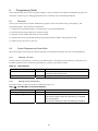
Table 2-1 Flash Memory Configuration
Area
Type
User area
Size
Flash memory
512 Kbytes
Block(s)
16 blocks
Eight 4-Kbyte blocks
One 32-Kbyte block
Seven 64-Kbyte blocks
User boot area
Flash memory
8 Kbytes
1 block
Boot area
Control program
-
-
2.2
Operating Modes
The H8S/2378 has six operating modes (modes 1 to 5 and 7). The operating mode is selected by the setting the mode
pins (MD2 to MD0).
Modes 1, 2, and 4 are externally expanded modes in which the CPU can access external memory and peripheral devices.
In an externally expanded mode, each area in the external address space can be switched between 8- or 16-bit address
space by the bus controller after the start of the execution of a program. If any one of the areas is set to 16-bit address
space, the 16-bit bus mode is used. When all areas are set to 8-bit address space, the 8-bit bus mode is used.
Mode 7 is a single-chip activation externally expanded mode in which the CPU can switch to access external memory
and peripheral devices at the start of the execution of a program.
Mode 3 is a boot mode and mode 5 is a user boot mode, both in which flash memory can be programmed or erased.
Do not change the settings of pins MD2 to MD0 during LSI operation.
For details, refer to the Hardware Manual.
Table 2-2 MCU Operating Modes
MCU
Operating
Mode
MD2
MD1
MD0
CPU Operating
Mode
Description
On-Chip
ROM
External Data Bus
Initial
Value
Maximum
Value
1
0
0
1
Advanced
Expanded mode with
on-chip ROM disabled
Disabled
16 bits
16 bits
2
0
1
0
Advanced
Expanded mode with
on-chip ROM disabled
Disabled
8 bits
16 bits
3
0
1
1
Advanced
Boot mode
Enabled
-
16 bits
4
1
0
0
Advanced
Expanded mode with
on-chip ROM enabled
Enabled
8 bits
16 bits
5
1
0
1
Advanced
User boot mode
Enabled
-
16 bits
7
1
1
1
Advanced
Single-chip mode
Enabled
-
16 bits
2
2.3
On-Board Programming Modes
There are three on-board programming modes: Boot mode, user program mode, and user boot mode. The on-board
programming modes are listed in Table 2-3.
Table 2-3 On-Board Programming Modes
Item
Operating mode
Boot Mode
User Program Mode
Mode 3
Mode 4 (Expanded mode
with on-chip ROM enabled)
User Boot Mode
Mode 5
Mode 7 (Single-chip mode)
The user area can be
programmed by using a
desired interface.
The user boot program of a
desired interface can be
created and the user area
can be programmed.
Boot area
User area
User boot area
(On-chip boot program)
(User-created user
program)
(User-created user boot
program)
Programming/erasing
enable area
User area
User area
User area
All erasure
9 (Automatic)
9
9
Block division erasure
9*1
9
9
Program-data transfer
From the host via the SCI
From a desired device via
RAM
From a desired device via
RAM
Reset start
On-chip boot program
storage area (Boot area)
User area
User boot area*2
Transition to user program
mode
Changing mode setting and
reset
Changing the FLSHE bit
setting
Changing mode setting
and reset
Function
This mode is a program
mode that uses an on-chip
SCI interface. The user area
and user boot area can be
programmed.
This mode can
automatically adjust the bit
rate between the host and
the LSI.
All areas in the user area
and user boot area are
erased first.
Control program
User boot area
Notes:
1. All-erasure is performed. After that, the specified block can be erased.
2. Firstly, the activation is made from the embedded program storage area. After the flash memory related registers are
checked, the reset vector is fetched from the user boot area.
The user boot area can be programmed or erased only in the boot mode.
The user area and user boot area are entirely erased in the boot mode. Then, the user area or user boot area can be
programmed by commands. However, the contents of the area cannot be read until the all-erasure state. You can
program the user boot area in the boot mode then program the user area is programmed in the user boot mode, or
program only the user area by not entering the user boot mode.
In the user boot mode, the boot operation via a desired interface can be performed by the mode pin setting different
from that in the user program mode.
3
3.
Functions of the Flash Development Toolkit
The Renesas Flash Development Toolkit is an on-board flash programming tool for Renesas F-ZTAT microcomputers,
which offers a sophisticated and easy-to-use graphical user interface.
When it is used with Renesas High-performance Embedded Workshop (HEW), it provides users who develop
embedded application software using Renesas F-ZTAT microcomputers with an integrated development environment.
The Flash Development Toolkit can also be used as an editor for S-record and hexadecimal files.
Note: F-ZTAT (Flexible-Zero Turn Around Time) is a trademark of Renesas Technology Corp.
3.1
Main Functions
•
Connecting a device: Connects to a device to the interface of the Flash Development Toolkit.
•
Disconnecting the device: Disconnects the device from the interface of the Flash Development Toolkit.
•
Erasing blocks: Open the "Erase Block" dialog to erase all or individual blocks in flash memory on the device.
•
Checking the blank status: Checks whether the flash memory on the target device is blank.
•
Uploading data: Uploads data from the target device.
•
Downloading a target file: Downloads an active file on the hexadecimal editor.
•
Returning a checksum: Returns a checksum of data in flash memory.
•
Specifying a flash area: Sets a flash area in which non-programming (such as uploading and blank check)
operations are to be performed.
•
The Flash Development Toolkit is available in the simple interface mode and basic simple interface mode to
facilitate the usability of the kit.
For details, refer to Renesas Flash Development Toolkit 3.4 User's Manual
4
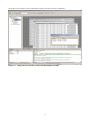
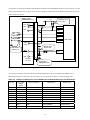
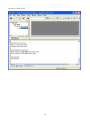
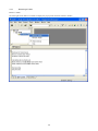
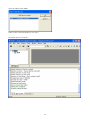
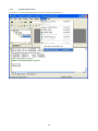
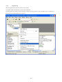
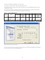
The graphical user interface screen of the Flash Development Toolkit is shown in Figure 3-1.
Figure 3-1 Graphical User Interface of the Flash Development Toolkit
5
4.
4.1
Operating the Flash Development Toolkit
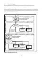
Connecting the Adapter Board
On-board programming adapter board for F-ZTAT* microcomputers HS0008EAUF1H (called the adapter board
hereafter), which is connected between a host computer and user system, has a function which can write a user
application program in flash memory incorporated in an F-ZTAT microcomputer on the user system (on-board) and
erase it from the flash memory.
The adapter board connection is shown in Figure 4-1.
Note: F-ZTAT (Flexible-Zero Turn Around Time) is a trademark of Renesas Technology Corp.
Note: FDM (flash development module) is a former name of the adapter board.
USB cable
Adapter board
Host computer
User system
F-ZTAT
microcomputer
Figure 4-1 Connecting the Adapter Board
6
The pin numbers and corresponding signals of the user system interface cable used for connecting the adapter board and
user system are shown below.
Table 4-1 Pin Numbers and Corresponding Signals of the HS0008EAUF1H User Interface Cable
No
Signal Name
No.
2
Signal Name
1
RES
GND
3
FWx
4
GND
5
MD0
6
GND
7
MD1
8
GND
9
MD2 (IO0)
10
GND
11
MD3 (IO1)
12
GND
13
MD4 (IO2)
14
GND
15
RXD (TXD on the user system side)
16
GND*1
17
TXD (RXD on the user system side)
18
VIN (Vcc or PVcc)*2
19
SCK (NC)
20
VIN (PVcc)*2
Notes:
1. Be sure to connect pin No. 16 to GND to confirm that the user system is connected properly.
2. For a device with Vcc and PVcc, be sure to supply Vcc or PVcc (pin No. 18) and PVcc (pin No. 20) to the VIN pins of
the user interface connector, respectively. To use a device under condition that Vcc = PVcc, or only Vcc is present in the
device, be sure to supply Vcc to both VIN pins Vcc or PVcc (pin No. 18) and PVcc (pin No. 20).
Connecting the Adapter Board
An example of connecting the H8S/2378F and Renesas adapter board (HS0008EAUF1H) is shown in Figure 4-2. The
pull-up and pull-down resistor values shown are only examples. Evaluate the microcomputer to determine the actual
values on the user system.
7
Adapter board
(HS0008EAUF1H)
Vcc
Pulled up at 47 kΩ
or more.
VIN 18,20
(Vcc)
RXD 15
TxD1
TXD
RxD1
17
SW6-1(MD0)
MD0
SW6-2(MD1)
MD1
SW6-3(MD2)
MD2
MD2 9
(IO0)
Pulled down
at about 1 kΩ.
H8S/2378F
Vcc
Pulled up at
about 1 kΩ.
RES
1
RES
GND
2,4,6,8,10,
12,14,16
Connector*1
3428-6002LCSC
Note: 1. Manufacturer: 3M Corporate
Figure 4-2 Example of Connecting the H8S/2378F and Adapter Board
4.1.1
Setting Pins on the Adapter Board
An example of setting pins for the boot mode when the H8S/2378F user system and Renesas adapter board
(HS0008EAUF1H) are connected is shown in Table 4-2. Use the mode switches to set the operating mode.
Table 4-2 Example of Setting Pins on the H8S/2378F and Adapter Board (for the Boot Mode)
Pin No.
Pin on the Adapter Board
Pin on the Device
Input/Output
Output Level
1
RES
RES
Output (default)
Adapter board
3
FWx
Mode switch
Output
High (1)
5
MD0
NC
NC
-
7
MD1
NC
NC
-
9
MD2(IO0)
Serial I/O switch
Output
Low (0)
11
MD3(IO1)
NC
NC
-
13
MD4(IO2)
NC
NC
-
15
RXD
TXD
Input (default)
Adapter board
17
TXD
RXD
Output (default)
Adapter board
19
SCK (NC)
NC
NC (default)
-
Note: NC: Means no connection.
8
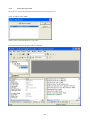
4.2
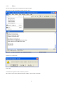
Setting the Flash Development Toolkit
Set the Flash Development Toolkit first to write a program in flash memory.
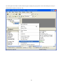
4.2.1
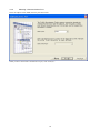
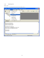
Starting the Flash Development Toolkit
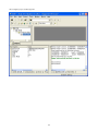
From the "All Programs" menu, select "Flash Development Toolkit 3.4."
4.2.2
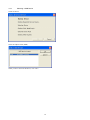
Selecting an Option
The "Welcome" screen of the Flash Development Toolkit appears.
Select "Create a new project workspace."
When the Flash Development Toolkit is started up for the second and subsequent times, the previously selected device
and port information is retained. Select "Open a recent project workspace."
When you have selected an option, click "OK."
9
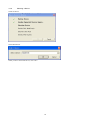
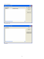
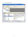
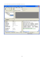
4.2.3
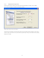
Setting a New Project Workspace
Set a new project workspace. Use "Browse..." and select a directory, and specify the device name in "Workspace
Name." Specify a project name if required. In this example, the same name is specified in "Workspace Name" and
"Project Name."
When you have set the project workspace, click "OK."
10
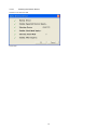
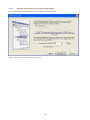
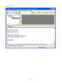
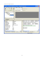
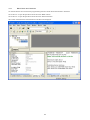
4.2.4
Selecting the Device and Kernel
Select the target device from the pull-down menu.
Select "Generic BOOT Device" because the H8S/2378F is a 0.18-μm product.
When you have selected the device, click "Next(N)."
11
4.2.5
Selecting a Communications Port
Select the adapter board (FDM) from the pull-down menu.
When you have selected the communications port, click "Next(N)."
12
4.2.6
Adapter Board Pin Settings
Set the pins on the adapter board (FDM) for the boot mode.
For example, set the output of FWx pin to high (1) (open jumper J15) and that of MD2 (IO0) to low (0).
In this example, the FWx pin outputs 1 for setting a mode and MD2 (IO0) outputs 0 for serial communication
connection.
Turn off the power and select the boot mode (mode 3) using DIP switch 6. Set DIP switch 6 as follows. When you have
set the pins, turn on the power.
Table 4-3 Operating Mode Settings
MCU
Operating
Mode
3
CPU Operating
Mode
Boot mode
Jumper
FWE
MD2
MD1
MD0
SCI Switch
J15
FWx (Pin 3) on
the Adapter
Board
SW6-3
SW6-2
SW6-1
MD2 (Pin 9) on
the Adapter
Board
1 (Output 1)
0 (ON)
1 (OFF)
1 (OFF)
0 (Output 0)
1 (Open)
When you have set the pins, click "OK."
When the device has been connected, click "OK."
Note: Do not operate the mode switches during CPU operation. Be sure to operate the FWE and MD pins after turning
off the power to the board or while pressing the RESET button.
13
An example of connecting the H8S/2378F and Renesas adapter board (HS0008EAUF1H) is shown in Figure 4-2. The
pull-up and pull-down resistor values shown are only examples. Evaluate the microcomputer to determine the actual
values on the user system.
Adapter board
(HS0008EAUF1H)
Vcc
Pulled up 47 k
Ω or more.
VIN 18,20
(Vcc)
RXD 15
TxD1
TXD
RxD1
17
SW6-1(MD0)
MD0
SW6-2(MD1)
MD1
SW6-3(MD2)
H8S/2378F
MD2
MD2 9
(IO0)
Pulled down
at about 1 k
Vcc
Pulled up at
about 1 kΩ.
RES
1
RES
GND
2,4,6,8,10,
12,14,16
Connector*1
3428-6002LCSC
Note: 1. Manufacturer: 3M Corporate
Figure 4-3 Example of Connecting the H8S/2378F and Adapter Board
An example of setting pins for the boot mode when the H8S/2378F user system and Renesas adapter board
(HS0008EAUF1H) are connected is shown in Table 4-4. Use the mode switches to set the operating mode.
Table 4-4 Example of Setting Pins on the H8S/2378F and Adapter Board (for the Boot Mode)
Pin No.
Pin on the
Adapter
Board
Pin on the Device
Input/Output
Output Level
1
RES
RES
Output (default)
Adapter board
3
FWx
Mode switch
Output
High (1)
5
MD0
NC
NC
-
7
MD1
NC
NC
-
9
MD2 (IO0)
Serial I/O switch
Output
Low (0)
11
MD3 (IO1)
NC
NC
-
13
MD4 (IO2)
NC
NC
-
15
RXD
TXD
Input (default)
Adapter board
17
TXD
RXD
Output (default)
Adapter board
19
SCK (NC)
NC
NC (default)
-
Note: NC: Means no connection.
14
4.2.7
Selecting a USB Device
Check the device.
Select the adapter board (FDM).
When you have selected USB device, click "OK."
15
4.2.8
Selecting a Device
Check the device.
Select HD64F2378.
When you have selected the device, click "OK."
16
4.2.9
Selecting the Clock Mode
Check the device.
Select the clock mode.
When you have selected the clock mode, click "OK."
17
4.2.10
Checking the Generic Device
The device has been checked.
Click "OK."
18
4.2.11
Setting the Device (Input Clock)
In the first column enter the frequency of the clock used for the board in MHz. For example, enter 8.25 (MHz).
Set 4 in "Select the multiplier for the Main clock frequency (CKM):."
When you have set the values, click "Next(N)."
The input clock is the frequency of the clock directly input to the microcomputer. Enter the frequency of the crystal or
ceramic resonator connected to the user system with three significant digits. The input clock differs from the operating
frequency (PLL output).
19
4.2.12
Selecting the Connection Type (Communication Speed)
Select a baud rate from the pull-down menu. For example, select 19200 (baud).
When you have selected the baud rate, click "Next(N)."
20
4.2.13
Selecting Programming Options (Protection Level and Messaging Level)
Select the protection level and messaging level. For example, select "Automatic" for "Protection" and "Advanced" for
"Messaging."
When you have selected programming options, click "Next(N)."
21
4.2.14
Reset Mode Pin Settings
Set pins on the adapter board for restarting the device in the reset mode. These settings are not required for this
procedure.
When you have set the items, click "Finish."
22
4.2.15
Completion of Connection
The H8S/2378F board has been connected to the Flash Development Toolkit in the boot mode.
At this time, the contents of the user boot area and user area have been erased.
23
4.3
Boot Mode 1 (Programming the User Boot Area)
Write a program in the user boot area in the boot mode. The program to be written is sample test program 2378F.mot
(S-type file). The bit rate in this program has been modified according to the frequency. On how to modify the bit rate,
refer to section 7.1.1, Bit Rate Setting (GenTest.h).
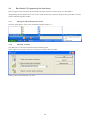
4.3.1
Selecting a File
To select a file to be programmed, select "Add Files..." from the "Project" pull-down menu.
24
In the "Add File(s)" dialog, add file "2378F.mot."
When you have selected the file, click "Add."
File 2378F.mot is added to the project.
25
4.3.2
Programming
To program the user boot area, set the user boot area.
Click the right mouse button on file 2378F.mot to display the pop-up menu. Click "User Boot Area" so that the file can
be downloaded to the user boot area.
26
Click the right mouse button on file 2378F.mot again to display the pop-up menu. Click "Download File to [User Boot
Area]" to download file 2378F.mot to the user boot area.
27
You can check that the program has been downloaded to the user boot area.
28
4.3.3
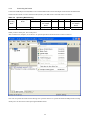
Blank Check
To confirm that the user boot area has been programmed, perform a blank check.
Click "Device" to open the pull-down menu and select "Flash Area for Non-Write Ops," then "User Boot Area."
29
Click "Device" again to open the pull-down menu and click "Blank Check."
30
The result of the blank check for the selected area is displayed.
The user boot area is not blank.
31
4.3.4
Checksum
To confirm that the user boot area has been programmed, display a checksum.
Click "Device" to open the pull-down menu and click "Flash Checksum."
32
The result of the checksum calculation is displayed.
When the user boot area is blank, the following value is displayed as the result:
Calculating device checksum
Flash Checksum: 0x001FE000 (User Boot Area)
Flash Checksum: 0x07F80000 (User Area)
33
4.3.5
Disconnecting the Device
After programming has been completed, disconnect the device.
Click "Device" to open the pull-down menu and click "Disconnect."
34
The device is disconnected.
35
4.3.6
Removing a File
Remove a file.
Click "Project" to open the pull-down menu and click "Remove Files...."
36
The file is displayed.
Click "Remove All."
Click "OK."
37
The file is removed.
38
4.3.7
Removing a Folder
Remove a folder.
Click the right mouse button on a folder to display the pop-up menu and click "Remove Folder."
39
The folder is removed.
40
4.3.8
Exiting
Save the work folder and exit the Flash Development Toolkit.
Click "File" to open the pull-down menu and click "Exit."
Choose to save the session.
Click "Yes."
The Flash Development Toolkit terminates operation.
The work file space of the Flash Development Toolkit is saved as file 2378.AWS.
41
4.4
Boot Mode 2 (Programming the User Area)
Write a program in the user area in the boot mode. The same program as used in section 4.3, Boot Mode 1
(Programming the User Boot Area) is to be written. In this section, the saved work file space file (2378.AWS) is used to
start the Flash Development Toolkit.
4.4.1
Starting the Flash Development Toolkit
From the "All Programs" menu, select "Flash Development Toolkit 3.4."
4.4.2
Selecting an Option
The "Welcome" screen of the Flash Development Toolkit appears.
Select "Open a recent project workspace" and project workspace file 2378.AWS.
When you have selected the file, click "OK."
42
Project 2378 is displayed.
The Flash Development Toolkit can also be started by directly opening (or double-clicking on) project workspace file
2378.AWS.
43
4.4.3
Connecting the Device
Connect the USB adapter board (FDM) to a PC and the H8S/2378F board to the adapter board and set the H8S/2378F
board in the boot mode. To select the boot mode (mode 3), use DIP switch 6. Set DIP switch 6 as follows.
Table 4-5 Operating Mode Setting
MCU
Operating
Mode
3
CPU Operating
Mode
Boot mode
Jumper
FWE
MD2
MD1
MD0
SCI Switch
J15
FWx (Pin 3) on
the Adapter
Board
SW6-3
SW6-2
SW6-1
MD2 (Pin 9) on
the Adapter
Board
1 (Output 1)
0 (ON)
1 (OFF)
1 (OFF)
0 (Output 0)
1 (Open)
When you have set the pins, turn on the power.
After connection is complete, click "Device" to open the pull-down menu and click "Connect to Device."
Note: Do not operate the mode switches during CPU operation. Be sure to operate the FWE and MD pins after turning
off the power to the board or while pressing the RESET button.
44
Select the adapter board (FDM).
When you have selected USB device, click "OK."
The adapter board is connected.
45
4.4.4
Selecting a File
To select a file to be programmed, select "Add Files..." from the "Project" pull-down menu.
46
In the "Add File(s)" dialog, add file "2378F.mot."
When you have selected the file, click "Add."
File 2378F.mot is added to the project.
47
4.4.5
Programming
Click the right mouse button on file 2378F.mot to display the pop-up menu. Click "Download File to [User Area]" to
download file 2378F.mot to the user area. The default is "Download File to [User Area]."
48
You can check that the program has been downloaded to the user area.
49
4.4.6
Blank Check and Checksum
To confirm that the user area has been programmed, perform a blank check and calculate a checksum.
Click "Device" to open the pull-down menu and click "Blank Check."
Click "Device" to open the pull-down menu and click "Flash Checksum."
The results of the blank check and checksum calculation are displayed.
50
4.5
User Boot Mode
In the user boot mode, the user area can be programmed or erased. The user boot area cannot be programmed or erased.
4.5.1
Writing a Program in the User Boot Area
Start "Flash Development Toolkit 3.4" and open project workspace file 2378.AWS.
Write program file 2378F.mot in the user boot area in the boot mode.
In this sample, toolbar positions are changed to display the Configure Project button.
51
4.5.2
Disconnecting the Device
Click "Device" to open the pull-down menu and click "Disconnect."
52
4.5.3
Configuring the Project
Click "Device" to open the pull-down menu and click "Configure Flash Project."
53
The configure project window appears.
54
4.5.4
Setting the User Program Mode
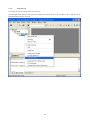
Select the "Device" tab in the configure project window and double-click "Connection" and "Boot."
55
Set the connection type.
Select "USER Program Mode" in "Select Connection:."
Set the baud rate to 9600 bps.
When you have set the connection type, click "Next."
56
Set the pins on the adapter board (FDM) for the user boot mode.
For example, set the output of FWx to high (1) and that of MD2 to low (0).
In this example, the FWx pin outputs 1 for selecting a mode (the jumper is open) and MD2 (IO0) outputs 0 for serial
communication connection.
Turn the power off and select the user boot mode (mode 5) using DIP switch 6. When you have set the pins, turn on the
power.
Table 4-6 Operating Mode Setting
MCU
Operating
Mode
5
CPU Operating
Mode
User boot mode
Jumper
FWE
MD2
MD1
MD0
SCI Switch
J15
FWx (Pin 3) on
the Adapter
Board
SW6-3
SW6-2
SW6-1
MD2 (Pin 9) on
the Adapter
Board
1 (Output 1)
1 (OFF)
0 (ON)
1 (OFF)
0 (Output 0)
1 (Open)
When you have set the items, click "Finish."
Note: Do not operate the mode switch during CPU operation. Be sure to operate the FWE and MD pins after turning the
power to the board off or while pressing the RESET button.
57
The user boot mode has been set.
58
4.5.5
Connecting the Device
Click "Device" to open the pull-down menu and click "Connect to Device."
Select the adapter board (FDM).
When you have selected the device, click "OK."
The connection in the user boot mode is completed.
59
4.5.6
Programming
Write a program in the user area in the user boot mode.
To program a file in the user area, specify a download area.
Click the right mouse button on file 2378F.mot to display the pop-up menu. Click "User Boot Area" to uncheck it so
that the file can be downloaded to the user area.
60
Click the right mouse button on file 2378F.mot again to display the pop-up menu. Click "Download [User Area]" to
download file 2378F.mot to the user area.
61
You can check that the program has been downloaded to the user area.
62
4.5.7
Blank Check and Checksum
To confirm that the user area has been programmed, perform a blank check and calculate a checksum.
Click "Device" to open the pull-down menu and click "Blank Check."
Click "Device" to open the pull-down menu and click "Flash Checksum."
The results of the blank check and checksum calculation are displayed.
63
4.6
User Program Mode
In the user program mode, the user area can be programmed or erased. The user boot area cannot be programmed or
erased.
4.6.1
Writing a Program in the User Area
Start "Flash Development Toolkit 3.4" and open project workspace file 2378.AWS.
Write program file 2378F.mot in the user area in the boot mode.
After programming the file, disconnect the device and display the configure project window. On how to display the
configure project window, refer to section 4.5.3, Configuring the Project.
64
4.6.2
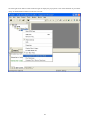
Setting the User Program Mode
Select the "Device" tab in the configure project window and double-click "Connection" and "Boot."
65
Set the connection type.
Select "USER Program Mode" in "Select Connection:."
Set the baud rate to 9600 bps.
When you have set the connection type, click "Next."
66
Set the pins on the adapter board (FDM) for the user boot mode.
For example, set the output of FWx to high (1) and that of MD2 to low (0).
In this example, the FWx pin outputs 1 for selecting a mode (jumper J15 is open) and MD2 (IO0) outputs 0 for serial
communication connection.
Turn off the power and select an expanded mode with on-chip ROM enabled (mode 4) or single-chip mode (mode 7).
To select the mode, use DIP switch 6. When you have set the pins, turn on the power.
Table 4-7 Operating Mode Settings
MCU
Operating
Mode
CPU Operating
Mode
Jumper
FWE
MD2
MD1
MD0
SCI Switch
J15
FWx (Pin 3) on
the Adapter
Board
SW6-3
SW6-2
SW6-1
MD2 (Pin 9) on
the Adapter
Board
4
Expanded mode with
on-chip ROM
enabled
1 (Open)
1 (Output 1)
1 (OFF)
0 (ON)
0 (ON)
0 (Output 0)
7
Single-chip mode
1 (Open)
1 (Output 1)
1 (OFF)
1 (OFF)
1 (OFF)
0 (Output 0)
When you have set the items, click "Finish."
Note: Do not operate the mode switch during CPU operation. Be sure to operate the FWE and MD pins after turning the
power to the board off or while pressing the RESET button.
67
The user program mode has been set.
68
4.6.3
Connecting the Device
Click "Device" to open the pull-down menu and click "Connect to Device(C)."
Select the adapter board (FDM).
When you have selected USB device, click "OK."
The connection in the user program mode is completed.
69
4.6.4
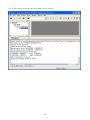
Programming
Write a program in the user area in the user program mode.
Click the right mouse button on file 2378F.mot to display the pop-up menu. Click "Download File to [User Area]" to
download file 2378F.mot to the user area.
70
You can check that the program has been downloaded to the user area.
71
4.6.5
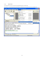
Blank Check and Checksum
To confirm that the user area has been programmed, perform a blank check and calculate a checksum.
Click "Device" to open the pull-down menu and click "Blank Check."
Click "Device" to open the pull-down menu and click "Flash Checksum."
The results of the blank check and checksum calculation are displayed.
72
5.
Flash Development Toolkit Processing
The Flash Development Toolkit can be connected in either of the following two modes: the boot mode or the user
program mode. In both modes, the continuation of the execution from a previous session can be specified. The
connection modes of the Flash Development Toolkit are listed in Table 5-1. Normally, a new connection processing is
used. The hexadecimal code is a command code of the Flash Development Toolkit. For details, refer to the description
on flash memory (0.18-μm F-ZTAT version) in the Hardware Manual.
Table 5-1 Connection Modes of the Flash Development Toolkit
Mode
Boot mode
New Connection Processing
Continuation of the Execution from a Previous
Session
Baud rate adjustment
H'27 (Programming unit inquiry)
H'27 (Programming unit inquiry)
H'4F (Status request)
H'10 (Device selection)
H'4D (User area blank check)
H'11 (Clock mode selection)
H'3F (New baud rate setting)
User boot mode
H'27 (Programming unit inquiry)
H'27 (Programming unit inquiry)
User program mode
H'10 (Device selection)
H'4F (Status request)
H'11 (Clock mode selection)
H'4D (User area blank check)
H'3F (New baud rate setting)
73
6.
Sample Program
This section describes the sample program in the user program mode of the H8S/2378F.
6.1
File Configuration
The file configuration is shown in Figure 6-1.
2378 2378 folder
⏐⎯Project Project folder
⏐ ⏐⎯2378F
2378F folder
⏐ ⏐ ⏐⎯Release Release folder
⏐ ⏐ ⏐⎯2378f.hwp
2378f project database file
⏐ ⏐ ⏐⎯2378F.tps Current session file
⏐ ⏐ ⏐⎯defaultsession.hsf Session file
⏐ ⏐⎯Project.hws
Project workspace file
⏐ ⏐⎯Project.tws
Current project file
⏐⎯Src
Source file folder
⏐ ⏐⎯BaudRate.src
Baud rate
⏐ ⏐⎯CmdFunc.c Command function
⏐ ⏐⎯CmdFunc.h Command function header
⏐ ⏐⎯commands.h
Command header
⏐ ⏐⎯DeviceInfo.h
Device information header
⏐ ⏐⎯FDTErase.c Erase function
⏐ ⏐⎯FDTUMain.c
Main function
⏐ ⏐⎯FDTUMain.h Main function header
⏐ ⏐⎯FDTWrite.c Programming function
⏐ ⏐⎯GenTest.c Test function
⏐ ⏐⎯GenTest.h Test function header
⏐ ⏐⎯io2378.h
I/O address header
⏐ ⏐⎯KAlg.h Library header
⏐ ⏐⎯KDevice.h Device header
⏐ ⏐⎯KStruct.h Structure header
⏐ ⏐⎯KTypes.h Type header
⏐ ⏐⎯rom2ram.src RAM address definition
⏐ ⏐⎯Strt2378.src
Start function
⏐ ⏐⎯Ugenu.c Micro function
⏐ ⏐⎯uGenu.h Micro function header
⏐⎯2378F.mot 2378F S-type file
Figure 6-1 File Configuration
74
6.2
Source Files
The source files are listed in Table 6-1.
Table 6-1 Source Files
File
Baud rate
File Name
Description
BaudRate.src
BRR calculation assembly language file
Command function
CmdFunc.c
Command processing source file
Command function header
CmdFunc.h
Command function definition file
Command header
commands.h
Command code definition file
Device information header
DeviceInfo.h
Device information definition file
Erase function
FDTErase.c
Erase function source file
Main function
FDTUMain.c
Main kernel function source file
Main function header
FDTUMain.h
Main kernel function definition file
Programming function
FDTWrite.c
Programming function source file
Test function
GenTest.c
User program mode test function source file
Test function header
GenTest.h
User program mode test definition file
I/O address header
io2378.h
Peripheral module register definition file
Library header
KAlg.h
Programming and erasing library definition file
Device header
KDevice.h
Device information definition file
Structure header
KStruct.h
Structure definition file
Type header
KTypes.h
Type definition file
RAM address definition
rom2ram.src
RAM address definition file
Start function
Strt2378.src
Start function assembly language file
Micro function
Ugenu.c
Micro kernel function source file
Micro function header
uGenu.h
Micro kernel definition file
75
6.3
Modules
The modules are listed in Table 6-2.
Table 6-2 Modules
File
Module
Module Name
Function
BaudRate.src
BRR calculation
cal_brr
CmdFunc.c
Reference function
ReferFunc
Reference function
Device selection
SelectDevice
Selects a device.
Clock mode selection
SelectClockMode
Selects a clock mode.
New baud rate setting
SetNewBaudRate
Sets a new baud rate.
Program status
RequestBootPrgSts
Program status
Sum check
SumCheck
Sum check
ACK transmission
SendAck
Sends ACK.
Blank check
CheckBlank
Checks the blank status.
Memory read
ReadMemory
Reads memory.
Command read
GetCmdData
Reads a command.
Flash erasing
EraseFLASH
Erases flash memory.
Erase data reception
GetEraseData
Receives erase data.
Erase initial setting
EraseInit
Performs erase initial setting.
Erasing start
EraseStart
Starts erasing operation.
RAM main
RamMain
RAM main processing
Command processing
ProcessCommand
Processes commands.
Library transfer
LibTrans
Transfers a library.
SCO bit setting
ScoBitSet
Sets the SCO bit.
User boot area selection
UserBootSelect
Selects the user boot area.
User area selection
UserMatSelect
Selects the user area.
Flash programming
WriteFLASH
Programs flash memory.
Programming data
reception
GetWriteData
Receives programming data.
Programming initial setting
WriteInit
Performs programming initial setting.
Programming start
WriteStart
Starts programming.
Main processing
main
Test main processing
SCI initial setting
InitSCI
Performs SCI initial setting.
Reception
Get
Reception
FDTErase.c
FDTUMain.c
FDTWrite.c
GenTest.c
Calculates the BRR value using the frequency
and bit rate.
Transmission
Put
Transmission
Strt2378.src
Start
startup
Sets and starts the stack pointer.
Ugenu.c
ROM main
RomMain
ROM main processing
Command function
CmdFunc
Receives and controls commands.
Transfer start
TransStart
Starts transferring a program.
Copy
RamCopy
Copies a program into RAM.
76
6.4
Module Hierarchical Structure
The module hierarchical structure is shown in Figure 6-2.
RESET_VECTOR (0x0000)
Reset vector
⏐⎯startup (0x1000) Start
⏐⎯main
Main processing
⏐⎯InitSCI
SCI initial setting
⏐⎯RomMain ROM main processing
⏐⎯TransStart Transfer start
⏐ ⏐⎯RamCopy Copy
⏐⎯CmdFunc
⏐ ⏐⎯Get
Command function
Reception
⏐ ⏐⎯SendAck ACK transmission
⏐ ⏐ ⏐⎯Put Transmission
⏐ ⏐⎯ReferFunc Reference function
⏐ ⏐ ⏐⎯Put Transmission
⏐ ⏐⎯GetCmdData Command read
⏐ ⏐ ⏐⎯Get
Reception
⏐ ⏐⎯SelectDevice
Device selection
⏐ ⏐ ⏐⎯SendAck ACK transmission
⏐ ⏐ ⏐⎯ErrorCode Error code macro
⏐ ⏐ ⏐⎯Put Transmission
⏐ ⏐⎯SelectClockMode Clock mode selection
⏐ ⏐ ⏐⎯SendAck ACK transmission
⏐ ⏐ ⏐⎯ErrorCode Error code macro
⏐ ⏐ ⏐⎯Put Transmission
⏐ ⏐⎯SetNewBaudRate
New bit rate setting
⏐ ⏐ ⏐⎯ErrorCode Error code macro
⏐ ⏐ ⏐⎯Put Transmission
⏐ ⏐ ⏐⎯cal_brr BRR calculation
⏐ ⏐ ⏐⎯SendAck ACK transmission
⏐ ⏐ ⏐⎯Get
Reception
⏐ ⏐⎯RequestBootPrgSts Program status
⏐ ⏐ ⏐⎯Put Transmission
⏐ ⏐⎯Put Transmission
⏐⎯RamMain (0xFF4000)
RAM main processing
(To be continued)
Figure 6-2 Module Hierarchical Structure (1)
77
(Continued)
⏐⎯RamMain (0xFF4000)
RAM main processing
⏐⎯ProcessCommand
⏐⎯Get
Command processing
Reception
⏐⎯RequestBootPrgSts Program status
⏐⎯SumCheck Sum check
⏐ ⏐⎯UserBootSelect User boot area selection
⏐ ⏐
⏐⎯nop NOP macro
⏐ ⏐⎯UserMatSelect User area selection
⏐ ⏐
⏐⎯nop NOP macro
⏐ ⏐⎯Put Transmission
⏐⎯LibTrans Library transfer
⏐ ⏐⎯ScoBitSet
⏐
SCO bit setting
⏐⎯nop NOP macro
⏐⎯SendAck ACK transmission
⏐⎯EraseFLASH Flash erasing
⏐ ⏐⎯EraseInit Erase initial setting
⏐ ⏐
⏐⎯UserMatSelect User area selection
⏐ ⏐
⏐⎯INIT_ADDR
⏐ ⏐⎯ErrorCode
Initial setting entry address
Error code macro
⏐ ⏐⎯Put Transmission
⏐ ⏐⎯Get Reception
⏐ ⏐⎯RequestBootPrgSts Program status
⏐ ⏐⎯GetEraseData Erase data reception
⏐ ⏐
⏐⎯Get
⏐ ⏐
⏐⎯ErrorCode
⏐ ⏐
⏐⎯Put Transmission
Reception
⏐ ⏐⎯EraseStart
⏐ ⏐
Error code macro
Erasing start
⏐⎯WRITE_ERASE_ADDR
Programming/erasing entry address
⏐ ⏐⎯SendAck ACK transmission
⏐⎯WriteFLASH Flash programming
⏐ ⏐⎯WriteInit Programming initial setting
⏐ ⏐
⏐⎯UserMatSelect User area selection
⏐ ⏐
⏐⎯INIT_ADDR
⏐ ⏐⎯ErrorCode
Initial setting entry address
Error code macro
⏐ ⏐⎯Put Transmission
⏐ ⏐⎯Get Reception
⏐ ⏐⎯RequestBootPrgSts Program status
⏐ ⏐⎯GetWriteData Programming data reception
⏐ ⏐
⏐⎯Get
⏐ ⏐
⏐⎯ErrorCode
⏐ ⏐
⏐⎯Put Transmission
Reception
Error code macro
⏐ ⏐⎯WriteStart Programming start
⏐ ⏐
⏐⎯WRITE_ERASE_ADDR
⏐ ⏐⎯SendAck ACK transmission
⏐⎯GetCmdData
Command read
⏐⎯ReadMemory
Memory read
(To be continued)
Figure 6-2 Module Hierarchical Structure (2)
78
Programming/erasing entry address
(Continued)
⏐⎯ReadMemory
Memory read
⏐ ⏐⎯UserBootSelect User boot area selection
⏐ ⏐⎯UserMatSelect User area selection
⏐ ⏐⎯ErrorCode
Error code macro
⏐ ⏐⎯Put Transmission
⏐⎯CheckBlank
Blank check
⏐ ⏐⎯UserBootSelect User boot area selection
⏐ ⏐⎯UserMatSelect User area selection
⏐ ⏐⎯ErrorCode
Error code macro
⏐ ⏐⎯Put Transmission
⏐ ⏐⎯SendAck ACK transmission
⏐⎯Put Transmission
Figure 6-2 Module Hierarchical Structure (3)
79
6.5
Flow of the Program
This section describes the flow of the sample program with referencing the module hierarchical structure.
6.5.1
Program Processing Flow
The processing flow of the sample program is shown in Figure 6-3. In the user program mode, bit rate adjustment and
user area erase processing, which are performed during boot operation, are not performed. For this reason, the program
and data written in flash memory can be saved.
Reset
Bit-rate-adjustment status
Bit rate
adjustment
Note: The sample program does
not contain this processing.
Inquiry/selection status
Wait for inquiry
and selection
Inquiry
Inquiry
processing
Transition to the
programming/
erase status
Selection
Selection
processing
Programming/erase status
User MAT/user
boot MAT erase
processing
Wait for
programming or
erasing to be
selected
Note: The sample program
does not contain this
i
Programming
Programming
processing
Erasing
Erase
processing
Figure 6-3 Program Processing Flow
80
Check
Check
processing
6.5.2
Main Processing (main)
The flow of main processing is shown below:
(1) The reset vector causes a branch to start (startup).
(2) Start (startup) sets the stack pointer and calls main processing (main).
(3) Main processing (main) calls SCI initial setting (InitSCI) and branches to ROM main processing (RomMain).
(4) ROM main processing (RomMain) transfers RAM main processing to RAM, receives and processes a command,
and sets items.
After setting items, ROM main processing branches to RAM main processing (RamMain) in RAM.
(5) RAM main processing (RamMain) processes the received commands and performs the following processing:
Transferring the programming/erasing library (LibTrans)
Erasing flash memory (EraseFLASH)
Programming flash memory (WriteFLASH)
Reading memory in the user boot area or user area (ReadMemory)
Calculating a checksum of data in the user boot area or user area (SumCheck)
Checking the blank status of the user boot area or user area (CheckBlank)
Note: ROM main processing (RomMain) is also called a micro-kernel. It runs in ROM.
RAM main processing (RamMain) is also called a main kernel. It runs in RAM.
6.5.3
ROM Main Processing (RomMain)
The flow of ROM main processing (RomMain) is shown below:
(1) Transfer start (TransStart) transfers the program in ROM to RAM.
This operation is for performing library transfer, erasing, and programming in RAM.
(2) Command function (CmdFunc) processes each command, responds to each inquiry, and sets selection.
(3) Reference function (ReferFunc) and program status (RequestBootPrgSts) respond to each inquiry that corresponds
to one of the following commands:
Supported device inquiry
Clock mode inquiry
Multiplication ratio inquiry
Operating frequency inquiry
User boot area information inquiry
User area information inquiry
Erase block information inquiry
Programming unit inquiry
Boot program status inquiry
(4) A selection setting command is set using one of the following modules:
Device selection (SelectDevice): Selects a device code.
Clock mode selection (SelectClockMode): Notifies the selected clock mode.
New bit rate setting (SetNewBaudRate): Selects a new bit rate.
(5) Inquiry/selection processing is completed and a branch is caused to RAM main processing (RamMain) transferred
to RAM.
81
6.5.4
RAM Main Processing (RamMain)
The flow of RAM main processing (RamMain) is shown below:
(1) Command processing (ProcessCommand) processes commands. The following commands are to be processed. The
sample program cannot process user boot area programming selection or block erasing for the user boot area
because it runs in the user program mode.
User area programming selection
128-byte programming
Erasing selection
Block erasing
Memory read
User boot area sum check
User area sum check
User boot area blank check
User area blank check
Boot program status inquiry
(2) For the user area programming selection command, command processing transfers the programming library using
library transfer (LibTrans) and branches to flash programming (WriteFLASH).
(3) Flash programming (WriteFLASH) sets the frequency using programming initial setting (WriteInit).
Then, it reads a command. When the command is 128-byte programming, programming data reception
(GetWriteData) receives programming data and programming start (WriteStart) programs flash memory.
When 128-byte data is programming end address data, the programming end codes are set in data to be
programmed and programming destination address to end programming (call programming start (WriteStart)
actually) and programming terminates.
In this sample program, 128-byte programming end address data is H'FFFFFFFF, the programming end code of
data to be programmed is H'F0F0F0F0, and the programming end code of the programming destination address is
H'0F0F0F0F.
(4) For the erasing selection command, library transfer (LibTrans) transfers the erasing library and branches to flash
erasing (EraseFLASH).
(5) Flash erasing (EraseFLASH) sets the frequency using erase initial setting (EraseInit).
Then, it reads a command. When the command is block erasing, erase data reception (GetEraseData) receives erase
data and erasing start (EraseStart) erases the specified block.
When erase data is erasing end data, erasing terminates.
(6) For the memory read command, command read (GetCmdData) specifies the read address. Memory read
(ReadMemory) reads memory in the user boot area or user area.
(7) For the user boot area sum check or user area sum check command, sum check (SumCheck) calculates a checksum
of data in the user boot area or user area.
(8) For the user boot area blank check or user area blank check command, blank check (CheckBlank) checks the blank
status of the user boot area or user area.
(9) For the boot program status inquiry command, program status (RequestBootPrgSts) sends the boot processing
status.
82
7.
Source Files of the Sample Program
This section describes main source files of the sample program.
7.1
Header Files
This sample program uses the following header files.
7.1.1
Bit Rate Setting (GenTest.h)
A bit rate is set.
/* 33MHz 9600bps */
//#define MA_BRR_SCI
0x6A
/* Bit rate register channel 1 */
/* 8.25MHz 9600bps */
#define MA_BRR_SCI
0x1A
/* Bit rate register channel 1 */
In the user program mode, communications between the connected device is performed at 9600 bps. For this reason, the
bit rate register (BRR) in the SCI module must be set according to the operating frequency. In this example, the
operating frequency is 8.25 MHz. To set 9600 bps, MA_BRR_SCI is set to 26 (0x1A). The relationships between
operating frequencies and BBR register settings is shown in Table 7-1.
Table 7-1
Operating Frequencies and BBR Register Settings (When the Bit Rate Is 9600 (bit/s))
Operating Frequency φ (MHz)
8
BRR Setting
25
Error (%)
0.16
8.25
26
-0.54
9.8304
31
0.00
10
32
-1.36
12
38
0.16
12.288
39
0.00
14
45
-0.93
14.7456
47
0.00
16
51
0.16
17.2032
55
0.00
18
58
-0.69
19.6608
63
0.00
20
64
0.16
The MA_BRR_SCI value is set according to the operating frequency of the board and built with HEW to create a
program in an S-type file.
83
7.1.2
I/O Register Definition (io2378.h)
The registers and bits related to the SCI module and ROM are defined.
/************************************************************************/
/*
H8S/2378F Internal I/O Include File
*/
/************************************************************************/
#define SCKCR
(*(volatile unsigned char *)0xFFFF3B)
#define STCS
(unsigned char)0x08
#define SYSCR
(*(volatile unsigned char *)0xFFFF3D)
#define FLSHE
(unsigned char)0x08
#define MSTPCRL
(*(volatile unsigned char *)0xFFFF41)
#define MSTP2
(unsigned char)0x04
#define PLLCR
(*(volatile unsigned char *)0xFFFF45)
/************************************************************************/
/*
SCI
*/
/*----------------------------------------------------------------------*/
/*
CHANNEL 1
*/
/************************************************************************/
#define SCI_SMR
(*(volatile unsigned char *)0xFFFF80)
#define SCI_BRR
(*(volatile unsigned char *)0xFFFF81)
#define SCI_SCR
(*(volatile unsigned char *)0xFFFF82)
#define TE
(unsigned char)0x20
#define RE
(unsigned char)0x10
#define TE_RE
(unsigned char)(TE | RE)
#define SCI_TDR
(*(volatile unsigned char *)0xFFFF83)
#define SCI_SSR
(*(volatile unsigned char *)0xFFFF84)
#define TDRE
(unsigned char)0x80
#define RDRF
(unsigned char)0x40
#define RDRF_ERR_CLR
(unsigned char)0x87
#define TEND
(unsigned char)0x04
#define SCI_RDR
(*(volatile unsigned char *)0xFFFF85)
/************************************************************************/
/*
FLASH
*/
/*----------------------------------------------------------------------*/
/*
*/
/************************************************************************/
#define FCCS
(*(volatile unsigned char *)0xFFFFC4)
#define FPCS
(*(volatile unsigned char *)0xFFFFC5)
84
#define FECS
(*(volatile unsigned char *)0xFFFFC6)
#define FKEY
(*(volatile unsigned char *)0xFFFFC8)
#define FMATS
(*(volatile unsigned char *)0xFFFFC9)
#define FTDAR
(*(volatile unsigned char *)0xFFFFCA)
#define FLASH18 (*(volatile struct st_flash18 *)0xFFFFE800) /* FLASH18 Address*/
7.1.3
Macro Definition (FDTUMain.h and KAIg.h)
Labels used in the program are defined.
(1) FDTUMain.h
/* D E F I N E */
enum {
FmatsUserBootMat = 0xaa,
FmatsUserMat = 0x00,
WriteMode = 0x01,
EraseMode = 0x01,
FkeyEnable = 0xA5
};
(2) KAlg.h
/* D E F I N E S */
#define LOOP_END
1
#define bufSize
0x80
#define BLOCK_NO_ERROR
0x09
#define ERASE_END
0xFF
#define WRITE_END
0xFFFFFFFF
#define ADDRESS_ERROR
0x03
#define WRITE_ERASE_ENABLE
0x5A
#define ADD_WRITE_PRM0
0xF0F0F0F0
#define ADD_WRITE_PRM1
0x0F0F0F0F
85
7.2
Main Processing and ROM Main Processing
7.2.1
Module Hierarchical Structure
The module hierarchical structure of main processing and ROM main processing is shown in Figure 7-1.
RESET_VECTOR (0x0000)
Reset vector
⏐⎯startup (0x1000) Start
⏐⎯main
Main processing
⏐⎯InitSCI
SCI initial setting
⏐⎯RomMain ROM main processing
⏐⎯TransStart Transfer start
⏐⎯CmdFunc
Command function
⏐⎯RamMain (0xFF4000)
Figure 7-1
RAM main processing
Module Hierarchical Structure of Main Processing and ROM Main Processing
The reset vector causes a branch to start, which sets the stack pointer (Strt2378.src) and branches to main processing
(main in GenTest.c).
Main processing performs initial setting for the SCI (InitSCI in GenTest.c) to enable transmission/reception and causes
a branch to ROM main processing (RomMain in Ugenu.c).
ROM main processing transfers RAM main processing and others to RAM (TransStart in Ugenu.c) and processes
commands (CmdFunc in Ugenu.c). At the end of data, ROM main processing branches to RAM main processing
(RamMain in FDTUMain.c).
Main processing and ROM main processing are executed in ROM.
7.2.2
Reset Vectors (GenTest.c and GenTest.h)
The reset vectors are shown below:
(1) GenTest.c
/*Declare the vector table*/
#pragma section _VECT
const DWORD RESET_VECTOR = (DWORD)RESET_JMP_ADDRESS;
#pragma section
(2) GenTest.h
#define RESET_JMP_ADDRESS
0x1000
86
7.2.3
Transfer Start (Ugenu.c and rom2ram.src)
The following modules are transferred from ROM to RAM according to the transfer table (rom2ram.src) when RAM
main processing and others are transferred. For the sections, ROM options are used.
Table 7-2 Transfer Modules
Section
Module
P_RAM_SCI
Get, Put (GenTest.c)
P_RAM_MAIN
RamMain and others (FDTUMain.c)
P_RAM_CMD
RequestBootPrgSts and others
(CmdFunc.c)
P_RAM_WRITE
WriteFLASH and others (FDTWrite.c)
P_RAM_ERASE
EraseFLASH (FDTErase.c)
7.2.4
Command Function (Ugenu.c, commands.h, CmdFunc.c, and DeviceInfo.h)
Command function (CmdFunc) processes inquiry and setting commands. Commands are defined as macros
(commands.h) and a process (CmdFunc.c) corresponding to each command is performed. For an inquiry command, a
response (DeviceInfo.h) corresponding to the command is output (ReferFunc in CmdFunc.c).
87
7.3
RAM Main Processing
RAM main processing transfers a library, and erases and programs flash memory. This processing is executed in RAM.
7.3.1
Library Transfer (FDTUMain.c)
(1) LibTrans
When the command ID is prepareErase (0x48), FECS is set to EraseMode (0x01) and the erasing library is selected.
When the command ID is other than the above (prepareUserAreaWrite, 0x43), FPCS is set to WriteMode (0x01) and the
programming library is selected. FKEY is set to FkeyEnable (0xA5) to select transfer and the SCO bit is set.
/*
///////////////////////
// LibTrans Function //
///////////////////////
*/
void LibTrans(BYTE commandID)
{
if (commandID == prepareErase){
FECS = EraseMode;
}else{
FPCS = WriteMode;
}
FKEY = FkeyEnable;
ScoBitSet();
}
88
(2) ScoBitSet
The library transfer destination address is set in the FTDAR register and the SCO bit of the FCCS register is set to 1. At
least four NOP instructions are required after the SCO bit setting.
To determine whether a transfer error occurs, 0xFF is programmed in the library transfer destination address before
transfer and 0x00 is checked after transfer.
/*
////////////////////////
// ScoBitSet Function //
////////////////////////
*/
BYTE ScoBitSet(void)
{
/* Transmission error check initialization */
*((volatile unsigned char *)TRANS_RAM_ADDR) = 0xFF;
FTDAR = FTDAR_VALUE;
FCCS |= 0x01;
/* SCO interruption */
nop();
nop();
nop();
nop();
/* Transmission error check */
if(0x00 == *((volatile unsigned char *)TRANS_RAM_ADDR)) {
return(NORMAL);
/* Transmission normal end */
}
return(ABNORMAL);
/* Transmission error */
}
TRANS_RAM_ADDR and FTDAR_VALUE are defined in KDevice.h as follows:
/* SCO define */
#define TRANS_RAM_ADDR
0xFF8000
#define FTDAR_VALUE
0x03
/* RAMTOP+16Kb */
89
7.3.2
Area Selection (FDTUMain.c)
To select the user boot area or user area, FmatsUserBootMat (0xaa) or FmatsUserMat (0x00) is set in the FMATS
register. At least two NOP instructions are required after setting.
/*
/////////////////////////////
// UserBootSelect Function //
/////////////////////////////
*/
void UserBootSelect(void)
{
FMATS = FmatsUserBootMat;
nop();
nop();
}
/*
////////////////////////////
// UserMatSelect Function //
////////////////////////////
*/
void UserMatSelect(void)
{
FMATS = FmatsUserMat;
nop();
nop();
}
90
7.3.3
Flash Memory Erasing (FDTErase.c)
(1) EraseInit
The user area is selected, the operating frequency is specified, and the erasing library is initialized. The operating
frequency specified with FDT is transmitted to the device with new bit rate selection. For initial setting of the library,
this operating frequency is used.
/*
////////////////////////
// EraseInit Function //
////////////////////////
*/
BYTE EraseInit(void)
{
InitPtr ERASE_INIT = (InitPtr)INIT_ADDR;
UserMatSelect();
FKEY = WRITE_ERASE_ENABLE;
return ((*ERASE_INIT)(Frequency));
}
(2) EraseStart
The block number for erasing is specified and the erasing library is called. The block number is received from the Flash
Development Toolkit. For details, refer to Source Files of the Sample Program.
/*
/////////////////////////
// EraseStart Function //
/////////////////////////
*/
BYTE EraseStart(BYTE blk_no)
{
ErasePtr ERASE_BLOCK = (ErasePtr)WRITE_ERASE_ADDR;
return ((*ERASE_BLOCK)(blk_no));
}
INIT_ADDR and WRITE_ERASE_ADDR are defined in KDevice.h as follows:
#define TRANS_RAM_ADDR
0xFF8000
#define INIT_ADDR
(TRANS_RAM_ADDR+32)
#define WRITE_ERASE_ADDR
(TRANS_RAM_ADDR+16)
91
7.3.4
Flash Memory Programming (FDTWrite.c)
(1) WriteInit
The user area is selected, the operating frequency is specified, and the initial setting of the programming library is
performed.
/*
////////////////////////
// WriteInit Function //
////////////////////////
*/
BYTE WriteInit(void)
{
InitPtr WRITE_INIT = (InitPtr)INIT_ADDR;
UserMatSelect();
FKEY = WRITE_ERASE_ENABLE;
return ((*WRITE_INIT)(Frequency));
}
(2) WriteStart
The programming data storage address, programming destination address are specified and the programming library is
called. The programming data and programming destination address are received from the Flash Development Toolkit.
For details, refer to Source Files of the Sample Program.
/*
/////////////////////////
// WriteStart Function //
/////////////////////////
*/
BYTE WriteStart(BYTE *data, DWORD adr)
{
WritePtr WRITE_DATA = (WritePtr)WRITE_ERASE_ADDR;
return ((*WRITE_DATA)((BYTE *)data, (BYTE *)adr));
}
92
(3) Executing programming end processing (WriteFLASH)
Flash memory programming end processing is partially shown below. For details, refer to Source Files of the Sample
Program.
Programming data reception (GetWriteData) receives the programming data storage address and programming
destination address. When the programming destination address is WRITE_END (0xFFFFFFFF), programming end
processing is performed.
The programming data storage address is set to ADD_WRITE_PRM0 (0xF0F0F0F0), the programming destination
address is set to ADD_WRITE_PRM1 (0x0F0F0F0F), and the programming library is read.
/* Acquisition of command data */
if (GetWriteData(pData, &pAddress, add_sum)){
return;
}
if (pAddress == WRITE_END){
pData = (BYTE *)ADD_WRITE_PRM0;
pAddress = ADD_WRITE_PRM1;
end_flg = LOOP_END;
}
/* A setup of boot status */
BootStatus = MODE_WRITE_RUN;
/* Write-in start */
if (ErrorStatus = WriteStart(pData, pAddress)){
93
8.
Programming Guide
This section describes how to write a program using the 0.18-μm F-ZTAT microcomputer standard boot program. The
section also contains tips on creating programs and notes. For details, refer to the Hardware Manual.
8.1
Overview
The 0.18-μm F-ZTAT microcomputer standard boot program consists of a transfer library, erasing library, and
programming library. The functions are listed below:
(1) Transfers the programming library or erasing library to the specified RAM area.
(2) Specifies the operating frequency by the initial setting.
(3) Specifies a block number and erases the relevant block.
(4) Specifies data to be programmed and the programming destination address and programs the data.
(5) Selects the user boot area or user area.
8.2
Control Registers and Control Bits
The control registers and control bits related to the library transfer function and user boot area are described below.
8.2.1
Selecting a Function
To select transfer, programming, or erasing, use the FKEY register. To transfer the programming or erasing library, set
the FKEY register to H'A5. To perform programming or erasing, set the register to H'5A.
Table 8-1 FKEY Register
State
Value
Transfer enabled
H’A5
Programming/erasing enabled
H’5A
Function
Can transfer a library.
Can write a value to the SCO bit.
8.2.2
Can program or erase flash memory.
Starting Library Downloading
To transfer a library, set the SCO bit (bit 0 of the FCCS register) to 1.
Table 8-2
SCO Bit (Bit 0 of the FCCS Register)
State
Value
Source program copy disabled
0
Source program copy enabled
1
Function
Does not download a library to RAM.
Issues a request to download a library to RAM.
H'A5 must be written to FKEY and execution in on-chip RAM
must be in progress.
The SCO bit is cleared to 0 when downloading is completed.
94
8.2.3
Selecting a Library
To select a library, set the corresponding bit of the FPCS or FECS register to 1.
Table 8-3
Registers for Selecting a Program to Be Transferred
Program to Be Transferred
Register
Bit Name
Bit
Programming program
FPCS register
PPVS bit
Bit 0
Erasing program
FECS register
EPVB bit
Bit 0
8.2.4
Selecting the User Boot Area
To select the user boot area, set the FMATS register to H'AA.
Table 8-4 FMATS Register
State
Value
Function
User area selection
Other than
H'AA
Selects the user area.
User boot area selection
H’AA
Selects the user boot area.
Note: The value can be changed only in RAM.
8.2.5
Selecting the Transfer Destination
Use the FTDAR register to set the RAM address of the library transfer destination. If the setting is invalid, bit 7 of the
FTDAR register is set to 1.
Table 8-5 FTDAR Register
Transfer Destination Address
Setting
Function
RAM start address + 20 Kbytes
H’00
Sets the start address to download a program to H'FF9000.
RAM start address + 24 Kbytes
H’01
Sets the start address to download a program to H'FFA000.
RAM start address + 28 Kbytes
H’02
Sets the start address to download a program to H'FFB000.
RAM start address + 16 Kbytes
H’03
Sets the start address to download a program to H'FF8000.
95
8.3
Using the Libraries
This section describes how to use the libraries.
8.3.1
Transfer
Perform transfer operation using the procedure below:
(1) Select the programming library or erasing library to be transferred. For the programming library, set the PPVS bit
(bit 0) of the FPCS register to 1. For the erasing library, set the EPVB bit (bit 0) of the FECS register to 1.
(2) Specify the transfer destination in RAM in the FTDAR register.
(3) Set the FKEY register to H'A5 to place the chip in the transfer enable state.
(4) Set the first byte of the transfer destination in RAM to H'FF so that the transfer result can be checked.
(5) Set the SCO bit (bit 0 of the FCCS register) to 1. Insert four NOP instructions after the bit set instruction.
(6) The return value is set in the first byte in RAM. Check that the value is H'00.
8.3.2
Erasing
Perform erasing operation using the procedure below:
(1) Call the erase initial setting entry (transfer destination + 32 bytes) and set the operating frequency (ER0).
The processing result is set in the R0L register.
(2) Set the FKEY register to H'5A to place the chip in the erasing/programming enable state.
(3) Select the user boot area or user area using the FMATS register. Set H'AA for the user boot area or a value other
than H'AA, such as H'00, for the user area. Insert two NOP instructions after FMATS setting.
(4) Set the erase block number in the ER0 register and call the erasing entry (transfer destination + 16 bytes).
(5) The processing result is set in the R0L register.
8.3.3
Programming
Perform programming operation using the procedure below:
(1) Call the programming initial setting entry (transfer destination + 32 bytes) and set the operating frequency (ER0).
The processing result is set in the R0L register.
(2) Set the FKEY register to H'5A to place the chip in the erasing/programming enabled state.
(3) Select the user boot area or user area using the FMATS register. Set H'AA for the user boot area or a value other
than H'AA, such as H'00, for the user area. Insert two NOP instructions after FMATS setting.
(4) Set the address of data to be programmed in the ER0 register and the programming destination address in the ER1
register, and call the programming entry (transfer destination + 16 bytes).
(5) The processing result is set in the R0L register.
(6) At the end of programming, set H'F0F0F0F0 as the programming data storage address in the ER0 register and
H'0F0F0F0F as the programming destination address in the ER1 register, and calls the programming entry.
96
8.4
Modules
There are the following libraries: Transfer library, erasing library, and programming library. The function of each
module is shown below:
Table 8-6
Libraries and Entries
Library
Module Name
Entry
Function
Transfer
Transfer start
Setting the SCO bit to 1
Transfers the program corresponding to the specified
program type and program code.
Erasing
Erase initial
setting
(Transfer destination +
32 bytes)
Calculates the erasing wait time using the specified
operating frequency.
Block erasing
(Transfer destination +
16 bytes)
Erases the specified block.
Programming
initial setting
(Transfer destination +
32 bytes)
Calculates the programming wait time using the
specified operating frequency.
Programming
(Transfer destination +
16 bytes)
Programs the specified data in the specified
programming destination address.
Programming
8.5
Module Specifications
The library module specifications are listed below for your information. For details, refer to the Hardware Manual.
8.5.1
Transfer Start
Name
Transfer start
Type
None
Sets the SCO bit of the FCCS bit to 1 to transfer a library.
Function
Transfers a program.
Argument
None
Input
For the programming library, set the PPVS bit (bit 0) of the FPCS register to 1.
For the erasing library, set the EPVB bit (bit 0) of the FECS register to 1.
Specify the transfer destination in RAM in the FTDAR register.
Set the FKEY register to H'A5.
Set the first byte of the transfer destination in RAM to H'FF.
Return
Value
None
Output
FTDAR register TDER bit (bit 7): Parameter check flag
Normal termination: 0
FTDAR register value error: 1 (downloading is suspended.)
First byte of the transfer destination in RAM: Processing result
Normal termination: H'00
FKEY register value error: H'03
Multi-selection error: H'05
Processing
Selects the library corresponding to the PPVS bit of the FPCS register or the EPVB bit of the FECS
register.
If a library selection error occurs, sets the processing result and returns control.
If FKEY is not H'A5, sets the processing result and returns control.
If an FTDAR error occurs, sets the TDER bit to 1 and returns control.
Transfers the library to the RAM area specified using FTDAR.
Clears the SCO bit to 0.
Returns control to the instruction next to that for setting the SCO bit.
97
8.5.2
Erase Initial Setting
Name
Erase initial setting
Type
typedef BYTE (*InitPtr)(WORD);
Function
Performs erase initial setting.
Argument
WORD: Operating frequency
Return
Value
Processing result
Normal termination: H'00
Operating frequency error: H'03
Processing
8.5.3
Calculates the erasing wait time using the operating frequency.
Block Erasing
Name
Block erasing
Type
typedef BYTE (*ErasePtr)(BYTE);
Function
Erases a block.
Argument
BYTE: Erase block number
Return
Value
Processing result
Normal termination: H'00
Erase block number error: H'09
FKEY error: H’11
Erasing error: H’21
Error protection: H'41
Processing
Checks FWE, FKEY, and block number. If an error occurs, sets an error code and returns control.
Obtains the address using the block number.
Erases the address corresponding to the block.
If an erasing error occurs, sets an error code and returns control.
Returns control at normal termination.
8.5.4
Programming Initial Setting
Name
Programming initial setting
Type
typedef BYTE (*InitPtr)(WORD);
Function
Performs programming initial setting.
Argument
WORD: Operating frequency
Return
Value
Processing result
Processing
Calculates the programming wait time using the operating frequency.
Normal termination: H'00
Operating frequency error: H'03
98
8.5.5
Programming
Name
Programming
Type
typedef BYTE (*WritePtr)(BYTE *, BYTE *);
Function
Performs programming.
Arguments
BYTE * (first argument): Programming data storage address
BYTE * (second argument): Programming destination address
Return
Value
Processing result
Normal termination: H'00
Programming data address error: H'03
Programming address error: H'05
FKEY error: H’11
Programming error: H'21
Error protection: H'41
Processing
Checks FWE, FKEY, and programming addresses. If an error occurs, sets an error code and returns
control.
Verifies and programs data.
Verifies the programmed data. When there is no error, returns control.
If there is an error, reprograms data.
If the programming count is exceeded, returns control with a programming count error.
When programming terminates normally, returns control.
99
Flash Development Toolkit Application Note (Applications)
User Program Mode (H8S/2378F)
Publication Date:
Jun. 28, 2006
Rev.1.00
Published by:
Sales Strategic Planning Div.
Renesas Technology Corp.
Edited by:
Microcomputer Tool Development Department
Renesas Solutions Corp.
© 2006. Renesas Technology Corp. and Renesas Solutions Corp., All rights reserved. Printed in Japan.
Flash Development Toolkit
Application Note (Applications)
1753, Shimonumabe, Nakahara-ku, Kawasaki-shi, Kanagawa 211-8668 Japan
REJ06J0003-0100