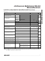
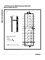
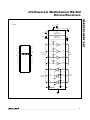
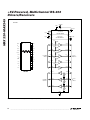
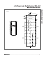
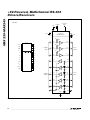
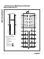
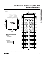
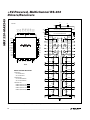
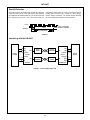
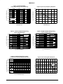
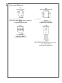
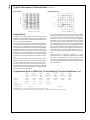
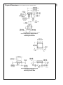
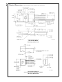
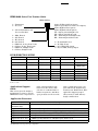
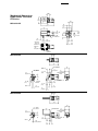
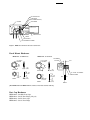
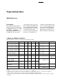
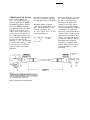
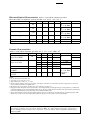
1
■ introduction ■ Spécification du produit ■ installation ■ fonctionnement ■ Dépannage ■ Référence ■ Contact Introduction DESCRIPTION SOMMAIRE DU PRODUIT : Le " LMKG série 2001 " est un système d'alarme programmable à dispositifs de sécurité multiples, conçu pour tout établissement nécessitant une surveillance constante. Il a été conçu en premier lieu comme matériel pédagogique pouvant servir dans les cours de Projets et de Dépannages. Le système est modulaire et facile à dépanner. ● ● ● ● Le système " LMKG " comprend quatre modes de détection : Caméra de surveillance fixe servant de témoin pour l'endroit à surveillé. Détecteur de mouvement par réflexions. Capteur de chaleur programmable. Capteur magnétique, pour détecter un déplacement. Tous les capteurs sont reliés au système d'alarme. Du système d'alarme les données sont transmises par fibre optique full duplex jusqu'à l'interface (convertisseur port série rs-232) au PC. Le PC pourra ainsi lire toutes les informations utiles telles que la température, introduction d'un intrus et déplacement d'un objet. Ce système est idéal pour contrôler la sécurité et réduire le nombre d'agent de sécurité. Le " LMKG série 2001" est indispensable pour toutes applications commerciale, gouvernementale et industrielles. http://www.angelfire.com/electronic/azmuth1/projet1.html [2001-03-28 22:43:10] introduction Introduction DESCRIPTION SOMMAIRE DU PRODUIT : Le " LMKG série 2001 " est un système d'alarme programmable à dispositifs de sécurité multiples, conçu pour tout établissement nécessitant une surveillance constante. Il a été conçu en premier lieu comme matériel pédagogique pouvant servir dans les cours de Projets et de Dépannages. Le système est modulaire et facile à dépanner. ● ● ● ● Le système " LMKG " comprend quatre modes de détection : Caméra de surveillance fixe servant de témoin pour l'endroit à surveillé. Détecteur de mouvement par réflexions. Capteur de chaleur programmable. Capteur magnétique, pour détecter un déplacement. Tous les capteurs sont reliés au système d'alarme. Du système d'alarme les données sont transmises par fibre optique full duplex jusqu'à l'interface (convertisseur port série rs-232) au PC. Le PC pourra ainsi lire toutes les informations utiles telles que la température, introduction d'un intrus et déplacement d'un objet. Ce système est idéal pour contrôler la sécurité et réduire le nombre d'agent de sécurité. Le " LMKG série 2001" est indispensable pour toutes applications commerciale, gouvernementale et industrielles. http://www.angelfire.com/electronic/azmuth1/intro.html [2001-03-28 22:43:20] Spécifications Spécifications SPÉCIFICATIONS DU PRODUIT Le système est subdiviser en trois parties distinctes : ● ● ● Un système de traitement de l'information. Un système de transmission/réception. Un système de gestion. Chaque parties seront détaillées dans les lignes suivantes : Spécification du capteur électromagnétique capteur électromagnétique sortie deux états possibles alimentation +5 volts DC Spécification du capteur de température Capteur de température sortie deux états possibles alimentation +5 volts DC Spécification du détecteur de mouvement Capteur de mouvement sortie numérique alimentation +30 volts DC http://www.angelfire.com/electronic/azmuth1/speci1.HTML [2001-03-28 22:43:29] Spécifications Spécifications Spécifications de la carte I/O Carte I/O alimentation deux états: capteur de température, capteur de mouvent, capteur infra-rouge, module fibre optique vers micro-contrôleur +15 v, -15 v, +5 v Amplificateur de température gain de 10 avec un offset de 1volt entrée Amplificateur de détecteur de mouvement gain de 18 2 buffers sortie utilisé les portes ET du 7400 numérique: avertisseur sonore, led vert, led rouge, lien f.o vers le pc Spécifications de la carte RS-232 RS-232 entrée/sortie deux états alimentation d'entrée +5 volts DC alimentation de sortie +12 v, -12 v, port série du pc Spécifications du TX/RX fibre optique TX/RX entrée/sortie deux états alimentation +5 volts taux de transfert max 9600 communication full duplex fibre optique multimode, 62.5/125 micro-mètre type de connecteur ST Pour des spécification sur le UART et le micro-contrôleur, voir la page de référence. http://www.angelfire.com/electronic/azmuth1/speci2.HTML [2001-03-28 22:43:35] Installation Installation MATÉRIEL REQUIS: ● ● ● 1 kit LMKG série 2001 Ordinateur 1 tournevis étoile moyen LISTE DES PIÈCES POUR UN KIT DE LMKG SÉRIE 2001 ● ● ● ● ● ● ● ● ● ● ● ● ● ● ● ● ● 1 Boîtier 1 Bloc d'alimentation ( +/-5Vdc +/- 12 V dc +/- 30 V dc) 1 Carte bus 1 Carte Contrôleur MC 1 Carte Communication série UART 1 Carte I/Oü 1 Carte interface rs-232 1 Carte win TV 1 Disquette 1 Avertisseur sonore 1 Capteur électromagnétique 1 Capteur de chaleur 1 Détecteur de mouvement 1 Mini-caméraü 1 Fil RCA 2 Transmetteurs à fibre optique 2 Récepteurs à fibre optique 2 Fibres optiques ü 1 Plaque réfléchissante 1 Sac de vis PROCÉDURE D'INSTALLATION 1. Déballer les pièces et vérifiez la liste. 2. Fixer le bloc d'alimentation et alimenter la carte bus à +5V dc et +/-15 V dc, le détecteur de mouvement à +/-30 V dc, les transmetteurs et récepteurs à 5V dc et le RS-232 à+5V dc. 3. Alimenter la mini-caméra 120V ac. 4. Installer la " Carte Contrôleur MC " dans la fente MC de la carte Bus. 5. Installer la " Carte Communication série UART " dans la fente COM de la carte Bus. 6. Installer la " Carte I/O " dans une des fente I/O de la carte Bus 7. Installer la " Carte interface RS-232 " à l'arrière de l'ordinateur sur un port série libre. http://www.angelfire.com/electronic/azmuth1/installation.html (1 of 2) [2001-03-28 22:43:42] Installation Mini-caméra 1. Avant d'installer la carte Win TV mettre le PC hors tension. 2. Toucher le châssis du PC avec la main pour décharger de toute électricité statique, avant de sortir la carte de son emballage. 3. Insérer la carte Win TV dans le connecteur PCI disponible(connecteur bu- master PCI).Il est important que Windows 95/98 soit installé. 4. Pour installer la caméra, il suffit de raccorder la prise RCA(vidéo)de la caméra à la prise RCA de la carte Win TV dans le PC. 5. Alimenter la caméra à l'aide du bloc d'alimentation fourni. 6. Ouvrir le programme hauppauge,Win TV 32. Avertisseur sonore 1.L'alimentation de l'avertisseur sonore est sur la carte I/O (5 Vdc) 2.Installer l'avertisseur prêt de l'objet à protéger. Capteur de chaleur 1.Alimenter à 5Vdc+mise à la terre.. 2.Installer la capteur de chaleur dans le centre de la pièce pour avoir une meilleur température d'ensemble. Capteur électromagnétique 1.Alimenter 5 Vdc +mise à la terre. 2.Installer le capteur sous l'objet. Détecteur de mouvement 1.Alimenter à 30Vdc +mise à la terre. 2.Installer le détecteur de mouvement devant l'objet a protéger et installer la plaque réfléchissante devant l'objectif. Module transmission et de réception à fibre optique 1.Toujours installer les deux connecteurs au module à fibre optique avant d'alimenter les modules, pour la transmission et la réception. 2.Ne jamais regarder dedans la fibre si elle est allimentée. 3.Alimenter le premier module à 5 Vdc + la mise à la terre. 4.Installer le module 1 prêt du boiter du système d'alarme. 5.Alimenter le module2 à 5 Vdc +la mise à la terre. 6.Installer l e module 2 prêt du PC et installer entré et la sortie du module au RS-232. Programme principale 1.Insérer la disquette du programme principale dans le lecteur A. 2.Aller dans le poste de travail, double click sur disquette A et double click sur install Ce programme crée un icône sur le bureau et copie les fichiers dans l'ordinateur. 3..Exécuter le programme. 4.Choisisser votre code d'accès et un nom d'utilisateur. 7. Relier avec le câble coaxiale de 20 cm la carte Communication RF 916 MHz au connecteur du boîtier. 8. Fermer le couvercle & connectez l'antenne sur le connecteur du boîtier 9. Brancher les senseurs, sonde, actionneur etc. sur la carte I/O http://www.angelfire.com/electronic/azmuth1/installation.html (2 of 2) [2001-03-28 22:43:42] Installation(suite) Installation(suite) CARTE BUS ISA À partir de cette carte vous pouvez insérez les cartes à connection ISA Chaque emplacement est bien identifier. Carte I/O Vous insérez la carte I/O Carte micro-contrôleur Vous insérez la carte du micro-contrôleur http://www.angelfire.com/electronic/azmuth1/installation2.html (1 of 2) [2001-03-28 22:43:59] Installation(suite) Carte UART Vous insérez la carte du UART http://www.angelfire.com/electronic/azmuth1/installation2.html (2 of 2) [2001-03-28 22:43:59] Installation Installation Fibre optique Pour alimenter le module de la fibre optique TX/RX, on prend l'alimentation sur le bornier de la carte I/O(5V, mise à la terre) MAX RS-232 On installe le MAX 232 à la sortie du module de la fibre optique (Vin et Vout) et le RS 232 à l'entrée du connecteur DB-9(série) du PC" et les quatre capteurs sont installés sur les borniers de la carte I/O. http://www.angelfire.com/electronic/azmuth1/installation3.html [2001-03-28 22:44:11] Fonctionnement Fonctionnement global Fonctionnement global: Fonctionnement global Avertisseur sonore : Lorsqu'une alarme est activée, l'avertisseur sonore se met en fonction. Capteur magnétique : Le capteur magnétique gère les allée et venue dans la pièce à protéger. Capteur infra-rouge : Il détecte tout mouvements dans la pièce autour de l'endroit à protéger Capteur de température : Lis la température ambiante de la pièce afin de respecter les normes pré-établies. Carte I/O : Elle adapte les signaux provenant des capteurs afin qu'ils soient correctement transmis au micro-contrôleur. Elle sert aussi d'interface entre le UART et le module TX, RX fibre optique . Caméra : La caméra de surveillance sert de gardien virtuel à l'endroit protégé. Elle est reliée directement à l'interface de l'usagé (PC) par câble RCA et n'a aucune relation avec les autres modules du système. Micro-contrôleur : Le programme insérer dans le micro-contrôleur gère les capteurs reliés à la carte I/O et transmet numériquement au UART l'information provenant de cette dernières. UART : Sa principale fonction est de convertir les données parallèle provenant du micro-contrôleur en données sérielles à des fins de transport et vice-versa.. Il est relié à la carte I/O pour permettre la transmission des données au module TX-RX fibre optique. Modules de transmission et de réception fibre optique : Ces deux modules adaptent le signal électriques à la sortie du UART en signal lumineux afin qu'il soit transmis sur fibre optique et reconverti en signal électrique avant d'entrée dans le MAX-232. N.B :Le premier module est relié à la carte I/O car c'est elle qui sert de lien entre le UART et le module fibre optique. MAX-232 : Sert d'interface entre le UART et le poste de l'usagé. Il converti les données série +5 volts qu'il reçoit en données sérielles bipolaires NRZ (+12 et -12 volts) et vice-versa. Il est relié au UART par les deux modules de TX-RX fibre optique. Poste de l'usagé : Agit comme poste de contrôle pour tous les modules contrôlés par le micro-contrôleur. Il permet l'activation et la désactivation du système d'alarme. Un code d'utilisateur est nécessaire afin d'y accéder. Carte bus : Elle est utilisée comme support et inter relie la carte M.C, huart et la carte I/O . Plan de fonctionnement À la page suivant vous pourrez visionner le fonctionnement de la programmation utilisée pour le projet. http://www.angelfire.com/electronic/azmuth1/foncglo.HTML [2001-03-28 22:44:18] http://www.angelfire.com/electronic/azmuth1/capteurvisio.jpg http://www.angelfire.com/electronic/azmuth1/capteurvisio.jpg [2001-03-28 22:44:28] Fonctionnement(suite) Fonctionnement (suite) Fonctionnement des programmes Micro- contrôleur et visual basic. Le LMKG alarme série 2001 possède un interface facile d'utilisation crée à l'aide de Visual Basic. Dans ce chapitre une brève explication du fonctionnement des programmes vous aideront à mieux comprendre de quel façon fonctionne le système. Micro- contrôleur Le micro contrôleur 68705 R3 à été programmer de tel façon, que lorsque le système se met en marche, il transmet des données envers l'interface PC afin de donnée l'état des capteurs ainsi que l'état de la température. Si un capteurs est activé ou si la température augmente ou s'abaisse à des point critiques, le micro déclenche automatiquement un avertisseur sonore en plus d'un voyant lumineux rouge pour signifier qu'il y a alarme. Ensuite le micro envoie l'état de ses capteurs et de la température vers le Pc. voir l'organigramme de transmission du micro-contrôleur voir l'organigramme de réception du micro-contrôleur voir la programmation Visual Basic L'interface sur le Pc à été crée à l'aide de VB. Le fonctionnement de la programmation VB est comme suit. Premièrement , lorsque l'utilisateur met en fonction l'interface à l'aide de son nom et de son mot de passe, le Vb active le port série afin de recevoir les données envoyer par le micro. Ensuite il gère la longueur de la trame envoyer par le micro afin de bien mettre les bonne données aux bons endroits. Par exemple lorsque le Pc a reçu le caractère " a " envoyer par le micro, il sait que c'est le début de la trame et commence à entrer ses données dans le buffer et lorsque sa trame est complète il affiche les résultats à l'écran. Lorsque l'usager se " log " une caméra est activer afin de pouvoir avoir une vue d'ensemble de l'endroit à surveiller. Sil y a alarme, l'interface indique clairement à l'usager à l'aide de dessin représentatif qui se met à flasher où se situe l'alarme. De plus, si l'usager ne se retrouve pas devant son poste au moment de l'alarme, le VB envoie un message directement sur le paget de l'usager. voir l'organigramme générale voir l'organigramme de réception http://www.angelfire.com/electronic/azmuth1/foncvb.html (1 of 2) [2001-03-28 22:44:35] Fonctionnement(suite) http://www.angelfire.com/electronic/azmuth1/foncvb.html (2 of 2) [2001-03-28 22:44:35] http://www.angelfire.com/electronic/azmuth1/dgtranmic.jpg http://www.angelfire.com/electronic/azmuth1/dgtranmic.jpg (1 of 3) [2001-03-28 22:44:59] http://www.angelfire.com/electronic/azmuth1/dgtranmic.jpg http://www.angelfire.com/electronic/azmuth1/dgtranmic.jpg (2 of 3) [2001-03-28 22:44:59] http://www.angelfire.com/electronic/azmuth1/dgtranmic.jpg http://www.angelfire.com/electronic/azmuth1/dgtranmic.jpg (3 of 3) [2001-03-28 22:44:59] http://www.angelfire.com/electronic/azmuth1/dgrecmic.jpg http://www.angelfire.com/electronic/azmuth1/dgrecmic.jpg (1 of 2) [2001-03-28 22:45:12] http://www.angelfire.com/electronic/azmuth1/dgrecmic.jpg http://www.angelfire.com/electronic/azmuth1/dgrecmic.jpg (2 of 2) [2001-03-28 22:45:12] Programme de micro 68705-R3 Programme du micro-contrôleur *************************************************** * Projet : SYSTEME D'ALARME * * Titre : Programmme Test pour TEMPERATURE * ** * Fichier : UARTEST2.ASM * * Auteur : MARTIN GAGNON * * Vers Orig : V1.0 * * Date : 01/12/2000 * * Vers Cour : V1.1 * * Date : 01/12/2000 * * Note Vers : * ** * Ordinateur : PC * * Compilateur : IASM05 * * Microcontrl : MC68705 R3 * * Fonct Prg : * *************************************************** * Definition des Variables * *************************************************** Debut EQU $80 ; Adr debut du code PRG PortA EQU $00 ; Adr Port Interrupteurs PortB EQU $01 ; Adr port d'Affichage PortC EQU $02 ; Adr Port 3 LED et + DDRA EQU $04 ; Adr Data Direct Port A DDRB EQU $05 ; Adr Data Direct Port B DDRC EQU $06 ; Adr Data Direct Port C TDR EQU $08 ; Adr Regist Data Timer TCR EQU $09 ; Adr Regist Contrl Timer MR EQU $0A ; Adr Regist Miscellaneous ACR EQU $0E ; Adr Regist Contrl A/N ARR EQU $0F ; Adr Regist Result A/N VALEUR EQU $10 ; memorise le valeur A/N Temp1 EQU $12 Temp2 EQU $13 Temp3 EQU $14 ATemp EQU $15 ; Adr Temporaire accumulateur XTemp EQU $16 ; Adr Temporaire reg index XTemp1 EQU $17 CAPTEUR EQU $18 ; MEMORISE ETAT DES CAPTEURS ALARME EQU $19 ; ETAT DE L ALARME CAPT1 EQU 0 ; PD0 CAPT2 EQU 1 ; PA5 CAPT3 EQU 2 ; PA6 LED1 EQU 4 ; PC0 LED2 EQU 5 ; PC1 BUZZER EQU 6 ; PC2 TBRL EQU 3 ; Bascule INV pour activer http://www.angelfire.com/electronic/azmuth1/progmic.html (1 of 6) [2001-03-28 22:45:20] Programme de micro 68705-R3 ; la Tx du UART ( PA0 ) ; CTRL sur PB1 ;CRL EQU ; Bascule pour charger les ; param de Tx et Rx du UART ; CTRL sur PA1 DDR EQU 1 ; TRE EQU 2 ; RRD EQU 0 Vecteurs EQU $FF8 ; Adr depart des Vecteurs *************************************************** * Debut du Programme * *************************************************** ORG Debut *************************************************** * UART RBR1-8 HIGH IMPEDANCE * *************************************************** DEPART_RESET BSET RRD,PORTA ; MET LE UART EN TX ET MET ; EN HAUTE IMPEDANCE LE ; RBR1-8 *************************************************** * Initialisation des variables * *************************************************** CLR XTemp CLR ATEMP CLR TEMP1 CLR VALEUR CLR CAPTEUR CLR ALARME *************************************************** * Definition des Ports en Entree/Sortie * *************************************************** * LE PORT A: * *************************************************** LDA #%10011011 ;Les 8 bits du port A STA DDRA ;sont defini en entrees/SORTIE *************************************************** * LE PORT B: * *************************************************** LDA #$FF ;Les 8 bits port B STA DDRB ; PORT DATA UART *************************************************** * LE PORT C: * *************************************************** LDA #%00001111 ;Les 8 bits du port C STA DDRC ; JSR SRINITUART ; Initialise le UART *************************************************** * Programme Principal * *************************************************** http://www.angelfire.com/electronic/azmuth1/progmic.html (2 of 6) [2001-03-28 22:45:20] Programme de micro 68705-R3 BSET RRD,PORTA ; MET LE UART EN TX ET MET ; EN HAUTE IMPEDANCE LE ; RBR1-8 DEPART BCLR 0,PORTC BSET 1,PORTC BCLR 2,PORTC LDA PORTA AND #%01100000 LSRA LSRA LSRA LSRA LSRA STA CAPTEUR JSR SRLIREVALEUR; lit le Canal 0 JSR SRAFFICHE ; AFFICHE VALEUR LDA Valeur ; CMP #!178 ; ( 3.5V ) BHI MSG1 ; CMP #!76 ; ( 1.5V ) BLO MSG1 LDA CAPTEUR CMP #$00 BEQ ATTEND MSG1 JSR ALLED ; (ALLUME LED) BSET 2,PORTC JSR SRMSG1 JSR SRMSG1 JSR SRRECEPTION ;INCLURE SOUS ROUTINE DE RECEPTION DE CARACTERE BRA DEPART ATTEND JSR SRMSG1 JSR SRDELAI BRA DEPART ; RECOMMENCE *************************************************** * SECTION SOUS-ROUTINE * *************************************************** *************************************************** * Sous Routine: Initialise le UART * *************************************************** SRINITUART BSET TBRL,PortA ; Init TBRL BSET DDR,PortA ; DRR -|_|NOP BCLR DDR,PortA ; Charge parametres NOP ; de TX et de Rx BSET DDR,PortA ; (e.i. 8 N 1 ) RTS *************************************************** * Sous Routine: Lecture d'un Canal 0 * *************************************************** http://www.angelfire.com/electronic/azmuth1/progmic.html (3 of 6) [2001-03-28 22:45:20] Programme de micro 68705-R3 SRLIREVALEUR LDA #$00 ; choisi canal 0 ; et active Conv STA ACR LOOPAN0 BRCLR 7,ACR,LOOPAN0 LDA ARR STA VALEUR ; sauve valeur RTS *************************************************** * Sous Routine: TRANSMETTRE TRAME * ** *************************************************** SRMSG1 LDA #'A' ; BIT DE VERIFICATION JSR SRUARTXCAR ; affiche 1 caractere JSR SRDELAI LDA #'B' ; BIT DE VERIFICATION JSR SRUARTXCAR ; affiche 1 caractere JSR SRDELAI LDA #'C' ; BIT DE VERIFICATION JSR SRUARTXCAR ; affiche 1 caractere JSR SRDELAI LDA #'D' ; BIT DE VERIFICATION JSR SRUARTXCAR ; affiche 1 caractere JSR SRDELAI LDA VALEUR ; ENVOIE TEMPÉRATURE JSR SRUARTXCAR ; affiche 1 caractere JSR SRDELAI LDA CAPTEUR ; ÉTAT DES CAPTEURS ADD #$30 JSR SRUARTXCAR ; affiche 1 caractere JSR SRDELAI LDA ALARME ; ETAT DES ALARMES JSR SRUARTXCAR ; affiche 1 caractere JSR SRDELAI LDA #'E' ; BIT DE FIN JSR SRUARTXCAR ; affiche 1 caractere JSR SRDELAI RTS ; retour prog princ *************************************************** * Sous Routine: TX un CARACTERE AVEC UART * *************************************************** SRUARTXCAR STA PortB ; Place la donnee ; sur Reg TX UART ; TBR0-TBR7 NOP NOP BCLR TBRL,PortA ; Active la transmission NOP NOP ; Dmin 150 ns BSET TBRL,PortA ; RTS http://www.angelfire.com/electronic/azmuth1/progmic.html (4 of 6) [2001-03-28 22:45:20] Programme de micro 68705-R3 *************************************************** * Sous Routine: DELAI ENTRE LES LECTURES * *************************************************** SRDELAI LDA #$FF ; Nombre de fois que la boucle ; interne sera repetee(1 a 255) CompInt LDX #$FF ; Valeur a compter de la boucle interne Compteur DECX ; Decremente la Valeur a Compter interne BNE Compteur; Branche a Compteur si CompInt n'est pas zero DECA ; Enleve 1 a la valeur cible BNE CompInt ; Recommence la boucle interne tant que ; la cible n'est pas zero RTS *************************************************** * Sous Routine : d'affiche * *************************************************** SRAFFICHE LDA VALEUR ; LIRE VALEUR STA PORTB ; AFFICHE PORT B RTS *************************************************** * SOUS-ROUTINE LED * *************************************************** ALLED BSET 0,PORTc ; bclr 1,portc ; A CHANGER RTS **************************************************** ***************************************************** * SOUS-ROUTINE DE RÉCEPTION DE CARACTERE * ***************************************************** SRRECEPTION LDA #$00 STA DDRB BCLR RRD,PORTA ; REMET LE UART EN RECEPTION STOP LDA PORTB STA ALARME CMP #%00000001 BNE STOP BCLR 2,PORTC STOP1 LDA PORTB STA ALARME CMP #%00000010 BNE STOP1 BSET RRD,PORTA ; MET LE UART EN TX ET MET ; EN HAUTE IMPEDANCE LE ; RBR1-8 LDA #$FF STA DDRB http://www.angelfire.com/electronic/azmuth1/progmic.html (5 of 6) [2001-03-28 22:45:20] Programme de micro 68705-R3 BCLR 0,PORTC BSET 1,PORTC CLR XTemp CLR ATEMP CLR TEMP1 CLR VALEUR CLR CAPTEUR CLR ALARME RTS ***************************************************** * Definition des Vecteurs d'Interruption * ***************************************************** ORG Vecteurs IntTimer FDB DEPART IntExterne FDB DEPART IntLogiciel FDB DEPART Reset FDB DEPART_RESET http://www.angelfire.com/electronic/azmuth1/progmic.html (6 of 6) [2001-03-28 22:45:20] http://www.angelfire.com/electronic/azmuth1/ogvb.jpg http://www.angelfire.com/electronic/azmuth1/ogvb.jpg (1 of 2) [2001-03-28 22:45:28] http://www.angelfire.com/electronic/azmuth1/ogvb.jpg http://www.angelfire.com/electronic/azmuth1/ogvb.jpg (2 of 2) [2001-03-28 22:45:28] http://www.angelfire.com/electronic/azmuth1/ogrecvb.jpg http://www.angelfire.com/electronic/azmuth1/ogrecvb.jpg (1 of 3) [2001-03-28 22:45:41] http://www.angelfire.com/electronic/azmuth1/ogrecvb.jpg http://www.angelfire.com/electronic/azmuth1/ogrecvb.jpg (2 of 3) [2001-03-28 22:45:41] http://www.angelfire.com/electronic/azmuth1/ogrecvb.jpg http://www.angelfire.com/electronic/azmuth1/ogrecvb.jpg (3 of 3) [2001-03-28 22:45:41] fonctionnement Procédures de tests procédures de tests Procédure de test : Test du capteur magnétique 1- Alimenter le capteur avec une tension de 5 volts. 2- Installer les sondes d'oscilloscopes. 3- Calibrer les sondes d'oscilloscopes. 4- Mettre sous-tension. Résultats du test # 6 : Test du capteur magnétique 1- Lorsque l'aimant est rapproché du contact, à l'écran de l'oscilloscope, une tension continue de 5 volts est obtenue. Ce qui indique que le relais est en position ouvert et qu'il n'y a pas de continuité électrique à l'intérieur de celui-ci. 2- Quand l'aimant est éloigné du contact, la tension aux bornes de celui-ci devient nulle. À ce moment le courant est maximum et est limité par une résistance de 1kW située entre la source et le contact. capteur magnétique http://www.angelfire.com/electronic/azmuth1/proced6.html [2001-03-28 22:45:48] http://www.angelfire.com/electronic/azmuth1/capteurmagnet.jpg http://www.angelfire.com/electronic/azmuth1/capteurmagnet.jpg [2001-03-28 22:45:53] Fonctionnement Procédure de tests (suite) suite...procédures de test Procédure de test : Test de l'avertisseur sonore 1- Alimenter le capteur à 5 volts. Résultats du test : Test de l'avertisseur sonore Des qu'il est alimenté, l'avertisseur sonore émet un signal. Avec le multimètre nous avons vérifié combien de courant est consommé (2 milliampères). Avec la programmation, l'avertisseur sonore va fonctionner par intermittence dès qu'un capteur détecte une situation anormale. http://www.angelfire.com/electronic/azmuth1/proced8.html [2001-03-28 22:46:00] fonctionnement Procédures de tests (suite) Procédure de test (suite) : Test du capteur de température 1- Alimenter le capteur tel qu'indiqué dans les fiches techniques pour que celui-ci soit capable d'indiquer des valeurs autant positives que négatives. 2- Calibrer une sonde d'oscilloscope. 3- Brancher la sonde d'oscilloscope à la patte Vout du capteur. 4- À l'aide d'un multimètre possédant une sonde de température, vérifier si le capteur réagit bien comme il est inscrit sur les fiches techniques du fabriquant. Pour de meilleur résultat, le capteur de température et la sonde du multimètre doivent être attaché ensemble pour ne pas qu'il y est d'écart de température lors des tests. 5- Tester le capteur sous des conditions au-dessus de zéro, dans les environs de 0°C, et inférieur à 0°C. Résultats du test : Test du capteur de température 1- Comme résultat de ce test, il est véridique que le capteur réagit avec 10mV par °C. Il a aussi été vérifié que la tension à 0°C correspond bien à 0V. Le capteur a été testé dans les températures négatives jusqu'à -8°C, ceci étant la température du congélateur dans lequel fut testé ce capteur. Comme le capteur a bien fonctionner jusqu'à cette température, il a été extrapolé que celui-ci continuerait de bien fonctionner jusqu'à des températures égale ou inférieure à -10°C. 2- Les résultats de l'expérimentation n'ont pas été consignés ici, dû au fait que la température lors de test est en constant changement, mais il a été vérifié que les tensions à la sortie du capteur restaient dans les normes du fabriquant. Par exemple, à 25°C, la tension à la patte Vout était ¡5mV du résultat théorique de 250 mV. (25°C * 10mV/°C = 250 mV) 3- Pour ce projet les tensions à mesurer sont de -10°C à 40°C, ce qui donne donc des tensions de sorties entre -100mV et 400 mV. http://www.angelfire.com/electronic/azmuth1/proced9.html [2001-03-28 22:46:06] Fonctionnement Procédures de tests (suite) suite...procédures de test Procédure de test : Test du détecteur de passage 1- Alimenter le détecteur à 5V. 2- Vérifier la différence de potentiel qui se crée lorsque le signal lumineux émis par le détecteur est coupé. Résultats du test : Test du détecteur de passage 1- Une fois le détecteur alimenté, une plaque réfléchissante doit être installée pour permettre le retour du signal lumineux vers sa source. Quant le signal lumineux est réfléchi correctement vers sa source, un DEL s'allume pour indiquer que le signal revient vers sa source. 2- La tension aux bornes du détecteur est de passe de 0V à 250 mV quand le signal est coupé. http://www.angelfire.com/electronic/azmuth1/proced10.html [2001-03-28 22:46:12] fonctionnement Procédures de tests (suite) suite...procédures de test Procédure de test : Test de l'amplificateur du capteur de température 1- Alimenter le circuit 2- Calibrer les sondes d'oscilloscope 3- Vérifier l'alimentation des composantes. 4- Ajuster le " offset " (PT 2) à 0V. 5- Ajuster le gain à 10. 6- Ajuster le " offset " à 1V. Résultats du test : Test de l'amplificateur du capteur de température 1- Pour ajuster le " offset " à 0V, il faut d'abord connecter l'entrée du capteur de température (patte 5) au ground, ensuite, placé une sonde d'oscilloscope au PT 2 ainsi qu'au PT 3. 2- Tourner le potentiomètre connecté à la patte 12 du MC4741 jusqu'à ce qu'une tension nulle apparaisse à l'écran de l'oscilloscope pour les deux ondes. 3- Pour ajuster le gain à 10, une sonde d'oscilloscope doit être connectée au PT 1 et une autre au PT 3. Mettre une tension inférieure à 1V à l'entrée du capteur de température (patte 5). 4- Ensuite, tourner le potentiomètre connecté à la patte 6 jusqu'à ce que la tension lue au PT 3 soit dix fois plus grande que celle lu au PT 1. 5- Pour ajuster le " offset " à 1V, il faut d'abord connecter l'entrée du capteur de température (patte 5) au ground, ensuite, placé une sonde d'oscilloscope au PT 2 ainsi qu'au PT 3. 6- Tourner le potentiomètre connecté à la patte 12 du MC4741 jusqu'à ce qu'une tension de 1V apparaisse à l'écran de l'oscilloscope pour le PT 2, et une tension correspondant à 10 fois l'entrée (patte 5) plus 1V au PT 3. Amplificateur de température http://www.angelfire.com/electronic/azmuth1/proced11.html [2001-03-28 22:46:18] http://www.angelfire.com/electronic/azmuth1/amplitemp.jpg http://www.angelfire.com/electronic/azmuth1/amplitemp.jpg [2001-03-28 22:46:31] fonctionnement Procédures de tests (suite) suite...procédures de test Procédures de test : Les lignes qui suivent explique les caractéristiques des broches utilisées pour le fonctionnement du micro-contrôleur MC-68705R3, du UART HD-6402. Ces explications permettent d'effectuer les tests nécessaires afin de s'assurer que le traitement des données se fera correctement.Il s'agit de mesurer ,à l'aide d'un multimètre ou d'un oscilloscope, la tension sur chacune de ces broches. Tests sur le micro-contrôleur MC-68705R3 : Vérifier les niveaux de tension sur les broches Vcc (pin.4) et Vpp (pin.7) du micro-contrôleur. La tension devrait être de +5 volts DC. Vérifier l'état du Vss (pin.1). Cette broche agit comme " ground ". Sur les broches EXTAL (pin.5) et XTAL (pin.6), vérifier la fréquence d'oscillation. L'oscillation devrait être d'environ 4.5 MHz. Mesurer sur ces broches : PC2 (pin.11) : alimente l'avertisseur sonore. Un niveau de tension de +5 volts fait sonner l'avertisseur. Un niveau de tension de 0 volts laisse l'avertisseur en attente. PC1 (pin.10) : alimente le LED#2. Ce voyant lumineux vert indique que le micro-contrôleur est en état de fonctionnement. PC9 (pin.9) : alimente le LED#1. Ce voyant lumineux rouge indique que le micro-contrôleur n'est pas en état de fonctionner. Registre de donnée du capteur magnétique: voir le manuel TOCCI p.159. PA7 (pin.40) et PA4 (pin.37) : Ces commandes sont les " reset " du capteur infra-rouge et magnétique. Le micro-contrôleur envoie une impulsion au registre concerné afin de le réinitialiser. PB0 (pin.25) à PB7 (pin.32) : port de réception et de transmission du micro-contrôleur. PDO/ANO (pin.24) : Cette broche converti l'information analogique reçue en format numérique. micro-contrôleur http://www.angelfire.com/electronic/azmuth1/proced14.html [2001-03-28 22:46:38] http://www.angelfire.com/electronic/azmuth1/68705.jpg http://www.angelfire.com/electronic/azmuth1/68705.jpg (1 of 2) [2001-03-28 22:47:06] http://www.angelfire.com/electronic/azmuth1/68705.jpg http://www.angelfire.com/electronic/azmuth1/68705.jpg (2 of 2) [2001-03-28 22:47:06] fonctionnement Procédures de tests suite suite...procédures de test Procédures de test du UART HD-6402 : Vérifier la tension d'entrée sur la broche Vcc (pin.1) du UART. La tension devrait être de +5 volts. La broche GND (pin.3) devrait être à 0 volt. /TBRL (pin.23) : Un niveau bas (0 volt) sur la broche /TBRL transfert l'information provenant des entrées TBR1 (pin.26) à TBR8 (pin.33). Le passage d'un niveau bas vers un niveau haut initialise le registre de transmission du UART. TRE (pin.24): Un niveau haut (+5 volts) sur TRE indique que le registre est vide et que la transmission est compléter. UART http://www.angelfire.com/electronic/azmuth1/proced15.html [2001-03-28 22:47:12] http://www.angelfire.com/electronic/azmuth1/Uart.jpg http://www.angelfire.com/electronic/azmuth1/Uart.jpg (1 of 2) [2001-03-28 22:47:33] http://www.angelfire.com/electronic/azmuth1/Uart.jpg http://www.angelfire.com/electronic/azmuth1/Uart.jpg (2 of 2) [2001-03-28 22:47:33] Installation Installation MATÉRIEL REQUIS: ● ● ● 1 kit LMKG série 2001 Ordinateur 1 tournevis étoile moyen LISTE DES PIÈCES POUR UN KIT DE LMKG SÉRIE 2001 ● ● ● ● ● ● ● ● ● ● ● ● ● ● ● ● ● 1 Boîtier 1 Bloc d'alimentation ( +/-5Vdc +/- 12 V dc +/- 30 V dc) 1 Carte bus 1 Carte Contrôleur MC 1 Carte Communication série UART 1 Carte I/Oü 1 Carte interface rs-232 1 Carte win TV 1 Disquette 1 Avertisseur sonore 1 Capteur électromagnétique 1 Capteur de chaleur 1 Détecteur de mouvement 1 Mini-caméraü 1 Fil RCA 2 Transmetteurs à fibre optique 2 Récepteurs à fibre optique 2 Fibres optiques ü 1 Plaque réfléchissante 1 Sac de vis PROCÉDURE D'INSTALLATION 1. Déballer les pièces et vérifiez la liste. 2. Fixer le bloc d'alimentation et alimenter la carte bus à +5V dc et +/-15 V dc, le détecteur de mouvement à +/-30 V dc, les transmetteurs et récepteurs à 5V dc et le RS-232 à+5V dc. 3. Alimenter la mini-caméra 120V ac. 4. Installer la " Carte Contrôleur MC " dans la fente MC de la carte Bus. 5. Installer la " Carte Communication série UART " dans la fente COM de la carte Bus. 6. Installer la " Carte I/O " dans une des fente I/O de la carte Bus 7. Installer la " Carte interface RS-232 " à l'arrière de l'ordinateur sur un port série libre. http://www.angelfire.com/electronic/azmuth1/depannage.html (1 of 2) [2001-03-28 22:47:39] Installation Mini-caméra 1. Avant d'installer la carte Win TV mettre le PC hors tension. 2. Toucher le châssis du PC avec la main pour décharger de toute électricité statique, avant de sortir la carte de son emballage. 3. Insérer la carte Win TV dans le connecteur PCI disponible(connecteur bu- master PCI).Il est important que Windows 95/98 soit installé. 4. Pour installer la caméra, il suffit de raccorder la prise RCA(vidéo)de la caméra à la prise RCA de la carte Win TV dans le PC. 5. Alimenter la caméra à l'aide du bloc d'alimentation fourni. 6. Ouvrir le programme hauppauge,Win TV 32. Avertisseur sonore 1.L'alimentation de l'avertisseur sonore est sur la carte I/O (5 Vdc) 2.Installer l'avertisseur prêt de l'objet à protéger. Capteur de chaleur 1.Alimenter à 5Vdc+mise à la terre.. 2.Installer la capteur de chaleur dans le centre de la pièce pour avoir une meilleur température d'ensemble. Capteur électromagnétique 1.Alimenter 5 Vdc +mise à la terre. 2.Installer le capteur sous l'objet. Détecteur de mouvement 1.Alimenter à 30Vdc +mise à la terre. 2.Installer le détecteur de mouvement devant l'objet a protéger et installer la plaque réfléchissante devant l'objectif. Module transmission et de réception à fibre optique 1.Toujours installer les deux connecteurs au module à fibre optique avant d'alimenter les modules, pour la transmission et la réception. 2.Ne jamais regarder dedans la fibre si elle est allimentée. 3.Alimenter le premier module à 5 Vdc + la mise à la terre. 4.Installer le module 1 prêt du boiter du système d'alarme. 5.Alimenter le module2 à 5 Vdc +la mise à la terre. 6.Installer l e module 2 prêt du PC et installer entré et la sortie du module au RS-232. Programme principale 1.Insérer la disquette du programme principale dans le lecteur A. 2.Aller dans le poste de travail, double click sur disquette A et double click sur install Ce programme crée un icône sur le bureau et copie les fichiers dans l'ordinateur. 3..Exécuter le programme. 4.Choisisser votre code d'accès et un nom d'utilisateur. 7. Relier avec le câble coaxiale de 20 cm la carte Communication RF 916 MHz au connecteur du boîtier. 8. Fermer le couvercle & connectez l'antenne sur le connecteur du boîtier 9. Brancher les senseurs, sonde, actionneur etc. sur la carte I/O http://www.angelfire.com/electronic/azmuth1/depannage.html (2 of 2) [2001-03-28 22:47:39] Référence Référence Voici une liste de référence de divers composantes du projet. le max-232 le UART Les ampli de la cartes I/O Capteur de température Module de transmission et de réception de la fibre optique Micro-contrôleur 68705 R3 Les noirs des circuits La liste des pièces http://www.angelfire.com/electronic/azmuth1/reference.html [2001-03-28 22:47:45] 19-4323; Rev 9; 4/00 +5V-Powered, Multichannel RS-232 Drivers/Receivers ____________________________Features Superior to Bipolar ♦ Operate from Single +5V Power Supply (+5V and +12V—MAX231/MAX239) ♦ Low-Power Receive Mode in Shutdown (MAX223/MAX242) ♦ Meet All EIA/TIA-232E and V.28 Specifications ♦ Multiple Drivers and Receivers ♦ 3-State Driver and Receiver Outputs ♦ Open-Line Detection (MAX243) Ordering Information ________________________Applications PART MAX220CPE MAX220CSE MAX220CWE MAX220C/D MAX220EPE MAX220ESE MAX220EWE MAX220EJE MAX220MJE Portable Computers Low-Power Modems Interface Translation Battery-Powered RS-232 Systems Multidrop RS-232 Networks TEMP. RANGE 0°C to +70°C 0°C to +70°C 0°C to +70°C 0°C to +70°C -40°C to +85°C -40°C to +85°C -40°C to +85°C -40°C to +85°C -55°C to +125°C PIN-PACKAGE 16 Plastic DIP 16 Narrow SO 16 Wide SO Dice* 16 Plastic DIP 16 Narrow SO 16 Wide SO 16 CERDIP 16 CERDIP Ordering Information continued at end of data sheet. *Contact factory for dice specifications. Selection Table Part Number MAX220 MAX222 MAX223 (MAX213) MAX225 MAX230 (MAX200) MAX231 (MAX201) MAX232 (MAX202) MAX232A MAX233 (MAX203) MAX233A MAX234 (MAX204) MAX235 (MAX205) MAX236 (MAX206) MAX237 (MAX207) MAX238 (MAX208) MAX239 (MAX209) MAX240 MAX241 (MAX211) MAX242 MAX243 MAX244 MAX245 MAX246 MAX247 MAX248 MAX249 Power Supply (V) +5 +5 +5 +5 +5 +5 and +7.5 to +13.2 +5 +5 +5 +5 +5 +5 +5 +5 +5 +5 and +7.5 to +13.2 +5 +5 +5 +5 +5 +5 +5 +5 +5 +5 No. of RS-232 Drivers/Rx 2/2 2/2 4/5 5/5 5/0 2/2 No. of Ext. Caps 4 4 4 0 4 2 Nominal Cap. Value (µF) 4.7/10 0.1 1.0 (0.1) — 1.0 (0.1) 1.0 (0.1) SHDN & ThreeState No Yes Yes Yes Yes No Rx Active in SHDN — — ✔ ✔ — — Data Rate (kbps) 120 200 120 120 120 120 2/2 2/2 2/2 2/2 4/0 5/5 4/3 5/3 4/4 3/5 4 4 0 0 4 0 4 4 4 2 1.0 (0.1) 0.1 — — 1.0 (0.1) — 1.0 (0.1) 1.0 (0.1) 1.0 (0.1) 1.0 (0.1) No No No No No Yes Yes No No No — — — — — — — — — — 120 (64) 200 120 200 120 120 120 120 120 120 5/5 4/5 2/2 2/2 8/10 8/10 8/10 8/9 8/8 6/10 4 4 4 4 4 0 0 0 4 4 1.0 1.0 (0.1) 0.1 0.1 1.0 — — — 1.0 1.0 Yes Yes Yes No No Yes Yes Yes Yes Yes — — ✔ — — ✔ ✔ ✔ ✔ ✔ 120 120 200 200 120 120 120 120 120 120 Features Ultra-low-power, industry-standard pinout Low-power shutdown MAX241 and receivers active in shutdown Available in SO 5 drivers with shutdown Standard +5/+12V or battery supplies; same functions as MAX232 Industry standard Higher slew rate, small caps No external caps No external caps, high slew rate Replaces 1488 No external caps Shutdown, three state Complements IBM PC serial port Replaces 1488 and 1489 Standard +5/+12V or battery supplies; single-package solution for IBM PC serial port DIP or flatpack package Complete IBM PC serial port Separate shutdown and enable Open-line detection simplifies cabling High slew rate High slew rate, int. caps, two shutdown modes High slew rate, int. caps, three shutdown modes High slew rate, int. caps, nine operating modes High slew rate, selective half-chip enables Available in quad flatpack package ________________________________________________________________ Maxim Integrated Products 1 For free samples & the latest literature: http://www.maxim-ic.com, or phone 1-800-998-8800. For small orders, phone 1-800-835-8769. MAX220–MAX249 General Description The MAX220–MAX249 family of line drivers/receivers is intended for all EIA/TIA-232E and V.28/V.24 communications interfaces, particularly applications where ±12V is not available. These parts are especially useful in battery-powered systems, since their low-power shutdown mode reduces power dissipation to less than 5µW. The MAX225, MAX233, MAX235, and MAX245/MAX246/MAX247 use no external components and are recommended for applications where printed circuit board space is critical. MAX220–MAX249 +5V-Powered, Multichannel RS-232 Drivers/Receivers ABSOLUTE MAXIMUM RATINGS—MAX220/222/232A/233A/242/243 20-Pin Plastic DIP (derate 8.00mW/°C above +70°C) ..440mW 16-Pin Narrow SO (derate 8.70mW/°C above +70°C) ...696mW 16-Pin Wide SO (derate 9.52mW/°C above +70°C)......762mW 18-Pin Wide SO (derate 9.52mW/°C above +70°C)......762mW 20-Pin Wide SO (derate 10.00mW/°C above +70°C)....800mW 20-Pin SSOP (derate 8.00mW/°C above +70°C) ..........640mW 16-Pin CERDIP (derate 10.00mW/°C above +70°C).....800mW 18-Pin CERDIP (derate 10.53mW/°C above +70°C).....842mW Operating Temperature Ranges MAX2_ _AC_ _, MAX2_ _C_ _ .............................0°C to +70°C MAX2_ _AE_ _, MAX2_ _E_ _ ..........................-40°C to +85°C MAX2_ _AM_ _, MAX2_ _M_ _ .......................-55°C to +125°C Storage Temperature Range .............................-65°C to +160°C Lead Temperature (soldering, 10sec) .............................+300°C Supply Voltage (VCC) ...............................................-0.3V to +6V Input Voltages TIN..............................................................-0.3V to (VCC - 0.3V) RIN (Except MAX220) ........................................................±30V RIN (MAX220).....................................................................±25V TOUT (Except MAX220) (Note 1) .......................................±15V TOUT (MAX220)...............................................................±13.2V Output Voltages TOUT ...................................................................................±15V ROUT .........................................................-0.3V to (VCC + 0.3V) Driver/Receiver Output Short Circuited to GND.........Continuous Continuous Power Dissipation (TA = +70°C) 16-Pin Plastic DIP (derate 10.53mW/°C above +70°C)....842mW 18-Pin Plastic DIP (derate 11.11mW/°C above +70°C)....889mW Note 1: Input voltage measured with TOUT in high-impedance state, SHDN or VCC = 0V. Note 2: For the MAX220, V+ and V- can have a maximum magnitude of 7V, but their absolute difference cannot exceed 13V. Stresses beyond those listed under “Absolute Maximum Ratings” may cause permanent damage to the device. These are stress ratings only, and functional operation of the device at these or any other conditions beyond those indicated in the operational sections of the specifications is not implied. Exposure to absolute maximum rating conditions for extended periods may affect device reliability. ELECTRICAL CHARACTERISTICS—MAX220/222/232A/233A/242/243 (VCC = +5V ±10%, C1–C4 = 0.1µF‚ MAX220, C1 = 0.047µF, C2–C4 = 0.33µF, TA = TMIN to TMAX‚ unless otherwise noted.) PARAMETER CONDITIONS MIN TYP MAX UNITS 0.8 V RS-232 TRANSMITTERS Output Voltage Swing All transmitter outputs loaded with 3kΩ to GND ±5 Input Logic Threshold Low Input Logic Threshold High ±8 1.4 All except MAX220 2 MAX220: VCC = 5.0V V 1.4 V 2.4 5 40 SHDN = 0V, MAX222/242, shutdown, MAX220 ±0.01 ±1 VCC = 5.5V, SHDN = 0V, VOUT = ±15V, MAX222/242 ±0.01 ±10 ±0.01 ±10 Data Rate VCC = SHDN = 0V, VOUT = ±15V All except MAX220, normal operation 200 116 Transmitter Output Resistance VCC = V+ = V- = 0V, VOUT = ±2V 300 10M Ω Output Short-Circuit Current VOUT = 0V ±7 ±22 mA All except MAX243 R2IN 0.8 1.3 MAX243 R2IN (Note 2) -3 Logic Pull-Up/lnput Current Output Leakage Current All except MAX220, normal operation µA µA kb/s RS-232 RECEIVERS RS-232 Input Voltage Operating Range ±30 RS-232 Input Threshold Low VCC = 5V RS-232 Input Threshold High VCC = 5V RS-232 Input Hysteresis 1.8 2.4 MAX243 R2IN (Note 2) -0.5 -0.1 0.5 1 RS-232 Input Resistance 2 1 3 IOUT = 3.2mA TTL/CMOS Output Voltage High IOUT = -1.0mA TTL/CMOS Output Short-Circuit Current 0.2 MAX243 TTL/CMOS Output Voltage Low V All except MAX243 R2IN All except MAX243, VCC = 5V, no hysteresis in shdn. V V V 5 7 kΩ 0.2 0.4 V 3.5 VCC - 0.2 Sourcing VOUT = GND -2 -10 Shrinking VOUT = VCC 10 30 _______________________________________________________________________________________ V mA +5V-Powered, Multichannel RS-232 Drivers/Receivers (VCC = +5V ±10%, C1–C4 = 0.1µF‚ MAX220, C1 = 0.047µF, C2–C4 = 0.33µF, TA = TMIN to TMAX‚ unless otherwise noted.) PARAMETER CONDITIONS TTL/CMOS Output Leakage Current SHDN = VCC or EN = VCC (SHDN = 0V for MAX222), 0V ≤ VOUT ≤ VCC EN Input Threshold Low MAX242 EN Input Threshold High MAX242 2.0 Operating Supply Voltage Shutdown Supply Current 3kΩ load both inputs MAX222/242 MAX220 UNITS ±0.05 ±10 µA 1.4 0.8 V 1.4 MAX222/232A/233A/242/243 4 10 MAX220 12 V mA MAX222/232A/233A/242/243 15 TA = +25°C 0.1 10 TA = 0°C to +70°C 2 50 TA = -40°C to +85°C 2 50 TA = -55°C to +125°C 35 100 ±1 µA 1.4 0.8 V MAX222/242 MAX222/242 SHDN Threshold High MAX222/242 CL = 50pF to 2500pF, MAX222/232A/233A/242/243 RL = 3kΩ to 7kΩ, VCC = 5V, TA = +25°C, measured from +3V MAX220 to -3V or -3V to +3V MAX222/232A/233A/242/243 tPHLT MAX220 tPLHT V 5.5 2 SHDN Threshold Low Transmitter Propagation Delay TLL to RS-232 (normal operation), Figure 1 MAX 0.5 SHDN Input Leakage Current Transition Slew Rate TYP 4.5 No load VCC Supply Current (SHDN = VCC), Figures 5, 6, 11, 19 MIN MAX222/232A/233A/242/243 MAX220 2.0 1.4 6 12 30 1.5 3 30 1.3 3.5 4 10 1.5 3.5 µA V V/µs 5 10 MAX222/232A/233A/242/243 0.5 1 MAX220 0.6 3 MAX222/232A/233A/242/243 0.6 1 µs Receiver Propagation Delay RS-232 to TLL (normal operation), Figure 2 tPHLR MAX220 0.8 3 Receiver Propagation Delay RS-232 to TLL (shutdown), Figure 2 tPHLS MAX242 0.5 10 tPLHS MAX242 2.5 10 Receiver-Output Enable Time, Figure 3 tER MAX242 125 500 ns Receiver-Output Disable Time, Figure 3 tDR MAX242 160 500 ns Transmitter-Output Enable Time (SHDN goes high), Figure 4 tET MAX222/242, 0.1µF caps (includes charge-pump start-up) 250 µs Transmitter-Output Disable Time (SHDN goes low), Figure 4 tDT MAX222/242, 0.1µF caps 600 ns Transmitter + to - Propagation Delay Difference (normal operation) tPHLT - tPLHT Receiver + to - Propagation Delay Difference (normal operation) tPHLR - tPLHR tPLHR MAX222/232A/233A/242/243 300 MAX220 2000 MAX222/232A/233A/242/243 100 MAX220 225 µs µs ns ns Note 3: MAX243 R2OUT is guaranteed to be low when R2IN is ≥ 0V or is floating. _______________________________________________________________________________________ 3 MAX220–MAX249 ELECTRICAL CHARACTERISTICS—MAX220/222/232A/233A/242/243 (continued) __________________________________________Typical Operating Characteristics MAX220/MAX222/MAX232A/MAX233A/MAX242/MAX243 4 VCC = ±5V NO LOAD ON TRANSMITTER OUTPUTS (EXCEPT MAX220, MAX233A) 2 0 0.1µF V- LOADED, NO LOAD ON V+ -2 1µF 0.1µF -4 ALL CAPS 1µF 9 VCC = +5.25V 8 ALL CAPS 0.1µF 7 1µF CAPS V+ V+, V- VOLTAGE (V) EITHER V+ OR V- LOADED +10V MAX220-02 6 OUTPUT LOAD CURRENT FLOWS FROM V+ TO V- 10 OUTPUT CURRENT (mA) 1µF 8 11 MAX220-01 10 MAX222/MAX242 ON-TIME EXITING SHUTDOWN VCC = +4.75V +5V +5V V+ 0.1µF CAPS SHDN 0V 0V 1µF CAPS 6 -6 V+ LOADED, NO LOAD ON V- -10 0 5 10 15 LOAD CURRENT (mA) 4 0.1µF CAPS 5 -8 20 25 V4 V- -10V 0 10 20 30 40 50 60 500µs/div DATA RATE (kbits/sec) _______________________________________________________________________________________ MAX220-03 AVAILABLE OUTPUT CURRENT vs. DATA RATE OUTPUT VOLTAGE vs. LOAD CURRENT OUTPUT VOLTAGE (V) MAX220–MAX249 +5V-Powered, Multichannel RS-232 Drivers/Receivers +5V-Powered, Multichannel RS-232 Drivers/Receivers 20-Pin Wide SO (derate 10 00mW/°C above +70°C).......800mW 24-Pin Wide SO (derate 11.76mW/°C above +70°C).......941mW 28-Pin Wide SO (derate 12.50mW/°C above +70°C) .............1W 44-Pin Plastic FP (derate 11.11mW/°C above +70°C) .....889mW 14-Pin CERDIP (derate 9.09mW/°C above +70°C) ..........727mW 16-Pin CERDIP (derate 10.00mW/°C above +70°C) ........800mW 20-Pin CERDIP (derate 11.11mW/°C above +70°C) ........889mW 24-Pin Narrow CERDIP (derate 12.50mW/°C above +70°C) ..............1W 24-Pin Sidebraze (derate 20.0mW/°C above +70°C)..........1.6W 28-Pin SSOP (derate 9.52mW/°C above +70°C).............762mW Operating Temperature Ranges MAX2 _ _ C _ _......................................................0°C to +70°C MAX2 _ _ E _ _ ...................................................-40°C to +85°C MAX2 _ _ M _ _ ...............................................-55°C to +125°C Storage Temperature Range .............................-65°C to +160°C Lead Temperature (soldering, 10sec) .............................+300°C Stresses beyond those listed under “Absolute Maximum Ratings” may cause permanent damage to the device. These are stress ratings only, and functional operation of the device at these or any other conditions beyond those indicated in the operational sections of the specifications is not implied. Exposure to absolute maximum rating conditions for extended periods may affect device reliability. ELECTRICAL CHARACTERISTICS—MAX223/MAX230–MAX241 (MAX223/230/232/234/236/237/238/240/241, VCC = +5V ±10; MAX233/MAX235, VCC = 5V ±5%‚ C1–C4 = 1.0µF; MAX231/MAX239, VCC = 5V ±10%; V+ = 7.5V to 13.2V; TA = TMIN to TMAX; unless otherwise noted.) PARAMETER CONDITIONS Output Voltage Swing All transmitter outputs loaded with 3kΩ to ground VCC Power-Supply Current No load, TA = +25°C V+ Power-Supply Current MIN TYP ±5.0 ±7.3 5 10 MAX223/230/234–238/240/241 7 15 MAX231/239 0.4 1 MAX231 1.8 5 MAX239 5 15 MAX223 15 50 MAX230/235/236/240/241 1 10 TA = +25°C Input Logic Threshold Low TIN; EN, SHDN (MAX233); EN, SHDN (MAX230/235–241) 0.8 TIN 2.0 Input Logic Threshold High EN, SHDN (MAX223); EN, SHDN (MAX230/235/236/240/241) 2.4 Logic Pull-Up Current TIN = 0V mA mA µA V V 1.5 -30 UNITS V MAX232/233 Shutdown Supply Current Receiver Input Voltage Operating Range MAX 200 µA 30 V _______________________________________________________________________________________ 5 MAX220–MAX249 ABSOLUTE MAXIMUM RATINGS—MAX223/MAX230–MAX241 VCC ...........................................................................-0.3V to +6V V+ ................................................................(VCC - 0.3V) to +14V V- ............................................................................+0.3V to -14V Input Voltages TIN ............................................................-0.3V to (VCC + 0.3V) RIN......................................................................................±30V Output Voltages TOUT ...................................................(V+ + 0.3V) to (V- - 0.3V) ROUT .........................................................-0.3V to (VCC + 0.3V) Short-Circuit Duration, TOUT ......................................Continuous Continuous Power Dissipation (TA = +70°C) 14-Pin Plastic DIP (derate 10.00mW/°C above +70°C)....800mW 16-Pin Plastic DIP (derate 10.53mW/°C above +70°C)....842mW 20-Pin Plastic DIP (derate 11.11mW/°C above +70°C)....889mW 24-Pin Narrow Plastic DIP (derate 13.33mW/°C above +70°C) ..........1.07W 24-Pin Plastic DIP (derate 9.09mW/°C above +70°C)......500mW 16-Pin Wide SO (derate 9.52mW/°C above +70°C).........762mW MAX220–MAX249 +5V-Powered, Multichannel RS-232 Drivers/Receivers ELECTRICAL CHARACTERISTICS—MAX223/MAX230–MAX241 (continued) (MAX223/230/232/234/236/237/238/240/241, VCC = +5V ±10; MAX233/MAX235, VCC = 5V ±5%‚ C1–C4 = 1.0µF; MAX231/MAX239, VCC = 5V ±10%; V+ = 7.5V to 13.2V; TA = TMIN to TMAX; unless otherwise noted.) PARAMETER RS-232 Input Threshold Low RS-232 Input Threshold High CONDITIONS TA = +25°C, VCC = 5V TA = +25°C, VCC = 5V Normal operation SHDN = 5V (MAX223) SHDN = 0V (MAX235/236/240/241) MIN TYP 0.8 1.2 0.6 Normal operation SHDN = 5V (MAX223) SHDN = 0V (MAX235/236/240/241) 1.5 1.7 1.5 2.4 0.2 0.5 1.0 V 3 5 7 kΩ 0.4 V 3.5 VCC - 0.4 RS-232 Input Resistance TA = +25°C, VCC = 5V TTL/CMOS Output Voltage Low IOUT = 1.6mA (MAX231/232/233, IOUT = 3.2mA) TTL/CMOS Output Voltage High IOUT = -1mA TTL/CMOS Output Leakage Current 0V ≤ ROUT ≤ VCC; EN = 0V (MAX223); EN = VCC (MAX235–241 ) Receiver Output Enable Time Normal operation MAX223 600 MAX235/236/239/240/241 400 Receiver Output Disable Time Normal operation MAX223 900 MAX235/236/239/240/241 250 Propagation Delay Normal operation RS-232 IN to TTL/CMOS OUT, SHDN = 0V CL = 150pF (MAX223) Transmitter Output Short-Circuit Current 6 2.4 V Shutdown (MAX223) SHDN = 0V, EN = 5V (R4IN‚ R5IN) VCC = 5V, no hysteresis in shutdown Transmitter Output Resistance UNITS V Shutdown (MAX223) SHDN = 0V, EN = 5V (R4IN, R5IN) RS-232 Input Hysteresis Transition Region Slew Rate MAX 0.05 ±10 ns 10 tPHLS 4 40 tPLHS 6 40 5.1 30 3 µA ns 0.5 MAX223/MAX230/MAX234–241, TA = +25°C, VCC = 5V, RL = 3kΩ to 7kΩ‚ CL = 50pF to 2500pF, measured from +3V to -3V or -3V to +3V µs V/µs MAX231/MAX232/MAX233, TA = +25°C, VCC = 5V, RL = 3kΩ to 7kΩ, CL = 50pF to 2500pF, measured from +3V to -3V or -3V to +3V VCC = V+ = V- = 0V, VOUT = ±2V V 4 30 Ω 300 ±10 _______________________________________________________________________________________ mA mA +5V-Powered, Multichannel RS-232 Drivers/Receivers TRANSMITTER OUTPUT VOLTAGE (VOH) vs. LOAD CAPACITANCE AT DIFFERENT DATA RATES 2 TRANSMITTERS LOADED 7.2 6.5 4.5 160kbits/sec 80kbits/sec 20kbits/sec 6.6 TA = +25°C VCC = +5V 3 TRANSMITTERS LOADED RL = 3kΩ C1–C4 = 1µF 6.4 6.2 6.0 0 1000 1500 7.0 3 TRANSMITTERS LOADED 4 TRANSMITTERS LOADED 6.0 5.0 4.0 0 2500 2000 500 1000 1500 2000 2500 LOAD CAPACITANCE (pF) TRANSMITTER OUTPUT VOLTAGE (VOL) vs. VCC TRANSMITTER OUTPUT VOLTAGE (VOL) vs. LOAD CAPACITANCE AT DIFFERENT DATA RATES TRANSMITTER OUTPUT VOLTAGE (V+, V-) vs. LOAD CURRENT -7.0 TA = +25°C VCC = +5V 3 TRANSMITTERS LOADED RL = 3kΩ C1–C4 = 1µF -6.2 -6.4 VOL (V) -6.6 -7.5 1 TRANSMITTER LOADED 2 TRANSMITTERS LOADED 10 8 6 -7.0 TA = +25°C VCC = +5V C1–C4 = 1µF V- LOADED, V+ AND VNO LOAD EQUALLY ON V+ LOADED 4 160kbits/sec 80kbits/sec 20Kkbits/sec -6.8 MAX220-09 -6.0 MAX220-08 TA = +25°C C1–C4 = 1µF TRANSMITTER LOADS = 3kΩ || 2500pF V+, V- (V) -6.5 2 0 -2 V+ LOADED, NO LOAD ON V- -4 -7.2 3 TRANSMITTERS LOADED -6 -7.4 -8 5.0 VCC (V) 5.5 ALL TRANSMITTERS UNLOADED -10 -7.6 -9.0 4.5 8.0 LOAD CAPACITANCE (pF) 4 TRANSMITTERS LOADED -8.5 500 2 TRANSMITTERS LOADED 9.0 VCC (V) -6.0 -8.0 6.8 5.5 5.0 TA = +25°C VCC = +5V LOADED, RL = 3kΩ C1–C4 = 1µF 10.0 SLEW RATE (V/µs) 3 TRANSMITTERS LOADED TA = +25°C C1–C4 = 1µF TRANSMITTER 4 TRANSMITTERS LOADS = 3kΩ || 2500pF LOADED 7.0 VOL (V) VOH (V) 1 TRANSMITTER LOADED 7.5 1 TRANSMITTER LOADED 11.0 7.0 MAX220-07 VOH (V) 8.0 12.0 MAX220-05 7.4 MAX220-04 8.5 TRANSMITTER SLEW RATE vs. LOAD CAPACITANCE MAX220-06 TRANSMITTER OUTPUT VOLTAGE (VOH) vs. VCC 0 500 1000 1500 0 2500 2000 5 10 15 20 25 30 35 40 45 50 CURRENT (mA) LOAD CAPACITANCE (pF) V+, V- WHEN EXITING SHUTDOWN (1µF CAPACITORS) MAX220-13 V+ O V- SHDN* 500ms/div *SHUTDOWN POLARITY IS REVERSED FOR NON MAX241 PARTS _______________________________________________________________________________________ 7 MAX220–MAX249 __________________________________________Typical Operating Characteristics MAX223/MAX230–MAX241 MAX220–MAX249 +5V-Powered, Multichannel RS-232 Drivers/Receivers ABSOLUTE MAXIMUM RATINGS—MAX225/MAX244–MAX249 Supply Voltage (VCC) ...............................................-0.3V to +6V Input Voltages TIN‚ ENA, ENB, ENR, ENT, ENRA, ENRB, ENTA, ENTB..................................-0.3V to (VCC + 0.3V) RIN .....................................................................................±25V TOUT (Note 3).....................................................................±15V ROUT ........................................................-0.3V to (VCC + 0.3V) Short Circuit (one output at a time) TOUT to GND ............................................................Continuous ROUT to GND............................................................Continuous Continuous Power Dissipation (TA = +70°C) 28-Pin Wide SO (derate 12.50mW/°C above +70°C) .............1W 40-Pin Plastic DIP (derate 11.11mW/°C above +70°C) ...611mW 44-Pin PLCC (derate 13.33mW/°C above +70°C) ...........1.07W Operating Temperature Ranges MAX225C_ _, MAX24_C_ _ ..................................0°C to +70°C MAX225E_ _, MAX24_E_ _ ...............................-40°C to +85°C Storage Temperature Range .............................-65°C to +160°C Lead Temperature (soldering,10sec) ..............................+300°C Note 4: Input voltage measured with transmitter output in a high-impedance state, shutdown, or VCC = 0V. Stresses beyond those listed under “Absolute Maximum Ratings” may cause permanent damage to the device. These are stress ratings only, and functional operation of the device at these or any other conditions beyond those indicated in the operational sections of the specifications is not implied. Exposure to absolute maximum rating conditions for extended periods may affect device reliability. ELECTRICAL CHARACTERISTICS—MAX225/MAX244–MAX249 (MAX225, VCC = 5.0V ±5%; MAX244–MAX249, VCC = +5.0V ±10%, external capacitors C1–C4 = 1µF; TA = TMIN to TMAX; unless otherwise noted.) PARAMETER CONDITIONS MIN TYP MAX UNITS 1.4 0.8 V 2 1.4 RS-232 TRANSMITTERS Input Logic Threshold Low Input Logic Threshold High Normal operation Logic Pull-Up/lnput Current Tables 1a–1d Data Rate Tables 1a–1d, normal operation Output Voltage Swing All transmitter outputs loaded with 3kΩ to GND Output Leakage Current (shutdown) Tables 1a–1d Shutdown ±5 V 10 50 ±0.01 ±1 120 64 ±7.5 µA kbits/sec V ENA, ENB, ENT, ENTA, ENTB = VCC, VOUT = ±15V ±0.01 ±25 VCC = 0V, VOUT = ±15V ±0.01 ±25 µA Transmitter Output Resistance VCC = V+ = V- = 0V, VOUT = ±2V (Note 4) 300 10M Ω Output Short-Circuit Current VOUT = 0V ±7 ±30 mA RS-232 Input Threshold Low VCC = 5V 0.8 1.3 RS-232 Input Threshold High VCC = 5V RS-232 Input Hysteresis VCC = 5V RS-232 RECEIVERS RS-232 Input Voltage Operating Range ±25 RS-232 Input Resistance 8 2.4 0.2 0.5 1.0 V 3 5 7 kΩ 0.2 0.4 V IOUT = 3.2mA TTL/CMOS Output Voltage High IOUT = -1.0mA 3.5 VCC - 0.2 Sourcing VOUT = GND -2 -10 Shrinking VOUT = VCC 10 30 TTL/CMOS Output Leakage Current Normal operation, outputs disabled, Tables 1a–1d, 0V ≤ VOUT ≤ VCC, ENR_ = VCC V 1.8 TTL/CMOS Output Voltage Low TTL/CMOS Output Short-Circuit Current V ±0.05 _______________________________________________________________________________________ V V mA ±0.10 µA +5V-Powered, Multichannel RS-232 Drivers/Receivers (MAX225, VCC = 5.0V ±5%; MAX244–MAX249, VCC = +5.0V ±10%, external capacitors C1–C4 = 1µF; TA = TMIN to TMAX; unless otherwise noted.) PARAMETER CONDITIONS MIN TYP MAX UNITS POWER SUPPLY AND CONTROL LOGIC Operating Supply Voltage No load VCC Supply Current (normal operation) Shutdown Supply Current 3kΩ loads on all outputs MAX225 4.75 5.25 MAX244–MAX249 4.5 5.5 MAX225 10 20 MAX244–MAX249 11 30 MAX225 40 MAX244–MAX249 57 TA = +25°C 8 TA = TMIN to TMAX 50 Leakage current Control Input 25 ±1 Threshold low 1.4 Threshold high 0.8 2.4 1.4 5 10 30 V mA µA µA V AC CHARACTERISTICS Transition Slew Rate CL = 50pF to 2500pF, RL = 3kΩ to 7kΩ, VCC = 5V, TA = +25°C, measured from +3V to -3V or -3V to +3V V/µs Transmitter Propagation Delay TLL to RS-232 (normal operation), Figure 1 tPHLT 1.3 3.5 tPLHT 1.5 3.5 Receiver Propagation Delay TLL to RS-232 (normal operation), Figure 2 tPHLR 0.6 1.5 tPLHR 0.6 1.5 Receiver Propagation Delay TLL to RS-232 (low-power mode), Figure 2 tPHLS 0.6 10 tPLHS 3.0 10 Transmitter + to - Propagation Delay Difference (normal operation) tPHLT - tPLHT 350 ns Receiver + to - Propagation Delay Difference (normal operation) tPHLR - tPLHR 350 ns µs µs µs Receiver-Output Enable Time, Figure 3 tER 100 500 ns Receiver-Output Disable Time, Figure 3 tDR 100 500 ns Transmitter Enable Time Transmitter Disable Time, Figure 4 tET tDT MAX246–MAX249 (excludes charge-pump start-up) 5 µs MAX225/MAX245–MAX249 (includes charge-pump start-up) 10 ms 100 ns Note 5: The 300Ω minimum specification complies with EIA/TIA-232E, but the actual resistance when in shutdown mode or VCC = 0V is 10MΩ as is implied by the leakage specification. _______________________________________________________________________________________ 9 MAX220–MAX249 ELECTRICAL CHARACTERISTICS—MAX225/MAX244–MAX249 (continued) __________________________________________Typical Operating Characteristics MAX225/MAX244–MAX249 8 V+ AND V- LOADED EXTERNAL POWER SUPPLY 1µF CAPACITORS 12 10 40kb/s DATA RATE 8 TRANSMITTERS LOADED WITH 3kΩ 8 6 4 VCC = 5V EXTERNAL CHARGE PUMP 1µF CAPACITORS 8 TRANSMITTERS DRIVING 5kΩ AND 2000pF AT 20kbits/sec 2 0 -2 EITHER V+ OR V- LOADED 2 3 LOAD CAPACITANCE (nF) 4 5 40kb/sec 7.0 60kb/sec 6.0 V+ AND V- LOADED 100kb/sec 200kb/sec 5.5 -8 1 20kb/sec 7.5 6.5 V+ LOADED -10 0 8.0 V- LOADED -4 -6 2 VCC = 5V WITH ALL TRANSMITTERS DRIVEN LOADED WITH 5kΩ 10kb/sec 8.5 V+, V (V) OUTPUT VOLTAGE (V) 6 14 9.0 MAX220-11 VCC = 5V 4 10 10 MAX220-10 18 16 TRANSMITTER OUTPUT VOLTAGE (V+, V-) vs. LOAD CAPACITANCE AT DIFFERENT DATA RATES OUTPUT VOLTAGE vs. LOAD CURRENT FOR V+ AND V- MAX220-12 TRANSMITTER SLEW RATE vs. LOAD CAPACITANCE TRANSMITTER SLEW RATE (V/µs) MAX220–MAX249 +5V-Powered, Multichannel RS-232 Drivers/Receivers ALL CAPACITIORS 1µF 5.0 0 5 10 15 20 25 LOAD CURRENT (mA) 30 35 0 1 2 3 LOAD CAPACITANCE (nF) ______________________________________________________________________________________ 4 5 +5V-Powered, Multichannel RS-232 Drivers/Receivers MAX220–MAX249 +3V 0V* +3V 50% 50% 50% 50% INPUT INPUT 0V VCC OUTPUT V+ 0V V- OUTPUT GND tPLHR tPLHS tPHLR tPHLS tPHLT tPLHT *EXCEPT FOR R2 ON THE MAX243 WHERE -3V IS USED. Figure 1. Transmitter Propagation-Delay Timing Figure 2. Receiver Propagation-Delay Timing EN RX OUT RX IN 1k RX VCC - 2V SHDN +3V 0V a) TEST CIRCUIT 150pF EN INPUT OUTPUT DISABLE TIME (tDT) +3V V+ 0V +5V EN OUTPUT ENABLE TIME (tER) 0V -5V +3.5V V- RECEIVER OUTPUTS +0.8V a) TIMING DIAGRAM b) ENABLE TIMING +3V EN INPUT EN 1 OR 0 0V TX 3k OUTPUT DISABLE TIME (tDR) VOH VOH - 0.5V RECEIVER OUTPUTS VOL 50pF VCC - 2V VOL + 0.5V b) TEST CIRCUIT c) DISABLE TIMING Figure 3. Receiver-Output Enable and Disable Timing Figure 4. Transmitter-Output Disable Timing ______________________________________________________________________________________ 11 MAX220–MAX249 +5V-Powered, Multichannel RS-232 Drivers/Receivers Table 1a. MAX245 Control Pin Configurations ENT ENR 0 0 Normal Operation All Active All Active 0 1 Normal Operation All Active All 3-State 1 0 Shutdown All 3-State All Low-Power Receive Mode 1 1 Shutdown All 3-State All 3-State OPERATION STATUS TRANSMITTERS RECEIVERS Table 1b. MAX245 Control Pin Configurations TRANSMITTERS RECEIVERS OPERATION STATUS TA1–TA4 TB1–TB4 0 Normal Operation All Active All Active All Active All Active 0 1 Normal Operation All Active All Active RA1–RA4 3-State, RA5 Active RB1–RB4 3-State, RB5 Active 1 0 Shutdown All 3-State All 3-State All Low-Power Receive Mode All Low-Power Receive Mode 1 1 Shutdown All 3-State All 3-State RA1–RA4 3-State, RA5 Low-Power Receive Mode RB1–RB4 3-State, RB5 Low-Power Receive Mode ENT ENR 0 RA1–RA5 RB1–RB5 Table 1c. MAX246 Control Pin Configurations 12 ENA ENB 0 0 0 OPERATION STATUS TRANSMITTERS RECEIVERS TA1–TA4 TB1–TB4 RA1–RA5 Normal Operation All Active All Active All Active All Active 1 Normal Operation All Active All 3-State All Active RB1–RB4 3-State, RB5 Active 1 0 Shutdown All 3-State All Active RA1–RA4 3-State, RA5 Active All Active 1 1 Shutdown All 3-State All 3-State RA1–RA4 3-State, RA5 Low-Power Receive Mode RB1–RB4 3-State, RA5 Low-Power Receive Mode ______________________________________________________________________________________ RB1–RB5 +5V-Powered, Multichannel RS-232 Drivers/Receivers TRANSMITTERS ENTA ENTB ENRA ENRB OPERATION STATUS RECEIVERS MAX247 TA1–TA4 TB1–TB4 RA1–RA4 RB1–RB5 MAX248 TA1–TA4 TB1–TB4 RA1–RA4 RB1–RB4 MAX249 TA1–TA3 TB1–TB3 RA1–RA5 RB1–RB5 0 0 0 0 Normal Operation All Active All Active All Active All Active 0 0 0 1 Normal Operation All Active All Active All Active All 3-State, except RB5 stays active on MAX247 0 0 1 0 Normal Operation All Active All Active All 3-State All Active 0 0 1 1 Normal Operation All Active All Active All 3-State All 3-State, except RB5 stays active on MAX247 0 1 0 0 Normal Operation All Active All 3-State All Active All Active 0 1 0 1 Normal Operation All Active All 3-State All Active All 3-State, except RB5 stays active on MAX247 0 1 1 0 Normal Operation All Active All 3-State All 3-State All Active 0 1 1 1 Normal Operation All Active All 3-State All 3-State All 3-State, except RB5 stays active on MAX247 1 0 0 0 Normal Operation All 3-State All Active All Active All Active 1 0 0 1 Normal Operation All 3-State All Active All Active All 3-State, except RB5 stays active on MAX247 1 0 1 0 Normal Operation All 3-State All Active All 3-State All Active 1 0 1 1 Normal Operation All 3-State All Active All 3-State All 3-State, except RB5 stays active on MAX247 1 1 0 0 Shutdown All 3-State All 3-State Low-Power Receive Mode Low-Power Receive Mode 1 1 0 1 Shutdown All 3-State All 3-State Low-Power Receive Mode All 3-State, except RB5 stays active on MAX247 1 1 1 0 Shutdown All 3-State All 3-State All 3-State Low-Power Receive Mode 1 1 1 1 Shutdown All 3-State All 3-State All 3-State All 3-State, except RB5 stays active on MAX247 ______________________________________________________________________________________ 13 MAX220–MAX249 Table 1d. MAX247/MAX248/MAX249 Control Pin Configurations MAX220–MAX249 +5V-Powered, Multichannel RS-232 Drivers/Receivers _______________Detailed Description The MAX220–MAX249 contain four sections: dual charge-pump DC-DC voltage converters, RS-232 drivers, RS-232 receivers, and receiver and transmitter enable control inputs. Dual Charge-Pump Voltage Converter The MAX220–MAX249 have two internal charge-pumps that convert +5V to ±10V (unloaded) for RS-232 driver operation. The first converter uses capacitor C1 to double the +5V input to +10V on C3 at the V+ output. The second converter uses capacitor C2 to invert +10V to -10V on C4 at the V- output. A small amount of power may be drawn from the +10V (V+) and -10V (V-) outputs to power external circuitry (see the Typical Operating Characteristics section), except on the MAX225 and MAX245–MAX247, where these pins are not available. V+ and V- are not regulated, so the output voltage drops with increasing load current. Do not load V+ and V- to a point that violates the minimum ±5V EIA/TIA-232E driver output voltage when sourcing current from V+ and V- to external circuitry. When using the shutdown feature in the MAX222, MAX225, MAX230, MAX235, MAX236, MAX240, MAX241, and MAX245–MAX249, avoid using V+ and Vto power external circuitry. When these parts are shut down, V- falls to 0V, and V+ falls to +5V. For applications where a +10V external supply is applied to the V+ pin (instead of using the internal charge pump to generate +10V), the C1 capacitor must not be installed and the SHDN pin must be tied to VCC. This is because V+ is internally connected to VCC in shutdown mode. RS-232 Drivers The typical driver output voltage swing is ±8V when loaded with a nominal 5kΩ RS-232 receiver and VCC = +5V. Output swing is guaranteed to meet the EIA/TIA232E and V.28 specification, which calls for ±5V minimum driver output levels under worst-case conditions. These include a minimum 3kΩ load, VCC = +4.5V, and maximum operating temperature. Unloaded driver output voltage ranges from (V+ -1.3V) to (V- +0.5V). Input thresholds are both TTL and CMOS compatible. The inputs of unused drivers can be left unconnected since 400kΩ input pull-up resistors to VCC are built in (except for the MAX220). The pull-up resistors force the outputs of unused drivers low because all drivers invert. The internal input pull-up resistors typically source 12µA, except in shutdown mode where the pull-ups are disabled. Driver outputs turn off and enter a high-impedance state—where leakage current is typically microamperes (maximum 25µA)—when in shutdown 14 mode, in three-state mode, or when device power is removed. Outputs can be driven to ±15V. The powersupply current typically drops to 8µA in shutdown mode. The MAX220 does not have pull-up resistors to force the ouputs of the unused drivers low. Connect unused inputs to GND or VCC. The MAX239 has a receiver three-state control line, and the MAX223, MAX225, MAX235, MAX236, MAX240, and MAX241 have both a receiver three-state control line and a low-power shutdown control. Table 2 shows the effects of the shutdown control and receiver threestate control on the receiver outputs. The receiver TTL/CMOS outputs are in a high-impedance, three-state mode whenever the three-state enable line is high (for the MAX225/MAX235/MAX236/MAX239– MAX241), and are also high-impedance whenever the shutdown control line is high. When in low-power shutdown mode, the driver outputs are turned off and their leakage current is less than 1µA with the driver output pulled to ground. The driver output leakage remains less than 1µA, even if the transmitter output is backdriven between 0V and (VCC + 6V). Below -0.5V, the transmitter is diode clamped to ground with 1kΩ series impedance. The transmitter is also zener clamped to approximately V CC + 6V, with a series impedance of 1kΩ. The driver output slew rate is limited to less than 30V/µs as required by the EIA/TIA-232E and V.28 specifications. Typical slew rates are 24V/µs unloaded and 10V/µs loaded with 3Ω and 2500pF. RS-232 Receivers EIA/TIA-232E and V.28 specifications define a voltage level greater than 3V as a logic 0, so all receivers invert. Input thresholds are set at 0.8V and 2.4V, so receivers respond to TTL level inputs as well as EIA/TIA-232E and V.28 levels. The receiver inputs withstand an input overvoltage up to ±25V and provide input terminating resistors with Table 2. Three-State Control of Receivers PART SHDN SHDN EN EN(R) RECEIVERS MAX223 __ Low High High X Low High __ High Impedance Active High Impedance MAX225 __ __ __ Low High High Impedance Active MAX235 MAX236 MAX240 Low Low High __ __ Low High X High Impedance Active High Impedance ______________________________________________________________________________________ +5V-Powered, Multichannel RS-232 Drivers/Receivers The receiver input hysteresis is typically 0.5V with a guaranteed minimum of 0.2V. This produces clear output transitions with slow-moving input signals, even with moderate amounts of noise and ringing. The receiver propagation delay is typically 600ns and is independent of input swing direction. Low-Power Receive Mode The low-power receive-mode feature of the MAX223, MAX242, and MAX245–MAX249 puts the IC into shutdown mode but still allows it to receive information. This is important for applications where systems are periodically awakened to look for activity. Using low-power receive mode, the system can still receive a signal that will activate it on command and prepare it for communication at faster data rates. This operation conserves system power. Negative Threshold—MAX243 The MAX243 is pin compatible with the MAX232A, differing only in that RS-232 cable fault protection is removed on one of the two receiver inputs. This means that control lines such as CTS and RTS can either be driven or left floating without interrupting communication. Different cables are not needed to interface with different pieces of equipment. The input threshold of the receiver without cable fault protection is -0.8V rather than +1.4V. Its output goes positive only if the input is connected to a control line that is actively driven negative. If not driven, it defaults to the 0 or “OK to send” state. Normally‚ the MAX243’s other receiver (+1.4V threshold) is used for the data line (TD or RD)‚ while the negative threshold receiver is connected to the control line (DTR‚ DTS‚ CTS‚ RTS, etc.). Other members of the RS-232 family implement the optional cable fault protection as specified by EIA/TIA232E specifications. This means a receiver output goes high whenever its input is driven negative‚ left floating‚ or shorted to ground. The high output tells the serial communications IC to stop sending data. To avoid this‚ the control lines must either be driven or connected with jumpers to an appropriate positive voltage level. Shutdown—MAX222–MAX242 On the MAX222‚ MAX235‚ MAX236‚ MAX240‚ and MAX241‚ all receivers are disabled during shutdown. On the MAX223 and MAX242‚ two receivers continue to operate in a reduced power mode when the chip is in shutdown. Under these conditions‚ the propagation delay increases to about 2.5µs for a high-to-low input transition. When in shutdown, the receiver acts as a CMOS inverter with no hysteresis. The MAX223 and MAX242 also have a receiver output enable input (EN for the MAX242 and EN for the MAX223) that allows receiver output control independent of SHDN (SHDN for MAX241). With all other devices‚ SHDN (SHDN for MAX241) also disables the receiver outputs. The MAX225 provides five transmitters and five receivers‚ while the MAX245 provides ten receivers and eight transmitters. Both devices have separate receiver and transmitter-enable controls. The charge pumps turn off and the devices shut down when a logic high is applied to the ENT input. In this state, the supply current drops to less than 25µA and the receivers continue to operate in a low-power receive mode. Driver outputs enter a high-impedance state (three-state mode). On the MAX225‚ all five receivers are controlled by the ENR input. On the MAX245‚ eight of the receiver outputs are controlled by the ENR input‚ while the remaining two receivers (RA5 and RB5) are always active. RA1–RA4 and RB1–RB4 are put in a three-state mode when ENR is a logic high. Receiver and Transmitter Enable Control Inputs The MAX225 and MAX245–MAX249 feature transmitter and receiver enable controls. The receivers have three modes of operation: full-speed receive (normal active)‚ three-state (disabled)‚ and lowpower receive (enabled receivers continue to function at lower data rates). The receiver enable inputs control the full-speed receive and three-state modes. The transmitters have two modes of operation: full-speed transmit (normal active) and three-state (disabled). The transmitter enable inputs also control the shutdown mode. The device enters shutdown mode when all transmitters are disabled. Enabled receivers function in the low-power receive mode when in shutdown. ______________________________________________________________________________________ 15 MAX220–MAX249 nominal 5kΩ values. The receivers implement Type 1 interpretation of the fault conditions of V.28 and EIA/TIA-232E. MAX220–MAX249 +5V-Powered, Multichannel RS-232 Drivers/Receivers Tables 1a–1d define the control states. The MAX244 has no control pins and is not included in these tables. The MAX246 has ten receivers and eight drivers with two control pins, each controlling one side of the device. A logic high at the A-side control input (ENA) causes the four A-side receivers and drivers to go into a three-state mode. Similarly, the B-side control input (ENB) causes the four B-side drivers and receivers to go into a three-state mode. As in the MAX245, one Aside and one B-side receiver (RA5 and RB5) remain active at all times. The entire device is put into shutdown mode when both the A and B sides are disabled (ENA = ENB = +5V). The MAX247 provides nine receivers and eight drivers with four control pins. The ENRA and ENRB receiver enable inputs each control four receiver outputs. The ENTA and ENTB transmitter enable inputs each control four drivers. The ninth receiver (RB5) is always active. The device enters shutdown mode with a logic high on both ENTA and ENTB. The MAX248 provides eight receivers and eight drivers with four control pins. The ENRA and ENRB receiver enable inputs each control four receiver outputs. The ENTA and ENTB transmitter enable inputs control four drivers each. This part does not have an always-active receiver. The device enters shutdown mode and transmitters go into a three-state mode with a logic high on both ENTA and ENTB. 16 The MAX249 provides ten receivers and six drivers with four control pins. The ENRA and ENRB receiver enable inputs each control five receiver outputs. The ENTA and ENTB transmitter enable inputs control three drivers each. There is no always-active receiver. The device enters shutdown mode and transmitters go into a three-state mode with a logic high on both ENTA and ENTB. In shutdown mode, active receivers operate in a low-power receive mode at data rates up to 20kbits/sec. __________Applications Information Figures 5 through 25 show pin configurations and typical operating circuits. In applications that are sensitive to power-supply noise, VCC should be decoupled to ground with a capacitor of the same value as C1 and C2 connected as close as possible to the device. ______________________________________________________________________________________ +5V-Powered, Multichannel RS-232 Drivers/Receivers MAX220–MAX249 +5V INPUT C3 TOP VIEW C5 C1+ 1 1 16 VCC C1 V+ 2 15 GND C1- 3 14 T1OUT C2+ 4 C2- 5 MAX220 MAX232 MAX232A V- 6 C2 12 R1OUT 9 11 T1IN -10V C4 T1OUT 14 RS-232 OUTPUTS 400k T2OUT 7 10 T2IN R2OUT 12 R1OUT CAPACITANCE (µF) C1 C2 C3 C4 4.7 4.7 10 10 1.0 1.0 1.0 1.0 0.1 0.1 0.1 0.1 6 +5V TTL/CMOS INPUTS DIP/SO DEVICE MAX220 MAX232 MAX232A V- +5V 400k 10 T2IN R2IN 8 V+ 2 +10V 3 C14 C2+ +10V TO -10V 5 C2- VOLTAGE INVERTER 13 R1IN 11 T1IN T2OUT 7 16 VCC +5V TO +10V VOLTAGE DOUBLER C1+ R1IN 13 TTL/CMOS OUTPUTS C5 4.7 1.0 0.1 RS-232 INPUTS 5k R2IN 8 9 R2OUT 5k GND 15 Figure 5. MAX220/MAX232/MAX232A Pin Configuration and Typical Operating Circuit +5V INPUT C3 ALL CAPACITORS = 0.1µF TOP VIEW C5 17 VCC 3 +10V C1+ +5V TO +10V V+ 4 C1- VOLTAGE DOUBLER 5 C2+ 7 -10V +10V TO -10V V6 C2C4 VOLTAGE INVERTER 2 (N.C.) EN 1 (N.C.) EN 1 18 SHDN C1+ 2 19 VCC C1+ 2 17 VCC V+ 3 18 GND V+ 3 16 GND C1- 4 17 T1OUT C1- 4 15 T1OUT C2+ 5 14 R1IN C2- 6 C2+ 5 C2- 6 MAX222 MAX242 13 R1OUT V- 7 T2OUT 8 R2IN 9 DIP/SO MAX222 MAX242 15 R1IN V- 7 C2 +5V 16 N.C. 14 R1OUT 12 T1IN T2OUT 8 13 N.C. 11 T2IN R2IN 9 12 T1IN R2OUT 10 11 T2IN 10 R2OUT C1 20 SHDN TTL/CMOS INPUTS 400k 12 T1IN +5V (EXCEPT MAX220) 400k 11 T2IN (EXCEPT MAX220) T1OUT 15 13 R1OUT R1IN 14 TTL/CMOS OUTPUTS SSOP RS-232 INPUTS 5k R2IN 9 10 R2OUT 1 (N.C.) EN ( ) ARE FOR MAX222 ONLY. PIN NUMBERS IN TYPICAL OPERATING CIRCUIT ARE FOR DIP/SO PACKAGES ONLY. RS-232 OUTPUTS T2OUT 8 5k SHDN GND 18 16 Figure 6. MAX222/MAX242 Pin Configurations and Typical Operating Circuit ______________________________________________________________________________________ 17 MAX220–MAX249 +5V-Powered, Multichannel RS-232 Drivers/Receivers +5V TOP VIEW 0.1 +5V 28 VCC 27 VCC 400k T1IN 3 ENR 1 28 VCC ENR 2 27 VCC T1IN 3 26 ENT T2IN 4 25 T3IN R1OUT 5 MAX225 23 T5IN R3OUT 7 22 R4OUT R3IN 8 21 R5OUT R2IN 9 20 R5IN R1IN 10 18 T3OUT T2OUT 12 17 T4OUT GND 13 16 T5OUT GND 14 15 T5OUT T2IN 4 T2OUT +5V 12 400k T3IN 25 T3OUT +5V 18 400k T4IN 24 +5V T4OUT 17 400k 19 R4IN T1OUT 11 11 400k 24 T4IN R2OUT 6 T1OUT +5V T5OUT T5IN 23 ENT 26 T5OUT R1OUT 5 R1IN 16 15 10 5k SO R2OUT 6 R2IN 9 5k R3OUT 7 MAX225 FUNCTIONAL DESCRIPTION 5 RECEIVERS 5 TRANSMITTERS 2 CONTROL PINS 1 RECEIVER ENABLE (ENR) 1 TRANSMITTER ENABLE (ENT) R3IN 8 R4IN 19 5k R4OUT 22 5k R5OUT 21 R5IN 5k PINS (ENR, GND, VCC, T5OUT) ARE INTERNALLY CONNECTED. CONNECT EITHER OR BOTH EXTERNALLY. T5OUT IS A SINGLE DRIVER. 1 2 ENR ENR GND 13 GND 14 Figure 7. MAX225 Pin Configuration and Typical Operating Circuit 18 ______________________________________________________________________________________ 20 +5V-Powered, Multichannel RS-232 Drivers/Receivers MAX220–MAX249 +5V INPUT TOP VIEW 1.0µF 12 11 VCC +5V TO +10V VOLTAGE DOUBLER C1+ 1.0µF 14 C115 C2+ 1.0µF 16 C2- +10V TO -10V VOLTAGE INVERTER 28 T4OUT 27 R3IN T2OUT 3 26 R3OUT R2IN 4 25 SHDN (SHDN) R2OUT 5 T2IN 6 24 EN (EN) MAX223 MAX241 T1IN 7 400k 6 T2IN 21 T4IN R1IN 9 20 T3IN GND 10 19 R5OUT* VCC 11 18 R5IN* C1+ 12 17 V- V+ 13 16 C2- C1- 14 15 C2+ Wide SO/ SSOP RS-232 OUTPUTS 400k 20 T3IN T3OUT 1 T3 23 R4IN* R1OUT 8 T2OUT 3 T2 +5V 22 R4OUT* T1OUT 2 T1 +5V TTL/CMOS INPUTS 17 400k 7 T1IN T1OUT 2 V- 13 1.0µF +5V T3OUT 1 1.0µF V+ +5V 21 T4IN 8 R1OUT 400k T4 T4OUT 28 R1 R1IN 9 5k 5 R2OUT R2IN 4 R2 5k LOGIC OUTPUTS 26 R3OUT R3 R3IN 27 R4IN 23 R5IN 18 5k 22 R4OUT R4 RS-232 INPUTS 5k 19 R5OUT R5 *R4 AND R5 IN MAX223 REMAIN ACTIVE IN SHUTDOWN NOTE: PIN LABELS IN ( ) ARE FOR MAX241 5k 24 EN (EN) GND SHDN 25 (SHDN) 10 Figure 8. MAX223/MAX241 Pin Configuration and Typical Operating Circuit ______________________________________________________________________________________ 19 MAX220–MAX249 +5V-Powered, Multichannel RS-232 Drivers/Receivers +5V INPUT TOP VIEW 1.0µF 1.0µF 20 T4OUT 1 T1OUT 2 19 T5IN T2OUT 3 18 N.C. T2IN 4 1.0µF 17 SHDN MAX230 T1IN 5 16 T5OUT GND 6 15 T4IN VCC 7 14 T3IN C1+ 8 13 V- V+ 9 12 C2- C1- 10 11 C2+ 11 +10V TO -10V C2+ 12 VC2- VOLTAGE INVERTER +5V 400k T1OUT 5 T1IN T1 +5V 400k T2OUT 4 T2IN T2 +5V 400k T3OUT 14 T3IN T3 +5V 400k T4OUT 15 T4IN T4 +5V 400k T5OUT 19 T5IN T5 T1 T3OUT 7 VCC V+ 9 +5V TO +10V VOLTAGE DOUBLER 8 C1+ 10 C1- TTL/CMOS INPUTS DIP/SO N.C. x 18 1.0µF 13 1.0µF 2 3 RS-232 OUTPUTS 1 20 16 17 GND SHDN 6 Figure 9. MAX230 Pin Configuration and Typical Operating Circuit +5V INPUT TOP VIEW +7.5V TO +12V 1.0µF 13 (15) 1 2 1.0µF C+ 1 CV- 2 3 T2OUT 4 14 V+ C+ 1 16 V+ 13 VCC C- 2 15 VCC V- 3 12 GND MAX231 R2IN 5 11 T1OUT T2OUT 4 9 R1OUT T2IN 7 8 T1IN R2OUT 6 8 10 T1IN N.C. 8 9 N.C. DIP SO T1IN T1OUT 11 T1 (13) RS-232 OUTPUTS (11) 7 T2IN 9 R1OUT T2OUT 4 T2 R1IN 10 R1 TTL/CMOS INPUTS 5k 6 R2OUT (12) RS-232 INPUTS R2IN 5 R2 GND 12 (14) Figure 10. MAX231 Pin Configurations and Typical Operating Circuit 20 C2 1.0µF 400k 5k PIN NUMBERS IN ( ) ARE FOR SO PACKAGE (16) 3 +5V TTL/CMOS INPUTS 11 R1OUT T2IN 7 V- 14 400k (10) 12 R1IN R2IN 5 10 R1IN R2OUT 6 13 T1OUT C1- V+ +5V 14 GND MAX231 VCC +12V TO -12V VOLTAGE CONVERTER C1+ ______________________________________________________________________________________ +5V-Powered, Multichannel RS-232 Drivers/Receivers MAX220–MAX249 +5V INPUT 1.0µF TOP VIEW 7 VCC +5V 400k T2IN 20 R2OUT 1 T1IN 2 19 R2IN R1OUT 3 R1IN 4 T1OUT 5 GND 6 +5V TTL/CMOS INPUTS 18 T2OUT 1 T2IN 3 R1OUT 14 V+ (C1-) (V+) C1+ 8 12 V- (C2+) (V-) CS- 10 18 R1IN 4 11 C2+ (C2-) DIP/SO 5k TTL/CMOS OUTPUTS 20 R2OUT 13 C1- (C1+) GND 9 T2OUT 16 C215 C2+ VCC 7 RS-232 OUTPUTS 400k 17 V- MAX233 MAX233A T1OUT 5 T1IN 2 8 (13) DO NOT MAKE CONNECTIONS TO 13 (14) THESE PINS 12 (10) INTERNAL -10 17 POWER SUPPLY INTERNAL +10V POWER SUPPLY RS-232 OUTPUTS R2IN 19 5k C1+ C1- C2+ V- C2- V14 (8) V+ C2GND 11 (12) C2+ 15 16 10 (11) GND 6 9 ( ) ARE FOR SO PACKAGE ONLY. Figure 11. MAX233/MAX233A Pin Configuration and Typical Operating Circuit +5V INPUT 1.0µF TOP VIEW 7 1.0µF 9 10 T1OUT 1 16 T3OUT T2OUT 2 15 T4OUT T2IN 3 T1IN 4 1.0µF C1C2+ 11 C2- 6 VCC +5V TO +10V VOLTAGE DOUBLER +10V TO -10V VOLTAGE INVERTER VCC 6 13 T3IN 10 C2+ 9 V+ 8 C1- V- 12 1.0µF T1 T1OUT 1 +5V 400k 3 T2IN 11 C2- C1+ 7 V+ 400k 4 T1IN 12 V- GND 5 1.0µF 8 +5V 14 T4IN MAX234 C1+ T2 T2OUT 3 +5V TTL/CMOS INPUTS RS-232 OUTPUTS 400k 13 T3IN T3 T3OUT 16 +5V DIP/SO 400k 14 T4IN T4 T4OUT 15 GND 5 Figure 12. MAX234 Pin Configuration and Typical Operating Circuit ______________________________________________________________________________________ 21 MAX220–MAX249 +5V-Powered, Multichannel RS-232 Drivers/Receivers +5V INPUT TOP VIEW 1.0µF 12 VCC +5V 400k 8 T1IN T1 T1OUT 3 T2 T2OUT 4 +5V 400k 7 T2IN +5V 400k TTL/CMOS INPUTS T4OUT 1 24 R3IN T3OUT 2 23 R3OUT T1OUT 3 22 T5IN T2OUT 4 21 SHDN R2IN 5 MAX235 R2OUT 6 15 T3IN T3OUT 2 T3 RS-232 OUTPUTS +5V 400k 16 T4IN +5V 20 EN 22 T5IN T4OUT 1 T4 400k T5OUT 19 T5 19 T5OUT T2IN 7 18 R4IN T1IN 8 17 R4OUT R1OUT 9 16 T4IN R1IN 10 15 T3IN GND 11 14 R5OUT VCC 12 13 R5IN DIP 9 R1OUT R1IN 10 T1 5k 6 R2OUT R2IN 5 R2 5k TTL/CMOS OUTPUTS 23 R3OUT R3IN 24 R3 RS-232 INPUTS 5k 17 R4OUT R4IN 18 R4 5k 14 R5OUT R5IN 13 R5 5k 20 EN SHDN 21 GND 11 Figure 13. MAX235 Pin Configuration and Typical Operating Circuit 22 ______________________________________________________________________________________ +5V-Powered, Multichannel RS-232 Drivers/Receivers MAX220–MAX249 TOP VIEW +5V INPUT 1.0µF 9 10 1.0µF 12 13 1.0µF 1.0µF VCC +5V TO +10V VOLTAGE DOUBLER C1+ C1- V+ C2+ V- +10V TO -10V VOLTAGE INVERTER 14 C2- 11 15 1.0µF +5V 400k 7 T1IN T3OUT 1 24 T4OUT T1OUT 2 23 R2IN T2OUT 3 22 R2OUT R1IN 4 21 SHDN R1OUT 5 MAX236 +5V 400k 6 T2IN TTL/CMOS INPUTS 19 T4IN T1IN 7 18 T3IN GND 8 17 R3OUT VCC 9 16 R3IN C1+ 10 15 V- V+ 11 14 C2- C1- 12 13 C2+ T2OUT T2 3 RS-232 OUTPUTS +5V 400k 20 EN T2IN 6 T1OUT 2 T1 18 T3IN T3OUT 1 T3 +5V 400k 19 T4IN 5 R1OUT T4OUT 24 T4 R1IN 4 R1 5k DIP/SO TTL/CMOS OUTPUTS 22 R2OUT R2 R2IN 23 R3IN 16 RS-232 INPUTS 5k 17 R3OUT R3 5k 20 EN SHDN 21 GND 8 Figure 14. MAX236 Pin Configuration and Typical Operating Circuit ______________________________________________________________________________________ 23 MAX220–MAX249 +5V-Powered, Multichannel RS-232 Drivers/Receivers TOP VIEW +5V INPUT 1.0µF 10 1.0µF 12 13 1.0µF 14 C1C2+ C2- 24 T4OUT T1OUT 2 23 R2IN T2OUT 3 22 R2OUT R1IN 4 R1OUT 5 MAX237 20 T5OUT T2IN 6 19 T4IN T1IN 7 18 T3IN GND 8 17 R3OUT VCC 9 16 R3IN C1+ 10 15 V- V+ 11 14 C2- C1- 12 13 C2+ 400k TTL/CMOS INPUTS T2OUT T2 +5V 3 400k 18 T3IN T3OUT 1 T3 +5V 1.0µF T1OUT 2 T1 6 T2IN 21 T5IN 15 V- 400k 7 T1IN +5V 11 V+ +10V TO -10V VOLTAGE INVERTER +5V T3OUT 1 1.0µF 9 VCC +5V TO +10V VOLTAGE DOUBLER C1+ RS-232 OUTPUTS 400k 19 T4IN T4OUT 24 T4 +5V 400k 21 T5IN DIP/SO 5 R1OUT T5OUT 20 T5 R1IN 4 R1 5k TTL/CMOS OUTPUTS 22 R2OUT R2 R2IN 23 R3IN 16 5k 17 R3OUT R3 5k GND 8 Figure 15. MAX237 Pin Configuration and Typical Operating Circuit 24 ______________________________________________________________________________________ RS-232 INPUTS +5V-Powered, Multichannel RS-232 Drivers/Receivers MAX220–MAX249 TOP VIEW +5V INPUT 1.0µF 1.0µF 9 10 1.0µF 12 13 1.0µF 14 C1+ C1- C2- 22 R3OUT R2OUT 4 T1IN 5 20 T4OUT R1OUT 6 19 T3IN R1IN 7 18 T2IN GND 8 17 R4OUT VCC 9 16 R4IN C1+ 10 15 V- V+ 11 14 C2- C1- 12 13 C2+ 21 T4IN 6 R1OUT T1OUT 2 400k T2OUT 1 400k 19 T3IN RS-232 OUTPUTS T3OUT 24 T3 +5V 15 1.0µF T2 +5V TTL/CMOS INPUTS 11 400k 18 T2IN 21 T4IN MAX238 V- T1 +5V 23 R3IN R2IN 3 +10V TO -10V VOLTAGE INVERTER 5 T1IN 24 T3OUT T1OUT 2 V+ C2+ +5V T2OUT 1 VCC +5V TO +10V VOLTAGE DOUBLER 400k T4OUT 20 T4 R1IN 7 R1 5k DIP/SO 4 R2OUT R2IN R2 TTL/CMOS OUTPUTS 3 RS-232 INPUTS 5k 22 R3OUT R3 R3IN 23 R4IN 16 5k 17 R4OUT R4 5k GND 8 Figure 16. MAX238 Pin Configuration and Typical Operating Circuit ______________________________________________________________________________________ 25 MAX220–MAX249 +5V-Powered, Multichannel RS-232 Drivers/Receivers TOP VIEW 7.5V TO 13.2V INPUT +5V INPUT 1.0µF 4 6 1.0µF 7 5 VCC C1+ V+ C1- +5V 24 T1IN R1IN 2 23 T2IN GND 3 22 R2OUT VCC 4 V+ 5 TTL/CMOS INPUTS C+ 6 19 T1OUT C- 7 18 R3IN V- 8 17 R3OUT R5IN 9 16 T3IN R5OUT 10 15 N.C. R4OUT 11 14 EN 16 T3IN 1 R1OUT T2OUT T2 +5V 20 T2OUT T1OUT 19 400k 23 T2IN 21 R2IN MAX239 1.0µF T1 +5V 8 400k 24 T1IN R1OUT 1 V- +10V TO -10V VOLTAGE INVERTER 20 RS-232 OUTPUTS 400k T3OUT 13 T3 R1IN 2 R1 5k R4IN 12 22 R2OUT R2IN 21 R2 13 T3OUT 5k DIP/SO TTL/CMOS OUTPUTS 17 R3OUT R3 R3IN 18 R4IN 12 R5IN 9 5k 11 R4OUT R4 5k 10 R5OUT R5 5k 14 EN N.C. GND 3 Figure 17. MAX239 Pin Configuration and Typical Operating Circuit 26 ______________________________________________________________________________________ 15 RS-232 INPUTS +5V-Powered, Multichannel RS-232 Drivers/Receivers 1.0µF 25 19 VCC +5V TO +10V VOLTAGE DOUBLER C1+ 1.0µF 27 C128 C2+ 1.0µF 29 C2- 400k N.C. R2IN N.C. T2OUT T1OUT T3OUT T4OUT R3IN R3OUT T5IN N.C. 11 10 9 8 7 6 5 4 3 2 1 N.C. N.C. C1+ V+ C1C2+ C2 VN.C. N.C. N.C. T2OUT 37 T3IN T3OUT 6 T3 +5V 2 T5IN 16 R1OUT RS-232 OUTPUTS 400k 38 T4IN +5V 8 400k T4OUT 5 T4 400k T5OUT T5 41 R1IN 17 R1 5k 13 R2OUT R2IN 10 R2 23 24 25 26 27 28 29 30 31 32 33 MAX240 T1OUT 7 T2 +5V N.C. SHDN EN T5OUT R4IN R4OUT T4IN T3IN R5OUT R5IN N.C. 30 400k 14 T2IN 44 43 42 41 40 39 38 37 36 35 34 V- T1 +5V 12 13 14 15 16 17 18 19 20 21 22 V+ 26 1.0µF 15 T1IN TTL/CMOS INPUTS 1.0µF +5V TO -10V VOLTAGE INVERTER +5V N.C. R2OUT T2IN T1IN R1OUT R1IN GND VCC N.C. N.C. N.C. MAX220–MAX249 +5V INPUT TOP VIEW 5k TTL/CMOS OUTPUTS 3 R3OUT R3 R3IN 4 R4IN 40 R5IN 35 5k RS-232 INPUTS Plastic FP 39 R4OUT R4 5k 36 R5OUT R5 5k 42 EN GND SHDN 43 18 Figure 18. MAX240 Pin Configuration and Typical Operating Circuit ______________________________________________________________________________________ 27 MAX220–MAX249 +5V-Powered, Multichannel RS-232 Drivers/Receivers ALL CAPACITORS = 0.1µF 0.1µF +5V INPUT TOP VIEW 0.1µF 1 C1+ 1 16 VCC V+ 2 15 GND C1- 3 14 T1OUT C2+ 4 MAX243 C2- 5 0.1µF 3 C14 C2+ 0.1µF 5 C2- 11 T1IN T2OUT 7 10 T2IN 9 V+ +10V TO -10V VOLTAGE INVERTER V- 2 +10V 6 -10V 0.1µF 400k 13 R1IN V- 6 16 VCC +5V TO +10V VOLTAGE DOUBLER +5V T1OUT 14 11 T1IN 12 R1OUT R2IN 8 C1+ +5V TTL/CMOS INPUTS RS-232 OUTPUTS 400k T2OUT 7 10 T2IN R2OUT DIP/SO 12 R1OUT R1IN 13 TTL/CMOS OUTPUTS 9 R2OUT RECEIVER INPUT ≤ -3 V OPEN ≥ +3V R1 OUTPUT HIGH HIGH LOW R2 OUTPUT HIGH LOW LOW R2IN 8 5k GND 15 Figure 19. MAX243 Pin Configuration and Typical Operating Circuit 28 RS-232 INPUTS 5k ______________________________________________________________________________________ +5V-Powered, Multichannel RS-232 Drivers/Receivers MAX220–MAX249 +5V TOP VIEW 1µF 1µF 20 VCC +5V TO +10V VOLTAGE DOUBLER RB5IN TB4OUT TB3OUT TB2OUT TB1OUT TA1OUT TA2OUT TA4OUT TA3OUT RA4IN RA5IN 21 1µF 1µF 6 5 4 3 2 1 44 43 42 41 40 C1+ 23 C124 C2+ 25 C2- 22 V+ 26 V- 1µF +10V TO -10V VOLTAGE INVERTER 2 TA1OUT +5V +5V TB1OUT 44 400k RA3IN 7 39 RB4IN RA2IN 8 38 RB3IN RA1IN 9 37 RB2IN RA1OUT 10 36 RB1IN RA2OUT 11 35 RB1OUT RA3OUT 12 MAX244 34 RB2OUT 33 RB3OUT RA5OUT 14 32 RB4OUT TA1IN 15 31 RB5OUT TA2IN 16 30 TB1IN TA3IN 17 29 TB2IN PLCC TB1IN 30 +5V +5V 2 TA2OUT TB2OUT 43 400k TB2IN 29 16 TA2IN +5V +5V 3 TA3OUT TB3OUT 42 400k 17 TA3IN TB3IN 28 +5V +5V 4 TA4OUT TB4OUT 41 400k 18 TA4IN TB4IN 27 9 RA1IN RB1IN 36 TB3IN TB4IN V- C2- C2+ V+ C1- VCC 19 20 21 22 23 24 25 26 27 28 C1+ 18 GND 13 TA4IN RA4OUT 15 TA1IN 5k 5k 10 RA1OUT RB1OUT 35 8 RA2IN MAX249 FUNCTIONAL DESCRIPTION 10 RECEIVERS 5 A-SIDE RECEIVER 5 B-SIDE RECEIVER 8 TRANSMITTERS 4 A-SIDE TRANSMITTERS 4 B-SIDE TRANSMITTERS NO CONTROL PINS RB2IN 37 5k 5k 11 RA2OUT RB2OUT 34 7 RA3IN RB3IN 38 5k 5k 12 RA3OUT RB3OUT 33 6 RA4IN RB4IN 39 5k 5k 13 RA4OUT RB4OUT 32 5 RA5IN RB5IN 40 5k 5k 14 RA5OUT GND 19 RB5OUT 31 Figure 20. MAX244 Pin Configuration and Typical Operating Circuit ______________________________________________________________________________________ 29 MAX220–MAX249 +5V-Powered, Multichannel RS-232 Drivers/Receivers +5V TOP VIEW 1µF 40 VCC ENR 40 1 VCC TA1IN 2 39 ENT TA2IN 3 38 TB1IN TA3IN 4 37 TB2IN TA4IN 5 36 TB3IN RA5OUT 6 35 TB4IN RA4OUT 7 34 RB5OUT MAX245 RA3OUT 8 33 RB4OUT RA2OUT 9 32 RB3OUT RA1OUT 10 31 RB2OUT RA1IN 11 30 RB1OUT RA2IN 12 29 RB1IN RA3IN 13 28 RB2IN RA4IN 14 27 RB3IN RA5IN 15 26 RB4IN TA1OUT 16 25 RB5IN TA2OUT 17 24 TB1OUT TA3OUT 18 23 TB2OUT TA4OUT GND 19 22 TB3OUT 20 21 TB4OUT +5V +5V 16 TA1OUT 2 TA1IN TB1IN 38 +5V +5V 17 TA2OUT 3 TA2IN TB2IN 37 +5V +5V 18 TA3OUT TB3OUT 22 400k 4 TA3IN TB3IN 36 +5V +5V 19 TA4OUT TB4OUT 21 400k 5 TA4IN TB4IN 35 1 ENR ENT 39 11 RA1IN RB1IN 29 5k 5k 10 RA1OUT RB1OUT 30 12 RA2IN RB2IN 28 5k 5k RB2OUT 31 13 RA3IN RB3IN 27 5k 5k MAX245 FUNCTIONAL DESCRIPTION 10 RECEIVERS 5 A-SIDE RECEIVERS (RA5 ALWAYS ACTIVE) 5 B-SIDE RECEIVERS (RB5 ALWAYS ACTIVE) 8 TRANSMITTTERS 4 A-SIDE TRANSMITTERS 2 CONTROL PINS 1 RECEIVER ENABLE (ENR) 1 TRANSMITTER ENABLE (ENT) TB2OUT 23 400k 9 RA2OUT DIP TB1OUT 24 400k 8 RA3OUT RB3OUT 32 14 RA4IN RB4IN 26 5k 5k 7 RA4OUT RB4OUT 33 15 RA5IN RB5IN 25 5k 5k 6 RA5OUT RB5OUT 34 GND 20 Figure 21. MAX245 Pin Configuration and Typical Operating Circuit 30 ______________________________________________________________________________________ +5V-Powered, Multichannel RS-232 Drivers/Receivers MAX220–MAX249 +5V TOP VIEW 1µF ENA 1 40 VCC TA1IN 2 39 ENB TA2IN 3 38 TB1IN TA3IN 4 37 TB2IN TA4IN 5 36 TB3IN RA5OUT 6 35 TB4IN RA4OUT 7 34 RB5OUT RA3OUT 8 33 RB4OUT MAX246 RA2OUT 9 32 RB3OUT RA1OUT 10 31 RB2OUT RA1IN 11 30 RB1OUT RA2IN 12 29 RB1IN RA3IN 13 28 RB2IN RA4IN 14 27 RB3IN RA5IN 15 26 RB4IN TA1OUT 16 25 RB5IN TA2OUT 17 24 TB1OUT TA3OUT 18 23 TB2OUT TA4OUT 19 22 TB3OUT GND 20 21 TB4OUT DIP 40 VCC +5V +5V TB1OUT 24 16 TA1OUT 400k 2 TA1IN TB1IN 38 +5V +5V 17 TA2OUT TB2OUT 23 400k 3 TA2IN TB2IN 37 +5V +5V 18 TA3OUT TB3OUT 22 400k 4 TA3IN TB3IN 36 +5V +5V 19 TA4OUT TB4OUT 21 400k 5 TA4IN TB4IN 35 1 ENA ENB 39 11 RA1IN RB1IN 29 5k 5k RB1OUT 30 10 RA1OUT 12 RA2IN RB2IN 28 5k 5k 9 RA2OUT RB2OUT 31 13 RA3IN MAX246 FUNCTIONAL DESCRIPTION 10 RECEIVERS 5 A-SIDE RECEIVERS (RA5 ALWAYS ACTIVE) 5 B-SIDE RECEIVERS (RB5 ALWAYS ACTIVE) 8 TRANSMITTERS 4 A-SIDE TRANSMITTERS 4 B-SIDE TRANSMITTERS 2 CONTROL PINS ENABLE A-SIDE (ENA) ENABLE B-SIDE (ENB) RB3IN 27 5k 5k 8 RA3OUT RB3OUT 32 14 RA4IN RB4IN 26 5k 5k 7 RA4OUT RB4OUT 33 15 RA5IN RB5IN 25 5k 5k 6 RA5OUT RB5OUT 34 GND 20 Figure 22. MAX246 Pin Configuration and Typical Operating Circuit ______________________________________________________________________________________ 31 MAX220–MAX249 +5V-Powered, Multichannel RS-232 Drivers/Receivers +5V TOP VIEW 1µF 40 VCC +5V +5V 1 ENTA ENTA 40 1 VCC TA1IN 2 39 ENTB TA2IN 3 38 TB1IN TA3IN 4 37 TB2IN TA4IN 5 36 TB3IN RB5OUT 6 35 TB4IN RA4OUT 7 34 RB4OUT RA3OUT 8 33 RB3OUT RA2OUT 9 32 RB2OUT RA1OUT 10 31 RB1OUT ENRA 11 30 ENRB MAX247 RA1IN 12 29 RB1IN RA2IN 13 28 RB2IN RA3IN 14 27 RB3IN RA4IN 15 26 RB4IN TA1OUT 16 25 RB5IN TA2OUT 17 24 TB1OUT TA3OUT 18 23 TB2OUT TA4OUT 19 22 TB3OUT GND 20 21 TB4OUT 16 TA1OUT ENTB 39 TB1OUT 24 400k 2 TA1IN TB1IN 38 +5V +5V 17 TA2OUT TB2OUT 23 400k 3 TA2IN TB2IN 37 +5V +5V 18 TA3OUT TB3OUT 22 400k 4 TA3IN TB3IN 36 +5V +5V 19 TA4OUT TB4OUT 21 400k 5 TA4IN TB4IN 35 6 RB5OUT RB5IN 25 5k 12 RA1IN RB1IN 29 5k 5k 10 RA1OUT RB1OUT 31 13 RA2IN RB2IN 28 DIP 5k 5k MAX247 FUNCTIONAL DESCRIPTION 9 RECEIVERS 4 A-SIDE RECEIVERS 5 B-SIDE RECEIVERS (RB5 ALWAYS ACTIVE) 8 TRANSMITTERS 4 A-SIDE TRANSMITTERS 4 B-SIDE TRANSMITTERS 4 CONTROL PINS ENABLE RECEIVER A-SIDE (ENRA) ENABLE RECEIVER B-SIDE (ENRB) ENABLE RECEIVER A-SIDE (ENTA) ENABLE RECEIVERr B-SIDE (ENTB) 9 RA2OUT RB2OUT 32 14 RA3IN RB3IN 27 5k 5k 8 RA3OUT RB3OUT 33 15 RA4IN RB4IN 26 5k 5k 7 RA4OUT RB4OUT 34 11 ENRA ENRB 30 GND 20 Figure 23. MAX247 Pin Configuration and Typical Operating Circuit 32 ______________________________________________________________________________________ +5V-Powered, Multichannel RS-232 Drivers/Receivers MAX220–MAX249 TOP VIEW +5V 1µF 1µF 20 4 3 2 1 44 43 42 41 40 1µF RB4IN TA4OUT TB1OUT TB3OUT TA1OUT TB2OUT TA2OUT 5 TA4OUT 6 TA3OUT RA3IN RA4IN 21 1µF C1+ 23 C124 C2+ 25 C2- VCC +5V TO +10V VOLTAGE DOUBLER V+ V- +5V 1 TA1OUT 39 RB3IN RA1IN 8 38 RB2IN ENRA 9 37 RB1IN RA1OUT 10 36 ENRB RA2OUT 11 35 RB1OUT MAX248 RA3OUT 12 RA4OUT 13 33 RB3OUT TA1IN 14 32 RB4OUT 34 RB2OUT TA2IN 15 31 TB1IN TA3IN 16 30 TB2IN 29 TB3IN TB4IN ENTB V- C2- C2+ V+ C1- VCC 19 20 21 22 23 24 25 26 27 28 C1+ 18 GND 17 ENTA TA4IN PLCC TB1OUT 44 400k 14 TA1IN TB1IN 31 +5V +5V 2 TA2OUT TB2OUT 43 400k 15 TA2IN TB2IN 30 +5V +5V 3 TA3OUT TB3OUT 42 400k 16 TA3IN TB3IN 29 +5V +5V 4 TA4OUT TB4OUT 41 400k 17 TA4IN TB4IN 28 8 RA1IN RB1IN 37 5k 5k MAX248 FUNCTIONAL DESCRIPTION 8 RECEIVERS 4 A-SIDE RECEIVERS 4 B-SIDE RECEIVERS 8 TRANSMITTERS 4 A-SIDE TRANSMITTERS 4 B-SIDE TRANSMITTERS 4 CONTROL PINS ENABLE RECEIVER A-SIDE (ENRA) ENABLE RECEIVER B-SIDE (ENRB) ENABLE RECEIVER A-SIDE (ENTA) ENABLE RECEIVER B-SIDE (ENTB) 1µF ENTB 27 +5V 7 26 +10V TO -10V VOLTAGE INVERTER 18 ENTA RA2IN 22 10 RA1OUT RB1OUT 35 7 RA2IN RB2IN 38 5k 5k 11 RA2OUT RB2OUT 34 6 RA3IN RB3IN 39 5k 5k 12 RA3OUT RB3OUT 33 5 RA4IN RB4IN 40 5k 5k 13 RA4OUT RB4OUT 32 9 ENRA ENRB 36 GND 19 Figure 24. MAX248 Pin Configuration and Typical Operating Circuit ______________________________________________________________________________________ 33 MAX220–MAX249 +5V-Powered, Multichannel RS-232 Drivers/Receivers +5V TOP VIEW 1µF 1µF 20 2 1 44 43 42 41 40 1µF RB4IN TB3OUT 3 RB5IN TB2OUT TB1OUT 4 TA1OUT 5 TA3OUT RA5IN 6 TA2OUT RA3IN RA4IN 21 1µF VCC +5V TO +10V VOLTAGE DOUBLER C1+ 23 C124 C2+ 25 C2- V+ V- +5V 1 TA1OUT 39 RB3IN RA1IN 8 38 RB2IN ENRA 9 37 RB1IN RA1OUT 10 36 ENRB RA2OUT 11 35 RB1OUT RA3OUT 12 RA4OUT 13 33 RB3OUT RA5OUT 14 32 RB4OUT TA1IN 15 31 RB5OUT TA2IN 16 30 TB1IN 34 RB2OUT 29 TB2IN TB3IN ENTB V- C2- C1- C2+ V+ VCC 19 20 21 22 23 24 25 26 27 28 C1+ 18 GND 17 ENTA TA3IN MAX249 PLCC TB1OUT 44 400k 15 TA1IN TB1IN 30 +5V +5V TB2OUT 43 2 TA2OUT 400k 16 TA2IN TB2IN 29 +5V +5V 3 TA3OUT TB3OUT 42 400k 17 TA3IN TB3IN 28 8 RA1IN RB1IN 37 5k 5k 10 RA1OUT RB1OUT 35 7 RA2IN RB2IN 38 5k 5k MAX249 FUNCTIONAL DESCRIPTION 10 RECEIVERS 5 A-SIDE RECEIVERS 5 B-SIDE RECEIVERS 6 TRANSMITTERS 3 A-SIDE TRANSMITTERS 3 B-SIDE TRANSMITTERS 4 CONTROL PINS ENABLE RECEIVER A-SIDE (ENRA) ENABLE RECEIVER B-SIDE (ENRB) ENABLE RECEIVER A-SIDE (ENTA) ENABLE RECEIVER B-SIDE (ENTB) 11 RA2OUT RB2OUT 34 6 RA3IN RB3IN 39 5k 5k 12 RA3OUT RB3OUT 33 5 RA4IN RB4IN 40 5k 5k 13 RA4OUT RB4OUT 32 4 RA5IN RB5IN 41 5k 5k 14 RA5OUT 9 ENRA RB5OUT 31 ENRB 36 GND 19 Figure 25. MAX249 Pin Configuration and Typical Operating Circuit 34 1µF ENTB 27 +5V 7 26 +10V TO -10V VOLTAGE INVERTER 18 ENTA RA2IN 22 ______________________________________________________________________________________ +5V-Powered, Multichannel RS-232 Drivers/Receivers PIN-PACKAGE MAX232AC/D 0°C to +70°C MAX222CPN PART TEMP. RANGE 0°C to +70°C 18 Plastic DIP MAX232AEPE -40°C to +85°C 16 Plastic DIP MAX222CWN 0°C to +70°C 18 Wide SO MAX232AESE -40°C to +85°C 16 Narrow SO MAX222C/D 0°C to +70°C Dice* MAX232AEWE -40°C to +85°C 16 Wide SO MAX222EPN -40°C to +85°C 18 Plastic DIP MAX232AEJE -40°C to +85°C 16 CERDIP MAX222EWN -40°C to +85°C 18 Wide SO MAX232AMJE -55°C to +125°C 16 CERDIP MAX222EJN -40°C to +85°C 18 CERDIP MAX232AMLP -55°C to +125°C 20 LCC MAX222MJN -55°C to +125°C 18 CERDIP MAX233CPP 0°C to +70°C 20 Plastic DIP MAX223CAI 0°C to +70°C 28 SSOP MAX233EPP -40°C to +85°C 20 Plastic DIP MAX223CWI 0°C to +70°C 28 Wide SO MAX233ACPP 0°C to +70°C 20 Plastic DIP MAX223C/D 0°C to +70°C Dice* MAX233ACWP 0°C to +70°C 20 Wide SO MAX223EAI -40°C to +85°C 28 SSOP MAX233AEPP -40°C to +85°C 20 Plastic DIP MAX223EWI -40°C to +85°C 28 Wide SO MAX233AEWP -40°C to +85°C 20 Wide SO MAX225CWI 0°C to +70°C 28 Wide SO MAX234CPE 0°C to +70°C 16 Plastic DIP MAX225EWI -40°C to +85°C 28 Wide SO MAX234CWE 0°C to +70°C 16 Wide SO MAX230CPP 0°C to +70°C 20 Plastic DIP MAX234C/D 0°C to +70°C Dice* MAX230CWP 0°C to +70°C 20 Wide SO MAX234EPE -40°C to +85°C 16 Plastic DIP MAX230C/D 0°C to +70°C Dice* MAX234EWE -40°C to +85°C 16 Wide SO MAX230EPP -40°C to +85°C 20 Plastic DIP MAX234EJE -40°C to +85°C 16 CERDIP MAX230EWP -40°C to +85°C 20 Wide SO MAX234MJE -55°C to +125°C 16 CERDIP MAX230EJP -40°C to +85°C 20 CERDIP MAX235CPG 0°C to +70°C 24 Wide Plastic DIP MAX230MJP -55°C to +125°C 20 CERDIP MAX235EPG -40°C to +85°C 24 Wide Plastic DIP MAX231CPD 0°C to +70°C 14 Plastic DIP MAX235EDG -40°C to +85°C 24 Ceramic SB MAX231CWE 0°C to +70°C 16 Wide SO MAX235MDG -55°C to +125°C 24 Ceramic SB MAX231CJD 0°C to +70°C 14 CERDIP MAX236CNG 0°C to +70°C 24 Narrow Plastic DIP MAX231C/D 0°C to +70°C Dice* MAX236CWG 0°C to +70°C 24 Wide SO MAX231EPD -40°C to +85°C 14 Plastic DIP MAX236C/D 0°C to +70°C Dice* MAX231EWE -40°C to +85°C 16 Wide SO MAX236ENG -40°C to +85°C 24 Narrow Plastic DIP MAX231EJD -40°C to +85°C 14 CERDIP MAX236EWG -40°C to +85°C 24 Wide SO MAX231MJD -55°C to +125°C 14 CERDIP MAX236ERG -40°C to +85°C 24 Narrow CERDIP MAX232CPE 0°C to +70°C 16 Plastic DIP MAX236MRG -55°C to +125°C 24 Narrow CERDIP MAX232CSE 0°C to +70°C 16 Narrow SO MAX237CNG 0°C to +70°C 24 Narrow Plastic DIP MAX232CWE 0°C to +70°C 16 Wide SO MAX237CWG 0°C to +70°C 24 Wide SO MAX232C/D 0°C to +70°C Dice* MAX237C/D 0°C to +70°C Dice* MAX232EPE -40°C to +85°C 16 Plastic DIP MAX237ENG -40°C to +85°C 24 Narrow Plastic DIP MAX232ESE -40°C to +85°C 16 Narrow SO MAX237EWG -40°C to +85°C 24 Wide SO MAX232EWE -40°C to +85°C 16 Wide SO MAX237ERG -40°C to +85°C 24 Narrow CERDIP MAX232EJE -40°C to +85°C 16 CERDIP MAX237MRG -55°C to +125°C 24 Narrow CERDIP MAX232MJE -55°C to +125°C 16 CERDIP MAX238CNG 0°C to +70°C 24 Narrow Plastic DIP MAX232MLP -55°C to +125°C 20 LCC MAX238CWG 0°C to +70°C 24 Wide SO 0°C to +70°C Dice* MAX232ACPE 0°C to +70°C 16 Plastic DIP MAX238C/D MAX232ACSE 0°C to +70°C 16 Narrow SO MAX238ENG MAX232ACWE 0°C to +70°C 16 Wide SO -40°C to +85°C Dice* 24 Narrow Plastic DIP * Contact factory for dice specifications. ______________________________________________________________________________________ 35 MAX220–MAX249 ___________________________________________Ordering Information (continued) MAX220–MAX249 +5V-Powered, Multichannel RS-232 Drivers/Receivers ___________________________________________Ordering Information (continued) PIN-PACKAGE MAX243CPE 0°C to +70°C 16 Plastic DIP MAX238EWG PART -40°C to +85°C TEMP. RANGE 24 Wide SO MAX243CSE 0°C to +70°C 16 Narrow SO MAX238ERG -40°C to +85°C 24 Narrow CERDIP MAX243CWE 0°C to +70°C 16 Wide SO MAX238MRG -55°C to +125°C 24 Narrow CERDIP MAX243C/D 0°C to +70°C Dice* MAX239CNG 0°C to +70°C 24 Narrow Plastic DIP MAX243EPE -40°C to +85°C 16 Plastic DIP MAX239CWG 0°C to +70°C 24 Wide SO MAX243ESE -40°C to +85°C 16 Narrow SO MAX239C/D 0°C to +70°C Dice* MAX243EWE -40°C to +85°C 16 Wide SO MAX239ENG -40°C to +85°C 24 Narrow Plastic DIP MAX243EJE -40°C to +85°C 16 CERDIP MAX239EWG -40°C to +85°C 24 Wide SO MAX243MJE -55°C to +125°C 16 CERDIP MAX239ERG -40°C to +85°C 24 Narrow CERDIP MAX244CQH 0°C to +70°C 44 PLCC MAX239MRG -55°C to +125°C 24 Narrow CERDIP MAX244C/D 0°C to +70°C Dice* MAX240CMH 0°C to +70°C 44 Plastic FP MAX244EQH -40°C to +85°C MAX240C/D 0°C to +70°C Dice* MAX245CPL 0°C to +70°C 40 Plastic DIP MAX241CAI 0°C to +70°C 28 SSOP MAX245C/D 0°C to +70°C Dice* MAX241CWI 0°C to +70°C 28 Wide SO MAX245EPL -40°C to +85°C 40 Plastic DIP MAX241C/D 0°C to +70°C Dice* MAX246CPL 0°C to +70°C 40 Plastic DIP MAX241EAI -40°C to +85°C 28 SSOP MAX246C/D 0°C to +70°C Dice* MAX241EWI -40°C to +85°C 28 Wide SO 44 PLCC MAX246EPL -40°C to +85°C 40 Plastic DIP MAX242CAP 0°C to +70°C 20 SSOP MAX247CPL 0°C to +70°C 40 Plastic DIP MAX242CPN 0°C to +70°C 18 Plastic DIP MAX247C/D 0°C to +70°C Dice* MAX242CWN 0°C to +70°C 18 Wide SO MAX247EPL -40°C to +85°C MAX242C/D 0°C to +70°C Dice* MAX248CQH 0°C to +70°C 44 PLCC MAX242EPN -40°C to +85°C 18 Plastic DIP MAX248C/D 0°C to +70°C Dice* MAX242EWN -40°C to +85°C 18 Wide SO MAX248EQH -40°C to +85°C 44 PLCC MAX242EJN -40°C to +85°C 18 CERDIP MAX249CQH 0°C to +70°C 44 PLCC MAX242MJN -55°C to +125°C 18 CERDIP MAX249EQH -40°C to +85°C 44 PLCC 40 Plastic DIP * Contact factory for dice specifications. Maxim cannot assume responsibility for use of any circuitry other than circuitry entirely embodied in a Maxim product. No circuit patent licenses are implied. Maxim reserves the right to change the circuitry and specifications without notice at any time. 36 __________________Maxim Integrated Products, 120 San Gabriel Drive, Sunnyvale, CA 94086 (408) 737-7600 © 2000 Maxim Integrated Products Printed USA is a registered trademark of Maxim Integrated Products. HD-6402 CMOS Universal Asynchronous Receiver Transmitter (UART) March 1997 Features Description • 8.0MHz Operating Frequency (HD-6402B) The HD-6402 is a CMOS UART for interfacing computers or microprocessors to an asynchronous serial data channel. The receiver converts serial start, data, parity and stop bits. The transmitter converts parallel data into serial form and automatically adds start, parity and stop bits. The data word length can be 5, 6, 7 or 8 bits. Parity may be odd or even. Parity checking and generation can be inhibited. The stop bits may be one or two or one and one-half when transmitting 5-bit code. • 2.0MHz Operating Frequency (HD-6402R) • Low Power CMOS Design • Programmable Word Length, Stop Bits and Parity • Automatic Data Formatting and Status Generation • Compatible with Industry Standard UARTs • Single +5V Power Supply The HD-6402 can be used in a wide range of applications including modems, printers, peripherals and remote data acquisition systems. Utilizing the Intersil advanced scaled SAJI IV CMOS process permits operation clock frequencies up to 8.0MHz (500K Baud). Power requirements, by comparison, are reduced from 300mW to 10mW. Status logic increases flexibility and simplifies the user interface. • CMOS/TTL Compatible Inputs Ordering Information PACKAGE TEMPERATURE RANGE 2MHz = 125K BAUD 8MHz = 500K BAUD PKG. NO. Plastic DIP -40oC to +85oC CERDIP -40oC to +85oC HD1-6402R-9 HD1-6402B-9 F40.6 SMD# -55oC to +125oC 5962-9052501MQA 5962-9052502MQA F40.6 HD3-6402R-9 HD3-6402B-9 E40.6 Pinout HD-6402 (PDIP, CERDIP) TOP VIEW VCC 1 40 TRC NC 2 39 EPE GND 3 38 CLS1 RRD 4 37 CLS2 RBR8 5 36 SBS RBR7 6 35 PI RBR6 7 34 CRL RBR5 8 33 TBR8 RBR4 9 32 TBR7 RBR3 10 31 TBR6 RBR2 11 30 TBR5 RBR1 12 29 TBR4 PE 13 28 TBR3 FE 14 27 TBR2 OE 15 26 TBR1 SFD 16 25 TRO RRC 17 24 TRE DRR 18 23 TBRL DR 19 22 TBRE RRI 20 21 MR CAUTION: These devices are sensitive to electrostatic discharge; follow proper IC Handling Procedures. http://www.intersil.com or 407-727-9207 | Copyright © Intersil Corporation 1999 5-1 File Number 2956.1 HD-6402 Functional Diagram (32) TBR8 (24) TRE (33) (30) (31) (28) (29) (26) (27) TBR1 TRANSMITTER BUFFER REGISTER (22) TBRE † PARITY LOGIC STOP (23) TBRL TRANSMITTER REGISTER TRANSMITTER TIMING AND CONTROL (40) TRC START MULTIPLEXER (25) TRO (38) CLS1 (37) CLS2 (34) CRL (21) MR (36) SBS (16) SFD (39) EPE (35) PI CONTROL REGISTER (20) RRI (17) RRC MULTIPLEXER RECEIVER TIMING AND CONTROL (18) DRR STOP LOGIC (19) DR † START LOGIC RECEIVER REGISTER PARITY LOGIC RECEIVER BUFFER REGISTER 3-STATE (16) SFD (4) RRD BUFFERS † RBR8 † THESE OUTPUTS ARE THREE-STATE † OE (15) † FE (14) † PE (13) † RBR1 (5) (6) (7) (8) (9) (10) (11) (12) Control Definition CONTROL WORD CHARACTER FORMAT CLS 2 CLS 1 PI EPE SBS START BIT DATA BITS PARITY BIT 0 0 0 0 0 1 5 ODD 1 0 0 0 0 1 1 5 ODD 1.5 0 0 0 1 0 1 5 EVEN 1 0 0 0 1 1 1 5 EVEN 1.5 0 0 1 X 0 1 5 NONE 1 0 0 1 X 1 1 5 NONE 1.5 0 1 0 0 0 1 6 ODD 1 0 1 0 0 1 1 6 ODD 2 0 1 0 1 0 1 6 EVEN 1 0 1 0 1 1 1 6 EVEN 2 0 1 1 X 0 1 6 NONE 1 0 1 1 x 1 1 6 NONE 2 1 0 0 0 0 1 7 ODD 1 1 0 0 0 1 1 7 ODD 2 1 0 0 1 0 1 7 EVEN 1 1 0 0 1 1 1 7 EVEN 2 1 0 1 X 0 1 7 NONE 1 1 0 1 x 1 1 7 NONE 2 1 1 0 0 0 1 8 ODD 1 1 1 0 0 1 1 8 ODD 2 1 1 0 1 0 1 8 EVEN 1 1 1 0 1 1 1 8 EVEN 2 1 1 1 X 0 1 8 NONE 1 1 1 1 x 1 1 8 NONE 2 5-2 STOP BITS HD-6402 Pin Description PIN TYPE SYMBOL PIN TYPE SYMBOL DESCRIPTION O TBRE A high level on TRANSMITTER BUFFER REGISTER EMPTY indicates the transmitter buffer register has transferred its data to the transmitter register and is ready for new data. 23 I TBRL A low level on TRANSMITTER BUFFER REGISTER LOAD transfers data from inputs TBR1TBR8 into the transmitter buffer register. A low to high transition on TBRL initiates data transfer to the transmitter register. If busy, transfer is automatically delayed so that the two characters are transmitted end to end. 24 O TRE A high level on TRANSMITTER REGISTER EMPTY indicates completed transmission of a character including stop bits. 25 O TRO Character data, start data and stop bits appear serially at the TRANSMITTER REGISTER OUTPUT. 26 I TRB1 A high level on PARITY ERROR indicates received parity does not match parity programmed by control bits. When parity is inhibited this output is low. Character data is loaded into the TRANSMITTER BUFFER REGISTER via inputs TBR1-TBR8. For character formats less than 8 bits the TBR8, 7 and 6 inputs are ignored corresponding to their programmed word length. 27 I TBR2 See Pin 26-TBR1. 28 I TBR3 See Pin 26-TBR1. A high level on FRAMING ERROR indicates the first stop bit was invalid. 29 I TBR4 See Pin 26-TBR1. 30 I TBR5 See Pin 26-TBR1. 31 I TBR6 See Pin 26-TBR1. 32 I TBR7 See Pin 26-TBR1. 33 I TBR8 See Pin 26-TBR1. 34 I CRL A high level on CONTROL REGISTER LOAD loads the control register with the control word. The control word is latched on the falling edge of CRL. CRL may be tied high. 35 I PI A high level on PARITY INHIBIT inhibits parity generation, parity checking and forces PE output low. 36 I SBS A high level on STOP BIT SELECT selects 1.5 stop bits for 5 character format and 2 stop bits for other lengths. 37 I CLS2 These inputs program the CHARACTER LENGTH SELECTED (CLS1 low CLS2 low 5 bits) (CLS1 high CLS2 low 6 bits) (CLS1 low CLS2 high 7 bits) (CLS1 high CLS2 high 8 bits.) 38 I CLS1 See Pin 37-CLS2. 39 I EPE When PI is low, a high level on EVEN PARITY ENABLE generates and checks even parity. A low level selects odd parity. 40 I TRC The TRANSMITTER REGISTER CLOCK is 16X the transmit data rate. 1 VCC † 2 NC 3 GND Ground Positive Voltage Supply No Connection 4 I RRD A high level on RECEIVER REGISTER DISABLE forces the receiver holding out-puts RBR1-RBR8 to high impedance state. 5 O RBR8 The contents of the RECEIVER BUFFER REGISTER appear on these three-state outputs. Word formats less than 8 characters are right justified to RBR1. 6 O RBR7 See Pin 5-RBR8 7 O RBR6 See Pin 5-RBR8 8 O RBR5 See Pin 5-RBR8 9 O RBR4 See Pin 5-RBR8 10 O RBR3 See Pin 5-RBR8 11 O RBR2 See Pin 5-RBR8 12 O RBR1 See Pin 5-RBR8 13 O PE 14 15 O O FE OE DESCRIPTION 22 A high level on OVERRUN ERROR indicates the data received flag was not cleared before the last character was transferred to the receiver buffer register. 16 I SFD A high level on STATUS FLAGS DISABLE forces the outputs PE, FE, OE, DR, TBRE to a high impedance state. 17 I RRC The Receiver register clock is 16X the receiver data rate. 18 I DRR A low level on DATA RECEIVED RESET clears the data received output DR to a low level. 19 O DR A high level on DATA RECEIVED indicates a character has been received and transferred to the receiver buffer register. 20 I RRI Serial data on RECEIVER REGISTER INPUT is clocked into the receiver register. 21 I MR A high level on MASTER RESET clears PE, FE, OE and DR to a low level and sets the transmitter register empty (TRE) to a high level 18 clock cycles after MR falling edge. MR does not clear the receiver buffer register. This input must be pulsed at least once after power up. The HD-6402 must be master reset after power up. The reset pulse should meet VIH and tMR. Wait 18 clock cycles after the falling edge of MR before beginning operation. † A 0.1µF decoupling capacitor from the VCC pin to the GND is recommended. 9 8 7 6 5 4 3 2 1 32 33 34 35 36 37 38 39 40 10 11 12 13 14 15 16 17 18 19 20 HD-6402 31 30 29 28 27 26 25 24 23 22 21 5-3 HD-6402 Transmitter Operation The transmitter section accepts parallel data, formats the data and transmits the data in serial form on the Transmitter Register Output (TRO) terminal (See serial data format). Data is loaded from the inputs TBR1-TBR8 into the Transmitter Buffer Register by applying a logic low on the Transmitter Buffer Register Load (TBRL) input (A). Valid data must be present at least tset prior to and thold following the rising edge of TBRL. If words less than 8 bits are used, only the least significant bits are transmitted. The character is right justified, so the least significant bit corresponds to TBR1 (B). The rising edge of TBRL clears Transmitter Buffer Register Empty (TBRE). 0 to 1 Clock cycles later, data is transferred to the transmitter register, the Transmitter Register Empty (TRE) pin goes to a low state, TBRE is set high and serial data information is transmitted. The output data is clocked by Transmitter Register Clock (TRC) at a clock rate 16 times the data rate. A second low level pulse on TBRL loads data into the Transmitter Buffer Register (C). Data transfer to the transmitter register is delayed until transmission of the current data is complete (D). Data is automatically transferred to the transmitter register and transmission of that character begins one clock cycle later. 1 TBRL TBRE 1/2 CLOCK 0 TO 1 CLOCK TRE DATA TRO A B C END OF LAST STOP BIT D FIGURE 1. TRANSMITTER TIMING (NOT TO SCALE) Receiver Operation Data is received in serial form at the Receiver Register Input (RRI). When no data is being received, RRI must remain high. The data is clocked through the Receiver Register Clock (RRC). The clock rate is 16 times the data rate. A low level on Data Received Reset (DRR) clears the Data Receiver (DR) line (A). During the first stop bit data is transferred from the Receiver Register to the Receiver Buffer Register (RBR) (B). If the word is less than 8 bits, the unused most significant bits will be a logic low. The output character is right justified to the least significant bit RBR1. A logic high on Overrun Error (OE) indicates overruns. An overrun occurs when DR has not been cleared before the present character was transferred to the RBR. One clock cycle later DR is reset to a logic high, and Framing Error (FE) is evaluated (C). A logic high on FE indicates an invalid stop bit was received, a framing error. A logic high on Parity Error (PE) indicates a parity error. BEGINNING OF FIRST STOP BIT RRI 7 1/2 CLOCK CYCLES RBR1-8, OE, PE DRR DR FE 1 CLOCK CYCLE A B C FIGURE 2. RECEIVER TIMING (NOT TO SCALE) START BIT 1, 11/2 OR 2 STOP BITS 5-8 DATA BITS LSB MSB † PARITY FIGURE 3. SERIAL DATA FORMAT 5-4 † IF ENABLED HD-6402 Start Bit Detection The receiver uses a 16X clock timing. The start bit could have occurred as much as one clock cycle before it was detected, as indicated by the shaded portion (A). The center of the start bit is defined as clock count 7 1/2. If the receiver clock is a symmetrical square wave, the center of the start bit will be located within ±1/2 clock cycle, ±1/32 bit or 3.125% giving a receiver margin of 46.875%. The receiver begins searching for the next start bit at the center of the first stop bit. CLOCK COUNT 71/2 DEFINED CENTER OF START BIT START A RRI INPUT 71/2 CLOCK CYCLES 81/2 CLOCK CYCLES FIGURE 4. Interfacing with the HD-6402 RECEIVER RB1 TRANSMITTER TBR1 TBR8 TRO RS232 DRIVER RS232 RECEIVER RRI DIGITAL SYSTEM HD-6402 HD-6402 CONTROL CONTROL RB1 RB8 CONTROL CONTROL RRI RS232 RECEIVER RS232 DRIVER TRO TBR1 TBR8 TRANSMITTER RB8 RECEIVER FIGURE 5. TYPICAL SERIAL DATA LINK 5-5 DIGITAL SYSTEM HD-6402 Absolute Maximum Ratings Thermal Information Supply Voltage . . . . . . . . . . . . . . . . . . . . . . . . . . . . . . . . . . . . . +8.0V Input, Output or I/O Voltage Applied. . . . . GND -0.5V to VCC +0.5V Storage Temperature Range . . . . . . . . . . . . . . . . . -65oC to +150oC Junction Temperature . . . . . . . . . . . . . . . . . . . . . . . . . . . . . . +175oC Lead Temperature (Soldering 10s) . . . . . . . . . . . . . . . . . . . . +300oC ESD Classification . . . . . . . . . . . . . . . . . . . . . . . . . . . . . . . . Class 1 Typical Derating Factor . . . . . . . . . . . . 1mA/MHz Increase in ICCOP Thermal Resistance (Typical) θJA θJC CERDIP Package . . . . . . . . . . . . . . . . 50oC/W 12oC/W PDIP Package . . . . . . . . . . . . . . . . . . . 50oC/W N/A Gate Count . . . . . . . . . . . . . . . . . . . . . . . . . . . . . . . . . . . 1643 Gates CAUTION: Stresses above those listed in “Absolute Maximum Ratings” may cause permanent damage to the device. This is a stress only rating and operation of the device at these or any other conditions above those indicated in the operational sections of this specification is not implied. Operating Conditions Operating Voltage Range . . . . . . . . . . . . . . . . . . . . . +4.5V to +5.5V DC Electrical Specifications Operating Temperature Range HD-6402R-9, HD6402B-9 . . . . . . . . . . . . . . . . . . .-40oC to +85oC VCC = 5.0V ± 10%, TA = -40oC to +85oC (HD-6402R-9, HD-6402B-9) LIMITS SYMBOL PARAMETER MIN MAX UNITS CONDITIONS VIH Logical ‘‘1’’ Input Voltage 2.0 - V VCC = 5.5V VIL Logical ‘‘0’’ Input Voltage - 0.8 V VCC = 4.5V -1.0 1.0 µA VIN = GND or VCC, VCC = 5.5V II Input Leakage Current VOH Logical ‘‘1’’ Output Voltage 3.0 VCC -0.4 - V IOH = -2.5mA, VCC = 4.5V IOH = -100µA VOL Logical ‘‘0’’ Output Voltage - 0.4 V IOL = +2.5mA, VCC = 4.5V IO Output Leakage Current -1.0 1.0 µA VO = GND or VCC, VCC = 5.5V ICCSB Standby Supply Current - 100 µA VIN = GND or VCC; VCC = 5.5V, Output Open ICCOP Operating Supply Current (See Note) - 2.0 mA VCC = 5.5V, Clock Freq. = 2MHz, VIN = VCC or GND, Outputs Open NOTE: Guaranteed, but not 100% tested Capacitance TA = +25oC LIMIT PARAMETER SYMBOL CONDITIONS TYPICAL UNITS CIN Freq. = 1MHz, all measurements are referenced to device GND 25 pF 25 pF Input Capacitance Output Capacitance COUT AC Electrical Specifications VCC = 5.0V ± 10%, TA = -40oC to +85oC (HD-6402R-9, HD6402B-9) LIMITS HD-6402R SYMBOL PARAMETER LIMITS HD-6402B MIN MAX MIN MAX UNITS (1) fCLOCK Clock Frequency D.C. 2.0 D.C. 8.0 MHz (2) tPW Pulse Widths, CRL, DRR, TBRL 150 - 75 - ns (3) tMR Pulse Width MR 150 - 150 - ns (4) tSET Input Data Setup Time 50 - 20 - ns (5) tHOLD Input Data Hold Time 60 - 20 - ns (6) tEN Output Enable Time - 160 - 35 ns 5-6 CONDITIONS CL = 50pF See Switching Waveform HD-6402 Switching Waveforms CLS1, CLS2, SBS, PI, EPE TBR1 - TBR8 VALID DATA SFD RRD VALID DATA TBRL STATUS OR RBR1 - RBR8 CRL (4) tSET tPW (2) tHOLD (5) (4) tSET tHOLD (5) tEN (6) tPW (2) FIGURE 6. DATA INPUT CYCLE FIGURE 7. CONTROL REGISTER LOAD CYCLE FIGURE 8. STATUS FLAG OUTPUT ENABLE TIME OR DATA OUTPUT ENABLE TIME A.C. Testing Input, Output Waveform INPUT OUTPUT VIH + 20% VIH VOH 1.5V 1.5V VIL - 50% VIL VOL FIGURE 9. NOTE: A.C. Testing: All input signals must switch between VIL - 50% VIL and VIH + 20% VIH. Input rise and fall times are driven at 1ns/V. Test Circuit OUT CL (SEE NOTE) FIGURE 10. NOTE: Includes stray and jig capacitance, CL = 50pF. All Intersil semiconductor products are manufactured, assembled and tested under ISO9000 quality systems certification. Intersil products are sold by description only. Intersil Corporation reserves the right to make changes in circuit design and/or specifications at any time without notice. Accordingly, the reader is cautioned to verify that data sheets are current before placing orders. Information furnished by Intersil is believed to be accurate and reliable. However, no responsibility is assumed by Intersil or its subsidiaries for its use; nor for any infringements of patents or other rights of third parties which may result from its use. No license is granted by implication or otherwise under any patent or patent rights of Intersil or its subsidiaries. For information regarding Intersil Corporation and its products, see web site http://www.intersil.com 5-7 Order this document by MC4741C/D The MC4741C is a true quad MC1741. Integrated on a single monolithic chip are four independent, low power operational amplifiers which have been designed to provide operating characteristics identical to those of the industry standard MC1741, and can be applied with no change in circuit performance. The MC4741C can be used in applications where amplifier matching or high packing density is important. Other applications include high impedance buffer amplifiers and active filter amplifiers. • Each Amplifier is Functionally Equivalent to the MC1741 • • • • • DIFFERENTIAL INPUT OPERATIONAL AMPLIFIER (QUAD MC1741) SEMICONDUCTOR TECHNICAL DATA Class AB Output Stage Eliminates Crossover Distortion True Differential Inputs 14 Internally Frequency Compensated 1 Short Circuit Protection P SUFFIX PLASTIC PACKAGE CASE 646 Low Power Supply Current (0.6 mA/Amplifier) 14 1 D SUFFIX PLASTIC PACKAGE CASE 751A (SO–14) PIN CONNECTIONS Out 1 1 2 Inputs 1 3 14 * ) 1 4 * ) Out 4 13 Inputs 4 12 Representative Schematic Diagram VCC (1/4 of Circuit Shown) G Noninverting Input VCC 4 5 Inputs 2 6 4.5 k Out 2 ) * 2 3 ) * 7 VEE 10 Inputs 3 9 8 Out 3 25 39 k Inverting Input 11 30 pF 7. 5k (Top View) Output 50 ORDERING INFORMATION Offset Null 1.0 k 50 k 1.0 k 5.0 k 50 k 50 VEE Device Operating Temperature Range Package TA = 0° to +70°C Plastic DIP MC4741CD MC4741CP SO–14 Motorola, Inc. 1996 MOTOROLA ANALOG IC DEVICE DATA Rev 5 1 MC4741C MAXIMUM RATINGS (TA = +25°C, unless otherwise noted.) Symbol Value Unit Power Supply Voltage VCC VEE +18 –18 Vdc Input Differential Voltage VID ±36 V V Rating Input Common Mode Voltage VICM ±18 Output Short Circuit Duration tSC Continuous Operating Ambient Temperature Range TA 0 to +70 °C Tstg –55 to +125 °C TJ 150 °C Storage Temperature Range Junction Temperature High Impedance Instrumentation Buffer/Filter + 1/4 MC4741C – C1 R4 R1 – 1/4 MC4741C + VID – 1/4 MC4741C + 2 R5 56 + 1/4 C2 MC4741C – R2 R3 MOTOROLA ANALOG IC DEVICE DATA MC4741C ELECTRICAL CHARACTERISTICS (VCC = +15 V, VEE = –15 V, TA = 25°C, unless otherwise noted.) Characteristic Symbol Min Typ Max Unit Input Offset Voltage (RS ≤ 10 k) VIO – 2.0 6.0 mV Input Offset Current IIO – 20 200 nA Input Bias Current IIB – 80 500 nA Input Resistance ri 0.3 2.0 – MΩ Input Capacitance Ci – 1.4 – pF Offset Voltage Adjustment Range VIOR – ±15 – mV Common Mode Input Voltage Range VICR ±12 ±13 – V Large Signal Voltage Gain (VO = ±10 V, RL ≥ 2.0 k) Av 20 200 – V/mV Output Resistance ro – 75 – Ω Common Mode Rejection (RS ≤ 10 k) CMR 70 90 – dB Supply Voltage Rejection Ratio (RS ≤ 10 k) PSRR – 30 150 µV/V ±12 ±10 ±14 ±13 – – Output Voltage Swing (RL ≥ 10 k) (RL ≥ 2 k) VO Output Short Circuit Current ISC – 20 – mA Supply Current – (All Amplifiers) ID – 3.5 7.0 mA Power Consumption (All Amplifiers) PC – 105 210 mW tTLH os SR – – – 0.3 15 0.5 – – – µs % V/µs Transient Response (Unity Gain – Non–Inverting) (VI = 20 mV, RL ≥ 2 kΩ, CL ≤ 100 pF) Rise Time (VI = 20 mV, RL ≥ 2 kΩ, CL ≤ 100 pF) Overshoot (VI = 10 V, RL ≥ 2 kΩ, CL ≤ 100 pF) Slew Rate V ELECTRICAL CHARACTERISTICS (VCC = +15 V, VEE = –15 V, TA = * Thigh to Tlow, unless otherwise noted.) Characteristic Symbol Min Typ Max Unit Input Offset Voltage (RS ≤ 10 kΩ) VIO – – 7.5 mV Input Offset Current (TA = 0° to + 70°C) IIO – – 300 nA Input Bias Current (TA = 0° to + 70°C) IIB – – 800 nA Large Signal Voltage Gain (RL ≥ 2k, VOUT = ±10 V) AV 15 – – V/mV Output Voltage Swing (RL ≥ 2 k) VO ±10 ±13 – V * Thigh = 70°C Tlow = –0°C MOTOROLA ANALOG IC DEVICE DATA 3 MC4741C Figure 1. Power Bandwidth (Large Signal Swing versus Frequency) Figure 2. Open Loop Frequency Response 120 24 100 A VOL, VOLTAGE GAIN (dB) VO, OUTPUT VOLTAGE (Vpp ) 28 20 16 12 Voltage Follower THD < 5% 8.0 4.0 0 10 100 1.0 k f, FREQUENCY (Hz) 10 k 80 60 40 20 0 –20 1.0 100 k 15 14 13 12 11 10 9.0 8.0 7.0 6.0 5.0 4.0 3.0 2.0 1.0 ±15 V Supplies ±12 V ±9.0 V ±6.0 V 100 200 500 700 1.0 k 2.0 k 5.0 k 7.0 k 10 k –15 –14 –13 –12 –11 –10 –9.0 –8.0 –7.0 –6.0 –5.0 –4.0 –3.0 –2.0 –1.0 RL, LOAD RESISTANCE (Ω) 4 1.0 k 10 k 100 k f, FREQUENCY (Hz) 1.0 M 10 M ±15 V Supplies ±12 V ±9.0 V ±6.0 V 100 200 500 700 1.0 k 2.0 k 5.0 k 7.0 k 10 k RL, LOAD RESISTANCE (Ω) Figure 6. Noninverting Pulse Response 5.0 V/DIV VO , OUTPUT VOLTAGE SWING (V pp ) Figure 5. Output Voltage Swing versus Load Resistance (Single Supply Operation) 28 30 V Supply 26 24 27 V 22 24 V 20 18 21 V 16 18 V 14 12 15 V 10 8.0 12 V 6.0 9.0 V 4.0 2.0 6.0 V 5.0 V 0 0 1.0 2.0 100 Figure 4. Negative Output Voltage Swing versus Load Resistance VO, OUTPUT VOLTAGE (Vpp ) VO, OUTPUT VOLTAGE (Vpp ) Figure 3. Positive Output Voltage Swing versus Load Resistance 10 Output Input 3.0 4.0 5.0 6.0 7.0 RL, LOAD RESISTANCE (kW) 8.0 9.0 10 10 µs/DIV MOTOROLA ANALOG IC DEVICE DATA MC4741C Figure 7. Bi–Quad Filter C1 Vin 100 k C R2 – R1 = QR C 1/4 – MC4741C 100 k 1/4 1/4 + MC4741C Vref R1 R2 + Bandpass Output Vref R3 – R = 160 kΩ C = 0.001 µF R1 = 1.6 MΩ R2 = 1.6 MΩ R3 = 1.6 MΩ C1 Notch Output MC4741C + Where: TBP = center frequency gain TN = passband notch gain 1 Vref = V 2 CC Vref 1/4 fo = 1.0 kHz Q = 10 TBP = 1 TN = 1 R2 = R1 TBP R3 = TNR2 C1 = 10 C – MC4741C + For: 1 fo = 2πRC R R Vref Figure 8. Open Loop Voltage Gain versus Supply Voltage Figure 9. Transient Response Test Circuit 105 A V , VOLTAGE GAIN (dB) 100 To Scope (Input) 95 – 90 To Scope (Output) + RL 85 CL 80 75 70 0 2.0 4.0 6.0 8.0 10 12 14 16 18 20 VCC, |VEE|, SUPPLY VOLTAGES (V) Figure 10. Absolute Value DVM Front End MSD6150 0.5 µF 500 k 500 k – 1/4 1 MC4741C + 1.0 k 2 MC1505 900 k + 100 k VCC 1/4 1.0 k 1.0 M MSD6102 Common Mode Adjust MC4741C – 1/4 – MC4741C – + MC4741C 1.0 k 47 k 1/4 + 1.0 M + Polarity – MC4741 Quad Op Amp 500 k Bridge Null Adjust VEE MOTOROLA ANALOG IC DEVICE DATA 5 MC4741C OUTLINE DIMENSIONS P SUFFIX PLASTIC PACKAGE CASE 646–06 ISSUE L 14 NOTES: 1. LEADS WITHIN 0.13 (0.005) RADIUS OF TRUE POSITION AT SEATING PLANE AT MAXIMUM MATERIAL CONDITION. 2. DIMENSION L TO CENTER OF LEADS WHEN FORMED PARALLEL. 3. DIMENSION B DOES NOT INCLUDE MOLD FLASH. 4. ROUNDED CORNERS OPTIONAL. 8 B 1 7 A F DIM A B C D F G H J K L M N L C J N H G D SEATING PLANE K M D SUFFIX PLASTIC PACKAGE CASE 751A–03 ISSUE F (SO–14) –A– 14 1 P 7 PL 0.25 (0.010) 7 G M F –T– M K D 14 PL 0.25 (0.010) M T B S M R X 45 _ C SEATING PLANE B A S MILLIMETERS MIN MAX 18.16 19.56 6.10 6.60 3.69 4.69 0.38 0.53 1.02 1.78 2.54 BSC 1.32 2.41 0.20 0.38 2.92 3.43 7.62 BSC 0_ 10_ 0.39 1.01 NOTES: 1. DIMENSIONING AND TOLERANCING PER ANSI Y14.5M, 1982. 2. CONTROLLING DIMENSION: MILLIMETER. 3. DIMENSIONS A AND B DO NOT INCLUDE MOLD PROTRUSION. 4. MAXIMUM MOLD PROTRUSION 0.15 (0.006) PER SIDE. 5. DIMENSION D DOES NOT INCLUDE DAMBAR PROTRUSION. ALLOWABLE DAMBAR PROTRUSION SHALL BE 0.127 (0.005) TOTAL IN EXCESS OF THE D DIMENSION AT MAXIMUM MATERIAL CONDITION. 8 –B– INCHES MIN MAX 0.715 0.770 0.240 0.260 0.145 0.185 0.015 0.021 0.040 0.070 0.100 BSC 0.052 0.095 0.008 0.015 0.115 0.135 0.300 BSC 0_ 10_ 0.015 0.039 J DIM A B C D F G J K M P R MILLIMETERS MIN MAX 8.55 8.75 3.80 4.00 1.35 1.75 0.35 0.49 0.40 1.25 1.27 BSC 0.19 0.25 0.10 0.25 0_ 7_ 5.80 6.20 0.25 0.50 INCHES MIN MAX 0.337 0.344 0.150 0.157 0.054 0.068 0.014 0.019 0.016 0.049 0.050 BSC 0.008 0.009 0.004 0.009 0_ 7_ 0.228 0.244 0.010 0.019 Motorola reserves the right to make changes without further notice to any products herein. Motorola makes no warranty, representation or guarantee regarding the suitability of its products for any particular purpose, nor does Motorola assume any liability arising out of the application or use of any product or circuit, and specifically disclaims any and all liability, including without limitation consequential or incidental damages. “Typical” parameters which may be provided in Motorola data sheets and/or specifications can and do vary in different applications and actual performance may vary over time. All operating parameters, including “Typicals” must be validated for each customer application by customer’s technical experts. Motorola does not convey any license under its patent rights nor the rights of others. Motorola products are not designed, intended, or authorized for use as components in systems intended for surgical implant into the body, or other applications intended to support or sustain life, or for any other application in which the failure of the Motorola product could create a situation where personal injury or death may occur. Should Buyer purchase or use Motorola products for any such unintended or unauthorized application, Buyer shall indemnify and hold Motorola and its officers, employees, subsidiaries, affiliates, and distributors harmless against all claims, costs, damages, and expenses, and reasonable attorney fees arising out of, directly or indirectly, any claim of personal injury or death associated with such unintended or unauthorized use, even if such claim alleges that Motorola was negligent regarding the design or manufacture of the part. Motorola and are registered trademarks of Motorola, Inc. Motorola, Inc. is an Equal Opportunity/Affirmative Action Employer. How to reach us: USA / EUROPE / Locations Not Listed: Motorola Literature Distribution; P.O. Box 20912; Phoenix, Arizona 85036. 1–800–441–2447 or 602–303–5454 JAPAN: Nippon Motorola Ltd.; Tatsumi–SPD–JLDC, 6F Seibu–Butsuryu–Center, 3–14–2 Tatsumi Koto–Ku, Tokyo 135, Japan. 03–81–3521–8315 MFAX: [email protected] – TOUCHTONE 602–244–6609 INTERNET: http://Design–NET.com ASIA/PACIFIC: Motorola Semiconductors H.K. Ltd.; 8B Tai Ping Industrial Park, 51 Ting Kok Road, Tai Po, N.T., Hong Kong. 852–26629298 6 ◊ *MC4741C/D* MOTOROLA ANALOG IC DEVICE DATA MC4741C/D LM35 Precision Centigrade Temperature Sensors General Description The LM35 series are precision integrated-circuit temperature sensors, whose output voltage is linearly proportional to the Celsius (Centigrade) temperature. The LM35 thus has an advantage over linear temperature sensors calibrated in ˚ Kelvin, as the user is not required to subtract a large constant voltage from its output to obtain convenient Centigrade scaling. The LM35 does not require any external calibration or trimming to provide typical accuracies of ± 1⁄4˚C at room temperature and ± 3⁄4˚C over a full −55 to +150˚C temperature range. Low cost is assured by trimming and calibration at the wafer level. The LM35’s low output impedance, linear output, and precise inherent calibration make interfacing to readout or control circuitry especially easy. It can be used with single power supplies, or with plus and minus supplies. As it draws only 60 µA from its supply, it has very low self-heating, less than 0.1˚C in still air. The LM35 is rated to operate over a −55˚ to +150˚C temperature range, while the LM35C is rated for a −40˚ to +110˚C range (−10˚ with improved accuracy). The LM35 series is available packaged in hermetic TO-46 transistor packages, while the LM35C, LM35CA, and LM35D are also available in the plastic TO-92 transistor package. The LM35D is also available in an 8-lead surface mount small outline package and a plastic TO-220 package. Features n n n n n n n n n n n Calibrated directly in ˚ Celsius (Centigrade) Linear + 10.0 mV/˚C scale factor 0.5˚C accuracy guaranteeable (at +25˚C) Rated for full −55˚ to +150˚C range Suitable for remote applications Low cost due to wafer-level trimming Operates from 4 to 30 volts Less than 60 µA current drain Low self-heating, 0.08˚C in still air Nonlinearity only ± 1⁄4˚C typical Low impedance output, 0.1 Ω for 1 mA load Typical Applications DS005516-4 DS005516-3 FIGURE 1. Basic Centigrade Temperature Sensor (+2˚C to +150˚C) Choose R1 = −VS/50 µA V OUT =+1,500 mV at +150˚C = +250 mV at +25˚C = −550 mV at −55˚C FIGURE 2. Full-Range Centigrade Temperature Sensor TRI-STATE ® is a registered trademark of National Semiconductor Corporation. © 2000 National Semiconductor Corporation DS005516 www.national.com LM35 Precision Centigrade Temperature Sensors August 1999 LM35 Connection Diagrams TO-46 Metal Can Package* SO-8 Small Outline Molded Package DS005516-1 DS005516-21 *Case is connected to negative pin (GND) N.C. = No Connection Order Number LM35H, LM35AH, LM35CH, LM35CAH or LM35DH See NS Package Number H03H Top View Order Number LM35DM See NS Package Number M08A TO-92 Plastic Package TO-220 Plastic Package* DS005516-2 Order Number LM35CZ, LM35CAZ or LM35DZ See NS Package Number Z03A DS005516-24 *Tab is connected to the negative pin (GND). Note: The LM35DT pinout is different than the discontinued LM35DP. Order Number LM35DT See NS Package Number TA03F www.national.com 2 TO-92 and TO-220 Package, (Soldering, 10 seconds) 260˚C SO Package (Note 12) Vapor Phase (60 seconds) 215˚C Infrared (15 seconds) 220˚C ESD Susceptibility (Note 11) 2500V Specified Operating Temperature Range: TMIN to T MAX (Note 2) LM35, LM35A −55˚C to +150˚C LM35C, LM35CA −40˚C to +110˚C LM35D 0˚C to +100˚C If Military/Aerospace specified devices are required, please contact the National Semiconductor Sales Office/ Distributors for availability and specifications. Supply Voltage Output Voltage Output Current Storage Temp.; TO-46 Package, TO-92 Package, SO-8 Package, TO-220 Package, Lead Temp.: TO-46 Package, (Soldering, 10 seconds) +35V to −0.2V +6V to −1.0V 10 mA −60˚C −60˚C −65˚C −65˚C to to to to +180˚C +150˚C +150˚C +150˚C 300˚C Electrical Characteristics (Notes 1, 6) LM35A Parameter Conditions Tested Typical T MIN≤TA≤TMAX ± 0.2 ± 0.3 ± 0.4 ± 0.4 ± 0.18 T MIN≤TA≤TMAX +10.0 Accuracy T A =+25˚C (Note 7) T A =−10˚C T A =TMAX T A =TMIN Nonlinearity LM35CA Design Limit Limit (Note 4) (Note 5) ± 0.5 ± 1.0 ± 1.0 ± 0.35 Tested Typical ± 0.2 ± 0.3 ± 0.4 ± 0.4 ± 0.15 Design Units Limit Limit (Max.) (Note 4) (Note 5) ± 0.5 ˚C ± 1.0 ± 1.0 ˚C ˚C ± 1.5 ± 0.3 ˚C +9.9, mV/˚C ˚C (Note 8) Sensor Gain (Average Slope) +9.9, +10.0 +10.1 Load Regulation T A =+25˚C (Note 3) 0≤IL≤1 mA T MIN≤TA≤TMAX Line Regulation T A =+25˚C (Note 3) 4V≤V S≤30V ± 0.4 ± 0.5 ± 0.01 ± 0.02 Quiescent Current V S =+5V, +25˚C 56 (Note 9) V S =+5V 105 V S =+30V, +25˚C 56.2 V S =+30V 105.5 +10.1 ± 1.0 ± 0.1 ± 0.4 ± 0.5 ± 0.01 ± 0.02 131 91 ± 3.0 ± 0.05 67 56 68 56.2 133 91.5 ± 1.0 mV/mA ± 3.0 ± 0.05 mV/mA mV/V ± 0.1 67 mV/V µA 114 µA 116 µA 68 µA Change of 4V≤VS≤30V, +25˚C 0.2 Quiescent Current 4V≤V S≤30V 0.5 2.0 0.5 2.0 µA +0.39 +0.5 +0.39 +0.5 µA/˚C +1.5 +2.0 +1.5 +2.0 ˚C 1.0 0.2 1.0 µA (Note 3) Temperature Coefficient of Quiescent Current Minimum Temperature In circuit of for Rated Accuracy Figure 1, IL =0 Long Term Stability T J =TMAX, for ± 0.08 ± 0.08 ˚C 1000 hours 3 www.national.com LM35 Absolute Maximum Ratings (Note 10) LM35 Electrical Characteristics (Notes 1, 6) LM35 Parameter Conditions Design Limit Limit (Note 4) (Note 5) Typical Accuracy, T A =+25˚C LM35, LM35C T A =−10˚C (Note 7) T A =TMAX ± 0.4 ± 0.5 ± 0.8 ± 0.8 T A =TMIN Accuracy, LM35D (Note 7) LM35C, LM35D Tested ± 1.0 ± 1.5 ± 1.5 T A =+25˚C TA =TMAX TA =TMIN Nonlinearity T MIN≤TA≤TMAX ± 0.3 T MIN≤TA≤TMAX +10.0 ± 0.5 Typical ± 0.4 ± 0.5 ± 0.8 ± 0.8 ± 0.6 ± 0.9 ± 0.9 ± 0.2 Tested Design Units Limit Limit (Max.) (Note 4) (Note 5) ± 1.0 ˚C ± 1.5 ± 1.5 ± 2.0 ± 1.5 ˚C ˚C ˚C ˚C ± 2.0 ± 2.0 ± 0.5 ˚C +9.8, mV/˚C ˚C ˚C (Note 8) Sensor Gain (Average Slope) +9.8, +10.0 +10.2 ± 0.4 ± 0.5 ± 0.01 ± 0.02 ± 2.0 V S =+5V, +25˚C 56 80 V S =+5V 105 V S =+30V, +25˚C 56.2 V S =+30V 105.5 Load Regulation T A =+25˚C (Note 3) 0≤IL≤1 mA T MIN≤TA≤TMAX Line Regulation T A =+25˚C (Note 3) 4V≤V S≤30V Quiescent Current (Note 9) +10.2 ± 5.0 ± 0.1 ± 0.2 158 82 ± 0.4 ± 0.5 ± 0.01 ± 0.02 ± 2.0 56 80 161 ± 0.1 mV/V µA 138 82 91.5 mV/mA mV/V ± 0.2 91 56.2 mV/mA ± 5.0 µA µA 141 µA Change of 4V≤VS≤30V, +25˚C 0.2 Quiescent Current 4V≤V S≤30V 0.5 3.0 0.5 3.0 µA +0.39 +0.7 +0.39 +0.7 µA/˚C +1.5 +2.0 +1.5 +2.0 ˚C 2.0 0.2 2.0 µA (Note 3) Temperature Coefficient of Quiescent Current Minimum Temperature In circuit of for Rated Accuracy Figure 1, IL =0 Long Term Stability T J =TMAX, for ± 0.08 ± 0.08 ˚C 1000 hours Note 1: Unless otherwise noted, these specifications apply: −55˚C≤TJ≤+150˚C for the LM35 and LM35A; −40˚≤TJ≤+110˚C for the LM35C and LM35CA; and 0˚≤TJ≤+100˚C for the LM35D. VS =+5Vdc and ILOAD =50 µA, in the circuit of Figure 2. These specifications also apply from +2˚C to TMAX in the circuit of Figure 1. Specifications in boldface apply over the full rated temperature range. Note 2: Thermal resistance of the TO-46 package is 400˚C/W, junction to ambient, and 24˚C/W junction to case. Thermal resistance of the TO-92 package is 180˚C/W junction to ambient. Thermal resistance of the small outline molded package is 220˚C/W junction to ambient. Thermal resistance of the TO-220 package is 90˚C/W junction to ambient. For additional thermal resistance information see table in the Applications section. Note 3: Regulation is measured at constant junction temperature, using pulse testing with a low duty cycle. Changes in output due to heating effects can be computed by multiplying the internal dissipation by the thermal resistance. Note 4: Tested Limits are guaranteed and 100% tested in production. Note 5: Design Limits are guaranteed (but not 100% production tested) over the indicated temperature and supply voltage ranges. These limits are not used to calculate outgoing quality levels. Note 6: Specifications in boldface apply over the full rated temperature range. Note 7: Accuracy is defined as the error between the output voltage and 10mv/˚C times the device’s case temperature, at specified conditions of voltage, current, and temperature (expressed in ˚C). Note 8: Nonlinearity is defined as the deviation of the output-voltage-versus-temperature curve from the best-fit straight line, over the device’s rated temperature range. Note 9: Quiescent current is defined in the circuit of Figure 1. Note 10: Absolute Maximum Ratings indicate limits beyond which damage to the device may occur. DC and AC electrical specifications do not apply when operating the device beyond its rated operating conditions. See Note 1. Note 11: Human body model, 100 pF discharged through a 1.5 kΩ resistor. Note 12: See AN-450 “Surface Mounting Methods and Their Effect on Product Reliability” or the section titled “Surface Mount” found in a current National Semiconductor Linear Data Book for other methods of soldering surface mount devices. www.national.com 4 LM35 Typical Performance Characteristics Thermal Resistance Junction to Air Thermal Response in Still Air Thermal Time Constant DS005516-26 DS005516-25 Thermal Response in Stirred Oil Bath DS005516-27 Minimum Supply Voltage vs. Temperature Quiescent Current vs. Temperature (In Circuit of Figure 1.) DS005516-29 DS005516-28 DS005516-30 Quiescent Current vs. Temperature (In Circuit of Figure 2.) Accuracy vs. Temperature (Guaranteed) Accuracy vs. Temperature (Guaranteed) DS005516-32 DS005516-33 DS005516-31 5 www.national.com LM35 Typical Performance Characteristics (Continued) Noise Voltage Start-Up Response DS005516-34 DS005516-35 The TO-46 metal package can also be soldered to a metal surface or pipe without damage. Of course, in that case the V− terminal of the circuit will be grounded to that metal. Alternatively, the LM35 can be mounted inside a sealed-end metal tube, and can then be dipped into a bath or screwed into a threaded hole in a tank. As with any IC, the LM35 and accompanying wiring and circuits must be kept insulated and dry, to avoid leakage and corrosion. This is especially true if the circuit may operate at cold temperatures where condensation can occur. Printed-circuit coatings and varnishes such as Humiseal and epoxy paints or dips are often used to insure that moisture cannot corrode the LM35 or its connections. These devices are sometimes soldered to a small light-weight heat fin, to decrease the thermal time constant and speed up the response in slowly-moving air. On the other hand, a small thermal mass may be added to the sensor, to give the steadiest reading despite small deviations in the air temperature. Applications The LM35 can be applied easily in the same way as other integrated-circuit temperature sensors. It can be glued or cemented to a surface and its temperature will be within about 0.01˚C of the surface temperature. This presumes that the ambient air temperature is almost the same as the surface temperature; if the air temperature were much higher or lower than the surface temperature, the actual temperature of the LM35 die would be at an intermediate temperature between the surface temperature and the air temperature. This is expecially true for the TO-92 plastic package, where the copper leads are the principal thermal path to carry heat into the device, so its temperature might be closer to the air temperature than to the surface temperature. To minimize this problem, be sure that the wiring to the LM35, as it leaves the device, is held at the same temperature as the surface of interest. The easiest way to do this is to cover up these wires with a bead of epoxy which will insure that the leads and wires are all at the same temperature as the surface, and that the LM35 die’s temperature will not be affected by the air temperature. Temperature Rise of LM35 Due To Self-heating (Thermal Resistance,θJA) TO-46, TO-46*, TO-92, TO-92**, SO-8 SO-8** TO-220 no heat sink small heat fin no heat sink small heat fin no heat sink small heat fin no heat sink Still air 400˚C/W 100˚C/W 180˚C/W 140˚C/W 220˚C/W 110˚C/W 90˚C/W Moving air 100˚C/W 40˚C/W 90˚C/W 70˚C/W 105˚C/W 90˚C/W 26˚C/W Still oil 100˚C/W 40˚C/W 90˚C/W 70˚C/W Stirred oil 50˚C/W 30˚C/W 45˚C/W 40˚C/W (Clamped to metal, Infinite heat sink) (24˚C/W) (55˚C/W) *Wakefield type 201, or 1" disc of 0.020" sheet brass, soldered to case, or similar. **TO-92 and SO-8 packages glued and leads soldered to 1" square of 1/16" printed circuit board with 2 oz. foil or similar. www.national.com 6 LM35 Typical Applications DS005516-19 FIGURE 3. LM35 with Decoupling from Capacitive Load DS005516-6 FIGURE 6. Two-Wire Remote Temperature Sensor (Output Referred to Ground) DS005516-20 FIGURE 4. LM35 with R-C Damper CAPACITIVE LOADS Like most micropower circuits, the LM35 has a limited ability to drive heavy capacitive loads. The LM35 by itself is able to drive 50 pf without special precautions. If heavier loads are anticipated, it is easy to isolate or decouple the load with a resistor; see Figure 3. Or you can improve the tolerance of capacitance with a series R-C damper from output to ground; see Figure 4. When the LM35 is applied with a 200Ω load resistor as shown in Figure 5, Figure 6 or Figure 8 it is relatively immune to wiring capacitance because the capacitance forms a bypass from ground to input, not on the output. However, as with any linear circuit connected to wires in a hostile environment, its performance can be affected adversely by intense electromagnetic sources such as relays, radio transmitters, motors with arcing brushes, SCR transients, etc, as its wiring can act as a receiving antenna and its internal junctions can act as rectifiers. For best results in such cases, a bypass capacitor from VIN to ground and a series R-C damper such as 75Ω in series with 0.2 or 1 µF from output to ground are often useful. These are shown in Figure 13, Figure 14, and Figure 16. DS005516-7 FIGURE 7. Temperature Sensor, Single Supply, −55˚ to +150˚C DS005516-8 FIGURE 8. Two-Wire Remote Temperature Sensor (Output Referred to Ground) DS005516-5 FIGURE 5. Two-Wire Remote Temperature Sensor (Grounded Sensor) DS005516-9 FIGURE 9. 4-To-20 mA Current Source (0˚C to +100˚C) 7 www.national.com LM35 Typical Applications (Continued) DS005516-11 FIGURE 11. Centigrade Thermometer (Analog Meter) DS005516-10 FIGURE 10. Fahrenheit Thermometer DS005516-12 FIGURE 12. Fahrenheit ThermometerExpanded Scale Thermometer (50˚ to 80˚ Fahrenheit, for Example Shown) DS005516-13 FIGURE 13. Temperature To Digital Converter (Serial Output) (+128˚C Full Scale) DS005516-14 FIGURE 14. Temperature To Digital Converter (Parallel TRI-STATE™ Outputs for Standard Data Bus to µP Interface) (128˚C Full Scale) www.national.com 8 LM35 Typical Applications (Continued) DS005516-16 * =1% or 2% film resistor Trim RB for VB =3.075V Trim RC for VC =1.955V Trim RA for VA =0.075V + 100mV/˚C x Tambient Example, VA =2.275V at 22˚C FIGURE 15. Bar-Graph Temperature Display (Dot Mode) DS005516-15 FIGURE 16. LM35 With Voltage-To-Frequency Converter And Isolated Output (2˚C to +150˚C; 20 Hz to 1500 Hz) 9 www.national.com LM35 Block Diagram DS005516-23 www.national.com 10 LM35 Physical Dimensions inches (millimeters) unless otherwise noted TO-46 Metal Can Package (H) Order Number LM35H, LM35AH, LM35CH, LM35CAH, or LM35DH NS Package Number H03H SO-8 Molded Small Outline Package (M) Order Number LM35DM NS Package Number M08A 11 www.national.com LM35 Physical Dimensions inches (millimeters) unless otherwise noted (Continued) Power Package TO-220 (T) Order Number LM35DT NS Package Number TA03F TO-92 Plastic Package (Z) Order Number LM35CZ, LM35CAZ or LM35DZ NS Package Number Z03A www.national.com 12 LM35 Precision Centigrade Temperature Sensors Notes LIFE SUPPORT POLICY NATIONAL’S PRODUCTS ARE NOT AUTHORIZED FOR USE AS CRITICAL COMPONENTS IN LIFE SUPPORT DEVICES OR SYSTEMS WITHOUT THE EXPRESS WRITTEN APPROVAL OF THE PRESIDENT AND GENERAL COUNSEL OF NATIONAL SEMICONDUCTOR CORPORATION. As used herein: 1. Life support devices or systems are devices or systems which, (a) are intended for surgical implant into the body, or (b) support or sustain life, and whose failure to perform when properly used in accordance with instructions for use provided in the labeling, can be reasonably expected to result in a significant injury to the user. National Semiconductor Corporation Americas Tel: 1-800-272-9959 Fax: 1-800-737-7018 Email: [email protected] www.national.com National Semiconductor Europe Fax: +49 (0) 180-530 85 86 Email: [email protected] Deutsch Tel: +49 (0) 69 9508 6208 English Tel: +44 (0) 870 24 0 2171 Français Tel: +33 (0) 1 41 91 8790 2. A critical component is any component of a life support device or system whose failure to perform can be reasonably expected to cause the failure of the life support device or system, or to affect its safety or effectiveness. National Semiconductor Asia Pacific Customer Response Group Tel: 65-2544466 Fax: 65-2504466 Email: [email protected] National Semiconductor Japan Ltd. Tel: 81-3-5639-7560 Fax: 81-3-5639-7507 National does not assume any responsibility for use of any circuitry described, no circuit patent licenses are implied and National reserves the right at any time without notice to change said circuitry and specifications. H Low Cost, Miniature Fiber Optic Components with ST®, SMA, SC and FC Ports Technical Data HFBR-0400 Series Features Applications • Meets IEEE 802.3 Ethernet and 802.5 Token Ring Standards • Low Cost Transmitters and Receivers • Choice of ST®, SMA, SC or FC Ports • 820 nm Wavelength Technology • Signal Rates up to 175 Megabaud • Link Distances Up to 4 km • Specified with 50/125 µm, 62.5/125 µm, 100/140 µm, and 200 µm HCS® Fiber • Repeatable ST Connections within 0.2 dB Typical • Unique Optical Port Design for Efficient Coupling • Auto-Insertable and Wave Solderable • No Board Mounting Hardware Required • Wide Operating Temperature Range -40°C to 85°C • AlGaAs Emitters 100% Burn-In Ensures High Reliability • Conductive Port Option with the SMA and ST Threaded Port Styles • Local Area Networks • Computer to Peripheral Links • Computer Monitor Links • Digital Cross Connect Links • Central Office Switch/PBX Links • Video Links • Modems and Multiplexers • Suitable for Tempest Systems • Industrial Control Links Description The HFBR-0400 Series of components is designed to provide cost effective, high performance fiber optic communication links for information systems and industrial applications with link distances of up to 4 kilometers. With the HFBR-24X6, the 125 MHz analog receiver, data rates of up to 175 megabaud are attainable. ST® is a registered trademark of AT&T. HCS ® is a registered trademark of the SpecTran Corporation. Transmitters and receivers are directly compatible with popular “industry-standard” connectors: ST, SMA, SC and FC. They are completely specified with multiple fiber sizes; including 50/125 µm, 62.5/125 µm, 100/ 140 µm, and 200 µm. Complete evaluation kits are available for ST and SMA product offerings; including transmitter, receiver, connectored cable, and technical literature. In addition, ST and SMA connectored cables are available for evaluation. 2 HFBR-0400 Series Part Number Guide HFBR X4XXaa 1 = Transmitter 2 = Receiver Option T (Threaded Port Option) Option C (Conductive Port Receiver Option) Option M (Metal Port Option) Option K (Kinked Lead Option) TA = Square pinout/straight lead TB = Square pinout/bent leads HA = Diamond pinout/straight leads HB = Diamond pinout/bent leads 4 = 820 nm Transmitter and Receiver Products 0 = SMA, Housed 1 = ST, Housed 2 = FC, Housed E = SC, Housed 3 = SMA Port, 90 deg. Bent Leads 4 = ST Port, 90 deg. Bent Leads 5 = SMA Port, Straight Leads 6 = ST Port, Straight Leads 2 4 2 6 = = = = Tx, Standard Power Tx, High Power Rx, 5 MBd, TTL Output Rx, 125 MHz, Analog Output LINK SELECTION GUIDE Data Rate (MBd) 5 5 20 Distance (m) 1500 2000 2700 Transmitter HFBR-14X2 HFBR-14X4 HFBR-14X4 Receiver HFBR-24X2 HFBR-24X2 HFBR-24X6 32 55 125 155 175 2200 1400 700 600 500 HFBR-14X4 HFBR-14X4 HFBR-14X4 HFBR-14X4 HFBR-14X4 HFBR-24X6 HFBR-24X6 HFBR-24X6 HFBR-24X6 HFBR-24X6 Fiber Size (µm) Evaluation Kit 200 HCS N/A 62.5/125 HFBR-04X0 62.5/125 HFBR-0414, HFBR-0463 62.5/125 HFBR-0414 62.5/125 HFBR-0414 62.5/125 HFBR-0416 62.5/125 HFBR-0416 62.5/125 HFBR-0416 For additional information on specific links see the following individual link descriptions. Distances measured over temperature range from 0 to 70°C. Applications Support Guide This section gives the designer information necessary to use the HFBR-0400 series components to make a functional fiber-optic transceiver. HP offers a wide selection of evaluation kits for hands-on experience with fiberoptic products as well as a wide range of application notes complete with circuit diagrams and board layouts. Furthermore, HP’s application support group is always ready to assist with any design consideration. Application Literature Title HFBR-0400 Series Reliability Data Application Bulletin 73 Application Bulletin 78 Application Note 1038 Application Note 1065 Application Note 1073 Application Note 1086 Description Transmitter & Receiver Reliability Data Low Cost Fiber Optic Transmitter & Receiver Interface Circuits Low Cost Fiber Optic Links for Digital Applications up to 155 MBd Complete Fiber Solutions for IEEE 802.3 FOIRL, 10Base-FB and 10 Base-FL Complete Solutions for IEEE 802.5J Fiber-Optic Token Ring HFBR-0319 Test Fixture for 1X9 Fiber Optic Transceivers Optical Fiber Interconnections in Telecommunication Products Contact your local HP components sales office to obtain these publications or download directly from the World Wide Web @ http: //www.hp.com/go/fiber/ 3 HFBR-0400 Series Evaluation Kits HFBR-0410 ST Evaluation Kit Contains the following : • One HFBR-1412 transmitter • One HFBR-2412 five megabaud TTL receiver • Three meters of ST connectored 62.5/125 (µm fiber optic cable with low cost plastic ferrules. • Related literature HFBR-0414 ST Evaluation Kit Includes additional components to interface to the transmitter and receiver as well as the PCB to reduce design time. Contains the following: • One HFBR-1414T transmitter • One HFBR-2416T receiver • Three meters of ST connectored 62.5/125 µm fiber optic cable • Printed circuit board • ML-4622 CP Data Quantizer • 74ACTllOOON LED Driver • LT1016CN8 Comparator • 4.7 µH Inductor • Related literature HFBR-0400 SMA Evaluation Kit Contains the following : • One HFBR-1402 transmitter • One HFBR-2402 five megabaud TTL receiver • Two meters of SMA connectored 1000 µm plastic optical fiber • Related literature HFBR-0416 Evaluation Kit Contains the following: • One fully assembled 1x9 transceiver board for 155 MBd evaluation including: -HFBR-1414 transmitter -HFBR-2416 receiver -circuitry • Related literature HFBR-0463 Ethernet MAU Evaluation Kit Contains the following: • One fully assembled Media Attachment Unit (MAU) board which includes: -HFBR-1414 transmitter -HFBR-2416 receiver -HFBR-4663 IC • Related literature Note: Cable not included. Order HFBR-BXS010 seperately (2 pieces) Package and Handling Information Package Information All HFBR-0400 Series transmitters and receivers are housed in a low-cost, dual-inline package that is made of high strength, heat resistant, chemically resistant, and UL 94V-O flame retardant ULTEM® (plastic (UL File #E121562). The transmitters are easily identified by the light grey color connector port. The receivers are easily identified by the dark grey color connector port. (Black color for conductive port.) The package is designed for auto-insertion and wave soldering so it is ideal for Ultem ® is a registered Trademark of the GE corporation. high volume production applications. Handling and Design Information Each part comes with a protective port cap or plug covering the optics. These caps/plugs will vary by port style. When soldering, it is advisable to leave the protective cap on the unit to keep the optics clean. Good system performance requires clean port optics and cable ferrules to avoid obstructing the optical path. Clean compressed air often is sufficient to remove particles of dirt; methanol on a cotton swab also works well. Recommended Chemicals for Cleaning/Degreasing HFBR-0400 Products Alcohols: methyl, isopropyl, isobutyl. Aliphatics: hexane, heptane, Other: soap solution, naphtha. Do not use partially halogenated hydrocarbons such as 1,1.1 trichloroethane, ketones such as MEK, acetone, chloroform, ethyl acetate, methylene dichloride, phenol, methylene chloride, or N-methylpyrolldone. Also, HP does not recommend the use of cleaners that use halogenated hydrocarbons because of their potential environmental harm. 4 Mechanical Dimensions HFBR-0400 SMA Series 12.7 (0.50) HFBR-X40X Rx/Tx COUNTRY OF ORIGIN hp YYWW HFBR-X40X 1/4 - 36 UNS 2A THREAD 22.2 (0.87) 6.35 (0.25) 12.7 (0.50) 6.4 DIA (0.25) 3.81 (0.15) 3.6 (0.14) 1.27 (0.05) 5 6 4 2.54 (0.10) 8 2 7 3 PINS 2,3,6,7 0.46 DIA. (0.018) 1 2.54 (0.10) PINS 1,4,5,8 0.51 X 0.38 (0.020 X 0.015) PIN NO. 1 INDICATOR PART MARKING YY WW HFBR-X43X 13.0 (0.51) 2.5 DIA PIN (0.10) CIRCLE 4.8 TYP (0.19) 7.1 DIA (0.28) 2.3 TYP (0.09) 8.6 DIA (0.34) 1 4 2 3 3.6 MIN (0.14) 7.1 (0.28) 0.46 DIA (0.018) TYP NOTE 2 2.5 TYP (0.10) 1/4 - 36 UNS 2A THREAD 2.5 TYP (0.10) 2.0 (0.08) 3.0 TYP (0.12) 4.1 (0.16) PART MARKING YY WW HFBR-X45X 13.0 (0.51) 2.5 DIA PIN (0.10) CIRCLE 13.2 (052) 7.1 DIA (0.28) 1/4 - 36 UNS 2A THREAD 8.6 DIA (0.34) 1 4 2 3 7.1 (0.28) 9.1 (0.36) NOTE 2 5.1 (0.20) .46 DIA (0.018) NOTE: ALL DIMENSIONS IN MILLIMETRES AND (INCHES). 2.0 (0.08) 4.1 (0.16) 10.2 (0.40) Mechanical Dimensions HFBR-0400 ST Series 12.7 (0.50) HFBR-X41X Rx/Tx COUNTRY OF ORIGIN hp YYWW HFBR-X41X 5 27.2 (1.07) 8.2 (0.32) 6.35 (0.25) 12.7 (0.50) 7.0 DIA (0.28) 3.81 (0.15) 5.1 (0.20) 1.27 (0.05) 4 5 3 6 2.54 (0.10) 2.54 (0.10) 1 PINS 2,3,6,7 0.46 DIA (0.018) 8 2 7 PINS 1,4,5,8 0.51 X 0.38 (0.020 X 0.015) 3.6 (0.14) PIN NO. 1 INDICATOR HFBR-X44X 18.6 (0.73) 4.9 TYP (0.19) 2.5 DIA PIN (0.10) CIRCLE 8.2 (0.32) 7.1 DIA (0.28) 2.4 TYP (0.09) 1 4 2 3 X-YWW 8.6 DIA (0.34) 7.1 (0.28) 7.0 (0.28) DIA PART MARKING 3.6 MIN (0.14) 0.46 (0.018) PIN DIA NOTE 2 2.0 (0.08) 3.0 TYP (0.12) 2.5 TYP (0.10) 2.5 TYP (0.10) HFBR-X46X 18.6 (0.73) 2.5 (0.10) DIA PIN CIRCLE 13.2 (0.52) 1 4 2 3 X-YWW 8.6 DIA (0.34) 7.1 (0.28) 9.1 (0.36) 8.2 (0.32) 7.1 DIA (0.28) 7.0 (0.28) DIA PART MARKING NOTE 2 0.46 PIN DIA (0.018) 2.O (0.08) NOTE: ALL DIMENSIONS IN MILLIMETRES AND (INCHES). 10.2 (0.40) 6 Mechanical Dimensions HFBR-0400T Threaded ST Series 12.7 (0.50) Rx/Tx COUNTRY OF ORIGIN hp YYWW HFBR-X41XT 5.1 (0.20) HFBR-X41XT 6.35 (0.25) 8.4 (0.33) 27.2 (1.07) 7.6 (0.30) 12.7 (0.50) 7.1 (0.28) DIA 3.6 (0.14) 5.1 (0.20) 3/8 - 32 UNEF - 2A 3.81 (0.15) 1.27 (0.05) 2 7 8 2.54 (0.10) 6 5 4 PINS 2,3,6,7 0.46 DIA (0.018) 3 PINS 1,4,5,8 0.51 X 0.38 (0.020 X 0.015) 1 2.54 DIA. (0.10) PIN NO. 1 INDICATOR 5.1 (0.20) HFBR-X44XT 18.5 (0.73) PART MARKING 4.9 TYP (0.19) 8.6 DIA (0.34) 1 4 2 3 3.6 (0.14) MIN 2.4 TYP (0.09) 8.4 (0.33) 7.6 (0.30) ACROSS THREAD FLATS YY WW 2.5 DIA PIN (0.10) CIRCLE 7.1 DIA (0.28) 7.1 (0.28) 2.0 (0.08) 0.46 (0.018) PIN DIA 3/8 - 32 UNEF - 2A THREAD 3.0 TYP (0.12) NOTE 2 4.1 (0.16) 2.5 TYP (0.10) 2.5 TYP (0.10) 5.1 (0.20) HFBR-X46XT 18.5 (0.73) 8.4 (0.33) 2.5 DIA PIN (0.10) CIRCLE PART MARKING 13.2 (0.52) 7.6 (0.30) ACROSS THREAD FLATS 1 4 2 3 YY WW 8.6 (0.34) DIA 7.1 (0.28) 9.1 (0.36) NOTE 2 0.46 PIN DIA (0.018) 3/8 - 32 UNEF - 2A THREAD 2.0 (0.08) 4.1 (0.16) 10.2 (0.40) 7 Mechanical Dimensions HFBR-0400FC Series 12.7 (0.50) Rx/Tx COUNTRY OF ORIGIN hp YYWW HFBR-X42X M8 x 0.75 6G THREAD (METRIC) 19.6 (0.77) 12.7 (0.50) 7.9 (0.31) 5.1 (0.20) 3.81 (0.15) 3.6 (0.14) 2.5 (0.10) 5 7 8 6 2 1 3 4 2.5 (0.10) PIN NO. 1 INDICATOR HFBR-X4EX Rx/Tx COUNTRY OF ORIGIN hp YYWW HFBR-X4EX Mechanical Dimensions HFBR-0400 SC Series 28.65 (1.128) 10.0 (0.394) 15.95 (0.628) 12.7 (0.500) 10.2 (0.40) 8 LED OR DETECTOR IC LENS–SPHERE (ON TRANSMITTERS ONLY) HOUSING LENS–WINDOW CONNECTOR PORT HEADER EPOXY BACKFILL PORT GROUNDING PATH INSERT Figure 1. HFBR-0400 ST Series Cross-Sectional View. Panel Mount Hardware HFBR-4401: for SMA Ports HFBR-4411: for ST Ports PART NUMBER 3/8 – 32 UNEF2B THREAD 7,87 (0.310) 12.70 DIA (0.50) 1.65 (0.065) HEX-NUT DATE CODE 0.2 IN. Rx/Tx COUNTRY OF ORIGIN hp YYWW HFBR-X40X 1/4 – 36 UNEF – 2B THREAD 1.65 (0.065) HEX-NUT 3/8 - 32 UNEF - 2A THREADING 7.87 TYP (0.310) DIA 6.61 DIA (0.260) WASHER 1 THREAD AVAILABLE 14.27 TYP (0.563) DIA 0.14 (0.005) 10.41 MAX (0.410) DIA WASHER WALL NUT 0.46 (0.018) WASHER (Each HFBR-4401 and HFBR-4411 kit consists of 100 nuts and 100 washers.) Port Cap Hardware HFBR-4402: HFBR-4120: HFBR-4412: HFBR-4417: 500 500 500 500 SMA Port Caps ST Port Plugs (120 psi) FC Port Caps SC Port Plugs 9 Options In addition to the various port styles available for the HFBR0400 series products, there are also several extra options that can be ordered. To order an option, simply place the corresponding option number at the end of the part number. For instance, a metal-port option SMA receiver would be HFBR-2406M. You can add any number of options in series at the end of a part number. Please contact your local sales office for further information or browse HP’s fiber optics home page at http:// www.hp.com/go/fiber/ Option T (Threaded Port Option) • Allows ST style port components to be panel mounted. • Compatible with all current makes of ST multimode connectors • Mechanical dimensions are compliant with MIL-STD83522/13 • Maximum wall thickness when using nuts and washers from the HFBR-4411 hardware kit is 2.8 mm (0.11 inch) • Available on all ST ports Option C (Conductive Port Receiver Option) • Designed to withstand electrostatic discharge (ESD) of 25kV to the port • Significantly reduces effect of electromagnetic interference (EMI) on receiver sensitivity • Allows designer to separate the signal and conductive port grounds • Recommended for use in noisy environments • Available on SMA and threaded ST port style receivers only Option M (Metal Port Option) • Nickel plated aluminum connector receptacle • Designed to withstand electrostatic discharge (ESD) of 15kV to the port • Significantly reduces effect of electromagnetic interference (EMI) on receiver sensitivity • Allows designer to separate the signal and metal port grounds • Recommended for use in very noisy environments • Available on SMA, FC, ST, and threaded ST ports Option K (Kinked Lead Option) • Grounded outside 4 leads are “kinked” • Allows components to stay anchored in the PCB during wave solder and aqueous wash processes Options TA, TB, HA, HB (Active Device Mount Options) (These options are unrelated to the threaded port option T.) • All metal, panel mountable package with a 3 or 4 pin receptacle end • Available for HFBR-14X4, 24X2 and 24X6 components • Choose from diamond or square pinout, straight or bent leads ADM Picture • TA = Square pinout/straight leads TB = Square pinout/bent leads HA = Diamond pinout/straight leads HB = Diamond pinout/bent leads Duplex Option In addition to the standard options, some HFBR-0400 series products come in a duplex configuration with the transmitter on the left and the receiver on the right. This option was designed for ergonomic and efficient manufacturing. The following part numbers are available in the duplex option: HFBR-5414 (Duplex ST) HFBR-5414T (Duplex Threaded ST) HFBR-54E4 (Duplex SC) 4 5 3 6 2 7 1 8 4 5 3 6 2 7 1 8 10 Typical Link Data HFBR-0400 Series Description The following technical data is taken from 4 popular links using the HFBR-0400 series: the 5 MBd link, Ethernet 20 MBd link, Token Ring 32 MBd link, and the 155 MBd link. The data given corresponds to transceiver solutions combining the HFBR-0400 series components and various recommended transceiver design circuits using off-the-shelf electrical components. This data is meant to be regarded as an example of typical link performance for a given design and does not call out any link limitations. Please refer to the appropriate application note given for each link to obtain more information. 5 MBd Link (HFBR-14XX/24X2) Link Performance -40°C to +85°C unless otherwise specified Parameter Optical Power Budget with 50/125 µm fiber Optical Power Budget with 62.5/125 µm fiber Optical Power Budget with 100/140 µm fiber Optical Power Budget with 200 µm fiber Date Rate Synchronous Asynchronous Symbol OPB 50 Min. 4.2 Typ. 9.6 OPB62.5 8.0 15 dB OPB100 8.0 15 dB OPB200 12 20 dB Propagation Delay LOW to HIGH Propagation Delay HIGH to LOW System Pulse Width Distortion Bit Error Rate tPLH 72 ns tPHL 46 ns tPLH -tPHL 26 ns dc dc BER Max. 5 2.5 10 -9 Units dB Conditions HFBR-14X4/24X2 NA = 0.2 HFBR-14X4/24X2 NA = 0.27 HFBR-14X2/24X2 NA = 0.30 HFBR-14X2/24X2 NA = 0.37 MBd MBd TA = 25°C, PR = -21 dBm Peak Reference Note 1 Note 1 Note 1 Note 1 Note 2 Note 3, Fig. 7 Figs. 6, 7, 8 Fiber cable length = 1 m Data Rate <5 Bd PR > -24 dBm Peak Notes: 1. OPB at TA = -40 to 85°C, VCC = 5.0 V dc, I F ON = 60 mA. PR = -24 dBm peak. 2. Synchronous data rate limit is based on these assumptions: a) 50% duty factor modulation, e.g., Manchester I or BiPhase Manchester II; b) continuous data; c) PLL Phase Lock Loop demodulation; d) TTL threshold. 3. Asynchronous data rate limit is based on these assumptions: a) NRZ data; b) arbitrary timing-no duty factor restriction; c) TTL threshold. 11 5 MBd Logic Link Design If resistor R1 in Figure 2 is 70.4 Ω, a forward current IF of 48 mA is applied to the HFBR14X4 LED transmitter. With IF = 48 mA the HFBR-14X4/24X2 logic link is guaranteed to work with 62.5/125 µm fiber optic cable over the entire range of 0 to 1750 meters at a data rate of dc to 5 MBd, with arbitrary data format and pulse width distortion typically less than 25%. By setting R 1 = 115 Ω, the transmitter can be driven with IF = 30 mA, if it is desired to economize on power or achieve lower pulse distortion. Figure 2. Typical Circuit Configuration. The following example will illustrate the technique for selecting the appropriate value of IF and R1. Maximum distance required = 400 meters. From Figure 3 the drive current should be 15 mA. From the transmitter data VF = 1.5 V (max.) at IF = 15 mA as shown in Figure 9. VCC - VF 5 V - 1.5 V R 1 = ––––––– = ––––––––– IF 15 mA R 1 = 233 Ω The curves in Figures 3, 4, and 5 are constructed assuming no inline splice or any additional system loss. Should the link consists of any in-line splices, these curves can still be used to calculate link limits provided they are shifted by the additional system loss expressed in dB. For example, Figure 3 indicates that with 48 mA of transmitter drive current, a 1.75 km link distance is achievable with 62.5/125 µm fiber which has a maximum attenuation of 4 dB/km. With 2 dB of additional system loss, a 1.25 km link distance is still achievable. Figure 3. HFBR-1414/HFBR-2412 Link Design Limits with 62.5/125 µm Cable. Figure 4. HFBR-14X2/HFBR-24X2 Link Design Limits with 100/140 µm Cable. 70 65 55 tPLH (TYP) @ 25°C 60 55 50 45 40 tPHL (TYP) @ 25°C 35 30 50 tD – NRZ DISTORTION – ns tPHL OR tPHL PROPOGATION DELAY –ns 75 45 40 35 30 25 25 20 -22 -21 -20 -19 -18 -17 -16 -15 -14 -13 -12 P R – RECEIVER POWER – dBm Figure 6. Propagation Delay through System with One Meter of Cable. 20 -22 -21 -20 -19 -18 -17 -16 -15 -14 -13 -12 P R – RECEIVER POWER – dBm Figure 7. Typical Distortion of Pseudo Random Data at 5 Mb/s. Figure 8. System Propagation Delay Test Circuit and Waveform Timing Definitions. 0 60 -1 WORST CASE -40°C, +85°C UNDERDRIVE -2 50 TYPICAL 26°C UNDERDRIVE -3 40 30 -4 CABLE ATTENUATION dB/km α MAX (-40°C, +85°C) 4 α MIN (-40°C, +85°C) 1 α TYP (-40°C, +85°C) 2.8 -5 -6 0 0.4 0.8 1.2 1.6 2 LINK LENGTH (km) Figure 5. HFBR-14X4/HFBR-24X2 Link Design Limits with 50/125 µm Cable. 20 IF TRANSMITTER FORWARD CURRENT (mA) 10 LOG (t/to) NORMALIZED TRANSMITTER CURRENT (dB) 12 13 Ethernet 20 MBd Link (HFBR-14X4/24X6) (refer to Application Note 1038 for details) Typical Link Performance Parameter Receiver Sensitivity Symbol Link Jitter Transmitter Jitter Optical Power LED rise time LED fall time Mean difference Bit Error Rate Output Eye Opening Data Format 50% Duty Factor PT tr tf | t r - t f| BER Typ.[1,2] -34.4 7.56 7.03 0.763 -15.2 1.30 3.08 1.77 10 -10 36.7 20 Units dBm average ns pk-pk ns pk-pk ns pk-pk dBm average ns ns ns ns MBd Conditions 20 MBd D2D2 Hexadecimal Data 2 km 62.5/125 µm fiber ECL Out Receiver TTL Out Receiver 20 MBd D2D2 Hexadecimal Data 20 MBd D2D2 Hexadecimal Data Peak IF,ON = 60 mA 1 MHz Square Wave Input At AUI Receiver Output Notes: 1. Typical data at T A = 25°C, VCC = 5.0 V dc. 2. Typical performance of circuits shown in Figure 1 and Figure 3 of AN-1038 (see applications support section). Token Ring 32 MBd Link (HFBR-14X4/24X6) (refer to Application Note 1065 for details) Typical Link Performance Parameter Receiver Sensitivity Symbol Link Jitter Transmitter Jitter Optical Power Logic Level “0” Optical Power Logic Level “1” LED Rise Time LED Fall Time Mean Difference Bit Error Rate Data Format 50% Duty Factor PT ON P T OFF tr tf | t r - t f| BER Typ.[1,2] -34.1 6.91 5.52 0.823 -12.2 -82.2 1.3 3.08 1.77 10 -10 32 Units dBm average ns pk-pk ns pk-pk ns pk-pk dBm peak nsec nsec nsec Conditions 32 MBd D2D2 Hexadecimal Data 2 km 62.5/125 µm fiber ECL Out Receiver TTL Out Receiver 32 MBd D2D2 Hexadecimal Data Transmitter TTL in IF ON = 60 mA, IF OFF = 1 mA 1 MHz Square Wave Input MBd Notes: 1. Typical data at T A = 25°C, VCC = 5.0 V dc. 2. Typical performance of circuits shown in Figure 1 and Figure 3 of AN-1065 (see applications support section) 14 155 MBd Link (HFBR-14X4/24X6) (refer to Application Bulletin 78 for details) Typical Link Performance Parameter Symbol Typ. [1,2] Optical Power Budget OPB 50 7.9 with 50/125 µm fiber Optical Power Budget OPB 62 11.7 with 62.5/125 µm fiber Optical Power Budget OPB 100 11.7 with 100/140 µm fiber Optical Power Budget OPB 200 16.0 with 200 µm HCSfFiber Data Format 20% to 1 80% Duty Factor System Pulse Width |t PL H - t PHL | Distortion Bit Error Rate BER Units Max. Units Conditions 13.9 dB NA = 0.2 17.7 dB NA = 0.27 17.7 dB NA = 0.30 22.0 dB NA = 0.35 175 1 10 -9 Ref. Note 2 MBd ns PR = -7 dBm Peak 1 meter 62.5/125 µm fiber Data Rate < 100 MBaud PR >-31 dBm Peak Note 2 Notes: 1. Typical data at TA = 25°C, VCC = 5.0 V dc, PECL serial interface. 2. Typical OPB was determined at a probability of error (BER) of 10-9. Lower probabilities of error can be achieved with short fibers that have less optical loss. 15 HFBR-14X2/14X4 LowCost High-Speed Transmitters Description The HFBR-14XX fiber optic transmitter contains an 820 nm AlGaAs emitter capable of efficiently launching optical power into four different optical fiber sizes: 50/125 µm, 62.5/125 µm, 100/140 µm, and 200 µm HCS®. This allows the designer flexibility in choosing the fiber size. The HFBR-14XX is designed to operate with the HewlettPackard HFBR-24XX fiber optic receivers. The HFBR-14XX transmitter’s high coupling efficiency allows the emitter to be driven at low current levels resulting in low power consumption and increased reliability of the transmitter. The HFBR-14X4 high power transmitter is optimized for small size fiber and typically can launch -15.8 dBm optical power at 60 mA into 50/125 µm fiber and -12 dBm into 62.5/125 µm fiber. The HFBR-14X2 standard transmitter typically can launch -12 dBm of optical power at 60 mA into 100/140 µm fiber cable. It is ideal for large size fiber such as 100/140 µm. The high launched optical power level is useful for systems where star couplers, taps, or inline connectors create large fixed losses. Housed Product Consistent coupling efficiency is assured by the double-lens optical system (Figure 1). Power coupled into any of the three fiber types varies less than 5 dB from part to part at a given drive current and temperature. Consistent coupling efficiency reduces receiver dynamic range requirements which allows for longer link lengths. Unhoused Product Absolute Maximum Ratings Parameter Storage Temperature Operating Temperature Lead Soldering Cycle Forward Input Current Reverse Input Voltage Symbol TS TA Temp. Time Peak dc IFPK IFdc VBR Min. -55 - 40 Max. +85 +85 +260 10 200 100 1.8 Units °C °C °C sec mA mA V Reference Note 1 16 Electrical/Optical Specifications -40°C to +85°C unless otherwise specified. Parameter Forward Voltage Symbol VF Forward Voltage Temperature Coefficient ∆VF /∆T Reverse Input Voltage Peak Emission Wavelength Diode Capacitance Optical Power Temperature Coefficient VBR λP CT ∆PT /∆T Thermal Resistance 14X2 Numerical Aperture 14X4 Numerical Aperture 14X2 Optical Port Diameter 14X4 Optical Port Diameter θJA NA NA D D Min. 1.48 1.8 792 Typ. [2] Max. Units 1.70 2.09 V 1.84 - 0.22 mV/°C - 0.18 3.8 V 820 865 nm 55 pF - 0.006 dB/°C - 0.010 260 °C/W 0.49 0.31 290 µm 150 µm IF IF IF IF IF Conditions = 60 mA dc = 100 mA dc = 60 mA dc = 100 mA dc = 100 µA dc Reference Figure 9 Figure 9 V = 0, f = 1 MHz I = 60 mA dc I = 100 mA dc Notes 3, 8 Note 4 Note 4 HFBR-14X2 Output Power Measured Out of 1 Meter of Cable Parameter 50/125 µm Fiber Cable NA = 0.2 Symbol P T50 62.5/125 µm Fiber Cable NA = 0.275 P T62 100/140 µm Fiber Cable NA = 0.3 P T100 200 µm HCS Fiber Cable NA = 0.37 P T200 Min. -21.8 -22.8 -20.3 -21.9 -19.0 -20.0 -17.5 -19.1 -15.0 16.0 -13.5 -15.1 -10.7 -11.7 - 9.2 -10.8 Typ.[2] -18.8 -16.8 -16.0 -14.0 -12.0 -10.0 -7.1 - 5.2 Max. -16.8 -15.8 -14.4 -13.8 -14.0 -13.0 -11.6 -11.0 -10.0 -9.0 -7.6 -7.0 - 4.7 -3.7 -2.3 -1.7 Unit dBm peak dBm peak dBm peak dBm peak Conditions TA = 25°C IF = 60 mA dc TA = 25°C IF = 100 mA dc TA = 25°C IF = 60 mA dc TA = 25°C IF = 100 mA dc TA = 25°C IF = 60 mA dc TA = 25°C IF = 100 mA dc TA = 25°C IF = 60 mA dc TA = 25°C IF = 100 mA dc Reference Notes 5, 6, 9 CAUTION: The small junction sizes inherent to the design of these components increase the components’ susceptibility to damage from electrostatic discharge (ESD). It is advised that normal static precautions be taken in handling and assembly of these components to prevent damage and/or degradation which may be induced by ESD. 17 HFBR-14X4 Output Power Measured Out of 1 Meter of Cable Parameter 50/125 µm Fiber Cable NA = 0.2 Symbol PT50 62.5/125 µm Fiber Cable NA = 0.275 PT62 100/140 µm Fiber Cable NA = 0.3 PT100 200 µm HCS Fiber Cable NA = 0.37 PT200 Min. -18.8 -19.8 -17.3 -18.9 -15.0 -16.0 -13.5 -15.1 -9.5 -10.5 -8.0 -9.6 -5.2 -6.2 -3.7 -5.3 Typ.[2] -15.8 -13.8 -12.0 -10.0 -6.5 -4.5 -3.7 -1.7 Max. -13.8 -12.8 -11.4 -10.8 -10.0 -9.0 -7.6 -7.0 -4.5 -3.5 -2.1 -1.5 +0.8 +1.8 +3.2 +3.8 Unit dBm peak dBm peak dBm peak dBm peak Conditions TA = 25°C IF = 60 mA dc TA = 25°C IF = 100 mA dc TA = 25°C IF = 60 mA dc TA = 25°C IF = 100 mA dc TA = 25°C IF = 60 mA dc TA = 25°C IF = 100 mA dc TA = 25°C IF = 60 mA dc TA = 25°C IF = 100 mA dc Reference Notes 5, 6, 9 14X2/14X4 Dynamic Characteristics Parameter Rise Time, Fall Time (10% to 90%) Rise Time, Fall Time (10% to 90%) Pulse Width Distortion Symbol tr, tf Min. Typ. [2] 4.0 Max. 6.5 tr, tf 3.0 Units nsec No Pre-bias nsec PWD 0.5 nsec Conditions IF = 60 mA Figure 12 IF = 10 to 100 mA Reference Note 7, Note 7, Figure 11 Figure 11 Notes: 1. For I FPK > 100 mA, the time duration should not exceed 2 ns. 2. Typical data at TA = 25°C. 3. Thermal resistance is measured with the transmitter coupled to a connector assembly and mounted on a printed circuit board. 4. D is measured at the plane of the fiber face and defines a diameter where the optical power density is within 10 dB of the maximum. 5. PT is measured with a large area detector at the end of 1 meter of mode stripped cable, with an ST® precision ceramic ferrule (MILSTD-83522/13) for HFBR-1412/1414, and with an SMA 905 precision ceramic ferrule for HFBR-1402/1404. 6. When changing µW to dBm, the optical power is referenced to 1 mW (1000 µW). Optical Power P (dBm) = 10 log P (µW)/1000 µW. 7. Pre-bias is recommended if signal rate >10 MBd, see recommended drive circuit in Figure 11. 8. Pins 2, 6 and 7 are welded to the anode header connection to minimize the thermal resistance from junction to ambient. To further reduce the thermal resistance, the anode trace should be made as large as is consistent with good RF circuit design. 9. Fiber NA is measured at the end of 2 meters of mode stripped fiber, using the far-field pattern. NA is defined as the sine of the half angle,determined at 5% of the peak intensity point. When using other manufacturer’s fiber cable, results will vary due to differing NA values and specification methods. All HFBR-14XX LED transmitters are classified as IEC 825-1 Accessible Emission Limit (AEL) Class 1 based upon the current proposed draft scheduled to go in to effect on January 1, 1997. AEL Class 1 LED devices are considered eye safe. See Hewlett-Packard Application Note XXXXX for more information. CAUTION: The small junction sizes inherent to the design of these components increase the components’ susceptibility to damage from electrostatic discharge (ESD). It is advised that normal static precautions be taken in handling and assembly of these components to prevent damage and/or degradation which may be induced by ESD. 18 Recommended Drive Circuits The circuit used to supply current to the LED transmitter can significantly influence the optical switching characteristics of the LED. The optical rise/fall times and propagation delays can be improved by using the appropriate circuit techniques. The LED drive circuit shown in Figure 11 uses frequency compensation to reduce the typical rise/fall times of the LED and a small pre-bias voltage to minimize propagation delay differences that cause pulse-width distortion. The circuit will typically produce rise/fall times of 3 ns, and a total jitter including pulse-width distortion of less than 1 ns. This circuit is recommended for applications requiring low edge jitter (VCC - VF) + 3.97 (VCC - VF - 1.6 V) Ry = ––––––––––––––––––––––––––––––– IF ON (A) ( ) or high-speed data transmission at signal rates of up to 155 MBd. Component values for this circuit can be calculated for different LED drive currents using the equations shown below. For additional details about LED drive circuits, the reader is encouraged to read HewlettPackard Application Bulletin 78 and Application Note 1038. (5 - 1.84) + 3.97 (5 - 1.84 - 1.6) Ry = ––––––––––––––––––––––––––––– 0.100 1 Ry RX1 = – –––– 2 3.97 3.16 + 6.19 Ry = ––––––––––– = 93.5 Ω 0.100 REQ2 (Ω) = RX1 - 1 1 RX1 = – 2 RX2 = RX3 = RX4 = 3(REQ2) REQ2 = 11.8 - 1 = 10.8 Ω 2000(ps) C(pF) = –––––––– RX1(Ω) RX2 = RX3 = RX4 = 3(10.8) = 32.4 Ω Example for IF ON = 100 mA: VF can be obtained from Figure 9 (= 1.84 V). 2000 ps C = ––––––– = 169 pF 11.8 Ω 93.5 )= 11.8 Ω (–––– 3.97 2.0 3.0 1.8 1.6 2.0 1.4 1.2 1.4 1.0 0.8 1.0 0 0.8 -1.0 0.6 -2.0 -3.0 -4.0 -5.0 -7.0 0.4 0.2 0 0 10 20 30 40 50 60 70 80 90 100 IF – FORWARD CURRENT – mA Figure 9. Forward Voltage and Current Characteristics. Figure 10. Normalized Transmitter Output vs. Forward Current. Figure 11. Recommended Drive Circuit. Figure 12. Test Circuit for Measuring tr, t f. P(IF) – P(60 mA) – RELATIVE POWER RATIO – dB P(IF) – P(60 mA) – RELATIVE POWER RATIO 19 20 HFBR-24X2 Low-Cost 5MBd Receiver Description The HFBR-24X2 fiber optic receiver is designed to operate with the Hewlett-Packard HFBR14XX fiber optic transmitter and 50/125 µm, 62.5/125 µm, 100/ 140 µm, and 200 µm HCS® fiber optic cable. Consistent coupling into the receiver is assured by the lensed optical system (Figure 1). Response does not vary with fiber size ≤0.100 µm. The HFBR-24X2 receiver incorporates an integrated photo IC containing a photodetector and dc amplifier driving an opencollector Schottky output transistor. The HFBR-24X2 is designed for direct interfacing to popular logic families. The absence of an internal pull-up resistor allows the open-collector output to be used with logic families such as CMOS requiring voltage excursions much higher than VCC. Housed Product Both the open-collector “Data” output Pin 6 and VCC Pin 2 are referenced to “Com” Pin 3, 7. The “Data” output allows busing, strobing and wired “OR” circuit configurations. The transmitter is designed to operate from a single +5 V supply. It is essential that a bypass capacitor (0.1 µF ceramic) be connected from Pin 2 (VCC) to Pin 3 (circuit common) of the receiver. Unhoused Product PIN 1 2 3 4 FUNCTION VCC (5 V) COMMON DATA COMMON Absolute Maximum Ratings Parameter Storage Temperature Operating Temperature Lead Soldering Cycle Symbol TS TA Min. -55 - 40 Temp. Time Supply Voltage Output Current Output Voltage Output Collector Power Dissipation Fan Out (TTL) VCC IO VO PO AV N - 0.5 - 0.5 Max. +85 +85 +260 10 7.0 25 18.0 40 5 Units °C °C °C sec V mA V mW Reference Note 1 Note 2 21 Electrical/Optical Characteristics -40°C to + 85°C unless otherwise specified Fiber sizes with core diameter ≤100 µm and NA ≤0.35, 4.75 V ≤VCC ≤5.25 V Typ. [3] 5 Max. 250 Units µA VOL 0.4 0.5 V High Level Supply Current ICCH 3.5 6.3 mA Low Level Supply Current ICCL 6.2 10 mA Equivalent N.A. Optical Port Diameter NA D 0.50 400 Parameter High Level Output Current Symbol IOH Low Level Output Voltage Min. Conditions VO = 18 PR < -40 dBm IO = 8 mA PR > -24 dBm VCC = 5.25 V PR < -40 dBm VCC = 5.25 V PR > -24 dBm µm Reference Note 4 Dynamic Characteristics -40°C to +85°C unless otherwise specified; 4.75 V ≤VCC ≤5.25 V; BER ≤10-9 Parameter Peak Optical Input Power Logic Level HIGH Peak Optical Input Power Logic Level LOW Propagation Delay LOW to HIGH Propagation Delay HIGH to LOW Symbol PRH Min. PRL -25.4 2.9 -24.0 4.0 Typ.[3] Max. - 40 0.1 -9.2 120 -10.0 100 tPLHR 65 Units dBm pk µW pk dBm pk µW pk dBm pk µW pk ns tPHLR 49 ns Conditions λP = 820 nm Reference Note 5 TA = +25°C, IOL = 8 mA Note 5 IOL = 8 mA TA = 25°C, PR = -21 dBm, Data Rate = 5 MBd Note 6 Notes: 1. 2.0 mm from where leads enter case. 2. 8 mA load (5 x 1.6 mA), R L = 560 Ω. 3. Typical data at TA = 25°C, VCC = 5.0 Vdc. 4. D is the effective diameter of the detector image on the plane of the fiber face. The numerical value is the product of the actual detector diameter and the lens magnification. 5. Measured at the end of 100/140 µm fiber optic cable with large area detector. 6. Propagation delay through the system is the result of several sequentially-occurring phenomena. Consequently it is a combination of data-rate-limiting effects and of transmission-time effects. Because of this, the data-rate limit of the system must be described in terms of time differentials between delays imposed on falling and rising edges. 7. As the cable length is increased, the propagation delays increase at 5 ns per meter of length. Data rate, as limited by pulse width distortion, is not affected by increasing cable length if the optical power level at the receiver is maintained. CAUTION: The small junction sizes inherent to the design of these components increase the components’ susceptibility to damage from electrostatic discharge (ESD). It is advised that normal static precautions be taken in handling and assembly of these components to prevent damage and/or degradation which may be induced by ESD. 22 HFBR-24X6 Low-Cost 125 MHz Receiver Description The HFBR-24X6 fiber optic receiver is designed to operate with the Hewlett-Packard HFBR14XX fiber optic transmitters and 50/125 µm, 62.5/125 µm, 100/ 140 µm and 200 µm HCS® fiber optic cable. Consistent coupling into the receiver is assured by the lensed optical system (Figure 1). Response does not vary with fiber size for core diameters of 100 µm or less. The receiver output is an analog signal which allows follow-on circuitry to be optimized for a variety of distance/data rate requirements. Low-cost external components can be used to convert the analog output to logic compatible signal levels for various data formats and data rates up to 175 MBd. This distance/data rate tradeoff results in increased optical power budget at lower data rates which can be used for additional distance or splices. The HFBR-24X6 receiver contains a PIN photodiode and low noise transimpedance pre-amplifier integrated circuit. The HFBR-24X6 receives an optical signal and converts it to an analog voltage. The output is a buffered emitterfollower. Because the signal amplitude from the HFBR-24X6 receiver is much larger than from a simple PIN photodiode, it is less susceptible to EMI, especially at high signaling rates. For very noisy environments, the conductive or metal port option is recommended. A receiver dynamic range of 23 dB over temperature is achievable (assuming 10-9 BER). The frequency response is typically dc to 125 MHz. Although the HFBR-24X6 is an analog receiver, it is compatible with digital systems. Please refer to Application Bulletin 78 for simple and inexpensive circuits that operate at 155 MBd or higher. The recommended ac coupled receiver circuit is shown in Figure 12. It is essential that a 10 ohm resistor be connected between pin 6 and the power supply, and a 0.1 µF ceramic bypass capacitor be connected between the power supply and ground. In addition, pin 6 should be filtered to protect the receiver from noisy host systems. Refer to AN 1038, 1065, or AB 78 for details. Housed Product 6 VCC 2 ANALOG SIGNAL 3, 7 VEE 4 5 3 6 2 7 1 8 BOTTOM VIEW PIN NO. 1 INDICATOR PINFUNCTION 1† N.C. 2 SIGNAL 3* VEE 4† N.C. 5† N.C. 6 VCC 7* VEE 8† N.C. * PINS 3 AND 7 ARE ELECTRICALLY CONNECTED TO THE HEADER. † PINS 1, 4, 5, AND 8 ARE ISOLATED FROM THE INTERNAL CIRCUITRY, BUT ARE ELECTRICALLY CONNECTED TO EACH OTHER. Unhoused Product PIN 1 2* 3 4* FUNCTION SIGNAL VEE VCC VEE 6 BIAS & FILTER CIRCUITS VCC POSITIVE SUPPLY 300 pF 2 VOUT ANALOG SIGNAL 5.0 mA 3, 7 VEE NEGATIVE SUPPLY Figure 11. Simplified Schematic Diagram. CAUTION: The small junction sizes inherent to the design of these components increase the components’ susceptibility to damage from electrostatic discharge (ESD). It is advised that normal static precautions be taken in handling and assembly of these components to prevent damage and/or degradation which may be induced by ESD. 23 Absolute Maximum Ratings Parameter Storage Temperature Operating Temperature Lead Soldering Cycle Symbol TS TA Min. -55 - 40 Max. +85 +85 +260 10 6.0 25 VCC Temp. Time Supply Voltage Output Current Signal Pin Voltage VCC IO VSIG - 0.5 - 0.5 Units °C °C °C s V mA V Reference Note 1 Electrical/Optical Characteristics -40°C to +85°C; 4.75 V ≤Supply Voltage ≤5.25 V, R LOAD = 511 Ω, Fiber sizes with core diameter ≤100 µm, and N.A. ≤-0.35 unless otherwise specified Parameter Responsivity Symbol RP Min. 5.3 Typ. [2] 7 Max. 9.6 Units mV/µW 0.40 11.5 0.59 mV/µW mV 0.70 mV - 43.0 - 41.4 dBm 0.050 0.065 4.5 RMS Output Noise Voltage VNO Equivalent Input Optical Noise Power (RMS) Optical Input Power (Overdrive) PN Output Impedance Zo dc Output Voltage Power Supply Current Equivalent N.A. Equivalent Diameter PR Vo dc IEE NA D -7.6 175 - 8.2 150 30 - 4.2 - 3.1 9 0.35 324 -2.4 15 Conditions Reference TA= 25°C Note 3, 4 @ 820 nm, 50 MHz Figure 16 @ 820 nm, 50 MHz Bandwidth Filtered Note 5 @ 75 MHz PR = 0 µW Unfiltered Bandwidth Figure 13 PR = 0 µW Bandwidth Filtered @ 75 MHz µW dBm pk TA = 25°C µW pk dBm pk µW pk Ω Test Frequency = 50 MHz V PR = 0 µW mA R LOAD = 510 Ω µm Figure 14 Note 6 Note 7 CAUTION: The small junction sizes inherent to the design of these components increase the components’ susceptibility to damage from electrostatic discharge (ESD). It is advised that normal static precautions be taken in handling and assembly of these components to prevent damage and/or degradation which may be induced by ESD. 24 Dynamic Characteristics -40°C to +85°C; 4.75 V ≤Supply Voltage ≤5.25 V; RLOAD = 511 Ω, CLOAD = 5 pF unless otherwise specified Parameter Rise/Fall Time 10% to 90% Pulse Width Distortion Symbol tr, tf Min. Typ. [2] 3.3 PWD Units ns Conditions PR = 100 µW peak Reference Figure 15 2.5 ns PR = 150 µW peak 2 % 125 0.41 MHz Hz • s PR = 5 µW peak, tr = 1.5 ns -3 dB Electrical Note 8, Figure 14 Note 9 0.4 Overshoot Bandwidth (Electrical) Bandwidth - Rise Time Product Max. 6.3 BW Note 10 Notes: 1. 2.0 mm from where leads enter case. 2. Typical specifications are for operation at TA = 25°C and VCC = +5 V dc. 3. For 200 µm HCS fibers, typical responsivity will be 6 mV/µW. Other parameters will change as well. 4. Pin #2 should be ac coupled to a load ≥510 ohm. Load capacitance must be less than 5 pF. 5. Measured with a 3 pole Bessel filter with a 75 MHz, -3 dB bandwidth. Recommended receiver filters for various bandwidths are provided in Application Bulletin 78. 6. Overdrive is defined at PWD = 2.5 ns. 7. D is the effective diameter of the detector image on the plane of the fiber face. The numerical value is the product of the actual detector diameter and the lens magnification. 8. Measured with a 10 ns pulse width, 50% duty cycle, at the 50% amplitude point of the waveform. 9. Percent overshoot is defined as: VPK - V100% –––––––––– x 100% V100% 10. The conversion factor for the rise time to bandwidth is 0.41 since the HFBR-24X6 has a second order bandwidth limiting characteristic. ( ) 0.1 µF +5 V 10 Ω 6 30 pF 2 3&7 POST AMP LOGIC OUTPUT RLOADS 500 Ω MIN. Figure 12. Recommended ac Coupled Receiver Circuit. (See AB 78 and AN 1038 for more information.) CAUTION: The small junction sizes inherent to the design of these components increase the components’ susceptibility to damage from electrostatic discharge (ESD). It is advised that normal static precautions be taken in handling and assembly of these components to prevent damage and/or degradation which may be induced by ESD. 25 3.0 125 100 75 50 25 0 2.5 2.0 1.5 1.0 0.5 0 0 50 100 150 200 250 300 FREQUENCY – MHZ Figure 13. Typical Spectral Noise Distortion vs. Peak Input Power. 1.25 NORMALIZED RESPONSE 6.0 tr, tf – RESPONSE TIME – ns SPECTRAL NOISE DENSITY – nV/ HZ PWD – PULSE WIDTH DISTORTION – ns 150 1.00 0.75 0.50 0.25 0 400 480 560 640 720 800 880 960 1040 λ – WAVELENGTH – nm Figure 16. Receiver Spectral Response Normalized to 820 nm. 0 10 20 30 40 50 60 70 PR – INPUT OPTICAL POWER – µW Figure 14. Typical Pulse Width Density vs. Frequency. 80 5.0 4.0 tf 3.0 tr 2.0 1.0 -60 -40 -20 0 20 40 60 TEMPERATURE – °C Figure 15. Typical Rise and Fall Times vs. Temperature. 80 100 H For technical assistance or the location of your nearest Hewlett-Packard sales office, distributor or representative call: Americas/Canada: 1-800-235-0312 or 408-654-8675 Far East/Australasia: (65) 290-6305 Japan: (81 3) 3331-6111 Europe: Call your local HP sales office listed in your telephone directory. Ask for a Components representative. Data subject to change. Copyright © 1996 Hewlett-Packard Co. Obsoletes 5962-6181E, 5962-6111E, 5962-8095E, 5091-9103E Printed in U.S.A. 5965-1655E (9/96) DISPOSITION LISTE DE LA PLAQUE DES PIÈCES Item Nb 1 4 Valeur CONN ISA Attribue 72 pins 2 BORNIER 10 - 1 BUS ISA ID CON1, CON2, CON3, CON4 CON5 DISPOSITION DE LA PLAQUE DE COMMUNICATION UART LISTE DES PIÈCES Item 1 2 3 Nb 1 1 3 Valeur 15nF 0.1uF 15uF Attribue POLAR0.6 POLAR0.6 POLAR0.6 4 5 2 6 33pF LED2 RAD0.2 Rouge 6 7 8 9 10 11 12 13 14 15 16 17 18 19 20 21 22 23 1 1 1 1 1 8 8 1 1 1 1 1 1 1 1 1 1 3 CONN CONN 10k 51 10M dipswitch dipswitch 10k 330 74LS04 HD6402 7474 74393 74LS123 4.9152MHZ Socket 40 Socket 16 Socket 14 IDC20 SIP2 AXIAL0.4 AXIAL0.4 AXIAL0.4 (8) (8) SIP10 SIP10 DIP14 (none) DIP14 HC33/51 - ID C4 C5 C6,C9 ,C10 C7,C8 D1,D2 ,D3, D4,D5 ,D6 J4 J5 R2 R3 R4 DSw1 DSw2 Sip5 Sip6 U2 U3 U4 U5 U6 XTAL2 - DISPOSITION DE LA PLAQUE MICROCONTRÔLEUR LISTE DES PIÈCES Item 1 2 3 4 5 6 7 Nb 1 2 1 2 1 1 4 Valeur 25pF 15uF LED1 CONN CONN 330 10k Attribue POLAR25 POLAR 25 v Rouge JMP4 JMP2 SIP10 8 9 10 1 1 1 aucun flash 11 1 switch MC68705R3 Cristal 3.5795MHZ Socket 40 pins ID C1 C2,C3 D1 J1,J2 J3 R1 sip1,sip2 , sip3,sip4 Sw1 U1 XTAL1 Sock1 CAHIER TECHNIQUE SCHÉMA DE LA PLAQUE BUS ISA PROFESSEUR : ERIC VANDAL SCHÉMA DE LA PLAQUE BUS ISA PAGE 1 SUR 2 CAHIER TECHNIQUE SCHÉMA PLAQUE DE LA DE COMMUNICATION UART 1 R2 10k Vcc 2Q 7 1 1 1 2 3 4 5 6 7 8 9 10 D3 2 1 2 1 2 1 2 1 D4 D2 D1 1B23/PA2 J5 P. Test Horloge 12 GND 1 6 2RC D5 8 2 2C D6 1 2 2Q 5 9 2A Sip6 330 +C 1 21 1RC 11 2CLR 10 2B 1 1A4/INT DR 19 PE 13 FE 14 OE 15 TRE 24 TBRE 22 U6 1 1A 74ls123 1Q 13 2 1B 1Q 4 R3 51 Vcc1 +V 5V 1 D18 0.1uF 5 16 15 14 1C 3 1CLR 1D17 GND 1 1 C4 15nF + 1 2 TRO 25 RRI 20 2 1 2 2 5V V1 +V EPE 39 CLS1 38 CLS2 37 SBS 36 PI 35 1 1 1 1 1 1 1 1 1 3 B24/PA1 1 23 TBRL 18 DRR 34 CRL 21 MR 16 SFD 4 RRD 40 TRC 17 RRC 2 1 2 2 2 2 2 2 B22/PA3 1 12 RBR1 VCC 11 RBR2 10 RBR3 9 RBR4 U3 8 RBR5 7 RBR6 6 RBR7 5 RBR8 33 TBR8 32 TBR7 31 TBR6 30 TBR5 6402 29 TBR4 28 TBR3 27 TBR2 26 TBR1 DSw2 2 2 2 2 2 2 2 2 1 2 1 + 1 12 1 D8/PB7 DSw1 C10 15uF 1 1 1 1 D7/PB6 1 1 D6/PB5 1 D5/PB4 1 D4/PB3 1 1 1 1 1 D2/PB1 1 D1/PB0 D3/PB2 1 2 3 4 5 6 7 8 9 10 Sip5 10k Vcc2 +V 5V 1 U2A B2/RESET 1 1 2 1 B25/PA0 Vcc5 5V +V Vcc3 1 R4 10M 2 U2E 11 U2D 10 9 S 2D 8 3 CP 10 U4A Q5 _ Q 6 11 CP 13 R 1 Q9 _ Q 8 Vcc 2 1CLR 1QA 3 1 1A 1QB 4 1QC 5 1QD 6 2QA 11 12 2CLR 2QB 10 13 2A 2QC 9 2QD 8 Ext + C9 15uF 1 3 5 7 9 11 13 15 17 19 J4 2 4 6 8 10 12 14 16 18 20 GND 1 Vcc4 +V 5V CLK 74393 7 C7 33pF U4B 1 1 12 1 12 R C8 33pF S 12 D U5 1 21 2 4 1 C6 15uF 14 XTAL2 4.9152MHZ + 1 21 1 1 5V+V 1 Circuit d'horloge du UART PROFESSEUR : ERIC VANDAL SCHÉMA DE LA PLAQUE DE COMMUNICATION UART PAGE 1 SUR 2 Contact Contact Projet réalisé par : Natasha Maillé Martin Gagnon Kevin Kennedy Michaël Lemieux Étudiants en Génie électrique, Option télécommunication 3e année, finissant. But : Rassembler et maîtriser la majorité des connaissances acquises au cours du DEC. Développer chez l'étudiant sa capacité à travailler en équipe. Respecter des délais déjà fixés par l'enseignant et l'étudiant. Rédiger un rapport complet en format internet. Objectif général : Réaliser un système de télécommunication complet. Objectifs spécifiques : Déterminer la fonction du projet. http://www.angelfire.com/electronic/azmuth1/contact1.HTML (1 of 2) [2001-03-28 22:55:20] Contact Élaborer un plan général du système et en décrire son fonctionnement global. Faire de la recherche afin de trouver la documentation nécessaire à l'élaboration du projet. Faire le montage des modules utilisés sur une plaque d'expérimentation et en étudier le fonctionnement. Procéder à la construction de chaque module sur carte ISA. Faire l'essai, la vérification et le dépannage de chaque modules ISA. Développer une méthode de fonctionnement programmable sur un micro-contrôleur. Vérifier le bon fonctionnement du programme sur assembleur. Tester le programme final avec le système et faire du dépannage si nécessaire. Procéder à la rédaction d'un cahier technique. Instauration du cahier technique sur le web. Pour nous rejoindre: Boite aux lettres http://www.angelfire.com/electronic/azmuth1/contact1.HTML (2 of 2) [2001-03-28 22:55:20]