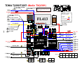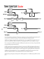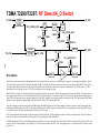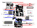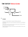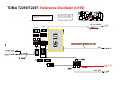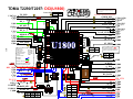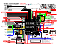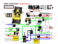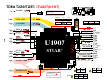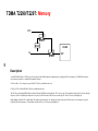
1
Service Manual Level 3 Release 1 ™ DIGITAL WIRELESS TELEPHONE TDMA T2290/T2297 COMPUTER SOFTWARE COPYRIGHTS The Motorola products described in this instruction manual may include copy-righted Motorola computer programs stored in semi-conductor memories or othermedia. Laws in the United States and other countries preserve for Motorola certain exclusive rights for copyrighted computer programs, including the exclusive right to copy or reproduce in any form the copyrighted computer program. Accordingly, any copyrighted Motorola computer programs contained in the Motorola products described in this instruction manual may not be copied or reproduced in any mannerwithout the express written permission of Motorola. Furthermore, the purchase of Motorola products shall not be deemed to grant either directly or by implication, estoppel, or otherwise, any license under the copyrights, patents or patent applica-tions of Motorola, except for the normal non-exclusive, royalty free license to use that arises by operation of law in the sale of a product. This manual is the property of Motorola. No part of this manual may be duplicated in any form without the express written permission of Motorola. This manual must be returned upon Motorola request The information in this manual is subject to change without notice. No guarantee is made for accuracy or thoroughness. This manual is intended as a training aid in conjuction with formal classes provided by Motorola. Motorola takes no responsibility for the use of this manual beyond its intended scope. Motorola, the Motorola Logo and all other trademarks identified as such herein are trademarks of Motorola, Inc. All other product or service names are the property of their respective owners. © Copyright 2000 by Motorola, Inc. All rights reserved About This Manual Scope of Manual General Safety Information This manual is intended for use by experienced technicians familiar with similar types of equipment. It is intended primarily to support basic servicing, which consists primarily of mechanical repairs and circuit board replacement. Authorized distributors may opt to receive additional training to become authorized to perform limited component repairs. Contact your regional Customer Support Manager for details. Model and Kit Identification Motorola products are specifically identified by an overall model number on the FCC label. In most cases, assemblies and kits which make up the equipment also have kit model numbers stamped on them. Service Motorola regional Cellular Subscriber Support Centers offer some of the Þnest repair capabilities available to Motorola Subscriber equipment users. The Cellular Subscriber Support Centers are able to perform computerized adjustments and repair most defective transceivers and boards. Contact your regional Customer Support Manager for more information about MotorolaÕ s repair capabilities and policy for in-warranty and outof-warranty repairs in your region. Portable Operation DO NOT hold the radio so that the antenna is very close to, or touching, exposed parts of the body, especially the face or eyes, while transmitting. The radio will perform best if it is held in the same manner as you would hold a telephone handset, with the antenna angled up and over your shoulder. Speak directly into the mouthpiece. DO NOT operate the telephone in an airplane. DO NOT allow children to play with any radio equipment containing a transmitter. Mobile Operation (Vehicle Adaptor) As with other mobile radio transmitting equipment, users are advised that for satisfactory operation of the equipment and for the safety of personnel, it is recommended that no part of the human body shall be allowed to come within 20 centimeters of the antenna during operation of the equipment. DO NOT operate this equipment near electrical blasting caps or in an explosive atmosphere. Mobile telephones are under certain conditions capable of interfering with blasting operations. When in the vicinity of construction work, look for and observe signs cautioning against mobile radio transmission. If transmission is prohibited, the cellu- ©2000 Motorola, Inc. iii About This Manual TDMA T2290/T2297 lar telephone must be turned off to prevent any transmission. In standby mode, the mobile telephone will automatically transmit to acknowledge a call if it is not turned off. All equipment must be properly grounded according to installation instructions for safe operation. Portable/Mobile Telephone Use and Driving Safety is every driver’s business. The portable telephone should only be used in situations in which the driver considers it safe to do so. Use of a cellular portable while driving may be illegal in some areas. Refer to the appropriate section of the product service manual for additional pertinent safety information. iv ©2000 Motorola, Inc. Service Manual About This Manual Specifications Table 1.Overall System Function Frequency Range Specification TX (800MHz) : 824.04 - 848.97 MHz Channels 1 to 799, fTX = 0.03 * N+ 825MHz Channels 990 to 1023, fTX = 0.03(N-1023)+ 825MHz RX(800 MHz): 869.04 – 893.97 MHz Channels 1 to 799, fRX = 0.03 * N+ 870MHz Channels 990 to 1023, fRX = 0.03(N-1023)+ 870MHz TX (1.9 GHz) : 1850.01 – 1909.95 MHz Channels 1 to 1999 fTX = 0.03 * N+ 1849.98MHz RX (1.9 GHz) : 1930.05 – 1989.99 MHz Channels 1 to 1999 fRX = TX + 80.04MHz Channel Spacing Channels Duplex Spacing Input/Output Impedance Operating Voltage Dimensions Weight Display Analog RF Power Output Digital RF Power Output Automatic Power Control 30 kHz 832 (800MHz), 1999 (1.9 GHz) 45 MHz (800MHz), 80.04 MHz (1.9GHz) 50 ohms (nominal) +3.6 to +4.1Vdc 120cc (Volume) 140 g 96 X 32 Graphic Matrix 0.316 Watts (25 dBm) 0.562 Watts (27.5 dBm) 9, 4 dBm steps Table 2. EAMPS System Function Modulation Type Frequency Stability Duty Cycle Audio Distortion (transmit and receive) FM Hum and Noise (C-MSG weighted) Voice Modulation Transmit Audio Sensitivity Receive Sensitivity Adjacent and Alternate Channel Desensitization IM Specification FM + 2.5ppm Continuous Less than 5% at 1 kHz; + 8 kHz deviation 32 dB below + 8 kHz deviation @ 1 kHz Maximum + 12 kHz deviation 9 kHz deviation (nom.) @ 97 dB SPL input @ 1 kHz -116 dBm for 12 dB SINAD (C-MSG weighted) -16 dB @ +30 kHz, -60 dB @ + 60 kHz Greater than 65 dB ©2000 Motorola, Inc. v About This Manual TDMA T2290/T2297 Table 3. DAMPS System Function Modulation Type Frequency Stability Duty Cycle Error Vector Magnitude (π/4DQPSK mode) Transmit Audio Sensitivity Receive Sensitivity Adjacent and Alternate Channel Desensitization IM Specification π/4DQPSK + 200 Hz 32.3% Error Vector Magnitude [Digital] 12.5% TOLR of –46 dB nominal -116 dBm for 3% static BER -116 dBm for 3% static BER Less than or equal to 3% static BER Table 4. Environment Function Temperature Humidity Vibration Shock vi Specification -30ºC to +60ºC 80% RH at 50ºC EIA PN1376 EIA PN1376 ©2000 Motorola, Inc. Table of Contents About This Manual ....................................................................................................................... iii Scope of Manual ....................................................................................................................... iii Model and Kit Identification ....................................................................................................... iii Service ...................................................................................................................................... iii General Safety Information ....................................................................................................... iii Portable Operation ........................................................................................................................................ iii Mobile Operation (Vehicle Adaptor) ............................................................................................................... iii Portable/Mobile Telephone Use and Driving ................................................................................................... iv Specifications ............................................................................................................................. v Cellular Overview .......................................................................................................................... 1 Introduction ................................................................................................................................1 Control (Data) Channels ................................................................................................................................ 2 Voice Channels .............................................................................................................................................. 3 Signaling Protocol .......................................................................................................................................... 3 Analog Cellular ...........................................................................................................................5 Signaling Tone (ST) and Digital ST (DST) ....................................................................................................... 5 SAT (Supervisory Audio Tone) and DSAT (Digital SAT) ................................................................................... 6 DTMF (Dual Tone Multi-Frequency) ................................................................................................................ 6 Analog Cellular Signal Summary (AMPS and NAMPS) ................................................................................... 7 Going into Service ......................................................................................................................................... 8 Placing a Call (Mobile to Land or Mobile to Mobile) ....................................................................................... 10 Receiving a Call (Land to Mobile) ................................................................................................................. 11 Power Steps ................................................................................................................................................ 13 Hand-offs ..................................................................................................................................................... 13 Call Termination ........................................................................................................................................... 15 Digital Cellular ..........................................................................................................................17 Multiplexing ................................................................................................................................................. 17 FDMA (Frequency Division Multiple Access) ................................................................................................. 17 Digitizing Voice ............................................................................................................................................ 17 TDMA (Time Division Multiple Access) ......................................................................................................... 18 Digitization and TDMA ................................................................................................................................. 18 Digitization of Voltage ................................................................................................................................... 19 Conventional Radio ...................................................................................................................................... 19 TDMA Radio ................................................................................................................................................ 20 Accessories ................................................................................................................................. 21 TDMA EASY NAM Programming ................................................................................................ 23 Introduction ..............................................................................................................................23 User Mode Programming .........................................................................................................23 Programming Sequence ..........................................................................................................24 ©2000 Motorola, Inc. vii Table of Contents TDMA T2290/T2297 Enter Programming Mode ............................................................................................................................ 24 Enter Security Code ..................................................................................................................................... 24 Enter Phone Number ................................................................................................................................... 24 Programming a second No. .......................................................................................................................... 24 If you make a mistake .................................................................................................................................. 24 TDMA Test Mode NAM Programming ........................................................................................ 25 Introduction ..............................................................................................................................25 Entering Test Mode NAM Programming ...................................................................................25 NAM Programming Steps ........................................................................................................25 NAM Data ................................................................................................................................26 User Mode Programming .........................................................................................................26 Test Mode NAM Programming Sequence ................................................................................27 Manual Test Mode ........................................................................................................................ 31 Introduction ..............................................................................................................................31 Entering Manual Test Mode .....................................................................................................31 Status Display Level ................................................................................................................31 Servicing Level .........................................................................................................................32 Test Procedures .......................................................................................................................... 35 Introduction ..............................................................................................................................35 Automatic Call-Processing Tests ..............................................................................................35 Analog Test Measurements .......................................................................................................................... 35 Digital Test Measurements ........................................................................................................................... 35 Test Connections .....................................................................................................................36 RF Cable Test ..........................................................................................................................37 To test the RF cable for proper loss: ............................................................................................................. 37 Set up for Analog call ...............................................................................................................38 Registration ................................................................................................................................................. 38 Page ............................................................................................................................................................ 38 Select CALL CNTL from the To Screen ......................................................................................................... 38 Origination ................................................................................................................................................... 38 RX Sensitivity Test (SINAD) .....................................................................................................39 Test Mode Commands: ................................................................................................................................ 39 Communications Analyzer Setup: ................................................................................................................. 39 TX Power Out Test ...................................................................................................................40 Test Mode Commands: ................................................................................................................................ 40 Communications Analyzer Setup: ................................................................................................................. 40 Test Mode Commands: ................................................................................................................................ 41 Communications Analyzer Setup: ................................................................................................................. 41 TX Maximum Deviation Test ....................................................................................................42 Test Mode Commands: ................................................................................................................................ 42 Communications Analyzer Setup: ................................................................................................................. 42 TX SAT Deviation Test .............................................................................................................43 Procedure .................................................................................................................................................... 43 Select CALL CNTL from the To Screen ......................................................................................................... 43 TX ST Deviation Test ...............................................................................................................44 Test Mode Commands: ................................................................................................................................ 44 viii ©2000 Motorola, Inc. Service Manual Table of Contents Communications Analyzer Setup: ................................................................................................................. 44 Setting up for PCS TDMA Measurements ................................................................................45 Power up the PCS Adapter, after two beeps are heard power up the 8920B ................................................. 45 Setting up for PCS TDMA Measurements ................................................................................46 Set up for TDMA call ................................................................................................................47 Call Process ................................................................................................................................................ 47 Registration ................................................................................................................................................. 47 Select CALL CNTL from the To Screen ......................................................................................................... 47 Page ............................................................................................................................................................ 47 Origination ................................................................................................................................................... 47 MAHO Measurements .............................................................................................................48 Setting up the MAHO measurement ............................................................................................................. 48 Measuring MAHO ........................................................................................................................................ 48 BER Measurements .................................................................................................................49 PCS Mode Handset Commands: .................................................................................................................. 49 BER Measurement Procedure ...................................................................................................................... 49 TX Power Measurements ........................................................................................................50 PCS Mode Handset Commands: .................................................................................................................. 50 Digital TX Power Out Test Procedure ........................................................................................................... 50 TX Frequency Error Measurements .........................................................................................51 PCS Mode Handset Commands: .................................................................................................................. 51 TX Frequency Error Measurement Test ........................................................................................................ 51 EVM Measurements ...............................................................................................................52 PCS Mode Handset Commands: .................................................................................................................. 52 TX Frequency Error Measurement Test ........................................................................................................ 52 Disassembly ................................................................................................................................ 53 Introduction ..............................................................................................................................53 Recommended Tools ...............................................................................................................53 Battery Removal ......................................................................................................................54 Antenna Removal ....................................................................................................................55 Back Housing Removal ............................................................................................................55 Transceiver Board Removal .....................................................................................................56 Display Removal ......................................................................................................................56 Keypad Removal ......................................................................................................................57 Speaker Removal ....................................................................................................................57 Parts List ...................................................................................................................................... 59 Introduction ..............................................................................................................................59 Mechanical Explosion ..............................................................................................................59 General Description .................................................................................................................... 61 Antenna Circuit ........................................................................................................................61 RX Front End ...........................................................................................................................61 NADC IC ..................................................................................................................................61 TX Operational Description .....................................................................................................62 Power Amp Integrated 800 MHz or 1900 MHz IC ....................................................................62 Analog TX Audio Processing ...................................................................................................63 ©2000 Motorola, Inc. ix Table of Contents TDMA T2290/T2297 Digital TX Audio Processing .....................................................................................................63 DSP Lucent 1629 .....................................................................................................................63 Stuart IC ...................................................................................................................................64 GCAP II ....................................................................................................................................64 Section B Service Diagrams ....................................................................................................................... B1 Antenna Circuit ....................................................................................................................... B3 Front End IC(U10) ................................................................................................................... B5 ZIFSYNTH(U110) .................................................................................................................... B7 VCO ........................................................................................................................................ B9 TX Offset Oscillator ............................................................................................................... B11 Merlyn(U301) ........................................................................................................................ B13 Exciter ................................................................................................................................... B15 PA Circuit .............................................................................................................................. B17 RF Detect .............................................................................................................................. B19 Reference Oscillator ............................................................................................................. B21 DCI(U1800) ........................................................................................................................... B23 GCAP2(U1500) ..................................................................................................................... B25 Voltage Regulators................................................................................................................ B27 Charger ................................................................................................................................. B29 Audio Circuit .......................................................................................................................... B31 DSP(U1900) .......................................................................................................................... B33 STUART(U1907) ................................................................................................................... B35 Call Processor(U1000) .......................................................................................................... B37 Memory ................................................................................................................................. B39 B+ Disconnect/Backlight Driver ............................................................................................. B41 Keypad .................................................................................................................................. B43 Connectors............................................................................................................................ B44 Layout Side 1 ........................................................................................................................ B45 Layout Side 2 ........................................................................................................................ B46 x ©2000 Motorola, Inc. Cellular Overview Introduction A cellular mobile telephone system divides the service area into small, low power radio frequency coverage areas called cells. A cellular system consists of a more or less continuous pattern of these cells, each having a 1 to 40 mile radius (typically 5 - 10 miles). Within each cell is a centralized cell site with an elevated antenna and a building. The building houses a base station with transceivers and related control equipment for the channels assigned to that cell. All the cell sites within a system are then connected either by dedicated land lines, microwave links, or a combination of both to a central control site called the central controller or switch . The switch controls the entire cellular system and serves as the interface between the cellular telephone user and the landline network. Each cell site operates on an assigned access channel, and may have any number of paging and voice channels assigned to it. Figure 1. Channel Assignments A BAND CHANNELS Primary Control Channels (21): Secondary Control Channels (21): Voice Channels... (395 AMPS / 1185 NAMPS): 313 - 333 688 - 708 001 - 312, 667 - 716, and 991 - 1023 B BAND Primary Control Channels (21): Secondary Control Channels (21): Voice Channels... (395 AMPS / 1185 NAMPS): NOTE: CHANNELS 334 - 354 737 - 757 355 - 666 and 717 - 799 In NAMPS applications, each AMPS voice channel provides space for three NAMPS voice channels. Digital cellular multiplexes voice channels to allow for the possibility of several additional conversations on a single channel. ©2000 Motorola, Inc. 1 Cellular Overview TDMA T2290/T2297 Introduction are defined in Figure 1. The cellular radio frequency spectrum has been divided by the FCC into two equal segments or bands to allow two independent cellular carriers to coexist and compete in the same geographic coverage area. Each band occupies one half of the available channels in the cellular spectrum. Initially there were 666 channels available across the entire cellular spectrum, but that number was expanded to 832 channels in 1987, and with NAMPS to 2,412 channels in 1991. Digital cellular promises to make a further expansion. To guarantee nationwide compatibility, the signaling channel frequencies have been pre-assigned to each segment (band). The two bands and their assigned channels Originally the B Band was assigned to the telephone company (referred to by a euphemism, the Wireline carrier). The A Band, by default, was referred to as the Non-Wireline carrier, guaranteed competition to the telephone company. Today the terms Wireline and Non-Wireline have little meaning since telephone company carriers now operate A Band systems, and vice-versa. Control (Data) Channels A cellular telephone in the cellular system is under the indirect control of the switch, or central controller. The central controller uses dedicated control channels to provide the sig- Figure 2. US Cellular Frequency Band US Cellular Frequency Band 832 channels 333 1023 991 001 A' 334 354 313 A 667 355 312 A B Band B 799 B' A' Voice Channels Control Channels 667 2 717 716 A' B Band A Voice Channels 666 717 666 716 TDMA Secondary Control Channels 688 - 708 ©2000 Motorola, Inc. 799 737 - 757 Service Manual Cellular Overview Introduction naling required to establish a telephone call. Control channels are used to send and receive only digital data between the base station and the cellular telephone. Voice channels are used for both audio and signaling once a call is established. The 21 control channels in each band may be dedicated according to two different applications: access and paging channels. The data on the forward control channel generally provides some basic information about the particular cellular system, such as the system ID and the range of channels to scan to find the access and paging channels. Access channels are used to respond to a page or originate a call. The system and the cellular telephone will use access channels where two-way data transfer occurs to determine the initial voice channel. Paging channels, if used, are the normal holding place for the idle cellular telephone. When a call is received at the central controller for a cellular telephone, the paging signaling will occur on a paging channel. In many systems both control channel functions will be served by the same control (access) channel for a particular cell. Only in very high density areas will multiple control (paging) channels be required. Primary control channels are used by all types of telephones. Secondary control channels are only used by TDMA telephones, providing them with an improved probability of locking onto a TDMA control channel. Voice Channels Voice channels are primarily used for conversation, with signaling being employed as necessary to handle cell-to-cell hand-offs, output power control of the cellular radiotelephone, and special local control features. Data from the cell site (known as FORWARD DATA) and data from the mobile or portable (known as REVERSE DATA) is sent using frequency shift keying. In AMPS signaling, various control and response tones are used for a variety of applications to be described later. However, in NAMPS signaling, the signaling data and tones have been replaced by sub-audible digital equivalents that constantly ride underneath the audio. And, of course, in digital cellular, all signaling is digital. Signaling Protocol In 1983, when the Federal Communications Commission (the FCC) licensed cellular telephony, the signaling protocol used was AMPS. AMPS (Advanced Mobile Phone Service) was the invention of Bell Labs, the signaling protocol that was ultimately adopted by all the governments of the entire Western Hemisphere and, eventually, several other governments throughout the world. Today, with the implementation of Narrow AMPS and TDMA, and the imminence of CDMA, it may seem that AMPS is out of date. The truth is that AMPS is very much alive, at the very core of all these traffic expanding alternatives to the original signaling protocol developed for conventional cellular telephony. Under the original AMPS protocol there were 21 control channels assigned to each of two possible carriers in any metropolitan area, with a total of 333 channels assigned to each carrier. Prior to 1987 the FCC had allocated 312 channels to voice (voice, DTMF, or data) ©2000 Motorola, Inc. 3 Cellular Overview TDMA T2290/T2297 Introduction applications for each carrier. In 1987 the FCC expanded the cellular spectrum (Expanded Spectrum) from a total of 666 channels to 832 channels, allowing for an increase of 83 voice channels for each carrier. But the number of control channels remained constant, 21 control channels for each carrier. In 1991, responding to the demand for even more voice channels, Motorola introduced NAMPS (Narrow AMPS), expanding the voice channels by a factor of 3, assuming all subscribers are using NAMPS telephones. But one thing remained constant, there were 21 control channels for each carrier. between digital cellular and AMPS is that all signals are digitized, including voice. At a basic level, cellular telephony has two divisions: analog cellular and digital cellular. In the following section, analog cellular (AMPS and NAMPS) will be discussed. In the succeeding section, digital cellular will be treated. In 1992, when Motorola tested its TDMA digital product, digitizing three communication links on each of 395 voice channels, one thing remained constant: there were still 21 control channels for each carrier. Leaving the control channels more or less untouched is the key to allowing telephones that are not capable of NAMPS or digital operation to have access to the system using the conventional AMPS scheme. In virtually every scheme (AMPS, NAMPS, or digital), each control channel has a bandwidth of 30 kHz and uses the signaling protocol, with minor variations for NAMPS and digital, developed for conventional AMPS The primary difference between NAMPS and AMPS is that a NAMPS voice channel has a bandwidth of only 10 kHz, whereas an AMPS voice channel has a bandwidth of 30 kHz. In addition, NAMPS does not make use of certain control and response tones on voice channels as does AMPS, but uses digital equivalents instead. As the name implies, the primary difference 4 ©2000 Motorola, Inc. Service Manual Cellular Overview Analog Cellular Analog Cellular central controller (switch). The simplified block diagram on page 1 - 7 illustrates an imaginary layout of one side (Band A, or Band B) of a hypothetical service area. The hexagons represent cells, and some of the cell sites shown here also illustrate the fact that an antenna tower and set of base stations are associated with each site. In a real world environment individual cells do not have the hexagonal shape but may take any form as dictated by the environment. As illustrated(figure 3.) by the antenna tower on the upper left, cell sites transmit overhead messages more or less continuously even if there are no mobiles or portables active within that cell. The cell sites are in communication with individual portable and mobile cellular telephones. These portables and mobiles may move from cell to cell, and as they do they are “handed off”under the supervision of the Figure 3. Channel Assignments The switch (center left) is in control of the system and interfaces with the central office of the telephone company. As illustrated by the deskset telephones, the telephone company interfaces with the entire landline network. The cell sites and the mobiles and portables communicate through the use of data or, in the case of AMPS, through the use of data and tones. A complete analysis of data signaling is beyond the scope of this manual. Refer to the Electronic Industries Association standard EIA-553 for a thorough discussion of AMPS signaling protocol, or to Motorola’s NAMPS Air Interface Specification for NAMPS. The tones used in AMPS signaling are Signaling Tones and Supervisory Audio Tones. NAMPS uses sub-audible digital equivalents. Cellular Switch Telephone Company Central Office Signaling Tone (ST) and Digital ST (DST) In AMPS, signaling tone is a 10 kHz signal used by the mobile or portable on the reverse voice channel (REVC) to signal certain activities or acknowledge various commands from the cell site, including hand-offs, alert orders, and call terminations, and to indicate switch-hook operation. Various burst lengths are used for different ST activities. On NAMPS channels ST is replaced by a digital equivalent called Digital ST (DST) which is ©2000 Motorola, Inc. 5 Cellular Overview TDMA T2290/T2297 Analog Cellular the complement of the assigned DSAT. SAT (Supervisory Audio Tone) and DSAT (Digital SAT) The Supervisory Audio Tone (SAT) is one of three frequencies around 6 kHz used in AMPS signaling. On NAMPS channels SAT is replaced by one of seven sub-audible digital equivalents or vectors called DSAT. SAT (or DSAT) is generated by the cell site, checked for frequency or accuracy by the cellular telephone, then transponded (that is, not merely reflected but generated and returned) to the cell site on the reverse voice channel (REVC). The cellular telephone uses (D)SAT to verify that it is tuned to the correct channel after a new voice channel assignment. When the central controller (switch) signals the mobile regarding the new Figure 4. Channel Assignments SAT 0 (5970 Hz) In general there are three uses of (D)SAT: (a) it provides a form of squelch; (b) it provides for call continuation (but if equipped for it, the switch will allow for VOX on all models); and (c) (D)SAT is used to prevent co-channel interference. DTMF (Dual Tone Multi-Frequency) DTMF (Dual Tone Multi-Frequency) touchcode dialing may also occur on voice channels. DTMF selects two tones from a total of nine (cellular only uses seven of these tones / four low and three high tones) to uniquely represent individual keys. Table 5. DTMF Values Cellular System SAT 1 (6000 Hz) voice channel, it also informs the mobile of the SAT frequency or DSAT vector to expect on the new channel. The returned (D)SAT is used at the cell site to verify the presence of the telephone’s signal on the designated channel. SAT 2 (6030 Hz) Key 1 2 3 4 5 6 7 8 9 * 0 # 327 320 329 333 324 322 332 328 326 326 330 331 140 119 98 77 56 319 318 324 326 313 198 177 156 135 114 143 122 101 80 330 140 119 98 77 56 Re-use 6 ©2000 Motorola, Inc. Low Tone 697 697 697 770 770 770 852 852 852 941 941 941 High Tone 1209 1336 1477 1209 1336 1477 1209 1336 1477 1209 1336 1477 Service Manual Cellular Overview Analog Cellular Analog Cellular Signal Summary (AMPS and NAMPS) The diagrams on the following pages outline the various uses of the signals employed in cellular systems. These signals include: SAT (Supervisory Audio Tone) 5970 Hz, 6000 Hz, or 6030 Hz. Used in AMPS for channel reuse, muting audio (squelch), and call continuation [typically ± 2 kHz deviation]. Digital SAT (DSAT) - One of seven codes or vectors used in NAMPS for the same purpose as SAT [± 700 Hz sub-audible NRZ data]. Data - Transmitted at 10 kilobits/second in AMPS and 200 bits/second in NAMPS. Data is used for sending System Orders and Mobile Identification. Do not confuse data with the 10 kHz signaling tone. In AMPS, data is transmitted as Manchester-encoded Frequency Shift Keying (FSK), where the carrier is shifted high or low 8 kHz, and the trailing edge transition is used to represent the logic. In NAMPS, data is transmitted as NRZ (Non-Return to Zero) FSK, where the carrier is shifted high or low 700 Hz, and the frequency shift itself is used to represent the logic. Signaling Tone (ST) - A 10 kHz tone used in AMPS for mobile ringing, call terminations, hand-offs, and switch-hook operation [typically ± 8 kHz deviation]. ST is always accompanied by SAT. Digital ST (DST) - One of seven digital equivalents of ST used on NAMPS channels. The transmitted DST is always the complement of the assigned DSAT [± 700 Hz subaudible NRZ data]. Audio - Includes microphone audio and DTMF [maximum ± 12 kHz deviation AMPS, ± 5 kHz deviation NAMPS]. DTMF deviation should be measured on the radians scale; use key five looking for 9 radians. Audio is accompanied by SAT in AMPS signaling. Figure 5. AMPS Deviation in kHz AMPS Deviation in kHz AMPS Voice Channels ±14 ±12 ±10 ±8 ±6 ±4 ±2 Control Channels SAT SAT Data Signal Tone Audio Data SAT ©2000 Motorola, Inc. 7 Cellular Overview TDMA T2290/T2297 Analog Cellular Total deviation of two or more signals is cumulative. Step 5. Decision point. Can the overhead message from the strongest control channel be decoded? If not, go to step 6. If it can be decoded go to step 8.* Step 6. The telephone tunes to the second strongest channel. Step 7. Decision point. Can the overhead message stream be decoded? If not, go to step 12. If it can be decoded, go to step 8.* Decision point. Does the decoded System ID match the Home System ID programmed in the telephone? If not, go to step 9. If it does match, go to step 10. Going into Service When first turned on, the cellular telephone will scan through the nationwide set of forward control channels (FOCC’s) and measure the signal strength on each one. It will then tune to the strongest one and attempt to decode the overhead control message. From the overhead message, the telephone will be able to determine whether or not it is in its home system, and the range of channels to scan for paging and access. Telephones not in their home system will be able to use other cellular telephone systems depending on the level of service requested by the user. If paging channels are used, the telephone next scans each paging channel in the specified range and tunes to the strongest one. On that channel the telephone continuously receives the overhead message information plus paging messages. At this point the telephone idles, continuously updating the overhead message information in its memory and monitoring the paging messages for its telephone number. Step 1. The telephone powers up and runs a self-test. The NoSvc indicator is illuminated. Step 2. The telephone scans its preferred system (A or B) as selected in programming. Step 3. The telephone scans all twenty-one control channels. Step 4. 8 The telephone tunes to the strongest control channel. Step 8. Step 9. The telephone turns on the ROAM indicator. Step 10. The telephone turns off the NoSvc indicator. Step 11. The telephone idles. Typically a rescan occurs after 5 minutes. Step 12. The telephone turns on (or leaves on) its NoSvc indicator. Step 13. The telephone switches to the nonpreferred system as recorded in programming, and goes back to step 3. The ability to return to step 3 can be disabled by some settings of System Registration. *The area between Decision point 5 and Decision point 8 can be quite active. In a few larger systems, following the suc- ©2000 Motorola, Inc. Service Manual Cellular Overview Analog Cellular cessful completion of either steps 5 or 7, the telephone scans a set of paging channels, tunes to the strongest, and attempts to decode the overhead message train. The procedure is exactly equivalent to that followed for the access (control) channel. Also at this point, in a few larger systems, the telephone is commanded to identity itself (transmit) and thereby indicate its location in the system. This is called Autonomous System Registration and, like paging channels, is used to improve paging efficiency. If the system employs Narrow AMPS, part of the overhead message stream is used to ask the for activity on one of the secondary or “digital” control channels, whereas a CDMA telephone will look for pilot signals. If digital signaling is not present, and if the telephone is capable of dual mode operation, it will default to AMPS mode. Figure 6. Going into Serivce Going Into Service With a Cellular Telephone 1. Power Up / Self Test Turn on No Svc Indicator 2. Scan Preferred System (A or B) 3. Scan all 21 Control Channels 4. Tune to Strongest Control Channel 5. Receive Overhead Info ? No 6. Tune to 2nd Strongest Channel 7. Receive Overhead Info ? No* Yes Yes Note: In order to turn on the Roam light, the SID in the overhead message stream must NOT match the SID programmed into the telephone. 8. SID matches Home SID ? Yes Note: In order to turn off the NoSvc light, the overhead message stream must have been decoded. No 12. Turn On NoSvc Indicator 9. Turn on Roam Indicator 13. Switch to Non-Preferred System 10. Turn Off NoSvc Indicator 11. Idle [Rescan after 5 minutes.] * In those telephones with Motorola Enhanced Scan, more than two control channels are sampled before proceeding to step 12. ©2000 Motorola, Inc. 9 Cellular Overview TDMA T2290/T2297 Analog Cellular Placing a Call (Mobile to Land or Mobile to Mobile) When the cellular telephone user originates the call, the cellular telephone re-scans the access channels to assure that it is still tuned to the strongest one. The cellular tele- phone then transmits data at the rate of 10 kilobits per second on the control channel to notify the switch of its mobile identification number (MIN) and the number it wants to reach. The switch verifies the incoming data and assigns a voice channel and a SAT (or DSAT for NAMPS channels) to the telephone. Figure 7. Cellular Telephone to Land Call Processing Cellular Telephone The cellular telephone is tuned to the access / paging channel, and responds to requests for data. The cellular telephone user dials a telephone number and presses SND. The telephone rescans the access channels for the strongest signal. The telephone sends out data, including the dialed digits, MIN, ESN, and NAMPS or digital capability to the cell site. Switch / Cell Site DATA FOCC & RECC DATA RECC DATA FOCC The cellular telephone receives the voice channel assignment, drops the access channel, tunes to the voice channel, and transponds the assigned SAT or DSAT. (D)SAT Overhead data is sent out on the control channels. The cell site receives the mobile-to-land call request. The cell site sends the data to the switch. The switch verifies the MIN & ESN and then sends out the call to the landline network. The local telephone company processes the telephone call. The switch assigns a voice channel and SAT or DSAT. The voice channel assignment is sent to the cellular telephone on the access channel. The cell site sends SAT or DSAT to the cellular telephone on the assigned voice channel. FOVC (D)SAT REVC The cellular telephone user hears the landline ringing. Landline Network The cell site receives the correct SAT or DSAT, then unmutes the voice path. VOICE + (D)SAT The landline person being called answers. FOVC & REVC Conversation in progress Conversation in progress 10 ©2000 Motorola, Inc. Service Manual Cellular Overview Analog Cellular The cellular telephone tunes to the assigned voice channel and verifies the presence of the proper forward SAT frequency (or DSAT message). If SAT (DSAT) is correct the telephone transponds SAT (DSAT) back to the cell site and unmutes the forward audio. The cell site detects reverse SAT (DSAT) from the cellular telephone and unmutes reverse audio. At this point both forward and reverse audio paths are unmuted and the cellular telephone user can hear the other end ring, after which conversation can take place. SAT (DSAT) is sent and received more or less continuously by both the base station and the cellular telephone. However, SAT (DSAT) is not sent during data transmissions, and the cellular telephone does not transpond SAT continuously during VOX operation. Also, DSAT is suspended during the transmission of DST. Notice that SAT and Signaling Tones are only used on AMPS voice channels, and that the Signaling Tone is only transmitted by the cellular telephone. site, the reception of SAT (DSAT) signals the central controller that the cellular telephone is ready for the call. An alert order is then sent to the cellular telephone which responds with a 10 KHz signaling tone (DST message). The subscriber unit rings for 65 seconds or until the user answers. Then the 10 KHz signaling tone (DST message) is terminated to alert the central controller that the user has answered. The switch then connects the incoming call to the appropriate circuit leading to the cell in contact with the cellular telephone. At this point both forward and reverse audio paths are unmuted and the conversation can take place. SAT (DSAT) is sent more or less continuously by the base station and transponded by the cellular telephone, except during data transmission. DSAT is suspended during DST transmission, and during VOX operation SAT (DSAT) is not transponded continuously by the cellular telephone. Receiving a Call (Land to Mobile) Once a cellular telephone has gone into service, it periodically scans the overhead message information in its memory and monitors the paging messages for its telephone number. When a page match occurs the cellular telephone scans each of the access channels and tunes to the strongest one. The cellular telephone then acknowledges the page on that access channel and thus notifies the central controller of its cell location. The switch then assigns a voice channel and a SAT (DSAT) to the cellular telephone. The cellular telephone tunes to the voice channel, verifies the presence of the proper SAT frequency (DSAT message) and transponds the signal back to the cell site. At the cell ©2000 Motorola, Inc. 11 Cellular Overview TDMA T2290/T2297 Figure 8. Land to Cellular Telephone Call Processing Landline Network The landline caller dials the cellular telephone number. The Public Service Telephone Network (central office) forwards the call to the central controller (switch). Switch / Cell Site Cellular Telephone DATA Overhead data is sent out on the control channels. FOCC & RECC The switch receives a call from land. The switch pages the cellular telephone. The page is sent as data on the forward control channel. DATA FOCC DATA The cell site receives the acknowledgement and sends it to the switch. The switch verifies the ESN & MIN and assigns a voice channel. The cell site informs the cellular telephone of the voice channel and SAT (DSAT). The cell site sends the SAT (DSAT) on the voice channel. RECC (D)SAT FOVC (D)SAT DATA (D)ST + (D)SAT The cell site unmutes the voice path. VOICE + (D)SAT FOVC & REVC 12 ©2000 Motorola, Inc. The cellular telephone rings. While ringing, the subscriber unit sends a 10 kHz signaling tone (DST message) to the cell site. REVC (D)SAT Conversation in progress The telephone receives the data and tunes to the assigned voice channel, then transponds the SAT (DSAT). REVC FOVC The cell site receives signaling tone (DST message) from the cellular telephone. The cellular Telephone decodes the data and successfully reads its MIN. The telephone scans the control channels for the strongest, then acknowledges the page by sending it’s ESN, MIN, and NAMPS or digital capability as data on the control channel. DATA FOCC The cell site receives the correct SAT (DSAT) and alerts the cellular telephone to ring. The landline caller hears ringing, busy, etc. The cellular telephone is tuned to the access / paging channel, and responds to requests for data. REVC The cellular telephone user answers by pressing SND The signaling tone stops. Conversation in progress Voice path unmuted Service Manual Cellular Overview Analog Cellular Power Steps As a call progresses, the cell site continuously monitors the reverse channel for signal strength. Every cellular telephone has a number of power steps ranging from full power (3 watts in a mobile and .6 watts in a portable) down to as low as about half a milliwatt. In reality all cellular telephones have eight power steps, but portable models are prevented from using the two highest power steps by the cell site. Transmit power level commands are sent to the cellular telephone as required to maintain the received signal strength within prescribed limits. This is done to minimize interference possibilities within the frequency re-use scheme. If the signal received from the cellular telephone is higher than the prescribed limit (such as when the unit is very near the cell site), the subscriber unit will be instructed to step down to a lower level. Hand-offs If the cellular telephone is at its maximum allowed power for the cell site it is using and the received signal at the cell site is approaching the minimum allowable (typically -100 dBm), the cell site will signal the switch to consider the subscriber unit for a hand-off. The central controller (switch) will in turn have a scanning receiver at each of the surrounding cell sites measure the cellular telephone’s signal strength. The site with the strongest signal will be the site to which the call will be handed to if there are available voice channels. On an AMPS channel the hand-off is executed by interrupting the conversation with a burst of data (called blank and burst) containing the new voice channel assignment. The telephone acknowledges the order by a 50 millisecond burst of 10 kHz signaling tone on the originally assigned voice channel. The mobile telephone then drops the original voice channel and tunes to the newly assigned voice channel, keying up on that channel and transponding the assigned SAT. But on a NAMPS channel the hand-off is executed with a low speed data transmission that does not interrupt the voice. The telephone acknowledges the order in this case by a DST message. In either case, once the hand-off has been accomplished, the newly assigned cell site then alerts the switch that the handoff has been completed, and the old voice channel is dropped. It should be noted that this data exchange happens very quickly, lasting only as long as 260 milliseconds. However, when data or signaling tones are transmitted, audio is muted for the duration of that transmission and a syllable or two may be dropped from conversation. This is normally not a problem, but during data signaling, such as that employed for telefacsimile, answering machine, and computer communications, significant amounts of information may be lost. For this reason it is recommended that when THE Cellular Connection™ equipment is used the vehicle should be stationary to avoid data loss during hand-offs and other data transmissions. Otherwise the equipment should employ an error correction protocol. ©2000 Motorola, Inc. 13 Cellular Overview TDMA T2290/T2297 Figure 9. Cell Site Handoffs Cellular Telephone Switch / Cell Site Conversation in progress. The voice path is unmuted. VOICE + (D)SAT The cellular telephone acknowledges the handoff request by sending a10 kHz signaling tone for 50 msec or a DST message. The voice path is muted while sending ST. The telephone drops the voice channel and keys up on the new voice channel frequency. The telephone sends the newly assigned SAT (DSAT). Conversation in progress. The voice path is unmuted. FOVC & REVC DATA FOVC (D)ST + SAT REVC Conversation in progress. The voice path is unmuted. The cell site monitors the cellular telephone's signal strength. When the signal strength falls below the allowed minimum (typically -100 dBm at the highest power step), the cell site informs the switch of the need for a handoff. The switch orders surrounding cell sites to measure the cellular telephone's signal strength. The switch assigns a new cell site, voice channel, and SAT (DSAT) based on the highest signal strength, and informs both cell sites. The old cell site mutes the voice path and sends a data burst with handoff information to the cellular telephone The originally assigned cell site receives the signaling tone (DST) and informs the switch to continue with the handoff. The switch moves the landline to the voice channel at the new cell site. (D)SAT REVC The new cell site receives the correct SAT (DSAT) and unmutes the voice path. VOICE + (D)SAT FOVC & REVC 14 Landline Network ©2000 Motorola, Inc. Conversation in progress. The voice path is unmuted. Service Manual Cellular Overview Analog Cellular Call Termination When the call is terminated by the landline caller (not the cellular telephone user), the central controller (switch) issues a release order to the subscriber unit. The cellular telephone acknowledges with a 10kHz signalling tone burst for 1.8 seconds and the cellular telephone ceases transmission. signalling tone burst for 1.8 seconds, indicating a call termination request to the switch. In either case after call termination, the cellular telephone goes back to rescan the nationwide set of forward controlchannels and repeats the Going into Service process it performed at first turn-on to re-establish itself on a paging channel. If the call was terminated by the cellular telephone user, the telephone generates a 10kHz Figure 10. Cellular Telephone Call Processing Termination Switch / Cell Site Cellular Telephone Conversation in progress. Voice path is unmuted. VOICE + (D)SAT Landline Network Conversation in progress. FOVC & REVC The cellular telephone user hangs up or hits the END key to terminate the call. The cellular telephone sends a 1.8 second burst of 10 kHz signaling tone or a DST vector to the cell site, then stops sending SAT (DST). (D)ST + (D)SAT REVC The cell site receives the signaling tone (DST) and notifies the switch of the disconnect. The cell site mutes the audio path on the voice channel. The switch 12 informs the TelCo of the disconnect and the landline is released. The cellular telephone rescans the access / paging channels for the strongest signal and decodes data. The cellular telephone responds to requests for data. DATA FOCC & RECC The landline is released. Overhead data sent out on the control channel. ©2000 Motorola, Inc. 15 Cellular Overview 16 TDMA T2290/T2297 ©2000 Motorola, Inc. Service Manual Cellular Overview Digital Cellular Digital Cellular Multiplexing Using a single frequency to carry two or more communication links (e.g., conversations) is called multiplexing. There are two types of multiplexing that are feasible for cellular: code division multiplexing and time division multiplexing. Both code division multiplexing and time division multiplexing digitize voice before transmitting the signal. Another type of multiplexing, frequency division multiplexing, was briefly considered, then abandoned. We will deal with each type of multiplexing separately. FDMA (Frequency Division Multiple Access) Frequency Division Multiple Access (FDMA) uses two or more modulated subcarriers to modulate a third true carrier simultaneously. While as many as six communication links can be accommodated on a single frequency with FDMA, the bandwidth requirements are enormous. Given the relatively small 30 kHz bandwidth of cellular, FDMA was never a contender for improving the load carrying capacity of cellular systems. Also, it should be pointed out that FDMA is not necessarily digital. Digitizing Voice If a person speaks into a microphone, a transducer in the microphone converts the mechanical air movements produced by the person’s vocal cords into varying voltages. If an oscilloscope probe is connected to the output from a microphone, a varying voltage Amplitude (voltage) Figure 11. Digitizing Voice Time ©2000 Motorola, Inc. 17 Cellular Overview TDMA T2290/T2297 Digital Cellular line, such as that shown in the accompanying illustration, will be produced. audio. TDMA (Time Division Multiple Access) In the illustration on page 1 - 19 we saw how speech could be sampled at some rate. Suppose we take only one of every three samples. If our sampling rate is fast enough, and if we can compress the samples, it turns out that we can interleave several different conversations (communication links) on a single frequency. However, we also have to provide some mechanism for ensuring that the transmitter and receiver are in synchronization, and we have to provide for some alternative to the control and response tones used in conventional AMPS. All of these non-voice signals are digital and take time from the assigned time slot, leaving only a relatively small amount of time to represent voice. For this reason the digital receiver has to filter the audio to closely approximate the original 18 Time Division Multiple Access (TDMA) today provides a times-3 increase in the number of communication links a channel can carry (just like NAMPS). Eventually TDMA is expected to take full advantage of all six time slots, allowing for six communications links in the bandwidth of a conventional AMPS channel. TDMA, like CDMA, employs a form of phase shift keying to represent symbols. However, TDMA also compresses the digitized signal, making use of predictive algorithms to reduce the number of symbols actually transmitted. Digitization and TDMA Here three conversations, represented by Figure 12. Digitization and TDMA A Amplitude If the varying voltages are sampled at some rate, the instantaneous voltages can be quantified. Let’s say we want to quantify measurements from values of zero to 255 (the maximum value a binary byte can hold). The value of 255 would represent the highest possible voltage we could expect from voice, and zero would represent silence. Each discrete integer between zero and 255 would represent a particular voltage, typically presented in binary form.Because of the redundancies of speech and the inability of the human ear to detect more than a fraction of the intelligence in speech, it is possible to sample a small portion of the sound produced by a person speaking, reproduce that sound at either a later time or another place, then filter the resulting reproduction to produce a “sound” that is indistinguishable from the original source. Time B C ©2000 Motorola, Inc. Service Manual Cellular Overview Digital Cellular voice samples as viewed on oscilloscopes, are clearly shown to be nothing more than varying voltages produced by microphones. Instantaneous samples are discrete voltages. It has been shown that if the sampling rate is fast enough, it is possible to make a faithful representation of each conversation. If these samples are then compressed, it is possible for more than a single conversation to occur on a single medium (such as a radio frequency) by sharing time slots. Here we see three conversations being shared on six time slots. The conversations shown are compressed sampled analog audio, not yet digitized. Figure 13. Slot Assignments Slot 1 Slot 2 Slot 3 Slot 4 Slot 5 Figure 14. Digitization of Voltage Slot Slot Slot Slot Slot Slot 1 2 3 4 5 6 2 volts 1.75 volts 1.5 volts 1.25 volts 1 volt .75 volt .5 volt .25 volt 0 volt A B C A B C The very first instantaneous sample has an amplitude of .625 volts represented by 01001111 (79 decimal). This instantaneous sample has an amplitude of 1.125 volts represented by 10001111 (143 decimal). Conventional Radio Slot 6 Radio uses transmitters to convert speech to radio energy and receivers to convert radio energy back to speech. In conventional analog radio, speech is converted into varying voltages called audio by a microphone. The Figure 15. Convetional Radio Microphone A B C A B C Speaker IF Digitization of Voltage A byte, consisting of 8 bits, holds 256 possible numbers (0 through 255). If the maximum voltage we might expect from our voice samples is 2 volts, we can arbitrarily match those voltages proportionally to our byte. The result is a binary string representing voltages. We now have digital voice. audio is mixed with a carrier frequency, amplified, and propagated through space as radio energy by an antenna. At the remote receiver an antenna converts the received radio energy to varying voltages at radio frequencies. The RF energy is beat against the output from a local oscillator to produce a difference frequency called the intermediate ©2000 Motorola, Inc. 19 Cellular Overview TDMA T2290/T2297 Digital Cellular frequency. The IF is processed in the IF strip, which provides filtering and amplification. A discriminator retrieves audio from the IF and the varying voltages of the audio are used to drive a speaker TDMA Radio TDMA radios use the same circuitry as analog radios, for the most part, but also have additional circuitry to convert analog audio to digitized form and vice versa, and to select the appropriate time slot. Figure 16. TDMA Radio 101010101010101010101 101 010101010101010101010 010 101010101010101010101 101 010101010101010101010 010 101 Processing Network Processing Network ZIF A/D Slot selector 20 D/A Slot selector ©2000 Motorola, Inc. Accessories STANDARD TRAVEL CHARGER 350 mAh Economy Travel Charger (Fixed Plug) o Argentina ...................................................................................................................SPN4678A o Australia ....................................................................................................................SPN4683A o Brazil 220 ..................................................................................................................SPN4679A o Brazil 110 ..................................................................................................................SPN4707A o China .........................................................................................................................SPN4677A o Euro 220 ....................................................................................................................SPN4682A o India (Small 5 Amp) ..................................................................................................SPN4684A o U.K. ............................................................................................................................SPN4680A o U.S. ............................................................................................................................SPN4681A VEHICLE POWER ADAPTER ...................................................................................... SYN8087A o Provides virtually unlimited in-vehicle use. o Conserves phone’s battery power while simultaneously providing a rapid battery charge. EASY INSTALL HANDS-FREE KIT .............................................................................. SYN8088A o Easy -Install Hands Free Car Kit (Analog Audio) o Includes Car Clip 2000 and Alligator Clip 2000 HEADSET o Headset (Mono) .........................................................................................................SYN6962A o Retractable Headset (Mono) .....................................................................................SYN8284A o Headset with Boom Microphone (Mono) ..................................................................SYN8146A BELT CLIP o Universal Belt Clip (spinning)..................................................................................SYN7158A o Universal Belt Clip (locking) ....................................................................................SYN8092A PHONE CLIPS o Shark “Z Look” Phone Clip .......................................................................................SYN8523A o Shark “R Look” Phone Clip ..................................................................................... SYN85234A ©2000 Motorola, Inc. 21 Accessories TDMA T2290/T2297 BATTERY DOORS o Battery Door - Z Look (Black) ...................................................................................SHN7282A o Battery Door - R Look (PUTTY GRAY) ....................................................................SHN7476A o Battery Door - R Look (GUNMTL BLACK) .............................................................SHN7477A o Battery Door - R Look (METALLIC ORANGE) .......................................................SHN7478A BATTERIES o AAA Long Battery 700 mAh NiMH (Q/A: 3) - English ............................................SNN5518A o AAA Long Battery 700 mAh NiMH (Q/A: 3) - China...............................................SNN5541A o AAA Long Battery 700 mAh NiMH (Q/A: 3) - Enlish/Port./Span. ..........................SNN5542A Note: Q/A = Quantity per Assembly IN-VEHICLE CLIPS o Car Clip compatible w/Belt Clip-On System ...........................................................SYN8184A o Alligator Clip compatible w/Belt Clip-On System ...................................................SYN8185A o Car Clip 2000 (compatible with Shark Belt Clip-On System) ................................SYN8525A o Alligator Clip 2000 (compatible with Shark Belt Clip-On System) ........................SYN8526A * The use of wireless devices and their accessories (“devices”) may be prohibited or restricted in certain areas. Always obey the laws and regulations on the use of these devices. ** All talk and standby times are approximate and depend on network configuration, signal strength and features selected. Talk times and standby times are lower when in analog mode. 22 ©2000 Motorola, Inc. TDMA Easy NAM Programming Introduction programming steps for User Mode NAM programming. The Number Assignment Module (NAM) is a section of memory that retains information about the phone’s characteristics, such as the assigned telephone number, system identification number, and options information. User Mode NAM programming steps are different from Test Mode NAM programming steps, and do not include all of the option bits available in Test Mode NAM programming. Two methods are available to program the NAM using the keypad: Test Mode and User Mode. Regardless of the method used, the NAM must be programmed before the phone can be placed into service. This chapter covers the NAM Programming steps for Easy NAM Programming which is the preferred programming method Access to User Mode NAM programming can be disabled by Test Mode NAM programming step 11, bit C7. Detailed description on Test Mode NAM Programming can be found in the TDMA Test Mode Nam Programming section of this manual. The following page describes the step by step procedure for Easy NAM Programming, which is the preferred programming method. User Mode Programming User Mode NAM programming requires a special key sequence to enter, but can be accomplished through the telephone keypad without the use of any specialized hardware. The telephone number can be changed up to fifteen times, after which the phone must be reset in Manual Test Mode using the 32# command (erasing all repertory memory and initializing counters). Some models may be available with a “User Mode NAM Programming Manual” which describes the entry key sequences and the ©2000 Motorola, Inc. 23 TDMA Easy NAM Programming TDMA T2290/T2297 Programming Sequence Programming Sequence Enter Programming Mode Ê Press # , carrier system ID (from your Cellular Service Provider), # , * , snd . Phone displays " NAM 1 Prog * = Yes # = No". Ë Press * . Display prompts for Security Code "_ _ _ _ _ _". Enter Security Code Ì Press 0+ , 0+ , 0+ , 0+ , 0+ , 0+ (factory set). Phone displays ESN (Electronic Security Number). Í Press snd . Phone prompts for Phone Number " Phon # _ _ _ _ _ _ _ _ _ _". Enter Phone Number Î Enter the entire Phone Number "_ _ _ _ _ _ _ _ _ _". Press SEND Phone displays " NAM Program Begins ". The phone will turn off. When you turn the phone back on, the phone number will be programmed. , # Programming a second No. Press # , carrier system ID , # , 2 , * , SEND . Continue with steps Ë - Î . Be sure to check with the carrier of the second telephone number for the system ID. ABC If you make a mistake 24 Try again will appear and you can re-enter the number. Press to erase a single digit or press and hold CLR CLR to erase the entire entry. Press snd when you are finished. ©2000Motorola, Inc. TDMA Test Mode NAM Programming Introduction NAM Programming Steps The Number Assignment Module (NAM) is a section of memory that retains information about the phone’s characteristics, such as the assigned telephone number, system identification number, and options information. Two methods are available to program the NAM using the keypad: Test Mode and User Mode. There are 19 steps in the NAM. For each step, the display shows factory default NAM data. When new data is entered via the keypad the display scrolls from left to right. Regardless of the method used, the NAM must be programmed before the phone can be placed into service. This chapter covers the NAM Programming steps for Test Mode NAM Programming. Entering Test Mode NAM Programming The recommended Manual Test Mode setup for NAM programming phones are described in “Entering Manual Test Mode”on page 33. Refer to “Test Connections”on page 38to see the recommended test setup for performing Servicing Level manual tests. The phone is in Status Display mode after powering up in Manual Test mode. To enter NAM Programming mode, first press the # key for at least two seconds to suspend the Status Display. Then enter 5 5 #. The phone will now be in Step 1 of the NAM. Use the * key to sequentially step through the NAM data fields, entering new data as required, or skipping past factory default values for parameters that do not need to be changed. Table 6, “Minimum Required Test Mode NAM Programming Steps”, shows the minimum required Test Mode NAM programming steps. The programming steps not listed in this table can be “stepped through”, retaining the factory default values for those steps. Table 7, “Test Mode NAM Programming Sequence,” on page 3 lists all NAM programming steps, complete with parameters and definitions. Table 6. Minimum Required Programming Steps Service Type Single NAM Dual NAM Enable Dual NAM Motorola Confidential Proprietary Minimum Required Programming 1, 3, 4, 6, 9 11 1, 3, 4, 6 25 TDMA Test Mode NAM Programming TDMA T2290/T2297 NAM Data NAM Data NAM Data is specified by the system operator. For most NAM steps, the information specified by the system operator is the same as the factory default data. ferent from Test Mode NAM programming steps, and do not include all of the option bits available in Test Mode NAM programming. Access to User Mode NAM programming can be disabled by Test Mode NAM programming step 11, bit C7. The factory default System ID (step 01) and User Telephone Number (step 03) must always be changed. Other portions of the factory default NAM data must sometimes be modified to conform to special system requirements, or to enable/ disable certain features. If a second phone number is to be programmed, step 11 C Option Byte, bit 6 must be set to 1. This bit enables dual-NAM operation and will cause NAM program-ming steps 1-6, 12, and 16 to be repeated for the second phone number. User Mode Programming User Mode NAM programming requires a special key sequence to enter, but can be accomplished through the telephone keypad without the use of any specialized hard-ware. The telephone number can be changed up to fifteen times, after which the phone must be reset in Manual Test Mode using the 32# command (erasing all repertory memory and initializing counters). NOTE Changed NAM values are not stored until pressing * after Step 19 (Step 16 if a second phone number was entered.) IMPORTANT Consult with the System Operator regarding NAM information. Incorrect NAM entries can cause the phone to Some models may be available with a “User Mode NAM Programming Manual” which describes the entry key sequences and the programming steps for User Mode NAM programming. User Mode NAM programming steps are dif- 26 Motorola Confidential Proprietary Service Manual TDMA Test Mode NAM Programming Test Mode NAM Programming Sequence * Advances to the next programming step; also programs the NAM after the last programming step is entered. CLR Clears the entered information and displays previously entered data for the current programming step. # Exits the programming mode without programming the NAM. Table 7. Test Mode NAM Programming Sequence Step Factory Default 01 00000 02 10110101 (A7-A0) 1 0 1 1 0 1 0 1 03 0000000000 04 00 05 00 06 00 Description System ID Number. Number assigned by system operator for system identification. A OPTION BYTE. The display for step 02 represents the status of eight options, A7 through A0. Bit A7 (msb) is programmed first, followed by A6A0. Bits enter display on the right and scroll left. Local Use (Bit A7). If set to 1 phone will respond to local control orders in the home area or when the group ID is matched. Assigned by system operator. Preferred System (Bit A6). Applies to units capable of operating on two service systems (A or B). 0 = system B; 1 = system A. End-to-End Signaling (Bit A5). When enabled, the phone is equipped for DTMF signaling during a call. 1 = enabled, 0 = disabled. Authentication Enable (Bit A4). Enter 1. Bit not used (Bit A3). Enter 0. Auxiliary Alert (Bit A2). When enabled, the user can place an Extended System in auxiliary alert mode and be notified of incoming calls via headlights, horn etc. 1 = enabled, 0 = disabled. Bit not used (Bit A1). Enter 0. MIN MARK (Bit A0). Supplied by system operator. When enabled the user’s area code will be sent with each call initiated or answered. 1 = enabled, 0 = disabled. User 10 digit radiotelephone phone number. Number is assigned by system operator. Station class mark. A 2 digit number assigned by the system operator. Indicates maximum power step, VOX capability, and number of channels used. Access overload class. Specifies the level of priority assigned to the phone when accessing the system. Assigned by system operator. Systems group ID mark. Specifies how many bits of the system ID are compared during call processing. Assigned by system operator. Motorola Confidential Proprietary 27 TDMA Test Mode NAM Programming TDMA T2290/T2297 Table 7: Test Mode NAM Programming Sequence (con’t) 07 000000 08 123 09 4 10 00000100 (B7-B0) 0 0 0 0 0 1 0 0 11 00001000 (C7-C0) 0 0 0 0 1 0 0 0 12 28 0334 Security code. A 6 digit number supplied by the user. This number is used by the user to access or change “security” features such as the 3-digit unlock code or the service level. Unlock code. A 3 digit number supplied by the user. If the lock feature is enabled by the user, the phone can be operated only by individuals who know the unlock code. Service level. This 3 digit number supplied by the user allows various call placement restrictions if desired. 004 = no restrictions. B OPTION BYTE The display for step 10 represents the status of eight options, B7 through B0. B7 (msb) is programmed first followed by B6-B0. Bits enter display on the right and scroll left. Bit not used (Bit B7). Enter 0. Bit not used (Bit B6). Enter 0. Bit not used (Bit B5). Enter 0. Bit not used (Bit B4). Enter 0. Single System Scan (Bit B3). If set to 1, phone will scan only one system based on the setting of the preferred system bit (option bit A6). 1= enabled, 0 = disabled. Auto Recall (Bit B2). When set to one, the user may access repertory by a one or two digit send sequence (speed dialing). Disable Service Levels (Bit B1). If set to 1, the service level (call restrictions) cannot be changed by the user. Lock Disable (Bit B0). When set to 1, the user cannot lock and unlock the phone unit via the 3 digit lock code. C OPTION BYTE The display for step 11 represents the status of eight options, C7 through C0. C7 (msb) is programmed first followed by C6-C0. Bits enter display on the right and scroll left. User Mode NAM Programming Disable (Bit C7). When set to 1, User Mode NAM programming cannot be accessed. Second Number Registration (Bit C6). When set to 1, allows access to the second phone number. Bit not used (Bit C5). Enter 0. Auto Redial Disable (Bit C4). When set to 1, the user cannot access the 6minute auto redial feature. Speaker Disable (Bit C3). This bit is used to disable internal handset speaker when adding V.S.P. option. 1 = handset speaker disabled, 0 = handset speaker enabled. Bit not used (Bit C2). Enter 0. Selectable System Scan Disable (Bit C1). When set to 1, the user cannot select the primary system. Diversity Antenna Enable (Bit C0). (Extended systems only) 0 = Nondiversity, 1 = Diversity. Initial Paging System. There are 4 significant bits for the initial paging channel. For system A enter 0333 and system B enter 0334. Motorola Confidential Proprietary Service Manual TDMA Test Mode NAM Programming Table 7: Test Mode NAM Programming Sequence (con’t) 13 14 15 0333 0334 021 16 0737 17 18 19 0708 0737 10111011 1 0 1 1 1 0 1 1 Initial A system channel. To initialize system A enter 0333. Initial B system channel. To initialize system B enter 0334. Dedicated Paging Channels. Number of dedicated paging channels is 21. Enter 021. Secondary Initial Paging System. There are 3 significant bits for the secondary initial paging channel. For system A enter 708 and system B enter 737. . Secondary initial paging channels are for digital applications, providing a secondary scan for a digital channel. Secondary Initial A system channel. To initialize system A enter 708. Secondary Initial B system channel. To initialize system B enter 737. D Option Byte. The display for step 16 represents the status of eight options, D7 through D0. D7 (msb) is programmed first, followed by D6-D0. Bits enter display on the right and scroll to left. Enhanced Scan Enable (Bit D7). Enter 1. Cellular Connection Enable (Bit D6). Normally set to 0. Long Tone DTMF Enable (Bit D5). Normally set to 1. Transportable Internal Ringer/Speaker Disable (Bit D4). When set to 0, audio is routed to the accessory speaker of the transportable. When set to 1, audio is routed to the handset speaker. Normally set to 1. Eight Hour Time-out Disable (Bit D3). Normally set to 0. Handset Test Mode Disable (Bit D2). Enter 0. Failed Page Indicator Disable (Bit D1). When set to 1, the failed-call tone alert feature is disabled. Word Sync Scan Disable (Bit D0). Enter 1. NOTE If the second phone number bit is enabled, (step 11 C Option Byte bit 6), then steps 1- 6, 12, and 16 are repeated. To store NAM data press the * key until the ’is displayed after step 19 Motorola Confidential Proprietary 29 TDMA Test Mode NAM Programming 30 Motorola Confidential Proprietary TDMA T2290/T2297 Manual Test Mode Introduction Status Display Level Manual Test Mode software allows service personnel to monitor the telephone status on the display, and manually control tele-phone functions via the keypad. Status Display level is the power-up state in manual test mode. In this level of manual test mode the phone will place and receive calls as normal, but the display shows two lines of status information. Manual Test Mode operates at two levels: 1) Status Display level, which allows the phone to operate normally while providing status indications in the display; and 2) Servicing Level, which disables normal call-processing and allows commands to be entered through the keypad to manually control operation of the phone. Entering Manual Test Mode Manual Test Mode is entered by entering the following keypad sequence: FCN 0 0 * * T E S T M O D E STO Once this key sequence is completed the Status Display screen appears. Press and hold the # key for 2 seconds to enter in manual test mode. Figure 19: “Connections for PCS Testing”on page 38 shows the recommended test setup. The display alternates between the channel number, RSSI status information, and primary status information: • SAT frequency • Carrier state • Signaling tone state • Power level • Voice/data channel mode • Audio states • DVCC and BER measurements The format of this status information is shown in Figure 17: “Test Mode Status Display (Analog Mode)” on page 35 and Figure 18: “Test Mode Status Display (Digital Mode)” on page 36. When dialing a phone number, the status display ceases when the first digit of the phone number is entered. The telephone number is then displayed as it is entered. When the Snd, End, or Clr button is pressed, the status information display resumes. The phone remains in Status Display Mode if the # key is pressed momentarily. Motorola Confidential Proprietary 31 Manual Test Mode TDMA T2290/T2297 Servicing Level Servicing Level The Servicing Level of Manual Test Mode allows service personnel to manually control operation of a phone by entering commands through the telephone keypad. Parameters such as operating channel, output power level, muting, and data trans-mission can all be selected by entering the corresponding commands. To enter the Servicing Level, press and hold the # button for at least 2 seconds while in Status Display level (power-up state of manual test mode.) In the Servicing Level, automatic call processing functions are disabled, and the phone is instead controlled manually by keypad commands. Table 3, “Test Commands For Manual Test Mode,” on page 23 lists the commonly used manual test commands and the resulting display and telephone function for each command. 32 Motorola Confidential Proprietary Service Manual Manual Test Mode Figure 17. Test Mode Status Display (Analog Mode) Status Display Line 1 } } } Blank in Analog Mode RSSI Reading Blank in Analog Mode Channel Number Status Display Line 2 Transmit Audio Path (Voice Channel) Busy/Idle (data channel) 0 = enabled/busy 1 = muted/idle SAT Frequency (voice channel) 0=5970 Hz, 1=6000 Hz, 2=6030 Hz 3= no SAT lock } TX Carrier State 0 = carrier off 1 = carrier on Signaling Tone (voice channel) Word Sync Status (data channel) 0 = off, 1 = on/sync acquired Blank Receive Audio Path 0 = enabled 1 = muted RF Power Level Steps 0-7 Motorola Confidential Proprietary Channel Type 0 = voice channel 1 = data channel 33 Manual Test Mode TDMA T2290/T2297 Figure 18. Test Mode Status Display (Digital Status Display Line 1 } } Blank 1900 Channel Assignment RSSI Reading 800 Channel Assignment Call Processing Mode 1 = DAMPS half rate, slot 1 2 = DAMPS half rate, slot 2 3 = DAMPS half rate, slot 3 4 = DAMPS half rate, slot 4 5 = DAMPS half rate, slot 5 6 = DAMPS half rate, slot 6 7 = DAMPS full rate, slot 1 8 = DAMPS full rate, slot 2 9 = DAMPS full rate, slot 3 Blank Status Display Line 2 } } Digital Verification Color Code (1 - 255) RF Power Level Steps 0-7 Blank Audio Paths 0 = enabled 1 = muted TX Carrier State 0 = carrier off 1 = carrier on Bit Error Rate 0-7 NOTE: 800MHz channels are displayed as three digits. Channel Numbers 1000-1023 are represented on the display as A00-A23. 1900MHz channels are displayed as four digits (0002 to 1998). 34 Motorola Confidential Proprietary Test Procedures Introduction The phone allows keypad controlled testing of various analog and digital operating parameters. This chapter includes the keypad button functions and recommended equipment setup to use when testing a phone. Automatic Call-Processing Tests Most communications analyzers can simulate a cell site in order to perform automatic call-processing tests. Automatic call processing tests can be performed while the phone is in its power-up state. However, it is useful to do the tests with the phone in Test Mode Status Display. Refer to the communications analyzer’s manual for details about performing call-processing tests. The following call-processing test sequence is recommended: 1. 2. 3. 4. 5. 6. 7. 8. Inbound call, analog mode Outbound call, analog mode Analog-to-Analog channel handoff Analog-to-Digital channel handoff Inbound call, digital mode Outbound call, digital mode Digital-to-Digital channel handoff Digital-to-Analog channel handoff Handoffs should be performed between low, middle, and high frequency channels, such as, 991 (lowest frequency), 333 (middle frequency), and 799 (highest frequency). In digital mode slots 1 & 4, 2 & 5, and 3 & 6 should be verified. Analog Test Measurements • RX Sensitivity (SINAD) • RX Audio Distortion • TX Power Out • TX Frequency Error • TX Audio Distortion • TX Maximum Deviation • TX SAT Deviation • TX ST Deviation Digital Test Measurements • Digital RX Sensitivity (BER) • Digital Power Out • TX Frequency Error • Digital Modulation Stability (EVM) The analog and digital parameters are stored in EPROM on the Transceiver Board. Each transceiver is shipped from the factory with these parameters already calibrated. However, if a board is repaired, these parameters should be measured and, if necessary, adjusted. Checking and adjusting calibration parameters is also useful as a troubleshooting/diagnostic tool to isolate defective assemblies. ©2000Motorola, Inc. 35 Test Procedures TDMA T2290/T2297 Test Connections The Zero Board test interface and an RF adapter with a low loss RF cable is used to interface with the communications analyzer. Test Connections The diagram below shows the recommended connections for PCS testing when using the HP83236B PCS Interface with the HP8920B via Serial Port. Make sure to set the HP-IB/ Ser switch of the HP-IB Address Selector on the rear panel of the PCS Interface to Ser. A variety of communications analyzers may be used. Refer to the analyzer manufacturers user manual for proper setup before starting tests. Figure 22. Connections for PCS Testing HP83206A 83 20 6 A T D M A C E L LU L A R A D A P T E R Back View RX TES T dB V S IN AD HP8920B 8 AC Lev el 0.00 0. 00011 24 RF G en F r eq AFg en 1 Fr eq AFg en 2 Fr eq Filter 1 AF G e n2 To Filter 2 To MH z S c re en KH z AF G e n1 To Am pl i tu d e dBm KH z Atte n Ho l d E xt Load R Ou tp u t P or t ½ POW ER HP83236B 83 2 36 B P O W E R PC S I N T E RF ACE T E ST SE T FR O M DU P L E X O U T 1. 7 - 2 .0 GHZ UU T TO AN T I N RF I N / O U T RE F RE F IN O U T RF OU T O n ly HP-IB OF F SERIAL PORT ON TX MCEL2000 sierra RF Connector 2887920K01 CVC Power Cable SKN4834A MI CRO T. A. C. TEST TEST MODE MOBILE TX RX Zero Bd pwr supply SPN4029A Test Cable 3080384L40 -SYEL TO POWER SUPPLY -VBLK 4.5 VDC +VRED 2A +SGR N Zero Bd-P3 SYN0223A 36 Motorola Confidential Proprietary Service Manual Test Procedures RF Cable Test RF Cable Test Figure 23. Duplex Test Screen DUPLEX TEST Tx Frequency Off Tx Power -0.62 Tune Mode Auto / Manual Tune Freq 834.990000 MHz Input Port RF In / Ant IF Filter 15 KHz Ext TX key On / Off dB dBm Rf Gen Freq 834.990000 MHz Amplitude 0.0 dBm Atten Hold On / Off Output Port RF Out / Dupl To test the RF cable for proper loss: AC Level Off SINAD AF Gen1 Freq 1.0000 AFGen1 To FM Off KHz FM Coupling AC / DC Audio Out AC / DC AF Anl In Audio I n Filter 1 50 Hz HPF Filter 2 15kHz LPF DE Emphasis 750 us / Off Detector RMS Off To Screen RF GEN RF ANL AF ANL SCOPE SPEC ANL ENCODER DECODER RADIO INT • Tune Freq should be set to TX frequency: 834.990000 MHz. • RF Gen Freq should be set to same frequency (834.990000 MHz). • Tx Power should be set to read in dBm, not Watts. More In order to properly measure and adjust the parameters of a telephone, it is important that you use RF cabling that has minimal loss. Therefore, it is important that you test the RF cable for proper loss. This can easily be done by using the DUPLEX TEST screen of your HP8920. To test the cable, set up the DUPLEX screen as shown above. Action: Take the cable under test and connect it from the RF in/out port to the Duplex Out port. At this point you will be getting some type of power reading for cable loss. If the reading you are getting shows gain (positive number,) you may need to zero the power meter. This may happen on an HP8920 whose memory has just been cleared. To zero the meter, press the TX button on the 8920 panel. Bring the cursor down to the field under TX Pwr Zero where it reads Zero. Tap the cursor on the Zero field and it will highlight for a moment as it zeroes the meter. Set up the screen as shown above, and test your cable. Good range: -.2 dBm through -.8 dBm Bad cable: More than -.8 dBm Motorola Confidential Proprietary 37 Test Procedures TDMA T2290/T2297 Set up for Analog call Set up for Analog call Figure 24. Call Control Screen CALL CONTROL Display Data / Meas Phone : 111-111-1111 ESN (dec) : 156-4460397 ESN (hex) : 9C440F6D SCM : Class IV, Continuous, 25 MHz Active Register Page Access Connect Active Register Page Handoff Release Order Chng PL 0 MS Id Phone Num 1111111111 Select CALL CNTL from the To Screen System Type DCCH Cntrl Chan 334 Traffic Chan Assisgnment Chan : Pwr Lvl : - Amplitude -50.0 dBm SID 231 SAT : 212 0 5970Hz • • To Screen • • CALL CNTL CALL CNFG ANLG MEAS SPEC ANL DIG MEAS More Registration 1. Put the Test Set in Active state by selecting Active from the list on the left side of the screen. 2. Select Data from the Data/Meas field. This is the default mode. 3. Select Register from the list to register phone. 4. If the registration message has been received, the Test Set will display registration data in the upper half of the screen as shown in the sample screen above. • • • • • Select System type: AMPS Zero the RF Power meter in the: Call Config Screen Set Amplitude to: -50 dBm Set SID: Your phone’s System ID Select: Active Voice Channel Assignment Type: Chan: 212 Pwr Lvl: 4 SAT: 5970Hz or press SEND on the mobile to start the conversation. 4 The Connect annunciator lights. This is the Connect state. Origination 1 Dial the desired phone number on the mobile station and press SEND. 2 The Access annunciator will light while the Test Set signals the mobile on the assigned voice channel. 3 The connect annunciator will light if the mobile properly signals the Test Set. Page 1 Select page from the list on the left side of the screen. 2 If the mobile responds, you will see the Access annunciator light briefly. 3 Answer the call by raising the flip 38 Motorola Confidential Proprietary Service Manual Test Procedures RX Sensitivity Test (SINAD) RX Sensitivity Test (SINAD) Figure 25. RX Test Screen Communications Analyzer Setup: RX TEST SINAD 8 AC Level dB 22.25 V 0.6336 24 -116.0 RF Gen Freq 879.990000 MHz AF Gen1 Freq 1 . 0000 kHz Amplitude -116.0 dBm Atten Hold On / Off AF Gen1 To FM 8.00 kHz AF Gen2 Freq 1 . 0000 kHz RF Out AF Gen2 To FM OFF Filter 1 C message 15 Ext Output Port RF Out / Dupl Filter 2 kHz LPF To Screen RF GEN RF ANL AF ANL SCOPE SPEC ANL ENCODER DECODER RADIO INT Load R 8 . 00 More • Select RX button from the Screen Con trol panel • Set RX frequency to 879.990 MHz • Set Amplitude to -116 dBm • Set AF gen1 to 1 kHz frequency at 8 kHz deviation, using FM modula tion (PLEASE NOTE: this is for AMPS only; NAMPS uses much lower devia tion) • Set AF Filter 1 set to C message fil tering • Set AF Filter 2 to 15 kHz Test Mode Commands: 11333# 08# 58# 474# 356# Loads synthesizer to chan nel 333 Unmute receive audio path Turn on compandor Set volume control to level 4 Set RX audio path to Ext. Au dio Path Sinad measured on the communications analyzer must be more than 12dB. Duplex SINAD can be measured with the same setup by entering 122# and the 05# test command, which turns on the transmitter at power step 2. Narrow band SINAD can be measured by entering 571# and setting the FM Deviation to 3kHz. Refer to the RX troubleshooting section for radios not within the pass specifications. Motorola Confidential Proprietary 39 Test Procedures TDMA T2290/T2297 TX Power Out Test TX Power Out Test Figure 26. TX Test Screen TX TEST TX Frequency MHZ 834.9900 Tx Power 27.49 Tune Mode Auto / Manual Tune Freq 834.990000 MHz Tx Pwr Zero Zero KHz 11.58 AF Freq dBm KHz 1.00000 Input Port RF In / Ant AF Anl In FM Demod If Filter 230 KHz Filter 1 50 Hz HPF Ext TX Key On / Off Communications Analyzer Setup: FM Deviation dB Filter 2 15 KHz LPF AF Gen 1 Freq 1.0000 KHz AF Gen 1 Lvl 6.00 V To Screen RF GEN RF ANL AF ANL SCOPE SPEC ANL ENCODER DECODER RADIO INT De-Emphasis 750 us / Off Detector More Pk +- Max Test Mode Commands: 11333# 12X# 05# • Select TX button from the Screen Control panel • PWR is measured in dBm • Set Frequency Measurement to auto or manual (display will show TX Freq. Error) • Set TX frequency to 834.990 MHz • Set IF filter to 230 kHz • Set AF Filter 1 to 50 Hz • Set AF Filter 2 to 15 kHz • Set AF gen1 for 1 kHz frequency at 6V level (output will go to the audio port) Loads synthesizer to chan nel 333 Set power level to step X, where X is a power level from 1 to 7. Turns on transmit carrier The TX Power Out specification for each portable power level is as follows: Power Step 2 Power Step 3 Power Step 4 Power Step 5 Power Step 6 Power Step 7 25dBm - 29dBm 21.5dBm - 25.5dBm 17.5dBm - 21.5dBm 13.5dBm - 17.5dBm 9.5dBm - 13.5dBm 5.3dBm - 9.5dBm Refer to the TX troubleshooting section for radios not within the pass specifications. Note: When taking measurements, remember to compensate for cable loss. 40 Motorola Confidential Proprietary Service Manual Test Procedures TX Frequency Error Test TX Frequency Error Test Figure 27. TX Test Screen TX TEST TX Frequency MHZ 834.9900 Tx Power 27.49 Tune Mode Auto / Manual Tune Freq 834.990000 MHz Tx Pwr Zero Zero KHz 11.58 AF Freq dBm KHz 1.00000 Input Port RF In / Ant AF Anl In FM Demod If Filter 230 KHz Filter 1 50 Hz HPF Ext TX Key On / Off Communications Analyzer Setup: FM Deviation dB Filter 2 15 KHz LPF AF Gen 1 Freq 1.0000 KHz AF Gen 1 Lvl 6.00 V To Screen RF GEN RF ANL AF ANL SCOPE SPEC ANL ENCODER DECODER RADIO INT De-Emphasis 750 us / Off Detector Pk +- Max More Test Mode Commands: 11333# 122# 05# • Select TX button from the Screen Control panel • PWR is measured in dBm • Set Frequency Measurement to auto or manual (display will show TX Freq. Error) • Set TX frequency to 834.990 MHz • Set IF filter to 230 kHz • Set AF Filter 1 to 50 Hz • Set AF Filter 2 to 15 kHz • Set AF gen1 for 1 kHz frequency at 6V level (output will go to the audio port) Loads synthesizer to channel 333 Set power level to step 2 Turn on transmit carrier The frequency error measured on the communications analyzer must be less than ±1 kHz. Motorola Confidential Proprietary 41 Test Procedures TDMA T2290/T2297 TX Maximum Deviation Test TX Maximum Deviation Test Figure 28. TX Test Screen Communications Analyzer Setup: TX TEST TX Frequency MHZ 834.9900 Tx Power 27.49 Tune Mode Auto / Manual Tune Freq 834.990000 MHz Tx Pwr Zero Zero FM Deviation dB AF Freq dBm KHz 1.00000 Input Port RF In / Ant AF Anl In FM Demod If Filter 230 KHz Filter 1 50 Hz HPF Ext TX Key On / Off KHz 11.58 Filter 2 15 KHz LPF AF Gen 1 Freq 1.0000 KHz AF Gen 1 Lvl 6.00 V To Screen RF GEN RF ANL AF ANL SCOPE SPEC ANL ENCODER DECODER RADIO INT De-Emphasis 750 us / Off Detector More Pk +- Max • Select TX button from the Screen Control panel • PWR is measured in dBm • Set Frequency Measurement to auto or manual (display will show TX Freq. Error) • Set TX frequency to 834.990 MHz • Set IF filter to 230 kHz • Set AF Filter 1 to 50 Hz • Set AF Filter 2 to 15 kHz • Set AF gen1 for 1 kHz frequency at 6V level (output will go to the audio port) Test Mode Commands: 11333# 122# 05# 356# 10# 58# Load synthesizer to channel 333 Set power level to power step 2 Turn on transmit carrier Select External TX Audio path Unmute TX Audio path Turn on compandor View FM Deviation for reading. TX Maximum Deviation Pass Specifications: 9.8 kHz - 12 kHz. 42 Motorola Confidential Proprietary Service Manual Test Procedures TX SAT Deviation Test TX SAT Deviation Test Figure 29. Call Control Screen Display Data / Meas Active Register Page Access Connect Active Register Page Handoff Release CALL CONTROL TX Frequency MHz TX Power dBm AF Freq 27.49 MS Id Phone Num 1111111111 KHz 6.00000 Voice Channel Assisgnment Chan : Pwr Lvl : - Ampli tude -50.0 dBm SID 231 KHz 1.890 834.9900 System Type AMPS Cntrl Chan 333 Order Chng PL 0 Select CALL CNTL from the To Screen FM Deviation SAT : 212 2 5970Hz To Screen CA LL CN TL CA LL CNFG AN LG MEAS SP EC ANL DI G ME AS • Select System type: AMPS • Zero the RF Power meter in the: Call Config Screen • Set Amplitude to: -50 dBm • Set SID: Your phone’s System ID • Select: Active • Voice Channel Assignment Type: • Chan: 212 • Pwr Lvl: 4 • SAT: 5970Hz More Procedure 1 2 3 Dial the desired phone number on the mobile station and press SEND. The Access annunciator will light while the Test Set signals the mobile on the assigned voice chan nel. The connect annunciator will light if the mobile properly signals the Test Set. View FM Deviation for the reading. The transponded peak SAT FM deviation should be 2 kHz ±200 Hz. The demodulated signal on the communications analyzer should have an audio frequency of 6000 Hz. Motorola Confidential Proprietary 43 Test Procedures TDMA T2290/T2297 TX ST Deviation Test TX ST Deviation Test Figure 30. TX Test Screen TX TEST TX Frequency MHZ 834.9900 Tx Power 27.49 Tune Mode Auto / Manual Tune Freq 834.990000 MHz Tx Pwr Zero Zero KHz 7.890 AF Freq dBm KHz 10.0000 Input Port RF In / Ant AF Anl In FM Demod If Filter 230 KHz Filter 1 50 Hz HPF Ext TX Key On / Off Communications Analyzer Setup : FM Deviation dB Filter 2 15 KHz LPF AF Gen 1 Freq 1.0000 KHz AF Gen 1 Lvl 6.00 V To Screen RF GEN RF ANL AF ANL SCOPE SPEC ANL ENCODER DECODER RADIO INT De-Emphasis 750 us / Off Detector More Pk +- Max Test Mode Commands: 11333# 122# 05# 14# • Select TX button from the Screen Con trol panel • PWR is measured in dBm • Set Frequency Measurement to auto or manual (display will show TX Freq. Error) • Set TX frequency to 834.990 MHz • Set IF filter to 230 kHz • Set AF Filter 1 to 50 Hz • Set AF Filter 2 to 15 kHz • Set AF gen1 for 1 kHz frequency at 6V level (output will go to the audio port) Load synthesizer to channel 333 Set power level to power step 2 Turn on transmit carrier Enable signaling tone View FM Deviation for reading. The peak ST deviation measured on the communications analyzer should be 8 kHz ±800 Hz deviation. The demodulated signal on the communications analyzer should have an audio frequency of 10 kHz. 44 Motorola Confidential Proprietary Service Manual Test Procedures Setting up for PCS TDMA Measurements Setting up for PCS TDMA Measurements Figure 31. Configure Screen RX/TX Cntl Auto / Manual Carrier / PTT RF Offset ON / Off (Gen) - (Anl) 0.000000 MHz RF Gen Volts 50 ohm / emf Range Hold Auto All Hold All State : Auto Notch Coupl RF Gen1 None CONFIGURE RF Display Freq / Chan Intensity 8 Beeper Quiet RF Chan Std MS AMPS Low Battery 10 min User Def Base Freq. 800.000000 MHz Date 072099 MMDDYY RF Level Offset On / Off PCS RF I/O 0.0 dB Total RAM 928kB RF GEN RF ANL AF ANL SCOPE SPEC ANL ENCODER DECODER RADIO INT SERVICE (Gen) - (Anl) 45.000000 MHz PCS Mode Off / On Power up the PCS Adapter, after two beeps are heard power up the 8920B 1 Serial No. US35360396 To Screen Chan Space 30.0000 KHz Time 10.38 HH.MM Firmware B.05.04 2 3 Go to the Configure screen on the 8920B (press blue shift key and then the Config/Duplex key). Turn PCS mode to On. Go to the Call Cntrl Screen by select ing More and then Call Cntrl from list. More Set PC Mode to “On” Figure 32. Call Control Screen CALL CONTROL Display Data / Meas Active Register Page Access Connect Active Register Page Handoff Release Cntrl Order Send SMS MS Id Phone Num 1111111111 4 5 Phone : 111-111-1111 ESN (dec) : 156-4460397 ESN (hex) : 9C440F6D SCM : Class IV, Continuous, 25 MHz Protocol Version : IS - 136 Model (hex) : 4 SW (hex) : 1 FW (hex) : 4 System Type DCCH Cntrl Chan 42 Dig / Analog US PCS Amplitude -50.0 dBm SID 231 Traffic Chan Assisgnment Type : Band : Chan : Slot : Pwr Lvl : DVCC : - DTC US PCS 1 1 4 1 ACELP Select Call Config 2 Screen. In the MS Capab field select select US PCS To Screen CALL CNTL CALL CNFG CALL CNFG 2 ANLG MEAS SPEC ANL AUTHEN DIG MEAS Voc : More Motorola Confidential Proprietary 45 Test Procedures TDMA T2290/T2297 Setting up for PCS TDMA Measurements Setting up for PCS TDMA Measurements Figure 33. DCCH Call Configure II Screen Num Voice 0 DCCH CALL CONFIGURE II Temperature Compensate Num SMS 0 MS Capab US PCS 5 In the MS Capab field select select US PCS Num Fax 0 Calling Num To Screen RF GEN RF ANL AF ANL SCOPE SPEC ANL ENCODER DECODER RADIO INT SERVICE Calling Name Name Size 0 Pres Type Pres OK Screen Ind Not Scrn More Figure 34. Call Control Screen CALL CONTROL Display Data / Meas Active Register Page Access Connect Active Register Page Handoff Release Cntrl Order Send SMS MS Id Phone Num 1111111111 46 Phone : 111-111-1111 ESN (dec) : 156-4460397 ESN (hex) : 9C440F6D SCM : Class IV, Continuous, 25 MHz Protocol Version : IS - 136 Model (hex) : 4 SW (hex) : 1 FW (hex) : 4 System Type DCCH Cntrl Chan 42 Dig / Analog US PCS Amplitude -50.0 dBm SID 231 Traffic Chan Assisgnment Type : Band : Chan : Slot : Pwr Lvl : DVCC : - DTC US PCS 1 1 4 1 ACELP To Screen 6 On the Call Cntrl Screen under the Cntrl Chan section select a digital control channel and select US PCS in the Cellular / PCS field. 7 On the Call Cntrl Screen under the Traffic Channel Assignment section in the Band field select US PCS. CALL CNTL CALL CNFG CALL CNFG 2 ANLG MEAS SPEC ANL AUTHEN DIG MEAS Voc : More Motorola Confidential Proprietary Service Manual Test Procedures Set up for TDMA call Set up for TDMA call Select CALL CNTL from the To Screen Figure 35. Call Control Screen • • CALL CONTROL Display Data / Meas Phone : 111-111-1111 ESN (dec) : 156-4460397 ESN (hex) : 9C440F6D SCM : Class IV, Continuous, 25 MHz Protocol Version : IS - 136 Model (hex) : 4 SW (hex) : 1 FW (hex) : 4 Active Register Page Access Connect Active Register Page Handoff Release Cntrl Order Send SMS MS Id Phone Num 1111111111 System Type DCCH Cntrl Chan 42 Dig / Analog US PCS Amplitude -50.0 dBm SID 231 Traffic Chan Assisgnment Type : Band : Chan : Slot : Pwr Lvl : DVCC : - DTC US PCS 1 1 4 1 ACELP To Screen CALL CNTL CALL CNFG CALL CNFG 2 ANLG MEAS SPEC ANL AUTHEN DIG MEAS Voc : More • • • • • • • • • • Select System type: DCCH Zero the RF Power meter in the: Call Config Screen Set Amplitude to: -50 dBm Set SID: Your phone’s System ID Select: Active Traffic Channel Assignment Type: Choose DTC to set up a Digital Traf fic channel Type: DTC Chan: 1 Slot: 1 Pwr Lvl: 4 DVCC: 1 Call Process shown in the sample screen above. The following 4 steps need to be performed prior to beginning registration test: 1. Enter Test Mode using FNC 0, 0, *, *, T, E, S, T, M, O, D, E, STO. 2. Perform a 51# command in Test Mode to clear the Historic List. Turn off the telephone. 3. Connect the RF connector to the radio and power on. Page Registration 1. Put the Test Set in Active state by selecting Active from the list on the left side of the screen. 2. Select Data from the Data/Meas field. This is the default mode. 3. Select Register from the list to register phone. 4. If the registration message has been received, the Test Set will display registration data in the upper half of the screen as 1 Select page from the list on the left side of the screen. 2 If the mobile responds, you will see the Access annunciator light briefly. 3 Answer the call by raising the flip or press SEND on the mobile to start the conversation. 4 The Connect annunciator lights. This is the Connect state. Data to be displayed is shown above. Origination 1 Dial the desired phone number on the mobile station and press SEND. 2 The Access annunciator will light while the Test Set signals the mobile on the assigned voice channel. 3 The connect annunciator will light if the mobile properly signals the Test Set. Motorola Confidential Proprietary 47 Test Procedures TDMA T2290/T2297 MAHO Measurements MAHO Measurements Figure 36. DCCH Call Configure Screen DCCH DVCC 128 Setting up the MAHO measurement DCCH CALL CONFIGURE Country Code 1 310 # Neighbors 5 Channel Zero 10 135 36 459 70 Downband Off / On Access Burst Norm / Abbrev Calling Num RF Path Bypass / IQ Dig Signal DTC Burst Norm / Shorten 2 Neighbor List Power Meter To Screen CALL CNTL 3 4 CALL CNFG ANLG MEAS SPEC ANL DIG MEAS Select CALL CNFG from the CALL CONTROL’s To Screen. Set the number of neighbors (up to 6) with the field # Neighbors. Neighbor List Channel fields ap pear below the # Neighbors field. Set the channel number of each neigh bor channel. Std / NonStd More Figure 37. Call Control Screen Display Data / Meas MAHO Active Register Page Access Connect Active Register Page Handoff Release Order Chng PL 4 MS Id Phone Num 1111111111 Measuring MAHO CALL CONTROL RSSI - Curr Chan dB >= -51 BER % < 0.01 System Type DCCH Cntrl Chan 42 Dig/Analog Amplitude -50.0 dBm SID 231 Neighbor List Channel RSSI 10 <= -113 dBm 135 <= -113 dBm 36 -89 dBm 459 <= -113 dBm 70 <= -113 dBm Traffic Chan Assisgnment Type : Chan : Slot : Pwr Lvl : DVCC : - DTC To Screen 2 3 CALL CNTL 1 1 4 1 CALL CNFG ANLG MEAS SPEC ANL DIG MEAS More MAHO (Mobile Assisted HandOff) is actually a measurement, not a handoff. The reported results are used by a base station to select the channel for the handoff. The mobile performs the measurements, and 48 1 4 5 From CALL CONTROL screen, set up a call (Test Set must be in Connect mode). Select Meas from the Data / Meas field. Select the field that has appeared be low Data / Meas. Select MAHO from the list of choices. The RSSI and BER of the current channel are reported, as well as the RSSI of the designated neighbor chan nels. them reports the results back to the base station. The mobile measures the RSSI of neighboring channels, as instructed by the base station. It also measures and reports the RSSI and BER of the current channel. Motorola Confidential Proprietary Service Manual Test Procedures BER Measurements BER Measurements Figure 37. Digital Measurements Screen BER Measurement Procedure DIGITAL MEASUREMENTS DTC Meas BER Arm Disarm Loopback BER % 2.8995 1 2 Bits Read: 10140 Ampli tude -110.0 dBm CALL CNTL 333 Slot 1 DVCC 1 BER Bits 10000 Trig Type 2x Frame 3 To Screen Traffic Chan CALL CNFG ANLG MEAS SPEC ANL DIG MEAS Cntrl Chan 42 DCCH DVCC 128 More PCS Mode Handset Commands: 1 2 3 4 5 6 Enter 576# (Loopback mode) 11333# (Loads Synthesizer Channel) Display prompt “Y” (enter desired time slot, for this test enter 1) Display prompt “Y” (enter band, 0 = 800, 1 = 1900) Set power level to step 2 (122#) Turn on transmitt carrier (05#) 4 5 6 7 8 9 10 11 12 13 14 Make sure the Test Set is in Active mode. Select DIG MEAS from the To Screen menu. Select the DTC Meas field to display a list of available tests. Select BER from the list. Enter the number of bits to be mea sured in the BER Bits field. (Note: the number of bits actually read will be calculated in whole frames.) Amplitude should be set to -110 dBm. Traffic Chan to 333. Slot to 1. DVCC to 1. Cntrl Chan to 42. DCCH DVCC to 128. Put the mobile into test mode and en ter the proper test commands for BER reading. Select ARM. After the actual number of bits has been transmitted and received, the BER should be displayed. The BER measured on the communications analyzer must be less than or equal to 3%. Motorola Confidential Proprietary 49 Test Procedures TDMA T2290/T2297 TX Power Measurements TX Power Measurements Figure 38. Digital Measurements Screen DTC Meas Avg Power Digital TX Power Out Test Procedure DIGITAL MEASUREMENTS Average Power 1 dBm 24.1898 2 3 Amplitude -50.0 dBm TX Pwr Det CW Mode To Screen Traffic Chan 333 Slot 1 CALL CNTL CALL CNFG ANLG MEAS SPEC ANL DIG MEAS DVCC 1 Trig Type 2X Frame More 4 5 6 7 Make sure the Test Set is in Active mode. Select DIG MEAS from the To Screen. Select the DTC Meas field. This shows the To Screen with a list of available tests. Select AVG Power. Traffic Chan should be set to 333. Put the mobile into test mode. Make Digital TX Power Out measure ments. PCS Mode Handset Commands: 1 2 3 4 5 6 Enter 575# (Digital signaling mode) 11333# (Loads synthesizer Channel) Display prompt “Y” (enter time slot) Display prompt “Y” (enter band, 0 = 800, 1 = 1900) Set power level to step 2 (122#) Turn on transmitt carrier (05#) Max Digital TX power out should be around 26 dB minus cable loss. You can also use Digital Call processing to make these measurements. 50 Motorola Confidential Proprietary Service Manual Test Procedures TX Frequency Error Measurements TX Frequency Error Measurements Figure 39. Digital Measurements Screen TX Frequency Error Measurement Test DTC Meas EVM 1 DIGITAL MEASUREMENTS Frequency Error kHz % EVM 3.9683 0.0081 TX Power dB Peak EVM 11.6270 -2.35879 Amplitude -50.0 % 2 3 To Screen Traffic Chan 333 dBm CALL CNTL Slot 1 Pwr Gain Auto / Hold 20 dB 1 CALL CNFG ANLG MEAS SPEC ANL DIG MEAS DVCC 1 Trig Type 2X Frame 4 5 6 7 Make sure the Test Set is in Active mode. Select DIG MEAS from the To Screen. Select the DTC Meas field. This shows the To Screen with a list of available tests. Select EVM 1. Traffic Chan should be set to 333. Put the mobile into test mode. Frequency error is displayed. More PCS Mode Handset Commands: 1 2 3 4 5 6 Enter 575# (Digital signaling mode) 11333# (Loads synthesizer Channel) Display prompt “Y” (enter time slot) Display prompt “Y” (enter band, 0 = 800, 1 = 1900) Set power level to step 2 (122#) Turn on transmitt carrier (05#) The frequency error measured on the communications analyzer must be <200Hz. You can also use Digital Call processing to make these measurements. Motorola Confidential Proprietary 51 Test Procedures TDMA T2290/T2297 EVM Measurements EVM Measurements Figure 40. Digital Measurements Screen DTC Meas EVM 1 Frequency Error kHz % EVM 3.9683 0.0081 TX Power dB Peak EVM % 11.6270 -2.35879 Amplitude -50.0 TX Frequency Error Measurement Test DIGITAL MEASUREMENTS 2 3 To Screen Traffic Chan 333 dBm CALL CNTL Slot 1 Pwr Gain Auto / Hold 20 dB 1 CALL CNFG ANLG MEAS SPEC ANL DIG MEAS DVCC 1 Trig Type 2X Frame More 4 5 6 7 Make sure the Test Set is in Active mode. Select DIG MEAS from the To Screen. Select the DTC Meas field. This shows the To Screen with a list of available tests. Select EVM 1. EVM 10 can also be selected, it measures a 10 burst aver age. Traffic Chan should be set to 333. Put the mobile into test mode. EVM is displayed. PCS Mode Handset Commands: 1 2 3 4 5 6 Enter 575# (Digital signaling mode) 11333# (Loads synthesizer Channel) Display prompt “Y” (enter time slot) Display prompt “Y” (enter band, 0 = 800, 1 = 1900) Set power level to step 2 (122#) Turn on transmitt carrier (05#) The 10 burst average EVM measured should be less than or equal to 12.5%. You can also use Digital Call processing to make these measurements. 52 Motorola Confidential Proprietary Disassembly Introduction Recommended Tools Some troubleshooting and maintenance procedures for cellular phones require disassembly of the phone to gain access to internal components. Reasonable care should be taken to avoid damaging or stressing the housing and internal components during disassembly and reassembly. The following tools are recommended for use during the disassembly and reassembly of the TDMA Modulus 3. • Anti-Static Mat Kit (RPX-4307A); includes: q Anti-Static Mat q Ground Cord q Wrist Band • T6 Torx driver CAUTION Many of the integrated circuit devices used in this equipment are vulnerable to damage from static charges. An anti-static wrist band, connected to an antistatic (conductive) work surface, must be worn during all phases of disassembly, repair, and reassembly. Motorola Confidential Proprietary 53 Disassembly Antenna Removal TDMA T2290/T2297 Telephone Disassembly Antenna Removal Use the thumb and index finger to remove the antenna using a counterclockwise twisting motion. Battery Removal 1. Turn off the telephone. 2. While holding the phone firmly with one hand, use the index finger on the other hand to press the latch on the battery cover. 3. Slide the cover back to release it from the phone. 54 Motorola Confidential Proprietary Disassembly TDMA T2290/T2297 Speaker Removal 4.Use the thumb and index finger to grab the batteries and pull them out of the telephone housing. Back Housing Removal 1.Using a T6 Torx driver, unscrew the five torx screws that attach the back housing to the main body of the phone. 2.Carefully lift the back housing and pull it off the main assembly. Motorola Confidential Proprietary 55 Disassembly Keypad Removal TDMA T2290/T2297 Transceiver Board Removal While holding the phone firmly with one hand, use the thumb, middle and index fingers of the other hand to carefully separate the transceiver phone from the main assembly. Display Removal 1. Lift the latches that hold the display in place to separate the display from the main board. . 2.Carefully separate the display from the main board, taking special care not to damage the flex assembly. 56 Motorola Confidential Proprietary Disassembly TDMA T2290/T2297 Speaker Removal 3.Using tweezers, lift the flex connector to release the flex assembly from the main board. Carefully lift the display from the main board. Keypad Removal Lift the keypad from the front housing using the thumb and index fingers. Speaker Removal Carefully pry off the speaker from the front housing using tweezers. Motorola Confidential Proprietary 57 Disassembly Keypad Removal 58 TDMA T2290/T2297 Motorola Confidential Proprietary Parts List Introduction Mechanical Explosion Motorola maintains a parts office staffed to process parts orders, identify part numbers, and otherwise assist in the maintenance and repair of Motorola Cellular products. Orders for all parts listed in this document should be directed to the following Motorola International Logistics Department: The Mechanical explosion contains a table of mechanical part numbers that may change after publication of this manual. For an updated list of part numbers contact an AAD representative at the numbers listed above. Accessories and Aftermarket (AAD) Schaumburg, IL, USA The eletrical parts list provided in this manual contains Motorola part numbers to all the electrical components that exist in the phone. The list is arranged in alphabetical order by reference designator. Domestic Customer Service: 1-800-422-4210 Hours: 7am - 7pm US Central Time International Customer Service: 1-847-538-8023 Hours: 8am - 6:30pm US Central Time When ordering replacement parts or equipment information, the complete identification number should be included. This applies to all components, kits, and chassis. If the component part number is not known, the order should include the number of the chassis or kit of which it is a part, and sufficient description of the desired component to identify it. Electrical Parts AAD will have available the most common electrical components in their warehouse. Electrical components like resistors and capacitors are not normally available in AAD’s warehouse. If service centers require the purchase of components that are not available AAD’s warehouse, call the AAD customer service line and place a request to have the component available. If there is a high demand for a particular component, AAD will make the components available for purchase. Motorola Confidential Proprietary 59 60 Motorola Confidential Proprietary 5009076E25 1585832K01 5009005J07 0103884K05 SPEAKER REAR HOUSING ALERT REAR HOUSING 3 4 5 6 7 0509472U01 7288454K02 DISPLAY 2 ALERT GROMMET 8588448K01 ANTENNA 1 6 5 4 3 2 1 Figure 39. Mechanical Explosion 14 13 10 9 6 7 8 SPEAKER DISH 1504779Z01 * 4709038K01 * SNN5542A BATTERY RIGHT SHAFT W/CVR 0309315B07 SCREW 4085941K01 SHN7282A MYLAR 3285837K01 GRIP LEFT DOOR BATTERY 7 8 9 21 20 14 15 13 12 11 ANTENNA SPRING ASSY. GRIP RIGHT LENS FRT. HOUSING KEYPAD MIC. 10 14 11 12 15 8585965H01 5509242E01 3285838K03 6185840K04 1585830K01 3885839K02 5009135L07 13 Parts List TDMA T2290/T2297 Service Manual Parts List Reference Designator Part Number Reference Designator Part Number Reference Designator Part Number A100 C1 C10 C100 C1000 C1001 C1002 C1003 C1004 C1005 C1006 C1012 C1021 C1022 C1023 C108 C109 C1093 C11 C111 C112 C113 C12 C1200 C121 C122 C124 C125 C126 C127 C128 C129 C13 C131 C132 C133 C134 C135 C14 C15 C150 C1501 C1502 C1503 C1505 C1506 39-89033K01 21-13743N26 21-13743N69 21-13743N22 21-13743M24 21-13741F49 21-13743E20 21-13743E20 21-13743M24 21-13743M24 21-13743M24 21-13743E20 21-13928P04 21-13743M24 21-13743M24 21-13743L17 21-13743A23 21-13743M24 21-13743N19 21-13743L17 21-13743N40 21-13743L05 21-13743N14 21-13928P04 21-13743N30 21-13743N30 21-13743E07 21-13743L01 21-13743L05 21-13743L11 21-13743L17 21-13741A59 21-13743N40 21-13741F39 21-13743E20 21-13743N50 21-13743L41 21-13743N26 21-13743L17 21-13743N34 21-13743L41 21-13928G01 21-13743N24 21-13743N24 21-13928K09 21-13928K09 C1507 C1508 C1509 C151 C1510 C1511 C1512 C1513 C1514 C1515 C1516 C1518 C1519 C152 C1520 C1521 C1522 C1523 C153 C1530 C1531 C1535 C1536 C1537 C1538 C1539 C1540 C1541 C1542 C1544 C1545 C1546 C155 C1550 C1551 C1552 C1553 C1562 C1563 C1564 C1570 C1571 C1572 C1573 C1574 C1575 21-13743E20 21-13928K09 23-11049A62 21-13743N40 21-13743N40 21-13743N40 21-13743L17 21-13743L05 21-13743N50 21-13743E20 21-13928N01 23-11049A89 21-13743L01 21-13743N35 21-13743L01 21-13743N40 21-13743N40 21-13743N40 21-13743N37 21-13928K09 21-13928K09 21-13743N40 21-13743N40 21-13928N01 21-13743L11 21-13743N40 21-13743N40 21-13928N01 21-13743E20 21-13743N40 21-13928N01 21-13743N26 21-13743N50 21-13743E20 21-13743E20 23-11049A62 23-11049A62 21-13928L05 23-11049A65 21-13743L41 21-13928N01 21-13743N40 21-13743N40 21-13743N40 21-13743N40 21-13743N40 C1576 C1577 C1578 C1579 C1580 C1581 C1582 C1583 C1584 C1585 C1587 C1588 C1589 C1590 C1591 C1592 C1593 C1594 C1595 C1596 C1597 C1598 C16 C1700 C1701 C1702 C1800 C1801 C1802 C1803 C1804 C1805 C1806 C1807 C1808 C1809 C1810 C1811 C1812 C1813 C1814 C1815 C1816 C1817 C18853 C18860 21-13743N40 21-13743N40 21-13743N40 21-13743N40 21-13743N40 21-13743E20 21-13743N40 21-13743N40 21-13743N40 21-13743N40 21-13743N26 21-13743N26 21-13743G26 21-13743F18 21-13743N24 21-13743E20 21-13743N24 21-13743N24 21-13743N24 21-13743N24 21-13743N24 21-13743N28 21-13743N40 21-13743M24 21-13743M24 21-13743M24 21-13743L41 21-13743E07 21-13743L25 21-13743N50 21-13743L41 21-13743L41 21-13743N16 21-13743E20 21-13743E20 21-13743E20 21-13743E20 21-13743A23 21-13743L41 21-13743E20 21-13743L41 21-13743L17 21-13743L41 21-13743L01 21-13743N50 21-13743N40 Motorola Confidential Proprietary 61 Parts List TDMA T2290/T2297 Reference Designator Part Number Reference Designator Part Number Reference Designator Part Number C18862 C18871 C18873 C18881 C18885 C18886 C18887 C18889 C18900 C18901 C18902 C18903 C18908 C18910 C18911 C18912 C18913 C18914 C18915 C1900 C1902 C1903 C1904 C1905 C1906 C1910 C1911 C2 C20 C202 C203 C204 C205 C21 C23 C24 C25 C251 C252 C253 C26 C261 C262 C263 C272 C273 23-11049A62 21-13743L41 21-13743N30 21-13743L17 21-13743N40 21-13743N40 21-13743N40 21-13743N40 21-13740F27 21-13740F27 23-11049A86 21-13928L05 21-13928N01 21-13743N26 21-13743N26 21-13743B29 21-13743N40 23-11049A86 23-11049A86 21-13743G26 21-13743M24 21-13743M24 21-13743M24 21-13743M24 21-13743M24 21-13743G26 21-13743N50 21-13743L17 21-13743N20 21-13743N40 21-13743N40 21-13743L41 21-13743N40 21-04801Z18 21-04801Z12 21-13743N40 21-13743L17 21-13928C03 21-13743F16 21-13743L41 21-13743L17 21-13743L41 21-13743F16 21-13743L41 21-13743L27 21-13743L41 C274 C3 C30 C300 C302 C303 C304 C305 C306 C307 C308 C309 C310 C311 C312 C313 C315 C316 C317 C32 C33 C333 C334 C335 C339 C34 C342 C343 C35 C350 C351 C36 C37 C38 C389 C395 C399 C4 C400 C401 C402 C404 C405 C406 C407 C410 21-13743L41 21-13743N40 21-13743N03 21-13743N40 21-13743L17 23-11049A40 21-13743N50 21-13743L17 21-13743E20 21-13743N09 21-13743L17 21-13743L01 21-13743L01 21-13743N33 21-13743N33 21-13743L27 21-13741A61 21-13743N50 21-13743L27 21-13743N69 21-13743N18 21-13743N67 21-13743L41 21-13743N40 21-13743N40 21-13743L25 21-13743N40 21-13743N40 21-13743N30 21-13743N40 21-13743N03 21-13743N22 21-13743N40 21-13743N05 21-13743N30 21-13743L17 21-13743L17 21-13743L17 21-13743N40 21-13743N40 21-13743L41 21-13743N40 21-13743N24 21-13743N40 21-13743N28 21-13743N05 C411 C412 C413 C414 C425 C426 C427 C447 C452 C454 C455 C487 C499 C5 C501 C502 C503 C504 C505 C506 C508 C509 C51 C510 C511 C512 C513 C515 C516 C517 C52 C53 C54 C550 C552 C628 C711 C772 C800 C801 C802 C803 C804 C805 C806 C807 21-13743N26 21-13743N26 21-13743N28 21-13743N05 21-13743N40 21-13743L41 21-13743L17 21-13743N26 21-13743N20 21-13743L17 21-13928N01 21-13743N40 21-13743N67 21-13743N02 21-13743N28 21-13743L41 21-13743N28 21-13743L41 21-13743L41 21-13743N28 21-13743N40 21-13743N40 21-13743N40 21-13743N09 21-04801Z14 21-13743N28 21-13743N28 21-13743N05 21-13743N16 21-13743N09 21-13743N40 21-13743N18 21-13743N16 21-13743N12 21-13743N02 21-13743N23 21-13743N22 21-13743N30 21-13743N40 21-13743N40 21-13743N27 21-13743N17 21-13743N40 21-13743N24 21-13743N23 21-13743N16 62 Motorola Confidential Proprietary Service Manual Parts List Reference Designator Part Number Reference Designator Part Number Reference Designator Part Number C808 C811 C814 C815 C820 C821 C822 C823 C824 C825 C826 C827 C828 C829 C830 C831 C882 C883 C884 C885 C886 C887 C888 C898 C899 C902 C903 C904 C905 C906 C907 C911 C912 C913 C914 C962 C963 C9910 C998 CR100 CR1001 CR1540 CR1562 CR1563 CR1590 CR1597 21-13743N40 21-13743N11 21-13743N69 21-13743N15 21-13743N40 21-13743M24 21-13743N40 21-13743N15 21-13743N69 21-13743N40 21-13743N40 21-13743L17 21-13743N40 23-03770S08 21-13743N26 21-13743N40 21-13741F41 21-13741F25 21-13741A45 21-13740F67 21-13741A61 21-13741F25 21-13743N40 21-13743L41 21-13743N40 21-04801Z16 21-04801Z20 21-13743N24 21-13743M24 21-13743N24 21-13743N24 21-04801Z13 21-04801Z11 21-13743N12 21-04801Z12 23-11049A86 23-11049A86 21-13743N40 21-13928N01 48-09877C08 48-09606E07 48-09924D09 48-09653F07 48-09606E02 48-09924D09 48-09948D33 CR1598 CR1599 CR300 CR301 CR302 CR501 CR502 CR503 CR504 CR730 CR810 CR822 CR823 CR910 DS901 DS902 DS903 DS904 DS905 DS906 DS907 DS908 DS909 DS910 DS911 DS912 DS913 F500 FL10 FL100 FL20 FL30 FL350 FL413 FL452 FL453 FL454 J1 J100 J900 J902 J940 J941 J942 L101 L11 48-09948D33 48-09948D33 48-09877C08 48-09877C08 48-09948D13 48-09948D33 48-09948D33 48-09948D12 48-09948D33 48-09606E02 48-09606E02 48-09948D12 48-09948D12 48-09606E02 48-09496B11 48-09496B11 48-09496B11 48-09496B11 48-09496B11 48-09496B11 48-09496B11 48-09496B11 48-09496B11 48-09496B11 48-09496B11 48-09496B11 48-09496B11 91-09381T01 91-03913K04 91-62928D01 91-03917K04 91-85861J02 91-03913K06 91-85623G02 91-03913K03 91-85911J05 91-03913K03 09-85882K01 09-87378K01 09-09195E01 09-09059E01 09-85839G03 39-09301S02 39-09301S02 24-04574Z11 24-09154M62 L12 L150 L1550 L1593 L1594 L1599 L20 L21 L23 L30 L302 L303 L31 L351 L361 L378 L40 L400 L401 L403 L404 L405 L406 L407 L451 L452 L502 L503 L504 L505 L550 L552 L553 L555 L800 L802 L803 L804 L820 L821 L907 L962 L967 L968 L969 Q1099 24-09154M61 24-62587Q53 24-09154M68 24-09154M71 24-09154M71 24-09154M71 24-13926K25 24-13926K23 24-13926K27 24-09154M56 24-09414M17 24-09414M12 24-09154M56 24-62587V33 24-09154M65 24-09154M65 24-09154M54 24-09154M57 24-09154M63 24-09154M51 24-09646M22 24-09646M98 24-09154M60 24-09154M58 24-09154M68 24-09154M68 24-09154M55 24-09154M60 24-09154M62 24-09154M63 24-09154M57 24-09154M55 24-09154M51 24-13926M14 24-09348J08 24-09154M62 24-09154M63 24-09154M63 24-09646M22 24-09646M22 24-09154M71 24-09414M09 24-09154M71 24-09154M61 24-09646M05 48-82033T02 Motorola Confidential Proprietary 63 Parts List TDMA T2290/T2297 Reference Designator Part Number Reference Designator Part Number Reference Designator Part Number Q1501 Q151 Q152 Q1551 Q1574 Q1597 Q1598 Q1802 Q1803 Q1804 Q1805 Q1806 Q1807 Q1809 Q1810 Q1811 Q1812 Q301 Q351 Q391 Q401 Q411 Q475 Q501 Q502 Q503 Q505 Q810 Q811 Q820 Q821 Q880 Q901 Q910 Q962 R1000 R10013 R10014 R10016 R10017 R10018 R10021 R10023 R10024 R1005 R1009 48-09579E42 48-09579E24 48-09605E02 48-09607E05 48-09579E40 48-09939C06 48-09607E02 48-09579E02 48-09579E02 48-09579E02 48-09579E02 48-09579E24 48-09807C32 48-09605E02 48-09605E05 48-09605E02 48-09807C37 48-09579E02 48-09579E43 48-09527E24 48-09527E22 48-87716K01 48-09579E42 48-09607E05 48-09527E18 48-09579E30 48-09579E02 48-09579E24 48-09579E24 48-09607E05 48-09607E05 48-09579E30 48-09807C32 48-09579E24 48-13824B11 06-62057N03 06-62057N06 06-62057M98 06-62057M98 06-62057M98 06-62057M38 06-62057M98 06-60076N36 06-62057M73 06-62057M98 06-62057M26 R10095 R10096 R1010 R10100 R10101 R10102 R10103 R10104 R10105 R10106 R10107 R10108 R10109 R1011 R10110 R10115 R10117 R1012 R10120 R10124 R10127 R10129 R1013 R10130 R10131 R10132 R10133 R10134 R10136 R1014 R1030 R1031 R1032 R1036 R1050 R1088 R1089 R1090 R1092 R1097 R1098 R1099 R1100 R1101 R1102 R1103 06-62057M36 06-62057M36 06-62057N01 06-62057M90 06-62057M74 06-62057M74 06-62057M74 06-62057M74 06-62057M74 06-62057M74 06-62057M74 06-62057M74 06-62057M74 06-62057N03 06-62057M74 06-62057M98 06-62057M01 06-62057M74 06-62057M01 06-62057N23 06-62057N09 06-62057M67 06-62057M74 06-62057M74 06-62057N17 06-62057M66 06-62057M58 06-11079A20 06-62057N23 06-62057N23 06-62057N09 06-62057N15 06-62057N15 06-62057M84 06-62057N15 06-62057M74 06-62057N23 06-62057M01 06-62057N15 06-62057N15 06-62057N03 06-62057N01 06-62057M38 06-62057M38 06-62057M38 06-62057M38 R1104 R1105 R1106 R1107 R1108 R1109 R1110 R1111 R1112 R1200 R1201 R1203 R1204 R1205 R121 R122 R131 R151 R1512 R1513 R1514 R1515 R1516 R152 R1521 R1522 R1523 R1524 R153 R1532 R1533 R1534 R1536 R1537 R154 R1540 R1553 R1554 R1555 R1561 R1573 R1574 R1575 R1580 R1581 R1592 06-62057M38 06-62057M38 06-62057M38 06-62057M38 06-62057M38 06-62057M38 06-62057M38 06-62057M38 06-62057M38 06-62057M90 06-62057M98 06-62057M98 06-62057N23 06-62057M74 06-62057M98 06-62057M90 06-62057M74 06-62057N03 06-62057M01 06-62057M01 06-62057M01 06-62057M98 06-62057N15 06-62057N15 06-62057N31 06-62057N25 06-62057M82 06-62057M98 06-62057N09 06-62057N25 06-62057N31 06-62057M90 06-62057M54 06-62057M98 06-62057M67 06-62057N15 06-62057M98 06-62057N13 06-62057M01 06-62057M92 06-60076N49 06-62057N23 06-62057N47 06-62057M98 06-62057M82 06-62057M98 64 Motorola Confidential Proprietary Service Manual Parts List Reference Designator Part Number Reference Designator Part Number Reference Designator Part Number R1593 R1594 R1596 R1597 R1598 R1700 R1800 R1801 R1804 R1806 R1810 R1811 R1820 R1830 R1900 R1901 R1910 R1911 R1912 R1913 R201 R3 R30 R301 R302 R303 R304 R305 R306 R308 R311 R341 R342 R350 R391 R392 R393 R402 R403 R405 R406 R407 R408 R409 R425 R450 06-09591M45 06-62057N39 06-62057N39 06-62057M98 06-62057M98 06-62057N33 06-62057N11 06-62057M01 06-62057M82 06-62057N16 06-62057N17 06-62057N17 06-62057N23 06-62057N15 06-62057M26 06-62057M01 06-62057M90 06-62057N11 06-62057N11 06-62057N15 06-62057M43 06-62057M37 06-62057M65 06-62057M72 06-62057N17 06-62057N01 06-62057N13 06-62057M81 06-62057N06 06-62057M54 06-62057M43 06-62057N13 06-62057N07 06-62057M68 06-62057M96 06-62057N03 06-62057M64 06-62057M98 06-62057N13 06-62057M34 06-62057M85 06-62057M52 06-62057M40 06-62057M85 06-62057N13 06-62057M50 R451 R452 R498 R499 R501 R502 R503 R504 R505 R506 R507 R508 R509 R510 R511 R515 R52 R53 R551 R552 R554 R562 R60 R712 R721 R722 R723 R724 R725 R726 R727 R728 R729 R730 R734 R735 R800 R801 R802 R804 R806 R807 R808 R809 R811 R825 06-62057M43 06-62057M74 06-62057M98 06-62057M98 06-62057M38 06-62057M98 06-62057M90 06-62057M90 06-62057N11 06-62057M76 06-62057M62 06-62057M38 06-62057M62 06-62057M50 06-62057M56 06-62057M46 06-62057M43 06-62057M43 06-62057A40 06-62057A40 06-62057A05 06-60076S01 06-62057N09 06-62057M01 06-62057M74 06-62057M74 06-62057M74 06-62057M74 06-62057M74 06-62057M74 06-62057M74 06-62057M74 06-62057M74 06-62057M90 06-62057M74 06-62057M74 06-62057M36 06-62057M26 06-62057M95 06-62057M61 06-62057M78 06-62057M43 06-62057M26 06-62057M26 06-62057M76 06-62057M36 R881 R882 R883 R884 R893 R906 R907 R908 R911 R964 R999 RT1 S508 S512 S525 SH1 SH10 SH11 SH2 SH3 SH4 SH5 SH6 SH7 SH8 SH9 U10 U1000 U110 U1200 U1300 U150 U1500 U1501 U1800 U1900 U1907 U1908 U301 U306 U801 U901 U903 U960 VR1500 VR1551 06-62057M92 06-62057N03 06-62057M92 06-62057M85 06-62057M94 06-62057M80 06-62057M80 06-62057M73 06-62057M66 06-80195M64 06-62057M20 06-87802K01 40-09368L01 40-09368L01 40-09368L01 26-87601K01 26-87610K01 26-87963K01 26-87602K01 26-87603K01 26-87604K01 26-87605K01 26-87606K01 26-87607K01 26-87608K01 26-87609K01 51-09944C39 51-09841C57 51-09879E24 51-99404C01 51-09509A16 48-09443R06 51-09879E42 51-09817F27 51-09817F34 51-99400C03 51-09962C16 51-99434A01 51-09879E25 48-09283D38 51-09730C16 51-09730C15 51-09920D22 51-09923D46 48-09788E06 48-09788E06 Motorola Confidential Proprietary 65 Parts List TDMA T2290/T2297 Reference Designator Part Number VR501 VR502 VR960 XFMR37 Y1500 48-09788E06 48-09788E06 48-09788E06 58-85758J03 48-09995L08 66 Reference Designator Part Number Motorola Confidential Proprietary Reference Designator Part Number General Description Two RF ports are designed in this transceiver; internal antenna and external antenna. An RF switch controls which antenna path is going to be used during operation. Since this transceiver operates in two frequency bands(800MHz and 1900MHz), the switch also controls the RF frequency paths. Only one RF port and frequency band is used at a time, therefore, only one RF switch configuration is used while the other is irrevelent. cellular band and 192.36 MHz in the PCS band. The RX loop operates from 981-1006 MHz in the cellular band and from 1021-1051 MHz in the PSC band. The IC also provides regulator and superfilter functions for its synthesizer and the external VCOs. The IF portion of the IC operates with an input frequency of 112.32 MHz. The IC is linear up to the I and Q outputs of the baseband filters, can operate with internal or external AGC, and has a minimum dynamic range of -96.5 to -5.5 dBm. Both ZIF and SYN sections of the IC contain battery saving circuitry controlled by the SPI, and activated by an external pin. RX Front End TX Operational Description In 800MHz mode, the receive signal is mixed with the VCO and the result is the IF signal which is filtered prior to entering the ZIF/ SYN IC. For the 800 Mhz band, the TX carrier frequency is generated by mixing the main VCO signal with the offset VCO.In analog mode, the Offset VCO is modulated to provide FM. In 1900MHz mode, the VCO signal goes through a frequency doubler before getting mixed with the 1900MHz receive signal. This process allows the 1900MHz carrier frequency to be removed without the need of a second VCO. In digital mode, the mixer output feeds an IQ modulator which is bypassed in analog mode.The signal passes through attenuators before being fed to the driver amplifier with bandpass filters and then it is sent to the 2 stage power amplifier. The Offset VCO, TX mixer, IQ modulator and amplifiers are contained within a custom integrated circuit. Antenna Circuit NADC/PDC ZIF/SYN IC The NADC/PDC ZIF/SYN is a 2.75 volt 81 pin BGA. It provides two fractional N phase locked loops for use with external VCOs. The transmit loop operates at 157.32 MHz in the The MerlinTX is a custom IC intended to provide IQ modulator, power control, and exciter functions for IS-136 TDMA portable cellular Motorola Confidential Proprietary 67 General Description TDMA T2290/T2297 Analog TX Audio Processing phones. Both cellular and PCS bands are supported. The following functional blocks are contained in the IC: • • • • • • Feedback amplifier for offset synthesis Offset mixer for transmit generation Quadrature Modulator VCA for transmit power control Cellular PA and PCS PA Upconverter for PCS operation For the 1900 Mhz band, the signal from the Offset VCO mixes with the main VCO to provide the TX IF.The signal,after passing through a series of attenuators, is filtered and mixed with the Main VCO signal to generate the 1900 TX carrier frequency.This signal goes throught the amplifying stages.The synthesizer consists of a ZIF/SYN IC that contains a reference divider, phase detector circuitry,prescaler,regulators and a charge pump as well as some circuitry for the Offset VCO. The reference frequency source for the Main VCO is provided by a temperature controlled crystal oscillator. In analog mode, DTMF, ST and SAT (among other things) are used to modulate the Offset VCO.In both 800 MHz and 1900 MHz digital modes, audio coming in from the microphone is filtered, digitized and structured into a TDMA time slot. A directional coupler and detector circuit at the output of the power amplifier provides a carrier power indicator to the logic unit, which then uses this value as feedback to set the voltageto the voltage controlled attenuator in an automatic power control loop.Power output is continually monitored. 68 The transmitter and receiver are duplexed with bandpass filters to a switch that feeds the signal to either the antenna connector or the external antenna jack. Analog TX Audio Processing The analog voice signal coming in through the microphone is taken by the CODEC and digitized.The samples produced by this step are then sent to the DSP.The following steps are realized with software implementation: • Nominal TX Mic. Audio adjust amplifier • Compressor -using a variable gain ampli- fier that controls the stage’s gain by detecting the power at its output and applying the result to control the gain • Deviation Limiter – using an amplifier in conjunction with a 7th order odd polynomial with two output comparators. The polynomial reduces the amount of spectral splatter while the comparators switch as the signal reaches a high or low threshold. • Audio mute • Summing of all analog transmit modulation signals (Mic. Audio, Data/ST, DTMF and SAT) A post-limiter splatter filter works with an up-shelf and a down-shelf filter to limit the maximum deviation of the transmitter.Data/ Signaling Tone is generated as a sinusoidal signal using a look-up table, which eases the filtering requirements for this signal because of the reduced harmonic energy it entails. DTMF is generated using look-up tables and SAT processing is also performed in the Transmit Audio Circuitry. The D/A converts audio samples to an analog signal. This signal is then filtered and Motorola Confidential Proprietary Service Manual General Description GCAP II applied to the Analog Mod. Input of the synthesizer circuit function controlled from DSP. Digital TX Audio Processing and CS switch module provides a 4-bits general-purpose I/O port, with programmable data direction, chip testing output pins muxed with IO pins, 19.44MHz clock control, SPI bus enable control, and special RAM chip select switch function. It also is used to generate a PWM output (PWM_OSC pin). • The GP timer module is a general purpose timer. It is synchronous, 16 bits, count-down, preloadable, readable, and reloading on terminal count. It’s input clock is 32.768KHz, which can be disabled, divided-by-2, or divided-by-4. • The FIFO SOI Interface provides a 96 bit and a 16 bit buffer register accessible by either the DSP or HC12. The DSP controls who has write access to the data buffer and the SPI control register. Data is written in using 8 bit words and sent via the RF SPI as either a 96 bit or 16 bit write. The SPI clock speed is selectable as either 4.86MHz or 1.215MHz. The external SPI clock automatically stops after each write. The internal SPI clock can be disabled to save current. A maskable interrupts are available at the end of each SPI write. The analog voice signal coming in through the microphone is taken by the CODEC and digitized. The samples are transmitted to the DSP where microphone compensation and echo cancellation processes take place. The DSP uses ACELP to compress the samples into data bits.These bits are interleaved with speech data from adjacent speech frames for error protection. System messages are then combined with the data bits and sent to the data converter for modulation. The data converter modulates the data using differential quadrature phase shift keying (DQPSK). The bit streams generated from this step are converted to analog signals which are filtered before being transmitted. DSP Lucent 1629 Digital Signal Processor, 80 MIPS, 3 volt operation. It has a DPS1600 core with 16k words of internal dual-port RAM and 48k words of ROM. It is contained in a 169 ball µBGA package with the balls on a 13 x 13mm grid on 0.8mm centers. Stuart IC The STUART chip is a device intended for the following five functions. • The HPI module provides a bus intercon- nection function, the host port, for the call processor (HC12) to talk to the DSP section via the call processor’s parallel bus, interconnected to the DSP’s parallel memory bus. • The DSP Timer module provides a timer • The IO, test, 19.44MHz clock control, SPI, GCAP II GCAP II is intended to provide audio and power management functions for Motorola cellular telephone applications. GCAP II is composed of two die. The GCAP II contains the following functions: • • • • 2.775V linear regulator (V1) 5V linear regulator (VSIM) 2.775V linear regulator (V2) 2.775V linear regulator (V3) Motorola Confidential Proprietary 69 General Description TDMA T2290/T2297 GCAP II • 2.775V low current reference (REF) • Two BUCK/BOOST switching regulators Switcher # 1 not used Switcher # 2 BUCK mode 3.3V • Charge Pump Output • High End PA Regulator • Differential Speaker (earpiece) amplifier • Single ended Alert amplifier • Single ended Auxiliary amplifier • Turn on control signals to activate the radio • Turn off control signals to turn off the radio if an error is detected • Battery Charger • SPI interface • 10 channel 8 bit A/D • 8 bit D/A • Microphone amplifiers • DSC bus buffers • Audio CODEC with serial interface • SPI interface 70 Motorola Confidential Proprietary Diplexer Motorola Confidential Proprietary Discrete RF Detector CELL_TX: 824 - 849Mhz PCS_PA RXPRE_IN Main VCO VCA_CNTL Σ Φ Offset VCO 19.44Mhz Ref. OSC. I_OUT Q_OUT AGC_RSSI ZIFSYN_VREF ATTN_CNTL MERLIN_TX TXPRE_IN FRACTIONAL-N SYNTHESIZER LVPADC ZIF IC RF_DET AOC_CNT TX_I TX_IX TX_Q TX_QX OUT_BIAS MOD_EN MODE_A_D BAND_SEL FM Mod. FMOUT OVCO_C CLKIN RX_ I RX_Q AGC VAGIN AGC_STEP RX_2.75V 5V RF_DATA RF_CLK ZIFSYN_EN To DCI Position Switch X2 Internal Buffers Crystal Filter 112.32Mhz VCC HV_SPLY DATA CLK CEX TX_SF TX_STEP QMOD_KEY A_D 800*_1900 To GCAPII PCS_TX: 1850 - 1910Mhz BPF: 1930 - 1990Mhz 1st Mixer MC13747 1st Mixer 2nd VCO RXPRE_IN ZIF CELL_PA LNA LNA BPF: 869 - 894Mhz Retractable Antenna PCS_Duplexer Cell_Duplexer Antenna connector/ switch Figure 40. RF Block Diagram Service Manual General Description To DCI To DCI 71 Motorola Confidential Proprietary AUX BATT B+ SENSE FR_EN TR_SET EXTB+ MAIN BATT BAT_FDBK_COM GND ACCESSORY CONNECTOR HSET_DTCT PWRON BOOM MIC MAIN SWITCH AUX SWITCH AUX_BAT_THERM MAN_LVL CMP_LVL 3WB_RTN AGC_RSSI HEADSET DETECT CIRCUIT B+ AUDIO IN BOOM OUT AUDIO OUT MAIN_FET AUX_FET MAIN_BAT SW_EXT_B+ MAIN_BAT_THERM CHRG_MAIN_BATT CHRG_AUX_BATT EXT_B+ DISCONNECT CIRCUIT MANTEST BATT FDBK AUDIO OUT AUDIO IN AUX_BAT CHARGE CONTROL COVIC Charger IC CMP M AN_TEST S CI TX/RX DISCRETE AUDIO COMPONENTS EXTB+ MICIN+ MICOUT MICIN- SPKRIN SPKR+ SPKROUT SPKRMIC_BIAS MB_CAP AUX_MICAUX_OUT EXT_MIC EXTOUT ALRTOUT MAIN_BATT+ MAIN_FET AUX_FET AUX_BATT+ MOBPORTB AD5 AD4 AD3 AD2 AD1 AD0 32KHZ CE GCAP 2 BGA 32KHz XTAL1 SPI BUS CODECBUS V3 VIN3 V2 VIN2 V1 VIN1 VSIN VSIM RESET B+ 2.75V SUPPLY 2.75V SUPPLY 2.75V SUPPLY FLIP SWITCH -5V REG TX_2.75V 2.75V RX_2.75V VSIM V_DISP B+ EE_EN EE HOLD VOLTAGE DOUBLER 5V SUPPLY 128K EEPROM PT5 3WB 144 BALL FSBGA 169 PF5 PJ6 KEYPAD PF3 PH7 uBGA 64Kx16 SRAM uBGA 8 MEG FLASH DATA IOBIT2_PB6 IOBIT0_PB4 IOBIT3_PB7 SSI BUS CKO CKI2 CKI ADDR DSPADDR AGC_RSSI SPI BUS RESET SSI BUS IRQ UP_CSB ECLK IO3 TXENBLB TX_CNTL RF_SPI DEMOD PWM_EN AOC_CNTL AOCM AOC CONTROL CIRCUIT PWM_EN AFC RX_I AFC RX_Q QMOD_KEY L0 RX_I RX_Q TX_STEP FM BAT_SAV FM L3 PM RX_EN TX_I TX_IX PM TX_QX TX_I TX_IX TX_QX AGC_STEP TX_Q RF_DETECT DCI DISC TX_Q AGC_STEP RF_DETECT VIBRATOR RF SECTION CONTROL LINES 19.44 MHZ AOC_CNTL TX_CNTL RF SPI BATT_FDBK_EN CHRG_AUX_BATT CHRG_MAIN_BATT IO1 IO2 IO0 TXENABLE Stuart ASIC DSPDATA DCI_FS GP_INT D_RWB IO_DSP RESET R_WB CPADDR RAM_CS FLASH_EN FLASH_WP CPDATA ACP_CNTL KEYPAD KEYPAD AND DISPLAY DISPLAY SED1567 96x32 COG DATA AGC_RSSI DISP_CS OSC_DIS FREQ_ERROR ADDR PF0 E_PE4 IRQ_PE1 RW_PE2 SIZE8_PE3 LUCENT DSP 1629 CODECBUS PS7 PF2 SPIBUS XTAL EXTAL 144 BALL BGA Thunder Lite 68HC12 SCI/DATABUS PF6 PT0 PT2 PT1 PT3 SILENT ALERT LED PJ7 ARSIE TRST External Interface (six test points) XTAL2 BOOM_MIC_DTCT INT1 AUX_BAT_SER_DAT IO MAIN_BAT_SER_DAT RESET RESETB VSTDBY_PAD7 SRAM VCC SR_VCCOUT PT6 DSP_TRAP TRAP MOTOROLA CONFIDENTIAL PROPRIETARY RJB 2/99 SROUT PF1 INT0 BACKLIGHT RWN TYPHOON AUDIO/LOGIC BLOCK DIAGRAM PF4 SRIN RDB OSC_OUT PJ0 WATCHDOG WDI HREQB CLKIN PAD1 L2 72 C19_44MHZ Figure 41. AL Block Diagram General Description TDMA T2290/T2297 Service Diagrams Introduction nections. The service diagrams were carefully prepared to allow a Motorola certified technician to easily troubleshoot cellular phone failures. Our professional staff provided directional labels, color coded traces, measurement values and other guidelines to help a technician troubleshoot a cellular phone with speed and accuracy. Because of the sensitivity of RF, measured readings will be greatly affected if they’re taken in certain locations. To get the most accurate readings, take measurements nearest to the labeled measurement on the service diagram. We worked hard in trying to provide the best service diagrams, therefore, to avoid cluttered diagrams, we excluded some components from the service diagrams. Our professional staff carefully selected to excluded components that are unlikely to fail. Test Point Measurements The measurements labeled on the service diagrams are approximate values and may vary slightly. These measurements are dependent on the accuracy of the test equipment. It is strongly recommended that the test equipment calibration schedule be followed as stated by the manufacturer. RF probes should be calibrated for each frequency in which tests are going to be performed. The types of probes used will also affect measurement values. Test probes and cables should be tested for RF losses and loose con- ©1999 Motorola, Inc. B-1 TDMA T2290/T2297: Antenna Circuit F500 FL100 A100 J100 RX_800 RF_800 TX_800 FL453 RF_1900 RX_1900 TX_1900 B2 Description A100 is the internal antenna port for dual band operation(800 &1900MHz). An antenna tap(J100) is used to allow a RF connection to test equipment for proper diagnostic testing. When nothing is inserted in J100, the switch is closed, allowing the internal antenna path to be used. If a connection is inserted in J100, the switch will open, not allowing the internal antenna path to be used. During this state the external RF path will be used. Diplexer FL100 is used to isolate the two operating frequency bands. The cellular(800MHz) frequencies will be routed to duplexer F500. The PCS(1900MHz) frequencies will be routed to duplexer FL453. F500 is a 800MHz duplexer used to isolate the cellul ar(800MHz) transmit and receive frequencies. FL453 is a 1900MHz duplexer used to isolate the PCS(1900MHz) transmit and receive frequencies. TDMA T2290/T2297: Antenna Circuit J100 A A100 C554 C24 RX_800 L562 page B5 FL100 C552 L553 TL541 C815 page B19 TX_800 F500 B L552 B3 FL453 C550 L550 C Channel: 333 Cellular TX Freq: PCS TX Freq: Cellular RX Input Freq: PCS RX Input Freq: RX Input: TX Power Level 2 TX SIGNAL RX SIGNAL Colored boxes represent the area in which the components are placed. This manual is Motorola property. Copying or distribution strictly prohibited without prior written consent from Motorola and must be returned upon Motorola's request. Motorola Confidential Proprietary 800MHz C 1.9GHz 800 Mhz RX A TX -39.64dbm 21.41dbm 1.9Ghz RX -47.7dbm 834.99MHz 1859.97MHz 879.99MHz 1940.01MHz -20dBm B RX TX -32.97dbm 15.12dbm RX TX -38.55dbm 5.60dbm TX 7.43dbm RX_1900 TX_1900 C36 page B5 C772 page B19 TDMA T2290/T2297: Front End IC(U10) FL10 BUFF_VCO RX_800 VCO 800*_1900 FL20 BAND_SW U10 RX_IF RX_1900 RX_2.75 DBLR_IN X2 VCC FE_EN LO_CTL SW_QMOD_KEY B4 FL30 Description The RX front end IC(U10) is used as a first amplifier an d downconverter for dual-band RF appl ications. It removes the RX carrier frequency to produce the RX IF signal. U10 also has some internal LNAs for the receive signals a nd buffers for the VCO signals. U10 has two RF input ports. One is used for the 800MHz receive signal and the other is used for the 1900MHz receive signal. Both signals are amplif ied within U10 and then routed to an external filter(FL10, FL30). The signal is then inje cted into the Down Converter of U10. In 800MHz mode, the receive signal is mi xed with the VCO and the result is the r eceive intermediate frquency(IF) signal which is filt ered by FL20 prior to entering the ZIF/ZYN IC(U110). In 1900MHz mode, the VCO output (DBLR_IN) goes through a frequency doubler internal to U10 before getting mixed with t he 1900MHz receive signal. This process allows the 1900MHz carrier frequency to be removed without the need of a second VCO. Line 800*_1900 is used to select which frequency path will be enabled for U10. Line 800*_1900 is high in 800MHz mode and low in 190 0MHz mode. Line FE_EN enables or disables n ormal operation of U10. A low state at FE_EN will disable U10. This line is use d to disable U10 when the transceiver is in it' s idle or transmit slot state. It is also used during s leep mode conditions. TDMA T2290/T2297: Front End IC -20.1dbm 1940.01 Mhz -18.3dbm 1940.01 Mhz -34.79dBm 1006.2Mhz 22 21 20 19 1 18 2 17 3 4 U10 IFIF+ 5 BUFF_VCO 23 B5 RX_2.75V FL453 page B3 A SW_QMOD_KEY 7 8 9 10 11 Q1501 page B25 C2 B 16 800*_1900 U1907-64 page B35 15 C 14 13 6 page B13 RX_1900 FE_EN 12 U1800-18 page B23 L11 R53 C3 R3 page B25 C30 24 RX_2.75V C34 Colored boxes represent the area in which the components are placed. -35.18dbm 1940.01 Mhz R30 L30 VOLTAGE SUPPLIES C32 VCO SIGNAL RX SIGNAL page B25 C35 879.99MHz 1940.01MHz -20dBm FL30 Channel: 333 Cellular RX Input Freq: PCS RX Input Freq: RX Input: RX_2.75V C38 L31 page B25 R808 DBLR_IN -30.16dBm 893.97Mhz page B9 R808 page B9 VCO -16.13dBm 1006.252Mhz -14.7dBm 893.97Mhz FL20 C20 page B25 C12 C14 -14.9dBm 893.97Mhz RX_IF C1806 page B7 TX On Off A 2.87V 0V Band B 800 1900 RX 0V 2.81V C On Off 0V This manual is Motorola property. Copying or distribution strictly prohibited without prior written consent from Motorola and must be returned upon Motorola's request. L23 F500 page B3 RX_2.75V page B25 C21 L21 L20 RX_2.75V FL10 C13 C51 -8.12dBm 112.32Mhz RX_800 Motorola Confidential Proprietary TDMA T2290/T2297: ZIF_SYNTH (U110) C109 RSSI IF Step Atten. U110 2nd LO Shifter U1000 SPI BUS DATA CLK CEX Offset LOOP SPI BUS 8/16/96 BIT MODES UP Converter VCO Offset VCO Demod DEMOD B6 Cap Filters Ref Osc Description MAIN LOOP AGC_RSSI LP_SWITCH 19.44MHz RX_I RX_Q U110(ZIF_SYNTH) can be divided into two functional sub systems: The ZIF (Zero-Intermediate-Frequency) which p rovides all of the functions of the back-end of a receiver, and the SYN (SYNthesizer) which contains phase-locked loops and modulators to produce the Local Oscillator (LO) and modulated transmit carri er. The ZIF implements the back end of the receiver. The incomin g signal is attenuated, amplified and mixed down to an extremely low frequency(Baseband)-not quite DC. The first amplifier a nd an Automatic Gain Control(AGC) circuit adjusts the amplifier gain to maintain a c onstant level in the baseband filter. C109 is used to add stability to the AGC circuit. The first mixing that occurs in th e ZIF requires a 2nd Local Oscill ator that is running at 221.184MH z. The 2nd LO is divided down the n phased shifted before being mixed with the IF signal., produci ng the baseband signal The baseband si gnal is low-pass filtered using a programmable low-pass fil ter. In TDMA mode, the baseband sign al is routed to U1800(DCI) via the RX_I and RX_Q lines. In analog mode, the baseband signa l is up-converted and then FM-demodulated, producing the DEMOD signal which is rou ted to U1800(DCI) for filtering and deemphasis. The RSSI(Receive Signal Strength Indicator) is a voltage that increases with respect to the received sign al strength. The SPI Bus is a serial i nterface used to program the internal filters and frequency di viders for U110, allowing selectivity of cellular channels. RF 19.44Mhz input is used to p rovide a frequency reference for U110. TDMA T2290/T2297: ZIF_SYNTH (U110) RX Input <-52dBm >-52dBm A 1.81V 2.83V TX_SF page B25 HVCC C1505 2.75v 4.8v [email protected] [email protected] page B13 VI_BYP 4.8v RXCP_OUT RXCP_ADA ZIF_SYN_EN RF_CLOCK U110 RF_DATA FREQ_ERROR DEMOD BASE Channel: 333 Cellular RX Input Freq: PCS RX Input Freq: RX Input: -47.5dbm 221.184Mhz Colored boxes represent the area in which the components are placed. 2.75v CRAMP U1800-24 page B23 U1800-22 page B23 This manual is Motorola property. Copying or distribution strictly prohibited without prior written consent from Motorola and must be returned upon Motorola's request. RX_Q 450mvp-p RX_I ZIFSYN_VREF 1.4v RX_2.75V page B25 L101 U1800-25 page B23 AGC_RSSI TX SIGNAL RX SIGNAL EMIT VREF U1500 page B25 VCO SIGNAL AGC_BYP VAG_REF page B11 879.99MHz 1940.01MHz -20dBm VOLTAGE SUPPLIES DEMOD C131 C302,C888 page B9 RX_2.75V page B25 page B23 LP_SWITCH HVCC 2.75v COLL 650mvp-p RF_19.44MHZ R807 RX_SF RXPRE_VR CR100 L962 page B37 U1800 2.75v C135 U1000 TXCP_OUT R131 U1907 page B35 U1907 page B35 RXPRE_IN HVCC 1.61v C133 B7 U150 page B21 C884 page B9 R893 page B9 U1907 page B35 [email protected] 2.52v HV_BYP RX_2.75V page B25 TXCP_ADA C134 C303 page B11 C203 4.7v SF_BYP page B11 C251 OVCO_FDBK TXPRE_VR R308 C252 C262 5V page B25 4.8v page B9 C272 L351 5v C204 RX_2.75V 2.48v 2.6v Motorola Confidential Proprietary [email protected] RX_IF A 0v AGC_STEP BATT_SAV FL20 page B25 U1800-45 U1800-16 page B23 page B23 TDMA T2290/T2297: VCO VCO_FDBK RX_SF VCO_STEER LP Filter VCO_OUT Filter Ckt. U306 RXCP_ADA Q880 A Q880 B B8 LP_SW Description U306 is the local oscillator module used to add frequency selectivity to the transceiver. The frequency of oscilla tion is dependent on the channel and frequency band that the transceiver will be operating in. The frequency is controlled by U110. U110 will receive channel information via the SPI bus and adjust the frequency of U306 by adjusting the voltage level to the input (VCO_STEER) of U306. The output of U306 is split into two paths. One path (VCO_FDBK) is used to feed back the generated signal to U110. The signal is prescaled and sent through a phase detector for proper frequency locking. The second path (VCO_OUT) is sent to the front end IC(U10). This signal is used for proper downconversion of the receive signa l. When the transceiver is operating in the 800MHz band, U306 will oscillate at a frequency of 112.32+RX frequency. In the 1900MHz band, U306 will oscillate at a frequency of (112.32+RX)/2. RX_SF (Super Filter) comes from U110 and provides a clean supply voltage to the VCO module. LP_SWITCH control comes from U110. In Analog mode, the input to Q880 becomes high causin g it to switch on. This condition will complete the filter circuit path to ground, thus allowing the filter ciruitry to become active on the VCO_STEER line. This filter circuit is used to improve phase noise due to stringent adjacent channels in Analo g mode. The RXCP_ADA is a loop filter adapt output. During a high current state R893 will be grounded. This will increase the loop filter bandwidth by decreasing the amount of resistance at the discharge path of C884. During low curent conditions R893 will not be grounded. This will decrease the loop filter bandwidth by increasing the amount of resistance at the discharge path of C884. TDMA T2290/T2297: VCO (U306) This manual is Motorola property. Copying or distribution strictly prohibited without prior written consent from Motorola and must be returned upon Motorola's request. A RXCP_OUT Motorola Confidential Proprietary C883 Channel: 333 Cellular VCO Freq: PCS VCO Freq: R881 Channel 992.31MHz 1026.165MHz R882 VCO Signal Colored boxes represent the area in which the components are placed. R893 Q880 VOLTAGE SUPPLIES U110 page B7 A C886 991 333 799 1.25V 1.69V 2.04V C884 R884 B9 U110 page B7 B LP_SW C888 RX_CP_ADA C882 C898 C887 C885 C899 U110 page B7 R883 RX_SF page B7 Analog Digital B -14.88 dBm@1900MHHz 1026.165MHz U306 -16.3 dBm@800MHz 992.31MHz C202 page B7 1.69V 2.59V -8.31 dBm@1900MHHz 1026.165MHz VCO_FDBK -12.61 dBm@800MHz 992.31MHz R807 R808 C628 VCO_OUT C16 page B5 TDMA T2290/T2297: TX Offset Oscillator FM U1800 DCI CR301 Q391 U110 ZIF-SYN IC TXCP_OUT TXCP_ADA LP_SWITCH B10 U1907 Loop Filter CR300 Tank Ckt U301 MERLIN TX Q301 800*_1900 C316 Q351 VCO_FDBK Description The offset oscillator frequency is controlled by U110(ZIF/SYN) via TXCP_OUT. The operating frequency will depend on the dc biasing of CR300. The offset oscillator frequency is 157.32MHz in 800MHz mode, an d 192.36MHz in 1900MHz mode. The two operating frequencies are controlled by the 800*_1900 line. A high state at 800*_1900 will switch Q351 on. This condition will bypass path to ground for C316, thus C316 is not be active with the tank circuit. During this state, the TX offset oscillator will operate at 192.36MHz. A low state at 800*_1900 will switch Q351 off. This condition will allow C316 to remain active with the tank circuit. Duri ng this state the TX offset oscillator will operate at 157.32MHz. The TXCP_ADA is a loop filter adapt output. During a high current state R308 will be grounded. This will increase the loop filter bandwidth by decreasing the amount of resistance at the discharge path of C303. During low curent conditions R308 will not be grounded. This will decrease the loop filter bandwidth by increasi ng the amount of resistance at the discharge path of C303. LP_SWITCH control comes from U110. In Analog mode, the input to Q301 becomes high causing it to switch on. This condition will complete the filter circuit path to ground, thus allowing the filter ciruitry to become active on the VCO_STEER line . This filter circuit is used to improve phase noise due to stringent adjacent channels in Analo g mode. In analog mode the FM signal comes from U1800(DCI) pin 39 and is modulated directly in the offset oscillator. The offset oscillator with the FM then enters U301 (QMOD). The Quadmod (U301) will fe ed back the offset frequency to U110 for proper PLL(Phase Locked Loop) operation. TDMA T2290/T2297: TX Offset Oscillator TX_SF C316 page B7 -11.29 dBm@800MHz 157.32MHz C312 OVCO This manual is Motorola property. Copying or distribution strictly prohibited without prior written consent from Motorola and must be returned upon Motorola's request. R305 R350 C311 A 800*_1900 Q351 Channel: 333 Cellular TX Offset Freq: PCS TX Offset Freq: 157.32MHz 192.36MHz TX SIGNAL VOLTAGE SUPPLIES Colored boxes represent the area in which the components are placed. FM TX_SF U1800-39 page B23 C308 B11 Q391 L303 Motorola Confidential Proprietary U1907-64 page B35 B L302 C350 page B13 C399 R393 C317 -11.39dBm@1900MHz 192.36MHz page B7 C313 C309 C310 R391 R306 TX_SF page B7 R304 C307 CR301 R392 R303 R308 U110 page B7 TXCP_ADA C LP_SW D C302 U110 page B7 Q301 Mode Analog Digital D 2.72V 0V 1900 .05V .08V 1.85V R302 C305 C315 C304 R301 Band 800 A 2.9V B 2.97V C 1.4V TXCP_OUT U110 page B7 TDMA T2290/T2297: MERLIN (U301) 1900_OUT U110 ZIFSYN U301 Merlin U10 Main VCO FL413 Offset Oscillator FM XFMR377 A_D U1800 DCI TX_I TX_Q IQ Mod B12 TX_STEP AOC_CNTL U1700 FL350 800_OUT 800*_1900 Description U301 is a TX modulator. It takes the TX information and modulates it on a carrier for RF transmission . In analog mode the offset oscillator with th e FM enters U301 and gets mixed with the mai n VCO. The resulting signal i s a differentia l carrier with the modulated information. The carrier is then passed through an IQ modulator. The A_D line controls the state of the IQ modulator. In analog mode, the IQ modulator simply f eeds the carrier though to a voltage controlled amplifier(VC A). The gain of the VCA i s controlled via the AOC_CNTL line, therefore, controlling the TX power steps of the transceiver. Once the carrier passes through the VCA, it passes through the cellular final p ower amplifier whi ch is still intern al to U301. In digital mode the offset oscillator doesn't contain the modulated information from the FM line. The offset oscillator is mixe d with the main VCO and a differential output signal is sent through the IQ modulator. In digital mode, the A_D line co nfigures the IQ modulator to allow IQ modulation to the carrier. The result carrier signal is then passed through the Voltage Controlled Amplifier( VCA). The gain of the VCA is adjusted b y the AOC_CNTL line, thus controlling th e TX digital power steps of the transceiver. When operating in th e 800MHz band the carrier is routed through the cellular fi nal power amplifier and out to the 800MHz transmit circuit. In 1900MHz mode the cellular final power amplifier is disabled via the 800*_1900 line and t he VCA output is routed to filter FL3 50 for noise and s purious performance improvement. The differential output is then routed into a PCS upconverter where the signal is upcon vertered to a PCS frequency by mixing the ca rrier signal wi th the main VCO . The output of the PCS upconverter is then routed to a Balun(XFMR377) for single ended signal conversion. The newly created single ended TX carrier signal is then filtered by FL413 and routed through the PCS power amplifier intern al to U301 before entering the 1900 TX excite r circuit. The TX_STEP line is used to control the biasing to the cellular final a mplifier, PC S final ampl ifier, and the PCS upconverter. This line is us ed as a course gain control for the fina l ampli fiers and PCS upconverter. TDMA T2290/T2297: Merlin TX(U301) -15.95 dBm@1900MHz -20.39 dBm@800MHz This manual is Motorola property. Copying or distribution strictly prohibited without prior written 157.32 MHz consent from Motorola and must be returned upon 192.36 MHz R350 page B11 OVCO Motorola's request. Motorola Confidential Proprietary TX_SF page B7 Channel: 333 Cellular TX Freq: 834.99MHz PCS TX Freq: 1859.97MHz L351 -18.82 dBm@1900MHz 192.36 MHz VCO SIGNAL -15.99 dBm@800MHz 157.32 MHz OVCO_FDBK VOLTAGE SUPPLIES Colored boxes represent the area in which the components are placed. VCO_BUFF C413 R53 C205 XFMR377 L452 -5.65 dBm 834.99MHz C499 VCO_OUT U301 page B25 1900_OUT R408 page B15 800_OUT FL452 800*_1900 D R452 U1907-64 page B35 U1800-17 page B23 TX_STEP FL350 MERLIN VCC_OFFSET2 L451 TX_2.75 page B15 UPCON_IN UPCON_INX TX_2.75 QMOD_KEY -27.57 dBm 1859.97MHz C333 L401 1900_IN UPCON_OUTX C300 C389 VCC_OFFSET OVCO_E L381 C401 L378 C454 page B25 C395 C339 C447 C487 B13 -23.85 dBm@800MHz 992.31 MHz C428 C334 UPCON_OUT R311 -9.11 dBm@1900MHz 1026.165 MHz -29.31 dBm 1859.97MHz C412 C402 page B5 TX_QX U1800-41 page B23 TX_Q U1800-42 page B23 U1800-37 page B23 C C425 TX_IX VCA_OUT C335 U1800-20 page B23 C1508 C52 FL413 C351 C350 C272 page B7 TX SIGNAL TX_I U1800-38 page B23 TX_2.75 R425 page B25 C342 C18871 C18873 R341 R342 AOC_CNTL A R403 C343 U1800-30 page B23 B C427 U1800-14 page B23 A_D Power Step A TX On Off C .09V 2.83V Band 800 1900 D .05V Analog Digital B 2.98V .06V 2 3 4 5 6 7 2.11v 1.81v 1.81v 1.38v 1.66v 1.52v TDMA T2290/T2297: Exciter A_D CR810-A 800KEY CR810-B 800BIAS TX_2.75 Q810 DRIVER_B+ Q475-A 800_OUT FL452 Q401 Q811 R811 800_PA_IN FL454 CR910-A 1900KEY CR910-B DRIVER_B+ B14 1900_OUT 1900BIAS TX_2.75 Q475-B Q910 Q411 1900_PA_IN Description After the desired transmit informati on is modulated with a TX carrier frequency, enough signal power needs to be provided for RF transmission through the antenna. The exciter stage is used to relieve amplifi cation of the final stage PA. This reduces excess heat dissipati on and overloading of the final stage PA. In 800MHz mode, the TX signal passses through FL452 and then is a mplified by Q401. Q401 is driven on by supp ling DRIVER_B+ through Q475-A. Q475-A can be switched on or off via the 800KEY line. In 8 00MHz TX mode, 800KEY is low. Thi s state brings the gate of Q475-A to a low level, causing Q475-A to switch on. There are two operating modes in the 800MHz band, analog and digital . In 800MHz mode Q810 is switched on with a low level of the gate. The output of Q810 will then be used to provide the biasi ng voltage for the final st age PA(U801). The 800BIAS voltage level determines the operating condition of the fina l stage PA. A lower voltage level at 800BIAS denotes digital mode and a higher voltage level denotes analog mode. In analog mode, A_D is pulled high caus ing Q811 to be switched off. This state causes a voltage drop across R811, thus, having a lower voltage level at 800BIAS. In digital mode A_D is pulled low causing Q811 to be switched on. During this state R8 11 is bypassed an d 800BIAS will ha ve a higher voltage level. In 1900MHz mode, the TX signal is ampli fied by Q411. Q411 is driv en on by suppling DRIVER_B+ through Q475-B. Q475-B can be switched on or off via the 1900KEY line. In 1 900MHz mode, 1900KEY is low. This state brings the gate of Q475-B to a low level, causi ng Q475-B to switch on. 1900BIAS provides the proper biasing voltage for the final stage PA(U901). 1900BIAS is supplied from TX_2.75. In 1900MHz mode, having 1900KEY low will swit ch Q910 on. TDMA T2290/T2297: Exciter This manual is Motorola property. Copying or distribution strictly prohibited without prior written consent from Motorola and must be returned upon Motorola's request. I 1900KEY* E 1900KEY Motorola Confidential Proprietary U1907-61 page B35 Q901-4 page B17 U1800-14 page B23 C 800BIAS Q811 C405 -1.21 dBm 834.99MHz D E Q401 L404 L403 R10018 R405 C410 Q411 L406 C411 B C404 C455 L407 R406 R451 C400 -11.31dbm 843.99Mhz C452 800_OUT R450 C499 page B13 1900_PA_IN L400 R999 page B17 FL452 C407 1900BIAS 1900KEY 800KEY -15.1dbm 834.99Mhz -12.16 dBm 834.99MHz A 2.95V .11V C 1.67V 1V R906 page B17 Q1805 Q1805 Channel: 333 Cellular TX Freq: 834.99MHz PCS TX Freq: 1859.97MHz Analog Digital L405 -20.18 dBm 1859.97MHz R498 R10016 R408 C406 Q910 H G R409 C414 page B25 R10017 Q475 FL454 1900_OUT Q1807-4 page B17 TX_2.75 R499 L K R407 B15 C333 page B13 -7.69 dBm 834.99MHz 800_PA_IN -25.96 dBm 1859.97MHz 800KEY U1907-62 page B35 F Q810 R801 page B17 B R811 R802 page B17 DRIVER_B+ page B25 A A_D 800KEY* J TX SIGNAL VOLTAGE SUPPLIES Colored boxes represent the area in which the components are placed. Off 1900TX On Off B 4.47V D .05V F .04V E 4.46V G .27V H .05V J .04V I .05V L 0V K .04V 800TX On TDMA T2290/T2297: PA Circuit 800KEY Q1807 B+ 800BIAS 800_PA_IN TX_800 U801 1900KEY Q901 B+ 1900BIAS B16 TX_800 1900_PA_IN Description U901 The final s tage PA circuit provides the n ecessary amount of power for RF trasmission through an antenna . U801 is a PA module that is capable of operating in the 800MHz band under anal og or digital mode. In analog mode line arity of the PA is not as critical as when operating in digital m ode. For this reason, effeiciency is a more important factor than linearit y when operating in analog mode. In digital mode, because of its IQ modulation scheme, PA lin earity is a more important factor than efficie ncy. Efficiency and lineari ty is controlled by varying the biasing of the PA(U801). In 1900MHz mode only one bias ing method is needed since 1900M Hz mode only operates in digital mode . Q1807 controls the supply voltage to U801. The PA supply is sourced from the B+ line. In 800MHz mode, 800KEY is held low ca using Q1807 to switc h on. When 800KEY is pulled high, Q1807 is turned off and the supply to U801 is cut off. Q901 controls the supply voltage to U901. The PA supply is sourced from the B+ line. In 800MHz mode, 1900KEY is held low causing Q901 to switch on. When 1900KEY is pulled high, Q901 is turned off and the supply to U901 is cut off. After the TX carrier is ampli fied it's sent to the duplex filter for final tr ansmission through the antenn a. TDMA T2290/T2297: PA Circuit This manual is Motorola property. Copying or distribution strictly prohibited without prior written consent from Motorola and must be returned upon Motorola's request. Motorola Confidential Proprietary D C911 R911 C907 10.28 dBm 1859.97MHz F C906 14 U901 12 6 11 TX SIGNAL 7 10 8 9 4 2 3 1 5 Colored boxes represent the area in which the components are placed. R809 C801 7 800KEY C821 3 Q1807 2 1900TX On L800 C820 8 6 5 2 15 3 14 4.46V D .04V F .05V U801 12 6 11 7 10 8 9 800_TX C804 page B19 C805 5 13 16.07 dBm 834.99MHz C806 4 C803 800BIAS L804 R806 page B15 R802 Q811 16 R800 C807 E 1 C814 -19.4 dBm 834.99MHz B L802 800_PA_IN C808 R801 R804 FL454 page B15 C830 R10021 1 Off C R10115 C802 B+ page B29 8 7 Q1805 page B15 4 6 Q901 C772 page B19 VOLTAGE SUPPLIES A page B15 1900_TX Channel: 333 Cellular TX Freq: 834.99MHz PCS TX Freq: 1859.97MHz 13 C C800 1900KEY 3 5 R906 B17 Q1804 15 4 1900_PA_IN -38.36 dBm 1859.97MHz 2 C914 R907 R908 C407 page B15 R999 16 C902 page B15 1900BIAS R10024 Q910 L969 C912 C905 1 C903 C904 800TX On Off A 4.47V B .04V Analog Digital E 1.62v 1v TDMA T2290/T2297: RF Detect/A_D Switch TX_800 TX_800 TL800 TL801 Q821 Load B SW_QMOD_KEY Load A SW_QMOD_KEY CR822 A_D Q505 TX_STEP TX_1900 TL901 TL900 CR504 TX_2.75 TX_1900 Q503-A RF_DET SW_QMOD_KEY TX_STEP Q501 B18 Q503-B Description CR503 Q502 CR502 The RF detect circuit is use d to detect the RF amplitud e level of the TX signal. RF detect reports back to U1800(DCI) pin 31, using a dc level, for amplitude stabi lization. The RF detect circuit is RF coupled with the TX sign al from either band, 8 00MHz or 1900MHz. The RF input is then conver ted into a dc level an d sent to the RF_DETECT line. There are two stages in the RF detect circuit which are used to increase the dynamic range of the RF detect output. The two stages are controlled by the TX_STEP line input. TX _STEP is high when power steps 0 through 5 are used . TX_STEP is low when power steps 6 through 10 are used . When TX_STEP is low Q503-A is switched on and Q503-B is swi tched off. Q501 inverts the state of Q503-B. This operation forward biases diode CR504. A t the same time it cuts off the supply to diode CR502, th us not forward biasing CR502. Whe n TX_STEP is hig h Q503-A is switc hed off and Q503 -B is switched on. This operation cuts off the supply to diode CR504. At the same time current is supplied to amplifier Q502 and CR502. During low power steps the signal is se nt directly to the RF _DET output through CR504. During high power steps the signal passes through amplifier Q502 and then sent to the RF _DET output through CR502. Proper PA loads need to be defined when op erating in 80 0MHz analog and 800MHz digit al mode. This is done by making Load B active or inactive on the PA output path. When transmitting in 800MHz an alog mode, LOAD A is used and LOAD B is bypassed. LOAD B is bypassed by allowing CR8 22 to be forward biased. Forward biasing CR822 w ill provide a ground state at the anode side, thus allowing only LOAD A(C823) to be present. CR822 is forward biase d by having a supply voltage present at the AD_SW line. When the A_D line is pulled d own, Q505 is switched on, forcing the base of Q821 low. PNP transistor Q821 will then b e switched on, allowin g the output(AD_SW) to be pulled high from SW _QMOD_KEY. In 800MHz digital mode, CR821 i s not forward biased, thus having CR821 in an open state. Dur ing this state LOAD A and LOAD B are used for the PA load. To have CR822 in an open state, AD_SW is not pulled high by SW_QMOD_KEY. The AD_SW state is determined by the A_D line . Having a high state at A_D would switch Q505 off, thus not switching Q821 oon. TDMA T2290/T2297: RF Detect/A_D Switch SW_QMOD_KEY A TX_STEP C502 CR501 R502 page B25 C504 C505 Motorola Confidential Proprietary R509 L502 C510 E C TX SIGNAL CR503 C513 C501 R503 D Channel: 333 Cellular TX Freq: 834.99MHz PCS TX Freq: 1859.97MHz R510 C506 R504 C772 C509 VOLTAGE SUPPLIES Colored boxes represent the area in which the components are placed. R507 CR502 B19 TX_1900 FL453 page B3 F L504 E TL901 D OFF 0.65V 0.19V 1.21V 2.76V TL900 C ON 0.2V 0.6V 0.18V 0.19V Q502 C511 TX_STEP 8.43 dBm 1859.97MHz This manual is Motorola property. Copying or distribution strictly prohibited without prior written consent from Motorola and must be returned upon Motorola's request. R506 1900_TX U901 page B17 Q501 F R508 page B25 Q503 R511 C508 C512 L503 TX_2.75 CR504 C503 R505 B 22.6 dBm 834.99MHz G R501 R515 TL801 C516 C515 C517 TL800 L803 H C815 1.51V .991V 1.01V .456V 1.24V .94V CR823 Q821 CR822 G I R1806 page B23 TX_800 F500 page B3 23.5 dBm 834.99MHz L821 LOAD_SW U1800-13 page B23 Q820 SW_QMOD_KEY page B25 C18881 C826 C828 H C827 R402 Q505 A_D L820 C824 2.89V 2.87V 2.87V 2.86V .14V .14V C825 7 C804 6 C811 5 R10023 U1800-14 page B23 4 C823 B 3 C822 A 2 I 2.97V .09V .24V .31V 1V 0V R825 L505 Power Step RF_DET Analog Digital 800_TX U801 page B17 page B25 U1800-17 page B23 TX_2.75 TDMA T2290/T2297: Reference Oscillator OSC_DIS RX_2.75 Q151 Q152 AFC 19.44MHZ U150 RF_19.44MHZ B20 Description The reference oscill ator U150, operating at 19.44MHz, provides a "reference frequency" for the RF synthesize rs and various logic circuits. The OSC_DIS line which is controlled by U1000 (CPU) is used to turn off U150 during sleep mode. The OSC_DIS line switches Q151 on or off, controllin g the supply voltage to U150 and Q152. U1800 (DCI) can "fine tune" U150 via the AFC line. Tuning of the reference oscillator is needed to synchroniz e frequencie s with the cellula r base station, therefore, the signal re ceived from the base wil l be used to determine th e correct reference frequency. The output of U150 is split into two signals. RF_19.44MHz is used for the RF frequency reference. Output 19.44MHz is amplified by Q152 and then sent to the logic section for logic clock synchronization. TDMA T2290/T2297: Reference Oscillator (U150) This manual is Motorola property. Copying or distribution strictly prohibited without prior written consent from Motorola and must be returned upon Motorola's request. VOLTAGE SUPPLIES Colored boxes represent the area in which the components are placed. Motorola Confidential Proprietary RF_19.44MHz C152 C155 R153 Q152 U150 R154 R152 B21 19.44MHz AFC L150 C1803,C18853 page B35 C153 U1500,C1911 page B33 page B25 C133 page B7 U1800-29 page B23 page B23 C150 Q151 C151 RX_2.75V R151 page B25 OSC_DIS U1000 page B37 TDMA T2290/T2297: DCI (U1800) BLOCK DIAGRAM NOT NECESSARY REFER TO PAGE B23 B22 Description The DCI (U1800) is data converter interface between the DSP and the RF functions of a dual band TDMA transceiver. It incorporates the following functions: • • • • • • • • • • • • • Dual channel forward data I and Q(RX_I & RX_Q) Two DACs for reverse data I and Q(TX_I & tx_Q) DAC for AFC DAC for AGC & DAC for reverse PA control DAC for PA bias Serial Synchronous Interface(SSI) Serial Peripheral Interface(SPI) Internally generates clocks from single master input Analog wide band forward data signalling functio ns with SPI inte rface Analog modulator interface Analog discrim inator interfaces RF Discontinuous Receive du ring Manchester decoding On chip voltage reference for transmit I and Q TDMA T2290/T2297: DCI(U1800) Power Step U1907-60 page B35 U110 page B7 CR504 page B19 U110 page B7 RX_I RF_DET RX_Q R1806 24 23 22 21 20 19 18 17 16 15 14 13 R1801 A C1802 B23 RX SIGNAL 10 28 9 29 8 30 7 31 6 32 5 33 4 34 RBIAS 3 35 VREBUF 2 A TX -20 -80 -116 2.36V 1.43V .39V Q1803 C G RX Input F On <-51dBm >-39dBm 1.81V 2.83V RX B On Off .03V 2.81V IRQ TX_DATA RX_DATA page B19 U1000 page B37 U1000 page B37 U1000 page B37 C153 page B21 U1000 page B37 U1000 page B37 U1900 page B33 U1900 page B33 RX_2.75V Off .11V 2.82V 0.1V 2.82V U301,Q811 page B13 page B15 Q505 page B19 Q820 Colored boxes represent the area in which the components are placed. .11V 0.6Vpp U301,Q1500 page B13 page B25 U10-14 page B5 U301,Q503 page B13 page B19 U110 page B7 VOLTAGE SUPPLIES MISO B R1830 MOSI 19.44MHz C1506 RX Input R1804 BATT_SAV INTEG_EN C1805 R10013 C1804 FM FE_EN 2.95V 37 38 39 40 41 42 43 44 45 46 47 48 TX_IX TX_I SS1 CLK Analog Digital E 1 Q1802 U10-14 page B5 U1800-18 U1800-16 U1900 page B33 11 27 C1801 page B25 26 36 C1800 Colored boxes represent the area in which the components are placed. 12 C1803 R1800 834.99MHz 1859.97MHz 879.99MHz 1940.01MHz -20dBm LOAD_SWITCH 25 R1820 DEMOD AFC AOC_CNTL AGC_RSSI VOLTAGE SUPPLIES TX_2.75 D R1810 E TX SIGNAL C306 page B11 QMOD_KEY FE_EN TX_STEP BATT_SAV A_D B Channel: 333 Cellular TX Freq: PCS TX Freq: Cellular RX Input Freq: PCS RX Input Freq: RX Input: TX Power Level 2 REF_2.75V page B25 U301 page B13 U301 page B13 Motorola Confidential Proprietary C R1811 U110 page B7 U150 page B21 R342 page B13 U110 page B7 6-10 D G C132 U110 page B7 TX_ENB ZIFSYN_REF 0-5 This manual is Motorola property. Copying or distribution strictly prohibited without prior written consent from Motorola and must be returned upon Motorola's request. F FS SCLK RESET AGC_STEP TX_Q TX_QX page B25 U1900 page B33 U1900 page B33 U1000 page B37 U110 page B7 2.75V page B25 U301 page B13 U301 page B13 TDMA T2290/T2297: GCAP2 (U1500) BLOCK DIAGRAM NOT NECESSARY REFER TO PAGE B25 B24 Description The GCAP2(U1500) provides the regulators and start-up functions for the entire radio. The GCAP2 contains the following hardware blocks: • • • • • • • • • On/Off control signal s to properly activate the radio. Bandgap reference voltage Audio amplifica tion for the speaker Audio amplifi cation for the alert Audio amplifica tion for the EXT speaker Audio amplific ation of the microphone Audio CODEC 8 channel, 8 bit A/D Linear regulators - RX_2.75V for RX circuits - 2.75V for logic circuits - TX_2.75V for TX circuits - 5V for negative regulator - REF_2.75V for negative regulator reference TDMAPWRON T2290/T2297: GCAP2 U960-6 page B29 U110 page B7 U1000 page B37 U1000 page B37 U1000 page B37 R1011 page B41 1VP-P Q1501 R1512 SPKR+ SPKRHDST_SPKR PA_DRV R1554 C1536 SW_QMOD_KEY B+ page B29 R10095 page B31 R10096 page B31 R1536 page B31 DRIVER_B+ 2.75V U1500 C1502 SPKR_IN C1594 AUX_MIC R1553 SPKROUT Y1500 U1800-20 page B23 TX_2.75 C1539 J940-1 page B31 CD_CAP C1503 GCAP2 CONV_BYP R1516 TX ON TX OFF C1580 C1522 C1511 C1510 C1521 C1514 C1523 AUDIO_IN R1524 VAG C1544 A R1537 CR1563 MIC_OUT AUX_OUT CODEC_BUS C1540 R1521 C18908 page B41 L1593 L1599 PA_SENSE LI_CELL R1513 .46Vpp AD4 SPI_BUS U1000 page B37 B L907 32kHz 650mv-pp@1K U1900 page B33 QMOD_KEY A RAM_CS0 SRAM_S1* GCAP2_INT 19.44MHZ WDI KEY_ON*_OFF ON2* 4.03V AUDIO_OUT RT1 REF_2.75V R1555 page B31 ALRT_OUT R10130 B25 SRAM_VCC U1000 page B37 U1300 page B39 U1000 page B37 C153 page B21 VDOUB U1000 page B37 5V RX_2.75V U1000 page B37 R10100 page B43 TP29 page B44 TP29 page B44 AGC_RSSI RESET 3WB_RTN CMP_LVL MAN_LVL .113V B 2.87V 2.82V 0V MIC_BIAS C1516 C1595 VAG MIC+ MICC1507 TX_2.75 R10132 R10133 THERM_AD R1597 R1514 This manual is Motorola property. Copying or distribution strictly prohibited without prior written consent from Motorola and must be returned upon Motorola's request. Motorola Confidential Proprietary J900-1 page B31 J900-2 page B31 VOLTAGE SUPPLIES Colored boxes represent the area in which the components are placed. 2.75V TDMA T2290/T2297: Voltage Regulators CR1590 2.75V -5V U903 C18914 BATT_SAV 2.75V U1501 VDOUB B26 CR1540 Description There are some circuits that require a voltage higher than the battery source. For this reason, a voltage doublin g charge pump circuit is provided. U1501 takes the 2.75V source and oscillates it w ith a high pe ak to peak signal. The positive region of the signal is then sent out to produced the VDOUB supply. BATT_SAV is used to cut off the VDOUB supply to conserve battery power. When the BATT_SAV line is on (high) , U1501 will b e disabled. U903 is the ne gative supply generator. It is used to supply -5V to the LCD displ ay contrast circuitry. U903 generates a negative voltage by generating a 3 Vpp square wave from the 2.75V source. The signal is then rectified to generate a -3V supply. This supply is not at a suffici ent level for proper operation of the LCD display. In order to increase the negative voltage a sample of a square wave that U903 produces is combined with the -3V output of U903. This process will change the voltage reference of the square wave to -3V instead of 0V. The square wave is now reaching a negative peak value of -5.4V. The square wave is then rectified by CR1590, allowing a -5V volt supply to be generated. TDMA T2290/T2297: Voltage Regulators This manual is Motorola property. Copying or distribution strictly prohibited without prior written consent from Motorola and must be returned upon Motorola's request. Motorola Confidential Proprietary -5V CR1590 VOLTAGE SUPPLIES Colored boxes represent the area in which the components are placed. U903 B27 2.75V page B25 B+ page B29 CR1540 VDOUB U1501 2.75V page B25 BATT_SAV U1800-16 page B23 TDMA T2290/T2297: Charger Q962 Q1812A EXT_B+ TRICKLE_SET CHRG_EN R964 B+ R1593 ISENSE SENSE Q1597A Q1812B BATT+ U960 PWRON Q1598 CR1599 C1589 Q1597B B28 Description U960 is a Charger control OverVoltage IC(COVIC). It is used to control the rate of charge to Nickel Metal Hydrid(NiMH) batteries that are ins talled in the transceiver. U960 is al so used to control any excessively hi gh voltage conditions that can damage the transceiver. EXT_B+ is the external supply from an accessory that is being used to allow the batteries to get charged. Q962 controls the rate of charge and is the disconnecting device to the internal c ircuit of the phone if a hig h voltage(overvoltage) condition exists. U960 controls the rate of charge through Q962. Three charging rates existsl;(1) trickel, (2) mainten ance, and (3) full. Trickel and mainten ance charging is controlled by the STUART(U1907) via the TRICKEL_SET line. Full rate charging is controlled by the STUART(U1907) via the CHRG_EN line. The time period of charging the batteries is determined by monitoring the battery voltage. The battery level is monitored in three categories; (1) 1/3 charge, (2) 1/2 charge, and (3) 3/4 charge. Each catergory will determine the tim e period of charge. Once the charging rate has been determined, the batteries will be charged through Q18 12B. Q1812B also helps in pre venting reverse battery conditions. If an over-voltage condition exists, Q962 needs to be completely turned off to protect the circuitry of the phone. The SENSE line in the U960 is used to determine whether there is a over-voltage condition. If an overvoltage condition exists, the TRICKLE_SET and CHRG_EN ports in the U960 will be disabled . Having these two ports disabled will not allow Q962 to be driven on. The SENSE line is also used to detect a charging accessory. When a charging accessory is detected the PWRON line is pulled high. This will in form the GCAP(U1500) that an external source is attached to the phone. Having the PWRON high will also switch Q1598 on and allow the voltage to rise across C1589. C1589 will then discharge into the base of Q1597B. Q1597B will be switched on during the discharge cycle of C1597. Switching Q1597B on will lower the base voltage of Q1597A and switch Q1597A on. Having Q1597A on will pull the gate of Q1812A high , switching Q1812A into an off state. Q1812A will remain off until C1589 is discharged. This circuit design is used to prolong the accessory source connection to the B+ lin e, giving U960 enough time to react to an overvoltage condition. TDMA T2290/T2297: Charger This manual is Motorola property. Copying or distribution strictly prohibited without prior written consent from Motorola and must be returned upon Motorola's request. VOLTAGE SUPPLIES Colored boxes represent the area in which the components are placed. EXT_B+ Motorola Confidential Proprietary EXT_B+ R1011 page B41 CR1562 J1 C1573 MANUAL_TEST B J605 R964 EXT_B+ Q962 1 3 C1574 4 2 C C1589 Q1597 B29 B+ R1593 B 4.47V 0V C 3.79V U1907-50 page B35 U1500 page B25 J604 0V CHRG_EN A PWRON D Q1812 Off .11V Q1598 R1596 A On 2.68V R1598 CR1598 R1594 CR1597 Charger U960 TRICKEL_SET CR1599 U1907-51 page B35 BATT+ VR960 EXT_B+ C1592 C1590 R1592 C829 Supply External Battery D 3.44V 0V BATT+ TDMA T2290/T2297: Audio Circuit J940 Headset Speaker HDST_ SPKR AUX_MIC Headset Mic 2.75V BOOM_MIC_DET B30 Q1551 R1540 Description When a headset is in serted in J940, the internal speaker an d microphone is dis abled. The user can now use the headset for handsfree conversation. BOOM_MIC_DET informs U1000 whethe r a headset is inse rted or not. The state of BOOM_MIC_DET is controlled by Q1551. When the headset is inserted the biasing voltage for the AUX_MIC will no longer be pr esent at the base of the NPN transistor Q1551. This will switch Q1551 on, thus, allowing BOOM_MIC_DE T to be pulled high by source 2.75V. When the headset is not inserted, the AUX_MIC biasing voltage is present at the base of Q1551. This condition will switch Q1551 off, thus, pulling the BOOM_MIC_DET to ground through R1540. There are two distinct audio paths for the microphone. One is for the auxilia ry microphone(headset mic) and the other is for the internal microphone. This is not the case with the speaker audio paths. The headset speaker and the int ernal speaker share the same audio path which comes from the GCAP(U1500). In order to disable the internal speaker when the headset is attached, the phase of the audio signal on the SPKR- line is phase shifted by 180 º. When the internal speaker is enabled the SPKR+ and SPKR- have the same audio signal e xcept that SPKR- is phase shifted 1 80º. When a headset is attached, the SPKR- is not phase shifted 180º . The SPKR+ and SPKRhave the same audio signal and are in phase. This condition will no t allow the internal s peaker to function, thus, disabling the inte rnal speaker. TDMA T2290/T2297: Audio Circuit This manual is Motorola property. Copying or distribution strictly prohibited without prior written consent from Motorola and must be returned upon Motorola's request. Motorola Confidential Proprietary A Headset A B On Off 0v 2.78v 2.78v 0v R1540 C18858 B BOOM_MIC_DET U1000 page B37 Q1551 J940 2.75V page B25 VR1551 HDST_SPKR SPKR+ R10095 VR501 B31 C1519 R1536 L1593 page B25 L907 page B25 C1572 VR502 ALERT_OUT R1555 C18901 SPKRMIC+ R1523 R1581 Colored boxes represent the area in which the components are placed. C1582 VOLTAGE SUPPLIES C18850 B+ page B29 J900 ALERT+ C1583 R10096 ALERT- VR1500 AL600 page B45 C18900 C1550 AL600 page B45 C1571 U1500 page B25 C1520 L1594 page B25 AUX_MIC J941 C1515 page B25 MIC_BIAS MIC- J942 L967 page B25 page B25 C1581 page B25 TDMA T2290/T2297: DSP (U1900) BLOCK DIAGRAM NOT NECESSARY REFER TO PAGE B33 Description B32 The following list is a description of the DSP(U1900): • • • • • • • • • ROM Mask Device(48K) Patch RAM space(16K) Fixed point MAC(multi ply accumulator) 8-bit parallel interface 8-bit control I/O interface Dual serial I/O ports Two external int errupts Flexible power management includi ng Sleep mode, Sleep with slow internal clock, and stop • • Three modes of operation • 1. Actively running 2. Light sl eep - Clocks running , but lower power consumption 3. Deep sleep - All cl ocks off, extremely l ow power consumption • Digital Traffic Channel 1. Acquiring and maintaining synchronization with the Digital Channel 2. AFC, AGC, AOC control loops 3. Vocoders (ACELP) 4. Channel equalization 5. Channel decoding 6. Channel encoding 7. Audio functions 8. MAHO measurements Digital Control channel 1. Essentially DTC minus audi o and vocoders 2. ROCM instead of MAHO 3. Modem goes into deep sleep for long periods Analog Control Channel 1. No RX functions - modem in d eep sleep 2. Manchester Encoder 3. Transmitter control Analog voice channel 1. Audio processing 2. SAT detection/Transponding TDMA T2290/T2297: DSP(U1900) This manual is Motorola property. Copying or distribution strictly prohibited without prior written consent from Motorola and must be returned upon Motorola's request. VOLTAGE SUPPLIES Colored boxes represent the area in which the components are placed. Motorola Confidential Proprietary R1913 U1000 page B37 DSP_RST R1901 C1906 2.75V page B25 C9910 R1912 R1900 U1907 page B35 MODEM_ADDR R10117 CODEC_BUS C1904 U1500 page B25 C1910 MODEM_DATA VPP C1905 U1907 page B35 U1900 C1903 C1911 19.44MHZ INTEG_EN GP_INT DSP_TRAP TX_DATA RX_DATA SCLK FS RWN IO 2.75V page B25 VDDA C1900 Q1802 page B23 U1903-27 page B35 U1000 page B37 U1800-2 page B23 U1800-1 page B23 U1800-47 page B23 U1800,U1907 page B35 page B23 U1907-28 page B35 U1907-29 page B35 C1902 B33 2.75V page B25 C153 page B21 CK12 R1910 2.75V page B25 TDMA T2290/T2297: STUART (U1903) BLOCK DIAGRAM NOT NECESSARY REFER TO PAGE B35 B34 Description The STUART IC(U1903) is a custom gate array that uses the following functions: Host Port Emulation - This provides a bus interconnection between the call processor and the DSP via the call processor’s parallel memory bus, interconnected to the modem DSP’s parallel memory bus. This communicati ons port is functionally identical to the host port provided for the Motorola DSP; To both devices, the port appears as a bus-mapped peripheral. The call processor sees the port as an 8-address block in memory at a location determined by the call processor’s programming of its own chip select for the START IC. The DSP sees the port as an 8-address block in I/O space. Because the STUART IC uses the high byte of the DSP’s bus, provisions are made for byte/word conversion, to be compatible with the existin g word-wide communications with U1000(Call processor). DSP Timer - It provides a timer function. This is a device, accessible to the DSP, which implement a continuously clocked timer, with rollover, a feature needed for modem functionalit y but difficult to implement with the Lucent device. The Lucent timer can be set up to either stop on count=0, or to repeat the last count interval. We need a counter that can be set up to in terrupt at a particular point in time, and then keeps counting, so that real-time is preserved, and can be set for a future time interval. This timer has a clock that is coherent with the symbol rate. General Purpose I/O - It provides a 4-bit general purpose I/O port, with programming d ata direction function, as an extension to the call processor bit I/O set. RF SPI interface - Improved interface between the Call processor, DSP, and ZIFSYN for scanning requirements needed because of the PCS band Transmitter control logic - Transmitter keying and frequency band selection. TDMA T2290/T2297: STUART(U1907) C153 page B21 19.44MHZ This manual is Motorola property. Copying or distribution strictly prohibited without prior written consent from Motorola and must be returned upon Motorola's request. C18853 U1000 page B37 800TX Pin 62 CALL_ADD Off .055v On Off .055v R1036 U1000 page B37 U1000 page B37 U1000 page B37 RWB 16 15 14 13 12 11 10 ECLK HOST_EN RESET R1700 8 7 6 5 4 3 2 1 17 64 18 63 19 62 20 61 21 22 23 24 25 U1907 STUART U1900 page B33 RWN 28 53 29 52 U1900 page B33 IO 30 51 31 50 32 49 55 54 FS C18910 MODEM_ADDR C1702 U1900 page B33 C1701 2.75V page B25 Q351 page B11 U10,U301 page B5 page B13 U104 page BXX Q1805 page B15 Q1804 page B15 U1800 page B23 U1200 page B39 U110 page B7 U110 page B7 U110 page B7 U1000 page B37 R1099 page B41 U960-3 page B29 U960-3 page B29 U1900 page B33 TX On Off Charger On Off A 0.1V 2.82V C 2.68V .11V MODEM_DATA VOLTAGE SUPPLIES 2.75V page B25 TRICKLE_SET CHRG_EN 57 56 26 33 34 35 36 37 38 39 40 41 42 43 44 45 46 47 48 C 58 GP_INT U1900 page B33 B 59 U1900 page B33 27 RDB ZIFSYN_EN RF_DATA RF_CLK IRQ ACC_STATE 60 C18911 2.75V page B25 9 800Mhz 1.9Ghz .055v 2.82v 2.82v .052v 800*_1900 800*_1900 800_1900* 800KEY* 1900KEY* A TX_ENB C1700 B35 U1000 page B37 Pin 63 Pin 64 C1531 U1000 page B37 CALL_DATA Motorola Confidential Proprietary 1900TX On Pin 61 Colored boxes represent the area in which the components are placed. Accessory B CLA AC Chrgr DHFA TDMA T2290/T2297: Call Processor (U1000) BLOCK DIAGRAM NOT NECESSARY REFER TO PAGE B37 B36 Description U1000 is a single-chip microcontroller that controls major functions of the cellular phone. U1000 will perform the functions of both the master controller and keyboard processor. These functions include: • • • • • Keypad interrupt and scanning Display driving Control of audio and RF hardware Call processing (signalli ng) software - ON/OFF control - EEPROM access - Synthesizer programmin g - Automatic Frequency Control(AFC) - Transmit power setting User Interface U1000 is not packaged with internal memories as past Call processors. This m eans that vital in formation that was previously stored in the memory of previous call processors is now stored in the external EEPROM(U1908). TDMA T2290/T2297: Call Processor(U1000) This manual is Motorola property. Copying or distribution strictly prohibited without prior written consent from Motorola and must be returned upon Motorola's request. Motorola Confidential Proprietary LSTRB EEPROM_HOLD R10120 R1089 CALL_DATA 3WB_RTN DISP_SEL CALL_ADD DATA_OUT R1009 R1032 0V U110 page B7 U1300 page B39 U1908 page B39 2.75V page B25 R1088 page B44 U1800-3 page B23 U1907-54 page B35 2.75V page B25 R1013 page B41 R1012 page B41 page B25 MAN_LVL GCAP2_INT BOOM_MIC_DET DISP_CS* OSC_DIS DSP_TRAP CMP_LVL FLASH_EN RAM_CS0 MOB_PORT 32kHz U1200 U1500,U1800 SRAM_VCC C1022 2.68V R1030 Off MODA On C1002 A DATA_IN R1031 Colored boxes represent the area in which the components are placed. Backlight MODA U1907-17 page B35 Q1810 page B41 2.75V page B25 C1001 VRH U1908 page B39 C1012 C1003 MISO MOSI CLK SPI_BUS IRQ U1000 KPR(1:5) KPC(1:4) KEYPAD_BUS VOLTAGE SUPPLIES R729 page B44 U1500 page B25 C1000 C1004 XFC U1500 page B25 R10129 U1500 U1908 U1800 C1005 KEYPAD page B43 DSP_RST RESET FREQ_ERROR R1098 B37 U1500 page B25 U1903 U1200 U1300 RWB BACKLIGHT A BKGND J7 U1903 U1200 WP* WDI R1050 U1900 page B33 ECLK C1006 R1205 page B39 U1500 page B25 EE_CS HOST_ENB R10136 U1907-19 page B35 U1907-18 page B35 2.75V page B25 R1011 page B41 U1500 page B25 Q1551 page B31 Q151 page B21 U1900 page B33 U1500,R1005 page B25 U1200 page B39 Q1099 page B41 page B41 TDMA T2290/T2297: Memory WP* Q1811 R1201 U1200 B+ WP* Q1806 B38 Description A serial EEPROM(U1908) of 256K bytes is used for storage of the NAM information, authentication keys, phasing data, ESN, and memory. The EEPROM serial inter face to the microcontroller i s a standard SPI-compatible i nterface. U1300 is a 64K x 16 low voltage, low power SRAM. U1300 uses a parallel interface bus. U1200 is a 512K x 16 flash EPROM. U1200 uses a parallel interface bus. The WP* line is used during EPROM flash con ditions. When the EPROM is not being flash ed, WP* is at a low state. This condition w ill switch Q1811 off, thus, allowing the gate of Q1806 to be pulled high. A high state at th e gate of Q1806 will switch Q1806 off, thus, not allow ing WP* from U1200 to be pulled high by B+. During flashing condi tions, WP* is pulled high. This condition will switch Q1811 on , allowing the voltage at the gate of Q1806 to drop. A lower voltage at the gate of Q1806 will switch the transistor on. This condition will allow WP* from U1200 to be pulled high by B+. TDMA T2290/T2297: Memory This manual is Motorola property. Copying or distribution strictly prohibited without prior written consent from Motorola and must be returned upon Motorola's request. Motorola Confidential Proprietary VOLTAGE SUPPLIES Colored boxes represent the area in which the components are placed. U1000 page B37 CALL_DATA U1000 page B37 CALL_ADD U1000 page B37 U1000 page B37 CALL_ADD U1000 page B37 2.75V page B25 FLASH_ENB C1093 R1090 B39 U1500 page B25 U1000 page B37 CALL_DATA SRAM_S1* LSTRB U1200 C1200 SRAM_VCC page B25 C1021 RDB C1023 2.75V page B25 U1300 WP* RESET U1000 page B37 U1000 page B37 2.75V page B25 B+ page B29 SPI_BUS EE_CS EEPROM_HOLD U1908 U1000 page B37 U1907-58 page B35 R1092 U1000 page B37 R1204 R1201 Q1806 Q1811 R1203 R1205 R1200 B+ page B29 WP* U1000 page B37 TDMA T2290/T2297: B+ Discharge/Backlight Driver BKLT_BIAS B+ 2.75V R1573 Q1810 BACKLIGHT Q1574B SRAM_VCC Q1574A Q1809 R1573 R10134 B40 Description The B+ discharge circ uit consists of Q1574 and it's related components. This circuit is used in conjuncti on with the Power Cut process. The Power Cut process will initiate an automatic power up cycle if battery power is disrupted for less than 3 seconds. During a Power Cut transistion, the phone will power up automatically without activating the wake-up tone. Also, the phone will wake up to the same state that is had prior to the power disruption. The customer will never realize that a power disruption occurred. If power is disrupted and not re-covered within 3 sec onds, the phone will re main off. Capacitor C1563(GCAP section, page B25) is used to maintain the SRAM_VCC supply active when a power disrupti on occurs. SRAM_VCC is the supply voltage to maintain the RAM(U1300) active durin g a power disruption. During a power disruption everything except SRAM_VCC, will be powered off. In this condtion the supply 2.75V is off. This will allow Q1574A to be switched on, allowing the gate of Q1574B to be pulled high by the source SRAM_VCC. Q1574B will be tu rned on when a high state is present at the gate. This will then ground R1573 and allow the B+ line to discharge through R1573. The process of discharging the B+ line help s in eliminati ng any parasiti cal voltages on the B+ line wh en the power is re-covered prior to the 3 second time out. When the phone is powered on, 2.75V will be present. This will switched Q1574A off and allow the gate of Q1574B to be pulled low by R1573. A low state at the gate of Q1574B will turn it off and not al low R1573 to be grounded. The BACKLIGHT line is used to activate the keypad backlights. A high state at BACKLIGHT will activate Q1810 and complete the backlight circui t path to ground. The LEDs will then turn on. Q1809 is used as an overvoltage protection. If the voltage at the base of Q1809 is high than the voltage at the base of Q1810, Q1809 will be switched on. This will force the BACKLIGHT line to ground and disable Q1810. The backlight circuit path will no longer have its path to ground and the backlights won't activate. The ACC_STATE lin e is used to in dicate what type of accessory is attached to the phone. The accessory will place a specific load on the MANUEL_TEST line that is unique to other types of accessories. TDMA T2290/T2297: B+ Discharge/Backlight Driver EXT_MIC AUDIO_IN TP28 page B44 CMP CMP_LVL DATA_OUT MANUAL_TEST MAN_LVL J1-4 U1500,U1000 page B25 page B37 page B29 C1546 R1574 R1099 R1011 2.75V page B25 R1010 B41 R1573 MOB_PORT U1000 page B37 TP21 page B44 R1013 R1097 B U1000 page B37 SRAM_VCC page B25 R1575 R1005 CR1001 2.75V page B25 TP22 page B44 A ACC_STATE U1907-53 page B35 C18908 R10131 R10127 C18913 U1500 page B25 Q1099 B+ page B29 DATA_OUT* EXT_B+ U1000 page B37 page B29 External Battery 2.79V 0V R1000 B Q1810 Source R10134 Q1809 DATA_IN* page B37 R1014 R1012 DATA_IN D BKLT_BIAS C This manual is Motorola property. Copying or distribution strictly prohibited without prior written consent from Motorola and must be returned upon Motorola's request. Motorola Confidential Proprietary Accessory A BACKLIGHT CLA AC Chrgr Channel: 333 AF Gen1 Freq: AF Gen1 Level: DHFA U1000 1kHz 600mV TX AUDIO SIGNAL VOLTAGE SUPPLIES Colored boxes represent the area in which the components are placed. Backlight C D On Off 1.35V 0V 2.1V 3.16V TP23 page B44 2.75V page B25 LEDS page BXX U1000 page B37 TDMA T2290/T2297: Keypad BLOCK DIAGRAM NOT NECESSARY REFER TO PAGE B43 Description B42 To cycle the power on the phone, the power key needs to be depressed. Upon depressing the power key, KEY_ON*_OFF will be pulled low. As soon as the power key is released the KEY_ON*_OFF line will be pulled high. The GCAP(U1500) will then recognize this transi stion and cycle the power to the phone. A power cycle can also be done externally using TP29. TP29 is a mupliplexe d line used for power cycling and an audio output line. CR730 isolates the power cycle function to the KEY_ON*_OFF line. U1000 will scan the row(KPR1:KPR6) and column(KPC1:KPC4) matrix to determine if a key is being depressed. One key press will h ave a row and column combination that U1000 uses to distinguish e ach key. TDMA T2290/T2297: KEYPAD This manual is Motorola property. Copying or distribution strictly prohibited without prior written consent from Motorola and must be returned upon Motorola's request. KPR(1) KPR(2) KPR(3) KPR(4) KEY_ON*_OFF KPC(2) KPC(1) KPR(5) Motorola Confidential Proprietary R10106 C112 R10107 R10108 C18885 R10102 R10104 R10105 R10100 U1000 page B37 U1000 page B37 U1000 page B37 U1000 page B37 U1500 page B35 U1000 page B37 U1000 page B37 U1000 page B37 R10103 END SND STORE RCL FCN B43 CLEAR Colored boxes represent the area in which the components are placed. 1 2 ABC 3 DEF 4GHI 5 JKL 6 MNO KPR(6) 7PQRS 8 TUV 9 WXYZ R730 KEY_ON*_OFF 0 OPR # * R10101 AUDIO_OUT U1000 page B37 U1500 page B25 TP29 page B44 CR730 C18887 U1000 page B37 R10109 R10110 C18886 KPC(3) KPC(4) U1000 page B37 TDMA T2290/T2297: Connectors This manual is Motorola property. Copying or distribution strictly prohibited without prior written consent from Motorola and must be returned upon Motorola's request. RESET Motorola Confidential Proprietary DISP_CS* J902 VOLTAGE SUPPLIES Colored boxes represent the area in which the components are placed. CA0 R734 TP25 TP961 GND RWB R728 CD8 1 R727 2 CD9 3 B44 SCI_RXD TP23 TP29 ON*/AUDOUT R726 4 CD10 5 R725 6 7 MANUAL_TEST TP20 TP21 R724 8 SCI_TXD 9 10 R723 AUDIN TP28 TP22 CMP 12 R722 R721 R1088 16 U1000 page B37 U1000 page B37 U1000 page B37 CD12 U1000 page B37 14 15 U1000 page B37 U1000 page B37 CD14 13 U1000 page B37 CD11 CD13 11 R712 U1000 page B37 R729 R735 B+ U1000 page B37 CD15 DISP_SEL U1000 page B37 U1000 page B37 U1000 page B37 U1000 page B37 C711 -5V page B37 2.75V page B35 TDMA T2290/T2297: Board Layout Side 1 Board Issue: P8 L551 C554 J100 C101 C887 C882 C23 C26 C801 L803 C824 CR823 CR822 R10023 Q821 C825 L820 C823 C822 C804 C811 R825 C815 R501 R515 C516 L505 C805 L804 C803 R802 R806 U801 C806 R800 C517 C515 C814 C808 C802 L802 R804 R801 R401 C342 C18871 C18873 C807 L800 C820 R10115 C830 C821 L821 Q820 VR501 C18900 VR502 R10096 C18901 C800 C389 Q1807 C772 C915 C906 R906 R907 R908 C401 C395 C428 R809 R10095 C902 C903 C912 R10024 C1508 U901 F500 L21 C25 C302 L20 R302 C305 C304 FL453 CR301 C309 C310 R822 C826 C828 C18881 C827 R402 Q505 VR1500 C1550 C829 FL350 R10021 C343 R403 R893 Q880 C308 C306 CR302 C425 R425 Q901 L401 C499 MERLIN R341 C1523 C1516 C1512 R1524 C1585 L451 C914 L381 C333 U301 L23 C628 C911 L378 R342 R1521 L452 C335 C427 C1510 C1521 C1514 C412 C300 C831 Q1551 L969 C21 C20 R999 XFMR377 R1540 R452 C1511 C339 C905 C454 Q1812 R1532 C1513 C1522 R1516 Q151 R151 J604 R10131 R1515 R1522 R1580 C1580 C1585 C447 C151 R808 R911 C904 C402 C205 C487 VR960 FL413 C413 R311 C153 L150 U1501 R1533 R1537 C1545 R1534 C1540 C1544 CR1540 C1542 C1502 C1503 GCAP2 R53 C334 C150 C1537 C1594 L302 C351 C1584 C1578 C154 R807 C907 C350 C1577 R1553 L1594 C1541 Q301 C152 C153 U306 R303 C315 R308 L351 C1597 C1538 L1550 L303 C1803 R1804 R154 CR300 C555 C551 FL20 R306 C307 L100 A100 L562 C898 R304 R301 U150 C155 C884 R883 C885 C899 C1506 C1804 C1805 C1801 Q1802 C1903 C1904 R10124 C1564 R10117 C1576 R152 C1539 U1500 C317 R305 R1820 R1801 C1906 C1802 R1800 C1800 C1579 R881 R884 C888 C313 C1575 R1830 Q1803 Q351 C311 R392 R1555 C883 C399 C886 R391 R10013 R1812 Q152 L1599 R1554 C1535 RT1 CR1563 C1591 R350 Q391 R882 C132 R1811 C1910 L967 C1551 Q1501 C1593 L1593 L907 C312 U1800 DCI C1536 C18910 C1701 Y1500 C1905 R1513 C1530 R1030 C1002 C1022 R1031 C1702 R1032 C1003 R1009 U1000 C1501 U903 C18911 R1512 STUART C1562 CR1590 C1700 U1907 C18903 U1900 R1700 R1098 U1908 C1001 R1036 C18859 R1900 R1911 C1911 C1531 C1005 R1050 C18850 C1004 C1000 R1092 R1798 R1799 R10129 C1582 C1006 J900 B45 R1593 U1300 C1021 C316 R1806 C1900 U1200 R1090 C1012 C1023 C1589 Q1597 C1583 R1810 R393 C9910 R1910 R1912 C1093 C1200 C18853 C1902 J605 C1574 Q1810 Q1809 R10134 J1 C1573 R964 Q962 CR1562 TDMA T2290/T2297: Layout Side 2 Board Issue: P8 C18858 S508 C1598 R1597 R499 R498 Q503 C1571 C1520 C505 L502 CR503 C501 R503 Q502 C30 C34 C35 C32 L30 C4 C3 R52 C10 C24 FL10 C15 C500 C12 C14 L552 C51 C550 L550 R10 L11 R60 C13 FL100 C552 S525 C2 C37 U10 L988 L101 C36 C1 C1813 C1815 C100 C108 C1810 C1809 C1808 C1811 R507 R30 C33 C5 C1816 C6 C1814 C54 C113 C111 L50 C1812 C1806 R506 R510 C38 L31 C1817 C504 CR504 C503 R3 U110 Q501 C509 R505 C203 C251 C124 C1807 R1200 Q1806 Q1811 C506 C513 C253 C261 C202 R201 C131 DS911 R1201 R1204 R1202 R10110 R1561 C18887 R10109 C252 CR100 L962 R1110 R1596 C18886 C262 FL30 R1111 R1913 R1901 R1014 R1012 R10014 Q1598 C1590 DS912 DS901 R1104 R1000 CR1598 R1598 R1102 DS908 C204 C272 C134 C133 R131 C135 R1100 Q1099 R1107 U960 R730 DS905 DS903 C1505 C407 R406 C400 FL452 C711 R509 L407 C414 R1536 C1519 C1572 C511 R451 R1109 L503 R508 R723 R722 C502 L504 R504 CR502 R712 Q401 Q411 R724 R1088 DS910 R1592 R1573 R1105 C408 L403 L404 C1592 C406 R10018 J902 C1546 R1574 R1575 R728 R727 R726 R725 R10017 FL454 Q475 R10016 CR501 R511 R1108 R735 R734 Q810 Q910 R729 R10101 R407 R408 DS909 DS907 R1106 R1103 DS913 C1596 R1099 R1010 R1011 B46 R1097 R1013 C1570 DS904 DS906 VR1551 J940 Q811 R1005 R1101 DS902 R1112 S512 R811 R10106 R10108 C18913 C112 R10107 C18885 R10130 R10127 R10102 R10133 R10132 R10104 R10105 R10103 R10100 R10120 R1080 R1581 R1523 R10136 C18908 C1507 R1514 L553 Feedback Form TDMA T2290/T2297 Feedback Form To report any problems or omissions to this service manual; 1. Photocopy this page. 2. Fill out the lines below and give your comments. 3. Fax this form to Motorola TDMA Global Service Support Fax number 1-815-884-3121 Attn: Documentation Staff Service Manual Number: ____________________ Revision: ___________ Your Name: ________________________________ Telephone Number: ____________________________ Nature of Problem or Omission: _______________________________________________________ _____________________________________________________________________________________ _____________________________________________________________________________________ _____________________________________________________________________________________ _____________________________________________________________________________________ _____________________________________________________________________________________ _____________________________________________________________________________________ _____________________________________________________________________________________ _____________________________________________________________________________________ ©2000 Motorola, Inc.