1
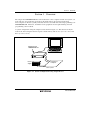
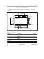
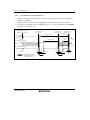
To our customers,
Old Company Name in Catalogs and Other Documents
On April 1st, 2010, NEC Electronics Corporation merged with Renesas Technology
Corporation, and Renesas Electronics Corporation took over all the business of both
companies. Therefore, although the old company name remains in this document, it is a valid
Renesas Electronics document. We appreciate your understanding.
Renesas Electronics website: http://www.renesas.com
April 1st, 2010
Renesas Electronics Corporation
Issued by: Renesas Electronics Corporation (http://www.renesas.com)
Send any inquiries to http://www.renesas.com/inquiry.
Notice
1.
2.
3.
4.
5.
6.
7.
All information included in this document is current as of the date this document is issued. Such information, however, is
subject to change without any prior notice. Before purchasing or using any Renesas Electronics products listed herein, please
confirm the latest product information with a Renesas Electronics sales office. Also, please pay regular and careful attention to
additional and different information to be disclosed by Renesas Electronics such as that disclosed through our website.
Renesas Electronics does not assume any liability for infringement of patents, copyrights, or other intellectual property rights
of third parties by or arising from the use of Renesas Electronics products or technical information described in this document.
No license, express, implied or otherwise, is granted hereby under any patents, copyrights or other intellectual property rights
of Renesas Electronics or others.
You should not alter, modify, copy, or otherwise misappropriate any Renesas Electronics product, whether in whole or in part.
Descriptions of circuits, software and other related information in this document are provided only to illustrate the operation of
semiconductor products and application examples. You are fully responsible for the incorporation of these circuits, software,
and information in the design of your equipment. Renesas Electronics assumes no responsibility for any losses incurred by
you or third parties arising from the use of these circuits, software, or information.
When exporting the products or technology described in this document, you should comply with the applicable export control
laws and regulations and follow the procedures required by such laws and regulations. You should not use Renesas
Electronics products or the technology described in this document for any purpose relating to military applications or use by
the military, including but not limited to the development of weapons of mass destruction. Renesas Electronics products and
technology may not be used for or incorporated into any products or systems whose manufacture, use, or sale is prohibited
under any applicable domestic or foreign laws or regulations.
Renesas Electronics has used reasonable care in preparing the information included in this document, but Renesas Electronics
does not warrant that such information is error free. Renesas Electronics assumes no liability whatsoever for any damages
incurred by you resulting from errors in or omissions from the information included herein.
Renesas Electronics products are classified according to the following three quality grades: “Standard”, “High Quality”, and
“Specific”. The recommended applications for each Renesas Electronics product depends on the product’s quality grade, as
indicated below. You must check the quality grade of each Renesas Electronics product before using it in a particular
application. You may not use any Renesas Electronics product for any application categorized as “Specific” without the prior
written consent of Renesas Electronics. Further, you may not use any Renesas Electronics product for any application for
which it is not intended without the prior written consent of Renesas Electronics. Renesas Electronics shall not be in any way
liable for any damages or losses incurred by you or third parties arising from the use of any Renesas Electronics product for an
application categorized as “Specific” or for which the product is not intended where you have failed to obtain the prior written
consent of Renesas Electronics. The quality grade of each Renesas Electronics product is “Standard” unless otherwise
expressly specified in a Renesas Electronics data sheets or data books, etc.
“Standard”:
8.
9.
10.
11.
12.
Computers; office equipment; communications equipment; test and measurement equipment; audio and visual
equipment; home electronic appliances; machine tools; personal electronic equipment; and industrial robots.
“High Quality”: Transportation equipment (automobiles, trains, ships, etc.); traffic control systems; anti-disaster systems; anticrime systems; safety equipment; and medical equipment not specifically designed for life support.
“Specific”:
Aircraft; aerospace equipment; submersible repeaters; nuclear reactor control systems; medical equipment or
systems for life support (e.g. artificial life support devices or systems), surgical implantations, or healthcare
intervention (e.g. excision, etc.), and any other applications or purposes that pose a direct threat to human life.
You should use the Renesas Electronics products described in this document within the range specified by Renesas Electronics,
especially with respect to the maximum rating, operating supply voltage range, movement power voltage range, heat radiation
characteristics, installation and other product characteristics. Renesas Electronics shall have no liability for malfunctions or
damages arising out of the use of Renesas Electronics products beyond such specified ranges.
Although Renesas Electronics endeavors to improve the quality and reliability of its products, semiconductor products have
specific characteristics such as the occurrence of failure at a certain rate and malfunctions under certain use conditions. Further,
Renesas Electronics products are not subject to radiation resistance design. Please be sure to implement safety measures to
guard them against the possibility of physical injury, and injury or damage caused by fire in the event of the failure of a
Renesas Electronics product, such as safety design for hardware and software including but not limited to redundancy, fire
control and malfunction prevention, appropriate treatment for aging degradation or any other appropriate measures. Because
the evaluation of microcomputer software alone is very difficult, please evaluate the safety of the final products or system
manufactured by you.
Please contact a Renesas Electronics sales office for details as to environmental matters such as the environmental
compatibility of each Renesas Electronics product. Please use Renesas Electronics products in compliance with all applicable
laws and regulations that regulate the inclusion or use of controlled substances, including without limitation, the EU RoHS
Directive. Renesas Electronics assumes no liability for damages or losses occurring as a result of your noncompliance with
applicable laws and regulations.
This document may not be reproduced or duplicated, in any form, in whole or in part, without prior written consent of Renesas
Electronics.
Please contact a Renesas Electronics sales office if you have any questions regarding the information contained in this
document or Renesas Electronics products, or if you have any other inquiries.
(Note 1) “Renesas Electronics” as used in this document means Renesas Electronics Corporation and also includes its majorityowned subsidiaries.
(Note 2) “Renesas Electronics product(s)” means any product developed or manufactured by or for Renesas Electronics.
User’s Manual
Flash Microcomputer
On-Board Programming Adapter
Board
User’s Manual
Renesas Microcomputer
Development Environment
System
HS0008EASF5HE
Rev.1.00 2009.10
Rev. 1.00 Oct. 02, 2009 Page ii of x
REJ10J2064-0100
Notes regarding these materials
1. This document is provided for reference purposes only so that Renesas customers may select the appropriate
Renesas products for their use. Renesas neither makes warranties or representations with respect to the
accuracy or completeness of the information contained in this document nor grants any license to any
intellectual property rights or any other rights of Renesas or any third party with respect to the information in
this document.
2. Renesas shall have no liability for damages or infringement of any intellectual property or other rights arising
out of the use of any information in this document, including, but not limited to, product data, diagrams, charts,
programs, algorithms, and application circuit examples.
3. You should not use the products or the technology described in this document for the purpose of military
applications such as the development of weapons of mass destruction or for the purpose of any other military
use. When exporting the products or technology described herein, you should follow the applicable export
control laws and regulations, and procedures required by such laws and regulations.
4. All information included in this document such as product data, diagrams, charts, programs, algorithms, and
application circuit examples, is current as of the date this document is issued. Such information, however, is
subject to change without any prior notice. Before purchasing or using any Renesas products listed in this
document, please confirm the latest product information with a Renesas sales office. Also, please pay regular
and careful attention to additional and different information to be disclosed by Renesas such as that disclosed
through our website. (http://www.renesas.com )
5. Renesas has used reasonable care in compiling the information included in this document, but Renesas
assumes no liability whatsoever for any damages incurred as a result of errors or omissions in the information
included in this document.
6. When using or otherwise relying on the information in this document, you should evaluate the information in
light of the total system before deciding about the applicability of such information to the intended application.
Renesas makes no representations, warranties or guaranties regarding the suitability of its products for any
particular application and specifically disclaims any liability arising out of the application and use of the
information in this document or Renesas products.
7. With the exception of products specified by Renesas as suitable for automobile applications, Renesas
products are not designed, manufactured or tested for applications or otherwise in systems the failure or
malfunction of which may cause a direct threat to human life or create a risk of human injury or which require
especially high quality and reliability such as safety systems, or equipment or systems for transportation and
traffic, healthcare, combustion control, aerospace and aeronautics, nuclear power, or undersea communication
transmission. If you are considering the use of our products for such purposes, please contact a Renesas
sales office beforehand. Renesas shall have no liability for damages arising out of the uses set forth above.
8. Notwithstanding the preceding paragraph, you should not use Renesas products for the purposes listed below:
(1) artificial life support devices or systems
(2) surgical implantations
(3) healthcare intervention (e.g., excision, administration of medication, etc.)
(4) any other purposes that pose a direct threat to human life
Renesas shall have no liability for damages arising out of the uses set forth in the above and purchasers who
elect to use Renesas products in any of the foregoing applications shall indemnify and hold harmless Renesas
Technology Corp., its affiliated companies and their officers, directors, and employees against any and all
damages arising out of such applications.
9. You should use the products described herein within the range specified by Renesas, especially with respect
to the maximum rating, operating supply voltage range, movement power voltage range, heat radiation
characteristics, installation and other product characteristics. Renesas shall have no liability for malfunctions or
damages arising out of the use of Renesas products beyond such specified ranges.
10. Although Renesas endeavors to improve the quality and reliability of its products, IC products have specific
characteristics such as the occurrence of failure at a certain rate and malfunctions under certain use
conditions. Please be sure to implement safety measures to guard against the possibility of physical injury, and
injury or damage caused by fire in the event of the failure of a Renesas product, such as safety design for
hardware and software including but not limited to redundancy, fire control and malfunction prevention,
appropriate treatment for aging degradation or any other applicable measures. Among others, since the
evaluation of microcomputer software alone is very difficult, please evaluate the safety of the final products or
system manufactured by you.
11. In case Renesas products listed in this document are detached from the products to which the Renesas
products are attached or affixed, the risk of accident such as swallowing by infants and small children is very
high. You should implement safety measures so that Renesas products may not be easily detached from your
products. Renesas shall have no liability for damages arising out of such detachment.
12. This document may not be reproduced or duplicated, in any form, in whole or in part, without prior written
approval from Renesas.
13. Please contact a Renesas sales office if you have any questions regarding the information contained in this
document, Renesas semiconductor products, or if you have any other inquiries.
Rev. 1.00 Oct. 02, 2009 Page iii of x
REJ10J2064-0100
Rev. 1.00 Oct. 02, 2009 Page iv of x
REJ10J2064-0100
IMPORTANT INFORMATION
READ FIRST
• READ this user's manual before using this adapter board.
• KEEP the user's manual handy for future reference.
• Do not attempt to use the adapter board until you fully understand its mechanism.
Adapter Board:
Throughout this document, the term "adapter board" shall be defined as the adapter board main
unit and attached cables manufactured by Renesas Technology Corp.
The user system or a host computer is not included in this definition.
Purpose of the Adapter Board:
The adapter board, which is connected between a host computer and the user system, has a
function that can write/erase user application programs on the flash memory incorporated in the
flash microcomputer on the user system (on-board) when it is used with the on-board
programming tool.
Therefore, the burden on the peripheral circuit required during on-board programming can be
minimized. This board can be used for all flash microcomputers incorporating a flash memory
using Vcc and PVcc and cannot be used for flash microcomputers in which 12 V is applied to Vpp
pin and MD pin.
This adapter board must only be used for the above purpose.
Limited Applications:
This adapter board is not authorized for use in MEDICAL, atomic energy, aeronautical or
space technology applications without consent of the appropriate officer of a Renesas sales
company. Such use includes, but is not limited to, use in life support systems. Buyers of this
adapter board must notify the relevant Renesas sales offices before planning to use the product in
such applications.
Improvement Policy:
Renesas Technology Corp. (including its subsidiaries, hereafter collectively referred to as
Renesas) pursues a policy of continuing improvement in design, performance, and safety of the
adapter board. Renesas reserves the right to change, wholly or partially, the specifications, design,
user's manual, and other documentation at any time without notice.
Rev. 1.00 Oct. 02, 2009 Page v of x
REJ10J2064-0100
Target User of the Adapter board:
This adapter board should only be used by those who have carefully read and thoroughly
understood the information and restrictions contained in the user's manual. Do not attempt to use
the adapter board until you fully understand its mechanism.
It is highly recommended that first-time users be instructed by users that are well versed in the
operation of the adapter board.
State Law:
Some states do not allow the exclusion or limitation of implied warranties or liability for
incidental or consequential damages, so the above limitation or exclusion may not apply to you.
This warranty gives you specific legal rights, and you may have other rights which may vary from
state to state.
The Warranty is Void in the Following Cases:
Renesas shall have no liability or legal responsibility for any problems caused by misuse,
abuse, misapplication, neglect, improper handling, installation, repair or modifications of the
adapter board without Renesas's prior written consent or any problems caused by the user system.
All Rights Reserved:
This user's manual and adapter board are copyrighted and all rights are reserved by Renesas.
No part of this user's manual, all or part, may be reproduced or duplicated in any form, in hardcopy or machine-readable form, by any means available without Renesas's prior written consent.
Other Important Things to Keep in Mind:
1. Circuitry and other examples described herein are meant merely to indicate the characteristics
and performance of Renesas's semiconductor products. Renesas assumes no responsibility for
any intellectual property claims or other problems that may result from applications based on
the examples described herein.
2. No license is granted by implication or otherwise under any patents or other rights of any third
party or Renesas.
Figures:
Some figures in this user's manual may show items different from your actual system.
Limited Anticipation of Danger:
Renesas cannot anticipate every possible circumstance that might involve a potential hazard.
The warnings in this user's manual and on the adapter board are therefore not all inclusive.
Therefore, you must use the adapter board safely at your own risk.
Rev. 1.00 Oct. 02, 2009 Page vi of x
REJ10J2064-0100
SAFETY PAGE
READ FIRST
• READ this user's manual before using this adapter board.
• KEEP the user's manual handy for future reference.
• Do not attempt to use the adapter board until you fully understand its mechanism.
DEFINITION OF SIGNAL WORDS
This is the safety alert symbol. It is used to alert you to potential personal
injury hazards. Obey all safety messages that follow this symbol to avoid
possible injury or death.
DANGER
WARNING
CAUTION
CAUTION
DANGER indicates an imminently hazardous situation which, if not
avoided, will result in death or serious injury.
WARNING indicates a potentially hazardous situation which, if not
avoided, could result in death or serious injury.
CAUTION indicates a potentially hazardous situation which, if not
avoided, may result in minor or moderate injury.
CAUTION used without the safety alert symbol indicates a
potentially hazardous situation which, if not avoided, may result
in property damage.
NOTE emphasizes essential information.
Rev. 1.00 Oct. 02, 2009 Page vii of x
REJ10J2064-0100
WARNING
Observe the precautions listed below. Failure to do so will
result in a FIRE HAZARD and will damage the user system and
the adapter board or will result in PERSONAL INJURY.
The USER PROGRAM will be LOST.
1. Always switch OFF the adapter board and user system before
connecting or disconnecting any CABLES, PARTS, or cable
head.
2. Before connecting, always make sure that pin 1 on both sides
are correctly aligned.
3. The adapter board can be used for flash microcomputers
to which Vcc = 2.7 V to 5.25 V, PVcc = 2.7 V to 5.25 V is
supplied from a single power source.
The adapter board cannot be used for flash microcomputers
in which 12 V is applied to both the Vpp pin and MD pin.
The values of Vcc and PVcc must not exceed the guaranteed
operation ranges.
Rev. 1.00 Oct. 02, 2009 Page viii of x
REJ10J2064-0100
Contents
Section 1 Overview..............................................................................................1
Section 2 Configuration .......................................................................................3
Section 3 Connectors, Switches, and LEDs.........................................................5
3.1
3.2
3.3
Connectors ........................................................................................................................ 5
3.1.1 User Interface Connector (P1) ............................................................................. 5
3.1.1 Serial Interface Connector (P2) ........................................................................... 9
3.1.2 Adapter Board Power-Supply Connector (P3)..................................................... 9
Switches............................................................................................................................ 9
3.2.1 Transfer Switch (START/STOP)......................................................................... 9
3.2.2 Power-Supply Switch (POWER)........................................................................ 10
3.2.3 Jumper Terminals for Power-Supply Switch (JP1).............................................. 11
3.2.4 Circuit Protector (F1)........................................................................................... 12
3.2.5 Control-Signal Enable/Disable Switches (S4) ..................................................... 13
3.2.6 Low (0)/High (1) Switches (S3) .......................................................................... 13
3.2.7 Vcc and PVcc Switches (S5 and S6) ................................................................... 14
3.2.8 S3, S4, S5, and S6 Setting Examples................................................................... 15
LEDs ................................................................................................................................. 15
3.3.1 START LED (START: Red) ............................................................................... 15
3.3.2 Power LED (POWER: Green) ............................................................................. 15
Section 4 Notes on Use........................................................................................17
Section 5 Specifications.......................................................................................19
5.1
5.2
Input Voltage and Consumption Current .......................................................................... 19
Write Processing ............................................................................................................... 19
5.2.1 Specification of Control Sequence 1.................................................................... 20
5.2.2 Specification of the Control Sequence 2.............................................................. 21
Rev. 1.00 Oct. 02, 2009 Page ix of x
REJ10J2064-0100
Rev. 1.00 Oct. 02, 2009 Page x of x
REJ10J2064-0100
Section 1 Overview
Section 1 Overview
The adapter board HS0008EASF5H, connected between a host computer and the user system, can
write and erase user application programs on the flash memory incorporated in the flash
microcomputer on the user system (on-board) when it is used with the on-board programming tool
HS6400FWIW5SR. Therefore, the burden on the peripheral circuit required during on-board
programming can be reduced.
A system configuration using the adapter board is shown in figure 1.1. This board can only be
used for the microcomputers that incorporate a flash memory and use Vcc (2.7 V to 5.25 V) and
PVcc (2.7 V to 5.25 V).
Adapter board
HS0008EASF5H
Host computer
Power
supply
Flash microcomputer
User system
Figure 1.1 System Configuration Using Adapter Board
Rev. 1.00 Oct. 02, 2009 Page 1 of 22
REJ10J2064-0100
Section 1 Overview
Rev. 1.00 Oct. 02, 2009 Page 2 of 22
REJ10J2064-0100
Section 2 Configuration
Section 2 Configuration
The configuration and components of the adapter board are shown in figure 2.1 and table 2.1,
respectively.
Serial interface connector
Power supply switch
Adapter board
power-supply
connector
Circuit protector
(breaker for protection)
POWER
FG
P2
P3
P1
107.3
F1
HS0008EASF5H
28.5
150.5
User interface connector
START/STOP
POWER
FG
START
Transfer switch
LEDs
Four screws for fixing the
upper and lower panels
Unit: mm
Figure 2.1 Adapter Board
Table 2.1
Components
Item Name
Description
Quantity
Adapter board
Main unit
1
Serial interface cable
Connection between main unit and host computer
(2000 mm)
1
User system interface cable
Connection between main unit and user system
(300 mm)
1
User system interface cable
connector
Connection between main unit and user system
1
Adapter board power cable
Adapter board power supply(1000 mm)
1
Rev. 1.00 Oct. 02, 2009 Page 3 of 22
REJ10J2064-0100
Section 2 Configuration
Rev. 1.00 Oct. 02, 2009 Page 4 of 22
REJ10J2064-0100
Section 3 Connectors, Switches, and LEDs
Section 3 Connectors, Switches, and LEDs
3.1
Connectors
This adapter board has connectors P1, P2, and P3.
3.1.1
User Interface Connector (P1)
WARNING
Observe the precautions listed below. Failure to do so
will result in a FIRE HAZARD and will damage the user
system and the adapter board or will result in PERSONAL
INJURY.
1. Always switch OFF the adapter board and the user
system before connecting or disconnecting ANY
CABLES
or PARTS.
2. Before connecting, always make sure that pin 1 on both
sides are correctly aligned.
3. When disconnecting cables, take care not to put
excessive stress on the cables.
The signals required for writing to flash memory are shown in figures 3.1 and 3.2. Connect the
adapter board and the user system using the user system interface cable provided (with an 20-pole
connector on each end) and a user system interface cable connector (used for connecting the cable
to the user system). The user system interface cable provided straight-matches the pins in the
adapter board to those in the user system, as shown in figure 3.2.
A 3428-6002LCPL manufactured by Sumitomo 3M Ltd. (former part code: 3428-6002 LCSC) is
used as the user-system interface cable connector.
Rev. 1.00 Oct. 02, 2009 Page 5 of 22
REJ10J2064-0100
Section 3 Connectors, Switches, and LEDs
Serial interface
connector (P2)
TXD 3
RXD 2
GND 5
3 RXD
2 TXD
5 GND
Power supply
1 2
3 4
.
.
.
Host computer
Vcc
GND
User interface
connector (P1)
1 Vcc (Red)
2 GND (Black)
Adapter board
power-supply
connector (P3)
(
17 18
19 20
Adapter
board
User system
1 2
3 4
.
.
.
17 18
19 20
Straightmatching
): Color of provided cable
Figure 3.1 Connector Pin Location
Rev. 1.00 Oct. 02, 2009 Page 6 of 22
REJ10J2064-0100
1: RES
3: FWE/FWP
5: MD0
7: MD1
9: IO0
11: IO1
User
13: IO2
15: RXD
TXD
17: TXD
RXD
18: VIN (Vcc)
20: VIN (PVcc)
2, 4, 6, 8,
10, 12, 14, 16: GND
Section 3 Connectors, Switches, and LEDs
20 19
.
.
.
.
.
20 19
.
.
.
.
.
User system side
2 1
2 1
HS0008EASF5H side
Pin 1
Top view
Side view
Connector: 3428-6002LCPL (Sumitomo 3M, Ltd.)
Figure 3.2 User System Interface Cable
Rev. 1.00 Oct. 02, 2009 Page 7 of 22
REJ10J2064-0100
Section 3 Connectors, Switches, and LEDs
Table 3.1
Correspondence between Signals and Numbers Indicated on the User System
Interface Cable
Number
on Cable
Signal
1
RES
2
GND
3
FWE/FWP
4
GND
5
MD0
6
GND
7
MD1
8
GND
9
IO0
10
GND
11
IO1
12
GND
13
IO2
14
GND
15
RXD (TXD for the user system)
16
GND
17
TXD (RXD for the user system)
18
VIN (Vcc)
19
NC
20
VIN (PVcc)
If the device has Vcc and PVcc, provide Vcc (pin 18) and PVcc (pin 20) to the VIN pin of the P1
connector. If the condition is Vcc = PVcc and the device that does not have both Vcc and PVcc is
used, provide Vcc (pin 18) or PVcc (pin 20) to the two VIN pins of the P1 connector.
When the target microcomputer requires port control during on-board programming, connect
necessary port signals. For details, refer to table 3.5 in section 3.2.8, S3, S4, S5, and S6 Setting
Examples.
Rev. 1.00 Oct. 02, 2009 Page 8 of 22
REJ10J2064-0100
Section 3 Connectors, Switches, and LEDs
3.1.1
Serial Interface Connector (P2)
Connect the adapter board and host computer using the serial interface cable provided.
3.1.2
Adapter Board Power-Supply Connector (P3)
Supply power to the adapter board from the user system power supply (Vcc: 2.7 V to 5.25 V,
PVcc: 2.7 V to 5.25 V) via the VIN pin of the user system interface cable.
If the device does not use the PVcc, provide Vcc to the two VIN pins.
If the current supply capability of the user system power supply is insufficient, power (Vcc 5 V ±
5%) can be supplied using a separate power supply from the P3 connector to the adapter board.
3.2
Switches
3.2.1
Transfer Switch (START/STOP)
• When control sequence 1 has been selected:
Pressing this switch once initiates programming control (in the mode selected by the switches).
In this case, the START LED (red) is turned on. Pressing this switch again after the program
has been transferred terminates programming control. At this time, the START LED (red) is
turned off and the high level is output by the RES pin.
• When control sequence 2 has been selected:
Pressing this switch once initiates programming control (in the mode selected by the switches).
In this case, the START LED (red) is turned on. Pressing this switch again after the program
has been transferred terminates programming control. At this time, the START LED (red) is
turned off and the low level is output by the RES pin.
Refer to section 5.2, Writing Processing, for details of the control sequences.
Rev. 1.00 Oct. 02, 2009 Page 9 of 22
REJ10J2064-0100
Section 3 Connectors, Switches, and LEDs
CAUTION
After program transfer, press the transfer switch
(START/STOP) and confirm that the START LED (red) is
turned off. If the user system power supply VIN (Vcc: 2.7 V
to 5.25 V, PVcc: 2.7 V to 5.25 V) is turned off while the
START LED is on, the user system will be damaged.
For details on activating the on-board programming tool, refer to the On-Board Programming
Tool User's Manual.
Activate the on-board programming tool, and select the boot mode or user program mode
displayed on the host computer. The hardware setting sequence is displayed. Then press the
transfer switch. The START LED (red) is turned on and a programming control is initiated.
After programming the flash memory in the selected mode, confirm the end message, press the
transfer switch again, and complete the programming control. At this time, the START LED is
turned off.
3.2.2
Power-Supply Switch (POWER)
The following two power-supply methods are available for this adapter board.
• Power is supplied from the user system power supply via the user system interface cable and
connector (VIN pin).
• As a countermeasure against insufficient current supply by the above method, power is
supplied through the power-supply connector (P3). In this case, the user must prepare a
separate power supply.
Vcc 5 V ± 5% is supplied to the power-supply connector (P3) of the adapter board. This switch
works as the power-supply switch (on and off) of the adapter board only when power is supplied
from the power-supply connector (P3) of the adapter board. (Refer to figure 3.3.) In this case,
power also needs to be supplied through the VIN pin of the user system interface cable.
When power is supplied to the adapter board only from the user system power supply, this powersupply switch does not work. In this case, the power-supply switch on the user system is used as
the power-supply switch for the adapter board.
Rev. 1.00 Oct. 02, 2009 Page 10 of 22
REJ10J2064-0100
Section 3 Connectors, Switches, and LEDs
On
Off
Figure 3.3 Power-Supply Switch (POWER)
3.2.3
Jumper Terminals for Power-Supply Switch (JP1)
The jumper terminals are inside the chassis. Open the upper panel by removing the screw in each
corner attaching the upper and lower panels. After jumper setting, close the chassis by re-fixing
the screws.
The following two methods are available for supplying power to the adapter board; appropriate
jumper setting is required for these jumper terminals.
• To supply power from the user system via the user system interface cable connector (VIN
pin), insert a jumper into 2 and 3.
• To supply power from power-supply connector (P3), prepare a power supply for the adapter
board. Insert a jumper into 1 and 2 (default setting at shipment).
JP1
1
2
3
Jumper
Figure 3.4 Jumper Terminals for Power-Supply Switch (JP1)
Rev. 1.00 Oct. 02, 2009 Page 11 of 22
REJ10J2064-0100
Section 3 Connectors, Switches, and LEDs
3.2.4
Circuit Protector (F1)
This adapter board is provided with a resumable circuit protector on the input section of the user
system power supply to prevent damage to the system. If the circuit protector is turned off due to
erroneous power-supply connection or excessive current (1 A or more), check the system, then
return the circuit protector to the original state by pressing the switch in the hole with a thin pin or
wire to activate the circuit protector (figure 3.5).
Off
Inside the case
On
Inside the case
Figure 3.5 Circuit Protector Setting
Rev. 1.00 Oct. 02, 2009 Page 12 of 22
REJ10J2064-0100
Section 3 Connectors, Switches, and LEDs
3.2.5
Control-Signal Enable/Disable Switches (S4)
This adapter board is provided with switches so that each control signal can be enabled or
disabled separately, as shown in table 3.2; the control-signal switches that are necessary to
program the
flash microcomputer should be set to E. These switches are inside the case. Open the upper panel
by removing the screw in each corner between the upper and lower panels. After switch setting,
reclose the case and refasten the screws.
Table 3.2
Control-Signal Enable/Disable Switches (S4)
Signal
E
D
FWE (S4-1)
Enabled
Disabled
MD0 (S4-2)
Enabled
Disabled
MD1 (S4-3)
Enabled
Disabled
IO0 (S4-4)
Enabled
Disabled
IO1 (S4-5)
Enabled
Disabled
IO2 (S4-6)
Enabled
Disabled
3.2.6
Low (0)/High (1) Switches (S3)
Level 0 or 1 can be selected by enabling the enable/disable switch (S4) (see table 3.2). Select 0 or
1 for the control signals according to the flash microcomputer you are using (to program the flash
microcomputer). Also, S3-8 (the RES output selection switch) can switch the control sequence at
the time of programming regardless of the setting of S4, so that the level output by the RES pin
after power has been supplied or operation in a mode has been terminated can be selected.
These switches are inside the case. Open the upper panel by removing the screw in each corner
between the upper and lower panels. After switch setting, reclose the case and refasten the
screws.
Rev. 1.00 Oct. 02, 2009 Page 13 of 22
REJ10J2064-0100
Section 3 Connectors, Switches, and LEDs
Table 3.3
Low (0)/High (1) Switches (S3)
Signal
0
1
FWE (S3-1)
Low
High
MD0 (S3-2)
Low
High
MD1 (S3-3)
Low
High
IO0 (S3-4)
Low
High
IO1 (S3-5)
Low
High
IO2 (S3-6)
Low
High
-
-
Low output from RES
(control sequence 2)
High output from RES
(control sequence 1)
- (S3-7)
SQMD (S3-8)
3.2.7
Vcc and PVcc Switches (S5 and S6)
Select Vcc or PVcc level for the control signals according to the flash microcomputer you are
using (to program the flash microcomputer). The Vcc or PVcc level can be selected by the switch
settings of S5 and S6 (see table 3.4). The switches are inside the case. Open the upper panel by
removing the screw in each corner between the upper and lower panels. After switch setting,
reclose the case and refasten the screws.
Table 3.4
Vcc and PVcc Switches (S5 and S6)
Signal
P
V
FWE (S5-1)
PVcc
Vcc
MD0 (S5-2)
PVcc
Vcc
MD1 (S5-3)
PVcc
Vcc
IO0 (S5-4)
PVcc
Vcc
IO1 (S6-1)
PVcc
Vcc
IO2 (S6-2)
PVcc
Vcc
Rev. 1.00 Oct. 02, 2009 Page 14 of 22
REJ10J2064-0100
Section 3 Connectors, Switches, and LEDs
3.2.8
S3, S4, S5, and S6 Setting Examples
Table 3.5 shows examples of S3 to S6 switch settings for on-board programming in boot mode.
When using an flash microcomputer that is not listed in table 3.5, refer to the corresponding
hardware manual.
Table 3.5
S3, S4, S5, and S6 Setting Examples
HS0008EASF5H
SH7055F
P1 Connector Signal
MCU Signal
S4
S3
S5 and S6
VIN (Vcc)
Vcc
*1
*1
*1
VIN (PVcc)
PVcc2
*1
*1
*1
GND
Vss
*1
*1
*1
RES
RES
*1
*1
*1
TXD
RXD
*1
*1
*1
RXD
TXD
*1
*1
*1
FWE/FWP
FWE
E
1
C (S5-1)
MD0
MD1
E
0
P (S5-2)
MD1
MD2
E
1
P (S5-3)
D
*2
*2
IO0
—
*3
IO1
—
*3
D
*2
*2
IO2
—
*3
D
*2
*2
Notes: 1. The P1 connector signals and MCU signals on the user system must always be
connected regardless of the S3, S4, S5, and S6 settings.
2. Either setting is available.
3. Need not be connected.
3.3
LEDs
3.3.1
START LED (START: Red)
This LED is turned on or off when the transfer switch (START/STOP) is pressed.
3.3.2
Power LED (POWER: Green)
This LED is on while the user system power supply VIN (Vcc: 2.7 V to 5.25 V, PVcc: 2.7 V to
5.25 V) or the power supply Vcc (5 V ± 5%) dedicated to the adapter board is supplied.
Rev. 1.00 Oct. 02, 2009 Page 15 of 22
REJ10J2064-0100
Section 3 Connectors, Switches, and LEDs
Rev. 1.00 Oct. 02, 2009 Page 16 of 22
REJ10J2064-0100
Section 4 Notes on Use
Section 4 Notes on Use
1. The RES pin of the adapter board is an open-collector output. Use a resistor that suits the user
system to pull up the RES pin (around 1-kΩ is recommended).
2. Do not directly connect control signals FWP/FWE, MD0, MD1, IO0, IO1, or IO2 to Vcc or
GND. The user interface of the adapter board is shown figure 4.1.
The resistance value is 20 Ω when analog switch HC4066 is on. It is recommended to pull up
or pull down the resistance with 4.7-kΩ or more. (For revision A, 47 kΩ or more is
recommended.)
3. After program transfer, press the transfer switch (START/STOP) and confirm that the START
LED (red) is turned off. If the user system power supply VIN (Vcc: 2.7 V to 5.25 V, PVcc:
2.7 V to 5.25 V) is turned off while the START LED is on, the user system will be damaged.
4. The host computer (DOS/V compatible machines) with built-in Pentium® can be connected to
the adapter board.
5. If the device has Vcc and PVcc, provide Vcc (pin 18) and PVcc (pin 20) to the VIN pin of the
P1 connector. If the condition is Vcc = PVcc and the device that does not have both Vcc and
PVcc is used, provide Vcc (pin 18) or PVcc (pin 20) to the two VIN pins of the P1 connector.
Vcc/PVcc
S5
S6
Control signals
for controller
1k
22
S3
Analog
switch
HC4066
User system
interface connector
Figure 4.1 Control-Signal Circuit Example
Rev. 1.00 Oct. 02, 2009 Page 17 of 22
REJ10J2064-0100
Section 4 Notes on Use
Rev. 1.00 Oct. 02, 2009 Page 18 of 22
REJ10J2064-0100
Section 5 Specification
Section 5 Specifications
5.1
Input Voltage and Consumption Current
• Power-supply input (VIN) from the user interface connector (Vcc: 2.7 V to 5.25 V, PVcc: 2.7
V to 5.25 V)
• Power-supply input (Vcc) from the P3 connector of the adapter board: 5 V ± 5%
• Consumption current: 200 mA at 5 V or 330 mA at 3 V
5.2
Write Processing
For write processing, control sequence 1 or control sequence 2 is selectable. Select either
according to the usage of the user system.
Set S3-8 to side 1:
Select control sequence 1
Set S3-8 to side 0:
Select control sequence 2
The respective control sequences are described below.
Rev. 1.00 Oct. 02, 2009 Page 19 of 22
REJ10J2064-0100
Section 5 Specification
5.2.1
Specification of Control Sequence 1
1. When the user system power supply is turned on or the power switch is on, the high level is
output by the RES pin.
2. When the transfer switch is pressed, the RES signal is held to the low level for 550 ms.
3. After 10 ms of the falling edge of the RES signal, 2.7- to 5.25-V application to the FWE/FWP
pin starts or stops (figure 5.1).
The user-system power supply or
POWER switch is turned on.
POWER LED is turned on.
The START/STOP
switch is pressed.
The START/STOP
switch is pressed.
The START/STOP
switch is pressed.
The START LED
is on.
The START LED is on.
2.7 to 5.25 V
VIN(VCC)
User system
mode
Write proccesing
0V to Vcc(2.7 to 5.25 V)
FWE etc.
0V to Vcc(2.7 to 5.25 V)
/RES
10 ms
10 ms
10 ms
540 ms
: Pin settings on the user
system board, such as
for FWE are valid.
550 ms
540 ms
550 ms
Figure 5.1 Reset Signal, 2.7- to 5.25-V Application, and Stop Timing (Control sequence 1)
Rev. 1.00 Oct. 02, 2009 Page 20 of 22
REJ10J2064-0100
Section 5 Specification
5.2.2
Specification of the Control Sequence 2
1.
When the user system power supply is turned on or the power switch is on, the low level is
output by the RES pin.
2.
After power has been turned on, pressing the transfer switch for the first time places the RES
pin at the high level, and the user system makes the transition to programming processing etc.
3.
After that, every time the transfer switch is pressed, the level of RES signal is inverted.
4.
The control sequence 2 has the two following states: execution of programming etc. is in
progress (the START LED is on) and the reset state (the START LED is off).
5.
When the transition to programming processing etc. is made, the application of 2.7 to 5.25 V
to the FWE/FWP pin starts or stops (figure 5.2) 10 ms after the transfer switch is pressed.
The user-system power supply or
POWER switch is turned on.
POWER LED is turned on.
The START LED is on.
The START/STOP
switch is pressed.
The START/STOP
switch is pressed.
The START LED is on.
2.7 to 5.25 V
The START/STOP
switch is pressed.
The START
LED is on.
The START/STOP
switch is pressed.
The START
LED is on.
VIN(VCC)
The user system
is reset state.
Write processing
Write processing
0V to Vcc(2.7 to 5.25 V)
FWE etc.
0V to Vcc(2.7 to 5.25 V)
/RES
10 ms
10 ms
10 ms
10ms
540 ms
: Pin settings on the user
system board, such as
for FWE are valid.
550 ms
540 ms
550 ms
Figure 5.2 Reset Signal, 2.7- to 5.25-V Application, and Stop Timing (Control sequence 2)
Rev. 1.00 Oct. 02, 2009 Page 21 of 22
REJ10J2064-0100
Section 5 Specification
Rev. 1.00 Oct. 02, 2009 Page 22 of 22
REJ10J2064-0100
Flash Microcomputer
On-Board Programming Adapter Board
User's Manual
Publication Date: Rev.1.00, October 2, 2009
Published by:
Sales Strategic Planning Div.
Renesas Technology Corp.
Edited by:
Customer Support Department
Global Strategic Communication Div.
Renesas Solutions Corp.
© 2009. Renesas Technology Corp., All rights reserved. Printed in Japan.
Sales Strategic Planning Div.
Nippon Bldg., 2-6-2, Ohte-machi, Chiyoda-ku, Tokyo 100-0004, Japan
RENESAS SALES OFFICES
http://www.renesas.com
Refer to "http://www.renesas.com/en/network" for the latest and detailed information.
Renesas Technology America, Inc.
450 Holger Way, San Jose, CA 95134-1368, U.S.A
Tel: <1> (408) 382-7500, Fax: <1> (408) 382-7501
Renesas Technology Europe Limited
Dukes Meadow, Millboard Road, Bourne End, Buckinghamshire, SL8 5FH, U.K.
Tel: <44> (1628) 585-100, Fax: <44> (1628) 585-900
Renesas Technology (Shanghai) Co., Ltd.
Unit 204, 205, AZIACenter, No.1233 Lujiazui Ring Rd, Pudong District, Shanghai, China 200120
Tel: <86> (21) 5877-1818, Fax: <86> (21) 6887-7858/7898
Renesas Technology Hong Kong Ltd.
7th Floor, North Tower, World Finance Centre, Harbour City, Canton Road, Tsimshatsui, Kowloon, Hong Kong
Tel: <852> 2265-6688, Fax: <852> 2377-3473
Renesas Technology Taiwan Co., Ltd.
10th Floor, No.99, Fushing North Road, Taipei, Taiwan
Tel: <886> (2) 2715-2888, Fax: <886> (2) 3518-3399
Renesas Technology Singapore Pte. Ltd.
1 Harbour Front Avenue, #06-10, Keppel Bay Tower, Singapore 098632
Tel: <65> 6213-0200, Fax: <65> 6278-8001
Renesas Technology Korea Co., Ltd.
Kukje Center Bldg. 18th Fl., 191, 2-ka, Hangang-ro, Yongsan-ku, Seoul 140-702, Korea
Tel: <82> (2) 796-3115, Fax: <82> (2) 796-2145
Renesas Technology Malaysia Sdn. Bhd
Unit 906, Block B, Menara Amcorp, Amcorp Trade Centre, No.18, Jln Persiaran Barat, 46050 Petaling Jaya, Selangor Darul Ehsan, Malaysia
Tel: <603> 7955-9390, Fax: <603> 7955-9510
Colophon 6.2
Flash Microcomputer
On-Board Programming Adapter Board
User’s Manual
1753, Shimonumabe, Nakahara-ku, Kawasaki-shi, Kanagawa 211-8668 Japan
REJ10J2064-0100