1
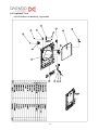
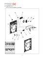
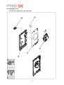
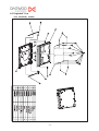
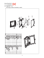
S/ M No. : OSPC790001
Ser v ice M a nua l
Portable DVD Player
Model: DPC-7900 Series
C aution
: In this Manual, some parts can be changed for improving,
their performance without notice in the parts list.
May. 2005
No.:
Revision:
0.1
Date:
Service Manual for
Portable DVD DPC-7900 Series
Name of Company
DAEWOO ELECTRONICS CORP.
Approved by
SIGNATURE
DATE
APPROVED BY
DATE
/
REVIEWED BY
/
PREPARED BY
/
Please return 1 copy for our confirmation
with your signature and comments.
Elliott Chang
18th.Dec.2005
Revision Record
Date
Rev No
Section
17/ Dec./ 2005
0.1
New edition
Description
Design and specifications are subject to change without notice.
All trademarks used in the specifications are the property of their respective owners.
1. General Descriptions ………………………………………………… 1
1.1. Model Features
1.2. Information
………………………………………………………… 1
………………………………………………………………… 2
2. Electrical Characteristics ……………………………………………
3
2.1. Optical Characteristics ………………………………………………………3
2.2. Electrical Characteristics ………………………………………………
3
2.3. System Block Diagram
4
……………………………………………………
2.4. Schematic Circuit Diagram ………………………………………… 5
3. Power ……………………………………………………………………… 11
3.1. Power Supply
……………………………………………………………… . 11
3.2. Rechargeable Battery
.
……………………………………………………… . 11
4. Dimension & Physical Characteristics …………………………. 13
4.1. Outline Dimension
………………………………………………… 13
4.2. Physical Characteristics ………………………………………………… ..13
4.3. Exploded View
……………………………………………………………… 14
5. Regulatory Standards …………………………………………… 19
5.1. Safety ………………………………………………………………………..19
5.2. EMI ………………………………………………………………………………. 19
5.3. Ergonomics
………………………………………………………………… 19
6. Service Tools and Equipment ………………………………… 20
6.1. Service Tools and Equipment
. ………………………………………
20
6.2. Storing and Handling Test Discs …………………………………… 20
6.3. Notes ……………………………………………………………………… 21
7. Spare Parts ………………………………………………………… 23
7.1. key Parts List ……………………………………………………………
23
8. Trouble shooting …………………………………………………………24
8.1. Error Code Table …………………………………………………… 24
8.2. Debug & Trouble Shooting
…………………………………………… 25
1 General Descriptions
1.1 Model Features
Video: DVD Playback, MPEG4(option) ,DivX(DivX Model),Kodak Picture CD compatible
& JPEG readable
Audio: CD, CD-R, CD-RW, MP3, WMA Playback
Firmware Upgradable
Dolby Digital Output
7" active-matrix TFT screen, 16:9 wide aspect ratio
Composite Video Output
Ultra dimension & light weight: 205mm(L) x 163.5mm(W) x 38mm(H) / 900g (around)
Slim size wireless remote control
Rechargeable battery pack
12-volt car cigarette lighter cable
Universal AC/DC power adapter
Audio/video cable for TV connection
Built-in stereo speakers
Two Stereo headphone jack
Parental Lock
Anti Shock Protection
-1-
1.2 Information
Disk Format
DVD, VCD, CD, MP3, CD-R, CD-RW, MPEG4 (OPTION),JPEG,
Kodak Picture CD, DivX(DivX Model),WMA
Video System
NTSC / PAL/Auto
Video Decompression
MPEG-2 (ISO/IEC-13818), MPEG-1
Video Output
800~1200mVpp/75 ohm
Audio Characteristic
2-Channel Analog
Analog Output
1.0~2.0Vrms/10K ohm
Frequency Response
DVD: 48kHz Sampling: 20Hz-20kHz
CD: 20Hz-20kHz
S/N Ratio
<= -65dB
Dynamic Range
<= -85dB
Audio Output Noise &Distortion Less than<= 0.01%
Digital Output
SPDIF
Headphone Jack
32ohm (30Mw) > 8ohm
LCD Display
7” active-matrix TFT type
Audio / Video Section
Audio input/output x1
Video input/output x1
S-Video / Coaxial output x1
Audio Section
Digital Output: Coaxial x1
Headphone Jack
Headphone Jack x1
Line Voltage
AC 100~240 VAC ± 10%(50/60Hz), (Adapter)
Power Consumption
12W (DC 12V, 1.0A)
Remote Control
DC 3V
Dimensions
205mm(L) x 163.5mm(W) x 38mm(H)
Weight
900 g (around)
Accessories
Slim Size Remote Controller with 3V Battery
12-volt Car Cigarette Lighter Cable
Universal AC/DC Power Adapter
Audio Cable / Video Cable
Infra-red
Ni-MH Rechargeable Battery Pack
S-video / Coaxial cable
-2-
2 Electrical Characteristics
2.1 Optical Characteristics
Parameter
Specifications
Unit
Screen Size
7.0 (16:9 diagonal)
inch
Display Format
1400 (H) 234 (V)
dot
Active Area
154.08 (H) 86.08 (V)
mm
Dot Pitch
0.107 (H) 0.370 (V)
mm
Pixel Configuration
Stripe
Outline Dimension
166.0 (W) 100.0 (H) 7.2 (D)(typ.)
Surface Treatment
Anti-Glare and Hard Coating
Weight
180 ± 10
mm
g
2.2 Electrical Characteristics
DVD/ SVCD/ VCD/ CD system decoding, packeted element streams and audio, video element
streams.
Fully digital servo processing (focusing, tracking, sledge and spindle servo control)
Fully digital calibration (focusing/ tracking offset and balance)
Digital phase lock loop with phase equalizer
Support Audio/ Video/ Photograph decoding and programming
Programmable Y/C delay relationship
Embedded micro-controller, up to 50MHz operating frequency
1.8V and 3.3V dual power supply, 208 pin PQFP
-3-
2.3 System Block Diagram
2.3.1. The System Block Diagram & the Block's Function Description
INVERTER
DISPLAY
7” TFT LCD
PW070XU3
DC To DC
MP1580
TFT LCD Driver
IR3Y29B +HX8806
Loader
DM-520A
2. Servo +MPEG
MT1389D/MT1389C
1.
-4-
(1)POWER_MPS
2.4 Schematic Circuit Diagram
CTR_5V
CTR_5V
R156
4.7k/open
RM12
330O
+3.3V
9VIN
RM11
4.7K/open
QM1
OPEN/3904
9VIN
NCTR_5V
NCTR_5V
NCTR_5V
C119
10uF
33R
OPEN
0.01uF
CM1
RM4
39K
RM9
OPEN
330O
R1
Q1
3904
1
2
3
4
UM1
MPS1580
BS
Sync
Vin
EN
Vsw Comp
GND
FB
CM8
MPS1580
BS
Sync
Vin
EN
Vsw Comp
GND
FB
0.01uF
UM2
1
2
3
4
D1
2
LED1
1
8
7
6
5
8
7
6
5
2
RM5
10K
1
DIODE
DM2
+3.3V
DELETA
DIODE
DM1
LM1
22uH
CM3
100pF
30.9K
CM9
0.022uF
0.022uF
CB60
0.1uF
CB59
0.1uF
100pF
16.9K
LDO_AV33
RFV33
RM8
CM10
RM6 10K 1%
22uH
LM3
RM3
CM5
RM1 10K 1%
RM10
10K
L26
FB
L27
FB
+
+
LM2
6.8uH
6.8uH
C136
22uF
LM4
22uF
C135
RFV33
C120
220uF/6.3V/lu
LDO_AV33
C121
220uF/6.3V/lu
100uF/10V/LU
CM2
CM7
220uF/6.3V/LU
+5V
+3.3V
+5V
+3.3V
-5-
2
1
C4
10uF
RM2
RM7
1
3
2
1
3
R2
OPEN/10K
1
3
2
C118
9VIN
9VIN
+3.3V
1
+
-
C2
+
D2
2
RB053L-30
0.1uF
+5V
L2
1
2
1
20uH
U1
OUT
BP
3
4
RT9167A-185CS
IN
SHDN-
C7
100uF/10V/LU
C5
0.01uF
2
R11
20K
C1
100uF/6.3V/LU
1
1
C6
100uF/6.3V/LU
C10
47uF/25V/LU
Q2
BSH105
1
D4
1N5819
D5
2
2
R14
1M
1N5819
V18
VCC
C11
22uF/25V/LU
C15
0.1uF
+3.3V
V18
VCC
+7.5V_TFT
220R
+3.3V
+5V
CTR_LOAD
+5V_TRAN
20uH
POWDET_MPEG
POWDET_MCU
CTR_TFT5V
CTR_AUDIO
L1
C9
47uF/25V/LU
-10V_TFT
R12
R13
20K
+ C16
100uF/16V/LU
+5V
+3.3V
CTR_LOAD
CTR_AUDIO
POWDET_MCU
CTR_TFT5V
+ C13
47uF/25V/LU
+15V_TFT
+5V_TRAN
POWDET_MPEG
C12
0.1uF
1
1
C3
47uF/25V/LU
POWDET_MCU
POWDET_MPEG
D3
1N5819
2
7
5
R17
200K
+
CON1
4
VOUT
PDET
VIN 3
OUT
VIN 2
1
GND
BATTERY
1
3
2
0.1uF
+3.3V
+3.3V
R5
3K
R7
3K
POWDET_MCU
1
U3A
LM393
VSYNC#
1
J1
R3
10k(8.2K)
2
3
7
1
FB
LX
EXT
U5
TER9.5*100M
LFB
LDOO
CE
U22
RT9262
8
4
3
R16
0R
-10V_TFT
+15V_TFT
+7.5V_TFT
+3.3V_TFT
+5V_TFT
1
-6-
U3B
LM393
+5V_TRAN
+5V_TRAN
R15
1.6M
6
6
5
BA05SFP
4
5
C17
1000pF
6
R4
47K
R10
47K
U6
VOUT
NC
VIN
CTL
+3.3V_TFT
C18
0.1uF
R18
560K
-10V_TFT
+3.3V_TFT
+7.5V_TFT
+15V_TFT
8
8
GND
GND
GND
GND
5
6
7
8
+5V_TRAN +5V_TFT
7
5
3
7
5
3
3
1
2
2
1
+3.3V
GND
R159
4.7K/open
6
1
8
4
8
4
R6
3.3K
R8
0(1.8K)
R9
3.9K
R160
330O
OPEN/10K
1
4.7k/open
R158
R157
GND
Q18
OPEN/3904
1
6
VDD
GND
1
3
POWERJACK
9VIN
C14
0.1uF
HSYNC#
CTR_TFT5V
3
2
1
(2) POWER FOR TFT
L51
RFV33
DV33
OPO
R173
150k
R169
0
RFV33
RFV33
TP4
TP5
TP6
L33
FB
L36
10uH
3216
+
ADACVDD3
R176
6.8
ADACVDD3
C88
16800PF
0603C
+
C74
0.1uF
CE48
100uF/16v
C8
+c88=17nf
0603C
0.1uF
CB75
C75
CB72
0.1uF
C76
RFVDD3
2200pF
C93
0.1uF
1
AGND
DVDA
DVDB
DVDC
DVDD
DVDRFIP
DVDRFIN
MA
MB
MC
MD
SA
SB
SC
SD
CDFON
CDFOP
TNI
TPI
MDI1
MDI2
LDO2
LDO1
SVDD3
CSO/RFOP
RFLVL/RFON
SGND
V2REFO
V20
VREFO
FEO
TEO
TEZISLV
OP_OUT
OP_INN
OP_INP
DMO
FMO
TROPENPWM
PWMOUT1/ADIN0
TRO
FOO
FG/ADIN1
GPIO0
GPIO1
GPIO2
IOA2
DVDD18
IOA3
IOA4
IOA5
IOA6
IOA7
HIGHA0
PLLVDD3
0.01uF
47uF/16v
+ CE53
V1P4
C15 closed to Pin186
+ CE52
V20
1uF
47uF/16v
R175
15k
C87
0.1uF
R199
R200
R201
R202
C110
0.015uF
L41
V1P4
V1P4
33k
33k
15k
10k
MO_VCC
0
FOO
TRO
FMO
DMO
RESET#
10uF/25v
C79
TP2
C80
JITFO
10uF/10v
C71
R166
750k
390pF
C81
1500pF
0603C
MT1389D
V1.7
V18
TP42
TP38
D6
1N4148
TP43
JITFN
TP3
TP8
TP40
TP1
URST#
TP44
R190
10k
DV33
100k
R23
39k
R22
TP39
TP37
TP46
+3.3V
47uF
+ C19
TP41
UQ216
U17
MT1389D
ACLK
ABCK
DVSS
GPIO5
GPIO4
GPIO3
DVDD18
RA4
RA5
RA6
RA7
DVDD3
RA8
RA9
RA11
CKE
RCLK
DVSS
RA3
DVSS
RA2
RA1
RA0
RA10
DVDD3
BA1
BA0
RCS#
RAS#
DVDD18
CAS#
RWE#
DVSS
DQM1
RD8
RD9
RD10
RD11
RD12
DVDD3
RD13
RD14
DVSS
RD15
RD0
RD1
RD2
DVSS
RD3
RD4
RD5
RD6
RD7
DQM0
0.1uF
CB71
DACVDD3
TP9
TP45
L3
FB
+ CE47
10uF/25v
DV33
V18
1
2
3
4
+3.3V
C114
XI
2.7u, DIP
R21
0
R182
2K
TP10
TP11
C116
22p
1
U20A
2
100k
C27MHz
2
74HC04
R218
Y1
1
CB81
CB88
0.1uF
CB82
0.1uF
CB89
0.1uF
CB83
0
U20B
XO
74HC04
INT/EXT
4
R167
0
+ CE46
10uF/25v
R217
R
INT/EXT
[4]
[3]
[3]
[3]
[3]
[3]
[3]
[3]
[3]
[3]
[3]
[3]
[3]
[3]
[3]
L34
FB
[5]
[5]
[5]
[4]
[5]
[5]
[5]
[3]
[3]
[5]
[5]
[1]
[4]
[4]
CTR_TFT5V
AVCC
[1 ]
PCE#
[3]
PWR#
[3]
HSYNC#
VSYNC#
Y[3..6]
[3]
MUTE_DAC
URST#
A[0..21]
AD[0..7]
PRD#
PWR#
PCE#
FLASH
MA[0..11]
DQ[0..15]
BA[0..1]
DQM[0..1]
DCLK
DCKE
CAS#
RAS#
WE#
CS#
MEMORY
SCL
SDA
ASDAT[0..2]
IIC
ALRCK
ACLK
ABCK
ASPDIF
AL
AR
VSCK
VSDA
AUDIO INTERFACE
ALRCK
ACLK
ABCK
ASPDIF
ASDAT[0..2]
AL
AR
VSCK
VSDA
SCL
SDA
DCKE
CAS#
RAS#
WE#
CS#
DQM[0..1]
DCLK
MA[0..11]
DQ[0..15]
BA[0..1]
PRD#
PWR#
PCE#
A[0..21]
AD[0..7]
FS0
VIDEO INTERFACE
Y[3..6]
FS0
MUTE_DAC
URST#
HSYNC#
VSYNC#
PCE#
PWR#
CTR_TFT5V
R220
3
0.1uF
CB70
APLLVDD3
C117
22p
0.1uF
0.1uF
TROUT
TRIN
LIMIT
CB80
CB87
0
0
0
0.1uF
0.1uF
ALRCK
CB79
CB86
R191
1k
0603R
0.1uF
0.1uF
V18
CB85
0.1uF
CB92
DV33
DV33
0.1uF
0.1uF
CB91
CB84
0.1uF
CB90
0.1uF
0.1uF
C95
L42
R187
R188
R189
1000p
FS
VREF
ACLK
ABCK
MA4
MA5
MA6
MA7
MA8
MA9
MA11
DCKE
DCLK
MA3
MA2
MA1
MA0
MA10
BA1
BA0
CS#
RAS#
CAS#
WE#
DQM1
DQ8
DQ9
DQ10
DQ11
DQ12
DQ13
DQ14
DQ15
DQ0
DQ1
DQ2
DQ3
DQ4
DQ5
DQ6
DQ7
DQM0
J8
RS-232
4x1 W/HOUSING
+3.3V
R183
4.7k
162
161
160
159
158
157
156
155
154
153
152
151
150
149
148
147
146
145
144
143
142
141
140
139
138
137
136
135
134
133
132
131
130
129
128
127
126
125
124
123
122
121
120
119
118
117
116
115
114
113
112
111
110
109
RxD
TxD
14
7
ADIN
OPOP+
R174
680k
V1P4
CB74
0.1uF
RFOP
RFON
RFVDD3
FB
R20
1
14
7
C73
0.1uF/N.C
C83
2200pF
47uF/16v
+ CE51
V2P8
CE49
CE1
+ 1000uF/10v
+ce49=1000uf
CB73
0.1uF
TP17
TP28
TP29
V2P8
V20
V1P4
FEO
TP33
TEO
TP34
TEZISLV
OPO
OPOP+
DMO
FMO
TROPEN
XI
XO
2200pF
680k
R
1
J6
6x1 W/HOUSING_180
C97
1uF
C98
1uF
C100 1uF
C101 1uF
SUBA
SUBB
SUBC
SUBD
E
F
MDI1
MDI2
LDO2
LDO1
0.1uF
C104
TP30
TP31
TP32
R
0
FS0
ASDAT2
ASDAT1
ASDAT0
ALRCK
0.47uF/N.C
C82
0.1uF
C77
C72
L37
10k
R168
R177
R181
V18
C99
C102 C
TP18
TP19
TP20
TP21
CB77
0.1uF
R193
TRO
FOO
ADIN
VSYNC#
HSYNC#
R194
A2
20pF
C84
L50
R172
150k
SPSP+
LIMIT
SL+
SL-
DV33
V18
R185
1uF
B
A
D
C
RFO
C
D
A
B
TP22
TP23
TP24
TP25
TP26
TP27
TP35
R192
STBY
Y4
DACVDD3
FB
220uF/16V
RFV33
CE78
220uF/16V
LDO_AV33
CE77
220uF/16V
RFV18
CB76
TP12
TP13
TP14
TP15
TP16
C103
RFVDD3
C105
V1P4
C
V18
R
1
2
3
4
5
6
7
8
9
10
11
12
13
14
15
16
17
18
19
20
21
22
23
24
25
26
27
28
29
30
31
32
33
34
35
36
37
38
39
40
41
42
43
44
45
46
47
48
49
50
51
52
53
54
4
AL
+ CE100
+
+
FB
0.1uF
AVCC
CE54
100uF/16v
V18
A3
A4
A5
A6
A7
A8
0.1uF
C107 C108 C109
330pF 330pF
VCC
1
DMSO
3
INT/EXT
2
TFT_SWITCH
C78
RFVDD3
100k
R170
1000pF
0.1uF
CB200
0.1uF
CB107
0.1uF
CB108
0.1uF
AVCC
FB
+
E3
A18
A19
DV33
FOSO
TRSO
FMSO
DMSO
R211
20k
C112
150pF
SW2
0.047uF
C92
+3.3V
+3.3V
LDO_AV33
L4
GND
Vs(Vc)
Vcc
E
F
D
A
B
C
VRF(1.4V)
GND(NC)
PD
GND
VR
LD(CD)
LD(DVD)
GND
VR
Vcc
PD(Monitor)
Fo+
FoTr+
Tr-
L38
C106
0.1uF
2
C
C
LDO2
LDO_AV33
LDO1
R210
10k
20k
TP50
TP52 MO_VCC
R206
1
R212
R155
+
V33
FB
L52
FB
VCC
FB
1
2
3
4
5
6
7
8
9
10
11
12
13
14
15
16
17
18
19
20
21
22
23
24
CB78
0.1uF
B
2SB1132
CE55
47uF/16v
47uF/16v
+ CE56
R205
1
SPSP+
FOSO
V1P4
TRCLOSE
10K
DACVDD3
ASPDIF
SDA
RESET#
MUTE_DAC
RXD
TXD
TRCLOSE
ICE
URST#
IR
INT0#
Very Important to
reduce Noise
1
4.7
4.7
2SB1132
FF+
14
13
12
11
10
9
8
29
7
6
5
4
3
2
1
47uF/16v
+ CE58
K1
3
1
POWERON/OFF
TROPEN
2
R69
10K
DACVDD3
Y3
VSTB
VSDA
SCL
L39
10uH
1
Q26
2SB1132
Q25
1
R197
R198
TP48
G1
VOFC+
VOFCVOSL+
VOSLPGND
PVCC1
VCC
VNFFC
VOSL
VINSLVINSL+
CF2
CF1
VINFC
0
10K
AR
ADACVDD3
AD7
A17
10
10
L40
10uH
PREGND
VINLD
CTK2
CTK1
VINTK
BIAS
STBY
G2
VOTK+
VOTKVOLD+
VOLDPGND
VNFTK
PVCC2
U38
TP47
15
16
17
18
19
20
21
30
22
23
24
25
26
27
28
BA5954
R19
R72
SW1
PUSHBUTTON
APLLVDD3
Y6
Y5
A0
UWR#
URD#
RGB_SWITCH
VSCK
HITACHI
HOP1200/1200N(1240)
R204
1
T-
T+
CB95
TRSO
V1P4
STBY
FMSO
0.1uF
CTR_5V
3
2
TROUT
PLLVDD3
A1
PRD#
GND
V20
AVCC1
E
F
D
A
B
C
RFO
GND
MDI1
GND
R195
LD-CD
LD-DVD
R196
AVCC1
MDI2
SL+
SL-
CB93
R215
4
1
DV33
0.1uF
C89
0
0
JITFN
JITFO
XTALI R178
R179
RFV18
AD0
AD1
AD2
AD3
AD4
AD5
AD6
A21
ALE
DV33
XTALI
[5]
C115
C
[5]
IR
ACLK
ABCK
ASDATA3
MC_DATA
ASDATA2
ASDATA2
VSCK
VSTB
VSDA
IR1
VCC
C33
100pF
CE16
1
2
3
4
5
6
7
8
9
10
11
100uF/6.3V/LU
1
2
3
4
5
6
7
8
9
10
11
+
1
+3.3V
CON2
R28
4.7K
CONTROLBORD,11P,PITCH=1.5MM
-7-
RFVDD3
C91
0.047uF
A15
A14
A13
A12
A11
A10
A9
A20
PCE#
HA1
1
2
3
4
5
6
7
8
9
10
11
12
13
14
15
16
17
18
19
20
21
22
23
24
HEADER 24 SMD0.5 TOP
R203
1
TP49
TP51
MO_VCC
20k
C111
150pF
10k
HOP1200/1200N(1240)
R209
0.1uF
TRIN
PWR#
A16
3
2
1
0.033uF
C90
C94
216
215
214
213
212
211
210
209
208
207
206
205
204
203
202
201
200
199
198
197
196
195
194
193
192
191
190
189
188
187
186
185
184
183
182
181
180
179
178
177
176
175
174
173
172
171
170
169
168
167
166
165
164
163
AVDD3
IREF
RFGC
OSN
OSP
RFGND
CRTPLP
HRFZC
RFRPAC
RFRPDC
RFVDD3
ADCVSS
ADCVDD3
LPFOP
LPFIN
LPFIP
LPFON
PLLVDD3
IDACEXLP
PLLVSS
JITFN
JITFO
XTALI
XTALO
RFVDD18
RFGND18
ADACGND
AL
VCM
AR
ADACVDD3
APLLVSS
APLLCAP
APLLVDD3
R
B
DACVSSA
G
DACVDDA
DACVSSB
DACVDDB
CVBS
DACVSSC
FS
VREF
DACVDDC
SPDIF
MC_DATA
DVDD3
ASDATA3
ASDATA2
ASDATA1
ASDATA0
ALRCK
IOA18
DVSS
IOA19
DVDD3
IOWR#
A16
DVDD3
HIGHA7
HIGHA6
HIGHA5
HIGHA4
HIGHA3
HIGHA2
HIGHA1
IOA20
IOCS#
DVSS
IOA1
IOOE#
DVSS
AD0
AD1
AD2
AD3
AD4
AD5
AD6
IOA21
ALE
DVDD18
AD7
A17
DVDD3
IOA0
UWR#
URD#
UP1_2
UP1_3
GPIO6
UP1_4
UP1_5
UP1_6
DVSS
UP1_7
UP3_0
UP3_1
UP3_4
UP3_5
GPIO7
ICE
PRST#
IR
INT0#
DVDD3
2
TOP
6
5
4
3
2
1
2
3
3
2
55
56
57
58
59
60
61
62
63
64
65
66
67
68
69
70
71
72
73
74
75
76
77
78
79
80
81
82
83
84
85
86
87
88
89
90
91
92
93
94
95
96
97
98
99
100
101
102
103
104
105
106
107
108
1
+
1
(3) SERVO&MPEG
(4) SDRAM&FLASH&EEPROM
MA0
MA1
MA2
MA3
MA4
MA5
MA6
MA7
MA8
MA9
MA10
DBA0
SDCLK
SDCKE
38
37
23
24
25
26
29
30
31
32
33
34
22
35
20
21
21
22
23
24
27
28
29
30
31
32
20
19
35
34
NC
NC
U7
A0
A1
A2
A3
A4
A5
A6
A7
A8
A9
A10
BA/A11
CLK
CKE
CS
RAS
CAS
WE
DQML
DQMH
NC
NC
VSS
VSS
DQ0
DQ1
DQ2
DQ3
DQ4
DQ5
DQ6
DQ7
DQ8
DQ9
DQ10
DQ11
DQ12
DQ13
DQ14
DQ15
VCC
VCC
VCCQ
VCCQ
VCCQ
VCCQ
VSSQ
VSSQ
VSSQ
VSSQ
VSSQ
VSSQ
VSSQ
VSSQ
VCCQ
VCCQ
VCCQ
VCCQ
VCC
VCC
VCC
DQ0
DQ1
DQ2
DQ3
DQ4
DQ5
DQ6
DQ7
DQ8
DQ9
DQ10
DQ11
DQ12
DQ13
DQ14
DQ15
2
3
5
6
8
9
11
12
39
40
42
43
45
46
48
49
1
25
7
13
38
44
4
10
41
47
6
12
46
52
3
9
43
49
1
14
27
2
4
5
7
8
10
11
13
42
44
45
47
48
50
51
53
ESMT M12L16161A-7
DQML
DQMH
CS
RAS
CAS
WE
CLK
CKE
A0
A1
A2
A3
A4
A5
A6
A7
A8
A9
A10/AP
A11
BA0/A13
BA1/A12
U9
26
50
33
37
18
17
16
15
MA0
MA1
MA2
MA3
MA4
MA5
MA6
MA7
MA8
MA9
MA10
MA11
DBA0
DBA1
19
18
17
16
DCS#
DRAS#
DCAS#
DWE#
SDCLK
SDCKE
15
39
14
36
DCS#
DRAS#
DCAS#
DWE#
DQM0
DQM1
DQM0
DQM1
36
40
54
41
28
ESMT M12L64164A/N.C
TSOP54
VSS
VSS
VSS
DQ7
DQ6
DQ5
DQ4
DQ3
DQ2
DQ1
DQ0
DQ8
DQ9
DQ10
DQ11
DQ12
DQ13
DQ14
DQ15
SD33
SD33
DQ7
DQ6
DQ5
DQ4
DQ3
DQ2
DQ1
DQ0
DQ8
DQ9
DQ10
DQ11
DQ12
DQ13
DQ14
DQ15
SD33
SD33
MA0
MA1
MA2
MA3
MA4
MA5
MA6
MA7
MA8
MA9
MA10
DBA0
21
22
23
24
27
28
29
30
31
32
20
19
18
17
16
15
35
34
DBA1
DRAS#
DCAS#
DWE#
14
36
SDCLK
SDCKE
DQM0
DQM1
33
37
26
50
R61
R62
U11
A0
A1
A2
A3
A4
A5
A6
A7
A8
A9
A10
A11
A12
A13
A14
A15
A16
A17
A18
A19
A20
CE
OE
WE
U8
A0
A1
A2
A3
A4
A5
A6
A7
A8
A9
A10
BA/A11
CLK
CKE
CS
RAS
CAS
WE
DQML
DQMH
NC
NC
16Mb
32Mb
R
R
D0
D1
D2
D3
D4
D5
D6
D7
D8
D9
D10
D11
D12
D13
D14
D15
BYTE
WP/ACC
VCC
GND1
GND2
VCC
VCC
DQ0
DQ1
DQ2
DQ3
DQ4
DQ5
DQ6
DQ7
DQ8
DQ9
DQ10
DQ11
DQ12
DQ13
DQ14
DQ15
VCCQ
VCCQ
VCCQ
VCCQ
VSSQ
VSSQ
VSSQ
VSSQ
27
46
37
47
2
3
5
6
8
9
11
12
39
40
42
43
45
46
48
49
1
25
7
13
38
44
4
10
41
47
AA20
AA21
14 R67
29
31
33
35
38
40
42
44
30
32
34
36
39
41
43
45
ESMT M12L16161A-7
VSS
VSS
RESET
TSOP 48 pin
STM29W160/MX29LV800(160)
12
26
28
11
25
24
23
22
21
20
19
18
8
7
6
5
4
3
2
1
48
17
16
9
10
A21
A20
delete
A1
A2
A3
A4
A5
A6
A7
A8
A9
A10
A11
A12
A13
A14
A15
A16
A17
A18
A19
AA20
AA21
PCE#
PRD#
PWR#
FLASH_VCC
R70
10k
FLASH_VCC
8M 16M 32M FLASH
SD33
DQ0
DQ1
DQ2
DQ3
DQ4
DQ5
DQ6
DQ7
DQ8
DQ9
DQ10
DQ11
DQ12
DQ13
DQ14
DQ15
SD33
AD0
AD1
AD2
AD3
AD4
AD5
AD6
AD7
A0
FLASH_VCC
0.1uF
CB54
10k
0.1uF
CB53
DV33
VCC
DV33
+ CE22
220uF/16V
220uF/16V
+ CE23
FB
FB
NO_USE
L23
L24
CB37
CB38
CB39
CB40
0.1uF
CB41
0.1uF
CB42
0.1uF
CB43
SD33
CB36
0.1uF
0.1uF
0.1uF
CB48
33
33
DCLK
DCKE
BA1
BA0
RN1
R63
33
CS#
RAS#
CAS#
WE#
R64
33
1
3
5
7
DBA0
R65
DCS#
DRAS#
DCAS#
DWE#
CB47
SD33
0.1uF
0.1uF
CB46
0.1uF
0.1uF
CB45
0.1uF
0.1uF
CB49
SD33
47uF/16V
+ CE24
FLASH_VCC
+ CE25
47uF/16V
DBA1
R66
2
4
6
8
0.1uF
CB44
0.1uF
SD33
0.1uF
CB50
L25
CB51
0.1uF
SDCKE
33x4
SDCLK
SD33
CB52
0.1uF
[2]
[2]
[2]
[2]
[2]
[2]
[2]
[2]
[2]
[2]
PCE#
PRD#
PWR#
MA[0..11]
BA[0..1]
DQM[0..1]
DCLK
DCKE
CAS#
RAS#
WE#
CS#
DQ[0..15]
DQ[0..15]
MA[0..11]
BA[0..1]
DQM[0..1]
DCLK
DCKE
CAS#
RAS#
WE#
CS#
A[0..21]
AD[0..7]
A[0..21]
PCE#
PRD#
PWR#
[2]
DRAM
[2]
[2]
[2]
AD[0..7]
FLASH
[2]
SCL
SDA
GND
IIC
SD33
[ 1,2,3,4,5 ]
[1]
[1]
680
R254
SCL
SDA
R68
8
7
6
5
680
DV33
VCC
SCL
SDA
[2]
[2]
GND
DV33
VCC
WP
SCL
SDA
EEPROM 24C16
SOP-8
NC
NC
NC
GND
U12
VCC
1
2
3
4
-8-
(5) VIDEO OUTPUT
ASPDIF
Y6
Y5
Y4
Y3
R153
100R
R146
150R
R149
150R
R151
150R
R152
75R
VIDEO_TV
R154
100R
L18
C43
47pF
L21
C48
47pF
L22
C51
47pF
L45
C128
47pF
C131 0.1uF
C132
330pF
C133
270pF
1.8uH
1.8uH
1.8uH
1.8uH
C44
47pF
C49
47pF
C122
47pF
C113
47pF
C134
470pF
J10
VIDEO
VIDEO
COAXIAL
GND
GND
SVIDEO_Y
SVIDEO_C
CVBS_TFT
CVBS_OUT
VIDEO/COAXIAL
1
2
3
4
5
L19
L20
2.7uH
2.7uH
C45
270pF
C46
270pF
TFT_OUT
CVBS_OUT
1
2
3
4
5
C129
OPEN
J7
S_Y
S_Y
S_C
GND
GND
S_VIDEO
L43
0
C123
OPEN
L44
1
0
SCALE
R147
P/N
TFT_CVBS
C124
330pF-OPEN
VIDEO_TV
C130
330pF-OPEN
4.7K
R150
1
4.7K
+5V
+5V
R145
4.7K
2
C
R148
4.7K
Q17
3904
-10V_TFT
9VIN
+3.3V_TFT
+5V_TFT
+7.5V_TFT
+15V_TFT
E3
2N3904
B
Q16
3904
1
1
+5V
+5V_TFT
+5V_TRAN
Y[3..6]
ASPDIF
INT/EXT
P/N
SCALE
CVBS_TFT
CVBS_OUT
TFT_OUT
+5V
+5V_TFT
+5V_TRAN
Y[3..6]
ASPDIF
INT/EXT
P/N
SCALE
CVBS_TFT
CVBS_OUT
TFT_OUT
CON4
SCALE
TFT_CVBS F2
FB
FB
FB
FB
7 -10V_TFT
8 GND
10 VIDEO
11 VGND
12 MODE
13
F3
FB
6 +9VPOWER
+5V_TRAN
F4
5
F1
F5
FB
F11
F9
FB
FB
FB
FB
1 HVGND
2 +15V_TFT
3 +7.5V_TFT
4 +5V_TFT
TFT I/O
F12
C127
0.1uF
F13
+3.3V
9 NTSC/PAL
-10V_TFT
F6
FB
9VIN
F8
FB
FB
F7
F10
+3.3V_TFT
+5V_TFT
+7.5V_TFT
+15V_TFT
+
C126
330uF/6.3V
1
-9-
3
2
3
2
ACLK
ALRCK
ABCK
ASDAT0
VCCAUD
MUTE_DAC
SHUTDOWN
+C63
VCCAUD
SHUTDOWN
ACLK
ALRCK
ABCK
ASDAT0
MUTE_DAC
SACLK
SLRCK
SBCLK
SDAT0
4
3
2
1
U16
SDATA
ACLK
ALRCK
ABCK
ASDAT0
VA
AOUTL
AGND
DEM/SCLK
AOUTR
CS4334-OPEN
LRCK
6
7
8
9
10
MCLK
AOUTR
GND
8
7
6
5
1
3
5
7
RN3
33x4
2
4
6
8
AL
DAC_ML
A_AVDD
SACLK
SLRCK
SBCLK
SDAT0
C58
0.1uF
DAC_MR
C53
10uF/16V
C61
10uF/16V
R88
10K
C52
C59
220pF
R100
10K
R89
5.1K
220pF
C55
1000pF
R101
5.1K
C64
1000pF
VREF5V
VREF5V
R92
R102
10K
C57
0.1uF
10K
R85
15K
R97
15K
2
3
5
6
C56
47uF/10V
+
U15A
MC33202D
1
VCC
U15B
MC33202D
7
A_IN/OUTL
L17
L16
22uH
22uH
C54
10uF/16V
R95
R93
100K/?
C60
10uF/16V
0R
0R
R103
100K/?
R104
C41
470pF
C67
C24
R109
1.8K
R90 1.8K
R99
10uF/6.3V
C42
470pF
4.7K
10uF/6.3V
J9
R94
560R
R96 560R
4.7K
1
1
+3.3V
C40
+
100uF/6.3V
R132
22K
A_R_SPEAKER
A_L_SPEAKER
R127
AUDIOL
AUDIOL
AUDIOR
GND
GND
AUDIO L/R
1
2
3
4
5
Q8
3904
3904
Q9
1
AOUT_L
3
1N4148
D7
AOUT_R
1
A_MUTE
D8
1N4148
R133
470R
Q10
8550
2
1
2
R114
3.3K
2
MUTE_IN
C39
100uF/6.3V
A_MUTE
C38
+
100uF/6.3V
1N4148
D9
R111
560R
+
1
Q11
3906
C34
0.1uF
A_R_SPEAKER
C37
+
A_L_SPEAKER
VCC_AUD
C35
+
C28
2.2uF/6.3V
C36
2.2uF/6.3V
47uF/10V 47uF/10V
C29
1uF
C30
1uF
R116
1k
R122
R117
open
R123
SE/BTL
ROUT+
4.7K
HP/LINE
VOLUME
GND
RHPIN
SEDIFF
ROUT-
RLINEIN
SEMAX
GND
BYBASS
GND
LOUT+
SHUTDOWN
FADE
LHPIN
LOUT-
PVDD
LLINEIN
LIN
VDD
RIN
PVDD
U19
3.9k
1
2
3
4
5
6
7
8
9
10
11
12
TPA6011
R118
3.3K
24
23
22
21
20
19
18
17
16
15
14
13
1
2
3
4
5
J4
1
2
3
4
5
VOLUME 10K
C182
2.2uF
SHUTDOWN
J5
PHONEJACK
2
3
4
5
6
1
VCC_AUD
R115
470R
R119
1K
L14
10uH
R129
200K
ROUT+
ROUTLOUT+
LOUT-
R130
0R
1
2
3
4
R120
1K
L13
10uH
R131
0R
SPEAKER
ROUT+
ROUTLOUT+
LOUT-
CON3
+C26
10uF/6.3V
C31 C32 C85 C86
PHONE_ON
A_IN/OUTR
+
R139
open
R134
open
INT/EXT
AOUT_R
A_IN/OUTR
A_R_SPEAKER
U21
F_TB3GA4.5Z
INT/EXT
A_L_SPEAKER
A_IN/OUTL
AOUT_L
+
R142 3K
-
C62
A_AVDD
U27
SDATA
AOUTL
VA
LRCK
DEM/SCLK
MCLK
+5V
1
+
VCC
R98
47R
220uF/6.3v
1
2
3
4
5
FILT+
CS4344-OPEN
CVBS_TFT
TFT_OUT
CVBS_OUT
U23
F_TB3GA4.5Z
CVBS_TFT
+C27
10uF/6.3
- 10 -
VQ
CVBS_TFT
TFT_OUT
680pF
VREF5V
AR
+3.3V
MUTE_IN
R144
1K
680pF
R110
1K/5k
C21
0.1uF
R136
560R
Q13
3904
Q14
9014
680pF
VCC
+
R113
1K/5k
VCC_AUD
4.7K 1
TFT_OUT
1
3
2
2
3
+
+
4
8
4
8
+
+
CVBS_OUT
680pF
+
+
0.1uF
C20
47uF/10V
L15
R138
4.7K
R141
CVBS_OUT
2
1
220uH
SHUTDOWN
R135
200K
Q12
3904
Q15
3904
2
3
VCC
4.7K
1
1
2
3
4
2
3
4
1
+
7
6
5
7
6
5
1
8
+
8
+3.3V
R140
4.7K
3
-
4
3
2
4
3
2
5
6
7
-
1
VCC
R137
4.7K
R143
3
2
5
6
7
2
+3.3V
MUTE_DAC
3
2
3
2
+
(6) AUDIO OUTPUT
1
3 Power
3.1 Power Supply
Input voltage:
Normal voltage: 100 to 240 Vac.
Variation range: 90 to 264 Vac.
Input frequency:
Normal frequency: 50 to 60 Hz.
Variation range: 47 to 63 Hz.
Input current: 0.6 arms max. at any input voltage and max. DC output rated load.
Inrush current: 70 amps max. cold start at 240 Vaz. Input, with rated load and 25 ambient.
AC leakage current: 0.25 mA max. at 240 Vac. Input.
3.2 Rechargeable Battery
Output Voltage8.4~6.0V
Cut-off Voltage5.7~6.0V
Charge voltageThe battery pack should be charged when the input voltage is from11V to 15V
Chargera.) Hiteker DC12V/2.0A adaptor.
b.) Hiteker DC12V/2.0A adaptor and Portable DVD
LED is in red color when the battery pack is in charging; and turns into green color when
batter pack is full.
If the battery pack is in Full status, no matter use adaptor charge directly or link DVD to
charge again, the LED must be turn into green color in 15 min.
The cycle life of battery pack has more than 300 cycles.
Charge: The battery pack must be able to charge when used the Hiteker DC12V/2.0A adaptor or
Hiteker DC12V/2.0A adaptor and portable DVD (power off status).
Discharge: Using the battery pack as the power source for portable DVD that in DVD disc
playing mode, the discharging time must be exceed 2.5hrs.
3.2.1 Electrical Protection
The battery pack shall be capable of withstanding a continuous short circuit output without damage.
- 11 -
The battery pack shall return to normal operation only after the fault has been removed.
A thermal fuse must be added on the surface of cell body to protect the battery pack.
A polyswitch must be add to protect the battery pack.
Charge & Play Time of Battery Pack
Ni-MH 2400mAh
(6S1P)
Charge Time
(hr)
DVD Title
Play Time (hr)
4~5
2.5
Styling
For DPC-7900 Series
- 12 -
4 Dimension & Physical Characteristics
4.1 Outline Dimension
205mm(L) x 163.5mm(W) x 38mm(H)
4.2 Physical Characteristics
1
15
15
2
3
4
5
6
7
8
9
10
11
12
13
14
1.LCD SCREEN
3.DISC MENU
5.TV MODE
7.SUB TITLE
9.PAUSE
11.ENTER
13.SETUP
15.SPEAKERS
2.TFT ON/OFF KNOB
4.PREV
6.NEXT
8.PLAY
10.STOP
12.DIRECTION BUTTONS/FR,FF
14.OPEN/PUSH
- 13 -
4.3 Exploded View
4.3.1 DVD Door & Mainbody_top module
- 14 -
4.3 Exploded View
4.3.2 Keyboard & Mainbody_top module
- 15 -
4.3 Exploded View
4.3.3 Mecha & Mainbody_bottom module
- 16 -
4.3 Exploded View
4.3.4 Mainbody module
- 17-
4.3 Exploded View
4.3.5 Display module & Mainbody module
- 18 -
5 Regulatory Standards
5.1 Safety
UL
FDA
LVD
5.2 EMI
CE
FCC
5.3 Ergonomics
Dolby
- 19 -
6 Service Tools and Equipment
6.1Service Tools and Equipment Table
Application
General
Name
DVD Testing Disc
General Tools
Confirm
screwdriver etc.
CD Testing Disc
VCD Testing Disc
Adjust
Oscillograph
Probes
AV Cables
TV Monitor
Searing-iron
Grounding for electrostatic breakdown
Antistatic wrist strap
Conductive material
steel sheet
6.2 Storing and Handling Test Discs
It is important for a DVD testing disc keeping its surface precise. Please
care for storing and using it.
1. Do not place the disc on worktable directly after using.
2. Do not store discs in places subject to direct sunlight or near heat sources.
- 20 -
3. Do not place the disc on a glass surface. It may damage the disc. If this happened,
please use a new testing disc adjust DVD player precision.
6.3 Notes
PLEASE READ ALL NOTES GIVEN IN THIS MANUAL.
■ Locate
● Place the unit on a firm, flat surface.
● Do not place in a high temperature (upwards of 40
) or high wet
(upwards of 80 percent) area.
● Do not place in an area with a lot of dust.
● Keep away from direct sunlight &domestic heating equipment.
■ Do not fall any objects into the unit.
● Care should be taken so that liquids are not spilled into the unit openings.
Such situations could result in fire or electrical shock.
● Keep the DVD video player away from any magnetic articles such as speaker etc.
■ Superposition
● Please place the DVD player horizontally. Do not place a heavy object
(amplifier, receiver) on it. The object may fall, causing serious personal injury
- 21 -
or death.
● This unit should be situated away from heat source, such as amplifiers, radiators,
stoves or any other units producing heat.
■ Condensation
Lens could be moistening in these cases.
● Turn on heater shortly,
● In a very wet room,
● Move the player from a cold environment to a heat environment quickly.
Being moisture inside the play could operate normally. Please turn on power and
wait about an hour for drying the moisture.
- 22-
7 Spare Parts
7.1 Key Parts List
Location
Part NO
GKB2.855.8105MX
GKB2.855.8138MX
U17
MT1389QE_D
U11
ICMT1389DE-C
U11
AT49LV4096AT-70TC
U14
ICMX26LV800BTC-70
U7
IC42S16100-7T
U13
IS42S16400-7T
U38
ICBA5954FP
U12
ICBA5954FP
U12
IC24C02
U15
IC24C02
UM1/2
MP1580
U1/2
MP1580
U19
TPA6011
U20
TPA6011
Part Name
Main Board
MPEG IC
FLASH Memory
IC
SDRAM IC
MOTOR DRIVE
IC
EEPROM IC
Power Trans IC
AUDIO Trans IC
Description
Maker
Remark
MEPG Board
Hiteker
W/O DivX
MEPG Board(With DivX)
Hiteker
With DivX
MTK1389D
MTK
W/O DivX
MTK1389C
MTK
With DivX
4M Memory
ATMEL
W/O DivX
8M Memory
FUJITSU
With DivX
SDRAM IC
ISSI
W/O DivX
SDRAM IC
ISSI
With DivX
DRIVE IC
ROHM
W/O DivX
DRIVE IC
ROHM
With DivX
EEPROM IC
ATMEL
W/O DivX
EEPROM IC
ATMEL
With DivX
DC TO DC
MPS
W/O DivX
DC TO DC
MPS
With DivX
AUDIO Amplifier
TI
W/O DivX
AUDIO Amplifier
TI
With DivX
GKB4.021.8027MX
Key PCB
Function Key Part
Hiteker
For All
GKB2.930.8026MX
High Voltage PCB
High Voltage PCB
TOP-STAR
For All
GKB2.855.8042MX
Drive PCB
TFT LCD Driver
Hiteker
For All
U201
HX8806
TCON IC
TCON IC
HIMAX
For All
U1
IR3Y29B
VIDEO Decode IC
VIDEO Decode IC
SHARP
For All
DM-520A
Loader
DVD Player
Foryou
For All
HOP-1200W
Pick up
Pick up
HITACH
For All
CCM03-030R1-49
Spindle Motor
Spindle Motor
Moretech
For All
WFF-030PB-08315
Sled Motor
Sled Motor
WeiZhen
For All
PW070XU3
TFT Screen
TFT screen
PVI
For All
GKB4.819.8045MX
Rechargeable Battery
Ni-MH2400mAh
Rebenergy
For All
GKB2.930.8015
AC/DC Adapter
DC 12V 2.7A
SiDa
For All
GKB2.018.8072WX
Remote Control
Remote Control
FeiDa
For All
- 23 -
8 Trouble Shooting
8.1 Error Code Table
CODE
Descriptions of Error
Note
Power Test
T01
No power no action
T02
Power Led indicator is not on or insufficient brightness
T03
Loading time too long
T04
Remote control bad sensing or not functional
T05
System stays in the Run In condition after power on, can’t be tested
T06
System down at power on
T07
System down during playing
T08
Power on unstable
T09
Abnormal sound in the system
Disc Drive Test
T11
Can’t read the disc (No Disc)
T12
Disc drive no action or locked
T13
Disc drive scratches the disc
T14
Some discs can’t be played (can’t play CD or VCD or DVD)
T15
Head does not work
T16
Spindle does not work
Video Test
T21
No video / abnormal (Please indicate the abnormal condition)
T22
Video: no video / abnormal (Please indicate the abnormal condition)
T23
S-Video No video / abnormal or black & white (Please indicate the
abnormal condition)
T24
VCD picture abnormal (Please indicate the abnormal condition)
T25
DVD picture abnormal (Please indicate the abnormal condition)
T26
Picture subtitle display abnormal or no display
T27
Setting menu picture abnormal (Please indicate the abnormal condition)
Audio Test
T31
Audio / left sound channel (AOL) does not have waveform (sound) or
waveform (sound) abnormal
T32
Audio / right sound channel (AOR) does not have waveform (sound) or
waveform (sound) abnormal
- 24 -
T33
MP3 abnormal sound
T34
Audio no waveform (sound) or waveform (sound) abnormal
Earphone Test
T41
Earphone no sound or the sound has pause, abnormal sound, noise, echo
T42
Earphone (right) no sound or the sound has pause, abnormal sound, noise
T43
Earphone (left) no sound or the sound has pause, abnormal sound, noise
Function Key Test
T51
Video can’t be still or stop
T52
Can’t execute fast forward or rewind
T53
Panel button
System Setting Test
T61
Can’t enter the system setting
T62
The system can not be played or it is down after the system is set
TFT Test
T71
TFT image and color error
T72
TFT image is black and white
T73
TFT image shakes and is distorted
T74
TFT PAL color strip
T75
TFT ripple
6.2 Debug & Trouble Shooting
CB for any missing components and bad soldering
T01No Power
Main Board
A. Check for components on the Main Board to see if there are any short circuits.
B. Check for the power adapter to see if the 12V power is abnormal.
C. Check for components C6,C7,CE100,C3 on the Main Board to see if there are
any short circuits.
D. Check for component CN1 on the Main Board to see if the switch have function.
E. If none of the above actions is effective, please change Main Board.
T02Power LED indicator not on or insufficient brightness
Main Board
A. Open the cover of the portable DVD-player to inspect if LED functions normally.
B. Measure the base electrode of Q1 to see if the voltage is high_and the emitter of
Q1 must be high voltage.Q1 is a NPN 3904 type transistor. If it is abnormal ,
- 25-
Please replace with a good one.
Disassemble F/W, replace with a good one or re-plug it to see if the LED lights
up when Power ON.
D. If the above actions are not working, replace the Main Board.
C.
T03Loading time too long
Main Board
A. Check the flat cable to see if it is adhibited to the right place.
B. Remove the cover to see if the resistors or resistor-array adjacent to U38 and or
U17, to see if there is any cold soldering, hollow soldering, misplaced soldering,
or wrong part.
C. If the above actions are not working, replace the Main Board.
T04Remote control bad sensing or not functional
Remote control
A. If the main body of the system works normally, then making sure that the
battery of the Remote control has sufficient power, if it is not, replace the battery.
Main Board
A. Remove the top cover and the panel. Check to see if IR1 has short circuit,
broken circuit, hollow soldering, or other problems. Also check if the pins 1 of
IR1 have power.
B. If the above actions are not working, replace the Main Board.
T05Stay in the Run In condition after power on, can’t be tested
Main Board
A. The same refer to T03.
B. If the above actions are not working, replace the Main Board.
T06System down at power on
Main Board
A. Remove the top cover, check all flat cables in the system to see if they are correctly
plugged to the fixed positions, or re-plug them.
B. Check the pin 1 of U3 to see if it is low voltage. If not , disassemble R5 or pull it to
low voltage with a lead.
C. If the above actions are not working, replace the Main Board.
T07System down during play
Main Board
A. Exclude the condition of using battery. (The system will down when the
voltage is too low.)
B. Disassemble U17 F/W, replace with a good one or re-plug it to see if the
symptom will disappear.
- 26 -
C. Remove the top cover, check all flat cables in the system to see if they are
correctly plugged to the fixed positions, or re-plug them.
D. Check the capacitors C19 and the diode D6 to see if the reset circuit works normally.
E. If the above actions are not working, replace the Main Board.
DVD ROM
A. Check the loader to see if it is not stable (any condition that some of the discs
can’t be played). If so, replace the loader.
DVD DISC
A. Check the Test Disc to see if there is any serious scratch or ring shape, circular
shape scratches, if so, replace the Test Disc and test again.
T08Power on unstable
Main Board
A. Remove the top cover, check all flat cables in the system to see if they are
correctly plugged to the fixed positions, or re-plug them.
B. Check the LDO Q3 to see if it works normally with a 1.8V output voltage.
C. Check the reset circuit refer to the title T07-D.
D. If the above actions are not working, replace the Main Board.
T09Abnormal sound in the machine base (Power on abnormal sound)
DVD ROM
A. Check the loader to see if it is the source of the abnormal sound. If so, replace the loader.
B. If the abnormal sound comes from the audio speakers, check the audion PNP3906
type Q16 and NPN 3904 type Q8/9/10/12/13/15 to confirm the mute circuit works
normally. If not ,change the audion.
T11Disc drive can’t read (NO DISC)
Main Board
A. Remove the top cover, check the 28-pin flat cable in the system to see if they
are correctly plugged to the fixed positions, or re-plug them.
B. Check the resistors or resistor-array adjacent to U38 and U17 to see if there is
any hollow soldering or cold soldering.
If the above actions are not working, replace the Main Board. If it is still not
working, replace the loader.
DVD ROM
A. Check the loader to see if it can’t read. If so, replace the loader.
T12Disc drive no action or locked
C.
Main Board
A. Remove the cover. Check to see if it is caused by mis-assembly.
B. Check the resistors or capacitors adjacent to U38 to see if there is any hollow
soldering or cold soldering.
C. If the above actions are not working, replace the loader. If it is still not working,
- 27 -
replace the main board.
T13Disc drive scratches disc
Main Board
A.
Check the resistors or capacitors adjacent to IC(U17) to see if there is any hollow
B.
soldering, cold soldering, wrong part, or misplaced soldering.
If the above actions are not working, replace the loader. If it is still not working,
replace the main board.
DVD ROM
A. Check the loader to see if it is the cause of disc scratching. If so, replace the
loader.
T14Not every disc can be played
Main Board
A.
Check the resistors or capacitors adjacent to IC(U17) to see if there is any hollow
soldering, cold soldering, wrong part, or misplaced soldering.
B.
If the above actions are not working, replace the loader. If it is still not working,
replace the main board.
T15Head does not work
Main Board
A. Remove the top cover, check the 28-pin flat cable and the 2-pin cable in the
system to see if they are correctly plugged to the fixed positions, or re-plug them.
B.
Check the resistors or capacitors adjacent to IC(U17) to see if there is any hollow
soldering, cold soldering, wrong part, or misplaced soldering.
C.
If the above actions are not working, replace the loader. If it is still not working,
replace the main board.
T16Spindle does not work.
Main Board
A. Remove the top cover, check the 4-pin flat cable in the system to see if they
are correctly plugged to the fixed positions, or re-plug them.
B.
Check the resistors or capacitors adjacent to IC(U17) to see if there is any hollow
soldering, cold soldering, wrong part, or misplaced soldering.
C.
If the above actions are not working, replace the loader. If it is still not working,
replace the main board.
T21No video / abnormal
Main Board
A. Remove the top cover, check all flat cables in the system to see if they are
- 28 -
correctly plugged to the fixed positions, or re-plug them.
B.
Use oscilloscope to measure if Y1 generates 27MHz. If it does not generate
said frequency, and the problems such as cold or hollow soldering have been
ruled out, it maybe Y1 work abnormally . Replace Y1 with a 27MHz
fundamental frequency oscillater.
C.
Check if U17(F/W) IC has any problem.
D. Check if switch for TFT on/off is normal; replace a new one if necessary.
E. If the above actions are not working, replace the Main Board.
Driver Board
A.
Check VR6,VR4,VR1,VR7,VR5 is using the correct component. Also check if
it’s damaged.
B.
Adjust VR4,VR6,VR1,VR7,VR5 to the appropriate value.
DVD ROM (less likely to happen)
A. If it is useless to change the main board, then replace the loader.
T22Video no video / abnormal
Main Board
A. Remove the cover. Check the main board to see if there is any cold or hollow
soldering and rule out the problem.
B. Remove the top cover, check all flat cables in the system to see if they are
correctly plugged to the fixed positions, or re-plug them.
C. Check RLC following CVBS to see if there is any wrong parts, cold and hollow
soldering, short circuit, broken circuit, broken parts and rule out the problem.
D. If the above actions do not work, then check U17Pin175 and Pin182 to see if
there is CVBS signals.
E.
If the above actions are not working, replace the Main Board.
T23S-Video no video / abnormal or black & white
Main Board
A. Remove the cover. Check the main board to see if there is any cold or hollow
soldering and rule out the problem.
B. Remove the top cover, check all flat cables in the system to see if they are
correctly plugged to the fixed positions, or re-plug them.
C. Check RLC following Y and C to see if there is any wrong parts, cold and
hollow soldering, short circuit, broken circuit, broken parts and rule out the
problem.
- 29 -
D.
If the above actions do not work, then check U17 Pin179 and Pin181 to see
if there is Y and C signals.
E.
If the above actions are not working, replace the Main Board.
T24VCD abnormal picture
Main Board
A.
B.
C.
Check main board to see if there is any cold or hollow soldering and short
circuit problem and rule out the problem.
Check the resistors or capacitors adjacent to IC(U17) to see if there is any
hollow soldering, cold soldering, wrong part, or misplaced soldering.
If the above actions are not working, replace the Main Board.
DVD ROM
A. If the abnormal picture is the problem of pause or skipping tracks, then making
sure if the disc has any scratches or dirt, if no such problems then replace the
loader.
T25DVD abnormal picture
Main Board
A.
B.
C.
Check U17 to see if there is any cold or hollow soldering and short circuit
problem and rule out the problem.
Check the resistors or capacitors adjacent to IC(U17) to see if there is any
hollow soldering, cold soldering, wrong part, or misplaced soldering.
If the above actions are not working, replace the Main Board.
DVD ROM
A. If the abnormal picture is the problem of pause or skipping tracks, then making
sure if the disc has any scratches or dirt, if no such problems then replace the
loader.
T26Picture subtitle abnormal display or no display
Main Board
A. Remove the top cover and dis-assemble F/W (U17). Replace it with a good
F/W or re-plug it, then check if the action is normal. Otherwise replace the F/W.
B. Check U17 to see if there is any cold or hollow soldering and short circuit
problem and rule out the problem.
C. If the above actions are not working, replace the Main Board.
T27Setting menu abnormal picture
Main Board
A. Check U17 to see if there is any cold or hollow soldering and rule out the problem.
- 30-
B. Remove and dis-assemble U7 with a 16Mbit SDRAM.
C. If the above actions are not working, replace the Main Board.
T31Audio /left channel (AOL) no sound or abnormal sound
Main Board
A. Remove the cover. Check U15 on the Main board to see if there is any cold
soldering, hollow soldering, or damage. Rule out the problem.
B. Check all parts following AOL to see if there is any cold or hollow soldering,
short circuit, broken circuit, parts missing, wrong parts and rule out the
problem.
C. If the above actions are not working, replace the Main Board.
T32Audio /right channel (AOR) no sound or abnormal sound
Main Board
A. Remove the cover. Check U15 on the Main board to see if there is any cold
soldering, hollow soldering, or damage. Rule out the problem.
B. Check all parts following AOR to see if there is any cold or hollow soldering,
short circuit, broken circuit, parts missing, wrong parts and rule out the
problem.
C. If the above actions are not working, replace the Main Board.
T33MP3 abnormal sound
Main Board
A. Remove the top cover, check all flat cables in the system to see if they are
correctly plugged to the fixed positions, or re-plug them.
B. Check the resistors or capacitors adjacent to IC(U17) to see if there is any
hollow soldering or cold soldering.
C.
If the above actions are not working, replace the main board. If it is still not
working, replace the loader.
T34Audio no waveform (sound) or waveform (sound) abnormal
Main Board
A. Remove the cover. Check U15 on the main board to see if there is any cold
or hollow soldering and rule out the problem.
B. Check all parts following AOL and AOR to see if there is any cold or hollow
soldering, short circuit, broken circuit, parts missing, or wrong parts. Rule out
the problem.
C. If the above actions are not working, replace the Main Board.
T41Earphone Audio no waveform (sound) or waveform (sound) abnormal
Main Board
A. Remove the top cover, check all flat cables in the system to see if they are
correctly plugged to the fixed positions, or re-plug them.
- 31 -
B.
Check U19,U15 and J4,CON3 to see if there is any cold or hollow soldering
and rule out the problem.
C. If the above action does not work after the inspection, replace the main board.
T42Earphone Audio right no waveform (sound) or waveform (sound ) abnormal
Main Board
A. Check U19,U15 and J4,CON3 to see if there is any cold or hollow soldering
and rule out the problem. Especially check for C24,C26,C28.
B. If the above action does not work after the inspection, replace the main board.
T43Earphone Audio left no waveform (sound) or waveform (sound) abnormal
Main Board
A. Check U19,U15 and J4,CON3 to see if there is any cold or hollow soldering
and rule out the problem.Especially check for C27,C36,C67.
B. If the above action does not work after the inspection, replace the main board.
T51Video can’t be still or stopped
Remote control
A. If the main body of the system works normally, then making sure that the
battery of the Remote control has sufficient power, if it is not, replace the
battery.
Main Board
A. Check to see if U17 is damaged, and check all parts following U17 to see
if there is any cold or hollow soldering, short circuit, broken circuit, broken
parts, parts missing and rule out the problem.
B. Check to see whether U17 is damaged.
C. If the above actions are not working, replace the Main Board.
T52Can’t execute fast forward or rewind
Main Board
A. Check to see if U17 is damaged, and check all parts following U17 to see
if there is any cold or hollow soldering, short circuit, broken circuit, broken
parts, parts missing and rule out the problem.
B. Check to see whether U17 is damaged.
C. If the above actions do not work after the inspection, it means the main board or
F/W is bad. Replace the main board or re-burn the F/W (U11).
T53Panel button
Main Board
A. Check U17 and 11-pin plug in jack CON2 to see if there is any cold or hollow
soldering and reverse soldering of IC or parts missing.
B. If the above actions do not work after the inspection, check the 11pin cable to see if there is any damage.
C. If the above actions are not working, Replace the control board or the main board.
T61Can’t enter the system setting
- 32 -
Main Board
A. Check U17 to see if there is any cold or hollow soldering and reverse soldering
of IC or parts missing.
B. If the above actions do not work after the inspection, it means the main board or
F/W is bad.
C. If the disk is abnormal, ask for a new version software .
T62System can’t play or system down after setting
Main Board
A. Check U17 to see if there is any cold or hollow soldering and reverse soldering
of IC or parts missing.
B. If the above actions do not work after the inspection, it means the main board or
F/W is bad. Replace the main board or re-burn the F/W (U11).
T71TFT image and color error
Main Board
A. Check the 11-pin cable connected to the driver board to see if there is any
problem of plugging. Rule out the problem.
B. Check devices after Y/C signal to see if there is any cold or hollow soldering
and reverse soldering of IC or parts missing.
C. Check U17 to see if there is any cold or hollow soldering and reverse soldering
of IC or parts missing.
D. If the above actions are not working, replace the Main Board.
Driver Board
A. Measure the voltages of VGH,VGE,VCC,VDD,VIN and VSS to see if they are
correct.
B. Check VC1 to see if there is any cold or hollow soldering and reverse soldering
of IC or parts missing.
C. Check Y1,Y2 to see if there is any cold or hollow soldering and reverse soldering
of IC or parts missing.
D. If the above actions are not working, replace the Driver Board.
T72TFT image is black and white
Main Board
A. Check the 11-pin cable connected to the driver board to see if there is any
problem of plugging. Rule out the problem.
B. Check devices after Y/C signal to see if there is any cold or hollow soldering
and reverse soldering of IC or parts missing.
C. Check U17 to see if there is any cold or hollow soldering and reverse soldering
of IC or parts missing.
D. If the above actions are not working, replace the Main Board.
Driver Board
- 33 -
A.
Measure the voltages of VGH,VGE,VCC,VDD,VIN and VSS to see if they are
correct.
B. Check VC1 to see if there is any cold or hollow soldering and reverse soldering
of IC or parts missing.
C. Check the devices surrounding U1 and U201 to see if there is any cold or hollow
soldering and reverse soldering of IC or parts missing.
D. Check Y1,Y2 to see if there is any cold or hollow soldering and reverse soldering
of IC or parts missing.
E. If the above actions are not working, replace the Driver Board.
T73TFT image shakes or is distorted
Main Board
A. Check the 11-pin cable connected to the driver board to see if there is any
problem of plugging. Rule out the problem.
B. Check devices after Y/C signal to see if there is any cold or hollow soldering
and reverse soldering of IC or parts missing.
C. Check U17 to see if there is any cold or hollow soldering and reverse soldering
of IC or parts missing.
D. If the above actions are not working, replace the Main Board.
Driver Board
A. Measure the voltages of VGH,VGE,VCC,VDD,VIN and VSS to see if they are
correct.
B. Check VC1 to see if there is any cold or hollow soldering and reverse soldering
of IC or parts missing.
C. Check the devices surrounding U1 and U201 to see if there is any cold or hollow
soldering and reverse soldering of IC or parts missing.
D. Check Y1,Y2 to see if there is any cold or hollow soldering and reverse soldering
of IC or parts missing.
E. If the above actions are not working, replace the Driver Board.
T74TFT PAL color strip
Driver Board
A. Measure the voltages of VGH,VGE,VCC,VDD,VIN and VSS to see if they are
correct.
B. Check VC1 to see if there is any cold or hollow soldering and reverse soldering
of IC or parts missing.
C. Check the devices surrounding U1 and U201 to see if there is any cold or hollow
soldering and reverse soldering of IC or parts missing.
D. Check Y1,Y2 to see if there is any cold or hollow soldering and reverse soldering
- 34 -
of IC or parts missing.
E. Check Pin 1 to Pin 16 on U202 for any cold or hollow soldering and reverse
soldering of IC or parts missing.
F. If the above actions are not working, replace the Driver Board.
T75TFT ripple
Main Board
A. Check the 13-pin cables connected to the driver board to see if there is any
problem of plugging. Rule out the problem.
B. Check the 3-pin cable connected to the high-voltage board to see if there is
any problem of plugging. Rule out the problem.
C. If the above actions are not working, replace the Main Board.
Driver Board
A. Measure the voltage U1 to see if it is correct.
B. Check the devices surrounding VR202 to see if there is any cold or hollow
soldering and reverse soldering of IC or parts missing.
C. If the above actions are not working, replace the Driver Board.
High-Voltage Board
A. Check the 3-pin cable connected to the high-voltage board to see if there is any
problem of plugging. Rule out the problem.
B. Check the sharing cable connected to the panel to see if there is any problem
of plugging. Rule out the problem.
C. Check the high-voltage cable connected to the panel to see if there is any
problem of plugging. Rule out the problem.
D. If the above actions are not working, replace the inverter board.
Panel
A. Check the sharing cable connected to the high-voltage board to see if there is
any problem of plugging. Rule out the problem.
B. Check the high-voltage cable connected to the panel to see if there is any
problem of plugging. Rule out the problem.
C. If the above actions are not working, replace the panel.
- 35 -