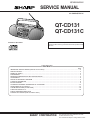
1
QT-CD131/131C
SERVICE MANUAL
No. S8870QTCD131/
QT-CD131
QT-CD131C
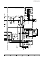
Illustration: QT-CD131
• In the interests of user-safety the set should be restored to its
original condition and only parts identical to those specified should
be used.
CONTENTS
Page
IMPORTANT SERVICE NOTES (FOR QT-CD131 ONLY) ................................................................................................ 2
SPECIFICATIONS ............................................................................................................................................................. 2
NAMES OF PARTS ........................................................................................................................................................... 3
DISASSEMBLY .................................................................................................................................................................. 4
REMOVING AND REINSTALLING THE MAIN PARTS ..................................................................................................... 5
ADJUSTMENT ................................................................................................................................................................... 6
NOTES ON SCHEMATIC DIAGRAM ................................................................................................................................ 8
TYPES OF TRANSISTOR ................................................................................................................................................. 8
BLOCK DIAGRAM ............................................................................................................................................................. 9
SCHEMATIC DIAGRAM / WIRING SIDE OF P.W.BOARD ............................................................................................. 12
WAVEFORMS OF CD CIRCUIT ...................................................................................................................................... 21
TROUBLESHOOTING (CD SECTION) ........................................................................................................................... 22
FUNCTION TABLE OF IC ................................................................................................................................................ 25
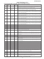
PARTS GUIDE/EXPLODED VIEW
PACKING OF THE SET (FOR QT-CD131 ONLY)
SHARP CORPORATION
–1–
This document has been published to be used
for after sales service only.
The contents are subject to change without notice.
QT-CD131/131C
FOR A COMPLETE DESCRIPTION OF THE OPERATION OF THIS UNIT, PLEASE REFER
TO THE OPERATION MANUAL.
IMPORTANT SERVICE NOTES (FOR QT-CD131 ONLY)
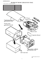
BEFORE RETURNING THE AUDIO PRODUCT
(Fire & Shock Hazard)
Before returning the audio product to the user, perform the
following safety checks.
1. Inspect all lead dress to make certain that leads are not
pinched or that hardware is not lodged between the chassis
and other metal parts in the audio product.
2. Inspect all protective devices such as insulating materials,
cabinet, terminal board, adjustment and compartment
covers or shields, mechanical insulators etc.
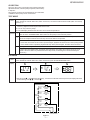
3. To be sure that no shock hazard exists, check for leakage
current in the following manner.
* Plug the AC line cord directly into a 120 volt AC outlet.
* Using two clip leads, connect a 1.5k ohm, 10 watt resistor
paralleled by a 0.15µF capacitor in series with all exposed
metal cabinet parts and a known earth ground, such as
conduit or electrical ground connected to earth ground.
* Use a VTVM or VOM with 1000 ohm per volt, or higher,
sensitivity to measure the AC voltage drop across the
resistor (See diagram).
* Connect the resistor connection to all exposed metal parts
having a return path to the chassis (antenna, metal cabinet,
screw heads, knobs and control shafts, escutcheon, etc.)
and measure the AC voltage drop across the resistor.
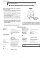
VTVM
AC SCALE
1.5k ohms
10W
0.15 µ F
TO EXPOSED
METAL PARTS
TEST PROBE
CONNECT TO
KNOWN EARTH
GROUND
All check must be repeated with the AC line cord plug connection
reversed.
Any reading of 0.3 volt RMS (this corresponds to 0.2 milliamp.
AC.) or more is excessive and indicates a potential shock
hazard which must be corrected before returning the audio
product to the owner.
SPECIFICATIONS
General
Power source:
Power consumption:
Output power:
(131)
Output power:
(131C)
Speakers:
Output terminals:
Dimensions:
Weight:
Tape recorder
AC 120V, 60 Hz
DC 12 V [ "D" size (UM/SUM-1,
R20 or HP-2) battery x 8]
DC 3 V ["AA" size (UM/SUM-3, R6
or HP-7) battery x 2 for tuner
memory]
20 W
FTC; 2.0 W min. RMS per channel
into 8 ohms from 150 Hz to 20 kHz,
with no more than 10 % total harmonic distortion.
RMS; 2.3 W/CH
(DC operation, 10 % T.H.D.)
RMS; 2.3 W/CH
(DC operation, 10 % T.H.D.)
4" (10 cm) full-range speaker x 2
Headphones; 16-50 ohms
(recommended; 32 ohms)
Width; 18-15/16" (480 mm)
Height; 6-1/16" (153 mm)
Depth; 10" (254 mm)
7.1 Ibs. (3.2 kg) without batteries
Frequency response:
Signal/noise ratio:
Wow and flitter:
Motor:
Bias system:
Erase system:
Compact disc player
Disc:
Signal readout:
Audio channels:
Quantization:
Filter:
D/A converter:
Wow and flutter:
Compact disc
Non-contact, 3-beam semiconductor laser pickup
2
16-bit linear quantization
4-tims oversampling digital filter
1-bit D/A converter
Unmeasurable
(less than 0.001% W. peak)
Specifications for this model are subject to change without
prior notice.
Radio
Frequency range:
50 - 14,000 Hz (Normal tape)
50 dB
0.25 % (WRMS)
DC 12 V electric governor
AC bias
Magnet erase
FM; 87.5 - 108 MHz
AM; 530 - 1,702 kHz
–2–
QT-CD131/131C
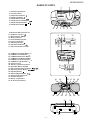
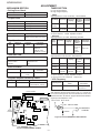
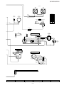
NAMES OF PARTS
2
1
1. Cassette Compartment
2. CD Compartment
3. (TAPE) Record Button:
4. (TAPE) Play Button:
5. (TAPE) Rewind Button:
6. (TAPE) Fast Forward Button:
7. (TAPE) Stop/Eject Button: /
8. (TAPE) Pause Button:
3
5
4
9. FM Stereo Mode Indicator: ST
10. FM Stereo Indicator:
11. Band Indicator: FM/AM
12. Memory Indicator
13. Preset Number Indicator
14. Frequency Indicator
15. (CD) Play Indicator:
16. (CD) Repeat Indicator:
17. (CD) Track Number Indicator
6
7
8
9 10 11
12
14
13
18. (TUNER) Preset Down Button:
19. (TUNER) Preset Up Button:
20. (TUNER) Band Selector Button
21. (TUNER) Preset Memory Button
22. (TUNER) Tuning Down Button:
23. (TUNER) Tuning Up Button:
24. Volume Control
25. Stand-by, On/Function Switch
26. Extra Bass Button: X-BASS
27. (CD) Track Down/Review Button:
28. (CD) Track Up/Cue Button:
29. (CD) Stop Button:
30. (CD) Play/Repeat Button:
31. FM Telescopic Rod Aerial
32. Headphone Socket
33. Battery Compartment
34. AC Power Input Socket
15
16
17
19
18
24
25
26
20 21 22
27
31
33
–3–
28
29
32
34
23
30
QT-CD131/131C
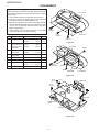
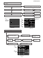
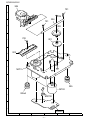
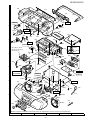
DISASSEMBLY
Caution on Disassembly
Follow the below-mentioned notes when disassembling the
unit and reassembling it, to keep it safe and ensure excellent
performance:
1. Take cassette tape and compact disc out of the unit.
2. Be sure to remove the power supply plug from the wall
outlet before starting to disassemble the unit.
3. Take off nylon bands or wire holders where they need be
removed when disassembling the unit. After servicing the
unit, be sure to rearrange the leads where they were
before disassembling.
4. Take suffcient care on static electricity of integrated
circuits and other circuits when servicing.
STEP
REMOVAL
PROCEDURE
FIGURE
1
Rear Cabinet
1. Screw ................. (A1) x10
2. Socket .................. (A2) x2
4-1
4-2
2
Top Cabinet
1. Knob ..................... (B1) x1
(with CD Mechanism/ 2. Screw ................... (B2) x3
Tape Mechanism/ 3. Socket .................. (B3) x2
Main PWB)
4-2
Main PWB/
Switch PWB
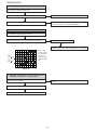
4
Tuner Display PWB/ 1. Screw .................. (D1) x3
Switch PWB
5-1
5
Tape Mechanism
1. Screw ................... (E1) x4
5-2
6
CD Mechanism
1. Screw ................... (F1) x3
5-2
7
Terminal PWB
1. Screw ................... (G1) x5
2. Hook ..................... (G2) x1
5-3
1. Hook ..................... (H1) x2
5-4
Battery PWB
(A1)x6
ø3x20mm
(A1)x3
ø3x12mm
Rear Cabinet
(A1)x1
ø3x12mm
Figure 4-1
Top Cabinet
3
8
1. Screw ................... (C1) x8
2. Socket .................. (C2) x4
Front Cabinet
(B1)x1
4-3
4-3,5-2
(B2)x3
ø3x10mm
(A2)x1
(A2)x1
(B3)x1
Main PWB
Front Cabinet
Figure 4-2
(C1)x6
ø3x10mm
(C2)x1
Switch PWB
(C1)x2
ø3x10mm
Main PWB
Headphones
PWB
Top Cabinet
Figure 4-3
–4–
QT-CD131/131C
(G2)x1
Switch PWB
Tuner Display
PWB
Push
Front Cabinet
Driver
(D1)x2
ø3x12mm
(G1)x2
ø3x10mm
Rear Cabinet
(D1)x1
ø3x10mm
(G1)x1
ø3x10mm
Figure 5-1
Terminal PWB
(E1)x4
ø3x10mm
(G1)x2
ø3x10mm
Figure 5-3
Rear Cabinet
(F1)x3
ø2.5x10mm
Pull
Tape
Mechanism
(C2)x2
(H1)x1
(H1)x1
Top Cabinet
CD Mechanism
(C2)x1
Pull
Battery PWB
Figure 5-2
Figure 5-4
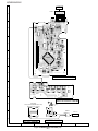
REMOVING AND REINSTALLING THE MAIN PARTS
CD MECHANISM SECTION
(A1) x2
2.6 x6mm
Perform steps 1, 2, 3 and 6 of the disassembly method to
remove the CD mechanism.
How to remove the pickup (See Fig. 5-5.)
CD
Mechanism
Pickup
1. Remove the screws (A1) x 2 pcs., to remove the shaft (A2)
x1 pc.
2. Remove the stop washer (A3) x1 pc., to remove the gear
(A4) x 1 pc.
3. Remove the pickup.
Shaft
(A2) x1
Gear
(A4) x1
Figure 5-5
–5–
Stop
Washer
(A3) x1
QT-CD131/131C
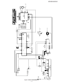
ADJUSTMENT
TUNER SECTION
MECHANISM SECTION
fL: Low-range frequency
fH: High-renge frequency
• Driving Force Check
Torque Meter
Specified Value
PLAY: TW-2412
• FM RF
Signal generator: 1 kHz, 75 kHz dev., FM modulated
Over 120 g
• Torque Check
Torque Meter
Test Stage Frequency
Frequency
Display
Specified Value
Play: TW-2111
25 to 65 g.cm
87.5 MHz
60 to 130 g.cm
Band
Coverage
—
Fast Forward: TW-2231
Rewind: TW-2231
60 to 130 g.cm
RF
90.0 MHz
(10~30 dB)
90.0 MHz
• Head Azimuth
Torque Meter
Output: Speaker Terminal
(CNP201 Load resistance: 8 ohms)
Test
Stage
• Tape Speed
Adjusting
Point
Test
Tape
MTT-111 In motor
Specified
Value
Instrument
Connection
3,000 ± 90 Hz
Output: Speaker
Teaminal
(CNP201 Load
resistance: 8 ohms)
*2
10.7 MHz
98.00 MHz
Setting/
Adjusting
Parts
Instrument
Connection
T1(Turn
the core of
T1 fully
counterclockwise.
Input: Pin 1 of
IC1
Output: TP2
• AM IF/RF
Signal generator: 400 Hz, 30%, AM modulated
Position of each switch or control
Volume control
Function switch
X-BASS
Max
Tape/Power Off
On
• Bias Oscillation
Instrument
Connection
Specified Value
82 kHz ± 6 kHz
– 6 kHz
L301
Frequency
Display
Frequency
IF
TAPE SECTION
Adjustment Point
L1
*1. Input: Antenna, Output: TP1
*2. Input: Antenna, Output: Speaker Terminal
• Detection
Signal generator: 10.7 MHz, FM sweep generator
Specified Value
MTT-114
Setting/ Instrument
Adjusting Connection
Parts
(fL): L2
*1
2.0 ± 0.1 V
Pin 2 of CNP201
Specified Value
MTT-118
1.8 V ± 3 dB
Frequency
Display
IF
450 kHz
1,720 kHz
Band
Coverage
—
530 kHz
(fL): L4
*3
1.0 ± 0.1 V
Tracking
600 kHz
1,400 kHz
600 kHz
1,400 kHz
(fL): L3
(fH):TC1
Adjusting Point
Speaker Terminal
(Load resistance: 8 ohms)
FM ROD ANTENNA
AM BAND
COVERAGE
MAIN PWB
76 kHz ± 200 Hz
VR1
TC1
G
FM DET.
21 19 17
L3
AM BAR
ANTENNA
13
Pin 13, pin 21 and
ground of IC2
Pin 21 of IC2
D
FET : 2SK19 or 2SK54
TO FREQUENCY
COUNTER
S
VCO
IC2
TP1
Instrument
Connection
Note:
After preparing the test circuit shown in Fig. 6-1, connect the
Pin 13, Pin 21 and ground of the IC2 with the test circuit, and
measure the value. At this time, apply a standard unmodulated
signal input and adjust the VCO.
Pin 13 of IC2
TP2
Specified
Value
R26
T2
L4
*2
• VCO Frequency
Instrument Connection
VR1
AM TRACKING
fL
fH
Setting/ Instrument
Adjusting Connection
Parts
T3
*1
*1. Input: Antenna, Output: Pin19 of IC2
*2. Input: Antenna, Output: Speaker Terminal
*3. Input: Input is not connected, Output: TP1
• Playback Amplifier Sensitivity Check
Test Tape
Test Stage Frequency
1
10 kohm
R7
FM IF
L2
T3
L1
Figure 6-1 VCO FREQUENCY TEST CIRCUIT
AM IF
FM RF
T1
1
IC1
FM BAND
COVERAGE
Figure 6-2 ADJUSTMENT POINTS
–6–
QT-CD131/131C
CD SECTION
Since this CD system incorporates the following automatic
adjustment function, when the pickup is replaced, it is necessary
to reajust it.
Since this CD unit does not need adjustment, the combination
of PWB and laser pickup unit is not restricted.
TEST MODE
Start
Note
Operation
While holding down the "STOP" button, move the FUNCTION/POWER switch to "CD".
Then, release the "STOP" button and, within 0.5 second, connect the TEST POINT to GND (within 0.5 second).
(See Fig. 7)
1. When the CD LID switch is in the OFF position, the unit will be able to enter the test mode.
However, playback cannot be performed in this mode.
2. You can only move the pickup.
3. The LCD display should be the same as it is for normal CD operations.
1
The use of the "UP/CUE" button will move the pickup to the outermost position.
The use of the "DOWN/REVIEW" button will move the pickup to the innermost position.
2
When the "PLAY" button is pressed, the laser will be lit, and when the "STOP" button is pressed, it will be
turned off. Playback will also start and stop when these buttons are pressed.
a. If the "PLAY" button is pressed while in the stop mode, the laser will simply be turned on at first.
b. If the laser is lit and the "PLAY" button is pressed again, playback will start from the current pickup position.
c. If the "STOP" button is pressed, playback will stop. When pressed again, the laser will be turned off.
3
Turning the tracking servo on or off.
a. Each time the PAUSE button is pressed during playback, the tracking servo will be turned on or off.
(Note: If the PLAY button is pressed while in the stop mode, the tracking servo will automatically be
turned on.)
LCD MODE
Start
Display
While holding down the "STOP" button, move the FUNCTION/POWER switch to "CD".
Then, release the "STOP" button and, within 0.5 second, press the REVIEW/DOWN button.
2
1
1 second
3
3
1 second
12
3
* After the number has appeared in the display, each time the "UP/CUE" button is pressed, the display will switch
in the following order: , , and then .
SWITCH PWB – A2
R771
3.9K
SW774
TRACK DOWN/
REVIEW
R772
2.7K
SW773
TRACK UP/
CUE
TEST
POINT
R773
1.8K
R774
1.5K
R776
10K
SW771
PLAY
SW7712
STOP
+B
3
1
TO CD SECTION
Figure 7
–7–
QT-CD131/131C
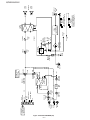
NOTES ON SCHEMATIC DIAGRAM
• Resistor:
To differentiate the units of resistors, the symbol as K and M
are used: the symbol K means 1000 ohm and the symbol M
means 1000 kohm and the resistor without any symbol is an
ohm resistor. The resistor designated "Fusible" is a fuse type
resistor
• Capacitor:
To indicate the unit of capacitor, a symbol P is used: this
symbol P means micro-micro-farad and the unit of the capacitor
without such a symbol is microfarad. As to electrolytic capacitor,
the expression “capacitance/withstand voltage” is used.
(CH), (TH), (RH), (UJ): Temperature compensation
(ML): Mylar type
(P.P.): Polypropylene type
• The indicated voltage in each section is the one measured by
Digital Multimeter between such a section and the chassis
with no signal given.
REF. NO
DESCRIPTION
1. Tuner
( ): AM mode
Marking except for ( ): FM mode
2. CD
( ): Play mode
Marking except for ( ): Stop state
3. Deck section
( ): Record mode
Marking except for ( ): Playback mode
Display / Control section:
( ): Active state
Marking except for ( ): CD Function mode at stop state
• Schematic diagram and Wiring Side of P.W.Board for this
model are subject to change for improvement without prior
notice.
• Parts marked with “
”(
) are important for
maintaining the safety of the set. Be sure to replace these
parts with specified ones for maintaining the safety and
performance of the set.
POSITION
REF. NO
DESCRIPTION
POSITION
SW102
RECODE/PLAYBACK
OFF—ON
SW506
PRESET DOWN
OFF—ON
SW201
FUNCTION/POWER
TAPE—TUNER— CD/
OFF—ON
SW601
TAPE MAIN
OFF—ON
SW702
PICKUP IN
OFF—ON
SW203
X-BASS
OFF—ON
SW761
CD LID OPEN/CLOSE
OFF—ON
SW501
BAND
OFF—ON
SW771
PLAY/REPEAT
OFF—ON
SW502
TUNER DOWN
OFF—ON
SW772
STOP
OFF—ON
SW503
TUNER UP
OFF—ON
SW773
TRACK UP/CUE
OFF—ON
SW504
MEMORY
OFF—ON
SW774
TRACK DOWN/REVIEW
OFF—ON
SW505
PRESET UP
OFF—ON
FRONT
VIEW
FRONT
VIEW
FRONT
VIEW
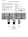
E C B
E C B
(S) (G) (D)
(1) (2) (3)
E B C
S8050D
2SA673-C
2SC1815 GR
2SC1674 K
Figure 8 TYPES OF TRANSISTOR
–8–
S9012H
24
27
28
30
31
34
35
36
SEG1
VLC3 38
VDD 25
9
~ 14 17 ~ 19 21
20
+5V
(D)
PU-IN SW
SL+ 13
SL– 14
SYSTEM
MICROCOMPUTER
IC701
IX0105AW
LID 37
23
33 22
~ 60 41 ~ 44
COM3
SEG4
57
PICKUP IN
SW702
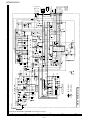
Figure 9 BLOCK DIAGRAM (1/3)
–9–
M702
SLIDE
MOTOR
M701
SPIN
MOTOR
TRACKING COIL
FOCUS COIL
PICKUP UNIT
M
M
17
18
26
27
11
12
1
2
30
31
1
2
3
4
SL–
SL+
FIN2
FIN1
E
F
62
64
IC801
LA9240M
SERVO AMP.
Q805
LDO
LASER +5V
DRIVER
JP– 32
Q804
FOCUS/TRACKING
/SPIN/SLIDE
DRIVER
13
28
5
6
7
8
22
+7.4V
CONSTANT
VOLTAGE
REGULATOR
CL, DAT, SELIAL CONTROL
49 50 51 52 53 54
IC804
BA5914FP
3 10 19 23 25
+5V
15 16 27 28 29
SLI 44
SLC 43
CV+ 40
9 EFMO
IC802
EFMIN
LCHO
CLV+ LC78622E
13 CLV– SERVO/SIGNAL
14 V/P
CONTROL
15 HFL
16 TES
17 TOFF
18 TGL
19 JP+
20 JP– RES. CQCK. COIN
SQOUT. RWC. WRQ
2 4 8 11
1 61 58 57 56 55 54 53
10
12
6 23 43
45
+5V
44
XL801
16.93MHz
XOUT
X701
4MHz
COM0
RES
XIN
LCD701
CD LCD
K1
XIN
SL–
DRF
VVDD
VDD
XVDD
CD
OPERATION
KEY
SW771~SW774
TO
FD
SPO
SLEO
SLD
XOUT
WRQ
RESET
~
VCC1
THLD/DEF
CLK
CL
DAT
CE
DRF
CD LID
OPEN/CLOSE
SW761
46
39
38
33
32
37
64
63
62
51
+7.4V
(CD)
R-CH
GND (A)
L-CH
+7.4V (D)
GND (D)
7
MUTE
6 POWER GND
1
2
3
4
5
TO
MAIN
SECTION
QT-CD131/131C
L-CH
Figure 10 BLOCK DIAGRAM (2/3)
– 10 –
ERASE
HEAD
R-CH
REC / PB
HEAD
FROM
CD/DISPLAY
SECTION
7
6
SW102-H
REC / PB
SW102
REC / PB
B.D
REC / PB
SW102
C,E
P.B
P.B
MUTE
(POWER GND)
R-CH
1 (AUDIO GND)
2
CD
L-CH
3
+7.4V
4
+B2
5
(DIGITAL GND)
BIAS
OSC.
REC
P. B
SW102-G
REC / PB
8
6
R 12
9 R
IC101
EQULIZER
AMP.
BA331IL
L 1
5 L
C201
L201
REC
REC
P.B
EC / PB
SW102
A,F
POWER/
FUNCTION
SW201-A,B
+B1
REC
TAPE
RADIO
FROM TUNER
SECTION
IC2-9,10PIN
M601
TAPE
MOTOR
SW601
MAIN
SW201-D
POWER /
FUNCTION
2
+B1
STANBY
VR201
A,B
VOLUME
5 11
6 R
2 L
8
10
12
SP502
R-CH
SPEAKERS
SP501
L-CH
SO651
AC INPUT
AC 120V
60Hz
BATTERY
DC3V
["AA" SIZE (UM/SUM-3,
R6 or HP-7)BATTERYx2
FOR TUNER MEMORY]
BATTERY
DC12V
["D" SIZE (UM/SUM-1,
R20 or HP-2)BATTERYx8]
T601
POWER
TRANSFORMER
TUNER
+B
BACK UP
+B
AM / FM
SELECT
+B
FM +B
SW201-C
POWER/
FUNCTION
D651~D654
RECTIFIER
IC203
3
KIA7808P
+B2
1
VOLTAGE
REGULATOR
SW203
A,B
X-BASS
IC202
LA4597
POWER AMP.
QT-CD131/131C
F1
B.P.F
1
FM RF
3
VD1
FM ROD
ANTENA
L1
L4
AM OSC.
4
5
6
FM IF
T1
VD3-2
VD3-1
7
Q1
IC1
TA7358AP
FM FRONT END
VT
TC1
FM OSC
RF AMP.
L2
L3
8
VD2
AM ANT.
VT
9
FM+B
CF1
X1
4.5MHz
VT CONTROL
Q3
Q4
VT
22 13 14
D GND
2
1
AM IF
T3
22
24
AM OSC OUT
AM MIX OUT
FM IF IN
1
X IN X OUT
7
6
IC3
TC9216P
PLL CONTROLLER
CF2
8
3
4
5
6
10
11
12
+B
21
9 15
10
16
13
18
VR1
VCO
20
5
AM IF IN
DATA
AM MIX OUT AM OSC
VSS
FM DET
PERIDO
AM RF IN
DOUT
FM DET
OF1 FM IN
AM IF IN
DET OUT
AM IN
STEREO
MPX VCO
GND
MPX IN
TUNER
R-CH OUT
IF IN
Figure 11 BLOCK DIAGRAM (3/3)
– 11 –
CLOCK
+B
MO/ST
FM+B
FM RIPPLE
FILTER
+5V
Q10
Q5
Q6
A-GND
TUNER +B
TO MAIN
SECTION
SW504
MEMORY
SW503
TUNER UP
SW502
TUNER DOWN
SW501
BAND
SW505
PRESET UP
SW506
PRESET DOWN
MUTE
AUDIO
+12V
SWITCHING
VOLTAGE
REGULATOR
ZD1
IC2
LA1805
FM IF DET.
/FM MPX./AM IF
L-CH OUT
22
20
24
23
31
1
7
8
9
65
80
45 44 43
50 51
IC501
TUNER
MICROCOMPUTER
6
30
33
48
41
IC502
RESET
RESET Q501
Q502
MONO/ST
1 2 3 4 5 6 7 8 9 10 11 12 13 14 15 16 17 18 19 20 21
LCD DISPLAY
LCD501
TUNER
+B
QT-CD131/131C
QT-CD131/131C
A
+B
R842 C848
22
1/50
5V
0V
0V
0V
0.4V
5V
3.1V
1.5V
2.4V
2.4V
2.4V
2.4V
2.4V
2.4V
2.4V
2.4V
2.4V
2.4V
2.4V
2.4V
2.4V
2.4V
2.4V
2.4V
2.4V
2.4V
2.4V
2.4V
2.4V
0V
0V
0V
SWITCH PWB-A2
1 2 3 4 5 6 7 8 9 10 1112 13 14 15 16
E
R828
1K
R829
1K
R812 C813
15K 0.1
R815
47K
VREF
R839
22K
GND
CL
CLK
DEF
DRF
CE
DAT
REFI
VCC2
FSS
VR
LF2
PH1
BH1
R817
82K
R822
R823 6.8K
1.2K
C814 R816
0.01 1.5K
R840
22K
R833
5.6K
R832
56K
R8
33
R836 R
47K 4
C832
27P
R835 C
470 0.
40
39
38
37
36
29
30 31 32
R810
82K
R827
220K
C821
1/50
C811
0.1
X701
4.10M
C834
0.033
TOFF 35
TGL 34
JP+ 33
SL–
SL+
JP–
21 22 23 24 25 26
27 28
C816
0.001
C812
330P
R813
33K
C705
0.022
R736
1K
CV+
CVSLOF
HFL
TES
17 FD–
13 TD
14 JP
15 TO
16 FD
+B
R715
15K
+B5V
DIGITAL GND
PU IN
WRQ
SQOUT
DRF
SL–
SL+
RWC
CO IN
CQCK
RES
1K
1K
1K
1K
1K
1K
R725 R721
15K 15K
R718
R719
R720
R722
R723
R716
10K
15K
15K
15K
15K
15K
R726
R728
R729
R731
R732
R733
R808
12K
RFSM 41
C810
180P
17 18 19 20
R714
10K
C704
100/10
R724
15K
COIN
RWC
SL+
SL–
D5
D6
D7
D8
D3 RES
D4 COCK
D1 MUTE
D
32
31
30
29
28
27
26
25
24
23
R713
22
1K
21
20
19
18
17
C809
0.047
R811
3.3K
R734
1K
R730
1K
R727
1K
AIN5
COM2
COM3
VLC1
VLC2
VLC3
KIDSW AIN7
SIMUKE AIN6
SEG16
COM0
COM1
48 47 46 45 44 43 42 41 40 39 38 37 36 35 34 33
49 SEG12
P32
50 SEG11
P31
P30
51 SEG10
IC701
52 SEG9
VREF
IX1015AW
SYSYTEM
53 SEG8
AVSS
MICROCOMPUTER
54 SEG7
XCIN
34 P3P40
55 SEG6
XCOUT
33 P33
56 SEG5
VDD
20 PU-IN P23
57 SEG4
VSS
19 WRQ P22
58 SEG3
XOUT
18 SQOUT P21
59 SEG2
XIN
DFR
P20
17
60 SEG1
RESET
61 SEG0 2 P10 POWER IN
62 P00
63 P01
64 P02
10 TH
11 TA
12 TD–
C830
2P
SLD
R711
2.7K
C808
0.068
SLC 43
RFS- 42
R824 10K
C818
C819
1/50
R825
47/16
1.2K
R831 R826 C820
1K 220K 0.0033
R807
1K
R809
27K
R709
1K
R710
10K
IC801
LA9241M
SERVO AMP.
8 TESI
9 SCI
SPD
SLEQ
1
C806
0.033
R806
100
48 NC
7 TE
R830
1K
2
R708
1K
3
C702
0.022
4
C701
0.022
5
C805
0.033
R805
6.8K
C807
0.1/50
6
R804
2.2K
TBC 47
FSC 46
GND 45
SLI 44
6 TE-
SPG
SP–
1
FIN1
E
F
TB
0.0047R820
10K
R821
56K
3
R802
100K
C804
0.001
2
3
4
5
C817
0.47/50
FW701
R803
15K
C850
0.1
48
C833
0.001
C803
0.1/50
1
SP
R776
10K
+B
3
C845
4.7/50
R871
61 60 59 58 57 56 55 5453 52 51 50 49 4.7K
64 63 62
VCC1
1 FIN2
+B
7
C835 0.1/50
SW761
CD LID
OPEN/CLOSE
A GND
NC
SW772
STOP
FE–
R774
1.5K
LDS
SW771
PLAY
LDD
R773
1.8K
C838 0.01
R772
2.7K
C837 10/16
C840
0.33/50
SW773
FWD
R819
39K
C815
R771
3.9K
C839 1/50
+B
SW774
REV
LCD701
8
C849
0.022
FA–
FE
C
LASER DRIVER
Q805
S9012H
VOLTAGE
FA
B
IC701
PIN
VOLTAGE NO.
0V
33
0V
34
0V
35
0V
36
0V
37
0V
38
3.9V
39
0V
40
5V
41
4.1V
42
4.1V
43
0V
44
0V
45
0V
46
0.4V
47
0.4V
48
0V
49
0V
50
0V
51
0V
52
5V
53
54
2.5V
55
2.5V
0V
56
5V
57
5V
58
0V
59
0V
60
5V
61
4.8V
62
0V
63
3.8V
64
R814
10K
PIN
NO.
1
2
3
4
5
6
7
8
9
10
11
12
13
14
15
16
17
18
19
20
21
22
23
24
25
26
27
28
29
30
31
32
+B
D740
1N4148
+B
R741
3.3K
Q740
2SC1815GR
R744
R740
10K
4.7K
F
C740
0.01
R745
10K
+B
R742
1K
C741
3.3/50
R743
100K
D741
1N4148
CD SIGNAL
G
PIN
NO.
1
2
3
4
5
6
7
8
9
10
11
12
13
14
15
16
17
18
19
20
21
22
VOLTAGE PIN
NO.
23
2.5V
2.5V
24
2.5V
25
2.5V
26
2.5V
27
28
2.5V
2.5V
29
2.5V
30
2.5V
31
2.5V
32
2.5V
33
2.5V
34
2.5V
35
2.5V
36
2.5V
37
38
2.5V
2.5V
39
40
2.5V
41
2.5V
42
2.5V
43
2.5V
44
0V
IC801
PIN
VOLTAGE NO.
2.5V
45
2.5V
46
2.5V
47
2.5V
48
2.5V
49
2.5V
50
2.5V
51
2.2V
52
2.2V
53
0V
54
0V
55
5V
56
5V
57
4.8V
58
0V
59
5V
60
0V
61
0V
62
1.5V
63
2.4V
64
2.5V
2.5V
VOLTAGE
0V
2.5V
2.5V
0V
0V
2.4V
4.1V
4.7V
0V
0V
5V
5V
2.5V
2.5V
0.9V
0.9V
2.1V
4.2V
0V
5V
PIN
NO.
1
2
3
4
5
6
7
8
9
10
11
12
13
14
15
16
17
18
19
20
21
22
IC802
PIN
VOLTAGE PIN
NO. VOLTAGE NO.
23 5V
0V
45
0V
24 0V
46
1.5V
25 0V
47
0V
26 0V
48
2V
27 0V
49
28 0V
5V
50
0.3V
29 0V
51
0V
30 5V
52
2.5V
31 2.5V
53
54
2.5V
32 0V
55
0V
33 0V
34 0V
0V
56
35 5V
0V
57
36 4.7V
5V
58
37 2V
0V
59
38 0V
60
4.8V
39 0V
5V
61
40 2V
5V
62
41 4.7V
0V
63
42 0V
0V
64
43 5V
2.5V
44 2.3V
0V
VOLTAGE
2V
0V
0.1V
2.2V
0V
2.5V
0V
2.5V
0V
0V
0V
4.1V
4.1V
5V
0V
2.7V
2.4V
0V
0V
0V
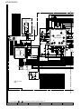
MAIN PWB-A1 ( 1 / 3 ) @
T
H
• The numbers 1 to 12 are waveform numbers shown in page 21.
1
2
3
4
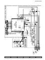
Figure 12 SCHEMATIC DIAGRAM (1/6)
– 12 –
5
6
+B
F
E
B
A
K
C802
47/16
1
2
3
4
5
6
7
8
TRTR+
FO+
FOGND
PD
VR
LD
TR+
FO+
FOTR+
FO+
FO–
TR–
TR–
PICKUP UNIT
+B
+B
C868 R874
10/16 100
C870
0.0022
R876
10K
C867
10/16
R873
100
LVDD 36
35
34
DOUT
TEST3
1
2
3
4
5
6
7
8
BI801
TR+
TR–
FO–
FO+
44
43
42
41
40
LCHO 37
C2F
EMPH
CONT5
CONT4
CONT3
CONT1
CONT2
1
2
3
4
5
6
7
8
B
F
XL801
16.93MHz
LVSS 38
35 MUTEL
34 NC
33 TEST4
MON
K
E
A
K
E
A
B
F
47
RVSS 39
15 HFL
16 TES
5
4
3
2
1
48
XVSS 46
XIN 45
XOUT
XVDD
MUTER
RVDD
RCHO
5
4
3
2
1
R875
10K
FSX
SFSY
PW
SBCK
RWC
WRQ
SQOUT
RES
COIN
CQCK
16M
TST11
CS
Vss
12 CLV+
13 CLV14 V/P
15
16
C822
220P
C869
0.0022
C890
100/10
33
R880
100
17 18 19 20 21 22 23 24 25 26 27 28 29 30 31 32
C873
0.01
JP–
F 35
L 34
+ 33
IC802
LA78623ED
VVDD
FR
EMFO
10 EMFIN
11 TEST2
R834
1K
C832
27P
R835 C831
470 0.0027
48 EFLG
47 SBSY
VDD
R856 1.2K
6
7
8
9
TEST5
4.2M
TEST1
27K
TOFF
40
39
38
37
36
R832
56K
R857
R836 R837
47K 47K
FSEQ
C830
2P
M 41
R833
5.6K
C801
0.01
+B
1 DEFI
2 TAI
PCK
C 43
S- 42
R838
33K
C834
0.033
+B
64 63 62 61 60 59 58 57 56 55 54 53 52 51 50 49
1
R858 C841
2
680 0.047
3 PDO
C842
4 VVss
0.047
5 ISET
JP+
JP-
C833
0.001
C 47
C 46
D 45
I 44
+
F
L
S
C850
0.1
48
TGL
C845
4.7/50
DEF
R871
9 4.7K
5
4
3
2
1
LD
1
VR
C
R801
1K
R860
1K
C847
0.01
+B
PD
CNS801
+B
LD
CNS802
BI802
QT-CD131/131C
32
+B
+B
+B
CNP803
C821
1/50
C851
0.022
R827
220K
TR+
TR–
FO–
FO+
+B
R849
100K
D802
1N4148
R810
82K
C843
100/10
L801
0.82µH
GND 28
+B
+3.8V
+B
R878
100
-3.2V
8 GND
9 VIN2G
10 VIN2
30
VCC 21
VIN3G 20
VIN3 19
11 VO2+
VO3+ 18
12 VO2–
VO3– 17
0V 13 GND
C889
10/16
+B
2.5V
2.5V
14 OP OUT
SL+
SL–
PU-IN
VIN4G 24
2.5V
7.4V
BIAS IN 23
VCC 22
MUTE
29
0V
CONSTANT
VOLTAGE
REGULATOR
Q804
R877 S8050D
220
NC
SP–
3.5V
3.5V
2.5V
OP IN + 16
OP IN – 15
0V
0V
C846
330/10
VIN1G
NC
IC804
BA5914FP
FOCUS/TRACKING
/SPIN/SLIDE DRIVER
0V 4
5
0V
6
0V 7
0V
VO4– 27
VO4+ 26
VIN4 25
+B
6
6
6
5
5
5
4
4
4
3
3
3
2
2
2
1
1
1
BI803
3.5V
2 VO1+
2.5V 3 VIN1
C844
330/10
1 VO1–
+B
SP+
CD MOTOR PWB-C
M
M701
SPINDLE
MOTOR
M
M702
SLED
MOTOR
SW702
PICKUP IN
CNS803
3.5V
+B
7.4V
2.7V
3.8V
3.2V
ZD801
MTZJ5.6B
+B
POWER GND
DIGITAL GND
DIGITAL +7.4V
L-CH
AUDIO GND
R-CH
C887 L802
0.022 0.68µH
10 9 8 7 6 5
P14 1 - F
TO MAIN SECTION
• NOTES ON SCHEMATIC DIAGRAM can be found on page 8.
7
8
9
10
Figure 13 SCHEMATIC DIAGRAM (2/6)
– 13 –
11
12
QT-CD131/131C
A
B
C105
0.0018
IC101:REC./P.B.EQUALIZER AMP.
R105
15K
2
2
3
3
4
4
SW102-B
P
R
C107
820P
C109
270P
P
R107
1K
3
NF1
5 IN1
C111
330P
9
C108
820P
R
P R108
1K
SW102-D
C106
0.0018
D
C110
270P
4
11
ALC T 2
OUT2
GND
6 7
12
C118
10/16
R116
3.9K
D103
1N4148
ON OFF
SW203-B
X-BASS
C123
100/10
X-BASS
SW203-A
ON OFF
R125
680K
R106
15K
C354
0.0056(ML)
R218
22K
P
R122
2.7K
C152
TAPE
0.039(ML)
TUNER
CD
R152
SW201-B 2.2K
R124
3.3K
R
P
R351
330
R352
150
C351
0.0022(ML)
0
SW102-F
R
C122
0.01
SW201-G
BIAS OSC.
L301
R217
22K
0
P
SW102-H
R151
2.2K
P
R
R118 R120
3.9K 3.3K
R114
C116
0.018(ML) 8.2K
SW201-A
C151
0.039(ML)
SW102-A
R119
3.3K
C121
0.01
IC101
BA3311L
C114
47/16
R110
120
R117
3.9K
1
OUT1
8
C119
VCC
2.2/50
FILTER 10
IN2
NF2
R
P
SW102-E
R
C112
330P
R115
3.9K
C117
10/16
R113
8.2K
D101
1N4148
1
CNS101
ERASE HEAD
1
R
C113
47/16
C120
47/16
L-CH
R-CH
SW102-C
CNP101
C
TAPE
RECORD/PLAYBACK
HEAD
R109
120
R101
330
R121
2.7K
C115
0.018(ML)
D102
1N4148
R102
330
TAPE
TUNER
CD
R103
12K
R123
3.3K
R104
12K
C352
220/10
R353
47K
C353
0.022(ML)
Q351
S8050D
R354
10
P16 3 - A
TO TUNER
SECTION
E
F
P13 7 - H
TO CD SERVO
SECTION
CNP502
P16 4 - A
TO TUNER
SECTION
R-CH
GND(A)
L-CH
TUNER +B
GND
BACK UP
R-CH
AUDIO GND
L-CH
CD +7.4V
DIGITAL GND
POWER GND
1
2
3
4
1
2
+B
R458
1.2K
CNS502
R457
1.2K
R456
15K
5
6
7
8
9
R455
15K
10
FM SIGNAL
CD SIGNAL
PLAYBACK SIGNAL
G
RECORD SIGNAL
IC101
PIN
VOLTAGE
NO.
1 <0V> [3.23V]
2 <0V> [0V]
3 <0.6V> [0.6V]
4 <0V> [0V]
5 <0V> [0V]
6 <0V> [0V]
7 <0V> [0V]
8 <7.43V> [7.43V]
9 <0V> [0V]
10 <7.37V> [7.37V]
11 <0.6V> [0.6V]
12 <3.3V> [3.3V]
< >: Recording
[
]: Play
IC202
PIN
NO.
1
2
3
4
5
6
7
8
9
10
11
12
13
VOLTAGE
0.1V
0V
11.2V
0V
11.3V
0V
0.1V
12V
10.4V
5.8V
0V
5.8V
10.4V
H
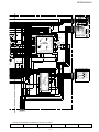
• NOTES ON SCHEMATIC DIAGRAM can be found on page 8.
1
2
3
4
Figure 14 SCHEMATIC DIAGRAM (3/6)
– 14 –
5
6
QT-CD131/131C
HEADPHONES PWB-A4
MAIN PWB-A1(2/3)
R227
120
R228
120
J201
HEADPHONES
1
5
R151
2.2K
FW202
C221
0.001
C215
0.039(ML)
VR201-A
20K
1
C223
100/10
R219
3.3K
4
R220
3.3K
11
C224
100/10
C216
0.039(ML)
C225
220/25
VR201-B
20K
C218
0.0039
–
+
3
C220
0.047(ML)
R222
1K
6
C222
0.001
152
9(ML)
C232
0.1(ML)
9
7
5
D201
1N4148
52
2K
+B
IN
1
OUT
3
8V
2
0V
3
R-CH
D652
1N4004
C651
0.022
C654
0.022
T601
POWER TRANSFORMER
C653
0.022
SO651
AC INPUT
120V,60Hz
DC 12V[ ''D'' SIZE(UM/SUM-1,
R20 OR HP-2) BATTERYx8]
C301
0.022
C302
0.022
D651
1N4004
1
2
D653
1N4004
D654
1N4004
C652
0.022
CNS602
CNP602
IC203
KIA7808P
VOLTAGE
REGULATOR
3
L-CH
SP501
SP502
C227
4700/25
1
2
SW201-C
2
C234
1000/10
11.83V
TAPE
TUNER
CD
1
2
10
8
TERMINAL PWB-A3
SW201-D
CD
TUNER
TAPE
1
SPEAKERS
C230
100/10
R218
22K
C231
0.1(ML)
13
C226
0.022
R217
22K
12
+
–
CNS201
2
C217
0.0039
5
1
C233
1000/10
CNP201
C219
0.047(ML)
R221
1K
MAIN VOL
C229
100/10
151
9(ML)
IC202
LA4597
POWER AMP.
+B
BATTERY PWB-B3,4
DC 3V [ ''AA'' SIZE(UM/SUM-3,
R6 OR HP-7) BATTERYx2
FOR TUNER MEMORY]
R230
2.7
C250
0.022
SW601
(241-7)
MAIN SW
+
–
7
8
9
10
Figure 15 SCHEMATIC DIAGRAM (4/6)
– 15 –
M
M601
(241-6)
TAPE MOTOR
11
12
3
4
Figure 16 SCHEMATIC DIAGRAM (5/6)
– 16 –
5
C5
0.01
+B
4
C3
4.7P
6
C8
15P
C14
0.022
FM IF
T1
R70
22K
L3 AM ANT.
AM SIGNAL
FM SIGNAL
AM BAND COVERAGE
L4
AM OSC.
C51 C52
10/16 0.022
7
9
R8
47K
R6
680
C11
22P
(CH)
C19
18P(UJ)
C18
0.022
VD3-2
KV1581A
C17
0.047
R9
100K
Q1
2SC1674K
RF AMP.
VD3-1
KV1581A
TC1
20P
R56
47
VD2
KV1360NT
C9
33P(CH)
R4
10
C10
24P(UJ)
8
AM TRACKING
fL
fH
FM BAND
COVERAGE
R3
33K
VD1
KV1360NT
5
C15 C16
0.022 0.022
R1
22
C7
0.001
+B
C6
0.01
C4
22P(CH)
L1
FM RF
C2
0.01
3
C20
470P
R11
56K
R12
4.7K
C58
0.022
C60
100P
2
CF1
3
R13
390
1
C13
10/16
R7
4.7K
R5
10K
C12
0.022
1
C31
0.022
C32
0.022
2
3
T2
Q4
2SC1815GR
R16
2.2K
R18
47K
C54
0.022
+B
R27
47K
R20
6.8K
R43
47K
R22
47K
C56
0.01
C30
15P(CH)
Q6
2SC1815GR
R23
47K
R21
5.6K
OT-3 8
OT-2 7
PERIOD 5
11 AM-IN OT-1 6
CLOCK 4
DATA 3
13 GND
12 FM-IN
X IN 2
14 DO 1
15 DO 2
C29
12P
(CH)
R28
10K
R29
1.2K
D3
1N4148
R30
15K
13
R40
47K
R52
1K
R45
220
+B
+B
C53
0.022
+B
R32
33K
ZD1
MTZ5.1B
R50
1K
C50
0.022
D4
1N4148
R44
270
C44
1/50
R31
1K
Q7
2SC1815GR
R33
4.7K
R34
4.7K
Q8
2SC1815GR
+B
+B
R51
1K
C55
330P
R39
10K
TP303
R41
22K
C57
100/10
VR1
6.8K(B)
VCO
15 14
FM- M/ST
TP2
SWITCHING
Q10
2SC1815GR
C21
0.022
R42
4.7K
16 VDD X OUT 1
L5
470µM
C40
470P
R26
1.5K
Q5,Q6: FM RIPPLE FILTER
C28
47/16
R19
10K
MAX- IN
C42
3.3/50
12
11
10
C48
1/50
R38 C49
6.8K 1/50
9
C47
1/50
C46
0.022
R36
2.2K
R37
6.8K
FM / AM IF MPX.
IC3 10 IF-IN
TC9216P
9 I/O5(ST)
PLL
Q5
2SA673-C
Q3,Q4: VT CONTROL
C22
0.01
C27
0.022
C26
0.022
+B
C37
0.022
C36
0.0022
R25
33K
8
C45
0.022
R35
2.2K
16
C41
3.3/50
C39
3.3/50
18 17
6
7
R14
10K
5
R55
10K
C38
0.018
20 19
R24
3.9K
C25
0.001
C35
0.022
C34
220/10
C24 R15
2.2/50 1.2K
Q3
2SC1815GR
4
2
C33
22/16
IC2
LA1805
AM IF
FM DET.
R17
10K
+B
TP1
+B
24 23 22 21
AM RF
2
R2
100K
MAIN PWB-A1(3/3)
D1
1N4148
D2
1N4148
1
AM MIX
1 2 3
FM +B
CF2
3
1
FM DET
T3
AM IF
+B
TUN IND
FM FRONT END
IC1
TA7358AP
GND
ST IND
DET OUT
F1
AM +B
FM IF
IN
AM OSC
L CH
FB
B.P.F
L2
FM 0SC
R10
68K
+B
CNS502
P14 1 - F
TO MAIN
SECTION
2
CNS501
P17 11 - H
TO TUNER
DISPLAY PWB
TUNER +B
CNP501
PLL(CLOCK)
2
1
PLL(DATA)
PLL(PERIOD)
GND(D)
3
4
5
6
STEREO
MUTE
TUNED
7
MONO/STEREO
9
8
10 BACK UP
FW502
1
CNP502
1 R-CH
2 GND(A)
4 TUNER +B
3 L-CH
GND 1
BACK UP
+B
2
+B
P14 1 - E
TO MAIN SECTION
X1
4.5MHz
2
R CH
Q9
2SA673-C
1
AM /FM
F
NC
E
VCO
D
C43
0.0015
C
R47 56K
A
R48 56K
B
R46 56K
G
R49 2.7K
H
FM
ROD ANTENA
QT-CD131/131C
• NOTES ON SCHEMATIC DIAGRAM can be found on page 8.
6
10
Figure 17 SCHEMATIC DIAGRAM (6/6)
– 17 –
11
10
9
8
7
6
5
4
3
2
1
10
9
8
7
6
5
4
3
2
1
CNS501
BI501
BACK UP +B
MONO/STEREO
MUTE
TUNED
STEREO
GND(D)
PLL(PERIOD)
PLL(DATA)
PLL(CLOCK)
+7.3V
P16 5 - A
TO MAIN PWB
CNP501
R525
R523
1K
10K
R521
10K
SW501
BAND
SW502
TUNER
DOWN
R519
1K
R518
3.3K
R517
5.6K
+B
+B
C501
10/16
R501
220
R502 560
R503 560
R504 560
D501
1N4148
C502
0.022
D502
1N4148
SWITCH PWB-B2
SW506
PRESET
DOWN
R524
3.3K
SW505
PRESET
UP
R515
8.2K
R516
5.6K
1
4
R505
2.7K
1
4
C505
2.2/50
C504
0.022
C506
0.022
D504
1N4148
D503
1N4148
R526
10K
R520 1K
R522 1K
R506
1.8K
L503
470µH
0V
R51(AIN1)
R52(AIN2)
VAREF
R50(AIN0)
IC501
IX0003SJ
TUNER CONTROL
MICROCOMPUTER
21
22
23
24
L502
470µH
C507
0.022
L501
470µH
C509
0.01
C508
0.022
R528
10K
C530
0.022
C513
0.01
R512
1M
25 26 27 28 29 30 31 32 33 34 35 36 37 38 39 40
XL501
4.19MHz
R511
820
R513
1K
R529
1K
R514
1K
5.6K
R508
+B
R510
47K
C512
0.0047
+B
R509
10K
D506
1N4148
Q501
2SC1815GR
RESET
C511
0.1/50
R507
100K
D505
1N4148
TUNER DISPLAY PWB-B1
SEG10 64
SEG9 63
SEG8 62
61
60
59
58
57
56
55
54
R73(XTOUT) 53
R72(XTIN) 52
R71(WTO) 51
R70(PULSE) 50
R83(T1) 49
R82(INT1) 48
R81(T2) 47
R80(INT2) 46
PLL(CLOCK)R92(SCK) 45
PLL(DATA)R91(SO) 44
PLL(PEREOD)R90(SI) 43
HOLD(KE0) 42
RESET 41
80 79 78 77 76 75 74 73 72 71 70 69 68 67 66 65
R53(AIN3)
4.3V
IC502
2 PST9142 1
RESET
3
5.2V
R527
1.8K
R530
1K
COM1
SEG27
R60(AIN4)
COM2
COM3
COM4
10 VLC
11 P10
12 P11
13 P12
14 P13
15 VSS
16 P20
17 P21
18 P22
19 P23
20 VASS(A/D GND)
21
20
23
24
1
2
3
4
5
6
7
8
9
6 7 8 9 10 11 12 13 14 15 16 17 18 19 20 21
SEG14
SEG13
SEG12
SEG11
1 2 3 4 5
SEG26
SEG25
SEG24
SEG23
R61(AIN5)
R62(AIN6)
SW503
TUNER
UP
ZD501
MTZJ5.6A
SEG22
SEG21
SEG20
SEG19
SEG18
SEG17
SEG16
SEG15
VDD
SW504
MEMORY
FW501
C503
100/6.3
2.6V
2.6V
2.6V
2.6V
2.6V
2.6V
2.6V
2.6V
2.6V
2.6V
2.6V
2.6V
2.6V
2.6V
2.6V
2.6V
R63(AIN7)
R40
R41
R42
9
C510
0.01
8
KO0
KO1
KO2
KO3
TEST
XIN
XOUT
7
2.6V
2.6V
2.6V
2.6V
LCD501
QT-CD131/131C
12
Q502
2SC1815GR
RESET
QT-CD131/131C
HEADPHONES PWB-A4
C351
P.B
VOLUME
R352
R106
R114
R116
R122
2
R124
C119
C120
CNP602
C227
C219
C232
C231
C229
1 2 3 4 5 6 7 8 9 10 11 12 13 IC202
FW502
2
R230
R825
R824
C818
R830
22
7
7
IC804
1
R828
R814
R816
C814
R815
C812
R817
C848
C849
R840
R839
R821
R820
C815
R819
C811
R826
C816
12
10
1
8
C807
R808
R811
R809 R812
C808
C809
R807
C806 R805
C810
16
C804
R803
R802
R804
C805
C803
R801
C802
E
B
C
C813
17
1
C801
C850
R827
C830
R834
64
BR
BK 1
BK 2
3
BK
4
BK
5
BK
6
BK
7
BK
8
R813
35 30
C840
C838
8
R829
C817
R823
R822
R831
C819
R832
C832
R833
R835
R837
C831
R871
C845
1
33 32
CNS801
R810
C889
R878
C873
R877
8
29
28
40
25
45
20
50
IC801 15
55
10
60 5
48
49
C837
R858
R716
C846
ZD801
R873
L802
C843
C820
1
C835
C741
C833
R740
D740
R741
R742
R726
R728
R723
R729
R722
R731
R720
R732
R719
R733
R718
C821 R849
C740
17
16
C842
R857
R856
R721
C841
R734
C851
1
Q740
E C B
R743
R860
C847
16
14
BI801
R730
64
Q804
C839
17
R725
64
E
X701
R713
R727
35 30
40
25
45
20
50
IC701 15
55
49
10
60
5
B C E
48
R724
R736
15
21
30
L801
32
33
35 30
40
25
45
20
50
IC802 15
49
55
10
60 5
R715
32
48
R745
R744
D741
XL801
C704
R880
C890
R836
C834
R838
C705
C702
R711
33
COR801
R714
C701
C867
J22
R710
R708
D802
8
7
6
5
4
3
2
1
C868
R456
R709
C869
R875
C887
R455
R458
LCD701
R874
C870
R876
R457
C250
C844
6
C302
C822
ON
D
CNS502
TO BATTERY
PWB
R842
1
2
3
C301
C
2
1
CNP502
1
IC203
SW203
X-BASS
B
C230
C225
A
D201
B
Q805
C226
C220
C224
C222
C223
C151
R806
A
C221
R218
OFF
TAPE
Q351
C152
R219
R151
D
B C E
C354
C233
R222
C215
A
C353
1
D103
R120
C122
VR201
C218
C217
R221
R217
SW201
FUNCTION
C123
C234
B
R152
TUNER
CD
D102
R125
1
B
C
R119
R123
D101
C121
5
R118
IC101
C118
C117
FW202
C106
R110
C114
C107
R108
C108
C112
C111
5 7 9 11
2 4 6 8 10 12
C216
C116
C110
C109
1 3
F
R102
D
R101
R107
R109
R103
R104
R113
R121
R115 C115
R117
B
C113
C105
1
R220
REC
SW102
A
R227
R105
R228
L301
G
C352
H
R353
E
R351
C
FW202
A
J201
HEADPHONES
CNP101 1 2 3 4
R354
1 2 3
CNP201
5
CNS802
1
BK
WH
WH
WH
WH
BI802
5
9
R45
R44
R39
R40
B C E
Q3
3
2
1
C8
Q1
C3
C58
F1
R29
R25
TP2
T2
C34
C35
L4
C51
R10
C18
R12
C11
C9
R70
R4
TP1
R56
T1
R1
L1
C4
R26
C36
VD2
C13
SW771
PLAY
C12
C41
C38
E C B
C10
R13
R8
9
8
7
6
IC1
5
4
3
C2
2
1
C40
C39
IC2
13
14
15
16
17
18
19
20
21
22
23
24
C52
C28
R15
C25
12
11
10
9
8
7
6
5
4
3
2
1
R24
R31
C44
R17
C32 Q4
L2
B C E
R774
T3
C24
R6
R773
1 2 3
CF2
C33 C31
C26
SW772
STOP
R776
C47
R14
R55
E C B
C22
C29
R772
C48
R37
R19
C27
R771
G
R27
C19
C20
R11
C17
R9
VD3
TC1
1
R35
Q5
CF1
C30
X1
IC3
R43
C42
C43
R7
3
TRACK UP/CUE
R50
R51
R52
C49
C45
R21
9
10 C21
11
12
13
L5
14
15
16
C54
Q10
B C E
1
2
3
4
5
6
TP3
R33
Q7 E C B
E
C
B
R38
R30
B C E
C46
R36
C14
TRACK DOWN/
REVIEW
R32
D4
Q6
VR1
R41
R16
CNS501
P20 5 - H
TO BATTERY
PWB
FW701
C55
8
7
6
5
4
3
2
1
2
SW773
SW774
R23
R48
R47
R46
SWITCH PWB-A2
Q9
6
BI803
E
C
B
R42
C56
C53
3
1
R34
C60
BK
R49
R22
BK
Q8
R20
F
1
R18
10
9
8
7
6
5
4
3
2
1
CD LID
OPEN/CLOSE
C57
CNS803
BR
GY
GY
GY
GY
GY
C37
VCO
D3
FW502
2
FW701
ZD1
5 4
CNP501
11
SW761
1
C50
3
R28
1
2
3
4
5
R5
C16
C15
D2
C6
C7
VD1
C5
3
D1
2
1
R2
R3
H
L3
AM BAR ANTENNA
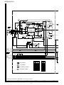
MAIN PWB-A1
• The numbers 1 to 12 are waveform numbers shown in page 21.
1
2
3
4
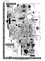
Figure 18 WIRING OF P.W.BOARD (1/3)
– 18 –
5
6
QT-CD131/131C
SPEKERS
SP502
R-CH
SP501
L-CH
COLOR TABLE
CNS201
SW601
TAPE MAIN
(241-7)
BR
1 WH
2 BK
3 RD
M601
TAPE MOTOR
(241-6)
TAPE
ERASE HEAD
(241-5)
RED
OR
ORANGE
YL
YELLOW
GR
GREEN
BL
BLUE
VL
VIOLET
GY
GRAY
WH(W)
WHITE
BK
BLACK
PK
PINK
RD
BK
BR
WH
YL
RECORD/PLAYBACK
HEAD(241-4)
BROWN
RD(R)
BK
CNS101
4
3
2
1
BK
WH
RD
BK
BK
(211)
T601
POWER
TRANSFORMER
TERMINAL PWB-A3
+
BATTERYS
DC12V ["D"size(UM/SUM-1,
R20 or HP2)battery 8]
YL
C653
D653
(236)
YL
D652
RD
C652
1
2
RD
C654
RD
CNS602
BK
D654
SO651
AC SOCKET
AC 120V
60Hz
D651
C651
OR
OR
PICK UP UNIT
CD MOTOR PWB-C
-
5 4 3 2 1
+
8 7 6 5 4 3 2 1
SW702
SPENDLE MOTOR
M701
CNP803
PICKUP IN
F3895AF
SLED MOTOR
M702
6
5
4
3
2
1
-
+
FM ROD ANTENNA(213)
7
8
9
10
Figure 19 WIRING OF P.W.BOARD (2/3)
– 19 –
11
12
QT-CD131/131C
TO MAIN PWB
CNP501
CNS501
1 2 3 4 5 6 7 8 9 10
BR
BK
BK
BK
BK
BK
BK
BK
BK
BK
A
C510
C509
10
1
R504
L502
R501
ZD501
D504
C502
D502
4
FW501
R502
C501
D501
1
B
R503
BI501
D503
C513
IC502
C503
3
2
1
C506
C
C507
R506
C511
C512
C505
Q501
21
E C B
R505
65
R514
C504
R507
D505
R513
64
R529
15
10
80
D
5
R508
R509
55
75
IC501
5
1
D506
60
70
R510
50
10
Q502
R511
40
35
15
B C E
41
45
30
20
1
XL501
R512
24
25
L501
R528
LCD501
C508
C530
R527
R530
E
R522
R520
L503
R526
TUNER DISPLAY PWB-B1
PRESET
DOWN
FW501
1
4
PRESET
UP
F
SW506
R525
SW505
R523
R524
R521
SW501
BAND
SW504
MEMORY
SW502
TUNER
DOWN
SW503
TUNER
UP
R519
R518
R515
R517
R516
SWITCH DISPLAY PWB-B2
G
BATTERYS
DC3V ["AA"size(UM/SUM-3,R6 or HP-7)
batteryx2 for tuner memory]
(247)
CNS502
BK
1
2
RD
P18 3 - G
CNP502
TO MAIN PWB
H
BATTERY PWB-B4
BATTERY PWB-B3
1
2
3
4
Figure 20 WIRING OF P.W.BOARD (3/3)
– 20 –
5
6
QT-CD131/131C
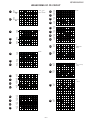
WAVEFORMS OF CD CIRCUIT
1
2
5ms
0.50 V
IC801 20 F.E
5ms
5.0 V
IC801 54 DRF
STOP
FOCUS
PLAY
SERCH
50ms
10.0 V
JP+
7
50ms
10.0 V
JP-
8
50ms
0.50 V
JP
9
50ms
1.00 V
TE
6
0.5ms
10.0 V
JP+
7
0.5ms
10.0 V
JP-
8
0.5ms
0.50 V
JP
9
0.5ms
1.00 V
TE
10
20ms
1.00 V
SPO
11
20ms
2.00 V
CLV+
10
50ms
1.00 V
SPO
11
50ms
2.00 V
CLV+
3
1
3
6
CUE
0.5ms
1.00 V
HF
1
4
0.5ms
5.0 V
HFL
5
0.5ms
5.0 V
TES
3
0.5ms
1.00 V
H.F
4
0.5ms
5.0 V
HFL
5
0.5ms
5.0 V
TES
2
REVIEW
3
REVIEW
PLAY
NORMAL DISC
TN0=01
1
6
50ms
10.0 V
JP+
7
50ms
10.0 V
JP-
8
50ms
0.50 V
JP
9
50ms
1.00 V
TE
6
0.5ms
10.0 V
JP+
7
0.5ms
10.0 V
JP-
8
0.5ms
0.50 V
JP
9
0.5ms
1.00 V
TE
2
3
PLAY
TCD-712 (140mm)
TN0=01
CUE
PLAY
TCD-712
12
5s
100mV
SLD
1
12
0.5s
100mV
SLD
1
– 21 –
QT-CD131/131C
TROUBLESHOOTING (CD SECTION)
When the CD does not function
When the CD section does not operate When the objective lens of the optical pickup is dirty,this section may not operate.Clean
the objective lens,and check the playback operation.When this section does not operate even after the above step is taken,check
the following items.
Remove the cabinet and follow the troubleshooting instructions.
"Track skipping and/or no TOC(Table Of Contents) may be caused by build up of dust other foreign matter on the laser pickup lens.
Before attempting any adjustment make certain that the lens is clean. If not, clean it as mentioned below."
Turn the power off.
Gently clean the lens with a lens cleaning tissue and a small amount of isopropyl alcohol.
Do not touch the lens with the bare hand.
• The CD function will not work.
The CD operating keys don't work.
Yes
Check the CD, DPS microcomputer (IC701), power supply, 4.19
MHz and 16.93 MHz clock, and reset terminal.
Yes
Check the waveform of SCK, SO (DATA) and SI (COMM).
Yes
See if the pick-up is in the pick-up in SW702 position.
Yes
If the items mentioned above are OK, check the main
microcomputer IC701.
• The CD operating keys work.
Check the Focus - HF system.
Playback can be performed without a disc.
Yes
Does the pick-up move up and down twice?
Focus search OK.
Yes
No
Does the output waveform of IC801(16)(FD) match that shown in
Fig. 22?
Check the area around IC804-BI801/CNS801.
Yes
No
Check the IC801(50)(CLK) line, 4MHz.
Check the microcomputer data on pins (51)(CL), (52)(DAT) and
(53)CE.
Focus search
is performed
two times
when play
operation is
done without
disc.
0.5s
0.50 V
IC801 16 FD
0.5s
0.50 V
IC801 15 TD
1
2
Figure 22
– 22 –
QT-CD131/131C
• Playback can only be performed when a disc
is loaded.
No
Check the laser diode driver.
Check the area around IC801(16) - (21) (focus servo circuit).
No
If the disc is not turning, the DRF
should not change to "H".
Is the Focus servo active? (Can you hear it working?)
Yes
▼
Yes
Does the DRF signal change from "L" to "H"?
Check the spin
system.
Yes
Yes
No
Level is abnormal.
▼
Is HF waveform normal (see the Fig. 23-1, 2)?
Yes
Check the periphery
of IC801 pins 41 and
42.
Yes
Check the tracking system.
HF
0.1V/DIV
0.5µsec/DIV(DC)
(When playing
back the disc)
▼
Waveform is unstable.
Check the spin
system.
Waveform in case
of normal playback
0.5s
1.00 V
IC801 16 FD
0.5s
10.0 V
IC801 12 CLV+
2
1
3
0.5s
10.0 V
IC801 54 DRF
4
0.5s
2.00 V
IC801 7 TE
Figure 23-1
Figure 23-2
• Check the tracking system.
Check waveform of IC801 pin 7 (TE).
The waveform shown in Fig. 23-3
appears, and no-disc state appears
soon.
Play is possible in
TEST mode.
Yes
Tracking servo is inoperative.
Yes
Although IL is possible,
play is impossible.
Yes
Data cannot be read.
Yes
Yes
Normal jump is impeded, and the
program top cannot be reached.
Check the VCO-PLL system.
5ms
1.00 V
IC801 7 TE
4
5 ms
5.0 V
IC801 54 DRF
3
Figure 23-3
– 23 –
Check the periphery of IC801
pin 8 to pin 15, and IC804 to
BI801/CNS801.
Yes
Check the periphery of
IC801 pin 14.
QT-CD131/131C
• Checking the spin system.
Play operation is performed without disc.
Yes
The spin driver circuit is normal.
The turntable rotates a little.
Yes
No
The turntable fails to rotate or rotates at high speed.
Yes
Check the periphery of IC801 pins 23 to 27, pin 39 and pin 40,
IC802 pin 12 and pin 13, IC804 to BI803/CNS803.
• Checking the VCO-PLL system
Play operation is performed when disc exits.
Yes
Although HF waveform is normal, TOC data cannot be read.
Yes
Check PDO waveform (Fig. 24).
Error
Check the IC801 pins 43 and 44, IC802 pins 3, 5, 7, 9 and 10.
0.5s
1.00 V
IC802 3 PDO
2
0.5s
1.00 V
IC801 16 FD
Stop --> Play
As VCO frequency is locked at
4.32 M Hz,
voltage of PDO
rises and stabilizes.
3
Figure 24
•
Although HF waveform is normal and the time
indication is normal, no sound is emitted.
Check IC802 pin 48 (EFLG).
No
Yes
Check IC802 pins 37and 40.
Abnomal
Check the periphery of IC803 (OPAMP).
– 24 –
Usually, the number of pulses of flawless disc is 100 pulses/sec
or less.
QT-CD131/131C
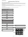
FUNCTION TABLE OF IC
IC701 RH-iX0105AWZZ (IX0105AW): System Control Microcomputer
Pin No.
Terminal
Name
Port Name
Input/
Output
Function
1*
P03
MTCONT2
Input/Output Used to input or output 4 bits at a time. When the output latch is set to "1", the unit will be in the
input mode. The key-on wakeup function, which can be switched on or off by the software, and a
pull-up transistor, which can be turned on or off by the software, are built in.
2*-5*
P10-P13
POWER-IN,
DATA (VOL),
STB (VOL)
Input/Output Used to input or output 4 bits at a time. When the output latch is set to "1", the unit will be in the
input CK (VOL), mode.The key-on wakeup function, which can be switched on or off by the software,
and a pull-up transistor,which can be turned on or off by the software, are built in.
6*
D0
POWER-ON
Input/Output Each terminal can be used to input or output 1 bit at a time. The output section has a latch which
holds 1 bit. One of the D ports is assigned by register Y as a data point, to execute input or output.
To use the port for input, set the output latch for that bit to "1". All of the output latches on port D can
be set to "1" using the CLD command.
7
D1
MUTE
Input/Output Each terminal can be used to input or output 1 bit at a time. The output section has a latch which
holds 1 bit. One of the D ports is assigned by register Y as a data point, to execute input or output.
To use the port for input, set the output latch for that bit to "1". All of the output latches on port D can
be set to "1" using the CLD command.
8*-12
D2-D6
SYNC-OUT,
RES,CQCK,
COIN,REC
Input/Output Each terminal can be used to input or output 1 bit at a time. The output section has a latch which
holds 1 bit. One of the D ports is assigned by register Y as a data point, to execute input or output.
To use the port for input, set the output latch for that bit to "1". All of the output latches on port D can
be set to "1" using the CLD command.
13,14
D7,D8
SL+,SL-
Input/Output Each terminal can be used to input or output 1 bit at a time. The output section has a latch which
holds 1 bit. One of the D ports is assigned by register Y as a data point, to execute input or output.
To use the port for input, set the output latch for that bit to "1". All of the output latches on port D can
be set to "1" using the CLD command.
15*,16*
D9,D10
SRS2,SRS1
Input/Output Each terminal can be used to input or output 1 bit at a time. The output section has a latch which
holds 1 bit. One of the D ports is assigned by register Y as a data point, to execute input or output.
To use the port for input, set the output latch for that bit to "1". All of the output latches on port D can
be set to "1" using the CLD command.
17
P20
DRF
Input/Output Used to receive 4 bits at a time.
18
P21
SQOUT
Input/Output Used to receive 4 bits at a time.
19
P22
WRQ
Input/Output Used to receive 4 bits at a time.
20
P23
PU-IN
Input/Output Used to receive 4 bits at a time.
21
RESET
22
XIN
23
XOUT
24
VSS
—
25
VDD
—
26*
XCOUT
27
XCIN
28
AVSS
Input
GND input terminal for the A-D converter.
29
VREF
Input
Reference voltage input terminal for the A-D converter.
30
P30
REMOCONINT2
Input
Used to receive 4 bits at a time.
31
P31
TORAY1
Input
Used to receive 4 bits at a time.
32
P32
TORAY2
Input
Used to receive 4 bits at a time.
33
P33
Input
Used to receive 4 bits at a time.
34
P40
Input
Used to receive 4 bits at a time.
35-37
AIN5-AIN7
Input
Used to receive 4 bits at a time.
38-40
VLC3-VLC1
Input
LCD power input terminals. To use the internal resistor, connect VLC3 to VDD (if a brightness
control is needed, connect VLC3 to VDD through a resistor). When an external power supply is
used, applyvoltages as follows: 0<VLC1<VLC3<VLCD<VDD.
41-44
COM3-COM0
Output
LCD common output terminals.
45-61*
SEG16-SEG0
(45*-56*)
Output
LCD segment output terminals.
62*-64*
P00-P02
Input/Output Reset pulse input/output terminal. When a reset is caused by the watch dog timer, an "L" level will
be output. The output is an N channel open drain.
Input
Input/output terminals for the main clock generation circuit. Used by connecting a ceramic resonator
between the XIN and XOUT terminals. There is a built-in feedback resistor between the XIN and
XOUT terminals.
Output
Input/output terminals for the main clock generation circuit. Used by connecting a ceramic resonator
between the XIN and XOUT terminals. There is a built-in feedback resistor between the XIN and
XOUT terminals.
GND input terminal.
Positive power supply terminal.
Output
Input/output terminals for the sub clock generation circuit. Used by connecting a crystal oscillator
between the XCIN and XCOUT terminals. There is a built-in feedback resistor between the XCIN
and XCOUT terminals.
Input
Input/output terminals for the sub clock generation circuit. Used by connecting a crystal oscillator
between the XCIN and XCOUT terminals. There is a built-in feedback resistor between the XCIN
and XCOUT terminals.
Input/Output Used to input or output 4 bits at a time. When the output latch is set to "1", the unit will be in the
input mode. The key-on wakeup function, which can be switched on or off by the software, and a
pull-up transistor, which can be turned on or off by the software, are built in.
In this unit, the terminal with asterisk mark (*) is (open) terminal which is not connected to the outside.
– 25 –
QT-CD131/131C
—MEMO—
– 26 –
QT-CD131/131C
PARTS GUIDE
MODEL
QT-CD131
QT-CD131C
“HOW TO ORDER REPLACEMENT PARTS”
To have your order filled promptly and correctly, please furnish the
following information.
1. MODEL NUMBER
2. REF. No.
3. PART NO.
4. DESCRIPTION
For U.S.A. only
Contact your nearest SHARP Parts Distributor to order.
For location of SHARP Parts Distributor,
Please call Toll-Free;
1-800-BE-SHARP
MARK: SPARE PARTS-DELIVERY SECTION
Explanation of capacitors/resistors parts codes
Capacitors
Resistors
VCC ....................... Ceramic type
VCK ........................ Ceramic type
VCT ........................ Semiconductor type
VC • • MF ............... Cylindrical type (without lead wire)
VC • • MN ............... Cylindrical type (without lead wire)
VC • • TV ................ Square type (without lead wire)
VC • • TQ ............... Square type (without lead wire)
VC • • CY ............... Square type (without lead wire)
VC • • CZ ............... Square type (without lead wire)
VC • • • • • • • • • J .. The 13th character represents capacity difference.
("J" ±5%, "K" ±10%, "M" ±20%, "N" ±30%,
"C" ±0.25 pF, "D" ±0.5 pF, "Z" +80-20%.)
VRD ....................... Carbon-film type
VRS ........................ Carbon-film type
VRN ....................... Metal-film type
VR • • MF ............... Cylindrical type (without lead wire)
VR • • MN ............... Cylindrical type (without lead wire)
VR • • TV ................ Square type (without lead wire)
VR • • TQ ............... Square type (without lead wire)
VR • • CY ............... Square type (without lead wire)
VR • • CZ ............... Square type (without lead wire)
VR • • • • • • • • • J .. The 13th character represents error.
("J" ±5%, "F" ±1%, "D" ±0.5%.)
If there are no indications for the electrolytic capacitors, error is ±20%.
If there are no indications for other parts, the resistors are ±5%
carbon-film type.
NOTE:
Parts marked with “
” are important for maintaining the safety of the set.
Be sure to replace parts with specified ones for maintaining the safety and performance of the set.
– 27 –
QT-CD131/131C
NO.
PRICE
RANK
PART CODE
DESCRIPTION
INTEGRATED CIRCUITS
VHITA7358AP-1
VHILA1805//-1
VHITC9216P/-1
VHIBA3311L/-1
J
J
J
J
AG
AM
AL
AK
IC202
IC203
IC501
VHILA4597//-1
VHIKIA7808P-1
RH-IX0003SJZZ
J
J
J
AH
AH
BA
IC502
IC701
VHIPST9142/-1
RH-IX0105AWZZ
J
J
AH
BA
IC801
IC802
IC804
VHILA9241M/-1
VHILC78623D-1
VHIBA5914FP-1
J
J
J
AS
AY
AN
FM Front End,TA7358AP
FM/AF IF MPX.,LA1805
PLL,TC9216P
REC./P.B.Equalizer Amp.,
BA3311L
Power Amp.,LA4597
Voltage Regulator,KIA7808P
Tuner Control Microcomputer,
IX0003SJ
Reset,PST9142
System Microcomputer,
IX0105AW
Servo Amp.,LA9241M
Servo/Signal Control,LC78623D
Focus/Tracking/Spin/Slide
Driver,BA5914FP
VS2SC1674K/-1
VS2SC1815GR-1
VS2SA673-C/-1
VS2SC1815GR-1
VS2SA673-C/-1
VS2SC1815GR-1
VSS8050D///-1
VS2SC1815GR-1
VS2SC1815GR-1
VSS8050D///-1
VSS9012H///-1
J
J
J
J
J
J
J
J
J
J
J
AD
AB
AC
AB
AC
AB
AC
AB
AB
AC
AC
Silicon,NPN,2SC1674K
Silicon,NPN,2SC1815 GR
Silicon,PNP,2SA673-C
Silicon,NPN,2SC1815 GR
Silicon,PNP,2SA673-C
Silicon,NPN,2SC1815 GR
Silicon,NPN,S8050 D
Silicon,NPN,2SC1815 GR
Silicon,NPN,2SC1815 GR
Silicon,NPN,S8050 D
Silicon,PNP,S9012 H
VHD1N4148//-1
VHD1N4148//-1
VHD1N4148//-1
VHD1N4148//-1
VHD1N4004//-1
VHD1N4148//-1
VHD1N4148//-1
VHCKV1360NT-1
VHCKV1581A2-3
VHEMTZJ5R1B-1
VHEMTZJ5R6A-1
VHEMTZJ5R6B-1
J
J
J
J
J
J
J
J
J
J
J
J
AA
AA
AA
AA
AB
AA
AA
AF
AE
AC
AC
AD
Silicon,1N4148
Silicon,1N4148
Silicon,1N4148
Silicon,1N4148
Silicon,1N4004
Silicon,1N4148
Silicon,1N4148
Variable Capacitance,KV1360NT
Variable Capacitance,KV1581A
Zener,5.1V,MTZJ5.1B
Zener,5.6V,MTZJ5.6A
Zener,5.6V,MTZJ5.6B
RFILF0001SJZZ
RFILA0002SJZZ
RFILR0001SJZZ
J
J
J
AD FM IF
AH AM IF
AD FM Band Pass Filter
RCILI0001SJZZ
RCILI0002SJZZ
RCILI0003SJZZ
RTRNP0001SJZZ
J
J
J
J
AD
AD
AD
AP
FM IF
FM Detection
AM IF
Power
RCILR0004SJZZ
RCILB0011SJZZ
RCILA0008SJZZ
RCILB0012SJZZ
VP-CH471K0000
RCILB0003SJZZ
VP-CH471K0000
VP-DHR82K0000
VP-DHR68K0000
J
J
J
J
J
J
J
J
J
AE
AF
AH
AF
AB
AD
AB
AE
AC
FM RF
OSC,FM
AM Bar Antenna
OSC,AM
470 µH,Choke
OSC,Bias
470 µH,Choke
0.82 µH,Choke
0.68 µF
J
J
AC 6.8 kohms (B),Semi-VR [VCO]
AE 20 kohms (B),Semi-VR [Volume]
J
AH Trimmer
TRANSISTORS
DIODES
!
D1~4
D101~103
D201
D501~506
D651~654
D740,741
D802
VD1,2
VD3
ZD1
ZD501
ZD801
FILTERS
CF1
CF2
F1
TRANSFORMERS
!
T1
T2
T3
T601
COILS
L1
L2
L3
L4
L5
L301
L501~503
L801
L802
VARIABLE RESISTORS
VR1
VR201
RVR-M0001SJZZ
RVR-B0001SJZZ
VARIABLE CAPACITOR
TC1
RTO-H1001SJZZ
PRICE
RANK
PARTS CODE
DESCRIPTION
VIBRATORS
IC1
IC2
IC3
IC101
Q1
Q3,4
Q5
Q6~8
Q9
Q10
Q351
Q501,502
Q740
Q804
Q805
NO.
X1
X701
XL501
XL801
RCRSB0001SJZZ
RCRM-0001SJZZ
RCRM-0003SJZZ
RCRM-0002SJZZ
J
J
J
J
AN
AD
AK
AE
Crystal,4.5 MHz
Ceramic,4.0 MHz
Ceramic,4.19 MHz
Ceramic,16.93 MHz
J
J
J
J
J
J
J
J
J
J
J
J
J
J
J
J
J
J
J
J
J
J
J
J
J
J
J
J
J
J
J
J
J
J
J
J
J
J
J
J
J
J
J
J
J
J
J
J
J
J
J
J
J
J
J
J
J
J
J
J
J
J
J
J
J
J
J
J
J
J
J
J
J
AE
AA
AA
AE
AA
AA
AA
AB
AA
AB
AB
AB
AB
AB
AB
AA
AA
AB
AE
AB
AA
AB
AB
AA
AA
AB
AB
AB
AB
AA
AB
AC
AB
AA
AB
AB
AB
AB
AB
AB
AB
AB
AA
AB
AB
AB
AA
AB
AA
AA
AA
AB
AB
AB
AB
AB
AB
AB
AB
AB
AA
AB
AA
AB
AB
AB
AG
AB
AB
AD
AB
AB
AA
0.01 µF,16V
4.7 pF (CH),50V
22 pF (CH),50V
0.01 µF,16V
0.001 µF,50V
15 pF (CH),50V
33 pF (CH),50V
24 pF (UJ),50V
22 pF (CH),50V
0.022 µF,50V
10 µF,16V,Electrolytic
0.022 µF,50V
0.022 µF,16V
0.047 µF,50V
0.022 µF,50V
18 pF (UJ),50V
470 pF,50V
0.022 µF,50V
0.01 µF,16V
2.2 µF,50V,Electrolytic
0.001 µF,50V
0.022 µF,50V
47 µF,16V,Electrolytic
12 pF (CH),50V
15 pF (CH),50V
0.022 µF,50V
22 µF,16V,Electrolytic
220 µF,10V,Electrolytic
0.022 µF,50V
0.0022 µF,50V
0.022 µF,50V
0.018 µF,16V
3.3 µF,50V,Electrolytic
470 pF,50V
3.3 µF,50V,Electrolytic
0.0015 µF,50V,Styrol
1 µF,50V,Electrolytic
0.022 µF,16V
1 µF,50V,Electrolytic
0.022 µF,50V
10 µF,16V,Electrolytic
0.022 µF,50V
330 pF,50V
0.01 µF,16V
100 µF,10V,Electrolytic
0.022 µF,50V
100 pF,50V
0.0018 µF,50V
820 pF,50V
270 pF,50V
330 pF,50V
47 µF,16V,Electrolytic
0.018 µF,50V,Mylar
10 µF,16V,Electrolytic
2.2 µF,50V,Electrolytic
47 µF,16V,Electrolytic
0.01 µF,16V
100 µF,10V,Electrolytic
0.039 µF,50V,Mylar
0.039 µF,50V,Mylar
0.0039 µF,50V
0.047 µF,50V,Mylar
0.001 µF,50V
100 µF,10V,Electrolytic
220 µF,25V,Electrolytic
0.022 µF,50V
4700 µF,25V,Electrolytic
100 µF,10V,Electrolytic
0.1 µF,50V,Mylar
1000 µF,10V,Electrolytic
0.022 µF,50V
0.022 µF,50V
0.0022 µF,50V,Mylar
CAPACITORS
C2
C3
C4
C5,6
C7
C8
C9
C10
C11
C12
C13
C14
C15,16
C17
C18
C19
C20
C21
C22
C24
C25
C26,27
C28
C29
C30
C31,32
C33
C34
C35
C36
C37
C38
C39
C40
C41,42
C43
C44
C45,46
C47~49
C50
C51
C52~54
C55
C56
C57
C58
C60
C105,106
C107,108
C109,110
C111,112
C113,114
C115,116
C117,118
C119
C120
C121,122
C123
C151,152
C215,216
C217,218
C219,220
C221,222
C223,224
C225
C226
C227
C229,230
C231,232
C233,234
C250
C301,302
C351
–1–
VCTYPA1CU103M
VCCCPA1HH4R7C
VCCCPA1HH220J
VCTYPA1CU103M
VCKYPA1HB102K
VCCCPA1HH150J
VCCCPA1HH330J
VCCUPA1HJ240J
VCCCPA1HH220J
VCKYPA1HF223Z
RC-GZA106AF1C
VCKYPA1HF223Z
VCTYPA1CU223M
VCKYPA1HF473Z
VCKYPA1HF223Z
VCCUPA1HJ180J
VCKYPA1HB471K
VCKYPA1HF223Z
VCTYPA1CU103M
RC-GZA225AF1H
VCKYPA1HB102K
VCKYPA1HF223Z
RC-GZA476AF1C
VCCCPA1HH120J
VCCCPA1HH150J
VCKYPA1HF223Z
RC-GZA226AF1C
RC-GZA227AF1A
VCKYPA1HF223Z
VCKYPA1HB222K
VCKYPA1HF223Z
VCTYPA1CU183M
RC-GZA335AF1H
VCKYPA1HB471K
RC-GZA335AF1H
VCQSMV1HS152J
RC-GZA105AF1H
VCTYPA1CU223M
RC-GZA105AF1H
VCKYPA1HF223Z
RC-GZA106AF1C
VCKYPA1HF223Z
VCKYPA1HB331K
VCKYPA1HF103Z
RC-GZA107AF1A
VCKYPA1HF223Z
VCKYPA1HB101K
VCKYPA1HB182K
VCKYPA1HB821K
VCKYPA1HB271K
VCKYPA1HB331K
RC-GZA476AF1C
VCQYKA1HM183K
RC-GZA106AF1C
RC-GZA225AF1H
RC-GZA476AF1C
VCKYPA1HF103Z
RC-GZA107AF1A
VCQYKA1HM393K
VCQYKA1HM393K
VCKYPA1HB392K
VCQYKA1HM473K
VCKYPA1HB102K
RC-GZA107AF1A
RC-GZA227AF1E
VCKYPA1HF223Z
RC-GZW478AF1E
RC-GZA107AF1A
VCQYKA1HM104K
RC-GZV108AF1A
VCKYPA1HF223Z
VCKYPA1HF223Z
VCQYKA1HM222K
QT-CD131/131C
NO.
C352
C353
C354
C501
C502
C503
C504
C505
C506~508
C509,510
C511
C512
C513
C530
C651~654
C701,702
C704
C705
C740
C741
C801
C802
C803
C804
C805,806
C807
C808
C809
C810
C811
C812
C813
C814
C815
C816
C817
C818
C819
C820
C821
C822
C830
C831
C832
C833
C834
C835
C837
C838
C839
C840
C841,842
C843
C844
C845
C846
C847
C848
C849
C850
C851
C867,868
C869,870
C873
C887
C889
C890
PRICE
RANK
PART CODE
RC-GZA227AF1A
VCQYKA1HM223K
VCQYKA1HM562K
RC-GZA106AF1C
VCKYPA1HF223Z
RC-GZA107AF1A
VCKYPA1HF223Z
RC-GZA225AF1H
VCKYPA1HF223Z
VCKYPA1HF103Z
RC-GZA104AF1H
VCKYPA1CU473M
VCKYPA1HF103Z
VCKYPA1HF223Z
VCKYPA1HF223Z
VCKYPA1HF223Z
RC-GZA107AF1A
VCKYPA1HF223Z
VCKYPA1HF103Z
RC-GZA335AF1H
VCKYPA1HF103Z
RC-GZA476AF1C
RC-GZA104AF1H
VCKYPA1HB102K
VCTYPA1CU333M
RC-GZA104AF1H
VCTYPA1CU683M
VCTYPA1CU473M
VCKYPA1HB181K
VCTYPA1CU104M
VCKYPA1HB331K
VCTYPA1CU104M
VCTYPA1CU103M
VCKYPA1HB472K
VCKYPA1HB102K
RC-GZA474AF1H
RC-GZA105AF1H
RC-GZA476AF1C
VCKYPA1HB332K
RC-GZA105AF1H
VCKYPA1HB221K
VCCCPA1HH2R0C
VCKYPA1HB272K
VCCCPA1HH270J
VCKYPA1HB102K
VCTYPA1CU333M
RC-GZA104AF1H
RC-GZA106AF1C
VCTYPA1CU103M
RC-GZA105AF1H
RC-GZA334AF1H
VCTYPA1CU473M
RC-GZA107AF1A
RC-GZA337AF1A
RC-GZA475AF1H
RC-GZA337AF1A
VCTYPA1CU103M
RC-GZA105AF1H
VCKYPA1HF223Z
VCTYPA1CU104M
VCKYPA1HF223Z
RC-GZA106AF1C
VCKYPA1HB222K
VCKYPA1HF103Z
VCKYPA1HF223Z
RC-GZA106AF1C
RC-GZA107AF1A
DESCRIPTION
J
J
J
J
J
J
J
J
J
J
J
J
J
J
J
J
J
J
J
J
J
J
J
J
J
J
J
J
J
J
J
J
J
J
J
J
J
J
J
J
J
J
J
J
J
J
J
J
J
J
J
J
J
J
J
J
J
J
J
J
J
J
J
J
J
J
J
AB
AB
AA
AB
AB
AB
AB
AB
AB
AB
AB
AB
AB
AB
AB
AB
AB
AB
AB
AB
AB
AB
AA
AB
AB
AB
AB
AA
AB
AA
AB
AE
AB
AA
AA
AB
AB
AA
AB
AA
AA
AA
AA
AA
AB
AB
AB
AE
AB
AA
AB
AB
AB
AB
AB
AE
AB
AB
AB
AB
AB
AA
AB
AB
AB
AB
220 µF,10V,Electrolytic
0.022 µF,50V,Mylar
0.0056 µF,50V,Mylar
10 µF,16V,Electrolytic
0.022 µF,50V
100 µF,10V,Electrolytic
0.022 µF,50V
2.2 µF,50V,Electrolytic
0.022 µF,50V
0.01 µF,16V
0.1 µF,50V,Electrolytic
0.047 µF,16V
0.01 µF,16V
0.022 µF,50V
0.022 µF,50V
0.022 µF,50V
100 µF,10V,Electrolytic
0.022 µF,50V
0.01 µF,16V
3.3 µF,50V,Electrolytic
0.01 µF,16V
47 µF,16V,Electrolytic
0.1 µF,50V,Electrolytic
0.001 µF,50V
0.033 µF,16V
0.1 µF,50V,Electrolytic
0.068 µF,16V
0.047 µF,16V
180 pF,50V
0.1 µF,16V
330 pF,50V
0.1 µF,16V
0.01 µF,16V
0.0047 µF,50V
0.001 µF,50V
0.47 µF,50V,Electrolytic
1 µF,50V,Electrolytic
47 µF,16V,Electrolytic
0.0033 µF,50V
1 µF,50V,Electrolytic
220 pF,50V
2 pF (CH),50V
0.0027 µF,50V
27 pF (CH),50V
0.001 µF,50V
0.033 µF,16V
0.1 µF,50V,Electrolytic
10 µF,16V,Electrolytic
0.01 µF,16V
1 µF,50V,Electrolytic
0.33 µF,50V,Electrolytic
0.047 µF,16V
100 µF,10V,Electrolytic
330 µF,10V,Electrolytic
4.7 µF,50V,Electrolytic
330 µF,10V,Electrolytic
0.01 µF,16V
1 µF,50V,Electrolytic
0.022 µF,50V
0.1 µF,16V
0.022 µF,50V
10 µF,16V,Electrolytic
0.0022 µF,50V
0.01 µF,16V
0.022 µF,50V
10 µF,16V,Electrolytic
100 µF,10V,Electrolytic
J
J
J
J
J
J
J
J
J
J
J
J
AA
AA
AA
AA
AA
AA
AA
AA
AA
AA
AA
AA
22 ohms,1/4W
100 kohm,1/6W
33 kohms,1/6W
10 ohm,1/6W
10 kohm,1/6W
680 ohms,1/4W
4.7 kohms,1/6W
47 kohms,1/6W
100 kohm,1/6W
68 kohms,1/6W
56 kohms,1/6W
4.7 kohms,1/6W
NO.
R13
R14
R15
R16
R17
R18
R19
R20
R21
R22,23
R24
R25
R26
R27
R28
R29
R30
R31
R32
R33,34
R35,36
R37,38
R39
R40
R41
R42
R43
R44
R45
R46~48
R49
R50~52
R55
R56
R70
R101,102
R103,104
R105,106
R107,108
R109,110
R113,114
R115~118
R119,120
R121,122
R123,124
R125
R151,152
R217,218
R219,220
R221,222
R227,228
R230
R351
R352
R353
R354
R455,456
R457,458
R501
R502~504
R505
R506
R507
R508
R509
R510
R511
R512
R513,514
R515
R516,517
R518
R519,520
R521
R522,523
R524
R525,526
R527
R528
R529,530
R708,709
R710
RESISTORS
R1
R2
R3
R4
R5
R6
R7
R8
R9
R10
R11
R12
VRD-ST2EE220J
VRD-ST2CD104J
VRD-ST2CD333J
VRD-ST2CD100J
VRD-ST2CD103J
VRD-ST2EE681J
VRD-ST2CD472J
VRD-ST2CD473J
VRD-ST2CD104J
VRD-ST2CD683J
VRD-ST2CD563J
VRD-ST2CD472J
–2–
PRICE
RANK
PARTS CODE
VRD-ST2EE391J
VRD-ST2CD103J
VRD-ST2CD122J
VRD-ST2CD222J
VRD-ST2CD103J
VRD-ST2CD473J
VRD-ST2CD103J
VRD-ST2CD682J
VRD-ST2CD562J
VRD-ST2CD473J
VRD-ST2CD392J
VRD-ST2CD333J
VRD-ST2CD152J
VRD-ST2CD473J
VRD-ST2CD103J
VRD-ST2CD122J
VRD-ST2CD153J
VRD-ST2CD102J
VRD-ST2CD333J
VRD-ST2CD472J
VRD-ST2CD222J
VRD-ST2CD682J
VRD-ST2CD103J
VRD-ST2CD473J
VRD-ST2CD223J
VRD-ST2CD472J
VRD-ST2CD473J
VRD-ST2EE271J
VRD-ST2EE221J
VRD-ST2CD563J
VRD-ST2CD272J
VRD-ST2CD102J
VRD-ST2CD103J
VRD-ST2CD470J
VRD-ST2CD223J
VRD-ST2CD331J
VRD-ST2CD123J
VRD-ST2CD153J
VRD-ST2CD102J
VRD-ST2CD121J
VRD-ST2CD822J
VRD-ST2CD392J
VRD-ST2CD332J
VRD-ST2CD272J
VRD-ST2CD332J
VRD-ST2CD684J
VRD-ST2CD222J
VRD-ST2CD223J
VRD-ST2CD332J
VRD-ST2CD102J
VRD-ST2EE121J
VRD-ST2EE2R7J
VRD-ST2EE331J
VRD-ST2EE151J
VRD-ST2EE473J
VRD-ST2EE100J
VRD-ST2CD153J
VRD-ST2CD122J
VRD-ST2EE221J
VRD-ST2CD561J
VRD-ST2CD272J
VRD-ST2CD182J
VRD-ST2CD104J
VRD-ST2CD562J
VRD-ST2CD103J
VRD-ST2CD473J
VRD-ST2CD821J
VRD-ST2CD105J
VRD-ST2CD102J
VRD-ST2CD822J
VRD-ST2CD562J
VRD-ST2CD332J
VRD-ST2CD102J
VRD-ST2CD103J
VRD-ST2CD102J
VRD-ST2CD332J
VRD-ST2CD103J
VRD-ST2CD182J
VRD-ST2CD103J
VRD-ST2CD102J
VRD-ST2CD102J
VRD-ST2CD103J
J
J
J
J
J
J
J
J
J
J
J
J
J
J
J
J
J
J
J
J
J
J
J
J
J
J
J
J
J
J
J
J
J
J
J
J
J
J
J
J
J
J
J
J
J
J
J
J
J
J
J
J
J
J
J
J
J
J
J
J
J
J
J
J
J
J
J
J
J
J
J
J
J
J
J
J
J
J
J
J
J
J
AA
AA
AA
AA
AA
AA
AA
AA
AA
AA
AA
AA
AA
AA
AA
AA
AA
AA
AA
AA
AA
AA
AA
AA
AA
AA
AA
AA
AA
AA
AA
AA
AA
AA
AA
AA
AA
AA
AA
AA
AA
AA
AA
AA
AA
AA
AA
AA
AA
AA
AA
AA
AA
AA
AA
AA
AA
AA
AA
AA
AA
AA
AA
AA
AA
AA
AA
AA
AA
AA
AA
AA
AA
AA
AA
AA
AA
AA
AA
AA
AA
AA
DESCRIPTION
390 ohms,1/4W
10 kohm,1/6W
1.2 kohms,1/6W
2.2 kohms,1/6W
10 kohm,1/6W
47 kohms,1/6W
10 kohm,1/6W
6.8 kohms,1/6W
5.6 kohms,1/6W
47 kohms,1/6W
3.9 kohms,1/6W
33 kohms,1/6W
1.5 kohms,1/6W
47 kohms,1/6W
10 kohm,1/6W
1.2 kohms,1/6W
15 kohms,1/6W
1 kohm,1/6W
33 kohms,1/6W
4.7 kohms,1/6W
2.2 kohms,1/6W
6.8 kohms,1/6W
10 kohm,1/6W
47 kohms,1/6W
22 kohms,1/6W
4.7 kohms,1/6W
47 kohms,1/6W
270 ohms,1/4W
220 ohms,1/4W
56 kohms,1/6W
2.7 kohms,1/6W
1 kohm,1/6W
10 kohm,1/6W
47 ohms,1/6W
22 kohms,1/6W
330 ohms,1/6W
12 kohms,1/6W
15 kohms,1/6W
1 kohm,1/6W
120 ohms,1/6W
8.2 kohms,1/6W
3.9 kohms,1/6W
3.3 kohms,1/6W
2.7 kohms,1/6W
3.3 kohms,1/6W
680 kohms,1/6W
2.2 kohms,1/6W
22 kohms,1/6W
3.3 kohms,1/6W
1 kohm,1/6W
120 ohms,1/4W
2.7 ohms,1/4W
330 ohms,1/4W
150 ohms,1/4W
47 kohms,1/4W
10 ohm,1/4W
15 kohms,1/6W
1.2 kohms,1/6W
220 ohms,1/4W
560 ohms,1/6W
2.7 kohms,1/6W
1.8 kohms,1/6W
100 kohm,1/6W
5.6 kohms,1/6W
10 kohm,1/6W
47 kohms,1/6W
820 ohms,1/6W
1 Mohm,1/6W
1 kohm,1/6W
8.2 kohms,1/6W
5.6 kohms,1/6W
3.3 kohms,1/6W
1 kohm,1/6W
10 kohm,1/6W
1 kohm,1/6W
3.3 kohms,1/6W
10 kohm,1/6W
1.8 kohms,1/6W
10 kohm,1/6W
1 kohm,1/6W
1 kohm,1/6W
10 kohm,1/6W
QT-CD131/131C
NO.
R711
R713
R714
R715
R716
R718~723
R724
R725
R726
R727
R728,729
R730
R731~734
R736
R740
R741
R742
R743
R744,745
R771
R772
R773
R774
R776
R801
R802
R803
R804
R805
R806
R807
R808
R809
R810
R811
R812
R813
R814
R815
R816
R817
R819
R820
R821
R822
R823
R824
R825
R826,827
R828,829
R830,831
R832
R833
R834
R835
R836,837
R838
R839,840
R842
R849
R856
R857
R858
R860
R871
R873,874
R875,876
R877
R878
R880
PRICE
RANK
PART CODE
VRD-ST2CD272J
VRD-ST2CD102J
VRD-ST2CD103J
VRD-ST2CD153J
VRD-ST2CD103J
VRD-ST2CD153J
VRD-ST2EE153J
VRD-ST2CD153J
VRD-ST2CD102J
VRD-ST2EE102J
VRD-ST2CD102J
VRD-ST2EE102J
VRD-ST2CD102J
VRD-ST2CD102J
VRD-ST2CD472J
VRD-ST2CD332J
VRD-ST2CD102J
VRD-ST2CD104J
VRD-ST2CD103J
VRD-ST2EE392J
VRD-ST2EE272J
VRD-ST2EE182J
VRD-ST2EE152J
VRD-ST2EE103J
VRD-ST2CD102J
VRD-ST2CD104J
VRD-ST2CD153J
VRD-ST2CD222J
VRD-ST2CD682J
VRD-ST2CD101J
VRD-ST2CD102J
VRD-ST2CD123J
VRD-ST2CD273J
VRD-ST2CD823J
VRD-ST2CD332J
VRD-ST2CD153J
VRD-ST2CD333J
VRD-ST2CD103J
VRD-ST2CD473J
VRD-ST2CD152J
VRD-ST2CD823J
VRD-ST2CD393J
VRD-ST2CD103J
VRD-ST2CD563J
VRD-ST2CD682J
VRD-ST2CD122J
VRD-ST2CD103J
VRD-ST2CD122J
VRD-ST2CD224J
VRD-ST2EE102J
VRD-ST2CD102J
VRD-ST2CD563J
VRD-ST2CD562J
VRD-ST2CD102J
VRD-ST2CD471J
VRD-ST2CD473J
VRD-ST2CD333J
VRD-ST2CD223J
VRD-ST2EE220J
VRD-ST2CD104J
VRD-ST2CD122J
VRD-ST2CD273J
VRD-ST2CD681J
VRD-ST2CD102J
VRD-ST2CD472J
VRD-ST2CD101J
VRD-ST2CD103J
VRD-ST2EE221J
VRD-ST2CD101J
VRD-ST2CD101J
J
J
J
J
J
J
J
J
J
J
J
J
J
J
J
J
J
J
J
J
J
J
J
J
J
J
J
J
J
J
J
J
J
J
J
J
J
J
J
J
J
J
J
J
J
J
J
J
J
J
J
J
J
J
J
J
J
J
J
J
J
J
J
J
J
J
J
J
J
J
DESCRIPTION
AA
AA
AA
AA
AA
AA
AA
AA
AA
AA
AA
AA
AA
AA
AA
AA
AA
AA
AA
AA
AA
AA
AA
AA
AA
AA
AA
AA
AA
AA
AA
AA
AA
AA
AA
AA
AA
AA
AA
AA
AA
AA
AA
AA
AA
AA
AA
AA
AA
AA
AA
AA
AA
AA
AA
AA
AA
AA
AA
AA
AA
AA
AA
AA
AA
AA
AA
AA
AA
AA
2.7 kohms,1/6W
1 kohm,1/6W
10 kohm,1/6W
15 kohms,1/6W
10 kohm,1/6W
15 kohms,1/6W
15 kohms,1/4W
15 kohms,1/6W
1 kohm,1/6W
1 kohm,1/4W
1 kohm,1/6W
1 kohm,1/4W
1 kohm,1/6W
1 kohm,1/6W
4.7 kohms,1/6W
3.3 kohms,1/6W
1 kohm,1/6W
100 kohm,1/6W
10 kohm,1/6W
3.9 kohms,1/4W
2.7 kohms,1/4W
1.8 kohms,1/4W
1.5 kohms,1/4W
10 kohm,1/4W
1 kohm,1/6W
100 kohm,1/6W
15 kohms,1/6W
2.2 kohms,1/6W
6.8 kohms,1/6W
100 ohm,1/6W
1 kohm,1/6W
12 kohms,1/6W
27 kohms,1/6W
82 kohms,1/6W
3.3 kohms,1/6W
15 kohms,1/6W
33 kohms,1/6W
10 kohm,1/6W
47 kohms,1/6W
1.5 kohms,1/6W
82 kohms,1/6W
39 kohms,1/6W
10 kohm,1/6W
56 kohms,1/6W
6.8 kohms,1/6W
1.2 kohms,1/6W
10 kohm,1/6W
1.2 kohms,1/6W
220 kohms,1/6W
1 kohm,1/4W
1 kohm,1/6W
56 kohms,1/6W
5.6 kohms,1/6W
1 kohm,1/6W
470 ohms,1/6W
47 kohms,1/6W
33 kohms,1/6W
22 kohms,1/6W
22 ohms,1/4W
100 kohm,1/6W
1.2 kohms,1/6W
27 kohms,1/6W
680 ohms,1/6W
1 kohm,1/6W
4.7 kohms,1/6W
100 ohm,1/6W
10 kohm,1/6W
220 ohms,1/4W
100 ohm,1/6W
100 ohm,1/6W
AQ
AF
AD
AE
AC
AC
AH
AG
AC
Connector Ass’y,10/10Pin
Connector Ass’y,8/8Pin
Connector Ass’y,5/5Pin
Connector Ass’y,6/6Pin
Plug,4Pin
Plug,3Pin
Plug,10Pin
Plug,2Pin
Plug,2Pin
OTHER CIRCUITRY PARTS
BI501/CNS501
BI801/CNS801
BI802/CNS802
BI803/CNS803
CNP101
CNP201
CNP501
CNP502
CNP602
QCNWN0024SJZZ
QCNWN0003SJZZ
QCNWN0004SJZZ
QCNWN0005SJZZ
QCNCW001DSJZZ
QCNCW001CSJZZ
QCNCW001KSJZZ
QCNCW001BSJZZ
QCNCW002BSJZZ
J
J
J
J
J
J
J
J
J
NO.
!
PRICE
RANK
PARTS CODE
CNP803
CNS101
QCNCM932FAFZZ J
————
CNS201
CNS502
CNS602
COR801
FW202
FW501
FW502
FW701
J22
J201
LCD501
LCD701
M601
M701
M702
SO651
SP501,502
SW102
QCNWN0001SJZZ
QCNWN0026SJZZ
QCNWN0007SJZZ
RCORF0001SJZZ
QCNWN0012SJZZ
QCNWN0025SJZZ
QCNWN0101SJZZ
QCNWN0008SJZZ
RCORF0001SJZZ
QJAKM0007AWZZ
RV-LX0002SJZZ
RV-LX0001SJZZ
9GD192112343W
RMOTV0408AFM3
RMOTV0409AFM1
QSOCA0001SJZZ
VSP0010PBT98S
QSW-S0001SJZZ
J
J
J
J
J
J
J
J
J
J
J
J
J
J
J
J
J
J
SW201
QSW-S0007SJZZ
J
SW203
SW501
SW502
SW503
SW504
SW505
SW506
SW601
SW702
SW761
QSW-P0001SJZZ
QSW-K0001SJZZ
QSW-K0001SJZZ
QSW-K0001SJZZ
QSW-K0001SJZZ
QSW-K0001SJZZ
QSW-K0001SJZZ
9GD6401011499
QSW-F9001AWZZ
QSW-F0001SJZZ
J
J
J
J
J
J
J
J
J
J
SW771
SW772
SW773
SW774
QSW-K0001SJZZ
QSW-K0001SJZZ
QSW-K0001SJZZ
QSW-K0001SJZZ
J
J
J
J
DESCRIPTION
AC Plug,6Pin
— Connector Ass’y,4Pin
(Not Replacement Item)
AD Connector Ass’y,3Pin
AK Connector Ass’y,2Pin
AC Connector Ass’y,2Pin
AC Core
AF Flat,Wire,5Pin
AK Flat,Wire,4Pin
Flat,Wire,2Pin
AC Flat Wire,3Pin
AC Core
AF Jack,Headphones
AV LCD
AH LCD
AX Motor with Pulley [Tape]
AN Motor with Chassis [Spindle]
AN Motor with Gear [Sled]
AE AC Socket
AL Speaker,Woofer
AD Switch,Slide Type
[Record/Playback]
AL Switch,Slide Type
[Function/Power]
AD Switch,Push Type [X-BASS]
AC Switch,Key Type [Band]
AC Switch,Key Type [Tuner Down]
AC Switch,Key Type [Tuner Up]
AC Switch,Key Type [Memory]
AC Switch,Key Type [Preset Up]
AC Switch,Key Type [Preset Down]
AE Switch,Leaf Type [Tape Main]
AE Switch,Push Type [Pickup In]
AD Switch,Leaf/Skeleton Type
[CD Lid Open/Close]
AC Switch,Key Type [Play/Repeat]
AC Switch,Key Type [Stop]
AC Switch,Key Type [Track Up/Cue]
AC Switch,Key Type
[Track Down/Review]
CD MECHANISM PARTS
!
301
302
303
304
305
306
701
702
703
704
M701
M702
SW702
NGERH0586AFZZ
NGERH0587AFZZ
MLEVP1054AFZZ
NSFTM0291AFFW
PCUSG0613AFZZ
RCTRH8179AFZZ
XBSSD26P06000
XHBSD20P05000
XBBSD20P03000
LX-WZ1070AFZZ
RMOTV0408AFM3
RMOTV0409AFM1
QSW-F9001AWZZ
J
J
J
J
J
J
J
J
J
J
J
J
J
AC
AC
AC
AD
AC
BG
AA
AA
AA
AA
AN
AN
AE
Gear,Middle
Gear,Drive
Rail,Guide
Shaft,Guide
Cushion
Pickup Unit Ass’y
Screw,ø2.6×6mm
Screw,ø2×5mm
Screw,ø2×3mm
Washer,ø4.5×ø1.5×0.25mm
Motor with Chassis [Spindle]
Motor with Gear [Sled]
Switch,Push Type [Pickup In]
J
J
J
J
J
J
J
J
J
J
J
J
J
J
J
J
J
J
J
J
J
J
J
BA Front Cabinet Ass’y
AL Top Cabinet
AZ Rear Cabinet [U]
Rear Cabinet [C]
AM Panel,Control
AN Panel,Display
AD Cover,Volume
AF Knob,Volume
AD Nylon Band
AC Spring,Battery,+/AE Handle
AG Rod Antenna
AC Spring,Rod Antenna
AD Battery Compartment Lid
AC Knob,X-BASS
AF Knob,CD
AC Knob,Function
AE Cassette Lid
AC Spring,Cassette Lid
AC Button,Pause
AC Button,Stop
AC Button,FF
AC Button,REW
CABINET PARTS
201
202
203
203
206
207
208
209
210
211
212
213
214
215
217
218
219
221
222
223
224
225
226
–3–
GCABA1010SJM1
GCABC1001SJSA
GCABB1010SJSA
GCABB1011SJSA
HPNLC1007SJSA
HPNLH1001SJSA
HDECQ0001SJSA
JKNBK0007SJSA
LHLDW1001SJZZ
MSPRC0002SJFD
JHNDP1001SJSA
QANTR0001SJZZ
MSPRZ0001SJFD
GFTAB1001SJSA
JKNBK0002SJSA
JKNBZ0004SJSA
JKNBK0003SJSA
GFTAC1001SJSA
MSPRD0001SJFD
JBTN-0001SJSA
JBTN-0002SJSA
JBTN-0003SJSA
JBTN-0004SJSA
QT-CD131/131C
NO.
PRICE
RANK
PART CODE
227
228
229
230
231
232
232- 1
JBTN-0005SJSA
JBTN-0006SJSA
LANGK0001SJFW
PGUMS0001SJZZ
GFTAT1001SJSA
CHLDM1001SJ01
————
J
J
J
J
J
J
AC
AC
AC
AB
AE
AG
—
232- 2
233
235
236
238
239
240
241
241- 1
241- 2
241- 3
241- 4
241- 5
241- 6(M601)
241- 7(SW601)
242
242
243
244
245
246
247
248
249
250
601
602
603
604
605
606
607
608
PMAGF0002AWZZ
MSPRP0001SJFW
LHLDZ1002SJZZ
MSPRC0001SJFN
PRDAR0001SJZZ
LHLDA1001SJZZ
TCAUZ0001SJZZ
CMECB0001SJ01
9GD192104309
9GD192107039
9GD192109389
9GD62070114
9GD62091010
9GD192112343W
9GD6401011499
TSPC-0011SJZZ
TSPC-0020SJZZ
LANGF0010SJFW
LHLDZ1006SJZZ
CGERH0001SJ01
LHLDZ1004SJZZ
MSPRC0003SJFE
JKNBZ0006SJSA
LHLDZ1005SJZZ
MSPRD0002SJFD
XUBSD30P12000
XUBSD30P20000
XUBSD30P10000
XUBSD25P10000
XWHSD28-08120
XUPSD25P08000
XUBSD30P08000
XBBSD20P04000
J
J
J
J
J
J
J
J
J
J
J
J
J
J
J
J
J
J
J
J
J
J
J
J
J
J
J
J
J
J
J
J
J
AE
AC
AC
AC
AD
AC
AY
AR
AE
AE
AL
AM
AX
AE
AK
AH
AG
AF
AF
AF
AL
AH
AC
AA
AA
AA
AB
AB
AB
AA
AA
DESCRIPTION
NO.
Button,Play
Button,Rec
Bracket,Button
Cushion
CD Lid
Stabilizer Ass’y
Stabilizer
(Not Replacement Item)
Magnet
Lever,Record
Holder,LCD
Spring,Battery,Heat Sink
Holder,Bar Antenna
Caution,Batterry [C Only]
Tape Mechanism Ass’y
Pinch Roller Arm Ass’y
Belt,RF
Belt,Main
Head,Playback/Record
Head,Erase
Motor with Pulley [Tape]
Switch,Leaf Type [Tape Main]
Label,Specification [U]
Label,Specifications [C]
Bracket,AC Socket [U Only]
Bracket,Tuner
Gear,Damper
Holder,LCD
Spring,Back Up
Knob,Tuning
Bracket,LCD PWB
Spring,CD Lid
Screw,ø3×12mm
Screw,ø3×20mm
Screw,ø3×10mm
Screw,ø2.5×10mm
Washer,ø2.8×ø12×0.8mm
Screw,ø2.5×8mm
Screw,ø3×8mm
Screw,ø2×4mm
PACKING PARTS [C ONLY]
SPAKA0001SJZZ
SPAKC0019SJZZ
SSAKH0001SJZZ
J
J
J
AK Packing Add.,Left/Right
Packing Case
AC Polyethylene Bag,Unit
J
J
J
J
J
J
AP AC Power Supply Cord
AL Operation Manual [U]
AL Operation Manual [C]
Label,Bar Code [C]
AC Label,Bar Code [U]
AB Feature Label
ACCESSORIES
QACCD0006AW00
TINSE0005SJZZ
TINSK0004SJZZ
TLABRF217SJZZ
TLABR0975SJZZ
TLABZ0013SJZZ
!
P.W.B. ASSEMBLY (Not Replacement Item)
PWB-A1~5
DCEKL0001SJ03
J
PWB-B1~4
DCEKN0001SJ03
J
PWB-C
QPWBF3895AFZZ
J
—
Main/Switch/Terminal/Headphones/Spacer
(Combined Ass’y)
— Tuner Display/Switch/Battery/
Battery (Combined Ass’y)
AC CD Motor (PWB Only)
–4–
PARTS CODE
PRICE
RANK
DESCRIPTION
QT-CD131/131C
306
701
A
704
304
701
302
B
702
C
D
301
303
703x2
E
M701
F
305
M702
305x2
G
SW702
H
PWB-C
1
2
3
4
Figure 5 CD MECHANISM EXPLODED VIEW
–5–
5
6
QT-CD131/131C
203
213
601x3
A
215
212
242
240
PWB-A3
C ONLY
236
B
247
T601
601x2
211
602x6
PWB-B3
221
PWB-B4
231
214
243
SO651
601
603
230x2
202
C
PWB-A5
603
603x2
603
601
PWB-A4
232-1
241 (241-1, 241-2
241-3, 241-4, 241-5,
241-6, 241-7)
232
D
232-2
222
601
x2
228
227
226
225
229
250
245
SW761
223
601
x3
249
606
246
224
603x4
233
LCD501
607x2
608
603
E
248
PWB-B2
CD
MECHANISM
Silicon
Grease
605x3
604x3
F
603x4
IC203
607
PWB-B1
244
IC202
201
607
PWB-A1
218
238
219
217
601x2
SP501
G
239
603
235
PWB-A2
207
L3
603x5
LCD701
603x4
210
208
SP502
209
206
H
NOTE: The parts of cassette mechanism which are supplied are only the unit and consumable parts.
1
2
3
4
Figure 6 CABINET EXPLODED VIEW
–6–
5
6
QT-CD131/131C
PACKING OF THE SET (FOR QT-CD131 ONLY)
• Setting position of switches and knobs
Tape Mechanism Control
STOP STATE
TUNING
LOW
POWER/FUNCTION
OFF/TAPE
X-BASS
OFF
VOLUME
LOW
AC Power
Supply Cord
Polyethylene Bag, Unit
SSAKH0001SJZZ
Packing Case
SPAKC0014SJZZ
Feature Label
FR
ON
T
Operation Manual
FR
ON
T
Packing Add., Left/Right
SPAKA0001SJZZ
Bar Code Label
: Not Replacement Item
–7–
QT-CD131/131C
—MEMO—
–8–
QT-CD131/131C
COPYRIGHT
©
1998 BY SHARP COPORATION
ALL RIGHTS RESERVED.
No part of this publication may be reproduced,
stored in a retrieval system, or transmitted in
any from or by any means, electronic, mechanical,
photocopying, recording, or otherwise, without
prior written permission of the publisher.
SHARP CORPORATION
Communication Systems Group
Quality & Reliability Control Center
Higashihiroshima, Hiroshima 739-0192, Japan
Printed in Japan
A9808-2577NS•HA•M
SC • SL