1
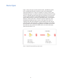
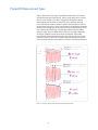
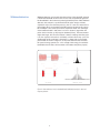
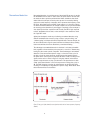
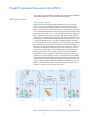
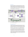
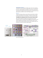
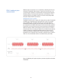
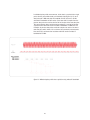
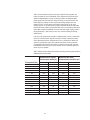
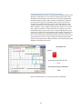
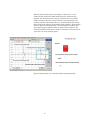
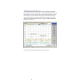
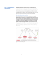
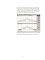
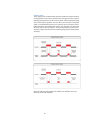
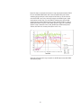
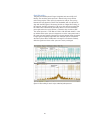
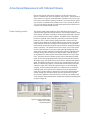
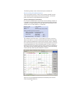
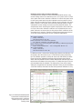
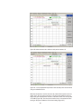
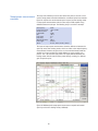
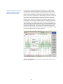
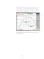
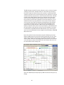
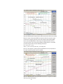
Agilent
PNA-X Series Microwave
Network Analyzers
Active-Device Characterization in Pulsed Operation
Using the PNA-X
Application Note
Table of Contents
Introduction ..........................................................................................................................3
Device Types ........................................................................................................................4
Pulsed-RF Measurement Types ................................................................................5
Pulsed-RF Detection Techniques..............................................................................6
Wideband detection ...........................................................................................................7
Narrowband detection .......................................................................................................8
Pulsed-RF S-parameter Measurements Using PNA-X.................................9
PNA-X pulse system ..........................................................................................................9
PNA-X hardware overview ...............................................................................................9
PNA-X IF paths.................................................................................................................10
Internal pulse generators ................................................................................................10
Internal pulse modulators ...............................................................................................11
Pulse I/O ..........................................................................................................................11
Pulse system delays ........................................................................................................12
Setting up measurements using Pulsed-RF measurement application ......................14
PNA-X wideband pulse measurements ......................................................................16
Wideband pulse data acquisition ...................................................................................16
Synchronizing pulsed-RF stimulus and measurements ...............................................19
Wideband pulse system dynamic range ........................................................................23
PNA-X narrowband pulse measurements ..................................................................24
Narrowband filter path with crystal filter ......................................................................24
Software gating ...............................................................................................................26
Digital filter nulling ..........................................................................................................28
Active-Device Measurements with Calibrated Stimulus..........................29
Power leveling modes ......................................................................................................29
Accurate pulsed stimulus using receiver leveling ....................................................30
Pulsed stimulus power calibration .................................................................................30
Receiver leveling with wideband detection...................................................................31
Receiver leveling with narrowband detection...............................................................33
Swept-power measurement examples ........................................................................35
Improving stimulus power level accuracy in pulse profile measurements.........36
Compression vs. Frequency Measurements in Pulse Mode ..................37
Two-tone IMD measurements in Pulse Mode ................................................39
Additional Resources ....................................................................................................42
Application note ................................................................................................................42
Web ......................................................................................................................................42
2
Introduction
Vector network analyzers (VNA) are the common tool for characterizing
RF and microwave components in both continuous-wave (CW) and pulsed
operations. Some external equipment may be used in conjunction with a VNA
to modulate the stimulus or DC bias, and to perform accurate S-parameter
measurements in pulsed operation. However, components that need to be
characterized in pulsed operation mode are often active devices such as
amplifiers or converters, and many active parameters are characterized in
addition to S-parameters. For amplifiers as an example, 1 dB compression (P1
dB), intermodulation distortion (IMD), and third-order intercept point (IP3) are
commonly measured, and many parameters such as noise figure, higher-order
distortion products, harmonics, etc. are characterized depending on their
intended application needs. These active parameters are power-dependent,
so additional factors must be considered for precise characterization.
To respond to such needs, Agilent’s PNA-X Series, the most flexible VNA
that employs many capabilities designed for active-device characterization,
enables S-parameter and active parameter measurements with a single
set of connections. The PNA-X’s four internal pulse generators and
pulse modulators, two internal sources with a combining network, and
active-application options provide fully integrated pulsed active-device
characterization. This application note discusses pulsed S-parameter
measurements using the PNA-X Series and measurement techniques that
enable power-dependent active-device characterization including compression
and distortion. It also provides a brief summary of pulsed-RF measurement
types, and two detection techniques (wideband and narrowband detection)
are explained specifically using PNA-X architecture and methodologies. Refer
to application note 1408-12 Pulsed-RF S-Parameter Measurements Using
Wideband and Narrowband Detection part number 5989-4839EN for further
details of measurement types and detection techniques.
3
Device Types
Figure 1 shows two types of pulse operation modes, pulsed-RF and pulsedbias. Pulsed-RF operation drives the device with a pulse-modulated RF
signal while the DC bias is always on. Amplifiers in receivers used in pulsemodulated applications are typically tested under pulsed-RF operation. Testing
devices in pulsed-RF operation requires RF pulse modulators for the stimulus
as well as pulse generators to drive the RF modulator and to synchronize or
gate the VNA receivers to capture the modulated RF signals. The pulsed-bias
operation is when the DC bias is switched on and off to generate a pulsemodulated signal while the input is mostly a CW signal and is always on.
Traveling-wave-tube (TWT) amplifiers are one example of this type and are
commonly used in radar transmitters. The RF pulse modulator is not required
for the stimulus in this mode, but pulse generators are needed to turn on and
off the DC bias and synchronize the VNA receivers to measure the output
signal when the device is on.
Pulsed-RF
Input: pulsed
Output: pulsed
DC bias: always on
Figure 1. Pulsed-RF and pulsed-bias operation modes
4
Pulsed-bias
Input: CW
Output: pulsed
DC bias: pulsed
Pulsed-RF Measurement Types
Figure 2 shows three major types of pulsed-RF measurements. The first two
are pulsed S-parameter measurements, where a single data point is acquired
for each carrier frequency. The data is displayed in the frequency domain
with magnitude and/or phase of transmission and/or reflection. Average
pulse measurements make no attempt to position the data point at a specific
position within the pulse. For each carrier frequency, the displayed S-parameter
represents the average value of the pulse. Point-in-pulse measurements result
from acquiring data only during a specified gate width and position (delay)
within the pulse. There are different ways to do this in hardware, depending
on the type of detection used, which will be covered later. Pulse profile
measurements display the magnitude and/or phase of the pulse versus time,
instead of frequency. The data is acquired at uniformly spaced time positions
across the pulse while the carrier frequency is fixed at some desired frequency.
Figure 2. Average, point-in-pulse and pulse profile measurements
5
Pulsed-RF Detection Techniques
Figure 3 shows an important measure of a pulsed RF signal and its relationship
between the time and frequency domain. When a signal is switched on and
off in the time domain (pulsed), the signal’s spectrum in the frequency domain
has a sin(x)/x response. The width of the lobes is inversely related to the pulse
width (PW). This means that as the pulses get shorter in duration, the spectral
energy is spread across a wider bandwidth. The spacing between the various
spectral components is equal to the pulse repetition frequency (PRF). If the PRF
is 10 kHz, then the spacing of the spectral components is 10 kHz. In the time
domain, the repetition of pulses is expressed as pulse repetition interval (PRI)
or pulse repetition period (PRP), which are two terms with the same meaning.
Another important measure of a pulsed RF signal is its duty cycle. This is the
amount of time the pulse is on, compared to the period of the pulses. A duty
cycle of 1 (100%) would be a CW signal. A duty cycle of 0.1 (10%) means that
the pulse is on for one-tenth of the overall pulse period. For a fixed pulse width,
increasing the PRF will increase the duty cycle. For a fixed PRF, increasing the
pulse width increases the duty cycle. Duty cycle will become an important
pulse parameter when we look at narrowband detection.
Figure 3. Pulsed-RF network analysis terminologies
6
Wideband detection
Wideband detection can be used when the majority of the pulsed-RF spectrum
is within the bandwidth of the receiver. In this case, the pulsed-RF signal will
be demodulated in the instrument, producing baseband pulses. With wideband
detection, the analyzer is synchronized with the pulse stream, and data
acquisition only occurs when the pulse is in the “on” state. This means that a
pulse trigger that is synchronized to the PRF must be present; for this reason,
this technique is also called synchronous acquisition mode. The advantage
of the wideband mode is that there is no loss in dynamic range when the
pulses have a low duty cycle (long time between pulses). The measurement
might take longer, but since the analyzer is always sampling when the pulse
is on, the signal-to-noise ratio is essentially constant versus duty cycle. The
disadvantage of this technique is that there is a lower limit to measurable
pulse widths. As shown in Figure 4, as the pulse width becomes narrower,
the spectral energy spreads out – once enough of the energy is outside the
bandwidth of the receiver, the instrument cannot detect the pulses properly.
Figure 4. Pulse width and receiver bandwidth with wideband detection in time and
frequency domain
7
Narrowband detection
Narrowband detection is used when most of the pulsed-RF spectrum is outside
the bandwidth of the receiver. In other words, the pulse width is narrower than
the minimum data acquisition period with the widest available receiver bandwidth. With this technique, the entire pulse spectrum is removed by filtering
except the central frequency component, which represents the frequency of the
RF carrier. After filtering, the pulsed-RF signal appears as a sinusoid or CW signal. With narrowband detection, the analyzer samples are not synchronized with
the incoming pulses (therefore no pulse trigger is required), so the technique is
also called asynchronous acquisition mode. Usually, the PRF is high compared
to the IF bandwidth of the receiver, so the technique is also sometimes called
the “high PRF” mode.
Agilent has developed a novel way of achieving narrowband detection using
wider IF bandwidths than normal, by using a unique “spectral nulling” and
“software gating” techniques that will be explained later. These techniques let
the user trade dynamic range for speed, with the result almost always yielding
faster measurements than those obtained by conventional filtering.
The advantage to narrowband detection is that there is no lower pulse-width
limit, regardless of how broad the pulse spectrum is, most of it is filtered away,
leaving only the central spectral component. The disadvantage to narrowband
detection is that measurement dynamic range is a function of duty cycle. As
the duty cycle of the pulses becomes smaller (longer time between pulses),
the power of the central spectral component becomes smaller, resulting in less
signal-to-noise ratio as shown in Figure 5. Using this method, measurement
dynamic range decreases as duty cycle decreases. This phenomenon is often
called “pulse desensitization” and can be expressed as 20*log (duty cycle) in
dB. The PNA-X employs a number of unique features to minimize this effect,
resulting in considerably less degradation in dynamic range. More details about
these features will be discussed later.
Figure 5. Duty cycle (time domain) versus signal-to-noise ratio of center spectrum (frequency
domain)
8
Pulsed-RF S-parameter Measurements Using PNA-X
This section discusses pulsed-RF S-parameter measurements using the PNA-X
with wideband detection and narrowband detection techniques.
PNA-X pulse system
PNA-X hardware overview
Figure 6 shows the PNA-X block diagram with two test ports, two internal
sources, source/receiver attenuators, internal combining network, and rear
access loops with mechanical path switches. Each source has two outputs;
Output 1 and 2 of Source 1 are routed to test port 1 and test port 2 and used for
basic S-parameter measurements. Output 1 and 2 of Source 2 are routed to two
front-panel source output ports on a 2-port configuration, and are routed to test
port 3 and test port 4 on a 4-port configuration (not shown). Output 1 (OUT 1)
of each source is filtered to reduce harmonics, and can be switched to the combining network for two-tone IMD measurements. Both outputs of each source
can be routed through the rear access loop for additional signal conditioning
or switched to the thru path to the test port. All source paths and test-receiver
paths have optional step attenuators to lower the source power for high gain
devices or to reduce the signal level to avoid receiver compression. The source
attenuators are sometimes used to improve the source match for active measurements. All of these features make the PNA-X the most flexible network
analyzer, enabling accurate S-parameters and active-device measurements
with the best possible configuration. The PNA-X also integrates internal pulse
generators, and a pulse modulator on OUT 1 of each internal source. Pulsed-RF
measurements with pulsed stimulus in the forward direction only requires one
internal source with a pulse modulator. Adding the second internal source and
a pulse modulator enables bi-directional pulsed-RF measurements. In this configuration, pulsed stimulus from the second internal source is routed from J8
through J1 connectors of the rear panel to the port 2.
Figure 6. 13.5/26.5 GHz PNA-X block diagram with options 200, 219, 224, 020, 021, 022 and 025
9
PNA-X IF paths
Figure 7 shows the PNA-X receiver/IF path block diagram with internal pulse
generators and modulators. The narrowband filter path employs a crystal filter
with 30 kHz bandwidth centered at 10.7 MHz for better signal selectivity, and
also adds receiver gating capability for narrowband pulse measurements. Earlier
PNA-X models had 60 MSa/s analog-to-digital converters (ADC) with 60 MHz
system clock (DSP version 4), later versions have been upgraded to 100 MSa/s
ADC with 100 MHz system clock (DSP version 5).
Figure 7. PNA-X IF path block diagram
Internal pulse generators
The PNA-X with internal pulse generators (Option 025) adds four pulse generators (P1, P2, P3, and P4) and an additional pulse generator (P0) that is used for
synchronizing the data acquisition. These internal pulse generators can be triggered internally or externally – all at the same time. They can have an individual
delay up to 35 s, and pulse width up to 10 s. When triggered internally, the
pulse generators output a continuous pulse train with specified periods up to
35 s. The minimum timing resolution of all pulse generators is based on the
clock, 16.7 ns with DSP version 4 and 10 ns with DSP version 5. P1 through
P4 pulse generators are used to drive internal pulse modulators, IF gates and/
or external devices, such as pulsed-bias switches. P0 pulse generator is used
to trigger the DSP for data acquisition. When P0 outputs a pulse, the DSP
starts data acquisition and continues until it completes the required number of
samples per specified IF bandwidth. If P0 outputs the next pulse before the DSP
completes the data acquisition, the P0 pulse is ignored. Approximate data acquisition time is 1/(IF bandwidth).
10
Internal pulse modulators
The PNA-X with the internal pulse modulator options adds a pulse modulator
to the “OUT 1” of each internal source (Option 021 for Source 1 and Option 022
for Source 2). Both modulators are driven by a common pulse, which can be
selected from P1 through P4 internal pulse generators, or external pulse inputs
with minimum pulse width of system clock timing resolution.
Pulse I/O
The pulse input/output (I/O) port on the PNA-X rear panel adds accessibility
to internal pulse generators and modulators, and enables synchronous pulse
measurements with external pulse generators or a device under test (DUT).
The N1966A pulse I/O adapter converts the 15-pin D-sub connector to SMB
connectors for five PULSE IN (inputs for A, B, C/R1, D/R2, and R receiver
gates), PULSE SYNC IN (to trigger internal pulse generators for pulse
modulation and data acquisition), RF PULSE MOD IN (to modulate RF sources),
and four PULSE OUT (P1 through P4). The four PULSE OUT ports are hardwired to the internal pulse generators without switches. Figure 8 shows how
the pulse I/O connectors map to the IF block diagram.
Figure 8. Rear panel pulse I/O
11
Pulse system delays
From pulse trigger to internal pulse generators, to pulse modulators, and then
to ADC for data acquisition, there are some delays in the pulse system that
need to be taken into account. Figure 9 shows the timing diagram from the
pulse trigger at PULSE SYNC IN through the data acquisition with wideband
detection technique.
Figure 9. PNA-X pulse system delays with wideband data acquisition
12
Internal pulse generators start generating the pulses approximately 60 to
100 ns after the pulse trigger inputs at the PULSE SYNC IN – (denoted as
pulse trigger delay). The jitter of this delay is the minimum time resolution
of the system. The exact pulse trigger delay can be measured with an
oscilloscope between PULSE SYNC IN and one of the PULSE OUT (P1
through P4). If the internal clock is used to trigger the pulse generators,
this pulse trigger delay is very small and therefore it can be neglected. One
of the P1 through P4 internal pulse generators drives the internal pulse
modulators to generate pulsed-RF signals. The actual pulsed-RF signals
have a delay of approximately 30 ns from the P1 through P4 modulation
pulse at the test port with a 48 inch RF test port cable – (denoted as pulse
modulation delay). The pulse modulation delay with RF carrier frequencies
of 3.2 GHz and below is about 40 ns or larger (nearly 100 ns delay at the
low-end frequency of the analyzer). The combiner path on port 1 adds an
additional 5 ns delay compared to the thru path. The pulse modulators
switch the RF sources on and off with approximately
4 ns rise time and 10 ns fall time.
P0 pulse generator is also triggered by PULSE SYNC IN (or internal
trigger) and generates a data acquisition pulse with the same amount of
pulse trigger delay as other internal pulse generators (or zero if triggered
internally). Although the data acquisition process starts immediately with
the P0 pulse, there is approximately 250 ns data-processing delay, the
time it takes for sampled data with pulse on to become available in the
buffer. The user-specified measurement delay (the delay for P0) must take
into account these data-acquisition and pulse-modulation delays to align
the pulsed stimulus and data-acquisition window. Approximately 300 ns
for the measurement delay accounts for pulse-modulation delay and dataacquisition delay, as well as pulse-settling time. Additional delay may be
necessary depending on the frequency, the PNA-X’s internal path switches,
and external cables and devices.
Setting up pulsed-RF measurements
The basis of pulsed-RF point-in-pulse measurements with wideband detection
method is to synchronize pulsed stimulus and data acquisition so that all
receivers measure responses only within the RF pulses. The following three
steps must be completed for successful measurements.
Step 1 Setup pulse generators and modulators
Specify pulse width, delay and period for internal pulse generators with Pulse
Generator Setup dialog (Figure 10a). Note that Pulse0 width is determined
by the IF bandwidth chosen (in step 3) thus it is not editable on the pulse
generator dialog. When internal pulse modulators are used, specify the drive
source (typically one of internal pulse generators). It is also required to disable
automatic level control (ALC) on the source port with pulse modulation
enabled. Change the leveling mode from “Internal” to “Open loop” on Power
and attenuator dialog. Otherwise the ALC will try to level the source with the
detected power level with pulse on and off, causing a source unleveled error.
13
Setting up pulsed-RF measurements continued
Step 2 Synchronize data acquisition and pulses
With internal pulse generator option, pulse trigger feature is added to the PNA-X
trigger system (Figure 10b Pulse Trigger tab on Trigger dialog). Specify trigger
source – either internal or external (incoming pulses to PULSE SYNC IN) and
check “Synchronize receiver to pulse generator Pulse0”. Note that measurement
trigger (MEAS TRIG IN port on PNA-X rear panel) is not used in typical setup.
Step 3 Adjust data acquisition time
Set IF bandwidth to be wider than at least 1/(pulse width), in order to complete
the data acquisition while pulse is on. For example, 10 µs pulse width requires at
least 100 kHz IF bandwidth or wider. It is recommended checking Pulse0 width
is smaller than the pulse width of modulation drive on Pulse Generator Setup
dialog. Recommended setting is to a step wider IF bandwidth than the narrowest
possible bandwidth for the given pulse width so that numerous system delays
do not cause a problem. The PNA-X, to account for the test port coupler rolloff at low frequencies, adjusts IF bandwidth automatically and maintains the
measurement accuracy. This causes a problem in pulse measurements using
wideband detection method. Turn off “Reduce IF Bandwidth at Low Frequency”
on IF Bandwidth dialog.
For pulse profile measurements, the basic steps stay the same as point-in-pulse
measurements, but add slightly more complexity. The sweep type must be CW
Time sweep. The IF bandwidth needs to be much wider than the one for pointin-pulse at the same pulse width. This is because pulse profile often requires
minimum 10 or more measurement points in a pulse compared to only one point
in a pulse with point-in-pulse. Define the IF bandwidth to achieve desired timing
resolution. In order to display the whole pulse profile, adjust number of points
and the delay for the modulation drive.
14
Setting up with pulsed-RF measurement application
Option 008 pulsed-RF application optimizes the setup through Pulse Setup
dialog, and adds narrowband pulse measurements. The basic pulsed-RF
measurements can be done by simply choosing measurement type (Standard
or Pulse Profile), specifying the pulse width and period on Pulse Setup
dialog (Figure 11a). All other necessary settings explained earlier are done
automatically. It also adds pulse measurements with narrowband detection
method to extend lower limit of measurable pulse width.
Figure 10a. Pulse Generators Setup dialog box
Figure 10b. Pulse Trigger tab or Trigger dialog box
Figure 11a. Basic Pulse Setup dialog box
Figure 11b. Advanced Pulse Setup dialog box
The Advanced setup shown in Figure 11b allows you to adjust the analyzer
settings for a particular case. The following are references for adjusting the pulse
measurement settings available in the Advanced setup dialog.
15
Autoselect Pulse Detection Method
If selected, wideband detection method is used for pulse widths of 267 ns or
wider for point-in-pulse measurements, and 1.6 us or wider pulse width for
pulse profile measurements. Otherwise, narrowband detection method is used.
Autoselect IF Path Gain and Loss
Autoselect is used in most cases, but it may need to be adjusted for highpower configurations with user-supplied high-power couplers and attenuators
instead of internal test port couplers. De-select to adjust the IF settings for
non-standard setups. Refer to PNA Help for more details.
Optimize Pulse Frequency
If selected, it adjusts the pulse frequency to maximize the spectral nulling
effect when using the narrowband detection method. It is ignored for the
wideband detection method.
Autoselect Profile Sweep Time
If selected, the time span in pulse profile measurements is set to double of
the pulse width, and a delay of half of the pulse width is added to the pulse
generator that drives the modulators. In the case of 10 us pulse width, the
hardware sets 20 us span and 5 us delay of the pulse generator, and displays
the pulse in the middle of the screen. If de-selected, it sets the time span
based on the current number of measurement points and IF bandwidth. The
start and stop time can be adjusted in the Sweep, Time menu.
IFBW
In wideband detection, the IF bandwidth is set automatically based on
the specified pulse width in order to make the data acquisition window
(approximately 1/IFBW) narrower than the pulse width. In narrowband
detection, it is also set automatically, but with a custom IF filter for spectral
nulling. The display shows the closest standard IF bandwidth.
Mater Pulse Trigger
It is used to define the trigger source between internal or external
(incoming pulse on PULSE SYNC IN).
Autoselect Width & Delay
If selected, the data acquisition or receiver gate widths and delays are set
to acquire data within the pulses. They are adjusted to display the pulse
in the middle of the screen in pulse profile. They can be customized in the
Measurement Timing table or in the Pulse Generators Setup dialog box.
Autoselect Pulse Generators
If selected, PNA firmware assigns Pulse1 to modulators in wideband and
narrowband mode, and Pulse2 to all receiver gates in narrowband mode. If
de-selected, any internal pulse generator and “external ” (Pulse Sync In) can
be selected in the Measurement Timing table. The pulse generators must be
enabled in the Pulse Generators Setup dialog box (Figure 10) to be activated.
16
PNA-X wideband pulse
measurements
Wideband pulse measurements are accomplished by modulating the RF source,
setting the IF bandwidth wide enough to capture all pulse spectrum, and
synchronizing the modulation and measurements with appropriate triggering
and delay settings. The internal pulse generators and modulators can be
controlled either by SCPI/COM commands or the Pulse Setup dialog added
with Option 008 pulsed-RF measurements.
Wideband pulse data acquisition
The PNA-X with DSP version 4 requires 16 samples with its widest IF bandwidth
of 5 MHz to get a single data point, which takes 267 ns (16.7 ns per sample)
with its 60 MSa/s ADC. The PNA-X with DSP version 5 enables widest IF
bandwidth of 15 MHz and requires only 10 samples, which takes 100 ns (10 ns
per sample) with its 100 MSa/s ADC. Figure 12 shows how the data acquisition
progressed in point-in-pulse and pulse-to-pulse measurements with wideband
detection technique. The RF carrier frequency of point-in-pulse is increased at
every data point, thus each data point needs to be calculated with the required
number of samples for specified IF bandwidth within the same pulse. The
minimum pulse width for wideband point-in-pulse measurements at widest IF
bandwidth is 267 ns with DSP version 4 and 100 ns with DSP version 5 (refer to
Table 1 for a list of bandwidths and the associated minimum pulse width).
Figure 12. Wideband point-in-pulse and pulse-to-pulse data acquisition with widest
IF bandwidth
17
In wideband pulse profile measurements, all the data is acquired with a single
pulse, thus the pulse width needs to be relatively wide (Figure 13). For each
data point with 1 MHz and wider IF bandwidth on DSP version 4 or 10 kHz
and wider IF bandwidth on DSP version 5, the latter half of samples from the
previous data point are used for the first half of samples of the next data point.
This means that the data acquisition timing resolution is one-half of the data
acquisition time. With DSP version 4 widest IF bandwidth of 5 MHz, the last
8 samples of previous data points and 8 new samples are used to calculate a
new data point, which makes 133 ns minimum time resolution measurements.
It becomes 50 ns minimum time resolution with DSP version 5 widest IF
bandwidth of 15 MHz.
Figure 13. Wideband pulse profile data acquisition using widest IF bandwidth
18
Table 1 shows theoretical values of the data-acquisition time-per-point and
timing resolution for each IF bandwidth. These represent the minimum pulse
width for wideband point-in-pulse and timing resolution for wideband pulse
profile respectively. The minimum timing resolution can also be found on the
PNA-X display by setting CW time sweep and dividing sweep time by the
number of points. In other words, the length of pulse profile can be set by
number of points, up to 32001 points in PNA-X standard operation mode. Note
that the maximum number of points with DSP version 4 is limited by 1001 points
with 1 MHz or wider IF bandwidth. Thus the maximum length of pulse profile is
(timing resolution) * (1001 points) in this case, instead of (timing resolution) *
(32001 points).
In practice, the minimum pulse width for wideband point-in-pulse is affected by
pulse rise and fall time, the alignment of pulses and data acquisition window,
and is determined based on measurement accuracy requirements. When one
of the few sampled data points falls outside of the pulse, the error becomes
considerably large. However, the number of samples increases with narrower
IF bandwidth and missing one of many samples causes a relatively small error,
which may be acceptable.
Table 1. Minimum pulse width (point-in-pulse) and timing resolution (pulse profile) in
wideband pulse measurements
IF bandwidth (kHz)
Wideband point-in-pulse
minimum pulse width (ns)
Wideband pulse profile
minimum timing resolution (ns)
DSP version 4 DSP version 5
DSP version 4
DSP version 5
100
10650
14520
10650
7260
150
7100
9680
7100
4840
200
4733
7260
4733
3630
280
3550
5160
3550
2580
360
2367
4420
2367
2410
600
1183
3620
2367
2410
1000
1433
1440
717
720
1500
933
960
467
480
2000
700
720
350
360
3000
467
500
233
250
5000
267
300
133
150
7000
n/a
200
n/a
100
10000
n/a
140
n/a
70
15000
n/a
100
n/a
50
19
Synchronizing pulsed-RF stimulus and measurements
In wideband pulse measurements, the appropriate IF bandwidth and the pulse
generators’ width/delay are set in order to acquire the data within pulses.
The following measurements demonstrate the results with inappropriate IF
bandwidth and delay settings, which should be avoided when customizing
pulse measurement setups. The following point-in-pulse measurements
are made using a PNA-X with DSP version 4, 4 to 6 GHz frequency range,
-5 dBm input power, and 2 us pulse width and 20 us PRI (10% duty cycle).
With “Autoselect” mode, 1 MHz IF bandwidth (which takes 1.433 us for the
data acquisition) and 467 ns measurement delay are selected. A narrower
IF bandwidth may be used to reduce noise. If the IF bandwidth becomes too
narrow such as 100 kHz, the data acquisition takes 10.65 us and the majority
of the measurements occur outside of the pulses, resulting in significant
errors in the absolute power measurements (B receiver trace) and noisy ratio
measurements (S21 trace) as shown in Figure 14a. Note that the examples
show S21 measurements with 1 dB/div and the B receiver measurements with
10 dB/div in both Figure 14a and 14b.
Figure 14a. Measurement errors caused by improper IF bandwidth
20
When the measurement delay (or pulse delay) is adjusted, it is crucial
to keep the data acquisition window within the pulses. Unlike previous
examples, the measurement errors may not be obvious due to a few ADC
samples outside of the pulses. Figure 14b shows the measurement errors
caused by improper measurement delay. It is recommended to have enough
timing margin when adjusting IF bandwidth and/or the delays. Approximately
300 ns or greater measurement delay is recommended to account for data
processing and pulse modulation delays as shown earlier in Figure 9. The
chosen IF bandwidth should leave a margin of more than a few internal clock
cycles (50 ns or more) within the pulses.
Figure 14b. Measurement errors caused by improper measurement delay
21
In pulse-to-pulse measurements, PRI has to be wide enough for the PNA-X to
keep up with the data acquisition from one pulse to the next. The minimum PRI
becomes slightly longer with narrower IF bandwidth as the data acquisition time
becomes longer. Table 2 is the minimum PRI by IF bandwidth for 26.5 GHz PNA-X
with DSP version 4 and 1.5 GHz CPU board as a reference. The minimum PRI
could be improved as the data processing time becomes shorter with a faster
CPU and/or DSP.
Table 2. Minimum PRI in wideband pulse-to-pulse measurement
IF bandwidth (kHz)
100
150
200
280
360
600
1000
1500
2000
3000
5000
Minimum PRI in wideband pulse-to-pulse
measurements (us)
47
43
41
40
39
37
36
34
34
33
32
If the data acquisition process is not ready when the second pulse comes, it waits
for the next pulse to take data for the second data point. Thus the missing pulses
cannot be easily seen in pulse-to-pulse measurements. To verify every single pulse
is measured in a particular setup, an oscilloscope may be used to compare the
PNA-X’s AUX trigger output to the pulse trigger. Figure 15 shows the setup and the
screen shots from the oscilloscope for every pulse and missing pulses.
Figure 15. Wideband pulse-to-pulse measurement verification
22
Wideband pulse system dynamic range
The wideband detection with PNA-X can be used for relatively fast pulsed-RF
operation (with shorter PRI or high PRF) compared to legacy VNA’s due to a wide
IF bandwidth up to 15 MHz. However, the recommended IF bandwidth should be
wide enough to capture most of the pulse spectrum, while the dynamic range
and trace noise performance meets the measurement requirements. Figure 16
compares the PNA-X wideband pulse dynamic ranges at 5 MHz and 200 kHz IF
bandwidth as a reference.
Figure 16. PNA-X wideband pulse measurement dynamic range
23
PNA-X narrowband pulse
measurements
The Option 008 pulsed-RF measurement uses narrowband detection
method for a pulse width narrower than 267 ns in standard pulse (point-inpulse) measurements and 1.6 us pulse width or narrower in pulse profile
measurements. When narrowband detection is selected, each receiver gate
width and delay can be controlled independently. The PNA-X narrowband
pulse implementation employs unique hardware and software techniques –
narrowband filter path, software gating, and digital filter nulling, all of which
improve the receiver sensitivity and the measurement throughput.
Narrowband filter path with crystal filter
The narrowband filter path consists of three major elements; an amplifier,
receiver gate switches, and a 30 kHz crystal filter centered at 10.7 MHz as
shown in Figure 17. The basic idea is to amplify the signal as much as possible
from the upstream receiver path before the IF gate. The levels are such that the
IF gate does not compress and the peak pulse envelop energy passes relatively
unchanged, the IF gate is then used for time discrimination. The crystal filter
removes the undesirable portion of the pulse spectrum before reaching the
downstream amplifiers and digitizer. As a result, it reduces the overall energy of
the pulsed spectrum avoiding the center spectral component to be compressed
by the ADC. The larger the duty cycle and smaller the pulse width (as the pulse
spectrum spreads out) the crystal filter contributes more to the sensitivity
improvement.
Figure 17. Narrowband filter path
24
Figure 18 shows how the narrowband filter path affects pulsed-RF signals
by looking at the central frequency tone of the pulsed-RF signals with 200
ns pulse width and 2 us PRI. In Figure 18, the top window shows the PNAX’s 500 Hz IF filter response with the wideband IF path. The bottom window
shows the narrowband filter path, which removes some of the undesired
spectrum of the pulse-RF signals with 30 kHz crystal filter.
Figure 18. Pulsed-RF signal filtered in wideband IF path and narrowband filter
25
Software gating
The IF gating in the narrowband filter path uses hardware switches driven by
a pulse generator, which leaves residual noise at the gate off time caused by
internally generated noise and the switch isolation. When hardware IF gating
and an internal pulse generator are used, the on and off times of the gated
signal can be determined precisely. Since the off times of the gate contain
undesirable noise and residual gate isolation, the algorithm can replace the
off times with an ideal off state (i.e. zeros), thereby improving the receiver
sensitivity. Figure 19 shows how the software gating improves measurement
sensitivity.
Figure 19. Software gating replaces the residual noise with ideal zeros and
increases the receiver sensitivity
26
Figure 20 shows an example of the dynamic range improvement that the PNA-X
has over the E836x PNA models due to the narrowband ilter path and the
software gating technique. In this example of .001% duty cycle, the measurement in the PNA is very noisy, and many averages are needed to get a usable
measurement. At this duty cycle, the PNA-X’s hardware gives about 20 dB
of improvement and the software gating provides another 20 dB, for a total of
40 dB improvement. This gives a very usable dynamic range; in fact, the 60 dB
dynamic range is about the same as that afforded by an 8510-based pulsed
solution, but with much shorter pulses (50 ns versus 1 us).
Figure 20. System dynamic range comparisons, 40 dB improvement with PNA-X
and software gating
27
Digital filter nulling
The gated and filtered pulsed IF signal is digitized and sent to DSP for IF
filtering. The remaining pulse spectrum is filtered using custom IF filter
nulls leaving only the center spectral component to analyze. The spacing
between the nulls depends on the IF filter bandwidth, which is adjusted to
align with the PRF. Figure 21 illustrates the effects of digital filter nulling. In
this example, the PRI is adjusted to 1.767 ms to align with the standard 500
Hz IF filter nulls to demonstrate the nulling effects. In actual narrowband
pulse applications the custom IF filter is created to align an arbitrary PRF.
The center spectrum is -75.15 dBm at 5 GHz as indicated with marker 1 in the
top window. Other pulse spectral components are at the same power level as
the center spectrum (marker 2 through 5 in the top window). After the pulsed
IF signal goes through the digital filter, the undesired spectral components
decrease by about 60 to 70 dB (marker 2 through 5 in the bottom window),
while the signal level of the center spectrum is nearly unchanged.
Figure 21. Filter nulling is used to reject undesired pulse spectrum
28
Active-Device Measurements with Calibrated Stimulus
Devices that operate under pulsed conditions are often discrete active
devices or modules that consist of amplifiers and/or mixers. The performance
of these devices is typically power-dependent. Therefore, they are characterized in linear and nonlinear operating conditions. Inaccurate stimulus power
may introduce considerable measurement errors. In this section we will discuss source leveling techniques in pulsed measurements that minimize errors
caused by inaccurate pulsed-RF stimulus.
Power leveling modes
The stimulus power of every PNA-X has been calibrated at the factory with
continuous-wave (CW) with a default setting to cover the entire frequency range
of the analyzer. This allows reasonably accurate stimulus power level at the test
ports even without source power calibration. The PNA-X monitors and adjusts
the source’s automatic level control (ALC) internally to maintain the specified
power level. This is called “internal” leveling mode and is used in most measurement setups. However, the internal detectors do not measure correct peak
power of the pulsed stimulus resulting in ALC-unleveled errors. For pulsed-RF
measurements the internal leveling has to be turned off by changing the leveling
mode to “open loop”. This prevents the ALC errors but at a cost of source level
accuracy. There are three accuracy errors with open loop leveling mode: level
offset, sweep-to-sweep, and band-crossing level inconsistency. The level offset
and band-crossing level inconsistency are typically within a few dB and they
are repeatable. This means that the source power calibration can correct these
errors. The power-sensor-loss feature must be used to calibrate the pulsed-RF
power, because the average pulse power is lower than the peak pulse power by
10*log (duty cycle); refer to the next section for how to calibrate pulsed stimulus
power. The sweep-to-sweep error is typically very small (typically less than 0.1
dB but it could be larger), appears as a short-term drift which the source power
calibration cannot correct. All of these open loop errors can be minimized by
using the “receiver” leveling mode, which uses a VNA receiver to monitor the
pulsed-RF power and correct the source power level on every measurement
sweep. Once receiver leveling is selected, the source level is adjusted with the
receiver readings, thus the source power correction coefficients are ignored
(source power calibration is not used even if it is turned on). The leveling mode
can be setup in Power and Attenuators, and Receiver Leveling Setup dialog boxes
as shown in Figure 22.
Figure 22. Power and Attenuator,
and Receiver Leveling
Setup dialog boxes
29
Accurate pulsed stimulus
using receiver leveling
Reference receivers are typically used for the receiver leveling, although any
receiver or a power sensor (if added as a receiver to the PNA-X) can be used.
The source level accuracy in receiver leveling mode depends on the receiver’s
absolute power measurement accuracy, therefore receiver calibration is strongly
recommended. There are three ways to calibrate the reference receivers – perform a receiver calibration independently, as a part of a source power calibration, or as a part of a guided S-parameter calibration. When performed independently, the receiver readings are compared to the calibrated source settings
(note that an independent receiver calibration requires a calibrated source).
Source accuracy and drift introduce additional errors to the receiver calibration. Thus performing receiver calibration either as a part of a source power or
S-parameter calibration is recommended. This way the reference receiver readings are compared to the power sensor readings regardless of the source accuracy when the correction coefficients are computed. As a result it transfers the
power sensor accuracy to the receiver with minimal errors. The open loop leveling mode must be used during calibration in order to keep the source settings
the same between calibration and measurements. The pulse modulation can
remain on if sensor loss compensation is used during the calibration. However,
a calibration with the pulse modulation off is recommended, because the sensor
loss value may add some errors (refer to the next section for more details). Also
the receiver setting such as attenuators, IF bandwidth, and gate widths must be
the same between the receiver calibration and the pulsed measurements, otherwise, the receiver calibration is turned off and then the source level becomes
inaccurate. Once the receiver is successfully calibrated, it accurately measures
the peak pulse power in wideband detection, and it adjusts the source power
until it’s within the specified tolerance or reaches the maximum number of
iterations before the measurement sweep.
Pulsed stimulus power calibration
Although turning off the pulse modulation is recommended during calibration, it
may not be possible in some cases such as using a booster amplifier that has a
different response between pulsed and non-pulsed signals. In this case, the pulse
modulator needs to stay on during calibration. The PNA-X uses power meters only
in average power measurement mode, regardless of an average or peak-power sensor. Therefore, under pulsed-RF stimulus, the power meter will read a value that is
lower than the peak pulse power (defined as the power during the time the pulse
is on) by 10*log (duty cycle). This difference is specified as a sensor loss to avoid
the PNA-X’s source to go unleveled as it tries to bring the test port power to the
desired level. For example, if the pulse duty cycle is 5%, then the power sensor
reading is 10*log (0.05) = -13 dB lower than the peak pulse power.
Note that the pulse desensitization (power sensor loss value) calculated from pulse
duty cycle introduces errors due to the pulse rise and fall time. If the pulse rise and
fall time are relatively large compared to the pulse width, the power sensor loss
value may need to be adjusted. The PNA-X’s internal pulse modulators provide
approximately 4 ns pulse rise time and 10 ns fall time. When the pulse width is 1
us and the duty cycle is 1% (100 us PRI), the average power is calculated as 20 dB
lower than the pulse peak power. The actual pulsed stimulus adds some RF energy
for 14 ns to the ideal pulsed stimulus, which makes the actual duty cycle 1.01%
approximately, and the average pulse power is 19.96 dB lower instead of the typical
20 dB. However, if the pulse width is 300 ns and the duty cycle is 1% (30 us PRI),
then the duty cycle is approximately 1.033% and the average pulse power is 19.85 dB
lower than the peak pulse power.
30
The following examples show calibration with pulse modulation off.
Receiver leveling with wideband detection
This section explains the basic steps to setup a leveled pulsed-RF stimulus,
make calibrated swept-frequency point-in-pulse S-parameter, and absolute
power measurements using wideband detection technique.
Setting up wideband pulse measurements
First, set up the wideband pulse measurements with the following conditions. It
is essential to set up the pulsed stimulus and measurements before performing
calibrations so that the calibrations are kept valid in the measurements. In this
example, we use a 5 GHz amplifier as a sample DUT.
Frequency range:
Source power:
Traces:
2 GHz to 8 GHz
-10 dBm
Tr1 S11, Tr2 S21, Tr3 R1,1, Tr4 B,1
Setting up wideband pulse measurements
Sweep – Pulse Setup… then enter the following
Pulse Measurement:
Standard Pulse
Pulse Timing:
Pulse Width:
1 us
Pulse Period:
100 us
Measurement Timing:
Rcvr A Delay:
300 ns
This modulates the stimulus with 1 us pulse width and 1% duty cycle. Rcvr A
delay is set to 300 ns to account for measurement delay (data processing delay,
refer to Figure 9 for detailed pulse system timing). Once the setup is completed,
the uncorrected input match, gain, input power, and output power are measured
using wideband detection in open loop leveling mode as shown in Figure 23.
Note that the pulse measurement application selects optimum IF bandwidth and
other settings from the specified pulse timing information, and sets the leveling
mode to open loop when the pulse modulation is turned on.
Figure 23. Uncorrected pulsed-RF S-parameters and absolute power measurements using wideband detection
31
Performing receiver and S-parameter calibrations
A calibrated receiver enables accurate and leveled pulsed-RF stimulus using
receiver leveling mode. In the calibration process, use a power sensor to create
source power and receiver calibration coefficients. In order for the power sensor
to read correct power levels, the pulse modulation must be turned off. Source
power calibration should be part of the calibration process. However, the source
power correction is not actually used to level the pulsed-RF stimulus; instead,
calibrated R1 receiver readings are used to level the pulsed-RF stimulus. The
example below shows measuring the amplifier output powers with the B receiver on port 2. B receiver calibration coefficients are computed from the source
power calibration, and transmission tracking and port match coefficients of the
S-parameter error correction. Therefore corrected output power measurements
can be done without performing B receiver calibration independently.
Turn off pulse modulation
Sweep – Pulse Setup…
Pulse Gen for Source1: CW – OK
Perform S-parameter, source and receiver calibration
Cal – Start Cal – Cal Wizard… then follow the wizard
Check “Calibrate source and receiver power” when selecting a calibration type and ports
Switch to receiver leveling
Power – Power and attenuators… - Port 1 Leveling Mode: Receiver – R1
Turn on pulse modulation
Sweep – Pulse Setup…
Pulse Gen for Source1: Pulse – OK
If a different receiver is shown in the leveling mode pull down menu (Receiver – B,
for example), select R1 receiver for port 1 in the Receiver Leveling setup dialog
box. The calibration procedure is exactly the same as the CW stimulus procedure.
Figure 24 shows the calibrated S-parameter and input/output power measurements under the pulsed-RF stimulus condition. Note that the calibration type annotation shown at the bottom of the screen adds a “Δ” (delta) when you turn on the
pulse modulation after the calibration. This indicates that a non-critical stimulus
setting was changed after the S-parameter calibration. Turning on pulse modulation
causes this indication, which does not affect the S-parameter calibration accuracy.
Figure 24. Calibrated wideband pulsed
S-parameters and absolute power
measurements with a comparison
between open loop and receiver
leveling modes
32
Comparing the results
Figure 24 also shows memory traces comparing the input match, gain, input power,
and output power under pulsed conditions with open loop and receiver leveling.
The difference is very small in the input match and gain measurements, but it is
quite large in the absolute power measurements. If you perform only S-parameter
measurements and the DUT is in the linear operation, the open loop leveling is
probably acceptable. However, if you measure absolute power and/or power
dependent performance such as compression and distortion, the pulsed stimulus
power needs to be accurately leveled. With wideband detection, the receivers
always measure during the pulses, thus receiver leveling is recommended.
Receiver leveling with narrowband detection
The PNA-X with DSP version 4 or version 5 must use narrowband detection
method for a pulse width narrower than 267 ns or 100 ns respectively. Fortunately,
the procedure to level the stimulus with narrowband pulse is exactly the same
as the one with wideband pulse – set up pulse measurements, turn off the pulse
modulator for calibration, then turn back on the modulator and use a receiver
to level the pulsed stimulus. In narrowband pulse, the receiver gates must be
placed inside the pulse, otherwise the receivers do not measure pulsed-RF signals. PNA-X firmware sets the receiver gate width one half of the pulse width by
default. Receiver gates have internal delay from the pulses that drive the pulse
modulator. This may cause the receiver gates to be off the pulse, resulting in
noisy measurements. The delay varies by frequency band and frequency model of
the PNA-X. It is recommended increasing receiver gate delay by the pulse system
timing resolution, 16.7 ns increments with DSP version 4 and 10 ns increments
with DSP version 5, to find an optimum delay at a particular measurement setup.
This example uses a 50 GHz PNA-X with DSP version 4, with a minimum receiver
gate delay of 16.7 ns. Figure 25a through Figure 25c show the S11, S21, input and
output powers of the same amplifier used in the previous example at each step.
The setup is 100 ns pulse width, 50 ns receiver gate width, 10 us pulse period,
16.7 ns receiver gate delay, and -10 dBm source power.
Figure 25a. Uncorrected narrowband pulse measurements
33
Figure 25b. Measurements after calibration with pulse modulator off
Figure 25c. Corrected pulsed-RF S-parameters and absolute power measurements
using narrowband detection
Note that the reference receiver measures the pulsed stimulus power at the set
power minus 20*log (receiver gate duty cycle) with some additional path loss
(Figure 25a). Once the reference receiver is calibrated it reads close to set power
at -10 dBm (Figure 25b). Then the pulsed stimulus level is well maintained after
turning on the pulse modulation and receiver leveling (Figure 25c).
34
Swept-power measurement
examples
The setup and calibration processes described in the previous sections can be
used for swept-power with either wideband or narrowband pulse measurements.
Figure 26 compares the results between open loop and receiver leveling modes
in swept-power measurements with the same sample 5 GHz ampliier using
wideband detection technique. The following setup is used in this example.
CW Frequency:
Power sweep range:
Number of points:
IF bandwidth:
PRI:
Pulse width:
Pulse delay:
Measurement delay:
Pulse trigger:
Traces:
5 GHz
-25 to +5 dBm
201
5 MHz
100 us
5 us
0s
400 ns
Internal
Tr1 S11, Tr2 S21, Tr3 R1,1, Tr4 B,1
The input and output power measurements show the differences between the
open loop and receiver leveling modes, which are similar to the swept-frequency
measurements. However, the gain traces are close with both modes while the
ampliier is in linear operation and exhibit differences as the ampliier compresses. This is because the input powers are slightly different between two
leveling modes with the same stimulus power settings, resulting in a different
gain compression point.
Figure 26. Wideband pulse swept-power measurement comparisons between
open loop and receiver leveling modes (calibrated)
35
Improving stimulus power
level accuracy in pulse
profile measurements
In pulse proile measurements, regardless of wideband or narrowband detection techniques, receivers measure signals inside of pulses as well as noise
outside of pulses. If receiver leveling is used while the receivers measure noise,
the source tries to adjust the source power by referencing the noise measurements causing source unleveled errors. Alternatively, the analyzer can remember
the previous receiver leveling during the stimulus on condition, and use it as
source power correction coeficients to improve the level accuracy. Receiver
leveling must be turned on once with the pulse modulators turned off. Follow
this procedure: turn off the pulse modulator, perform a calibration, switch to the
receiver leveling, select “Update source power calibration with leveling data”,
switch to the Open Loop leveling mode, then turn on the pulse modulator. Once
the receiver leveling result is used for source power cal (“Update source power
calibration with leveling data” can be found in the “Receiver Leveling” dialog
box shown in Figure 22), the pulsed stimulus level becomes reasonably accurate
in pulse proile measurements, as shown in Figure 27.
Figure 27. Narrowband pulse profile with “last receiver leveling result” used for
source power calibration
36
Compression vs. Frequency Measurements in Pulse Mode
Gain Compression (commonly specified as input/output power at 1 dB compression point: IP1dB/OP1dB) is a very popular amplifier characteristic. It is
measured and calculated from either swept-power gain (S21) or amplifier output
power at a single frequency point. Often this is repeated at many frequency
points to characterize the amplifier compression point over its operating frequency range (Figure 28). The PNA-X offers a gain compression application
(GCA) option that provides fast and accurate compression measurements versus
frequency with a very simple setup. It is important in this measurement that
the compression points are calculated from accurate input power with gain or
output power measurements. The GCA corrects power/receiver and mismatch
errors, providing the highest level of accuracy for compression measurements.
When the amplifiers are in pulse mode, these error corrections need to be kept
valid in order to take advantage of the accurate measurements with GCA. In
this section, we will discuss amplifier’s compression versus frequency measurements under pulse operation using the GCA option and wideband detection
technique (narrowband pulse is not available in PNA-X application measurement
classes). But this technique for setting up a pulsed-RF measurement is also
applied to setting up a pulsed-RF mixer/converter compression measurement in
a Gain Compression Converters (GCX) measurement class.
Compression
Point
Gain
Pin
Frequency
Figure 28. Compression measurements vs. frequency
The measurement setup and calibration procedure is similar to the pulsed
S-parameter measurement setup. Measuring stimulus level correctly is crucial for accurate compression measurements, which requires GCA calibration
remains enabled with pulsed stimulus. Use receiver leveling to level the pulsed
stimulus, then GCA calibration for accurate compression versus frequency
measurements. Fortunately, R1 receiver used for the source leveling is calibrated during the GCA calibration (B receiver is calibrated as well); therefore
no additional calibration for the receiver leveling is needed. Note, measurements with such wide IF bandwidth become noisy thus adding averaging is
recommended. A wider IF bandwidth may cause misalignment between the
data acquisition and pulses resulting in a noisy trace. Adding 300 ns or more
delay to the Pulse 0 (the pulse for data acquisition) solves this problem as
explained earlier in the PNA-X pulse system delay section. Once the GCA and
pulse setup is completed, turn off the pulse modulation for calibration. The
GCA calibration wizard guides you through the steps based on the measurement setup. Then the pulse modulation drive can be switched back to the
pulse generator and the R1 receiver is ready for leveling pulsed stimulus.
37
In the swept power measurement example shown earlier (Figure 26), found were
different input powers at compression points by the leveling mode due to the
errors of the input powers. In GCA, the input and output powers at compression
point versus frequency also show some difference between the leveling modes.
Shown in Figure 29, the maximum difference is about 1 dB.
Figure 29. Wideband pulse GCA measurement comparisons between open loop
and receiver leveling
38
Two-tone IMD measurements in Pulse Mode
The PNA-X employs clean internal sources with high output power, internal
combining network, and an optional IMD measurement application that makes
two-tone IMD measurements over the frequencies easier and faster. Unlike
traditional signal generators and a spectrum analyzer method, the IMD measurements using PNA-X provides single point of setup dialog, guided calibration, and several-tens to one-hundred times improved measurement speed
in swept-frequency or swept-power IMD measurements. In this swept IMD
measurement, the PNA-X uses its unique narrowband filter path for better signal selectivity. In this section, we will discuss IMD measurements under pulse
condition with measurement setup considerations and techniques to overcome
measurement problems (narrowband pulse is not available in PNA-X application measurement classes).
There is a fundamental setup conflict between typical IMD measurements
and wideband pulse measurements, when made together. The wideband pulse
measurements use relatively wide IF bandwidth (to narrow the data acquisition window), while IMD measurements in general use narrow IF bandwidth
to accurately measure low level distortion products. The following are some
considerations in IMD measurement setups under pulse operation.
Tone spacing versus IF bandwidth
The spacing between two main tones should be approximately more than 10
times wider than the IF bandwidth. If narrower tone spacing is required, the
IF bandwidth must be reduced to avoid signal interference (seen as ripples on
the traces) thus requires wider pulse width.
Use standard IF filter path
The IMD application automatically switches to the narrowband IF filter path,
where the IF signal is filtered with the high-Q crystal filter with 30 kHz bandwidth. This filter prevents capturing the whole spectrum of pulsed-RF signal. It
must be switched to standard IF path when IF bandwidths greater than 30 kHz
are used.
Disable “Reduce IFBW at Low Frequencies”
The PNA-X uses narrow IF bandwidth to reduce trace noise at low frequencies
by default. The frequency and the IF bandwidth reduction ratio depend on the
frequency models. It is recommended that this capability is always turned off
when making IMD measurements under pulsed operation.
Use sweep averaging to reduce noise
IMD measurements become noisier with wide IF bandwidths, so sweep averaging is recommended to reduce the noise.
39
The IMD calibration includes R1 receiver calibration, source 1 and source 2 power
calibration, and B receiver calibration when port 1 for the DUT input and port 2
for the DUT output are selected. If 2-port error correction is used during an IMD
calibration, the power sensor mismatch during R1 receiver calibration is corrected
and the transmission response term is used to transfer the R1 receiver calibration
to the B receiver. IMD calibration without 2-port calibration ignores the power
sensor mismatches during R1 receiver calibration and uses a response calibration to transfer to the B receiver. Calibrating at all receiver frequencies is recommended for wide tone spacing; otherwise it can be at only the center frequency
of each stimulus setup. Often recommended in wideband pulse measurements,
is to calibrate all frequencies due to the fact that wider IF bandwidth requires
wider tone spacing, easily wider than 1 MHz or often several megahertz. The
frequency responses of the receivers at each tone frequency can be different from
the center frequency with wide tone spacing. The pulse modulation must switch
to CW before the swept IMD calibration. Note that both f1 (port 1) and f2 (port 1
source 2) source leveling mode must be changed to receiver leveling in Swept IMD
Measurement class.
Figure 30a and 30b show the measurement example of wideband pulse sweptfrequency IMD with open loop and receiver leveling respectively. The 12 us pulse
width is selected based on the minimum pulse width for 100 kHz IF bandwidth
shown in Table 1. With open loop leveling mode the input powers are inconsistent
across the frequency range and a few dB off from the set power level, which can
be corrected with receiver leveling mode.
Figure 30a. Wideband pulse swept-frequency IMD measurements with open loop
leveling
40
Figure 30b. Wideband pulse swept-frequency IMD measurements with receiver leveling
Figure 30c shows swept-power IMD measurements with the same pulse setup
as above and compares open loop and receiver leveling modes. Although IM3
traces show a few dB difference, both input and output referred IP3 are very
close to each other. This is because the difference of IM products is translated
to smaller changes of IP3 from the following IP3 formula.
IP3 = ½(3*P_main – P_im3)
where, P_main is main tone power and P_im3 is IM3 power
If IP3 is a main interest or stimulus power and IM levels are not as important as
IP3, open loop leveling mode may be acceptable.
Figure 30c. Wideband pulse swept-power IMD measurement comparisons between
open loop and receiver leveling
41
Additional Resources
www.agilent.com
www.agilent.com/find/pna
Application note
Pulsed-RF S-Parameter Measurements
Using Wideband and Narrowband
Detection AN 1408-12, literature
number 5989-4839EN
Web
More information about the PNA-X,
including pulsed-RF measurement
option can be found at:
www.agilent.com/find/pnax
Agilent pulsed-RF signal generation,
power/spectrum/network measurements can be found at:
www.agilent.com/find/pulsedrf
Application Note 1408-21
Three-Year Warranty
www.agilent.com/find/ThreeYearWarranty
Agilent’s combination of product reliability
and three-year warranty coverage is another
way we help you achieve your business goals:
increased confidence in uptime, reduced cost
of ownership and greater convenience.
www.agilent.com/find/AdvantageServices
Accurate measurements throughout the
life of your instruments.
Agilent Electronic Measurement Group
DEKRA Certified
ISO 9001:2008
Quality Management Sys
System
myAgilent
www.agilent.com/find/myagilent
A personalized view into the information most
relevant to you.
www.lxistandard.org
LAN eXtensions for Instruments puts
the power of Ethernet and the Web
inside your test systems. Agilent is a
founding member of the LXI consortium.
Agilent Channel Partners
www.agilent.com/find/channelpartners
Get the best of both worlds: Agilent’s
measurement expertise and product
breadth, combined with channel
partner convenience.
www.agilent.com/find/contactus
Americas
Canada
Brazil
Mexico
United States
(877) 894 4414
(11) 4197 3600
01800 5064 800
(800) 829 4444
Asia Pacific
Australia
China
Hong Kong
India
Japan
Korea
Malaysia
Singapore
Taiwan
Other AP Countries
1 800 629 485
800 810 0189
800 938 693
1 800 112 929
0120 (421) 345
080 769 0800
1 800 888 848
1 800 375 8100
0800 047 866
(65) 375 8100
Agilent Advantage Services
www.agilent.com/quality
myAgilent
For more information on Agilent
Technologies’ products, applications or
services, please contact your local Agilent
office. The complete list is available at:
Europe & Middle East
Belgium
32 (0) 2 404 93 40
Denmark
45 45 80 12 15
Finland
358 (0) 10 855 2100
France
0825 010 700*
*0.125 €/minute
Germany
49 (0) 7031 464 6333
Ireland
1890 924 204
Israel
972-3-9288-504/544
Italy
39 02 92 60 8484
Netherlands
31 (0) 20 547 2111
Spain
34 (91) 631 3300
Sweden
0200-88 22 55
United Kingdom 44 (0) 118 927 6201
For other unlisted countries:
www.agilent.com/find/contactus
(BP-3-1-13)
Product specifications and descriptions
in this document subject to change
without notice.
© Agilent Technologies, Inc. 2011, 2013
Printed in USA, June 19, 2013
5990-7781EN