1
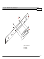
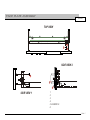
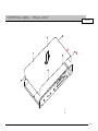
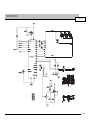
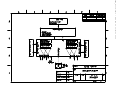
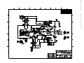
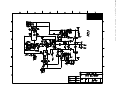
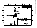
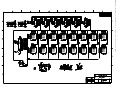
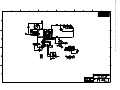
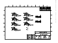
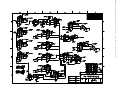
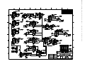
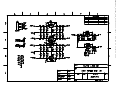
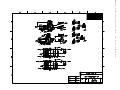
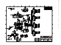
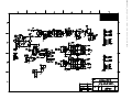
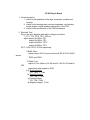
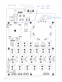
Classé
CP-65
PREAMPLIFIER
SERVICE MANUAL
v 1.0
Index
Mechanical Assembly
PC Boards
Testing Procedures
Diagrams
3
17
30
33
CP-65
MECHANICAL
ASSEMBLY
FACE PLATE ASSEMBLY
CP-65
2
1
M
UT
E
O
O
T
SE
CT
LE
O
UT
UT
T
PU
1
T
PU
2
3
E
AP
R
<
ST
M
O
L
DE
CP
DB
AN
Y
65
1 MS-2347 PHILIPS
2 L1A2XR01
3 L1A3XR02
Classé - 1
FACE PLATE ASSEMBLY
CP-65
TOP VIEW
1
2
3
SIDE VIEW 2
4
5
6
SIDE VIEW 1
1
2
3
4
5 L214XR01-S
6
Classé - 2
CHASSIS REAR VIEW
CP-65
1
2
3
4
5
6
7
8
Classé - 3
CHASSIS
CP-65
TOP VIEW
4
1
3
2
1 PLA CAPFR1
2 HDW #8 FLAT WASHER
3 BZO 8-32x3/4” BHCS
4
Classé - 6
SHIPPING AREA - FINAL ASSY
CP-65
1
2
T1
PU
UT
O
T2
PU
E
UT
M
UT
O
PE
TA
R
O
CT
LE
SE
<
Y
DB
AN
ST
L
DE
O
M
5
-6
CP
1
2
Classé - 9
CP-65
PC BOARDS
MAINBOARD
CP-65
N/A
Classé - 10
CP-65
TESTING
PROCEDURES
START - UP
CP-65
N/A
Classé - 14
CP-65
DIAGRAMS
B2BXR00
CP-65
Classé - 16
CP65_block.sch-1 - Thu Jun 20 11:11:21 2002
B2B7XR03_amp.sch-1 - Thu Jun 20 11:00:56 2002
B2B7XR03_amp.sch-2 - Thu Jun 20 11:01:28 2002
B2B6XR00_IR_input.sch-1 - Thu Jun 20 10:59:40 2002
B2B5XR01_Encoder.sch-1 - Thu Jun 20 10:59:01 2002
B2B4XR01_display_5_button.sch-2 - Thu Jun 20 11:07:05 2002
B2B4XR01_display_5_button.sch-1 - Thu Jun 20 11:08:57 2002
B2b2XR00_line input2.sch-1 - Thu Jun 20 10:56:01 2002
B2B1XR02_mother_PCB_with cs3310.sch-1 - Thu Jun 20 10:51:01 2002
B2B1XR02_mother_PCB_with cs3310.sch-2 - Thu Jun 20 10:51:38 2002
B2B1XR02_mother_PCB_with cs3310.sch-3 - Thu Jun 20 10:53:20 2002
B2B1XR02_mother_PCB_with cs3310.sch-4 - Thu Jun 20 10:54:28 2002
B2B1XR02_mother_PCB_with cs3310.sch-5 - Thu Jun 20 10:55:06 2002
B2B8XR02_ext ps.sch-1 - Thu Jun 20 11:13:08 2002
Classé CP-65 Software Upgrade
This document details the steps to upgrade your CP-65 Preamplifier from
software revision 65-102A47 to CS103B02.
This new release solves the random problem of the unit becoming unstable when
using the unity gain option.
Warning !
Before starting this procedure make sure the unit is shut off and unplugged from
the main A.C. line.
Section 1.0 Removing Main Unit Cover
To remove the cover of the CP-65 main unit simply remove the 8 medium sized
Philips screws and lift off the top cover.
Section 2.0 Replacing the Firmware IC
We have supplied 2 schematic diagrams, Figures 1 and 2, to help you locate the
integrated circuit (IC) that needs to be replaced. Figure 1 shows you the
complete layout of the main unit and a highlighted area in which the firmware
IC (U503) is located.
U503 is located in the center of figure 2 and above C340 and C317 when looking
at the unit with the front panel facing you. The IC is a dual inline package with 28
pins and is placed on the main board with the notch towards the rear panel.
Remove U503 with the supplied chip puller and replace it with the new IC
labeled CS103B02. Make sure you place the new IC with its’ notch facing the
rear of the unit.
Incorrect placement will of U503 will cause your CP-65 not to turn on.
Once you have replaced the IC you should power up the unit to ensure proper
placement and seating. When you have verified proper power up of the unit
you can then shut down the unit and replace the top cover. We have supplied
you with 8 new top cover screws to replace any damaged or marked during this
procedure.
CP-65 Power Supply
1. Visual check:
- check the silkscreen of the chassis
- check scratches
- check for all screws, washers, lock washers, PEM nuts
- check for the polarities of the caps, diodes, missing components,
solder bridges, cold solders, and quality of the PCB
- check for the correct fuse:
F6- .5A
F5- 6DC 2A
F1-F4- 1A
2. Electrical Test:
1. Short pin 1&3 of connector U3 in order to switch the unit
2. Plug the unit. Crank variac to 60 vac. Check the polarities
3. Crank unit to 120 vac full blast.
Measure all voltages as follows:
a) Q8- IN-18 VDC
OUT-14 VDC
R13-13 VDC
b) D1-12 VDC
c) Q1- IN- 27.8 VDC
OUT- 18 VDC
d) Q2- IN- -27.8 VDC
OUT- -18 VDC
e) Q3- IN- 27.8 VDC
OUT- 18 VDC
f) Q4- IN- -27.8 VDC
OUT- -18 VDC
g) V3- PIN#1- 13 VDC
PIN#3- 4.5 VDC (w/ wad)
h) V4- PIN#3- -18 VDC
PIN#1- 18 VDC
i) V6- PIN#3- -18 VDC
PIN#1- 18 VDC
j) V8- PIN#3- -18 VDC
PIN#1- 18 VDC
k) V7- PIN#3- -18 VDC
PIN#1- 18 VDC
4. Set- up for Japan (100 VAC only)
1. remove R6, R9, Q7, Q8 (transistor leave it to the PCB
2. cut the pins of Q8 on the board and short pins 2 & 3
3. measure electrical voltage as follows
a) at 95 Vac
D1- 10.5 VDC
R6- 11.9 VDC
b) at 100 Vac
D1- 11.25 VDC
R6- 12.7 VDC
CP-65 Mother PCB
1. Visual Inspection
1. check for the polarities of the caps, IC’s, transistor sockets,
connectors, relays, and diodes.
2. check for the pads of Q 305 and 306
3. check for missing parts, wrong components, cold solders, solder
bridges, solder splashes, and quality of the PCB
4. PCB’s must be cleaned very well
5. check balance lock if working smoothly and the same appearance
2. Electrical Test:
Plug the unit and measure as follows:
1) U1- PIN#1- 18 VDC
PIN#3 –18 VDC
2) U2- PIN#1- 18 VDC
PIN#3 –18 VDC
3) Relays control power must be 5 VDC
4) Q301- T1- 18 VDC
T2- 15 VDC
5) Q302- T3- -18 VDC
T4- -15 VDC
6) Q 303- T5- 18 VDC
T6 15 VDC
7) Q304- T7- -18 VDC
T8- -15 VDC
8) Q305- IN- 13.3 VDC
OUT- 7.0 VDC
9) Check Signal
CP-65 Plug-In Board
1. Visual Inspection
1. check for the polarities of the caps, transistors, sockets and
trimpots
2. check for the missing parts, wrong components, cold solders,
solder bridges, solder splashes and quality of the PCB
3. check for the modification of the PCB see sample.
2. Electrical Test
Plug in the unit. Measure and adjust voltages as follows:
1. TP1, TP2, TP12, TP11- 200 mv
- adjust trimpot Rv103 for TP1
trimpot Rv102 for TP2
trimpot Rv203 for TP12
trimpot Rv202 for TP11
R113, R102, R213, R 202 respectively
2.BIAS- 25mv
-adjust trimpot Rv101 across resistors R123 & R124, Rv201
across
R223 and R224
3.Offset- 0 mv
-adjust to 0 mv offset on Rv103 and Rv 102, Rv 203 and Rv
202
respectively with respect to GND
4.a) Positive Supply
TP3, Tp10- 1.1 Vdc
b) Negative Supply
TP4, TP9- 1.1 Vdc
c) Positive Supply
TP5, TP8- .5 Vdc
d) Negative Supply- .5 Vdc
CP-65 Panel and Display
1. Visual Inspection:
- check for the quality of the PCB
- check for the orientation of the sockets, x’sistor, polarities, missing
components, solder bridges, cold solder, wrong components
- check the direction of the lightbars of display
- check also the lightbars if they are soldered flat to the PCB
3. Functions:
1. install microchip
2. plug-in unit
3. led of power supply lights green
4. hear relay clicks and led turns red
5. see Classe
• CP 65* on display
•
6. hear relay clicks and unit goes to standby
- green led lights
7. press all the switch buttons one by one and check if switches
are good and corresponds to the selected inputs on display.
8. check volume control if it is working well
9. check all the function in remote control including the programs
such as the display. Off, Unity Gain, and Reset
10. check the vol. On R.C. close and far to the unit
11. check signal
12. Reset the unit
CP-65 Final Testing
1. Visual Inspection
- check the silkscreen of the chassis
- check scratches
- check for all screws, washers, nuts, Pemnuts. Screws must be tight
- check balance lock if working smoothly
- check input/output PCB’s. Left is for Left, right is for Right.
Left PCB- R6, R7 – 33
Right PCB- R1, R2- 33
2. Electrical Test
1) check the polarities of the dc cable
2) plug-in the unit. Test and measure voltages both main and
phono Dc supply of the power supply.
3) Refer to Cp-65 Mother PCB Part 2 Electrical Test Procedure
how to measure the supply voltage of the mother PCB.
4) Readjust the bias. Offset and 200 mv on the plug-in board.
Refer to Part 2 of CP-65 Plug In Board Procedure
3. Display Test and Functions
- refer to Cp-65 Panel and Display Procedure
4. Signal Test
1) Feed input signal 1 KHZ sinewave into input 1. Connect output
to the oscilloscope. Turn the volume up and down. Should see
both outputs. Check for noise and distortion
2) Check the unity gain of Line 1
3) Check the IR in and IR out
4) Check the 12v. trigger
5) Check balance left and right
6) Check mute on and off
7) Reset unit
8) Check back the Line 1 output. Should see output on output 1
and 2, output 1, output 2, both on balance and single ended
outputs but using the remote control
9) Check the phase
10) Repeat steps 1,2,8,9, for inputs 2,3, Tape 1, Tape 2, single
ended and balance inputs
11) Check bal. Outputs: the inverted signal should be the same
level with non-inverted signal, and should be 180 out of phase
with non inverted signal
12) Test output signals at 20 Hz, 100 Hz, 1KHz, 10 KHz, 20 KHZ
and 30 KHz square-wave. Look for noise and distortion
5. Noise Test
1) connect balanced outputs to a power amplifier. Select
line. Turn the volume up and down manually and
listen for the noise and hum with speaker. Do the
same thing in balance, Tape1 and 2
2) repeat step 1 with single ended outputs
3) repeat steps 1 and 2 with remote control
6. Paper Works
1) turn volume up to 15. measure and record the
offset voltages.
2) Measure and record bias voltages
3) Measure and record the difference in right and left
channels. (in dB)
4) Measure and record the gain (in dB)
7. Audio- Precision Test
1) set-up unit to the computer. Volume must be 30
2) load frequency response test and sweep
3) load THD plus N- Freq. Response test
4)
and B must be 0.003%
5) measure noise in dB
8. 1) check the RS232 port
2) reset the unit
3) mark F.T.