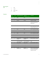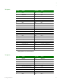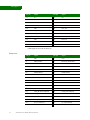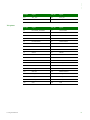
1
NS9210 Processor Module Hardware Reference 90001002_A August 2008 ©2008 Digi International Inc. All rights reserved. Digi, Digi International, the Digi logo, a Digi International Company, Digi JumpStart Kit, ConnectCore, NET+, NET+OS and NET+Works are trademarks or registered trademarks of Digi International, Inc. in the United States and other countries worldwide. All other trademarks are the property of their respective owners. Contents ....................................................................... Customer support .............................................................................. 7 Chapter 1: About the Module .............................. 9 Features and functionality ............................................................10 Module variant ................................................................................10 Module pinout ..........................................................................10 Pinout legend: Type ..........................................................................11 X1 pinout .......................................................................................11 X2 pinout .......................................................................................15 Configuration pins — CPU .............................................................23 Default module CPU configuration .........................................................23 Configuration pins — Module .........................................................24 Identification of the module ................................................................24 Module pin configuration ....................................................................24 Clock generation .......................................................................25 Clock frequencies .............................................................................25 Changing the CPU speed .....................................................................26 Boot process ............................................................................26 Chip selects .............................................................................27 Chip select memory map ....................................................................27 SDRAM banks ............................................................................27 Multiplexed GPIO pins .................................................................27 GPIO multiplex table .........................................................................28 External interrupts ............................................................................32 Interfaces ................................................................................33 10/100 Mbps Ethernet port ..................................................................33 UART ............................................................................................33 SPI ...............................................................................................33 I2C bus ..........................................................................................34 RTC ..............................................................................................34 Power ....................................................................................34 Power supply ...................................................................................34 Internal voltage ...............................................................................34 C h a p t e r 2 : A b o u t t h e D e v e l o p m e n t B o a r d . . . . . . . . . . . . . . . 35 What’s on the development board? ........................................................35 The development board ......................................................................37 User interface ..........................................................................38 Switches and pushbuttons ............................................................39 Reset control, S3 ..............................................................................39 Power switch, S2 ..............................................................................39 User pushbuttons, S6 and S7 ................................................................40 Legend for multi-pin switches ..............................................................40 Module configuration switches, S4 .........................................................40 Wake-up button, S8 ...........................................................................40 Serial Port B MEI configuration switches, S1 ..............................................41 Jumpers ..................................................................................42 Jumper functions ..............................................................................43 Battery and Battery Holder ...........................................................43 4 NS9210 Processor Module Hardware Reference ..... LEDs ...................................................................................... 44 WLAN LED LE7 ................................................................................. 44 Power LEDs, LE3 and LE4 .................................................................... 44 User LEDs, LE5 and LE6 ...................................................................... 44 Serial status LEDs ............................................................................. 45 Status LEDs Serial Port D LEDs .............................................................. 45 Status LEDs Serial Port B LEDs .............................................................. 45 Serial UART ports ...................................................................... 46 Serial port D, RS232 .......................................................................... 46 Serial port A TTL interface ................................................................. 47 Serial port C TTL interface ................................................................. 48 Serial port B, MEI interface ................................................................. 49 I2C interface ........................................................................... 50 I2C header ..................................................................................... 50 I2C digital I/O expansion .................................................................... 50 SPI interface ............................................................................ 52 Pin allocation ................................................................................. 53 Current Measurement Option ........................................................ 54 How the CMO works .......................................................................... 55 JTAG interface ......................................................................... 55 Standard JTAG ARM connector, X13 ....................................................... 56 PoE module connectors - IEEE802.3af .............................................. 56 The PoE module .............................................................................. 57 X9 ............................................................................................... 58 X26 .............................................................................................. 58 POE_GND ....................................................................................... 58 www.digiembedded.com 5 Power Jack, X24 ...............................................................................58 Ethernet interface .....................................................................58 RJ-45 pin allocation, X19 ....................................................................59 LEDs .............................................................................................60 Peripheral (expansion) headers ......................................................60 Peripheral application header, X33 ........................................................61 Module and test connectors ..........................................................62 Module connectors ............................................................................62 Test connectors ...............................................................................62 X10 pinout ......................................................................................63 X11 pinout ......................................................................................63 X20 pinout ......................................................................................64 X21 pinout ......................................................................................65 Appendix A:Specifications ................................................................. 67 Environmental specifications .........................................................67 Mechanical specifications .............................................................67 Safety statements ......................................................................67 Power requirements ...................................................................68 Typical module current / power measurements ..................................69 Typical power save module / JumpStart board current / power consumption measurements 69 Module, top view ..............................................................................70 Module, side view .............................................................................70 Layout recommendation ..............................................................71 Reset and edge sensitive input timing requirements .............................73 Appendix B:Certifications ................................................................. 75 FCC Part 15 Class B ....................................................................75 6 NS9210 Processor Module Hardware Reference ..... This guide provides information about the Digi NS9210 Processor Module embedded core module. Conventions used in this guide This table describes the typographic conventions used in this guide: This convention Is used for italic type Emphasis, new terms, variables, and document titles. monospaced type Filenames, pathnames, and code examples. Digi information .................................................................................. Related documentation For additional documentation, see the Documentation folder under the Digi JumpStart kit Start menu tab. Documentation updates Be aware that if you see differences between the documentation you received in your package and the documentation on the web site, the web site content is the latest version. Customer support To get help with a question or technical problem with this product, or to make comments and recommendations about our products or documentation, use the following contact information: To contact Digi International by Use United States telephone: 1 877 912 3444 International telephone: 1 952 912 3444 Address: Digi International 11001 Bren Road East Minnetonka, MN 55343 U.S.A Web site: www.digiembedded.com www.digiembedded.com 7 8 ConnectCore 9P 9215 Hardware Reference About the Module C H A P T E R 1 T he NS9210 Processor Module is part of the ConnectCore embedded core processor module family. Built on leading Digi technology, the network-enabled ConnectCore 9P family provides a modular and scalable core processor solution that significantly minimizes hardware and software design risk. This module combines superior performance and a complete set of integrated peripherals and component connectivity options in a compact and versatile form factor. The NS9210 Processor Module is built around the NS9215 processor with a powerful ARM926EJ-S core. For further information about the NS9215, see the NS9215 Hardware Reference available through your Digi JumpStart Kit. The embedded module offers 8MB SDRAM and can support a maximum of 64MB SDRAM. The module has also 4MB NOR flash and can support up to a maximum of 16MB NOR flash, a single high speed serial peripheral interface (SPI) module, an I2C interface, UARTs, programmable flexible interface modules (FIMs), ADC, 16-bit data/17-bit address bus (buffered), and 64 shared GPIO signals for application-specific usage. 9 Chapter 1 Features and functionality .................................................................................. Module variant 32-bit NET+ARM (ARM926EJ-S) RISC processor NS9215 @ 150MHz ARM9 core with memory management unit (MMU) 4K data cache/4K instruction cache 8MB SDRAM (can support a maximum of 64MB SDRAM) 4MB NOR Flash (can support a maximum of 16MB NOR flash) 10 general purpose timers; NS9210 Processor Module supports 7 as timer/counters and one quadrature decoder 64 GPIOs signals with up to five different multiplexing schemes (all are on connector X2) Two 80-pin connectors Up to four UARTs One SPI channel, multiplexed on different places Integrated 10/100Mbps Ethernet MAC/PHY I2C interface JTAG signals available on module connector 8 ADC (analog to digital converter) inputs 2x flexible interface modules (FIMs) running at max. 300 MHz, integrated in NS9215 processor 2 LEDs (LE1: green, and LE2:orange) available on module 16-bit data and 17-bit address buses, both are buffered Single +3.3V power supply The NS9210 Processor Module is currently available in standard variants below. Product numbers: Features CC-9P-V502-C 150 MHz CPU speed, 8MB SDRAM, 4 MB NOR flash, RTC, 10/100 Mbps Ethernet CC-9P-V501-C 150 MHz CPU speed, 8MB SDRAM, 2MB NOR flash, RTC, 10/100 Mbps Ethernet29 Module pinout .................................................................................. The module has two 80 pins connectors, X1 and X2. The next tables describe each pin, its properties, and its use on the development board. 10 NS9210 Processor Module Hardware Reference ..... Pinout legend: Type I Input O Output I/O Input or output P Power X1 pinout X1 pin number Type Module functionality Usage on Development board Comments 1 P GND GND 2 P GND GND 3 I RSTIN# RSTIN# 10k pull-up on module 4 O PWRGOOD PWRGOOD Output of the reset controller push pull with 470R current limiting resistor www.digiembedded.com 5 O RSTOUT# RSTOUT# Output of logical AND function between NS9215 RESET_DONE and NS9215 RESET_OUT# 6 I TCK TCK JTAG - 10k pull-up on module 7 I TMS TMS JTAG - 10k pull-up on module 8 I TDI TDI JTAG - 10k pull-up on module 9 O TDO TDO JTAG - 10k pull-up on module 10 I TRST# TRST# JTAG - 2k2 pull-up on module 11 O RTCK RTCK JTAG - Optional 12 I CONF2/OCD_EN# CONF2/OCD_EN# 10k pull-up on module 13 I LITTLE# / BIG ENDIAN LITTLE# / BIG ENDIAN 2k2 series resistor on module 14 I Reserved (WLAN_DISABLE#) Reserved (WLAN_DISABLE#) Low active WLAN Disable signal 15 I SOFT_CONF0 SOFT_CONF0 2k2 series resistor on module 16 I SOFT_CONF1 SOFT_CONF1 2k2 series resistor on module 17 I SOFT_CONF2 SOFT_CONF2 2k2 series resistor on module 18 I SOFT_CONF3 SOFT_CONF3 2k2 series resistor on module 19 O Reserved (WLAN_LED#) Reserved (WLAN_LED#) Active low signal coming from Piper chip. This signal comes directly from the Piper chip without series resistor. 11 Chapter 1 X1 pin number Type Module functionality Usage on Development board 20 P GND GND 21 I/O D0 D0 Comments Buffered Data - only active when either CS0# or CS2# is active NS9215 D[31:16] 12 22 I/O D1 D1 23 I/O D2 D2 24 I/O D3 D3 25 I/O D4 D4 26 I/O D5 D5 27 I/O D6 D6 28 I/O D7 D7 29 I/O D8 D8 30 I/O D9 D9 31 I/O D10 D10 32 I/O D11 D11 33 I/O D12 D12 34 I/O D13 D13 35 I/O D14 D14 36 I/O D15 D15 37 P GND GND 38 O AO AO 39 O A1 A1 40 O A2 A2 41 O A3 A3 42 O A4 A4 43 O A5 A5 44 O A6 A6 45 O A7 A7 46 O A8 A8 47 O A9 A9 48 O A10 A10 49 O A11 A11 50 O A12 A12 NS9210 Processor Module Hardware Reference Buffered Address always active ..... www.digiembedded.com X1 pin number Type Module functionality Usage on Development board Comments 51 O A13 A13 52 O A14 A14 53 O A15 A15 54 O A16 A16 55 O GND GND 56 O EXT_OE# EXT_OE# 57 O EXT_WE# EXT_WE# 58 O CSO# CSO# 59 O CS2# CS2# 60 O BLE# BLE# NS9215 BE2# 61 O BHE# BHE# NS9215 BE3# 62 I EXT_WAIT# EXT_WAIT# 10k pull-up on module 63 O BCLK BCLK Connected over a 22R resistor to NS9215 CLK_OUT1 pin 64 P GND GND 65 I ETH_TPIN ETH_TPIN 66 O ETH_ACTIVITY# ETH_ACTIVITY# 67 I ETH_TPIP ETH_TPIP 68 O ETH_LINK# ETH_LINK 69 O ETH_TPON ETH_TPON 70 O ETH_TROP ETH_TROP 71 P GND GND 72 P Reserved (USB_VBUS) Reserved (USB_VBUS) 73 I Reserved (USB_OC#) Reserved (USB_OC#) 74 I/O Reserved (USB_P) Reserved (USB_P) 75 I/O Reserved (USB_N) Reserved (USB_N) 76 O Reserved (USB_PWREN#) Reserved (USB_PWREN#) 77 I Reserved (USB_OTG_ID) Reserved (USB_OTG_ID) Low active signal with 330R resistor on module Low active signal with 330R resistor on module 13 Chapter 1 X1 pin number Type Module functionality Usage on Development board Comments 78 P VRTC VRTC Backup Battery for RTC, for 3V cell. Can be left floating, if RTC backup not needed. 79 P VLIO VLIO Mobile: Power from Li-Ion Battery (2.5V-5.5V) Non-Mobile: connected to 3.3V 80 14 P GND NS9210 Processor Module Hardware Reference GND ..... X2 pinout X2 pin number Type Module functionality 1 P GND 2 P GND 3 I/O DCDA#/ Usage on Development board Comments DMA0_DONE/ PIC_0_GEN_IO[0] GPIO0/ SPI_EN (dup) 4 I/O CTSA#/ EIRQ0/ PIC_0_GEN_IO[1] GPIO1/ -reserved- 5 I/O DSRA#/ EIRQ1/ PIC_0_GEN_IO[2] GPIO2/ -reserved- 6 I/O RXDA/ DMA0_PDEN/ PIC_0_GEN_IO[3] GPIO3/ SPI_RX (dup) 7 I/O RIA#/ EIRQ2/ Timer6_in/ GPIO4 SPI_CLK (dup)/ 8 I/O RTSA#/ RS485CTLA EIRQ3/ Timer6_Out/ GPIO5/ SPI_CLK (dup)/ 9 I/O DTRA#/ TXCLKA DMA0_REQ/ Timer7_In/ GPIO6/ PIC_DBG_DATA_OUT www.digiembedded.com 15 Chapter 1 X2 pin number Type Module functionality 10 I/O TXDA/ Usage on Development board Comments Timer8_In/ Timer7_Out/ GPIO7/ SPI_TX (dup) 11 I/O DCDC#/ DMA1_DONE/ Timer8_Out/ GPIO8/ SPIB_EN (dup)/ 12 I/O CTSC#/ I2C_SCK/ EIRQ0 (dup)/ GPIO9/ PIC_DBG_DATA_IN 13 I/O DSRC#/ QDCI/ EIRQ1 (dup) GPIO10/ PIC_DBG_CLK 14 I/O RXDC/ DMA1_DP/ EIRQ2 (dup)/ GPIO11/ SPI_RXboot 15 I/O RIC#/ RXCLKC I2C_SDA/ RST_DONE/ GPIO12/ SPI_CLK (dup) 16 I/O RTSC#/ QDCQ/ Ext Timer Event Out Ch 9/ GPIO13/ SPI_CLKboot 17 I/O DTRC#/ TXCLKC DMA1_REQ/ PIC_0_CAN_RXD GPIO14/ SPI_TXDboot 16 NS9210 Processor Module Hardware Reference When booting, NS9215 RIC# signal is default configured as Output, RST_DONE. To avoid input/output conflicts, put a series resistor on this signal if necessary. ..... X2 pin number Type Module functionality 18 I/O TXDC/ Usage on Development board Comments Timer9_In/ PIC_0_CAN_TXD GPIO15/ SPI_ENboot 19 I/O DCDB# (dup)/ PIC_0_BUS_1[8] PIC_1_BUS_1[8] GPIO51/ 20 I/O CTSB# (dup)/ PIC_0_BUS_1[9] PIC_1_BUS_1[9] GPIO52/ 21 I/O DSRB# (dup)/ PIC_0_BUS_1[10] PIC_1_BUS_1[10] GPIO53/ 22 I/O RXDB (dup)/ PIC_0_BUS_1[11] PIC_1_BUS_1[11] GPIO54/ 23 I/O RIB# (dup)/ PIC_0_BUS_1[12] PIC_1_BUS_1[12] GPIO55/ 24 I/O RTSB# (dup) / RS485CTLB (dup) / PIC_0_BUS_1[13] PIC_1_BUS_1[13] GPIO56/ 25 I/O TXCLKB (dup)/ DTRB# (dup) / PIC_0_BUS_1[14] PIC_1_BUS_1[14] GPIO57/ 26 I/O TXDB (dup)/ PIC_0_BUS_1[15] PIC_1_BUS_1[15] GPIO58/ www.digiembedded.com 17 Chapter 1 X2 pin number Type Module functionality 27 I/O DCDD# (dup) / PIC_0_BUS_1[16] PIC_1_BUS_1[16] GPIO59/ 28 I/O CTSD# (dup)/ PIC_0_BUS_1[17] PIC_1_BUS_1[17] GPIO60/ 29 I/O DSRD# (dup)/ PIC_0_BUS_1[18] PIC_1_BUS_1[18] GPIO61/ 30 I/O RXDD (dup)/ PIC_0_BUS_1[19] PIC_1_BUS_1[19] GPIO62/ 31 I/O RID# (dup)/ PIC_0_BUS_1[20] PIC_1_BUS_1[20] GPIO63/ 32 I/O RTSD# (dup) / RS485CTLD(dup) / PIC_0_BUS_1[21] PIC_1_BUS_1[21] GPIO64/ 33 I/O TXCLKD (dup) / DTRD# (dup) / PIC_0_BUS_1[22] PIC_1_BUS_1[22] GPIO65 34 I/O TXDD (dup) / PIC_0_BUS_1[23] PIC_1_BUS_1[23] GPIO66 35 I/O PIC_0_CLK[I] PIC_0_CLK[0] EIRQ3 (dup)/ GPIO67 36 I/O PIC_0_GEN_IO[0] PIC_1_GEN_IO[0] PIC_1_CAN_RXD GPIO68 18 NS9210 Processor Module Hardware Reference Usage on Development board Comments ..... X2 pin number Type Module functionality 37 I/O PIC_0_GEN_IO[1] Usage on Development board Comments PIC_1_GEN_IO[1] PIC_1_CAN_TXD GPIO69 38 I/O PIC_0_GEN_IO[2] PIC_1_GEN_IO[2] PWM0/ GPIO70 39 I/O PIC_0_GEN_IO[3] PIC_1_GEN_IO[3] PWM1/ GPIO71 40 I/O PIC_0_GEN_IO[4] PIC_1_GEN_IO[4] PWM2/ GPIO72 41 I/O PIC_0_GEN_IO[5] PIC_1_GEN_IO[5] PWM3/ GPIO73 42 I/O PIC_0_GEN_IO[6] PIC_1_GEN_IO[6] Timer0_In/ GPIO74 43 I/O PIC_0_GEN_IO[7] PIC_1_GEN_IO[7] Timer1_In/ GPIO75 44 I/O PIC_0_CTL_IO[0] PIC_1_CTL_IO[0] Timer2_In/ GPIO76 45 I/O PIC_0_CTL_IO[1] PIC_1_CTL_IO[1] Timer3_In/ GPIO77 46 I/O PIC_0_CTL_IO[2] PIC_1_CTL_IO[2] Timer4_In/ GPIO78 www.digiembedded.com 19 Chapter 1 X2 pin number Type Module functionality 47 I/O PIC_0_CTL_IO[3] PIC_1_CTL_IO[3] Timer5_In/ GPIO79 48 I/O PIC_0_BUS_0[0] PIC_1_BUS_0[0] Timer6_In (dup)/ GPIO80 49 I/O PIC_0_BUS_0[1] PIC_1_BUS_0[1] Timer7_In (dup)/ GPIO81 50 I/O PIC_0_BUS_0[2] PIC_1_BUS_0[2] Timer8_In (dup)/ GPIO82 51 I/O PIC_0_BUS_0[3] PIC_1_BUS_0[3] Timer9_In (dup)/ GPIO83 52 I/O PIC_0_BUS_0[4] PIC_1_BUS_0[4] Timer0_Out/ GPIO84 53 I/O PIC_0_BUS_0[5] PIC_1_BUS_0[5] Timer1_Out/ GPIO85 54 I/O PIC_0_BUS_0[6] PIC_1_BUS_0[6] Timer2_Out/ GPIO86 55 I/O PIC_0_BUS_0[7] PIC_1_BUS_0[7] Timer3_Out/ GPIO87 56 I/O PIC_0_BUS_0[13]/ PIC_1_BUS_0[13]/ Timer9_Out (dup)/ GPIO93 20 NS9210 Processor Module Hardware Reference Usage on Development board Comments ..... X2 pin number Type Module functionality 57 I/O PIC_0_BUS_0[14]/ Usage on Development board Comments PIC_1_BUS_0[14]/ QDCI (dup)/ GPIO94 58 I/O PIC_0_BUS_0[15]/ PIC_1_BUS_0[15]/ QDCQ (dup)/ GPIO95 59 I/O PIC_0_BUS_1[0]/ PIC_1_BUS_1[0]/ PIC_0_CAN_RXD GPIO96 60 I/O PIC_0_BUS_1[1]/ PIC_1_BUS_1[1]/ PIC_0_CAN_TXD GPIO97 61 I/O PIC_0_BUS_1[2]/ PIC_1_BUS_1[2]/ PIC_1_CAN_RXD GPIO98 62 I/O PIC_0_BUS_1[3]/ PIC_1_BUS_1[3]/ PIC_1_CAN_TXD GPIO99 63 I/O PIC_0_BUS_1[4]/ PIC_1_BUS_1[4]/ PWM4/ GPIO100 64 I/O PIC_0_BUS_1[5]/ PIC_1_BUS_1[5]/ EIRQ3/ GPIO101 65 I/O PIC_0_BUS_1[6]/ 4k7 pull-up on module PIC_1_BUS_1[6]/ I2C_SCL (dup)/ GPIO102 66 I/O PIC_0_BUS_1[7]/ 4k7 pull-up on module PIC_1_BUS_1[7]/ I2C_SDA (dup)/ GPIO103 www.digiembedded.com 21 Chapter 1 X2 pin number Type Module functionality 67 I VIN0_ADC 68 I VIN1_ADC 69 I VIN2_ADC 70 I VIN3_ADC 71 I VIN4_ADC 72 I VIN5_ADC 73 I VIN6_ADC 74 I VIN7_ADC 75 P VSS_ADC Connected on module to AGND through 0Ω resistor 76 P VREF_ADC 100nF decoupling capacitor between VREF_ADC and VSS_ADC 77 P 3.3V 78 P 3.3V 79 P GND 80 P GND 22 NS9210 Processor Module Hardware Reference Usage on Development board Comments ..... Configuration pins — CPU .................................................................................. None of the 64 GPIO pins on connector X2 disturb CPU boot strap functions. The boot strap functions are controlled by address signals; the user can not disturb boot strap functions from outside, if the module configuration signals, described below, are correctly configured. Default module CPU configuration www.digiembedded.com The user has access to six configuration signals: LITTLE#/BIG_ ENDIAN which allows the user to select the endianess of the module OCD_EN# which allows the user to activate on-chip debugging SW_CONF [3:0] which are reserved for the user; the user software can read out these signals through the GEN ID register (@ 0xA090_0210). 23 Chapter 1 Configuration pins — Module .................................................................................. The NS9210 Processor Module supports the following JTAG signals: TCK, TMS, TDI, TDO, TRST#, and RTCK. Selection can be made between ARM debug mode and boundary scan mode with the signal OCD_EN#. Identification of the module In order to make it easier for software to recognize a module and especially a hardware variant of the module, a specific bit field made of 4-bits has been reserved on the module. This bit field can be read out through GEN ID register and correspond to A[12:9]. These configuration signals use the internal CPU pull-up resistor and can be pulled down through external population option 2k2 resistors. In the same way, 3 bits have been available on the module to identify the SDRAM configuration scheme. This bits correspond to A[19:17]. It is impossible for the user to disturb either the variant specific or SDRAM configuration specific bits from outside. The NS9210 Processor Module has also available 4-bit for platform identification. This bit field can be read out through GEN ID register and correspond to A[16:13]. Configuration of these signals is done through the SW_CONF pins. SW_CONF0 is connected to A13 through a 2k2 series resistor, and so on for the further SW_CONF pins. So this bit can be set high by leaving the corresponding SW_CONF pin unconnected and set low by connecting the corresponding SW_CONF pin directly low. The user can benefit from these pins to support application or platform specific software configurations. Module pin configuration Signal name Function PU/PD LITTLE#/BIG_ Set module endianess. 0 module PU ENDIAN boots in little endian mode. 1 module boots in big endian mode. OCD_EN# JTAG / Boundary scan function select 0 1 SW_CONF0 24 Comment Signal LITTLE#/BIG_ENDIAN is connected to GPIO_A3/A27 through a 2k2 series resistor. PU 10K ARM debug mode, BISTEN# set to high Boundary scan mode, BISTEN# set to low User-defined software configuration pin; can be read in GEN_ID register bit 4, default high NS9210 Processor Module Hardware Reference Connected to A13 through a 2k2 series resistor. Read bit 4 of GEN ID register (@ 0xA0900210). ..... Signal name Function PU/PD Comment SW_CONF1 User-defined software configuration pin; can be read in GEN ID register bit 5, default high Connected to A14 through a 2k2 series resistor.Read bit 5 of GEN ID register (@ 0xA0900210). SW_CONF2 User-defined software configuration pin; can be read in GEN ID register bit 6, default high Connected to A15 through a 2k2 series resistor. Read bit 6 of GEN ID register (@ 0xA0900210). SW_CONF3 User-defined software configuration pin; can be read in GEN ID register bit 7, default high Connected to A16 through a 2k2 series resistor. Read bit 7 of GEN ID register (@ 0xA0900210). Clock generation .................................................................................. Clock frequencies Hardware strapping determines the initial powerup PLL settings. The table below summarizes the default clock frequencies for the NS9210 Processor Module: Hardware strapping: "PLL reference clock divider setting: A[4:0] = 0x1D (0b11101) NR = 5 "PLL output divider setting: A[6:5] = 0x3 (0b11) OD = 0 "PLL bypass setting: A[7] = 0x1 (0b1) Normal operation PLL frequency formula: PLL Vco = (RefClk / NR+1) * (NF+1) ClkOut = PLL Vco / (OD+1) RefClk (Crystal) = 29.4912MHz NF = 0x3C (reset value - can only be changed by software). PLL Vco = (29.4912 / 6) * 61 = 299.8272 MHz ClkOut = 299.8272 MHz Resulting clock settings: PIC clock = 299.8272 MHz www.digiembedded.com 25 Chapter 1 CPU clock = 299.8272 MHz / 2 = 149.9136 MHz AHB clock = 149.9136 MHz / 2 = 74.9568 MHz Changing the CPU speed After powerup, software can change the PLL settings by writing to the PLL configuration register (@ 0xA090_0188) Important: When PLL parameters are changed, a reset is provided for the PLL to stabilize. Applications using this feature need to be aware the SDRAM contents will be lost. See reset behavior in the table below. Reset Behavior RESET _n pin SRESET _n pin PLL Config Reg. Update Watchdog Time-Out Reset SPI boot YES YES YES YES Strapping PLL YES NO NO NO Other strappings (Endianess) YES NO NO NO GPIO configuration YES NO NO NO Other (ASIC) registers YES YES YES YES SDRAM keeps its contents NO YES NO YES Boot process .................................................................................. The NS9210 Processor Module boots directly from NOR flash. The start-up code is located at address 0x00000000 during the boot process. When the system is booted, the SDRAM is remapped to address 0x00000000 and Nor Flash to 0x50000000 by modifying the address map in the AHB decoder. 26 NS9210 Processor Module Hardware Reference ..... Chip selects .................................................................................. The module has eight chip selects: four for dynamic memory and four for static memory. Each chip select has a 256MB range. Chip select memory map Name CPU Sig. name Pin Address range Size [Mb] Usage Comments SDM_CS0# CS1# D6 0x00000000– 0x0FFFFFFF 256 SDRAM bank 0 First bank on module SDM_CS1# CS3# B5 0x10000000– 0x1FFFFFFF 256 not used SDM_CS2# CS5# A4 0x20000000– 0x2FFFFFFF 256 not used SDM_CS3# CS7# B4 0x30000000– 0x3FFFFFFF 256 not used EXT_CS0# CS0# C6 0x40000000– 0x4FFFFFFF 256 external, CS0# INT_CS1# CS2# B6 0x50000000– 0x5FFFFFFFF 256 NOR-Flash EXT_CS2# CS4# C5 0x60000000– 0x6FFFFFFFF 256 external, CS2# INT_CS3# CS6# A3 0x70000000– 0x7FFFFFFF 256 internal, CS3# Program memory on module Reserved for internal usage SDRAM banks .................................................................................. The module provides connection to 1 SDRAM chip, connected to CS1# (SDM_CS0#). The other SDRAM chip selects are not used. The standard module has one of these SDRAM onboard: 1Mx16x4-banks. A13 is the highest address connected. BA0 and BA1 are connected to A21 and A22, respectively. Multiplexed GPIO pins .................................................................................. The 64 GPIOs pins available on the module connector are multiplexed with other functions like: www.digiembedded.com 27 Chapter 1 Pin notes GPIO multiplex table UART SPI Ethernet DMA I2C port Timers and interrupt inputs Memory bus data GPIO [15:0] allow five multiplex modes. GPIO [103:16] and GPIO_A [3:0] have four multiplex modes. Using a pin as GPIO means always to give up other functionalities. Some functions are duplicated to enhance the chance to use them without giving up other vital functions. Using original and (dup) functions in parallel is not recommended. Default function of GPIOs after CPU power up is function 03, except GPIO12 (function 02-reset_done) and GPIO [31:16] (function 00 - DATA[15:0]). In the GPIO multiplex table below, the default function is written bold, # means low active signal, (dup) means function is available multiple times. Port name, Function 03 Alternate function 00 Alternate function 01 Alternate function 02 Alternate function 04 (only GPIO00...GPIO15) On module, default used as GPIO0 DCDA# DMA0_DONE PIC_0_GEN_IO[0] SPI_EN# (dup) DCDA# / SPI_EN# GPIO1 CTSA# EIRQ0 PIC_0_GEN_IO[1] Reserved CTSA# GPIO2 DSRA# EIRQ1 PIC_0_GEN_IO[2] Reserved DSRA# GPIO3 RXDA# DMA0_PDEN PIC_0_GEN_IO[3] SPI_RXD (dup) RXDA / SPI_RXD GPIO4 RIA# EIRQ2 Timer6_In SPI_CLK (dup) RIA# / SPI_CLK GPIO5 RTSA# / 485CTLA EIRQ3 Timer6_Out SPI_CLK (dup) RTSA# GPIO6 TXCLKA / DTRA# DMA0_REQ Timer7_In PIC_DBG_DATA_OUT DTRA# GPIO7 TXDA Timer8_In Timer7_Out SPI_TXD (dup) TXDA / SPI_TXD GPIO8 DCDC# / TXCLKC DMA1_DONE Timer8_Out SPI_EN# (dup) DCDC# GPIO9 CTSC# I2C_SCL EIRQ0 (dup) PIC_DBG_DATA_IN CTSC# GPIO10 DSRC# QDCI EIRQ1 (dup) PIC_DBG_CLK DSRC# 28 NS9210 Processor Module Hardware Reference ..... Port name, Function 03 Alternate function 00 Alternate function 01 Alternate function 02 Alternate function 04 (only GPIO00...GPIO15) On module, default used as GPIO11 RXDC# DMA1_PDEN EIRQ2 (dup) SPI_RXD (boot) RXDC GPIO12 RXCLKC / RIC# I2C_SDA RESET_DONE SPI_CLK (dup) RIC# 1 GPIO13 RXCLKC / RTSC# /485CTLC QDCQ Reserved SPI_CLK (boot) RXCLKC / RTSC# GPIO14 TXCLKC / DTRC# DMA1_REQ PIC_0_CAN_RXD SPI_TXD (boot) TXCLKC GPIO15 TXDC Timer9_In PIC_0_CAN_TXD SPI_EN# (boot) TXDC GPIO16 D0 DCDB# EIRQ0 (dup) Reserved for upper data lines GPIO17 D1 CTSB# EIRQ1 (dup) Reserved for upper data lines GPIO18 D2 DSRB# EIRQ2 (dup) Reserved for upper data lines GPIO19 D3 RXDB EIRQ3 (dup) Reserved for upper data lines GPIO20 D4 RIB# DMA0_DONE (dup) Reserved for upper data lines GPIO21 D5 RTSB# / 485CTLB DMA0_PDEN (dup) Reserved for upper data lines GPIO22 D6 TXCLKB / DTRB# DMA1_DONE (dup) Reserved for upper data lines GPIO23 D7 TXDB PIC_1_CAN_RXD Reserved for upper data lines GPIO24 D8 DCDD# PIC_1_CAN_TXD Reserved for upper data lines GPIO25 D9 CTSD# RESET_DONE (dup) Reserved for upper data lines GPIO26 D10 DSRD# PIC_1_GEN_IO[0] Reserved for upper data lines GPIO27 D11 RXDD PIC_1_GEN_IO[1] Reserved for upper data lines GPIO28 D12 RID# PIC_1_GEN_IO[2] Reserved for upper data lines GPIO29 D13 RTSD# / 485CTLD PIC_1_GEN_IO[3] Reserved for upper data lines GPIO30 D14 TXCLKD / DTRD# Reserved Reserved for upper data lines www.digiembedded.com 29 Chapter 1 Port name, Function 03 Alternate function 00 Alternate function 01 Alternate function 02 GPIO31 D15 TXDD Reserved Reserved for upper data lines GPIO32 MII_MDC PIC_0_GEN_IO[0] Reserved MII Interface GPIO33 MII_TXC PIC_0_GEN_IO[1] Reserved MII Interface GPIO34 MII_RXC PIC_0_GEN_IO[2] Reserved MII Interface GPIO35 MII_MDIO PIC_0_GEN_IO[3] Reserved MII Interface GPIO36 MII_RXDV PIC_0_GEN_IO[4] Reserved MII Interface GPIO37 MII_RXER PIC_0_GEN_IO[5] Reserved MII Interface GPIO38 MII_RXD0 PIC_0_GEN_IO[6] Reserved MII Interface GPIO39 MII_RXD1 PIC_0_GEN_IO[7] Reserved MII Interface GPIO40 MII_RXD2 PIC_1_GEN_IO[0] Reserved MII Interface GPIO41 MII_RXD3 PIC_1_GEN_IO[1] Reserved MII Interface GPIO42 MII_TXEN PIC_1_GEN_IO[2] Reserved MII Interface GPIO43 MII_TXER PIC_1_GEN_IO[3] Reserved MII Interface GPIO44 MII_TXD0 PIC_1_GEN_IO[4] Reserved MII Interface GPIO45 MII_TXD1 PIC_1_GEN_IO[5] Reserved MII Interface GPIO46 MII_TXD2 PIC_1_GEN_IO[6] Reserved MII Interface GPIO47 MII_TXD3 PIC_1_GEN_IO[7] Reserved MII Interface GPIO48 MII_COL Reserved Reserved MII Interface GPIO49 MII_CRS Reserved Reserved MII Interface GPIO50 MII_PHY_Int PIC_1_CLK (I) PIC_1_CLK(0) MII Interface GPIO51 DCDB# (dup) PIC_0_BUS_1[8] PIC_1_BUS_1[8] DCDB# GPIO52 CTSB# (dup) PIC_0_BUS_1[9] PIC_1_BUS_1[9] CTSB# GPIO53 DSRB# (dup) PIC_0_BUS_1[10] PIC_1_BUS_1[10] DSRB# GPIO54 RXDB (dup) PIC_0_BUS_1[11] PIC_1_BUS_1[11] RXDB GPIO55 RIB# (dup) PIC_0_BUS_1[12] PIC_1_BUS_1[12] RIB# GPIO56 RTSB# / 485CTLB (dup) PIC_0_BUS_1[13] PIC_1_BUS_1[13] RTSB# GPIO57 TXCLKB (dup) / DTRB# (dup) PIC_0_BUS_1[14] PIC_1_BUS_1[14] DTRB# GPIO58 TXDB (dup) PIC_0_BUS_1[15] PIC_1_BUS_1[15] TXDB GPIO59 DCDD# (dup) PIC_0_BUS_1[16] PIC_1_BUS_1[16] DCDD# GPIO60 CTSD# (dup) PIC_0_BUS_1[17] PIC_1_BUS_1[17] CTSD# 30 NS9210 Processor Module Hardware Reference Alternate function 04 (only GPIO00...GPIO15) On module, default used as ..... Port name, Function 03 Alternate function 00 Alternate function 01 Alternate function 02 GPIO61 DSRD# (dup) PIC_0_BUS_1[18] PIC_1_BUS_1[18] DSRD# GPIO62 RXDD (dup) PIC_0_BUS_1[19] PIC_1_BUS_1[19] RXDD GPIO63 RID# (dup) PIC_0_BUS_1[20] PIC_1_BUS_1[20] RID# GPIO64 RTSD# / 485CTLD (dup) PIC_0_BUS_1[21] PIC_1_BUS_1[21] RTSD# TXCLKD (dup) / PIC_0_BUS_1[22] PIC_1_BUS_1[22] DTRD# GPIO65 Alternate function 04 (only GPIO00...GPIO15) On module, default used as DTRD# (dup) GPIO66 TXDD (dup) PIC_0_BUS_1[23] PIC_1_BUS_1[23] TXDD GPIO67 PIC_0_CLK (I) PIC_0_CLK (O) EIRQ3 (dup) PIC_0_CLK GPIO68 PIC_0_GEN_IO[0] PIC_1_GEN_IO[0] PIC_1_CAN_RXD PIC_0_GEN_IO[0] GPIO69 PIC_0_GEN_IO[1] PIC_1_GEN_IO[1] PIC_1_CAN_TXD PIC_0_GEN_IO[1] GPIO70 PIC_0_GEN_IO[2] PIC_1_GEN_IO[2] PWM0 PIC_0_GEN_IO[2] GPIO71 PIC_0_GEN_IO[3] PIC_1_GEN_IO[3] PWM1 PIC_0_GEN_IO[3] GPIO72 PIC_0_GEN_IO[4] PIC_1_GEN_IO[4] PWM2 PIC_0_GEN_IO[4] GPIO73 PIC_0_GEN_IO[5] PIC_1_GEN_IO[5] PWM3 PIC_0_GEN_IO[5] GPIO74 PIC_0_GEN_IO[6] PIC_1_GEN_IO[6] Timer0_In PIC_0_GEN_IO[6] GPIO75 PIC_0_GEN_IO[7] PIC_1_GEN_IO[7] Timer1_In PIC_0_GEN_IO[7] GPIO76 PIC_0_CTL_IO[0] PIC_1_CTL_IO[0] Timer2_In PIC_0_CTL_IO[0] GPIO77 PIC_0_CTL_IO[1] PIC_1_CTL_IO[1] Timer3_In PIC_0_CTL_IO[1] GPIO78 PIC_0_CTL_IO[2] PIC_1_CTL_IO[2] Timer4_In PIC_0_CTL_IO[2] GPIO79 PIC_0_CTL_IO[3] PIC_1_CTL_IO[3] Timer5_In PIC_0_CTL_IO[3] GPIO80 PIC_0_BUS_0[0] PIC_1_BUS_0[0] Timer6_In (dup) Timer6_In GPIO81 PIC_0_BUS_0[1] PIC_1_BUS_0[1] Timer7_In (dup) Timer7_In GPIO82 PIC_0_BUS_0[2] PIC_1_BUS_0[2] Timer8_In (dup) Timer8_In GPIO83 PIC_0_BUS_0[3] PIC_1_BUS_0[3] Timer9_In (dup) Timer9_In GPIO84 PIC_0_BUS_0[4] PIC_1_BUS_0[4] Timer0_Out Timer0_Out GPIO85 PIC_0_BUS_0[5] PIC_1_BUS_0[5] Timer1_Out Timer1_Out GPIO86 PIC_0_BUS_0[6] PIC_1_BUS_0[6] Timer2_Out Timer2_Out GPIO87 PIC_0_BUS_0[7] PIC_1_BUS_0[7] Timer3_Out Timer3_Out GPIO88 PIC_0_BUS_0[8] PIC_1_BUS_0[8] Timer4_Out Reserved for module LEDs GPIO89 PIC_0_BUS_0[9] PIC_1_BUS_0[9] Timer5_Out Reserved for module LEDs www.digiembedded.com 31 Chapter 1 Port name, Function 03 Alternate function 00 Alternate function 01 Alternate function 02 Alternate function 04 (only GPIO00...GPIO15) On module, default used as GPIO90 PIC_0_BUS_0[10] PIC_1_BUS_0[10] Timer6_Out (dup) GPIO reserved on module GPIO91 PIC_0_BUS_0[11] PIC_1_BUS_0[11] Timer7_Out (dup) Reserved NAND_R/B# GPIO92 PIC_0_BUS_0[12] PIC_1_BUS_0[12] Timer8_Out (dup) GPIO reserved on module GPIO93 PIC_0_BUS_0[13] PIC_1_BUS_0[13] Timer9_Out (dup) Timer9_Out GPIO94 PIC_0_BUS_0[14] PIC_1_BUS_0[14] QDCI (dup) QDCI GPIO95 PIC_0_BUS_0[15] PIC_1_BUS_0[15] QDCQ (dup) QDCQ GPIO96 PIC_0_BUS_1[0] PIC_1_BUS_1[0] PIC_0_CAN_RXD PIC_0_CAN_RXD GPIO97 PIC_0_BUS_1[1] PIC_1_BUS_1[1] PIC_0_CAN_TXD PIC_0_CAN_TXD GPIO98 PIC_0_BUS_1[2] PIC_1_BUS_1[2] PIC_1_CAN_RXD PIC_1_CAN_RXD GPIO99 PIC_0_BUS_1[3] PIC_1_BUS_1[3] PIC_1_CAN_TXD PIC_1_CAN_TXD GPIO100 PIC_0_BUS_1[4] PIC_1_BUS_1[4] PWM4 PWM4 GPIO101 PIC_0_BUS_1[5] PIC_1_BUS_1[5] EIRQ3 EIRQ3 GPIO102 PIC_0_BUS_1[6] PIC_1_BUS_1[6] I2C_SCL (dup) I2C_SCL GPIO103 PIC_0_BUS_1[7] PIC_1_BUS_1[7] I2C_SDA (dup) I2C_SDA GPIO_A0 A24 I2C_SCL dupe EIRQ0 (dup) Reserved EIRQ0 - Piper GPIO_A1 A25 I2C_SDA dupe EIRQ1 (dup) Reserved EIRQ1 - USB GPIO_A2 A26 CS0_WE# EIRQ2 (dup) GPIO reserved on module GPIO_A3 A27 CS0_OE# UART_REFCLK Little/Big Endian 1 Put a series resistor on the baseboard in this case to avoid input/output conflict between RESET_DONE (output/boot default) and RIC# (input/configuration default). External interrupts The NS9210 Processor Module provides access to four external interrupts signals, which are multiplexed with other functions on the GPIO pins. Every interrupt is multiplexed to two or three different GPIO pins. These duplicate signals are marked as (dup) in the GPIO table. External interrupt GPIO multiplexing Other functions, 1st position EIRQ0 GPIO1 X2.4 GPIO9 X2.12 GPIO2 X2.5 GPIO10 X2.13 EIRQ1 32 NS9210 Processor Module Hardware Reference Comments ..... External interrupt GPIO multiplexing Other functions, 1st position EIRQ2 GPIO4 X2.7 GPIO11 X2.14 GPIO5 X2.8 GPIO67 X2.35 GPIO101 X2.64 EIRQ3 Comments EIRQ3# is used on the development board to implement I²C I/O expander interrupt functionality. Interfaces .................................................................................. 10/100 Mbps Ethernet port The NS9215 10/100 Mbps Ethernet MAC allows a glueless connection of a 3.3V MII PHY chip that generates the physical Ethernet signals. The module has a MII PHY chip (ICS ICS1893BKILFT) in a 56-pin QFN package on board. By default, the module does not have a transformer or Ethernet connector; the base board must provide these parts. However, it's possible to populate a specific RJ45 connector with magnetics on the module. The appropriate RJ-45 is Midcom MIC2412A5108W-LF3. A PHY clock of 25 MHz is generated in the PHY chip with a 25 MHz crystal. GPIO90 is controlling the PHY RESET# signal. This GPIO has a 2k2 pull-down resistor to GND populated on the module. GPIO90 must be asserted high before PHY can be used. When not used, the PHY can be put in low-power mode by asserting GPIO90 low. The PHY address on the MII bus is 0x7 (0b00111). The module does not only provide access to the Ethernet signals coming out of the PHY, but supports also two status LEDs: ETH_ACTIVITY# and ETH_LINK#. UART The module provides up to four UART ports with all handshake signals, used in asynchronous mode: Port A = GPIOO through GPIO7 Port B = GPIO51 through GPIO58 Port C = GPIO8 through GPIO15 Port D = GPIO59 through GPIO66 The module supports baud rates up to 1.8432 Mbps in asynchronous mode. Each UART has a 64-byte TX and RX FIFO available. SPI www.digiembedded.com The module provides one SPI port which can be used in either master or slave mode. 33 Chapter 1 Master: 33.33 Mbps Slave: 7.50 Mbps The SPI module is made of four signals: RXD, TXD, CLK and CS# The I2C bus is completely free on the module - no EEPROM and no RTC - since the RTC is in the processor. I 2 C bus The I²C clock is max 400kHz. I2C signals are provided on the module with 4k7 pull-up resistors. The RTC is integrated in the processor and has its own 32.768 KHz clock crystal. RTC When powered by VBAT, RTC unit will function until VBAT (X1.78) reaches a threshold of 2.3 - 2.4V - then the internal unit switches off. The battery current without +3.3V power applied is up to 40µA. The current is used to power the RTC, 32.768kHz oscillator and 64-byte internal RAM. When the development board ships from the factory the battery is disabled. To enable the battery, place a jumper on the development board at J2. Power .................................................................................. Power supply The module has +3.3V and VLIO supply pins. VLIO can be connected either to a Li-Ion battery (2.5V - 5.5V) in a mobile application, or it can be connected directly to +3.3V. Connecting VLIO to a battery causes efficiency to be gained without an additional voltage regulator. Internal voltage 34 The internal 1.8V core voltage is generated through a high-efficiency synchronous step-down converter, which uses VLIO as input voltage. The core voltage regulator can provide up to 600mA. NS9210 Processor Module Hardware Reference About the Development Board C H A P T E R 2 T he NS9210 Processor Module Development board supports the NS9210 Processor Module. This chapter describes the components of the development board and explains how to configure the board for your requirements. The development board has two 4x20 pin connectors that are 1:1 copies of the module pins. What’s on the development board? RJ-45 Ethernet connector 2 x RP-SMA antenna connectors (reserved for future use) Four serial interface connectors: 1 x UART B MEI (RS232/RS4xx) with status LEDs on SUB-D 9-pin connector (X6) 1 x UART D RS232 with status LEDs, on SUB-D 9-pin connector (X3) 1 x UART C with TTL levels shared with HDLC signals on 10-pin header (X5) 1 x UART A with TTL levels shared with SPI signals on 10-pin header (X4) ADC, SPI, and I2C headers JTAG connector Peripheral application header Including access to 16-bit data/10-bit address bus signals Headers with 1:1 copies of the module pins (X1/X2) Two user pushbuttons, two user LEDs, wake-up button Eight-position configuration dip switches Four each for hardware/software configuration GPIO screw-flange connector 35 Chapter 2 36 +9/30VDC power supply Current measurement option Development board + Module, and module alone 3.3V coincell battery with socket PoE connectors for optional application kit (IEEE 802.3af) Prototyping area (15 x 28 holes) with +3.3V and GND connections NS9210 Processor Module Hardware Reference ..... The development board www.digiembedded.com 37 Chapter 2 User interface .................................................................................. The NS9210 Processor Module Development board implements two user buttons and two user LEDs in addition to those provided on the module. The user LEDs on the development board can be enabled or disabled by correctly setting jumper J5&6. The table below shows which NS9215 GPIO is available for implementing the user interface. 38 Signal name GPIO used Comments USER_BUTTON1 GPIO81 10k pull-up to +3.3V on the development board USER_LED1# GPIO82 USER_BUTTON2 GPIO84 USER_LED2# GPIO85 NS9210 Processor Module Hardware Reference 10k pull-up to +3.3V on the development board ..... Switches and pushbuttons .................................................................................. Configuration switch, S4 Power Switch, S2 Reset button S3 Serial Port B (MEI) configuration switch S1 Wake Up button S8 User Button 1 S6 User Button 2 S7 Reset control, S3 The reset pushbutton, S3, resets the module. On the module, RSTOUT# and PWRGOOD are produced for peripherals. A pushbutton allows manual reset by connecting RSTIN# to ground. The reset controller is located on the NS9210 Processor Module. Power switch, S2 The development board has an ON/OFF switch, S2. The power switch S2 can switch both 9V-30V input power supply and 12V coming out of the PoE module. However, if a power plug is connected in the DC power jack, the PoE module is disabled. www.digiembedded.com 39 Chapter 2 User pushbuttons, S6 and S7 Use the user pushbuttons to interact with the applications running on the NS9210 Processor Module. Use these module signals to implement the pushbuttons: Signal name Switch (pushbutton) GPIO used USER_PUSH_BUTTON_1 S6 GPIO81 USER_PUSH_BUTTON_2 S7 GPIO84 Legend for multipin switches Switches 1 and 4 are multi-pin switches. In the description tables for these switches, the pin is designated as S[switch number].[pin number]. For example, pin 1 in switch 4 is specified as S4.1. Module configuration switches, S4 Use S4 to configure the module: Switch pin Function S4.1 On = Little endian Off = Big endian S4.2 Not used S4.3 On = ARM Debug Off = Boundary Scan Wake-up button, S8 40 S4.4 Not used S4.5 – S4.8 Not defined. Software configuration signals, which can be available for user specific configuration. The wake-up pushbutton, S8, generates an external interrupt to the module's NS9215 processor using the EIRQ2 signal. NS9210 Processor Module Hardware Reference ..... Serial Port B MEI configuration switches, S1 Use S1 to configure the line interface for serial port B MEI: Switch pin Function S1.1 On = RS232 transceiver enabled RS422/RS485 transceivers disabled Off = RS232 transceiver disabled RS422/RS485 transceivers enabled S1.2 On = Auto Power Down enabled Off = Auto Power Down disabled S1.3 Comments Auto Power Down is not supported on this board. This signal is only accessible to permit the user to completely disabled the MEI interface for using the signals for other purposes. To disable the MEI interface, go in RS232 mode (S1.1 = ON) and activate the Auto Power Down feature (S1.2 = ON) - be sure that no cable is connected to connector X3. On = 2-wire interface (RS422/RS485) Off = 4-wire interface (RS422) S1.4 On = Termination on Off = No termination www.digiembedded.com 41 Chapter 2 Jumpers .................................................................................. Battery Jumper J2 Serial Port D transceiver Jumper J1 User LED1 Jumper J5 User LED2 Jumper J4 42 NS9210 Processor Module Hardware Reference WLAN Jumper J3 ..... Jumper functions Jump er Name If connection made Default J1 Enable transceiver This jumper allows to disable the console RS232 transceiver. Connection made = console active J2 Battery enable Supplies the real time clock with 3V from the battery (lithium coin cell battery, G1) even if the board is switched off. This is for keeping time in the RTC. Connection not made = Backup battery disabled J3 WLAN_DISABLE# Reserved for future use. Connection made = WLAN disabled Disables the WiFi unit on the module. J4 USER_LED2# Enables User LED2 (LE6) to show the status of this signal (lit if low). Connection made = User LED2 enabled J5 USER_LED1# Enables User LED1 (LE5) to show the status of this signal (lit if low). Connection made = User LED1 enabled Battery and Battery Holder .................................................................................. www.digiembedded.com Battery Holder Battery Coin-Cell Holder for CR2477 Battery, THT Lithium coin cell, CR2477, 24mm, 950mAh Keystone 1025-7 Panasonic CR2477 Ettinger 15.61.252 Renata CR2477N 43 Chapter 2 LEDs .................................................................................. Power LED 9-30V, LE3 Power LED +3.3V, LE4 WLAN LED LE7 Serial Port D status LEDs Serial Port B status (MEI) LEDs User LED2, LE6 User LED1, LE5 WLAN LED LE7 Reserved for future use. Power LEDs, LE3 and LE4 The power LEDs are all red LEDs. These power supplies must be present and cannot be switched. User LEDs, LE5 and LE6 44 LE3 ON indicates the +9VDC / +30VDC power is present. LE4 ON indicates the +3.3VDC power is present. The user LEDs are controlled through applications running on the NS9210 Processor Module, if J5 and J4 are set. Use these module signals to implement the LEDs: NS9210 Processor Module Hardware Reference ..... Serial status LEDs Status LEDs Serial Port D LEDs Signal name LED GPIO used USER_LED1# LE5 GPIO82 USER_LED2# LE6 GPIO85 The development board has two sets of serial port LEDs — four for serial port D and eight for serial port B. The LEDs are connected to the TTL side of the RS232 or RS422/485 transceivers. Green means corresponding signal high. Red means corresponding signal low. The intensity and color of the LED will change when the voltage is switching. LED reference Function RED GREEN LE60 LE45 CTSD#/GPIO60 LE61 LE46 RTSD#/GPIO64 LE62 LE47 RXDD/GPIO62 LE63 LE48 TXDD/GPIO66 Status LEDs Serial Port B LEDs LED reference www.digiembedded.com Function RED GREEN LE64 LE49 DCDB#/GPIO51 LE65 LE50 RIB#/GPIO55 LE66 LE51 DSRB#/GPIO53 LE67 LE52 DTRB#/GPIO57 LE68 LE53 CTSB#/GPIO52 LE69 LE54 RTSB#/GPIO56 LE70 LE55 RXDB/GPIO54 LE71 LE56 TXDB/GPIO58 45 Chapter 2 Serial UART ports .................................................................................. The development board supports the four serial ports available on the NS9210 Processor Module. Serial Port D (RS232), X3 Serial Port B (MEI) X6 Serial Port A TTL X4 Serial Port C TTL, X5 Serial port D, RS232 The serial (UART) port D connector, X3, is a DSUB9 male connector and is also used as the standard console. This asynchronous serial port is DTE and requires a null-modem cable to connect to a computer serial port. The serial port D interface corresponds to NS9215 UART port D. The line driver is enabled or disabled using the jumper J1. 46 NS9210 Processor Module Hardware Reference ..... Serial port D pins are allocated as shown: Pin Function Defaults to 1 DCD# GPIO59 2 RXD GPIO62 3 TXD GPIO66 4 DTR# GPIO65 5 GND 6 DSR# GPIO61 7 RTS# GPIO64 8 CTS# GPIO60 9 RIB# GPIO63 By default, Serial D signals are configured to their respective GPIO signals. It is the responsibility of the driver to configure them properly. Serial port A TTL interface The serial (UART) port A interface is a TTL interface connected to a 2x5 pin, 0.1” connector, X4. The connector supports only TTL level. The serial port A interface corresponds to NS9215 UART port A. Serial port A pins are allocated as shown: Pin Function Defaults to Comment 1 DCDA#/SPI_EN# GPIO0 Can be programmed as SPI enable to X4 2 DSRA# GPIO2 3 RXDA/SPI_RXD GPIO3 Can be programmed as SPI receive data to X4 4 RTSA#/SPI_CLK GPIO5 Can be programmed as SPI clock to X4 5 TXDA/SPI_TXD GPIO7 Can be programmed as SPI transmit data to X4 6 CTSA# GPIO1 7 DTRA# GPIO6 8 RIA#/EIRQ2 GPIO4 9 GND 10 3.3V This signal is default configured to support the wakeup button on the development board. By default, Serial A signals are configured to their respective GPIO signals. It is the responsibility of the driver to configure them properly. Serial Port A must not be connected if SPI or WakeUp functionality is used. www.digiembedded.com 47 Chapter 2 Serial port C TTL interface The serial (UART) port C interface is a TTL interface connected to a 2x5 pin, 0.1” connector, X5. The connector supports only TTL level. The serial port C interface corresponds to the NS9215 UART port C. The signals are shared with the HDLC interface. Serial port C pins are allocated as shown: Pin Function Defaults to 1 DCDC#/TXCLKC GPIO8. 2 DSRC# GPIO10. 3 RXDC# GPIO11 4 RTSC#/RXCLKC GPIO13 5 TXDC GPIO15 6 CTSC# GPIO9 7 DTRC#/TXCLKC GPIO14 8 RIC#/RXCLKC/GPIO 12 RESET_DONE See note 9 GND 10 3.3V Note: By using GPIO12 as RIC#, be sure to populate a series resistor on the baseboard. This is necessary to avoid conflict between the default configuration of the GPIO when booting (RESET_DONE / output) and the chosen configuration once booted (RIC# / input). By default, Serial C signals are configured to their respective GPIO signals, except for GPIO12. It is the responsibility of the driver to configure them properly. 48 NS9210 Processor Module Hardware Reference ..... Serial port B, MEI interface The serial (UART) port B connector, X6, is a DSUB9 male connector. This asynchronous serial port is DTE and requires a null-modem cable to connect to a computer serial port. The serial port B MEI (Multiple Electrical Interface) interface corresponds to NS9215 UART port B. The line drivers are configured using switch S1. Note that all pins on S1 contribute to the line driver settings for this port. Serial port B pins are allocated as shown: Pin RS232 function RS232 default RS485 function RS485 default 1 DCD# GPIO51 CTS- n/a 2 RXD GPIO54 RX+ GPIO54 3 TXD GPIO58 TX+ GPIO58 4 DTR# GPIO57 RTS- n/a 5 GND 6 DSR# GPIO53 RX- n/a 7 RTS# GPIO56 RTS+ GPIO56 8 CTS# GPIO52 CTS+ GPIO52 9 RI# GPIO55 TX- n/a GND By default, Serial B signals are configured to their respective GPIO signals. It is the responsibility of the driver to configure them properly. www.digiembedded.com 49 Chapter 2 I2C interface .................................................................................. I2C header, X15 I 2 C header I 2 C digital I/O expansion 50 I2C digital I/Os, X44 The I²C interface has only one device connected to the bus on the development board - an I/O expander (see next paragraph). Otherwise, additional I²C devices (like EEPROMs) can be connected to the module by using I²C header X15. The pinning of this header is provided below. Pin Signal 1 I2C_SDA/GPIO103 2 +3.3V 3 I2C_SCL/GPIO102 4 GND The development board provides a 3.81mm (1.50") green terminal block, X44, for additional digital I/Os. The I2C I/O port chip is on-chip ESD-protected, 5V tolerant, and provides an open drain interrupt output. NS9210 Processor Module Hardware Reference ..... The I/O expander is a Philips PCA9554D at I2C address 0x20 / 0x21. The pins are allocated as shown: www.digiembedded.com Pin Signal 1 IO_0 2 IO_1 3 IO_2 4 IO_3 5 IO_4 6 IO_5 7 IO_6 8 IO_7 9 GND 51 Chapter 2 SPI interface .................................................................................. SPI header, X8 The development board provides access to the SPI interface on the module using the SPI connector, X8. The SPI interface on the development board is shared with UART_A (NS9215 port A). Because the module’s SPI interface is shared with a UART interface, you cannot use both simultaneously. Note: The default configuration of UART port A is to support GPIOs. To move from GPIO to UART or SPI, you need to configure the software properly. 52 NS9210 Processor Module Hardware Reference ..... Pin allocation www.digiembedded.com SPI connector pins are allocated as shown: Pin Signal 1 +3.3V 2 TXDA/SPI_TXD/GPIO7 3 RXDA/SPI_RXD/GPIO3 4 RTSA#/SPI_CLK/GPIO5 5 DCDA#/SPI_EN#/GPIO0 6 GND 53 Chapter 2 Current Measurement Option .................................................................................. The Current Measurement Option uses 0.025R ohm series resistors to measure the current. The NS9210 Processor Module Development board allows to measure: the current used by the development board and module (through R80), and the current used by the internal NS9215 1.8V core generated from VLIO using a high-efficiency synchronous step-down converter (through R81) Current Measurement Option (CMO) +3.3V development board and module, R80 Current Measurement Option (CMO) +3.3V VLIO for 1.8V core, module only, R81 Current Measurement Option (CMO) +3.3V for module only R94 54 NS9210 Processor Module Hardware Reference ..... How the CMO works To measure the load current used on different power supplies, measure DC voltage across the sense (CMO) resistor. The value of the resistor is 0.025R ± 1%. Calculate the current using this equation: I = U/R where I = current in Amps U = measured voltage in Volts R = 0.025 Ohms JTAG interface .................................................................................. JTAG Multi-Ice connector X13 www.digiembedded.com 55 Chapter 2 Standard JTAG ARM connector, X13 The standard JTAG ARM connector is a 20-pin header and can be used to connect development tools such as Digi’s JTAG Link, ARM’s Multi-ICE, Abatron BDI2000, and others. Pin Signal Pin Signal 1 +3.3V 2 +3.3V 3 TRST# 4 GND 5 TDI 6 GND 7 TMS 8 GND 9 TCK 10 GND 11 RTCK (optional) 12 GND 13 TDO 14 GND 15 SRESET# 16 GND 17 No connect 18 GND 19 No connect 20 GND PoE module connectors - IEEE802.3af .................................................................................. The development board has two PoE module connectors, X9 and X26. The PoE module is an optional accessory item that can be plugged on the development board through the two connectors: 56 X9, input connector: Provides access to the PoE signals coming from the Ethernet interface. X26, output connector: Provides the output power supply from the PoE module. NS9210 Processor Module Hardware Reference ..... Power Jack, X24 PoE header, X9 PoE header, X26 The PoE module Plug in the PoE module at a right angle to the development board, as shown in this drawing: PoE module Jump Start development board www.digiembedded.com 57 Chapter 2 This is how the PoE input connector pins are allocated: X9 Pin Signal 1 POE_TX_CT 2 POE_RX_CT 3 POE_RJ45_4/5 4 POE_RJ45_7/8 This is how the PoE output connector pins are allocated: X26 Pin Signal 1 +12V_PoE 2 +12V_PoE 3 GND 4 GND 5 PoE_GND 6 PoE_GND POE_GND The development board provides access to POE_GND allowing it to be turned off when power is provided through Power Jack X26.4 and X26.5. Power Jack, X24 The power jack is a barrel connector with 9-30VDC operating range. The power jack is labeled X24 on the development board. This figure schematically represents the power jack’s polarity. Ethernet interface .................................................................................. The module provides the 10/100 Ethernet PHY chip. The development board provides the 1:1 transformer and Ethernet connector. The Ethernet connector is an 8-wire RJ-45 jack, labeled X19, on the development board. The connector has eight interface pins, as well as two integrated LEDs that provide link status and network activity information. 58 NS9210 Processor Module Hardware Reference ..... Ethernet RJ-45, X19 RJ-45 pin allocation, X19 RJ-45 connector pins are configured as shown: Pin Signal 802.3af End-Span (mode A) 1 TXD+ Negative VPort Transmit data + 2 TXD- Negative VPort Transmit data - 3 RXD+ Positive VPort Receive data + 4 EPWR+ Positive VPort Power from switch + 5 EPWR+ Positive VPort Power from switch + 6 RXD- 7 EPWR+ Negative VPort Power from switch - 8 EPWR+ Negative VPort Power from switch - www.digiembedded.com 802.3af Mid-Span (Mode B) Positive VPort Description Receive data - 59 Chapter 2 LEDs The RJ-45 connector has two LEDs located near the outer lower corners of the connector. These LEDs are not programmable. LED Description Yellow Network activity (speed): Flashing when network traffic detected; Off when no network traffic detected. Green Network link: On indicates an active network link; Off indicates that no network link is present. Peripheral (expansion) headers .................................................................................. Peripheral Application Header, X33 60 NS9210 Processor Module Hardware Reference ..... The development board provides one, 2x25-pin, 0.10” (2.54mm) pitch header for supporting application-specific daughter cards/expansion boards: Peripheral application header, X33 X33, Peripheral application header. Provides access to an 16-bit data bus, 10bit address bus, and control signals (such as CE#, IRQ#, WE#), as well as I2C and power (+3.3V). Using these signals, you can connect Digi-specific extension modules or your own daughter card to the module’s address/data bus. Peripheral application pins are allocated as shown: Pin Signal Pin Signal 1 GND 2 BDO 3 BD1 4 BD2 5 BD3 6 GND 7 BD4 8 BD5 9 BD6 10 BD7 11 GND 12 BD8 13 BD9 14 BD10 15 BD11 16 GND 17 BD12 18 BD13 19 BD14 20 BD15 21 GND 22 * 8-bit / 16-bit# GND selects 16-bit data bus www.digiembedded.com 23 GND 24 +3.3V 25 +3.3V 26 BA0 27 BA1 28 BA2 29 BA3 30 GND 31 BA4 32 BA5 33 BA6 34 BA7 35 GND 36 BA8 37 BA9 38 GND 39 EXT_CSO# 40 I2C_SDA/GPIO103 41 EXT_WE# 42 EXT_OE# 43 I2C_SCL/GPIO102 44 EIRQ3/GPIO101 45 +3.3V 46 +3.3V 47 GPIO86 48 GPIO87 49 EXT_CLK 50 GND 61 Chapter 2 Module and test connectors .................................................................................. The NS9210 Processor Module plugs into the module connectors X1 and X2 on the development board. Test Connector, X10, X11 Module connector, X1 Module connector, X2 Test connector, X20, X21 Module connectors See “Module pinout” on page 12 for related information. Test connectors The development board provides two 4x20 pin test connectors, labeled X10/X11 and X20/X21. These connectors are 1:1 copies of the module pins and are used for measurement or test purposes. 62 X10 and X11 correspond to module connector X1. X20 and X21 correspond to module connector X2. NS9210 Processor Module Hardware Reference ..... X10 pinout X10 pin Signal X10 pin Signal A1 GND B1 GND A2 RSTOUT# B2 TCK A3 TDO B3 TRST# A4 LITTLE#/BIG_ENDIAN B4 WLAN_DISABLE# A5 SW_CONF2 B5 SW_CONF3 A6 BD0 B6 BD1 A7 BD4 B7 BD5 A8 BD8 B8 BD9 A9 BD12 B9 BD13 A10 GND B10 BA0 A11 BA3 B11 BA4 A12 BA7 B12 BA8 A13 BA11 B13 BA12 A14 BA15 B14 BA16 A15 EXT_WE# B15 EXT_CS0# A16 BE3# B16 EXT_WAIT# A17 (ETH_TPIN) NC B17 NC (ETH_ACTIVITY#) A18 (ETH_TPON) NC B18 NC (ETH_TPOP) A19 Reserved* B19 Reserved* A20 Reserved* B20 VBAT *USB signals are reserved for future use. X11 pinout www.digiembedded.com X11 pin Signal X11 pin Signal C1 RSTIN# D1 SRESET# C2 TMS D2 TDI C3 RTCK D3 OCD_EN# C4 SW_CONF0 D4 SW_CONF1 C5 (WLAN_LED#) Reserved D5 GND C6 BD2 D6 BD3 C7 BD6 D7 BD7 C8 BD10 D8 BD11 C9 BD14 D9 BD15 63 Chapter 2 X11 pin Signal X11 pin Signal C10 BA1 D10 BA2 C11 BA5 D11 BA6 C12 BA9 D12 BA10 C13 BA13 D13 BA14 C14 GND D14 EXT_OE# C15 EXT_CS2# D15 BE2# C16 EXT_CLK D16 GND C17 (ETH_TPIP) NC D17 NC (ETH_LINK#) C18 GND D18 Reserved* C19 Reserved* D19 Reserved* C20 3.3V D20 GND *USB signals are reserved for future use. X20 pinout 64 X20 pin Signal X20 pin Signal A1 GND B1 GND A2 DSRA#/GPIO2 B2 RXDA/SPI_RXD/GPIO3 A3 DTRA#/GPIO6 B3 TXDA/SPI_TXD/GPIO7 A4 DSRC#/GPIO10 B4 RXDC/GPIO11 A5 DTRC#/TXCLKC/GPIO14 B5 TXDC/GPIO15 A6 DSRB#/GPIO53 B6 RXDB/GPIO54 A7 DTRB#/GPIO57 B7 TXDB/GPIO58 A8 DSRD#/GPIO61 B8 RXDD/GPIO62 A9 DTRD#/GPIO65 B9 TXDD/GPIO66 A10 GPIO69 B10 GPIO70 A11 GPIO73 B11 GPIO74 A12 GPIO77 B12 GPIO78 A13 USER_BUTTON1#/GPIO81 B13 USER_LED1#/GPIO82 A14 USER_LED2#/GPIO85 B14 GPIO86 A15 GPIO94 B15 GPIO95 A16 CAN1_RXD/GPIO98 B16 CAN1_TXD/GPIO99 A17 I2C_SCL/GPIO102 B17 12C_SDA/GPIO103 A18 ADC_IN2 B18 ADC_IN3 NS9210 Processor Module Hardware Reference ..... X20 pin Signal X20 pin Signal A19 ADC_IN6 B19 ADC_IN7 A20 +3.3V B20 +3.3V X21 pin Signal X21 pin Signal C1 DCDA#/SPI_EN/GPIO0 D1 CTSA#/GPIO1 C2 RIA#/EIRO2/GPIO4 D2 RTSA#/SPI_CLK/GPIO5 C3 DCDC#/TXCLKC/GPIO8 D3 CTSC#/GPIO9 C4 RIC#/RXCLKC/GPIO12 D4 RTSC#/RCLKC/GPIO13 C5 DCDB#/GPIO51 D5 CTSB#/GPIO52 C6 RIB#/GPIO55 D6 RTSB#/GPIO56 C7 DCDD#/GPIO59 D7 CTSD#/GPIO60 C8 RID#/GPIO63 D8 RTSD#/GPIO64 C9 GPIO67 D9 GPIO68 C10 GPIO71 D10 GPIO72 C11 GPIO75 D11 GPIO76 C12 GPIO79 D12 GPIO80 C13 GPIO83 D13 USER_BUTTON2#/GPIO84 C14 GPIO87 D14 GPIO93 C15 CAN0_RXD/GPIO96 D15 CAN0_TXD/GPIO97 C16 GPIO100 D16 EIR03#/GPIO101 C17 ADC_IN0 D17 ADC_IN1 C18 ADC_IN4 D18 ADC_IN5 C19 AGND_ADC D19 VREF_ADC C20 GND D20 GND X21 pinout www.digiembedded.com 65 Chapter 2 66 NS9210 Processor Module Hardware Reference Appendix A:Specifications T his appendix provides NS9210 Processor Module and electrical specifications, as well as module and development board mechanical specifications. Environmental specifications .................................................................................. The module board assembly meets all functional requirements when operating in this environment: Operating temperature: -40°C to +85°C Storage temperature: -40°C to +125°C Relative humidity: 5% to 95%, non-condensing Altitude: 0 to 12,000 feet Mechanical specifications .................................................................................. The module size is 50 x 50mm. Two board-to-board connectors are used on the module. The distance between the module and the base board depends on the counterpart on the base board. The minimum distance is 5mm. The height of the parts mounted on the bottom side of the module should not exceed 2.5mm. The height of the parts mounted on the top side of the module should not exceed 4.1mm. Safety statements .................................................................................. To avoid contact with electrical current: Never install electrical wiring during an electrical storm. 67 A Use a screwdriver and other tools with insulated handles. Wear safety glasses or goggles. Installation of inside wiring may bring you close to electrical wire, conduit, terminals and other electrical facilities. Extreme caution must be used to avoid electrical shock from such facilities. Avoid contact with all such facilities. Protectors and grounding wire placed by the service provider must not be connected to, removed, or modified by the customer. Do not touch or move the antenna(s) while the unit is transmitting or receiving. Do not hold any component containing a radio such that the antenna is very close to or touching any exposed parts of the body, especially the face or eyes, while transmitting. Do not operate a portable transmitter near unshielded blasting caps or in an explosive environment unless it is a type especially qualified for such use. Any external communications wiring you may install needs to be constructed to all relevant electrical codes. In the United States, this is the National Electrical Code Article 800. Contact a licensed electrician for details. Power requirements .................................................................................. 68 Parameter Limits Input voltage (Vcc) 3.3V±5% (3.00V to 3.60V) Input current 554mA max Input low voltage 0.0V <VIL <0.3*Vcc Input high voltage 0.7*Vcc <VIH <Vcc Output low voltage 0.0V <VOL <0.4V Output high voltage Vcc-0.4V <VOH NS9210 Processor Module Hardware Reference <Vcc ..... Typical module current / power measurements .................................................................................. The following illustrates typical power consumption when all clocks are active and the ethernet is connected to a 100Mb network. With FIMs (DRPIC) enabled3, 4 3, 4 With FIMs (DRPIC) disabled VLIO 1 +3.3V 2 Total Power 1.27 (384mA @ 3..3V) .561W (170mA @ 3.3V) 1.83W .904W (274mA @ 3.3V) .561W (170mA @ 3.3V) 1.47W 1 VLIO is supplying the core voltage regulator. This value is reached when all clocks are on. This typical measurement was made with VLIO set to 3.3V. VLIO can vary between 2.5V to 5.0V. 2 This value is reached when Ethernet is activated. This typical measurement was made with +3.3V set to 3.3V. +3.3V can vary between 3.1V to 3.6V. 3 FIM is the Flexible Interface Module. 4 DRPIC is a High performance 8-bit RISC Microcontroller. Typical power save module / JumpStart board current / power consumption measurements .................................................................................. The following table illustrates typical power consumption using various NS9215 power management mechanisms. These measurements were taken with all NS9215 I/O clocks disabled except UART B, UART D, Ethernet MAC, I/O Hub, and the Memory Clock0 and the ethernet connected to a 100Mb network, using a standard module plugged into a JumpStart Kit board, with nominal voltage applied: Module and Dev Baoard 1 Module only 2 1.63W (496mA) 1.45W (443mA) Full clock scaling mode .879W (267mA) .683W (208mA) Sleep mode5 .346W (105mA) .151W (46mA) Normal operational mode3 4 1 This measurement was taken from the R80 current sense resistor (0.025 ohm) on the JumpStart Kit development board. 2 This measurement represents only the current of the VLIO and +3.3V inputs to the module, measured from the two current sense resistors R81 and R94 (0.025 ohm) located on the JumpStart Kit development board. 3 This is the default power consumption mode when entering applicationStart(), as measured with the napsave sample application. The value of the NS9215 Clock Configuration register (A090017C) is 02012015 hexadecimal. 4 This measurement was produced by selecting the "Clock Scale" menu option in the napsave sample application. 5 This measurement was produced by selecting the "Deep Sleep/Wakeup with an External IRQ" menu option in the napsave sample application. www.digiembedded.com 69 A Module, top view Note: Measurements are in millimeters. Module, side view Note: Measurements are in millimeters. 70 NS9210 Processor Module Hardware Reference ..... Layout recommendation .................................................................................. Below are the mechanical dimensions of the standard NS9210 Processor Module. The layout of the NS9210 Processor Module JumpStart board is consistent with the recommendations from Berg/FCI for the mating connector (Berg/FCI 61083084409LF). There is a 41mm separation between the two module connectors. Drawing number 61083 on the FCI web page: www.fciconnect.com shows the manufacturer recommended layout. BOTTOM View TOP View 50.00 3.00 44.00 3.00 2x Ӆ2.20 1 2 1 80 79 2 X2 44.00 50.00 X1 80 2.50 79 41.00 29.50 max 3mm 13.55 1.40 3.75 X3 6.00 max 2.2mm 41.00 SIDE View www.digiembedded.com 71 A Device Berg/FCI connector NS9210 Processor Module 61082-081409LF NS9210 Processor Module JumpStart board 61083-084409LF (mating connector on the base board) 72 NS9210 Processor Module Hardware Reference ..... Reset and edge sensitive input timing requirements .................................................................................. The critical timing requirement is the rise and fall time of the input. If the rise time is too slow for the reset input, the hardware strapping options may be registered incorrectly. If the rise time of a positive-edge-triggered external interrupt is too slow, then an interrupt may be detected on both the rising and falling edge of the input signal. A maximum rise and fall time must be met to ensure that reset and edge sensitive inputs are handled correctly. With Digi processors, the maximum is 500 nanoseconds as shown: tR reset_n or positive edge input t R max = 500nsec VIN = 0.8V to 2.0V tF negative edge input t F max = 500nsec VIN = 2.0V to 0.8V On the NS9210 Processor Module JumpStart there was a measurement of 220ns rise time and 10ns fall time. www.digiembedded.com 73 A 74 NS9210 Processor Module Hardware Reference Appendix B:Certifications T he NS9210 Processor Module product complies with the standards cited in this section. FCC Part 15 Class B .................................................................................. Radio Frequency Interface (RFI) (FCC 15.105) The NS9210 Processor Module has been tested and found to comply with the limits for Class B digital devices pursuant to Part 15 Subpart B, of the FCC rules. These limits are designed to provide reasonable protection against harmful interference in a residential environment. This equipment generates, uses, and can radiate radio frequency energy, and if not installed and used in accordance with the instruction manual, may cause harmful interference to radio communications. However, there is no guarantee that interference will not occur in a particular installation. If this equipment does cause harmful interference to radio or television reception, which can be determined by turning the equipment off and on, the user is encouraged to try and correct the interference by one or more of the following measures: Reorient or relocate the receiving antenna. Increase the separation between the equipment and receiver. Connect the equipment into an outlet on a circuit different from that to which the receiver is connected. Consult the dealer or an experienced radio/TV technician for help. Labeling Requirements (FCC 15.19) This device complies with Part 15 of FCC rules. Operation is subject to the following two conditions: (1) this device may not cause harmful interference, and (2) this device must accept any interference received, including interference that may cause undesired operation. 75 B If the FCC ID is not visible when installed inside another device, then the outside of the device into which the module is installed must also display a label referring to the enclosed module FCC ID. THis exterior label can use wording such as the following: “Contains Transmitter Module FCC ID: MCQ-50M1355/ IC: 1846A50M1355”. Modifications (FCC 15.21) Changes or modifications to this equipment not expressly approved by Digi may void the user’s authority to operate this equipment. Industry Canada This digital apparatus does not exceed the Class B limits for radio noise emissions from digital apparatus set out in the Radio Interference Regulations of the Canadian Department of Communications. Le present appareil numerique n’emet pas de bruits radioelectriques depassant les limites applicables aux appareils numeriques de la class B prescrites dans le Reglement sur le brouillage radioelectrique edicte par le ministere des Communications du Canada. 76 NS9210 Processor Module Hardware Reference ..... Declaration of Conformity (In accordance with FCC Dockets 96-208 and 95-19) Manufacturer’s Name: Digi International Corporate Headquarters: 11001 Bren Road East Minnetonka MN 55343 Manufacturing Headquarters: 10000 West 76th Street Eden Prairie MN 55344 Digi International declares, that the product: Product Name NS9210 Processor Module Model Numbers: FS-3029 FS-3038 to which this declaration relates, meets the requirements specified by the Federal Communications Commission as detailed in the following specifications: Part 15, Subpart B, for Class B equipment FCC Docket 96-208 as it applies to Class B personal Personal computers and peripherals The product listed above has been tested at an External Test Laboratory certified per FCC rules and has been found to meet the FCC, Part 15, Class B, Emission Limits. Documentation is on file and available from the Digi International Homologation Department. www.digiembedded.com 77 B International EMC Standards The NS9210 Processor Module meets the following standards: Standards NS9210 Processor Module Emissions FCC Part 15 Subpart B ICES-003 Immunity EN 55022 EN 55024 Safety UL 60950-1 CSA C22.2, No. 60950-1 EN60950-1 78 NS9210 Processor Module Hardware Reference 80 ConnectCore 9P 9215 Hardware Reference