1
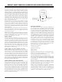
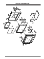
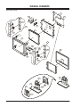
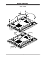
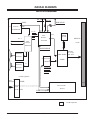
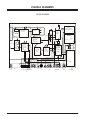
SERVICE MANUAL
Product Type:
Chassis:
Manual Series:
Manual Part #:
Model Line:
Product Year:
Model Series:
ZLD15A1
LCD TV
ZLD
CM153
923-03443R1
D
2001
ZLD20A1
CONTENTS
General Info/Remotes .................................... 1
Installer’s Menu ............................................. 2
Servicing/Troublshooting ............................... 3
Module/Model Part Lists ................................. 4
Exploded Views ............................................. 5
Schematics/PCB Layouts ................................. 6
Published by Technical Publications
Zenith Electronics Corporation
P.O. Box 240007
Huntsville, Alabama 35824
Copyright
Printed in U.S.A.
ZLD20 CCI 2.5k
?
April 2001 by Zenith Electronics Corporation
PRODUCT SAFETY SERVICING GUIDELINES FOR AUDIO-VIDEO PRODUCTS
IMPORTANT SAFETY NOTICE
This manual was prepared for use only by properly trained audiovisual service technicians. When servicing this product, under no
circumstances should the original design be modified or altered
without permission from Zenith Electronics Corporation. All
components should be replaced only with types identical to those
in the original circuit and their physical location, wiring, and lead
dress must conform to original layout upon completion of repairs. If
any fuse (or Fusible Resistor) in this TV receiver is blown, replace it
only with the factory specified fuse type and rating. When replacing
a high wattage resistor (Oxide Metal Film Resistor, over 1W), keep the
resistor 10mm away from PCB. Always keep wires away from high
voltage or high temperature parts.
Special components are also used to prevent x-radiation, shock, and
fire hazard. These components are indicated by the letter “x” included
in their component designators and are required to maintain safe
performance. No deviations are allowed without prior approval by
Zenith Electronics Corporation. Service work should be performed
only after you are thoroughly familiar with these safety checks and
servicing guidelines.
Circuit diagrams may occasionally differ from the actual circuit used.
This way, implementation of the latest safety and performance
improvement changes into the set is not delayed until the new
service literature is printed.
CAUTION: Do not attempt to modify this product in any way. Never
perform customized installations without manufacturer’s approval.
Unauthorized modifications will not only void the warranty, but
may lead to property damage or user injury.
LEAKAGE CURRENT HOT CHECK CIRCUIT
A.C. Voltmeter
0.15uF
Good Earth Ground
such as the Water
Pipe, Conduit, etc.
10 WATT
REGULATORY INFORMATION
This equipment, trade name Zenith, model number, IQD27D53T, has
been tested and found to comply with the limits for a Class B digital
device, pursuant to Part 15 of the FCC Rules. These limits are designed
to provide reasonable protection against harmful interference when
the equipment is operated in a residential installation. This equipment
generates, uses and can radiate radio frequency energy and, if not
installed and used in accordance with the instruction manual, may
cause harmful interference to radio communications. However, there
is no guarantee that interference will not occur in a particular
installation. If this equipment does cause harmful interference to
radio or television reception, which can be determined by turning
the equipment off and on, the user is encouraged to try to correct
the interference by one or more of the following measures: Reorient
or relocate the receiving antenna; Increase the separation between
the equipment and receiver; Connect the equipment into an outlet
on a circuit different from that to which the receiver is connected;
Consult the dealer or an experienced radio/TV technician for help.
The responsible party for this device compliance is:
Zenith Electronics Corporation
201 James Record Road
Huntsville, AL 35824, USA
Digital TV Hotline:
1-800-243-0000
Dolby Digital® Manufactured under license from Dolby Laboratories.
“Dolby” and the double-D symbol are trademarks of Dolby
Laboratories. Confidential Unpublished Works.
©1992-1997 Dolby Laboratories, Inc. All rights reserved.
The presence of the DTV certification mark indicates that this product
will successfully receive digital television transmissions that conform
to any and all of the video formats described in the ATSC Digital
Television Standard.
VCR Plus+, PlusCode and GUIDE Plus+ are trademarks of Gemstar
Development Corporation. The VCR Plus+ and GUIDE Plus+ systems
are manufactured under license from Gemstar Development
Corporation and VCR Index Systems B.V., respectively.
Gemstar is not in any way liable for the accuracy of the program
schedule information provided by the GUIDE Plus+ system. In no
event shall Gemstar be liable for any amounts representing loss of
profits, loss of business, or indirect, special, or consequential damages
in connection with the provision or use of any information,
equipment, or services relating to the GUIDE plus+ system.
GENERAL GUIDANCE
An lsolation Transformer should always be used during the servicing
of a receiver whose chassis is not isolated from the AC power line. Use
a transformer of adequate power rating to protect against personal
injury from electrical shocks. It will also protect the receiver and it’s
components from being damaged by accidental shorts of the circuitry
that may be inadvertently introduced during the service operation.
Before returning the receiver to the customer, always perform an AC
leakage current check on the exposed metallic parts of the cabinet,
such as antennas, terminals, etc., to be sure the set is safe to operate
without damage of electrical shock.
LEAKAGE CURRENT COLD CHECK (ANTENNA COLD CHECK)
With the instrument AC plug removed from AC source, connect an
electrical jumper across the two AC plug prongs. Place the AC switch
in the on position, connect one lead of ohm-meter to the AC plug
prongs tied together and touch other ohm-meter lead in turn to
each exposed metallic parts such as antenna terminals, phone jacks,
etc. If the exposed metallic part has a return path to the chassis, the
measured resistance should be between 1M½ and 5.2M½. When the
exposed metal has no return path to the chassis the reading must be
infinite. Any other abnormality that exists must be corrected before
the receiver is returned to the customer.
LEAKAGE CURRENT HOT CHECK (SEE BELOW FIGURE)
Plug the AC cord directly into the AC outlet. Do not use a line
Isolation Transformer during this check. Connect 1.5K/10watt resistor
in parallel with a 0.15uF capacitor between a good earth ground
(Water Pipe, Conduit, etc.) and the exposed metallic parts. Measure
the AC voltage across the resistor using AC voltmeter with 1000
ohms/volt or more sensitivity. Reverse plug the AC cord into the AC
outlet and repeat AC voltage measurements for each exposed metallic
part. Any voltage measured must not exceed 0.75 volt RMS at 0.5mA.
In case any measurement is out of the limits specified, there is the
possibility of shock hazard and the set must be checked and repaired
before it is returned to the customer.
923-03443R1
1500 OHM
Place this probe
on each exposed
metal part.
2
ZLDA1
TABLE OF CONTENTS
TABLE OF CONTENTS .............................................. 2
SERVICING PRECAUTIONS ....................................... 3
ADJUSTMENTS ..................................................... 5
TROUBLE SHOOTING .............................................. 7
PARTS LIST .......................................................... 8
EXPLODED VIEW ................................................... 14
BLOCK DIAGRAM .................................................. 15
PCB MAIN (TOP VIEW) .......................................... 16
PCB MAIN (BOTTOM VIEW) ..................................... 17
PCB LAYOUT CONTROL & TUNER .............................. 18
SCHEMATIC ......................................................... 19
CM152
3
ZLDA1
SERVICING
9. Use with this receiver only the test fixtures specified
in this service manual.
CAUTION: Do not connect the test fixture ground strap
to any heatsink in this receiver.
SERVICING PRECAUTIONS
CAUTION: Before servicing receivers covered by this service
manual and its supplements and addenda, read and follow
the SAFETY PRECAUTIONS on page 3 of this publication.
NOTE: If unforeseen circumstances create conflict between
the following servicing precautions and any of the safety
precautions on page 3 of this publication, always follow
the safety precautions. Remember: Safety First.
ELECTROSTATIC SENSITIVE (ES) DEVICES
Some semiconductor (solid state) devices can be
damaged easily by static electricity. Such components
commonly are called Electrostatic Sensitive Devices.
Examples of typical ES devices are integrated circuits
and some field effect transistors and semiconductor “chip”
components. The following techniques should be used
to help reduce the incidence of component damage
caused by static electricity.
GENERAL SERVICING PRECAUTIONS
1. Always unplug the receiver AC power cord from the
AC power source before performing the following.
a. Removing or reinstalling any component,
circuit board module or any other receiver
assembly.
b. Disconnecting or reconnecting any receiver
electrical plug or other electrical connection.
c. Connecting a test substitute in parallel with
an electrolytic capacitor in the receiver.
2. Test high voltage only by measuring it with an appropriate high voltage meter or other voltage-measuring device (DVM, FETVOM, etc) equipped with a
suitable high voltage probe. Do not test high voltage by “drawing an arc”.
3. Discharge the picture tube anode only by (a) first
connecting one end of an insulated clip lead to the
degaussing or kine aquadag grounding system shield
at the point where the picture tube socket ground
lead is connected, and then (b) touch the other end
of the insulated clip lead to the picture tube anode
button, using an insulating handle to avoid personal
contact with high voltage.
4. Do not spray chemicals on or near this receiver or
any of its assemblies.
5. Unless specified otherwise in this service manual,
clean electrical contacts only by applying the following mixture to the contacts with a pipe cleaner, cotton-tipped stick or comparable nonabrasive applicator; 10% (by volume) Acetone and 90% (by volume)
isopropyl alcohol (90%-99% strength)
CAUTION: This is a flammable mixture. Unless specified
otherwise in this service manual, lubrication of contacts in not required.
6. Do not defeat any plug/socket B+ voltage interlocks
with which receivers covered by this service manual
might be equipped.
7. Do not apply AC power to this instrument and/or any
of its electrical assemblies unless all solid-state device heat sinks are correctly installed.
8. Always connect the test receiver ground lead to the
receiver chassis ground before connecting the test
receiver positive lead. Always remove the test receiver
ground lead last.
CM153 - 923-03443R1
1. Immediately before handling any semiconductor component or semiconductor-equipped assembly, drain
off any electrostatic charge on your body by touching a known earth ground. Alternatively, obtain and
wear a commercially available discharging wrist strap
device, which should be removed to prevent potential shock reasons prior to applying power to the
unit under test.
2. After removing an electrical assembly equipped with
ES devices, place the assembly on a conductive surface such as aluminum foil, to prevent electrostatic
charge buildup or exposure of the assembly.
3. Use only a grounded-tip soldering iron to solder or
unsolder ES devices.
4. Use only an anti-static type solder removal device.
Some solder removal devices not classified as “antistatic” can generate electrical charges sufficient to
damage ES devices.
5. Do not use freon-propelled chemicals. These can generate electrical charges sufficient to damage ES devices.
6. Do not remove a replacement ES device from its protective package until immediately before you are ready
to install it. (Most replacement ES devices are packaged with leads electrically shorted together by conductive foam, aluminum foil or comparable conductive material).
7. Immediately before removing the protective material
from the leads of a replacement ES device, touch the
protective material to the chassis or circuit assembly
into which the device will be installed.
CAUTION: Be sure no power is applied to the chassis or
circuit, and observe all other safety precautions.
8. Minimize bodily motions when handling unpackaged
replacement ES devices. (Otherwise harmless motion
such as the brushing together of your clothes fabric
or the lifting of your foot from a carpeted floor can
generate static electricity sufficient to damage an
ES device.)
4
ZLD20A1 - SERVICING
SERVICING
GENERAL SOLDERING GUIDELINES
1. Use a grounded-tip, low-wattage soldering iron and
appropriate tip size and shape that will maintain tip
temperature within the range or 500cF to 600cF.
2. Use an appropriate gauge of RMA resin-core solder
composed of 60 parts tin/40 parts lead.
3. Keep the soldering iron tip clean and well tinned.
4. Thoroughly clean the surfaces to be soldered. Use a
mall wire bristle (0.5 inch, or 1.25cm) brush with a
metal handle. Do not use freon-propelled spray-on
cleaners.
5. Use the following unsoldering technique
a. Allow the soldering iron tip to reach normal
temperature. (500cF to 600cF)
b. Heat the component lead until the solder
melts.
c. Quickly draw the melted solder with an antistatic, suction-type solder removal device or
with solder braid. CAUTION: Work quickly to
avoid overheating the circuit board printed
foil.
6. Use the following soldering technique.
a. Allow the soldering iron tip to reach a normal
temperature (500cF to 600cF)
b. First, hold the soldering iron tip and solder
the strand against the component lead until
the solder melts.
c. Quickly move the soldering iron tip to the
junction of the component lead and the
printed circuit foil, and hold it there only
until the solder flows onto and around both
the component lead and the foil.
CAUTION: Work quickly to avoid overheating
the circuit board printed foil.
d. Closely inspect the solder area and remove any
excess or splashed solder with a small wirebristle brush.
IC REMOVE/REPLACEMENT
Some chassis circuit boards have slotted holes (oblong)
through which the IC leads are inserted and then bent
flat against the circuit foil. When holes are the slotted
type, the following technique should be used to remove
and replace the IC. When working with boards using the
familiar round hole, use the standard technique as
outlined in paragraphs 5 and 6 above.
REMOVAL
1. Desolder and straighten each IC lead in one operation by gently prying up on the lead with the soldering iron tip as the solder melts.
2. Draw away the melted solder with an anti-static suction-type solder removal device (or with solder braid)
before removing the IC.
CM153 - 923-923-03443R1
REPLACEMENT
1. Carefully insert the replacement IC in the circuit
board.
2. Carefully bend each IC lead against the circuit foil
pad and solder it.
3. Clean the soldered areas with a small wire-bristle brush.
(It is not necessary to reapply acrylic coating to the
areas).
“SMALL-SIGNAL” DISCRETE TRANSISTOR
REMOVAL/REPLACEMENT
1. Remove the defective transistor by clipping its leads
as close as possible to the component body.
2. Bend into a “U” shape the end of each of three leads
remaining on the circuit board.
3. Bend into a “U” shape the replacement transistor
leads.
4. Connect the replacement transistor leads to the corresponding leads extending from the circuit board
and crimp the “U” with long nose pliers to insure
metal to metal contact then solder each connection.
POWER OUTPUT, TRANSISTOR DEVICE
REMOVAL/REPLACEMENT
1. Heat and remove all solder from around the transistor
leads.
2. Remove the heatsink mounting screw (if so equipped).
3. Carefully remove the transistor from the heat sink of
the circuit board.
4. Insert new transistor in the circuit board.
5. Solder each transistor lead, and clip off excess lead.
6. Replace heatsink.
DIODE REMOVAL/REPLACEMENT
1. Remove defective diode by clipping its leads as close
as possible to diode body.
2. Bend the two remaining leads perpendicular to the
circuit board.
3. Observing diode polarity, wrap each lead of the new
diode around the corresponding lead on the circuit
board.
4. Securely crimp each connection and solder it.
5. Inspect (on the circuit board copper side) the solder
joints of the two “original” leads. If they are not
shiny, reheat them and if necessary, apply additional
solder.
FUSE AND CONVENTIONAL RESISTOR
REMOVAL/REPLACEMENT
1. Clip each fuse or resistor lead at top of the circuit
board hollow stake.
2. Securely crimp the leads of replacement component
around notch at stake top.
5
ZLD20A1 - SERVICING
SERVICING
3. Solder the connections.
CAUTION: Maintain original spacing between the
replaced component and adjacent components
and the circuit board to prevent excessive
component temperatures.
CIRCUIT BOARD FOIL REPAIR
Excessive heat applied to the copper foil of any printed
circuit board will weaken the adhesive that bonds the
foil to the circuit board causing the foil to separate
from or “lift-off” the board. The following guidelines
and procedures should be followed whenever this
condition is encountered.
AT IC CONNECTIONS
To repair a defective copper pattern at IC connections
use the following procedure to install a jumper wire on
the copper pattern side of the circuit board. (Use this
technique only on IC connections).
1. Carefully remove the damaged copper pattern with a
sharp knife. (Remove only as much copper as absolutely necessary).
2. carefully scratch away the solder resist and acrylic
coating (if used) from the end of the remaining copper pattern.
3. Bend a small “U” in one end of a small gauge jumper
wire and carefully crimp it around the IC pin. Solder
the IC connection.
4. Route the jumper wire along the path of the outaway copper pattern and let it overlap the previously
scraped end of the good copper pattern. Solder the
overlapped area and clip off any excess jumper wire.
AT OTHER CONNECTIONS
Use the following technique to repair the defective copper pattern at connections other than IC Pins. This
technique involves the installation of a jumper wire
on the component side of the circuit board.
1. Remove the defective copper pattern with a sharp
knife. Remove at least ¼ inch of copper, to ensure
that a hazardous condition will not exist if the jumper
wire opens.
2. Trace along the copper pattern from both sides of
the pattern break and locate the nearest component
that is directly connected to the affected copper
pattern.
3. Connect insulated 20-gauge jumper wire from the lead
of the nearest component on one side of the pattern
break to the lead of the nearest component on the
other side. Carefully crimp and solder the connections. CAUTION: Be sure the insulated jumper wire is
dressed so the it does not touch components or sharp
edges.
CM153 - 923-03443R1
6
ZLD20A1 - SERVICING
SECTION 1
OVERVIEW
SERVICING
USING METHOD FOR CA-110
ADJUSTMENTS
This set uses an adapter, so connect the adapter and the
set correctly before adjustment. The adjustment must
be performed under the correct sequence.
The adjustment must be performed in the circumstance
of 25+/-5cC of temperature 65+/-10% of relative
humidity if there is no specific designation. The input
voltage of the receiver must keep 220V, 60Hz in adjusting.
The set must be operated for 30 minutes preliminarily
before adjustment if there is no specific designation.
CA110
Screen
Input signal of Video
30[cm]
LCD TV
NTSC 13 CH
Note: Heat Run must be performed with the full white signal
or TV noise signal in the internal part of the set. The
time for Heat Run can be changed owing to production
plan.
DVCO ADJUSTMENT
Turn the TV on.
(2) Receive the Digital Pattern.
3-2. Adjustment
(1) Select DVCO ADJ by pressing ADJ Key(or SVC Key) of
Remote Control for Adjustment.
(2) Press the VOL + Key repeatly to appear ÒOKÓ.
AUTO RGB ADJUSTMENT
4-1. Preparation for Adjustment
(1) Adjust it after performing DVCO Adjustment.
(2) Receive the Digital Pattern.
4-2. Adjustment
(1) Select AUTO RGB ADJ by pressing ADJ Key(or SVC
Key)
of Remote Control for Adjustment.
(2) Press the VOL + Key repeatly to appear ÒOKÓ.
RGB LEVEL ADJUSTMENT
5-1. Using Equipment
(1) Pattern Generator(408NPS-READER) which 10 STEP
is possible.
(2) A Remote Control for Adjustment 5-2. Adjustment
(1) Select RGB LEVEL by pressing ADJ Key(or SVC Key) of
Remote Control for Adjustment.
(2) Select it by using VOL + Key.
(3) Adjust that until 9th and 10th STEP is
undistinguished by using VOL +/- Key in R-DRIVE item.
(4) Adjust G-DRIVE and B-DRIVE as same way.
(5) When adjustment is finished, escape it by pressing
ENTER Key.
CM153 - 923-03443R1
7
ZLD20A1 - SERVICING
ADJUSTMENT INSTRUCTIONS ZLD15A1
1. Application Object
Low Light(Black)
This instruction is for the application to the LCD TV.
2. Notes
Unit-Decimal
IC
IIC Type
Name
Default
Adj. Mode
VPC3230D
IIC 0x52/7:0/
BR
0
No.304
2930
No.236~237
0
No.248
VPC3230D IIC 0x30/11:0/ ACC_Sat
(1) This set uses an adapter, so connect the adapter and the
set correctly before adjusting.
(2) The adjustment must be performed in the correct
sequence.
(3) The adjustments must be performed in the circumstance of
25+ 5 C of temperature and 65 10% of relative humidity
unless otherwise specified.
(4) The input voltage of the receiver must be 220V, 60Hz
during adjustment.
(5) The set must be operated for 30 minutes preliminarily
before adjustment unless otherwise specified.
* "Heat Run" must be performed with the full white signal or TV
noise signal in the internal part of the set.
Fp 0xDC
VPC3230D
Tint
Red
Green
Blue
White
x
0.63
0.30
0.14
0.32
y
0.34
0.60
0.10
0.34
150[cd/m^2]
Brightness:[cd/m^2]
4. PC Input Mode Adjustment
4-1. Required Test Equipment
(1) A pattern generator being in proportion to VG819 ; Pattern
of 64 tones
(2) A remote control
3. TV Mode Adjustment
4-2. Preparation for Adjustment
(1) Perform "Heat Run" for more than 30 minutes in white
pattern.
(2) Connect the signal of pattern generator to LCD TV.
(3) Lean the set 45 backward. (Adjustment is easy.)
Before entering into the adjustment mode set the TV up with
the MENU button as below.
Contrast
Brightness
Saturation
Tint
85
100
50
0
45
3-1. White Balance Adjustment
(4) Set the PC mode menu as below.
3-1-1. Required Test Equipment
(1) A Remote Control
(2) A Color Analyzer for LCD : CA-110
(3) A TV Signal Generator : Pattern of 64 (128) tones or Ch. 13
in the company.
3-1-2. Preparation for Adjustment
Brightness
70
100
Initial Value
4-3. White Adjustment
(1) Approve the signal of 64 tones of XGA(1024 * 768).
(2) Select all the gain of R, B and G with using ADJ of remote
control.
(3) After making 62 tones, 63 tones and 64 tones not
distinguished with using each signal of R, G and B, finish
adjusting at the moment when the signal 62, 63 and 64 is
distinguished.
(1) This adjustment should be performed 30 minutes later
after "Heat Run".
(2) This adjustment should be performed in a darkroom or in
the simmilar condition.
3-1-3. Low Light Adjustment
(1) Seletc Ch.13 .
(2) Enter into the adjustment mode with the ADJ button.
(3) Select the Sub-bright and stop adjusting at the moment
when Gray 0 and 1 are not distinguished.
R
G
Error
B
Color Coordinates(x,y) 0.63 0.34 0.30 0.60 0.14 0.10
AD9884
CM153
Contrast
8
0x02
0x03
0x04
+/- 0.03
Register
ZLD15A1
4-4. Position of Mode Adjustment
Timing of Mode Table
Mode
VGA-60
VGA-67
VGA-72
VGA-75
VGA-85
TEXT-70
SVGA-56
SVGA-60
SVGA-72
H_Total
800
864
832
840
832
900
1024
1056
1040
H_Display
640
640
656
640
640
720
800
800
800
H_Blanking
160
224
176
200
192
180
224
256
240
64
56
108
72
128
120
H_Sync
96
64
40
HPolarity
NEG.
NEG.
NEG.
NEG.
NEG.
NEG.
POS
POS
POS
H_Bp
48
96
120
120
80
54
128
88
64
H_Fp
16
64
16
16
56
18
24
40
56
H-Freq[KHz]
31.469
35.0
37.861
37.5
43.269
31.469
35.156
37.879
48.077
/Clk[MHz]
25.175
30.24
31.5
31.5
36.0
28.324
36.0
40.0
50.0
V_Total
525
525
520
500
509
449
625
628
666
V_Display
480
480
496
480
480
400
600
600
600
V_Blanking
45
45
24
20
29
49
25
28
66
V_Sync
2
3
3
3
3
2
2
4
6
VPolarity
NEG
NEG
NEG
NEG
NEG
POS
POS
POS
POS
V_Bp
33
39
20
16
25
34
22
23
23
V_Fp
10
3
1
1
1
13
1
1
37
Mode
SVGA-75
SVGA-85
XGA-60
XGA-70
XGA-75
MAC-75
H_Total
1056
1048
1344
1328
1312
1152
H_Display
800
800
1024
1024
1024
832
H_Blanking
256
248
320
304
288
320
H_Sync
80
64
136
136
96
64
POS
NEG
224
HPolarity
POS
POS
NEG
NEG
H_Bp
160
152
136
144
176
H_Fp
16
32
160
24
16
32
H-Freq[KHz]
46.875
53.674
48.363
56.476
60.23
49.725
/Clk[MHz]
49.5
56.25
65.0
75.0
78.75
57.283
V_Total
625
631
806
806
800
667
V_Display
600
600
768
768
768
624
V_Blanking
25
31
38
38
32
43
V_Sync
3
3
6
6
3
3
VPolarity
POS
POS
NEG
NEG
POS
NWG
V_Bp
21
27
29
29
28
39
V_Fp
1
1
3
3
1
1
To gain access to the Service menu hold (Menu) key until the menu diappears
from the screen then press 9,8,7,6, (Enter).
Service Menu for ZLD15A1
DVCOAdjust
AutoRGB
ClampLevel
RGBLevel
VolumeCurve
Auto
Auto
44
Auto
12345
Service Menu for ZLD20A1
0
1
2
3
4
5
6
7
8
9
CM153
S-BRTTV
R-Gain
G-Gain
B-Gain
AL30016H
AL30019H
AL3001AH
AL30039H
AL3003CH
S-ConTV
107
33
34
29
14
84
32
47
115
5
9
ZLD15A1
TROUBLE SHOOTING
1. General Features
No.
Problem
Possible Cause
Solution
1
Soft touch doesn't
function properly
Defective speaker wire
and inverter wire
1) Make some space between the speaker wire and
the Soft touch Board by sticking the speaker wire
to the guide hole of the cabinet.
2) Arrange working state of A1. Tape in the inverter wire
and correct working state of the Shield case.
2
Soft touch doesn't
function
1) Broken components and
soldering of them
2) P101 connector error
1) Check Soft touch with eyes
Check and repair soldering
2) Check and repair the P101 connector
3
No screen
Input error of inverter connector
1) Bend the pin legs of P802 connector -> recheck them
2) Check and repair the IC806 SI4925
P501 and Pin 41 connector
slipped out
1) Check and fix P501 connector
2) Check and fix the components at P501 LCD module
and at main board.
3) Check Pin41 and check and repair rubber packing
Cracked components and
soldering at tuner board
1) Check and repair tuner board and main board
2) Solder Q301, Q801 and R810
4
Dark screen
1) Defective LCD lamp
2) Defective inverter
1) Replace the inverter
2) Replace the LCD lamp
5
Broken OSD display
Defective font rom of IC502
Replace IC502
2. PC Mode
No.
Problem
Possible Cause
Solution
6
Screen noise
Clock or phase being
not able to be adjusted
1) Resettig is needed according to the video card of each
PC
2) Horizontal noise : adjust phase until no horizontal
noise occurres
3) Vertical noise : adjust clock in menu until no vertical
noise occurres
7
Screen position error
Screen position error
horizontally or vertically
Adjust horizontal and vertical position until the screen
displayes normally
8
Color beat noise
Soldering AD converter
or making it short
Recheck and repair
3. TV and external input
No.
9
10
Problem
Possible Cause
Solution
No sound
- Speaker
- Earphone
Defective Reset IC of IC603
Defective MSP3400D of IC601
1) Check volume and speaker
- Sound comes out only when being input into Audio
L/R
2) Check after replacing IC603
3) Replace IC601
Video color beat noise
Earphone shield case being touched
Check the mould of shield and JA401, Replace shield case
Soldering IC901 and IC501
Re-soldering
CM153
10
ZLD15A1
COMPONENT PARTS
PARTS LIST
ZLD15A1
NOTE: This list will enable you to easily determine the parts used on each Model, Chassis, or Assembly.
REF
PART#
DESCRIPTION
112
120
121
174
900-10048
849-10036
812-10136
811-10039
LCD(LIQUID CRYSTAL D 151X2-C2TH 151" LGP
SPEAKER, GENERAL T401SX-095K14 LG C&D
METAL HOLDER SPK SBHG
POWER CORD PS204-001 VOLEX UL/C
300
310
400
420
430
450
500
521
857-10335
959-10102
814-10159
812-10137
812-10138
812-10139
809-10540
926-10055
CABINET ASSY ZLD15A10 ZENITH
BUTTON CONTROL 8KEY ABS
BACK COVER ASSY ZLD15A1
METAL STAND SECC
HOLDER STAND ABS AF-303S(04
COVER STAND ASSY ZLD15A1
PWB(PCB) ASSY MAIN NF99LA US
METAL MAIN FRAME SBHG
540
541
550
A1
A2
A3
A4
895-10117
926-10054
809-10541
206-03652
924-10091
895-10118
812-10090
INVERTER ASSY 12VOLT 500VOLT KS
SHIELD CASE INVERTER ET-C
PWB(PCB) ASSY, SUB CTL NF99LA ZLD15A1
MANUAL, OWNERS NF99LA ZLD15A1
REMOTE CONTROLLER NF99LA ZLD15A1
ADAPTER, AC-DC AC110VOLT DC12VOLT
ADAPTER ANT RF
REF
PART#
DESCRIPTION
Critical safety components are identified by
shading. Replace only with part numbers
specified.
CM153
11
ZLD15A1 - PARTS
300
120
121
310
112
550
500
CM153
430
540
521
943
541
420
400
410
ZLD15A1 EXPLODED VIEW
12
ZLD15A1
MODEL PARTS
ZLD20A1 PARTS
ZLD20A1
Location
1
2
2
3
4
5
6
7
8
9
10
11
12
13
14
15
16
17
19
20
21
22
23
24
25
26
27
28
29
Part Number
804-10107
849-10045
809-10661
814-10196
849-10048
895-10137
811-10044
836-10003
857-10362
836-10002
959-10110
809-10659
900-10059
895-10136
809-10658
809-10657
804-10106
849-10046
809-10660
814-10195
849-10047
Part of 28
Part of 28
Part of 28
Part of 28
Part of 28
Part of 28
812-10155
814-10197
CM153 - 923-03443R1
Description
CASE,SPEAKER
SPEAKER, GENERAL
LEFT SPKR BRD
SPEAKER REAR PANEL (L)
SPEAKER W/CASE ASSY
AC DC ADAPTER
POWER CORD
HANDLE ASSY ZLD20A1
PANEL ASSY, FRONT
HANDLE ASSY ZLD20A1
BUTTON, CONTROL
CONTROL BRD ASSY
LCD 20 INCH
INVERTER ASSY 15V
SUB MODULE ASSY ZLD20A1
MAIN MODULE ZLD20A1
CASE,SPEAKER
SPEAKER, TWEETER
RIGHT SPKR BRD
SPEAKER REAR PANEL (R)
SPEAKER W/CASE ASSY
BRACKET FRONT LEFT
BRACKET FRONT RIGHT
METAL STAND BASE
METAL SHFT GUIDE SCP1
BRACKET STAND READ
METAL STAND
STAND ASSY
REAR CABINET MAIN
13
ZLD20A1 - PARTS
ZLD20A1 DIAGRAMS
EXPLODED VIEW
13
14
5
1
15
3
6
4
12
2
7
8
21
11
16
17
20
29
10
9
18
19
28
25
24
26
22
27
23
CM153 - 923-03443R1
14
ZLD20A1 - DIAGRAMS
ZLD20A1 DIAGRAMS
WIRING DIAGRAM
MAIN P201B
CN1
P803B
SC801
0 1B
P0
S/P LEAD TIES
S/P LEAD
BAND
HOLDER
CN1
CONTROL, POWER
SPEAKER LEAD
HOLDER
CM153 - 923-03443R1
0 1B
P0
15
ZLD20A1 - DIAGRAMS
ZLD15A1 DIAGRAMS
BLOCK DIAGRAM
Ext _Video
Ext _Y/C
DVD Y/Pb/Pr
CVBS
Tuner & IF
SIF
- 6700VNF003C
For TV
. Contrast
. Brightness
. Color
. Tint
1H/1V
Video
Decorder
EPROM
For OSD
LM151X2
Ext - L
Ext - R
Audio
Processor
- VPC3230D
< 6-bits >
- MSP3400C
OSD FB/R/G/B
Audio-Amp
L
Video Scaler
D-R/G/B,
H / V -Sync,
Den, Clock
TDA7052A
A to D Converter
- AL300
- AD9884
R
Audio-Amp
TDA7052A
For PC Input
- Contrast
- Brightness
- Color
For MNT Application
From
Computer
R/G/B
LCD
Computer
Signal
Micro-Controller
- M 37274
- D-Sub
H/V
CVBS For Caption
For MNT Application
CM153 - 923-03443R1
16
ZLD15A1 - DIAGRAMS
ZLD15A1 PCB Main (Top)
MAIN(TOP)
CM153 - 923-03443R1
17
ZLD15A1 - DIAGRAMS
ZLD15A1 PCB Control & Tuner
CTL(TOP)
CTL(BOTTOM)
TUNER(TOP)
TUNER(BOTTOM)
CM153 - 923-03443R1
18
ZLD15A1 - DIAGRAMS
ZLD20A1 DIAGRAMS
BLOCK DIAGRAM
EEP
EEP
ROM
ROM
L
C
2
0
1
V
1
A
3
3.3V
3.3V 5V(FOR RESET IC 3,3V)
3.3V
3.3V
5V
VIDEO RAM
2M
5V
SCL1/SDA1
SCL/SDA
SCALER(Format Converter)
MX88L-284FC-V
14.318MHz
R/G/B
9V
5.0V
Audio Processor
MSP-34XX
RF : 2, SCART : 4
MONO : 1
I2S : 2
------18.432MHz--L-SPK/WOOFER
H/P, I2S
SCART OUT : 2
VIDE O H/V
H/V
(2H)
Analog
R/G/B/H/V
Multi-Component
Processor(BBVSP)
CXA 2101AQ
YCrCb : 2 / 4
RGB : 4 / 2
OUT RGB :1, TUV : 1
15V
Dual Audio AMP
LA4282
Caption
Processor
R/G/B
24
8 /8 /8bit
8.0V
3.3V
AD Converter
THS8083
SCL/SDA
3.3V
BRI-AD J
3.3V
Y/U/V
4:2:2
3.3V
R-SPK
IC201
Color Decoder/
A/D Converter
VPC-3230D
CLK
IC301
H- FILTER
(DRP Processor)
LGTV-1001
15V
5V
H-sync
4:2:2
TO MICOM
POWER-ON/OF F TO MICOM
H-Sync.
SEP
CAPTION
R/G/B
Y/U/V
15V
33V
480I/P
ÆÇ´Ü
SCL/SDA
Y/U/V
(480P)
0.5-0.7
IC302
SCAN Converter
SDA-9410
27.0MHz
IC1
MICOM / TXT
6.0MHz
R/G/B
OSD
RESET 4.2V
Y/U/V
(480P)
SCL/SDA
POWER
DC to DC Converter
(SI786,SI4808DY,T801)
DC to AC
INVEERTER
SCL/SDA
LCD PANNEL
.
SCL/SDA
L-SPK
. COMB/FIL : 4H
INPUT . 4 CVBS . 1 S-VHS
. 2 RGB /YCrCb
. 1 F/B
. 1 CVBS OUTPUT
. Y /Cr /Cb OUTPUT
20.25MHz
RF(VIN3 : CVBS)
15V
5V
SCL
SDA
CVBS
SCL/SDA
M/O(CVBS)
30V
X2
SCART(R/G/B/FB)
YUV IN(VIN4 : H-CHECK)480I
S-VHS(VIN1 : Y/C))
A/V2(VIN2 : CVBS)
SIF
IF AGC
Y/U/V in
DC
(12V)
PC
CM153 - 923-03443R1
Y
PB
SCART JACK
PR
L
DVD/DT V
(480I/480P)
TUNER
TUNER
....
R/G/B/FB L / Ri n TV/L/R out
R
V
H/P
S -
19
L
R
V
L
VIDEO
R
DC
(12V)
ANT (RF )
ZLD20A1 - DIAGRAMS
ZLD20A1 PCB LAYOUTS
MAIN PCB LAYOUT
CM153 - 923-03443R1
20
ZLD20A1 - PCBS
ZLD20A1 PCB LAYOUTS
MX PCB LAYOUT
MX(TOP)
MX(BOTTOM)
CM153 - 923-03443R1
21
ZLD20A1 - PCBS
ZLD20A1 PCB LAYOUTS
CONTROL PANEL PCB LAYOUT
CONTROL(TOP)
CONTROL(BOT TOM)
SPEAKER CONNECT PCB LAYOUT
SPEAKER( TOP)
SPEAKER(BOT TOM)
CM153 - 923-03443R1
22
ZLD20A1 - PCBS