1
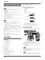
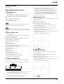
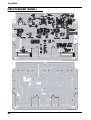
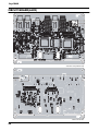
Sep.2004
RC-20XL
SERVICE NOTES
Issued by RJA
TABLE DF CONTENTS
CAUTIONARY NOTES ...................................................2
SPECIFICATIONS.............................................................2
LOCATION OF CONTROLS ..........................................4
LOCATION OF CONTROLS PARTS LIST ...................5
EXPLODED VIEW, EXPLODED
VIEW PARTS LIST ........................6
PARTS LIST......................................................................10
CHECKING THE VERSION NUMBER.......................13
SERIAL DUMP (SYSTEM UPDATE, USERS
DATA SAVE AND LOAD) ..............13
INSTRUCTIONS FOR FACTORY RESET ...................14
TEST MODE.....................................................................14
BLOCK DIAGRAM.........................................................19
CIRCUIT BOARD (PANEL) ..........................................20
CIRCUIT DIAGRAM (PANEL).....................................22
CIRCUIT BOARD (JACK)..............................................24
CIRCUIT DIAGRAM (JACK 1) .....................................26
CIRCUIT DIAGRAM (JACK 2) .....................................28
Copyright © 2004 ROLAND CORPORATION
All rights reserved. No part of this publication may be reproduced in any form without the written permission
of ROLAND CORPORATION.
17058256E0
Printed in Japan (0500) (TP)
Sep.2004
CAUTIONARY NOTES
AUX IN Jack (Stereo miniature phone type)
PHRASE SHIFT Jack (1/4 inch TRS phone type)
REVERSE Jack (1/4 inch phone type)
User data status
User data status after each of the following processes is described below.
Whenever carrying out procedures that involve deleting or erasing user data,
always be sure to back up the user data to some form of external media (refer
to Saving and Loading Data).
OUTPUT Jack (1/4 inch phone type)
AC Adaptor Jack
Power
DC 9V: Dry battery (R6/LR6 (AA) type) x 6
AC Adaptor (PSA-series)
Power Consumption
Process
Checking Version number
SERIAL DUMP
Test Mode
*
User Data
Preserved
Deleted
Preserved
120 mA (9 V max.)
*
Executing Test Mode during Factory Reset deletes the user data.
Expected battery life under continuous use:
Carbon:
6 hours
Alkaline:
16 hours
These figures will vary depending on the actual conditions of use.
PARTS LIST
Due to one or more of the following reasons, parts with parts code ********
cannot be supplied as service parts.
•
Part supplied only as a component in a complete assembly
•
Copyright does not permit the part to be supplied
•
Part is sold commercially
Dimensions
173 (W) x 158 (D) x 57 (H) mm
6-13/16 (W) x 6-1/4 (D) x 2-1/4 (H) inches
Weight
1.2 kg / 2 lbs 11 oz (including batteries)
Accessories
SPECIFICATIONS
Nominal Input Level
INST:
-20 dBu (variable)
MIC:
-40 dBu (variable)
AUX IN:
-10 dBu
Input Impedance
INST:
1 M ohms
MIC:
1 k ohms
AUX IN:
47 k ohms
Nominal Output Level
OUTPUT:
-20 dBu
Output Impedance
1 k ohms
Recommended Load Impedance
10 k ohms or greater
Internal Memory
Recording time: 16 min. (max.)
Maximum number of saved phrases:
11 phrases (max.)
Controls
REC/PLAY/OVERDUB Pedal, STOP/TAP TEMPO Pedal, INST Knob, MIC
Knob, PHRASE SELECT Knob, GUIDE Knob, LEVEL Knob, REVERSE Button,
TAP TEMPO Button, WRITE Button, EXIT Button, AUTO START Button,
MODE Button
Indicators
POWER (serves also as battery check indicator), REC, PLAY, OVERDUB,
PEAK, LOOP QUANTIZE, LOOP PHRASE, ONE SHOT PHRASE, TAP
TEMPO, REVERSE, WRITE, EXIT, AUTO START, MODE, INST & MIC,
NORMAL, CENTER CANCEL, FLAT AMP SIMULATE
Connectors
INST Jack (1/4 inch phone type)
MIC Jack (1/4 inch phone type)
2
Owner’s Manual ENGLISH:(#G6017384)
JAPANESE:(#G6017382)
Leaflet (“USING THE UNIT SAFELY,” “IMPORTANT NOTES,” and
“Information”):(#********)
Dry battery (AA type) x 6:(#********)
Sound Library for RC-20XL (Sample Phrase CD):(#********)
Options
AC Adaptor (PSA-series)
Foot Switch (FS-5U)
*
0 dBu = 0.775 Vrms
*
In the interest of product improvement, the specifications and/or appearance of
this unit are subject to change without prior notice.
RC-20XL
3
Sep.2004
LOCATION OF CONTROLS
fig.panel
30
19
30
31
4
31
RC-20XL
LOCATION OF CONTROLS
PARTS LIST
NO
1
2
3
4
5
6
7
8
9
10
11
12
13
14
15
16
17
18
19
20
21
22
23
24
25
26
27
28
29
30
31
PART CODE
G2017145
G2187530
G2187531
G2357116
H5029851
G2217185
H5029855
F3279802
F3279803
F3279805
G2477122
G247751001
G247751301
G2217186
1502928100
F5029117
F5029125
F5029124
15029342
F5029126
G2527110
F344941501
F3449707
13449155MF
F3449709
G2017621
75D422E000
G2357118
G2537558
F3129306
13129778
CATEGORY
CASING
CASING
CASING
CASING
CASING
CASING
SCREWS
POTENTIOMETER
POTENTIOMETER
POTENTIOMETER
KNOB,BUTTON
KNOB,BUTTON
KNOB,BUTTON
CASING
DIODE
DIODE
DIODE
DIODE
DIODE
DIODE
CASING
JACK,EXT TERMINAL
JACK,EXT TERMINAL
JACK,EXT TERMINAL
JACK,EXT TERMINAL
CASING
CASING
MISCELLANEOUS
MISCELLANEOUS
SWITCH
SWITCH
PART NAME
TOP CASE
PEDAL R
PEDAL L
PEDAL PLATE
PEDAL SHAFT
PANEL
SCREW M4X8
POTENTIOMETERNO CLICK 50KB
POTENTIOMETER 11 CLICKS 50KB
POT.(W/O CLICK)
R-KNOB
VGA KEYTOP S BLACK WITH LENS
VGA KEYTOP S WITHOUT LENS
LED PANEL
LED (RED)
LED
LED (YELLOW)
LED (GREEN)
LED
POWER LED
REAR PANEL
ADAPTOR JK
PHONE JK(STREO)
PHONE JACK (MONO)
3.5MM MINI JACK
BATTERY COVER
BOTTOM COVER
BOTTOM FOOT
QUICK MANUAL&CAUTION
SWITCH
TACT SWITCH
DESCRIPTION
62X53
HEXAGON BUTTON HEAD NI
RD901-40-125F-B54-00D
RD901-40-125F-B54-11D
RD901-40-125F-AF5-00D 250KA
L-34HDSL
L-312LRD
L-34YDSL
L-34GDSY
GL3ED8
L-113GDT
PANEL
KM02009BB
HTJ-064-12DS
HTJ-064-12I
SHJ-3513TS (STEREO)
LABEL
SKQKAB
SKQKAh
Q’TY
1
1
1
2
2
1
4
2
1
2
5
4
2
1
8
4
1
2
1
1
1
1
1
3
1
1
1
2
1
6
2
5
Sep.2004
EXPLODED VIEW, EXPLODED VIEW PARTS LIST
EXPLODED VIEW1
fig.explo-1
7
6
h
8 RIGHT SIDE
9 LEFT SIDE
2
g
1
5
i
3
4
EXPLODED VIEW 1 PARTS LIST
[PART]
NO
1
2
3
4
5
6
7
8
9
PART CODE
G2017145
G2357111
H5029851
2215770201
2217710900
G2357116
G2357115
G2187530
G2187531
PART NAME
TOP CASE
CUSHION R
PEDAL SHAFT
PEDAL GUIDE BUSH
COIL SPRING
PEDAL PLATE
PEDAL FOOT
PEDAL R
PEDAL L
DESCRIPTION
215-702
217-109
62X53
M8
Q’TY
1
2
2
2
2
2
2
1
1
[SCREW]
NO
g
h
i
6
PART CODE
H5029852
H5039413
H5039414
PART NAME
SCREW4M3 FEBZC
NYLON WASHER M4.1X7.5X0.5
NYLON WASHER M5.1X9.5X0.5
DESCRIPTION
HEXAGON SOCKET BUTTON HEAD
BLACK
BLACK
Q’TY
2
2
2
RC-20XL
EXPLODED VIEW 2
fig.explo-2
21
k
c
24
32
33
33
26
32
EXPLODED VIEW 2 PARTS LIST
[PART]
NO
21
24
26
32
33
PART CODE
G2477122
G2217185
G2217186
G247751301
G247751001
PART NAME
R-KNOB
PANEL
LED PANEL
VGA KEYTOP S WITHOUT LENS
VGA KEYTOP S BLACK WITH LENS
DESCRIPTION
Q’TY
5
1
1
2
4
[SCREW]
NO
c
k
PART CODE
H5029855
H5039521
PART NAME
SCREW M4X8
VR ACCESSORY NUT M7
DESCRIPTION
HEXAGON BUTTON HEAD NI
Q’TY
4
5
7
Sep.2004
EXPLODED VIEW 3
fig.explo-3
11
12
a
18
10
a
17
16
13
Refer to Fig A
Magnified view
14
j
15
Magnified view
EXPLODED VIEW 3 PARTS LIST
[PART]
NO
10
11
12
13
14
15
16
17
18
PART CODE
G2017148
G2357118
G2017621
G2017620
G2177308
G2177309
G2177307
G2257130
G2537558
PART NAME
BOTTOM COVER
BOTTOM FOOT
BATTERY COVER
BATTERY CASE
BATTERY TERMINAL(+)
BATTERY TERMINAL(-)
BATTERY TERMINAL(+-)
BATTERY INSULATING SHEET
QUICK MANUAL&CAUTION
DESCRIPTION
LABEL
Q’TY
1
2
1
1
1
1
1
1
1
[SCREW]
NO
a
j
8
PART CODE
H5019115
H5019430
PART NAME
SCREW M3X8
SCREW M2.6X5
DESCRIPTION
PAN TAPPING-2 FEBZC
BINDING HEAD TAPTITE P FEZC
Q’TY
7
2
RC-20XL
EXPLODED VIEW (Fig. A)
fig.explo-4
b
19
22
46
34
b
m
20
1
25
e
f
EXPLODED VIEW(Fig. A) PARTS LIST
[PART]
NO
1
19
20
22
25
34
46
PART CODE
G2017145
75E183M000
75E183P000
G225712901
G2527110
********
G2147821
PART NAME
TOP CASE
JACK BOARD ASSY
PANEL BOARD ASSY
INSULATING SHEET CENTER
REAR PANEL
This PWB ASSY is inclueded the JACK BOARD ASSY.
JACK HOLDER
DESCRIPTION
Q’TY
1
1
1
1
1
1
1
[SCREW]
NO
b
e
f
m
PART CODE
H5019110
H5039510
H5039112
H5039324
PART NAME
SCREW M3X6
NUT M9X12X2
WASHER M9
MINI JACK NUT
DESCRIPTION
PAN TAPTITE FEZC
FENI
AJ324A-3C
Q’TY
13
5
5
1
9
Sep.2004
PARTS LIST
fig.part1e
SAFETY PRECAUTIONS:
The parts marked
have
safety-related characteristics. Use
only listed parts for replacement.
Due to one or more of the following reasons,
parts with parts code ******** cannot be supplied as service parts.
• Part supplied only as a component in a complete assembly
• Copyright does not permit the part to be supplied
• Part is sold commercially
NOTE: The parts marked # are new. (initial parts)
CASING
#
The description "Q'TY" means a necessary number of the parts per one product.
G2527110
G2357116
G2017620
G2017621
75D422E000
G2357118
G2217186
G2217185
G2187531
G2187530
H5029851
G2017145
REAR PANEL
PEDAL PLATE
BATTERY CASE
BATTERY COVER
BOTTOM COVER
BOTTOM FOOT
LED PANEL
PANEL
PEDAL L
PEDAL R
PEDAL SHAFT
TOP CASE
G3487163
WIRING BATTERY
G2477122
G247751001
G247751301
R-KNOB
VGA KEYTOP S BLACK WITH LENS
VGA KEYTOP S WITHOUT LENS
13129778
F3129306
TACT SWITCH
SWITCH
SKQKAH
SKQKAB
SW1,SW8 on PB
SW2,SW3,SW4,SW5,SW6,SW7 on PB
2
6
JACK,EXT TERMINAL
F3449709
F344941501
13449155MF
F3449707
3.5MM MINI JACK
ADAPTOR JK
PHONE JACK (MONO)
PHONE JK(STREO)
SHJ-3513TS (STEREO)
KM02009BB
HTJ-064-12I
HTJ-064-12DS
JK3 on JK
JK6 on JK
JK1,JK2,JK5 on JK
JK4,JK7 on JK
1
1
3
2
PWB ASSY
#
#
75E183M000
75E183P000
JACK BOARD ASSY
PANEÇk BOARD ASSY
F5279861
F5209123
F5289102
15189261
02121556
F5179125
03675078
F5279306
15259884
02451434
F5279305
M12L16161A-7T
S-80930ALMP-DAT-T2
NJM2100M 8P SOP
M5218AFP-600E
LC24085B-SD1
S-8520E33MC-BJS-T2
UPD703106AGJ-087-UEN
TC4W66F
TC7S08F(TE85L)
AK4552VT
TC4066BFT
IC (SDRAM)
IC (REST)
IC (OP.AMP)
IC (BIPOLAR OP AMP)
IC (I/F)
IC (DC-DC)
IC (CPU)
IC (CMOS)
IC (CMOS)
IC (AD/DA)
IC
IC1 on JK
IC6 on JK
IC13 on JK
IC9,IC10,IC12,IC15 on JK,IC1 on PB
IC4 on JK
IC16 on JK
IC3 on JK
IC11 on JK
IC7 on JK
IC14 on JK
IC8 on JK
1
1
1
5
1
1
1
1
1
1
1
15319107
15329521
F5139608
15329103
F5329522
2SC4116-GR(TE85R)
RN1307(TE85R)
IRF7606
2SK880GR-TE85R
RN2307
TRANSISTOR
TRANSISTOR
POWER MOS FET
FET TRANSISTOR
DIGITAL TRANSISTOR
Q12 on JK,Q2,Q1 on PB
Q1,Q2,Q3,Q4,Q11,Q13,Q14,Q15,Q16,Q17 on JK
Q18 on JK
Q9,Q10 on JK
Q5,Q6,Q7,Q8 on JK
1
10
1
2
4
#
#
#
1
2
1
1
1
2
1
1
1
1
2
1
62X53
CHASSIS
L=80MM 2P
1
KNOB,BUTTON
5
4
2
SWITCH
IC
#
#
#
1
1
TRANSISTOR
#
10
RC-20XL
DIODE
#
F5019309
F5029126
F5029125
1502928100
02DZ5.1-Y
L-113GDT
L-34YDSL
L-34HDSL
ZENNER DIODE
POWER LED
LED (YELLOW)
LED (RED)
D9 on PB
LED17 on PB
LED6 on PB
LED2,LED3,LED4,LED12,LED13,LED14,LE
D15,LED16
LED5,LED7 on PB
LED1 on PB
LED8,LED9,LED10,LED11 on PB
D1 on JK,D1,D2,D3,D4,D5,D6,D7,D8 on PB
DA2,DA5,DA6,DA7 on JK
D2 on JK
D5,D6 on JK
1
1
1
8
F5029124
15029342
F5029117
15339119
15339120
F5339138
F5339137
L-34GDSY
GL3ED8
L-312LRD
1SS-352
1SS302
1SS355
SS14 VF=0.45V
LED (GREEN)
LED
LED
DIODE
DIODE
DIODE
DIODE
F5419707
F5419716
F5419715
F5399115
F5399145
F5399157
F5399133
F5399296
F5399158
CRN34101J
CRN34103J
CRN34680J
100 J
12K J
39K J
4.7K J
4.7J
47K J
RESISTOR ARRAY
RESISTOR (CHIP)
RESISTOR (CHIP)
RESISTOR
RESISTOR
RESISTOR
RESISTOR
RESISTOR
RESISTOR
1
5
11
6
2
1
2
1
12
MTL.FILM RESISTOR
MTL.FILM RESISTOR
MTL.FILM RESISTOR
MTL.FILM RESISTOR
MTL.FILM RESISTOR
MTL.FILM RESISTOR
MTL.FILM RESISTOR
MTL.FILM RESISTOR
MTL.FILM RESISTOR
MTL.FILM RESISTOR
MTL.FILM RESISTOR
MTL.FILM RESISTOR
RESISTOR
MTL.FILM RESISTOR
MTL.FILM RESISTOR
RA13 on JK
RA8,RA14,RA18,RA19,RA20 on JK
RA1,RA2,RA3,RA4,RA5,RA7,RA11,RA12,RA15,RA16,
R9,R11,R14,R18,R21,R22 on JK
R65,R72 on JK
R80 on JK
R37,R33 on JK
R74 on JK
R30,R32,R34,R39,R40,R49,R50,R51,R52,R53,
R59,R9,R10 on PB
R36 on JK
R86 on JK
R24 on JK
R83,R7 on JK
R35,R43,R46,R89 on JK,R4 on PB
R1,R10,R12,R13,R23,R25,R26,R27,R29,R38,
R41,R,R3 on PB
R45,R56 on JK
R66,R70,R71 on JK
R88,R100,R102,R105 on JK,R6 on PB
R15,R28,R31 on JK,R5,R7on PB
R16,R17 on JK
R57,R60 on JK
R8,R90 on JK
R48,R55,R58,R63,R77,R79 on JK
R68,R73,R78 on JK
R75,R82 on JK
R3,R4,R5,R19,R20,R44,R61,R91,R92,R96,R98,R10
R76 on JK
R1 on PB
R8 on PB
R2 on PB
F5399166
F2569127
F5399129
F5399104
F5399170
F5399140
82K J
MINISMDC075
1.5K J
10 J
100K J
10K J
RESISTOR
POLY SWITCH
MTL.FILM RESISTOR
MTL.FILM RESISTOR
MTL.FILM RESISTOR
MTL.FILM RESISTOR
F5399180
F5399147
F5399128
F5399200
F5399117
F5399152
F5399106
F5429393
F5399160
F5429394
F5399109
F5399165
F5399127
F5399154
F5399118
150K
15K J
1K J
1M J
220
22K J
47 J
47KD
56K J
56KD
68
68K
1.2K J
27K J
330
RD901-40-125F-B54-00D
RD901-40-125F-B54-11D
RD901-40-125F-AF5-00D 250KA
POTENTIOMETERNO CLICK 50KB
POTENTIOMETER 11 CLICKS 50KB
POT.(W/O CLICK)
VR3,VR2 on PB
VR1 on PB
VR4,VR5 on PB
2
1
2
F5399158
F5349704
F5367542
47K J
ECPU1C474MA5 0.47
10/16V ALUMINIUM
RESISTOR
MYLAR CAPACITOR (SUBMICRON)
ELECTROLYTIC CAPACITOR
F5367542
F5367546
F5367503
F5359348
F5359328
F5359313
F5359313
F5369805
F5369601
F5359311
F5359318
F5359708
F5359309
F5359387
F5359345
10/16V ALUMINIUM
100/16V ALUMINIUM
47/6.3V ALUMINIUM
0.0056
0.01
0.1
0.1
470P
1/50V
100P
10P
22P
33P
GRM39B102K50PT 0.001 K
0.027U (1608TYPE)
ELECTROLYTIC CAPACITOR
ELECTROLYTIC CAPACITOR
ELECTROLYTIC CAPACITOR
CHIP CAPACITOR
CHIP CAPACITOR
CHIP CAPACITOR
CHIP CAPACITOR
CHIP CAPACITOR
CHIP CAPACITOR
CHIP CAPACITOR
CHIP CAPACITOR
CHIP CAPACITOR
CHIP CAPACITOR
CERAMIC CAPACITOR
CAPCITOR (CHIP)
C1,C14,C16,C18,C30,C83,C86,C89 on JK
C84 on JK
C42,C63,C68 on JK
C19,C20,C21,C46,C48,C52 on JK
C2,C3,C4,C5,C6,C7,C8,C9,C10,C11,C12,C13,C17,
C1 on PB
C56,C61 on JK
C47,C49,C67,C75 on JK,C5,C6 on PB
C51 on JK
C22,C23,C64,C70,C74 on JK
C25,C24 on JK
C53,C57 on JK
C43,C32 on JK
C50 on JK
6
8
1
3
6
32
1
2
4
1
5
2
2
2
1
SLF7032T-4R7M1R7-2(4.7UH)
N1608Z601T02
SMD COIL
FERRITE-BEAD
L19 on JK
L1,L2,L3,L4,L5,L7,L9,L10,L16,L17,L22 on JK
1
11
2
1
4
1
4
1
2
RESISTOR
#
#
#
#
#
#
#
POTENTIOMETER
F3279802
F3279803
F3279805
1
1
1
2
4
27
2
3
4
3
2
2
2
6
3
2
12
1
1
1
1
CAPACITOR
#
#
#
#
#
#
#
#
C45,C55,C59 on JK
C62,C72,C77,C78,C81,C85 on
JK,C7,C8,C9,C10,C11,C12 on PB
2
3
6
1Z
INDUCTOR,COIL,FILTER
F2449210
F5409102
11
Sep.2004
INDUCTOR,COIL,FILTER
#
F5409117
12449386
F2449209
NFM4516P13C204F
SBT-0180W
SLF7032T-151MR29-2(150UH)
EMI FILTER
EMI FILTER
COIL
C80 on JK
FL1 on JK
L20 on JK
1
1
1
CRYSTAL,RESONATOR
F5299114
#
F5299104
HC-49SM 5MHZ
MA-406 (24.576MHZ)
CRYSTAL
CRYSTAL
X3 on JK
X2 on JK
1
1
F3439160
F3439167
F3439193
53015-0210 2P P=2MM
A2001WR2-14P
A2001WV2-7P
CONNECTOR
CONNECTOR
CONNECTOR
CN6 on JK
CN1,CN3 on JK
CN2 on JK
1
2
1
G3477146
G3487419
RIBBON CABLE
WIRING 14P
3P L=40X5X5 MM P=2MM
CN4,CN5 on JK
CN1,CN2 on PB
1
2
H5019110
H5019115
H5029852
H5029855
H5039510
H5039413
H5039414
H5019430
H5039324
G2147821
H5039521
H5039112
SCREW M3X6
SCREW M3X8
SCREW 4M3 FEBZC
SCREW M4X8
NUT M9X12X2
NYLON WASHER M4.1X7.5X0.5
NYLON WASHER M5.1X9.5X0.5
SCREW M2.6X5
MINI JACK NUT
JACK HOLDER
VR ACCESSORY NUT M7
WASHER M9
PAN TAPTITE FEZC
PAN TAPPING-2 FEBZC
HEXAGON SOCKET BUTTON HEAD
HEXAGON BUTTON HEAD NI
FENI
BLACK
BLACK
BINDING HEAD TAPTITE P FEZC
AJ324A-3C
F2569113
G2607212
G2627754
G2237613
G2237614
CD PAD
PACKING CASE LOWER
PACKING CASE(UPPER)
REAR PAD
SIDE PAD
CONNECTOR
#
WIRING, CABLE
#
SCREWS
#
PACKING
#
#
1
1
1
1
1
MISCELLANEOUS
G2357115
#
G2537558
H2369427
#
H2369406
2217710900
2215770201
G2257130
G2177308
G2177307
G2177309
G2357111
G225712901
G2197126
PEDAL FOOT
QUICK MANUAL&CAUTION
LED SPACER
LED SPCER
COIL SPRING
PEDAL GUIDE BUSH
BATTERY INSULATING SHEET
BATTERY TERMINAL(+)
BATTERY TERMINAL(+-)
BATTERY TERMINAL(-)
CUSHION R
INSULATING SHEET CENTER
LED GUIDE
M8
LABEL
H=8MM
H=7MM(FOR GL3ED8)
217-109
215-702
ACCESSORIES (Standard)
G6017383
#
#
********
G601730301
#
G2537733
#
G6017382
#
G6017384
CD MANUAL
CD ROM
IMPORTANT NOTES
LEAF CAUTION
OWNER’S MANUAL
OWNER’S MANUAL
ENGLISH/JAPANESE
DEMO PHRASE
ENGLISH/JAPANESE
JAPANESE/ENGLSIH
JAPANESE
ENGLISH
12
13
7
2
4
5
2
2
2
1
1
5
5
on PB
on PB
on PB
2
1
8
1
2
2
1
1
1
1
2
1
1
1
1
1
1
1
1
RC-20XL
CHECKING THE VERSION
NUMBER
Connect the REVERSE jack and PHRASE SHIFT jack respectively.
1.
Completely turn down all volume controls.
2.
2.
Hold down the left pedal (ON/OFF) and right pedal (TAPL/MEMORY)
and connect the +9 V DC plug to the ADAPTOR JACK.
1) While holding down the [TAP TEMPO] and [AUTO START] buttons,turn
on the power of the transmitting RC-20XL.
(This turns on the power).
*
If no +9 V DC plug is available to connect to the ADAPTOR JACK, the power
can be turned on by placing batteries in the unit and connecting a cable to the
OUTPUT jack.
Transmitting RC-20XLReceiving RC-20XL
REVERSE
----------> PHRASE SHIFT
PHRASE SHIFT ----------> REVERSE
Start up the transmitting RC-20XL in Dump mode.
2) [EXIT] and the [FLAT AMP SIMULATE] and [REC] [PLAY] [OVERDUB]
indicators will light.
3.
Start up the receiving RC-20XL in Update mode.
1) Turn the [LEVEL] knob and [GUIDE] knob all the way to the left.
3.
Only the POWER LED lights up.
2) Set the [PHRASE SELECT] knob to 1.
4.
Release the left and right pedals.
3) While holding down the [REVERSE] and [MODE] buttons, turn on the
power of the receiving RC-20XL.
5.
Press the left and right pedals, in that sequence, within a period of two
second.
4) Within three seconds of turning on the power, press the [REVERSE] button
and then the [MODE] button.
6.
The unit enters Test mode, and all LEDs other than the PEAK LED light.
[WRITE] and the [FLAT AMP SIMULATE] and [REC] [PLAY] [OVERDUB]
indicators will light.
*
7.
Failure of all LEDs other than the PEAK LED to light indicates an error. For
more detailed information, refer to the individual test categories in “Test Mode.”
Press the right pedal.
The internal ROM version and external FLASH version are indicated by the
LEDs.
*
4.
In Dump mode the [EXIT] indicator will light, but in Update mode the
[WRITE] indicator will light.
Select the data that you want to send from the transmitting RC-20XL
1)Press the [TAP TEMPO] button to select the data that you want to send.
The type of data being transmitted is indicated by the [TAP TEMPO] LED.
Display of the Internal ROM Version
This is indicated by the four LEDs “FLAT AMP SIMULATE,” “CENTER
CANCEL,” “NORMAL,” and “INST & MIC.”
LED
Only “FLAT AMP SIMULATE” lit
Only “CENTER CANCEL” lit
Only “NORMAL” lit
Only “INST & MIC” lit
Version
Ver1.00
Ver1.01
Ver1.02
Ver1.03
[TAP TEMPO]
Dark
Green
Red
Orange
Transmitting data
Program, Guide sound, All phrases
Specified phrase
Guide sound
Program
2)If the [TAP TEMPO] indicator is green, use the [PHRASE SELECT]
knob to select the phrase that will be transmitted.
5.
Transmit the data from the transmitting RC-20XL.
Display of the External FLASH Version
Transmission will begin when you press the left pedal of the transmitting RC20XL.
This is indicated by the four LEDs “REVERSE,” “TAP TEMPO,” “WRITE,”
“EXIT,” “AUTO START,” “LOOP PHRASE,” and “LOOP QUANTIZE.”
During transmission, the “CENTER CANCEL” [MODE] indicator lights for
both devices.
LED
Only “TAP TEMPO” lit
Only “WRITE” lit
Only “EXIT” lit
Only “AUTO START” lit
Only “LOOP PHRASE” lit
Only “LOOP QUANTIZE” lit
Version
Ver1.01
Ver1.02
Ver1.03
Ver1.04
Ver1.05
Ver1.06
SERIAL DUMP(SYSTEM
UPDATE, USERS DATA SAVE
AND LOAD)
The following data can be transmitted and received between two RC-20
Transmission and reception are completed when the [MODE] indicator stops
at “FLAT AMP SIMULATE” on both the transmitting and receiving RC-20XL.
When the [TAP TEMPO] indicator goes off, the [MODE] indicator on the
transmitting device stops at “FLAT AMP SIMULATE,” and the [MODE]
indicator on the receiving device stops at “INST&MIC.”
State of the transmitting RC-20XL
“FLAT AMP SIMULATE” Waiting to transmit
*
The RC-20XL will briefly be in this state between data items.
*
Since the guide sound data is divided into two parts, the RC-20XL will briefly be
in this state even when transmitting only the guide sound data.
“CENTER CANCEL” Now transmitting
“NORMAL” No data for transmission
State of the receiving RC-20XL
“FLAT AMP SIMULATE” Waiting for reception
*
The RC-20XL will briefly be in this state between data items.
*
Since the guide sound data is divided into two parts, the RC-20XL will
units without using any other devices.
briefly be in this state even when receiving only the guide sound data.
1.
“CENTER CANCEL” Now receiving
Program
The RC-20XL’s original external FLASH ROM can be updated by setting the
RC-20XL with the latest version as the transmitting device and the RC-20XL
with the previous version as the receiving device.
2.
“NORMAL” Error
*
An error will also occur if memory becomes full.
Guide sound
The RC-20XL’s guide sound can be transmitted and received.
With the factory settings, transmitting the program, guide sound, and all
3.
phrases will require approximately 2 minutes.
Phrases (1-11)
Any RC-20XL phrase to which the Phrase Select Volume has been saved can be
transmitted and received.
Use this function to save the user’s phrases temporarily during repairs.
Never turn off the power until transmission/reception has been completed.
Procedure
6.
Repeat steps 4. - 5. as necessary.
1.
7.
Turn off the power when you are finished.
Connect the transmitting RC-20XL and the receiving RC-20XL as follows.
13
Sep.2004
INSTRUCTIONS FOR FACTORY RESET
16. PHRASE SELECT volume check
The RC-20XL can be restored to its original factory settings with the following
procedure.
18. Battery operation check
17. Noise check
Items required for tests
Restoring the factory settings with this procedure requires another RC-20XL
currently programmed with the factory settings.
Procedure
1.
Turn on the power to the RC-20XL that is to have the factory settings
restored.
2.
Turn the PHRASE SELECT knob to “1.”
3.
Hold down SHIFT(EXIT) and press the DELETE(WRITE) button, causing
the two indicators to flash.
The RC-20XL is put in delete standby.
4.
•
Oscillators x 2
•
Oscilloscope
•
Noise meter
•
Monitor amp
•
FS-5U x 2
•
1k ohm stereo mini short plug:(#17041376)
•
150 ohm short plug:(#17041511)
•
47k ohm short plug:(#17041375)
•
Parallel box(BOSS J-5 etc.)
Press the DELETE(WRITE) button.
The indicator lights while the delete is in progress; when the delete is finished,
the indicator light goes off.
150K
Do not turn off the power to the unit while the WRITE indicator or EXIT
indicator is lit.
All data saved to the Phrase tracks is completely deleted.
47K
5.
Repeat Steps 2-4 above for the PHRASE SELECT knob settings “2” to “4.”
•
+9V DC PLUG(AC ADAPTOR BOSS PSA-series)
6.
Turn off the power to the unit.
•
Stereo phone <-> monaural phone conversion cable(PCS-31 ect.)
7.
As per the instructions for “Serial Dump” above, set the RC-20XL to
which the factory settings are being loaded as the receiving device and
the RC-20XL already containing the factory settings as the transmitting
device.
•
Stereo mini <-> monaural phone conversion cable
1) When the settings are transmitted, the [TAP TEMPO] indicator in Step 4 of
“Serial Dump” is green.
2) Set PHRASE SELECT VOLUME to “5” to execute transmission/reception of
the data.
8.
Set PHRASE SELECT VOLUME to “6” and repeat the procedure for 6 to
11.
9.
Turn off the power to the unit.
Entering test mode
•
Refer to the following figure and connect the diagnostic equipment.
fig.setuzokuzu-e
Monitor Amp
Noise Meter
or
OSCILLOSCOPE
or
CH1 CH2
(0.5V/DIV,1mS/DIV)
9V PLAG
PSA ADPTOR
10. Confirm that the phrases with the factory settings are saved to PHRASE
SELECT VOLUME 5-11.
FS-5U x 3
R side
GND
L side
GND
Parallel BOX
J-5
AUX :
MIC :
INST :
GND
R
L
TEST MODE
Ocillator
200mVp-p
Ocillator
Test items
1.
FLASH ROM check
2.
Version number check
3.
Switch and LED check
4.
LEVEL volume check
5.
GUIDE volume check
6.
DA check
7.
Output check
8.
INST volume check
9.
MIC volume check
10. MUTE check
11. AUX IN (NORMAL) check
-37dBm
•
Set all volumes to minimum.
•
While hoding the left pedal and right pedal, connecte the adaptor to the
AC ADAPTOR JACK to trun on the power.
When only the POWER LED is lit, within two seconds press the left pedal and
then the right pedal.
•
You will enter Test mode, and all LEDs other than “PEAK” will either
light or blink.
A FLASH ROM check is automatically performed when you enter Test mode.
The state of the LEDs when you enter
Test mode will depend on the result of this test. For details refer to the
following item “1. FLASH check.”
12. AUX IN (FLAT AMP SIMULATE) check
13. AUX IN (CENTER CANCEL) check
14. AUX IN (L ch) check
15. solder spot check
14
For details on how to skip directly to a desired test item, refer to “Skipping
directly to the desired test,” following the explanations of each test item.
RC-20XL
Exiting Test Mode
Turn off the power
•
Press the AUTO START switch, and verify that “AUTO START” goes
dark.
•
Press the MODE switch, and verify that “INST & MIC”, “NORMAL”,
“CENTER CANCEL”, and “FLAT AMP SIMULATE” go dark.
Explanation of each test item
•
Press the FS-5U connected to the PHRASE SHIFT jack (left channel), and
confirm that the “ONE SHOT PHRASE” indicator light goes off.
1.FLASH ROM check
•
Press the FS-5U connected to the PHRASE SHIFT jack (right channel),
and confirm that the “LOOP PHRASE” indicator light goes off.
•
Press the FS-5U that is connected to the REVERSE jack, and verify that
•
Enter Test mode.
•
The FLASH ROM check will be performed when you enter Test mode.
•
If there are no problems, all LEDs other than “PEAK” will light.
If there is a problem, the state of the LEDs will indicate the problem as
follows.
“OVERDUB” (yellow) blinking : MAKER ID error
“PLAY” (green) blinking : DEVICE ID error
“REC” (red) blinking : BUSY error
all LEDs other than “PEAK” light.
4.LEVEL volume check
•
Refer to the connection diagram in “Entering Test Mode” and connect the
diagnostic equipment.
Input
INST : 200Hz, square wave, 200 mVp-p
MIC : 200 Hz, sine wave, -34 dBm
AUX IN : 200 Hz, square wave, 200 mVp-p, STEREO
If a problem was found, operation will stop and it will not be possible to
proceed to the next step. Turn off the power to exit Test mode.
•
Move the LEVEL volume to approximately the center position, and
then back to the minimum position.
•
Move the LEVEL volume from ‘minimum’ to ‘maximum’, and verify
that the waveform increases smoothly.
If there are any unlit LEDs regardless of whether or not there was a problem, it
is possible that the LED is faulty or soldered incorrectly. (With the exception of
“PEAK.”)
2.Version number check
•
Press the right pedal.
•
The internal ROM version number and the external FLASH ROM version
At this time, the MODE LEDs will light consecutively from “FLAT
AMP SIMULATE,” following the waveform.
•
With the LEVEL volume at maximum, verify that the output waveform
is the same as shown in the diagram.
•
Confirm that all LEDs other than PEAK are lit.
fig.DA_40
number will be indicated by the LEDs.
Internal ROM version number display
This is indicated by the four LEDs “FLAT AMP SIMULATE”, “CENTER
CANCEL”, “NORMAL”, and “INST & MIC.”
“FLAT AMP SIMULATE” only lit : Ver1.00
“CENTER CANCEL” only lit : Ver1.01
“NORMAL” only lit : Ver1.02
“INST & MIC” only lit : Ver1.03
External FLASH ROM version number display
This is indicated by the following six LEDs: “TAP TEMPO”, “WRITE”, “EXIT”,
“AUTO START”, “ONE SHOT PHRASE”,
and “LOOP QUANTIZE.”
“TAP TEMPO” only lit : Ver1.01
“WRITE” only lit : Ver1.02
“EXIT” only lit : Ver1.03
“AUTO START” only lit : Ver1.04
“ONE SHOT PHRASE” only lit : Ver1.05
“LOOP QUANTIZE” only lit : Ver1.06
(0.5V/DIV, 1mS/DIV)
200Hz, 2.2Vp-p
0.2Vp-p
5.GUIDE volume check
•
Move the GUIDE volume to approximately the center position, and
then back to the minimum.
•
Move the GUIDE volume from ‘minimum’ to ‘maximum,’ and verify
•
After verifying the version, press the right pedal.
that the waveform increases smoothly.
•
All LEDs other than “PEAK” will light.
At this time, the MODE LEDs will change successively from “FLAT
AMP SIMULATE,” following the waveform.
3.Switches and LED check
•
Connect two FS-5U units to the PHRASE SHIFT jack and REVERSE
jack.
•
•
With the GUIDE volume at maximum, verify that the output waveform
is the same as shown in the diagram.
•
Confirm that all LEDs other than PEAK are lit.
fig.DA_40
Set the FS-5U polarity switches to the position shown in the diagram.
fig.FS5U_40
•
Press the REVERSE switch.
•
Verify that “REVERSE”, “PLAY”, and “OVERDUB”, go dark, and that
“TAP TEMPO” changes from orange to red.
•
Press the TAP TEMPO switch, and verify that “TAP TEMPO” goes
(0.5V/DIV, 1mS/DIV)
dark.
•
Press the WRITE switch, and verify that “WRITE” goes dark.
•
Press the EXIT switch, and verify that goes dark “EXIT.”
200Hz, 2.2Vp-p
0.2Vp-p
15
Sep.2004
6.DA check
•
fig.INST_40
Once again check the output wavwform at the point that “5.GUIDE
volume check” is completed, to check the DC leakage and level.In the
following cases, the result is NG.
Excessive level NG
↑
2.4
Vpp
↓
Insufficient level NG
↑
2.0
Vpp
↓
(0.5V/DIV, 1mS/DIV)
1.2Vp-p
(0.5V/DIV, 1mS/DIV)
(0.5V/DIV, 1mS/DIV)
+DC NG(Asymmetrical:the upper
and lower sides)
-DC NG(Asymmetrical:the upper
and lower sides)
0.2Vp-p
9.MIC volume check
•
Set the PHRASE SELECT volume to the ‘4’ position.
•
Verify that “TAP TEMPO” changes from red to green.
•
Set the MIC volume to minimum, and gradually move it to maximum.
•
Verify that the waveform increases smoothly.
•
Rotate the MIC volume control and confirm that “PEAK” lights as shown
in the figure.
fig.p-mic_40
Lighting Start
(0.5V/DIV, 1mS/DIV)
(0.5V/DIV, 1mS/DIV)
Full lighting
7.OUTPUT check
.Set the INST volume and MIC volume to ‘minimum’.
•
Confirm that the same waveform as in the figure is produced when the
MIC volume control is at maximum.
fig.MIC_40
.Set the PHRASE SELECT volume to the ‘REVERSE’ are lit.
.Verify that the output waveform is as shown in the diagram.
fig.AUX+DA_40
(0.5V/DIV, 1mS/DIV)
•
(0.5V/DIV, 1mS/DIV)
Connect a noise meter to OUTPUT, and verify that the reading is in the
range of -1.0 dBm
1.5 dBm.
10.MUTE check
The waveform will change slightly depending on the inaccuracy of the input
function.
8.INST volume check
•
Set the PHRASE SELECT volume to the ‘3’ position.
•
Verify that “REVERSE” is dark and “TAP TEMPO” is lit red.
•
Set the INST volume to ‘minimum,’ and slowly move it to ‘maximum.’
•
Verify that the waveform increases smoothly.
•
Verify that that when the INST volume is at maximum, the waveform is
•
Set the PHRASE SELECT volume to the ‘5’ position.
•
Verify that “TAP TEMPO” is dark and “LOOP QUANTIZE” is lit.
•
Verify that the output waveform is the same as the waveform shown in
the diagram.
fig.MIC-Mut_40
the same as shown in the diagram.
(0.5V/DIV, 1mS/DIV)
•
Connect a noise meter to OUTPUT, and verify that the reading is in the
range of -22.0 dBm
16
1.5 dBm.
RC-20XL
11.AUX IN (NORMAL) check
•
Set the PHRASE SELECT volume to the ‘6’ position.
•
Verify that “LOOP QUANTIZE” is dark and “LOOP PHRASE” is lit.
•
Verify that the output waveform is the same as the waveform shown in
(0.5V/DIV, 1mS/DIV)
1.8Vp-p
0.2Vp-p
15.solder spot check
the diagram.
•
Set the PHRASE SELECT volume to the ‘10’ position.
fig.NORMAL_40
•
Verify that “CENTER CANCEL” is dark and “FLAT AMP SIMULATE”
is lit.
•
Verify that there is no longer an output waveform.
•
Set the PHRASE SELECT volume to the ‘11’ position.
•
Verify that all LEDs are lit except for “PEAK.”
•
Verify that the output waveform is the same waveform as shown in the
diagram.
fig.DA_40
(0.5V/DIV, 1mS/DIV)
0.6Vp-p
0.1Vp-p
12.AUX IN (FLAT AMP SIMULATE) check
•
Set the PHRASE SELECT volume to the ‘7’ position.
•
Verify that “LOOP PHRASE” is dark and “INST & MIC” is lit.
•
Verify that the output waveform is the same as the waveform shown in
the diagram.
fig.F-AMP_40
(0.5V/DIV, 1mS/DIV)
200Hz, 2.2Vp-p
0.2Vp-p
16. PHRASE SELECT volume check
(0.5V/DIV, 1mS/DIV)
2.0Vp-p
•
0.2Vp-p
Press the FS-5U that is connected to the REVERSE jack, and verify that
the waveform does not decrease.
13.AUX IN (CENTER CANCEL) check
•
Set the PHRASE SELECT control to the “10” position.
•
Confirm that the FLAT AMP SIMULATE LED goes off.
•
Set the PHRASE SELECT control to the “9” position.
•
Confirm that the CENTER CANCEL LED goes off.
•
Set the PHRASE SELECT control to the “8” position.
•
Confirm that the NORMAL LED goes off.
•
Set the PHRASE SELECT control to the “7” position.
•
Confirm that the INST & MIC LED goes off.
•
Set the PHRASE SELECT control to the “6” position.
•
Confirm that the LOOP PHRASE LED goes off.
•
Set the PHRASE SELECT control to the “5” position.
•
Confirm that the LOOP QUANTIZE LED goes off.
•
Set the PHRASE SELECT control to the “4” position.
•
Confirm that the TAP TEMPO LED changes from red to orange.
•
Set the PHRASE SELECT control to the “3” position.
•
Confirm that the TAP TEMPO LED goes off.
•
Set the PHRASE SELECT volume to the ‘8’ position.
•
Set the PHRASE SELECT control to the “2” position.
•
Verify that “INST & MIC” is dark and “NORMAL” is lit.
•
Confirm that the REVERSE LED goes off.
•
Verify that there is no longer an output waveform.
•
Set the PHRASE SELECT control to the “1” position.
•
Confirm that all LEDs other than the PEAK LED are lit.
•
Confirm that the “POWER” indicator is lit.
14.AUX IN (L ch) check
•
Set the PHRASE SELECT volume to the ‘9’ position.
•
Verify that “NORMAL” is dark and “CENTER CANCEL” is lit.
•
Input only the L channel to AUX IN.
•
Set the PHRASE SELECT volume to the ‘2’ position.
•
Verify that the output waveform is the same as the waveform shown in
•
Connect a 47k ohm short plug to the INST jack, a 150k ohm short plug
the diagram.
fig.L-ch_40
17.Noise check
to the MIC jack, and a 1 k ohm stereo short plug to the AUX IN jack.
•
Connect a monitor amp to OUTPUT.
•
Set the INST volume and MIC volume to the maximum.
•
Drop the unit from a height of 10 cm, and verify that no abnormal noise
is output.
•
Turn the INST volume and MIC volume, and verify that no abnormal
noise is output.
•
With the INST volume and MIC volume at the maximum positions,
measure the residual noise, and verify that it is less than -78 dBm (IHFA).
18.Battery operation check
•
Put the battery in the battery compartment and insert the plug into the
OUTPUT jack.
•
Verify that POWER is lit
17
Sep.2004
Always check the battery after repairing or servicing
the product.
Skipping directly to the desired test
•
Enter Test mode.
•
The FLASH ROM check will occur automatically, and if there is no
problem, all LEDs other than “PEAK” will light.
•
Follow the procedure described in the section for the test you want to
perform.
In order to perform “5. GUIDE volume check,” you must
first perform “4. LEVEL volume check.”
Exiting Test mode
•
Disconnect the plug from the ADAPTOR jack to turn off the power.
Cautions
After repairing or servicing the product, you must check all test items.
18
PHRASE
SHIFT
REVERSE
INST
MIC
AUX IN
Q9
IC9A
IC9B
Q12
MIC
VR5
CENTER
CANCEL
FILTER
IC10B
FLAT AMP
FILTER
PEAK
LED16
SW
PANEL BOARD
LED
CN1
CN2
INST
VR4
CN1
GATE ARRAY
IC4
SDRAM
IC1
IC6
WIRING
P/N:G3487419
VR
1---3
IC13B
RESET IC
IC13A
CN3
CPU
IC3
IC12B
WIRING
P/N:G3487419
IC12A
FLASH
MEMORY
IC6
AD/DA
IC14
+3.3V
DC/DC
CONVERTER
IC16
IC15A
IC15B
JACK BOARD
IC10A
WIRING
P/N:G3477146
WIRING
P/N:G3487163
CN5 CN4
CN6
OUTPUT
BATTERY
BOX
RC-20XL
BLOCK DIAGRAM
fig.block.eps
19
Sep.2004
CIRCUIT BOARD (PANEL)
fig.b-panel-1
fig.b-panel-2
View from components side
View from foil side
20
RC-20XL
21
Sep.2004
RC-20XL
CIRCUIT DIAGRAM (PANEL)
D7
MODE
2
1
SW7
SKQKAB
2
1
D8
1SS352
D5
EXIT
2
1
2
SW5
SKQKAB
2
1
L-34GDSL
LED5
1
2
L-34HDSL
LED2
1
2
L-34HDSL
LED13
1
2
L-312LRD
LED9
1
2
L-34YDSL
LED6
1
2
PLAY
L-34HDSL
LED3
1
2
ONE
SHOT
L-34HDSL
LED14
1
2
CENTER
CANCEL
L-312LRD
LED10
1
2
EXIT
(green)
LED1
GL3ED8
1
3
OVER
DUB
L-34GDSL
LED7
1
2
TAP
TEMPO
2
L-34HDSL
LED4
1
2
(red)
REC
L-34HDSL
LED12
1
2
FLAT_AMP
SIM
INST
MIC
L-312LRD
LED8
1
2
AUTO
START
REVERSE
TAP
TEMPO
LOOP
PHRASE
2
1
NORMAL
L-312LRD
LED11
1
2
WRITE
PEDAL_L
1
2
D6
1
SW6
SKQKAB
1
2
AUTO
START
1SS352
2
D1
LOOP
QUANTIZE
L-34HDSL
LED15
1
2
2
SW3
SKQKAB
2
1
1SS352
2
PEDAL_R
1SS352
1SS352
D3
1
SW8
SKQKAH
1
2
SW1
SKQKAH
1
D4
1
1
SW4
SKQKAB
2
WRITE
1SS352
1SS352
2
D2
1
SW2
SKQKAB
1
2
REVERSE
1SS352
CN1
SW6
SW5
SW4
SW3
SW2
SW1
LED_S4
LED_S3
LED_S2
LED_S1
LED_S7
LED_S8
LED_S5
LED_S6
VR1
RD901-40-125F-B54-11D (50KB 11clicks)
VR_VDD
VR2
14
13
12
11
10
9
8
7
6
5
4
3
2
1
14
13
12
11
10
9
8
7
6
5
4
3
2
1
TO CN1 ON
JACK
BOARD
WIRING 14P
RD901-40-125F-B54-00D (50KB)
AVcc
VR3
RD901-40-125F-B54-00D (50KB)
1
C3
N.I.U
C4
N.I.U
1
3
2
RD901-40-125F-AF5-00D (250KA)
VR5
2
INST
3
C13N.I.U
1
MIC
C10
AVcc
M5218AFP
IC1C
10/16
AVcc
C9
R8
27k
2
-
3
+
10/16
R6
1k
IC1B
R7
6
-
5
+
1
M5218AFP
IC1A
M5218AFP
VR_VDD
CN2
3
C14N.I.U
C7
10/16
R5 1M
C8
10/16
VR1
VR2
VR3
AVcc
1M
7
PEAK_LED
POWER_LED
MIC_IN
MIC_OUT
INST_OUT
INST_IN
8
R9
C11
10/16
47k
C15
N.I.U
A
14
13
12
11
10
9
8
7
6
5
4
3
2
1
14
13
12
11
10
9
8
7
6
5
4
3
2
1
TO CN3 ON
JACK
BOARD
WIRING 14P
R10
4
D
2
1
RD901-40-125F-AF5-00D (250KA)
VR4
A
+
LEVEL
A
N.I.U.
D10
1
02DZ5.1-Y
D9
-
C2
N.I.U
GUIDE
2
2
2
2
L-113GDT
2
C6
1/50
2
LED17
1/50
R4
100k
2
1
POWER
C5
1
Q2
2SC4116GR
C1
0.1
PHRASE
SELECT
1
PEAK
3
Q1
1
LED16
R3
10k
3
R1
1.2k
3
R2
330
2
1
2SC4116GR
1
3
L-34HDSL
47k
A
A
C16 C12
N.I.U 10/16
22
23
Sep.2004
CIRCUIT BOARD(JACK)
View from components side
View from foil side
24
RC-20XL
25
Sep.2004
RC-20XL
CIRCUIT DIAGRAM (JACK1)
AVcc
VR_VDD
CN3
2
DA1
N.I.U
FROM DIGITAL BLOCK
3
AVcc
INST IN
L12
AVcc
R29
10k
AVcc
R35
100k
C49
1/50
R36
82k
R41
10k
IC8D
TC4066BFT
C53
33p
11
1_2VCC
R45
150k
+
C56
470p
R57
22K
+
1
2
A
DA4
N.I.U
DA5
1SS302
3
1
D +3. 3
D
2
3
1
C65
N.I.U
+
7
1
IC10B
M5218AFP
1
5
C63
R65
0.0056 12k
IC11B
TC4W66F
A
R66
15k
2
-
3
+
1
R67
10k
R69
10k
6
-
5
+
1
IC13A
NJM2100M
(fc=32 k)
1
7
2
4
Q15
RN1307
3
Q16
RN1307
C73
0.1
4
A
2
R83
10
8
R81
10k
D5 SS14
1_2VCC
C77
10/16
14
3
+
R84
10k
C78
10/16
ROUT
R77
47kD
15
2
VA
LRCK
BCLK
MCLK
SDTO
SDTI
PDN
VD
C79
0.1
10
12
11
8
9
13
LR_CK
BCK
MCK
ADIN
DAOUT
RESET
R79
47kD
C83
C90
N.I.U
FROM DIGITAL
BLOCK
VSS
C84
47/6.3
C91
N.I.U
A
IC13C
NJM2100M
C81
10/16
-
R71
15k
C70
10p
A
C75
1/50
R76
68k
6
5
1
+
IC10A
M5218AFP
2
-
3
+
-
C85
10/16
R80
39k
N1608Z601T01
L17
JK7
2
3
1
+
1
IC15A
M5218AFP
R88
1k
7
IC15B
M5218AFP
R89
100k
L18
N.I.U
OUTPUT
HTJ-064-12DS
1_2VCC
AVcc
R82
56kD
C82
0.1
L22
N1608Z601T01
AVcc
IC10C
M5218AFP
IC15C
M5218AFP
+
+
4
A
R87
10k
R70
15k
A
VCOM
A
100/16
C67
1/50
DIRECT_IN
C74
10p
R78
56k
N.I.U
C76
1_2VCC
D
R86
miniSMDC075
C68
0.0056
R73
56k
R75
56kD
16
LIN
-
R85
10k
C69
N.I.U
3
C72
10/16
AVcc
1
R72
12K
D +3. 3
6
7
D
LOUT
L16
N1608Z601T01
3
FL1
SBT-0180W
DEM0
DEM1
RIN
IC13B
NJM2100M
R74 *1
4.7
DA6
1SS302
4
1
CN5
RIBON 3P
Q14
RN1307
IC14 AK4552VT
5
CN4
RIBON 3P
Q13
RN1307
A
D +3. 3
C80
NFM4516P13C204F
KM02009BB
D
Q17
RN1307
P103
P104
P105
P106
P107
T-SHIFT
T-SHIFT2
REVERSE
FET_SW
C64
10p
C66
N.I.U
R68
56k
D
3
2
1
INST_MUTE
FLAT_AMP_ON/OFF
MIC_MUTE
AUX_NORM_MUTE
AUX_C_CANCEL_MUTE
T-SHIFT
(SERIAL_IO1)
T-SHIFT2
REVERSE (SERIAL_IO2)
FET_SW
CODEC_IN
D
3
2
1
1
FROM DIGITAL BLOCK
1
D
3
2
1
1
6
IC11C
TC4W66F
2
3
2
1
1
DA7
1SS302
3
1
2
3
1
-
2
C71
N.I.U
L15
N.I.U
JK6
-
AVcc
A
D +3. 3
R100
1k
D
R53
47k
+
2
C60
0.1
R64
47K
D
HTJ-064-12I
R52
47k
A
D
10k
REVERSE
R51
47k
3
5
C62
10/16
3
R99
2
3
1
R50
47k
A
D
JK5
R49
47k
8
L13
N.I.U
AVcc
M5218AFP
IC12C
1_2VCC
A
4
C58
N.I.U
D +3. 3
AVcc
R46
100k
3
D +3. 3
R105 1k
HTJ-064-12DS
IC12B
M5218AFP
4
1
R101
10k
R102 1k
JK4
7
1_2VCC
IC11A
TC4W66F
47K
R59
R63
47KD 1_2VCC
2
PHASE
SHIFT
+
+
A
R104
10k
-
IC9C
M5218AFP
8
2
3
6
AVcc
D +3. 3
D +3. 3
C61
470p
AVcc
A
-
5
3
R60
22K
IC9A
M5218AFP
6
8
R62
N.I.U
2
1_2VCC 3
1
2
L11
N.I.U
+
2
SHJ-3513TS
-
3
3
R56
150k
2
2
R55
47kD
Q11
D
A
4
C59
0.47/16S
A
47KD
R58
A
N1608Z601T01
L10
1
C51 100p
3
3
2
1
AUX_IN
RN1307
R40
47k
2
JK3
C46
0.01
4
IC9B
C57 M5218AFP
33p
TO CN2 ON
PANEL
BOARD
2
2
R34 47k
IC12A
M5218AFP
2SC4116GR
Q12
R47
10k
7
1
1
R39
47k
AVcc
2
8
1_2VCC 5
R54
N.I.U
R33
4.7k
3
-
R43
100k
R38
10k
7
6
1
R42
10k
1
R48
47kD
C55
A
0.47/16S
R32
47k
2
A2001WR2-14P
R30
47k
3
C52
0.01
10
12
3
IC8B
TC4066BFT
4
6
DA3
N.I.U
A
N1608Z601T01
L9
C50
0.027
5
2
R37
4.7k
9
AVcc
L8
N.I.U
IC8A
TC4066BFT
1
IC8C
TC4066BFT
8
HTJ-064-12I
C47
1/50
13
C48
0.01
N1608Z601T01
3
2
3
1
MIC
INST OUT
A
R31
1M
2
7
A
L7
D2
1SS355
8
A
Q10
2SK880GR
3
IC8E
TC4066BFT
1
A
14
13
12
11
10
9
8
7
6
5
4
3
2
1
A
3
JK2
N.I.U
INST_OUT
INST_IN
DA2
1SS302
14
L6
N.I.U
MIC OUT
1
AVcc
R28
1M
1_2VCC
HTJ-064-12I
Q9
2SK880GR
3
N1608Z601T01
PEAK_LED
POWER_LED
MIC_IN
MIC_OUT
MIC IN
2
A
2
C45
0.47/16S
VR1
VR2
VR3
AVcc
1
2
3
1
INST
R27
10k
L5
2
JK1
14
13
12
11
10
9
8
7
6
5
4
3
2
1
A
A
BATTERY
A
BATTRY_WIRING
2
1
2
1
2
1
2
1
CN6
53015-0210
Q18
AVcc
2
1
BAT1
R/6/LR6 SIZE AA * 2
BAT2
R/6/LR6 SIZE AA * 2
SLF7032T-4R7M1R7-2 4.7uH
L19
1
2
1
IC16
BAT3
R/6/LR6 SIZE AA * 2
C86
100/16
C87
0.1
2
1
BATTERY BOX
EXT
4
D
A
4
S
D
S
D
G
D
8
SLF7032T-151MR37-2 150uH
L20
VSS
VOUT
D +3. 3
*0.47/16S = Submicron Chip Capacitor
7
6
5
IRF7606
ON/OFF
*1:
D6
SS14
1.00Lot-1.99Lot: 0
2.00Lot-: 4.7
3
S-8520E33MC-BJS
C54 0.1
A
26
1
VIN
D
1
2
5
3
S
2
2
A
C88
0.1
C89
100/16
D
27
Sep.2004
RC-20XL
CIRCUIT DIAGRAM (JACK 2)
C19 C20 C21
0.01 0.01 0.01
(SW_SCAN1)
(SW_SCAN2)
(SW_READ1)
(SW_READ2)
(SW_READ3)
(SW_READ4)
SW1
SW2
SW3
SW4
SW5
SW6
RA5
R91
R92
P52/TO03
P51/IP031
P50/IP030/TI030
PCM5/SELFREF
PCM4/REFRQ
PCM3/HLDRQ
PCM2/HLDAK
CRN34680J
68
68
60
62
R93
10k
C25 22p
R94
10k
X3
PCM0/WAIT
PCT7/BCYST
PCS7/CS7
PCS2/CS2/IOWR
PCS0/CS0
RA7
VSS
VSSQ
VSSQ
VSSQ
VSSQ
M12L16161A-7T
50
54
41
28
26
4
10
41
47
6
12
46
52
C10 C11 C12 C13 C14
0.1 0.1 0.1 0.1 100/16
VSS
VSS
VSS
IC4
LC24085B-SD1
5
6
7
8
5
6
7
8
131
130
A9
A8
A7
A6
A5
A4
A3
A2
A1
VSSQ
VSSQ
VSSQ
VSSQ
DMARQ1
DMARQ0
SM_CS
GA_CS
GA_WR
CRN34680J
CRN34680J
68
47
68
RA20
CRN34103J
C23 10p
RA19
CRN34103J
RA18
CRN34103J
X2
MA-406 (24.576MHz)
R95 10k
100
105
107
X1
CPU_3.3V
61
CVDD
VDD
VDD
VDD
VDD
VDD
VDD
VDD
VDD
VDD
C26
0.1
64
CVSS
59
CPU_3.3V D +3. 3
RESET
1
2
3
4
5
6
7
N1608Z601T01
134
124
112
98
81
37
47
27
8
A2001WV2-7P
1
2
3
4
5
6
7
D +3. 3
C15
R6
N.I.U.
N.I.U.
1
D
D +3. 3
R8 47
C18
100/16
32
31
30
29
28
27
TO CN1
D
1
D
Q7
RN2307
2
D1
TP47
TP
1
IC6
2
C30
100/16
LED_S1
LED_S2
LED_S3
LED_S4
LED_S5
LED_S6
LED_S7
LED_S8
R11 100
2
3
34
35
71
74
75
106
107
143
R14 100
Q6
RN2307
1
Q5
RN2307
1
R17 220
TO ANALOG BLOCK
125
47
48
128
129
104
103
102
101
100
99
98
C31
0.1
4
VDD
OUT
1
NC
VSS
Cp
5
53
56
C42
0.0056
S-80930ALMP-DAT-T2
100
100
LR_CK
BCK
MCK
DAOUT
ADIN
RESET
96
CD_SW
95
94
89
88
87
86
85
84
CD5
CD6
CD4
CD7
CD3
CD8
CD2
CD1
83
82
81
80
79
78
77
76
CD_WP_C
CD_RB
CD_WE
CD_RE
CD_ALE
CD_CE
CD_CLE
CD_PRTCT
D +3. 3
L3
N1608Z601T01
IC5
49
50
51
52
RESET
R21
R22
D +3. 3
44
45
46
1SS352
3
44
43
42
41
32
31
30
29
28
27
26
25
+
D 3. 3 24
23
22
R24
21
1.5k
19
CD_WP
CD8
CD7
CD6
CD5
CD4
CD3
CD2
CD1
33
D
C33 C34 C35 C36 C37 C38 C39 C40 C41
0.1 0.1 0.1 0.1 0.1 0.1 0.1 0.1 0.1
D
127
108
91
72
55
36
19
1
D
Q8
RN2307
Q4
RN1307
97
38
39
40
57
D
9
28
48
38
82
99
113
125
135
D
C32
0.001
CN2
D +3. 3
L4
VSS
VSS
VSS
VSS
VSS
VSS
VSS
VSS
VSS
D
137
136
135
134
133
132
138
124
41
42
43
D
CX-49G/5M
1
R18 100
D
91
92
R23
10K
Q3
RN1307
Q2
RN1307
93
D +3. 3
VPP/MODE2
MODE1
MODE0
123
122
121
120
119
118
117
116
R15
1M
R16
220
1
105
115
114
113
112
92
TP
TP46
RA17
RA16
R61
R90
R44
1
D
C22 10p
CPU_RD
18
57
58
111
110
26
25
24
23
22
21
20
17
16
D +3. 3
DMAAK1
DMAAK0
Q1
RN1307
59
58
40
NC
D
4
3
2
1
4
3
2
1
TP TP44
103 CPU_CS3 1
104 CPU_CS4 1
TP TP45
1
68
69
70
3
D7 7
D6 6
D5 5
D4 4
D3 142
D2 141
D1 140
D0 139
R10
10k
90
94
95
96
97
101
102
106
108
109
110
111
R97 10k
60
61
62
63
64
65
66
67
2
TP17
TP18
TP19
TP20
TP21
TP22
TP23
TP24
TP26
TP28
TP29
TP31
TP32
TP33
N.I.U
RA12 CRN34680J
D +3. 3
D15 15
D14 14
D13 13
D12 12
D11 11
D10 10
D9 9
D8 8
36
NC
D
3
TP
TP
TP
TP
TP
TP
TP
TP
TP
TP
TP
TP
TP
TP
D
TO ANALOG BLOCK
3
7
13
38
44
VDD
VDD
VDD
VDDQ
VDDQ
VDDQ
VDDQ
16
15
39
19
18
17
38
37
WE
LDQM
UDQM
CS
RAS
CAS
CLK
CKE
1
1
1
1
1
1
1
1
1
1
1
1
1
1
2
1
14
27
3
49
9
43
A12
A11
A10
A9
A8
A7
A6
A5
A4
A3
A2
A1
2
NC
1
25
A22_BA
A21_BA
A12
A11
A10
A9
A8
A7
A6
A5
A4
A3
A2
A1
A22_BA
A21_BA
144
126
109
90
73
54
37
18
D14 1
D8 1
D15 1
D7 1
D13 1
D6 1
D12 1
D5 1
N.C/RFU VDDQ
VDDQ
VDDQ
VDDQ
CRN34680J
RA11 CRN34680J
D11 1
D4 1
D9 1
D3 1
D10 1
D2 1
L2
N1608Z601T01
VDD
VDD
20
21
35
22
34
33
32
31
30
29
26
25
24
23
A13
A12
A11
A10/AP
A9
A8
A7
A6
A5
A4
A3
A2
A1
A0
D +3. 3
VSS
33
DQ15
DQ14
DQ13
DQ12
DQ11
DQ10
DQ9
DQ8
DQ7
DQ6
DQ5
DQ4
DQ3
DQ2
DQ1
DQ0
2
TP39
TP40
TP41
TP42
TP43
TP37
TP38
A12
A11
A10
A9
A8
A7
A6
A5
A4
A3
A2
A1
53
51
50
48
47
45
44
42
13
11
10
8
7
5
4
2
D15
D14
D13
D12
D11
D10
D9
D8
D7
D6
D5
D4
D3
D2
D1
D0
3
TP
TP
TP
TP
TP
TP
TP
1
2
3
4
1
2
3
4
1
2
3
4
D15
D14
D13
D12
D11
D10
D9
D8
D7
D6
D5
D4
D3
D2
D1
D0
3
1
1
1
1
1
1
1
D1 1
R3 68
R4 68
R96 68
WE
LDQM
UDQM
CS
RAS
CAS
CLK
CKE
49
48
46
45
43
42
40
39
12
11
9
8
6
5
3
2
2
A19
A18
A17
A16
A15
A14
A13
8
7
6
5
8
7
6
5
8
7
6
5
15
14
36
18
17
16
35
34
37
D +3. 3
X2
63
D
TP TP34
TP TP35
TP TP36
1
1
1
A22_BA
A21_BA
A20_BA
1
D
RA8
CRN34103J
PCS4/CS4/RAS4
PCS3/CS3/RAS3
CKSEL
C24 22p
A2001WR2-14P
TO CN1 ON
PANEL
BOARD
83
84
85
86
87
88
89
8
7
6
5
2
LED_S4
LED_S3
LED_S2
LED_S1
LED_S7
LED_S8
LED_S5
LED_S6
1
2
3
4
8
7
6
5
14
13
12
11
10
9
8
7
6
5
4
3
2
1
1
2
3
4
14
13
12
11
10
9
8
7
6
5
4
3
2
1
SD_WE
GA_WR
SD_UDQM
SD_CS
SD_RCAS
SD_CAS
SD_CLK
SD_CKE
R9 100
PCM1/CLKO/BUSCL
PCT5/WE
PCT4/RD
PCT1/UCS/UW/UDQ
PCT0/LCS/LW/LDQ
PCS6/CS6/RAS6
PCS5/CS5/IORD
PCS1/CS1/RAS1
PCD3/UBE/SDRAS
PCD2/LBE/SDCAS
PCD1/SDCLK
PCD0/SDCKE
RA13
CRN34101J
CN1
D7
D6
D5
D4
D3
D2
D1
D0
DQ15
DQ14
DQ13
DQ12
DQ11
DQ10
DQ9
DQ8
DQ7
DQ6
DQ5
DQ4
DQ3
DQ2
DQ1
DQ0
C3
0.1
C5
0.1
C7
0.1
C9
0.1
2
8
7
6
5
4
3
2
1
4
3
2
1
TP30
TP
1 A20_BA
IC2
A10/AP
A9
A8
A7
A6
A5
A4
A3
A2
A1
A0
BA
C1
100/16
P103
P104
P105
P106
P107
T-SHIFT
T-SHIFT2
REVERSE
FET_SW
VR1
VR2
VR3
3
1
2
3
4
A25
A24
A23
D15
D14
D13
D12
D11
D10
D9
D8
L1
N1608Z601T01
C2
0.1
C4
0.1
C6
0.1
C8
0.1
2
VR1
VR2
VR3
C17
0.1
AVDD/AVREF
AVSS
P77/ANI7
P76/ANI6
P75/ANI5
P74/ANI4
P73/ANI3
P72/ANI2
P71/ANI1
P70/ANI0
114
115
116
117
118
119
120
121
122
123
126
127
128
129
130
131
132
133
136
137
138
139
140
141
142
143
IC1
20
32
31
30
29
28
27
24
23
22
21
A20_BA19
A11
A10
A9
A8
A7
A6
A5
A4
A3
A2
A1
D +3. 3
TP10 TP11 TP12 TP13 TP14 TP15 TP16
TP
TP
TP
TP
TP
TP
TP
3
C16
100/16
71
72
73
74
75
76
77
78
79
80
5
6
7
8
5
6
7
8
TP9
TP
2
VR_VDD
10
11
12
13
14
15
16
17
4
3
2
1
4
3
2
1
TP8
TP
P103 INST_MUTE
P104 FLAT_AMP_ON/OFF
P105 MIC_MUTE
P106 AUX_NORM_MUTE
P107 AUX_C.CANCEL_MUTE
(SERIAL_IO1)
T-SHIFT
T-SHIFT2
REVERSE (SERIAL_IO2)
FET_SW
3
D +3. 3
R7 10
PAH9/A25
PAH8/A24
PAH7/A23
PAH6/A22
PAH5/A21
PAH4/A20
PAH3/A19
PAH2/A18
PAH1/A17
PAH0/A16
PAL15/A15
PAL14/A14
PAL13/A13
PAL12/A12
PAL11/A11
PAL10/A10
PAL9/A9
PAL8/A8
PAL7/A7
PAL6/A6
PAL5/A5
PAL4/A4
PAL3/A3
PAL2/A2
PAL1/A1
PAL0/A0
5
6
7
8
5
6
7
8
TP7
TP
1
P103
P104
P105
P106
P107
FET_SW
D7/PDL7
D6/PDL6
D5/PDL5
D4/PDL4
D3/PDL3
D2/PDL2
D1/PDL1
D0/PDL0
144
1
2
3
4
5
6
7
TP6
TP
1
1
2
3
4
8
7
6
5
D +3. 3
PDL15/D15
D14/PDL14
D13/PDL13
D12/PDL12
D11/PDL11
D10/PDL10
D9/PDL9
D8/PDL8
TP5
TP
4
DRQ3/IP103/P07
DRQ2/IP102/P06
DRQ1/IP101/P05
DRQ0/IP100/P04
TO00/P03
IP001/P02
TIO00/IP000/P01
PWM0/P00
DMAAK3/PBD3
DMAAK2/PBD2
DMAAK1/PBD1
DMAAK0/PBD0
TO01/P13
IP011/P12
TIO10/IP010/P11
PWM1/P10
TC3/IP113/P27
TC2/IP112/P26
TC1/IP111/P25
TC0/IP110/P24
TO02/P23
IP021/P22
TIO20/IP020/P21
NMI/P20
ADTRG/IP123/P37
IP122/P36
IP121/P35
RXD2/IP120/P34
TXD2/IP133/P33
SCK2/IP132/P32
SI2/IP131/P31
SO2/IP130/P30
SCK1/P45
RXD1/SI1/P44
PCT6/OE
TXD1/SO1/P43
SCK0/P42
RXD0/SIO/P41
TXD0/SO0/P40
TP4
TP
1
19
20
21
22
23
1 DP
24
TP TP25
1 F_DP
25
TP TP27
26
29
30
31
DMAAK1
32
DMAAK0
33
RA15 CRN34680J
34
R19
68
35
R20
68
36
1
8
39
P103
2
7
40
P104
3
6
41
P105
4
5
42
P106
43
P107
44
FET_SW
45
D +3. 3
46
SD_SEL
49
R1
SDRAM SELECT
D 50
10k
51
H:IC1 SELECT
52
SD_SEL
L:IC2 SELECT
53
R2
54
N.I.U
55
R5
68
56
65
D R106 68
R98
68
(SERIAL_IO1)
66
T-SHIFT
93
T-SHIFT2
67
REVERSE (SERIAL_IO2)
68
69
70
DMARQ1
DMARQ0
CRN34680J
CRN34680J
CRN34680J
CRN34680J
TP3
TP
8
7
6
5
8
7
6
5
8
7
6
5
IC3
uPD70F3107A (1.00LOT-1.99LOT)
uPD703106A(2.00LOT-)
R103
10k
R12 R13 RA14
10k 10k CRN34103J
RA1
RA2
RA3
RA4
TP2
TP
1
2
3
4
1
2
3
4
1
2
3
4
D +3. 3
TP1
TP
D0 1
fig.c-digital
C43
0.001
CD_RB
CD_WE
CD_RE
CD_ALE
CD_CE
CD_CLE
7
18
8
17
9
16
I/O8
I/O7
I/O6
I/O5
I/O4
I/O3
I/O2
I/O1
NC
NC
NC
NC
NC
NC
NC
NC
WP
RY/BY
WE
RE
ALE
CE
CLE
VCC
VCC
NC
NC
NC
NC
NC
NC
NC
NC
NC
NC
NC
NC
NC
NC
NC
NC
NC
NC
NC
NC
VSS
VSS
GND
TC58DVM82A1TG00
12
37
48
47
46
45
40
39
38
35
34
33
20
15
14
11
10
5
4
3
2
1
13
36
6
C27
N.I.U
C28
N.I.U
C29
N.I.U
D
D
D
D +3. 3
D3R3VX4
D +3. 3
D +3. 3
D+3R3V
D +3. 3
TP
5
TP
R25
10k
1
TP
1
1
TP TP
1
TP
1
1
1
TP
1
DGNDX4
TP TP TP TP
1
1
1
TP
1
DGNDX4
TP
1
TP
1
DGND
1
4
D
D
1
WP_CTL
2
C44
0.1
3
TP
TP48
D
R26
10k
28
IC7
TC7S08F
29
Sep.2004
30