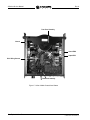
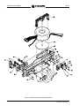
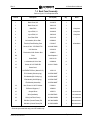
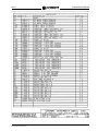
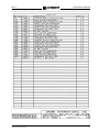
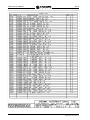
1
?
K SERIES
Service Manual
17
17
19
19
21
21
25
25
30
30
45
45
100
100
B
B
A
LL A
A
N
C
E
D
C
U
R
R
E
N
TT A
A
M
P
LL III F
FF III E
E
R
BA
AL
AN
NC
CE
ED
D C
CU
UR
RR
RE
EN
NT
AM
MP
PL
ER
R
15
15 13
13 11
11
1
1
99
77
55
33
11
00dB
dB
Thermal
Thermal
Clip
Clip
IOC
IOC
Signal
Signal
17
17
19
19
21
21
25
25
30
30
45
45
100
100
15
15 13
13 11
11
22
99
77
55
Enable
33 Enable
11
00dB
dB
PROFESSIONAL AUDIO AMPLIFIERS
Models:
K1, K2
© 1999 by Crown International, Inc., P.O. Box 1000, Elkhart, Indiana 46515-1000 U.S.A. Telephone: 219294-8000. K Series amplifiers are produced by Crown International, Inc. Trademark Notice: Balanced
Current Amplifier™ is a trademark, and Crown® and BCA® are registered trademarks of Crown
International, Inc. Other trademarks are the property of their respective owners.
KSVCK1K2
03/98
Rev. A
Rev. A
K Series Service Manual
The information furnished in this manual does not include all of the details of design, production, or variations
of the equipment. Nor does it cover every possible situation which may arise during installation, operation or
maintenance. If you need special assistance beyond the scope of this manual, please contact the Crown
Technical Support Group.
Mail: P.O. Box 1000 Elkhart IN 46515-1000
Shipping: Plant 2 S.W., 1718 W. Mishawaka Rd., Elkhart IN 46517
Phone: (800) 342-6939/(219) 294-8200
FAX: (219) 294-8301
Web: www.crownaudio.com
CAUTION
AVIS
TO PREVENT ELECTRIC SHOCK DO
NOT REMOVE TOP OR BOTTOM
COVERS. NO USER SERVICEABLE
PARTS INSIDE. REFER SERVICING
TO QUALIFIED SERVICE
PERSONNEL. DISCONNECT
POWER CORD BEFORE REMOVING
REAR INPUT MODULE TO ACCESS
GAIN SWITCH.
À PRÉVENIR LE CHOC
ÉLECTRIQUE N’ENLEVEZ
PAS LES COUVERTURES.
RIEN DES PARTIES
UTILES À L’INTÉRIEUR.
DÉBRANCHER LA BORNE
AVANT D’OUVRIR LA
MODULE EN ARRIÈRE.
WARNING
TO REDUCE THE RISK OF ELECTRIC
SHOCK, DO NOT EXPOSE THIS
EQUIPMENT TO RAIN OR MOISTURE!
The lightning bolt
triangle is used to
alert the user to the
risk of electric shock.
I
The exclamation point
triangle is used to alert the
user to important operating
or maintenance instructions.
©1999 Crown International, Inc.
K Series Service Manual
Rev. A
Revision History
Revision Number
Date
None
3-98
Initial Printing
Rev. A
6-99
Added Revision History, Module and Schematic
Information, and Module Parts Sections.
Upgraded Manual to Facilitate Component-Level
Troubleshooting of PWA’s.
Updated Cover Page and Table of Contents.
©1999 Crown International, Inc.
Changes
II
Rev. A
K Series Service Manual
This page intentionally left blank
III
©1999 Crown International, Inc.
K Series Service Manual
Rev. A
Table of Contents
1 Introduction ............................................................................
1.1 Introduction ......................................................................
1.1.1 The K Series Amplifiers ...........................................
1.2 Warranty ...........................................................................
1.3 Repair Strategy ................................................................
1.4 Service Procedure ...........................................................
1-1
1-1
1-1
1-1
1-2
1-2
2 Specifications .........................................................................
2.1 Performance ....................................................................
2.2 Controls ............................................................................
2.3 Indicators .........................................................................
2.4 Input/Output .....................................................................
2.5 Output Signal ...................................................................
2.6 Protection .........................................................................
2.7 Construction .....................................................................
2-1
2-1
2-1
2-1
2-2
2-2
2-2
2-2
3 Theory ......................................................................................
3.0 Overview ..........................................................................
3.1 Power Supplies ................................................................
3.1.1 Main Power Supply ..................................................
3.1.2 Low Voltage Supplies ..............................................
3.2 Input Stage ......................................................................
3.3 DC Servo ..........................................................................
3.4 Sleep Circuit ....................................................................
3.5 Error Amp .........................................................................
3.6 Modulator .........................................................................
3.7 Triangle Generator ...........................................................
3.8 Proportional Vcc Generator .............................................
3.9 Output ..............................................................................
3.10 Output Filter ...................................................................
3.11 Current Limiter ...............................................................
3.13 Overlap Correction and Adjustment ..............................
3.14 Display Circuitry .............................................................
3.15 Control Circuitry .............................................................
3.16 Crowbar Circuitry ...........................................................
3-1
3-1
3-1
3-1
3-1
3-2
3-2
3-2
3-2
3-2
3-3
3-3
3-3
3-3
3-3
3-4
3-4
3-4
3-5
4 Line Voltage Conversion ........................................................ 4-1
4.1 Line Voltage Conversion .................................................. 4-1
5 Maintenance ............................................................................ 5-1
5.1 Where to Begin ................................................................ 5-1
5.2 Disassembly for Inspection & Service ............................. 5-1
©1999 Crown International, Inc.
IV
Rev. A
K Series Service Manual
Table of Contents
5.2.1 Cover Removal ........................................................ 5-1
5.2.2 Power Supply Discharge ......................................... 5-2
5.2.3 Back Panel Assembly Removal ............................... 5-2
5.2.4 Front Panel Assembly Removal ............................... 5-3
5.2.5 Input PWA Removal ................................................. 5-3
5.2.6 Main PWA Removal ................................................. 5-3
5.2.7 Output PWA Removal .............................................. 5-4
5.2.8 Control PWA Removal ............................................. 5-4
5.2.9 Line Filter PWA Removal ......................................... 5-4
5.2.10 Power Transformer Removal .................................. 5-4
5.2.11 Display PWA Removal ........................................... 5-5
5.2.12 Bridge PWA Removal ............................................ 5-5
5.3 Troubleshooting ............................................................... 5-6
5.3.1 Identifying Symptoms .............................................. 5-6
5.3.2 Identifying and Repairing the Cause ....................... 5-6
5.4 Required Test Equipment ................................................. 5-8
5.5 Electrical Checkout Procedures....................................... 5-8
5.5.1 Quiescent AC Power Draw ...................................... 5-9
5.5.2 Gain Switches .......................................................... 5-9
5.5.3 “Y” Input Switch Operation ...................................... 5-9
5.5.4 Bridge Mono Operation ........................................... 5-9
5.5.5 Frequency Response ............................................ 5-10
5.5.6 Short Circuit Test ................................................... 5-10
5.5.7 Output Power ......................................................... 5-10
5.5.8 Intermodulation Distortion ..................................... 5-10
5.5.9 Signal to Noise Ratio ............................................. 5-10
5.5.10 Crosstalk at 1 kHz................................................ 5-10
5.5.11 Post Test Settings ................................................ 5-11
5.6 Calibrations .................................................................... 5-11
5.6.1 Gaussian Filter Calibration .................................... 5-11
5.6.2 Overlap Correction and Adjustment ...................... 5-11
V
6 Parts .......................................................................................
6.1 General Information .........................................................
6.2 Ordering and Receiving Parts .........................................
6.2.1 Terms .......................................................................
6.2.2 Shipment .................................................................
6-1
6-1
6-1
6-1
6-1
7 Exploded View Parts ..............................................................
7.1 General Information .........................................................
7.2 Main Chassis Assembly ...................................................
7.3 Front Panel Assembly ......................................................
7.4 Back Panel Assembly ......................................................
7-1
7-1
7-3
7-5
7-7
©1999 Crown International, Inc.
K Series Service Manual
Rev. A
Table of Contents
8 Module and Schematic Information ......................................
8.1 General Information .........................................................
8.2 PWAs ...............................................................................
8.3 Schematics ......................................................................
8-1
8-1
8-1
8-2
9 Module Parts ........................................................................... 9-1
9.1 General Information ......................................................... 9-1
100438 PWA .......................................................................... 9-2
Component Map ............................................................... 9-6
101554 Assembly .................................................................. 9-7
100469 PWA .......................................................................... 9-9
Component Map ............................................................. 9-11
100497 PWA ........................................................................ 9-12
Component Map ............................................................. 9-29
100524 PWA ........................................................................ 9-31
Component Map ............................................................. 9-39
101014 PWA ........................................................................ 9-40
Component Map ............................................................. 9-42
101809 ................................................................................. 9-43
Component Map ............................................................. 9-51
101850 PWA ........................................................................ 9-52
Component Map ............................................................. 9-54
101865 PWA ........................................................................ 9-55
Component Map ............................................................. 9-57
102176 PWA ........................................................................ 9-58
Component Map ............................................................. 9-62
102175 Assembly ................................................................ 9-63
102552 PWA ........................................................................ 9-65
Component Map ............................................................. 9-67
10 Schematics ......................................................................... 10-1
©1999 Crown International, Inc.
VI
Rev. A
K Series Service Manual
This page intentionally left blank
VII
©1999 Crown International, Inc.
Rev A.
K Series Service Manual
19
21
17
25
30
45
100
B
BA
A LL A
AN
NC
CE
ED
D C
CU
UR
RR
RE
EN
N TT A
AM
MP
P LL II FF II E
ER
R
15 13
11
Thermal
9
7
5
3
1
1
0 dB
Clip
IOC
Signal
19
21
17
25
30
45
100
15 13
11
9
7
5
3
2
Enable
1
0 dB
Figure 1.1 The Crown K2 Amplifier
mance. Other features include convection cooling,
balanced inputs, Bridge-Mono operation, “Y” Input for
routing one signal to both channels, and input compression for maximum loudspeaker protection.
1 Introduction
1.1 Introduction
This manual contains complete service information
on the Crown K1 and K2 power amplifiers. It contains
service information for both non-CE and CE (European) units. It is designed to be used in conjunction
with the Reference Manual; however, some important
information is duplicated in this Service Manual in case
the Reference Manual is not readily available.
NOTE: THE INFORMATION IN THIS MANUAL IS INTENDED FOR USE BY AN EXPERIENCED TECHNICIAN ONLY!
1.1.1 The K Series Amplifiers
The K Series of power amplifiers are efficient, compact, high-power audio amplifiers designed for professional use. They provide full audio bandwidth, highpower amplification with minimum distortion. Crown’s
patented Balanced Current Amplifier™ design allows
for maintenance-free operation with maximum perfor-
1.2 Warranty
Each Reference Manual contains basic policies as
related to the customer. In addition, it should be stated
that this service documentation is meant to be used
only by properly trained personnel. Because most
Crown products carry a 3-Year Full Warranty (including round trip shipping within the United States), all
warranty service should be referred to the Crown Factory or Authorized Warranty Service Center. See the
applicable Reference Manual for warranty details. To
find the location of the nearest Authorized Warranty
Service Center or to obtain instructions for receiving
Crown Factory Service, please contact the Crown
Technical Support Group (within North America), or
your Crown/Amcron Importer (outside North America).
If you are an Authorized Warranty Service Center and
have questions regarding the warranty of a product,
please contact the Field Service Manager or the Technical Support Group.
Crown Customer Service
Technical Support Group
Factory Service
Parts Department
Mailing Address: P.O. Box 1000, Elkhart IN 46515
Shipping Address: Plant 2 S. W.
1718 W. Mishawaka Rd., Elkhart IN 46517
Phone: (219) 294-8200
Toll Free: (800) 342-6939
Fax: (219) 294-8301
http://www.crownaudio.com
©1999 Crown International, Inc.
Introduction 1-1
K Series Service Manual
Rev A.
1.3 Repair Strategy
1.4 Service Procedure
The Balanced Current Amplifier technology rings in a
new era in Crown history. Taking full advantage of the
modular design approach used in the design of K Series amplifiers, we are able to offer a module exchange
program for this product. The concept is that the PWA
(Printed Wire Assembly) as a whole is one component, and when a part of the assembly is defective,
the whole assembly is defective. Exceptions are the
Control, Bridge, Display, and Line Filter PWAs. Those
PWAs may be repaired at the component level unless
there is sufficient damage or malfunction to warrant
PWA replacement. Non-PWA components are also excluded from this program.
Servicing a Balanced Current Amplifier requires certain steps to be followed. See Figure 1.2 for a flow
chart of these steps. It is important that the defective
Printed Wire Assemblies (PWAs) be returned to Crown
for evaluation and repair. Under the module exchange
program, warranty claims for PWA replacement will
not be honored unless the defective PWA accompanies the warranty claim. In the event of a non-warranty repair, rebuilt PWAs will be available at a lower
price than new PWAs, and a discount will be given if
the defective PWA is returned to Crown.
Under the module exchange program, defective
PWAs are returned to Crown for evaluation and rework. The reworked assemblies will then be stocked
in the Crown Parts Department to be sold as refurbished parts.
This strategy offers several advantages. One advantage is less time spent in troubleshooting and repairing the amplifier, thus resulting in greater customer
satisfaction. This strategy also allows Crown to collect the necessary information from amplifier failures,
so improvements can be made for even greater product reliability.
Each PWA purchased from the Crown parts department will have a tag indicating that it is “Available for
Issue.” This tag will have two parts. The first part simply states that the PWA is ready for use. It also has
instructions for the PWA and the serial number of the
module. Once the new PWA is installed, this part is to
be discarded. The second part will be filled out by
the service technician. After it is filled out with data
such as the amplifier serial number and a description
of the failure, it will be attached to the failed PWA.
This part has three copies. The first is for the service
center to keep. Copies 2 and 3 will remain together
for use at Crown.
WARNING
Component-level troubleshooting and repair of
PWAs included in the module exchange program
should not be attempted without expressed authorization from the Crown Audio Service Manager.
Such an attempt, without specialized training and
specialized test equipment, will likely result in substantial damage to the amplifier. Crown will not
authorize payment of warranty claims in such an
instance.
1-2 Introduction
©1999 Crown International, Inc.
Rev A.
K Series Service Manual
Figure 1.2 Service Procedure Flow Chart
©1999 Crown International, Inc.
Introduction 1-3
K Series Service Manual
Rev A.
This page intentionally left blank
1-4 Introduction
©1999 Crown International, Inc.
Rev A.
2 Specifications
All specifications relate to both Export and Domestic
units, regardless of voltage and frequency.
2.1 Performance
K Series Service Manual
Power
An on/off rocker switch located on the front panel.
Input Sensitivity
A two–position switch for each channel, located on the
back panel near each channel’s input connectors. Can
be set to 1.4 V for full output power into an 8-ohm load
or a fixed voltage gain of 26 dB.
Frequency Response
±0.25 dB from 20 Hz to 20 kHz. The frequency response is band limited with an 8-Hz double-integrated
3rd-order Butterworth high-pass filter and a 30-kHz 7thorder Gaussian low-pass filter.
Bridge Output
An on/off switch located on the back panel between
the input connectors. This switch, when turned on,
bridges the two outputs with the channel one input signal.
Output Power
Measured at 1 kHz with both channels driven to 0.1%
or less true THD.
“Y” Input
An on/off switch located on the back panel between
the input connectors. This switch, when turned on, parallels the two input channels.
K1
2 ohm Stereo: 750 watts per channel.
4 ohm Stereo: 550 watts per channel.
8 ohm Stereo: 350 watts per channel.
4 ohm Bridge Mono: 1,500 watts.
8 ohm Bridge Mono: 1,100 watts.
K2
2 ohm Stereo: 1,250 watts per channel.
4 ohm Stereo: 800 watts per channel.
8 ohm Stereo: 500 watts per channel.
4 ohm Bridge Mono: 2,500 watts.
8 ohm Bridge Mono: 1,600 watts.
Signal-to-Noise Ratio
Greater than 100 dB below rated power, A-weighted.
Voltage Gain
1.4 VRMS input sensitivity or a fixed gain of 26 dB
(back panel switchable).
Damping Factor
Greater than 3,000 from 10 Hz to 400 Hz.
Line Voltage Requirements
Universal power supply can be configured to operate
with 100, 120, 200, 230, 240 or 250 VAC at 50 or 60 Hz.
2.2 Controls
Level
A calibrated rotary level control for each channel located on the front panel. Each control is labeled from 0
to 100 dB of voltage attenuation.
©1999 Crown International, Inc.
2.3 Indicators
Thermal
A red LED for each channel which turns on with a dim
glow shortly before the amplifier needs help dissipating heat. The LED will turn brighter as the Thermal Level
Control (TLC) protection is activated.
Clip
An orange LED for each channel which turns on when
distortion of any type becomes audible in the amplifier
output.
IOC
A yellow LED for each channel which serves as a distortion indicator. This indicator will light long before the
distortion is audible. The IOC indicators include a pulse–
stretching feature that helps make them more noticeable, even with rapid transient signals.
Signal
A green LED for each channel which flashes dimly when
a very low–level signal (as low as 10 mW) is present in
the output. They flash brightly when a louder signal (at
least 1 watt) is present at the output.
Enable
A green LED that turns on when the amplifier has been
turned on and has power. When first turned on, there
will be a brief two–second delay while the amplifier
performs a quick turn–on diagnostic. Then the Enable
indicator will turn on to its full brightness. If no signal is
present, the Enable indicator will switch to a dim level.
Specifications 2-1
K Series Service Manual
2.4 Input/Output
Input Connectors
One balanced ¼–inch phone jack and one 3–pin female XLR connector for each channel.
Rev A.
Out–of–band low–pass and high–pass filters protect
the amplifier and loads from infrasonic frequencies below 8 Hz and ultrasonic frequencies above 30 kHz.
Input Stage
Input is electronically balanced and employs precision
1% resistors.
Turn On
State–of–the–art “soft start” feature prevents the amplifier from drawing a large inrush current when it is
first turned on. This feature also assures that no dangerous artifacts are produced by the amplifier.
Input Impedance
Nominally 20 K ohms, balanced. Nominally 10 K ohms,
unbalanced.
2.7 Construction
Input Sensitivity
1.4 volts for standard 1 kHz power (33 dB of gain), or
26 dB gain.
Output Connectors
Two sets of color–coded binding posts for banana plugs,
spade lugs or bare wire. European models do not accept banana plugs.
DC Output Offset
±10 millivolts maximum.
2.5 Output Signal
Stereo
Unbalanced, two channel.
Bridge–Mono
Balanced, single–channel. Channel 1 controls are active; channel 2 should be turned down. For polarity the
same as the input signal, use channel 1 output post as
the speaker positive and the channel 2 output post as
the speaker negative.
2.6 Protection
Chassis
Beautiful cast–aluminum front panel coated with a durable powder coat finish. Front panel labels are printed
in color on Lexan for durability and fingerprinting resistance. Aluminum chassis with durable black finish.
Cooling
High performance passive convection cooling system
allows the amplifier to drive 2-ohm loads to high music
sound levels (8 dB into clip) in a 40° C environment
without overthermalling.
Dimensions
Standard 19–inch (48.3-cm) rack mount width (EIA RS–
310–B), 3.5–inch (8.9-cm) height and 16–inch (40.6cm) depth behind front mounting surface.
Weight
K1
32 pounds (14.6 kg).
K2
38 pounds (17.3 kg).
Center of gravity approximately 6 inches (15.2-cm) behind front mounting surface and left-right centered.
General Protection
K-Series amplifiers are protected against shorted, open
or mismatched loads; overloaded power supplies; excessive temperature, chain destruction phenomena,
input overload damage and high–frequency blowups.
They also protect loudspeakers from input/output DC,
DC offset and turn–on/turn–off transients.
TLC protection circuitry protects the amplifier from excessive heat by subtly and dynamically reducing the
gain only when necessary to reduce heat levels. Transformer overheating (an extremely unlikely event) will
result in a temporary shutdown; when it has cooled to
a safe temperature, the transformer will automatically
reset itself.
2-2 Specifications
©1999 Crown International, Inc.
Rev A.
3 Theory
K Series Service Manual
Full wave rectification is achieved by the bridge rectifying units D1 and D2 for the high energy supplies
(±Vcc). C5 and C7 filter unwanted AC ripple from the
±Vcc power supplies.
3.0 Overview
This section of the manual explains the general operation of the K Series power amplifier. Topics covered include Power Supplies, Input Stage, DC Servo,
Sleep Circuit, Error Amp, and Modulator. For Simplicity, the circuit theory will only refer to channel one. It
may be assumed that channel two is identical to channel one.
3.1 Power Supplies
There are numerous power supplies and voltage regulators found within the K Series amplifiers. The main
high energy power supply and the low energy power
supplies are located on the main module.
3.1.1 Main Power Supply
The AC line cord is terminated through the fuse to the
AC line filter circuit. C1 is a .22uF capacitor and is
located across the line and neutral leads. C2 and C3
are .0047uF capacitors. C2 is connected from line to
ground and C3 is connected from neutral to ground.
This filter prevents unwanted emissions from contaminating the AC power line. The AC power then is routed
to the control board where the power-on relay, soft
start circuit and the AC line voltage configuration circuits take place.
When S1 is closed and power is first applied the relay
K1 is open and current passes through PTC (R1) to
the power transformer primary. The PTC restricts the
amount of inrush current while the transformer is energizing. When the power supply voltage reaches operating voltage level the relay (K1) closes and bypasses the PTC resistor. D1 is a diode bridge that is
configured to filter out any DC component on the AC
line. This is included to eliminate the possibility of
“Transformer Buzz” which can occur when a torroidial
transformer is subjected to “dirty” or “noisy” AC power.
The primary wiring configuration for the multi-tap
torroidial power transformer (T1) is accomplished with
a connector plug that contains 9 connections. The
jumpers on the plug determine the amplifiers line voltage operating level. Line voltage reconfiguration can
be achieved by inserting the appropriately wired pug
(See Section 4) or by rewiring the existing plug.
©1999 Crown International, Inc.
D3, D4 and R1 detect low energy by sampling the
transformer secondary voltage levels and passing this
on to the Power OK circuit located on the Main module (to be covered later).
3.1.2 Low Voltage Power Supplies
On power up the ±Vcc power supplies first initiate.
Once the +Vcc supplies are up to an operational level
they power up the 125KHz oscillator: U9 and the gate
driver: U10. The +Vcc is fed through F1 (3 amp fuse),
L1 and R6. This sends+15V to both U9 and U10. The
output of U10 is amplified by Q2, rectified by D3 and
filtered by C15. The result is a regulated +15VDC. This
+15V feeds U4 (+5V) which starts a 4MHz generator
Y1/U6D (main schematic). The 4MHz output of U6D
is sent to a divide-by chip, U5. U5 generates two outputs:
1. 500KHz–routed to the triangle generator (see Triangle generator circuit description).
2. 125KHz–routed back to the low voltage power supply. This 125KHz signal is fed back in order to drive a
high frequency switch mode power supply. This SMPS
consists of D4, D5, U11A, U11B, Q3 and Q4. U11A
and B drive the 2 FET devices Q3 and Q4. The resulting output is a +7V 125KHz signal. The output of this
switch mode power supply is routed in three directions:
1. Through C23 this supply is rectified and filtered by
D10, D11, C24, and L5. The output is –13V.
2. Through C22 a 7VAC (15Vp-p) source is routed to
the output stage. In the output stage T1 relays the
power source to the full wave bridge (D01 and D02).
Power Supply filtering is provided by C1, C2, C3 and
C4. This +15V now feeds U03A and U03B (output
stage FET drivers) and a +5V regulator (U01).
3. T1 Transformation:
a. Using the primary coil of T1 the signal is filtered by
C26 and L6 to supply +7V. This +7V is used to
feed a number of 5V regulators found on the main
module.
b. T1 secondary #1: this power supply uses -Vcc as a
reference point. The output is labeled -Vcc+12.
Since the K2 Vcc is ±103V the output of this power
supply is –103V +12V = –98V. D12 and D13 provide rectification and C27 and C28 provide filtering.
Theory 3-1
K Series Service Manual
Rev A.
c. T1 secondary#2: After rectification (D14 and D15)
and filtering (C29 and C30) B2+7 and B2-7
mount. There are three filters that eliminate any AC
component:
d. T1 secondary#3: After rectification (D16 and D17)
and filtering (C31 and C32) B1+7 and B1-7
1. R147 and C121 for a 1 pole filter (-3 point is 8Hz).
4. Oscillator Sync: the final destination of the 125KHz
signal is to synchronize the original 125KHz oscillator
U9.
3.2 Input Stage
Both XLR and phone jack input connectors are in parallel with each other. While in most audio products
the incoming shield is tied to the amplifiers ground
network, K Series amplifiers insert a 24 ohm resistor
(R100) paralleled with two .01uf capacitors(C100 and
C135) for the purpose of inhibiting ground loop circulating currents and RFI protection.
The signal is fed to the balanced to unbalanced gain
stage. Input impedance is 20K ohm balanced and
10K ohm unbalanced.
K Series amplifiers come with two input sensitivity selections: 26dB and 1.4V. With the gain switch (S100)
out the inverting gain stage is unity (gain of 1). With
the gain switch (S100) in the inverting gain stage adds
(depending on the amplifier model) the necessary
gain to achieve 1.4V input sensitivity.
2. The RC networks C114/R141 and C118/R148 each
form a single pole filter.
The combination of all three filters form a three-pole
filter leaving only the DC voltage.
3.4 Sleep Circuit
The sleep circuit monitors each channel for a signal.
When no signal is present for approximately six seconds the sleep circuit sends a Standby signal to the
main module turning off the carrier frequency within
the modulator circuit. It takes approximately 0.5mV of
input signal to bring the amplifier out of Sleep mode.
Signal is sampled from the second stage (U103A pin
1) of the Gaussian low pass filter. U5D generates the
Standby control signal to place the amplifier in sleep
mode. R17, R15 and C7 form the RC timing network
that determines the time of switching states of U5D
from +0.9V (awake) and –13V (asleep). The Standby
control signal is routed to the base of Q102 through
the diode D111.
3.5 Error Amp
Inherent within all PWM amplifiers is a rise in gain at
higher frequencies. Because of this a 7th order
Gaussian low pass filter has been included in the input stage of the K Series amplifiers. This Gaussian
filter is found immediately after the gain stage. U103A,
U103B, U103C, U103D comprise this filter. U101D and
R172 form the gain calibration stage for this 7th order
Gaussian filter.
The audio signal enters the main module from the input module. the audio and negative feedback signals
are both processed by the error amplifier U100D. From
the error amplifier the signal is divided and is fed to
the modulator. Since the modulator circuit is balanced
the drive signal for the positive modulator is inverted
by U100C.
3.6 Modulator
3.3 DC Servo
Because the K series of amplifiers are DC coupled
from the Gaussian Filter through to the amplifier output DC offset voltages can appear. This DC voltage
can be amplified and the audio signal ride on top shifting its reference point resulting in nonsymmetrical clipping. For this reason a DC correction circuit has been
added. The non-inverting input of U105 is tied to the
speaker output.
Since the purpose of U105 is to compensate for DC
offset voltages elimination of any AC signal is para-
3-2 Theory
U101 and U103 are high speed differential comparators. The comparator section has two outputs: inverting and non-inverting. Therefore the output is balanced. The audio signal is applied to the inverting
input of both differential comparators. The 250KHz
triangle wave is applied to the non-inverting input of
both differential comparators. With no audio signal the
250KHz is passed on to the NAND gate section of the
differential comparator unchanged. Each NAND gate
has two inputs: the modulated signal from the high
speed comparater section and current limiter
signal(U6A). In the event of over current the current
limiter (U6A) signal is shut off disabling the NAND
©1999 Crown International, Inc.
Rev A.
gates. This results in disrupting of the signal path.
The output of U101 is balanced and forms the positive portion of the output waveform (Vp). The output
of U103 is balanced and forms the negative portion
of the output waveform (Vn). These two balanced signal lines are routed to the output stage drivers, U02
and U52.
3.7 Triangle Generator
The 250KHz triangle wave has its origins from the
4MHz generator. After entering the divide-by chip (U5),
a 500KHz output signal (pin 9) is routed to U12B. The
output of U12B is a 250KHz square wave.
The 250KHz signal is then sent through U2C. U2C is
a linear IC with R186, R187, C153 and C154 in its
feedback loop. This stage converts the 250KHz
square wave into a triangle wave. From Pin 8 of U2C
and through C152 the 250Kz triangle wave is sent to
U105 which has two functions: gain and high frequency filtering. C150, C151 and R162 serve to filter
the triangle wave signal.
The output of U105 is the 250KHz signal that is routed
to the positive and negative modulators, U101 and
U103.
3.8 Proportional Vcc Generator
The Proportional Vcc generator outputs a DC voltage
that varies as the ±Vcc levels vary. This varying DC
voltage influences the 250KHz output level. Because
output signal gain in a PWM amplifier can deviate as
VCC varies a DC voltage proportional to the Vcc supplies is applied to the Triangle generator circuit.
U3C functions as the Proportional Vcc generator.
Through a resistor dropping network (R23/R24) +Vcc
is applied to the non-inverting input. Through another
resistor dropping network (R22/R21) –Vcc is applied
to the inverting input. On the output of U3A is a DC
voltage of 6.2VDC.Through diode D21 and resistor
R20 5.1VDC is applied to U12B.
K Series Service Manual
cuitry. The output of U02 and U52 are then sent to the
output MOSTFET drivers.
U03A, U03B, U53A and U53B are dual inverting high
speed drivers designed to interface low current digital circuitry (U02 and U52) with power MOSFETs.
U03A, U03B, U53A and U53B are used to drive the
gates of the output FETs (Q1-Q4, Q51-Q54).
The output stage is divided into two sections, positive
and negative. The signal is then routed to the BCA
filter inductors (Ln and Lp) and the current sense resistors (R13/R14 and R63/R64). The combining point
is then sent to the Output Filter.
With no audio modulation both negative and positive
FET stages conduct. The frequency, phase and amplitude of output FET conduction is identical. Since
the FET conduction signals are the same but opposite in polarity complete cancellation takes where the
BCA filter inductors and current sense resistors connect. As the fundamental center frequency (250KHz)
is modulated with audio differences in frequency,
phase and amplitude appear and audio output develops from the BCA filter. This signal is then routed
back to the Output Filters located on the main module.
3.10 Output Filter
The output filter is made up of three individual filters:
a 250KHz filter (L101/C127), a 500KHz filter (L102/
C131) and a final 250KHz filter. The signal passes
through these three filters to eliminate both any residual 500KHz and 250KHz signals. The audio signal
is the connected to the output speaker connectors.
3.11 Current Monitor
Audio output current levels are monitored by the use
of transformer T100. A small primary winding is in
series with the output line and the secondary develops a voltage related to the output current of the amplifier. This output current information is used for two
purposes:
1. Negative feed back.
3.9 Output
The modulated 250KHz signal exits the main module
and enters output assembly by means of U02 (Vp)
and U52 (Vn). U02 and U52 are optically coupled
gates giving electrical isolation from main module cir-
©1999 Crown International, Inc.
2. Current feedback information for the Triangle wave
generator.
3.12 Current Limiter
To prevent excessive output current the K series am-
Theory 3-3
K Series Service Manual
plifiers are incorporated with a current limiting protection circuit. The output current is sense by the current sense resistors found in series with the BCA filter
inductors. The voltage dropped across these two resistors is sent back to U106A and U106B. The voltage windows for U106A and U106B are set by the
dropping resistors R303/R310 and the zener diodes
D113/D114. The window voltage is ±0.7V. The outputs of the window comparator are normally +0.6V.
This positive voltage is sent to U107A, an optically
coupled gate. Pin 2 of U107A is tied to B1-7 and as
long as pin 1 is positive the device conducts. The
output is an inverting stage so when its input is positive its output will be negative. If the current limit detector switches states (becomes negative) pin 1 is
negative and pin 7 becomes positive.
The output of U107A is routed to U6A (exclusive NOR)
and as long its inputs are negative the output of U6A
will be positive allowing the modulating network (U101
and U103) to output signal. If the output of U107A
goes positive the output of U6A goes negative thus
disabling the modulating circuit.
3.13 Overlap Correction and Adjustment
The Overlap adjustment corrects for DC shift in the
Triangle waveform. In order to track thermal variations
the Overlap adjustment potentiometer (R25) is located
on each of the Output assemblies. A positive DC voltage is routed from the wiper arm of R26 to the Triangle wave gain stage. This DC voltage varies the
DC component of the 250KHz waveform.
3.14 Display Circuitry
The IOC (Input Output Comparator) circuit uses the
error signal from the error amplifier (U100D). With a
window of ±0.3V U102A and U102D have a positive
output. This in turn biases off D105 leaving a positive
voltage on the base of Q103. If an error signal appears the ±0.3V window is overcome and the combined outputs become negative. This results in the
output of U102C to go negative and in turn biasing on
Q103. As Q103 biases on, E102 illuminates.
Rev A.
nal. When initialized U1B output (pin 7) becomes positive. After routed through the non-inverting input of
U1A this positive signal turns on E100.
The signal used to switch on the Power LED comes
from the Power OK control circuit. As this lime goes
positive Q1 conducts lighting E1.
3.15 Control Circuitry
After initial power supply power up the outputs of U7C
and U7D become positive (+1.2V). The output of U7
C and U7D is routed to two places: 1.) the first is the
Power OK LED and 2.) then the Modulator able/disable comparator, U108A.. This positive logic signal
causes the output of U108A to become positive
(+1.3V) which next biases on Q102. With Q102 biased on the collector/emitter voltage is low (0.6V).
Since U6A is a NOR gate and both inputs are low the
output is a logic high allowing the modulator circuits
(U101 and U103) to pass signal.
There are four functions that can disable the modulator circuit and disable the amplifier. These four inputs
all effect the control line connected to pin 5 of U108A.
The normal logic levels for this control line are: ON/
0.6 and OFF/–14). The four control functions are:
1. Initial Turn On Delay (U8A). On initial turn on the
control line to U108A is logic low causing the modulator to be disabled. Once the capacitor found within
the RC timing network (C161/R302) charges this comparator stage switches states allowing the Modulator
to conduct. (Normal logic levels are ON/0.6 and OFF/
-14).
2. Over Temperature (U108B). In the event the amplifier overheats the output of U108B switches states
disabling the Modulator.
3. Proportional Vcc (U8C). The Proportional Vcc circuit monitors the ±Vcc power supplies. In the event
that the line voltage drops to far below the rated line
voltage (causing erratic operation) U8C switches
states disabling the Modulator circuit.
4. Current Limit (U108D).
A sample of the amplifier output (Fo CH1) is sent to
U2A and U2B. This audio waveform sample then
drives Q102 varying the current to the SPI (Signal Presence Indicator) LED E101.
If the amplifiers current limit is exceeded because of
low impedances or a short circuit loading, U108D
switches states and disables the modulator circuit.
The compressor circuit is initiated by either the IOC
initialization signal or The Thermal Limit Control sig-
3-4 Theory
©1999 Crown International, Inc.
Rev A.
K Series Service Manual
3.16 Crowbar Circuit
U13B and U13C form the DC protection comparator
circuitry. R191, R192 and C156 form a combination
resistive dividing and low pass filter networks. Signals below 8Hz (including DC voltages) cause the
combined outputs to become a logic low (–14V). This
logic level is inverted by the next comparator stage,
U7B. a logic high (0.6V) causes Q10 to conduct. Once
U7B switches states (logic high) U7A inverts this logic
level and latches the Fault circuit in the Crowbar disabled condition. In order to clear this latched state
the amplifier must be first turned off.
When the amplifier is turned on the line current conducts through the R1 (power supply circuit diagram)
until the relay energizes. The relay primary is energized when Q8 is biased on. Q8 is biased on when
Q7 is biased off (high collector/emitter voltage). When
the relay closes R1 is bypassed allowing full power
supply energy available to the output stage. If Q10
conducts Q7 is biased on and Q8 is biased off. This
disables the power input relay.
Figure 3.1 Amplifier Block Diagram
©1999 Crown International, Inc.
Theory 3-5
K Series Service Manual
Rev A.
This Page Intentionally Left Blank
3-6 Theory
©1999 Crown International, Inc.
Rev A.
K Series Service Manual
appropriate operating voltage. Figure 4.1 has information on jumper location for each voltage.
4 Line Voltage
Conversion
When wiring the molex connector the proper insertion
and removal too should be used (example, Amp
#458994-2).
4.1 Line Voltage Conversion
When converting from the 100V range to the 200V range,
or vice versa, be sure and change the back panel line
fuse. The fuse values and Crown Part Numbers are
listed in Figure 4.1.
The K Series amplifier can be configured to operate at
any line voltage in the world. It is also made to operate
at 50- or 60-hertz frequency with no modification. To
convert from one line voltage to another, change the
Voltage Plug (P7), a 9 pin connector plug on the Control PWA. Refer to Figure 4.1 for the Crown Part Number of the plug you need. These plugs are available
from the Crown Parts Department.
For your reference, Figure 4.2 shows the Control PWA,
P7, and the pin configuration of P7. To access the Control PWA, remove the bottom cover of the amplifier.
The Control PWA is located in the center of the chassis. For additional information on disassembly and assembly of the amplifier refer to Chapter 5.
The Voltage Plugs have jumpers installed which configure the primary power transformer windings for the
Voltage
Plug Part #
Voltage
Plug
Jumpers
Fuse
100V
101230-1
120V
130V
200V
220V
230V
240V
250V
101231-1
NA*
NA*
101232-1
101233-1
101234-1
NA*
5–7
5–8
1-8
2–4
2–4
2–4
1–4
1–4
6–2
6–1
3-4
5–7
5–8
5–9
5–8
5–9
3–4
3–4
5-9
K1: A10285-27, 15A
K1: A10285-40, 8A
K2: A10285-28, 20A
K2: A10285-26, 10A
* Voltage Plug not available. Voltage may be obtained by positioning the jumpers as indicated.
The Crown Part Number for the Voltage Jumper Wire is A11555-P025P.
The Crown Part Number for the 9-Pin Molex Connector is C10303-3.
Figure 4.1 Line Voltage Selection Table
C3
P5
R1
C2
C1
1
P6
P11
L2
P10
1
D2
1
4
7
2
5
8
3
6
9
P7
Voltage Plug
L1
K1
D1
P9
P4
P8
P13
P12
1
Figure 4.2 Control PWA with Voltage Plug
©1999 Crown International, Inc.
Line Voltage Conversion 4-1
K Series Service Manual
Rev A.
This page intentionally left blank
4-2 Line Voltage Conversion
©1999 Crown International, Inc.
Rev A.
K Series Service Manual
5 Maintenance
5.1 Where to Begin
Effective repair involves three basic steps: 1) Determine the symptom(s) of the problem; 2) Identify the
cause(s) of the symptom(s); 3) Repair the unit to eliminate the cause(s). To determine the symptoms, you
will want to get as much information from the user as
possible. Get as much information as you can about
the system and how the amplifier is used. There is
always the possibility that the problem will show up
only if used in a specific way.
Once you have all the information about the symptom(s),
it is time to inspect the amplifier. A careful visual inspection is valuable for most problems which you may
encounter. To inspect the inside of the amplifier remove
the cover as described in Section 5.2.1.
Begin the inspection by looking for anything which
appears abnormal, like loose connectors, broken wires
and burnt or visibly damaged components. Inspect
the printed circuit assemblies for broken traces and
loose connections. Be thorough. The time you spend
visually inspecting the amp is time well spent.
5.2 Disassembly for Inspection & Service
The extent of disassembly required will depend upon
the extent of inspection and service required.
NOTE: TO AVOID THE RISK OF ELECTRIC SHOCK,
TURN OFF AND UNPLUG THE AMPLIFIER FROM
THE AC POWER OUTLET BEFORE DISASSEMBLY
OR REASSEMBLY IS ATTEMPTED.
5.2.1 Bottom Cover Removal
To remove the cover of the amplifier you will need a
#15 torx bit (TX15). After the cover is removed, and
before any internal cables are disconnected, discharge
the supplies. See Section 5.2.2.
1. Turn the amplifier on its side on your workbench.
The only access to the inside of the amplifier is the
bottom cover.
2. Using the TX15 bit, remove the 14 screws around
the perimeter of the cover.
3. The cover lifts straight up after the screws are removed.
4. Vacuum out any metal particles in the unit that are a
result of the lock washers digging into the chassis.
The cover on early units may appear to be symetrical
but it’s not. When installing it onto the unit, make sure
there is no gap between the front edge of the cover
and the lip of the front panel extrusion. If installed backwards, there will be an 1/8-inch gap at the front, and an
1/8-inch overhang out the back of the unit.
WARNING
Amplifier components are ESD sensitive.
When servicing the amplifier, the technician
must have approved ESD protection. Proper
grounding straps and test equipment are
required. Failure to use proper protection
will result in component failure.
©1999 Crown International, Inc.
WARNING
Before unplugging or plugging in any connectors or wires in the amplifier, discharge
the power supplies. See section 5.2.2 for
instructions. Failure to do so will result in
circuit failure.
Maintenance 5-1
K Series Service Manual
Rev A.
5.2.2 Power Supply Discharge
Before any connectors and PWAs are removed, the
Power Supplies need to be discharged. Follow these
simple steps.
1. Make sure the amplifier is unplugged from the AC
power source.
2. Locate Test Point 1 (TP1) on the Main PWA. See
Figure 5.1.
3. With a flat blade screwdriver or another metal object, short TP1 to the nearest resistor pad. This resistor
is the second one from the end of a row of seven 3W
resistors. Once the short is made you do not have to
hold the screwdriver in place. The initial short triggers
a latching triac circuit which discharges the supplies.
4. Wait a few seconds before attempting to disassemble the amplifier.
Caution: the three-watt resistors will become hot as
the power supplies discharge.
5.2.3 Back Panel Assembly Removal
The back panel assembly is removed to access the
Input and Main PWAs.
1. Follow the instructions in Section 5.2.2. Supply
discharge is necessary to avoid circuit damage.
2. Remove the aluminum shield by removing the two
screws on the rear and the one on the control board.
TP1
Note: This shield is not used on early non-CE units.
3. Using a TX15 bit, remove the two screws on each
side of the amp that hold the rear supports. See Figure 5.2. Item A
4. Remove the five TX15 screws along the top rear of
the amplifier.
Caution: These screws are shorter than the other
cover screws and must be reinstalled in the same
location or Main PWA will be shorted to chassis.
5. Remove the two TX15 screws on the Main PWA.
See Figure 5.2. Item B
6. Unplug the black and white wires (P8 & P9) and the
ribbon cable (P4) from the Control PWA. See Figure
5.2. Item C
7. Unplug the P1 ribbon cable from the Input PWA.
See Figure 5.2. Item D
8. Unplug the main wiring harness from the Main PWA.
See Figure 5.2. Item E
9. Remove the necessary tie wraps and unplug the
ribbon cables from the Output PWAs. See Figure 5.2.
Item F
10. Gently slide the back panel assembly straight out
the back of the amplifier. Note that the PC cards slide
in the rails formed in the aluminium heatsink. Be careful of the wires and cables that will come with the assembly.
Resistor Pad
Figure 5.1 Discharge Test Point
5-2 Maintenance
©1999 Crown International, Inc.
Rev A.
K Series Service Manual
5.2.4 Front Panel Assembly Removal
The front panel assembly is removed to access the
Power Switch, Display PWA, Bridge PWA and the Power
Transformer.
1. Follow the instructions in Section 5.2.2. Supply
discharge is necessary to avoid circuit damage.
2. Using a TX 15 bit, remove two screws on each side
of the amp located directly behind the rack ears. See
Figure 5.2. Item G
3. Remove the four TX 15 screws along the top front of
the amplifier.
4. Unplug the main wiring harness from the Bridge
PWA. See Figure 5.2. Item H
5. Remove the P1 ribbon connector from the Input
PWA. See Figure 5.2. Item D
6. Remove the P5 and P6 transformer wire connectors, and P10, P11, P12 and P13 switch wires from the
Control PWA. See Figure 5.2. Item I
7. The Front Panel Assembly will now come off of the
amplifier. Pull on the front panel handles while securing the chassis of the amplifier. Be careful of the wires
and cables that will come with the assembly. When
reinstalling the Front Panel, make sure the capacitors
on the Bridge PWA clear the aluminum heat sink and
the Output PWA.
5.2.5 Input PWA Removal
The Back Panel Assembly must be removed to gain
access to the Input PWA.
1. Follow the instructions in Section 5.2.2. Supply
discharge is necessary to avoid circuit damage.
2. Remove the P2 ribbon cable from the Input PWA.
3. Using a #1 Phillips bit, remove the four screws that
hold the two female XLR jacks on the back panel.
4. Using a 5/8-inch nut driver, remove the two plastic
nuts that hold the 1/4-inch input jacks in place.
5. Using a TX15 bit, remove the two screws on the
back panel that hold the Input PWA in place.
6. Locate the plastic board stand–off between the Main
and Input PWAs. Using your fingernail or pliers, press
the release tab on the stand–off while gently lifting the
Input PWA off the stand–off.
7. While guiding the input jacks out of the holes in the
back panel, slowly lift the PWA out of the assembly.
5.2.6 Main PWA Removal
The Back Panel Assembly must be removed to gain
access to the Main PWA.
1. Follow the instructions in Section 5.2.2. Supply
discharge is necessary to avoid circuit damage.
I
G
G
H
F
F
C
D
E
A
A
B
Figure 5.2 Bottom View
©1999 Crown International, Inc.
Maintenance 5-3
K Series Service Manual
Rev A.
2. Remove the P2 ribbon cable from the Input PWA.
3. Using a needle nose pliers, unplug the six red wires
that go to the positive output binding posts. Note where
they go.
4. Using a TX15 bit, remove the three screws that secure the Main PWA to the back panel.
Caution: Do not power up the amplifier without replacing these screws, or circuit damage to the Output PWAs will occur.
5. Locate the plastic board stand–off between the Main
and Input PWAs. Using your fingernail or pliers, press
the release tab on the stand–off while gently separating the two PWAs.
6. Lift the Main PWA away from the back panel.
When installing the Main PWA onto the Back Panel
Assembly be careful not to bend the capacitor located
under the Line Filter PWA. If the unit is an early non-CE
unit, the clearance between a capacitor on the Line
Filter and a capacitor on the Main PWA is very small.
5.2.7 Output PWA Removal
The left and right Output PWAs are identical.
1. Follow the instructions in Section 5.2.2. Supply
discharge is necessary to avoid circuit damage.
2. Unplug the P01 ribbon connector and the P3 wiring
harness connector from the Output PWA.
3. Using a TX15 bit, remove the screw located at the
center–top of the assembly. See Figure 5.3. Item A.
4. Using a TX20 bit, remove the six screws located by
the four large coils on the assembly. See Figure 5.3.
Item B
Be very careful not to damage the coils with your screwdriver. Note that the screws have belleville washers on
them. When replacing the screws be sure the cupped
side of the washer is down toward the assembly.
5. Carefully lift the assembly out of the chassis. When
reinstalling the Output Assembly use a new insulator
pad and make sure there are no metal shavings on the
pad or the heatsinks. Any metal shavings will result in
a “blow–up” when the unit is first turned on. To be sure
that the insulator is free of shavings, and is installed
correctly, use an Ohm Meter to check for continuity
between the assembly heatsink and the chassis. There
should be no continuity.
5.2.8 Control PWA Removal
1. Follow the instructions in Section 5.2.2. Supply
discharge is necessary to avoid circuit damage.
2. Remove EMC shield on all but early non-CE units.
3. While noting where each wire goes, disconnect each
connector on the Control PWA. The white wire goes on
P9, and the black wire on P8. The two orange wires go
on P10 and P11. The two purple wires go on P12 and
P13.
4. To remove the Bridge Rectifier (D1) along with the
PWA, use an 11/32 -inch (.86 cm) nut driver to remove
the nut. If you wish to leave the Bridge installed to the
chassis then desolder the four rectifier pads.
5. Using a TX15 bit, remove the three screws that hold
the Control PWA in place.
6. Lift the Control PWA out of the chassis.
If replacing the PWA with a new one, be sure and remove the Voltage Plug (P7) and install it on the new
PWA.
If replacing the Bridge Rectifier, be sure and use thermal heatsink compound between the rectifier and the
chassis.
B
A
B
Figure 5.3 Output PWA Screws
5-4 Maintenance
5.2.9 Line Filter PWA Removal (Early non-CE Units Only)
1. Follow the instructions in Section 5.2.2. Supply
discharge is necessary to avoid circuit damage.
2. While noting where each wire goes, disconnect each
wire from the PWA. The blue power cord wire goes on
P4. The long black wire goes on P1, the white on P2.
The short black wire from the fuse goes on P3.
3. Using a TX15 bit, remove the two screws that attach
the assembly to the back panel.
4. Lift the Line Filter PWA out of the chassis.
5.2.10 Power Transformer Removal
The Front Panel Assembly must be removed in order
to remove the Power Transformer.
1. Follow the instructions in Section 5.2.2. Supply
discharge is necessary to avoid circuit damage.
©1999 Crown International, Inc.
Rev A.
K Series Service Manual
2. Clip the tie wrap which holds the orange and purple
wires to the Transformer Bracket.
3. Unplug the white wires from the Bridge PWA (P11,
P12 and P13). Note that the white wire with the black
ring attaches to P12.
4. Using a TX15 bit, remove the two screws which
hold the Transformer Bracket to the Front Panel.
5. Using a TX25 bit, remove the bolt which goes through
the center of the transformer. The plastic bracket can
now be removed.
6. While carefully lifting the transformer out of the
front panel, route the white wires underneath the Bridge
PWA. The transformer will now lift free of the front panel.
5.2.11 Display PWA Removal
The Front Panel Assembly must be removed in order
to remove the Display PWA.
1. Follow the instructions in Section 5.2.2. Supply
discharge is necessary to avoid circuit damage.
2. The two level control knobs on the front panel are
press fit onto the shafts. Remove these knobs.
3. Using a 7/16 -inch nut driver, remove the nuts on the
level control shafts. Also remove the flat washers.
4. Lift the Display PWA out of the Front Panel Assembly.
5.2.12 Bridge PWA Removal
The Front Panel Assembly must be removed in order
to remove the Bridge PWA.
1. Follow the instructions in Section 5.2.2. Supply
discharge is necessary to avoid circuit damage.
2. Unplug the white transformer wires from the PWA.
Note that the white wire with the black ring goes to
P12.
3. Using a T20 bit, remove the two screws that hold
the bridge rectifiers to the front panel. The screws have
bellville washers. When installing the screws with the
washers, make sure the cupped side of the washer is
toward the bridge.
4. Using a T20 bit, remove the screw in the center of
the PWA.
5. The bridge assembly will now lift out of the front
panel. When installing it back into the front panel,
make sure there is thermal heatsink compound between
the bridges and the front panel.
Power Transformer
Bridge PWA
Display PWA
Control PWA
Output PWA
Output PWA
Main PWA
Input PWA
Figure 5.4 Discharge Test Point
Line Filter PWA
Figure 5.4 PWA Layout
©1999 Crown International, Inc.
Maintenance 5-5
K Series Service Manual
Rev A.
5.3 Troubleshooting
As mentioned earlier, the three steps to effective repair are: Determine the symptoms; identify the cause
of the symptoms; repair the unit to eliminate the cause.
The purpose of this section is to help you through these
steps in an orderly manner.
5.3.1 Identifying Symptoms
Why was the amplifier brought in for repair? Can you
get it to malfunction again? Some problems can be
intermittent and difficult to find.
Once you have identified and verified the symptoms,
you can look for helpful information in Section 5.3.2 as
to where the cause of the problem is located.
If you don’t observe anything wrong with the amplifier,
tactfully inquire how the owner used it and try to determine if it was misused or some other component in
their system could have been at fault. Remember that
the protection circuits in this amplifier will protect loudspeakers from problems caused upstream from the
amplifier (DC protect).
If you lack sufficient information about the problem,
and there aren’t any obvious problems with the amplifier, skip to Section 5.4, the Electrical Checkout Procedures.
5.3.2 Identifying and Repairing the Cause
The first step in identifying the cause of the problem is
always a visual inspection. Once the bottom cover is
removed, and the supplies are discharged, look for
loose connectors, broken wires, loose hardware, burnt
components, or bad solder joints on the PC boards.
Any burnt components are a sure sign that the PWA
will need to be replaced.
Once the visual inspection is complete you may proceed in powering up the unit. The best way to positively locate which PWA is at fault is to have a working
PWA of each type on hand and plug them into the
amplifier one at a time to see when the problem goes
away. Output and Input PWAs can be plugged into the
amplifier easily without removing the old PWA. When
doing so, use an insulating material to isolate it from
the chassis and other PWAs. The Main PWA, however,
needs to be installed into the chassis before it can be
properly hooked up.
The following Symptoms and Causes may help you
determine which corrective action to take. We realize
that this list is limited. Please read through the Theory
chapter in this manual to better understand the function of each PWA. This will help you come to your own
conclusion as to the location of the problem.
Amp does not appear to power up. No Enable light.
First, check the power supply fuse. Also, make sure
the AC line voltage is correct for the amplifier you are
working on. Severely low AC line voltage could cause
the amp to not power up. If both check out, then the
amplifier is in a fault mode. The two most likely areas
are the Main PWA or an Output PWA.
First, check the Output PWAs. Discharge the supplies, then disconnect the main wiring harness (P3)
from the PWA in question. Now power up the unit. After the delay, if the enable light comes on, the disconnected Output PWA needs to be repaired or replaced.
To check if the Main PWA is at fault discharge the
supplies, then unplug only one Output PWA from the
main wiring harness (P3), and unplug the Input PWA
(P2) from the Main PWA. Now apply power and check
the +15VDC and the -13VDC. To do this, locate U7 on
the Main PWA (next to where the Input PWA overlaps
WARNING
Before unplugging or plugging in any connectors
or wires in the amplifier, discharge the power supplies. See section 5.2.2 for instructions. Failure
to do so will result in circuit failure.
5-6 Maintenance
©1999 Crown International, Inc.
Rev A.
K Series Service Manual
the Main PWA). Using the chassis as the ground reference, pin 3 is +15VDC and pin 12 is –13VDC. If the
both voltages are correct, discharge power supplies,
then plug Output PWA back in, and unplug the other
Output PWA. Repeat test. If one or both of the DC
voltages is not correct then repair or replace the Main
PWA.
Output PWA.
No Signal; one or both channels. Enable on. IOC on.
A constant IOC condition indicates a problem in the
signal path including the Error Amp circuit. This includes the Main and Output PWA’s. The problem most
likely exists on the Main PWA.
Frequency Response out of tolerance.
The problem most likely exists on the Input PWA. The
Input PWA has the EQ circuit for a flat response. If this
circuit is faulty the amplifier will have poor frequency
response. Discharge the supplies, then repair or replace Input PWA.
No Signal; one or both channels. Enable light only.
The problem most likely exists on the Input PWA. If
the Input PWA proves to not be the problem then the
Main PWA is at fault.
To check the Input PWA, inject a signal into the channel at fault and turn the level control up. Locate U103
(Ch1) or U203 (Ch2). With an oscilloscope check to
see if there is signal at pin 8. If there is no signal at this
point discharge the supplies, then repair or replace
the PWA. If there is signal then check U5 pin 13 with a
DC volt meter. If this pin is at –13VDC then the signal
detect circuit is not working. Discharge the supplies,
then repair or replace the Input PWA. If you find signal
at U103/203 pin 8, and U5 pin 13 is high (0 VDC), then
the Input PWA is OK. Discharge the supplies, then
repair or replace the Main PWA.
Distortion; one or both channels. IOC indication.
The problem most likely exists on either the Output
PWA or Main PWA. Check the Output PWA first. If the
Output PWA checks out, repair or replace Main PWA.
Distortion; one or both channels. No IOC.
The problem most likely exists on the Input PWA. First
check levels on affected channels, no load. If levels
check out, discharge the supplies, then repair or replace Input PWA.
Amplifier does not meet power specs.
Check your power source. If the AC voltage sags below the specified operating voltage of the amplifier then
the unit will not produce full rated output.
The large power supply filter capacitors located on the
Output PWAs are wired in parallel from one PWA to the
other. If one or more of these capacitors has a broken
solder joint it could result in the amplifier not meeting
power specifications. To check the capacitors, discharge the supplies, then remove the Output Assembly. Wiggle the capacitors back and forth. If they appear to be loose then they are bad. Repair or replace
©1999 Crown International, Inc.
Check the Main Wiring Harness. Multiple wires are used
in parallel to handle the high supply currents. If one or
more of these wires is broken then it will result in restricted current. This could result in the amplifier not
meeting power specifications.
Voltage gain problems.
If you experience voltage gain problems with no distortion, the problem most likely exists on the Input
PWA. The Input Sensitivity/Gain Stage circuitry is located on the Input PWA. Discharge the supplies, then
check the Input PWA. If it is faulty, repair or replace
PWA. If Input PWA checks out, the problem is likely
on the Display PWA, which includes the Level Control
Pots. Discharge the supplies, then check Display
PWA. If Display PWA is faulty, repair or replace PWA.
If you have gain problems with distortion, resulting in
an IOC condition, then the problem most likely exists
on the Main PWA. Discharge the supplies, then check
Main PWA. If faulty, repair or replace PWA.
Amplifier gets extremely warm at idle.
Sleep Mode is indicated on the front panel by the Enable indicator. When it switches to half intensity then
the amplifier is in sleep mode. It takes approximately
6 seconds after the signal is removed before the amplifier goes into Sleep Mode. Note that any signal at
all, even a small one, will keep the amplifier out of
sleep mode and it will get warm to the touch. If, with no
signal at all, the amplifier never goes into Sleep Mode
then the problem most likely exists on the Input PWA.
The Signal Detect circuit for Sleep Mode is located on
the Input PWA. Discharge the supplies, then check
Input PWA. If faulty, repair or replace PWA.
To verify the operation of the Signal Detect Circuit, locate U5 on the Input PWA. Monitor pin 13 with a DC
volt meter referenced to chassis ground. If it switches
to –13VDC 6 seconds after signal is removed then the
circuit is OK. If this circuit is OK, but the amplifier
never goes to Sleep, then the problem exists on the
Main PWA. Discharge the supplies, then repair or replace Main PWA.
Amplifier consistently trips breakers at turn on.
A Soft Start circuit on the Control PWA limits the amount
Maintenance 5-7
K Series Service Manual
Rev A.
of inrush current at turn on. Check the PTC (R1) on the
Control PWA. It should measure approximately 5 ohms.
If it is shorted then replace it. Another possibility is
that the relay (K1) has failed.
If the amplifier trips breakers and you can never get it
powered up, Discharge the supplies, then check the
bridge rectifiers (D1 and D2) at the Bridge PWA located in the Front Panel Assembly.
DC output offset
If there is an IOC indication, the problem most likely
exists on the Main PWA. Discharge the supplies, then
check the Main PWA. if faulty, repair or replace PWA.
If there is no IOC condition then the problem is on the
Input PWA. Discharge the supplies, then repair or
replace Input PWA.
Signal to noise out of spec.
If the ribbon cable between the Display and Input PWA
is not routed properly it can cause high Signal to Noise.
Device
Oscilloscope
It needs to be lying down and away from the large
coils on the Output PWA. The coils can induce noise
into the ribbon cables.
Turn on/off transient
The problem is most likely on the Input PWA. The only
real way of verifying this is to plug a working Input
PWA into the amplifier and see if the problem goes
away. If it is not the Input PWA, it is probably the Main
PWA. The amplifier should be silent at turn-on and turnoff.
5.4 Required Test Equipment
Due to the complex circuitry utilized the the K Series
amplifiers, special calibration procedures and the correct test equipment are necessary to insure original
factory specifications are achieved. Following is list of
test equipment needed to successfully service the K
Series amplifier. Recommended models are those used
by Crown:
Requirements
* 500 MHz or greater
Recommended Model
LeCroy 9354A
Distortion Analyzer
THD and IM measurements
Audio Precision ATS-1
DC Power Suppies
* 103 VDC with I-Limiting and
* 12-15 VDC with I-Limiting
Leader 760-3D (Qty. 2)
Leader 18-3D
Function Generator
AC/DC volt meter
Dummy Loads
Hewlett-Packard HP 33120A
* dB reading capability
Hewlett-Packard HP 34401A
8 ohm, 550 watt, 4 ohm, 850 watt,
and 2 ohm, 1300 watt
* Requirement for component-level troubleshooting only
5-8 Maintenance
©1999 Crown International, Inc.
Rev A.
K Series Service Manual
5.5 Electrical Checkout Procedures
The test procedures in this section are used to verify
the operation of the amplifier. You may, however, find
these tests helpful in troubleshooting a problem if the
problem is not easily identified.
All tests assume that AC power is from a regulated
source at the voltage the amplifier is set up for. See
Chapter 4 if you need to change the operating voltage.
Test equipment includes an oscilloscope, a DMM, a
signal generator, loads, watt meter, I.M. distortion analyzer, and a true THD meter.
During each test, it is assumed that the following conditions are set on the amplifier unless otherwise noted:
—Level controls fully clockwise.
—Bridge Output switch off.
—“Y” Input switch off.
—Input Sensitivity of both channels set at 26 dB.
5.5.1 Quiescent AC Power Draw
Spec: 100 watts maximum quiescent. 10 watts in sleep
mode.
Procedure: With no load connected to the amplifier,
turn on the amplifier. Inject a small signal into one of
the inputs to keep the amplifier out of sleep mode.
Measure AC power draw. It should be less than 100
watts. Remove the signal from the amplifier and wait
approximately 6 seconds for the amp to go into sleep
mode. Measure AC power draw. It should be 10 watts
±3 W.
5.5.2 Gain Switches
Spec: 1.4 V, 26 dB
K1 Procedure: No Load. With the level controls at full
gain and the input sensitivity switches set to 1.4 V,
inject a 1 kHz, 0.775 Vrms, into each channel. At the
output of each channel measure 29.3 Vrms, ±0.9 Vrms.
Switch the Input Sensitivity switches to 26 dB. Measure 15.3 Vrms, ±0.6 Vrms, at the outputs.
K2 Procedure: No load. With the level controls at full
gain and the Input Sensitivity switches set to 1.4 V,
inject a 1 kHz, 0.775 Vrms, into each channel. At the
output of each channel measure 34 Vrms, ±1.3 Vrms.
Switch the Input Sensitivity switches to 26 dB. Measure 15.3 Vrms, ±0.6 Vrms, at the outputs.
5.5.3 “Y” Input Switch Operation
Spec: Channel 1 input will produce an output at both
channels. Both outputs will be in phase.
Procedure: No load. Switch the “Y” Input switch on.
Inject a 1 kHz sine wave into channel 1 only. You should
see output on both channels. They should be in phase
with each other. With the gain switches set the same,
and the level controls both at full volume, you should
see the same output voltage at both channels. Remove the signal and turn the “Y” Input switch off.
5.5.4 Bridge Mono Operation
Spec: Same voltage out both channels, channel 2 out
of phase.
Procedure: No load. Switch the Bridge Mono switch
on and inject a 1 kHz sine wave into channel 1 only.
Monitor both outputs of the amplifier. They should be
the same voltage and out of phase with each other.
Remove the signal and turn the Bridge Mono switch
off.
WARNING
Before unplugging or plugging in any connectors
or wires in the amplifier, discharge the power supplies. See section 5.2.2 for instructions. Failure
to do so will result in circuit failure.
©1999 Crown International, Inc.
Maintenance 5-9
K Series Service Manual
Rev A.
5.5.5 Frequency Response
Spec: ±0.25 dB from 20 Hz to 20 kHz.
Procedure: Load the channel under test to 4 ohms.
Inject a 0.1Vrms, 1kHz sine wave into the input. Measure the output voltage. It should be 2.0 Vrms. This is
now your 1 kHz reference voltage. Switch the frequency
to 20 Hz and verify that the input voltage is still 0.1
Vrms. Measure the output voltage. It should
K2 Procedure 8 ohm: Load the channel under test to 8
ohms. Inject a 1kHz sine wave and bring the level up until
the output reaches 0.1% TRUE THD. Measure at least 61.6
Vrms at the output.
K2 Procedure 4 ohm: Load the channel under test to 4
ohms. Inject a 1kHz sine wave and bring the level up until
the output reaches 0.1% TRUE THD. Measure at least 56.6
Vrms at the output.
be the same as the 1 kHz reference voltage ±0.25 dB.
Switch the frequency to 20 kHz and verify that the input
voltage is still 0.1 Vrms. Measure the output voltage and
compare it to the 1 kHz reference voltage. Tolerance is ±0.25
dB. Remove the load and signal. Note: Many oscillators
need a frequency check at 20 kHz.
K2 Procedure 2 ohm: Due to the duty cycle of a test signal,
the line fuse will blow if both channels are tested at the
same time. When testing 2-ohm power, test one channel at
a time. Load the channel under test to 2 ohms. Inject a 1kHz
sine wave and bring the level up until the output reaches
0.1% TRUE THD. Measure at least 50.0 Vrms at the output.
5.5.6 Short Circuit Test
Spec: Amplifier will protect itself
5.5.8 Intermodulation Distortion
Spec: Less than 0.2% from 0 dB to -35 dB.
Procedure: Inject a 1kHz, 1Vrms sine wave into the input of
channel 1. Short the output of channel 1 to ground for 10
seconds. The amplifier should cycle into fault mode. Every
two seconds the Clip and IOC lights will flash, indicating
that it is checking to see if the short is still there. Remove the
short and perform the test on channel 2.
Procedure: Load the channel under test to 8 ohms. Inject a
SMPTE standard IM signal (60 Hz and 7 kHz mixed at 4:1).
Adjust the output voltage for a peak equivalent voltage of
60.0 volts (K1) or 70.0 volts (K2). This is your 0-dB reference. Measure less than 0.2% IMD from 0 dB to -35 dB in 5dB steps.
5.5.7 Output Power
K1 Spec: Each channel
5.5.9 Signal to Noise Ratio
Spec: Greater than 100 dB below rated 8 ohm power, A
weighted.
K2 Spec: Each channel
350 watts into 8 ohms
550 watts into 4 ohms
750 watts into 2 ohms
475 watts into 8 ohms
800 watts into 4 ohms
1250 watts into 2 ohms
Procedure: Load the channel under test to 8 ohms. Terminate the input with 600 ohms. Verify that the gain switch is
set at 26 dB and level control is at full volume. Measure less
than 529 µVrms (K1) or 616 µVrms (K2) at the output using
an A-weighted filter.
Measure less than 0.1% true THD.
K1 Procedure 8 ohm: Load the channel under test to 8
ohms. Inject a 1kHz sine wave and bring the level up until
the output reaches 0.1% TRUE THD. Measure at least 52.9
Vrms at the output.
K1 Procedure 4 ohm: Load the channel under test to 4
ohms. Inject a 1kHz sine wave and bring the level up until
the output reaches 0.1% TRUE THD. Measure at least 46.9
Vrms at the output.
K1 Procedure 2 ohm: Due to the duty cycle of a test signal,
the line fuse will blow if both channels are tested at the
same time. When testing 2-ohm power, test one channel at
a time. Load the channel under test to 2 ohms. Inject a 1kHz
sine wave and bring the level up until the output reaches
0.1% TRUE THD. Measure at least 38.7 Vrms at the output.
5-10 Maintenance
Note: Due to the power conservation circuit you only have 6
seconds to do this test after a signal is injected. After a
signal is used, quickly remove the signal and measure Signal to Noise.
5.5.10 Crosstalk at 1 kHz
Spec: Greater that 90 dB.
Procedure: Load each channel to 8 ohms. Verify that both
gain switches are set at 26 dB and both level controls are at
full volume. Inject a 2.5 Vrms, 1 kHz, sine wave into channel
1 and terminate channel 2 with 600 ohms. Measure less
than 1.58 mV at the output of channel 2. Now remove the
signal from channel one and inject it into channel 2. Terminate channel 1 with 600 ohms. Measure less than 1.58 mV
at the output of channel 1.
©1999 Crown International, Inc.
Rev A.
5.5.11 Post Test Settings
After completion of testing, if all tests are satisfactory, the
amplifier controls should be returned to the positions required by the customer. If the conditions are unknown or
unspecified, the factory settings are as follows:
–Gain switches set to 1.4 V
–Bridge Mono switch turned off
–“Y” Input switch turned off
–Level controls at 0 dB
–Power switch turned off
K Series Service Manual
to perform this procedure the Sleep circuit may cause
the amplifier to go into standby. A brief input signal
(no load) will bring the amplifier out of Sleep mode.
5.6 Calibrations
These calibrations should only be performed by those
servicers authorized to do component-level repair of
PWAs included in the module exchange program (see
Section 1.3).
5.6.1 Gaussian Filter Calibration
Procedure 1: Obtain a multimeter with decibel measurement capabilities.Set the multimeter to dB measurement mode. Insert a 1Khz signal into the input
and measure at pin 8 of U103C. Reset the meter to
0dB using the 1KHz signal as a reference signal. Increase the signal generator frequency to 20KHz, leaving the output level unchanged. While measuring pin 8
of U103C adjust R172 for a reduction of level by 2.6dB
(readout should be -2.6dB).
Procedure 2: Obtain a multimeter with decibel measurement capabilities. Set the meter to dB measurement mode. Insert a 1Khz signal into the input and
measure at the speaker output (no load). Reset the
meter to 0dB using the 1KHz signal as a reference
signal. Increase the signal generator frequency to
20KHz, leaving the output level unchanged. Adjust
R172 for a meter reading of 0db. This second test
method is an alternative to the first and should give
the desired results: a flat frequency response throughout the audio bandwidth.
Figure 5.1 Correct Overlap Adjustment
Figure 5.2 Underlap
5.6.2 Overlap Correction and Adjustment
Conditions:
—Amplifier output assembly MUST be room temperature (72 degrees F/21 degrees C)
—No input signal
—No load
Procedure: Monitor TP51 found on the Output Assembly. Center oscilloscope to view lower right portion of
waveform. Adjust R25 on each Output PWA for sharpest squarewave edges (see Figure 5.1). Figure 5.2
shows “Underlap” (under adjustment). Figure 5.3 shows
“Overlap” (over adjustment). If too much time is taken
©1999 Crown International, Inc.
Figure 5.3 Excessive Overlap
Maintenance 5-11
K Series Service Manual
Rev A.
This page intentionally left blank
5-12 Maintenance
©1999 Crown International, Inc.
Rev A.
K Series Service Manual
6 Parts
6.1 General Information
This chapter includes both a mechanical and electrical
parts list for this product. All serviceable parts and
assemblies will have a Crown Part Number (CPN) listed
in this chapter. The parts listed are current as of the
date printed. Crown reserves the right to modify and
improve its products for the benefit of its customers.
Crown is not a general parts warehouse. Parts sold by
the Crown Parts Department are solely for servicing
Crown/Amcron products.
Part prices and availability are subject to change without
notice.
6.2.1 Terms
Normal terms are prepaid. Net-30 Days applies to only
those having pre-established accounts with Crown. The
Crown Parts Department does accept Visa or Master
Card. If prepaying, the order must be packed and
weighed before a total bill can be established, after
which an amount due will be issued and shipment made
upon receipt of payment. New parts returned for credit
are subject to a restocking fee, and authorization from
the Crown Parts Department must be obtained before
returning parts for credit.
6.2.2 Shipment
Shipment will normally be made via UPS, or best other
method unless you specify otherwise. Shipments are
made to and from Elkhart, Indiana USA, only. Established accounts with Crown will receive shipment freight
prepaid and will be billed. All others will receive shipment on a C.O.D. or prepayment (check or credit card)
basis.
6.2 Ordering and Receiving Parts
When ordering parts, be sure to give the product model,
and include a description and part number from the
parts listing. Price quotes are available on request.
Crown Customer Service
Technical Support Group
Factory Service
Parts Department
Mailing Address: P.O. Box 1000, Elkhart IN 46515
Shipping Address: Plant 2 S. W.
1718 W. Mishawaka Rd., Elkhart IN 46517
Phone: (219) 294-8200
Toll Free: (800) 342-6939
Fax: (219) 294-8301
http://www.crownaudio.com
©1999 Crown International, Inc.
Parts 6-1
K Series Service Manual
Rev A.
This Page Intentionally Left Blank
6-2 Parts
©1999 Crown International, Inc.
Rev A.
K Series Service Manual
7 Exploded View Parts
7.1 General Information
This chapter includes a mechanical part list for this
product. All serviceable parts and assemblies will have
a Crown Part Number (CPN) listed in this chapter. The
parts listed are current as of the date printed. Crown
reserves the right to modify and improve its products
for the benefit of its customers.
©1999 Crown International, Inc.
Exploded View Parts 7-1
K Series Service Manual
Rev A.
Front Panel Assembly
Chassis
Control PWA
Output PWA
Main Wiring Harness
Back Panel Assembly
Figure 7.1 View of Main Chassis from Bottom
7-2 Exploded View Parts
©1999 Crown International, Inc.
Rev A.
K Series Service Manual
7.2 Main Chassis Assembly
Refer to figure 7.1 for Location of Major Parts
Description
Chassis
Part # (CPN)
Qty.
102226-X
1
Notes
Front Panel Assembly
—
1
See 6.4
Back Panel Assembly
—
1
See 6.5
Bottom Cover
102076-X
1
Control PWA
—
1
See Sect. 7
Output PWA
—
2
See Sect. 7
Screw, 8-32 X .812 T20
A12148-70813
12
Rear Support
100848-X
2
Insulator, Output PWA
100536-X
2
#6 Internal Star Washer, Black
A10094-3
7
#8 Belleville Washer
A10098-3
13
8-32 Hex Nut
A10102-6
1
Screw, 6-32X.375 Pan HD T15
A12148-70606
7
5.5" Cable Tie
C 8812-7
3
35A 400V Bridge, Wire Lead
C10246-4
1
At Control PCA
Screw, 8-32X.5 Flt Hd T15
100331-70808
18
Cover
Screw, 8-32X.312 Flt Hd T15
100331-70805
5
Top Rear
Screw, 8-32X.5 Flt Hd T15
101087-70808
8
Front Panel to
Chassis
Lockwasher, CSK Ext Tooth #8
101357-1
31
Wire, Pwr Switch Violet
A11569-E160F
2
Wire Pwr Switch Orange
A12122-C140D
2
Main Wiring Harness
101838-1
1
101528-1
1
©1999 Crown International, Inc.
Early non-CE
Models Only
Exploded View Parts 7-3
K Series Service Manual
Rev A.
Figure 7.2 Front Panel Assembly Exploded View
7-4 Exploded View Parts
©1999 Crown International, Inc.
Rev A.
K Series Service Manual
7.3 Front Panel Assembly
Refer to figure 7.2 for Exploded View
Item #
Description
Part # (CPN)
Qty.
Notes
1
Bridge Rect. PWA
100444-X
1
See 6.9
2
Bracket, Transformer Mounting
100124
1
3
Power Transformer, K2
102236-1
1
w/connectors
Power Transformer, K1
H43525-7
1
w/connectors
4
Display PCA
102552-X
1
See 6.10
5
Knob, K2
D 8959-5
2
6
Rubber Washer, Toroid
A10659-6
1
-
Rubber Dampening Pad
102243-1
1
K1
7
Bridge, 35A 400V Wire Lead
C10246-4
2
Qty 1 for K1
8
Lock Washer, #8 Internal Star
A10094-6
1
9
Screw, 8-32 x .812 PNHD T20
A12148-70813
3
10
Handle
F12722-9
2
11
Switch, Rocker DPDT 10A
100222-1
1
12
Screw, 1/4-20 x 2.0 FLTHD T27
A12149-72532
1
13
Belleville Washer, #8
A10098-3
2
14
Screw, 8-32 x .5 UC FLTHD T15
100331-70808
6
15
Front Panel
F12717-9
1
16
Overlay, Set, K2 Front Panel
102181-X
1
16
Overlay, Set, K1 Front Panel
102183-X
1
17
5K Ohm Vol Pot Hardware
C10245-6
2
18
Feet, Selfstick Black
C 3342-0
2
©1999 Crown International, Inc.
Pot w/Hrdwr
Exploded View Parts 7-5
K Series Service Manual
Rev A.
Figure 7.3 Back Panel Assembly Exploded View
7-6 Exploded View Parts
©1999 Crown International, Inc.
Rev A.
K Series Service Manual
7.4 Back Panel Assembly
Refer to figure 7.3 for Exploded View
Item #
Description
Part # (CPN)
Qty.
Notes
1
Back Panel, K2
101085-X
1
1
Back Panel, K1
102013-X
1
2
Main PCA
100497-X
1
Complete
3
Input PCA, K1
101809-X
1
Complete
3
Input PCA, K2
100524-X
1
Complete
4
Line Filter PWA
101014-X
1
*
5
Lockwasher, #6 Int. Star
A10094-3
7
6
Terminal, Dual Binding Post
C10184-7
2
7
Screw, 6-32 X .375 PNHD T15
A12148-70606
7
8
8-32 Hex Nut
A10102-6
1
9
Fuseholder, 3AG–Scrdvr–Slot
100850-1
1
9X
Fuse
See Chapter 4
1
10
Strain Relief
A10214-10
1
11
Lockwasher, #10 Int. Star
A10094-8
6
12
Screw, #4 X .5 PNHD PH
A10111-70408
4
13
Power Cord:
A1/E3/E8/E17/Dom. (Nema 5-15)
101011-2
1
E13 Models (Schuko plug)
A10793-0508T
1
E14 Models (BS 1363 plug)
A10793-0608T
1
E24 Models (Old BS plug)
A10793-0708T
1
E34 Models (Australia)
A10793-0908T
1
14
Nut, Phone Jk 1/4" PC Mount
C10226-1
2
15
PC Board Support, 1"
100939-1
1
16
Output Wires
100537-1
2
w/connectors
17
Wire (feedback)
A11382-F040L
2
w/connectors
18
Wire (Line Filter Power)
A11384-C020M
1
w/connectors
19
Blk Wire (Control Power) P8
A11384-C095M
1
w/connectors *
Wht Wire (Control Power) P9
A11565-A095M
1
w/connectors *
w/hardware
* Denotes part used with early, non-CE models only
©1999 Crown International, Inc.
Exploded View Parts 7-7
K Series Service Manual
Rev. A
8.2.2 Input PWA:
8 Module and Schematic
Information
102524-1
Input PWA built on 100523-1 PWB.
8.1 General Information
102524-3
Input PWA built on 100523-5 PWB. Replaced 100523-2.
Since the introduction of the K Series amplifiers there
have been several updates and revisions. Many of
these changes called for new modules. The following pages list all modules used as of the printing of
this manual.
When replacing an Output PWA, it is recommended
that you order a complete, pre-assembled Output Assembly, which includes the PWA, heatsink, matched
output inductors and other parts.
The Crown Parts Department stocks the most current
PWAs and Output Assemblies for each K Series
model, which will retrofit into all older units.
Parts lists and schematics for Main, Output, and Input PWAs are included begining with current production PWAs as of Revision A of this manual. Call the
Crown Technical Support Group if you require a parts
list or schematic for a module not included in this
manual.
The schematics referenced and provided are representative only. There may be slight variations between
amplifier to amplifier. These schematics are intended
to be used for troubleshooting purposes only.
Note on circuit board designations: Crown circuit
boards are referenced with a PWA and/or PWB part
number. PWA stands for Printed Wire Assembly. This
is the completed circuit board with all components
assembled. PWB stands for Printed Wire Board. This
is the circuit board only, without components.
8.2 PWAs
102524-2
Input PWA built on 100523-2 PWB. Replaced 100523-1.
K1
101809-1
Input PWA built on 100523-5 PWB. Replaced 100523-3
with K1.
101809-2
Input PWA built on 100523-5 PWB. Replaced 101809-1.
101809-3
Input PWA built on 100523-7 PWB. Replaced 101809-2.
101809-4
Input PWA built on 100523-7 PWB. Replaced 101809-3.
K2
102524-4
Input PWA built on 100523-5 PWB. Replaced 100523-3
with K2.
102524-5
Input PWA built on 100523-7 PWB. Replaced 100523-4.
102524-6
Input PWA built on 100523-7 PWB. Replaced 100523-5.
8.2.3 Output PWA:
Note: When replacing an Output PWA, Crown recommends that you order a complete, pre-assembled Output Assembly, which includes the PWA, heatsink,
matched output inductors and other parts. CPNs for
Output Assemblies are given after Output PWA listings below for K1 and K2..
8.2.1 Main PWA:
100497-1
Main PWA built on 100496-1 PWB.
100497-2
Main PWA built on 100496-2 PWB. Replaced 100496-1.
100497-3
Main PWA built on 100496-3 PWB. Replaced 100496-2.
100497-4
Main PWA built on 100496-4 PWB. Replaced 100496-3.
100497-5
Main PWA built on 100496-5 PWB. Replaced 100496-4.
Module and Schematic Information 8-1
K1
101795-1
Output PWA built on 100437-2 PWB.
102176-1
Output PWA built on 100437-2 PWB. Replaced 101795-1.
102176-2
Output PWA built on 100437-3 PWB. Replaced 102176-1.
102175-2
Complete Output Assembly. Replaces all earlier Output
Assemblies.
©1999 Crown International, Inc.
Rev. A
K Series Service Manual
K2
100438-1
Output PWA built on 100437-1 PWB.
8.3 Schematic Diagrams
100438-2
Output PWA built on 100437-2 PWB. Replaced 100438-1.
For PWA 100497-5 refer to schematic 100495 G.
100438-3
Output PWA built on 100437-3 PWB. Replaced 100438-2.
8.3.2 Input PWA
101554-2
Complete Output Assembly. Replaces all earlier Output Assemblies.
8.3.1 Main PWA
K1
For PWA 101809-4 refer to schematic 101946 F.
K2
For PWA 100524-6 refer to schematic 100522 M.
8.2.4 Control PWA:
Q43425-0
Control PWA built on 100109-1 PWB.
100469-1
Control PWA built on 100109-2 PWB. Replaced Q43425-0.
101850-1
Control PWA built on 101849-1 PWB. Used in CE-approved
models.
8.3.3 Output PWA
K1
For PWA 102176-2 refer to schematic 102195 C.
K2
For PWA 100438-3 refer to schematic 100436 D.
8.3.4 Control PWA
For PWA 100469-1 refer to schematic 100468 A.
8.2.5 Bridge Rectifier PWA:
100444-1
Bridge Rectifier PWA built on 100443-1 PWB.
For PWA 101850-1 refer to schematic 101848 B.
101865-1
Bridge Rectifier PWA built on 100443-2 PWB. Used starting
with CE approved models. Replaced 100444-1.
8.3.5 Bridge Rectifier PWA
8.2.6 Display PWA:
Q43449-0
Display PWA built on D9242-5 PWB.
102552-1
Display PWA built on 102551-1 PWB. Replaced Q43449-0.
For PWA 101865-1 refer to schematic 100442 C.
8.3.6 Display PWA
For PWA 102552-1 refer to schematic 102550 A.
8.3.7 Line Filter PWA
For PWA 101014-2 refer to schematic 101012 B.
102552-2
Display PWA built on 102551-1 PWB. Added foam LED insulator. Replaced 102552-1.
8.2.7 Line Filter PWA:
101014-1
Line Filter PWA built on 101013-1 PWB.
101014-2
Line Filter PWA built on 101013-2 PWB. Replaced 1010141.
©1999 Crown International, Inc.
Module and Schematic Information 8-2
K Series Service Manual
Rev. A
This page left intentionally blank
Module and Schematic Information 8-3
©1999 Crown International, Inc.
Rev A.
K Series Service Manual
9 Module Parts
9.1 General Information
This chapter includes electrical parts lists for this product. All serviceable parts and assemblies will have a
Crown Part Number (CPN) listed in this chapter. The
parts listed are current as of the date printed. Crown
reserves the right to modify and improve its products
for the benefit of its customers.
100438-3
100469-1
100497-5
100524-6
101014-2
101554-2
101809-4
101850-1
101865-1
102175-2
102176-2
102552-1
©1999 Crown International, Inc.
Module Parts 9-1
K Series Service Manual
9-2 Module Parts
Rev A.
©1999 Crown International, Inc.
Rev A.
©1999 Crown International, Inc.
K Series Service Manual
Module Parts 9-3
K Series Service Manual
9-4 Module Parts
Rev A.
©1999 Crown International, Inc.
Rev A.
©1999 Crown International, Inc.
K Series Service Manual
Module Parts 9-5
K Series Service Manual
Rev A.
100438-3 Component Map (Component Side of Module)
9-6 Module Parts
©1999 Crown International, Inc.
Rev A.
©1999 Crown International, Inc.
K Series Service Manual
Module Parts 9-7
K Series Service Manual
Rev A.
View of Inductor Pair, CPN H43507-5, for Output Assembly CPN 101554
9-8 Module Parts
©1999 Crown International, Inc.
Rev A.
©1999 Crown International, Inc.
K Series Service Manual
Module Parts 9-9
K Series Service Manual
9-10 Module Parts
Rev A.
©1999 Crown International, Inc.
Rev A.
©1999 Crown International, Inc.
K Series Service Manual
Module Parts 9-11
K Series Service Manual
9-12 Module Parts
Rev A.
©1999 Crown International, Inc.
Rev A.
©1999 Crown International, Inc.
K Series Service Manual
Module Parts 9-13
K Series Service Manual
9-14 Module Parts
Rev A.
©1999 Crown International, Inc.
Rev A.
©1999 Crown International, Inc.
K Series Service Manual
Module Parts 9-15
K Series Service Manual
9-16 Module Parts
Rev A.
©1999 Crown International, Inc.
Rev A.
©1999 Crown International, Inc.
K Series Service Manual
Module Parts 9-17
K Series Service Manual
9-18 Module Parts
Rev A.
©1999 Crown International, Inc.
Rev A.
©1999 Crown International, Inc.
K Series Service Manual
Module Parts 9-19
K Series Service Manual
9-20 Module Parts
Rev A.
©1999 Crown International, Inc.
Rev A.
©1999 Crown International, Inc.
K Series Service Manual
Module Parts 9-21
K Series Service Manual
9-22 Module Parts
Rev A.
©1999 Crown International, Inc.
Rev A.
©1999 Crown International, Inc.
K Series Service Manual
Module Parts 9-23
K Series Service Manual
9-24 Module Parts
Rev A.
©1999 Crown International, Inc.
Rev A.
©1999 Crown International, Inc.
K Series Service Manual
Module Parts 9-25
K Series Service Manual
9-26 Module Parts
Rev A.
©1999 Crown International, Inc.
Rev A.
©1999 Crown International, Inc.
K Series Service Manual
Module Parts 9-27
K Series Service Manual
Rev A.
This Page Intentionally Left Blank
9-28 Module Parts
©1999 Crown International, Inc.
Rev A.
K Series Service Manual
100497-5 PWA Component Map (Component Side)
Module Parts 9-29
K Series Service Manual
Rev A.
This Page Intentionally Left Blank
9-30 Module Parts
Rev A.
©1999 Crown International, Inc.
K Series Service Manual
Module Parts 9-31
K Series Service Manual
9-32 Module Parts
Rev A.
©1999 Crown International, Inc.
Rev A.
©1999 Crown International, Inc.
K Series Service Manual
Module Parts 9-33
K Series Service Manual
9-34 Module Parts
Rev A.
©1999 Crown International, Inc.
Rev A.
©1999 Crown International, Inc.
K Series Service Manual
Module Parts 9-35
K Series Service Manual
9-36 Module Parts
Rev A.
©1999 Crown International, Inc.
Rev A.
©1999 Crown International, Inc.
K Series Service Manual
Module Parts 9-37
K Series Service Manual
9-38 Module Parts
Rev A.
©1999 Crown International, Inc.
Rev A.
K Series Service Manual
100524-6 PWA Component Map (Component Side)
©1999 Crown International, Inc.
Module Parts 9-39
K Series Service Manual
9-40 Module Parts
Rev A.
©1999 Crown International, Inc.
Rev A.
©1999 Crown International, Inc.
K Series Service Manual
Module Parts 9-41
K Series Service Manual
9-42 Module Parts
Rev A.
©1999 Crown International, Inc.
Rev A.
©1999 Crown International, Inc.
K Series Service Manual
Module Parts 9-43
K Series Service Manual
9-44 Module Parts
Rev A.
©1999 Crown International, Inc.
Rev A.
©1999 Crown International, Inc.
K Series Service Manual
Module Parts 9-45
K Series Service Manual
9-46 Module Parts
Rev A.
©1999 Crown International, Inc.
Rev A.
©1999 Crown International, Inc.
K Series Service Manual
Module Parts 9-47
K Series Service Manual
9-48 Module Parts
Rev A.
©1999 Crown International, Inc.
Rev A.
©1999 Crown International, Inc.
K Series Service Manual
Module Parts 9-49
K Series Service Manual
9-50 Module Parts
Rev A.
©1999 Crown International, Inc.
Rev A.
K Series Service Manual
101809-4 PWA Component Map (Component Side)
©1999 Crown International, Inc.
Module Parts 9-51
K Series Service Manual
9-52 Module Parts
Rev A.
©1999 Crown International, Inc.
Rev A.
©1999 Crown International, Inc.
K Series Service Manual
Module Parts 9-53
K Series Service Manual
9-54 Module Parts
Rev A.
©1999 Crown International, Inc.
Rev A.
©1999 Crown International, Inc.
K Series Service Manual
Module Parts 9-55
K Series Service Manual
9-56 Module Parts
Rev A.
©1999 Crown International, Inc.
Rev A.
©1999 Crown International, Inc.
K Series Service Manual
Module Parts 9-57
K Series Service Manual
9-58 Module Parts
Rev A.
©1999 Crown International, Inc.
Rev A.
©1999 Crown International, Inc.
K Series Service Manual
Module Parts 9-59
K Series Service Manual
9-60 Module Parts
Rev A.
©1999 Crown International, Inc.
Rev A.
©1999 Crown International, Inc.
K Series Service Manual
Module Parts 9-61
K Series Service Manual
Rev A.
102176-2 PWA Component Map (Component Side of Module)
9-62 Module Parts
©1999 Crown International, Inc.
Rev A.
©1999 Crown International, Inc.
K Series Service Manual
Module Parts 9-63
K Series Service Manual
Rev A.
View of Inductor Pair, CPN H43507-5, for Output Assembly CPN 102175-2
9-64 Module Parts
©1999 Crown International, Inc.
Rev A.
©1999 Crown International, Inc.
K Series Service Manual
Module Parts 9-65
K Series Service Manual
9-66 Module Parts
Rev A.
©1999 Crown International, Inc.
Rev A.
©1999 Crown International, Inc.
K Series Service Manual
Module Parts 9-67
K Series Service Manual
Rev A.
This Page Intentionally Left Blank
9-68 Module Parts
©1999 Crown International, Inc.
Rev A.
K Series Service Manual
10 Schematic Diagrams
The schematics referenced and provided are representative only. There may be slight variations between
amplifier to amplifier. These schematics are intended
to be used for troubleshooting purposes only.
100436
100442
100495
100522
101012
101848
101946
102195
102550
Rev
Rev
Rev
Rev
Rev
Rev
Rev
Rev
Rev
D
C
G
M
B
B
F
C
A
©1999 Crown International, Inc.
Schematics 10-1
K Series Service Manual
Rev A.
This Page Intentionally Left Blank
10-2 Schematics
©1999 Crown International, Inc.