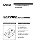
1
ELECTRONIC CASH REGISTER
ER-650 / 650R
SERVICE Manual
ELECTRONIC CASH REGISTER
CONTENTS
1.
Precaution Statements
2.
Product Specifications
3.
Installation and Operation
4.
Assembly and Disassembly
5.
Maintenance Adjustment
6.
Exploded View and Part List
7.
PBA Layout and Part List
8.
Trouble Shooting
9.
Block diagram
10. Wiring Diagram
11. Schematic Diagram
Overview of this ECR
This service manual provides the technical information for many individual component systems, circuits and gives an
analysis of the operations performed by the circuits. If you need more technical information, please contact our service
branch or R&D center. Schematics and specifications provide the needed information for the accurate troubleshooting.
All information in this manual is subject to change without prior notice. Therefore, you must check the correspondence of
your manual with your machine. No part of this manual may be copied or reproduced in any form or by any means, without
the prior written consent of Shin Heung Precision .
Note: Before using this Electronic Cash Register (ECR) for the first time, leave it powered on in the REG mode for
at least twenty-four hours. This allows the Ni-MH battery, which maintains the memory of the ECR while the
power is off, to charge completely.
“Proper disposal of batteries is required. Refer to your local codes for disposal requirements.”
About this Manual
This service manual describes how to perform
hardware service maintenance for the SAM4S
ER-650/R Series Electronic Cash Register.
Notes
Notes may appear anywhere in the manual.
They describe additional information about the
item.
Precaution symbols
. Indicates a Safety Precaution that applies to
this part component.
. Indicates the part or component is an
electro-statically sensitive device. Use caution
when handling these parts.
Copyright
ⓒ 2007 by Shin Heung Precision.
All right reserved.
This manual may not, in whole or in part, be
copied, photocopied, reproduced, translated or
converted to any electronic or machine readable
from without prior written permission of Shin
Heung Precision .
SAM4S ER-650/R SERIES
Service Manual First edition.
July 2007.
V2.0
Printed in KOREA
1 Precaution Statements
Follow these safety, servicing and ESD precautions to prevent damage and to protect against potential hazards such as
electrical shock.
1-1 Safety Precautions
1. Be sure that all built-in protective devices are
replaced. Restore any missing protective shields.
2. When reinstalling the chassis and its assemblies, be
sure to restore all protective devices, including
nonmetallic control knobs and compartment covers.
3. Make sure there are no cabinet openings through
which people - particularly children - might insert
fingers and contact dangerous voltages.
Such openings include excessively wide cabinet
ventilation slots and improperly fitted covers and
drawers.
4. Design Alteration Warning:
Never alter or add to the mechanical or electrical
design of the ECR. Unauthorized alterations might
create a safety hazard. Also, any design changes or
additions will void the manufacturer’s warranty.
5. Components, parts and wiring that appear to have
overheated or that are otherwise damaged should be
replaced with parts that meet the original
specifications. Always determine the cause of
damage or over- heating, and correct any potential
hazards.
CAUTION
Dangerous explosion if battery is incorrectly replaced.
Replace only with the same or equivalent type
recommended by the manufacturer.
Dispose used batteries according to the manufacturer’s
instructions.
SAM4S ER-650 SERIES
6. Observe the original lead dress, especially near the
following areas : sharp edges, and especially the AC
and high voltage supplies.
Always inspect for pinched, out-of-place, or frayed
wiring. Do not change the spacing between components and the printed circuit board. Check the AC
power cord for damage. Make sure that leads and
components do not touch thermally hot parts.
7. Product Safety Notice:
Some electrical and mechanical parts have special
safety-related characteristics which might not be
obvious from visual inspection.
These safety features and the protection they give
might be lost if the replacement component differs
from the original - even if the replacement is rated
for higher voltage, wattage, etc.
Components that are critical for safety are indicated
in the circuit diagram by shading, ( ) or ( ).
Use replacement components that have the same
ratings, especially for flame resistance and dielectric
strength specifications. A replacement part that
does not have the same safety characteristics as the
original might create shock, fire or other hazards.
ATTENTION
ll y a danger d’explosion s’il y a remplacement incorrect
de la batterie.
Remplacer uniquement avec une batterie du même type
ou d’un type équivalent recommandé par le constructeur.
Mettre au rebut les batteries usagées conformément aux
instructions du fabricant.
1-1
1 Precaution Statements
1-2 Servicing Precautions
WARNING: First read the-Safety Precautions-section of this manual. If some unforeseen circumstance creates a conflict
between the servicing and safety precautions, always follow the safety precautions.
WARNING: An electrolytic capacitor installed with the wrong polarity might explode.
1. Servicing precautions are printed on the cabinet.
Follow them.
2. Always unplug the units AC power cord from the AC
power source before attempting to:
(a) Remove or reinstall any component or assembly
(b) Disconnect an electrical plug or connector
(c) Connect a test component in parallel with an
electrolytic capacitor
3. Some components are raised above the printed circuit
board for safety. An insulation tube or tape is
sometimes used. The internal wiring is sometimes
clamped to prevent contact with thermally hot
components. Reinstall all such elements to their
original position.
4. After servicing, always check that the screws,
components and wiring have been correctly
reinstalled. Make sure that the portion around the
serviced part has not been damaged.
5. Check the insulation between the blades of the AC
plug and accessible conductive parts (examples metal
panels and input terminals).
6. Insulation Checking Procedure:
Disconnect the power cord from the AC source and
turn the power switch ON. Connect an insulation
resistance meter (500V) to the blades of AC plug.
The insulation resistances between each blade of the
AC plug and accessible conductive parts (see above)
should be greater than 1 Mega Ohm.
7. Never defeat any of the B+ voltage interlocks.
Do not apply AC power to the unit (or any of its
assemblies) unless all solid-state heat sinks are
correctly installed.
8. Always connect an instrument’s ground lead to the
instrument chassis ground before connecting the
positive lead ; always remove the instrument’s ground
lead last.
1-3 Precautions for Electrostatic Sensitive Devices (ESDs)
1. Some semiconductor (solid state) devices are easily
damaged by static electricity. Such components are
called Electrostatic Sensitive Devices (ESDs);
examples include integrated circuits and some fieldeffect transistors. The following techniques will reduce
the occurrence of component damage caused by static
electricity.
2. Immediately before handling any semiconductor
components or assemblies, drain the electrostatic
charge from your body by touching a known earth
ground. Alternatively, wear a discharging wrist-strap
device. (Be sure to remove it prior to applying power
- this is an electric shock precaution.)
3. After removing an ESD-equipped assembly, place it
on a conductive surface such as aluminum foil to
prevent accumulation of electrostatic charge.
4. Do not use Freon-Propelled chemicals. These can
generate electrical charges that damage ESDs.
5. Use only a grounded-tip soldering iron when
soldering or unsoldering ESDs.
6. Use only an anti-static solder removal device. Many
solder removal devices are not rated as anti-static;
these can accumulate sufficient electrical charge to
damage ESDs.
1-2
7. Do not remove a replacement ESD from its protective
package until you are ready to install it. Most
replacement ESDs are packaged with leads that are
electrically shorted together by conductive foam,
aluminum foil or other conductive materials.
8. Immediately before removing the protective material
from the leads of a replacement ESD, touch the
protective material to the chassis or circuit assembly
into which the device will be installed.
9. Minimize body motions when handling unpackaged
replacement ESDs. Motions such as brushing clothe
together, or lifting a foot from a carpeted floor can
generate enough static electricity to damage an ESD.
SAM4S ER-650 SERIES
2 Product Specifications
Specifications are correct at the time of printing. Product specifications are subject to change without notice. See below
for product specifications.
2-1 General Specifications
Item
Processor
Description
• MITSUBISHI M16C/62 Group M30622SFP (16 Bit)
Remark
External ROM Version
• RAM
SRAM (K6T1008C2E) : 1Mbits × 2EA
SRAM (K6T4008C1C) : 4Mbits × 2EA(Option)
Memory
• EP-ROM
ER-ROM(27C040) : 4Mbits
Battery
Data Storage
• Type
: Ni-MH, 3.6V 70mAh
• Charging Time
: 24 Hours
• Life
: 3 Years
When battery is Full
• 60 Days
charged
• Flow Control :
Interface Serial
(RS-232C)
① DTR / DSR
: H/W Flow Control
② XON / XOFF
: S/W Flow Control
• Baud Rate
: 4800 / 9600 / 19200 Bps
• Connector
: DB9P Female (I/F PBA)
RS-232C #1
RS-232C #2
• Flow Control :
① XON/XOFF
: S/W Flow Control
Same as RS-485 2-Wire
• Baud Rate
: 9600 Bps
Communication Method
• Connector
: Modular Jack Connector 12Pin (2 Port-6Pin)
• Model
: STM-210
Detail Spec refer to Next
• Printing Speed
: 50mm(13.3 Lines) / Sec
Page
• Operator Display
: LCD (128 × 64 Dots)
• Customer Display
: VFD (10 Digits)
• Raised Key
: 78 Key
• Flat Rubber Key
: 98 Key
Interface Serial
(IRC)
Printer
Display
Key Board
Power Consumption
• Approx. 15W (Regularity), Approx. 28W (Peak)
Power Requirement
• AC 120V 60Hz, 230V 50Hz
Environment
• Temperature
: 0℃ ~ 45℃
Condition
• humidity
: 30% ~ 80% RH
Weight
• 13.7 Kg (SET), 15.8Kg (Box Packing)
Dimensions(mm)
• 400(W) × 450(D) × 282.7(H)
Table2-1 General Specifications
SAM4S ER-650 SERIES
2-1
2 Product Specifications
2-2 Appearance
2-2 A. Appearance Dimensions (mm)
282.7
40
0
45
0
Figure2-1 Dimensions
2-2
SAM4S ER-650 SERIES
2 Product Specifications
2-2 B. Feature Locations
Figure2-2 Feature Locations
SAM4S ER-650 SERIES
2-3
2 Product Specifications
2-3 Thermal Printer Specifications
2-3 A. Printer Specification
Item
Description
Model
• STM-210
Print Method
• Thermal Line Printing
Total number of dots
Printing Format
Dot Pitch
• 384 Dots / I Line
• Vertical
: 0.125 mm
• Horizontal
: 0.125 mm
Printing Speed
• 50 mm/s ( At 8.5V of Motor Terminal Voltage)
Printing Direction
• Unidirection with friction feed
Paper Feeding
Power Supply Volt
Printer Head
Motor
Sensor
Reliability
Remark
Feeding Method
• Friction Feed
Minimum Feed Pitch
• 0.0625 mm
Feeding Speed
• 50 mm/s (At 8.5V of Motor Terminal Voltage)
Power Voltage
• 8V / 8.5V (Recommend)
Head/Motor
Circuit input Voltage
• 5V
Head Control/Sensor
Heat Element Density
• 8 Dots/mm (0.125 mm/Dot)
Total Head Elements
• 384 Dots/Dot Line
Available Printing Width
• 48 mm
Heat element typical Ω
• 176 Ω±4%
Paper Feed Motor
• 4-Phase Bi-Polar Stepping Motor
Head Temperature
• Thermister
Paper-End Sensor
• Reflecting Photo Sensor
Cover Open Sensor
• Micro Switch
Life
• 15,000,000 Lines
MCBF
• 37,000,000 Line
Dimension (mm)
• 82.5 (W) ×147.3 (D) ×101.4 (H)
Weight
• Approx. 365 g
Table2-2 Thermal Printer Specifications
2-4
SAM4S ER-650 SERIES
2 Product Specifications
2-3 Thermal Printer Specifications
2-3 B. Paper Specification
Item
Description
Paper Type
• Single-ply Thermal Paper Roll
Paper Size
• 57.5 mm±0.5 mm (Width) ×80 mm or less
Specified Paper
• Original Paper No.
Remark
Table2-3 Paper Specification
Note: The following paper can be used instead of the specified paper above.
TF50KS-E
PD 160R
F380
: Nippon paper industries Co.,Ltd.
: New Oji paper Mfg, Co.,Ltd.
: Kansaki specialty papers, Inc. (USA)
2-3 C. Printable Area
The Printable area of a paper with width of 80-1.0mm(3.13”±0.02”) is 72.2±0.2mm(2.84””±0.008”)(512 dots) and the
space on the right and left sides are approximately 3.7mm(0.146”).
a
a = 57.5±0.5 mm (Paper Width)
b = 1.mm (1 Char.
b
c = 48 mm (384 Dots/Printable Area)
d = 4.75 mm (Left Space)
e = 4.75 mm (Right Space)
d
c
e
Figure2-3 Printable Area
2-3 D. Character Specification
Item
Description
Character Structure
• 12(W) × 24(H) Font (Including a horizontal spacing)
Character Size
• 1.25 mm(W) ×3.0 mm(H)
Column Pitch
• 1.5 mm
Line Pitch
• 3.75 mm (Including 6-dot line spacing)
Number of Column
• 32 (12×24 Font/Character)
Remark
Table2-4 Character Specification
SAM4S ER-650 SERIES
2-5
2 Product Specifications
2-3 Thermal Printer Specifications
2-3 E. Other Component Specification
Item
Description
Type
• 4-Phase 20 Step PM Stepping Motor
Power Supply Voltage
• 8V ~ 8.5V DC
Coil Resistance
• 20 Ω±1.4Ω (25℃/Phase)
Paper Feed Motor
Current Consumption
• Peak
: 2A or less
• Mean
: Approx. 350 mA
• Constant-Voltage Driving
Drive Method
using 2-2 Phase
Excitation
Number of Heat Element
• 384 Dots
Heat Element Density
• 8 Dots/mm (0.125 mm/Dot)
Typical Resistance Value
• 176 Ω±4%
Current
• Approx. 3.1 A
Constant B
• 3950K ±2%
Resistance Value
• 30㏀ ±5% (25℃)
Temperature Character
• Rt=R(25)×Exp[B×{1/(T+273)-1/(25+273)}]
Operating Temperature
• -20℃ ~ 80℃
Type
• Reflecting Photo Sensor
Spec
• SG-2BC (Kodenshi corp.)
Type
• Micro Switch
Cover Open
Supply Voltage
• 5 VDC±5%
Sensor
Current Rating
• 1A ~ 50 mA
Detect Method
• On when the printer head is load
Printer Head
Thermister
Paper End Sensor
Remark
Table2-5 Other Component Specification
2-3 F. Printer Connector
2-3 F-(a) Cover Open Sensor Pin Assignments
Pin No.
Signal Description
1
VCC
2
GND
Remark
Table2-6 Printer Pin Assignment
2-6
SAM4S ER-650 SERIES
2 Product Specifications
2-3 Thermal Printer Specifications
2-3 F-(b) Paper Feed Motor Pin Assignments
Pin No.
1
Phase B
2
Phase B-
3
Phase A
4
Phase A_
Signal Description
Remark
Signal Description
Remark
2-3 F-(c) Paper-End Sensor Pin Assignments
Pin No.
1
GND
2
Paper End Signal
3
VCC
2-3 F-(d) Thermal Head Connector Pin Assignments
Pin No.
Signal Description
1
VH
2
VH
3
D0
4
/LAT
5
GND
6
GND
7
STB1
8
STB2
9
STB3
10
TM
11
TM
12
VCC
13
STB4
14
STB5
15
STB6
16
GND
17
GND
18
CLK
19
DI
20
VH
21
VH
SAM4S ER-650 SERIES
Remark
2-7
2 Product Specifications
2-4 Power Specifications
2-4 A. Power Specification
Item
Description
Input Voltage &
• U.S.A
: AC 120V, 150mA, 60Hz (Min : 90V, Max : 132V)
Current
• Europe
: AC 230V, 80mA, 50Hz (Min : 198V, Max : 264V)
Power Consumption
Output Voltage
Remark
• Stand-By : 10W
• Operating
: 15W
• AC 19V 2.3A (Wire Color : Blue-Blue)
Power Transformer
• AC 24V 0.15A (Wire Color : Red-Red)
Output
Table2-7 Power Specification
2-8
SAM4S ER-650 SERIES
2 Product Specifications
2-5 Interface Specifications
2-5 A. RS-232C Serial Interface
2-5 A-(a) Specification
Item
Description
Data Transmission
• Serial
Synchronization
• Asynchronous
Hand Shaking
(Flow Control)
• H/W : DTR / DSR
• S/W : XON / XOFF
Signal Level
• Logic”1” (MARK) : -3V ~ -15V
• Logic”0” (SPACE) : +3V ~ +15V
Baud Rate
• 1200 / 2400 / 4800 / 9600 / 19200 bps
Data Word Length
• 7 Bit / 8 Bit
Parity
• None / Even / Odd
Connector
• DB9P Female (I/F PBA Side)
Voltage Supply
• VCC(+5V/200mA) is supplied at 9Pin of D-SUB Connector.
Remark
XON : ASC Code 11h
XOFF : ASC Code 13h
For Bar Code Reader
or other devices
Table2-18 RS-232C Specification
2-5 A-(b) RS-232C I/F Cable
FERRITE CORE : 1 Turn (OP-118E : 18.2×12.5×25.5)
Figure2-4 RS-232C Cable
2-5 A-(c) Cable Connection
ECR
SIDE(9P)
(F.G)
(F.G)
2 (RXD)
2 (TXD)
3 (TXD)
3 (RSD)
4 (RTS)
8 (CTS)
5 (CTS)
6 (DSR)
6 (DSR)
4 (DTR)
20 (DTR)
5 (S.G)
7(S.G)
HOST
SIDE(25P)
DSR and CTS are shorted on I/F PBA of ER-5200
Figure2-5 RS232C Cable Connection
SAM4S ER-650 SERIES
2-9
2 Product Specifications
2-5 Interface Specifications
2-5 A. RS-232C Serial Interface
2-5 A-(d) Signal Description
Pin No.
BODY
Signal Name
Signal Direction
Function
Frame GND
-
Frame Ground
2
RXD
Input
Receive Data
3
TXD
Output
Transmit Data
This Signal indicates whether the ECR(ER-5200) is busy. (H/W flow control)
① MARK(Logic1) : The ECR is busy
4
DTR
Output
② SPACE(Logic0) : The ECR is not busy
③ The host transmits a data to the ECR, after confirming this signal.
④ When XON/XOFF flow control is selected, the host does not check this signal.
5
Signal GND
-
Signal Ground
This signal indicates whether the host computer or receipt printer can receive data.
(H/W flow control)
6
DSR
Input
① MARK(Logic1) : The host can receive a data.
② SPACE(Logic0) : The host can not receive a data
③ The ECR transmits a data to the host or receipt printer, after confirming this signal.
④ When XON/XOFF flow control is selected, the printer does not check this signal.
9
VCC
Output
VCC(+5V/200mA) is supplied at 9Pin of D-SUB Connector.
Table2-19 RS-232C Signal Description
Caution: The VCC is supplied for the barcode or other devices power source. The Supply Current 200mA is
total value including COM1 and COM2 Power Consumption. If the Total Power Consumption of the
attached devices is exceeded the specification (200mA), the system cut the VCC of D-SUB Connector.
Then, the attached devices do not work and It is possible that the ECR is damaged.
Caution: If the device with 5V/200mA is connected to COM1, the VCC of COM2 can not use. If the device with
5V/100mA is connected to COM1, Other device with 5V/100mA can be connected to COM2 Port.
2-5 A-(e) H/W Flow Control Timing
When DTR/DSR flow control is select, before transmitting a data, the ECR checks whether the host is BUSY or not.
If the host is BUSY, ECR does not transmit a data to the host. If the host is not BUSY, ECR transmits a data to the
Host. The host is the same. Refer to the Interface Part of Chapter 7(Special Circuit Diagrams).
2-5 A-(f) S/W Flow Control Timing
When XON/XOFF flow control is selected, the ECR transmits XON(ASCII 11h) or XOFF(ACSII 13h) signal through
the Serial Data Line. If the ECR is busy, the printer transmits XOFF(ASCII 13h) to host through the Serial Data Line.
Then the host recognizes that the ECR is busy. So, the host does not transmit a data to the ECR. If the ECR is released
from busy, the ECR transmits XON(ASCII 11h) to host through the Serial Data Line. Then the host recognizes that the
ECR is not busy. And the host transmits a data to the ECR.
2-10
SAM4S ER-650 SERIES
2 Product Specifications
2-5 Interface Specifications
2-5 B.IRC Serial Interface
2-5 B-(a) Specification (Same as RS-485 2-Wire Communication Method)
Item
Description
Data Transmission
• Serial
Synchronization
• Asynchronous
Signal Level
• Logic”1”
:
(VA-VB) ≥ 0.2V
(Receive)
• Logic”0”
:
(VA-VB) ≤ -0.2V
Baud Rate
• 9600 bps Only
Data Word Length
• 7 Bit / 8 Bit
Parity
• None / Even / Odd
Connector
• Modular Jack Connector 12P (2Port-6Pin)
Remark
Table2-20 IRC Specification
2-5 B-(b) IRC I/F Cable
Tighten with Tie Cable
Ferrite Core : 5 Turn (AC 29.5×8×18mm)
Ferrite Core and Tie Cable are included in a Accessory Package
Figure2-6 IRC Cable
2-5 B-(c) Cable Connection
ECR
MASTER or
SLAVE
1 (TX/RX_B)
1 (TX/RX_B)
2 (TX/RX_B)
2 (TX/RX_B)
3 (F.GND)
3 (F.GND)
4 (F.GND)
4 (F.GND)
5 (TX/RX_A)
5 (TX/RX_A)
6 (TX/RX_A)
6 (TX/RX_A)
ECR
SLAVE
Figure2-7 IRC Cable Connection
SAM4S ER-650 SERIES
2-11
2 Product Specifications
2-5 Interface Specifications
2-5 B-(d) Signal Description (Port#1)
Pin No.
Signal Name
Signal Direction
Function
1(7)
TX/RX_B
In/Out
Transmit/Receive Data Line B
2(8)
TX/RX_B
In/Out
Pin 1 and Pin 2 are shorted each other on I/F PBA.
3(9)
F.GND
-
4(10)
F.GND
-
5(11)
TX/RX_A
In/Out
Transmit/Receive Data Line A
6(12)
TX/RX_A
In/Out
Pin 4 and Pin 5 are shorted each other on I/F PBA.
Frame Ground
Table2-21 IRC Signal Description
Note : The signal description of the Port#2 are same as it of the Port#1
2-12
SAM4S ER-650 SERIES
3 Installation and Operation
3-1 System Configuration
3-1 A. Configuration
Figure3-1 System Configuration
SAM4S ER-650 SERIES
3-1
3 Installation and Operation
3-2 Installation
3-2 A. Paper Roll Installation
Figure3-2 Paper Installation
1. Open the cover printer.
2. Push the Blue cap Lever towards the rear of the printer and lift up to open the paper cover.
3. Ensure that the paper is being fed from the bottom of the roll,(as illustrated above) place the roll into the concave
bottom of the printer. And put the leading edge of the paper over the printer..
4. Close the printer cover slowly until it locks firmly.
Tear off the excess paper.
3-2 B. RS-232C Serial Cable Installation
Figure3-3 RS-232C and IRC Cable Installation
1. Connect the RS-232C serial cable to the RS-232C serial port on the right side of ECR.
2. Secure the serial cable with screws.
3. Connect the other end of the RS-232C serial Cable to your host computer.
3-2
SAM4S ER-650 SERIES
3 Installation and Operation
3-2 C. IRC Serial Cable Installation
1. Connect the IRC serial cable to the IRC port on the right side of ECR.
2. Connect the other end of the IRC serial Cable to other ECR.
3-2 D. Options
No.
Item
Description
1
RS-232 / IRC I/F Board
I/F PBA
2
Clerk Key
5EA, 10EA, 15EA
Remark
Selectable
Table 3-1 Option
3-2 E. Supplies
No.
Item
Description
1
Paper Roll
1 EA
2
Cable Tie
2 EA
3
Ferrite Core
RING-TR29A
4
Mode Key
VD, REG, X, Z, P, C
5
User Manual
1 EA
6
Clerk Key
5EA, 10EA, 15EA
Remark
: 2 EA
Option
Table 3-2 Supplies
SAM4S ER-650 SERIES
3-3
3 Installation and Operation
3-2 Operation
Note: Before using this Electronic Cash Register(ECR) for the first time, leave it powered ON in the REG mode for a at
least 24 hours. This allows the Ni-Cad battery, which maintains the ECR’s memory while the power is OFF, to
fully charge.
3-3 A. Mode Switch
The position of the Mode Switch determines the action of the ECR. The modes are as shown in Table 3-1
Mode
Key
VOID
VD
OFF
-
REG
REG
X
X
Use to read register reports and perform other manager
functions.
Z
Z
Use to read register reports and reset totals to zero.
PGM
P
Use to program the register
SM
C
Use for H/W tests and special setting.
Figure3-4 Mode Switch
Function
Use to void (correct) items outside of a sale.
The Register is inoperable.
Use for normal registrations.
Table3-3 Mode Switch Function
The mode keys can be used to access the following key lock positions.
Key
VOID
Accessible Position
Void, Off, Register, Manager
X
Off, Register, Manager
Z
Off, Register, Manager, Clear Totals
PGM
C
Remark
Void, Off, Register, Manager, Clear Totals, Program
Void, Off, Register, Manager, Clear Totals, Program, Service Mode
Table3-4 Key Function
Note:
3-4
The Key can be removed from the key lock in the OFF or REGISTER position.
SAM4S ER-650 SERIES
3 Installation and Operation
3-3 B. Key Board Matrix (Dealer Option)
Figure3-5 Key Board
3-3 C. All Clear
This step insures that the cash register is cleared of any totals or programming. After this procedure, the cash register is
ready for programming and operation.
WARNING: This is a one time procedure. Do not repeat this procedure after the cash register is
programmed, it causes all programs and totals to be erased and to be default.
1. Turn off the power switch.
2. Turn the Mode key marked ‘C’ to Service Mode position.
3. Press and hold the CHECK key on key board and turn on the power switch at the same time.
4. When “RAM ALL CLEAR SERV.” message display, press PAGE UP, 0, CLERK# and CASH/ENTER in sequence.
5. When memory is cleared, the register prints a message “RAM ALL CLEAR OK!”
=====================
RAM ALL CLEAR OK !
=====================
CLERK 00
No. 000001 00
Figure3-6 All Clear
SAM4S ER-650 SERIES
3-5
3 Installation and Operation
3-3 D. Self Test
1. Turn the Mode key marked ‘C’ to Service Mode position.
2. Select “0. SELF TEST” from the menu and Press 0 on the key board.
3. H/W test menu will be displayed.
4. Select the number from the menu.
H/W TEST
0. TEST PRINTER
1. TEST DISPLAY
2. TEST KEY BOARD
3. TEST MODE KEY
4. TEST RS-232
5. TEST RTC
6. TEST PRINTING PATTERN
Figure3-7 Self Test
3-3 D-(a) Test Printer
1. Press 0 key on key board.
2. Then the printer prints a test pattern. The printing message
shows some information sush as ‘TM value’,’stbIdx (Strobe
index)’.
3. After printing, The drawer is opened. Then the printer test is
finished.
Shin Heung Precision CO.,LTD
MODEL : ER-650R
THANK YOU YOUE RECEIPT
CALL AGAIN
DATE 08/25/2002 WED
TIME 19:04
****************************
ER-650R PRINTER TEST
****************************
DEPT 1
$10.00
SUBTOTAL
$10.00
CASH
#10.00
CLERK C.Y.H
No. 0000001
a
ab
abc
abcd
TM value = 7f : 127
StbIdx value = 10
CLERK 00
No.000016
00
Figure3-8 Printer Self Test
3-3 D-(b) Test Display
→
H/W TEST
1. Press 1 key on key board.
0. TEST PRINTER
1.
TEST
DISPLAY
2. Then the buzzer will work for 1 sec.
2. TEST KEY BOARD
3. After testing the buzzer, Some characters are displayed on the
rear VFD display
4. After testing the rear VFD display, the LCD display tests.
The LCD is filled with a black screen. And then the black screen erase. Figure3-9 Display Self Test
3-6
SAM4S ER-650 SERIES
3 Installation and Operation
3-3 D-(c) Test Key Board
1. Press 2 key on key board.
2. Press any key you want on the key board.
3. Already pressed key will be showed on the LCD screen that
the position of key pressed with a black square and key code.
4. Turn the mode key to any position to finish this test.
TEST KEY BOARD
54
Figure3-10 Key Board Self Test
3-3 D-(d) Test Mode Key
1. Press 3 key on key board.
2. Turn the mode key to any position.
3. The corresponding Mode name will be showed on the LCD
screen.
TEST MODE
MODE : REGISTER MODE
Figure3-11 Mode Key Self Test
3-3 D-(e) Test RS232C
1. Install the serial loop back test jig. (Short “pin 2,3” and “pin 4,6” of DSUB connector)
2. Press 4 key on key board.
3. Press 0 key on the key board. (0= Loop Back Test for RS232 Port#1)
If error occur, the message (PORT#1 TEST N.G) is displayed on LCD and the Buzzer beep. Then Press “C” key.
4.Press 1 key on the key board. (1= Loop Back Test for RS232 Port#2)
If error occur, the message (PORT#2 TEST N.G) is displayed on LCD and the Buzzer beep. Then Press “C” key.
5.Press 2 key on the key board. (2= Loop Back Test for IRC)
The message (TEST IRC OK) is displayed on LCD.
Note:
When the ports is no connection or the cable is open, the Error occur.
SAM4S ER-650 SERIES
3-7
3 Installation and Operation
Memo
3-8
SAM4S ER-650 SERIES
4 Assembly and Disassembly
Caution :
· Before installation, be sure to turn off the power switch.
· Use gloves to protect your hand from being cut by the angle and the chassis.
· Connect all the cables correctly. When connecting or disconnecting the cables, be careful not to apply
stress to the cables. (It may cause disconnection)
· Be careful not to bind interface cables and AC power cord together.
4-1 Disassembly the Case Upper Block
4-1 A. Case Upper Block
1. Open the Printer Cover Ass’y (A). (Page 6-1)
2. Remove the two screws (B-15,B-22). (Page 6-3)
3. Lift off the Case Upper Ass’y (B). (Page 6-1)
4. Separate the four harnesses (d,e,f,u) from the Main PBA(E-12). (Page 6-12)
5. Separate the Case Upper Ass’y (B). (Page 6-1)
Note:
To Install, Reverse the removal procedure.
4-1 B. LCD and VFD Display Block
1. Remove the two screws (B-24). (Page 6-3)
2. Remove the Window Holder (B-23). (Page 6-3)
3. Separate the LCD Display parts (B-1~6, B-20) from the Case Upper Ass’y (B). (Page 6-3)
4. Separate the VFD Display parts (B-16~19) from the Case Upper Ass’y (B). (Page 6-3)
Note: The position of Ferrite core and the number of turn refer to the display part of chapter specification.
Note: To Install, Reverse the removal procedure.
4-1 C. Mode and Clerk Key Block
1. Remove the three screws(B-12). And separate the Mode and Clerk Key Ass’y (B-8~14) from the Case Upper Assy(B).
(Page 6-3)
2. Remove the two screws (B-11). And separate the Mode Key Ass’y (B-14) from the BRKT Mode S/W (B-8). (Page 6-3)
3. Remove the two screws (B-10). And separate the Clerk Key Ass’y (B-13) from the BRKT Mode S/W (B-8). (Page 6-3)
Note: The position of Ferrite core and the number of turn refer to the display part of chapter specification.
Note: To Install, Reverse the removal procedure.
SAM4S ER-650 SERIES
4-1
4 Assembly and Disassembly
4-2 Disassembly the Case Lower Block
4-2 A. Printer
1. Remove the two screws (E-5,E-13). And separate the GND wire (a, b). (Page 6-12)
2. Remove the screw(C-42) and separate the Cover Front(C-41). (Page 6-5)
3. Separate the harness(C-40). (Page 6-5)
4. Remove the four screws(C-43). (Page 6-5)
5. Separate the Printer Ass’y(C) from the Case Lower Ass’y (E). (Page 6-1)
Note:
To Install, Reverse the removal procedure.
4-2 B. RS-232 / IRC I/F PBA
1. Remove the two screws (E-7) on the I/F PBA (E-21). (Page 6-12)
2. Separate the two I/F harnesses (n, q) from the Main PBA (E-12). (Page 6-12)
3. Separate the I/F PBA (E-21) from the Case Lower Ass’y (E). (Page 6-12)
Note:
Note:
The position of Ferrite core and the number of turn refer to the Serial I/F part of chapter specification.
To Install, Reverse the removal procedure
4-2 C. Power Transformer and Power PBA
1. Separate the two harnesses (j, p) from the Main PBA (E-12) and Power PBA (E-3). (Page 6-12)
2. Remove the two screws (E-1) on the Power Transformer (E-4). (Page 6-12)
3. Remove the Power Transformer (E-4). (Page 6-12)
4. Separate the Power S/W harness (m) and Power Cord harness (k) from Power PBA (E-3). (Page 6-12)
5. Remove the two screws (E-2) on the Power PBA (E-3). (Page 6-12)
6. Remove the Power PBA (E-3). (Page 6-12)
Note:
To Install, Reverse the removal procedure.
4-2 D. Main PBA
1. Separate the Drawer, Compulsory harness (r, s) from the Main PBA (E-12). (Page 6-12)
2. Remove the four screws (E-10) on the Main PBA (E-12). (Page 6-12)
3. Remove the Main PBA (E-12). (Page 6-12)
Note: To Install, Reverse the removal procedure.
4-2
SAM4S ER-650 SERIES
5 Maintenance and Adjustment
5-1 Maintenance
5-1 A. Cleaning the Printer Head
After printing, the printer head can be very hot. Be careful not to touch it. Also let it cool before you clean it.
Do not damage the printer head by touching it with your fingers or any hard object.
1. Turn the ECR power switch off.
2. Open the printer cover.
3. Open the cover of paper supplier with pushing the blue-cap lever.
4. Clean the Printer Head Thermal Element with a cotton swab moistened with alcohol solvent. (ethanol, methanol IPA )
5. After confirming that alcohol solvent has been dried up completely, close the cover of paper supplier
Until be locked.
Figure5-1 Clean the Printer Head
Caution: Note that the thermal head becomes very hot during normal operation. To prevent the danger of Burn
injury from thermal, be sure to wait for about 10 minutes after turning power off before beginning the
cleaning.
SAM4S ER-650 SERIES
5-1
5 Maintenance and Adjustment
5-2 Adjustment
5-2 A. LCD Display Angle
You can adjust the view angle of the Operator LCD Display
Figure5-2 Adjustment of the View Angle
5-2 B. LCD Display Contrast
You can adjust the contrast of the Operator LCD Display by using the VR on the left side.
Figure5-3 Adjustment of Contrast
5-2
SAM4S ER-650 SERIES
6 Exploded View and Part List
Figure6-1 Total Disassembly (ER-650/ER-650R)
SAM4S ER-650 SERIES
6-1
6 Exploded View and Part List
Figure6-2 ASS’Y COVER-PRINTER
A. ASS’Y COVER-PRINTER
No.
Parts No.
A
JK97-10008A
JK70-10320A
JK72-20011B
6-2
Description / Specification
MEA HOU-COVER PRINTER:ER-650R,STD
IPR-CUTTER PAPER
PMO-COVER PRINTER
Q`ty
1
1
1
Design-Location
Serviceable
Remark
Y
N
N
SAM4S ER-650 SERIES
6 Exploded View and Part List
Figure6-3 ASS’Y CASE-UPPER
SAM4S ER-650 SERIES
6-3
6 Exploded View and Part List
B. ASS’Y CASE-UPPER
No.
B-1
Parts No.
JK72-00061A
Description / Specification
PMO-WINDOW VIEW: PMMA,TRP,T1.2
Q`ty
1
B-2
JK72-00045A
PMO-WINDOW LCD: PC,BL06,HB
1
B-3
6006-000003
SCREW-ASS'Y TAPT:WT,BH,+,M2.6,L5.5
4
B-4
JK96-01080A
ELA ETC-DISPLAY(650):ER-650,BASIC
1
Design-Location
Serviceable
Y
LCD+BRKT
Y
Y
Y
B-5
6002-000174
SCREW-TAPPING:PWH,+,2,M3,L10,ZPC
2
B-6
JK70-10408A
IPR-BRKT WINDOW_LCD: SECC,T1.2
1
Y
JK72-20012A
PMO-COVER MODE S/W: HIPS(V0)
1
Y
JK72-20013A
PMO-COVER CLERK KEY: HIPS(V0)
1
Y
JK70-00052A
IPR-BRKT MODE S/W: SECC,T1.0
1
Y
B-7
B-8
W/L+BRKT
Y
B-9
6002-000319
SCREW-TAPPING:PH,+,2,M3,L8,ZPC(YEL)
2
B-10
JK39-40508A
CBF HARNESS:UL1015,350mm
1
B-11
6002-000319
SCREW-TAPPING:PH,+,2,M3,L8,ZPC(YEL)
2
B/MODE+ROTARY
Y
B-12
6002-000319
SCREW-TAPPING:PH,+,2,M3,L8,ZPC(YEL)
3
B/MODE+C/MODE
Y
B-13
JK96-01081A
ELA ETC-CLERK:BASIC
1
B-14
JK96-00956A
ELA ETC-MODEKEY ASSY: NO CORE
1
B-15
6002-000172
SCREW-TAPPING:PH,+,2S,M4,L15,STS304
1
B-16
JK72-00034A
PMO-WINDOW TURRET:PC,BL06,HB
1
B/MODE+CLERK
Y
Y
Y
Y
C/U+C/L(LEFT)
Y
Y
B-17
JK92-00970A
PBA SUB-650,TURRET:BASIC
1
Y
B-18
JK68-00013A
LABEL(P)-TURRET SHEET: PE,L100*W70
1
Y
B-19
JK72-00016A
PMO-TURRET BODY: HIPS(V0)
1
Y
B-20
JK72-00047A
PMO-WINDOW LOWER: HIPS(V0)
1
Y
B-21
JK72-00038A
PMO-CASE UPPER: HIPS(V0)
1
B-22
6001-000367
SCREW-MACHINE:FH,+,M4,L10,NI
1
B-23
JK72-00048A
PMO-WINDOW HOLDER: POM,WHITE,HB
1
Y
B-24
6002-000174
SCREW-TAPPING:PWH,+,2,M3,L10,ZPC
2
Y
6-4
Remark
Y
C/U+C/L(RIGHT)
Y
SAM4S ER-650 SERIES
6 Exploded View and Part List
Figure6-4 ASS’Y PRINTER(STM-210)
SAM4S ER-650 SERIES
6-5
6 Exploded View and Part List
Figure6-5 Lubrication Points of the Printer (STM-210)
6-6
SAM4S ER-650 SERIES
6 Exploded View and Part List
C. ASS’Y PRINTER
No.
C
Parts No.
JK59-20001A
Description / Specification
UNIT-PRINTER:STM-210(A)
Q`ty
1
JK59-20001B
UNIT-PRINTER:STM-210(B)
1
JK59-20001C
UNIT-PRINTER:STM-210(C)
1
JK59-20001D
UNIT-PRINTER:STM-210(D)
1
JK59-20005A
UNIT-PRINTER:STM-220
1
C-1
JK72-20001A
PMO-COVER TOP: HIPS(HB),IVORY
1
C-2
6001-000665
SCREW-MACHINE: PWH,+,2,M3,L4,ZPC
2
C-3
JK70-30001A
SPRING-HOOK: SWP
1
C-4
JK72-20003A
PMO-CAP LEVER: HIPS(HB),BLUE
1
C-5
JK60-00003A
SCREW-SPECIAL: SUM 24L,WHITE
2
C-6
JK70-20003A
IPR-BRACKET HOOK: SECC T1.0
1
C-7
JK70-50011A
SCREW TAPPING: PH,+,2,M2,L4,WHITE
2
C-8
6001-000665
SCREW-MACHINE: PWH,+,2,M3,L4,ZPC
2
C-9
JK70-20002A
IPR-FIXED CUTTER: SECC T1.2
1
C-10
JK70-50004A
POLY WASHER: Φ3.1,RED
2
C-11
JK70-20001A
IPR-COVER HOUSING: SECC T1.0
1
C-12
JK70-70001A
ICT-SHAFT HINGE: SUM
1
C-13
JK97-10002A
ASSY-PLATEN ROLLER: STM-210
1
C-14
JK70-50002A
ICT-BUSHING
1
C-15
JK70-50010A
E-RING: Φ2.0, T0.5
1
C-16
6002-000147
SCREW-TAPPING: PH,+,2,M3,L10,ZPC
1
C-17
JK70-50009A
SCREW-MACHINE: RH,+,2,M2,L4,WHITE
2
C-18
JK72-20005A
PMO-SIDE COVER: POM,BLK
1
C-19
JK72-20007A
PMO-GEAR REDUCTION 17_39: POM
1
C-20
JK72-20008A
PMO-GEAR REDUCTION 21_41: POM
1
C-21
JK70-50006A
SCREW-MACHINE: RH,+,2,M1.7,L2,WHITE
2
C-22
JK72-20006A
PMO-GEAR REDUCTION 13_43: POM
1
C-23
6002-000147
SCREW TAPPING: PH,+,2,M3,L10,ZPC
1
C-24
JK68-40002A
LABEL(P)-WARNING HOT: ART-PAPER
1
C-25
JK70-20004A
IPR-MAIN FRAME
1
C-26
JK96-01233A
ELA-LEVER SENSOR
1
C-27
JK70-50007A
SCREW-MACHINE: RH,+,2,M1.7,L8,WHITE
1
C-28
JK59-40001A
MOTOR ASS'Y: STM-210
1
C-29
JK96-01231A
ELA-P/END SENSOR: STM-210
1
JK70-50009A
SCREW-MACHINE: RH,+,2,M2,L4,WHITE
1
JK70-50009A
SCREW-MACHINE: RH,+,2,M2,L4,WHITE
2
C-31
JK97-10004A
ASS'Y TPH: STM-210
1
C-32
JK39-40554A
CBF SIGNAL-PRINTER FFC: 21P,120MM
1
C-30
C-33
JK97-10004B
ASS'Y TPH,HEAT-SINK: STM-210
1
JK47-10001A
TPH: ROHM
1
JK70-50005A
TPH TAPE: 3M
1
JK70-20006A
HEAT-SINK: ZNDC
1
C-34
JK70-30002A
SPRING-TPH: SWP
2
C-35
JK70-20005A
IPR-BRACKET-REAR: SECC T1.0
1
C-36
6001-000665
SCREW-MACHINE: PWH,+,2,M3,L4,ZPC
2
C-37
JK72-20002A
PMO-PAPER SUPPLY: ABS+GF 20%
1
C-38
JK92-01224A
PBA-SUB PRT CONN BOARD: STM-210
1
SAM4S ER-650 SERIES
Design-Location
Serviceable
Y
Y
Y
Y
Y
Y
Y
Y
Y
Y
Y
Y
Y
Y
Y
Y
Y
Y
Y
Y
Y
Y
Y
Y
Y
Y
Y
Y
Y
Y
Y
Y
Y
Y
Y
Y
Y
Y
Y
N
N
N
Y
Y
Y
Y
Y
Remark
ER-650
STM-210
STM-220
6-7
6 Exploded View and Part List
C-39
6002-000175
SCREW-TAPPING: PWH,+,2,M3,L8,ZPC
1
C-40
JK39-00012A
CBF-HARNESS-KEY OPTION: 200mm
1
C-41
JK72-20009A
PMO-COVER FRONT: HIPS(HB): NONE A/C
1
C-42
6002-000147
SCREW TAPPING: PH,+,2,M3,L10,ZPC
1
C-43
6003-000198
SCREW TAPPING: PWH,+,2,M3,L12,ZPC
4
C-44
JK70-20010A
IPR-FIXED BLADE: SKH-51,T1.4
1
C-45
6001-000665
SCREW-MACHINE: PWH,+,2,M3,L4,ZPC
2
C-46
JK39-40021A
CBF HARNESS: UL1015,330/130,GRN
1
C-47
JK96-01231B
ELA-P/END SENSOR: STM-220
1
C-48
JK96-10141A
ELA PARTITION ASS'Y: STM-220
1
JK72-20114A
PMO-PAPER SEPARATOR: ABS,BLACK
1
JK72-20114A
PMO-PAPER SEPARATOR: ABS,BLACK
2
C-49
C-50
JK72-20023A
PMO-HOSUING-PAPER END
1
C-51
JK72-20023A
PMO-KNOB-PAPER END
1
C-52
6002-000175
SCREW-TAPPING: PWH,+,2,M3,L8,ZPC
2
C-53
JK96-01232A
ELA NEAR PAPER END SENSOR PCB
1
C-54
6002-001079
SCREW-TAPPING: PWH,+,2,M3,L5,ZPC
1
6-8
Y
Y
Y
Y
Y
Y
Y
Y
Y
Y
Y
Y
Y
Y
Y
Y
Y
ONLY
SAC-60
STM-220
STM-220
OPTION
SAM4S ER-650 SERIES
6 Exploded View and Part List
1.Unscrew the bolt of COVER FRONT and
disassemble it from the PRINTER.
2. Open the COVER TOP.
3. Disassemble the TPH assembly by pulling the
lower part of TPH assembly and lift it up.
4. Assemble the TPH assembly in reverse order and
close the COVER TOP.
Figure6-6 Thermal Printer Head assembly replacement
SAM4S ER-650 SERIES
6-9
6 Exploded View and Part List
Figure6-7 ASS’Y KEYBOARD (FLAT)
6-10
Figure6-8 ASS’Y KEYBOARD (RAISED)
SAM4S ER-650 SERIES
6 Exploded View and Part List
D.
ASS’Y KEYBOARD
- FLAT(98 KEY)
No.
D
Parts No.
JK59-00006A
Description / Specification
UNIT-KEYBOARD: 98KEY
Q`ty
1
Design-Location
Serviceable
Y
D-1
JK73-00006A
RMO-WATER PROOF: SILICON,100*200
1
Y
D-2
JK68-00054A
LABEL-MARK KBD SHEET: PC
1
N
D-3
JK72-00051A
PMO-KEYBOARD HOUSING: HIPS(V0)
1
Y
D-4
JK73-00007A
RMO-KEY RUBBER: SILICON,260*117
1
Y
D-5
JK96-01115A
ELA ETC-FPC ASSY: STD
1
Y
D-6
JK70-00053A
IPR-KBD FRAME: SECC,T1.0
1
Y
D-7
JK81-20005A
SCREW-TAPTITE
11
Y
Remark
- RAISED(78 KEY)
No.
D
D-1
D-2
D-3
D-4
D-5
D-6
D-7
D-8
D-9
Parts No.
JK59-30001A
JK59-30002A
JK59-30002B
JK59-30002C
JK59-30002D
JK72-20010A
JK81-10946A
JK81-10286B
JK81-20001A
JK81-10945A
JK81-20013A
JK81-10285T
UNIT-KEYBOARD: EUROPE,STD
Q`ty
1
1
UNIT-KEYBOARD: GERMAN
UNIT-KEYBOARD: FRENCH
UNIT-KEYBOARD: SPANISH
PMO-BLANK KEY-TOP(1*6): POM,IVORY
AS-KEY/CAP,L: 1X2
LABEL-KEY TOP SET: ER-650R
AS-SPRING CONTACT: 601KAS-001
SPRING-RETURN: 1X2
KEY-CAP(S): 1X1
KEY-TOP ASS'Y(S),1X1
AS-SPRING RETURN: 1X1
1
2
1
62
4
50
50
50
Design-Location
Serviceable
Y
Y
Y
Y
Y
Y
Y
N
Y
Y
Y
KEY-TOP,1
1
Y
JK81-10934A
KEY-TOP,2
1
Y
JK81-10935A
KEY-TOP,3
1
Y
JK81-10936A
KEY-TOP,4
1
Y
JK81-10937A
KEY-TOP,5
1
Y
JK81-10938A
KEY-TOP,6
1
Y
JK81-10939A
KEY-TOP,7
1
Y
JK81-10940A
KEY-TOP,8
1
Y
JK81-10941A
KEY-TOP,9
1
Y
JK81-10942A
KEY-TOP,0
1
Y
JK81-10943A
KEY-TOP,00
1
Y
JK81-20002A
JK81-20003A
JK81-20004A
JK81-20005A
JK73-20211A
KEY-TOP,●
KBD-HOUSING
AS-FPC ASSY:ER-650R
FRAME
SCREW-TAPTITE
WATER- PROOF:ER-650R,URETANE
SAM4S ER-650 SERIES
Remark
Y
JK81-10933A
JK81-10944A
D-10
D-11
D-12
D-13
D-14
Description / Specification
UNIT-KEYBOARD: USA,STD
1
Y
1
1
1
13
1
Y
Y
Y
Y
Y
6-11
6 Exploded View and Part List
Figure9-6 ASS’Y CASE-LOWER
6-12
SAM4S ER-650 SERIES
6 Exploded View and Part List
E. ASS’Y CASE-LOWER
No.
E-1
Parts No.
6006-000195
Description / Specification
SCREW-ASS'Y TAPP:WS,BH,+,M4,L10,ZPC
Q`ty
2
Design-Location
Serviceable
Y
E-2
6002-000174
SCREW-TAPPING:PWH,+,2,M3,L10,ZPC
2
Y
E-3
JK92-00949A
PBA PWR-650: BASIC
1
Y
JK26-00013A
TRANS POWER-USA: 120V
1
Y
JK26-00014A
TRANS POWER-EUROPE: 230V
1
Y
E-5
JK60-00001A
SCREW-ASSY TAPTITE: BH,WT,M3,L8,ZPC
3
Y
E-6
JK39-00037A
CBF HARNESS-I/F: FLAT,UL1007
1
Y
E-7
6002-000174
SCREW-TAPPING:PWH,+,2,M3,L10,ZPC
2
Y
E-8
JK39-00039A
CBF HARNESS-RS232: FLAT,UL1007
1
Y
E-9
6006-000199
SCREW-ASS'Y TAPT:WT,BH,+,M4,L8,ZPC
1
Y
E-10
6002-000174
SCREW-TAPPING:PWH,+,2,M3,L10,ZPC
4
Y
E-11
JK70-00049A
IPR-GROUND PLATE: SECC,T0.8
1
Y
E-12
JK92-01223A
PBA MAIN-BOARD:ER-650R,BASIC
1
Y
E-13
6003-001149
SCREW-TAPTITE:PWH,+,S,M4,L10,ZPC
1
Y
E-14
6002-000171
SCREW-TAPPING:PH,+,2S,M4,L10,ZPC
1
Y
E-15
JK70-00046A
IPR-BRKT CASING: SECC,T2.0
1
Y
E-16
JK72-00039A
PMO-CASE LOWER: HIPS(V0)
1
Y
E-17
JK39-00008A
CBF- POWER S/W: UL1617,UL/CSA,150
1
Y
JK39-10002A
CBF-POWER CORD: AUSTRALIA
1
Y
JK39-10003A
CBF-POWER CORD: USA
1
Y
JK39-10008A
CBF-POWER CORD: UK
1
Y
E-4
E-18
JK39-10501A
CBF-POWER CORD: EUROPE
1
Y
E-19
JK39-40200A
CBF HARNESS: UL1007,250MM
1
Y
E-20
JK39-40302C
CBF HARNESS: UL1007,180MM
1
Y
E-21
JK92-00948D
PBA I/F-BOARD
1
Y
SAM4S ER-650 SERIES
Remark
6-13
6 Exploded View and Part List
a5
a3
a9
a4
a2
a1
a10
c3
a6
a. ASS'Y
BILL-COIN
(4B8C)
c1
a7
c. ASS'Y
HOUSING
a8
c2
d6
d7
d11
d8
d10
d3
b7
b5
b8
b4
d5
d1
b9
d4
b10
b. ASS'Y
TRAY-TILL
d. ASS'Y
LOCK
d9
d2
b6
e3
b2
e4
e6
b3
e2
b1
e7
e. ASS'Y
BOTTOM
e5
e1
e8
b12
b11
Figure6-10 ASS’Y DRAWER (4B/8C)
a3
a4
a2
a5
c3
a1
a6
c1
a. ASS'Y
BILL-COIN
(5B5C)
c. ASS'Y
HOUSING
a7
a8
c2
d6
d7
d11
d8
d10
d3
b7
b5
b8
b4
d. ASS'Y
LOCK
d9
d2
d5
d1
b9
d4
b10
b6
e3
b. ASS'Y
TRAY-TILL
b2
e4
e6
b3
e2
e7
b1
e. ASS'Y
BOTTOM
e5
e1
e8
b12
b11
Figure6-11 ASS’Y DRAWER (5B/5C)
a3
a1
a. ASS'Y
BILL-COIN
(7B8C)
c3
c1
a2
a4
c. ASS'Y
HOUSING
c2
d6
d7
d11
d8
a5
d10
d3
d2
b7
b5
b8
b4
d. ASS'Y
LOCK
d9
d5
d1
b9
d4
b10
b6
e3
b. ASS'Y
TRAY-TILL
b2
e4
e6
b3
b1
e2
e7
e5
e. ASS'Y
BOTTOM
e1
e8
b12
b11
Figure6-12 ASS’Y DRAWER (7B/8C)
6-14
SAM4S ER-650 SERIES
6 Exploded View and Part List
F. ASS’Y DRAWER
(a) ASS’Y BILL-COIN (4B/8C, 5B/5C)
No.
a
Code No.
JK97-20014A
Description / Specification
MEA-UNIT BILL COIN: A-TYPE, 4B8C
Q`ty
Design-Location
Serviceable
1
Y
JK97-00407A
MEA-UNIT BILL COIN: A-TYPE, 5B5C
1
Y
a-1
JK72-40267A
PMO-LEVER PRESS: A-TYPE,POM
4
Y
a-2
6107-000134
SPRING ES: SUS304
4
Y
a-3
JK70-10314A
IPR-HOLDER LEVER: A-TYPE,T1.2,ZPC
4
Y
a-4
6002-000175
SCREW-TAPPING: PWH,+2,M3,L8,ZPC(YEL)
3
Y
a-5
6002-001078
SCREW-TAPPING: PWH,+2,M3,L5
4
Y
a-6
JK70-10304A
IPR-PLATE HOLDER: A-TYPE,SBHG-1,T1.2
1
Y
a-7
JK72-40269A
PMO-PANEL PARTITION: A-TYPE,HIPS,BLK
3
Y
JK72-20088A
PMO-BILL COIN TILL: A-TYPE,4B8C,HIPS,BLK
1
Y
JK72-40268A
PMO-BILL COIN TILL: A-TYPE,5B5C,HIPS,BLK
1
Y
a-9
JK72-20090A
PMO-COIN PARTITION: A-TYPE,4B8C
6
Y
a-10
JK72-20089A
PMO-COIN TILL: A-TYPE,4B8C,-
1
Y
a-8
Remark
(a) ASS’Y BILL-COIN (7B/8C)
No.
Code No.
a
JK97-01103A
Description / Specification
MEA-UNIT BILL COIN: A-TYPE, 7B8C
Q`ty
Design-Location
1
Serviceable
Remark
Y
a-1
6002-000175
SCREW-TAPPING: PWH,+2,M3,L8,ZPC(YEL)
3
Y
a-2
JK70-00068A
IPR-HOLDER PLATE: A-TYPE,SBHG-1, T1.2
1
Y
a-3
JK72-00083A
PMO-BILL PARTITION: A-TYPE,HIPS,BLK
5
Y
a-4
JK72-00082A
PMO-BILL TILL: A-TYPE,HIPS,BLK
2
Y
a-5
JK72-00084A
PMO-BILL COIN TILL: A-TYPE,HIPS,BLK
1
Y
(b) ASS’Y TRAY-TILL
No.
Code No.
JK97-01073B
b
b-1
b-2
b-3
Description / Specification
Q`ty
Design-Location
Serviceable
1
N
1
N
JK75-10389A
MEA-UNIT TRAY TILL: A-TYPE,5B5C
MEA-UNIT TRAY TILL:
A-TYPE,4B8C,7B8C(EURO)
MEC-LOCK: DRAWER
1
Y
JK70-10014A
IPR-PLATE FRONT: A-TYPE,SBC-1,T1.0
1
Y
JK97-01073D
JK70-10014B
IPR-PLATE FRONT: A-TYPE,4B8C,7B8C
1
Y
JK75-00025A
MEA-TRAY TILL: A-TYPE,4B8C,7B8C
1
N
JK75-00025B
MEA-TRAY TILL: A-TYPE,5B5C
1
N
b-4
JK73-10203A
RPR-TENSION: DRAWER,SPONGE,BLK
2
N
b-5
JK75-10386A
MEC-ROLLER: DRAWER,DR-10-B1/ Φ19
2
Y
b-6
6031-000549
WASHER-PLAIN: IDΦ6.5,ODΦ13, T1.0
2
Y
b-7
6003-000221
SCREW-TAPTITE: PWH,+2,M4,L8,ZPC(YEL)
1
Y
b-8
JK70-10324A
IPR-SUPPORT TRAY: DRAWER,SBHG-1,T1.2
1
N
b-9
JK70-40302A
ICT,SHAFT PIN: A-TYPE
1
N
b-10
6044-000124
RING-E: IDΦ3,ODΦ7, T0.6,ZPC(BLK),STSC
1
Y
b-11
6002-001042
SCREW-TAPPING: FH,+2,M3,L6
2
Y
b-12
JK70-10323A
IPR-PLATE CLIP: DRAWER,SWP,T0.5
1
Y
SAM4S ER-650 SERIES
Remark
6-15
6 Exploded View and Part List
(c) ASS’Y HOUSING
No.
Code No.
JK97-01074A
Description / Specification
c-2
JK75-10386A
MEA-COVER HOUSING: A-TYPE,BASIC
MEA-COVER HOUSING:
A-TYPE,NONE HOLE,OPTION
MEA-SUB HOUSING: A-TYPE,BASIC
MEA-SUB HOUSING:
A-TYPE,NONE HOLE,OPTION
MEC-ROLLER: DRAWER,DR-10-B1/ Φ19
c-3
JK73-20207A
REX-PAD DRAWER: DRAWER,NR,BLK
c
JK97-01074B
JK75-00026A
c-1
JK75-00026B
Q`ty
Design-Location
Serviceable
1
N
2
N
2
N
1
N
1
N
1
N
Remark
(d) ASS’Y LOCK
No.
Code No.
Description / Specification
Q`ty
Design-Location
Serviceable
d-1
6002-000157
MEA-UNIT LOCK:
A-TYPE,2-LATCH,LONG LEVER
MEA-UNIT LOCK:
A-TYPE,2-LATCH,SHORT LEVER
SCREW-TAPPING: PH,+2,M4,L14,ZPC(YEL)
1
Y
d-2
JK73-20210A
REX-BUMPER: DRAWER,NR,BLK
1
Y
d-3
JK61-70100A
1
Y
1
N
1
N
1
Y
JK97-00985A
d
JK97-00987A
1
Y
1
Y
d-5
6107-001014
SPRING-PUSH: DRAWER,FZN
MEC-LOCK LEVER:
A-TYPE,2-LATCH,LONG LEVER
MEC-LOCK LEVER:
A-TYPE,2-LATCH,SHORT LEVER
SPRING-ES: Φ0.4,D4.8,L18
d-6
JK33-10500A
SOLENOID-DC: A-DRAWER
1
Y
d-7
6001-000131
SCREW-MACHINE: BH,+2,M3,L6,ZPC(YEL)
2
Y
d-8
6001-000525
SCREW-MACHINE: PH,+2,M3,L14,ZPC(YEL)
2
Y
d-9
3405-001013
SWITCH-MICRO: 125V,5A
1
Y
d-10
JK39-40301R
CBF-HARNESS: 2P,150MM,BRN,1007
1
Y
d-11
6002-000161
SCREW-TAPPING: PH,+2,M4,L8,ZPC(YEL)
3
Y
JK75-00027A
d-4
JK75-00027B
Remark
(e) ASS’Y BOTTOM
No.
e
e-1
e-2
Code No.
Description / Specification
JK97-01976A
MEA-UNIT BOTTOM: A-TYPE
Q`ty
Design-Location
Serviceable
1
N
N
JK97-01076B
MEA-UNIT BOTTOM: A-TYPE,UNIVERSAL
1
JK70-10938A
IPR-PLATE BOTTOM: A-TYPE,SBHG-1,T1.0
1
N
JK73-40200A
RMO-STOPPER: DRAWER,NR,BLK
2
N
JK73-10902A
RMO-STOPPER: DRAWER,NR,BLK,UNIVERSAL
2
N
e-3
JK61-40200A
RMO-FOOT RUBBER: DRAWER,NR,GRAY,80HB
4
Y
e-4
6002-000234
SCREW-TAPPING: TH,+2,M4,L16,ZPC(YEL)
4
Y
e-5
6003-000267
SCREW-TAPTITE: PWH,+2,M3,L8,ZPC(YEL)
6
Y
e-6
6003-000267
SCREW-TAPTITE: PWH,+2,M3,L8,ZPC(YEL)
2
Y
e-7
JK70-10401A
IPR-PLATE SPRING: DRAWER,STS304,T0.3
2
Y
e-8
6003-000267
SCREW-TAPTITE: PWH,+2,M3,L8,ZPC(YEL)
4
Y
6-16
Remark
SAM4S ER-650 SERIES
7 PBA Layout and Part List
7-1 Main PBA
SAM4S ER-650 SERIES
7-1
7 PBA Layout and Part List
No
-
Part-No
JK92-01470A
Description / Specification
PBA MAIN-BOARD:ER-650R,EUROPE,RoHS
JK92-01470B
JK92-01470C
Q’TY
1
Design Location
STANDARD
Serviceable
Y
PBA MAIN-BOARD:ER-650R,4M_SRAM,RoHS
1
STANDARD
Y
SRAM: 10MBIT
PBA MAIN-BOARD:ER-650R,CRS,RoHS
1
USA
Y
SRAM: 2MBIT
-
0402-000119
DIODE-BRIDGE:W02G,200V,1.5A,-,-
1
BD1
Y
-
0402-000168
DIODE-RECTIFIER:1N5822,40V,3A,DO-201AD,T
2
D2,D3
Y
-
0402-000290
DIODE-BRIDGE:KBU6B,100V,6A,-,BK
1
BD2
Y
-
0403-000161
DIODE-ZENER:1N4751,30V,5%,1000MW,DO-41,T
1
ZD1
Y
-
0501-000294
TR-SMALL SIGNAL:KSA708-Y,PNP,800mW,TO-92
2
Q2,Q6
Y
-
0502-000234
TR-POWER:KSA1010Y,PNP,40W,TO-220,TP,100
1
Q7
Y
-
0502-000288
TR-POWER:KSD288,NPN,25W,TO-220,-,120-24
2
Q4,Q5
Y
-
0502-000240
TR-POWER:KSA614-Y,PNP,25W,TO-220,TP,120
1
Q16
Y
-
1102-000161
IC-EPROM:27C040,512Kx8BIT,DIP,32P,600MI
1
U15
Y
-
1106-000245
IC-SRAM:684000,512Kx8BIT,DIP,32P,600MI
2
U13,U14
Y
-
1203-001752
IC-POSI.FIXED REG.:LF33CV,TO-220,3P,-,PL
1
U27
Y
-
1209-001089
IC-DETECTOR:M51953B,SIP,5P,-,PLASTIC,18V
1
U4
Y
-
2001-000027
R-CARBON:100OHM,5%,1/4W,AA,TP,2.4X6.4MM
1
R118
Y
-
2001-000065
R-CARBON:10KOHM,5%,1/4W,AA,TP,2.4X6.4MM
1
R3
Y
-
2001-000119
R-CARBON:680OHM,5%,1/4W,AA,TP,2.4X6.4MM
1
R28
Y
-
2001-000855
R-CARBON:560OHM,5%,1/4W,AA,TP,2.4X6.4MM
2
R8,R29
Y
-
2003-000003
R-METAL OXIDE(S):75ohm,5%,2W,AA,TP,4x12m
1
R6
Y
Y
-
2005-000419
R-WIRE WOUND,NON:0.33ohm,1%,1W,AA,TP,4.3
1
R11
-
2005-001001
R-WIRE WOUND:0.1ohm,5%,1W,AA,TP,3.3x9mm
2
R4,R5
Y
-
2101-001023
VR-ROTARY:10Kohm,30%,0.03W,BUTTOM,-
1
VR1
Y
-
2301-000010
C-FILM,PEF:100nF,5%,100V,TP,11.5x12.5mm,
1
C11
Y
-
2401-000032
C-AL:100uF,20%,50V,GP,TP,8x12,5mm
1
C1
Y
-
2401-001312
C-AL:4700uF,20%,50V,GP,BK,22x40,10
2
C7,C8
Y
-
2401-001363
C-AL:470uF,20%,16V,GP,TP,10x12.5,5
3
C12,C13,C24
Y
-
2401-001429
C-AL:470uF,20%,50V,GP,TP,13x20,5
1
C2
Y
-
2801-003382
CRYSTAL-SMD:14.7456MHZ,SX-1,18pF
1
OSC1
Y
-
3002-001027
BUZZER-PIEZO:85dB,1.5V,24mA,2.048KHz,BK
1
AU1
Y
-
3601-000261
FUSE-CARTRIDGE:250V,3.15A,TIME-LAG,GLASS
1
FU1
Y
-
3602-000001
FUSE-CLIP:-,-,30mohm
2
FU1
Y
-
3704-000255
SOCKET-IC:32P,DIP,SN,2.54mm
3
U13,U14,U15
Y
-
3708-000327
CONNECTOR-FPC/FFC/PIC:8P,2.54mm,STRAIGHT
1
CN20
Y
-
3708-001389
CONNECTOR-FPC/FFC/PIC:13P,2.54MM,STRAIGH
1
CN19
Y
-
3711-000033
CONNECTOR-HEADER:BOX,2P,1R,2.5mm,STRAIG
1
CN15
Y
-
3711-000041
CONNECTOR-HEADER:BOX,8P,1R,2.5mm,STRAIG
1
CN7
Y
-
3711-000183
CONNECTOR-HEADER:1WALL,2P,1R,3.96mm,STR
2
CN3,CN4
Y
-
3711-000242
CONNECTOR-HEADER:1WALL,4P,1R,3.96mm,STR
1
CN1
Y
-
3711-000840
CONNECTOR-HEADER:BOX,30P,2R,2MM,STRAIGH
1
CN22
Y
-
3711-001054
CONNECTOR-HEADER:BOX,6P,1R,2.5mm,STRAIG
1
CN8
Y
-
3711-001133
CONNECTOR-HEADER:BOX,8P,1R,2.5mm,STRAIG
2
CN16,CN18
Y
-
3711-003359
CONNECTOR-HEADER:BOX,10P,1R,2.5mm,STRAIG
2
CN6,CN17
Y
-
3711-003969
CONNECTOR-HEADER:BOX,2P,1R,2.5mm,STRAIG
2
CN2,CN5
Y
-
3711-001011
CONNECTOR-HEADER:BOX,5P,1R,2.5mm,STRAIG
1
CN9
Y
Y
-
4302-000126
BATTERY-NICD(2ND):3.6V(1.2Vx3),60mAH,CYL
1
BAT1
-
JK27-60100B
COIL FILTER:SER-6500,220 UH,-,-
1
L2
Y
-
JK27-60100D
COIL FILTER:ER-350,140 UH,-,-
1
L10
Y
7-2
Remarks
SRAM: 2MBIT
SAM4S ER-650 SERIES
7 PBA Layout and Part List
No
Part-No
-
JK39-40541A
Description / Specification
CBF HARNESS-MAIN:ER-4615,1R,UL1015,220mm
Q’TY
1
Design Location
MAIN+GND_PLATE
Serviceable
-
0502-000234
TR-POWER:KSA1010Y,PNP,40W,TO-220,TP,100
2
Q3,Q11
Y
-
6003-000119
SCREW-TAPTITE:BH M3x8 BLK
2
Q3,Q11
Y
-
6203-000107
HEAT SINK:NONE,T2,W17,L22,H45,DEGRE,AL60
2
Q3,Q11
Y
-
0801-000523
IC-CMOS LOGIC:74HCT541,BUFFER/DRIVER,SOP
2
U5,U23
Y
-
0801-000642
IC-CMOS LOGIC:74HC138,3-TO-8 DECODER,SOP
4
U7,U8,U24,U25
Y
-
0801-000696
IC-CMOS LOGIC:74HC245,TRANSCEIVER,SOP,20
1
U22
Y
-
0801-000887
IC-CMOS LOGIC:74HCT08,AND GATE,SOP,14P,1
1
U17
Y
-
0801-001090
IC-CMOS LOGIC:74HC14,SCHIMITT INVERTER,S
1
U10
Y
-
0903-001154
IC-MICROCOMPUTER:30622,16BIT,QFP,100P,-,
1
U6
Y
-
0909-000137
IC-REAL TIME CLOCK:RS5C372A-E2-F,SSOP,8P
1
U18 (Serial RTC)
Y
-
1003-001234
IC-MOTOR DRIVER:LB1838M,SOP,14P,173MIL,S
1
U9
Y
-
1106-000131
IC-SRAM:681000,128Kx8BIT,SOP,32P,525MI
2
U19,U20
Y
-
1202-000164
IC-VOLTAGE COMP.:393,SOP,8P,150MIL,DUAL,
1
U29
Y
-
1203-000404
IC-DC/DC CONVERTER:34063,SOP,8P,150MIL,P
2
U1,U2
Y
-
4701-001020
IC-FREQ-ATTENUATOR:5-80MHz,15dB,-,0.03W
1
U3
Y
-
0801-000891
IC-CMOS LOGIC:74HCT32,OR GATE,SOP,14P,15
1
U28
Y
-
1202-000164
IC-VOLTAGE COMP.:393,SOP,8P,150MIL,DUAL,
1
U12
Y
-
2801-000111
CRYSTAL-SMD:32.768KHz,20ppm,28-AAW,20pF,
1
Y
-
0401-001003
DIODE-SWITCHING:MMBD6050LT1,70V,200mA,22
20
OSC2
D30,D9,D5,D18,D19,D16,D24
D13,D6,D21,D7,D23,D28,D14
D27,D15,D25,D8,D17,D20
D1,D4
Y
N
N
-
0402-001189
DIODE-RECTIFIER:M4,400V,1A,SMD-2,TP
2
-
0404-001051
DIODE-SCHOTTKY:SK14,40V,1000MA,DO-214AA,
2
-
0501-000457
TR-SMALL SIGNAL:MMBT2222A,NPN,350MW,SOT-
8
-
2007-000001
R-CHIP:68KOHM,5%,1/10W,DA,TP,2012
3
D11,D29
Q13,Q9,Q15,Q14,Q20,Q8
Q10,Q1
R120,R121,R122
-
2007-000026
R-CHIP:200OHM,5%,1/10W,DA,TP,2012
4
R7,R16,R41,R93
Y
Y
Y
-
2007-000221
R-CHIP:1.2KOHM,5%,1/10W,DA,TP,2012
1
R70
N
-
2007-000254
R-CHIP:1.62KOHM,1%,1/10W,DA,TP,2012
1
R68
N
-
2007-000290
R-CHIP:100OHM,5%,1/10W,DA,TP,2012
2
N
-
2007-000300
R-CHIP:10KOHM,5%,1/10W,DA,TP,2012
19
N
N
-
2007-000308
R-CHIP:10OHM,5%,1/10W,DA,TP,2012
1
R43,R94
R96,R99,R107,R111,R25
R106,R31,R98,R101,R34
R105,R91,R21,R95,R30,R35
R18,R102,R36
R40
-
2007-000352
R-CHIP:12KOHM,1%,1/10W,DA,TP,2012
1
R19
N
-
2007-000395
R-CHIP:150KOHM,5%,1/10W,DA,TP,2012
2
R65,R66
N
-
2007-000653
R-CHIP:27KOHM,5%,1/10W,DA,TP,2012
1
R13
N
-
2007-000457
R-CHIP:18KOHM,5%,1/10W,DA,TP,2012
1
2007-000468
R-CHIP:1KOHM,5%,1/10W,DA,TP,2012
10
-
2007-000493
R-CHIP:2.2KOHM,5%,1/10W,DA,TP,2012
6
R15
R20,R110,R1,R82,R119,R2
R72,R77,R97,R86
R88,R92,R76,R37,R84,R81
N
-
-
2007-000686
R-CHIP:3.3KOHM,5%,1/10W,DA,TP,2012
2
N
-
2007-000872
R-CHIP:4.7KOHM,5%,1/10W,DA,TP,2012
42
-
2007-000941
R-CHIP:47KOHM,5%,1/10W,DA,TP,2012
1
R80,R90
R12,R42,R52,R60,R63,R103
R45,R62,R64,R55,R58,R33
R51,R50,R59,R57,R73,R32
R39,R78,R83,R46,R48,R71
R113,R54,R125,R74,R26
R47,R85,R56,R9,R14,R44
R38,R114,R61,R53,R49
R200,R201
R27
-
2007-001071
R-CHIP:6.8KOHM,5%,1/10W,DA,TP,2012
1
R67
N
-
2007-001113
R-CHIP:680KOHM,5%,1/10W,DA,TP,2012
1
R123
N
N
N
N
N
-
2007-001118
R-CHIP:680OHM,5%,1/10W,DA,TP,2012
1
R124
N
-
2007-001662
R-CHIP:36KOHM,1%,1/10W,DA,TP,2012
2
R17,R23
N
SAM4S ER-650 SERIES
Remarks
Y
7-3
7 PBA Layout and Part List
No
Part-No
-
2007-000406
R-CHIP:15KOHM,1%,1/10W,DA,TP,2012
Description / Specification
Q’TY
1
R22
Design Location
Serviceable
N
-
2007-001152
R-CHIP:750OHM,1%,1/10W,DA,TP,2012
1
R24
N
-
2007-000642
R-CHIP:270OHM,5%,1/10W,DA,TP,2012
1
R89
N
-
2007-001013
R-CHIP:51OHM,5%,1/10W,DA,TP,2012
1
N
-
2203-000192
C-CERAMIC,CHIP:100nF,+80-20%,50V,Y5V,TP,
46
-
2203-000239
C-CERAMIC,CHIP:0.1nF,5%,50V,NP0,TP,2012
22
-
2203-000260
C-CERAMIC,CHIP:10nF,10%,50V,X7R,TP,2012
4
R104
C71,C108,C69,C62,C39,C93
C18,C29,C82,C86,C87,C98
C79,C103,C110,C112,C21
C4,C65,C30,C53,C5,C95,C55
C26,C31,C47,C81,C51,C28
C96,C105,C97,C117,C118
C6,C16,C10,C17,C3,C46,C84
C122,C80,,C45,C15
C83,C67,C102,C111,C91
C73,C89,C104,C66,C68,C70
C72,C100,C64,C94,C113
C63,C109,C92,C107,C61
C106
C36,C40,C57,C74
-
2203-000634
C-CERAMIC,CHIP:0.022nF,5%,50V,NP0,TP,201
3
-
2203-000748
C-CERAMIC,CHIP:0.03nF,5%,50V,NP0,TP,2012
13
N
N
N
-
2203-000938
C-CERAMIC,CHIP:0.47nF,5%,50V,NP0,TP,2012
9
-
2402-000168
C-AL,SMD:100uF,20%,16V,GP,TP,8.3x8.3x6.3
3
C27,C32,C33
C35,C37,C58,C41,C49,C50
C52,C54,C59,C42,C43
C9,C56
C22,C23,C121,C34,C25,C14
C20,C48,C19
C44,C90,C116
-
2402-000179
C-AL,SMD:47uF,20%,16V,GP,TP,6.6x6.6x5.4
2
C60,C75
Y
-
2402-000139
C-AL,SMD:22uF,20%,35V,GP,TP,6.6x6.6x5.4
2
C38,C99
Y
-
2402-000117
C-AL,SMD:10uF,20%,35V,GP,TP,5.3x5.3x5.4
1
Y
-
3301-000325
CORE-FERRITE BEAD:AB,3.2x2.5x1.3mm,-,-
28
-
3301-000317
CORE-FERRITE BEAD:AB,2x1.25x0.9mm,-,-
22
-
JK41-00011C
PCB-MAIN:ER-650/R,FR-4,2L,T1.6mm,RoHS
1
C77
L53,L44,L51,L56,L57,L37
L50,L41,L42,L47,L39,L4,L14
L40,L46,L17,L54,L45,L55
L52,L6,L5,L21,L48,L43,L38
L7,L49
L8,L29,L19,L18,L26,L24,L1
L22,L16,L12,L13,L31,L23
L30,L25,L28,L27,L11,L9,L3
L15,L20
Serial RTC
7-4
Remarks
N
N
N
Y
N
N
N
SAM4S ER-650 SERIES
7 PBA Layout and Part List
7-2 Power Filter PCB Layout
No
Code No.
-
JK92-00949A
PBA PWR-650;ER-650,BASIC,WORLD
1
-
1405-000111
VARISTOR;1800V,4500A,17.5x15mm
1
V3
Y
-
1405-000147
VARISTOR;470V,4500A,17x12mm,BK
2
V1,2
Y
-
2201-000023
C-CERAMIC,DISC;2.2nF,20%,125V,
1
C4,5
Y
-
2305-001021
C-FILM,MPEF;100nF,20%,275V,TP,
1
C2
Y
-
3601-000246
FUSE-FERRULE;250V,2A,TL,GLASS,
1
FU1
Y
-
3602-000001
FUSE-CLIP;-,-,30mohm
2
FU1
Y
-
3711-000829
CONNECTOR-HEADER;BOX,2P,1R,6.2
1
CN2
Y
-
3711-000829
CONNECTOR-HEADER;BOX,2P,1R,6.2
1
CN1
Y
-
3711-002104
CONNECTOR-HEADER;1WALL,2P,1R,7
1
CN5
Y
-
JC27-60503A
COIL FILTER-3mH;ML5500,3.0mH,0
1
T1
JK41-00013A
PCB-650 POWER;ER-650,FR-1,1L,T
1
-
Description / Specification
SAM4S ER-650 SERIES
Q’TY
Design-Location
Serviceable
Remarks
Y
Y
N
7-5
7 PBA Layout and Part List
7-3 RS-232C and IRC PCB Layout
No.
Parts No.
Description / Specification
Q`ty
-
JK92-00948D
PBA SUB-I/F 232/IRC:ER-650/655/650R,STD
1
ASSY
Y
-
1006-000259
IC-LINE TRANSCEIVER:75176A,DIP,8P,300MIL
1
U1
Y
Serviceable
-
3701-000232
CONNECTOR-DSUB:9P,2R,FEMALE,ANGLE,AUF
2
CN3,CN5
Y
-
3711-003359
CONNECTOR-HEADER:BOX,10P,1R,2.5mm,STRAIG
1
CN2
Y
-
3711-001054
CONNECTOR-HEADER:BOX,6P,1R,2.5mm,STRAIGH
1
CN4
Y
-
3722-000001
JACK-MODULAR:12P/2C,-,AU,GRAY,-
1
CN1
Y
-
0403-000141
DIODE-ZENER:1N4735A,6.2V,5%,1W,DO-41,TP
4
ZD1,ZD2,ZD3,ZD4
Y
-
3301-000344
CORE-FERRITE BEAD:AA,3.5x0.6x6.5mm,DUAL
1
R1
Y
-
0501-000294
TR-SMALL SIGNAL:KSA708-Y,PNP,800mW,TO-92
2
Q2,Q3
Y
-
1006-000133
IC-DRIVER/RECEIVER:232,SOP,16P,150MIL,DU
2
U2,U3
Y
-
2203-000192
C-CERAMIC,CHIP:100nF,+80-20%,50V,Y5V,TP,
2
C4,C6
N
2203-000938
C-CERAMIC,CHIP:0.47nF,5%,50V,NP0,TP,2012
8
2402-000170
C-AL,SMD:1uF,20%,50V,GP,TP,4.3x4.3x5.4,
10
-
2203-000495
C-CERAMIC,CHIP:2.2nF,10%,50V,X7R,TP,2012
2
C2,C3
N
-
2203-000784
C-CERAMIC,CHIP:0.33nF,5%,50V,NP0,TP,2012
2
C1,C5
N
-
-
C7,C10,C11,C12,C16,C1,
C20,C24
C8,C9,C13,C14,C15,C17,
C18,C21,C22,C23
Remark
N
Y
L2,L3,L5,L6,L7,L8,L9,L10,
3301-000317
CORE-FERRITE BEAD:AB,2x1.25x0.9mm,-,-
20
L11,L12,L13,L14,L15,L16,
-
0501-000279
TR-SMALL SIGNAL:KSA1182-Y,PNP,150mW,SOT-
1
Q1
Y
-
2007-000931
R-CHIP:470OHM,5%,1/8W,DA,TP,2012
1
R3
N
-
2007-000872
R-CHIP:4.7KOHM,5%,1/10W,DA,TP,2012
3
R2,R4,R5
N
L1,L4
N
-
7-6
Design- Location
N
L17,L18,L19,L20,L21,L22
-
2007-001013
R-CHIP:51OHM,5%,1/10W,DA,TP,2012
2
-
JK41-10546A
PCB-I/O:ER-650/5200,FR-4,2L,T1.6,97*46mm
1
N
SAM4S ER-650 SERIES
7 PBA Layout and Part List
7-4 Display Layout
7-4
A. Parts List (Front LCD)
No
-
JK96-01080A
ELA ETC-DISPLAY(650);ER-650,BA
1
ASS’Y
Y
-
JK07-20100A
DISPLAY-LCD;ER-550,PG12864LRS-
1
[A]
Y
-
JK39-40305Y
CBF-HARNESS;18P,450MM,RED/WHT,
1
[B] 8P/10P
Y
-
JK39-40305Z
CBF-HARNESS;2P,500MM,RED/WHT,U
1
[B] 2P
Y
7-4
Code No.
Description / Specification
Q’TY
Design-Location
Serviceable Remarks
B. Parts List (Rear VFD)
No
-
Code No.
Description / Specification
Q’TY
Design-Location
Serviceable Remarks
JK92-00970A
PBA SUB-650,TURRET:ER-650,BASIC
1
ER-650
Y
-
0402-000129
DIODE-RECTIFIER;1N4003,200V,1A
1
D1
Y
-
0402-000208
DIODE-RECTIFIER:EK-04,40V,1.5A,DO-41
1
D2
Y
-
2202-000579
C-CERAMIC,MLC-AXIAL:100nF,+80-20%,50V,Z5
2
C1,C2
Y
-
1003-001381
IC-VFD:HV5812P,DIP,28P,540MIL,-,-,ST,PLA
1
U1
Y
-
3711-001133
CONNECTOR-HEADER;BOX,8P,1R,2,5
1
CN1
Y
-
JC39-40511A
CBF-HARNESS;ML-80,JUMPER,AWG22
9
J1 ~ J9
Y
-
JK07-00005A
DISPLAY VFD-DC10G:FUTABA,10-LT-50GK
1
V1
Y
-
JK39-00042A
CBF HARNESS-TURRET(WITH TUBE);
1
TURRET TO MAIN
-
JK41-10547A
PCB-TURRET:ER-650/5200,FR-1,1L,T1.6
1
-
JK73-10207A
RPR-PAD;ER-220N,SPONGE,-,BLK,-
2
SAM4S ER-650 SERIES
Y
N
T5.0
Y
7-7
7 PBA Layout and Part List
7-5 Fiscal Layout
(Memory Size = 1MBITs)
Description / Specification
Q’TY
Part-No
-
JK92-00132B
PBA SUB-FISCAL B/D;1MBITs
1
1MBITs ASSY
-
1102-000109
IC-EPROM:27C010,128Kx8BIT,DIP,32P,600MI
1
U1
Y
-
0403-000141
DIODE-ZENER:1N4735A,6.2V,5%,1W,DO-41,TP
1
ZD1
Y
-
JK39-40305B
CBF HARNESS:,-,UL 1007,120,WHT/BLU/RED,2
1
CN1
Y
-
2007-000029
R-CHIP:0OHM,5%,1/10W,DA,TP,2012
1
R3
N
-
2007-000030
R-CHIP:560OHM,5%,1/10W,DA,TP,2012
1
R2
N
-
2007-000221
R-CHIP:1.2KOHM,5%,1/10W,DA,TP,2012
1
R4
N
-
2007-000872
R-CHIP:4.7KOHM,5%,1/10W,DA,TP,2012
10
R1,R5~R13
N
-
2203-000192
C-CERAMIC,CHIP:100nF,+80-20%,50V,Y5V,TP,
1
C2
N
-
0404-001051
DIODE-SCHOTTKY:SK14,40V,1000MA,DO-214AA,
2
D1,D2
Y
Q1
-
0501-000457
TR-SMALL SIGNAL:MMBT2222A,NPN,350MW,SOT-
1
-
JK41-10531B
PCB-FISCAL:ER-5240F,FR-4,2L,T1.6mm,348X5
1
Design Location
Serviceabl
e
Y
No
Remark
s
Y
N
(Memory Size = 2MBITs)
Description / Specification
Q’TY
Design Location
Serviceabl
e
Y
No
Part-No
-
JK92-00132C
PBA SUB-FISCAL B/D;2MBITs
1
2MBITs ASSY
-
1102-000136
IC-EPROM:27C020,256Kx8BIT,DIP,32P,600MI
1
U1
Y
-
0403-000141
DIODE-ZENER:1N4735A,6.2V,5%,1W,DO-41,TP
1
ZD1
Y
-
JK39-40305B
CBF HARNESS:,-,UL 1007,120,WHT/BLU/RED,2
1
CN1
Y
-
2007-000029
R-CHIP:0OHM,5%,1/10W,DA,TP,2012
1
R3
N
-
2007-000030
R-CHIP:560OHM,5%,1/10W,DA,TP,2012
1
R2
N
-
2007-000221
R-CHIP:1.2KOHM,5%,1/10W,DA,TP,2012
1
R4
N
-
2007-000872
R-CHIP:4.7KOHM,5%,1/10W,DA,TP,2012
10
R1,R5~R13
N
-
2203-000192
C-CERAMIC,CHIP:100nF,+80-20%,50V,Y5V,TP,
1
C2
N
Y
-
0404-001051
DIODE-SCHOTTKY:SK14,40V,1000MA,DO-214AA,
2
D1,D2
-
0501-000457
TR-SMALL SIGNAL:MMBT2222A,NPN,350MW,SOT-
1
Q1
-
JK41-10531B
PCB-FISCAL:ER-5240F,FR-4,2L,T1.6mm,348X5
1
7-8
Remark
s
Y
N
SAM4S ER-650 SERIES
7 PBA Layout and Part List
MEMO
SAM4S ER-650 SERIES
7-9
8 Trouble Shooting
8-1 Power Problem
Power
Problem
Power Out
Ok? On Trans
N
Y
1. Check the Power Cable
2. Check the AC Filter PWB.
3. Check the Power Transformer.
Power VDI
(+30V) Ok?
N
1. Check the Bridge Diode(BD1)
Y
2. Check the Zenner Diode(ZD1)
3. Check the TR (Q1)
Power VDR
(+24V) Ok?
N
1. Check the Fuse (FU1)
Y
Power VCC
(+5V) Ok?
Y
2. Check the Bridge Diode(BD2)
N
Power VPH
(+8.5V) OK?
1. Check the IC34063(U2)
Y
N
1. Check the IC34063 (U1)
2. Check the TR 1010 (Q11)
2. Check the TR1010,708 (Q2,3)
3. Check Generated Frequency
3. Check Generated Frequency
Power VH
(+8V) Ok?
Y
N
1. CPU the Port 1.7 (VH_on_off)
2. Check the TR1010,708 (Q6,7)
End
SAM4S ER-650 SERIES
8-1
8 Trouble Shooting
8-2 System Problem
System Problem
Reset Signal
N
Ok?
Y
1. Check the IC M51953B(U4)
2. Check the 74HC14(U10).
3. Check the RST Pattern on PCB.
Power Fail
N
Signal Ok?
1. Check the LM393(U12)
Y
2. Check the Power (24V,5V)
3. Check the Pattern on PCB
Program
N
Ok?
1. Check the Addr/Data line Pattern
Y
SRAM
2. Check & Change the EP-ROM
N
Ok?
Y
1. Check the /CS Decoder HC138 (U2)
2. Check the Each SRAM
3. Check the Addr/Data Pattern
CPU
N
Ok?
Y
1. Check the Main Clock(14.7456MHz)
2. Check the Addr/Data Pattern
3. Replace the Main PBA.
End
8-2
SAM4S ER-650 SERIES
8 Trouble Shooting
8-3 LCD Display Problem
LCD Problem
Reset Signal
N
Ok?
Y
1. Refer to the Reset Part of System Problem
2. Check the Harness
Data Signal
N
Ok?
1. Check the Harness
Y
2. Check the 74HC245 (U22)
3. Check the HC138 (U7) & LCD_CS Signal
4. Check the CPU /RD Signal
Control Line
N
Ok?
1. Check the CPU F_LCD_CS1 (P1.0)
Y
2. Check the CPU F_LCD_CS2 (P1.1)
3. Check the CPU LCD_RW (P7.4)
4. Check the LCD_DI (P8.2)
Back Light
N
Ok?
Y
1. Check the CPU INTP1 (P8.3)
2. Check the TR A473, 2222 (14,16)
3. Check the LF33CV (U27)
Contrast
N
Ok?
Y
1. Check the VR1(10K)
2. Check the LCD Output VO
3. Check the Harness
4. Check & Replace the LCD Module
End
SAM4S ER-650 SERIES
8-3
8 Trouble Shooting
8-4 VFD Display Problem
VFD Problem
Control Signal
N
Ok?
Y
1. Check the CPU Control Pin (Data/CLK/Latch) .
2. Check the Harness.
Connector
N
Ok?
1. Check the Harness.
Y
2. Check the CPU Disconnection Function
Pin(P10.7)
Power VDI,
N
VCC Ok?
1. Refer to the Power Problem.
Y
VFD PBA
2. Check the Harness.
N
Assy Ok?
Y
1. Check and Replace the VFD PBA.
2. Check the UCL5812.
3. Check the VFD.
4. Check THE Harness & Soldering Point.
End
8-4
SAM4S ER-650 SERIES
8 Trouble Shooting
8-5 Thermal Printer Problem
Thermal Printer
Problem
Control Signal
N
Ok?
1. Check the Control Signal on CPU
Y
(Data/CLK/Latch/Strobe1,Strobe4)
2. Check the Harness.
3. Check the related Circuit and Pattern.
Power Vcc
N
VH Ok?
1. Refer to the Power Problem.
Y
Sensor
2. Check the Harness.
N
OK?
1. Check the related Circuit and Pattern(IC LM393).
Y
2. Check the Harness.
3. Check the Sensor PBA.
Feed Motor
N
OK?
1. Check the related Circuit and Pattern(IC LB1838).
Y
2. Check the Harness.
3. Check the Feed Step Motor .
Printer Work
N
OK?
Y
1. Replace the Thermal Printer .
End
SAM4S ER-650 SERIES
8-5
8 Trouble Shooting
8-6 Key Board Problem
Key Board Problem
Key Input
Y
Failure ?
N
1. Check Decoder HC138(U7) & Key Board
CS Signal
2. Check HC138(U24,U25)
3. Check HCT541 & Data Line
4. Check the related circuit
5. Check & Change Key Board Ass’y
6. Check the KBD Connector on PBA
Specific Key
Y
Failure?
N
1. Check the affected Key
2. Check the Matrix Bus & Data Bus
3. Check the Diodes(D13~D28)
4. Check the Key Board Ass’y
Mode Key
N
Ok?
Y
1. Check the Harness & Mode Key Ass’y
2. Check Diode (D23)
3. Check the HCT541 & Data Bus
End
8-6
SAM4S ER-650 SERIES
8 Trouble Shooting
8-7 Drawer and RTC(Real Time Clock) Problem
Drawer Problem
Drawer Open
Y
Failure ?
N
1. Check the Drawer Connector & Harness.
2. Check Drawer Signals on CPU (p8.4/P8.7).
3. Check the related circuit & Component
D288 (Q4,Q5).
4. Check the Solenoid in the Drawer.
Compulsory
Y
Failure?
1. Check the Compulsory Harness &
Connector.
N
2. Check the micro switch in the Drawer.
End
RTC Problem
RTC
N
Ok?
Y
1. Check the Clock (32.768KHz)
2. Check the Battery Voltage (VBU)
3. Check the RF5c15 & the related circuit.
(Addr/Data bus, /CS signal)
End
SAM4S ER-650 SERIES
8-7
8 Trouble Shooting
8-8 RS-232C Serial Communication Problem
RS-232C Problem
Loop Back
Y
Failure ?
N
1. Perform the “SELF TEST” in the S-MODE using the
Loop Back test Connector.
2. Check the connection of the RS-232C Connector and
Loop Back Connector.
3. Check the Txd,Rxd Pin on CPU.
4. Check the MAX232 Driving Chip and related Circuit on
I/F PBA.
Communication
Y
Failure?
N
1. Check the connection of the RS-232C Connector and
Other side.
2. Check the I/F Cable whether it is open or short.
3. Check whether Signal is affected by the Cable Noise.
H/W Handshake
N
Ok?
Y
1. Check the connection of the H/W handshaking
Line and Other side
2. Check the I/F Cable whether it is open or short.
3. Confirm the H/W handshaking Protocol.
End
8-8
SAM4S ER-650 SERIES
8 Trouble Shooting
8-9 IRC Serial Communication Problem
IRC Problem
Loop Back
Y
Failure ?
N
1. Perform the “SELF TEST” in the S-MODE using the Loop
Back test Connector.
2. Check the Tx,Rx Pin on I/F PBA.
3. Check the 75176 Driving Chip and related Circuit on I/F
PBA.
Communication
Y
Failure?
N
1. Check the connection of the IRC Connector and Other
side.
2. Check the IRC Cable whether it is open or short.
3. Check whether Signal is affected by the Cable Noise.
End
SAM4S ER-650 SERIES
8-9
8 Trouble Shooting
Memo
8-10
SAM4S ER-650 SERIES
9 Block Diagram
9-1 ER-650R
VH(+8
VPH(+8.5V)
VDR(+24V)
VDI(+30V)
POWER
CIRCUIT
RS-232
DRIVER#1,2
RS-232C
CONNECTOR#1,2
IRC
DRIVER
IRC
CONNECTOR
FRONT LCD
DRIVER
FORNR LCD
REAR VFD
DRIVER
REAR VFD
KEY BOARD
DRIVER
KEY BOARD
MODE KEY
DRIVER
MODE KEY
CLERK KEY
DRIVER
CLERK KEY
THERMAL PRT
DRIVER
THERMAL PRT
VCC
VCC
VCC
+24V
RESET
CIRCUIT
P_FAIL
CIRCUIT
ADDRESS
EP-ROM
27C040
DATA
ADDRESS
SRAM
(2 MBit)
CPU
M30622SFP
DATA
Expansion
SRAM
(4 Mbit×2)
ADDRESS
Real Time
Clock
(32.768KHz)
ADDRESS
BUZZER
Option
SAM4S ER-650 SERIES
DATA
DATA
BUZZER
CIRCUIT
STM-210
CLOCK CIRCUIT
(14.7456MHz)
9-1
9 Block Diagram
Memo
9-2
SAM4S ER-650 SERIES
10 Wiring Diagram
10-1 ER-650R
1 2 3 4 5 6
1 2 3 4 5 6 7 8 9 10
TXD1
GND
RXD1
DSR1
DTR1
VCC
TXD2
GND
RXD2
DSR2
DTR2
IRC_EN
TXD3(IRC)
IRC_RE
RXD3(IRC)
VCC
Serial I/F PBA
1 2 3 4 5 6
PRINTE
R
STM-210
13
14
15
16
17
18
19
20
21
GND
GND
DI
STB1
GND
LATCH
GND
GND
VH
VH
Step Motor BGND
24
Step Motor B
25
11
14
17
20
E
/RW
DI
VO
8
7
6
5
4
3
2
1
LCD
2
1
23
26
Step Motor A
28
Step Motor A8.5V
29
CN18
CLERK KEY
CN9
30
MODE KEY
CN7
CN19
CN20
KEY BOARD
SAM4S ER-650 SERIES
9
8
7
6
5
4
3
2
1
Back Light Voltage
2
GND
1
22
24
D1
D0
CS
LCD_RW
LCD_DI
VO(VR1)
VCC
GND
10
CN15
MAIN PBA
19
VOUT(VR1)
RESET
F_LCD_CS2
F_LCD_CS1
D7
D6
D5
D4
D3
D2
CN16
16
15
18
9
8
7
6
5
4
3
2
1
8
7
6
5
4
3
2
1
13
21
30
CN17
9
12
23
29
10
CN6
10
22
27
CN8
CN22
8
7
6
5
4
3
2
1
Disconnect Check
Pull-Up
CLK
LATCH
GND
Vdi(+30V)
VCC
DATA
CN3
GND
TM
CLK
11
STB4
12
9
10
2
1
4
1 2 3 4 5 6 7 8 9 10
Drawer signal
CN2
Lever-Sensor
1
Vcc
2
P-End Sensor
3
Compulsory
8
7
6
5
4
3
2
1
VFD
DRAWER
CN13
FISCAL MEMORY
PBA
10-1
10 Wiring Diagram
Memo
10-2
SAM4S ER-650 SERIES
11 Schematic Diagrams
[ Schematics Sheet Content ]
1. Main PCB Schematics.
1) CPU Block ----------------------------------------------------------
11-2
2) Memory, Decoder Block------------------------------------------
11-3
3) Power Fail, Buzzer Block ----------------------------------------
11-4
4) Fiscal Block ---------------------------------------------------------
11-5
5) Power Block --------------------------------------------------------
11-6
6) Rear Display, Drawer Block -------------------------------------
11-7
7) Key Scan Block ----------------------------------------------------
11-8
8) LCD Display Block ------------------------------------------------
11-9
9) Printer Block--------------------------------------------------------
11-10
10) Printer Connection Block---------------------------------------
11-11
2. Interface PCB Schematics. --------------------------------------
11-12
3. Rear Display PCB Schematics-----------------------------------
11-13
4. Fiscal PCB Schematics--------------------------------------------
11-14
SAM4S ER-650 SERIES
11-1
11-2
100nF
C18
100nF
C21
100nF
C28
100nF
5A
4A
3A
2A
1A
4
100nF
C26
L14
C98
C33
22pF
100nF
C32
22pF
100nF
C117
C22
470pF
R37
2.2K
4
3
2
1
C46
100nF
C27
22pF
VCC
VI
VO
GND
FS741
XIN
XOUT
REF
LF
U1
5
6
7
8
R40
10
C31
100nF
100nF
3
C80
VCC
C65
RESET CIRCUIT
100nF
C48
47nF
4
100nF
C97
74HC14
C38
22UF
50V
R38
47K
100nF
3
C51
1 2 3 4 5
100nF
C71
U10:2
C30
R45
4.7K
100nF
100nF
M51953B
C53
C103
OSC1
U4
R39
47k
200
R41
_RESET
RESET
C45
100nF
C39
100nF
C36
10nF
VCC
C40
10nF
SYSCLK
VBU
B
_RESET
4.7K
4.7K
100
100nF
VCC
C90
100uF
16V
100nF
C84
14.7456MHz
VCC
C44
100uF
16V
B
C86
2
1
VCC
A
_RD
C47
100nF
R43
SYSCLK
R50
R53
_WR
_CS3
_CS2
_CS1
_CS0
A(19)
A(18)
A(17)
A(16)
A(15)
A(14)
A(13)
A(12)
A(11)
A(10)
A(9)
A(8)
A(7)
A(6)
A(5)
A(4)
A(3)
A(2)
A(1)
A(0)
D(7)
D(6)
D(5)
D(4)
D(3)
D(2)
D(1)
D(0)
8
9
16
14
12
62
64
15
13
46
45
44
43
42
41
40
39
54
53
52
51
50
49
48
47
63
61
60
59
58
57
56
55
72
71
70
69
68
67
66
65
88
87
86
85
84
83
82
81
BYTE
CNVSS
VCC2
VSS2
RESET
VCC1
VSS1
XIN
XOUT
P50-WRL/WR
P51-WRH/BHE
P52-RD
P53-BCLK
P54-HLDA
P55-HOLD
P56-ALE
P57-RDY-CLKOUT
P40-A16
P41-A17
P42-A18
P43-A19
P44-CS0
P45-CS1
P46-CS2
P47-CS3
P30-A8(D8)
P31-A9(D9)
P32-A10(D10)
P33-A11(D11)
P34-A12(D12)
P35-A13(D13)
P36-A14(D14)
P37-A15(D15)
P20-A0(D0)
P21-A1(D1)
P22-A2(D2)
P23-A3(D3)
P24-A4(D4)
P25-A5(D5)
P26-A6(D6)
P27-A7(D7)
P00-D0
P01-D1
P02-D2
P03-D3
P04-D4
P05-D5
P06-D6
P07-D7
U6
C
AVCC
VREF
AVSS
P100-AN0
P101-AN1
P102-AN2
P103-AN3
P104-AN4/KI0
P105-AN5/KI1
P106-AN6/KI2
P107-AN7/KI3
P90-TB0IN/CLK3
P91-TB1IN/RXD3/SCL3/
P92-TB2IN/TXD3/SDA3/
P93-DA0/TB3IN/ CTS3
P94-DA1/TB4IN/ CTS4
P95-ANEX0-CLK4
P96-ANEX1/TXD4/SDA4
P97-ADTRG/RXD4/SCL4
P80-TA4OUT/U
P81-TA4-U
P82-INT0
P83-INT1
P84-INT2
P85-NMI
P86-XCOUT
P87-XCIN
P70-TXD2-SDA2-TA0OUT
P71-RXD2-SCL2-TA0IN
P72-CLK2-TA1OUT
P73-CTS2/RTS2/TA
P74-TA2OUT/W
P75-TA2IN/W
P76-TA3OUT
P77-TA3IN
P60-CTS0/RTS0
P61-CLK0
P62-RXD0
P63-TXD0
P64-CTS1/RTS1/C
P65-CLK1
P66-RXD1
P67-TXD1
P10-D8
P11-D9
P12-D10
P13-D11
P14-D12
P15-D13/ INT3
P16-D14/ INT4
P17-D15/ INT5
C
99
98
96
97
95
94
93
92
91
90
89
7
6
5
4
3
2
1
100
22
21
20
19
18
17
11
10
30
29
28
27
26
25
24
23
38
37
36
35
34
33
32
31
80
79
78
77
76
75
74
73
DIS_CON
INTP1
RTC_SDA
RTC_SCLK
MODE
ALL_CLEAR
TM
C55
100nF
R42
4.7K
VCC
C57
10nF
END_SENSOR
DISDI
DISCLK
DISLAT
FIS_CS
PDATA
STB4
PCLK
DWR2
STB1
DWR1
INTP1
LCD_DI
FIS_A17
FIS_A16
FIS_12_5
BUZZER
MEM_CE
LCD_RW
_RE
IRC_EN
RXD3
TXD3
TXD2
RXD2
DSR2
DTR2
TXD1
RXD1
DSR1
DTR1
VH_ON_OFF
PLATCH
STEP_MD
STEP_MC
STEP_MB
STEP_MA
F_LCD_CS2
F_LCD_CS1
C118
100nF
R114
4.7K
2
1
3
2
1
CN21:C
CN21:B
CN21:A
F_LCD_CS2
F_LCD_CS1
[All Clear Switch]
ALL_CLEAR
VCC
7
74HCT32
D
ER-650_R MAIN.SCH
2006.05.09
Rev 1.0
Drawn by Sungho,KIM
2 of 9
Sheet
CPU Part
JK41-00011C (RTC: RS5C372A)
TITLE : ER-650_R MAIN PCB
Shin Heung Precision Co., Ltd.
Date
File Name
A3
Size
R63
4.7K
R56
4.7K
VCC
3
U28:1 14
VCC
D
4
3
2
1
11-1 CPU PART
M30622SFP
SAM4S ER-650 SERIES
11-2 MEMORY PART
SAM4S ER-650 SERIES
11-3
11-4
C35
470pF
C19
100nF
C29
[ RS-232 #2, IRC ]
_RE
RXD3
TXD3
B
DOT_PRRD
_RD
D(7)
D(6)
D(5)
D(4)
1
19
OE1
OE2
Y0
Y1
Y2
Y3
Y4
Y5
Y6
Y7
U5
GND
A0
A1
A2
A3
A4
A5
A6
A7
VCC
10
2
3
4
5
6
7
8
9
20
C
CLERK4
CLERK3
CLERK2
CLERK1
DWR_COMP2
4.7K
D(3)
18
17
16
15
14
13
12
11
VCC
VCC
R16
R7
DWR_COMP1
C17
100nF
R21
10K
VCC
1
1
4.7K
R61
D(1)
D(2)
D(0)
[RTC Chip Detect]
H: RF5C15
L: RS5C372A
L9
L8
C4
100nF
R18
10K
Q5
KSD288-Y
Q4
KSD288-Y
4.7K
R59
DTR2
IRC_EN
R25
10K
2
1
Drawer Compulsory 2
CN5
L3
L1
VCC
3
2
3
2
4.7K
R57
R30
10K
2
1
Drawer Compulsory 1
CN2
L6
D4
M4
4.7K
R54
RXD2
DSR2
TXD2
2
1
DRAWER2
CN4
L4
D1
M4
C
24V
4.7K
R46
1
2
3
4
5
6
7
8
9
10
VCC
DIS_CON
DISCLK
DISLAT
DISDI
2
1
DRAWER1
CN3
24V
4.7K
R47
CN6
TXD1
DSR1
DTR1
RXD1
L11
L13
L12
L16
B
4.7K
R49
VCC
R32
4.7K
[ Rear Display (VFD) ]
C25
470pF
R52
4
L15
R33
4.7K
VCC
C23
470pF
1
2
3
4
5
6
VCC
1
2
3
4
5
6
7
8
L17
30V VCC
C20
470pF
[ RS-232 #1 ]
CN8
CN7
VCC
470pF
3
2
1
A
200
200
COVER_OPEN
DWR_COMP1
DWR_COMP2
5
4
3
2
1
[Clerk Key]
Date
File Name
D
ER-650_R MAIN.SCH
2006.05.09
Rev 1.0
Drawn by Sungho,KIM
7 of 9
Sheet
Display/Drawer/Interface/Clerk Part
JK41-00011C (RTC: RS5C372A)
TITLE : ER-650_R MAIN PCB
Shin Heung Precision Co., Ltd.
CN9
DWR2
DWR1
A3
Size
R14
4.7K
R9
4.7K
D
4
3
2
1
11-3 BUZZER / POWER FAIL / RTC PART
74HCT541
SAM4S ER-650 SERIES
11-4 FISCAL PART
SAM4S ER-650 SERIES
11-5
Y
11-5 POWER PART
11-6
SAM4S ER-650 SERIES
G
11-6 DRAWER / DISPLAY(VFD) PART
SAM4S ER-650 SERIES
11-7
Y
11-7 KEY SCAN PART
11-8
SAM4S ER-650 SERIES
.
11-8 LCD DISPLAY PART
SAM4S ER-650 SERIES
11-9
G
11-9 PRINTER PART
11-10
SAM4S ER-650 SERIES
11-10 PRINTER CONNECTION PART
SAM4S ER-650 SERIES
11-11
11-12
4
3
2
1
1
2
3
4
5
6
1
2
3
4
5
6
7
8
9
10
CON-BOX;10P,2.5MM,ST
CN2:A
CN2:B
CN2:C
CN2:D
CN2:E
CN2:F
CN2:G
CN2:H
CN2:I
CN2:J
VCC
CON-BOX;6P,2.5MM,ST
CN4:A
CN4:B
CN4:C
CN4:D
CN4:E
CN4:F
VCC
A
L10
L8
L7
L6
L5
L3
L2
V24
V25
V26
V23
V15
V7
V16
L19
L18
L17
L9
V14
L20
V21
C9
1uF
50V
V19
V20
C14
1uF
50V
V17
C17
1uF
50V
C21
1uF
50V
V2
C8
1uF
50V
C18
1uF
50V
V3
V4
V5
V22
V18
V6
1
2
3
4
5
6
7
8
1
2
3
4
5
6
7
8
V1
U2
1uF
50V
MAX232
C1+
VCC
V+
GND
C1T1OUT
C2+
R1IN
C2R1OUT
VT1IN
T2OUT T2IN
R2IN R2OUT
C15
MAX232
C1+
VCC
V+
GND
C1T1OUT
C2+
R1IN
C2R1OUT
VT1IN
T2OUT T2IN
R2IN R2OUT
U3
C22
1uF
50V
B
16
15
14
13
12
11
10
9
16
15
14
13
12
11
10
9
B
VCC
V8
V9
V10
V11
VCC
C23
C1
330pF
1uF
50V
C13
1uF
50V
R1
V29
V30
V27
V28
1
Q1
KSA1182-Y
R4
4.7K
U4
SMDC050
1
2
1
2
3
4
VCC
B
A
GND
U1
SN75176BP
R
/RE
DE
D
8
7
6
5
C4
100nF
VCC
1
2
R3
470
C
R5
4.7K
R2
4.7K
C3
2.2nF
C7
470pF
L4
L1
C2
2.2nF
FGND
L12
L13
L11
L14
C6
100nF
V_SERIAL
C19
470pF
L21
L22
L16
L15
Q3
KSA708-Y
3
C12
470pF
Q2
KSA708-Y
3
CURRENT RESTRAINT CIRCUIT
BEAD(DUAL)
C5
330pF
3
2
VCC
C16
470pF
C
ZD3
1N4735A
ZD1
1N4735A
R-CHIP
51ohm
R-CHIP
51ohm
C11
470pF
C24
470pF
1
2
3
4
5
6
7
8
9
10
11
12
13
14
FGND
FGND
CN1:A
CN1:B
CN1:C
CN1:D
CN1:E
CN1:F
CN1:G
CN1:H
CN1:I
CN1:J
CN1:K
CN1:L
CN1:M
CN1:N
Guide Pin
Guide Pin
CON-RJ45;12P,2MM,AN
10
11
10
11
D
Rev 1.1
Drawn by S.H KIM
Sheet 1 of 1
SERIAL (RS232,IRC) I/F B'D
TITLE : ER-650 / 5200 SERIES
Shin Heung Precision Co., Ltd.
FGND
CN3
CN-DSUB-9P
3
4
2
6
5
1
7
8
9
CN-DSUB-9P
CN5
2003.08.13
Date
File Name ER-650 IF.SCH
A3
Size
ZD4
1N4735A
ZD2
1N4735A
C10
470pF
C20
470pF
3
4
2
6
5
1
7
8
9
D
4
3
2
1
11-11 Interface PCB
SAM4S ER-650 SERIES
4
3
2
C N 1:A
C N 1:B
C N 1:C
C N 1:D
C N 1:E
C N 1:F
C N 1:G
C N 1:H
1
2
3
4
5
6
7
8
C O N -BO X;8P,2.5M M ,ST
e P6
VC C
VC CVD ISP
C1
100nF
C2
100nF
VD ISP
VFD _STO R BE
VFD _SC LK
VFD _LATC H
VFD _SD IN
com P9
B
VC C
0123456789
VFD _STO R BE
VFD _LATC H
VFD _SD IN
P5_C
14
2
15
27
16
13
1
28
G ND
SD O U T
SC LK
SD IN
STB/LAT
BLN K/nSTB
VBB
VD D
O1
O2
O3
O4
O5
O6
O7
O8
O9
O 10
O 11
O 12
O 13
O 14
O 15
O 16
O 17
O 18
O 19
O 20
26
25
24
23
22
21
20
19
18
17
12
11
10
9
8
7
6
5
4
3
G 10
P10_H
P1_A
P2_B
P5_C
P7_D
G1
G2
G3
G4
G5
G6
G7
G8
G9
P8_D P
P6_E
P4_G
P3_F
U1
IC -VFD ;U C N 5812AF,D IP,28P
P6_E
P2_B
P1_A
P3_F
F1
F1
1
2
VFD _SC LK
P4_G
VC C VD ISP
P7_D
dp P8
P10_H
P7
d
h
P10
P5 c
P8_D P
P4
g
V1
VFD ;10-LT-50G /G K,10D IG ,FU TABA
G9
P2 b
G8
P1
a
G7
f P3
G 10
B
G6
P1
P2
P3
P4
P5
P6
P7
P8
P9
P10
G5
3
4
5
6
7
8
9
10
11
12
G4
G 10
G9
G8
G7
G6
G5
G4
G3
G2
G1
G3
13
14
15
16
17
18
19
20
21
22
G2
F2
F2
23
24
SAM4S ER-650 SERIES
G1
1
A
C
D1
1N 4003
C
D2
EK-04
VFD R EAR PAR T
D
V1.0
R ev
D raw n by H yun-O h,Yun
Sheet 1 of 1
TITLE :ER -650 /5500 D ISPLAY
D ate
2002.10.28
File N am e ER 650R EAR VFD .SC H
A3
Size
Shin H eung Precision C o.,Ltd.
D
4
3
2
1
11-12 Display (Rear)
11-13
11-14
4
3
2
A(0:16)
D(0:7)
A16
A11
A10
A9
A8
A12
A13
A14
A15
A0
A1
A2
A3
2
4
6
8
10
12
14
16
18
20
22
24
26
28
30
BO AR D -IN H AR ,30P
1
3
5
7
9
11
13
15
17
19
21
23
25
27
29
CN1
/C E
A4
A5
A6
A7
A17
D0
D1
D2
D7
D6
D5
D4
D3
C2
100nF
C H IP
VC C
JP1
0
B
ZD 1
1N 4735A
6.2V
C1
100nF
AXIAL
(512K)
B
R1
4.7K
R2
560
1.2K
R4
1
Q1
M M BT2222A
V1
D IO D E-SK14
D1
D2
D IO D E-SK14
VC C
2
3
VC C
R5
4.7K
C
A16
A15
A14
A13
A12
A11
A10
A9
A8
A7
A6
A5
A4
A3
A2
A1
A0
C
31
1
12
11
10
9
8
7
6
5
27
26
23
25
4
28
29
3
2
U1
G ND
VC C
NC
CE
OE
D0
D1
D2
D3
D4
D5
D6
D7
27C 1001
PG M
VPP
A0
A1
A2
A3
A4
A5
A6
A7
A8
A9
A10
A11
A12
A13
A14
A15
A16
16
32
30
22
24
13
14
15
17
18
19
20
21
VC C
VC C
/C E
R6
1
A
R8
0
JP2
0
R3
R 11
R 10
D7
D6
D5
D4
D3
D2
D1
D0
D
N EW FISC AL PC B
V1.1
Rev
Drawn by KSH /C KW
Sheet 1 of 1
512K/1M /2M FISC AL PC B
2002-12-28
TITLE :
Shin H eung Precision C o.,Ltd.
R 12
Date
File N am e
A3
Size
A17
R 13
4.7K * 8
D
4
3
2
1
11-13 Fiscal PCB
SAM4S ER-650 SERIES
R9
R7
UPDATE LOG
Application
Date
Page
Part #
Notes (Cause & Solution)
S/Bulletin
Use this page to record any special servicing information such as Service Bulletins or Supplements.
When possible, record changes to Code numbers directly on the actual Parts List.
Always records Service Bulletin numbers and Application Dates on this log to ensure that your data is always as
current as possible.
SAM4S ER-650 SERIES
ⓒ Shin Heung Precision. July 2007
Printed in KOREA
V2.0
Code No. : JK68-00061B


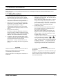


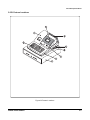
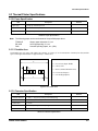
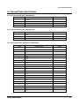
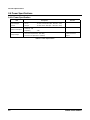

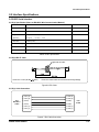

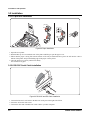
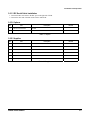
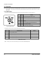
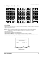


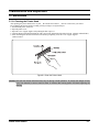


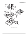


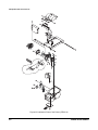


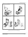


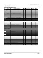
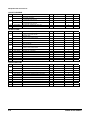
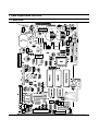


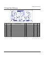
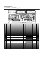
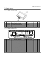
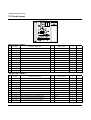

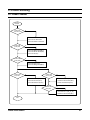
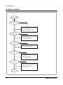

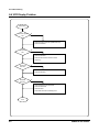
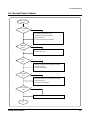
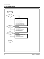


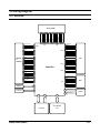


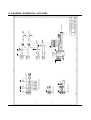
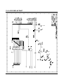
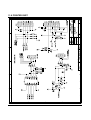

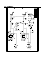


![[SPT-3000] e](http://vs1.manualzilla.com/store/data/005667089_1-a5f3766b3193f6552f250995926a69c5-150x150.png)