1
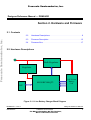
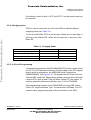
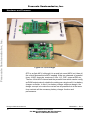
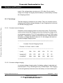
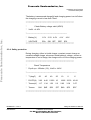
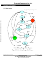
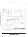
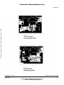
Freescale Semiconductor, Inc...
Freescale Semiconductor, Inc.
Li-ion Battery Charger
Designer Reference
Manual
M68HC08
Microcontrollers
DRM043/D
Rev. 0, 06/2003
MOTOROLA.COM/SEMICONDUCTORS
For More Information On This Product,
Go to: www.freescale.com
Freescale Semiconductor, Inc...
Freescale Semiconductor, Inc.
For More Information On This Product,
Go to: www.freescale.com
Freescale Semiconductor, Inc.
Designer Reference Manual — DRM043/D
Section 1. Table of Contents
Freescale Semiconductor, Inc...
Section 1. System Overview
1.1
Contents . . . . . . . . . . . . . . . . . . . . . . . . . . . . . . . . . . . . . . . . . . . 7
1.2
Introduction . . . . . . . . . . . . . . . . . . . . . . . . . . . . . . . . . . . . . . . . . 7
1.3
Overview. . . . . . . . . . . . . . . . . . . . . . . . . . . . . . . . . . . . . . . . . . . 7
1.4
8-pin PDIP MC68HC908QT2 Feature . . . . . . . . . . . . . . . . . . . . 8
Section 2. Hardware and Firmware
2.1
Contents . . . . . . . . . . . . . . . . . . . . . . . . . . . . . . . . . . . . . . . . . . . 9
2.2
Hardware Descriptions . . . . . . . . . . . . . . . . . . . . . . . . . . . . . . . . 9
2.3
Firmware Description . . . . . . . . . . . . . . . . . . . . . . . . . . . . . . . . 13
2.4
Firmware files . . . . . . . . . . . . . . . . . . . . . . . . . . . . . . . . . . . . . . 17
Section 3.
3.1
Contents . . . . . . . . . . . . . . . . . . . . . . . . . . . . . . . . . . . . . . . . . . 19
3.2
Test Description . . . . . . . . . . . . . . . . . . . . . . . . . . . . . . . . . . . . 19
3.3
Extra Features . . . . . . . . . . . . . . . . . . . . . . . . . . . . . . . . . . . . . 19
3.4
Further Information . . . . . . . . . . . . . . . . . . . . . . . . . . . . . . . . . . 20
3.5
Schematics . . . . . . . . . . . . . . . . . . . . . . . . . . . . . . . . . . . . . . . . 21
Glossary
DRM043/D — Rev 0
MOTOROLA
Designer Reference Manual
Table of Contents
For More Information On This Product,
Go to: www.freescale.com
3
Freescale Semiconductor, Inc.
Freescale Semiconductor, Inc...
Table of Contents
Designer Reference Manual
4
DRM043/D — Rev 0
Table of Contents
For More Information On This Product,
Go to: www.freescale.com
MOTOROLA
Freescale Semiconductor, Inc.
Li-ion Battery Charger
Freescale Semiconductor, Inc...
Designer Reference Manual — Rev 0
by: Roger Fan
Applications Engineering
Microcontroller Division
Hong Kong
DRM043/D — Rev 0
Designer Reference Manual
MOTOROLA
5
For More Information On This Product,
Go to: www.freescale.com
Freescale Semiconductor, Inc...
Freescale Semiconductor, Inc.
Designer Reference Manual
DRM043/D — Rev 0
6
MOTOROLA
For More Information On This Product,
Go to: www.freescale.com
Freescale Semiconductor, Inc...
Freescale Semiconductor, Inc.
Designer Reference Manual — DRM043/D
Section 1. System Overview
1.1 Contents
1.2
Introduction . . . . . . . . . . . . . . . . . . . . . . . . . . . . . . . . . . . . . . . . . 7
1.3
Overview. . . . . . . . . . . . . . . . . . . . . . . . . . . . . . . . . . . . . . . . . . . 7
1.4
8-pin PDIP MC68HC908QT2 Feature . . . . . . . . . . . . . . . . . . . . 8
1.2 Introduction
This manual describes a reference design of Li-ion battery charger for
mobile phone cell by using a MC68HC908QY/QT MCU.
For Full MC68HC908QY specification, please refer to the data sheet,
Motorola order number: MC68HC908QY/D.
1.3 Overview
The Motorola MC68HC908QY/QT is a member of the HC08 Family of
microcontrollers (MCUs). The features of the MC68HC908QY/QT
include a 4-channel Analog to Digital Converter and Timer module which
can be set to generate PWM signals. This feature makes this MCU
suitable for application such as a single cell Li-ion battery charger. The
MC68HC908QY/QT is available in several packages with different
memory size to fit into various applications. A Li-ion battery charger is
demonstrated here using the MC68HC908QT2 with 8-pin PDIP
package. The main features of this Li-ion battery charger reference
design include:
•
Capable to rapid charge a 3.6V Li-ion battery cell.
•
Auto-detect of battery insertion.
DRM043/D — Rev 0
MOTOROLA
Designer Reference Manual
System Overview
For More Information On This Product,
Go to: www.freescale.com
7
Freescale Semiconductor, Inc...
Freescale Semiconductor, Inc.
System Overview
•
Applied constant current and constant voltage charge method.
•
Implemented trickle charge mode when battery voltage is too low.
•
Charge cut off and signify battery full when charging current fall
below 75mA.
•
Over current, over voltage, over temperature protection.
•
In-circuit programming for firmware upgrade
1.4 8-pin PDIP MC68HC908QT2 Feature
MC68HC908QT2 is an 8-pin MCU which has on-chip in-application
programmable, 1536 bytes of user FLASH memory (with internal
program/erase voltage generation). Good enough for small application
like battery charger. It has128 bytes RAM, 4 channel 8 bit ADC. The
trimmable internal oscillator with accuracy +/- 5% helps to reduce the
system cost of the application by eliminate the external crystal
oscillation circuit. It has one 16 bit timer module with 2 timer channel
which can generated PWM signals. Besides the Vdd and Vss pins, all
other 6 pins can be used by the application. These pins are multiplex
together with the I/O, ADC, KBI, TIM. It gives great flexibility for the
user's application.
Designer Reference Manual
8
DRM043/D — Rev 0
System Overview
For More Information On This Product,
Go to: www.freescale.com
MOTOROLA
Freescale Semiconductor, Inc...
Freescale Semiconductor, Inc.
Designer Reference Manual — DRM043/D
Section 2. Hardware and Firmware
2.1 Contents
2.2
Hardware Descriptions . . . . . . . . . . . . . . . . . . . . . . . . . . . . . . . . 9
2.3
Firmware Description . . . . . . . . . . . . . . . . . . . . . . . . . . . . . . . . 13
2.4
Firmware files . . . . . . . . . . . . . . . . . . . . . . . . . . . . . . . . . . . . . . 17
2.2 Hardware Descriptions
5V
Bulk Regulator
Regulator
3.6V Li-ion
Battery
Cell
MC68HC908QT2
ICP
Figure 2-1. Li-ion Battery Charger Block Diagram
DRM043/D — Rev 0
MOTOROLA
Designer Reference Manual
Hardware and Firmware
For More Information On This Product,
Go to: www.freescale.com
9
Freescale Semiconductor, Inc...
Freescale Semiconductor, Inc.
Hardware and Firmware
2.2.1 Power supply to the MCU
Please refer to the schematic at 3.5 Schematics
The power input to the charger should be a regulated 5V, 1A supply to
P1.
TL431 is used in this reference design to act as a voltage regulator with
1% accuracy to provide power to the micro-controller.
2.2.2 Charging control
Pin 7 of the MCU is the TCH0 which is configured as a PWM output. The
PWM signal will control the on-off charging power to the battery, and
thus control the charging current and voltage. Q2, D1,L1 and C4 form the
bulk regulator will provide a smoother power source to charge the
battery.
2.2.3 Sensing circuit.
Three ADC channels of the micro-controller are used to check battery's
voltage, current and temperature.
Charging current is sensed at the B- of J1. When battery is under
charging, charging current will flow through the sensing resistor R13 and
R14. A voltage drop will appear on the resistor R13 and R14. It can be
sensed at B-. Since R13//R14 is 0.5 ohms, so when a charge current is
300mA, then the voltage at B- will be 150mV.
The battery voltage is sensed by directly sensing the voltage at B+ point
of J1.
When battery is under charging, it is required to subtract the voltage at
B- in order to obtain the actual battery voltage across its terminals.
The battery's temperature can be sensed by sensing the voltage at
terminal T of J1. The change of voltage is caused by the variation of
resistance value of the NTC.
Designer Reference Manual
10
DRM043/D — Rev 0
Hardware and Firmware
For More Information On This Product,
Go to: www.freescale.com
MOTOROLA
Freescale Semiconductor, Inc...
Freescale Semiconductor, Inc.
Hardware and Firmware
Hardware Descriptions
If the battery is built in with a NTC, the NTC Z1 on the demo board can
be removed.
2.2.4 Charging status
PTA3 is used to control the on-off of two LEDs to indicate different
charging status( see Table 2-1).
To turn on both LEDs, PTA3 is set as input. When set to output high, it
will turn on the Green LED. When set as output low, it will turn on the
Red LED.
Table 2-1. Charging Status
RED
GREEN
Fast Charge in progress
On
Off
Battery is fully charged
Off
On
Battery is not connected
On
On
Fault condition occurred
--Flashing--
2.2.5 In-Circuit-Programming
J2 contains the signals for the MCU68HC908QT2 to enter monitor mode
for ICP. The ICP requires connecting J2 with a cable to the ICP adaptor
board, which is plugged-into the M68HC08 Serial Programmer
(M68SPGRM08) (see Figure 2-2). The signals from the J2 are Vdd, Vss,
Vtst and OSC1 and PA0. Beside these signals, enter monitor mode also
required PTA1 pull-up and PTA4 pull-down. When ICP, the jumper J3
must be opened to disconnect the filter cap, 0.1uF at PTA0/AD0.
The programming software is the PROG08SZ.exe from P&E. Select
Class I for Target Hardware Type. The baud rate is 4800bps. The ICP
support erase, programming and verify the firmware in the MCU.
DRM043/D — Rev 0
MOTOROLA
Designer Reference Manual
Hardware and Firmware
For More Information On This Product,
Go to: www.freescale.com
11
Freescale Semiconductor, Inc.
Freescale Semiconductor, Inc...
Hardware and Firmware
Figure 2-2. QT2 Charger
QT2 is an 8pin MCU, although it is a small pin count MCU but it has all
the critical features that a MCU needed. It has two channels of powerful
timer, 4 ADC channels, maximum 6 I/Os. LVI, COP, external IRQ etc.
The four 4 8-bit ADC channel and the powerful timer which can be config
as PWM output make it suitable for working as a single cell Li-ion battery
charger controller. In this Li-ion battery charger reference desgin, the
design concept is to make the cost as low as possible but at the same
time maintain all the necessary battery charger function and
performance.
Designer Reference Manual
12
DRM043/D — Rev 0
Hardware and Firmware
For More Information On This Product,
Go to: www.freescale.com
MOTOROLA
Freescale Semiconductor, Inc.
Hardware and Firmware
Firmware Description
2.3 Firmware Description
2.3.1 Battery inserted detection.
Freescale Semiconductor, Inc...
Normally, a Lithium-ion battery has 3 terminals, B+, B- and T. The
terminal T can be one of the terminals for temperature sensor or a
dummy resistor. The battery charger can sense the voltage at the
corresponding T of J1 (refer to charger schematic at 3.5). When the
battery is removed, the voltage that appears at T will be pulled up to Vdd
by the 10K resistor, i.e., it is in high state. When the battery is inserted,
the voltage at T will be equal to Z1/(Z1+10K) x Vdd. Charger can then
sense insertion of the battery insertion by checking the voltage at T by
ADC.
When battery insertion is detected, the firmware will go on to check the
inserted battery's voltage and temperature. If it falls in the valid range,
then proceed to charging mode.
Vbat < 1.0V
No charging, bad battery, flashing LEDs
Vbat > 4.0V
Battery full, no charging, green LED on
1.0V < Vbat < 2.5V
Trickle charge, red LED on
2.5V <Vbat < 4.0V
Fast charge, red LED on
Vtemp < 0 C
No charging. Flashing LEDs
Vtemp > 45 C
No charging. Flashing LEDs
I_charge > 500mA
Over current, stop charging, flashing LEDs
2.3.2 Trickle charge
If the battery voltage is <2.5V, then go to trickle charge. The current for
trickle charge is set to 0.1C to 0.2C which equals to the 10% or 20% of
the battery's rate capacity, and the max. Charge time is 10 mins. If within
10 mins time, the battery voltage raise above 2.5V, then it means the
battery is a good battery and the charger can then switch to fast charging
DRM043/D — Rev 0
MOTOROLA
Designer Reference Manual
Hardware and Firmware
For More Information On This Product,
Go to: www.freescale.com
13
Freescale Semiconductor, Inc...
Freescale Semiconductor, Inc.
Hardware and Firmware
mode. If the voltage does not raise up to 2.5V after 10 mins trickle
charge, the charger will signify that the battery is a bad battery and stop
the charging process.
2.3.3 Fast charge
The fast charging is divided into two states. They are constant current
charging and constant voltage charging. A max charging time is also set
for the fast charging mode.
2.3.3.1 Constant current charging
Constant current charging mode is a close loop control. The firmware
continuously checks the charging current by sensing the voltage at the
current sense resistors (R13, R14) and adjusts the duty of PWM output
from MCU. The battery's voltage is checked frequently. Whenever found
the battery's voltage reaches or above 4.1V, the charger will switch to
constant voltage charging mode.
************************************************************************
*
*
Constant Current Charging Control
R sense = 0.5 ohm, VrefH = 4.40V
*-----------------------------------------------------------------------------------*
I (mA)
380
310
200
100
75
50
*
Isense(mV)
190
155
100
50
37
25
*
CURRENT
$0B
$09
$06
$03
$02
$01
*************************************************************************
2.3.3.2 Constant voltage charging
In constant voltage charging state, the battery voltage is checked and
maintained at 4.1V by controlling the duty of PWM output. The charging
current will gradually decrease when the battery is close to battery full.
Designer Reference Manual
14
DRM043/D — Rev 0
Hardware and Firmware
For More Information On This Product,
Go to: www.freescale.com
MOTOROLA
Freescale Semiconductor, Inc...
Freescale Semiconductor, Inc.
Hardware and Firmware
Firmware Description
The battery is announced charge full and charging power is cut off when
the charging current is less than 75mA.
********************************************************************
*
*
Check Battery voltage valid (ADC3)
VrefH = 4.40V
*------------------------------------------------------------------*
Battery(V)
1.0V
2.5V 4.0V
4.1V
4.2V
* VOLTAGE
$3A $91 $E7 $EE $F4
********************************************************************
2.3.4 Safety protection
During charging, either in trickle charge, constant current charge or
constant voltage charge, whenever found battery's voltage, current or
temperature is out of range, the charger will cut of the charging power.
********************************************************************
*
*
Check Temperature
R pull-up = 10Kohm (1%), VrefH = 4.40V
*----------------------------------------------------------------------------------*
T (degC)
50
*
R NTC(K)
3.63
4.40
5.356 10
19.85 32.33
42.81
*
Tsense(V) 1.17
1.34
1.53
2.2
2.92
3.36
3.57
*
Tsense
$4E
$59
$7F
$A9
$C2
$CF
$44
45
40
25
10
0
-5
********************************************************************
DRM043/D — Rev 0
MOTOROLA
Designer Reference Manual
Hardware and Firmware
For More Information On This Product,
Go to: www.freescale.com
15
Freescale Semiconductor, Inc.
Hardware and Firmware
2.3.5 State diagram
At any stage, if battery removed, will go to START
START
battery removed
N
battery not
removed
Check
Battery
Insert
Freescale Semiconductor, Inc...
Y
T, V out-range
FAULT
Check
Battery
V, T
1 < V < 2.5v
V > = 4.1v
Trickle
Charge
Mode
V > 2.5v
V > 2.5v
battery removed
Fast
Charge
Mode
battery not
removed
battery removed
battery not
removed
pre-charge
time_out
Battery
FULL
charge
time_out
charge
time_out
I < 75mA
battery removed
CC
Charge
Mode
T,I out-range
V = 4.1v
CV
Charge
Mode
T,I out-range
battery not
removed
Li-ion Battery Charger State Diagram
Figure 2-3. Li-ion Battery Charger State Diagram
Designer Reference Manual
16
DRM043/D — Rev 0
Hardware and Firmware
For More Information On This Product,
Go to: www.freescale.com
MOTOROLA
Freescale Semiconductor, Inc.
Hardware and Firmware
Firmware files
2.4 Firmware files
Firmware is complied under CASM08Z.EXE ver 3.16 from P&E
Microcomputer System, Inc.
Table 2-2 summarizes the functions of each firmware files:
Table 2-2. Functions
Functions
QT4CHGRDEMO.asm
Charger main program
MC68HC908QT4.equ
QT4 registers and memory definitions
QT4CHGR_INC.asm
Subroutines include files
Freescale Semiconductor, Inc...
Files
DRM043/D — Rev 0
MOTOROLA
Designer Reference Manual
Hardware and Firmware
For More Information On This Product,
Go to: www.freescale.com
17
Freescale Semiconductor, Inc.
Freescale Semiconductor, Inc...
Hardware and Firmware
Designer Reference Manual
18
DRM043/D — Rev 0
Hardware and Firmware
For More Information On This Product,
Go to: www.freescale.com
MOTOROLA
Freescale Semiconductor, Inc...
Freescale Semiconductor, Inc.
Designer Reference Manual — DRM043/D
Section 3.
3.1 Contents
3.2
Test Description . . . . . . . . . . . . . . . . . . . . . . . . . . . . . . . . . . . . 19
3.3
Extra Features . . . . . . . . . . . . . . . . . . . . . . . . . . . . . . . . . . . . . 19
3.4
Further Information . . . . . . . . . . . . . . . . . . . . . . . . . . . . . . . . . . 20
3.5
Schematics . . . . . . . . . . . . . . . . . . . . . . . . . . . . . . . . . . . . . . . . 21
3.2 Test Description
The solution was tested with one 3.6V Li-ion battery cells using a +5V
power supply (HP6236B)
3.3 Extra Features
There is a useful subroutine included in the file QY2CHGR_INC.asm. It
is DSRL_OUT which is a serial RS232 data transmit routine. It uses
PTA3 as the data line to serial out the data. The baud rate is 19200bps
when the ICG of QT2 is trimmed at bus frequency 3.2MHz. The data line
is output to a standard RS232 interface circuit that connected to the
COM port of a PC. This routine is helpful in project development as
developer can monitor the battery charging status and got the charging
parameters such as voltage, temperature and current for analysis.
Since ICG is used, some fine tune might need on the bit delay routines
if the bus frequency cannot be tuned to exactly to 3.2MHz bus frequency.
When calling this routine, the interrupt mask bit is set to avoid interrupt,
and the mask interrupt bit will be clear before leave this subroutine.
When development of the software is completed. The called of this
routine is not necessary and should be removed and the PTA3 is set it
back to control the LEDs.
DRM043/D — Rev 0
Designer Reference Manual
MOTOROLA
19
For More Information On This Product,
Go to: www.freescale.com
Freescale Semiconductor, Inc.
3.4 Further Information
3.4.1 Related Documents
Freescale Semiconductor, Inc...
MC68HC908QT2 Technical Data
Designer Reference Manual
DRM043/D — Rev 0
20
MOTOROLA
For More Information On This Product,
Go to: www.freescale.com
Freescale Semiconductor, Inc.
Schematics
Freescale Semiconductor, Inc...
3.5 Schematics
DRM043/D — Rev 0
Designer Reference Manual
MOTOROLA
21
For More Information On This Product,
Go to: www.freescale.com
Freescale Semiconductor, Inc...
Freescale Semiconductor, Inc.
Designer Reference Manual
DRM043/D — Rev 0
22
MOTOROLA
For More Information On This Product,
Go to: www.freescale.com
Freescale Semiconductor, Inc.
Freescale Semiconductor, Inc...
Schematics
DRM043/D — Rev 0
Designer Reference Manual
MOTOROLA
23
For More Information On This Product,
Go to: www.freescale.com
Freescale Semiconductor, Inc...
Freescale Semiconductor, Inc.
Designer Reference Manual
DRM043/D — Rev 0
24
MOTOROLA
For More Information On This Product,
Go to: www.freescale.com
Freescale Semiconductor, Inc...
Freescale Semiconductor, Inc.
Designer Reference Manual — DRM043/D
Section 1. Glossary
A — See “accumulators (A and B or D).”
accumulators (A and B or D) — Two 8-bit (A and B) or one 16-bit (D) general-purpose registers
in the CPU. The CPU uses the accumulators to hold operands and results of arithmetic
and logic operations.
acquisition mode — A mode of PLL operation with large loop bandwidth. Also see ’tracking
mode’.
address bus — The set of wires that the CPU or DMA uses to read and write memory locations.
addressing mode — The way that the CPU determines the operand address for an instruction.
The M68HC12 CPU has 15 addressing modes.
ALU — See “arithmetic logic unit (ALU).”
analogue-to-digital converter (ATD) — The ATD module is an 8-channel, multiplexed-input
successive-approximation analog-to-digital converter.
arithmetic logic unit (ALU) — The portion of the CPU that contains the logic circuitry to perform
arithmetic, logic, and manipulation operations on operands.
asynchronous — Refers to logic circuits and operations that are not synchronized by a common
reference signal.
ATD — See “analogue-to-digital converter”.
B — See “accumulators (A and B or D).”
baud rate — The total number of bits transmitted per unit of time.
BCD — See “binary-coded decimal (BCD).”
binary — Relating to the base 2 number system.
DRM043/D — Rev 0
MOTOROLA
Designer Reference Manual
Glossary
For More Information On This Product,
Go to: www.freescale.com
25
Freescale Semiconductor, Inc...
Freescale Semiconductor, Inc.
Glossary
binary number system — The base 2 number system, having two digits, 0 and 1. Binary
arithmetic is convenient in digital circuit design because digital circuits have two
permissible voltage levels, low and high. The binary digits 0 and 1 can be interpreted to
correspond to the two digital voltage levels.
binary-coded decimal (BCD) — A notation that uses 4-bit binary numbers to represent the 10
decimal digits and that retains the same positional structure of a decimal number. For
example,
234 (decimal) = 0010 0011 0100 (BCD)
bit — A binary digit. A bit has a value of either logic 0 or logic 1.
branch instruction — An instruction that causes the CPU to continue processing at a memory
location other than the next sequential address.
break module — The break module allows software to halt program execution at a
programmable point in order to enter a background routine.
breakpoint — A number written into the break address registers of the break module. When a
number appears on the internal address bus that is the same as the number in the break
address registers, the CPU executes the software interrupt instruction (SWI).
break interrupt — A software interrupt caused by the appearance on the internal address bus
of the same value that is written in the break address registers.
bus — A set of wires that transfers logic signals.
bus clock — See "CPU clock".
byte — A set of eight bits.
CAN — See "Motorola scalable CAN."
CCR — See “condition code register.”
central processor unit (CPU) — The primary functioning unit of any computer system. The
CPU controls the execution of instructions.
CGM — See “clock generator module (CGM).”
clear — To change a bit from logic 1 to logic 0; the opposite of set.
clock — A square wave signal used to synchronize events in a computer.
clock generator module (CGM) — The CGM module generates a base clock signal from which
the system clocks are derived. The CGM may include a crystal oscillator circuit and/or
phase-locked loop (PLL) circuit.
Designer Reference Manual
26
DRM043/D — Rev 0
Glossary
For More Information On This Product,
Go to: www.freescale.com
MOTOROLA
Freescale Semiconductor, Inc...
Freescale Semiconductor, Inc.
Glossary
comparator — A device that compares the magnitude of two inputs. A digital comparator defines
the equality or relative differences between two binary numbers.
computer operating properly module (COP) — A counter module that resets the MCU if
allowed to overflow.
condition code register (CCR) — An 8-bit register in the CPU that contains the interrupt mask
bit and five bits that indicate the results of the instruction just executed.
control bit — One bit of a register manipulated by software to control the operation of the
module.
control unit — One of two major units of the CPU. The control unit contains logic functions that
synchronize the machine and direct various operations. The control unit decodes
instructions and generates the internal control signals that perform the requested
operations. The outputs of the control unit drive the execution unit, which contains the
arithmetic logic unit (ALU), CPU registers, and bus interface.
COP — See "computer operating properly module (COP)."
CPU — See “central processor unit (CPU).”
CPU12 — The CPU of the MC68HC12 Family.
CPU clock — Bus clock select bits BCSP and BCSS in the clock select register (CLKSEL)
determine which clock drives SYSCLK for the main system, including the CPU and buses.
When EXTALi drives the SYSCLK, the CPU or bus clock frequency (fo) is equal to the
EXTALi frequency divided by 2.
CPU cycles — A CPU cycle is one period of the internal bus clock, normally derived by dividing
a crystal oscillator source by two or more so the high and low times will be equal. The
length of time required to execute an instruction is measured in CPU clock cycles.
CPU registers — Memory locations that are wired directly into the CPU logic instead of being
part of the addressable memory map. The CPU always has direct access to the
information in these registers. The CPU registers in an M68HC12 are:
•
A (8-bit accumulator)
•
B (8-bit accumulator)
– D (16-bit accumulator formed by concatenation of
accumulators A and B)
•
IX (16-bit index register)
•
IY (16-bit index register)
DRM043/D — Rev 0
MOTOROLA
Designer Reference Manual
Glossary
For More Information On This Product,
Go to: www.freescale.com
27
Freescale Semiconductor, Inc...
Freescale Semiconductor, Inc.
Glossary
•
SP (16-bit stack pointer)
•
PC (16-bit program counter)
• CCR (8-bit condition code register)
cycle time — The period of the operating frequency: tCYC = 1/fOP.
D — See “accumulators (A and B or D).”
decimal number system — Base 10 numbering system that uses the digits zero through nine.
duty cycle — A ratio of the amount of time the signal is on versus the time it is off. Duty cycle is
usually represented by a percentage.
ECT — See “enhanced capture timer.”
EEPROM — Electrically erasable, programmable, read-only memory. A nonvolatile type of
memory that can be electrically erased and reprogrammed.
EPROM — Erasable, programmable, read-only memory. A nonvolatile type of memory that can
be erased by exposure to an ultraviolet light source and then reprogrammed.
enhanced capture timer (ECT) — The HC12 Enhanced Capture Timer module has the features
of the HC12 Standard Timer module enhanced by additional features in order to enlarge
the field of applications.
exception — An event such as an interrupt or a reset that stops the sequential execution of the
instructions in the main program.
fetch — To copy data from a memory location into the accumulator.
firmware — Instructions and data programmed into nonvolatile memory.
free-running counter — A device that counts from zero to a predetermined number, then rolls
over to zero and begins counting again.
full-duplex transmission — Communication on a channel in which data can be sent and
received simultaneously.
hexadecimal — Base 16 numbering system that uses the digits 0 through 9 and the letters A
through F.
high byte — The most significant eight bits of a word.
illegal address — An address not within the memory map
illegal opcode — A nonexistent opcode.
Designer Reference Manual
28
DRM043/D — Rev 0
Glossary
For More Information On This Product,
Go to: www.freescale.com
MOTOROLA
Freescale Semiconductor, Inc...
Freescale Semiconductor, Inc.
Glossary
index registers (IX and IY) — Two 16-bit registers in the CPU. In the indexed addressing
modes, the CPU uses the contents of IX or IY to determine the effective address of the
operand. IX and IY can also serve as a temporary data storage locations.
input/output (I/O) — Input/output interfaces between a computer system and the external world.
A CPU reads an input to sense the level of an external signal and writes to an output to
change the level on an external signal.
instructions — Operations that a CPU can perform. Instructions are expressed by programmers
as assembly language mnemonics. A CPU interprets an opcode and its associated
operand(s) and instruction.
inter-IC bus (I2C) — A two-wire, bidirectional serial bus that provides a simple, efficient method
of data exchange between devices.
interrupt — A temporary break in the sequential execution of a program to respond to signals
from peripheral devices by executing a subroutine.
interrupt request — A signal from a peripheral to the CPU intended to cause the CPU to
execute a subroutine.
I/O — See “input/output (I/0).”
jitter — Short-term signal instability.
latch — A circuit that retains the voltage level (logic 1 or logic 0) written to it for as long as power
is applied to the circuit.
latency — The time lag between instruction completion and data movement.
least significant bit (LSB) — The rightmost digit of a binary number.
logic 1 — A voltage level approximately equal to the input power voltage (VDD).
logic 0 — A voltage level approximately equal to the ground voltage (VSS).
low byte — The least significant eight bits of a word.
M68HC12 — A Motorola family of 16-bit MCUs.
mark/space — The logic 1/logic 0 convention used in formatting data in serial communication.
mask — 1. A logic circuit that forces a bit or group of bits to a desired state. 2. A photomask used
in integrated circuit fabrication to transfer an image onto silicon.
MCU — Microcontroller unit. See “microcontroller.”
DRM043/D — Rev 0
MOTOROLA
Designer Reference Manual
Glossary
For More Information On This Product,
Go to: www.freescale.com
29
Freescale Semiconductor, Inc...
Freescale Semiconductor, Inc.
Glossary
memory location — Each M68HC12 memory location holds one byte of data and has a unique
address. To store information in a memory location, the CPU places the address of the
location on the address bus, the data information on the data bus, and asserts the write
signal. To read information from a memory location, the CPU places the address of the
location on the address bus and asserts the read signal. In response to the read signal,
the selected memory location places its data onto the data bus.
memory map — A pictorial representation of all memory locations in a computer system.
MI-Bus — See "Motorola interconnect bus".
microcontroller — Microcontroller unit (MCU). A complete computer system, including a CPU,
memory, a clock oscillator, and input/output (I/O) on a single integrated circuit.
modulo counter — A counter that can be programmed to count to any number from zero to its
maximum possible modulus.
most significant bit (MSB) — The leftmost digit of a binary number.
Motorola interconnect bus (MI-Bus) — The Motorola Interconnect Bus (MI Bus) is a serial
communications protocol which supports distributed real-time control efficiently and with
a high degree of noise immunity.
Motorola scalable CAN (msCAN) — The Motorola scalable controller area network is a serial
communications protocol that efficiently supports distributed real-time control with a very
high level of data integrity.
msCAN — See "Motorola scalable CAN".
MSI — See "multiple serial interface".
multiple serial interface — A module consisting of multiple independent serial I/O sub-systems,
e.g. two SCI and one SPI.
multiplexer — A device that can select one of a number of inputs and pass the logic level of that
input on to the output.
nibble — A set of four bits (half of a byte).
object code — The output from an assembler or compiler that is itself executable machine code,
or is suitable for processing to produce executable machine code.
opcode — A binary code that instructs the CPU to perform an operation.
open-drain — An output that has no pullup transistor. An external pullup device can be
connected to the power supply to provide the logic 1 output voltage.
Designer Reference Manual
30
DRM043/D — Rev 0
Glossary
For More Information On This Product,
Go to: www.freescale.com
MOTOROLA
Freescale Semiconductor, Inc...
Freescale Semiconductor, Inc.
Glossary
operand — Data on which an operation is performed. Usually a statement consists of an
operator and an operand. For example, the operator may be an add instruction, and the
operand may be the quantity to be added.
oscillator — A circuit that produces a constant frequency square wave that is used by the
computer as a timing and sequencing reference.
OTPROM — One-time programmable read-only memory. A nonvolatile type of memory that
cannot be reprogrammed.
overflow — A quantity that is too large to be contained in one byte or one word.
page zero — The first 256 bytes of memory (addresses $0000–$00FF).
parity — An error-checking scheme that counts the number of logic 1s in each byte transmitted.
In a system that uses odd parity, every byte is expected to have an odd number of logic
1s. In an even parity system, every byte should have an even number of logic 1s. In the
transmitter, a parity generator appends an extra bit to each byte to make the number of
logic 1s odd for odd parity or even for even parity. A parity checker in the receiver counts
the number of logic 1s in each byte. The parity checker generates an error signal if it finds
a byte with an incorrect number of logic 1s.
PC — See “program counter (PC).”
peripheral — A circuit not under direct CPU control.
phase-locked loop (PLL) — A clock generator circuit in which a voltage controlled oscillator
produces an oscillation which is synchronized to a reference signal.
PLL — See "phase-locked loop (PLL)."
pointer — Pointer register. An index register is sometimes called a pointer register because its
contents are used in the calculation of the address of an operand, and therefore points to
the operand.
polarity — The two opposite logic levels, logic 1 and logic 0, which correspond to two different
voltage levels, VDD and VSS.
polling — Periodically reading a status bit to monitor the condition of a peripheral device.
port — A set of wires for communicating with off-chip devices.
prescaler — A circuit that generates an output signal related to the input signal by a fractional
scale factor such as 1/2, 1/8, 1/10 etc.
program — A set of computer instructions that cause a computer to perform a desired operation
or operations.
DRM043/D — Rev 0
MOTOROLA
Designer Reference Manual
Glossary
For More Information On This Product,
Go to: www.freescale.com
31
Freescale Semiconductor, Inc...
Freescale Semiconductor, Inc.
Glossary
program counter (PC) — A 16-bit register in the CPU. The PC register holds the address of the
next instruction or operand that the CPU will use.
pull — An instruction that copies into the accumulator the contents of a stack RAM location. The
stack RAM address is in the stack pointer.
pullup — A transistor in the output of a logic gate that connects the output to the logic 1 voltage
of the power supply.
pulse-width — The amount of time a signal is on as opposed to being in its off state.
pulse-width modulation (PWM) — Controlled variation (modulation) of the pulse width of a
signal with a constant frequency.
push — An instruction that copies the contents of the accumulator to the stack RAM. The stack
RAM address is in the stack pointer.
PWM period — The time required for one complete cycle of a PWM waveform.
RAM — Random access memory. All RAM locations can be read or written by the CPU. The
contents of a RAM memory location remain valid until the CPU writes a different value or
until power is turned off.
RC circuit — A circuit consisting of capacitors and resistors having a defined time constant.
read — To copy the contents of a memory location to the accumulator.
register — A circuit that stores a group of bits.
reserved memory location — A memory location that is used only in special factory test modes.
Writing to a reserved location has no effect. Reading a reserved location returns an
unpredictable value.
reset — To force a device to a known condition.
SCI — See "serial communication interface module (SCI)."
serial — Pertaining to sequential transmission over a single line.
serial communications interface module (SCI) — A module that supports asynchronous
communication.
serial peripheral interface module (SPI) — A module that supports synchronous
communication.
set — To change a bit from logic 0 to logic 1; opposite of clear.
Designer Reference Manual
32
DRM043/D — Rev 0
Glossary
For More Information On This Product,
Go to: www.freescale.com
MOTOROLA
Freescale Semiconductor, Inc...
Freescale Semiconductor, Inc.
Glossary
shift register — A chain of circuits that can retain the logic levels (logic 1 or logic 0) written to
them and that can shift the logic levels to the right or left through adjacent circuits in the
chain.
signed — A binary number notation that accommodates both positive and negative numbers.
The most significant bit is used to indicate whether the number is positive or negative,
normally logic 0 for positive and logic 1 for negative. The other seven bits indicate the
magnitude of the number.
software — Instructions and data that control the operation of a microcontroller.
software interrupt (SWI) — An instruction that causes an interrupt and its associated vector
fetch.
SPI — See "serial peripheral interface module (SPI)."
stack — A portion of RAM reserved for storage of CPU register contents and subroutine return
addresses.
stack pointer (SP) — A 16-bit register in the CPU containing the address of the next available
storage location on the stack.
start bit — A bit that signals the beginning of an asynchronous serial transmission.
status bit — A register bit that indicates the condition of a device.
stop bit — A bit that signals the end of an asynchronous serial transmission.
subroutine — A sequence of instructions to be used more than once in the course of a program.
The last instruction in a subroutine is a return from subroutine (RTS) instruction. At each
place in the main program where the subroutine instructions are needed, a jump or branch
to subroutine (JSR or BSR) instruction is used to call the subroutine. The CPU leaves the
flow of the main program to execute the instructions in the subroutine. When the RTS
instruction is executed, the CPU returns to the main program where it left off.
synchronous — Refers to logic circuits and operations that are synchronized by a common
reference signal.
timer — A module used to relate events in a system to a point in time.
toggle — To change the state of an output from a logic 0 to a logic 1 or from a logic 1 to a logic 0.
tracking mode — A mode of PLL operation with narrow loop bandwidth. Also see ‘acquisition
mode.’
DRM043/D — Rev 0
MOTOROLA
Designer Reference Manual
Glossary
For More Information On This Product,
Go to: www.freescale.com
33
Freescale Semiconductor, Inc...
Freescale Semiconductor, Inc.
Glossary
two’s complement — A means of performing binary subtraction using addition techniques. The
most significant bit of a two’s complement number indicates the sign of the number (1
indicates negative). The two’s complement negative of a number is obtained by inverting
each bit in the number and then adding 1 to the result.
unbuffered — Utilizes only one register for data; new data overwrites current data.
unimplemented memory location — A memory location that is not used. Writing to an
unimplemented location has no effect. Reading an unimplemented location returns an
unpredictable value.
variable — A value that changes during the course of program execution.
VCO — See "voltage-controlled oscillator."
vector — A memory location that contains the address of the beginning of a subroutine written
to service an interrupt or reset.
voltage-controlled oscillator (VCO) — A circuit that produces an oscillating output signal of a
frequency that is controlled by a dc voltage applied to a control input.
waveform — A graphical representation in which the amplitude of a wave is plotted against time.
wired-OR — Connection of circuit outputs so that if any output is high, the connection point is
high.
word — A set of two bytes (16 bits).
write — The transfer of a byte of data from the CPU to a memory location.
Designer Reference Manual
34
DRM043/D — Rev 0
Glossary
For More Information On This Product,
Go to: www.freescale.com
MOTOROLA
Freescale Semiconductor, Inc...
Freescale Semiconductor, Inc.
For More Information On This Product,
Go to: www.freescale.com
Freescale Semiconductor, Inc...
Freescale Semiconductor, Inc.
HOW TO REACH US:
DRM043/D
USA/EUROPE/LOCATIONS NOT LISTED:
Motorola Literature Distribution
P.O. Box 5405
Denver, Colorado 80217
1-800-521-6274 or 480-768-2130
JAPAN:
Motorola Japan Ltd.
SPS, Technical Information Center
3-20-1, Minami-Azabu, Minato-ku
Tokyo 106-8573, Japan
81-3-3440-3569
ASIA/PACIFIC:
Motorola Semiconductors H.K. Ltd.
Silicon Harbour Centre
2 Dai King Street
Tai Po Industrial Estate
Tai Po, N.T., Hong Kong
852-26668334
HOME PAGE:
http://motorola.com/semiconductors
Information in this document is provided solely to enable system and software implementers to use Motorola products.
There are no express or implied copyright licenses granted hereunder to design or fabricate any integrated circuits or
integrated circuits based on the information in this document.
Motorola reserves the right to make changes without further notice to any products herein. Motorola makes no warranty,
representation or guarantee regarding the suitability of its products for any particular purpose, nor does Motorola assume
any liability arising out of the application or use of any product or circuit, and specifically disclaims any and all liability,
including without limitation consequential or incidental damages. “Typical” parameters that may be provided in Motorola
data sheets and/or specifications can and do vary in different applications and actual performance may vary over time. All
operating parameters, including “Typicals”, must be validated for each customer application by customer’s technical
experts. Motorola does not convey any license under its patent rights nor the rights of others. Motorola products are not
designed, intended, or authorized for use as components in systems intended for surgical implant into the body, or other
applications intended to support or sustain life, or for any other application in which the failure of the Motorola product could
create a situation where personal injury or death may occur. Should Buyer purchase or use Motorola products for any such
unintended or unauthorized application, Buyer shall indemnify and hold Motorola and its officers, employees, subsidiaries,
affiliates, and distributors harmless against all claims, costs, damages, and expenses, and reasonable attorney fees arising
out of, directly or indirectly, any claim of personal injury or death associated with such unintended or unauthorized use, even
if such claim alleges that Motorola was negligent regarding the design or manufacture of the part.
MOTOROLA and the Stylized M Logo are registered in the US Patent and Trademark Office. All other product or service
names are the property of their respective owners. Motorola, Inc. is an Equal Opportunity/Affirmative Action Employer.
© Motorola Inc. 2003
DRM043/D
Rev. 0
6/2003
For More Information On This Product,
Go to: www.freescale.com