1
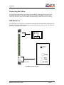
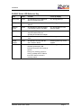
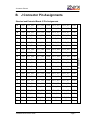
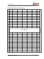
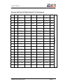
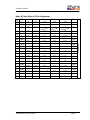
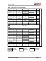
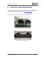
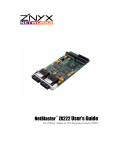
ZX4300P 10/100 ETHERNET SWITCH
USER'S GUIDE
Layer 2 CPSB Switch
Document No: DC0138-04
Copyright Notice
ZNYX Networks
48421 Milmont Drive
Fremont, CA 94538 USA
Telephone:
Fax:
Email:
Website:
(510) 249-0800 or (800) 724-0911
(510) 656-2460
[email protected]
[email protected]
www.znyx.com
ZX4300P Series User's Guide
Document # DC0138-04
September 26, 2001
©2001 ZNYX Networks. All rights reserved worldwide. Information in this document is subject
to change without prior notice. ZNYX Networks, RAIN, RAINlink, OpenArchitect are
trademarks or registered trademarks of ZNYX Networks in the United States and/or other
countries. Adobe, the Adobe logo, Acrobat, and the Reader are trademarks of Adobe Systems
Incorporated. All other marks, trademarks or service marks are the property of their respective
owners.
ZNYX Networks may have patents, pending patent applications, trademarks, copyrights or other
intellectual property rights covered in the subject matter of this document. By furnishing this
document, ZNYX Networks does not license nor waive its license to those intellectual property
rights except as expressly provided in a written license agreement from ZNYX Networks.
Information in this document is subject to change without prior notice.
ZX4300P Series User's Guide
About this Manual
This manual includes the installation, troubleshooting, and reference data for the ZX4300P
10/100 Ethernet Switch. See the ZNYX Networks data sheet for product specifications.
All documentation for ZNYX Networks products, including data sheets, release notes and User's
Guides are available for downloading from the ZNYX Networks website (http://www.znyx.com).
Files are supplied in PDF format so your system requires Adobe Acrobat Reader to open and read
the documentation.
Technical Support
If you have difficulty installing your switch or need further assistance after reading this User's
Guide, the ZNYX Networks professional technical support team is available to answer your
questions. Contact us at:
Telephone:
Fax:
Email:
Website:
ZX4300P Series User's Guide
(510) 249-0800 or (800) 724-0911
(510) 656-2460
[email protected]
http://www.znyx.com
Overview
Chapter 1 Overview of the ZX4300PSwitch
The ZX4300P CompactPCI Ethernet 10/100 Mbps switch is the cost-effective and flexible
solution to Embedded Carrier Class Layer 2 switching requirements.
ZNYX Networks' ZX4300P is the first switch designed to support the upcoming PICMG 2.16
specification for a CompactPCI Packet Switching Backplane (CPSB), but it can also be deployed
in a standard CompactPCI chassis by using one of three optional Rear Transition Boards (RTB).
When installed in the fabric slot of a CPSB chassis, the ZX4300P includes support for the
extended CPSB specification, routing all 24 10/100 ports to the backplane. It also supports the
typical 19 node CPSB, and with the addition of the ZXRTB05 RTB, routes the remaining 5 ports
to rear panel RJ-45 connectors. This allows the systems architect to easily add another chassis to
the switched backplane fabric.
The same ZX4300P may be installed in a standard CompactPCI chassis and configured with rear
panel I/O for all 24 10/100 ports. In an extension of PICMG 2.16, ports 20 through 24 are routed
to the J4 connecter, which cannot be part of an H.110 connection. Options include either the
ZXRTB24 dual-slot RTB with 24 RJ-45 connectors or the ZX4024RP single slot RTB with two
RJ-21 Telco connectors.
In either chassis, the ZX4300P's Hot Swap and instant reconfiguration features allow rapid
installation in a live system and a mean time to repair of mere seconds.
By using the latest switch silicon, the ZX4300P features non-blocking line-rate switching, 802.3x
and back-pressure flow control. Like the ZNYX Networks OpenArchitect switches, the ZX4300P
is designed for NEBS compliance and may be used with any host operating system or any host
CPU including Sun SPARC, Intel x86, and Motorola PowerPC.
ZX4300P Series User's Guide
Page 1
Overview
Features of the ZX4300PSwitch
The ZX4300P switch best satisfies the demand for high density, low cost, and high performance.
It enables system architects to accelerate development of their next-generation CPSB products
and achieve first-to-market deployment.
•
Designed for use in CompactPCI PICMG 2.16 fabric slots
•
Designed for standard CompactPCI chassis slots
•
Designed with 3 optional Rear Transition Board (RTB) configurations
•
Layer 2 switching
•
Non-blocking line-rate performance
•
802.3x and back-pressure flow control
•
HotSwap™ and CarrierClass™
•
Works with any host OS or CPU
•
Minimal power consumption (5V at 2.85A; full traffic rate)
ZX4300P Models
Model
ZX4300P
Fast Ethernet Channels
24 ports to CompactPCI Packet Switched Backplane (CPSB).
When installed in a CPSB chassis, the ZX4500P may be used with the
ZXRTB05 RTB or without any RTB.
Rear Transition Board (RTB) models for the ZX4300P
Model
ZXRTB05
ZXRTB24
ZXRTB24R
Fast Ethernet Channels
Single-slot wide RTB with 5 ports egressed through RJ-45 ports.
Remaining 19 ports are CPSB. Use this RTB only with CPSB chassis.
Two-slot wide RTB with all 24 ports egressed through RJ-45 ports. For
use in standard CompactPCI chassis without H.110 bus.
Single-slot wide RTB with all 24 ports egressed through two RJ-21 telco
connectors (use with dual RJ-21 cables and 1U RJ-45 patch panel, not
included). For use in standard CompactPCI chassis without H.110 bus.
ZX4300P Series User's Guide
Page 2
Installation
Chapter 2 Installation
The ZX4300P is an unmanaged layer 2 switch requiring no software setup or configuration. Once
the switch is installed in a chassis and power applied, it is fully operational as a layer 2 switch.
Be sure to carefully follow the instructions for attaching the ZX4300P switch into an available 6U
Compact PCI (cPCI) slot to prevent damage. For CPSB applications, the ZX4300P must be
placed in a PICMG 2.16 compliant fabric slot. If you intend to use a Rear Transition Board, a
cPCI chassis is required that supports the rear panel I/O for a corresponding Rear Transition
Board. Some steps in this procedure may vary depending on the specific system used.
If the ZX4300P is installed in a non-CPSB chassis, i.e. a standard CompactPCI chassis, ensure
the slot used does NOT contain an H.110 backplane.
Preparing for the Install
Refer to your specific system documentation for additional installation reference.
1. Power off your system.
2. Discharge any static electricity from your body by touching the metal chassis, or by using
an anti-static wrist strap. If you do not have a ground strap, maintain physical contact with the
case to maintain the same electrical potential with the system.
Installing the ZX4300P cPCI Card
1. Select an available slot on your cPCI system and remove the slot cover from the front panel.
For CPSB applications, choose a fabric slot.
2. Carefully insert the ZX4300P into the slot. Be sure you push the card straight into the slot.
The card and the slot must be properly aligned and the card fully seated. A card is seated
properly when it touches the system case up to the extraction levers.
3. Push the extraction levers towards one another to finish seating the switch and secure the
retention screws.
ZX4300P Series User's Guide
Page 3
Installation
Installing the Rear Transition Board (RTB)
1. Remove the slot cover (or covers) from the corresponding rear panel bracket (slot filler) on
your system.
2. Insert the correct Rear Transition Board into the slot.
NOTE: Exercise extreme care when inserting the RTB card into the chassis. Improper
alignment of the rear transition card connector with the rear panel connector pins can
damage the pins. Your switch includes AB connectors to assist in properly aligning the
RTB for insertion. Follow the same insertion precautions as the switch.
3. Push the extraction levers towards one another to finish seating the RTB and secure the
retention screws.
ZX4300P Series User's Guide
Page 4
Installation
Connecting the Cables
The ZX4300P uses Broadcom's proprietary HP-AutoMDI-X technology that senses the cable
attachment and adjusts it's internal Transmit and receive paths accordingly. The ports of the
switch will auto-sense and correct for MDI (straight-through) or MDI-X (crossover) cabling.
LED Reference
The LED lights on the ZX4300P switch and corresponding Rear Transition Board (RTB) provide
diagnostic and activity information during power up and normal use of the switch. A definition of
each LED is included in this section.
SPD100
ACT
LNK
0
Extraction lever
ZX4300PFront Display Panel
ZX4300P Series User's Guide
Page 5
Installation
ZX4300P Series LED Reference Key
LED
Color
Function
Power up Display
LNK (0-23)
Green
ON indicates a link is established
with the corresponding port.
OFF during power up.
ACT (0-23)
Yellow
Flashing indicates activity on the
channel.
OFF during power up.
SPD100
(0-23)
Green
ON indicates the ethernet channel
is successfully linked at 100 Mb/s
OFF during power up. OFF
linked at 10Mb/s
RESET
Pressing RESET runs a lamp test to
ensure all switch LEDs are
operating and restarts the adapter.
POWER
Green
ON indicates the power source is
active.
ON during power up.
REAR
PANEL
Green
ON indicates continuity with the
Rear Transition Board
ON during power up, if RTB
installed.
HOTSWAP
Blue
After the extraction levers are
released (pulled apart), ON
indicates the switch unit is ready to
remove.
OFF during power up.
During “hot” insertion (system is
active), HotSwap LED is ON and
turns OFF when the switch is
correctly seated.
ZX4300P Series User's Guide
Page 6
Legal Notices and Certifications
A. Legal Notices and Certification
FCC Class A Notice:
ZX4300P SERIES
Pending
THE ZX4300P IS FOR USE ONLY WITH COMPACT PCI BUS COMPATIBLE SYSTEMS
THAT HAVE ENCLOSED POWER SUPPLIES WITH SELV OUTPUTS AND
INSTALLATION INSTRUCTIONS DETAILING USER INSTALLATION OF CARD CAGE
ACCESSORIES.
Manufacturer Name:
Manufacturer Address:
ZNYX Networks
48421 Milmont Drive,
Fremont, CA 94538
Warranty
ZNYX Networks warrants to the original purchaser of any ZNYX Networks compact PCI
Ethernet Switch product that is to be free from defects in workmanship and materials, under
normal use and service, for a period of one year from the date of purchase from ZNYX Networks
or its authorized dealer. In order for this warranty to be valid, this hardware product must remain
in its original system and be registered with ZNYX Networks within one year of purchase. ZNYX
Networks warrants to the original purchaser of this hardware product that it is to be in good
working order for a period of twelve (12) months from the date of purchase from ZNYX
Networks or an authorized dealer.
Should this product, in ZNYX Network’s opinion, malfunction during the applicable warranty
period, ZNYX Networks will, at its expense, repair the defective product or part or, at its option,
deliver to the Customer an equivalent product or part to replace the defective item. To prevent
damage in transport, the Customer must return the product in its original packaging or, if this is
not available, other protective packaging approved in advance by ZNYX Networks. All returned
products will become the property of ZNYX Networks. At ZNYX Network’s option, replacement
parts may be new or reconditioned. Any replaced product or part has a ninety (90) day warranty
or the remainder of the initial warranty period, whichever is longer
ZX4300P Series User's Guide
Page 7
Connector Pinouts
B. J Connector Pin Assignments
22
GND
LP19_DA+
LP19_DA-
GND
LP19_DC+
LP19_DC-
GND
21
GND
LP19_DB+
LP19_DB-
GND
LP19_DD+
LP19_DD-
GND
20
GND
LP18_DA+
LP18_DA-
GND
LP18_DC+
LP18_DC-
GND
19
GND
LP18_DB+
LP18_DB-
GND
LP18_DD+
LP18_DD-
GND
18
GND
LP17_DA+
LP17_DA-
GND
LP17_DC+
LP17_DC-
GND
17
GND
LP17_DB+
LP17_DB-
GND
LP17_DD+
LP17_DD-
GND
16
GND
LP16_DA+
LP16_DA-
GND
LP16_DC+
LP16_DC-
GND
15
GND
LP16_DB+
LP16_DB-
GND
LP16_DD+
LP16_DD-
GND
14
GND
LP15_DA+
LP15_DA-
GND
LP15_DC+
LP15_DC-
GND
13
GND
LP15_DB+
LP15_DB-
GND
LP15_DD+
LP15_DD-
GND
12
GND
LP14_DA+
LP14_DA-
GND
LP14_DC+
LP14_DC-
GND
11
GND
LP14_DB+
LP14_DB-
GND
LP14_DD+
LP14_DD-
GND
10
GND
LP13_DA+
LP13_DA-
GND
LP13_DC+
LP13_DC-
GND
9
GND
LP13_DB+
LP13_DB-
GND
LP13_DD+
LP13_DD-
GND
8
GND
LP12_DA+
LP12_DA-
GND
LP12_DC+
LP12_DC-
GND
7
GND
LP12_DB+
LP12_DB-
GND
LP12_DD+
LP12_DD-
GND
6
GND
LP11_DA+
LP11_DA-
GND
LP11_DC+
LP11_DC-
GND
5
GND
LP11_DB+
LP11_DB-
GND
LP11_DD+
LP11_DD-
GND
4
GND
LP10_DA+
LP10_DA-
GND
LP10_DC+
LP10_DC-
GND
3
GND
LP10_DB+
LP10_DB-
GND
LP10_DD+
LP10_DD-
GND
2
GND
LP9_DA+
LP9_DA-
GND
LP9_DC+
LP9_DC-
GND
1
GND
LP9_DB+
LP9_DB-
GND
LP9_DD+
LP9_DD-
GND
Pin
Z(5)
A
B
C
D
E
F(6)
ZX4300P Series User's Guide
Page 8
J5 Connector
Standard and Extended Board J5 Pin Assignments
Connector Pinouts
25
GND LP20_DA+
LP20_DA-
GND
LP20_DC+
LP20_DC-
GND
24
GND
LP20_DB+
LP20_DB-
GND
LP20_DD+
LP20_DD-
GND
23
GND LP21_DA+
LP21_DA-
GND
LP21_DC+
LP21_DC-
GND
22
GND
LP21_DB+
LP21_DB-
GND
LP21_DD+
LP21_DD-
GND
21
GND LP22_DA+
LP22_DA-
GND
LP22_DC+
LP22_DC-
GND
20
GND
LP22_DB+
LP22_DB-
GND
LP22_DD+
LP22_DD-
GND
19
GND LP23_DA+
LP23_DA-
GND
LP23_DC+
LP23_DC-
GND
18
GND
LP23_DB+
LP23_DB-
GND
LP23_DD+
LP23_DD-
GND
17
GND LP24_DA+
LP24_DA-
GND
LP24_DC+
LP24_DC-
GND
16
GND
LP24_DB+
LP24_DB-
GND
LP24_DD+
LP24_DD-
GND
15
GND
BP(I/O)(1,3)
BP(I/O)(1,3)
BP(I/O)(1,3)
BP(I/O)(1,3)
BP(I/O)(1,3)
GND
14
13
RAL #1024 KEY
12
11
GND BP(I/O)(1,17) BP(I/O)(1,17) BP(I/O)(1,17) BP(I/O)(1,17) BP(I/O)(1,17) GND
10
GND BP(I/O)(1,17) BP(I/O)(1,17) BP(I/O)(1,17) BP(I/O)(1,17) BP(I/O)(1,17) GND
9
GND BP(I/O)(1,17) BP(I/O)(1,17) BP(I/O)(1,17) BP(I/O)(1,17) BP(I/O)(1,17) GND
8
GND BP(I/O)(1,17) BP(I/O)(1,17) BP(I/O)(1,17) BP(I/O)(1,17) BP(I/O)(1,17) GND
7
GND BP(I/O)(1,17) BP(I/O)(1,17) BP(I/O)(1,17) BP(I/O)(1,17) BP(I/O)(1,17) GND
6
GND BP(I/O)(1,17) BP(I/O)(1,17) BP(I/O)(1,17) BP(I/O)(1,17) BP(I/O)(1,17) GND
5
GND BP(I/O)(1,17) BP(I/O)(1,17) BP(I/O)(1,17) BP(I/O)(1,17) BP(I/O)(1,17) GND
4
GND BP(I/O)(1,17) BP(I/O)(1,17) BP(I/O)(1,17) BP(I/O)(1,17) BP(I/O)(1,17) GND
3
GND BP(I/O)(1,17) BP(I/O)(1,17) BP(I/O)(1,17) BP(I/O)(1,17) BP(I/O)(1,17) GND
2
GND BP(I/O)(1,16) BP(I/O)(1,16) BP(I/O)(1,16) BP(I/O)(1,16) BP(I/O)(1,16) GND
1
GND BP(I/O)(1,16) BP(I/O)(1,16) BP(I/O)(1,16) BP(I/O)(1,16) BP(I/O)(1,16) GND
Pin
Z(5)
A
ZX4300P Series User's Guide
B
C
D
E
F(6)
Page 9
J4 Connector
Extended Fabric Board J4 Pin Assignment
Connector Pinouts
19
GND
SGA4(4)
SGA3(4)
SGA2(4)
SGA1(4)
SGA0(4)
GND
18
GND
LPf_DA+
LPf_DA-
GND
LPf_DC+
LPf_DC-
GND
17
GND
LPf_DB+
LPf_DB-
GND
LPf_DD+
LPf_DD-
GND
16
GND
LP8_DA+
LP8_DA-
GND
LP8_DC+
LP8_DC-
GND
15
GND
LP8_DB+
LP8_DB-
GND
LP8_DD+
LP8_DD-
GND
14
GND
LP7_DA+
LP7_DA-
GND
LP7_DC+
LP7_DC-
GND
13
GND
LP7_DB+
LP7_DB-
GND
LP7_DD+
LP7_DD-
GND
12
GND
LP6_DA+
LP6_DA-
GND
LP6_DC+
LP6_DC-
GND
11
(2)
LP6_DB+
LP6_DB-
GND
LP6_DD+
LP6_DD-
(2)
10
(2)
LP5_DA+
LP5_DA-
GND
LP5_DC+
LP5_DC-
(2)
9
(2)
LP5_DB+
LP5_DB-
GND
LP5_DD+
LP5_DD-
(2)
8
GND
LP4_DA+
LP4_DA-
GND
LP4_DC+
LP4_DC-
GND
7
GND
LP4_DB+
LP4_DB-
GND
LP4_DD+
LP4_DD-
GND
6
GND
LP3_DA+
LP3_DA-
GND
LP3_DC+
LP3_DC-
GND
5
GND
LP3_DB+
LP3_DB-
GND
LP3_DD+
LP3_DD-
GND
4
GND
LP2_DA+
LP2_DA-
GND
LP2_DC+
LP2_DC-
GND
3
GND
LP2_DB+
LP2_DB-
GND
LP2_DD+
LP2_DD-
GND
2
GND
LP1_DA+
LP1_DA-
GND
LP1_DC+
LP1_DC-
GND
1
GND
LP1_DB+
LP1_DB-
GND
LP1_DD+
LP1_DD-
GND
Pin
Z(5)
A
B
C
D
E
F(6)
ZX4300P Series User's Guide
Page 10
J3 Connector
Standard and Extended Fabric Board J3 Pin Assignment
Connector Pinouts
Node & Fabric Board J2 Pin Assignment
GND GA4(3,7) GA3(3,7)
(7,16)
(7,16)
GND
(7,16)
(7,16)
GND
(7,17)
(7,17)
GND
18
17
16
15
14
13
12
11
10
9
8
7
6
5
4
3
2
1
Pin
GND
GND
GND
GND
GND
GND
GND
GND
GND
GND
GND
GND
GND
GND
GND
GND
GND
GND
Z(5)
GA2(3,7)
GA1(3,7)
GA0(3,7)
(7,16)
(7,16)
(7,16)
(7,16)
(7,16)
(7,16)
SMB_
SDA(7,18)
SMB_
(7,18)
SCL
SMB_
(7,18)
ALERT
(7,17)
(7,17)
(7,17)
(7,17)
(7,17)
(7,17)
(7,17)
(7,17)
(7,17)
(7,17)
(7,17)
(7,17)
(7,17)
(7,17)
(7,17)
(7,17)
(7,17)
(7,17)
(7,17)
(7,17)
(7,17)
(7,17)
(7,17)
(7,17)
(7,17)
(7,17)
(7,17)
(7,17)
(7,17)
(7,17)
(7,17)
(7,17)
(7,17)
(7,17)
(7,17)
(7,17)
(7,17)
(7,17)
(7,17)
(7,17)
(7,17)
(7,17)
(7,17)
(7,17)
(7,17)
(7,17)
(7,17)
(7,17)
(7,17)
(7,17)
(7,17)
(7,17)
(7,17)
(7,17)
(7,17)
(7,17)
(7,17)
(7,17)
(7,17)
(7,17)
(7,17)
(7,17)
(7,17)
(7,17)
(7,17)
(7,17)
(7,17)
(7,17)
(7,17)
(7,17)
(7,17)
(7,17)
(7,17)
(7,17)
(7,17)
(7,17)
(7,17)
(7,17)
(7,17)
(7,17)
(7,17)
(7,17)
SYSEN#(9)
(7,17)
(7,17)
(7,17)
(7,17)
(7,17)
(7,17)
(7,17)
A
B
C
D
E
ZX4300P Series User's Guide
GND
GND
GND
GND
GND
GND
GND
GND
GND
GND
GND
GND
GND
GND
GND
GND
GND
GND
GND
GND
GND
GND
F(6)
Page 11
J2 Connector
22
21
20
19
Connector Pinouts
Node & Fabric Board J1 Pin Assignment
25
GND
5V(8)
(7)
ENUM#(15)
3.3V(8)
24
23
22
21
20
19
18
17
GND
GND
GND
GND
GND
GND
GND
GND
(7)
5V(8)
V(I/O)(8)
(7)
(7)
3.3V(8)
(7)
(7)
5V(8)
(7)
(7)
GND(8)
3.3V(8)
(7)
(7)
3.3V(8)
(7)
(7)
(7)
(7)
(7)
GND(8)
V(I/O)(8)
(7)
(7)
3.3V(8)
(7)
(7)
GND(8)
(7)
(7)
GND(8)
IPMB_ SCL(7)
(7)
(7)
GND(8)
(7)
16
GND
GND(8)
3.3V(8)
IPMB_
SDA(7)
V(I/O)(8)
(7)
(7)
GND
15
GND 3.3V(8)
(7)
(7)
BD_SEL#(9)
(7)
GND
(7)
GND(8)
(7)
(7)
GND
GND
(7)
GND
GND
GND
GND
GND
GND
GND
GND
14
13
12
11
10
GND
GND
(7)
(7)
GND(8)
3.3V(8)
(7)
9
GND
(7)
(7)
(7)
GND(8)
(7)
GND
8
7
6
GND
GND
GND
(7)
GND(8)
V(I/O)(8)
(7)
(7)
(7)
(7)
(7)
(7)
(7)
PCI_
PRESENT#(11)
3.3V
GND(8)
PCI_CLK(13)
GND
GND
GND
5
4
(7)
(7)
PCI_RST#(12)
GND
GND IPMB_ HEALTHY#(14)
V(I/O)(8)
PWR(7)
(7)
(7)
(7)
GND
(7)
(7)
5V(8)
GND
(7)
GND
5V
-12V(8)
GND(8)
(7)
(7)
(7)
5V(8)
(7)
(7)
(7)
+12V(8)
5V(8)
GND
GND
GND
D
E
F(6)
3
2
1
Pin
KEY AREA
Z(5)
(7)
A
= long pins
(front only)
ZX4300P Series User's Guide
B
C
= short pins
(front only)
(7)
GND
GND
= medium pins
(front only)
Page 12
J1 Connector
3.3V(8)
5V(8) GND
Connector Pinouts
Notes for J Connector Pinouts from Previous Tables
Sections referenced below pertain to the CompactPCI Packet Switching Backplane PICMG 2.16
Draft 0.6.5 June 19, 2001
1. BP(I/O) connects Front card to Rear card and does not connect to backplane. Refer to
Section 3.1.1.2 for Alternate Node Board Keying Compliance.
2. GND for Type B style J3 connector.
3. Refer to Sections 3.3.2.3, 3.3.3.7, 3.3.5.1, 3.3.6.1, 4.3.5, 4.3.6, 4.4.1, and 4.4.10.
4. Refer to Sections 3.3.3.8, 3.3.6.2, 4.3.7, 4.4.1, 4.4.9, and 4.4.10.
5. Refer to Sections 4.3.6 and 4.4.5.
6. Refer to Section 4.4.6.
7. Refer to the PICMG 2.0 Rev 3.0 CompactPCI Specification.
8. Required as per PICMG 2.0 Rev 3.0 CompactPCI Specification.
9. Refer to Sections 3.3.1.4 and 3.3.4.3.
10. Refer to Section 3.5.1.3.
11. Refer to Sections 3.3.1.1, 3.3.4.1, and 4.4.2.
12. Refer to Sections 3.3.1.3 and 4.3.4.
13. Refer to Sections 3.3.1.5 and 4.3.1.
14. In accordance with PICMG 2.1 R2.0.
15. Refer to Sections 3.5.1.1 and 3.5.2.1.
16. Signal edge rate shall not exceed 6.4 V/ns. Refer to Section 4.4.10.
17. Signal edge rate shall not exceed 12.8 V/ns. Refer to Section 4.4.10.
18. Refer to Sections 3.3.1.7 and 3.3.4.5.
ZX4300P Series User's Guide
Page 13
Patch Panel Cable Specifications
C. Patch Panel Cable Specifications
The specifications required to build a cable for attaching the ZX4300P Series ZXRTB24R Rear
Transition Board to a standard patch panel are on the following page. Contact your ZNYX
Networks Sales Representative for assistance, or visit http://www.panduit.com.
The diagrams below illustrate the cables when they are properly attached.
Figure D-1 Cable Attached to the ZXRTB24R
Figure D-2 Cable Attached to the Panel
ZX4300P Series User's Guide
Page 14
Patch Panel Cable Specifications
Ordering Information (from www.panduit.com)
Depth Length Width Width Height Height No. of
(in)
(ft)
(in)
(mm) (in)
(mm) Ports
Part Number
Part Description
DP24584TV25
19" (482.6mm) W X 1.39" 1.39
(35.3mm) D X 1.72"
(43.7mm) H
19
482.6 1.72
43.7
24
DP48584TV25
19" (482.6mm) W X 1.39" 1.39
(25.3mm) D X 3.47"
(88.1mm) H
19
482.6 3.47
88.1
48
UTPCH8SR25
Part Drawing
Straight, 110° , Right
orientation
8
UTPCH8SL25
Part Drawing
Straight, 110° Left
orientation
8
UTPCH8L25
Part Drawing
Both 110° Left
orientation
8
UTPCH8R25
Part Drawing
Both 110° Right
orientation
8
UTPCH8LR25
Part Drawing
110° Left, 110° Right
8
UTPCH812PP25 12 Pan-Plug Modular
Part Drawing
Plugs, Straight
8
ZX4300P Series User's Guide
Page 15