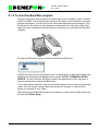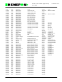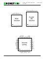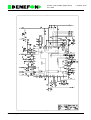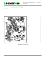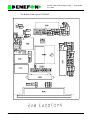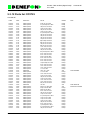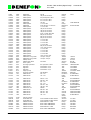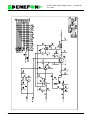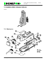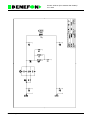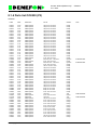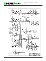
1
Product: TDP-52-SN3 /
27.1.1999
SERVICE MANUAL
BENEFON SIGMA GOLD
TDP-52-SN3
Dp_52ngbTOC.fm
1
Product: TDP-52-SN3 /
27.1.1999
TDP-52-SN3
1.0 GENERAL . . . . . . . . . . . . . . . . . . . . . . . . . . . . . . . . . . 1 - 1
1.1 TECHNICAL INFORMATION . . . . . . . . . . . . . . . . . . . . 1 - 1
1.1.1 Operational System . . . . . . . . . . . . . . . . . . . . . . . . . . . . . . . . . . 1 - 1
1.1.2 Dimensions . . . . . . . . . . . . . . . . . . . . . . . . . . . . . . . . . . . . . . . . 1 - 1
1.1.3 Power Consumption . . . . . . . . . . . . . . . . . . . . . . . . . . . . . . . . . . 1 - 1
1.1.4 Accessories . . . . . . . . . . . . . . . . . . . . . . . . . . . . . . . . . . . . . . . . 1 - 1
1.1.5 Ringing Tones . . . . . . . . . . . . . . . . . . . . . . . . . . . . . . . . . . . . . . 1 - 2
1.1.6 Memory . . . . . . . . . . . . . . . . . . . . . . . . . . . . . . . . . . . . . . . . . . . 1 - 2
1.1.7 Clock . . . . . . . . . . . . . . . . . . . . . . . . . . . . . . . . . . . . . . . . . . . . . 1 - 2
1.1.8 Pager . . . . . . . . . . . . . . . . . . . . . . . . . . . . . . . . . . . . . . . . . . . . . 1 - 2
1.1.9 Other Functions . . . . . . . . . . . . . . . . . . . . . . . . . . . . . . . . . . . . . 1 - 3
1.1.10 Additional Exchange-Based Features . . . . . . . . . . . . . . . . . . . 1 - 3
1.1.11 Manufacturer . . . . . . . . . . . . . . . . . . . . . . . . . . . . . . . . . . . . . . 1 - 3
1.2 PRODUCT FAMILY . . . . . . . . . . . . . . . . . . . . . . . . . . . 1 - 4
2.0 OWNER’S MANUAL . . . . . . . . . . . . . . . . . . . . . . . . . . 2 - 1
3.0 INSTALLATION INSTRUCTIONS . . . . . . . . . . . . . . . 3 - 1
3.1 Phone Programming . . . . . . . . . . . . . . . . . . . . . . . . . . 3 - 1
3.1.1 To program Using the Phone Keys . . . . . . . . . . . . . . . . . . . . . . 3 - 1
3.1.2 To program Using the BeneLoc Program . . . . . . . . . . . . . . . . . 3 - 3
3.2 CAR KIT INSTALLATION . . . . . . . . . . . . . . . . . . . . . . 3 - 5
3.2.1 Antenna . . . . . . . . . . . . . . . . . . . . . . . . . . . . . . . . . . . . . . . . . . . 3 - 5
3.2.2 Phone Holder KDS-50 . . . . . . . . . . . . . . . . . . . . . . . . . . . . . . . . 3 - 5
3.2.3 Microphone . . . . . . . . . . . . . . . . . . . . . . . . . . . . . . . . . . . . . . . . 3 - 5
3.2.4 Cable . . . . . . . . . . . . . . . . . . . . . . . . . . . . . . . . . . . . . . . . . . . . . 3 - 5
3.2.5 External Handset HDS-50 . . . . . . . . . . . . . . . . . . . . . . . . . . . . . 3 - 5
3.2.6 Car Box UDH-50 . . . . . . . . . . . . . . . . . . . . . . . . . . . . . . . . . . . . 3 - 6
3.2.7 Hf Speaker . . . . . . . . . . . . . . . . . . . . . . . . . . . . . . . . . . . . . . . . . 3 - 6
3.3 HF-FUNCTION . . . . . . . . . . . . . . . . . . . . . . . . . . . . . . . 3 - 8
3.3.1 CAR KIT TUNING/OFFICE SET TUNING (theory) . . . . . . . . . . 3 - 8
3.3.2 CAR KIT SWING/OFFICE SET SWING (theory) . . . . . . . . . . . 3 - 10
3.3.3 HF-function tuning in practice . . . . . . . . . . . . . . . . . . . . . . . . . 3 - 11
Dp_52ngbTOC.fm
2
Product: TDP-52-SN3 /
27.1.1999
4.0 SERVICE APPLICATIONS . . . . . . . . . . . . . . . . . . . . . 4 - 1
4.1 BeneWin SCA-50 . . . . . . . . . . . . . . . . . . . . . . . . . . . . . 4 - 1
4.1.1 Installation of BeneWin program . . . . . . . . . . . . . . . . . . . . . . . . 4 - 1
4.1.2 To start the BeneWin program . . . . . . . . . . . . . . . . . . . . . . . . . . 4 - 3
4.2 Beneloc . . . . . . . . . . . . . . . . . . . . . . . . . . . . . . . . . . . . 4 - 4
4.2.1 Installation of Beneloc program . . . . . . . . . . . . . . . . . . . . . . . . . 4 - 4
4.2.2 To start the BeneLoc program . . . . . . . . . . . . . . . . . . . . . . . . . . 4 - 5
4.2.3 Using the BeneLoc program . . . . . . . . . . . . . . . . . . . . . . . . . . . 4 - 6
4.3 WinFlash . . . . . . . . . . . . . . . . . . . . . . . . . . . . . . . . . . . 4 - 7
4.3.1 To start WinFlash . . . . . . . . . . . . . . . . . . . . . . . . . . . . . . . . . . . . 4 - 7
4.3.2 Using the WinFlash program . . . . . . . . . . . . . . . . . . . . . . . . . . . 4 - 8
5.0 PHONE’S CONSTRUCTION . . . . . . . . . . . . . . . . . . . . 5 - 1
5.1 LOGIC / AUDIO . . . . . . . . . . . . . . . . . . . . . . . . . . . . . . 5 - 2
5.1.1 General . . . . . . . . . . . . . . . . . . . . . . . . . . . . . . . . . . . . . . . . . . . 5 - 2
5.1.2 Connectors: . . . . . . . . . . . . . . . . . . . . . . . . . . . . . . . . . . . . . . . . 5 - 3
5.1.3 Circuit Diagram . . . . . . . . . . . . . . . . . . . . . . . . . . . . . . . . . . . . . 5 - 5
5.1.4 Functions . . . . . . . . . . . . . . . . . . . . . . . . . . . . . . . . . . . . . . . . . . 5 - 6
5.1.5 Function Description . . . . . . . . . . . . . . . . . . . . . . . . . . . . . . . . 5 - 10
5.1.6 TX-audio . . . . . . . . . . . . . . . . . . . . . . . . . . . . . . . . . . . . . . . . . . 5 - 10
5.1.7 RX-Audio . . . . . . . . . . . . . . . . . . . . . . . . . . . . . . . . . . . . . . . . . 5 - 11
5.1.8 FII Signal . . . . . . . . . . . . . . . . . . . . . . . . . . . . . . . . . . . . . . . . . 5 - 11
5.1.9 FFSK Modem . . . . . . . . . . . . . . . . . . . . . . . . . . . . . . . . . . . . . . 5 - 11
5.1.10 The DTMF Generator/Receiver . . . . . . . . . . . . . . . . . . . . . . . 5 - 12
5.1.11 Signal level detectors . . . . . . . . . . . . . . . . . . . . . . . . . . . . . . . 5 - 12
5.1.12 Compander/Expander . . . . . . . . . . . . . . . . . . . . . . . . . . . . . . 5 - 12
5.1.13 Alarm buzzer . . . . . . . . . . . . . . . . . . . . . . . . . . . . . . . . . . . . . 5 - 12
5.1.14 Audio signals for answer module . . . . . . . . . . . . . . . . . . . . . . 5 - 13
5.1.15 The other in audio asic (I405) . . . . . . . . . . . . . . . . . . . . . . . . 5 - 13
5.1.16 Parts list OA0701 . . . . . . . . . . . . . . . . . . . . . . . . . . . . . . . . . . 5 - 14
5.2 KEYBOARD . . . . . . . . . . . . . . . . . . . . . . . . . . . . . . . . 5 - 29
5.2.1 General . . . . . . . . . . . . . . . . . . . . . . . . . . . . . . . . . . . . . . . . . . 5 - 29
5.2.2 Connectors: . . . . . . . . . . . . . . . . . . . . . . . . . . . . . . . . . . . . . . . 5 - 29
5.2.3 Parts list OH0700 . . . . . . . . . . . . . . . . . . . . . . . . . . . . . . . . . . . 5 - 31
5.3 RF MODULE . . . . . . . . . . . . . . . . . . . . . . . . . . . . . . . 5 - 36
Dp_52ngbTOC.fm
3
Product: TDP-52-SN3 /
27.1.1999
5.3.1 General . . . . . . . . . . . . . . . . . . . . . . . . . . . . . . . . . . . . . . . . . . 5 - 36
5.3.2 Functional Description . . . . . . . . . . . . . . . . . . . . . . . . . . . . . . . 5 - 36
5.3.3 Control- and Output-Signals . . . . . . . . . . . . . . . . . . . . . . . . . . . 5 - 36
5.3.4 General . . . . . . . . . . . . . . . . . . . . . . . . . . . . . . . . . . . . . . . . . . 5 - 37
5.3.5 Function Description . . . . . . . . . . . . . . . . . . . . . . . . . . . . . . . . 5 - 37
5.3.6 Control- and Output-Signals . . . . . . . . . . . . . . . . . . . . . . . . . . . 5 - 38
5.3.7 General . . . . . . . . . . . . . . . . . . . . . . . . . . . . . . . . . . . . . . . . . . 5 - 39
5.3.8 Input- and Output-Signals . . . . . . . . . . . . . . . . . . . . . . . . . . . . 5 - 40
5.3.9 General . . . . . . . . . . . . . . . . . . . . . . . . . . . . . . . . . . . . . . . . . . 5 - 41
5.3.10 Function Description . . . . . . . . . . . . . . . . . . . . . . . . . . . . . . . 5 - 41
5.3.11 Control- and Output-Signals . . . . . . . . . . . . . . . . . . . . . . . . . . 5 - 41
5.3.12 Parts list OY0725 . . . . . . . . . . . . . . . . . . . . . . . . . . . . . . . . . . 5 - 44
6.0 CHARGING . . . . . . . . . . . . . . . . . . . . . . . . . . . . . . . . . 6 - 1
6.1 MAINS CHARGER CMA-50-230 . . . . . . . . . . . . . . . . . 6 - 2
6.2 LIGHTER SOCKET CHARGER CCS-50-12 . . . . . . . . 6 - 3
7.0 CAR ASSEMBLY KIT . . . . . . . . . . . . . . . . . . . . . . . . . 7 - 1
7.1 CARBOX UDH-50 . . . . . . . . . . . . . . . . . . . . . . . . . . . . 7 - 2
7.1.1 Including attached functions . . . . . . . . . . . . . . . . . . . . . . . . . . . . 7 - 2
7.1.2 Connector descriptions . . . . . . . . . . . . . . . . . . . . . . . . . . . . . . . 7 - 2
7.1.3 Parts list OO0700 . . . . . . . . . . . . . . . . . . . . . . . . . . . . . . . . . . . . 7 - 5
7.2 CARBOX UDH-50 . . . . . . . . . . . . . . . . . . . . . . . . . . . 7 - 16
7.2.1 Including attached functions . . . . . . . . . . . . . . . . . . . . . . . . . . . 7 - 16
7.2.2 Connector descriptions . . . . . . . . . . . . . . . . . . . . . . . . . . . . . . 7 - 16
7.2.3 Parts list OW0700 . . . . . . . . . . . . . . . . . . . . . . . . . . . . . . . . . . 7 - 19
7.2.4 System Cable . . . . . . . . . . . . . . . . . . . . . . . . . . . . . . . . . . . . . . 7 - 32
7.3 HANDS-FREE CRADLE KDS-50 . . . . . . . . . . . . . . . . 7 - 33
7.3.1 Mechanics . . . . . . . . . . . . . . . . . . . . . . . . . . . . . . . . . . . . . . . . 7 - 33
7.3.2 Module OO0702 . . . . . . . . . . . . . . . . . . . . . . . . . . . . . . . . . . . . 7 - 34
7.4 EXTERNAL HANDSET WITH CRADLE HDS-50 . . . 7 - 36
7.4.1 External Handset (not serviceable) . . . . . . . . . . . . . . . . . . . . . 7 - 36
7.4.2 General . . . . . . . . . . . . . . . . . . . . . . . . . . . . . . . . . . . . . . . . . . 7 - 37
7.4.3 Connector XIN Signals . . . . . . . . . . . . . . . . . . . . . . . . . . . . . . . 7 - 38
7.4.4 Microphone . . . . . . . . . . . . . . . . . . . . . . . . . . . . . . . . . . . . . . . 7 - 38
7.4.5 Speaker . . . . . . . . . . . . . . . . . . . . . . . . . . . . . . . . . . . . . . . . . . 7 - 38
Dp_52ngbTOC.fm
4
Product: TDP-52-SN3 /
27.1.1999
7.4.6 Hook . . . . . . . . . . . . . . . . . . . . . . . . . . . . . . . . . . . . . . . . . . . . . 7 - 38
7.4.7 Parts list OO0009 . . . . . . . . . . . . . . . . . . . . . . . . . . . . . . . . . . . 7 - 39
7.4.8 Cradle . . . . . . . . . . . . . . . . . . . . . . . . . . . . . . . . . . . . . . . . . . . . 7 - 43
8.0 OFFICE SET . . . . . . . . . . . . . . . . . . . . . . . . . . . . . . . . 8 - 1
8.1 OFFICE SET DDS-50 . . . . . . . . . . . . . . . . . . . . . . . . . 8 - 2
8.1.1 General . . . . . . . . . . . . . . . . . . . . . . . . . . . . . . . . . . . . . . . . . . . 8 - 2
8.1.2 Connectors . . . . . . . . . . . . . . . . . . . . . . . . . . . . . . . . . . . . . . . . . 8 - 3
8.1.3 Operation . . . . . . . . . . . . . . . . . . . . . . . . . . . . . . . . . . . . . . . . . . 8 - 7
8.1.4 Parts list OO0303 (P3) . . . . . . . . . . . . . . . . . . . . . . . . . . . . . . . . 8 - 9
8.1.5 Parts list OO301 . . . . . . . . . . . . . . . . . . . . . . . . . . . . . . . . . . . . 8 - 18
8.1.6 Part list OO0302 . . . . . . . . . . . . . . . . . . . . . . . . . . . . . . . . . . . . 8 - 20
8.2 EXTERNAL HANDSET HXS-40 . . . . . . . . . . . . . . . . 8 - 23
8.2.1 External Handset (not serviceable) . . . . . . . . . . . . . . . . . . . . . 8 - 23
8.2.2 General . . . . . . . . . . . . . . . . . . . . . . . . . . . . . . . . . . . . . . . . . . 8 - 24
8.2.3 Connector XIN Signals . . . . . . . . . . . . . . . . . . . . . . . . . . . . . . . 8 - 25
8.2.4 Microphone . . . . . . . . . . . . . . . . . . . . . . . . . . . . . . . . . . . . . . . 8 - 25
8.2.5 Speaker . . . . . . . . . . . . . . . . . . . . . . . . . . . . . . . . . . . . . . . . . . 8 - 25
8.2.6 Hook . . . . . . . . . . . . . . . . . . . . . . . . . . . . . . . . . . . . . . . . . . . . . 8 - 25
8.2.7 Parts list OO0009 . . . . . . . . . . . . . . . . . . . . . . . . . . . . . . . . . . . 8 - 26
9.0 OTHER ACCESSORIES . . . . . . . . . . . . . . . . . . . . . . . 9 - 1
9.1 LINE INTERFACE LIF-40 . . . . . . . . . . . . . . . . . . . . . . 9 - 2
9.1.1 General . . . . . . . . . . . . . . . . . . . . . . . . . . . . . . . . . . . . . . . . . . . 9 - 2
9.1.2 Using the line interface . . . . . . . . . . . . . . . . . . . . . . . . . . . . . . . . 9 - 2
9.1.3 Technical information . . . . . . . . . . . . . . . . . . . . . . . . . . . . . . . . . 9 - 3
9.1.4 Manufacturers Declaration for BABT/SITS/85/22 . . . . . . . . . . . 9 - 7
9.1.5 Parts list OO0245 . . . . . . . . . . . . . . . . . . . . . . . . . . . . . . . . . . . . 9 - 9
9.2 BRANCHING UNIT . . . . . . . . . . . . . . . . . . . . . . . . . . 9 - 16
9.2.1 General . . . . . . . . . . . . . . . . . . . . . . . . . . . . . . . . . . . . . . . . . . 9 - 17
9.2.2 Connectors . . . . . . . . . . . . . . . . . . . . . . . . . . . . . . . . . . . . . . . . 9 - 17
9.2.3 Operation . . . . . . . . . . . . . . . . . . . . . . . . . . . . . . . . . . . . . . . . . 9 - 18
9.2.4 Parts list OO0241 . . . . . . . . . . . . . . . . . . . . . . . . . . . . . . . . . . . 9 - 19
Dp_52ngbTOC.fm
5
Product: TDP-52-SN3 /
General
27.1.1999
1.0 GENERAL
General
1.1 TECHNICAL INFORMATION
1.1.1 Operational System
NMT-450i
1.1.2 Dimensions
Size: 58 x 153 x 26 mm
Weight: 295 g
1.1.3 Power Consumption
- Batteries: 5 x 1.2 V NiCd (or NiMH)
- Sleep current: 2 mA
- Standby current: 60 mA
- Conversation mode, high power: app. 0.9 A
- Conversation mode, low power: app. 0.4 A
Charger:
- automatic 1 h rapid charging for NiCd or NiMH batteries
1.1.4 Accessories
- hands free car kit (carbox, holder, car-radio mute, external antenna,
microphone, loudspeaker, external alert)
- light holder
- portable hands free
- line interface
- mains charger
- cigarette lighter charger
- office set
- branching unit
- external handset with holder
- BeneWin
2DP_52GB
1
Product: TDP-52-SN3 /
General
27.1.1999
- hand strap
- belt clip
1.1.5 Ringing Tones
Adjustable
- type, five fixed, one changeable with BeneWin
- volume
- progressive or fixed
Silent alert
- short tone and ‘call coming’ text in the display
1.1.6 Memory
Alphanumeric
- 99 memory locations, 23 characters, 16 alphanumeric / memory location
- memory scroll and recall in alphabetical or numerical order
- writing in memory during a call
Repeat: last dialled number or one of 6 numbers from the quick-memory locations
1.1.7 Clock
- time and date display
- real time alarm setting
- real time power on setting
- real time power off setting
- elapsed conversation time counter (both incoming and outgoing)
- received call counter and time display
1.1.8 Pager
- answers incoming calls and receives numeric messages
- 9 memory locations (23 characters / location)
- pre-set number of ring tones before answering (0...6)
- record own message (16 s max), optional feature
2DP_52GB
2
Product: TDP-52-SN3 /
General
27.1.1999
1.1.9 Other Functions
DTMF - receiver / transmitter
DTMF - key tones
Display and key illumination
Volume control
- 5 levels
- level indicator
Battery charge level indicator
- battery empty alarm tone and display
- used battery capacity display
- battery specific charge memory
Field strength indicator
Battery-saving function
Menu structure for user customisation
Automatic Prefix Management (APM)
Keys lockable to prevent accidental operation
Phone code to prevent unauthorised use
SIS protection function
CLIP, calling line identity presentation
‘+’ international prefix
1.1.10 Additional Exchange-Based Features
- R-function (Register recall)
- MFT-function (DTMF signal transmission)
1.1.11 Manufacturer
Benefon Oyj
P.O. Box 84
24101 Salo
Finland
Tel. +358 2 77400 Fax. +358 2 7332633
2DP_52GB
3
Product: TDP-52-SN3 /
General
27.1.1999
1.2 PRODUCT FAMILY
- BENEFON SIGMA GOLD HANDPORTABLE TDP-52-SN3
- MAINS CHARGER CMA-50-230
- CIGARETTE LIGHTER CHARGER CCS 50-12
- LIGHT HOLDER KDC-50
- HANDS FREE CAR KIT
This kit includes a charging holder KDS-50, carbox UDH-50, external antenna,
loudspeaker and microphone for hands free function, car radio mute and
external alert facility.
- EXTERNAL HANDSET WITH HOLDER HDS-50
This is an optional accessory for the hands free car kit.
- LINE INTERFACE LIF-40
To connect to the mobile phone any appliance using DTMF or MFT dialling
such as the home telephone, wireless phone, answering machine, telefax or
modem and microcomputer.
- BRANCHING UNIT DB-40
With a branching unit, two different accessories can be used simultaneously.
- BENEWIN
- OFFICE SET DDS-50
- PORTABLE HANDS FREE
- HAND STRAP
- BELT CLIP
2DP_52GB
4
Product: TDP-52-SN3 /
General
27.1.1999
Benefon
Sigma Gold
Mains charger
CMA-50-230
LIGHT CAR KIT
Antenna
adapter
Light holder
KDC-50
Cigarette lighter
charger
CCS-50-12
2DP_52GB
5
Product: TDP-52-SN3 /
General
27.1.1999
HANDS FREE CAR KIT
Benefon
Sigma Gold
Holder
Antenna
KDS-50
External handset
with holder HDS-50
Carbox
Microphone
UDH-50
Loudspeaker
+12/24V
External Car Radio Mute
Alert
2DP_52GB
6
Product: TDP-52-SN3 /
General
27.1.1999
Line interface
LIF-40
Branching unit
DB-40
2DP_52GB
7
Product: TDP-52-SN3 /
General
27.1.1999
OFFICE SET
Microcomputer Telephone
Telefax
Modem
Benefon
Sigma Gold
Line
interface
Mains
charger
Spare
battery
OFFICE SET
DDS-50
2DP_52GB
8
Product: TDP-52-SN3 /
General
27.1.1999
Portable
hands free
Belt clip
Hand strap
BeneWin
2DP_52GB
9
2.0 OWNER’S MANUAL
1user_gb.fm
1
Product: TDP-52-SN3 /
27.1.1999
3.0 INSTALLATION INSTRUCTIONS
3.1 Phone Programming
You can program Benefon Sigma Gold by using either the keys on your phone,
or the BeneLoc computer program. In either case, you will need a localbox.
Programming Menu Commands:
- SALES DATE
- RADIO PATH ID
- PHONE CODE
- HF-FUNCTION
CAR KIT TUNING (background noise tuning)
CAR KIT SWING (MIC-ERP contrast tuning)
OFFICE SET TUNING (background noise tuning)
OFFICE SET SWING (MIC-ERP contrast tuning)
- SW VERSION
- SAK
- PRODUCT CODE
- UPDATE LOCALBOX
- BASE BAND
- RESET RAM
3.1.1 To program Using the Phone Keys
1. Connect the localbox to your phone, and turn the phone on.
2. Press and the following text will appear in the display: ***BENEFON***.
* will be flashing in the display.
3.1.1.1 Sales Date
1. Choose SELECT. The following text will appear in the display:
SALES DATE [XXXXXX].
2. Choose CHANGE. [XXXXXX] will be replaced by the date
[daydaymonthmonthyearyear]. Remember to check that the date is correct.
If the date is correct, choose SAVE. If the date is incorrect, delete it by
choosing and enter the correct date (six digits in the following form:
daydaymonthmonthyearyear). To save the date, choose SAVE.
6DP_52GB
1
Product: TDP-52-SN3 /
27.1.1999
It is possible to program the sales date ONLY ONCE, which means that you
will not be able to change it again afterwards. If the sales date has not been
programmed, your phone will not enter the normal stand-by mode.
3.1.1.2 Radio Path Identification
1. Press , and the following text will appear in the display:
RADIO PATH ID [XXXXXXXXXX].
2. Choose CHANGE. Enter the radio path identification (ten digits), and
save the identification by choosing SAVE. Remember to check that the
radio path identification is correct.
3.1.1.3 Phone Code
1. Press , and the following text will appear in the display:
PHONE CODE [XXXX].
2. Choose CHANGE. Enter the phone code (four digits), and save the code
by choosing SAVE.
3.1.1.4 Closing Instructions
1. Having programmed the necessary information choose QUIT, and the
following text will appear in the display: ***BENEFON***.
2. Turn off your phone, and disconnect the localbox.
3. Turn the phone on once more, and make a test call.
6DP_52GB
2
Product: TDP-52-SN3 /
27.1.1999
GEN
METER
COM1 COM2
PHONE
3.1.2 To program Using the BeneLoc Program
Start the installed program by clicking the icon. The phone must be connected
to the system as discribed above.
Main window
Press Dealer-key to enter the programming window.
6DP_52GB
3
Product: TDP-52-SN3 /
27.1.1999
You can read the phone data by pressing the Read phone -key. You can
change the miscellanous settings with the computer and transfer them to
phone by pressing the Program phone -key.
BeneLoc includes Help-program for further information.
6DP_52GB
4
Product: TDP-52-SN3 /
27.1.1999
3.2 CAR KIT INSTALLATION
The Car Kit includes a phone holder (KDS-50), a car box (UDH-50), an
antenna, an installation base, a hf speaker, a microphone and a cable. The Car
Kit sales package also includes an installation material bag, which contains the
necessary installation equipment. On page 7 you will find a diagram of
connections explaining how to install the Car Kit.
3.2.1 Antenna
Choose a suitable place for the antenna. It is recommended that you place the
antenna on the roof of the vehicle.
3.2.2 Phone Holder KDS-50
Choose such a place for the phone holder in the vehicle that will be both easy
and safe when using the phone. Remember to leave enough space for the
antenna plug behind the phone holder. First, fix the installation base to the
place you have chosen, and then install the phone holder in the installation
base.
3.2.3 Microphone
Install the microphone so that it is aimed directly at the user, and comes as
close as possible to the user’s mouth. A good place for the microphone is near
the rearview mirror where the noise level is lower than, for example, beside a
windshield pillar. It is also possible to install the microphone on a sun visor, but
then it will be inconvenient to use the sun visor and microphone at the same
time. One alternative would be a swan-neck microphone as it can be placed
closest to the user’s mouth.
3.2.4 Cable
Obtain the necessary +-electricity from a suitable place, preferably directly
from the battery of the vehicle. Connect the fuse chamber to the +-wire. You
will find the fuse chamber in the installation material bag. Connect the ground
lead to the frame of the car with a short wire.
3.2.5 External Handset HDS-50
Install the external handset the same way as you installed the phone holder.
6DP_52GB
5
Product: TDP-52-SN3 /
27.1.1999
3.2.6 Car Box UDH-50
Place the car box out of sight inside the dashboard of the car or to another
place. First, connect the wires to the car box. Install the car box so, that the
heat sink has some space for cooling. The car box has holes which enable you
to fasten the car box with a cable tie. The installation material bag also contains
adhesive band fasteners.
3.2.7 Hf Speaker
Install the speaker in a suitable place near the floor of the car.To avoid echo
remember to pay attention to the position of the microphone as well.
6DP_52GB
6
Product: TDP-52-SN3 /
27.1.1999
A Diagram of Connections
How to install a
cable to a carbox.
KDS-50
HDS-50
Installation
base
to KDS-50
Microphone
Installation
base
open
UDH-50
Hf Speaker
fuse
Vb
PIN
1
2
3
4
5
6
at
1
t, +
2 /2
4V
Car Radio
Mute
External
Alert
Name
Car Radio Mute (active low)
Hf Speaker
Ground External Alert (active low)
Hf Speaker
Vbatt, +12/24 V
External Alert
Car Radio Mute (See the installation
instructions of your car radio)
MUTE
+ACC
86
85
85
87
87
30
87
87A
85
+VB
+VB
Battery Voltage
30
External Alert
86
30
85
30
Car Radio
Supply Voltage
+ACC: to the +12 V power terminal
which is energized in the accessory
position of the ignition key
6DP_52GB
Horn
86 87A
86 87A
87
87A
Color
Blue
Grey
Black
Brown
Grey
Red
+VB
Horn
External Alert
7
Product: TDP-52-SN3 /
27.1.1999
3.3 HF-FUNCTION
Benefon Sigma Gold offers you two different hands free -setups for the Car Kit
and Office Set: the background noise tuning (CAR KIT/OFFICE SET TUNING)
and MIC-ERP contrast tuning (CAR KIT/OFFICE SET SWING).
3.3.1 CAR KIT TUNING/OFFICE SET TUNING (theory)
You can set up the activation level of the microphone by using the CAR KIT
TUNING option. The level is correct when the microphone path is activated by
voice alone, and not, for example, by background noise in your car or office.
The following figure shows you the CAR KIT TUNING setup process. You can
set up the OFFICE SET TUNING following the same procedure.
a. If the CAR KIT TUNING is set too high, your voice (1) will not activate the
microphone path properly, and the person at the other end will only hear
interrupted transmission of speech.
(1)
50
Car kit tuning
40
30
6DP_52GB
8
Product: TDP-52-SN3 /
27.1.1999
b. If the CAR KIT TUNING has been set up too low, the background noise in
your car (2) will activate the microphone path, and the volume of the HFspeaker will be low.
50
(2)
40
Car kit tuning
30
c. When the CAR KIT TUNING has been set correctly only your voice (1 & 3)
will open the microphone path.
(1)
(3)
50
Car kit tuning
40
30
(2)
Benefon phones have been set in our factory so that they will function in most
cars. The factory setting for the CAR KIT TUNING is 38, and for the OFFICE
SET TUNING 42. The recommended adjustment range is +/- 5 units from the
factory setting.
6DP_52GB
9
Product: TDP-52-SN3 /
27.1.1999
3.3.2 CAR KIT SWING/OFFICE SET SWING (theory)
The four-step CAR KIT SWING/OFFICE SET SWING tuning is used to set the
contrast of the microphone amplification/speaker attenuation swing. In the
following figures the swing position while listening to the Car Kit or Office Set is
indicated by a solid line and the position while speaking into Car Kit or Office
Set the indicated by a dotted line.
a. With a tuning value of 4 it is possible to obtain the smallest difference
between the amplification and attenuation of the microphone and speaker. This
means that the connection is almost bidirectional. If the HF-function easily
creates feedback, decrease the value of the CAR KIT SWING/OFFICE SET
SWING. By turning down the volume it is possible to reduce the occurance of
feedback.
MIC
SPK
Listening
4
3
Speaking
2
1
b. With a tuning value of 1 it is possible to obtain the greatest difference
between the amplification and attenuation of the microphone and speaker. This
means that the connection is almost unidirectional.
MIC
SPK
Listening
4
3
2
1
Speaking
The factory setting for the CAR KIT SWING/OFFICE SET SWING is 3.
6DP_52GB
10
Product: TDP-52-SN3 /
27.1.1999
3.3.3 HF-function tuning in practice
You can tune HF-functions two ways: manually or with car kit.
Manual tuning
1. Connect the localbox to your phone, and turn the phone on.
2. Press and the following text will appear in the display: ***BENEFON***.
* will be flashing in the display.
3. Press , and the following text will appear in the display:
HF-FUNCTION
4. Choose SELECT, and the following text will appear in the display:
CAR KIT TUNING [038]. (The figure can be different).
5. Choose CHANGE, and the following text will appear in the display:
CAR KIT TUNING [ ] (026). (The figure can be different).
6. Enter three digits and SAVE. Yhe recommended value is between 033
and 043.
7. Choose SELECT, and the following text will appear in the display:
CAR KIT SWING (1...4): [3]. (The figure can be different).
8. Choose SELECT, and the following text will appear in the display:
CAR KIT SWING (1...4): [3]. (3 is blinking)
9. Enter one digit and OK.
Tuning in car kit
1. Connect the localbox to your phone, and turn the phone on.
2. Press and the following text will appear in the display: ***BENEFON***.
* will be flashing in the display.
3. Connect the hand portable to the car kit
4. Press , and the following text will appear in the display:
HF-FUNCTION
5. Choose SELECT, and the following text will appear in the display:
CAR KIT TUNING [038]. (The figure can be different).
6. Choose CHANGE, and the following text will appear in the display:
CAR KIT TUNING [ ] (026). (The figure can be different).
7. Drive the car so that you can get a normal back ground noise level. The
figure (026) will be changed according the back ground noice level.
8. Enter three digits (back by pressing ) shown in the figure (xxx) and SAVE. The level will be stored.
6DP_52GB
11
Product: TDP-52-SN3 /
27.1.1999
4.0 SERVICE APPLICATIONS
4.1 BeneWin SCA-50
The BeneWin SCM Program for Windows is designed to facilitate maintenance of
phone numbers and user settings on Benefon mobile phones. You can also use your
phone to carry out the commands in the BeneWin Program, but it is handier to process data using your screen and keyboard - the advantage of the BeneWin Program. For example, all user settings are displayed in a single window, which enables
you to check at a glance your current settings.
Your personal settings and phone numbers stored on the hard disk can be transferred to the mobile phone whenever necessary. When you travel or use a borrowed
phone, your own settings make the phone feel like your own.
The main functions of the BeneWin Program are divided into two windows: the
BeneWin SCM window, in which you can modify the phone numbers, and the User
window, in which you can modify the phone’s user settings.
4.1.1 Installation of BeneWin program
Start Windows.
Insert the BeneWin installation disk in the floppy disk drive of your computer.
In the Program Manager window, choose Run from the File menu.
3DP_52GB
1
Product: TDP-52-SN3 /
27.1.1999
In the Command Line box, type the letter A: or B: to indicate your floppy disk
drive, and then type SETUP. For example, A:SETUP.
Click the OK button, and follow the instructions displayed on your screen.
First, accept the location of the source files, which is the floppy disk drive you used
for Setup.
To continue Setup, choose the Continue button. To quit Setup, choose the Exit
Setup button.
Next, the Setup Program will ask you to specify the drive and directory in which you
want to install the BeneWin Program. The Program suggests the following:
C:\BENEWIN. Accept the drive and directory by clicking the Continue button. You
can quit Setup by clicking the Exit Setup button.
The Setup Program creates a BENEWIN directory and within it the necessary subdirectories in drive C of your computer. Setup also creates its own group window in
Program Manager.
3DP_52GB
2
Product: TDP-52-SN3 /
27.1.1999
4.1.2 To start the BeneWin program
Connect your phone with a cable to the serial port of your computer, which is called
COM1 or COM2. The serial ports are located in the back of your computer, and more
precise instructions can be found in the manual accompanying the computer. Plug
the flat end of the cable into the connector at the bottom of your phone. When the
cable has been connected and the phone is functioning, you can start the BeneWin
Program.
To start the BeneWin Program, double-click the BeneSCM icon.
If the phone has not been connected to the computer and you start the Program, the
following error message will appear on the screen: FATAL COMMUNICATION
ERROR. You will, however, be able to modify the data stored in your computer’s
memory locations by clicking the OK button.
If you use a laptop computer make sure that the computer is not in the energy saving
mode. If so the energy saving mode may prevent the transfer of data from the
phone to computer or vice versa.
After starting up the BeneWin program will guide you further with the help of an electric manual (Online Help).
3DP_52GB
3
Product: TDP-52-SN3 /
27.1.1999
4.2 Beneloc
1
ABC
3
GHI
5
JKL
6
7 PQRS
8
TUV
9
4
2
DEF
MNO
WXYZ
0
RM
HF
power
5V log
gen
flash
5V log
meter
BeneLoc program is designed to help service person on tuning and service purpose.
With BeneLoc Program you will also get WinFlash Program. With WinFlash Program
you can change the software to Benefon phones.
Both, BeneLoc and WinFlash program will need Local Box with service rights to
work.
4.2.1 Installation of Beneloc program
Start Windows. Close all other programs except Program Manager.
Insert Beneloc Installation Disc 1 in the floppy disk drive of your computer. In the
Program Manager window, choose Run from File menu.
Type the letter A: or B: to indicate your floppy disc drive, and then type SETUP.EXE.
For example, A:\SETUP.EXE.
Click the OK button, and follow the instructions displayed on your screen.
3DP_52GB
4
Product: TDP-52-SN3 /
27.1.1999
The Setup Program will ask you to specify the drive and directory in which you want
to install the Beneloc Program. The Program suggests the following: C:\BeneApp\BeneLoc. Accept the drive and directory by clicking Next button. You can also
type your own directory for Beneloc Program.
The Setup Program creates all necessary directories and subdirectories to your
computer. Setup Program also creates its own group window in Program Manager.
WinFlash Program will be installed automatically by Setup Program. You can find
WinFlash.exe from the same directory as the Beneloc: e.g. C:\BeneApp\WinFlash.
4.2.2 To start the BeneLoc program
Connect the Service LocalBox to serial port of your computer, which is called COM1
or COM2. The serial ports are usually located in the back of your computer, and
more precise instructions can be found in the manual accompanying the computer.
Switch off the phone. Plug the cable with flat connector into the connector at the bottom of the phone. When the cable has been connected and the phone is switched
on, the phone should be in LOCAL mode. You can test this by pressing arrow button.
There should be ***BENEFON*** on the display, if not, clean connectors and try
again. When phone is in LOCAL mode you can start the BeneLoc Program.
To start the BeneLoc Program, double click the BeneLoc icon.
In the BeneLoc Startup window, first select the correct serial port. Then, you have to
select type of the phone. You can also use the Autodetect option. After selection
click OK to start BeneLoc Program. When operating without external power supply
the phone may be on sleep mode and registration fails. You can wake up the phone
by pressing some buttons on the phone.
3DP_52GB
5
Product: TDP-52-SN3 /
27.1.1999
4.2.3 Using the BeneLoc program
In the main window of the BeneLoc, you will find submenus and buttons. Clicking the
buttons you can go to the submenus.
Change
For changing phone to another similar you do not need to do more than enter into
main menu. It means that this button is not needed. If you are going to change the
tested phone to one having different software in, clicking Change will start the registration protocol again.
Help
About BeneLoc submenu will tell you version of the BeneLoc Program and also the
state of memory.
About Cellular submenu will show you information of the phone. Type of phones
software, sales date, date of the software, serial number and present tuning values
of the phone. You can not change the tuning values from Help menu.
Dealer
From Dealer submenu you can make or check programming of the phone. You will
also find the SIS information from Dealer submenu.
Service
You can control the audio lines (for example, switch Rx audio and compander on/off)
in the Service main menu. It is also possible to control the phone to desired channel.
There is also possible to change the power of transmitter.
In the Ports submenu is you can see the status of different digital ports. There is
also possible to control some of the output ports.
You can read the status of the A/D converters from the A/D submenu. Select 8 different topics to view. By clicking SCAN AD button The Beneloc will scan A/D the state
of converters continuously. Scanning can stopped by clicking STOP AD.
Memory submenu allows you to make Ram reset.
By clicking Initialize You can clear all LOCAL settings in service menu.
Home button will return you back to main menu.
3DP_52GB
6
Product: TDP-52-SN3 /
27.1.1999
Tunings
From Tunings main menu you can select different tunings to do. Every tuning have
they own instruction window. Follow given instructions to do tunings. Clicking
START will start tuning. The value will be stored only by clicking SAVE. Some of the
tunings are chained and you can enter to next phase by clicking NEXT.
System
You select used mobile phone system from this submenu.
File
From settings submenu you can manually change settings of the communication
port.
4.3 WinFlash
4.3.1 To start WinFlash
Connect the LocalBox to serial port of your computer, which is called COM1 or
COM2. The serial ports are usually located in the back of your computer, and more
precise instructions can be found in the manual accompanying the computer.
It is recommended to use external power supply when transferring software to
phone with WinFlash. If it is impossible to use external power supply the battery of
phone must be fully charged.
NOTE !
Before starting WinFlash save the short code memory places and settings of the
phone to disc. You can use Benewin or Beneserv to save the SCM and settings.
Switch off the phone. Plug the cable with flat connector into the connector at the bottom of the phone. Start WinFlash by double clicking WinFlash icon. After opening
the main window of the WinFlash select the correct communication port.
3DP_52GB
7
Product: TDP-52-SN3 /
27.1.1999
4.3.2 Using the WinFlash program
You will find all Benefon mobile phone softwares installed to your computer from window in the left side.
Select the software you want to transfer to phone by clicking it. In the right side window you will find some information of the selected software. Click Execute to start
software transferring to phone. Follow the instructions shown in the screen. You can
reset the phone by removing the flat connector from the phone and attaching it back
again. Be sure that there are no marks on the display before pressing enter.
3DP_52GB
8
MF
1502
A
AM
0062
Version
Nordic, Poland
7DP_52GB
Black
Blue
Red
Grey
Green
Wooden effect
Color
YA0070
Code
A
MC0836
MC0837
MC0840
MC0838
MC0839
MC0841
B
MC0806
MC0808
MC0810
MC0812
MC0814
MC0824
Code
Nordic
Poland
AV
0001
Version
D
OD0725
OD0785
F
OY0725
OY0785
Code
NC
2108
dg0102.ds4
Product: TDP-52-SN3 (Sigma Gold)
/
27.1.1999
5.0 PHONE’S CONSTRUCTION
1
Product: TDP-52-SN3 (Sigma Gold)
/ OA0701 Processor
27.1.1999
5.1 LOGIC / AUDIO
OA0701 Processor
Processor
5.1.1 General
The entire radio audio and processor functions are found within a single
PA0700 board, through which all other modules are connected. Only the RF
signals have a different path and the keyboard has a different unit.
The processor controls the audio and radio modules, internal devices and
external accessories.
The processor includes:
CPU
PROM
RAM
68HC11A1
28F020
62256
ASIC
IA8001
SIS
68HC11A8
4A0701GB.__1
8-bit, 8 A/D, 512*8 EEPROM, 256*8 RAM, I/O
256*8 EEPROM, program memory
8K*8 CMOS RAM, number memory
32 pcs out and 14 pcs inp, 3 series out, 3 analog
out, frequency counter, clock
SIS function, 8k ROM, 512*8 EEPROM, 256*8
RAM
2
Product: TDP-52-SN3 (Sigma Gold)
/ OA0701 Processor
27.1.1999
5.1.2 Connectors:
5.1.2.1 RF-Module, V102 20 pin connector
1
2
3
4
5
SSDATA
SSCLK
SSLE
SRX_REG
STX_REG
6
SAFC
7
8
9
10
11
12
13
14
15
16
17
18
19
20
SSNTC
SRXAUDIO
SRSSI
GND
S450K
GND
SDTUNE
SSPARE
VB
VB
VB
STXBIAS
STXPWR
STXAUDIO
RX and TX data to the splitter
RX and TX data clock
RX and TX divider enable pulse
rx vco start up
tx vco start up
frequency compensation control
voltage
temperature data, analog
RX audio signal
RX signal strength indicator, analog
ground
450kHz for AFC measurement
ground
not function
not function
power supply from the battery
0/5V
0/5V
5V
5V
5V
0-5V
220 mVrms
0-5V
TX initiate, 0V = TX OFF
TX power control, analog
TX audio signal
0/5V
0-5V
220 mVrms
approx 2.5V
approx 1Vpp
6V
5.1.2.2 Keyboard module + systemconnector lines
V101 40 pin connector
1
2
3
4
5
6
VB
VB
VB
VB
VB
EXTMIC
7
EXTERP
8
9
10
11
12
13
14
15
XCADET
I2CINT
SGL
SDA
TXD
RXD
XEXTIO
GND
4A0701GB.__1
power supply from battery
6V
external audio from the microphone
external audio to the speaker amplifier
carbox identification
i2c interrupt, radio input
i2c clock
i2c data
rs232 out
rs232 in
reserve
ground
400 mVrms
220 mVrms
0/5V
0/5V
0/5V
0/5V
0/5V
0/5V
0/5V
3
Product: TDP-52-SN3 (Sigma Gold)
/ OA0701 Processor
27.1.1999
16
17
18
19
20
21
22
23
24
25
26
27
28
29
30
GND
GND
GND
GND
GND
XKEYINP0
XKEYINP1
XKEYINP2
XKEYINP3
XKEYINP3
XKEYOUT0
XKEYOUT1
XKEYOUT2
XKEYOUT3
XCHGIND
31
XBMEM
32
33
34
35
36
37
38
39
40
4A0701GB.__1
MICINPUT
XISIGN
KEYLEDVB
IVBDET
V-PROG
V-PROG
key matrix input
0/5V
key matrix output
0/5V
charging voltage indicator
input memory data-line from the battery
nc
nc
microphone-line
nc
battery voltage course indicator
voltage for the led of keyboard
battery current indicator
battery charging voltage
0/5V
0/5V
0/5V
6V
0-5V
4
Product: TDP-52-SN3 (Sigma Gold)
/ OA0701 Processor
27.1.1999
5.1.2.3 Display Module, A101
1
2
3
4
5
6
7
8
9
10
11
12
13
14
15
16
VCC
RES
CSI
AO
SCL
SI
GND
CONT
GND
LED
KEYOUT1
KEYINP4
KEYINP4
KEYOUT0
PWRKEY
GND
supply voltage
reset-line
display data input
5V
0/5V
0/5V
clock line for data
0/5V
ground
not function
supply voltage for led of display
key matrix output (volume key -)
0/5V
key matrix input (volume keys+/-) 0/5V
key matrix output (volume key +) 0/5V
powerkey
5.1.2.4 Answer Module, I101
1
2
3
4
5
6
7
8
9
10
VCC
REC
GND
PLAYE
PLAYL
ANAIN
GND1
VCCA
SP+
GND2
supply voltage
record control
ground
play control
audio input
ground
supply voltage
audio output
ground
5V
0/5V
5V
0/5V
5V
5.1.3 Circuit Diagram
The processor and audio circuit diagram is split into five parts. Signals in the
circuit diagrams have been given names, and signals with the same name are
connected between diagrams.
4A0701GB.__1
5
Product: TDP-52-SN3 (Sigma Gold)
/ OA0701 Processor
27.1.1999
5.1.3.1 Circuit Diagram Contents
OA0701A
OA0701B
OA0701C
OA0701D
OA0701E
module connector pins
power supply
cpu, ASIC, RAM, EPROM
audio parts
SIS-function
5.1.4 Functions
5.1.4.1 CPU
I304 is itself a processor circuit. It is comprised of CPU, 512*8bit EEPROM,
timers, A/D converters, and both series- and parallel I/O lines. The clock
oscillator is located in the audio circuit and provides the CPU with a 7.2 MHz
clock signal. The CPU divides this by 4 to get timing signal E.
When the processor is operating, RESET = 5V, VCC = 5V, E = 1.8 Mhz, AS, R/
W and A0...A15 pulses should be 0/5V (no intermediate values, only 0 or 5V).
4A0701GB.__1
6
Product: TDP-52-SN3 (Sigma Gold)
/ OA0701 Processor
27.1.1999
5.1.4.2 Memories
Memory and external I/O-circuit address coding is done with the ASIC circuit
I305. The circuit options CSR, CSP, and OE are 0-active.
The program memory is in 256k*8 EPROM. The program uses the addresses
2100H...FFFFH. Page selection makes available another similar memory
block.
RAM-memory is 8k*8 CMOS RAM at the addresses 0000H...1FFFH. RAM
receives its power supply from its own regulator which is always operating,
even when the radio is in the OFF state.
5.1.4.3 The Modem
The FFSK modem is located in the audio circuit. The modem is connected to
the CPU by a series line, input to synchronised port, and transmission is
controlled by an ASIC series output. The modem gives a 1200 Hz signal
RXCLK to the processor and TXCLK to ASIC. There is a data detector within
the modem, the speed of which is controlled by C438.The CPU A/D converter
measures the level of acceptance from ERPDET line. The same detector also
serves to control the HF function.
5.1.4.4 AFC
The AFC function is performed by an internal ASIC frequency counter. A 450
kHz intermediate frequency is amplified to a square-wave form by Q305. The
frequency is adjusted by ASIC pulse frequency modulated signal D/A 0, which
is integrated by C378. This approx. 2.5V DC voltage is fed to the synthesiser
AFC pin.
5.1.4.5 Sleep Timer
The phone puts the central functions to sleep for a time. Although everything
seems normal to the user, most of the functions are closed down. The radio
and audio units are closed down completely. The processor still has a power
supply, but the processor is halted and has minimal power consumption. Only
the ASIC circuit sleep timer and its 32 kHz crystal oscillator remain in active
mode. The phone is "woken up" by interrupting the sleep timer or by changing
the keyboard state. The sleep timer 32 kHz clock freqency is produced by the
oscillator made by crystal X305.
5.1.4.6 Warm Start
C352 and R352 measure the length of a voltage break. The voltage drops
during a break, after which it is measured by the A/D convertor. The time
constant is approx. 10 s . Thus a "warm start" is detected.
4A0701GB.__1
7
Product: TDP-52-SN3 (Sigma Gold)
/ OA0701 Processor
27.1.1999
5.1.4.7 RESET
The processor voltage regulator ERROR output resets (stops) the processor
and zeroes the controls when the battery voltage drops below 5V. When the
voltage rises again, the processor restarts.
5.1.4.8 Power Switch
The power switch (PWRKEY) is grounded, and directs the regulator I201 to
conduct when pressed. The program commences and checks the PWRSW line
to ensure that the switch is being pressed, and sets hold on the regulator for
the PWRON line. When the switch is depressed for a longer time, the program
directs power to the PWROFF line. During a short voltage break, C211 and
R211 remember the previous control, i.e. fet Q202 conducts again when the
voltage is restored within 10 seconds. The switch-fet also serves as a watchdog should the voltage drop or processor error-state continue; after 10
seconds, the radio will shut down completely.
Note! The RAM and ASIC circuits have their own regulator connected to the
battery to ensure an uninterrupted power supply. RAM power supply is
ensured during a battery-pack change by the battery B201.
5.1.4.9 Battery Voltage Measurement
The battery voltage is measured by an A/D converter. The converter 256 step
conversion scale is not sufficient as it stands, so the measured range is
restricted to 5...8V by the operational amplifier I303. The reference voltage for
the measurement is provided by the processor regulator 5V supply. Calibration
is done by the program against a precisely known battery voltage.
5.1.4.10 I/O ports
The ASIC I/O ports PA...PF are 8-bit hold circuits. DATA is fed to the
addressed output. When the RESET line is down (0V) all the ASIC ports are
zeroed (0V). As RESET rises again, all of the two-way I/O ports are inputs until
the program sets them to the desired state. With the radio in OFF state,
RESET is down so all of the controls are also down although ASIC is still
provided with operational voltage (VRAM).
5.1.4.11 SIS
SIS functions are provided by a mask-programmed single chip processor I503
(68HC11A8). It communicates with the host processor via ASIC with an RS232
bus (5V levels). The circuit operation is not externally visible as it is a singlechip solution. User specific information is stored in EEPROM which CANNOT
be read from outside the chip. All external attempts to read the information
clear both EEPROM and RAM (fill with FF).
4A0701GB.__1
8
Product: TDP-52-SN3 (Sigma Gold)
/ OA0701 Processor
27.1.1999
5.1.4.12 Power Adjustment
The transmitter control logic switches TX power and also adjusts it to the
correct level. The STX_REG signal sets the transmitter to ready mode. Power
is controlled by the ASIC analog output D/A 1. It is a pulse frequency
modulated output which is converted to a DC voltage by integrating it with
C379. 0V corresponds to "no power" state, and 5V to maximum transmitter
power. The power levels are calibrated by the program at the source of
measurement.
5.1.4.13 Charging Control
The charger is controlled by the program. The charger is detected by a voltage
at the SV-CHG pin. The charging current (0...1,5A) is controlled by an analog
(0...5V) CHGCONT signal which comes from the ASIC D/A 2 pulse frequency
output. Charging is governed by the battery and radio temperatures, battery
voltage, and time measurement.
5.1.4.14 Temperature Measurement
The radio has two separate temperature sensors, one within the battery pack,
and the other within the radio module. Inside the radio the NTC resistor R316
voltage is measured by the processor A/D converter. This value is converted
by a programmed table to a temperature reading.
5.1.4.15 Real-time Clock
A real-time clock is provided within ASIC to give the time and date. The alarm
function can also be programmed to the ALARM pin. This will initiate the
processor regulator and thus also the radio although it is in OFF state.
The ASIC circuit has a continuous power supply and the 32 kHz clock crystal
runs constantly. Not even the RESET line stops the clock. If the power supply
has dropped too low, the clock will need to be reset with the radio buttons (from
the menu).
5.1.4.16 Answer Module
Answer module can save a maximum 16 second message. The message can
be recorded from the microphone, external microphone or RX-audio. The
message can be sent to the earphone, external earphone or TX-audio.
4A0701GB.__1
9
Product: TDP-52-SN3 (Sigma Gold)
/ OA0700 Audio
27.1.1999
Audio
5.1.5 Function Description
OA0700 Audio
The audio module is comprised of the following functions:
1. TX-audio signal handling
2. RX-audio signal handling
3. Fii signal handling
4. FFSK modem
5. DTMF generator/receiver
6. Signal level detectors
7. Compander
8. Expander
9. Buzzer
The audio functions are mainly located in a single circuit AK2339. This chip
from AKM is controlled by a serialbus. It is possible to shut down parts of the
circuit, one block at a time to minimise power consumption.
5.1.6 TX-audio
The input from the microphone is fed to the audio circuit I405 pin 61, which is
an operational amplifier (AMP1) inverting input. The operational amplifier gain
is set by resistors R413 and R416. The amplifier is connected as a low pass
filter. After the amplifier is the microphone switch and then summing junction of
MIC input signal, EXTMIC input signal and transmit DTMF signal. VR1 is a
programmable amplifier, which sets the microphone signal (sensitivity) to the
correct level. After VR1 comes band-pass filter for transmitting the voice signal.
After the TXBPF is the summing junction (AMP6) of the tx signal and transmit
answer signal (ANAOUT). TXDET is the transmit voice signal detection circuit
which works as a full wave rectifier. Next comes ATT1 which is an attenuate
circuit to set the transmit signal level in the HF-mode. COMP is the compressor
circuit. Compress the transmitting signal amplitude with square root law. It can
be hypassed. The linearity is adjustable by the control register CVR. Next is
VR2, normal deviation gain control circuit to set the signal level. The P/E &
LIMIT pre-emphasis circuit and limiting circuit, emphasize the higher frequency
component of the signal in order to improve the signal-to-noise ratio of
modulated signal. This block includes a limiting circuit for signal amplitude in
order to confine the maximum deviation of the transmit modulated signal.
TXLPF is the low pass filter to reject the higher frequency component on the
4A0701GB.__1
10
Product: TDP-52-SN3 (Sigma Gold)
/ OA0700 Audio
27.1.1999
transmit signal. VR3 is a maximum deviation gain control circuit to set the
transmit signal level. After the VR3 comes switch TXAUDON, which mutes the
tx-audio signal using the TXMUTE control. From the switch, the signal is fed to
the summing junction (ADD3) of the tx-audio signal, FFSK signal and Fiisignal. Next comes VR4 gain control circuit to set. SMF1 is smoothing filter for
tx-audio signal. The tx-audio signal is then fed to the V102 connector pin 20.
5.1.7 RX-Audio
The rx-audio signal coming from the receiver through the V102 pin 8 is fed to
the audio circuit I405 pin 23. Inside the circuit, the signal is fed to the
operational amplifier (AMP2) inverting input. The amplifier gain is set by
resistors R440 and R441. The signal is next passed through an anti-aliasign
filter. VR5 is a gain control circuit to set the rx-audio signal to the correct level.
Next comes de-emphasis (D/E) circuit. Equalize the pre-empassized rx-audio
signal. The signal passes from the D/E through the switch RXAUDON. RXBPF
is the band-pass filter for the rx-audio signal. RXDET is the rx-audio signal
detection circuit. This circuit works as a full wave rectifier. After the RXBPF
comes expander circuit (EXP). Expand the rx-audio signal amplitude. It can be
bypassed. The linearity is adjustable by the control register EVR. VR6 is a gain
control circuit to set the rx-audio signal to the correct level. After VR6 comes
the RXMUTE switch, which is operated by the RXMUTE control. ADD4 is the
summing junction of the rx-audio signal, external signal (not used), DTMF
signal and transmit signal. VR10 is the volume control circuit to set the level of
earphone and external earphones. The rx-audio signal is connected through
the receiver driver (RECAMP) to the earphone.
5.1.8 FII Signal
The NMT system uses the FII signal to check the radio path quality. This
approx. 4kHz signal is split from the rx-audio signal after the VR5 and is filtered
through the band-pass filter (FBPF). VR7 sets the FII signal to the correct level.
Switch FILOOPON can be operated by the FIION control, to be summed with
the tx-audio signal before the VR4.
5.1.9 FFSK Modem
The FFSK data signal from FFSK modulator to be transmitted is passed
through the FFSK low-pass filter and pre-emphasis (FFSKP-EM) to the VR9,
which adjusts its level. The data signal is switched using switch FFSKTXON.
The data signal is summed with the tx-audio signal by the ADD3.
The received data signal is split from the rx-audio signal after the de-emphasis
circuit. The data signal is fed through the FFSK band-pass filter to the FFSK
demodulator and FFSK data detector.
FFSK DET block. The block works to judge the FFSK signal existence by
comparing the amplitude of the noise reduced FFSK signal and the provided
4A0701GB.__1
11
Product: TDP-52-SN3 (Sigma Gold)
/ OA0700 Audio
27.1.1999
detection level standard. Once the detector judges a valid FFSK signal, ’H’
signal is put out on the FFSKDET pin (pin43). The data detector speed is
determined by the external condensator C438.
FFSK DEMOD. To recover 1200bps receive data and clock from the FFSK
signal fed on DEM1 pin.
The modem is connected to the CPU by series lines, the receiver to a
synchronised gate, and transmission is directed to an ASIC series output. The
modem provides a 1200 Hz clock signal RXCLK to the processor and TXCLK
to ASIC.
5.1.10 The DTMF Generator/Receiver
The DTMF generator provides all sixteen standard DTMF tones, and each
individual frequency separately. The generator is used to produce both key and
alarm tones and enable numeric message transmission during a call.
Key and alarm tones are taken from the generator to switch DTMFRXON and
is summed with the rx-audio signal. Key tones are connected to earphone and
external earphones.
When transmitting a numeric message, the DTMF tones produced by the
generator are fed through the VR8, which set the DTMF signal level to the
switch DTMFTXON, and then the signal is summed with the tx-audio signal.
The DTMF receiver takes in numeric messages sent to the phone. The route to
the DTMF receiver splits from the rx-audio signal after the summing junction
ADD4.
5.1.11 Signal level detectors
Audio signal level detectors are required for the HF-function to measure the
transmitted and received audio signal level, and to study the data signal level.
Measurement is done by rectifying the signal, and the resultant DC voltage is
read by a phone’s prosessor A/D converter. TXDET is at the transmission side
detector and RXDET is at the receiver side detector.
5.1.12 Compander/Expander
Compander and expander units are included in audio asic I405 and can be
controlled by registers.
5.1.13 Alarm buzzer
Tones for the internal alarm tones are provided by the DTMF generator. The
internal alarm tones path way is DTMF generator, VR8, switch DTMFRXON,
summing junction ADD4, VR11, AMP5 and buzzer. The buzzer volume is
controlled by the DA3.
4A0701GB.__1
12
Product: TDP-52-SN3 (Sigma Gold)
/ OA0700 Audio
27.1.1999
5.1.14 Audio signals for answer module
The record signal comes from the tx side through the switch AUDLOOPON,
ADD4, VR11 and AMP5 to answer module I101. The audio signal from the
answer module comes to the summing junction AMP6.
5.1.15 The other in audio asic (I405)
OSC is the main oscillator and clock divider for the prosessor.
CLKBUF is clock buffer generate clock out from main clock.
INTERFACE & DATA REGISTER is a 16 bit address/data serial interface
circuit.
BIAS is bias current generator for amplifiers.
TIMER is an 8 bit timer (not used).
DA1, DA2, DA3 are 8 bit linear DA converters.
4A0701GB.__1
13
Product: TDP-52-SN3 (Sigma Gold)
/ OA0701 Proc./
27.1.1999
5.1.16 Parts list OA0701
OA0701 Proc./Audio
CODE
PART
DESCRIPT.
VALUE
MANUF.
TYPE
OO0521
AE0017
AE0016
AB0002
CF0223
CF0223
CF0223
CF0223
CF0223
CU1106
CU1226
CF0223
CU1106
CF0101
CF0101
CU1106
CF0223
CF0223
CF0102
CF0223
CF0223
CF0223
CF0223
CF0223
CF0223
CF0223
CF0223
CU1106
CF0223
CF0223
CF0103
CF0220
CF0220
CU1105
CU0334
A101
A400
A401
B201
C108
C175
C176
C202
C205
C206
C208
C209
C211
C213
C214
C215
C216
C305
C306
C307
C308
C309
C310
C315
C316
C334
C351
C352
C353
C360
C365
C367
C368
C378
C379
Matrix display module
Buzzer
Earphone
Lithium battery
SMD capasitor
SMD capasitor
SMD capasitor
SMD capasitor
SMD capasitor
SMD tantal
SMD tantal
SMD capasitor
SMD tantal
SMD capasitor
SMD capasitor
SMD tantal
SMD capasitor
SMD capasitor
SMD capasitor
SMD capasitor
SMD capasitor
SMD capasitor
SMD capasitor
SMD capasitor
SMD capasitor
SMD capasitor
SMD capasitor
SMD tantal
SMD capasitor
SMD capasitor
SMD capasitor
SMD capasitor
SMD capasitor
SMD tantal
SMD tanlat
5V
13x11x3mm 1.5V/80mA
Ceramic receiver
3V 39mAh
22 nF 10% 50 V X7R
22 nF 10% 50 V X7R
22 nF 10% 50 V X7R
22 nF 10% 50 V X7R
22 nF 10% 50 V X7R
10uF/16V
22uF/6.3V 20% 6x3.2mm
22 nF 10% 50 V X7R
10uF/16V
100 pF 5% 50 V NP0
100 pF 5% 50 V NP0
10uF/16V
22 nF 10% 50 V X7R
22 nF 10% 50 V X7R
1 nF 5 % NP0
22 nF 10% 50 V X7R
22 nF 10% 50 V X7R
22 nF 10% 50 V X7R
22 nF 10% 50 V X7R
22 nF 10% 50 V X7R
22 nF 10% 50 V X7R
22 nF 10% 50 V X7R
22 nF 10% 50 V X7R
10uF/16V
22 nF 10% 50 V X7R
22 nF 10% 50 V X7R
10 nF 10% 50 V X7R
22 pF 5% 50 V NP0
22 pF 5% 50 V NP0
1uF/16V
0.33uF/20V/10%
LSU4Y4021A
MB-11A-K
CR9II-35
BR 1225SM-B
CU1105
CF0223
CU3475
CF0101
CD0473
CF0222
CF0223
CD0223
CF0223
CF0223
CF0223
CD0473
CH0105
CF0220
CF0223
CU1105
CU1105
CU1105
CD0473
C380
C403
C411
C412
C413
C414
C420
C422
C424
C425
C426
C428
C429
C431
C432
C434
C435
C436
C438
SMD tantal
SMD capasitor
SMD tantal
SMD capasitor
SMD capasitor
SMD capasitor
SMD capasitor
SMD capasitor
SMD capasitor
SMD capasitor
SMD capasitor
SMD capasitor
SMD capasitor
SMD capasitor
SMD capasitor
SMD tantal
SMD tantal
SMD tantal
SMD capasitor
1uF/16V
22 nF 10% 50 V X7R
4.7uF/10V 20%
100 pF 5% 50 V NP0
47 nF 10% 50 V X7R
2.2 nF 5% 50 V NP0
22 nF 10% 50 V X7R
22 nF 10% 50 V X7R
22 nF 10% 50 V X7R
22 nF 10% 50 V X7R
22 nF 10% 50 V X7R
47 nF 10% 50 V X7R
1uF/-20/+80%/16V
22 pF 5% 50 V NP0
22 nF 10% 50 V X7R
1uF/16V
1uF/16V
1uF/16V
47 nF 10% 50 V X7R
Alps
Primo
Primo
Rayovac
Philips
Philips
Philips
Philips
Philips
AVX
Matsushita
Philips
AVX
Philips
Philips
AVX
Philips
Philips
Philips
Philips
Philips
Philips
Philips
Philips
Philips
Philips
Philips
AVX
Philips
Philips
Philips
Philips
Philips
AVX
AVX/KYOCER
AVX
Philips
AVX
Philips
Philips
Philips
Philips
Philips
Philips
Philips
Philips
Philips
TaiyoYuden
Philips
Philips
AVX
AVX
AVX
Philips
4A0701GB.__1
TAJB106M016R
ECSTOJC 226R
TAJB106M016R
TAJB106M016R
TAJB106M016R
TAJR105M016R
TAJR334K020R
TAJR105M016R
TAJA475M010R
EMK212 F105Z00T
TAJR105M016R
TAJR105M016R
TAJR105M016R
14
Product: TDP-52-SN3 (Sigma Gold)
/ OA0701 Proc./
27.1.1999
CODE
CH0105
CD0104
CD0104
CH0105
CF0331
CF0223
CD0223
CF0220
CF0220
CF0221
CF0223
DS1070
DS1070
DS1070
DY0054
DS1070
DS1056
DS1099
OO0020
IR7250
IR8850
IM0256
IM2010
IA7550
IP6810
IG8001
IX2339
IP6832
LF0003
LF0003
LF0003
QS0858
QS0848
QS0858
QS0848
QF7002
QS0848
QS0848
QS0848
QS0848
QS0848
QF7002
RF0103
RF0103
RF0472
RF0472
RF0103
RF0104
RF0104
RF0104
RF0101
RF0103
RF0105
RF0102
RF0102
RF0102
RF0102
RF0102
RF0102
RF0102
PART
C440
C443
C444
C446
C447
C451
C452
C458
C459
C502
C510
D201
D202
D203
D205
D206
D301
D401
I101
I201
I202
I301
I302
I303
I304
I305
I405
I503
L150
L151
L160
Q101
Q102
Q105
Q106
Q202
Q203
Q210
Q301
Q302
Q305
Q401
R101
R102
R103
R104
R105
R106
R107
R108
R109
R110
R111
R121
R122
R123
R124
R125
R126
R127
4A0701GB.__1
DESCRIPT.
SMD capasitor
SMD capasitor
SMD capasitor
SMD capasitor
SMD capasitor
SMD capasitor
SMD capasitor
SMD capasitor
SMD capasitor
SMD capasitor
SMD capasitor
SMD diode pair
SMD diode pair
SMD diode pair
Shottky diode
SMD diode pair
SMD diode pair
SMD diode pair
Answer module
Regulator
SMD regulator
SRAM
Flash memory
Single op.amp.
Prosessor (Peippo)
ASIC
Audio processor
Processor (SIS)
EMI filter
EMI filter
EMI filter
SMD transistor
SMD transistor
SMD transistor
SMD transistor
SMD n-channel FET
SMD transistor
SMD transistor
SMD transistor
SMD transistor
SMD transistor
SMD n-channel FET
SMD resistor
SMD resistor
SMD resistor
SMD resistor
SMD resistor
SMD resistor
SMD resistor
SMD resistor
SMD resistor
SMD resistor
SMD resistor
SMD resistor
SMD resistor
SMD resistor
SMD resistor
SMD resistor
SMD resistor
SMD resistor
VALUE
1uF/-20/+80%/16V
100 nF 10% 50 V X7R
100 nF 10% 50 V X7R
1uF/-20/+80%/16V
330 pF 5% 50 V NP0
22 nF 10% 50 V X7R
22 nF 10% 50 V X7R
22 pF 5% 50 V NP0
22 pF 5% 50 V NP0
220 pF 5% 50 V NP0
22 nF 10% 50 V X7R
70V/100mA common cathode
70V/100mA common cathode
70V/100mA common cathode
70V/100mA common cathode
70V/100mA common anode
70 V 200 mA
5V /100mA
5V/30mA
CMOS 32kx8 5V
2Mb
512 EEPROM, 8A/D, no ROM
CMOS base band pros
8k maskPROM,512EEPROM
50MHz=65ohm +-40%
50MHz=65ohm +-40%
50MHz=65ohm +-40%
PNP 0.1A/30V hFE 125-800
NPN 0.1A/30V hFE 110-800
PNP 0.1A/30V hFE 125-800
NPN 0.1A/30V hFE 110-800
60V 0.115A Rds7.5
NPN 0.1A/30V hFE 110-800
NPN 0.1A/30V hFE 110-800
NPN 0.1A/30V hFE 110-800
NPN 0.1A/30V hFE 110-800
NPN 0.1A/30V hFE 110-800
60V 0.115A Rds7.5
10 k 5% 0.125 W
10 k 5% 0.125 W
4.7 k 5% 0.125 W
4.7 k 5% 0.125 W
10 k 5% 0.125 W
100 k 5% 0.125 W
100 k 5% 0.125 W
100 k 5% 0.125 W
100 R 5% 0.125 W
10 k 5% 0.125 W
1 M 5% 0.125 W
1 k 5% 0.125 W
1 k 5% 0.125 W
1 k 5% 0.125 W
1 k 5% 0.125 W
1 k 5% 0.125 W
1 k 5% 0.125 W
1 k 5% 0.125 W
MANUF.
TaiyoYuden
Philips
Philips
TaiyoYuden
Philips
Philips
Philips
Philips
Philips
Philips
Philips
Philips
Philips
Philips
Philips
Philips
Philips
Philips
Elcoteq
TexasInstr
SeikoInstr
Samsung
Intel
Toshiba
Motorola
SeikoEpson
AsahiKasei
Motorola
Murata
Murata
Murata
Philips
Philips
Philips
Philips
Siliconix
Philips
Philips
Philips
Philips
Philips
Siliconix
Kamaya
Kamaya
Kamaya
Kamaya
Kamaya
Kamaya
Kamaya
Kamaya
Kamaya
Kamaya
Kamaya
Kamaya
Kamaya
Kamaya
Kamaya
Kamaya
Kamaya
Kamaya
TYPE
EMK212 F105Z00T
EMK212 F105Z00T
BAV 70W
BAV 70W
BAV 70W
BAT 54
BAV 70W
BAW 56W
BAV 99W 115
TPS7250QDR
S-8850AF-TF
KM62256CLTG-10L
E28F020-150
TA 75S01F-TE85L
MC68HC11A1FU
SLA919SF1V
AK2339
MC68HC11A8 FU
BLM11B141DPTM00BLM11B141DPTM00BLM11B141DPTM00BC858BW
BC848BW, 115
BC858BW
BC848BW, 115
2N7002-T1
BC848BW, 115
BC848BW, 115
BC848BW, 115
BC848BW, 115
BC848BW, 115
2N7002-T1
15
Product: TDP-52-SN3 (Sigma Gold)
/ OA0701 Proc./
27.1.1999
CODE
RF0102
RF0102
RF0101
RF0101
RF0101
RF0103
RF0103
RF0102
RF0102
RF0102
RF0102
RF0102
RF0102
RF0102
RF0102
RF0102
RF0102
RF0102
RF0101
RF0222
RF0102
RF0102
RF0102
RF0102
RF0102
RF0102
RF0102
RF0102
RF0102
RF0331
RF0103
RF0103
RF0104
RF0104
RF0104
RF0224
RF0103
RF0683
RF0102
RF0103
RF0473
RF0104
RF0223
RF0104
RF0105
RF0223
RF0101
RF0222
RD0470
RF0104
RF0104
RF0103
RF0103
RF0103
RF0100
RF0392
RF0104
RF0104
RF0104
RF0104
PART
R128
R129
R130
R131
R132
R135
R136
R141
R142
R143
R144
R145
R146
R147
R148
R149
R150
R151
R154
R155
R157
R158
R159
R160
R161
R163
R164
R165
R166
R170
R171
R172
R175
R176
R177
R201
R202
R203
R204
R205
R206
R207
R208
R210
R211
R212
R215
R220
R221
R301
R302
R303
R304
R305
R307
R308
R309
R310
R311
R312
4A0701GB.__1
DESCRIPT.
SMD resistor
SMD resistor
SMD resistor
SMD resistor
SMD resistor
SMD resistor
SMD resistor
SMD resistor
SMD resistor
SMD resistor
SMD resistor
SMD resistor
SMD resistor
SMD resistor
SMD resistor
SMD resistor
SMD resistor
SMD resistor
SMD resistor
SMD resistor
SMD resistor
SMD resistor
SMD resistor
SMD resistor
SMD resistor
SMD resistor
SMD resistor
SMD resistor
SMD resistor
SMD resistor
SMD resistor
SMD resistor
SMD resistor
SMD resistor
SMD resistor
SMD resistor
SMD resistor
SMD resistor
SMD resistor
SMD resistor
SMD resistor
SMD resistor
SMD resistor
SMD resistor
SMD resistor
SMD resistor
SMD resistor
SMD resistor
SMD resistor
SMD resistor
SMD resistor
SMD resistor
SMD resistor
SMD resistor
SMD resistor
SMD resistor
SMD resistor
SMD resistor
SMD resistor
SMD resistor
VALUE
1 k 5% 0.125 W
1 k 5% 0.125 W
100 R 5% 0.125 W
100 R 5% 0.125 W
100 R 5% 0.125 W
10 k 5% 0.125 W
10 k 5% 0.125 W
1 k 5% 0.125 W
1 k 5% 0.125 W
1 k 5% 0.125 W
1 k 5% 0.125 W
1 k 5% 0.125 W
1 k 5% 0.125 W
1 k 5% 0.125 W
1 k 5% 0.125 W
1 k 5% 0.125 W
1 k 5% 0.125 W
1 k 5% 0.125 W
100 R 5% 0.125 W
2.2 k 5% 0.125 W
1 k 5% 0.125 W
1 k 5% 0.125 W
1 k 5% 0.125 W
1 k 5% 0.125 W
1 k 5% 0.125 W
1 k 5% 0.125 W
1 k 5% 0.125 W
1 k 5% 0.125 W
1 k 5% 0.125 W
330 R 5% 0.125 W
10 k 5% 0.125 W
10 k 5% 0.125 W
100 k 5% 0.125 W
100 k 5% 0.125 W
100 k 5% 0.125 W
220 k 5% 0.125 W
10 k 5% 0.125 W
68 k 5% 0.125 W
1 k 5% 0.125 W
10 k 5% 0.125 W
47 k 5% 0.125 W
100 k 5% 0.125 W
22 k 5% 0.125 W
100 k 5% 0.125 W
1 M 5% 0.125 W
22 k 5% 0.125 W
100 R 5% 0.125 W
2.2 k 5% 0.125 W
47 R 5% 0.125 W
100 k 5% 0.125 W
100 k 5% 0.125 W
10 k 5% 0.125 W
10 k 5% 0.125 W
10 k 5% 0.125 W
10 R 5% 0.125 W
3.9 k 5% 0.125 W
100 k 5% 0.125 W
100 k 5% 0.125 W
100 k 5% 0.125 W
100 k 5% 0.125 W
MANUF.
Kamaya
Kamaya
Kamaya
Kamaya
Kamaya
Kamaya
Kamaya
Kamaya
Kamaya
Kamaya
Kamaya
Kamaya
Kamaya
Kamaya
Kamaya
Kamaya
Kamaya
Kamaya
Kamaya
Kamaya
Kamaya
Kamaya
Kamaya
Kamaya
Kamaya
Kamaya
Kamaya
Kamaya
Kamaya
Kamaya
Kamaya
Kamaya
Kamaya
Kamaya
Kamaya
Kamaya
Kamaya
Kamaya
Kamaya
Kamaya
Kamaya
Kamaya
Kamaya
Kamaya
Kamaya
Kamaya
Kamaya
Kamaya
Kamaya
Kamaya
Kamaya
Kamaya
Kamaya
Kamaya
Kamaya
Kamaya
Kamaya
Kamaya
Kamaya
Kamaya
TYPE
16
Product: TDP-52-SN3 (Sigma Gold)
/ OA0701 Proc./
27.1.1999
CODE
RF0104
RF0224
RF0103
RTN154
RF0104
RF0224
RF0104
RF0104
RF0104
RF0103
RF0103
RF0103
RF0103
RF0104
RF0104
RF0104
RF0104
RF0104
RF0104
RF0105
RF0105
RF0104
RF0182
RF0104
RF0182
RF0104
RF0392
RF0106
RF0102
RF0104
RF0103
RF0103
RF0103
RF0223
RF0104
RF0104
RF0103
RF0222
RF0153
RF0105
RF0153
RF0103
RF0103
RF0563
RF0103
RF0104
RF0105
RF0104
RF0563
RF0224
RF0471
RF0471
RF0153
RF0222
RF0104
RF0103
RF0224
RF0563
RF0000
RF0000
PART
R313
R314
R315
R316
R325
R326
R327
R328
R329
R331
R332
R333
R334
R341
R342
R343
R344
R345
R346
R351
R352
R353
R354
R355
R357
R365
R366
R368
R375
R376
R378
R379
R380
R401
R402
R403
R411
R412
R413
R416
R417
R418
R419
R421
R423
R424
R425
R436
R440
R441
R443
R444
R445
R446
R447
R448
R449
R452
R456
R458
4A0701GB.__1
DESCRIPT.
SMD resistor
SMD resistor
SMD resistor
SMD NTC-resistor
SMD resistor
SMD resistor
SMD resistor
SMD resistor
SMD resistor
SMD resistor
SMD resistor
SMD resistor
SMD resistor
SMD resistor
SMD resistor
SMD resistor
SMD resistor
SMD resistor
SMD resistor
SMD resistor
SMD resistor
SMD resistor
SMD resistor
SMD resistor
SMD resistor
SMD resistor
SMD resistor
SMD resistor
SMD resistor
SMD resistor
SMD resistor
SMD resistor
SMD resistor
SMD resistor
SMD resistor
SMD resistor
SMD resistor
SMD resistor
SMD resistor
SMD resistor
SMD resistor
SMD resistor
SMD resistor
SMD resistor
SMD resistor
SMD resistor
SMD resistor
SMD resistor
SMD resistor
SMD resistor
SMD resistor
SMD resistor
SMD resistor
SMD resistor
SMD resistor
SMD resistor
SMD resistor
SMD resistor
SMD resistor
SMD resistor
VALUE
100 k 5% 0.125 W
220 k 5% 0.125 W
10 k 5% 0.125 W
150k 5% B=4100
100 k 5% 0.125 W
220 k 5% 0.125 W
100 k 5% 0.125 W
100 k 5% 0.125 W
100 k 5% 0.125 W
10 k 5% 0.125 W
10 k 5% 0.125 W
10 k 5% 0.125 W
10 k 5% 0.125 W
100 k 5% 0.125 W
100 k 5% 0.125 W
100 k 5% 0.125 W
100 k 5% 0.125 W
100 k 5% 0.125 W
100 k 5% 0.125 W
1 M 5% 0.125 W
1 M 5% 0.125 W
100 k 5% 0.125 W
1.8 k 5% 0.125 W
100 k 5% 0.125 W
1.8 k 5% 0.125 W
100 k 5% 0.125 W
3.9 k 5% 0.125 W
10 M 5% 0.125 W
1 k 5% 0.125 W
100 k 5% 0.125 W
10 k 5% 0.125 W
10 k 5% 0.125 W
10 k 5% 0.125 W
22 k 5% 0.125 W
100 k 5% 0.125 W
100 k 5% 0.125 W
10 k 5% 0.125 W
2.2 k 5% 0.125 W
15 k 5% 0.125 W
1 M 5% 0.125 W
15 k 5% 0.125 W
10 k 5% 0.125 W
10 k 5% 0.125 W
56 k 5% 0.125 W
10 k 5% 0.125 W
100 k 5% 0.125 W
1 M 5% 0.125 W
100 k 5% 0.125 W
56 k 5% 0.125 W
220 k 5% 0.125 W
470 R 5% 0.125 W
470 R 5% 0.125 W
15 k 5% 0.125 W
2.2 k 5% 0.125 W
100 k 5% 0.125 W
10 k 5% 0.125 W
220 k 5% 0.125 W
56 k 5% 0.125 W
0R
0R
MANUF.
Kamaya
Kamaya
Kamaya
Hokuriku
Kamaya
Kamaya
Kamaya
Kamaya
Kamaya
Kamaya
Kamaya
Kamaya
Kamaya
Kamaya
Kamaya
Kamaya
Kamaya
Kamaya
Kamaya
Kamaya
Kamaya
Kamaya
Kamaya
Kamaya
Kamaya
Kamaya
Kamaya
Kamaya
Kamaya
Kamaya
Kamaya
Kamaya
Kamaya
Kamaya
Kamaya
Kamaya
Kamaya
Kamaya
Kamaya
Kamaya
Kamaya
Kamaya
Kamaya
Kamaya
Kamaya
Kamaya
Kamaya
Kamaya
Kamaya
Kamaya
Kamaya
Kamaya
Kamaya
Kamaya
Kamaya
Kamaya
Kamaya
Kamaya
Kamaya
Kamaya
TYPE
157-154-45001TP
17
Product: TDP-52-SN3 (Sigma Gold)
/ OA0701 Proc./
27.1.1999
CODE
RF0105
RF0102
RF0102
RF0102
RF0104
RF0103
RF0103
RF0103
RF0103
RF0103
VN0017
VM0220
X32765
X14400
PA0700
PART
R459
R501
R502
R503
R510
R511
R512
R513
R514
R515
V101
V102
X305
X401
Y7
DESCRIPT.
SMD resistor
SMD resistor
SMD resistor
SMD resistor
SMD resistor
SMD resistor
SMD resistor
SMD resistor
SMD resistor
SMD resistor
SMD B/B-connector
SMD connector male
SMD Crystal
SMD crystal
PCB for OA0700
VALUE
1 M 5% 0.125 W
1 k 5% 0.125 W
1 k 5% 0.125 W
1 k 5% 0.125 W
100 k 5% 0.125 W
10 k 5% 0.125 W
10 k 5% 0.125 W
10 k 5% 0.125 W
10 k 5% 0.125 W
10 k 5% 0.125 W
2x20 pin
20pin
32.768kHz +/-20ppm
14,4MHz +-50ppm
51,8x64,0mm 6-layer
MANUF.
Kamaya
Kamaya
Kamaya
Kamaya
Kamaya
Kamaya
Kamaya
Kamaya
Kamaya
Kamaya
JAE
Suyin
Citizen
ThohokuCry
TYPE
IL312-40SB-VF30
12757A-20G2
CM200
TQ3316SMD-14.400
Last
update
27.01.97
4A0701GB.__1
18
Product: TDP-52-SN3 (Sigma Gold)
/ OA0701 Proc./
27.1.1999
The Top Side Layout PA0700 A5
4A0701GB.__1
19
Product: TDP-52-SN3 (Sigma Gold)
/ OA0701 Proc./
27.1.1999
The Bottom Side Layout PA0700 A5
4A0701GB.__1
20
4A0701GB.__1
GND
VCC
COMP2
COMP1
TAGND
BIAS
AGND
EXTRIN
EXPIN
RXDET
RAGND
VCC
GND
EXTOUT
REC2
REC3
1
2
3
4
5
6
7
8
9
10
11
12
13
14
15
16
48
47
46
45
44
43
42
41
40
39
38
37
36
35
34
33
TXDE
TXDATA
TXCLK
RXDATA
RXCLK
FFSKDET
STD
NC
TMO
VCC
GND
XIN
XOUT
CLKOUT
CKSEL2
CKSEL1
1
2
3
4
5
6
7
8
9
10
11
12
13
14
1
2
3
4
5
6
7
8
9
10
11
12
13
14
15
16
OE
A11
A9
A8
A13
WE
VCC
A14
A12
A7
A6
A5
A4
A3
A11
A9
A8
A13
A14
A17
WE
VCC
VPP
A16
A15
A12
A7
A6
A5
A4
28
27
26
25
24
23
22
21
20
19
18
17
16
15
A10
CS
I/O7
I/O6
I/O5
I/O4
I/O3
GND
I/O2
I/O1
I/O0
A0
A1
A2
32
31
30
29
28
27
26
25
24
23
22
21
20
19
18
17
OE
A10
CE
D7
D6
D5
D4
D3
GND
D2
D1
D0
A0
A1
A2
A3
Product: TDP-52-SN3 (Sigma Gold)
RAM
TSOP28
DA1O
DA2O
DA3O
AMPN
AMPP
AMPO
MODOUT
VR3OUT
TXRECIN
ATTIN
TXBPFO
MIC3
MIC1
MIC2
EXTIN
TXDET
49
50
51
52
53
54
55
56
57
58
59
60
61
62
63
64
AK2339
QFP64
32
31
30
29
28
27
26
25
24
23
22
21
20
19
18
17
/ OA0701 Proc./
27.1.1999
FLASH
2M
TSOP32
DO
SCK
DI
CSN
RESET
NC
FFSKCT
GT
DEM2
DEM1
FFSKDL
RECP
RECN
RECIN
RXBPFO
REC1
21
Product: TDP-52-SN3 (Sigma Gold)
/ OA0701 Proc./
48 NC
47 PD0
46 IRQ
45 XIRQ
44 NC
43 RESET
42 AD7
41 AD6
40 AD5
39 AD4
38 AD3
37 AD2
36 AD1
35 NC
34 AD0
33 XTAL
27.1.1999
68HC11A1FU
QFP64
1
2
3
4
5
6
7
8
9
10
11
12
13
14
15
16
49
50
51
52
53
54
55
56
57
58
59
60
61
62
63
64
32
31
30
29
28
27
26
25
24
23
22
21
20
19
18
17
NC
EXTAL
R/W
E
AS
MODA
NC
MODB
VSS
VSS
Vrh
Vrl
PE7
PE3
PE6
PE2
75
74
73
72
71
70
69
68
67
66
65
64
63
62
61
60
59
58
57
56
55
54
53
52
51
D0
OE
CSIO1
CSIO0
CSROM
CSRAM
GND
VDD
RPAGE
AH7
AH6
AH5
AH4
AH3
AH2
AH1
AH0
AL7
AL6
AL5
AL4
AL3
AL2
AL1
AL0
PA0
NC
NC
NC
PB7
PB6
PB5
PB4
PB3
PB2
PB1
PB0
PE0
PE4
PE1
PE5
VSS
PD1
PD2
PD3
PD4
PD5
VDD
PA7
PA6
PA5
PA4
NC
NC
PA3
PA2
PA1
IG8001
QFP15-100
50
49
48
47
46
45
44
43
42
41
40
39
38
37
36
35
34
33
32
31
30
29
28
27
26
I2CINT
SCL
SDA
MCLK
MDATA
SCLK
SDATA
PF7
PF6
PF5
PF4
PF3
PF2
PF1
PF0
GND
VDD
PD7
PD6
PD5
PD4
PD3
PD2
PD1
PD0
1
2
3
4
5
6
7
8
9
10
11
12
13
14
15
16
17
18
19
20
21
22
23
24
25
76
77
78
79
80
81
82
83
84
85
86
87
88
89
90
91
92
93
94
95
96
97
98
99
100
GND
PA0
PA1
PA2
PA3
PA4
PA5
PA6
PA7
PB0
PB1
PB2
PB3
PB4
PB5
PB6
PB7
PC0
PC1
PC2
PC3
PC4
PC5
PC6
PC7
D1
D2
D3
D4
D5
D6
D7
RW
E
AS
IRQ
XIRQ
FCNT
ALARM
DA0
TONE
DA1
DA2
I2CINT2
SCL2
SDA2
RESET
SLEOUT
SLECLK
VDD
4A0701GB.__1
22
Product: TDP-52-SN3 (Sigma Gold)
/ OA0701 Proc./
27.1.1999
4A0701GB.__1
23
Product: TDP-52-SN3 (Sigma Gold)
/ OA0701 Proc./
27.1.1999
4A0701GB.__1
24
Product: TDP-52-SN3 (Sigma Gold)
/ OA0701 Proc./
27.1.1999
4A0701GB.__1
25
Product: TDP-52-SN3 (Sigma Gold)
/ OA0701 Proc./
27.1.1999
4A0701GB.__1
26
Product: TDP-52-SN3 (Sigma Gold)
/ OA0701 Proc./
27.1.1999
4A0701GB.__1
27
Product: TDP-52-SN3 (Sigma Gold)
/ OA0701 Proc./
27.1.1999
4A0701GB.__1
28
Product: TDP-52-SN3 (Sigma Gold)
/
OH0700
27.1.1999
5.2 KEYBOARD
OH0700 Keyboard
5.2.1 General
Keyboard unit includes: key matrix, battery current measuring components, radio
base connector, battery connectors and microphone.
5.2.2 Connectors:
5.2.2.1 Processor / audio module, V101 40 pin connector
1
2
3
4
5
6
VB
VB
VB
VB
VB
EXTMIC
7
EXTERP
8
9
10
11
12
13
14
15
16
17
18
19
20
21
22
23
24
25
26
27
28
29
30
CADET
I2CINT
SGL
SDA
TXD
RXD
EXTIO
CHGCONT
GND
GND
GND
GND
GND
XKEYINP0
XKEYINP1
XKEYINP2
XKEYINP3
XKEYINP3
XKEYOUT0
XKEYOUT1
XKEYOUT2
XKEYOUT3
CHGIND
4H0700GB.__2
power supply from battery
6V
external audio from the microphone
external audio to the speaker ampilifier
carbox identification
i2c interrupt, radio input
i2c clock
i2c data
rs232 out
rs232 in
reserve
charging control voltage
ground
400 mVrms
220 mVrms
0/5V
0/5V
0/5V
0/5V
0/5V
0/5V
0/5V
0...4.2V
key matrix input
0/5V
key matrix output
0/5V
charging voltage indicator
0/5V
29
Product: TDP-52-SN3 (Sigma Gold)
/
OH0700
27.1.1999
31
32
33
34
35
36
37
38
39
40
BMEM
MICINPUT
ISIGN
KEYLEDVB
IVBDET
V-PROG
V-PROG
input memory data-line from the bat- 0/5V
tery
nc
nc
microphone-line
nc
battery voltage course indicator
0/5V
voltage for the led of keyboard
6V
battery current indicator
0-5V
battery charging voltage
5.2.2.2 Radio Base Connector (printed circuit)
1
2
3
SV-CHG
SV-CHG
VB
4
V-PROG
5
9
10
11
12
13
14
15
SEXTMIC+PWR
GND
GND
EXTERPX+
HOOK
SCADET
SI2CINT
SSCL
SSDA
STXD
SRXD
SEXTIO
16
SCHGCONT
6
7
8
battery charging voltage IN
battery charging voltage IN
6 V output to accessories
FLASH PROM programming
voltage IN
external audio from the
microphone
2A
2A
0.5A
external audio to the speaker
amplifier
carbox identification
i2c interrupt, radio input
i2c clock
i2c data
rs232 OUT
rs232 IN
reserve
220 mVrms
charging control voltage
0.5/12 VDC
400 mVrms
0/5V
0/5V
0/5V
0/5V
0/5V
0/5V
0/5V
0...5VDG
analog
The Ext-hook switch is connected to the erp-line so that the erp-line dc level drops
when the handset is in its holder.
4H0700GB.__2
30
Product: TDP-52-SN3 (Sigma Gold)
/
OH0700
27.1.1999
5.2.3 Parts list OH0700
CODE
PART
DESCRIPT.
VALUE
MANUF.
TYPE
AM0062
CF0101
CF0101
CF0102
CF0102
CF0101
CF0101
CF0101
DY0014
AF1103
AF1005
IA0471
RF0101
RF0101
RF0101
RF0101
RF0101
RF0101
RF0101
RF0101
RF0470
RF0470
RF0470
RF0470
RF0101
RF0101
RF0101
RF0101
RF0101
RF0101
RF0101
RF0101
RF0222
RF0222
RF0222
RF0222
RF0222
RF0222
RF0222
RF0222
RF0222
RF0101
RF0000
RF0470
RF0221
AS0115
AS0115
AS0115
AS0115
AS0115
AS0115
AS0115
AS0115
AS0115
AS0115
AS0115
AS0115
A100
C120
C121
C122
C123
C124
C125
C126
D100
F100
F101
I100
R100
R101
R102
R103
R104
R105
R106
R107
R108
R109
R110
R111
R112
R113
R114
R115
R116
R117
R118
R119
R120
R121
R122
R123
R125
R126
R127
R128
R129
R130
R131
R132
R135
S120
S121
S122
S123
S124
S125
S126
S127
S128
S129
S130
S131
Microphone
SMD capasitor
SMD capasitor
SMD capasitor
SMD capasitor
SMD capasitor
SMD capasitor
SMD capasitor
SMD diode
SMD fuse
SMD PTC Fuse
Current sense ampl.
SMD resistor
SMD resistor
SMD resistor
SMD resistor
SMD resistor
SMD resistor
SMD resistor
SMD resistor
SMD resistor
SMD resistor
SMD resistor
SMD resistor
SMD resistor
SMD resistor
SMD resistor
SMD resistor
SMD resistor
SMD resistor
SMD resistor
SMD resistor
SMD resistor
SMD resistor
SMD resistor
SMD resistor
SMD resistor
SMD resistor
SMD resistor
SMD resistor
SMD resistor
SMD resistor
SMD resistor
SMD resistor
SMD resistor
Switch with LED
Switch with LED
Switch with LED
Switch with LED
Switch with LED
Switch with LED
Switch with LED
Switch with LED
Switch with LED
Switch with LED
Switch with LED
Switch with LED
Electret condenser -65 -+4dB
100 pF 5% 50 V NP0
100 pF 5% 50 V NP0
1 nF 5 % NP0
1 nF 5 % NP0
100 pF 5% 50 V NP0
100 pF 5% 50 V NP0
100 pF 5% 50 V NP0
1,5A/40V
3.5A nanofuce
0.5A
Matsushita
Philips
Philips
Philips
Philips
Philips
Philips
Philips
Shindengen
Littelfuse
Raychem
MAXIM
Kamaya
Kamaya
Kamaya
Kamaya
Kamaya
Kamaya
Kamaya
Kamaya
Kamaya
Kamaya
Kamaya
Kamaya
Kamaya
Kamaya
Kamaya
Kamaya
Kamaya
Kamaya
Kamaya
Kamaya
Kamaya
Kamaya
Kamaya
Kamaya
Kamaya
Kamaya
Kamaya
Kamaya
Kamaya
Kamaya
Kamaya
Kamaya
Kamaya
Citizen
Citizen
Citizen
Citizen
Citizen
Citizen
Citizen
Citizen
Citizen
Citizen
Citizen
Citizen
WM-62A
4H0700GB.__2
100 R 5% 0.125 W
100 R 5% 0.125 W
100 R 5% 0.125 W
100 R 5% 0.125 W
100 R 5% 0.125 W
100 R 5% 0.125 W
100 R 5% 0.125 W
100 R 5% 0.125 W
47 R 5% 0.125 W
47 R 5% 0.125 W
47 R 5% 0.125 W
47 R 5% 0.125 W
100 R 5% 0.125 W
100 R 5% 0.125 W
100 R 5% 0.125 W
100 R 5% 0.125 W
100 R 5% 0.125 W
100 R 5% 0.125 W
100 R 5% 0.125 W
100 R 5% 0.125 W
2.2 k 5% 0.125 W
2.2 k 5% 0.125 W
2.2 k 5% 0.125 W
2.2 k 5% 0.125 W
2.2 k 5% 0.125 W
2.2 k 5% 0.125 W
2.2 k 5% 0.125 W
2.2 k 5% 0.125 W
2.2 k 5% 0.125 W
100 R 5% 0.125 W
0R
47 R 5% 0.125 W
220 R 5% 0.125 W
D1FS4A
R271 03.5
miniSMD050-2
MAX471ESA-T
LS5J2M-1YG-T
LS5J2M-1YG-T
LS5J2M-1YG-T
LS5J2M-1YG-T
LS5J2M-1YG-T
LS5J2M-1YG-T
LS5J2M-1YG-T
LS5J2M-1YG-T
LS5J2M-1YG-T
LS5J2M-1YG-T
LS5J2M-1YG-T
LS5J2M-1YG-T
31
Product: TDP-52-SN3 (Sigma Gold)
/
OH0700
27.1.1999
CODE
AS0115
AS0115
AS0115
AS0115
AS0115
AS0115
CF0221
CF0223
CF0221
CF0221
CF0221
CF0221
CF0221
CF0221
CF0221
CF0221
CF0221
CF0221
VM0242
VM0017
VP0009
LF0061
LF0061
PH0700
PART
S132
S133
S134
S135
S136
S137
T100
T101
T102
T103
T104
T105
T106
T107
T108
T109
T110
T111
V100
V101
V102
X100
X101
Y10
DESCRIPT.
Switch with LED
Switch with LED
Switch with LED
Switch with LED
Switch with LED
Switch with LED
SMD capasitor
SMD capasitor
SMD capasitor
SMD capasitor
SMD capasitor
SMD capasitor
SMD capasitor
SMD capasitor
SMD capasitor
SMD capasitor
SMD capasitor
SMD capasitor
SMD system connector
SMD B/B-connector
Battery connector
SMD EMI suppression filt
SMD EMI suppression filt
PCB for OH0700
VALUE
220 pF 5% 50 V NP0
22 nF 10% 50 V X7R
220 pF 5% 50 V NP0
220 pF 5% 50 V NP0
220 pF 5% 50 V NP0
220 pF 5% 50 V NP0
220 pF 5% 50 V NP0
220 pF 5% 50 V NP0
220 pF 5% 50 V NP0
220 pF 5% 50 V NP0
220 pF 5% 50 V NP0
220 pF 5% 50 V NP0
1x16 pin
2x20 pin
3 pin
4700pF/2A 1.6x6.8mm
4700pF/2A 1.6x6.8mm
49,8x82,3mm 4-layer
MANUF.
Citizen
Citizen
Citizen
Citizen
Citizen
Citizen
Philips
Philips
Philips
Philips
Philips
Philips
Philips
Philips
Philips
Philips
Philips
Philips
AMP
JAE
SMC
Murata
Murata
TYPE
LS5J2M-1YG-T
LS5J2M-1YG-T
LS5J2M-1YG-T
LS5J2M-1YG-T
LS5J2M-1YG-T
LS5J2M-1YG-T
188227-1
IL312-40PB-VF30
972396
NFM61R30T472
NFM61R30T472
Last
update
30.01.97
4H0700GB.__2
32
Product: TDP-52-SN3 (Sigma Gold)
/
OH0700
27.1.1999
The Top Side Layout PH0700 A5
4H0700GB.__2
33
Product: TDP-52-SN3 (Sigma Gold)
/
OH0700
27.1.1999
The Bottom Side Layout PH0700 A5
4H0700GB.__2
34
Product: TDP-52-SN3 (Sigma Gold)
/
OH0700
27.1.1999
4H0700GB.__2
35
Product: TDP-52-SN3 (Sigma Gold) /
Synthesizer
27.1.1999
5.3 RF MODULE
RX Synthesizer
Synthesizer
5.3.1 General
The RX synthesizer generates an upper side injection frequency for the receiver.
The injection frequency is fed to the receiver’s first mixer.
Operating voltage
Current consumption
Output level to the receiver
Frequency range
4.75VDC
14 mA
+1 dBm
540,25...544,725 MHz
5.3.2 Functional Description
The RX injection frequency is generated with a phase locked loop. The VCO produces the injection frequency determined by the control voltage. After the VCO
stage comes the amplifier stage Q320. After the amplifier stage, part of the signal is
fed to the synthesizer circuits I300 divider. The synthesizer circuit contains a prescaler, programmable divider, reference frequency divider, and a phase detector.
The synthesizer circuit produces current pulses at output DO1 as controlled by the
phase detector. The current pulses either charge or discharge the loop filter. The
VCO control voltage is derived from the loop filter output.
The synthesizer 12.5 kHz reference frequency is made by dividing the 12.8 MHz signal from the temperature compensated oscillator (TCXO). The series-form signal
which controls the channel frequency comes from the audio/processor-module via
connector V600. SDATA, SCLK and SLE signals are common to both TX- and RXsynthesizers. A positive pulse in the SLE line loads the division ratio (corresponding
to the frequency of the channel) fed to the SDATA line, to the synthesizer circuit
I300.
5.3.3 Control- and Output-Signals
VRX
SCLK
SDATA
SLE
RXINJ
RX_REG
4Z0700GB.__2
RX synthesizer operating voltage
Clock signal for the synthesizer control data
Synthesizer control data
ENABLE pulse to the synthesizer
RX synthesizer output to the receiver
Control line for VRX-regulator
4.75V
+1 dBm
36
Product: TDP-52-SN3 (Sigma Gold) /
Synthesizer
27.1.1999
TX-Synthesizer
5.3.4 General
The TX synthesizer generates the final modulated transmission frequency, which is
fed to the transmitter.
Operating voltage
Current consumption
Output level to the transmitter
Frequency range
4.75VDC
<30 mA
+6 dBm
453.000...457.475 MHz
5.3.5 Function Description
The TX frequency is generated with a phase locked loop (PLL). The VCO produces
the injection frequency determined by the control voltage, and the VCO also has a
modulation input. After the VCO stage come two amplifier stages Q420 and Q430.
These ensure separation between the VCO and transmitter, and also boost the
injection level sufficiently. Part of the signal is fed from between the amplifier stages
to the synthesizer circuit I300 pre-scaler input Fin2. The synthesizer circuit contains
a pre-scaler, programmable divider, reference frequency divider, and a phase detector.
The synthesizer circuit produces current pulses at output DO2 as a result of the
phase detection. The current pulses either charge or discharge the loop filter condensators. The VCO control voltage is derived from the loop filter output.
The synthesizer 12.5 kHz reference frequency is made by dividing the 12,8 MHz signal from the temperature compensated oscillator (TCXO). The series-form signal
which controls the channel frequency comes from the audio/processor-modules via
the V600 connector. SDATA and SCLK signals are common to both TX- and RXsynthesizers. A positive pulse in the SLE-line loads the division ratio (corresponding
to the TX frequency of the channel) fed to the SDATA line, to the synthesizer circuit
I300.
Modulation is fed to the TX synthesizer TX-AUDIO line. The frequency response is
corrected by the components R463 - R465, C461 and C462. Modulation sensitivity
is set by the resistor R460.
4Z0700GB.__2
37
Product: TDP-52-SN3 (Sigma Gold) /
Synthesizer
27.1.1999
5.3.6 Control- and Output-Signals
VTXS
TXAUDIO
12.8M
SCLK
SDATA
SLE
TXINJ
AFC
TXS_REG
4Z0700GB.__2
TX synthesizer operating voltage (4.75V)
Transmitter audio signal
12.8 MHz signal to the receiver circuit.
Clock signal for synthesizer control data
Synthesizer control data
ENABLE pulse to the synthesizer
TX synthesizer output to the transmitter (+6 dBm)
AFC control voltage from AF/LOGIC-board
Control line for VTXS-regulator
38
Product: TDP-52-SN3 (Sigma Gold)
/
OY0725
27.1.1999
Receiver
OY0725 Receiver
5.3.7 General
The module contains all FM-receiver functional blocks.
RF-amplifier
1. mixer
1. IF-amplifier
FM IF system
CF 739
double-balanced mixer
CF 739
SA 607 includes the following blocks:
2. mixer
IF limiter
quadrature detector
RSSI (received signal strength indicator)
When the RF signal isreceived it is brought through the duplex filter to the amplifier
stage Q101. The amplified signal is passed through the attenuator to the double-balanced mixer X 102.
The upper side injection frequency is brought from the synthesizer through a small
resistive attenuator to the mixer LO pin 1 (LO = local oscillator). The 77.25 MHz
intermediate frequency from the mixer output is fed through the IF-SAW filter X102
to the FM IF-circuit I201.
RX injection frequency 540,250...544,725MHz
Injection-level/impedance +1 dBm / 50 ohm
The second intermediate-freqency local-oscillator-frequency required by the FM IFcircuit is generated by multiplying the 12.8 MHz reference-oscillator frequency by
six. The multiplier circuit is made with transistor Q201.
The second intermediate frequency is 450 kHz. The phase-shift required by the
quadrature detector is made with the parallel-circuit L203 and C226. The detected
AF-signal temperature correction is done in the buffer amplifier stage.
4Z0700GB.__2
39
Product: TDP-52-SN3 (Sigma Gold)
/
OY0725
27.1.1999
5.3.8 Input- and Output-Signals
RF input from the duplex filter
RXINJ
12.8 MHz
VRX
450 kHz
RXAUDIO
RSSI
463,000...467,475 MHz
RX injection signal to the double balanced
mixer
12.8 MHz signal to the multiplier for the
2.mixer
RX operating voltage 4.75 V from the regulator
Output from 2. IF to the AFC detector
Receiver audio output 100mVrms
Received signal strength indicator output
0,5...2V
SENSITIVITY CHECK
channel
RF input
SINAD psof.
001
180
-113 dBm
-113 dBm
≥20 dB
≥20 dB
4Z0700GB.__2
40
Product:
TDP-52-SN3
(Sigma
Gold)
/
27.1.1999
Transmitter
OY0725Transmitter
5.3.9 General
Operating voltage
Current consumption
Input level from the synthesizer
Output level to the duplex filter
Frequency range
5,7...8,0 VDC
mid power max. 1.0 A
low power max. 0.45 A
+6 dBm
mid power 33 dBm (2.0W)
low power 24.7 dBm (0.3W)
453,000...457,475 MHz
5.3.10 Function Description
The transmitter unit is comprised of three amplifier stages and two attenuator
stages. The pre-amplifier Q600 and power module I620 form the transmitter amplifier chain. The attenuators surrounding the pre-amplifier are included to enhance the
electric separation between the TX synthesizer and the transmitter. C650 enhances
power module efficiency.
The operational amplifier I610 and transistors Q610 and Q611 serve as a power regulator circuit, which adjusts the power level so that the voltage from the transmitter
power detector (D610) and the control voltage TXPWR from the audio/processor
unit are equal. The power-module power-control voltage must not exceed 4V.
I601 serves as voltage regulator for the power controller and also as the ON/OFF
switch for RF output power.
When the phone is connected to an external voltage supply, the audio/processor unit
raises the transmitter power by approx 1.0 dB using the TXPWR control.
5.3.11 Control- and Output-Signals
VBAT
TXBIAS
TXPWR
TXINJ
TXDUPLEX
4Z0700GB.__2
Transmitter operating voltage from the
battery-pack (fused)
Power ON/OFF control
Power level control signal from the D/A
converter
RF signal from the TX synthesizer
Transmitter output to the duplex filter
0...5V
+6dBm
41
Product: TDP-52-SN3 (Sigma Gold) /
OY0725-RF
27.1.1999
The Top Side Layout PY0700A3
OY0725-RF
4Z0700GB.__2
42
Product: TDP-52-SN3 (Sigma Gold) /
OY0725-RF
27.1.1999
The Bottom Side Layout PY0700A3
4Z0700GB.__2
43
Product: TDP-52-SN3 (Sigma Gold) /
OY0725-RF
27.1.1999
5.3.12 Parts list OY0725
OY0725-RF
CODE
PART
DESCRIPT.
VALUE
MANUF.
CF0330
CF0479
CF0101
CF0180
CF0101
CF0180
CF0279
CF0101
CF0101
CF0101
CF0101
CF0829
CF0821
CF0101
CF0821
CF0103
CF0150
CF0101
CF0689
CF0223
CF0223
CF0399
CF0223
CF0223
CF0223
CF0100
CF0223
CF0103
CF0103
CF0102
CU3106
CF0102
CF0103
CF0150
CF0101
CF0150
CF0103
CF0103
CF0331
CU2105
CF3471
CF0399
CF0390
CF0223
CF0101
CF0150
CF0479
CF0150
CF0120
CF0180
CF0101
CF0223
CF0109
CF0479
CF0101
C101
C102
C103
C104
C105
C106
C107
C108
C109
C110
C111
C112
C113
C114
C116
C117
C118
C201
C202
C203
C204
C205
C206
C207
C208
C209
C210
C211
C212
C213
C214
C215
C216
C217
C218
C219
C220
C222
C224
C225
C226
C227
C228
C230
C302
C303
C310
C311
C312
C314
C320
C321
C322
C323
C326
SMD capasitor
SMD capasitor
SMD capasitor
SMD capasitor
SMD capasitor
SMD capasitor
SMD capasitor
SMD capasitor
SMD capasitor
SMD capasitor
SMD capasitor
SMD capasitor
SMD capasitor
SMD capasitor
SMD capasitor
SMD capasitor
SMD capasitor
SMD capasitor
SMD capasitor
SMD capasitor
SMD capasitor
SMD capasitor
SMD capasitor
SMD capasitor
SMD capasitor
SMD capasitor
SMD capasitor
SMD capasitor
SMD capasitor
SMD capasitor
SMD tantal
SMD capasitor
SMD capasitor
SMD capasitor
SMD capasitor
SMD capasitor
SMD capasitor
SMD capasitor
SMD capasitor
SMD tantal
SMD capasitor
SMD capasitor
SMD capasitor
SMD capasitor
SMD capasitor
SMD capasitor
SMD capasitor
SMD capasitor
SMD capasitor
SMD capasitor
SMD capasitor
SMD capasitor
SMD capasitor
SMD capasitor
SMD capasitor
33 pF 5% 50 V NP0
4.7 pF/0.25pF 50 V NP0
100 pF 5% 50 V NP0
18 pF 5% 50 V NPO
100 pF 5% 50 V NP0
18 pF 5% 50 V NPO
2.7 pF/0.25pF 50 V NP0
100 pF 5% 50 V NP0
100 pF 5% 50 V NP0
100 pF 5% 50 V NP0
100 pF 5% 50 V NP0
8p2/0.25pF 50V NP0
820 pF 5% 50 V X7R
100 pF 5% 50 V NP0
820 pF 5% 50 V X7R
10 nF 10% 50 V X7R
15 pF 5% 50 V NP0
100 pF 5% 50 V NP0
6.8 pF/0.25pF 50 V NP0
22 nF 10% 50 V X7R
22 nF 10% 50 V X7R
3.9pF 0.25 50V NP0
22 nF 10% 50 V X7R
22 nF 10% 50 V X7R
22 nF 10% 50 V X7R
10 pF/0.25pF 50 V NP0
22 nF 10% 50 V X7R
10 nF 10% 50 V X7R
10 nF 10% 50 V X7R
1 nF 5 % NP0
10uF / 6V +-20%
1 nF 5 % NP0
10 nF 10% 50 V X7R
15 pF 5% 50 V NP0
100 pF 5% 50 V NP0
15 pF 5% 50 V NP0
10 nF 10% 50 V X7R
10 nF 10% 50 V X7R
330 pF 5% 50 V NP0
1uF/10V
470pF+-2% 50V NPO
3.9pF 0.25 50V NP0
39pF 5% 50V NP0
22 nF 10% 50 V X7R
100 pF 5% 50 V NP0
15 pF 5% 50 V NP0
4.7 pF/0.25pF 50 V NP0
15 pF 5% 50 V NP0
12 pF 5% 50 V NP0
18 pF 5% 50 V NPO
100 pF 5% 50 V NP0
22 nF 10% 50 V X7R
1 pF/0.25pF 50 V NP0
4.7 pF/0.25pF 50 V NP0
100 pF 5% 50 V NP0
Philips
Philips
Philips
Philips
Philips
Philips
Philips
Philips
Philips
Philips
Philips
Philips
Philips
Philips
Philips
Philips
Philips
Philips
Philips
Philips
Philips
Philips
Philips
Philips
Philips
Philips
Philips
Philips
Philips
Philips
AVX
Philips
Philips
Philips
Philips
Philips
Philips
Philips
Philips
AVX
AVX
Philips
Philips
Philips
Philips
Philips
Philips
Philips
Philips
Philips
Philips
Philips
Philips
Philips
Philips
4Y0725GB
TYPE
TAJA106M006R
TAJR105M010R
CM105CG471G50AB
44
Product: TDP-52-SN3 (Sigma Gold) /
OY0725-RF
27.1.1999
CODE
CF0101
CU3106
CC0223
CU0334
PART
C328
C329
C341
C342
DESCRIPT.
SMD capasitor
SMD tantal
SMD capasitor
SMD tantalium capasitor
VALUE
100 pF 5% 50 V NP0
10uF / 6V +-20%
22 nF 10% 50 V X7R
0.33uF/20V/20%
CC0103
CC0223
CH0105
CF0223
CU2105
CF0103
CF0330
CF0103
CF0101
CU0105
CC0104
CU3106
CF0102
CU2105
CF0101
CF0101
CF0220
CF0229
CF0479
CF0150
CF0120
CF0390
CF0101
CF0223
CF0109
CF0390
CF0101
CF0101
CU3106
CF0101
CF0101
CF0101
CF0109
CF0569
CC0473
CU2105
CC0103
CC0223
CH0105
CF0223
CU0334
C343
C344
C350
C351
C360
C361
C362
C365
C367
C380
C381
C382
C383
C384
C401
C402
C403
C404
C410
C411
C412
C414
C420
C421
C422
C423
C426
C428
C429
C430
C431
C432
C433
C434
C441
C442
C443
C444
C450
C451
C461
SMD capasitor
SMD capasitor
SMD capasitor
SMD capasitor
SMD tantal
SMD capasitor
SMD capasitor
SMD capasitor
SMD capasitor
SMD tantal
SMD capasitor
SMD tantal
SMD capasitor
SMD tantal
SMD capasitor
SMD capasitor
SMD capasitor
SMD capasitor
SMD capasitor
SMD capasitor
SMD capasitor
SMD capasitor
SMD capasitor
SMD capasitor
SMD capasitor
SMD capasitor
SMD capasitor
SMD capasitor
SMD tantal
SMD capasitor
SMD capasitor
SMD capasitor
SMD capasitor
SMD capasitor
SMD capasitor
SMD tantal
SMD capasitor
SMD capasitor
SMD capasitor
SMD capasitor
SMD tantalium capasitor
10 nF 10% 50V X7R
22 nF 10% 50 V X7R
1uF/-20/+80%/16V
22 nF 10% 50 V X7R
1uF/10V
10 nF 10% 50 V X7R
33 pF 5% 50 V NP0
10 nF 10% 50 V X7R
100 pF 5% 50 V NP0
1uF/16V 20% 3.2x1.6mm
100 nF 10% 50V X7R
10uF / 6V +-20%
1 nF 5 % NP0
1uF/10V
100 pF 5% 50 V NP0
100 pF 5% 50 V NP0
22 pF 5% 50 V NP0
2.2pF +-0.25pF 50V NPO
4.7 pF/0.25pF 50 V NP0
15 pF 5% 50 V NP0
12 pF 5% 50 V NP0
39pF 5% 50V NP0
100 pF 5% 50 V NP0
22 nF 10% 50 V X7R
1 pF/0.25pF 50 V NP0
39pF 5% 50V NP0
100 pF 5% 50 V NP0
100 pF 5% 50 V NP0
10uF / 6V +-20%
100 pF 5% 50 V NP0
100 pF 5% 50 V NP0
100 pF 5% 50 V NP0
1 pF/0.25pF 50 V NP0
5.6 pF/0.25pF 50 V NP0
47 nF 10% 50 V X7R
1uF/10V
10 nF 10% 50V X7R
22 nF 10% 50 V X7R
1uF/-20/+80%/16V
22 nF 10% 50 V X7R
0.33uF/20V/20%
CU0334
C462
SMD tantalium capasitor
0.33uF/20V/20%
CC0104
CU3106
CF0102
CU0224
C481
C482
C483
C484
SMD capasitor
SMD tantal
SMD capasitor
SMD tanlat
100 nF 10% 50V X7R
10uF / 6V +-20%
1 nF 5 % NP0
0.22uF/20V/10%
CC0104
CU1105
CF0102
CF0223
CU3475
CF0101
C601
C602
C603
C604
C605
C610
SMD capasitor
SMD tantal
SMD capasitor
SMD capasitor
SMD tantal
SMD capasitor
100 nF 10% 50V X7R
1uF/16V
1 nF 5 % NP0
22 nF 10% 50 V X7R
4.7uF/10V 20%
100 pF 5% 50 V NP0
4Y0725GB
MANUF.
Philips
AVX
Philips
AVX/KYOCER
Philips
Philips
TaiyoYuden
Philips
AVX
Philips
Philips
Philips
Philips
Matsushita
Philips
AVX
Philips
AVX
Philips
Philips
Philips
Philips
Philips
Philips
Philips
Philips
Philips
Philips
Philips
Philips
Philips
Philips
AVX
Philips
Philips
Philips
Philips
Philips
Philips
AVX
Philips
Philips
TaiyoYuden
Philips
AVX/KYOCER
AVX/KYOCER
Philips
AVX
Philips
AVX/KYOCER
Philips
AVX
Philips
Philips
AVX
Philips
TYPE
TAJA106M006R
TAJR334M020R
EMK212 F105Z00T
TAJR105M010R
ECST1CY 105R
TAJA106M006R
TAJR105M010R
TAJA106M006R
TAJR105M010R
EMK212 F105Z00T
TAJR334M020R
TAJR334M020R
TAJA106M006R
TAJR224K020R
TAJR105M016R
TAJA475M010R
45
Product: TDP-52-SN3 (Sigma Gold) /
OY0725-RF
27.1.1999
CODE
CF0101
CF0569
CF0222
CF0332
CU2105
CF0102
CU0225
CF0102
CF0101
CF0101
CF0101
CF0229
CF0221
CF0221
CF0221
CF0102
CF0102
CF0102
CF0102
CF0221
CF0103
CF0102
CF0102
CF0102
CF0102
CF0153
DC0229
DC0229
DP0132
DY0062
IV6070
IS2335
IR1248
IR1248
IR1248
IA7550
IW8710
LC3392
LC3123
PART
C611
C612
C620
C621
C622
C631
C632
C633
C640
C641
C642
C650
C660
C661
C662
C663
C664
C665
C666
C667
C668
C670
C671
C672
C673
C674
D301
D401
D600
D610
I201
I300
I380
I480
I601
I610
I620
L101
L102
DESCRIPT.
SMD capasitor
SMD capasitor
SMD capasitor
SMD capasitor
SMD tantal
SMD capasitor
SMD tantal
SMD capasitor
SMD capasitor
SMD capasitor
SMD capasitor
SMD capasitor
SMD capasitor
SMD capasitor
SMD capasitor
SMD capasitor
SMD capasitor
SMD capasitor
SMD capasitor
SMD capasitor
SMD capasitor
SMD capasitor
SMD capasitor
SMD capasitor
SMD capasitor
SMD capasitor
SMD silicon tuning diode
SMD silicon tuning diode
SMD pin diode
SMD shcottky diode
FM IF-system
Dual freg.synthesizer
Regulator
Regulator
Regulator
Single op.amp.
RF-power amplifier
SMD inductor
SMD inductor
LC3334
LC2334
LC3223
LC3472
LC2334
LC2104
LI0450
LC2224
LC1224
LC1224
LC3183
L103
L104
L105
L106
L201
L202
L203
L204
L301
L401
L430
SMD inductor
SMD inductor
SMD inductor
SMD inductor
SMD inductor
SMD inductor
SMD Quad. coil
SMD inductor
SMD inductor
SMD inductor
SMD inductor
330nH +-10%
330 nH/+-10%
22n -+2%
4n7 -+2%
330 nH/+-10%
100 nH/+-10%
450kHz
220 nH/+-10%
220 nH/+-10%
220 nH/+-10%
18n -+2%
PY0700
QFB739
QFB739
QAA193
QA4995
QA4995
QAA193
QA4995
PCB1
Q101
Q102
Q201
Q301
Q320
Q360
Q410
PCB for OY0720
GaAs MES FET
GaAs MES FET
SMD RF-transistor
SMD RF transistor
SMD RF transistor
SMD RF-transistor
SMD RF transistor
2 GHz 240mW N1.8dB/1.75GHz
2 GHz 240mW N1.8dB/1.75GHz
6GHz/300mW F=1.9dB
NPN 11GHZ 16dB/900MHz
NPN 11GHZ 16dB/900MHz
6GHz/300mW F=1.9dB
NPN 11GHZ 16dB/900MHz
4Y0725GB
VALUE
100 pF 5% 50 V NP0
5.6 pF/0.25pF 50 V NP0
2.2 nF 5% 50 V NP0
3.3 nF 5% 50 V NP0
1uF/10V
1 nF 5 % NP0
2.2uF/16V 20% 4.7x2.6mm
1 nF 5 % NP0
100 pF 5% 50 V NP0
100 pF 5% 50 V NP0
100 pF 5% 50 V NP0
2.2pF +-0.25pF 50V NPO
220 pF 5% 50 V NP0
220 pF 5% 50 V NP0
220 pF 5% 50 V NP0
1 nF 5 % NP0
1 nF 5 % NP0
1 nF 5 % NP0
1 nF 5 % NP0
220 pF 5% 50 V NP0
10 nF 10% 50 V X7R
1 nF 5 % NP0
1 nF 5 % NP0
1 nF 5 % NP0
1 nF 5 % NP0
15nF 10% 50V X7R
1V/19pF...4V/11pF
1V/19pF...4V/11pF
40V 20mA
PLL+prescaler 1.2GHz
4.8V/240mA +-2,4%
4.8V/240mA +-2,4%
4.8V/240mA +-2,4%
430-460 MHz
3n9 -+2%
12n -+2%
MANUF.
Philips
Philips
Philips
Philips
AVX
Philips
Matsushita
Philips
Philips
Philips
Philips
Philips
Philips
Philips
Philips
Philips
Philips
Philips
Philips
Philips
Philips
Philips
Philips
Philips
Philips
Philips
Toshiba
Toshiba
Hitachi
Siemens
Philips
NationalSe
Toko
Toko
Toko
Toshiba
Mitsubishi
Panasonic
PANASONIC
TDK
TDK
Panasonic
Panasonic
TDK
TDK
Sagami
TDK
Coilcraft
Coilcraft
PANASONIC
Irlandus
Siemens
Siemens
Philips
Hitachi
Hitachi
Philips
Hitachi
TYPE
TAJR105M010R
ECST1CB 225R
1SV229
1SV229
HVC132
BAT 62
SA607DK
LMX23352TMX
TK11248AM
TK11248AM
TK11248AM
TA 75S01F-TE85L
M68710H
ELJRE3N9ZF2
ELJRE12NGF2
MLF1608DR33K
MLF2012DR33KT
ELJRE22NGF2
ELJRE4N7ZF2
MLF2012DR33KT
MLF2012DR10KT
950997404
MLF2012DR22KT
0805CS-221XKBC
0805CS-221XKBC
ELJRE18NGF2
CF 739 B
CF 739 B
BFR93AW
2SC4995
2SC4995
BFR93AW
2SC4995
46
Product: TDP-52-SN3 (Sigma Gold) /
OY0725-RF
27.1.1999
CODE
QA4995
QFA739
QA3606
QS0848
QS0858
QS0848
RF0102
RF0102
RF0100
RF0101
RF0102
RF0271
RF0472
RF0220
RF0100
RF0180
RF0271
RF0271
RF0100
RF0472
RF0102
RF0242
RF0332
RF0153
RF0100
RF0822
RF0220
RF0473
RF0393
RF0683
RTN223
RF0682
RF0102
RF0683
RF0473
RF0272
RF0822
RF0222
RF0151
RF0220
RF0472
RF0152
RF0151
RF0151
RF0150
RF0392
RF0152
RF0152
RF0100
RF0221
RF0470
RF0150
RF0103
RF0473
RF0104
RF0103
RF0473
RF0472
RF0472
RF0472
4Y0725GB
PART
Q420
Q430
Q600
Q610
Q611
Q620
R101
R102
R103
R104
R105
R106
R107
R108
R110
R112
R114
R115
R116
R201
R202
R203
R204
R205
R206
R207
R208
R209
R210
R211
R212
R213
R214
R215
R216
R220
R310
R311
R312
R320
R321
R322
R325
R326
R329
R340
R341
R342
R343
R350
R351
R360
R361
R363
R364
R365
R383
R390
R391
R392
DESCRIPT.
SMD RF transistor
GaAs MES FET
SMD RF-transistor
SMD transistor
SMD transistor
SMD transistor
SMD resistor
SMD resistor
SMD resistor
SMD resistor
SMD resistor
SMD resistor
SMD resistor
SMD resistor
SMD resistor
SMD resistor
SMD resistor
SMD resistor
SMD resistor
SMD resistor
SMD resistor
SMD resistor
SMD resistor
SMD resistor
SMD resistor
SMD resistor
SMD resistor
SMD resistor
SMD resistor
SMD resistor
SMD-NTC resistor
SMD resistor
SMD resistor
SMD resistor
SMD resistor
SMD resistor
SMD resistor
SMD resistor
SMD resistor
SMD resistor
SMD resistor
SMD resistor
SMD resistor
SMD resistor
SMD resistor
SMD resistor
SMD resistor
SMD resistor
SMD resistor
SMD resistor
SMD resistor
SMD resistor
SMD resistor
SMD resistor
SMD resistor
SMD resistor
SMD resistor
SMD resistor
SMD resistor
SMD resistor
VALUE
NPN 11GHZ 16dB/900MHz
2 GHz 240mW N1.8dB/1.75GHz
NPN 7GHz NF=1.1dB
NPN 0.1A/30V hFE 110-800
PNP 0.1A/30V hFE 125-800
NPN 0.1A/30V hFE 110-800
1 k 5% 0.125 W
1 k 5% 0.125 W
10 R 5% 0.125 W
100 R 5% 0.125 W
1 k 5% 0.125 W
270 R 5% 0.125 W
4.7 k 5% 0.125 W
22 R 5% 0.125 W
10 R 5% 0.125 W
18 R 5% 0.125 W
270 R 5% 0.125 W
270 R 5% 0.125 W
10 R 5% 0.125 W
4.7 k 5% 0.125 W
1 k 5% 0.125 W
2.4 k 5% 0.125 W
3.3 k 5% 0.125 W
15 k 5% 0.125 W
10 R 5% 0.125 W
8.2 k 5% 0.125 W
22 R 5% 0.125 W
47 k 5% 0.125 W
39 k 5% 0.125 W
68 k 5% 0.125 W
22k 10% B=3924
6.8 k 5% 0.125 W
1 k 5% 0.125 W
68 k 5% 0.125 W
47 k 5% 0.125 W
2.7 k 5% 0.125 W
8.2 k 5% 0.125 W
2.2 k 5% 0.125 W
150 R 5% 0.125 W
22 R 5% 0.125 W
4.7 k 5% 0.125 W
1.5 k 5% 0.125 W
150 R 5% 0.125 W
150 R 5% 0.125 W
15 R 5% 0.125 W
3.9 k 5% 0.125 W
1.5 k 5% 0.125 W
1.5 k 5% 0.125 W
10 R 5% 0.125 W
220 R 5% 0.125 W
47 R 5% 0.125 W
15 R 5% 0.125 W
10 k 5% 0.125 W
47 k 5% 0.125 W
100 k 5% 0.125 W
10 k 5% 0.125 W
47 k 5% 0.125 W
4.7 k 5% 0.125 W
4.7 k 5% 0.125 W
4.7 k 5% 0.125 W
MANUF.
Hitachi
Siemens
Toshiba
Philips
Philips
Philips
Kamaya
Kamaya
Kamaya
Kamaya
Kamaya
Kamaya
Kamaya
Kamaya
Kamaya
Kamaya
Kamaya
Kamaya
Kamaya
Kamaya
Kamaya
Kamaya
Kamaya
Kamaya
Kamaya
Kamaya
Kamaya
Kamaya
Kamaya
Kamaya
Hokuriku
Kamaya
Kamaya
Kamaya
Kamaya
Kamaya
Kamaya
Kamaya
Kamaya
Kamaya
Kamaya
Kamaya
Kamaya
Kamaya
Kamaya
Kamaya
Kamaya
Kamaya
Kamaya
Kamaya
Kamaya
Kamaya
Kamaya
Kamaya
Kamaya
Kamaya
Kamaya
Kamaya
Kamaya
Kamaya
TYPE
2SC4995
CF 739 A
2SC3606
BC848BW, 115
BC858BW
BC848BW, 115
157-223-45001TP
47
Product: TDP-52-SN3 (Sigma Gold) /
OY0725-RF
27.1.1999
CODE
RF0822
RF0222
RF0151
RF0220
RF0472
RF0152
RF0151
RF0151
RF0150
RF0680
RF0151
RF0150
RF0331
RF0222
RF0472
RF0472
RF0100
RF0221
RF0470
RF0101
RF0823
RF0183
RF0103
RF0472
RF0473
RF0473
RF0334
RF0102
RF0471
RF0152
RF0220
RF0101
RF0392
RF0102
RF0470
RF0391
RF0100
RF0391
RF0184
RF0103
RF0103
RF0104
VN0220
OD0720
XM0006
XW7725
XC3450
XC4450
XR1650
XO3128
XR1550
XI0005
LF0061
MD0306
MD0800
MD0801
MD0305
QA4931
QA4931
QA4931
4Y0725GB
PART
R410
R411
R412
R420
R421
R422
R425
R426
R429
R430
R431
R432
R433
R440
R441
R442
R443
R450
R451
R460
R461
R463
R464
R465
R483
R600
R610
R611
R612
R613
R620
R621
R622
R623
R624
R630
R631
R632
R640
R641
R642
R643
V600
X100
X102
X103
X201
X202
X301
X360
X401
X600
X610
Y1
Y133
Y135
Y2
Y302
Y321
Y411
DESCRIPT.
SMD resistor
SMD resistor
SMD resistor
SMD resistor
SMD resistor
SMD resistor
SMD resistor
SMD resistor
SMD resistor
SMD resistor
SMD resistor
SMD resistor
SMD resistor
SMD resistor
SMD resistor
SMD resistor
SMD resistor
SMD resistor
SMD resistor
SMD resistor
SMD resistor
SMD resistor
SMD resistor
SMD resistor
SMD resistor
SMD resistor
SMD resistor
SMD resistor
SMD resistor
SMD resistor
SMD resistor
SMD resistor
SMD resistor
SMD resistor
SMD resistor
SMD resistor
SMD resistor
SMD resistor
SMD resistor
SMD resistor
SMD resistor
SMD resistor
SMD connector female
Duplexer Nord.
Dual balanced mixcer
SAW IF-filter
Ceramic IF-filter
Ceramic IF-filter
Ceramic coaxial resonato
SMD VCTCXO
Ceramic coaxial resonato
Directional coupler
SMD EMI suppression filt
Tx-fastening plate
Tx-VCO cover
Rx-VCO cover
Shield plate for Tx
SMD RF-tarnsistor
SMD RF-tarnsistor
SMD RF-tarnsistor
VALUE
8.2 k 5% 0.125 W
2.2 k 5% 0.125 W
150 R 5% 0.125 W
22 R 5% 0.125 W
4.7 k 5% 0.125 W
1.5 k 5% 0.125 W
150 R 5% 0.125 W
150 R 5% 0.125 W
15 R 5% 0.125 W
68 R 5% 0.125 W
150 R 5% 0.125 W
15 R 5% 0.125 W
330 R 5% 0.125 W
2.2 k 5% 0.125 W
4.7 k 5% 0.125 W
4.7 k 5% 0.125 W
10 R 5% 0.125 W
220 R 5% 0.125 W
47 R 5% 0.125 W
100 R 5% 0.125 W
82 k 5% 0.125 W
18 k 5% 0.125 W
10 k 5% 0.125 W
4.7 k 5% 0.125 W
47 k 5% 0.125 W
47 k 5% 0.125 W
330 k 5% 0.125 W
1 k 5% 0.125 W
470 R 5% 0.125 W
1.5 k 5% 0.125 W
22 R 5% 0.125 W
100 R 5% 0.125 W
3.9 k 5% 0.125 W
1 k 5% 0.125 W
47 R 5% 0.125 W
390 R 5% 0.125 W
10 R 5% 0.125 W
390 R 5% 0.125 W
180 k 5% 0.125 W
10 k 5% 0.125 W
10 k 5% 0.125 W
100 k 5% 0.125 W
20pin
Rx 465Mhz, Tx 455MHz
450 MHz
77.25MHZ, I/O 1.6K//2.3pF
450Khz
450kHz
650MHz 4x4x13mm Q>250
12.8 MHZ
550MHz 4x4x14,5mm Q>250
NMT450
4700pF/2A 1.6x6.8mm
10 x 23,3mm
21,3 x 9,8mm
NPN 9GHz/NF1.2dB/G13dB
NPN 9GHz/NF1.2dB/G13dB
NPN 9GHz/NF1.2dB/G13dB
MANUF.
Kamaya
Kamaya
Kamaya
Kamaya
Kamaya
Kamaya
Kamaya
Kamaya
Kamaya
Kamaya
Kamaya
Kamaya
Kamaya
Kamaya
Kamaya
Kamaya
Kamaya
Kamaya
Kamaya
Kamaya
Kamaya
Kamaya
Kamaya
Kamaya
Kamaya
Kamaya
Kamaya
Kamaya
Kamaya
Kamaya
Kamaya
Kamaya
Kamaya
Kamaya
Kamaya
Kamaya
Kamaya
Kamaya
Kamaya
Kamaya
Kamaya
Kamaya
Suyin
Solitra
MiniCircui
Murata
Murata
Murata
Siemens
TEW
Siemens
MKT Taisei
Murata
Telemetall
SMC Ltd Oy
SMC Ltd Oy
Telemetall
Sanyo
Sanyo
Sanyo
TYPE
12750A-20
NBS 4502
RMS-1LL
SAFC77.250MA53X
CFUCG450E
CFUCG450F
B69614-G0655-B42
TXS 1144M
B69614-G0550-BA4
DCS3120-09
NFM61R30T472
931584 41
95194240
95194140
931583 41
2SC4931-B2
2SC4931-B2
2SC4931-B2
48
Product: TDP-52-SN3 (Sigma Gold) /
OY0725-RF
27.1.1999
CODE
QA4931
PART
Y421
DESCRIPT.
SMD RF-tarnsistor
VALUE
NPN 9GHz/NF1.2dB/G13dB
MANUF.
Sanyo
TYPE
2SC4931-B2
Last
update
22.01.99
4Y0725GB
49
Product: TDP-52-SN3 (Sigma Gold) /
OY0725-RF
27.1.1999
4Y0725GB
50
Product: TDP-52-SN3 (Sigma Gold) /
OY0725-RF
27.1.1999
4Y0725GB
51
Product: TDP-52-SN3 (Sigma Gold) /
OY0725-RF
27.1.1999
4Y0725GB
52
26.1.1999
6.0 CHARGING
CHARGING
8HAR_GB.fm
1
Product: CMA-50-230 (Mains Charger) /
27.1.1999
6.1 MAINS CHARGER CMA-50-230
The charger provides functions for charging Benefon brand mobile phones from a
mains supply.
Connector A
YO0240
YC0055
CONNECTOR A
1
8CMA50GB_fm5.f
16
PIN CONFIGURATION:
1,2
charge current
3-5
nc
6,7
ground
8 - 15 nc
16
control voltage
max. 10V, 1,5A
0-5 VDC
2
Product: CCS-50-12 (Light Socket Charger) /
27.1.1999
6.2 LIGHTER SOCKET CHARGER CCS-50-12
The charger includes functions for using the handportable and for charging its batteries from the car battery.
Connector A
YO0243
YC0058
CONNECTOR A
1
8CCS50GB_fm5.f
16
PIN CONFIGURATION:
1,2
charge current
3-5
nc
6,7
ground
8 - 15 nc
16
control voltage
max. 10V, 1,5A
0-5 VDC
3
26.1.1999
7.0 CAR ASSEMBLY KIT
CAR ASSEMBLY KIT
8CARA_GB.fm
1
Product: UDH-50 (Carbox) /
YO0702
27.1.1999
7.1 CARBOX UDH-50
YO0702
7.1.1 Including attached functions
- power supply filter
- voltage regulators
- processor controlled battery charger
- controls for external relays (AL, MUTE)
- handsfree amplifiers
- PC/AUX-connector
- handset connector
- integrated branching unit
7.1.2 Connector descriptions
7.1.2.1 EXTVB V100
1
MUTE
2
GND
3
GND
4
AL
5
HF_SPKR
6
VBATT
8udh50gb_fm5.fm
car radio
mute
speaker
ground
ground
external
alarm control
HF-speaker
operating
voltage
max. 500 mA
max 500 mA
4 ohm 1.5 W
10.8 - 31 V max 3A
2
Product: UDH-50 (Carbox) /
YO0702
27.1.1999
7.1.2.2 HANDSET V102:
1
2
3
4
HS_ERP
EGND
MGND
HS_MIC
Audio signal for earphone + HOOK-signal
HS Microphone signal to carbox
7.1.2.3 EXTMIC V103
1
2
3
4
5
GND
NC
HFMIC
GND
NC
ground
not connected
HF Microphone signal to carbox
ground
not connected
7.1.2.4 PC/AUX V104
1
2
3
4
5
6
7
8
9
10
11
12
13
14
15
16
8udh50gb_fm5.fm
NC
NC
9V
NC
AUX_MIC
GND
GND
AUX_ERP
CADET
I2CINT
SCL
SDA
TXD
RXD
EXTIO
NC
not connected
not connected
PC
not connected
audio in
ground
ground
audio out
carbox detection
I2C interrupt
I2C clock
I2C data
RS 232
RS 232
extra-IO
not connected
9V 500 mA
400 mV RMS
200 mV RMS
+5V
3
Product: UDH-50 (Carbox) /
YO0702
27.1.1999
7.1.2.5 BOX V105
1
2
3
4
5
6
7
8
9
10
11
12
13
14
15
V_CHARGE
V_CHARGE
V-BAT
NC
EXTMIC
GND
GND
EXTERP
CADET
I2CINT
SCL
SDA
TXD
RXD
EXTIO
16
CHGCONT
battery charging current
battery charging current
battery voltage
not connected
external microphone signal
ground
ground
external ERP-signal
carbox detection
I2C interrupt
I2C clock
I2C data
RS 232
RS 232
extra-IO
charging control from the
processor
max. 2A / 9V
400 mV RMS
200 mV RMS
+5V
7.1.2.6 Operation
Operating voltage is fed to pin EXTVB/6. L100/C104 filters the power supply and
D100 limits any voltage peaks. When the radio telephone is placed in its handset, a
voltage is fed through the BOX/3 pin which triggers Q201 and Q200 open.
The regulator I200 feeds +9V to the audio stage and PC-connector pin 3 and I210
feeds +5V to other functions. External relay drivers Q231 and Q241 are controlled
by I2C I/O-expander I220.
The HF microphone gets its bias voltage through resistors R330 and R331. I330
serves as the microphone amplifier and as a low-pass filter with a border frequency
of 3.3 kHz.
The analog switch I320 connects the HF microphone or HS microphone signal to the
EXTMIC-line.
The analog switch I322, controlled by AUX_MODE selects either microphone (HS or
HF) or external signal source AUX_MIC to be connected to EXTMIC signal pin.
The analog switch I430 connects audio signal to handset earphone or HF-speaker.
The analog switch I431 connects audio signal to connector PC/AUX/8 or to HS erp /
HF spkr.
When audio power amplifiers I410 and I460 are not in use, they are in mute-mode.
8udh50gb_fm5.fm
4
Product: UDH-50 (Carbox) /
OO0700
27.1.1999
7.1.3 Parts list OO0700
OO0700
CODE
PART
DESCRIPT.
VALUE
MANUF.
CD0101
CD0101
CD0223
CD0223
CE0109
CD0102
CD0102
CD0102
CD0101
CD0101
CD0101
CD0101
CD0101
CD0101
CD0101
CD0101
CD0101
CD0101
CD0101
CD0101
CD0101
CD0101
CD0101
CD0101
CD0101
CD0101
CD0223
CD0223
CU1106
CH0105
CH0105
CD0223
CD0223
CU1106
CD0223
CD0222
CD0222
CU0105
CD0223
CD0222
CD0223
CD0680
CD0101
CD0223
CH0105
CU0105
CD0104
CD0222
CD0680
CD0223
CU0105
CD0223
CU0226
CU0226
CD0104
C100
C101
C102
C103
C104
C110
C111
C112
C120
C121
C122
C123
C124
C125
C130
C131
C132
C133
C134
C135
C136
C137
C138
C139
C140
C141
C200
C201
C202
C203
C204
C205
C210
C211
C220
C230
C240
C300
C301
C302
C303
C304
C320
C321
C322
C330
C331
C332
C333
C334
C340
C401
C411
C413
C414
SMD capasitor
SMD capasitor
SMD capasitor
SMD capasitor
Al-elko
SMD capasitor
SMD capasitor
SMD capasitor
SMD capasitor
SMD capasitor
SMD capasitor
SMD capasitor
SMD capasitor
SMD capasitor
SMD capasitor
SMD capasitor
SMD capasitor
SMD capasitor
SMD capasitor
SMD capasitor
SMD capasitor
SMD capasitor
SMD capasitor
SMD capasitor
SMD capasitor
SMD capasitor
SMD capasitor
SMD capasitor
SMD tantal
SMD capasitor
SMD capasitor
SMD capasitor
SMD capasitor
SMD tantal
SMD capasitor
SMD capasitor
SMD capasitor
SMD tantal
SMD capasitor
SMD capasitor
SMD capasitor
SMD capasitor
SMD capasitor
SMD capasitor
SMD capasitor
SMD tantal
SMD capasitor
SMD capasitor
SMD capasitor
SMD capasitor
SMD tantal
SMD capasitor
SMD tantal
SMD tantal
SMD capasitor
100 pF 5% 50 V NP0
100 pF 5% 50 V NP0
22 nF 10% 50 V X7R
22 nF 10% 50 V X7R
1000uF/40V 12.5x30mm
1 nF 5 % NP0
1 nF 5 % NP0
1 nF 5 % NP0
100 pF 5% 50 V NP0
100 pF 5% 50 V NP0
100 pF 5% 50 V NP0
100 pF 5% 50 V NP0
100 pF 5% 50 V NP0
100 pF 5% 50 V NP0
100 pF 5% 50 V NP0
100 pF 5% 50 V NP0
100 pF 5% 50 V NP0
100 pF 5% 50 V NP0
100 pF 5% 50 V NP0
100 pF 5% 50 V NP0
100 pF 5% 50 V NP0
100 pF 5% 50 V NP0
100 pF 5% 50 V NP0
100 pF 5% 50 V NP0
100 pF 5% 50 V NP0
100 pF 5% 50 V NP0
22 nF 10% 50 V X7R
22 nF 10% 50 V X7R
10uF/16V
1uF/-20/+80%/16V
1uF/-20/+80%/16V
22 nF 10% 50 V X7R
22 nF 10% 50 V X7R
10uF/16V
22 nF 10% 50 V X7R
2.2 nF 5% 50 V NP0
2.2 nF 5% 50 V NP0
1uF/16V 20% 3.2x1.6mm
22 nF 10% 50 V X7R
2.2 nF 5% 50 V NP0
22 nF 10% 50 V X7R
68 pF 5% 50 V NP0
100 pF 5% 50 V NP0
22 nF 10% 50 V X7R
1uF/-20/+80%/16V
1uF/16V 20% 3.2x1.6mm
100 nF 10% 50 V X7R
2.2 nF 5% 50 V NP0
68 pF 5% 50 V NP0
22 nF 10% 50 V X7R
1uF/16V 20% 3.2x1.6mm
22 nF 10% 50 V X7R
22uF/16V 10% 7.3x4.3mm
22uF/16V 10% 7.3x4.3mm
100 nF 10% 50 V X7R
Philips
Philips
Philips
Philips
Philips
Philips
Philips
Philips
Philips
Philips
Philips
Philips
Philips
Philips
Philips
Philips
Philips
Philips
Philips
Philips
Philips
Philips
Philips
Philips
Philips
Philips
Philips
Philips
AVX
TaiyoYuden
TaiyoYuden
Philips
Philips
AVX
Philips
Philips
Philips
Matsushita
Philips
Philips
Philips
Philips
Philips
Philips
TaiyoYuden
Matsushita
Philips
Philips
Philips
Philips
Matsushita
Philips
Kyocera
Kyocera
Philips
8udh50gb_fm5.fm
TYPE
2222 021 17102
TAJB106M016R
EMK212 F105Z00T
EMK212 F105Z00T
TAJB106M016R
ECST1CY 105R
EMK212 F105Z00T
ECST1CY 105R
ECST1CY 105R
TAJD226K016R
TAJD226K016R
5
Product: UDH-50 (Carbox) /
OO0700
27.1.1999
CODE
CE0476
CD0104
CU1106
CU0225
CH0105
CH0105
CH0105
CH0105
CH0105
CD0101
CD0104
CH0105
CH0105
CU0225
CU1106
CD0104
CE0337
CE0476
CE0337
CD0104
CD0103
CU0105
DT0033
PART
C415
C416
C417
C418
C419
C420
C421
C430
C431
C440
C441
C460
C461
C462
C463
C464
C465
C466
C467
C468
C469
C480
D100
DESCRIPT.
Al elko
SMD capasitor
SMD tantal
SMD tantal
SMD capasitor
SMD capasitor
SMD capasitor
SMD capasitor
SMD capasitor
SMD capasitor
SMD capasitor
SMD capasitor
SMD capasitor
SMD tantal
SMD tantal
SMD capasitor
Al elko
Al elko
Al elko
SMD capasitor
SMD capasitor
SMD tantal
SMD Transil
VALUE
47 uF/25 V 7x7mm
100 nF 10% 50 V X7R
10uF/16V
2.2uF/16V 20% 4.7x2.6mm
1uF/-20/+80%/16V
1uF/-20/+80%/16V
1uF/-20/+80%/16V
1uF/-20/+80%/16V
1uF/-20/+80%/16V
100 pF 5% 50 V NP0
100 nF 10% 50 V X7R
1uF/-20/+80%/16V
1uF/-20/+80%/16V
2.2uF/16V 20% 4.7x2.6mm
10uF/16V
100 nF 10% 50 V X7R
330uF/16V 20% 15x8mm
47 uF/25 V 7x7mm
330uF/16V 20% 15x8mm
100 nF 10% 50 V X7R
10 nF 10% 50 V X7R
1uF/16V 20% 3.2x1.6mm
33V71500W
DZ0180
DT0033
D200
D230
SMD zener
SMD Transil
18V 5% 300mW
33V71500W
DT0033
D240
SMD Transil
33V71500W
IR1317
IR2951
II8574
IA7550
IC0453
IA7550
IC0453
IA7550
IA1905
I200
I210
I220
I300
I320
I321
I322
I330
I410
Adjustable regulator
Regulator
8 bit I/O
Single op.amp.
SMD 2x multip./demultip.
Single op.amp.
SMD 2x multip./demultip.
Single op.amp.
Audio power amplifier
1.2-37V 1.5A
100mA 5V adj. 5%
I2C
IC0453
IC0453
IA7550
IA1905
I430
I431
I440
I460
SMD 2x multip./demultip.
SMD 2x multip./demultip.
Single op.amp.
Audio power amplifier
5W/20V/4ohm
LA3117
QF9024
QF7002
QSB858
QS1054
QSB858
QS1054
QSB848
QF7002
QSB848
QSB848
RD0224
RD0103
RD0104
RD0103
RD0152
RD1241
L100
Q200
Q201
Q230
Q231
Q240
Q241
Q400
Q401
Q402
Q450
R200
R201
R202
R203
R204
R205
Inductor
SMD p-channel FET
SMD n-channel FET
SMD transistor
SMD transistor
SMD transistor
SMD transistor
SMD transistor
SMD n-channel FET
SMD transistor
SMD transistor
SMD resistor
SMD resistor
SMD resistor
SMD resistor
SMD resistor
SMD resistor
110uH 3A R=0.07ohm
60V 9A Rds=0.28
60V 0.115A Rds7.5
PNP 0.1A/30V F<10dB
NPN 1.5A/45V
PNP 0.1A/30V F<10dB
NPN 1.5A/45V
NPN 0.1A/30V F=2dB
60V 0.115A Rds7.5
NPN 0.1A/30V F=2dB
NPN 0.1A/30V F=2dB
220 k 5% 0.125 W
10 k 5% 0.125 W
100 k 5% 0.125 W
10 k 5% 0.125 W
1.5 k 5% 0.125 W
240R 1% 0.125 W
8udh50gb_fm5.fm
5W/20V/4ohm
MANUF.
Philips
Philips
AVX
Matsushita
TaiyoYuden
TaiyoYuden
TaiyoYuden
TaiyoYuden
TaiyoYuden
Philips
Philips
TaiyoYuden
TaiyoYuden
Matsushita
AVX
Philips
Philips
Philips
Philips
Philips
Philips
Matsushita
SGSThomso
Philips
SGSThomso
SGSThomso
National S
National
Philips
Toshiba
Toshiba
Toshiba
Toshiba
Toshiba
SGS/
Thomso
Toshiba
Toshiba
Toshiba
SGS/
Thomso
Fuji
I&R
Siliconix
Philips
Philips
Philips
Philips
Philips
Siliconix
Philips
Philips
Kamaya
Kamaya
Kamaya
Kamaya
Kamaya
Kamaya
TYPE
2222 097 56479
TAJB106M016R
ECST1CB 225R
EMK212 F105Z00T
EMK212 F105Z00T
EMK212 F105Z00T
EMK212 F105Z00T
EMK212 F105Z00T
EMK212 F105Z00T
EMK212 F105Z00T
ECST1CB 225R
TAJB106M016R
222213555331
2222 097 56479
222213555331
ECST1CY 105R
SM15T33A
BZX84C18
SM15T33A
SM15T33A
LM317AT
LP2951CM
PCF8574T
TA 75S01F-TE85L
TC4W53F-TE 12L
TA 75S01F-TE85L
TC4W53F-TE 12L
TA 75S01F-TE85L
TDA1905
TC4W53F-TE 12L
TC4W53F-TE 12L
TA 75S01F-TE85L
TDA1905
SL03B111BE
IRFR9024TR
2N7002-T1
BC 858 B
BCP 54
BC 858 B
BCP 54
BC 848 B
2N7002-T1
BC 848 B
BC 848 B
RGC 1/10
6
Product: UDH-50 (Carbox) /
OO0700
27.1.1999
CODE
RD0103
RD0101
RD0101
RD0103
RD0102
RD0103
RD0103
RD0102
RD0103
RD0103
RD0102
RD0103
RD0224
RD0153
RD0103
RD0333
RD0224
RD0103
RD0224
RD0103
RD0102
RD0183
RD0224
RD0153
RD0103
RD0333
RD0104
RD0683
RD0473
RD0104
RD0104
RD0104
RD0333
RD0103
RD0101
RD0103
RD0339
RD0102
RD0102
RD0183
RD0104
RD0333
RD0333
RD0333
RD0104
RD0104
RD0103
RD0224
RD0103
RD0223
RD0223
RD0102
RD0223
RD0101
RD0103
RD0561
RD0339
RD0104
RD0683
VW0106
PART
R210
R220
R221
R230
R231
R232
R240
R241
R242
R300
R301
R302
R303
R304
R305
R306
R320
R321
R322
R330
R331
R332
R333
R334
R335
R336
R340
R341
R400
R401
R402
R403
R404
R405
R410
R411
R412
R413
R414
R415
R416
R430
R431
R432
R440
R441
R442
R450
R451
R452
R460
R461
R462
R463
R464
R465
R466
R480
R481
V100
8udh50gb_fm5.fm
DESCRIPT.
SMD resistor
SMD resistor
SMD resistor
SMD resistor
SMD resistor
SMD resistor
SMD resistor
SMD resistor
SMD resistor
SMD resistor
SMD resistor
SMD resistor
SMD resistor
SMD resistor
SMD resistor
SMD resistor
SMD resistor
SMD resistor
SMD resistor
SMD resistor
SMD resistor
SMD resistor
SMD resistor
SMD resistor
SMD resistor
SMD resistor
SMD resistor
SMD resistor
SMD resistor
SMD resistor
SMD resistor
SMD resistor
SMD resistor
SMD resistor
SMD resistor
SMD resistor
SMD resistor
SMD resistor
SMD resistor
SMD resistor
SMD resistor
SMD resistor
SMD resistor
SMD resistor
SMD resistor
SMD resistor
SMD resistor
SMD resistor
SMD resistor
SMD resistor
SMD resistor
SMD resistor
SMD resistor
SMD resistor
SMD resistor
SMD resistor
SMD resistor
SMD resistor
SMD resistor
Connector
VALUE
10 k 5% 0.125 W
100 R 5% 0.125 W
100 R 5% 0.125 W
10 k 5% 0.125 W
1 k 5% 0.125 W
10 k 5% 0.125 W
10 k 5% 0.125 W
1 k 5% 0.125 W
10 k 5% 0.125 W
10 k 5% 0.125 W
1 k 5% 0.125 W
10 k 5% 0.125 W
220 k 5% 0.125 W
15 k 5% 0.125 W
10 k 5% 0.125 W
33 k 5% 0.125 W
220 k 5% 0.125 W
10 k 5% 0.125 W
220 k 5% 0.125 W
10 k 5% 0.125 W
1 k 5% 0.125 W
18 k 5% 0.125 W
220 k 5% 0.125 W
15 k 5% 0.125 W
10 k 5% 0.125 W
33 k 5% 0.125 W
100 k 5% 0.125 W
68 k 5% 0.125 W
47 k 5% 0.125 W
100 k 5% 0.125 W
100 k 5% 0.125 W
100 k 5% 0.125 W
33 k 5% 0.125 W
10 k 5% 0.125 W
100 R 5% 0.125 W
10 k 5% 0.125 W
3.3 R 5% 0.125 W
1 k 5% 0.125 W
1 k 5% 0.125 W
18 k 5% 0.125 W
100 k 5% 0.125 W
33 k 5% 0.125 W
33 k 5% 0.125 W
33 k 5% 0.125 W
100 k 5% 0.125 W
100 k 5% 0.125 W
10 k 5% 0.125 W
220 k 5% 0.125 W
10 k 5% 0.125 W
22 k 5% 0.125 W
22 k 5% 0.125 W
1 k 5% 0.125 W
22 k 5% 0.125 W
100 R 5% 0.125 W
10 k 5% 0.125 W
560 R 5% 0.125 W
3.3 R 5% 0.125 W
100 k 5% 0.125 W
68 k 5% 0.125 W
male 6-pin
MANUF.
Kamaya
Kamaya
Kamaya
Kamaya
Kamaya
Kamaya
Kamaya
Kamaya
Kamaya
Kamaya
Kamaya
Kamaya
Kamaya
Kamaya
Kamaya
Kamaya
Kamaya
Kamaya
Kamaya
Kamaya
Kamaya
Kamaya
Kamaya
Kamaya
Kamaya
Kamaya
Kamaya
Kamaya
Kamaya
Kamaya
Kamaya
Kamaya
Kamaya
Kamaya
Kamaya
Kamaya
Kamaya
Kamaya
Kamaya
Kamaya
Kamaya
Kamaya
Kamaya
Kamaya
Kamaya
Kamaya
Kamaya
Kamaya
Kamaya
Kamaya
Kamaya
Kamaya
Kamaya
Kamaya
Kamaya
Kamaya
Kamaya
Kamaya
Kamaya
Molex
TYPE
5569-06-A1
7
Product: UDH-50 (Carbox) /
OO0700
27.1.1999
CODE
VN0003
VN0005
VM0242
VM0116
OW0022
LF0061
LF0061
PART
V102
V103
V104
V105
V106
X100
X101
DESCRIPT.
Modular jack
Stereo jack
SMD system connector
Contact strip angle
Charger module
SMD EMI suppression filt
SMD EMI suppression filt
VALUE
4-pin
3.5mm
1x16 pin
2x8
6V/2A
4700pF/2A 1.6x6.8mm
4700pF/2A 1.6x6.8mm
MANUF.
AMP
Zupami
AMP
NB-electr.
Powerfinn
Murata
Murata
TYPE
215875-1
3.5 EJW-C386
188227-1
H4-6-16G
NFM61R30T472
NFM61R30T472
Last
update
14.05.97
8udh50gb_fm5.fm
8
Product: UDH-50 (Carbox) /
OO0700
27.1.1999
The Top Side Layout PW0700B2
8udh50gb_fm5.fm
9
Product: UDH-50 (Carbox) /
OO0700
27.1.1999
The Bottom Side Layout PW0700B2
8udh50gb_fm5.fm
10
Product: UDH-50 (Carbox) /
OO0700
27.1.1999
A2
8udh50gb_fm5.fm
11
Product: UDH-50 (Carbox) /
OO0700
27.1.1999
A2
8udh50gb_fm5.fm
12
Product: UDH-50 (Carbox) /
OO0700
27.1.1999
A2
8udh50gb_fm5.fm
13
Product: UDH-50 (Carbox) /
OO0700
27.1.1999
A2
8udh50gb_fm5.fm
14
Product: UDH-50 (Carbox) /
YO0702 / Mechanics
27.1.1999
YO0702 / Mechanics
MF
1502
MD
0702
NC
2008 8 pcs
OO
0700
NC
2066
NG
1015
NF
0200 2 pcs
NG
0011
NC
2010
NG
0012
MF
1140
MD
0703
UDH-50
Carbox
YO0702
8udh50gb_fm5.fm
15
Product: UDH-50 (Carbox) /
YO0704
27.1.1999
7.2 CARBOX UDH-50
YO0704
7.2.1 Including attached functions
- power supply filter
- voltage regulators
- processor controlled battery charger
- controls for external relays (AL, MUTE)
- handsfree amplifiers
- PC/AUX-connector
- handset connector
- integrated branching unit
7.2.2 Connector descriptions
7.2.2.1 EXTVB V100
1
MUTE
2
GND
3
GND
4
AL
5
HF_SPKR
6
VBATT
8UDH50GB.__1_f
car radio
mute
speaker
ground
ground
external
alarm control
HF-speaker
operating
voltage
max. 500 mA
max 500 mA
4 ohm 1.5 W
10.8 - 31 V max 3A
16
Product: UDH-50 (Carbox) /
YO0704
27.1.1999
7.2.2.2 HANDSET V102:
1
2
3
4
HS_ERP
EGND
MGND
HS_MIC
Audio signal for earphone + HOOK-signal
HS Microphone signal to carbox
7.2.2.3 EXTMIC V103
1
2
3
4
5
GND
NC
HFMIC
GND
NC
ground
not connected
HF Microphone signal to carbox
ground
not connected
7.2.2.4 PC/AUX V104
1
2
3
4
5
6
7
8
9
10
11
12
13
14
15
16
8UDH50GB.__1_f
NC
NC
9V
NC
AUX_MIC
GND
GND
AUX_ERP
CADET
I2CINT
SCL
SDA
TXD
RXD
EXTIO
NC
not connected
not connected
PC
not connected
audio in
ground
ground
audio out
carbox detection
I2C interrupt
I2C clock
I2C data
RS 232
RS 232
extra-IO
not connected
9V 500 mA
400 mV RMS
200 mV RMS
+5V
17
Product: UDH-50 (Carbox) /
YO0704
27.1.1999
7.2.2.5 BOX V105
1
2
3
4
5
6
7
8
9
10
11
12
13
14
15
V_CHARGE
V_CHARGE
V-BAT
NC
EXTMIC
P_GND
GND
EXTERP
CADET
I2CINT
SCL
SDA
TXD
RXD
EXTIO
16
CHGCONT
battery charging current
battery charging current
battery voltage
not connected
external microphone signal
ground
ground
external ERP-signal
carbox detection
I2C interrupt
I2C clock
I2C data
RS 232
RS 232
extra-IO
charging control from the
processor
max. 2A / 9V
400 mV RMS
200 mV RMS
+5V
7.2.2.6 Operation
Operating voltage is fed to pin EXTVB/6. L100/C104 filters the power supply and
D100 limits any voltage peaks. When the radio telephone is placed in its handset, a
voltage is fed through the BOX/3 pin which triggers Q201 and Q200 open.
The regulator I200 feeds +9V to the audio stage and PC-connector pin 3 and I210
feeds +5V to other functions. External relay drivers Q231 and Q241 are controlled
by I2C I/O-expander I220.
The HF microphone gets its bias voltage through resistors R330 and R331. I330
serves as the microphone amplifier and as a low-pass filter with a border frequency
of 3.3 kHz.
The analog switch I320 connects the HF microphone or HS microphone signal to the
EXTMIC-line.
The analog switch I322, controlled by AUX_MODE selects either microphone (HS or
HF) or external signal source AUX_MIC to be connected to EXTMIC signal pin.
The analog switch I430 connects audio signal to handset earphone or HF-speaker.
The analog switch I431 connects audio signal to connector PC/AUX/8 or to HS erp /
HF spkr.
When audio power amplifiers I410 and I460 are not in use, they are in mute-mode.
8UDH50GB.__1_f
18
Product: UDH-50 (Carbox) /
OW0700
27.1.1999
7.2.3 Parts list OW0700
OW0700
CODE
PART
DESCRIPT.
VALUE
MANUF.
CD0101
CD0101
CD0223
CD0223
CE0109
CD0101
CD0101
CD0102
CD0102
CD0471
CD0101
CD0101
CD0101
CD0101
CD0101
CD0101
CD0101
CD0101
CD0101
CD0101
CD0101
CD0101
CD0101
CD0101
CD0101
CD0101
CD0101
CD0101
CD0223
CD0223
CU1106
CH0105
CH0105
CD0223
CD0223
CU1106
CD0223
CD0222
CD0222
CU0105
CD0223
CD0222
CD0223
CD0680
CD0270
CD0270
CD0101
CD0223
CH0105
CD0471
CD0270
CD0270
CD0270
CD0270
CU0105
C100
C101
C102
C103
C104
C105
C106
C110
C111
C112
C120
C121
C122
C123
C124
C125
C130
C131
C132
C133
C134
C135
C136
C137
C138
C139
C140
C141
C200
C201
C202
C203
C204
C205
C210
C211
C220
C230
C240
C300
C301
C302
C303
C304
C306
C307
C320
C321
C322
C323
C324
C325
C326
C327
C330
SMD capasitor
SMD capasitor
SMD capasitor
SMD capasitor
Al-elko
SMD capasitor
SMD capasitor
SMD capasitor
SMD capasitor
SMD capasitor
SMD capasitor
SMD capasitor
SMD capasitor
SMD capasitor
SMD capasitor
SMD capasitor
SMD capasitor
SMD capasitor
SMD capasitor
SMD capasitor
SMD capasitor
SMD capasitor
SMD capasitor
SMD capasitor
SMD capasitor
SMD capasitor
SMD capasitor
SMD capasitor
SMD capasitor
SMD capasitor
SMD tantal
SMD capasitor
SMD capasitor
SMD capasitor
SMD capasitor
SMD tantal
SMD capasitor
SMD capasitor
SMD capasitor
SMD tantal
SMD capasitor
SMD capasitor
SMD capasitor
SMD capasitor
SMD capasitor
SMD capasitor
SMD capasitor
SMD capasitor
SMD capasitor
SMD capasitor
SMD capasitor
SMD capasitor
SMD capasitor
SMD capasitor
SMD tantal
100 pF 5% 50 V NP0
100 pF 5% 50 V NP0
22 nF 10% 50 V X7R
22 nF 10% 50 V X7R
1000uF/40V 12.5x30mm
100 pF 5% 50 V NP0
100 pF 5% 50 V NP0
1 nF 5 % NP0
1 nF 5 % NP0
470 pF 5% 50 V NP0
100 pF 5% 50 V NP0
100 pF 5% 50 V NP0
100 pF 5% 50 V NP0
100 pF 5% 50 V NP0
100 pF 5% 50 V NP0
100 pF 5% 50 V NP0
100 pF 5% 50 V NP0
100 pF 5% 50 V NP0
100 pF 5% 50 V NP0
100 pF 5% 50 V NP0
100 pF 5% 50 V NP0
100 pF 5% 50 V NP0
100 pF 5% 50 V NP0
100 pF 5% 50 V NP0
100 pF 5% 50 V NP0
100 pF 5% 50 V NP0
100 pF 5% 50 V NP0
100 pF 5% 50 V NP0
22 nF 10% 50 V X7R
22 nF 10% 50 V X7R
10uF/16V
1uF/-20/+80%/16V
1uF/-20/+80%/16V
22 nF 10% 50 V X7R
22 nF 10% 50 V X7R
10uF/16V
22 nF 10% 50 V X7R
2.2 nF 5% 50 V NP0
2.2 nF 5% 50 V NP0
1uF/16V 20% 3.2x1.6mm
22 nF 10% 50 V X7R
2.2 nF 5% 50 V NP0
22 nF 10% 50 V X7R
68 pF 5% 50 V NP0
27pF 5% 50V NPO
27pF 5% 50V NPO
100 pF 5% 50 V NP0
22 nF 10% 50 V X7R
1uF/-20/+80%/16V
470 pF 5% 50 V NP0
27pF 5% 50V NPO
27pF 5% 50V NPO
27pF 5% 50V NPO
27pF 5% 50V NPO
1uF/16V 20% 3.2x1.6mm
Philips
Philips
Philips
Philips
Philips
Philips
Philips
Philips
Philips
Philips
Philips
Philips
Philips
Philips
Philips
Philips
Philips
Philips
Philips
Philips
Philips
Philips
Philips
Philips
Philips
Philips
Philips
Philips
Philips
Philips
AVX
TaiyoYuden
TaiyoYuden
Philips
Philips
AVX
Philips
Philips
Philips
Matsushita
Philips
Philips
Philips
Philips
Philips
Philips
Philips
Philips
TaiyoYuden
Philips
Philips
Philips
Philips
Philips
Matsushita
8UDH50GB.__1_f
TYPE
2222 021 17102
TAJB106M016R
EMK212 F105Z00T
EMK212 F105Z00T
TAJB106M016R
ECST1CY 105R
EMK212 F105Z00T
ECST1CY 105R
19
Product: UDH-50 (Carbox) /
OW0700
27.1.1999
CODE
CD0104
CD0222
CD0680
CD0223
CD0221
CD0270
CD0270
CU0105
CD0223
CU0226
CU0226
CD0104
CE0476
CD0104
CU1106
CU0225
CH0105
CH0105
CH0105
CH0105
CH0105
CD0270
CD0270
CD0101
CD0104
CD0220
CD0220
CH0105
CH0105
CU0225
CU1106
CD0104
CE0337
CE0476
CE0337
CD0104
CD0103
CU0105
CE3106
CD0101
CD0471
CD0104
CD0473
CP0155
CP0155
CE0476
CD0471
CD0101
CP0155
CE3106
CD0101
CD0101
CE0127
CD0101
CD0104
CD0104
CD0101
CD0101
CD0103
CD0101
PART
C331
C332
C333
C334
C335
C336
C337
C340
C401
C411
C413
C414
C415
C416
C417
C418
C419
C420
C421
C430
C431
C432
C433
C440
C441
C443
C444
C460
C461
C462
C463
C464
C465
C466
C467
C468
C469
C480
C501
C510
C511
C512
C513
C514
C515
C520
C521
C522
C530
C531
C532
C533
C534
C535
C536
C540
C541
C542
C543
C544
8UDH50GB.__1_f
DESCRIPT.
SMD capasitor
SMD capasitor
SMD capasitor
SMD capasitor
SMD capasitor
SMD capasitor
SMD capasitor
SMD tantal
SMD capasitor
SMD tantal
SMD tantal
SMD capasitor
Al elko
SMD capasitor
SMD tantal
SMD tantal
SMD capasitor
SMD capasitor
SMD capasitor
SMD capasitor
SMD capasitor
SMD capasitor
SMD capasitor
SMD capasitor
SMD capasitor
SMD capasitor
SMD capasitor
SMD capasitor
SMD capasitor
SMD tantal
SMD tantal
SMD capasitor
Al elko
Al elko
Al elko
SMD capasitor
SMD capasitor
SMD tantal
Al-elko
SMD capasitor
SMD capasitor
SMD capasitor
SMD capasitor
Polyester cap
Polyester cap
Al elko
SMD capasitor
SMD capasitor
Polyester cap
Al-elko
SMD capasitor
SMD capasitor
Al elko
SMD capasitor
SMD capasitor
SMD capasitor
SMD capasitor
SMD capasitor
SMD capasitor
SMD capasitor
VALUE
100 nF 10% 50 V X7R
2.2 nF 5% 50 V NP0
68 pF 5% 50 V NP0
22 nF 10% 50 V X7R
220 pF 5% 50 V NP0
27pF 5% 50V NPO
27pF 5% 50V NPO
1uF/16V 20% 3.2x1.6mm
22 nF 10% 50 V X7R
22uF/16V 10% 7.3x4.3mm
22uF/16V 10% 7.3x4.3mm
100 nF 10% 50 V X7R
47 uF/25 V 7x7mm
100 nF 10% 50 V X7R
10uF/16V
2.2uF/16V 20% 4.7x2.6mm
1uF/-20/+80%/16V
1uF/-20/+80%/16V
1uF/-20/+80%/16V
1uF/-20/+80%/16V
1uF/-20/+80%/16V
27pF 5% 50V NPO
27pF 5% 50V NPO
100 pF 5% 50 V NP0
100 nF 10% 50 V X7R
22 pF 5% 50 V NP0
22 pF 5% 50 V NP0
1uF/-20/+80%/16V
1uF/-20/+80%/16V
2.2uF/16V 20% 4.7x2.6mm
10uF/16V
100 nF 10% 50 V X7R
330uF/16V 20% 15x8mm
47 uF/25 V 7x7mm
330uF/16V 20% 15x8mm
100 nF 10% 50 V X7R
10 nF 10% 50 V X7R
1uF/16V 20% 3.2x1.6mm
10uF/63V -+20% 11x5mm
100 pF 5% 50 V NP0
470 pF 5% 50 V NP0
100 nF 10% 50 V X7R
47 nF 10% 50 V X7R
1.5uF 20% 50V
1.5uF 20% 50V
47 uF/25 V 7x7mm
470 pF 5% 50 V NP0
100 pF 5% 50 V NP0
1.5uF 20% 50V
10uF/63V -+20% 11x5mm
100 pF 5% 50 V NP0
100 pF 5% 50 V NP0
120uF/16V 6.3x11,5
100 pF 5% 50 V NP0
100 nF 10% 50 V X7R
100 nF 10% 50 V X7R
100 pF 5% 50 V NP0
100 pF 5% 50 V NP0
10 nF 10% 50 V X7R
100 pF 5% 50 V NP0
MANUF.
Philips
Philips
Philips
Philips
Philips
Philips
Philips
Matsushita
Philips
Kyocera
Kyocera
Philips
Philips
Philips
AVX
Matsushita
TaiyoYuden
TaiyoYuden
TaiyoYuden
TaiyoYuden
TaiyoYuden
Philips
Philips
Philips
Philips
Philips
Philips
TaiyoYuden
TaiyoYuden
Matsushita
AVX
Philips
Philips
Philips
Philips
Philips
Philips
Matsushita
Panasonic
Philips
Philips
Philips
Philips
Roeredstei
Roeredstei
Philips
Philips
Philips
Roeredstei
Panasonic
Philips
Philips
NCC
Philips
Philips
Philips
Philips
Philips
Philips
Philips
TYPE
ECST1CY 105R
TAJD226K016R
TAJD226K016R
2222 097 56479
TAJB106M016R
ECST1CB 225R
EMK212 F105Z00T
EMK212 F105Z00T
EMK212 F105Z00T
EMK212 F105Z00T
EMK212 F105Z00T
EMK212 F105Z00T
EMK212 F105Z00T
ECST1CB 225R
TAJB106M016R
222213555331
2222 097 56479
222213555331
ECST1CY 105R
ECEA1JU100
MKT 1826-515/05
MKT 1826-515/05
2222 097 56479
MKT 1826-515/05
ECEA1JU100
SXE16VB120MJF11
20
Product: UDH-50 (Carbox) /
OW0700
27.1.1999
CODE
DT0033
PART
D100
DESCRIPT.
SMD Transil
VALUE
33V71500W
DZ0180
DT0033
D200
D230
SMD zener
SMD Transil
18V 5% 300mW
33V71500W
DT0033
D240
SMD Transil
33V71500W
DS0056
DS0056
DY0045
DS0099
DZ1569
DT0010
IR1317
IR2951
II8574
IA7550
IC0453
IA7550
IC0453
IA7550
IA1905
D510
D511
D530
D531
D532
D533
I200
I210
I220
I300
I320
I321
I322
I330
I410
SMD diode pair
SMD diode pair
Shottky diode
SMD diode
SMD zener
SMD Trans zorb
Adjustable regulator
Regulator
8 bit I/O
Single op.amp.
SMD 2x multip./demultip.
Single op.amp.
SMD 2x multip./demultip.
Single op.amp.
Audio power amplifier
70V/100mA common anode
70V/100mA common anode
45V/10A
70 V 200 mA
5V6 2% 300mW
10V/35A/600W
1.2-37V 1.5A
100mA 5V adj. 5%
I2C
IC0453
IC0453
IA7550
IA1905
I430
I431
I440
I460
SMD 2x multip./demultip.
SMD 2x multip./demultip.
Single op.amp.
Audio power amplifier
IX0555
IO0172
IA2902
LA3117
LA1391
LA1391
PW0700
QF9024
QF7002
QSB858
QS1054
QSB858
QS1054
QSB848
QF7002
QSB848
QSB848
QSB848
QSB858
QSB848
QF0124
QF0124
RD0101
RD0101
RD0224
RD0103
RD0104
RD0103
RD0152
RD1241
RD0103
RD0101
RD0101
I520
I521
I540
L100
L501
L530
PCB1
Q200
Q201
Q230
Q231
Q240
Q241
Q400
Q401
Q402
Q450
Q510
Q511
Q512
Q513
Q514
R100
R101
R200
R201
R202
R203
R204
R205
R210
R220
R221
Timer
Optocoupler
Low power quar op-amp.
Inductor
Choke horizintal
Choke horizintal
PCB for carbox
SMD p-channel FET
SMD n-channel FET
SMD transistor
SMD transistor
SMD transistor
SMD transistor
SMD transistor
SMD n-channel FET
SMD transistor
SMD transistor
SMD transistor
SMD transistor
SMD transistor
N-channel fet
N-channel fet
SMD resistor
SMD resistor
SMD resistor
SMD resistor
SMD resistor
SMD resistor
SMD resistor
SMD resistor
SMD resistor
SMD resistor
SMD resistor
8UDH50GB.__1_f
5W/20V/4ohm
5W/20V/4ohm
Pipolar
110uH 3A R=0.07ohm
90uH +-10%
90uH +-10%
60V 9A Rds=0.28
60V 0.115A Rds7.5
PNP 0.1A/30V F<10dB
NPN 1.5A/45V
PNP 0.1A/30V F<10dB
NPN 1.5A/45V
NPN 0.1A/30V F=2dB
60V 0.115A Rds7.5
NPN 0.1A/30V F=2dB
NPN 0.1A/30V F=2dB
NPN 0.1A/30V F=2dB
PNP 0.1A/30V F<10dB
NPN 0.1A/30V F=2dB
55V/17A Rds=0.07
55V/17A Rds=0.07
100 R 5% 0.125 W
100 R 5% 0.125 W
220 k 5% 0.125 W
10 k 5% 0.125 W
100 k 5% 0.125 W
10 k 5% 0.125 W
1.5 k 5% 0.125 W
240R 1% 0.125 W
10 k 5% 0.125 W
100 R 5% 0.125 W
100 R 5% 0.125 W
MANUF.
SGSThomso
Philips
SGSThomso
SGSThomso
Philips
Philips
I&R
Philips
Philips
Motorola
National S
National
Philips
Toshiba
Toshiba
Toshiba
Toshiba
Toshiba
SGS/
Thomso
Toshiba
Toshiba
Toshiba
SGS/
Thomso
Philips
Siemens
NationalSe
Fuji
Trafocomp
Trafocomp
Aspocomp
I&R
Siliconix
Philips
Philips
Philips
Philips
Philips
Siliconix
Philips
Philips
Philips
Philips
Philips
I&R
I&R
Kamaya
Kamaya
Kamaya
Kamaya
Kamaya
Kamaya
Kamaya
Kamaya
Kamaya
Kamaya
Kamaya
TYPE
SM15T33A
BZX84C18
SM15T33A
SM15T33A
BAW 56
BAW 56
10TQ045
BAV 99
BZX84B5V6
1SMB10AT3
LM317AT
LP2951CM
PCF8574T
TA 75S01F-TE85L
TC4W53F-TE 12L
TA 75S01F-TE85L
TC4W53F-TE 12L
TA 75S01F-TE85L
TDA1905
TC4W53F-TE 12L
TC4W53F-TE 12L
TA 75S01F-TE85L
TDA1905
SA555D
CNY17-2
LM2902M
SL03B111BE
TJ1391
TJ1391
IRFR9024TR
2N7002-T1
BC 858 B
BCP 54
BC 858 B
BCP 54
BC 848 B
2N7002-T1
BC 848 B
BC 848 B
BC 848 B
BC 858 B
BC 848 B
IRFZ24N
IRFZ24N
RGC 1/10
21
Product: UDH-50 (Carbox) /
OW0700
27.1.1999
CODE
RD0103
RD0102
RD0103
RD0103
RD0102
RD0103
RD0103
RD0102
RD0103
RD0224
RD0153
RD0103
RD0103
RD0333
RD0224
RD0103
RD0224
RD0103
RD0103
RD0102
RD0183
RD0224
RD0153
RD0103
RD0103
RD0333
RD0104
RD0683
RD0473
RD0104
RD0104
RD0104
RD0333
RD0103
RD0101
RD0103
RD0339
RD0102
RD0102
RD0183
RD0104
RD0333
RD0333
RD0333
RD0104
RD0104
RD0473
RD0103
RD0473
RD0103
RD0223
RD0223
RD0102
RD0223
RD0101
RD0103
RD0561
RD0339
RD0104
RD0683
PART
R230
R231
R232
R240
R241
R242
R300
R301
R302
R303
R304
R305
R306
R307
R320
R321
R322
R323
R330
R331
R332
R333
R334
R335
R336
R337
R340
R341
R400
R401
R402
R403
R404
R405
R410
R411
R412
R413
R414
R415
R416
R430
R431
R432
R440
R441
R442
R443
R450
R451
R452
R460
R461
R462
R463
R464
R465
R466
R480
R481
8UDH50GB.__1_f
DESCRIPT.
SMD resistor
SMD resistor
SMD resistor
SMD resistor
SMD resistor
SMD resistor
SMD resistor
SMD resistor
SMD resistor
SMD resistor
SMD resistor
SMD resistor
SMD resistor
SMD resistor
SMD resistor
SMD resistor
SMD resistor
SMD resistor
SMD resistor
SMD resistor
SMD resistor
SMD resistor
SMD resistor
SMD resistor
SMD resistor
SMD resistor
SMD resistor
SMD resistor
SMD resistor
SMD resistor
SMD resistor
SMD resistor
SMD resistor
SMD resistor
SMD resistor
SMD resistor
SMD resistor
SMD resistor
SMD resistor
SMD resistor
SMD resistor
SMD resistor
SMD resistor
SMD resistor
SMD resistor
SMD resistor
SMD resistor
SMD resistor
SMD resistor
SMD resistor
SMD resistor
SMD resistor
SMD resistor
SMD resistor
SMD resistor
SMD resistor
SMD resistor
SMD resistor
SMD resistor
SMD resistor
VALUE
10 k 5% 0.125 W
1 k 5% 0.125 W
10 k 5% 0.125 W
10 k 5% 0.125 W
1 k 5% 0.125 W
10 k 5% 0.125 W
10 k 5% 0.125 W
1 k 5% 0.125 W
10 k 5% 0.125 W
220 k 5% 0.125 W
15 k 5% 0.125 W
10 k 5% 0.125 W
10 k 5% 0.125 W
33 k 5% 0.125 W
220 k 5% 0.125 W
10 k 5% 0.125 W
220 k 5% 0.125 W
10 k 5% 0.125 W
10 k 5% 0.125 W
1 k 5% 0.125 W
18 k 5% 0.125 W
220 k 5% 0.125 W
15 k 5% 0.125 W
10 k 5% 0.125 W
10 k 5% 0.125 W
33 k 5% 0.125 W
100 k 5% 0.125 W
68 k 5% 0.125 W
47 k 5% 0.125 W
100 k 5% 0.125 W
100 k 5% 0.125 W
100 k 5% 0.125 W
33 k 5% 0.125 W
10 k 5% 0.125 W
100 R 5% 0.125 W
10 k 5% 0.125 W
3.3 R 5% 0.125 W
1 k 5% 0.125 W
1 k 5% 0.125 W
18 k 5% 0.125 W
100 k 5% 0.125 W
33 k 5% 0.125 W
33 k 5% 0.125 W
33 k 5% 0.125 W
100 k 5% 0.125 W
100 k 5% 0.125 W
47 k 5% 0.125 W
10 k 5% 0.125 W
47 k 5% 0.125 W
10 k 5% 0.125 W
22 k 5% 0.125 W
22 k 5% 0.125 W
1 k 5% 0.125 W
22 k 5% 0.125 W
100 R 5% 0.125 W
10 k 5% 0.125 W
560 R 5% 0.125 W
3.3 R 5% 0.125 W
100 k 5% 0.125 W
68 k 5% 0.125 W
MANUF.
Kamaya
Kamaya
Kamaya
Kamaya
Kamaya
Kamaya
Kamaya
Kamaya
Kamaya
Kamaya
Kamaya
Kamaya
Kamaya
Kamaya
Kamaya
Kamaya
Kamaya
Kamaya
Kamaya
Kamaya
Kamaya
Kamaya
Kamaya
Kamaya
Kamaya
Kamaya
Kamaya
Kamaya
Kamaya
Kamaya
Kamaya
Kamaya
Kamaya
Kamaya
Kamaya
Kamaya
Kamaya
Kamaya
Kamaya
Kamaya
Kamaya
Kamaya
Kamaya
Kamaya
Kamaya
Kamaya
Kamaya
Kamaya
Kamaya
Kamaya
Kamaya
Kamaya
Kamaya
Kamaya
Kamaya
Kamaya
Kamaya
Kamaya
Kamaya
Kamaya
TYPE
22
Product: UDH-50 (Carbox) /
OW0700
27.1.1999
CODE
RC0108
RD0332
RD0103
RD0153
RD0150
RC0108
RD0102
RD0104
RD0154
RD0471
RD0123
RD0103
RD0103
RD0563
RD0103
RD0393
RD0104
RD0103
RD0685
RD0274
RD0105
RD0102
RD0104
RD0105
RD0105
RD0104
RD0102
RD0274
RD0683
LT0005
VW0106
VN0003
VN0005
VM0242
VM0116
LF0061
LF0061
PART
R501
R510
R511
R520
R530
R531
R532
R533
R534
R540
R541
R542
R543
R544
R545
R546
R547
R548
R549
R550
R551
R552
R553
R554
R555
R556
R557
R558
R559
T530
V100
V102
V103
V104
V105
X100
X101
DESCRIPT.
SMD resistor
SMD resistor
SMD resistor
SMD resistor
SMD resistor
SMD resistor
SMD resistor
SMD resistor
SMD resistor
SMD resistor
SMD resistor
SMD resistor
SMD resistor
SMD resistor
SMD resistor
SMD resistor
SMD resistor
SMD resistor
SMD resistor
SMD resistor
SMD resistor
SMD resistor
SMD resistor
SMD resistor
SMD resistor
SMD resistor
SMD resistor
SMD resistor
SMD resistor
Transformer
Connector
Modular jack
Stereo jack
SMD system connector
Contact strip angle
SMD EMI suppression filt
SMD EMI suppression filt
VALUE
0.1 R 5% 0.25W
3.3 k 5% 0.125 W
10 k 5% 0.125 W
15 k 5% 0.125 W
15 R 5% 0.125 W
0.1 R 5% 0.25W
1 k 5% 0.125 W
100 k 5% 0.125 W
150 k 5% 0.125 W
470 R 5% 0.125 W
12 k 5% 0.125 W
10 k 5% 0.125 W
10 k 5% 0.125 W
56 k 5% 0.125 W
10 k 5% 0.125 W
39 k 5% 0.125 W
100 k 5% 0.125 W
10 k 5% 0.125 W
6.8 M 5% 0.125 W
270 k 5% 0.125 W
1 M 5% 0.125 W
1 k 5% 0.125 W
100 k 5% 0.125 W
1 M 5% 0.125 W
1 M 5% 0.125 W
100 k 5% 0.125 W
1 k 5% 0.125 W
270 k 5% 0.125 W
68 k 5% 0.125 W
MANUF.
Philips
Kamaya
Kamaya
Kamaya
Kamaya
Philips
Kamaya
Kamaya
Kamaya
Kamaya
Kamaya
Kamaya
Kamaya
Kamaya
Kamaya
Kamaya
Kamaya
Kamaya
Kamaya
Kamaya
Kamaya
Kamaya
Kamaya
Kamaya
Kamaya
Kamaya
Kamaya
Kamaya
Kamaya
TYPE
232272496002
male 6-pin
4-pin
3.5mm
1x16 pin
2x8
4700pF/2A 1.6x6.8mm
4700pF/2A 1.6x6.8mm
Molex
AMP
Zupami
AMP
NB-electr.
Murata
Murata
5569-06-A1
215875-1
3.5 EJW-C386
188227-1
H4-6-16G
NFM61R30T472
NFM61R30T472
232272496002
Last
update
14.05.97
8UDH50GB.__1_f
23
Product: UDH-50 (Carbox) /
OW0700
27.1.1999
The Top Side Layout PW0700A5
8UDH50GB.__1_f
24
Product: UDH-50 (Carbox) /
OW0700
27.1.1999
The Bottom Side Layout PW0700A5
8UDH50GB.__1_f
25
Product: UDH-50 (Carbox) /
OW0700
27.1.1999
A5
8UDH50GB.__1_f
26
Product: UDH-50 (Carbox) /
OW0700
27.1.1999
A5
8UDH50GB.__1_f
27
Product: UDH-50 (Carbox) /
OW0700
27.1.1999
A5
8UDH50GB.__1_f
28
Product: UDH-50 (Carbox) /
OW0700
27.1.1999
A5
8UDH50GB.__1_f
29
Product: UDH-50 (Carbox) /
OW0700
27.1.1999
A5
8UDH50GB.__1_f
30
Product: UDH-50 (Carbox) /
YO0704 / Mechanics
27.1.1999
YO0704 / Mechanics
MF
1502
MD
0702
NC
2008 8 pcs
OW
0700
NC
2066
NG
1015
NF
0200 2 pcs
NG
0011
NC
2010
NG
0012
MF
1140
MD
0703
UDH-50
Carbox
YO0704
8UDH50GB.__1_f
31
Product: UDH-50 (Carbox) /
System cable YC1304
27.1.1999
7.2.4 System Cable
System cable YC1304
1300
41.0
F5.5
1
15
material:PVC; colour:black
16
A
cable tie
Cable clamp
AMP
CORD GUARD 6-100648-1
CABLE CLAMP KIT
6-100611-2
ORGANIZER 6-100387-1
CLAMP COVER6-100386-3
connector housing:MOLEX 90143-0016 or similar
contacts:MOLEX 90119-2110 or similar
Hole 4 universal polarisizing pin MOLEX 40713-1 or similar
CLAMP BASE 6-100386-2
CABLE CONNECTOR 6-100385-1
TORX SCREW 6-100649-1 ( 2 kpl)
Direction A
8
Connection
AMP
W ire mm
16
2
MOLEX
X
1
2
..........
..........
1
2
0.15
3
4
5
6
..........
3
0.15
..........
..........
..........
NC
5
6
0.15
7
..........
7
0.30
0.15
8
9
..........
..........
8
9
0.15
0.15
10
0.15
0.15
10 ...........
11 ...........
11
12 ...........
13 ...........
12
13
14 ...........
14
15 ...........
16 ...........
0.15
9
0.15
0.15
0.15
15
16
1
0.15
0.15
System cable
YC 1304
96222430
YC1304 is a system cable for the hands-free car kit of Gamma.
8UDH50GB.__1_f
32
Product: KDS-50 (Hands-free Cradle) /
YO0701
27.1.1999
7.3 HANDS-FREE CRADLE KDS-50
YO0701
7.3.1 Mechanics
8kds50gb_fm5.fm
33
Product: KDS-50 (Hands-free Cradle) /
YO0701
27.1.1999
7.3.2 Module OO0702
The Top Side Layout PO0702A0
The Bottom Side Layout PO0702A0
8kds50gb_fm5.fm
34
Product: KDS-50 (Hands-free Cradle) /
YO0701
27.1.1999
KDS-50
8kds50gb_fm5.fm
35
Product: HDS-50 (Ext. Handset With Cradle) /
27.1.1999
7.4 EXTERNAL HANDSET WITH CRADLE HDS-50
7.4.1 External Handset (not serviceable)
7.4.1.1 Mechanics
External Handset
HDS-50
YH0442
8HDS50GB_fm5.f
36
Product: HDS-50 (Ext. Handset With Cradle) /
27.1.1999
7.4.1.2 Cable
1500
4
F14
1
X
360
COILED FLAT CABLE (4.8x2.6) 4 POS.
Modular connector
AMP #641334-2
100
24 AWG STRANDED WIRE, COLOR BLACK
FLAT UNDERSIDE
red
blue
+5
123 4
4 MIC
3 MGND
2 EGND
1 EAR
Direction X
20
green
white
90123
4321
white
green
red
blue
Handset cable
YC0056
951980-34
CONNECTOR HOUSING: MOLEX 90123-0104 OR SIMILAR
CONTACTS: MOLEX 90119-2110 OR SIMILAR
Outer Sheath
Material:
Colour:
Length:
Number of conductors:
Size:
Resistance:
Number of strands
Insulation material:
Strain relief:
Finnish:
Total:
Coiled length:
4
AWG 26 stranded wire
< 100 mohm/m
Multiwire (30 x 0.08 mm
PCW)
Coloured polypropylene
Shall be firmly attached to
the cable
Coloured PVC
Black, BS 6748
TYPE TM2 and
BT M140C
Matt
5 ±0,2 m
3 ±0,2 m
7.4.2 General
The external handset is designed for use together with the hands-free car kit. The
external handset includes a microphone, an earphone and a reed switch. The handset kit contains a handset with a cable and a modular connector, a cradle, and
mounting devices. A reed element shall be used to switch the audio signals to the
handset when the handset is hooked off.
8HDS50GB_fm5.f
37
Product: HDS-50 (Ext. Handset With Cradle) /
27.1.1999
7.4.3 Connector XIN Signals
1
2
3
4
ERP
GND
GND
MIC
earphone input, HOOK state
ground
ground
microphone output
7.4.4 Microphone
Sensitivity:
-43 dB ± 6 dB
Vendor and part no:
Hosiden KUC2023 or KUB2023
33 pF; Size: 0805; Mounted on the microphone
element.
RF decoupling capacitor:
7.4.5 Speaker
Sensitivity
95 dB ± 5 dB
Vendor and part no:
Impedance:
Resistance (DC):
Hosiden KDR0928-IE-0030
min 120 ohm
max 3 kohm
7.4.6 Hook
The hook operation is done by use of a reed switch. Hook operation is connected to
the handset earphone terminal.
The operation is as follows:
ON_HOOK
OFF_HOOK
8HDS50GB_fm5.f
HIGH DC IMPEDANCE (SWITCH OPEN)
LOW DC IMPEDANCE (SWITCH CLOSED), 2.2 KOHM RESISTANCE
38
Product: HDS-50 (Ext. Handset With Cradle) /
27.1.1999
7.4.7 Parts list OO0009
CODE
PART
DESCRIPT.
VALUE
MANUF.
TYPE
CU0475
CD0221
CD0221
CD0221
CD0221
PO0009
RP0222
RD0222
AR0016
AE0018
AM2024
VM0204
C106
C108
C110
C112
C114
M100
R100
R102
S102
XERP
XMIC
XIN
SMD tantal
SMD capasitor
SMD capasitor
SMD capasitor
SMD capasitor
PCB for OO0900
Edge control pot.
SMD resistor
Reed-relay
Assembled earphone unit
Assembled microphone unit
Contact strip angle
4.7uF/16V 20% 4.7X2.6MM
220 pF 5% 50 V NP0
220 pF 5% 50 V NP0
220 pF 5% 50 V NP0
220 pF 5% 50 V NP0
Matsushita
Philips
Philips
Philips
Philips
ECST1CB 475R
2.2k 0.1W LOG.
2.2 k 5% 0.125 W
Ruwido
Kamaya
Hamlin
Hoside
Hoside
0037-006 2k2 log
150ohm/94-+3dB/60mW
Electret condenser -43-+4dB
1x4
59160-031
KDR0928-1E-0300
KUB2023-030444SB
Last
update
16.05.97
8HDS50GB_fm5.f
39
Product: HDS-50 (Ext. Handset With Cradle) /
27.1.1999
The Top Side Layout PO0009A1 (Schematic OO0009A1)
8HDS50GB_fm5.f
40
Product: HDS-50 (Ext. Handset With Cradle) /
27.1.1999
The Bottom Side Layout PO0009A1 (Schematic OO0009A1)
8HDS50GB_fm5.f
41
Product: HDS-50 (Ext. Handset With Cradle) /
HLS-41, HDS-50, HXS-40
27.1.1999
8HDS50GB_fm5.f
42
Product: HDS-50 (Ext. Handset With Cradle) /
27.1.1999
7.4.8 Cradle
7.4.8.1 Mechanics
8HDS50GB_fm5.f
43
27.1.1999
8.0 OFFICE SET
OFFICE SET
8OSET_GB.fm
1
Product: DDS-50(Office set) /
YO0311
27.1.1999
8.1 OFFICE SET DDS-50
YO0311
8.1.1 General
Main features of the office set are:
- Hands Free microphone and speaker
- Handset
- connection for external antenna
- intelligent charge functions for both the phone battery and the spare battery
- connection for additional accessories
Office set DDS-50
The office set is designed to make the use of the mobile phone easier and more
effective both at home and at the workplace.
You can charge the phone battery and charge and discharge the spare battery in the
desk top stand. The desk top stand also offers a fixed microphone and loudspeaker
for a hands free function. An external antenna and various terminal appliances can
also be connected to the desk top stand. A handset guarantees privacy for your conversation and improves audibility in a noisy environment.
8dds50gb_fm5.fm
2
Product: DDS-50(Office set) /
YO0311
27.1.1999
8.1.2 Connectors
8.1.2.1 Main module OO0303
AUX/PWR_IN_1, AUX/PWR_IN_2
PIN #
1,2
3
4
5
6,7
8
9
10
11
12
13
14
15
16
NAME
VB
PH_VOLT
nc
AUX_MIC
GND
AUX_ERP
nc
I2CINT
SCL
SDA
TxD
RxD
nc
VB_CTRL
PIN #
1
2
3
4
5
6
7
8
NAME
GND
HS_MIC
HS_ERP
PH_R
PH_G
B_R
B_G
SWITCH
DESCRIPTION
power in
mobile battery voltage
LEVEL
max. 10 V, 1,5 A
auxiliary microphone signal
ground
auxiliary earphone signal
I2C bus interrupt
I2C bus clock
I2C bus data
RS-232 TxD
RS-232 RxD
power supply control
0 - 5 VDC
V2
8dds50gb_fm5.fm
DESCRIPTION
ground
Handset microphone signal
Handset earphone signal
phone charge indicator led, red
phone charge indicator led, green
battery charge indicator led, red
battery charge indicator led, green
battery discharge switch
LEVEL
0 / 5 VDC
0 / 5 VDC
0 / 5 VDC
0 / 5 VDC
0/ 5 VDC
3
Product: DDS-50(Office set) /
YO0311
27.1.1999
V4
PIN #
1
2
3
4
5
6
7
8
9
10
11
12
NAME
V_CHG
V_BATT
EXTMIC
GND
EXTERP
CADET
I2CINT
SCL
SDA
TxD
RxD
PH_CTRL
DESCRIPTION
charge current for phone
mobile battery voltage
microphone signal
ground
earphone signal
office kit indicator for phone
LEVEL
max. 10 V, 1.5 A
charger control from phone
PIN #
NAME
I_BATT
DESCRIPTION
charge current for battery
LEVEL
max. 10 V, 1.5 A
PIN #
NAME
BMEM
DESCRIPTION
battery pack data
LEVEL
PIN #
NAME
B_TEMP
DESCRIPTION
battery pack temperature
LEVEL
0 - 5 VDC
PIN #
NAME
GND
DESCRIPTION
ground for battery pack
LEVEL
PIN #
1
2
NAME
HF_MIC
GND
DESCRIPTION
Hands Free microphone
ground
LEVEL
5 VDC
I2C bus interrupt
I2C bus clock
I2C bus data
RS-232 TxD
RS-232 RxD
0 - 5 VDC
V5, V13
V6, V11
V7
V8, V12
V9
8dds50gb_fm5.fm
4
Product: DDS-50(Office set) /
YO0311
27.1.1999
V10
PIN #
1
2
NAME
HF_SPKR
GND
DESCRIPTION
Hands Free speaker
ground
LEVEL
8.1.2.2 Led module OO0301
V1
PIN #
1
2
3
4
5
6
7
8
NAME
GND
HS_MIC
HS_ERP
PH_R
PH_G
B_R
B_G
SWITCH
DESCRIPTION
ground
Handset microphone signal
Handset earphone signal
phone charge indicator led, red
phone charge indicator led, green
battery charge indicator led, red
battery charge indicator led, green
battery discharge switch
PIN #
1
2
3
NAME
GND
HS_ERP
HS_MIC
DESCRIPTION
ground
Handset earphone signal
Handset microphone signal
LEVEL
0 / 5 VDC
0 / 5 VDC
0 / 5 VDC
0 / 5 VDC
0 / 5 VDC
V2
8.1.2.3 Connector module OO0302
V1
PIN #
1
2
3
4
5
6
7
8
9
10
11
12
8dds50gb_fm5.fm
NAME
V_CHG
V_BATT
EXTMIC
GND
EXTERP
CADET
I2CINT
SCL
SDA
TxD
RxD
PH_CTRL
DESCRIPTION
charge current for phone
mobile battery voltage
microphone signal
ground
earphone signal
office kit indicator for phone
I2C bus interrupt
I2C bus clock
I2C bus data
RS-232 TxD
RS-232 RxD
charger control from phone
LEVEL
max. 10 V, 1.5 A
5 VDC
0 - 5 VDC
5
Product: DDS-50(Office set) /
YO0311
27.1.1999
V2
PIN #
1,2
3
4
5
6,7
8
9
10
11
12
13
14
15
16
8dds50gb_fm5.fm
NAME
V_CHG
V_BATT
nc
EXTMIC
GND
EXTERP
CADET
I2CINT
SCL
SDA
TxD
RxD
nc
PH_CTRL
DESCRIPTION
charge current for phone
mobile battery voltage
microphone signal
ground
earphone signal
office kit indicator for phone
I2C bus interrupt
I2C bus clock
I2C bus data
RS-232 TxD
RS-232 RxD
power supply control
LEVEL
max. 10 V, 1.5 A
5 VDC
0 - 5 VDC
6
Product: DDS-50(Office set) /
YO0311
27.1.1999
8.1.3 Operation
8.1.3.1 General
Power supply unit is connected to one of the connectors on the back of the unit.
Connections on these two connectors are identical to each other. Supply voltage
(VB) turns on regulator I124 which is used to generate +5 VDC supply (VCC) for processor and other electronics. Note that the power amplifiers of the earphone signal,
I499 and I528 do not use VCC but VB instead. Once the VCC signal has risen, also
signal CADET is activated. This causes the phone to communicate with the I2C circuit and register that office kit is present.
8.1.3.2 Processor / charging
The processor I264 is National Semiconductor COPCF888. Crystal frequency used
is 8,00 MHz.
I/O pins/signals are as follows:
I/O SIGNALS
C0
C7
D0
D1
D2
D3
D4
D5
D6
D7
G3
I0
I1
I2
I3
I4
spare battery discharge switch
battery pack memory
phone charge fet control
spare battery charge fet control
spare battery discharge control
phone detect current control
phone charge indicator (red) controlOUT
phone charge indicator (green) control
spare battery charge indicator (red) control
spare battery charge indicator (green) control
power supply control
charger control from phone
spare battery temperature
phone battery voltage
spare battery voltage
PWM_CHK (not used)
DIRECTION
IN
IN / OUT
OUT
OUT
OUT
OUT
OUT
OUT
OUT
OUT
IN
IN
IN
IN
IN
A/D input I3 is used to measure the voltage of the spare battery. Amplifier I277 converts the input voltage level into the new range which is suitable for A/D input. Output G3 is a PWM signal which is converted with R291 and C293 into analog DC
signal. This signal is used to control the output current of the power supply unit. Outputs D0 and D1 are used to turn on charging current for the phone and spare battery. P-channel fets Q211 and Q221 are normally in non-conducting state (gate
voltage tied to VB) and are turned on with fets Q212 and Q222 as the control signal
has been activated. In normal operation fets Q211 and Q221 are never simultaneously in the conducting state.
8dds50gb_fm5.fm
7
Product: DDS-50(Office set) /
YO0311
27.1.1999
Spare battery discharge is controlled with signal D2. High level on output switches
transistors Q287 and Q285 into conducting state, which makes current flow through
resistors R280-283 and transistor Q285. Nominal value of discharge current is ~ 180
mA.
Signal D3 is used to turn on/off the detect current supply I234. The logic high signal
turns the regulator off and logic low on. When the phone is present, the state of this
pin is usually low. Only when the charge control line I0 has a value greater than 4
VDC does it have a high output. Regulator I234 output is ~ 7 VDC, Imax 150 mA.
Charge indicator leds are turned on using the signals D4 to D7. Logic high signals
switch transistors Q303, Q305, Q313 and Q315 into conducting state. The emitter
pins of the transistors are directly connected to the anode pins of the leds.
8.1.3.3 Audio
The signal P1 (HF_OFF) of the I2C circuit I203 is used to control the analog
switches I435 and I437. Q512 inverts this signal for switch I484. The inverted signal
is also used for controlling the MUTE pin of the power amplifier I528. Low level signal turns MUTE on and high level signal (3 V) off respectively. Switch I481 and
MUTE pin of the power amplifier I499 are controlled with signal HS_CTRL. This signal is inverted from the DC level of the handset earphone signal.
The HOOK signal is controlled with the handset. Whenever the handset has been
placed on the holder, the DC level of the HS_ERP signal should be ~ 4,2 V. Removing the handset from the holder makes the voltage drop to a value of 0,4 VDC. This
signal and the transistors Q474 and Q475 are used to control the DC level of the
EXTERP signal. ON_HOOK level is ~ 5 VDC, OFF_HOOK ~ 0,6 VDC.
8dds50gb_fm5.fm
8
Product: DDS-50(Office set) /
OO0303
27.1.1999
8.1.4 Parts list OO0303 (P3)
OO0303
CODE
PART
DESCRIPT.
VALUE
MANUF.
CD0101
CD0101
CD0101
CD0101
CD0101
CD0101
CD0101
CD0101
CD0101
CD0101
CD0101
CD0101
CD0101
CD0101
CD0101
CD0101
CD0101
CD0101
CD0101
CD0473
CU0226
CD0223
CU0226
CD0223
CD0104
CD0101
CD0101
CD0101
CD0101
CD0101
CD0101
CD0101
CD0101
CD0101
CD0101
CD0101
CD0101
CD0680
CD0680
CD0223
CU1106
CD0223
CU1106
CD0101
CD0223
CD0223
CD0223
CD0223
CD0220
CD0220
CD0473
CD0473
CD0223
CD0101
CD0223
C100
C101
C102
C103
C104
C105
C106
C107
C108
C109
C111
C112
C113
C114
C115
C116
C117
C118
C119
C120
C121
C123
C125
C126
C127
C130
C131
C140
C141
C142
C143
C144
C145
C146
C147
C148
C149
C160
C161
C202
C232
C233
C235
C242
C247
C252
C255
C258
C260
C263
C265
C267
C272
C275
C279
SMD capasitor
SMD capasitor
SMD capasitor
SMD capasitor
SMD capasitor
SMD capasitor
SMD capasitor
SMD capasitor
SMD capasitor
SMD capasitor
SMD capasitor
SMD capasitor
SMD capasitor
SMD capasitor
SMD capasitor
SMD capasitor
SMD capasitor
SMD capasitor
SMD capasitor
SMD capasitor
SMD tantal
SMD capasitor
SMD tantal
SMD capasitor
SMD capasitor
SMD capasitor
SMD capasitor
SMD capasitor
SMD capasitor
SMD capasitor
SMD capasitor
SMD capasitor
SMD capasitor
SMD capasitor
SMD capasitor
SMD capasitor
SMD capasitor
SMD capasitor
SMD capasitor
SMD capasitor
SMD tantal
SMD capasitor
SMD tantal
SMD capasitor
SMD capasitor
SMD capasitor
SMD capasitor
SMD capasitor
SMD capasitor
SMD capasitor
SMD capasitor
SMD capasitor
SMD capasitor
SMD capasitor
SMD capasitor
100 pF 5% 50 V NP0
100 pF 5% 50 V NP0
100 pF 5% 50 V NP0
100 pF 5% 50 V NP0
100 pF 5% 50 V NP0
100 pF 5% 50 V NP0
100 pF 5% 50 V NP0
100 pF 5% 50 V NP0
100 pF 5% 50 V NP0
100 pF 5% 50 V NP0
100 pF 5% 50 V NP0
100 pF 5% 50 V NP0
100 pF 5% 50 V NP0
100 pF 5% 50 V NP0
100 pF 5% 50 V NP0
100 pF 5% 50 V NP0
100 pF 5% 50 V NP0
100 pF 5% 50 V NP0
100 pF 5% 50 V NP0
47 nF 10% 50 V X7R
22uF/16V 10% 7.3x4.3mm
22 nF 10% 50 V X7R
22uF/16V 10% 7.3x4.3mm
22 nF 10% 50 V X7R
100 nF 10% 50 V X7R
100 pF 5% 50 V NP0
100 pF 5% 50 V NP0
100 pF 5% 50 V NP0
100 pF 5% 50 V NP0
100 pF 5% 50 V NP0
100 pF 5% 50 V NP0
100 pF 5% 50 V NP0
100 pF 5% 50 V NP0
100 pF 5% 50 V NP0
100 pF 5% 50 V NP0
100 pF 5% 50 V NP0
100 pF 5% 50 V NP0
68 pF 5% 50 V NP0
68 pF 5% 50 V NP0
22 nF 10% 50 V X7R
10uF/16V
22 nF 10% 50 V X7R
10uF/16V
100 pF 5% 50 V NP0
22 nF 10% 50 V X7R
22 nF 10% 50 V X7R
22 nF 10% 50 V X7R
22 nF 10% 50 V X7R
22 pF 5% 50 V NP0
22 pF 5% 50 V NP0
47 nF 10% 50 V X7R
47 nF 10% 50 V X7R
22 nF 10% 50 V X7R
100 pF 5% 50 V NP0
22 nF 10% 50 V X7R
Philips
Philips
Philips
Philips
Philips
Philips
Philips
Philips
Philips
Philips
Philips
Philips
Philips
Philips
Philips
Philips
Philips
Philips
Philips
Philips
Kyocera
Philips
Kyocera
Philips
Philips
Philips
Philips
Philips
Philips
Philips
Philips
Philips
Philips
Philips
Philips
Philips
Philips
Philips
Philips
Philips
AVX
Philips
AVX
Philips
Philips
Philips
Philips
Philips
Philips
Philips
Philips
Philips
Philips
Philips
Philips
8dds50gb_fm5.fm
TYPE
TAJD226K016R
TAJD226K016R
TAJB106M016R
TAJB106M016R
9
Product: DDS-50(Office set) /
OO0303
27.1.1999
CODE
CD0223
CH0105
CH0105
CD0104
CD0222
CD0680
CD0223
CH0105
CD0104
CD0222
CD0680
CD0223
CD0101
CD0223
CD0104
CD0104
CU2105
CU2105
CD0101
CD0223
CD0223
CD0104
CH0105
CU0226
CU0226
CD0104
CD0104
CE0476
CU1106
CU0225
CE0337
CH0105
CH0105
CH0105
CD0222
CH0105
CH0105
CD0104
CU0225
CE0476
CU1106
CE0337
CE0337
CD0104
DY0006
DS0070
IR2952
II8574
IR2952
IP8882
IA7550
IA7550
IA7550
IC0453
IC0453
IA7550
IA7550
IC0453
IC0453
PART
C292
C293
C402
C403
C406
C408
C409
C422
C423
C426
C428
C429
C441
C442
C445
C446
C452
C455
C461
C463
C472
C477
C485
C490
C491
C492
C496
C498
C500
C501
C502
C503
C506
C507
C520
C523
C526
C527
C529
C531
C532
C535
C536
C537
D224
D236
I124
I203
I234
I264
I277
I410
I430
I435
I437
I443
I464
I481
I484
8dds50gb_fm5.fm
DESCRIPT.
SMD capasitor
SMD capasitor
SMD capasitor
SMD capasitor
SMD capasitor
SMD capasitor
SMD capasitor
SMD capasitor
SMD capasitor
SMD capasitor
SMD capasitor
SMD capasitor
SMD capasitor
SMD capasitor
SMD capasitor
SMD capasitor
SMD tantal
SMD tantal
SMD capasitor
SMD capasitor
SMD capasitor
SMD capasitor
SMD capasitor
SMD tantal
SMD tantal
SMD capasitor
SMD capasitor
Al elko
SMD tantal
SMD tantal
Al elko
SMD capasitor
SMD capasitor
SMD capasitor
SMD capasitor
SMD capasitor
SMD capasitor
SMD capasitor
SMD tantal
Al elko
SMD tantal
Al elko
Al elko
SMD capasitor
Shottky diode
SMD diode pair
Regulator
8 bit I/O
Regulator
Microcontr. for DDS-50
Single op.amp.
Single op.amp.
Single op.amp.
SMD 2x multip./demultip.
SMD 2x multip./demultip.
Single op.amp.
Single op.amp.
SMD 2x multip./demultip.
SMD 2x multip./demultip.
VALUE
22 nF 10% 50 V X7R
1uF/-20/+80%/16V
1uF/-20/+80%/16V
100 nF 10% 50 V X7R
2.2 nF 5% 50 V NP0
68 pF 5% 50 V NP0
22 nF 10% 50 V X7R
1uF/-20/+80%/16V
100 nF 10% 50 V X7R
2.2 nF 5% 50 V NP0
68 pF 5% 50 V NP0
22 nF 10% 50 V X7R
100 pF 5% 50 V NP0
22 nF 10% 50 V X7R
100 nF 10% 50 V X7R
100 nF 10% 50 V X7R
1uF/10V
1uF/10V
100 pF 5% 50 V NP0
22 nF 10% 50 V X7R
22 nF 10% 50 V X7R
100 nF 10% 50 V X7R
1uF/-20/+80%/16V
22uF/16V 10% 7.3x4.3mm
22uF/16V 10% 7.3x4.3mm
100 nF 10% 50 V X7R
100 nF 10% 50 V X7R
47 uF/25 V 7x7mm
10uF/16V
2.2uF/16V 20% 4.7x2.6mm
330uF/16V 20% 15x8mm
1uF/-20/+80%/16V
1uF/-20/+80%/16V
1uF/-20/+80%/16V
2.2 nF 5% 50 V NP0
1uF/-20/+80%/16V
1uF/-20/+80%/16V
100 nF 10% 50 V X7R
2.2uF/16V 20% 4.7x2.6mm
47 uF/25 V 7x7mm
10uF/16V
330uF/16V 20% 15x8mm
330uF/16V 20% 15x8mm
100 nF 10% 50 V X7R
60V/3.3A
70V/100mA common cathode
100mA 5V adj. 0.5%
I2C
100mA 5V adj. 0.5%
Single-Chip CMOS
MANUF.
Philips
TaiyoYuden
TaiyoYuden
Philips
Philips
Philips
Philips
TaiyoYuden
Philips
Philips
Philips
Philips
Philips
Philips
Philips
Philips
AVX
AVX
Philips
Philips
Philips
Philips
TaiyoYuden
Kyocera
Kyocera
Philips
Philips
Philips
AVX
Matsushita
Philips
TaiyoYuden
TaiyoYuden
TaiyoYuden
Philips
TaiyoYuden
TaiyoYuden
Philips
Matsushita
Philips
AVX
Philips
Philips
Philips
I&R
Philips
Micrel
Philips
Micrel
NationalSe
Toshiba
Toshiba
Toshiba
Toshiba
Toshiba
Toshiba
Toshiba
Toshiba
Toshiba
TYPE
EMK212 F105Z00T
EMK212 F105Z00T
EMK212 F105Z00T
TAJR105M010R
TAJR105M010R
EMK212 F105Z00T
TAJD226K016R
TAJD226K016R
2222 097 56479
TAJB106M016R
ECST1CB 225R
222213555331
EMK212 F105Z00T
EMK212 F105Z00T
EMK212 F105Z00T
EMK212 F105Z00T
EMK212 F105Z00T
ECST1CB 225R
2222 097 56479
TAJB106M016R
222213555331
222213555331
30WQ06F
BAV 70
MIC2951-02BM
PCF8574T
MIC2951-02BM
COP888CF-XXX/V
TA 75S01F-TE85L
TA 75S01F-TE85L
TA 75S01F-TE85L
TC4W53F-TE 12L
TC4W53F-TE 12L
TA 75S01F-TE85L
TA 75S01F-TE85L
TC4W53F-TE 12L
TC4W53F-TE 12L
10
Product: DDS-50(Office set) /
OO0303
27.1.1999
CODE
IA1905
PART
I499
DESCRIPT.
Audio power amplifier
VALUE
5W/20V/4ohm
IA1905
I528
Audio power amplifier
5W/20V/4ohm
LF0061
LF0061
QF9430
QF7002
QF9430
QF7002
QS0054
QSB848
QSB848
QSB848
QSB848
QSB848
QF7002
QSB848
QSB848
QSB848
RD0474
RD0103
RD0104
RD0103
RD0101
RD0101
RD0104
RD0104
RD0104
RD0104
RD0473
RD0103
RD0100
RD0182
RD0104
RD0103
RD0103
RD0104
RD0104
RD0223
RD0103
RD0105
RD0104
RD0473
RD0104
RD0823
RD0473
RD0103
RK0131
RK0131
RK0131
RK0131
RD0102
RD0471
RD0103
RD0103
RD0103
RD0103
RD0103
RD0471
L109
L110
Q211
Q212
Q221
Q222
Q285
Q287
Q303
Q305
Q313
Q315
Q474
Q475
Q479
Q512
R100
R113
R119
R122
R200
R201
R210
R213
R220
R223
R230
R231
R240
R241
R245
R246
R251
R253
R254
R256
R257
R262
R270
R271
R273
R274
R276
R278
R280
R281
R282
R283
R286
R288
R289
R290
R291
R300
R301
R302
SMD EMI suppression filt
SMD EMI suppression filt
SMD p-channel MOSFET
SMD n-channel FET
SMD p-channel MOSFET
SMD n-channel FET
SMD transistor
SMD transistor
SMD transistor
SMD transistor
SMD transistor
SMD transistor
SMD n-channel FET
SMD transistor
SMD transistor
SMD transistor
SMD resistor
SMD resistor
SMD resistor
SMD resistor
SMD resistor
SMD resistor
SMD resistor
SMD resistor
SMD resistor
SMD resistor
SMD resistor
SMD resistor
SMD resistor
SMD resistor
SMD resistor
SMD resistor
SMD resistor
SMD resistor
SMD resistor
SMD resistor
SMD resistor
SMD resistor
SMD resistor
SMD resistor
SMD resistor
SMD resistor
SMD resistor
SMD resistor
SMD resistor
SMD resistor
SMD resistor
SMD resistor
SMD resistor
SMD resistor
SMD resistor
SMD resistor
SMD resistor
SMD resistor
SMD resistor
SMD resistor
4700pF/2A 1.6x6.8mm
4700pF/2A 1.6x6.8mm
20V/4,8A/Rds=0.06
60V 0.115A Rds7.5
20V/4,8A/Rds=0.06
60V 0.115A Rds7.5
NPN 1.5A/45V
NPN 0.1A/30V F=2dB
NPN 0.1A/30V F=2dB
NPN 0.1A/30V F=2dB
NPN 0.1A/30V F=2dB
NPN 0.1A/30V F=2dB
60V 0.115A Rds7.5
NPN 0.1A/30V F=2dB
NPN 0.1A/30V F=2dB
NPN 0.1A/30V F=2dB
470 k 5% 0.125 W
10 k 5% 0.125 W
100 k 5% 0.125 W
10 k 5% 0.125 W
100 R 5% 0.125 W
100 R 5% 0.125 W
100 k 5% 0.125 W
100 k 5% 0.125 W
100 k 5% 0.125 W
100 k 5% 0.125 W
47 k 5% 0.125 W
10 k 5% 0.125 W
10 R 5% 0.125 W
1.8 k 5% 0.125 W
100 k 5% 0.125 W
10 k 5% 0.125 W
10 k 5% 0.125 W
100 k 5% 0.125 W
100 k 5% 0.125 W
22 k 5% 0.125 W
10 k 5% 0.125 W
1 M 5% 0.125 W
100 k 5% 0.125 W
47 k 5% 0.125 W
100 k 5% 0.125 W
82 k 5% 0.125 W
47 k 5% 0.125 W
10 k 5% 0.125 W
130 ohm 1W 5%
130 ohm 1W 5%
130 ohm 1W 5%
130 ohm 1W 5%
1 k 5% 0.125 W
470 R 5% 0.125 W
10 k 5% 0.125 W
10 k 5% 0.125 W
10 k 5% 0.125 W
10 k 5% 0.125 W
10 k 5% 0.125 W
470 R 5% 0.125 W
8dds50gb_fm5.fm
MANUF.
SGS/
Thomso
SGS/
Thomso
Murata
Murata
Siliconix
Siliconix
Siliconix
Siliconix
Philips
Philips
Philips
Philips
Philips
Philips
Siliconix
Philips
Philips
Philips
Kamaya
Kamaya
Kamaya
Kamaya
Kamaya
Kamaya
Kamaya
Kamaya
Kamaya
Kamaya
Kamaya
Kamaya
Kamaya
Kamaya
Kamaya
Kamaya
Kamaya
Kamaya
Kamaya
Kamaya
Kamaya
Kamaya
Kamaya
Kamaya
Kamaya
Kamaya
Kamaya
Kamaya
Vitrohm
Vitrohm
Vitrohm
Vitrohm
Kamaya
Kamaya
Kamaya
Kamaya
Kamaya
Kamaya
Kamaya
Kamaya
TYPE
TDA1905
TDA1905
NFM61R30T472
NFM61R30T472
Si9430DY
2N7002-T1
Si9430DY
2N7002-T1
BCX 54
BC 848 B
BC 848 B
BC 848 B
BC 848 B
BC 848 B
2N7002-T1
BC 848 B
BC 848 B
BC 848 B
509-0
509-0
509-0
509-0
11
Product: DDS-50(Office set) /
OO0303
27.1.1999
CODE
RD0471
RD0103
RD0103
RD0471
RD0471
RD0103
RD0102
RD0183
RD0224
RD0153
RD0103
RD0223
RD0103
RD0102
RD0183
RD0224
RD0153
RD0103
RD0333
RD0224
RD0224
RD0103
RD0104
RD0683
RD0104
RD0683
RD0103
RD0104
RD0104
RD0333
RD0223
RD0104
RD0104
RD0103
RD0104
RD0223
RD0333
RD0333
RD0333
RD0333
RD0339
RD0103
RD0102
RD0101
RD0104
RD0102
RD0183
RD0104
RD0103
RD0223
RD0104
RD0102
RD0474
RD0101
RD0103
RD0471
RD0339
VM0242
NI0508
NI0508
PART
R304
R310
R311
R312
R314
R400
R401
R404
R405
R407
R411
R412
R420
R421
R424
R425
R427
R431
R432
R436
R440
R444
R450
R451
R453
R454
R460
R462
R465
R466
R470
R471
R473
R476
R477
R478
R480
R482
R483
R485
R493
R494
R495
R497
R505
R508
R509
R510
R511
R513
R521
R524
R525
R530
R533
R534
R538
V1
V11
V12
8dds50gb_fm5.fm
DESCRIPT.
SMD resistor
SMD resistor
SMD resistor
SMD resistor
SMD resistor
SMD resistor
SMD resistor
SMD resistor
SMD resistor
SMD resistor
SMD resistor
SMD resistor
SMD resistor
SMD resistor
SMD resistor
SMD resistor
SMD resistor
SMD resistor
SMD resistor
SMD resistor
SMD resistor
SMD resistor
SMD resistor
SMD resistor
SMD resistor
SMD resistor
SMD resistor
SMD resistor
SMD resistor
SMD resistor
SMD resistor
SMD resistor
SMD resistor
SMD resistor
SMD resistor
SMD resistor
SMD resistor
SMD resistor
SMD resistor
SMD resistor
SMD resistor
SMD resistor
SMD resistor
SMD resistor
SMD resistor
SMD resistor
SMD resistor
SMD resistor
SMD resistor
SMD resistor
SMD resistor
SMD resistor
SMD resistor
SMD resistor
SMD resistor
SMD resistor
SMD resistor
SMD system connector
Battery contact spring
Battery contact spring
VALUE
470 R 5% 0.125 W
10 k 5% 0.125 W
10 k 5% 0.125 W
470 R 5% 0.125 W
470 R 5% 0.125 W
10 k 5% 0.125 W
1 k 5% 0.125 W
18 k 5% 0.125 W
220 k 5% 0.125 W
15 k 5% 0.125 W
10 k 5% 0.125 W
22 k 5% 0.125 W
10 k 5% 0.125 W
1 k 5% 0.125 W
18 k 5% 0.125 W
220 k 5% 0.125 W
15 k 5% 0.125 W
10 k 5% 0.125 W
33 k 5% 0.125 W
220 k 5% 0.125 W
220 k 5% 0.125 W
10 k 5% 0.125 W
100 k 5% 0.125 W
68 k 5% 0.125 W
100 k 5% 0.125 W
68 k 5% 0.125 W
10 k 5% 0.125 W
100 k 5% 0.125 W
100 k 5% 0.125 W
33 k 5% 0.125 W
22 k 5% 0.125 W
100 k 5% 0.125 W
100 k 5% 0.125 W
10 k 5% 0.125 W
100 k 5% 0.125 W
22 k 5% 0.125 W
33 k 5% 0.125 W
33 k 5% 0.125 W
33 k 5% 0.125 W
33 k 5% 0.125 W
3.3 R 5% 0.125 W
10 k 5% 0.125 W
1 k 5% 0.125 W
100 R 5% 0.125 W
100 k 5% 0.125 W
1 k 5% 0.125 W
18 k 5% 0.125 W
100 k 5% 0.125 W
10 k 5% 0.125 W
22 k 5% 0.125 W
100 k 5% 0.125 W
1 k 5% 0.125 W
470 k 5% 0.125 W
100 R 5% 0.125 W
10 k 5% 0.125 W
470 R 5% 0.125 W
3.3 R 5% 0.125 W
1x16 pin
for DDS-40
for DDS-40
MANUF.
Kamaya
Kamaya
Kamaya
Kamaya
Kamaya
Kamaya
Kamaya
Kamaya
Kamaya
Kamaya
Kamaya
Kamaya
Kamaya
Kamaya
Kamaya
Kamaya
Kamaya
Kamaya
Kamaya
Kamaya
Kamaya
Kamaya
Kamaya
Kamaya
Kamaya
Kamaya
Kamaya
Kamaya
Kamaya
Kamaya
Kamaya
Kamaya
Kamaya
Kamaya
Kamaya
Kamaya
Kamaya
Kamaya
Kamaya
Kamaya
Kamaya
Kamaya
Kamaya
Kamaya
Kamaya
Kamaya
Kamaya
Kamaya
Kamaya
Kamaya
Kamaya
Kamaya
Kamaya
Kamaya
Kamaya
Kamaya
Kamaya
AMP
TYPE
188227-1
95204240
95204240
12
Product: DDS-50(Office set) /
OO0303
27.1.1999
CODE
NI0508
VM0242
X80006
X80007
PO0300
NC2015
NC2015
NC2015
NC2015
NF0200
NF0200
NF0200
NF0200
PART
V13
V3
X1
X261
Y15
Y16
Y17
Y18
Y19
Y20
Y21
Y22
Y23
DESCRIPT.
Battery contact spring
SMD system connector
Crystal
SMD crystal
PCB for the office kit
Cross recessed screw
Cross recessed screw
Cross recessed screw
Cross recessed screw
Nut
Nut
Nut
Nut
VALUE
for DDS-40
1x16 pin
8.0000 MHz
8.000MHz Hold.HC-49/USMD-B
Delta DDS-40
M2x5 DIN7985A pozidrive
M2x5 DIN7985A pozidrive
M2x5 DIN7985A pozidrive
M2x5 DIN7985A pozidrive
M2 SFS2067 / DIN943
M2 SFS2067 / DIN943
M2 SFS2067 / DIN943
M2 SFS2067 / DIN943
MANUF.
AMP
Telequartz
Toyocom
TYPE
95204240
188227-1
8.00MHZ/B
TQC-210C-6RB
Ruuvitalo
Ruuvitalo
Ruuvitalo
Ruuvitalo
Ruuvitalo
Ruuvitalo
Ruuvitalo
Ruuvitalo
Last
update
13.11.96
8dds50gb_fm5.fm
13
Product: DDS-50(Office set) /
OO0303
27.1.1999
The Top Side Layout PO0300A0
The Bottom Side Layout PO0300A0
8dds50gb_fm5.fm
14
Product: DDS-50(Office set) /
OO0303
27.1.1999
8dds50gb_fm5.fm
15
Product: DDS-50(Office set) /
OO0303
27.1.1999
8dds50gb_fm5.fm
16
Product: DDS-50(Office set) /
OO0303
27.1.1999
8dds50gb_fm5.fm
17
Product: DDS-50(Office set) /
OO0301
27.1.1999
8.1.5 Parts list OO301
OO0301
CODE
PART
DESCRIPT.
VALUE
MANUF.
TYPE
CD0221
CD0221
CD0223
DLG155
DLG155
VN0005
AS0105
PO0301
C1
C2
C3
D1
D2
V2
V3
Y8
SMD capasitor
SMD capasitor
SMD capasitor
SMD bicolor
SMD bicolor
Stereo jack
Tact switch
Connector PCB for office
220 pF 5% 50 V NP0
220 pF 5% 50 V NP0
22 nF 10% 50 V X7R
Green/red 25mcd/20mA
Green/red 25mcd/20mA
3.5mm
h=9,5mm
kit Delta DDS-40
Philips
Philips
Philips
Citizen
Citizen
Zupami
Alps
CL-155UR/G
CL-155UR/G
3.5 EJW-C386
SKHHAP
Last
update
12.11.96
The Top Side and the Bottom Side Layouts PO0301A3
8dds50gb_fm5.fm
18
Product: DDS-50(Office set) /
OO0301
27.1.1999
8dds50gb_fm5.fm
19
Product: DDS-50(Office set) /
OO0302
27.1.1999
8.1.6 Part list OO0302
OO0302
CODE
PART
DESCRIPT.
VALUE
MANUF.
VN0242
PO0302
V2
Y1
SMD system conn.
Flexible PCB for OO0302
(holder)
DDS-40
AMP
Simflex
TYPE
Last
update
12.11.96
The Bottom Side Layout PO0302A1
8dds50gb_fm5.fm
20
Product: DDS-50(Office set) /
OO0302
27.1.1999
8dds50gb_fm5.fm
21
Product: DDS-50(Office set) /
OO0302
27.1.1999
8dds50gb_fm5.fm
22
Product: HXS-40 (External Handset) /
27.1.1999
8.2 EXTERNAL HANDSET HXS-40
8.2.1 External Handset (not serviceable)
8.2.1.1 Mechanics
External Handset
HXS-40
YH0443
8hxs40gb_fm5.fm
23
Product: HXS-40 (External Handset) /
27.1.1999
8.2.1.2 Cable
100
360
F 17±1
COILED FLAT CABLE (4.8x2.6) 4 POS.
GND
24 AWG STRANDED WIRE, COLOR BLACK
FLAT UNDERSIDE
EAR
+5
MIC
CONNECTOR: 3.5 mm stereo plug
4 MIC
3 MGND
2 EGND
1 EAR
90123
4321
white
red
green
blue
Handset coil cord
YC0049
951916-35
CONNECTOR HOUSING: MOLEX 90123-0104 OR SIMILAR
CONTACTS: MOLEX 90119-2110 OR SIMILAR
Outer Sheath
Material:
Colour:
Length:
Number of conductors:
Size:
Resistance:
Number of strands
Insulation material:
Strain relief:
Finnish:
Total:
Coiled length:
4
AWG 26 stranded wire
< 100 mohm/m
Multiwire (30 x 0.08 mm
PCW)
Coloured polypropylene
Shall be firmly attached to
the cable
Coloured PVC
Black, BS 6748
TYPE TM2 and
BT M140C
Matt
5 ±0,2 m
3 ±0,2 m
8.2.2 General
The external handset is designed for use together with the office set. The external
handset includes a microphone, an earphone and a reed switch. A reed element
shall be used to switch the audio signals to the handset when the handset is hooked
off.
8hxs40gb_fm5.fm
24
Product: HXS-40 (External Handset) /
27.1.1999
8.2.3 Connector XIN Signals
1
2
3
4
ERP
GND
GND
MIC
earphone input, HOOK state
ground
ground
microphone output
8.2.4 Microphone
Sensitivity:
-43 dB ± 6 dB
Vendor and part no:
Hosiden KUC2023 or KUB2023
33 pF; Size: 0805; Mounted on the microphone
element.
RF decoupling capacitor:
8.2.5 Speaker
Sensitivity
95 dB ± 5 dB
Vendor and part no:
Impedance:
Resistance (DC):
Hosiden KDR0928-IE-0030
min 120 ohm
max 3 kohm
8.2.6 Hook
The hook operation is done by use of a reed switch. Hook operation is connected to
the handset earphone terminal.
The operation is as follows:
ON_HOOK
OFF_HOOK
8hxs40gb_fm5.fm
HIGH DC IMPEDANCE (SWITCH OPEN)
LOW DC IMPEDANCE (SWITCH CLOSED), 2.2 KOHM RESISTANCE
25
Product: HXS-40 (External Handset) /
27.1.1999
8.2.7 Parts list OO0009
CODE
PART
DESCRIPT.
VALUE
MANUF.
TYPE
CU0475
CD0221
CD0221
CD0221
CD0221
PO0009
RP0222
RD0222
AR0016
AE0018
AM2024
VM0204
C106
C108
C110
C112
C114
M100
R100
R102
S102
XERP
XMIC
XIN
SMD tantal
SMD capasitor
SMD capasitor
SMD capasitor
SMD capasitor
PCB for OO0900
Edge control pot.
SMD resistor
Reed-relay
Assembled earphone unit
Assembled microphone unit
Contact strip angle
4.7uF/16V 20% 4.7X2.6MM
220 pF 5% 50 V NP0
220 pF 5% 50 V NP0
220 pF 5% 50 V NP0
220 pF 5% 50 V NP0
Matsushita
Philips
Philips
Philips
Philips
ECST1CB 475R
2.2k 0.1W LOG.
2.2 k 5% 0.125 W
Ruwido
Kamaya
Hamlin
Hoside
Hoside
0037-006 2k2 log
150ohm/94-+3dB/60mW
Electret condenser -43-+4dB
1x4
59160-031
KDR0928-1E-0300
KUB2023-030444SB
Last
update
16.05.97
8hxs40gb_fm5.fm
26
Product: HXS-40 (External Handset) /
27.1.1999
The Top Side Layout PO0009A1 (Schematic OO0009A1)
8hxs40gb_fm5.fm
27
Product: HXS-40 (External Handset) /
27.1.1999
The Bottom Side Layout PO0009A1 (Schematic OO0009A1)
8hxs40gb_fm5.fm
28
Product: HXS-40 (External Handset) /
HLS-41, HDS-50, HXS-40
27.1.1999
8hxs40gb_fm5.fm
29
27.1.1999
9.0 OTHER ACCESSORIES
OTHER ACCESSORIES
8OTHE_GB.fm
1
Product: LIF-40 (Line Interface) /
YO0245
27.1.1999
9.1 LINE INTERFACE LIF-40
YO0245
9.1.1 General
The line interface is an accessory for a Benefon phone to enable a tele-device
approved for the general network to be connected to the handportable. The teledevice should be approved for connection to a fixed line network.
9.1.1.1 Telefax devices and modems
An error correcting modem (e.g. MNP, LAPM), and telefax (Level III or newer) are
recommended for data transfer. Check that the recipient also uses an equivalent
protocol, otherwise the error correction feature will not operate.
The data transfer speed will depend on the quality of the call. Whenever possible,
use a fixed baud rate. An automatic baud rate selector does not necessarily work
with a cellular phone.
The modem/telefax may suffer interference from a powerful radio field. Check this by
testing with e.g. a magnetic antenna.
9.1.1.2 Fixed line telephones
Check that the telephone does not suffer interference from the handportable radio
field. Connect the line interface to the desired tele-device. Make a call from the
device and move the hand-phone antennna around the vicinity of the device.
9.1.1.3 Cordless telephones
These are not recommended for use with the line interface.
9.1.1.4 Other tele-devices
Before connecting the device to the line interface, make sure that the device has
been type-approved and meets the standards required for connection to a fixed line
network.
9.1.2 Using the line interface
9.1.2.1 Calling from the tele-device
When the dialling tone is heard through the tele-device handset, dial the area code
and number (max.23digits). The number dialled will appear in the handportable display.
About 7 s. after the last entry, the hand-phone will initiate the call. If the call is unsuccessful, a busy tone will be heard from the handset.
Xo0245e4_fm5.fm
2
Product: LIF-40 (Line Interface) /
YO0245
27.1.1999
When the dialling tone is heard, there is approx. 30 s. time to start dialling the number.
The number may also be dialled from the handportable keyboard.
9.1.2.2 Answering a call with the tele-device.
A call is answered normally by lifting the tele-device handset or allowing the device
to answer automatically.
If the call has been answered by the handportable , it can be transferred to the teledevice as follows: Lift the tele-device handset (or press ON LINE from the telefax),
and press the handportable HF key.
9.1.2.3 Terminating a call.
The call is terminated normally by returning the handset to its cradle.
The call may also be terminated by pressing the lightning key on the handportable.
The busy signal will then be heard from the tele-device handset. Do not forget to
replace the tele-device handset, as the line interface uses power from the handportable battery.
9.1.2.4 Making and receiving a call with the hand-phone
A call can be made and received normally from the handportable as long as the teledevice handset has not been lifted.
9.1.3 Technical information
The line interface only consumes power when the tele-device handset is lifted.
The phone battery can be charged and the line interface used simultaneously by
connecting the charger and line interface to the handportable through a branching
unit.
Performance values:
Current consumption
Line current
Line impedance
Dialling/busy tone
Frequency range
Ring voltage
Xo0245e4_fm5.fm
200 mA
25 mA
860 ohm / 39 nF
400 Hz
300...3400 Hz ± 1 dB
60 VAC
3
Product: LIF-40 (Line Interface) /
YO0245
27.1.1999
9.1.3.1 TROUBLE SHOOTING
When moving about or in an area with poor reception, radio fade and changes
between base stations will interrupt radio contact. Typical symptoms of data transfer
errors are random characters, missing characters, loss of contact, drop in data transfer speed, missing lines and error lines in telefaxes.
The data transfer device and program should withstand momentary breaks.
An error correcting modem is only of value if it is available at both ends of the transmission.
It is recommended to stay in one place during data transfer, and to select a location
with as strong field strength as possible.
The line interface takes its power from the hand-phone battery, so allow for the
increased consumption by first charging the battery or by connecting the charger
using the branching unit.
Use the cellular phone exchange data transfer service to eliminate problems caused
by channel changing.
Modem settings:
- long elapsed time range for carrier wave control (ATS10=30)
- short data blocks (AT&BS0)
- error correction ON (AT&E2)
- speed select (AT$MB2400)
There are tele-devices that take their power from the telephone line, in which case
the line interface supply of 25 mA will not be enough. These, generally nonapproved devices are not recommended for use with the line interface.
Typically, problems arise from modem or telefax internal settings (see tele-device
operating manual). Data transfer may function normally with a fixed telephone line,
but not with the handportable. Frequently the settings for radio transmission have to
be found by experimentation.
9.1.3.2 Functional Description
You can use the line converter for connecting your Benefon handportable to any
two-wire data terminal approved for use in the public telephone network. The line
converter receives its operation power from the handportable battery; a separate
branching unit enables a charging device to be simultaneously connected to the
handportable. The line converter consists of the following operations: ring voltage
and line current generation, audio input and output, line current detection (HOOK),
and low-power standby mode.
The line converter can be divided into seven different functional units: audio, frequency divider, chopper, current sink, I2C connection, free/reserved tone generation, line switches for ring signal, and HOOK detection.
Xo0245e4_fm5.fm
4
Product: LIF-40 (Line Interface) /
YO0245
27.1.1999
9.1.3.3 Connectors
X120
1
2
3
4
5
6
7
EXTMIC
GND
EXTERp
VBAT
I2CDAT
I2CCLK
I2CINT
MIC input for hand-portable
Signal ground
ERP output from hand-portable
NiCd battery voltage
I2C-connection data line
I2C-connection clock line
I2C-connection interrupt
400 mVrms
200 mVrms
7.2 V
0/5 V
0/5 V
0/5 V
X121
1
2
LB
LA
Two-wire connection to data terminal
9.1.3.4 Audio
The audio unit consists of operation amplifiers I100C and I100D and their peripheral
components. The low-frequency alternating current passing through the two-wire
data terminal is formed by a current coming from the I100D output through resistor
R109 (signal received by the data terminal) and by a current coming through resistor
R109 to I100C (signal transmitted by the data terminal). R109/C111 is used for generating the line impedance appropriate to the data terminal.
The -3 dBm level (549 mVrms / 600 ohm) causes a 400 mVrms voltage in the EXTMIC line and a ±3 kHz deviation in the transmitter. Likewise, the ±3 kHz deviation in
the receiver causes a 400 mVrms voltage in the EXTERP line and a -16 dBm level
(123 mVrms / 600 ohm) in the data terminal.
9.1.3.5 Basic Frequencies
Components R114, R115, C109 and I105 form an oscillator vibrating at a frequency
of approx 220 kHz. This frequency is divided within I105 into frequencies 430 Hz
(free/reserved tone) and 26 Hz (ring frequency).
9.1.3.6 Switched Mode Voltage Converter
The basic chopper connection consists of operation amplifier I100A, quad NAND
I101, MOSFET Q100, and coil L100. Saw wave to the I101A input pin 2 is generated
from the basic frequency 220 kHz by using resistor R131 and capacitor C121. By
changing the dc-level of the saw wave, the operation amplifier I100A controls the
pulse width at gate Q100.
An extended width pulse from the basic frequency is brought to the I101A input pin 1
in order to make sure that the MOSFET is led to be momentarily non-conductive in
every cycle.
Xo0245e4_fm5.fm
5
Product: LIF-40 (Line Interface) /
YO0245
27.1.1999
While Q100 is conducting, the energy flows through resistor R108 to the coil L100.
When the switch Q100 stops conducting, the energy received by L100 is discharged
through the rectifier diode D100 to the capacitor C106. The fet is protected by C122
and C123 against excessive voltage peaks, while L101/C107 functions as a lowpass filter for filtering the ripple voltage. The output voltage in capacitor C107 pins
depends on the RINGON signal mode, being approx 50V in the ring mode (RINGON=1) and 15 ±3 VDC in the normal mode (RINGON=0).
9.1.3.7 Current Sink
The current passing through the two-wire data terminal is kept constant by a constant-current load formed by I103A, Q101 and Q102. The closed-loop current is 25
±5 mA.
9.1.3.8 Connection of I2C
The control connection is made with the I2C circuit I104, which controls the switching-on of the voltage, call and free/reserved tone according to the commands coming from the portable. Data received by the portable is a HOOK mode, the change of
which is identified by the portable as interruption.
In addition, one of the I104 inputs (pin 7) has been connected to the ground so that
the portable receives interruption every time the voltage is switched on.
9.1.3.9 Free/Reserved Tone
The free/reserved tone is connected by transistor Q106 to a filter consisting of the
operation amplifier I100B. In this filter, the tone is reduced to a suitable level, and the
square wave received from Q106 is made more gentle.
9.1.3.10 Line Switches
The double fet switches Q107/Q110 and Q109/Q108 form the line switches which
switch on the ring voltage to the two-wire connection. While conducting, Q104
switches the double fet Q107/Q110 to conduct, whereby the current passes in line
connection from pin LB to pin LA. While conducting, Q103 switches the double fet
Q109/Q108 to conduct, whereby the current passes in line connection from pin LA to
pin LB.
Q111 ensures that only one of the switches Q103 and Q104 is conducting and that
R144/R145 form the voltage distribution which will prevent the VDD from overflowing
through VCC 1102 in standby mode.
9.1.3.11 HOOK Detection
HOOK detection is carried out by operation amplifier I103B which controls the data
terminal current coming from resistors R123/R124. The threshold level is changed
according to the power mode in order to detect the OFF-HOOK mode using a low
battery voltage and to make sure the OFF-HOOK mode is not switched on too easily
during a call.
Xo0245e4_fm5.fm
6
Product: LIF-40 (Line Interface) /
YO0245
27.1.1999
9.1.4 Manufacturers Declaration for BABT/SITS/85/22
a) The electrical conditions present at the terminal apparatus connector are as follows:
i) 5-10 VDC depending on the battery voltage of the portable
ii) as above
iii) ringing voltage 50 Vrms, f = 26 Hz
maximum REN driving capability = 1
iv) free/reserved tone 430 Hz, I = 25 ±5 mA
b) Maximum loop resistance of possible extension cable between line interface and
terminal apparatus is 25 ohms.
c) This line interface apparatus does not cause the Mobile Station to operate contrary to the requirements of BABT/SITS/84/13.
Xo0245e4_fm5.fm
7
Xo0245e4_fm5.fm
TXAUDIO
RXAUDIO
SCL
SDA
IICINT
VB
I2C address 4AH
PCF 8574
REG.
+5V
P2/400HZ_OFF
OSCILLATOR/
DIVIDER
(74HC4060)
P4/HOOK_DET (+5V=ON HOOK)
P1/PWR_OFF
P0/RING_OFF
Input: 5.5V - 10V
Out: 15V +- 3V
/ 60V+- 10V
400Hz
.220kHz
25Hz
DC/DC Converter
4/2-WIRE
AUDIO
CONV.
HOOK DET.
LPF
Title: Line interface
Date: 21.4.1993 / HJo
BENEF
Current sink
LA
LB
N
Product: LIF-40 (Line Interface) /
YO0245
27.1.1999
8
Product: LIF-40 (Line Interface) /
OO0245
27.1.1999
9.1.5 Parts list OO0245
OO0245
CODE
PART
DESCRIPT.
VALUE
MANUF.
CF0680
CF0680
CF0680
CF0223
CF0223
CF0223
CP0105
CP0105
CB0224
CF0151
CF0222
CC0393
CB0224
CF0223
CE0105
CU0106
CF0223
CU0106
CB0224
CF0680
CC0473
CF0151
CK0680
CK0680
CU0106
CK0680
CF0680
CF0680
CF0680
CF0680
CF0822
CF0680
CF0223
CC0103
DS0070
DS0032
DS0032
DS0032
DS0032
AF1103
IA0324
IH0000
IC7S08
IA0272
II8574
IH4060
IR2951
YC0206
LF0157
LF0157
PO0245
NE1014
NE1014
NE1014
NE1014
C100
C101
C102
C103
C104
C105
C106
C107
C108
C109
C110
C111
C112
C113
C114
C115
C116
C117
C118
C119
C120
C121
C122
C123
C124
C125
C126
C127
C128
C129
C130
C131
C132
C222
D100
D101
D102
D103
D104
F100
I100\
I101\
I102\
I103\
I104
I105
I106
IN
L100
L101
M100
M101
M102
M103
M104
SMD capasitor
SMD capasitor
SMD capasitor
SMD capasitor
SMD capasitor
SMD capasitor
Polyester cap
Polyester cap
SMD capasitor
SMD capasitor
SMD capasitor
SMD capasitor
SMD capasitor
SMD capasitor
Al elko
SMD tantal
SMD capasitor
SMD tantal
SMD capasitor
SMD capasitor
SMD capasitor
SMD capasitor
Cer capasitor
Cer capasitor
SMD tantal
Cer capasitor
SMD capasitor
SMD capasitor
SMD capasitor
SMD capasitor
SMD capasitor
SMD capasitor
SMD capasitor
SMD capasitor
SMD diode pair
SMD diode
SMD diode
SMD diode
SMD diode
SMD fuse
4 x opamp
4x2-inp NAND
2-input and
2 x op.amp.
8 bit I/O
14-bit bin.counter
Regulator
Line converter cable
RF-inductor
RF-inductor
PCB for OO0245
PT-screw
PT-screw
PT-screw
PT-screw
68 pF 5% 50 V NP0
68 pF 5% 50 V NP0
68 pF 5% 50 V NP0
22 nF 10% 50 V X7R
22 nF 10% 50 V X7R
22 nF 10% 50 V X7R
1uF 20% 50V
1uF 20% 50V
220 nF 20% 50 V X7R
150pF 5% 50V NP0
2.2 nF 5% 50 V NP0
39 nF 10% 50V X7R
220 nF 20% 50 V X7R
22 nF 10% 50 V X7R
1uF/63V 4x7mm
10uF/16V 20% 6x3.2mm
22 nF 10% 50 V X7R
10uF/16V 20% 6x3.2mm
220 nF 20% 50 V X7R
68 pF 5% 50 V NP0
47 nF 10% 50 V X7R
150pF 5% 50V NP0
68pF 100V +-10%
68pF 100V +-10%
10uF/16V 20% 6x3.2mm
68pF 100V +-10%
68 pF 5% 50 V NP0
68 pF 5% 50 V NP0
68 pF 5% 50 V NP0
68 pF 5% 50 V NP0
8.2nF 10% 50V
68 pF 5% 50 V NP0
22 nF 10% 50 V X7R
10 nF 10% 50V X7R
70V/100mA common cathode
75V/0.45A
75V/0.45A
75V/0.45A
75V/0.45A
3.5A nanofuce
Philips
Philips
Philips
Philips
Philips
Philips
Wima
Wima
Philips
Philips
Philips
Philips
Philips
Philips
Philips
Matsushita
Philips
Matsushita
Philips
Philips
Philips
Philips
Philips
Philips
Matsushita
Philips
Philips
Philips
Philips
Philips
Philips
Philips
Philips
Philips
Philips
Philips
Philips
Philips
Philips
Littelfuse
Xo0245e4_fm5.fm
HCMOS
C2MOS
LinCMOS Low noise,power
I2C
Si-gate CMOS
100mA 5V adj. 5%
6-100611-2+cable
100uH/1.13A/0.221ohm/20Q
100uH/1.13A/0.221ohm/20Q
50x60mm/4-layer FR4
2,2x8 FeZnA
2,2x8 FeZnA
2,2x8 FeZnA
2,2x8 FeZnA
Toshiba
Texas
Philips
Philips
National
Toko
Toko
Metalex
Konetuote
Konetuote
Konetuote
Konetuote
TYPE
MK5
MK5
2222 097 58108
ECST1CC 106R
ECST1CC 106R
ECST1CC 106R
BAV 70
BAS32L
BAS32L
BAS32L
BAS32L
R271 03.5
LM324
74HC00
TC7S08F
TLC27M2ID
PCF8574T
74HC4060T
LP2951CM
931549 30
262LYF-0092K
262LYF-0092K
KB22x8 WN1442
KB22x8 WN1442
KB22x8 WN1442
KB22x8 WN1442
9
Product: LIF-40 (Line Interface) /
OO0245
27.1.1999
CODE
MC1280
MF1405
QF0024
QF7002
QS1054
QF7002
QF7002
QF0610
QSB858
QF0610
QF0610
QF0610
QF0610
QSB858
QSB858
RF0103
RF0103
RF0562
RF0103
RF0103
RF0103
RF0103
RF0103
RC0229
RF0102
RF0223
RF0103
RF0104
RF0104
RF0123
RF0223
RF0472
RF0222
RF0104
RF0103
RF0563
RF0104
RF0103
RC0151
RC0151
RF0221
RF0221
RF0221
RF0153
RF0183
RF0473
RF0223
RF0103
RF0272
RF0473
RF0154
RF0104
RF0104
RF0104
RF0104
RF0104
RF0473
RF0473
RF0472
RF0473
PART
M105
M108
Q100
Q101
Q102
Q103
Q104
Q105
Q106
Q107
Q108
Q109
Q110
Q111
Q112
R100
R101
R102
R103
R104
R105
R106
R107
R108
R109
R110
R111
R112
R113
R114
R115
R116
R117
R118
R119
R120
R121
R122
R123
R124
R125
R126
R127
R128
R129
R130
R131
R132
R133
R134
R135
R136
R137
R138
R139
R140
R141
R142
R143
R144
Xo0245e4_fm5.fm
DESCRIPT.
Charger case
Type plate
SMD n-channel
SMD n-channel FET
SMD transistor
SMD n-channel FET
SMD n-channel FET
SMD p-channel fet
SMD transistor
SMD p-channel fet
SMD p-channel fet
SMD p-channel fet
SMD p-channel fet
SMD transistor
SMD transistor
SMD resistor
SMD resistor
SMD resistor
SMD resistor
SMD resistor
SMD resistor
SMD resistor
SMD resistor
SMD resistor
SMD resistor
SMD resistor
SMD resistor
SMD resistor
SMD resistor
SMD resistor
SMD resistor
SMD resistor
SMD resistor
SMD resistor
SMD resistor
SMD resistor
SMD resistor
SMD resistor
SMD resistor
SMD resistor
SMD resistor
SMD resistor
SMD resistor
SMD resistor
SMD resistor
SMD resistor
SMD resistor
SMD resistor
SMD resistor
SMD resistor
SMD resistor
SMD resistor
SMD resistor
SMD resistor
SMD resistor
SMD resistor
SMD resistor
SMD resistor
SMD resistor
SMD resistor
VALUE
LIF-40
60V/15A/Rds=0.1
60V 0.115A Rds7.5
NPN 1.5A/45V
60V 0.115A Rds7.5
60V 0.115A Rds7.5
Rds=10R max, IDmax=120mA
PNP 0.1A/30V F<10dB
Rds=10R max, IDmax=120mA
Rds=10R max, IDmax=120mA
Rds=10R max, IDmax=120mA
Rds=10R max, IDmax=120mA
PNP 0.1A/30V F<10dB
PNP 0.1A/30V F<10dB
10 k 5% 0.125 W
10 k 5% 0.125 W
5.6 k 5% 0.125 W
10 k 5% 0.125 W
10 k 5% 0.125 W
10 k 5% 0.125 W
10 k 5% 0.125 W
10 k 5% 0.125 W
2R2 5% 0.125 W
1 k 5% 0.125 W
22 k 5% 0.125 W
10 k 5% 0.125 W
100 k 5% 0.125 W
100 k 5% 0.125 W
12 k 5% 0.125 W
22 k 5% 0.125 W
4.7 k 5% 0.125 W
2.2 k 5% 0.125 W
100 k 5% 0.125 W
10 k 5% 0.125 W
56 k 5% 0.125 W
100 k 5% 0.125 W
10 k 5% 0.125 W
150 R 5% 0.125 W
150 R 5% 0.125 W
220 R 5% 0.125 W
220 R 5% 0.125 W
220 R 5% 0.125 W
15 k 5% 0.125 W
18 k 5% 0.125 W
47 k 5% 0.125 W
22 k 5% 0.125 W
10 k 5% 0.125 W
2.7 k 5% 0.125 W
47 k 5% 0.125 W
150 k 5% 0.125 W
100 k 5% 0.125 W
100 k 5% 0.125 W
100 k 5% 0.125 W
100 k 5% 0.125 W
100 k 5% 0.125 W
47 k 5% 0.125 W
47 k 5% 0.125 W
4.7 k 5% 0.125 W
47 k 5% 0.125 W
MANUF.
Tamplast
ScreenHous
I&R
Siliconix
Philips
Siliconix
Siliconix
Siliconix
Philips
Siliconix
Siliconix
Siliconix
Siliconix
Philips
Philips
Kamaya
Kamaya
Kamaya
Kamaya
Kamaya
Kamaya
Kamaya
Kamaya
Kamaya
Kamaya
Kamaya
Kamaya
Kamaya
Kamaya
Kamaya
Kamaya
Kamaya
Kamaya
Kamaya
Kamaya
Kamaya
Kamaya
Kamaya
Kamaya
Kamaya
Kamaya
Kamaya
Kamaya
Kamaya
Kamaya
Kamaya
Kamaya
Kamaya
Kamaya
Kamaya
Kamaya
Kamaya
Kamaya
Kamaya
Kamaya
Kamaya
Kamaya
Kamaya
Kamaya
Kamaya
TYPE
931652 40
IRFR024
2N7002-T1
BCP 54
2N7002-T1
2N7002-T1
TP0610T
BC 858 B
TP0610T
TP0610T
TP0610T
TP0610T
BC 858 B
BC 858 B
10
Product: LIF-40 (Line Interface) /
OO0245
27.1.1999
CODE
RF0103
RF0104
RF0103
RF0103
RF0103
RF0223
RF0103
RF0223
RF0103
RF0275
RC0562
VR0407
PART
R145
R146
R147
R148
R149
R150
R151
R152
R153
R201
R203
TEL
DESCRIPT.
SMD resistor
SMD resistor
SMD resistor
SMD resistor
SMD resistor
SMD resistor
SMD resistor
SMD resistor
SMD resistor
SMD resistor
SMD resistor
Line conv.modular cable
VALUE
10 k 5% 0.125 W
100 k 5% 0.125 W
10 k 5% 0.125 W
10 k 5% 0.125 W
10 k 5% 0.125 W
22 k 5% 0.125 W
10 k 5% 0.125 W
22 k 5% 0.125 W
10 k 5% 0.125 W
2.7 M 5% 0.125 W
5.6 k 5% 0.125 W
MANUF.
Kamaya
Kamaya
Kamaya
Kamaya
Kamaya
Kamaya
Kamaya
Kamaya
Kamaya
Kamaya
Kamaya
TYPE
Last
update
07.03.96
Xo0245e4_fm5.fm
11
Product: LIF-40 (Line Interface) /
OO0245
27.1.1999
OO0245
Component Side Layout PO0245A0
Xo0245e4_fm5.fm
12
Product: LIF-40 (Line Interface) /
OO0245
27.1.1999
Solder Side Layout PO0245A0
Xo0245e4_fm5.fm
13
Product: LIF-40 (Line Interface) /
OO0245
27.1.1999
Xo0245e4_fm5.fm
14
Product: LIF-40 (Line Interface) /
OO0245
27.1.1999
Xo0245e4_fm5.fm
15
Product: DB-40 (Branching Unit) /
YO0236
27.1.1999
9.2 BRANCHING UNIT
YO0236
Xo0236e4_fm5.fm
16
Product: DB-40 (Branching Unit) /
YO0236
27.1.1999
9.2.1 General
With the branching box you can simultaneously connect several accessories, such
as an external handset and a line converter, to the car installation kit and the handportable.
9.2.2 Connectors
9.2.2.1 Connector PC/HS Signals
1 and 2
3
4
V-CHARGE
+9V
TXD
5
HSMIC
6and 7
8
9
10
11
12
GND
HSERP
RXD
I2CINT
SCL
SDA
13
CHCONT
14
EXTIO
Battery charging voltage 2 A in
Operation voltage for accessories 0.5 A in
Rs232 0/5V out
Ext audio from microphone 1 kHz/ 400
mVrms
Ground
Ext audio for earphone 1 kHz/200 mVrms
Rs232 0/5 V in
I2c interruption, input to radio 0/5 V
I2c clock 0/5 V
I2c data 0/5 V
Voltage for controlling charger current
0...5 VDC analog
Extra-IO
9.2.2.2 CONNECTOR HS SIGNALS
1 and 2
V-CHARGE
3
9V
5
HSMIC
6 and 7
GND
8
HSERP
10
11
12
13
14
I2CINT
SCL
SDA
TXD
RXD
16
CHCGONT
Xo0236e4_fm5.fm
Battery charging voltage 2A in
Operation voltage for accessories 0.5 A
out
Ext audio from microphone 1 kHz / 400
mVrms
Ground
Ext audio for loudspeaker amplifier 1 kHz
/ 200 mVrms
I2c interruption, input to radio 0/5 V
I2c clock 0/5 V
I2c data 0/5 V
Rs232 0/5 V out
Rs232 0/5 V in
Voltage for controlling charger current
0...5 VDC analog
17
Product: DB-40 (Branching Unit) /
YO0236
27.1.1999
9.2.2.3 Connector PC Signals
1 and 2
3
V-CHARGE
9V
5
PCMIC
6 and 7
GND
8
PCERP
10
11
12
13
14
I2CINT
SCL
SDA
TXD
RXD
16
CHCGONT
Battery charging voltage 2 A in
Operation voltage for accessories 0.5 A out
Ext audio from microphone1 kHz / 400
mVrms
Ground
Ext audio for loudspeaker amplifier 1 kHz /
200 mVrms
I2c interruption, input to radio 0/5 V
I2c clock 0/5 V
I2c data 0/5 V
Rs232 0/5 V out
Rs232 0/5 V in
Voltage for controlling charger current 0...5
VDC analog
9.2.3 Operation
Audio routes for either an external handset or a line converter are selected
using audio switches I201 (mic) and I202 (erp). The operation is controlled by
the HOOK data coming from the XHSERP line. OFF HOOK audio signals have
been routed to connector HS, and ON HOOK audio signals to connector PC.
Voltage regulation is done by components R205, C207 and D201.
Xo0236e4_fm5.fm
18
Product: DB-40 (Branching Unit) /
OO0241
27.1.1999
9.2.4 Parts list OO0241
OO0241
CODE
PART
DESCRIPT.
VALUE
MANUF.
TYPE
CH0105
CH0105
CH0105
CH0105
CH0105
CH0105
CH0105
CD0180
CD0180
CD0180
DZ0519
VM0242
IC0453
IC0453
PO0241
NC2005
NC2005
NC2005
NC2005
NF0200
NF0200
NF0200
NF0200
VM0242
VM0116
RD0103
RD0103
RD0103
RD0103
RD0102
C201
C202
C203
C204
C205
C206
C207
C208
C209
C210
D201
HS
I201
I202
M200
M201
M202
M203
M204
M205
M206
M207
M208
PC
PC/HS
R201
R202
R203
R204
R205
SMD capasitor
SMD capasitor
SMD capasitor
SMD capasitor
SMD capasitor
SMD capasitor
SMD capasitor
SMD capasitor
SMD capasitor
SMD capasitor
SMD zener
SMD system connector
SMD 2x multip./demultip.
SMD 2x multip./demultip.
PCB for juction box
Cross recessed screw
Cross recessed screw
Cross recessed screw
Cross recessed screw
Nut
Nut
Nut
Nut
SMD system connector
Contact strip angle
SMD resistor
SMD resistor
SMD resistor
SMD resistor
SMD resistor
1uF/-20/+80%/16V
1uF/-20/+80%/16V
1uF/-20/+80%/16V
1uF/-20/+80%/16V
1uF/-20/+80%/16V
1uF/-20/+80%/16V
1uF/-20/+80%/16V
18 pF 5% 50 V NPO
18 pF 5% 50 V NPO
18 pF 5% 50 V NPO
5V1 5% 300mW
1x16 pin
TaiyoYuden
TaiyoYuden
TaiyoYuden
TaiyoYuden
TaiyoYuden
TaiyoYuden
TaiyoYuden
Philips
Philips
Philips
Philips
AMP
Toshiba
Toshiba
Metalex
Ruuvitalo
Ruuvitalo
Ruuvitalo
Ruuvitalo
Ruuvitalo
Ruuvitalo
Ruuvitalo
Ruuvitalo
AMP
NB-electr.
Kamaya
Kamaya
Kamaya
Kamaya
Kamaya
EMK212 F105Z00T
EMK212 F105Z00T
EMK212 F105Z00T
EMK212 F105Z00T
EMK212 F105Z00T
EMK212 F105Z00T
EMK212 F105Z00T
60x40mm FR4
M2x5 SFS2977 DIN9652
M2x5 SFS2977 DIN9652
M2x5 SFS2977 DIN9652
M2x5 SFS2977 DIN9652
M2 SFS2067 / DIN943
M2 SFS2067 / DIN943
M2 SFS2067 / DIN943
M2 SFS2067 / DIN943
1x16 pin
2x8
10 k 5% 0.125 W
10 k 5% 0.125 W
10 k 5% 0.125 W
10 k 5% 0.125 W
1 k 5% 0.125 W
BZX84C5V1
188227-1
TC4W53F-TE 12L
TC4W53F-TE 12L
Pozidriv
Pozidriv
Pozidriv
Pozidriv
188227-1
H4-6-16G
Last
update
12.12.94
Xo0236e4_fm5.fm
19
Product: DB-40 (Branching Unit) /
OO0241
27.1.1999
OO0241
Component Side Layout PO0241A3 (Schematic OO0241A3)
Xo0236e4_fm5.fm
20
Product: DB-40 (Branching Unit) /
OO0241
27.1.1999
Solder Side Layout PO0241A3 (Schematic OO0241A3)
Xo0236e4_fm5.fm
21
Product: DB-40 (Branching Unit) /
OO0241
27.1.1999
Xo0236e4_fm5.fm
22