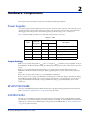
1
M1 System Management Board
User’s Guide
Actel Corporation, Mountain View, CA 94043
© 2008 Actel Corporation. All rights reserved.
Printed in the United States of America
Part Number: 50200081-1
Release: November 2008
No part of this document may be copied or reproduced in any form or by any means without prior written
consent of Actel.
Actel makes no warranties with respect to this documentation and disclaims any implied warranties of
merchantability or fitness for a particular purpose. Information in this document is subject to change
without notice. Actel assumes no responsibility for any errors that may appear in this document.
This document contains confidential proprietary information that is not to be disclosed to any
unauthorized person without prior written consent of Actel Corporation.
Trademarks
Actel and the Actel logo are registered trademarks of Actel Corporation.
Adobe and Acrobat Reader are registered trademarks of Adobe Systems, Inc.
All other products or brand names mentioned are trademarks or registered trademarks of their respective
holders.
Table of Contents
1
Introduction . . . . . . . . . . . . . . . . . . . . . . . . . . . . . . . . . . . . 5
Design Example . . . . . . . . . . . . . . . . . . . . . . . . . . . . . . . . . . . . . . . . . . . 8
Document Contents . . . . . . . . . . . . . . . . . . . . . . . . . . . . . . . . . . . . . . . . . 8
2
Contents and System Requirements . . . . . . . . . . . . . . . . . . . . . . . 9
Kit Contents . . . . . . . . . . . . . . . . . . . . . . . . . . . . . . . . . . . . . . . . . . . . . 9
System Requirements . . . . . . . . . . . . . . . . . . . . . . . . . . . . . . . . . . . . . . . . . 9
3
Hardware Components . . . . . . . . . . . . . . . . . . . . . . . . . . . . . . 11
Power Supplies . . . . . . . . . . . .
M1AFS1500-FG484 . . . . . . . . .
A3P250-FG144 . . . . . . . . . . . .
Clocks and Reset . . . . . . . . . . .
Programming . . . . . . . . . . . . .
DIP Switch, LEDs and Push Buttons
LCD Display . . . . . . . . . . . . .
Memory . . . . . . . . . . . . . . . .
PCI . . . . . . . . . . . . . . . . . .
Legacy Connector . . . . . . . . . . .
Santa Cruz Connector Header . . . .
ARM Debugger . . . . . . . . . . . .
Ports . . . . . . . . . . . . . . . . .
ATX Connector Supply . . . . . . .
Temperature Diodes . . . . . . . . .
Heater/FAN Loads . . . . . . . . . .
Voltage Monitors . . . . . . . . . . .
Digital Brick . . . . . . . . . . . . .
Smart Battery . . . . . . . . . . . . .
Test Points . . . . . . . . . . . . . .
Prototype Section . . . . . . . . . . .
4
.
.
.
.
.
.
.
.
.
.
.
.
.
.
.
.
.
.
.
.
.
.
.
.
.
.
.
.
.
.
.
.
.
.
.
.
.
.
.
.
.
.
.
.
.
.
.
.
.
.
.
.
.
.
.
.
.
.
.
.
.
.
.
.
.
.
.
.
.
.
.
.
.
.
.
.
.
.
.
.
.
.
.
.
.
.
.
.
.
.
.
.
.
.
.
.
.
.
.
.
.
.
.
.
.
.
.
.
.
.
.
.
.
.
.
.
.
.
.
.
.
.
.
.
.
.
.
.
.
.
.
.
.
.
.
.
.
.
.
.
.
.
.
.
.
.
.
.
.
.
.
.
.
.
.
.
.
.
.
.
.
.
.
.
.
.
.
.
.
.
.
.
.
.
.
.
.
.
.
.
.
.
.
.
.
.
.
.
.
.
.
.
.
.
.
.
.
.
.
.
.
.
.
.
.
.
.
.
.
.
.
.
.
.
.
.
.
.
.
.
.
.
.
.
.
.
.
.
.
.
.
.
.
.
.
.
.
.
.
.
.
.
.
.
.
.
.
.
.
.
.
.
.
.
.
.
.
.
.
.
.
.
.
.
.
.
.
.
.
.
.
.
.
.
.
.
.
.
.
.
.
.
.
.
.
.
.
.
.
.
.
.
.
.
.
.
.
.
.
.
.
.
.
.
.
.
.
.
.
.
.
.
.
.
.
.
.
.
.
.
.
.
.
.
.
.
.
.
.
.
.
.
.
.
.
.
.
.
.
.
.
.
.
.
.
.
.
.
.
.
.
.
.
.
.
.
.
.
.
.
.
.
.
.
.
.
.
.
.
.
.
.
.
.
.
.
.
.
.
.
.
.
.
.
.
.
.
.
.
.
.
.
.
.
.
.
.
.
.
.
.
.
.
.
.
.
.
.
.
.
.
.
.
.
.
.
.
.
.
.
.
.
.
.
.
.
.
.
.
.
.
.
.
.
.
.
.
.
.
.
.
.
.
.
.
.
.
.
.
.
.
.
.
.
.
.
.
.
.
.
.
.
.
.
.
.
.
.
.
.
.
.
.
.
.
.
.
.
.
.
.
.
.
.
.
.
.
.
.
.
.
.
.
.
.
.
.
.
.
.
.
.
.
.
.
.
.
.
.
.
.
.
.
.
.
.
.
.
.
.
.
.
.
.
.
.
.
.
.
.
.
.
.
.
.
.
.
.
.
.
.
.
.
.
.
.
.
.
.
.
.
.
.
.
.
.
.
.
.
.
.
.
.
.
.
.
.
.
.
.
.
.
.
.
.
.
.
.
.
.
.
.
.
.
.
.
.
.
.
.
.
.
.
.
.
.
.
.
.
.
.
.
.
.
.
.
.
.
.
.
.
.
.
.
.
.
.
.
.
.
.
.
.
.
.
.
.
.
.
.
11
11
11
12
12
14
15
15
15
15
16
16
17
18
22
24
24
25
26
27
29
System Management Software . . . . . . . . . . . . . . . . . . . . . . . . . . 31
Board Status
Graphs . . .
Event Log . .
Comms . . .
Thresholds .
5
.
.
.
.
.
.
.
.
.
.
.
.
.
.
.
.
.
.
.
.
.
.
.
.
.
.
.
.
.
.
.
.
.
.
.
.
.
.
.
.
.
.
.
.
.
.
.
.
.
.
.
.
.
.
.
.
.
.
.
.
.
.
.
.
.
.
.
.
.
.
.
.
.
.
.
.
.
.
.
.
.
.
.
.
.
.
.
.
.
.
.
.
.
.
.
.
.
.
.
.
.
.
.
.
.
.
.
.
.
.
.
.
.
.
.
.
.
.
.
.
.
.
.
.
.
.
.
.
.
.
.
.
.
.
.
.
.
.
.
.
.
.
.
.
.
.
.
.
.
.
.
.
.
.
.
.
.
.
.
.
.
.
.
.
.
.
.
.
.
.
.
.
.
.
.
.
.
.
.
.
.
.
.
.
.
.
.
.
.
.
.
.
.
.
.
.
.
.
.
.
.
.
.
.
.
.
.
.
.
.
.
.
.
.
.
.
.
.
.
.
.
.
.
.
.
.
.
.
.
.
.
.
.
.
.
.
.
.
.
.
.
32
34
34
35
36
Setting Thresholds . . . . . . . . . . . . . . . . . . . . . . . . . . . . . . . . 39
Setting the Thresholds Graphically . . . . . . . . . . . . . . . . . . . . . . . . . . . . . . . . . 39
Setting the Thresholds with the Slider Marker . . . . . . . . . . . . . . . . . . . . . . . . . . . 40
Voltage, Current, and Temperature Status Indicators . . . . . . . . . . . . . . . . . . . . . . . 40
M1 System Management Board User’s Guide
3
Table of Contents
6
Demonstration Scripts . . . . . . . . . . . . . . . . . . . . . . . . . . . . . . 41
General Setup . . . . . .
Basic Controls . . . . .
Voltage Monitoring . . .
Current Monitoring . . .
Temperature Monitoring
RTC Control . . . . . .
Logging Events . . . . .
.
.
.
.
.
.
.
.
.
.
.
.
.
.
.
.
.
.
.
.
.
.
.
.
.
.
.
.
.
.
.
.
.
.
.
.
.
.
.
.
.
.
.
.
.
.
.
.
.
.
.
.
.
.
.
.
.
.
.
.
.
.
.
.
.
.
.
.
.
.
.
.
.
.
.
.
.
.
.
.
.
.
.
.
.
.
.
.
.
.
.
.
.
.
.
.
.
.
.
.
.
.
.
.
.
.
.
.
.
.
.
.
.
.
.
.
.
.
.
.
.
.
.
.
.
.
.
.
.
.
.
.
.
.
.
.
.
.
.
.
.
.
.
.
.
.
.
.
.
.
.
.
.
.
.
.
.
.
.
.
.
.
.
.
.
.
.
.
.
.
.
.
.
.
.
.
.
.
.
.
.
.
.
.
.
.
.
.
.
.
.
.
.
.
.
.
.
.
.
.
.
.
.
.
.
.
.
.
.
.
.
.
.
.
.
.
.
.
.
.
.
.
.
.
.
.
.
.
.
.
.
.
.
.
.
.
.
.
.
.
.
.
.
.
.
.
.
.
.
.
.
.
.
.
.
.
.
.
.
.
.
.
.
.
.
.
41
43
44
44
45
45
45
A M1AFS1500-FG484 Pin List . . . . . . . . . . . . . . . . . . . . . . . . . . 47
B A3P250-FG144 Pin List . . . . . . . . . . . . . . . . . . . . . . . . . . . . . 63
C Board Schematics . . . . . . . . . . . . . . . . . . . . . . . . . . . . . . . . . 69
D Board Stackup . . . . . . . . . . . . . . . . . . . . . . . . . . . . . . . . . . . 87
E Product Support . . . . . . . . . . . . . . . . . . . . . . . . . . . . . . . . . . 89
Customer Service . . . . . . . . . . . . . . . . . . . . . . . . . . . . . . . . . . . . . . . . . . 89
Contacting the Customer Technical Support Center . . . . . . . . . . . . . . . . . . . . . . . . 90
Index . . . . . . . . . . . . . . . . . . . . . . . . . . . . . . . . . . . . . . . 91
4
M1 System Management Board User’s Guide
Introduction
The Actel M1 System Management Board Development Kit provides an excellent platform for developing system
management applications and/or applications with a microprocessor. The kit includes a CortexTM-M1-enabled Fusion
device, a system management GUI, and a platform (Figure 1) for systems that performs the following functions:
• Power-up detection
• Power sequencing
• Thermal management
• Sleep modes
• System diagnostics
• Remote communications
• Clock generation and management
Figure 1. M1 System Management Board
The M1 System Management Board includes an M1AFS1500 device, which is compatible with Cortex-M1, Core8051,
and other processors, as well as non-processor-based implementations. The kit’s demonstration design uses the MicroC/
OS-II on Cortex-M1 with the system management GUI, which is multi-tabbed for board status, application data, IPMI
data, and a graphical display of the monitored analog data. In addition, the GUI source code is available for custom
modification. All the documentation in this M1 System Management user’s guide for the M1-SYSMGMT-DEV-KIT
board, fitted with an M1AFS1500 part, is equally applicable to the old M7-enabled board that was fitted with an
M7AFS600 device. The board is essentially the same and only the FPGA has been changed. As a result, this guide can
also be used as documentation for the older SYSMGMT-DEV-KIT board that featured an ARM® CoreMP7-enabled
device. The new M1-enabled board features a much larger AFS device with more embedded nonvolatile memory and a
greater programmable silicon space.
M1 System Management Board User’s Guide
5
The system management GUI (Figure 2, Figure 3 and Figure 4) includes the following tabs:
• Board status
• Application data
• IPMI data
• Graphical display of analog data
The GUI helps users to:
• Monitor power supplies
• Monitor temperature sensors
• Set LEDs and text for display
• Set and read the RTC
• Display embedded Flash contents
Figure 2. Board Status Tab
6
M1 System Management Board User’s Guide
Figure 3. Threshold Tab
Figure 4. Graphs Tab
M1 System Management Board User’s Guide
7
Design Example
This user’s guide utilizes the M1 System Management Board, the System Management software and examples to
demonstrate System Management’s capabilities. It can also be used as a reference design to jumpstart user application
designs, including a firmware platform for re-use. Design examples for the older CoreMP7-enabled board, featuring the
M7AFS600 device, may still be found on the Actel web site. Only Cortex-M1-enabled designs should be used with the
M1-SYSMGMT-DEV-KIT board.
The System Management software enables the user to run tests for demonstration purposes, using a laptop or PC
connected via serial communications link to the board. These are the main features:
• View the board's status in real-time.
• Observe all voltages, current and temperature in specific places on the board for real-time diagnostics.
• Test asynchronous buttons on the board and view the result in the software upon depressing any given button.
• Threshold control and event logging to control the warning limits within a given range and log specific events as a result
of these threshold levels.
Future releases will extend the capabilities to include power sequencing and a range of other more advanced features.
Document Contents
Chapter 1 – Contents and System Requirements describes the contents of the M1 System Management Kit.
Chapter 2 – Hardware Components describes the components of the System Management Board and the system
requirements for the System Management software installation.
Chapter 3 – System Management Software describes the System Management user interface.
Chapter 4 – Setting Thresholds describes how to set the thresholds graphically or using the sliders.
Chapter 5 – Demonstration Scripts provides simple instructions of the basic scripts for the System Management
software.
Appendix A – M1AFS1500-FG484 Pin List
Appendix B – A3P250-FG144 Pin List
Appendix C – Board Schematics
Appendix D – Board Stackup
8
M1 System Management Board User’s Guide
1
Contents and System Requirements
This chapter details the contents of the Cortex-M1-enabled Fusion-based System Management Kit and lists the
necessary components required to use it.
Kit Contents
• M1 System Management Board
• Switching brick power supply (rated from 110 V to 240 V AC) from 50 Hz to 60 Hz input, an providing 9 V DC
output at up to 2 A, part number DTS090220UP5P-SZ from CUI, Inc.
• Power cables and adapter
• RS-232 cable
• User’s guide
Optional:
• 7.2 V 2100 mAh NiMH battery
• Temperature diode two-pin flex cable
• ATX power supply
• 10-pin JTAG cable for Fusion to Fusion programming
• FlashPro v5.0
• Libero IDE GOLD
• CD with design/application examples
System Requirements
The system requirements for the System Management Board and the System Management software:
• ATX power supply, which can connect directly to the board
• Actel M1AFS1500-FG484 Demonstrator Board
• Serial communications cable (RS-232)
• PC running Windows® XP. Windows XP is the only supported operating system.
• Serial communications port, preferably COM Port 1. Future versions will incorporate ethernet communication.
M1 System Management Board User’s Guide
9
2
Hardware Components
This chapter describes the hardware components of the M1 System Management Board.
Power Supplies
A 9 V power supply is provided with the kit. The 9 V brick is connected to the J1 connector on the board. This power
supply feeds the input voltage of three LDO-type regulators—U1, U2, and U3—through a slide switch, SW7. The
switch toggles between two positions On-Off. The regulators provide three voltages 5 V, 3.3 V and 1.5 V.
Table 2-1 illustrates LEDs provided to ensure that all the voltage reach the correct state.
Table 2-1 · LEDs
LED
Reference
Designator
SW7
Description
Off
On
Red LED
D26
On
On
9 V input voltage before switch SW7
Yellow LED
D29
Off
On
9 V input voltage after switch SW7
Yellow LED
D25
Off
On
5 V supply
Yellow LED
D21
Off
On
3.3 V supply
Yellow LED
D27
Off
On
1.5 V supply
Jumper Settings
JP13 is a two-pin jumper that provides VJTAG with a 3.3 V supply. VJTAG is needed to power up the JTAG circuitry of
the M1AFS1500-FG484 and A3P250-FG144 parts. While programming these two parts, make sure this location has a
jumper.
JP35 is a two-pin jumper that provides VPUMP with a 3.3 V supply. VPUMP is needed while programming the
M1AFS1500-FG484 and A3P250-FG144 parts. While programming these two parts, make sure this location has a
jumper.
JP1 is a three-pin jumper that provides 1.5 V to the M1AFS1500-FG484 part.
JP1.1-2 connects the 1.5 V going to the M1AFS1500-FG484 part to 1.5_INT. This voltage is generated internally by
the M1AFS1500-FG484 part through an on-chip regulator powered by the 3.3 V supply. JP1.2-3 connects the 1.5 V
going to the M1AFS1500-FG484 part to voltage 1.5_EXT. This voltage is generated externally by the on-board
regulator U3.
M1AFS1500-FG484
This is the Actel ARM-enabled Fusion FPGA demonstrated on the System Management Board and located at U23.
Refer to “M1AFS1500-FG484 Pin List” on page 47 for pin list information.
A3P250-FG144
This device is an Actel FPGA used purely due to the limitation on the number of I/Os on the M1AFS1500-FG484
part. This device controls all user interfaces: LCD, key pads, DIP switch, LEDs, etc. The M1AFS1500-FG484 and the
A3P250 device communicate via a UART interface using the Actel CoreUART IP. Refer to “A3P250-FG144 Pin List”
on page 63 for pin list information.
M1 System Management Board User’s Guide
11
Hardware Components
Clocks and Reset
CLK Source
A 50 MHz clock with 50 ppm stability is provided at location U5. This clock is the clock source for the A3P250-FG144
device at U24 (pin F12) and the M1AFS1500-FG484 device at location U23 (pin A3). A user clock is also provided at
location U7. Any 3.3 V clock can be installed in the socket of this location. The user clock feeds only to the
M1AFS1500-FG484 device.
A 32.768 kHz crystal is provided at location Y1 on the board. This is the crystal used to start the internal RTC counter
on the M1AFS1500-FG484 device.
Jumper Settings
JP25 is a two-pin jumper. By default there is no jumper at this location. In this state, the clock is free running. If the
jumper is placed, it puts the enable pin of the clock to GND and shuts off the clock oscillator.
PUB Signal
The PUB signal of the M1AFS1500-FG484 unit has a 1 MΩ pull to 3.3 V along with a push button SW8 to provide an
active low pulse.
Reset
An active low pin reset is provided by the push button SW6. The reset signal goes to the M1AFS1500-FG484 device at
pin B17 and A3P250 device at pin E2.
Programming
Different programming techniques are provided on the System Management Board.
FlashPro3
FlashPro3
In-system programming is provided to enable programming of all devices on the JTAG boundary scan chain, see Figure
2-1.
M1AFS
A3P
PCI 1
PCI 2
Figure 2-1. FlashPro3 In-System Programming Setup
Place all jumpers as shown in Table 2-2 and plug in the FlashPro3 connector on J13 to start programming .
Table 2-2 · Jumpers Settings for In-System Programming
Jumper
12
Setting for In-System Programming
JP35
1-2
JP13
1-2
JP12
1-2
M1 System Management Board User’s Guide
Programming
Table 2-2 · Jumpers Settings for In-System Programming (Continued)
Jumper
Setting for In-System Programming
JP14
1-2
JP15
1-2
JP16
1-2
JP17
1-2
JP10 (If PCI1 is not in chain)
1-2
JP11 (If PCI2 is not in chain)
1-2
M1AFS1500-FG484 to A3P Programming
The board can be configured to program an A3P250 device with the M1AFS1500-FG484 device, see Figure 2-2.
Table 2-3 shows the jumpers settings required.
M1AFS1500-FG484
A3P250-FG144
Figure 2-2. M1AFS1500-FG484 to A3P Programming Setup
Table 2-3 · Jumper Settings for M1AFS1500-FG484 to A3P250-FG144 Programming
Jumper
Setting for In-System Programming
JP35
1-2
JP13
1-2
JP12
2-3
JP14
2-3
JP15
2-3
JP16
2-3
JP17
2-3
JP24
2-3
JP21
2-3
JP22
2-3
JP23
2-3
M1 System Management Board User’s Guide
13
Hardware Components
External Programming
The System Management Board can program an external JTAG compliant device with the M1AFS1500-FG484 device.
Figure 2-3 shows the external programming setup. See Table 2-4 for the jumper settings.
Buffers
Connector
Cable
M1AFS1500-FG484
External
Device
Figure 2-3. External Programming Setup
Table 2-4 · Jumper Settings for External Programming
Jumper
Setting for Programming External Device
JP24
2-3
JP21
2-3
JP22
2-3
JP23
2-3
TDO JP17
TDI JP16
TRST JP15
TMS JP14
TCK JP12
Figure 2-4 shows the JTAG complaint device.
JTAG Port
A3P_JTAG
AFS_JTAG
GND
Figure 2-4. JTAG Compliant Device
DIP Switch, LEDs and Push Buttons
DIP Switch S1
Eight signals are provided for debug purposes. The signals toggle between 0 V (low) and 3.3 V (high) logic. The signals
are controlled by the A3P250 FPGA.
LEDs
Four green LEDs (D6, D7, D8 and D9) and four red LEDs (D10, D11, D12 and D13) are provided for debug
purposes. The LEDs are controlled by the A3P250 FPGA. If the signals are at logic high, the LEDs are On. If the
signals are driven low, the LEDs are Off.
14
M1 System Management Board User’s Guide
LCD Display
Push Buttons
Five push buttons are provided at SW1, SW2, SW3, SW4 and SW5, see Figure 2-5. These push buttons are located
near the LCD display and are used to navigate the LCD screen for different tests/demo scripts. These signals are driven
to the A3P250 device.
SW2
UP
SW3
Select
SW1
SW4
Right
Left
Down
SW5
Figure 2-5. Push Buttons
LCD Display
An 8-bit, 16 x 2 character LCD display (part# LCMS01602DSFC) is provided on the board at LCD1. The A3P250FG144 device controls the 8-bit signals, control signals, and backlight of the display. The contrast of the LCD display
can be changed using the potentiometer at R19.
Memory
An external synchronous SRAM (part# 816018) is provided with 1 M x 32 bits memory, located at U8 and U9 on the
board.
Flash memory (part# M29W160ET) is provided with 1 M x 32 bits of memory, located at U25 and U26 on the board.
All signals interface with the M1AFS1500-FG484 device at U23.
PCI
Two PCI ports, P2-PCI_1 and P3-PCI_2, are provided. These two ports interface with the M1AFS1500-FG484
device. The PCI bus supports the 3.3 V 32-bit operations at a system frequency of 33 MHz and 66 MHz and is
compliant with the local bus PCI 2.3 specifications.
Legacy Connector
A 40-pin 0.100 in x 0.100 in connector ( J12) is provided for debug purposes. All Actel demonstration and evaluation
boards are populated with this connector so they can interface with other Actel boards.
All I/Os on the legacy connector are shared with the PCI signals.
Note: Do not exercise the PCI connector and the Santa Cruz connector header simultaneously.
M1 System Management Board User’s Guide
15
Hardware Components
Santa Cruz Connector Header
A set of three headers ( J8, J9, and J11), per the Santa Cruz header specification, are provided for debug purposes and
installing compatible daughter boards. All I/Os on the Santa Cruz header are shared with the PCI signals.
Note: Do not exercise the PCI connector and the Santa Cruz connector header simultaneously.
J3
J1
GND
NC
PROTOIO30
PROTOIO32
PROTOIO34
PROTOIO36
PROTOIO38
1 2
3 4
5 6
7 8
9 10
11 12
13 14
NC
PROTOIO29
PROTOIO31
PROTOIO33
PROTOIO35
PROTOIO37
PROTOIO39
J3
Vunreg
NC
VCC3_3
VCC3_3
OSC
CLK1
CLK2
NC
NC
NC
1
3
5
7
9
11
13
15
17
19
2
4
6
8
10
12
14
16
18
20
GND
GND
GND
GND
GND
GND
GND
GND
GND
GND
RESERTPROTOIO0
PROTOIO2
PROTOIO4
PROTOIO6
PROTOIO8
PROTOIO10
PROTOIO12
PROTOIO14
GND
PROTOIO16
PROTOIO17
PROTOIO18
PROTOIO19
PROTOIO21
PROTOIO22
PROTOIO24
PROTOIO25
PROTOIO27
PROTOIO28
1
3
5
7
9
11
13
15
17
19
21
23
25
27
29
31
33
35
37
39
2
4
6
8
10
12
14
16
18
20
22
24
26
28
30
32
34
36
38
40
GND
PROTOIO1
PROTOIO3
PROTOIO5
PROTOIO7
PROTOIO9
PROTOIO11
PROTOIO13
PROTOIO15
NC
GND
GND
GND
PROTOIO20
GND
PROTOIO23
GND
PROTOIO26
CARDSELGND
Figure 2-6. Santa Cruz Connector Pinout
ARM Debugger
A 20-pin port ( J10) is provided ( see Figure 2-7) for installing an ARM Real View debugger that interfaces with the
M1AFS1500-FG484 device.
TDO
TDI
TRST
TMS
TCK
Note: While using the debugger to run the software, add a jumper from JP16 pin 1 to JP17 pin 1. This will make the
M1AFS1500-FG484 the only part in the chain.
JTAG Port
A3P_JTAG
AFS_JTAG
GND
Figure 2-7. ARM Debugger
16
M1 System Management Board User’s Guide
Ports
Ports
RS232
This kit contains one RS-232 port with a MAX3221 transceiver that can be used for communications between the
M1AFS1500-FG484 device and a common serial port found on a PC or other RS-232 compatible device.
Note: The RS-232 interface does not support hardware RTS/CTS hand shaking. The default configuration has the RTS
and CTS shorted together to create a loopback connection.
RS485
This kit contains one RS485 2-wire port with a MAX3362 that can be used for communications between the
M1AFS1500-FG484 device and a RS485 port. Necessary terminating resistors are provided on the board.
Ethernet 10/100 PHY
One MII ethernet port is provided on the part. It uses a DP83846A transceiver chip and an RJ-45 connector. This
directly interfaces with the M1AFS1500-FG484 device. Four LEDs are provided along with the port. See Table 2-5.
Table 2-5 · LED Description
LED Reference Designator
Silkscreen
D2
FD
D3
COL
D4
RX
D5
SPEED
SMBUS Port
Three ports ( J4, J5, and J71) are provided for SMBus communications. All signals directly interface with the
M1AFS1500-FG484 device. The connections are shown in Table 2-6 and Table 2-7 on page 17. 0.100 in x 0.100 in
center-to-center connectors are used as the interface. 1.8-kΩ pull-ups are used for all the signals.
Table 2-6 · Jumper Settings
Jumper
Connections
JP21
1-2
JP22
1-2
JP23
1-2
JP24
1-2
Table 2-7 · Connector Settings
Connector
Pin 1
Settings
3.3 V
Pin 2
SCL
Pin 3
SDA
Pin 4
1-GND
M1 System Management Board User’s Guide
17
Hardware Components
ATX Connector Supply
The ATX connections demonstrate the analog function features of the M1AFS1500-FG484 device. The functional
description and pin out information is shown in Figure 2-8. All supplies on the ATX power supply can support a
maximum of 10 A.
Current Monitored Output Power Supply
12V
0.1 ohm
5V
3.3V
0.1 ohm
0.1 ohm
External Board Power Supply
12V
3.3V
Q14
Q15
AV0
AV1
AV2
AC0
AC1
AC2
Q13
5V
AV8
AV7
AV9
M7AFS
AG2
AG1
AG0
12V
5V
3.3V
ATX Input Power Supply
Figure 2-8. M1AFS1500-FG484 Functional Description
Table 2-8 · ATX Main Power Connector Pinout
Pin Number
18
Signal Function
1
+3.3 VDC
2
+3.3 VDC
3
COM
4
+5 VDC
5
COM
6
+5 VDC
7
COM
8
PWR_OK
M1 System Management Board User’s Guide
ATX Connector Supply
Table 2-8 · ATX Main Power Connector Pinout (Continued)
Pin Number
Signal Function
9
+5 VSB
10
+12 VDC
11
+3.3 VDC
12
–12 VDC
13
COM
14
PS_ON#
15
COM
16
COM
17
COM
18
N/C
19
5 VDC
20
5 VDC
Note: Do not plug in the ATX supply to J73.
Table 2-9 · ATX Main Power Connect Pinout by Function
Signal Function
Pin Number
+3.3 VDC
1
+3.3 VDC
2
+3.3 VDC
11
5 VDC
19
5 VDC
20
+5 VDC
4
+5 VDC
6
+5 VSB
9
–12 VDC
12
+12 VDC
10
COM
3
COM
5
COM
7
COM
13
COM
15
M1 System Management Board User’s Guide
19
Hardware Components
Table 2-9 · ATX Main Power Connect Pinout by Function (Continued)
Signal Function
Pin Number
COM
16
COM
17
N/C
18
PS_ON#
14
PWR_OK
8
PS_ON# Signal
The ATX supply plugs in to the J72 connector. The PS_ON# signal is the main switch for the ATX supply. The signal
logic is controlled by the signal AFS_PS_ON on the M1AFS1500-FG484 device.
Table 2-10 · PS_ON# Signal Settings
AFS_PS_ON
(M1AFS1500-FG484)
PS_ON# (ATX)
ATX Supply
0
1
Off
1
0
On
Power_OK Signal
The PWR_OK signal is an output of the ATX supply. It is a flag set by the ATX supply if all output voltages are good.
The PWR_OK is continuously monitored by the M1AFS1500-FG484 device using a regular I/O pin
IN_POWER_OK.
Table 2-11 · PWR_OK Signal Settings
PWR_OK (ATX)
0
5V
IN_POWER_OK
(M1AFS)
ATX Supply
3.3 V
BAD
0
GOOD
5VSB Signal
The 5VSB signal on the J72 ATX supply is routed directly to the 5VSB pin on the J73 ATX connector. It does not go to
the M1AFS1500-FG484 device. This signal is a sense voltage, which is an input signal to the ATX supply from a
plugged in daughter board.
Gate Driver
All input voltages (12 V, 5 V, 3.3 V) are monitored through the AV pads on the M1AFS1500-FG484 device (Figure 28 on page 18). The input voltage goes to a P-Type Power MOSFET (FDS7079ZN3). All three voltages can be switched
On/Off using the gate driver (AG) controlling the FET.
20
M1 System Management Board User’s Guide
ATX Connector Supply
Table 2-12 · Gate Driver Settings
AG
FET
Output Voltage
Tristate
Off
0V
On
On
12 V, 5 V, 3.3 V
Note: The gate driver has to be configured as a constant current sink with a 10-μa or 30-μa drive level to get different
ramp-rates.
Power-Out Connectors
The output voltage of the FETs goes to two different power-out connectors:
ATX Connector J73 – Any external daughter board can be plugged into this connector. All voltages on the J73
connector are monitored by the M1AFS1500-FG484 device.
MB_PS_ON# – This signal may be driven by an external daughter board. It is an output from the external daughter
board. The function of the signal is similar to the PS_ON signal. This signal behaves as a switch to the power going to
the external daughter board.
Table 2-13 · MB_PS_ON Settings
MB_PS_ON# (ATX-J73)
AFS_MB_PS_ON (M1AFS)
External DB Power
NC
0
Off
0
1
On
1
0
Off
MB_POWER_OK – This sense/flag signal is an input to the external daughter board. It indicates whether the power
going to the external board is good. This signal is driven by the M1AFS1500-FG484 device.
Table 2-14 · MB_POWER_OK Settings
12 V, 5 V, 3.3 V Output Voltage
MB_POWER_OK (M7ADS)
GOOD
BAD
3.3 V
0
Header pins – Header pins are provided for 12 V, 5 V, and 3.3 V in the current monitored external daughter board
section of the board. Alligator clips can be used to connect any external board to these pins to power the board. All
voltages and current are monitored using 0.1 Ω resistors through the M1AFS1500-FG484 device.
Note: The external board connected to the header pins consumes less than 3 A.
M1 System Management Board User’s Guide
21
Hardware Components
Dummy Loads
Dummy loads can be connected to the output voltages to demonstrate the capability of the M1AFS1500-FG484 device
to monitor current in the absence of an external daughter board. Connect the dummy loads as shown in Table 2-15.
Table 2-15 · Dummy Loads Settings
Reference
Designator
Load
Output Voltage
Approximate
Current
JP32
110 Ω
12 V
109 mA
JP33
39 Ω
5V
128 mA
JP34
39 Ω
3.3 V
84 mA
Temperature Diodes
Five temperature diodes (MMBT3904) are provided across the board for monitoring environment temperature: heater,
regulators, board, PCI, and copper pad.
Heater
Temperature diode Q10 is located very close to the heater element, R161, and monitors the temperature of the heater.
The red LED, D22, can be used to toggle if the temperature crosses some threshold.
Regulators
Temperature diode Q7 is located in the middle of all the LDO regulators to monitor the temperature. The red LED
D19 can be used to toggle if the temperature crosses some threshold.
Board
Temperature diode Q1 is located beneath the LCD display to monitor average board temperature. The red LED D1 can
be used to toggle if the temperature crosses some threshold.
PCI
A two-pin header, JP19, is located between the two PCI connectors. Attach a two-pin cable with a temperature-sensing
device to this connector to monitor temperature of the PCI card. The red LED D30 can be used to toggle if the
temperature crosses some threshold.
Copper Pad
Temperature diode Q16 is located next to the exposed copper area to monitor the temperature of the exposed copper
pad. This pad will be used for calibration purposes to record a stable room temperature. The red LED D34 can be used
to toggle if the temperature crosses some threshold.
Potentiometer
A 2-kΩ potentiometer (R150) is provided with a control knob to demonstrate voltage monitoring by exercising an AV
pad on the M1AFS1500-FG484 device. The potentiometer is connected across a 5 V signal. The voltage strobe moves
22
M1 System Management Board User’s Guide
Temperature Diodes
from 0 V to 5 V using the knob control (Figure 2-9).
Voltage
Increase
Voltage
Decrease
Figure 2-9. Potentiometer Knob Control
Tri-Color LED
A tri-color LED (AAF5060PBESEEVG) is provided on the board. The LED has three colors—blue, orange, and
green—controlled by three gate driver (AG) pins from the M1AFS1500-FG484 device. A combination of colors can be
turned On to form new colors. To make the tri-color LED operational, place jumpers on JP29, JP30, and JP31, as
shown in Table 2-16 and Table 2-17.
Table 2-16 · AG Pads Settings
AG Pads (M1AFS1500-FG484)
LED
Tristate
Off
On-High Current Drive
On
Table 2-17 · Jumpers Settings
Jumpers
LED
JP29
Blue
JP30
Orange
JP31
Green
Note: Set the AG pad in a high current drive mode, which can sink 25 mA.
M1 System Management Board User’s Guide
23
Hardware Components
Heater/FAN Loads
The board has two loads controlled by the gate drivers from the M1AFS1500-FG484 device: heater and fan.
VCC
Q11
AG
Load
Figure 2-10. Heater/ Fan Loads.
Table 2-18 · AG Pads Settings
AG Pads (M1AFS1500-FG484)
LED
Tristate
Off
On-High Current Drive
On
Note: Set the AG pad in a high current drive mode, which can sink 25 mA.
Heater
A 7.5 Ω wire-wound resistor (R106) is provided on the board. The resistor is a conduction type of heater element that
dissipates heat of up to 11 W. The heater is used to demonstrate the temperature variance on the temperature diode
(Q10) sitting close to it.
Fan
A 3.3 V fan is provided on the board with a tachometer option to measure the speed of the fan. Each revolution creates
two pulses on the tachometer output. The tachometer output signal goes to the A3P250-FG144 device. A connector
JP18 is provided in parallel to the fan load to allow removing the fan and adding an external load.
Note: Do not add a load that requires more than 300 mA.
Voltage Monitors
Three monitors are provided on the board to monitor external voltages: EXT_VOL[1:3]. Voltages of an external board
can be monitored by using alligator clips to plug into one of the monitor pins. The voltage is monitored using the AV
pads of the M1AFS1500-FG484 device. The input voltage (V1) from the external board can be divided down to one of
the options below using a 4-pole switch (Table 2-19). Three switches are provided to allow independent division of the
external voltages: switch U15 is used for EXT_VOL[1}, switch U17 is used for EXT_VOL[2] and switch U18 is used
24
M1 System Management Board User’s Guide
Digital Brick
for EXT_VOL[3]. Identical switch positions are used for common division factors across all three switches. The table
below applies to any switch.
Table 2-19 · Switch Settings
Numerical Switch Position
Internal Voltage as Factor of External Voltage Vext
1
Vext * 1
2
Vext * 1/2
3
Vext * 1/4
4
Vext * 1/8
Note: If an external board has voltages greater than 12 V that need to be monitored, use these options to apply the right
range of voltage to the AV pad.
Digital Brick
You can connect a digital brick on the board. The following signals are common to all digital bricks.
VIN_D
This is the input power to the digital brick. Use alligator clips to connect the VIN_D pin to the input supply of the
digital brick. This pin can provide 9-12 V, depending on the input supply used for the System Management Board.
DIG_BRK_OUT
This is the output voltage of the digital brick. This voltage is monitored by the M1AFS1500-FG484 device using the
AV pads.
VSENSE
This pin is an input to the digital brick that senses back the output voltage of the brick
(Figure 2-11).
DIG_BRK_OUT
VSENSE
Figure 2-11. VSENSE
M1 System Management Board User’s Guide
25
Hardware Components
TRIM_VOL
This pin is an input to the digital brick controlled by the M1AFS1500-FG484 I/O with a PWM control. The PWM
output can be configured using different RC values on the surface mount pads (Figure 2-12).
5 V Power
R224
R207
AFS Pad
R206
TRIM_VOL
C36
Figure 2-12. TRIM_VOL
This pin can be used to trim the output voltage of the digital brick. The trim voltage varies based on the type of digital
brick being used.
Smart Battery
Battery operation of the System Management Board includes battery backup, charging, and discharging routines using
the M1AFS1500-FG484 device.
A maximum 7.2 V NiMH 2100 mAh battery can be plugged in the two pin header JP4. The battery operates for
approximately 15 to 20 minutes. Make sure the polarity of the battery matches the silkscreen on the header. A
temperature diode can be plugged in the two pin header JP5 and can be placed on the battery to monitor temperature,
see Table 2-20.
Table 2-20 · Switch Settings
Header
26
Function
JP4 pin 1
GND
JP4 pin 2
Battery Voltage
JP5 pin 1
TRN – Temperature Diode
1/JP5 pin 2
AT – Temperature Diode
M1 System Management Board User’s Guide
Test Points
Charging and Discharging Routines
The battery is charged/discharged using the two FET controls (Figure 2-13). When Q3 is turned On and Q2 is turned
Off, the constant current source (20 mA) will slowly charge up the 7.2 V battery. When Q3 is turned Off and Q2 is
turned On, the battery is placed in discharge mode and will power up the board and start discharging. All voltages and
current are monitored by the M1AFS1500-FG484 device. A number of algorithms can be designed in the M1AFS
device for implementing the charging and discharging routines of the battery.
M7AFS
AG
Constant
Current Source
AV
Q3
AC
AG
AV
AC
Q2
Battery Ouput
Power
Input
Power
7.2V Battery
Figure 2-13. Charging and Discharging Routines
For demonstration purposes, you can discharge the battery and place a jumper on JP3. This adds an extra 110 Ω load to
the battery output voltage.
Note: The above figure is not a complete representation of the board schematics.
Temperature Monitoring
Connect a temperature diode to header JP5 to monitor battery temperature. Charging/discharging algorithms monitor
battery temperature.
Battery Backup
If you need a constant battery backup without any discharging algorithms in the M1AFS1500-FG484 device, place a
jumper to JP27. This keeps Q2 On and puts the battery in discharge mode. Both the power brick and the battery are
connected, but the power brick powers up the board automatically because the power brick is at a higher voltage than the
battery. If the power brick is pulled out in the middle of operation, the battery supply takes over with no interruptions.
Test Points
Table 2-21 and Table 2-22 show various test points provided across the board, and how to access them.
Table 2-21 · Test Points by Numerical Sequence
Test Points
Signal Name
TP1
Digital 3.3 V
TP2
Digital GND
TP3
Digital GND
M1 System Management Board User’s Guide
27
Hardware Components
Table 2-21 · Test Points by Numerical Sequence (Continued)
Test Points
Signal Name
TP4
Digital 3.3 V
TP5
1.5 V EXT
TP6
1.5 V
TP9
Main 3.3 V
TP10
1.5 V
TP11
Analog GND
TP12
VIN_D
TP13
Main GND
TP14
5V
TP15
VIN
TP16
Analog 3.3 V
TP17
Analog GND
TP18
ATX output 12 V
TP19
ATX output 5 V
TP24
ATX Output 3.3 V
Table 2-22 · Test Points in Signal Name Order
Signal Name
28
Test Points
1.5 V
TP6
1.5 V
TP10
1.5 V EXT
TP5
5V
TP14
Analog 3.3 V
TP16
Analog GND
TP17
Analog GND
TP11
ATX output 12 V
TP18
ATX Output 3.3 V
TP24
ATX output 5 V
TP19
Digital 3.3 V
TP1
Digital 3.3 V
TP4
Digital GND
TP2
M1 System Management Board User’s Guide
Prototype Section
Table 2-22 · Test Points in Signal Name Order (Continued)
Signal Name
Test Points
Digital GND
TP3
Main 3.3 V
TP9
Main GND
TP13
VIN
TP15
VIN_D
TP12
Prototype Section
A prototype section is provided at the bottom of the board for debug and development purposes (Figure 2-14). The
section is 20 holes x 20 holes large with the hole size at 0.100 in x 0.100 in, center to center.
Digital Domain
5 V Power
3 V Power
Analog Domain
5 V Power
IO_BLUE_TRI_AG Pad
IO_GREEN_TRI_AG Pad
Spare IO[12:23]
Spare IO[0:11]
IO_ORANGE_TRI_AG Pad
TRIM_VOL_PWM Pad
EXT_VOL1
EXT_VOL2
EXT_VOL3
Digital GND
Digital GND
Analog GND
Figure 2-14. Prototype Section
M1 System Management Board User’s Guide
29
Hardware Components
The following signals are provided in the debug area:
• Power: 5 V, 3.3 V, 1.5 V and digital and analog GND are provided in this are for easy access. Ensure that the current
consumption for any part added to this does not exceed 500 mA.
• Spare I/Os: 24 I/Os are provided for debug purposes. These I/Os are connected to the A3P250-FG144 FPGA part.
• Gate Driver: Three gate driver pins are provided: IO_BLUE_TRI, IO_GREEN_TRI, IO_ORANGE_TRI. When
using these gate drivers, check the jumper settings (Figure 2-23).
Table 2-23 · Jumper Settings
Signal
Jumpers
Tri-LED
Gate Driver
IO_BLUE_TRI
JP29
1-2
Remove Jumper
IO_GREEN_TRI
JP30
1-2
Remove Jumper
IO_ORANGE_TRI
JP31
1-2
Remove Jumper
• Trim Voltage: This signal is used in the digital brick application. See “Digital Brick” on page 25. This signal is also
routed to the prototype area. This pin can be configured as PWM output.
• External Voltages: These are the same input signal provided in “Voltage Monitors” on page 24 and can be used for
debug purposes.
30
M1 System Management Board User’s Guide
3
System Management Software
The System Management software has scrollable, zoomable, and sizeable real-time updated diagrams that enable the
simultaneous monitoring of the voltages, currents, and temperatures throughout the board. You can also set the
thresholds for these variables and log specific events, when they breach a target level. A full range of current capabilities
include the following:
• Event logging with type, time-stamp, and description of each event
• Voltage, current, and temperature monitoring and graphing
• Zoom functions on graph page: zoom in, zoom out, zoom fit, and zoom reset
• Adjustable threshold levels for voltage, current, and temperature
• Internal Flash memory (NVM) address and data screen dump
• Each individual line of raw data displayed in the Comms tab
• Display on board components in GUI: LEDs, push buttons, DIP switches, potentiometer, etc.
• Adjustable, on-board LCD text through GUI
The System Management software can also be used to set the RTC by matching it with the host PC. Logging events are
controlled and monitored through the interface.
The software initially communicates via RS-232 serial communications. Baud rate is selectable from the Comms tab.
The COM port is selectable, but Actel recommends you use COM port 1.
There is limited self-testability in the absence of an actual board. You can use one copy of the software to generate serial
communications traffic and to log that traffic with another running copy.
The user interface is organized in the following tabs (Figure 3-1 on page 31):
• Board Status: Covering the basic I/O tests and RTC, including real-time voltage, current, and temperature
monitoring, and internal Flash memory reading.
• Graphs: A set number of labelled graphs to the same time-base, monitoring of board voltages and currents, including
readings for the heater, PCI, finger pad, regulator, board, and potentiometer.
• Event Log: Event logging is displayed here. By uploading the stored event log from the board, you can view the events
and their individual warning level, type of event, time of occurrence, and a short description.
• Comms: This tab enables the user to change the baud rate and COM port (COM port 1 is recommended). In this tab,
you can enable a System Management software test to start/stop reception and transmission of bit sequences for
observation. A raw data window displays the sampled data. This tab contains a continuously updated display of data
sent and received.
• Thresholds: The board thresholds can be set for the board supply, PSU supply, temperature, and potentiometer.
Figure 3-1. Tabs
M1 System Management Board User’s Guide
31
System Management Software
Board Status
The Board Status tab is split into ten panels that control the behavior of the board (Figure 3-2).
Figure 3-2. Board Status Tab
LEDs
To turn on and off each LED on the board, click the corresponding LED button in the software.
LCD
To output two lines of text to the LCD screen, type the text that you want to display and click the Set to button. The
board firmware also uses the LCD and displays the “Clock”.
Clock
To synchronize the real-time on-board clock with the computer’s local time, click the Set From PC button.
Push Buttons
To test the correct synchronization between the push buttons on the board and the software, push the button on the
board and check that the corresponding button in the software lights up.
Demonstration
In this version only basic operations are demonstrated. However, in future versions you will be able to select from a range
of pre-selected demonstration scripts.
Internal Flash Memory
Enter the starting address (in hexadecimal) and click the Update button to dump all current data and the addresses
stored in the internal Fusion nonvolatile Flash memory into this window for debug purposes. Commencing at the
starting address, the data lists each byte chunk on each line, 16 in total, ending in their corresponding ASCII code. 16
lines are printed, representing 256 bytes of nonvolatile memory.
32
M1 System Management Board User’s Guide
Board Status
Controls
To display the state (open or closed) of the on-board DIP switches, open and close the DIP switches on the board. The
results are displayed in the software.
To display the potential difference across the potentiometer, adjust the rotating switches on the board. The results are
displayed in the software.
Board Supply
The board supply displays a real-time reading of the voltage and current ratings for the main supply. It also displays the
real-time voltages for the 1.5 V, 3.3 V, and 5.0 V supplies respectively. See “Voltage, Current and Temperature Status
Indicators” for more information on the status indicators.
PSU Supply (ATX Supply)
The PSU supply displays the real-time voltage and current ratings for the attached ATX (3.3 V, 5.0 V, and +12 V)
supply, and the real-time voltage for the -12 V supply.
Temperature
The temperature section displays the real-time temperature (°C) on the board from the sensors loaded at the heater, the
PCI, the finger pad, the regulator, and the board itself.
Voltage, Current and Temperature Status Indicators
The following explains the voltage, current, and temperature status indicators found in the Board Status tab next to each
reading.
Red - Voltage/current/temperature is above the maximum or below the minimum.
Green - Voltage/current/temperature is within set range.
Yellow - Voltage/current/temperature between maximum and local maximum or between minimum and local
minimum.
M1 System Management Board User’s Guide
33
System Management Software
Graphs
The Graphs tab generates the graphs for the various voltages, currents, and temperatures involved on the board (Figure
3-3).
Figure 3-3. Graphs Tab
The Zoom box allows you to zoom in, zoom out, zoom fit, or zoom reset the graphs.
To turn the graph background from the default black to white, check the appropriate box in the Background box.
The scale in percentages to the left of each graph corresponds to the absolute measured range for any of the displayed
graphs. The percentage of 0% represents Range-Lo and 100% represents Range-Hi. Refer to “Thresholds” on page 36
for more information on Range-Lo and Range-Hi. Refer to “Setting the Thresholds Graphically” on page 39 for more
information about setting the thresholds on the Graphs tab.
Note: Figure 3-3 contains spikes, which were caused by global reset and will occur every time the reset button is pressed.
Event Log
The Events Log tab displays the type of triggered event followed by a timestamp, source, and historic data. The event
log is stored in the on-chip NVM (nonvolatile memory). Events result from thresholds set on each monitored source
34
M1 System Management Board User’s Guide
Comms
(see “Thresholds” on page 36). The timestamp is based on the time set on the board at the instant the event occurred.
The events show all crossing of thresholds (including returning to normal). See “Event Log Tab” on page 35.
Figure 3-4. Event Log Tab
To upload the stored event log from the target board, click the Update button. Refer to “To set up sample/threshold data
logging:” on page 46 for more information about setting up event logging.
Comms
The Comms tab allows you to change the baud rate, the COM port in use, and start or stop reception and transmission
of bit sequences as part of the System Management software.
The following options are available from the Comms tab:
• Start Rx: Starts reception of data
• Start Tx: Starts transmission of data
• Stop Rx: Stops reception of data
• Stop Tx: Stops transmission of data
• Bytes Tx: Bytes transmitted
• Bytes Rx: Bytes received
• Enable GUI Test: Check this box for debugging purposes if problems arise with the demonstration
M1 System Management Board User’s Guide
35
System Management Software
The raw data window displays raw data based on the transmitted bit sequences (Figure 3-5).
Figure 3-5. Comms Tab
Thresholds
The Thresholds tab allows you to adjust thresholds for which events are logged (Figure 3-6).
Figure 3-6. Threshold Tab
The Thresholds tab is divided into four sections:
• Board Supply
• PSU Supply
• Temperature
• Potentiometer
You can change the thresholds using the threshold sliders:
• Lo-Limit is the absolute minimum threshold and produces a RED if breached.
36
M1 System Management Board User’s Guide
Thresholds
• Lo-Warn is a local minimum, which produces a YELLOW light if breached.
• Hi-Warn is a local maximum, which if passed also produces a YELLOW light.
• Hi-Limit is the absolute maximum, which produces a RED light if breached.
When the thresholds are set between Lo-Warn and Hi-Warn, a green light indicates that the board is operating at
optimum levels between these two points.
The shaded boxes on the right display the exact threshold values for the Lo-Limit, Lo-Warn, Hi-Warn and Hi-Limit.
The Range-Lo and Range-Hi panels indicate the extreme far right and far left of the colored lines. None of these
shaded boxes can be changed manually and can only be set by the slider markers.
See “Setting Thresholds” on page 39 for more information about setting threshold limits in the Threshold tab and in the
Graphs tab.
M1 System Management Board User’s Guide
37
4
Setting Thresholds
This section details how to set the thresholds used throughout the demonstration. The board thresholds can be set in
two different ways in the Thresholds tab: you can set and see the points and triggers graphically or you can use the highwater/low-water slider marker, which will allow tracking of extreme values.
Setting the Thresholds Graphically
1.
Click the Graphs tab.
2.
Slide the marker on the right hand side of the graph to set the maximum/minimum and local maximum/minimum
levels. To change these, simply drag the arrow to the desired position.
3.
Click Zoom Fit to fit the graph in the window. The red/yellow line across the graph represents the level marker (red
represents the absolute maximum/minimum or Hi-Limit/Lo-Limit; yellow represents the local maximum/
minimum or Hi-Warn, Lo-Warn).
Note: The maximum/minimum and local maximum/minimum lines are better viewed in a white background.
Figure 4-1. Setting Thresholds Graphically
M1 System Management Board User’s Guide
39
Setting Thresholds
Setting the Thresholds with the Slider Marker
1.
Click the Thresholds tab.
2.
Select the part for which you wish to alter the threshold levels.
3.
Set the Lo-Warn and Hi-Warn levels as desired.
4.
Set the Lo-Limit and Hi-Limit levels as desired.
Figure 4-2. Setting Thresholds by Slide Marker
Voltage, Current, and Temperature Status Indicators
The following explains the voltage, current, and temperature status indicators found in the Board Status tab next to each
reading.
Red - Voltage, current, or temperature is above the maximum or below the minimum.
Green - Voltage, current, or temperature is within set range.
Yellow - Voltage, current, or temperature is between maximum and local maximum or between minimum and local
minimum.
40
M1 System Management Board User’s Guide
5
Demonstration Scripts
The scripts in this chapter demonstrate some of the basic functions of the board and the System Management software,
including the following:
• General setup
• Basic controls
• Voltage monitoring
• Current monitoring
• Temperature monitoring
• RTC control
• Logging events
General Setup
This section describes how to set up the System Management board and software using an external power supply brick.
1.
Connect the ATX power supply to the white connector labeled “ATX input power supply” (Figure 5-1, Figure 5-2
on page 41, and Figure 5-3 on page 42).
Figure 5-1. ATX Power Supply Connector (female)
Figure 5-2. Standard ATX Power Supply Connector (male)
M1 System Management Board User’s Guide
41
Demonstration Scripts
Figure 5-3. ATX Power Supply
2.
Using the RS-232 cable supplied, connect one end to the on-board RS-232 port and the other end to serial COM
Port 1 (recommended) on the host PC.
3.
Power-on the board controller.
Note: The power connector can only be inserted in one way, with the tag facing towards the LCD screen.
4.
Press the global reset (GL_RESET) button on-board before every demonstration (Figure 5-4).
5.
Start the System Management software.
6.
Ensure that the System Management software is communicating with the board by pressing the buttons on the board
and awaiting its graphical response in the Board Status tab. If you have any problems, check that the cables are
correctly and fully inserted and repeat steps 1 to 6.
7.
Wait for voltages and currents in the Board Status tab to reach a steady state (this may take several minutes).
Figure 5-4. Global Reset Button
42
M1 System Management Board User’s Guide
Basic Controls
Basic Controls
This section demonstrates simple on-board functions.
1.
Set up the board, as indicated in “General Setup” on page 41.
2.
Start the System Management software, and click the Board Status tab.
3.
Click each LED, one through 12. This individually lights up the LEDs on the board. LEDs 0 to 7 are shown in
Figure 5-5. LEDs 8 to 12 are scattered around the board.
Figure 5-5. LEDs 0-7
4.
Press the push buttons on the top left of the board. The result appears in the Push Buttons panel in the Board Status
tab, (Figure 5-6).
Figure 5-6. Push Buttons
5.
Open and close the DIP switches. The changes appear in the Controls panel in the Board Status tab (Figure 5-7).
Figure 5-7. DIP Switches
6.
Enter text into the LCD Text box in the Board Status tab. Now click the Set to button to update the on-board LCD
screen with the entered information (Figure 5-8).
Note: The LCD screen can only display 16 characters per line and errors may appear if this is exceeded.
Figure 5-8. LCD Screen
Note: Refer to “RTC Control” on page 45 for more information about the real-time clock.
M1 System Management Board User’s Guide
43
Demonstration Scripts
Voltage Monitoring
This section demonstrates how to use the System Management software to monitor the board's voltages with the
external power supply.
1.
Observe voltages in real-time (including potentiometer) in the Board Status tab (Figure 5-9).
2.
View the graphs in the Graphs tab. If necessary, scroll down to view the desired graph. Note that the graph may
change slowly upon connection to power.
3.
Observe the reading for Main Supply in the Board Supply panel (Figure 5-9). Compare this reading to the reading
for the main supply voltage in the Graphs tab (Figure 5-10).
Figure 5-9. Board Voltage Monitoring
Figure 5-10. Board Voltage Monitoring: Main Supply Graph
4.
Observe the reading for 3.3 V, 5.0 V, and +12 V in the PSU Supply panel (Figure 5-9). Compare this reading to the
reading for each voltage level in the Graphs tab. You may have to scroll down for each voltage level using the scroll
bar on the right hand side.
Current Monitoring
This example demonstrates the real-time current reading for advanced technology extended (ATX) loads (+12 V, +5 V,
and +3.3 V) under the Board Status tab. ATX power supply refers to the power supply used throughout.
44
1.
Observe the current of the main supply in real-time in the Board Status tab.
2.
Compare the readings in the Board Supply panel in the Board Status tab with their corresponding graph in the
Graphs tab.
M1 System Management Board User’s Guide
Temperature Monitoring
3.
Remove the load resistors (pull on the black plastic tab, shown in Figure 5-11). Observe the currents (3.3 V, 5.0 V,
and +12 V) in the PSU Supply panel on the Board Status tab.
Figure 5-11. Load Resistors
4.
Observe the graph as the load is removed. Note the current goes to 0 mA.
5.
Compare the readings in the Board Supply and PSU Supply panels to their corresponding graphs in the Graphs tab.
Temperature Monitoring
Observe the board temperature in real-time in the Board Status tab in the System Management software (all except
battery temperature).
To observe the copper pad (finger pad) temperature:
1.
Hold your finger on the copper pad (Figure 5-12).
Figure 5-12. Finger Pad
2.
Observe the finger pad temperature in real-time in the Board Status tab. Also observe the graph in the Graphs tab.
You may have to scroll down to view the finger graph.
Note: The finger pad may take several minutes to heat up due to body heat, but it should reach around 38.5°C.
When you remove your finger, the pad will take much longer to cool down due to lack of direct cooling, but
will reach room temperature.
RTC Control
The real-time clock (RTC) is the clock used on the board, which keeps track of the current time. It is possible to
synchronize the on-board clock with the PC's clock through the following setup.
To set up the RTC:
1.
To set the RTC from the PC, click the Set from PC button in the Board Status tab.
2.
You can view the board's time stored in the real-time clock on the System Event Log in the Event Log tab.
Logging Events
The System Event Log available on the Event Log tab can be used to record the incoming captured data from the board.
M1 System Management Board User’s Guide
45
Demonstration Scripts
To upload a stored event log from the target board, click the Update button. This takes all the current board information
from the internal Fusion Flash nonvolatile memory and displays it on-screen with specific details about type, channel,
timestamp, and description. Description may include source, time, and historic data.
To set up sample/threshold data logging:
1.
Click the Thresholds tab and set the threshold for the potentiometer. Ensure the potentiometer is in range. Refer
to “Setting Thresholds” on page 39 for more information about setting thresholds.
2.
Move the potentiometer by turning the handle.
3.
Click the Board Status tab and observe the potentiometer field as you move the potentiometer. The indicator
changes from yellow to green, then to red.
4.
Click the Event Log tab and click the Update button.
Figure 5-13. Event Log Example
5.
View the log and make note of the changes in the potentiometer field. Table 1 specifies the warning levels.
Table 1. Warning Legend
Warning
6.
Description
Severe – Under
Lo-Limit breached
Warn – Under
Lo-Warn breached
Ok
Within acceptable range
Warn – Over
Hi-Warn breached
Severe – Over
Hi-Limit breached
Click the Graphs tab and observe the graph for the potentiometer.
The example shown in Figure 5-13 shows that at time 23:23:52, channel 18 sent a warning event indicating that the
voltage/current/temperature level dropped below the stated local minimum (Lo-Warn).
46
M1 System Management Board User’s Guide
A
M1AFS1500-FG484 Pin List
This pin list is also applicable to the older SYSMGMT-DEV-KIT fitted with an M7AFS600-FG484 device. Pin usage
is the same on these kits.
A1 Ball Pad Corner
22 21 20 19 18 17 16 15 14 13 12 11 10 9 8 7 6 5 4 3 2 1
A
B
C
D
E
F
G
H
J
K
L
M
N
P
R
T
U
V
W
Y
AA
AB
Figure A-1. 484-Pin FBGA (Bottom View)
Note: Full pin list data for the 484-Pin FBGA package is available in the Fusion datasheet, at
http://www.actel.com/documents/Fusion_DS.pdf
Table A-1 · Subset of M1AFS1500-FG484 Pin List Usage Specific to System Management Board
Pin Name
Pin Description
A3
CLK_50MHZ
A4
FPGA-ENA-RXD[2]
A5
FLASH_WRITEN/SSRAM_BWRITTEN Shared
A6
MEM_DATA[16]
A7
MEM_DATA[15]
A8
PCIREQN[2]
M1 System Management Board User’s Guide
47
M1AFS1500-FG484 Pin List
Table A-1 · Subset of M1AFS1500-FG484 Pin List Usage Specific to System Management Board
48
A9
SSRAM_CSN
A10
FLASH_READN/SSRAM_READN Shared
A11
MEM_ADDR[8]
A12
IO_AFS_TX
A13
SDA1
A14
FPGA-ENA-TXD[2]
A15
MEM_DATA[12]
A16
FPGA_ENA_MDC
A17
FPGA_ENA_RXCLK
A18
RS485_RO
A19
RVI-ME-RCK
A20
RVI-ME-DBGRQ
B3
FPGA_ENA_RXER
B5
MEM_ADDR[10]
B6
MEM_ADDR[19]
B8
MEM_ADDR[9]
B9
SSRAM_B2N
B11
MEM_DATA[3]
B12
FPGA_ENA_RXD[1]
B14
AFS_PS_ON
B17
GL_RESET
C1
SSRAM_B0N
C3
RVI-ME-Vtref
C4
RVI-ME-DBGACK
C6
MEM_DATA[31]
C7
MEM_DATA[30]
C9
FLASH_RB
C10
FLASH_RPN
C13
FPGA_ENA_TXD[0]
C14
FPGA_ENA_TXD[1]
C16
SCL1
C17
RVI_ME_TMS
C20
RS232_RX0
M1 System Management Board User’s Guide
Table A-1 · Subset of M1AFS1500-FG484 Pin List Usage Specific to System Management Board
C22
FPGA_ENA_RXD[3]
D1
SSRAM_B1N
D3
MEM_DATA[5]
D4
SSRAM_CLK
D5
RVI-ME-nSRST
D6
RVI-ME-nTRST
D7
SSRAM_B3N
D8
MEM_DATA[6]
D9
MEM_DATA[4]
D10
MEM_ADDR[1]
D11
RS484_DI
D12
FPGA_ENA_CRS
D14
FPGA_ENA_MDIO
D15
FLASH_CSN
D16
FPGA_ENA_TXCLK
D17
FPGA_ENA_TXEN
D20
FPGA_ENA_RXD[0]
D22
AFS_MB_PS_ON
E1
MEM_DATA[8]
E2
MEM_DATA[9]
E4
RVI-ME-TCK
E5
RVI-ME-TDI
E11
MEM_ADDR[15]
E12
AFS_TDO
E19
SDA2/AFS_TMS
E21
AD[14]
E22
AD[1]
F1
MEM_DATA[10]
F2
MEM_DATA[7]
F4
MEM_ADDR[6]
F9
MEM_ADDR[5]
F10
MEM_ADDR[4]
F13
MEM_ADDR[3]
M1 System Management Board User’s Guide
49
M1AFS1500-FG484 Pin List
Table A-1 · Subset of M1AFS1500-FG484 Pin List Usage Specific to System Management Board
50
F14
MEM_ADDR[16]
F19
RS485_REB/AFS_TRST
F20
AD[3]
F21
AD[11]
F22
AD[10]
G1
MEM_DATA[21]
G3
MEM_DATA[11]
G4
MEM_DATA[22]
G9
MEM_ADDR[18]
G10
MEM_ADDR[11]
G11
PCIREQN[1]
G19
AD[2]
G20
AD[6]
G22
AD[7]
H1
MEM_DATA[19]
H2
IO_FET_FAN
H4
MEM_DATA[23]
H5
MEM_ADDR[12]
H18
MEM_DATA[2]
H19
AD[4]
H21
AD[26]
H22
AD[9]
J2
MEM_DATA[25]
J3
MEM_DATA[26]
J4
SCL2/AFS_TCK
J16
MEM_DATA[0]
J18
IO_AFS_RX
J19
AD[15]
J20
AD[23]
J22
AD[16]
K1
MEM_DATA[29]
K3
MEM_DATA[13]
K4
PCISMBDAT
M1 System Management Board User’s Guide
Table A-1 · Subset of M1AFS1500-FG484 Pin List Usage Specific to System Management Board
K16
PCIPME[2]
K20
AD[22]
K22
AD[21]
L1
MEM_DATA[14]
L5
INTBN
L7
PCISMBCLK
L16
MEM_ADDR[13]
L18
MEM_ADDR[17]
L19
AD[17]
L21
AD[20]
L22
AD[5]
M5
MEM_ADDR[0]
M7
MEM_DATA[20]
M16
MEM_ADDR[14]
M18
MEM_ADDR[2]
M19
IN_POWER_OK
M21
AD[0]
M22
AD[19]
N3
PCICLK
N16
CBEN[0]
N19
AD[28]
N20
AD[12]
N22
AD[8]
P1
PCIGNTN[2]
P2
INTAN
P3
FRAMEN
P4
MEM_DATA[28]
P5
MEM_DATA[24]
P16
MEM_DATA[1]
P18
FPGA_ENA_COL
P19
AD[27]
P20
AD[29]
P21
AD[30]
M1 System Management Board User’s Guide
51
M1AFS1500-FG484 Pin List
Table A-1 · Subset of M1AFS1500-FG484 Pin List Usage Specific to System Management Board
52
P22
AD[25]
R1
MEM_DATA[17]
R2
MEM_DATA[18]
R4
MEM_DATA[27]
R5
IRDYN
R18
TRDYN
R19
MEM_ADDR[7]
R21
AD[24]
R22
AD[18]
T3
SERRN
T4
M66EN
T10
BAT_DISCHARGE_MON_AV
T12
AV_PSU_N12V
T13
AV_POT
T19
RVI-ME-TDO
T20
RS232_TX0
T22
AD[13]
U1
PERRN
U2
DEVSELN
U3
PCIPME[1]
U4
STOPN
U10
BAT_DISCHARGEMON_AC
U13
BAT_MODE
U19
SSRAM_PWRDWN
U20
RS485_DE/AFS_TDI
U22
MB_POWER_OK
V1
INTDN
V2
CLK_VAR
V4
INTCN
V5
PCIGNTN[1]
V10
BAT_CHARGE_MODE
V11
AT4_COPPER
V12
ATRN_COPPER
M1 System Management Board User’s Guide
Table A-1 · Subset of M1AFS1500-FG484 Pin List Usage Specific to System Management Board
V13
EXT_VOL2
W4
CBEN[2]
W5
AD[31]
W6
AV_PWR2_3.3V
W8
AV_PWR2_5V
W9
AV_PWR2_12V
W11
BAT_CHARGE_MON_AV
W12
AV_PSU_12V
W14
AV_PSU_5V
W15
AV_PSU_3.3V
W17
VIN_BAT_AV
Y1
CBEN[3]
Y2
PCIRSTN
Y3
CBEN[1]
Y4
PAR
Y6
AC_PWR2_3.3V
Y8
AC_PWR2_5V
Y9
AC_PWR2_12V
Y11
BAT_CHARGEMON_AC
Y12
SKP_5V
Y14
SKP_3.3V
Y15
1.5V
Y17
VIN_BAT_AC
AA6
AG_PSU_3.3V
AA8
AG_PSU_5V
AA9
AG_PSU_12V
AA11
AG_PSU_N12V
AA12
IO_BLEU_TRI
AA14
IO_GREEN_TRI
AA15
IO_ORANGE_TRI
AA17
AG_FET_HEATER
AA18
VAREF
AB6
AT0_REG
M1 System Management Board User’s Guide
53
M1AFS1500-FG484 Pin List
Table A-1 · Subset of M1AFS1500-FG484 Pin List Usage Specific to System Management Board
AB7
ATRN_REG
AB8
EXT_VOL1
AB9
BAT_AT
AB10
BAT_ATRN/ATRN_PCI
AB11
AT3_PCI
AB12
AT6_LCD
AB14
EXT_VOL3
AB15
AT8_Heater
AB16
ATRN_HEATER
AB17
DIG_BRK_OUT1
Shared
Table A-2 · Subset of M1AFS1500-FG484 Pin List Usage Specific to System Management Board by
Function Order
ARM Debugger
RVI-ME-DBGACK
C4
RVI-ME-DBGRQ
A20
RVI-ME-nSRST
D5
RVI-ME-nTRST
D6
RVI-ME-RCK
A19
RVI-ME-TCK
E4
RVI-ME-TDI
E5
RVI-ME-TDO
T19
RVI-ME-TMS
C17
RVI-ME-Vtref
C3
ATX
Pin Name
AFS_MB_PS_ON
D22
AFS_PS_ON
B14
IN_POWER_OK
M19
IO_FET_FAN
H2
MB_POWER_OK
U22
CoreUART(A3P-M1AFS)
54
Pin Name
Pin Name
IO_AFS_RX
J18
IO_AFS_TX
A12
M1 System Management Board User’s Guide
Table A-2 · Subset of M1AFS1500-FG484 Pin List Usage Specific to System Management Board by
Function Order (Continued)
Ethernet
Pin Name
FPGA_ENA_MDC
A16
FPGA_ENA_MDIO
D14
FPGA_ENA_COL
P18
FPGA_ENA_RXCLK
A17
FPGA_ENA_RXDV
B18
FPGA_ENA_CRS
D12
FPGA_ENA_RXER
B3
FPGA_ENA_RXD[0]
D20
FPGA_ENA_RXD[1]
B12
FPGA_ENA_RXD[2]
A4
FPGA_ENA_RXD[3]
C22
FPGA_ENA_TXCLK
D16
FPGA_ENA_TXEN
D17
FPGA_ENA_TXD[0]
C13
FPGA_ENA_TXD[1]
C14
FPGA_ENA_TXD[2]
A14
FPGA_ENA_TXD[3]
B15
Gate Drivers
Pin Name
AG_FET_HEATER
AA17
AG_PSU_12V
AA9
AG_PSU_3.3V
AA6
AG_PSU_5V
AA8
AG_PSU_N12V
AA11
BAT_CHARGE_MODE
V10
BAT_MODE
U13
IO_BLEU_TRI
AA12
IO_GREEN_TRI
AA14
IO_ORANGE_TRI
AA15
M1AFS Pin Description
CLK_50MHZ
VAREF
M1 System Management Board User’s Guide
Pin Name
A3
AA18
55
M1AFS1500-FG484 Pin List
Table A-2 · Subset of M1AFS1500-FG484 Pin List Usage Specific to System Management Board by
Function Order (Continued)
GL_RESET
B17
PCI
56
Pin Name
AD[0]
M21
AD[1]
E22
AD[2]
G19
AD[3]
F20
AD[4]
H19
AD[5]
L22
AD[6]
G20
AD[7]
G22
AD[8]
N22
AD[9]
H22
AD[10]
F22
AD[11]
F21
AD[12]
N20
AD[13]
T22
AD[14]
E21
AD[15]
J19
AD[16]
J22
AD[17]
L19
AD[18]
R22
AD[19]
M22
AD[20]
L21
AD[21]
K22
AD[22]
K20
AD[23]
J20
AD[24]
R21
AD[25]
P22
AD[26]
H21
AD[27]
P19
AD[28]
N19
AD[29]
P20
M1 System Management Board User’s Guide
Table A-2 · Subset of M1AFS1500-FG484 Pin List Usage Specific to System Management Board by
Function Order (Continued)
AD[30]
P21
AD[31]
W5
CBEN[0]
N16
CBEN[1]
Y3
CBEN[2]
W4
CBEN[3]
Y1
DEVSELN
U2
FRAMEN
P3
INTAN
P2
INTBN
L5
INTCN
V4
INTDN
V1
IRDYN
R5
M66EN
T4
PAR
Y4
PCICLK
N3
PCIGNTN[1]
V5
PCIGNTN[2]
P1
PCIREQN[1]
G11
PCIREQN[2]
A8
PCIRSTN
Y2
PERRN
U1
SERRN
T3
STOPN
U4
TRDYN
R18
CLK_VAR
V2
PCIPME[1]
U3
PCIPME[2]
K16
PCISMBCLK
L7
PCISMBDAT
K4
RS232
RS232_RX0
M1 System Management Board User’s Guide
Pin Name
C20
57
M1AFS1500-FG484 Pin List
Table A-2 · Subset of M1AFS1500-FG484 Pin List Usage Specific to System Management Board by
Function Order (Continued)
RS232_TX0
T20
RS485
RS484_DI
D11
RS485_DE/AFS_TDI
U20
RS485_REB/AFS_TRST
F19
RS485_RO
A18
SMBus
Pin Name
AFS_TDO
E12
SCL1
C16
SCL2/AFS_TCK
J4
SDA1
A13
SDA2/AFS_TMS
E19
SRAM/FLASH
58
Pin Name
Pin Name
FLASH_CSN
D15
FLASH_RB
C9
FLASH_READN/SSRAM_READN Shared
A10
FLASH_RPN
C10
FLASH_WRITEN/SSRAM_BWRITTEN Shared
A5
MEM_ADDR[0]
M5
MEM_ADDR[1]
D10
MEM_ADDR[2]
M18
MEM_ADDR[3]
F13
MEM_ADDR[4]
F10
MEM_ADDR[5]
F9
MEM_ADDR[6]
F4
MEM_ADDR[7]
R19
MEM_ADDR[8]
A11
MEM_ADDR[9]
B8
MEM_ADDR[10]
B5
MEM_ADDR[11]
G10
MEM_ADDR[12]
H5
MEM_ADDR[13]
L16
M1 System Management Board User’s Guide
Table A-2 · Subset of M1AFS1500-FG484 Pin List Usage Specific to System Management Board by
Function Order (Continued)
MEM_ADDR[14]
M16
MEM_ADDR[15]
E11
MEM_ADDR[16]
F14
MEM_ADDR[17]
L18
MEM_ADDR[18]
G9
MEM_ADDR[19]
B6
MEM_DATA[0]
J16
MEM_DATA[1]
P16
MEM_DATA[2]
H18
MEM_DATA[3]
B11
MEM_DATA[4]
D9
MEM_DATA[5]
D3
MEM_DATA[6]
D8
MEM_DATA[7]
F2
MEM_DATA[8]
E1
MEM_DATA[9]
E2
MEM_DATA[10]
F1
MEM_DATA[11]
G3
MEM_DATA[12]
A15
MEM_DATA[13]
K3
MEM_DATA[14]
L1
MEM_DATA[15]
A7
MEM_DATA[16]
A6
MEM_DATA[17]
R1
MEM_DATA[18]
R2
MEM_DATA[19]
H1
MEM_DATA[20]
M7
MEM_DATA[21]
G1
MEM_DATA[22]
G4
MEM_DATA[23]
H4
MEM_DATA[24]
P5
MEM_DATA[25]
J2
M1 System Management Board User’s Guide
59
M1AFS1500-FG484 Pin List
Table A-2 · Subset of M1AFS1500-FG484 Pin List Usage Specific to System Management Board by
Function Order (Continued)
MEM_DATA[26]
J3
MEM_DATA[27]
R4
MEM_DATA[28]
P4
MEM_DATA[29]
K1
MEM_DATA[30]
C7
MEM_DATA[31]
C6
SSRAM_B0N
C1
SSRAM_B1N
D1
SSRAM_B2N
B9
SSRAM_B3N
D7
SSRAM_CLK
D4
SSRAM_CSN
A9
SSRAM_PWRDWN
U19
Temperature Monitors
AT0_REG
AB6
AT3_PCI
AB11
AT4_COPPER
V11
AT6_LCD
AB12
AT8_Heater
AB15
ATRN_COPPER
V12
ATRN_HEATER
AB16
ATRN_REG
AB7
BAT_AT
AB9
BAT_ATRN/ATRN_PCI
60
Pin Name
Shared
AB10
Voltage/Current Monitors
Pin Name
1.5V
Y15
AC_PWR2_12V
Y9
AC_PWR2_3.3V
Y6
AC_PWR2_5V
Y8
AV_POT
T13
AV_PSU_12V
W12
AV_PSU_3.3V
W15
M1 System Management Board User’s Guide
Table A-2 · Subset of M1AFS1500-FG484 Pin List Usage Specific to System Management Board by
Function Order (Continued)
AV_PSU_5V
W14
AV_PSU_N12V
T12
AV_PWR2_12V
W9
AV_PWR2_3.3V
W6
AV_PWR2_5V
W8
BAT_CHARGE_MON_AV
W11
BAT_CHARGEMON_AC
Y11
BAT_DISCHARGE_MON_AV
T10
BAT_DISCHARGEMON_AC
U10
DIG_BRK_OUT1
AB17
EXT_VOL1
AB8
EXT_VOL2
V13
EXT_VOL3
AB14
SKP_3.3V
Y14
SKP_5V
Y12
VIN_BAT_AC
Y17
VIN_BAT_AV
W17
M1 System Management Board User’s Guide
61
B
A3P250-FG144 Pin List
A1 Ball Pad Corner
12
11
10
9
8
7
6
5
4
3
2
1
A
B
C
D
E
F
G
H
J
K
L
M
Figure B-1. 144-Pin FBGA (Bottom View)
Note: Full pin list data for the 144-Pin FBGA package is available in the ProASIC3 datasheet, at
http://www.actel.com/documents/PA3_DS.pdf
Table B-1 · Subset of A3P250-FG144 Pin List Usage Specific to System Management Board
Pin Name
Pin Description
A3
dip[7]
A4
dip[6]
A5
dip[5]
A7
dip[4]
A9
dip[3]
A10
dip[2]
A11
dip[1]
M1 System Management Board User’s Guide
63
A3P250-FG144 Pin List
Table B-1 · Subset of A3P250-FG144 Pin List Usage Specific to System Management Board
64
B5
rx
B6
tx
B7
lcd_blk
B9
led[7]-green
B10
dip[0]
B10
led[6]-green
C1
led[5]-green
C2
led[4]-green
C3
led[3]-red
C5
led[2]-red
C6
led[1]-red
C7
led[0]-red
C8
key[0]-select
C9
key[3]-right
C10
key[4]-left
C11
key[1]-down
C12
key[2]-up
D1
debug[10]
D2
debug[9]
D3
debug[8]
D4
debug[7]
D5
debug[6]
D6
debug[5]
D7
debug[4]
D8
debug[3]
D9
debug[2]
D10
debug[1]
D11
debug[0]
E2
gl_reset
E11
led_heater
E12
led_reg
F1
led_copper
F3
led_lcd
M1 System Management Board User’s Guide
Table B-1 · Subset of A3P250-FG144 Pin List Usage Specific to System Management Board
F4
led_pci
F12
clk_50Mhz
G1
PCI_PRSNT1
G4
PCI_PRSNT2
G8
sram_ft
G9
lcd_tr
G10
lcd_re
G11
eth_rst
H2
eth_an_en
H3
eth_an1
H4
eth_an0
H6
lcd_db[7]
H7
lcd_db[6]
H8
lcd_db[5]
H9
lcd_db[4]
H11
lcd_db[3]
J1
lcd_db[2]
J2
lcd_db[1]
J4
lcd_db[0]
J5
lcd_rw
J6
lcd_rs
K1
debug[18]
K2
debug[19]
K3
debug[20]
K4
debug[21]
K5
debug[22]
K6
debug[23]
L3
clk_25Mhz
M2
debug[17]
M3
debug[16]
M4
debug[15]
M5
debug[14]
M6
debug[13]
M1 System Management Board User’s Guide
65
A3P250-FG144 Pin List
Table B-1 · Subset of A3P250-FG144 Pin List Usage Specific to System Management Board
M7
debug[12]
M8
debug[11]
Table B-2 · Subset of A3P250-FG144 Pin List Usage Specific to System Management Board by Function
Order
Clocks and Resets
clk_25Mhz
L3
clk_50Mhz
F12
gl_reset
E2
CoreUART(A3P-M1AFS)
Pin Name
rx
B5
tx
B6
DIP Switch
Pin Name
dip[0]
B10
dip[1]
A11
dip[2]
A10
dip[3]
A9
dip[4]
A7
dip[5]
A5
dip[6]
A4
dip[7]
A3
Ethernet
Pin Name
eth_an_en
H2
eth_an0
H4
eth_an1
H3
eth_rst
G11
KeyPads
66
Pin Name
Pin Name
key[0]-select
C8
key[1]-down
C11
key[2]-up
C12
key[3]-right
C9
key[4]-left
C10
M1 System Management Board User’s Guide
Table B-2 · Subset of A3P250-FG144 Pin List Usage Specific to System Management Board by Function
Order
LCD Display
Pin Name
lcd_blk
B7
lcd_db[0]
J4
lcd_db[1]
J2
lcd_db[2]
J1
lcd_db[3]
H11
lcd_db[4]
H9
lcd_db[5]
H8
lcd_db[6]
H7
lcd_db[7]
H6
lcd_re
G10
lcd_rs
J6
lcd_rw
J5
lcd_tr
G9
LEDs
Pin Name
led[0]-red
C7
led[1]-red
C6
led[2]-red
C5
led[3]-red
C3
led[4]-green
C2
led[5]-green
C1
led[6]-green
B10
led[7]-green
B9
led_copper
F1
led_heater
E11
led_lcd
F3
led_pci
F4
led_reg
E12
Miscellaneous
Pin Name
PCI_PRSNT1
G1
PCI_PRSNT2
G4
sram_ft
G8
M1 System Management Board User’s Guide
67
A3P250-FG144 Pin List
Table B-2 · Subset of A3P250-FG144 Pin List Usage Specific to System Management Board by Function
Order
Spare I/Os
68
Pin Name
debug[0]
D11
debug[1]
D10
debug[2]
D9
debug[3]
D8
debug[4]
D7
debug[5]
D6
debug[6]
D5
debug[7]
D4
debug[8]
D3
debug[9]
D2
debug[10]
D1
debug[11]
M8
debug[12]
M7
debug[13]
M6
debug[14]
M5
debug[15]
M4
debug[16]
M3
debug[17]
M2
debug[18]
K1
debug[19]
K2
debug[20]
K3
debug[21]
K4
debug[22]
K5
debug[23]
K6
M1 System Management Board User’s Guide
A
B
C
3
2
1
CONN_KLD_SMT
J1
9 VOLT
2
VIN
1
5
1.5V_EXT
C15
47uF 16V
0-22uF 25V
C84
SKP_3.3V
S5BC-13-F
D23
+
+
1.5V
2
3
4
5
7
C254
10uF 25V
0-1
NC
IN3
IN4
EN
SENSE
U3
C255
1uF 25V
1K
1K
R261
R283
@
19
18
16
15
14
13
12
9
8
6
2A (Max)
4
4-99K
VIN
3
2
4
4
2
TL1105SP_F100Q
3
VOUT
TAB
1
SW6
VIN
2
4
+
3
C98
@
C165
5A (Max)
0-1uF 10V
C94
5A (Max)
C164
1.5V Pwr LED
1
R104
2K
YELLOW LED
D27
R119
274
SKP_3.3VA
2K
R105
1.5V
TP10
2
D25
R108
475
SKP_5V
PUB
1.5V_INT
2-2uF 16V
C35
Q8
BD137
SKP_3.3V
5V Pwr LED
TP13
TP14
Date:
Size
B
Title
D21
R91
200
SKP_3.3V
1M
R118
SKP_3.3VA
1.5V
3.3V Pwr LED
TP9
Wednesday, September 13, 2006
Document Number
SK Power Supply
M7AFS System Management Board
1.5V-REG PASS TRANSISTOR CIRCUIT
PTEM
PTBASE
SKP_3.3V
0-1uF 10V
C162
SKP_5V
0-1uF 10V 0-1uF 10V 0-1uF 10V 0-1uF 10V
C97
@
0-1uF 10V
C163
5V
3.3V
0-1uF 10V
C95
Q9
MMBT2222
+
C38
10uF 25V
C39
10uF 25V
GL_RESET
U2 LT1084CT-3-3 TO220
VOUT
TAB
U1 LT1084CT-5-0 TO220
C31
10uF 25V
3
C30
10uF 25V
+
0-1uF 10V
C81
+
VIN_D
R179
TP8
One shot pulse generator for RESET
Depolulate after prototype checks
L202011MS02Q
TPS75215_QPWP
NC7
NC6
NC5
NC4
NC3
NC2
NC1
O/P9
O/P8
RESET
C257
OPEN
R296
OPEN
SW7
1
4
R282
2
5
VIN_BAT_AC
3
6
VIN_BAT_AV
Analog and Digital GND
2
2
1
3
YELLOW LED
4
2
1
VIN_BAT
1
2
1
2
VIN
D26
RED LED
R107
1-8K
1
Sheet
2
SW8
1
3
2
of
D29
R125
1-8K
VIN_D
4
3
19
Rev
A
1.5V_INT
1.5V_EXT
TP12
TL1105SP_F100Q
2
1
JP1
VIN Pwr LED
TP15
1
2
1
D
1
2
YELLOW LED
ADJ
1
ADJ
1
1
2
GND
GND1
GND2
GND3
GND4
21
1
10
11
17
20
21
2
1
3
2
1
2
2
1
M1 System Management Board User’s Guide
YELLOW LED
5
A
B
C
D
C
Board Schematics
This section provides board schematics for the M1 System Management Board, which uses an ARM®-enabled Actel
M1AFS1500-FG484 device, together with an Actel A3P250-FG144.
Note: The previous System Management Kit was exactly the same board, but fitted with the smaller CoreMP7enabled M7AFS600-FG484 device, instead of the Cortex-M1-enabled M1AFS1500-FG484 device.
Figure C-1. SK Power Supply
69
A
B
C
5
BAT_ATRN
BAT_AT
BAT_DISCHARGEMON_AV
BAT_DISCHARGEMON_AC
BAT_MODE
BAT_CHARGEMON_AV
BAT_CHARGEMON_AC
BAT_CHARGE
VIN_BAT
1
3
VOUT
LM317S-TO263
ADJ
VIN
U4
2
4
1
TEMP DIODE
JP5
R49
402K
27
R50
4
2 3
4
5 6 7 8
9
0-1
FDS7079ZN3 R28
Q3
2
3
1N5401
D18
3
1
2
1
2 3
BATTERY
JP4
402K
R48
1
4
5 6 7 8
9
FDS7079ZN3
Q2
0-1
R27
2
2
2
D20
1N5401
1
Date:
Size
B
Title
2
1
1K
R22
1
Sheet
3
0-01uF 50V
C9
of
ACCELERATED DISCHARGE
JP3
Wednesday, September 13, 2006
Document Number
Smart Battery Operation
VIN_BAT
1
R89
HIGH POWER
M7AFS System Management Board
JP27
2
1
D
2
1
1
70
2
5
19
Rev
A
A
B
C
D
Board Schematics
Figure C-2. Smart Battery Operation
M1 System Management Board User’s Guide
Figure C-3. Clocks
A
B
C
D
2
1
M1 System Management Board User’s Guide
71
5
C85
0-1uF 10V
C86
0-1uF 10V
4
1
8
OUTPUT
xxxxxxxxx
GND
OE
OUTPUT
3
R193
39
CLK_50MHZ
Use Socket for the OSC
5
4
5
4
R194
39
3
CLK_VAR
Use Socket for the OSC
ECS-2200BX-500
GND
OE
VCC
U5
VCC
U7
SKP_3.3V
4
1
8
SKP_3.3V
OSC_ENABLE
JP25
5
Date:
Size
A
Title
2
Wednesday, September 13, 2006
Document Number
Clocks
M7AFS System Management Board
2
Sheet
4
1
1
of
19
Rev
A
A
B
C
D
A
B
C
SKP_3.3V
10K
R198
5
SSRAM_BWRITEN
SSRAM_B0N
SSRAM_B1N
SSRAM_PWRDWN
SSRAM_CLK
GS88018
87
93
94
64
88
89
MEM_ADDR0
37
MEM_ADDR1
36
MEM_ADDR2
35
MEM_ADDR3
34
MEM_ADDR4
33
MEM_ADDR5
32
MEM_ADDR6 100
MEM_ADDR7
99
MEM_ADDR8
82
MEM_ADDR9
81
MEM_ADDR10 80
MEM_ADDR11 44
MEM_ADDR12 45
MEM_ADDR13 46
MEM_ADDR14 47
MEM_ADDR15 48
MEM_ADDR16 49
MEM_ADDR17 50
MEM_ADDR18 43
U8
4
11
20
27
54
61
70
77
BW
BA
BB
ZZ
GW
CK
A0
A1
A2
A3
A4
A5
A6
A7
A8
A9
A10
A11
A12
A13
A14
A15
A16
A17
A18
15
41
65
91
VDD1
VDD2
VDD3
VDD4
MEM_ADDR19
LBO
FT
G
ADSP
ADSC
ADV
E2
E1
E3
DQA0
DQA1
DQA2
DQA3
DQA4
DQA5
DQA6
DQA7
DQB0
DQB1
DQB2
DQB3
DQB4
DQB5
DQB6
DQB7
DQPA
DQPB
C141
C143
C150
DECOUPLING CAPACITORS
C160
C161
4
0-1uF 10V 0-1uF 10V 0-1uF 10V 0-1uF 10V 0-1uF 10V 0-1uF 10V
C140
SKP_3.3V
31
14
86
84
85
83
97
98
92
58
59
62
63
68
69
72
73
8
9
12
13
18
19
22
23
74
24
MEM_DATA0
MEM_DATA1
MEM_DATA2
MEM_DATA3
MEM_DATA4
MEM_DATA5
MEM_DATA6
MEM_DATA7
MEM_DATA8
MEM_DATA9
MEM_DATA10
MEM_DATA11
MEM_DATA12
MEM_DATA13
MEM_DATA14
MEM_DATA15
SKP_3.3V
MEM_DATA[31:0]
10K
10K
10K
10K
R262
R263
R264
R265
VDDQ1
VDDQ2
VDDQ3
VDDQ4
VDDQ5
VDDQ6
VDDQ7
VDDQ8
VSS1
VSS2
VSS3
VSS4
VSS5
VSS6
VSS7
VSS8
VSS9
VSS10
VSS11
VSS12
1
10K
R197
10K
10K
R196
R219
42
51
52
53
56
57
66
75
78
79
95
96
5
10
17
21
26
40
55
60
67
71
76
90
1
2
+ C156
10uF 25V
SKP_3.3V
+ C145
10uF 25V
SKP_3.3V
SSRAM_FT
SSRAM_READN
SSRAM_CSN
1
NC13
NC14
NC15
NC16
NC17
NC18
NC19
NC20
NC21
NC22
NC23
NC24
2
C144
C91
C142
DECOUPLING CAPACITORS
C147
SSRAM_BWRITEN
SSRAM_B2N
SSRAM_B3N
SSRAM_PWRDWN
SSRAM_CLK
MEM_ADDR0
MEM_ADDR1
MEM_ADDR2
MEM_ADDR3
MEM_ADDR4
MEM_ADDR5
MEM_ADDR6
MEM_ADDR7
MEM_ADDR8
MEM_ADDR9
MEM_ADDR10
MEM_ADDR11
MEM_ADDR12
MEM_ADDR13
MEM_ADDR14
MEM_ADDR15
MEM_ADDR16
MEM_ADDR17
MEM_ADDR18
MEM_ADDR19
C149
SKP_3.3V
BW
BA
BB
ZZ
GW
CK
A0
A1
A2
A3
A4
A5
A6
A7
A8
A9
A10
A11
A12
A13
A14
A15
A16
A17
A18
C148
GS88018
87
93
94
64
88
89
37
36
35
34
33
32
100
99
82
81
80
44
45
46
47
48
49
50
43
U9
C93
C157
C155
C159
C151
C153
C154
C152
3
0-1uF 10V 0-1uF 10V 0-1uF 10V 0-1uF 10V 0-1uF 10V 0-1uF 10V0-1uF 10V
0-1uF 10V
C158
2
SSRAM 512K/1M *
16
816018 - 1M
88018 - 512k
0-1uF 10V 0-1uF 10V 0-1uF 10V 0-1uF 10V 0-1uF 10V 0-1uF 10V0-1uF 10V0-1uF 10V
C146
SKP_3.3V
MEM_ADDR[19:0]
1
2
NC1
NC2
NC3
NC4
NC5
NC6
NC7
NC8
NC9
NC10
NC11
NC12
1
2
1
2
1
2
3
6
7
16
25
28
29
30
38
39
1
2
1
2
MEM_ADDR[19:0]
2
SKP_3.3V
1
2
1
2
D
1
2
1
2
1
3
2
SSRAM 512K/1M * 16
816018 - 1M
88018 - 512k
1
2
2
1
4
11
20
27
54
61
70
77
2
4
1
2
1
15
41
65
91
VDD1
VDD2
VDD3
VDD4
VDDQ1
VDDQ2
VDDQ3
VDDQ4
VDDQ5
VDDQ6
VDDQ7
VDDQ8
LBO
FT
G
ADSP
ADSC
ADV
E2
E1
E3
DQA0
DQA1
DQA2
DQA3
DQA4
DQA5
DQA6
DQA7
DQB0
DQB1
DQB2
DQB3
DQB4
DQB5
DQB6
DQB7
DQPA
DQPB
2
VSS1
VSS2
VSS3
VSS4
VSS5
VSS6
VSS7
VSS8
VSS9
VSS10
VSS11
VSS12
10K
R203
1
2
1
2
1
2
1
2
1
2
1
2
1
2
31
14
86
84
85
83
97
98
92
58
59
62
63
68
69
72
73
8
9
12
13
18
19
22
23
74
24
MEM_DATA16
MEM_DATA17
MEM_DATA18
MEM_DATA19
MEM_DATA20
MEM_DATA21
MEM_DATA22
MEM_DATA23
MEM_DATA24
MEM_DATA25
MEM_DATA26
MEM_DATA27
MEM_DATA28
MEM_DATA29
MEM_DATA30
MEM_DATA31
10K
42
51
52
53
56
57
66
75
78
79
95
96
5
10
17
21
26
40
55
60
67
71
76
90
Date:
Size
C
Title
1
SKP_3.3V
MEM_DATA[31:0]
1
Wednesday, September 13, 2006
Document Number
SRAM Memory Block
Sheet
SSRAM_FT
SSRAM_READN
SSRAM_CSN
M7AFS System Management Board
10K
10K
10K
10K
R266
R267
R268
R269
NC13
NC14
NC15
NC16
NC17
NC18
NC19
NC20
NC21
NC22
NC23
NC24
NC1
NC2
NC3
NC4
NC5
NC6
NC7
NC8
NC9
NC10
NC11
NC12
1
2
3
6
7
16
25
28
29
30
38
39
10K
10K
10K
R201
R221
R222
72
R202
5
5
of
19
Rev
A
A
B
C
D
Board Schematics
Figure C-4. SRAM Memory Block
M1 System Management Board User’s Guide
A
B
C
FPGA_ENA_MDC
FPGA_ENA_MDIO
FPGA_ENA_CRS
FPGA_ENA_COL
R172
R175
1
0
0
0
0
AN_EN
1
1
1
1
AN1
0
0
1
1
AN1
0
0
1
AN_EN
1
0
1
0
1
AN0
0
1
0
AN0
A3P_AN_EN
A3P_AN1
A3P_AN0
CLK_25MHZ
FPGA_ENA_RESET
FPGA_ENA_RXCLK
FPGA_ENA_RXD3
FPGA_ENA_RXD2
FPGA_ENA_RXD1
FPGA_ENA_RXD0
FPGA_ENA_RXER
FPGA_ENA_RXDV
39
39
39
39
39
39
39
39
39
39
1%
5
SKP_3.3V
RBIAS
X1
X2
RESET
AN_EN
AN_1
AN_0
RX_CLK
RXD[3]
RXD[2]
RXD[1]
RXD[0]
RX_ER/PAUSE_EN
RX_DV
TX_CLK
TXD[3]
TXD[2]
TXD[1]
TXD[0]
TX_EN
TX_ER
MDC
MDIO
CRS/LED_CFG
COL
U11
DP83846A
3
67
66
62
27
26
25
45
38
39
40
41
46
44
51
59
58
55
54
52
50
37
36
61
60
9-31K
R167
R7
1-5K
10BASE-T, Half-Duplex
10BASE-T, Full-Duplex
100BASE-TX, Half-Duplex
100BASE-TX, Full-Duplex
Advertised Mode
10BASE-T, Half/Full-Duplex
100BASE-T, Half/Full-Duplex
10BASE-T, Half-Duplex
100BASE-TX,
10BASE-T, Half/Full-Duplex
Half-Duplex
100BASE-TX,
Half/Full-Duplex
Forced Mode
R177
R171
R23
R173
R24
R26
R25
R174
FPGA_ENA_TXCLK
FPGA_ENA_TXD3
FPGA_ENA_TXD2
FPGA_ENA_TXD1
FPGA_ENA_TXD0
FPGA_ENA_TXEN
R6
1-5K
SKP_3.3V
RESERVED
1,5,8,20,
21,22,47,
63,68,69,
70,71,74,
75,77,78,80
35
43
57
65
VCC
B
A
GND
8
7
6
5
0-1uF 10V
C52
+
0-1uF 10V
10K
R155
R18
OPEN
R17
121
R16
OPEN
R14
121
121
R13
0-1uF 10V
4
10
13
3
3
2
1
4
CHS
J7
JP9
95001-2441
JP8
0-1uF 10V
10K
R151
0-1uF 10V
C80
R153
10K
C79
RED LED
D5
1K
R15
1K
R10
1K
0-1uF 10V
9
14
12
R11
C78
RED LED
D3
1K
R9
RJ45_WM
CHS
0-1uF 10V
C74
10K
R154
RED LED
D2
1K
R8
C73
SKP_5V
0-1uF 10V
C75
SKP_3.3V
0-1uF 10V
C77
C67
0-1uF 10V 0-1uF 10V
C76
RS485 2 WIRE System Transceiver
SKP_3.3V
C71
0-1uF 10V
54-9
1
2
3
4
5
6
7
8
11
J3
R152
10K
10/100
RED LED
D4
1K
R12
RS232_RX0
RS232_TX0
C54
+
0-1uF 10V
1
2
12
1
9
11
5
6
2
4
2
C1
+
0-1uF 10V
U10
FORCEON
EN
R1OUT
T1IN
C2+
C2-
C1+
C1-
INVALID
R1IN
T1OUT
V-
V+
FORCEOFF
MAX3221
RS-232
C2
+
0-1uF 10V
16
10
8
13
7
3
C3
+
0-1uF 10V
1
+
SKP_3.3V
C6
0-1uF 10V
C55
+
0-1uF 10V
RX0_RS232
2
1
2
C53
+
0-1uF 10V
2
2
1
3
10/100 Ethernet PORT
0-1uF 10V
R32
54-9
49-9
49-9
R31
R29
R30
C69
SKP_3.3V
C72
MAX3362EKA-T
RO
RE
DE
DI
U12
0-1uF 10V
1
2
3
4
C68
0-1uF 10V
33
32
31
30
29
28
11
10
16
17
C70
SKP_3.3V
RS485_RO
RS485_REB
RS485_DE
RS485_DI
RD+
RD-
TD+
TD-
L2
BLM31AF700SN1K
L1
BLM31AF700SN1K
LED_DPLX/PHYAD0
LED_COL/PHYAD1
LED_GDLNK/PHYAD2
LED_TX/PHYAD3
LED_RX/PHYAD4
LED_SPEED
IO_GND
IO_GND
IO_GND
IO_GND
IO_GND
34
42
53
56
64
R178
4-99K
24
49
72
IO_VDD
IO_VDD
IO_VDD
IO_VDD
CORE_GND
CORE_GND
CORE_GND
23
48
73
GND
14
CORE_VDD
CORE_VDD
CORE_VDD
ANA_GND
ANA_GND
ANA_GND
ANA_GND
ANA_GND
ANA_GND
2
6
9
13
15
18
VCC
15
4
7
12
14
ANA_VDD
ANA_VDD
ANA_VDD
ANA_VDD
SUB_GND
SUB_GND
SUB_GND
19
76
79
D
R170
R169
R168
4-99K
4-99K
4-99K
4
1
2
1
2
1
TX0_RS232
0-1uF 10V
C5
J5
4 HEADER
J4
4 HEADER
Date:
Size
C
Title
4
3
2
1
4
3
2
1
1
1
Wednesday, September 13, 2006
Document Number
Ethernet, SMBus, RS232, RS485
M7AFS System Management Board
SKP_3.3V
TRANSCEIVER
I2C/SMBUS
2
1
2
1
2
5
1
2
1
2
2R1
2R2
2R4
2R5
110K
110K
110K
110K
D14
IN4001
D15
IN4001
D17
D16
IN4001
M1 System Management Board User’s Guide
IN4001
+
Figure C-5. Ethernet, SMBus, RS232, RS485
73
Sheet
5
9
4
8
3
7
2
6
1
6
10
11
of
SDA2
SCL2
SDA1
SCL1
19
Rev
A
CONNECTOR DB9F
P1
A
B
C
D
A
B
C
D
JP10
2
"A"
C238
OPEN
PCIX1CAP
PCI_1_TDI#
8-25k
8-25k
8-25k
8-25k
8-25k
8-25k
8-25k
8-25k
8-25k
8-25k
8-25k
8-25k
4-99K
10K
10K
B
0 ohm resistor
0 ohm resistor
0.01uF capacitor
0.01uF capacitor
0.01uF capacitor
0.01uF capacitor
PCI_INTB#
PCI_INTD#
FPGA_PCI_M66EN
PCI_SERR#
PCI_LOCK#
PCI_PERR#
PCI_IRDY#
PCI_DEVSEL#
PCI_REQ#
PCI_PRSNT2#
PCI_PRSNT1#
Std PCI Capability
33 MHz
66 MHz
33 MHz
66 MHz
33 MHz
66 MHz
PCI_1_PME#
These Pins go to the
A3P Device
Layout: Place M66EN and PCIXCAP resistors and capacitors within 0.25" of the associated pin.
5
TCK_PCI_1_2
PSU_PW_5V
PSU_PW_3.3V
4
0
R237
C248
0-1uF 10V
PSU_PW_3.3V_D
C239
10uF 25V
4
C246
0-1uF 10V
J71
4 HEADER
Default: No Resistor
No need for FPGA to select mode
It is defaultly configured for 66MHz Standard PCI
PCI_VAUX
+
PSU_PW_3.3V
PSU_PW_3.3V_D
C236
0-1uF 10V
SMBUS PORT
4
3
2
1
PCI_VAUX
C237
0-1uF 10V
PSU_PW_3.3V
C235
0-1uF 10V
C230
0-1uF 10V
A14
A15
A16
A17
A18
A19
A20
A21
A22
A23
A24
A25
A26
A27
A28
A29
A30
A31
A32
A33
A34
A35
A36
A37
A38
A39
A40
A41
A42
A43
A44
A45
A46
A47
A48
A49
A50
A51
A52
A53
A54
A55
A56
A57
A58
A59
A60
A61
A62
A1
A2
A3
A4
A5
A6
A7
A8
A9
A10
A11
C229
0-1uF 10V
PCI_GNT#
PCI_INTA#
PCI_INTC#
PCI_AD2
PCI_AD0
PCI_AD6
PCI_AD4
PCI_C/BE#0
PCI_AD9
PCI_AD13
PCI_AD11
PCI_AD15
PCI_SMBCLK
PCI_SMBDAT
PCI_STOP#
PCI_TRDY#
PCI_FRAME#
PCI_AD18
PCI_AD16
PCI_AD22
PCI_AD20
PCI_AD24
PCI_IDSEL1
PCI_AD28
PCI_AD26
PCI_AD30
PCI_VAUX
PSU_PW_3.3V
3
4-99K
R116
PCI_SMBDAT
PCI_SMBCLK
4-99K
R115
C250
0-1uF 10V
PSU_PW_5V
C247
0-1uF 10V
PSU_PW_12V
PCI_C/BE#[3..0]
BYPASS
PCI_3V
Default operation is 66MHz
Standard PCI
3.3VAUX
RST#
+3.3V
GNT#
GND
PME#
AD30
+3.3V
AD28
AD26
GND
AD24
IDSEL
+3.3V
AD22
AD20
GND
AD18
AD16
+3.3V
FRAME#
GND
TRDY#
GND
STOP#
+3.3V
SMBCLK
SMBDAT
GND
PAR
AD15
+3.3V
AD13
AD11
GND
AD9
GND
GND
C/BE0#
+3.3V
AD6
AD4
GND
AD2
AD0
+3.3V
REQ64#
+5V
+5V
TRST#
+12V
TMS
TDI
+5V
INTA#
INTC#
+5V
RESERVED3
+3.3V
RESERVED4
PSU_PW_5V
PCI_AD[31..0]
RESERVED2
GND
CLK
GND
REQ#
+3.3V
AD31
AD29
GND
AD27
AD25
+3.3V
C/BE3#
AD23
GND
AD21
AD19
+3.3V
AD17
C/BE2#
GND
IRDY#
+3.3V
DEVSEL#
PCIXCAP
LOCK#
PERR#
+3.3V
SERR#
+3.3V
C/BE1#
AD14
GND
AD12
AD10
M66EN
GND
GND
AD8
AD7
+3.3V
AD5
AD3
GND
AD1
+3.3V
ACK64#
+5V
+5V
-12V
TCK
GND
TDO
+5V
+5V
INTB#
INTD#
PRSNT1#
RESERVED1
PRSNT2#
PSU_PW_12V
PCI_C/BE#[3..0]
B14
B15
B16
B17
B18
B19
B20
B21
B22
B23
B24
B25
B26
B27
B28
B29
B30
B31
B32
B33
B34
B35
B36
B37
B38
B39
B40
B41
B42
B43
B44
B45
B46
B47
B48
B49
B50
B51
B52
B53
B54
B55
B56
B57
B58
B59
B60
B61
B62
B1
B2
B3
B4
B5
B6
B7
B8
B9
B10
B11
P2
PSU_PW_N12V
3
PCI_AD[31..0]
PCI_AD1
PCI_AD5
PCI_AD3
PCI_AD8
PCI_AD7
PCI_AD12
PCI_AD10
PCI_C/BE#1
PCI_AD14
PCIXCAP
PCI_AD17
PCI_C/BE#2
PCI_AD21
PCI_AD19
PCI_C/BE#3
PCI_AD23
PCI_AD27
PCI_AD25
PCI_AD31
PCI_AD29
PCI_1_TDO#
PRSNT1# and PRSNT2# strapped to
indicate 25W power requirement.
PSU_PW_3.3V
PCI-X Capability
Not capable
Not capable
PCI-X 66 MHz
PCI-X 66 MHz
PCI-X 133 MHz
PCI-X 133 MHz
PCI_IRDY#
PCI_DEVSEL#
PCI_PERR#
PCI_SERR#
PCI_INTD#
PCI_INTB#
PCI_INTA#
PCI_INTC#
PCI_TRDY#
PCI_STOP#
PCI_LOCK#
PCI_FRAME#
FPGA_PCI_M66EN
PCI_GNT#
PCI_REQ#
C
0 ohm resistor
0.01uF capacitor
0 ohm resistor
0.01uF capacitor
0 ohm resistor
0.01uF capacitor
PCI_SERR#
PCI_LOCK#
PCI_PERR#
PCI_IRDY#
PCI_DEVSEL#
PCI_1_REQ#
PCI_PRSNT2#
PCI_INTB#
PCI_INTD#
PCI_PRSNT1#
FPGA_PCI_M66EN
Pull Up Resistor Configuration
R110
R126
R128
R131
R94
R93
R92
R95
R109
R130
R129
R127
R132
R114
R111
No support for PCI-X
"B"
R252
0
Bypass Jtag if needed
1
PSU_PW_3.3V_D
Default: A = empty, B = 0.01uF, C = 0.01uF for PCI-X 133MHz and Std PCI 66MHz support
A
empty
empty
10k ohm resistor
10k ohm resistor
empty
empty
PSU_PW_3.3V_D
PCI_1_TDO#
1
S5BC-13-F
D35
R260
4-99K
PCI SLOT 1
R97
4-99K
R96
4-99K
2
0-01uF 50VC220
PSU_PW_3.3V
43-2K R238
74
0-01uF 50VC219
5
0-1uF 10V
C222
PSU_PW_N12V
CLK_PCI_EDGE
C221
0-1uF 10V
4-99K R259
PCI_C/BE#[3..0]
PCI_AD[31..0]
PSU_PW_3.3V
PCI_PAR
PCI_SMBCLK
PCI_SMBDAT
PCI_STOP#
PCI_TRDY#
PCI_FRAME#
PCI_AD25
PCI_1_PME#
PCI_1_GNT#
PCI_VAUX
PCI_RST#
PCI_INTA#
PCI_INTC#
TMS_PCI_1_2
TRST_PCI_1_2
2
2
PCI_1_TDI#
Date:
Size
C
Title
1
Wednesday, September 13, 2006
Document Number
PCI CONNECTOR 1
M7AFS System Management Board
1
Sheet
7
of
19
Rev A
A
B
C
D
Board Schematics
Figure C-6. PCI Connector 1
M1 System Management Board User’s Guide
Figure C-7. PCI Connector 2
A
B
C
D
JP11
2
"B"
"A"
C241
OPEN
B
0 ohm resistor
0 ohm resistor
0.01uF capacitor
0.01uF capacitor
0.01uF capacitor
0.01uF capacitor
C
0 ohm resistor
0.01uF capacitor
0 ohm resistor
0.01uF capacitor
0 ohm resistor
0.01uF capacitor
Pull Up Resistor Configuration
10K
10K
Std PCI Capability
33 MHz
66 MHz
33 MHz
66 MHz
33 MHz
66 MHz
These pins go to
A3P Device
PCI_PRSNT2#
PSU_PW_3.3V_D
FPGA_PCI_M66EN
PCI_SERR#
PCI_LOCK#
PCI_PERR#
PCI_IRDY#
PCI_DEVSEL#
PCI_REQ#
0
R112
C223
10uF 25V
PCI_VAUX
+
PSU_PW_3.3V
C50
0-1uF 10V
4
C249
0-1uF 10V
PSU_PW_3.3V_D
C251
0-1uF 10V
3
C224
0-1uF 10V
C240
0-1uF 10V
C231
0-1uF 10V
PSU_PW_5V
PCI_GNT#
PCI_AD2
PCI_AD0
PCI_AD6
PCI_AD4
PCI_C/BE#0
PCI_AD9
PCI_AD13
PCI_AD11
PCI_AD15
PCI_SMBCLK
PCI_SMBDAT
PCI_STOP#
PCI_TRDY#
PCI_FRAME#
PCI_AD18
PCI_AD16
PCI_AD22
PCI_AD20
PCI_AD24
PCI_IDSEL2
PCI_AD28
PCI_AD26
PCI_AD30
PCI_VAUX
PCI_INTA#
PCI_INTC#
C232
0-1uF 10V
C252
0-1uF 10V
C51
0-1uF 10V
PSU_PW_12V
PCI_AD[31..0]
PSU_PW_3.3V
A14
A15
A16
A17
A18
A19
A20
A21
A22
A23
A24
A25
A26
A27
A28
A29
A30
A31
A32
A33
A34
A35
A36
A37
A38
A39
A40
A41
A42
A43
A44
A45
A46
A47
A48
A49
A50
A51
A52
A53
A54
A55
A56
A57
A58
A59
A60
A61
A62
PSU_PW_3.3V
PCI_C/BE#[3..0]
BYPASS
PCI_3V
Default operation is 66MHz
Stadard PCI
3.3VAUX
RST#
+3.3V
GNT#
GND
PME#
AD30
+3.3V
AD28
AD26
GND
AD24
IDSEL
+3.3V
AD22
AD20
GND
AD18
AD16
+3.3V
FRAME#
GND
TRDY#
GND
STOP#
+3.3V
SMBCLK
SMBDAT
GND
PAR
AD15
+3.3V
AD13
AD11
GND
AD9
GND
GND
C/BE0#
+3.3V
AD6
AD4
GND
AD2
AD0
+3.3V
REQ64#
+5V
+5V
A1
A2
A3
A4
A5
A6
A7
A8
A9
A10
A11
PSU_PW_12V
TRST#
+12V
TMS
TDI
+5V
INTA#
INTC#
+5V
RESERVED3
+3.3V
RESERVED4
PSU_PW_5V
PCI_AD[31..0]
RESERVED2
GND
CLK
GND
REQ#
+3.3V
AD31
AD29
GND
AD27
AD25
+3.3V
C/BE3#
AD23
GND
AD21
AD19
+3.3V
AD17
C/BE2#
GND
IRDY#
+3.3V
DEVSEL#
PCIXCAP
LOCK#
PERR#
+3.3V
SERR#
+3.3V
C/BE1#
AD14
GND
AD12
AD10
M66EN
GND
GND
AD8
AD7
+3.3V
AD5
AD3
GND
AD1
+3.3V
ACK64#
+5V
+5V
-12V
TCK
GND
TDO
+5V
+5V
INTB#
INTD#
PRSNT1#
RESERVED1
PRSNT2#
P3
3
PCI_C/BE#[3..0]
PCI_AD1
PCI_AD5
PCI_AD3
PCI_AD8
PCI_AD7
PCI_AD12
PCI_AD10
PCI_C/BE#1
PCI_AD14
PCIXCAP
PCI_AD17
PCI_C/BE#2
PCI_AD21
PCI_AD19
PCI_C/BE#3
PCI_AD23
PCI_AD27
PCI_AD25
B14
B15
B16
B17
B18
B19
B20
B21
B22
B23
B24
B25
B26
B27
B28
B29
B30
B31
B32
B33
B34
B35
B36
B37
B38
B39
B40
B41
B42
B43
B44
B45
B46
B47
B48
B49
B50
B51
B52
B53
B54
B55
B56
B57
B58
B59
B60
B61
B62
B1
B2
B3
B4
B5
B6
B7
B8
B9
B10
B11
PSU_PW_N12V
Default: No Resistor
No need for FPGA to select mode
It is defaultly configured for 66MHz Standard PCI
PCI_2_PME#
PSU_PW_5V
PSU_PW_3.3V
PCI_AD31
PCI_AD29
TCK_PCI_1_2
PRSNT1# and PRSNT2# strapped to
indicate 25W power requirement.
Layout: Place M66EN and PCIXCAP resistors and capacitors within 0.25" of the associated pin.
5
PCI_2_TDO#
PCI_INTB#
PCI_INTD#
PCI_PRSNT1#
PCI-X Capability
Not capable
Not capable
PCI-X 66 MHz
PCI-X 66 MHz
PCI-X 133 MHz
PCI-X 133 MHz
PSU_PW_3.3V
FPGA_PCI_M66EN
PCI_SERR#
PCI_LOCK#
PCI_PERR#
PCI_IRDY#
PCI_DEVSEL#
PCI_2_REQ#
PCI_PRSNT2#
PCI_INTB#
PCI_INTD#
PCI_PRSNT1#
Default: A = empty, B = 0.01uF, C = 0.01uF for PCI-X 133MHz and Std PCI 66MHz support
A
empty
empty
10k ohm resistor
10k ohm resistor
empty
empty
R216
R228
PSU_PW_3.3V_D
PCIX2CAP
PCI_2_TDI#
No support for PCI-X
R253
0
Bypass Jtag if needed
1
PCI_2_REQ#
PCI_2_GNT#
PCI_2_TDO#
PCI_2_TDI#
Boundary Scan Chain
PCI_1_TDO#
R234
4-99K
R233
4-99K
PCI SLOT 2
0-01uF 50V C33
R141
4-99K
4
0-01uF 50V C32
5
43-2K R113
TRST_PCI_1_2
2
PSU_PW_3.3V
0-1uF 10V
C226
PSU_PW_N12V
CLK_PCI_EDGE
PCI_C/BE#[3..0]
PCI_AD[31..0]
PCI_PAR
PCI_SMBCLK
PCI_SMBDAT
PCI_STOP#
PCI_TRDY#
PCI_FRAME#
PCI_AD26
PCI_2_PME#
PCI_2_GNT#
PCI_VAUX
PCI_RST#
PCI_INTA#
PCI_INTC#
TMS_PCI_1_2
PCI_2_TDI#
C225
0-1uF 10V
2
R142
4-99K
M1 System Management Board User’s Guide
75
Date:
Size
C
Title
1
Wednesday, September 13, 2006
Document Number
PCI Connector 2
M7AFS System Management Board
1
Sheet
8
of
19
Rev A
A
B
C
D
76
A
B
C
D
RVI-ME_VTref
RVI-ME_nTRST
RVI-ME_TDI
RVI-ME_TMS
RVI-ME_TCK
RVI-ME_RTCK
RVI-ME_TDO
RVI-ME_nSRST
RVI-ME_DBGRQ
RVI-ME_DBGACK
5
1
3
5
7
9
11
13
15
17
19
2
4
6
8
10
12
14
16
18
20
HEADER 10X2
1
3
5
7
9
11
13
15
17
19
J10
2
4
6
8
10
12
14
16
18
20
RVI ME HEADER
SKP_5V
C227
0-1uF 10V
LEGACY_IO5
LEGACY_IO7
LEGACY_IO9
LEGACY_IO11
LEGACY_IO13
LEGACY_IO15
LEGACY_IO17
LEGACY_IO19
LEGACY_IO21
LEGACY_IO23
LEGACY_IO25
LEGACY_IO27
LEGACY_IO29
LEGACY_IO31
LEGACY_IO33
LEGACY_IO35
SKP_3.3V
ARM REAL VIEW DEBUGGER
5
2
4
6
8
10
12
14
16
18
20
22
24
26
28
30
32
34
36
38
40
TSS-120-01-G-D
J12
1
3
5
7
9
11
13
4
2
4
6
8
10
12
14
1
3
5
7
9
11
13
15
17
19
2
4
6
8
10
12
14
16
18
20
SKP_3.3V
HEADER 10X2
J11
HEADER 7X2
J8
LEGACY CONNECTOR
1
3
5
7
9
11
13
15
17
19
21
23
25
27
29
31
33
35
37
39
OSC
CLK1
CLK2
Vunreg
SKP_3.3V
SCZ_30
SCZ_32
SCZ_34
SCZ_36
SCZ_38
4
LEGACY_IO6
LEGACY_IO8
LEGACY_IO10
LEGACY_IO12
LEGACY_IO14
LEGACY_IO16
LEGACY_IO18
LEGACY_IO20
LEGACY_IO22
LEGACY_IO24
LEGACY_IO26
LEGACY_IO28
LEGACY_IO30
LEGACY_IO32
LEGACY_IO34
LEGACY_IO36
SCZ_29
SCZ_31
SCZ_33
SCZ_35
SCZ_37
SCZ_39
SKP_5V
3
C234
0-1uF 10V
SKP_3.3V
SCZ_16
SCZ_17
SCZ_18
SCZ_19
SCZ_21
SCZ_22
SCZ_24
SCZ_25
SCZ_27
SCZ_28
RESET
SCZ_0
SCZ_2
SCZ_4
SCZ_6
SCZ_8
SCZ_10
SCZ_12
SCZ_14
C245
0-1uF 10V
1
3
5
7
9
11
13
15
17
19
21
23
25
27
29
31
33
35
37
39
2
4
6
8
10
12
14
16
18
20
22
24
26
28
30
32
34
36
38
40
C228
0-1uF 10V
SKP_3.3V
TSS-120-01-G-D
J9
SANTA CRUZ HEADER
3
SCZ_26
CARDSEL
SCZ_23
SCZ_20
SCZ_1
SCZ_3
SCZ_5
SCZ_7
SCZ_9
SCZ_11
SCZ_13
SCZ_15
2
2
LEGACY_IO6
LEGACY_IO8
LEGACY_IO10
LEGACY_IO12
LEGACY_IO14
LEGACY_IO16
LEGACY_IO18
LEGACY_IO20
LEGACY_IO22
LEGACY_IO24
LEGACY_IO26
LEGACY_IO28
LEGACY_IO30
LEGACY_IO32
LEGACY_IO34
LEGACY_IO36
LEGACY_IO5
LEGACY_IO7
LEGACY_IO9
LEGACY_IO11
LEGACY_IO13
LEGACY_IO15
LEGACY_IO17
LEGACY_IO19
LEGACY_IO21
LEGACY_IO23
LEGACY_IO25
LEGACY_IO27
LEGACY_IO29
LEGACY_IO31
LEGACY_IO33
LEGACY_IO35
SCZ_30
SCZ_32
SCZ_34
SCZ_36
SCZ_38
OSC
CLK1
CLK2
SCZ_29
SCZ_31
SCZ_33
SCZ_35
SCZ_37
SCZ_39
RESET
SCZ_0
SCZ_2
SCZ_4
SCZ_6
SCZ_8
SCZ_10
SCZ_12
SCZ_14
SCZ_16
SCZ_17
SCZ_18
SCZ_19
SCZ_21
SCZ_22
SCZ_24
SCZ_25
SCZ_27
SCZ_28
SCZ_1
SCZ_3
SCZ_5
SCZ_7
SCZ_9
SCZ_11
SCZ_13
SCZ_15
SCZ_20
SCZ_23
SCZ_26
CARDSEL
Vunreg
Sheet
Wednesday, September 13, 2006
1
Document Number
Connectors for ARM, Santa Cruz, Legacy
M7AFS System Management Board
Date:
PCI_AD[31..0]
9
PCI_C/BE#[3..0]
PCI_IRDY#
PCI_DEVSEL#
PCI_LOCK#
PCI_PERR#
PCI_SERR#
FPGA_PCI_M66EN
PCI_FRAME#
PCI_TRDY#
PCI_STOP#
PCI_SMBCLK
PCI_AD[31..0]
Size
C
Title
IO SHARING
PCI_AD0
PCI_AD1
PCI_AD2
PCI_AD3
PCI_AD4
PCI_AD5
PCI_AD6
PCI_AD7
PCI_AD8
PCI_AD9
PCI_AD10
PCI_AD11
PCI_AD12
PCI_AD13
PCI_AD14
PCI_AD15
PCI_AD16
PCI_AD17
PCI_AD18
PCI_AD19
PCI_AD20
PCI_AD21
PCI_AD22
PCI_AD23
PCI_AD24
PCI_AD25
PCI_AD26
PCI_AD27
PCI_AD28
PCI_AD29
PCI_AD30
PCI_AD31
PCI_C/BE#0
PCI_C/BE#1
PCI_C/BE#2
PCI_C/BE#3
PCI_AD0
PCI_AD1
PCI_AD2
PCI_AD3
PCI_AD4
PCI_AD5
PCI_AD6
PCI_AD7
PCI_AD8
PCI_AD9
PCI_AD10
PCI_AD11
PCI_AD12
PCI_AD13
PCI_AD14
PCI_AD15
PCI_AD16
PCI_AD17
PCI_AD18
PCI_AD19
PCI_AD20
PCI_AD21
PCI_AD22
PCI_AD23
PCI_AD24
PCI_AD25
PCI_AD26
PCI_AD27
PCI_AD28
PCI_AD29
PCI_AD30
PCI_AD31
1
of
19
Rev
A
A
B
C
D
Board Schematics
Figure C-8. Connections for ARM, Santa Cruz, Legacy
M1 System Management Board User’s Guide
Figure C-9. JTAG ICE Programming
A
B
C
2
1
VJTAG
VJTAG
2
1
JP35
5
C22
0-1uF 10V
VJTAG
J_TRST
+
2
4
6
8
10
1
3
5
7
9
HEADER 2X5
J13
PLACE JUMPER BY DEFAULT
JP13
1
2
VPUMP
2
2
2
JP401
2
JP391
JP371
JP381
2
JP361
J_TCK
J_TDO
J_TMS
VPUMP
J_TDI
VPUMP
4
0
R21
2
2
12
9
6
4
10
13
1
SKP_3.3V
3
R20
74LVTH125PWR
0
0
0
0
3
SKP_3.3V
U13E
R85
R180
R181
U28A
74LVTH125PWR
3
U13D
74LVTH125PWR
11
U13C
74LVTH125PWR
8
U13B
74LVTH125PWR
5
U13A
74LVTH125PWR
14
7
SKP_3.3V
1
2
0-1uF 10V
C4
TRST
TDI
TMS
TDO
TCK
U28E
SKP_3.3V
TDO
3
1
2
0
0
JP12
3
1
2
JP14
2
U29E
Date:
Size
B
Title
SKP_3.3V
39
J14
HEADER 5x1
2
74LVTH125PWR
R277
OPEN
R276
R275
0-1uF 10V
C82
TCK_AFS
TMS_AFS
TRST_AFS
TDI_AFS
TDO_AFS
PCI_1TMP_TDI#
INT_TDO
TRST
TMS
TCK
PCI_1TMP_TDI#
74LVTH125PWR
VPUMP
14
7
3
1
2
D
4
3
1
JP15
2
JP16
2
JP17
12
9
5
TCK_A3P
TMS_A3P
TRST_A3P
TDI_A3P
TDO_A3P
1
1
Sheet
PCI_2_TDO#
Wednesday, September 13, 2006
Document Number
JTAG ISP Programming
2
PCI_1_TDI#
3
1
M7AFS System Management Board
2
74LVTH125PWR
U29A
0-1uF 10V
C253
R281 3
3
1
1
5
14
7
1
2
3
4
5
1
2
4
10
of
19
Rev
A
U29D
74LVTH125PWR
11
8
U29C
74LVTH125PWR
6
U29B
74LVTH125PWR
10
13
M1 System Management Board User’s Guide
77
1
A
B
C
D
A
B
C
J72
1
R208
2K
11
12
13
14
15
16
17
18
19
20
5V_STANDBY
PSU_PW_12V
PSU_PW_5V
PSU_PW_5V
PSU_PW_3.3V
PSU_PW_3.3V
5
TP18
39-29-9202
3-3VDC1
3-3VDC2
COM1
5VDC1
COM2
5VDC2
COM3
PWR_OK
5VSB
12VDC
J73
MB_PS_ON#
AG_PSU_N12V
AG_PSU_12V
AG_PSU_5V
AG_PSU_3.3V
3-3VDC3
N12VDC
COM4
PS_ON
COM5
COM6
COM7
5VDC3
5VDC4
5VDC5
11
12
13
14
15
16
17
18
19
20
4
TP25
TP19 TP24
PS_ON# Signal coming from MB
is Active Low
MMBT3904LT1
Q5
1
R211
4-7K
D322
Power Connector to attach
other Daughter Cards
1
2
3
4
5
6
7
8
9
10
PS_ON#
AFS_PS_ON
SKP_3.3V
R210
4-7K
R209
2K
PS_ON# Signal going the AFS
device is Active High
AFS_MB_PS_ON
Q6
MMBT2222
PS_ON#
POWER_OK
3-3VDC3
N12VDC
COM4
PS_ON
COM5
COM6
COM7
5VDC3
5VDC4
5VDC5
SKP_5V
39-29-9202
3-3VDC1
3-3VDC2
COM1
5VDC1
COM2
5VDC2
COM3
PWR_OK
5VSB
12VDC
5V_STANDBY
1
2
3
4
5
6
7
8
9
10
3
2
D332
1
R145
200
D312
YELLOW
1 LED
475 R144
R236
R250
R248
R246
PSU_PW_5V
PSU_PW_5V
MB_PS_ON#
PSU_PW_3.3V
PSU_PW_N12V
MB_POWER_OK
R235
4-7K
R249
402K
R247
249K
R245
180K
1
1
1
2
4-7
1
4-7
2 3
4-7
2 3
4-7
2 3
4
4
4
AV_PSU_3.3V
AV_PSU_5V
JP28
9
C41
TP28
C49
TP31
1
10uF 25V
3
3K
7K
1K
R139
R258
1K
4-7
R140
R257
4-7
R256
U17
TP23
TP22
TP21
TP20
1
2
3
4
1
2
3
4
C
C
2
EXT_VOL2
TP27
C48
TP30
TP26
C47
TP29
Date:
Size
B
Title
7K
1K
R136
R244
VSENSE1
1
2
3
4
U18
C
C
1
2
3
4
1
2
3
4
C
C
EXT_VOL3
EXT_VOL1
CS-4-14NA 4to1 Switch
1
2
3
4
CS-4-14NA 4to1 Switch
U15
Short these signal
near the AFS FPGA
DIG_BRK_OUT1
TRIM_VOL1
Wednesday, September 13, 2006
Document Number
PSU_DIG_EXT_SUPPLY
M7AFS System Management Board
1
Sheet
11
of
19
Rev
A
EXT BOARD SUPPLY
1K
R242
3K
1K
R243
4-7
7K
R135
R137
1K
R241
R240
3K
R134
4-7
4-7
R239
R138
4-7
R133
C44
C43
C42
1
DIG_BRK_OUT1
VSENSE1
VIN_D
DIG BRICK SUPPLY
2
CS-4-14NA 4to1 Switch
PSU_PW_N12V
PSU_PW_12V
PSU_PW_5V
PSU_PW_3.3V
R149
C233 C45
C46
FDS7079ZN3
Q13
9
FDS7079ZN3
Q14
9
FDS7079ZN3
Q15
Mosfets rated at @9A
FDS6680
5
6
7
8
Q12
5 6 7 8
5 6 7 8
5 6 7 8
2
3
AV_PSU_12V
4
R143 YELLOW
1 LED
2K
AV_PSU_N12V
10uF 25V
10uF 25V
10uF 25V
3
10uF 25V
10uF 25V
D
3
2
10uF 25V
10uF 25V
PSUSUPPLY
10uF 25V
10uF 25V
NC
NC
4
NC
NC
NC
78
NC
5
A
B
C
D
Board Schematics
Figure C-10. PSU_DIG_EXT_SUPPLY
M1 System Management Board User’s Guide
Figure C-11. Tri-Color LED, Heater and Fan Assembly
A
B
C
+
4-7
4
10uF 25V
C256
R122
Q11
1
1
1
FDS7079ZN3
P- CHANNEL HEATER ASSY
5
JP31
JP30
JP29
R123
4-7K
2
2
2
6
D28
R124
1-8K
The Resistor should be a
socketed
AG_FET_HEATER
IO_GREEN_TRI
IO_ORANGE_TRI
IO_BLUE_TRI
IOs driving TRICOLOR LED
TRICOLOR_LED
SKP_3.3VA
5
RED LED
D
2
1
75
5
432
4
BLUE
1
R146
ORANGE
2
R147
GREEN 3
R148
9
1
5
6
7
8
2
3
AAF5060PBESEEVG
U20
VIN_D
100
R106
0-10
4
4
IO_FET_FAN
3
3
R52
4-7K
4-7
4
Q4
FDS7079ZN3
R51
9
1
0-001uF 50V
C16
100
R53
Rsense
5
6
7
8
2
3
SKP_3.3V
1
2
1
JP18
+
2
3
3
U19
3_3V_FAN
SKP_3.3V
2
Date:
Size
B
Title
IO_TACH_FAN
Wednesday, September 13, 2006
Document Number
TRILED, Heater Assy, Fan Assy
M7AFS System Management Board
P- CHANNEL FAN ASSY with Tachometer
2
1
1
2
2
R90
1-65K
M1 System Management Board User’s Guide
79
1
Sheet
1
12
of
19
Rev
A
A
B
C
D
A
B
C
74LVT245
5
FPGA_LCD_RW
FPGA_LCD_RS
FPGA_LCD_RE
FPGA_LCD_TR
18
17
16
15
14
13
12
11
B0
B1
B2
B3
B4
B5
B6
B7
U21
2
3
4
5
6
7
8
9
LCD_BL_ON
A0
A1
A2
A3
A4
A5
A6
A7
GND
10
432
R156
1
1
4
NEAR EXPOSED
COPPER PAD
ATRN_COPPER
2000pF 50V
C243
AT4_COPPER
ATRN_REG
2000pF 50V
C96
AT0_REG
1
3
A
K
VDD
Vo
Vss
1
Q16
MMBT3904LT1
ATRN_LCD
JP19
1
3
0-1uF 10V
C59
Q1
MMBT3904LT1
Placed between the two PCI Slots
AT3_PCI
ATRN_PCI
C60
NEAR LCD
2000pF 50V
Q10
AT6_LCD
MMBT3904LT1
TEMPERATURE DIODE
ATRN_HEATER
2000pF 50V
C56
0-1uF 10V0-1uF 10V
C90
0-1uF 10V
C61
SKP_5V
0-1uF 10V
C58
SKP_3.3V
AV_POT
2
2
LCD MODULE INTERFACE CIRCUIT
LCMS01602DSFC
1
3
2
7
8
9
10
11
12
13
14
5
4
6
15
16
LCD1
NEAR FAN ASSY
MMBT2222
Q17
0-1
R3
CCW
SKP_5V
Q7
AT8_HEATER
MMBT3904LT1
C37
NEAR REGULATORS
0-1uF 10V
C57
LCD_RW
LCD_RS
LCD_RE
LCD0
LCD1
LCD2
LCD3
LCD4
LCD5
LCD6
LCD7
CW
R19
10k Pot
1
2
20
V3_3
T/R
OE
1
19
39
39
39
39
39
39
39
39
1
2
R38
R37
R36
R42
R41
R40
R39
R35
1
2
1
2
D
FPGA_LCD_DB0
FPGA_LCD_DB1
FPGA_LCD_DB2
FPGA_LCD_DB3
FPGA_LCD_DB4
FPGA_LCD_DB5
FPGA_LCD_DB6
FPGA_LCD_DB7
3
2
2
3
1
2
4
1
2
1
2
3
2
3
2
1
2
1
2
1
2
SKP_3.3V
2
1
3
2
Date:
Size
B
0
R150
1
Wednesday, September 13, 2006
1
Sheet
Document Number
LCD Display, Potentiometer, Temp Diodes
13
2-2uF 16V
C242
2k Pot 3310Y-001-202-ND
POTENTIOMETER
R254
SKP_5V
M7AFS System Management Board
OPEN
Title
C244
2
80
1
5
of
19
Rev
A
A
B
C
D
Board Schematics
Figure C-12. LCD Display, Potentiometer, Temperature Diodes
M1 System Management Board User’s Guide
Figure C-13. M1AFS1500-FG484 Pin Assignment
A
B
C
BAT_CHARGE
BAT_MODE
0-22UF 50V
C40
2
1
0-01UF 16V
100pF 50V
1
Y1
CRYSTAL
100pF 50V
C167
C217
2
C216
AV_PSU_N12V
AV_PSU_12V
AV_PSU_5V
AV_PSU_3.3V
100
R227
C168
0-33UF 16V
VPUMP
SHROUDED HEADER
JP20
C28
C211
22pF 50V
Put Tri colr LED Ios on AFS
5
Use AT pins nearer to the center of the FPGA....AT9
may have na issue
1K
1K
1K
R293
R294
R295
1.5V
1K
1K
1K
1K
1K
R288
R289
R290
R291
R292
2-2uF 16V
C213
0-1uF 10V
C192
1K
1K
R286
R287
0-1uF 10V
C191
0-1uF 10V
C193
PCI_INTA#
PCI_INTC#
CLK_VAR
PCI_RST#
PCI_1_GNT#
PCI_1_PME#
PCI_FRAME#
PCI_2_GNT#
PCI_TRDY#
PCI_2_PME#
PCI_STOP#
PCI_INTB#
PCI_INTD#
PCI_IRDY#
INT_TDO
PTBASE
PTEM
PUB
VIN_BAT_AC
AV_POT
AT0_REG
ATRN_COPPER
ATRN_LCD
ATRN_HEATER
ATRN_REG
AT8_HEATER
AT6_LCD
AT3_PCI
AT4_COPPER
VJTAG
TCK
TDI
TMS
TRST
VPUMP
PCI_AD0
PCI_AD1
PCI_AD2
PCI_AD3
PCI_AD4
PCI_AD5
PCI_AD6
PCI_AD7
PCI_AD8
PCI_AD9
PCI_AD10
PCI_AD11
PCI_AD12
PCI_AD13
PCI_AD14
PCI_AD15
PCI_AD16
PCI_AD17
PCI_AD18
PCI_AD19
PCI_AD20
PCI_AD21
PCI_AD22
PCI_AD23
PCI_AD24
PCI_AD25
PCI_AD26
PCI_AD27
PCI_AD28
PCI_AD29
PCI_AD30
PCI_AD31
PCI_C/BE#0
PCI_C/BE#1
PCI_C/BE#2
PCI_C/BE#3
0-1uF 10V
C189
R225
39
SKP_5V
SKP_3.3V
1.5V
AG_FET_HEATER
ATRN_PCI
1K
1K
R285
R284
IO_BLUE_TRI
IO_GREEN_TRI
IO_ORANGE_TRI
PCI_C/BE#[3..0]
EXT_VOL3
EXT_VOL2
PCI_AD[31..0]
VCOMPLB
EXT_VOL1
C29
10uF 25V
7343-31
DIG_BRK_OUT1
+
REMINDER : Avoid putting the RESET on the ‘west’ side
of the FPGA so that it does not conflict with the
PLL/RC_OSC for global resource (that’s an issue on
the current Starter Kit)
Ideally at placement the
PCI_IRDY and PCI_TRDY
signals should be close to
global inputs, internally
in the FPGA we route to a
CLKINT cell and so not
want to incur a nig
routing delay inside the
FPGA here
AC_PWR2_3.3V
AC_PWR2_5V
AC_PWR2_12V
BAT_CHARGEMON_AC
BAT_DISCHARGEMON_AC
VIN_BAT_AV
AV_PWR2_3.3V
AV_PWR2_5V
AV_PWR2_12V
BAT_CHARGEMON_AV
BAT_DISCHARGEMON_AV
AG_PSU_3.3V
AG_PSU_5V
AG_PSU_12V
AG_PSU_N12V
C99
1
2
BAT_ATRN
USER VAREF
BAT_AT
1
2
1
2
2
1
1
2
0-01uF 50V
0-1uF 10V
c0603h35C0402H22
1
2
250
1
2
1.5V
AV0
AV1
AT6
AT8
AV2
AV3
AV4
AV5
AV6
AG9
AG0
AG1
AG2
AG3
AG4
AG5
0-1uF 10V
C115
SKP_3.3V
0-1uF 10V
C209
AV7
AV8
AV9
AT0
AT2
AT3
AT4
4
0-1uF 10V
C190
0-1uF 10V
C210
1
1uF 25V
C182
MRB0N2AR037
TRC2P2AR072
P2AR064
P2AR068
MRA2P2AR054
MRC1P2AR046
N2AR063
N2AR065
P2AR018
P2AR062
P2AR066
N2AR067
P2AR026
LRC1P2AR012
N2AR071
N2AR053
P2AR048
MRA1P2AR034
P2AR016
MRB1P2AR038
MRC0N2AR045
N2AR047
N2AR049
MRC2P2AR050
N2AR015
N2AR017
N2AR061
LRB1P2AR010
N2AR025
N2AR013
P2AR014
N4AL003
LRB2P2AR004
LLA2P4AL002
LLB2P4AL004
LLC2P4AL006
MLA0N4AL029
LLA1P4AL008
LLB0N4AL009
N4AL005
LLA0N4AL007
LLC1P4AL012
N4AL023
MLA1P4AL030
LRA0N2AR007
N2AR051
LLC0N4AL011
MLC1P4AL038
LLB1P4AL010
N4AL013
VJTAG
TCK
TDI
TDO
TMS
TRSTB
VPP
XTAL
EXTAL
NCAP
PCAP
PTBASE
PTEM
PUB
VAREF
AC0A3AB006
AC1A3AB012
AC2A3AB015
AC3A3AB021
AC4A3AB024
AC5A3AB030
AC6A3AB033
AC7A3AB039
AC8A3AB042
AC9A3AB048
AV0A3AB005
AV1A3AB013
AV2A3AB014
AV3A3AB022
AV4A3AB023
AV5A3AB031
AV6A3AB032
AV7A3AB040
AV8A3AB041
AV9A3AB049
AG0A3AB007
AG1A3AB011
AG2A3AB016
AG3A3AB020
AG4A3AB025
AG5A3AB029
AG6A3AB034
AG7A3AB038
AG8A3AB043
AG9A3AB047
ATRTN01A3AB009
ATRTN23A3AB018
ATRTN45A3AB027
ATRTN67A3AB036
ATRTN89A3AB045
AT0A3AB008
AT1A3AB010
AT2A3AB017
AT3A3AB019
AT4A3AB026
AT5A3AB028
AT6A3AB035
AT7A3AB037
AT8A3AB044
AT9A3AB046
2
0-1uF 10V
C187
0-1uF 10V
C179
AFS600_FG484
M21
E22
G19
F20
H19
L22
G20
G22
N22
H22
F22
F21
N20
T22
E21
J19
J22
L19
R22
M22
L21
K22
K20
J20
R21
P22
H21
P19
N19
P20
P21
W5
N16
Y3
W4
Y1
P2
V4
V2
Y2
V5
U3
P3
P1
R18
K16
U4
L5
V1
R5
V19
W20
U17
V22
V18
V21
Y22
L4
M2
Y5
AA5
Y19
AA20
U15
AA18
Y6
Y8
Y9
Y11
U10
T13
Y12
Y14
Y15
Y17
W6
W8
W9
W11
T10
T12
W12
W14
W15
W17
AA6
AA8
AA9
AA11
V10
U13
AA12
AA14
AA15
AA17
AB7
AB10
V12
AB13
AB16
AB6
AB8
AB9
AB11
V11
V13
AB12
AB14
AB15
AB17
U23
1
2
D
1
2
SKP_3.3VA
0-1uF 10V
C114
0-1uF 10V
C177
1
0-1uF 10V
C119
0-1uF 10V
C175
0-1uF 10V
C184
SKP_3.3V
2
C199
2-2uF 16V
0-1uF 10V
C195
0-1uF 10V
C181
0-1uF 10V
C208
1
VCCPLB
0-1uF 10V
C118
0-1uF 10V
C183
0-1uF 10V
C124
1
VCOMPLA
0-1uF 10V
C107
0-1uF 10V
C113
0-1uF 10V
C103
1
C34
10uF 25V
7343-31
SKP_3.3V
0-1uF 10V
C116
0-1uF 10V
C178
0-1uF 10V
C123
1
+
3
0-1uF 10V
C196
0-1uF 10V
C201
0-1uF 10V
C102
1
C126
0-1uF 10V
C112
0-1uF 10V
C104
0-1uF 10V
C105
1
C129
0-1uF 10V
C188
0-1uF 10V
C171
0-1uF 10V
C106
1
0-01uF 50V
0-1uF 10V
c0603h35C0402H22
1
2
3
0-1uF 10V
C110
0-1uF 10V
C194
0-1uF 10V
C122
1
0-1uF 10V
C176
0-1uF 10V
C108
0-1uF 10V
C203
2
R215
1
2
1.5V
1.5V
0-1uF 10V
C200
0-1uF 10V
C173
0-1uF 10V
C197
1
2
1
2
TP3
0-1uF 10V
C180
0-1uF 10V
C172
0-1uF 10V
C125
TP6
1
2
4
1
2
1
2
1
2
1
2
1
2
1
1
2
1
2
1
2
1
2
2
1
2
1
2
1
2
2
1
2
1
2
1
2
2
1
2
1
2
2
1
2
1
2
2
1
2
SKP_3.3V
2
0-1uF 10V
C121
0-1uF 10V
C206
C127
10uF 16V
2
0-1uF 10V
C207
0-1uF 10V
C174
1
2
2
1
2
0-1uF 10V
C198
0-1uF 10V
C186
1
2
2
1
2
1
2
1
2
2
1
2
1
2
1
2
0-1uF 10V
C204
0-1uF 10V
C185
A9
B9
D7
D4
D22
C1
D1
U19
U22
J16
P16
H18
B11
D9
D3
D8
F2
E1
E2
F1
G3
A15
K3
L1
A7
A6
R1
R2
H1
M7
G1
G4
H4
P5
J2
J3
R4
P4
K1
C7
C6
M5
D10
M18
F13
F10
F9
F4
R19
A11
B8
B5
G10
H5
L16
M16
E11
F14
L18
G9
B6
A10
A5
D15
C10
C9
C3
D6
E5
C17
E4
A19
T19
D5
A20
C4
J4
E19
F19
U20
E12
H2
A3
B12
M19
C16
A13
A16
D14
D12
P18
D16
B15
A14
C14
C13
A17
B14
D17
C22
A4
B17
D20
B3
B18
D11
A18
T20
C20
A12
J18
G11
A8
L7
K4
Y4
N3
T3
U2
G12
U1
T4
R47
0-1uF 10V
TP36
SSRAM_B0N
SSRAM_B1N
SSRAM_PWRDWN
SSRAM_CSN
SSRAM_B2N
SSRAM_B3N
SSRAM_CLK
R58
0-1uF 10V
SDA2_TMS
SCL2_TCK
PCI_PERR#
FPGA_PCI_M66EN
PCI_1_REQ#
PCI_2_REQ#
PCI_SMBCLK
PCI_SMBDAT
PCI_PAR
CLK_PCI_EDGE
PCI_SERR#
PCI_DEVSEL#
39
FPGA_ENA_RXD0
FPGA_ENA_RXER
FPGA_ENA_RXDV
RS485_DI
RS485_RO
FPGA_ENA_TXEN
FPGA_ENA_RXD3
FPGA_ENA_RXD2
0-1uF 10V
C202
TP4
TP7
C109
10uF 16V
RS485DE_TDI
RS485REB_TRST
0-1uF 10V
C218
39
39
39
39
39
39
39
39
IO_FET_FAN
CLK_50MHZ
FPGA_ENA_RXD1
RVI-ME_VTref
RVI-ME_nTRST
RVI-ME_TDI
RVI-ME_TMS
RVI-ME_TCK
RVI-ME_RTCK
RVI-ME_TDO
RVI-ME_nSRST
RVI-ME_DBGRQ
RVI-ME_DBGACK
MEM_ADDR0
MEM_ADDR1
MEM_ADDR2
MEM_ADDR3
MEM_ADDR4
MEM_ADDR5
MEM_ADDR6
MEM_ADDR7
MEM_ADDR8
MEM_ADDR9
MEM_ADDR10
MEM_ADDR11
MEM_ADDR12
MEM_ADDR13
MEM_ADDR14
MEM_ADDR15
MEM_ADDR16
MEM_ADDR17
MEM_ADDR18
MEM_ADDR19
R212
R86
R88
R87
R214
R213
R176
C117
SKP_3.3V
U27E
C212
SKP_3.3VA
TP16
39
39
39
39
39
39
39
MEM_DATA0
MEM_DATA1
MEM_DATA2
MEM_DATA3
MEM_DATA4
MEM_DATA5
MEM_DATA6
MEM_DATA7
MEM_DATA8
MEM_DATA9
MEM_DATA10
MEM_DATA11
MEM_DATA12
MEM_DATA13
MEM_DATA14
MEM_DATA15
MEM_DATA16
MEM_DATA17
MEM_DATA18
MEM_DATA19
MEM_DATA20
MEM_DATA21
MEM_DATA22
MEM_DATA23
MEM_DATA24
MEM_DATA25
MEM_DATA26
MEM_DATA27
MEM_DATA28
MEM_DATA29
MEM_DATA30
MEM_DATA31
R100
39
R67
39
R82
39
R76
39
R62
39
R63
39
R65
39
R83
39
R75
39
R69
39
R61
39
R102
39
R103
39
R79
39
R80
39
R68
39
R77
39
R81
39
R101
39
R60
39
R57
R64
R84
R73
R71
R56
R66
74LVTH125PWR
0-1uF 10V
C111
C214
10uF 16V
N0BT091
P0BT085
TLC1P0AT021
TLC2P4AL072
N2AR073
P4AL070
N4AL069
N2AR001
LRC0N2AR011
MRB2P2AR052
N2AR003
P2AR058
N1AT115
P0BT061
N4AL071
N0BT059
P4AL066
N4AL067
P4AL068
N4AL065
N4AL061
N1BT163
N4AL047
N4AL045
P0BT045
N0BT043
P4AL026
N4AL025
N4AL057
MLB0N4AL033
P4AL058
P4AL062
N4AL063
N4AL015
N4AL053
MLB2P4AL048
P4AL014
P4AL016
MLC2P4AL046
P0AT037
N0AT035
MLC0N4AL037
N0BT067
N2AR029
N1AT155
P0BT053
N0BT051
N4AL073
LRB0N2AR009
P1AT117
N0BT063
N0AT031
P0AT029
P4AL064
P2AR022
N2AR021
N0BT099
P1AT157
P2AR030
N0AT027
P0AT033
P0BT093
TLB1N0AT017
P1BT161
P0BT069
N0BT083
N0AT007
TLC0N0AT019
N4AL075
TRB0N1BT179
TLB2P4AL074
N1BT187
N2AR005
TLA2P4AL076
P1BT189
P0AT009
MLA2P4AL050
P2AR070
N2AR069
LRC2P2AR002
P1AT101
P4AL054
TLA1P0AT013
N1AT123
MRA0N2AR033
N1BT171
N1AT131
P1BT165
N1BT159
P1AT109
LRA1P2AR008
P1BT173
P1AT149
P1AT133
P1AT141
N1AT139
TRC0N1BT175
N1AT147
TRB1P1BT181
TRB2P2AR074
TLB0N0AT015
TRC1P1BT177
N2AR075
TLA0N0AT011
TRA1P1BT185
N1AT107
TRA0N1BT183
LRA2P2AR006
TRA2P2AR076
P1AT125
N2AR057
N0BT075
P0BT065
MLB1P4AL034
N4AL049
N4AL001
P4AL024
P4AL018
N4AL021
P0BT077
P4AL022
N4AL017
2
1
2
AB18
AVDD
L2
VCC_OSC
U8
AB5
Y7
Y16
Y13
Y10
V9
V16
V14
U11
R9
R13
R11
V7
VDD15A
VDDN33
VDD33_1
VDD33_1
VDD33_1
VDD33_1
VDD33_1
VDD33_1
VDD33_1
VDD33_1
VDD33_1
VDD33_1
VDD33_1
VDD33_0
C19 VCOMPLB
F6 VCOMPLA
B20 VCCPLB
F7 VCCPLA
VCOMPLB
VCOMPLA
VCCPLB
VCCPLA
V3
U7
T5
R3
P8
M8
M6
M3
L8
L6
L3
J8
H3
G5
E3
AA4
V20
U16
T18
R20
P15
M20
M17
M15
L20
L17
L15
J15
H20
G18
E20
AA19
H14
H12
F12
E16
C18
C15
C12
H9
H11
F11
E7
C8
C5
C11
VCCI4A
VCCI4A
VCCI4A
VCCI4A
VCCI4A
VCCI4A
VCCI4A
VCCI4A
VCCI4A
VCCI4A
VCCI4A
VCCI4A
VCCI4A
VCCI4A
VCCI4A
VCCI4A
VCCI2A
VCCI2A
VCCI2A
VCCI2A
VCCI2A
VCCI2A
VCCI2A
VCCI2A
VCCI2A
VCCI2A
VCCI2A
VCCI2A
VCCI2A
VCCI2A
VCCI2A
VCCI2A
VCCI1A
VCCI1A
VCCI1A
VCCI1A
VCCI1A
VCCI1A
VCCI1A
VCCI0A
VCCI0A
VCCI0A
VCCI0A
VCCI0A
VCCI0A
VCCI0A
Y21
U6
VCC_NVM
VCC_NVM
R15
P9
P13
P11
N14
N12
N10
M9
M13
M11
L14
L12
L10
K9
K13
K11
J14
J12
J10
H8
B22
B1
AB21
AB2
AA22
AA1
A21
A2
VCC
VCC
VCC
VCC
VCC
VCC
VCC
VCC
VCC
VCC
VCC
VCC
VCC
VCC
VCC
VCC
VCC
VCC
VCC
VCC
VCC
VCC
VCC
VCC
VCC
VCC
VCC
VCC
1
2
1
2
1
2
G7
AA3
W18
D18
F15
F8
VMV4A
VMV4
VMV2A
VMV2
VMV1
VMV0
1
1
2
1
2
1
2
AB3
W22
W19
W3
W1
V8
V15
U21
T9
T6
T17
T16
T14
T11
T1
R6
NC-1
NC-6
NC-5
NC-2
NC-3
NC-4
NC-7
NC-8
NC-9
NC-10
NC-11
NC-12
NC-13
NC-14
NC-15
NC-16
2
1
A22 GND
AA2
GND
AA21 GND
AB1 GND
AB19 GND
AB22
GND
AB4
GND
B10
GND
B13 GND
B16
GND
B19
GND
B2 GND
B21 GND
B4 GND
B7 GND
D2
GND
D21 GND
E10 GND
E13
GND
A1
GND
E17 GND
E6 GND
F18 GND
F5 GND
G15
GND
G2
GND
G21 GND
G8 GND
H10 GND
H13
GND
H15 GND
H16 GND
H7 GND
J11 GND
J13
GND
J9 GND
K10 GND
K12 GND
K14 GND
K15 GND
K18 GND
K2 GND
K21 GND
K5 GND
K8 GND
L11 GND
L13 GND
L9 GND
M10 GND
M12 GND
M14 GND
N11 GND
N13 GND
N15 GND
N18 GND
N2 GND
N21 GND
N5 GND
N8 GND
N9 GND
P10 GND
P12 GND
P14 GND
R16 GND
R7 GND
R8 GND
T2 GND
T21 GND
U18 GND
U5 GND
V17 GND
V6 GND
W2 GND
W21 GND
T7 GND_NVM
Y20 GND_NVM
M4 GND_OSC
AA10 GNDA
AA13 GNDA
AA16 GNDA
AA7 GNDA
R10 GNDA
R12 GNDA
R14 GNDA
T15 GNDA
T8 GNDA
U12 GNDA
U14
GNDA
U9 GNDA
W10 GNDA
W13 GNDA
W16 GNDA
W7
GNDA
Y18 ADCGNDREF
AB20
NC-56
C2
NC-55
C21
NC-54
D13
NC-53
D19
NC-52
E14
NC-51
E15
NC-50
E18
NC-49
E8
NC-48
E9
NC-47
F16 NC-46
F17
NC-45
F3
NC-44
G13
NC-43
G14 NC-42
G16
NC-41
G17
NC-40
G6
NC-39
H17
NC-38
H6
NC-37
J1
NC-36
J17
NC-35
J21
NC-34
J5 NC-33
J6 NC-32
J7 NC-31
K17
NC-30
K19 NC-29
K6
NC-28
K7 NC-27
M1
NC-26
N1 NC-25
N17 NC-24
N4
NC-23
N6
NC-22
N7
NC-21
P17 NC-20
P6
NC-19
P7 NC-18
R17 NC-17
1
2
14
VCCPLA
1
2
1
2
250
1
2
7
2
2
2
2
1
3
1
3
1
3
1
3
Date:
Size
D
Title
JP24
JP23
JP22
JP21
12
9
5
2
SCL2
R98
U27D
74LVTH125PWR
11
U27C
74LVTH125PWR
R99
8
SDA2
U27B
74LVTH125PWR
6
39
Wednesday, September 13, 2006
Document Number
M7AFS600-FG484 Pin Assignment
1
14
RS485_DE
39
of
RS485_REB
39
39
39
TRIM_VOL1
RS232_TX0
RS232_RX0
SCL1
SDA1
TDO_AFS
19
TDI_AFS
Rev
A
TRST_AFS
TMS_AFS
TCK_AFS
FLASH_READN
FLASH_WRITEN
FLASH_CSN
FLASH_RPN
FLASH_RB
SSRAM_BWRITEN
SSRAM_READN
Sheet
R229
39
R230
R232
R231
OPEN
U27A
74LVTH125PWR
3
C36
OPEN
R206
OPEN
R224
SKP_5V
FPGA_ENA_TXD3
FPGA_ENA_TXD2
FPGA_ENA_TXD1
FPGA_ENA_TXD0
FPGA_ENA_RXCLK
FPGA_ENA_MDC
FPGA_ENA_MDIO
OPEN
POWER_OK
Sharing IOS for Read and Write
R271
4-7K
M7AFS System Management Board
R207
IO_AFS_TX
IO_AFS_RX
R226
GL_RESET
AFS_PS_ON
FPGA_ENA_CRS
FPGA_ENA_COL
FPGA_ENA_TXCLK
IN_POWER_OK
39
39
39
39
39
39
SCL2_TCK
SDA2_TMS
RS485REB_TRST
RS485DE_TDI
R74
R59
R78
R72
R70
MEM_ADDR[19:0]
MEM_DATA[31:0]
AFS_MB_PS_ON
MB_POWER_OK
1
SKP_3.3V
R270
4-7K
MMBT3904LT1
Q18
IN_POWER_OK
1
3
2
R217
1
2
5
1
2
1
2
1.5V
1
2
1
4
10
13
M1 System Management Board User’s Guide
81
A
B
C
D
A
B
C
5
4 GREEN LEDS
1
2
D6
D7
D30
R251
274
D8
D1
D34
D10
D19
4
D11
D22
D12
4
RED_LED_TMP_HEATER
RED_LED_TMP_REG
RED_LED_TMP_COPPER
RED_LED_TMP_LCD
RED_LED_TMP_PCI
RED_LED_A3P1
RED_LED_A3P2
RED_LED_A3P3
RED_LED_A3P4
GREEN_LED_A3P1
GREEN_LED_A3P2
GREEN_LED_A3P3
GREEN_LED_A3P4
4 RED LEDS
5 RED LEDS
D13
R185 R184 R183 R182
274
274
274
274
R157 R255 R192 R223
274
274
274
274
D9
R189 R188 R187 R186
274
274
274
274
1
2
1
2
1
2
D
1
2
1
2
1
2
1
2
1
2
1
2
1
2
1
2
1
2
3
3
SKP_3.3V
332
R161
332
R159
332
R166
332
R191
332
R163
SW2
4
3
SW4
4
3
SW1
4
3
SW5
4
3
SW3
4
3
TL1105SP_F100Q
2
1
TL1105SP_F100Q
2
1
TL1105SP_F100Q
2
1
TL1105SP_F100Q
2
1
TL1105SP_F100Q
2
1
2
1
2
1
2
1
2
1
2
1
82
2
2
5
C63
0-01uF 50V
C62
0-01uF 50V
C66
0-01uF 50V
C65
0-01uF 50V
C64
0-01uF 50V
Date:
Size
B
Title
R160
1K
R158
1K
R165
1K
R164
1K
R162
1K
Wednesday, September 13, 2006
Document Number
Keypad and Leds
M7AFS System Management Board
KEWSW_SEL
KEWSW_RIGHT
KEWSW_LEFT
1
Sheet
15
of
19
Rev
A
Key Pad Switch Placement
Please add appropriate
silkscreen indicating
the arrows
KEWSW_DOWN
KEWSW_UP
1
A
B
C
D
Board Schematics
Figure C-14. Keypad and LEDs
M1 System Management Board User’s Guide
Figure C-15. Current Monitoring, DIP Switch
A
B
C
5
0-1
R121
0-1
R120
0-1
R117
CURRENT MONITORING
4
DIP SWITCH Configuration
AV_PWR2_3.3V
AV_PWR2_5V
AV_PWR2_12V
PSU_PW_12V
PSU_PW_5V
PSU_PW_3.3V
4
4-7K
SW DIP-8
S1
RA1
1
2
3
4
5
6
7
8
JP32
JP33
16
15
14
13
12
11
10
9
10
9
8
7
6
5
4
3
2
1
R272
2
39 5W
1
39 5W
1
R273
2
D
5
1
R274
2
39 5W
M1 System Management Board User’s Guide
83
3
JP34
3
DIPSW_8
DIPSW_7
DIPSW_6
DIPSW_5
DIPSW_4
DIPSW_3
DIPSW_2
DIPSW_1
SKP_3.3V
TP34
TP37
2
TP17
TP35
AC_PWR2_12V
AC_PWR2_5V
AC_PWR2_3.3V
TP32
TP33
2
Date:
Size
B
Title
M7AFS System Management Board
Wednesday, September 13, 2006
Document Number
Current Monitoring, DIP Switch
1
Sheet
1
16
of
19
Rev
A
A
B
C
D
A
B
C
U14E
0-1uF 10V
C87
0-1uF 10V
C27
SKP_3.3V
5
0-1uF 10V
C20
TDO J10 is sent to
J11 for buffering.
TDO will come out
from J12. This is
the actual TDO
after Buffering.
Sending TRST to L12
and K12. Will bring
out TRST from K11.
Using A3P as a
Buffering device to
send TRST to PCI
Slots.
Sending TMS to L8
and L9. Will bring
out TMS from L7.
Using A3P as a
Buffering device to
send TMS to PCI
Slots.
Sending TCK to J9.
Will bring out TCK
from K8. Using A3P
as a Buffering
device to send TCK
to PCI Slots.
74LVTH125PWR
1
4
10
SKP_3.3V
U14C
74LVTH125PWR
8
1
2
9
1
2
TRST
14
7
39
0-1uF 10V
C24
TDO_A3P
TCK_A3P
FPGA_LCD_RW
FPGA_LCD_RS
0-1uF 10V
C13
1.5V_EXT
0-1uF 10V
C23
11
VCC_PLL
0-1uF 10V
C136
12
74LVTH125PWR
U14D
FPGA_LCD_DB0
FPGA_LCD_DB2
FPGA_LCD_DB1
FPGA_LCD_DB3
FPGA_LCD_DB7
FPGA_LCD_DB6
FPGA_LCD_DB5
FPGA_LCD_DB4
A3P_AN_EN
A3P_AN1
A3P_AN0
TMS_A3P
VJTAG
TRST_A3P
VPUMP
TDI_A3P
R195
39
39
39
39
39
39
PCI_PRSNT2#
PCI_PRSNT1#
RED_LED_TMP_HEATER
RED_LED_TMP_REG
RED_LED_TMP_COPPER
RED_LED_TMP_LCD
RED_LED_TMP_PCI
CLK_50MHZ
TMS_A3P
VJTAG
TRST_A3P
VPUMP
TDI_A3P
39
TCK_A3P
R34
R33
R54
R44
R45
R46
TRST_PCI_1_2
TMS_PCI_1_2
SSRAM_FT
FPGA_LCD_TR
FPGA_LCD_RE
FPGA_ENA_RESET
R280
1
2
6
1
2
D
1
2
13
1
2
74LVTH125PWR
250
R218
4
0-1uF 10V
C19
1.5V_EXT
0-1uF 10V
C133
1.5V_EXT
SKP_3.3V
1
2
5
1
2
1
2
G1
G2
G3
G4
G5
G6
G7
G8
G9
G10
G11
G12
H1
H2
H3
H4
H5
H6
H7
H8
H9
H10
H11
H12
J1
J2
J3
J4
J5
J6
J7
J8
J9
J10
J11
J12
0-1uF 10V
C21
0-1uF 10V
C134
G1
G2
G3
G4
G5
G6
G7
G8
G9
G10
G11
G12
H1
H2
H3
H4
H5
H6
H7
H8
H9
H10
H11
H12
J1
J2
J3
J4
J5
J6
J7
J8
J9
J10
J11
J12
C17
7343-31
10uF 25V
C139
0-1uF 10V
1
2
TMS
0-1uF 10V
C18
0-1uF 10V
C88
1
2
SKP_3.3V 1.5V_EXT
A3P_FG144
U24
Actel
A3P250-FG144
TP1
1
2
U14A
74LVTH125PWR
SKP_3.3V
0-1uF 10V
C14
C130
10uF 16V
1
2
U14B
0-1uF 10V
C25
TP11
1
2
4
1
2
TCK_PCI_1_2
1
2
+
3
F12
F11
F10
F9
F8
F7
F6
F5
F4
F3
F2
F1
E12
E11
E10
E9
E8
E7
E6
E5
E4
E3
E2
E1
D12
D11
D10
D9
D8
D7
D6
D5
D4
D3
D2
D1
C12
C11
C10
C9
C8
C7
C6
C5
C4
C3
C2
C1
B12
B11
B10
B9
B8
B7
B6
B5
B4
B3
B2
B1
A12
A11
A10
A9
A8
A7
A6
A5
A4
A3
A2
A1
F12
F11
F10
F9
F8
F7
F6
F5
F4
F3
F2
F1
E12
E11
E10
E9
E8
E7
E6
E5
E4
E3
E2
E1
D12
D11
D10
D9
D8
D7
D6
D5
D4
D3
D2
D1
K1
K2
K3
K4
K5
K6
K7
K8
K9
K10
K11
K12
L1
L2
L3
L4
L5
L6
L7
L8
L9
L10
L11
L12
M1
M2
M3
M4
M5
M6
M7
M8
M9
M10
M11
M12
3
0-1uF 10V
C26
K1
K2
K3
K4
K5
K6
K7
K8
K9
K10
K11
K12
L1
L2
L3
L4
L5
L6
L7
L8
L9
L10
L11
L12
M1
M2
M3
M4
M5
M6
M7
M8
M9
M10
M11
M12
R278
1
2
5
C131
0-1uF 10V
C138
0-1uF 10V
C12
C11
C10
C9
C8
C7
C6
C5
C4
C3
C2
C1
B12
B11
B10
B9
B8
B7
B6
B5
B4
B3
B2
B1
A12
A11
A10
A9
A8
A7
A6
A5
A4
A3
A2
A1
SKP_3.3V
0-1uF 10V
C89
1.5V_EXT
1
2
39
1
2
3
0-1uF 10V
C135
R55
DIPSW_6
DIPSW_7
DIPSW_8
DIPSW_5
DIPSW_2
DIPSW_3
DIPSW_4
DIPSW_1
0-1uF 10V
C137
39
39
IO_TACH_FAN
R43
LCD_BL_ON
GREEN_LED_A3P3
GREEN_LED_A3P4
RED_LED_A3P4
GREEN_LED_A3P1
GREEN_LED_A3P2
KEWSW_UP
KEWSW_DOWN
KEWSW_LEFT
KEWSW_RIGHT
KEWSW_SEL
RED_LED_A3P1
RED_LED_A3P2
RED_LED_A3P3
GL_RESET
1
2
2
IO_AFS_TX
IO_AFS_RX
2
2
0-1uF 10V
C132
TP5
PR_A3P_IO11
PR_A3P_IO12
PR_A3P_IO13
PR_A3P_IO14
PR_A3P_IO15
PR_A3P_IO16
PR_A3P_IO17
PR_A3P_IO18
PR_A3P_IO19
PR_A3P_IO20
PR_A3P_IO21
PR_A3P_IO22
PR_A3P_IO23
CLK_25MHZ
1
2
1
2
1
84
TP2
2
TCK
C12
10uF 16V
PR_A3P_IO0
PR_A3P_IO1
PR_A3P_IO2
PR_A3P_IO3
PR_A3P_IO4
PR_A3P_IO5
PR_A3P_IO6
PR_A3P_IO7
PR_A3P_IO8
PR_A3P_IO9
PR_A3P_IO10
Date:
Size
C
Title
PR1
PROTO
PR4
PROTO
PR5
PROTO
PR6
PROTO
PR7
PROTO
PR8
PROTO
PR9
PROTO
PR10
PROTO
PR11
PROTO
PR12
PROTO
PR13
PROTO
PR24
PROTO
PR2
PROTO
PR3
PROTO
PR14
PROTO
PR15
PROTO
PR16
PROTO
PR17
PROTO
PR18
PROTO
PR19
PROTO
PR20
PROTO
PR21
PROTO
PR22
PROTO
PR23
PROTO
PR_A3P_IO6
PR_A3P_IO7
1
1
PR_A3P_IO13
PR_A3P_IO16
PR_A3P_IO20
PR_A3P_IO23
1
1
Wednesday, September 13, 2006
Document Number
A3P250FG144 IO Extender FPGA
M7AFS System Management Board
PR_A3P_IO22
1
PR_A3P_IO21
PR_A3P_IO19
1
1
PR_A3P_IO18
1
1
PR_A3P_IO17
PR_A3P_IO15
1
1
1
PR_A3P_IO14
PR_A3P_IO12
1
1
PR_A3P_IO11
PR_A3P_IO10
1
1
1
1
PR_A3P_IO9
PR_A3P_IO8
PR_A3P_IO5
1
1
PR_A3P_IO4
1
PR_A3P_IO3
PR_A3P_IO2
1
1
PR_A3P_IO1
PR_A3P_IO0
1
1
PR_A3P_IO[0:23]
1
Sheet
17
of
PR_A3P_IO[0:23]
19
Rev
A
A
B
C
D
Board Schematics
Figure C-16. A3P250-FG144 IO Extender FPGA
M1 System Management Board User’s Guide
Figure C-17. Flash Memory
A
B
C
C11
C10
C7
5
0-1uF 10V 0-1uF 10V 0-1uF 10V
C8
SKP_3.3V
C83
0-1uF 10V 0-1uF 10V 0-1uF 10V
C92
SKP_3.3V
MEM_ADDR[19:0]
512kx16 Flash- M29W800DT
1Mx16 Flash - M29W160ET
MEM_ADDR[19:0]
4
SKP_3.3V
MEM_ADDR19
MEM_ADDR0
MEM_ADDR1
MEM_ADDR2
MEM_ADDR3
MEM_ADDR4
MEM_ADDR5
MEM_ADDR6
MEM_ADDR7
MEM_ADDR8
MEM_ADDR9
MEM_ADDR10
MEM_ADDR11
MEM_ADDR12
MEM_ADDR13
MEM_ADDR14
MEM_ADDR15
MEM_ADDR16
MEM_ADDR17
MEM_ADDR18
37
9
10
13
14
FLASH_RPN
12
15
46
27
FLASH_CSN
U26
VSS
VSS1
RP
RB
E
BYTE
G
W
DQ0
DQ1
DQ2
DQ3
DQ4
DQ5
DQ6
DQ7
DQ8
DQ9
DQ10
DQ11
DQ12
DQ13
DQ14
DQ15A-1
M29W160ET
VCC
NC1
NC2
NC3
NC4
A0
A1
A2
A3
A4
A5
A6
A7
A8
A9
A10
A11
A12
A13
A14
A15
A16
A17
A18
FLASH_READN
FLASH_WRITEN
MEM_DATA0
MEM_DATA1
MEM_DATA2
MEM_DATA3
MEM_DATA4
MEM_DATA5
MEM_DATA6
MEM_DATA7
MEM_DATA8
MEM_DATA9
MEM_DATA10
MEM_DATA11
MEM_DATA12
MEM_DATA13
MEM_DATA14
MEM_DATA15
3
26
47
28
11
29
31
33
35
38
40
42
44
30
32
34
36
39
41
43
45
46
27
12
15
26
47
28
11
29
31
33
35
38
40
42
44
30
32
34
36
39
41
43
45
3
FLASH_RPN
FLASH_RB
FLASH_CSN
FLASH_READN
FLASH_WRITEN
MEM_DATA16
MEM_DATA17
MEM_DATA18
MEM_DATA19
MEM_DATA20
MEM_DATA21
MEM_DATA22
MEM_DATA23
MEM_DATA24
MEM_DATA25
MEM_DATA26
MEM_DATA27
MEM_DATA28
MEM_DATA29
MEM_DATA30
MEM_DATA31
FLASH 512K * 16
VSS
VSS1
RP
RB
E
BYTE
G
W
DQ0
DQ1
DQ2
DQ3
DQ4
DQ5
DQ6
DQ7
DQ8
DQ9
DQ10
DQ11
DQ12
DQ13
DQ14
DQ15A-1
M29W160ET
VCC
NC1
NC2
NC3
NC4
A0
A1
A2
A3
A4
A5
A6
A7
A8
A9
A10
A11
A12
A13
A14
A15
A16
A17
A18
U25
FLASH 512K * 16
25
24
23
22
21
20
19
18
8
7
6
5
4
3
2
1
48
17
16
37
MEM_ADDR19 9
10
13
14
MEM_ADDR0 25
MEM_ADDR1 24
MEM_ADDR2 23
MEM_ADDR3 22
MEM_ADDR4 21
MEM_ADDR5 20
MEM_ADDR6 19
MEM_ADDR7 18
MEM_ADDR8 8
MEM_ADDR9 7
MEM_ADDR10 6
MEM_ADDR11 5
MEM_ADDR12 4
MEM_ADDR13 3
MEM_ADDR14 2
MEM_ADDR15 1
MEM_ADDR16 48
MEM_ADDR17 17
MEM_ADDR18 16
SKP_3.3V
4
10K
R190
10K
R205
SKP_3.3V
SKP_3.3V
MEM_DATA[31:0]
10K
R200
SKP_3.3V
MEM_DATA[31:0]
1
2
D
1
2
1
2
1
2
1
2
5
1
2
1
2
1
2
1
2
M1 System Management Board User’s Guide
85
FLASH_RB
2
2
Date:
Size
B
Title
Wednesday, September 13, 2006
Document Number
FLASH Memory
M7AFS System Management Board
1
Sheet
1
18
of
19
Rev
A
A
B
C
D
86
A
B
5
4
3
2
Title
Date:
Size
C
1
Wednesday, September 13, 2006
Document Number
Prototype Area
M7AFS System Management Board
1
Sheet
19
of
19
Rev
A
A
B
C
2
C
3
D
4
D
5
Board Schematics
Figure C-18. Prototype Area
M1 System Management Board User’s Guide
D
Board Stackup
The Fusion evaluation board is a 14-layer board. The stackup of each layer of copper is shown in Figure D-1. Some
layers use 2 oz. weight copper to allow for higher currents to be passed; other layers use 1 oz. or 0.5 oz. weight copper.
The thicknesses of the copper layers is shown in mils (thousandths of an inch) next to each layer.
.094” +/- .10”
(NOM)
Figure D-1. Board Stackup
Analog signals require good grounding when used for temperature and current monitoring due to the very small signal
values involved. The board stackup allows the best possible signal integrity. Use of the same layer by split analog and
digital ground planes stops digital ground bounce from affecting analog ground bounce, which would occur if an entire
layer of digital ground was placed above an entire layer of analog ground.
The M1 System Management Board has multiple ground planes, one for each signal layer, and a power plane above each
signal layer to allow construction of microstrip and stripline for impedance control. Each ground layer is split into a
digital ground and an analog ground. There are four separate ground planes used in the M1 System Management Board.
The geometry of the analog section and the digital section in each ground plane is the same across ground planes (the
digital areas overlap only other digital areas, and the analog areas overlap only other analog areas) to minimize crosscoupling between analog and digital grounds between the layers. To prevent earth loops, each layer has the analog and
digital grounds connected at only one point, which is common between all layers.
M1 System Management Board User’s Guide
87
E
Product Support
Actel backs its products with various support services including Customer Service, a Customer Technical Support
Center, a web site, an FTP site, electronic mail, and worldwide sales offices. This appendix contains information about
contacting Actel and using these support services.
Customer Service
Contact Customer Service for non-technical product support, such as product pricing, product upgrades, update
information, order status, and authorization.
From Northeast and North Central U.S.A., call 650.318.4480
From Southeast and Southwest U.S.A., call 650. 318.4480
From South Central U.S.A., call 650.318.4434
From Northwest U.S.A., call 650.318.4434
From Canada, call 650.318.4480
From Europe, call 650.318.4252 or +44 (0) 1276 401 500
From Japan, call 650.318.4743
From the rest of the world, call 650.318.4743
Fax, from anywhere in the world 650.318.8044
Actel Customer Technical Support Center
Actel staffs its Customer Technical Support Center with highly skilled engineers who can help answer your hardware,
software, and design questions. The Customer Technical Support Center spends a great deal of time creating application
notes and answers to FAQs. So, before you contact us, please visit our online resources. It is very likely we have already
answered your questions.
Actel Technical Support
Visit the Actel Customer Support website (www.actel.com/custsup/search.html) for more information and support.
Many answers available on the searchable web resource include diagrams, illustrations, and links to other resources on
the Actel web site.
Website
You can browse a variety of technical and non-technical information on Actel’s home page, at www.actel.com.
M1 System Management Board User’s Guide
89
Product Support
Contacting the Customer Technical Support Center
Highly skilled engineers staff the Technical Support Center from 7:00 A.M. to 6:00 P.M., Pacific Time, Monday through
Friday. Several ways of contacting the Center follow:
Email
You can communicate your technical questions to our email address and receive answers back by email, fax, or phone.
Also, if you have design problems, you can email your design files to receive assistance. We constantly monitor the email
account throughout the day. When sending your request to us, please be sure to include your full name, company name,
and your contact information for efficient processing of your request.
The technical support email address is [email protected].
Phone
Our Technical Support Center answers all calls. The center retrieves information, such as your name, company name,
phone number and your question, and then issues a case number. The Center then forwards the information to a queue
where the first available application engineer receives the data and returns your call. The phone hours are from 7:00 A.M.
to 6:00 P.M., Pacific Time, Monday through Friday. The Technical Support numbers are:
650.318.4460
800.262.1060
Customers needing assistance outside the US time zones can either contact technical support via email ([email protected])
or contact a local sales office. Sales office listings can be found at www.actel.com/contact/offices/index.html.
90
M1 System Management Board User’s Guide
Index
5VSB signal 20
FlashPro3 programming 12
A
G
A3P250-FG144 11
A3P250-FG144 pin list 63
Actel
web site 89
web-based technical support 89
ARM debugger 16
ATX connector supply 18
Gate driver 20
B
basic control 43
battery backup 27
board 22
board schematics 69
Board Stackup 87
Board Status 32
C
charging routine 27
clocks and reset 12
Contacting Actel
customer service 89
electronic mail 90
telephone 90
web-based technical support 89
contents and systems requirements 9
copper pad 22
current monitoring 44
Customer service 89
D
DIG_BRK_OUT 25
digital brick 25
DIP switch 14
discharging routine 27
Dummy loads 22
E
Electronic mail 90
Ethernet 10/100 PHY 17
external programming 14
F
fan load 24
M1 System Management Board User’s Guide
H
hardware components 11
heater 22
heater load 24
K
kit contents 9
L
LCD 32
LCD display 15
LEDs 14, 32
legacy connector 15
logging events 45
M
M1AFS1500-FG484 11
M1AFS1500-FG484 pin list 47
M1AFS1500-FG484 to A3P programming 13
memory 15
P
PCI 15, 22
potentiometer 22
power supplies 11
Power_OK signal 20
Power-Out connectors 21
Product Support 89–90
Product support
customer service 89
electronic mail 90
technical support 89
web site 89
programming 12
prototype section 29
PS_ON# signal 20
push buttons 15
R
regulators 22
RS232 port 17
91
Index
RS485 port 17
RTC control 45
Thresholds 36
tri-color LED 23
TRIM_VOL 26
S
U
Santa Cruz connector header 16
setting thresholds 39
setting thresholds graphically 39
setting thresholds with the slider marker 40
setup 41
smart battery 26
SMBUS port 17
system requirements 9
VIN_D 25
voltage monitor 24
voltage monitoring 44
VSENSE 25
T
W
Temperature diodes 22
temperature monitoring 27, 45
test points 27
Web-based technical support 89
92
user interface 31
V
M1 System Management Board User’s Guide
For more information about Actel’s products, visit our website at
www.actel.com
Actel Corporation • 2061 Stierlin Court • Mountain View, CA 94043 • USA
Phone 650.318.4200 • Fax 650.318.4600 • Customer Service: 650.318.1010 • Customer Applications Center: 800.262.1060
Actel Europe Ltd. • River Court, Meadows Business Park • Station Approach, Blackwater • Camberley Surrey GU17 9AB • United Kingdom
Phone +44 (0) 1276 609 300 • Fax +44 (0) 1276 607 540
Actel Japan • EXOS Ebisu Building 4F • 1-24-14 Ebisu Shibuya-ku • Tokyo 150 • Japan
Phone +81.03.3445.7671 • Fax +81.03.3445.7668 • www.jp.actel.com
Actel Hong Kong • Room 2107, China Resources Building • 26 Harbour Road • Wanchai • Hong Kong
Phone +852 2185 6460 • Fax +852 2185 6488 • www.actel.com.cn
50200081-1/11.08