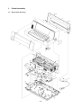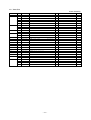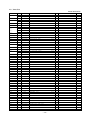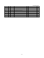
1
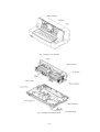
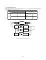
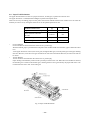
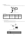
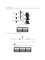
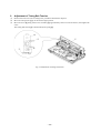
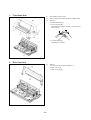
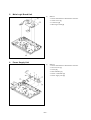
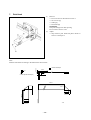
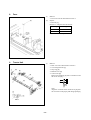
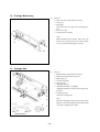
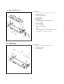
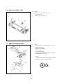
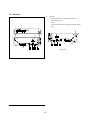
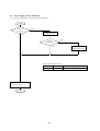
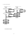
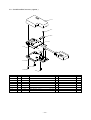
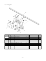
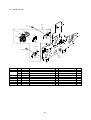
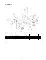
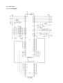
DOT MATRIX PRINTER
LC-7211
TECHNICAL MANUAL
[ THIRD EDITION ]
NOTICE
• All rights reserved. Reproduction of any part of this manual in any
form whatsoever, without STAR’s express permission is forbidden.
• The contents of this manual are subject to change without notice.
• All efforts have been made to ensure the accuracy of the contents
of this manual at the time of going to press. However, should any
errors be detected, STAR would greatly appreciate being informed of them.
• The above notwithstanding, STAR can assume no responsibility
for any errors in this manual.
© Copyright 1996 Star Micronics Co.,Ltd.
INTRODUCTION
This manual is an introduction to the LC-7211.
It is designed for use as a reference for periodic inspections and maintenance procedures to be executed by
service personnel. It is not intended for the general user. Users of this manual should have a basic knowledge
and understanding of the English language.
• This manual is divided into the following sections:
Chapter 1
Chapter 2
Chapter 3
Chapter 4
Chapter 5
Chapter 6
Chapter 7
• First edition
General Specifications
Theory of Operation
Adjustments
Parts Replacement
Maintenance and Lubrication
Troubleshooting
Parts List
: Dec. 1995
Second edition : Aug. 1996
Third edition
: Aug. 1997
1
2
3
4
5
6
7
CHAPTER 1
GENERAL SPECIFICATIONS
1.
General Specifications.......................................................................................... 3
2.
External Appearance and Composition ..............................................................5
3.
Control Panel .........................................................................................................7
4.
5.
6.
3-1.
Switch Combination Functions ............................................................................. 7
3-2.
EDS Mode Settings ................................................................................................. 8
Parallel Interface.................................................................................................... 9
4-1.
General Specifications ........................................................................................... 9
4-2.
Connector Signals .................................................................................................. 9
Serial Interface (optional) ................................................................................... 10
5-1.
General Specifications ......................................................................................... 10
5-2.
Connector Signals and Functional Descriptions............................................... 10
5-3.
DIP Switch Settings .............................................................................................. 11
EE-PROM Mode ................................................................................................... 12
6-1.
Outline ................................................................................................................... 12
6-2.
Explanation of Special Control Codes ................................................................ 12
6-3.
EE-PROM MAP ...................................................................................................... 13
6-4.
Rewriting the EE-PROM ....................................................................................... 16
1
1.
General Specifications
Printing System
Printing Speed
Print Direction
Print Head
Line Spacing
Character Matrix
Environment
Paper
Serial Impact Dot-Matrix
Pitch
Draft(cps/dpi)
NLQ(cps/dpi)
Pice (10cpi)
225/120H
56/240H
Elite (12cpi)
270/120H
67/240H
Condensed pica (17cpi)
191/240H
95/240H
Condensed elite (20cpi)
225/240H
112/240H
H:half-dot
Draft:
Bi-directional logic seeking
NLQ:
Uni-directional/bi-directional logic seeking (selectable)
Bit-Image:
Uni-directional/bi-directional logic seeking (selectable)
Number of pins:
9
Life:
200 million dots/pin (adjustment lever position 1 to 3)
100 million dots/pin (adjustment lever position 4 to 8)
1/6", 1/8"
7/72", n/72", n/216": software
Pitch
Draft
NLQ
Pica (10cpi)
9×11
18×23
Elite (12cpi)
9×9
18×19
Condensed Pica (17cpi)
9×11
18×12
Coodensed elite (20cpi)
9×9
18×10
Operating temperature: 41°F to 95°F (5°C to 35°C)
Storage temperature:
–22°F to 149°F (–30°C to 65°C)
Operating humidity:
30% to 80% (noncondensing)
Storage humidity:
20% to 90% (noncondensing)
Cut-sheet
Paper width:
5.5" to 12" / 140 to 305mm
Paper length:
5.5" to 11"/ 140 to 280mm
Paper weight (1-ply):
14 to 42 lbs / 52 to 156 g/m2 / 45 to 135 kg
Multi-part:
11 to 14 lbs / 40 to 52 g/m2 / 34 to 45 kg; pressure
sensitive paper
Total thickness: 0.020" / 0.5mm
Copies:
Original + 6
Fanfold
Paper width:
4.5" to 12" / 114 to 305mm
Paper weight (1-ply):
14 to 22 lbs / 52 to 81 g/m2 / 45 to 70 kg
Multi-part:
11 to 14 lbs / 40 to 52 g/m2 / 34 to 45 kg; pressure
sensitive paper
Total thickness: 0.02" / 0.5mm
Copies:
Original + 6
–3–
Interface
Ribbon Type
Ribbon Life
Power Supply
”
14
.57
0m
m
525
mm
20.6
7”
37
Options
230mm
Power Consumption
9.06”
Emulation
Labels
Backing sheet:
4.5" to 12" / 114 to 305mm
Thickness:
Backing sheet 0.0028" to 0.0035" / 0.07 to 0.09mm
Total thickness 0.0075" / 0.19mm max.
Envelope
#10
9.4 × 4.1 / 240 × 104mm
Standard Mode: EPSON ESC/P (9-pin)
IBM Mode: Proprinter III
Standard:
Centronics parallel
Option:
RS-232C serial
On-carriage, dedicated
Fabric monochrome ribbon (Black only)
Z9HD: Standard type
LZ9:
Long life type (option)
Z9HD: 2 million characters (ASCII draft)
LZ9:
4 million characters (ASCII draft)
120V AC +10%/–17%, 230V AC +14%/–13%; 50/60Hz (depending on country of
purchase)
10W during stand-by
31W during ASCII draft printing
SPC-8K Serial-To-Parallel Converter
Weight 16.1lbs/7.3kg
Fig. 1-1 External dimensions
–4–
2.
External Appearance and Composition
Front cover
Adjustment lever
Paper guide
Platen knob
Power switch
Interface connector
Control panel
Fig. 1-2 Front view of the Printer
Release laber
Fig. 1-3 Rear view of the Printer
–5–
Fig. 1-4 Front cover removed
Fig. 1-5 Diagram of internal layout
–6–
3.
Control Panel
3-1. Switch Combination Functions
BANK
SW
A
ROMAN
1
B
SANSERIF
COURIER
2
PRESTIGE
ORATOR
4
C
D
E
POWER
DRAFT
3
QUIET
5
F
6
MICRO FEED
QUIET
FONT
MODE
LF
ON LINE
FF
= Push
= Hold
Short test 2
Hex-Dump
Long test Short test 1
Dot-adjust mode
EDS mode
EDS mode
Aging mode
POWER-ON
Quiet
Tear off Set/Eject/Park Off-Line
ON-LINE
Font
Mode
Panel macro
Backward
LF/Set
On-Line
Form feed
Forward
Micro feed
Set TOF
Buffer clear and All reset
Auto loading position change mode
OFF-LINE
Bank
Switch
On/Off
Exit
Print
EDS MODE
Left
Right
Next
Exit
DOT ADJUSTMENT MODE
Paper
Loading
Backward
Foward
Cancel
Set
Save
Factory settings
AUTO LOADING POSITION CHANGE MODE
–7–
3-2. EDS Mode Settings
Bank
Switch
A
1
2
B
C
3
4
5
6
1
2
3
4
5
6
1, 2
3,4,5
D
E
F
6
1,2,3,4
1,2,3,4,5
1, 2, 3, 4, 5
Function
ON
Emulation
Character Table (CT) Standard / EPSON mode
IBM mode
RAM Usage
(Not used)
Paper Out Detector
(Not used)
Graphics Direction
Auto Tear-off (Long)
Line Spacing
Auto LF with CR
Zero Style
Strobe Timing
Print Mode
Draft
ON
(Not used)
OFF
Print Pitch
10cpi
ON
ON
12cpi
OFF ON
17cpi
ON
OFF
Quiet
Page Length
11"/Letter
ON
ON
ON
8"
OFF ON
ON
11.7"/A4
ON
OFF ON
12"
OFF OFF ON
8.5"/Letter
ON
ON
OFF
Code Page (CT=Graphics, IBM #1, #2)
#437
ON
ON
ON
ON
#850
OFF ON
ON
ON
#860
ON
OFF ON
ON
#861
OFF OFF ON
ON
#863
ON
ON
OFF ON
#865
OFF ON
OFF ON
#866
ON
OFF OFF ON
#3840
OFF OFF OFF ON
#3841
ON
ON
ON
OFF
#3843
OFF ON
ON
OFF
#3844
ON
OFF ON
OFF
#3845
OFF OFF ON
OFF
#3846
ON
ON
OFF OFF
#3847
OFF ON
OFF OFF
#3848
ON
OFF OFF OFF
#852
OFF OFF OFF OFF
International Character Set (CT=Italics)
U.S.A.
ON
ON
ON
ON
France
OFF ON
ON
ON
Germany
ON
OFF ON
ON
England
OFF OFF ON
ON
Denmark-1 ON
ON
OFF ON
Sweden
OFF ON
OFF ON
Italy
ON
OFF OFF ON
Spain-1
OFF OFF OFF ON
LQ Font Selection
Roman
ON
ON
ON
ON
Sanserif
OFF ON
ON
ON
Courier
ON
OFF ON
ON
–8–
OFF
Standard / EPSON
Graphics
IBM #2
Input Buffer
IBM
Italics
IBM #1
Download Buffer
Enabled
Disabled
Bi-directional
Disabled
1/6"
Disabled
Normal
Normal
Uni-directional
Enabled
1/8"
Enabled
Slashed
Reverse
ON
ON
NLQ
(Not used)
ON
ON
ON
20cpi
Proportional
OFF
ON
Disabled
ON
ON
ON
ON
ON
14"/Legal
10.5"/Executive
7.25"/Executive
3.5"
5.5"
ON
ON
ON
ON
ON
ON
ON
ON
ON
ON
ON
ON
ON
ON
ON
ON
#1001
#737
#851
#869
#928
#2001
#772
#774
#3001
#3002
#3011
#3012
#3021
#3031
#3041
ON
ON
ON
ON
ON
ON
ON
ON
ON
ON
ON
ON
OFF
OFF
OFF
OFF
ON
ON
OFF
Enabled
OFF
ON
OFF
ON
OFF
ON
OFF
OFF
ON
OFF
OFF
OFF
OFF
ON
ON
ON
ON
ON
OFF
OFF
ON
OFF
ON
OFF
ON
OFF
ON
OFF
ON
OFF
ON
OFF
ON
OFF
ON
ON
ON
OFF
OFF
ON
ON
OFF
OFF
ON
ON
OFF
OFF
ON
ON
OFF
ON
ON
ON
ON
OFF
OFF
OFF
OFF
ON
ON
ON
ON
OFF
OFF
OFF
ON
ON
ON
ON
ON
ON
ON
ON
OFF
OFF
OFF
OFF
OFF
OFF
OFF
OFF
OFF
OFF
OFF
OFF
OFF
OFF
OFF
OFF
OFF
OFF
OFF
OFF
OFF
OFF
Japan
Norway
Denmark-2
Spain-2
Latin America
Korea
Ireland
Legal
ON
OFF
ON
OFF
ON
OFF
ON
OFF
ON
ON
OFF
OFF
ON
ON
OFF
OFF
ON
ON
ON
ON
OFF
OFF
OFF
OFF
OFF
OFF
OFF
OFF
OFF
OFF
OFF
OFF
ON
ON
ON
ON
ON
ON
ON
ON
Prestige
Orator
OFF
OFF
OFF
OFF
ON
OFF
ON
ON
ON
ON
4.
Parallel Interface
4-1. General Specifications
Item
Interface
Synchronization System
I/F Protocol
Logic Level
Specifications
Centronics-compatible
Via externally supplied STROBE pulse
Using ACK and BUSY signals
Compatible with TTL level
ACK
t
4.1µs 4.1µs
t
t
t
Data
STROBE
(EDS B-6 : ON)
STROBE
(EDS B-6 : OFF)
BUSY
t : More than 0.5µs
Fig. 1-6 Timing Charts for Parallel Interface
4-2. Connector Signals
Pin
1
2
3
4
5
6
7
8
9
10
11
12
13
14
15
16
17
18
19~30
31
32
33
34~35
36
Name
STROBE
DATA0
DATA1
DATA2
DATA3
DATA4
DATA5
DATA6
DATA7
ACK
BUSY
PAPER
SELECT
AFXT
SIGNAL GND
CHASSIS
+5V
GND
RESET
ERROR
EXT GND
SELECT IN
Function
Goes low for ≥ 0.5µs when active.
These signals represent information for the 1st through 8th bit of
parallel data, respectively. Each signal is HIGH when data is logical 1,
and LOW when logical 0.
10µs low to acknowledge receipt of data.
Printer sets line low when ready to receive data.
High when paper runs out.
High when printer is on-line.
Printer ignores this signal.
Not used.
Signal ground
Chassis ground (isolated from signal ground)
+5V DC output from printer
Twisted pair ground return
Printer is reset when this signal goes low.
Low when printing cannot continue due to error.
External ground
Not used
Printer ignores this signal.
–9–
5
Serial Interface (optional)
When using the serial interface, the optional Serial-Parallel Converter must be connected to the printer.
5-1. General Specifications
Item
Interface
Synchronization System
Baud rate
Word length
Start bit:
Data bit:
Parity bit:
Stop bit:
Signal polarity
Mark:
Space:
Handshaking
Specifications
RS-232C level
Asynchronous
150 - 19,200 bits per second (BPS) [selectable]
150, 300, 600, 1200, 2400, 4800, 9600, 19200 BPS
1 bit
7 or 8 bits (selectable)
Odd, Even or None (selectable)
More then 1bit length
Logic “1” (–3V to –15V)
Logic “0” (+3V to +15V)
DTR
XON /XOFF
ETX/ACK
8KB (standard)
Data buffer
5-2. Connector Signal and Functional Descriptions
Pin No.
1
2
3
4
Signal name
GND
TXD
RXD
RTS
Direction
—
OUT
IN
OUT
5
CTS
—
6
7
8~10
NC
GND
NC
—
11
RCH
OUT
12~19
20
21~25
NC
DTR
NC
OUT
Function
Printer chassis ground.
This pin carries data from the printer.
This pin carries data to the printer.
Always space.
This signal is space when the computer is ready to send data.
The printer does not check this pin.
Unused.
Signal ground.
Unused.
The printer sets this signal to space when it is ready to receive data.
This line carries the same signal as pin 20.
Unused.
The printer sets this signal to space when it is ready to receive data.
Unused.
– 10 –
5-3. DIP Switch Settings
Switch
1
2
3
4
5
6
7
8
ON
8 data bits
No parity
OFF
7 data bits
Parity checked
Handshaking protocols – see table below
Odd parity
Even parity
Data transfer rate – see table below
All switches are set to ON before the printer leaves the factory.
Protocol
DTR mode
XON /XOFF mode
ETX/ACK mode
Baud rate
150
300
600
1200
2400
4800
9600
19200
Switch 6
OFF
OFF
OFF
OFF
ON
ON
ON
ON
– 11 –
Switch 3
ON
ON
OFF
Switch 4
ON
OFF
ON
Switch 7
OFF
OFF
ON
ON
OFF
OFF
ON
ON
Switch 8
OFF
ON
OFF
ON
OFF
ON
OFF
ON
6.
EE-PROM mode
6-1. Outline
These settings can be changed in the EE-PROM mode by writing data directly to the EE-PROM on the main logic board:
Setting EE-PROM mode
• Send <ESC><SUB>(09)H command.
Canceling EE-PROM mode
• Initialize the printer by sending <ESC>@
6-2. Explanation of special control codes
<ESC>@
Exits printer from EE-PROM mode and initializes the printer.
<ESC>M@
Returns all data in the EE-PROM to the factory settings. After the buffer is cleared, the buzzer sounds. If
the printer is powered off before the buzzer sounds, all data in the buffer is not cleared.
If all data is not cleared from the buffer, operation is not guaranteed. Be sure to allow the buzzer
to sound before you turn the printer off!
<ESC>MWn
Code
<ESC>MW0 <data>
<ESC>MW1nm
<ESC>MW2<data>
Function
Stores data into entire area of EE-PROM.
Stores data (m) into the address (n)
Stores auto-start software data into
EE-PROM.
Address Capacity
00H-7FH 128bytes
nH
1 byte
2CH-54H 41bytes
55H-7DH 41bytes
• The data (m) used in the commands above are stored in the specified address in order (n).
• When the data to be stored exceeds the specified capacity, subsequent data are ignored.
• Data are stored in the EE-PROM according to the memory map. (See section 3. EDS mode setting and
6-3. EE-PROM Map.)
• After all data are stored, a beep indicates the completion of storage.
• If the printer is powered off during data storage, data stored before power off are valid, but subsequent
operation of the printer is not guaranteed.
Do not power off the printer while data is being stored!
<ESC>MR Dumps all data in the EE-PROM to a hard copy.
For an example of using these control codes, see section 6-4. For the corresponding EE-PROM addresses, see the
EE-PROM memory map in section 3-2. EDS mode setting and 6-3 EE-PROM Map.
– 12 –
6-3. EE-PROM MP
Address
00H
Function
EDS setting
FFH
Bit Function
b0 Emulation
Character Table
b1
Standard / EPSON mode
IBM mode
b2 RAM Usage
b3 (Not used)
b4 Paper out Detector
b5 (Not used)
01H
1
Graphics
IBM #2
Input Buffer
—
Enabled
—
Italics
IBM #1
Download Buffer
—
Disabled
—
FFH
Function
Graphics Direction
Tear-off
Line Spacing
Auto LF with CR
Zero Style
Strobe Timing
1
Bi-directional
Disabled
1/6"
Disabled
Normal
Normal
0
Uni-directional
Enabled
1/8"
Enabled
Slashed
Reverse
EDS setting
FFH
Print Mode
Function
b0
Draft
1
NLQ
1
Print Pitch
Function
b2
10cpi
1
12cpi
0
17cpi
1
20cpi
0
Proportional 1
b1
1
0
Bit Function
b5 Quiet
03H
0
STANDARD/EPSON IBM
EDS setting
Bit
b0
b1
b2
b3
b4
b5
02H
Factory data
1
Disabled
b3
1
1
0
0
1
b4
1
1
1
1
0
0
Enabled
EDS setting
FFH
Page Length
Function
11"/Letter
8"
11.7"/A4
12"
8.5"/Letter
b0
1
0
1
0
1
b1
1
1
0
0
1
b2
1
1
1
1
0
b3
1
1
1
1
1
Function
14"/Legal
10.5"/Executive
7.25"/Executive
3.5"
5.5"
– 13 –
b0
0
1
0
1
0
b1
1
0
0
1
1
b2
0
0
0
1
1
b3
1
1
1
0
0
Address
04H
Function
Factory data
EDS setting
IBM Code Page (Character Table=Graphics, IBM#1, #2)
Function
b0 b1 b2 b3 b4
Function
#437
1 1 1 1 1
#3841
#850
0 1 1 1 1
#3843
#860
1 0 1 1 1
#3844
#861
0 0 1 1 1
#3845
#863
1 1 0 1 1
#3846
#864
0 1 0 1 1
#3847
#866
1 0 0 1 1
#3848
#3840
0 0 0 1 1
#852
International Character Set (Character Table=Italics)
Function
U.S.A.
France
Germany
England
Denmark-1
Sweden
Italy
Spain-1
05H
b1
1
1
0
0
1
1
0
0
b2
1
1
1
1
0
0
0
0
b3
1
1
1
1
1
1
1
1
b4
1
1
1
1
1
1
1
1
Function
Japan
Norway
Denmark-2
Spain-2
Latin America
Korea
Ireland
Legal
b0 b1 b2
1 1 1
0 1 1
1 0 1
0 0 1
1 1 0
0 1 0
1 0 0
0 0 0
b3 b4
0 1
0 1
0 1
0 1
0 1
0 1
0 1
0 1
b0 b1 b2
1 1 1
0 1 1
1 0 1
0 0 1
1 1 0
0 1 0
1 0 0
0 0 0
b3 b4
0 1
0 1
0 1
0 1
0 1
0 1
0 1
0 1
EDS setting
NLQ Font Selection
Function
Roman
Sanserif
Courier
06H
07H
08H
09H
0AH
0BH
0CH
0DH
0EH
0FH
10H
11H
12H
13H
14H
15H
16H
17H
18H
19H
b0
1
0
1
0
1
0
1
0
FFH
b0
1
0
1
FFH
b1
1
1
0
Misalignment correction
Misalignment correction
Misalignment correction
Misalignment correction
Misalignment correction
Misalignment correction
Misalignment correction
Misalignment correction
Misalignment correction
Misalignment correction
Misalignment correction
Misalignment correction
Misalignment correction
Misalignment correction
Misalignment correction
Misalignment correction
Misalignment correction
Misalignment correction
Misalignment correction
Misalignment correction
b2
1
1
1
b3
1
1
1
b4
1
1
1
Function
Prestige
Orator
Multi-part Mode
Multi-part Mode
Multi-part Mode
Multi-part Mode
Multi-part Mode
Multi-part Mode
Multi-part Mode
Multi-part Mode
Multi-part Mode
Multi-part Mode
– 14 –
b0 b1 b2 b3 b4
0 0 1 1 1
0 0 0 1 1
60 DPI (F)
72 DPI (F)
80 DPI (F)
90 DPI (F)
120 DPI (H) Text
120 DPI (H) Bit-image
120 DPI (F)
144 DPI (H)
240 DPI (H) Text
240 DPI (H) Bit-image
60 DPI (F)
72 DPI (F)
80 DPI (F)
90 DPI (F)
120 DPI (H) Text
120 DPI (H) Bit-image
120 DPI (F)
144 DPI (H)
240 DPI (H) Text
240 DPI (H) Bit-image
80H
80H
80H
80H
80H
80H
80H
80H
80H
80H
80H
80H
80H
80H
80H
80H
80H
80H
80H
80H
Address
Function
Factory data
1AH, 1BH
Top Margin in Auto-loading Tractor
1CH, 1DH
Top Margin in Auto-loading Friction
1EH~21H
Macro Set EPSON
48H
00H
48H
00H
00H
22H~25H
Macro Set IBM
00H
00H
26H, 27H
TEAR OFF (Short)
28H, 29H
TEAR OFF (Long)
2AH, 2BH
Initial Condition Area
2CH~54H
Auto Start Area EPSON (41 byte)
00H
00H
80H
00H
80H
FFH
FFH
00H
Auto Start Area IBM (41 byte)
00H
00H
FF Control Code (Space 00H / Null 0FH)
EE-PROM Check Code
00H
00H
01H
55H~70H
7EH
7FH
– 15 –
6-4. Rewriting the EE-PROM
Follow this procedure to rewrite the EE-PROM.
(1)
Turn the printer on.
(2)
Load a BASIC disk in the computer.
(3)
Turn the computer on.
(4)
Set a sheet of paper in the printer, and press the ON LINE switch.
(5)
Enter the program listed below and run the program.
10 LPRINT CHR$(27);CHR$(26);CHR$(&H09)
20 LPRINT CHR$(27);”MW1";CHR$(&H01);CHR$(&HFB)
30 LPRINT CHR$(27);”MR”
BASIC Program Code
What It Does
10 LPRINT CHR$(27);CHR$(26);CHR$(&H09) Enters the EE-PROM mode.
20 LPRINT CHR$(27);”MW1";
Starts rewriting the EE-PROM.
CHR$(&H01);
Address data from &H01 will show
EDS mode from the EE-PROM memory
map.
CHR$(&HFB)
Data from &HFB will change the Line
spacing from 1/6" to 1/8".
30 LPRINT CHR$(27);”MR”
Dumps all EE-PROM data to hexadecimal.
(6)
To complete the setting, turn the printer off.
– 16 –
CHAPTER 2
THEORY OF OPERATION
1.
Block Diagram (Main logic Board) .....................................................................19
2.
Main Logic Board ................................................................................................20
2-1.
General Flow Chart ............................................................................................... 20
3.
Power Supply Circuit .......................................................................................... 21
4.
Mechanisms .........................................................................................................22
4-1.
Print Head Mechanism ......................................................................................... 22
4-2.
Print Head Carrying Mechanism ......................................................................... 23
4-3.
Ink Ribbon Feed Mechanism ............................................................................... 24
4-4.
Paper Feed Mechanism ........................................................................................ 25
4-5.
Detectors ............................................................................................................... 26
2
1.
Block Diagram (Main logic Board)
The block diagram of this printer is shown in Fig. 2-1.
Data (From Host Computer)
Print head
Parallel
interface
LED
Driver
Carriage
motor
Masked ROM
2M
CPU
Detectors
UVE-PROM
512K
Driver
Paper feed
motor
EE-PROM
RAM
Gate array
Switch
Control
panel board
Power
supply unit
AC Power
Main logic board
Printer
mechanism
Fig. 2-1 Block Diagram
(1)
(2)
(3)
(4)
Main Logic Board
This board receives data from the host computer and stores it in the RAM in the order it arrives. The CPU on this
board reads the data from the RAM, and edits it according to the program stored in the ROM.
When editing is completed, various drive signals from the CPU are sent to the printer mechanism to perform
printing.
Explanation
• CPU TMP90C041
Controls this printer.
• UVE-PROM 27512 512K bit
Contains the program which executes control of the printer. UVE-PROM is not provided with some versions of the
software.
• Masked ROM 2M bit
Contains the character font and the program.
• EE-PROM KM93C46 64 × 16 bits
Contains the data (EDS data and so on) in the memory switch.
• RAM 256K bytes
Used as a stack area, work area and data buffer of the CPU.
• Parallel interface
• Gate array (custom IC)
Inputs/outputs several signals.
• Driver
The data edited by the CPU and gate array are sent to the printer mechanism after conversion to the signal for the
print head drive and motor drives.
Control panel board
Panel circuit for manual control of the printer.
Printer Mechanism
Consists of a print head, carriage motor, paper feed motor, and detectors.
Power Supply Unit
Converts AC power to 33VDC and 5VDC.
– 19 –
2.
Main Logic Board
2-1. General Flow Chart
The flow chart below shows you the general flow of editing and printing operations.
POWER ON
Initialization
Ready state
Read data
Control
code?
No
YES
Control code
processing
NO
Print?
Data
storage
(Line buffer determination)
YES
Data processing
or printing
NO
(Print out of data)
Return?
YES
Return action
Fig. 2-2 General Flow Chart of Editing and Printing
– 20 –
3.
Power Supply Circuit
A ringing choke converter type circuit is used with a dropper type circuit in the power supply unit, fulfilling the input and
output conditions described in the chart below.
Voltage Range
Max. Current Output
Service
110VAC, 120VAC
1.0 A
Input
220VAC to 240VAC
0.6 A
5 VDC ±5%
0.4 A
For logic circuit
drive, for motor
holding.
Output
For print head
33 VDC ±5%
1.25A
drive, for motor
drive.
Input
110VAC
120VAC
220VAC
230VAC
240VAC
Noise filter
circuit
In rush current
protection
circuit
Switching
section
(Transistor Q1)
Ringing choke
converter.
Ringing
choke
converter
Output
33V DC
Dropper
circuit
Output
5V DC
PC1
Voltage
reference
Photo-Coupler
Fig. 2-3 Power Supply unit block diagram
– 21 –
Dropper
Rectifier
circuit
Transformer T1
Control
circuit
Circuit Type
4.
Mechanism
4-1. Print Head Mechanism
The print head consists of 9 needle wires and 9 print solenoids.
The following explains how each needle wire operates during printing.
(1) When the print solenoid is energized, the clapper is attracted by the iron core and the needle wire is driven toward
the platen.
(2) This needle wire hits the platen via the ink ribbon and paper. A single dot is printed on the paper.
(3) When the print solenoid is de-energized, the needle wire is returned to its original position by rebound energy and
spring and clapper holder (leaf spring) force.
Paper
Paper guide
Ink ribbon
Spring
Stopper
Needle wire
Guide
Subguide
Clapper holder
Iron core
Print solenoid
Clapper
Fig. 2-4 Outline of Print Head Mechanism
– 22 –
Platen
4-2. Print Head Carrying Mechanism
The print head carrying mechanism consists of a carriage, timing belt, carriage motor, and home position detector.
Carriage
The carriage is supported horizontally by the carriage stay and rear angle. The carriage moves from side to side with
the print head mounted above it. A timing belt is clamped to the base of the carriage and a shield plate is mounted
at the base for home position detection.
Timing Belt
The timing belt is suspended between the timing pulley of the carriage motor and the timing pulley of the tension
lever. The timing belt maintains a constant tension.
The timing belt is also clamped to the base of the carriage so that it can move the carriage accurately with driving
force from the carriage motor.
Carriage Motor
The carriage motor is a HB (Hybrid)type, 4-phase, 192-pole pulse motor driven by pulse signals from the control
circuit. The rotational rate depends on the number of pulses per unit time. By varying this rotational rate (carriage
carrying rate), the size of the horizontal letters can be changed in each print mode.
Fig. 2-5 Print Head Carrying Mechanism
– 23 –
4-3. Ink ribbon feed mechanism
The ink ribbon feed mechanism is linked to the print head carrying mechanism so the ink ribbon always winds
automatically in the same direction while the carriage moves left and right.
The movement of the carriage along the serrated edge of the rear angle of the printer mechanism drives the idler gear. The
rotation of the idler gear is conveyed sequentially to the gears that work and wind the ribbon. The carriage has a clutch
lever that keeps the direction of the cassette gear rotation constant, regardless of the direction of the idler gear rotation
as the carriage moves left and right.
Cassette Gear
Gear of The Clutch Lever
Idler Gear
Fig. 2-6 Ribbon feed mechanism
– 24 –
4-4. Paper Feed Mechanism
The paper feed mechanism consists of a paper feed motor, an idler gear, a platen and a traction unit.
The paper feed motor is a PM (Permanent Magnet) 4-phase and 48 pulse motor.
There are two ways of feeding paper into the printer: the friction method and the tractor method. You can select the
method you want to use by setting the release lever on the optional push tractor unit.
Position of release lever
Engaement of the PF idler gear
Status of the PF roller and
PF roller
Release lever position detector
Paper feeding method
•
•
[1]
[2]
Not linked
Linked
Pressed
Not
Open
Closed
Friction
Tractor
Friction Method
Friction method is selected when the release lever is position [1].
With this method, paper is pressed between the platen roller and the holder roller therefore, paper is fed as the rollers
turn.
As the paper feed motor is driven, the motor gear, through the idler gear, turns the platen gear in the paper feeding
direction. However, since the tractor gear and the tractor clutch are not linked at this time, the tractor unit will not
be driven.
Tractor Method
Tractor method is selected when the release lever is position [2].
Paper feeding is facilitated by rotation of the sprocket pin of the tractor unit. When the tractor method is selected,
the PF idler gear is linked to the PF idler gear, enabling the drive force generated by the paper feed motor to be
transferred to the tractor unit via the idler gear.
Fig. 2-7 Paper Feed Mechanism
– 25 –
4-5. Detectors
(1)
Print head temperature detectors
The A/D converter in the CPU detects the print head temperature at power on and before each line begins to print.
+5V
+5V
Printer head
Vref
Thermistor
R1
AN0
R2
CPU
Fig. 2-8 Printer head temperature detector circuit
Control Method
Print
Error stop (thermistor open)
Normal print
Unidirectional print
Print stop
Error stop (thermistor closed)
(2)
A/D Conversion Value
POINT
0-5
6-213
214-221
222-251
252-255
AN Voltage
V
0.00
0.00-4.35
4.35-4.48
4.48-4.83
Over 5.00
Temperature
°C
~120
120-130
Over 130
-
Home Position Detector
A photo-interrupter is used in the home detector on the printer.
ON/OFF signals are generated according to the position of the carriage. (Shield plate mounted at the base of the
carriage.) The printing position is determined by these signals.
+5V
Detecting
signal
R1
R2
C1
+5V
R3
Fig. 2-9 Carriage home position detector circuit
Control Method
Output (V)
5
0
Decision
in home position (with shield plate)
not in home position (without shield plate)
– 26 –
(3)
Paper end Detector
The paper end Detector is located in the paper chute unit. The A/D converter in the CPU detects the presence or
absence of paper.
+5V
+5V
R2
R1
Detecting
signal
Friction
Detecting
signal
R5
R4
R3
Skew
R8
R7
R6
Detecting
signal
Tractor
R9
Fig. 2-10Paper end detector circuit
Control Method
Output
(V)
(4)
Detection
0
No paper
5
Paper present
Release lever switch and lever switch Adjustment
+5V
R2
R1
Detecting
signal
Leaf switch
Fig. 2-11 Release lever switch circuit and Adjustment lever switch circuit
Control Method
Output
(V )
Release
Lever SW
Adjustment
Lever SW
0
Tractor
Normal mode
5
Friction
Multi-part mode
– 27 –
CHAPTER 3
ADJUSTMENTS
This printer has undergone various adjustments so that it will attain a given standard of performance.
In this chapter, a brief explanation is given of the methods for making adjustments.
Follow the instructions when performing maintenance inspections or when replacing parts to correct
malfunctions.
1.
Adjustment of Gap Between Print Head and Platen ........................................ 31
2.
Adjustment of Timing Belt Tension ................................................................... 32
3
1.
Adjustment of Gap Between Print Head and Platen
Remove the front case unit ,rear angle and ribbon holder [1] according to the procedures described in chapter 4.
(Fig. 3-1)
(2) Install rear angle [2].
(3) Set adjusting lever [3] to the second position from the bottom. (Fig. 3-1)
(4) Position the center of the carriage unit [4] 55 mm from the left end of the platen assy [5]. (Fig. 3-2)
(5) Measure the gap between platen [5] and head [6] using a gauge [7] . (Fig. 3-3)
(6) Use adjusting bushing L [8] to adjust the gap to between 0.34 and 0.40 mm. (Fig. 3-4)
(7) Position the center of the carriage unit [4] 55 mm from the right end of the platen assy [5], then measure the gap
and adjust it in the same way.
(8) Repeat steps (4) to (6) to measuring the gap and readjusting as necessary.
(9) Remove the rear angle [2].
(10) Install the ribbon holder [1], rear angle [2] and front case.
(1)
[4]
L
R
[5]
55mm
Fig. 3-1 Mechanism
55mm
Fig. 3-2 Positioning the carriage unit
gap
[7]
+
[6]
gap
–
(L)
–
[8]
+
(R)
[5]
Fig. 3-3 Gap measurement
Fig. 3-4 Adjusting bushing
– 31 –
2.
Adjustment of Timing Belt Tension
(1)
(2)
(3)
Remove the front case unit according to the procedures described in chapter 4.
Move the carriage unit [1] up to the extreme right position.
Move the screw [3] fixing tension lever assembly [2] approximately 1mm to loosen the tension, then tighten the
screw.
The timing belt tension [4] is determined by the spring [5].
Fig 3-5 Adjustment of timing belt tension
– 32 –
CHAPTER 4
PARTS REPLACEMENT
This chapter explains disassembly and reassembly of the printer. Note the following regarding disassembly
and reassembly.
1. Disconnect the printer from the wall outlet before servicing it.
2. Assy is the reverse of disassembly unless otherwise specified.
3. After reassembly, coat the screw heads with locking sealant.
4. Lubrication information is not provided in this chapter. Refer to section 2 in chapter 5.
1.
Front Case Unit.................................................................................................... 35
2.
Rear Case Unit ..................................................................................................... 35
3.
Ribbon Holder ......................................................................................................36
4.
Printer Mechanism ..............................................................................................36
5.
Main Logic Board Unit ........................................................................................ 37
6.
Power Supply Unit ...............................................................................................37
7.
Print Head ............................................................................................................ 38
8.
Fuse ...................................................................................................................... 39
9.
Tractor Unit .......................................................................................................... 39
10. Carriage Motor Assy ........................................................................................... 40
11. Carriage Unit ........................................................................................................40
12. Paper Feed Roller A ............................................................................................ 41
13. Frame Holder .......................................................................................................41
14. Paper Guide Assy ................................................................................................42
15. Platen Assembly.................................................................................................. 42
16. Paper Feed Motor Assy ......................................................................................43
17. Paper Path Change Plate .................................................................................... 43
18. Detector ................................................................................................................44
– 33 –
4
1.
Front Case Unit
(1)
(2)
(3)
Turn off the power switch.
Remove the power cord from the AC output socket.
Remove
• Platen knob unit [1]
• Front case unit [2]
Detach the five hooks marked A using the tool
shown below.
• Control board [3]
Detach the two hooks.
2.
Rear Case Unit
(1)
– 35 –
Remove
• Front case unit as described above 1.
• Four screws [1]
• Rear case unit [2]
3.
4.
Ribbon Holder
(1)
Remove
• Front case unit as described in section 1.
• Two screws [1]
• Rear angle [2]
• Ribbon holder [3]
Center the carriage unit, tile it, then remove the
ribbon holder.
(1)
Remove
• Four screws [1]
• Four connectors [2]
• Cable [3]
• Printer mechanism [4]
Printer Mechanism
– 36 –
5.
6.
Main Logic Board Unit
(1)
Remove
• Printer mechanism as described in section 4.
• Three screws [1]
• Connector [2]
• Main logic board [3]
(1)
Remove
• Printer mechanism as described in section 4.
• Seven screws [1]
• Screw [2]
• Switch holder [3]
• Power cord holder [4]
• Power supply unit [5]
Power Supply Unit
– 37 –
7.
Print Head
(1)
(2)
Remove
• Front case unit as described in section 1.
• Two screws [1]
• Cable [2]
• Print head [3]
WARNING
The print head gets hot after printing.
Do not touch it until it cools.
Adjust
• Gap between print head and platen. Refer to
section 1 of Chapter 3.
Note:
Fold the head cables according to the dimensions shown below.
19±1
10±1
Cat size (Double-sided tape)
0.5±0.5
— Double-sided tape
163±1
85±0.5
468±1
90°±1
108.5±1
21±1
90°±1
: mm
– 38 –
8.
Fuse
(1)
(2)
Remove
• Front case unit as described in section 1.
Inspect
• Fuse F1 [1]
Defective → Replace fuse as follows:
AC voltage
110/120V
220V/240V
Fuse Type
5TT2A-250V
215-1A-250V
New fuse blown → Inspect circuit
9.
Tractor Unit
(1)
Remove
• Rear case unit as described in section 2.
• Two hexagonal nuts [1]
• Stop ring [2]
• Release lever [3]
• Tractor unit [5]
Push tractor bushing [4] with a screwdriver and
lift tractor unit [5].
B
Note:
Align the “∆” mark on the release lever [3] with
the “∆” mark on the paper path change plate [6].
– 39 –
10. Carriage Motor Assy
(1)
Remove
• Rear case unit as described in section 2.
• Screw [1]
• Spring [2]
Set tension lever assy [3] in the unlocked position.
• Two screws [4]
• Carriage motor unit [5]
Note:
When assembling the carriage motor assy, the
tension lever assy [3] must be secured with the
screw [1] when the spring [2] is in place.
11. Carriage Unit
(1)
Remove
• Ribbon holder as described in section 3.
• Print head as described in section 8.
• Head cable [1]
• Ground spring [2]
• Stop ring [3]
• Adjusting gear [4]
• Adjusting bushings L, R [5] [6]
Adjusting bushings L/R can be removed by turning them.
• Carriage unit [7]
Center the carriage unit.
Note:
Move the carriage unit to the center position, then
align the “∆” mark of adjusting gear [4] with the
“∆” mark of adjusting lever [8].
– 40 –
12. Paper Feed Roller Assy
(1)
Remove
• Carriage unit as described in section 11
• Four springs [1], [2], [6]
• Four stop rings[7]
• Two gears [3]
• Two plain washer [4]
• Tow paper feed roller Assy [5]
(1)
Remove
• Rear angle [1]
• Carriage motor unit [2] as described in section 8
• Home position detector [3]
• Four roll pins [4]
• Frame holder [5]
13. Frame Holder
Note:
Roll pins [4] should not be used again once they
have been removed. Always use new ones.
– 41 –
14. Paper Guide Assy
(1)
Remove
• Paper feed roller Assy as described in section 12.
• Three screws [1]
• Frame support (R) [2]
• Stop ring [3]
• Platen gear [4]
• Gear [5]
• Frame holder as described in section 13.
• Four screws [6]
• Two screws [7]
• Two washers [8]
• Paper guide assy [9]
Note:
Gears [4],[5] should not be used again once it has
been removed. Always use a new one.
15. Platen Assy
(1)
– 42 –
Remove
Paper guide assy as described in section 14.
• Two stop rings [1]
• Platen assy [2]
16. Paper Feed Motor Assy
(1)
Remove
Platen assy as described in section 15.
• Two screws [1]
• Paper feed motor assy [2]
(1)
Remove
• Paper feed roller A as described in section 12.
• Right stop ring [1]
• Right release shaft [2]
Push inwards.
• Left release shaft [2]
Pull the shaft outwards until the slot is exposed.
• Paper path change plate [3]
17. Paper Path Change Plate
Note:
Align the “∆” mark on the paper path change plate
with the “∆” mark on the release gear.
– 43 –
18. Detector
(1)
[1]
Remove
• Paper guide assy as described in section 14.
• Four detectors [1]
Note:
Secure the lead wires at one point using fasteners
[2] .
[1]
[2]
[1]
Solder side
– 44 –
CHAPTER 5
MAINTENANCE AND LUBRICATION
1.
2.
Maintenance ......................................................................................................... 47
1-1.
Cleaning ................................................................................................................ 47
1-2.
Checks ................................................................................................................... 47
Lubrication ........................................................................................................... 48
2-1.
Lubricant ............................................................................................................... 48
2-2.
Lubricating Method .............................................................................................. 48
2-3
Lubricated Areas .................................................................................................. 48
5
1.
Maintenance
In order to maintain the optimum performance of this printer and to prevent trouble, maintenance must be carried out
according to the following items.
1-1. Cleaning
(1)
(2)
Removal of dirt
Wipe off dirt with a soft cloth soaked in alcohol or benzine.
*Note: Do not use thinner, trichlene or ketone solvents because they may damage plastic parts. Also during
cleaning, be careful not to moisten or damage electronic parts, wiring, or mechanical parts.
Removal of dust, pile, etc.
Vacuum cleaning (with an electric cleaner) is preferred. Remove all dust, etc., inside the printer.
*Note: After cleaning, check the oil level. If it is not adequate due to cleaning, replenish it.
1-2. Checks
Checks must be carried out at two levels: a “daily check” which the operator can easily carry out during operation, and
a “periodic check” which an expert should carry out.
(1) Daily check
When the printer is used on a daily basis, check that the printer is used properly. Make sure that the printer is
operating under the best conditions.
• Is any paper stuck in the paper box or printer case?
• Is the cartridge ribbon set at the right position?
• Is there any foreign matter inside the printer? (Remove if any.)
• Is the print head getting excessively dirty?
(2) Periodic check
After 6 months or printing 1 million lines, the periodic check and lubrication must be carried out.
• Check for deformation of springs.
• Check the gap between the platen and the print head.
• Remove dust, dirt, etc., around the detectors.
– 47 –
2.
Lubrication
Lubrication is very important to maintain optimum performance and to prevent trouble.
2-1. Lubricant
The type of lubricant greatly affects the performance and durability of the printer, especially in a low temperature
environment. We recommend use of the grease and lubrication oils listed below for this printer
Type of oil
Product name
Maker
Grease
MOLYKOTE EM-30L
DOW CORNING ASIA LTD
Lubricant
Mobil 1
Mobil oil
2-2. Lubricating Method
When lubrication is carried out in assembly and disassembly, wash parts well to remove dust and dirt before lubrication.
Lubrication must be carried out regularly once every 6 months or after 1 million lines have been printed. Lubrication is
necessary irrespective of the regular lubrication whenever lubricant becomes deficient after cleaning or whenever parts
have been disassembled or replaced.
2-3. Lubricated Areas
NO.
[1]
[2]
[3]
[4]
[5]
[6]
[7]
[8]
[9]
[10]
[11]
[12]
[13]
[14]
[15]
[16]
[17]
[18]
[19]
LubricationProduct
Rubbing surfaces of pully bushing B,Timing pulley and Shaft
Rubbing surfaces of Release lever and Frame
Rubbing surfaces of Release lever spring and Frame
Rubbing surfaces of Adjusting lever and Frame
Rubbing surfaces of Springs and Paper feed roller B
Rubbing surfaces of Carrige stay
Rubbing surfaces of Gear 32x0.5 and Shaft
Rubbing surfaces of Idler gear 16x72x0.5 and Shaft
Rubbing surfaces of PF roller assy and Roller holder L.R
Rubbing surfaces of Paper feed loller B and Roller holder L.R
Rubbing surfaces of Platen washer and Stopring
Rubbing surfaces of Gear cover and Shaft
Rubbing surfaces of Idler assy and Gear cover
Rubbing surfaces of Ribbon cassette gear and Gear cover
Rubbing surfaces of Gear,idler and Shaft
Rubbing surfaces of Rear loller and Shaft
Rubbing surfaces of Tractor shaft and Release lever
Rubbing surfaces of Tractor shaft
Rubbing surfaces of Gear and Shaft
– 48 –
Name
EM-30L
EM-30L
EM-30L
EM-30L
EM-30L
Mobil 1
EM-30L
EM-30L
EM-30L
EM-30L
EM-30L
EM-30L
EM-30L
EM-30L
EM-30L
EM-30L
EM-30L
EM-30L
EM-30L
Fig. 5-1 Lubricated Areas (printer mechanism)
– 49 –
Fig. 5-2 Lubricated Areas (Carriage unit )
[17]
[18]
20
mm
10
mm
[18]
Fig. 5-3 Lubricated Areas (tractor unit)
– 50 –
10
mm
10
mm
Fig. 5-4 Lubricated Areas (Frame R unit)
– 51 –
CHAPTER 6
TROUBLESHOOTING
1.
Troubleshooting Procedures ............................................................................. 55
2.
Unit Replacement Priority Chart ........................................................................ 56
3.
Repair by Unit Replacement............................................................................... 57
4.
Repair by Parts Replacement ............................................................................. 63
4-1.
Does not Operate at All with Power on............................................................... 63
4-2.
Power Supply Circuit Abnormal .......................................................................... 64
4-3.
Defective Motor Operation ................................................................................... 65
4-4.
Defective Print Head Operation ........................................................................... 66
4-5.
Defective Interface Operation .............................................................................. 67
6
1.
Troubleshooting Procedures
Troubleshooting is never easy because various problems arise depending upon the particular location of the breakdown.
The following procedures should be taken in making repairs.
(1)
The first method is to make repairs through unit replacements. The two display codes appearing in the flow chart
are defined as follows: 1) indicates main logic board replacement; and 2) indicates printer mechanism replacement,
to be carried out if the problem has not been corrected.
1)
Main Logic Board Replacement
2)
Printer Mechanism Replacement
Check again at this time whether the replaced unit is malfunctioning. (This is done to rule out trouble caused by improper
contact of connectors.)
Replaceable units consist of the following:
• Power supply unit
• Main logic board
• Printer mechanism
• Control panel board
In replacing these units, always refer to the unit replacement priority chart.
(2) The second method is to make repairs by parts replacement to replace defective elements inside a particular unit.
(Note 1) Before starting to repair, be sure to check visually the contact of the connector and the mounting of the IC in
the IC socket.
(Note 2) Always turn off power source and remove power plug before replacing any units or parts.
(Note 3) All check items shown in the flow chart must be checked. Otherwise, newly mounted parts or units may become
damaged.
(Note 4) If, in the process of making repairs, there is any confusion about proper procedures, restart the job from the
beginning.
(Note 5) Be careful to avoid injury from static electricity when handling ICs and main logic board.
– 55 –
2.
Unit Replacement Priority Chart
Error indication
Interface related and others
Detector
related
Print head
related
Motor related
Operation related
Category
Problem
Details
Specific display
lamp only will
not glow
Specific switch
only cannot be
input
Buzzer does not
sound (sound
volume
inadequate)
Strange sounds
during operation
No motor
holding power
(power very
weak)
Dots skipped
Print is too light
Ink ribbon
entanglement
(wire sticks out)
Absence of paper
not detected
Lever position
not detected
Incorrect printing
Ink ribbon not
forwarded
No operation at
EDS setting
Faulty operation
when power is
turned on/off
Abnormal motor
operating speed
(slow)
Fuse blown
during operation
Error detection of
head temperature
Carriage motor
error
Paper handling error
S. W. I error
EE-PROM &
RAM error
Watch dog timer
error
Unit Exchange Sequence
Power
supply unit
2
Main
logic board
Printer
mechanism
Control
panel board
2
1
2
1
1
2
1
2
Remarks
1
2
2
1
1
2
1
2
1
1
2
1
Replace ink ribbon
Check I/F cable
1
1
1
3
1
2
1
2
2
1
ROMAN lamp blink
2
1
COURIER lamp blink
2
1
1
ORATOR lamp blink
POWER lamp light
1
DRAFT lamp blink
1
POWER lamp light
Note: The figures 1, 2 and 3 mean the priority of replacement.
– 56 –
3.
Repair by Unit Replacement
START
A
* Turn power off.
* Remove I/F cable.
* Mount ink ribbon.
* Set paper.
* Move carriage to center.
Turn power on.
Carriage
Moves?
NO
B
YES
Carriage operates
normally?
NO
*1 See (6) and waveform in
item 7 of Chapter 7.
YES
Carriage motor
operating waveform is
normal? *1
NO
YES
1) Replace main logic
board.
2) Replace printer
mechanism.
Replace printer mechanism.
A
Carriage
stops at home
position?
(left side)
YES
NO
Home position
switch signal is
normal?
YES
Replace main logic board.
1
A
– 57 –
NO
1) Replace main logic
board.
2) Replace printer
mechanism.
1
NO
On line lamp light?
YES
On line lamp
signal is normal?
NO
Replace main logic board.
Press on line switch to take
off line.
YES
Replace control panel board.
NO
On line lamp is out?
A
YES
E
Press paper feed switch.
Paper feed switch
operation is normal?
NO
*2 See (7) and (8) waveform in
item 7 of Chapter 7.
Paper feed
motor drive waveform
is normal? *2
YES
NO
1) Replace main logic board.
2) Replace printer mechanism.
YES
Turn power off.
Replace printer mechanism.
Holding paper feed switch,
turn power on.
Self
printing:
A
Carriage operates
normally?
YES
NO
*1 See (6) and waveform in
item7 of Chapter 7.
Carriage motor
drive waveform is
normal? *1
YES
Replace printer mechanism.
2
A
– 58 –
NO
1) Replace main logic board.
2) Replace printer mechanism.
2
Printing operation
is normal?
NO
*3 See (4) and (5) waveform in
item 7 of Chapter 7.
Print head
drive signal waveform is
normal? *3
YES
NO
1) Replace main logic board.
2) Replace printer mechanism.
YES
Replace printer mechanism.
A
Paper feed
operation is
normal?
NO
*2 See (7) and (8) waveform in
item 7 of Chapter 7.
Paper feed
NO
motor drive waveform is
normal? *2
YES
Ribbon feed
operation is
normal?
YES
Terminates self printing.
YES
NO
1) Replace ink ribbon.
2) Replace printer mechanism.
Replace printer mechanism.
A
A
Check host computer
connection.
Turn power off and check
I/F cable.
C
Turn power on.
Send print program from host
computer.
3
– 59 –
NO
1) Replace main logic board.
2) Replace printer mechanism.
3
Printing begins?
NO
D
YES
Printing
operation normal?
NO
YES
1) Replace I/F cable.
2) Replace main logic board.
3) Check host computer.
Stop print program.
END
C
B
Carriage moves
with hand?
NO
Replace printer mechanism.
YES
Output
(+33V, +5V)
of power supply unit is
normal? *4
YES
1) Replace main logic board.
2) Replace printer mechanism.
3) Replace control panel
board.
NO
Turn power off.
Fuse blows out?
YES
NO
Replace power supply unit.
Replace fuse.
Remove connector CN6 from
main logic board.
A
Turn power on.
*4 Power Supply Unit
VH (33V) Line
+33V ± 5%
Between Pin 4 and Pin 3 of CN101
VL (5V) Line
+5V ± 5%
Between Pin 1 and Pin 2 of CN101
4
– 60 –
4
Output of
power supply unit is
normal? *4
NO
YES
Turn power off.
Replace power supply unit.
Connect connector CN6
from main logic board.
Turn power on.
Fuse blows out?
NO
YES
Replace fuse.
1) Replace main logic board.
2) Replace printer mechanism.
3) Replace control panel board.
A
*4 Power Supply Unit
VH (33V) Line
+33V ± 5%
Between Pin 4 and Pin 3 of CN101
VL (5V) Line
+5V ± 5%
Between Pin 1 and Pin 2 of CN101
– 61 –
D
*5 See (9) waveform in
item 7 of Chapter 7.
I/F signal is
normal? *5
YES
NO
Ready condition?
NO
YES
There is data
transmission?
YES
NO
Check hardware or host
computer print program.
I/F mode set
up properly?
NO
Change I/F mode.
YES
1) Replace I/F cable.
2) I/F cartridge
3) Replace main logic board.
A
C
E
On line switch
goes ON/OFF?
NO
YES
On line lamp
drive signal is
normal?
NO
YES
Replace control panel board.
Replace main logic board.
A
– 62 –
1) Replace control panel board.
2) Replace main logic board.
4.
Repair by Parts Replacement
4-1. Does not Operate at All with Power on
START
+33V, +5V
are
supplied? *1
NO
DC Power abnormal.
YES
RESET
signal becomes
HIGH? *2
NO
Check RESET circuit;
replace parts.
YES
Crystal
waveform is
normal? *3
NO
Check crystal circuit;
replace parts.
YES
ROM OE
signals become
LOW?
YES
Carriage motor abnormal.
Check operation.
END
See 4-2. Power Supply
Circuit Abnormal.
NO
1) Replace CPU or ROM.
2) Check relevant circuit.
*1
VH (33V) Line
+33V ± 5%
Between Pin 4 and Pin 3 of CN101
VL (5V) Line
+5V ± 5%
Between Pin 1 and Pin 2 of CN101
*2 See (2) waveform in item 7 of Chapter 7.
*3 See (1) waveform in item 7 of Chapter 7.
– 63 –
4-2. Power Supply Circuit Abnormal
(1)
Remove connector CN101 from power supply unit.
START
Fuse F1
is blown?
NO
YES
Replace Fuse F1
Fuse is
blown again?
YES
NO
Replace
1) Power supply unit
The no load voltages are below:
VH (33V) Line
+33V ± 5%
Between Pin 4 and Pin 3 of CN101
VL (5V) Line
+5V ± 5%
Between Pin 1 and Pin 2 of CN101
Check the 5V line of the
main logic board.
END
– 64 –
4-3. Defective Motor Operation
START
Paper Feed Motor
LF-CMN
signal is normal?
*4
NO
YES
LF-ø1,
ø2, ø3, ø4 are
normal? *5
YES
START
CR-ø1,
ø2, ø3, ø4 are
normal? *6
Check and replace
1) TR6
2) TR7
3) Gate array
YES
NO
Replace
CR motor
Check and replace
1) TA1
2) CPU
Check operation
END
Replace
LF motor
Check operation
END
*4 See (7) waveform in item 7 of Chapter 7.
*5 See (8) waveform in item 7 of Chapter 7.
*6 See (6) waveform in item 7 of Chapter 7.
– 65 –
Carriage Motor
NO
Check and replace
1) TA 2
2) Gate array
4-4. Defective Print Head Operation
START
Does not
print at all?
NO
YES
+33V line
is supplied?
A specific
pin does not
work?
NO
NO
YES
YES
Check and replace
• TA3 (HD1, 2, 4, 6)
• TA4 (HD3, 7, 8, 9)
Check and replace
1) Power supply unit
(Refer to item 4-2.)
Check and replace
1) TR11
2) TR8 ~ TR10
3) Gate array
Print is light
as whole?
YES
NO
Head
energizing control
signal is normal?
*7
YES
Check and replace
1) Print head
Adjust gap
(Refer to Chapter 3.)
NO
Check and replace
1) Gate array
2) CPU
*7 See (4) waveform in item 7 of Chapter 7.
END
– 66 –
4-5. Defective Interface Operation
START
Press on line switch to
take on line.
Send print program
from host computer.
*8 See (9) waveform in
item 7 of Chapter 7.
Is I/F
signal normal? *8
NO
YES
Incorrect print
generated?
YES
NO
Check I/F cable.
Check and replace
1) IC 6
2) Gate array
3) CPU
Check operation
END
– 67 –
CHAPTER 7
PARTS LIST
HOW TO USE PARTS LIST
(1)
(2)
(3)
(4)
(5)
(6)
(7)
DRWG. NO.
This column shows the drawing number of the illustration.
REVISED EDITION MARK
This column shows a revision number.
Part that have been added in the revised edition are indicated with “#”.
Part that have been abolished in the revised edition are indicated with “*”.
#1 : First edition → Second edition *1 : First edition → Second edition
PARRTS NO.
Parts numbers must be notified when ordering replacement parts. Parts described as “NPN” have no parts number
and are not in stock, i.e., unavailable.
PARTS NAME
Parts names must be notified when ordering replacement parts.
Q’TY
This column shows the number of the part used as indicated in the figure.
REMARKS
When there are differences in the specifications of the fuse, destinations, etc., the differences are described in words
or indicated by two letters.
US ..... U.S.A.
EC ..... EC(with Germany)
UK ..... United Kingdom
HK ..... Hong Kong
AS ..... Australia
LA ..... Latin America
SU ..... Russia
RANK
Parts marked “S” are service parts. Service parts are recommended to be in stock for maintenance.
1. Printer Assembly ................................ 70
1-1. Disassembly Drawing ....................... 70
1-2. Parts List............................................ 71
2. Printer Mechanism ............................. 72
2-1. Disassembly Drawing ....................... 72
2-2. Parts List............................................ 73
3. Sub-Assembly .................................... 75
3-1.
3-2.
3-3.
3-4.
3-5.
3-6.
3-7.
3-8.
Lower Case Unit ................................ 75
Front Case Unit ................................. 76
Serial-Parallel Converter (Option) ... 77
Tractor Unit........................................ 78
Carriage Unit ..................................... 79
Frame Base Assy .............................. 80
Frame L Unit ...................................... 81
Frame R Unit ..................................... 82
4. Wiring Scheme of Printer .................. 83
5. Electrical Parts ................................... 84
5-1. Main Logic Board .............................. 84
5-1-1. Circuit Diagram ....................... 84
5-1-2. Component Layout ................. 86
5-1-3. Parts List .................................. 88
5-2. Control Panel Board ......................... 91
5-2-1. Circuit Diagram ....................... 91
5-2-2. Component Layout ................. 91
5-2-3. Parts List .................................. 91
5-3. Connected Board .............................. 92
5-3-1. Component Layout ................. 92
5-3-2. Parts List .................................. 92
5-4. Power Supply Unit ............................ 93
5-4-1. Circuit Diagram ....................... 93
5-4-2. Component Layout ................. 94
5-4-3. Parts List .................................. 95
6. Serial-Parallel Converter Board
( Option ) ............................................. 97
6-1. Wiring Scheme .................................. 97
6-2. I/F Board ............................................ 98
6-2-1. Circuit Diagram ....................... 98
6-2-2. Component Layout ................. 98
6-2-3. Parts List .................................. 98
6-3. CPU Board ......................................... 99
6-3-1. Circuit Diagram ....................... 99
6-3-2. Component Layout ............... 100
6-3-3. Parts List ................................ 100
7. Waveform with Oscilloscope ........... 101
7
1.
Printer Assembly
1-1. Disassembly Drawing
– 70 –
1-2. Parts List
Printer Assembly
DRWG.NO.
REV. PARTS NO.
1
2
3
4
5
6
7
8
9
10
11
12
13
14
15
16
17
18
*2
#2
#2
*2
#2
*2
#2
89430050
87814610
87814620
87814630
87814640
87814650
87822080
87822081
86822281
87821080
87821081
87820640
80910461
87820180
87820160
87816300
NPN
NPN
87820450
82902600
01914036
01914031
01903038
00930803
89595010
89595020
89510230
89510240
89510260
89510270
PARTS NAME
Q’TY
MECHANISM WITH HEAD DP701E (D)
POWER SPLY BD UNIT
HA-15 US(D)
POWER SPLY BD UNIT
HA-15 EC(D)
POWER SPLY BD UNIT
HA-15 UK(D)
POWER SPLY BD UNIT
HA-15 AS(D)
POWER SPLY BD UNIT
HA-15 HK(D)
MAIN LOGIC BD UNIT
HF-12H(D)
MAIN LOGIC BD UNIT
HF-12H
MAIN LOGIC BD UNIT
HF-12H RU
LOWER CASE UNIT
HBF-12(D)
LOWER CASE UNIT
HBF-12(D)
SUB-GUIDE B ASSY
HF-12(D)
SUB-GUIDE B WITH TAPE
HF-12
PRINTER COVER UNIT
HF-12H(D)
FRONT CASE UNIT
HF-12H(D)
PLATEN KNOB UNIT
QBF-10(D)
POWER CORD HOLDER
HF-12
SWITCH HOLDER
HF-12
REAR CASE ASSY
HF-12(D)
RIBBON HOLDER
701C
SCREW TR 4-5 WS
SCREW TAT 4-12 PT-FL
SCREW TAT 3-10 PT-FL
SCREW TAT 3-8 PT
S-P CONVERTER SPC-8K
UPC
S-P CONVERTER SPC-8K
JAN
RIBBON CASSETTE JAN
Z9HD
RIBBON CASSETTE UPC
Z9HD
RIBBON CASSETTE JAN
LZ9
RIBBON CASSETTE UPC
LZ9
1
1
1
1
1
1
1
1
1
1
1
1
1
1
1
1
1
1
1
1
1
8
10
1
1
1
1
1
1
1
– 71 –
REMARKS
FOR
FOR
FOR
FOR
FOR
US
EC,LA,RU
UK
AS
HK
EXCEPT FOR RU
FOR RU
INCLUDED DRWG.NO.11
INCLUDED DRWG.NO.11
RANK
S
S
S
S
S
S
S
S
S
S
S
S
S
S
S
S
S
S
S
S
S
S
FOR US,LA
:OPTION
EXCEPT FOR US,LA:OPT
EXCEPT FOR US,LA
FOR US,LA
EXCEPT FOR US,LA:OPT
FOR US,LA
:OPTION
S
S
2.
Printer Mechanism
2-1. Disassembly Drawing
– 72 –
2-2. Parts List
Printer Mechanism
DRWG.NO.
1
2
3
4
5
6
6-1
6-2
6-3
7
8
9
10
11
12
13
14
15
16
17
18
19
20
21
22
23
24
25
26
27
28
29
30
31
32
33
34
35
36
37
38
39
40
41
42
43
44
45
46
47
48
49
REV. PARTS NO.
*2
89137060
#2
89137061
86436010
*2
86432010
#2
86432011
86431310
NPN
86430420
83200881
81361150
04020014
86430390
86430350
86430050
86430040
86430020
86037381
*2
83904520
#2
83904521
83904470
83904460
*2
83401341
#2
83401342
83401331
83401320
83201100
83201090
83201080
83200222
83120570
83101910
83101900
83101890
83101880
83101820
83101240
83100520
83010090
NPN
NPN
82210200
82210120
NPN
82091610
81361040
NPN
80531110
80531090
80511170
80511161
80510670
80510590
80510220
80201270
04020018
04020017
PARTS NAME
PRINT HEAD DP7001E
PRINT HEAD DP7001E
TRACTOR UNIT
CARRIAGE UNIT
CARRIAGE UNIT
HEAD CABLE ASSY
FRAME BASE ASSY
PF ROLLER ASSY
HOLDER ROLLER
PF ROLLER SHAFT
STOP RING SE6.0
CARRIAGE MOTOR ASSY
PLATEN ASSY
FRAME R UNIT
PAPER GUIDE UNIT
FRAME L UNIT
TENSION LEVER ASSY
PICK-UP LEVER
PICK-UP LEVER
ROLLER HOLDER L
ROLLER HOLDER R
PE DETECTOR LEVER
PE DETECTOR LEVER
ADJUSTING LEVER
RELEASE LEVER
ADJUSTING BUSHING L
ADJUSTING BUSHING R
BUSHING F10X14X5.5
PULLEY CAP
TIMING PULLEY B
RELEASE GEAR
ADJUSTING GEAR
GEAR 30X0.5
GEAR 15X1
PLATEN GEAR
GEAR 32X0.5
IDLER GEAR 16X72X0.5
PAPER PATH CHANGE PLATE
FRAME SUPPORT L
FRAME SUPPORT R
WAVE WASHER
WAVE WASHER
FRAME HOLDER
REAR ANGLE
RELEASE SHAFT
CARRIAGE STAY
RELEASE LEVER SPRING
GROUND SPRING
SPRING E050-035-0236-B
SPRING E040-018-0146
SPRING E040-023-0137
SPRING E050-040-0263
SPRING E050-060-0183
PAPER FEED ROLLER B
STOP RING SE8.0
STOP RING SE5.0
– 73 –
(D)
(D)
701C
701C
701C
701C
791C
701C
102
701C
701C
701C
701E
701C
701C
981
791C
791C
701C
701C
701C
701C
701C
701C
701C
701C
701C
868
102
701C
701C
701C
701C
721
941
701C
701C
701C
701C
905
701C
701C
701C
701C
701C
701C
701C
Q’TY
1
1
1
1
1
1
1
2
8
1
8
1
1
1
1
1
1
1
1
2
2
2
2
1
1
1
1
1
1
1
2
1
2
4
1
1
1
1
1
1
1
1
1
1
1
1
1
1
1
3
1
2
1
2
3
9
REMARKS
RANK
S
S
S
S
S
S
INCLUDED DRWG.NO.6
INCLUDED DRWG.NO.6
INCLUDED DRWG.NO.6
S
S
S
S
S
S
S
S
S
S
S
S
S
S
S
S
S
S
S
S
S
S
S
S
S
Printer Mechanism
DRWG.NO.
50
51
52
53
54
55
56
57
58
59
60
61
REV. PARTS NO.
04020016
04020015
04012501
02440401
02210001
02206002
02020401
01903073
01903038
01903031
00630404
#2
03870405
PARTS NAME
STOP RING SE4.0
STOP RING SE3.0
ROLL PIN SP2.5X10
WAVE WASHER WW4X8X0.2X1.5H
PLAIN WASHER WF10X18X1.6
PLAIN WASHER WF6X13X1.0
HEXAGON NUT NH4-2
SCREW TR 3-6 FL SPECIAL
SCREW TAT 3-10 PT-FL
SCREW TR 3-6 FL
SCREW TR 3-4
BEARING L-940ZZR
– 74 –
Q’TY
2
4
8
2
1
3
2
1
2
2
14
1
REMARKS
RANK
S
S
S
S
S
S
S
S
S
S
S
S
3.
Sub - Assembly
3-1. Lower Case Unit
DRWG.NO.
4-1
4-2
4-3
4-4
4-5
REV. PARTS NO.
*2
83026071
#2
83026072
NPN
NPN
02010401
00930803
PARTS NAME
LOWER CASE
LOWER CASE
LOWER CASE CHASSIS
RUBBER FOOT 15X15
HEXAGON NUT NH4-1
SCREW TAT 3-8 PT
– 75 –
HF-12
HF-12
HF-12
QBS-10
Q’TY
1
1
1
2
1
1
REMARKS
RANK
S
S
3-2. Front Case Unit
DRWG.NO.
7-1
7-2
REV. PARTS NO.
*1
#1
7-3
7-4
7-5
7-6
7-7
7-8
7-9
*2
#2
7-10
7-11
87820430
83904512
83904780
83026062
NPN
NPN
NPN
NPN
80910451
80088210
80088350
80088210
83904770
83912390
Pin
PARTS NAME
Q’TY
BLIND BRUSH ASSY
PAPER ADJUSTER
PAPER ADJUSTER
FRONT CASE
SHEET 3
SHEET 2
RUBBER CUSHION B
RUBBER CUSHION A
SUB-GUIDE A
OPERATION SHEET
OPERATION SHEET
OPERATION SHEET
ADJUSTER HOLDER
KEY-TOP
7-2 (PAPER ADJUSTER)
7-3
(FRONT CASE)
HF-12(D)
HF-12
HBF-12
HF-12
HF-12
HF-12
HF-12
HF-12
HF-12
HF-12H
HF-12H SU
HF-12H
HF-12H
HBF-12
2
1
1
1
1
1
1
1
1
1
1
1
1
1
REMARKS
RANK
:NOTE1
:NOTE1
S
S
EXCEPT FOR RU
FOR RU
FOR RU
:NOTE1
NOTE 1: An adjuster holder (7-10) has been installed in
printers manufactured after the first lot. For
installation, insert the pins on the paper adjuster
into the holes in the adjuster holder, then use
plastic adhesive to glue together the paper adjuster and adjuster holder.
7-10 (ADJUSTER HOLDER)
– 76 –
3-3. Serial-Parallel Converter ( Option )
17-1
17-7
17-5
17-2
17-3
17-8
17-4
17-6
17-6
17-6
DRWG.NO.
17-1
17-2
17-3
17-4
17-5
17-6
17-7
17-8
–
REV. PARTS NO.
NPN
NPN
87590020
NPN
NPN
NPN
NPN
NPN
NPN
PARTS NAME
UPPER CASE
CPU BOARD UNIT
IF BOARD UNIT
LOWER CASE UNIT
CORD HOLDER
SCREW TAT 3-12 PT-FL
SCREW TAT 3-8 PT-FL
CORD HOLDER PLATE
FERRITE CORE HF70RU12X5
– 77 –
Q’TY
SPC-8K
SPC-8K
SPC-8K
SPC-8K
SPC-8K
SPC-8K
1
1
1
1
1
3
1
1
2
REMARKS
RANK
3-4. Tractor Unit
DRWG.NO.
2-1
2-2
2-3
2-4
2-5
2-6
2-7
2-8
2-9
2-10
2-11
REV. PARTS NO.
86436330
86436320
NPN
83200651
83101690
NPN
NPN
80521090
04020017
04012002
02307050
PARTS NAME
TRACTOR L ASSY
TRACTOR R ASSY
SHEET GUIDE
TRACTOR BUSHING
TRACTOR GEAR
TRACTOR SHAFT
TRACTOR STAY
SPRING C090-060-0179
STOP RING SE5.0
ROLL PIN SP2.0X10
POLY-SLIDER WP7X0.5
– 78 –
Q’TY
701C
701C
701C
891
771
701C
701C
1
1
1
2
1
1
1
1
3
1
2
REMARKS
RANK
S
S
S
S
3-5. Carriage Unit
DRWG.NO.
3-1
3-2
3-3
3-4
3-5
3-6
3-7
3-8
3-9
3-10
3-11
3-12
3-13
3-14
REV. PARTS NO.
*2
#2
86432320
86432310
86432311
86060810
86032411
83912331
83904490
83200990
83120470
83101370
83100721
NPN
NPN
80902220
80511150
PARTS NAME
CLUTCH PLATE UNIT
CARRIAGE ASSY
CARRIAGE ASSY
IDLER ASSY
GEAR A ASSY
GEAR COVER
CARD HOLDER
REAR ROLLER
RIBBON CASSETTE GEAR
GEAR 48X0.3
RF IDLER GEAR 37X0.3
ROLLER SHAFT
ROLLER SHAFT
TIMING BELT HTD102 446X4.8
SPRING E035-029-0171
– 79 –
Q’TY
701C
701C
701C
921
981
701C
701C
981
921
965
905
981
965
1
1
1
1
1
1
1
2
1
1
2
1
1
1
1
REMARKS
RANK
S
S
S
S
S
3-6. Frame Base Assy
5-3
5-3
5-1-3
5-1-2
5-1-3
5-1-2
5-3
a
ab
c
b
5-1-1
5-1-3
5-1
5-1-2
c
5-3
5-2
5-4
DRWG.NO.
5-1
5-1-1
5-1-2
5-1-3
5-2
5-3
5-4
REV. PARTS NO.
#2
86430630
*2
87770280
#2
80705710
83904500
08300152
NPN
01903064
NPN
PARTS NAME
DETECTOR A UNIT
CABLE ASSY A
CABLE UNIT A
DETECTOR HOLDER
PHOTO-INTERRUPTER RPI-574
FRAME BASE
SCREW TAT 3-5 CT
WIRE 18UL1007BLK125TT
– 80 –
791C
791C(D)
791C
701C
701C
Q’TY
1
1
1
3
3
1
4
1
REMARKS
RANK
S
S
S
3-7. Frame L Unit
11-1
11-3
a
11-1-3
11-1-2
c
a b
11-1-4
11-1-5
b
11-1-1
11-1-3
11-3
c
DRWG.NO.
11-1
11-1-1
11-1-2
11-1-3
11-1-4
11-1-5
11-2
11-3
REV. PARTS NO.
#2
86430620
*2
87770210
#2
80705650
83904500
09090039
08300152
NPN
NPN
00926603
11-2
11-1-5
PARTS NAME
DETECTOR B UNIT
CABLE ASSY B
CABLE UNIT B
DETECTOR HOLDER
LEAF SWITCH LSA1119H
PHOTO-INTERRUPTER RPI-574
HEAT-SHRINK TUBE F2-2.0
FRAME L ASSY
SCREW TAT 2.6-6 CT
– 81 –
701C
701C(D)
701C
701C
701C
Q’TY
1
1
1
1
2
1
4
1
2
REMARKS
RANK
S
S
S
S
S
3-8. Frame R Unit
DRWG.NO.
9-1
9-2
9-3
9-4
9-5
9-6
REV. PARTS NO.
86430440
NPN
83100510
83100110
04020010
01903064
PARTS NAME
PAPER FEED MOTOR ASSY
FRAME R ASSY
GEAR 40X0.5
GEAR 26X0.5
STOP RING SE2.0
SCREW TAT 3-5 CT
– 82 –
791C
701C
Q’TY
1
1
4
1
1
2
REMARKS
RANK
S
S
S
4.
Wiring Scheme of Printer
– 83 –
5.
Electrical Parts
5-1. Main Logic Board
5-1-1. Circuit Diagram
– 84 –
– 85 –
5-1-2. Component Layout
– 86 –
– 87 –
5-1-3. Parts List
Main Logic Board
DRWG.NO.
IC1
IC2
IC3
IC4
IC5
IC6
IC7
IC8
IC9
D1
D2-3
D4-5
D6
ZD1-2
ZD3
TA1
TA2
TA3-4
TR1-3
TR4-5
TR6
TR7-8
TR9-10
TR11
TR12
TR13
C1
C2
C3
C4
C5-6
C7-10
C11-12
C13-14
C15-16
C17
C18
C19
C20-21
C22
C23
C24-31
C32-34
C35-36
C37
C38
C39-40
REV. PARTS NO.
08250007
08221044
*2
08223300
#2
08223271
*2
NPN
*2
08222017
#2
08220116
NPN
08210103
08240081
08222047
08200142
08200091
*1
08000087
#1
08000084
*2
08000039
#2
08000096
08000040
*2
#2
*2
#2
*2
#2
08020130
08020099
07650052
08043001
07650056
07011752
07601002
07601004
07113871
07601002
07601004
07018411
07320101
07601002
07601004
07011752
NPN
NPN
PARTS NAME
CPU
TMP90C041
PSRAM HM65256BLSP-100NS
MASKED ROM 1.0
MASKED ROM 2.0
IC SOCKET ICS-32-2T
EPROM D27C1001D-150NS
EPROM 27512-150NS
IC SOCKET ICS-32-2T
TTL IC 74LS06
GATE ARRAY D65626GF-H09W1
EEPROM KM93C46
IC-RESET PST592D-2*
IC-LIN NJM2903D
DIODE 1N4002
DIODE 1N4002
DIODE 1S1588
DIODE 1S2076A*A
DIODE DSM1D1
ZENER DIODE HZ33-1
ZENER DIODE RD30JSB2
TRANSISTOR ARRAY STA475A
FET ARRAY UPA1501H
TRANSISTOR ARRAY UPA1428AH
TRANSISTOR 2SA1266*
TRANSISTOR 2SC3198GR*
TRANSISTOR 2SC3199GR*
TRANSISTOR 2SB1387TZ
TRANSISTOR 2SC3198GR*
TRANSISTOR 2SC3199GR*
TRANSISTOR 2SA1841
TRANSISTOR 2SD2010
TRANSISTOR 2SC3198GR*
TRANSISTOR 2SC3199GR*
TRANSISTOR 2SA1266*
CERA. CAPA. 0.01UF 50V
CERA. CAPA. 470PF 50V
NPN
NPN
NPN
CERA. CAPA. 0.01UF 250V
CERA. CAPA. 0.022UF 50V
CERA. CAPA. 100PF 50V
NPN
NPN
NPN
CERA. CAPA. 1000PF 50V
CERA. CAPA. 470PF 50V
CERA. CAPA. 0.022UF 50V
NPN
NPN
NPN
NPN
CERA.
CERA.
CERA.
CERA.
CAPA. 0.022UF 50V
CAPA. 0.01UF 50V
CAPA. 100PF 50V
CAPA.
33PF 50V
NPN
NPN
NPN
NPN
NPN
CERA.
CERA.
CERA.
CERA.
CERA.
CAPA.
CAPA.
CAPA.
CAPA.
CAPA.
0.022UF
33PF
0.01UF
0.022UF
0.01UF
50V
50V
50V
50V
50V
– 88 –
HF-12H
HA-15
Q’TY
REMARKS
1
1
1
1
1
1
1
HF12 H *.*
1
1
1
1
1
1
1
1
2
2
2
NOT MOUNTED
2
1
1
1
2
3
2
2
1
2
2
2
1
1
1
1
1
1
NOT MOUNTED
1
2
4
NOT MOUNTED
2
2
1
NOT MOUNTED
1
2
1
1
NOT USED
3
2
1
1
2
RANK
S
S
S
S
S
S
S
S
S
S
S
S
S
Main Logic Board
DRWG.NO.
C41
C42-44
C45
C46
C47
CA1-3
CA4
R1
R2
R3-10
R11
R12
R13-15
R16
R17
R18
R19
R20
R21-22
R23
R24-25
R26-29
R30-33
R34-37
R38-41
R42
R43-44
R45
R46-47
R48
R49-50
R51-52
R53
R54
R55
R56
R57-58
R59-60
R61-62
R63-71
R72-74
R75-76
R77
R78
R79-81
R82-85
R86-88
R89-91
R92-94
R95
R96-98
R99
R100-101
RA1
RA2
RA3
REV. PARTS NO.
NPN
NPN
NPN
PARTS NAME
CERA. CAPA. 0.022UF 50V
CERA. CAPA. 1000PF 50V
CERA. CAPA. 470PF 50V
Q’TY
1
3
1
REMARKS
NOT MOUNTED
NPN
NPN
NPN
CERA. CAPA. 0.022UF 50V
CAPA. ARRAY 100PF 50V 8EL
CAPA. ARRAY 1000PF 50V 4EL
1
3
1
NPN
NPN
NPN
NPN
NPN
NPN
NPN
NPN
NPN
NPN
NPN
NPN
NPN
NPN
RD
RD
RD
RD
RD
RD
RD
RD
RD
RD
RD
RD
RD
RD
1
8
1
1
3
1
1
1
1
1
2
1
2
4
NPN
NPN
RD RESISTOR 220 OHM 1/6W
JUMPER WIRE STP122
4
4
NPN
NPN
NPN
NPN
NPN
NPN
NPN
NPN
NPN
NPN
NPN
NPN
NPN
NPN
NPN
NPN
NPN
NPN
NPN
NPN
NPN
NPN
NPN
NPN
NPN
NPN
NPN
NPN
NPN
NPN
RD RESISTOR 4.7 K-OHM 1/6W
RN RESISTOR 5.1 K-OHM 1/6W
RD RESISTOR 10 K-OHM 1/6W
RN RESISTOR 2.2 K-OHM 1/6W
RD RESISTOR 10 K-OHM 1/6W
RN RESISTOR
1 OHM 2W
RD RESISTOR 2.2 K-OHM 1/6W
RD RESISTOR 33 K-OHM 1/6W
RD RESISTOR 2.2 K-OHM 1/6W
RD RESISTOR 10 K-OHM 1/6W
RD RESISTOR 2.2 K-OHM 1/6W
RN RESISTOR 1.5 K-OHM 1W
RD RESISTOR 220 OHM 1/6W
RD RESISTOR 2.2 K-OHM 1/6W
RD RESISTOR 220 OHM 1/6W
RD RESISTOR 10 K-OHM 1/6W
RN RESISTOR 1 K-OHM 1/6W 1%
RN RESISTOR 5.1 K-OHM 1/6W
RD RESISTOR 10 K-OHM 1/6W
RD RESISTOR 2.2 K-OHM 1/6W
RD RESISTOR 4.7 K-OHM 1/6W
RD RESISTOR 33 K-OHM 1/6W
RD RESISTOR 220 OHM 1/6W
RD RESISTOR 33 K-OHM 1/6W
RD RESISTOR 4.7 K-OHM 1/6W
RD RESISTOR 220 OHM 1/6W
RD RESISTOR 10 K-OHM 1/6W
RESIS. ARRAY 4.7K-OHM 1/8W 8EL
RESIS. ARRAY 2.2K-OHM 1/8W 8EL
RESIS. ARRAY 4.7K-OHM 1/8W 4EL
2
1
2
1
2
2
1
1
1
1
2
2
2
9
3
2
1
1
3
4
3
3
3
1
3
1
2
1
1
1
NOT USED
RESISTOR
RESISTOR
RESISTOR
RESISTOR
RESISTOR
RESISTOR
RESISTOR
RESISTOR
RESISTOR
RESISTOR
RESISTOR
RESISTOR
RESISTOR
RESISTOR
2.2
4.7
2.2
100
4.7
2.2
4.7
2.2
4.7
2.2
4.7
220
100
2.2
K-OHM 1/6W
K-OHM 1/6W
K-OHM 1/6W
OHM 1/6W
K-OHM 1/6W
K-OHM 1/6W
K-OHM 1/6W
K-OHM 1/6W
K-OHM 1/6W
K-OHM 1/6W
K-OHM 1/6W
OHM 1/6W
OHM 1/6W
K-OHM 1/6W
NOT USED
– 89 –
P=5mm
NOT MOUNTED
RANK
Main Logic Board
DRWG.NO.
CN1
CN2
CN3
CN4
CN5
CN6
CN8-9
CN10
CN11
JP1
JP2
JP3
REV. PARTS NO.
09100615
09100621
09100573
09100620
09100267
09100317
09100624
09100622
09100623
80705570
80705470
*2
87775070
#2
80701900
JP4-5
*2
87775080
#2
80701910
JP6
80700250
J63-JPSW1 #2
80701960
X1
09250040
L1
*2
09990706
#2
09990737
L2
*2
09990705
#2
09990736
L3
*2
09990706
#2
09990737
L4-5
*2
09990705
#2
09990736
L6
*2
09990706
#2
09990737
L7
*2
09990705
#2
09990736
PARTS NAME
CONNECTOR 57RE4036080BD29A
CONNECTOR 53253-1210
CONNECTOR 53253-0610
CONNECTOR 53253-0810
CONNECTOR 5483-06A
CONNECTOR 5483-04A
CONNECTOR 51048-1300
CONNECTOR 51016-1100
CONNECTOR 51020-1100
FLAT CABLE 11X215
HF-12H
FLAT CABLE 13X298
HF-12
WIRE 20UL1007BLK180
WIRE 20UL1007BLK180
WIRE 20UL1007BLK085
WIRE 20UL1007BLK085
WIRE 18UL1007BLK055T
WIRE 28UL1007BLK075
CERA. OSCILLATOR CST12.0MTW
BEADS INDUCTOR B-01AT
BEADS INDUCTOR RH035047AT-Y7
BEADS INDUCTOR B01-RT
BEADS INDUCTOR RH035047RT-Y7
BEADS INDUCTOR B-01AT
BEADS INDUCTOR RH035047AT-Y7
BEADS INDUCTOR B01-RT
BEADS INDUCTOR RH035047RT-Y7
BEADS INDUCTOR B-01AT
BEADS INDUCTOR RH035047AT-Y7
BEADS INDUCTOR B01-RT
BEADS INDUCTOR RH035047RT-Y7
– 90 –
Q’TY
1
1
1
1
1
1
2
1
1
1
1
1
1
2
2
1
1
1
1
1
1
1
1
1
2
2
1
1
1
1
REMARKS
RANK
5-2. Control Panel Board
5-2-1. Circuit Diagram
5-2-2. Component Layout
5-2-3. Parts List
Control Panel Board
DRWG.NO.
REV. PARTS NO.
SW0-2
OLSW
LED0-5,P
09010041
09010041
08300151
08300168
*2
#2
PARTS NAME
PUSH SWITCH SKHHAL
PUSH SWITCH SKHHAL
LED LTL232
LED GL3EG8
Q’TY
3
1
7
7
– 91 –
REMARKS
RANK
5-3. Connected Board
5-3-1. Component Layout
5-3-2. Parts List
Relay Board
DRWG.NO.
CN7
J118
REV. PARTS NO.
09100373
NPN
PARTS NAME
CONNECTOR HLEM16S-1
JUMPER WIRE STP122
– 92 –
Q’TY
1
1
REMARKS
RANK
5-4. Power Supply Unit
5-4-1. Circuit Diagram
– 93 –
5-4-2. Component Layout
– 94 –
5-4-3. Parts List
Power Supply Unit
DRWG.NO.
R1
R2
R3
R4
R5
R6
R7
R8
R9
R10
R11
R101
R102
R103
R104
R105
R106
ZD1
ZD101
ZD102
C1
C2
C3-5
C6
C7
C8-9
C10
C11
C12
C13-14
C101
C102
C103
C104
CN101
D1
D2
D3
D101
D102
DB1
F1
IC101
REV. PARTS NO.
NPN
NPN
NPN
NPN
NPN
NPN
NPN
NPN
NPN
NPN
NPN
NPN
NPN
NPN
NPN
NPN
NPN
NPN
NPN
NPN
NPN
NPN
NPN
NPN
NPN
NPN
NPN
NPN
NPN
NPN
NPN
NPN
NPN
NPN
NPN
NPN
NPN
NPN
NPN
NPN
NPN
NPN
NPN
*2
NPN
#2
NPN
NPN
NPN
*2
NPN
#2
NPN
NPN
NPN
NPN
09990080
09990090
NPN
NPN
PARTS NAME
CEMENT RESISTOR 5.6 OHM 5W
CEMENT RESISTOR 10 OHM 5W
RN RESISTOR 62 K-OHM 3W
RD RESISTOR 330 K-OHM 1/4W
RD RESISTOR 680 K-OHM 1/4W
RN RESISTOR 100 OHM 3W
RN RESISTOR 22 OHM 2W
RN RESISTOR 39 OHM 2W
RN RESISTOR 0.15 OHM 2W
RN RESISTOR 0.36 OHM 2W
RD RESISTOR 150 OHM 1/4W
RD RESISTOR 560 OHM 1/4W
RD RESISTOR 820 OHM 1/4W
RD RESISTOR 3.3 K-OHM 1/4W
RD RESISTOR 120 OHM 1/4W
RD RESISTOR 330 K-OHM 1/4W
RD RESISTOR 680 K-OHM 1/4W
RD RESISTOR 1 K-OHM 1/4W
RD RESISTOR 5.6 K-OHM 1/6W 2%
RD RESISTOR 1 K-OHM 1/6W
RN RESISTOR 5.6 K-OHM 1/6W 1%
RN RESISTOR 1470 OHM 1/6W
RN RESISTOR 1.5 K-OHM 3W
ZENER DIODE RD4.3EB3
ZENER DIODE RD6.2JSB2
ZENER DIODE RD39FB1-T
FILM CAPA. 0.22UF 250V
FILM CAPA.
0.1UF 275V
CERA. CAPA. 2200PF 400V
CHEM. CAPA. 220UF 200V
CHEM. CAPA. 100UF 400V
FILM CAPA. 0.01UF 630V
CERA. CAPA. 470PF 1KV
CERA. CAPA. 220PF 1KV
FILM CAPA. 0.047UF 50V
FILM CAPA. 0.022UF 50V
FILM CAPA.
0.1UF 50V
FILM CAPA. 6800UF 50V
FILM CAPA. 0.022UF 50V
CHEM. CAPA. 1000UF 10V
CHEM. CAPA. 470UF 10V
CHEM. CAPA. 4700UF 35V
CERA. CAPA. 0.01UF 250V
CABLE UNIT 04X135CC
CABLE UNIT 04X135CC
FAST DIODE RU1P
FAST DIODE ERA22-02
DIODE 1S1588
DIODE 1S2076A*A
SCHOTTKY DIODE SB140
FAST DIODE FMX-12S
DIODE STACK D2SBA60
FUSE 5TT2A-250V
FUSE 215-1A-250V
FUSE HOLDER PFC5000
IC-REG KIA7805PI
– 95 –
(D)
Q’TY
1
1
1
1
1
1
1
1
1
1
1
1
1
1
1
1
1
1
1
1
1
1
1
1
1
1
1
1
3
1
1
1
2
2
1
1
1
2
2
1
1
1
1
1
1
1
1
1
1
1
1
1
1
1
2
1
REMARKS
FOR US
EXCEPT FOR US
FOR US
EXCEPT FOR US
FOR US
EXCEPT FOR US
FOR US
EXCEPT FOR US
FOR US
EXCEPT FOR US
FOR US
EXCEPT FOR US
EXCEPT FOR US
FOR US
EXCEPT FOR US
FOR US
EXCEPT FOR US
FOR US
EXCEPT FOR US
FOR US
EXCEPT FOR US
RANK
DRWG.NO.
J10
J11
L1
L1-2
PC1
Q1
Q101
Q2
SW1
T1
W1-2
-
REV. PARTS NO.
*2
NPN
#2
NPN
*2
NPN
#2
NPN
NPN
*2
NPN
#2
NPN
NPN
NPN
NPN
NPN
NPN
NPN
*2
NPN
#2
NPN
*2
NPN
#2
NPN
*2
NPN
#2
NPN
*2
NPN
NPN
#2
NPN
*2
NPN
NPN
NPN
NPN
*2
NPN
#2
NPN
NPN
NPN
*2
NPN
#2
NPN
*2
NPN
#2
NPN
NPN
NPN
PARTS NAME
BEADS INDUCTOR B01-RT
BEADS INDUCTOR RH035047RT-Y7
BEADS INDUCTOR B01-RT
BEADS INDUCTOR RH035047RT-Y7
NOISE FILTER HR-24-183
NOISE FILTER LF-4D-183
NOISE FILTER 64A-6001
OPTCOUPLER PC123FY2
TRANSISTOR 2SC4546
TRANSISTOR 2SC4234
TRANSISTOR 2SC1740SE
TRANSISTOR 2SC2655
SEESAW SWITCH T881SGSS9
CONVERTER TRANSFORMER QBS-SDUS
CONVERTER TRANSFORMER HAD US
CONVERTER TRANSFORMER QBS-SDEC
CONVERTER TRANSFORMER HAD EC
CABLE UNIT 01X160T
(D)
CABLE UNIT 01X160T
SCREW TAT 3-8 CT-FL
WARNING SEAL
ZBL-10
CAUTION SEAL UK POWER CORD
POWER CHASSIS
HA-15
RADIATION PLATE
QBS-10
FASTENER T18S
FASTENER T18S
CORD SET EC-PN
HA-10
CORD SET EC-PN
HA-10
CORD SET US-PN
HA-10
CORD SET UK-PN
LC
CORD SET AS-PN
LC
CORD SET AS-PN L=1.8M
LC
CORD SET HK-PN
QBA
CORD SET HK-PN SAA-1.8M
SCREW TR 3-9 WS/WF
HEAT RADIATION BD PUH23-35
Q’TY
1
1
1
1
1
2
2
1
1
1
1
1
1
1
1
1
1
2
2
3
1
1
1
1
2
3
1
1
1
1
1
1
1
1
4
1
* The fuse (F1) is the only part in the power supply unit that can be replaced.
– 96 –
REMARKS
FOR US
FOR US
FOR US
EXCEPT FOR US
EXCEPT FOR US
FOR US
EXCEPT FOR US
FOR US
FOR US
EXCEPT FOR US
EXCEPT FOR US
FOR UK
FOR AS,HK
EXCEPT FOR AS,HK
FOR EC,LA
FOR EC,LA,RU
FOR US
FOR UK
FOR AS
FOR AS
FOR HK
FOR HK
RANK
6.
Serial - Parallel Converter Board ( Option )
6-1. Wiring Scheme
– 97 –
6-2. I/F Board
6-2-1. Circuit diagram
6-2-2. Component Layout
6-2-3. Parts List
DRWG.NO.
IC101
IC102
R101
C101-104
C105
CN101
CN102
J101-108
REV. PARTS NO.
08200125
08200109
NPN
NPN
NPN
09100461
09100462
93930006
PARTS NAME
IC-I/F LT1081CN
IC-RESET M51953BL
RD RESISTOR 3.3 K-OHM 1/6W
CHEM. CAPA. 4.7UF 25V
CAPACITOR 0.1UF 50V
CONNECTOR DBLC-J25SAF-23L8
CONNECTOR 5532-08A
JUMPER WIRE STP122
– 98 –
Q’TY
1
1
1
4
1
1
1
8
REMARKS
P=10mm
RANK
6-3. CPU Board
6-3-1. Circuit diagram
– 99 –
6-3-2. Component Layout
6-3-3. Parts List
CPU Board
DRWG.NO.
IC1
IC2
TR1
R1
TR2-4
TR5
TR6-7
TR8
RA1
C1
C2
C3
C4
C5-6
XTAL1
DSW1
SW1
CN1A-1B
CN2
REV. PARTS NO.
PARTS NAME
Q’TY
08250011
08221021
07603007
NPN
06751021
06754721
06783313
06754721
NPN
NPN
NPN
NPN
MASKED CPU HD63B01YF-IF
SRAM
HM6264LFP-100NS
DIGITAL TRANSISTOR RTIN434C-T
CHIP RESISTOR 4.7 K-OHM 1/10W
CHIP RESISTOR 1 K-OHM 1/10W
CHIP RESISTOR 4.7 K-OHM 1/10W
CHIP RESISTOR 330 OHM 1/8W
CHIP RESISTOR 4.7 K-OHM 1/10W
RESIS. ARRAY 4.7K-OHM 1/16W8EL
CERA. CAPA. CHIP 0.1UF 25V
TANTALUM CAPA. CHIP 4.7UF 10V
CERA. CAPA. CHIP 0.1UF 25V
1
1
1
1
3
1
2
1
1
1
1
1
NPN
09250039
09090018
09010047
80706070
09100463
CERA. CAPA. CHIP 1000PF 50V
CERA. OSCILLATOR EFO-W4914B5
DIP SWITCH KSD08
PUSH SWITCH SKHHLS0001
INTERFACE CABLE
SPC-8K
CONNECTOR 5533-08CPB
2
1
1
1
1
1
REMARKS
NOT USED
– 100 –
RANK
7.
Waveform with Oscilloscope
(1) Crystal (12 MHz)
(2) RESET (Power on reset)
(4V)
(2V)
(0V)
(0V)
(4V)
(0V)
Crystal
Pin 34 of IC1
Time/Div : 0.2 µs
Volt/Div : 1V
Upper
Lower
(3) Protection Circuit
Upper
Lower
: RESET
: Drive
Time/Div
Volt/Div
: RESET input
: RESET output
Time/Div :
Volt/Div :
Pin 1 of IC8
Pin 3 of IC8
10 ms
2V
(4) Head Energizing Control Signal
(4V)
(4V)
(0V)
(0V)
(4V)
(4V)
(0V)
(0V)
Pin 3 of IC8
Collector of TR13
: 5 ms
: Upper 2V
Lower 2V
(5) Print Head Control Signal and Waveform
Upper
Lower
: HDEN
: HD1 Data
Time/Div
Volt/Div
Pin 57 of IC6
Pin 47 of IC6
: 50µs
: Upper 2V
Lower 2V
(6) Carriage Motor Control Signal and Driving Signal
(5V)
(0V)
(5V)
(0V)
Upper
Lower
: HD1 Data
: HD1
Time/Div
Volt/Div
(40V)
(80V)
(20V)
(40V)
(0V)
(0V)
Pin 47 of IC6
Pin 5 of JP2
: 0.1 ms
: Upper 5V
Lower 10V
Upper
Lower
– 101 –
: Carriage-ø1 Control Signal Pin 38 of IC6
: Carriage-ø1 Driving Signal Pin 3 of CN5
Time/Div : 1 ms
Volt/Div : Upper 5V
Lower 20V
(7) Paper Feed Motor Common Control Signal and
Driving Signal
(8) Paper Feed Motor Control Signal and
Driving Signal
(4V)
(5V)
(0V)
(0V)
(30V)
(60V)
(0V)
(0V)
Upper
Lower
: LF-CM Control SignalPin 39 of IC6
: LF-CM Driving SignalPin 1 of CN3
Time/Div : 20 ms
Volt/Div : Upper 2V
Lower 10V
Upper
Lower
(9) Parallel Interface (parallel type Only)
(5V)
(0V)
(4V)
(0V)
Upper
Lower
: STB
: BUSY
Time/Div
Volt/Div
Pin 1 of CN1
Pin 11 of CN1
: 50 ms
: Upper 5V
Lower 2V
– 102 –
: LF-ø1 Control Signal Pin 13 of IC1
: LF-ø1 Driving Signal Pin 3 of CN3
Time/Div : 2 ms
Volt/Div : Upper 5V
Lower 20V
HEAD QUARTERS
STAR MICRONICS CO., LTD. JAPAN
OVERSEAS SUBSIDIARY COMPANIES
STAR MICRONICS AMERICA INC.
536 Nanatsushinya, Shimizu,
Shizuoka, 424, Japan
70-D Ethel Road West.
Piscataway, NJ 08854-5950, U.S.A
Tel: 732-572-5550
Telefax: 732-572-5693
Star House, Peregrine Business
Park, Gomm Road, High Wycombe
Bucks, HP13 7DL U.K.
Tel: 01494-471111
Telefax: 01494-473333
STAR MICRONICS PTY. LTD.
STAR MICRONICS ASIA LTD.
STAR MICRONICS (N.Z.) LTD.
Unit A/107-115 Asquith Street,
Silverwater, NSW 2141
Australia
Tel: 02-748-4300
Telefax: 02-748-3527
18/F., Tower II, Enterprise Square
9 Sheung Yuet Road, Kowloon Bay
Hong Kong
Tel: 2796-2727
Telefax: 2799-9344
64 Lunn Ave. Mount Wellington
P.O. Box 6255, Wellesley St.,
Auckland, New Zealand.
Tel: 570-1450
Telefax: 570-1448
Tel: 0543-47-0113
Telefax: 0543-48-5013
STAR MICRONICS U.K.LTD.
Distributed by
Printed in Japan, 80823422
HF-12H