1
CY7C67200
EZ-OTG™ Programmable USB
On-The-Go Host/Peripheral Controller
EZ-OTG Features
Single-chip programmable USB dual-role (Host/Peripheral)
controller with two configurable Serial Interface Engines (SIEs)
and two USB ports
■
SPI supports both master and slave
■
Supports 12 MHz external crystal or clock
■
Supports USB OTG protocol
■
2.7 V to 3.6 V power supply voltage
■
On-chip 48-MHz 16-bit processor with dynamically switchable
clock speed
■
Package option: 48-pin FBGA
■
Configurable IO block supports a variety of IO options or up to
25 bits of General Purpose IO (GPIO)
■
4K × 16 internal mask ROM contains built-in BIOS that supports
a communication-ready state with access to I2C™ EEPROM
interface, external ROM, UART, or USB
■
Typical Applications
EZ-OTG is a very powerful and flexible dual-role USB controller
that supports a wide variety of applications. It is primarily
intended to enable USB OTG capability in applications such as:
■
Cellular phones
■
8K x 16 internal RAM for code and data buffering
■
PDAs and pocket PCs
■
16-bit parallel host port interface (HPI) with DMA/Mailbox data
path for an external processor to directly access all on-chip
memory and control on-chip SIEs
■
Video and digital still cameras
■
MP3 players
Fast serial port supports from 9600 baud to 2.0M baud
■
Mass storage devices
■
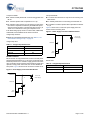
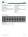
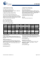
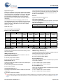
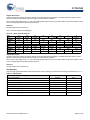
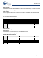
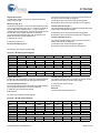
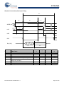
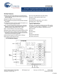
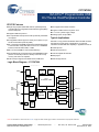
Logic Block Diagram – CY7C67200
CY7C67200
Timer 0
Control
Timer 1
UART I/F
Watchdog
CY16
16-bit RISC CORE
I2C
EEPROM I/F
Vbus, ID
OTG
D+,D-
USB-A
HSS I/F
SIE1
HOST/
Peripheral
USB Ports
SPI I/F
USB-A
D+,D-
4Kx16
ROM BIOS
SIE2
X1
X2
PLL
8Kx16
RAM
HPI I/F
SHARED INPUT/OUTPUT PINS
nRESET
GPIO [24:0]
GPIO
Mobile
Power
Booster
Errata: For information on silicon errata, see “Errata” on page 84. Details include trigger conditions, devices affected, and proposed workaround.
Cypress Semiconductor Corporation
Document Number: 38-08014 Rev. *J
•
198 Champion Court
•
San Jose, CA 95134-1709
•
408-943-2600
Revised July 31, 2013
CY7C67200
Contents
Introduction ....................................................................... 3
Processor Core Functional Overview ............................. 3
Processor .................................................................... 3
Clocking ....................................................................... 3
Memory ....................................................................... 3
Interrupts ..................................................................... 3
General Timers and Watchdog Timer ......................... 3
Power Management .................................................... 3
Interface Descriptions ...................................................... 3
USB Interface .............................................................. 4
OTG Interface .............................................................. 4
General Purpose IO Interface ..................................... 4
UART Interface [1] ....................................................... 4
I2C EEPROM Interface [2] .......................................... 5
Serial Peripheral Interface ........................................... 5
High-Speed Serial Interface ........................................ 5
Host Port Interface (HPI) ............................................. 6
Charge Pump Interface ............................................... 6
Booster Interface ......................................................... 7
Crystal Interface .......................................................... 8
Boot Configuration Interface ........................................ 8
Operational Modes ...................................................... 9
Power Savings and Reset Description ......................... 10
Power Savings Mode Description ............................. 10
Sleep ......................................................................... 10
External (Remote) Wakeup Source ........................... 10
Power-On Reset (POR) Description .......................... 10
Reset Pin ................................................................... 10
USB Reset ................................................................. 10
Memory Map .................................................................... 10
Mapping ..................................................................... 10
Internal Memory ........................................................ 10
Registers ......................................................................... 11
Processor Control Registers ..................................... 11
Timer Registers ......................................................... 18
General USB Registers [8] ........................................ 20
USB Host Only Registers .......................................... 22
USB Device Only Registers ...................................... 30
OTG Control Registers [9] ......................................... 42
GPIO Registers ......................................................... 43
Document Number: 38-08014 Rev. *J
HSS Registers ........................................................... 47
HPI Registers ............................................................ 53
SPI Registers ............................................................ 57
UART Registers ........................................................ 65
Pin Diagram ..................................................................... 67
Pin Descriptions ............................................................. 67
Absolute Maximum Ratings .......................................... 69
Operating Conditions ..................................................... 69
Crystal Requirements (XTALIN, XTALOUT) ................. 69
DC Characteristics ....................................................... 70
USB Transceiver ....................................................... 71
AC Timing Characteristics ............................................. 71
Reset Timing ............................................................ 71
Clock Timing ............................................................. 72
I2C EEPROM Timing ............................................... 72
HPI (Host Port Interface) Read Cycle Timing ........... 74
HSS BYTE Mode Transmit ....................................... 75
HSS Block Mode Transmit ....................................... 75
HSS BYTE and BLOCK Mode Receive ................... 75
Hardware CTS/RTS Handshake ............................... 76
Register Summary .......................................................... 77
Ordering Information ...................................................... 81
Ordering Code Definitions ......................................... 81
Package Diagram ............................................................ 82
Acronyms ........................................................................ 83
Document Conventions ................................................. 83
Units of Measure ....................................................... 83
Errata ............................................................................... 84
Part Numbers Affected .............................................. 84
CY7C67200 Qualification Status ............................... 84
CY7C67200 Errata Summary .................................... 84
Document History Page ................................................. 91
Sales, Solutions, and Legal Information ...................... 93
Worldwide Sales and Design Support ....................... 93
Products .................................................................... 93
PSoC® Solutions ...................................................... 93
Cypress Developer Community ................................. 93
Technical Support ..................................................... 93
Page 2 of 93
CY7C67200
Introduction
Memory
EZ-OTG™ (CY7C67200) is Cypress Semiconductor’s first USB
On-The-Go (OTG) host/peripheral controller. EZ-OTG is
designed to easily interface to most high-performance CPUs to
add USB host functionality. EZ-OTG has its own 16-bit RISC
processor to act as a coprocessor or operate in standalone
mode. EZ-OTG also has a programmable IO interface block
allowing a wide range of interface options.
EZ-OTG has a built-in 4K × 16 masked ROM and an 8K × 16
internal RAM. The masked ROM contains the EZ-OTG BIOS.
The internal RAM can be used for program code or data.
Processor Core Functional Overview
An overview of the processor core components are presented in
this section.
Processor
Interrupts
EZ-OTG provides 128 interrupt vectors. The first 48 vectors are
hardware interrupts and the following 80 vectors are software
interrupts.
General Timers and Watchdog Timer
EZ-OTG has two built-in programmable timers and a watchdog
timer. All three timers can generate an interrupt to the EZ-OTG.
Power Management
EZ-OTG has a general purpose 16-bit embedded RISC
processor that runs at 48 MHz.
EZ-OTG has one main power-saving mode, Sleep. Sleep mode
pauses all operations and provides the lowest power state.
Clocking
EZ-OTG requires a 12 MHz source for clocking. Either an
external crystal or TTL-level oscillator may be used. EZ-OTG has
an internal PLL that produces a 48 MHz internal clock from the
12 MHz source.
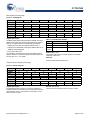
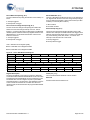
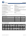
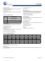
Interface Descriptions
EZ-OTG has a variety of interface options for connectivity, with
several interface options available. See Table 1 to understand
how the interfaces share pins and can coexist. Below are some
general guidelines:
■
I2C EEPROM and OTG do not conflict with any interfaces
■
HPI is mutually exclusive to HSS, SPI, and UART
Table 1. Interface Options for GPIO Pins
GPIO Pins
GPIO31
GPIO30
GPIO29
GPIO24
GPIO23
GPIO22
GPIO21
GPIO20
GPIO19
GPIO15
GPIO14
GPIO13
GPIO12
GPIO11
GPIO10
GPIO9
GPIO8
GPIO7
GPIO6
GPIO5
GPIO4
GPIO3
GPIO2
GPIO1
GPIO0
HPI
HSS
SPI
UART
I2C
SCL/SDA
SCL/SDA
OTG
OTGID
INT
nRD
nWR
nCS
A1
A0
D15
D14
D13
D12
D11
D10
D9
D8
D7
D6
D5
D4
D3
D2
D1
D0
Document Number: 38-08014 Rev. *J
CTS
RTS
RXD
TXD
MOSI
SCK
nSSI
MISO
TX
RX
Page 3 of 93
CY7C67200
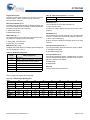
USB Interface
OTG Interface
EZ-OTG has two built-in Host/Peripheral SIEs that each have a
single USB transceiver, meeting the USB 2.0 specification requirements for full and low speed (high speed is not supported).
In Host mode, EZ-OTG supports two downstream ports; each
supports control, interrupt, bulk, and isochronous transfers. In
Peripheral mode, EZ-OTG supports one peripheral port with
eight endpoints for each of the two SIEs. Endpoint 0 is dedicated
as the control endpoint and only supports control transfers. Endpoints 1 though 7 support Interrupt, bulk (up to 64 bytes per packet), or isochronous transfers (up to 1023 bytes per packet size).
EZ-OTG also supports a combination of Host and Peripheral
ports simultaneously, as shown in Table 2.
Table 2. USB Port Configuration Options
EZ-OTG has one USB port that is compatible with the USB
On-The-Go supplement to the USB 2.0 specification. The USB
OTG port has various hardware features to support Session Request Protocol (SRP) and Host Negotiation Protocol (HNP).
OTG is only supported on USB PORT 1A.
OTG Features
■
Internal Charge Pump to supply and control VBUS
■
VBUS Valid Status (above 4.4 V)
■
VBUS Status for 2.4 V < VBUS < 0.8 V
■
ID Pin Status
Port 1A
Port 2A
■
Switchable 2-Kohminternal discharge resistor on VBUS
OTG
OTG
–
■
Switchable 500-ohm internal pull-up resistor on VBUS
OTG + 1 Host
OTG
Host
■
OTG + 1 Peripheral
OTG
Peripheral
Individually switchable internal pull-up and pull-down resistors
on the USB data lines
1 Host + 1 Peripheral
Host
Peripheral
1 Host + 1 Peripheral
Peripheral
Host
2 Hosts
Host
Host
1 Host
Host
–
1 Host
–
Host
2 Peripherals
Peripheral
Peripheral
1 Peripheral
Peripheral
–
1 Peripheral
–
Peripheral
Port Configurations
USB Features
OTG Pins
Table 4. OTG Interface Pins
Pin Name
DM1A
Pin Number
F2
DP1A
E3
OTGVBUS
C1
OTGID
F4
CSwitchA
D1
CSwitchB
D2
■
USB 2.0 compatible for full and low speed
General Purpose IO Interface
■
Up to two downstream USB host ports
■
Up to two upstream USB peripheral ports
EZ-OTG has up to 25 GPIO signals available. Several other optional interfaces use GPIO pins as well and may reduce the overall number of available GPIOs.
■
Configurable endpoint buffers (pointer and length), must reside
in internal RAM
■
Up to eight available peripheral endpoints (1 control endpoint)
■
Supports Control, Interrupt, Bulk, and Isochronous transfers
All Inputs are sampled asynchronously with state changes occurring at a rate of up to two 48 MHz clock cycles. GPIO pins are
latched directly into registers, a single flip-flop.
■
Internal DMA channels for each endpoint
Unused Pin Descriptions
■
Internal pull up and pull down resistors
■
Internal Series termination resistors on USB data lines
Unused USB pins must be tri-stated with the D+ line pulled high
through the internal pull-up resistor and the D– line pulled low
through the internal pull-down resistor.
Unused GPIO pins must be configured as outputs and driven
low.
USB Pins
Table 3. USB Interface Pins
Pin Name
DM1A
GPIO Description
Pin Number
F2
DP1A
E3
DM2A
C2
DP2A
D3
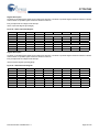
UART Interface [1]
EZ-OTG has a built-in UART interface. The UART interface
supports data rates from 900 to 115.2K baud. It can be used as
a development port or for other interface requirements. The
UART interface is exposed through GPIO pins.
Note
1. Errata: The UART is not designed to recognize framing errors. For more information, see the Errata on page 84.
Document Number: 38-08014 Rev. *J
Page 4 of 93
CY7C67200
UART Features
■
Slave SPI signaling synchronization and filtering
■
Supports baud rates of 900 to 115.2K
■
Slave SPI clock rates up to 2 MHz
■
8-N-1
■
Maskable interrupts for block and byte transfer modes
■
Individual bit transfer for non-byte aligned serial communication in PIO mode
■
Programmable delay timing for the active/inactive master SPI
clock
■
Auto or manual control for master mode slave select signal
■
Complete access to internal memory
UART Pins
Table 5. UART Interface Pins
Pin Name
Pin Number
TX
B5
RX
B4
I2C EEPROM Interface [2]
SPI Pins
EZ-OTG provides a master-only I2C interface for external serial
EEPROMs. The serial EEPROM can be used to store
application-specific code and data. This I2C interface is only to
be used for loading code out of EEPROM, it is not a general I2C
interface. The I2C EEPROM interface is a BIOS implementation
and is exposed through GPIO pins. Refer to the BIOS
documentation for additional details on this interface.
The SPI port has a few different pin location options as shown in
Table 7. The pin location is selectable via the GPIO Control register [0xC006].
I2C EEPROM Features
Table 7. SPI Interface Pins
Pin Name
Pin Number
nSSI
F6 or C6
SCK
D5
■
Supports EEPROMs up to 64 KB (512K bit)
MOSI
D4
■
Auto-detection of EEPROM size
MISO
C5
I2C EEPROM Pins
High-Speed Serial Interface
Table 6. I2C EEPROM Interface Pins
Pin Name
Pin Number
SMALL EEPROM
SCK
H3
SDA
F3
LARGE EEPROM
SCK
F3
SDA
H3
EZ-OTG provides an HSS interface. The HSS interface is a programmable serial connection with baud rate from 9600 baud to
2M baud. The HSS interface supports both byte and block mode
operations as well as hardware and software handshaking. Complete control of EZ-OTG can be accomplished through this interface via an extensible API and communication protocol. The
HSS interface can be exposed through GPIO pins or the External
Memory port.
HSS Features
■
8-bit, no parity code
Serial Peripheral Interface
■
Programmable baud rate from 9600 baud to 2M baud
EZ-OTG provides an SPI interface for added connectivity.
EZ-OTG may be configured as either an SPI master or SPI slave.
The SPI interface can be exposed through GPIO pins or the External Memory port.
■
Selectable 1- or 2-stop bit on transmit
■
Programmable intercharacter gap timing for Block Transmit
■
8-byte receive FIFO
SPI Features
■
Glitch filter on receive
■
Block mode transfer directly to/from EZ-OTG internal memory
(DMA transfer)
■
Selectable CTS/RTS hardware signal handshake protocol
■
Selectable XON/XOFF software handshake protocol
■
Programmable Receive interrupt, Block Transfer Done interrupts
■
Complete access to internal memory
■
Master or slave mode operation
■
DMA block transfer and PIO byte transfer modes
■
Full duplex or half duplex data communication
■
8-byte receive FIFO and 8-byte transmit FIFO
■
Selectable master SPI clock rates from 250 kHz to 12 MHz
■
Selectable master SPI clock phase and polarity
Note
2. Errata: If, while the BIOS is loading fi rmware, the part is reset and at that time the EEPROM is drivi ng the SDA line low, the BIOS will configure the part for co-processor
mode instead of standalone mode. For more information, see the Errata on page 84.
Document Number: 38-08014 Rev. *J
Page 5 of 93
CY7C67200
Table 9. HPI Interface Pins [3, 4] (continued)
HSS Pins
Pin Name
Table 8. HSS Interface Pins
Pin Name
Pin Number
Pin Number
A0
F5
F6
CTS
F6
D15
RTS
E4
D14
E4
RX
E5
D13
E5
TX
E6
D12
E6
D11
D4
Host Port Interface (HPI)
D10
D5
EZ-OTG has an HPI interface. The HPI interface provides DMA
access to the EZ-OTG internal memory by an external host, plus
a bidirectional mailbox register for supporting high-level communication protocols. This port is designed to be the primary
high-speed connection to a host processor. Complete control of
EZ-OTG can be accomplished through this interface via an
extensible API and communication protocol. Other than the
hardware communication protocols, a host processor has
identical control over EZ-Host whether connecting to the HPI or
HSS port. The HPI interface is exposed through GPIO pins.
D9
C6
D8
C5
D7
B5
D6
B4
D5
C4
D4
B3
D3
A3
D2
C3
D1
A2
D0
B2
Note It should be noted that for up to 3 ms after BIOS starts
executing, GPIO[24:19] and GPIO[15:8] will be driven as outputs
for a test mode. If these pins need to be used as inputs, a series
resistor is required (10 ohm to 48 ohm is recommended). Refer
to BIOS documentation for addition details. See section “Reset
Pin” on page 10.
The two HPI address pins are used to address one of four
possible HPI port registers as shown in Table 10 below.
HPI Features
Table 10. HPI Addressing
■
16-bit data bus interface
■
16 MB/s throughput
HPI A[1:0]
■
Auto-increment of address pointer for fast block mode transfers
■
Direct memory access (DMA) to internal memory
■
Bidirectional Mailbox register
■
Byte Swapping
■
Complete access to internal memory
■
Complete control of SIEs through HPI
■
Dedicated HPI Status register
A1
A0
HPI Data
0
0
HPI Mailbox
0
1
HPI Address
1
0
HPI Status
1
1
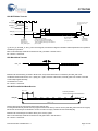
Charge Pump Interface
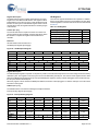
VBUS for the USB On-The-Go (OTG) port can be produced by
EZ-OTG using its built-in charge pump and some external
components. The circuit connections should look similar to
Figure 1 below.
Figure 1. Charge Pump
HPI Pins
Pin Name
D2
D1
Table 9. HPI Interface Pins [3, 4]
Pin Number
INT
H4
nRD
G4
nWR
H5
nCS
G5
A1
H6
CSWITCHA
CY7C67200
CSWITCHB
C1
VBUS
OTGVBUS
C2
Notes
3. HPI_INT is for the Outgoing Mailbox Interrupt.
4. HPI strobes are negative logic sampled on rising edge.
Document Number: 38-08014 Rev. *J
Page 6 of 93
CY7C67200
Component details:
Component details:
■
D1 and D2: Schottky diodes with a current rating greater than
60 mA.
■
L1: Inductor with inductance of 10 µH and a current rating of at
least 250 mA
■
C1: Ceramic capacitor with a capacitance of 0.1 µF.
■
D1: Schottky diode with a current rating of at least 250 mA
■
C2: Capacitor value must be no more that 6.5 µF since that is
the maximum capacitance allowed by the USB OTG specification for a dual-role device. The minimum value of C2 is 1 µF.
There are no restrictions on the type of capacitor for C2.
■
C1: Tantalum or ceramic capacitor with a capacitance of at least
2.2 µF
If the VBUS charge pump circuit is not to be used, CSWITCHA,
CSWITCHB, and OTGVBUS can be left unconnected.
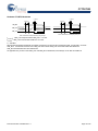
Charge Pump Features
■
Figure 3 shows how to connect the power supply when the
booster circuit is not being used.
Figure 3. Power Supply Connection Without Booster
BOOSTVcc
3.0V to 3.6V
Power Supply
Meets OTG Supplement Requirements, see Table 41, “DC
Characteristics: Charge Pump,” on page 70.
Charge Pump Pins
VSWITCH
Table 11. Charge Pump Interface Pins
Pin Name
Pin Number
OTGVBUS
C1
CSwitchA
D1
CSwitchB
D2
VCC
AVCC
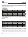
Booster Interface
EZ-OTG has an on-chip power booster circuit for use with power
supplies that range between 2.7 V and 3.6 V. The booster circuit
boosts the power to 3.3 V nominal to supply power for the entire
chip. The booster circuit requires an external inductor, diode, and
capacitor. During power down mode, the circuit is disabled to
save power. Figure 2 shows how to connect the booster circuit.
Figure 2. Power Supply Connection With Booster
Booster Pins
Table 12. Charge Pump Interface Pins
Pin Name
Pin Number
BOOSTVcc
F1
VSWITCH
E2
BOOSTVcc
L1
2.7V to 3.6V
Power Supply
VSWITCH
D1
3.3V
VCC
AVCC
C1
Document Number: 38-08014 Rev. *J
Page 7 of 93
CY7C67200
Crystal Interface
Boot Configuration Interface
The recommended crystal circuit to be used with EZ-OTG is
shown in Figure 4. If an oscillator is used instead of a crystal
circuit, connect it to XTALIN and leave XTALOUT unconnected.
For further information on the crystal requirements, see Table 39,
“Crystal Requirements,” on page 69.
EZ-OTG can boot into any one of four modes. The mode it boots
into is determined by the TTL voltage level of GPIO[31:30] at the
time nRESET is deasserted. Table 14 shows the different boot
pin combinations possible. After a reset pin event occurs, the
BIOS bootup procedure executes for up to 3 ms. GPIO[31:30]
are sampled by the BIOS during bootup only. After bootup these
pins are available to the application as GPIOs.
Figure 4. Crystal Interface
Table 14. Boot Configuration Interface
XTALIN
CY7C67200
Y1
XTALOUT
12MHz
Parallel Resonant
Fundamental Mode
500uW
20-33pf ±5%
C1 = 22 pF
C2 = 22 pF
Crystal Pins
Table 13. Crystal Pins
Pin Name
Pin Number
XTALIN
G3
XTALOUT
G2
Document Number: 38-08014 Rev. *J
GPIO31
(Pin 39)
GPIO30
(Pin 40)
0
0
Host Port Interface (HPI)
0
1
High Speed Serial (HSS)
1
0
Serial Peripheral Interface (SPI, slave
mode)
1
1
I2C EEPROM (Standalone Mode)
Boot Mode
GPIO[31:30] must be pulled high or low, as needed, using
resistors tied to VCC or GND with resistor values between 5K
ohm and 15K ohm. GPIO[31:30] must not be tied directly to VCC
or GND. Note that in Standalone mode, the pull ups on those two
pins are used for the serial I2C EEPROM (if implemented). The
resistors used for these pull ups must conform to the serial
EEPROM manufacturer's requirements.
If any mode other then standalone is chosen, EZ-OTG will be in
coprocessor mode. The device will power up with the appropriate
communication interface enabled according to its boot pins and
wait idle until a coprocessor communicates with it. See the BIOS
documentation for greater detail on the boot process.
Page 8 of 93
CY7C67200
Operational Modes
Standalone Mode
There are two modes of operation: Coprocessor and Standalone.
In standalone mode, there is no external processor connected to
EZ-OTG. Instead, EZ-OTG’s own internal 16-bit CPU is the main
processor and firmware is typically downloaded from an
EEPROM. Optionally, firmware may also be downloaded via
USB. Refer to Table 14 for booting into standalone mode.
Coprocessor Mode
EZ-OTG can act as a coprocessor to an external host processor.
In this mode, an external host processor drives EZ-OTG and is
the main processor rather then EZ-OTG’s own 16-bit internal
CPU. An external host processor may interface to EZ-OTG
through one of the following three interfaces in coprocessor
mode:
■
HPI mode, a 16-bit parallel interface with up to 16 MBytes
transfer rate
■
HSS mode, a serial interface with up to 2M baud transfer rate
■
SPI mode, a serial interface with up to 2 Mbits/s transfer rate.
At bootup GPIO[31:30] determine which of these three interfaces
are used for coprocessor mode. Refer to Table 14 for details.
Bootloading begins from the selected interface after POR + 3 ms
of BIOS bootup.
After booting into standalone mode (GPIO[31:30] = ‘11’), the following pins are affected:
■
GPIO[31:30] are configured as output pins to examine the
EEPROM contents.
■
GPIO[28:27] are enabled for debug UART mode.
■
GPIO[29] is configured as OTGID for OTG applications on
PORT1A.
❐ If OTGID is logic 1 then PORT1A (OTG) is configured as a
USB peripheral.
❐ If OTGID is logic 0 then PORT1A (OTG) is configured as a
USB host.
■
Ports 1B, 2A, and 2B default as USB peripheral ports.
■
All other pins remain INPUT pins.
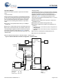
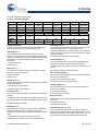
Minimum Hardware Requirements for Standalone Mode – Peripheral Only
Figure 5. Minimum Standalone Hardware Configuration – Peripheral Only
EZ-OTG
CY7C67200
VCC, AVCC,
BoostVCC
VReg
Standard-B
or Mini-B
VBus
D+
Reset
Logic
nRESET
DPlus
DMinus
DGND
SHIELD
Bootstrap Options
Vcc Vcc
10k 10k
GPIO[30]
SCL*
GPIO[31]
SDA*
Int. 16k x8
Code / Data
VCC
A0
A1
A2
Up to 64k x8
EEPROM
Bootloading Firmware
VCC
WP
SCL
GND
SDA
Reserved
GND, AGND,
BoostGND
*Bootloading begins after POR + 3ms BIOS bootup
*GPIO[31:30]
Up to 2k x8
>2k x8 to 64k x8
31
30
SCL SDA
SDA SCL
Document Number: 38-08014 Rev. *J
22pf
XIN
12MHz
XOUT
22pf
* Parallel Resonant
Fundamental Mode
500uW
20-33pf ±5%
Page 9 of 93
CY7C67200
Power Savings and Reset Description
Upon wakeup, code begins executing within 200 ms, the time it
takes the PLL to stabilize.
The EZ-OTG modes and reset conditions are described in this
section.
Table 15. wakeup Sources[5, 6]
Power Savings Mode Description
Wakeup Source (if enabled)
Event
USB Resume
D+/D– Signaling
OTGVBUS
Level
Sleep mode is used for USB applications to support USB
suspend and non USB applications as the main chip power down
mode.
OTGID
Any Edge
HPI
Read
In addition, EZ-OTG is capable of slowing down the CPU clock
speed through the CPU Speed register [0xC008] without
affecting other peripheral timing. Reducing the CPU clock speed
from 48 MHz to 24 MHz reduces the overall current draw by
around 8 mA while reducing it from 48 MHz to 3 MHz reduces
the overall current draw by approximately 15 mA.
HSS
Read
SPI
Read
IRQ0 (GPIO 24)
Any Edge
EZ-OTG has one main power savings mode, Sleep. For detailed
information on Sleep mode; See section “Sleep”.
Sleep
Sleep mode is the main chip power down mode and is also used
for USB suspend. Sleep mode is entered by setting the Sleep
Enable (bit 1) of the Power Control register [0xC00A]. During
Sleep mode (USB Suspend) the following events and states are
true:
■
GPIO pins maintain their configuration during sleep (in
suspend).
■
External Memory Address pins are driven low.
■
XTALOUT is turned off.
■
Internal PLL is turned off.
■
Firmware must disable the charge pump (OTG Control register
[0xC098]) causing OTGVBUS to drop below 0.2 V. Otherwise
OTGVBUS will only drop to VCC – (2 schottky diode drops).
Power-On Reset (POR) Description
The length of the power-on-reset event can be defined by (VCC
ramp to valid) + (Crystal start up). A typical application might
utilize a 12-ms power-on-reset event = ~7 ms + ~5 ms, respectively.
Reset Pin
The Reset pin is active low and requires a minimum pulse duration of sixteen 12-MHz clock cycles (1.3 ms). A reset event restores all registers to their default POR settings. Code execution
then begins 200 ms later at 0xFF00 with an immediate jump to
0xE000, the start of BIOS.
Note It should be noted that for up to 3 ms after BIOS starts
executing, GPIO[24:19] and GPIO[15:8] will be driven as outputs
for a test mode. If these pins need to be used as inputs, a series
resistor is required (10 ohm to 48 ohm is recommended). Refer
to BIOS documentation for addition details.
USB Reset
■
Booster circuit is turned off.
A USB Reset affects registers 0xC090 and 0xC0B0, all other
registers remain unchanged.
■
USB transceivers is turned off.
Memory Map
■
CPU suspends until a programmable wakeup event.
External (Remote) Wakeup Source
There are several possible events available to wake EZ-OTG
from Sleep mode as shown in Table 15. These may also be used
as remote wakeup options for USB applications. See section
“Power Control Register [0xC00A] [R/W]” on page 15.
Memory map information is presented in this section.
Mapping
The EZ-OTG has just over 24 KB of addressable memory
mapped from 0x0000 to 0xFFFF. This 24 KB contains both
program and data space and is byte addressable. Figure 6.
shows the various memory region address locations.
Internal Memory
Of the internal memory, 15 KB is allocated for user’s program
and data code. The lower memory space from 0x0000 to 0x04A2
is reserved for interrupt vectors, general purpose registers, USB
control registers, the stack, and other BIOS variables. The upper
internal memory space contains EZ-OTG control registers from
0xC000 to 0xC0FF and the BIOS ROM itself from 0xE000 to
0xFFFF. For more information on the reserved lower memory or
Notes
5. Read data will be discarded (dummy data).
6. HPI_INT will assert on a USB Resume.registers
Document Number: 38-08014 Rev. *J
Page 10 of 93
CY7C67200
the BIOS ROM, refer to the Programmers documentation and
the BIOS documentation.
Registers
During development with the EZ-OTG toolset, the lower area of
User's space (0x04A4 to 0x1000) should be left available to load
the GDB stub. The GDB stub is required to allow the toolset
debug access into EZ-OTG.
Some registers have different functions for a read vs. a write
access or USB host vs. USB device mode. Therefore, registers
of this type have multiple definitions for the same address.
Figure 6. Memory Map
Internal Memory
HW INTs
0x0000 - 0x00FF
0x0100 - 0x011F
0x0120 - 0x013F
0x0140 - 0x0148
0x014A - 0x01FF
SW INTs
Primary Registers
Swap Registers
HPI Int / Mailbox
LCP Variables
0x0200- 0x02FF
USB Registers
0x0300- 0x030F
0x0310- 0x03FF
0x0400- 0x04A2
Slave Setup Packet
BIOS Stack
USB Slave & OTG
0x04A4- 0x3FFF
USER SPACE
~15K
0xC000- 0xC0FF
Control Registers
0xE000- 0xFFFF
BIOS
Document Number: 38-08014 Rev. *J
The default register values listed in this data sheet may be
altered to some other value during BIOS initialization. Refer to
the BIOS documentation for Register initialization information.
Processor Control Registers
There are eight registers dedicated to general processor control.
Each of these registers is covered in this section and is summarized in Table 16.
Table 16. Processor Control Registers
Register Name
Address
R/W
CPU Flags Register
0xC000
R
Register Bank Register
0xC002
R/W
Hardware Revision Register
0xC004
R
CPU Speed Register
0xC008
R/W
Power Control Register
0xC00A
R/W
Interrupt Enable Register
0xC00E
R/W
Breakpoint Register
0xC014
R/W
USB Diagnostic Register
0xC03C
W
Page 11 of 93
CY7C67200
CPU Flags Register [0xC000] [R]
Figure 7. CPU Flags Register
Bit #
15
14
13
12
11
10
9
8
Read/Write
–
–
–
–
Default
0
0
–
–
–
–
0
0
0
0
0
0
Bit #
7
6
5
4
3
2
1
0
Global
Interrupt
Enable
Negative
Flag
Overflow
Flag
Carry
Flag
Zero
Flag
Field
Reserved...
...Reserved
Field
Read/Write
–
–
–
R
R
R
R
R
Default
0
0
0
X
X
X
X
X
Register Description
The CPU Flags register is a read only register that gives
processor flags status.
Global Interrupt Enable (Bit 4)
The Global Interrupt Enable bit indicates if the Global Interrupts
are enabled.
1: Enabled
0: Disabled
Negative Flag (Bit 3)
The Negative Flag bit indicates if an arithmetic operation results
in a negative answer.
1: MS result bit is ‘1’
0: MS result bit is not ‘1’
Overflow Flag (Bit 2)
The Overflow Flag bit indicates if an overflow condition has
occurred. An overflow condition can occur if an arithmetic result
Document Number: 38-08014 Rev. *J
was either larger than the destination operand size (for addition)
or smaller than the destination operand should allow for
subtraction.
1: Overflow occurred
0: Overflow did not occur
Carry Flag (Bit 1)
The Carry Flag bit indicates if an arithmetic operation resulted in
a carry for addition, or borrow for subtraction.
1: Carry/Borrow occurred
0: Carry/Borrow did not occur
Zero Flag (Bit 0)
The Zero Flag bit indicates if an instruction execution resulted in
a ‘0’.
1: Zero occurred
0: Zero did not occur
Page 12 of 93
CY7C67200
Bank Register [0xC002] [R/W]
Figure 8. Bank Register
Bit #
15
14
13
12
Field
Read/Write
11
10
9
8
Address...
R/W
R/W
R/W
R/W
R/W
R/W
R/W
R/W
Default
0
0
0
0
0
0
0
1
Bit #
7
6
5
4
3
2
1
0
Field
Read/Write
Default
...Address
Reserved
R/W
R/W
R/W
–
–
–
–
–
0
0
0
X
X
X
X
X
Register Description
.
Table 17. Bank Register Example
The Bank register maps registers R0–R15 into RAM. The eleven
MSBs of this register are used as a base address for registers
R0–R15. A register address is automatically generated by:
1. Shifting the four LSBs of the register address left by 1
2. ORing the four shifted bits of the register address with the 12
MSBs of the Bank Register
3. Forcing the LSB to zero
For example, if the Bank register is left at its default value of
0x0100, and R2 is read, then the physical address 0x0102 will
be read. See Table 17 for details.
Register
Hex Value
Bank
0x0100
R14
0x000E << 1 = 0x001C
RAM
0x011C
Location
Binary Value
0000 0001 0000 0000
0000 0000 0001 1100
0000 0001 0001 1100
Address (Bits [15:4])
The Address field is used as a base address for all register
addresses to start from.
Reserved
All reserved bits must be written as ‘0’.
Hardware Revision Register [0xC004] [R]
Figure 9. Revision Register
Bit #
15
14
13
12
11
10
9
8
Read/Write
R
R
R
R
Default
X
X
R
R
R
R
X
X
X
X
X
X
3
2
1
0
Field
Bit #
Revision...
7
6
5
4
Read/Write
R
R
R
R
R
R
R
R
Default
X
X
X
X
X
X
X
X
Field
...Revision
Register Description
Revision (Bits [15:0])
The Hardware Revision register is a read-only register that
indicates the silicon revision number. The first silicon revision is
represented by 0x0101. This number is increased by one for
each new silicon revision.
The Revision field contains the silicon revision number.
Document Number: 38-08014 Rev. *J
Page 13 of 93
CY7C67200
CPU Speed Register [0xC008] [R/W]
Figure 10. CPU Speed Register
Bit #
15
14
13
12
Field
11
10
9
8
Reserved...
Read/Write
-
-
-
-
-
-
-
-
Default
0
0
0
0
0
0
0
0
Bit #
7
6
5
4
3
2
1
0
Field
...Reserved
CPU Speed
Read/Write
-
-
-
-
R/W
R/W
R/W
R/W
Default
0
0
0
0
1
1
1
1
Register Description
The CPU Speed register allows the processor to operate at a user selected speed. This register only affects the CPU; all other
peripheral timing is still based on the 48-MHz system clock (unless otherwise noted).
CPU Speed (Bits[3:0])
The CPU Speed field is a divisor that selects the operating speed of the processor as defined in Table 18.
Table 18. CPU Speed Definition
CPU Speed [3:0]
Processor Speed
0000
48 MHz/1
0001
48 MHz/2
0010
48 MHz/3
0011
48 MHz/4
0100
48 MHz/5
0101
48 MHz/6
0110
48 MHz/7
0111
48 MHz/8
1000
48 MHz/9
1001
48 MHz/10
1010
48 MHz/11
1011
48 MHz/12
1100
48 MHz/13
1101
48 MHz/14
1110
48 MHz/15
1111
48 MHz/16
Reserved
All reserved bits must be written as ‘0’.
Document Number: 38-08014 Rev. *J
Page 14 of 93
CY7C67200
Power Control Register [0xC00A] [R/W]
Figure 11. Power Control Register
Bit #
15
14
13
Reserved
Host/Device 2
Wake Enable
Reserved
Read/Write
–
R/W
–
R/W
Default
0
0
0
0
Bit #
7
6
Field
HPI
Wake Enable
Field
Read/Write
Default
12
5
Reserved
11
10
9
8
Reserved
HSS
Wake Enable
SPI
Wake Enable
R/W
–
R/W
R/W
0
0
0
0
Host/Device 1
OTG
Wake Enable Wake Enable
4
3
2
1
0
GPI
Wake Enable
Reserved
Boost 3V
OK
Sleep
Enable
Halt
Enable
R/W
–
–
R/W
–
R
R/W
R/W
0
0
0
0
0
0
0
0
Register Description
SPI Wake Enable (Bit 8)
The Power Control register controls the power-down and
wakeup options. Either the sleep mode or the halt mode options
can be selected. All other writable bits in this register can be used
as a wakeup source while in sleep mode.
The SPI Wake Enable bit enables or disables a wakeup condition
to occur on a falling SPI_nSS input transition. The processor
may take several hundreds of microseconds before being operational after wakeup. Therefore, the incoming data byte that
causes the wakeup will be discarded.
Host/Device 2 Wake Enable (Bit 14)
The Host/Device 2 Wake Enable bit enables or disables a
wakeup condition to occur on an Host/Device 2 transition. This
wake up from the SIE port does not cause an interrupt to the
on-chip CPU.
1: Enable wakeup on Host/Device 2 transition.
0: Disable wakeup on Host/Device 2 transition.
Host/Device 1 Wake Enable (Bit 12)
The Host/Device 1 Wake Enable bit enables or disables a
wakeup condition to occur on an Host/Device 1 transition. This
wakeup from the SIE port does not cause an interrupt to the
on-chip CPU.
1: Enable wakeup on falling SPI nSS input transition
0: Disable SPI_nSS interrupt
HPI Wake Enable (Bit 7)
The HPI Wake Enable bit enables or disables a wakeup
condition to occur on an HPI interface read.
1: Enable wakeup on HPI interface read
0: Disable wakeup on HPI interface read
GPI Wake Enable (Bit 4)
The GPI Wake Enable bit enables or disables a wakeup
condition to occur on a GPIO(25:24) transition.
1: Enable wakeup on Host/Device 1 transition
1: Enable wakeup on GPIO(25:24) transition
0: Disable wakeup on Host/Device 1 transition
0: Disable wakeup on GPIO(25:24) transition
OTG Wake Enable (Bit 11)
Boost 3V OK (Bit 2)
The OTG Wake Enable bit enables or disables a wakeup
condition to occur on either an OTG VBUS_Valid or OTG ID
transition (IRQ20).
The Boost 3V OK bit is a read only bit that returns the status of
the OTG Boost circuit.
1: Boost circuit not ok and internal voltage rails are below 3.0 V
1: Enable wakeup on OTG VBUS valid or OTG ID transition
0: Boost circuit ok and internal voltage rails are at or above 3.0 V
0: Disable wakeup on OTG VBUS valid or OTG ID transition
Sleep Enable (Bit 1)
HSS Wake Enable (Bit 9)
Setting this bit to ‘1’ immediately initiates SLEEP mode. While in
SLEEP mode, the entire chip is paused achieving the lowest
standby power state. All operations are paused, the internal
clock is stopped, the booster circuit and OTG VBUS charge
pump are all powered down, and the USB transceivers are
powered down. All counters and timers are paused but will retain
their values. SLEEP mode exits by any activity selected in this
register. When SLEEP mode ends, instruction execution
resumes within 0.5 ms.
The HSS Wake Enable bit enables or disables a wakeup
condition to occur on an HSS Rx serial input transition. The
processor may take several hundreds of microseconds before
being operational after wakeup. Therefore, the incoming data
byte that causes the wakeup will be discarded.
1: Enable wakeup on HSS Rx serial input transition
0: Disable wakeup on HSS Rx serial input transition
1: Enable Sleep Mode
0: No Function
Halt Enable (Bit 0)
Document Number: 38-08014 Rev. *J
Page 15 of 93
CY7C67200
Setting this bit to ‘1’ immediately initiates HALT mode. While in
HALT mode, only the CPU is stopped. The internal clock still runs
and all peripherals still operate, including the USB engines. The
power savings using HALT in most cases will be minimal, but in
applications that are very CPU intensive the incremental savings
may provide some benefit.
The HALT state is exited when any enabled interrupt is triggered.
Upon exiting the HALT state, one or two instructions immediately
following the HALT instruction may be executed before the
waking interrupt is serviced (you may want to follow the HALT
instruction with two NOPs).
1: Enable Halt Mode
0: No Function
Reserved
All reserved bits must be written as ‘0’.
Interrupt Enable Register [0xC00E] [R/W] [7]
Figure 12. Interrupt Enable Register
Bit #
15
14
13
Reserved
Field
12
11
10
OTG
Interrupt
Enable
SPI
Interrupt
Enable
Reserved
9
8
Host/Device 2 Host/Device 1
Interrupt
Interrupt
Enable
Enable
Read/Write
–
–
–
R/W
R/W
–
R/W
R/W
Default
0
0
0
0
0
0
0
0
Bit #
7
6
5
4
3
2
1
0
In Mailbox
Interrupt
Enable
Out Mailbox
Interrupt
Enable
Reserved
Field
HSS
Interrupt
Enable
UART
Interrupt
Enable
GPIO
Interrupt
Enable
Timer 1
Interrupt
Enable
Timer 0
Interrupt
Enable
R/W
R/W
R/W
–
R/W
R/W
R/W
R/W
0
0
0
1
0
0
0
0
Read/Write
Default
Register Description
Host/Device 1 Interrupt Enable (Bit 8)
The Interrupt Enable Register allows control of the hardware
interrupt vectors.
The Host/Device 1 Interrupt Enable bit enables or disables all of
the following Host/Device 1 hardware interrupts: Host 1 USB
Done, Host 1 USB SOF/EOP, Host 1 WakeUp/Insert/Remove,
Device 1 Reset, Device 1 SOF/EOP or WakeUp from USB,
Device 1 Endpoint n.
OTG Interrupt Enable (Bit 12)
The OTG Interrupt Enable bit enables or disables the OTG
ID/OTG4.4 V Valid hardware interrupt.
1: Enable OTG interrupt
0: Disable OTG interrupt
SPI Interrupt Enable (Bit 11)
The SPI Interrupt Enable bit enables or disables the following
three SPI hardware interrupts: SPI TX, SPI RX, and SPI DMA
Block Done.
1: Enable SPI interrupt
0: Disable SPI interrupt
Host/Device 2 Interrupt Enable (Bit 9)
The Host/Device 2 Interrupt Enable bit enables or disables all of
the following Host/Device 2 hardware interrupts: Host 2 USB
Done, Host 2 USB SOF/EOP, Host 2 WakeUp/Insert/Remove,
Device 2 Reset, Device 2 SOF/EOP or WakeUp from USB,
Device 2 Endpoint n.
1: Enable Host 2 and Device 2 interrupt
0: Disable Host 2 and Device 2 interrupt
1: Enable Host 1 and Device 1 interrupt
0: Disable Host 1 and Device 1 interrupt
HSS Interrupt Enable (Bit 7)
The HSS Interrupt Enable bit enables or disables the following
High-speed Serial Interface hardware interrupts: HSS Block
Done, and HSS RX Full.
1: Enable HSS interrupt
0: Disable HSS interrupt
In Mailbox Interrupt Enable (Bit 6)
The In Mailbox Interrupt Enable bit enables or disables the HPI:
Incoming Mailbox hardware interrupt.
1: Enable MBXI interrupt
0: Disable MBXI interrupt
Out Mailbox Interrupt Enable (Bit 5)
The Out Mailbox Interrupt Enable bit enables or disables the HPI:
Outgoing Mailbox hardware interrupt.
1: Enable MBXO interrupt
0: Disable MBXO interrupt
Note
7. Errata: Host/Device 1 SIE events will still trigger an interrupt when only the Host/Device 2 SIE Interrupt Enable is set and vise versa. For more information, see the
Errata on page 84.
Document Number: 38-08014 Rev. *J
Page 16 of 93
CY7C67200
UART Interrupt Enable (Bit 3)
Timer 1 Interrupt Enable (Bit 1)
The UART Interrupt Enable bit enables or disables the following
UART hardware interrupts: UART TX and UART RX.
The Timer 1 Interrupt Enable bit enables or disables the TImer1
Interrupt Enable. When this bit is reset, all pending Timer 1 interrupts are cleared.
1: Enable UART interrupt
1: Enable TM1 interrupt
0: Disable UART interrupt
0: Disable TM1 interrupt
GPIO Interrupt Enable (Bit 2)
The GPIO Interrupt Enable bit enables or disables the General
Purpose IO Pins Interrupt (See the GPIO Control Register).
When GPIO bit is reset, all pending GPIO interrupts are also
cleared.
Timer 0 Interrupt Enable (Bit 0)
1: Enable GPIO interrupt
1: Enable TM0 interrupt
0: Disable GPIO interrupt
0: Disable TM0 interrupt
The Timer 0 Interrupt Enable bit enables or disables the TImer0
Interrupt Enable. When this bit is reset, all pending Timer 0 interrupts are cleared.
Reserved
All reserved bits must be written as ‘0’.
Breakpoint Register [0xC014] [R/W]
Figure 13. Breakpoint Register
Bit #
15
14
13
12
Field
Read/Write
11
10
9
8
Address...
R/W
R/W
R/W
R/W
R/W
R/W
R/W
R/W
Default
0
0
0
0
0
0
0
0
Bit #
7
6
5
4
3
2
1
0
Field
Read/Write
Default
...Address
R/W
R/W
R/W
R/W
R/W
R/W
R/W
R/W
0
0
0
0
0
0
0
0
Register Description
The Breakpoint Register holds the breakpoint address. When the program counter match this address, the INT127 interrupt occurs.
To clear this interrupt, a zero value must be written to this register.
Address (Bits [15:0])
The Address field is a 16-bit field containing the breakpoint address.
Document Number: 38-08014 Rev. *J
Page 17 of 93
CY7C67200
USB Diagnostic Register [0xC03C] [R/W]
Figure 14. USB Diagnostic Register
Bit #
15
14
13
12
Reserved
Port 2A
Diagnostic
Enable
Reserved
Port 1A
Diagnostic
Enable
Read/Write
-
R/W
-
R/W
-
Default
0
0
0
0
Field
Bit #
11
10
9
8
-
-
-
0
0
0
0
2
1
0
Reserved...
7
6
5
4
3
...Reserved
Pull-down
Enable
LS Pull-up
Enable
FS Pull-up
Enable
Reserved
Read/Write
-
R/W
R/W
R/W
-
R/W
R/W
R/W
Default
0
0
0
0
0
0
0
0
Field
Force Select
Register Description
FS Pull-up Enable (Bit 4)
The USB Diagnostic Register provides control of diagnostic
modes. It is intended for use by device characterization tests, not
for normal operations. This register is Read/Write by the on-chip
CPU but is write-only via the HPI port.
The FS Pull-up Enable bit enables or disables a full-speed
pull-up resistor (pull up on D+) for testing.
Port 2A Diagnostic Enable (Bit 15)
The Port 2A Diagnostic Enable bit enables or disables Port 2A
for the test conditions selected in this register.
1: Apply any of the following enabled test conditions: J/K, DCK,
SE0, RSF, RSL, PRD
0: Do not apply test conditions
1: Enable full-speed pull-up resistor on D+
0: Pull-up resistor is not connected on D+
Force Select (Bits [2:0])
The Force Select field bit selects several different test condition
states on the data lines (D+/D–). See Table 19 for details.
Table 19. Force Select Definition
Force Select [2:0]
Data Line State
Port 1A Diagnostic Enable (Bit 15)
1xx
Assert SE0
The Port 1A Diagnostic Enable bit enables or disables Port 1A
for the test conditions selected in this register.
01x
Toggle JK
1: Apply any of the following enabled test conditions: J/K, DCK,
SE0, RSF, RSL, PRD
001
Assert J
000
Assert K
0: Do not apply test conditions
Reserved
Pull-down Enable (Bit 6)
All reserved bits must be written as ‘0’.
The Pull-down Enable bit enables or disables full-speed
pull-down resistors (pull down on both D+ and D–) for testing.
Timer Registers
0: Disable pull-down resistors on both D+ and D–
There are three registers dedicated to timer operations. Each of
these registers are discussed in this section and are summarized
in Table 20.
LS Pull-up Enable (Bit 5)
Table 20. Timer Registers
The LS Pull-up Enable bit enables or disables a low-speed
pull-up resistor (pull up on D–) for testing.
Address
R/W
Watchdog Timer Register
0xC00C
R/W
1: Enable low-speed pull-up resistor on D–
Timer 0 Register
0xC010
R/W
0: Pull-up resistor is not connected on D–
Timer 1 Register
0xC012
R/W
1: Enable pull-down resistors on both D+ and D–
Document Number: 38-08014 Rev. *J
Register Name
Page 18 of 93
CY7C67200
Watchdog Timer Register [0xC00C] [R/W]
Figure 15. Watchdog Timer Register
Bit #
15
14
13
12
Field
Read/Write
11
10
9
8
Reserved...
R/W
R/W
R/W
R/W
R/W
R/W
R/W
R/W
Default
0
0
0
0
0
0
0
0
Bit #
7
5
4
Field
Read/Write
Default
6
...Reserved
Timeout
Flag
3
Period
Select
2
1
0
Lock
Enable
WDT
Enable
Reset
Strobe
R/W
R/W
R/W
R/W
R/W
R/W
R/W
W
0
0
0
0
0
0
0
0
Register Description
Lock Enable (Bit 2)
The Watchdog Timer register provides status and control over
the Watchdog timer. The Watchdog timer can also interrupt the
processor.
The Lock Enable bit does not allow any writes to this register until
a reset. In doing so the Watchdog timer can be set up and
enabled permanently so that it can only be cleared on reset (the
WDT Enable bit is ignored).
Timeout Flag (Bit 5)
The Timeout Flag bit indicates if the Watchdog timer has expired.
The processor can read this bit after exiting a reset to determine
if a Watchdog timeout occurred. This bit is cleared on the next
external hardware reset.
1: Watchdog timer expired
0: Watchdog timer not permanently set
WDT Enable (Bit 1)
The WDT Enable bit enables or disables the Watchdog timer.
1: Enable Watchdog timer operation
0: Watchdog timer did not expire
0: Disable Watchdog timer operation
Period Select (Bits [4:3])
The Period Select field is defined in Table 21. If this time expires
before the Reset Strobe bit is set, the internal processor is reset.
Table 21. Period Select Definition
Period Select[4:3]
00
01
10
11
1: Watchdog timer permanently set
WDT Period Value
1.4 ms
5.5 ms
22.0 ms
66.0 ms
Document Number: 38-08014 Rev. *J
Reset Strobe (Bit 0)
The Reset Strobe is a write-only bit that resets the Watchdog
timer count. It must be set to ‘1’ before the count expires to avoid
a Watchdog trigger
1: Reset Count
Reserved
All reserved bits must be written as ‘0’.
Page 19 of 93
CY7C67200
Timer n Register [R/W]
■
Timer 0 Register 0xC010
■
Timer 1 Register 0xC012
Figure 16. Timer n Register
Bit #
15
14
13
12
Field
11
10
9
8
Count...
Read/Write
R/W
R/W
R/W
R/W
R/W
R/W
R/W
R/W
Default
1
1
1
1
1
1
1
1
Bit #
7
6
5
4
3
2
1
0
Field
...Count
Read/Write
Default
R/W
R/W
R/W
R/W
R/W
R/W
R/W
R/W
1
1
1
1
1
1
1
1
Register Description
The Timer n Register sets the Timer n count. Both Timer 0 and Timer 1 decrement by one every 1-µs clock tick. Each can provide an
interrupt to the CPU when the timer reaches zero.
Count (Bits [15:0])
The Count field sets the Timer count.
General USB Registers [8]
There is one set of registers dedicated to general USB control. This set consists of two identical registers, one for Host/Device Port
1 and one for Host/Device Port 2. This register set has functions for both USB host and USB peripheral options and is covered in this
section and summarized in Table 22. USB Host-only registers are covered in Section “USB Host Only Registers” on page 22 and USB
Device-only registers are covered in Section “USB Device Only Registers” on page 30.
Table 22. USB Registers
Register Name
Address (SIE1/SIE2)
R/W
USB n Control Register
0xC08A/0xC0AA
R/W
USB n Control Register [R/W]
■
USB 1 Control Register 0xC08A
■
USB 2 Control Register 0xC0AA
Figure 17. USB n Control Register
Bit #
15
14
Reserved
Field
13
12
11
10
9
8
Port A
D+ Status
Port A
D– Status
Reserved
LOA
Mode
Select
Reserved
Read/Write
-
-
R
R
-
R/W
R/W
-
Default
X
X
X
X
0
0
0
0
4
3
Bit #
7
Field
Port A
Resistors Enable
Read/Write
Default
6
5
Reserved
Port A
Force D± State
2
1
0
Suspend
Enable
Reserved
Port A
SOF/EOP Enable
R/W
-
-
R/W
R/W
R/W
-
R/W
0
0
0
0
0
0
0
0
Note
8. Errata: Writing to the SIE2 Control register via HPI can corrupt the SIE1 control register. Writing to the SIE1 Control register via HPI can corrupt the SIE2 control
register. For more information, see the Errata on page 84.
Document Number: 38-08014 Rev. *J
Page 20 of 93
CY7C67200
Register Description
The USB n Control register is used in both host and device mode. It monitors and controls the SIE and the data lines of the USB ports.
This register can be accessed by the HPI interface.
Port A D+ Status (Bit 13)
Port A Force D± State (Bits [4:3])
The Port A D+ Status bit is a read-only bit that indicates the value
of DATA+ on Port A.
The Port A Force D± State field controls the forcing state of the
D+ D– data lines for Port A. This field forces the state of the Port
A data lines independent of the Port Select bit setting. See
Table 24 for details.
1: D+ is high
0: D+ is low
Table 24. Port A Force D± State
Port A D– Status (Bit 12)
The Port A D– Status bit is a read-only bit that indicates the value
of DATA– on Port A.
1: D– is high
0: D– is low
LOA (Bit 10)
The LOA bit selects the speed of Port A.
Port A Force D± State
MSB
LSB
0
0
0
1
1
0
1
1
Function
Normal Operation
Force USB Reset, SE0 State
Force J-State
Force K-State
1: Port A is set to Low-speed mode
Suspend Enable (Bit 2)
0: Port A is set to Full-speed mode
The Suspend Enable bit enables or disables the suspend feature
on both ports. When suspend is enabled the USB transceivers
are powered down and can not transmit or received USB packets
but can still monitor for a wakeup condition.
Mode Select (Bit 9)
The Mode Select bit sets the SIE for host or device operation.
When set for device operation only one USB port is supported.
The active port is selected by the Port Select bit in the Host n
Count Register.
1: Enable suspend
0: Disable suspend
1: Host mode
Port A SOF/EOP Enable (Bit 0)
0: Device mode
The Port A SOF/EOP Enable bit is only applicable in host mode.
In Device mode this bit must be written as ‘0’. In host mode this
bit enables or disables SOFs or EOPs for Port A. Either SOFs or
EOPs will be generated depending on the LOA bit in the USB n
Control Register when Port A is active.
Port A Resistors Enable (Bit 7)
The Port A Resistors Enable bit enables or disables the
pull-up/pull-down resistors on Port A. When enabled, the Mode
Select bit and LOA bit of this register sets the pull-up/pull-down
resistors appropriately. When the Mode Select is set for Host
mode, the pull-down resistors on the data lines (D+ and D–) are
enabled. When the Mode Select is set for Device mode, a single
pull-up resistor on either D+ or D–, determined by the LOA bit,
will be enabled. See Table 23 for details.
1: Enable SOFs or EOPs
0: Disable SOFs or EOPs
Reserved
All reserved bits must be written as ‘0’.
1: Enable pull-up/pull-down resistors
0: Disable pull-up/pull-down resistors
Table 23. USB Data Line Pull-up and Pull-down Resistors
L0A
Mode
Select
Port n
Resistors
Enable
X
X
0
Pull up/Pull down on D+ and
D– Disabled
X
1
1
Pull down on D+ and D–
Enabled
1
0
1
Pull up on USB D– Enabled
0
0
1
Pull up on USB D+ Enabled
Function
Document Number: 38-08014 Rev. *J
Page 21 of 93
CY7C67200
USB Host Only Registers
There are twelve sets of dedicated registers to USB host only operation. Each set consists of two identical registers (unless otherwise
noted); one for Host Port 1 and one for Host Port 2. These register sets are covered in this section and summarized in Table 25.
Table 25. USB Host Only Register
Address
(Host 1/Host 2)
Register Name
R/W
Host n Control Register
0xC080/0xC0A0
R/W
Host n Address Register
0xC082/0xC0A2
R/W
Host n Count Register
0xC084/0xC0A4
R/W
Host n Endpoint Status Register
0xC086/0xC0A6
R
Host n PID Register
0xC086/0xC0A6
W
Host n Count Result Register
0xC088/0xC0A8
R
Host n Device Address Register
0xC088/0xC0A8
W
Host n Interrupt Enable Register
0xC08C/0xC0AC
R/W
Host n Status Register
0xC090/0xC0B0
R/W
Host n SOF/EOP Count Register
0xC092/0xC0B2
R/W
Host n SOF/EOP Counter Register
0xC094/0xC0B4
R
Host n Frame Register
0xC096/0xC0B6
R
Host n Control Register [R/W]
■
Host 1 Control Register 0xC080
■
Host 2 Control Register 0xC0A0
Figure 18. Host n Control Register
Bit #
15
14
13
12
Read/Write
-
-
-
-
-
-
-
-
Default
0
0
0
0
0
0
0
0
Bit #
7
6
5
4
3
2
1
0
Field
Preamble
Enable
Sequence
Select
Sync
Enable
ISO
Enable
R/W
R/W
R/W
R/W
-
-
-
R/W
0
0
0
0
0
0
0
0
Field
Read/Write
Default
11
10
9
8
Reserved
Document Number: 38-08014 Rev. *J
Reserved
Arm
Enable
Page 22 of 93
CY7C67200
1: The next enabled packet will be transferred after the SOF or
EOP packet is transmitted
Register Description
The Host n Control register allows high-level USB transaction
control.
0: The next enabled packet will be transferred as soon as the SIE
is free
Preamble Enable (Bit 7)
The Preamble Enable bit enables or disables the transmission of
a preamble packet before all low-speed packets. This bit should
only be set when communicating with a low-speed device.
ISO Enable (Bit 4)
1: Enable Preamble packet
1: Enable Isochronous transaction
0: Disable Preamble packet
0: Disable Isochronous transaction
Sequence Select (Bit 6)
Arm Enable (Bit 0)
The Sequence Select bit sets the data toggle for the next packet.
This bit has no effect on receiving data packets; sequence
checking must be handled in firmware.
The Arm Enable bit arms an endpoint and starts a transaction.
This bit is automatically cleared to ‘0’ when a transaction is
complete.
1: Send DATA1
1: Arm endpoint and begin transaction
0: Send DATA0
0: Endpoint disarmed
Sync Enable (Bit 5)
Reserved
The Sync Enable bit synchronizes the transfer with the SOF
packet in full-speed mode and the EOP packet in low-speed
mode.
All reserved bits must be written as ‘0’.
The ISO Enable bit enables or disables an Isochronous transaction.
Host n Address Register [R/W]
■
Host 1 Address Register 0xC082
■
Host 2 Address Register 0xC0A2
Figure 19. Host n Address Register
Bit #
15
14
13
12
Field
Read/Write
11
10
9
8
Address...
R/W
R/W
R/W
R/W
R/W
R/W
R/W
R/W
Default
0
0
0
0
0
0
0
0
Bit #
7
6
5
4
3
2
1
0
Field
Read/Write
Default
...Address
R/W
R/W
R/W
R/W
R/W
R/W
R/W
R/W
0
0
0
0
0
0
0
0
Register Description
Address (Bits [15:0])
The Host n Address register is used as the base pointer into
memory space for the current host transactions.
The Address field sets the address pointer into internal RAM or
ROM.
Document Number: 38-08014 Rev. *J
Page 23 of 93
CY7C67200
Host n Count Register [R/W]
■
Host 1 Count Register 0xC084
■
Host 2 Count Register 0xC0A4
Figure 20. Host n Count Register
Bit #
15
14
13
Field
12
11
10
9
Reserved
8
Count...
Read/Write
-
-
-
-
-
-
R/W
R/W
Default
0
0
0
0
0
0
0
0
Bit #
7
6
5
4
3
2
1
0
Field
Read/Write
Default
...Count
R/W
R/W
R/W
R/W
R/W
R/W
R/W
R/W
0
0
0
0
0
0
0
0
Register Description
Count (Bits [9:0])
The Host n Count register is used to hold the number of bytes
(packet length) for the current transaction. The maximum packet
length is 1023 bytes in ISO mode. The Host Count value is used
to determine how many bytes to transmit, or the maximum
number of bytes to receive. If the number of received bytes is
greater then the Host Count value then an overflow condition will
be flagged by the Overflow bit in the Host n Endpoint Status
register.
The Count field sets the value for the current transaction data
packet length. This value is retained when switching between
host and device mode, and back again.
Reserved
All reserved bits must be written as ‘0’.
Host n Endpoint Status Register [R]
■
Host 1 Endpoint Status Register 0xC086
■
Host 2 Endpoint Status Register 0xC0A6
Figure 21. Host n Endpoint Status Register
Bit #
15
14
13
12
Reserved
Field
11
10
Overflow
Flag
Underflow
Flag
9
8
Reserved
Read/Write
-
-
-
-
R
R
-
-
Default
0
0
0
0
0
0
0
0
Bit #
7
6
5
4
3
2
1
0
Stall
Flag
NAK
Flag
Length
Exception
Flag
Reserved
Sequence
Status
Timeout
Flag
Error
Flag
ACK
Flag
Read/Write
R
R
R
-
R
R
R
R
Default
0
0
0
0
0
0
0
0
Field
Register Description
0: Overflow condition did not occur
The Host n Endpoint Status register is a read-only register that
provides status for the last USB transaction.
Underflow Flag (Bit 10)
Overflow Flag (Bit 11)
The Overflow Flag bit indicates that the received data in the last
data transaction exceeded the maximum length specified in the
Host n Count Register. The Overflow Flag should be checked in
response to a Length Exception signified by the Length
Exception Flag set to ‘1’.
1: Overflow condition occurred
Document Number: 38-08014 Rev. *J
The Underflow Flag bit indicates that the received data in the last
data transaction was less then the maximum length specified in
the Host n Count register. The Underflow Flag should be
checked in response to a Length Exception signified by the
Length Exception Flag set to ‘1’.
1: Underflow condition occurred
0: Underflow condition did not occur
Page 24 of 93
CY7C67200
Stall Flag (Bit 7)
Timeout Flag (Bit 2)
The Stall Flag bit indicates that the peripheral device replied with
a Stall in the last transaction.
The Timeout Flag bit indicates if a timeout condition occurred for
the last transaction. A timeout condition can occur when a device
either takes too long to respond to a USB host request or takes
too long to respond with a handshake.
1: Device returned Stall
0: Device did not return Stall
1: Timeout occurred
NAK Flag (Bit 6)
0: Timeout did not occur
The NAK Flag bit indicates that the peripheral device replied with
a NAK in the last transaction.
Error Flag (Bit 1)
The Error Flag bit indicates a transaction failed for any reason
other than the following: Timeout, receiving a NAK, or receiving
a STALL. Overflow and Underflow are not considered errors and
do not affect this bit. CRC5 and CRC16 errors will result in an
Error flag along with receiving incorrect packet types.
1: Device returned NAK
0: Device did not return NAK
Length Exception Flag (Bit 5)
The Length Exception Flag bit indicates the received data in the
data stage of the last transaction does not equal the maximum
Host Count specified in the Host n Count register. A Length
Exception can either mean an overflow or underflow and the
Overflow and Underflow flags (bits 11 and 10, respectively)
should be checked to determine which event occurred.
1: Error detected
0: No error detected
ACK Flag (Bit 0)
The ACK Flag bit indicates two different conditions depending on
the transfer type. For non-Isochronous transfers, this bit represents a transaction ending by receiving or sending an ACK
packet. For Isochronous transfers, this bit represents a
successful transaction that will not be represented by an ACK
packet.
1: An overflow or underflow condition occurred
0: An overflow or underflow condition did not occur
Sequence Status (Bit 3)
The Sequence Status bit indicates the state of the last received
data toggle from the device. Firmware is responsible for
monitoring and handling the sequence status. The Sequence bit
is only valid if the ACK bit is set to ‘1’. The Sequence bit is set to
‘0’ when an error is detected in the transaction and the Error bit
will be set.
1: For non-Isochronous transfers, the transaction was ACKed.
For Isochronous transfers, the transaction was completed
successfully.
0: For non-Isochronous transfers, the transaction was not
ACKed. For Isochronous transfers, the transaction was not
completed successfully.
1: DATA1
0: DATA0
Host n PID Register [W]
■
Host 1 PID Register 0xC086
■
Host 2 PID Register 0xC0A6
Figure 22. Host n PID Register
Bit #
15
14
13
12
Read/Write
-
-
-
-
-
-
-
-
Default
0
0
0
0
0
0
0
0
Bit #
7
6
5
4
3
2
1
0
Read/Write
W
W
W
W
W
W
W
W
Default
0
0
0
0
0
0
0
0
Field
11
10
9
8
Reserved
Field
PID Select
Document Number: 38-08014 Rev. *J
Endpoint Select
Page 25 of 93
CY7C67200
Table 26. PID Select Definition (continued)
Register Description
The Host n PID register is a write-only register that provides the
PID and Endpoint information to the USB SIE to be used in the
next transaction.
PID Select (Bits [7:4])
The PID Select field defined as in Table 26. ACK and NAK tokens
are automatically sent based on settings in the Host n Control
register and do not need to be written in this register.
Table 26. PID Select Definition
PID TYPE
PID Select [7:4]
PREAMBLE
1100 (C Hex)
NAK
1010 (A Hex)
STALL
1110 (E Hex)
DATA0
0011 (3 Hex)
DATA1
1011 (B Hex)
Endpoint Select (Bits [3:0])
set-up
1101 (D Hex)
The Endpoint field allows addressing of up to 16 different
endpoints.
IN
1001 (9 Hex)
Reserved
OUT
0001 (1 Hex)
All reserved bits must be written as ‘0’.
SOF
0101 (5 Hex)
PID TYPE
PID Select [7:4]
Host n Count Result Register [R]
■
Host 1 Count Result Register 0xC088
■
Host 2 Count Result Register 0xC0A8
Figure 23. Host n Count Result Register
Bit #
15
14
13
12
Field
11
10
9
8
Result...
Read/Write
R
R
R
R
R
R
R
R
Default
0
0
0
0
0
0
0
0
Bit #
7
6
5
4
3
2
1
0
Field
...Result
Read/Write
R
R
R
R
R
R
R
R
Default
0
0
0
0
0
0
0
0
Register Description
Result (Bits [15:0])
The Host n Count Result register is a read-only register that
contains the size difference in bytes between the Host Count
Value specified in the Host n Count register and the last packet
received. If an overflow or underflow condition occurs, that is the
received packet length differs from the value specified in the Host
n Count register, the Length Exception Flag bit in the Host n
Endpoint Status register will be set. The value in this register is
only valid when the Length Exception Flag bit is set and the Error
Flag bit is not set; both bits are in the Host n Endpoint Status
register.
The Result field contains the differences in bytes between the
received packet and the value specified in the Host n Count
register. If an overflow condition occurs, Result [15:10] is set to
‘111111’, a 2’s complement value indicating the additional byte
count of the received packet. If an underflow condition occurs,
Result [15:0] indicates the excess byte count (number of bytes
not used).
Document Number: 38-08014 Rev. *J
Reserved
All reserved bits must be written as ‘0’.
Page 26 of 93
CY7C67200
Host n Device Address Register [W]
■
Host 1 Device Address Register 0xC088
■
Host 2 Device Address Register 0xC0A8
Figure 24. Host n Device Address Register
Bit #
15
14
13
12
Field
11
10
9
8
Reserved...
Read/Write
-
-
-
-
-
-
-
-
Default
0
0
0
0
0
0
0
0
Bit #
7
6
5
4
3
2
1
0
Field
...Reserved
Address
Read/Write
-
W
W
W
W
W
W
W
Default
0
0
0
0
0
0
0
0
Register Description
Address (Bits [6:0])
The Host n Device Address register is a write-only register that
contains the USB Device Address that the host wishes to
communicate with.
The Address field contains the value of the USB address for the
next device that the host is going to communicate with. This
value must be written by firmware.
Reserved
All reserved bits must be written as ‘0’.
Host n Interrupt Enable Register [R/W]
■
Host 1 Interrupt Enable Register 0xC08C
■
Host 2 Interrupt Enable Register 0xC0AC
Figure 25. Host n Interrupt Enable Register
Bit #
15
14
Field
VBUS
Interrupt Enable
ID Interrupt
Enable
R/W
R/W
-
-
-
-
R/W
-
0
0
0
0
0
0
0
0
Read/Write
Default
Bit #
13
12
11
10
Reserved
8
SOF/EOP
Interrupt Enable
Reserved
7
6
5
4
Reserved
Port A
Wake Interrupt Enable
Reserved
Port A Connect
Change
Interrupt Enable
Read/Write
-
R/W
-
R/W
-
-
-
R/W
Default
0
0
0
0
0
0
0
0
Field
3
9
2
Reserved
Register Description
0: Disable VBUS interrupt
The Host n Interrupt Enable register allows control over
host-related interrupts.
ID Interrupt Enable (Bit 14)
In this register a bit set to ‘1’ enables the corresponding interrupt
while ‘0’ disables the interrupt.
VBUS Interrupt Enable (Bit 15)
The VBUS Interrupt Enable bit enables or disables the OTG
VBUS interrupt. When enabled this interrupt triggers on both the
rising and falling edge of VBUS at the 4.4 V status (only
supported in Port 1A). This bit is only available for Host 1 and is
a reserved bit in Host 2.
1: Enable VBUS interrupt
Document Number: 38-08014 Rev. *J
1
0
Done
Interrupt Enable
The ID Interrupt Enable bit enables or disables the OTG ID
interrupt. When enabled this interrupt triggers on both the rising
and falling edge of the OTG ID pin (only supported in Port 1A).
This bit is only available for Host 1 and is a reserved bit in Host 2.
1: Enable ID interrupt
0: Disable ID interrupt
SOF/EOP Interrupt Enable (Bit 9)
The SOF/EOP Interrupt Enable bit enables or disables the
SOF/EOP timer interrupt.
Page 27 of 93
CY7C67200
1: Enable SOF/EOP timer interrupt
1: Enable Connect Change interrupt
0: Disable SOF/EOP timer interrupt
0: Disable Connect Change interrupt
Port A Wake Interrupt Enable (Bit 6)
Done Interrupt Enable (Bit 0)
The Port A Wake Interrupt Enable bit enables or disables the
remote wakeup interrupt for Port A.
0: Disable remote wakeup interrupt for Port A
The Done Interrupt Enable bit enables or disables the USB
Transfer Done interrupt. The USB Transfer Done triggers when
either the host responds with an ACK, or a device responds with
any of the following: ACK, NAK, STALL, or Timeout. This
interrupt is used for both Port A and Port B.
Port A Connect Change Interrupt Enable (Bit 4)
1: Enable USB Transfer Done interrupt
The Port A Connect Change Interrupt Enable bit enables or
disables the Connect Change interrupt on Port A. This interrupt
triggers when either a device is inserted (SE0 state to J state) or
a device is removed (J state to SE0 state).
0: Disable USB Transfer Done interrupt
1: Enable remote wakeup interrupt for Port A
Reserved
All reserved bits must be written as ‘0’.
Host n Status Register [R/W]
■
Host 1 Status Register 0xC090
■
Host 2 Status Register 0xC0B0
Figure 26. Host n Status Register
Bit #
15
14
Field
VBUS
Interrupt Flag
ID Interrupt
Flag
R/W
R/W
-
-
-
-
R/W
-
X
X
X
X
X
X
X
X
Read/Write
Default
Bit #
13
12
11
10
Reserved
9
8
SOF/EOP
Interrupt Flag
Reserved
7
6
5
4
3
2
1
0
Reserved
Port A
Wake Interrupt
Flag
Reserved
Port A Connect
Change
Interrupt Flag
Reserved
Port A
SE0
Status
Reserved
Done
Interrupt Flag
Read/Write
-
R/W
-
R/W
-
R/W
-
R/W
Default
X
X
X
X
X
X
X
X
Field
Register Description
The Host n Status register provides status information for host
operation. Pending interrupts can be cleared by writing a ‘1’ to
the corresponding bit. This register can be accessed by the HPI
interface.
The ID Interrupt Flag bit indicates the status of the OTG ID
interrupt (only for Port 1A). When enabled this interrupt triggers
on both the rising and falling edge of the OTG ID pin. This bit is
only available for Host 1 and is a reserved bit in Host 2.
1: Interrupt triggered
VBUS Interrupt Flag (Bit 15)
0: Interrupt did not trigger
The VBUS Interrupt Flag bit indicates the status of the OTG
VBUS interrupt (only for Port 1A). When enabled this interrupt
triggers on both the rising and falling edge of VBUS at 4.4 V. This
bit is only available for Host 1 and is a reserved bit in Host 2.
SOF/EOP Interrupt Flag (Bit 9)
1: Interrupt triggered
1: Interrupt triggered
0: Interrupt did not trigger
The SOF/EOP Interrupt Flag bit indicates the status of the
SOF/EOP Timer interrupt. This bit triggers ‘1’ when the
SOF/EOP timer expires.
0: Interrupt did not trigger
ID Interrupt Flag (Bit 14)
Document Number: 38-08014 Rev. *J
Page 28 of 93
CY7C67200
Port A Wake Interrupt Flag (Bit 6)
Port A SE0 Status (Bit 2)
The Port A Wake Interrupt Flag bit indicates remote wakeup on
Port A.
The Port A SE0 Status bit indicates if Port A is in an SE0 state or
not. Together with the Port A Connect change Interrupt Flag bit,
it can be determined whether a device was inserted (non-SE0
condition) or removed (SE0 condition).
1: Interrupt triggered
0: Interrupt did not trigger
1: SE0 condition
Port A Connect Change Interrupt Flag (Bit 4)
0: Non-SE0 condition
The Port A Connect Change Interrupt Flag bit indicates the
status of the Connect Change interrupt on Port A. This bit
triggers ‘1’ on either a rising edge or falling edge of a USB Reset
condition (device inserted or removed). Together with the Port A
SE0 Status bit, it can be determined whether a device was
inserted or removed.
Done Interrupt Flag (Bit 0)
The Done Interrupt Flag bit indicates the status of the USB
Transfer Done interrupt. The USB Transfer Done triggers when
either the host responds with an ACK, or a device responds with
any of the following: ACK, NAK, STALL, or Timeout. This
interrupt is used for both Port A and Port B.
1: Interrupt triggered
1: Interrupt triggered
0: Interrupt did not trigger
0: Interrupt did not trigger
Host n SOF/EOP Count Register [R/W]
■
Host 1 SOF/EOP Count Register 0xC092
■
Host 2 SOF/EOP Count Register 0xC0B2
Figure 27. Host n SOF/EOP Count Register
Bit #
15
Field
14
13
12
11
Reserved
10
9
8
Count...
Read/Write
-
-
R/W
R/W
R/W
R/W
R/W
R/W
Default
0
0
1
0
1
1
1
0
Bit #
7
6
5
4
3
2
1
0
R/W
R/W
R/W
R/W
R/W
R/W
R/W
R/W
1
1
1
0
0
0
0
0
Field
Read/Write
Default
...Count
Register Description
Count (Bits [13:0])
The Host n SOF/EOP Count register contains the SOF/EOP
Count Value that is loaded into the SOF/EOP counter. This value
is loaded each time the SOF/EOP counter counts down to zero.
The default value set in this register at power-up is 0x2EE0,
which will generate a 1-ms time frame. The SOF/EOP counter is
a down counter decremented at a 12-MHz rate. When this
register is read, the value returned is the programmed SOF/EOP
count value.
The Count field sets the SOF/EOP counter duration.
Document Number: 38-08014 Rev. *J
Reserved
All reserved bits must be written as ‘0’.
Page 29 of 93
CY7C67200
Host n SOF/EOP Counter Register [R]
■
Host 1 SOF/EOP Counter Register 0xC094
■
Host 2 SOF/EOP Counter Register 0xC0B4
Figure 28. Host n SOF/EOP Counter Register
Bit #
15
Field
14
13
12
11
Reserved
10
9
8
Counter...
Read/Write
-
-
R
R
R
R
R
R
Default
X
X
X
X
X
X
X
X
Bit #
7
6
5
4
3
2
1
0
Read/Write
R
R
R
R
R
R
R
R
Default
X
X
X
X
X
X
X
X
Field
...Counter
Register Description
Counter (Bits [13:0])
The Host n SOF/EOP Counter register contains the current value
of the SOF/EOP down counter. This value can be used to
determine the time remaining in the current frame.
The Counter field contains the current value of the SOF/EOP
down counter.
Host n Frame Register [R]
■
Host 1 Frame Register 0xC096
■
Host 2 Frame Register 0xC0B6
Figure 29. Host n Frame Register
Bit #
15
14
Field
13
12
11
10
Reserved
9
8
Frame...
Read/Write
-
-
-
-
-
R
R
R
Default
0
0
0
0
0
0
0
0
Bit #
7
6
5
4
3
2
1
0
Field
...Frame
Read/Write
R
R
R
R
R
R
R
R
Default
0
0
0
0
0
0
0
0
Register Description
Reserved
The Host n Frame register maintains the next frame number to
be transmitted (current frame number + 1). This value is updated
after each SOF transmission. This register resets to 0x0000 after
each CPU write to the Host n SOF/EOP Count register (Host 1:
0xC092, Host 2: 0xC0B2).
All reserved bits must be written as ‘0’.
Frame (Bits [10:0])
The Frame field contains the next frame number to be transmitted.
USB Device Only Registers
There are ten sets of USB Device Only registers. All sets consist
of at least two registers, one for Device Port 1 and one for Device
Port 2. In addition, each Device port has eight possible
endpoints. This gives each endpoint register set eight registers
for each Device Port for a total of 16 registers per set. The USB
Device Only registers are covered in this section and summarized in Table 27.
Table 27. USB Device Only Registers
Register Name
Address
(Device 1/Device 2)
R/W
Device n Endpoint n Control Register
0x02n0
R/W
Device n Endpoint n Address Register
0x02n2
R/W
Document Number: 38-08014 Rev. *J
Page 30 of 93
CY7C67200
Table 27. USB Device Only Registers (continued)
Address
(Device 1/Device 2)
Register Name
Device n Endpoint n Count Register
0x02n4
R/W
R/W
Device n Endpoint n Status Register
0x02n6
R/W
Device n Endpoint n Count Result Register
0x02n8
R/W
Device n Interrupt Enable Register
0xC08C/0xC0AC
R/W
Device n Address Register
0xC08E/0xC0AE
R/W
Device n Status Register
0xC090/0xCB0
R/W
Device n Frame Number Register
0xC092/0xC0B2
R
Device n SOF/EOP Count Register
0xC094/0xC0B4
W
Device n Endpoint n Control Register [R/W]
■
Device n Endpoint 0 Control Register [Device 1: 0x0200 Device 2: 0x0280]
■
Device n Endpoint 1 Control Register [Device 1: 0x0210 Device 2: 0x0290]
■
Device n Endpoint 2 Control Register [Device 1: 0x0220 Device 2: 0x02A0]
■
Device n Endpoint 3 Control Register [Device 1: 0x0230 Device 2: 0x02B0]
■
Device n Endpoint 4 Control Register [Device 1: 0x0240 Device 2: 0x02C0]
■
Device n Endpoint 5 Control Register [Device 1: 0x0250 Device 2: 0x02D0]
■
Device n Endpoint 6 Control Register [Device 1: 0x0260 Device 2: 0x02E0]
■
Device n Endpoint 7 Control Register [Device 1: 0x0270 Device 2: 0x02F0]
Figure 30. Device n Endpoint n Control Register
Bit #
15
14
13
12
Field
11
10
9
8
Reserved
Read/Write
-
-
-
-
-
-
-
-
Default
X
X
X
X
X
X
X
X
Bit #
7
6
5
4
3
2
1
0
Sequence
Select
Stall
Enable
ISO
Enable
NAK
Interrupt
Enable
Direction
Select
Enable
Field
IN/OUT
Ignore
Enable
Arm
Enable
R/W
R/W
R/W
R/W
R/W
R/W
R/W
R/W
X
X
X
X
X
X
X
X
Read/Write
Default
Register Description
Sequence Select (Bit 6)
The Device n Endpoint n Control register provides control over a
single EP in device mode. There are a total of eight endpoints for
each of the two ports. All endpoints have the same definition for
their Device n Endpoint n Control register.
The Sequence Select bit determines whether a DATA0 or a
DATA1 will be sent for the next data toggle. This bit has no effect
on receiving data packets, sequence checking must be handled
in firmware.
IN/OUT Ignore Enable (Bit 6)
1: Send a DATA1
The IN/OUT Ignore Enable bit forces endpoint 0 (EP0) to ignore
all IN and OUT requests. This bit must be set so that EP0 only
excepts Setup packets at the start of each transfer. This bit must
be cleared to except IN/OUT transactions. This bit only applies
to EP0.
1: Ignore IN/OUT requests
0: Do not ignore IN/OUT requests
Document Number: 38-08014 Rev. *J
0: Send a DATA0
Stall Enable (Bit 5)
The Stall Enable bit sends a Stall in response to the next request
(unless it is a setup request, which are always ACKed). This is a
sticky bit and continues to respond with Stalls until cleared by
firmware.
1: Send Stall
Page 31 of 93
CY7C67200
is set incorrectly, the setup will be ACKed and the Set-up Status
Flag will be set (refer to the setup bit of the Device n Endpoint n
Status register for details).
0: Do not send Stall
ISO Enable (Bit 4)
The ISO Enable bit enables and disables an Isochronous transaction. This bit is only valid for EPs 1–7 and has no function for
EP0.
1: OUT transfer (host to device)
1: Enable Isochronous transaction
Enable (Bit 1)
0: Disable Isochronous transaction
The Enable bit must be set to allow transfers to the endpoint. If
Enable is set to ‘0’ then all USB traffic to this endpoint is ignored.
If Enable is set ‘1’ and Arm Enable (bit 0) is set ‘0’ then NAKs will
automatically be returned from this endpoint (except setup
packets, which are always ACKed as long as the Enable bit is
set).
NAK Interrupt Enable (Bit 3)
The NAK Interrupt Enable bit enables and disables the generation of an Endpoint n interrupt when the device responds to the
host with a NAK. The Endpoint n Interrupt Enable bit in the
Device n Interrupt Enable register must also be set. When a NAK
is sent to the host, the corresponding EP Interrupt Flag in the
Device n Status register will be set. In addition, the NAK Flag in
the Device n Endpoint n Status register will be set.
1: Enable NAK interrupt
0: IN transfer (device to host)
1: Enable transfers to an endpoint
0: Do not allow transfers to an endpoint
Arm Enable (Bit 0)
0: Disable NAK interrupt
The Arm Enable bit arms the endpoint to transfer or receive a
packet. This bit is cleared to ‘0’ when a transaction is complete.
Direction Select (Bit 2)
1: Arm endpoint
The Direction Select bit needs to be set according to the
expected direction of the next data stage in the next transaction.
If the data stage direction is different from what is set in this bit,
it will get NAKed and either the IN Exception Flag or the OUT
Exception Flag will be set in the Device n Endpoint n Status
register. If a setup packet is received and the Direction Select bit
0: Endpoint disarmed
Reserved
All reserved bits must be written as ‘0’.
Device n Endpoint n Address Register [R/W]
■
Device n Endpoint 0 Address Register [Device 1: 0x0202 Device 2: 0x0282]
■
Device n Endpoint 1 Address Register [Device 1: 0x0212 Device 2: 0x0292]
■
Device n Endpoint 2 Address Register [Device 1: 0x0222 Device 2: 0x02A2]
■
Device n Endpoint 3 Address Register [Device 1: 0x0232 Device 2: 0x02B2]
■
Device n Endpoint 4 Address Register [Device 1: 0x0242 Device 2: 0x02C2]
■
Device n Endpoint 5 Address Register [Device 1: 0x0252 Device 2: 0x02D2]
■
Device n Endpoint 6 Address Register [Device 1: 0x0262 Device 2: 0x02E2]
■
Device n Endpoint 7 Address Register [Device 1: 0x0272 Device 2: 0x02F2]
Figure 31. Device n Endpoint n Address Register
Bit #
15
14
13
12
Field
Read/Write
11
10
9
8
Address...
R/W
R/W
R/W
R/W
R/W
R/W
R/W
R/W
Default
X
X
X
X
X
X
X
X
Bit #
7
6
5
4
3
2
1
0
Field
Read/Write
Default
...Address
R/W
R/W
R/W
R/W
R/W
R/W
R/W
R/W
X
X
X
X
X
X
X
X
Document Number: 38-08014 Rev. *J
Page 32 of 93
CY7C67200
Register Description
The Device n Endpoint n Address register is used as the base pointer into memory space for the current Endpoint transaction. There
are a total of eight endpoints for each of the two ports. All endpoints have the same definition for their Device n Endpoint n Address
register.
Address (Bits [15:0])
The Address field sets the base address for the current transaction on a signal endpoint.
Device n Endpoint n Count Register [R/W]
■
Device n Endpoint 0 Count Register [Device 1: 0x0204 Device 2: 0x0284]
■
Device n Endpoint 1 Count Register [Device 1: 0x0214 Device 2: 0x0294]
■
Device n Endpoint 2 Count Register [Device 1: 0x0224 Device 2: 0x02A4]
■
Device n Endpoint 3 Count Register [Device 1: 0x0234 Device 2: 0x02B4]
■
Device n Endpoint 4 Count Register [Device 1: 0x0244 Device 2: 0x02C4]
■
Device n Endpoint 5 Count Register [Device 1: 0x0254 Device 2: 0x02D4]
■
Device n Endpoint 6 Count Register [Device 1: 0x0264 Device 2: 0x02E4]
■
Device n Endpoint 7 Count Register [Device 1: 0x0274 Device 2: 0x02F4]
Figure 32. Device n Endpoint n Count Register
Bit #
15
14
13
12
11
10
9
Read/Write
-
-
-
-
-
-
R/W
Default
X
R/W
X
X
X
X
X
X
X
Bit #
7
6
5
4
3
2
1
0
Field
Reserved
Count...
Field
Read/Write
Default
8
...Count
R/W
R/W
R/W
R/W
R/W
R/W
R/W
R/W
X
X
X
X
X
X
X
X
Document Number: 38-08014 Rev. *J
Page 33 of 93
CY7C67200
Register Description
The Device n Endpoint n Count register designates the maximum packet size that can be received from the host for OUT transfers
for a single endpoint. This register also designates the packet size to be sent to the host in response to the next IN token for a single
endpoint. The maximum packet length is 1023 bytes in ISO mode. There are a total of eight endpoints for each of the two ports. All
endpoints have the same definition for their Device n Endpoint n Count register.
Count (Bits [9:0])
The Count field sets the current transaction packet length for a single endpoint.
Reserved
All reserved bits must be written as ‘0’.
Device n Endpoint n Status Register [R/W]
■
Device n Endpoint 0 Status Register [Device 1: 0x0206 Device 2: 0x0286]
■
Device n Endpoint 1 Status Register [Device 1: 0x0216 Device 2: 0x0296]
■
Device n Endpoint 2 Status Register [Device 1: 0x0226 Device 2: 0x02A6]
■
Device n Endpoint 3 Status Register [Device 1: 0x0236 Device 2: 0x02B6]
■
Device n Endpoint 4 Status Register [Device 1: 0x0246 Device 2: 0x02C6]
■
Device n Endpoint 5 Status Register [Device 1: 0x0256 Device 2: 0x02D6]
■
Device n Endpoint 6 Status Register [Device 1: 0x0266 Device 2: 0x02E6]
■
Device n Endpoint 7 Status Register [Device 1: 0x0276 Device 2: 0x02F6]
Figure 33. Device n Endpoint n Status Register
Bit #
15
14
13
12
Reserved
Field
11
10
9
8
Overflow
Flag
Underflow
Flag
OUT
Exception Flag
IN
Exception Flag
Read/Write
-
-
-
-
R/W
R/W
R/W
R/W
Default
X
X
X
X
X
X
X
X
Bit #
7
6
5
4
3
2
1
0
Field
Stall
Flag
NAK
Flag
Length
Exception Flag
Setup
Flag
Sequence
Flag
Timeout
Flag
Error
Flag
ACK
Flag
Read/Write
R/W
R/W
R/W
R/W
R/W
R/W
R/W
R/W
X
X
X
X
X
X
X
X
Default
Register Description
1: Overflow condition occurred
The Device n Endpoint n Status register provides packet status
information for the last transaction received or transmitted. This
register is updated in hardware and does not need to be cleared
by firmware. There are a total of eight endpoints for each of the
two ports. All endpoints have the same definition for their Device
n Endpoint n Status register.
0: Overflow condition did not occur
The Device n Endpoint n Status register is a memory-based
register that must be initialized to 0x0000 before USB Device
operations are initiated. After initialization, this register must not
be written to again.
Overflow Flag (Bit 11)
The Overflow Flag bit indicates that the received data in the last
data transaction exceeded the maximum length specified in the
Device n Endpoint n Count register. The Overflow Flag should
be checked in response to a Length Exception signified by the
Length Exception Flag set to ‘1’.
Document Number: 38-08014 Rev. *J
Underflow Flag (Bit 10)
The Underflow Flag bit indicates that the received data in the last
data transaction was less then the maximum length specified in
the Device n Endpoint n Count register. The Underflow Flag
should be checked in response to a Length Exception signified
by the Length Exception Flag set to ‘1’.
1: Underflow condition occurred
0: Underflow condition did not occur
OUT Exception Flag (Bit 9)
The OUT Exception Flag bit indicates when the device received
an OUT packet when armed for an IN.
1: Received OUT when armed for IN
0: Received IN when armed for IN
Page 34 of 93
CY7C67200
IN Exception Flag (Bit 8)
The IN Exception Flag bit indicates when the device received an
IN packet when armed for an OUT.
Enable bit settings as long as the Device n EP n Control register
Enable bit is set.
1: Setup packet was received
1: Received IN when armed for OUT
0: Setup packet was not received
0: Received OUT when armed for OUT
Sequence Flag (Bit 3)
Stall Flag (Bit 7)
The Sequence Flag bit indicates whether the last data toggle
received was a DATA1 or a DATA0. This bit has no effect on
receiving data packets; sequence checking must be handled in
firmware.
The Stall Flag bit indicates that a Stall packet was sent to the
host.
1: Stall packet was sent to the host
0: Stall packet was not sent
NAK Flag (Bit 6)
The NAK Flag bit indicates that a NAK packet was sent to the
host.
1: NAK packet was sent to the host
0: NAK packet was not sent
Length Exception Flag (Bit 5)
The Length Exception Flag bit indicates the received data in the
data stage of the last transaction does not equal the maximum
Endpoint Count specified in the Device n Endpoint n Count
register. A Length Exception can either mean an overflow or
underflow and the Overflow and Underflow flags (bits 11 and 10,
respectively) should be checked to determine which event
occurred.
1: An overflow or underflow condition occurred
0: An overflow or underflow condition did not occur
Setup Flag (Bit 4)
The Setup Flag bit indicates that a setup packet was received.
In device mode setup packets are stored at memory location
0x0300 for Device 1 and 0x0308 for Device 2. Setup packets are
always accepted regardless of the Direction Select and Arm
1: DATA1 was received
0: DATA0 was received
Timeout Flag (Bit 2)
The Timeout Flag bit indicates whether a timeout condition
occurred on the last transaction. On the device side, a timeout
can occur if the device sends a data packet in response to an IN
request but then does not receive a handshake packet in a
predetermined time. It can also occur if the device does not
receive the data stage of an OUT transfer in time.
1: Timeout occurred
0: Timeout condition did not occur
Error Flag (Bit 2)
The Error Flag bit is set if a CRC5 and CRC16 error occurs, or if
an incorrect packet type is received. Overflow and Underflow are
not considered errors and do not affect this bit.
1: Error occurred
0: Error did not occur
ACK Flag (Bit 0)
The ACK Flag bit indicates whether the last transaction was
ACKed.
1: ACK occurred
0: ACK did not occur
Document Number: 38-08014 Rev. *J
Page 35 of 93
CY7C67200
Device n Endpoint n Count Result Register [R/W]
■
Device n Endpoint 0 Count Result Register [Device 1: 0x0208 Device 2: 0x0288]
■
Device n Endpoint 1 Count Result Register [Device 1: 0x0218 Device 2: 0x0298]
■
Device n Endpoint 2 Count Result Register [Device 1: 0x0228 Device 2: 0x02A8]
■
Device n Endpoint 3 Count Result Register [Device 1: 0x0238 Device 2: 0x02B8]
■
Device n Endpoint 4 Count Result Register [Device 1: 0x0248 Device 2: 0x02C8]
■
Device n Endpoint 5 Count Result Register [Device 1: 0x0258 Device 2: 0x02D8]
■
Device n Endpoint 6 Count Result Register [Device 1: 0x0268 Device 2: 0x02E8]
■
Device n Endpoint 7 Count Result Register [Device 1: 0x0278 Device 2: 0x02F8]
Figure 34. Device n Endpoint n Count Result Register
Bit #
15
14
13
12
11
10
9
8
R/W
R/W
R/W
R/W
Default
X
X
R/W
R/W
R/W
R/W
X
X
X
X
X
X
Bit #
7
6
5
4
3
2
1
0
R/W
R/W
R/W
R/W
R/W
R/W
R/W
R/W
X
X
X
X
X
X
X
X
Field
Read/Write
Result...
Field
Read/Write
Default
...Result
Register Description
Result (Bits [15:0])
The Device n Endpoint n Count Result register contains the size
difference in bytes between the Endpoint Count specified in the
Device n Endpoint n Count register and the last packet received.
If an overflow or underflow condition occurs, that is the received
packet length differs from the value specified in the Device n
Endpoint n Count register, the Length Exception Flag bit in the
Device n Endpoint n Status register will be set. The value in this
register is only considered when the Length Exception Flag bit is
set and the Error Flag bit is not set; both bits are in the Device n
Endpoint n Status register.
The Result field contains the differences in bytes between the
received packet and the value specified in the Device n Endpoint
n Count register. If an overflow condition occurs, Result [15:10]
is set to ‘111111’, a 2’s complement value indicating the
additional byte count of the received packet. If an underflow
condition occurs, Result [15:0] indicates the excess byte count
(number of bytes not used).
Reserved
All reserved bits must be written as ‘0’.
The Device n Endpoint n Count Result register is a memory
based register that must be initialized to 0x0000 before USB
Device operations are initiated. After initialization, this register
must not be written to again.
Document Number: 38-08014 Rev. *J
Page 36 of 93
CY7C67200
Device n Interrupt Enable Register [R/W]
■
Device 1 Interrupt Enable Register 0xC08C
■
Device 2 Interrupt Enable Register 0xC0AC
Figure 35. Device n Interrupt Enable Register
Bit #
15
14
Field
VBUS
Interrupt
Enable
ID Interrupt
Enable
R/W
R/W
-
-
0
0
0
0
Read/Write
Default
13
12
Reserved
11
10
9
8
SOF/EOP
Timeout
Interrupt Enable
Reserved
SOF/EOP
Interrupt
Enable
Reset
Interrupt
Enable
R/W
-
R/W
R/W
0
0
0
0
Bit #
7
6
5
4
3
2
1
0
Field
EP7 Interrupt
Enable
EP6 Interrupt
Enable
EP5 Interrupt
Enable
EP4 Interrupt
Enable
EP3 Interrupt
Enable
EP2 Interrupt
Enable
EP1 Interrupt
Enable
EP0 Interrupt
Enable
R/W
R/W
R/W
R/W
R/W
R/W
R/W
R/W
0
0
0
0
0
0
0
0
Read/Write
Default
Register Description
SOF/EOP Interrupt Enable (Bit 9)
The Device n Interrupt Enable register provides control over
device-related interrupts including eight different endpoint interrupts.
The SOF/EOP Interrupt Enable bit enables or disables the
SOF/EOP received interrupt.
VBUS Interrupt Enable (Bit 15)
0: Disable SOF/EOP Received interrupt
The VBUS Interrupt Enable bit enables or disables the OTG
VBUS interrupt. When enabled this interrupt triggers on both the
rising and falling edge of VBUS at the 4.4 V status (only
supported in Port 1A). This bit is only available for Device 1 and
is a reserved bit in Device 2.
Reset Interrupt Enable (Bit 8)
1: Enable VBUS interrupt
0: Disable USB Reset Detected interrupt
0: Disable VBUS interrupt
ID Interrupt Enable (Bit 14)
The ID Interrupt Enable bit enables or disables the OTG ID
interrupt. When enabled this interrupt triggers on both the rising
and falling edge of the OTG ID pin (only supported in Port 1A).
This bit is only available for Device 1 and is a reserved bit in
Device 2.
1: Enable ID interrupt
0: Disable ID interrupt
1: Enable SOF/EOP Received interrupt
The Reset Interrupt Enable bit enables or disables the USB
Reset Detected interrupt
1: Enable USB Reset Detected interrupt
EP7 Interrupt Enable (Bit 7)
The EP7 Interrupt Enable bit enables or disables an endpoint
seven (EP7) Transaction Done interrupt. An EPx Transaction
Done interrupt triggers when any of the following responses or
events occur in a transaction for the device’s given Endpoint:
send/receive ACK, send STALL, Timeout occurs, IN Exception
Error, or OUT Exception Error. In addition, the NAK Interrupt
Enable bit in the Device n Endpoint Control register can also be
set so that NAK responses triggers this interrupt.
1: Enable EP7 Transaction Done interrupt
SOF/EOP Timeout Interrupt Enable (Bit 11)
0: Disable EP7 Transaction Done interrupt
The SOF/EOP Timeout Interrupt Enable bit enables or disables
the SOF/EOP Timeout Interrupt. When enabled this interrupt
triggers when the USB host fails to send a SOF or EOP packet
within the time period specified in the Device n SOF/EOP Count
register. In addition, the Device n Frame register counts the
number of times the SOF/EOP Timeout Interrupt triggers
between receiving SOF/EOPs.
EP6 Interrupt Enable (Bit 6)
1: SOF/EOP timeout occurred
0: SOF/EOP timeout did not occur
The EP6 Interrupt Enable bit enables or disables an endpoint six
(EP6) Transaction Done interrupt. An EPx Transaction Done
interrupt triggers when any of the following responses or events
occur in a transaction for the device’s given Endpoint:
send/receive ACK, send STALL, Timeout occurs, IN Exception
Error, or OUT Exception Error. In addition, the NAK Interrupt
Enable bit in the Device n Endpoint Control register can also be
set so that NAK responses triggers this interrupt.
1: Enable EP6 Transaction Done interrupt
0: Disable EP6 Transaction Done interrupt
Document Number: 38-08014 Rev. *J
Page 37 of 93
CY7C67200
EP5 Interrupt Enable (Bit 5)
EP2 Interrupt Enable (Bit 2)
The EP5 Interrupt Enable bit enables or disables an endpoint five
(EP5) Transaction Done interrupt. An EPx Transaction Done
interrupt triggers when any of the following responses or events
occur in a transaction for the device’s given Endpoint:
send/receive ACK, send STALL, Timeout occurs, IN Exception
Error, or OUT Exception Error. In addition, the NAK Interrupt
Enable bit in the Device n Endpoint Control register can also be
set so that NAK responses triggers this interrupt.
The EP2 Interrupt Enable bit enables or disables an endpoint two
(EP2) Transaction Done interrupt. An EPx Transaction Done
interrupt triggers when any of the following responses or events
occur in a transaction for the device’s given Endpoint:
send/receive ACK, send STALL, Timeout occurs, IN Exception
Error, or OUT Exception Error. In addition, the NAK Interrupt
Enable bit in the Device n Endpoint Control register can also be
set so that NAK responses triggers this interrupt.
1: Enable EP5 Transaction Done interrupt
1: Enable EP2 Transaction Done interrupt
0: Disable EP5 Transaction Done interrupt
0: Disable EP2 Transaction Done interrupt
EP4 Interrupt Enable (Bit 4)
EP1 Interrupt Enable (Bit 1)
The EP4 Interrupt Enable bit enables or disables an endpoint
four (EP4) Transaction Done interrupt. An EPx Transaction Done
interrupt triggers when any of the following responses or events
occur in a transaction for the device’s given Endpoint:
send/receive ACK, send STALL, Timeout occurs, IN Exception
Error, or OUT Exception Error. In addition, the NAK Interrupt
Enable bit in the Device n Endpoint Control register can also be
set so that NAK responses triggers this interrupt.
The EP1 Interrupt Enable bit enables or disables an endpoint
one (EP1) Transaction Done interrupt. An EPx Transaction Done
interrupt triggers when any of the following responses or events
occur in a transaction for the device’s given Endpoint:
send/receive ACK, send STALL, Timeout occurs, IN Exception
Error, or OUT Exception Error. In addition, the NAK Interrupt
Enable bit in the Device n Endpoint Control register can also be
set so that NAK responses triggers this interrupt.
1: Enable EP4 Transaction Done interrupt
1: Enable EP1 Transaction Done interrupt
0: Disable EP4 Transaction Done interrupt
0: Disable EP1 Transaction Done interrupt
EP3 Interrupt Enable (Bit 3)
EP0 Interrupt Enable (Bit 0)
The EP3 Interrupt Enable bit enables or disables an endpoint
three (EP3) Transaction Done interrupt. An EPx Transaction
Done interrupt triggers when any of the following responses or
events occur in a transaction for the device’s given Endpoint:
send/receive ACK, send STALL, Timeout occurs, IN Exception
Error, or OUT Exception Error. In addition, the NAK Interrupt
Enable bit in the Device n Endpoint Control register can also be
set so that NAK responses triggers this interrupt.
The EP0 Interrupt Enable bit enables or disables an endpoint
zero (EP0) Transaction Done interrupt. An EPx Transaction
Done interrupt triggers when any of the following responses or
events occur in a transaction for the device’s given Endpoint:
send/receive ACK, send STALL, Timeout occurs, IN Exception
Error, or OUT Exception Error. In addition, the NAK Interrupt
Enable bit in the Device n Endpoint Control register can also be
set so that NAK responses triggers this interrupt.
1: Enable EP3 Transaction Done interrupt
1: Enable EP0 Transaction Done interrupt
0: Disable EP3 Transaction Done interrupt
0: Disable EP0 Transaction Done interrupt
Reserved
All reserved bits must be written as ‘0’.
Document Number: 38-08014 Rev. *J
Page 38 of 93
CY7C67200
Device n Address Register [W]
■
Device 1 Address Register 0xC08E
■
Device 2 Address Register 0xC0AE
Figure 36. Device n Address Register
Bit #
15
14
13
12
Read/Write
-
-
-
-
-
-
-
-
Default
0
0
0
0
0
0
0
0
Bit #
7
6
5
4
3
2
1
0
Field
...Reserved
Field
11
10
9
8
Reserved...
Address
Read/Write
-
W
W
W
W
W
W
W
Default
0
0
0
0
0
0
0
0
Register Description
The Device n Address register holds the device address assigned by the host. This register initializes to the default address 0 at reset
but must be updated by firmware when the host assigns a new address. Only USB data sent to the address contained in this register
will be responded to, all others are ignored.
Address (Bits [6:0])
The Address field contains the USB address of the device assigned by the host.
Reserved
All reserved bits must be written as ‘0’.
Device n Status Register [R/W]
■
Device 1 Status Register 0xC090
■
Device 2 Status Register 0xC0B0
Figure 37. Device n Status Register
Bit #
15
14
Field
VBUS
Interrupt Flag
ID Interrupt
Flag
R/W
R/W
-
-
-
X
X
X
X
X
Read/Write
Default
13
12
11
10
9
8
SOF/EOP
Interrupt Flag
Reset
Interrupt Flag
-
R/W
R/W
X
X
X
Reserved
Bit #
7
6
5
4
3
2
1
0
Field
EP7 Interrupt
Flag
EP6 Interrupt
Flag
EP5 Interrupt
Flag
EP4 Interrupt
Flag
EP3 Interrupt
Flag
EP2 Interrupt
Flag
EP1 Interrupt
Flag
EP0 Interrupt
Flag
R/W
R/W
R/W
R/W
R/W
R/W
R/W
R/W
X
X
X
X
X
X
X
X
Read/Write
Default
Register Description
ID Interrupt Flag (Bit 14)
The Device n Status register provides status information for
device operation. Pending interrupts can be cleared by writing a
‘1’ to the corresponding bit. This register can be accessed by the
HPI interface.
The ID Interrupt Flag bit indicates the status of the OTG ID
interrupt (only for Port 1A). When enabled this interrupt triggers
on both the rising and falling edge of the OTG ID pin. This bit is
only available for Device 1 and is a reserved bit in Device 2.
1: Interrupt triggered
0: Interrupt did not trigger
VBUS Interrupt Flag (Bit 15)
The VBUS Interrupt Flag bit indicates the status of the OTG
VBUS interrupt (only for Port 1A). When enabled this interrupt
triggers on both the rising and falling edge of VBUS at 4.4 V. This
bit is only available for Device 1 and is a reserved bit in Device 2.
1: Interrupt triggered
0: Interrupt did not trigger
Document Number: 38-08014 Rev. *J
SOF/EOP Interrupt Flag (Bit 9)
The SOF/EOP Interrupt Flag bit indicates if the SOF/EOP
received interrupt has triggered.
1: Interrupt triggered
Page 39 of 93
CY7C67200
0: Interrupt did not trigger
0: Interrupt did not trigger
Reset Interrupt Flag (Bit 8)
EP3 Interrupt Flag (Bit 3)
The Reset Interrupt Flag bit indicates if the USB Reset Detected
interrupt has triggered.
The EP3 Interrupt Flag bit indicates if the endpoint three (EP3)
Transaction Done interrupt has triggered. An EPx Transaction
Done interrupt triggers when any of the following responses or
events occur in a transaction for the device’s given EP:
send/receive ACK, send STALL, Timeout occurs, IN Exception
Error, or OUT Exception Error. In addition, if the NAK Interrupt
Enable bit in the Device n Endpoint Control register is set, this
interrupt also triggers when the device NAKs host requests.
1: Interrupt triggered
0: Interrupt did not trigger
EP7 Interrupt Flag (Bit 7)
The EP7 Interrupt Flag bit indicates if the endpoint seven (EP7)
Transaction Done interrupt has triggered. An EPx Transaction
Done interrupt triggers when any of the following responses or
events occur in a transaction for the device’s given EP:
send/receive ACK, send STALL, Timeout occurs, IN Exception
Error, or OUT Exception Error. In addition, if the NAK Interrupt
Enable bit in the Device n Endpoint Control register is set, this
interrupt also triggers when the device NAKs host requests.
1: Interrupt triggered
0: Interrupt did not trigger
EP6 Interrupt Flag (Bit 6)
The EP6 Interrupt Flag bit indicates if the endpoint six (EP6)
Transaction Done interrupt has triggered. An EPx Transaction
Done interrupt triggers when any of the following responses or
events occur in a transaction for the device’s given EP:
send/receive ACK, send STALL, Timeout occurs, IN Exception
Error, or OUT Exception Error. In addition, if the NAK Interrupt
Enable bit in the Device n Endpoint Control register is set, this
interrupt also triggers when the device NAKs host requests.
1: Interrupt triggered
0: Interrupt did not trigger
EP5 Interrupt Flag (Bit 5)
The EP5 Interrupt Flag bit indicates if the endpoint five (EP5)
Transaction Done interrupt has triggered. An EPx Transaction
Done interrupt triggers when any of the following responses or
events occur in a transaction for the device’s given EP:
send/receive ACK, send STALL, Timeout occurs, IN Exception
Error, or OUT Exception Error. In addition, if the NAK Interrupt
Enable bit in the Device n Endpoint Control register is set, this
interrupt also triggers when the device NAKs host requests.
1: Interrupt triggered
0: Interrupt did not trigger
EP4 Interrupt Flag (Bit 4)
The EP4 Interrupt Flag bit indicates if the endpoint four (EP4)
Transaction Done interrupt has triggered. An EPx Transaction
Done interrupt triggers when any of the following responses or
events occur in a transaction for the device’s given EP:
send/receive ACK, send STALL, Timeout occurs, IN Exception
Error, or OUT Exception Error. In addition, if the NAK Interrupt
Enable bit in the Device n Endpoint Control register is set, this
interrupt also triggers when the device NAKs host requests.
1: Interrupt triggered
0: Interrupt did not trigger
EP2 Interrupt Flag (Bit 2)
The EP2 Interrupt Flag bit indicates if the endpoint two (EP2)
Transaction Done interrupt has triggered. An EPx Transaction
Done interrupt triggers when any of the following responses or
events occur in a transaction for the device’s given EP:
send/receive ACK, send STALL, Timeout occurs, IN Exception
Error, or OUT Exception Error. In addition, if the NAK Interrupt
Enable bit in the Device n Endpoint Control register is set, this
interrupt also triggers when the device NAKs host requests.
1: Interrupt triggered
0: Interrupt did not trigger
EP1 Interrupt Flag (Bit 1)
The EP1 Interrupt Flag bit indicates if the endpoint one (EP1)
Transaction Done interrupt has triggered. An EPx Transaction
Done interrupt triggers when any of the following responses or
events occur in a transaction for the device’s given EP:
send/receive ACK, send STALL, Timeout occurs, IN Exception
Error, or OUT Exception Error. In addition, if the NAK Interrupt
Enable bit in the Device n Endpoint Control register is set, this
interrupt also triggers when the device NAKs host requests.
1: Interrupt triggered
0: Interrupt did not trigger
EP0 Interrupt Flag (Bit 0)
The EP0 Interrupt Flag bit indicates if the endpoint zero (EP0)
Transaction Done interrupt has triggered. An EPx Transaction
Done interrupt triggers when any of the following responses or
events occur in a transaction for the device’s given EP:
send/receive ACK, send STALL, Timeout occurs, IN Exception
Error, or OUT Exception Error. In addition, if the NAK Interrupt
Enable bit in the Device n Endpoint Control register is set, this
interrupt also triggers when the device NAKs host requests.
1: Interrupt triggered
0: Interrupt did not trigger
Reserved
All reserved bits must be written as ‘0’.
1: Interrupt triggered
Document Number: 38-08014 Rev. *J
Page 40 of 93
CY7C67200
Device n Frame Number Register [R]
■
Device 1 Frame Number Register 0xC092
■
Device 2 Frame Number Register 0xC0B2
Figure 38. Device n Frame Number Register
Bit #
15
Field
SOF/EOP
Timeout Flag
14
13
12
SOF/EOP
Timeout Interrupt Counter
11
10
Reserved
9
8
Frame...
Read/Write
R
R
R
R
-
R
R
R
Default
0
0
0
0
0
0
0
0
Bit #
7
6
5
4
3
2
1
0
Field
...Frame
Read/Write
R
R
R
R
R
R
R
R
Default
0
0
0
0
0
0
0
0
Register Description
The Device n Frame Number register is a read only register that
contains the Frame number of the last SOF packet received. This
register also contains a count of SOF/EOP Timeout occurrences.
SOF/EOP Timeout Flag (Bit 15)
The SOF/EOP Timeout Interrupt Counter field increments by 1
from 0 to 7 for each SOF/EOP Timeout Interrupt. This field resets
to 0 when a SOF/EOP is received. This field is only updated
when the SOF/EOP Timeout Interrupt Enable bit in the Device n
Interrupt Enable register is set.
Frame (Bits [10:0])
The SOF/EOP Timeout Flag bit indicates when an SOF/EOP
Timeout Interrupt occurs.
The Frame field contains the frame number from the last
received SOF packet in full speed mode. This field has no
function for low-speed mode. If a SOF Timeout occurs, this field
contains the last received Frame number.
1: An SOF/EOP Timeout interrupt occurred
0: An SOF/EOP Timeout interrupt did not occur
SOF/EOP Timeout Interrupt Counter (Bits [14:12])
Device n SOF/EOP Count Register [W]
■
Device 1 SOF/EOP Count Register 0xC094
■
Device 2 SOF/EOP Count Register 0xC0B4
Figure 39. Device n SOF/EOP Count Register
Bit #
15
Field
14
13
12
11
Reserved
10
9
8
Count...
Read/Write
-
-
R
R
R
R
R
R
Default
0
0
1
0
1
1
1
0
Bit #
7
6
5
4
3
2
1
0
Field
...Count
Read/Write
R
R
R
R
R
R
R
R
Default
1
1
1
0
0
0
0
0
Document Number: 38-08014 Rev. *J
Page 41 of 93
CY7C67200
The Count field contains the current value of the SOF/EOP down
counter. At power-up and reset, this value is set to 0x2EE0 and
for expected 1-ms SOF/EOP intervals, this SOF/EOP count
should be increased slightly.
Register Description
The Device n SOF/EOP Count register must be written with the
time expected between receiving a SOF/EOPs. If the SOF/EOP
counter expires before an SOF/EOP is received, an SOF/EOP
Timeout Interrupt can be generated. The SOF/EOP Timeout
Interrupt Enable and SOF/EOP Timeout Interrupt Flag are
located in the Device n Interrupt Enable and Status registers,
respectively.
Reserved
All reserved bits must be written as ‘0’.
OTG Control Registers [9]
The SOF/EOP count must be set slightly greater than the
expected SOF/EOP interval. The SOF/EOP counter decrements
at a 12-MHz rate. Therefore in the case of an expected 1-ms
SOF/EOP interval, the SOF/EOP count must be set slightly
greater then 0x2EE0.
There is one register dedicated for OTG operation. This register
is covered in this section and summarized in Table 28.
Table 28. OTG Registers
Register Name
Count (Bits [13:0])
Address
R/W
C098H
R/W
OTG Control Register
OTG Control Register [0xC098] [R/W]
Figure 40. OTG Control Register
Bit #
15
Field
14
Reserved
13
12
11
10
9
8
VBUS
Pull-up
Enable
Receive
Disable
Charge Pump
Enable
VBUS
Discharge
Enable
D+
Pull-up
Enable
D–
Pull-up
Enable
Read/Write
-
-
R/W
R/W
R/W
R/W
R/W
R/W
Default
0
0
0
0
0
0
0
0
5
4
3
Bit #
7
6
Field
D+
Pull-down
Enable
D–
Pull-down
Enable
Read/Write
R/W
R/W
-
-
Default
0
0
0
0
2
1
0
OTG Data
Status
ID
Status
VBUS Valid
Flag
-
R
R
R
0
X
X
X
Reserved
Register Description
0: OTG VBus charge pump disabled
The OTG Control register allows control and monitoring over the
OTG port on Port1A.
VBUS Discharge Enable (Bit 10)
VBUS Pull-up Enable (Bit 13)
The VBUS Pull-up Enable bit enables or disables a 500 ohm
pull-up resistor onto OTG VBus.
1: 500 ohm pull-up resistor enabled
0: 500 ohm pull-up resistor disabled
Receive Disable (Bit 12)
The Receive Disable bit enables or powers down (disables) the
OTG receiver section.
1: OTG receiver powered down and disabled
0: OTG receiver enabled
Charge Pump Enable (Bit 11)
The Charge Pump Enable bit enables or disables the OTG VBus
charge pump.
1: OTG VBus charge pump enabled
The VBUS Discharge Enable bit enables or disables a 2K-ohm
discharge pull-down resistor onto OTG VBus.
1: 2K-ohm pull-down resistor enabled
0: 2K-ohm pull-down resistor disabled
D+ Pull-up Enable (Bit 9)
The D+ Pull-up Enable bit enables or disables a pull-up resistor
on the OTG D+ data line.
1: OTG D+ dataline pull-up resistor enabled
0: OTG D+ dataline pull-up resistor disabled
D– Pull-up Enable (Bit 8)
The D– Pull-up Enable bit enables or disables a pull-up resistor
on the OTG D– data line.
1: OTG D– dataline pull-up resistor enabled
0: OTG D– dataline pull-up resistor disabled
Note
9. Errata: The VBUS interrupt in the Host/Device Status Registers [0xC090 and 0xC0B0] and OTG Control Register [0xC098] triggers multiple times whenever VBUS
is turned on. It should only trigger once when VBUS rises above 4.4 V and once when VBUS falls from above 4.4 V to 0 V. For more information, see the Errata on
page 84.
Document Number: 38-08014 Rev. *J
Page 42 of 93
CY7C67200
D+ Pull-down Enable (Bit 7)
0: OTG VBus is less than 0.8 V
The D+ Pull-down Enable bit enables or disables a pull-down
resistor on the OTG D+ data line.
ID Status (Bit 1)
The ID Status bit is a read only bit that indicates the state of the
OTG ID pin on Port A.
1: OTG D+ dataline pull-down resistor enabled
0: OTG D+ dataline pull-down resistor disabled
1: OTG ID Pin is not connected directly to ground (>10K ohm)
D– Pull-down Enable (Bit 6)
0: OTG ID Pin is connected directly ground (< 10 ohm)
The D– Pull-down Enable bit enables or disables a pull-down
resistor on the OTG D– data line.
VBUS Valid Flag (Bit 0)
The VBUS Valid Flag bit indicates whether OTG VBus is greater
than 4.4 V. After turning on VBUS, firmware should wait at least
10 µs before this reading this bit.
1: OTG D– dataline pull-down resistor enabled
0: OTG D– dataline pull-down resistor disabled
1: OTG VBus is greater then 4.4 V
0: OTG VBus is less then 4.4 V
OTG Data Status (Bit 2)
The OTG Data Status bit is a read only bit and indicates the TTL
logic state of the OTG VBus pin.
Reserved
1: OTG VBus is greater than 2.4 V
All reserved bits must be written as ‘0’.
GPIO Registers
There are seven registers dedicated for GPIO operations. These seven registers are covered in this section and summarized in
Table 29.
Table 29. GPIO Registers
Address
R/W
GPIO Control Register
Register Name
0xC006
R/W
GPIO0 Output Data Register
0xC01E
R/W
GPIO0 Input Data Register
0xC020
R
GPIO0 Direction Register
0xC022
R/W
GPIO1 Output Data Register
0xC024
R/W
GPIO1 Input Data Register
0xC026
R
GPIO1 Direction Register
0xC028
R/W
GPIO Control Register [0xC006] [R/W]
Figure 41. GPIO Control Register
Bit #
15
14
Field
Write Protect
Enable
Reserved
Read/Write
Default
13
12
Reserved
11
8
-
R
-
R/W
R/W
R/W
R/W
0
0
0
0
0
0
0
0
4
3
2
7
6
5
Field
HSS
Enable
Reserved
SPI
Enable
R/W
-
R/W
-
-
0
0
0
0
0
Default
9
Mode
Select
R/W
Bit #
Read/Write
10
SAS
Enable
Document Number: 38-08014 Rev. *J
1
0
Interrupt 0
Polarity Select
Interrupt 0
Enable
-
R/W
R/W
0
0
0
Reserved
Page 43 of 93
CY7C67200
Table 30. Mode Select Definition (continued)
Register Description
The GPIO Control register configures the GPIO pins for various
interface options. It also controls the polarity of the GPIO
interrupt on IRQ0 (GPIO24).
001
000
Reserved
GPIO – General Purpose Input Output
Write Protect Enable (Bit 15)
HSS Enable (Bit 7)
The Write Protect Enable bit enables or disables the GPIO write
protect. When Write Protect is enabled, the GPIO Mode Select
[15:8] bits are read-only until a chip reset.
1: HSS is routed to GPIO
The HSS Enable bit routes HSS to GPIO[15:12].
1: Enable Write Protect
0: HSS is not routed to GPIOs. GPIO[15:12] are free for other
purposes.
0: Disable Write Protect
SPI Enable (Bit 5)
SAS Enable (Bit 11)
The SPI Enable bit routes SPI to GPIO[11:8]. If the SAS Enable
bit is set, it overrides and routes the SPI_nSSI pin to GPIO15.
The SAS Enable bit, when in SPI mode, reroutes the SPI port
SPI_nSSI pin to GPIO[15] rather then GPIO[9].
1: SPI is routed to GPIO[11:8]
0: Leave SPI_nss on GPIO[9]
0: SPI is not routed to GPIO[11:8]. GPIO[11:8] are free for other
purposes.
Mode Select (Bits [10:8])
Interrupt 0 Polarity Select (Bit 1)
The Mode Select field selects how GPIO[15:0] and GPIO[24:19]
are used as defined in Table 30.
The Interrupt 0 Polarity Select bit selects the polarity for IRQ0.
1: Sets IRQ0 to rising edge
Table 30. Mode Select Definition
0: Sets IRQ0 to falling edge
1: Reroute SPI_nss to GPIO[15]
Mode Select
[10:8]
111
110
101
100
011
010
Interrupt 0 Enable (Bit 0)
GPIO Configuration
The Interrupt 0 Enable bit enables or disables IRQ0. The GPIO
bit on the interrupt Enable register must also be set in order for
this for this interrupt to be enabled.
Reserved
SCAN – (HW) Scan diagnostic. For production test only. Not for normal operation
HPI – Host Port Interface
Reserved
Reserved
Reserved
1: Enable IRQ0
0: Disable IRQ0
Reserved
All reserved bits must be written as ‘0’.
GPIO 0 Output Data Register [0xC01E] [R/W]
Figure 42. GPIO 0 Output Data Register
Bit #
15
14
13
12
11
10
9
8
Field
GPIO15
GPIO14
GPIO13
GPIO12
GPIO11
GPIO10
GPIO9
GPIO8
R/W
R/W
R/W
R/W
R/W
R/W
R/W
R/W
Default
0
0
0
0
0
0
0
0
Bit #
7
6
5
4
3
2
1
0
Field
GPIO7
GPIO6
GPIO5
GPIO4
GPIO3
GPIO2
GPIO1
GPIO0
R/W
R/W
R/W
R/W
R/W
R/W
R/W
R/W
0
0
0
0
0
0
0
0
Read/Write
Read/Write
Default
Document Number: 38-08014 Rev. *J
Page 44 of 93
CY7C67200
Register Description
The GPIO 0 Output Data register controls the output data of the GPIO pins. The GPIO 0 Output Data register controls GPIO15 to
GPIO0 while the GPIO 1 Output Data register controls GPIO31 to GPIO19. When read, this register reads back the last data written,
not the data on pins configured as inputs (see Input Data Register).
Writing a 1 to any bit will output a high voltage on the corresponding GPIO pin.
Reserved
All reserved bits must be written as ‘0’.
GPIO 1 Output Data Register [0xC024] [R/W]
Figure 43. GPIO n Output Data Register
Bit #
15
14
13
Field
GPIO31
GPIO30
GPIO29
R/W
R/W
R/W
-
-
-
-
R/W
0
0
0
0
0
0
0
0
2
1
0
Read/Write
Default
12
11
10
9
Reserved
8
GPIO24
Bit #
7
6
5
4
3
Field
GPIO23
GPIO22
GPIO21
GPIO20
GPIO19
R/W
R/W
R/W
R/W
R/W
-
-
-
0
0
0
0
0
0
0
0
Read/Write
Default
Reserved
Register Description
The GPIO 1 Output Data register controls the output data of the GPIO pins. The GPIO 0 Output Data register controls GPIO15 to
GPIO0 while the GPIO 1 Output Data register controls GPIO31 to GPIO19. When read, this register reads back the last data written,
not the data on pins configured as inputs (see Input Data Register).
Writing a 1 to any bit will output a high voltage on the corresponding GPIO pin.
Reserved
All reserved bits must be written as ‘0’.
GPIO 0 Input Data Register [0xC020] [R]
Figure 44. GPIO 0 Input Data Register
Bit #
15
14
13
12
11
10
9
8
Field
GPIO15
GPIO14
GPIO13
GPIO12
GPIO11
GPIO10
GPIO9
GPIO8
Read/Write
R
R
R
R
R
R
R
R
Default
0
0
0
0
0
0
0
0
Bit #
7
6
5
4
3
2
1
0
Field
GPIO7
GPIO6
GPIO5
GPIO4
GPIO3
GPIO2
GPIO1
GPIO0
Read/Write
R
R
R
R
R
R
R
R
Default
0
0
0
0
0
0
0
0
Document Number: 38-08014 Rev. *J
Page 45 of 93
CY7C67200
Register Description
The GPIO 0 Input Data register reads the input data of the GPIO pins. The GPIO 0 Input Data register reads from GPIO15 to GPIO0
while the GPIO 1 Input Data register reads from GPIO31 to GPIO19.
Every bit represents the voltage of that GPIO pin.
GPIO 1 Input Data Register [0xC026] [R]
Figure 45. GPIO 1 Input Data Register
Bit #
15
14
13
Field
GPIO31
GPIO30
GPIO29
12
11
10
9
Read/Write
R
R
R
-
-
-
-
R
Default
0
0
0
0
0
0
0
0
2
1
0
Reserved
8
GPIO24
Bit #
7
6
5
4
3
Field
GPIO23
GPIO22
GPIO21
GPIO20
GPIO19
Read/Write
R
R
R
R
R
-
-
-
Default
0
0
0
0
0
0
0
0
Reserved
Register Description
The GPIO 1 Input Data register reads the input data of the GPIO pins. The GPIO 0 Input Data register reads from GPIO15 to GPIO0
while the GPIO 1 Input Data register reads from GPIO31 to GPIO19.
Every bit represents the voltage of that GPIO pin.
GPIO 0 Direction Register [0xC022] [R/W]
Figure 46. GPIO 0 Direction Register
Bit #
15
14
13
12
11
10
9
8
Field
GPIO15
GPIO14
GPIO13
GPIO12
GPIO11
GPIO10
GPIO9
GPIO8
R/W
R/W
R/W
R/W
R/W
R/W
R/W
R/W
0
0
0
0
0
0
0
0
Read/Write
Default
Bit #
7
6
5
4
3
2
1
0
Field
GPIO7
GPIO6
GPIO5
GPIO4
GPIO3
GPIO2
GPIO1
GPIO0
R/W
R/W
R/W
R/W
R/W
R/W
R/W
R/W
0
0
0
0
0
0
0
0
Read/Write
Default
Document Number: 38-08014 Rev. *J
Page 46 of 93
CY7C67200
Register Description
The GPIO 0 Direction register controls the direction of the GPIO data pins (input/output). The GPIO 0 Direction register controls
GPIO15 to GPIO0 while the GPIO 1 Direction register controls GPIO31 to GPIO19.
When any bit of this register is set to ‘1’, the corresponding GPIO data pin becomes an output. When any bit of this register is set to
‘0’, the corresponding GPIO data pin becomes an input.
Reserved
All reserved bits must be written as ‘0’.
GPIO 1 Direction Register [0xC028] [R/W]
Figure 47. GPIO 1 Direction Register
Bit #
15
14
13
Field
GPIO31
GPIO30
GPIO29
R/W
R/W
Default
0
Bit #
Field
Read/Write
Read/Write
12
11
R/W
R/W
0
0
7
6
GPIO23
R/W
0
Default
10
9
R/W
R/W
R/W
R/W
0
0
0
0
0
5
4
3
2
1
0
GPIO22
GPIO21
GPIO20
GPIO19
R/W
R/W
R/W
R/W
R/W
R/W
R/W
0
0
0
0
0
0
0
Reserved
8
GPIO24
Reserved
Register Description
The GPIO 1 Direction register controls the direction of the GPIO data pins (input/output). The GPIO 0 Direction register controls
GPIO15 to GPIO0 while the GPIO 1 Direction register controls GPIO31 to GPIO19.
When any bit of this register is set to ‘1’, the corresponding GPIO data pin becomes an output. When any bit of this register is set to
‘0’, the corresponding GPIO data pin becomes an input.
Reserved
All reserved bits must be written as ‘0’.
HSS Registers
There are eight registers dedicated to HSS operation. Each of these registers are covered in this section and summarized in Table 31.
Table 31. HSS Registers
Register Name
Address
R/W
HSS Control Register
0xC070
R/W
HSS Baud Rate Register
0xC072
R/W
HSS Transmit Gap Register
0xC074
R/W
HSS Data Register
0xC076
R/W
HSS Receive Address Register
0xC078
R/W
HSS Receive Length Register
0xC07A
R/W
HSS Transmit Address Register
0xC07C
R/W
HSS Transmit Length Register
0xC07E
R/W
Document Number: 38-08014 Rev. *J
Page 47 of 93
CY7C67200
HSS Control Register [0xC070] [R/W]
Figure 48. HSS Control Register
Bit #
Field
15
14
13
12
11
10
9
8
HSS
Enable
RTS
Polarity Select
CTS
Polarity Select
XOFF
XOFF
Enable
CTS
Enable
Receive
Interrupt
Enable
Done
Interrupt
Enable
R/W
R/W
R/W
R
R/W
R/W
R/W
R/W
0
0
0
0
0
0
0
0
7
6
Read/Write
Default
Bit #
Field
Transmit
Receive
Done Interrupt Done Interrupt
Enable
Enable
Read/Write
5
4
3
2
1
0
One
Stop Bit
Transmit
Ready
Packet
Mode
Select
Receive
Overflow
Flag
Receive
Packet Ready
Flag
Receive
Ready
Flag
R/W
R/W
R/W
R
R/W
R/W
R
R
0
0
0
0
0
0
0
0
Default
Register Description
Receive Interrupt Enable (Bit 9)
The HSS Control register provides high-level status and control
over the HSS port.
The Receive Interrupt Enable bit enables or disables the Receive
Ready and Receive Packet Ready interrupts.
HSS Enable (Bit 15)
1: Enable the Receive Ready and Receive Packet Ready interrupts
The HSS Enable bit enables or disables HSS operation.
1: Enables HSS operation
0: Disables HSS operation
RTS Polarity Select (Bit 14)
0: Disable the Receive Ready and Receive Packet Ready interrupts
Done Interrupt Enable (Bit 8)
The RTS Polarity Select bit selects the polarity of RTS.
The Done Interrupt Enable bit enables or disables the Transmit
Done and Receive Done interrupts.
1: RTS is true when LOW
1: Enable the Transmit Done and Receive Done interrupts
0: RTS is true when HIGH
0: Disable the Transmit Done and Receive Done interrupts
CTS Polarity Select (Bit 13)
Transmit Done Interrupt Flag (Bit 7)
The CTS Polarity Select bit selects the polarity of CTS.
The Transmit Done Interrupt Flag bit indicates the status of the
Transmit Done Interrupt. It will set when a block transmit is
finished. To clear the interrupt, a ‘1’ must be written to this bit.
1: CTS is true when LOW
0: CTS is true when HIGH
1: Interrupt triggered
XOFF (Bit 12)
0: Interrupt did not trigger
The XOFF bit is a read-only bit that indicates if an XOFF has
been received. This bit is automatically cleared when an XON is
received.
Receive Done Interrupt Flag (Bit 6)
1: XOFF received
0: XON received
The Receive Done Interrupt Flag bit indicates the status of the
Receive Done Interrupt. It will set when a block transmit is
finished. To clear the interrupt, a ‘1’ must be written to this bit.
1: Interrupt triggered
XOFF Enable (Bit 11)
0: Interrupt did not trigger
The XOFF Enable bit enables or disables XON/XOFF software
handshaking.
One Stop Bit (Bit 5)
0: Disable XON/XOFF software handshaking
The One Stop Bit bit selects between one and two stop bits for
transmit byte mode. In receive mode, the number of stop bits
may vary and does not need to be fixed.
CTS Enable (Bit 10)
1: One stop bit
The CTS Enable bit enables or disables CTS/RTS hardware
handshaking.
0: Two stop bits
1: Enable XON/XOFF software handshaking
1: Enable CTS/RTS hardware handshaking
0: Disable CTS/RTS hardware handshaking
Document Number: 38-08014 Rev. *J
Page 48 of 93
CY7C67200
Transmit Ready (Bit 4)
Receive Packet Ready Flag (Bit 1)
The Transmit Ready bit is a read only bit that indicates if the HSS
Transmit FIFO is ready for the CPU to load new data for transmission.
The Receive Packet Ready Flag bit is a read only bit that
indicates if the HSS receive FIFO is full with eight bytes.
1: HSS transmit FIFO ready for loading
0: HSS receive FIFO is not full
0: HSS transmit FIFO not ready for loading
1: HSS receive FIFO is full
Receive Ready Flag (Bit 0)
Packet Mode Select (Bit 3)
The Receive Ready Flag is a read only bit that indicates if the
HSS receive FIFO is empty.
The Packet Mode Select bit selects between Receive Packet
Ready and Receive Ready as the interrupt source for the RxIntr
interrupt.
1: HSS receive FIFO is not empty (one or more bytes is reading
for reading)
1: Selects Receive Packet Ready as the source
0: HSS receive FIFO is empty
0: Selects Receive Ready as the source
Receive Overflow Flag (Bit 2)
The Receive Overflow Flag bit indicates if the Receive FIFO
overflowed when set. This flag can be cleared by writing a ‘1’ to
this bit.
1: Overflow occurred
0: Overflow did not occur
HSS Baud Rate Register [0xC072] [R/W]
Figure 49. HSS Baud Rate Register
Bit #
15
Field
14
13
12
11
Reserved
10
9
8
Baud...
Read/Write
-
-
-
R/W
R/W
R/W
R/W
R/W
Default
0
0
0
0
0
0
0
0
Bit #
7
6
5
4
3
2
1
0
Field
Read/Write
Default
...Baud
R/W
R/W
R/W
R/W
R/W
R/W
R/W
R/W
0
0
0
1
0
1
1
1
Document Number: 38-08014 Rev. *J
Page 49 of 93
CY7C67200
Register Description
The HSS Baud Rate register sets the HSS Baud Rate. At reset, the default value is 0x0017 which sets the baud rate to 2.0 MHz.
Baud (Bits [12:0])
The Baud field is the baud rate divisor minus one, in units of 1/48 MHz. Therefore the Baud Rate = 48 MHz/(Baud + 1). This puts a
constraint on the Baud Value as follows: (24 – 1) < Baud > (5000 – 1)
Reserved
All reserved bits must bit written as ‘0’.
HSS Transmit Gap Register [0xC074] [R/W]
Figure 50. HSS Transmit Gap Register
Bit #
15
14
13
12
Field
11
10
9
8
Reserved
Read/Write
-
-
-
-
-
-
-
-
Default
0
0
0
0
0
0
0
0
Bit #
7
6
5
4
3
2
1
0
Field
Read/Write
Default
Transmit Gap Select
R/W
R/W
R/W
R/W
R/W
R/W
R/W
R/W
0
0
0
0
1
0
0
1
Register Description
The HSS Transmit Gap register is only valid in block transmit mode. It allows for a programmable number of stop bits to be inserted
thus overwriting the One Stop Bit in the HSS Control register. The default reset value of this register is 0x0009, equivalent to two stop
bits.
Transmit Gap Select (Bits [7:0])
The Transmit Gap Select field sets the inactive time between transmitted bytes. The inactive time = (Transmit Gap Select – 7) * bit
time. Therefore an Transmit Gap Select Value of 8 is equal to having one Stop bit.
Reserved
All reserved bits must be written as ‘0’.
HSS Data Register [0xC076] [R/W]
Figure 51. HSS Data Register
Bit #
15
14
13
12
Field
11
10
9
8
Reserved
Read/Write
-
-
-
-
-
-
-
-
Default
X
X
X
X
X
X
X
X
Bit #
7
6
5
4
3
2
1
0
Field
Read/Write
Default
Data
R/W
R/W
R/W
R/W
R/W
R/W
R/W
R/W
X
X
X
X
X
X
X
X
Document Number: 38-08014 Rev. *J
Page 50 of 93
CY7C67200
Register Description
The HSS Data register contains data received on the HSS port (not for block receive mode) when read. This receive data is valid
when the Receive Ready bit of the HSS Control register is set to ‘1’. Writing to this register initiates a single byte transfer of data. The
Transmit Ready Flag in the HSS Control register must read ‘1’ before writing to this register (this avoids disrupting the previous/current
transmission).
Data (Bits [7:0])
The Data field contains the data received or to be transmitted on the HSS port.
Reserved
All reserved bits must be written as ‘0’.
HSS Receive Address Register [0xC078] [R/W]
Figure 52. HSS Receive Address Register
Bit #
15
14
13
12
Field
Read/Write
11
10
9
8
Address...
R/W
R/W
R/W
R/W
R/W
R/W
R/W
R/W
Default
0
0
0
0
0
0
0
0
Bit #
7
6
5
4
3
2
1
0
Field
Read/Write
Default
...Address
R/W
R/W
R/W
R/W
R/W
R/W
R/W
R/W
0
0
0
0
0
0
0
0
Register Description
The HSS Receive Address register is used as the base pointer address for the next HSS block receive transfer.
Address (Bits [15:0])
The Address field sets the base pointer address for the next HSS block receive transfer.
HSS Receive Counter Register [0xC07A] [R/W]
Figure 53. HSS Receive Counter Register
Bit #
15
14
13
Field
12
11
10
9
Reserved
8
Counter...
Read/Write
-
-
-
-
-
-
R/W
R/W
Default
0
0
0
0
0
0
0
0
Bit #
7
6
5
4
3
2
1
0
Field
Read/Write
Default
...Counter
R/W
R/W
R/W
R/W
R/W
R/W
R/W
R/W
0
0
0
0
0
0
0
0
Document Number: 38-08014 Rev. *J
Page 51 of 93
CY7C67200
Register Description
The HSS Receive Counter register designates the block byte length for the next HSS receive transfer. This register must be loaded
with the word count minus one to start the block receive transfer. As each byte is received this register value is decremented. When
read, this register indicates the remaining length of the transfer.
Counter (Bits [9:0])
The Counter field value is equal to the word count minus one giving a maximum value of 0x03FF (1023) or 2048 bytes. When the
transfer is complete this register returns 0x03FF until reloaded.
Reserved
All reserved bits must be written as ‘0’.
HSS Transmit Address Register [0xC07C] [R/W]
Figure 54. HSS Transmit Address Register
Bit #
15
14
13
12
11
10
9
8
R/W
R/W
R/W
R/W
Default
0
0
R/W
R/W
R/W
R/W
0
0
0
0
0
0
Bit #
7
6
5
4
3
2
1
0
R/W
R/W
R/W
R/W
R/W
R/W
R/W
R/W
0
0
0
0
0
0
0
0
Field
Read/Write
Address...
Field
Read/Write
Default
...Address
Register Description
The HSS Transmit Address register is used as the base pointer address for the next HSS block transmit transfer.
Address (Bits [15:0])
The Address field sets the base pointer address for the next HSS block transmit transfer.
HSS Transmit Counter Register [0xC07E] [R/W]
Figure 55. HSS Transmit Counter Register
Bit #
15
14
13
12
11
10
9
Read/Write
-
-
-
-
-
-
R/W
Default
0
R/W
0
0
0
0
0
0
0
Bit #
7
6
5
4
3
2
1
0
R/W
R/W
R/W
R/W
R/W
R/W
R/W
R/W
0
0
0
0
0
0
0
0
Field
Reserved
Counter...
Field
Read/Write
Default
8
...Counter
Document Number: 38-08014 Rev. *J
Page 52 of 93
CY7C67200
Register Description
HPI Registers
The HSS Transmit Counter register designates the block byte
length for the next HSS transmit transfer. This register must be
loaded with the word count minus one to start the block transmit
transfer. As each byte is transmitted this register value is decremented. When read, this register indicates the remaining length
of the transfer.
There are five registers dedicated to HPI operation. In addition,
there is an HPI status port which can be address over HPI. Each
of these registers is covered in this section and are summarized
in Table 32.
Table 32. HPI Registers
Address
R/W
The Counter field value is equal to the word count minus one
giving a maximum value of 0x03FF (1023) or 2048 bytes. When
the transfer is complete this register returns 0x03FF until
reloaded.
HPI Breakpoint Register
Register Name
0x0140
R
Interrupt Routing Register
0x0142
R
SIE1msg Register
0x0144
W
Reserved
SIE2msg Register
0x0148
W
HPI Mailbox Register
0xC0C6
R/W
Counter (Bits [9:0])
All reserved bits must be written as ‘0’.
HPI Breakpoint Register [0x0140] [R]
Figure 56. HPI Breakpoint Register
Bit #
15
14
13
12
Field
11
10
9
8
Address...
Read/Write
R
R
R
R
R
R
R
R
Default
0
0
0
0
0
0
0
0
Bit #
7
6
5
4
3
2
1
0
Field
...Address
Read/Write
R
R
R
R
R
R
R
R
Default
0
0
0
0
0
0
0
0
Register Description
The HPI Breakpoint register is a special on-chip memory location, which the external processor can access using normal HPI memory
read/write cycles. This register is read-only by the CPU but is read/write by the HPI port. The contents of this register have the same
effect as the Breakpoint register [0xC014]. This special Breakpoint register is used by software debuggers which interface through
the HPI port instead of the serial port.
When the program counter matches the Breakpoint Address, the INT127 interrupt triggers. To clear this interrupt, a zero value must
be written to this register.
Address (Bits [15:0])
The Address field is a 16-bit field containing the breakpoint address.
Interrupt Routing Register [0x0142] [R]
Figure 57. Interrupt Routing Register
Bit #
15
14
Field
VBUS to HPI
Enable
ID to HPI
Enable
Read/Write
R
R
R
R
R
R
R
R
Default
0
0
0
1
0
1
0
0
5
2
1
Bit #
7
6
Field
Resume2 to
HPI Enable
Resume1 to
HPI Enable
13
12
11
10
9
SOF/EOP2 to SOF/EOP2 to SOF/EOP1 to SOF/EOP1 to Reset2 to HPI
HPI Enable
CPU Enable
HPI Enable
CPU Enable
Enable
4
Reserved
3
Done2 to HPI
Enable
Done1 to HPI Reset1 to HPI
Enable
Enable
8
HPI Swap 1
Enable
0
HPI Swap 0
Enable
Read/Write
-
-
-
-
-
-
-
-
Default
0
0
0
0
0
0
0
0
Document Number: 38-08014 Rev. *J
Page 53 of 93
CY7C67200
Register Description
0: Do not route signal to CPU
The Interrupt Routing register allows the HPI port to take over
some or all of the SIE interrupts that usually go to the on-chip
CPU. This register is read-only by the CPU but is read/write by
the HPI port. By setting the appropriate bit to ‘1’, the SIE interrupt
is routed to the HPI port to become the HPI_INTR signal and also
readable in the HPI Status register. The bits in this register select
where the interrupts are routed. The individual interrupt enable
is handled in the SIE interrupt enable register.
Reset2 to HPI Enable (Bit 9)
VBUS to HPI Enable (Bit 15)
0: Do not route signal to HPI port
Both HPI Swap bits (bits 8 and 0) must be set to identical values.
When set to ‘00’, the most significant data byte goes to
HPI_D[15:8] and the least significant byte goes to HPI_D[7:0].
This is the default setting. By setting to ‘11’, the most significant
data byte goes to HPI_D[7:0] and the least significant byte goes
to HPI_D[15:8].
ID to HPI Enable (Bit 14)
Resume2 to HPI Enable (Bit 7)
The ID to HPI Enable bit routes the OTG ID interrupt to the HPI
port instead of the on-chip CPU.
The Resume2 to HPI Enable bit routes the USB Resume
interrupt that occurs on Host 2 to the HPI port instead of the
on-chip CPU.
The VBUS to HPI Enable bit routes the OTG VBUS interrupt to
the HPI port instead of the on-chip CPU.
1: Route signal to HPI port
1: Route signal to HPI port
0: Do not route signal to HPI port
SOF/EOP2 to HPI Enable (Bit 13)
The SOF/EOP2 to HPI Enable bit routes the SOF/EOP2 interrupt
to the HPI port.
1: Route signal to HPI port
0: Do not route signal to HPI port
The Reset2 to HPI Enable bit routes the USB Reset interrupt that
occurs on Device 2 to the HPI port instead of the on-chip CPU.
1: Route signal to HPI port
0: Do not route signal to HPI port
HPI Swap 1 Enable (Bit 8)
1: Route signal to HPI port
0: Do not route signal to HPI port
Resume1 to HPI Enable (Bit 6)
The Resume1 to HPI Enable bit routes the USB Resume
interrupt that occurs on Host 1 to the HPI port instead of the
on-chip CPU.
1: Route signal to HPI port
SOF/EOP2 to CPU Enable (Bit 12)
0: Do not route signal to HPI port
The SOF/EOP2 to CPU Enable bit routes the SOF/EOP2
interrupt to the on-chip CPU. Since the SOF/EOP2 interrupt can
be routed to both the on-chip CPU and the HPI port the firmware
must ensure only one of the two (CPU, HPI) resets the interrupt.
Done2 to HPI Enable (Bit 3)
1: Route signal to CPU
1: Route signal to HPI port
0: Do not route signal to CPU
0: Do not route signal to HPI port
SOF/EOP1 to HPI Enable (Bit 11)
Done1 to HPI Enable (Bit 2)
The SOF/EOP1 to HPI Enable bit routes the SOF/EOP1 interrupt
to the HPI port.
The Done1 to HPI Enable bit routes the Done interrupt for
Host/Device 1 to the HPI port instead of the on-chip CPU.
1: Route signal to HPI port
1: Route signal to HPI port
0: Do not route signal to HPI port
0: Do not route signal to HPI port
SOF/EOP1 to CPU Enable (Bit 10)
Reset1 to HPI Enable (Bit 1)
The SOF/EOP1 to CPU Enable bit routes the SOF/EOP1
interrupt to the on-chip CPU. Since the SOF/EOP1 interrupt can
be routed to both the on-chip CPU and the HPI port the firmware
must ensure only one of the two (CPU, HPI) resets the interrupt.
The Reset1 to HPI Enable bit routes the USB Reset interrupt that
occurs on Device 1 to the HPI port instead of the on-chip CPU.
1: Route signal to CPU
Document Number: 38-08014 Rev. *J
The Done2 to HPI Enable bit routes the Done interrupt for
Host/Device 2 to the HPI port instead of the on-chip CPU.
1: Route signal to HPI port
0: Do not route signal to HPI port
Page 54 of 93
CY7C67200
HPI Swap 0 Enable (Bit 0)
Both HPI Swap bits (bits 8 and 0) must be set to identical values. When set to ‘00’, the most significant data byte goes to HPI_D[15:8]
and the least significant byte goes to HPI_D[7:0]. This is the default setting. By setting to ‘11’, the most significant data byte goes to
HPI_D[7:0] and the least significant byte goes to HPI_D[15:8].
SIEXmsg Register [W] [10]
• SIE1msg Register 0x0144
• SIE2msg Register 0x0148
Figure 58. SIEXmsg Register
Bit #
15
14
13
12
11
10
9
8
Read/Write
W
W
W
W
Default
X
X
W
W
W
W
X
X
X
X
X
X
Bit #
7
6
5
4
3
2
1
0
Read/Write
W
W
W
W
Default
W
W
W
W
X
X
X
X
X
X
X
X
Field
Data...
Field
...Data
Register Description
The SIEXmsg register allows an interrupt to be generated on the HPI port. Any write to this register causes the SIEXmsg flag in the
HPI Status Port to go high and also causes an interrupt on the HPI_INTR pin. The SIEXmsg flag is automatically cleared when the
HPI port reads from this register.
Data (Bits [15:0])
The Data field[15:0] simply must have any value written to it to cause SIExmsg flag in the HPI Status Port to go high.
HPI Mailbox Register [0xC0C6] [R/W]
Figure 59. HPI Mailbox Register
Bit #
15
14
13
12
Field
Read/Write
11
10
9
8
Message...
R/W
R/W
R/W
R/W
R/W
R/W
R/W
R/W
Default
0
0
0
0
0
0
0
0
Bit #
7
6
5
4
3
2
1
0
Field
Read/Write
Default
...Message
R/W
R/W
R/W
R/W
R/W
R/W
R/W
R/W
0
0
0
0
0
0
0
0
Register Description
The HPI Mailbox register provides a common mailbox between the CY7C67200 and the external host processor.
If enabled, the HPI Mailbox RX Full interrupt triggers when the external host processor writes to this register. When the CY7C67200
reads this register the HPI Mailbox RX Full interrupt automatically gets cleared.
If enabled, the HPI Mailbox TX Empty interrupt triggers when the external host processor reads from this register. The HPI Mailbox
TX Empty interrupt is automatically cleared when the CY7C67200 writes to this register.
In addition, when the CY7C67200 writes to this register, the HPI_INTR signal on the HPI port asserts signaling the external processor
that there is data in the mailbox to read. The HPI_INTR signal deasserts when the external host processor reads from this register.
Message (Bits [15:0])
The Message field contains the message that the host processor wrote to the HPI Mailbox register.
Note
10. Errata: The SIE1msg and SIE2msg Registers [0x0144 and 0x0148] are not initialized at power up. For more information, see the Errata on page 84.
Document Number: 38-08014 Rev. *J
Page 55 of 93
CY7C67200
HPI Status Port [] [HPI: R]
Figure 60. HPI Status Port
Bit #
15
14
13
12
11
10
9
8
Field
VBUS
Flag
ID
Flag
Reserved
SOF/EOP2
Flag
Reserved
SOF/EOP1
Flag
Reset2
Flag
Mailbox In
Flag
Read/Write
R
R
-
R
-
R
R
R
Default
X
X
X
X
X
X
X
X
Bit #
7
6
5
4
3
2
1
0
Field
Resume2
Flag
Resume1
Flag
SIE2msg
SIE1msg
Done2
Flag
Done1
Flag
Reset1
Flag
Mailbox Out
Flag
Read/Write
R
R
R
R
R
R
R
R
Default
X
X
X
X
X
X
X
X
Register Description
0: Interrupt did not trigger
The HPI Status Port provides the external host processor with
the MailBox status bits plus several SIE status bits. This register
is not accessible from the on-chip CPU. The additional SIE status
bits are provided to aid external device driver firmware development, and are not recommended for applications that do not
have an intimate relationship with the on-chip BIOS.
Mailbox In Flag (Bit 8)
Reading from the HPI Status Port does not result in a CPU HPI
interface memory access cycle. The external host may continuously poll this register without degrading the CPU or DMA performance.
0: Interrupt did not trigger
VBUS Flag (Bit 15)
The VBUS Flag bit is a read-only bit that indicates whether OTG
VBus is greater than 4.4 V. After turning on VBUS, firmware
should wait at least 10 µs before this reading this bit.
1: OTG VBus is greater then 4.4 V
The Mailbox In Flag bit is a read-only bit that indicates if a
message is ready in the incoming mailbox. This interrupt clears
when on-chip CPU reads from the HPI Mailbox register.
1: Interrupt triggered
Resume2 Flag (Bit 7)
The Resume2 Flag bit is a read-only bit that indicates if a USB
resume interrupt occurs on either Host/Device 2.
1: Interrupt triggered
0: Interrupt did not trigger
Resume1 Flag (Bit 6)
0: OTG VBus is less then 4.4 V
The Resume1 Flag bit is a read-only bit that indicates if a USB
resume interrupt occurs on either Host/Device 1.
ID Flag (Bit 14)
1: Interrupt triggered
The ID Flag bit is a read-only bit that indicates the state of the
OTG ID pin.
0: Interrupt did not trigger
SOF/EOP2 Flag (Bit 12)
The SIE2msg Flag bit is a read-only bit that indicates if the
CY7C67200 CPU has written to the SIE2msg register. This bit is
cleared on an HPI read.
The SOF/EOP2 Flag bit is a read-only bit that indicates if a
SOF/EOP interrupt occurs on either Host/Device 2.
1: Interrupt triggered
0: Interrupt did not trigger
SIE2msg (Bit 5)
1: The SIE2msg register has been written by the CY7C67200
CPU
SOF/EOP1 Flag (Bit 10)
0: The SIE2msg register has not been written by the CY7C67200
CPU
The SOF/EOP1 Flag bit is a read-only bit that indicates if a
SOF/EOP interrupt occurs on either Host/Device 1.
SIE1msg (Bit 4)
1: Interrupt triggered
0: Interrupt did not trigger
Reset2 Flag (Bit 9)
The Reset2 Flag bit is a read-only bit that indicates if a USB
Reset interrupt occurs on either Host/Device 2.
1: Interrupt triggered
Document Number: 38-08014 Rev. *J
The SIE1msg Flag bit is a read-only bit that indicates if the
CY7C67200 CPU has written to the SIE1msg register. This bit is
cleared on an HPI read.
1: The SIE1msg register has been written by the CY7C67200
CPU
0: The SIE1msg register has not been written by the CY7C67200
CPU
Page 56 of 93
CY7C67200
Done2 Flag (Bit 3)
1: Interrupt triggered
In host mode the Done2 Flag bit is a read-only bit that indicates
if a host packet done interrupt occurs on Host 2. In device mode
this read only bit indicates if any of the endpoint interrupts occurs
on Device 2. Firmware needs to determine which endpoint
interrupt occurred.
0: Interrupt did not trigger
1: Interrupt triggered
1: Interrupt triggered
0: Interrupt did not trigger
0: Interrupt did not trigger
Done1 Flag (Bit 2)
Mailbox Out Flag (Bit 0)
In host mode the Done 1 Flag bit is a read-only bit that indicates
if a host packet done interrupt occurs on Host 1. In device mode
this read-only bit indicates if any of the endpoint interrupts occurs
on Device 1. Firmware needs to determine which endpoint
interrupt occurred.
The Mailbox Out Flag bit is a read-only bit that indicates if a
message is ready in the outgoing mailbox. This interrupt clears
when the external host reads from the HPI Mailbox register.
Reset1 Flag (Bit 1)
The Reset1 Flag bit is a read-only bit that indicates if a USB
Reset interrupt occurs on either Host/Device 1.
1: Interrupt triggered
0: Interrupt did not trigger
SPI Registers
There are 12 registers dedicated to SPI operation. Each register is covered in this section and summarized in Table 33.
Table 33. SPI Registers
Register Name
SPI Configuration Register
Address
R/W
0xC0C8
R/W
SPI Control Register
0xC0CA
R/W
SPI Interrupt Enable Register
0xC0CC
R/W
SPI Status Register
0xC0CE
R
SPI Interrupt Clear Register
0xC0D0
W
SPI CRC Control Register
0xC0D2
R/W
SPI CRC Value
0xC0D4
R/W
SPI Data Register
0xC0D6
R/W
SPI Transmit Address Register
0xC0D8
R/W
SPI Transmit Count Register
0xC0DA
R/W
SPI Receive Address Register
0xC0DC
R/W
SPI Receive Count Register
0xC0DE
R/W
SPI Configuration Register [0xC0C8] [R/W]
Figure 61. SPI Configuration Register
Bit #
15
14
13
Field
3Wire
Enable
Phase
Select
SCK Polarity
Select
R/W
R/W
R/W
R/W
R/W
R/W
R/W
-
1
0
0
0
0
0
0
0
4
3
2
1
0
Read/Write
Default
12
11
10
9
Scale Select
8
Reserved
Bit #
7
6
5
Field
Master
Active Enable
Master
Enable
SS
Enable
Read/Write
R
R/W
R/W
R/W
R/W
R/W
R/W
R/W
Default
0
0
0
1
1
1
1
1
Document Number: 38-08014 Rev. *J
SS Delay Select
Page 57 of 93
CY7C67200
Register Description
The SPI Configuration register controls the SPI port. Fields apply to both master and slave mode unless otherwise noted.
3Wire Enable (Bit 15)
Master Active Enable (Bit 7)
The 3Wire Enable bit indicates if the MISO and MOSI data lines
are tied together allowing only half duplex operation.
1: MISO and MOSI data lines are tied together
The Master Active Enable bit is a read-only bit that indicates if
the master state machine is active or idle. This field only applies
to master mode.
0: Normal MISO and MOSI Full Duplex operation (not tied
together)
1: Master state machine is active
0: Master state machine is idle
Phase Select (Bit 14)
Master Enable (Bit 6)
The Phase Select bit selects advanced or delayed SCK phase.
This field only applies to master mode.
The Master Enable bit sets the SPI interface to master or slave.
This bit is only writable when the Master Active Enable bit reads
‘0’, otherwise value will not change.
1: Advanced SCK phase
1: Master SPI interface
0: Delayed SCK phase
0: Slave SPI interface
SCK Polarity Select (Bit 13)
This SCK Polarity Select bit selects the polarity of SCK.
1: Positive SCK polarity
SS Enable (Bit 5)
The SS Enable bit enables or disables the master SS output.
1: Enable master SS output
0: Negative SCK polarity
Scale Select (Bits [12:9])
0: Disable master SS output (three-state master SS output, for
single SS line in slave mode)
The Scale Select field provides control over the SCK frequency,
based on 48 MHz. See Table 34 for a definition of this field. This
field only applies to master mode.
SS Delay Select (Bits [4:0])
Table 34. Scale Select Field Definition for SCK Frequency
Scale Select [12:9]
0000
0001
0010
0011
0100
0101
0110
0111
1000
1001
1010
1011
1100
1101
1110
1111
Document Number: 38-08014 Rev. *J
SCK Frequency
12 MHz
8 MHz
6 MHz
4 MHz
3 MHz
2 MHz
1.5 MHz
1 MHz
750 KHz
500 KHz
375 KHz
250 KHz
375 KHz
250 KHz
375 KHz
250 KHz
When the SS Delay Select field is set to ‘00000’ this indicates
manual mode. In manual mode SS is controlled by the SS
Manual bit of the SPI Control register. When the SS Delay Select
field is set between ‘00001’ to ‘11111’, this value indicates the
count in half bit times of auto transfer delay for: SS LOW to SCK
active, SCK inactive to SS HIGH, SS HIGH time. This field only
applies to master mode.
Page 58 of 93
CY7C67200
SPI Control Register [0xC0CA] [R/W]
Figure 62. SPI Control Register
Bit #
15
14
13
12
11
10
9
8
Field
SCK
Strobe
FIFO
Init
Byte
Mode
Full Duplex
SS
Manual
Read
Enable
Transmit
Ready
Receive
Data Ready
Read/Write
W
W
R/W
R/W
R/w
R/W
R
R
Default
0
0
0
0
0
0
0
1
5
4
3
2
1
0
Bit #
7
6
Field
Transmit
Empty
Receive
Full
Read/Write
R
R
R/W
R/W
R/W
R/W
R/w
R/W
Default
1
0
0
0
0
0
0
0
Transmit Bit Length
Receive Bit Length
Register Description
Read Enable (Bit 10)
The SPI Control register controls the SPI port. Fields apply to
both master and slave mode unless otherwise noted.
The Read Enable bit initiates a read phase for a master mode
transfer or set the slave to receive (in slave mode).
SCK Strobe (Bit 15)
1: Initiates a read phase for a master transfer or sets a slave to
receive. In master mode this bit is sticky and remains set until the
read transfer begins.
The SCK Strobe bit starts the SCK strobe at the selected
frequency and polarity (set in the SPI Configuration register), but
not phase. This bit feature can only be enabled when in master
mode and must be during a period of inactivity. This bit is
self-clearing.
1: SCK Strobe Enable
0: No Function
0: Initiates the write phase for slave operation
Transmit Ready (Bit 9)
The Transmit Ready bit is a read-only bit that indicates if the
transmit port is ready to empty and ready to be written.
FIFO Init (Bit 14)
1: Ready for data to be written to the port. The transmit FIFO is
not full.
The FIFO Init bit initializes the FIFO and clear the FIFO Error
Status bit. This bit is self-clearing.
0: Not ready for data to be written to the port
1: FIFO Init Enable
Receive Data Ready (Bit 8)
0: No Function
The Receive Data Ready bit is a read-only bit that indicates if the
receive port has data ready.
Byte Mode (Bit 13)
1: Receive port has data ready to read
The Byte Mode bit selects between PIO (byte mode) and DMA
(block mode) operation.
0: Receive port does not have data ready
1: Set PIO (byte mode) operation
Transmit Empty (Bit 7)
0: Set DMA (block mode) operation
The Transmit Empty bit is a read-only bit that indicates if the
transmit FIFO is empty.
Full Duplex (Bit 12)
1: Transmit FIFO is empty
The Full Duplex bit selects between full-duplex and half-duplex
operation.
0: Transmit FIFO is not empty
1: Enable full duplex. Full duplex is not allowed and will not set
if the 3Wire Enable bit of the SPI Configuration register is set to
‘1’
Receive Full (Bit 6)
The Receive Full bit is a read-only bit that indicates if the receive
FIFO is full.
0: Enable half-duplex operation
SS Manual (Bit 11)
The SS Manual bit activates or deactivates SS if the SS Delay
Select field of the SPI Control register is all zeros and is
configured as master interface. This field only applies to master
mode.
1: Activate SS, master drives SS line asserted LOW
1: Receive FIFO is full
0: Receive FIFO is not full
Transmit Bit Length (Bits [5:3])
The Transmit Bit Length field controls whether a full byte or
partial byte is to be transmitted. If Transmit Bit Length is ‘000’, a
full byte is transmitted. If Transmit Bit Length is ‘001’ to ‘111’, the
value indicates the number of bits that will be transmitted.
0: Deactivate SS, master drives SS line deasserted HIGH
Document Number: 38-08014 Rev. *J
Page 59 of 93
CY7C67200
Receive Bit Length (Bits [2:0])
The Receive Bit Length field controls whether a full byte or partial byte will be received. If Receive Bit Length is ‘000’ then a full byte
will be received. If Receive Bit Length is ‘001’ to ‘111’, then the value indicates the number of bits that will be received.
SPI Interrupt Enable Register [0xC0CC] [R/W]
Figure 63. SPI Interrupt Enable Register
Bit #
15
14
13
12
Field
11
10
9
8
Reserved...
Read/Write
-
-
-
-
-
-
-
-
Default
0
0
0
0
0
0
0
0
Bit #
7
6
5
4
3
...Reserved
Field
2
1
0
Receive
Interrupt Enable
Transmit
Interrupt Enable
Transfer
Interrupt Enable
Read/Write
-
-
-
-
-
R/W
R/W
R/W
Default
0
0
0
0
0
0
0
0
Register Description
1: Enables byte mode transmit interrupt
The SPI Interrupt Enable register controls the SPI port.
0: Disables byte mode transmit interrupt
Receive Interrupt Enable (Bit 2)
Transfer Interrupt Enable (Bit 0)
The Receive Interrupt Enable bit enables or disables the byte
mode receive interrupt (RxIntVal).
The Transfer Interrupt Enable bit enables or disables the block
mode interrupt (XfrBlkIntVal).
1: Enable byte mode receive interrupt
1: Enables block mode interrupt
0: Disable byte mode receive interrupt
0: Disables block mode interrupt
Transmit Interrupt Enable (Bit 1)
Reserved
The Transmit Interrupt Enable bit enables or disables the byte
mode transmit interrupt (TxIntVal).
All reserved bits must be written as ‘0’.
SPI Status Register [0xC0CE] [R]
Figure 64. SPI Status Register
Bit #
15
14
13
12
Field
11
10
9
8
Reserved
Read/Write
-
-
-
-
-
-
-
-
Default
0
0
0
0
0
0
0
0
Bit #
7
6
5
4
3
Field
FIFO Error
Flag
Reserved
2
1
0
Receive
Interrupt Flag
Transmit
Interrupt Flag
Transfer
Interrupt Flag
Read/Write
R
-
-
-
-
R
R
R
Default
0
0
0
0
0
0
0
0
Document Number: 38-08014 Rev. *J
Page 60 of 93
CY7C67200
The Receive Interrupt Flag is a read only bit that indicates if a
byte mode receive interrupt has triggered.
1: Indicates a byte mode receive interrupt has triggered
0: Indicates a byte mode receive interrupt has not triggered
Register Description
The SPI Status register is a read only register that provides
status for the SPI port.
FIFO Error Flag (Bit 7)
Transmit Interrupt Flag (Bit 1)
The FIFO Error Flag bit is a read only bit that indicates if a FIFO
error occurred. When this bit is set to ‘1’ and the Transmit Empty
bit of the SPI Control register is set to ‘1’, then a Tx FIFO
underflow has occurred. Similarly, when set with the Receive Full
bit of the SPI Control register, a Rx FIFO overflow has
occured.This bit automatically clear when the SPI FIFO Init
Enable bit of the SPI Control register is set.
The Transmit Interrupt Flag is a read only bit that indicates a byte
mode transmit interrupt has triggered.
1: Indicates a byte mode transmit interrupt has triggered
0: Indicates a byte mode transmit interrupt has not triggered
Transfer Interrupt Flag (Bit 0)
1: Indicates FIFO error
0: Indicates no FIFO error
The Transfer Interrupt Flag is a read only bit that indicates a
block mode interrupt has triggered.
Receive Interrupt Flag (Bit 2)
1: Indicates a block mode interrupt has triggered
0: Indicates a block mode interrupt has not triggered
SPI Interrupt Clear Register [0xC0D0] [W]
Figure 65. SPI Interrupt Clear Register
Bit #
15
14
13
12
11
Field
10
9
8
Reserved
Read/Write
-
-
-
-
-
-
-
-
Default
0
0
0
0
0
0
0
0
4
3
Bit #
7
6
5
2
Reserved
Field
1
0
Transmit
Transfer
Interrupt Clear Interrupt Clear
Read/Write
-
-
-
-
-
-
W
W
Default
0
0
0
0
0
0
0
0
Register Description
Transfer Interrupt Clear (Bit 0)
The SPI Interrupt Clear register is a write-only register that allows
the SPI Transmit and SPI Transfer Interrupts to be cleared.
The Transfer Interrupt Clear bit is a write-only bit that will clear
the block mode interrupt. This bit is self clearing.
Transmit Interrupt Clear (Bit 1)
1: Clear the block mode interrupt
The Transmit Interrupt Clear bit is a write-only bit that clears the
byte mode transmit interrupt. This bit is self-clearing.
0: No function
1: Clear the byte mode transmit interrupt
All reserved bits must be written as ‘0’.
Reserved
0: No function
SPI CRC Control Register [0xC0D2] [R/W]
Figure 66. SPI CRC Control Register
Bit #
15
Field
Read/Write
14
CRC Mode
13
12
11
10
9
8
CRC
Enable
CRC
Clear
Receive
CRC
One in
CRC
Zero in
CRC
Reserved...
R/W
R/W
R/W
R/W
R/W
R
R
-
Default
0
0
0
0
0
0
0
0
Bit #
7
6
5
4
3
2
1
0
Field
...Reserved
Read/Write
-
-
-
-
-
-
-
-
Default
0
0
0
0
0
0
0
0
Document Number: 38-08014 Rev. *J
Page 61 of 93
CY7C67200
Register Description
1: Clear CRC with all ones
The SPI CRC Control register provides control over the CRC
source and polynomial value.
0: No Function
CRC Mode (Bits [15:14)
The Receive CRC bit determines whether the receive bit stream
or the transmit bit stream is used for the CRC data input in full
duplex mode. This bit is a don’t care in half-duplex mode.
Receive CRC (Bit 11)
The CRCMode field selects the CRC polynomial as defined in
Table 35.
1: Assigns the receive bit stream
0: Assigns the transmit bit stream
Table 35. CRC Mode Definition
One in CRC (Bit 10)
CRCMode
[9:8]
CRC Polynomial
00
MMC 16-bit: X^16 + X^12 + X^5 + 1
(CCITT Standard)
01
CRC7 7-bit: X^7+ X^3 + 1
10
MST 16-bit: X^16+ X^15 + X^2 + 1
11
Reserved, 16-bit polynomial 1.
The One in CRC bit is a read-only bit that indicates if the CRC
value is all zeros or not.
1: CRC value is not all zeros
0: CRC value is all zeros
Zero in CRC (Bit 9)
CRC Enable (Bit 13)
The Zero in CRC bit is a read-only bit that indicates if the CRC
value is all ones or not.
The CRC Enable bit enables or disables the CRC operation.
1: CRC value is not all ones
1: Enables CRC operation
0: CRC value is all ones
0: Disables CRC operation
Reserved
CRC Clear (Bit 12)
All reserved bits must be written as ‘0’.
The CRC Clear bit will clear the CRC with a load of all ones. This
bit is self clearing and always reads ‘0’.
SPI CRC Value Register [0xC0D4] [R/W]
Figure 67. SPI CRC Value Register
Bit #
15
14
13
12
Field
Read/Write
11
10
9
8
CRC...
R/W
R/W
R/W
R/W
R/W
R/W
R/W
R/W
Default
1
1
1
1
1
1
1
1
Bit #
7
6
5
4
3
2
1
0
Field
Read/Write
Default
...CRC
R/W
R/W
R/W
R/W
R/W
R/W
R/W
R/W
1
1
1
1
1
1
1
1
Register Description
The SPI CRC Value register contains the CRC value.
CRC (Bits [15:0])
The CRC field contains the SPI CRC. In CRC Mode CRC7, the CRC value will be a seven bit value [6:0]. Therefore bits [15:7] are
invalid in CRC7 mode.
Document Number: 38-08014 Rev. *J
Page 62 of 93
CY7C67200
SPI Data Register [0xC0D6] [R/W]
Figure 68. SPI Data Register
Bit #
15
14
13
12
Field
11
10
9
8
Reserved
Read/Write
-
-
-
-
-
-
-
-
Default
X
X
X
X
X
X
X
X
Bit #
7
6
5
4
3
2
1
0
Field
Read/Write
Default
Data
R/W
R/W
R/W
R/W
R/W
R/W
R/W
R/W
X
X
X
X
X
X
X
X
Register Description
The SPI Data register contains data received on the SPI port when read. Reading it empties the eight byte receive FIFO in PIO byte
mode. This receive data is valid when the receive bit of the SPI Interrupt Value is set to ‘1’ (RxIntVal triggers) or the Receive Data
Ready bit of the SPI Control register is set to ‘1’. Writing to this register in PIO byte mode will initiate a transfer of data, the number of
bits defined by Transmit Bit Length field in the SPI Control register.
Data (Bits [7:0])
The Data field contains data received or to be transmitted on the SPI port.
Reserved
All reserved bits must be written as ‘0’.
SPI Transmit Address Register [0xC0D8] [R/W]
Figure 69. SPI Transmit Address Register
Bit #
15
14
13
12
Field
Read/Write
11
10
9
8
Address...
R/W
R/W
R/W
R/W
R/W
R/W
R/W
R/W
Default
0
0
0
0
0
0
0
0
Bit #
7
6
5
4
3
2
1
0
Field
Read/Write
Default
...Address
R/W
R/W
R/W
R/W
R/W
R/W
R/W
R/W
0
0
0
0
0
0
0
0
Register Description
The SPI Transmit Address register is used as the base address for the SPI transmit DMA.
Address (Bits [15:0])
The Address field sets the base address for the SPI transmit DMA.
Document Number: 38-08014 Rev. *J
Page 63 of 93
CY7C67200
SPI Transmit Count Register [0xC0DA] [R/W]
Figure 70. SPI Transmit Count Register
Bit #
15
14
Field
13
12
11
10
Reserved
9
8
Count...
Read/Write
-
-
-
-
-
R/W
R/W
R/W
Default
0
0
0
0
0
0
0
0
Bit #
7
6
5
4
3
2
1
0
R/W
R/W
R/W
R/W
R/W
R/W
R/W
R/W
0
0
0
0
0
0
0
0
Field
Read/Write
Default
...Count
Register Description
The SPI Transmit Count register designates the block byte length for the SPI transmit DMA transfer.
Count (Bits [10:0])
The Count field sets the count for the SPI transmit DMA transfer.
Reserved
All reserved bits must be written as ‘0’.
SPI Receive Address Register [0xC0DC [R/W]
Figure 71. SPI Receive Address Register
Bit #
15
14
13
12
Field
Read/Write
11
10
9
8
Address...
R/W
R/W
R/W
R/W
R/W
R/W
R/W
R/W
Default
0
0
0
0
0
0
0
0
Bit #
7
6
5
4
3
2
1
0
Field
Read/Write
Default
...Address
R/W
R/W
R/W
R/W
R/W
R/W
R/W
R/W
0
0
0
0
0
0
0
0
9
8
Register Description
The SPI Receive Address register is issued as the base address for the SPI Receive DMA.
Address (Bits [15:0])
The Address field sets the base address for the SPI receive DMA.
SPI Receive Count Register [0xC0DE] [R/W]
Figure 72. SPI Receive Count Register
Bit #
15
14
Field
13
12
11
10
Reserved
Count...
Read/Write
-
-
-
-
-
R/W
R/W
R/W
Default
0
0
0
0
0
0
0
0
Bit #
7
6
5
4
3
2
1
0
Field
Read/Write
Default
...Count
R/W
R/W
R/W
R/W
R/W
R/W
R/W
R/W
0
0
0
0
0
0
0
0
Document Number: 38-08014 Rev. *J
Page 64 of 93
CY7C67200
Register Description
The SPI Receive Count register designates the block byte length for the SPI receive DMA transfer.
Count (Bits [10:0])
The Count field sets the count for the SPI receive DMA transfer.
Reserved
All reserved bits must be written as ‘0’.
UART Registers
There are three registers dedicated to UART operation. Each of these registers is covered in this section and summarized in Table 36.
Table 36. UART Registers
Register Name
Address
R/W
UART Control Register
0xC0E0
R/W
UART Status Register
0xC0E2
R
UART Data Register
0xC0E4
R/W
UART Control Register [0xC0E0] [R/W]
Figure 73. UART Control Register
Bit #
15
14
13
12
Field
11
10
9
8
Reserved...
Read/Write
-
-
-
-
-
-
-
-
Default
0
0
0
0
0
0
0
0
Bit #
7
6
5
4
3
2
1
...Reserved
Field
Scale
Select
Baud
Select
0
UART
Enable
Read/Write
-
-
-
R/W
R/W
R/W
R/W
R/W
Default
0
0
0
0
0
1
1
1
Register Description
Baud Select (Bits [3:1])
The UART Control register enables or disables the UART
allowing GPIO7 (UART_TXD) and GPIO6 (UART_RXD) to be
freed up for general use. This register must also be written to set
the baud rate, which is based on a 48-MHz clock.
Refer to Table 37 for a definition of this field.
Table 37. UART Baud Select Definition
Baud Select [3:1]
Baud Rate
w/DIV8 = 0
Baud Rate
w/DIV8 = 1
000
115.2K baud
14.4K baud
001
57.6K baud
7.2K baud
1: Enable prescaler
010
38.4K baud
4.8K baud
0: Disable prescaler
011
28.8K baud
3.6K baud
100
19.2K baud
2.4K baud
101
14.4K baud
1.8K baud
Scale Select (Bit 4)
The Scale Select bit acts as a prescaler that will divide the baud
rate by eight.
110
9.6K baud
1.2K baud
111
7.2K baud
0.9K baud
UART Enable (Bit 0)
The UART Enable bit enables or disables the UART.
1: Enable UART
0: Disable UART. This allows GPIO6 and GPIO7 to be used for
general use
Document Number: 38-08014 Rev. *J
Page 65 of 93
CY7C67200
Reserved
All reserved bits must be written as ‘0’.
UART Status Register [0xC0E2] [R]
Figure 74. UART Status Register
Bit #
15
14
13
12
Field
11
10
9
8
Reserved...
Read/Write
-
-
-
-
-
-
-
-
Default
0
0
0
0
0
0
0
0
Bit #
7
6
5
Field
4
3
2
...Reserved
1
0
Receive Full
Transmit Full
Read/Write
-
-
-
-
-
-
R
R
Default
0
0
0
0
0
0
0
0
Register Description
The UART Status register is a read-only register that indicates the status of the UART buffer.
Receive Full (Bit 1)
Transmit Full (Bit 0)
The Receive Full bit indicates whether the receive buffer is full.
It can be programmed to interrupt the CPU as interrupt #5 when
the buffer is full. This can be done though the UART bit of the
Interrupt Enable register (0xC00E). This bit will automatically be
cleared when data is read from the UART Data register.
The Transmit Full bit indicates whether the transmit buffer is full.
It can be programmed to interrupt the CPU as interrupt #4 when
the buffer is empty. This can be done though the UART bit of the
Interrupt Enable register (0xC00E). This bit will automatically be
set to ‘1’ after data is written by EZ-Host to the UART Data
register (to be transmitted). This bit will automatically be cleared
to ‘0’ after the data is transmitted.
1: Receive buffer full
0: Receive buffer empty
1: Transmit buffer full (transmit busy)
0: Transmit buffer is empty and ready for a new byte of data
UART Data Register [0xC0E4] [R/W]
Figure 75. UART Data Register
Bit #
15
14
13
12
Field
11
10
9
8
Reserved
Read/Write
-
-
-
-
-
-
-
-
Default
0
0
0
0
0
0
0
0
Bit #
7
6
5
4
3
2
1
0
R/W
R/W
R/W
R/W
R/W
R/W
R/W
R/W
0
0
0
0
0
0
0
0
Field
Read/Write
Default
Data
Register Description
The UART Data register contains data to be transmitted or received from the UART port. Data written to this register will start a data
transmission and also causes the UART Transmit Empty Flag of the UART Status register to set. When data received on the UART
port is read from this register, the UART Receive Full Flag of the UART Status register will be cleared.
Data (Bits [7:0])
The Data field is where the UART data to be transmitted or received is located
Reserved
All reserved bits must be written as ‘0’.
Document Number: 38-08014 Rev. *J
Page 66 of 93
CY7C67200
Pin Diagram
The following describes the CY7C67200 48-pin FBGA.
Figure 76. EZ-OTG Pin Diagram
A1
GND
F1
BOOSTVCC
GPIO2/D2
D3
D2
CSWITCHB
DP2A
E3
E2
VSWITCH
DP1A
F3
F2
DM1A
G1
AVCC
C3
C2
E1
BOOSTGND
GPIO4/D4
DM2A
D1
CSWITCHA
B3
B2
GPIO0/D0
C1
OTGVBUS
GPIO3/D3
GPIO1/D1
B1
AGND
A3
A2
GPIO30/SDA
G3
G2
XTALIN
XTALOUT
H1
H2
GND
VCC
H3
GPIO31/SCL
A4
VCC
B4
GPIO6/D6/RX
C4
GPIO5/D5
D4
GPIO11/D1/
MOSI
A5
nRESET
B5
GPIO7/D7/TX
A6
Reserved
B6
GND
C5
C6
GPIO8/D8/
MISO
GPIO9/D9/
nSSI
D5
GPIO10/D10/
SCK
D6
VCC
E5
E6
GPIO14/D14/
RTS
F4
GPIO13/D13/
RXD
F5
GPIO12/D12/
TXD
F6
GPIO29/
OTGID
GPIO19/A0
GPIO15/D15/
CTS/nSSI
E4
G4
GPIO23/nRD/
nWAIT
H4
GPIO24/INT/
IRQ0
G5
GPIO21/nCS/
nRESET
G6
GND
H5
H6
GPIO22/nWR
GPIO20/A1
Pin Descriptions
Table 38. Pin Descriptions
Pin
H3
Name
GPIO31/SCK
Type
IO
F3
GPIO30/SDA
IO
F4
GPIO29/OTGID
IO
H4
GPIO24/INT/IRQ0 [11]
IO
G4
GPIO23/nRD
IO
Description
GPIO31: General Purpose IO
SCK: I2C EEPROM SCK
GPIO30: General Purpose IO
SDA: I2C EEPROM SDA
GPIO29: General Purpose IO
OTGID: Input for OTG ID pin. When used as OTGID, this pin must be
tied high through an external pull-up resistor. Assuming VCC = 3.0 V,
a 10K to 40K resistor must be used.
GPIO24: General Purpose IO
INT: HPI INT
IRQ0: Interrupt Request 0. See Register 0xC006. This pin is also one
of two possible GPIO wakeup sources.
GPIO23: General Purpose IO
nRD: HPI nRD
Note
11. Errata: Part does not service USB ISRs when GPIO24 pin (also labeled as HPI_INT and IORDY) is low and any IDE register is read. For more information, see
the Errata on page 84.
Document Number: 38-08014 Rev. *J
Page 67 of 93
CY7C67200
Table 38. Pin Descriptions (continued)
Pin
H5
Name
GPIO22/nWR
Type
IO
G5
GPIO21/nCS
IO
H6
GPIO20/A1
IO
F5
GPIO19/A0
IO
F6
GPIO15/D15/CTS/
nSSI
IO
E4
GPIO14/D14/RTS
IO
E5
GPIO13/D13/RXD
IO
E6
GPIO12/D12/TXD
IO
D4
GPIO11/D11/MOSI
IO
D5
GPIO10/D10/SCK
IO
C6
GPIO9/D9/nSSI
IO
C5
GPIO8/D8/MISO
IO
B5
GPIO7/D7/TX
IO
B4
GPIO6/D6/RX
IO
C4
GPIO5/D5
IO
B3
GPIO4/D4
IO
A3
GPIO3/D3
IO
C3
GPIO2/D2
IO
A2
GPIO1/D1
IO
B2
GPIO0/D0
IO
F2
E3
C2
DM1A
DP1A
DM2A
IO
IO
IO
Document Number: 38-08014 Rev. *J
Description
GPIO22: General Purpose IO
nWR: HPI nWR
GPIO21: General Purpose IO
nCS: HPI nCS
GPIO20: General Purpose IO
A1: HPI A1
GPIO19: General Purpose IO
A0: HPI A0
GPIO15: General Purpose IO
D15: D15 for HPI
CTS: HSS CTS
nSSI: SPI nSSI
GPIO14: General Purpose IO
D14: D14 for HPI
RTS: HSS RTS
GPIO13: General Purpose IO
D13: D13 for HPI
RXD: HSS RXD (Data is received on this pin)
GPIO12: General Purpose IO
D12: D12 for HPI
TXD: HSS TXD (Data is transmitted from this pin)
GPIO11: General Purpose IO
D11: D11 for HPI
MOSI: SPI MOSI
GPIO10: General Purpose IO
D10: D10 for HPI
SCK: SPI SCK
GPIO9: General Purpose IO
D9: D9 for HPI
nSSI: SPI nSSI
GPIO8: General Purpose IO
D8: D8 for HPI
MISO: SPI MISO
GPIO7: General Purpose IO
D7: D7 for HPI
TX: UART TX (Data is transmitted from this pin)
GPIO6: General Purpose IO
D6: D6 for HPI
RX: UART RX (Data is received on this pin)
GPIO5: General Purpose IO
D5: D5 for HPI
GPIO4: General Purpose IO
D4: D4 for HPI
GPIO3: General Purpose IO
D3: D3 for HPI
GPIO2: General Purpose IO
D2: D2 for HPI
GPIO1: General Purpose IO
D1: D1 for HPI
GPIO0: General Purpose IO
D0: D0 for HPI
USB Port 1A D–
USB Port 1A D+
USB Port 2A D–
Page 68 of 93
CY7C67200
Table 38. Pin Descriptions (continued)
Pin
D3
G3
G2
A5
A6
F1
E2
E1
C1
D1
D2
G1
B1
H2, D6, A4
G6, B6, A1, H1
Name
DP2A
XTALIN
XTALOUT
nRESET
Reserved
BOOSTVCC
VSWITCH
BOOSTGND
OTGVBUS
CSWITCHA
CSWITCHB
AVCC
AGND
VCC
GND
Type
IO
Input
Output
Input
–
Power
Analog Output
Ground
Analog IO
Analog
Analog
Power
Ground
Power
Ground
Description
USB Port 2A D+
Crystal Input or Direct Clock Input
Crystal output. Leave floating if direct clock source is used.
Reset
Tie to Gnd for normal operation.
Booster Power Input: 2.7 V to 3.6 V
Booster Switching Output
Booster Ground
USB OTG Vbus
Charge Pump Capacitor
Charge Pump Capacitor
USB Power
USB Ground
Main VCC
Main Ground
Absolute Maximum Ratings
Operating Conditions
This section lists the absolute maximum ratings. Stresses above
those listed can cause permanent damage to the device.
Exposure to maximum rated conditions for extended periods can
affect device operation and reliability.
Supply Voltage (VCC, AVCC) .........................+3.0 V to +3.6 V
Storage Temperature .................................. –40°C to +125°C
Ground Voltage................................................................. 0 V
Ambient Temperature with Power Supplied.. –40°C to +85°C
FOSC (Oscillator or Crystal Frequency).... 12 MHz ± 500 ppm
Supply Voltage to Ground Potential................0.0 V to +3.6 V
................................................................... Parallel Resonant
TA (Ambient Temperature Under Bias) ......... –40°C to +85°C
Supply Voltage (BoostVCC)[12] ......................+2.7 V to +3.6 V
DC Input Voltage to Any General Purpose Input Pin.... 5.5 V
DC Voltage Applied to XTALIN ........... –0.5 V to VCC + 0.5 V
Static Discharge Voltage (per MIL-STD-883, Method 3015) >
2000 V
Max Output Current, per Input Output. ......................... 4 mA
Crystal Requirements (XTALIN, XTALOUT)
Table 39. Crystal Requirements
Crystal Requirements, (XTALIN, XTALOUT)
Min
Parallel Resonant Frequency
Typical
Max
12
Unit
MHz
Frequency Stability
–500
+500
PPM
Load Capacitance
20
33
pF
500
µW
5
ms
Driver Level
Start-up Time
Mode of Vibration: Fundamental
Note
12. The on-chip voltage booster circuit boosts BoostVCC to provide a nominal 3.3 V VCC supply.
Document Number: 38-08014 Rev. *J
Page 69 of 93
CY7C67200
DC Characteristics
Table 40. DC Characteristics[13]
Min.
Typ.
Max.
Unit
VCC, AVCC
Parameter
Supply Voltage
Description
Conditions
3.0
3.3
3.6
V
BoosVCC
Supply Voltage
2.7
–
3.6
V
VIH
Input HIGH Voltage
2.0
–
5.5
V
VIL
Input LOW Voltage
II
Input Leakage Current
VOH
VOL
IOH
IOL
CIN
Input Pin Capacitance
–
–
0.8
V
0< VIN < VCC
–10.0
–
+10.0
A
Output Voltage HIGH
IOUT = 4 mA
2.4
–
–
V
Output LOW Voltage
IOUT = –4 mA
–
–
0.4
V
Output Current HIGH
–
–
4
mA
Output Current LOW
–
–
4
mA
VHYS
Hysteresis on nReset Pin
ICC[14, 15]
Supply Current
Except D+/D–
–
–
10
pF
D+/D–
–
–
15
pF
250
–
–
mV
2 transceivers powered
–
80
100
mA
ICCB
Supply Current with Booster Enabled 2 transceivers powered
–
135
180
mA
ISLEEP
Sleep Current
USB Peripheral: includes 1.5K
internal pull up
–
210
500
A
Without 1.5K internal pull up
–
5
30
A
–
210
500
A
–
5
30
A
[14, 15]
ISLEEPB
Sleep Current with Booster Enabled USB Peripheral: includes 1.5K
internal pull up
Without 1.5K internal pull up
Table 41. DC Characteristics: Charge Pump
Parameter
Description
Conditions
Min.
Typ.
Max.
Unit
4.4
–
5.25
V
–
100
ms
8
–
10
mA
VA_VBUS_OUT
Regulated OTGVBUS Voltage
8 mA< ILOAD < 10 mA
TA_VBUS_RISE
VBUS Rise Time
ILOAD = 10 mA
IA_VBUS_OUT
Maximum Load Current
CDRD_VBUS
OUTVBUS Bypass Capacitance
4.4 V< VBUS < 5.25 V
1.0
–
6.5
pF
VA_VBUS_LKG
OTGVBUS Leakage Voltage
OTGVBUS not driven
–
–
200
mV
VDRD_DATA_LKG
Dataline Leakage Voltage
ICHARGE
Charge Pump Current Draw
–
–
342
mV
ILOAD = 8 mA
–
20
20
mA
ILOAD = 0 mA
–
0
1
mA
Charge Pump Current Draw with ILOAD = 8 mA
Booster Active
ILOAD = 0 mA
–
30
45
mA
–
0
5
mA
IB_DSCHG_IN
B-Device (SRP Capable)
Discharge Current
–
–
8
mA
VA_VBUS_VALID
A-Device VBUS Valid
4.4
–
–
V
ICHARGEB
0 V< VBUS < 5.25 V
Notes
13. All tests were conducted with Charge pump off.
14. ICC and ICCB values are the same regardless of USB host or peripheral configuration.
15. There is no appreciable difference in ICC and ICCB values when only one transceiver is powered.
Document Number: 38-08014 Rev. *J
Page 70 of 93
CY7C67200
Table 41. DC Characteristics: Charge Pump (continued)
Parameter
Description
Min.
Typ.
Max.
Unit
VA_SESS_VALID
A-Device Session Valid
Conditions
0.8
–
2.0
V
VB_SESS_VALID
B-Device Session Valid
0.8
–
4.0
V
VA_SESS_END
B-Device Session End
0.2
–
0.8
V
E
Efficiency When Loaded
75
–
%
RPD
Data Line Pull Down
14.25
–
24.8
RA_BUS_IN
A-device VBUS Input Impedance
to GND
VBUS is not being driven
40
–
100
k
RB_SRP_UP
B-device VBUS SRP Pull Up
Pull-up voltage = 3.0 V
281
–
–
RB_SRP_DWN
B-device VBUS SRP Pull Down
656
–
–
ILOAD = 8 mA, VCC = 3.3 V
USB Transceiver
USB 2.0-compatible in full- and low-speed modes.
This product was tested as compliant to the USB-IF specification under the test identification number (TID) of 100390449 and is listed
on the USB-IF’s integrators list.
AC Timing Characteristics
Reset Timing
tRESET
nRESET
tIOACT
nRD or nWRL or nWRH
Reset Timing
Parameter
Description
Min.
Typ.
Max.
Unit
tRESET
nRESET Pulse Width
16
–
–
clocks[16]
tIOACT
nRESET HIGH to nRD or nWRx Active
200
–
–
µs
Note
16. Clock is 12 MHz nominal.
Document Number: 38-08014 Rev. *J
Page 71 of 93
CY7C67200
Clock Timing
tCLK
tLOW
XTALIN
tFALL
tHIGH
tRISE
Clock Timing
Parameter
fCLK
vXINH[17]
tCLK
tHIGH
tLOW
tRISE
tFALL
Duty Cycle
Description
Clock Frequency
Clock Input High
(XTALOUT left floating)
Min.
–
1.5
Typ.
12.0
3.0
Max.
–
3.6
Unit
MHz
V
Clock Period
Clock High Time
Clock Low Time
Clock Rise Time
Clock Fall Time
83.17
36
36
–
–
45
83.33
–
–
–
–
–
83.5
44
44
5.0
5.0
55
ns
ns
ns
ns
ns
%
I2C EEPROM Timing
1. I2C EEPROM Bus Timing - Serial I/O
tHIGH
tLOW
tR
tF
SCL
tSU.STA
tHD.STA
tSU.DAT
tHD.DAT
tSU.STO
tBUF
SDA IN
tAA
tDH
SDA OUT
Parameter
fSCL
tLOW
tHIGH
tAA
tBUF
tHD.STA
tSU.STA
tHD.DAT
tSU.DAT
tR
tF
tSU.STO
tDH
Description
Clock Frequency
Clock Pulse Width Low
Clock Pulse Width High
Clock Low to Data Out Valid
Bus Idle Before New Transmission
Start Hold Time
Start Setup Time
Data In Hold Time
Data In Setup Time
Input Rise Time
Input Fall Time
Stop Setup Time
Data Out Hold Time
Min.
–
1300
600
900
1300
600
600
0
100
–
–
600
0
Typical
–
–
–
–
–
–
–
–
–
–
–
–
–
Max.
400
–
–
–
–
–
–
–
–
300
300
–
–
Unit
kHz
ns
ns
ns
ns
ns
ns
ns
ns
ns
ns
ns
ns
Note
17. vXINH is required to be 3.0 V to obtain an internal 50/50 duty cycle clock.
Document Number: 38-08014 Rev. *J
Page 72 of 93
CY7C67200
Figure 77. HPI (Host Port Interface) Write Cycle Timing
tCYC
tASU
tWP
tAH
ADDR [1:0]
tCSH
tCSSU
nCS
nWR
nRD
Dout [15:0]
tDSU
Parameter
tWDH
Description
Min.
Typical
Max.
Unit
tASU
Address Setup
–1
–
–
ns
tAH
Address Hold
–1
–
–
ns
tCSSU
Chip Select Setup
–1
–
–
ns
tCSH
Chip Select Hold
–1
–
–
ns
tDSU
Data Setup
6
–
–
ns
tWDH
Write Data Hold
2
–
–
ns
tWP
Write Pulse Width
2
–
–
T[18]
tCYC
Write Cycle Time
6
–
–
T[18]
Note
18. T = system clock period = 1/48 MHz.
Document Number: 38-08014 Rev. *J
Page 73 of 93
CY7C67200
HPI (Host Port Interface) Read Cycle Timing
tCYC
tASU
tRP
tAH
ADDR [1:0]
tCSH
tCSSU
nCS
tRDH
nWR
nRD
Din [15:0]
tACC
Parameter
Description
tRDH
Min.
Typ.
Max.
Unit
tASU
Address Setup
–1
–
–
ns
tAH
Address Hold
–1
–
–
ns
tCSSU
Chip Select Setup
–1
–
–
ns
tCSH
Chip Select Hold
–1
–
–
ns
tACC
Data Access Time, from HPI_nRD falling
–
–
1
T[18]
tRDH
Read Data Hold, relative to the earlier of HPI_nRD
rising or HPI_nCS rising
0
–
7
ns
tRP
Read Pulse Width
2
–
–
T[18]
tCYC
Read Cycle Time
6
–
–
T[18]
Document Number: 38-08014 Rev. *J
Page 74 of 93
CY7C67200
HSS BYTE Mode Transmit
qt_clk
CPU may start another BYTE
transmit right after TxRdy
goes high
CPU_A[2:0]
CPUHSS_cs
CPU_wr
BT
BT
TxRdy flag
HSS_TxD
start bit
Byte transmit
triggered by a
CPU write to the
HSS_TxData register
bit 0
bit 1
bit 2
bit 3
bit 4
bit 5
bit 6
bit 7
start of last data bit to TxRdy high:
0 min, 4 T max.
(T is qt_clk period)
TxRdy low to start bit delay:
0 min, BT max when starting from IDEL.
For back to back transmit, new START Bit
begins immediately following previous STOP bit.
(BT = bit period)
stop bit
start bit
programmable
1 or 2 stop bits.
1 stop bit shown.
qt_clk, CPU_A, CPUHSS_cs, CPU_wr are internal signals, included in the diagram to illustrate relationship between CPU operations
and HSS port operations.
Bit 0 is LSB of data byte. Data bits are HIGH true: HSS_TxD HIGH = data bit value ‘1’.
BT = bit time = 1/baud rate.
HSS Block Mode Transmit
BT
HSS_TxD
t
GAP
BLOCK mode transmit timing is similar to BYTE mode, except the STOP bit time is controlled by the HSS_GAP value.
The BLOCK mode STOP bit time, tGAP = (HSS_GAP – 9) BT, where BT is the bit time, and HSS_GAP is the content of the HSS
Transmit Gap register 90xC074].
The default tGAP is 2 BT.
BT = bit time = 1/baud rate.
HSS BYTE and BLOCK Mode Receive
BT +/- 5%
received byte added to
receive FIFO during the final data bit time
BT +/- 5%
HSS_RxD
start bit
bit 0
bit 1
bit 2
bit 3
bit 4
bit 5
bit 6
bit 7
stop bit
start bit
10 BT +/- 5%
Receive data arrives asynchronously relative to the internal clock.
Incoming data bit rate may deviate from the programmed baud rate clock by as much as ±5% (with HSS_RATE value of 23 or higher).
BYTE mode received bytes are buffered in a FIFO. The FIFO not empty condition becomes the RxRdy flag.
BLOCK mode received bytes are written directly to the memory system.
Bit 0 is LSB of data byte. Data bits are HIGH true: HSS_RxD HIGH = data bit value ‘1’.
BT = bit time = 1/baud rate.
Document Number: 38-08014 Rev. *J
Page 75 of 93
CY7C67200
Hardware CTS/RTS Handshake
tCTShold
tCTShold
tCTSsetup
tCTSsetup
HSS_RTS
HSS_CTS
HSS_TxD
Start of transmission delayed until HSS_CTS goes high
Start of transmission not delayed by HSS_CTS
tCTSset-up: HSS_CTS setup time before HSS_RTS = 1.5T min.
tCTShold: HSS_CTS hold time after START bit = 0 ns min.
T = 1/48 MHz.
When RTS/CTS hardware handshake is enabled, transmission can be held off by deasserting HSS_CTS at least 1.5T before
HSS_RTS. Transmission resumes when HSS_CTS returns HIGH. HSS_CTS must remain HIGH until START bit.
HSS_RTS is deasserted in the third data bit time.
An application may choose to hold HSS_CTS until HSS_RTS is deasserted, which always occurs after the START bit.
Document Number: 38-08014 Rev. *J
Page 76 of 93
CY7C67200
Register Summary
Table 42. Register Summary
R/W
R
Address Register
0x0140
HPI Breakpoint
Bit 15
Bit 14
Bit 13
Bit 12
Bit 11
Bit 10
Bit 9
Bit 8
Default High
Bit 7
Bit 6
Bit 5
Bit 4
Bit 3
Bit 2
Bit 1
Bit 0
Default Low
Address...
0000 0000
...Address
R
W
R/W
0x0142
Interrupt Routing
0000 0000
VBUS to HPI
Enable
ID to HPI
Enable
SOF/EOP2 to SOF/EOP2 to SOF/EOP1 to SOF/EOP1 to Reset2 to HPI HPI Swap 1
HPI Enable
CPU Enable HPI Enable CPU Enable Enable
Enable
0001 0100
Resume2 to
HPI Enable
Resume1 to
HPI Enable
Reserved
0000 0000
1: 0x0144 SIEXmsg
2: 0x0148
Data...
xxxx xxxx
...Data
xxxx xxxx
0x02n0
Reserved
Device n Endpoint n Control
xxxx xxxx
IN/OUT
Sequence
Ignore Enable Select
R/W
Done2 to HPI Done1 to HPI Reset1 to HPI HPI Swap 0
Enable
Enable
Enable
Enable
0x02n2
Device n Endpoint n Address
Stall
Enable
ISO
Enable
NAK Interrupt Direction
Enable
Select
Enable
ARM
Enable
Address...
xxxx xxxx
...Address
R.W
0x02n4
Device n Endpoint n Count
Reserved
R/W
0x02n6
Device n Endpoint n Status
Reserved
xxxx xxxx
Count...
xxxx xxxx
...Count
Stall
Flag
R/W
0x02n8
Device n Endpoint n Count Re- Result...
sult
...Result
R
0xC000
CPU Flags
xxxx xxxx
NAK
Flag
Length
Set-up
Exception Flag Flag
0xC002
Bank
0xC004
Hardware Revision
Underflow
Flag
OUT
IN
xxxx xxxx
Exception Flag Exception Flag
Sequence
Status
Timeout
Flag
Error
Flag
ACK
Flag
0000 0000
Global Interrupt Enable
Negative
Flag
Overflow
Flag
Carry
Flag
Zero
Flag
Address...
R/W
0xC006
0xC008
GPIO Control
CPU Speed
000x xxxx
Revision...
xxxx xxxx
xxxx xxxx
Write Protect
Enable
UD
Reserved
HSS
Enable
Reserved
SPI
Enable
SAS
Enable
0xC00A
Power Control
0xC00C
Watchdog Timer
R/W
0xC00E
0xC098
Interrupt Enable
OTG Control
Reserved
R/W
Host/Device 2 Reserved
Wake Enable
HSS
Wake Enable
SPI
0000 0000
Wake Enable
GPI
Reserved
Wake Enable
Boost 3V
OK
Sleep
Enable
Halt
Enable
Period
Select
Lock
Enable
WDT
Enable
Reset
Strobe
0000 0000
0000 0000
Timeout
Flag
Reserved
OTG
Interrupt
Enable
SPI
Interrupt
Enable
Reserved
Host/Device 2 Host/Device 1 0000 0000
Interrupt
Interrupt
Enable
Enable
Reserved
UART
Interrupt
Enable
GPIO
Interrupt
Enable
Timer 1
Interrupt
Enable
HSS Interrupt In Mailbox
Enable
Interrupt
Enable
Out Mailbox
Interrupt
Enable
Reserved
VBUS
Receive
Pull-up Enable Disable
D–
Pull-down
Enable
0000 0000
Timer 0
Interrupt
Enable
0001 0000
D+
D–
0000 0000
Charge Pump VBUS Discharge Enable Pull-up Enable Pull-up Enable
Enable
Reserved
OTG Data Sta- ID
tus
Status
VBUS Valid
Flag
0000 0XXX
Count...
1111 1111
...Count
1111 1111
0xC014
Address...
0000 0000
...Address
0000 0000
Breakpoint
1: 0xC018 Extended Page n Map
2: 0xC01A
R/W
0xC01E
R/W
0000 000F
Host/Device 1 OTG
Reserved
Wake Enable Wake Enable
0: 0xC010 Timer n
1: 0xC012
R/W
R
0000 0000
0000 0000
Reserved...
D+
Pull-down
Enable
R/W
Interrupt 0
Interrupt 0
Polarity Select Enable
CPU Speed
...Reserved
R/W
0000 0000
Reserved...
HPI
Reserved
Wake Enable
R/W
Mode
Select
Reserved
.Reserved
R/W
000x xxxx
0000 0001
Reserved
...Revision
R/W
xxxx xxxx
xxxx xxxx
Reserved...
...Address
R
Overflow
Flag
xxxx xxxx
...Reserved
R/W
xxxx xxxx
0xC020
0xC022
GPIO 0 Output Data
GPIO 0 Input Data
GPIO 0 Direction
Address...
...Address
GPIO15
GPIO14
GPIO13
GPIO12
GPIO11
GPIO10
GPIO9
GPIO8
0000 0000
GPIO7
GPIO6
GPIO5
GPIO4
GPIO3
GPIO2
GPIO1
GPIO0
0000 0000
GPIO15
GPIO14
GPIO13
GPIO12
GPIO11
GPIO10
GPIO9
GPIO8
0000 0000
GPIO7
GPIO6
GPIO5
GPIO4
GPIO3
GPIO2
GPIO1
GPIO0
0000 0000
GPIO15
GPIO14
GPIO13
GPIO12
GPIO11
GPIO10
GPIO9
GPIO8
0000 0000
GPIO7
GPIO6
GPIO5
GPIO4
GPIO3
GPIO2
GPIO1
GPIO0
0000 0000
Document Number: 38-08014 Rev. *J
Page 77 of 93
CY7C67200
Table 42. Register Summary (continued)
R/W
R/W
R
R/W
R/W
R/W
R/W
R/W
R/W
R/W
Address Register
0xC024
0xC026
0xC028
0xC03C
0xC070
0xC072
0xC074
0xC076
0xC078
GPIO 1 Output Data
GPIO 1 Input Data
GPIO 1 Direction
USB Diagnostic
HSS Control
HSS Baud Rate
HSS Transmit Gap
HSS Data
HSS Receive Address
Bit 15
Bit 14
Bit 13
Bit 12
Bit 11
Bit 10
Bit 9
Bit 8
Default High
Bit 7
Bit 6
Bit 5
Bit 4
Bit 3
Bit 2
Bit 1
Bit 0
Default Low
GPIO31
GPIO30
GPIO29
Reserved
GPIO23
GPIO22
GPIO21
GPIO20
GPIO31
GPIO30
GPIO29
Reserved
GPIO23
GPIO22
GPIO21
GPIO20
GPIO24
GPIO19
Reserved
GPIO19
Reserved
GPIO19
Reserved
GPIO24
GPIO31
GPIO30
GPIO29
Reserved
GPIO23
GPIO22
GPIO21
GPIO20
Reserved
Port 2A Diag- Reserved
nostic Enable
Port 1A Diag- Reserved...
nostic Enable
...Reserved
Pull-down
Enable
FS Pull-up
Enable
HSS
Enable
RTS
CTS
XOFF
Polarity Select Polarity Select
LS Pull-up
Enable
Transmit Done Receive Done One
Interrupt Flag Interrupt Flag Stop Bit
Transmit
Ready
Reserved
HSS Baud...
R/W
0xC07A
0xC07C
HSS Receive Counter
HSS Transmit Address
GPIO24
0xC07E
HSS Transmit Counter
0000 0000
Reserved
Force Select
XOFF
Enable
CTS
Enable
0000 0000
Receive Inter- Done Interrupt 0000 0000
rupt Enable
Enable
Packet
Receive
Receive Pack- Receive
Mode Select Overflow Flag et Ready Flag Ready Flag
0000 0000
0001 0111
Reserved
0000 0000
Transmit Gap Select
0000 1001
Reserved
xxxx xxxx
Data
xxxx xxxx
Address...
0000 0000
0000 0000
Reserved
Counter...
0000 0000
...Counter
0000 0000
Address..
0000 0000
0000 0000
Reserved
0xC080
0xC0A0
Host n Control
0xC082
0xC0A2
Host n Address
R/W
0xC084
0xC0A4
Host n Count
Reserved
R
0xC086
0xC0A6
Host n PID
Reserved
R/W
Counter...
0000 0000
R
W
R/W
R/W
Preamble
Enable
R/W
R/W
0xC088
0xC0A8
Host n Count Result
0xC088
0xC0A8
Host n Device Address
0xC08A
0xC0AA
USB n Control
0xC08E
0xC0AE
Sync
Enable
ISO
Enable
Reserved
Arm
Enable
Address...
0000 0000
Port Select
Reserved
Count...
0000 0000
0000 0000
0000 0000
NAK
Flag
Length
Reserved
Exception Flag
Device n Address
Underflow
Flag
Reserved
Sequence
Status
Timeout
Flag
Error
Flag
ACK
Flag
0000 0000
0000 0000
Endpoint Select
0000 0000
Result...
0000 0000
...Result
0000 0000
Reserved...
...Reserved
Device 1 Interrupt Enable
Overflow
Flag
Reserved
PID Select
Host 1 Interrupt Enable
0000 0000
0000 0000
...Count
Host n EP Status
0xC08C
0000 0000
Sequence
Select
...Address
0xC086
0xC0A4
0xC08C
0000 0000
Reserved
Stall
Flag
W
0000 0000
...Baud
...Counter
R/W
0000 0000
0000 0000
...Address
R/W
0000 0000
0000 0000
...Address
R/W
0000 0000
0000 0000
0000 0000
Address
Reserved
0000 0000
Port A
D+ Status
Port A
Resistors
Enable
Reserved
VBUS
Interrupt
Enable
ID
Interrupt
Enable
Reserved
Port A
Reserved
Wake Interrupt
Enable
VBUS
Interrupt
Enable
ID
Interrupt
Enable
Reserved
EP7
Interrupt
Enable
EP6
Interrupt
Enable
EP5
Interrupt
Enable
Reserved...
...Reserved
Document Number: 38-08014 Rev. *J
Port A
D– Status
Reserved
Port A
Force D±
State
LOA
Mode
Select
Reserved
xxxx 0000
Suspend
Enable
Reserved
Port A
SOF/EOP
Enable
0000 0000
SOF/EOP
Interrupt
Enable
Reserved
0000 0000
Done
Interrupt
Enable
0000 0000
Reserved
Port A Connect Change
Interrupt
Enable
EP4
Interrupt
Enable
Reserved
SOF/EOP
Reserved
Timeout Interrupt Enable
SOF/EOP
Interrupt
Enable
Reset
Interrupt
Enable
0000 0000
EP3
Interrupt
Enable
EP1
Interrupt
Enable
EP0
Interrupt
Enable
0000 0000
EP2
Interrupt
Enable
0000 0000
Address
0000 0000
Page 78 of 93
CY7C67200
Table 42. Register Summary (continued)
R/W
R/W
R/W
R/W
Address Register
0xC090
0xC090
Host 1 Status
Device 1 Status
0xC092
0xC0B2
Host n SOF/EOP Count
R
0xC092
0xC0B2
Device n Frame Number
R
0xC094
0xC0B4
Host n SOF/EOP Counter
W
0xC094
0xC0B4
Device n SOF/EOP Count
0xC096
0xC0B6
Host n Frame
0xC0AC
Host 2 Interrupt Enable
Bit 15
Bit 14
Bit 13
Bit 12
Bit 11
Bit 10
Bit 9
Bit 8
Bit 7
Bit 6
Bit 5
Bit 4
Bit 3
Bit 2
Bit 1
Bit 0
Default Low
VBUS
Interrupt
Flag
ID
Interrupt
Flag
Reserved
SOF/EOP
Interrupt
Flag
Reserved
xxxx xxxx
Reserved
Port A
Reserved
Wake Interrupt
Flag
Reserved
Done
Interrupt
Flag
xxxx xxxx
VBUS
Interrupt
Flag
ID
Interrupt
Flag
Reserved
SOF/EOP
Interrupt
Flag
Reset
Interrupt
Flag
xxxx xxxx
EP7
Interrupt
Flag
EP6
Interrupt
Flag
EP5
Interrupt
Flag
EP1
Interrupt
Flag
EP0
Interrupt
Flag
xxxx xxxx
Reserved
Port A ConReserved
nect
Change
Interrupt Flag
EP4
Interrupt
Flag
EP3
Interrupt
Flag
Port A
SE0
Status
EP2
Interrupt
Flag
Count...
0010 1110
...Count
SOF/EOP
Timeout
Flag
1110 0000
SOF/EOP
Timeout
Interrupt Count
Reserved
Frame...
0000 0000
...Frame
R
R/W
0xC0AC
0xC0B0
Reserved
0xC0B0
Count...
...Count
Reserved
Frame...
0000 0000
...Frame
Device 2 Interrupt Enable
Host 2 Status
Device 2 Status
0000 0000
Reserved
SOF/EOP
Interrupt
Enable
Port A
Reserved
Wake Interrupt
Enable
Port A Connect Change
Interrupt
Enable
Reserved
EP6
Interrupt
Enable
EP5
Interrupt
Enable
EP4
Interrupt
Enable
Reserved
Port A
Reserved
Wake Interrupt
Flag
0xC0C6
HPI Mailbox
Done
Interrupt
Enable
0000 0000
Reset
Interrupt
Enable
0000 0000
EP3
Interrupt
Enable
EP1
Interrupt
Enable
EP0
Interrupt
Enable
0000 0000
SOF/EOP
Interrupt Flag
Reserved
xxxx xxxx
Port A
SE0
Status
Reserved
Done
Interrupt
Flag
xxxx xxxx
Wake
Interrupt
Flag
SOF/EOP
Interrupt
Flag
Reset
Interrupt
Flag
xxxx xxxx
EP2
Interrupt
Enable
SOF/EOP
Timeout
Interrupt
Enable
EP7
EP6
EP5
EP4
EP3
EP2
EP1
Interrupt Flag Interrupt Flag Interrupt Flag Interrupt Flag Interrupt Flag Interrupt Flag Interrupt Flag
R/W
0000 0000
SOF/EOP
Interrupt
Enable
Port A ConReserved
nect Change
Interrupt Flag
Reserved
Reserved
SOF/EOP
Wake
Timeout Inter- Interrupt
rupt Enable Enable
Reserved
Reserved
R/W
Counter...
...Counter
EP7
Interrupt
Enable
R/W
0000 0000
Reserved
Reserved
R/W
EP0
xxxx xxxx
Interrupt Flag
Message...
0000 0000
...Message
R/W
R/W
R/W
0xC0C8
0xC0CA
0xC0CC
SPI Configuration
SPI Control
SPI Interrupt Enable
3Wire
Enable
0000 0000
Phase
Select
SCK
Scale Select
Polarity Select
0xC0CE
SPI Status
SS
Enable
SS Delay Select
SCK
Strobe
FIFO
Init
Byte
Mode
FullDuplex
Transmit
Empty
Receive
Full
Transmit Bit Length
R/W
R/W
0xC0D0
0xC0D2
0xC0D4
SPI Interrupt Clear
SPI CRC Control
SPI CRC Value
SS
Manual
1000 0000
0001 1111
Read
Enable
Transmit
Ready
Receive
Data Ready
Receive Bit Length
0000 0001
1000 0000
Reserved...
0000 0000
Receive
Interrupt
Enable
Transmit
Interrupt
Enable
Transfer
Interrupt
Enable
Reserved...
FIFO Error
Flag
W
Reserved
Master
Master
Active Enable Enable
...Reserved
R
Default High
0000 0000
0000 0000
Transmit
Receive
Interrupt Flag Interrupt Flag
Reserved
Transfer
0000 0000
Interrupt Flag
Reserved...
0000 0000
...Reserved
Transmit
Transmit
0000 0000
Interrupt Clear Interrupt Clear
CRC Mode
CRC Enable
CRC Clear
Receive CRC One in CRC
Zero in CRC
Reserved...
0000 0000
...Reserved
0000 0000
CRC..
1111 1111
...CRC
1111 1111
Document Number: 38-08014 Rev. *J
Page 79 of 93
CY7C67200
Table 42. Register Summary (continued)
R/W
R/W
R/W
Address Register
0xC0D6
0xC0D8
SPI Data Port t
SPI Transmit Address
Bit 15
Bit 14
Bit 13
Bit 12
Bit 11
Bit 10
Bit 9
Bit 8
Default High
Bit 7
Bit 6
Bit 5
Bit 4
Bit 3
Bit 2
Bit 1
Bit 0
Default Low
Reserved
xxxx xxxx
Data
xxxx xxxx
Address...
0000 0000
...Address
R/W
R/W
0xC0DA
0xC0DC
SPI Transmit Count
SPI Receive Address
0000 0000
Reserved
Count...
0000 0000
...Count
0000 0000
Address...
0000 0000
...Address
R/W
0xC0DE
SPI Receive Count
0000 0000
Reserved
Count...
0000 0000
...Count
R/W
0xC0E0
UART Control
0000 0000
Reserved...
0000 0000
...Reserved
R
0xC0E2
UART Status
Scale
Select
Baud
Select
UART
Enable
Reserved...
0000 0000
...Reserved
R/W
0xC0E4
UART Data
Receive
Full
Transmit
Full
Reserved
HPI Status Port
0000 0000
VBUS
Flag
ID
Flag
Reserved
SOF/EOP2
Flag
Reserved
SOF/EOP1
Flag
Reset2
Flag
Mailbox In
Flag
Resume2
Flag
Resume1
Flag
SIE2msg
SIE1msg
Done2
Flag
Done1
Flag
Reset1
Flag
Mailbox Out
Flag
Document Number: 38-08014 Rev. *J
0000 0000
0000 0000
Data
R
0000 0111
Page 80 of 93
CY7C67200
Ordering Information
Table 43. Ordering Information
Ordering Code
Pb-Free
Temperature Range
48-pin FBGA
Package Type
X
–40 to 85 °C
CY7C67200-48BAXIT
48-pin FBGA, Tape and reel
X
–40 to 85 °C
CY3663
Development Kit
CY7C67200-48BAXI
Ordering Code Definitions
CY
7
C
67 XXX
-
XX
XXXX
I
T
Tape and Reel
Thermal Rating: I = Industrial
Package Type:
BAX: Ball Grid Array Pb-free
48-pin Count
Part number
Family Code: USB
Technology Code: CMOS
Marketing Code: Cypress products
Company Code: CY = Cypress
Document Number: 38-08014 Rev. *J
Page 81 of 93
CY7C67200
Package Diagram
Figure 78. 48-ball (7.00 mm × 7.00 mm × 1.2 mm) FBGA BA48
51-85096 *I
Document Number: 38-08014 Rev. *J
Page 82 of 93
CY7C67200
Acronyms
Document Conventions
Table 44. Acronyms Used in this Document
Units of Measure
Acronym
Description
Table 45. Units of Measure
AC
alternating current
AEC
Automotive Electronics Council
ns
nanosecond
CPU
central processing unit
V
volt
CRC
cyclic redundancy check
mV
millivolt
DC
direct current
µW
microwatt
DMA
direct memory access
µA
microampere
EEPROM
electronically erasable programmable read only
memory
mA
milliampere
EOP
end of packet
µs
microsecond
XRAM
external ram memory
ms
millisecond
FIFO
first in first out
MHz
megahertz
GPIO
general purpose input/output
µF
microfarad
HSS
high speed serial
pF
picofarad
HPI
host port interface
mW
milliwatt
IDE
integrated device electronics
W
watt
I2C
inter-integrated circuit
ppm
parts per million
KVM
keyboard-video-mouse
°C
degree Celsius
OTG
on-the-go protocol
PLL
phase locked loop
POR
power-on reset
PIO
programmed input/output
PWM
pulse width modulation
RAM
random access memory
ROM
read only memory
SPI
serial peripheral interface
SIE
serial-interface-engine
SE0
single ended zero
SOF
start of frame
SRAM
static random access memory
TQFP
thin quad flat pack
TTL
transistor-transistor logic
UART
universal asynchronous receiver/transmitter
USB
universal serial bus
WDT
watchdog timer
Document Number: 38-08014 Rev. *J
Symbol
Unit of Measure
Page 83 of 93
CY7C67200
Errata
This section describes the errata for the CY7C67200. Details include errata trigger conditions, scope of impact, available workaround,
and silicon revision applicability.
Contact your local Cypress Sales Representative if you have questions.
Part Numbers Affected
Part Number
Device Characteristics
CY7C67200
All Packages
CY7C67200 Qualification Status
In Production
CY7C67200 Errata Summary
The following table defines the errata applicability to available CY7C67200 family devices. An “X” indicates that the errata pertains to
the selected device.
Note Errata items, in the table below, are hyperlinked. Click on any item entry to jump to its description.
CY7C67200
Silicon
Revision
Fix Status
<xref>1. HPI Write to SIE Registers
X
A
No fix is currently planned for future silicon
versions. Use workaround.
<xref>2. IDE Register Read When GPIO24 Pin is Low
X
A
No fix is currently planned for future silicon
versions. Use workaround.
<xref>3. UART Does Not Recognize Framing Errors
X
A
No fix is currently planned for future silicon
versions. Use workaround.
<xref>4. UART Does Not Override GPIO Control Register
X
A
No fix is currently planned for future silicon
versions. Use workaround.
<xref>5. VBUS Interrupt (VBUS Valid) Requires Debouncing
X
A
No fix is currently planned for future silicon
versions. Use workaround.
<xref>6. Coupled SIE Interrupt Enable Bits
X
A
No fix is currently planned for future silicon
versions. Use workaround.
<xref>7. Un-Initialized SIExmsg Registers
X
A
No fix is currently planned for future silicon
versions. Use workaround.
<xref>8. BIOS USB Peripheral Mode: Descriptor Length
X
A
No fix is currently planned for future silicon
versions. Use workaround.
<xref>9. Peripheral Short Packet Issue
X
A
Will be fixed in future silicon revision. Use
workaround.
<xref>10. Data Toggle Corruption Issue
X
A
Will be fixed in future silicon revision. Use
workaround.
Items
Document Number: 38-08014 Rev. *J
Page 84 of 93
CY7C67200
1. HPI Write to SIE Registers
■
Problem Definition
Writing to the SIE2 Control register via HPI can corrupt the SIE1 control register.
Writing to the SIE1 Control register via HPI can corrupt the SIE2 control register.
■
Parameters Affected
SIE control registers
■
Trigger Condition(S)
When an external processor accesses the SIE1 or SIE2 register at the same time the internal CY16 CPU is also accessing the
opposite SIE, the SIE accessed by the CY16 CPU will be corrupted.
For example, the external processor writes a value of 0x80 to the SIE2 register 0xC0B0 while the internal CY16 is doing a read/write
to the SIE1 register 0xC08C, the SIE1 register 0xC08C, will be corrupted with the value 0x80.
■
Scope of Impact
If the internal CPU and external CPU access the SIEs at the same time, contention will occur resulting in incorrect data in one of
the SIE registers.
■
Workaround
1. Use the LCP COMM_WRITE_CTRL_REG to handle the writing to SIE registers.
2. Use download code to handle SIE WRITE commands.
3. Avoid accessing SIE register from the external CPU. For example: Route all the SIE interrupts to the software mailbox
interrupt registers 0x144 and 0x148. This requires user to create download code.
■
Fix Status
Use workaround. No fix is currently planned for future silicon revisions. An implementation example is included in the Cypress
Windows CE driver.
2. IDE Register Read When GPIO24 Pin is Low
■
Problem Definition
Part does not service USB ISRs when GPIO24 pin (also labeled as HPI_INT and IORDY) is low and any IDE register is read.
■
Parameters Affected
USB ISRs do not get serviced.
■
Trigger Conditions
The IDE registers (0xC050 through 0xC06E) should not be read unless IDE is being used. Debuggers that read all memory
locations while single stepping can cause this situation to manifest itself.
■
Scope of Impact
If debugging and using this pin, your application will appear to hang.
■
Workaround
When running in stand-alone mode, avoid using the GPIO24 pin if possible.
■
Fix Status
Other workarounds being investigated. No fix is currently planned for future silicon revisions.
Document Number: 38-08014 Rev. *J
Page 85 of 93
CY7C67200
3. UART Does Not Recognize Framing Errors
■
Problem Definition
The UART is not designed to recognize framing errors.
■
Parameters Affected
UART serial communications.
■
Trigger Conditions
Some platforms can cause EZ-OTG to see a string of NULL characters and cause the UART to get out of sync.
■
Scope of Impact
This can cause the UART to lose connection with the host during serial communications. One example of this is if the UART is
used as the debug port to the PC. This problem has occurred on, but is not limited to, Dell machines running WinXP or Win2k.
■
Workaround
For general use, there is no workaround. If this problem is experienced while debugging, try running the debugger on a different
Host (PC/OS). Otherwise the USB port can be used for the debugging interface.
■
Fix Status
No fix is currently planned for future silicon versions.
4. UART Does Not Override GPIO Control Register
■
Problem Definition
When the UART is enabled, the GPIO Control Register still has control over GPIO 6 (UART RX pin). When enabled, the UART
should override the GPIO Control Register, which defaults to setting the pin as an input.
■
Parameters Affected
UART serial communications.
■
Trigger Conditions
Enabling UART
■
Scope of Impact
GPIO 6 UART RX pin is controlled by GPIO Control Register and defaults to an input. The UART mode does not override the GPIO
control register for this pin and can be inadvertently configured as an output.
■
Workaround
Ensure the GPIO Control Register is written appropriately to set GPIO6 as an input when the UART is enabled.
■
Fix Status
No fix is currently planned for future silicon versions.
Document Number: 38-08014 Rev. *J
Page 86 of 93
CY7C67200
5. VBUS Interrupt (VBUS Valid) Requires Debouncing
■
Problem Definition
The VBUS interrupt in the Host/Device Status Registers [0xC090 and 0xC0B0] and OTG Control Register [0xC098] triggers multiple
times whenever VBUS is turned on. It should only trigger once when VBUS rises above 4.4 V and once when VBUS falls from
above 4.4 V to 0 V.
■
Parameters Affected
Electrical.
■
Trigger Conditions
VBUS turned on.
■
Scope of Impact
Host/Device Registers and OTG Control Register trigger multiple times.
■
Workaround
When reading the status of this interrupt, a software debounce should be implemented.
■
Fix Status
No fix is currently planned for future silicon versions.
6. Coupled SIE Interrupt Enable Bits
■
Problem Definition
Host/Device 1 SIE events will still trigger an interrupt when only the Host/Device 2 SIE Interrupt Enable is set and vise versa.
■
Parameters Affected
Host/Device SIE Interrupts.
■
Trigger Conditions
Setting only 1 Host/Device SIE Interrupt Enable.
■
Scope of Impact
The Host/Device global Interrupt Enable bits can not be used to disable each Host/Device SIE independently. These bits are found
in the Interrupt Enable Register (0xC00E).
■
Workaround
If an SIE Interrupt is desired, both Host/Device 1 and Host/Device 2 Interrupt Enable bits should be set in the global Interrupt Enable
Register (0xC00E). To properly mask an SIE Interrupt to a single SIE, the lower level Host/Device Interrupt Enable Registers
(0xC08C and 0xC0AC) must be used. For example, setting the Host/Device 2 IE Register to 0x0000 will prevent any Host/Device
2 events from generating a Host/Device Interrupt. To disable all SIE interrupts, both Host/Device Interrupt Enable bits in the Interrupt
Enable Register should be cleared.
■
Fix Status
No fix is currently planned for future silicon versions. Examples provided in the Development Kit Software.
Document Number: 38-08014 Rev. *J
Page 87 of 93
CY7C67200
7. Un-Initialized SIExmsg Registers
■
Problem Definition
The SIE1msg and SIE2msg Registers [0x0144 and 0x0148] are not initialized at power up.
■
Parameters Affected
HPI interrupts.
■
Trigger Conditions
Power-up initialization.
■
Scope of Impact
If using the HPI interface in coprocessor mode, random data will be written to the SIE1msg and SIE2msg Registers [0x0144 and
0x0148] at power up. This will cause two improper HPI interrupts (HPI_INTR) to occur, one for each of the two SIExmsg Registers.
■
Workaround
The external processor should clear the SIExmsg Registers [0x0144 and 0x0148] shortly after nRESET is de-asserted and prior
to the expected processing of proper HPI interrupts (generally 10ms after nRESET is de-asserted.)
■
Fix Status
No fix is currently planned for future silicon versions.
8. BIOS USB Peripheral Mode: Descriptor Length
■
Problem Definition
The BIOS will not properly return a descriptor or set of descriptors if the length is a multiple of the control endpoint’s maximum
packet size.
■
Parameters Affected
Control Endpoint maximum packet size.
■
Trigger Conditions
Get Descriptor requests.
■
Scope of Impact
If the descriptor length is a multiple of the maximum packet size, the BIOS will respond with a STALL instead of a zero-length data
packet for the final IN request.
■
Workaround
If the requested descriptor length is a multiple of the maximum packet size, then either the maximum packet size or the descriptor
length needs to change. A descriptor length can be increased by simply adding a padded byte to the end of a descriptor and
increasing the descriptor Length byte by one. Section 9.5 (Descriptor) of the USB2.0 specification allows a descriptor length to be
larger than the value defined in the specification.
■
Fix Status
No fix is currently planned for future silicon versions.
Document Number: 38-08014 Rev. *J
Page 88 of 93
CY7C67200
9. Peripheral Short Packet Issue
■
Problem Definition
When a SIE is configured as a peripheral, the SUSBx_RECEIVE function does not invoke the callback function when it receives
a short packet.
■
Parameters Affected
SIEx Endpoint x Interrupt (Interrupt 32-47).
■
Trigger Conditions
This issue is seen when a SIE is configured as a peripheral during an OUT data transfer when the host sends a zero length or
short packet. If this occurs the BIOS will behave as if a full packet was received and will continue to accept data until the Device n
Endpoint n Count Register value is satisfied.
■
Scope of Impact
All peripheral functions are susceptible to this as it is a normal occurrence with USB traffic.
■
Workaround
To fix this problem the SIEx Endpoint x Interrupt must be replaced for any peripheral endpoint that is configured as an OUT endpoint.
1. Acquire the file called susb1.s from Cypress Support or by downloading a newer version of the frameworks that has had
this fix applied and includes susb1.s.
2. Modify fwxcfg.h in your project to have the following flags and define/undef the fix for the endpoints you are using:
3.
#define
#define
#undef
#undef
#undef
#undef
#undef
FIX_USB1_EP1
FIX_USB1_EP2
FIX_USB1_EP3
FIX_USB1_EP4
FIX_USB1_EP5
FIX_USB1_EP6
FIX_USB1_EP7
#undef
#undef
#undef
#undef
#undef
#undef
#undef
FIX_USB2_EP1
FIX_USB2_EP2
FIX_USB2_EP3
FIX_USB2_EP4
FIX_USB2_EP5
FIX_USB2_EP6
FIX_USB2_EP7
Add the new susb1.s to the included assembly source files in the make file.
For example: ASM_SRC := startup.s isrs.s susb1.s
4.
Add usb_init somewhere in the startup code. This will likely be in fwxmain.c as demonstrated below:
void fwx_program_init(void)
{
void usb_init();
/* define the prototype */
usb_init();
fwx_init();
/* Initialize everything in the base framework. */
}
5.
■
Build the project using the modified make file.
Fix Status
The ROM version of the BIOS will be updated during any future silicon rolls. No current roll of the part currently exists.
10.Data Toggle Corruption Issue
Document Number: 38-08014 Rev. *J
Page 89 of 93
CY7C67200
■
Problem Definition
When a SIE is configured as a peripheral, data toggle corruption as specified in the USB 2.0 spec, section 8.6.4, does not work as
specified.
■
Parameters Affected
SIEx Endpoint x Interrupt (Interrupt 32-47).
■
Trigger Conditions
This issue is seen when a SIE is configured as a peripheral and the host sends an incorrect data toggle. According to the USB
specification, when an incorrect data toggle is seen from the host the peripheral should throw away the data but increment the data
toggle bit to re-synchronize the data toggle bits. In the current ROM BIOS the SIEx Endpoint x Interrupt will ignore the data toggle
error and accept the data.
■
Scope of Impact
All peripheral functions are susceptible to this as it is a normal occurrence with USB traffic.
■
Workaround
To fix this problem the SIEx Endpoint x Interrupt must be replaced for any endpoint that is configured as an OUT endpoint.
1.
2.
3.
4.
Acquire the file called susb1.s from Cypress Support or by downloading a newer version of the frameworks that has this
included.
Modify fwxcfg.h in your project to have the following flags and define/undef the fix for the endpoints you are using:
#define
#define
#undef
#undef
#undef
#undef
#undef
FIX_USB1_EP1
FIX_USB1_EP2
FIX_USB1_EP3
FIX_USB1_EP4
FIX_USB1_EP5
FIX_USB1_EP6
FIX_USB1_EP7
#undef
#undef
#undef
#undef
#undef
#undef
#undef
FIX_USB2_EP1
FIX_USB2_EP2
FIX_USB2_EP3
FIX_USB2_EP4
FIX_USB2_EP5
FIX_USB2_EP6
FIX_USB2_EP7
Add the new susb1.s to the included assembly source files in the make file.
For example: ASM_SRC := startup.s isrs.s susb1.s
Add usb_init somewhere in the startup code. This will likely be in fwxmain.c as demonstrated below:
void fwx_program_init(void)
{
void usb_init(); /* define the prototype */
usb_init();
fwx_init();
}
5.
■
/* Initialize everything in the base framework. */
Build the project using the modified make file.
Fix Status
The ROM version of the BIOS will be updated during any future silicon rolls. No current roll of the part currently exists.
Document Number: 38-08014 Rev. *J
Page 90 of 93
CY7C67200
Document History Page
Document Title: CY7C67200 EZ-OTG™ Programmable USB On-The-Go Host/Peripheral Controller
Document Number: 38-08014
Revision
ECN
Orig. of
Change
Submission
Date
Description of Change
**
111872
MUL
03/22/02
New Data Sheet
*A
116988
MUL
08/23/02
Preliminary Data Sheet
*B
124954
MUL
04/10/03
Added Memory Map Section and Ordering Information Section
Moved Functional Register Map Tables into Register section
General Clean-up
Changed from “Preliminary” to “Preliminary Confidential“
*C
126211
MUL
05/23/03
Added Interface Description Section and Power Savings and Reset Section
Added Char Data
General Clean-up
Removed DRAM, MDMA, and EPP
Added “Programmable” to the title page
*D
127334
KKV
05/29/03
Corrected font to enable correct symbol display
*E
129394
MUL
10/07/03
Final Data Sheet
Changed Memory Map Section
Added USB OTG Logo
General Clean-up
*F
472875
ARI
See ECN
Removed “power consumption” bullet from the Features bullet list.
Corrected number GPIO[31:20] to read GPIO[31:30] in Section “Standalone
Mode”.
Made sentence into a Note in Section “Reset Pin” and repeated the note in
Section “Host Port Interface (HPI)”.
Corrected the Host/Device 1 Interrupt Enable (Bit 8) Information in Section
“Interrupt Enable Register [0xC00E] [R/W] [7]”.
Corrected data on Write Protect Enable (Bit 15) Section “GPIO Control Register
[0xC006] [R/W]” to read “the GPIO Mode Select [15:8] bits are read only until
a chip reset“.
Re-wrote the Register Description in Section “SIEXmsg Register [W] [10]”.
Put document on 2-column template and corrected grammar. Put the figure
captions at the top of the figures per new template specifications.
Added Static Discharge Voltage information in Section “Absolute Maximum
Ratings”
Added compliance statement and TID in Section “USB Transceiver”.
*G
567317
KKVTMP
See ECN
Added the lead free information on the Ordering Information Section. Implemented the new template with no numbers on the headings.
*H
3378752
NMMA
09/21/11
Updated template and styles according to current Cypress standards.
Updated pin description in Ordering Information table.
Added Acronyms and Units of Measure.
Added Ordering Code Definitions.
*I
3997630
PRJI
05/11/2013
Document Number: 38-08014 Rev. *J
Added Errata.
Page 91 of 93
CY7C67200
Document History Page (continued)
Document Title: CY7C67200 EZ-OTG™ Programmable USB On-The-Go Host/Peripheral Controller
Document Number: 38-08014
Revision
ECN
Orig. of
Change
Submission
Date
*J
4082823
PRJI
07/31/2013
Description of Change
Added Errata footnotes (Note 1, 2, 7, 8, 9, 10, 11).
Updated Interface Descriptions:
Updated UART Interface [1]:
Added Note 1 and referred the same note in the heading.
Updated I2C EEPROM Interface [2]:
Added Note 2 and referred the same note in the heading.
Updated Registers:
Updated Processor Control Registers:
Updated Interrupt Enable Register [0xC00E] [R/W] [7]:
Added Note 7 and referred the same note in the heading.
Updated General USB Registers [8]:
Added Note 8 and referred the same note in the heading.
Updated OTG Control Registers [9]:
Added Note 9 and referred the same note in the heading.
Updated HPI Registers:
Updated SIEXmsg Register [W] [10]:
Added Note 10 and referred the same note in the heading.
Updated Pin Descriptions:
Added Note 11 and referred the same note in “GPIO24/INT/IRQ0” pin.
Updated in new template.
Completing Sunset Review.
Document Number: 38-08014 Rev. *J
Page 92 of 93
CY7C67200
Sales, Solutions, and Legal Information
Worldwide Sales and Design Support
Cypress maintains a worldwide network of offices, solution centers, manufacturer’s representatives, and distributors. To find the office
closest to you, visit us at Cypress Locations.
PSoC® Solutions
Products
Automotive
cypress.com/go/automotive
Clocks & Buffers
Interface
Lighting & Power Control
cypress.com/go/clocks
cypress.com/go/interface
cypress.com/go/powerpsoc
cypress.com/go/plc
Memory
cypress.com/go/memory
PSoC
cypress.com/go/psoc
Touch Sensing
PSoC 1 | PSoC 3 | PSoC 4 | PSoC 5LP
Cypress Developer Community
Community | Forums | Blogs | Video | Training
Technical Support
cypress.com/go/support
cypress.com/go/touch
USB Controllers
Wireless/RF
psoc.cypress.com/solutions
cypress.com/go/USB
cypress.com/go/wireless
© Cypress Semiconductor Corporation, 2006-2013. The information contained herein is subject to change without notice. Cypress Semiconductor Corporation assumes no responsibility for the use of
any circuitry other than circuitry embodied in a Cypress product. Nor does it convey or imply any license under patent or other rights. Cypress products are not warranted nor intended to be used for
medical, life support, life saving, critical control or safety applications, unless pursuant to an express written agreement with Cypress. Furthermore, Cypress does not authorize its products for use as
critical components in life-support systems where a malfunction or failure may reasonably be expected to result in significant injury to the user. The inclusion of Cypress products in life-support systems
application implies that the manufacturer assumes all risk of such use and in doing so indemnifies Cypress against all charges.
Any Source Code (software and/or firmware) is owned by Cypress Semiconductor Corporation (Cypress) and is protected by and subject to worldwide patent protection (United States and foreign),
United States copyright laws and international treaty provisions. Cypress hereby grants to licensee a personal, non-exclusive, non-transferable license to copy, use, modify, create derivative works of,
and compile the Cypress Source Code and derivative works for the sole purpose of creating custom software and or firmware in support of licensee product to be used only in conjunction with a Cypress
integrated circuit as specified in the applicable agreement. Any reproduction, modification, translation, compilation, or representation of this Source Code except as specified above is prohibited without
the express written permission of Cypress.
Disclaimer: CYPRESS MAKES NO WARRANTY OF ANY KIND, EXPRESS OR IMPLIED, WITH REGARD TO THIS MATERIAL, INCLUDING, BUT NOT LIMITED TO, THE IMPLIED WARRANTIES
OF MERCHANTABILITY AND FITNESS FOR A PARTICULAR PURPOSE. Cypress reserves the right to make changes without further notice to the materials described herein. Cypress does not
assume any liability arising out of the application or use of any product or circuit described herein. Cypress does not authorize its products for use as critical components in life-support systems where
a malfunction or failure may reasonably be expected to result in significant injury to the user. The inclusion of Cypress’ product in a life-support systems application implies that the manufacturer
assumes all risk of such use and in doing so indemnifies Cypress against all charges.
Use may be limited by and subject to the applicable Cypress software license agreement.
Document Number: 38-08014 Rev. *J
Revised July 31, 2013
All products and company names mentioned in this document may be the trademarks of their respective holders.
Page 93 of 93