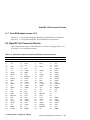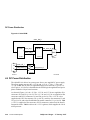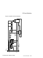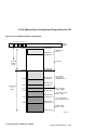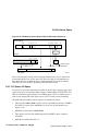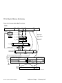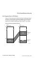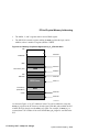
1
Digital Semiconductor
AlphaPC 164 Motherboard
Technical Reference Manual
Order Number: EC–QPFYB–TE
Revision/Update Information: This manual supersedes the Digital Semiconductor
AlphaPC 164 Motherboard Technical Reference
Manual (EC–QPFYA–TE).
Preliminary
Digital Equipment Corporation
Maynard, Massachusetts
http://www.digital.com/semiconductor
January 1997
Possesion, use, or copying of the software described in this publication is authorized only pursuant to a valid written
licence from DIGITAL or an authorized sublicensor.
While DIGITAL believes the information included in this publication is correct as of the date of publication, it is
subject to change without notice.
Digital Equipment Corporation makes no representations that the use of its products in the manner described in this
publication will not infringe on existing or future patent rights, nor do the descriptions contained in this publication
imply the granting of licenses to make, use, or sell equipment or software in accordance with the description.
©Digital Equipment Corporation 1997. All rights reserved.
Printed in U.S.A.
AlphaGeneration, AlphaPC, DEC, DECchip, DECladebug, DIGITAL, Digital Semiconductor, the AlphaGeneration
design mark, and the DIGITAL logo are trademarks of Digital Equipment Corporation.
DIGITAL UNIX Version 3.2 for Alpha is a UNIX 93 branded product.
Digital Semiconductor is a Digital Equipment Corporation business.
AMD and MACH are trademarks of Advanced Micro Devices, Inc.
CDC is a registered trademark of Control Data Corporation.
CompuServe is a registered trademark of CompuServe, Inc.
FaxBACK and Intel are registered trademarks of Intel Corporation.
GRAFOIL is a registered trademark of Union Carbide Corporation.
IEEE is a registered trademark of The Institute of Electrical and Electronics Engineers, Inc.
Linux is a registered trademark of Croce, William R. Della, Jr.
Microsoft and Visual C++ are registered trademarks and NT and Windows NT are trademarks of Microsoft
Corporation.
SMC and Standard Microsystems are registered trademarks of Standard Microsystems Corporation.
TriQuint is a registered trademark of TriQuint Semiconductor, Inc.
UNIX is a registered trademark in the United States and other countries, licensed exclusively through
X/Open Company Ltd.
Xilinx is a trademark of Xilinx Incorporated.
All other trademarks and registered trademarks are the property of their respective holders.
Subject to Change – 17 January 1997
Contents
Preface
1
xi
Introduction to the AlphaPC 164 Motherboard
1.1
1.1.1
1.1.2
1.1.3
1.1.4
1.1.5
1.1.6
1.2
1.3
1.4
1.4.1
1.4.2
1.4.3
1.4.4
2
...........................................................
System Components and Features . . . . . . . . . . . . . . . . . . . . . . . . . . . . .
Digital Semiconductor 21172 Core Logic Chipset . . . . . . . . . . . . . . .
Memory Subsystem . . . . . . . . . . . . . . . . . . . . . . . . . . . . . . . . . . . . . .
L3 Bcache Subsystem Overview . . . . . . . . . . . . . . . . . . . . . . . . . . . .
PCI Interface Overview . . . . . . . . . . . . . . . . . . . . . . . . . . . . . . . . . . .
ISA Interface Overview. . . . . . . . . . . . . . . . . . . . . . . . . . . . . . . . . . . .
Miscellaneous Logic . . . . . . . . . . . . . . . . . . . . . . . . . . . . . . . . . . . . . .
Flash Memory Organization . . . . . . . . . . . . . . . . . . . . . . . . . . . . . . . . . . .
Fail-Safe Booter . . . . . . . . . . . . . . . . . . . . . . . . . . . . . . . . . . . . . . . . . . . .
Software Support . . . . . . . . . . . . . . . . . . . . . . . . . . . . . . . . . . . . . . . . . . .
Windows NT ARC Firmware. . . . . . . . . . . . . . . . . . . . . . . . . . . . . . . .
Alpha SRM Console Firmware . . . . . . . . . . . . . . . . . . . . . . . . . . . . . .
Evaluation Board Software Developer’s Kit . . . . . . . . . . . . . . . . . . . .
Design Support. . . . . . . . . . . . . . . . . . . . . . . . . . . . . . . . . . . . . . . . . .
1–1
1–3
1–3
1–4
1–4
1–5
1–5
1–6
1–7
1–7
1–7
1–8
1–8
1–8
System Configuration and Connectors
2.1
2.1.1
2.1.2
2.1.3
2.1.4
2.1.5
2.1.6
2.1.7
2.2
AlphaPC 164 Jumper Configurations . . . . . . . . . . . . . . . . . . . . . . . . . . . .
Memory Bus Width Jumper (J1) . . . . . . . . . . . . . . . . . . . . . . . . . . . . .
System Clock Divisor Jumpers (IRQ3 through IRQ0) . . . . . . . . . . . .
Bcache Size Jumpers (CF1 and CF2) . . . . . . . . . . . . . . . . . . . . . . . .
Bcache Speed Jumpers (CF4 and CF5) . . . . . . . . . . . . . . . . . . . . . .
Mini-Debugger Jumper (CF6). . . . . . . . . . . . . . . . . . . . . . . . . . . . . . .
Boot Option Jumper (CF7) . . . . . . . . . . . . . . . . . . . . . . . . . . . . . . . . .
Flash ROM Update Jumper (J31) . . . . . . . . . . . . . . . . . . . . . . . . . . .
AlphaPC 164 Connector Pinouts . . . . . . . . . . . . . . . . . . . . . . . . . . . . . . .
17 January 1997 – Subject to Change
2–4
2–5
2–6
2–6
2–6
2–6
2–6
2–7
2–7
iii
3
Power and Environmental Requirements
3.1
3.2
3.3
4
AlphaPC 164 Bcache Interface. . . . . . . . . . . . . . . . . . . . . . . . . . . . . . . . .
Digital Semiconductor 21172 Core Logic Chipset . . . . . . . . . . . . . . . . . .
CIA Chip Overview . . . . . . . . . . . . . . . . . . . . . . . . . . . . . . . . . . . . . . .
DSW Chip Overview. . . . . . . . . . . . . . . . . . . . . . . . . . . . . . . . . . . . . .
Main Memory Interface. . . . . . . . . . . . . . . . . . . . . . . . . . . . . . . . . . . .
PCI Devices . . . . . . . . . . . . . . . . . . . . . . . . . . . . . . . . . . . . . . . . . . . . . . .
Saturn-IO (SIO) Chip . . . . . . . . . . . . . . . . . . . . . . . . . . . . . . . . . . . . .
PCI Expansion Slots. . . . . . . . . . . . . . . . . . . . . . . . . . . . . . . . . . . . . .
ISA Bus Devices . . . . . . . . . . . . . . . . . . . . . . . . . . . . . . . . . . . . . . . . . . . .
Combination Controller. . . . . . . . . . . . . . . . . . . . . . . . . . . . . . . . . . . .
Utility Bus Memory Device . . . . . . . . . . . . . . . . . . . . . . . . . . . . . . . . .
ISA Expansion Slots . . . . . . . . . . . . . . . . . . . . . . . . . . . . . . . . . . . . . .
Interrupts. . . . . . . . . . . . . . . . . . . . . . . . . . . . . . . . . . . . . . . . . . . . . . . . . .
Interrupt PLD Function . . . . . . . . . . . . . . . . . . . . . . . . . . . . . . . . . . . .
System Clocks . . . . . . . . . . . . . . . . . . . . . . . . . . . . . . . . . . . . . . . . . . . . .
Reset and Initialization . . . . . . . . . . . . . . . . . . . . . . . . . . . . . . . . . . . . . . .
Serial ROM . . . . . . . . . . . . . . . . . . . . . . . . . . . . . . . . . . . . . . . . . . . . . . . .
DC Power Distribution. . . . . . . . . . . . . . . . . . . . . . . . . . . . . . . . . . . . . . . .
System Software. . . . . . . . . . . . . . . . . . . . . . . . . . . . . . . . . . . . . . . . . . . .
Serial ROM Code . . . . . . . . . . . . . . . . . . . . . . . . . . . . . . . . . . . . . . . .
Mini-Debugger Code . . . . . . . . . . . . . . . . . . . . . . . . . . . . . . . . . . . . .
Operating Systems . . . . . . . . . . . . . . . . . . . . . . . . . . . . . . . . . . . . . . .
4–2
4–3
4–5
4–5
4–6
4–6
4–8
4–8
4–9
4–9
4–11
4–11
4–11
4–15
4–16
4–19
4–21
4–22
4–24
4–24
4–24
4–25
Upgrading the AlphaPC 164
5.1
5.2
5.3
5.3.1
5.3.2
5.3.3
5.3.4
iv
3–1
3–2
3–2
Functional Description
4.1
4.2
4.2.1
4.2.2
4.2.3
4.3
4.3.1
4.3.2
4.4
4.4.1
4.4.2
4.4.3
4.5
4.5.1
4.6
4.7
4.8
4.9
4.10
4.10.1
4.10.2
4.10.3
5
Power Requirements . . . . . . . . . . . . . . . . . . . . . . . . . . . . . . . . . . . . . . . .
Environmental Requirements . . . . . . . . . . . . . . . . . . . . . . . . . . . . . . . . . .
Board Dimensions . . . . . . . . . . . . . . . . . . . . . . . . . . . . . . . . . . . . . . . . . .
Configuring DRAM Memory . . . . . . . . . . . . . . . . . . . . . . . . . . . . . . . . . . .
Upgrading DRAM Memory . . . . . . . . . . . . . . . . . . . . . . . . . . . . . . . . . . . .
Increasing Microprocessor Speed . . . . . . . . . . . . . . . . . . . . . . . . . . . . . .
Preparatory Information . . . . . . . . . . . . . . . . . . . . . . . . . . . . . . . . . . .
Required Tools . . . . . . . . . . . . . . . . . . . . . . . . . . . . . . . . . . . . . . . . . .
Removing the 21164 Microprocessor. . . . . . . . . . . . . . . . . . . . . . . . .
Installing the 21164 Microprocessor. . . . . . . . . . . . . . . . . . . . . . . . . .
5–1
5–2
5–3
5–3
5–5
5–5
5–5
Subject to Change – 17 January 1997
A
System Address Mapping
A.1
A.2
A.2.1
A.2.2
A.3
A.3.1
A.3.2
A.3.3
A.3.4
A.3.4.1
A.3.4.2
A.3.4.3
A.3.5
A.4
A.4.1
A.4.1.1
A.4.1.2
A.4.2
A.4.3
A.4.3.1
A.4.4
A.4.4.1
A.4.4.2
B
Address Mapping Overview . . . . . . . . . . . . . . . . . . . . . . . . . . . . . . . . A–1
21164 Address Space Configuration Supported by the CIA . . . . . . . A–2
21164 Access to Address Space . . . . . . . . . . . . . . . . . . . . . . . . A–4
PCI Access to Address Space . . . . . . . . . . . . . . . . . . . . . . . . . . A–4
21164 Address Space . . . . . . . . . . . . . . . . . . . . . . . . . . . . . . . . . . . . A–8
PCI Dense Memory Space . . . . . . . . . . . . . . . . . . . . . . . . . . . . A–10
PCI Sparse Memory Space . . . . . . . . . . . . . . . . . . . . . . . . . . . . A–12
PCI Sparse I/O Space . . . . . . . . . . . . . . . . . . . . . . . . . . . . . . . . A–17
PCI Configuration Space . . . . . . . . . . . . . . . . . . . . . . . . . . . . . . A–21
Device Select (IDSEL) . . . . . . . . . . . . . . . . . . . . . . . . . . . . A–24
PCI Special/Interrupt Acknowledge Cycles. . . . . . . . . . . . . A–25
Hardware-Specific and Miscellaneous Register Space . . . A–26
Byte/Word PCI Space . . . . . . . . . . . . . . . . . . . . . . . . . . . . . . . . A–26
PCI-to-Physical Memory Addressing . . . . . . . . . . . . . . . . . . . . . . . . A–29
Address Mapping Windows . . . . . . . . . . . . . . . . . . . . . . . . . . . . A–29
PCI Device Address Space. . . . . . . . . . . . . . . . . . . . . . . . . A–31
Address Mapping Example . . . . . . . . . . . . . . . . . . . . . . . . . A–31
Direct-Mapped Addressing . . . . . . . . . . . . . . . . . . . . . . . . . . . . A–34
Scatter-Gather Addressing . . . . . . . . . . . . . . . . . . . . . . . . . . . . A–35
Scatter-Gather Translation Lookaside Buffer (TLB) . . . . . . A–37
Suggested Use of a PCI Window . . . . . . . . . . . . . . . . . . . . . . . A–41
PCA Compatibility Addressing and Holes. . . . . . . . . . . . . . A–42
Memory Chip Select Signal mem_cs_l . . . . . . . . . . . . . . . . A–42
I/O Space Address Maps
PCI Sparse Memory Space . . . . . . . . . . . . . . . . . . . . . . . . . . . . . . . . B–1
B.1
PCI Sparse I/O Space . . . . . . . . . . . . . . . . . . . . . . . . . . . . . . . . . . . . B–1
B.2
PCI Sparse I/O Space-Region A . . . . . . . . . . . . . . . . . . . . . . . . . B–1
B.2.1
FDC37C935 Combination Controller Register Address
B.2.1.1
Space . . . . . . . . . . . . . . . . . . . . . . . . . . . . . . . . . . . . . . . . . . . . . . . B–2
Flash ROM Segment Select Register . . . . . . . . . . . . . . . . . . B–5
B.2.1.2
Configuration Jumpers (CF0–CF7). . . . . . . . . . . . . . . . . . . . B–5
B.2.1.3
Interrupt Control PLD Addresses . . . . . . . . . . . . . . . . . . . . . B–6
B.2.1.4
PCI Sparse I/O Space-Region B . . . . . . . . . . . . . . . . . . . . . . . . . B–6
B.2.2
PCI Dense Memory Space . . . . . . . . . . . . . . . . . . . . . . . . . . . . . . . B–10
B.3
Flash ROM Memory Addresses . . . . . . . . . . . . . . . . . . . . . . . . B–10
B.3.1
Map of Flash ROM Memory . . . . . . . . . . . . . . . . . . . . . . . . . . . B–11
B.3.2
Flash ROM Configuration Registers . . . . . . . . . . . . . . . . . . . . . B–11
B.3.3
PCI Configuration Address Space . . . . . . . . . . . . . . . . . . . . . . . . . . B–13
B.4
17 January 1997 – Subject to Change
v
B.4.1
B.5
B.6
B.6.1
B.6.2
B.6.3
B.7
C
SIO PCI-to-ISA Bridge Configuration Address Space . . . . . . . . . . . .
PCI Special/Interrupt Acknowledge Cycle Address Space . . . . . . . . . . . .
Hardware-Specific and Miscellaneous Register Space . . . . . . . . . . . . . .
CIA Main CSR Space . . . . . . . . . . . . . . . . . . . . . . . . . . . . . . . . . . . . .
CIA Memory Control CSR Space . . . . . . . . . . . . . . . . . . . . . . . . . . . .
CIA PCI Address Translation Map Space . . . . . . . . . . . . . . . . . . . . .
21164 Microprocessor Cbox IPR Space . . . . . . . . . . . . . . . . . . . . . . . . . .
B–13
B–15
B–15
B–15
B–16
B–17
B–20
SROM Initialization
C.1
C.2
C.3
C.4
C.5
C.6
C.7
C.8
C.9
SROM Initialization . . . . . . . . . . . . . . . . . . . . . . . . . . . . . . . . . . . . . . . . . .
Firmware Interface . . . . . . . . . . . . . . . . . . . . . . . . . . . . . . . . . . . . . . . . . .
Automatic CPU Speed Detection . . . . . . . . . . . . . . . . . . . . . . . . . . . . . . .
Memory Initialization . . . . . . . . . . . . . . . . . . . . . . . . . . . . . . . . . . . . . . . . .
Bcache Initialization . . . . . . . . . . . . . . . . . . . . . . . . . . . . . . . . . . . . . . . . .
Special ROM Header . . . . . . . . . . . . . . . . . . . . . . . . . . . . . . . . . . . . . . . .
Flash ROM Loading . . . . . . . . . . . . . . . . . . . . . . . . . . . . . . . . . . . . . . . . .
Flash ROM Access . . . . . . . . . . . . . . . . . . . . . . . . . . . . . . . . . . . . . . . . . .
Icache Flush Code . . . . . . . . . . . . . . . . . . . . . . . . . . . . . . . . . . . . . . . . . .
D
Supporting Products
E
Glossary and Acronyms
F
Support, Products, and Documentation
C–1
C–2
C–3
C–4
C–4
C–5
C–8
C–9
C–10
Index
vi
Subject to Change – 17 January 1997
Figures
1–1
1–2
2–1
2–2
4–1
4–2
4–3
4–4
4–5
4–6
4–7
4–8
4–9
4–10
5–1
A–1
A–2
A–3
A–4
A–5
A–6
A–7
A–8
A–9
A–10
A–11
A–12
A–13
A–14
A–15
A–16
A–17
A–18
A–19
A–20
A–21
A–22
C–1
AlphaPC 164 Functional Block Diagram . . . . . . . . . . . . . . . . . . . . . . . . .
Division of Flash Blocks. . . . . . . . . . . . . . . . . . . . . . . . . . . . . . . . . . . . . .
AlphaPC 164 Jumper/Connector/Component Location. . . . . . . . . . . . . .
AlphaPC 164 Configuration Jumpers . . . . . . . . . . . . . . . . . . . . . . . . . . .
AlphaPC 164 L3 Bcache Array . . . . . . . . . . . . . . . . . . . . . . . . . . . . . . . .
Main Memory Interface . . . . . . . . . . . . . . . . . . . . . . . . . . . . . . . . . . . . . .
AlphaPC 164 PCI Bus Devices . . . . . . . . . . . . . . . . . . . . . . . . . . . . . . . .
AlphaPC 164 ISA Bus Devices . . . . . . . . . . . . . . . . . . . . . . . . . . . . . . . .
Interrupt Logic . . . . . . . . . . . . . . . . . . . . . . . . . . . . . . . . . . . . . . . . . . . . .
Interrupt/Interrupt Mask Registers . . . . . . . . . . . . . . . . . . . . . . . . . . . . . .
AlphaPC 164 System Clocks. . . . . . . . . . . . . . . . . . . . . . . . . . . . . . . . . .
System Reset and Initialization . . . . . . . . . . . . . . . . . . . . . . . . . . . . . . . .
Serial ROM . . . . . . . . . . . . . . . . . . . . . . . . . . . . . . . . . . . . . . . . . . . . . . .
AlphaPC 164 Power Distribution . . . . . . . . . . . . . . . . . . . . . . . . . . . . . . .
Fan/Heat Sink Assembly . . . . . . . . . . . . . . . . . . . . . . . . . . . . . . . . . . . . .
21164 Address Space . . . . . . . . . . . . . . . . . . . . . . . . . . . . . . . . . . . . . . .
21164 Address Space Configuration . . . . . . . . . . . . . . . . . . . . . . . . . . . .
Address Space Overview . . . . . . . . . . . . . . . . . . . . . . . . . . . . . . . . . . . .
Address Mapping Overview. . . . . . . . . . . . . . . . . . . . . . . . . . . . . . . . . . .
21164 and DMA Read and Write Transactions . . . . . . . . . . . . . . . . . . . .
Dense Space Address Generation . . . . . . . . . . . . . . . . . . . . . . . . . . . . .
PCI Memory Sparse Space Address Generation (Region 1) . . . . . . . . .
PCI Memory Sparse Space Address Generation (Region 2) . . . . . . . . .
PCI Memory Sparse Space Address Generation (Region 3) . . . . . . . . .
PCI Sparse I/O Space Address Translation (Region A) . . . . . . . . . . . . .
PCI Sparse I/O Space Address Translation (Region B) . . . . . . . . . . . . .
PCI Configuration Space Definition . . . . . . . . . . . . . . . . . . . . . . . . . . . . .
Byte/Word PCI Space . . . . . . . . . . . . . . . . . . . . . . . . . . . . . . . . . . . . . . .
PCI DMA Addressing Example . . . . . . . . . . . . . . . . . . . . . . . . . . . . . . . .
PCI Target Window Compare . . . . . . . . . . . . . . . . . . . . . . . . . . . . . . . . .
Direct-Mapped Translation . . . . . . . . . . . . . . . . . . . . . . . . . . . . . . . . . . .
Scatter-Gather PTE Format. . . . . . . . . . . . . . . . . . . . . . . . . . . . . . . . . . .
Scatter-Gather Associative TLB . . . . . . . . . . . . . . . . . . . . . . . . . . . . . . .
Scatter-Gather Map Translation . . . . . . . . . . . . . . . . . . . . . . . . . . . . . . .
Default PCI Window Allocation . . . . . . . . . . . . . . . . . . . . . . . . . . . . . . . .
Memory Chip Select Signal (mem_cs_l) Decode Area . . . . . . . . . . . . . .
Memory Chip Select Signal (mem_cs_l) Logic . . . . . . . . . . . . . . . . . . . .
Special Header Content. . . . . . . . . . . . . . . . . . . . . . . . . . . . . . . . . . . . . .
17 January 1997 – Subject to Change
1–2
1–6
2–2
2–5
4–2
4–4
4–7
4–10
4–12
4–15
4–17
4–20
4–22
4–23
5–6
A–2
A–3
A–4
A–5
A–7
A–11
A–16
A–16
A–17
A–18
A–19
A–21
A–27
A–32
A–33
A–34
A–36
A–38
A–40
A–41
A–43
A–44
C–5
vii
Tables
1–1
2–1
2–2
2–3
2–4
2–5
2–6
2–7
2–8
2–9
2–10
2–11
2–12
2–13
2–14
2–15
2–16
2–17
2–18
3–1
4–1
4–2
5–1
5–2
A–1
A–2
A–3
A–4
A–5
A–6
A–7
A–8
A–9
A–10
A–11
A–12
A–13
B–1
B–2
B–3
B–4
viii
Main Memory Sizes . . . . . . . . . . . . . . . . . . . . . . . . . . . . . . . . . . . . . . . . .
AlphaPC 164 Jumper/Connector/Component List. . . . . . . . . . . . . . . . . .
Peripheral Component Interface (PCI) Bus Connector Pinouts. . . . . . . .
ISA Expansion Bus Connector Pinouts (J33, J35) . . . . . . . . . . . . . . . . .
DRAM SIMM Connector Pinouts (J5 through J12) . . . . . . . . . . . . . . . . .
IDE Drive Bus Connector Pinouts (J13, J14). . . . . . . . . . . . . . . . . . . . . .
Diskette Drive Bus Connector Pinouts (J18) . . . . . . . . . . . . . . . . . . . . . .
Parallel Bus Connector Pinouts (J16) . . . . . . . . . . . . . . . . . . . . . . . . . . .
COM1/COM2 Serial Line Connector Pinouts (J4) . . . . . . . . . . . . . . . . . .
Keyboard/Mouse Connector Pinouts (J15) . . . . . . . . . . . . . . . . . . . . . . .
SROM Test Data Input Connector Pinouts (J32). . . . . . . . . . . . . . . . . . .
Input Power Connector Pinouts (J3) . . . . . . . . . . . . . . . . . . . . . . . . . . . .
Enclosure Fan (+12 V dc) Power Connector Pinouts (J2, J22) . . . . . . . .
Speaker Connector Pinouts (J23) . . . . . . . . . . . . . . . . . . . . . . . . . . . . . .
Microprocessor Fan Power Connector Pinouts (J21) . . . . . . . . . . . . . . .
Power LED Connector Pinouts (J27). . . . . . . . . . . . . . . . . . . . . . . . . . . .
IDE Drive LED Connector Pinouts (J28) . . . . . . . . . . . . . . . . . . . . . . . . .
Reset Button Connector Pinouts (J24) . . . . . . . . . . . . . . . . . . . . . . . . . .
Halt Button Connector Pinouts (J25) . . . . . . . . . . . . . . . . . . . . . . . . . . . .
Power Supply DC Current Requirements . . . . . . . . . . . . . . . . . . . . . . . .
AlphaPC 164 System Interrupts . . . . . . . . . . . . . . . . . . . . . . . . . . . . . . .
ISA Interrupts. . . . . . . . . . . . . . . . . . . . . . . . . . . . . . . . . . . . . . . . . . . . . .
AlphaPC 164 DRAM Memory Configurations . . . . . . . . . . . . . . . . . . . . .
Memory Upgrade Options . . . . . . . . . . . . . . . . . . . . . . . . . . . . . . . . . . . .
21164 Physical Address Space . . . . . . . . . . . . . . . . . . . . . . . . . . . . . . . .
int4_valid_h<3:0> and addr<4:3> for Sparse Space Write Transactions
PCI Memory Sparse Space Read/Write Encodings . . . . . . . . . . . . . . . .
HAE_MEM High-Order Sparse Space Bits . . . . . . . . . . . . . . . . . . . . . . .
PCI I/O Sparse Space Read/Write Encodings. . . . . . . . . . . . . . . . . . . . .
PCI Configuration Space Read/Write Encodings . . . . . . . . . . . . . . . . . .
Generating IDSEL Pin Signals. . . . . . . . . . . . . . . . . . . . . . . . . . . . . . . . .
Hardware-Specific Register Address Space . . . . . . . . . . . . . . . . . . . . . .
21164 Byte/Word Addressing . . . . . . . . . . . . . . . . . . . . . . . . . . . . . . . . .
PCI Target Window MASK Register (Wn_MASK) . . . . . . . . . . . . . . . . . .
Direct-Mapped PCI Target Address Translation . . . . . . . . . . . . . . . . . . .
Scatter-Gather Mapped PCI Target Address Translation . . . . . . . . . . . .
PCI Window Power-Up Configuration . . . . . . . . . . . . . . . . . . . . . . . . . . .
Combination Controller Register Address Space Map . . . . . . . . . . . . . .
Flash ROM Segment Select Register . . . . . . . . . . . . . . . . . . . . . . . . . . .
Configuration Jumpers (CF0-CF7) . . . . . . . . . . . . . . . . . . . . . . . . . . . . .
Interrupt Control PLD Addresses. . . . . . . . . . . . . . . . . . . . . . . . . . . . . . .
1–4
2–3
2–7
2–8
2–9
2–10
2–10
2–10
2–11
2–11
2–11
2–12
2–12
2–12
2–12
2–13
2–13
2–13
2–13
3–1
4–13
4–14
5–2
5–2
A–8
A–14
A–14
A–15
A–20
A–23
A–24
A–26
A–28
A–30
A–35
A–37
A–42
B–2
B–5
B–5
B–6
Subject to Change – 17 January 1997
B–5
B–6
B–7
B–8
B–9
B–10
B–11
B–12
B–13
B–14
C–1
C–2
SIO Bridge Operating Register Address Space Map. . . . . . . . . . . . . . . .
Flash ROM Memory Addresses (Within Segment) . . . . . . . . . . . . . . . . .
Map of Flash ROM Memory. . . . . . . . . . . . . . . . . . . . . . . . . . . . . . . . . . .
Flash ROM Configuration Registers . . . . . . . . . . . . . . . . . . . . . . . . . . . .
Address Bits and PCI Device IDSEL Pins . . . . . . . . . . . . . . . . . . . . . . . .
SIO Bridge Configuration Address Space Map . . . . . . . . . . . . . . . . . . . .
CIA Control, Diagnostic, and Error Registers . . . . . . . . . . . . . . . . . . . . .
CIA Memory Control Registers . . . . . . . . . . . . . . . . . . . . . . . . . . . . . . . .
PCI Address Translation Registers . . . . . . . . . . . . . . . . . . . . . . . . . . . . .
21164 Cache Configuration Registers. . . . . . . . . . . . . . . . . . . . . . . . . . .
Output Parameter Descriptions . . . . . . . . . . . . . . . . . . . . . . . . . . . . . . . .
Special Header Entry Descriptions . . . . . . . . . . . . . . . . . . . . . . . . . . . . .
17 January 1997 – Subject to Change
B–6
B–10
B–11
B–12
B–13
B–13
B–15
B–16
B–17
B–20
C–2
C–6
ix
Preface
Overview
This manual describes the DIGITAL AlphaPC 164 motherboard, a module for
computing systems based on the Digital Semiconductor 21164 Alpha
microprocessor and the Digital Semiconductor 21172 core logic chipset.
Audience
This manual is intended for system designers and others who use the AlphaPC 164
motherboard to design or evaluate computer systems based on the Digital
Semiconductor 21164 Alpha microprocessor and the Digital Semiconductor 21172
core logic chipset.
Scope
This manual describes the features, configuration, functional operation, and
interfaces of the AlphaPC 164 motherboard. This manual does not include specific
bus specifications (for example, PCI or ISA buses). Additional information is
available in the AlphaPC 164 schematics, program source files, and the appropriate
vendor and IEEE specifications. See Appendix F for information on how to order
related documentation and obtain additional technical support.
Manual Organization
This manual includes the following chapters and appendixes and an index.
•
Chapter 1, Introduction to the AlphaPC 164 Motherboard, is an overview of the
AlphaPC 164 motherboard, including its components, features, and uses.
•
Chapter 2, System Configuration and Connectors, describes the userenvironment configuration, board connectors and functions, and jumper
functions. It also identifies jumper and connector locations.
•
Chapter 3, Power and Environmental Requirements, describes the AlphaPC 164
power and environmental requirements and provides board dimensions.
17 January 1997 – Subject to Change
xi
•
Chapter 4, Functional Description, provides a functional description of the
AlphaPC 164 motherboard, including the 21172 core logic chipset, L3 backup
cache (Bcache) and memory subsystems, system interrupts, clock and power
subsystems, and peripheral component interconnect (PCI) and Industry Standard
Architecture (ISA) devices.
•
Chapter 5, Upgrading the AlphaPC 164, describes how to upgrade the AlphaPC
164 motherboard’s DRAM memory and microprocessor speed.
•
Appendix A, System Address Mapping, describes the mapping of the 40-bit
processor address space into memory and I/O space addresses.
•
Appendix B, I/O Space Address Maps, lists the physical AlphaPC 164 PCI
address spaces and regions, including the 21172-CA operating registers and
PCI/ISA device registers.
•
Appendix C, SROM Initialization, describes the general serial read-only
memory (SROM), Bcache, and memory initialization steps and associated
parameters. Also included are the firmware interface, timing considerations, and
SROM header information.
•
Appendix D, Supporting Products, lists sources for components and accessories
not included with the AlphaPC 164 motherboard.
•
Appendix E, Glossary and Acronyms, lists and defines terms associated with the
AlphaPC 164 motherboard.
•
Appendix F, Support, Products, and Documentation, describes how to obtain
Digital Semiconductor information and technical support, and how to order
Digital Semiconductor products and associated literature.
Conventions
This section defines product-specific terminology, abbreviations, and other
conventions used throughout this manual.
Abbreviations
•
Register Access
The following list describes the register bit and field abbreviations:
xii
Subject to Change – 17 January 1997
Bit/Field Abbreviation Description
RO (read only)
RW (read/write)
WO (write only)
•
Bits and fields specified as RO can be read but not written.
Bits and fields specified as RW can be read and written.
Bits and fields specified as WO can be written but not read.
Binary Multiples
The abbreviations K, M, and G (kilo, mega, and giga) represent binary multiples
and have the following values.
=
210 (1024)
=
=
220 (1,048,576)
230 (1,073,741,824)
2KB
=
2 kilobytes
4MB
8GB
=
=
K
M
G
For example:
=
4 megabytes =
8 gigabytes =
2 × 210 bytes
4 × 220 bytes
8 × 230 bytes
Addresses
Unless otherwise noted, all addresses and offsets are hexadecimal.
Bit Notation
Multiple-bit fields can include contiguous and noncontiguous bits contained in angle
brackets (<>). Multiple contiguous bits are indicated by a pair of numbers separated
by a colon (:). For example, <9:7,5,2:0> specifies bits 9,8,7,5,2,1, and 0. Similarly,
single bits are frequently indicated with angle brackets. For example, <27> specifies
bit 27.
Caution
Cautions indicate potential damage to equipment, software, or data.
Data Field Size
The term INTnn, where nn is one of 2, 4, 8, 16, 32, or 64, refers to a data field of nn
contiguous NATURALLY ALIGNED bytes. For example, INT4 refers to a
NATURALLY ALIGNED longword.
17 January 1997 – Subject to Change
xiii
Data Units
The following data-unit terminology is used throughout this manual.
Term
Words
Bytes
Bits
Other
Byte
Word
Longword/Dword
Quadword
Octaword
Hexword
½
1
2
4
8
16
1
2
4
8
16
32
8
16
32
64
128
256
—
—
Longword
2 Longwords
2 Quadwords
2 Octawords
Note
Notes emphasize particularly important information.
Numbering
All numbers are decimal or hexadecimal unless otherwise indicated. The prefix 0x
indicates a hexadecimal number. For example, 19 is decimal, but 0x19 and 0x19A
are hexadecimal (also see Addresses). Otherwise, the base is indicated by a
subscript; for example, 1002 is a binary number.
Ranges and Extents
Ranges are specified by a pair of numbers separated by two periods (..) and are
inclusive. For example, a range of integers 0..4 includes the integers 0, 1, 2, 3, and 4.
Extents are specified by a pair of numbers in angle brackets (< >) separated by a
colon (:) and are inclusive. Bit fields are often specified as extents. For example, bits
<7:3> specifies bits 7, 6, 5, 4, and 3.
Register and Memory Figures
Register figures have bit and field position numbering starting at the right (low
order) and increasing to the left (high order).
Memory figures have addresses starting at the top and increasing toward the bottom.
Schematic References
Logic schematics are included in the AlphaPC 164 design package. In this manual,
references to schematic pages are printed in italics. For example, the following
specifies schematic page 3:
“. . . the 36.66-MHz oscillator (pc164.3) supplies . . .”
xiv
Subject to Change – 17 January 1997
In some cases, more than one schematic page is referenced. For example, the
following specifies schematic pages 10 through 13:
“. . . the data switches (pc164.10–13) . . .”
Signal Names
All signal names are printed in boldface type. Signals whose name originates in an
industry-standard specification, such as PCI or IDE, are printed in the case as found
in the specification (usually uppercase). Active-high signals are indicated by the _h
suffix. Active-low signals have the _l suffix, a pound sign “#” appended, or a “not”
overscore bar. Signals with no suffix are considered high-asserted signals. For
example, signals data_h<127:0> and cia_int are active-high signals. Signals
mem_ack_l, FRAME#, and RESET are active-low signals.
UNPREDICTABLE and UNDEFINED
Throughout this manual the terms UNPREDICTABLE and UNDEFINED are used.
Their meanings are quite different and must be carefully distinguished.
In particular, only privileged software (that is, software running in kernel mode) can
trigger UNDEFINED operations. Unprivileged software cannot trigger
UNDEFINED operations. However, either privileged or unprivileged software can
trigger UNPREDICTABLE results or occurrences.
UNPREDICTABLE results or occurrences do not disrupt the basic operation of the
processor. The processor continues to execute instructions in its normal manner. In
contrast, UNDEFINED operations can halt the processor or cause it to lose
information.
The terms UNPREDICTABLE and UNDEFINED can be further described as
follows:
•
UNPREDICTABLE
–
Results or occurrences specified as UNPREDICTABLE might vary from
moment to moment, implementation to implementation, and instruction to
instruction within implementations. Software can never depend on results
specified as UNPREDICTABLE.
–
An UNPREDICTABLE result might acquire an arbitrary value that is
subject to a few constraints. Such a result might be an arbitrary function of
the input operands or of any state information that is accessible to the
process in its current access mode. UNPREDICTABLE results may be
unchanged from their previous values.
17 January 1997 – Subject to Change
xv
Operations that produce UNPREDICTABLE results might also produce
exceptions.
–
An occurrence specified as UNPREDICTABLE may or may not happen
based on an arbitrary choice function. The choice function is subject to the
same constraints as are UNPREDICTABLE results and must not constitute a
security hole.
Specifically, UNPREDICTABLE results must not depend upon, or be a
function of, the contents of memory locations or registers that are
inaccessible to the current process in the current access mode.
Also, operations that might produce UNPREDICTABLE results must not
write or modify the contents of memory locations or registers to which the
current process in the current access mode does not have access. They must
also not halt or hang the system or any of its components.
For example, a security hole would exist if some UNPREDICTABLE result
depended on the value of a register in another process, on the contents of
processor temporary registers left behind by some previously running
process, or on a sequence of actions of different processes.
•
xvi
UNDEFINED
–
Operations specified as UNDEFINED can vary from moment to moment,
implementation to implementation, and instruction to instruction within
implementations. The operation can vary in effect from nothing, to stopping
system operation.
–
UNDEFINED operations can halt the processor or cause it to lose
information. However, UNDEFINED operations must not cause the
processor to hang, that is, reach an unhalted state from which there is no
transition to a normal state in which the machine executes instructions. Only
privileged software (that is, software running in kernel mode) can trigger
UNDEFINED operations.
Subject to Change – 17 January 1997
1
Introduction to the AlphaPC 164
Motherboard
This chapter provides an overview of the AlphaPC 164 motherboard, its
components, features, and uses.
The Digital Semiconductor AlphaPC 164 Motherboard (AlphaPC 164) is a module
for computing systems based on the Digital Semiconductor 21172 core logic chipset.
The AlphaPC 164 provides a single-board hardware and software development
platform for the design, integration, and analysis of supporting logic and subsystems.
The board also provides a platform for PCI I/O device hardware and software
development.
Appendix F provides ordering information and a list of related documentation.
1.1 System Components and Features
The AlphaPC 164 is implemented in industry-standard parts and uses a Digital
Semiconductor 21164 Alpha microprocessor running at 366 MHz (supports 400,
433, 466, and 500 MHz). The functional components are shown in Figure 1–1 and
introduced in the following subsections.
17 January 1997 – Subject to Change
Introduction to the AlphaPC 164 Motherboard
1–1
System Components and Features
Figure 1–1 AlphaPC 164 Functional Block Diagram
Index
19
Control
21164 Alpha
Microprocessor
1MB L3
Bcache
Bcache Tag
10
Data
128
Check
DECchip 21172 Core
Logic Chipset
DECchip 21172-BA
Data Switch
16
(X4)
37
DRAM
SIMM
Sockets
(X8)
Data
64
Control
Address
128/256-Bit Data
DECchip 21172-CA
Control, I/O Interface,
and Address
Commands
Address/Control
PCI Bus
IDE
Controller
Support
- Oscillator
- Serial ROM
2 Dedicated 64-Bit PCI Slots
2 Dedicated 32-Bit PCI Slots
2 Dedicated ISA Slots
PCI-to-ISA
Bridge
4 Devices
Flash ROM
Combination
Controller
1–2
Introduction to the AlphaPC 164 Motherboard
Diskette
Parallel Port
2 Serial Ports
Keyboard/Mouse
Time-of-Year Clock
PC164-01
Subject to Change – 17 January 1997
System Components and Features
1.1.1 Digital Semiconductor 21172 Core Logic Chipset
The 21164 microprocessor is supported by the 21172 core logic chipset. The chipset
consists of the following two application-specific integrated circuit (ASIC) types:
•
One copy of the Digital Semiconductor 21172-CA control, I/O interface, and
address (CIA) chip provides the interface between the 21164 microprocessor,
main memory (addressing and control), and the PCI bus. It also provides the
companion data switch chips with control information to direct the data flow.
•
Four copies of the Digital Semiconductor 21172-BA data switch (DSW) chip
provide the memory interface data path and route PCI data through the CIA chip.
The chipset includes the majority of functions required to develop a highperformance PC or workstation, requiring minimum discrete logic on the module. It
provides flexible and generic functions to allow its use in a wide range of systems.
1.1.2 Memory Subsystem
The dynamic random-access memory (DRAM) is contained in one bank of single
inline memory modules (SIMMs). Single- or double-sided SIMMs may be used.
Each SIMM is 36 bits wide, with 32 data bits and 4 check bits, with 70 ns or less
access. Four SIMMs fill a data bus width of 128 bits and provide 16MB to 256MB.
Eight SIMMs fill a data bus width of 256 bits and provide 32MB to 512MB.
Table 1–1 lists the SIMM sizes supported and the corresponding main memory size
for 256-bit arrays.
17 January 1997 – Subject to Change
Introduction to the AlphaPC 164 Motherboard
1–3
System Components and Features
Table 1–1 Main Memory Sizes
Total Memory
128-Bit Data Bus Width
with 4 SIMMs of Size...
16MB
32MB
64MB
128MB
256MB
1Mb X 36
2Mb X 36
4Mb X 36
8Mb X 36
16Mb X 36
Total Memory
256-Bit Data Bus Width
with 8 SIMMs of Size...
32MB
64MB
128MB
256MB
512MB
1Mb X 36
2Mb X 36
4Mb X 36
8Mb X 36
16Mb X 36
1.1.3 L3 Bcache Subsystem Overview
The AlphaPC 164 board-level L3 backup cache (Bcache) is a 1MB, direct-mapped,
synchronous SRAM with a 128-bit data path. The board is capable of handling an L3
cache size of 2MB.
1.1.4 PCI Interface Overview
The AlphaPC 164 PCI interface is the main I/O bus for the majority of functions
(SCSI interface, graphics accelerator, and so on). The PCI interface has a 33 MHz
data transfer rate at all supported microprocessor speed BINs. PCI-IDE support is
provided by an onboard controller chip (CMD646). An onboard PCI-to-ISA bridge
is provided through an Intel 82378ZB Saturn-I/O (SIO) chip.
The PCI bus has four dedicated PCI expansion slots (two 64-bit and two 32-bit).
1–4
Introduction to the AlphaPC 164 Motherboard
Subject to Change – 17 January 1997
System Components and Features
1.1.5 ISA Interface Overview
The ISA bus provides the following system support functions:
•
Two expansion slots.
•
An SMC FDC37C935 combination controller chip provides:
•
–
A mouse and keyboard controller
–
A diskette controller
–
Two universal asynchronous receiver-transmitters (UARTs) with full
modem control
–
A bidirectional parallel port
–
A time-of-year (TOY) clock
Operating system support—provided by a 1MB flash ROM that contains
supporting firmware.
1.1.6 Miscellaneous Logic
The AlphaPC 164 contains the following miscellaneous components:
•
Clocks
–
A 36.66-MHz oscillator (default) and X10 phase-locked loop (PLL) clock
generator provide a clock source to the 366 MHz 21164 microprocessor. The
microprocessor supplies a clock to the system PLL/clock buffer for the
chipset and PCI devices.
–
A 14.318-MHz crystal and frequency generator provide a clock source for
the FDC37C935 ISA device controller. The controller’s onchip generator
then provides other clocks as needed.
–
A 32-kHz crystal provides the TOY clock source.
•
Serial ROM – A Xilinx XC17128 serial ROM (SROM) contains initial code that
is loaded into the 21164 instruction cache (Icache) on power-up. A serial line
interface is also provided to allow direct connection to a terminal line for
debugging purposes.
•
AMD MACH210-15 programmable logic devices (PLDs) for interrupts and PCI
bus arbitration.
17 January 1997 – Subject to Change
Introduction to the AlphaPC 164 Motherboard
1–5
Flash Memory Organization
1.2 Flash Memory Organization
The AlphaPC 164 incorporates a 1MB flash having sixteen 64KB blocks or
segments. Figure 1–2 shows the division of these blocks. The first 64KB block,
block 0, contains the fail-safe booter. The next fourteen 64KB blocks, blocks 1
through 14 (896KB), are allocated to the primary firmware. The last block, block 15,
is allocated for storing any environment variables that the primary firmware needs to
save.
Figure 1–2 Division of Flash Blocks
Environment Space 64KB
Block 15
Primary Firmware
896KB
Fail-Safe Booter 64KB
Block 0
PC164-11
The AlphaPC 164 ships with one of two types of primary firmware; Windows NT
ARC firmware or the Alpha SRM Console firmware. Under normal conditions the
primary firmware runs by default when power is applied to the AlphaPC 164. A user
may run other firmware by replacing their primary firmware with the desired code
using the standard firmware update utility (fwupdate.exe) provided with the
Evaluation Board Software Developer’s Kit and Firmware Update (EBSDK)
compact disk.
1–6
Introduction to the AlphaPC 164 Motherboard
Subject to Change – 17 January 1997
Fail-Safe Booter
1.3 Fail-Safe Booter
The fail-safe booter is a small (64KB) firmware program that provides a recovery
procedure when the flash is corrupted. When the flash becomes corrupted, this utility
can be run to facilitate booting a firmware update utility from a floppy diskette that is
capable of reprogramming the flash. When the fail-safe booter runs, it expects to find
a floppy containing the file fwupdate.exe. If the file is found, the fail-safe booter
loads and executes this program.
Due to the size limitation placed on the fail-safe booter, status is not displayed on
either the graphics display or the serial communications ports while the firmware
update utility is loading. The user is informed that the fail-safe booter is in operation
by a series of beeps along with the activity light being activated on the floppy drive
while the program is loading. The beep code 1-2-3 is the beep sequence assigned to
the fail-safe booter. That is one beep, then two beeps, followed by three beeps.
A user can force the fail-safe booter to run instead of the primary firmware by
inserting jumper CF7, described in Section 2.1.6. If the primary firmware image
becomes corrupted in flash memory, the fail-safe booter is automatically run to
enable the user to reprogram the flash image.
In the unlikely event that the entire flash is corrupted such that neither the fail-safe
booter or the primary firmware can be started, the Xload procedure (Uload on
UNIX) can be used along with the SROM Mini-Debugger to provide a low-level
flash recovery mechanism. Xload and Uload are provided on the EBSDK along
with instructions on how to use them. The EBSDK also includes source code for the
fail-safe booter and some of the tools required to build it.
1.4 Software Support
The support elements described in this section are either included with the
AlphaPC 164 or are available separately.
1.4.1 Windows NT ARC Firmware
Windows NT ARC firmware is required to install and boot the Microsoft
Windows NT operating system on the AlphaPC 164. This Digital Semiconductor
firmware comes factory installed in the 21A04-B0 variation of the AlphaPC 164.
When installed, this firmware occupies the flash blocks reserved for the primary
firmware. Binary images of the Windows NT ARC firmware are included on the
EBSDK, along with a license describing the terms for use and distribution.
17 January 1997 – Subject to Change
Introduction to the AlphaPC 164 Motherboard
1–7
Software Support
1.4.2 Alpha SRM Console Firmware
The Alpha SRM Console firmware is required to install and boot DIGITAL UNIX
on the AlphaPC 164. This Digital Semiconductor firmware comes factory installed
in the 21A04-B2 variation of the AlphaPC 164. When installed, this firmware
occupies the flash blocks reserved for the primary firmware. Binary images of the
Alpha SRM Console firmware are included on the EBSDK compact disk, along with
a license describing the terms for use and distribution.
1.4.3 Evaluation Board Software Developer’s Kit
The Evaluation Board Software Developer’s Kit and Firmware Update is designed to
provide an environment for developing software for Alpha motherboard products. It
is also specially suited for low-level software development and hardware debug for
other Alpha microprocessor-based designs.
The following list includes some of the components of the EBSDK:
•
The Alpha Evaluation Board Debug Monitor firmware with source code.
•
Power-up initialization SROM and SROM Mini-Debugger with source code.
•
Sample PALcode sources modeled after DIGITAL UNIX with source code.
•
Fail-safe booter with source code.
•
Various additional tools with source code.
The following development platforms are supported by the EBSDK:
•
DIGITAL UNIX with the C Developer’s Extensions.
•
Windows NT (Alpha) with the Microsoft Visual C++ Development System for
DIGITAL Alpha.
•
Windows NT (Intel) with the Microsoft Visual C++ Development System and
Tools provide limited support. This environment is currently useful for SROM
and PALcode development only.
1.4.4 Design Support
The full design database, including schematics and source files, is supplied. User
documentation is also included. The database allows designers with no previous
Alpha architecture experience to successfully develop a working Alpha system with
minimal assistance.
1–8
Introduction to the AlphaPC 164 Motherboard
Subject to Change – 17 January 1997
2
System Configuration and Connectors
This chapter describes the user-environment configuration, board connectors and
functions, and jumper functions. It also identifies jumper and connector locations.
The AlphaPC 164 uses jumpers to implement configuration parameters such as
system speed, data path width, and boot parameters. These jumpers must be
configured for the user’s environment. Onboard connectors are provided for the I/O
interfaces, SIMMs, and serial and parallel peripheral ports.
Figure 2–1 shows the board outlines, and identifies the location of jumpers,
connectors, and major components. Table 2–1 lists and defines these items. Refer to
Section 2.1 for jumper configurations. Refer to Section 2.2 for connector pinouts.
17 January 1997 – Subject to Change
System Configuration and Connectors
2–1
Figure 2–1 AlphaPC 164 Jumper/Connector/Component Location
J30
J35
J31
J33
U52
U51
2
26
1
25
J32
1
3
J28
U49
U48
U50
J29
J27
B1
J25
J21
1
3 1 1 3
1
5
4
U34
J20
U41
U39
J22
J26
1 2
U40
U35
J19
U36
J23
J18
33
1
2
34
J24
U25
U29
U21
U22
J13
1 2 1 2
J14
U15
U16
U17
U10
U11
U12
J16
U18
39 40 39 40
J15
U14
U5
U6
U7
Top:
Mouse
Bottom: Keyboard
J4
Cache SRAM (L3)
Top:
COM1
Bottom: COM2
U2
1 3
20
J3
2–2
10 View from edge
11
1
J1
J5
J6
System Configuration and Connectors
J7
J8
J9
J10
J11
J12
J2
MK-2306-35
Subject to Change – 17 January 1997
Table 2–1 AlphaPC 164 Jumper/Connector/Component List
Item Number Description
Item Number Description
B1
J2
J4
J6
J8
J10
J12
J14
J16
J19
J21
RTC battery (CR2032)
Fan power, enclosure (+12V)
COM1/COM2 (DB9) connectors
DRAM SIMM 1 [71:36] connector
DRAM SIMM 3 [143:108] connector
DRAM SIMM 5 [215:180] connector
DRAM SIMM 7 [287:252] connector
IDE drive 0/1 connector
Parallel I/O connector
PCI slot 3 (32-bit)
Microprocessor fan/fan sense connector
Speaker connector
Halt button connector
Power LED connector
PCI slot 0 (64-bit)
Flash update enable/disable jumper
ISA slot 1
Data switch 0 (DSC 21172-BA)
Cache SRAM (L3)
Cache SRAM (L3)
Microprocessor, socketed
(DSC 21164 Alpha)
I/O interface and address control
(DSC 21172-CA)
Microprocessor clock crystal, 36.66MHz (default), socketed
System clock PLL (CDC 2586)
J1
J3
J5
J7
J9
J11
J13
J15
J18
J20
J22
Memory bus width jumper
Power (+3V, +5V, -5V, +12V, -12V)
DRAM SIMM 0 [35:0] connector
DRAM SIMM 2 [107:72] connector
DRAM SIMM 4 [179:144] connector
DRAM SIMM 6 [251:216] connector
IDE drive 2/3 connector
Keyboard/mouse connectors
Diskette (floppy) drive connector
PCI slot 2 (32-bit)
Enclosure fan +12V power connector
J24
J26
J28
J30
J32
J35
U5 to U7
U14
U18
U22
Reset button connector
PCI slot 1 (64-bit)
Hard-drive LED connector
Configuration jumpers
SROM test port connector
ISA slot 0
Cache SRAM (L3)
Data switch 1 (DSC 21172-BA)
Data switch 2 (DSC 21172-BA)
Data switch 3 (DSC 21172-BA)
U29
IDE controller
U35
PCI-to-ISA bridge
(Intel 82378ZB)
Flash ROM (1MB)
PCI interrupt request PAL
Power sense
U41
Microprocessor clock PLL (TriQuint
TQ2061)
Serial ROM, socketed
(Xilinx XC17128D)
Combination controller, Super I/O
(SMC FDC37C935)
PCI arbiter PAL
Power controller
—
J23
J25
J27
J29
J31
J33
U2
U10 to U12
U15 to U17
U21
U25
U34
U36
U40
U48
U50
U52
17 January 1997 – Subject to Change
U39
U49
U51
—
System Configuration and Connectors
2–3
AlphaPC 164 Jumper Configurations
2.1 AlphaPC 164 Jumper Configurations
The AlphaPC 164 has three groups of jumpers at location J1, J30, and J31. These
jumpers set the hardware configuration and boot options. Figure 2–1 shows the
jumper location on the AlphaPC 164. Figure 2–2 shows the jumper functions for
each group. Section 2.1.1 through Section 2.1.7 describe the jumper configurations.
2–4
System Configuration and Connectors
Subject to Change – 17 January 1997
AlphaPC 164 Jumper Configurations
Figure 2–2 AlphaPC 164 Configuration Jumpers
J30 System Configuration Jumpers
IRQ3
1
IRQ2
3
IRQ1
5
IRQ0
7
CF0
9
CF1
11
CF2
13
CF3
15
CF4
17
CF5
19
CF6
21
Mini-Debugger (Default Out)
CF7
23
Boot_Option (Default Out)
25
Not Used
Frequency
366 MHz
400 MHz
433 MHz
466 MHz
500 MHz
Ratio
11
12
13
14
15
IRQ3 IRQ2 IRQ1 IRQ0
In
Out Out
Out
Out
In
In
Out
Out
In
Out
Out
Out
Out Out
In
Out
Out Out Out
All other combinations
Comments
Reserved
Reserved (Default Out)
Bcache Size
1MB
2MB
CF1
CF2
Out
Out
Out
In
All other combinations
Reserved (Default Out)
Bcache Speed
9 ns
CF4
CF5
Out
Out
All other combinations
Comments
Default
Reserved
Comments
Default
Reserved
J1 Memory Bus Width Jumper
1
In = 128-Bit Bus
2
Out = 256-Bit Bus
Note: Jumper must be out when all
eight DRAM SIMM sockets are populated.
J31 Flash ROM Update Jumper
1
1 to 2 In = Disable
2
2 to 3 In = Enable (Default)
3
MK-2306-36A
2.1.1 Memory Bus Width Jumper (J1)
The memory bus width can be either 128-bits (J5 through J8 populated with SIMMs
and J9 through J12 empty) or 256-bits (J5 through J12 populated with SIMMs).
When using a memory bus width of 128-bits, jumper J1 must be in. When using a
memory bus width of 256-bits, jumper J1 must be out.
17 January 1997 – Subject to Change
System Configuration and Connectors
2–5
AlphaPC 164 Jumper Configurations
2.1.2 System Clock Divisor Jumpers (IRQ3 through IRQ0)
The system clock divisor jumpers are located at J30—1/2 (IRQ3), J30—3/4 (IRQ2),
J30—5/6 (IRQ1), and J30—7/8 (IRQ0). The jumper configuration set in IRQ3
through IRQ0 determines the frequency of the microprocessor’s system clock
output. These four jumpers set the speed at power-up as listed in Figure 2–2. The
microprocessor frequency divided by the ratio determines the system clock
frequency.
2.1.3 Bcache Size Jumpers (CF1 and CF2)
The Bcache size jumpers are located at J30—11/12, CF1 and J30—13/14, CF2.
These jumpers configure the Bcache as specified in Figure 2–2.
2.1.4 Bcache Speed Jumpers (CF4 and CF5)
The Bcache speed jumpers are located at J30—17/18, CF4 and J30—19/20, CF5.
These jumpers select the Bcache timing parameters used to compute a value that is
loaded into the microprocessor’s Bcache configuration register at power-up time.
Because the Bcache SRAMs are soldered onto the board, the default jumper
configuration selecting an SRAM access time of 9 ns as shown in Figure 2–2 will
always be used.
2.1.5 Mini-Debugger Jumper (CF6)
The Mini-Debugger jumper is located at J30—21/22 (CF6). The default position for
this jumper is out (Figure 2–2). The Alpha SROM Mini-Debugger is stored in the
SROM. When this jumper is in it causes the SROM initialization to trap to the MiniDebugger (communication through connector J32) after all initialization is complete,
but before starting the execution of the system flash ROM code.
2.1.6 Boot Option Jumper (CF7)
The boot option jumper is located at J30—23/24 (CF7). The default position for this
jumper is out (Figure 2–2). This jumper selects the image to be loaded into memory
from the system flash ROM. With the jumper out, the Windows NT ARC firmware
is loaded. With the jumper in, the fail-safe booter is loaded. For more information
about the fail-safe booter, refer to the AlphaPC 164 Motherboard User’s Manual.
2–6
System Configuration and Connectors
Subject to Change – 17 January 1997
AlphaPC 164 Connector Pinouts
2.1.7 Flash ROM Update Jumper (J31)
When J31—2/3 are jumpered together (default), the flash ROM is write-enabled.
When J31—1/2 are jumpered together, the flash ROM is write-protected.
2.2 AlphaPC 164 Connector Pinouts
This section lists the pinouts of all connectors (see Table 2–2 through Table 2–18).
See Figure 2–1 for connector locations.
Table 2–2 Peripheral Component Interface (PCI) Bus Connector Pinouts
Pin
Signal
Pin
Signal
Pin
Signal
Pin
Signal
32-Bit and 64-Bit PCI Connectors (J19, J20, J26, J29)
A1
A5
TRST#
+5V
A2
A6
+12V
INTA
A3
A7
TMS
INTC
A4
A8
TDI
+5V
A9
A13
A17
A21
A25
A29
A33
A37
A41
A45
A49
A53
—
GND
GNT#
+3V
AD[24]
AD[20]
+3V
STOP#
SBO#
+3V
AD[09]
+3V
A10
A14
A18
A22
A26
A30
A34
A38
A42
A46
A50
A54
+5V
—
GND
AD[28]
IDSEL
GND
FRAME#
STOP#
GND
AD[13]
Not used
AD[06]
A11
A15
A19
A23
A27
A31
A35
A39
A43
A47
A51
A55
—
RST#
—
AD[26]
+3V
AD[18]
GND
+3V
PAR
AD[11]
Not used
AD[04]
A12
A16
A20
A24
A28
A32
A36
A40
A44
A48
A52
A56
GND
+5V
AD[30]
GND
AD[22]
AD[16]
TRDY#
SDONE
AD[15]
GND
C/BE#[0]
GND
A57
A61
B3
B7
B11
B15
B19
B23
B27
B31
B35
B39
AD[02]
+5V
GND
INTB
PRSNT2#
GND
+5V
AD[27]
AD[23]
+3V
IRDY#
LOCK#
A58
A62
B4
B8
B12
B16
B20
B24
B28
B32
B36
B40
AD[00]
+5V
TDO
INTD
GND
CLK
AD[31]
AD[25]
GND
AD[17]
+3V
PERR#
A59
B1
B5
B9
B13
B17
B21
B25
B29
B33
B37
B41
+5V
-12V
+5V
PRSNT1#
GND
GND
AD[29]
+3V
AD[21]
C/BE#[2]
DEVSEL#
+3V
A60
B2
B6
B10
B14
B18
B22
B26
B30
B34
B38
B42
REQ64#
TCK
+5V
—
—
REQ#
GND
C/BE#[3]
AD[19]
GND
GND
SERR#
17 January 1997 – Subject to Change
System Configuration and Connectors
2–7
AlphaPC 164 Connector Pinouts
Table 2–2 (Continued) Peripheral Component Interface (PCI) Bus Connector Pinouts
Pin
Signal
Pin
Signal
Pin
Signal
Pin
Signal
B43
B47
B51
B55
B59
+3V
AD[12]
Not used
AD[05]
+5V
B44
B48
B52
B56
B60
C/BE#[1]
AD[10]
AD[08]
AD[03]
ACK64#
B45
B49
B53
B57
B61
AD[14]
GND
AD[07]
GND
+5V
B46
B50
B54
B58
B62
GND
Not used
+3V
AD[01]
+5V
64-Bit PCI Connectors Only (J26, J29)
A63
A67
A71
A75
A79
A83
A87
A91
B63
B67
B71
GND
PAR64
D[58]
+5V
D[48]
D[42]
GND
D[32]
—
GND
D[59]
A64
A68
A72
A76
A80
A84
A88
A92
B64
B68
B72
C/BE#[7]
D[62]
GND
D[52]
D[46]
+5V
D[36]
—
GND
D[63]
D[57]
A65
A69
A73
A77
A81
A85
A89
A93
B65
B69
B73
C/BE#[5]
GND
D[56]
D[50]
GND
D[40]
D[34]
GND
C/BE#[6]
D[61]
GND
A66
A70
A74
A78
A82
A86
A90
A94
B66
B70
B74
+5V
D[60]
D[54]
GND
D[44]
D[38]
GND
—
C/BE#[4]
+5V
D[55]
B75
B79
B83
B87
B91
D[53]
+5V
D[43]
D[37]
GND
B76
B80
B84
B88
B92
GND
D[47]
D[41]
+5V
—
B77
B81
B85
B89
B93
D[51]
D[45]
GND
D[35]
—
B78
B82
B86
B90
B94
D[49]
GND
D[39]
D[33]
GND
Table 2–3 ISA Expansion Bus Connector Pinouts (J33, J35)
Pin
Signal
Pin
Signal
Pin
Signal
Pin
Signal
1
5
9
GND
+5V
–5V
2
6
10
IOCHCK#
SD6
SD4
3
7
11
RSTDRV
IRQ9
DRQ2
4
8
12
SD7
SD5
SD3
13
17
21
25
29
33
37
41
45
–12V
+12V
SMEMW#
IOW#
DACK3#
DACK1#
REFRESH#
IRQ7
IRQ5
14
18
22
26
30
34
38
42
46
SD2
SD0
AEN
SA18
SA16
SA14
SA12
SA10
SA8
15
19
23
27
31
35
39
43
47
ZEROWS#
GND
SMEMR#
IOR#
DRQ3
DRQ1
SYSCLK
IRQ6
IRQ4
16
20
24
28
32
36
40
44
48
SD1
IOCHRDY
SA19
SA17
SA15
SA13
SA11
SA9
SA7
2–8
System Configuration and Connectors
Subject to Change – 17 January 1997
AlphaPC 164 Connector Pinouts
Table 2–3 (Continued) ISA Expansion Bus Connector Pinouts (J33, J35)
Pin
Signal
Pin
Signal
Pin
Signal
Pin
Signal
49
53
57
61
65
69
IRQ3
TC
+5V
GND
IOCS16#
IRQ11
50
54
58
62
66
70
SA6
SA4
SA2
SA0
LA23
LA21
51
55
59
63
67
71
DACK2#
BALE
OSC
MEMCS16#
IRQ10
IRQ12
52
56
60
64
68
72
SA5
SA3
SA1
SBHE#
LA22
LA20
73
77
81
85
89
93
97
IRQ15
DACK0#
DACK5#
DACK6#
DACK7#
+5V
GND
74
78
82
86
90
94
98
LA19
LA17
MEMW#
SD9
SD11
SD13
SD15
75
79
83
87
91
95
—
IRQ14
DRQ0
DRQ5
DRQ6
DRQ7
MASTER#
—
76
80
84
88
92
96
—
LA18
MEMR#
SD8
SD10
SD12
SD14
—
Table 2–4 DRAM SIMM Connector Pinouts (J5 through J12)
Pin
Signal
Pin
Signal
Pin
Signal
Pin
Signal
1
GND
2
DQ1
3
DQ2
4
DQ3
5
9
13
17
21
25
29
33
37
41
45
49
DQ4
DQ8
A1
A5
DQ10
DQ14
A11
RAS3
DQ19
CAS2
RAS1
DQ21
6
10
14
18
22
26
30
34
38
42
46
50
DQ5
+5V
A2
A6
DQ11
DQ15
+5V
RAS2
DQ20
CAS3
+5V
DQ22
7
11
15
19
23
27
31
35
39
43
47
51
DQ6
GND
A3
A10
DQ12
DQ16
A8
DQ17
GND
CAS1
WE
DQ23
8
12
16
20
24
28
32
36
40
44
48
52
DQ7
A0
A4
DQ9
DQ13
A7
A9
DQ18
CAS0
RAS0
NC
DQ24
53
57
61
65
69
DQ25
DQ29
DQ32
DQ36
NC
54
58
62
66
70
DQ26
DQ30
DQ33
+5V
NC
55
59
63
67
71
DQ27
+5V
DQ34
NC
GND
56
60
64
68
72
DQ28
DQ31
DQ35
NC
GND
17 January 1997 – Subject to Change
System Configuration and Connectors
2–9
AlphaPC 164 Connector Pinouts
Table 2–5 IDE Drive Bus Connector Pinouts (J13, J14)
Pin
Signal
Pin
Signal
Pin
Signal
Pin
Signal
1
5
9
13
17
21
25
29
RESET
IDE_D6
IDE_D4
IDE_D2
IDE_D0
MARQ
IOR
MACK
2
6
10
14
18
22
26
30
GND
IDE_D9
IDE_D11
IDE_D13
IDE_D15
GND
GND
GND
3
7
11
15
19
23
27
31
IDE_D7
IDE_D5
IDE_D3
IDE_D1
GND
IOW
CHRDY
IRQ
4
8
12
16
20
24
28
32
IDE_D8
IDE_D10
IDE_D12
IDE_D14
NC (key pin)
GND
BALE
IOCS16
33
37
ADDR1
CS0
34
38
NC
CS1
35
39
ADDR0
ACT
36
40
ADDR2
GND
Table 2–6 Diskette Drive Bus Connector Pinouts (J18)
Pin
Signal
Pin
Signal
Pin
Signal
Pin
Signal
1
5
GND
GND
2
6
DEN0
DEN1
3
7
GND
GND
4
8
NC
INDEX
9
13
17
21
25
29
33
GND
GND
GND
GND
GND
ID0
ID1
10
14
18
22
26
30
34
MTR0
DR0
DIR
WDATA
TRK0
RDATA
DSKCHG
11
15
19
23
27
31
—
GND
GND
GND
GND
GND
GND
—
12
16
20
24
28
32
—
DR1
MTR1
STEP
WGATE
WRTPRT
HDSEL
—
Table 2–7 Parallel Bus Connector Pinouts (J16)
Pin
Signal
Pin
Signal
Pin
Signal
Pin
Signal
1
5
9
13
17
21
25
STB
PD3
PD7
SLCT
SLIN
GND
GND
2
6
10
14
18
22
—
PD0
PD4
ACK
AFD
GND
GND
—
3
7
11
15
19
23
—
PD1
PD5
BUSY
ERR
GND
GND
—
4
8
12
16
20
24
—
PD2
PD6
PE
INIT
GND
GND
—
2–10
System Configuration and Connectors
Subject to Change – 17 January 1997
AlphaPC 164 Connector Pinouts
Table 2–8 COM1/COM2 Serial Line Connector Pinouts (J4)
COM1 Pin
(Top)
COM1 Signal
COM2 Pin
(Bottom)
COM2 Signal
1
2
3
4
5
6
7
8
9
DCD1
RxD1
TxD1
DTR1
SG1
DSR1
RTS1
CTS1
RI1
1
2
3
4
5
6
7
8
9
DCD2
RxD2
TxD2
DTR2
SG2
DSR2
RTS2
CTS2
RI2
Table 2–9 Keyboard/Mouse Connector Pinouts (J15)
Keyboard Pin
(Top)
Keyboard Signal
Mouse Pin
(Bottom)
Mouse Signal
1
2
3
4
5
6
1
2
3
4
5
6
MSDATA
NC
GND
+5V
MSCLK
NC
KBDATA
NC
GND
+5V
KBCLK
NC
Table 2–10 SROM Test Data Input Connector Pinouts (J32)
Pin
Signal
Name
1
2
3
4
5
NC
SROM_CLK_L
GND
NC
TEST_SROM_D_L
—
Clock out
—
—
SROM serial data in
6
NC
—
17 January 1997 – Subject to Change
System Configuration and Connectors
2–11
AlphaPC 164 Connector Pinouts
Table 2–11 Input Power Connector Pinouts (J3)
Pin
Voltage
Pin
Voltage
Pin
Voltage
Pin
Voltage
1
5
9
13
17
+3.3 V dc
Ground
NC
Ground
Ground
2
6
10
14
18
+3.3 V dc
+5 V dc
+12 V dc
NC
–5 V dc
3
7
11
15
19
Ground
Ground
+3.3 V dc
Ground
+5 V dc
4
8
12
16
20
+5 V dc
P_DCOK
–12 V dc
Ground
+5 V dc
Table 2–12 Enclosure Fan (+12 V dc) Power Connector Pinouts (J2, J22)
Pin
Voltage
1
2
3
Ground
+12 V dc
Ground
Table 2–13 Speaker Connector Pinouts (J23)
Pin
Signal
Name
1
2
3
4
SPKR
GND
GND
GND
Speaker output
—
—
—
Table 2–14 Microprocessor Fan Power Connector Pinouts (J21)
2–12
Pin
Signal
Name
1
2
3
+12V
FAN_CONN_L
GND
—
Fan connected
—
System Configuration and Connectors
Subject to Change – 17 January 1997
AlphaPC 164 Connector Pinouts
Table 2–15 Power LED Connector Pinouts (J27)
Pin
Signal
Name
1
2
3
4
5
POWER_LED_L
GND
NC
NC
NC
Pull-up to +5V
—
—
—
—
Table 2–16 IDE Drive LED Connector Pinouts (J28)
Pin
Signal
Name
1
2
HD_ACT_L
HD_LED_L
Hard drive active
Pull-up to +5V
Table 2–17 Reset Button Connector Pinouts (J24)
Pin
Signal
Name
1
2
RESET_BUTTON
GND
Reset system
—
Table 2–18 Halt Button Connector Pinouts (J25)
Pin
Signal
Name
1
2
HALT_BUTTON
GND
Halt system
—
Note:
The Halt button is not used with the Windows NT operating system.
17 January 1997 – Subject to Change
System Configuration and Connectors
2–13
3
Power and Environmental Requirements
This chapter describes the AlphaPC 164 power and environmental requirements, and
physical board parameters.
3.1 Power Requirements
The AlphaPC 164 derives its main dc power from a user-supplied power supply. The
board has a total power dissipation of 116 W, excluding any plug-in PCI and ISA
devices. An onboard +5 V to +2.5 V dc-to-dc convertor is designed to handle 15 A of
current. Table 3–1 lists the power requirement for each dc supply voltage.
The power supply must supply a dcok signal to the system reset logic. Refer to
Section 4.7, and schematic pages pc164.29 and pc164.30 for additional information.
Table 3–1 Power Supply DC Current Requirements
Voltage
Current1
+3.3 V dc
5.0 A
+5 V dc
12.0 A
–5 V dc
0A
+12 V dc
1.0 A
–12 V dc
100.0 mA
1Values
indicated are for an AlphaPC 164 (64MB DRAM) excluding adapter cards and
disk drives.
Caution:
Fan Sensor Required
The 21164 cooling fan must have a built-in sensor that will drive a signal
if the airflow stops. The sensor is connected to AlphaPC 164 board connector J21. When the signal is generated, it resets the system.
17 January 1997 – Subject to Change
Power and Environmental Requirements
3–1
Environmental Requirements
3.2 Environmental Requirements
The 21164 microprocessor is cooled by a small fan blowing directly into the chip’s
heat sink. The AlphaPC 164 is designed to run efficiently using only this fan.
Additional fans may be necessary depending upon cabinetry and I/O board
requirements. Such fans (12 V dc) may be connected to J2 and J22.
The AlphaPC 164 is specified to run within the following environment:
Parameter
Operating temperature
Storage temperature
Relative humidity
Specification
10°C to 40°C (50°F to 104°F)
–55°C to 125°C (–67°F to 257°F)
10% to 90% with maximum wet bulb temperature 28°C
(82°F) and minimum dew point 2°C (36°F)
Rate of (dry bulb) temperature 11°C/hour ±2°C/hour (20°F/hour ±4°F/hour)
change
3.3 Board Dimensions
The AlphaPC 164 is an ATX-size printed-wiring board (PWB) with the following
dimensions:
•
Width: 24.38 cm (9.6 in. ±0.0005 in.)
•
Length: 30.48 cm (12.0 in. ±0.0005 in.)
•
Height: 6.0 cm (2.4 in.)
The board can be used in certain desktop and deskside systems that have adequate
clearance for the 21164 heat sink and its cooling fan. All ISA and PCI expansion
slots are usable in standard desktop or deskside enclosures.
3–2
Power and Environmental Requirements
Subject to Change – 17 January 1997
4
Functional Description
This chapter describes the functional operation of the AlphaPC 164. The description
introduces the Digital Semiconductor 21172 core logic chipset and describes its
implementation with the 21164 microprocessor, its supporting memory, and I/O
devices. Figure 1–1 shows the AlphaPC 164 major functional components.
Information, such as bus timing and protocol, found in other data sheets and
reference documentation is not duplicated. See Appendix F for a list of supporting
documents and order numbers.
Note:
For detailed descriptions of bus transactions, chipset logic, and operation, refer to the Digital Semiconductor 21164 Alpha Microprocessor
Hardware Reference Manual and the Digital Semiconductor 21172
Core Logic Chipset Technical Reference Manual. For details of the PCI
interface, refer to the PCI System Design Guide.
17 January 1997 – Subject to Change
Functional Description
4–1
AlphaPC 164 Bcache Interface
4.1 AlphaPC 164 Bcache Interface
The 21164 microprocessor controls the board-level L3 backup cache (Bcache) array
(see Figure 4–1). The data bus (data_h<127:0>), check bus (data_check_h<15:0>),
tag_dirty_h, and tag_ctl_par_h signals are shared with the system interface.
Figure 4–1 AlphaPC 164 L3 Bcache Array
21164
Microprocessor
index_h<20:4>
Bcache
SRAM
data_ram_oe_h
data_ram_we_h
tag_ram_oe_h
tag_ram_we_h
index_h<20:6>
tag_data_h<38:30>
Tag
Array
tag_data_h<29:20>
Data
Array
tag_data_par_h
tag_ctl_par_h
tag_valid_h
tag_dirty_h
data_h<127:0>
data_check_h<15:0>
st_clk1_h
idle_bc
pc164.2
Buffer
st_clk1_<9:1>_h
pc164.4
(From CIA Chip)
pc164.5,6
PC164-02
The Bcache is a 1MB, direct-mapped, synchronous SRAM with a 128-bit data path.
It is populated with 9 ns, 32K x 36 static RAMs (SRAMs). In most cases, wavepipelined accesses can decrease the cache loop times by one CPU cycle. The Bcache
supports 128-byte or 64-byte transfers to and from memory as dictated by the DSW
chip mode.
4–2
Functional Description
Subject to Change – 17 January 1997
Digital Semiconductor 21172 Core Logic Chipset
4.2 Digital Semiconductor 21172 Core Logic Chipset
The 21172 core logic chipset provides a cost-competitive solution for designers
using the 21164 microprocessor to develop uniprocessor systems. The chipset
provides a 128-bit or 256-bit memory interface and a PCI I/O interface, and includes
the following two gate array types:
•
One Digital Semiconductor 21172-CA CIA chip packaged in a 388-pin plastic
ball grid array (PBGA)
•
Four Digital Semiconductor 21172-BA DSW chips, each packaged in a 208-pin
plastic quad flat pack (PQFP)
Figure 4–2 shows the AlphaPC 164 implementation of the 21172 core logic chipset.
17 January 1997 – Subject to Change
Functional Description
4–3
4–4
Functional Description
pc164.2
21164
128bit_l
* addr_bus_req
adr_cmd_par
cack
cmd<3:0>
dack
fill
fill_error
fill_id
idle_bc
int4_valid<3:0>
sys_res<1:0>
tag_ctl_par
tag_dirty
victim_pending
System Control*
addr_h<39:4>
J1
data_check_h<15:0>
data_h<127:0>
64-Bit PCI
I/O Bus
and Address
mem_dat<287:144>
mem_dat<143:0>
pc164.7
memrasa_l<7:0>
memrasb_l<7:0>
memcas_l<7:0>
memwe_l
memadr<11:0>
iod<63:0>
iod_ecc<7:0>
Control, I/O Interface,
cmc<8:0>
ioc<<6:0>
mem_en
pc164.8-.11
(X 4)
Data Switch
pc164.16
Buffers
bn_we_l
bnmemadr<11:0>
PC164-03
Main Memory Array
DRAM0 pc164.12
DRAM1 pc164.12
DRAM2 pc164.13
DRAM3 pc164.13
DRAM4 pc164.14
DRAM5 pc164.14
DRAM6 pc164.15
DRAM7 pc164.15
Digital Semiconductor 21172 Core Logic Chipset
Figure 4–2 Main Memory Interface
Subject to Change – 17 January 1997
Digital Semiconductor 21172 Core Logic Chipset
4.2.1 CIA Chip Overview
The CIA application-specific integrated circuit (ASIC) accepts addresses and
commands from the 21164 microprocessor and drives the main memory array with
the address and control signals. It also provides an interface to the 64-bit PCI I/O
bus.
The CIA chip provides the following functions:
•
Serves as the interface between the 21164 microprocessor, main memory
(addressing and control), and the PCI bus. A 3-entry CPU instruction queue is
implemented to capture commands should the memory or I/O port be busy.
•
Provides the DSW chips with control information to direct the data flow.
•
Provides the interface to the PCI bus, and therefore, contains a portion of the
data path. This includes the error correction code (ECC) generation and check
logic for data transfers to and from the DSW chips. It also contains data buffers
for all four transaction types (I/O read and write operations, and direct memory
access (DMA) read and write operations). Each buffer is 64 bytes in size.
•
Generates the row and column addresses for the DRAM SIMMs, as well as all
the memory control signals (RAS, CAS, WE). All the required DRAM refresh
control is contained in the CIA.
•
Provides all the logic to map 21164 noncacheable addresses to PCI address
space, as well as all the translation logic to map PCI DMA addresses to system
memory.
Two DMA conversion methods are supported: direct mapping, where a base offset is
concatenated with the PCI address, and scatter-gather mapping, which maps an 8KB
PCI page to any 8KB memory page. The CIA contains an 8-entry scatter-gather
translation lookaside buffer (TLB), where each entry holds four consecutive page
table entries (PTEs).
Refer to Appendix A for additional details on PCI and DMA address mapping.
4.2.2 DSW Chip Overview
Four DSW ASICs provide the interface between the 128-bit 21164 data bus
(data_h<127:0>) and 16-bit check bus (data_check_h<15:0>), the 288-bit DRAM
memory data bus (mem_dat<287:0>), and the CIA chip for PCI data (iod<63:0>
and iod_ecc<7:0>).
17 January 1997 – Subject to Change
Functional Description
4–5
PCI Devices
The DSW chip contains the memory interface data path. This includes a 64-byte
victim buffer, a 32-byte I/O read buffer, four 32-byte I/O write buffers, and two
DMA buffers.
The four DSW chips receive data from the CPU by means of the 128-bit CPU data
bus. They transfer data to and from the CIA by means of the 64-bit IOD bus. Any
data directed to or from the PCI bus must be transferred through the CIA. The DSW
chips provide the system with a selectable 128-bit or 256-bit-wide memory path.
Selection is made through jumper J1.
4.2.3 Main Memory Interface
Four DSW chips, along with the CIA, provide a 128-bit or 256-bit-wide, high-speed
memory data path for both CPU memory accesses and PCI DMA. The AlphaPC 164
supports four (128-bit mode) or eight (256-bit mode) DRAM SIMM modules.
Quadword ECC is supported on the DRAM and CPU buses. The same quadword
ECC that is supported by the 21164 microprocessor is also supported on the memory
bus. Byte parity is generated on the PCI bus.
The AlphaPC 164 supports a maximum of 512MB of main memory. In all cases, the
memory is organized as one single bank. Table 1–1 lists total memory and memory
bus width along with the corresponding SIMM sizes required. All CPU cacheable
memory accesses and PCI DMA accesses are controlled and routed to main memory
by the 21172 core logic chipset.
The AlphaPC 164 implements the alternate memory mode for DRAM RAS and CAS
control signals. Alternate memory mode is explained in the Digital Semiconductor
21172 Core Logic Technical Reference Manual. The row and column addresses for
the DRAM SIMMs are partitioned such that any victim’s row address will match its
corresponding read miss row address. This allows a page-mode-write operation to
follow a read operation during read miss/victim processing.
4.3 PCI Devices
The AlphaPC 164 uses the PCI bus as the main I/O bus for the majority of peripheral
functions (see Figure 4–3). The board implements the ISA bus as an expansion bus
for system support functions and for relatively slow peripheral devices.
4–6
Functional Description
Subject to Change – 17 January 1997
PCI Devices
Figure 4–3 AlphaPC 164 PCI Bus Devices
CIA
pc164.7
PCI Bus
82378ZB
SIO Bridge
PCI0646
IDE Controller
pc164.22
pc164.18
ISA Bus
Drive 0 Drive 1
J14
J13
Device
IDSEL Select
pci_ad16
Slot 2
pci_ad17
Slot 0
Slot 1
pci_ad18
SIO Bridge pci_ad19
Slot 3
pci_ad20
pci_ad21
Reserved
IDE Control pci_ad22
PCI
Slot 0
J29
PCI
Slot 1
J26
PCI
Slot 2
J20
PCI
Slot 3
J19
PC164-04
The PCI bus supports multiplexed, burst mode, read and write transfers. It supports
synchronous operation of between 25 MHz and 33 MHz. It also supports either a
32-bit or 64-bit data path with 32-bit device support in the 64-bit configuration.
Depending upon the configuration and operating frequencies, the PCI bus supports
anywhere between 100-MB/s (25 MHz, 32-bit) to 264-MB/s (33 MHz, 64-bit) peak
throughput. The PCI provides parity on address and data cycles. Three physical
address spaces are supported:
•
32-bit memory space
•
32-bit I/O space
•
256-byte-per-agent configuration space
17 January 1997 – Subject to Change
Functional Description
4–7
PCI Devices
The bridge from the 21164 system bus to the 64-bit PCI bus is provided by the CIA
chip. It generates the required 32-bit PCI address for 21164 I/O accesses directed to
the PCI. It also accepts 64-bit double address cycles and 32-bit single address cycles.
However, the 64-bit address support is subject to some constraints. Refer to
Appendix A for more information on these constraints.
4.3.1 Saturn-IO (SIO) Chip
The 82378ZB SIO chip provides the bridge between the PCI bus and the ISA bus.
The SIO incorporates the logic for the following:
•
A PCI interface (master and slave)
•
An ISA interface (master and slave)
•
Enhanced 7-channel DMA controller that supports fast DMA transfers and
scatter-gather, and data buffers to isolate the PCI bus from the ISA bus
•
PCI and ISA arbitration
•
A 14-level interrupt controller
•
A 16-bit basic input/output system (BIOS) timer
•
Three programmable timer counters
•
Nonmaskable interrupt (NMI) control logic
•
Decoding and control for utility bus peripheral devices
•
Speaker driver
Refer to Intel document 82420/82430 PCIset ISA and EISA Bridges for additional
information.
4.3.2 PCI Expansion Slots
Four dedicated PCI expansion slots are provided on the AlphaPC 164. This allows
the system user to add additional 32-bit or 64-bit PCI options. While both the 32-bit
and the 64-bit slots use the standard 5-V PCI connector and pinout, +3.3 V is
supplied for those boards that require it. The SIO chip provides the interface to the
ISA expansion I/O bus.
4–8
Functional Description
Subject to Change – 17 January 1997
ISA Bus Devices
4.4 ISA Bus Devices
Figure 4–4 shows the AlphaPC 164 ISA bus implementation with peripheral devices
and connectors. Two dedicated ISA expansion slots are provided. System support
features such as serial lines, parallel port, diskette controller, keyboard/mouse
control, and time-of-year clock are embedded on the module by means of an
FDC37C935 combination controller chip. Also shown is the utility bus (Ubus) with
its system support devices.
4.4.1 Combination Controller
The AlphaPC 164 uses the Standard Microsystems Corporation FDC37C935 Ultra
I/O combination controller chip (see Figure 4–4). It is packaged in a 160-pin PQFP
configuration. The chip provides the following ISA peripheral functions:
•
Diskette controller–Software compatible to the Intel N82077 FDC. Integrates
the functions of the formatter/controller, digital data separator, write
precompensation, and data-rate selection logic requiring no external filter
components. Supports the 2.88MB drive format and other standard diskette
drives used with 5.25-inch and 3.5-inch media. FDC data and control lines are
brought out to a standard 34-pin connector (J18). A ribbon cable interfaces the
connector to one or two diskette drives.
•
Serial ports–Two UARTs with full modem control, compatible with NS16450
or PC16550 devices, are brought out to two separate onboard, 9-pin
D-subminiature connectors (J4).
•
Parallel port–The bidirectional parallel port is brought out to an onboard 25-pin
connector (J16). It can be brought out through a 25-pin female D-subminiature
connector on the bulkhead of a standard PC enclosure.
•
Keyboard/mouse–An 8042-compatible interface is brought out to separate
6-pin DIN connectors (J15).
•
Time-of-year clock–A DS1287-compatible clock is backed up by a replaceable
battery.
An onboard clock generator chip supplies a 14.3-MHz reference clock for the
diskette data separator and serial ports.
Refer to Appendix F for additional information on the combination controller.
17 January 1997 – Subject to Change
Functional Description
4–9
4–10
Functional Description
pc164.22
PCI-to-ISA
Bridge
82378ZB
PCI Bus
sa<15:0>
pc164.25
K/M
sa<2:0>
ecasaddr<2>
ior,iow
ubus_data<0>
J15
COM1/2 J4
Parallel J16
Diskette J18
pc164.4
Transceivers
sa<19:0>
Combination
Controller
37C935
sd<7:0>
ubus_data<7:0>
pc164.17
Ubus
Decoder
pc164.4
Config.
Jumpers
sd<15:0>
la<23:17>
adr19
sa<18:0>
pc164.28
Flash
ROM
1M X 8b
pc164.23
J33
PC164-05
J35
ISA1
pc164.23
ISA0
ISA Bus Devices
Figure 4–4 AlphaPC 164 ISA Bus Devices
Subject to Change – 17 January 1997
Interrupts
4.4.2 Utility Bus Memory Device
The AlphaPC 164 Ubus drives a flash ROM memory device. The flash ROM chip
provides 1MB of flash memory for operating system support.
Flash data is accessed through 20 address inputs. The low-order 19 address bits are
driven by ISA bus sa<18:0>. The high-order 20th bit (flash_adr19) is driven by the
Ubus decode PLA. Address bit flash_adr19 can be changed by writing to ISA I/O
port x800.
The +12 V is applied to the flash ROM by means of jumper J31 so that code updates
can be accomplished, if desired.
4.4.3 ISA Expansion Slots
Two ISA expansion slots are provided for plug-in ISA peripherals (J33 and J35).
4.5 Interrupts
This section describes the AlphaPC 164 interrupt logic. PCI-, ISA-, and CIAgenerated interrupts are described. Figure 4–5 shows the interrupt logic.
The PCI-to-ISA SIO bridge chip provides the functionality of two 8259 interrupt
control devices. These ISA-compatible interrupt controllers are cascaded such that
14 external and 2 internal interrupts are available. The PCI interrupt acknowledge
command should be used to read the interrupt request vector from the SIO.
However, the AlphaPC 164 system has more external interrupts than the SIO can
handle. Therefore, all the ISA interrupts are sent to the SIO except for the 2 CIA
interrupts, the TOY interrupt, the IDE controller interrupt, and the 16 PCI interrupts.
They are sent to an external interrupt programmable logic array (PLA). This PLA
takes these interrupts, as well as an OR of the nonexistent memory (NMI) and error
signals from the SIO, and generates pci_isa_irq. During reset, cpu_irq<3:0>
convey the system clocking ratios and delays, which are set by jumpers on J30.
Table 4–1 lists each system interrupt, its fixed interrupt priority level (IPL), and its
AlphaPC 164 implementation. Table 4–2 lists each ISA bus interrupt and its
AlphaPC 164 implementation.
17 January 1997 – Subject to Change
Functional Description
4–11
4–12
Functional Description
pc164.23
ISA
Slots
pc164.18
irq<15:3 ,1>
<3:0>
pc164.25
Combination
Controller
sio_int
pci_isa_irq
Ubus<7:0>
pc164.17
System
Interrupt
PLD
<15:9,7:3,1>
drq<7:5, 3:0>
ide_int_l
pci_int xn _l
IDE
Controller
pc164.20-.21
PCI
Slots
PCI Bus
pc164.22
PCI-to-ISA
Bridge
pc164.7
Control,
I/O Interface,
and Address
sio_nmi
cia_error
pc164.3
sys_mch_chk_irq
pwr_fail_irq
mch_hlt_irq
cpu_irq0
cpu_irq1
cpu_irq2
cpu_irq3
*From Halt Switch
**From Configuration Jumpers J30
irq_reset_l
error_nmi
jmp_pwr_fail MUX
jmp_mch_hlt*
cia_int
pci_isa_irq
rtc_irq_h
pc164.3
Pull-Down
error_nmi
jmp_pwr_fail
jmp_mch_hlt*
jmp_irq0**
jmp_irq1**
jmp_irq2**
jmp_irq3**
PC164-06
pc164.2
21164
Interrupts
Figure 4–5 Interrupt Logic
Subject to Change – 17 January 1997
Interrupts
Table 4–1 AlphaPC 164 System Interrupts
21164 Interrupt
IPL1
Suggested Usage
AlphaPC 164 Usage
cpu_irq<0>
20
Corrected system error
Corrected ECC error and
sparse space reserved encodings detected by CIA
cpu_irq<1>
21
—
PCI and ISA interrupts
cpu_irq<2>
22
Interprocessor and
timer interrupts
TOY clock interrupt
cpu_irq<3>
23
—
Reserved
pwr_fail_irq
30
Powerfail interrupt
Reserved
sys_mch_chk_irq 31
System machine check
interrupt
SIO NMI and CIA errors
mch_hlt_irq
Halt
Reserved
1IPL
—
= interrupt priority level (fixed)
17 January 1997 – Subject to Change
Functional Description
4–13
Interrupts
Table 4–2 ISA Interrupts
Interrupt
Number
Interrupt Source
IRQ0
Internal timer
IRQ1
Keyboard
IRQ2
Interrupt from controller 2
IRQ3
COM2
IRQ4
COM1
IRQ5
Available
IRQ6
Diskette
IRQ7
IRQ8#
Reserved
IRQ9
Available
IRQ10
Available
IRQ11
Available
IRQ12
Mouse
IRQ13
Available
IRQ14
IDE
IRQ15
IDE
1
4–14
Parallel port
1
The # symbol indicates an active low signal.
Functional Description
Subject to Change – 17 January 1997
Interrupts
4.5.1 Interrupt PLD Function
The MACH210A PLD is an 8-bit I/O slave on the ISA bus at hex addresses 804,
805, and 806. This is accomplished by a decode of the three ISA address bits
sa<2:0> and the three ecas_addr<2:0> bits.
Each interrupt can be individually masked by setting the appropriate bit in the mask
register (see Figure 4–6). An interrupt is disabled by writing a 1 to the desired
position in the mask register. An interrupt is enabled by writing a 0. For example, bit
<1> set in interrupt mask register 1 indicates that the INTB2 interrupt is disabled.
There are three mask registers located at ISA addresses 804, 805, and 806.
An I/O read transaction at ISA addresses 804, 805, and 806 returns the state of the 18
PCI interrupts rather than the state of the masked interrupts. On read transactions, a 1
means that the interrupt source has asserted its interrupt. The mask register can be
updated by writing addresses 804, 805, or 806. The mask register is write-only.
Figure 4–6 Interrupt/Interrupt Mask Registers
ISA Address 804
7
6
INTB0
Reserved
ISA Address 805
7
6
INTD0
INTC3
ISA Address 806
7
6
Reserved
5
4
3
2
1
0
IDE
SIO
INTA3
INTA2
INTA1
INTA0
5
4
3
2
1
0
INTC2
INTC1
INTC0
INTB3
INTB2
INTB1
5
4
3
2
1
0
INTD3
INTD2
INTD1
Reserved Reserved
Reserved
Reserved
MK2306-37
17 January 1997 – Subject to Change
Functional Description
4–15
System Clocks
4.6 System Clocks
Figure 4–7 shows the AlphaPC 164 clock generation and distribution scheme.
The AlphaPC 164 system includes input clocks to the microprocessor as well as
clock distribution for the various system memory and I/O devices. There are other
miscellaneous clocks for ISA bus support. System clocking can be divided into the
following three main areas:
•
Microprocessor input clock — The input clock runs at the operating frequency
of the 21164 microprocessor. The AlphaPC 164 supports cycle times from
2.72 ns to 2.0 ns. This implies input clock frequencies from 366 MHz to
500 MHz. The clock is provided by using a relatively low-frequency oscillator
whose output is fed into a PLL. The PLL multiplies the input frequency by a
factor of 10. This 10x frequency is then used as the 21164 input clock.
•
Clock distribution — Clock distribution includes the distribution of system
clocks from the 21164 microprocessor to the system logic. The AlphaPC 164
clock distribution scheme is flexible enough to allow the majority of cycle-time
combinations to be supported. Because the PCI is synchronous to the system
clock generated by the 21164 microprocessor, the PCI cycle time is a multiple of
the 21164 cycle time. This distribution scheme allows a range of supported PCI
clock combinations between 25 MHz and 33 MHz.
•
Miscellaneous clocks — The miscellaneous clocks include those needed for
ISA and the combination controller. These clocks are provided by a crystal and a
frequency generator with fixed scaling.
The default microprocessor input clock oscillator runs at 36.66 MHz. A TriQuint
TQ2060 PLL multiplier synthesizes a higher-frequency CPU clock (signals
clk_in_h and clk_in_l) and drives the 21164 differential clock inputs at
366.6 MHz. The 21164 microprocessor uses this clock to generate its internal
366.6-MHz clock. The divide-by-one function (normal state) is set in the 21164
microprocessor (clk_mode_h<2:0> input pins = 101). This oscillator is
socketed. Other oscillators with different frequencies can be substituted. Refer to
Section 5.3.1 for examples.
4–16
Functional Description
Subject to Change – 17 January 1997
System Clocks
Figure 4–7 AlphaPC 164 System Clocks
Socketed
Oscillator
36.6-MHz
(Default)
pc164.3
Socketed
PLL Clock
Generator
X10
clk_in_h
21164
Microprocessor
clk_in_l
pc164.3
irq_h<3:0>
J30 Jumpers
pc164.2
sys_clk_out1
PLL
Clock
Driver
cia_clk_h
CIA
DSW0
DSW1
dsw0_clk_h
dsw1_clk_h
DSW2
dsw2_clk_h
DSW3
dsw3_clk_h
pciclk_slot0
pciclk_slot1
pciclk_slot2
PCI
Slots
pc164.20,21
pciclk_slot3
pciclk_ide
pciclk_arb
pciclk_sio
82378ZB
pc164.4
Bridge
14.3-MHz
Oscillator 14mhz_out
37C935
Combination
Controller
sysclk
osc
pc164.22
ISA
Slots
pc164.23
pc164.29
pc164.25
PC164-07
17 January 1997 – Subject to Change
Functional Description
4–17
System Clocks
At system reset, the 21164 microprocessor’s irq_h<3:0> pins are driven by the
clock divisor values set by four jumpers on J30. During normal operation, these
signals are used for interrupt requests. The pins are either switched to ground or
pulled up in a specific combination to set the 21164 microprocessor’s internal
divider. The divisor is programmable and can range from 3 to 15. (Refer to Section
2.1.2 for a list of jumper combinations.)
The 21164 microprocessor produces the divided clock output signal sys_clk_out1
that drives the CDC586 PLL clock-driver chip. This synchronous system clock
provides the system memory and I/O clock reference.
The clock-driver chip is used to minimize system-level clock skew as well as
creating square-wave clocks from what can sometimes be an asymmetrical clock
from the 21164 microprocessor. The clock driver provides a 50% duty-cycle output
clock that is referenced to the 21164 microprocessor’s sys_clk_out1 signal and
aligned with a reference feedback clock. The clock driver is configured (OPT<2:0>
= 011) such that the output frequency equals the input frequency and is in phase. The
PLL provides copies to each DSW chip, the CIA chip, each PCI slot, the PCI-to-ISA
bridge, and the PCI IDE controller. The PLL also synchronizes the arbiter.
The DSW/CIA chipset generates its own 1X and 2X clocks on each ASIC. Each
ASIC uses an integrated PLL together with an onchip clock trunk/buffer scheme to
maintain chip skews under 0.6 ns.
Clock signal pciclk_sio synchronizes the PCI-to-ISA bridge’s PCI bus transactions.
The supported PCI cycle times range from 40 ns (25 MHz) to 30 ns (33.3 MHz).
However, because of the 21164 microprocessor’s speed BIN points, the 33.3-MHz
cycle time will always be used.
A 14.3-MHz frequency generator produces the signal 14mhz_out. This signal is
delivered to the 37C935 combination controller for the diskette data separator and
other I/O clocks. The combination controller produces output clock osc, which is
then delivered to the two ISA slots and the PCI-to-ISA bridge for synchronization.
4–18
Functional Description
Subject to Change – 17 January 1997
Reset and Initialization
4.7 Reset and Initialization
A TL7702B power monitor senses the +3.3-V rail to ensure that it is stable before
+2.5 V is applied to the 21164 microprocessor. In normal operation, should the
+3.3-V rail fall below 2.5 V, the power monitor enables shdn_l, which turns off the
+2.5-V regulator (pc164.32).
An external reset switch can be connected to J24 (pc164.28). The reset function
initializes the 21164 microprocessor and the system logic. The p_dcok signal
provides a full system initialization, equivalent to a power-down and power-up
cycle.
In addition, the fan sense signal (fan_ok_l) is logically ORed with the reset switch
output and, when enabled, drives rst_l, indicating a fan failure.
The rst_l signal is buffered and drives a set of sys_reset signals to reset the
remainder of the system, including PCI and ISA devices through the CIA chip.
17 January 1997 – Subject to Change
Functional Description
4–19
4–20
Functional Description
Power Supply
Reset Switch
Fan Sensor
+3 V
J3
J24
8
pc164.31
J3
2
1
pc164.28
2
pc164.28
J21
pc164.31
p_dcok
Debounce
fan_ok_l
pc164.32
Power
Sense
shdn_l
pc164.30
b_dcok
To +2.5-V Regulator
pc164.30
rst_l
pc164.29
dc_ok_h
sys_reset_l
Buffering sys_reset(n)_l
irq_reset_l
pc164.22
SIO
PC164-08
pc164.2
21164
IRQ Mux
System
Reset
pc164.7
CIA
Reset and Initialization
Figure 4–8 System Reset and Initialization
Subject to Change – 17 January 1997
Serial ROM
4.8 Serial ROM
The serial ROM (SROM) provides the following functions:
•
Initializes the CPU’s internal processor registers (IPRs).
•
Sets up the microprocessor’s internal L1/L2 caches.
•
Performs the minimum I/O subsystem initialization necessary to access the
real-time clock (RTC) and the system’s flash ROM.
•
Detects CPU speed by polling the periodic interrupt flag (PIF) in the RTC.
•
Sets up memory and backup cache (Bcache) parameters based on the speed of
the CPU.
•
Wakes up the DRAMs.
•
Initializes the Bcache.
•
Copies the contents of the entire system memory to itself to ensure good memory
data parity.
•
Scans the system flash ROM for a special header that specifies where and how
the system flash ROM firmware should be loaded.
•
Copies the contents of the system flash ROM to memory and begins code
execution.
•
Passes parameters up to the next level of firmware to provide a predictable
firmware interface.
Figure 4–9 is a simplified diagram of the SROM and serial port logic.
Signal srom_oe_l selects the input to a multiplexer (pc164.3). The multiplexer
selects either the output of the Xilinx XC17128 SROM (real_srom_d) or a usersupplied input through the test SROM port (test_srom_d). The multiplexer output
(srom_dat_h) provides data input to the 21164 microprocessor.
After the initial SROM code has been read into the 21164 microprocessor’s Icache,
the test SROM port can be used as a software-controlled serial port. This serial port
can be used for diagnosing system problems when the only working devices are the
microprocessor, the SROM, and the circuits needed for the direct support of the
microprocessor and SROM (such as the clock). Connector J32 supports an RS-232
or RS-422 terminal connection to this port by using 1488 and 1489 line driver and
receiver components. Additional external logic is not required.
17 January 1997 – Subject to Change
Functional Description
4–21
DC Power Distribution
Figure 4–9 Serial ROM
srom_dat_h
21164
srom_oe_l
SROM
real_srom_d
MUX
srom_clk_h
pc164.2
2
5
pc164.3
pc164.3
srom_clk_l
test_srom_d
test_srom_d_l
J32
pc164.26
eb164.3
PC164-09
4.9 DC Power Distribution
The AlphaPC 164 derives its system power from a user-supplied PC power supply.
The power supply must provide +12 V dc and -12 V dc, -5 V dc, +3 V dc, and
+5 V dc (Vdd). The dc power is supplied through power connector J3 (pc164.31).
(See Figure 4–10.) Power is distributed to the board logic through dedicated power
planes within the 8-layer board structure.
As shown in Figure 4–10, the +12 V dc, -12 V dc, and -5 V dc are supplied to ISA
connectors J33 and J35 (pc164.23). The +12 V dc and -12 V dc are supplied to ISA
connectors and PCI32 connectors J19 and J20 (pc164.20). The +12 V dc is also
supplied to the CPU fan connector J21 (pc164.28), auxiliary fan connectors J2 and
J22 (pc164.28), and to the flash ROM write-enable connector J31 (pc164.28). Vdd
(+5.0 V) is supplied to ISA connectors, PCI32 connectors, and most of the board’s
integrated circuits. Vdd also drives the +2.5-V regulator, which supplies the 21164
microprocessor.
4–22
Functional Description
Subject to Change – 17 January 1997
10
17 January 1997 – Subject to Change
1,2,11
3,5,7,13
15,16,17
18
4,6,19,20
12
pc164.31
+3.3 V
+3.3-V Pull-Ups
GND (Vss)
-5 V
pc164.23
ISA Conn.
+12 V
-12 V
+5 V (Vdd)
Power
Connector
J3
pc164.21
PCI64 Conn.
pc164.20
PCI32 Conn.
Spkr
vddi_level_h
Pull-Downs
+5-V Pull-Ups
pc164.32
+2.5-V
Regulator
+2.5 V (Vddi)
Integrated
Circuits/Clocks
pc164.28
Flash
Fan
PC164-10
pc164.2
21164
P/J21
Fans
J2, J22
DC Power Distribution
Figure 4–10 AlphaPC 164 Power Distribution
Functional Description
4–23
System Software
4.10 System Software
AlphaPC 164 software consists of the following:
•
Serial ROM code
•
Mini-Debugger code
•
Windows NT ARC firmware
•
Operating systems
The serial ROM code, Mini-Debugger code, and Windows NT ARC firmware are all
included with the AlphaPC 164 and do not require a license. Only binaries for the
Windows NT ARC firmware are included, not the sources. Operating systems are
available as licensed products. Refer to Appendix F for a list of related
documentation.
4.10.1 Serial ROM Code
The serial ROM code is contained in the Xilinx XC17128 serial configuration ROM.
This code is executed by the 21164 microprocessor when system power is turned on
(see Section 4.8). The serial ROM code initializes the system, then transfers control
to either the Mini-Debugger or the selected firmware, depending upon the setting of
the configuration jumpers (CF6 and CF7).
4.10.2 Mini-Debugger Code
The Alpha SROM Mini-Debugger provides basic hardware debugging capability
through a serial connector interface to the SROM port of the 21164 microprocessor.
Using only an SROM containing this program, a clock source, the 21164
microprocessor, and a few gates, you can exercise devices connected to the CPU to
debug caches, main memory, and I/O subsystems until the board is functional
enough to support a more fully-featured monitor.
4–24
Functional Description
Subject to Change – 17 January 1997
System Software
The Mini-Debugger provides the following:
•
Basic hardware debugging capability
•
The capability to load code through the SROM test port
•
A monitor that can point to hardware addresses, and exercise registers and
devices at those locations
•
The ability to examine and deposit memory locations
•
A case-independent command language
•
Support for variable CPU speeds and communication baud rates
For additional information, refer to the Alpha Microprocessors SROM MiniDebugger User’s Guide.
4.10.3 Operating Systems
The AlphaPC 164 is designed to run the Windows NT and DIGITAL UNIX licensed
operating systems. AlphaPC 164 model number 21A04–B0 runs Windows NT.
AlphaPC 164 model number 21A04–B1 runs DIGITAL UNIX. For additional
information, contact Digital Semiconductor (see Appendix F).
17 January 1997 – Subject to Change
Functional Description
4–25
5
Upgrading the AlphaPC 164
The AlphaPC 164 can be upgraded in two ways. For higher system speed or greater
throughput, DRAM memory can be upgraded either by replacing SIMMs with those
of greater size, or by widening the memory bus from 128 bits to 256 bits by adding
more SIMMs. For higher CPU speed, the Digital Semiconductor 21164
microprocessor can be replaced with a higher speed Alpha chip. The following
sections describe the upgrade processes.
Note:
When configuring or upgrading DRAM, the following rules must be
observed:
• All SIMMs must be 36-bit and have a 70-ns or faster access time.
• All SIMMs must be of equal size.
5.1 Configuring DRAM Memory
Table 5–1 lists the DRAM memory configurations available. Refer to Figure 2–1 for
SIMM connector location.
17 January 1997 – Subject to Change
Upgrading the AlphaPC 164
5–1
Upgrading DRAM Memory
Table 5–1 AlphaPC 164 DRAM Memory Configurations
Total Memory
128-Bit Memory Mode (J1 In)
J5 Through J8 Populated
with SIMM Sizes...
16MB
32MB
64MB
128MB
256MB
1Mb X 36
2Mb X 36
4Mb X 36
8Mb X 36
16Mb X 36
Total Memory
256-Bit Memory Mode (J1 Out)
J5 Through J12 Populated
with SIMM Sizes...
32MB
64MB
128MB
256MB
512MB
1Mb X 36
2Mb X 36
4Mb X 36
8Mb X 36
16Mb X 36
5.2 Upgrading DRAM Memory
There are three options for upgrading DRAM memory (see Table 5–2).
Table 5–2 Memory Upgrade Options
5–2
Option
Memory Bus
Width Before
Memory Bus
Width After
1
128-bit
128-bit
2
128-bit
256-bit
3
256-bit
256-bit
Upgrading the AlphaPC 164
Upgrade Possibilities
Replace the 4 SIMMs in sockets J5 through J8
with SIMMs of greater size, thus retaining the
128-bit memory bus width.
Add 4 SIMMs in sockets J9 through J12 with
sizes equal to those in sockets J5 through J8,
thus widening the memory bus width to 256
bits.
Replace the 8 SIMMs in sockets J5 through J12
with SIMMs of greater size.
Subject to Change – 17 January 1997
Increasing Microprocessor Speed
To widen the memory bus to its 256-bit maximum (upgrade option 2), add four
SIMMs and make a jumper change (remove J1). The SIMMs that you add must be of
the same size (nMb X 36-bit) and have an access time equal to or less than the four
SIMMs already in the system. Refer to Figure 2–1 for SIMM connector and jumper
location.
To upgrade DRAM memory, perform the following steps:
1. Observe antistatic precautions. Handle SIMMs only at the edges to prevent
damage.
2. Remove power from the system.
3. Hold the SIMM at an angle with the notch facing the key in the socket.
4. Firmly push the module into the connector and stand the module upright. Ensure
that the SIMM snaps into the metal locking clips on both ends.
5. For 128-bit memory bus width, jumper J1 must be in. For 256-bit memory bus
width, jumper J1 must be out.
6. Restore power to the system.
5.3 Increasing Microprocessor Speed
To increase microprocessor speed, the following must be done:
•
Replace the Digital Semiconductor 21164 microprocessor with an Alpha chip
that has a higher speed rating.
•
Replace the microprocessor clock oscillator.
•
Reconfigure the clock divisor jumpers.
5.3.1 Preparatory Information
Caution:
Static-Sensitive Component – Due to the sensitive nature of electronic
components to static electricity, anyone handling the microprocessor
must wear a properly grounded antistatic wriststrap. Use of antistatic
mats, ESD approved workstations, or exercising other good ESD practices is recommended.
A Digital Semiconductor 21164 microprocessor with a higher speed rating is
available from your local distributor. For the name of the distributor nearest you, call
the Digital Semiconductor Information Line (refer to Appendix F).
17 January 1997 – Subject to Change
Upgrading the AlphaPC 164
5–3
Increasing Microprocessor Speed
When replacing the microprocessor chip, the thermal conducting GRAFOIL pad
should be replaced with it. A parts kit, including the heat sink, GRAFOIL pad, two
hex nuts, heat sink clips, 60-mm fan, fan guard, and four screws is available from:
United Machine and Tool Design
River Road
Fremont NH 03044
Phone: 603.642.5040
FAX: 603.642.5819
When replacing the microprocessor chip with one of a different speed rating, the
clock oscillator must also be changed. Individual clock oscillators are available from
the sources listed in Appendix D. A complete kit of oscillators with supported
frequencies is available from Digital Equipment Corporation as part number
70-33058-01. Refer to Appendix F for ordering instructions.
5–4
CPU Frequency
Oscillator Frequency
21164-366
21164-400
21164-433
21164-466
21164-500
36.66 MHz (default)
40.0 MHz
43.33 MHz
46.66 MHz
50.0 MHz
Upgrading the AlphaPC 164
Subject to Change – 17 January 1997
Increasing Microprocessor Speed
5.3.2 Required Tools
The following tools are required when replacing the microprocessor chip:
A TS30 manual nut/torque driver (or equivalent) with the following attachments is
required to affix the heat sink and fan to the microprocessor’s IPGA package:
•
1/4-inch hex bit
•
7/16-inch socket with 1/4-inch hex drive
•
#2 Phillips-head screwdriver bit
5.3.3 Removing the 21164 Microprocessor
Remove the microprocessor currently in place at location U21 by performing the
following steps:
1. Unplug the fan power/sensor cable from connector J21 (see Figure 2–1).
2. Remove the four 6-32 X 0.875-inch screws that secure the fan and fan guard to
the heat sink.
3. Remove the fan and fan guard.
4. If the sink/chip/fan clip is used, remove it by unhooking its ends from around the
ZIF socket retainers.
5. Using a 7/16-inch socket, remove the two nuts securing the heat sink to the
microprocessor studs.
6. Remove the heat sink by gently lifting it off the microprocessor.
7. Remove and discard the GRAFOIL heat conduction pad.
8. Thoroughly clean the bottom surface of the heat sink before affixing it to the
new microprocessor.
9. Lift the ZIF socket actuator handle to a full 90° angle.
10. Remove the microprocessor chip by lifting it straight out of the socket.
5.3.4 Installing the 21164 Microprocessor
Install the new microprocessor in location U21 by performing the following steps:
Note:
Install the heat sink only after the microprocessor has been assembled to
the ZIF socket.
1. Observe antistatic precautions.
17 January 1997 – Subject to Change
Upgrading the AlphaPC 164
5–5
Increasing Microprocessor Speed
2. Lift the ZIF socket actuator handle to a full 90° angle.
3. Ensure that all the pins on the microprocessor package are straight.
4. The ZIF socket and microprocessor are keyed to allow for proper installation.
Align the microprocessor, with its missing AD01 pin, with the corresponding
plugged AD01 position on the ZIF socket. Gently lower into position.
5. Close the ZIF socket actuator handle to its locked position.
6. Install the heat sink and heat sink fan as directed in the following steps. A heat
sink/fan kit is available from the vendor listed at the beginning of this procedure.
Refer to Figure 5–1 for heat sink and fan assembly details.
Figure 5–1 Fan/Heat Sink Assembly
Screw, 6-32 x 0.875 in
Qty 4
Guard, Fan
Fan
Clip, Heat Sink/Chip/Fan
Nut, Hex, 1/4-20, 2011-T3
Aluminum, 0.438 in Across
Flats, Qty 2
Torque to 20 +/- 2 in-lbs
Heat Sink, with Fan
Mounting Holes
Thermal Pad
Alpha 21164
LJ04412A.AI4
5–6
Upgrading the AlphaPC 164
Subject to Change – 17 January 1997
Increasing Microprocessor Speed
a. Put the GRAFOIL thermal pad in place. The GRAFOIL pad is used to
improve the thermal conductivity between the chip package and the heat
sink by replacing micro air pockets with a less insulative material. Perform
the following steps to position the GRAFOIL pad:
1. Perform a visual inspection of the package slug to ensure that it is free of
contamination.
2. Wearing clean gloves, pick up the GRAFOIL pad. Do not perform this
with bare hands because skin oils can be transferred to the pad.
3. Place the GRAFOIL pad on the gold-plated slug surface and align it with
the threaded studs.
b. Attach the microprocessor heat sink. The heat sink material is clear anodized, hot-water-sealed, 6061-T6 aluminum. The nut material is 2011-T3 aluminum (this grade is critical). Perform the following steps to attach the heat
sink:
1. Observe antistatic precautions.
2. Align the heat sink holes with the threaded studs on the ceramic package.
3. Handle the heat sink by the edges and lower it onto the chip package,
taking care not to damage the stud threads.
4. Set a calibrated torque driver to 20 in-lbs, ±2 in-lbs, (2.3 Nm, ±0.2 Nm).
The torque driver should have a mounted 7/16-inch socket.
5. Insert a nut into the 7/16-inch socket, place on one of the studs, and
tighten to the specified torque. Repeat for the second nut.
6. If the sink/chip/fan clip is used, properly install it by positioning it over
the assembly and hooking its ends around the ZIF socket retainers.
c. Attach the heat sink fan assembly:
1. Place the fan assembly on top of the heat sink, aligning the fan mounting
holes with the corresponding threaded heat sink holes. Align the fan so
that the fan power/sensor wires exit the fan closest to connector J21 (see
Figure 2–1). Fan airflow must be directed into the heat sink (fan label
facing down toward the heat sink).
2. Place the fan guard on top of the fan. Orient the guard so that the corner
mounting areas lay flush against the heat sink.
17 January 1997 – Subject to Change
Upgrading the AlphaPC 164
5–7
Increasing Microprocessor Speed
3. Secure the fan and fan guard to the heat sink with four 6–32 X 0.875-inch
screws.
4. Plug the fan power/sensor cable into connector J21 (see Figure 2–1).
Note:
5–8
When installing a 400-MHz, 433-MHz, 466-MHz, or 500-MHz microprocessor, you must reconfigure the clock divisor jumpers on header J30
as shown in Figure 2–2. You must also change the clock oscillator at
location U34. The clock oscillators and oscillator kit are available from
the sources listed in Appendix D.
Upgrading the AlphaPC 164
Subject to Change – 17 January 1997
A
System Address Mapping
This appendix describes the AlphaPC 164 motherboard’s CIA chip mapping of
40-bit 21164 physical addresses to memory addresses and I/O space addresses. It
also describes translation of a 21164-initiated address into a PCI address and
translation of a PCI-initiated address into a physical memory address.
Topics include dense and sparse address space1, PCI addressing, scatter-gather
address translation for DMA operations, and Industry Standard Architecture (ISA)
requirements.
A.1 Address Mapping Overview
The 21164 address space is divided into two regions, as shown in Figure A–1, using
physical address bit addr<39>. When clear, the 21164 access is to cacheable
memory space (partly reserved). When set, the 21164 access is to noncacheable
address space. The noncached address space is used for the CSRs, uncached
diagnostic memory access, and to access the memory-mapped PCI I/O address
space.
The PCI defines the following three physical address spaces:
•
A 64-bit PCI memory space
•
A 4GB PCI I/O space
•
A 256-byte-per-device PCI configuration space
In addition to these three PCI address spaces, the 21164 microprocessor’s noncached
space is also used to generate PCI interrupt acknowledge and special cycles.
1
Dense and sparse address spaces are defined in Section A.3.1 and Section A.3.2,
respectively.
17 January 1997 – Subject to Change
System Address Mapping
A–1
21164 Address Space Configuration Supported by the CIA
Figure A–1 21164 Address Space
00.0000.0000
Cached Memory
01.FFFF.FFFF
02.0000.0000
Reserved
7F.FFFF.FFFF
80.0000.0000
Noncacheable Address Space
8B.FFFF.FFFF
LJ04259A.AI5
A.2 21164 Address Space Configuration Supported by the CIA
As shown in Figure A–2, the CIA supports only the first 8GB of cacheable memory
space; the remainder is reserved. The cacheable memory space block size is fixed at
64 bytes. The CIA will send READ and FLUSH commands to the 21164 caches for
DMA traffic to the 8GB memory address area.
The CIA supports 21164 access to memory-mapped I/O devices in noncacheable
address space. The CIA defines the following five address spaces within the
noncacheable space:
•
22GB PCI memory sparse space
•
2GB PCI I/O space
•
4GB PCI memory dense space
•
4GB that includes address space for:
•
A–2
–
PCI configuration
–
Special/interrupt acknowledge cycles
–
CIA control and status registers (CSR)
–
Flash ROM and support logic registers
16GB PCI byte/word I/O space
System Address Mapping
Subject to Change – 17 January 1997
21164 Address Space Configuration Supported by the CIA
Figure A–2 21164 Address Space Configuration
39 38 37 36 35 34 33 32 31 30
Size
00
Physical
Address
0
000XX
00.0000.0000
8GB Cached
Memory
01.FFFF.FFFF
02.0000.0000
Reserved
0=Cached
Memory
Space
1=Noncached
I/O
Space
00XXX
7F.FFFF.FFFF
80.0000.0000
0100X
83.FFFF.FFFF
84.0000.0000
01010
84.FFFF.FFFF
85.0000.0000
01011
85.8000.0000
0110X
86.0000.0000
PCI - Memory
Sparse Space
704MB Maximum
PCI - I/O Sparse
Space - 64MB
PCI - Memory Dense
Space - 4GB
0111X
86.FFFF.FFFF
87.0000.0000
PCI - Configuration,
CIA CSRs, Flash ROM
1000X
87.FFFF.FFFF
88.0000.0000
Byte/Word PCI
Space - 16GB
8B.FFFF.FFFF
LJ-04868.AI4
17 January 1997 – Subject to Change
System Address Mapping
A–3
21164 Address Space Configuration Supported by the CIA
A.2.1 21164 Access to Address Space
The 21164 microprocessor has access to the complete address space. It can access
cached memory and CSRs, as well as all the PCI memory, I/O, and configuration
regions, as shown in Figure A–3.
Figure A–3 Address Space Overview
21164
Environment
Main System
Memory
PCI
Memory Space
PCI Window
PCI
Device
21164
PCI
Device
PCI I/O Space
CSRs
PCI
Configuration
Space
LJ-04261.AI
A.2.2 PCI Access to Address Space
PCI devices have a restricted view of the address space. They can access any PCI
device through the PCI memory or PCI I/O space, but they have no access to PCI
configuration space.
Furthermore, the CIA restricts PCI access to the system memory (for DMA
operations) through five programmable address windows in PCI memory space, as
shown in Figure A–3.
A–4
System Address Mapping
Subject to Change – 17 January 1997
21164 Address Space Configuration Supported by the CIA
DMA access to system memory is achieved by means of windows through one of the
following three access methods:
•
The direct method uses the “Monster Window” with dual address cycles where
PCI address <33:0> equals memory address <33:0>.
•
The directly-mapped method concatenates an offset to a portion of the PCI
address.
•
The virtually-mapped method uses a scatter-gather translation map. The scattergather map allows any 8KB page of PCI memory address region (page) to be
redirected to any 8KB cached memory page, as shown in Figure A–4.
Figure A–4 Address Mapping Overview
21164 CPU
Cached Memory Space (8GB)
PCI Memory
Space
8KB
Page
PCI Window
Direct Map
PCI Window
Scatter-Gather
Map
LJ04220A.AI5
17 January 1997 – Subject to Change
System Address Mapping
A–5
21164 Address Space Configuration Supported by the CIA
The CIA generates 32-bit PCI addresses but accepts both 64-bit PCI address cycles
(DAC1) and 32-bit PCI address cycles (SAC2). The following window restrictions
apply to PCI main memory accesses:
•
Window 4, the “Monster Window,” provides full access to main memory. It is
accessed by DAC cycles only with PCI address bit <40>=1. Memory address
bits <33:0> equal PCI address bits <33:0>.
•
Window 3 can be accessed either by DAC or SAC cycles, but not both. If using
DAC cycles, the following three restrictions apply:
•
–
PCI address bits <63:40> must be zero
–
PCI address bits <39:32> must match the DAC register
–
PCI address bits <31:0> must hit in window 3.
Windows 0, 1, and 2 accept only SAC cycles.
Figure A–5 shows how the 21164 address map translates to the PCI address space. It
also shows how PCI devices access 21164 memory space via DMAs. Notice that the
PCI memory space is double mapped using dense and sparse space.
1
Dual-address cycle (PCI 64-bit address transfer)-used only if address bits ad<63:32> are
nonzero.
2
Single-address cycle (PCI 32-bit address transfer).
A–6
System Address Mapping
Subject to Change – 17 January 1997
21164 Address Space Configuration Supported by the CIA
Figure A–5 21164 and DMA Read and Write Transactions
21164
Memory Space
Cached
Memory
Scatter-Gather
or
Direct
Translation
PCI Windows
Reserved
PCI-Memory
Space
PCI-Memory
Dense Space
PCI-I/O
Space
PCI-Memory
Sparse Space
PCI-I/O
Space
21164 Programmed I/O
DMA Read/Write
LJ04263A.AI5
17 January 1997 – Subject to Change
System Address Mapping
A–7
21164 Address Space
A.3 21164 Address Space
This section lists and describes the 21164 address space regions. The requirements
for using the address regions are also shown and described. Table A–1 lists the
21164 address regions.
Table A–1 21164 Physical Address Space
21164 Address
Size (GB)
Selection
00.0000.0000–01.FFFF.FFFF
8
Main memory
80.0000.0000–83.FFFF.FFFF
16
PCI memory—512MB sparse space—Region 0
84.0000.0000–84.FFFF.FFFF
4
PCI memory—128MB sparse space—Region 1
85.0000.0000–85.7FFF.FFFF
2
PCI memory—64MB sparse space—Region 2
85.8000.0000–85.BFFF.FFFF
1
PCI I/O space—32MB sparse space—Region A
85.C000.0000–85.FFFF.FFFF
1
PCI I/O space—32MB sparse space—Region B
86.0000.0000–86.FFFF.FFFF
4
PCI memory, 4GB—Dense space
87.0000.0000–87.1FFF.FFFF
0.5
PCI configuration sparse space
87.2000.0000–87.3FFF.FFFF
0.5
PCI special/interrupt acknowledge sparse space
87.4000.0000–87.4FFF.FFFF
0.25
CIA main CSRs pseudosparse1
87.5000.0000–87.5FFF.FFFF
0.25
CIA PCI memory control CSRs pseudosparse1
87.6000.0000–87.6FFF.FFFF
0.25
CIA PCI address translation pseudosparse1
87.7000.0000–87.7FFF.FFFF
0.25
Reserved
88.0000.0000–88.FFFF.FFFF
4
21164 byte/word PCI memory space
89.0000.0000–89.FFFF.FFFF
4
21164 byte/word PCI I/O space
8A.0000.0000--8A.FFFF.FFFF
4
21164 byte/word PCI configuration space–type 0
8B.0000.0000--8B.FFFF.FFFF
4
21164 byte/word PCI configuration space–type 1
1
Pseudosparse space is a hardware-specific restricted version of sparse space.
A–8
System Address Mapping
Subject to Change – 17 January 1997
21164 Address Space
The reasons for using the 21164 I/O space address map are as follows:
•
Provides 4GB of dense space to completely map the 32-bit PCI memory space.
•
Provides abundant PCI sparse memory space because sparse memory space has
byte granularity and is the safest memory space to use (no prefetching).
Furthermore, the larger the space, the less likely software will need to
dynamically relocate the sparse space segments. The main problem with sparse
space is that it is wasteful of 21164 address space. For instance, 16GB of 21164
address space maps to only 512MB of PCI sparse space.
The CIA supports three PCI sparse space memory regions, allowing 704MB of
total sparse memory space. The three regions can be relocated by using the
HAE_MEM CSR, and the simplest configuration allows for 704MB of
contiguous memory space:
–
512MB region, which may be located on any NATURALLY ALIGNED
512MB segment of the PCI memory space. Software developers may find
this region sufficient for their needs and can ignore the remaining two
regions.
–
128MB region, which may be located on any NATURALLY ALIGNED
128MB segment of the PCI memory space.
–
64MB region, which may be located on any NATURALLY ALIGNED
64MB segment of the PCI memory space.
•
Limits the PCI I/O space to sparse space. Although the PCI I/O space can handle
4GB, some chips can access only 64KB. So most, if not all, PCI devices will not
exceed 64KB for the foreseeable future. Therefore, the CIA supports 64MB of
sparse I/O space.
•
Supports two CIA PCI sparse space I/O regions. Region A contains 32MB and is
fixed in PCI segment 0-32 MB. Region B also contains 32MB, but can be
relocated using the HAE_IO register.
17 January 1997 – Subject to Change
System Address Mapping
A–9
21164 Address Space
A.3.1 PCI Dense Memory Space
PCI dense memory space is located in the range 86.0000.0000 to 86.FFFF.FFFF. It is
typically used for memory-like data buffers such as video frame buffers or
nonvolatile RAM (NVRAM). Dense space does not allow byte or word access but
has the following advantages over sparse space:
•
Contiguous memory locations—Some software, like the default graphics
routines of Windows NT, require memory-like access. These routines cannot use
sparse space addresses because sparse space addresses require PCI transactions
to be at adjacent Alpha addresses, instead of being widely separated as in sparse
space. As as result, if the user-mode driver uses sparse space for its frame-buffer
manipulation, it cannot “hand over” the buffer to the common Windows NT
graphics code.
•
Higher bus bandwidth—PCI bus burst transfers are not usable in sparse space
except for a 2-longword burst for quadword write transactions. Dense space is
defined to allow both burst read and write transactions.
•
Efficient read/write buffering—In sparse space, separate accesses use separate
read or write buffer entries. Dense space allows separate accesses to be collapsed
in read and write buffers (this is exactly what the 21164 microprocessor does).
•
Few memory barriers—In general, sparse space accesses are separated by
memory barriers to avoid read/write buffer collapsing. Dense space accesses
only require barriers when explicit ordering is required by the software.
Dense space is provided for the 21164 microprocessor to access PCI memory space,
but not for accessing PCI I/O space. Dense space has the following characteristics:
•
There is a one-to-one mapping between 21164 microprocessor addresses and
PCI addresses. A longword address from the 21164 microprocessor will map to
a longword on the PCI with no shifting of the address field.
•
The concept of dense space (and sparse space) is applicable only to 21164generated addresses. There is no such thing as dense space (or sparse space) for
PCI-generated address.
•
Byte or word accesses are not possible in this space. The minimum access
granularity is a longword on write transactions and a quadword on read
transactions. The maximum transfer length is 32 bytes (performed as a burst of 8
longwords on the PCI). Any combination of longwords may be valid on write
A–10 System Address Mapping
Subject to Change – 17 January 1997
21164 Address Space
transactions. Valid longwords surrounding invalid longwords (called a “hole”)
are required to be handled correctly by all PCI devices. The CIA will allow such
“holes” to be issued.
•
Read transactions will always be performed as a burst of two or more longwords
on the PCI because the minimum granularity is a quadword. The processor can
request a longword but the CIA will always fetch a quadword, thus prefetching a
second longword. Therefore, this space cannot be used for devices that have read
side effects. Although a longword may be prefetched, the prefetch buffer is not
treated as a cache and thus coherency is not an issue. A quadword read
transaction is not atomic on the PCI, that is, the target device is at liberty to force
a retry after the first longword of data is sent, and then allow another device to
take control of the PCI bus. The CIA does not drive the PCI lock signal and thus
the PCI cannot ensure atomicity. This is true of all current Alpha systems using
the PCI.
•
The 21164 microprocessor merges noncached read transactions up to a 32-byte
maximum. The largest dense space read transaction is thus 32 bytes from the
PCI bus.
•
Write transactions to this space are buffered in the 21164 microprocessor. The
CIA supports a burst length of 8 on the PCI, corresponding to 32 bytes of data. In
addition, the CIA provides four 32-byte write buffers to maximize I/O write
performance. These four buffers are strictly ordered.
Address generation in dense space is shown in Figure A–6.
Figure A–6 Dense Space Address Generation
21164 Address
39 38
1
35 34 33 32 31
05 04
02 01 00
1 1 0
00
<31:5>
int4_valid
21164
PCI Dense
Memory
Address
31
05 04
02 01 00
00
LJ04264A.AI5
17 January 1997 – Subject to Change
System Address Mapping A–11
21164 Address Space
Address generation in dense space is described in the following list:
•
addr<31:5> is directly sent out on the PCI as ad<31:5>.
•
addr<4:2> is not sent from the 21164 microprocessor, but is inferred from
int4_valid_h<3:0>.
•
ad<4:3> is a copy of addr<4:3>.
•
ad<2> differs for read and write transactions as follows:
–
For a read transaction, ad<2> is zero (minimum read resolution in noncached space is a quadword).
–
For a write transaction, ad<2> equals addr<2>.
A.3.2 PCI Sparse Memory Space
The CIA supports three regions of contiguous 21164 address space that maps to PCI
sparse memory space. The total 21164 range is from 80.0000.0000 to
85.7FFF.FFFF. Sparse address space maps a large piece of 21164 memory address
space to a small PCI address space. For example, a 32-byte memory address might
map to a single-byte PCI address.
A problem arises because the Alpha instruction set can express only ALIGNED
longword and quadword data references. The PCI bus requires the ability to express
byte, word, tribyte, longword, and quadword references. The CIA must also be able
to emulate PCI transactions for PCI devices designed for systems that are capable of
generating the UNALIGNED references.
The CIA accomplishes UNALIGNED PCI references by encoding the size of the
data transfer (byte, word, and so on) and the byte-enable information in the 21164
address. Address bits addr<6:3> are used for this purpose. The PCI longword
address ad<26:3> is generated by using the remaining address bits addr<31:7>.
Quadword address encoding is provided by addr<6:3> with addr<7> assumed to be
zero by the CIA hardware (see Table A–3).
The loss of address bits addr<6:3> has resulted in a 22GB “sparse” address space
that maps to only 704MB of address space on the PCI.
The rules for accessing sparse space are as follows:
•
Sparse space supports all the byte encodings that are expected to be generated in
a system to ensure compatibility with existing and expected PCI devices/drivers.
The results of some references are not explicitly defined (these are the missing
A–12 System Address Mapping
Subject to Change – 17 January 1997
21164 Address Space
entries in Table A–3, such as word size with address addr<6:5> = 11). The
hardware will complete the reference, but the reference is not required to
produce any particular result nor will the CIA report an error.
•
Software must use longword load or store instructions (LDL/STL) to perform a
reference that is of longword length or less on the PCI bus.
–
The bytes to be transferred must be positioned within the longword in the
correct byte lanes as indicated by the PCI byte enable.
–
The hardware will do no byte shifting within the longword.
•
Quadword load and store instructions (LDQ/STQ) must be used only to perform
quadword transfers. Use of LDQ/STQ instructions for any other references will
produce UNPREDICTABLE results.
•
Read-ahead (prefetch) is not performed in sparse space by the CIA hardware
because the read-ahead might have unwanted side effects.
•
Programmers are required to insert memory barrier (MB) instructions between
sparse space accesses to prevent collapsing in the 21164 write buffer. However,
this is not always necessary. For instance, consecutive sparse space addresses
will be separated by 32 bytes (and will not be collapsed by the 21164
microprocessor).
•
Programmers are required to insert MB instructions if the sparse space address
ordering/coherency to a dense space address is to be maintained.
•
On read transactions, the 21164 microprocessor sends out addr<4:3> indirectly
on the int4_valid_h<3:0>.
•
Accesses with addr<2:0> nonzero will produce UNPREDICTABLE results.
•
The relationship between int4_valid_h<3:0> and 21164 addr<4:3> for a sparse
space write transaction is shown in Table A–2. The important point is that all
other int4_valid_h<3:0> patterns will produce UNPREDICTABLE results such
as the result of collapsing in the 21164 write buffer or issuing an STQ instruction
when an STL instruction was required.
17 January 1997 – Subject to Change
System Address Mapping A–13
21164 Address Space
Table A–2 int4_valid_h<3:0> and addr<4:3> for Sparse Space Write
Transactions
21164 Data Cycle
int4_valid_h<3:0>1
addr_h<4:3>
First
0001 0010 0100 1000
00 00 01 01
Second
0001 0010 0100 1000
1100 (STQ)2
10 10 11 11 11
1
All other
2
int4_valid_h<3:0> patterns cause UNPREDICTABLE results.
Only one STQ case is allowed.
Table A–3 defines the low-order PCI sparse memory address bits. Address bits
addr<7:3> are used to generate the length of the PCI transaction in bytes, the byte
enables, and ad<2:0>. Address bits addr<30:8> correspond to the quadword PCI
address and are sent out on the PCI as ad<25:3>.
Table A–3 PCI Memory Sparse Space Read/Write Encodings
PCI
Data-In
Register
Size
Byte Offset
21164
addr<4:3>
addr<6:5>1
Instruction
ad<2:0>2
Byte3 Enable
Byte Lanes
[7:0]
00
01
10
11
LDL, STL
addr<7>,00
1110
1101
1011
0111
<0>
<1>
<2>
<3>
00
01
10
LDL, STL
addr<7>,00
1100
1001
0011
<1:0>
<2:1>
<3:2>
00
01
LDL, STL
addr<7>,00
1000
0001
<2:0>
<3:1>
Byte
00
Word
01
Tribyte
10
A–14 System Address Mapping
Subject to Change – 17 January 1997
21164 Address Space
Table A–3 (Continued) PCI Memory Sparse Space Read/Write Encodings
Data-In
Register
Size
Byte Offset
21164
PCI
addr<4:3>
addr<6:5>1
Instruction
ad<2:0>2
Byte3 Enable
Byte Lanes
[7:0]
00
LDL, STL
addr<7>,00
0000
<3:0>
11
LDQ, STQ
000
0000
<7:0>
Longword
11
Quadword
11
1
Missing entries (such as word size with addr<6:5> = 112 cause
2
In PCI sparse memory space, ad<1:0> is always equal to zero.
3
UNPREDICTABLE results.
Byte enable set to zero indicates that the byte lane carries meaningful data.
The high-order PCI address bits ad<31:26> are obtained from either the hardware
address extension register (HAE_MEM) or the 21164 address, depending on sparse
space regions, as shown in Table A–4.
Table A–4 HAE_MEM High-Order Sparse Space Bits
PCI Address
Region1
<31>
<30>
<29>
<28>
<27>
<26>
1
HAE_MEM HAE_MEM HAE_MEM
<31>
<30>
<29>
21164<33>
21164<32>
21164<31>
2
HAE_MEM HAE_MEM HAE_MEM
<15>
<14>
<13>
HAE_MEM
<12>
HAE_MEM
<11>
21164<31>
3
HAE_MEM HAE_MEM HAE_MEM
<7>
<6>
<5>
HAE_MEM
<4>
HAE_MEM
<3>
HAE_MEM
<2>
1
Region 1 is 80.0000.0000 to 83.FFFF.FFFF.
Region 2 is 84.0000.0000 to 84.FFFF.FFFF.
Region 3 is 85.0000.0000 to 85.7FFF.FFFF.
The HAE_MEM register is located in the CIA chip. Figure A–7, Figure A–8, and
Figure A–9 show mapping for the three regions.
17 January 1997 – Subject to Change
System Address Mapping A–15
21164 Address Space
Figure A–7 PCI Memory Sparse Space Address Generation (Region 1)
21164 Address
35 34 33
39 38
0
SBZ
1
08 07 06 05 04 03 02
00
PCI QW Address
int4_valid
21164
HAE_MEM CSR
31
29 28
00
43
31
29 28
Length in Bytes
Byte Offset
03 02 01 00
0 0
PCI Address
LJ04265A.AI5
Figure A–8 PCI Memory Sparse Space Address Generation (Region 2)
21164 Address
35 34 33 32 31
39 38
SBZ
1
1 0 0
08 07 06 05 04 03 02
00
PCI QW Address
int4_valid
21164
HAE_MEM CSR
31
16 15
11 10
00
43
31
27 26
03 02 01 00
Length in Bytes
Byte Offset
0 0
PCI Address
LJ-04266.AI
A–16 System Address Mapping
Subject to Change – 17 January 1997
21164 Address Space
Figure A–9 PCI Memory Sparse Space Address Generation (Region 3)
21164 Address
35 34 33 32 31 30
39 38
1
SBZ
1 0 1 0
08 07 06 05 04 03 02
00
PCI QW Address
int4_valid
21164
HAE_MEM CSR
31
08 07
02 01 00
43
31
26 25
03 02 01 00
Length in Bytes
Byte Offset
0 0
PCI Address
LJ-04267.AI
The 21164 microprocessor provides six physical address bits <39:34> that can be
used to backfill the “lost” sparse space bits. However, other 21164 platforms use
these high-order bits in different ways, encoding multiple PCI ports for instance.
Therefore, for easier software portability, these bits are not used.
A.3.3 PCI Sparse I/O Space
PCI sparse I/O space has characteristics similar to the PCI sparse memory space. PCI
sparse I/O space is located in the address range 85.8000.0000 to 85.FFFF.FFFF. This
2GB 21164 address segment maps to two 32MB regions of PCI I/O address space. A
read or write transaction to this space causes a PCI I/O read or write transaction.
The high-order PCI address bits for region A are handled as follows:
•
This region has addr<34:30> equal to 101102, and addresses the lower 32MB of
PCI sparse I/O space; thus, ad<31:25> are set to zero by the hardware (see
Figure A–10).
•
ad<24:3> are derived from addr<29:8>.
•
This region is used for ISA addressing (the ISA 64KB I/O space cannot be
relocated).
•
ad<2:0> are defined in Table A–5.
17 January 1997 – Subject to Change
System Address Mapping A–17
21164 Address Space
Figure A–10 PCI Sparse I/O Space Address Translation (Region A)
21164 Address
35 34 33 32 31 30 29
39 38
1
SBZ
08 07 06 05 04 03 02
00
1 0 1 1 0
<29:8>
int4_valid
21164
43
31
25 24
0 0 0 0 0 0 0
03 02 01 00
Length in Bytes
Byte Offset
0 0
PCI Address
LJ-04268.AI
The high-order PCI address bits for region B are handled as follows:
•
This region has addr<34:30> equal to 101112, and addresses 32MB of PCI
sparse I/O space that can be relocated.
•
This 32MB segment is relocated by assigning ad<31:25> equal to
HAE_IO<31:25>, as shown in Figure A–11.
A–18 System Address Mapping
Subject to Change – 17 January 1997
21164 Address Space
Figure A–11 PCI Sparse I/O Space Address Translation (Region B)
21164 Address
35 34 33 32 31 30 29
39 38
1
SBZ
08 07 06 05 04 03 02
00
1 0 1 1 1
int4_valid
21164
HAE_IO CSR
31
25 24
43
31
25 24
03 02 01 00
Length in Bytes
Byte Offset
0 0
PCI Address
LJ04269A.AI5
The power-on self-test (POST), running POST11 software, should initialize the
contents of HAE_IO and the register should then remain unchanged.
The PCI address is assembled as follows:
•
ad<31:25> are derived from HAE_IO<31:25>
•
ad<24:3> are derived from addr<29:8>.
•
ad<2:0> are defined in Table A–5.
17 January 1997 – Subject to Change
System Address Mapping A–19
21164 Address Space
Table A–5 PCI I/O Sparse Space Read/Write Encodings
PCI
Data-In
Register
Size
Byte Offset
21164
addr<4:3>
addr<6:5>1
Instruction
ad<2:0>1
Byte2
Enable
Byte Lanes
[7:0]
00
01
10
11
LDL, STL
addr<7>,00
addr<7>,01
addr<7>,10
addr<7>,11
1110
1101
1011
0111
<0>
<1>
<2>
<3>
00
01
10
LDL, STL
addr<7>,00
addr<7>,01
addr<7>,10
1100
1001
0011
<1:0>
<2:1>
<3:2>
00
01
LDL, STL
addr<7>,00
addr<7>,01
1000
0001
<2:0>
<3:1>
00
LDL, STL
addr<7>,00
0000
<3:0>
11
LDQ, STQ
000
0000
<7:0>
Byte
00
Word
01
Tribyte
10
Longword
11
Quadword
11
1
Missing
2
entries (such as word size with addr<6:5> = 112 cause UNPREDICTABLE results.
Byte enable set to zero indicates that the byte lane carries meaningful data.
The ISA devices have reserved the lower 64KB of PCI I/O space (85.8000.0000 to
85.801F.FFFF). Hence, all PCI devices should be relocated above this region.
Note:
A quadword access to the PCI sparse I/O space will result in a 2-longword burst on the PCI. However, PCI devices might not support bursting
in I/O space.
A–20 System Address Mapping
Subject to Change – 17 January 1997
21164 Address Space
A.3.4 PCI Configuration Space
PCI configuration space is located in the address range: 87.0000.0000 to
87.1FFF.FFFF. Software designers are advised to clear
CIA_CTRL[FILL_ERR_EN] when probing for PCI devices using configuration
space read transactions. This will prevent the CIA from generating an ECC error if
no device responds to the configuration cycle and UNPREDICTABLE data is read
from the PCI bus.
A 21164 read or write access to this address space causes a configuration read or
write cycle on the PCI. The two types of targets selected, depending upon the value
of the configuration register (CFG), are listed here and shown in Figure A–12.
•
Type 0—These are targets on the primary 64-bit 21164 system PCI bus. These
are selected by making CFG<1:0> equal to 002.
•
Type 1—These are targets on the secondary 32-bit 21164 system PCI bus (that
is, behind a PCI–PCI bridge). These are selected by making CFG<1:0> equal to
012.
CFG<1:0> equal to 102 and 112 are reserved by the PCI specification.
Note:
Figure A–12 PCI Configuration Space Definition
CPU Address
39 38
1
35 34
MBZ
32 31
29 28
21 20
16 15
13 12
07 06 05 04 03 02
00
1 1 1 0 0 0
Length
Byte Offset
CFG<1:0>
Type 0 PCI
Configuration
Address
Type 1 PCI
Configuration
Address
31
11 10
IDSEL
31
27 26
24 23
0 0 0 0 0 0 0 0
Function
16 15
Bus
08 07
11 10
Device
02 01 00
Register
08 07
Function
0 0
02 01 00
Register
0 1
LJ04270A.AI5
17 January 1997 – Subject to Change
System Address Mapping A–21
21164 Address Space
Software must program CFG before running a configuration cycle. Sparse address
decoding is used.
Note:
The CIA uses CFG<1:0> instead of unused addr<38:35> to be
compatible with the Digital Semiconductor 21071 core logic chipset.
The Digital Semiconductor 21071 core logic chipset is used with Alpha
21064 series microprocessors.
The configuration space address is assembled as follows:
•
The high-order PCI address bits ad<31:24> are always zero.
•
Address bits addr<28:7> correspond to PCI ad<23:2> and provide the
configuration command information (which device to select).
•
Address bits addr<6:3> are used to generate both the length of the PCI
transaction in bytes and the byte enables, as shown in Table A–6.
•
Address bits ad<1:0> are obtained from CFG<1:0>
A–22 System Address Mapping
Subject to Change – 17 January 1997
21164 Address Space
.
Table A–6 PCI Configuration Space Read/Write Encodings
PCI
Data-In
Register
Size
Byte Offset
21164
addr<4:3>
addr<6:5>1
Instruction
ad<1:0>1
Byte2 Enable
Byte Lanes
[7:0]
00
01
10
11
LDL, STL
CFG<1:0>
CFG<1:0>
CFG<1:0>
CFG<1:0>
1110
1101
1011
0111
<0>
<1>
<2>
<3>
00
01
10
LDL, STL
CFG<1:0>
CFG<1:0>
CFG<1:0>
1100
1001
0011
<1:0>
<2:1>
<3:2>
00
01
LDL, STL
CFG<1:0>
CFG<1:0>
1000
0001
<2:0>
<3:1>
00
LDL, STL
CFG<1:0>
0000
<3:0>
11
LDQ, STQ
CFG<1:0>
0000
<7:0>
Byte
00
Word
01
Tribyte
10
Longword
11
Quadword
11
1
Missing
2
entries (such as word size with addr<6:5> = 112 cause UNPREDICTABLE results.
Byte enable set to zero indicates that the byte lane carries meaningful data.
17 January 1997 – Subject to Change
System Address Mapping A–23
21164 Address Space
A.3.4.1 Device Select (IDSEL)
Peripherals are selected during a PCI configuration cycle if the following three
statements are true:
•
Their IDSEL pin is asserted.
•
The PCI bus command indicates a configuration read or write transaction.
•
Address bits <1:0> are 00.
Address bits <7:2> select a longword register in the peripheral’s 256-byte
configuration address space. Transactions can use byte masks.
Peripherals that integrate multiple functional units (like SCSI and Ethernet) can
provide configuration space for each function. Address bits ad<10:8> can be
decoded by the peripheral to select one of eight functional units. Address bits
ad<31:11> are available to generate the IDSEL signals. (Note that IDSELs behind a
PCI–PCI bridge are determined from the device field encoding of a Type 1 access.)
The IDSEL pin of each device corresponds to a unique PCI address bit from
ad<31:11>. The binary value of addr<20:16> is used to select an address that is
asserted on ad<31:11>, as listed in Table A–7.
Table A–7 Generating IDSEL Pin Signals
addr<20:16>
ad<31:11>–IDSEL
00000
0000 0000 0000 0000 0000 1
00001
0000 0000 0000 0000 0001 0
00010
0000 0000 0000 0000 0010 0
00011
0000 0000 0000 0000 0100 0
.....
.... .... .... .... .... .
10011
0100 0000 0000 0000 0000 0
10100
1000 0000 0000 0000 0000 0
10101
0000 0000 0000 0000 0000 01
.....
.... .... .... .... .... .
11111
0000 0000 0000 0000 0000 01
1
No device selected.
A–24 System Address Mapping
Subject to Change – 17 January 1997
21164 Address Space
Note:
If a quadword access is specified for the configuration cycle, then the
least significant bit (LSB) of the register number field, ad<2>, must be
zero. A quadword read/write transaction must access quadword-aligned
registers.
If the PCI cycle is a configuration read or write cycle, but ad<1:0> equals 012 (like a
Type 1 transfer), then a device on an hierarchical bus is being selected using a
PCI–PCI bridge. This cycle is accepted by the PCI–PCI bridge for propagation to its
secondary PCI bus. During this cycle, ad<23:16> selects a unique bus number;
ad<15:8> selects a device on that bus (typically decoded by the PCI–PCI bridge to
generate the secondary PCI address pattern for IDSEL); and ad<7:2> selects a
longword in the device’s configuration space.
Each PCI–PCI bridge can be configured by PCI configuration cycles on its primary
PCI interface. Configuration parameters in the PCI–PCI bridge will identify the bus
number for its secondary PCI interface, and a range of bus numbers that can exist
hierarchically behind it.
If the bus number of the configuration cycle matches the bus number of the PCI–PCI
bridge secondary PCI interface, it will accept the configuration cycle, decode it, and
generate a PCI configuration cycle with address bits <1:0> = 002 on its secondary
PCI interface.
If the bus number is within the range of bus numbers that may exist hierarchically
behind its secondary PCI interface, the PCI–PCI bridge passes on the unmodified
PCI configuration cycle (address bits <1:0> = 012). It will be accepted by a bridge
further downstream. The IDSEL lines are significant in Type 0 configuration cycles.
A.3.4.2 PCI Special/Interrupt Acknowledge Cycles
PCI special/interrupt acknowledge cycle addresses are located in the range
87.2000.0000 to 87.3FFF.FFFF.
The special-cycle command provides a simple message broadcasting mechanism on
the PCI.
The special cycle contains no explicit destination address, but is broadcast to all
devices. The CIA will drive all zeros as the special-cycle address. Each receiving
device must determine if the message contained in the data field is applicable to it.
A write transaction to address range 87.2000.0000 to 87.3FFF.FFFF causes a special
cycle write transaction on the PCI. The 21164 write data will be passed unmodified
to the PCI. Software must write the data in longword 0 of the hexword within the
following fields:
17 January 1997 – Subject to Change
System Address Mapping A–25
21164 Address Space
•
Bytes 0 and 1 contain the encoded message.
•
Bytes 2 and 3 contain a message-dependent (optional) data field.
A read to address range 87.2000.0000 to 87.3FFF.FFFF will result in an interrupt
acknowledge cycle on the PCI returning the vector data, which is provided by the
PCI-to-ISA bridge, to the 21164 microprocessor.
A.3.4.3 Hardware-Specific and Miscellaneous Register Space
Hardware-specific and miscellaneous register space is located in the range
87.4000.0000 to 87.FFFF.FFFF. Table A–8 lists the regions, with hardware
registers, within this space.
Table A–8 Hardware-Specific Register Address Space
addr<39:28>
Selected Region
addr<27:6>
addr<5:0>
1000.0111.01001
CIA control,
diagnostic, error
registers
LW address
000000
1000.0111.01011
CIA memory control
registers
LW address
000000
1000.0111.01101
CIA PCI address
translation (S/G,
windows, and so on)
LW address
000000
1000.0111.0111 to
1000.0111.1111
Reserved
—
—
1
This address space is a hardware-specific variant of sparse space encoding. For the CSRs,
addr<27:6> specify a longword address where addr<5:0> must be zero. All CIA registers are
accessed with longword granularity. For more specific details on the CIA CSRs, refer to the
Digital Semiconductor 21172 Core Logic Chipset Technical Reference Manual.
A.3.5 Byte/Word PCI Space
The 21164 microprocessor supports byte/word instructions that allow software to
access I/O space with byte granularity without using sparse space. Byte/word space
is divided into four regions as shown in Figure A–13.
A–26 System Address Mapping
Subject to Change – 17 January 1997
21164 Address Space
Figure A–13 Byte/Word PCI Space
PCI Memory Space - 4GB
39 38 37 36 35 34 33 32 31
1 Size 0 1 0 0 0
2
PCI Memory Address <31:2>
1
0
0 0
PCI I/O Space - 4GB
39 38 37 36 35 34 33 32 31
0
1 Size 0 1 0 0 1
PCI I/O Address
PCI Type 0 Configuration Space - 4GB
39 38 37 36 35 34 33 32 31
1 Size 0 1 0 1 0
2
PCI Configuration Address <31:2>
1
0
0 0
PCI Type 1 Configuration Space - 4GB
39 38 37 36 35 34 33 32 31
1 Size 0 1 0 1 1
2
PCI Configuration Address <31:2>
1
0
0 1
MK1455-24
Each of these regions operates identically as follows:
•
Byte and word instructions issue a single byte/word read or write PCI
transaction.
•
Longword instructions issue a single longword read transaction, and up to eight
longword write transactions.
•
Quadword instructions issue up to four quadword read or write transactions.
17 January 1997 – Subject to Change
System Address Mapping A–27
21164 Address Space
The size field (address bits <38:37>) is added by the 21164 hardware as shown in the
following list. The software value is zero.
Size
00
01
10
11
Data Size
INT8
INT4
INT2
INT1
The following operations have single data transfers on the PCI:
•
INT1 read/write operations
•
INT2 read/write operations
•
INT4 read operations
The following operations may have multiple data transfers on the PCI:
•
INT4 write operations
•
INT8 read/write operations
Byte/word support is enabled when 21164 CSR ICSR<17>=1 and when CIA CSR
CIA_CNFG<IOA_BWEN>=1. Table A–9 shows noncached 21164 addresses when
byte/word support is enabled.
Table A–9 21164 Byte/Word Addressing
Instruction
addr<38:37>
int4_valid<3:0>
LDQ
00
INT8 mask
LDL
01
addr<3:2>,<1:0>undefined
LDWU
10
addr<3:1>,<0>undefined
LDBU
11
addr<3:0>
STQ
00
INT4 mask
STL
01
INT4 mask
STW
10
addr<3:1>,<0>undefined
STB
11
addr<3:0>
A–28 System Address Mapping
Subject to Change – 17 January 1997
PCI-to-Physical Memory Addressing
A.4 PCI-to-Physical Memory Addressing
This section describes direct and scatter-gather mapping through the use of windows.
A.4.1 Address Mapping Windows
PCI addresses coming into the CIA (32-bit or 64-bit) are mapped to the 21164
cached memory space (8GB). The CIA provides five programmable address
windows that control access of PCI peripherals to system memory. Each window
location is defined by its base register (Wn_BASE), and its size is defined by its
mask register (Wn_MASK). The five PCI address windows are also referred to as
the PCI target windows.
Mapping from the PCI address to a physical memory address can be direct (physical
mapping with an address offset) or scatter-gather (virtual mapping).
Windows [3:0]
Windows [3:0] have three registers associated with them. They are as follows:
•
PCI base register (Wn_BASE)
•
PCI mask register (Wn_MASK)
•
Translation base register (Tn_BASE)
In addition, there is an another register that is associated with window 3 only. It is
the PCI window DAC base register (W_DAC). It is used for PCI 64-bit addresses
(DAC).
Wn_MASK provides a mask corresponding to bits <31:20> of an incoming PCI
address. The size of each window can be programmed to be from 1MB to 4GB in
powers of two, by masking bits of the incoming PCI address using Wn_MASK as
shown in Table A–10.
17 January 1997 – Subject to Change
System Address Mapping A–29
PCI-to-Physical Memory Addressing
Table A–10 PCI Target Window MASK Register (W n_MASK)
W_MASK<31:20>
Size of Window
Value of n1
0000 0000 0000
1MB
20
0000 0000 0001
2MB
21
0000 0000 0011
4MB
22
0000 0000 0111
8MB
23
0000 0000 1111
16MB
24
0000 0001 1111
32MB
25
0000 0011 1111
64MB
26
0000 0111 1111
128MB
27
0000 1111 1111
256MB
28
0001 1111 1111
512MB
29
0011 1111 1111
1GB
30
0111 1111 1111
2GB
31
1111 1111 1111
4GB
32
All others
UNPREDICTABLE –
1
Only incoming ad<31:n> are compared with PCI base register <31:n> as shown in Figure A–15. If
n=32, no comparison is performed. Windows are not allowed to overlap.
Based on the value of the window mask register, the unmasked bits of the incoming
PCI address are compared with the corresponding bits of each window’s Wn_BASE.
If the address in one of the Wn_BASE registers and the incoming PCI address
match, then the PCI address has hit that PCI target window. Otherwise, it has missed
the window.
A window enable bit, Wn_BASE [W_EN], allows windows to be independently
enabled ([W_EN]=1) or disabled ([W_EN]=0). If a hit occurs in any of the windows
that are enabled, the CIA will respond to the PCI cycle by asserting devsel_l. The
PCI target windows must be programmed so that their address ranges do not overlap.
If they overlap, the compare results are UNDEFINED.
The window base address must be on a NATURALLY ALIGNED address boundary
corresponding to the size of the window. For example, a 4MB window cannot start at
address 1MB; it must start at address 4MB, or 8MB, or 12MB, and so on.
A–30 System Address Mapping
Subject to Change – 17 January 1997
PCI-to-Physical Memory Addressing
A.4.1.1 PCI Device Address Space
A PCI device specifies the amount of memory space it requires by using base
registers in its configuration space. The registers are implemented such that the
address space consumed by the device is a power of two in size, and is
NATURALLY ALIGNED on the size of the space consumed.
A PCI device need not use all of the address range that it consumes, that is, the size
of the PCI address window defined by the base address. Also, a PCI device need not
respond to unused portions of the address space.
Note:
The one exception to this is a PCI bridge that requires two additional
registers (the base and limit address registers). These registers specify
the address space that the PCI bridge will respond to in transactions.
A PCI bridge responds to all addresses in the range: base ≤ address < limit.
These base and limit address registers are initialized by POST code at power-up. The
CIA, as a PCI host-bridge device, does not have base and limit registers. Host
bridges, because they are under system control, do not have to operate within the
rules for other PCI devices. The CIA does respond to all the addresses within the
four windows.
A.4.1.2 Address Mapping Example
Figure A–14 shows how the DMA address ranges of a number of PCI devices are
within the PCI window ranges. PCI devices are allowed to have multiple DMA
address ranges, like device 2.
17 January 1997 – Subject to Change
System Address Mapping A–31
PCI-to-Physical Memory Addressing
Figure A–14 PCI DMA Addressing Example
21164 System
PCI Device's DMA
Memory Space
8KB
Page
Direct
Map
Scatter-Gather
Map
21164 Memory
Space (8GB)
PCI Memory
Space (4GB)
PCI
Device 0
PCI
Device 1
PCI
Device 2
LJ-04272.AI
Figure A–14 also shows that the CIA window can be larger than the corresponding
device’s DMA address range, as with device 0. Devices 1 and 2 have address ranges
that are accepted by one CIA window. Wn_BASE [Wn_BASE_SG] for each
window determines whether direct mapping or scatter-gather mapping is used to
access physical memory.
PCI single- and dual-address cycles have the following characteristics:
•
Dual-address cycle (DAC)—Issued only if <63:32> are nonzero in 64-bit PCI
address mode, and only if enabled by W3_BASE[DAC_ENABLE].
•
Single-address cycle (SAC)—All 32-bit addresses. A PCI device must use SAC
if bits <63:32> of a 64-bit address equal zero.
Figure A–15 shows the PCI window comparison logic.
A–32 System Address Mapping
Subject to Change – 17 January 1997
PCI-to-Physical Memory Addressing
Figure A–15 PCI Target Window Compare
PCI Address
63
40
Zero
Detect
32
39
Compare &
Hit Logic
31
n n-1
02
20 19
Hit (Window 3 Only)
Target
Window
Hit Logic
Hit Window 3
Hit Window 2
Hit Window 1
Hit Window 0
W_DAC
Window Enable (WENB)
31
n n-1
Wn_BASE DAC
31
Wn_MASK
20
XXXXX
n n-1
00000000
Window 3 SG Bit
Window 2 SG Bit
Window 1 SG Bit
Window 0 SG Bit
20
11111
LJ04273A.AI5
The comparison logic associated with ad<63:32> is used only for DAC with
window 3. The other windows recognize only 32-bit PCI addresses (SAC).
For a hit to occur on a DAC address, address bits <63:40> must be zero and
ad<39:32> must match the W_DAC[DAC_BASE<7:0>]. The low-order address
bits ad<31:20> must also hit. This scheme allows a NATURALLY ALIGNED
1MB-to-4GB PCI window to be placed anywhere in the first 1TB of a 64-bit PCI
address space.
When an address match occurs with a PCI target window, the CIA translates the
32-bit PCI address ad<31:0> to a memory address <33:0>. The translated address is
generated in one of two ways as determined by Wn_BASE[Wn_BASE_SG].
17 January 1997 – Subject to Change
System Address Mapping A–33
PCI-to-Physical Memory Addressing
A.4.2 Direct-Mapped Addressing
If Wn_BASE [Wn_BASE_SG] is clear, the DMA address is direct mapped. The
translated address is generated by concatenating bits from the matching window’s
Tn_BASE with bits from the incoming PCI address (ad<31:0>). This process is
shown in Figure A–16 with n being the LSB from the Tn_BASE column of
Table A–11.
Figure A–16 Direct-Mapped Translation
PCI
Address
63
40 39
32 31
n n-1
20 19
31
n n-1
20
02 01
00
0000000000000000000
Window
Hit
Compare
Logic
W_DAC
XXXXX
Wn_BASE
Wn_MASK 00000000 11111
n-10 n-11
33
Tn_BASE
10
000000000
0
Tn_BASE Select
32
n n-1
02
Physical
Memory <39:33>=0
Address
LJ04274A.AI5
The bits involved in the concatenation are defined by the window’s Wn_MASK, as
shown in Table A–11. Because memory is located in the lower 8GB of the 21164
address space, the CIA implicitly ensures that addr<39:33> are always zero.
Because Tn_BASE is simply concatenated to the PCI address, direct mapping is to a
NATURALLY ALIGNED memory region. For example, a 4MB direct-mapped
window will map to any 4MB region in main memory that falls on a 4MB boundary.
A–34 System Address Mapping
Subject to Change – 17 January 1997
PCI-to-Physical Memory Addressing
Table A–11 Direct-Mapped PCI Target Address Translation
Translated Address Source
W_MASK<31:20>
Window Size
Tn_BASE1
PCI Address
0000 0000 0000
1MB
addr<32:20>
addr<19:2>
0000 0000 0001
2MB
addr<32:21>
addr<20:2>
0000 0000 0011
4MB
addr<32:22>
addr<21:2>
0000 0000 0111
8MB
addr<32:23>
addr<22:2>
0000 0000 1111
16MB
addr<32:24>
addr<23:2>
0000 0001 1111
32MB
addr<32:25>
addr<24:2>
0000 0011 1111
64MB
addr<32:26>
addr<25:2>
0000 0111 1111
128MB
addr<32:27>
addr<26:2>
0000 1111 1111
256MB
addr<32:28>
addr<27:2>
0001 1111 1111
512MB
addr<32:29>
addr<28:2>
0011 1111 1111
1GB
addr<32:30>
addr<29:2>
0111 1111 1111
2GB
addr<32:31>
addr<30:2>
1111 1111 1111
4GB
addr<32>
addr<31:2>
1
Unused bits of Tn_BASE must be cleared because the hardware performs an OR operation for the
concatenation.
A.4.3 Scatter-Gather Addressing
When Wn_BASE[Wn_BASE_SG] is set, the translated address is generated by
using a table lookup. The table is referred to as a scatter-gather map.
The incoming PCI address is compared to the PCI window addresses for a hit. The
Tn_BASE of the window that was hit is used to specify the starting address of the
scatter-gather map table in memory.
Part of the incoming PCI address is used as an offset from this starting address to
access the scatter-gather PTE. This PTE, together with the remaining leastsignificant PCI address bits, forms the 21164 memory address.
17 January 1997 – Subject to Change
System Address Mapping A–35
PCI-to-Physical Memory Addressing
Each scatter-gather map entry maps an 8KB page of PCI address space into an 8KB
page of 21164 address space. This offers a number of advantages to software such
as:
•
Performance—ISA devices map to the lower 16MB of memory. The Windows
NT operating system currently copies data from this part of memory to user
space. The scatter-gather map avoids this copy operation.
•
Address management—User I/O buffers might not be physically contiguous or
contained within a page. Without scatter-gather maps, software has to manage
the scattered nature of the user buffer.
In PCA, the term scatter-gather is not an address translation scheme, but instead, is
used to signify a DMA transfer list. An element of this transfer list contains the
DMA address and the number of data items to transfer. The DMA device fetches
each item of the list until the list is empty. Many of the PCI devices, such as the
PCI-to-ISA bridge, support this form of scatter-gather process.
Each scatter-gather PTE is a quadword and has a valid bit in PTE<0> as shown in
Figure A–17. Page address bit <13> is at PTE<1>.
Figure A–17 Scatter-Gather PTE Format
63
21 20
01 00
MBZ
PAGE_ADDRESS<32:13>
VALID
LJ-04275.AI
Because the CIA implements only valid memory addresses up to 8GB, scatter-gather
PTE bits <63:21> must be set to zero. PTE bits <20:1> are used to generate the
physical page address. This address is appended to ad<12:5> of the incoming PCI
address to generate the memory address.
The size of the scatter-gather map table is determined by the size of the PCI target
window defined by Wn_MASK, as shown in Table A–12. The number of entries is
the window size divided by the page size (8KB). The size of the table is simply the
number of entries multiplied by 8 bytes.
The scatter-gather map table address is obtained from Tn_BASE and the PCI
address, as shown in Table A–12.
A–36 System Address Mapping
Subject to Change – 17 January 1997
PCI-to-Physical Memory Addressing
Table A–12 Scatter-Gather Mapped PCI Target Address Translation
Scatter-Gather Map Address<33:3>
W_MASK<31:20> Window Size
S-G Map
Table Size
Tn_Base1
PCI Address
0000 0000 0000
1MB
1KB
<32:10>
<19:13>
0000 0000 0001
2MB
2KB
<32:11>
<20:13>
0000 0000 0011
4MB
4KB
<32:12>
<21:13>
0000 0000 0111
8MB
8KB
<32:13>
<22:13>
0000 0000 1111
16MB
16KB
<32:14>
<23:13>
0000 0001 1111
32MB
32KB
<32:15>
<24:13>
0000 0011 1111
64MB
64KB
<32:16>
<25:13>
0000 0111 1111
128MB
128KB
<32:17>
<26:13>
0000 1111 1111
256MB
256KB
<32:18>
<27:13>
0001 1111 1111
512MB
512KB
<32:19>
<28:13>
0011 1111 1111
1GB
1MB
<32:20>
<29:13>
0111 1111 1111
2GB
2MB
<32:21>
<30:13>
1111 1111 1111
4GB
4MB
<32:22>
<31:13>
1
Unused bits of Tn_BASE must be zero for correct operation.
A.4.3.1 Scatter-Gather Translation Lookaside Buffer (TLB)
An 8-entry TLB is provided in the CIA for scatter-gather PTEs. The TLB is a
fully-associative cache and holds the eight most recent scatter-gather map lookups.
Four of these entries can be “locked,” preventing their displacement by the hardware
TLB-miss handler. Each of the eight TLB entries holds a PCI address for the tag, and
four consecutive 8KB page addresses as the TLB data, as shown in Figure A–18.
17 January 1997 – Subject to Change
System Address Mapping A–37
PCI-to-Physical Memory Addressing
Figure A–18 Scatter-Gather Associative TLB
PCI
DAC Address
Cycle <31:15>
8KB CPU Page Address
Hit
TAG
V
V
V
V
V
V
V
V
V
V
V
V
V
V
V
V
DATA
V
V
V
V
V
V
V
V
V
V
V
V
V
V
V
V
PCI Address<14:13>
Memory Page
Address<32:13>
Physical memory
Dword Address
PCI
Address<12:2>
Index
LJ04276A.AI5
Each time an incoming PCI address hits in a PCI target window that has scattergather enabled, ad<31:15> are compared with the 32KB PCI page address in the
TLB tag. If a match is found, the required 21164 page address is one of the four
items provided by the data in the matching TLB entry. Address bits ad<14:13>
select the correct 8KB page address from the four addresses fetched.
With a TLB hit, the scatter-gather map table lookup in memory is avoided, resulting
in enhanced performance. If no match is found in the TLB, the scatter-gather map
lookup is performed and four PTE entries are fetched and written over an existing
entry in the TLB. The TLB entry to be replaced is determined by a round-robin
algorithm on the “unlocked” entries. Coherency of the TLB is maintained by
software write transactions (invalidates) to the translation buffer invalidate all
(TBIA) register.
The TAG portion of the TLB entry contains a DAC flag to indicate that PCI tag
address bits <31:15> correspond to a 64-bit DAC address. Only one bit is required
instead of the high-order PCI address bits ad<39:32>, because only window 3 is
assigned to a DAC cycle, and the window-hit logic has already performed a
comparison of the high-order address bits against W_DAC.
A–38 System Address Mapping
Subject to Change – 17 January 1997
PCI-to-Physical Memory Addressing
Figure A–19 shows the entire translation process, from PCI address to physical
address, on a window that implements scatter-gather. The MSB from the PCI
address column of Table A–12 equals n-1. Both paths are indicated; the path for a
TLB hit is to the right, and the path for a TLB miss is to the left. The scatter-gather
TLB is shown in a slightly simplified but functionally equivalent form.
Scatter-Gather TLB Hit Process
The process for a scatter-gather TLB hit is as follows:
•
The window-compare logic determines if the PCI address has hit in one of the
four windows, and Wn_BASE[Wn_BASE_SG] determines if the scatter-gather
path should be taken. If window 3 has DAC mode enabled, and the PCI cycle is
a DAC cycle, then a further comparison is made between the high-order PCI bits
and W_DAC.
•
Address bits ad<31:13> are sent to the TLB associative tag together with the
DAC hit indication. If the address and DAC bits match in the TLB, the
corresponding 8KB page 21164 memory address is read out of the TLB. If the
data entry is valid, then a TLB hit occurs and this page address is concatenated
with ad<12:2> to form the physical memory address. If the data entry is invalid,
or if the TAG compare fails, then a TLB miss occurs.
Scatter-Gather TLB Miss Process
The process for a scatter-gather TLB miss is as follows:
•
The relevant bits of the PCI address (as determined by Wn_MASK) are
concatenated with the relevant Tn_BASE bits to form the address used to access
the scatter-gather PTE from a table located in main memory.
•
Scatter-gather PTE<20:1> are used to generate the page address that is appended
to the page offset to generate the physical memory address.
At this point, the TLB is also updated (round-robin algorithm) with the four PTE
entries that correspond to the 32KB PCI page 21164 memory address that first
missed the TLB. The tag portion of the TLB is loaded with this PCI page
address, and the DAC bit is set if this PCI cycle is a DAC cycle.
•
If the requested PTE is marked invalid (bit 0 clear), then a TLB invalid entry
exception is taken.
17 January 1997 – Subject to Change
System Address Mapping A–39
PCI-to-Physical Memory Addressing
Figure A–19 Scatter-Gather Map Translation
PCI LW
Address
63
40 39
32 31
20 19
n n-1
02
13 12
0000000000000000000
Offset
Window
Hit
Compare
Logic
31
W_DAC
n n-1
ad_h<31:13>
sent to TLB
for PCI window
"hit."
20
XXXXX
Wn_BASE
DAC indicator
also sent.
Wn_MASK 00000000 11111
33
n-10
10
n-11
000000000
Tn_BASE 0
Tn_BASE Select
n-10 n-11
33
00
03
Scatter-Gather
Table Address
000
Scatter-Gather Map in Memory
Base
21 20
63
01 00
000000000000000000
V
TAG
20
Scatter-Gather TLB
Data
01 00
DAC Tag Addr<31:13>
V
Offset
Physical
Memory
Address
32
13 12
02
Offset
LJ-04277.AI5
A–40 System Address Mapping
Subject to Change – 17 January 1997
PCI-to-Physical Memory Addressing
A.4.4 Suggested Use of a PCI Window
Figure A–20 shows a power-up PCI window assignment (as configured by firmware)
and Table A–13 lists the details. PCI window 0 was chosen for the 8MB-to-16MB
ISA region because this window incorporates the mem_cs_l logic. PCI window 3
was not used as it incorporates the DAC cycle logic. PCI window 1 was chosen
arbitrarily for the 1GB direct-mapped region, and PCI window 2 is not assigned.
Figure A–20 Default PCI Window Allocation
PCI
Memory Space
21164
Memory Space
4GB
4GB
2GB
1GB
Direct-Mapped
Window 1
1GB
1GB
1GB
16MB
8MB
0
8MB
Scatter-Gather
Window 0
0MB
LJ-04278.AI
17 January 1997 – Subject to Change
System Address Mapping A–41
PCI-to-Physical Memory Addressing
Table A–13 PCI Window Power-Up Configuration
PCI Window
Assignment
Size
Comments
0
Scatter-Gather
8MB
Not used by firmware. mem_cs_l disabled.
1
Direct Mapped
1GB
Mapped to 0GB to 1GB of main memory.
2
Disabled
—
—
3
Disabled
—
—
A.4.4.1 PCA Compatibility Addressing and Holes
The peripheral component architecture (PCA) allows certain ISA devices to respond
to hardwired memory addresses. An example is a VGA graphics device that has its
frame buffer located in memory address region A0000-BFFFF. Such devices
“pepper” memory space with holes that are collectively known as peripheral
component architecture compatibility holes.
The PCI-to-ISA bridge decodes PCI addresses and generates a signal, mem_cs_l,
that takes into account the various compatibility holes.
A.4.4.2 Memory Chip Select Signal mem_cs_l
The PCI-to-ISA bridge provides address decode logic with attributes (such as read
only, write only, VGA frame buffer, memory holes, and BIOS shadowing) to help
manage the ISA memory map and peripheral component architecture compatibility
holes.
This is known as main memory decoding in the PCEB chip, and results in the
generation of the memory chip select (mem_cs_l) signal. One exception is the VGA
memory hole region that never asserts mem_cs_l. If enabled, the CIA uses
mem_cs_l with W0_BASE.
In Figure A–21, the two main holes are lightly shaded, while the mem_cs_l range is
darkly shaded.
The mem_cs_l range of Figure A–21 is subdivided into several portions (such as the
BIOS area) that are individually enabled/disabled using CSRs as listed here:
•
The MCSTOM (top-of-memory) register has 2MB granularity and can be
programmed to select the regions from 1MB up to 512MB.
•
The MCSTOH (top-of-hole) and MCSBOH (bottom-of-hole) registers define a
memory hole region where mem_cs_l is not selected. The granularity of the hole
is 64KB.
A–42 System Address Mapping
Subject to Change – 17 January 1997
PCI-to-Physical Memory Addressing
•
The MAR1, 2, and 3 registers enable various BIOS regions.
•
The MCSCON (control) register enables the mem_cs_l decode logic, and in
addition, selects a number of regions (0KB to 512KB).
Figure A–21 Memory Chip Select Signal (mem_cs_l) Decode Area
4GB
MCSTOM
512MB Max
16MB
MCSTOH
Main Memory Hole
Hole
MCSBOH
1MB
1MB-64KB
MCSCON
BIOS Area
VGA Memory
(A0000-BFFF)
MAR1,2,3
Hole
512KB
MCSCON
MCSCON
LJ-04279.AI5
As shown in Figure A–22, PCI window 0 in the CIA can be enabled to accept the
mem_cs_l signal as the PCI memory decode signal. With this path enabled, the PCI
window-hit logic simply uses the mem_cs_l signal. For example, if mem_cs_l is
asserted, then a PCI window 0 hit occurs and the dev_sel_l signal is asserted on the
PCI.
17 January 1997 – Subject to Change
System Address Mapping A–43
PCI-to-Physical Memory Addressing
Figure A–22 Memory Chip Select Signal (mem_cs_l) Logic
mem_cs_l
1
PCI Address
Wn_BASE
Window 0
Hit Detect
Logic
0
devsel
Wn_MASK
W0_BASE<mem_cs_enable>
LJ-04280.AI
Consequently, the window address area must be large enough to encompass the
mem_cs_l region programmed into the PCI-to-ISA bridge. The remaining window
attributes listed as follows are still applicable and/or required.
•
W0_BASE [Wn_BASE_SG] determines if scatter-gather or direct mapping is
applicable.
•
W0_MASK size information must match the mem_cs_l size for the scattergather and direct-mapping algorithms to correctly use the translated base
register.
•
The mem_cs_l enable bit, W0_BASE [MEMCS_ENABLE], takes precedence
over W0_BASE [W_EN].
A–44 System Address Mapping
Subject to Change – 17 January 1997
B
I/O Space Address Maps
This appendix provides lists of the physical AlphaPC 164 I/O space assignments,
including CIA operating register address space maps and PCI/ISA device register
maps. Refer to Appendix A for detailed information on sparse/dense space and
address translation. The lists include only that portion that is unique to AlphaPC 164
and that affects or reflects the system environment. For full descriptions of all
AlphaPC 164 registers refer to the Digital Semiconductor 21164 Alpha
Microprocessor Hardware Reference Manual, the Digital Semiconductor 21172
Core Logic Chipset Technical Reference Manual, and applicable manufacturer’s
chip data sheets.
B.1 PCI Sparse Memory Space
There are three regions in the PCI sparse memory contiguous CPU address space:
•
Region 0 occupies physical addresses 80.0000.0000 through 83.FFFF.FFFF.
•
Region 1 occupies physical addresses 84.0000.0000 through 84.FFFF.FFFF.
•
Region 2 occupies physical addresses 85.0000.0000 through 85.7FFF.FFFF.
Refer to Section A.3.2 for additional information on PCI sparse memory space.
B.2 PCI Sparse I/O Space
There are two regions in the PCI sparse I/O contiguous CPU address space:
•
Region A occupies physical addresses 85.8000.0000 through 85.BFFF.FFFF.
•
Region B occupies physical addresses 85.C000.0000 through 85.FFFF.FFFF.
Refer to Section A.3.3 for additional information on PCI sparse I/O space.
B.2.1 PCI Sparse I/O Space-Region A
PCI sparse I/O space, Region A, occupies physical addresses 85.8000.0000 through
85.BFFF.FFFF. The ISA devices are included in this space. Section B.2.1.1 through
Section B.2.1.4 list the ISA device address maps.
17 January 1997 – Subject to Change
I/O Space Address Maps
B–1
PCI Sparse I/O Space
B.2.1.1 FDC37C935 Combination Controller Register Address Space
Table B–1 lists the base address values for the SMC FDC37C935 combination
diskette, serial port, parallel port, keyboard, mouse, and TOY clock controller.
The general registers are located at addresses 398 (index address) and 399 (data
address). For example, writing an index value of 1 to address 398 selects the function
address register. If a read operation from address 399 follows, the data associated
with the function address register is returned. If a write operation to address 399
follows, the function address register will be updated.
Table B–1 Combination Controller Register Address Space Map
Address Offset
Read/Write
Physical Address
Register
General Registers
398
85.8000.7300
Index address
399
85.8000.7320
Data address
Index
Register
0
Function enable
1
Function address
2
Power and test
COM2 Serial Port Registers
B–2
2F8-R
0DLAB=0
85.8000.5F00
COM2 receiver buffer
2F8-W
0DLAB=0
85.8000.5F00
COM2 transmitter holding
2F8 0DLAB=1
85.8000.5F00
COM2 divisor latch (LSB)
2F9 1DLAB=0
85.8000.5F20
COM2 interrupt enable
2F9 1DLAB=1
85.8000.5F20
COM2 divisor latch (MSB)
2FA-R
85.8000.5F40
COM2 interrupt identification
2FA-W
85.8000.5F40
COM2 FIFO control
2FB
85.8000.5F60
COM2 line control
2FC
85.8000.5F80
COM2 modem control
2FD
85.8000.5FA0
COM2 line status
I/O Space Address Maps
Subject to Change – 17 January 1997
PCI Sparse I/O Space
Table B–1 (Continued) Combination Controller Register Address Space Map
Address Offset
Read/Write
Physical Address
Register
2FE
85.8000.5FC0
COM2 modem status
2FF
85.8000.5FE0
COM2 scratch pad
Parallel Port Registers
3BC-R/W
85.8000.7780
Data
3BD-R
85.8000.77A0
Status
3BE-R/W
85.8000.77C0
Control
3BF-R/W
85.8000.77E0
EPP address
3C0-R/W
85.8000.7800
EPP data 0
3C1-R/W
85.8000.7820
EPP data 1
3C2-R/W
85.8000.7840
EPP data 2
3C3-R/W
85.8000.7860
EPP data 3
Diskette Registers
3F0-R
85.8000.7E00
Status A
3F1-R
85.8000.7E20
Status B
3F2-R/W
85.8000.7E40
Digital output
3F3-R/W
85.8000.7E60
Tape drive
3F4-R
85.8000.7E80
Main status
3F4-W
85.8000.7E80
Data rate select
3F5-R/W
85.8000.7EA0
Data (FIFO)
3F6
85.8000.7EC0
None (tristate bus)
3F7-R
85.8000.7EE0
Digital input
3F7-W
85.8000.7EE0
Configuration control
COM1 Serial Port Registers
3F8-R
0DLAB=0
85.8000.7F00
COM1 receiver buffer
3F8-W
0DLAB=0
85.8000.7F00
COM1 transmitter holding
17 January 1997 – Subject to Change
I/O Space Address Maps
B–3
PCI Sparse I/O Space
Table B–1 (Continued) Combination Controller Register Address Space Map
Address Offset
Read/Write
Physical Address
Register
3F8 0DLAB=1
85.8000.7F00
COM1 divisor latch (LSB)
3F9 1DLAB=0
85.8000.7F20
COM1 interrupt enable
3F9 1DLAB=1
85.8000.7F20
COM1 divisor latch (MSB)
3FA-R
85.8000.7F40
COM1 interrupt identification
3FA-W
85.8000.7F40
COM1 FIFO control
3FB
85.8000.7F60
COM1 line control
3FC
85.8000.7F80
COM1 modem control
3FD
85.8000.7FA0
COM1 line status
3FE
85.8000.7FC0
COM1 modem status
3FF
85.8000.7FE0
COM1 scratch pad
Keyboard and Mouse Registers
60-R
85.8000.0C00
Auxiliary/keyboard data
60-W
85.8000.0C00
Command data
64-R
85.8000.0C80
Read status
64-W
85.8000.0C80
Command
Time-of-Year Clock Registers
B–4
0
85.8000.0E00
Seconds
1
85.8000.0E00
Seconds alarm
2
85.8000.0E00
Minutes
3
85.8000.0E00
Minutes alarm
4
85.8000.0E00
Hour
5
85.8000.0E00
Hour alarm
6
85.8000.0E00
Day of week
7
85.8000.0E00
Day of month
8
85.8000.0E00
Month
9
85.8000.0E00
Year
I/O Space Address Maps
Subject to Change – 17 January 1997
PCI Sparse I/O Space
Table B–1 (Continued) Combination Controller Register Address Space Map
Address Offset
Read/Write
Physical Address
Register
A
85.8000.0E00
Register A
B
85.8000.0E00
Register B
C
85.8000.0E00
Register C
D
85.8000.0E00
Register D
B.2.1.2 Flash ROM Segment Select Register
The flash ROM is partitioned into two 512KB segments. The segments are selected
by flash_adr19. To select the first 512KB segment, write a value of 0 to ISA port
address 0x80016. To access the second 512KB segment, write a value of 1 to this
register.
Table B–2 lists the register address for the flash ROM segment select register. This
register is write-only. Refer to Section B.3.1 for dense space flash ROM memory
addresses.
Table B–2 Flash ROM Segment Select Register
Offset
Physical Address
Register
x800
85.8001.0000
Flash ROM segment select
B.2.1.3 Configuration Jumpers (CF0–CF7)
Reading the addresses listed in Table B–3 returns the value of the configuration
jumpers CF0 through CF7.
Table B–3 Configuration Jumpers (CF0-CF7)
Offset
Physical Address
Description
x801
85.8001.0020
Bits <7:0> are CF<7:0>.
17 January 1997 – Subject to Change
I/O Space Address Maps
B–5
PCI Sparse I/O Space
B.2.1.4 Interrupt Control PLD Addresses
Table B–4 lists the registers and memory addresses for the interrupt control
programmable logic device (PLD).
Table B–4 Interrupt Control PLD Addresses
Offset
Physical Address
Register
x804
85.8001.0080
Interrupt status/interrupt mask 1
x805
85.8001.00A0
Interrupt status/interrupt mask 2
x806
85.8001.00C0
Interrupt status/interrupt mask 3
B.2.2 PCI Sparse I/O Space-Region B
PCI sparse I/O space, Region B, occupies physical addresses 85.C000.0000 through
85.FFFF.FFFF. This region includes the PCI-to-ISA bridge operating register
address space as well as the operating registers for any optional PCI plug-in boards.
Table B–5 is a map of the SIO PCI-to-ISA bridge operating address space.
Table B–5 SIO Bridge Operating Register Address Space Map
B–6
Offset
Address
Register
000
85.C000.0000
DMA1 CH0 base and current address
001
85.C000.0020
DMA1 CH0 base and current count
002
85.C000.0040
DMA1 CH1 base and current address
003
85.C000.0060
DMA1 CH1 base and current count
004
85.C000.0080
DMA1 CH2 base and current address
005
85.C000.00A0
DMA1 CH2 base and current count
006
85.C000.00C0
DMA1 CH3 base and current address
007
85.C000.00E0
DMA1 CH3 base and current count
008
85.C000.0100
DMA1 status and command
009
85.C000.0120
DMA1 write request
00A
85.C000.0140
DMA1 write single mask bit
00B
85.C000.0160
DMA1 write mode
00C
85.C000.0180
DMA1 clear byte pointer
I/O Space Address Maps
Subject to Change – 17 January 1997
PCI Sparse I/O Space
Table B–5 (Continued) SIO Bridge Operating Register Address Space Map
Offset
Address
Register
00D
85.C000.01A0
DMA1 master clear
00E
85.C000.01C0
DMA1 clear mask
00F
85.C000.01E0
DMA1 read/write all mask register bits
020
85.C000.0400
INT 1 control
021
85.C000.0420
INT 1 mask
040
85.C000.0800
Timer counter 1 - counter 0 count
041
85.C000.0820
Timer counter 1 - counter 1 count
042
85.C000.0840
Timer counter 1 - counter 2 count
043
85.C000.0860
Timer counter 1 - command mode
060
85.C000.0C00
Reset Ubus IRQ12
061
85.C000.0C20
NMI status and control
070
85.C000.0E00
CMOS RAM address and NMI mask
078–07B
85.C000.0F18
BIOS timer
080
85.C000.1000
DMA page register reserved
081
85.C000.1020
DMA channel 2 page
082
85.C000.1040
DMA channel 3 page
083
85.C000.1060
DMA channel 1 page
084
85.C000.1080
DMA page register reserved
085
85.C000.10A0
DMA page register reserved
086
85.C000.10C0
DMA page register reserved
087
85.C000.10E0
DMA channel 0 page
088
85.C000.1100
DMA page register reserved
089
85.C000.1120
DMA channel 6 page
08A
85.C000.1140
DMA channel 7 page
08B
85.C000.1160
DMA channel 5 page
08C
85.C000.1180
DMA page register reserved
17 January 1997 – Subject to Change
I/O Space Address Maps
B–7
PCI Sparse I/O Space
Table B–5 (Continued) SIO Bridge Operating Register Address Space Map
B–8
Offset
Address
Register
08D
85.C000.11A0
DMA page register reserved
08E
85.C000.11C0
DMA page register reserved
08F
85.C000.11E0
DMA low page register refresh
090
85.C000.1200
DMA page register reserved
092
85.C000.1240
Port 92
094
85.C000.1280
DMA page register reserved
095
85.C000.12A0
DMA page register reserved
096
85.C000.12C0
DMA page register reserved
098
85.C000.1300
DMA page register reserved
09C
85.C000.1380
DMA page register reserved
09D
85.C000.13A0
DMA page register reserved
09E
85.C000.13C0
DMA page register reserved
09F
85.C000.13E0
DMA low page register refresh
0A0
85.C000.1400
INT2 control
0A1
85.C000.1420
INT2 mask
0C0
85.C000.1800
DMA2 CH0 base and current address
0C2
85.C000.1840
DMA2 CH0 base and current count
0C4
85.C000.1880
DMA2 CH1 base and current address
0C6
85.C000.18C0
DMA2 CH1 base and current count
0C8
85.C000.1900
DMA2 CH2 base and current address
0CA
85.C000.1940
DMA2 CH2 base and current count
0CC
85.C000.1980
DMA2 CH3 base and current address
0CE
85.C000.19C0
DMA2 CH3 base and current count
0D0
85.C000.1A00
DMA2 status(r) and command(w)
0D2
85.C000.1A40
DMA2 write request
0D4
85.C000.1A80
DMA2 write single mask bit
I/O Space Address Maps
Subject to Change – 17 January 1997
PCI Sparse I/O Space
Table B–5 (Continued) SIO Bridge Operating Register Address Space Map
Offset
Address
Register
0D6
85.C000.1AC0
DMA2 write mode
0D8
85.C000.1B00
DMA2 clear byte pointer
0DA
85.C000.1B40
DMA2 master clear
0DC
85.C000.1B80
DMA2 clear mask
0DE
85.C000.1BC0
DMA2 read/write all mask register bits
0F0
85.C000.1E00
Coprocessor error
372
85.C000.6E40
Secondary floppy disk digital output
3F2
85.C000.7E40
Primary floppy disk digital output
40A
85.C000.8140
Scatter/gather interrupt status
40B
85.C000.8160
DMA1 extended mode
410
85.C000.8200
CH0 scatter/gather command
411
85.C000.8220
CH1 scatter/gather command
412
85.C000.8240
CH2 scatter/gather command
413
85.C000.8260
CH3 scatter/gather command
415
85.C000.82A0
CH5 scatter/gather command
416
85.C000.82C0
CH6 scatter/gather command
417
85.C000.82E0
CH7 scatter/gather command
418
85.C000.8300
CH0 scatter/gather status
419
85.C000.8320
CH1 scatter/gather status
41A
85.C000.8340
CH2 scatter/gather status
41B
85.C000.8360
CH3 scatter/gather status
41D
85.C000.83A0
CH5 scatter/gather status
41E
85.C000.83C0
CH6 scatter/gather status
41F
85.C000.83E0
CH7 scatter/gather status
420–423
85.C000.8418
CH0 scatter/gather descriptor table pointer
424–427
85.C000.8498
CH1 scatter/gather descriptor table pointer
17 January 1997 – Subject to Change
I/O Space Address Maps
B–9
PCI Dense Memory Space
Table B–5 (Continued) SIO Bridge Operating Register Address Space Map
Offset
Address
Register
428–42B
85.C000.8518
CH2 scatter/gather descriptor table pointer
42C–42F
85.C000.8598
CH3 scatter/gather descriptor table pointer
434–437
85.C000.8698
CH5 scatter/gather descriptor table pointer
438–43B
85.C000.8718
CH6 scatter/gather descriptor table pointer
43C–43F
85.C000.8798
CH7 scatter/gather descriptor table pointer
481
85.C000.9020
DMA CH2 high page
482
85.C000.9040
DMA CH3 high page
483
85.C000.9060
DMA CH1 high page
487
85.C000.90E0
DMA CH0 high page
489
85.C000.9120
DMA CH6 high page
48A
85.C000.9140
DMA CH7 high page
48B
85.C000.9160
DMA CH5 high page
4D6
85.C000.9AC0
DMA2 extended mode
B.3 PCI Dense Memory Space
PCI dense memory space occupies physical addresses 86.0000.0000 through
86.FFFF.FFFF, and is typically used for PCI data buffers (such as a video frame
buffer). Refer to Section A.3.1 for additional information on PCI dense memory
space.
B.3.1 Flash ROM Memory Addresses
Table B–6 lists the address range for the flash ROM. Refer to Section B.2.1.2 for
details on selecting one of two flash ROM segments.
Table B–6 Flash ROM Memory Addresses (Within Segment)
Offset
Physical Address
Capacity
0.0000–7.FFFF
86.FFF8.0000–86.FFFF.FFFF
512KB
B–10 I/O Space Address Maps
Subject to Change – 17 January 1997
PCI Dense Memory Space
B.3.2 Map of Flash ROM Memory
Table B–7 provides a map of flash ROM memory.
Table B–7 Map of Flash ROM Memory
Offset
Physical Address1
Block Number2
Capacity
0.0000–0.FFFF
86.FFF8.0000–86.FFF8.FFFF
0,8
64KB
1.0000–1.FFFF
86.FFF9.0000–86.FFF9.FFFF
1,9
64KB
2.0000–2.FFFF
86.FFFA.0000–86.FFFA.FFFF
2,10
64KB
3.0000–3.FFFF
86.FFFB.0000–86.FFFB.FFFF
3,11
64KB
4.0000–4.FFFF
86.FFFC.0000–86.FFFC.FFFF
4,12
64KB
5.0000–5.FFFF
86.FFFD.0000–86.FFFD.FFFF
5,13
64KB
6.0000–6.FFFF
86.FFFE.0000–86.FFFE.FFFF
6,14
64KB
7.0000–7.FFFF
86.FFFF.0000–86.FFFF.FFFF
7,15
64KB
1
Dense space addresses. Byte accesses are not possible using this space. Use sparse
space for finer granularity.
2
The block number is determined by the value in the flash ROM segment select register
(see Section B.2.1.2).
B.3.3 Flash ROM Configuration Registers
Table B–8 lists the configuration registers for the Intel 28F008SA 1MB flash ROM.
A read operation is performed by reading from the appropriate address.
To write data, the flash ROM must first be erased. The structure of the flash ROM
allows only the flash ROM to be erased in 64KB blocks (see Section B.3.2).
In order to change one byte, the following steps must be completed:
1. Read the entire 64KB block into system memory.
2. Change the desired byte in system memory.
3. Erase the 64KB block in flash ROM.
4. Write the entire 64KB block from system memory to the flash ROM.
Note:
In order to write to flash ROM, Jumper J31 (enable/disable) must be
positioned on pins 2 and 3 (see Figure 2–2 and schematic pc164.28).
17 January 1997 – Subject to Change
I/O Space Address Maps B–11
PCI Dense Memory Space
All flash ROM accesses (except for read operations) require two bus cycles. During
the first cycle, register data is written to set up the registers. During the second cycle,
the read or write transaction performs the operation desired. For more information
about reading, erasing, and writing the flash ROM, see the Intel Flash Memory
document.
Accessing the flash ROM registers requires byte access, which is only possible
through use of PCI sparse memory space. The AlphaPC 164 flash ROM resides in
PCI memory address range FFF8.0000 to FFFF.FFFF. See Section B.2.2 for
information about accessing this address range through sparse memory space.
Table B–8 Flash ROM Configuration Registers
Offset
Data Written on
First Access
Register
X1
FF
Read array/reset
X
90
Intelligent identifier
X
70
Read status
X
50
Clear status
BA 2
20
Erase setup/confirm
X
B0
Erase suspend/resume
WA3
40
Byte write setup/write
WA
10
Alternate byte write setup/write
1X
= Any byte within the flash ROM address range.
= Target address within the block being erased.
2BA
3
WA = Target address of write transaction to memory.
B–12 I/O Space Address Maps
Subject to Change – 17 January 1997
PCI Configuration Address Space
B.4 PCI Configuration Address Space
The PCI configuration address space occupies physical addresses 87.0000.0000
through 87.1FFF.FFFF. The PCI configuration register set occupies this space. A
read or write access to this space causes a configuration read or write cycle on the
PCI. Table B–9 identifies the AlphaPC 164 PCI devices and the corresponding PCI
address bit that drives the device’s idsel pin. Refer to Section A.3.4 for additional
information on PCI configuration address space.
Table B–9 Address Bits and PCI Device IDSEL Pins
PCI Device
PCI Address Bit Driving
IDSEL Pin
Physical Address
PCI expansion slot 2 (J20)
pci_ad<16>
87.0005.0000
PCI expansion slot 0 (J29)
pci_ad<17>
87.0006.0000
PCI expansion slot 1 (J26)
pci_ad<18>
87.0007.0000
SIO bridge
pci_ad<19>
87.0008.0000
PCI expansion slot 3 (J19)
pci_ad<20>
87.0009.0000
Reserved
pci_ad<21>
87.000A.0000
PCI IDE controller
pci_ad<22>
87.000B.0000
B.4.1 SIO PCI-to-ISA Bridge Configuration Address Space
Table B–10 is a map of SIO PCI-to-ISA bridge configuration address space. PCI
address bit pci_ad19 drives the idsel chip select pin for access to the configuration
register space.
Table B–10 SIO Bridge Configuration Address Space Map
Offset
Address
Register
00–01
87.0008.0008
Vendor ID
02–03
87.0008.0048
Device ID
04–05
87.0008.0088
Command
06–07
87.0008.00C8
Device status
08
87.0008.0100
Revision ID
40
87.0008.0800
PCI control
17 January 1997 – Subject to Change
I/O Space Address Maps B–13
PCI Configuration Address Space
Table B–10 (Continued) SIO Bridge Configuration Address Space Map
Offset
Address
Register
41
87.0008.0820
PCI arbiter control
42
87.0008.0840
PCI arbiter priority control
44
87.0008.0880
MEMCS# control
45
87.0008.08A0
MEMCS# bottom of hole
46
87.0008.08C0
MEMCS# top of hole
47
87.0008.08E0
MEMCS# top of memory
48
87.0008.0900
ISA address decoder control
49
87.0008.0920
ISA address decoder ROM block enable
4A
87.0008.0940
ISA address decoder bottom of hole
4B
87.0008.0960
ISA address decoder top of hole
4C
87.0008.0980
ISA controller recovery timer
4D
87.0008.09A0
ISA clock divisor
4E
87.0008.09C0
Utility bus chip select enable A
4F
87.0008.09E0
Utility bus chip select enable B
54
87.0008.0A80
MEMCS# attribute register #1
55
87.0008.0AA0
MEMCS# attribute register #2
56
87.0008.0AC0
MEMCS# attribute register #3
57
87.0008.0AE0
Scatter/gather relocation base address
80–81
87.0008.1008
BIOS timer base address
B–14 I/O Space Address Maps
Subject to Change – 17 January 1997
PCI Special/Interrupt Acknowledge Cycle Address Space
B.5 PCI Special/Interrupt Acknowledge Cycle Address Space
This space occupies physical addresses 87.2000.0000 through 87.3FFF.FFFF. Refer
to Section A.3.4.2 for additional information on this address space.
B.6 Hardware-Specific and Miscellaneous Register Space
This space occupies physical addresses 87.4000.0000 through 87.6FFF.FFFF and
covers the 21172-CA (CIA) address space. Registers accessed in this space use a
hardware-specific variant of sparse space encoding. CPU address bits <27:6> are
used as a longword address. CPU address bits <5:0> must be zero. All CIA registers
are accessed with longword granularity.
B.6.1 CIA Main CSR Space
This space occupies physical addresses 87.4000.0000 through 87.4FFF.FFFF. Table
B–11 lists all the CIA chip’s general control, diagnostic, and error registers.
Table B–11 CIA Control, Diagnostic, and Error Registers
Register
Type
Address
Description
CIA_REV
RO
87.4000.0080
CIA revision register
PCI_LAT
RO
87.4000.00C0
PCI latency register
CIA_CTRL
RW
87.4000.0100
CIA control register
CIA_CNFG
RO
87.4000.0140
CIA configuration register
HAE_MEM
RW
87.4000.0400
Hardware address extension register
HAE_IO
RW
87.4000.0440
Hardware address extension I/O register
CFG
RW
87.4000.0480
PCI configuration register
CACK_EN
RW
87.4000.0600
CIA acknowledgment enable register
General Registers
Diagnostic Registers
CIA_DIAG
RW
87.4000.2000
CIA diagnostic control register
DIAG_CHECK
RW
87.4000.3000
Diagnostic check register
17 January 1997 – Subject to Change
I/O Space Address Maps B–15
Hardware-Specific and Miscellaneous Register Space
Table B–11 (Continued) CIA Control, Diagnostic, and Error Registers
Register
Type
Address
Description
Performance Monitor Registers
PERF_MONITOR
RO
87.4000.4000
Performance monitor register
PERF_CONTROL
RW
87.4000.4040
Performance control register
CPU_ERR0
RO
87.4000.8000
CPU error information register 0
CPU_ERR1
RO
87.4000.8040
CPU error information register 1
CIA_ERR
R/WC
87.4000.8200
CIA error register
CIA_STAT
RW
87.4000.8240
CIA status register
ERR_MASK
R/WC
87.4000.8280
CIA error mask register
CIA_SYN
RO
87.4000.8300
CIA syndrome register
MEM_ERR0
RO
87.4000.8400
CIA memory port status register 0
MEM_ERR1
RO
87.4000.8440
CIA memory port status register 1
PCI_ERR0
R/WC
87.4000.8800
PCI error status register 0
PCI_ERR1
R/WC
87.4000.8840
PCI error status register 1
PCI_ERR2
R/WC
87.4000.8880
PCI error status register 2
Error Registers
B.6.2 CIA Memory Control CSR Space
CIA memory control CSR space occupies physical addresses 87.5000.0000 through
87.5FFF.FFFF. Table B–12 lists all the CIA chip’s memory control registers.
Table B–12 CIA Memory Control Registers
Register
Type
Address
Description
MCR
RW
87.5000.0000
Memory configuration register
MBA0
RW
87.5000.0600
Memory base address register 0
MBA2
RW
87.5000.0680
Memory base address register 2
MBA4
RW
87.5000.0700
Memory base address register 4
MBA6
RW
87.5000.0780
Memory base address register 6
MBA8
RW
87.5000.0800
Memory base address register 8
B–16 I/O Space Address Maps
Subject to Change – 17 January 1997
Hardware-Specific and Miscellaneous Register Space
Table B–12 (Continued) CIA Memory Control Registers
Register
Type
Address
Description
MBAA
RW
87.5000.0880
Memory base address register 10
MBAC
RW
87.5000.0900
Memory base address register 12
MBAE
RW
87.5000.0980
Memory base address register 14
TMG0
RW
87.5000.0B00 Memory timing information base register 0
TMG1
RW
87.5000.0B40 Memory timing information base register 1
TMG2
RW
87.5000.0B80 Memory timing information base register 2
B.6.3 CIA PCI Address Translation Map Space
CIA PCI address translation map space occupies physical addresses 87.6000.0000
through 87.6FFF.FFFF. Table B–13 lists all the CIA chip’s PCI address translation
registers.
Table B–13 PCI Address Translation Registers
Register
Type
Address
Description
TBIA
WO
87.6000.0100
Scatter-gather translation buffer invalidate
register
W0_BASE
RW
87.6000.0400
Window base 0 register
W0_MASK
RW
87.6000.0440
Window mask 0 register
T0_BASE
RW
87.6000.0480
Translated base 0 register
W1_BASE
RW
87.6000.0500
Window base 1 register
W1_MASK
RW
87.6000.0540
Window mask 1 register
T1BASE
RW
87.6000.0580
Translated base 1 register
W2_BASE
RW
87.6000.0600
Window base 2 register
W2_MASK
RW
87.6000.0640
Window mask 2 register
T2_BASE
RW
87.6000.0680
Translated base 2 register
W3_BASE
RW
87.6000.0700
Window base 3 register
W3_MASK
RW
87.6000.0740
Window mask 3 register
T3_BASE
RW
87.6000.0780
Translated base 3 register
W_DAC
RW
87.6000.07C0
Window DAC register
17 January 1997 – Subject to Change
I/O Space Address Maps B–17
Hardware-Specific and Miscellaneous Register Space
Table B–13 (Continued) PCI Address Translation Registers
Register
Type
Address
Description
LTB_TAG0
RW
87.6000.0800
Lockable translation buffer tag0
LTB_TAG1
RW
87.6000.0840
Lockable translation buffer tag1
LTB_TAG2
RW
87.6000.0880
Lockable translation buffer tag2
LTB_TAG3
RW
87.6000.08C0
Lockable translation buffer tag3
TB_TAG0
RW
87.6000.0900
Translation buffer tag0
TB_TAG1
RW
87.6000.0940
Translation buffer tag1
TB_TAG2
RW
87.6000.0980
Translation buffer tag2
TB_TAG3
RW
87.6000.09C0
Translation buffer tag3
TB0_PAGE0 RW
87.6000.1000
Translation buffer 0 page0
TB0_PAGE1 RW
87.6000.1040
Translation buffer 0 page1
TB0_PAGE2 RW
87.6000.1080
Translation buffer 0 page2
TB0_PAGE3 RW
87.6000.10C0
Translation buffer 0 page3
TB1_PAGE0 RW
87.6000.1100
Translation buffer 1 page0
TB1_PAGE1 RW
87.6000.1140
Translation buffer 1 page1
TB1_PAGE2 RW
87.6000.1180
Translation buffer 1 page2
TB1_PAGE3 RW
87.6000.11C0
Translation buffer 1 page3
TB2_PAGE0 RW
87.6000.1200
Translation buffer 2 page0
TB2_PAGE1 RW
87.6000.1240
Translation buffer 2 page1
TB2_PAGE2 RW
87.6000.1280
Translation buffer 2 page2
TB2_PAGE3 RW
87.6000.12C0
Translation buffer 2 page3
TB3_PAGE0 RW
87.6000.1300
Translation buffer 3 page0
TB3_PAGE1 RW
87.6000.1340
Translation buffer 3 page1
TB3_PAGE2 RW
87.6000.1380
Translation buffer 3 page2
TB3_PAGE3 RW
87.6000.13C0
Translation buffer 3 page3
TB4_PAGE0 RW
87.6000.1400
Translation buffer 4 page0
TB4_PAGE1 RW
87.6000.1440
Translation buffer 4 page1
B–18 I/O Space Address Maps
Subject to Change – 17 January 1997
Hardware-Specific and Miscellaneous Register Space
Table B–13 (Continued) PCI Address Translation Registers
Register
Type
Address
Description
TB4_PAGE2 RW
87.6000.1480
Translation buffer 4 page2
TB4_PAGE3 RW
87.6000.14C0
Translation buffer 4 page3
TB5_PAGE0 RW
87.6000.1500
Translation buffer 5 page0
TB5_PAGE1 RW
87.6000.1540
Translation buffer 5 page1
TB5_PAGE2 RW
87.6000.1580
Translation buffer 5 page2
TB5_PAGE3 RW
87.6000.15C0
Translation buffer 5 page3
TB6_PAGE0 RW
87.6000.1600
Translation buffer 6 page0
TB6_PAGE1 RW
87.6000.1640
Translation buffer 6 page1
TB6_PAGE2 RW
87.6000.1680
Translation buffer 6 page2
TB6_PAGE3 RW
87.6000.16C0
Translation buffer 6 page3
TB7_PAGE0 RW
87.6000.1700
Translation buffer 7 page0
TB7_PAGE1 RW
87.6000.1740
Translation buffer 7 page1
TB7_PAGE2 RW
87.6000.1780
Translation buffer 7 page2
TB7_PAGE3 RW
87.6000.17C0
Translation buffer 7 page3
17 January 1997 – Subject to Change
I/O Space Address Maps B–19
21164 Microprocessor Cbox IPR Space
B.7 21164 Microprocessor Cbox IPR Space
The 21164 microprocessor cache control and bus interface unit (Cbox) IPR space
occupies physical addresses FF.FFF0.0000 through FF.FFFF.FFFF.
Table B–14 lists three key 21164 registers that configure the internal L2 secondary
cache (Scache) and external L3 backup cache (Bcache). For additional information,
refer to the Digital Semiconductor 21164 Alpha Microprocessor Hardware
Reference Manual.
Table B–14 21164 Cache Configuration Registers
Register
Type
Address
Description
SC_CTL
RW
FF.FFF0.00A8
Scache control register
BC_CONTROL W
FF.FFF0.0128
Bcache, system interface, and Bcache test
control register
BC_CONFIG
FF.FFF0.01C8
Bcache configuration register (size and
timing)
W
B–20 I/O Space Address Maps
Subject to Change – 17 January 1997
C
SROM Initialization
The 21164 microprocessor provides a mechanism for loading the initial instruction
stream (Istream) from a compact serial ROM (SROM) to start the bootstrap
procedure. The SROM executable image is limited to the size of the CPU instruction
cache (Icache). Because the image is running only in the Icache, it is relatively
difficult to debug. Therefore, DIGITAL suggests that the scope and purpose of this
code be limited to performing the system initialization necessary to boot the next
level of firmware contained in the larger system (flash) ROM.
However, trade-offs between simplicity and convenience were made to support the
AlphaPC 164 in various configurations. The source code for the AlphaPC 164
SROM is available with free licensing for use and modification.
C.1 SROM Initialization
After reset, the contents of the SROM are loaded into the Icache. After loading the
Icache, the CPU begins execution at location zero. Execution is performed in the
CPU PALmode environment with privileged access to the computer hardware. The
general steps performed by the SROM initialization are:
1. Initialize the CPU’s IPRs.
2. Set up internal L1/L2 caches.
3. Perform the minimum I/O subsystem initialization necessary to access the TOY
clock and the system’s flash ROM.
4. Detect CPU speed by polling the PIF in the TOY clock.
5. Set up memory and Bcache parameters based on the speed of the CPU.
6. Wake up the DRAMs.
7. Initialize the Bcache.
8. Copy the contents of the entire system memory to itself to ensure good memory
data parity.
9. Scan the system flash ROM for a special header that specifies where and how the
system flash ROM firmware should be loaded.
17 January 1997 – Subject to Change
SROM Initialization
C–1
Firmware Interface
10. Copy the contents of the system flash ROM to memory and begin code execution.
11. Pass parameters up to the next level of firmware to provide a predictable firmware interface.
C.2 Firmware Interface
A firmware interface provides a mechanism for passing critical information about
the state of the system and CPU up to the next level of firmware. This interface is
achieved through the use of a set of defined SROM output parameters as described in
Table C–1.
This specific firmware interface serves the 21164 microprocessor. Other Alpha
microprocessor implementations require a different firmware interface.
Table C–1 Output Parameter Descriptions
Output Parameter
Parameter Description
r1 (t0)—BC_CONTROL
value
The BC_CONTROL value allows the next-level software
to preserve any system-specific Bcache configuration
information.
The BC_CONFIG value preserves the Bcache
configuration information such as size and read/write
speed.
The BC_CONFIG value for turning the Bcache off (if
necessary). This value may be harder to be determined by
the next level of firmware, so the SROM computes it and
passes it up.
This value is an unsigned quadword count of the number of
contiguous bytes of good memory in the system starting at
physical address zero. This simple mechanism is sufficient
for simple systems. Systems that need to communicate
more detailed memory configuration can do so through the
system context value (see last entry in this table).
This value is the number of picoseconds that elapse for
each increment of the processor cycle count (as read by the
RPCC instruction). This may be a multiple of the actual
internal cycle count of the microprocessor as specified in
the Alpha AXP Architecture Reference Manual (a
microprocessor will increment the processor cycle count a
multiple of the microprocessor clock, where the multiple is
a power of 2, including 20 = 1).
r2 (t1)—BC_CONFIG value
r3 (t2)—BC_CONFIG_OFF
value
r17 (a1)—Memory size
r18 (a2)—Cycle count in
picoseconds
C–2
SROM Initialization
Subject to Change – 17 January 1997
Automatic CPU Speed Detection
Table C–1 (Continued) Output Parameter Descriptions
Output Parameter
Parameter Description
r19 (a3)—Signature and
system revision ID
This register includes a signature that specifies that the
transfer is following the standard protocol and that the
other values can be trusted. In addition, the signature can
identify which version of the protocol is being followed.
The system revision is a 16-bit field that communicates
system revisions that would be significant to operating
system software. The register has the following format:
Bits <63:32> = Ignore
Bits <31:16> = Signature
Bits <15:0> = System Revision
r20 (a4)—Active processor
mask
Valid signatures have the following values:
0xdeca–V1 (previous version of this specification)
0xdecb–V2 (current version of this specification)
The processor mask identifies each processor that is
present on the current system. Each mask bit corresponds
to a processor number associated by the bit number (for
example, bit 0 corresponds to processor 0). A value of 1 in
the mask indicates that the processor is present, a value of 0
indicates that the processor is not present.
To qualify as present a processor must be:
• Physically present
• Functioning normally
• Capable of sending and receiving interprocessor
interrupt requests
r21 (a5)—System context
value
Uniprocessor systems pass a value of 1 to this register.
The context value is interpreted in a system-specific
manner. If the system needs to pass more than one systemspecific parameter, then it may pass a context value. A
context value is a physical address pointer to a data
structure of many system-specific values.
C.3 Automatic CPU Speed Detection
The AlphaPC 164 TOY clock detects the speed of the CPU. This allows a somewhat
generic SROM to support AlphaPC 164 systems configured for different CPU
speeds. The speed is determined by counting CPU cycles between TOY clock
interrupts that are set to occur at known time intervals (1/8 second).
17 January 1997 – Subject to Change
SROM Initialization
C–3
Memory Initialization
C.4 Memory Initialization
Eight consecutive row address strobe (RAS) cycles are performed to the system
memory bank to “wake up” the DRAMs. This is done by reading the bank eight
times. The caches are disabled at this point so the read data goes directly to the
DRAMs (except for the Scache, which cannot be turned off).
Good data parity is ensured by writing all memory locations. This is done by
rewriting the full contents of memory with the same data. Reading before writing
memory lengthens the time to initialize data parity, however, it conserves the
memory state for debugging purposes.
C.5 Bcache Initialization
The Bcache is initialized by the following steps:
1. Set the BC_CONTROL register in the CPU to ignore parity/ECC reporting.
2. Turn on the Bcache in the 21164 microprocessor and the CIA.
3. Sweep the Bcache with read operations at cache-block increments.
4. Reenable error reporting.
5. Clear error registers.
When the system is powered up, the Bcache contains UNPREDICTABLE data in the
tag RAMs. As the Bcache is swept for initialization, the old blocks (referred to as
dirty-victim blocks) are written back to main memory. These victim write operations
will occur based on the tag address (tag), which stores the upper part of the address
location for the dirty blocks of memory.
Because the tags are unpredictable, the victim write operations could occur to
UNPREDICTABLE addresses. Therefore, these write operations could be attempted
to nonexistent memory. Should this happen, the transaction would complete and an
error would be reported. Therefore, reporting of all nonexistent memory errors in the
CIA must be turned off prior to sweeping.
C–4
SROM Initialization
Subject to Change – 17 January 1997
Special ROM Header
C.6 Special ROM Header
The MAKEROM tool is used to place a special header on ROM image files. The
SROM allows the system (flash) ROM to contain several different ROM images,
each with its own header. The header informs the SROM where to load the image,
and whether or not it has been compressed with the MAKEROM tool. The header is
optional for system ROMs containing a single image. If the header does not exist, the
complete 1MB system flash ROM is loaded and executed starting at physical address
zero. For more information on the MAKEROM tool, refer to the Alpha
Microprocessors Evaluation Board Software Design Tools User’s Guide.
Figure C–1 shows the header content.
Figure C–1 Special Header Content
31
0
Validation Pattern 5A5AC3C3
0x00
Inverse Validation Pattern A5A53C3C
0x04
Header Size (Bytes)
0x08
Image Checksum
0x0C
Image Size (Memory Footprint)
0x10
Decompression Flag
Rsvd<31:24>
Offset
0x14
Destination Address Lower Longword
0x18
Destination Address Upper Longword
0x1C
Hdr Rev Ext<23:16>
FW ID<15:8>
Hdr Rev<7:0>
0x20
Flash ROM Image Size
0x24
Optional Firmware ID<31:0>
0x28
Optional Firmware ID<63:32>
0x2C
ROM Offset <31:2>
ROM Offset Valid <0>
Header Checksum (excluding this field)
0x30
0x34
MK-2306-19
17 January 1997 – Subject to Change
SROM Initialization
C–5
Special ROM Header
Table C–2 describes each entry in the special header.
Table C–2 Special Header Entry Descriptions
C–6
Entry
Description
Validation and inverse
validation pattern
This quadword contains a special signature pattern used to
validate that the special ROM header has been located. The
pattern is 5A5AC3C3A5A53C3C.
Header size (bytes)
This longword provides the size of the header block, which
varies among versions of the header specification. When the
header is located, SROM code determines where the image
begins based on the header size. Additional data added to the
header is ignored by older SROM code. A header size of 32
bytes implies version 0 of the header specifications. For other
sizes, see Header revision to determine header version.
Image checksum
This longword is used to verify the integrity of the ROM.
Image size
The image size is used by the SROM code to determine how
much of the system flash ROM should be loaded.
Decompression flag
The decompression flag informs the SROM code whether the
MAKEROM tool was used to compress the ROM image with a
repeating byte algorithm. The SROM code contains routines
that execute the decompression algorithm. Other compression
and decompression schemes, which work independently from
this scheme, may be employed.
Destination address
This quadword contains the destination address for the image.
The SROM code loads the image at this address and begins
execution.
Header revision
The revision of the header specification used in this header.
This is necessary to provide for changes to the header
specification. Version 0 headers are identified by the size of the
header (32 bytes). See Header size. For Version 1 or greater
headers, this field must be set to a value of 1. The header
revision for version 1 or greater headers is determined by the
sum of this field and the Header rev ext field. See Header rev
ext.
SROM Initialization
Subject to Change – 17 January 1997
Special ROM Header
Table C–2 (Continued) Special Header Entry Descriptions
Entry
Description
Firmware ID
The firmware ID is a byte that specifies the firmware type. This
information facilitates image boot options necessary to boot
different operating systems. Firmware IDs and types include the
following:
Firmware ID
DBM
WNT
SRM
FSB
Milo
Firmware
Type
Description
0
Debug monitor
firmware
1
Windows NT ARC
firmware
2
Alpha SRM Console
firmware
6
Fail-safe booter
7
Linux miniloader
Header rev ext
The header revision for version 1 or greater headers is
determined by the sum of this field and the Header revision
field. See Header revision.
Flash ROM image size
The flash ROM image size reflects the size of the image as it is
contained in the flash ROM. See Image size.
Optional firmware ID
This optional field can be used to provide additional firmware
information such as firmware revision or a character-descriptive
string of up to eight characters.
ROM offset
This field specifies the default ROM offset to be used when
programming the image into the ROM.
ROM offset valid
The lower bit of ROM offset valid must be set when the ROM
offset field is specified. When no ROM offset is specified, the
ROM offset and ROM offset valid fields will contain zero.
Header checksum
The checksum of the header. This is used to validate the
presence of a header beyond the validation provided by the
validation pattern.
17 January 1997 – Subject to Change
SROM Initialization
C–7
Flash ROM Loading
C.7 Flash ROM Loading
Under normal conditions, the AlphaPC 164 loads and executes the second firmware
image that it finds in the flash. If jumper CF7 is installed, the first firmware image
will be loaded. This process begins with a search for the header signature beginning
at the first location in the flash.
Once the appropriate header is found, based on its ordinal position in the flash, the
header checksum is validated. If the header checksum is valid, the image is loaded
into memory based on the location specified in the header. If the header checksum is
not valid, the search continues until the first physically valid header is located. If no
header containing a proper checksum is located, the search repeats from the first
location in the flash ignoring header checksums.
While loading an image into memory, the image checksum is validated. If the image
checksum is valid, control is turned over to the loaded image, passing in the SROM
parameters defined by the firmware interface.
If the image checksum is not valid, the search continues as though this image did not
contain a valid header.
If no image containing a proper checksum is located, the search repeats from the first
location in the flash ignoring all checksums.
Then, if no image can be located in the flash, the entire flash is loaded and executed
starting at memory location zero.
C–8
SROM Initialization
Subject to Change – 17 January 1997
Flash ROM Access
C.8 Flash ROM Access
The flash ROM can be viewed as two banks of 512KB each. At power-up the lower
512KB bank is accessed by using the address range 86.FFF8.0000 to 86.FFFF.FFFF.
Setting address bit 19 (flash_adr19) allows you to access the higher 512KB of flash
ROM. Write a 1 to the register at address 0x800 to set address bit 19. Manually
deposit a 1 to address 0x800 or enter the following command from the debug
monitor:
> wb 800 1
The address range for the higher bank is 86.FFF8.0000 to 86.FFFF.FFFF, the same
as for the lower bank. Access is now to the higher bank and will continue until the
AlphaPC 164 is reset or a 0 is written to the register at address 0x800.
Note:
The write-enable jumper must be installed at J31—2/3 (see Figure 2-1
and Figure 2-2). This enables writing to the flash ROM.
17 January 1997 – Subject to Change
SROM Initialization
C–9
Icache Flush Code
C.9 Icache Flush Code
The following code is loaded into memory after the system ROM image. The code is
then executed to flush the SROM initialization code from the Icache. The SROM
initialization code is loaded into the Icache and maps to memory beginning at
address zero.
77FF0119 mt
r31, flushIc
C0000001 br
r0, +4
.long destination
6C008000 ldl_p r0, 0x0 (r0)
47FF041F bis
r31, 31, 31
47FF041F bis
r31, 31, 31
.
. (total of 44 bis instructions)
.
47FF041F bis
r31, 31, 31
47FF041F bis
r31, 31, 31
6BE00000
jmp
r31, (r0)
In an attempt to transfer execution to the first page in memory, execution would
continue in the SROM initialization code at that address. Therefore, execution must
be transferred to some address that does not hit in the Icache where other code can
flush the Icache.
The NOPs following the Icache flush allow the instructions that were fetched before
the Icache was updated to be cleared from the pipeline. Execution will ultimately
continue at the address contained in r0. At this point r0 contains the starting address
where the system flash ROM image was loaded into memory.
C–10 SROM Initialization
Subject to Change – 17 January 1997
D
Supporting Products
This appendix lists sources for components and accessories, some of which are not
included with the AlphaPC 164. Digital Equipment Corporation does not warrant
components or accessories available from other vendors, or guarantee that they will
function in all configurations.
Clock Oscillators
An Alpha microprocessor clock solution. Components are available from:
Digital Equipment Corporation
A complete kit of clock oscillators is available under PN 70-33058-01.
Individual oscillators are available from the following sources:
NEL Frequency Controls, Inc.
357 Beloit Street
PO Box 457
Burlington WI 53105
Phone: 414.763.3591
FAX: 414.763.2881
PN HA-1259 (frequency)
Valpey Fisher Corporation
75 South Street
Hopkinton MA 01748
Phone: 800.982.5737
FAX: 508.435.5289
PN VF70-T xxx (xxx = frequency)
17 January 1997 – Subject to Change
Supporting Products
D–1
CPU Frequency
Oscillator Frequency
21164-366
21164-400
21164-433
21164-466
21164-500
36.66 MHz (default)
40.0 MHz
43.33 MHz
46.66 MHz
50.0 MHz
Thermal Products
A heat-sink and fan solution. Components included: heat sink, GRAFOIL pad, two
hex nuts, heat-sink clips, 60-mm fan, fan guard, and four screws. Components are
available from:
United Machine and Tool Design
River Road
Fremont NH 03044
Phone: 603.642.5040
Power Supply
An ATX form-factor power supply, suitable for use with the AlphaPC 164 (+3.3 V,
+5 V, –5 V, +12 V, –12 V), is available from the following vendors:
Emacs Electronics USA, Inc.
1410 Gail Borden Place C-4
El Paso TX 79935
Phone: 915.599.2688
PN AP2-5300F (300 W)
Enclosure
An enclosure, suitable for housing the AlphaPC 164 and its power supply, is
available from:
Axxion Group Corporation
7801 Trade Center Avenue
El Paso TX 79912
Phone: 915.877.5288
PN DL17 (modified for DIGITAL applications)
D–2
Supporting Products
Subject to Change – 17 January 1997
E
Glossary and Acronyms
This glossary provides definitions for terms and acronyms associated with the
AlphaPC 164 motherboard and chips, specifically as applied to Alpha architecture.
AlphaPC 164
An evaluation board. A hardware/software application development platform for the
Digital Semiconductor 21164 microprocessor and Digital Semiconductor 21172 core
logic chipset program.
ASIC
Application-specific integrated circuit.
Bcache
Backup cache. On the AlphaPC 164, a board-level L3 cache with a size of between
2MB and 8MB.
BGA
Ball grid array.
BIOS
Basic input/output system. A set of programs encoded in read-only memory (ROM).
These programs facilitate the transfer of data, and control instructions between the
computer and peripherals, such as, ISA devices and the keyboard.
bridge
The circuitry that connects one computer bus to another computer bus and allows an
agent on one bus to access an agent on the other bus.
17 January 1997 – Subject to Change
Glossary and Acronyms
E–1
bus
A group of signals that consists of many transmission lines or wires. It interconnects
computer-system components to provide communications paths for addresses, data,
and control information. The buses used in the AlphaPC 164 include PCI64, PCI32,
and ISA.
cache memory
A small, high-speed memory placed between slower main memory and the
processor. A cache increases effective memory transfer rates and processor speed. It
contains copies of data recently used by the processor and fetches several bytes of
data from memory, anticipating that the processor will access the next sequential
series of bytes. The 21164 microprocessor contains three onchip internal caches, one
8KB L1 cache for instructions, one 8KB L1 cache for data, and one unified 96KB L2
combined instruction and data cache. See also Bcache and write-back cache.
CAS
Column address strobe.
CIA
Control, I/O interface, and address chip. Part of the 21172 core logic chipset.
CMOS
Complementary metal-oxide semiconductor.
Dcache
Data cache. An 8KB L1 cache reserved for data on the 21164 microprocessor chip.
DRAM
Dynamic random-access memory. Read/write memory that must be refreshed (read
from or written to) periodically to maintain the storage of information.
DSW
Data switch chip. Part of the 21172 core logic chipset.
E–2
Glossary and Acronyms
Subject to Change – 17 January 1997
EBSDK
Evaluation board software design kit.
ECC
Error correction code. A 16-bit ECC is passed on the 21164 microprocessor’s
data_check lines for each 128-bit data transfer.
flash ROM
Flash read-only memory. On the AlphaPC 164, a 1MB, nonvolatile, writable ROM.
Icache
Instruction cache. An 8KB L1 cache reserved for instructions on the 21164
microprocessor chip.
IPR
Internal processor register.
ISA
Industry Standard Architecture. An 8-bit or 16-bit interface for interconnecting data
storage, data processing, and peripheral control devices in a closely-coupled
configuration.
local bus
A bus that is in close proximity to the CPU and shares its speed. PCI is a local bus.
PAL
Programmable array logic.
PCI
Peripheral component interconnect. The 64-bit and 32-bit local bus developed by
Intel.
17 January 1997 – Subject to Change
Glossary and Acronyms
E–3
PGA
Pin grid array.
PLA
Programmable logic array.
PLD
Programmable logic device.
PLL
Phase-locked loop.
PQFP
Plastic quad flat pack.
primary cache
The cache that is the fastest and closest to the processor. The 21164 microprocessor
contains instruction, data, and unified instruction and data caches. Also called L1
cache.
RAM
Random-access memory.
RAS
Row address strobe.
region
One of four areas in physical memory space based on the two most significant,
implemented, physical address bits.
E–4
Glossary and Acronyms
Subject to Change – 17 January 1997
RISC
Reduced instruction set computing. A computing system architecture with an
instruction set that is paired down and reduced in complexity so that most
instructions can be performed in a single processor cycle. High-level compilers
synthesize the more complex, least frequently used instructions by breaking them
down into simpler instructions. This approach allows the RISC architecture to
implement a small, hardware-assisted instruction set, thus eliminating the need for
microcode.
Scache
Secondary cache. A 96KB L2 cache reserved for instructions and data on the 21164
microprocessor chip.
SIMM
Single inline memory module.
SRAM
Static random-access memory.
SROM
Serial read-only memory.
UART
Universal asynchronous receiver–transmitter.
word
Two contiguous bytes (16 bits) starting on an arbitrary byte boundary. The bits are
numbered from right to left, 0 through 15.
write-back cache
A cache in which copies are kept of any data in the region. Read and write operations
may use the copies, and write operations use additional states to determine whether
there are other copies to invalidate or update.
17 January 1997 – Subject to Change
Glossary and Acronyms
E–5
write-through cache
A cache in which copies are kept of any data in the region. Read operations may use
the copies, but write operations update the actual data location and either update or
invalidate all copies.
E–6
Glossary and Acronyms
Subject to Change – 17 January 1997
F
Support, Products, and Documentation
If you need technical support, a Digital Semiconductor Product Catalog, or help
deciding which documentation best meets your needs, visit the Digital
Semiconductor World Wide Web Internet site:
http://www.digital.com/semiconductor
or call the Digital Semiconductor Information Line:
United States and Canada
Outside North America
1–800–332–2717
+1–510–490–4753
Digital Semiconductor Products
To order the AlphaPC 164 motherboard, 21164 microprocessor, or 21172 core logic
chipset, contact your local distributor.
The following table lists some of the semiconductor products available from
DIGITAL.
Product
Order Number
AlphaPC 164 Motherboard with 1MB L3 cache for Windows NT
21A04–B0
AlphaPC 164 Motherboard with 1MB L3 cache for DIGITAL UNIX 21A04–B2
21164 Alpha microprocessor (366 MHz)
21164–366
21164 Alpha microprocessor (400 MHz)
21164–400
21164 Alpha microprocessor (433 MHz)
21164–433
21164 Alpha microprocessor (466 MHz)
21164–466
21164 Alpha microprocessor (500 MHz)
21164–500
21172 core logic chipset
21172–AA
17 January 1997 – Subject to Change
Support, Products, and Documentation
F–1
Digital Semiconductor Documentation
The following table lists some of the available Digital Semiconductor documentation. For a complete list, contact the Digital Semiconductor Information Line.
Title
Order Number
Alpha AXP Architecture Reference Manual
EY–T132E–DP
Alpha Architecture Handbook
EC–QD2KB–TE
Digital Semiconductor AlphaPC 164 Motherboard Product Brief
EC–QUQKB–TE
AlphaPC 164 Motherboard User’s Manual
EC–QPG0B–TE
AlphaPC 164 Motherboard Digital UNIX User’s Manual
EC–QZT5B–TE
Digital Semiconductor Alpha 21164 Microprocessor Product Brief EC–QP97C–TE
F–2
Digital Semiconductor 21164 Alpha Microprocessor Data Sheet
EC–QP98B–TE
Digital Semiconductor 21164 Alpha Microprocessor Hardware
Reference Manual
EC–QP99B–TE
Digital Semiconductor 21172 Core Logic Chipset Product Brief
EC–QUQHA–TE
Digital Semiconductor 21172 Core Logic Chipset Technical
Reference Manual
EC–QUQJA–TE
Answers to Common Questions about PALcode for Alpha AXP
Systems
EC–N0647–72
PALcode for Alpha Microprocessors System Design Guide
EC–QFGLC–TE
Alpha Microprocessors Evaluation Board Windows NT 3.51 and
4.0 Installation Guide
EC–QLUAF–TE
SPICE Models for Alpha Microprocessors and Peripheral Chips:
An Application Note
EC–QA4XF–TE
Alpha Microprocessors SROM Mini-Debugger User’s Guide
EC–QHUXB–TE
Alpha Microprocessors Evaluation Board Debug Monitor User’s
Guide
EC–QHUVD–TE
Alpha Microprocessors Evaluation Board Software Design Tools
User’s Guide
EC–QHUWB–TE
Support, Products, and Documentation
Subject to Change – 17 January 1997
Ordering Third–Party Documentation
You can order the following third-party documentation directly from the vendor:
Title
Vendor
PCI Local Bus Specification, Revision 2.1
PCI Special Interest Group
U.S.
1.800.433.5177
International 1.503.797.4207
FAX
1.503.234.6762
PCI System Design Guide
PCI Special Interest Group
(See previous entry.)
82420/82430 PCIset ISA and EISA Bridges
(includes 82378IB/ZB SIO)
PN 290483
Intel Corporation
Literature Sales
P.O. Box 7641
Mt. Prospect IL 60056 USA
1.800.628.8686
FaxBACK Service
1.800.628.2283
BBS 1.916.356.3600
Flash Memory
PN 210830
Intel Corporation
(See previous entry.)
Super I/O Combination Controller
(FDC37C935) Data Sheet
Standard Microsystems
Corporation
80 Arkay Drive
Hauppauge NY 11788 USA
Phone: 1.516.435.6000
FAX: 1.516.231.6004
Hardware Compatibility List
Contact Microsoft’s Customer
Service representatives at
1.800.426.9400, or access
CompuServe Information
Systems in Library 1 of the
WINNT forum (GO WINNT) or
Library 17 of the MSWIN32
forum (GO MSWIN32).
17 January 1997 – Subject to Change
Support, Products, and Documentation
F–3
Index
Numerics
C
21164
Cbox IPR space, B–20
21172 core logic chipset. See Chipset.
21172-BA. See DSW.
21172-CA. See CIA.
37C935. See Combination controller.
82378ZB. See SIO.
CAS, 4–5, 4–6
Caution, xiii
Chipset, 1–3, 4–3
CIA, 4–3, 4–5
CSR address space
main, B–15
memory control, B–16
PCI address translation map space, B–17
Clocks, 1–5
14.3-MHz reference, 4–9
time-of-year, 4–9
Combination controller, 1–5, 4–9
address map, B–2
COMn
connector pinouts, 2–11
ports, 4–9
Compatability holes, A–42
Component list, 2–3
Components and features, 1–1
Configuration
address space, B–13
read/write cycles, A–21, A–25
space, A–21
Configuration jumpers, 2–4, 2–5
read address, B–5
Connectors, 2–3
12 V dc enclosure fan, 2–12
COMn serial line, 2–11
dc input power, 2–12
diskette drive bus, 2–10
DRAM SIMM, 2–9
IDE drive bus, 2–10
ISA bus, 2–8
A
Abbreviations, xii
Address cycles, A–32
Address mapping, A–1
windows, A–29
Address space
microprocessor access, A–4
PCI access, A–4
PCI devices, A–31
regions, A–8
Airflow requirements, 3–2
B
Bcache
initialization, C–4
interface, 4–2
subsystem, 1–4
Bit notation, xiii
Block diagram, 1–2
Board
dimensions, 3–2
Byte/word space, A–26
17 January 1997 – Subject to Change
Index–1
keyboard, 2–11
microprocessor fan, 2–12
mouse, 2–11
parallel bus, 2–10
PCI bus, 2–7
pinouts, 2–7 to 2–13
speaker, 2–12
SROM test data, 2–11
Conventions
numbering, xiv
Current
dc ampere requirements, 3–1
D
DAC, A–32
Data field size, xiii
Data units, xiv
dc input power connector pinouts, 2–12
dc power requirements, 3–1
Debug monitor
system support, 1–7
Dense memory space, A–10, B–10
Design support, 1–8
Dimensions, 3–2
Direct mapping, 4–5, A–29, A–32, A–34
Diskette controller, 4–9
Diskette drive connector pinouts, 2–10
DMA conversion, 4–5
DRAM, 4–5
configuring, 5–1
initialization, C–4
SIMM connector pinouts, 2–9
upgrading, 5–2
DSW, 4–3, 4–5
Dual address cycle. See DAC.
E
EBSDK, 1–6, 1–7, 1–8
ECC, 4–5, 4–6
Environmental requirements, 3–2
Extents, xiv
Index–2
F
Fail-safe booter, 1–6, 1–7
Fan sensor, 3–1
Fans
enclosure fan power connector pinouts,
2–12
microprocessor fan power connector
pinouts, 2–12
FDC37C935. See Combination controller.
Flash
organization, 1–6
Flash ROM, 1–7, 4–11
address assignments, B–10
bank access, C–9
configuration registers , B–11
images, C–5
segment select register, B–5
structure, C–8
H
Holes, A–42
I
IDE bus connector pinouts, 2–10
Interface
main memory, 4–6
Interrupt acknowledge cycle, A–25
Interrupts, 4–11
control PLD addresses, B–6
system assignment, 4–13
IOD bus, 4–6
ISA
bus, 4–6
connector pinouts, 2–8
devices, 4–9
expansion slots, 4–9
interface, 1–5
Subject to Change – 17 January 1997
J
Jumper configurations, 2–4
Jumpers, 2–3
Bcache size, 2–6
Bcache speed, 2–6
boot option, 2–6
clock divisor, 2–6
flash ROM update, 2–7
memory bus width, 2–5
Mini-Debugger, 2–6
K
Keyboard
connector pinouts, 2–11
controller, 4–9
M
Memory mode, 4–6
Memory subsystem, 1–3
Mini-Debugger, 4–24
Mouse
connector pinouts, 2–11
controller, 4–9
N
bridge, 4–8
bus, 4–6
connector pinouts, 2–7
speed, 4–7
configuration address space, B–13
dense memory space, B–10
devices, 4–6
expansion slots, 4–8
interface, 1–4
sparse I/O space, B–1
sparse memory space, B–1
window uses, A–41
Physical mapping. See Direct mapping.
Power
distribution, 4–22
monitor, 4–19
requirements, 3–1
Power supply
dc ampere requirements, 3–1
wattage requirements, 3–1
PTE, 4–5, A–35
R
Ranges, xiv
RAS, 4–5, 4–6, C–4
RO, xiii
RW, xiii
Numbering convention, xiv
O
Operating systems, 4–25
software support, 1–7
Ordering information, F–1
P
Packaging
chipset, 4–3
Parallel
port, 4–9
Parallel bus connector pinouts, 2–10
PCI
17 January 1997 – Subject to Change
S
SAC, A–32
Scatter-gather
addressing, A–35
mapping, 4–5, A–32
TLB hit, A–39
TLB miss, A–39
Serial ports, 4–9
Serial ROM. See SROM.
Single address cycle. See SAC.
SIO, 4–8, 4–11
address assignments, B–6
configuration address space, B–13
Index–3
Software support, 1–7
Sparse
I/O space, A–17, B–1
memory space, A–12, B–1
Speaker connector pinouts, 2–12
Special cycle, A–25
SRM Console, 1–8
SROM, 1–5, 4–21, 4–24
code
system support, 1–7
system initialization, C–1
test data connector pinouts, 2–11
Support, F–1
System
components and features, 1–1
environment, B–1
software, 4–24
support, 1–7
T
Target windows, A–29
Technical support, F–1
Time-of-year clock, 4–9
TLB, 4–5, A–37
hit, A–39
miss, A–39
Translation lookaside buffer. See TLB.
U
UARTs, 4–9
Ubus, 4–9, 4–11
UNDEFINED, xv
UNPREDICTABLE, xv
Upgrading
DRAM, 5–2
microprocessor, 5–3
Utility bus. See Ubus.
W
Wave pipelining, 4–2
WO, xiii
Index–4
Subject to Change – 17 January 1997