1
about.book Page 1 Friday, December 18, 1998 9:41 AM
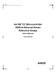
Am186™CC
Communications Controller
ISDN TA Reference Design
User’s Manual
Order #22033A
about.book Page ii Friday, December 18, 1998 9:41 AM
$PTM&&0LFURFRQWUROOHU,6'17$5HIHUHQFH'HVLJQ0DQXDORUGHU$
E\$GYDQFHG0LFUR'HYLFHV,QF
$OOULJKWVUHVHUYHG1RSDUWRIWKLVSXEOLFDWLRQPD\EHUHSURGXFHGVWRUHGLQDUHWULHYDOV\VWHPRUWUDQVPLWWHGLQDQ\IRUPRU
E\DQ\PHDQVHOHFWURQLFPHFKDQLFDOSKRWRFRS\LQJUHFRUGLQJRURWKHUZLVHZLWKRXWWKHSULRUZULWWHQSHUPLVVLRQRI$GYDQFHG
0LFUR'HYLFHV,QF
8VHGXSOLFDWLRQRUGLVFORVXUHE\WKH*RYHUQPHQWLVVXEMHFWWRUHVWULFWLRQVDVVHWIRUWKLQVXEGLYLVLRQELLRIWKH5LJKWV
LQ7HFKQLFDO'DWDDQG&RPSXWHU6RIWZDUHFODXVHDW$GYDQFHG0LFUR'HYLFHV,QF(%HQ:KLWH%OYG
$XVWLQ7;
$0' WKH $0' ORJR DQG FRPELQDWLRQV WKHUHRI $P $P ( (021 DQG 6PDUW'0$ DUH WUDGHPDUNV RI
$GYDQFHG0LFUR'HYLFHV,QF
)XVLRQ(LVDVHUYLFHPDUNRI$GYDQFHG0LFUR'HYLFHV,QF
0LFURVRIWLVDUHJLVWHUHGWUDGHPDUNRI0LFURVRIW&RUS
:LQGRZVLVDUHJLVWHUHGWUDGHPDUNRI0LFURVRIW&RUS
2WKHUSURGXFWRUEUDQGQDPHVDUHXVHGVROHO\IRULGHQWLILFDWLRQDQGPD\EHWKHWUDGHPDUNVRUUHJLVWHUHGWUDGHPDUNVRIWKHLU
UHVSHFWLYHFRPSDQLHV
about.book Page iii Friday, December 18, 1998 9:41 AM
IF YOU HAVE QUESTIONS, WE’RE HERE TO HELP YOU.
7KH$0'FXVWRPHUVHUYLFHQHWZRUNLQFOXGHV86RIILFHVLQWHUQDWLRQDORIILFHVDQGDFXVWRPHU
WUDLQLQJFHQWHU([SHUWWHFKQLFDODVVLVWDQFHLVDYDLODEOHIURPWKH$0'ZRUOGZLGHVWDIIRIILHOG
DSSOLFDWLRQHQJLQHHUVDQGIDFWRU\VXSSRUWVWDIIWRDQVZHU(DQG&RPPIDPLO\KDUGZDUHDQG
VRIWZDUHGHYHORSPHQWTXHVWLRQV
)UHTXHQWO\DFFHVVHGQXPEHUVDUHOLVWHGEHORZ$GGLWLRQDOFRQWDFWLQIRUPDWLRQLVOLVWHGRQWKHEDFN
RIWKLVPDQXDO$0'¶V:::VLWHOLVWVWKHODWHVWSKRQHQXPEHUV
Technical Support
$QVZHUVWRWHFKQLFDOTXHVWLRQVDUHDYDLODEOHRQOLQHWKURXJKHPDLODQGE\WHOHSKRQH
*RWR$0'¶VKRPHSDJHDWZZZDPGFRPDQGIROORZWKH6HUYLFHOLQNIRUWKHODWHVW$0'WHFKQLFDO
VXSSRUWSKRQHQXPEHUVVRIWZDUHDQG)UHTXHQWO\$VNHG4XHVWLRQV
)RUWHFKQLFDOVXSSRUWTXHVWLRQVRQDOO(DQG&RPPSURGXFWVVHQGHPDLOWR
HSGVXSSRUW#DPGFRPLQWKH86DQG&DQDGDRUHXURWHFK#DPGFRPLQ(XURSHDQGWKH8.
<RXFDQDOVRFDOOWKH$0'&RUSRUDWH$SSOLFDWLRQV+RWOLQHDW
7ROOIUHHIRU86DQG&DQDGD
8.DQG(XURSHKRWOLQH
WWW Support
)RUVSHFLILFLQIRUPDWLRQRQ(DQG&RPPSURGXFWVDFFHVVWKH$0'KRPHSDJHDW
ZZZDPGFRPDQGIROORZWKH(PEHGGHG3URFHVVRUVOLQN7KHVHSDJHVSURYLGHLQIRUPDWLRQRQ
XSFRPLQJSURGXFWUHOHDVHVRYHUYLHZVRIH[LVWLQJSURGXFWVLQIRUPDWLRQRQSURGXFWVXSSRUWDQGWRROV
DQGDOLVWRIWHFKQLFDOGRFXPHQWDWLRQ6XSSRUWWRROVLQFOXGHRQOLQHEHQFKPDUNLQJWRROVDQG&RGH.LW
VRIWZDUH²WHVWHGVRXUFHFRGHH[DPSOHDSSOLFDWLRQV0DQ\RIWKHWHFKQLFDOGRFXPHQWVDUHDYDLODEOH
RQOLQHLQ3')IRUP
4XHVWLRQVUHTXHVWVDQGLQSXWFRQFHUQLQJ$0'¶V:::SDJHVFDQEHVHQWYLDHPDLOWR
ZHEPDVWHU#DPGFRP
Documentation and Literature Support
'DWDERRNVXVHU¶VPDQXDOVGDWDVKHHWVDSSOLFDWLRQQRWHVDQGSURGXFW&'VDUHIUHHZLWKDVLPSOH
SKRQHFDOO,QWHUQDWLRQDOO\FRQWDFW\RXUORFDO$0'VDOHVRIILFHIRUSURGXFWOLWHUDWXUH
7RRUGHUOLWHUDWXUHFDOO
7ROOIUHHIRU86DQG&DQDGD
'LUHFWGLDOZRUOGZLGH
)D[
Third-Party Support
$0')XVLRQ(60SDUWQHUVSURYLGHDQDUUD\RISURGXFWVGHVLJQHGWRPHHWFULWLFDOWLPHWRPDUNHWQHHGV
3URGXFWVDQGVROXWLRQVDYDLODEOHLQFOXGHHPXODWRUVKDUGZDUHDQGVRIWZDUHGHEXJJHUVERDUGOHYHOSURGXFWV
DQGVRIWZDUHGHYHORSPHQWWRROVDPRQJRWKHUV7KH:::VLWHDQGWKH()DPLO\3URGXFWV
'HYHORSPHQW7RROV&'RUGHU GHVFULEHWKHVHVROXWLRQV,QDGGLWLRQPDWXUHGHYHORSPHQW
WRROVDQGDSSOLFDWLRQVIRUWKH[SODWIRUPDUHZLGHO\DYDLODEOHLQWKHJHQHUDOPDUNHWSODFH
about.book Page iv Friday, December 18, 1998 9:41 AM
iv
Am186TMCC Microcontroller ISDN TA Reference Design Manual
about.book Page v Friday, December 18, 1998 9:41 AM
Contents
$ERXWWKH$P70&&0LFURFRQWUROOHU,6'17$5HIHUHQFH
'HVLJQ
7KHRU\RI2SHUDWLRQ [
$P&&0LFURFRQWUROOHU,6'17$5HIHUHQFH'HVLJQ)HDWXUHV [L
,6'1%DFNJURXQG [LL
'RFXPHQWDWLRQ [LLL
$ERXWWKLV0DQXDO [LLL
6XJJHVWHG5HIHUHQFH0DWHULDO [LY
&KDSWHU4XLFN6WDUW
&RQQHFWLQJWRD3& )RU0RUH,QIRUPDWLRQ &KDSWHU6\VWHP)HDWXUHVDQG&RPSRQHQWV
/D\RXWDQG3ODFHPHQW $P&&0LFURFRQWUROOHU 6\VWHP0HPRU\ ,6'167,QWHUIDFH ,6'18,QWHUIDFH 6HULDO3&,QWHUIDFH Am186TMCC Microcontroller ISDN TA Reference Design Manual
v
about.book Page vi Friday, December 18, 1998 9:41 AM
86%3&,QWHUIDFH 3RZHU6XSSO\ 7HVW,QWHUIDFH3RUW7,3 ,6'17$3LQ8VDJH 5(6&21&RQILJXUDWLRQ $SSHQGL[$
%LOORI0DWHULDOV%20DQG6FKHPDWLFV
$SSHQGL[%
*ORVVDU\RI7HUPV
,QGH[
vi
Am186TMCC Microcontroller ISDN TA Reference Design Manual
about.book Page vii Friday, December 18, 1998 9:41 AM
/LVWRI)LJXUHV
)LJXUH ,6'17$5HIHUHQFH'HVLJQ%ORFN'LDJUDP YLLL
)LJXUH ,6'15HIHUHQFH3RLQW'LDJUDP [
)LJXUH ,6'17$5HIHUHQFH'HVLJQ&LUFXLW%RDUG/D\RXW )LJXUH $P&&0LFURFRQWUROOHU,6'17$5HIHUHQFH'HVLJQ
%ORFN'LDJUDP )LJXUH ,6'17$&ORFN*HQHUDWLRQ&LUFXLW )LJXUH ,6'17$6\VWHP0HPRU\ )LJXUH ,6'17$67,QWHUIDFH )LJXUH ,6'17$8,QWHUIDFH&LUFXLW )LJXUH ,6'17$+LJK6SHHG6HULDO,QWHUIDFH )LJXUH ,6'17$86%,QWHUIDFH )LJXUH ,6'17$3RZHU6XSSO\DQG5HVHW&LUFXLW )LJXUH 7HVW,QWHUIDFH3RUW7,3&RQQHFWRU&LUFXLW )LJXUH )ODVK0HPRU\-XPSHUIRU[%RRW-3 )LJXUH 5(6&215HJLVWHU%LWV )LJXUH ,6'17$5(6&21&RQILJXUDWLRQ /LVWRI7DEOHV
7DEOH
,6'17$5HIHUHQFH'HVLJQ3DUWV/LVW 7DEOH
&XUUHQWDQG3RZHU(VWLPDWHVIRUWKH,6'17$ 7DEOH
3LQ8VDJHIRUWKH,6'17$ 7DEOH$
,6'17$67,QWHUIDFH%RDUG%20 $
7DEOH$
,6'17$8,QWHUIDFH%RDUG%LOORI0DWHULDOV $
Am186TMCC Microcontroller ISDN TA Reference Design Manual
vii
about.book Page viii Friday, December 18, 1998 9:41 AM
viii
Am186TMCC Microcontroller ISDN TA Reference Design Manual
about.book Page ix Friday, December 18, 1998 9:41 AM
About the Am186TMCC
Communications Controller ISDN
TA Reference Design
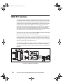
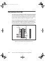
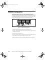
The Am18670CC communications controller ISDN terminal adapter (TA)
reference design is designed as a small, cost-effective ISDN solution for embedded
communications applications. This design is intended to reduce the time to market
for ISDN designers using the Am186CC communications controller. Figure 0-1
shows a block diagram of the ISDN TA reference design.
The ISDN TA reference design is a fully functional ISDN TA that illustrates the
benefits of using the Am186CC communications controller ISDN TA reference
design. The Am186CC communications controller has a number of integrated
features required in many communication applications. These features include four
high-level data link controller (HDLC) channels and a universal serial bus (USB)
peripheral controller with an internal transceiver. The HDLC channels support
GCI/IOM-2, PCM, and DCE interfaces. Other integrated features include four
general-purpose DMA channels, eight SmartDMA™ controller channels, four
time slot assigners (TSAs), UART, High-Speed UART with autobaud, and an
integrated DRAM controller.
The ISDN TA reference design illustrates how to use many of the integrated
peripherals to provide a small, low-cost, ISDN TA. The reference design supports
either an ISDN 2B+D U or S/T network interface by a component population
option. You can interface to a PC using either the High-Speed UART connection
at up to 230 kbps, or by using a full-speed USB connection at 12 Mbps.
Note that the High-Speed UART is capable of 460 kbps, but is limited by the
reference design’s UART transceiver, which is only capable of 230 kbps, and also
by the PCs that the ISDN TA would connect because most of them are only capable
of speeds up to 115 kbps or 230 kbps.
Am18670CC Microcontroller ISDN TA Reference Design Manual
ix
about.book Page x Friday, December 18, 1998 9:41 AM
$P&&&RPPXQLFDWLRQV&RQWUROOHU
7,3
.[
'5$0
$0')ODVK
0HPRU\
$P)
%,8
&KLS
6HOHFWV
0HPRU\
&RQWUROOHU
7LPHU
,&8
8$57
+LJK
8$57
;&95
'%
3HUIRUPDQFH
ELWFRUH
+'/& +'/&
+'/& +'/&
*&,
3&0
86%
86%
'0$
66,
3,2
677UDQVFHLYHU
$0'$P&$
5-
25
87UDQVFHLYHU
7
Figure 0-1. ISDN TA Reference Design Block Diagram
Theory of Operation
The ISDN TA reference design demonstrates the processor’s functionality in an
ISDN application. You can use this design as a reference to create your own ISDN
designs. The small size and simplicity of this design highlight the benefits of the
Am186CC communications controller ISDN TA reference design’s many
integrated peripherals.
x
Am18670CC Microcontroller ISDN TA Reference Design Manual
about.book Page xi Friday, December 18, 1998 9:41 AM
Am186CC Microcontroller ISDN TA
Reference Design Features
The ISDN TA reference design provides the following features:
• 2B+D ISDN network interface (For more information about ISDN, see “ISDN
Background” on page xii)
– ISDN U interface available by population option
– ISDN S/T interface available by population option
• High-Speed, 230-kbps, serial PC interface
• 12-Mbps, USB PC interface
• Single, +5V AC/DC wall-adapter power supply
• Very small form factor
• Four-layer printed circuit board (two signal, VCC, GND)
Am18670CC Microcontroller ISDN TA Reference Design Manual
xi
about.book Page xii Friday, December 18, 1998 9:41 AM
ISDN Background
ISDN (integrated services digital network) is an alternative to analog phone lines.
ISDN provides greater performance than analog and is still affordable to
consumers. There are many different variations of ISDN available, but the most
common is 128-kbps data transfer rate over two B (bearer) channels, plus 16 kbps
of signaling data over the D channel; this is the 2B+D configuration, the
configuration used by the ISDN TA reference design discussed in this manual.
Another configuration uses a single B channel and transfers data at 64 kbps.
Broadband ISDN is available and can achieve data rates in the 100-Mbps range.
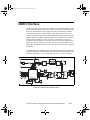
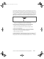
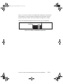
There are a number of reference points in an ISDN system. Figure 0-2 shows a
graphical representation of the ISDN reference points. The U reference point is the
local loop between the LE (local exchange) and the NT (network termination)
device. The U interface is a two-wire interface, which in North America and Asia
is typically supplied by a telecommunications service provider. The U interface
operates in 2B1Q (two binary, one quaternary) format, and can travel for miles
without repeaters. The T reference point is used only with customer premises
switching equipment (NT2). The S/T reference point is the four-wire interface
between the network termination device (NT1) and the terminal equipment (TE1)
or terminal adapter (TA). The S/T interface is offered in Europe, and is also used
with stand-alone NT1 devices.
Network
Termination Type 2
(NT2)
S
ISDN Terminal
Equipment
(TE1)
or
T Network
U
Termination Type 1
(NT1)
S/T
Terminal
Adapter
(TA)
ISDN
Local
Exchange
(LE)
R Non-ISDN
Terminal
Equipment (TE2)
Figure 0-2. ISDN Reference Point Diagram
xii
Am18670CC Microcontroller ISDN TA Reference Design Manual
about.book Page xiii Friday, December 18, 1998 9:41 AM
Documentation
The Am18670CC Microcontroller ISDN TA Reference Design User’s Manual
provides information on the system and board features, functionality, and ISDN
interfaces. Additional information can be found in the documentation listed on
page xiv.
About this Manual
Chapter 1, "Quick Start" provides installation information for the ISDN TA
reference design.
Chapter 2, "System Features and Components" contains descriptions of the
reference design features and components, ISDN interfaces, power supply, test
interface port, and ISDN TA pin usage.
Chapter 3, "Product Support" provides information on reaching and using the AMD
Corporate Applications technical support services, product information available
through AMD’s World Wide Web site, and support tools for the embedded E86
family.
Appendix A, "Bill of Materials (BOM) and Schematics" shows the bill of materials
for the reference design and the actual CAD schematics used to build the board.
Appendix B, "Glossary of Terms" contains definitions of terms used in this manual.
Am18670CC Microcontroller ISDN TA Reference Design Manual
xiii
about.book Page xiv Friday, December 18, 1998 9:41 AM
Suggested Reference Material
• Am186TMCC Communications Controller User’s Manual
Advanced Micro Devices, order #21914
• Am186TMCC Communications Controller Data Sheet
Advanced Micro Devices, order #21915
• Am186TMCC Communications Controller Register Set Manual
Advanced Micro Devices, order #21916
• Am186TM and Am188TM Family Instruction Set Manual
Advanced Micro Devices, order #21076
• E86TM Family Products and Development Tools CD
Advanced Micro Devices, order #21508
• ISDN Concepts, Facilities, and Services
Gary C. Kessler, ISBN: 0-07-034242-3
• ISDN For Dummies, 2nd Edition
David Angell, ISBN: 0-7645-0064-3
• ISDN Implementor’s Guide: Standards, Protocols, Services
Charles K. Summers, ISBN: 0-07-069416-8
• International Telecommunication Union Standards at www.itu.ch
xiv
Am18670CC Microcontroller ISDN TA Reference Design Manual
about.book Page 1 Friday, December 18, 1998 9:41 AM
Chapter 1
Quick Start
This chapter provides information that helps you quickly setup and install the ISDN
TA reference design.
• For information on how to connect the ISDN TA reference design to a PC (highspeed serial connection or full-speed USB connection), see page 1-2.
• For information on how to locate other sources of information, see page 1-3.
• For information on invoking the software supported by the reference design,
refer to the Software Quick Start information, included in your kit.
Am186TMCC Microcontroller ISDN TA Reference Design Manual
1-1
Connecting to a PC
The procedure in this section describes how to connect the ISDN TA reference
design to a PC using either a USB or serial port. Follow the steps below to connect
the ISDN TA reference design board to your PC. For information on how to invoke
the software, see the Software Quick Start document included in your kit.
Installation Requirements
The items listed below are necessary to install and run the ISDN TA:
• PC with an available COM port
• Terminal emulation software (such as MicrosoftWindows Terminal or
ProComm Plus) that supports ASCII file transfers, software flow control (Xon/
Xoff), and send break capability
• Dial-up networking configured as per your ISP’s recommendations
• Power source for universal power supply (47–63 Hz, 100–250 VAC)
Board Installation
CAUTION: As with all computer equipment, the ISDN TA may
be damaged by electrostatic discharge (ESD). Please take proper
ESD precautions when handling any board.
1. Remove the board from the shipping carton. Visually inspect the board to verify
that it was not damaged during shipment.
2. Connect the ISDN TA board’s DB-9 serial port to an available COM port. Use
the serial cable included in the ISDN TA kit and note that a DB-9 to DB-25
serial connector adapter is provided if your host system requires it. If using
your own cable, use a straight through cable, not a null modem cable.
DANGER: Make sure the power supply is not plugged into
an electrical outlet before connecting it to the ISDN TA.
1-2
Am186TMCC Microcontroller ISDN TA Reference Design Manual
about.book Page 3 Friday, December 18, 1998 9:41 AM
3. Plug the AC adapter into a power source. Connect the 5 VDC from the AC
adapter to the ISDN TA through the barrel connector.
4. If you are using a USB PC interface, connect the USB cable into the USB TypeB connector on the ISDN TA.
5. When all of the power and PC connections have been made, apply power by
toggling the switch located at the back of the ISDN TA. The power LED
(PWR LED) turns on when power is correctly applied.
For More Information...
,I\RXQHHGPRUHLQIRUPDWLRQDERXW
7KH$P&&FRPPXQLFDWLRQVFRQWUROOHU,6'17$UHIHUHQFHGHVLJQ
KDUGZDUH
VHH&KDSWHU
3UREOHPVZLWKWKHUHIHUHQFHGHVLJQ
VHHSDJHLLL
7KH$P&&FRPPXQLFDWLRQVFRQWUROOHU,6'17$UHIHUHQFHGHVLJQERDUG
OD\RXW
VHH&KDSWHU
• 7KH$P&&FRPPXQLFDWLRQVFRQWUROOHU,6'17$UHIHUHQFHGHVLJQ
schematics,
see Appendix A.
7KH$P&&PLFURFRQWUROOHU
VHHWKH$P70&&&RPPXQLFDWLRQV&RQWUROOHU'DWD6KHHWDQGWKH
$P70&&&RPPXQLFDWLRQV&RQWUROOHU8VHU¶V0DQXDOLQFOXGHGLQ\RXUNLW
• The latest release and updates, see Demo Board Updates at
www.amd.com/products/lpd/lpd.html.
Am186TMCC Microcontroller ISDN TA Reference Design Manual
1-3
about.book Page 4 Friday, December 18, 1998 9:41 AM
1-4
Am186TMCC Microcontroller ISDN TA Reference Design Manual
about.book Page 1 Friday, December 18, 1998 9:41 AM
Chapter 2
System Features and
Components
The ISDN TA reference board provides a small, low-cost, stand-alone system for
use by ISDN developers using the Am186CC communications controller.
The following sections explain the operation of the board in detail:
• “Layout and Placement” on page 2-2
• “Am186CC Microcontroller” on page 2-5
• “System Memory” on page 2-7
• “ISDN S/T Interface” on page 2-8
• “ISDN U Interface” on page 2-9
• “Serial PC Interface” on page 2-10
• “USB PC Interface” on page 2-11
• “Power Supply” on page 2-12
• “Test Interface Port (TIP)” on page 2-14
• “ISDN TA Pin Usage” on page 2-16
• “RESCON Configuration” on page 2-18
Am186TMCC Microcontroller ISDN TA Reference Design Manual
2-1
about.book Page 2 Friday, December 18, 1998 9:41 AM
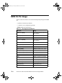
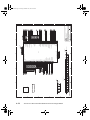
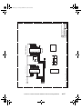
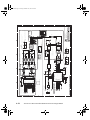
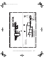
Layout and Placement
The ISDN TA reference design emphasizes the small board size that can be obtained
by using the Am186CC communications controller in an embedded
communications application. Refer to Figure 2-1 on page 2-4 for layout and
component placement.
The ISDN TA reference design board has the Flash memory, DRAM, and TIP
connector located close to the processor to provide a linear, logical signal flow for
the address and data bus. The connectors and the power switch are located at the
back of the board, and the status indicator LEDs are located at the front of the
board. This placement makes it possible to manufacture the board in a small
enclosure. The ISDN interface devices are overlapped where possible to minimize
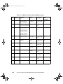
board size. In Table 2-1, all of the parts are identified by part number and part
description.
Table 2-1. ISDN TA Reference Design Parts List
2-2
Part
Number
Part
Description
Part
Location
U1
Am186CC communications controller
B-1
U2
EDO DRAM - Mosel Vitelic, 256Kx16
A-2
U3
Flash memory - Am29F400, 256Kx16
A-1
U4
ISDN S/T transceiver - Am79C32A
A-2
U5
ISDN S transformer
B-3
U6
ISDN S choke
C-3
U7
Optocoupler
B-3
U8
ISDN DC termination IC
B-3
U9
ISDN U transceiver - Lucent T7237
A-3
U10
ISDN U transformer
B-3
U13
High-Speed UART transceiver
C-2
U14
74ACT04
C-1
U15
3.-V LDO
C-1
Am186TMCC Microcontroller ISDN TA Reference Design Manual
about.book Page 3 Friday, December 18, 1998 9:41 AM
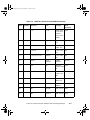
Table 2-1. ISDN TA Reference Design Parts List (Continued)
Part
Number
Part
Description
Part
Location
CR2–CR8
Status indicator LEDs
A-1–A-3
P1
RJ-45 connector
C-3
P2
DB-9 connector
C-2
P3
USB type-B connector
C-2
P4
Power connector
C-1
P5
TIP connector
B-1
SW1
Power switch
C-1
SW2
Reset button
C-2
JP1
Flash memory CS jumper
A-1
JP2
x8 boot jumper
A-1
F1
ISDN U interface line fuse
C-3
F2
1.5-A power supply main fuse
C-1
Am186TMCC Microcontroller ISDN TA Reference Design Manual
2-3
about.book Page 4 Friday, December 18, 1998 9:41 AM
C
B
A
1
2
3
Figure 2-1. ISDN TA Reference Design Circuit Board Layout
2-4
Am186TMCC Microcontroller ISDN TA Reference Design Manual
about.book Page 5 Friday, December 18, 1998 9:41 AM
The ISDN TA reference design was designed to fit in a very small desktop
enclosure. The circuit board is 3.85” x 4.75”, and fits into a variety of enclosures.
There are mounting holes on three corners; the fourth is on the side.
Am186CC Microcontroller
The ISDN TA reference design is used to control the ISDN TA. A block diagram
of the ISDN TA reference design is shown in Figure 2-2. The many integrated
features of the Am186CC communications controller make it ideal for an ISDN
application. The integrated DRAM controller allows a glueless interface to the
system memory. You can use the built-in High-Speed UART with autobaud to
communicate with the PC. You can also use the full-speed USB peripheral
controller with built-in transceiver for a 12-Mbps PC interface. The HDLCs
provide a glueless interface to either the S/T transceiver or the U transceiver.
Figure 2-2. Am186CC Microcontroller ISDN TA Reference Design Block
Diagram
Am186TMCC Microcontroller ISDN TA Reference Design Manual
2-5
about.book Page 6 Friday, December 18, 1998 9:41 AM
The system uses a single 24-MHz crystal. This design uses an internal 2x PLL
which provides a 48-MHz system clock and the required 48-MHz USB clock.
Because the USB clock is derived from the system PLL, the USB crystal input,
USBX1, is terminated. The clock generation circuit is shown in Figure 2-3.
X3
X1
X2
USBX1
2
C57
27pF
1
24.000 MHz
R33
10K
C58
27pF
Figure 2-3. ISDN TA Clock Generation Circuit
2-6
Am186TMCC Microcontroller ISDN TA Reference Design Manual
about.book Page 7 Friday, December 18, 1998 9:41 AM
System Memory
This design uses 512 Kbyte of AMD Flash memory for code space located from
0x80000h–0xFFFFFh, and 512 Kbyte of DRAM. The memory schematic is shown
in Figure 2-4. The Am29F400 Flash memory is used in a 256k x 16 configuration.
The Am29F400 is byte/word selectable using the BYTE# pin. In case the
512 Kbyte of Flash memory is not sufficient, PIO 35 is routed to the chip to act as
a bank select. This allows drop in compatibility for larger Flash memory, such as
the 29F800 device.
MA[0..19]
256Kx16 DRAM Device
256Kx16 FLASH Device
AD[0..15]
U2
MA1
MA3
MA5
MA7
MA9
MA11
MA13
MA15
MA17
16
17
18
19
22
23
24
25
26
30
11
12
15
[RAS0#]
[CAS0#]
[CAS1#]
[RD#]
[WR#]
14
29
28
27
13
A0
A1
A2
A3
A4
A5
A6
A7
A8
NC
NC
NC
NC
RAS#
LCAS#
UCAS#
OE#
WR#
U3
DQ0
DQ1
DQ2
DQ3
DQ4
DQ5
DQ6
DQ7
DQ8
DQ9
DQ10
DQ11
DQ12
DQ13
DQ14
DQ15
VCC
VCC
VCC
VSS
VSS
VSS
2
3
4
5
7
8
9
10
31
32
33
34
36
37
38
39
AD0
AD1
AD2
AD3
AD4
AD5
AD6
AD7
AD8
AD9
AD10
AD11
AD12
AD13
AD14
AD15
PIO35
VCC5
20
1
6
21
35
40
VCC5
R4
R5
10K
10K
MA1
MA2
MA3
MA4
MA5
MA6
MA7
MA8
MA9
MA10
MA11
MA12
MA13
MA14
MA15
MA16
MA17
MA18
FLASH_UCS#
V53C16258H SOJ
Mosel Vitelic V53C16258HK40
BYTE#
25
24
23
22
21
20
19
18
8
7
6
5
4
3
2
1
48
17
16
26
11
28
12
15
47
A0
A1
A2
A3
A4
A5
A6
A7
A8
A9
A10
A11
A12
A13
A14
A15
A16
A17
NC
DQ0
DQ1
DQ2
DQ3
DQ4
DQ5
DQ6
DQ7
DQ8
DQ9
DQ10
DQ11
DQ12
DQ13
DQ14
DQ15/A-1
CE#
WE#
OE#
RESET#
RY/BY#
BYTE#
VCC
NC
NC
NC
NC
VSS
VSS
29
31
33
35
38
40
42
44
30
32
34
36
39
41
43
45
37
AD0
AD1
AD2
AD3
AD4
AD5
AD6
AD7
AD8
AD9
AD10
AD11
AD12
AD13
AD14
AD15
VCC5
9
10
13
14
46
27
AM29F400 TSOP
LCS#
MCS2#
MCS1#
RD#
WR#
RES#
PIO31
UCS#
R6
*0
JP1
1
2
FLASH JP
Figure 2-4. ISDN TA System Memory
DRAM was chosen over SRAM as main memory in this application because
DRAM is more cost effective than SRAM and because the ISDN TA reference
design has an integrated DRAM controller that makes a glueless DRAM interface
simple to use. The Am186CC communications controller DRAM interface allows
zero-wait state operation at 48 MHz using a 40-ns DRAM. This DRAM device is
located from 0x00000h–0x7FFFFFh in low memory space and is selected using
LCS/RAS0.
Am186TMCC Microcontroller ISDN TA Reference Design Manual
2-7
about.book Page 8 Friday, December 18, 1998 9:41 AM
ISDN S/T Interface
The Am79C32A IDC (ISDN data controller) circuit is used to provide the fourwire 2B+D S/T interface. This device has a general circuit interface (GCI) or IOM-2
serial microprocessor interface, which is used to transfer B channel data to and
from the Am186CC microcontroller’s integrated HDLC controller. The Am186CC
communications controller-based ISDN TA reference design provides a fullduplex path between the terminal equipment (TE) and the network termination
(NT) device. The controller processes the ISDN basic rate interface (BRI) bit
stream, which consists of two 64-kbps B channels and a single 16-kbps D channel.
The schematic for the S/T interface block is shown in Figure 2-5.
The Am79C32A IDC circuit includes a D-channel HDLC controller which is used
by software to send and receive data on the D channel.
The four-wire ISDN S/T interface is first directed through an S transformer and
line filtering devices These isolate and protect the modem from the outside lines.
The crystal is used to generate MCLK, which can be used as a master clock output
and as the system clock for the microprocessor.
The signals SBIN, SBOUT, SCLK, SFS, and BCL/CH2STRB can be configured
for serial bus port (SBP) or GCI. SBP is used by the current terminal adapter
software and is connected to HDLC Channel A on the Am186CC communications
controller.
X1
1
2
12.228MHz
C20
27pF
C21
27pF
U4
34
RESOUT
PCS1#
RD#
WR#
INT1
MA[19..0]
AD[15..0]
CLKA
FSCA
TXDA
RXDA
11
12
13
14
35
MA1
MA2
MA3
18
17
16
AD0
AD1
AD2
AD3
AD4
AD5
AD6
AD7
27
26
25
24
22
21
20
19
30
31
28
29
23
XTAL1
XTAL2
RESET
CS#
RD#
WR#
INT#
LIN2
LIN1
LOUT2
LOUT1
HSW
A0
A1
A2
D0
D1
D2
D3
D4
D5
D6
D7
SCLK
SFS
SBIN
SBOUT
BCL/C2ST
MCLK
RSRVD
RSRVD
RSRVD
RSRVD
RSRVD
RSRVD
RSRVD
RSRVD
RSRVD
RSRVD
AVCC
DVCC
AVSS
DVSS
DVSS
AM79C32A PLCC
R108
2K
1206
33
41
42
38
39
40
32
43
44
1
2
3
4
5
6
7
8
9
10
37
15
36
LIN2
LIN1
LOUT2
LOUT1
R110
2K
1206
U16
1
2
3
4
8
7
6
5
R109 3.6K
1206 16 U5
1
+/- 1%, 1/8W
LC03-6
15
2
14
3
C25
R8
100
0805
680pF
R111
R112
22.6
1210
+/- 1%, 1/2W
VCC5
R113
22.6
1210
+/- 1%, 1/2W
U17
1
2
3
4
3.6K
1206 13
8
7
6
5
4
12
11
6
10
7
9
8
R115
22.6
1210
+/- 1%, 1/2W
Pulse PE-65799
S Transformer
P1
1
8
2
7
R11
3
6
100
0805
4
C26
680pF
LC03-6
R114
22.6
1210
+/- 1%, 1/2W
U6
5
+/- 1%, 1/8W
1
2
3
4
5
6
7
8
5
C75
PE65554
C77
C76
1000pF
1000pF
C78
1000pF
1000pF
Figure 2-5. ISDN TA S/T Interface
2-8
Am186TMCC Microcontroller ISDN TA Reference Design Manual
11
12
1
2
3
4
5
6
7
8
GND1
GND2
RJ45A
about.book Page 9 Friday, December 18, 1998 9:41 AM
ISDN U Interface
The Lucent T7237 circuit is used to provide the two-wire 2B+D U interface. This
device has a PCM serial microprocessor interface and an SSI (synchronous serial
interface). These interfaces are used to transfer data to and from the Am186CC
microcontroller using it’s integrated HDLC. This chip provides the two-wire
network termination. It processes the ISDN BRI bit stream that consists of two 64kbps B channels and a single 16-kbps D channel. The schematic for the U interface
block is shown in Figure 2-6. The U-interface circuit includes a line fuse, U
transformer, DC termination IC, and opto-isolation circuitry. The LED shown in
Figure 2-6 is used to indicate device status. The four states of the LED are Low,
High, 1 Hz, and 8 Hz. Refer to the Lucent T7237 device data sheet for a complete
description.
The U-interface data is in 2B1Q format, which provides a four-level (quaternary)
amplitude modulation. A single quaternary symbol represents two binary bits. The
quaternary symbols are ± 3, ± 1, which represent 00, 01, 10, and 11 in binary.
VCC5
C27 1.0uF
RESOUT#
R13
17.8K
0805
1%
VCC5
CR1
2
1
GREEN
CATH
ORANGE
R17
270
R15
R14
10K
0805
U7
5
6
7
8
3
LED SOT-23
Lumex SSL-LX15IGC-RP-TR
R20
0805
R16
137
2.2M
GND
VO
VB
Vcc
NC
Cathode
Anode
NC
0805
1%
R18
137
4
3
2
1
8
7
6
5
6N139
VCC5
1.1K
U8
0805
1%
TC
RS
PD
COM
PR+
T
R
PR-
1
2
3
4
R19
1.1K
LH1465AB
VCCAU
6
5
4
3
2
1
44
43
42
41
40
FSCA
VCCAU
ILOSS#
VDDD
FS
STLED
OPTOIN
GNDD
HIGHZ#
RESET#
VDDA
GNDA
GNDA
R24
T7237A PLCC
C28
820pF
5%
10K
VCC5
U10
R22
16.9
R23
16.9
VCCAU
1206
1%
1
U11
7
+/- 1%, 1/4W
1206
FUSE
U12
R21 21
TIP
1
2
3
4
5
6
7
8
10
1206
1%
6
SM6T6V8CA
C30 1.0uF
11
12
P2300SB
1
2
3
4
5
6
7
8
GND1
GND2
RJ45A
5
GNDO
VDDO
X1
X2
VDDA
NC
NC
GNDA
NC
NC
VRCM
VCC5
VCC5
39
38
37
36
35
34
33
32
31
30
29
C31
3300pF
Pulse T4008
9
RING
U Transformer
18
19
20
21
22
23
24
25
26
27
28
SDATA
SCLK
VDDA
SDINP
SDINN
HP
LON
GNDA
VDDA
LOP
HN
VRN
VRP
1
INT2
TDMDI
TDMD0
TDMCLK
GNDD
INT#
SDI
VDDD
SDO
SCK
GNDD
CKOUT
2
7
8
9
10
11
12
13
14
15
16
17
F1
1
TXDA
RXDA
CLKA
P1
C29
3300pF
2
U9
C32
0.1uF
C33
0.1uF
C34
0.1uF
X2
1
2
15.36011MHz
VCCAU
Figure 2-6. ISDN TA U Interface Circuit
Am186TMCC Microcontroller ISDN TA Reference Design Manual
2-9
about.book Page 10 Friday, December 18, 1998 9:41 AM
Serial PC Interface
The serial port may be used for communication with a PC. The Sipex high-speed
RS-232 transceiver is used to provide serial data rates up to 230 kbps. The DCE
serial connection is made through a standard female DB-9, which uses a straightthrough serial cable. PIO1 and PIO28 are used to provide extra flow control
signaling to support Plug and Play (PnP) operation. The two LEDs are used to
indicate transmit and receive activity. The schematic for the serial interface is
shown in Figure 2-7.
R25
680
CR2
1
2
LED RT GREEN
R26
680
CR3
1
2
LED RT GREEN
P2
U13
PIO1
RTRHU#
RXDHU
CTSHU#
TXDHU
PIO28
8
5
7
26
22
6
20
21
19
24
25
R1OUT
R2OUT
T1IN
R3OUT
R4OUT
T2IN
T3IN
T4IN
R5OUT
EN#
SD
12
C1+
C50
0.1uF
14
R1IN
R2IN
T1OUT
R3IN
R4IN
T2OUT
T3OUT
T4OUT
R5IN
VC2+
C2V+
9
4
2
27
23
3
1
28
18
5
9
4
8
3
7
2
6
1
100
100
100
100
100
100
C42
0.1uF
C43
0.1uF
C44
C45
C46
C47
C48
C49
1000pF1000pF 1000pF 1000pF 1000pF 1000pF
16
13
C51
0.1uF
VCC5
11
10
SP211
Figure 2-7. ISDN TA High Speed Serial Interface
2-10
10
11
CONNECTOR DB9
17
15
C1VCC
GND
R101
R102
R103
R104
R105
R106
Am186TMCC Microcontroller ISDN TA Reference Design Manual
about.book Page 11 Friday, December 18, 1998 9:41 AM
USB PC Interface
The ISDN TA reference design has an integrated USB peripheral controller with
a built in transceiver; differential USB signals connect directly to the controller
without requiring an external transceiver. A USB type B connector is used for
connection to a PC. The N MOSFETs are used with the two PIOs for VCC attach
and detach. The attach and detach steps are listed below. The USB interface
transfers data at up to 12 Mbps. The schematic for the USB interface is shown in
Figure 2-8.
Attach
1. Am186CC microcontroller polls USB_Detect (PIO42) for logic High to detect
when an active host USB port is connected.
2. Am186CC microcontroller drives USB_Vcc (PIO43) High to enable Q1 and
pulls up the USBD+ line to indicate to the host that this is a full-speed device.
Detach
1. Am186CC microcontroller polls USB_Detect for logic Low to detect a
disconnect of the host.
2. Am186CC microcontroller three-states USBD± in response to a disconnect.
3. Am186CC microcontroller removes USB_VCC to disable Q1; Q2 isolates
USB_Detect in response to a disconnect.
PIO43
3
PIO - USB_Vcc
1 G
D Q1
S TN0200T
2
VCC3
R27
C52
0.1uF
RESOUT
1.5K
U14A
3
14
D1
1
2
2
3
D
S
Q2
FB2
TN0200T
MURATABLM21A121SPB
SOT-23
G 1
R28
R29
DIODE RB400D
2
7
74ACT04
C53
22pF
P3
DD+
1
2
3
4
C54
VUSB
USBDUSBD+
GND
GND
GND
5
6
USB CON
22pF
AMP 787780-1
R107
100k
RESOUT#
PIO42
USBDUSBD+
0
0
FB3
PIO - USB_Detect
Figure 2-8. ISDN TA USB Interface
Am186TMCC Microcontroller ISDN TA Reference Design Manual
2-11
about.book Page 12 Friday, December 18, 1998 9:41 AM
Power Supply
This design requires only two voltages, +5 V and +3.3 V. The associated currents
and power estimates are included in Table 2-2. A 5-V, 500-mA, regulated, wallmount AC adapter is used to supply system power. The AC adapter is connected
to the system using a standard 5.5-mm barrel connector. A Raychem 750-mA fuse
is used to protect the circuit from any surge in current. To reset the fuse, unplug
the board and allow the fuse to cool. Most of the devices on the board require 5 V.
The 5 V is used directly from the regulated supply. The Am186CC microcontroller
and the inverter chip are the only 3.3-V devices on this board. The 3.3 V is obtained
from the LDO (Low Drop Out) linear regulator. The power supply and reset
schematics are shown in Figure 2-9.
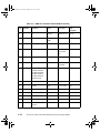
Table 2-2. Current and Power Estimates for the ISDN TA
2-12
Volt (V)
Device
Ityp(ma)
Imax(ma)
Ptyp(mw) Pmax(mw)
3.3
Am186CC
controller
-
288
-
950
5
DRAM
65
99
650
990
5
Flash memory
-
60
-
300
5
UART Xcvr
20
30
100
150
5
ISDN S/T Xcvr
31
38
155
190
5
ISDN U Xcvr
54
70
270
350
3.3
Total
-
288
-
950
5
Total
-
297
-
1980
Am186TMCC Microcontroller ISDN TA Reference Design Manual
The reset circuit consists of a push button, a diode, and an RC circuit used to provide
a time delay. The reset circuit is shown in Figure 2-9. The RES signal into the
Am186CC microcontroller must be held Low for at least 1 ms to allow the internal
circuitry to settle. The Am186CC microcontroller begins fetching instructions
6.5 CLKOUT periods after RES is deasserted.
VCC5
VCC3
U15
F2
1
2
3
+
SW SPDT C+K 7101
C55
10uF
16V
C-CASE
1
750mA
2
IN
OUT
GND TAB
3
C56
4
+ 10uF
LDO 3.3
Micrel MIC5209-3.3BS
16V
C-CASE
R32
270
D2
R31
100K
2
CENTER
SHUNT
SLEEVE
BARREL CON
1
2
3
3
SW1
P4
R52
SW2
0
1
1
RES#
3
Reset Switch
CR5
2
LED RT GREEN
C59
0.1uF
Figure 2-9. ISDN TA Power Supply and Reset Circuit
CAUTION: If using your own power supply, ensure that it is a
5-V supply. Using a 9-V or 12-V supply will permanently damage
the board.
Am186TMCC Microcontroller ISDN TA Reference Design Manual
2-13
about.book Page 14 Friday, December 18, 1998 9:41 AM
Test Interface Port (TIP)
The test interface port (also available from AMD, but not included with the ISDN
TA reference design) provides an interface to a low-cost AMD development board.
This board is useful for testing, debugging, and developing software on AMD’s
reference designs. It contains an 8-bit Flash memory device, LEDs, hexadecimal
displays, an LCD, serial ports, a parallel port, and an Ethernet controller.
In the event of a Flash memory failure on the main board, you can boot the ISDN
TA from an external TIP board. Refer to the Am186TMCC Communications
Controller Test Interface Port (TIP) User’s Manual for more information. Note
that the TIP board and user’s manual are available from AMD, but are not included
in your kit. The TIP connector circuit and pinout are shown in Figure 2-10.
AD[0..15]
MA[0..19]
P5
MA0
MA2
MA4
MA6
MA8
MA10
MA12
MA14
MA16
MA18
AD0
AD2
AD4
AD6
PCS3#
RD#
WLB#
S2#
RES#
RESOUT
RD#
WLB#
UCS#
2
4
6
8
10
12
14
16
18
20
22
24
26
28
30
32
34
36
38
40
42
44
46
48
50
52
54
56
58
60
1
3
5
7
9
11
13
15
17
19
21
23
25
27
29
31
33
35
37
39
41
43
45
47
49
51
53
55
57
59
MA1
MA3
MA5
MA7
MA9
1
MA11
MA13
MA15
MA17
MA19
AD1
AD3
AD5
AD7
AD7
INT0
INT7
INT8
VCC5
C60
COND60
2
+ 10uF
59
60
Top View
16V
C-CASE
Figure 2-10. Test Interface Port (TIP) Connector Circuit
2-14
Am186TMCC Microcontroller ISDN TA Reference Design Manual
about.book Page 15 Friday, December 18, 1998 9:41 AM
To boot from the TIP board, the Am186CC microcontroller must be reset in x8
boot mode, and the UCS signal must be routed to the TIP Flash memory. The x8
boot is accomplished by using JP2 to pull the MCS0# signal to ground during reset
(see Figure 2-11). To route the UCS signal to the TIP Flash memory, remove the
jumper on JP1 and install the jumper on the TIP. When booting from the on-board
Flash memory, use only JP1; this routes UCS to the ISDN TA Flash memory.
MCS0#
TP_TERM
JP2
1
2
HEADER 2
R38
10K
Figure 2-11. Flash Memory Jumper for x8 Boot (JP2)
To boot from the TIP Flash memory, perform the following:
• Disconnect UCS from on board Flash memory (remove JP1).
• Route UCS to the TIP Flash memory (install UCS jumper on TIP).
• Boot in x8 mode (install JP2).
To boot from on-board Flash memory, perform the following:
• Route UCS to the on board Flash memory (install JP1).
• Boot in x16 mode (remove JP2).
A corrupted Flash memory on the main board can be restored by booting from the
TIP board, entering the Z command, changing the jumpers to the settings for
booting from the main board, then following the prompts from the Z command.
Am186TMCC Microcontroller ISDN TA Reference Design Manual
2-15
about.book Page 16 Friday, December 18, 1998 9:41 AM
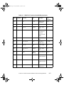
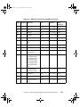
ISDN TA Pin Usage
Table 2-3 shows the Am186CC microcontroller multiplexed pin usage for the ISDN
TA.
• [] indicates an alternate pin function.
• {} indicates a reset configuration (pinstrap).
• boldface denotes the pin function.
Table 2-3. Pin Usage for the ISDN TA
2-16
Pin Name
Usage
TMROUT1 [PIO1]
DCE serial port flow control for
Plug and Play
ARDY [PIO8]
USB active LED
RTRA# [PIO18]
ISDN B1-Channel active LED
TMROUT0 [PIO28]
DCE serial port flow control for
Plug and Play
PCS7# [PIO31]
Flash memory RY/BY
PCS6# [PIO32]
ISDN D-Channel active LED
SRDY [PIO35]
Flash memory A18
RTRB# [PIO39]
ISDN B2-Channel active LED
RXDC [RXDC] [PIO42]
USB detect
TXDC [TXDC] [PIO43]
USB VCC enable
INT0
TIP - Ethernet IRQ
INT1
ISDN S/T transceiver interrupt
INT2
ISDN U transceiver interrupt
INT7 [PIO7]
TIP - serial port 1 interrupt
INT8 [PWD] [PIO6]
TIP - serial port 0 interrupt
UCS# [ONCE#]
Flash memory CE#
LCS# [RAS0#]
DRAM RAS#
Am186TMCC Microcontroller ISDN TA Reference Design Manual
about.book Page 17 Friday, December 18, 1998 9:41 AM
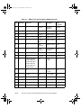
Table 2-3. Pin Usage for the ISDN TA (Continued)
Pin Name
Usage
MCS0# {UCSX8#} [PIO4]
x8 TIP boot
MCS1# [CAS1#]
DRAM LCAS#
MCS2# [CAS0#]
DRAM UCAS#
PCS1# {USBSEL1} [PIO14]
S/T-transceiver chip select
PCS3#
TIP
RXDA [DDA] [RXDA]
HDLC Channel A interface to
ISDN components
TXDA [DUA] [TXDA]
HDLC Channel A interface to
ISDN components
RCLKA [DCLA] [CLKA]
HDLC Channel A interface to
ISDN components
TCLKA [FSCA] [FSCA]
HDLC Channel A interface to
ISDN components
RXDHU [PIO16]
High-Speed UART receive data
TXDHU
High-Speed UART transmit data
CTSHU# [CTSD#] [TSCD#] [PIO46]
High-Speed UART clear to send
RTRHU# [RTRD#] [PIO47]
High-Speed UART ready to
receive
SCLK [PIO11]
ISDN U transceiver synchronous
serial interface
SDATA [PIO12]
ISDN U transceiver synchronous
serial interface
Am186TMCC Microcontroller ISDN TA Reference Design Manual
2-17
about.book Page 18 Friday, December 18, 1998 9:41 AM
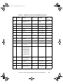
RESCON Configuration
The RESCON register provides a way to make design-specific hardware
configuration information available to software. The RESCON register is read
from AD[0..15] during reset. Because the Am186CC communications controller
has weak internal pulldowns, the default value is logic Low. Setting a bit requires
a 10-kΩ pullup resistor. Figure 2-12 shows the RESCON register bits.
Figure 2-12. RESCON Register Bits
• Validation Board - Identifies if the board is a validation board.
• Board ID - Unique board identifier that is used to determine what features are
available to the software.
• 0 - Bits are reserved for future use.
• Panic Bit - Used by software to boot in a safe mode (not currently supported).
• TIP - Identifies the TIP board as being present in the system.
• Board Configuration - Identifies particular population option for the board.
2-18
Am186TMCC Microcontroller ISDN TA Reference Design Manual
about.book Page 19 Friday, December 18, 1998 9:41 AM
Figure 2-13 shows the schematic for the RESCON configuration. The Board ID
for the ISDN TA is 0x100. The Board Configuration for the ISDN U interface
population option is 0x0000. The S interface Board Configuration is 0x0001.
NOTE: The components designated with an asterisk (*) are not populated.
VCC5
AD[0..15]
AD0
AD1
AD2
AD3
AD8
AD9
AD10
AD14
R53
R54
R55
R56
R57
R58
R59
R60
10K
*10K
*10K
*10K
*10K
*10K
*10K
10K
Figure 2-13. ISDN TA RESCON Configuration
Am186TMCC Microcontroller ISDN TA Reference Design Manual
2-19
about.book Page 20 Friday, December 18, 1998 9:41 AM
2-20
Am186TMCC Microcontroller ISDN TA Reference Design Manual
about.book Page 1 Friday, December 18, 1998 9:41 AM
Appendix A
Bill of Materials (BOM) and
Schematics
The ISDN TA, S/T interface, reference design board bill of materials begins on
page A-2.
The ISDN TA, U interface, reference design board bill of materials begins on page
A-7.
The actual schematics used to build the Am186CC microcontroller ISDN TA
reference design board can be found on the following pages:
Am186CC microcontroller, page A-14
DRAM and Flash memory, page A-15
ISDN interfaces, page A-16
USB and serial ports, page A-17
Power supply, crystal, TIP, etc., page A-18
Am186TMCC Microcontroller ISDN TA Reference Design Manual
A-1
about.book Page 2 Friday, December 18, 1998 9:41 AM
Table A-1. ISDN TA S/T Interface Board BOM
Item
Quantity
Reference
Part
Part Spec.
PCB
Footprint
1
1
CR1
LED SOT-23
Lumex SSLLX15IGC-RPTR
SOT-23
2
7
CR2,CR3,CR4,CR5,
CR6,CR7,CR8
LED RT green SLI 5608F5
TH-2
3
1
C1
3.3 µF
Tantalum, B
CASE, 16V
B-CASE
4
8
C2,C14,C44,C45,C46 1000 pF
,C47,C48, C49
± 10%, X7R,
16V
603
5
9
C3,C15,C35,C36,
C37,C38,C39,C40,
C41
0.01 µF
± 10%, X7R,
16V
603
6
26
C4,C5,C6,C7,C8,C9,
C10,C11,C12,C13,
C32,C33,C34,C42,
C43,C50,C51,C52,
C59,C61,C62,C63,
C64,C65,C66,C67
0.1 µF
± 10%, X7R,
16V
603
7
4
C16,C17,C18,C19
0.33 µF
± 10%, X7R,
16V
805
8
2
C21,C20
27 pF1
± 10%, COG,
25V
603
9
1
C22
10 µF1
Tantalum, C
CASE, 16V
C-CASE
10
2
C23,C24
0.1 µF1
± 10%, X7R,
16V
603
11
2
C25,C26
680 pF1
± 10%, X7R,
16V
603
A-2
Am186TMCC Microcontroller ISDN TA Reference Design Manual
about.book Page 3 Friday, December 18, 1998 9:41 AM
Table A-1. ISDN TA S/T Interface Board BOM (Continued)
Item
Quantity
Reference
Part
Part Spec.
PCB
Footprint
12
1
C27
1.0 µF
Phillips 2222
370 75105
TH-2
13
1
C28
820 pF
± 5%, X7R, 16V 603
14
2
C29,C31
3300 pF
± 10%, X7R,
16V
603
15
1
C30
1.0 µF
Phillips 2222
373 41105, or
Vitramon
VJ9253Y105K
XPM
TH-2
16
2
C54,C53
22 pF
± 10%, COG,
25V
603
17
3
C55,C56,C60
10 µF
Tantalum, C
CASE, 16V
C-CASE
18
2
C57,C58
27 pF
± 10%, COG,
25V
603
19
4
C75,C76,C77,
C78
1000 pF1
± 10%, X7R,
16V
603
20
2
D2,D1
Diode
RB400D
ROHM RB400D SOT-23
21
1
FB1
FB
MURATA
BLM31P500SP
B
22
2
FB3,FB2
FB
MURATA
805
BLM21A121SP
B
23
1
F1
Fuse
Raychem
TR600-150
Am186TMCC Microcontroller ISDN TA Reference Design Manual
1206
TH-2
A-3
about.book Page 4 Friday, December 18, 1998 9:41 AM
Table A-1. ISDN TA S/T Interface Board BOM (Continued)
Item
Quantity
Reference
Part
Part Spec.
PCB
Footprint
24
1
F2
750 mA
Raychem
SMD075
SMT-2
25
1
JP1
Flash JP
AMP 103186-1
TH-2
26
1
JP2
Header 2
AMP 103186-1
TH-2
27
1
P1
RJ45A
AMP 555153-1
TH-12
28
1
P2
Connector
DB9
AMP 787844-5
TH-11
29
1
P3
USB
connector
AMP 787780-1
TH-4
30
1
P4
Barrel
connector
KYCON KLD0202-BC
TH-3
31
1
P5
COND60
AMP 104068-6
TH-2x30
32
2
Q1,Q2
TN0200T
Temic TN0200T SOT-23
33
24
R1,R4,R5,R24,R33,
R38,R45,R46,R47,
R48,R49,R50,R60,
R84,R87,R89,R91,
R93,R94,R95,R97,
R98,R99,R100
10K
± 5%,
1/10W
603
34
1
R6
01
± 5%,
1/10W
603
35
2
R11,R8
1001
± 1%, 1/8W
805
36
1
R13
17.8K
± 1%, 1/8W
805
37
1
R14
10K
± 5%, 1/8W
805
38
2
R15,R19
1.1K
Dale WSC-2
SMT-2
39
2
R16,R18
137
± 1%, 1/8W
805
A-4
Am186TMCC Microcontroller ISDN TA Reference Design Manual
about.book Page 5 Friday, December 18, 1998 9:41 AM
Table A-1. ISDN TA S/T Interface Board BOM (Continued)
Item
Quantity
Reference
Part
Part Spec.
PCB
Footprint
40
6
R17,R30,R32,R35,
R36,R37
270
± 5%,
1/10W
603
41
1
R20
2.2M
± 5%, 1/8W
805
42
1
R21
21
± 1%, 1/4W
1206
43
2
R22,R23
16.9
± 1%, 1/4W
1206
44
2
R25,R26
680
± 5%, 1/10W
603
45
1
R27
1.5K
± 5%, 1/10W
603
46
5
R28,R29,R43,R44,
R52
0
± 5%, 1/10W
603
47
2
R31,R107
100k
± 5%, 1/10W
603
48
1
R51
10
± 5%, 1/10W
603
49
7
R53,R54,R55,R56,
R57,R58,R59
10K1
± 5%, 1/10W
603
50
29
R61,R62,R63,R64,
R65,R66,R67,R68,
R69,R70,R71,R72,
R73,R74,R75,R76,
R77,R78,R79,R80,
R81,R82,R83,R85,
R86,R88,R90,R92,
R96
56
± 5%, 1/10W
603
51
6
R101,R102,R103,
R104,R105,R106
100
± 5%, 1/10W
603
52
2
R110,R108
2K1
± 5%, 1/4W
1206
53
2
R109,R111
3.6K1
± 5%, 1/4W
1206
54
4
R112,R113,R114,
R115
22.61
± 1%, 1/2W
1210
Am186TMCC Microcontroller ISDN TA Reference Design Manual
A-5
about.book Page 6 Friday, December 18, 1998 9:41 AM
Table A-1. ISDN TA S/T Interface Board BOM (Continued)
Item
Quantity
Reference
Part
Part Spec.
55
1
SW1
SW SPDT
C+K 7101
C&K
TH-3
7101J1AV2BE2
56
1
SW2
Reset switch
Alcoswitch
FSM4J
TH-4
57
1
U1
Am186CC
AM186CC
PQFP-160
58
1
U2
V53C16258H Mosel Vitelic
SOJ
V53C16258HK
40
SOJ-40
59
1
U3
Am29F400
TSOP
AM29F400BT55EC
TSOP-48
60
1
U4
Am79C32A
PLCC1
AM79C32AJC
PLCC-44
61
1
U5
S
Transformer1
Pulse PE-65799 SMT-16
62
1
U6
PE655541
Pulse PE65554
TH-8
63
1
U7
6N139
Siemens 6N139
DIP-8
64
1
U8
LH1465AB
Lucent
LH1465AB
DIP-8
65
1
U9
T7237A
PLCC
Lucent T7237A- PLCC-44
-ML-DT
66
1
U10
UTransformer Pulse T4008
TH-10
67
1
U11
SM6T6V8CA SGS-Thomson
SM6T6V8CA
SMB
68
1
U12
P2300SB
SMB
A-6
Teccor
P2300SB,or
SGS-Thomson
SMP100-200
PCB
Footprint
Am186TMCC Microcontroller ISDN TA Reference Design Manual
about.book Page 7 Friday, December 18, 1998 9:41 AM
Table A-1. ISDN TA S/T Interface Board BOM (Continued)
Item
Quantity
Reference
Part
Part Spec.
PCB
Footprint
69
1
U13
SP211
Sipex
SP211ECA
SSOP-28
70
1
U14
74ACT04
National
74ACT04SC
SOIC-14
71
1
U15
LDO 3.3
Micrel
SOT-223
MIC5209-3.3BS
72
2
U16,U17
LC03-61
Semtech LC03-6 SO-8
73
1
X1
12.228MHz1
Ecliptek EC112.228MCL100
74
1
X2
15.36011MHz Saronix
SRX5144
HC-49
75
1
X3
24.000 MHz
HC-49
Ecliptek EC224.000MCL100
HC-49
1. This part is not populated.
Table A-2. ISDN TA U Interface Board BOM
Item
Quantity
Reference
Part
Part Spec.
PCB
Footprint
1
1
CR1
LED SOT-23
Lumex SSLLX15IGCRP-TR
SOT-23
2
7
CR2,CR3,CR4,CR5,
CR6,CR7,CR8
LED RT green SLI 5608F5
TH-2
3
1
C1
3.3 µF
B-CASE
Tantalum, B
CASE, 16V
Am186TMCC Microcontroller ISDN TA Reference Design Manual
A-7
about.book Page 8 Friday, December 18, 1998 9:41 AM
Table A-2. ISDN TA U Interface Board BOM (Continued)
Item
Quantity
Reference
Part
Part Spec.
PCB
Footprint
4
8
C2,C14,C44,C45,
C46,C47,C48,C49
1000 pF
± 10%, X7R,
16V
603
5
9
C3,C15,C35,C36,
0.01 µF
C37,C38,C39,C40,C41
± 10%, X7R,
16V
603
6
26
C4,C5,C6,C7,C8,C9,
C10,C11,C12,C13,
C32,C33,C34,C42,
C43,C50,C51,C52,
C59,C61,C62,C63,
C64,C65,C66,C67
0.1 µF
± 10%, X7R,
16V
603
7
4
C16,C17,C18,C19
0.33 µF
± 10%, X7R,
16V
805
8
2
C21,C20
27 pF1
± 10%, COG,
25V
603
9
1
C22
10 µF1
Tantalum, C
CASE, 16V
C-CASE
10
2
C23,C24
0.1 µF1
± 10%, X7R,
16V
603
11
2
C25,C26
680pF1
± 10%, X7R,
16V
603
12
1
C27
1.0 µF
Phillips 2222
370 75105
TH-2
13
1
C28
820 pF
± 5%, X7R,
16V
603
14
2
C29,C31
3300 pF
± 10%, X7R,
16V
603
A-8
Am186TMCC Microcontroller ISDN TA Reference Design Manual
about.book Page 9 Friday, December 18, 1998 9:41 AM
Table A-2. ISDN TA U Interface Board BOM (Continued)
Item
Quantity
Reference
Part
Part Spec.
PCB
Footprint
15
1
C30
1.0 µF
Phillips 2222
373 41105,or
Vitramon
VJ9253Y105
KXPM
TH-2
16
2
C54,C53
22 pF
± 10%, COG,
25V
603
17
3
C55,C56,C60
10 µF
Tantalum, C
CASE, 16V
C-CASE
18
2
C57,C58
27 pF
± 10%, COG,
25V
603
19
4
C75,C76,C77,C78
1000 pF1
± 10%, X7R,
16V
603
20
2
D2,D1
Diode
RB400D
ROHM
RB400D
SOT-23
21
1
FB1
FB
MURATA
1206
BLM31P500S
PB
22
2
FB3,FB2
FB
MURATA
BLM21A121
SPB
805
23
1
F1
Fuse
Raychem
TR600-150
TH-2
24
1
F2
750 mA
Raychem
SMD075
SMT-2
25
1
JP1
Flash JP
AMP 103186- TH-2
1
26
1
JP2
Header 2
AMP 103186- TH-2
1
Am186TMCC Microcontroller ISDN TA Reference Design Manual
A-9
about.book Page 10 Friday, December 18, 1998 9:41 AM
Table A-2. ISDN TA U Interface Board BOM (Continued)
Item
Quantity
Reference
Part
Part Spec.
27
1
P1
RJ45A
AMP 555153- TH-12
1
28
1
P2
Connector
DB9
AMP 787844- TH-11
5
29
1
P3
USB Conn.
AMP 787780- TH-4
1
30
1
P4
Barrel conn.
KYCON
KLD-0202BC
31
1
P5
COND60
AMP 104068- TH-2x30
6
32
2
Q1,Q2
TN0200T
Temic
TN0200T
SOT-23
33
24
R1,R4,R5,R24,R33,
R38,R45,R46,R47,
R48,R49,R50,R60,
R84,R87,R89,R91,
R93,R94,R95,R97,
R98,R99,R100
10K
± 5%, 1/10W
603
34
1
R6
01
± 5%, 1/10W
603
35
2
R11,R8
1001
± 1%, 1/8W
805
36
1
R13
17.8K
± 1%, 1/8W
805
37
1
R14
10K
± 5%, 1/8W
805
38
2
R15,R19
1.1K
Dale WSC-2
SMT-2
39
2
R16,R18
137
± 1%, 1/8W
805
40
6
R17,R30,R32,R35,
R36,R37
270
± 5%, 1/10W
603
A-10
PCB
Footprint
TH-3
Am186TMCC Microcontroller ISDN TA Reference Design Manual
about.book Page 11 Friday, December 18, 1998 9:41 AM
Table A-2. ISDN TA U Interface Board BOM (Continued)
Item
Quantity
Reference
Part
Part Spec.
PCB
Footprint
41
1
R20
2.2M
± 5%, 1/8W
805
42
1
R21
21
± 1%, 1/4W
1206
43
2
R22,R23
16.9
± 1%, 1/4W
1206
44
2
R25,R26
680
± 5%, 1/10W
603
45
1
R27
1.5K
± 5%, 1/10W
603
46
5
R28,R29,R43,R44,
R52
0
± 5%, 1/10W
603
47
2
R31,R107
100k
± 5%, 1/10W
603
48
1
R51
10
± 5%, 1/10W
603
49
7
R53,R54,R55,R56,
R57,R58,R59
10K1
± 5%, 1/10W
603
50
29
R61,R62,R63,R64,
R65,R66,R67,R68,
R69,R70,R71,R72,
R73,R74,R75,R76,
R77,R78,R79,R80,
R81,R82,R83,R85,
R86,R88,R90,R92,
R96
56
± 5%, 1/10W
603
51
6
R101,R102,R103,
R104,R105,R106
100
± 5%, 1/10W
603
52
2
R110,R108
2K1
± 5%, 1/4W
1206
53
2
R109,R111
3.6K1
± 5%, 1/4W
1206
54
4
R112,R113,R114,
R115
22.61
± 1%, 1/2W
1210
Am186TMCC Microcontroller ISDN TA Reference Design Manual
A-11
about.book Page 12 Friday, December 18, 1998 9:41 AM
Table A-2. ISDN TA U Interface Board BOM (Continued)
Item
Quantity
Reference
Part
Part Spec.
PCB
Footprint
55
1
SW1
SW SPDT
C+K 7101
C&K
7101J1AV2B
E2
TH-3
56
1
SW2
Reset Switch
Alcoswitch
FSM4J
TH-4
57
1
U1
Am186CC
AM186CC
PQFP-160
58
1
U2
V53C16258H
SOJ
Mosel Vitelic
V53C16258H
K40
SOJ-40
59
1
U3
Am29F400
TSOP
AM29F400B
T-55EC
TSOP-48
60
1
U4
Am79C32A
PLCC1
AM79C32AJ
C
PLCC-44
61
1
U5
S
Transformer1
Pulse PE65799
SMT-16
62
1
U6
PE655541
Pulse
PE65554
TH-8
63
1
U7
6N139
Siemens
6N139
DIP-8
64
1
U8
LH1465AB
Lucent
LH1465AB
DIP-8
65
1
U9
T7237A
PLCC
Lucent
T7237A- ML-DT
PLCC-44
66
1
U10
U Transformer Pulse T4008
67
1
U11
SM6T6V8CA SGSSMB
Thomson
SM6T6V8CA
A-12
TH-10
Am186TMCC Microcontroller ISDN TA Reference Design Manual
about.book Page 13 Friday, December 18, 1998 9:41 AM
Table A-2. ISDN TA U Interface Board BOM (Continued)
Item
Quantity
Reference
Part
Part Spec.
PCB
Footprint
68
1
U12
P2300SB
Teccor
P2300SB,or
SGSThomson
SMP100-200
SMB
69
1
U13
SP211
Sipex
SP211ECA
SSOP-28
70
1
U14
74ACT04
National
74ACT04SC
SOIC-14
71
1
U15
LDO 3.3
Micrel
MIC52093.3BS
SOT-223
72
2
U16,U17
LC03-61
Semtech
LC03-6
SO-8
73
1
X1
12.228MHz1
Ecliptek EC1- HC-49
12.228MCL100
74
1
X2
15.36011MHz Saronix
SRX5144
75
1
X3
24.000 MHz
HC-49
Ecliptek EC2- HC-49
24.000MCL100
1. This part is not populated.
Am186TMCC Microcontroller ISDN TA Reference Design Manual
A-13
Am186TMCC Microcontroller ISDN TA Reference Design Manual
A
B
C
D
E
VCC
VCCA
40
1
C5
0.1uF
1000pF
C2
1
REV 2.0:
41
81
80
121
120
C6
0.1uF
C3
0.01uF
C7
0.1uF
C4
0.1uF
Test points removed
AM186CC
160
R51
C8
0.1uF
10
C9
0.1uF
C10
0.1uF
C11
0.1uF
NOTE: Decoupling
capacitors each located
next to a VCC pin
3.3uF
16V
B-CASE
+ C1
VCC3
2
C12
0.1uF
2
MA0
MA1
MA2
MA3
MA4
MA5
MA6
MA7
MA8
MA9
MA10
MA11
MA12
MA13
MA14
MA15
MA16
MA17
MA18
MA19
C62
0.1uF
C13
0.1uF
C63
0.1uF
C64
0.1uF
141
142
143
144
PIO1
PIO28
INT_TERM
INT6
107
109
110
111
112
113
145
146
147
115
124
105
28
34
38
46
51
66
86
92
29
35
39
47
52
67
87
93
30
31
32
36
37
42
43
44
45
49
50
64
65
69
70
84
85
88
89
90
14
15
98
99
C61
0.1uF
Added
56 CCMAR0
56 CCMAR1
56 CCMAR2
56 CCMAR3
56 CCMAR4
56 CCMAR5
56 CCMAR6
56 CCMAR7
56 CCMAR8
56 CCMAR9
56 CCMAR10
56 CCMAR11
56 CCMAR12
56 CCMAR13
56 CCMAR14
56 CCMAR15
56 CCMAR16
56 CCMAR17
56 CCMAR18
56 CCMAR19
INT_TERM
AD0
AD1
AD2
AD3
AD4
AD5
AD6
AD7
AD8
AD9
AD10
AD11
AD12
AD13
AD14
AD15
REV 2.0:
R65
R67
R68
R69
R70
R71
R72
R73
R74
R75
R76
R77
R79
R81
R83
R85
R86
R88
R90
R92
73
74
60
22
75
76
PIO8
PIO35
INT7
INT8
INT0
INT1
INT2
VCC3
AD[0..15]
MA[0..19]
USBX1
X1
X2
3
C65
0.1uF
TMROUT0 [PIO28]
TMRIN0 [PIO27]
TMROUT1 [PIO1]
TMRIN1 [PIO0]
ARDY [PIO8]
SRDY [PIO35]
HLDA {CLKSEL1}
HOLD
INT0
INT1
INT2
INT3
INT4
INT5
INT6 [PIO19]
INT7 [PIO7]
INT8 [PWD] [PIO6]
NMI
DRQ0 [PIO9]
DRQ1
AD0
AD1
AD2
AD3
AD4
AD5
AD6
AD7
AD8
AD9
AD10
AD11
AD12
AD13
AD14
AD15
A0
A1
A2
A3
A4
A5
A6
A7
A8
A9
A10
A11
A12
A13
A14
A15
A16
A17
A18
A19
X1
X2
CLKOUT
UCLK [USBSOF] [USBSCI] [PIO21]
USBX1
USBX2
U1
3
AM186CC
VSS
VSS
VSS
VSS
VSS
VSS
VSS
VSS
VSS
VSS
VSS
VSS
VSS
VSS
VSSUSB
VSSA
10K
10K
10K
10K
10K
10K
10K
R45
R46
R47
R48
R49
R50
R1
C66
0.1uF
1000pF
C14
VCC
12
27
40
48
59
68
78
91
106
120
125
133
148
160
79
77
VCC3
RES#
RESOUT
4
RSRVD1 [UXVRCV]
RSRVD2 [UXVEN#]
RSRVD3 [UTXDMNS]
RSRVD4 [UTXDPLS]
USBD- [UDMNS]
USBD+ [UDPLS]
SDEN [PIO10]
SCLK [PIO11]
SDATA [PIO12]
RXDU [RXDD] [RXDD] [PIO26]
TXDU [TXDD] [TXDD] [PIO20]
CTSU# [TCLKD] [FSCD] [PIO24]
RTRU# [RCLKD] [CLKD] [PIO25]
RXDHU [PIO16]
TXDHU
CTSHU# [CTSD#] [TSCD#] PIO46]
RTRHU# [RTRD#] [PIO47]
RXDC [RXDC] [PIO42]
TXDC [TXDC] [PIO43]
RCLKC [CLKC] [PIO22]
TCLKC [FSCC] [PIO23]
CTSC# [TSCC#] [PIO44]
RTRC# [PIO45]
RXDB [RXDB] [PIO36]
TXDB [TXDB] [PIO37]
RCLKB [CLKB] [PIO40]
TCLKB [FSCB] [PIO41]
CTSB# [TSCB#] [PIO38]
RTRB# [PIO39]
RXDA [DDA] [RXDA]
TXDA [DUA] [TXDA]
RCLKA [DCLA] [CLKA]
TCLKA [FSCA] [FSCA]
CTSA# [TSCA#] [PIO17]
RTRA# [PIO18]
S0# {USBXCVR#}
S1#
S2#
S6
BSIZE8#
QS0
QS1
ALE [PIO33]
DT/R# [PIO29]
DEN# [DS#] [PIO30]
BHE# {ADEN#} [PIO34]
RD#
WR# {PRODTST#} [PIO15]
WLB#
WHB#
MURATA BLM31P500SPB
C15
0.01uF
FB1
VCCA
4
UCS# {ONCE#}
LCS# [RAS0#]
MCS0# {UCSX8#} [PIO4]
MCS1# [CAS1#]
MCS2# [CAS0#]
MCS3# [RAS1#] [PIO5]
PCS0# {USBSEL1} [PIO13]
PCS1# {USBSEL2} [PIO14]
PCS2#
PCS3#
PCS4# {CLKSEL2} [PIO3]
PCS5# {TESTMODE#} [PIO2]
PCS6# [PIO32]
PCS7# [PIO31]
VCC
VCC
VCC
VCC
VCC
VCC
VCC
VCC
VCC
VCC
VCC
VCC
VCC
VCC
VCCUSB
VCCA
A-14
1
21
33
41
53
61
71
83
100
108
121
130
140
155
82
72
1
10K
10K
56
10K
10K
10K
10K
R94
R95
R96
R97
R98
R99
R100
CCS0R
CCS1R
CCS2R
CCS6R
CCBSIZER
CCQS0R
CCQS1R
57
56
55
54
94
62
63
104
103
102
101
80
81
2
3
4
158
159
157
156
25
26
24
23
153
154
150
149
152
151
138
139
135
134
137
136
Schematic Sheet Name
PROCESSOR.SCH
Date: Friday, August 14, 1998
5
2
of
(800) 222-9323
Sheet
5204 E. Ben White Blvd.
Austin, TX 78741
AMD Proprietary/All Rights Reserved
Design Name
Size
16x12.5
[UDMNS]
[UDPLS]
RXDA
S2#
[CAS1#]
[CAS0#]
[RAS0#]
(C) Advanced Micro Devices, Inc.
USBDUSBD+
SCLK
SDATA
RXDHU
TXDHU
CTSHU#
RTRHU#
PIO42
PIO43
PIO39
PIO18
TXDA
CLKA
FSCA
10K
10K
10K
10K
R87
R89
R91
R93
CCALER
CCDTRR
CCDENR
CCBHER
19
17
18
20
118
119
117
116
123
122
56 RD#
56 WR#
56 WLB#
10K
PIO32
PIO31
PCS3#
PCS1#
UCS#
LCS#
MCS0#
MCS1#
MCS2#
RES#
RESOUT
R78
R80
R82
R84
56
56
56
56
56
R61
R62
R63
R64
R66
Added
CCRDR
CCWRR
CCWLBR
CCWHBR
CCUCSR
CCLCSR
CCMCS0R
CCMCS1R
CCMCS2R
REV 2.0:
97
16
96
95
132
131
126
127
128
129
5
6
7
8
9
10
11
13
114
58
5
6
Rev
1.0
A
B
C
D
E
about.book Page 14 Friday, December 18, 1998 9:41 AM
Am186TMCC Microcontroller ISDN TA Reference Design Manual
E
D
C
B
A
1
LCS#
MCS2#
MCS1#
RD#
WR#
RES#
PIO31
UCS#
AD[0..15]
MA[0..19]
1
[RAS0#]
[CAS0#]
[CAS1#]
[RD#]
[WR#]
MA13
MA15
MA17
MA1
MA3
MA5
MA7
MA9
MA11
20
1
14
29
28
27
13
30
11
12
15
16
17
18
19
22
23
24
25
26
VCC
VCC
VCC
VSS
VSS
VSS
DQ0
DQ1
DQ2
DQ3
DQ4
DQ5
DQ6
DQ7
DQ8
DQ9
DQ10
DQ11
DQ12
DQ13
DQ14
DQ15
20
1
6
21
35
40
2
3
4
5
7
8
9
10
31
32
33
34
36
37
38
39
SOJ-40
DRAM
21
40
2
R6
V53C16258H SOJ
Mosel Vitelic V53C16258HK40
RAS#
LCAS#
UCAS#
OE#
WR#
NC
NC
NC
NC
A0
A1
A2
A3
A4
A5
A6
A7
A8
U2
AD0
AD1
AD2
AD3
AD4
AD5
AD6
AD7
AD8
AD9
AD10
AD11
AD12
AD13
AD14
AD15
256Kx16 DRAM Device
2
*0
VCC5
VCC5
C16
0.33uF
0805
10K
R5
C17
0.33uF
0805
DRAM
10K
R4
VCC5
C18
0.33uF
0805
FLASH JP
1
2
JP1
PIO35
3
C19
0.33uF
0805
FLASH
BYTE#
FLASH_UCS#
MA1
MA2
MA3
MA4
MA5
MA6
MA7
MA8
MA9
MA10
MA11
MA12
MA13
MA14
MA15
MA16
MA17
MA18
3
VSS
VSS
24
1
NC
NC
NC
NC
VCC
DQ0
DQ1
DQ2
DQ3
DQ4
DQ5
DQ6
DQ7
DQ8
DQ9
DQ10
DQ11
DQ12
DQ13
DQ14
DQ15/A-1
Changed PN
AM29F400 TSOP
AM29F400BT-55EC
CE#
WE#
OE#
RESET#
RY/BY#
BYTE#
A0
A1
A2
A3
A4
A5
A6
A7
A8
A9
A10
A11
A12
A13
A14
A15
A16
A17
NC
U3
REV 2.0:
26
11
28
12
15
47
25
24
23
22
21
20
19
18
8
7
6
5
4
3
2
1
48
17
16
TSOP-48
FLASH
46
27
9
10
13
14
37
29
31
33
35
38
40
42
44
30
32
34
36
39
41
43
45
VCC5
AD0
AD1
AD2
AD3
AD4
AD5
AD6
AD7
AD8
AD9
AD10
AD11
AD12
AD13
AD14
AD15
25
48
4
4
A-15
Document Number
MEMORY.SCH
Date: Monday, August 03, 1998
Size
Title
5
of
(800) 222-9323
Sheet 3
5204 E. Ben White Blvd.
Austin, TX 78741
AMD Proprietary/All Rights Reserved
(C) Advanced Micro Devices, Inc.
5
6
Rev
1.0
E
D
C
B
A
about.book Page 15 Friday, December 18, 1998 9:41 AM
Am186TMCC Microcontroller ISDN TA Reference Design Manual
E
D
C
B
A
3
1
2
FSCA
VCC5
VCC5
1
R24
SDATA
SCLK
INT2
TXDA
RXDA
CLKA
17
3
RESET
CS#
RD#
WR#
INT#
1
STLEDX
*10K
1
TDMDI
TDMD0
TDMCLK
GNDD
INT#
SDI
VDDD
SDO
SCK
GNDD
CKOUT
27pF
C21
VCC5
R108
2K
1206
REV 2.0:
VCCAU
*T7237A PLCC
VCCAU
2
C32
*0.1uF
VRCM
VDDA
SDINP
SDINN
HP
LON
GNDA
VDDA
LOP
HN
VRN
VRP
R20
0805
R13
*17.8K
0805
1%
VCC5
R114
DT8
22.6
1210
+/- 1%, 1/2W
39
38
37
36
35
34
33
32
31
30
29
LDP
HN
VRN
VRP
SDINP
SDINN
HP
LON
C28
C34
*0.1uF
*6N139
GND
VO
VB
Vcc
U7
VCCAU
5
6
7
8
*820pF
5%
9
1206
1%
1206
1%
C31
*3300pF
*SM6T6V8CA
U11
C29
*3300pF
3
*0.01uF
C39
*0.01uF
C40
*0.01uF
C41
11
1
0805
1% RSRR
TCC
9
0805
R18
1%
*137
UPDANOD
UPCOMCATH
R16
*137
PE65554
C23
0.1uF
5
1
8
7
6
5
2
7
8
*LH1465AB
TC
RS
PD
COM
U8
TTXFRD
C36
9
PR+
T
R
PR-
*0.01uF
C37
12
10
4
C30 *1.0uF
6 UTXFRR2
R21 *21
10 UTXFRR1
+/- 1%, 1/4W
1206
7
*0.01uF *0.01uF
C35
VCC5
*U Transformer
Pulse T4008
U10
79C32
4
Component Side View
Mounting Hole Layout
4
U6
VCC5
Layout Note:
Keepout Area, No Power or GND planes
Signal Trace = 20 mils, route all traces
on top signal layer
1 2 3 4 5 6 7 8
Front View
3
100
0805
+/- 1%, 1/8W
2
1
R11
100
0805
+/- 1%, 1/8W
R8
C27 *1.0uF
STXFRL4
680pF
RJ45 Connector
8
7
10
C26
STXFRL3
STXFRL2
680pF
C25
STXFRL1
NOTE: VCCAU is isolated from VCC5
plane. Connect at single point.
*0.01uF
C38
VCCAU
R23
*16.9
R22
*16.9
RNRTXFRX
6 STXFR4
5
11
RPRTXFRX 12
STXFR2
Pulse PE-65799
S Transformer
3
4
2 STXFR3
14
1
15
TNRTXFRX 13
STXFR1
4
3
2
1
3
Layout Note:
Keepout Area, No Power or GND planes
Signal Trace = 20 mils, route all traces
on top signal layer
TPRTXFRX 16 U5
NC
Cathode
Anode
NC
R115
22.6
1210
+/- 1%, 1/2W
R113
22.6
1210
+/- 1%, 1/2W
8 DT6
7
6
DT7
5
3.6K
1206
R109 3.6K
1206
R111
8 DT2
7
6
5 DT3
C33
*0.1uF
VCCAU
R14
*10K
0805
LC03-6
U17
LC03-6
U16
VCR
*2.2M
VBR
1
2
3
4
DT1 1
2
3
4
DT4
Added
R112
DT5
22.6
1210
+/- 1%, 1/2W
R110
2K
1206
OPTVDR
VCC5
LIN2
LIN1
LOUT2
LOUT1
STLED
9
10
37
15
36
32
43
44
1
2
3
4
5
6
7
8
41
42
38
39
40
2 UINTX2
UINTX1
*15.36011MHz
X2
*270
U9
29
39
VCC5
7
8
9
10
11
12
13
14
15
16
17
R17
44-PIN PLCC
VCC5
AVCC
DVCC
AVSS
DVSS
DVSS
MCLK
RSRVD
RSRVD
RSRVD
RSRVD
RSRVD
RSRVD
RSRVD
RSRVD
RSRVD
RSRVD
LIN2
LIN1
LOUT2
LOUT1
HSW
XTAL2
33
2 SINTX1
AM79C32A PLCC
AM79C32AJC
SCLK
SFS
SBIN
SBOUT
BCL/C2ST
D0
D1
D2
D3
D4
D5
D6
D7
A0
A1
A2
X1
12.228MHz
1
XTAL1
*LED SOT-23
Lumex SSL-LX15IGC-RP-TR
GREEN
CATH
ORANGE
CR1
RESOUT#
system Vcc through single point.
Layout Note:
SOT-23 Top View
1
2
7
27
26
25
24
22
21
20
19
AD0
AD1
AD2
AD3
AD4
AD5
AD6
AD7
30
31
28
29
23
18
17
16
11
12
13
14
35
34
U4
SINTX2
MA1
MA2
MA3
ISDN U Interface
CLKA
FSCA
TXDA
RXDA
AD[15..0]
RESOUT
PCS1#
RD#
WR#
INT1
MA[19..0]
C20
27pF
6
5
4
3
2
1
44
43
42
41
40
Layout Note:
79C32 is a single substrate
device. Separate Vcc plance
for this area, connected to
System Vcc through single
point. See Bypass Cap below
for bulk capacitance.
2
UTXFRRC
1
1
2
ILOSS#
VDDD
FS
STLED
OPTOIN
GNDD
HIGHZ#
RESET#
VDDA
GNDA
GNDA
GNDO
VDDO
X1
X2
VDDA
NC
NC
GNDA
NC
NC
VRCM
18
19
20
21
22
23
24
25
26
27
28
1000pF
1
2
3
4
U12
PRM
PRP
Board Edge
RJ451
RJ453
11
12
1
2
3
4
5
6
7
8
RJ45A
GND1
GND2
1
2
3
4
5
6
7
8
P1
ISDN.SCH
5
Sheet 4
5204 E. Ben White Blvd.
Austin, TX 78741
AMD Proprietary/All Rights Reserved
of
(800) 222-9323
REV 2.0: Removed
isolation
resistors
(C) Advanced Micro Devices, Inc.
RING
R44
*0
Date: Wednesday, August 05, 1998
Size
Title
*P2300SB
TIP
R43
*0
Document Number
*1.1K
R19
*FUSE
*1.1K
LHRR
R15
F1
PINS: 1-8
NP MOUNTING HOLES: 9, 10
SHIELD MOUNTING HOLES:
11, 12
Added
Corrected
RJ454
RJ452
1000pF
1000pF
C78
1000pF
C77
C76
5
Do not use separate supplies for AVCC
and DVCC due to single substrate
REV 2.0:
10uF
16V
C-CASE
+ C22
C75
REV 2.0:
5
6
7
8
C24
0.1uF
Bulk Capacitance, place at single point
connection for Vcc plane(ISDN S
Interface)
1
A-16
2
ISDN S Interface
6
Rev
1.0
E
D
C
B
A
about.book Page 16 Friday, December 18, 1998 9:41 AM
Am186TMCC Microcontroller ISDN TA Reference Design Manual
A
B
C
D
1
AM186CC Tri-states USBD+/-
USB_Detect)
2)
2) AM186CC drives USB_Vcc to enable Q1
Detach
Attach
Serrano USB Attach/Detach
USB Interface
NOTE: SIPEX XCVR'S HAVE 400K PULLUPS ON
DRIVER INPUTS AND 5K PULLDOWNS ON
RECEIVER INPUTS
PIO28
PIO1
RTRHU#
RXDHU
CTSHU#
TXDHU
2
2
PIO8
74ACT04
U14A
2
2
C52
0.1uF
1
1
2
3
VCC5
VCC5
SLEDX4
2
R30
3
270
DIODE RB400D
D1
3
C67
0.1uF
C42
0.1uF
R101
R102
R103
R104
R105
R106
100
100
100
100
100
100
D
S
VCC5
G
C45
C46
C47
C48
C49
SOT-23
TN0200T
1
S
3
1 G
SOT-23 Top View
TN0200T
2
1
G
D
PIOINHS
RTRHS#
RXDHS
CTSHS#
TXDHS
PIOOUTHS
1000pF1000pF 1000pF 1000pF 1000pF 1000pF
C44
USBDODFET
Q2
REV 2.0: Added
SOT-23 Top View
RB400D
C51
0.1uF
PAH82
PAH80
C43
0.1uF
PAH59
PAH81
R2INR
T1OUTR
R3INR
R4INR
T2OUTR
T3OUTR
LED RT GREEN
SLI 5608F5
CR4
PIO - USB_Detect
7
1
14
11
10
16
13
17
15
9
4
2
27
23
3
1
28
18
PIO - USB_Vcc
VCC3
USB Active
USBDUSBD+
RESOUT#
PIO42
RESOUT
PIO43
VCC
GND
C2V+
VC2+
R1IN
R2IN
T1OUT
R3IN
R4IN
T2OUT
T3OUT
T4OUT
R5IN
SP211
Sipex SP211ECA
C1-
C1+
EN#
SD
T3IN
T4IN
R5OUT
R1OUT
R2OUT
T1IN
R3OUT
R4OUT
T2IN
U13
REV 2.0: Changed PN
PAH6914
C50
0.1uF
PAH7012
24
25
20
21
19
8
5
7
26
22
6
3
D Q1
S TN0200T
5
9
4
8
3
7
2
6
1
FETFBR
11
10
R26
680
R25
680
4
22pF
C53
Q1_R
RX_LED
TX_LED
1
1
22pF
C54
USBFB
R28
R29
2
2
R107
100k
LED RT GREEN
SLI 5608F5
CR3
LED RT GREEN
SLI 5608F5
CR2
5
6
A-17
Schematic Sheet Name
SERIAL_USB.SCH
Date: Friday, August 14, 1998
5
Board Edge
5
of
(800) 222-9323
Sheet
5204 E. Ben White Blvd.
Austin, TX 78741
AMD Proprietary/All Rights Reserved
Design Name
Size
AMP 787780-1
USB CON
GND
GND
REV 2.0: Pinout
VUSB
USBDUSBD+
GND
P3
4
PCB Footprint
TOP VIEW
1
3
5
2
MURATA BLM21A121SPB
FB3
1
2
3
4
4
3
USB Type B
Front View
1
2
(C) Advanced Micro Devices, Inc.
REV 2.0: Added
DD+
16x12.5
0
0
MURATA BLM21A121SPB
FB2
1.5K
R27
CONNECTOR DB9
AMP 787844-5
P2
4
USBFBGND
E
1
3
2
3
2
Serial Interface
6
Rev
1.0
A
B
C
D
E
about.book Page 17 Friday, December 18, 1998 9:41 AM
Am186TMCC Microcontroller ISDN TA Reference Design Manual
E
D
C
B
A
CENTER
SHUNT
SLEEVE
3
1
POWER
Top View
1
Barrel Connector
2
BARREL CON
KYCON KLD-0202-BC
P4
1
2
3
Power Supply
REV 2.0: Pinout
MA[0..19]
AD[0..15]
3
1
AD0
AD2
AD4
AD6
1
3
5
7
9
11
13
15
17
19
21
23
25
27
29
31
33
35
37
39
41
43
45
47
49
51
53
55
57
59
COND60
2
4
6
8
10
12
14
16
18
20
22
24
26
28
30
32
34
36
38
40
42
44
46
48
50
52
54
56
58
60
P5
AD1
AD3
AD5
AD7
MA11
MA13
MA15
MA17
MA19
MA1
MA3
MA5
MA7
MA9
AD0
AD1
AD2
AD3
AD8
AD9
AD10
AD14
2
R53
R54
R55
R56
R57
R58
R59
R60
10K
*10K
*10K
*10K
*10K
*10K
*10K
10K
4
3
GND
C60
VCC5
16V
C-CASE
+ 10uF
VCC5
INT7
INT8
INT0
AD7
SOT-223 Top View
3
2
1
LED RT GREEN
SLI 5608F5
CR5
OUT
GND TAB
IN
U15
LDO 3.3
Micrel MIC5209-3.3BS
2
1
VCC_LED_ANODE
NOTE: AD7 low during
reset indicates TIP is
present.
TIP Connector
Power LED
R32
270
750mA
Raychem SMD075
F2
VCC5
RESCON Configuration
MA10
MA12
MA14
MA16
MA18
AD[0..15]
RESOUT
RD#
WLB#
UCS#
RES#
PCS3#
RD#
WLB#
S2#
VCCAU
MA0
MA2
MA4
MA6
MA8
POWER_FUSE
SW SPDT C+K 7101
C&K 7101J1AV2BE2
SW1
VCC5
16V
C-CASE
C55
+ 10uF
2
2
1
2
A-18
60
2
R52
Top View
59
1
RES#
+
C56
10uF
16V
C-CASE
0
3
SW1_CON
R31
100K
VCC3
3
3
C59
0.1uF
2
1
SW2
3
3
4
Alcoswitch FSM4J
1
2
Reset Switch
Alcoswitch FSM4J
1
REV 2.0: Pinout
DIODE RB400D
D2
3
SOT-23 Top View
RB400D
1
2
U14D
74ACT04
U14F
4
REV 2.0: Grounded
inputs
7
13
14
U14B
74ACT04
VCC3
7
9
14
ISDN D
ISDN B2
ISDN B1
X1
X2
USBX1
12
8
4
PIO32
PIO39
7
11
14
U14E
1SLEDX1
1SLEDX2
1
R37
R36
R35
5
270
270
270
VCC5
C58
27pF
POWER.SCH
5
1
2
JP2
of
6
HEADER 2
(800) 222-9323
Sheet 6
5204 E. Ben White Blvd.
Austin, TX 78741
AMD Proprietary/All Rights Reserved
(C) Advanced Micro Devices, Inc.
NOTE: Use jumper to boot
from x8 FLASH
R38
10K
TP_TERM
MCS0#
x8 FLASH Boot
1SLEDX3
LED RT GREEN
SLI 5608F5
CR8
LED RT GREEN
SLI 5608F5
CR7
LED RT GREEN
SLI 5608F5
CR6
Document Number
10
6
2
2
2
Date: Friday, August 14, 1998
Size
Title
74ACT04
VCC3
7
5
U14C
74ACT04
VCC3
14
X3
24.000 MHz
2
Status Indicator LEDs
10K
R33
C57
27pF
System Clock
PIO18
Spare Gates
74ACT04
VCC3
7
3
14
VCC3
4
Rev
1.0
E
D
C
B
A
about.book Page 18 Friday, December 18, 1998 9:41 AM
about.book Page 1 Friday, December 18, 1998 9:41 AM
Appendix B
Glossary of Terms
2B+D - Describes the BRI configuration for ISDN of two bearer channels and one
D channel.
2B1Q - Two binary, one quaternary, data format for the U-interface. One quaternary
symbol (±3, ±1) represents two bits.
B Channel - Bearer channel, 64kbps voice/data channel for ISDN.
bps - Bits per second.
BRI - Basic Rate Interface. The simple 2B+D access method defined by CCITT
recommendation I.430.
CCITT/ITU - International Telegraph and Telephone Consultative Committee /
International Telecommunications Union. ITU is an agency of the UN. CCITT is
a committee of the ITU which makes recommendations for network
communications.
C.O. - Central Office.
CPE - Customer Premises Equipment. Devices such as the NT1, designated to be
the customer's responsibility to provide.
D Channel - 16kbps channel used to carry out-of-band network signaling or packetmode user data. (Refer to the ITU standards found at www.itu.ch.)
FCC - Federal Communications Commission. Regulates the U.S. telephone
industry.
GCI - General Circuit Interface.
Am186TMCC Microcontroller ISDN TA Reference Design Manual
B-1
about.book Page 2 Friday, December 18, 1998 9:41 AM
HDLC - High-Level Data-Link Controller. ISO standard for layer-2 data bitoriented communications protocol. HDLC is used for LAPB, LAPD, V.120 and
SS7.
IDC - ISDN Data Controller. Performs D channel processing on the S/T reference
point data.
IOM-2 - Industry standard serial bus developed by Siemens.
ISDN - Integrated Services Digital Network.
ISO - International Standardization Organization. Developed the OSI reference
model and HDLC standards.
LAPB - Link Access Procedure Balanced. The X.25 data link layer protocol. X.25
is a special case of HDLC.
LAPD - Link Access Procedures on the D channel. ISDN data link layer protocol
defined by CCITT. LAPD is a special case of HDLC
LE - Local Exchange. Class 5 C.O.
MPI - Microprocessor Interface.
NT1 - Network Termination Type 1. Termination device located on the customer
premises that converts the two wire U-interface to a four wire S/T-interface.
NT2 - Network Termination Type 2. Termination device separating the S and T
reference points used for customer-controlled communication distribution (such
as PBX or LAN)
OSI - Open Systems Interconnection reference model. Seven layer architecture
developed by ISO for open system communications.
PBX - Private Branch Exchange. Customer site switch, incorporating the use of
an NT2 device.
PCM - Pulse Code Modulation.
PIO - Programmable Input/Output.
B-2
Am186TMCC Microcontroller ISDN TA Reference Design Manual
about.book Page 3 Friday, December 18, 1998 9:41 AM
R -Interface - Reference point between non-ISDN devices and terminal adapters.
SBP - Serial Bus Port. The simple PCM highway used by the Am79C32A device.
SS7 - Signal System 7. High-speed, common channel interoffice signaling system
necessary for ISDN implementation.
S/T-interface - The reference point comprising the 4 wire interface between the
network termination device (NT1) and the terminal equipment (TE1) or terminal
adapter (TA). If an NT2 is used for on-site switching, the S and T reference points
are considered to be separated at the NT2 device. The T reference point is between
the NT1 and NT2, and the S reference point is between the NT2 and the TE1 or TA.
TA - Terminal Adapter. Converts analog information from a TE2 device to digital
format which can be used for ISDN.
TDM - Time Division Multiplexing.
TE - Terminal Equipment. Equipment that may be placed on ISDN (directly or
indirectly).
TE1 - Terminal Equipment Type 1. ISDN compatible terminal equipment.
TE2 - Terminal Equipment Type 2. Non-ISDN compatible terminal equipment,
which requires a terminal adapter.
U-interface - Reference point comprising the two-wire interface between the LE
and NT device.
USB - Universal serial bus. Intel standard; used for PC-to-peripheral
communication.
Am186TMCC Microcontroller ISDN TA Reference Design Manual
B-3
about.book Page 4 Friday, December 18, 1998 9:41 AM
B-4
Am186TMCC Microcontroller ISDN TA Reference Design Manual
about.book Page 1 Friday, December 18, 1998 9:41 AM
,QGH[
$
)
$P&&PLFURFRQWUROOHU
EORFNGLDJUDP
VFKHPDWLF$
)ODVKPHPRU\
ERRWLQJIURP
VFKHPDWLF$
)XVLRQ(SURJUDPLLL
%
%LOORIPDWHULDOV%20$
%ORFNGLDJUDP[
&
&ORFNJHQHUDWLRQ
&RQQHFWLQJWRD3&
&U\VWDOVFKHPDWLF$
'
*
*&,
*HQHUDOFLUFXLWLQWHUIDFH
*ORVVDU\%
+
+'/&
+RWOLQHQXPEHUVLLL
'RFXPHQWDWLRQ
DERXWWKLVPDQXDO[LLL
DGGLWLRQDO
UHIHUHQFHPDWHULDO[LY
'5$0
VFKHPDWLF$
(
HPDLOWHFKQLFDOVXSSRUWLLL
$PTM&&0LFURFRQWUROOHU,6'17$5HIHUHQFH'HVLJQ0DQXDO
,QGH[
about.book Page 2 Friday, December 18, 1998 9:41 AM
,
,QVWDOODWLRQ
ERDUG
UHTXLUHPHQWV
,20
,6'1
EDFNJURXQG[LL
GDWDFRQWUROOHU
UHIHUHQFHSRLQWV[LL
67LQWHUIDFH
VFKHPDWLF$
8LQWHUIDFH
,6'1LQWHUIDFH
VFKHPDWLF$
,6'167LQWHUIDFH[LL
,6'17$UHIHUHQFHGHVLJQ
ELOORIPDWHULDOV$
EORFNGLDJUDP[
FORFNJHQHUDWLRQFLUFXLW
FRQQHFWLQJWRD3&
GHVFULSWLRQL[
'5$0
IHDWXUHVXPPDU\[L
IHDWXUHV
)ODVKPHPRU\
LQVWDOODWLRQ
,6'167LQWHUIDFH
,6'18LQWHUIDFH
OD\RXWDQGSODFHPHQW
SDUWVOLVW
SLQXVDJH
SRZHUVXSSO\
SURGXFWVXSSRUWLLL
5(6&21FRQILJXUDWLRQ
UHVHWFLUFXLWU\
VFKHPDWLFV$
VHULDO3&LQWHUIDFH
65$0
,QGH[
V\VWHPPHPRU\
WHVWLQWHUIDFHSRUW7,3
WKHRU\RIRSHUDWLRQ[
86%3&LQWHUIDFH
,6'18LQWHUIDFH[LL
/
/D\RXWDQGSODFHPHQW
/('
0
0&/.
0HPRU\
'5$0
)ODVK
65$0
V\VWHP
3
3&0
3HULSKHUDOFRQWUROOHU
3LQXVDJH
WDEOH
3LQV
$5'<
&76+8
,17
,17
,17
,17
,17
/&'
0&6
0&6
0&6
3&6
$PTM&&0LFURFRQWUROOHU,6'17$5HIHUHQFH'HVLJQ0DQXDO
about.book Page 3 Friday, December 18, 1998 9:41 AM
3&6
3&6
3&6
5&/.$
575$
575%
575+8
5;'$
5;'&
5;'+8
6&/.
6'$7$
65'<
7&/.$
705287
705287
7;'$
7;'&
7;'+8
8&6
3OXJDQG3OD\
3Q3
3RZHUVXSSO\
VFKHPDWLF$
3URGXFWVXSSRUW
WKLUGSDUW\)XVLRQ(LLL
:::VLWHLLL
4
4XLFNVWDUW
GHVFULSWLRQL[
'5$0
IHDWXUHV
)ODVKPHPRU\
LQVWDOODWLRQ
,6'167LQWHUIDFH
,6'18LQWHUIDFH
OD\RXWDQGSODFHPHQW
SDUWVOLVW
SLQXVDJH
SRZHUVXSSO\
SURGXFWVXSSRUWLLL
5(6&21FRQILJXUDWLRQ
UHVHWFLUFXLWU\
VFKHPDWLFV$
VHULDO3&LQWHUIDFH
65$0
V\VWHPPHPRU\
WHVWLQWHUIDFHSRUW7,3
WKHRU\RIRSHUDWLRQ[
86%3&LQWHUIDFH
5HIHUHQFHPDWHULDO
5(6&21FRQILJXUDWLRQ
5(6&21UHJLVWHU
ELW
ERDUGFRQILJXUDWLRQ
ERDUG,'
SDQLFELW
7,3
YDOLGDWLRQERDUG
5HVHWFLUFXLWU\
56WUDQVFHLYHU
5
5HIHUHQFHGHVLJQ
ELOORIPDWHULDOV$
EORFNGLDJUDP[
FORFNJHQHUDWLRQFLUFXLW
FRQQHFWLQJWRD3&
$PTM&&0LFURFRQWUROOHU,6'17$5HIHUHQFH'HVLJQ0DQXDO
,QGH[
about.book Page 4 Friday, December 18, 1998 9:41 AM
7,3
ERRWLQJIURP
VFKHPDWLF$
6
6FKHPDWLFV$
$P&&PLFURFRQWUROOHU$
FU\VWDO$
'5$0$
)ODVKPHPRU\$
,6'1LQWHUIDFHV$
SRZHUVXSSO\$
7,3$
86%DQGVHULDOSRUWV$
6HULDO3&LQWHUIDFH
3,2
3,2
6HULDOSRUW
VFKHPDWLF$
65$0
66,
6XSSRUWSURGXFW6HHSURGXFWVXSSRUW
6XSSRUWWHFKQLFDO6HHWHFKQLFDOVXSSRUW
6\VWHPPHPRU\
8
86%
VFKHPDWLF$
86%3&LQWHUIDFH
3,2
3,2
:
:::
SURGXFWVXSSRUWLLL
WHFKQLFDOVXSSRUWLLL
7
7HFKQLFDOVXSSRUWLLL
HPDLOVXSSRUWLLL
KRWOLQHQXPEHUVLLL
:::VXSSRUWLLL
7HUPLQDODGDSWHU
GHVFULSWLRQL[
7HVWLQWHUIDFHSRUW7,3
ERRWLQJIURP
VFKHPDWLF$
7KHRU\RIRSHUDWLRQ[
,QGH[
$PTM&&0LFURFRQWUROOHU,6'17$5HIHUHQFH'HVLJQ0DQXDO