1
Aspire L350/Veriton 1000
Service Guide
Service guide files and updates are available
on the AIPG/CSD web; for more information,
please refer to http://csd.acer.com.tw
PRINTED IN TAIWAN
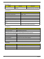
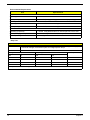
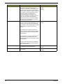
Revision History
Please refer to the table below for the updates made on Aspire L350/Veriton 1000 service guide.
Date
January 9, 2007
II
Chapter
Updates
initial release
Copyright
Copyright © 2007 by Acer Incorporated. All rights reserved. No part of this publication may be reproduced,
transmitted, transcribed, stored in a retrieval system, or translated into any language or computer language, in
any form or by any means, electronic, mechanical, magnetic, optical, chemical, manual or otherwise, without
the prior written permission of Acer Incorporated.
III
Disclaimer
The information in this guide is subject to change without notice.
Acer Incorporated makes no representations or warranties, either expressed or implied, with respect to the
contents hereof and specifically disclaims any warranties of merchantability or fitness for any particular
purpose. Any Acer Incorporated software described in this manual is sold or licensed "as is". Should the
programs prove defective following their purchase, the buyer (and not Acer Incorporated, its distributor, or its
dealer) assumes the entire cost of all necessary servicing, repair, and any incidental or consequential
damages resulting from any defect in the software.
Acer is a registered trademark of Acer Corporation.
Intel is a registered trademark of Intel Corporation.
Pentium 4 and Celeron are trademarks of Intel Corporation.
Other brand and product names are trademarks and/or registered trademarks of their respective holders.
IV
Conventions
The following conventions are used in this manual:
Screen messages
Denotes actual messages that appear
on screen.
NOTE
Gives bits and pieces of additional
information related to the current
topic.
WARNING
Alerts you to any damage that might
result from doing or not doing specific
actions.
CAUTION
Gives precautionary measures to
avoid possible hardware or software
problems.
IMPORTANT
Reminds you to do specific actions
relevant to the accomplishment of
procedures.
V
Preface
Before using this information and the product it supports, please read the following general information.
VI
1.
This Service Guide provides you with all technical information relating to the BASIC CONFIGURATION
decided for Acer's "global" product offering. To better fit local market requirements and enhance product
competitiveness, your regional office MAY have decided to extend the functionality of a machine (e.g.
add-on card, modem, or extra memory capability). These LOCALIZED FEATURES will NOT be covered
in this generic service guide. In such cases, please contact your regional offices or the responsible
personnel/channel to provide you with further technical details.
2.
Please note WHEN ORDERING FRU PARTS, that you should check the most up-to-date information
available on your regional web or channel. If, for whatever reason, a part number change is made, it will
not be noted in the printed Service Guide. For ACER-AUTHORIZED SERVICE PROVIDERS, your Acer
office may have a DIFFERENT part number code to those given in the FRU list of this printed Service
Guide. You MUST use the list provided by your regional Acer office to order FRU parts for repair and
service of customer machines.
Table of Contents
Chapter 1 System Specifications 1
Overview . . . . . . . . . . . . . . . . . . . . . . . . . . . . . . . . . . . . . . . . . . . . . . . . . . . . . . . . . . . .1
Features . . . . . . . . . . . . . . . . . . . . . . . . . . . . . . . . . . . . . . . . . . . . . . . . . . . . . . . . . . . .2
System Block Diagram . . . . . . . . . . . . . . . . . . . . . . . . . . . . . . . . . . . . . . . . . . . . . . . . .6
Main Board Layout . . . . . . . . . . . . . . . . . . . . . . . . . . . . . . . . . . . . . . . . . . . . . . . . . . . .7
Your Acer Notebook tour . . . . . . . . . . . . . . . . . . . . . . . . . . . . . . . . . . . . . . . . . . . . . . .8
Front view . . . . . . . . . . . . . . . . . . . . . . . . . . . . . . . . . . . . . . . . . . . . . . . . . . . . . . .8
Rear view . . . . . . . . . . . . . . . . . . . . . . . . . . . . . . . . . . . . . . . . . . . . . . . . . . . . . . .9
System Peripherals . . . . . . . . . . . . . . . . . . . . . . . . . . . . . . . . . . . . . . . . . . . . . . . . . . .11
Mouse (PS/2 or USB, manufacturing option) . . . . . . . . . . . . . . . . . . . . . . . . . . .11
Keyboard (PS/2 or USB, manufacturing option) . . . . . . . . . . . . . . . . . . . . . . . . .11
Speakers . . . . . . . . . . . . . . . . . . . . . . . . . . . . . . . . . . . . . . . . . . . . . . . . . . . . . . .11
Hardware Specifications and Configurations . . . . . . . . . . . . . . . . . . . . . . . . . . . . . . .13
Power Management Function (ACPI support function) . . . . . . . . . . . . . . . . . . . . . . .19
Dual Channel . . . . . . . . . . . . . . . . . . . . . . . . . . . . . . . . . . . . . . . . . . . . . . . . . . . . . . .20
Chapter 2 System Utilities 21
Entering Setup . . . . . . . . . . . . . . . . . . . . . . . . . . . . . . . . . . . . . . . . . . . . . . . . . . . . . .22
Product Information . . . . . . . . . . . . . . . . . . . . . . . . . . . . . . . . . . . . . . . . . . . . . . . . . .23
Standard CMOS Features . . . . . . . . . . . . . . . . . . . . . . . . . . . . . . . . . . . . . . . . . . . . .24
Advanced BIOS Features . . . . . . . . . . . . . . . . . . . . . . . . . . . . . . . . . . . . . . . . . . . . . .26
CPU Feature . . . . . . . . . . . . . . . . . . . . . . . . . . . . . . . . . . . . . . . . . . . . . . . . . . . .29
Hard Disk Boot Priority . . . . . . . . . . . . . . . . . . . . . . . . . . . . . . . . . . . . . . . . . . . .31
Network Boot Priority . . . . . . . . . . . . . . . . . . . . . . . . . . . . . . . . . . . . . . . . . . . . .32
Advanced Chipset Features . . . . . . . . . . . . . . . . . . . . . . . . . . . . . . . . . . . . . . . . . . . .33
Integrated Peripherals . . . . . . . . . . . . . . . . . . . . . . . . . . . . . . . . . . . . . . . . . . . . . . . .38
Power Management Setup . . . . . . . . . . . . . . . . . . . . . . . . . . . . . . . . . . . . . . . . . . . . .40
PnP/PCI Configuration . . . . . . . . . . . . . . . . . . . . . . . . . . . . . . . . . . . . . . . . . . . . . . . .42
PC Health Status . . . . . . . . . . . . . . . . . . . . . . . . . . . . . . . . . . . . . . . . . . . . . . . . . . . .43
Frequency Control . . . . . . . . . . . . . . . . . . . . . . . . . . . . . . . . . . . . . . . . . . . . . . . . . . .44
Load Default Settings . . . . . . . . . . . . . . . . . . . . . . . . . . . . . . . . . . . . . . . . . . . . . . . . .45
Set Supervisor/User Password . . . . . . . . . . . . . . . . . . . . . . . . . . . . . . . . . . . . . . . . . .46
Save & Exit Setup . . . . . . . . . . . . . . . . . . . . . . . . . . . . . . . . . . . . . . . . . . . . . . . . . . . .47
Exit Without Saving . . . . . . . . . . . . . . . . . . . . . . . . . . . . . . . . . . . . . . . . . . . . . . . . . . .48
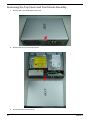
Chapter 3 Machine Disassembly and Replacement 49
General Information . . . . . . . . . . . . . . . . . . . . . . . . . . . . . . . . . . . . . . . . . . . . . . . . . .50
Before You Begin . . . . . . . . . . . . . . . . . . . . . . . . . . . . . . . . . . . . . . . . . . . . . . . .50
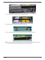
Aspire L350 Disassembly Procedure . . . . . . . . . . . . . . . . . . . . . . . . . . . . . . . . . . . . .51
Removing the Stand Assembly . . . . . . . . . . . . . . . . . . . . . . . . . . . . . . . . . . . . . .51
Removing the Top Cover and Front Bezel Assembly . . . . . . . . . . . . . . . . . . . . .52
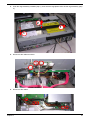
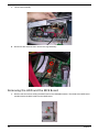
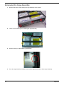
Removing the RF Keyboard/Mouse Antenna and ODD Module . . . . . . . . . . . . .54
Removing the Cage Assembly . . . . . . . . . . . . . . . . . . . . . . . . . . . . . . . . . . . . . .56
TOC
V
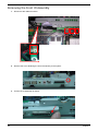
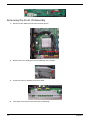
Removing the HDD and the MCE Board . . . . . . . . . . . . . . . . . . . . . . . . . . . . . .58
Removing the Front IO Assembly . . . . . . . . . . . . . . . . . . . . . . . . . . . . . . . . . . . .60
Removing Cables/TV Tuner Board/TV Tuner Card and Wireless LAN Card . . .61
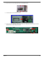
Removing the Thermal Module/CPU/Memory and the Main Board . . . . . . . . . .62
Veriton 1000 Disassembly Procedure . . . . . . . . . . . . . . . . . . . . . . . . . . . . . . . . . . . .66
Removing the Stand Assembly . . . . . . . . . . . . . . . . . . . . . . . . . . . . . . . . . . . . . .66
Removing the Top Cover and Front Bezel Assembly . . . . . . . . . . . . . . . . . . . . .67
Removing the ODD Module . . . . . . . . . . . . . . . . . . . . . . . . . . . . . . . . . . . . . . . .68
Removing the Cage Assembly . . . . . . . . . . . . . . . . . . . . . . . . . . . . . . . . . . . . . .70
Removing the HDD and ODD Transfer Board . . . . . . . . . . . . . . . . . . . . . . . . . .71
Removing the Front IO Assembly . . . . . . . . . . . . . . . . . . . . . . . . . . . . . . . . . . . .72
Removing the Cables . . . . . . . . . . . . . . . . . . . . . . . . . . . . . . . . . . . . . . . . . . . . .73
Removing the Thermal Module/CPU/Memory and the Main Board . . . . . . . . . .74
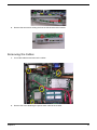
Chapter 4 Troubleshooting 78
Power-On Self-Test (POST) . . . . . . . . . . . . . . . . . . . . . . . . . . . . . . . . . . . . . . . . . . . .79
POST Error Messages List . . . . . . . . . . . . . . . . . . . . . . . . . . . . . . . . . . . . . . . . . . . . .85
Error Symptoms List . . . . . . . . . . . . . . . . . . . . . . . . . . . . . . . . . . . . . . . . . . . . . . . . . .87
Undetermined Problems . . . . . . . . . . . . . . . . . . . . . . . . . . . . . . . . . . . . . . . . . . . . . . .92
Chapter 5 Jumper and Connector Information 93
Main Board Layout . . . . . . . . . . . . . . . . . . . . . . . . . . . . . . . . . . . . . . . . . . . . . . . . . . .93
VI
TOC
Chapter 1
System Specifications
Overview
AcerPower 1000 series is highly integrated desktop for the customers. If you want a simple, small size, not
expensive working platform. AcerPower 1000 is definitely one of the best choices for you.
AMD mobile Athlon 64x2 and Sempron processor enable this product working with less power
consumption: only 62W. This exactly shows Acer’s endeavor to environment protection. AcerPower integrates
nVidia C51PV/G that supports 475/425 MHz graphics core speed, DVI output and directX-9 high level
specification.
Chapter 1
1
Features
CPU
T
Socket Type: Intel socket T (LGA775)
T
Socket Quantity: 1
T
Supports Intel Conroe (E6700/E6600/E6400/E6300) TDP=65W
T
L2 Cache varies with CPU
T
Northbridge: Intel G965, Southbridge: Intel ICH8DH (ViiV-for Aspire L350)
T
Northbridge: Intel Q965, Southbridge: Intel ICH8DO (vPro-for Veriton 1000)
T
Socket Type: DDR II so-DIMM,1.8 Voltage
T
Socket Quantity: 2
T
Capacity support: 256MB ~ 2GB, supporting dual channel
T
Support Memory Speed: DDR II 533/667/800MHz
Chipset
Memory
Graphic Solution
T
Intel Broadwater-G on-die graphic solution
T
Support integrated graphic display
T
Display output supporting HDMI/DVI/D-sub output
T
TV output (for Aspire L350)
Mini PCI Slot
T
Slot Type: PCI 2.3 slot
T
Slot Quantity: for Mini-card (PCI Express):1; for Mini-PCI:1
T
Slot Type : SATA IDE connector
T
Slot Quantity : 2
T
Storage Type support: HDD, (optional for Veriton 1000) DVD-ROM/Combo/DVD Dual/DVD SuperMulti (w/PATA to SATA daughter board)
T
Codec : Realtek ALC888 7.1 with S/PDIF out
T
Compliant with Microsoft’s UAA (Universal Audio Architecture) support (rear only)
T
S/N ratio: 90dB at rear output jack
T
Connectors support: 6 audio jacks at rear side
T
1 CD-in on board header
T
SNR should be ≥ 90 dB at rear output jack
T
S/PDIF out on board header (4 pins)
T
1 2*5 Header for supporting front audio daughter board
IDE
Audio
2
Chapter 1
LAN
T
Controller : Intel ICH8DH (for Aspire L350)/Intel ICH8DO (for Veriton 1000)
T
LAN Chip : Intel 82556DC supports Giga LAN
T
Should be worked under 10/100/1000 Mbs environment
T
Integrated 1.25 GHz SERDES for 1000BASE-X fiber applic
T
Reserved disabled function on both hardware & BIOS side. Default is enabled
T
Controller : Intel ICH8DH (for Aspire L350)/Intel ICH8DO (for Veriton 1000)
T
Connectors Quantity : 10 (rear connectors: 4/ front connectors: 2/ on-board header: 2)
USB
T
T
2 2*5 pin standard USB for front panel USB ports
USB 2.0/1.1
System LED Definition
Chassi
s
Bezel
Power LED
S0
S1,S3
HDD LED
LAN LED
ODD LED
S4,S5
H701
V751
Blue
Blue Blinking
OFF
Blue
Blue
Blue
H500
H500
Green
Green
Blinking
OFF
Green
Green
N/A
V451
Blue
Blue Blinking
OFF
Blue
Blue
Blue
A451
Blue
Blue Blinking
OFF
Blue
Blue
Blue
H401
On-Board Connector
For Aspire L350
T
T
Chapter 1
Rear I/O Connectors
T
1 DVI output
T
1 RJ 45 LAN port
T
4 USB ports
T
1 IEEE 1394 (6-pin)
T
1 5.1 channel out put
T
1 Microphone in jack
T
1 19V DC-in
Front I/O
T
1 Headphone output
T
1 Microphone in
T
2 USB ports
T
1 IEEE 1394 (4-pin)
T
1 3-in-1 card reader (MS/MS Pro/SD)
T
1 Power/Standby button
T
1 Power LED
T
1 storage LED
T
1 ODD LED
3
T
T
T
T
1 LAN LED
TV Daughter board
T
2 Antenna input
T
1 S-video/composite/stereo input
T
1 S-video output
T
1 SPDIF output
Main Board Connectors
T
1 CPU socket LGA775
T
2 memory DDR II sockets so-DIMM
T
1 mini-PCI
T
2 SATA IDE connectors
T
2 USB connectors with 2*5 connector
T
System fan connector 4-pin
T
Power/LED FPIO 2*7 pin connector
T
GPIO for on button recovery
T
Intruder header
Other Connectors
T
1 Intrusion switch
T
1 recovery button
For Veriton 1000
T
T
T
4
Rear I/O Connectors
T
1 DVI output
T
1 RJ 45 LAN port
T
4 USB ports
T
1 5.1 channel phone jack
T
1 microphone in jack
T
1 19V DC in
Front I/O Connectors
T
1 Headphone output
T
1 Microphone in jack
T
4 USB ports
T
1 Power/Standby button
T
1 Power LED
T
1 Storage LED
T
1 ODD LED
T
1 LAN active LED
Main Board Connectors
T
1 CPU socket LGA775
T
2 memory DDR II socket so-DIMM
T
1 mini-PCI
T
2 SATA IDE connector
Chapter 1
T
Chapter 1
T
2 USB connectors with 2*5 connectors
T
System fan connector 4-pin
T
Power/LED FPIO 2*7 pin connector
T
GPIO for one button recovery
T
Intruder header
Other Connectors
T
1 Intrusion switch
T
1 recovery button
5
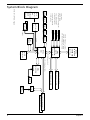
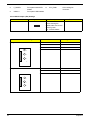
System Block Diagram
Analong Display
RAMDAC: 400MHz
Resolutions Up To 1920x1080@85Hz
VGA to SDTV/EDTV/HDTV
Resolutions Up To1600x1200
USB3
2 ports
Audio Codec
ALC888
SATA1 7Pin
SATA2 7pin
USB1394
2 ports
Scaleable Output Bandwidth
25-165 MegaPixels/s
CARD
1 ports
Line in
Line out
Mic in
Surround
Center/Bass out
Side-Surround
PCB : 235 x 170 mm ; 6 Layers
INTEL
P4 Processor
CONRO CPU
LGA 775 pin
LPC bus
128pin QFP
Super I/O
ITE IT8718F
652pin MBGA
INTEL
ICH8
BW : DDR2 :533/667/800MHz
DIMM1: DDRII Socket 200P
RJ45
USBLAN
DIMM1: DDRII Socket 200P
INTEL
82566DC/DM
81pin BGA
BW : 133MB/s @Freq : 33MHz
BW : 2GB/s (Support Lsoch)
INTEL
GMCH
(BROWATER)
1226pin FC-BGA
BW : FSB : 533MHz & Freq : 133MHz
BW : FSB : 800MHz & Freq : 200MHz
BW : FSB : 1066MHz & Freq : 266MHz
USB V2.0
intel
SPI ROM
8 pin SO8
Azalia I/F
USBLAN
2 ports
VGA (G only)
S-VIDEO
HDMI
USB4
2 ports
BW : 150MB/s
TI 1394
CONN/
HEADER
MINI PCI Slot 124pin @ AD25
MINI PCI-E Slot 52pin
Chapter 1
6
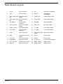
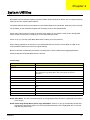
Main Board Layout
1
DC_IN
DC IN Connector
15
C51
Nvidia C51 NorthBridge
2
VGA
VGA Connector
16
MCP51
Nvidia MCP51
SouthBridge
3
SATA_ODD_POW SATA ODD power
ER
Header
17
COMS_BAT
COMS Battery Holder
4
SATA_HDD_POW SATA HDD power
ER
Header
18
CLS_CMOS
Clear COMS Header
5
DVI_ADUIO
DVI and Audio
Connector
19
BUZZER
System BUZZER
6
TVOUT_SPDIF
TV OUT and SPDIF
Header
20
MINI_1394
Mini-1394 Header
7
FRONT_AUDIO
Front Audio Header
21
F_USB2
Front USB*2 Header
8
LAN_USB2
LAN and USB*2
Connector
22
F_USB2
Front USB*2 Header
9
USB2
USB*2 Connector
23
IDE_ODD_DAUG
HTER
IDE ODD Connector
10
OBR
One Bottom Recovery
header
24
SATA1
SATA Header
11
CPU_FAN
CPU Fan Connector
25
SATA2
SATA Header
12
INTRUSION
Case Open header
26
F_LED_HD
Front LED Panel Header
13
CPU_SOCKET
AMD M-2 CPU Socket
27
DIMM_SOCK1
DIMM_SOCK1
14
MINI_PCI
Mini-PCI Connector
28
DIMM_SOCK2
DIMM_SOCK2
Chapter 1
7
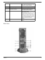
Your Acer Notebook tour
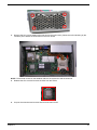
After knowing your computer features, let us show you around your new AcerPower computer.
Front view
#
8
Component
Description
1
Power button
Press to power on or power off the
system.
2
Media activity
Indicates when the hard disk or optical
drive is active.
3
LAN indicator
Indicates the status of LAN
communication.
4
Infrared port
Receives IR signals from the remote
control.
5
Multi Writable DVD drive
Use to access and record data on
compact disks (CDs) and digital video
disks (DVDs).
6
Drive eject button
Ejects the optical disk.
Chapter 1
7
USB 2.0 ports
Connects to USB peripherals devices
(e.g., USB mouse, USB printer, USB
combo drive, digital cameras).
8
1/4” microphone jack
Connects to a microphone.
9
1/4” headphone jack
Connects to a headphone.
10
4-pin IEEE 1394 port
Connects to an IEEE 1394 device
(e.g., digital video camcorder).
11
XD/SD/MMC/MS/MS Pro slot
Accepts an XD (eXtreme Digital), SD
(SecureDigital), MMC
(MultimediaCard), MS (Memory Stick)
or MS Pro (Memory Stick Pro) card.
Warning: If you want to read contents
from small form factor memory cards,
such as mini-SD, RS-MMC, or MS Pro
Duo you should use a suitable
adapter.
12
IR (Infrared) receiver
Receives IR signals from the remote
control.
Rear view
Chapter 1
9
#
Component
Description
1
HDMI
Connects to a TV with HDMI input.
2
Coaxial digital audio output jack
Connects to a digital device, such as
MiniDisc recorders, home theater
receivers, or A/V receivers.
3
USB 2.0 ports
Connects to USB peripheral devices
(e.g., USB mouse, USB printer, USB
drive).
4
Multi-channel speaker audio
output connectors
Connects to an amplifier which has
multi-channel audio system.
5
DC-in jack
Connects to an AC adapter.
6
Kensington lock slot
Connects to a Kensington-compatible
computer security lock.
7
LAN port
Connects to an Ethernet 10/100/1Gbased network.
8
IR blaster port
Connect an IR blaster to the set-topbox°¶s IR sensor window.
9
6-pin IEEE 1394 port
Connects to an IEEE 1394 device
(e.g., digital video camcorder, hard
disk, scanners).
10
FM radio input jack
Connects to an external FM radio
antenna.
11
TV antenna/cable input jack
Connects to a antenna or cable TV.
12
AV-In port
Accepts input signals from audio/
visual (AV) devices.
13
VGA port
Connects to a display device (e.g.,
external monitor, LCD projector).
Audio output connectors function table
Color/Use
1.1 CH
3.1 CH
5.1 CH
7.1 CH
Line-in
Line-in
Line-in
Line-in
Line-in
Green
Headphone
Line-out
Front
Front
Front
Mic-in
Mic-in
Mic-in
Mic-in
Rear
Rear
Pink
Orange
Black
Gray
10
Headphone
Blue
Center & woofer Center & woofer Center & woofer
Side
Chapter 1
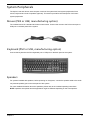
System Peripherals
The Aspire L350 and Veriton 1000 computer consist of the system itself, and system peripherals, like a
mouse, keyboard and a set of speakers (optional). This section provides a brief description of the basic
system peripherals.
Mouse (PS/2 or USB, manufacturing option)
The included mouse is a standard two-button wheel mouse. Connect the mouse to the PS/2 mouse port or
USB port on the back panel of the system.
Keyboard (PS/2 or USB, manufacturing option)
Connect the keyboard to the PS/2 keyboard port or USB port on the back panel of the system.
Speakers
For systems bundled with speakers, before powering on the system, connect the speaker cable to the audio
out (external speaker) port on the back panel of the system.
For more detailed information about the speakers, please refer to the included operating instructions.
NOTE: speakers are optional and the appearance might be different depending on the actual product.
Chapter 1
11
12
Chapter 1
Hardware Specifications and Configurations
System Board Major Chip
Item
Specification
System Core Logic
Northbridge: Intel G965, Southbridge: Intel ICH8DH (ViiV-for
Aspire L350)
Northbridge: Intel Q965, Southbridge: Intel ICH8DO (vPro-for
Veriton 1000)
Super I/O Controller
ITE IT8718F
LAN Controller
Intel 82566DM
Memory Controller
Intel G965
SATA/P-IDE Controller
Intel ICH8
RJ45 Controller
Intel 82566DC/DM
Audio Controller
Realtek ALC888
VGA Controller
Intel G965
Processor
Item
Specification
Type
Intel Conroe (E6700/E6600/E6400/E6300)
Slot
Intel socket T (LGA775)
Speed
Depends on CPU, which is local configured
Front Side Bus Frequency
1066MHz
Voltage
Processor voltage can be detected by any system without
setting any jumper
BIOS
Item
BIOS code programmer
Specification
Award
BIOS version
BIOS ROM size
8Mbit (=1MB for Aspire L350)/16Mbit (=2MB for Veriton 1000)
BIOS ROM package
32-pin PLCC package
Support protocol
USB 1.1, 2.0, ACPI 1.2, 2.0, LS-120 removable media
support, SMBIOS 2.4, WFF 2.0 (wire for management), ASF
2.0, LPC decoding for TPM support, SIPP support, PnP
support, PCI 2.3 PXE 2.0, APM 1.2,VESA/DPMS (VBE/PM
V1.1), Bootable CD-ROM 1.0, UHCI 1.0
Boot from CD-ROM feature
Yes
Support to LS-120 drive
Yes
Support to BIOS boot block feature
Yes
BIOS Password Control
Yes
The BIOS can be overwritten/upgraded by using “AFLASH” utility (AFLASH.EXE).
Chapter 1
13
BIOS Hotkey List
Hotkey
Function
Del/F12
Description
Enter BIOS Setup Utility/Enter
Boot menu
Press while the system is booting to
enter BIOS Setup Utility or boot menu.
System Memory
Item
Specification
Memory Slot Number
2 Slots
Supported Memory Size per Slot
256 MB ~ 1GB
Supported Maximum Memory Size
2GB
Supported Memory Speed
533/667/800 MHz
Supported memory voltage
1.8 V
Support memory module package
240-pin DIMM
Support to parity check feature
Yes
Support to Error Correction Code (ECC)
feature
Yes
Memory module combinations
You can install memory modules in any combination as
long as they match the above specifications.
Cache Memory
Item
Specification
First-Level Cache Configurations
Cache function control
Enable/Disable by BIOS Setup
Second-Level Cache Configurations
The information below is only applicable to system installed with a Pentium 4 processor
Tag RAM Location
On Processor
L2 Cache RAM Location
On Processor
L2 Cache RAM type
PBSRAM (Pipelined-burst Synchronous RAM)
L2 Cache RAM size
Depends on CPU, which is local configured
L2 Cache RAM speed
Full of the processor core clock frequency (Advanced Transfer Cache)
L2 Cache function control
Enable/Disable by BIOS Setup
L2 Cache scheme
Fixed in write-back
LAN Interface
Item
14
Specification
LAN Controller
Intel 82566DC support Giga LAN
LAN Controller Resident Bus
PCI Bus
LAN Port
ONE RJ-45 on board
Function Control
Enable/Disable by BIOS Setup
Chapter 1
IDE Interface
Item
Specification
IDE Controller
Built-in Intel ICH8DH (ViiV-for Aspire L350)/Intel ICH8DO (vPro-for
Veriton 1000)
IDE Controller Resident Bus
PCI bus
Number STAT IDE slot
2
Device Type Support
T
HDD,CD-ROM,CD-RW,DVD-ROM,DVD-RW,DVD+RW,DVD Dual,
DVD Supermultiplus
Supports LS-120
Yes
Supports bootable CD-ROM
Yes
Function Control
Enable/Disable by BIOS setup
USB Port
Item
Specification
Universal HCI
USB 2.0/1.1
Controller
Built-in Intel ICH8DH (for Aspire L350)/Intel ICH8DO (for Veriton
1000)
Number of the connectors
6 (for Aspire L350)/ 8 (for Veriton 1000)
Location
Rear : 2 (for Aspire L350)/ 4 (for Veriton 1000)
Front : 4 (for Aspire L350)/ 4 (for Veriton 1000)
USB Class
Support legacy keyboard for legacy mode
Wake-up Event Specifications
Device
S1
S3
S4
S5
Power Button
Enabled
Enabled
Enabled
Enabled
PS2 Keyboard
Disabled
Disabled
Disabled
Disabled
USB Keyboard
Disabled
Disabled
N/A
N/A
PME
Disabled
Disabled
Disabled
Disabled
WOR (wake on Ring)
Disabled
Disabled
Disabled
Disabled
RTC (real time clock)
Disabled
Disabled
Disabled
Disabled
Thermal Design
Item
Thermal Design
Chapter 1
Description
T
Thermal solution should cover Intel Conroe family
TDP=65W
T
4-pin fan connector
15
Memory Address Map
Address
16
Size
Function
0000000 - 009FFFF
640 KB System Memory
Onboard DRAM
00A0000-00BFFFF
128 KB Video RAM
Reserved for Graphics Display
Buffer
Non-Cacheable
00C0000-00CFFFF
32 KB I/O Expansion ROM
Reserved for ROM on I/O
Adapters
00D0000-00D3FFF
16 KB I/O Expansion ROM
Reserved for ROM on I/O
Adapters
00D4000-00D7FFF
16 KB I/O Expansion ROM
Reserved for ROM on I/O
Adapters
00D8000-00DBFFF
16 KB I/O Expansion ROM
Reserved for ROM on I/O
Adapters
00DC000-00DFFFF
16 KB I/O Expansion ROM
Reserved for ROM on I/O
Adapters
00E0000-00E7FFF
32 KB for SCSI BIOS
Reserved for SCSI BIOS
00E8000-00EFFFF
32 KB
Reserved Onboard
00F0000-00FFFFF
64 KB BIOS
System ROM BIOS (ROM)
System RAM BIOS (DRAM)
0100000-0F9FFFF
System Memory
Onboard DRAM
0FA0000-0FFFFFF
384 KB I/O Card Memory
Reserved for Memory Map
I/O Card
Non-Cacheable
1000000-FFFFFFF
System Memory
Onboard DRAM
Chapter 1
I/O Address Map
Hex Range
Devices
000-01F
020-021
040-043
060-060
061-061
070-071
080-08F
0A0-0A1
0C0-0DF
0F0-0FF
170-177
1F0-1F7
278-27F
2F8-2FF
378-37F
3F0-3F5
3F6-3F6
3F7-3F7
3F8-3FF
0CF8
0CFC
778-77A
DMA Controller-1
Interrupt Controller-1
System Timer
Keyboard Controller 8742
System Speaker
CMOS RAM Address and Real Time Clock
DMA Page Register
Interrupt Controller-2
DMA Controller-2
Math Co-Processor
Secondary IDE
Primary IDE
Parallel Printer Port 2
Serial Asynchronous Port 2
Parallel Printer Port 1
Floppy Disk Controller
Secondary IDE
Primary IDE
Serial Asynchronous Port 1
Configuration Address Register
Configuration Data Register
Parallel Printer Port 1
IRQ Assignment Map
IRQx
System Devices
Add-On-Card Devices
IRQ0
Timer
N
IRQ1
Keyboard
N
IRQ2
Reserved
N
IRQ3
Serial Port 2
Reserved
IRQ4
Serial Port 1
Reserved
IRQ5
Reserved
Reserved
IRQ6
Floppy Disk
Reserved
IRQ7
Parallel Port
Reserved
IRQ8
Real Time Clock
N
IRQ9
N
Reserved
IRQ10
N
Reserved
IRQ11
N
Reserved
IRQ12
PS/2 Mouse
Reserved
IRQ13
Numeric Processor
N
IRQ14
Embedded Hard Disk
Reserved
IRQ15
Reserved
Reserved
NOTE: N - Not be used
Chapter 1
17
Environmental Requirements
Item
Specifications
Temperature
Operating
+5°C ~ +35°C
Non-operating
-20 ~ +60°C (Storage package), -10°C~+60°C (un-package)
Humidity
Operating
15% to 80% RH, non-condensing
Non-operating
10% to 90% RH, non-condensing at 40°C
Vibration
Operating (unpacked)
5 ~ 500Hz, 2.20g RMS random,10 minutes per axis in all 3 axes
Non-operating (packed)
5 ~ 500Hz, 1.09g RMS random,1 hour per axis in all 3 axes
Shock Operating
Half sine, 2g 11m seconds
Drop Test
Drop Test
Definition
The protection ability of packing & cushion must be capable of withstanding, with no physical
or functional damage, mechanical impact from height-specific drops.
Test Standard
see below table:
Package Cross Weight
Drop Height
Not of Drop
KGs
lbs
CM
Inch
0~9.1
0~20
76
30
10
9.1~18.2
20~40
61
24
10
18.2~27.3
40~60
46
18
10
27.3~45.4
60~100
31
12
10
10 drops : one corner, three edges, six surfaces
18
Chapter 1
Power Management Function (ACPI support function)
Device Standby Mode
T
Independent power management timer for hard disk drive devices
(0-15 minutes, time step=1 minute).
T
Hard disk drive goes into Standby mode (for ATA standard interface).
T
Disable V-sync to control the VESA DPMS monitor.
T
Resume method: device activated (Keyboard for DOS, keyboard & mouse for Windows).
T
Resume recovery time: 3-5 sec.
Global Standby Mode
T
Global power management timer (2-120 minutes, time step=10 minute).
T
Hard disk drive goes into Standby mode (for ATA standard interface).
T
Disable H-sync and V-sync signals to control the VESA DPMS monitor.
T
Resume method: Return to original state by pushing external switch button, modem ring in,
keyboard and mouse for APM mode.
T
Resume recovery time: 7-10 sec.
Suspend Mode
T
Independent power management timer (2-120 minutes, time step=10 minutes) or pushing external
switch button.
T
CPU goes into SMM.
T
CPU asserts STPCLK# and goes into the Stop Grant State.
T
LED on the panel turns amber colour.
T
Hard disk drive goes into SLEEP mode (for ATA standard interface).
T
Disable H-sync and V-sync signals to control the VESA DPMS monitor.
T
Ultra I/O and VGA chip go into power saving mode.
T
Resume method: Return to original state by pushing external switch button, modem ring in,
keyboard and mouse for APM mode.
T
Return to original state by pushing external switch button, modem ring in and USB keyboard for
ACPI mode.
T
ACPI specification 1.0b.
T
S0, S1, S3 and S5 sleep state support.
T
On board device power management support.
T
On board device configuration support.
ACPI
Chapter 1
19
Dual Channel
VT x800 series support the Dual Channel Technology. After operating the dual channel
technology, the bandwidth of memory bus will add double up to 4GB/s.
The mainboard includes 4 DIMM slots, and each channel has two DIMM sockets as following:
T
Channel A : DDR1, DDR3
T
Channel B : DDR2, DDR4
If you want to operate the Dual Channel Technology, please note the following explanations due to
the limitation of Intel chipset specifications.
Memory Number
Description
1
Only one DDR memory module is
installed?
The Dual Channel Technology can’t operate when only
one DDR memory module is installed.
2
Two DDR memory modules are
installed (the same memory size
and type)?
The Dual Channel Technology will operate when two
memory modules are inserted individually into Channel A
and B. If you install two memory modules in the same
channel, the Dual Channel Technology will not operate.
3
Three DDR memory modules are
installed?
Pleae note that the Dual Channel Technology will not
operate when three DDR memory modules are installed;
part of them will not be detected.
4
Four DDR memory modules are
installed?
If you install four memory modules at the same time, the
Dual Channel Technology will operate only when those
modules have the same size and type.
NOTE: We strongly recommend user to slot two DDR memory modules into the DIMMs with the same color in
order for Dual Channel Technology to work.
The following tables include all memory-installed combination types:
Dual Channel Technology (DS: Double Side, SS: Single Side)
DDR1
2 memory modules
4 memory modules
20
DDR2
DDR3
DDR4
DS/SS
X
DS/SS
X
X
DS/SS
X
DS/SS
DS/SS
DS/SS
DS/SS
DS/SS
Chapter 1
Chapter 2
System Utilities
BIOS (Basic Input and Output System) includes a CMOS SETUP utility which allows user to configure required
setting or to active certain system features.
The CMOS SETUP saves the configuration in the CMOS SRAM of the mainboard. When the power is turned
off, the battery on the mainboard supplies the necessary power to the CMOS SRAM.
Press <Del> button when the system is turned to enter Setup. As you press the <Del> button during BIOS
POST (Power-On Self Test), it will take you to the CMOS SETUP screen.
Press <F12> you can then enter BIOS Boot Menu to select your boot up device.
When setting up BIOS for the first time, it is recommended that you save the current BIOS to a disk in the
event that BIOS needs to be reset to its original settings.
BIOS is a Window s-based utility that doesn’t required users to boot to DOS before upgrading BIOS but
directly download and update BIOS from the Internet.
Control Keys
Item
Description
wxyz
Move to selection
e
Select Item
^
Main Menu: Quit and not save changes into CMOS Status Page Setup
Menu and Option Page Setup Menu, Exit current page and return to
Main Menu.
{
Increase the numeric value or make changes
}
Decrease the numeric value or make changes
l
General help, only for Status Page Setup Menu and Option Page Setup Menu
m
Item Help
p
Restore the previous CMOS value from CMOS, only for option Page Setup
Menu
r
Load the Optimized Defaults
t
System Information
u
Save all the CMOS changes, only for Main Menu
NOTE: Main Menu: This is the online description of the highlighted setup functions is displayed at the bottom
of the screen.
NOTE: Status Page Setup Menu/ Option Page Setup Menu: Press F1 to pop up a small help window that
describes the appropriate keys to use and the possible selections for the highlighted item. To exit the
Help Window press <Esc>.
Chapter 2
21
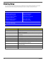
Entering Setup
Once enter Award BIOS CMOS Setup Utility, the Main Menu (as figure below) will appear on the screen.
Use arrow keys to select among the items and press <Enter> to accept or enter the sub-menu.
Phoenix - Award BIOS CMOS Setup Utility
XProduct Information
XStandard CMOS Features
Load Default Settings
XAdvanced BIOS Features
Frequency Control
XAdvanced Chipset Features
Set Supervisor Password
XIntegrated Peripherals
x Set User Password
XPower Management Setup
Save & Exit Setup
XPnP/PCI Configurations
Exit Without Saving
Esc:Quit
F10: Save & Exit Setup
Parameter
Product Information
22
XPC Health Status
KLIJ : Select Item
Description
This page shows the relevant information of the mainboard
Standard CMOS Features
This setup page includes all the items in standard compatible BIOS
Advanced BIOS Features
The values for the chipset can be changed through this menu, and the system
performance can be optimized.
Advanced Chipset Features
This setup page allows user to configure the advanced chipset settings, such as
memory timing.
Integrated Peripherals
This setup page includes all onboard peripherals
Power Management Setup
This setup page includes all the items of Green function features
PnP/PCI Configuration
This setup page includes all configurations of PCI&PnP ISA resources
PC Health Status
This setup page is the System auto detect Temperature, voltage, fan and speed
Frequency Control
Use this menu to specify your settings for frequency control.
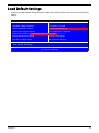
Load Default Settings
Default Settings indicates the value of the system parameters which the system
would be in best performance configuration
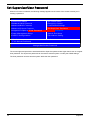
Set Supervisor Password
Change, set or disable password. It allows you to limit access to the system and
Setup, or just to Setup
Set User Password
Change, set or disable password. It allows you to limit access to the system
Save & Exit Setup
Save CMOS value settings to CMOS and exit setup
Exit Without Saving
Abandon all CMOS value changes and exit setup
Chapter 2
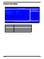
Product Information
Product Name
System S/N
Main Board ID
System BIOS Version
SMBIOS Version
BIOS Release Date
Phoenix - Award BIOS CMOS Setup Utility
Product Information
Aspire L350
EG965RT
R01-A0
2.3
Nov. 21, 2006
Item Help
Menu Level
X
KLIJ :Move Enter: Select +/-/PU/PD :Value F10:Save ESC:Exit F1:General Help
F5:Previous Values F7:Default Settings
Parameter
Description
Product Name
This item lists the product name
System S/N
This item lists the system serial number
Main Board ID
This item lists the mainboard ID
System BIOS Version
This item lists the system BIOS version
SMBIOS Version
This item lists the system SMBIOS version
BIOS Release Date
This item lists the BIOS release date
Chapter 2
23
Standard CMOS Features
Date (MM:DD:YY):
Time (HH:MM:SS):
Phoenix - Award BIOS CMOS Setup Utility
Standard CMOS Features
Mon, Nov 21 2006
11:08:43
Item Help
Menu Level X
IDE Channel
SATA Channel
None
None
Halt On
[All, But Keyboard]
Base Memory
Extended Memory
Total Memory
640K
2070528K
2071552K
KLIJ :Move Enter: Select +/-/Pu/PD :Value F10:Save ESC:Exit F1:General Help
F5:Previous Values F7:Default Settings
The following table describes the parameters found in this menu:
Parameter
Date
Description
Lets you set the date following the weekdaymonth-day-year format
Options
Week : from Sun. to Sat., determined by
BIOS and is display only
Month : from Jan. through Dec.
Day : from 1 to 31 (or the maximum allowed
in the month)
Year : from 1999 to 2098
Time
Lets you set the time following the hour-minutesecond format
The items format is <hour>
<minut><second>. The time is calculated
base on the 24-hour military-time clock. For
example, 1 p.m. is 13:00:00
IDE channel
Display IDE interface devices data pathway
None : No SATA devices are installed
SATA channel
Display SATA interface devices data pathway.
None : No SATA devices are installed
Halt On
This parameter enables you to control the
system stops in case of Power On Self Test
errors (POST)
No Errors : The system boot will not stop for
any error that may be detected and you will
be prompted
All Errors : Whenever the BIOS detects a
non-fatal error the system will be stopped
All, But Keyboard : The system boot will not
stop for a keyboard error; it will stop for all
other errors (Default value)
All, But Diskette : The system boot will not
stop for a disk error; it will stop for all other
errors
All, But Disk/Key : The system boot will not
stop for a keyboard or disk error; it will stop
for all other errors.
24
Chapter 2
Parameter
Base Memory
Description
The amount of RAM that comes with each model
of a particular computer. The base memory can
usually be upgraded to a significantly higher
amount. For example, a desktop machine with
64MB might be upgradable to 768MB.
Options
N/A
Extended Memory
N/A
Total Memory
N/A
Chapter 2
25
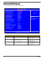
Advanced BIOS Features
The following screen shows the Advanced BIOS Features:
Phoenix - Award BIOS CMOS Setup Utility
Advanced BIOS Features
X CPU Feature
[Press Enter]
X Hard Disk Boot Priority
[Press Enter]
X Network Boot Priority
[Press Enter]
CPU L1 & L2 Cache
[Enabled]
CPU L3 Cache
[Enabled]
Quick Power On Self Test
[Enabled]
First Boot Device
[N/A]
Second Boot Device
[Hard Disk]
Third Boot Device
[Disabled]
Boot Other Device
[Enabled]
Boot Up NumLock Status
[On]
Typematic Rate Setting
[Disabled]
x Typematic Rate (Chars/Sec)
6
x Typematic Delay (Msec)
250
Security Option
[Setup]
APIC Mode
Enabled
MPS Version Control For OS
[1.4]
HDD S.M.A.R.T. Capability
[Disabled]
Silent Boot
[Enabled]
Small Logo (EPA) Show
[Disabled]
Configuration Table
[Disabled]
Item Help
Menu Level X
Select Hard Disk Boot
Device Priority
KLIJ :Move Enter: Select +/-/PU/PD :Value F10:Save ESC:Exit F1:General Help
F5:Previous Values F7:Default Settings
Parameter
26
Description
Options
CPU Feature
Press [Enter] to see CPU feature
Use wx to select a device, then
press<+> to move it up, or < - > to
move it down the list.
Hard Disk Boot Priority
Press [Enter] to enter the sub menu to select
hard disk boot device priority.
Use wx to select a device, then
press<+> to move it up, or < - > to
move it down the list.
Network Boot Priority
Press [Enter] to enter the sub menu to select
network boot device priority.
Use wx to select a device, then
press<+> to move it up, or < - > to
move it down the list.
Chapter 2
Parameter
CPU L1 & L2 Cache
Description
This BIOS feature controls the functionality of
the processor's L1 & L2 cache.
Options
Enabled
Disabled
When enabled, the processor's Ll 1 & L2 cache
will be allowed to function. This allows the best
possible performance from the processor.
When disabled, the processor's Level 1 cache
will be disabled. The processor will bypass the
Level 1 & L2 cache and rely only on the Level 3
caches. This reduces the performance of the
processor.
The recommended setting is obviously Enabled
since disabling it severely affects the
processor's performance. However, the
Disabled setting is useful as a troubleshooting
tool, especially when you are overclocking your
processor
CPU L3 Cache
This BIOS feature controls the functionality of
the processor's Level 3 cache.
Enabled
Disabled
When enabled, the processor's Level 3 cache
will be allowed to function. This allows the best
possible performance from the processor.
When disabled, the processor's Level 3 cache
will be disabled. The processor will bypass the
Level 3 cache and rely only on the Level 1 and
Level 2 caches. This reduces the performance
of the processor.
This feature allows the system to skip certain
tests while booting. When this function is
enabled, it will decrease the time needed to
boot the system, which means to quick power
on self test function
Enabled
First/Second/Third Boot
Device
The item allows you to set the sequence of boot
device where BIOS attempts to load the disk
operating system.
Floppy, LS120, Hard Disk, CD-ROM,
ZIP, USB-FDD, USB-ZIP, USBCDROM, USB-HDD, LAN, Disabled
Boot Other Device
This item allows you to enable or disable to boot
from other device
Enabled
Boot Up NumLock Status
This item allows you to enable or disable to set
keyboard is number keys or arrow keys
Enabled
Typematic Rate Setting
If this option is on, it allows you to set manually
the Typematic Rate or the Typematic Delay.
Enabled
Typematic Rate
This item displays the highest number of
characters that can be typed in a second on the
keyboard.
6, 8, 10, 12, 15, 20, 24, 30
Typematic Delay
This item displays the time (in milliseconds)
needed before pressing again a key on the
keyboard.
250, 500, 750, 1000
Security Option
This BIOS feature controls the application of the
BIOS' password protection. It will only work
once you have created a password through the
Password Setting option in the main BIOS
screen.
System, Setup
Quick Power On Self Test
Disabled
Disabled
Disabled
Disabled
Selecting the System option will force the BIOS
to ask for the password every time the system
boots up.
If you choose Setup, then the password is only
required for access to the BIOS. This option is
useful for system administrators or computer
resellers who need to keep novice users from
messing around with the BIOS.
Chapter 2
27
Parameter
APCI Mode
Description
This option is used to set up enable or disable
the APCI function
MPS Version Control For OS This feature is only applicable to multiprocessor
motherboards as it specifies the version of the
Multi-Processor Specification (MPS) that the
motherboard will use. The MPS is a
specification by which PC manufacturers design
and build Intel architecture systems with two or
more processors.
Options
Enabled
Disabled
1.1, 1.4
MPS 1.1 was the original specification. MPS
version 1.4 adds extended configuration tables
for improved support of multiple PCI bus
configurations and greater expandability in the
future. In addition, MPS 1.4 introduces support
for a secondary PCI bus without requiring a PCI
bridge.
If your operating system comes with support for
MPS 1.4, you should change the setting from
the default of 1.1 to 1.4. You also need to
enable MPS 1.4 support if you need to make
use of the secondary PCI bus on a motherboard
that doesn't come with a PCI bridge.
You should only leave it as 1.1 only if you are
running an older operating system that only
supports MPS 1.1.
HDD S.M.A.R.T. Capability
This BIOS feature controls support for the hard
disk's S.M.A.R.T. (Self Monitoring Analysis And
Reporting Technology) capability.
Enabled
Disabled
S.M.A.R.T. is supported by all current hard
disks and it allows the early prediction and
warning of impending hard disk disasters. You
should enable it if you want to use S.M.A.R.T.aware utilities to monitor the hard disk's
condition. Enabling it also allows the monitoring
of the hard disk's condition over a network.
While S.M.A.R.T. looks like a really great safety
feature, it isn't really that useful or even
necessary for most users. For S.M.A.R.T. to
work, it is not just a matter of enabling it in the
BIOS. You must also keep a S.M.A.R.T.-aware
hardware monitoring utility running in the
background all the time.
Silent Boot
Small Logo (EPA) Show
This features allows you to enable or disable if
the screen logo to display or no during POST
Enabled
This BIOS feature determines if the EPA
(Environmental Protection Agency) Energy Star
logo will appear during the system boot-up
process.
Enabled
Disabled
Disabled
When it is enabled, the BIOS will display the
EPA Energy Star logo during the boot-up
sequence.
When it is disabled, the BIOS will not display
the EPA Energy Star logo during the boot-up
sequence.
Please note that enabling this BIOS feature
may potentially delay the boot-up process by 23 seconds, which ensures that the logo is
displayed for a sufficient amount of time.
Therefore, it is recommended that you disable
this BIOS feature for a faster boot-up time.
28
Chapter 2
Parameter
Configuration Table
Description
This feature allows you to enable or disable if
showing summary screen or not
Options
Enabled
Disabled
CPU Feature
The following screen shows the Advanced BIOS Features:
Phoenix - Award BIOS CMOS Setup Utility
CPU Feature
Item Help
Thermal Management
Limit CPUID MaxVal
C1E Function
Execute Disable Bit
Virtualization Technology
Intel(R)SpeedStep(tm)Tech.
[Enabled]
[Disabled]
[Auto]
[Enabled]
[Enabled]
[Enabled]
Menu Level X
When enabled, TM
function depend on
CPU supported
KLIJ :Move Enter: Select +/-/PU/PD :Value F10:Save ESC:Exit F1:General Help
F5:Previous Value F7:Default Settings
Parameter
Thermal Management
Limit CPUID MaxVal
Description
Options
This item enables or disables thermal
management function for CPU.
Enabled
When the computer is booted up, the operating
system executes the CPUID instruction to
identify the processor and its capabilities.
Before it can do so, it must first query the
processor to find out the highest input value
CPUID recognizes. This determines the kind of
basic information CPUID can provide the
operating system.
Enabled
Disabled
Disabled
The maximum CPUID input value determines
the values that the operating system can write
to the CPUID's EAX register to obtain
information about the processor.
Chapter 2
29
Parameter
C1E Function
Execute Disable Bit
Description
Options
Also called “Enhanced Halt State” function. It is
improved function for Intel (R) Pentium 4
processor C1 Halt state. The operating system
will send out HLT command to the processor
while the system loading is not high. This allows
the processor to enter power-saving C1 halt
state and to reduce the loading for the
processor. Basically, C1E function is very
similar to C1 Halt State. The difference is C1E
function can lower down the processor’s
voltage and clock rate. C1E function together
with EIST can provide a better energy-saving
environment for the processor.
Auto
This BIOS feature is actually a toggle for the
processor's Execute Disable Bit feature. In fact,
the acronym XD is short for Execute Disable
and is specific to Intel's implementation. AMD's
implementation is called NX, short for No
Execute.
Enabled
Enabled
Disabled
Disabled
When enabled, the processor prevents the
execution of code in data-only memory pages.
This provides some protection against buffer
overflow attacks.
When disabled, the processor will not restrict
code execution in any memory area. This
makes the processor more vulnerable to buffer
overflow attacks.
It is highly recommended that you enable this
BIOS feature for increased protection against
buffer overflow attacks.
30
Virtualization Technology
This item allows you to enable or disable Intel
(R) Virtualization Technology function.
Enabled
Intel(R)SpeedStep(tm) Tech.
Enables or disables Intel(R)SpeedStep(tm)
Tech. function.
Enabled
Disabled
Disabled
Chapter 2
Hard Disk Boot Priority
The following screen shows the hard disk boot priority:
Phoenix - Award BIOS CMOS Setup Utility
Hard Disk Boot Priority
Item Help
1. Bootable Add-in Cards
Menu Level X
Use <K> or <L> to select
a device, then press <+> to
to move it up, or <-> to
move it down the list.
Press <ESC> to exit
this menu.
KLIJ :Move Enter: Select +/-/PU/PD :Value F10:Save ESC:Exit F1:General Help
F5:Previous Value F7:Default Settings
Parameter
Bootable Add-in Cards
Chapter 2
Description
Displays the bootable device order.
Options
N/A
31
Network Boot Priority
The following screen shows the network boot priority:
Phoenix - Award BIOS CMOS Setup Utility
Network Boot Priority
Item Help
1. Legacy Lan Cards
Menu Level X
Use <K> or <L> to select
a device, then press <+> to
to move it up, or <-> to
move it down the list.
Press <ESC> to exit
this menu.
KLIJ :Move Enter: Select +/-/PU/PD :Value F10:Save ESC:Exit F1:General Help
F5:Previous Value F7:Default Settings
Parameter
Legacy Lan Cards
32
Description
Displays the bootable device order.
Options
N/A
Chapter 2
Advanced Chipset Features
Phoenix - Award BIOS CMOS Setup Utility
Advanced Chipset Features
Item Help
System BIOS Cacheable
Memory Hole at 15M-16M
X PCI Express Root Port Func
** VGA Setting **
On-Chip Frame Buffer Size
DVMT Mode
DVMT/FIXED Memory Size
[Enabled]
[Disable]
[Press Enter]
Menu Level X
[8MB]
[DVMT]
[256MB]
KLIJ :Move Enter: Select +/-/PU/PD :Value F10:Save ESC:Exit F1:General Help
F5:Previous Value F7:Default Settings
Parameter
System BIOS Cacheable
Description
Enabling this feature allows the caching of the motherboard
BIOS ROM from F0000h to FFFFFh by the processor's
Level 2 cache. This greatly speeds up accesses to the
BIOS.
Options
Enabled
Disabled
However, this does not translate into better system
performance because modern operating systems like
Microsoft Windows XP do not need to communicate with
the hardware via the BIOS. Current operating systems
make use of drivers to access the hardware directly.
Therefore, it would be a waste of the Level 2 cache's
bandwidth if the motherboard BIOS was cached instead of
data that are more critical to the system's performance.
In addition, if any errant program writes into this memory
area, it will result in a system crash. Therefore, it is highly
recommended that you disable this feature for better
system performance.
Chapter 2
33
Parameter
Memory Hole at 15M-16M
Description
Certain ISA cards require exclusive access to the 1MB
block of memory, from the 15th to the 16th megabyte, to
work properly. This BIOS feature allows you to reserve that
1MB block of memory for such cards to use.
Options
Enabled
Disabled
If you enable this feature, 1MB of memory (the 15th MB)
will be reserved exclusively for the ISA card's use. This
effectively reduces the total amount of memory available to
the operating system by 1MB.
Please note that in certain motherboards, enabling this
feature may actually render all memory above the 15th MB
unavailable to the operating system!
If you disable this feature, the 15th MB of RAM will not be
reserved for the ISA card's use. The full range of memory is
therefore available for the operating system to use.
However, if your ISA card requires the use of that memory
area, it may then fail to work.
Since ISA cards are a thing of the past, it is highly
recommended that you disable this feature. Even if you
have an ISA card that you absolutely have to use, you may
not actually need to enable this feature.
Most ISA cards do not need exclusive access to this
memory area. Make sure that your ISA card requires this
memory area before enabling this feature. You should use
this BIOS feature only in a last-ditch attempt to get a
stubborn ISA card to work.
PCI Express Root Port Func Press [Enter] to enter the sub menu to select PCI Express
Root Port Function
34
Use wx to
select a device,
then press<+> to
move it up, or < > to move it down
the list.
Chapter 2
Parameter
Description
Options
On-Chip Frame Buffer Size
This BIOS feature controls the amount of system memory
that is allocated to the integrated graphics processor when
the system boots up. However, its effect depends on
whether your motherboard supports the older Unified
Memory Architecture (UMA) or the new Dynamic Video
Memory Technology (DVMT).
1MB, 4MB, 8MB,
16MB, 32MB,
64MB, 128MB (for
UMA)
1MB, 8MB (for
DVMT)
If you have a motherboard that supports UMA, the memory
size you select determines the maximum amount of system
memory that is allocated to the graphics processor. Once
allocated, it can only be used as graphics memory. It is no
longer accessible to the operating system or applications.
Therefore, it is recommended that you select the absolute
minimum amount of system memory that the graphics
processor requires for your monitor. You can calculate it by
multiplying the resolution and colour depth that you are
using. Of course, if you intend to play 3D games, you will
need to allocate more memory.
If you have a motherboard that supports DVMT, the
memory size you select determines the maximum amount
of system memory that is pre-allocated to the graphics
processor. Once allocated, it can only be used as graphics
memory. It is no longer accessible to the operating system
or applications.
However, unlike in a UMA system, this memory is only
allocated for use during the boot process or with MS-DOS
or legacy operating systems. Additional system memory is
allocated only after the graphics driver is loaded. It is
recommended that you set it to 8MB as this allows for highresolution splash screens as well as higher resolutions in
MS-DOS applications and games.
Chapter 2
35
Parameter
DVMT Mode
Description
Unified Memory Architecture (UMA) is a concept whereby
system memory is shared by both CPU and graphics
processor. While this reduces cost, it also reduces the
system's performance by taking up a large portion of
memory for the graphics processor.
Options
Fixed, DVMT,
Both
Intel's Dynamic Video Memory Technology (DVMT) takes
that concept further by allowing the system to dynamically
allocate memory resources according to the demands of
the system at any point in time. The key idea in DVMT is to
improve the efficiency of the memory allocated to either
system or graphics processor.
The BIOS feature that controls all this is the DVMT Mode
BIOS feature. It allows you to select the DVMT operating
mode.
When set to Fixed, the graphics driver will reserve a fixed
portion of the system memory as graphics memory. This
ensures that the graphics processor has a guaranteed
amount of graphics memory but the downside is once
allocated, this memory cannot be used by the operating
system even when it is not in use.
When set to DVMT, the graphics chip will dynamically
allocate system memory as graphics memory, according to
system and graphics requirements. The system memory is
allocated as graphics memory when graphics-intensive
applications are running but when the need for graphics
memory drops, the allocated graphics memory can be
released to the operating system for other uses.
When set to Both, the graphics driver will allocate a fixed
amount of memory as dedicated graphics memory, as well
as allow more system memory to be dynamically allocated
between the graphics processor and the operating system.
It is recommended that you set this BIOS feature to DVMT
for maximum performance. Setting it to DVMT ensures that
system memory is dynamically allocated for optimal
balance between graphics and system performance.
36
Chapter 2
Parameter
DVMT/FIXED Memory Size
Description
Unified Memory Architecture (UMA) is a concept whereby
system memory is shared by both CPU and graphics
processor. While this reduces cost, it also reduces the
system's performance by taking up a large portion of
memory for the graphics processor.
Options
64MB, 128MB
Intel's Dynamic Video Memory Technology (DVMT) takes
that concept further by allowing the system to dynamically
allocate memory resources according to the demands of
the system at any point in time. The key idea in DVMT is to
improve the efficiency of the memory allocated to either
system or graphics processor.
This is where the DVMT/FIXED Memory BIOS feature
comes in. It allows you to set the maximum amount of
system memory that can be allocated as graphics memory,
but only for the Fixed or DVMT operating modes. When the
DVMT + Fixed mode is selected, this BIOS feature is
grayed out because when in that operating mode, the
graphics driver automatically allocates a total of 128MB of
graphics memory.
When set to 64MB, up to 64MB of system memory can be
used as graphics memory.
When set to 128MB, up to 128MB of system memory can
be used as graphics memory.
Generally, you can leave this BIOS feature at the default
setting of 128MB. This setting works well in systems with
lots of memory (768MB or more). But if you have 384MB or
less of system memory, it is highly recommended that you
restrict the amount of DVMT memory to 64MB. Intel's
graphics processors are not so fast that allocating huge
amounts of memory is going to have any significant effect
on their performance.
Chapter 2
37
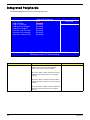
Integrated Peripherals
All onboard peripherals can be set up through this menu.
Phoenix - Award BIOS CMOS Setup Utility
Integrated Peripherals
SATA Mode
AHCI
Item Help
USB Controller
[Enabled]
USB 2.0 Controller
[Enabled]
Menu Level X
USB Keyboard Support
[Enabled]
USB Mouse Support
[Enabled]
Onboard 1394 Controller
[Enabled]
Onboard LAN Controller
[Enabled]
Onboard Lan Boot ROM
[Disabled]
KLIJ :Move Enter: Select +/-/PU/PD :Value F10:Save ESC:Exit F1:General Help
F5:Previous Values F7:Default Settings
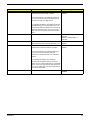
Parameter
SATA Mode
Description
This BIOS feature controls the SATA controller's
operating mode. There are three available
modes - IDE, SATA or AHCI and RAID.
Options
RAID, SATA or AHCI, IDE
When set to SATA or AHCI, the SATA controller
enables its AHCI features when the computer
boots up.
When set to RAID, the SATA controller enables
its RAID and AHCI functions when the computer
boots up.
When set to IDE, the SATA controller disables its
RAID and AHCI functions when the computer
boots up.
38
Chapter 2
Parameter
USB Controller
Description
This BIOS feature enables or disables the
motherboard's onboard USB controller.
Options
Enabled
Disabled
It is recommend that you enable this feature so
that you can use the onboard USB controller to
communicate with your USB devices.
If you disable this feature, the USB controller will
be disabled and you will not be able to use it to
communicate with any USB device. This frees up
an IRQ for other devices to use. This is useful
when you have many devices that cannot share
IRQs.
USB 2.0 Controller
Enable this item if the system supports USB 2.0
Enabled : Enable USB 2.0
Controller
Disabled : Disable USB 2.0
Controller
USB Keyboard/Mouse Support
This BIOS feature determines if support for the
Enabled
USB keyboard/mouse should be provided or not. Disabled
Onboard 1394/LAN Controller
This BIOS feature enables or disables the
motherboard's onboard 1394/LAN controller.
Enabled
Disabled
It is recommend that you enable this feature so
that you can use the onboard 1394/LAN
controller to communicate with your 1394/LAN
devices.
If you disable this feature, the 1394/LAN
controller will be disabled and you will not be
able to use it to communicate with any 1394/LAN
device. This frees up an IRQ for other devices to
use. This is useful when you have many devices
that cannot share IRQs.
Onboard Lan Boot ROM
Enabled
Disabled
Chapter 2
39
Power Management Setup
The Power Management menu lets you configure your system to most effectively save energy while operating
in a manner consistent with your own style of computer use.
Phoenix - Award BIOS CMOS Setup Utility
Power Management Setup
ACPI Function
[Enabled]
ACPI Suspend Type
[S3(STR)]
Soft-Off by PWR-BTTN
[Delay 4 Sec]
Energy Lake Function
[Enabled]
Wake-Up by Onboard Lan
[Enabled]
USB KB Wake-Up From S3
[Disabled]
Resume by Alarm
[Disabled]
x Date(of Month) Alarm
0
x Time(hh:mm:ss) Alarm
00:00:00
Item Help
Menu Level X
** Reload Global Timer Events **
PWON After PWR-Fail
[Off]
KLIJ :Move Enter: Select +/-/PU/PD :Value F10:Save ESC:Exit F1:General Help
F5:Previous Values F7:Default Settings
Parameter
ACPI Function
Description
This BIOS feature is used to enable or disable the
motherboard's APIC (Advanced Configuration and
Power Interface). The ACPI provides multiprocessor
support, more IRQs and faster interrupt handling.
Options
Disabled
Enabled
However, it is only supported by newer operating
systems like Microsoft Windows NT, Windows 2000
and Windows XP. Older operating systems like DOS or
Windows 95/98 do not support this feature.
It is recommended that you enable this feature if you
are using a newer operating system like Windows XP.
Disable it only if you are using an older operating
system like DOS or Windows 95/98.
ACPI Suspend Type
40
This item specifies the power saving modes for ACPI
function. S1(POS): The S1 sleep mode is a low power
state. In this state, no system context (CPU or chipset)
is lost and hardware maintains all system context. S3
(STR): The S3 sleep mode is s power-down state in
which power is supplied only to essential components
such as main memory and wake-capable devices and
all system context is saved to main memory. The
information stored in memory will be used to restore
the PC to the previous state when an wake-up event
occurs.
S1 (POS) : Set ACPI suspend
type to S1/POS(Power On
Suspend).
S3 (STR) : Set ACPI suspend
type to S3/STR
Chapter 2
Parameter
Soft-Off by PWR-BTTN
Description
Options
This feature allows users to configure the power button
function.
Instand-off : Press down
button then power off instantly
Delay 4 Sec. : Press power
button 4 sec. to power off.
Enter suspend if button is
pressed less than 4 sec.
Energy Lake Function
Wake-Up by Onboard Lan
Chapter 2
41
PnP/PCI Configuration
Phoenix - Award BIOS CMOS Setup Utility
PNP/PCI Configurations
Reset Configuraton Data
[Disabled]
Resources Controlled By
X IRQ Resources
PCI/VGA Palette Snoop
INT Pin 1 Assignment
INT Pin 2 Assignment
INT Pin 3 Assignment
INT Pin 4 Assignment
INT Pin 5 Assignment
INT Pin 6 Assignment
INT Pin 7 Assignment
INT Pin 8 Assignment
Item Help
Menu Level X
[Auto(ESCD)]
Press Enter
[Disabled]
[Auto]
[Auto]
[Auto]
[Auto]
[Auto]
[Auto]
[Auto]
[Auto]
** PCI Express relative items **
Maximum Payload Size
[128]
Default is Disabled.
Select Enabled to
reset Extended System
Configuration Data
ESCD) when you exit
Setup if you have
installed an new add-on
and the system
reconfiguration has
caused such as serious
conflict that the OS
cannot boot
KLIJ :Move Enter: Select +/-/PU/PD :Value F10:Save ESC:Exit F1:General Help
F5:Previous Values F7:Default Settings
Parameter
Description
Options
Reset Configuration Data
Disabled, Enabled
In case a conflict occurs after you assign the IRQs or
after you configure your system, you can enable this
function to allow your system to automatically reset
your configuration and reassign the IRQs, DMAs and I/
O address.
Resources Controlled By
if this option is set to Auto, the BIOS automatically
selects all the devices Plug & Play compatible
specifying their Interrupt and DMA. If you selected the
manual setting, you can specify the device for each
interrupt it is assigned to (ISA o PCI); this is the same
for DMAs.
Auto (ESCD), Manual
PCI/VGA Palette Snoop
Enable this option to correct screen color shifts, when
there is a combination of VGA cards, accelerator cards,
or MPEG cards present.
Disabled, Enabled
This item allows you to select the payload size for PCI
Express device’s maximum TLP (Transmission Level
Point).
128, 256, 512, 1024, 2048,
4096
INT Pin 1-8 Assignment
Maximum Payload Size
42
Chapter 2
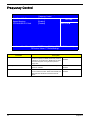
PC Health Status
Phoenix - Award BIOS CMOS Setup Utility
PC Health Status
XAdvanced Fan Speed Control
CPU FAN Speed
SYS FAN Speed
CPU core voltage
+3.3V
+5V
+12V
DIMM voltage
CPU Tempature
Shutdown Tempature
[Press Enter]
2871 RPM
2719 RPM
1.28V
3.28V
5.10V
12.08V
1.76V
58 O C
[Disabled]
Item Help
Menu Level X
KLIJ :Move Enter: Select +/-/PU/PD :Value F10:Save ESC:Exit F1:General Help
F5: Previous Values F7:Default Settings
The following table describes the parameters found in this menu:
Parameter
Description
Advanced Fan Speed Control
Press [Enter] to enter the sub menu to see
advanced fan speed control
Use wx to select a device,
then press<+> to move it up,
or < - > to move it down the
list.
CPU FAN Speed
This field displays CPU fan speed. The system
detects CPU fan speed status automatically.
Displays CPU fan speed
directly.
SYS FAN Speed
This field displays system fan speed. The system
detects system fan speed status automatically
Displays system fan speed
directly.
CPU core voltage
This field displays CPU core voltage. The system
detects CPU core voltage automatically.
Displays CPU core voltage
directly.
DIMM voltage
This field displays DIMM voltage. The system
detects DIMM voltage automatically.
Displays DIMM voltage
directly.
CPU Tempature
This field displays CPU tempature. The system
detects CPU tempature automatically.
Displays CPU tempature.
Shutdown Tempature
This feature allow to set the Shutdown
temperature.
90 ° C/194 ° F
Chapter 2
Disabled
43
Frequency Control
Phoenix - AwardBIOS CMOS Setup Utility
Frequency Control
Auto Detect PCI Clk
[Enabled]
Item Help
Spread Spectrum
[Enabled]
CPU Host/SRC/PCI Clock
[Enabled]
Menu Level X
KLIJ :Move Enter: Select +/-/PU/PD :Value F10:Save ESC:Exit F1:General Help
F5:Previous Values F7:Default Settings
Parameter
Description
To reduce the occurrence of electromagnetic
interference (EMI), the BIOS detects the presence
or absence of components in DIMM and PCI slots
and turns off system clock generator pulses to
empty slots.
Enabled
Spread Spectrum
This feature allows to enable/disable the Spread
Spectrum modulate.
Enabled
CPU Host/SRC/PCI Clock
Select Default or select a timing combination for
the CPU and the PCI bus. When set to Default, the
BIOS uses the actual CPU and PCI bus clock
values.
Enabled
Auto Detect PCI Clk
44
Disabled
Disabled
Disabled
Chapter 2
Load Default Settings
Selecting the field loads the factory defaults for BIOS and Chipset Features which the system automatically.
detects.
Phoenix - Award BIOS CMOS Setup Utility
XProduct Information
XPC Health Status
XStandard CMOS Features
XFrequency Control
XAdvanced BIOS Features
Load Default Settings
XAdvanced Chipset Features
Set Supervisor Password
XIntegrated Periphera
Load Optimized Default?(Y/N)
Password
XPower Management Setup
Save & Exit Setup
XPnP/PCI Configurations
Exit Without Saving
Esc:Quit
F10: Save & Exit Setup
KLIJ : Select
Load Default Settings
Chapter 2
45
Set Supervisor/User Password
When this function is selected, the following message appears at the center of the screen to assist you in
creating a password.
Phoenix - Award BIOS CMOS Setup Utility
X Product Information
X PC Health Status
X Standard CM OS Features
X Frequency Control
X Advanced BIOS Features
Load Default Settings
X Advanced Chipset Features
Set Supervisor Password
X Integrated Periphera Enter Password:
Password
X Power Managem ent Setup
Save & Exit Setup
X PnP/PCI Configurations
Exit W ithout Saving
Esc:Quit
F10: Save & Exit Setup
KLI J : Select
Change/Set/Disable Password
The access rights and permission associated with the Supervisor password are higher than those os a regular
User password. The Supervisor password can be used to start the system or modify the CMOS settings.
The User password can also start the system. While the User password
46
Chapter 2
Save & Exit Setup
Highlight this item and press <Enter> to save the changes that you have made in the Setup Utility and exit the
Setup Utility.
CMOS Setup Utility - Copyright (C) 1984-2005 Award Software
XProduct Information
XPC Health Status
XStandard CMOS Features
XFrequency Control
XAdvanced BIOS Features
Load Default Settings
XAdvanced Chipset Features
Set Supervisor Password
XIntegrated Periphera
Save to CMOS and Exit (Y/N)?N
XPower Management Setup
Save & Exit Setup
XPnP/PCI Configurations
Exit Without Saving
Esc:Quit
F10: Save & Exit Setup
KLIJ : Select
When the Save and Exit dialog box appears, press <Y> to save and exit, or press <N> to return to the main
menu.
Chapter 2
47
Exit Without Saving
Highlight this item and press <Enter> to discard any changes that you have made in the Setup Utility and exit
the Setup Utility.
CMOS Setup Utility - Copyright (C) 1984-2005 Award Software
XProduct Information
XPC Health Status
XStandard CMOS Features
XFrequency Control
XAdvanced BIOS Features
Load Default Settings
XAdvanced Chipset Features
Set Supervisor Password
XIntegrated Periphera Quit Without Saving(Y/N)? Y
Password
XPower Management Setup
Save & Exit Setup
XPnP/PCI Configurations
Exit Without Saving
Esc:Quit
F10: Save & Exit Setup
KLIJ : Select
When the Exit Without Saving dialog box appears, press <Y> to discard changes and exit, or press <N> to
return to the main menu.
NOTE: If you have made settings that you do not want to save, use the "Exit Without Saving" item and press
<Y> to discard any changes you have made.
48
Chapter 2
Chapter 3
Machine Disassembly and Replacement
This chapter will guide you how to disassemble and Reassemble the Aspire L350/Veriton 1000.
To disassemble the computer, you need the following tools:
T
Wrist grounding strap and conductive mat for preventing electrostatic discharge.
T
Wire cutter.
T
Phillips screwdriver (may require different size).
NOTE: The screws for the different components vary in size. During the disassembly process, group the
screws with the corresponding components to avoid mismatches when putting back the components.
Chapter 3
49
General Information
Before You Begin
Before proceeding with the disassembly procedure, make sure that you do the following:
50
1.
Turn off the power to the system and all peripherals.
2.
Unplug the AC adapter and all power and signal cables from the system.
Chapter 3
Aspire L350 Disassembly Procedure
This section tells you how to disassemble the system when you need to perform system service. Please also
refer to the disassembly video, if available.
CAUTION: Before you proceed, make sure you have turned off the system and all peripherals connected to it.
Removing the Stand Assembly
1.
Remove the screw holding the stand assembly.
2.
Then detach the system from the stand assembly.
Chapter 3
51
Removing the Top Cover and Front Bezel Assembly
52
1.
Remove the screw fastening the top cover.
2.
Remove the top cover from the system.
3.
Pull up the three locks as shown.
Chapter 3
4.
Detach the front bezel from the system.
5.
Place the front bezel as shown.
6.
Release the hooks holding the PCB card.
Chapter 3
53
7.
Detach the PCB card from the left side. You can then remove the front bezel.
Removing the RF Keyboard/Mouse Antenna and ODD Module
1.
54
Remove the two screws holding the RF keyboard/mouse antenna.
Chapter 3
2.
Then disconnect the RF keyboard/mouse antenna as shown.
3.
If you only need to remove the ODD module, you can remove the screw holding the ODD module to the
system as shown.
4.
Then push the ODD module outwards as shown.
5.
Remove the two screws fastening the ODD bracket to the ODD.
Chapter 3
55
6.
Detach the ODD bracket from the ODD.
Removing the Cage Assembly
56
1.
Remove the three screws holding the cage assembly to the system.
2.
There are four fastening hooks holding the cage assembly.
3.
See the closeup for the fastening hooks below.
Chapter 3
4.
Push the cage assembly outwards (step 1), then hold the cage plastic belt to lift the cage assembly (step
2).
2
1
1
5.
Disconnect the cables as shown.
6.
Disconnect the cables.
Chapter 3
57
7.
Lift the cage assembly.
8.
Disconnect the antennae then remove the cage assembly.
Removing the HDD and the MCE Board
1.
58
Remove the two screws holding the MCE board to the HDD/ODD bracket. Then detach the MCE board
and disconnect the MCE cable from the MCE board.
Chapter 3
2.
Remove the four screws holding the HDD to the HDD/ODD bracket.
3.
Push the HDD out of the HDD/ODD bracket.
4.
Remove the screw fastening the ODD transfer board on the HDD/ODD bracket, then push the ODD
transfer board to the left to detach the board.
Chapter 3
59
Removing the Front IO Assembly
60
1.
Disconnect the cables as shown.
2.
Remove the screw fastening the front IO assembly to the system.
3.
Pull out the IO assembly as shown.
Chapter 3
4.
Then detach the IO assembly as shown.
5.
Remove three screws holding the IO board (two screws) and card reader (one screw) to the IO bracket.
Then detach the IO board and card reader.
Removing Cables/TV Tuner Board/TV Tuner Card and Wireless
LAN Card
1.
Cut off the cable ties and disconnect the cables from the system.
2.
Remove the two screws fastening the TV tuner board.
Chapter 3
61
3.
Disconnect the antennae and detach the TV tuner board.
4.
Pop out the TV tuner card and detach the wireless LAN card from the main board.
Removing the Thermal Module/CPU/Memory and the Main
62
Chapter 3
Board
1.
Disconnect the system fan power cable.
2.
Remove the four screws holding the system fan on the rear side. Then detach the fan from the system.
3.
Remove the four screws fastening the heat sink to the main board. (Follow the order indicating by the
numbers).Then detach the heat sink from the main board.
4
1
2
3
NOTE: The thermal module on the headline refers to the system fan and the heat sink.
4.
Release the CPU lock and remove the CPU from the socket.
Chapter 3
63
64
5.
Pop out the memories and remove them from the main board.
6.
Remove the four screws and one fastening screw holding the main board to the chassis.
7.
Lift the main board as shown then detach the main board from the chassis.
Chapter 3
Chapter 3
65
Veriton 1000 Disassembly Procedure
This section tells you how to disassemble the system when you need to perform system service. Please also
refer to the disassembly video, if available.
CAUTION: Before you proceed, make sure you have turned off the system and all peripherals connected to it.
Removing the Stand Assembly
66
1.
Remove the screw holding the stand assembly.
2.
Then detach the system from the stand assembly.
Chapter 3
Removing the Top Cover and Front Bezel Assembly
3.
Remove the screw fastening the top cover.
4.
Remove the top cover from the system.
5.
Pull up the three locks as shown.
Chapter 3
67
1
6.
Place the front bezel as shown.
2
7.
Release the two hooks highlighted with red circles, then detach the cable from the front bezel.
Removing the ODD Module
1.
68
Remove the screw holding the ODD module to the system.
Chapter 3
2.
Push the ODD module outwards and remove it from the system.
3.
Remove the two screws holding the ODD bracket to the ODD.
4.
Turn over the ODD module (with ODD bracket) and detach the ODD module as shown.
NOTE: If you only need to remove the ODD module, you can do as the steps mentioned above. However, if
you need to remove the entire cage assembly, please see the steps below.
Chapter 3
69
Removing the Cage Assembly
70
1.
Remove the three screws holding the cage assembly to the system.
2.
There are four fastening hooks holding the cage assembly.
3.
See the close-up for the fastening hooks below.
4.
Push the cage assembly outwards, then hold the cage plastic belt to lift the cage assembly.
Chapter 3
5.
Disconnect the cables and remove the cage assembly.
Removing the HDD and ODD Transfer Board
1.
Disconnect the four screws fastening the HDD to the HDD/ODD bracket.
2.
Detach the HDD from the HDD/ODD bracket.
3.
Remove the screw fastening the ODD transfer board on the HDD/ODD bracket, then push the ODD
transfer board to the left to detach the board.
Chapter 3
71
Removing the Front IO Assembly
72
1.
Disconnect the cables from the main board as shown.
2.
Remove the screw holding the front IO assembly to the chassis.
3.
Pull out the front IO assembly from the chassis.
4.
Then push to the right to remove the front IO assembly.
Chapter 3
5.
Remove the two screws holding the front IO USB board and the bracket.
Removing the Cables
1.
Cut off the cable ties and remove the cables.
2.
Remove the screw fastening the power switch cable to the chassis.
Chapter 3
73
3.
Disconnect the power switch cable from the main board and remove the cable.
Removing the Thermal Module/CPU/Memory and the Main
Board
74
1.
Disconnect the system fan power cable.
2.
Remove the four screws holding the system fan on the rear side. Then detach the fan from the system.
Chapter 3
3.
Remove the four screws fastening the heat sink to the main board. (Follow the order indicating by the
numbers).Then detach the heat sink from the main board.
4
1
2
3
NOTE: The thermal module on the headline refers to the system fan and the heat sink.
4.
Release the CPU lock and remove the CPU from the socket.
5.
Pop out the memories and remove them from the main board.
Chapter 3
75
76
6.
Remove the four screw nuts on the rear side.
7.
Remove the four screws and one fastening screw holding the main board to the chassis.
8.
Lift the main board as shown then detach the main board from the chassis.
Chapter 3
Chapter 3
77
Chapter 4
Troubleshooting
This chapter provides troubleshooting information for the Aspire L350/Veriton 1000
Chapter 4
T
Power-On Self-Test (POST)
T
Index of Error Message
T
Index of Error Symptoms
T
Undetermined Problems
78
Power-On Self-Test (POST)
Each time you turn on the system, the Power-on Self Test (POST) is initiated. Several items are tested during
POST, but is for the most part transparent to the user.
The Power-On Self Test (POST) is a BIOS procedure that boots the system, initializes and diagnoses the
system components, and controls the operation of the power-on password option. If POST discovers errors in
system operations at power-on, it displays error messages on screen, generates a check point code at port
80h or even halts the system if the error is fatal.
The main components on the main board that must be diagnosed and/or initialized by POST to ensure system
functionality are as follows:
T
Microprocessor with built-in numeric co-processor and cache memory subsystem
T
Direct Memory Access (DMA) controller
T
Interrupt system
T
Three programmable timers
T
ROM subsystem
T
RAM subsystem
T
CMOS RAM subsystem and real time clock/calendar with battery backup
T
Onboard parallel interface controller
T
Embedded hard disk interface and one diskette drive interface
T
Keyboard and auxiliary device controllers
T
1.44M floppy controller
T
I/O ports
T
One parallel port
T
One PS/2-compatible mouse port
T
One PS/2-compatible keyboard port
NOTE: When Post executes a task, it uses a series of preset numbers called check points to be latched at
port 80h, indicating the stages it is currently running. This latch can be read and shown on a debug board.
The following table describes the BIOS common tasks carried out by POST. Each task is denoted by an
unique check point number. For other unique check point numbers that are not listed in the table, refer to the
corresponding product service guide.
Post Checkpoints List: The list may vary accordingly depending on your BIOS
.
Checkpoint
79
Description
CFh
Test CMOS R/W functionality
C0h
Early chipset initialization:
-Disable shadow RAM
-Disable L2 cache (socket 7 or below)
-Program basic chipset registers
C1h
Detect memory
-Auto-detection of DRAM size, type and ECC.
-Auto-detection of L2 cache (socket 7 or below)
C3h
Expand compressed BIOS code to DRAM
C5h
Call chipset hook to copy BIOS back to E000 & F000 shadow RAM.
01h
Expand the Xgroup codes locating in physical address 1000:0
02h
Reserved
Chapter 4
.
Checkpoint
Description
03h
Initial Superio_Early _Init switch
04h
Reserved
05h
1. Blank out screen
2. Clear CMOS error flag
06h
Reserved
07h
1. Clear 8042 interface
2. Initialize 8042 self-test
08h
1. Test special keyboard controller for Winbond 977 series Super I/O chips.
2. Enable keyboard interface.
09h
Reserved
0Ah
1. Disable PS/2 mouse interface (optional)
2. Auto detect ports for keyboard & mouse followed by a port & interface swap
(optional).
3. Reset keyboard for Winbond 977 series Super I/Q chips.
0Bh
Reserved
0Ch
Reserved
0Dh
Reserved
0Eh
Test F000h segment shadow to see whether it is R/W-able or not. If test fails,
keep beeping the speaker.
0Fh
Reserved
10h
Auto detect flash type to load appropriate flash R/W codes into the run time area
in F000 for ESCD & DMI support.
11h
Reserved
12h
Use walking 1’s algorithm to check out interface in CMOS circuitry. Also set realtime clock power status, and then check for override.
13h
Reserved
14h
Program chipset default values into chipset. Chipset default values are
MODBINable by OEM customers.
15h
Reserved
16h
Initial Early_Init_Onboard_Generator switch.
17h
Reserved
18h
Detect CPU information including brand, SMI type (Cyrix or Intel) and CPU level
(586 or 686)
19h
Reserved
1Ah
Reserved
1Bh
Initial interrupts vector table. If no special specified, all H/W interrupts are
directed to SPURIOUS_INT_HDLR & S/W interrupts to
SPURIOUS_soft_HDLR.
1Ch
Reserved
1Dh
Initial Early_PM_INIT switch.
1Eh
Reserved
1Fh
Load keyboard matrix (notebook platform)
20h
Reserved
21h
HPM initialization (notebook platform)
22h
Reserved
Chapter 4
80
.
Checkpoint
81
Description
23h
1. Check validity of RTC value:
e.g. a value of 5Ah is an invalid value for RTC minute.
2. Load CMOS settings into BIOS stack. If CMOS checksum fails, use default
value
instead.
3. Prepare BIOS resource map for PCI & PnP use. If ESCD is valid, take into
consideration of the ESCD’s legacy information.
4. Onboard clock generator initialization. Disable respective clock resource to
empty PCI
& DIMM slots.
5. Early PCI initialization
-Enumerate PCI bus number
-Assign memory & I/O resource
-Search for a valid VGA device and VGA BIOS, and put it into C000:0
24h
Reserved
25h
Reserved
26h
Reserved
27h
Initialize INT 09 buffer
28h
Reserved
29h
1. Program CPU internal MTRR (P6 & PII) for 0-640K memory address.
2. Initialize the APIC for Pentium class CPU.
3. Program early chipset according to CMOS setup. Example: onboard IDE
controller.
4. Measure CPU speed.
5. Invoke video BIOS.
2Ah
Reserved
2Bh
Reserved
2Ch
Reserved
2Dh
1. Initialize multi-language
2. Put information on screen display, including Award title, CPU type, CPU
speed...
2Eh
Reserved
2Fh
Reserved
30h
Reserved
31h
Reserved
32h
Reserved
33h
Reset keyboard except Winbond 977 series Super I/O chips.
34h
Reserved
35h
Reserved
36h
Reserved
37h
Reserved
38h
Reserved
39h
Reserved
3Ah
Reserved
3Bh
Reserved
Chapter 4
.
Checkpoint
Description
3Ch
Test 8254.
3Dh
Reserved
3Eh
Test 8259 interrupt mask bits for channel 1
3Fh
Reserved
40h
Test 8259 interrupt mask bits for channel 2
41h
Reserved
42h
Reserved
43h
Test 8259 functionality
44h
Reserved
45h
Reserved
46h
Reserved
47h
Initialize EISA slot
48h
Reserved
49h
1. Calculate total memory by testing the last double word of each 64K.
2. Program writes allocation for AMD K5 CPU.
4Ah
Reserved
4Bh
Reserved
4Ch
Reserved
4Dh
Reserved
4Eh
1. Program MTRR of M1 CPU.
2. Initialize L2 cache for P6 class CPU & program CPU with proper cacheable
range.
3. Initialize the APIC for P6 class CPU.
4. On MP platform, adjust the cacheable range to smaller one in case the
cacheable
ranges between each CPU are not identical.
4Fh
Reserved
50h
Initialize USB
51h
Reserved
52h
Test all memory (clear all extended memory to 0)
53h
Reserved
54h
Reserved
55h
Display number of processors (multi-processor platform)
56h
Reserved
57h
1. Display PnP logo
2. Early ISA PnP initialization
-Assign CSN to every ISA PnP device.
58h
Reserved
59h
Initialize the combined Trend Anti-Virus code.
5Ah
Reserved
5Bh
(Optional Feature)
Show message for entering AWDFLASH.EXE from FDD (optional)
5Ch
Reserved
Chapter 4
82
.
Checkpoint
83
Description
5Dh
1. Initialize Init_Onboard_Super_IO switch.
2. Initialize Init_Onboard_AUDIO switch.
5Eh
Reserved
5Fh
Reserved
60h
Okay to enter Setup utility; i.e. not until this POST stage can users enter the
CMOS setup utility.
61h
Reserved
62h
Reserved
63h
Reserved
64h
Reserved
65h
Initialize PS/2 Mouse
66h
Reserved
67h
Prepare memory size information for function call:
INT 15h ax=E820h
68h
Reserved
69h
Turn on L2 cache
6Ah
Reserved
6Bh
Program chipset registers according to items described in Setup& Autoconfiguration table.
6Ch
Reserved
6Dh
1. Assign resources to all ISA PnP devices.
2. Auto assign ports to onboard COM ports if the corresponding item in Setup is
set to
“AUTO”
6Eh
Reserved
6Fh
1. Initialize floppy controller
2. Set up floppy related fields in 40: hardware.
70h
Reserved
71h
Reserved
72h
Reserved
73h
(Optional Feature)
Enter AWDFLASH.EXE if:
-AWDFLASH is found in floppy drive
-ALT+F2 is pressed
74h
Reserved
75h
Detect & install all IDE devices: HDD, LS120, ZIP,CDROM.....
76h
Reserved
77h
Detect serial ports & parallel ports
78h
Reserved
79h
Reserved
7Ah
Detect & install co-processor
7Bh
Reserved
7Ch
Reserved
7Dh
Reserved
Chapter 4
.
Checkpoint
Description
7Eh
Reserved
7Fh
1. Switch back to text mode if full screen logo is supported.
-If errors occur, report errors & wait for keys
-If no errors occur or F1 key is pressed to continue:
Clear EPA or customization logo.
80h
Reserved
81h
Reserved
82h
1. Call chipset power management hook.
2. Recover the text fond used by EPA logo (not for full screen logo)
3. If password is set, ask for password.
83h
Save all data in stack back to CMOS.
84h
Initialize ISA PnP boot devices.
85h
1. USB final Initialization
2. NET PC: Build SYSID structure
3. Switch screen back to text mode.
4. Set up ACPI table at top of memory.
5. Invoke ISA adapter ROMs.
6. Assign IRQs to PCI devices
7. Initialize APM
8. Clear noise of IRQs
86h
Reserved
87h
Reserved
88h
Reserved
89h
Reserved
90h
Reserved
91h
Reserved
92h
Reserved
93h
Read HDD boot sector information for Trend Anti-Virus code
94h
1. Enable L2 cache
2. Program boot up speed
3. Chipset final initialization
4. Power management final initialization
5. Clear screen & display summary table
6. Program K6 write allocation
7 Program P6 class write combining.
95h
1. Program daylight saving
2. Update keyboard LED & typematic rate
96h
1. Build MP table
2. Build & update ESCD
3. Set CMOS century to 20h or 19h
4. Load CMOS time into DOS timer tick
5. Build MSIRQ routing table
FFh
Boot attempt (INT 19h)
Chapter 4
84
POST Error Messages List
If you cannot run the diagnostics program tests but did receive a POST error message, use “POST Error
Messages List” to diagnose system problems. If you did not receive any error message, look for a description
of your error symptoms in “Error Symptoms List” on page 87.
NOTE: When you have deemed it necessary to replace an FRU, and have done so, you must run a total
system check to ensure that no other activity has been affected by the change. This system check can
be done through the diagnostics program.
NOTE: Check all power supply voltages, switch, and jumper settings before you replace the main board. Also
check the power supply voltages if you have a “system no-power” condition.
If you are unable to correct the problem by using the “BIOS Messages List” table and “Error Symptoms List”
table, go to “Undetermined Problems”.
To diagnose a problem, first find the BIOS error messages in the left column. If directed to a check procedure,
replace the FRU indicated in the check procedure. If no check procedure is indicated, the first Action/FRU
listed in right column is the most likely cause.
BIOS Messages
85
Action/FRU
BIOS ROM checksum error - System halted
The checksum of the BIOS code in the BIOS chip is
incorrect, indicating the BIOS code may have
become corrupt. Contact your system dealer to
replace the BIOS.
CMOS Battery Failed
The CMOS battery is no longer functional. Contact
your system dealer for a replacement the BIOS.
CMOS Checksum Error- defaults loaded
Checksum of CMOS is incorrect, so the system
loads the default equipment configuration. A
checksum error may indicate that CMOS has
become corrupt. A weak battery may have caused
this error. Check the battery and replace if
necessary.
CPU at nnnn
Displays the running speed of CPU.
Display switch is set incorrectly
The display switch on the motherboard can be set to
either monochrome or color. This message indicates
the switch is set to a different setting than indicated
in Setup. Determine which setting is correct, and
then either turn off the system and change the
jumper, or enter Setup and change the Video
selection.
Press ESC to skip memory test
The user may press Esc to skip the full memory test.
Floppy disk(s) fail
Cannot find or initialize the floppy drive controller or
the drive. Make sure the controller is installed
correctly, if no floppy drives are installed, be sure the
Diskette Drive selection in Setup is set to NONE or
AUTO.
HARD DISK initializing - Please wait a moment
Some hard drives require extra time to initialize.
HARD DISK INSTALL FAILURE
Cannot find or initialize the hard drive controller or
the drive. Make sure the controller is installed
correctly. If no hard drives are installed, be sure the
Hard Drive Selection in Setup is set to NONE.
Hard disk(s) diagnosis fail
The system may run specific disk diagnostic
routines. This message appears if one or more hard
disks return an error when the diagnostics run.
Chapter 4
BIOS Messages
Action/FRU
Keyboard Error Or No Keyboard Present
Cannot initialize the keyboard. Make sure the
keyboard is attached correctly and no keys are
pressed during POST. To purposely configure the
system without a keyboard, set the error halt
condition in Setup to HALT ON ALL, BUT
KEYBOARD. The BIOS then ignores the missing
keyboard during POST.
Keyboard is locked out - Unlock the key
This message usually indicates that one or more
keys have been pressed during the keyboard tests.
Be sure no objects are resting on the keyboard.
Memory Test:
This message displays during a full memory test,
counting down the memory areas being tested.
Memory test fail
If POST detects an error during memory testing,
additional information appears giving specifics about
the type and location of the memory error.
Override enabled - Defaults loaded
If the system cannot boot using the current CMOS
configuration, the BIOS can override the current
configuration with a set of BIOS defaults designed
for the most stable, minimal-performance system
operations.
Press TAB to show POST screen
System OEMs may replace the Phoenix
Technologies Award BIOS POST display with their
own proprietary display. Including this message in
the OEM display permits the operator to switch
between the OEM display and the default POST
display.
Primary master hard disk fail
POST detects an error in the primary master IDE
hard drive.
Primary slave hard disk fail
POST detects an error in the secondary master IDE
hard drive.
Secondary master hard disk fail
POST detects an error in the primary slave IDE hard
drive.
Secondary slave hard disk fail
POST detects an error in the secondary slave IDE
hard drive.
Chapter 4
86
Error Symptoms List
NOTE: To diagnose a problem, first find the error symptom in the left column. If directed to a check procedure,
replace the FRU indicated in the check procedure. If no check procedure is indicated, the first Action/
FRU listed in right column is the most likely cause.
Error Symptom
Action/FRU
Processor / Processor Fan
NOTE: Normally, the processor fan should be operative, and the processor clock setting should be
exactly set to match its speed requirement before diagnosing any processor problems.
Processor fan does not run but power
supply fan runs.
1. Ensure the system is not in power saving mode. See
“Power Management” in chapter 2.
2. With the system power on, measure the voltage of
processor fan connector. Its reading should be +12Vdc.
Its reading should be +12Vdc. If the reading shows
normal, but the fan still does not work, then replace a
good fan.
3. Main board.
Processor test failed.
1. Processor.
2. Main board.
Main board and Memory
NOTE: Ensure the memory modules are installed properly and the contact leads are clean before
diagnosing any system problems.
Memory test failed.
1. See "Memory"
2. Main board
Incorrect memory size shown or
repeated during POST.
1. Insert the memory modules in the DIMM sockets properly,
then reboot the system.
2. Memory module.
3. Main board.
System works but fails to enter power
saving mode when the Power
Management Mode is set to Enabled.
1. Enter BIOS Setup and load default settings.
In Windows Systems, check settings in Power
Management Property of Control Panel.
2. Reload software from Recovery CD.
Blinking cursor only; system does not
work.
1.
2.
3.
4.
Diskette/IDE drive connection/cables
Diskette/IDE disk drives
See “Undetermined Problems”.
Main board
Diskette Drive
NOTE: Ensure the diskette drive is auto-setting in BIOS Setup and its read/write head is clean before
diagnosing any diskette drive problems.(If only one drive is installed, please make sure the
drive is connected to master connector or the drive is set to master.)
87
Media and drive are mismatched.
1. Ensure the diskette drive is configured correctly in the
Disk Drives of BIOS Setup.
2. Ensure the diskette drive is correctly formatted.
3. Diskette drive connection/cable
4. Diskette drive
5. Main board
Diskette drive does not work.
1. Ensure the diskette drive is not set to None in the Disk
Drives of BIOS Setup.
2. Diskette drive power
3. Diskette drive connection/cable
4. Diskette drive
5. Main board
Chapter 4
Error Symptom
Action/FRU
Diskette drive read/write error.
1.
2.
3.
4.
Diskette.
Diskette drive cable.
Diskette drive.
Main board.
Diskette drive LED comes on for more
than 2 minutes when reading data.
1.
2.
3.
4.
Diskette
Diskette drive connection/cable
Diskette drive
Main board
Diskette drive LED fails to light, and the
drive is unable to access for more than 2
minutes.
1.
2.
3.
4.
5.
Diskette
Diskette drive power
Diskette drive connection/cable
Diskette drive
Main board
Diskette drive test failed.
1.
2.
3.
4.
Diskette
Diskette drive
Diskette drive cable
Main board
Hard Disk Drive
NOTE: Ensure hard disk drive is configured correctly in BIOS Setup, cable/jumper are set correctly
before diagnosing any hard disk drive problems. (If only one drive is installed, please make
sure the drive is connected to master connector or the drive is set to master.)
Hard disk drive test failed.
1.
2.
3.
4.
Enter BIOS Setup and Load default settings.
Hard disk drive cable.
Hard disk drive.
Main board.
Hard disk drive cannot format
completely.
1.
2.
3.
4.
Enter BIOS Setup and Load default settings.
Hard disk drive cable.
Hard disk drive.
Main board.
Hard disk drive has write error.
1. Enter BIOS Setup and Load default settings.
2. Hard disk drive.
Hard disk drive LED fails to light, but
system operates normally.
1. With the system power on, measure the voltage of hard
disk LED connector.
2. Hard drive LED cable.
CD/DVD-ROM Drive
NOTE: Ensure CD/DVD-ROM drive is configured correctly in BIOS Setup, cable/jumper are set
correctly and its laser beam is clean before diagnosing any CD/DVD-ROM drive problems.
CD/DVD-ROM drive LED doesn't come
on but works normally.
1. CD/DVD-ROM drive
CD/DVD-ROM drive LED flashes for
more than 30 seconds before LED
shutting off.
1. CD/DVD-ROM may have dirt or foreign material on it.
Check with a known good disc.
2. CD/DVD-ROM is not inserted properly.
3. CD/DVD-ROM is damaged.
Software asks to reinstall disc.
Software displays a reading CD/DVD
error.
CD/DVD-ROM drive cannot load or eject
when the system is turned on and its
eject button is pressed and held.
Chapter 4
1. Disconnect all cables from CD/DVD-ROM drive except
power cable, then press eject button to try to unload the
disk.
2. CD/DVD-ROM drive power.
3. CD/DVD-ROM drive
88
Error Symptom
Action/FRU
CD/DVD-ROM drive does not read and
there are no messages are displayed.
1. CD may have dirt or foreign material on it. Check with a
known good disc.
2. Ensure the CD/DVD-ROM driver is installed properly.
3. CD/DVD-ROM drive.
CD/DVD-ROM drive can play audio CD
but no sound output.
1. Ensure the headphone jack of the CD/DVD-ROM has an
output.
2. Turn up the sound volume.
3. Speaker power/connection/cable.
4. CD/DVD-ROM drive.
Real-Time Clock
Real-time clock is inaccurate.
1. Ensure the information in the Standard CMOS
Feature of BIOS Setup is set correctly.
2. RTC battery.
3. Main board
Audio
Audio software program invokes but no
sound comes from speakers.
1. Speaker power/connection/cable.
Modem
Modem ring cannot wake up system
from suspend mode.
1. For the External Modem, make sure Power on By Ring in
BIOS Setup or Power Management is set to Enabled. For
the PCI modem, make sure Wake up by PCI card is set to
Enabled.
2. If PCI modem card is used, reinsert the modem card to
PCI slot firmly or replace the modem card.
3. In Win 98, ensure the telephone application is configured
correctly for your modem and set to receive messages
and/or fax.
Data/fax modem software program
invokes but cannot receive/send data/
fax
1. Ensure the modem card is installed properly.
Fax/voice modem software program
invokes but has no sound output. (Data
files are received normally; voice from
modem cannot be produced, but system
sound feature works normally.)
1. Ensure the modem voice-in cable from modem adapter
card to main board
Video and Monitor
89
Video memory test failed.
Video adapter failed.
1. Remove all non-factory-installed cards.
2. Load default settings (if screen is readable).
3. Main board
Display problem:
- Incorrect colors
No high intensity
Missing, broken, or incorrect characters
Blank monitor (dark)
Blank monitor (bright)
Distorted image
Unreadable monitor
Other monitor problems
1.
2.
3.
4.
Display changing colors.
1. Monitor signal connection/cable
2. Monitor
3. Main board
Monitor signal connection/cable.
Monitor
Video adapter card
Main board
Chapter 4
Error Symptom
Display problem not listed above
(including blank or illegible monitor).
Chapter 4
Action/FRU
1. “Monitor"
2. Load default settings (if screen is readable).
3. Main board
90
Error Symptom
Action/FRU
Parallel/Serial Ports
Execute “Load BIOS Default Settings” in BIOS Setup to confirm ports presence before diagnosing any
parallel/serial ports problems.
Serial or parallel port loop-back test
failed.
1. Make sure that the LPT# or COM# you test is the same
as the setting in BIOS Setup.
2. Loop-back.
3. Main board.
Printing failed.
1. Ensure the printer driver is properly installed. Refer to the
printer service manual.
2. Printer.
3. Printer cable.
4. Main board.
Printer problems.
1. Refer to the service manual for the printer.
Keyboard
Some or all keys on keyboard do not
work.
1. Keyboard
Pressing power switch does not turn off
system. (Only unplugging the power
cord from electrical outlet can turn off the
system.)
1. Ensure the Soft-off by PWR-BTTN. in BIOS Setup
of Power Management is not set to Instant-off.
2. Power switch cable assembly
Pressing power switch does not turn on
the system.
1. Ensure the power override switch (situated at the back of
the machine, just above the connector for the power
cable) is not set to OFF.
2. Power switch cable assembly.
Executing software shutdown from
Windows98 Start menu does not turn off
the system. (Only pressing power switch
can turn off the system).
1. Load default settings.
2. Reload software from Recovery CD.
No system power, or power supply fan is
not running.
1. Power Supply
2. Main board
Power Supply
Other Problems
Any other problems.
91
1. Undetermined Problems
Chapter 4
Undetermined Problems
If an error message is present, go to “POST Error Messages List” on page 85. If you did not receive any
messages, if the symptom is listed in “or “Error Symptoms List” on page 87. If you still cannot solve the
problem, continue with this check:
1.
Check the power supply voltage. If the voltage are correct continue with the following steps:
2.
Power off the system unit.
3.
Perform the following checks, one by one, until you have isolated the problem FRU.
4.
Load default settings in setup.
5.
Check all main board jumper positions and switch settings.
6.
Check all adapter card jumper positions.
7.
Check all device jumper positions.
8.
Check all cables and connectors for proper installation.
9.
If the jumpers, switches and voltage settings are correct, remove or disconnect the following, one at a
time:
10. Non-Acer devices
T
External devices
T
Any adapter card (modem card, LAN card or video card, if installed)
T
CD/DVD-ROM drive
T
Diskette drive
T
Hard disk drive
T
DIMM
T
Processor
T
Main board
11. Power on the system unit.
12. Repeat steps 2 through 5 until you find the failing device or adapter.
Chapter 4
92
Chapter 5
Jumper and Connector Information
Main Board Layout
1
CPU Socket
LGA775 socket for Intel
CoreTM 2 Duo with 65W
TDP CPUs
10
SPI2
Video input header
2
SATA1~2
Serial ATA connectors
11
F_AUDIO2
Front panel audio header
3
SCN2~3
Two 200-pin DDR2
SDRAM SO-DIMMs
12
MINI_PCI1
32-bit/33 MHz MINI PCI
slot
4
JP2
Clear CMOS jumper
13
SCN1
MINI PCI Express slot
5
J4
3-pin ODD power
connector
14
JP5
Case open header
6
J3
SATA HDD power
connector
15
JP6
DVI-D header
7
CR1
USB power header
16
SYS_FAN1
System cooling fan
connector
Chapter 5
93
8
F_PANEL1
Front panel switch/LED
header
9
USB3~4
Front panel USB headers
17
CPU_FAN1
CPU cooling fan
connector
Clear CMOS Jumper (JP2) Settings
Location
Symbol
Description
JP2
JP2
Location and Header Type
CPU_FAN1
Clear CMOS
Pin
1
1
Function
1-2: NORMAL
Before clearing the
CMOS,make sure to turn
off the sys-tem.
2-3: CLEAR CMOS
Signal Name
GND
2
+12V
3
SENSE
4
Control
1
GND
2
3
4
SYS_FAN1
2
+12V
3
SENSE
1
2
3
94
Chapter 5
Location and Header Type
USB3
Signal Name
USBPWR1
2
USBPWR1
3
USBP2N
2
4
USBP2N
3
4
5
USBP2P
5
6
6
USBP3P
7
8
7
GND
1
10
USB4
8
GND
10
NC
1
USBPWR6
2
USBPWR6
3
USBP0N
2
4
USBP1N
3
4
5
USBP0P
5
6
6
USBP1P
7
8
7
GND
1
10
AUDIO1
8
GND
10
NC
1
MIC2_RL
2
AGND
3
MIC2_RR
2
4
VCC3
3
4
5
LINE2_RR
5
6
6
RET_R
7
8
7
REVD
1
10
1394CN1
9
LINE2_RL
10
RET_L
1
AIP
2
AIM
3
GND
1
2
4
GND
3
4
5
B1P
6
B1M
7
CPWR
8
CPWR
10
GND
5
6
7
8
10
Chapter 5
Pin
1
95
Location and Header Type
SPI2
Pin
Signal Name
12
S_VIDEO_Y
2
S_VIDEO_C
3
AUDIO_R_IN
2
4
GND
3
4
5
AUDIO_L_IN
5
6
6
COMP_IN
7
8
7
GND
1
10
CR1
1
8
GND
10
NC
1
USBPWR3
2
USBP4N
3
USBP4P
4
GND
1
MIC2-L
2
AGND
2
3
4
F_AUDIO1
3
LINE2-R
2
4
VCC3
3
4
5
LINE2-R
5
6
6
PET_R
7
8
7
SENSEB
8
KEy
9
10
9
LINE2-L
10
RET_L
1
96
Chapter 5