1
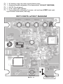
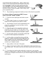
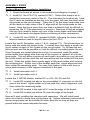
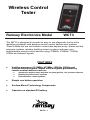
Wireless Control Tester Ramsey Electronics Model WCT3 The WCT3 is designed to provide an easy to use diagnostic tool to aid in identifying problems with wireless remote control devices and systems. These include but are not limited to automotive keyless entry, starter and tire pressure systems, wireless building access systems and even your entertainment remote control devices using 315MHz, 433MHz, 125KHz, 20KHz and Infrared signals. FEATURES Verifies presence of 315MHz, 433MHz, 125KHz, 20KHz and Infrared control signals remote control signals generated by remote control devices such as: Automotive keyless entry key fobs, keyless ignition , tire pressure sensors Building keyless access systems Entertainment / media systems Simple one button operation Surface Mount Technology Components Operates on standard 9V battery WCT3 1 PARTIAL LIST OF AVAILABLE KITS: RAMSEY TRANSMITTER KITS FM10A, FM25B, FM30, FM Stereo Transmitters FM100B, FM35 Professional FM Stereo Transmitters AM1, AM25 AM Broadcast Band Transmitters RAMSEY RECEIVER KITS FR1 FM Broadcast Receiver AR1 Aircraft Band Receiver SR2 Shortwave Receiver SC1 Shortwave Converter RAMSEY HOBBY KITS LBC6K Laser Beam Communicator SG7 Personal Speed Radar SS70C Speech Scrambler/Descrambler TT1 Telephone Recorder LLS1 Laser Light Show MD3 Microwave Motion Detector LEDS1 LED Strobe Light BE66 Blinky Eyes Animated Display LTS1 Laser Trip Sensor ICI1C Infrared Switch Control Interface RAMSEY AMATEUR RADIO KITS HR Series HF All Mode Receivers DDF1 Doppler Direction Finder Kit QRP Series HF CW Transmitters and QAMP Power Amplifiers CW7 CW Keyer RAMSEY MINI-KITS Many other kits are available for hobby, school, scouts and just plain FUN. New kits are always under development. Write or call for our free Ramsey catalog. WCT3 Wireless Control Tester Ramsey Electronics publication No. WCT3 Rev 1.0 This Printing: March 2011 COPYRIGHT 2010 by Ramsey Electronics, Inc. 590 Fishers Station Drive, Victor, New York 14564. All rights reserved. No portion of this publication may be copied or duplicated without the written permission of Ramsey Electronics, Inc. Printed in the United States of America. WCT3 2 Ramsey Publication No. WCT3: Manual Price Only $5.00 INSTRUCTION MANUAL AND ASSEMBLY STEPS FOR WCT3 Wireless Control Tester TABLE OF CONTENTS Introduction ** ...................................... 4 Theory of Operation ............................. 5 Parts List ............................................ 10 Parts Layout Diagram ........................ 11 “Learn as you Build” ** ....................... 12 Assembly Steps ................................. 14 Schematic Diagram............................ 18 Operational Check ............................. 23 Final Case Assembly ......................... 24 Using The WCT3 ............................... 25 Troubleshooting ................................. 27 How To Get Help From Ramsey........ 32 User Notes ......................................... 31 Warranty ............................................ 33 ** IMPORTANT!: Please read notes about cleaning the circuit board. RAMSEY ELECTRONICS, INC. 590 Fishers Station Drive Victor, New York 14564 Phone (585) 924-4560 Fax (585) 924-4555 www.ramseykits.com WCT3 3 INTRODUCTION The WCT3 can be used to detect 315MHz, 433MHz, 125KHz, 20KHz and Infrared signals generated by various devices such as, but not limited to, automotive key fobs, tire pressure sensors, building access control systems, and infrared remote control devices. The WCT3 provides verification of the presence of the various types of signals. It does not provide any information about the actual data transmitted by the device. It should be noted that all remote control devices and systems are not created equal. There are different signal levels, signal radiation and data patterns generated by these devices. Because of this you may find that it is necessary to adjust the position of the WCT3 and device being tested in relation to each other in order to obtain signal indication. This is normal operation. Remember that the WCT3 provides a basic indication of signal generation. This indication does not assure the data included on a signal is correct. !!! PLEASE NOTE !!! Please take note that because of the extreme sensitivity of the WCT3 we highly recommend the use of a NO-CLEAN, ROSIN CORE solder to assemble your WCT3. Also note that you should avoid use of any type of cleaning solution to remove rosin residue. Any attempt to use cleaning solutions may degrade the performance of your WCT3. You can purchase the recommended solder from Ramsey Electronics, LLC or call us at 585-924-4560 if you any questions. About the signals detected: The 315MHz section of the WCT3 is optimized to detect signals in the 315MHz range but is also useful in detecting a fairly wide range of signal frequencies including 433MHz signals often used for some types of remote control systems. The sensitivity may be decreased for these signals but an indication is still possible. The 315/433MHz indicator will indicate presence of these signals. The 125KHz and 20KHz functions of the WCT3 are precisely tuned to detect signals within a few kilohertz above or below the indicated frequency. Infrared signals will be detected only if the signal is modulated with data. If an un-modulated infrared source is present you may find that the indicator will flash only if the source is being moved and there may be no indication if the source is held stationary. This is normal operation and does not indicate a problem with the WCT3. WCT3 4 THEORY OF OPERATION The WCT3 consists of 4 separate stages, one for each of the wireless control signals to be detected. The sections are basically identical in operation but each is specifically designed to detect the signal of interest. In order to keep things simple we will describe the basic operation of one section and then briefly describe the differences between the sections. Looking at the schematic on pages 18 & 19 you will notice that it is divided into 5 columns titled “INPUT/FILTER”, “DETECTOR”, “AMPLIFIER”, “COMPARATOR”, and “POWER SUPPLY”. There are also 4 apparent rows left to right which correspond to the 315/433MHz, 125KHz, 20KHz and Infrared sections from top to bottom respectively. The power supply is common to all sections and is the right most column. We’ll look at the 125KHz section for this discussion. Starting on the left side of the schematic in the “INPUT/FILTER” column is the antenna, “ANT2”, which essentially ‘collects’ the 125KHz signal to be detected. Next is coil L1 and capacitor C4. L1 is a specialized coil called an RFID (Radio Frequency Identification) transponder coil. L1 along with C4 are designed, or tuned, to allow a very narrow band of frequencies centered around 125KHz to pass on to the detector stage of the WCT3. Any frequencies outside the desired band are blocked from passing into the circuit. The technical term for this circuit is a band pass filter. Now that we have captured only the desired signal we want it needs to be detected and this is done in the detector section. Diode D2, which is actually a small package that contains 2 diodes, forms the detector. Without getting into the details of how a detector works just know that D2 actually converts the 125KHz signal into a DC(direct current) signal. The diode connected between C5 and R25 provides a positive DC signal to the amplifier, U1B pin 5, thru R25 and the other diode connected to ground prevents any negative part of the signal from interfering with the operation of the rest of the circuit. C5 and R25 are in the circuit to provide a little more filtering of the 125KHz signal and help stabilize the captured signal before being detected. Resistor R5 is a very high resistance, 3,900,000 ohms and provides a very high resistance for the output of the detector. This is necessary because the detected signal has an extremely low power level. Up to this point the circuit design had to take into consideration the frequency of the signal we were working with. Now that it has been detected by D2 the signal is a simple DC level which will have an amplitude, or DC level, that is proportional to the strength of the detected signal. Because the signal is now a DC level it is much easier to amplify and provide an indication of a signal being present. As you have probably guessed the nice DC signal will now be amplified by the WCT3 5 amplifier stage formed by U1B and the resistors R5, R6, R8 and capacitor C7. U1B is a high gain, high frequency, high input resistance, low noise amplifier. There are 4 of these amplifiers in the U1 package and one is used for each of the 4 sections of the WCT3. The reason an amplifier with the characteristics of U1 is needed is because the detected signal level is extremely small, actually in the micro volt, (that’s 0.000001 volts), range. The amplifier in the case of the 125KHz signal amplifies the signal about 330 times so, for example, a signal level of 100 micro volts, (0.0001 volts), will result in a level of 33 millivolts, (0.033 volts), at the output of the amplifier. This gain is determined by R6 and R8 and is calculated by dividing the value of R6 by R8. So R6 / R8 = 330,000 / 1000 which equals 330. Believe it or not we now have a signal level that is easy to work with. Now that we have a workable signal level it is time to indicate that a signal has been detected. This is the job of the comparator circuit formed by U2B and resistors R14 and R15. U2 , like U1, has 4 identical parts with one being used for each of the WCT3 sections. What U2B does is look at the signal applied to U2B pin 6 from amplifier U1B pin 7 and compares it to a predetermined voltage level set by R14 and R15 on U2B pin 5. This is a simple voltage divider and for the 125KHz signal provides a level of about 685 millivolts. You will notice that this level is shown on the schematic near the junction of R14, R15 and U2B pin 5. If the voltage level applied to U2B pin 6 from the amplifier goes above 685mV the output, U2B pin 7, goes low and LED D7 lights indicating a signal has been detected. Operation Of The Other Sections If you look at the other sections of the schematic you will notice that they all look about the same as the 125KHz section. The component values are different for each section but the basic operation is the same. The major difference is in the Input/Filter sections because it is necessary to allow signals of different frequencies to be detected. Notice that the 20KHz section uses the same transponder coil but has a different value for capacitor C17 compared to C4 in the 125KHz section so only signals in the 20KHz frequency range will be detected. Changing the capacitor value changes the resonance of the circuit. The transponder coils, L1 and L2, are identical and have an inductance value of about 7.5 millihenries. To learn more about resonance try searching on the Web for “resonance frequency”. There is lots of information available. For the 315/433MHz section the filter has a different type of coil. It actually works the same way as L1 and L2 but because of the much higher frequency the coil is constructed differently. In this case the coil, M2, is actually formed by a copper trace which is physically part of the circuit board. This is called a strip-line inductor and makes it much easier to accurately construct the coil. It’s inductance value is about 0.18microhenries (0.00000018 henries), much smaller than L1 and L2. If you look at the circuit board you will see M2 which WCT3 6 is a spiral circuit trace near the ANT1 connection on the left side of the board. You will also notice that the detector diodes D3 and D4 are a different type. This is because of the much higher frequency we are working with. The diode package used on the other sections will not function at these frequencies. The Infrared section of the WCT3 is the least critical section even though the infrared signal is near the frequency range of visible light. This is because the device that captures the infrared signal, Q1, easily responds to signals in the frequency range of light. Q1 is called a photo transistor which acts like a switch and turns on when it ’sees’ infrared or light. The infrared signal from a control is turned on and off, modulated, so Q1 actually turns on and off at the rate of the modulated signal. The frequency of the modulation is typically in the range of 38KHz and is therefore extremely easy to work with. You can think of Q1 as the antenna and filter, and the detector is actually detecting the modulation signal rather than the actual infrared signal. The amplifier and comparator stages of all the sections are identical in operation with the only differences being in the amplifier stage gain and comparator reference levels. Each of these areas is designed specifically for the characteristics of signal to be detected. Power Supply Operation Power for the WCT3 is provided by a standard 9V battery. Looking at the power supply section of the schematic you will see the battery on the left. When push button switch S1 is pressed power is applied to operate the WCT3. Capacitor C3 is a filter which insures a stable 9 volts under sudden heavy loads, such as when an LED lights. It acts like a big reserve reservoir for sudden power surges. Now you are asking why the voltage connection after switch S1 is labeled “+4.5V”. Good question. You will notice that there are two types of ‘ground’ connection symbols used in the schematic. One is a simple triangle and the other is a triangle made up of three parallel lines. Notice that the ‘-‘ connection of the 9 volt battery as well as the, ‘-‘ lead of C3, Pin 11 of U1-D and U2D, and one lead of R7 and R22 are connected to the triangle. If a measurement is taken with reference to this ground connection a reading of +9 volts will be seen. This is actually the power ground reference but is not the signal ground reference point used for the detected signals. The ground connection indicated by the other triangle symbol is the signal ground reference. Resistors R22 and R23 are used to create a reference point half way between the 9 volt supply and power ground that supplies power to U1 and U2. This allows the amplifier and comparator to accept a signal that swings between a positive and negative level with reference to the signal ground point which is the connection between the resistors. The WCT3 7 “+4.5V” voltage is referenced to the signal ground and not the power ground. If a reading is taken between the power ground and signal ground with reference to the signal ground you will see a reading of “-4.5V”. So the difference between the “+4.5V” and “-4.5V”, (measurements referenced to signal ground), points of the circuit is now +9 volts with reference to the power ground. A Little More About Wireless Remote Control Signals Here’s a little more information about how most wireless remote control systems work and how the WCT3 detects the signals. The 315/433MHz, 125KHz and 20KHz sections of the WCT3 will detect the presence of virtually any signal that is within the design frequency range. It doesn’t matter if there is data, modulation, on the signal or not. The simple presence of the signal will be indicated. The infrared section operates in a slightly different way. We’ll take a look at the circuit operation differences here. When you see the indicator flashing when you activate any wireless remote control you are seeing the modulation signal. Most remote controls, both RF and infrared type systems, modulate the signal by turning the signal on and off. This is often referred to as OOK, On-Off_Keying, modulation. When the indicator flashes you are seeing the result of the modulation. Actually an unmodulated signal is constantly turning on and off at the frequency of the unmodulated signal. This unmodulated signal is called the carrier, (i.e. it carries the data). The frequency of the carriers, except for the infrared, detected by the WCT3 are 315MHZ, 433MHz, 120KHz and 20KHz. If the indicator does not flash but simply stays on that indicates that the signal is not being modulated and only the fact that a signal in the proper frequency range is present. (Actually the indicator may be flashing or flickering but it is so fast that your eyes think it’s on all the time, but that’s beyond the scope of this manual.) The infrared section also indicates the modulation by flashing but it will not provide an indication if the signal is not modulated. That’s because the frequency of the infrared carrier is so high that Q1 simply turns on and turns off when light is present and removed. The detector section actually detects only the 38KHz carrier signal. You can think of Q1 as both the antenna and filter part of the “Input/Filter” section of the infrared section. This means that virtually any infrared or light signal will be indicated by the WCT3 as long as it is modulated so you can use it to test any virtually any remote that uses infrared and a carrier signal. An interesting experiment you can try is to use the WCT3 to detect movement of a light source or of an object moving between the light source and WCT3. If you point the infrared detector of the WCT3 toward a light source you may see a brief flash of the IR indicator. By simply moving your hand between the light and WCT3 rapidly you will see the indicator flicker or even stay on if you WCT3 8 can move your hand REALLY, REALLY, REALLY …. fast. (If you can move that fast there are probably some military research facilities that would like to talk to you). For the same reason, if the light source is moved rapidly past the WCT3 you may also see the indicator flash indicating detection of the light. You are actually modulating the IR signal seen by the WCT3 by blocking and unblocking or moving the light source, (OOK modulation). An infrared control turns the signal on and off in specific patterns and rates which are decoded by the device being controlled. Conclusion Now that you are completely confused, don’t worry about it, (I’m often confused too), and enjoy your WCT3. Hopefully you have gained a basic understanding of the WCT3 operation. This description is intended to give a simple overview of the unit. A more detailed description of the operation is beyond the scope of this manual. If it has inspired you to learn more that’s great. There’s a lot of information about electronic circuit design available on the Web and with a little searching you can find much more detailed information about the operation of the basic circuits described here. After years of electronics engineering I find lots of things I didn’t know, (or is it that I forgot ….?), out there. I forget……. ENJOY!!!!! WCT3 9 WCT3 PARTS LIST Each type and value of a surface mount component, (indicated by “[smt]”), is placed in its own labeled baggie. Be aware not all [smt] components have value markings so be careful not to mix them up. In the parts list an “X” in the reference designation indicates that an extra component or two is provided because they like to “fly away” due to the small size. Semiconductors 1 LF347F IC, marked LF347 ,(U1) [smt] 1 LM324M IC, marked LM324, (U2) [smt] 2 CDSH270 diode, CDSH270, (D3, D4) 3 BAV99 diode, marked A7 or A7X, (D2, D5, D9) [smt] 1 Infrared transistor, marked with green dot, (Q1) 2 RED LED (D1, D6) 2 GREEN LED (D7, D10) 1 YELLOW LED (D8) Resistors (ALL [smt]) 5 560 ohm resistors, marked 560, (R18, R19,R20, R32, X) 11 1k ohm resistors, marked 102, (R4, R7, R8, R9, R10, R11, R22, R23, R29, R30, X) 2 1.2K ohm resistor, marked 122, (R26, X) 2 2.7K ohm resistor, marked 272, (R15, X) 2 5.6K ohm resistor, marked 562, (R13, X) 2 6.8K ohm resistor, marked 682, (R17, X) 6 10k ohm resistors, marked 103, (R12, R14, R16, R21, R27, X) 2 150k ohm resistors, marked 154, (R31, X) 3 330k ohm resistors, marked 334, (R3, R6, X) 7 3.9M ohm resistors, marked 395, (R2, R5, R24, R25, R28, R33, X) Capacitors 4 0.001uF Ceramic disk, not marked, (C2, C11, C13, X) [smt] 11 0.01uF Ceramic disk, not marked, (C5, C6, C7, C8, C9, C10, C14, C15, C16, C17, X) [smt] 2 8.2pF Ceramic, not marked, (C12, X) [smt] 2 220pF Ceramic, not marked, (C4, X) [smt] 1 10uF Electrolytic SMT, marked 10, (C3) [smt] Miscellaneous 1 SPST Push Button switch (S1) 1 0.32” long round black switch cap 2 resonator coil, marked 715, (L1, L2) [smt] 1 Case cover label WCT3 10 1 9V battery snap clip with red and black wires 1 Antenna bundle assembly (Pre-Assembled. DO NOT DEFORM) 1 WCT3 Circuit board 5 5/16” nylon LED spacers 1 Case assembly (includes 4 screws, red end cap (VERY dark red), top & bottom case shell, belt clip) WCT3 PARTS LAYOUT DIAGRAM /R33 WCT3 11 JUMPER WIRE RAMSEY “LEARN-AS-YOU-BUILD” ASSEMBLY STRATEGY Completely read through all of the steps and check the boxes as you go to be sure you didn't miss any important assembly instructions. Although you may be in a hurry to see results, before you switch on the power check all wiring diodes, transistors, IC’s, and capacitors for proper orientation. Also check the board for any possible solder shorts and/or cold solder joints. Any of these mistakes could have detrimental effects on your kit - not to mention your ego! Kit building tips: !!! IMPORTANT !!! DUE TO THE EXTREME SENSITIVITY OF THE WCT3, ATTEMPTING TO CLEAN THE ROSIN FLUX FROM THE BOARD MAY RESULT IN DEGRADED PERFORMANCE OF THE UNIT. WE HIGHLY RECOMMEND THE USE OF ONLY NO-CLEAN ROSIN CORE SOLDER. Warning: Use only rosin core solder or solder designed to be used with electronic equipment. Use of acid core solder will void your warranty and produce a board that will disintegrate in a short period of time. For Through-Hole Components, the word "Install" means: 1. Pick the correct part type and value or part number. 2. Mount all electrical components on the top (silkscreened) side of the PC board unless otherwise noted. 4. Orient the part correctly. Follow the PC board drawing or silk screen and the written directions for every part! Certain types of parts must be installed with the proper leads in specific holes. Things to watch for include diode bands, electrolytic capacitor polarity, transistor shapes, dotted or notched ends of IC's, and so forth. 5. Insert the part into the correct PC board location. Make sure the part is mounted as close to the PC board as possible, unless otherwise noted. Most parts, including lay down parts, have holes or pads that are located inside or near a rectangle, oval, or circle. Stand up resistors, diodes, or inductors have a circle around one pad (part body location) with a line leading from that circle to the other pad (lead only). 6. Bend the component and insert thru the board and then bend leads on the backside of the board to prevent the part falling out before soldering. 7. Flip board and solder all connections unless directed otherwise. Apply a touch of solder to the iron tip and then heat both the component lead and WCT3 12 circuit board pad simultaneously. Apply a little more solder to the component lead and the pad when they are hot enough to melt the solder and remove the iron. DO NOT move the component lead or board until the solder cools a little. The finished joint should look like a drop of water on paper, clean, shiny, with joint completely filled. 8. Clip remaining component leads as close to the board as possible. For Surface Mount Technology (SMT) Components, the word "Install" means: 1. Pick the correct part type and value or part number. 2. Melt a dab of solder on one pad of the PC board for the component you wish to install. 3. Use tweezers to pick up the appropriate component by grabbing it across the body, not the solder connections. 4. Place the part in the assembly location as noted by the silk-screen on the top layer of the board (the bottom side has no writing on it). Use one hand to hold the tweezers and part in place. 5. Use the other hand to re-heat the solder dab to melt it to the component connection. 6. Let the solder cool and then let go with the tweezers. Inspect orientation and make sure the part is square over the correct pads. Make sure stray solder connections don’t overlap or short across any to adjacent pads. 7. Apply solder to the rest of the pads. 8. Apply a touch more solder to the initial pad to make sure there is a good solder joint. The rosin core flux will clean the joint and insure stability. 9. If you have too much solder and wish to remove it, use a solder sucker or solder wick to “soak up” the extra solder. Solder bridges on SMT IC pins are a frequent occurrence so you should always have some solder wick handy. WCT3 13 ASSEMBLY STEPS Surface Mount Semiconductor Installation 1. Orient the board as shown in the board layout diagram on page 1 2. Install U1, the LF347 IC( marked LF347). Notice that there is an indented dot near one corner of the IC. This indicates the location pin 1 and the IC must be installed so this dot is to the upper left near the small white dot printed on the circuit board. Place the IC on the board and make sure all the leads on both sides of the IC align with all the solder pads on the board. Note that once more than one lead is soldered it will be difficult to reposition the IC if the placement is incorrect. Because of this we suggest that you first carefully solder only one of the corner leads and then make sure all other leads are aligned before soldering all other connections. 3. Install U2, the LM324 IC, (marked LM324), following the same installation procedure used in step #2 above for the LF347. Locate the two(2) Resonator coils, L1 & L2, marked 715. The connections for these coils are under the device body. To install them first apply a small coating of solder on each of the 4 pads on the circuit board. Try to keep the surface as level and flat as possible or it will be difficult to properly place the coil. Once the pads are coated place the coil so it is centered inside the white printed white lines taking note that one of the corners is ‘marked’ at a 45 degree angle. This will allow a portion of each pad to be visible so you can melt the solder which will also heat the coil connection and the solder will flow onto the coil. When the solder flows evenly apply a little more solder and remove the soldering iron. Solder one of the smaller pads first, check alignment and then solder the remaining pads. You may find it takes a little more time on some pads because of the copper connected to the pad. 4. Install resonator coil L1. 5. Install resonator coil L2. Locate the 3 BAV99 diodes, marked A7 or A7X, D2, D5 and D9. 6. Install D2 located just above the preinstalled L1 resonator on the left side of the board. Again solder only one lead first, check alignment, and then solder the remaining leads 7. Install D5 located to the right of U1 near the edge of the board. 8. Install D9 located just above D5 near the edge of the board. Now we’ll start installing the resistors and capacitors. We will install each value as a batch to keep from mixing them up. Unless otherwise instructed all these components can be installed in either direction as long as they are placed within the areas indicated for each. WCT3 14 Resistor Installation: Let’s start with the four(4) 560 ohm resistors, marked 561. 9. Install R18, 560 ohm resistor 10. Install R19, 560 ohm resistor 11. Install R20, 560 ohm resistor 12. Install R32, 560 ohm resistor Now located the ten(10) 1K ohm resistors, marked 102. 13. Install R4, 1K ohm resistor 14. Install R7, 1K ohm resistor 15. Install R8, 1K ohm resistor 16. Install R9, 1K ohm resistor 17. Install R10, 1K ohm resistor 18. Install R11, 1K ohm resistor 19. Install R22, 1K ohm resistor 20. Install R23, 1K ohm resistor 21. Install R29, 1K ohm resistor 22. Install R30, 1K ohm resistor Ok… how ‘bout the one(1) 1.2K ohm resistor, marked 122. 23. Install 1.2K ohm resistor R26 Next comes the one(1) 2.7K ohm resistor, marked 272 24. Install 2.7K ohm resistor R15. Next find the 5.6K ohm resistor, marked 562. 25. Install 5.6K ohm resistor R13 Where is that pesky 6.8K ohm resistor, marked 682..? Can you tell I’m getting a little crazy writing the same thing over and over…?? 26. Install R17, 6.8K ohm resistor Find the little bag containing the five(5) 10K ohm resistors, marked 103. 27. Install R12, 10K ohm resistor 28. Install R14, 10K ohm resistor 29. Install R16, 10K ohm resistor 30. Install R21, 10K ohm resistor WCT3 15 31. Install R27, 10K ohm resistor Almost there… let’s do the 150K ohm resistor, marked 154. 32. Install R31, 150K ohm resistor Locate the two(2) 330K ohm resistors marked 334. 33. Install R3, 330K ohm resistor 34. Install R6, 330K ohm resistor Locate the last resistors, six(6) 3.9M ohm resistors, marked 395, (that’s 3million, 900 thousand ohms.. 3,900,000 ohms). Three(3) of these resistors will be installed now and the 4th will be installed in a little while. Don’t lose it!!!! 35. Install R2, 3.9M ohm resistor 36. Install R5, 3.9M ohm resistor 37. Install 3.9M ohm resistor R24 38. Install 3.9M ohm resistor R25 39 Install 3.9M ohm resistor R28 Why don’t you take a little break at this point and check over your work. Make sure there are no solder bridges between the installed components and other pads. Also check that each location has the correct value. REMEMBER!! DO NOT clean the circuit board!!! Capacitor Installation: Next we’ll install the capacitors. With the exception of C3 all these capacitors may be installed in either direction. Make sure to open only ONE package at a time to avoid mixing up the values. This is especially true for the capacitors since they have no markings of any kind. Start buy locating the package of three(3) .001uF capacitors. 40. Install C2, .001uF capacitor 41. Install C11, .001uF capacitor 42. Install C13, .001uF capacitor The ten(10) .0.01uF capacitors are next 43. Install C5, .01uF capacitor 44. Install C6, .01uF capacitor 45. Install C7, .01uF capacitor 46. Install C8, .01uF capacitor WCT3 16 47. Install C9, .01uF capacitor 48. Install C10, .01uF capacitor 49. Install C14, .01uF capacitor 50. Install C15, .01uF capacitor 51. Install C16, .01uF capacitor 52. Install C17, .01uF capacitor Remember that 3.9M ohm resistor, marked 395, we didn’t install? Well, it’s R33 and now is the time to install it. 53 R33 is installed a little differently. We’re going to install it right on top of C2 that you installed in step 40. Relax, you’re an expert SMT component installer now and it’s not that hard. Simply place R33 on top of C2 and flow a little solder up from the connection on C2 next to D4 up to R33. Then do the same for the other connection next to D3. Find the 8.2pF capacitor package 54. Install C12, 8.2pF capacitor Now for the 220pF capacitor 55. Install C4, 220pF capacitor Ok, now you need to be careful and pay attention to the instructions. Locate the 10uF electrolytic capacitor, marked 10. 56. Install C3, 10uF capacitor. This capacitor is a little silver cylinder with a black base. You will notice that there is a black mark indicating the “-” terminal on one side of the cylinder and the 2 corners of the base are notched at a 45 degree angle indicating the “+” terminal. C3 MUST be positioned so the black mark is to the left and the notches are on the right. There are two small leads on the bottom of the capacitor which must be placed over the two solder pads on the board. Apply a little solder on each of the board pads and then place C3 over the pads and apply heat to one of the pads, not the capacitor lead, at a time being careful to not get the black plastic base too hot. This will melt the pad solder first and allow it to flow onto the capacitor pad. Check the alignment and then solder the other connection. REMEMBER!! DO NOT clean the circuit board!!! WCT3 17 Thru hole component installation: The remainder of the components are thru hole components. When installing all except the LED’s they should be inserted and placed as close to the circuit board as possible. 57. Next install D3 and D4, marked CDSH270. Notice that there is a black band on one end of the diodes. Place the diodes so band matches the wide white printed line on the board. Again place the body of the diodes against the circuit board. Cut the leads from the bottom of the board, saving one for use in the next step. 58. Refer to the parts layout on page 11 and locate the position of U3 at the bottom to the left of S1. U3 will not be installed, instead, take one of the leads you cut from D3 or D4 in the previous step and use it as a jumper between the round and square pad locations as indicated on the layout diagram. The next component is the Infrared detector transistor Q1. It is the small clear device with 2 leads and a green dot painted on it. Be sure to follow the instructions exactly for proper installation. Refer to Figure 1. 59. Look closely at Q1 and notice that there is a flat area on the base and the lead next to it is shorter than the other. Hold Q1 so the leads are pointed toward you with the flat area/shorter lead to your right. While holding the leads near the base of Q1 with a pair of needle nose plies bend one lead at a time with your fingers, not the pliers, downward to a 90 degree angle as shown in Figure 1. The bend should be about 0.1 inch from the base of Q1. Figure 1 60. Install Q1 with the shorter lead/flat side to the right, corresponding to the small white dot on the board. The front rounded edge of Q1 should be positioned close to, but not extended past, the top edge of the circuit board. You may leave the body of Q1 slightly off the board to allow adjusting it’s position later. The LED’s are next. Make sure the flat area/short lead, of the LED matches the white printed pattern on the board. Spacers are provided to position the LED’s at a precise distance above the circuit board. It is important that the bodies of the LED’s be installed so they are tight against the spacer and the spacers are tight against the board so the LED’s do not extend beyond the top surface of the case when assembled. Insert the leads of each LED into a spacer from the end with the large single opening. Place the LED leads thru the correct holes in the board, bend the leads so the LED and spacer are held firmly on the board and then solder the leads on the back of the board. You may find that one or more of the LED’s does not have a flat area in which case the short lead is used as the orientation indicator. WCT3 20 61. Install D1, a RED LED 62. Install D6, a RED LED 63. Install D7, a GREEN LED 64. Install D10, a GREEN LED 65. Install D8, a Yellow LED 66. Install S1 push button switch Make sure to seat the body flush to the circuit board. Locate the 9 volt battery snap clip. This is the black connector with a red and black wire attached. 67. Trim the leads of the battery clip so they are 2.25 (two and a quarter, 2 1/4), inches long measured from the black cover. 68. Carefully strip about 1/8 inch of insulation form both the red and black leads. 69. Insert and solder the red wire on the battery snap clip into the “BAT1” “+” hole at the bottom left of the circuit board. 70. Insert and solder the black wire on the battery snap clip into the “BAT1” “-” hole at the bottom left of the circuit board. The next steps will install the pre-assembled antenna bundle for the 315/433MHZ, 125KHz and 20KHz signals. The heavy black rectangular box in Figure 2 on page 22 represents the main antenna bundle and the 6 smaller lines extending from the bundle are the individual antenna connections. There are 5 cable ties holding the bundle together at the locations indicated by the oval symbols. Take note of the ties indicated as “TR1”, “TR2” and “TR3” in the following steps. Be careful not to deform the bundle as overall performance of your WCT3 may be degraded. 71. Looking at the antenna bundle, identify the 2 wires exiting the bundle on either side of cable tie “TR1”. Insert and solder these two wires at locations “A1” and “A2” as shown in Figure 2. 72. Identify the wire exiting the bundle just above cable tie “TR2”. Insert and solder this wire at location “ANT2”. 73. Identify the remaining wire from the same side of the bundle. Insert and solder this wire at location “ANT1”. 74. On the opposite side of the bundle insert and solder the wire exiting just above cable tie “TR3” at location “ANT3”. 75. The remaining wire exiting from the upper right corner of the bundle is inserted into location “A3” and soldered. REMEMBER!! DO NOT CLEAN THE BOARD WCT3 21 ANTENNA PLACEMENT Figure 2 TR3 TR1 TR2 S1 WCT3 22 FINAL ASSEMBLY You’re on the final leg of your journey. Now we’ll do some final mechanical assembly and testing and you’ll be using your WCT3 in no time. Locate the back of the case assembly. This is the part with a slide off door for the battery. Slide the battery cover off the case bottom and position the back so the inside is up and the battery compartment area is nearest you. 76. Place the circuit board into the case back so D6, D7, D8, D10 and Q1 are at the top facing up with the 4 notches on the sides fitting over the 4 posts in the case. 77. You will notice there is small slot between the battery area and circuit board area in the case at the bottom left corner of the circuit board. Route the red and black wires thru this slot so there is about 1.25 inches of wire in the battery compartment area and carefully push them into the slot. The remainder of the wire can be placed along the left side of the round post near the slot and folded so it lays neatly in the circuit board area. 78. Find the small black cylindrical push button cap and press it firmly onto the small button on switch S1. Take a moment and check over all your work. Make sure that all the LED’s are standing straight up from the board, Q1 does not extend past the edge of the board and that the battery wires pass between the board and battery areas as instructed in step #72. Also make one last check for any solder bridges and unsoldered components and that all parts are in the proper location and orientation as necessary. OPERATIONAL CHECK The moment of truth is here. Connect a 9 volt battery to the battery clip. 79. Press S1 and observe the LED’s. Power indicator D1 should light and stay on as long as S1 is pressed. If it doesn’t make sure that D1 and R7 are installed correctly. 80. The other 4 LED’s may flash momentarily and go out. This is normal operation. If you find that D8, the IR indicator, stays on try covering Q1 or turning it away from the bright light you may have on your work bench. It may be detecting the ‘flicker’ of a florescent light source or any other light that is modulated at 60/50Hz. 81. At this point it would be a good idea to try testing the 315/433MHz, 125KHz and 20KHz detector operation. To do this you will need a known good source of these signals like the key fob for your car or an IR remote control. If you have a signal generator capable of generating these signals you can use them to test the detector circuits by simply connecting them to a test lead wire and placing it near the WCT3. Remember that signal strength and physical placement of the source and WCT3 will affect WCT3 23 the operation. Refer to “Theory of Operation”, on page 5, or “Troubleshooting”, on page 28, sections of this manual for further information. Final Case Assembly 82. Disconnect the battery and locate the top of the case. Place it over the case bottom with the circuit board in place and make sure all the LED’s and S1 are properly aligned with the holes in the top and that they are either flush or slightly recessed below the top surface. Switch S1 may extend slightly past the top. This should not be a problem. Then make sure the battery and antenna wires do not interfere with the mating of the case halves. 83. Locate the label sticker. The top end of the case is the open end. It is best to remove a small amount of the protective backing and start applying the sticker from the top or bottom. Place the sticker so the top of the sticker is at the top of the case and aligned against the top edge of the slightly recessed area. Make sure the top and side edges of the sticker are properly aligned inside the recessed area, remove the remainder of the backing slowly and smooth the sticker out onto the case. 84. Locate the red end cap panel, (yes it is red and is transparent to infrared signals). Insert this into the groove in the bottom half of the case in front of Q1 along the top edge of the circuit board. 85. Place the case top onto the case bottom and insert and tighten the 2 screws near the end of the case. 86. Insert the 2 remaining screws in the holes located under the battery cover. Tighten these screws so the top and bottom case sections are held firmly and do not allow the case sections to pull apart. These screws may not be completely tight but as long as the case top and bottom cannot be pulled apart you are good to go. 87. Check and make sure the “PRESS TO TEST” button can be pressed and you hear/feel it snap on and off. If you find the button does not actuate, back the two screws under the battery cover out slightly, (1/4 turn or less at a time), until it operates. This will correct the problem while still holding the case sections firmly together. 88. Install a 9V battery, insert it into the battery compartment and slide the battery cover back onto the case. That’s it… You’re all done and ready to test all those remote control systems you’ve always wanted to test. We hope you enjoyed building your WCT3 and enjoy using it for may years to come. WCT3 24 Using the WCT3: 1. Press and hold the “Press To Test” button on the WCT3. The “Test Active” indicator will illuminate and any or all of the “315MHz”, “125KHz”, 20KIHz and “IR” indicators may flash momentarily. 2. With the WCT3 activated and in close proximity to the device being tested, activate the device being tested. If an infrared signal is being tested it is necessary to point the IR emitter of the device into the top end of the WCT3 toward the “DET” labeling in the upper right corner of the WCT3 where the IR detector is located. 3. If the signal(s) being tested are present the corresponding indicator(s) will illuminate. Depending on the characteristics of the device the indicator(s) may flash momentarily, constantly or remain solid on. If no indication is initially obtained try repositioning the device in relation to the WCT3. Once you become familiar with the various devices being tested you will learn the characteristics of each and be able to obtain consistent indications. Automotive 125KHz and 315MHz communications test. While standing close to the vehicle, activate the WCT3 and observe if the 125KHz indicator illuminates. If the key fob generates a 315MHz signal upon detection of 125KHz the fob should be held close to the WCT3 for this test. Results: If the key fob generates a 315MHz return signal when the 125KHz is present the WCT3 315MHz and 125KHz indicators will illuminate if the fob is held near the WCT3. Otherwise there will only be a 125KHz indication. Problem? If only a 125KHz signal is indicated and 315MHz is also expected the problem may be a dead battery or other electronic problem with the fob. If both the 125KHz and 315MHz indicators illuminate but there is no resulting system activity it is possible the key fob data is corrupt or there is a problem with the vehicle 315MHz receiver system. If there is no 125KHz indication there is a problem with the 125KHz transmitter system. WCT3 25 315MHz signal test: While holding the remote control in close proximity to the WCT3, activate the WCT3 and then the device under test. Results: WCT3 indicates 315MHz signal. Problem? If no signal indication is obtained there is a problem with the device such as a dead battery or other electronic problem. If a 315MHz signal is indicated and there is no response from the vehicle a problem with the vehicle 315MHz receiving system or corrupted key fob data is indicated Infrared signal test: Point the device being tested so the infrared source is pointing toward the infrared detector on the WCT3, activate the WCT3 and then activate the device under test. Results: The “IR” indicator on the WCT3 is illuminated. If the device under test also produces a 315MHz signal the 315MHz indicator will also be illuminated. It is possible that the 315MHz indicator will be activated even if this signal is not expected. This is the result of the WCT3 detecting the internal microprocessor clock signal internal to the device under test and does not indicate a problem. Problem? If no signal indication is obtained a problem with the device under test such as a dead battery or other electronic problem is indicated. If a 315MHz signal is also expected and the “315MHz” indicator is not illuminated a problem with the device under test such as a dead battery or other electronic problem is indicated. WCT3 26 Building access system signal test: This test assumes the access control system produces a constant 125KHz signal. Activate the WCT3 while holding it near the building access device reader. Results: The “125KHz” indicator on the WCT3 is illuminated. Problem? If no signal indication is obtained there is a problem with the building access system. Troubleshooting OK, so you have completed the assembly of your WCT3 and there’s something not quite right about it. We’ll try to give you some help and see if we can get it working. The very first thing we tell our customers when they call us for help is to go back and check that all components are installed properly, there are no solder bridges and that all components have all the leads soldered. Over 95% of kits returned for repair are found to have one of these problems. It is often a good idea to have someone else check over your work as it is very common to miss a problem you missed the first time around. It happens to me all the time. If you are still having problems and you are not sure where to go next, check out the next part of this section and maybe you can find the problem. Otherwise you can to contact our tech support department. Give us a call at 585924-4560 or email at ‘[email protected]’. It will probably be faster to just give a call and ask for hobby kit tech support. By talking to us we can ask you some questions, have you do some checks and probably get you going in a very short time. If you opt to go with email you will need to send us the email and wait for us to respond with a few questions, since we don’t do long distance, or even short distance for that matter, mind reading well and then wait for us to respond to your answer. We only work during normal business hours and the phone calls take priority so an email exchange may take a while. We can typically get you going on the first call in a very short time. If you stump us, which doesn’t happen very often, then we may ask you to return your WCT3 and we will do our best to correct the problem. Read on for a few other things to try specific to the WCT3 before you give up and call. WCT3 27 FINDING THE PROBLEM: You will need to have a multimeter available to proceed with the following procedures. Pushbutton S1 MUST be pressed in order to make voltage measurements. If a resistance measurement is indicated be sure to remove the battery before making the reading to avoid damage to your meter. You may need to refer to the schematic and board layout to determine the exact location of the test points. Readings will be indicated in the brackets, “[xxx]” , in the text below. The readings should be within the range indicated. Make sure you have a fresh 9 volt battery installed for the voltage readings. Connect the black or negative lead of your meter on the “-” connection of the battery at the black wire from the battery on the board unless otherwise instructed. If you find that a measurement is not as expected, or if everything looks right but it still doesn’t work, stop and go to the “WRONG MEASUREMENT(s)?“ section for help finding the problem because any further readings may be wrong because of the problem. PROBLEM: The 315MHz, 120KHz and 20KHz indications stay on all the time If you have used a cleaning solution to attempt to make the board look pretty you should call us. The use of cleaning solutions with No-Clean solder fluxes can cause the input amplifiers in U1 to have problems due to the high input impedance and gains involved. A good check for this is to measure the voltage on the “+” and “-” input pins, (U1 pins 2 and 3 for example), on one of the problem stages. With no signal present the voltages should be less than +/- 10mV, (0.010V), with reference to the “virtual” ground between R22 and R23. If the levels are any higher than this the problem could be caused by the use of a cleaning solvent. If you think this is the case please contact our tech support department at 585-924-4560 and we will try help you. PROBLEM: Nothing happens when the “PRESS & HOLD TO TEST” button is pressed Measure the voltage at the following points. “+” connection of the battery , [+8.5V to +9.1V]. Connection between R22 and R23 , [+4.5V to +5.2V]. WRONG MEASUREMENT(s)? Make sure you have a fresh battery. Then make sure C3, R22, R23, R7 and D1 are the correct values and properly installed . WCT3 28 PROBLEM: D1 lights but I don’t get any indications from one or more of the sections Measure the voltage / resistance at the following points. “+” connection of the battery , [+8.5V to +9.1V]. Connection between R22 and R23 , [+4.5V to +5.2V]. U1 & U2 pin 4, [+8.5V to +9.1V] U1 & U2 pin 11, [0VDC] With out pressing pushbutton S1 measure the resistance at U1 & U2 pin 11, [0 ohms]. With out pressing pushbutton S1 measure the resistance at U1 & U2 pin 4, [1.7K ohms]. NOTE! The next voltage is measured with the black lead connected to the “virtual” ground between R22 & R23. Measure the voltage on the “+” lead of the comparator section of U2 for the section with the problem. For example U2 pin 3 if the 315MHz section is the problem. [The reading should be within +/- 20mV of the reading indicated on the schematic.] WRONG MEASUREMENT(s)? (or if everything looks right but it still doesn’t work) This may be a tough one because there are a number of things that could be going on. You may find the following procedures helpful. How to troubleshoot the detector and amplifier sections. Because the problem may be caused by a weak signal or a detector/amplifier problem and we are working with very small signals we will do some very basic checks with a simple multimeter. We’ll refer to the 315MHz section for this discussion but the steps apply to all sections of the WCT3, just refer to the schematic and translate the references to match the applicable section. NOTE! The next voltage is measured with the black lead connected to the “virtual” ground between R22 & R23. With push button S1 activated, measure the voltage at U1 pin 1 and activate and deactivate the 315MHz signal. The reading should change between a level lower than 1300mV without a signal and over 1300mV when activated. WCT3 29 If you see a very small change and it does not go over the 1300mV it may be that the signal is not strong enough or there is a problem with the detector or amplifier. First, try to increase the signal level by repositioning the devices. The level you see will be proportional to the input signal strength. Unfortunately the level from the detector presented on U1 pin 3 may be so low the multimeter may not be able to measure it. You may need more sensitive equipment. Because of this it is best to check all the components in the detector and amplifier sections for correct installation. If you still can’t get a reading then check the voltage levels on the power supply connection of U1 and U2. [On both U1 and U2 pin 4 should measure about +9VDC and pin 11 should measure 0VDC, depending on the battery condition, when referenced to the “-” lead of the battery]]. If you don’t have the proper voltage or resistance readings you can try tracing the connections between all components of the defective section, using the resistance function of your multimeter, all the way from input to the signal indicator, D6, in the case of the 315MHz section. Also verify that all components are installed properly and the correct value for all sections.. IN CONCLUSION Ideally your WCT3 functioned the first time and you didn’t need to use this section. Hopefully if you had a problem and have gotten this far everything is working now. Otherwise it’s easy for me to say that the WCT3 operation is fairly straight forward and easy to troubleshoot but after all I designed it. In reality it can be a tricky device to troubleshoot since we are working with very low levels and it is very sensitive to noise at any of the signal frequencies we are working with. This makes it hard to figure out the problem if you don’t have known signal levels to work with. Even in the lab it can be a challenge. For these reasons don’t be afraid to call us for help. We can usually help you sort thru things. See “HOW TO RETURN YOUR WCT3 FOR SERVICE OR CONTACT US FOR MORE HELP “ on page 32. WCT3 30 USER NOTES: WCT3 31 HOW TO RETURN YOUR WCT3 FOR SERVICE OR CONTACT US FOR MORE HELP If you are still unable to solve your kit problems you may send your kit in for repair. For instructions on how to return kits for repair please see the “Factory Repair of Assembled Kits” section of our Ramsey Kit Warranty page on the next page of this manual. Remember that we also have repair/replacement parts available for all our products. Just contact our sales department at the phone number below to order parts. You may contact our Technical Support Department at : Phone: All Departments: (585) 924-4560 Email: Technical questions: [email protected] To purchase replacement parts or other products: [email protected] Address: Ramsey Electronics, LLC Attn. Hobby Kit Department 590 Fishers Station Drive Victor, NY 14564 CONCLUSION We sincerely hope that you will enjoy the use of this Ramsey product. As always, we have tried to compose our manual in the easiest, most “user friendly” format possible. We value your opinions, comments, and suggestions on what you would like to see in future publications. Please submit comments or ideas to address/email given above. And once again, thanks from the folks at Ramsey! WCT3 32 THE RAMSEY KIT WARRANTY 1. GENERAL: Notice that this is not a "fine print" warranty. We want you to understand your rights and ours too! All Ramsey kits will work if assembled properly. The very fact that your kit includes this new manual is your assurance that prior to release of this kit, a varied group of knowledgeable people have assembled this kit from scratch using this manual. During this process, changes and additions are noted by each assembler and integrated into the final version of the manual…which you have! If you need help, please read through your manual carefully, all information required to properly build and test your kit is contained within the pages! However, customer satisfaction is our goal, so in the event that you do have a problem, please note the following: 2. DEFECTIVE PARTS: It's always easy to blame a part for a problem in your kit. Before you conclude that a part may be bad, thoroughly check your work. Today's semiconductors and passive components have reached incredibly high reliability levels, and it’s sad to say that our human construction skills have not! But on rare occasions a sour component can slip through. All of our kit parts carry the Ramsey Electronics Warranty that they are free from defects for a full ninety (90) days from the date of purchase. Defective parts will be replaced promptly at our expense. If you suspect any part to be defective, please mail it to our factory for testing and replacement. Please send only the defective parts), not the entire kit. The part's) MUST be returned to us in suitable condition for testing. Please be aware that testing can usually determine if the part was truly defective or damaged by assembly or usage. Don't be afraid of telling us that you “damaged it” or “burned it out”, we're all human and in most cases, replacement parts are very reasonably priced. Remember, our goal for over three decades is to have a happy customer, and we’re here to work WITH you, not AGAINST you! 3. MISSING PARTS: Before assuming a part value is missing, check the parts listing carefully to see if it is a critical value such as a specific coil or IC, or whether a RANGE of values is suitable for the component (such as a "100 to 500 uF capacitor"). Often times, common sense will solve a mysterious missing part problem. If you're missing five 10K ohm resistors and received five extra 1K resistors, you can pretty much be assured that the “1K ohm” resistors are actually the “missing” 10 K parts ("Hum-m-m, I guess the orange band really does look red!") Ramsey Electronics project kits are packed with pride in the USA by our own staff personnel. While separate QC checks are made on all product kits, we too are human, and once in a great while there is a chance something can get through those checks! If you believe we packed an incorrect part or omitted a part clearly indicated in your assembly manual for your Ramsey kit, please contact us with information on the part you need. Contact our Repair Department via telephone, email or writing. Please have your invoice number and date of purchase handy. 4. REFUNDS: All Ramsey products, kit or factory assembled units have an unconditional 10 day (from the date of purchase) return policy to examine our products. If you are not satisfied for any reason, you may return your unassembled kit with all the parts and instructions, or your factory assembled and tested product, together with your proof of purchase to the factory for a full refund less shipping. The return package should be packed securely. Insurance and tracking is highly recommended. A reminder, this applies to unassembled kits. They must be in the same new condition as received, not partially assembled! Assembled kits cannot be returned for credit. No RMA’s are required; simply return to Ramsey Electronics LLC, Attn: Product Returns, 590 Fishers Station Drive, Victor, NY, 14564. If you have any questions, please contact us at 585-924-4560. 5. FACTORY REPAIR OF ASSEMBLED KITS: Most of us at Ramsey are technically oriented and we do realize that things happen! Even following the best practices, with all of the best intentions, there is that chance that your kit doesn’t work when you have completed it. Each manual goes into detailed troubleshooting based on the specific kit to help you troubleshoot the problem. We have found that 95% of returned kits involved wrongly installed components (wrong part or backwards polarity). This section of the warranty assumes you have gone through all those steps, and have now reached the point that you need to send it back. To qualify for factory repair of customer assembled kits, the following conditions apply: 1. Kits must not be assembled with acid solder flux 2. Kit boards or circuits must not be modified in any manner from the version received 3. Kits must be fully assembled, not partially assembled. Our warranty does not include “finishing” your kit! 4. Must include a full description of the problem encountered including the troubleshooting steps you have already done. 5. Must not include non-standard, non-Ramsey accessories, cases, enclosures, knobs, etc. or any batteries. 6. Must include the minimum repair fee of $25 USD in the form of check, money order or credit card authorization. 7. Ramsey Electronics, LLC reserves the right to refuse any repair due to excessive errors in construction methods. 8. If, due to customer construction methods, the repair is estimated to exceed the minimum flat rate, Ramsey Electronics, LLC will contact the customer to discuss the repairs needed and to receive authorization and payment for repair prior to repair. 9. In the unlikely case that a defective part is found to be the cause of the problem, the repairs will be made at no-charge to the customer, and any payments received for repair will be returned or credited back to the customer. 10. Properly pack your kit, insure the package, and use a carrier that can be tracked. Ramsey Electronics, LLC is not responsible for any loss or damage in shipment. Send the package together with your repair fee to the return address below. No RMA is required. 6. FACTORY REPAIR FEES: Please understand that our Tech Support Group personnel are not volunteers! They are a dedicated group of highly trained technicians each configured with a very properly equipped test bench. Upon receipt of a repair, the setup, testing, diagnosis, repair, paperwork, and repacking of your kit requires nearly an hour of their time regardless of the size or complexity of the kit! The minimum repair fee represents ½ hour Tech Support time at $50/hour USD. We try to keep all kit repairs within the realm of the $25 flat rate whenever possible…and trust us; we exceed that time spent on most kits received more often than not! 7. CONTACT INFORMATION AND RETURN ADDRESS: Technical Questions RAMSEY ELECTRONICS, LLC Attn: Tech Support 590 Fishers Station Drive WCT3 Victor, NY 14564 585-924-4560; 585-924-4886 Fax [email protected] Product Repair & Returns 33 RAMSEY ELECTRONICS, LLC Attn: Repairs 590 Fishers Station Drive Victor, NY 14564 585-924-4560; 585-924-4886 Fax [email protected] TABLE OF CONTENTS Introduction .......................................... 5 Theory of Operation ............................ 4 Parts List............................................ 10 Parts Layout Diagram ........................ 11 “Learn as you Build” .......................... 12 Assembly Steps ................................. 14 Schematic Diagram ........................... 18 Troubleshooting ................................. 27 How To Get Help From Ramsey ....... 32 Warranty ............................................ 33 REQUIRED TOOLS Soldering Iron with small tip Thin No-Clean Rosin Core Solder Needle Nose Pliers Tweezers Small Diagonal Cutters ADDITIONAL SUGGESTED ITEMS Helping Hands Holder for PC Board/Parts MAGNIFYING device De-soldering Braid Manual Price Only: $5.00 Ramsey Publication No. MWCT3 Assembly and Instruction manual for: RAMSEY MODEL NO. WCT3 Wireless Control Tester RAMSEY ELECTRONICS, LLC 590 Fishers Station Drive Victor, New York 14564 Phone (585) 924-4560 WCT3 34 Fax (585) 924-4555 TOTAL SOLDER POINTS 170 TOTAL COMPONENTS 68 ESTIMATED ASSEMBLY TIME Beginner ............... 5.0 hrs Intermediate ......... 2.5hrs Advanced ............. 1.5 hrs