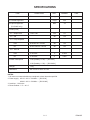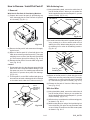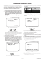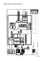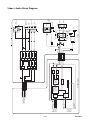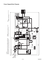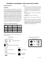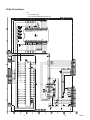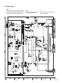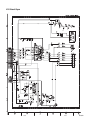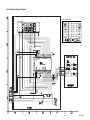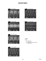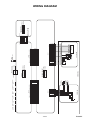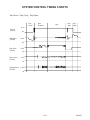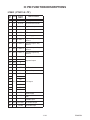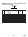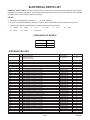
1
DV-SL80/DV-SL80X
SERVICE MANUAL
S45S9DV-SL80/
SERVICE MANUAL
DVD VIDEO PLAYER
OPERATE
NTSC/PAL
MODELS
DVD VIDEO PLAYER
3
---DV-SL80
4
DV-SL80
DV-SL80X
In the interests of user-safety (Required by safety regulations in some countries) the set should be restored to its
original condition and only parts identical to those specified
be used.
---DV-SL80X
CONTENTS
MODELS
DV-SL80/DV-SL80X
Page
SPECIFICATIONS ............................................................................................................................. 1-1-1
LASER BEAM SAFETY PRECAUTIONS .......................................................................................... 1-2-1
IMPORTANT SAFEGUARDS AND PRECAUTIONS ......................................................................... 1-3-1
STANDARD NOTES FOR SERVICING ............................................................................................. 1-4-1
OPERATING CONTROLS AND FUNCTIONS .................................................................................. 1-5-1
CABINET DISASSEMBLY INSTRUCTIONS ..................................................................................... 1-6-1
FIRMWARE RENEWAL MODE ......................................................................................................... 1-7-1
TROUBLESHOOTING ....................................................................................................................... 1-8-1
BLOCK DIAGRAMS ........................................................................................................................... 1-9-1
SCHEMATIC DIAGRAMS/ CBA’S AND TEST POINTS .................................................................. 1-10-1
WAVEFORMS .................................................................................................................................. 1-11-1
WIRING DIAGRAM .......................................................................................................................... 1-12-1
SYSTEM CONTROL TIMING CHARTS .......................................................................................... 1-13-1
IC PIN FUNCTION DESCRIPTIONS ............................................................................................... 1-14-1
LEAD IDENTIFICATIONS ................................................................................................................ 1-15-1
EXPLODED VIEWS ......................................................................................................................... 1-16-1
MECHANICAL PARTS LIST ............................................................................................................ 1-17-1
ELECTRICAL PARTS LIST ............................................................................................................. 1-18-1
SHARP CORPORATION
1
This document has been published to be used for
after sales service only.
The contents are subject to change without notice.
SPECIFICATIONS
ITEM
UNIT
NOMINAL
LIMIT
Vpp
1.0
±0.1
2-1 Coaxial Digital Out
mVpp
500
2-2 Optical Digital Out
dBm
-18
Vrm
2.0
dB
120
1 Video Output
CONDITIONS
75 Ω
(DV-SL80X only)
3 Audio (PCM)
3-1. Output Level
1 kHz 0 dB
3-2. S/N
3-3. Freq. Response
DVD
fs=48 kHz 20 ~ 22 kHz
dB
±0.5
CD
fs=44.1 kHz 20 ~ 22 kHz
dB
±0.5
DVD
1k Hz 0 dB
%
0.0025
CD
1k Hz 0 dB
%
0.003
3-4. THD +N
4 Power consumption
14 W (Standby: 2.0 W) --- [ DV-SL80 ]
12 W (Standby: 1.5 W) --- [ DV-SL80X ]
5 Weight
1.3kg
6 Dimension
435 mm X 51 mm X 211 mm
NOTES:
1. All Items are measured without pre-emphasis unless otherwise specified.
2. Power supply : AC110 - 240 V ~ 50/60Hz --- [ DV-SL80 ]
AC220 - 240 V ~ 50/60Hz --- [ DV-SL80X ]
3. Load imp. : 100 k ohm
4. Room ambient : 5 °C ~ 40 °C
1-1-1
E5943SP
LASER BEAM SAFETY PRECAUTIONS
This DVD player uses a pickup that emits a laser beam.
Do not look directly at the laser beam coming
from the pickup or allow it to strike against
your skin.
The laser beam is emitted from the location shown in the figure. When checking the laser diode, be sure to keep your
eyes at least 30cm away from the pickup lens when the diode is turned on. Do not look directly at the laser beam.
Caution: Use of controls and adjustments, or doing procedures other than those specified herein, may result in
hazardous radiation exposure.
Drive Mecha Assembly
Laser Beam Radiation
Laser Pickup
Turntable
1-2-1
DVD_LASER
IMPORTANT SAFEGUARDS AND PRECAUTIONS
1. IMPORTANT SERVICE NOTES
Reverse the AC plug on the set and repeat AC voltage
measurements for each exposed part. Any reading of
1.4V rms (this corresponds to 0.7mA rms AC.) or more
is excessive and indicates a potential shock hazard
which must be corrected before returning the DVD
video player to the owner.
BEFORE RETURNING THE DVD VIDEO PLAYER
Before returning the DVD video player to the user,
perform the following safety checks.
1. Inspect all lead dress to make certain that leads are
not pinched or that hardware is not lodged between
the chassis and other metal parts in the DVD video
player.
2. Inspect all protective devices such as non-metallic
control knobs, insulation materials, cabinet backs,
adjustment and compartment covers or shields, isolation resistor/capacitor networks, mechanical insulators etc.
3. To be sure that no shock hazard exists, check for
current in the following manner.
Plug the AC line cord directly into a 230 volt AC outlet
(Do not use an isolation transformer for this test).
Using two clip leads, connect a 1.5k ohm, 10 watt
resistor paralleled by a 0.15µF capacitor in series with
all exposed metal cabinet parts and a known earth
ground, such as a water pipe or conduit.
Use an DVM or VOM with 1000 ohm per volt, or higher,
sensitivity or measure the AC voltage drop across the
resistor (See Diagram).
Move the resistor connection to earth exposed metal
part having a return path to the chassis (metal cabinet,
screw heads, knobs and control shafts, etc.) and
measure the AC voltage drop across the resistor.
SSVM
AC SCALE
1.5k ohms.
10W
0.15 F
TEST PROBE
CONNECT TO
KNOWN EARTH
GROUNG
TO EXPOSED
METAL PARTS
1. NOTES DE SERVICE IMPORTANTES
pièces métalliques exposées ayant un parcours de
retour au châssis (coffret métallique, tétes de vis, boutons et arbres de commande, etc.) et mesurer la chute
de tension CA entre la résistance. Inverser la fiche CA
(une fiche intermédiaire non polarisée doit être utilisée
à seule fin de faire ces vérifications.) sur l’appareil et
répéter les mesures de tension CA pour chaque piéce
métallique exposée. Toute lecture de 1,4 V rms (ceci
correspond à 0,7 mA rms CA) ou plus est excessive et
signale un danger de choc qui doit être corrigé avant de
rendre le reproductor de vídeo DVD à son utilisateur.
AVANT DE RENDRE LE REPRODUCTOR DE VíDEO
DVD
Avant de rendre le reproductor de vídeo DVD à l’utilisateur,
effectuer les vérifications de sécurité suivantes.
1. Vérifier toutes les gaines de fil pour être sûr que les fils
ne sont pas pincés ou que le matériel n’est pas coincé
entre le châssis et les autres pièces métalliques dans le
reproductor de vídeo DVD.
2. Vérifier tous les dispositifs de protection tels que les
boutons de commande non métalliques, les matériaux
d’isolement, le dos du coffret, les couvercles de
compartiment et ajustement ou les boucliers, les
réseaux de résistance / condensateur d’isolement, Ies
isolateurs mécaniques, etc.
3. Pour être sûr qu’il n’y a aucun risque de choc électrique,
vérifier le courant de fuite de la maniére suivante.
Brancher le cordon d’alimentation secteur directement
dans une prise de courant de 230 volts. (Ne pas utiliser
de transformateur d’isolement pour cet essai).
Utiliser deux fils à pinces et connecter une résistance
de 10 watts 1,5 kohm en parallèle avec un condensateur
de 0,15 µF en série avec des pièces du coffret métallique
exposées et une masse de terre connue telle qu’un
tuyau ou un conduit d’eau.
Utiliser un DVM ou VOM avec une sensibilité de 1000
ohms par volt ou plus ou mesurer la chute de tension
CA entre la résistance (voir diagramme).
Déposer la connexion de la résistance à toutes les
VTVM
AC SCALE
1.5k ohms
10W
0.15 F
TEST PROBE
TO EXPOSED
METAL PARTS
1-3-1
CONNECT TO
KNOWN EARTH
GROUND
E5943IMP
STANDARD NOTES FOR SERVICING
Circuit Board Indications
Using lead-free wire solder
a. The output pin of the 3 pin Regulator ICs is indicated
as shown.
When fixing the PWB soldered with the lead-free solder,
apply lead-free wire solder. Repairing with conventional
lead wire solder may cause damage or accident due to
cracks.
As the melting point of lead-free solder (Sn-Ag-Cu) is
higher than the lead wire solder by 40°C, we recommend
you to use a dedicated soldering bit, if you are not
familiar with how to obtain lead-free wire solder or
soldening bit, contact our service station or service
ranch in your area.
Top View
Out
Bottom View
In
Input
b. For other ICs, pin 1 and every fifth pin are indicated
as shown.
Soldering
< Bottom View >
5
Pin 1
10
c. The 1st pin of every male connector is indicated as
shown.
< Bottom View >
Pin 1
Instructions for Connectors
1. When you connect or disconnect the FFC (Flexible
Foil Connector) cable, be sure to first disconnect the
AC cord.
2. FFC (Flexible Foil Connector) cable should be inserted parallel into the connector, not at an angle.
As the melting point of lead-free solder (Sn-Ag-Cu) is
about 220°C which is higher than the conventional lead
solder by 40°C, and as it has poor solder wettabillty, you
may be apt to keep the soldering bit in contact with the
PWB for extended period of time. However, Since the
land may be peeled off or the maximum heat-resistance
temperature of parts may be excoeded, remove the bit
from the PWB as soon as you conurm the steady
soldering condition.
Lead-free solder contains more tin, and the end of the
soldering bit may be easily corroded. Make sure to tum
on and off the power of the bit as required. if a different
type of solder stays on the tip of the soldering bit, it is
alloyed with lead-free solder. Clean the bit after every
use of it.
When the tip of the soldering bit is blackened during
use, file it with steel wool or fine sandpaper.
Becareful when replacing parts with polarity indication
on the PWB silk.
Lead-free wire solder for servicing
Part No.
Description
Code
ZHNDAi123250E
J
0.3mm 250g(1roll)
BL
ZHNDAi126500E
J
0.6mm 500g(1roll)
BK
ZHNDAi12801KE
J
1.0mm 1kg(1roll)
BM
FFC Cable
Connector
CBA
* Be careful to avoid a short circuit.
1-4-1
DVD_NOTE2
How to Remove / Install Flat Pack-IC
1. Removal
With Hot-Air Flat Pack-IC Desoldering Machine:
(1) Prepare the hot-air flat pack-IC desoldering machine, then apply hot air to the Flat Pack-IC (about 5
to 6 seconds). (Fig. S-1-1)
With Soldering Iron:
(1) Using desoldering braid, remove the solder from all
pins of the flat pack-IC. When you use solder flux
which is applied to all pins of the flat pack-IC, you can
remove it easily. (Fig. S-1-3)
Flat Pack-IC
Desoldering Braid
Soldering Iron
Fig. S-1-3
Fig. S-1-1
(2) Remove the flat pack-IC with tweezers while applying the hot air.
(2) Lift each lead of the flat pack-IC upward one by one,
using a sharp pin or wire to which solder will not
adhere (iron wire). When heating the pins, use a fine
tip soldering iron or a hot air desoldering machine.
(Fig. S-1-4)
(3) Bottom of the flat pack-IC is fixed with glue to the
CBA; when removing entire flat pack-IC, first apply
soldering iron to center of the flat pack-IC and heat
up. Then remove (glue will be melted). (Fig. S-1-6)
(4) Release the flat pack-IC from the CBA using tweezers. (Fig. S-1-6)
Caution:
1. Do not supply hot air to the chip parts around the flat
pack-IC for over 6 seconds because damage to the
chip parts may occur. Put masking tape around the
flat pack-IC to protect other parts from damage.
(Fig. S-1-2)
2. The flat pack-IC on the CBA is affixed with glue, so
be careful not to break or damage the foil of each pin
or the solder lands under the IC when removing it.
Hot-air
Flat Pack-IC
Desoldering
Machine
CBA
Masking
Tape
Tweezers
Sharp
Pin
Fine Tip
Soldering Iron
Fig. S-1-4
(3) Bottom of the flat pack-IC is fixed with glue to the
CBA; when removing entire flat pack-IC, first apply
soldering iron to center of the flat pack-IC and heat
up. Then remove (glue will be melted). (Fig. S-1-6)
(4) Release the flat pack-IC from the CBA using tweezers. (Fig. S-1-6)
With Iron Wire:
(1) Using desoldering braid, remove the solder from all
pins of the flat pack-IC. When you use solder flux
which is applied to all pins of the flat pack-IC, you can
remove it easily. (Fig. S-1-3)
Flat Pack-IC
Fig. S-1-2
(2) Affix the wire to a workbench or solid mounting point,
as shown in Fig. S-1-5.
(3) While heating the pins using a fine tip soldering iron
or hot air blower, pull up the wire as the solder melts
so as to lift the IC leads from the CBA contact pads
as shown in Fig. S-1-5.
1-4-2
DVD_NOTE2
(4) Bottom of the flat pack-IC is fixed with glue to the
CBA; when removing entire flat pack-IC, first apply
soldering iron to center of the flat pack-IC and heat
up. Then remove (glue will be melted). (Fig. S-1-6)
(5) Release the flat pack-IC from the CBA using tweezers. (Fig. S-1-6)
Note:
When using a soldering iron, care must be taken to
ensure that the flat pack-IC is not being held by glue.
When the flat pack-IC is removed from the CBA,
handle it gently because it may be damaged if force
is applied.
2. Installation
(1) Using desoldering braid, remove the solder from the
foil of each pin of the flat pack-IC on the CBA so you
can install a replacement flat pack-IC more easily.
(2) The “ ” mark on the flat pack-IC indicates pin 1. (See
Fig. S-1-7.) Be sure this mark matches the 1 on the
PCB when positioning for installation. Then presolder the four corners of the flat pack-IC. (See Fig. S1-8.)
(3) Solder all pins of the flat pack-IC. Be sure that none
of the pins have solder bridges.
Example :
Hot Air Blower
or
Iron Wire
Pin 1 of the Flat Pack-IC
is indicated by a " " mark.
Soldering Iron
To Solid
Mounting Point
Presolder
Fig. S-1-5
CBA
Fig. S-1-7
Fine Tip
Soldeing Iron
Flat Pack-IC
CBA
Fig. S-1-8
Flat Pack-IC
Tweezers
Fig. S-1-6
1-4-3
DVD_NOTE2
Instructions for Handling
Semi-conductors
Electrostatic breakdown of the semi-conductors may
occur due to a potential difference caused by electrostatic
charge during unpacking or repair work.
1. Ground for Human Body
Be sure to wear a grounding band (1MΩ) that is properly
grounded to remove any static electricity that may be
charged on the body.
2. Ground for Workbench
Be sure to place a conductive sheet or copper plate with
proper grounding (1MΩ) on the workbench or other
surface, where the semi-conductors are to be placed.
Because the static electricity charge on clothing will not
escape through the body grounding band, be careful to
avoid contacting semi-conductors with your clothing.
< Incorrect >
CBA
< Correct >
Grounding Band
CBA
Conductive Sheet or
Copper Plate
1-4-4
DVD_NOTE2
OPERATING CONTROLS AND FUNCTIONS
1
FRONT PANEL
2 3 4 5
9
7
6
OPERATE
8
REAR VIEW
AUDIO OUT
L
CR / PR
Y
DIGITAL AUDIO OUT
4
CB / PB
S-VIDEO
OUT
11 12 13 14 15
16
OPTICAL COAXIAL
10
R
COMPONENT
VIDEO OUT
VIDEO
OUT
1. OPERATE
to switch the player to ON or OFF
2. PLAY
to start or resume disc playback
3. STOP
to stop playback
/ REV
4. SKIP
goes to previous chapter or track during playback; press
and hold for 1.5 seconds for a reverse search
/ FWD
5. SKIP
goes to next chapter or track during playback; press and
hold for 1.5 seconds for a forward search
6. OPEN/CLOSE
to open/close the disc tray
7. Disc tray
8. Remote sensor window
9. Display
10. MAINS (AC Power Cord)
connect to a standard AC outlet
REMOTE CONTROL
OPERATE
1
2
3
4
5
6
7
8
OPEN/
CLOSE
ON
SCREEN
SETUP
DIMMER GAMMA
MODE
MARKER
SUBTITLE
ANGLE
AUDIO
ZOOM
TITLE
MENU
RETURN
ENTER
REPEAT
9
1
2
3
4
5
6
A-B REPEAT
7
8
9
0
+10
SKIP
CLEAR
10
C
REV
11
12
13
14
15
16
17
18
19
20
21
22
23
24
25
26
27
FWD
28
PLAY
DIRECT SKIP
STILL/PAUSE
STOP
29
1. OPERATE Button
Press to turn the power on and off.
2. ON SCREEN Button
Displays the current status on the TV screen for checking
purposes.
3. DIMMER Button
Press to change the Panel Display settings.
4. GAMMA Button
Press to adjust the black parts of the picture brighter.
5. ZOOM Button
Enlarges part of a DVD-reproduced image.
6. SUBTITLE Button
Press to select a desired subtitle language.
7. TITLE Button
Displays the title menu.
8. RETURN Button
Returns to the previous operation.
9. Numerical Buttons
10. CLEAR Button
Resets a setting.
11. REV Button
Fast reverse playback to a desired point.
11. OPTICAL (Digital audio out)
connect to digital (optical) audio equipment
(DV-SL80X only)
12. COAXIAL (Digital audio out)
connect to AUDIO inputs of a digital (coaxial) audio
equipment
13. AUDIO OUT (Left/Right)
connect to AUDIO inputs of an amplifier, receiver or
stereo system
14. VIDEO OUT
connect to the Video Input of a TV
15. COMPONENT VIDEO OUT
connect to a TV with Component video in jacks
16. S-VIDEO OUT
connect to a TV with S-Video inputs
CAUTION:
Do not touch the inner pins of the jacks on the rear
panel. Electrostatic discharge may cause permanent damage to the player.
12. PLAY Button
Starts playback of the disc contents.
13. DIRECT SKIP Button
Press to locate a desired point.
14. STOP Button
Stops operation of the disc.
15. OPEN/CLOSE Button
Press to insert discs into or remove them from the tray.
16. SETUP Button
Press to enter the setup mode or to change setup items.
17. MARKER Button
Press to call back the Marker display.
18. MODE Button
Activates programme playback or random playback mode.
(CD/MP3/JPEG)
Activates the 3D sound or Rapid Play. (DVD)
19. AUDIO Button
Press to select a desired audio language or sound mode.
20. ANGLE Button
Press to change the camera angle to see the sequence
being played back from a different angle.
21. MENU Button
Displays the DVD menus and MP3 file lists.
)
22. Arrow Buttons (
(left/right/up/down) Select an item in the menu.
23. ENTER Button
Press to accept a setting.
24. REPEAT Button
Repeats playback of the current disc, title, chapter or track.
25. A-B REPEAT Button
Repeats playback of a selected section.
Button
26. SKIP
Plays back from the beginning of the next chapter or track.
Button
27. SKIP
Plays back from the beginning of the current chapter or
track.
28. FWD Button
Fast forwards playback to a desired point.
29. STILL/PAUSE Button
Pause playback temporarily/frame-by-frame playback.
1-5-1
E5943IB
CABINET DISASSEMBLY INSTRUCTIONS
1. Disassembly Flowchart
This flowchart indicates the disassembly steps to gain
access to item(s) to be serviced. When reassembling,
follow the steps in reverse order. Bend, route, and dress
the cables as they were originally.
1 : Identification (location) No. of parts in the figures
2 : Name of the part
3 : Figure Number for reference
4 : Identification of parts to be removed, unhooked,
unlocked, released, unplugged, unclamped, or desoldered.
P=Spring, L=Locking Tab, S=Screw,
CN=Connector,
*=Unhook, Unlock, Release, Unplug, or Desolder
e.g. 5(S-1) = five Screws (S-1),
2(L-2) = two Locking Tabs (L-2)
[1] Top Case
[2] Front Assembly
[3] Reinforce Plate
[4] DVD Main CBA Unit
5 : Refer to "Reference Notes."
[5] DVD Mecha
[6] AV CBA
[7] Function CBA
About tightening screws
When tightening screws, tighten them with the following
torque.
2. Disassembly Method
ID/
LOC.
No.
PART
[1] Top Case
Screws
REMOVAL
REMOVE/
Fig. *UNHOOK/UNLOCK/
No. RELEASE/UNPLUG/
DESOLDER
1 3(S-1)
(S-3B)
0.38 ± 0.04 N•m
-
2
[3] Reinforce
Plate
3
3(S-2)
1
1-1
1-2
[4] DVD Main
CBA Unit
4
(S-3A), (S-3B),
*CN201, *CN301,
*CN401, *CN601
[5] DVD
Mecha
5
4(S-4)
-
[6] AV CBA
6
(S-5),
4(S-6)---[DV-SL80]
5(S-6)---[DV-SL80X],
*2(L-5)
-
[7] Function
CBA
6
*CN2001
-
↑
1
↑
3
-
↑
4
0.45 ± 0.05 N•m
(S-5), (S-6)
Note
[2] Front
Assembly
↑
2
*4(L-1), *3(L-2),
*3(L-3),
(S-1), (S-2), (S-3A), (S-4),
Torque
2
2-1
2-2
3
↑
5
Reference Notes
CAUTION 1: Locking Tabs (L-1), (L-2) and (L-3) are
fragile. Be careful not to break them.
1-1. Release four Locking Tabs (L-1). Then, release
three Locking Tabs (L-2) .
1-2. Release three Locking Tabs (L-3). Then remove
the Front Assembly.
CAUTION 2: Electrostatic breakdown of the laser diode
in the optical system block may occur as a potential
difference caused by electrostatic charge accumulated
on cloth, human body etc., during unpacking or repair
work.
To avoid damage of pickup follow next procedures.
2-1. Short the three short lands (either of two places) of
FPC cable with solder before removing the FFC
cable (CN201) from it as shown in “View for A” in
Fig. 4. If you disconnect the FFC cable (CN201),
the laser diode of pickup will be destroyed. (Fig. 4)
2-2. Disconnect Connectors (CN301), (CN401) and
(CN601). Remove two Screws (S-3A) and (S-3B)
and lift the DVD Main CBA Unit. (Fig. 4)
CAUTION 3: When reassembling, confirm the FFC
cable (CN201) is connected completely. Then remove
the solder from the three short lands of FPC cable.
(Fig. 4)
1-6-1
E5943DC
(S-3B)
[1] Top Case
(S-1)
(S-3A)
CN201
CN601
CN301
CN401
[4] DVD Main
CBA Unit
A
Fig. 1
(L-1)
(L-3)
Solder
Short the three short lands
by soldering.
(Either of two places.)
Short
lands
(L-1)
OR
Short lands
(L-2)
[2] Front Assembly
FPC Cable
Fig. 2
Solder
View for A
(S-2)
Fig. 4
(S-4)
[3] Reinforce Plate
[5] DVD Mecha
(S-4)
(S-4)
Fig. 3
Fig. 5
1-6-2
E5943DC
[7] Function CBA
(S-5)
[6] AV CBA
CN2001
DV-DL80X
only
(S-6)
(S-6)
(L-5)
Fig. 6
HOW TO EJECT MANUALLY (Method 1)
1 Remove the Top Case.
2 Remove the Reinforce Plate.
3 Rotate the roulette in the direction of the arrow as shown below.
View for A
Rotate this roulette in
the direction of the arrow
A
1-6-3
E5943DC
HOW TO EJECT MANUALLY (Method 2)
1 Turn the unit over.
2 Insert the shaft less than a diameter of 3 mm (e.g. screwdriver) straightly into the opening
as shown.
3 Turn the shaft along with the opening clockwise.
4 Repeat steps 2 and 3 until the tray will open.
5 Pull the tray slowly with a hand.
View for B
Rear
Turn the shaft along with
the opening clockwise.
Shaft
(e.g. screwdriver)
Opening
B
Front
1-6-4
E5943DC
FIRMWARE RENEWAL MODE
The appearance shown in (*2) of Fig. c is described
as follows:
FIRMWARE is built-in program to operate DVD player.
To get rid of error when playing new software (disc) in
the market, FIRMWARE version is updated. Perform
the following to update the FIRMWARE version.
1. Turn the power on and remove the disc on the tray.
2. To put the DVD player into version up mode, press
[9], [8], [7], [6], and [DIRECT SKIP] buttons on the
remote control unit in that order. The tray will open
automatically.
Fig. a appears on the screen and Fig. b appears on
the VFD.
No.
State
Reading...
Sending files into the memory
2
Erasing...
Erasing previous version data
3
Programming... Writing new version data
5. After programming is finished, the tray opens automatically. Fig. e appears on the screen and the
checksum in (*3) of Fig. e appears on the VFD.
(Fig. f)
"*******" differ depending on the models.
"*******" differ depending on the models.
F/W Version Up Mode
Appearance
1
F/W Version Up Mode
Model No : *******
VERSION : *.**
VERSION : E5****_****.ab5
Completed
SUM : 7ABC (*3)
Model No : *******
VERSION : *.**
Please insert a DISC
for F/W Version Up.
EXIT: POWER
Fig. a Version Up Mode Screen
Fig. e Completed Program Mode Screen
Fig. b VFD in Version Up Mode
Fig. f VFD upon Finishing the Programming Mode (Example)
The DVD player can also enter the version up mode
with the tray open. In this case, Fig. a will be shown
on the screen while the tray is open.
3. Load the disc for version up.
4. The DVD player enters the F/W version up mode
automatically. Fig. c appears on the screen and Fig.
d appears on the VFD. If you enter the F/W for
different models, "Disc Error" will appear on the
screen, then the tray will open automatically.
At this time, no buttons are available.
6. Remove the disc on the tray.
7. Unplug the AC cord from the AC outlet. Then plug it
again.
8. Turn the power on by pressing the [OPERATE]
button and the tray will close.
9. Press [1], [2], [3], [4], and [ON SCREEN] buttons on
the remote control unit in that order.
Fig. g appears on the screen.
"*******" differ depending on the models.
"*******" differ depending on the models.
F/W Version Up Mode
Model No : *******
VERSION : *.**
VERSION : E5****_****.ab5
Reading...(*2)
MODEL : *******
Version : *.**
Region : *
EEPROM CLEAR : CLEAR
EXIT: POWER
Fig. g
Fig. c Programming Mode Screen
10.Press [CLEAR] button on the remote control unit.
Fig. h appears on the screen.
Fig. d VFD in Programming Mode (Example)
1-7-1
E5945TEST
"*******" differ depending on the models.
MODEL : *******
Version : *.**
Region : *
EEPROM CLEAR : OK
EEPROM CLEAR : CLEAR
EXIT: POWER
Fig. h
When "OK" appears on the screen, the factory
default will be set. Then the firmware renewal mode
is complete.
11.To exit this mode, press [OPERATE] button.
1-7-2
E5945TEST
TROUBLESHOOTING
FLOW CHART NO.1
The power cannot be turned on.
Is the fuse normal?
Yes
Is normal state restored when once unplugged
power cord is plugged again after several seconds?
Yes
Is the EV +3.3V line voltage normal?
Yes
Check each rectifying circuit of the secondary circuit
and service it if defective.
No
No
No
See FLOW CHART No.2 <The fuse blows out.>
Check if there is any leak or short-circuiting on the
primary circuit component, and service it if defective.
(Q1001, Q1003, Q1008, T1001, D1001, D1002,
D1004, D1005, D1011, C1003, C1005)
FLOW CHART NO.2
The fuse blows out.
Check the presence that the primary component
is leaking or shorted and service it if defective.
Check the presence that the rectifying diode or
circuit is shorted in each rectifying circuit of
secondary side, and service it if defective.
After servicing, replace the fuse.
FLOW CHART NO.3
When the output voltage fluctuates.
Does the photo coupler circuit on the secondary
side operate normally?
Yes
Check IC1001, D1012, D1024 and their periphery,
and service it if defective.
No
Check IC1001, IC1006, D1048 and their
periphery, and service it if defective.
FLOW CHART NO.4
When buzz sound can be heard in the vicinity of power circuit.
Check if there is any short-circuit on the rectifying diode and the circuit in each rectifying circuit of the secondary
side, and service it if defective. (D1003, D1006, D1008, D1016, D1030, IC1002, Q1002, Q1004, Q1005, Q1011)
FLOW CHART NO.5
-FL is not outputted.
Is approximately -23V voltage supplied to the
anode of D1003?
Yes
Check if there is any leak or short-circuit
on the loaded circuit, and service it if defective.
No
1-8-1
Check D1003 and periphery circuit, and service it
if defective.
E5943TS
FLOW CHART NO.6
P-ON+10V (EV+11V) is not outputted.
Is 11V voltage supplied to the emitter of Q1002?
No
Yes
No
Is the voltage of base on Q1002 lower than the
voltage of emitter on Q1002 when turning the power on?
Check D1030, D1048, C1035, C1048, L1009 and
the periphery circuit, and service it if defective.
Check Q1016 and PWRCON line and service it if
defective.
Yes
Replace Q1002.
FLOW CHART NO.7
P-ON+5V is not outputted. (EV+11V is outputted normally.)
Is the "H" signal inputted into the base of Q1004?
Yes
Replace Q1004.
No
Check R1068 and D1046, and service it if defective.
FLOW CHART NO.8
P-ON+3.3V is not outputted. (P-ON+10V is outputted normally.)
Is 3.3V voltage supplied to the collector of Q1011?
Yes
Replace Q1011 or R1067.
No
Check D1008, C1007, C1038, L1007 and the
periphery circuit, and service it if defective.
FLOW CHART NO.9
EV+5V is not outputted.
Is EV+11V outputted normally?
Yes
Check D1047 and the periphery circuit,
and service it if defective.
No
Refer to "FLOW CHART NO.6"
<P-ON+10V (EV+11V) is not outputted.>
FLOW CHART NO.10
EV+1.2V is not outputted.
Is 2.5V voltage supplied to Pin(1) of IC1002?
Yes
Replace IC1002.
No
1-8-2
Check D1006, C1014, L1008 and the periphery
circuit, and service it if defective.
E5943TS
FLOW CHART NO.11
The fluorescent display tube does not light up.
Is 3.3V voltage supplied to Pins(6,24) of IC2001?
Yes
Is the voltage of approximately -20V supplied to
Pin(15) of IC2001?
Yes
No
No
Check the -FL (-20V) line and service it if defective.
No
Check R2002, IC2001 and their periphery, and
service it if defective.
Is there 500kHz oscillation at Pin(26) of IC2001?
Yes
Are the filament voltage supplied between
Pins(1, 2) and Pins(29, 30) of the fluorescent
display tube? And the negative voltage applied
between these pins and GND?
Check the EV+3.3V line and service it if defective.
Check D1016, D1017, T1001, and their periphery,
and service it if defective.
No
No
Is -15V voltage supplied to collector of Q1005?
Yes
Check PWRCON
line, and service
No it if defective.
Yes
Check Q1015, Q1016, D1055, and
their periphery, and service it if defective.
Is the "H" signal inputted
to base of Q1016?
Yes
Replace the fluorescent display tube.
FLOW CHART NO.12
The key operation is not functioning.
Are the contact point and the installation state of the
key switches (SW2101, SW2104-2108) normal?
Yes
When pressing each switches (SW2101, SW21042108), do the voltage of each pin of IC2001
(shown below) increase?
SW2104, 2106, 2107: IC2001 3PIN
SW2101, 2105, 2108: IC2001 4PIN
No
Re-install the switches (SW2101, SW2104-2108)
correctly or replace the poor switch.
No
Check the switches (SW2101, SW2104-2108) and
their periphery, and service it if detective.
Yes
Replace IC2001.
FLOW CHART NO.13
No operation is possible from the remote control unit.
Operation is possible from the DVD, but no
operation is possible from the remote control unit.
No
Is 5V voltage supplied to Pin(3) terminal of
the infrared remote control receiver (RM2001)?
Yes
Is the "L" pulse sent out Pin(1) terminal of receiver
No
(RM2001) when the infrared remote control is activated?
Yes
No
Is the "L" pulse supplied to the Pin(22) of CN1001?
Yes
Replace DVD Main CBA.
1-8-3
Check EV+5V line and service it if defective.
Replace the infrared remote control receiver (RM2001).
Or replace the remote control unit.
Check the line between Pin(1) terminal of receiver
(RM2001) and Pin(22) of CN1001, and service it if
defective.
E5943TS
FLOW CHART NO.14
The disc tray cannot be opened and closed. (It can be done using the remote control unit.)
Is the normal control voltage inputted to Pin(4) of
IC2001? Refer to "FLOW CHART NO.12" <The key
operation is not functioning.>
No
Replace the "OPEN/CLOSE" button (SW2108).
Yes
Refer to "FLOW CHART NO.15" <The disc tray
cannot be opened and closed.>
FLOW CHART NO.15
The disc tray cannot be opened and closed.
Replace the DVD Main CBA.
No improvement can be found.
Yes
Replace the DVD Mecha.
No
Original DVD Main CBA is poor.
FLOW CHART NO.16
[No Disc] indicated. (When the focus error occurs.)
Replace the DVD Main CBA.
No improvement can be found.
Yes
No
Original DVD Main CBA is poor.
Replace the DVD Mecha.
FLOW CHART NO.17
[No Disc] indicated. (When the focus servo is not functioning.)
Replace the DVD Main CBA.
No improvement can be found.
Yes
No
Original DVD Main CBA is poor.
Replace the DVD Mecha.
FLOW CHART NO.18
[No Disc] indicated. (When the laser beam does not light up.)
Replace the DVD Main CBA.
No improvement can be found.
Yes
No
Original DVD Main CBA is poor.
Replace the DVD Mecha.
1-8-4
E5943TS
FLOW CHART NO.19
Both functions of picture and sound do not operate normally.
Replace the DVD Main CBA.
No improvement can be found.
Yes
No
Original DVD Main CBA is poor.
Replace the DVD Mecha.
FLOW CHART NO.20
Picture does not appear normally.
Set the disc on the disc tray, and playback.
Are the video signals outputted to each pin of
CN1601 on the AV CBA?
CN1601 4PIN
CN1601 6PIN
CN1601 8PIN
CN1601 10PIN
No
Cr/Pr
Cb/Pb
S-Y
S-C
Yes
Are the video signals shown above inputted into
each pin of IC1402?
IC1402
IC1402
IC1402
IC1402
Replace the DVD Main CBA or DVD Mecha.
No
Check the line between each pin of CN1601 and
each pin of IC1402 on the AV CBA, and service
it if detective.
CN1601 10PIN → IC1402
CN1601 8PIN → IC1402
CN1601 6PIN → IC1402
CN1601 4PIN → IC1402
1PIN S-C
3PIN S-Y
6PIN Cb/Pb
8PIN Cr/Pr
1PIN
3PIN
6PIN
8PIN
S-C
S-Y
Cb/Pb
Cr/Pr
Yes
Are the video signals outputted to each pin
of IC1402?
IC1402
IC1402
IC1402
IC1402
IC1402
13PIN
11PIN
10PIN
14PIN
15PIN
S-Y
Cb/Pb
Cr/Pr
CVBS
S-C
No
Is 5V voltage applied to the pin(4, 12) of IC1402?
Yes
Replace IC1402.
Yes
Are the video signals outputted to the specific
output terminal?
Are the luminance signals outputted to the
S-OUT terminal (JK1401)?
No
Check P-ON+5V line and
service it if detective.
No
Check the periphery of JK1401 from
Pin (13) of IC1402 and service it if detective.
Are the chroma signals outputted to the
S-OUT terminal (JK1401)?
No
Check the periphery of JK1401 from
Pin (15) of IC1402 and service it if detective.
Are the component video signals outputted to the
VIDEO OUT terminal (JK1404)?
No
Check the periphery of JK1404 from Pins (10, 11,
13) of IC1402 and service it if detective.
Are the composite video signals outputted to
the VIDEO OUT terminal (JK1404)?
No
Check the periphery of JK1404 from Pin(14) of
IC1402 and service it if detective.
1-8-5
E5943TS
FLOW CHART NO.21
Audio is not outputted normally.
Set the disc on the disc tray, and playback.
Are the analog audio signals outputted to each pin
of CN1601 on AV CBA?
No
Replace the DVD Main CBA or DVD Mecha.
CN1601 14PIN AUDIO-L
CN1601 16PIN AUDIO-R
Yes
Are the analog audio signals inputted to each pin
of IC1201.
No
IC1201 2PIN AUDIO-L
IC1201 6PIN AUDIO-R
Check each line between each pin of CN1601
and each pin of IC1201 on AV CBA, and service it
if detective.
CN1601 14PIN → IC1201 2PIN AUDIO-L
CN1601 16PIN → IC1201 6PIN AUDIO-R
Yes
Is the "H" level mute signal outputted to CN1601
on AV CBA ?
CN1601 13PIN A-MUTE
CN1601 15PIN A-R-MUTE
No
Replace the DVD Main CBA or DVD Mecha.
Yes
Are the analog audio signals outputted to each pin
of IC1201?
No
IC1201 1PIN AUDIO-L
IC1201 7PIN AUDIO-R
Replace IC1201.
Yes
Are the audio signals outputted to the specific
output terminal?
No
Check the periphery between Pins(1,7) of IC1201
and JK1404, and service it if detective.
Are the audio signals outputted to the audio
terminal (JK1404)?
1-8-6
E5943TS
1-9-1
M
SLED
MOTOR
M
SPINDLE
MOTOR
TRAY-IN
TS(+)
TS(-)
FS(+)
FS(-)
DRIVE CBA
TO DIGITAL SIGNAL
PROCESS BLOCK
DIAGRAM
SP(+)
SP(-)
TRAY-IN
GND
SL(-)
SL(+)
PCM-SCLK
A-MUTE
ADAC-MD
ADAC-MC
ADAC-ML
CN301
3
4
5
6
7
8
-
17
18
12
13
5
6
3
2
-
+
-
+
-
+
IC202
(OP AMP)
23
6
4
5
3
1
2
25
24
27
26
14
7
1
VREF
RESET 3
IC462
DVD MAIN CBA UNIT
+3.3V
+
SLED
MOTOR
DRIVE
-
+
-
-
+
+
SPINDLE
MOTOR
DRIVE
TRACKING
ACTUATOR
DRIVE
FOCUS
ACTUATOR
DRIVE
1
+3.3V
12
11
14
13
15
16
RESET 1
IC461
IC301
(SERVO DRIVE)
2
+3.3V
PCM-SCLK
A-MUTE
ADAC-MD
ADAC-MC
ADAC-ML
FP-STB
FP-DIN
FP-DOUT
FP-CLK
REMOTE
66 TRAY-IN
81 SL-AMP
143 SP-ROT
75 SLD
76 SPDL
139 TD-OFST
147 TRACKING
DRIVE
146 FD-OFST
148 FOCUS DRIVE
73 RESET
163
88
57
56
86
82
60
61
59
67
CN401
20
19
21
18
22
FP-STB
FP-DIN
FP-DOUT
FP-CLK
REMOTE
1G 23
IC2001
(FRONT PANEL CONTROL)
REMOTE
SENSOR
RM2001
7
8
9
10
11
12
13
14
16
AV CBA
K2 4
K1 3
a/KEY-1
b/KEY-2
c/KEY-3
d/KEY-4
e
CN1001
20
f
2 FP-STB
19
g
28 FP-DIN
21
h
27 FP-DOUT
18
i
1 FP-CLK
22
7G 17
~
TO
VIDEO/ AUDIO
BLOCK DIAGRAM
~
IC101
(MICRO CONTROLLER)
GRID
5
3
4
6
1
2
CN2001
KEY-1
KEY-2
KEY-3
KEY-4
K2
K1
SEGMENT
FIP
FL2001
5
3
4
6
1
2
KEY
MATRIX
FUNCTION CBA
CN2101
BLOCK DIAGRAMS
System Control / Servo Block Diagram
E5943BLS
FS
PICK-UP
UNIT
TS
DETECTOR
FS(+)
FS(-)
TS(+)
TS(-)
CD-LD
DVD-LD
PD-MONI
GND(DVD-PD)
GND(CD-PD)
GND(LD)
C
D
A
B
E
F
CD/DVD
2
13
42
~
~
CN201
2
3
1
4
CD
4
6
FS(+)
FS(-)
TS(+)
TS(-)
IC201
(SW)
DVD
DATA
RAM
INST.
ROM
INTERRUPT
CONTROLLER
RF
SIGNAL
PROCESS
CIRCUIT
83 CD/DVD
126
124
125
123
114
115
116
117
132
131
134
133
129
130
TIMER
ECC
WATCH DOG
TIMER
32BIT
CPU
DVD/CD
FORMATTER
SDRAM DATA(0-15)
DVD MAIN CBA UNIT
1 3
Q253,Q254
CN201
10
AMP
8
AMP
Q251,Q252
7
6
5
9
1
18
252
256
EXTERNAL
MEMORY
I/F
IC101 (MICRO CONTROLLER)
TO SYSTEM
CONTROL/SERVO
BLOCK DIAGRAM
SDRAM DATA(0-15)
CN201
16
18
17
15
14
12
19
53
~
SDRAM
~
22
217
26
SDRAM ADDRESS(0-11)
SDRAM ADDRESS(0-11)
29
238
35
~
~
~
IC503 (SDRAM)
BCU
CPU
I/F
DMA
DECODER
I/F
192~212
READ
MEMORY
UMAC
STREAM
I/F
23~51
CPU
I/F
DSP
DECODER
DEBUG
SERIAL
INST
RAM
DATA
RAM
32BIT CPU
REMOTE
CONTROL
WATCH DOG
TIMER
TIMER
INTERRUPT
CONTROLLER
GENERAL
I/O
INST.
ROM
DATA
RAM
INST.
ROM
DATA
RAM
DATA(AUDIO) SIGNAL
I/O
PROCESSOR
BCU
VIDEO SIGNAL
VIDEO
I/F
AUDIO
I/F
NTSC/PAL
ENCODER
VIDEO-C
VIDEO-Y
TO
VIDEO
/AUDIO
BLOCK
DIAGRAM
TO
VIDEO
/AUDIO
BLOCK
DIAGRAM
29
36
38
45
FLASH
ROM
* IC103 (FLASH ROM)
VIDEO-Cb/Pb
VIDEO-Cr/Pr
FDQ (0-15)
151
152
158
149
1
9
16
25
48
Cb/Pb
Cr/Pr
C
Y
SPDIF
PCM-BCK
PCM-DATA
PCM-LRCLK
FADR (0-19)
D/A
D/A
D/A
D/A
177
170
171
169
IC103 is not supplied separatery.
Be sure to replace with the DVD Main CBA unit when servicing IC103.
*Note:
~
~
~
1-9-2
~
DATA(VIDEO/AUDIO) SIGNAL
Digital Signal Process Block Diagram
E5943BLD
1-9-3
TO
SYSTEM
CONTROL
/SERVO
BLOCK
DIAGRAM
TO
DIGITAL
SIGNAL
PROCESS
BLOCK
DIAGRAM
PCM-SCLK
A-MUTE
ADAC-MD
ADAC-MC
ADAC-ML
PCM-BCK
PCM-DATA
PCM-LRCLK
SPDIF
13
14
15
1
2
3
VIDEO-C
VIDEO-Y
VIDEO-Cb/Pb
VIDEO-Cr/Pr
SERIAL
CONTROL
SERIAL
PORT
DVD MAIN CBA UNIT
16
SYSTEM CLOCK
DAC
DAC
WF1
WF2
ZERO DETECT
ENHANCED
MULTI-LEVEL
DELTA-SIGMA
MODULATOR
CN1601
VIDEO-C
10
VIDEO-Y
8
VIDEO-Cb/Pb 6
VIDEO-Cr/Pr 4
4X/8X
OVERSAMPLING
DIGITAL FILTER
/FUNCTION
CONTROLLER
IC601 (AUDIO DAC)
TO DIGITAL
SIGNAL PROCESS
BLOCK DIAGRAM
CN601
10
8
6
4
8
LPF+AMP
R-CH
11
8
7
LPF
4dB
AMP
6
LPF+AMP
LPF
4dB
AMP
L-CH
LPF
LPF
3
4dB
AMP
4dB
AMP
1
CN1601
19
14
16
15
13
DRIVER
DRIVER
SPDIF
AUDIO-L
AUDIO-R
A-R-MUTE
A-MUTE
2dB
AMP
2dB
AMP
DRIVER
DRIVER
2dB
AMP
2dB
AMP
DRIVER
2dB
AMP
CN601
19
14
16
15
13
IC1402 (VIDEO DRIVER)
WF3
WF6
10
11
13
14
15
WF5
WF4
Q1351
AMP
+3.3V
Q1204
+5V
VIDEO SIGNAL
AV CBA
6
5
3
2
1
Q1201
JK1202
IC1204
4
C
JK1404
COAXIAL
DIGITAL
AUDIO
OUT
AUDIO-R
OUT
AUDIO-L
OUT
OPTICAL
VIDEO-Cr/Pr
OUT
VIDEO-Cb/Pb
OUT
VIDEO-Y
OUT
COMPOSITE
VIDEO OUT
JK1401
S-VIDEO OUT
AUDIO SIGNAL
JK1404
2
DV-SL80X
3
Q1202
7
1
IC1201 (AMP)
Y
DATA(AUDIO) SIGNAL
Video / Audio Block Diagram
E5943BLV
AC1001
AC CORD
1-9-4
LATCH
Q1008
DV-SL80
F1001
T1.6A L 250V
LINE
FILTER
L1001
HOT CIRCUIT. BE CAREFUL.
AV CBA
SWITCHING
SWITCHING
CONTROL
HOT
Q1001
Q1003
BRIDGE
RECTIFIER
D1001, D1002
D1004, D1005
3
4
2
1
D1003
RECTIFIER
D1016
RECTIFIER
D1030
D1008
SCHOTTKY
BARRIER
D1006
SCHOTTKY
BARRIER
RECTIFIER
IC1006 REG
(SHUNT REGULATOR)
18
6
IC1001
ERROR
VOLTAGE DET
17
16
15
14
13
12
11
Q1015
Q1005
Q1011
+1.2V
REG.
IC1002
CAUTION
FOR CONTINUED PROTECTION AGAINST FIRE HAZARD,
REPLACE ONLY WITH THE SAME TYPE FUSE.
7
4
2
T1001
CAUTION !
Fixed voltage ( or Auto voltage selectable ) power supply circuit is used in this unit.
If Main Fuse (F1001) is blown, check to see that all components in the power supply
circuit are not defective before you connect the AC plug to the AC power supply.
Otherwise it may cause some components in the power supply circuit to fail.
Q1004
Q1016
Q1002
-FL
F1
F2
P-ON+10V
EV+3.3V
EV+5V
P-ON+5V
P-ON+3.3V
CN1001
1,2
3,4,5
8,9
7
6
17
TO CN401
EV+1.2V
EV+3.3V
EV+11V
P-ON+5V
P-ON+3.3V
PWRCON
NOTE :
The voltage for parts in hot circuit is measured using
hot GND as a common terminal.
Power Supply Block Diagram
E5943BLP
SCHEMATIC DIAGRAMS / CBA’S AND TEST POINTS
Standard Notes
WARNING
Many electrical and mechanical parts in this chassis
have special characteristics. These characteristics often
pass unnoticed and the protection afforded by them
cannot necessarily be obtained by using replacement
components rated for higher voltage, wattage, etc.
Replacement parts that have these special safety
characteristics are identified in this manual and its
supplements; electrical components having such
features are identified by the mark " ! " in the schematic
diagram and the parts list. Before replacing any of these
components, read the parts list in this manual carefully.
The use of substitute replacement parts that do not
have the same safety characteristics as specified in the
parts list may create shock, fire, or other hazards.
Capacitor Temperature Markings
Mark
Notes:
1. Do not use the part number shown on these drawings for ordering. The correct part number is shown
in the parts list, and may be slightly different or
amended since these drawings were prepared.
2. All resistance values are indicated in ohms (K=103,
M=106).
3. Resistor wattages are 1/4W or 1/6W unless otherwise specified.
4. All capacitance values are indicated in µF
(P=10-6 µF).
5. All voltages are DC voltages unless otherwise specified.
6. Electrical parts such as capacitors, connectors, diodes, IC's, transistors, resistors, switches, and fuses
are identified by four digits. The first two digits are
not shown for each component. In each block of the
diagram, there is a note such as shown below to
indicate these abbreviated two digits.
Capacity
Standard Temperature
change rate temperature
range
(B)
±10%
20°C
-25~+85°C
(F)
+30 - 80%
20°C
-25~+85°C
(SR)
±15%
20°C
-25~+85°C
(Z)
+30 - 80%
20°C
-10~+70°C
Capacitors and transistors are represented by the
following symbols.
CBA Symbols
Schematic Diagram Symbols
Digital Transistor
(Top View) (Bottom View)
+
Electrolytic Capacitor
(Bottom View)
Transistor or Digital Transistor
E
C
B
(Top View)
(Top View)
PNP Transistor
NPN Transistor
ECB
ECB
(Top View)
(Top View)
PNP Digital
Transistor
NPN Digital Transistor
ECB
ECB
1-10-1
SC-FN2
LIST OF CAUTION, NOTES, AND SYMBOLS USED IN THE SCHEMATIC DIAGRAMS ON THE FOLLOWING
PAGES:
1. CAUTION:
FOR CONTINUED PROTECTION AGAINST FIRE HAZARD, REPLACE ONLY WITH THE SAME TYPE FUSE.
2. CAUTION:
Fixed Voltage (or Auto voltage selectable) power supply circuit is used in this unit.
If Main Fuse (F1001) is blown, first check to see that all components in the power supply circuit are not defective
before you connect the AC plug to the AC power supply. Otherwise it may cause some components in the power
supply circuit to fail.
3. Note:
(1) Do not use the part number shown on the drawings for ordering. The correct part number is shown in the parts
list, and may be slightly different or amended since the drawings were prepared.
(2) To maintain original function and reliability of repaired units, use only original replacement parts which are listed
with their part numbers in the parts list section of the service manual.
4. Voltage indications for PLAY and STOP mode on the schematics are as shown below:
2
1
(Unit: Volt)
5.0
The same voltage for
both PLAY & STOP modes
3
5.0
(2.5)
PLAY mode
STOP mode
Indicates that the voltage
is not consistent here.
5. How to read converged lines
1-D3
3
Distinction Area
Line Number
(1 to 3 digits)
AREA D3
1-B1
AREA B1
2
Examples:
1. "1-D3" means that line number "1" goes to area "D3".
2. "1-B1" means that line number "1" goes to area "B1".
1-D3
1
A
B
C
D
6. Test Point Information
: Indicates a test point with a jumper wire across a hole in the PCB.
: Used to indicate a test point with a component lead on foil side.
: Used to indicate a test point with no test pin.
: Used to indicate a test point with a test pin.
1-10-2
SC-FN2
DVD Main 1/3 Schematic Diagram
1-10-3
1-10-4
E5943SCD1
DVD Main 2/3 Schematic Diagram
1-10-5
1-10-6
E5943SCD2
IC101 VOLTAGE CHART
PIN.NO
PLAY
STOP
PIN.NO
PLAY
STOP
PIN.NO
PLAY
1
~
~
33
~
~
65
0
2
~
~
34
3.4
3.4
66
3.4
3
0
0
35
0
0
67
3.2
4
~
~
36
~
~
68
STOP
PIN.NO
PLAY
STOP
PIN.NO
PLAY
STOP
PIN.NO
PLAY
STOP
PIN.NO
PLAY
0
97
-----
-----
129
2.3
2.3
161
3.4
3.4
193
~
3.5
98
3.4
3.4
130
2.3
2.3
162
0
0
194
~
3.2
99
0.9
0.8
131
2.3
2.3
163
1.8
1.8
195
~
0
0
100
0
0
132
2.4
2.3
164
0
0
196
STOP
PIN.NO
PLAY
STOP
~
225
3.4
3.4
~
226
~
~
~
227
~
~
3.4
3.4
228
~
~
5
~
~
37
~
~
69
-----
-----
101
2.4
2.4
133
2.4
2.4
165
1.7
1.8
197
~
~
229
0
0
6
3.4
3.4
38
0.4
0.3
70
3.4
3.4
102
2.2
2.2
134
2.4
2.4
166
1.7
1.7
198
~
~
230
~
~
7
~
~
39
~
~
71
-----
-----
103
1.9
1.9
135
2.3
2.3
167
3.4
3.4
199
~
~
231
3.4
3.4
8
~
~
40
~
~
72
-----
-----
104
0.4
0.3
136
2.3
2.3
168
0
0
200
~
~
232
1.3
1.6
9
0
0
41
~
~
73
3.4
3.4
105
0
0
137
2.3
2.3
169
1.8
1.8
201
0
0
233
~
~
10
~
~
42
~
~
74
0
0
106
1.7
1.7
138
2.3
2.3
170
1.7
1.7
202
3.4
3.4
234
1.9
2.3
11
~
~
43
~
~
75
1.7
1.8
107
3.4
3.4
139
1.7
1.7
171
1.3
0.1
203
~
~
235
0
0
12
3.4
3.4
44
1.3
1.3
76
2.3
1.8
108
-----
-----
140
-----
-----
172
1.3
1.3
204
~
~
236
1.3
1.3
13
~
~
45
~
~
77
-----
-----
109
-----
-----
141
3.4
3.4
173
0
0
205
0
0
237
~
~
14
~
~
46
~
~
78
-----
-----
110
1.9
1.9
142
1.3
1.3
174
-----
-----
206
~
~
238
~
~
15
~
~
47
~
~
79
-----
-----
111
1.9
1.9
143
2.1
1.7
175
-----
-----
207
~
~
239
3.4
3.4
16
0
0
48
3.4
3.4
80
3.4
0.1
112
1.7
1.7
144
2.2
2.2
176
-----
-----
208
~
~
240
3.4
3.3
17
~
~
49
0
0
81
0.1
0.1
113
1.7
1.7
145
0
0
177
1.8
1.7
209
3.4
3.4
241
1.9
1.9
18
~
~
50
~
~
82
2.8
2.8
114
1.7
1.7
146
1.7
1.7
178
3.4
3.5
210
~
~
242
0
0
19
3.4
3.4
51
~
~
83
0.1
0.1
115
1.7
1.7
147
1.8
1.7
179
0
0
211
~
~
243
1.9
1.9
20
0
0
52
0.8
0.8
84
3.4
3.4
116
1.7
1.7
148
1.7
1.7
180
-----
-----
212
~
~
244
3.4
3.3
21
-----
-----
53
0
0
85
0.1
0.1
117
1.7
1.7
149
0.6
0.5
181
-----
-----
213
0
0
245
3.4
3.4
22
3.5
3.5
54
-----
-----
86
3.6
3.4
118
3.4
3.4
150
3.4
3.4
182
-----
-----
214
-----
-----
246
3.4
3.4
23
~
~
55
-----
-----
87
0
0
119
2.0
2.0
151
0.5
0.6
183
-----
-----
215
-----
-----
247
0
0
24
~
~
56
3.4
3.4
88
3.5
0.1
120
1.7
1.7
152
0.5
0.4
184
-----
-----
216
3.4
3.4
248
3.3
3.4
25
~
~
57
3.5
3.5
89
1.3
1.3
121
1.5
1.5
153
1.4
1.3
185
-----
-----
217
~
~
249
3.2
3
26
1.3
1.3
58
-----
-----
90
-----
-----
122
0
0
154
1.4
1.3
186
-----
-----
218
0
0
250
0
0
27
~
~
59
3.4
3.4
91
-----
-----
123
0.3
0.1
155
2.4
2.4
187
-----
-----
219
1.3
1.3
251
3.2
3.0
28
3.4
3.4
60
3.4
3.4
92
-----
-----
124
1.2
0.1
156
-----
-----
188
-----
-----
220
~
~
252
~
~
29
0
0
61
3.5
3.5
93
0
0
125
0.3
0.1
157
0
0
189
-----
-----
221
~
~
253
0
0
30
~
~
62
3.4
3.4
94
-----
-----
126
0.1
0.1
158
0.9
0.9
190
3.4
3.5
222
0
0
254
~
~
31
~
~
63
0
0
95
-----
-----
127
2.3
2.3
159
3.4
3.4
191
0
0
223
~
~
255
3.4
3.4
32
~
~
64
0
0
96
-----
-----
128
1.7
1.7
160
0
0
192
~
~
224
~
~
256
~
~
1-10-7
1-10-8
DVD Main 3/3 Schematic Diagram
* Note:
IC103 is not supplied separately.
Be sure to replace with the DVD Main CBA unit when servicing IC103.
1-10-9
1-10-10
E5943SCD3
AV 1/3 Schematic Diagram
CAUTION !
Fixed voltage ( or Auto voltage selectable ) power supply circuit is used in this unit.
If Main Fuse (F1001) is blown, check to see that all components in the power supply
circuit are not defective before you connect the AC plug to the AC power supply.
Otherwise it may cause some components in the power supply circuit to fail.
1-10-11
CAUTION
NOTE :
FOR CONTINUED PROTECTION AGAINST FIRE HAZARD,
REPLACE ONLY WITH THE SAME TYPE FUSE.
THE VOLTAGE FOR PARTS IN HOT CIRCUIT IS MEASURED USING
HOT GND AS A COMMON TERMINAL.
1-10-12
E5943SCAV1
AV 2/3 Schematic Diagram
1-10-13
1-10-14
E5943SCAV2
AV 3/3 & Function Schematic Diagram
FL2001 MATRIX CHART
7G
6G
5G
VCR
REPEAT TITLE GROUP
A B
ALL
f
i
i
4G
3G
2G
REC SACD
CHP TRK PSCAN
DVD A
PM
HD VCD
c
f
a
d
g
7G
6G
5G
4G
3G
2G
1G
a
a
a
a
a
SACD
b
b
c
c
c
d
d
d
e
REPEAT
A
B
ALL
b
e
e
e
f
f
f
f
f
g
g
g
1G
a
b
b
c
e
d
g
GROUP
h
i
1-10-15
i
TITLE VCR
1-10-16
PSCAN
DVD
d
d
A
e
e
P
f
f
M
g
g
HD
CHP TRK V
REC CD
b
b
c
c
E5943SCAV3
DVD MAIN CBA Top View
1-10-17
1-10-18
BE5900G04012
DVD MAIN CBA Bottom View
1-10-19
1-10-20
BE5900G04012
AV CBA Top View
CAUTION !
Fixed voltage ( or Auto voltage selectable ) power supply circuit is used in this unit.
If Main Fuse (F1001) is blown, check to see that all components in the power supply
circuit are not defective before you connect the AC plug to the AC power supply.
Otherwise it may cause some components in the power supply circuit to fail.
1-10-21
CAUTION
FOR CONTINUED PROTECTION AGAINST FIRE HAZARD,
REPLACE ONLY WITH THE SAME TYPE FUSE.
NOTE :
The voltage for parts in hot circuit is measured
using hot GND as a common terminal.
1-10-22
BE5942F01011A
AV CBA Bottom View
CAUTION !
Fixed voltage ( or Auto voltage selectable ) power supply circuit is used in this unit.
If Main Fuse (F1001) is blown, check to see that all components in the power supply
circuit are not defective before you connect the AC plug to the AC power supply.
Otherwise it may cause some components in the power supply circuit to fail.
WF3
WF2
WF1
C1402
PIN 10 OF PIN 8 OF
PLUS LEAD CN1601 CN1601
1-10-23
CAUTION
FOR CONTINUED PROTECTION AGAINST FIRE HAZARD,
REPLACE ONLY WITH THE SAME TYPE FUSE.
NOTE :
The voltage for parts in hot circuit is measured
using hot GND as a common terminal.
WF6
WF4
WF5
PIN 14 OF PIN 16 OF PIN 19 OF
CN1601
CN1601
CN1601
1-10-24
BE5942F01011A
FUNCTION CBA Top View
FUNCTION CBA Bottom View
1-10-25
1-10-26
BE5942F01011B
WAVEFORMS
WF1
Pin 8 of CN1601
VIDEO-Y
WF2
0.2V
20µs
20
0.2V
Pin 16 of CN1601
AUDIO-R
Pin 10 of CN1601
VIDEO-C
WF3
WF5
WF6
20µs
20
1V
0.5ms
Pin 19 of CN1601
SPDIF
1V
0.1µs
0.1
C1402 PLUS LEAD
NOTE:
VIDEO-CVBS
WF4
0.5V
Input
CD: 1kHz PLAY
(WF4~WF6)
DVD: POWER ON (STOP) MODE
(WF1~WF3)
20µs
20
Pin 14 of CN1601
AUDIO-L
1V
0.5ms
1-11-1
E5PWF
VIDEO
OUT
VIDEO-Y
OUT
VIDEO-Cb/Pb
OUT
OPTICAL
COAXIAL
DIGITAL AUDIO OUT
CN1601
(CN1601 is soldered directly to the PCB.)
AC CORD
SLED
MOTOR
M
DVD MECHA
CN201
DRIVE CBA
TRAY-IN
SPINDLE
MOTOR
M
TS
FS
PICK UP UNIT
DETECTOR
7 9 11 2 3 6 5 4
SP(+)
SP(-)
TRAY-IN
GND
SL(-)
SL(+)
3
4
5
6
7
8
CN2001
1
2
3
4
5
6
TS(+)
FS(+)
FS(-)
TS(-)
GND(CD-PD)
GND(DVD-PD)
PD-MONI
DVD-LD
GND(LD)
CD-LD
GND
F
VREF
E
B
C
A
D
CD/DVD
P-ON+5V
1-12-1
1
2
3
4
5
6
7
8
9
10
11
12
13
14
15
16
17
18
19
20
CN301
(9HSN79S4HAP) DV-SL80X
(9HSN79S2HHP) DV-SL80
CN601
DVD MAIN CBA UNIT
(9HS1VSA10069A) DV-SL80X
AV CBA
(9HS1VSA10081A) DV-SL80
DV-SL80X
CN401
VIDEO-Cr/Pr
OUT
1
2
3
4
5
6
7
8
9
10
11
12
13
14
15
16
17
18
19
20
21
22
EV+1.2V
EV+1.2V
EV+3.3V
EV+3.3V
EV+3.3V
P-ON+3.3V
P-ON+5V
EV+11V
EV+11V
GND
GND
GND
GND
GND
GND
GND
PWRCON
FP-CLK
FP-DIN
FP-STB
FP-DOUT
REMOTE
1
2
3
4
5
6
7
8
9
10
11
12
13
14
15
16
17
18
19
20
21
22
CN1001
(CN1001 is soldered directly to the PCB.)
S-VIDEO
OUT
4
5
6
7
8
9
10
11
12
13
14
15
16
17
18
19
VIDEO-Cr/Pr
GND
VIDEO-Cb/Pb
GND
VIDEO-Y
GND
VIDEO-C
AUDIO-GND
AUDIO-GND
A-MUTE
AUDIO-L
A-R-MUTE
AUDIO-R
AUDIO+5V
AUDIO+5V
SPDIF
4
5
6
7
8
9
10
11
12
13
14
15
16
17
18
19
AUDIO-L AUDIO-R
OUT
OUT
K2
K1
KEY-2
KEY-3
KEY-1
KEY-4
CN2101 is soldered
directly to the PCB.
CN2101
1
FUNCTION CBA
2
(9HS1VSA10081B) DV-SL80
3
(9HS1VSA10069B) DV-SL80X
4
5
6
WIRING DIAGRAM
E5943WI
SYSTEM CONTROL TIMING CHARTS
Tray Close ~ Play / Play ~ Tray Open
Tray
Close
Disc
Rotation
Play
Disc
Stop
Tray
Open
3.3V
Tray IN
(TL221)
Sled Drive
(TP303)
0V
1.65V
0V
Disc Drive
(TP301)
1.65V
Focus Drive
(TP304)
1.65V
0V
0V
Tracking Drive
(TP302)
1.65V
0V
1-13-1
E5945TI
IC PIN FUNCTION DESCRIPTIONS
IC2001 ( PT6313-S -TP )
Pin
In/Out
No.
Signal
Name
Name Function
1
In
FP-CLK
Clock Input
2
In
FP-STB
Serial Interface Strobe
3
In
K1
Key Data 1 Input
4
In
K2
Key Data 2 Input
5
-
VSS
GND
6
-
VDD
Power Supply
7
Out
a / KEY-1 Segment Output / Key
Souce-1
8
Out
b / KEY-2 Segment Output / Key
Souce-2
9
Out
c / KEY-3 Segment Output / Key
Souce-3
10
Out
d / KEY-4 Segment Output/ Key
Souce-4
11
Out
e
12
Out
f
13
Out
g
14
Out
h
15
-
VEE
Pull Down Level
16
Out
i
Segment Output
17
7G
18
6G
19
5G
20
Out
4G
21
3G
22
2G
23
1G
Segment Output
Grid Output
24
-
VDD
Power Supply
25
-
VSS
GND
26
In
OSC
Oscillator Input
27
Out
28
In
FP-DOUT Serial Data Output
FP-DIN
Serial Data Input
1-14-1
E5945PIN
LEAD IDENTIFICATIONS
KRA110M
KTA1267(Y)
KTC3199(GR,Y)
KTC3203(Y)
KTA1266 (Y)
0C-0805T*002
1 2 3
E C B
E C B
PQ070XZ5MZP
3
12345
PT6313-S-TP
KIA4558P
8
5
28
15
1
4
1
14
KIA431-AT
1: Vin
2: Vc
3: Vo
4: Vadj
5: GND
K A R
MM1637XVBE
16
2SK3566
9
LTV-817B-F
A
K
1
8
G D S
1-15-1
C
E
Note:
A: Anode
K: Cathode
E: Emitter
C: Collector
B: Base
R: Reference
S: Source
G: Gate
D: Drain
E5943LE
EXPLODED VIEWS
Cabinet
See Electrical Parts List
for parts with this mark.
2L011
Some Ref. Numbers are
not in sequence.
2L011
2L081
2B5
2L011
2L081
2L021
2L021
A16
2L021
1B1
Comparison Chart of
Models and Marks
2L105
DVD Main
CBA Unit
Mark
Model
A
B
DV-SL80
DV-SL80X
2L105
2L021
JK1401 JK1404
JK1202
IC1204
[B]
2L031
Function CBA
F1001
AV CBA
[A]
2B1
AC1001
2B11
2L042
A21
2L041
2L041
[B]
A13
A1X
A15
1-16-1
A13
E5943EX
Packing
X2
X5
X10
X1
S2
X4
S4
Unit
S2
A22
S1
1-16-2
E5943EX
MECHANICAL PARTS LIST
PRODUCT SAFETY NOTE: Products marked with a ! have special characteristics important to safety. Before
replacing any of these components, read carefully the product safety notice in this service manual. Don't degrade
the safety of the product through improper servicing.
COMPARISON OF MODELS
Ref. No.
A1X
A13
A15
A15
A16
A21!
A21!
A22
A22
1B1
2B5
2L011
2L021
2L031
2L041
2L081
2L105
S1
S1
S2
S2
S4
X1
X2
X4
X5
X10!
X10!
Mark
A
B
A
B
A
B
A
B
A
B
A
B
Model
Mark
DV-SL80
A
DV-SL80X
B
Description
Part No.
FRONT ASSEMBLY E5946AD
FOOT(REAR) E5710UD
CHASSIS(V0) E5942HD
CHASSIS(V0) E5946AD
CASE, TOP E5 PLASTIC
LABEL,MODEL NO. E5943PD
LABEL,MODEL NO. E5946AD
LABEL, BAR CODE E5943PD
LABEL, BAR CODE E5946AD
DVD MECHA(FG LESS) 0838 VCZL0500
REINFORCE PLATE E5 PLASTIC
SCREW, P-TIGHT 3X10 BIND HEAD+
SCREW, P-TIGHT 3X11 BIND HEAD+
P-TIGHT SCREW 3X8 BIND +
SCREW, B-TIGHT M3X8 BIND HEAD +
SCREW, P-TIGHT M3X8 WASHER+
P-TIGHT SCREW 3X8 BIND +
GIFT BOX CARTON E5943PD
GIFT BOX CARTON E5946AD
SIDE PAD E5940CD
SIDE PAD(UK) E5914BD
UNIT, BAG E5500UD
REMOTE CONTROL UNIT DVD 0364 VCZF05EE
DRY BATTERY R6P/2S
ACCESSORY BAG E5700UD
AV CORD
OWNER'S MANUAL E5942HD
OWNER'S MANUAL E5946AD
1-17-1
9HS1VM220070
9HS0VM415007
9HS0VM204660
9HS0VM204661
9HS0VM306830
------------------------------------9HSN79F0HVM
9HS0VM306575
9HSGBEP3100
9HSGBMP3110
9HSGBMP3080
9HSGBKB3080
9HSGCMP3080
9HSGBMP3080
9HS0VM306958
9HS0VM306957
9HS0VM101366
9HS0VM101379
9HS0VM411683
9HSNA533ED
9HSB0M451T0001
9HS0VM415576
9HSX1E56B5-001
9HS0VMN04100
9HS0VMN04099
Code
AX
AC
AQ
AQ
AS
----BS
AF
AA
AA
AA
AA
AA
AA
AV
AV
AG
AG
AC
AY
AE
AC
AL
AH
AH
E5943CA
ELECTRICAL PARTS LIST
PRODUCT SAFETY NOTE: Products marked with a ! have special characteristics important to safety. Before
replacing any of these components, read carefully the product safety notice in this service manual. Don't degrade
the safety of the product through improper servicing.
NOTES:
1. Parts that not assigned part numbers (---------) are not available.
2. IC103 is not supplied separately. Be sure to replace with the DVD Main CBA unit when servicing IC103.
3. Tolerance of Capacitors and Resistors are noted with the following symbols.
C.....±0.25%
D.....±0.5%
F.....±1%
G.....±2%
M.....±20%
N.....±30%
Z.....+80/-20%
J......±5%
K.....±10%
COMPARISON OF MODELS
Model
Mark
DV-SL80
A
DV-SL80X
B
DVD MAIN CBA UNIT
Ref. No.
Mark
A
B
CAPACITORS
C101
C102
C103
C104
C105
C106
C107
C108
C109
C110
C111
C112
C113
C114
C116
C117
C118
C119
C120
C121
C122
C123
C124
C125
C126
C127
C128
C129
C130
C131
C134
C135
C136
C152
Description
Part No.
Code
DVD MAIN CBA UNIT
DVD MAIN CBA UNIT
Consists of the following
9HSN79S2HHP
9HSN79S4HAP
BU
BU
CHIP CERAMIC CAP.(1005) F Z 0.1µF/16V
CHIP CERAMIC CAP.(1005) F Z 0.1µF/16V
CHIP CERAMIC CAP.(1005) F Z 0.1µF/16V
CHIP CERAMIC CAP.(1005) F Z 0.1µF/16V
CHIP CERAMIC CAP.(1005) F Z 0.1µF/16V
CHIP CERAMIC CAP.(1005) F Z 0.1µF/16V
CHIP CERAMIC CAP.(1005) F Z 0.1µF/16V
CHIP CERAMIC CAP.(1005) F Z 0.1µF/16V
CHIP CERAMIC CAP.(1005) F Z 0.1µF/16V
CHIP CERAMIC CAP.(1005) F Z 0.1µF/16V
CHIP CERAMIC CAP.(1005) F Z 0.1µF/16V
CHIP CERAMIC CAP.(1005) F Z 0.1µF/16V
CHIP CERAMIC CAP.(1005) F Z 0.1µF/16V
CHIP CERAMIC CAP.(1005) F Z 0.1µF/16V
CHIP CERAMIC CAP.(1005) F Z 0.1µF/16V
CHIP CERAMIC CAP.(1005) F Z 0.1µF/16V
CHIP CERAMIC CAP.(1005) F Z 0.1µF/16V
CHIP CERAMIC CAP.(1005) F Z 0.1µF/16V
CHIP CERAMIC CAP.(1608) B K 1µF/10V
CHIP CERAMIC CAP.(1005) F Z 0.1µF/16V
CHIP CERAMIC CAP.(1005) B K 0.1µF/10V
CHIP ELECTROLYTIC CAP. 330µF/6.3V M(UD)
CHIP CERAMIC CAP.(1005) F Z 0.1µF/16V
CHIP CERAMIC CAP.(1005) F Z 0.1µF/16V
CHIP CERAMIC CAP.(1005) F Z 0.1µF/16V
CHIP CERAMIC CAP.(1005) F Z 0.1µF/16V
CHIP CERAMIC CAP.(1005) F Z 0.1µF/16V
CHIP CERAMIC CAP.(1005) F Z 0.1µF/16V
CHIP CERAMIC CAP.(1005) F Z 0.1µF/16V
CHIP CERAMIC CAP.(1005) F Z 0.1µF/16V
CHIP CERAMIC CAP.(1005) F Z 0.1µF/16V
CHIP CERAMIC CAP. F Z 4.7µF/16V(2012)
CHIP ELECTROLYTIC CAP. 1000µF/6.3V M(UR)
CHIP CERAMIC CAP.(1005) F Z 0.1µF/16V
9HSHB1CZ30F104
9HSHB1CZ30F104
9HSHB1CZ30F104
9HSHB1CZ30F104
9HSHB1CZ30F104
9HSHB1CZ30F104
9HSHB1CZ30F104
9HSHB1CZ30F104
9HSHB1CZ30F104
9HSHB1CZ30F104
9HSHB1CZ30F104
9HSHB1CZ30F104
9HSHB1CZ30F104
9HSHB1CZ30F104
9HSHB1CZ30F104
9HSHB1CZ30F104
9HSHB1CZ30F104
9HSHB1CZ30F104
9HSHD1AK30B105
9HSHB1CZ30F104
9HSHB1AK30B104
9HSA0K331NC182
9HSHB1CZ30F104
9HSHB1CZ30F104
9HSHB1CZ30F104
9HSHB1CZ30F104
9HSHB1CZ30F104
9HSHB1CZ30F104
9HSHB1CZ30F104
9HSHB1CZ30F104
9HSHB1CZ30F104
9HSHE1CZ30F475
9HSA0K102NC183
9HSHB1CZ30F104
AA
AA
AA
AA
AA
AA
AA
AA
AA
AA
AA
AA
AA
AA
AA
AA
AA
AA
AC
AA
AA
AC
AA
AA
AA
AA
AA
AA
AA
AA
AA
AC
AD
AA
1-18-1
E5943EL
Ref. No.
C191
C192
C195
C196
C201
C202
C203
C207
C208
C210
C211
C212
C215
C217
C218
C219
C220
C221
C222
C223
C224
C225
C226
C227
C228
C229
C230
C231
C232
C233
C234
C237
C238
C239
C250
C253
C255
C257
C259
C263
C280
C281
C284
C288
C289
C301
C302
C303
C305
C308
C310
C311
C313
C314
C315
C316
C317
C318
C324
C325
C326
C327
C328
C329
C402
C403
C405
C410
C411
Mark
Description
Part No.
CHIP CERAMIC CAP.(1005) CH J 15pF/50V
CHIP CERAMIC CAP.(1005) CH J 22pF/50V
CHIP CERAMIC CAP.(1005) F Z 0.1µF/16V
CHIP CERAMIC CAP.(1005) F Z 0.1µF/16V
CHIP CERAMIC CAP.(1005) F Z 0.1µF/16V
CHIP CERAMIC CAP.(1005) F Z 0.1µF/16V
CHIP CERAMIC CAP.(1005) F Z 0.1µF/16V
CHIP CERAMIC CAP.(1005) B K 0.1µF/10V
CHIP CERAMIC CAP.(1005) B K 0.1µF/10V
CHIP CERAMIC CAP.(1005) F Z 0.1µF/16V
CHIP CERAMIC CAP.(1005) B K 0.1µF/10V
CHIP CERAMIC CAP.(1005) F Z 0.1µF/16V
CHIP CERAMIC CAP.(1005) F Z 0.1µF/16V
CHIP CERAMIC CAP.(1608) B K 1µF/10V
CHIP CERAMIC CAP.(1608) B K 1µF/10V
CHIP CERAMIC CAP.(1608) B K 1µF/10V
CHIP CERAMIC CAP.(1608) B K 1µF/10V
CHIP CERAMIC CAP.(1005) CH J 47pF/50V
CHIP CERAMIC CAP.(1005) B K 0.1µF/10V
CHIP CERAMIC CAP.(1005) B K 0.033µF/16V
CHIP CERAMIC CAP.(1005) CH J 47pF/50V
CHIP CERAMIC CAP.(1005) B K 0.1µF/10V
CHIP CERAMIC CAP.(1005) B K 0.1µF/10V
CHIP CERAMIC CAP.(1005) B K 0.1µF/10V
CHIP CERAMIC CAP.(1005) CH J 47pF/50V
CHIP CERAMIC CAP.(1005) CH J 47pF/50V
CHIP CERAMIC CAP.(1005) B K 0.018µF/25V
CHIP CERAMIC CAP.(1005) B K 5600pF/25V
CHIP CERAMIC CAP.(1005) B K 0.01µF/25V
CHIP CERAMIC CAP.(1005) B K 0.01µF/25V
CHIP CERAMIC CAP.(1005) B K 560pF/50V
CHIP CERAMIC CAP.(1005) B K 0.1µF/10V
CHIP CERAMIC CAP.(1005) B K 0.1µF/10V
CHIP CERAMIC CAP.(1005) B K 0.1µF/10V
CHIP CERAMIC CAP.(1005) F Z 0.1µF/16V
CHIP ELECTROLYTIC CAP. 47µF/6.3V M(WR)
CHIP ELECTROLYTIC CAP. 4.7µF/25V M(WX)
CHIP CERAMIC CAP.(1608) B K 1µF/10V
CHIP CERAMIC CAP.(1608) B K 1µF/10V
CHIP ELECTROLYTIC CAP. 47µF/6.3V M(WR)
CHIP CERAMIC CAP.(1005) B K 0.1µF/10V
CHIP CERAMIC CAP.(1005) F Z 0.1µF/16V
CHIP CERAMIC CAP.(1005) B K 6800pF/25V
CHIP CERAMIC CAP.(1005) B K 0.047µF/16V
CHIP CERAMIC CAP.(1005) B K 0.047µF/16V
CHIP CERAMIC CAP.(1005) B K 0.1µF/10V
CHIP CERAMIC CAP.(1005) B K 820pF/50V
CHIP CERAMIC CAP.(1005) CH J 68pF/50V
CHIP CERAMIC CAP.(1005) B K 6800pF/25V
CHIP CERAMIC CAP.(1005) B K 0.039µF/16V
CHIP CERAMIC CAP.(1005) F Z 0.1µF/16V
CHIP CERAMIC CAP.(1005) F Z 0.1µF/16V
CHIP CERAMIC CAP.(1005) CH J 220pF/50V
CHIP CERAMIC CAP.(1005) B K 3300pF/50V
CHIP CERAMIC CAP.(1005) F Z 0.1µF/16V
CHIP CERAMIC CAP.(1005) F Z 0.1µF/16V
CHIP CERAMIC CAP.(1005) F Z 0.1µF/16V
CHIP CERAMIC CAP.(1005) F Z 0.1µF/16V
CHIP CERAMIC CAP.(1005) F Z 0.1µF/16V
CHIP CERAMIC CAP.(1005) F Z 0.1µF/16V
CHIP CERAMIC CAP.(1005) F Z 0.1µF/16V
CHIP CERAMIC CAP.(1005) F Z 0.1µF/16V
CHIP CERAMIC CAP.(1005) CH J 150pF/50V
CHIP CERAMIC CAP.(1005) CH J 150pF/50V
CHIP CERAMIC CAP.(1005) F Z 0.1µF/16V
CHIP CERAMIC CAP.(1005) F Z 0.1µF/16V
CHIP CERAMIC CAP.(1005) F Z 0.1µF/16V
CHIP CERAMIC CAP.(1005) F Z 0.1µF/16V
CHIP CERAMIC CAP.(1005) F Z 0.1µF/16V
1-18-2
9HSHB1JJ3CH150
9HSHB1JJ3CH220
9HSHB1CZ30F104
9HSHB1CZ30F104
9HSHB1CZ30F104
9HSHB1CZ30F104
9HSHB1CZ30F104
9HSHB1AK30B104
9HSHB1AK30B104
9HSHB1CZ30F104
9HSHB1AK30B104
9HSHB1CZ30F104
9HSHB1CZ30F104
9HSHD1AK30B105
9HSHD1AK30B105
9HSHD1AK30B105
9HSHD1AK30B105
9HSHB1JJ3CH470
9HSHB1AK30B104
9HSHB1CK30B333
9HSHB1JJ3CH470
9HSHB1AK30B104
9HSHB1AK30B104
9HSHB1AK30B104
9HSHB1JJ3CH470
9HSHB1JJ3CH470
9HSHB1EK30B183
9HSHB1EK30B562
9HSHB1EK30B103
9HSHB1EK30B103
9HSHB1JK30B561
9HSHB1AK30B104
9HSHB1AK30B104
9HSHB1AK30B104
9HSHB1CZ30F104
9HSA0K470NC180
9HSA1E4R7NC181
9HSHD1AK30B105
9HSHD1AK30B105
9HSA0K470NC180
9HSHB1AK30B104
9HSHB1CZ30F104
9HSHB1EK30B682
9HSHB1CK30B473
9HSHB1CK30B473
9HSHB1AK30B104
9HSHB1JK30B821
9HSHB1JJ3CH680
9HSHB1EK30B682
9HSHB1CK30B393
9HSHB1CZ30F104
9HSHB1CZ30F104
9HSHB1JJ3CH221
9HSHB1JK30B332
9HSHB1CZ30F104
9HSHB1CZ30F104
9HSHB1CZ30F104
9HSHB1CZ30F104
9HSHB1CZ30F104
9HSHB1CZ30F104
9HSHB1CZ30F104
9HSHB1CZ30F104
9HSHB1JJ3CH151
9HSHB1JJ3CH151
9HSHB1CZ30F104
9HSHB1CZ30F104
9HSHB1CZ30F104
9HSHB1CZ30F104
9HSHB1CZ30F104
Code
AA
AA
AA
AA
AA
AA
AA
AA
AA
AA
AA
AA
AA
AC
AC
AC
AC
AA
AA
AA
AA
AA
AA
AA
AA
AA
AA
AA
AA
AA
AA
AA
AA
AA
AA
AC
AB
AC
AC
AC
AA
AA
AA
AA
AA
AA
AA
AA
AA
AA
AA
AA
AA
AA
AA
AA
AA
AA
AA
AA
AA
AA
AA
AA
AA
AA
AA
AA
AA
E5943EL
Ref. No.
C412
C416
C417
C418
C421
C422
C423
C424
C425
C426
C471
C472
C501
C502
C503
C504
C505
C506
C507
C508
C509
C510
C511
C512
C514
C561
C601
C602
C605
C606
C608
C609
C610
C611
C619
C620
C621
C622
C624
C658
C901
C902
C904
C905
C910
C913
C914
C915
C916
C917
C918
C919
CONNECTORS
CN201
CN301
CN401
CN601
DIODE
D204
ICs
IC101
IC103
IC201
IC202
IC301
IC461
IC462
IC503
IC601
Mark
Description
Part No.
Code
CHIP CERAMIC CAP.(1005) F Z 0.1µF/16V
CHIP CERAMIC CAP.(1005) F Z 0.1µF/16V
CHIP CERAMIC CAP.(1005) F Z 0.1µF/16V
CHIP CERAMIC CAP.(1005) F Z 0.1µF/16V
CHIP CERAMIC CAP.(1005) CH J 47pF/50V
CHIP CERAMIC CAP.(1005) CH J 47pF/50V
CHIP CERAMIC CAP.(1005) CH J 47pF/50V
CHIP CERAMIC CAP.(1005) CH J 47pF/50V
CHIP CERAMIC CAP.(1005) CH J 47pF/50V
CHIP CERAMIC CAP.(1005) CH J 47pF/50V
CHIP CERAMIC CAP.(1005) F Z 0.1µF/16V
CHIP CERAMIC CAP. F Z 1µF/10V
CHIP CERAMIC CAP.(1005) F Z 0.1µF/16V
CHIP CERAMIC CAP.(1005) F Z 0.1µF/16V
CHIP CERAMIC CAP.(1005) F Z 0.1µF/16V
CHIP CERAMIC CAP.(1005) F Z 0.1µF/16V
CHIP CERAMIC CAP.(1005) F Z 0.1µF/16V
CHIP CERAMIC CAP.(1005) F Z 0.1µF/16V
CHIP CERAMIC CAP.(1005) F Z 0.1µF/16V
CHIP CERAMIC CAP.(1005) F Z 0.1µF/16V
CHIP CERAMIC CAP.(1005) F Z 0.1µF/16V
CHIP CERAMIC CAP.(1005) F Z 0.1µF/16V
CHIP CERAMIC CAP.(1005) F Z 0.1µF/16V
CHIP CERAMIC CAP.(1005) F Z 0.1µF/16V
CHIP CERAMIC CAP.(1005) F Z 0.1µF/16V
CHIP CERAMIC CAP.(1005) F Z 0.1µF/16V
CHIP CERAMIC CAP.(1005) F Z 0.1µF/16V
CHIP ELECTROLYTIC CAP. 330µF/6.3V M (UR)
CHIP ELECTROLYTIC CAP. 47µF/6.3V M(WR)
CHIP CERAMIC CAP.(1005) F Z 0.1µF/16V
CHIP CERAMIC CAP.(1005) CH D 10pF/50V
CHIP CERAMIC CAP.(1005) F Z 0.1µF/16V
CHIP CERAMIC CAP.(1005) B K 0.01µF/25V
CHIP CERAMIC CAP.(1005) B K 0.01µF/25V
CHIP CERAMIC CAP.(1005) CH J 22pF/50V
CHIP CERAMIC CAP.(1005) CH J 22pF/50V
CHIP CERAMIC CAP.(1005) CH J 22pF/50V
CHIP CERAMIC CAP.(1005) CH J 22pF/50V
CHIP CERAMIC CAP.(1005) B K 1000pF/50V
CHIP ELECTROLYTIC CAP. 100µF/6.3V M(WR)
CHIP CERAMIC CAP.(1005) F Z 0.1µF/16V
CHIP CERAMIC CAP.(1005) F Z 0.1µF/16V
CHIP CERAMIC CAP.(1005) F Z 0.1µF/16V
CHIP CERAMIC CAP.(1005) F Z 0.1µF/16V
CHIP CERAMIC CAP.(1005) F Z 0.1µF/16V
CHIP CERAMIC CAP.(1005) F Z 0.1µF/16V
CHIP CERAMIC CAP.(1005) F Z 0.1µF/16V
CHIP CERAMIC CAP.(1005) F Z 0.1µF/16V
CHIP CERAMIC CAP.(1005) F Z 0.1µF/16V
CHIP CERAMIC CAP.(1005) F Z 0.1µF/16V
CHIP CERAMIC CAP.(1005) F Z 0.1µF/16V
CHIP CERAMIC CAP.(1005) F Z 0.1µF/16V
9HSHB1CZ30F104
9HSHB1CZ30F104
9HSHB1CZ30F104
9HSHB1CZ30F104
9HSHB1JJ3CH470
9HSHB1JJ3CH470
9HSHB1JJ3CH470
9HSHB1JJ3CH470
9HSHB1JJ3CH470
9HSHB1JJ3CH470
9HSHB1CZ30F104
9HSHD1AZ30F105
9HSHB1CZ30F104
9HSHB1CZ30F104
9HSHB1CZ30F104
9HSHB1CZ30F104
9HSHB1CZ30F104
9HSHB1CZ30F104
9HSHB1CZ30F104
9HSHB1CZ30F104
9HSHB1CZ30F104
9HSHB1CZ30F104
9HSHB1CZ30F104
9HSHB1CZ30F104
9HSHB1CZ30F104
9HSHB1CZ30F104
9HSHB1CZ30F104
9HSA0K331NC183
9HSA0K470NC180
9HSHB1CZ30F104
9HSHB1JD3CH100
9HSHB1CZ30F104
9HSHB1EK30B103
9HSHB1EK30B103
9HSHB1JJ3CH220
9HSHB1JJ3CH220
9HSHB1JJ3CH220
9HSHB1JJ3CH220
9HSHB1JK30B102
9HSA0K101NC180
9HSHB1CZ30F104
9HSHB1CZ30F104
9HSHB1CZ30F104
9HSHB1CZ30F104
9HSHB1CZ30F104
9HSHB1CZ30F104
9HSHB1CZ30F104
9HSHB1CZ30F104
9HSHB1CZ30F104
9HSHB1CZ30F104
9HSHB1CZ30F104
9HSHB1CZ30F104
AA
AA
AA
AA
AA
AA
AA
AA
AA
AA
AA
AB
AA
AA
AA
AA
AA
AA
AA
AA
AA
AA
AA
AA
AA
AA
AA
AC
AC
AA
AA
AA
AA
AA
AA
AA
AA
AA
AA
AC
AA
AA
AA
AA
AA
AA
AA
AA
AA
AA
AA
AA
FFC CONNECTOR 20P 9611S-20Y916
FFC/FPC CONNECTOR 6P 04 6232 106 102 800
FFC/FPC CONNECTOR 22P 04 6232 122 102 800
FFC CONNECTOR 16P 9611S-16Y914
9HSC96D20ER014
9HSC62D06TM002
9HSC62D22TM002
9HSC96D16ER013
AD
AD
AE
AD
SWITCHING DIODE DAN202U T106
9HSD1Z0DAN202U
AC
DVD 1CHIP LSI MN35201
16M MIRROR FLASH MOMORY MBM29LV160BM90TN
1CIRCUIT ANALOG SWITCH NC7SB3157P6X
OPAMP LM324PWR
ACTUATER DRIVER SA5694
IC:RESET IC-PST3229NR
SYSTEM RESET IC BMR-110529
IC SDRAM K4S641632H-UC75
IC(AUDIO D/A) PCM1755DBQR
9HSSZBA0RMS024
9HSSZBA0RFJ034
9HSSZBA0TF3063
9HSSZBA0TTY140
9HSSZBA0T0S002
9HSSZBA0TMM093
9HSSZBA0TKK002
9HSSZBA0RSM050
9HSSZBA0TTY133
BE
AU
AE
AD
AM
AD
AD
AZ
AH
1-18-3
E5943EL
Ref. No.
COILS
L104
L106
L107
L108
L201
L250
L401
L402
L403
L501
L561
L611
L612
L613
L614
L618
TRANSISTORS
Q251
Q252
Q253
Q254
RESISTORS
R101
R102
R106
R107
R108
R109
R110
R112
R113
R114
R116
R120
R121
R122
R124
R128
R131
R133
R191
R192
R203
R206
R208
R213
R214
R217
R218
R219
R220
R225
R226
R227
R228
R231
R232
R233
R234
R241
R242
R243
R251
R252
R255
R258
R261
R262
Mark
Description
Part No.
Code
CHIP BEAD MMZ1608Y121CT
CHIP RES.(1608) 1/10W 0 Ω
CHIP RES.(1608) 1/10W 0 Ω
CHIP INDUCTOR LB2016T2R2M
CHIP INDUCTOR LB2012T470M
CHIP RES.(1608) 1/10W 0 Ω
CHIP BEAD MMZ1608D121CT
CHIP BEAD MMZ1608D121CT
CHIP BEAD MMZ1608D121CT
CHIP RES.(1608) 1/10W 0 Ω
CHIP RES.(1608) 1/10W 0 Ω
CHIP INDUCTOR BK1608HM102
CHIP INDUCTOR BK1608HM102
CHIP INDUCTOR BK1608HM102
CHIP INDUCTOR BK1608HM102
CHIP INDUCTOR BK1608LM152
9HSL06001TE004
9HSRXAJR5Z0000
9HSRXAJR5Z0000
9HSLC2R2MTU007
9HSLC470MTU038
9HSRXAJR5Z0000
9HSL06001TE007
9HSL06001TE007
9HSL06001TE007
9HSRXAJR5Z0000
9HSRXAJR5Z0000
9HSLC102NTU018
9HSLC102NTU018
9HSLC102NTU018
9HSLC102NTU018
9HSLC152NTU020
AB
AA
AA
AC
AC
AA
AB
AB
AB
AA
AA
AA
AA
AA
AA
AA
CHIP TRANSISTOR KTC3875S-GR-RTK/P
CHIP TRANSISTOR KTA1504S-Y-RTK/P
CHIP TRANSISTOR KTC3875S-GR-RTK/P
CHIP TRANSISTOR KTA1504S-Y-RTK/P
9HSQ14KTC3875S
9HSQ1YKTA1504S
9HSQ14KTC3875S
9HSQ1YKTA1504S
AB
AB
AB
AB
CHIP RES.(1005) 1/16W J 82 Ω
CHIP BEAD MMZ1608D121CT
CHIP RES.(1005) 1/16W J 300 Ω
CHIP RES.(1005) 1/16W J 220 Ω
CHIP RES.(1005) 1/16W J 220 Ω
CHIP RES.(1005) 1/16W J 220 Ω
CHIP INDUCTOR BK1608LL121
CHIP RES.(1005) 1/16W F 30k Ω
CHIP RES.(1005) 1/16W F 30k Ω
CHIP RES.(1005) 1/16W F 20k Ω
CHIP RES.(1005) 1/16W J 100 Ω
CHIP RES.(1005) 1/16W J 6.8 Ω
CHIP RES.(1005) 1/16W J 220 Ω
CHIP RES.(1005) 1/16W J 220 Ω
CHIP RES.(1005) 1/16W J 220 Ω
CHIP RES.(1005) 1/16W F 1.5k Ω
CHIP RES.(1005) 1/16W J 10k Ω
CHIP RES.(1005) 1/16W J 10k Ω
CHIP RES.(1005) 1/16W J 680 Ω
CHIP RES.(1005) 1/16W J 1M Ω
CHIP RES.(1005) 1/16W J 10k Ω
CHIP RES. (1005) 1/16W J 0 Ω
CHIP RES. (1005) 1/16W J 0 Ω
CHIP RES.(1005) 1/16W J 1k Ω
CHIP RES.(1005) 1/16W J 1k Ω
CHIP RES. (1005) 1/16W J 0 Ω
CHIP RES. (1005) 1/16W J 0 Ω
CHIP RES. (1005) 1/16W J 0 Ω
CHIP RES. (1005) 1/16W J 0 Ω
CHIP RES.(1005) 1/16W J 1k Ω
CHIP RES.(1005) 1/16W J 1k Ω
CHIP RES.(1005) 1/16W J 1k Ω
CHIP RES.(1005) 1/16W J 1k Ω
CHIP RES.(1005) 1/16W J 1k Ω
CHIP RES.(1005) 1/16W J 1k Ω
CHIP RES.(1005) 1/16W J 1k Ω
CHIP RES.(1005) 1/16W J 1k Ω
CHIP RES.(1005) 1/16W J 1k Ω
CHIP RES.(1005) 1/16W J 1k Ω
CHIP RES. (1005) 1/16W J 0 Ω
CHIP RES.(3216) 1/4W J 3.3 Ω
CHIP RES.(1005) 1/16W J 2.2 Ω
CHIP RES.(1005) 1/16W J 470 Ω
CHIP RES.(1005) 1/16W J 180 Ω
CHIP RES.(3216) 1/4W J 5.6 Ω
CHIP RES.(1005) 1/16W J 2.2 Ω
9HSRXGJR4Z0820
9HSL06001TE007
9HSRXGJR4Z0301
9HSRXGJR4Z0221
9HSRXGJR4Z0221
9HSRXGJR4Z0221
9HSLC121NTU019
9HSRXGFR4Z0303
9HSRXGFR4Z0303
9HSRXGFR4Z0203
9HSRXGJR4Z0101
9HSRXGJR4Z06R8
9HSRXGJR4Z0221
9HSRXGJR4Z0221
9HSRXGJR4Z0221
9HSRXGFR4Z0152
9HSRXGJR4Z0103
9HSRXGJR4Z0103
9HSRXGJR4Z0681
9HSRXGJR4Z0105
9HSRXGJR4Z0103
9HSRXGJR4Z0000
9HSRXGJR4Z0000
9HSRXGJR4Z0102
9HSRXGJR4Z0102
9HSRXGJR4Z0000
9HSRXGJR4Z0000
9HSRXGJR4Z0000
9HSRXGJR4Z0000
9HSRXGJR4Z0102
9HSRXGJR4Z0102
9HSRXGJR4Z0102
9HSRXGJR4Z0102
9HSRXGJR4Z0102
9HSRXGJR4Z0102
9HSRXGJR4Z0102
9HSRXGJR4Z0102
9HSRXGJR4Z0102
9HSRXGJR4Z0102
9HSRXGJR4Z0000
9HSRX4JR7Z03R3
9HSRXGJR4Z02R2
9HSRXGJR4Z0471
9HSRXGJR4Z0181
9HSRX4JR7Z05R6
9HSRXGJR4Z02R2
AA
AB
AA
AA
AA
AA
AA
AA
AA
AA
AA
AA
AA
AA
AA
AA
AA
AA
AA
AA
AA
AA
AA
AA
AA
AA
AA
AA
AA
AA
AA
AA
AA
AA
AA
AA
AA
AA
AA
AA
AA
AA
AA
AA
AA
AA
1-18-4
E5943EL
Ref. No.
R265
R268
R270
R271
R274
R275
R276
R277
R278
R279
R280
R281
R282
R283
R284
R285
R286
R289
R298
R299
R301
R302
R303
R304
R305
R306
R307
R308
R313
R315
R316
R317
R318
R319
R320
R321
R322
R325
R333
R334
R402
R403
R404
R405
R406
R407
R413
R415
R417
R421
R422
R423
R471
R509
R510
R562
R565
R567
R601
R607
R618
R619
MISCELLANEOUS
X101
Mark
Description
CHIP RES.(1005) 1/16W J 470 Ω
CHIP RES.(1005) 1/16W J 180 Ω
CHIP RES.(1005) 1/16W J 8.2k Ω
CHIP RES.(1005) 1/16W J 18k Ω
CHIP RES.(1005) 1/16W J 4.7k Ω
CHIP RES.(1005) 1/16W J 6.8k Ω
CHIP RES.(1005) 1/16W J 47k Ω
CHIP RES.(1005) 1/16W J 47k Ω
CHIP RES.(1005) 1/16W J 47k Ω
CHIP RES.(1005) 1/16W J 47k Ω
CHIP RES.(1005) 1/16W J 1k Ω
CHIP RES.(1005) 1/16W F 10k Ω
CHIP RES.(1005) 1/16W F 10k Ω
CHIP RES.(1005) 1/16W F 10k Ω
CHIP RES.(1005) 1/16W F 10k Ω
CHIP RES.(1005) 1/16W J 22k Ω
CHIP RES.(1005) 1/16W J 2.2k Ω
CHIP RES. (1005) 1/16W J 0 Ω
CHIP RES.(1005) 1/16W J 100 Ω
CHIP RES. (1005) 1/16W J 0 Ω
CHIP RES.(1005) 1/16W J 1.5k Ω
CHIP RES.(1005) 1/16W J 220 Ω
CHIP RES.(1005) 1/16W J 22k Ω
CHIP RES. (1005) 1/16W J 0 Ω
CHIP RES.(1005) 1/16W J 1k Ω
CHIP RES. (1005) 1/16W J 0 Ω
CHIP RES.(1005) 1/16W J 100 Ω
CHIP RES.(1005) 1/16W J 68k Ω
CHIP RES.(1005) 1/16W J 10k Ω
CHIP RES. (1005) 1/16W J 91k Ω
CHIP RES.(3216) 1/4W J 2.2 Ω
CHIP RES.(3216) 1/4W J 2.2 Ω
CHIP RES.(3216) 1/4W J 2.2 Ω
CHIP RES.(3216) 1/4W J 2.2 Ω
CHIP RES.(3216) 1/4W J 2.2 Ω
CHIP RES.(3216) 1/4W J 2.2 Ω
CHIP RES.(1005) 1/16W J 10k Ω
CHIP RES.(1005) 1/16W J 1k Ω
CHIP RES. (1005) 1/16W J 0 Ω
CHIP RES. (1005) 1/16W J 0 Ω
CHIP RES.(1005) 1/16W J 1k Ω
CHIP RES.(1005) 1/16W J 1k Ω
CHIP RES.(1005) 1/16W J 1k Ω
CHIP RES.(1005) 1/16W J 1k Ω
CHIP RES.(1005) 1/16W J 1k Ω
CHIP RES.(1005) 1/16W J 1k Ω
CHIP RES. (1005) 1/16W J 0 Ω
CHIP RES. (1005) 1/16W J 0 Ω
CHIP RES. (1005) 1/16W J 0 Ω
CHIP RES. (1005) 1/16W J 0 Ω
CHIP RES. (1005) 1/16W J 0 Ω
CHIP RES. (1005) 1/16W J 0 Ω
CHIP RES.(1005) 1/16W J 47k Ω
CHIP RES. (1005) 1/16W J 0 Ω
CHIP RES.(1005) 1/16W J 47k Ω
CHIP RES.(1005) 1/16W J 10k Ω
CHIP RES.(1005) 1/16W J 47 Ω
CHIP RES.(1005) 1/16W J 47 Ω
CHIP RES. (1005) 1/16W J 0 Ω
CHIP RES.(1005) 1/16W J 1k Ω
CHIP RES. (1005) 1/16W J 0 Ω
CHIP RES. (1005) 1/16W J 0 Ω
Part No.
9HSRXGJR4Z0471
9HSRXGJR4Z0181
9HSRXGJR4Z0822
9HSRXGJR4Z0183
9HSRXGJR4Z0472
9HSRXGJR4Z0682
9HSRXGJR4Z0473
9HSRXGJR4Z0473
9HSRXGJR4Z0473
9HSRXGJR4Z0473
9HSRXGJR4Z0102
9HSRXGFR4Z0103
9HSRXGFR4Z0103
9HSRXGFR4Z0103
9HSRXGFR4Z0103
9HSRXGJR4Z0223
9HSRXGJR4Z0222
9HSRXGJR4Z0000
9HSRXGJR4Z0101
9HSRXGJR4Z0000
9HSRXGJR4Z0152
9HSRXGJR4Z0221
9HSRXGJR4Z0223
9HSRXGJR4Z0000
9HSRXGJR4Z0102
9HSRXGJR4Z0000
9HSRXGJR4Z0101
9HSRXGJR4Z0683
9HSRXGJR4Z0103
9HSRXGJR4Z0913
9HSRX4JR7Z02R2
9HSRX4JR7Z02R2
9HSRX4JR7Z02R2
9HSRX4JR7Z02R2
9HSRX4JR7Z02R2
9HSRX4JR7Z02R2
9HSRXGJR4Z0103
9HSRXGJR4Z0102
9HSRXGJR4Z0000
9HSRXGJR4Z0000
9HSRXGJR4Z0102
9HSRXGJR4Z0102
9HSRXGJR4Z0102
9HSRXGJR4Z0102
9HSRXGJR4Z0102
9HSRXGJR4Z0102
9HSRXGJR4Z0000
9HSRXGJR4Z0000
9HSRXGJR4Z0000
9HSRXGJR4Z0000
9HSRXGJR4Z0000
9HSRXGJR4Z0000
9HSRXGJR4Z0473
9HSRXGJR4Z0000
9HSRXGJR4Z0473
9HSRXGJR4Z0103
9HSRXGJR4Z0470
9HSRXGJR4Z0470
9HSRXGJR4Z0000
9HSRXGJR4Z0102
9HSRXGJR4Z0000
9HSRXGJR4Z0000
Code
AA
AA
AA
AA
AA
AA
AA
AA
AA
AA
AA
AA
AA
AA
AA
AA
AA
AA
AA
AA
AA
AA
AA
AA
AA
AA
AA
AA
AA
AA
AA
AA
AA
AA
AA
AA
AA
AA
AA
AA
AA
AA
AA
AA
AA
AA
AA
AA
AA
AA
AA
AA
AA
AA
AA
AA
AA
AA
AA
AA
AA
AA
X'TAL SMD-49 27.000MHz
9HSXC276CDS002
AG
1-18-5
E5943EL
AV CBA + FUNCTION CBA
Ref. No.
Mark
A
A
A
B
B
B
Description
Part No.
AV CBA + FUNCTION CBA
Consists of the following
AV CBA
FUNCTION CBA
AV CBA + FUNCTION CBA
Consists of the following
AV CBA
FUNCTION CBA
Code
9HS1VSA10081
BR
9HS1VSA10081A
9HS1VSA10081B
9HS1VSA10069
BR
AS
BR
9HS1VSA10069A
9HS1VSA10069B
BR
AS
AV CBA
Ref. No.
Mark
A
B
CAPACITORS
C1001!
C1003
C1004
C1004
C1005
C1005
C1006!
C1007
C1007
C1009
C1010
C1013
C1014
C1014
C1017
C1018
C1021
C1022
C1029
C1032
C1033
C1034
C1034
C1035
C1036
C1037
C1038
C1039
C1047
C1048
C1049
C1201
C1202
C1205
C1206
C1207
C1208
C1221
C1222
C1223
C1224
C1245
C1246
C1247
C1249
C1250
C1351
C1352
C1354
C1355
A
B
A
B
A
B
A
A
B
A
B
Description
Part No.
Code
AV CBA
AV CBA
Consists of the following
9HS1VSA10081A
9HS1VSA10069A
BR
BR
METALLIZED FILM CAP. 0.047µF/250V M
CERAMIC CAP. B K 0.01µF/500V
ELECTROLYTIC CAP. 100µF/400V M
ELECTROLYTIC CAP. 33µF/400V M(L.Z)
CERAMIC CAP. CH K 22pF/1KV
CERAMIC CAP. SL K 56pF/1KV
SAFETY CAP. 2200pF/250V
ELECTROLYTIC CAP. 1000µF/6.3V M(105C)
ELECTROLYTIC CAP. 1000µF/6.3V M
ELECTROLYTIC CAP. 2200µF/6.3V
CERAMIC CAP.(AX) CH J 100pF/50V
CERAMIC CAP.(AX) B K 3300pF/50V
ELECTROLYTIC CAP. 1000µF/6.3V M(105C)
ELECTROLYTIC CAP. 1000µF/6.3V M
CERAMIC CAP.(AX) Y M 0.01µF/16V
ELECTROLYTIC CAP. 100µF/6.3V M
CHIP CERAMIC CAP.(1608) B K 0.01µF/50V
CHIP CERAMIC CAP.(1608) B K 0.01µF/50V
CERAMIC CAP.(AX) X K 5600pF/16V
ELECTROLYTIC CAP. 10µF/16V M
FILM CAP.(P) 0.022µF/50V J
ELECTROLYTIC CAP. 4700µF/6.3V SL
ELECTROLYTIC CAP. 2200µF/6.3V
ELECTROLYTIC CAP. 1000µF/16V M
CHIP CERAMIC CAP.(1608) B K 0.01µF/50V
CHIP CERAMIC CAP.(1608) F Z 0.1µF/50V
ELECTROLYTIC CAP. 470µF/6.3V M
CHIP CERAMIC CAP.(1608) F Z 0.1µF/50V
FILM CAP.(P) 0.01µF/100V J
ELECTROLYTIC CAP. 220µF/16V M
CHIP CERAMIC CAP.(1608) F Z 0.1µF/50V
ELECTROLYTIC CAP. 10µF/16V M
ELECTROLYTIC CAP. 10µF/16V M
CHIP CERAMIC CAP. CH J 220pF/50V
CHIP CERAMIC CAP. CH J 220pF/50V
CHIP CERAMIC CAP.(1608) CH J 47pF/50V
CHIP CERAMIC CAP.(1608) CH J 47pF/50V
ELECTROLYTIC CAP. 10µF/16V M
ELECTROLYTIC CAP. 10µF/16V M
CHIP CERAMIC CAP.(1608) CH J 1000pF/50V
CHIP CERAMIC CAP.(1608) CH J 1000pF/50V
CHIP CERAMIC CAP.(1608) F Z 0.1µF/50V
CHIP CERAMIC CAP.(1608) F Z 0.1µF/50V
ELECTROLYTIC CAP. 470µF/6.3V M
ELECTROLYTIC CAP. 47µF/16V M H7
CHIP RES.(1608) 1/10W 0 Ω
CHIP CERAMIC CAP.(1608) B K 0.1µF/25V
ELECTROLYTIC CAP. 47µF/6.3V M H7
CHIP CERAMIC CAP.(1608) CH J 100pF/50V
CHIP RES.(1608) 1/10W 0 Ω
9HST2E473MS037
9HSCD2JKP0B103
9HSA2H101NC084
9HSE2HMZATH330
9HSCD3AKPCH220
9HSCD3AKPSL560
9HSCN2EMP0E222
9HSE0KMASDH102
9HSE0KMASDL102
9HSE0KMASDL222
9HSA1J101TU008
9HSA1J332TU011
9HSE0KMASDH102
9HSE0KMASDL102
9HSCA1CMT0Y103
9HSE0KMASDL101
9HSHD1JK30B103
9HSHD1JK30B103
9HSCA1CKT0X562
9HSE1CMASDL100
9HSMA1JJS00223
9HSE0KMZADL472
9HSE0KMASDL222
9HSE1CMASDL102
9HSHD1JK30B103
9HSHD1JZ30F104
9HSE0KMASDL471
9HSHD1JZ30F104
9HSMA2AJS00103
9HSE1CMASDL221
9HSHD1JZ30F104
9HSE1CMASDL100
9HSE1CMASDL100
9HSHD1JJ3CH221
9HSHD1JJ3CH221
9HSHD1JJ3CH470
9HSHD1JJ3CH470
9HSE1CMASDL100
9HSE1CMASDL100
9HSHD1JJ3CH102
9HSHD1JJ3CH102
9HSHD1JZ30F104
9HSHD1JZ30F104
9HSE0KMASDL471
9HSE1CMASSL470
9HSRXAZR5Z0000
9HSHD1EK30B104
9HSE0KMASSL470
9HSHD1JJ3CH101
9HSRXAZR5Z0000
AC
AD
AP
AL
AD
AD
AD
AA
AC
AE
AB
AB
AA
AC
AA
AB
AA
AA
AA
AB
AB
AE
AE
AE
AA
AA
AB
AA
AB
AB
AA
AB
AB
AA
AA
AA
AA
AB
AB
AA
AA
AA
AA
AB
AB
AA
AB
AC
AA
AA
1-18-6
E5943EL
Ref. No.
C1361
C1362
C1394
C1395
C1402
C1421
C1422
C1441
C1442
C1461
C1462
C1481
C1482
C1522
C1524
C1531
C1532
C1533
C1534
C2001
C2002
C2003
C2004
C2031
C2032
C2034
CONNECTORS
CN1001
CN1601
CN2001
DIODES
D1001
D1002
D1003
D1004
D1005
D1006
D1008
D1011
D1012
D1016
D1017
D1018
D1022
D1024
D1025
D1030
D1046
D1047
D1048
D1051
D1055
D1058
D1059
D1070
D1073
D1073
D1301
D2041
D2042
D2043
D2044
ICs
IC1001!
IC1002
IC1006
IC1201
IC1204
IC1402
Mark
B
A
A
B
B
Description
ELECTROLYTIC CAP. 220µF/6.3V M H7
CHIP CERAMIC CAP.(1608) F Z 0.1µF/50V
ELECTROLYTIC CAP. 47µF/10V M
ELECTROLYTIC CAP. 1000µF/6.3V M
ELECTROLYTIC CAP. 470µF/6.3V M
CHIP CERAMIC CAP.(1608) B K 0.01µF/50V
CHIP CERAMIC CAP.(1608) B K 0.1µF/25V
CHIP CERAMIC CAP.(1608) B K 0.33µF/10V
ELECTROLYTIC CAP. 1000µF/6.3V M
ELECTROLYTIC CAP. 1µF/50V M
ELECTROLYTIC CAP. 470µF/6.3V M
ELECTROLYTIC CAP. 1µF/50V M
ELECTROLYTIC CAP. 470µF/6.3V M
ELECTROLYTIC CAP. 10µF/16V M
ELECTROLYTIC CAP. 100µF/6.3V M
CHIP CERAMIC CAP.(1608) B K 0.01µF/50V
ELECTROLYTIC CAP. 22µF/6.3V M H7
CHIP CERAMIC CAP.(1608) F Z 0.1µF/50V
CHIP CERAMIC CAP.(1608) F Z 0.1µF/50V
ELECTROLYTIC CAP. 22µF/50V M
ELECTROLYTIC CAP. 22µF/50V M
CHIP CERAMIC CAP.(1608) F Z 0.1µF/50V
CHIP CERAMIC CAP.(1608) F Z 0.1µF/50V
ELECTROLYTIC CAP. 100µF/6.3V M
CHIP CERAMIC CAP.(1608) F Z 0.1µF/50V
CHIP CERAMIC CAP.(1608) CH J 1000pF/50V
Part No.
9HSE0KMASSL221
9HSHD1JZ30F104
9HSE1AMASDL470
9HSE0KMASDL102
9HSE0KMASDL471
9HSHD1JK30B103
9HSHD1EK30B104
9HSHD1AK30B334
9HSE0KMASDL102
9HSE1JMASDL010
9HSE0KMASDL471
9HSE1JMASDL010
9HSE0KMASDL471
9HSE1CMASDL100
9HSE0KMASDL101
9HSHD1JK30B103
9HSE0KMASSL220
9HSHD1JZ30F104
9HSHD1JZ30F104
9HSE1JMASDL220
9HSE1JMASDL220
9HSHD1JZ30F104
9HSHD1JZ30F104
9HSE0KMASDL101
9HSHD1JZ30F104
9HSHD1JJ3CH102
Code
AB
AA
AB
AC
AB
AA
AB
AC
AC
AB
AB
AB
AB
AB
AB
AA
AB
AA
AA
AB
AB
AA
AA
AB
AA
AA
22P FFC AV PCB TO MAIN
16P FFC AV PCB TO MAIN
FMN CONNECTOR, TOP 6P 06FMN-BTRK
9HSX1E5900-001
9HSX1E5900-002
9HSCFNG06JG002
AD
AD
AC
RECTIFIER DIODE 1N4005
RECTIFIER DIODE 1N4005
RECTIFIER DIODE BA157
RECTIFIER DIODE 1N4005
RECTIFIER DIODE 1N4005
SCHOTTKY BARRIER DIODE SB140
SCHOTTKY BARRIER DIODE SB140
RECTIFIER DIODE BA158
SWITCHING DIODE 1N4148M
RECTIFIER DIODE BA157
ZENER DIODE DZ-18BSBT265
SWITCHING DIODE 1N4148M
SWITCHING DIODE 1N4148M
SWITCHING DIODE 1N4148M
SWITCHING DIODE 1N4148M
RECTIFIER DIODE FR202-B/P
ZENER DIODE DZ-5.6BSCT265
ZENER DIODE DZ-5.1BSAT265
ZENER DIODE DZ-15BSAT265
ZENER DIODE DZ-6.2BSBT265
SWITCHING DIODE 1N4148M
SCHOTTKY BARRIER DIODE SB140
RECTIFIER DIODE 1N4005
ZENER DIODE DZ-33BSDT265
SWITCHING DIODE 1N4148M
PCB JUMPER D0.6-P5.0
ZENER DIODE DZ-5.6BSBT265
SWITCHING DIODE 1N4148M
SWITCHING DIODE 1N4148M
SWITCHING DIODE 1N4148M
SWITCHING DIODE 1N4148M
9HSDQZ001N4005
9HSDQZ001N4005
9HSDQZ000BA157
9HSDQZ001N4005
9HSDQZ001N4005
9HSDQZ000SB140
9HSDQZ000SB140
9HSDQZ000BA158
9HSDTZ01N4148M
9HSDQZ000BA157
9HSDTB00DZ18BS
9HSDTZ01N4148M
9HSDTZ01N4148M
9HSDTZ01N4148M
9HSDTZ01N4148M
9HSDQZ000FR202
9HSDTC0DZ5R6BS
9HSDTA0DZ5R1BS
9HSDTA00DZ15BS
9HSDTB0DZ6R2BS
9HSDTZ01N4148M
9HSDQZ000SB140
9HSDQZ001N4005
9HSDTD00DZ33BS
9HSDTZ01N4148M
Not Used
9HSDTB0DZ5R6BS
9HSDTZ01N4148M
9HSDTZ01N4148M
9HSDTZ01N4148M
9HSDTZ01N4148M
AB
AB
AB
AB
AB
AC
AC
AB
AA
AB
AB
AA
AA
AA
AA
AB
AB
AB
AB
AB
AA
AC
AB
AB
AA
AL
AB
AA
AA
AA
AA
PHOTOCOUPLER LTV-817B-F
VOLTAGE REGULATOR PQ070XZ5MZP
IC:SHUNT REGULATOR KIA431-AT
IC:OP AMP KIA4558P
FIBER OPTIC TRANS.MODULE 0C-0805T*002
DRIVER FOR DVD MM1637XVBE
9HSPEB0LTV817F
9HSSZBA0TSH034
9HSSZLA0TJY001
9HSSZBA0SJY004
9HSWHHA00JD002
9HSSZBA0TMM102
AE
AG
AE
AE
AL
AK
1-18-7
E5943EL
Ref. No.
IC2001
COILS
L1001!
L1007
L1008
L1009
L1060
L1350
L1351
L1401
L1421
L1441
L1442
L1461
L1481
L1521
L1522
L2001
L2031
TRANSISTORS
Q1001
Q1002
Q1003
Q1004
Q1005
Q1008
Q1011
Q1015
Q1016
Q1201
Q1202
Q1204
Q1351
Q1352
RESISTORS
R1002
R1004
R1005
R1006
R1008
R1010
R1011
R1011
R1013
R1014
R1015
R1016
R1019
R1020
R1020
R1021
R1021
R1022
R1023
R1025
R1029
R1032
R1034
R1034
R1035
R1036
R1037
R1037
R1038
R1039
R1043
R1044
R1059
R1067
Mark
A
B
A
B
A
B
A
B
A
B
FL DRIVER IC PT6313-S-TP
Description
Part No.
9HSSZBA0TG2006
Code
AK
LINE FILTER 50MH LF-4Z-E503
CHOKE COIL 22µH-K
PCB JUMPER D0.6-P5.0
CHOKE COIL 22µH-K
PCB JUMPER D0.6-P5.0
INDUCTOR(100µH K) LAP02TA101K
INDUCTOR(0.47µH K) LAP02TAR47K
CHIP INDUCTOR BK1608HM121-T
CHIP INDUCTOR BK1608HM121-T
CHIP INDUCTOR BK1608HM121-T
CHIP INDUCTOR BK1608HM121-T
CHIP INDUCTOR BK1608HM121-T
CHIP INDUCTOR BK1608HM121-T
CHOKE COIL 22µH-K
CHIP RES.(1608) 1/10W 0 Ω
PCB JUMPER D0.6-P5.0
INDUCTOR(100µH K) LAP02TA101K
9HSLBG00ZKQ008
9HSLBD00PKV006
9HSJW5.0T
9HSLBD00PKV006
9HSJW5.0T
9HSLAXKATTU101
9HSLAXKATTUR47
9HSLBC003TU051
9HSLBC003TU051
9HSLBC003TU051
9HSLBC003TU051
9HSLBC003TU051
9HSLBC003TU051
9HSLBD00PKV006
9HSRXAZR5Z0000
9HSJW5.0T
9HSLAXKATTU101
AE
AB
AL
AB
AL
AB
AB
AB
AB
AB
AB
AB
AB
AB
AA
AL
AB
FET 2SK3566
TRANSISTOR KTA1267(Y)
TRANSISTOR KTC3199(GR)
TRANSISTOR KTC3199(Y)
TRANSISTOR KTC3199(Y)
TRANSISTOR KTC3199(GR)
TRANSISTOR KTC3203(Y)
RES. BUILT-IN TRANSISTOR KRA110M
TRANSISTOR KTC3199(GR)
TRANSISTOR KTC3199(GR)
TRANSISTOR KTC3199(GR)
TRANSISTOR KTA1266(Y)
TRANSISTOR KTC3199(GR)
TRANSISTOR KTC3199(GR)
9HSFWZ02SK3566
9HSQSY0KTA1267
9HSQS10KTC3199
9HSQSY0KTC3199
9HSQSY0KTC3199
9HSQS10KTC3199
9HSQSY0KTC3203
9HSQSZ0KRA110M
9HSQS10KTC3199
9HSQS10KTC3199
9HSQS10KTC3199
9HSQSY0KTA1266
9HSQS10KTC3199
9HSQS10KTC3199
AH
AC
AB
AC
AC
AB
AC
AB
AB
AB
AB
AB
AB
AB
CHIP RES.(1608) 1/10W 0 Ω
METAL OXIDE FILM RES. 1W J 150k Ω
CARBON RES. 1/4W J 1.5M Ω
CARBON RES. 1/4W J 1.5M Ω
CARBON RES. 1/4W J 560 Ω
CARBON RES. 1/4W J 3.9k Ω
METAL OXIDE FILM RES. 1W J 1.8 Ω
METAL OXIDE FILM RES. 1W J 2.2 Ω
CARBON RES. 1/4W J 1.2k Ω
CARBON RES. 1/4W J 1.8k Ω
CARBON RES. 1/4W J 1.2k Ω
CARBON RES. 1/6W J 22k Ω
CHIP RES.(1608) 1/16W F 680 Ω
CHIP RES.(1608) 1/10W J 470 Ω
CHIP RES.(1608) 1/10W J 1.8k Ω
CHIP RES.(1608) 1/10W J 1k Ω
CHIP RES.(1608) 1/10W J 4.7k Ω
CHIP RES.(1608) 1/10W J 820 Ω
CHIP RES.(1608) 1/16W F 2.2k Ω
CHIP RES.(1608) 1/10W J 10k Ω
CARBON RES. 1/6W J 100k Ω
CARBON RES. 1/4W J 1k Ω
PCB JUMPER D0.6-P5.0
CARBON RES. 1/6W J 390k Ω
CARBON RES. 1/4W J 1k Ω
CARBON RES. 1/6W J 47k Ω
CARBON RES. 1/6W J 5.6k Ω
CARBON RES. 1/4W J 10k Ω
CARBON RES. 1/6W J 100k Ω
CARBON RES. 1/6W J 470k Ω
METAL OXIDE FILM RES. 1W J 2.7 Ω
CHIP RES.(1608) 1/10W J 100k Ω
CHIP RES.(1608) 1/10W J 10k Ω
CHIP RES.(1608) 1/10W J 1k Ω
9HSRXAZR5Z0000
9HSN01154ZU001
9HSCX4JATZ0155
9HSCX4JATZ0155
9HSCX4JATZ0561
9HSCX4JATZ0392
9HSN011R8ZU001
9HSN012R2ZU001
9HSCX4JATZ0122
9HSCX4JATZ0182
9HSCX4JATZ0122
9HSCX6JATZ0223
9HSRXGFR5Z0681
9HSRXAJR5Z0471
9HSRXAJR5Z0182
9HSRXAJR5Z0102
9HSRXAJR5Z0472
9HSRXAJR5Z0821
9HSRXGFR5Z0222
9HSRXAJR5Z0103
9HSCX6JATZ0104
9HSCX4JATZ0102
9HSJW5.0T
9HSCX6JATZ0394
9HSCX4JATZ0102
9HSCX6JATZ0473
9HSCX6JATZ0562
9HSCX4JATZ0103
9HSCX6JATZ0104
9HSCX6JATZ0474
9HSN012R7ZU001
9HSRXAJR5Z0104
9HSRXAJR5Z0103
9HSRXAJR5Z0102
AA
AA
AA
AA
AA
AA
AB
AB
AA
AA
AA
AA
AA
AA
AA
AA
AA
AA
AA
AA
AA
AA
AL
AA
AA
AA
AA
AA
AA
AA
AA
AA
AA
AA
1-18-8
E5943EL
Ref. No.
R1068
R1069
R1072
R1073
R1074
R1075
R1076
R1077
R1078
R1079
R1080
R1081
R1082
R1083
R1084
R1085
R1091
R1092
R1095
R1096
R1097
R1205
R1206
R1207
R1208
R1209
R1210
R1211
R1212
R1221
R1222
R1223
R1224
R1225
R1226
R1227
R1228
R1236
R1238
R1240
R1245
R1351
R1352
R1353
R1354
R1355
R1356
R1366
R1392
R1396
R1397
R1402
R1421
R1422
R1441
R1442
R1443
R1461
R1462
R1481
R1482
R1521
R2001
R2002
R2012
R2013
R2014
R2015
R2016
Mark
B
A
Description
Part No.
CARBON RES. 1/6W J 820 Ω
CARBON RES. 1/4W J 560 Ω
CHIP RES.(1608) 1/10W J 680 Ω
METAL OXIDE FILM RES. 2W J 33 Ω
RECTIFIER DIODE 1N4005
CHIP RES. 1/16W F 10 Ω
CHIP RES. 1/16W F 1k Ω
CHIP RES.(1608) 1/10W 0 Ω
CHIP RES.(1608) 1/10W J 22 Ω
PCB JUMPER D0.6-P5.0
CHIP RES.(1608) 1/10W J 22k Ω
CHIP RES. 1/16W F 82 Ω
CHIP RES.(1608) 1/10W 0 Ω
CARBON RES. 1/4W J 2.2 Ω
CHIP RES.(1608) 1/10W J 220k Ω
CHIP RES.(1608) 1/10W J 6.8k Ω
CHIP RES.(1608) 1/10W 0 Ω
PCB JUMPER D0.6-P5.0
CHIP RES.(2125) 1/8W J 0.1 Ω
CARBON RES. 1/6W J 390k Ω
METAL OXIDE FILM RES. 3W J 150k Ω
CHIP RES.(1608) 1/16W F 20k Ω
CHIP RES.(1608) 1/16W F 20k Ω
CHIP RES.(1608) 1/10W J 8.2k Ω
CHIP RES.(1608) 1/10W J 8.2k Ω
CHIP RES. 1/16W F 30k Ω
CHIP RES. 1/16W F 30k Ω
CHIP RES.(1608) 1/10W 0 Ω
CHIP RES.(1608) 1/10W 0 Ω
CHIP RES.(1608) 1/10W J 100k Ω
CHIP RES.(1608) 1/10W J 100k Ω
CHIP RES.(1608) 1/10W J 470 Ω
CHIP RES.(1608) 1/10W J 470 Ω
CHIP RES.(1608) 1/10W J 1k Ω
CHIP RES.(1608) 1/10W J 1k Ω
CHIP RES.(1608) 1/10W J 220 Ω
CHIP RES.(1608) 1/10W J 220 Ω
CHIP RES.(1608) 1/10W J 2.2k Ω
CHIP RES.(1608) 1/10W J 2.2k Ω
CHIP RES.(1608) 1/10W J 100k Ω
CHIP RES.(1608) 1/10W J 10 Ω
CHIP RES.(1608) 1/10W J 2k Ω
CHIP RES.(1608) 1/10W J 2.2k Ω
CHIP RES.(1608) 1/10W J 2.2k Ω
CHIP RES.(1608) 1/10W J 220 Ω
CHIP RES.(1608) 1/10W J 75 Ω
CHIP RES.(1608) 1/10W J 100k Ω
CHIP RES.(1608) 1/10W 0 Ω
CHIP RES.(1608) 1/10W J 1k Ω
CHIP RES.(1608) 1/10W J 470 Ω
CHIP RES.(1608) 1/10W J 470 Ω
CHIP RES.(1608) 1/10W J 75 Ω
CHIP RES. 1/10W F 160 Ω
CHIP RES.(1608) 1/10W J 75 Ω
CHIP RES. 1/10W F 160 Ω
CHIP RES.(1608) 1/10W J 75 Ω
CHIP RES.(1608) 1/10W J 75 Ω
CHIP RES. 1/16W F 75 Ω
CHIP RES.(1608) 1/10W J 75 Ω
CHIP RES. 1/16W F 75 Ω
CHIP RES.(1608) 1/10W J 75 Ω
CHIP RES.(1608) 1/10W J 2.2k Ω
CARBON RES. 1/6W J 10 Ω
CHIP RES.(1608) 1/10W J 68k Ω
CHIP RES.(1608) 1/10W J 1k Ω
CHIP RES.(1608) 1/10W J 1k Ω
CHIP RES.(1608) 1/10W J 1k Ω
CHIP RES.(1608) 1/10W J 1k Ω
CHIP RES.(1608) 1/10W J 10k Ω
9HSCX6JATZ0821
9HSCX4JATZ0561
9HSRXAJR5Z0681
9HSN02330ZU001
9HSDQZ001N4005
9HSRXGFR5Z0100
9HSRXGFR5Z0102
9HSRXAZR5Z0000
9HSRXAJR5Z0220
9HSJW5.0T
9HSRXAJR5Z0223
9HSRXGFR5Z0820
9HSRXAZR5Z0000
9HSCX4JATZ02R2
9HSRXAJR5Z0224
9HSRXAJR5Z0682
9HSRXAZR5Z0000
9HSJW5.0T
9HSRX8R10HH005
9HSCX6JATZ0394
9HSN03154ZU001
9HSRXGFR5Z0203
9HSRXGFR5Z0203
9HSRXAJR5Z0822
9HSRXAJR5Z0822
9HSRXGFR5Z0303
9HSRXGFR5Z0303
9HSRXAZR5Z0000
9HSRXAZR5Z0000
9HSRXAJR5Z0104
9HSRXAJR5Z0104
9HSRXAJR5Z0471
9HSRXAJR5Z0471
9HSRXAJR5Z0102
9HSRXAJR5Z0102
9HSRXAJR5Z0221
9HSRXAJR5Z0221
9HSRXAJR5Z0222
9HSRXAJR5Z0222
9HSRXAJR5Z0104
9HSRXAJR5Z0100
9HSRXAJR5Z0202
9HSRXAJR5Z0222
9HSRXAJR5Z0222
9HSRXAJR5Z0221
9HSRXAJR5Z0750
9HSRXAJR5Z0104
9HSRXAZR5Z0000
9HSRXAJR5Z0102
9HSRXAJR5Z0471
9HSRXAJR5Z0471
9HSRXAJR5Z0750
9HSRXGFR5Z0161
9HSRXAJR5Z0750
9HSRXGFR5Z0161
9HSRXAJR5Z0750
9HSRXAJR5Z0750
9HSRXGFR5Z0750
9HSRXAJR5Z0750
9HSRXGFR5Z0750
9HSRXAJR5Z0750
9HSRXAJR5Z0222
9HSCX6JATZ0100
9HSRXAJR5Z0683
9HSRXAJR5Z0102
9HSRXAJR5Z0102
9HSRXAJR5Z0102
9HSRXAJR5Z0102
9HSRXAJR5Z0103
1-18-9
Code
AA
AA
AA
AB
AB
AA
AA
AA
AA
AL
AA
AA
AA
AB
AA
AA
AA
AL
AA
AA
AA
AA
AA
AA
AA
AA
AA
AA
AA
AA
AA
AA
AA
AA
AA
AA
AA
AA
AA
AA
AA
AA
AA
AA
AA
AA
AA
AA
AA
AA
AA
AA
AA
AA
AA
AA
AA
AA
AA
AA
AA
AA
AA
AA
AA
AA
AA
AA
AA
E5943EL
Ref. No.
R2031
R2032
R2033
R2041
R2042
R2043
R2044
R2045
MISCELLANEOUS
2L042
2B1
2B11
AC1001!
AC1001!
F1001!
FL2001
FH1001
FH1002
J2647
JK1202
JK1401
JK1404
RM2001
SA1001!
T1001!
T1001!
Mark
A
A
A
B
A
B
Description
CHIP RES.(1608) 1/10W J 6.8k Ω
CHIP RES.(1608) 1/10W J 10k Ω
CHIP RES.(1608) 1/10W J 22k Ω
CHIP RES.(1608) 1/10W J 10k Ω
CHIP RES.(1608) 1/10W J 10k Ω
CHIP RES.(1608) 1/10W J 10k Ω
CHIP RES.(1608) 1/10W J 10k Ω
CHIP RES.(1608) 1/10W 0 Ω
Part No.
9HSRXAJR5Z0682
9HSRXAJR5Z0103
9HSRXAJR5Z0223
9HSRXAJR5Z0103
9HSRXAJR5Z0103
9HSRXAJR5Z0103
9HSRXAJR5Z0103
9HSRXAZR5Z0000
Code
AA
AA
AA
AA
AA
AA
AA
AA
SCREW, S-TIGHT M3X8 BIND + CHROME
HOLDER, F.I.P. E5900UD
HEATSINK E5717QD
AC CORD PE8G2CG9G0A-055
AC CORD PS8B5SP1H0A-065
FUSE T1.6AL/250V
V.F.D. 7-BT-298N
FUSE HOLDER MSF-015
FUSE HOLDER MSF-015
CERAMIC CAP.(AX) CH J 680pF/50V
RCA JACK(BLACK) MSP-251V-01 NI
S TYPE JACK MDC-050V-2.4
RCA JACK MSP-246V34-65NI-FELF
REMOTE RECEIVER PIC-37043LU
SURGE ABSORBER 470V+-10PER
PULSE TRANSE 04741
PULSE TRANS 04726
9HSGBMS3080
9HS0VM416070
9HS0VM415264
9HSAE0162LW001
9HSAA0192LW007
9HSAGC20BW3162
9HSVFD150FT012
9HSH01Z00LY001
9HSH01Z00LY001
9HSA1J681TU008
9HSXRL010LY070
9HSXEL040LY001
9HSXRL060LY082
9HSSESJRSKK039
9HSVQZ10D471KB
9HSTT00ZPKT148
9HSTT00EPKT133
AA
AQ
AD
AG
AP
AC
AR
AA
AA
AB
AC
AE
AG
AR
AC
AF
AF
FUNCTION CBA
Ref. No.
Mark
A
B
CONNECTOR
CN2101
RESISTORS
R2101
R2102
R2103
R2104
R2105
R2106
SWITCHES
SW2101
SW2104
SW2105
SW2106
SW2107
SW2108
Description
Part No.
Code
FUNCTION CBA
FUNCTION CBA
Consists of the following
9HS1VSA10081B
9HS1VSA10069B
AS
AS
6P FFC AV PCB TO SW PCB
9HSX1E5900-005
AE
CHIP RES.(1608) 1/10W 0 Ω
CHIP RES.(1608) 1/10W 0 Ω
CHIP RES.(1608) 1/10W 0 Ω
CHIP RES.(1608) 1/10W 0 Ω
CHIP RES.(1608) 1/10W 0 Ω
CHIP RES.(1608) 1/10W 0 Ω
9HSRXAZR5Z0000
9HSRXAZR5Z0000
9HSRXAZR5Z0000
9HSRXAZR5Z0000
9HSRXAZR5Z0000
9HSRXAZR5Z0000
AA
AA
AA
AA
AA
AA
TACT SWITCH KSM0614B
TACT SWITCH KSM0614B
TACT SWITCH KSM0614B
TACT SWITCH KSM0614B
TACT SWITCH KSM0614B
TACT SWITCH KSM0614B
9HSST0101HH013
9HSST0101HH013
9HSST0101HH013
9HSST0101HH013
9HSST0101HH013
9HSST0101HH013
AB
AB
AB
AB
AB
AB
1-18-10
E5943EL
DV-SL80/DV-SL80X
COPYRIGHT © 2004 BY SHARP CORPORATION
ALL RIGHTS RESERVED.
No part of this publication may be reproduced,
stored in a retrieval system, or transmitted in
any form or by any means, electronic, mechanical,
photocopying, recording, or otherwise, without
prior written permission of the publisher.
SHARP CORPORATION
AV Systems Group
Quality & Reliability Control Center
Yaita, Tochigi 329-2193, Japan
Jun. 2004 Printed in JAPAN
1