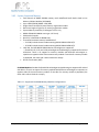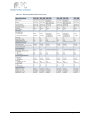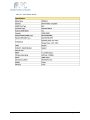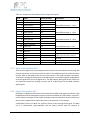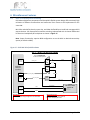
1
IPC2 Hardware Specification CompuLab Ltd. Revision 1.2 September 2014 Legal Notice © 2013 CompuLab Ltd. All Rights Reserved. No part of this document may be photocopied, reproduced, stored in a retrieval system, or transmitted, in any form or by any means whether, electronic, mechanical, or otherwise without the prior written permission of CompuLab Ltd. No warranty of accuracy is given concerning the contents of the information contained in this publication. To the extent permitted by law no liability (including liability to any person by reason of negligence) will be accepted by CompuLab Ltd., its subsidiaries or employees for any direct or indirect loss or damage caused by omissions from or inaccuracies in this document. CompuLab Ltd. reserves the right to change details in this publication without notice. Product and company names herein may be the trademarks of their respective owners. CompuLab Ltd. 17 HaYetsira St., Yokneam Elite 20692, P.O.B 687 ISRAEL Tel: +972-4-8290100 http://www.compulab.co.il http://fit-pc.com/web/ Fax: +972-4-8325251 CompuLab Ltd. IPC2 – Hardware Specification Page 2 of 83 Revision History Revision 1.0 1.1 1.2 1.3 CompuLab Ltd. HW Engineer Maxim Birger Maxim Birger Maxim Birger Maxim Birger Revision Changes Initial public release Typo fixes and diagram updates Fixed RS232 serial COM port mapping Added power supply temperature ratings: 10.2 IPC2 – Hardware Specification Page 3 of 83 Table of Contents Legal Notice................................................................................................................................................... 2 Revision History ............................................................................................................................................ 3 1 2 3 Introduction ........................................................................................................................................ 10 1.1 About This Document ................................................................................................................. 10 1.2 Reference .................................................................................................................................... 10 1.3 Terms and Acronyms .................................................................................................................. 11 System Overview ................................................................................................................................ 12 2.1 Highlights .................................................................................................................................... 12 2.2 Specifications .............................................................................................................................. 12 2.3 System Block Diagram ................................................................................................................. 15 2.4 Models and Platform SKUs ......................................................................................................... 15 Platform .............................................................................................................................................. 16 3.1 Processor..................................................................................................................................... 16 3.1.1 Processor Features .................................................................................................................. 16 3.1.2 Supported Technologies ......................................................................................................... 16 3.1.3 Processor Power States........................................................................................................... 17 3.1.3.1 System States .......................................................................................................................... 18 3.2 Processor Graphics Controller .................................................................................................... 19 3.2.1 3.3 Graphics Features ................................................................................................................... 19 PCH (Chipset) .............................................................................................................................. 20 3.3.1 PCH Capability Overview ......................................................................................................... 20 3.3.1.1 Direct Media Interface (DMI) .................................................................................................. 20 3.3.1.2 PCI Express* Interface ............................................................................................................. 20 3.3.1.3 Serial ATA (SATA) Controller ................................................................................................... 21 3.3.1.3.1 AHCI..................................................................................................................................... 21 3.3.1.4 Low Pin Count (LPC) Interface................................................................................................. 21 3.3.1.5 Serial Peripheral Interface (SPI) .............................................................................................. 21 3.3.1.6 Universal Serial Bus (USB) Controllers .................................................................................... 21 3.3.1.7 Flexible I/O .............................................................................................................................. 21 3.3.1.8 Gigabit Ethernet Controller..................................................................................................... 22 3.3.1.9 RTC .......................................................................................................................................... 23 CompuLab Ltd. IPC2 – Hardware Specification Page 4 of 83 3.3.1.10 GPIO .................................................................................................................................... 23 3.3.1.11 System Management Bus (SMBus) ..................................................................................... 23 3.3.1.12 High Definition Audio Controller......................................................................................... 23 3.4 Intel Management Engine........................................................................................................... 24 3.5 System Clocks .............................................................................................................................. 25 3.5.1 Functional Blocks .................................................................................................................... 26 3.5.2 Clock Configuration Access Overview ..................................................................................... 27 3.6 3.6.1 Processor Integrated Memory Controller ............................................................................... 28 3.6.2 System Supported Memory .................................................................................................... 29 3.6.3 System Memory Timing Support ............................................................................................ 30 3.6.4 System Memory Organization Modes .................................................................................... 31 3.6.4.1 Single-Channel Mode .............................................................................................................. 31 3.6.4.2 Dual-Channel Mode (Intel Flex Memory Technology Mode) ................................................. 31 3.6.4.3 Dual-Channel Symmetric Mode .............................................................................................. 31 3.6.4.4 System Memory Frequency .................................................................................................... 31 3.7 4 System Memory .......................................................................................................................... 28 Storage ........................................................................................................................................ 32 3.7.1 Certified storage devices......................................................................................................... 33 3.7.1.1 HDD examples ......................................................................................................................... 33 3.7.1.2 mSATA SSD examples .............................................................................................................. 37 Peripherals .......................................................................................................................................... 39 4.1 Display Interface ......................................................................................................................... 39 4.2 Network ...................................................................................................................................... 41 4.2.1 LAN1 – Intel MAC/PHY GbE Controller ................................................................................... 41 4.2.2 LAN2 – Intel I211AT GbE Controller ........................................................................................ 43 4.2.2.1 Intel I211AT Features .............................................................................................................. 43 4.2.3 LAN Ports LEDs notifications ................................................................................................... 43 4.3 Wireless Networks ...................................................................................................................... 44 4.4 Wireless Module Features .......................................................................................................... 44 4.5 Audio ........................................................................................................................................... 46 4.5.1 Audio Codec General Description ........................................................................................... 46 4.5.2 Audio Codec Features ............................................................................................................. 46 CompuLab Ltd. IPC2 – Hardware Specification Page 5 of 83 4.6 5 Interfaces ............................................................................................................................................ 50 5.1 7 PCI Express .................................................................................................................................. 50 5.1.1 PCI Express Specifications ....................................................................................................... 50 5.1.2 Mini PCI Express* Edge Connector ......................................................................................... 51 5.2 6 Super-I/O Controller ................................................................................................................... 49 Digital Display Interface .............................................................................................................. 52 5.2.1 High Definition Multimedia Interface (HDMI) ........................................................................ 53 5.2.1.1 HDMI Connector ..................................................................................................................... 54 5.2.2 Digital Video Interface (DVI) ................................................................................................... 55 5.2.3 Display Port Interface (DP) ...................................................................................................... 55 5.2.3.1 DisplayPort Connector ............................................................................................................ 57 5.3 USB Interface .............................................................................................................................. 60 5.4 RS232 Serial Interface ................................................................................................................. 61 Miscellaneous Features...................................................................................................................... 63 6.1 Mini PCI Express/mSATA sharing ................................................................................................ 63 6.2 SIM Interface ............................................................................................................................... 64 6.3 SPI Interface ................................................................................................................................ 64 6.4 Custom Design GPIOs.................................................................................................................. 64 6.5 FACE Module Interface ............................................................................................................... 65 6.5.1 Extension Connectors ............................................................................................................. 66 6.5.2 Connectors Pinout................................................................................................................... 67 6.5.3 FM-USB3 ................................................................................................................................. 69 6.5.3.1 Description .............................................................................................................................. 69 6.5.3.2 Highlights ................................................................................................................................ 69 6.5.3.3 Block Diagram ......................................................................................................................... 69 6.5.3.4 mSATA slot .............................................................................................................................. 69 6.5.3.5 Mechanics ............................................................................................................................... 70 6.5.3.5.1 PCB Assembly ...................................................................................................................... 70 6.5.3.5.2 Front Panel .......................................................................................................................... 70 Advanced Technologies...................................................................................................................... 71 7.1 Intel vPRO technology ................................................................................................................. 71 7.2 Intel Active Management Technology ........................................................................................ 71 CompuLab Ltd. IPC2 – Hardware Specification Page 6 of 83 7.3 8 Intel Virtualization Technology ................................................................................................... 71 Power Management ........................................................................................................................... 73 8.1 9 Embedded Controller Renesas H8S/2113 ................................................................................... 73 Electrical Characteristics .................................................................................................................... 74 9.1 Absolute Maximum Ratings ........................................................................................................ 74 9.2 Recommended Operating Conditions......................................................................................... 74 9.3 DC Electrical Characteristics........................................................................................................ 74 9.4 Power Supply .............................................................................................................................. 75 10 Mechanical Characteristics ............................................................................................................ 76 10.1 Mechanical Drawings .................................................................................................................. 76 10.1.1 Chassis ..................................................................................................................................... 76 10.1.2 Single Board Computer ........................................................................................................... 80 10.1.2.1 With FACE Module .............................................................................................................. 80 10.1.2.2 Without FACE Module ........................................................................................................ 81 10.2 11 Environmental ............................................................................................................................. 82 Resources ........................................................................................................................................ 83 Table of Figures Figure 1 – IPC2 Top Level Block Diagram ................................................................................................... 15 Figure 2 – Processor Power States ............................................................................................................. 17 Figure 3 – PCH Internal Clock Diagram ...................................................................................................... 26 Figure 4 – Memory Interface ..................................................................................................................... 28 Figure 5 – SATA Interface ........................................................................................................................... 32 Figure 6 – Processor Display Architecture ................................................................................................. 39 Figure 7 – PCH Display Architecture .......................................................................................................... 40 Figure 8 – Wireless Module Block Diagram ............................................................................................... 45 Figure 9 – Wireless Module Mechanical Dimensions ............................................................................... 45 Figure 10 – Audio Codec Functional Block Diagram .................................................................................. 48 Figure 11 – SMSC SIO1007 Super-I/O Controller functional block diagram ............................................. 49 Figure 12 – IPC2 PCI Express Interface scheme ......................................................................................... 50 Figure 13 – HDMI Link Diagram ................................................................................................................. 53 Figure 14 – DP Link Diagram ...................................................................................................................... 56 Figure 15 – IPC2 USB Interface scheme ..................................................................................................... 60 Figure 16 – IPC2 Serial Connectivity .......................................................................................................... 61 CompuLab Ltd. IPC2 – Hardware Specification Page 7 of 83 Figure 17 – IPC2 Mini PCIe/mSATA scheme .............................................................................................. 63 Figure 18 – FACE Module concept ............................................................................................................. 65 Figure 19 – FACE Module FM-USB3 block diagram ................................................................................... 69 Figure 20 – FM-USB3 PCB Assembly Top ................................................................................................... 70 Figure 21 – FM-USB3 front panel ............................................................................................................... 70 Figure 22 – Renesas H8S/2113 Functional Block Diagram ........................................................................ 73 Figure 23 – IPC2 Isometric Front ................................................................................................................ 76 Figure 24 – IPC2 Isometric Back ................................................................................................................. 76 Figure 25 – IPC2 Front Panel ...................................................................................................................... 77 Figure 26 – IPC2 Back Panel ....................................................................................................................... 77 Figure 27 – IPC2 Top ................................................................................................................................... 78 Figure 28 – IPC2 Bottom ............................................................................................................................. 78 Figure 29 – IPC2 service door with mounted HDD/SSD storage drive ..................................................... 79 Figure 30 – SBC-iHSW Mechanical Drawing with FACE Module ............................................................... 80 Figure 31 – SBC-iHSW Mechanical Drawing without FACE Module ......................................................... 81 Table of Tables Table 1 – Reference Documents ................................................................................................................ 10 Table 2 – Terms and Acronyms .................................................................................................................. 11 Table 3 – Platform Specifications .............................................................................................................. 12 Table 4 – Display and Graphics Specifications .......................................................................................... 13 Table 5 – Audio Specifications ................................................................................................................... 13 Table 6 – Networking Specifications.......................................................................................................... 13 Table 7 – Connectivity Specifications ........................................................................................................ 13 Table 8 – Mechanical and Environmental Specifications.......................................................................... 14 Table 9 – Models and Platform SKUs......................................................................................................... 15 Table 10 – System States............................................................................................................................ 18 Table 11 – Processor Core States ............................................................................................................... 18 Table 12 – Flexible I/O High Speed Signal settings with PCIe, USB3.0, and SATA Ports .......................... 22 Table 13 – PCH Clock Input ........................................................................................................................ 25 Table 14 – PCH Clock Outputs .................................................................................................................... 25 Table 15 – PCH PLL...................................................................................................................................... 26 Table 16 – Modulator Block ....................................................................................................................... 27 Table 17 – Supported SO-DIMM Memory Modules Configurations ........................................................ 29 Table 18 – Supported Max Memory Size per SO-DIMM ........................................................................... 30 Table 19 – DDR3L System Memory Timing Support ................................................................................. 30 Table 20 – WD Scorpio Blue HDD series .................................................................................................... 33 Table 21 – WD Scorpio Blue HDD series (cont.) ........................................................................................ 34 Table 22 – Hitachi CinemaStar C5K750 HDD models ................................................................................ 35 Table 23 – Seagate Momentus HDD series................................................................................................ 36 Table 24 – Micron mSATA NAND Flash SSD .............................................................................................. 37 Table 25 – ACPI CMS2G-M SSD .................................................................................................................. 38 CompuLab Ltd. IPC2 – Hardware Specification Page 8 of 83 Table 26 – LAN ports LEDs status notification ........................................................................................... 43 Table 27 – Wireless Module Features ....................................................................................................... 44 Table 28 – mini PCI Express edge connector pinout ................................................................................. 51 Table 29 – Downstream Port HDMI Connector Pinout ............................................................................. 54 Table 30 – Downstream Port HDMI Connector Signal Description .......................................................... 55 Table 31 – Downstream Port DP Connector Pinout .................................................................................. 57 Table 32 – Upstream Port DP Connector Pinout ....................................................................................... 58 Table 33 – Display Port Cable..................................................................................................................... 59 Table 34 – Common COM port mapping ................................................................................................... 61 Table 35 – COM3 Serial Port Pinout .......................................................................................................... 62 Table 36 – Custom Design GPIO table ....................................................................................................... 64 Table 37 – B2B receptacle connector HOST side ....................................................................................... 66 Table 38 – B2B plug connector FACE Module side .................................................................................... 66 Table 39 – EXT1 connector HOST side pinout ........................................................................................... 67 Table 40 – Absolute Maximum Ratings ..................................................................................................... 74 Table 41 – Recommended Operating Condition ....................................................................................... 74 Table 42 – DC Electrical Characteristics ..................................................................................................... 74 Table 43 – Operating Temperature Grades ............................................................................................... 82 CompuLab Ltd. IPC2 – Hardware Specification Page 9 of 83 1 Introduction 1.1 About This Document This document is part of a set of reference documents providing information necessary to operate Compulab’s IPC2 computer. 1.2 Reference For additional information not covered in this manual, please refer to the documents listed in Table 1. Table 1 – Reference Documents Document Ordering Information Guide Location http://fit-pc.com/download/General/orderinginformation-guide.pdf Application Note - fit-PC products http://fit-pc.com/download/faceFACE Module compatibility matrix modules/documents/app-note-products-fmcompatibility-matrix.pdf FACE Module HW Specifications http://fit-pc.com/download/facemodules/documents/face-modules-hw-specifications.pdf Intel vPRO Technology http://www.intel.com/content/www/us/en/architectureand-technology/vpro/vpro-technology-general.html Intel AMT Technology http://www.intel.com/content/www/us/en/architectureand-technology/intel-active-managementtechnology.html Intel Virtualization Technology http://www.intel.com/technology/virtualization/ CompuLab Ltd. IPC2 – Hardware Specification Page 10 of 83 1.3 Terms and Acronyms Table 2 – Terms and Acronyms Term APM B2B BER bps BT CAN Codec DDR DSP FACE Module FM-xxxx GB/s GPIO GT/s HW JTAG kbps LAN MB/s Mbps MT/s NVM OTP PCH PCM PEG Rx SCH SDRAM SIM SoC SPI Tx UART USB USB-OTG USIM VCTCXO WLAN XO CompuLab Ltd. Definition Advanced Power Management Board to Board (connectors) Bit error rate Bits per second Bluetooth Controller Area Network Coder decoder Dual data rate Digital signal processor Function And Connectivity Extension Module FACE Module – connectivity options Gigabytes per second General-purpose input/output Giga Transfers per second (throughput) Hardware Joint Test Action Group (ANSI/ICEEE Std. 1149.1-1990) Kilobits per second Local Area Network Megabytes per second Megabits per second Mega Transfers per second (throughput) Non Volatile Memory One Time Programmable Platform Controller Hub Pulse-coded Modulation PCI Express Graphics Receive System Controller Hub Synchronous dynamic random access memory Subscriber Identity Module System-on-Chip Serial peripheral interface Transmit Universal asynchronous receiver transmitter Universal serial bus Universal serial bus on-the-go UMTS subscriber interface module Voltage-controlled temperature-compensated crystal oscillator Wireless Local Area Network Crystal oscillator IPC2 – Hardware Specification Page 11 of 83 2 System Overview 2.1 Highlights IPC2 is a fully functional miniature computer based on Intel 4th generation (Haswell ULT) Mobile Intel® Core™ 64-bit dual core processor family. Together with powerful Intel HD graphics engine, rich peripherals and connectivity options, completely fanless design delivers outstanding performance at lowest power consumption of any PC at its class. High performance, low-power, rich I/O and miniature rugged design, position IPC2 as an attractive solution for a wide range of applications – industrial control and automation, networking and communications infrastructures, media players, IPTV, infotainment system, digital signage and smart kiosks, gaming or small-footprint desktop replacement. 2.2 Specifications Table 3 – Platform Specifications Feature Processor Chipset Memory Storage Advanced Technologies Special Functionality Operating Systems CompuLab Ltd. Specifications Mobile Intel® Core™ i7/5/3 and Celeron 4th Gen (Haswell ULT) Dual core 64-bit Clock speeds 1.4GHz – 2.1GHz (turbo boost up to 3.3GHz) (Note 1) 15W TDP Intel Mobile Lynx Point LP PCH (MCP package) Up to 16GB (2x 8GB) DDR3L-1333/1600 (1.35V operation) 2x SO-DIMM 204-pin DDR3L SDRAM memory slots 1x SATA up to 6 Gbps (SATA 3.0) for internal 2.5” HDD/SSD, HDD to be used 5400rpm only 2x mSATA slot up to 6 Gbps (SATA 3.0), (1x mSATA in Celeron/i3 models) vPRO (i7 and i5 models) AMT (i7 and i5 models) CPU Virtualization Auto-On Wake-on-LAN Wake-on-Timer PXE Boot (LAN boot) Watchdog Windows 7/8, 32-bit and 64-bit Windows Server 2012 R2 Linux 32-bit and 64-bit Embedded OS IPC2 – Hardware Specification Page 12 of 83 Table 4 – Display and Graphics Specifications Feature GPU Video Output 1 Video Output 2 Video Output 3 Specifications Intel HD Graphics 4400 Triple display mode supported HDMI 1.4a up to 4096 x 2304 @ 24Hz DisplayPort 1.2 up to 3200 x 2000 @ 60Hz HDMI 1.4a up to 4096 x 2304 @ 24Hz Table 5 – Audio Specifications Feature Codec Audio Output Audio Input Specifications Realtek ALC888-VC2 HD audio codec Analog stereo output Digital 7.1+2 channels S/PDIF output 3.5mm jack Analog stereo Microphone input Digital S/PDIF input 3.5mm jack Table 6 – Networking Specifications Feature LAN Wireless Specifications 2x GbE LAN ports (extendable up to 6) LAN1: Intel I218 GbE PHY (MAC integrated into the chipset) (RJ-45) LAN2: Intel I211 GbE controller (RJ-45) LAN3-6: Depends on FACE Module installed (Note 2) WLAN 802.11ac (2.4/5GHz dual band Intel 7260HMW module) Bluetooth 4.0 Table 7 – Connectivity Specifications Feature USB Serial SIM Special I/O Expansion CompuLab Ltd. Specifications 4x USB 3.0 (Note 3) 2x USB 2.0 3x Serial communication ports COM1: 2-wire RS232 via mini serial connector COM2: 2-wire RS232 via mini serial connector COM3: Full RS232 via mini serial connector 1x micro SIM slot (6 pins) See Note 4 Half-size mini-PCIe socket Full-size mini-PCIe socket (Note 5) IPC2 – Hardware Specification Page 13 of 83 Table 8 – Mechanical and Environmental Specifications Feature Input Voltage Power Consumption Operating Temperatures Enclosure Material Cooling Dimensions Weight Specifications Unregulated 10 – 15VDC input (Note 6) 6W – 24W 1. Commercial HDD models: 0°C – 50°C SSD models: 0°C – 70°C 2. Extended (TE) SSD models only: -20°C – 70°C 3. Industrial (TI) SSD models only: -40°C – 70°C Die Cast Aluminum Passive Cooling Fanless Design 19cm x 16cm x 4cm 1150gr Notes: 1. For full processors specifications based on IPC2 model, please refer to models and platform SKU Table 9. 2. Natively 2x GbE LAN ports on the back panel with an option for additional 4x GbE LAN ports. LAN3-6 based on FACE Module installed (refer to FACE Module HW specifications - Table 1): a. FM-1LAN: LAN3 RTL8111F-CG GbE controller (RJ-45), LAN4-6: N/A b. FM-4LAN: Intel 82574 GbE Controller (RJ-45) c. FM-POE: Intel I211 GbE Controller (RJ-45) 3. Back panel 2x USB3.0 + 2x USB2.0. Front panel 2x USB3.0 with default FACE Module. 4. Refer to FACE Module HW specifications document - Table 1. 5. Shared with mSATA. Refer to Figure 17. 6. Nominal input voltage: 12V CompuLab Ltd. IPC2 – Hardware Specification Page 14 of 83 2.3 System Block Diagram IPC2 system Top Level Block Diagram is shown below. Later chapters in this document describe functions and entities shown in the below diagram. Figure 1 – IPC2 Top Level Block Diagram DDR3L SDRAM (up to 8GB DDR3L-1600) SO-DIMM 204-pin slot A MEM Channel A (x64, 800MHz max) DDR3L SDRAM (up to 8GB DDR3L-1600) SO-DIMM 204-pin slot B MEM Channel B (x64, 800MHz max) Memory Controller HDMI 1.4a HDMI port HDMI 1.4a Renesas H8S/2113 16-bit MCU i7-4600U; i5-4300U; i3-4010U; Celeron-2955U TPM IEEE802.3 LAN1 RJ45 Port IEEE802.3 Audio In 3.5'’ jack Audio Out 3.5'’ jack Intel GbE controller PCIe2.0 @ 5Gbps Intel GbE PHY I218 Clock Unit SMSC SuperIO SIO1007 SMBus controller RS232 2-wire USB EHCI Host controllers USB3 x2 ports USB3.0 @ 5Gbps (x2) xHCI USB3.0 controller LPC Bus PCIe2.0 / SATA3.0 (x1) Flexible I/Os Lynx Point LP PCH chipset PCIe2.0 / USB3.0 (x2) SATA Host Controller SATA3.0 @ 6Gbps (x1) USB EHCI Host controllers USB2.0 (x2) HD Audio HDAudio @ 48Mbps PCI Express Root USB2.0 (x2) RS232 full SMBus MCP Package USB2 x2 ports RS232 driver MAX3243 GPIOs (x7) HD Audio HDA @ 48Mbps UART LPC BUS controller GbE MAC PCIe2.0 @ 5Gbps Realtek Audio Codec ALC888-VC2 Graphics Controller PCI Express Root port SMBus AAUD_L/R SPDIF_OUT RS232 2-wire UART RTC I211 MIC/LINE_IN SPDIF_IN RS232 driver MAX3243 Serial COM1 Serial COM2 Atmel AT97SC3204 Digital Display Interface CMOS Battery LAN2 RJ45 Port UART PCIe2.0 (x1) PCIe2.0 @ 5Gbps (x1) PLX PCIE Switch PEX8603 SATA3.0 @ 6Gbps (x1) Serial COM3 HOST / FACE Module interface HDMI port Micro SIM slot MUX PCIe2.0 @ 5Gbps (x1) SSD/HDD storage bay 2.5'’/1.8'’ Form Factor SPI_PCH SPI_EC SATA Host Controller From EC SATA Host Controller SATA3.0 @ 6Gbps (x1) Interrupt Controllers AMT* (i5/i7 SKUs only) SATA3.0 @ 6Gbps (x1) MUX SNOR Flash CONFIG SPI 2.4 Embedded Controller (EC) DP 1.2 DP port SNOR Flash BIOS Intel 4th Gen Core i7/5/3/ Celeron mobile processor (Haswell ULT) Dual core 64-bit Mini PCIe / mSATA Full size USB EHCI Host controller USB2.0 (x1) PCI Express Root Port PCIe2.0 @ 5Gbps (x1) USB EHCI Host controller USB2.0 (x1) Mini PCIe slot Half size Models and Platform SKUs Table 9 – Models and Platform SKUs Model Processor Core Clock IPC2 Value Intel Celeron 2955U 1.4GHz IPC2 i3 Intel Core i3-4010U 1.7GHz Cores TDP Chipset 64-bit dual core 15W Lynx Point LP PCH 64-bit dual core 15W Lynx Point LP PCH CompuLab Ltd. IPC2 i5 Intel Core i5-4300U 1.9GHz (turbo boost up to 2.9GHz) 64-bit dual core 15W Lynx Point LP PCH IPC2 – Hardware Specification IPC2 i7 Intel Core i7-4600U 2.1GHz (turbo boost up to 3.3GHz) 64-bit dual core 15W Lynx Point LP PCH Page 15 of 83 3 Platform 3.1 Processor The 4th Generation Intel® Core™ processor based on Mobile U-Processor line are 64-bit, multicore processors built on 22-nanometer process technology. Haswell ULT processor designed for a two-chip platform on a single Multi-Chip Package (MCP) that includes a processor die and lowpower Platform Controller Hub (PCH) die, and enables higher performance and lower power consumption relatively to previous generation. The processor includes Integrated Display Engine, Processor Graphics, and an Integrated Memory Controller. The processor is designed for mobile platforms. 3.1.1 Processor Features Two execution cores A 32-KB instruction and 32-KB data first-level cache (L1) for each core A 512-KB shared instruction / data second-level cache (L2), shared among all cores Up to 4-MB shared instruction / data third-level cache (L3), shared among all cores 3.1.2 Supported Technologies CompuLab Ltd. Intel® Virtualization Technology (Intel® VT) Intel® Active Management Technology 9.5 (Intel® AMT9.5) Intel® Trusted Execution Technology (Intel® TXT) Intel® Streaming SIMD Extensions 4.2 (Intel® SSE4.2) Intel® Hyper-Threading Technology (Intel® HT Technology) Intel® 64 Architecture Execute Disable Bit Intel® Turbo Boost Technology 2.0 Intel® Advanced Vector Extensions 2.0 (Intel® AVX2) Intel® Advanced Encryption Standard New Instructions (Intel® AES-NI) Intel® Secure Key Intel® Transactional Synchronization Extensions - New Instructions (Intel® TSXNI) IPC2 – Hardware Specification Page 16 of 83 3.1.3 Processor Power States This chapter provides information on the processor Advanced Configuration and Power Interface (ACPI) states. Figure 2 – Processor Power States CompuLab Ltd. IPC2 – Hardware Specification Page 17 of 83 3.1.3.1 System States Table 10 – System States State G0/S0 G1/S3-Cold G1/S4 G2/S5 G3 Description Full On Mode, Display On Suspend-to-RAM (STR). Context saved to memory (S3-Hot state is not supported by the processor). Suspend-to-Disk (STD). All power lost (except wakeup on PCH). Soft off. All power lost (except wakeup on PCH). Total reboot. Mechanical off. All power removed from system. Table 11 – Processor Core States State C0 C1 C1E C3 C6 C7 C8 C9 C10 Description Active mode, processor executing code. Auto HALT state. Auto HALT state with lowest frequency and voltage operating point. Execution cores in C3 state flush their L1 instruction cache, L1 data cache, and L2 cache to the L3 shared cache. Clocks are shut off to each core. Execution cores in this state save their architectural state before removing core voltage. Execution cores in this state behave similarly to the C6 state. If all execution cores request C7 state, L3 cache ways are flushed until it is cleared. If the entire L3 cache is flushed, voltage will be removed from the L3 cache. Power removal to SA, Cores and L3 will reduce power consumption. C7 state plus voltage is removed from all power domains after required state is saved. PLL is powered down. C8 state plus processor VCC input voltage at 0 V. C9 state plus VR12.6 is set to low-power state, near shut off. While executing code, Enhanced Intel SpeedStep® Technology optimizes the processor’s frequency and core voltage based on workload. Each frequency and voltage operating point is defined by ACPI as a P-state. When the processor is not executing code, it is idle. A low-power idle state is defined by ACPI as a C-state. In general, deeper power C-states have longer entry and exit latencies. CompuLab Ltd. IPC2 – Hardware Specification Page 18 of 83 3.2 Processor Graphics Controller New Graphics Engine Architecture includes 3D compute elements, Multi-format hardware assisted decode/encode pipeline, and Mid-Level Cache (MLC) for superior high definition playback, video quality, and improved 3D performance and Media. The Display Engine handles delivering the pixels to the screen. GSA (Graphics in System Agent) is the primary channel interface for display memory accesses and “PCI-like” traffic in and out. 3.2.1 Graphics Features CompuLab Ltd. The Processor Graphics contains a generation 7.5 graphics core architecture enabling substantial gains in performance and lower power consumption Up to 40 Execution Units are supported depending on the processor SKU Next Generation Intel Clear Video Technology HD Support is a collection of video playback and enhancement features that improve the end user’s viewing experience: — Encode / transcode HD content — Playback of high definition content including Blu-ray Disc* — Superior image quality with sharper, more colorful images — Playback of Blu-ray disc S3D content using HDMI (V.1.4a with 3D) DirectX* Video Acceleration (DXVA) support for accelerating video processing — Full AVC/VC1/MPEG2 HW Decode Advanced Scheduler 2.0, 1.0, XPDM support Windows* 8, Windows* 7, Mac OSX, Linux* operating system support DirectX* 11.1, DirectX* 11, DirectX* 10.1, DirectX* 10, DirectX* 9 support OpenGL* 4.0 support IPC2 – Hardware Specification Page 19 of 83 3.3 PCH (Chipset) Haswell ULT platform designed in a compact single MCP package that contains both processor and PCH dies on the same package board. The PCH provides extensive I/O support. Functions and capabilities include: PCI Express* Base Specification, Revision 2.0 support for up to six ports with transfers up to 5 GT/s ACPI Power Management Logic Support, Revision 4.0a Enhanced DMA controller, interrupt controller, and timer functions Integrated SATA host controllers within dependent DMA operation on up to four ports xHCI USB controller provides support for up to 8 USB ports, of which four can be configured as SuperSpeed USB 3.0 ports Flexible I/O allows some high speed I/O signals to be configured as PCIe, SATA or USB 3.0 Integrated 10/100/1000 Gigabit Ethernet MAC with System Defense System Management Bus (SMBus), Version 2.0 with additional support for I2C devices Supports Intel® High Definition Audio (Intel® HD Audio) Supports Intel® Rapid Storage Technology (Intel® RST) Supports Intel® Active Management Technology (Intel® AMT) Supports Intel® Virtualization Technology for Directed I/O (Intel® VT-d) Integrated Clock Controller Intel® Flexible Display Interconnect (Intel® FDI) Low Pin Count (LPC) interface Serial Peripheral Interface (SPI) support Two integrated Intel® serial I/O I2C Host controllers Intel® Anti-Theft Technology (Intel® AT) 3.3.1 PCH Capability Overview The following sub-sections provide an overview of the PCH capabilities. 3.3.1.1 Direct Media Interface (DMI) Haswell ULT platform (MCP package) features package internal DMI and not available on external pins. Direct Media Interface (DMI) is the chip-to-chip connection between the processor and PCH. This high-speed interface integrates advanced priority-based servicing allowing for concurrent traffic and true isochronous transfer capabilities. 3.3.1.2 PCI Express* Interface The PCH provides up to 6 PCI Express Root Ports, supporting the PCI Express Base Specification, Revision 2.0. Each Root Port x1 lane supports up to 5 Gbps bandwidth in each direction (10 Gbps concurrent). Refer to section 5.1 for detailed feature set. CompuLab Ltd. IPC2 – Hardware Specification Page 20 of 83 3.3.1.3 Serial ATA (SATA) Controller The PCH has one integrated SATA host controller that support independent DMA operation on up to four ports and supports data transfer rates of up to 6 Gbps. The SATA controller contains one mode of operation – an AHCI mode using memory space. The SATA controller no longer supports legacy mode using I/O space. Therefore, AHCI software is required. The PCH supports the Serial ATA Specification, Revision 3.1. 3.3.1.3.1 AHCI The PCH provides hardware support for Advanced Host Controller Interface (AHCI), a standardized programming interface for SATA host controllers. Platforms supporting AHCI may take advantage of performance features such as port independent DMA Engines – each device is treated as a master – and hardware-assisted native command queuing. AHCI also provides usability enhancements such as Hot-Plug and advanced power management. AHCI requires appropriate software support (such as an AHCI driver) and for some features, hardware support in the SATA device or additional platform hardware. 3.3.1.4 Low Pin Count (LPC) Interface The PCH implements an LPC Interface as described in the LPC 1.1 Specification. The Low Pin Count (LPC) bridge function of the PCH resides in PCI Device 31: Function 0. In addition to the LPC bridge interface function, D31:F0 contains other functional units including DMA, interrupt controllers, timers, power management, system management, GPIO, and RTC. 3.3.1.5 Serial Peripheral Interface (SPI) The SPI Flash Controller supports running instructions at 20 MHz, 33 MHz, and 50 MHz and used by the PCH for BIOS code, to provide chipset configuration settings, integrated Gigabit Ethernet MAC/PHY configuration and Intel® Management Engine (Intel® ME) settings. The SPI Flash Controller supports the Serial Flash Discoverable Parameter (SFDP) JEDEC standard, which provides a consistent way of describing the functional and feature capabilities of serial flash devices in a standard set of internal parameter tables. The SPI Flash Controller queries these parameter tables to discover the attributes to enable divergent features from multiple SPI part vendors, such as Quad I/O Fast Read capabilities or device storage capacity, among others. 3.3.1.6 Universal Serial Bus (USB) Controllers The PCH contains one eXtensible Host Controller Interface (xHCI) controller and one Enhanced Host Controller Interface (EHCI) controller. The xHCI controller supports up to 8 USB 2.0 ports of which 4 can be configured as SuperSpeed (USB 3.0) ports. 3.3.1.7 Flexible I/O Flexible I/O is an architecture to allow some high speed signals to be configured as PCIe, USB 3.0 or SATA signals per I/O needs on a platform. Through soft straps, the functionality on these multiplexed signals are selected to meet the I/O needs on the platform. There are 14 differential pairs that are split between the three interfaces. Among them, 6 differential pairs are multiplexed: 2 multiplexed differential pairs can be configured to be used as PCIe port 1, 2 or USB3.0 port 3, 4 CompuLab Ltd. IPC2 – Hardware Specification Page 21 of 83 and the other 4 differential pairs can be configured to be used as PCIe port 6 lane 3 to 0 or SATA port 3 to 0. The below example illustrates how the signals are utilized for Flexible I/O. Table 12 – Flexible I/O High Speed Signal settings with PCIe, USB3.0, and SATA Ports CONFIG 1 CONFIG 2 (default) 2x PCIe2.0 2x USB3.0 CONFIG 3 CONFIG 4 CONFIG 5 3x PCIe2.0 1x SATA3.0* 1x PCIe2.0 1x SATA3.0* 2x USB3.0 2x SATA3.0* 2x USB2.0 2x PCIe2.0 1x SATA3.0* 1x USB3.0 2x SATA3.0* 2x USB2.0 1x PCIe2.0 3x SATA3.0* 2x USB3.0 2x USB2.0 2x PCIe2.0 3x SATA3.0* 1x USB3.0 2x USB2.0 Flexible I/O functionality 4x PCIe2.0 Fixed I/O Functionality 2x SATA3.0* 2x USB2.0 2x SATA3.0* 2x USB2.0 2x SATA3.0* 2x USB2.0 FACE Module High Speed Connectivity 4x PCIe2.0 2x SATA3.0* 2x USB2.0 3x PCIe2.0 3x SATA3.0* 2x USB2.0 Suitable FACE Modules All except FM-USB3 2x PCIe2.0 2x SATA3.0* 2x USB3.0 2x USB2.0 FM-USB3 (see 6.5.3) Custom design (see Notes) Relevant Flexible I/O pins on FACE Module connector: PCIe/USB3: [A35/A36, B35/B36]; [A38/A39, B38/B39] PCIe/SATA: [A41/A42, B41/B42]; Notes: 1. Flexible I/O configuration requires firmware programming and done in CompuLab facilities only. IPC2 Flexible I/O factory firmware is FACE Module dependent, meaning that IPC2 FW will be programmed according to the selected configuration and FACE Module. 2. Intel Celeron and i3 models support single (x1) SATA interface on the FACE Module, and it is a shared/multiplexed connection with onboard mini PCIe interface (refer to 6.1). 3. Intel i5 and i7 models support up to three (x3) SATA interfaces on the FACE Module, when one is a shared/multiplexed connection with onboard mini PCIe interface (refer to 6.1). 4. Configuration 3, 4 and 5 possible for i5/i7 processors SKU only. 5. Configuration 3, 4 and 5 possible for custom products with MOQ > 100 units. 6. Refer to FM-USB3 module description – see 6.5.3. 3.3.1.8 Gigabit Ethernet Controller Refer to section 4.2 for detailed feature set. CompuLab Ltd. IPC2 – Hardware Specification Page 22 of 83 3.3.1.9 RTC The PCH contains a Motorola MC146818B-compatible real-time clock with 256 bytes of batterybacked RAM. The real-time clock performs two key functions—keeping track of the time of day and storing system data, even when the system is powered down. The RTC operates on a 32.768 kHz crystal and a 3V battery. 3.3.1.10 GPIO Various general purpose inputs and outputs are provided for custom system design. Refer to section 6.4. 3.3.1.11 System Management Bus (SMBus) The PCH provides System Management Bus (SMBus) 2.0 host controller as well as SMBus Slave Interface. The host controller provides a mechanism for the processor to initiate communications with SMBus peripherals (slaves). The PCH is also capable of operating in a mode in which it can communicate with I2C compatible devices. The host SMBus controller supports up to 100 KHz clock speed. 3.3.1.12 High Definition Audio Controller The PCH High Definition Audio (HDA) controller communicates with the external codec(s) over the Intel® High Definition Audio serial link. The controller consists of a set of DMA engines that are used to move samples of digitally encoded data between system memory and an external codec(s). The PCH implements four output DMA engines and 4 input DMA engines. The output DMA engines move digital data from system memory to a D/A converter in a codec. The PCH implements a single Serial Data Output signal (HDA_SDO) that is connected to external codecs. The input DMA engines move digital data from the A/D converter in the codec to system memory. The PCH implements four Serial Digital Input signals (HDA_SDI[1:0]) supporting two audio codecs. Audio software renders outbound and processes inbound data to/from buffers in system memory. The location of individual buffers is described by a Buffer Descriptor List (BDL) that is fetched and processed by the controller. The data in the buffers is arranged in a predefined format. The output DMA engines fetch the digital data from memory and reformat it based on the programmed sample rate, bit/sample and number of channels. The data from the output DMA engines is then combined and serially sent to the external codecs over the Intel High Definition Audio link. The input DMA engines receive data from the codecs over the Intel High Definition Audio link and format the data based on the programmable attributes for that stream. The data is then written to memory in the predefined format for software to process. Each DMA engine moves one stream of data. A single codec can accept or generate multiple streams of data, one for each A/D or D/A converter in the codec. Multiple codecs can accept the same output stream processed by a single DMA engine. Codec commands and responses are also transported to and from the codecs using DMA engines. With the support of multi-channel audio stream, 32-bit sample depth, and sample rate up to 192 kHz, the Intel HD Audio controller provides audio quality that can deliver CE levels of audio experience. On the input side, the PCH adds support for an array of microphones. CompuLab Ltd. IPC2 – Hardware Specification Page 23 of 83 3.4 Intel Management Engine This embedded operating environment is called the Intel Management Engine (Intel ME). The key properties of Intel ME: Connectivity — Integration into I/O subsystem of PCH — Delivery of advanced I/O functions Security — More secure (Intel root of trust) and isolated execution — Increased security of flash file system Modularity and Partitioning — OSV, VMM and SW Independence — Rapid response to competitive changes Power — Always On Always Connected — Advanced functions in low power S3-S4-S5 operation — OS independent PM and thermal heuristics Intel ME FW provides a variety of services that range from low-level hardware initialization and provisioning to high-level end-user software based IT manageability services. One of Intel ME FW’s most established and recognizable features is Intel Active Management Technology (Intel AMT). For more information on various Intel ME FW features supported by Intel ME FW, such as Intel Active Management Technology refer to chapter 7.2. The following list of components compose the Intel® ME hardware infrastructure: CompuLab Ltd. The Intel ME is the general purpose controller that resides in the PCH. It operates in parallel to, and is resource-isolated from, the host processor. The SPI flash device stores Intel ME Firmware code that is executed by the Intel ME for its operations. The PCH controls the flash device through the SPI interface and internal logic. In the M0 power state, the Intel ME Firmware code is loaded from SPI flash into DRAM and cached in secure and isolated SRAM. In order to interface with DRAM, the Intel ME utilizes the integrated memory controller (IMC) present in the processor. In the lower Intel ME power state, M3, code is executed exclusively from secure and isolated Intel ME local RAM. The LAN controller embedded in the PCH as well as the Intel Gigabit Platform LAN Connect device are required for Intel ME and Intel AMT network connectivity. BIOS provides asset detection and POST diagnostics (BIOS and Intel AMT can optionally share same flash memory device). An ISV software package, such as LANDesk*, Altiris*, or Microsoft* SMS, can be used to take advantage of the platform manageability capabilities of Intel AMT. IPC2 – Hardware Specification Page 24 of 83 3.5 System Clocks The PCH provides a complete system clocking solution through Integrated Clocking. PCH based platforms require several single-ended and differential clocks to synchronize signal operation and data propagation system-wide between interfaces and across clock domains. In Integrated Clock mode, all the system clocks will be provided by PCH from a 24 MHz crystal generated clock input. The output signals from PCH are: 6x 100 MHz differential sources for PCI Express* 2.0 devices 1x 100 MHz differential clock for XDP/ITP 2x 24 MHz single-ended sources for other LPC devices Table 13 – PCH Clock Input Table 14 – PCH Clock Outputs CompuLab Ltd. IPC2 – Hardware Specification Page 25 of 83 3.5.1 Functional Blocks Figure 3 – PCH Internal Clock Diagram The PCH has one main PLL in which its output is divided down through Modulators and Dividers to provide great flexibility in clock source selection, configuration, and better power management. Table 15 describes the PLLs on the PCH and the clock domains that are driven from the PLLs. Table 15 – PCH PLL CompuLab Ltd. IPC2 – Hardware Specification Page 26 of 83 Table 16 provides a basic description of the available spread modulators. The spread modulators each operate on the XCK PLL’s 2.7 GHz outputs. Spread Spectrum tuning and adjustment can be made on the fly without a platform reboot using specific programming sequence to the clock registers. Table 16 – Modulator Block 3.5.2 Clock Configuration Access Overview The PCH provides increased flexibility of host equivalent configurability of clocks, using Intel ME FW. In the Intel ME FW assisted configuration mode, Control settings for PLLs, Spread Modulators and other clock configuration registers will be handled by the Intel ME engine. The parameters to be loaded will reside in the Intel ME data region of the SPI Flash device. BIOS would only have access to the register set through a set of Intel MEI commands to the Intel ME. CompuLab Ltd. IPC2 – Hardware Specification Page 27 of 83 3.6 System Memory 3.6.1 Processor Integrated Memory Controller Processor’s Integrated Memory Controller (IMC) supports DDR3L protocol with two independent, 64-bit wide channels. The IMC supports one unbuffered non-ECC DDR3L DIMM per-channel; thus, allowing up to two device ranks per-channel. Figure 4 – Memory Interface IPC2 – Memory Interface MEMA_DQS_P/N[7:0] MEMA_CLK_P/N[3:0] SMB_SCL SMB_SDA SO-DIMM 204-pin Slot A DDR3L SDRAM (1.35V operation) up to 8GB DDR3L-1333/1600 SPD EEPROM MEMB_ADD[15:0] MEMB_DQ[63:0] Channel B Integrated Memory Controller MEMA_DQ[63:0] MEMA_RAS/CAS/WE MEMA_CLKE[3:0] MEMA_CS[3:0]/BS[2:0]/ODT[3:0] SMBus Controller Intel 4th Gen Core i7/5/3/ Celeron mobile processor (Haswell ULT) Dual core 64-bit i7-4600U; i5-4300U; i3-4010U; Celeron-2955U Channel A MEMA_ADD[15:0] MEMB_DQS_P/N[7:0] MEMB_CLK_P/N[3:0] MEMB_RAS/CAS/WE MEMB_CLKE[3:0] MEMB_CS[3:0]/BS[2:0]/ODT[3:0] SO-DIMM 204-pin Slot B DDR3L SDRAM (1.35V operation) up to 8GB DDR3L-1333/1600 SPD EEPROM CompuLab Ltd. IPC2 – Hardware Specification Page 28 of 83 3.6.2 System Supported Memory Two channels of DDR3L SDRAM memory with unbuffered Small Outline Dual In-Line Memory 204-pin Modules (SO-DIMM) Up to 16GB (2x 8GB) DDR3L-1333/1600 Single-channel and dual-channel memory organization modes Data burst length of eight for all memory organization modes System Memory Interface I/O Voltage of 1.35 V only DDR3L SDRAM SO-DIMMs running at 1.35 V only 64-bit wide channels Non-ECC, Unbuffered SO-DIMMs only Theoretical maximum memory bandwidth of: — 21.3 GB/s in dual-channel mode assuming DDR3L SDRAM 1333 MT/s — 25.6 GB/s in dual-channel mode assuming DDR3L SDRAM 1600 MT/s 1Gb, 2Gb, and 4Gb DDR3L SDRAM device technologies are supported — Standard 1-Gb, 2-Gb, and 4-Gb technologies and addressing are supported for x16 and x8 devices. There is no support for memory modules with different technologies or capacities on opposite sides of the same memory module. If one side of a memory module is populated, the other side is either identical or empty. On-Die Termination (ODT) SO-DIMM Modules: Standard 2Gb and 4Gb technologies and addressing are supported for x8 and x16 devices. There is no support for memory modules with different technologies or capacities on opposite sides of the same memory module. If one side of a memory module is populated, the other side is either identical or empty. Table 17 – Supported SO-DIMM Memory Modules Configurations CompuLab Ltd. IPC2 – Hardware Specification Page 29 of 83 Table 18 – Supported Max Memory Size per SO-DIMM 3.6.3 System Memory Timing Support The IMC supports the following Speed Bins, CAS Write Latency (CWL), and command signal mode timings on the main memory interface: tCL = CAS Latency tRCD = Activate Command to READ or WRITE Command delay tRP = PRECHARGE Command Period CWL = CAS Write Latency Command Signal modes = 1N indicates a new command may be issued every clock and 2N indicates a new command may be issued every 2 clocks. Command launch mode programming depends on the transfer rate and memory configuration. Table 19 – DDR3L System Memory Timing Support Note: Refer to DDR3L memories only CompuLab Ltd. IPC2 – Hardware Specification Page 30 of 83 3.6.4 System Memory Organization Modes The IMC supports two memory organization modes, single-channel and dual-channel. Depending upon how the SO-DIMM Modules are populated in each memory channel, a number of different configurations can exist. 3.6.4.1 Single-Channel Mode In this mode, all memory cycles are directed to a single-channel. Single-channel mode is used when either Channel A or Channel B SO-DIMM connectors are populated in any order, but not both. 3.6.4.2 Dual-Channel Mode (Intel Flex Memory Technology Mode) The IMC supports Intel Flex Memory Technology Mode. Memory is divided into a symmetric and asymmetric zone. The symmetric zone starts at the lowest address in each channel and is contiguous until the asymmetric zone begins or until the top address of the channel with the smaller capacity is reached. In this mode, the system runs with one zone of dual-channel mode and one zone of single-channel mode, simultaneously, across the whole memory array. Note: Channels A and B can be mapped for physical channel 0 and 1 respectively or vice versa; however, channel A size must be greater or equal to channel B size. 3.6.4.3 Dual-Channel Symmetric Mode Dual-Channel Symmetric mode, also known as interleaved mode, provides maximum performance on real world applications. Addresses are ping-ponged between the channels after each cache line (64-byte boundary). If there are two requests, and the second request is to an address on the opposite channel from the first, that request can be sent before data from the first request has returned. If two consecutive cache lines are requested, both may be retrieved simultaneously, since they are ensured to be on opposite channels. Use Dual-Channel Symmetric mode when both Channel A and Channel B SO-DIMM connectors are populated in any order, with the total amount of memory in each channel being the same. When both channels are populated with the same memory capacity and the boundary between the dual channel zone and the single channel zone is the top of memory, IMC operates completely in Dual-Channel Symmetric mode. Note: The DRAM device technology and width may vary from one channel to the other. 3.6.4.4 System Memory Frequency In all modes, the frequency of system memory is the lowest frequency of all memory modules placed in the system, as determined through the SPD registers on the memory modules. The system memory controller supports up to two DIMM connectors per channel. If DIMMs with different latency are populated across the channels, the BIOS will use the slower of the two latencies for both channels. For dual-channel mode both channels must have a DIMM connector populated. For single-channel mode, only a single channel can have a DIMM connector populated. CompuLab Ltd. IPC2 – Hardware Specification Page 31 of 83 3.7 Storage IPC2 supports various types of storage devices due to advanced PCH SATA Host Controller capabilities and I/O availability, described in section 3.3.1.3. Supported devices include HDD and SSD storage devices in 2.5’’ form factor. HDD limited to 5400rpm only due to power dissipation reasons. mSATA NAND Flash solid state drive modules supported as well and share mini PCIe full size slot. For detailed architecture refer to section 6.1. In addition, IPC2 offers two eSATA connectors, available on the back panel which allow connection of external storage drives. IPC2 storage architecture and BIOS features RAID functionality. Note eSATA connectivity provide signaling only, when power to the external drives must be supplied externally. Figure 5 – SATA Interface SATA1_TX_P/N SATA1_RX_P/N Port 0 SATA3.0 6Gbps Lynx Point LP PCH SATA Host Controller SATA0_TX_P/N SATA0_RX_P/N SATA controller Mini PCIe / mSATA slot Full size SATA0b_TX_P/N SATA0b_RX_P/N Port 2 SATA3.0 6Gbps SATA2_TX_P/N SATA2_RX_P/N Flexible IO SATA3.0/ PCIE2.0 CompuLab Ltd. SSD/HDD storage 2.5'’/1.8'’ Form Factor MUX 2:1 SATA0a_TX_P/N SATA0a_RX_P/N SATA controller SATA3/PCIE6_TX_P/N SATA3/PCIE6_RX_P/N IPC2 – Hardware Specification FACE Module Interface Connectors Port 1 SATA3.0 6Gbps Page 32 of 83 3.7.1 Certified storage devices 3.7.1.1 HDD examples Table 20 – WD Scorpio Blue HDD series CompuLab Ltd. IPC2 – Hardware Specification Page 33 of 83 Table 21 – WD Scorpio Blue HDD series (cont.) CompuLab Ltd. IPC2 – Hardware Specification Page 34 of 83 Table 22 – Hitachi CinemaStar C5K750 HDD models CompuLab Ltd. IPC2 – Hardware Specification Page 35 of 83 Table 23 – Seagate Momentus HDD series CompuLab Ltd. IPC2 – Hardware Specification Page 36 of 83 3.7.1.2 mSATA SSD examples Table 24 – Micron mSATA NAND Flash SSD CompuLab Ltd. IPC2 – Hardware Specification Page 37 of 83 Table 25 – ACPI CMS2G-M SSD CompuLab Ltd. IPC2 – Hardware Specification Page 38 of 83 4 Peripherals 4.1 Display Interface Unlike previous Intel Core iX Generation platforms, Haswell ULT display interface resides mostly within the processor, with a very small functionality in the PCH. The processor houses memory interface, display planes, pipes and digital display interfaces/ports while PCH has transcoder. The PCH integrates digital display side band signals AUX CH, DDC bus and Hot-Plug Detect signals even though digital display interfaces are moved to processor. There are two pairs of AUX CH, DDC Clock/Data and Hot-Plug Detect Signals on PCH that correspond to digital display interface/ports. IPC2 design supports up to three native simultaneous independent and concurrent display configurations. Note: During boot only two displays are available and can be configured in BIOS. As soon as OS has been loaded the third display interface becomes available. Processor and PCH display data path architecture described in Figure 6 and Figure 7. Figure 6 – Processor Display Architecture CompuLab Ltd. IPC2 – Hardware Specification Page 39 of 83 Figure 7 – PCH Display Architecture Display is the presentation stage of graphics. This involves: CompuLab Ltd. Pulling rendered data from memory Converting raw data into pixels Blending surfaces into a frame Organizing pixels into frames Optionally scaling the image to the desired size Re-timing data for the intended target Formatting data according to the port output standard IPC2 – Hardware Specification Page 40 of 83 4.2 Network The following section provides information about IPC2 main network components and features. 4.2.1 LAN1 – Intel MAC/PHY GbE Controller The PCH integrates a Gigabit Ethernet (GbE) controller. The integrated GbE controller is compatible with the Intel I218 Platform LAN PHY device. The integrated GbE controller provides two interfaces for 10/100/1000 Mbps and manageability operation: Based on PCI Express – A high-speed SerDes interface using PCI Express electrical signaling at half speed while keeping the custom logical protocol for active state operation mode. System Management Bus (SMBus) – A very low speed connection for low power state mode for manageability communication only. The frequency of this connection can be configured to one of three different speeds (100 KHz, 400 KHz or 1 MHz). At this low power state mode the Ethernet link speed is reduced to 10MB/s. The Intel I218 Platform LAN PHY Connect Device can be connected to any non-multiplexed (fixed) PCI Express port on the PCH. The I218 only runs at a speed of 1250 Mbps, which is 1/2 of the 2.5 Gbps PCI Express frequency. Each of the PCI Express root ports in the PCH have the ability to run at the 1250 Mbps rate. There is no need to implement a mechanism to detect that the I218 LAN device is connected. The port configuration (if any), attached to the LAN PHY I218 device, is preloaded from the NVM. The selected port adjusts the transmitter to run at the 1250 Mbps rate and does not need to be PCI Express compliant. The integrated GbE controller operates at full-duplex at all supported speeds or half duplex at 10/100 Mbps. It also adheres to the IEEE 802.3x Flow Control Specification. GbE operation (1000 Mbps) is only supported in S0 mode. In Sx modes, SMBus is the only active bus and is used to support manageability/remote wake-up functionality. The integrated GbE controller provides a system interface using a PCI Express function. A full memory-mapped or I/O-mapped interface is provided to the software, along with DMA mechanisms for high performance data transfer. The integrated GbE controller features are: CompuLab Ltd. Network Features — Compliant with the 1 Gbps Ethernet 802.3 802.3u, 802.3z and 802.3ab specifications — Multi-speed operation: 10/100/1000 Mbps — Full-duplex operation at 10/100/1000 Mbps: Half-duplex at 10/100 Mbps — Flow control support compliant with the 802.3X specification, as well as the specific operation of asymmetrical flow control defined by 802.3z — VLAN support compliant with the 802.3q specification — MAC address filters: perfect match unicast filters; multicast hash filtering, broadcast filter and promiscuous mode — PCI Express/SMBus interface to GbE PHYs IPC2 – Hardware Specification Page 41 of 83 Host Interface Features — 64-bit address master support for systems using more than 4GB of physical memory — Programmable host memory receive buffers (256 Bytes to 16 KB) — Intelligent interrupt generation features to enhance driver performance — Descriptor ring management hardware for transmit and receive — Software controlled reset (resets everything except the configuration space) — Message Signaled Interrupts Performance Features — Configurable receive and transmit data FIFO, programmable in 1 KB increments — TCP segmentation capability compatible with Windows NT* 5.x offloading features — Fragmented UDP checksum offload for packet reassembly — IPv4 and IPv6 checksum offload support (receive, transmit, and TCP segmentation offload) — Split header support to eliminate payload copy from user space to host space — Receive Side Scaling (RSS) with two hardware receive queues — Supports 9018 bytes of jumbo packets — Packet buffer size — LinkSec offload compliant with 802.3ae specification — TimeSync offload compliant with 802.1as specification Power Management Features — Magic Packet* wake-up enable with unique MAC address — ACPI register set and power down functionality supporting D0 and D3 states — Full wake up support (APM, ACPI) — MAC power down at Sx, DMoff with and without WoL CompuLab Ltd. IPC2 – Hardware Specification Page 42 of 83 4.2.2 LAN2 – Intel I211AT GbE Controller Intel Ethernet I211 controller is a single port, compact, low power component that supports GbE designs. The I211 offers a fully-integrated GbE Media Access Control (MAC), Physical Layer (PHY) port and supports PCI Express 2.1 (5GT/s). The I211 enables 1000BASE-T implementations using an integrated PHY. It can be used for server system configurations such as rack mounted or pedestal servers, in an add-on NIC or LAN on Motherboard (LOM) design. Another possible system configuration is for blade servers as a LOM or mezzanine card. It can also be used in embedded applications such as switch add-on cards and network appliances. One independent interface is used to connect the I211 port to external devices. The following protocol is supported: MDI (copper) support for standard IEEE 802.3 Ethernet interface for 1000BASE-T, 100BASE-TX, and 10BASE-T applications (802.3, 802.3u, and 802.3ab). 4.2.2.1 Intel I211AT Features Intel I211 Gigabit Ethernet controller main features show below: Integrated 10/100/1000 transceiver Auto-Negotiation with Next Page capability PCIe v2.1 (5 GT/s) x1, with Switching Voltage Regulator (iSVR) Integrated Non-Volatile Memory (iNVM) Platform Power Efficiency IEEE 802.3az Energy Efficient Ethernet (EEE) Proxy: ECMA-393 and Windows logo for proxy offload Jumbo frames Interrupt moderation, VLAN support, IP checksum offload RSS and MSI-X to lower CPU utilization in multi-core systems Advanced cable diagnostics, auto MDI-X ECC – error correcting memory in packet buffers Four Software Definable Pins (SDPs) 4.2.3 LAN Ports LEDs notifications LAN ports LEDs status notifications shown in the table below: Table 26 – LAN ports LEDs status notification LED color Yellow Green CompuLab Ltd. Mode Blink On Off IPC2 – Hardware Specification Function Activity 100 Mbps 10/1000 Mbps Page 43 of 83 4.3 Wireless Networks IPC2 configured with Intel 7260HMW module in mini PCIe half size form factor. The 7260HMW is highly integrated 2.4/5GHz dual band IEEE 802.11ac and Bluetooth 4.0 in a single Intel 7260 chip with two host interfaces, PCI Express Host interface used for communication with WLAN part of a baseband chip and USB Host interface used for communication with BT part of a baseband chip, thus allowing higher and more effective data management and throughput. Intel® Dual Band Wireless-AC 7260 code name Wilkins Peak 2 (WP2) shall be the VHT-5G WiFi 2x2 and Bluetooth combination single chip solution. WP2 shall use Intel’s 1st generation 802.11ac WiFi solution and shall support both 2.4, and 5GHz bands. On 5GHz band, it shall operate on an 80MHz wide channel reaching PHY rates of up to 867Mbps. WP2 shall use a Bluetooth core that shall support Bluetooth 4.0 standard including Bluetooth 3.0 High Speed and Bluetooth 4.0 Low Energy (BLE). WP2 shall have 2 antenna ports: one shall be WiFi only and the second will be shared between WiFi and Bluetooth. WiFi shall support Rx antenna diversity. Note: Any other mini PCIe half size RF module can be installed and with relevant driver package can provide wireless infrastructure for the system. 4.4 Wireless Module Features Table 27 – Wireless Module Features WLAN WiFi Antennas WLAN TX/RX chains WLAN Frequency band Antenna Allocation Wi-Fi TX/RX Throughput Security BT Bluetooth Core BT Throughput BT Frequency band Host Interface General Intel® WiDi Support AMT Support (Windows OS only) Features 802.11ac 2x2 2 2x2 chains 2.4GHz, 5GHz a. WLAN only b. WLAN/BT shared 867Mbps Authentication: WPA, WPA2 Encryption: 64-bit and 128-bit WEP, AES-CCMP, TKIP Management Frame Protection: 802.11w Features Bluetooth 4.0 24Mbps 2.4GHz USB Features Intel® WiDi 4 AMT9.5 AMT9.0.20 For more information, including WLAN/BT detailed channel list contact Intel or Compulab. CompuLab Ltd. IPC2 – Hardware Specification Page 44 of 83 Figure 8 – Wireless Module Block Diagram Figure 9 – Wireless Module Mechanical Dimensions CompuLab Ltd. IPC2 – Hardware Specification Page 45 of 83 4.5 Audio IPC2 system support analog and digital inputs/outputs via standard 3.5’’ audio jacks. For system audio specifications refer to Table 5. 4.5.1 Audio Codec General Description IPC2 incorporates Realtek ALC888S-VC2 audio codec. ALC888S-VC2 is a high-performance 7.1+2 Channel High Definition Audio Codec with two independent S/PDIF outputs. It feature ten DAC channels that simultaneously support 7.1 sound playback, plus independent stereo sound output (multiple streaming) through the front panel stereo outputs, and integrate two stereo ADCs that can support a stereo microphone, and feature Acoustic Echo Cancellation (AEC), Beam Forming (BF), and Noise Suppression (NS) for voice applications. The ALC888S-VC2 supports 16/20/24-bit S/DPIF input and output functions with sampling rate of up to 192 kHz, offering easy connection of PCs to high quality consumer electronic products such as digital decoders and Minidisk devices. In addition to the standard (primary) S/PDIF output function, the ALC888S features another independent (secondary) S/PDIF-OUT output and converters that transport digital audio output to a High Definition Media Interface (HDMI) transmitter (becoming more common in high-end PCs). All analog IO are input and output capable, and headphone amplifiers are also integrated at each analog output. All analog IOs can be re-tasked according to user’s definitions, or automatically switched. The ALC888S-VC2 support host audio controller from the Intel ICH series chipset, and also from any other HDA compatible audio controller. With EAX/Direct Sound 3D/I3DL2/A3D compatibility, and excellent software utilities like environment sound emulation, multiple-band software equalizer and dynamic range control, optional Dolby® Digital Live, DTS® CONNECT™, and Dolby® Home Theater programs, the ALC888S provides an excellent home entertainment package and game experience for PC users. The ALC888S-VC2 meets the current WLP3.10 (Windows Logo Program) and future WLP requirements that become effective from 01 June 2008 (See Enhanced Features section below). The ALC888S-VC2 also conforms to Intel’s Audio Codec low power state white paper and is ECR compliant. 4.5.2 Audio Codec Features Meets premium audio requirements for Microsoft WLP 3.10 High-performance DACs with 97dB SNR (A-Weighting), ADCs with 90dB SNR (A-Weighting) Ten DAC channels support 16/20/24-bit PCM format for 7.1 sound playback, plus 2 channels of independent stereo sound output (multiple streaming) through the front panel output Two stereo ADCs support 16/20/24-bit PCM format recording simultaneously All DACs supports 16/20/24-bit, 44.1k/48k/96k/192kHz sample rate All ADCs supports 16/20/24-btt, 44.1k/48k/96k/192kHz sample rate CompuLab Ltd. IPC2 – Hardware Specification Page 46 of 83 Two independent S/PDIF-OUT converters support 16/20/24-bit, 4.1k/48k/88.2k/96k/192kHz sample rate. One converter for normal S/PDIF output, the other outputs an independent digital stream to the HDMI transmitter One S/PDIF-IN converter supports 44.1k/48k/96k/192k Hz sample rate Two jack detection pins each designed to detect up to 4 jacks Extra jack detection pin for CD input when it is used as an optional line level input, S/PDIF input and output Supports legacy analog mixer architecture Wide range (–80dB ~ +42dB) volume control with 1.5dB resolution of analog to analog mixer gain Software selectable boost gain (+10/+20/+30dB) for analog microphone input All analog jacks are stereo input and output re-tasking for analog plug & play Built-in headphone amplifiers for each re-tasking jack Support stereo digital microphone interface to improve voice quality Integrates high pass filter to cancel DC offset generated from digital microphone Support low voltage IO for HDA Link (1.5V~3.3V) Intel low power ECR compliant, supports power status control for each analog converter and pin widgets, supports jack detection and wake up event in D3 mode CompuLab Ltd. IPC2 – Hardware Specification Page 47 of 83 Figure 10 – Audio Codec Functional Block Diagram The markers in the Figure 10 apply to audio functionality implemented in IPC2 system and summarized below: 1. 2. 3. 4. 5. Audio Jack Detect function implemented via Sense A: Analog audio output: Port D, FRONT_HOUT_R/L (detect via 5k) Analog audio input: Port B, MIC_IN_R/L (detected via 20k) Digital audio output: S/PDIF-OUT1 Digital audio input: S/PDIF-IN CompuLab Ltd. IPC2 – Hardware Specification Page 48 of 83 4.6 Super-I/O Controller IPC2 design provides RS232 serial communication between Data Terminal Equipment (Host) and Data Communication Equipment (Device) by the means of Super-I/O Controller SMSC SIO1007, which implements LPC Bus to UART Bridge. The SIO1007 implements the LPC interface with the LPC PortSwitch interface. The LPC PortSwitch interface is a hot switchable external docking LPC interface. It also features a full 16bit internally decoded address bus, a Serial IRQ interface with PCI clock support, relocatable configuration ports and three DMA channel options. The SIO1007 incorporates one complete 8-pin UART. Main Features — One full function Serial port — High Speed UART with Send/Receive 16-Byte FIFOs — Support 115k Baud rates — Programmable baud rate generator — Modem control circuit — LPC bus Host interface — LPC PortSwitch interface — Two IRQ input pins — PC99a and ACPI 1.0 Compliant — Intelligent Auto Power Management — 7x GPIOs Figure 11 – SMSC SIO1007 Super-I/O Controller functional block diagram CompuLab Ltd. IPC2 – Hardware Specification Page 49 of 83 5 Interfaces 5.1 PCI Express This section describes the PCI Express interface capabilities of the processor. See the PCI Express Base Specification for details of PCI Express. 5.1.1 PCI Express Specifications The port may negotiate down to narrower widths. Support for x1 widths for a single PCI Express mode. 2.5 GT/s and 5.0 GT/s PCI Express frequencies are supported. Gen1 Raw bit-rate on the data pins of 2.5 GT/s, resulting in a real bandwidth per pair of 250 MB/s given the 8b/10b encoding used to transmit data across this interface. This also does not account for packet overhead and link maintenance. Gen 2 Raw bit-rate on the data pins of 5.0 GT/s, resulting in a real bandwidth per pair of 500 MB/s given the 8b/10b encoding used to transmit data across this interface. This also does not account for packet overhead and link maintenance. PCI Express reference clock is 100-MHz differential clock. Power Management Event (PME) functions. Dynamic width capability. Figure 12 – IPC2 PCI Express Interface scheme Port 4 5Gbps PCIE_3/SATA_0_TX_P/N PCIE_3/SATA_0_RX_P/N PLX PCIE Switch PEX8603 PCIE_50_TX_P/N PCIE_50_RX_P/N Port 3 5Gbps PCIE_3_TX_P/N PCIE_3_RX_P/N Intel GbE controller Port 52 5Gbps PCIE_52_TX_P/N PCIE_52_RX_P/N Intel GbE PHY I218 Flexible IO PCIE_1/USB3_3 Mini PCIe / mSATA Full size PCIE I211 PCIE_1/USB3_0_TX_P/N PCIE_1/USB3_0_RX_P/N PCIE/ USB3 CompuLab Ltd. Flexible IO PCIE_2/USB3_4 PCIE_2/USB3_1_TX_P/N PCIE_2/USB3_1_RX_P/N Flexible IO PCIE_6/SATA_3 PCIE_6/SATA_3_TX_P/N PCIE_6/SATA_3_RX_P/N IPC2 – Hardware Specification HOST / FACE Module interface Lynx Point LP PCH PCI Express Root Ports PCIE_50_TX_P/N PCIE_50_RX_P/N MUX 2:1 SATA_0_TX_P/N SATA_0_RX_P/N SATA0 Port 50 5Gbps Mini PCIe Half size PCIE_4_TX_P/N PCIE_4_RX_P/N PCIE/ SATA Page 50 of 83 5.1.2 Mini PCI Express* Edge Connector Table 28 – mini PCI Express edge connector pinout mini PCI Express edge connector Pin # Pin Name Signal Description Pin # 1 WAKE# Open drain, active low signal driven low by a mini PCIe card to reactivate the PCIe link 3 COEX1/Reserved Pin Name Signal Description 2 3.3V 3.3V power rail 4 GND Ground connection COEX2/Reserved Reserved for future wireless coexistence control interface between radios (if needed) 6 1.5V 1.5V power rail 7 CLKREQ# Clock request - open drain, active low driven by mini PCIe card to request PCIe reference clock 8 UIM_PWR/Reserved 9 GND Ground connection 10 UIM_DATA/Reserved 12 UIM_CLK/Reserved 14 UIM_RESET/Reserved 16 UIM_VPP/Reserved 5 11 REFCLK- 13 REFCLK+ PCI Express differential reference clock (100 MHz) 15 GND Ground connection The UIM signals are defined on the system connector to provide the interface between the removable User Identity Module (UIM) Interface - an extension of SIM and WWAN. Mechanical Notch Key 17 Reserved/UIM_C8 Reserved 18 GND Ground connection 19 Reserved/UIM_C4 Reserved 20 W_DISABLE# Active low signal when asserted by the system disable radio operation. Reserved for future use. 21 GND Ground connection 22 PERST# Asserted when power is switched off and also can be used by the system to force HW reset 23 PERn0 24 3.3V 3.3V power rail 25 PERp0 PCI Express differential receive pair 26 GND Ground connection 27 GND Ground connection 28 1.5V 1.5V power rail 29 GND Ground connection 30 SMB_CLK 31 PETn0 32 SMB_DATA Not Connected 33 PETp0 PCI Express differential transmit pair 34 GND Ground connection 35 GND Ground connection 36 USB_D- 37 GND Ground connection 38 USB_D+ USB Host Interface 39 3.3V Not Connected 40 GND Ground connection 41 3.3V Not Connected 42 LED_WWAN# 43 GND Ground connection 44 LED_WLAN# Not Connected Active low output signals are provided to allow status indications to users via system provided LEDs 45 CLink_CLK Clock signal on specific Intel AMT interface 46 LED_WPAN# Not Connected 47 CLink_DATA Data signal on specific Intel AMT interface 48 1.5V 1.5V power rail CLink_RST Reset signal on specific Intel AMT interface 50 GND Ground connection Reserved Not Connected 52 3.3V 3.3V power rail 49 51 CompuLab Ltd. IPC2 – Hardware Specification Page 51 of 83 5.2 Digital Display Interface The 4th generation of Intel Core Microarchitecture (code name Haswell) migrated the Digital Display Interface block functionality from PCH to Processor chip itself, thus eliminating latency due to increasing video resolutions and bandwidths, and creating better integration between graphics processor and display interface. The PCH can drive up to three independent digital interfaces natively. One DisplayPort and two HDMI ports. The processor supports: Two Digital Display (x4 DDI) interfaces that can be configured as DisplayPort, HDMI. The DisplayPort can be configured to use 1, 2, or 4 lanes depending on the bandwidth requirements and link data rate of RBR (1.62 GT/s), HBR (2.97 GT/s), and HBR2 (5.4 GT/s). When configured as HDMI, the DDIx4 port can support 2.97 GT/s. The HDMI interface supports HDMI with 3D, 4K, Deep Color, and x.v. Color. The DisplayPort interface supports the VESA DisplayPort Standard Version 1, Revision 2 (DP1.2). The processor supports High-bandwidth Digital Content Protection (HDCP) for high-definition content playback over digital interfaces. The processor also integrates dedicated a Mini HD audio controller to drive audio on integrated digital display interfaces, such as HDMI and DisplayPort. The HD audio controller on the PCH would continue to support down CODECs, and so on. The processor Mini HD audio controller supports two High-Definition Audio streams simultaneously on any of the three digital ports. The processor supports streaming any 3 independent and simultaneous display combination of DisplayPort/HDMI monitors. In the case of 3 simultaneous displays, two High Definition Audio streams over the digital display interfaces are supported. Each digital port is capable of driving resolutions up to 3200x2000 at 60 Hz through DisplayPort and 4096x2304 at 24 Hz using HDMI. DisplayPort Aux CH, DDC channel, Panel power sequencing, and HPD are supported through the PCH. CompuLab Ltd. IPC2 – Hardware Specification Page 52 of 83 5.2.1 High Definition Multimedia Interface (HDMI) The High-Definition Multimedia Interface (HDMI) is provided for transmitting uncompressed digital audio and video signals from DVD players, set-top boxes and other audiovisual sources to television sets, projectors and other video displays. It can carry high quality multi-channel audio data and all standard and high-definition consumer electronics video formats. HDMI display interface connecting the PCH and display devices utilizes transition minimized differential signaling (TMDS) to carry audiovisual information through the same HDMI cable. HDMI includes three separate communications channels: TMDS, DDC, and the optional CEC (consumer electronics control). CEC is not supported on the processor. As shown in Figure 13 the HDMI cable carries four differential pairs that make up the TMDS data and clock channels. These channels are used to carry video, audio, and auxiliary data. In addition, HDMI carries a VESA DDC. The DDC is used by an HDMI Source to determine the capabilities and characteristics of the Sink. Audio, video and auxiliary (control/status) data is transmitted across the three TMDS data channels. The video pixel clock is transmitted on the TMDS clock channel and is used by the receiver for data recovery on the three data channels. The digital display data signals driven natively are AC coupled and needs level shifting to convert the AC coupled signals to the HDMI compliant digital signals. HDMI interface is designed as per High-Definition Multimedia Interface Specification 1.4a. The processor HDMI interface is designed in accordance with the High-Definition Multimedia Interface with 3D, 4K, Deep Color, and x.v. Color. Figure 13 – HDMI Link Diagram CompuLab Ltd. IPC2 – Hardware Specification Page 53 of 83 5.2.1.1 HDMI Connector Table 29 shows the pin assignments of the HDMI external connector on a downstream port on a Source device (IPC2). Table 29 – Downstream Port HDMI Connector Pinout Pin # 1 3 5 7 9 11 13 15 17 19 CompuLab Ltd. Signal TMDS_DATA2+ TMDS_DATA2TMDS_DATA1 Shield TMDS_DATA0+ TMDS_DATA0TMDS_CLK Shield CEC DDC_SCL GND HPD Pin # 2 4 6 8 10 12 14 16 18 IPC2 – Hardware Specification Signal TMDS_DATA2 Shield TMDS_DATA1+ TMDS_DATA1TMDS_DATA0 Shield TMDS_CLK+ TMDS_CLKReserved DDC_SDA PWR_5V Page 54 of 83 Table 30 – Downstream Port HDMI Connector Signal Description Pin # 1 2 3 4 5 6 7 8 9 10 11 12 13 14 15 16 17 18 19 Signal TMDS_DATA2+ TMDS_DATA2 Shield TMDS_DATA2TMDS_DATA1+ TMDS_DATA1 Shield TMDS_DATA1TMDS_DATA0+ TMDS_DATA0 Shield TMDS_DATA0TMDS_CLK+ TMDS_CLK Shield TMDS_CLKCEC Reserved DDC_SCL DDC_SDA GND PWR_5V HPD Source Direction Out Out Out Out Out Out Out Out In/Out Out In/Out Out In Description Data differential pair 2 - Link 1 Data differential pair 1 - Link 1 Data differential pair 0 - Link 1 Clock differential pair - Link 1 Consumer Electronics Control EDID Communication channel Ground Power Hot Plug Detect 5.2.2 Digital Video Interface (DVI) The Processor Digital Ports can be configured to drive DVI-D. DVI uses TMDS for transmitting data from the transmitter to the receiver which is similar to the HDMI protocol but without the audio and CEC. Refer to the HDMI section for more information on the signals and data transmission. To drive DVI-I through the back panel the VGA DDC signals is connected along with the digital data and clock signals from one of the Digital Ports. The digital display data signals driven natively are AC coupled and needs level shifting to convert the AC coupled signals to the HDMI compliant digital signals. 5.2.3 Display Port Interface (DP) DisplayPort is a digital communication interface that utilizes differential signaling to achieve a high bandwidth bus interface designed to support connections between PCs and monitors, projectors, and TV displays. DisplayPort is also suitable for display connections between consumer electronics devices such as high definition optical disc players, set top boxes, and TV displays. A DisplayPort consists of a Main Link, Auxiliary channel, and a Hot Plug Detect signal. The Main Link is a unidirectional, high-bandwidth, and low latency channel used for transport of CompuLab Ltd. IPC2 – Hardware Specification Page 55 of 83 isochronous data streams such as uncompressed video and audio. The Auxiliary Channel (AUX CH) is a half-duplex bidirectional channel used for link management and device control. The Hot Plug Detect (HPD) signal serves as an interrupt request for the sink device. The processor is designed in accordance with the VESA DisplayPort Standard Version 1.2a. The processor supports VESA DisplayPort PHY Compliance Test Specification 1.2a and VESA DisplayPort Link Layer Compliance Test Specification 1.2a. Figure 14 – DP Link Diagram CompuLab Ltd. IPC2 – Hardware Specification Page 56 of 83 5.2.3.1 DisplayPort Connector Table 31 shows the pin assignments of the DisplayPort external connector on a downstream port on a Source device (IPC2) and Table 32 show the pin assignments of the DisplayPort external connector on an upstream port on a Sink device (DisplayPort Monitor). Table 31 – Downstream Port DP Connector Pinout Notes: 1. Pins 13 and 14 must be connected to ground through a pull-down device. External devices and cable assemblies must be designed to not rely on a low impedance ground path from these pins. 2. Pin 20, PWR Out, must provide +3.3V+/-10% with a maximum current of 500mA and a minimum power capability of 1.5 watts. CompuLab Ltd. IPC2 – Hardware Specification Page 57 of 83 Table 32 – Upstream Port DP Connector Pinout Notes: 1. Pins 13 and 14 must be connected to ground through a pull-down device. External devices and cable assemblies must be designed to not rely on a low impedance ground path from these pins. 2. Pin 20, PWR Out, must provide +3.3 volts ±10% with a maximum current of 500mA and a minimum power capability of 1.5 watts. CompuLab Ltd. IPC2 – Hardware Specification Page 58 of 83 Table 33 shows the wiring of an external cable connector assembly. Table 33 – Display Port Cable CompuLab Ltd. IPC2 – Hardware Specification Page 59 of 83 5.3 USB Interface IPC2 platform provides 6 downstream USB interface ports for bus-powered and self-powered devices, four USB3.0 SuperSpeed 5Gbps and two USB2.0 compliant. IPC2 USB interface scheme shown in the following diagram. Figure 15 – IPC2 USB Interface scheme USB2_0_P/N Port 1 USB2.0 USB2_1_P/N Port 1 USB3.0 5Gbps USB3_0_TX_P/N USB3_0_RX_P/N Port 2 USB3.0 5Gbps USB3_1_TX_P/N USB3_1_RX_P/N Port 4 USB2.0 USB2_3_P/N Port 5 USB2.0 USB2_2_P/N USB2 USB3 USB2 EHCI USB2.0 xHCI USB3.0 controllers Port 6 USB2.0 USB2_6_P/N Mini PCIe / mSATA Full size Port 7 USB2.0 USB2_7_P/N Mini PCIe slot Half size Port 2/3 USB2.0 CompuLab Ltd. USB2_5_P/N USB2_4_P/N Flexible IO PCIE_1/USB3_3 PCIE_1/USB3_0_TX_P/N PCIE_1/USB3_0_RX_P/N Flexible IO PCIE_2/USB3_4 PCIE_2/USB3_1_TX_P/N PCIE_2/USB3_1_RX_P/N IPC2 – Hardware Specification PCIE/ USB3 HOST / FACE Module interface Intel 8 Series PCH chipset (Lynx Point) Dual USB Connector Port 0 USB2.0 Dual USB3 Connector IPC2 – USB Interface Page 60 of 83 5.4 RS232 Serial Interface IPC2 design provides three RS232 serial communication ports. COM1/2 support 2-wire interface (Tx/Rx) and COM3 support full RS232 signal set, when COM1 implemented via Embedded Controller UART and COM2/3 by UARTs located in Super-I/O Controller. Due to small dimension physical port is implemented with ultra mini serial connector with the pinout in the table below. Figure 16 – IPC2 Serial Connectivity UART_COM1_TX UART_COM1_RX Embedded Controller (EC) Renesas H8S/2113 16-bit MCU RS232 transceiver UART_COM2_TX UART_COM2_RX Lynx Point LP PCH LPC RS232 transceiver RS232_COM1_TX RS232_COM1_RX RS232_COM2_TX RS232_COM2_RX Serial COM1 Serial COM2 SMSC SuperIO SIO1007 UART_COM3_TX UART_COM3_RTS UART_COM3_RX UART_COM3_CTS UART_COM3_DTR UART_COM3_DSR UART_COM3_RI RS232 transceiver RS232_COM3_TX RS232_COM3_RTS RS232_COM3_RX RS232_COM3_CTS RS232_COM3_DTR RS232_COM3_DSR RS232_COM3_RI Serial COM3 Table 34 – Common COM port mapping COM port COM1 COM2 COM3 CompuLab Ltd. UART type Tx/Rx Tx/Rx Full UART Controller Embedded Controller SuperIO Controller SuperIO Controller IPC2 – Hardware Specification IO address 0x03F8 – 0x03FF 0x02F8 – 0x02FF 0x03E8 – 0x03EF Page 61 of 83 Table 35 – COM3 Serial Port Pinout Pin # 1 Signal COM3_TX Host Direction Out 2 COM3_RTS Out 3 COM3_RX In 4 COM3_CTS In 5 COM3_DTR Out 6 COM3_DSR In 7 COM3_RI N/A Description Transmit Data – Carries data from DTE to DCE Request To Send – DTE requests the DCE prepare to receive data Receive Data – Carries data from DCE to DTE Clear To Send – Indicates DCE is ready to accept data Data Terminal Ready – Indicates presence of DTE to DCE Data Set Ready – DCE is ready to receive commands or data Ring Indicator is not supported 8 GND - Ground CompuLab Ltd. IPC2 – Hardware Specification Page 62 of 83 6 Miscellaneous Features 6.1 Mini PCI Express/mSATA sharing IPC2 advanced platform components and Compulab’s flexible system design offers extremely high utilization of different functionalities and mechanical Form Factors to be implemented on the same HW. Mini PCIe and mSATA share the same slot, and allow the flexibility to install both storage and PCI express devices. PCI Express/SATA interface switching implemented with 4-channel differential bi-directional multiplexer/de-multiplexer as shown in Figure 17. Note: Proper functionality requires BIOS configuration to set the MUX to desired connectivity option (in default mSATA). Figure 17 – IPC2 Mini PCIe/mSATA scheme IPC2 – Mini PCIe/mSATA scheme Pericom PI2PCIE412-D 4-diff CH 2:1 Mux/Demux SATA SATA0 A-B HOST / FACE Module interface SATA Host Controller SATA0_PCH Intel 8 Series PCH chipset (Lynx Point) A-C INT_SATA A-C SLOT_SATA A-B SEL GPIO8 PCIE3_PCH PCIE_5-L0_PCH PCIE Switch PEX8603 PCIE PCI Express Root Port SATA_PCIE_MUX_SEL PCIE_5-L0 Shared Mini PCIe / mSATA Full Size slot PCIE3/SATA0 USB EHCI Host Controller USB6 SMBus controller SMBus 43 BIOS Settings Advanced South Bridge Configuration mSATA-PCIE CompuLab Ltd. mSATA card: NC Mini PCIe card: GND Mux Switching Logic MUX SEL HIGH (A-C): mSATA (default) MUX SEL LOW (A-B): Mini PCIe IPC2 – Hardware Specification Page 63 of 83 6.2 SIM Interface IPC2 system incorporates micro SIM slot with dedicated interface to mini PCIe full size slot. In conjunction with cellular modem and authenticated micro SIM card from your mobile operator, the system can be used for cellular communication, data and/or voice (depends on modem). 2G/3G/4G cellular modems in mini PCIe card form factor supported. The micro SIM slot uses 6pin interface. 6.3 SPI Interface The main functionality of SPI bus is initialization, configuration of HW components and BIOS execution during system power up. Two Serial NOR flash (SNOR) devices stores system CONFIG and BIOS code. Attention: IPC2 SPI interface used for system configuration purposes only and restricted for customer use. Data provided in this section is informative only. Any violation of the design, by the use of other SPI slave devices may result in system failures and void of warranty. 6.4 Custom Design GPIOs IPC2 incorporates 7 general purpose input output signals for user application implementations and custom system design, operated from SuperIO controller via PCH-SuperIO LPC interface. The GPIOs were selected and configured to provide convenient in/out functionality. Table 36 – Custom Design GPIO table SuperIO/Signal SIO_GPIO15 (CIR_RX) SIO_GPIO16 SIO_GPIO30 SIO_GPIO31 SIO_GPIO35 SIO_GPIO36 SIO_GPIO37 EXT1 pin# A4 Op state Always Direction Out Reset state High Pull (PU/PD) PU – 10k A8 A9 A11 B16 A20 A12 S0 (Active) S0 (Active) S0 (Active) S0 (Active) S0 (Active) S0 (Active) In In In Out Out In High Low High High High High PU – weak PD – 100k PU – weak PU – 10k PD – 10k PU – weak Notes: 1. SIO_GPIO15 can be used for wakeup event. SMI/PME capable – non-maskable system management interrupt with highest priority level, and transparent to OS power management. 2. All GPIOs when configured as push-pull output: 8mA sink, 4mA source. 3. All GPIOs when configured as open-drain output: 8mA sink. CompuLab Ltd. IPC2 – Hardware Specification Page 64 of 83 6.5 FACE Module Interface FACE Module (Function And Connectivity Extension Module) designed as additional/optional system board providing extended functionality and IO connectivity options. The interface between main system board and FACE module implemented with high speed, low pitch, and high pin count board-to-board connector (B2B). Connector’s pinout including signals mapping and description described later in this chapter. Figure 18 – FACE Module concept CPU Peripherals Chipset Storage Memory FACE Module Peripherals CompuLab Ltd. IOs IOs Peripherals FACE Module Interface EXT-1 plug connector Peripherals B2B connector FACE Module Interface EXT-1 receptacle connector Main System Board (Host) IPC2 – Hardware Specification Peripherals Page 65 of 83 6.5.1 Extension Connectors Complete B2B receptacle and plug connector’s specifications shown in the tables below. Table 37 – B2B receptacle connector HOST side Item Manufacturer PN Type Positions Pitch Current rating Height Stacking height Option A FCI 61082-10260 Receptacle 2x50 0.8mm 0.5A 7.7mm 12mm Option B Tyco 5-5179180-4 Receptacle 2x50 0.8mm 0.5A 7.7mm 12mm Option C Oupiin 2382-100C00DP1T-M Receptacle 2x50 0.8mm 0.5A 7.7mm 12mm Table 38 – B2B plug connector FACE Module side Item Manufacturer PN Type Positions Pitch Current rating Height Stacking height CompuLab Ltd. Option A FCI 61083-10460 Plug 2x50 0.8mm 0.5A 7.7mm 12mm Option B Tyco 3-5177986-4 Plug 2x50 0.8mm 0.5A 7.7mm 12mm IPC2 – Hardware Specification Option C Oupiin 2381-100C00DP4T-M Plug 2x50 0.8mm 0.5A 7.7mm 12mm Page 66 of 83 6.5.2 Connectors Pinout The tables below provide complete pinout of extension connector EXT1 and signals mapping. Table 39 – EXT1 connector HOST side pinout EXT-1 connector HOST side Pin # Signal Name Signal Description Pin # Signal Name Signal Description A1 GND Ground connection B1 GND Ground connection A2 SATA2_TX+ B2 CLK1_PCIE+ A3 SATA2_TX- SATA2.0 differential transmit pair 2; Host signal shared with mini PCIe (MUX channel B) B3 CLK1_PCIE- Host PCIe CLK output differential pair - 100MHz A4 CIR_RX/SIO_GPIO15 SuperIO GPO, PU-10k B4 SATA0_LED SATA activity LED indicator A5 SATA2_RX+ B5 CLK_PCIE_PLX2+ A6 SATA2_RX- SATA2.0 differential receive pair 2; Host signal shared with mini PCIe (MUX channel B) B6 CLK_PCIE_PLX2- Host PCIe CLK output differential pair - 100MHz A7 GND Ground connection B7 V5SBY 5V power domain A8 SIO_GPIO16 SuperIO GPI, PU-weak B8 SATA0_RX+ A9 SIO_GPIO30 SuperIO GPI, PD-100k B9 SATA0_RX- A10 SMB_ALRT# SMBus Alert used to wake the system B10 SLP_S4# A11 SIO_GPIO31 SuperIO GPI, PU-weak B11 SATA0_TX+ A12 SIO_GPIO37 SuperIO GPI, PU-weak B12 SATA0_TX- SATA3.0 differential transmit pair 1 A13 V5SBY B13 V5SBY 5V power domain A14 SMB_CLK B14 NC NC A15 SMB_DAT 5V power domain SMBus host clock output. Connect to SMBus slave SMBus bidirectional data. Connect to SMBus slave B15 NC NC A16 HDA_RST# High Definition Audio host reset B16 SIO_GPIO35 SuperIO GPO, PU-10k A17 HDA_SYNC B17 NC NC A18 HDA_BITCLK High Definition Audio host sync High Definition Audio host bit clock out 24MHz B18 NC NC A19 HDA_SDOUT High Definition Audio serial host data out B19 V5SBY 5V power domain A20 SIO_GPIO36 SuperIO GPO, PD-10k B20 Reserved For internal use only A21 HDA_SDIN1_EXT High Definition Audio serial host data in0 B21 Reserved For internal use only A22 DEBUG3 Reserved debug signal B22 LPC_SERIRQ A23 GND Ground connection B23 LPC_CLK Serial Interrupt Request Single Ended 33MHz CLK host out to PCI devices A24 USB4_P B24 LPC_FRAME# LPC interface frame signal A25 USB4_N USB2.0 Host interface 0 B25 GND Ground connection A26 USB_OC0_1# USB Overcurrent Indicator for SerDes 0/1 B26 Reserved For internal use only A27 USB5_P B27 Reserved For internal use only A28 USB5_N USB2.0 Host interface 1 B28 Reserved For internal use only A29 GND Ground connection B29 Reserved For internal use only A30 LPC_AD0 B30 Reserved A31 LPC_AD1 B31 RESET# For internal use only Active Low Platform Reset driven by the Host A32 LPC_AD2 B32 CLK0_PCIE+ A33 LPC_AD3 B33 CLK0_PCIE- CompuLab Ltd. LPC bus multiplexed command, address and data. Internal PU provided on LPC[3:0] IPC2 – Hardware Specification SATA3.0 differential receive pair 1 SLP_S4# - S4 state flag active low output Host PCIe CLK output differential pair - 100MHz Page 67 of 83 A34 GND A35 PCIE_TX2+/USB3_TX4+ Ground connection Flexible IO differential transmit pair PCIe2.0 / USB3.0 (up to 5Gbps) PCI Express Wake Event from Device to Host B34 CLK0_OE# PCI Express Clock OE# B35 PCIE_RX2+/USB3_RX4+ B36 PCIE_RX2-/USB3_RX4- Flexible IO differential receive pair PCIe2.0 / USB3.0 (up to 5Gbps) B37 RESERVED For internal use only B38 PCIE_RX1+/USB3_RX3+ A36 PCIE_TX2-/USB3_TX4- A37 PCIE_WAKE# A38 PCIE_TX1+/USB3_TX3+ A39 PCIE_TX1-/USB3_TX3- Flexible IO differential transmit pair PCIe2.0 / USB3.0 (up to 5Gbps) B39 PCIE_RX1-/USB3_RX3- Flexible IO differential receive pair PCIe2.0 / USB3.0 (up to 5Gbps) A40 GND Ground connection B40 GND Ground connection A41 SATA_TX3+/PCIE_TX1+ B41 SATA_RX3+/PCIE_RX1+ A42 SATA_TX3-/PCIE_TX1- Flexible IO differential transmit pair PCIe2.0 / SATA3.0 (up to 6Gbps) B42 SATA_RX3-/PCIE_RX1- Flexible IO differential receive pair PCIe2.0 / SATA3.0 (up to 6Gbps) A43 PS_ON_SW# System power button signal B43 SLP_S3# S3 state flag active low output A44 PCIE_TX5+ B44 PCIE_RX5+ A45 PCIE_TX5- PCIe2.0 differential transmit pair 5 B45 PCIE_RX5- PCIe2.0 differential receive pair 5 A46 RESERVED Reserved debug signal B46 BOARD_LED# Board LED indication A47 VCC_12V B47 VCC_12V A48 VCC_12V B48 VCC_12V A49 VCC_12V B49 VCC_12V A50 VCC_12V B50 VCC_12V CompuLab Ltd. Main 12V power domain IPC2 – Hardware Specification Main 12V power domain Page 68 of 83 6.5.3 FM-USB3 6.5.3.1 Description FM-USB3 FACE Module provide market new USB3.0 Super Speed connectivity, with legacy USB2.0 downstream ports. In addition single mSATA SSD storage card can be implemented via mini PCIe slot either half or full form factors. 6.5.3.2 Highlights 2x USB3.0 downstream ports (USB2.0 supported on separate pins), up to 5Gbps full-duplex. 1x mSATA slot allow to connect mSATA SSD storage (i5/i7 models only). 6.5.3.3 Block Diagram Figure 19 – FACE Module FM-USB3 block diagram USB2.0 USB3 Type-A Receptacle USB3.0_TX USB3.0_RX USB2.0 USB3 Type-A Receptacle HOST / FACE Module interface USB3.0_TX USB3.0_RX SATA3.0/PCIe2.0 PCIe REFCLK @100MHz mSATA slot full/half FF LED Indications SMBus 6.5.3.4 EEPROM ON/OFF Storage activity Sleep mSATA slot FM-USB3 incorporates single mSATA slot (i5/i7 models only) and provides an option for connecting either full or half size form factor card. CompuLab Ltd. IPC2 – Hardware Specification Page 69 of 83 6.5.3.5 Mechanics 6.5.3.5.1 PCB Assembly Figure 20 – FM-USB3 PCB Assembly Top 6.5.3.5.2 Front Panel Figure 21 – FM-USB3 front panel CompuLab Ltd. IPC2 – Hardware Specification Page 70 of 83 7 Advanced Technologies 7.1 Intel vPRO technology Intel vPRO technology is supported on IPC2 i5 and i7 models only. An added layer of security for businesses and intelligent systems today’s businesses and intelligent systems developers face four critical areas of IT security: Threat management, including protection from rootkits, viruses, and malware Identity and website access point protection Confidential personal and business data protection Remote and local monitoring, remediation, and repair of PCs and workstations Intel® vPro™ technology addresses each of these and other needs through its comprehensive set of security, manageability, and productivity-enhancing capabilities. This technology is built into the new Intel® Core™ vPro™ processor family, Intel® chipsets, and network adapters that simplify and accelerate these four critical IT functions. 7.2 Intel Active Management Technology Intel AMT is a fundamental component of Intel® vPro™ technology. AMT is a set of advanced manageability features developed to meet the evolving demands placed on IT to manage a network infrastructure. Intel AMT reduces the Total Cost of Ownership (TCO) for IT management through features such as asset tracking, remote manageability, and robust policy based security, resulting in fewer desk-side visits and reduced incident support durations. Intel AMT extends the manageability capability for IT through Out Of Band (OOB), allowing asset information, remote diagnostics, recovery, and contain capabilities to be available on client systems even when they are in a low power, or “off” state, or in situations when the operating system is hung. Intel AMT9.5 technology supported on selected platforms with the following components only and with relevant BIOS support: IPC2 i5 and i7 models, Intel GbE MAC/PHY (LAN1). 7.3 Intel Virtualization Technology Increasing manageability, security, and flexibility in IT environments, virtualization technologies like hardware-assisted Intel® Virtualization Technology (Intel® VT) combined with software-based virtualization solutions provide maximum system utilization by consolidating multiple environments into a single server or PC. By abstracting the software away from the underlying hardware, a world of new usage models opens up that reduce costs, increase management efficiency, strengthen security, while making your computing infrastructure more resilient in the event of a disaster. Intel Virtualization Technology (Intel VT) makes a single system appear as multiple independent systems to software. This allows multiple, independent operating systems to run simultaneously on a single system. Intel VT comprises technology components to support virtualization of platforms based on Intel architecture microprocessors and chipsets. Intel Virtualization Technology for IA-32, Intel64 and Intel Architecture (Intel® VT-x) added hardware support in the processor to improve the virtualization performance and robustness. Intel Virtualization CompuLab Ltd. IPC2 – Hardware Specification Page 71 of 83 Technology for Directed I/O adds chipset hardware implementation to support and improve I/O virtualization performance and robustness. CompuLab Ltd. IPC2 – Hardware Specification Page 72 of 83 8 Power Management 8.1 Embedded Controller Renesas H8S/2113 Renesas H8S/2113 embedded controller is an integral part and its HW/FW fully defined by Intel platform architecture. The power manager is a core component in the system and responsible for power management and housekeeping functionality in the platform. It interfaces with processor, chipset, boot devices, system power supplies and power sequencing logic. It is essential part for proper system operation. The core of H8S/2113 Group of CISC (complex instruction set computer) microcomputers is an H8S/2000 CPU, which has an internal 16-bit architecture. Figure 22 – Renesas H8S/2113 Functional Block Diagram CompuLab Ltd. IPC2 – Hardware Specification Page 73 of 83 9 Electrical Characteristics 9.1 Absolute Maximum Ratings Operating the IPC2 under conditions beyond its absolute maximum ratings may damage the device. Absolute maximum ratings are limiting values to be considered individually when all other parameters are within their specified operating ranges. Functional operation and specification compliance under any absolute maximum condition, or after exposure to any of these conditions, are not guaranteed or implied. Exposure may affect device reliability. Table 40 – Absolute Maximum Ratings Parameter Main power supply voltage 9.2 Min Typ. 8.5 Max - Unit 16 V Recommended Operating Conditions Operating conditions include parameters that are under the control of the user: power-supply voltage and ambient temperature. The IPC2 meets all performance specifications when used within the recommended operating conditions, unless otherwise noted. Table 41 – Recommended Operating Condition Parameter Main power supply voltage V5SBY – 5V power domain current 9.3 Min 10 - Typ. 12 - Max 15 4 Unit V A DC Electrical Characteristics Table 42 – DC Electrical Characteristics Parameter Operating Conditions VIH VIL VOH VOL IOH IOL IOL leakage SIO_GPIO [15,16,30,31,35-37] TX Voltage Swing Input Voltage Range CompuLab Ltd. Min Typ. Max Unit 3.3V Digital I/O 2.0 10 V V V V mA mA µA ±5.4 - V - 25 V 0.8 2.4 0.4 -4 8 -10 RS232 ±5.0 -25 IPC2 – Hardware Specification Page 74 of 83 9.4 Power Supply IPC2 wall power supply: CompuLab Ltd. Input: 100-240VAC 50/60Hz Output: 12VDC 5A, 60W IPC2 – Hardware Specification Page 75 of 83 10 Mechanical Characteristics 10.1 Mechanical Drawings 10.1.1 Chassis Figure 23 – IPC2 Isometric Front Figure 24 – IPC2 Isometric Back CompuLab Ltd. IPC2 – Hardware Specification Page 76 of 83 Figure 25 – IPC2 Front Panel Figure 26 – IPC2 Back Panel CompuLab Ltd. IPC2 – Hardware Specification Page 77 of 83 Figure 27 – IPC2 Top Figure 28 – IPC2 Bottom CompuLab Ltd. IPC2 – Hardware Specification Page 78 of 83 Figure 29 – IPC2 service door with mounted HDD/SSD storage drive CompuLab Ltd. IPC2 – Hardware Specification Page 79 of 83 10.1.2 Single Board Computer Single Board Computers or Open Chassis platforms based on IPC2 HW available for system integration and industrial business applications. Available in both variations with or without FACE Module. SBC HW should be thermally coupled to a passive or active cooling system in order to guarantee proper operation and maximal performance. SBC supplied with a heat plate in order to simplify system integration and provide an easy way to attach it to a heat sink. Note: Heat plate alone does NOT guarantee sufficient cooling in order to provide maximal performance, therefore in order to avoid system throttling or thermal shut down in worst cases, system integrators must supply additional system cooling method. 10.1.2.1 With FACE Module Figure 30 – SBC-iHSW Mechanical Drawing with FACE Module CompuLab Ltd. IPC2 – Hardware Specification Page 80 of 83 10.1.2.2 Without FACE Module Figure 31 – SBC-iHSW Mechanical Drawing without FACE Module CompuLab Ltd. IPC2 – Hardware Specification Page 81 of 83 10.2 Environmental IPC2 models available in 3 operating temperature grades – Commercial, Extended and Industrial. Please refer to the table below: Table 43 – Operating Temperature Grades Operating Conditions Commercial Op. Temp. grades Extended (TE) Industrial (TI) HDD models 0°C – 50°C N/A N/A SSD models 0°C – 70°C -20°C – 70°C -40°C – 70°C Note: Power supply temperature ratings differs from system ratings, mainly due to material used, and limited to the following: Operating: 0°C – 40°C Storage: -10°C – 70°C Customers have the ability to power the computers from another source. CompuLab Ltd. IPC2 – Hardware Specification Page 82 of 83 11 Resources For more Compulab resources please use the following links: 1. Fit-PC website: http://www.fit-pc.com/web/ 2. IPC2 website: http://www.fit-pc.com/web/products/ipc2/ 3. Wiki pages for additional documentation and driver download: http://www.fit-pc.com/wiki/index.php/Main_Page 4. Forum: http://www.fit-pc.com/forum/index.php?sid=47b935636d5b916b34e9acea453fa815 5. Ordering Information Guide: http://fit-pc.com/download/General/ordering-information-guide.pdf 6. Application Note - fit-PC products FACE Module compatibility matrix: http://fit-pc.com/download/face-modules/documents/app-note-products-fm-compatibilitymatrix.pdf CompuLab Ltd. IPC2 – Hardware Specification Page 83 of 83