1
To our customers,
Old Company Name in Catalogs and Other Documents
On April 1st, 2010, NEC Electronics Corporation merged with Renesas Technology
Corporation, and Renesas Electronics Corporation took over all the business of both
companies. Therefore, although the old company name remains in this document, it is a valid
Renesas Electronics document. We appreciate your understanding.
Renesas Electronics website: http://www.renesas.com
April 1st, 2010
Renesas Electronics Corporation
Issued by: Renesas Electronics Corporation (http://www.renesas.com)
Send any inquiries to http://www.renesas.com/inquiry.
Notice
1.
2.
3.
4.
5.
6.
7.
All information included in this document is current as of the date this document is issued. Such information, however, is
subject to change without any prior notice. Before purchasing or using any Renesas Electronics products listed herein, please
confirm the latest product information with a Renesas Electronics sales office. Also, please pay regular and careful attention to
additional and different information to be disclosed by Renesas Electronics such as that disclosed through our website.
Renesas Electronics does not assume any liability for infringement of patents, copyrights, or other intellectual property rights
of third parties by or arising from the use of Renesas Electronics products or technical information described in this document.
No license, express, implied or otherwise, is granted hereby under any patents, copyrights or other intellectual property rights
of Renesas Electronics or others.
You should not alter, modify, copy, or otherwise misappropriate any Renesas Electronics product, whether in whole or in part.
Descriptions of circuits, software and other related information in this document are provided only to illustrate the operation of
semiconductor products and application examples. You are fully responsible for the incorporation of these circuits, software,
and information in the design of your equipment. Renesas Electronics assumes no responsibility for any losses incurred by
you or third parties arising from the use of these circuits, software, or information.
When exporting the products or technology described in this document, you should comply with the applicable export control
laws and regulations and follow the procedures required by such laws and regulations. You should not use Renesas
Electronics products or the technology described in this document for any purpose relating to military applications or use by
the military, including but not limited to the development of weapons of mass destruction. Renesas Electronics products and
technology may not be used for or incorporated into any products or systems whose manufacture, use, or sale is prohibited
under any applicable domestic or foreign laws or regulations.
Renesas Electronics has used reasonable care in preparing the information included in this document, but Renesas Electronics
does not warrant that such information is error free. Renesas Electronics assumes no liability whatsoever for any damages
incurred by you resulting from errors in or omissions from the information included herein.
Renesas Electronics products are classified according to the following three quality grades: “Standard”, “High Quality”, and
“Specific”. The recommended applications for each Renesas Electronics product depends on the product’s quality grade, as
indicated below. You must check the quality grade of each Renesas Electronics product before using it in a particular
application. You may not use any Renesas Electronics product for any application categorized as “Specific” without the prior
written consent of Renesas Electronics. Further, you may not use any Renesas Electronics product for any application for
which it is not intended without the prior written consent of Renesas Electronics. Renesas Electronics shall not be in any way
liable for any damages or losses incurred by you or third parties arising from the use of any Renesas Electronics product for an
application categorized as “Specific” or for which the product is not intended where you have failed to obtain the prior written
consent of Renesas Electronics. The quality grade of each Renesas Electronics product is “Standard” unless otherwise
expressly specified in a Renesas Electronics data sheets or data books, etc.
“Standard”:
8.
9.
10.
11.
12.
Computers; office equipment; communications equipment; test and measurement equipment; audio and visual
equipment; home electronic appliances; machine tools; personal electronic equipment; and industrial robots.
“High Quality”: Transportation equipment (automobiles, trains, ships, etc.); traffic control systems; anti-disaster systems; anticrime systems; safety equipment; and medical equipment not specifically designed for life support.
“Specific”:
Aircraft; aerospace equipment; submersible repeaters; nuclear reactor control systems; medical equipment or
systems for life support (e.g. artificial life support devices or systems), surgical implantations, or healthcare
intervention (e.g. excision, etc.), and any other applications or purposes that pose a direct threat to human life.
You should use the Renesas Electronics products described in this document within the range specified by Renesas Electronics,
especially with respect to the maximum rating, operating supply voltage range, movement power voltage range, heat radiation
characteristics, installation and other product characteristics. Renesas Electronics shall have no liability for malfunctions or
damages arising out of the use of Renesas Electronics products beyond such specified ranges.
Although Renesas Electronics endeavors to improve the quality and reliability of its products, semiconductor products have
specific characteristics such as the occurrence of failure at a certain rate and malfunctions under certain use conditions. Further,
Renesas Electronics products are not subject to radiation resistance design. Please be sure to implement safety measures to
guard them against the possibility of physical injury, and injury or damage caused by fire in the event of the failure of a
Renesas Electronics product, such as safety design for hardware and software including but not limited to redundancy, fire
control and malfunction prevention, appropriate treatment for aging degradation or any other appropriate measures. Because
the evaluation of microcomputer software alone is very difficult, please evaluate the safety of the final products or system
manufactured by you.
Please contact a Renesas Electronics sales office for details as to environmental matters such as the environmental
compatibility of each Renesas Electronics product. Please use Renesas Electronics products in compliance with all applicable
laws and regulations that regulate the inclusion or use of controlled substances, including without limitation, the EU RoHS
Directive. Renesas Electronics assumes no liability for damages or losses occurring as a result of your noncompliance with
applicable laws and regulations.
This document may not be reproduced or duplicated, in any form, in whole or in part, without prior written consent of Renesas
Electronics.
Please contact a Renesas Electronics sales office if you have any questions regarding the information contained in this
document or Renesas Electronics products, or if you have any other inquiries.
(Note 1) “Renesas Electronics” as used in this document means Renesas Electronics Corporation and also includes its majorityowned subsidiaries.
(Note 2) “Renesas Electronics product(s)” means any product developed or manufactured by or for Renesas Electronics.
16
M16C/6N Group (M16C/6NK, M16C/6NM)
Hardware Manual
RENESAS MCU
M16C FAMILY / M16C/60 SERIES
All information contained in this material, including products and product specifications at
the time of publication of this material, is subject to change by Renesas Electronics Corp.
without notice.
Please review the latest information published by Renesas Electronics Corp. through
various means, including the Renesas Electronics Corp. website
Rev.2.10 Apr 2006
Keep safety first in your circuit designs!
•
Renesas Technology Corporation puts the maximum effort into making semiconductor products better and more reliable, but there is always the possibility that trouble may occur with
them. Trouble with semiconductors may lead to personal injury, fire or property damage.
Remember to give due consideration to safety when making your circuit designs, with appropriate measures such as (i) placement of substitutive, auxiliary circuits, (ii) use of nonflammable material or (iii) prevention against any malfunction or mishap.
Notes regarding these materials
• These materials are intended as a reference to assist our customers in the selection of the
Renesas Technology Corporation product best suited to the customer's application; they do
not convey any license under any intellectual property rights, or any other rights, belonging
to Renesas Technology Corporation or a third party.
• Renesas Technology Corporation assumes no responsibility for any damage, or infringement of any third-party's rights, originating in the use of any product data, diagrams, charts,
programs, algorithms, or circuit application examples contained in these materials.
• All information contained in these materials, including product data, diagrams, charts, programs and algorithms represents information on products at the time of publication of these
materials, and are subject to change by Renesas Technology Corporation without notice
due to product improvements or other reasons. It is therefore recommended that customers contact Renesas Technology Corporation or an authorized Renesas Technology Corporation product distributor for the latest product information before purchasing a product
listed herein.
The information described here may contain technical inaccuracies or typographical errors.
Renesas Technology Corporation assumes no responsibility for any damage, liability, or
other loss rising from these inaccuracies or errors.
Please also pay attention to information published by Renesas Technology Corporation by
various means, including the Renesas Technology Corporation Semiconductor home page
(http://www.renesas.com).
• When using any or all of the information contained in these materials, including product
data, diagrams, charts, programs, and algorithms, please be sure to evaluate all information as a total system before making a final decision on the applicability of the information
and products. Renesas Technology Corporation assumes no responsibility for any damage, liability or other loss resulting from the information contained herein.
• Renesas Technology Corporation semiconductors are not designed or manufactured for
use in a device or system that is used under circumstances in which human life is potentially at stake. Please contact Renesas Technology Corporation or an authorized Renesas
Technology Corporation product distributor when considering the use of a product contained herein for any specific purposes, such as apparatus or systems for transportation,
vehicular, medical, aerospace, nuclear, or undersea repeater use.
• The prior written approval of Renesas Technology Corporation is necessary to reprint or
reproduce in whole or in part these materials.
• If these products or technologies are subject to the Japanese export control restrictions,
they must be exported under a license from the Japanese government and cannot be imported into a country other than the approved destination.
Any diversion or reexport contrary to the export control laws and regulations of Japan and/
or the country of destination is prohibited.
• Please contact Renesas Technology Corporation for further details on these materials or
the products contained therein.
General Precautions in the Handling of MPU/MCU Products
The following usage notes are applicable to all MPU/MCU products from Renesas. For detailed usage notes on the
products covered by this manual, refer to the relevant sections of the manual. If the descriptions under General
Precautions in the Handling of MPU/MCU Products and in the body of the manual differ from each other, the description
in the body of the manual takes precedence.
1. Handling of Unused Pins
Handle unused pins in accord with the directions given under Handling of Unused Pins in the manual.
The input pins of CMOS products are generally in the high-impedance state. In operation with an
unused pin in the open-circuit state, extra electromagnetic noise is induced in the vicinity of LSI, an
associated shoot-through current flows internally, and malfunctions occur due to the false
recognition of the pin state as an input signal become possible. Unused pins should be handled as
described under Handling of Unused Pins in the manual.
2. Processing at Power-on
The state of the product is undefined at the moment when power is supplied.
The states of internal circuits in the LSI are indeterminate and the states of register settings and pins
are undefined at the moment when power is supplied.
In a finished product where the reset signal is applied to the external reset pin, the states of pins are
not guaranteed from the moment when power is supplied until the reset process is completed.
In a similar way, the states of pins in a product that is reset by an on-chip power-on reset function
are not guaranteed from the moment when power is supplied until the power reaches the level at
which resetting has been specified.
3. Prohibition of Access to Reserved Addresses
Access to reserved addresses is prohibited.
The reserved addresses are provided for the possible future expansion of functions. Do not access
these addresses; the correct operation of LSI is not guaranteed if they are accessed.
4. Clock Signals
After applying a reset, only release the reset line after the operating clock signal has become stable.
When switching the clock signal during program execution, wait until the target clock signal has
stabilized.
When the clock signal is generated with an external resonator (or from an external oscillator) during
a reset, ensure that the reset line is only released after full stabilization of the clock signal. Moreover,
when switching to a clock signal produced with an external resonator (or by an external oscillator)
while program execution is in progress, wait until the target clock signal is stable.
5. Differences between Products
Before changing from one product to another, i.e. to one with a different type number, confirm that the
change will not lead to problems.
The characteristics of MPU/MCU in the same group but having different type numbers may differ
because of the differences in internal memory capacity and layout pattern. When changing to
products of different type numbers, implement a system-evaluation test for each of the products.
Blank page
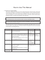
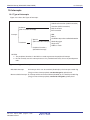
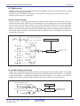
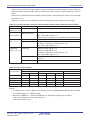
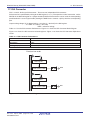
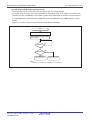
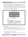
How to Use This Manual
1. Purpose and Target Readers
This manual is designed to provide the user with an understanding of the hardware functions and electrical
characteristics of the MCU. It is intended for users designing application systems incorporating the MCU.
A basic knowledge of electric circuits, logical circuits, and MCUs is necessary in order to use this manual.
The manual comprises an overview of the product; descriptions of the CPU, system control functions,
peripheral functions, and electrical characteristics; and usage notes.
Particular attention should be paid to the precautionary notes when using the manual. These notes occur
within the body of the text, at the end of each section, and in the Usage Notes section.
The revision history summarizes the locations of revisions and additions. It does not list all revisions.
Refer to the text of the manual for details.
The following documents apply to the M16C/6N Group (M16C/6NK, M16C/6NM). Make sure to refer to
the latest versions of these documents. The newest versions of the documents listed may be obtained
from the Renesas Technology Web site.
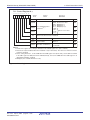
Document Type
Datasheet
Description
Hardware overview and
Document Title
M16C/6N Group
electrical characteristics
(M16C/6NK, M16C/6NM)
Datasheet
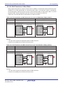
Hardware manual Hardware specifications (pin assignments, M16C/6N Group
Document No.
REJ03B0058
This hardware
memory maps, peripheral function specifications, (M16C/6NK. M16C/6NM) manual
electrical characteristics, timing charts) and Hardware Manual (REJ09B0124)
operation description
Note: Refer to the application notes for details
Software manual
on using peripheral functions.
Description of CPU instruction set
M16C/60,
REJ09B0137
M16C/20,
M16C/Tiny Series
Software Manual
Application note
Information on using peripheral functions and Available from Renesas
application examples
Sample programs
Information on writing programs in assembly
Renesas
language and C
Product specifications, updates on documents,
technical update
etc.
Technology web site
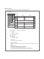
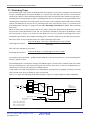
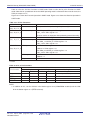
2. Notation of Numbers and Symbols
The notation conventions for register names, bit names, numbers, and symbols used in this manual are
described below.
(1) Register Names, Bit Names, and Pin Names
Registers, bits, and pins are referred to in the text by symbols. The symbol is accompanied by the
word “register,” “bit,” or “pin” to distinguish the three categories.
Examples the PM03 bit in the PM0 register
P3_5 pin, VCC pin
(2) Notation of Numbers
The indication “b” is appended to numeric values given in binary format. However, nothing is
appended to the values of single bits. The indication “h” is appended to numeric values given in
hexadecimal format. Nothing is appended to numeric values given in decimal format.
Examples Binary: 11b
Hexadecimal: EFA0h
Decimal: 1234
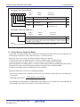
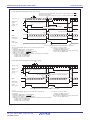
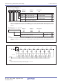
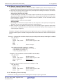
3. Register Notation
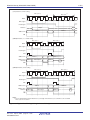
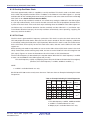
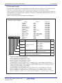
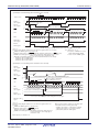
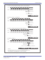
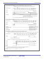
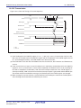
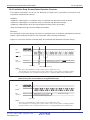
The symbols and terms used in register diagrams are described below.
XXX Register
b7
b6
b5
b4
b3
b2
b1
*1
b0
0 0
Symbol
XXX
Bit
Symbol
Address
XXX
After Reset
00h
Bit Name
Function
RW
b1 b0
XXX0
XXX bits
XXX1
(b2)
(b4-b3)
0 0: XXX
0 1: XXX
1 0: Do not set a value
1 1: XXX
Reserved bits
Set to 0
XXX bits
Function varies depending on
operating mode
XXX6
*2
RW
Nothing is assigned. If necessary, set to 0,
When read, the content is undefined.
XXX5
XXX7
RW
*3
WO
*4
RW
RW
XXX bit
0: XXX
1: XXX
RO
*1
Blank: Set to 0 or 1 according to the application
0 : Set to 0
1 : Set to 1
X : Nothing is assigned
*2
RW : Read and write
RO : Read only
WO : Write only
– : Nothing is assigned
*3
• Reserved bit
Reserved bit. Set to specified value.
*4
• Nothing is assigned
Nothing is assigned to the bit. As the bit may be used for future functions, if necessary,
set to 0.
• Do not set a value
Operation is not guaranteed when a value is set.
• Function varies depending on operating mode
The function of the bit varies with the peripheral function mode.
Refer to the register diagram for information on the individual modes.
4. List of Abbreviations and Acronyms
Abbreviation
ACIA
Full Form
Asynchronous Communication Interface Adapter
bps
CRC
bits per second
Cyclic Redundancy Check
DMA
DMAC
Direct Memory Access
Direct Memory Access Controller
GSM
Hi-Z
Global System for Mobile Communications
High Impedance
IEBus
I/O
Inter Equipment bus
Input/Output
IrDA
LSB
Infrared Data Association
Least Significant Bit
MSB
NC
Most Significant Bit
Non-Connection
PLL
PWM
Phase Locked Loop
Pulse Width Modulation
SFR
SIM
Special Function Registers
Subscriber Identity Module
UART
Universal Asynchronous Receiver/Transmitter
VCO
Voltage Controlled Oscillator
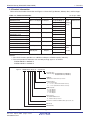
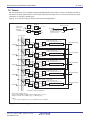
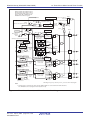
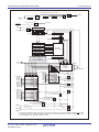
Table of Contents
SFR Page Reference ............................................................................................................ B-1
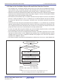
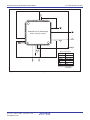
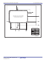
1. Overview ............................................................................................................................... 1
1.1 Applications .................................................................................................................................................. 1
1.2 Performance Overview ................................................................................................................................ 2
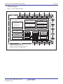
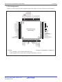
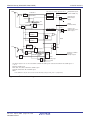
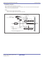
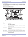
1.3 Block Diagram .............................................................................................................................................. 4
1.4 Product Information ...................................................................................................................................... 5
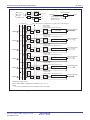
1.5 Pin Assignments .......................................................................................................................................... 6
1.6 Pin Functions ............................................................................................................................................. 13
2. Central Processing Unit (CPU) ........................................................................................... 16
2.1 Data Registers (R0, R1, R2, and R3) ........................................................................................................ 16
2.2 Address Registers (A0 and A1) .................................................................................................................. 16
2.3 Frame Base Register (FB) ......................................................................................................................... 17
2.4 Interrupt Table Register (INTB) .................................................................................................................. 17
2.5 Program Counter (PC) ............................................................................................................................... 17
2.6 User Stack Pointer (USP), Interrupt Stack Pointer (ISP) ........................................................................... 17
2.7 Static Base Register (SB) .......................................................................................................................... 17
2.8 Flag Register (FLG) ................................................................................................................................... 17
2.8.1 Carry Flag (C Flag) ............................................................................................................................ 17
2.8.2 Debug Flag (D Flag) .......................................................................................................................... 17
2.8.3 Zero Flag (Z Flag) .............................................................................................................................. 17
2.8.4 Sign Flag (S Flag) .............................................................................................................................. 17
2.8.5 Register Bank Select Flag (B Flag) .................................................................................................... 17
2.8.6 Overflow Flag (O Flag) ....................................................................................................................... 17
2.8.7 Interrupt Enable Flag (I Flag) ............................................................................................................. 17
2.8.8 Stack Pointer Select Flag (U Flag) ..................................................................................................... 17
2.8.9 Processor Interrupt Priority Level (IPL) .............................................................................................. 17
2.8.10 Reserved Area ................................................................................................................................. 17
3. Memory ............................................................................................................................... 18
4. Special Function Registers (SFRs) ..................................................................................... 19
5. Resets ................................................................................................................................. 35
5.1 Hardware Reset ......................................................................................................................................... 35
5.1.1 Reset on a Stable Supply Voltage ..................................................................................................... 35
5.1.2 Power-on Reset ................................................................................................................................. 35
5.2 Software Reset .......................................................................................................................................... 37
5.3 Watchdog Timer Reset ............................................................................................................................... 37
5.4 Oscillation Stop Detection Reset ............................................................................................................... 37
5.5 Internal Space ............................................................................................................................................ 37
6. Processor Mode .................................................................................................................. 38
6.1 Types of Processor Mode .......................................................................................................................... 38
6.2 Setting Processor Modes ........................................................................................................................... 39
7. Bus ...................................................................................................................................... 45
7.1 Bus Mode ................................................................................................................................................... 45
7.1.1 Separate Bus ..................................................................................................................................... 45
7.1.2 Multiplexed Bus .................................................................................................................................. 45
A-1
7.2 Bus Control ................................................................................................................................................ 46
7.2.1 Address Bus ....................................................................................................................................... 46
7.2.2 Data Bus ............................................................................................................................................ 46
7.2.3 Chip Select Signal .............................................................................................................................. 46
7.2.4 Read and Write Signals ..................................................................................................................... 48
7.2.5 ________
ALE Signal ......................................................................................................................................... 48
7.2.6 __________
RDY Signal ........................................................................................................................................ 49
7.2.7 HOLD Signal ...................................................................................................................................... 50
7.2.8 BCLK Output ...................................................................................................................................... 50
7.2.9 External Bus Status when Internal Area Accessed ............................................................................ 52
7.2.10 Software Wait ................................................................................................................................... 52
8. Clock Generation Circuit ..................................................................................................... 56
8.1 Types of Clock Generation Circuit.............................................................................................................. 56
8.1.1 Main Clock ......................................................................................................................................... 64
8.1.2 Sub Clock ........................................................................................................................................... 65
8.1.3 On-chip Oscillator Clock .................................................................................................................... 66
8.1.4 PLL Clock ........................................................................................................................................... 66
8.2 CPU Clock and Peripheral Function Clock ................................................................................................ 68
8.2.1 CPU Clock and BCLK ........................................................................................................................ 68
8.2.2 Peripheral Function Clock .................................................................................................................. 68
8.3 Clock Output Function ............................................................................................................................... 68
8.4 Power Control ............................................................................................................................................ 69
8.4.1 Normal Operating Mode ..................................................................................................................... 69
8.4.2 Wait Mode .......................................................................................................................................... 71
8.4.3 Stop Mode .......................................................................................................................................... 73
8.5 Oscillation Stop and Re-oscillation Detection Function ............................................................................. 78
8.5.1 Operation when CM27 Bit = 0 (Oscillation Stop Detection Reset) ..................................................... 78
8.5.2 Operation when CM27 Bit = 1 (Oscillation Stop, Re-oscillation Detection Interrupt) ......................... 78
8.5.3 How to Use Oscillation Stop and Re-oscillation Detection Function .................................................. 79
9. Protection ............................................................................................................................ 80
10. Interrupts ........................................................................................................................... 81
10.1 Type of Interrupts ..................................................................................................................................... 81
10.2 Software Interrupts ................................................................................................................................... 82
10.2.1 Undefined Instruction Interrupt ......................................................................................................... 82
10.2.2 Overflow Interrupt ............................................................................................................................ 82
10.2.3 BRK Interrupt ................................................................................................................................... 82
10.2.4 INT Instruction Interrupt ................................................................................................................... 82
10.3 Hardware Interrupts ................................................................................................................................. 83
10.3.1 Special Interrupts ............................................................................................................................. 83
10.3.2 Peripheral Function Interrupts .......................................................................................................... 83
10.4 Interrupts and Interrupt Vector ................................................................................................................. 84
10.4.1 Fixed Vector Tables .......................................................................................................................... 84
10.4.2 Relocatable Vector Tables ............................................................................................................... 84
10.5 Interrupt Control ....................................................................................................................................... 86
10.5.1 I Flag ................................................................................................................................................ 88
10.5.2 IR Bit ................................................................................................................................................ 88
10.5.3 Bits ILVL2 to ILVL0 and IPL ............................................................................................................. 88
A-2
10.5.4 Interrupt Sequence .......................................................................................................................... 89
10.5.5 Interrupt Response Time .................................................................................................................. 90
10.5.6 Variation of IPL when Interrupt Request is Accepted ....................................................................... 90
10.5.7 Saving Registers .............................................................................................................................. 91
10.5.8 Returning from Interrupt Routine ..................................................................................................... 92
10.5.9 Interrupt Priority ............................................................................................................................... 92
10.5.10
Interrupt Priority Level Select Circuit .............................................................................................. 92
______
10.6 INT
Interrupt ............................................................................................................................................. 94
______
10.7 NMI Interrupt ............................................................................................................................................ 98
10.8 Key Input Interrupt ................................................................................................................................... 98
10.9 CAN0/1 Wake-up Interrupt ....................................................................................................................... 98
10.10 Address Match Interrupt ......................................................................................................................... 99
11. Watchdog Timer .............................................................................................................. 101
11.1 Count Source Protective Mode .............................................................................................................. 102
12. DMAC .............................................................................................................................. 103
12.1 Transfer Cycle ........................................................................................................................................ 108
12.1.1 Effect of Source and Destination Addresses .................................................................................. 108
12.1.2 Effect of BYTE Pin Level ................................................................................................................ 108
12.1.3 Effect of ________
Software Wait ................................................................................................................... 108
12.1.4 Effect of RDY Signal ...................................................................................................................... 108
12.2 DMA Transfer Cycles ............................................................................................................................. 110
12.3 DMA Enable ........................................................................................................................................... 111
12.4 DMA Request ......................................................................................................................................... 111
12.5 Channel Priority and DMA Transfer Timing ............................................................................................ 112
13. Timers ............................................................................................................................. 113
13.1 Timer A ................................................................................................................................................... 115
13.1.1 Timer Mode .................................................................................................................................... 119
13.1.2 Event Counter Mode ...................................................................................................................... 120
13.1.3 One-shot Timer Mode .................................................................................................................... 125
13.1.4 Pulse Width Modulation (PWM) Mode ........................................................................................... 127
13.2 Timer B ................................................................................................................................................... 130
13.2.1 Timer Mode .................................................................................................................................... 133
13.2.2 Event Counter Mode ...................................................................................................................... 134
13.2.3 Pulse Period and Pulse Width Measurement Mode ...................................................................... 135
14. Three-Phase Motor Control Timer Function .................................................................... 138
15. Serial Interface ................................................................................................................ 149
15.1 UARTi ..................................................................................................................................................... 149
15.1.1 Clock Synchronous Serial I/O Mode .............................................................................................. 159
15.1.2 Clock Asynchronous Serial I/O (UART) Mode ............................................................................... 167
15.1.3 Special Mode 1 (I2C Mode) ............................................................................................................ 175
15.1.4 Special Mode 2 .............................................................................................................................. 184
15.1.5 Special Mode 3 (IE Mode) ............................................................................................................. 189
15.1.6 Special Mode 4 (SIM Mode) (UART2) ........................................................................................... 191
15.2 SI/Oi ....................................................................................................................................................... 196
15.2.1 SI/Oi Operation Timing ................................................................................................................... 200
15.2.2 CLK Polarity Selection ................................................................................................................... 200
15.2.3 Functions for Setting an SOUTi Initial Value .................................................................................. 201
A-3
16. A/D Converter .................................................................................................................. 202
16.1 Mode Description ................................................................................................................................... 206
16.1.1 One-shot Mode .............................................................................................................................. 206
16.1.2 Repeat Mode ................................................................................................................................. 208
16.1.3 Single Sweep Mode ....................................................................................................................... 210
16.1.4 Repeat Sweep Mode 0 .................................................................................................................. 212
16.1.5 Repeat Sweep Mode 1 .................................................................................................................. 214
16.2 Function ................................................................................................................................................. 216
16.2.1 Resolution Select Function ............................................................................................................ 216
16.2.2 Sample and Hold ........................................................................................................................... 216
16.2.3 Extended Analog Input Pins ........................................................................................................... 216
16.2.4 External Operation Amplifier (Op-Amp) Connection Mode ............................................................ 216
16.2.5 Current Consumption Reducing Function ...................................................................................... 217
16.2.6 Output Impedance of Sensor under A/D Conversion ..................................................................... 217
17. D/A Converter .................................................................................................................. 219
18. CRC Calculation .............................................................................................................. 221
19. CAN Module .................................................................................................................... 223
19.1 CAN Module-Related Registers ............................................................................................................. 224
19.1.1 CANi Message Box ........................................................................................................................ 224
19.1.2 Acceptance Mask Registers........................................................................................................... 224
19.1.3 CAN SFR Registers ....................................................................................................................... 224
19.2 CANi Message Box ................................................................................................................................ 225
19.3 Acceptance Mask Registers ................................................................................................................... 227
19.4 CAN SFR Registers ............................................................................................................................... 228
19.5 Operational Modes ................................................................................................................................. 234
19.5.1 CAN Reset/Initialization Mode ....................................................................................................... 234
19.5.2 CAN Operation Mode ..................................................................................................................... 235
19.5.3 CAN Sleep Mode ........................................................................................................................... 235
19.5.4 CAN Interface Sleep Mode ............................................................................................................ 235
19.5.5 Bus Off State .................................................................................................................................. 236
19.6 CAN Module System Clock Configuration ............................................................................................. 237
19.7 Bit Timing Configuration ......................................................................................................................... 237
19.8 Bit-rate ................................................................................................................................................... 238
19.8.1 Calculation of Bit-rate ..................................................................................................................... 238
19.9 Acceptance Filtering Function and Masking Function ............................................................................ 239
19.10 Acceptance Filter Support Unit (ASU) .................................................................................................. 240
19.11 Basic CAN Mode .................................................................................................................................. 241
19.12 Return from Bus Off Function .............................................................................................................. 242
19.13 Time Stamp Counter and Time Stamp Function .................................................................................. 242
19.14 Listen-Only Mode ................................................................................................................................. 242
19.15 Reception and Transmission ................................................................................................................ 243
19.15.1 Reception ..................................................................................................................................... 244
19.15.2 Transmission ................................................................................................................................ 245
19.16 CAN Interrupt ....................................................................................................................................... 246
20. Programmable I/O Ports ................................................................................................. 247
20.1 PDi Register ........................................................................................................................................... 248
20.2 Pi Register, PC14 Register .................................................................................................................... 248
20.3 PURj Register ........................................................................................................................................ 248
20.4 PCR Register ......................................................................................................................................... 248
A-4
21. Flash Memory Version .................................................................................................... 260
21.1 Memory Map .......................................................................................................................................... 261
21.1.1 Boot Mode ...................................................................................................................................... 262
21.2 Functions to Prevent Flash Memory from Rewriting .............................................................................. 262
21.2.1 ROM Code Protect Function .......................................................................................................... 262
21.2.2 ID Code Check Function ................................................................................................................ 262
21.3 CPU Rewrite Mode ................................................................................................................................ 264
21.3.1 EW0 Mode ..................................................................................................................................... 265
21.3.2 EW1 Mode ..................................................................................................................................... 265
21.3.3 Registers FMR0 and FMR1 ........................................................................................................... 266
21.3.4 Notes on CPU Rewrite Mode ......................................................................................................... 271
21.3.5 Software Commands ..................................................................................................................... 273
21.3.6 Data Protect Function .................................................................................................................... 278
21.3.7 Status Register (SRD Register) ..................................................................................................... 278
21.3.8 Full Status Check ........................................................................................................................... 280
21.4 Standard Serial I/O Mode ...................................................................................................................... 282
21.4.1 ID Code Check Function ................................................................................................................ 282
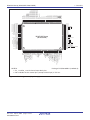
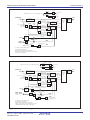
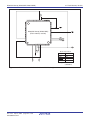
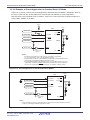
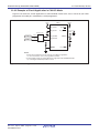
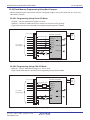
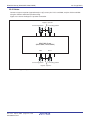
21.4.2 Example of Circuit Application in Standard Serial I/O Mode .......................................................... 286
21.5 Parallel I/O Mode ................................................................................................................................... 287
21.5.1 User ROM and Boot ROM Areas ................................................................................................... 287
21.5.2 ROM Code Protect Function .......................................................................................................... 287
21.6 CAN I/O Mode ........................................................................................................................................ 288
21.6.1 ID Code Check Function ................................................................................................................ 288
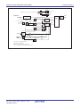
21.6.2 Example of Circuit Application in CAN I/O Mode ........................................................................... 291
22. Electrical Characteristics ................................................................................................. 292
22.1 Electrical Characteristics (Normal-ver.) .................................................................................................. 292
22.2 Electrical Characteristics (T/V-ver.) ........................................................................................................ 328
23. Usage Notes ................................................................................................................... 338
23.1 SFRs ...................................................................................................................................................... 338
23.2 External Bus (Normal-ver. only) ............................................................................................................. 339
23.3 External Clock ........................................................................................................................................ 340
23.4 PLL Frequency Synthesizer ................................................................................................................... 341
23.5 Power Control ........................................................................................................................................ 342
23.6 Oscillation Stop, Re-oscillation Detection Function ............................................................................... 344
23.7 Protection ............................................................................................................................................... 345
23.8 Interrupts ................................................................................................................................................ 346
23.8.1 Reading Address 00000h ............................................................................................................... 346
23.8.2 _______
Setting SP ...................................................................................................................................... 346
23.8.3 NMI Interrupt .................................................................................................................................. 346
23.8.4 Changing
Interrupt Source ............................................................................................................. 347
_____
23.8.5 INT Interrupt ................................................................................................................................... 347
23.8.6 Rewrite Interrupt Control Register ................................................................................................. 348
23.8.7 Watchdog Timer Interrupt .............................................................................................................. 348
23.9 DMAC .................................................................................................................................................... 349
23.9.1 Write to DMAE Bit in DMiCON Register ........................................................................................ 349
23.10 Timers .................................................................................................................................................. 350
23.10.1 Timer A ......................................................................................................................................... 350
23.10.2 Timer B ......................................................................................................................................... 354
A-5
23.11 Thee-Phase Motor Control Timer Function .......................................................................................... 356
23.12 Serial Interface ..................................................................................................................................... 357
23.12.1 Clock Synchronous Serial I/O Mode ............................................................................................ 357
23.12.2 Special Modes ............................................................................................................................. 358
23.12.3 SI/Oi ............................................................................................................................................. 359
23.13 A/D Converter ...................................................................................................................................... 360
23.14 CAN Module ......................................................................................................................................... 362
23.14.1 Reading CiSTR Register .............................................................................................................. 362
23.14.2 Performing CAN Configuration .................................................................................................... 364
23.14.3 Suggestions to Reduce Power Consumption .............................................................................. 365
23.14.4 CAN Transceiver in Boot Mode .................................................................................................... 366
23.15 Programmable I/O Ports ...................................................................................................................... 367
23.16 Dedicated Input Pin .............................................................................................................................. 368
23.17 Electrical Characteristic Differences between Mask ROM and Flash Memory Version MCUs ............ 369
23.18 Mask ROM Version (Normal-ver. only) ............................................................................................... 370
23.19 Flash Memory Version ......................................................................................................................... 371
23.19.1 Functions to Prevent Flash Memory from Rewriting .................................................................... 371
23.19.2 Stop Mode .................................................................................................................................... 371
23.19.3 Wait Mode .................................................................................................................................... 371
23.19.4 Low Power Dissipation Mode and On-Chip Oscillator Low Power Dissipation Mode .................. 371
23.19.5 Writing Command and Data ......................................................................................................... 371
23.19.6 Program Command ...................................................................................................................... 371
23.19.7 Lock Bit Program Command ........................................................................................................ 371
23.19.8 Operating Speed .......................................................................................................................... 371
23.19.9 Prohibited Instructions ................................................................................................................. 372
23.19.10 Interrupts .................................................................................................................................... 372
23.19.11 How to Access ............................................................................................................................ 372
23.19.12 Rewriting in User ROM Area ...................................................................................................... 372
23.19.13 DMA Transfer ............................................................................................................................. 372
23.20 Flash Memory Programming Using Boot Program .............................................................................. 373
23.20.1 Programming Using Serial I/O Mode ........................................................................................... 373
23.20.2 Programming Using CAN I/O Mode ............................................................................................. 373
23.21 Noise .................................................................................................................................................... 374
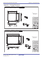
Appendix 1. Package Dimensions ........................................................................................ 375
Register Index ....................................................................................................................... 377
Specifications written in this manual are believed to be accurate, but are not guaranteed to be entirely free
of error. Specifications in this manual may be changed for functional or performance improvements.
Please make sure your manual is the latest edition.
A-6
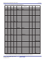
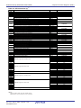
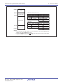
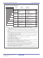
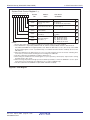
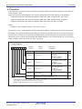
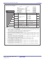
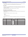
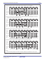
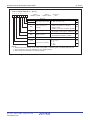
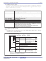
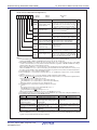
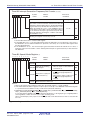
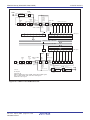
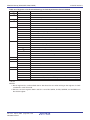
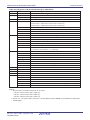
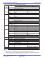
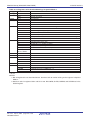
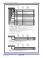
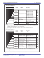
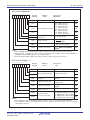
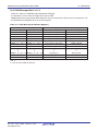
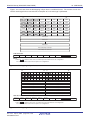
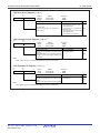
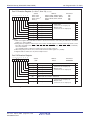
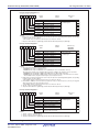
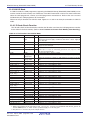
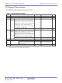
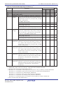
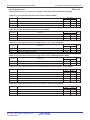
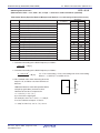
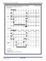
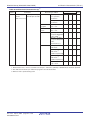
SFR Page Reference
Address
0000h
0001h
0002h
0003h
0004h
0005h
0006h
0007h
0008h
0009h
000Ah
000Bh
000Ch
000Dh
000Eh
000Fh
0010h
0011h
0012h
0013h
0014h
0015h
0016h
0017h
0018h
0019h
001Ah
001Bh
001Ch
001Dh
001Eh
001Fh
0020h
0021h
0022h
0023h
0024h
0025h
0026h
0027h
0028h
0029h
002Ah
002Bh
002Ch
002Dh
002Eh
002Fh
0030h
0031h
0032h
0033h
0034h
0035h
0036h
0037h
0038h
0039h
003Ah
003Bh
003Ch
003Dh
003Eh
003Fh
Register
Symbol
Page
Processor Mode Register 0
Processor Mode Register 1
System Clock Control Register 0
System Clock Control Register 1
Chip Select Control Register
Address Match Interrupt Enable Register
Protect Register
PM0
PM1
CM0
CM1
CSR
AIER
PRCR
40
41
58
59
46
100
80
Oscillation Stop Detection Register
CM2
60
Watchdog Timer Start Register
Watchdog Timer Control Register
WDTS
WDC
102
102
Address Match Interrupt Register 0
RMAD0
100
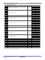
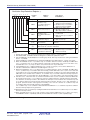
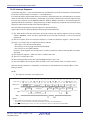
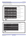
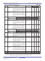
Address
0040h
0041h
0042h
0043h
0044h
0045h
0046h
0047h
0048h
0049h
004Ah
004Bh
004Ch
004Dh
004Eh
Address Match Interrupt Register 1
RMAD1
Chip Select Expansion Control Register CSE
PLC0
PLL Control Register 0
Processor Mode Register 2
PM2
004Fh
0050h
0051h
0052h
0053h
0054h
0055h
0056h
100
52
63
0057h
0058h
62
0059h
DMA0 Source Pointer
SAR0
005Ah
107
005Bh
DMA0 Destination Pointer
DAR0
107
DMA0 Transfer Counter
TCR0
107
DMA0 Control Register
DM0CON
005Ch
005Dh
005Eh
005Fh
0060h
0061h
0062h
0063h
0064h
0065h
0066h
0067h
0068h
0069h
006Ah
006Bh
006Ch
006Dh
006Eh
006Fh
0070h
0071h
0072h
0073h
0074h
0075h
0076h
0077h
0078h
0079h
007Ah
007Bh
007Ch
007Dh
007Eh
007Fh
106
DMA1 Source Pointer
SAR1
107
DMA1 Destination Pointer
DAR1
107
DMA1 Transfer Counter
TCR1
107
DMA1 Control Register
DM1CON
106
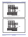
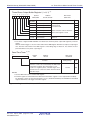
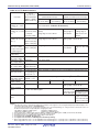
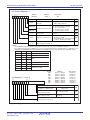
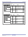
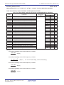
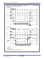
Blank spaces are reserved. No access is allowed.
B-1
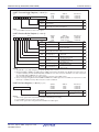
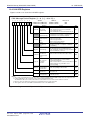
Register
Symbol
Page
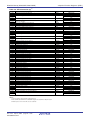
CAN0/1 Wake-up Interrupt Control Register
CAN0 Successful Reception Interrupt Control Register
CAN0 Successful Transmission Interrupt Control Register
INT3 Interrupt Control Register
Timer B5 Interrupt Control Register
SI/O5 Interrupt Control Register
Timer B4 Interrupt Control Register
UART1 Bus Collision Detection Interrupt Control Register
Timer B3 Interrupt Control Register
UART0 Bus Collision Detection Interrupt Control Register
CAN1 Successful Reception Interrupt Control Register
SI/O4 Interrupt Control Register
INT5 Interrupt Control Register
CAN1 Successful Transmission Interrupt Control Register
SI/O3 Interrupt Control Register
INT4 Interrupt Control Register
UART2 Bus Collision Detection Interrupt Control Register
DMA0 Interrupt Control Register
DMA1 Interrupt Control Register
CAN0/1 Error Interrupt Control Register
A/D Conversion Interrupt Control Register
Key Input Interrupt Control Register
UART2 Transmit Interrupt Control Register
UART2 Receive Interrupt Control Register
UART0 Transmit Interrupt Control Register
UART0 Receive Interrupt Control Register
UART1 Transmit Interrupt Control Register
UART1 Receive Interrupt Control Register
Timer A0 Interrupt Control Register
Timer A1 Interrupt Control Register
Timer A2 Interrupt Control Register
INT7 Interrupt Control Register
Timer A3 Interrupt Control Register
INT6 Interrupt Control Register
Timer A4 Interrupt Control Register
Timer B0 Interrupt Control Register
SI/O6 Interrupt Control Register
Timer B1 Interrupt Control Register
INT8 Interrupt Control Register
Timer B2 Interrupt Control Register
INT0 Interrupt Control Register
INT1 Interrupt Control Register
INT2 Interrupt Control Register
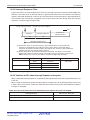
C01WKIC
C0RECIC
C0TRMIC
INT3IC
TB5IC
S5IC
TB4IC
U1BCNIC
TB3IC
U0BCNIC
C1RECIC
S4IC
INT5IC
C1TRMIC
S3IC
INT4IC
U2BCNIC
DM0IC
DM1IC
C01ERRIC
ADIC
KUPIC
S2TIC
S2RIC
S0TIC
S0RIC
S1TIC
S1RIC
TA0IC
TA1IC
TA2IC
INT7IC
TA3IC
INT6IC
TA4IC
TB0IC
S6IC
TB1IC
INT8IC
TB2IC
INT0IC
INT1IC
INT2IC
86
86
86
87
86
86
86
86
86
86
87
87
87
87
87
87
86
86
86
86
86
86
86
86
86
86
86
86
86
86
87
87
87
87
86
86
86
87
87
86
87
87
87
CAN0 Message Box 0: Identifier / DLC
CAN0 Message Box 0: Data Field
CAN0 Message Box 0: Time Stamp
CAN0 Message Box 1: Identifier / DLC
CAN0 Message Box 1: Data Field
CAN0 Message Box 1: Time Stamp
225
226
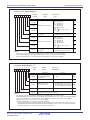
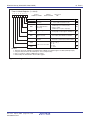
Address
0080h
0081h
0082h
0083h
0084h
0085h
0086h
0087h
0088h
0089h
008Ah
008Bh
008Ch
008Dh
008Eh
008Fh
0090h
0091h
0092h
0093h
0094h
0095h
0096h
0097h
0098h
0099h
009Ah
009Bh
009Ch
009Dh
009Eh
009Fh
00A0h
00A1h
00A2h
00A3h
00A4h
00A5h
00A6h
00A7h
00A8h
00A9h
00AAh
00ABh
00ACh
00ADh
00AEh
00AFh
00B0h
00B1h
00B2h
00B3h
00B4h
00B5h
00B6h
00B7h
00B8h
00B9h
00BAh
00BBh
00BCh
00BDh
00BEh
00BFh
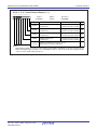
Register
Symbol
Page
Address
00C0h
00C1h
00C2h
00C3h
00C4h
00C5h
00C6h
00C7h
00C8h
00C9h
00CAh
00CBh
00CCh
00CDh
00CEh
00CFh
00D0h
00D1h
00D2h
00D3h
00D4h
00D5h
00D6h
00D7h
00D8h
00D9h
00DAh
00DBh
00DCh
00DDh
00DEh
00DFh
00E0h
00E1h
00E2h
00E3h
00E4h
00E5h
00E6h
00E7h
00E8h
00E9h
00EAh
00EBh
00ECh
00EDh
00EEh
00EFh
00F0h
00F1h
00F2h
00F3h
00F4h
00F5h
00F6h
00F7h
00F8h
00F9h
00FAh
00FBh
00FCh
00FDh
00FEh
00FFh
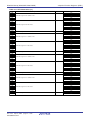
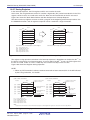
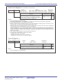
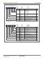
CAN0 Message Box 2: Identifier / DLC
CAN0 Message Box 2: Data Field
CAN0 Message Box 2: Time Stamp
CAN0 Message Box 3: Identifier / DLC
CAN0 Message Box 3: Data Field
CAN0 Message Box 3: Time Stamp
225
226
CAN0 Message Box 4: Identifier / DLC
CAN0 Message Box 4: Data Field
CAN0 Message Box 4: Time Stamp
CAN0 Message Box 5: Identifier / DLC
CAN0 Message Box 5: Data Field
CAN0 Message Box 5: Time Stamp
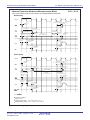
B-2
Register
Symbol
Page
CAN0 Message Box 6: Identifier / DLC
CAN0 Message Box 6: Data Field
CAN0 Message Box 6: Time Stamp
CAN0 Message Box 7: Identifier / DLC
CAN0 Message Box 7: Data Field
CAN0 Message Box 7: Time Stamp
CAN0 Message Box 8: Identifier / DLC
CAN0 Message Box 8: Data Field
CAN0 Message Box 8: Time Stamp
CAN0 Message Box 9: Identifier / DLC
CAN0 Message Box 9: Data Field
CAN0 Message Box 9: Time Stamp
225
226
Address
0100h
0101h
0102h
0103h
0104h
0105h
0106h
0107h
0108h
0109h
010Ah
010Bh
010Ch
010Dh
010Eh
010Fh
0110h
0111h
0112h
0113h
0114h
0115h
0116h
0117h
0118h
0119h
011Ah
011Bh
011Ch
011Dh
011Eh
011Fh
0120h
0121h
0122h
0123h
0124h
0125h
0126h
0127h
0128h
0129h
012Ah
012Bh
012Ch
012Dh
012Eh
012Fh
0130h
0131h
0132h
0133h
0134h
0135h
0136h
0137h
0138h
0139h
013Ah
013Bh
013Ch
013Dh
013Eh
013Fh
Register
Symbol
Page
Address
0140h
0141h
0142h
0143h
0144h
0145h
0146h
0147h
0148h
0149h
014Ah
014Bh
014Ch
014Dh
014Eh
014Fh
0150h
0151h
0152h
0153h
0154h
0155h
0156h
0157h
0158h
0159h
015Ah
015Bh
015Ch
015Dh
015Eh
015Fh
0160h
0161h
0162h
0163h
0164h
0165h
0166h
0167h
0168h
0169h
016Ah
016Bh
016Ch
016Dh
016Eh
016Fh
0170h
0171h
0172h
0173h
0174h
0175h
0176h
0177h
0178h
0179h
017Ah
017Bh
017Ch
017Dh
017Eh
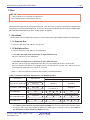
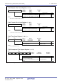
017Fh
CAN0 Message Box 10: Identifier / DLC
CAN0 Message Box 10: Data Field
CAN0 Message Box 10: Time Stamp
CAN0 Message Box 11: Identifier / DLC
CAN0 Message Box 11: Data Field
CAN0 Message Box 11: Time Stamp
225
226
CAN0 Message Box 12: Identifier / DLC
CAN0 Message Box 12: Data Field
CAN0 Message Box 12: Time Stamp
CAN0 Message Box 13: Identifier / DLC
CAN0 Message Box 13: Data Field
CAN0 Message Box 13: Time Stamp
Blank spaces are reserved. No access is allowed.
B-3
Register
Symbol
Page
CAN0 Message Box 14: Identifier /DLC
CAN0 Message Box 14: Data Field
CAN0 Message Box 14: Time Stamp
225
226
CAN0 Message Box 15: Identifier /DLC
CAN0 Message Box 15: Data Field
CAN0 Message Box 15: Time Stamp
CAN0 Global Mask Register
C0GMR
227
CAN0 Local Mask A Register
C0LMAR
227
CAN0 Local Mask B Register
C0LMBR
227
Address
0180h
0181h
0182h
0183h
0184h
0185h
0186h
0187h
0188h
0189h
018Ah
018Bh
018Ch
018Dh
018Eh
018Fh
0190h
0191h
0192h
0193h
0194h
0195h
0196h
0197h
0198h
0199h
019Ah
019Bh
019Ch
019Dh
019Eh
019Fh
01A0h
01A1h
01A2h
01A3h
01A4h
01A5h
01A6h
01A7h
01A8h
01A9h
01AAh
01ABh
01ACh
01ADh
01AEh
01AFh
01B0h
01B1h
01B2h
01B3h
01B4h
01B5h
01B6h
01B7h
01B8h
01B9h
01BAh
01BBh
01BCh
01BDh
01BEh
01BFh
Register
Symbol
Flash Memory Control Register 1
FMR1
266
Flash Memory Control Register 0
FMR0
266
Address Match Interrupt Register 2
RMAD2
100
Address Match Interrupt Enable Register 2 AIER2
Address Match Interrupt Register 3
RMAD3
Address
01C0h
01C1h
01C2h
01C3h
01C4h
01C5h
01C6h
01C7h
01C8h
01C9h
01CAh
01CBh
01CCh
01CDh
01CEh
01CFh
01D0h
01D1h
01D2h
01D3h
01D4h
01D5h
01D6h
01D7h
01D8h
01D9h
01DAh
01DBh
01DCh
01DDh
01DEh
01DFh
01E0h
01E1h
01E2h
01E3h
01E4h
01E5h
01E6h
01E7h
01E8h
01E9h
01EAh
01EBh
01ECh
01EDh
01EEh
01EFh
01F0h
01F1h
01F2h
01F3h
01F4h
01F5h
01F6h
01F7h
01F8h
01F9h
01FAh
01FBh
01FCh
01FDh
01FEh
01FFh
Page
100
100
Blank spaces are reserved. No access is allowed.
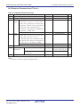
B-4
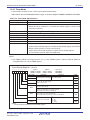
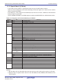
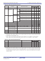
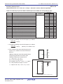
Register
Timer B3, B4, B5 Count Start Flag
Symbol
TBSR
Timer A1-1 Register
TA11
143
Timer A2-1 Register
TA21
143
Timer A4-1 Register
TA41
143
Three-Phase PWM Control Register 0
Three-Phase PWM Control Register 1
Three-Phase Output Buffer Register 0
Three-Phase Output Buffer Register 1
Dead Time Timer
Timer B2 Interrupt Generation Frequency Set Counter
INVC0
INVC1
IDB0
IDB1
DTT
ICTB2
140
141
142
142
142
144
Interrupt Source Select Register 2
IFSR2
97
Timer B3 Register
TB3
131
Timer B4 Register
TB4
131
Timer B5 Register
TB5
131
SI/O6 Transmit/Receive Register
S6TRR
197
SI/O6 Control Register
SI/O6 Bit Rate Register
SI/O3, 4, 5, 6 Transmit/Receive Register
Timer B3 Mode Register
Timer B4 Mode Register
Timer B5 Mode Register
Interrupt Source Select Register 0
Interrupt Source Select Register 1
SI/O3 Transmit/Receive Register
S6C
S6BRG
S3456TRR
TB3MR
TB4MR
TB5MR
IFSR0
IFSR1
S3TRR
197
197
198
131
133
135
136
95
96
197
SI/O3 Control Register
SI/O3 Bit Rate Register
SI/O4 Transmit/Receive Register
S3C
S3BRG
S4TRR
197
197
197
SI/O4 Control Register
SI/O4 Bit Rate Register
SI/O5 Transmit/Receive Register
S4C
S4BRG
S5TRR
197
197
197
SI/O5 Control Register
SI/O5 Bit Rate Register
UART0 Special Mode Register 4
UART0 Special Mode Register 3
UART0 Special Mode Register 2
UART0 Special Mode Register
UART1 Special Mode Register 4
UART1 Special Mode Register 3
UART1 Special Mode Register 2
UART1 Special Mode Register
UART2 Special Mode Register 4
UART2 Special Mode Register 3
UART2 Special Mode Register 2
UART2 Special Mode Register
UART2 Transmit/Receive Mode Register
UART2 Bit Rate Register
S5C
S5BRG
U0SMR4
U0SMR3
U0SMR2
U0SMR
U1SMR4
U1SMR3
U1SMR2
U1SMR
U2SMR4
U2SMR3
U2SMR2
U2SMR
U2MR
U2BRG
197
197
158
157
157
156
158
157
157
156
158
157
157
156
154
153
UART2 Transmit Buffer Register
U2TB
153
UART2 Transmit/Receive Control Register 0 U2C0
UART2 Transmit/Receive Control Register 1 U2C1
154
155
UART2 Receive Buffer Register
153
U2RB
Page
132
Address
0200h
0201h
0202h
0203h
0204h
0205h
0206h
0207h
0208h
0209h
020Ah
020Bh
020Ch
020Dh
020Eh
020Fh
0210h
0211h
0212h
0213h
0214h
0215h
0216h
0217h
0218h
0219h
021Ah
021Bh
021Ch
021Dh
021Eh
021Fh
0220h
0221h
0222h
0223h
0224h
0225h
0226h
0227h
0228h
0229h
022Ah
022Bh
022Ch
022Dh
022Eh
022Fh
0230h
0231h
0232h
0233h
0234h
0235h
0236h
0237h
0238h
0239h
023Ah
023Bh
023Ch
023Dh
023Eh
023Fh
Register
CAN0 Message Control Register 0
CAN0 Message Control Register 1
CAN0 Message Control Register 2
CAN0 Message Control Register 3
CAN0 Message Control Register 4
CAN0 Message Control Register 5
CAN0 Message Control Register 6
CAN0 Message Control Register 7
CAN0 Message Control Register 8
CAN0 Message Control Register 9
CAN0 Message Control Register 10
CAN0 Message Control Register 11
CAN0 Message Control Register 12
CAN0 Message Control Register 13
CAN0 Message Control Register 14
CAN0 Message Control Register 15
Symbol
Page
C0MCTL0
C0MCTL1
C0MCTL2
C0MCTL3
C0MCTL4
C0MCTL5
C0MCTL6
C0MCTL7
228
C0MCTL8
C0MCTL9
C0MCTL10
C0MCTL11
C0MCTL12
C0MCTL13
C0MCTL14
C0MCTL15
CAN0 Control Register
C0CTLR
229
CAN0 Status Register
C0STR
230
CAN0 Slot Status Register
C0SSTR
231
CAN0 Interrupt Control Register
C0ICR
231
CAN0 Extended ID Register
C0IDR
231
CAN0 Configuration Register
C0CONR
232
CAN0 Receive Error Count Register
CAN0 Transmit Error Count Register
C0RECR
C0TECR
233
233
CAN0 Time Stamp Register
C0TSR
233
CAN1 Message Control Register 0
CAN1 Message Control Register 1
CAN1 Message Control Register 2
CAN1 Message Control Register 3
CAN1 Message Control Register 4
CAN1 Message Control Register 5
CAN1 Message Control Register 6
CAN1 Message Control Register 7
CAN1 Message Control Register 8
CAN1 Message Control Register 9
CAN1 Message Control Register 10
CAN1 Message Control Register 11
CAN1 Message Control Register 12
CAN1 Message Control Register 13
CAN1 Message Control Register 14
CAN1 Message Control Register 15
C1MCTL0
C1MCTL1
C1MCTL2
C1MCTL3
C1MCTL4
C1MCTL5
C1MCTL6
C1MCTL7
228
C1MCTL8
C1MCTL9
C1MCTL10
C1MCTL11
C1MCTL12
C1MCTL13
C1MCTL14
C1MCTL15
CAN1 Control Register
C1CTLR
229
CAN1 Status Register
C1STR
230
CAN1 Slot Status Register
C1SSTR
231
CAN1 Interrupt Control Register
C1ICR
231
CAN1 Extended ID Register
C1IDR
231
CAN1 Configuration Register
C1CONR
232
CAN1 Receive Error Count Register
CAN1 Transmit Error Count Register
C1RECR
C1TECR
233
233
CAN1 Time Stamp Register
C1TSR
233
Address
0240h
0241h
0242h
0243h
0244h
0245h
0246h
0247h
0248h
0249h
024Ah
024Bh
024Ch
024Dh
024Eh
024Fh
0250h
0251h
0252h
0253h
0254h
0255h
0256h
0257h
0258h
0259h
025Ah
025Bh
025Ch
025Dh
025Eh
025Fh
0260h
0261h
0262h
0263h
0264h
0265h
0266h
0267h
0268h
0269h
026Ah
026Bh
026Ch
026Dh
026Eh
026Fh
0270h
0271h
0272h
0273h
0274h
0275h
0276h
0277h
0278h
0279h
027Ah
027Bh
027Ch
027Dh
027Eh
027Fh
Blank spaces are reserved. No access is allowed.
B-5
Register
Symbol
Page
CAN0 Acceptance Filter Support Register C0AFS
233
CAN1 Acceptance Filter Support Register C1AFS
233
PCLKR
CCLKR
61
62
Peripheral Clock Select Register
CAN0/1 Clock Select Register
CAN1 Message Box 0: Identifier / DLC
CAN1 Message Box 0: Data Field
CAN1 Message Box 0:Time Stamp
CAN1 Message Box 1: Identifier / DLC
CAN1 Message Box 1: Data Field
CAN1 Message Box 1:Time Stamp
225
226
Address
0280h
0281h
0282h
0283h
0284h
0285h
0286h
0287h
0288h
0289h
028Ah
028Bh
028Ch
028Dh
028Eh
028Fh
0290h
0291h
0292h
0293h
0294h
0295h
0296h
0297h
0298h
0299h
029Ah
029Bh
029Ch
029Dh
029Eh
029Fh
02A0h
02A1h
02A2h
02A3h
02A4h
02A5h
02A6h
02A7h
02A8h
02A9h
02AAh
02ABh
02ACh
02ADh
02AEh
02AFh
02B0h
02B1h
02B2h
02B3h
02B4h
02B5h
02B6h
02B7h
02B8h
02B9h
02BAh
02BBh
02BCh
02BDh
02BEh
02BFh
Register
Symbol
Page
Address
02C0h
02C1h
02C2h
02C3h
02C4h
02C5h
02C6h
02C7h
02C8h
02C9h
02CAh
02CBh
02CCh
02CDh
02CEh
02CFh
02D0h
02D1h
02D2h
02D3h
02D4h
02D5h
02D6h
02D7h
02D8h
02D9h
02DAh
02DBh
02DCh
02DDh
02DEh
02DFh
02E0h
02E1h
02E2h
02E3h
02E4h
02E5h
02E6h
02E7h
02E8h
02E9h
02EAh
02EBh
02ECh
02EDh
02EEh
02EFh
02F0h
02F1h
02F2h
02F3h
02F4h
02F5h
02F6h
02F7h
02F8h
02F9h
02FAh
02FBh
02FCh
02FDh
02FEh
02FFh
CAN1 Message Box 2: Identifier / DLC
CAN1 Message Box 2: Data Field
CAN1 Message Box 2: Time Stamp
CAN1 Message Box 3: Identifier / DLC
CAN1 Message Box 3: Data Field
CAN1 Message Box 3: Time Stamp
225
226
CAN1 Message Box 4: Identifier / DLC
CAN1 Message Box 4: Data Field
CAN1 Message Box 4: Time Stamp
CAN1 Message Box 5: Identifier / DLC
CAN1 Message Box 5: Data Field
CAN1 Message Box 5: Time Stamp
B-6
Register
Symbol
Page
CAN1 Message Box 6: Identifier / DLC
CAN1 Message Box 6: Data Field
CAN1 Message Box 6: Time Stamp
CAN1 Message Box 7: Identifier / DLC
CAN1 Message Box 7: Data Field
CAN1 Message Box 7: Time Stamp
CAN1 Message Box 8: Identifier / DLC
CAN1 Message Box 8: Data Field
CAN1 Message Box 8: Time Stamp
CAN1 Message Box 9: Identifier / DLC
CAN1 Message Box 9: Data Field
CAN1 Message Box 9: Time Stamp
225
226
Address
0300h
0301h
0302h
0303h
0304h
0305h
0306h
0307h
0308h
0309h
030Ah
030Bh
030Ch
030Dh
030Eh
030Fh
0310h
0311h
0312h
0313h
0314h
0315h
0316h
0317h
0318h
0319h
031Ah
031Bh
031Ch
031Dh
031Eh
031Fh
0320h
0321h
0322h
0323h
0324h
0325h
0326h
0327h
0328h
0329h
032Ah
032Bh
032Ch
032Dh
032Eh
032Fh
0330h
0331h
0332h
0333h
0334h
0335h
0336h
0337h
0338h
0339h
033Ah
033Bh
033Ch
033Dh
033Eh
033Fh
Register
Symbol
Page
Address
0340h
0341h
0342h
0343h
0344h
0345h
0346h
0347h
0348h
0349h
034Ah
034Bh
034Ch
034Dh
034Eh
034Fh
0350h
0351h
0352h
0353h
0354h
0355h
0356h
0357h
0358h
0359h
035Ah
035Bh
035Ch
035Dh
035Eh
035Fh
0360h
0361h
0362h
0363h
0364h
0365h
0366h
0367h
0368h
0369h
036Ah
036Bh
036Ch
036Dh
036Eh
036Fh
0370h
0371h
0372h
0373h
0374h
0375h
0376h
0377h
0378h
0379h
037Ah
037Bh
037Ch
037Dh
037Eh
037Fh
CAN1 Message Box 10: Identifier / DLC
CAN1 Message Box 10: Data Field
CAN1 Message Box 10: Time Stamp
CAN1 Message Box 11: Identifier / DLC
CAN1 Message Box 11: Data Field
CAN1 Message Box 11: Time Stamp
225
226
CAN1 Message Box 12: Identifier / DLC
CAN1 Message Box 12: Data Field
CAN1 Message Box 12: Time Stamp
CAN1 Message Box 13: Identifier / DLC
CAN1 Message Box 13: Data Field
CAN1 Message Box 13: Time Stamp
Blank spaces are reserved. No access is allowed.
B-7
Register
Symbol
Page
CAN1 Message Box 14: Identifier / DLC
CAN1 Message Box 14: Data Field
CAN1 Message Box 14: Time Stamp
225
226
CAN1 Message Box 15: Identifier / DLC
CAN1 Message Box 15: Data Field
CAN1 Message Box 15: Time Stamp
CAN1 Global Mask Register
C1GMR
227
CAN1 Local Mask A Register
C1LMAR
227
CAN1 Local Mask B Register
C1LMBR
227
Address
0380h
0381h
0382h
0383h
0384h
0385h
0386h
0387h
0388h
0389h
038Ah
038Bh
038Ch
038Dh
038Eh
038Fh
0390h
0391h
0392h
0393h
0394h
0395h
0396h
0397h
0398h
0399h
039Ah
039Bh
039Ch
039Dh
039Eh
039Fh
03A0h
03A1h
03A2h
03A3h
03A4h
03A5h
03A6h
03A7h
03A8h
03A9h
03AAh
03ABh
03ACh
03ADh
03AEh
03AFh
03B0h
03B1h
03B2h
03B3h
03B4h
03B5h
03B6h
03B7h
03B8h
03B9h
03BAh
03BBh
03BCh
03BDh
03BEh
03BFh
Register
Count Start Flag
Clock Prescaler Reset Flag
One-Shot Start Flag
Trigger Select Register
Up/Down Flag
Symbol
TABSR
CPSRF
ONSF
TRGSR
UDF
Page
117,132,145
118,132
118
118,145
117
Timer A0 Register
TA0
Timer A1 Register
TA1
Timer A2 Register
TA2
Timer A3 Register
TA3
116
Timer A4 Register
TA4
116
143
Timer B0 Register
TB0
131
Timer B1 Register
TB1
131
Timer B2 Register
TB2
131
143
Timer A0 Mode Register
Timer A1 Mode Register
Timer A2 Mode Register
Timer A3 Mode Register
Timer A4 Mode Register
Timer B0 Mode Register
Timer B1 Mode Register
Timer B2 Mode Register
Timer B2 Special Mode Register
TA0MR
TA1MR
TA2MR
TA3MR
TA4MR
TB0MR
TB1MR
TB2MR
TB2SC
Address
03C0h
03C1h
03C2h
03C3h
03C4h
03C5h
03C6h
03C7h
03C8h
03C9h
03CAh
03CBh
03CCh
03CDh
03CEh
03CFh
03D0h
03D1h
03D2h
03D3h
03D4h
03D5h
03D6h
03D7h
03D8h
03D9h
03DAh
03DBh
03DCh
03DDh
03DEh
03DFh
03E0h
03E1h
03E2h
03E3h
03E4h
03E5h
03E6h
03E7h
03E8h
03E9h
03EAh
03EBh
03ECh
03EDh
03EEh
03EFh
03F0h
03F1h
03F2h
03F3h
03F4h
03F5h
03F6h
03F7h
03F8h
03F9h
03FAh
03FBh
03FCh
03FDh
03FEh
03FFh
116
116
143
116
143
116
119 146
121 123,146
126 123
128 123,146
131,133
134,136
146
144
UART0 Transmit/Receive Mode Register U0MR
UART0 Bit Rate Register
U0BRG
154
153
UART0 Transmit Buffer Register U0TB
153
UART0 Transmit/Receive Control Register 0 U0C0
UART0 Transmit/Receive Control Register 1 U0C1
154
155
UART0 Receive Buffer Register U0RB
153
UART1 Transmit/Receive Mode Register U1MR
UART1 Bit Rate Register
U1BRG
154
153
UART1 Transmit Buffer Register U1TB
153
UART1 Transmit/Receive Control Register 0 U1C0
UART1 Transmit/Receive Control Register 1 U1C1
154
155
UART1 Receive Buffer Register U1RB
153
UART Transmit/Receive Control Register 2 UCON
156
DMA0 Request Source Select Register DM0SL
105
DMA1 Request Source Select Register DM1SL
106
CRC Data Register
CRCD
221
CRC Input Register
CRCIN
221
Blank spaces are reserved. No access is allowed.
B-8
Register
Symbol
Page
A/D Register 0
AD0
A/D Register 1
AD1
A/D Register 2
AD2
A/D Register 3
AD3
A/D Register 4
AD4
A/D Register 5
AD5
A/D Register 6
AD6
A/D Register 7
AD7
A/D Control Register 2
ADCON2
205
A/D Control Register 0
A/D Control Register 1
D/A Register 0
ADCON0
ADCON1
DA0
204,207,209
211,213,215
220
D/A Register 1
DA1
220
D/A Control Register
DACON
220
Port P14 Control Register
Pull-Up Control Register 3
Port P0 Register
Port P1 Register
Port P0 Direction Register
Port P1 Direction Register
Port P2 Register
Port P3 Register
Port P2 Direction Register
Port P3 Direction Register
Port P4 Register
Port P5 Register
Port P4 Direction Register
Port P5 Direction Register
Port P6 Register
Port P7 Register
Port P6 Direction Register
Port P7 Direction Register
Port P8 Register
Port P9 Register
Port P8 Direction Register
Port P9 Direction Register
Port P10 Register
Port P11 Register
Port P10 Direction Register
Port P11 Direction Register
Port P12 Register
Port P13 Register
Port P12 Direction Register
Port P13 Direction Register
Pull-up Control Register 0
Pull-up Control Register 1
Pull-up Control Register 2
Port Control Register
PC14
PUR3
P0
P1
PD0
PD1
P2
P3
PD2
PD3
P4
P5
PD4
PD5
P6
P7
PD6
PD7
P8
P9
PD8
PD9
P10
P11
PD10
PD11
P12
P13
PD12
PD13
PUR0
PUR1
PUR2
PCR
255
257
255
255
254
254
255
255
254
254
255
255
254
254
255
255
254
254
255
255
254
254
255
255
254
254
255
255
254
254
256
256
256
257
205
M16C/6N Group (M16C/6NK, M16C/6NM)
Renesas MCU
1. Overview
The M16C/6N Group (M16C/6NK, M16C/6NM) of MCUs are built using the high-performance silicon gate
CMOS process using the M16C/60 Series CPU core and are packaged in 100-pin and 128-pin plastic
molded LQFP. These MCUs operate using sophisticated instructions featuring a high level of instruction
efficiency. With 1 Mbyte of address space, they are capable of executing instructions at high speed. Being
equipped with two CAN (Controller Area Network) modules in the M16C/6N Group (M16C/6NK, M16C/6NM),
the MCU is suited to drive automotive and industrial control systems. The CAN modules comply with the 2.0B
specification. In addition, this MCU contains a multiplier and DMAC which combined with fast instruction
processing capability, makes it suitable for control of various OA, communication equipment which requires
high-speed arithmetic/logic operations.
1.1 Applications
• Car audio and industrial control systems, other (Normal-ver. product)
• Automotive, industrial control systems and other automobile, other (T/V-ver. product)
Rev.2.10 Apr 14, 2006
REJ09B0124-0210
page 1 of 378
M16C/6N Group (M16C/6NK, M16C/6NM)
1. Overview
1.2 Performance Overview
Tables 1.1 and 1.2 list the Functions and Specifications for M16C/6N Group (M16C/6NK, M16C/6NM).
Table 1.1 Functions and Specifications for M16C/6N Group (100-pin Version: M16C/6NK)
Specification
Item
Normal-ver.
T/V-ver.
CPU
Number of fundamental
91 instructions
instructions
Minimum instruction
41.7 ns (f(BCLK) = 24 MHz,
50.0 ns (f(BCLK) = 20 MHz,
execution time
1/1 prescaler, without software wait) 1/1 prescaler, without software wait)
Operating mode
Single-chip, memory expansion, Single-chip mode
and microprocessor modes
Address space
1 Mbyte
Memory capacity
Refer to Table 1.3 Product Information
Peripheral Ports
Input/Output: 87 pins, Input: 1 pin
Function
Multifunction timers
Timer A: 16 bits ✕ 5 channels
Timer B: 16 bits ✕ 6 channels
Three-phase motor control circuit
Serial interfaces
3 channels
Clock synchronous, UART, I2C-bus (1), IEBus (2)
2 channels
Clock synchronous
A/D converter
10-bit A/D converter: 1 circuit, 26 channels
D/A converter
8 bits ✕ 2 channels
DMAC
2 channels
CRC calculation circuit
CRC-CCITT
CAN module
2 channels with 2.0B specification
Watchdog timer
15 bits ✕ 1 channel (with prescaler)
Interrupts
Internal: 32 sources, External: 9 sources
Software: 4 sources, Priority levels: 7 levels
Clock generation circuits 4 circuits
• Main clock oscillation circuit (*)
• Sub clock oscillation circuit (*)
• On-chip oscillator
• PLL frequency synthesizer
(*) Equipped with on-chip feedback resistor
Oscillation-stopped detector Main clock oscillation stop and re-oscillation detection function
Electrical
Supply voltage
VCC = 3.0 to 5.5 V (f(BCLK) = 24 MHz, VCC = 4.2 to 5.5 V (f(BCLK) = 20 MHz,
Characteristics
1/1 prescaler, without software wait) 1/1 prescaler, without software wait)
Consumption Mask ROM 21 mA (f(BCLK) = 24 MHz,
current
PLL operation, no division)
Flash memory 23 mA (f(BCLK) = 24 MHz,
21 mA (f(BCLK) = 20 MHz,
PLL operation, no division)
PLL operation, no division)
Mask ROM 3 µA (f(BCLK) = 32 kHz, Wait mode, Oscillation capacity Low)
Flash memory 0.8 µA (Stop mode, Topr = 25°C)
Flash Memory Programming and erasure voltage 3.0 ± 0.3 V or 5.0 ± 0.5 V
5.0 ± 0.5 V
Version
Programming and erasure endurance 100 times
I/O
I/O withstand voltage
5.0 V
Characteristics Output current
5 mA
Operating Ambient Temperature
-40 to 85°C
T version: -40 to 85°C
V version: -40 to 125°C (option)
Device Configuration
CMOS high-performance silicon gate
Package
100-pin molded-plastic LQFP
NOTES:
1. I2C-bus is a trademark of Koninklijke Philips Electronics N.V.
2. IEBus is a trademark of NEC Electronics Corporation.
option: All options are on request basis.
Rev.2.10 Apr 14, 2006
REJ09B0124-0210
page 2 of 378
M16C/6N Group (M16C/6NK, M16C/6NM)
1. Overview
Table 1.2 Functions and Specifications for M16C/6N Group (128-pin Version: M16C/6NM)
Item
CPU
Peripheral
Function
Number of fundamental
instructions
Minimum instruction
execution time
Operating mode
Address space
Memory capacity
Ports
Multifunction timers
Serial interfaces
A/D converter
D/A converter
DMAC
CRC calculation circuit
CAN module
Watchdog timer
Interrupts
Clock generation circuits
Oscillation-stopped detector
Electrical
Supply voltage
Characteristics
Consumption Mask ROM
current
Flash memory
Mask ROM
Flash memory
Flash Memory Programming and erasure voltage
Version
Programming and erasure endurance
I/O
I/O withstand voltage
Characteristics Output current
Operating Ambient Temperature
Specification
Normal-ver.
91 instructions
41.7 ns (f(BCLK) = 24 MHz,
50.0 ns (f(BCLK) = 20 MHz,
1/1 prescaler, without software wait) 1/1 prescaler, without software wait)
Single-chip, memory expansion, Single-chip mode
and microprocessor modes
1 Mbyte
Refer to Table 1.3 Product Information
Input/Output: 113 pins, Input: 1 pin
Timer A: 16 bits ✕ 5 channels
Timer B: 16 bits ✕ 6 channels
Three-phase motor control circuit
3 channels
Clock synchronous, UART, I2C-bus (1), IEBus (2)
4 channels
Clock synchronous
10-bit A/D converter: 1 circuit, 26 channels
8 bits ✕ 2 channels
2 channels
CRC-CCITT
2 channels with 2.0B specification
15 bits ✕ 1 channel (with prescaler)
Internal: 34 sources, External: 12 sources
Software: 4 sources, Priority levels: 7 levels
4 circuits
• Main clock oscillation circuit (*)
• Sub clock oscillation circuit (*)
• On-chip oscillator
• PLL frequency synthesizer
(*) Equipped with on-chip feedback resistor
Main clock oscillation stop and re-oscillation detection function
VCC = 3.0 to 5.5 V (f(BCLK) = 24 MHz, VCC = 4.2 to 5.5 V (f(BCLK) = 20 MHz,
1/1 prescaler, without software wait) 1/1 prescaler, without software wait)
21 mA (f(BCLK) = 24 MHz,
PLL operation, no division)
23 mA (f(BCLK) = 24 MHz,
21 mA (f(BCLK) = 20 MHz,
PLL operation, no division)
PLL operation, no division)
3 µA (f(BCLK) = 32 kHz, Wait mode, Oscillation capacity Low)
0.8 µA (Stop mode, Topr = 25°C)
3.0 ± 0.3 V or 5.0 ± 0.5 V
5.0 ± 0.5 V
100 times
5.0 V
5 mA
-40 to 85°C
T version: -40 to 85°C
V version: -40 to 125°C (option)
CMOS high-performance silicon gate
128-pin molded-plastic LQFP
Device Configuration
Package
NOTES:
1. I2C-bus is a trademark of Koninklijke Philips Electronics N.V.
2. IEBus is a trademark of NEC Electronics Corporation.
option: All options are on request basis.
Rev.2.10 Apr 14, 2006
REJ09B0124-0210
page 3 of 378
T/V-ver.
M16C/6N Group (M16C/6NK, M16C/6NM)
1. Overview
1.3 Block Diagram
Figure 1.1 shows a Block Diagram.
8
Port P0
8
8
Port P1
Port P3
INTB
PC
Rev.2.10 Apr 14, 2006
REJ09B0124-0210
page 4 of 378
Port P13
(3)
(3)
2
8
Port P12
(3)
8
Port P11
(3)
8
8
Figure 1.1 Block Diagram
Multiplier
FLG
Port P14
NOTES:
1: ROM size depends on MCU type.
2: RAM size depends on MCU type.
3: Ports P11 to P14 are only in the 128-pin version.
4: 8 bits ✕ 2 channels in the 100-pin version.
RAM (2)
8
A0
A1
FB
ROM (1)
ISP
7
R2
R3
SB
USP
Port P10
D/A converter
(8 bits ✕ 2 channels)
R0L
R1L
Memory
Port P9
DMAC
(2 channels)
CAN module
(2 channels)
M16C/60 Series CPU core
R0H
R1H
Port P8_5
Watchdog timer
(15 bits)
Port P6
8
CRC calculation circuit (CCITT)
(Polynomial: X16+X12+X5+1)
Clock synchronous serial I/O
(8 bits ✕ 4 channels) (4)
8
Port P8
Three-phase motor
control circuit
Port P5
XIN-XOUT
XCIN-XCOUT
PLL frequency synthesizer
On-chip oscillator
Timer (16 bits)
UART or
Clock synchronous serial I/O
(3 channels)
Port P4
8
System clock generation circuit
A/D converter
(10 bits ✕ 8 channels
Expandable up to 26 channels)
Output (timer A): 5
Input (timer B): 6
8
Port P7
Internal peripheral functions
Port P2
8
M16C/6N Group (M16C/6NK, M16C/6NM)
1. Overview
1.4 Product Information
Table 1.3 lists the Product Information and Figure 1.2 shows the Type Number, Memory Size, and Packages.
Table 1.3 Product Information
Type No.
M306NKFHGP
M306NMFHGP
M306NKFJGP
M306NMFJGP
M306NKFHTGP
M306NMFHTGP
M306NKFJTGP
M306NMFJTGP
M306NKFHVGP
M306NMFHVGP
M306NKFJVGP
M306NMFJVGP
M306NKME-XXXGP
As of Apr. 2006
(2)
(D)
(D)
(D)
(D)
(D)
(D)
(D)
(D)
(D)
ROM Capacity RAM Capacity Package Type
PLQP0100KB-A
384 K + 4 Kbytes 31 Kbytes
PLQP0128KB-A
PLQP0100KB-A
512 K + 4 Kbytes 31 Kbytes
PLQP0128KB-A
PLQP0100KB-A
384 K + 4 Kbytes 31 Kbytes
PLQP0128KB-A
PLQP0100KB-A
512 K + 4 Kbytes 31 Kbytes
PLQP0128KB-A
PLQP0100KB-A
384 K + 4 Kbytes 31 Kbytes
PLQP0128KB-A
PLQP0100KB-A
512 K + 4 Kbytes 31 Kbytes
PLQP0128KB-A
16
PLQP0100KB-A
192 Kbytes
Kbytes
Remarks
Normal-ver.
Flash
memory
version (1)
Mask
PLQP0128KB-A ROM
PLQP0100KB-A version
PLQP0128KB-A
T-ver.
V-ver.
Normal-ver.
M306NMME-XXXGP
M306NKMG-XXXGP
20 Kbytes
256 Kbytes
M306NMMG-XXXGP
(D): Under development
NOTES:
1. Data flash memory provides an additional 4 Kbytes of ROM capacity (block A).
2. The correspondence between new and old package types is as follows.
PLQP0100KB-A: 100P6Q-A
PLQP0128KB-A: 128P6Q-A
Type No. M30 6N K M G T - XXX GP
Package type:
GP: Package PLQP0100KB-A (100P6Q-A)
PLQP0128KB-A (128P6Q-A)
ROM No.
Omitted on flash memory version
Characteristics
(no) : Normal-ver.
T : T-ver. (Automotive 85°C version)
V : V-ver. (Automotive 125°C version)
ROM capacity:
E : 192 Kbytes
G: 256 Kbytes
H : 384 Kbytes
J : 512 Kbytes
Memory type:
M : Mask ROM version
F : Flash memory version
Shows the number of CAN module, pin count, etc.
6N Group
M16C Family
Figure 1.2 Type Number, Memory Size, and Package
Rev.2.10 Apr 14, 2006
REJ09B0124-0210
page 5 of 378
M16C/6N Group (M16C/6NK, M16C/6NM)
1. Overview
1.5 Pin Assignments
75
74
73
72
71
70
69
68
67
66
65
64
63
62
61
60
59
58
57
56
55
54
53
52
51
P1_3/D11
P1_4/D12
P1_5/D13/INT3
P1_6/D14/INT4
P1_7/D15/INT5
P2_0/AN2_0/A0(/D0/-)
P2_1/AN2_1/A1(/D1/D0)
P2_2/AN2_2/A2(/D2/D1)
P2_3/AN2_3/A3(/D3/D2)
P2_4/AN2_4/A4(/D4/D3)
P2_5/AN2_5/A5(/D5/D4)
P2_6/AN2_6/A6(/D6/D5)
P2_7/AN2_7/A7(/D7/D6)
VSS
P3_0/A8(/-/D7)
VCC2
P3_1/A9
P3_2/A10
P3_3/A11
P3_4/A12
P3_5/A13
P3_6/A14
P3_7/A15
P4_0/A16
P4_1/A17
Figures 1.3 and 1.4 show the Pin Assignment (Top View). Tables 1.4 and 1.5 list the List of Pin Names.
76
77
78
79
80
50
49
48
47
46
45
44
43
81
82
83
84
85
86
87
88
89
90
M16C/6N Group
(M16C/6NK)
91
92
93
94
95
96
97
98
42
41
40
39
38
37
36
35
34
33
32
31
30
29
28
99
100
27
26
P4_2/A18
P4_3/A19
P4_4/CS0
P4_5/CS1
P4_6/CS2
P4_7/CS3
P5_0/WRL/WR
P5_1/WRH/BHE
P5_2/RD
P5_3/BCLK
P5_4/HLDA
P5_5/HOLD
P5_6/ALE
P5_7/RDY/CLKOUT
P6_0/CTS0/RTS0
P6_1/CLK0
P6_2/RXD0/SCL0
P6_3/TXD0/SDA0
P6_4/CTS1/RTS1/CTS0/CLKS1
P6_5/CLK1
P6_6/RXD1/SCL1
P6_7/TXD1/SDA1
P7_0/TXD2/SDA2/TA0OUT
P7_1/RXD2/SCL2/TA0IN/TB5IN (1)
P7_2/CLK2/TA1OUT/V
P9_4/DA1/TB4IN
P9_3/DA0/TB3IN
P9_2/TB2IN/SOUT3
(1) P9_1/TB1IN/SIN3
P9_0/TB0IN/CLK3
BYTE
CNVSS
P8_7/XCIN
P8_6/XCOUT
RESET
XOUT
VSS
XIN
VCC1
P8_5/NMI
P8_4/INT2/ZP
P8_3/INT1
P8_2/INT0
P8_1/TA4IN/U
P8_0/TA4OUT/U(SIN4)
P7_7/TA3IN/CRX1
P7_6/TA3OUT/CTX1
P7_5/TA2IN/W(SOUT4)
P7_4/TA2OUT/W(CLK4)
P7_3/CTS2/RTS2/TA1IN/V
1
2
3
4
5
6
7
8
9
10
11
12
13
14
15
16
17
18
19
20
21
22
23
24
25
P1_2/D10
P1_1/D9
P1_0/D8
P0_7/AN0_7/D7
P0_6/AN0_6/D6
P0_5/AN0_5/D5
P0_4/AN0_4/D4
P0_3/AN0_3/D3
P0_2/AN0_2/D2
P0_1/AN0_1/D1
P0_0/AN0_0/D0
P10_7/AN7/KI3
P10_6/AN6/KI2
P10_5/AN5/KI1
P10_4/AN4/KI0
P10_3/AN3
P10_2/AN2
P10_1/AN1
AVSS
P10_0/AN0
VREF
AVCC
P9_7/ADTRG/SIN4
P9_6/ANEX1/CTX0/SOUT4
P9_5/ANEX0/CRX0/CLK4
NOTES:
Package: PLQP0100KB-A (100P6Q-A)
1. P7_1 and P9_1 are N channel open-drain pins.
2. Not available the bus control pins (except CLKOUT pin) in T/V-ver..
Figure 1.3 Pin Assignments (Top View) (1)
Rev.2.10 Apr 14, 2006
REJ09B0124-0210
page 6 of 378
M16C/6N Group (M16C/6NK, M16C/6NM)
1. Overview
Table 1.4 List of Pin Names for 100-Pin Package (1)
Pin No.
1
2
3
4
5
6
7
8
9
10
11
12
13
14
15
16
17
18
19
20
21
22
23
24
25
26
27
28
29
30
31
32
33
34
35
36
37
38
39
40
41
42
43
44
45
46
47
48
49
50
Control
Pin
Port
Interrupt
Pin
P9_4
P9_3
P9_2
P9_1
P9_0
BYTE
CNVSS
XCIN
P8_7
XCOUT P8_6
_____________
RESET
XOUT
VSS
XIN
VCC1
P8_5
P8_4
P8_3
P8_2
P8_1
P8_0
P7_7
P7_6
P7_5
P7_4
P7_3
P7_2
P7_1
P7_0
P6_7
P6_6
P6_5
P6_4
P6_3
P6_2
P6_1
P6_0
P5_7
P5_6
P5_5
P5_4
P5_3
P5_2
P5_1
P5_0
P4_7
P4_6
P4_5
P4_4
P4_3
P4_2
Timer Pin
TB4IN
TB3IN
TB2IN
TB1IN
TB0IN
UART Pin
Analog CAN Module
Pin
Pin
DA1
DA0
SOUT3
SIN3
CLK3
________
NMI
_________
INT2
_________
INT1
_________
INT0
ZP
___
TA4IN/U
TA4OUT/U
TA3IN
TA3OUT
____
TA2IN/W
TA2OUT/W
___
TA1IN/V
TA1OUT/V
TA0IN/TB5IN
TA0OUT
(SIN4)
CRX1
CTX1
(SOUT4)
(CLK4)
__________ __________
CTS2/RTS2
CLK2
RXD2/SCL2
TXD2/SDA2
TXD1/SDA1
RXD1/SCL1
CLK1
_________ _________ _________
CTS1/RTS1/CTS0/CLKS1
TXD0/SDA0
RXD0/SCL0
CLK0
__________ __________
CTS0/RTS0
NOTE:
1. Not available the bus control pins (except CLKOUT pin; Pin No.37) in T/V-ver..
Rev.2.10 Apr 14, 2006
REJ09B0124-0210
Bus Control
Pin (1)
page 7 of 378
_________
RDY/CLKOUT
ALE
___________
HOLD
___________
HLDA
BCLK
______
RD
__________________
WRH/BHE
_________ ______
WRL/WR
_______
CS3
_______
CS2
_______
CS1
_______
CS0
A19
A18
M16C/6N Group (M16C/6NK, M16C/6NM)
1. Overview
Table 1.5 List of Pin Names for 100-Pin Package (2)
Pin No.
51
52
53
54
55
56
57
58
59
60
61
62
63
64
65
66
67
68
69
70
71
72
73
74
75
76
77
78
79
80
81
82
83
84
85
86
87
88
89
90
91
92
93
94
95
96
97
98
99
100
Control
Pin
Port
Interrupt
Pin
Timer Pin
UART Pin
Analog CAN Module
Pin
Pin
Bus Control
Pin (1)
P4_1
P4_0
P3_7
P3_6
P3_5
P3_4
P3_3
P3_2
P3_1
A17
A16
A15
A14
A13
A12
A11
A10
A9
P3_0
A8(/-/D7)
VCC2
VSS
P2_7
P2_6
P2_5
P2_4
P2_3
P2_2
P2_1
P2_0
P1_7
P1_6
P1_5
P1_4
P1_3
P1_2
P1_1
P1_0
P0_7
P0_6
P0_5
P0_4
P0_3
P0_2
P0_1
P0_0
P10_7
P10_6
P10_5
P10_4
P10_3
P10_2
P10_1
AN2_7
AN2_6
AN2_5
AN2_4
AN2_3
AN2_2
AN2_1
AN2_0
_________
INT5
_________
INT4
_________
INT3
AN0_7
AN0_6
AN0_5
AN0_4
AN0_3
AN0_2
AN0_1
AN0_0
AN7
AN6
AN5
AN4
AN3
AN2
AN1
______
KI3
______
KI2
______
KI1
______
KI0
AVSS
P10_0
AN0
VREF
AVCC
______________
P9_7
P9_6
P9_5
SIN4
SOUT4
CLK4
NOTE:
1. Not available the bus control pins in T/V-ver..
Rev.2.10 Apr 14, 2006
REJ09B0124-0210
page 8 of 378
ADTRG
ANEX1 CTX0
ANEX0 CRX0
A7(/D7/D6)
A6(/D6/D5)
A5(/D5/D4)
A4(/D4/D3)
A3(/D3/D2)
A2(/D2/D1)
A1(/D1/D0)
A0(/D0/-)
D15
D14
D13
D12
D11
D10
D9
D8
D7
D6
D5
D4
D3
D2
D1
D0
VREF
AVCC
P9_7/ADTRG/SIN4
P9_6/ANEX1/CTX0/SOUT4
P9_5/ANEX0/CRX0/CLK4
P9_4/DA1/TB4IN
P9_3/DA0/TB3IN
P9_2/TB2IN/SOUT3
(1) P9_1/TB1IN/SIN3
P9_0/TB0IN/CLK3
P14_1
P14_0
BYTE
CNVSS
P8_7/XCIN
P8_6/XCOUT
RESET
XOUT
VSS
XIN
VCC1
P8_5/NMI
P8_4/INT2/ZP
P8_3/INT1
P8_2/INT0
P8_1/TA4IN/U
P8_0/TA4OUT/U(SIN4)
P7_7/TA3IN/CRX1
P7_6/TA3OUT/CTX1
P7_5/TA2IN/W(SOUT4)
P7_4/TA2OUT/W(CLK4)
P7_3/CTS2/RTS2/TA1IN/V
P7_2/CLK2/TA1OUT/V
(1) P7_1/RXD2/SCL2/TA0IN/TB5IN
P7_0/TXD2/SDA2/TA0OUT
P6_7/TXD1/SDA1
VCC1
P6_6/RXD1/SCL1
Rev.2.10 Apr 14, 2006
REJ09B0124-0210
page 9 of 378
Figure 1.4 Pin Assignments (Top View) (2)
38
37
36
35
34
33
32
31
30
29
28
27
26
25
24
23
22
21
20
19
18
17
16
15
114
115
116
117
118
14
13
12
11
10
9
8
7
6
5
4
3
P1_0/D8
P0_7/AN0_7/D7
P0_6/AN0_6/D6
P0_5/AN0_5/D5
P0_4/AN0_4/D4
P0_3/AN0_3/D3
P0_2/AN0_2/D2
P0_1/AN0_1/D1
P0_0/AN0_0/D0
P11_7/SIN6
P11_6/SOUT6
P11_5/CLK6
P11_4
P11_3
P11_2/SOUT5
P11_1/SIN5
P11_0/CLK5
P10_7/AN7/KI3
P10_6/AN6/KI2
P10_5/AN5/KI1
P10_4/AN4/KI0
P10_3/AN3
P10_2/AN2
P10_1/AN1
AVSS
P10_0/AN0
2
1
65
66
67
68
69
70
71
72
73
74
75
76
77
78
79
80
81
82
83
84
85
86
87
88
89
90
91
92
93
94
95
96
97
98
99
100
101
102
P1_1/D9
P1_2/D10
P1_3/D11
P1_4/D12
P1_5/D13/INT3
P1_6/D14/INT4
P1_7/D15/INT5
P2_0/AN2_0/A0(/D0/-)
P2_1/AN2_1/A1(/D1/D0)
P2_2/AN2_2/A2(/D2/D1)
P2_3/AN2_3/A3(/D3/D2)
P2_4/AN2_4/A4(/D4/D3)
P2_5/AN2_5/A5(/D5/D4)
P2_6/AN2_6/A6(/D6/D5)
P2_7/AN2_7/A7(/D7/D6)
VSS
P3_0/A8(/-/D7)
VCC2
P12_0
P12_1
P12_2
P12_3
P12_4
P3_1/A9
P3_2/A10
P3_3/A11
P3_4/A12
P3_5/A13
P3_6/A14
P3_7/A15
P4_0/A16
P4_1/A17
P4_2/A18
P4_3/A19
P4_4/CS0
P4_5/CS1
P4_6/CS2
P4_7/CS3
M16C/6N Group (M16C/6NK, M16C/6NM)
1. Overview
103
104
105
106
107
108
109
64
63
62
61
60
59
110
111
112
113
58
57
56
55
M16C/6N Group
(M16C/6NM)
54
53
52
51
50
119
120
121
122
123
124
125
126
127
128
49
48
47
46
45
44
43
42
41
40
39
P12_5
P12_6
P12_7
P5_0/WRL/WR
P5_1/WRH/BHE
P5_2/RD
P5_3/BCLK
P13_0
P13_1
P13_2
P13_3
P5_4/HLDA
P5_5/HOLD
P5_6/ALE
P5_7/RDY/CLKOUT
P13_4
P13_5/INT6
P13_6/INT7
P13_7/INT8
P6_0/CTS0/RTS0
P6_1/CLK0
P6_2/RXD0/SCL0
P6_3/TXD0/SDA0
P6_4/CTS1/RTS1/CTS0/CLKS1
P6_5/CLK1
VSS
NOTES:
Package: PLQP0128KB-A (128P6Q-A)
1. P7_1 and P9_1 are N channel open-drain pins.
2. Not available the bus control pins (except CLKOUT pin) in T/V-ver..
M16C/6N Group (M16C/6NK, M16C/6NM)
1. Overview
Table 1.6 List of Pin Names for 128-Pin Package (1)
Pin No.
1
2
3
4
5
6
7
8
9
10
11
12
13
14
15
16
17
18
19
20
21
22
23
24
25
26
27
28
29
30
31
32
33
34
35
36
37
38
39
40
41
42
43
44
45
46
47
48
49
50
Control
Pin
Port
Interrupt
Pin
Timer Pin
UART Pin
VREF
AVCC
Analog CAN Module
Pin
Pin
Bus Control
Pin (1)
______________
P9_7
P9_6
P9_5
P9_4
P9_3
P9_2
P9_1
P9_0
P14_1
P14_0
BYTE
CNVSS
XCIN
P8_7
XCOUT P8_6
_____________
RESET
XOUT
VSS
XIN
VCC1
P8_5
P8_4
P8_3
P8_2
P8_1
P8_0
P7_7
P7_6
P7_5
P7_4
P7_3
P7_2
P7_1
P7_0
P6_7
VCC1
P6_6
VSS
P6_5
P6_4
P6_3
P6_2
P6_1
P6_0
P13_7
P13_6
P13_5
P13_4
P5_7
SIN4
SOUT4
CLK4
TB4IN
TB3IN
TB2IN
TB1IN
TB0IN
ADTRG
ANEX1 CTX0
ANEX0 CRX0
DA1
DA0
SOUT3
SIN3
CLK3
________
NMI
_________
INT2
_________
INT1
_________
INT0
ZP
___
TA4IN/U
TA4OUT/U
TA3IN
TA3OUT
____
TA2IN/W
TA2OUT/W
___
TA1IN/V
TA1OUT/V
TA0IN/TB5IN
TA0OUT
(SIN4)
CRX1
CTX1
(SOUT4)
(CLK4)
__________ __________
CTS2/RTS2
CLK2
RXD2/SCL2
TXD2/SDA2
TXD1/SDA1
RXD1/SCL1
_________
CLK1
_________ _________ _________
CTS1/RTS1/CTS0/CLKS1
TXD0/SDA0
RXD0/SCL0
CLK0
__________ __________
CTS0/RTS0
INT8
_________
INT7
_________
INT6
NOTE:
1. Not available the bus control pins (except CLKOUT pin; Pin No.50) in T/V-ver..
Rev.2.10 Apr 14, 2006
REJ09B0124-0210
page 10 of 378
_________
RDY/CLKOUT
M16C/6N Group (M16C/6NK, M16C/6NM)
1. Overview
Table 1.7 List of Pin Names for 128-Pin Package (2)
Pin No.
51
52
53
54
55
56
57
58
59
60
61
62
63
64
65
66
67
68
69
70
71
72
73
74
75
76
77
78
79
80
81
82
83
84
85
86
87
88
89
90
91
92
93
94
95
96
97
98
99
100
Control
Pin
Port
Interrupt
Pin
Timer Pin
UART Pin
Analog CAN Module
Pin
Pin
Bus Control
Pin (1)
P5_6
P5_5
P5_4
P13_3
P13_2
P13_1
P13_0
P5_3
P5_2
P5_1
P5_0
P12_7
P12_6
P12_5
P4_7
P4_6
P4_5
P4_4
P4_3
P4_2
P4_1
P4_0
P3_7
P3_6
P3_5
P3_4
P3_3
P3_2
P3_1
P12_4
P12_3
P12_2
P12_1
P12_0
ALE
___________
HOLD
___________
HLDA
P3_0
A8(/-/D7)
BCLK
______
RD
__________________
WRH/BHE
_________ ______
WRL/WR
_______
CS3
_______
CS2
_______
CS1
_______
CS0
A19
A18
A17
A16
A15
A14
A13
A12
A11
A10
A9
VCC2
VSS
P2_7
P2_6
P2_5
P2_4
P2_3
P2_2
P2_1
P2_0
P1_7
P1_6
P1_5
P1_4
P1_3
_________
INT5
_________
INT4
_________
INT3
NOTE:
1. Not available the bus control pins in T/V-ver..
Rev.2.10 Apr 14, 2006
REJ09B0124-0210
page 11 of 378
AN2_7
AN2_6
AN2_5
AN2_4
AN2_3
AN2_2
AN2_1
AN2_0
A7(/D7/D6)
A6(/D6/D5)
A5(/D5/D4)
A4(/D4/D3)
A3(/D3/D2)
A2(/D2/D1)
A1(/D1/D0)
A0(/D0/-)
D15
D14
D13
D12
D11
M16C/6N Group (M16C/6NK, M16C/6NM)
1. Overview
Table 1.8 List of Pin Names for 128-Pin Package (3)
Pin No.
101
102
103
104
105
106
107
108
109
110
111
112
113
114
115
116
117
118
119
120
121
122
123
124
125
126
127
128
Control
Pin
Port
P1_2
P1_1
P1_0
P0_7
P0_6
P0_5
P0_4
P0_3
P0_2
P0_1
P0_0
P11_7
P11_6
P11_5
P11_4
P11_3
P11_2
P11_1
P11_0
P10_7
P10_6
P10_5
P10_4
P10_3
P10_2
P10_1
Interrupt
Pin
Timer Pin
UART Pin
Analog CAN Module
Pin
Pin
AN0_7
AN0_6
AN0_5
AN0_4
AN0_3
AN0_2
AN0_1
AN0_0
SIN6
SOUT6
CLK6
______
SOUT5
SIN5
CLK5
KI3
______
KI2
______
KI1
______
KI0
AN7
AN6
AN5
AN4
AN3
AN2
AN1
AVSS
P10_0
NOTE:
1. Not available the bus control pins in T/V-ver..
Rev.2.10 Apr 14, 2006
REJ09B0124-0210
page 12 of 378
AN0
Bus Control
Pin (1)
D10
D9
D8
D7
D6
D5
D4
D3
D2
D1
D0
M16C/6N Group (M16C/6NK, M16C/6NM)
1. Overview
1.6 Pin Functions
Tables 1.9 to 1.11 list the Pin Functions.
Table 1.9 Pin Functions (100-pin and 128-pin Versions) (1)
Signal Name
Power supply
input
Analog power
supply input
Reset input
CNVSS (2)
Pin Name
VCC1, VCC2,
VSS
AVCC, AVSS
I/O Type
Description
I
Apply 3.0 to 5.5 V to the VCC1 and VCC2 pins and 0 V to the VSS
RESET
CNVSS
I
I
External data
bus width
select input (2)
BYTE
I
Bus control
pins (3)
D0 to D7
I/O
D8 to D15
I/O
A0 to A19
A0/D0 to A7/D7
O
I/O
A1/D0 to A8/D7
I/O
I
_____________
_______
_______
O
CS0 to CS3
_________ ______
WRL/WR
_________
________
WRH/BHE
______
RD
O
ALE
__________
HOLD
O
I
__________
O
I
HLDA
________
RDY
I: Input
O: Output
pin. The VCC apply condition is that VCC2 = VCC1 (1).
Applies the power supply for the A/D converter. Connect the AVCC
pin to VCC1. Connect the AVSS pin to VSS.
The MCU is in a reset state when applying “L” to the this pin.
Switches processor mode. Connect this pin to VSS to when after
a reset to start up in single-chip mode. Connect this pin to VCC1
to start up in microprocessor mode.
Switches the data bus in external memory space. The data bus
is 16-bit long when the this pin is held “L” and 8-bit long when
the this pin is held “H”. Set it to either one. Connect this pin to
VSS when single-chip mode.
Inputs and outputs data (D0 to D7) when these pins are set as
the separate bus.
Inputs and outputs data (D8 to D15) when external 16-bit data
bus is set as the separate bus.
Output address bits (A0 to A19).
Input and output data (D0 to D7) and output address bits (A0 to
A7) by time-sharing when external 8-bit data bus are set as the
multiplexed bus.
Input and output data (D0 to D7) and output address bits (A1 to
A8) by time-sharing when external 16-bit data bus are set as the
multiplexed
bus.
_______
_______
_______
_______
Output CS0 to CS3 signals. CS0 to CS3 are chip-select signals
to specify
an external______
space.
________ _________
________
_____
________
_________
Output
WRL,
WRH,
(WR,
BHE), RD signals. WRL and WRH or
________
______
BHE, and WR can be switched by program.
________ _________
_____
• WRL,
WRH, and RD are selected
________
The WRL signal becomes “L” by writing data to an even address
in an
external memory space.
_________
The WRH signal becomes “L” by writing data to an odd address
in an_____
external memory space.
The RD pin signal becomes “L” by reading data in an external
memory
space._____
______ ________
• WR, ______
BHE, and RD are selected
The WR signal becomes “L” by writing data in an external
memory space.
_____
The RD signal becomes “L” by reading data in an external
memory
space.
________
The BHE
signal becomes
“L” by accessing an odd address.
______ ________
_____
Select WR, BHE, and RD for an external 8-bit data bus.
ALE is a signal
to latch the address.
__________
While the HOLD pin is held “L”, the MCU is placed in a hold
state.
__________
In a hold state, HLDA outputs a “L” signal.
________
While applying a “L” signal to the RDY pin, the MCU is placed in
a wait state.
I/O: Input/Output
NOTES:
1. In this manual, hereafter, VCC refers to VCC1 unless otherwise noted.
2. Connect to VSS in T/V-ver..
3. Not available the bus control pins in T/V-ver..
Rev.2.10 Apr 14, 2006
REJ09B0124-0210
page 13 of 378
M16C/6N Group (M16C/6NK, M16C/6NM)
1. Overview
Table 1.10 Pin Functions (100-pin and 128-pin Versions) (2)
Signal Name
Main clock
input
Main clock
output
Sub clock
input
Sub clock
output
BCLK output (3)
Clock output
INT
interrupt input
_______
NMI interrupt
input
Key input
interrupt input
Timer A
XIN
Pin Name
I
XOUT
O
XCIN
I
XCOUT
O
BCLK
CLKOUT
NT0
to INT8 (2)
________
NMI
O
O
I
I
Description
I/O pins for the main clock oscillation circuit. Connect a ceramic
(1)
resonator or crystal oscillator between XIN and XOUT .
To use the external clock, input the clock from XIN and leave
XOUT open.
I/O pins for a sub clock oscillation circuit. Connect a crystal
oscillator between XCIN and XCOUT (1).
To use the external clock, input the clock from XCIN and leave
XCOUT open.
Outputs the BCLK signal.
The clock of the same
cycle as fC, f8, or f32 is output.
______
Input pins for the_______
INT interrupt.
Input pin for the NMI interrupt.
I
Input pins for the key input interrupt.
______
I/O Type
______
KI0 to KI3
TA0OUT to TA4OUT
TA0IN to TA4IN
ZP
Timer B
TB0IN
to___TB5IN
___
____
Three-phase motor U, U, V, V, W, W
control output
__________
__________
Serial interface CTS0
to CTS2
__________
__________
RTS0 to RTS2
CLK0 to CLK6 (2)
RXD0 to RXD2
SIN3 to SIN6 (2)
TXD0 to TXD2
SOUT3 to SOUT6 (2)
CLKS1
I/O
I
I
I
O
These are timer A0 to timer A4 I/O pins.
These are timer A0 to timer A4 input pins.
Input pin for the Z-phase.
These are timer B0 to timer B5 input pins.
These are Three-phase motor control output pins.
I
O
I/O
I
I
O
O
O
These are transmit control input pins.
These are receive control output pins.
These are transfer clock I/O pins.
These are serial data input pins.
These are serial data input pins.
These are serial data output pins.
These are serial data output pins.
This is output pin for transfer clock output from multiple pins
function.
These are serial data I/O pins.
These are transfer clock I/O pins. (however, SCL2 for
the N-channel open drain output.)
Applies the reference voltage for the A/D converter and D/A
converter.
Analog input pins for the A/D converter.
I2C mode
SDA0 to SDA2
SCL0 to SCL2
Reference
voltage input
A/D converter
VREF
I
AN0 to AN7
AN0_0 to AN0_7
AN2_0
to AN2_7
_____________
ADTRG
ANEX0
I
I/O
I/O
This is an A/D trigger input pin.
This is the extended analog input pin for the A/D converter,
and is the output in external op-amp connection mode.
This is the extended analog input pin for the A/D converter.
I
ANEX1
D/A converter
These are the output pins for the D/A converter.
DA0, DA1
O
These are the input pins for the CAN module.
CAN module
I
CRX0, CRX1
These are the output pins for the CAN module.
CTX0, CTX1
O
I: Input
O: Output
I/O: Input/Output
I
I/O
NOTES:
1. ________
Ask the ________
oscillator maker the oscillation characteristic.
2. INT6 to INT8, CLK5, CLK6, SIN5, SIN6, SOUT5, SOUT6 are only in the 128-pin version.
3. Not available the bus control pins in T/V-ver..
Rev.2.10 Apr 14, 2006
REJ09B0124-0210
page 14 of 378
M16C/6N Group (M16C/6NK, M16C/6NM)
1. Overview
Table 1.11 Pin Functions (100-pin and 128-pin Versions) (3)
Signal Name
I/O port
Pin Name
P0_0 to P0_7
I/O Type
Description
8-bit I/O ports in CMOS, having a direction register to select
I/O
P1_0 to P1_7
an input or output.
P2_0 to P2_7
Each pin is set as an input port or output port. An input port
P3_0 to P3_7
P4_0 to P4_7
can be set for a pull-up or for no pull-up in 4-bit unit by
P5_0 to P5_7
(however P7_1 and P9_1 for the N-channel open drain
P6_0 to P6_7
output.)
program.
P7_0 to P7_7
P8_0 to P8_4
P8_6, P8_7
P9_0 to P9_7
P10_0 to P10_7
P11_0 to P11_7
(1)
P12_0 to P12_7
(1)
P13_0 to P13_7
(1)
P14_0, P14_1
Input port
(1)
P8_5
_______
I
Input pin for the NMI interrupt.
Pin states can be read by the P8_5 bit in the P8 register.
I: Input
O: Output
I/O: Input/Output
NOTE:
1. Ports P11 to P14 are only in the 128-pin version.
Rev.2.10 Apr 14, 2006
REJ09B0124-0210
page 15 of 378
M16C/6N Group (M16C/6NK, M16C/6NM)
2. Central Processing Unit (CPU)
2. Central Processing Unit (CPU)
Figure 2.1 shows the CPU Registers. The CPU has 13 registers. Of these, R0, R1, R2, R3, A0, A1, and FB
configure a register bank. There are two register banks.
b31
b15
b8 b7
b0
R2
R0H (R0's high bits) R0L (R0's low bits)
R3
R1H (R1's high bits) R1L (R1's low bits)
Data Registers (1)
R2
R3
A0
Address Registers (1)
A1
FB
b19
Frame Base Registers (1)
b15
b0
INTBH
Interrupt Table Register
INTBL
The upper 4 bits of INTB are INTBH and the lower 16 bits of INTB are INTBL.
b19
b0
Program Counter
PC
b15
b0
USP
User Stack Pointer
ISP
Interrupt Stack Pointer
SB
Static Base Register
b15
b0
FLG
b15
Flag Register
b8 b7
IPL
U
b0
I
O B S
Z
D C
Carry Flag
Debug Flag
Zero Flag
Sign Flag
Register Bank Select Flag
Overflow Flag
Interrupt Enable Flag
Stack Pointer Select Flag
Reserved Area
Processor Interrupt Priority Level
Reserved Area
NOTE:
1. These registers comprise a register bank. There are two register banks.
Figure 2.1 CPU Registers
2.1 Data Registers (R0, R1, R2, and R3)
The R0 register consists of 16 bits, and is used mainly for transfers and arithmetic/logic operations. R1 to
R3 are the same as R0.
The R0 register can be separated between high (R0H) and low (R0L) for use as two 8-bit data registers.
R1H and R1L are the same as R0H and R0L. Conversely R2 and R0 can be combined for use as a 32-bit
data register (R2R0). R3R1 is analogous to R2R0.
2.2 Address Registers (A0 and A1)
The A0 register consists of 16 bits, and is used for address register indirect addressing and address
register relative addressing. They also are used for transfers and arithmetic/logic operations. A1 is the
same as A0.
In some instructions, A1 and A0 can be combined for use as a 32-bit address register (A1A0).
Rev.2.10 Apr 14, 2006
REJ09B0124-0210
page 16 of 378
M16C/6N Group (M16C/6NK, M16C/6NM)
2. Central Processing Unit (CPU)
2.3 Frame Base Register (FB)
FB is configured with 16 bits, and is used for FB relative addressing.
2.4 Interrupt Table Register (INTB)
INTB is configured with 20 bits, indicating the start address of an interrupt vector table.
2.5 Program Counter (PC)
PC is configured with 20 bits, indicating the address of an instruction to be executed.
2.6 User Stack Pointer (USP), Interrupt Stack Pointer (ISP)
Stack pointer (SP) comes in two types: USP and ISP, each configured with 16 bits.
Your desired type of stack pointer (USP or ISP) can be selected by the U flag of FLG.
2.7 Static Base Register (SB)
SB is configured with 16 bits, and is used for SB relative addressing.
2.8 Flag Register (FLG)
FLG consists of 11 bits, indicating the CPU status.
2.8.1 Carry Flag (C Flag)
This flag retains a carry, borrow, or shift-out bit that has occurred in the arithmetic/logic unit.
2.8.2 Debug Flag (D Flag)
This flag is used exclusively for debugging purpose. During normal use, set to 0.
2.8.3 Zero Flag (Z Flag)
This flag is set to 1 when an arithmetic operation resulted in 0; otherwise, it is 0.
2.8.4 Sign Flag (S Flag)
This flag is set to 1 when an arithmetic operation resulted in a negative value; otherwise, it is 0.
2.8.5 Register Bank Select Flag (B Flag)
Register bank 0 is selected when this flag is 0; register bank 1 is selected when this flag is 1.
2.8.6 Overflow Flag (O Flag)
This flag is set to 1 when the operation resulted in an overflow; otherwise, it is 0.
2.8.7 Interrupt Enable Flag (I Flag)
This flag enables a maskable interrupt.
Maskable interrupts are disabled when the I flag is 0, and are enabled when the I flag is 1. The I flag is set
to 0 when the interrupt request is accepted.
2.8.8 Stack Pointer Select Flag (U Flag)
ISP is selected when the U flag is 0; USP is selected when the U flag is 1.
The U flag is set to 0 when a hardware interrupt request is accepted or an INT instruction for software
interrupt Nos. 0 to 31 is executed.
2.8.9 Processor Interrupt Priority Level (IPL)
IPL is configured with three bits, for specification of up to eight processor interrupt priority levels from level
0 to level 7.
If a requested interrupt has priority greater than IPL, the interrupt request is enabled.
2.8.10 Reserved Area
When white to this bit, write 0. When read, its content is undefined.
Rev.2.10 Apr 14, 2006
REJ09B0124-0210
page 17 of 378
M16C/6N Group (M16C/6NK, M16C/6NM)
3. Memory
3. Memory
Figure 3.1 shows a Memory Map. The address space extends the 1 Mbyte from address 00000h to FFFFFh.
The internal ROM is allocated in a lower address direction beginning with address FFFFFh. For example, a
512-Kbyte internal ROM is allocated to the addresses from 80000h to FFFFFh.
As for the flash memory version, 4-Kbyte space (block A) exists in 0F000h to 0FFFFh. 4-Kbyte space is
mainly for storing data. In addition to storing data, 4-Kbyte space also can store programs.
The fixed interrupt vector table is allocated to the addresses from FFFDCh to FFFFFh. Therefore, store the
start address of each interrupt routine here.
The internal RAM is allocated in an upper address direction beginning with address 00400h. For example, a
31-Kbyte internal RAM is allocated to the addresses from 00400h to 07FFFh. In addition to storing data, the
internal RAM also stores the stack used when calling subroutines and when interrupts are generated.
The Special Function Registers (SFRs) are allocated to the addresses from 00000h to 003FFh. Peripheral
function control registers are located here. Of the SFR, any area which has no functions allocated is reserved
for future use and cannot be accessed by user.
The special page vector table is allocated to the addresses from FFE00h to FFFDBh. This vector is used by
the JMPS or JSRS instruction. For details, refer to M16C/60, M16C/20, M16C/Tiny Series Software Manual.
In memory expansion and microprocessor modes, some areas are reserved for future use and cannot be
used by users.
Use T/V-ver. in single-chip mode. The memory expansion and microprocessor modes cannot be used.
00000h
SFR
00400h
Internal RAM
XXXXXh
FFE00h
Reserved area (1)
0F000h
0FFFFh
10000h
Internal ROM
(data flash) (3)
Special page
vector table
External area
27000h
Internal ROM (4)
Internal RAM
Reserved area
FFFDCh
BRK instruction
Address match
Single step
External area
Capacity
Address XXXXXh
Capacity
Address YYYYYh
16 Kbytes
043FFh
192 Kbytes
D0000h
80000h
20 Kbytes
053FFh
256 Kbytes
C0000h
YYYYYh
31 Kbytes
07FFFh
384 Kbytes
A0000h
512 Kbytes
80000h
Undefined instruction
Overflow
28000h
Reserved area (2)
Oscillation stop and re-oscillation
detection / watchdog timer
Internal ROM
(program area) (4)
FFFFFh
FFFFFh
DBC
NMI
Reset
NOTES:
1. During memory expansion mode or microprocessor mode, cannot be used.
2. In memory expansion mode, cannot be used.
3. As for the flash memory version, 4-Kbyte space (block A) exists.
4. When using the masked ROM version, write nothing to internal ROM area.
5. Shown here is a memory map for the case where the PM10 bit in the PM1 register is 1 (block A enabled, addresses 10000h to
26FFFh for CS2 area) and the PM13 bit in the PM1 register is 1 (internal RAM area is expanded over 192 Kbytes).
* Not available memory expansion and microprocessor modes in T/V-ver..
And not available external area in T/V-ver..
Figure 3.1 Memory Map
Rev.2.10 Apr 14, 2006
REJ09B0124-0210
page 18 of 378
M16C/6N Group (M16C/6NK, M16C/6NM)
4. Special Function Registers (SFRs)
4. Special Function Registers (SFRs)
An SFR (Special Function Register) is a control register for a peripheral function.
Tables 4.1 to 4.16 list the SFR Information.
Table 4.1 SFR Information (1) (5)
Address
0000h
0001h
0002h
0003h
Register
Symbol
After Reset
00000000b (CNVSS pin is "L")
00000011b (CNVSS pin is "H") (3)
00001000b
01001000b
00100000b
00000001b
XXXXXX00b
XX000000b
0004h
Processor Mode Register 0 (1)
PM0
0005h
0006h
0007h
0008h
0009h
000Ah
000Bh
000Ch
000Dh
000Eh
000Fh
0010h
0011h
0012h
0013h
0014h
0015h
0016h
0017h
0018h
0019h
001Ah
001Bh
001Ch
001Dh
001Eh
001Fh
0020h
0021h
0022h
0023h
0024h
0025h
0026h
0027h
0028h
0029h
002Ah
002Bh
002Ch
002Dh
002Eh
002Fh
0030h
0031h
0032h
0033h
0034h
0035h
0036h
0037h
0038h
0039h
003Ah
003Bh
003Ch
003Dh
003Eh
003Fh
Processor Mode Register 1
System Clock Control Register 0
System Clock Control Register 1
Chip Select Control Register (4)
Address Match Interrupt Enable Register
Protect Register
PM1
CM0
CM1
CSR
AIER
PRCR
Oscillation Stop Detection Register (2)
CM2
0X000000b
Watchdog Timer Start Register
Watchdog Timer Control Register
WDTS
WDC
Address Match Interrupt Register 0
RMAD0
XXh
00XXXXXXb
00h
00h
X0h
Address Match Interrupt Register 1
RMAD1
Chip Select Expansion Control Register (4)
PLL Control Register 0
CSE
PLC0
00h
0001X010b
Processor Mode Register 2
PM2
XXX00000b
DMA0 Source Pointer
SAR0
XXh
XXh
XXh
DMA0 Destination Pointer
DAR0
XXh
XXh
XXh
DMA0 Transfer Counter
TCR0
XXh
XXh
DMA0 Control Register
DM0CON
DMA1 Source Pointer
SAR1
XXh
XXh
XXh
DMA1 Destination Pointer
DAR1
XXh
XXh
XXh
DMA1 Transfer Counter
TCR1
XXh
XXh
DMA1 Control Register
DM1CON
00h
00h
X0h
00000X00b
00000X00b
X: Undefined
NOTES:
1. Bits PM00 and PM01 in the PM0 register do not change at software reset, watchdog timer reset and oscillation stop detection reset.
* Effective when memory expansion and microprocessor modes (= Normal-ver.).
2. Bits CM20, CM21, and CM27 in the CM2 register do not change at oscillation stop detection reset.
3. CNVSS pin = H is not available in T/V-ver.. Do not set a value.
4. These registers are not available in T/V-ver.
5. Blank spaces are reserved. No access is allowed.
Rev.2.10 Apr 14, 2006
REJ09B0124-0210
page 19 of 378
M16C/6N Group (M16C/6NK, M16C/6NM)
4. Special Function Registers (SFRs)
Table 4.2 SFR Information (2) (2)
Address
0040h
0041h
0042h
0043h
0044h
0045h
0046h
0047h
0048h
0049h
004Ah
004Bh
004Ch
004Dh
004Eh
004Fh
0050h
0051h
0052h
0053h
0054h
0055h
0056h
0057h
0058h
0059h
005Ah
005Bh
005Ch
005Dh
005Eh
005Fh
0060h
0061h
0062h
0063h
0064h
0065h
0066h
0067h
0068h
0069h
006Ah
006Bh
006Ch
006Dh
006Eh
006Fh
0070h
0071h
0072h
0073h
0074h
0075h
0076h
0077h
0078h
0079h
007Ah
007Bh
007Ch
007Dh
007Eh
007Fh
Register
CAN0/1 Wake-up Interrupt Control Register
CAN0 Successful Reception Interrupt Control Register
CAN0 Successful Transmission Interrupt Control Register
INT3 Interrupt Control Register
Timer B5 Interrupt Control Register
SI/O5 Interrupt Control Register (1)
Timer B4 Interrupt Control Register
UART1 Bus Collision Detection Interrupt Control Register
Timer B3 Interrupt Control Register
UART0 Bus Collision Detection Interrupt Control Register
CAN1 Successful Reception Interrupt Control Register
SI/O4 Interrupt Control Register
INT5 Interrupt Control Register
CAN1 Successful Transmission Interrupt Control Register
SI/O3 Interrupt Control Register
INT4 Interrupt Control Register
UART2 Bus Collision Detection Interrupt Control Register
DMA0 Interrupt Control Register
DMA1 Interrupt Control Register
CAN0/1 Error Interrupt Control Register
A/D Conversion Interrupt Control Register
Key Input Interrupt Control Register
UART2 Transmit Interrupt Control Register
UART2 Receive Interrupt Control Register
UART0 Transmit Interrupt Control Register
UART0 Receive Interrupt Control Register
UART1 Transmit Interrupt Control Register
UART1 Receive Interrupt Control Register
Timer A0 Interrupt Control Register
Timer A1 Interrupt Control Register
Timer A2 Interrupt Control Register
INT7 Interrupt Control Register (1)
Timer A3 Interrupt Control Register
INT6 Interrupt Control Register (1)
Timer A4 Interrupt Control Register
Timer B0 Interrupt Control Register
SI/O6 Interrupt Control Register (1)
Timer B1 Interrupt Control Register
INT8 Interrupt Control Register (1)
Timer B2 Interrupt Control Register
INT0 Interrupt Control Register
INT1 Interrupt Control Register
INT2 Interrupt Control Register
CAN0 Message Box 0: Identifier / DLC
CAN0 Message Box 0: Data Field
CAN0 Message Box 0: Time Stamp
CAN0 Message Box 1: Identifier / DLC
CAN0 Message Box 1: Data Field
CAN0 Message Box 1: Time Stamp
X: Undefined
NOTES:
1. These registers exist only in the 128-pin version.
2. Blank spaces are reserved. No access is allowed.
Rev.2.10 Apr 14, 2006
REJ09B0124-0210
page 20 of 378
Symbol
C01WKIC
C0RECIC
C0TRMIC
INT3IC
TB5IC
S5IC
TB4IC
U1BCNIC
TB3IC
U0BCNIC
C1RECIC
S4IC
INT5IC
C1TRMIC
S3IC
INT4IC
U2BCNIC
DM0IC
DM1IC
C01ERRIC
ADIC
KUPIC
S2TIC
S2RIC
S0TIC
S0RIC
S1TIC
S1RIC
TA0IC
TA1IC
TA2IC
INT7IC
TA3IC
INT6IC
TA4IC
TB0IC
S6IC
TB1IC
INT8IC
TB2IC
INT0IC
INT1IC
INT2IC
After Reset
XXXXX000b
XXXXX000b
XXXXX000b
XX00X000b
XXXXX000b
XXXXX000b
XXXXX000b
XX00X000b
XX00X000b
XXXXX000b
XXXXX000b
XXXXX000b
XXXXX000b
XXXXX000b
XXXXX000b
XXXXX000b
XXXXX000b
XXXXX000b
XXXXX000b
XXXXX000b
XXXXX000b
XXXXX000b
XX00X000b
XX00X000b
XXXXX000b
XXXXX000b
XX00X000b
XXXXX000b
XX00X000b
XX00X000b
XX00X000b
XXh
XXh
XXh
XXh
XXh
XXh
XXh
XXh
XXh
XXh
XXh
XXh
XXh
XXh
XXh
XXh
XXh
XXh
XXh
XXh
XXh
XXh
XXh
XXh
XXh
XXh
XXh
XXh
XXh
XXh
XXh
XXh
M16C/6N Group (M16C/6NK, M16C/6NM)
4. Special Function Registers (SFRs)
Table 4.3 SFR Information (3)
Address
0080h
0081h
0082h
0083h
0084h
0085h
0086h
0087h
0088h
0089h
008Ah
008Bh
008Ch
008Dh
008Eh
008Fh
0090h
0091h
0092h
0093h
0094h
0095h
0096h
0097h
0098h
0099h
009Ah
009Bh
009Ch
009Dh
009Eh
009Fh
00A0h
00A1h
00A2h
00A3h
00A4h
00A5h
00A6h
00A7h
00A8h
00A9h
00AAh
00ABh
00ACh
00ADh
00AEh
00AFh
00B0h
00B1h
00B2h
00B3h
00B4h
00B5h
00B6h
00B7h
00B8h
00B9h
00BAh
00BBh
00BCh
00BDh
00BEh
00BFh
Register
CAN0 Message Box 2: Identifier / DLC
CAN0 Message Box 2: Data Field
CAN0 Message Box 2: Time Stamp
CAN0 Message Box 3: Identifier / DLC
CAN0 Message Box 3: Data Field
CAN0 Message Box 3: Time Stamp
CAN0 Message Box 4: Identifier / DLC
CAN0 Message Box 4: Data Field
CAN0 Message Box 4: Time Stamp
CAN0 Message Box 5: Identifier / DLC
CAN0 Message Box 5: Data Field
CAN0 Message Box 5: Time Stamp
X: Undefined
Rev.2.10 Apr 14, 2006
REJ09B0124-0210
page 21 of 378
Symbol
After Reset
XXh
XXh
XXh
XXh
XXh
XXh
XXh
XXh
XXh
XXh
XXh
XXh
XXh
XXh
XXh
XXh
XXh
XXh
XXh
XXh
XXh
XXh
XXh
XXh
XXh
XXh
XXh
XXh
XXh
XXh
XXh
XXh
XXh
XXh
XXh
XXh
XXh
XXh
XXh
XXh
XXh
XXh
XXh
XXh
XXh
XXh
XXh
XXh
XXh
XXh
XXh
XXh
XXh
XXh
XXh
XXh
XXh
XXh
XXh
XXh
XXh
XXh
XXh
XXh
M16C/6N Group (M16C/6NK, M16C/6NM)
4. Special Function Registers (SFRs)
Table 4.4 SFR Information (4)
Address
00C0h
00C1h
00C2h
00C3h
00C4h
00C5h
00C6h
00C7h
00C8h
00C9h
00CAh
00CBh
00CCh
00CDh
00CEh
00CFh
00D0h
00D1h
00D2h
00D3h
00D4h
00D5h
00D6h
00D7h
00D8h
00D9h
00DAh
00DBh
00DCh
00DDh
00DEh
00DFh
00E0h
00E1h
00E2h
00E3h
00E4h
00E5h
00E6h
00E7h
00E8h
00E9h
00EAh
00EBh
00ECh
00EDh
00EEh
00EFh
00F0h
00F1h
00F2h
00F3h
00F4h
00F5h
00F6h
00F7h
00F8h
00F9h
00FAh
00FBh
00FCh
00FDh
00FEh
00FFh
Register
CAN0 Message Box 6: Identifier / DLC
CAN0 Message Box 6: Data Field
CAN0 Message Box 6: Time Stamp
CAN0 Message Box 7: Identifier / DLC
CAN0 Message Box 7: Data Field
CAN0 Message Box 7: Time Stamp
CAN0 Message Box 8: Identifier / DLC
CAN0 Message Box 8: Data Field
CAN0 Message Box 8: Time Stamp
CAN0 Message Box 9: Identifier / DLC
CAN0 Message Box 9: Data Field
CAN0 Message Box 9: Time Stamp
X: Undefined
Rev.2.10 Apr 14, 2006
REJ09B0124-0210
page 22 of 378
Symbol
After Reset
XXh
XXh
XXh
XXh
XXh
XXh
XXh
XXh
XXh
XXh
XXh
XXh
XXh
XXh
XXh
XXh
XXh
XXh
XXh
XXh
XXh
XXh
XXh
XXh
XXh
XXh
XXh
XXh
XXh
XXh
XXh
XXh
XXh
XXh
XXh
XXh
XXh
XXh
XXh
XXh
XXh
XXh
XXh
XXh
XXh
XXh
XXh
XXh
XXh
XXh
XXh
XXh
XXh
XXh
XXh
XXh
XXh
XXh
XXh
XXh
XXh
XXh
XXh
XXh
M16C/6N Group (M16C/6NK, M16C/6NM)
4. Special Function Registers (SFRs)
Table 4.5 SFR Information (5)
Address
0100h
0101h
0102h
0103h
0104h
0105h
0106h
0107h
0108h
0109h
010Ah
010Bh
010Ch
010Dh
010Eh
010Fh
0110h
0111h
0112h
0113h
0114h
0115h
0116h
0117h
0118h
0119h
011Ah
011Bh
011Ch
011Dh
011Eh
011Fh
0120h
0121h
0122h
0123h
0124h
0125h
0126h
0127h
0128h
0129h
012Ah
012Bh
012Ch
012Dh
012Eh
012Fh
0130h
0131h
0132h
0133h
0134h
0135h
0136h
0137h
0138h
0139h
013Ah
013Bh
013Ch
013Dh
013Eh
013Fh
Register
CAN0 Message Box 10: Identifier / DLC
CAN0 Message Box 10: Data Field
CAN0 Message Box 10: Time Stamp
CAN0 Message Box 11: Identifier / DLC
CAN0 Message Box 11: Data Field
CAN0 Message Box 11: Time Stamp
CAN0 Message Box 12: Identifier / DLC
CAN0 Message Box 12: Data Field
CAN0 Message Box 12: Time Stamp
CAN0 Message Box 13: Identifier / DLC
CAN0 Message Box 13: Data Field
CAN0 Message Box 13: Time Stamp
X: Undefined
Rev.2.10 Apr 14, 2006
REJ09B0124-0210
page 23 of 378
Symbol
After Reset
XXh
XXh
XXh
XXh
XXh
XXh
XXh
XXh
XXh
XXh
XXh
XXh
XXh
XXh
XXh
XXh
XXh
XXh
XXh
XXh
XXh
XXh
XXh
XXh
XXh
XXh
XXh
XXh
XXh
XXh
XXh
XXh
XXh
XXh
XXh
XXh
XXh
XXh
XXh
XXh
XXh
XXh
XXh
XXh
XXh
XXh
XXh
XXh
XXh
XXh
XXh
XXh
XXh
XXh
XXh
XXh
XXh
XXh
XXh
XXh
XXh
XXh
XXh
XXh
M16C/6N Group (M16C/6NK, M16C/6NM)
4. Special Function Registers (SFRs)
Table 4.6 SFR Information (6) (1)
Address
0140h
0141h
0142h
0143h
0144h
0145h
0146h
0147h
0148h
0149h
014Ah
014Bh
014Ch
014Dh
014Eh
014Fh
0150h
0151h
0152h
0153h
0154h
0155h
0156h
0157h
0158h
0159h
015Ah
015Bh
015Ch
015Dh
015Eh
015Fh
0160h
0161h
0162h
0163h
0164h
0165h
0166h
0167h
0168h
0169h
016Ah
016Bh
016Ch
016Dh
016Eh
016Fh
0170h
0171h
0172h
0173h
0174h
0175h
0176h
0177h
0178h
0179h
017Ah
017Bh
017Ch
017Dh
017Eh
017Fh
Register
Symbol
CAN0 Message Box 14: Identifier /DLC
CAN0 Message Box 14: Data Field
CAN0 Message Box 14: Time Stamp
CAN0 Message Box 15: Identifier /DLC
CAN0 Message Box 15: Data Field
CAN0 Message Box 15: Time Stamp
CAN0 Global Mask Register
C0GMR
CAN0 Local Mask A Register
C0LMAR
CAN0 Local Mask B Register
C0LMBR
X: Undefined
NOTE:
1. Blank spaces are reserved. No access is allowed.
Rev.2.10 Apr 14, 2006
REJ09B0124-0210
page 24 of 378
After Reset
XXh
XXh
XXh
XXh
XXh
XXh
XXh
XXh
XXh
XXh
XXh
XXh
XXh
XXh
XXh
XXh
XXh
XXh
XXh
XXh
XXh
XXh
XXh
XXh
XXh
XXh
XXh
XXh
XXh
XXh
XXh
XXh
XXh
XXh
XXh
XXh
XXh
XXh
XXh
XXh
XXh
XXh
XXh
XXh
XXh
XXh
XXh
XXh
XXh
XXh
M16C/6N Group (M16C/6NK, M16C/6NM)
4. Special Function Registers (SFRs)
Table 4.7 SFR Information (7) (2)
Address
0180h
0181h
0182h
0183h
0184h
0185h
0186h
0187h
0188h
0189h
018Ah
018Bh
018Ch
018Dh
018Eh
018Fh
0190h
0191h
0192h
0193h
0194h
0195h
0196h
0197h
0198h
0199h
019Ah
019Bh
019Ch
019Dh
019Eh
019Fh
01A0h
01A1h
01A2h
01A3h
01A4h
01A5h
01A6h
01A7h
01A8h
01A9h
01AAh
01ABh
01ACh
01ADh
01AEh
01AFh
01B0h
01B1h
01B2h
01B3h
01B4h
01B5h
01B6h
01B7h
01B8h
01B9h
01BAh
01BBh
01BCh
01BDh
01BEh
01BFh
Register
Symbol
After Reset
Flash Memory Control Register 1 (1)
FMR1
0X00XX0Xb
Flash Memory Control Register 0 (1)
FMR0
Address Match Interrupt Register 2
RMAD2
Address Match Interrupt Enable Register 2
AIER2
Address Match Interrupt Register 3
RMAD3
00000001b
00h
00h
X0h
XXXXXX00b
00h
00h
X0h
X: Undefined
NOTES:
1. These registers are included in the flash memory version. Cannot be accessed by users in the mask ROM version.
2. Blank spaces are reserved. No access is allowed.
Rev.2.10 Apr 14, 2006
REJ09B0124-0210
page 25 of 378
M16C/6N Group (M16C/6NK, M16C/6NM)
4. Special Function Registers (SFRs)
Table 4.8 SFR Information (8) (3)
Address
01C0h
01C1h
01C2h
01C3h
01C4h
01C5h
01C6h
01C7h
01C8h
01C9h
01CAh
01CBh
01CCh
01CDh
01CEh
01CFh
01D0h
01D1h
01D2h
01D3h
01D4h
01D5h
01D6h
01D7h
01D8h
01D9h
01DAh
01DBh
01DCh
01DDh
01DEh
01DFh
01E0h
01E1h
01E2h
01E3h
01E4h
01E5h
01E6h
01E7h
01E8h
01E9h
01EAh
01EBh
01ECh
01EDh
01EEh
01EFh
01F0h
01F1h
01F2h
01F3h
01F4h
01F5h
01F6h
01F7h
01F8h
01F9h
01FAh
01FBh
01FCh
01FDh
01FEh
01FFh
Timer B3, B4, B5 Count Start Flag
Register
Symbol
TBSR
Timer A1-1 Register
TA11
Timer A2-1 Register
TA21
Timer A4-1 Register
TA41
Three-Phase PWM Control Register 0
Three-Phase PWM Control Register 1
Three-Phase Output Buffer Register 0
Three-Phase Output Buffer Register 1
Dead Time Timer
Timer B2 Interrupt Generation Frequency Set Counter
INVC0
INVC1
IDB0
IDB1
DTT
ICTB2
Interrupt Source Select Register 2
IFSR2
Timer B3 Register
TB3
Timer B4 Register
TB4
After Reset
000XXXXXb
XXh
XXh
XXh
XXh
XXh
XXh
00h
00h
00111111b
00111111b
XXh
XXh
S6TRR
X0000000b
XXh
XXh
XXh
XXh
XXh
XXh
XXh
SI/O6 Control Register (1)
SI/O6 Bit Rate Register (1)
SI/O3, 4, 5, 6 Transmit/Receive Register (2)
Timer B3 Mode Register
Timer B4 Mode Register
Timer B5 Mode Register
Interrupt Source Select Register 0
Interrupt Source Select Register 1
SI/O3 Transmit/Receive Register
S6C
S6BRG
S3456TRR
TB3MR
TB4MR
TB5MR
IFSR0
IFSR1
S3TRR
01000000b
XXh
XXXX0000b
00XX0000b
00XX0000b
00XX0000b
00h
00h
XXh
SI/O3 Control Register
SI/O3 Bit Rate Register
SI/O4 Transmit/Receive Register
S3C
S3BRG
S4TRR
01000000b
XXh
XXh
SI/O4 Control Register
SI/O4 Bit Rate Register
SI/O5 Transmit/Receive Register (1)
S4C
S4BRG
S5TRR
01000000b
XXh
XXh
SI/O5 Control Register (1)
SI/O5 Bit Rate Register (1)
UART0 Special Mode Register 4
UART0 Special Mode Register 3
UART0 Special Mode Register 2
UART0 Special Mode Register
UART1 Special Mode Register 4
UART1 Special Mode Register 3
UART1 Special Mode Register 2
UART1 Special Mode Register
UART2 Special Mode Register 4
UART2 Special Mode Register 3
UART2 Special Mode Register 2
UART2 Special Mode Register
UART2 Transmit/Receive Mode Register
UART2 Bit Rate Register
S5C
S5BRG
U0SMR4
U0SMR3
U0SMR2
U0SMR
U1SMR4
U1SMR3
U1SMR2
U1SMR
U2SMR4
U2SMR3
U2SMR2
U2SMR
U2MR
U2BRG
UART2 Transmit Buffer Register
U2TB
UART2 Transmit/Receive Control Register 0
UART2 Transmit/Receive Control Register 1
U2C0
U2C1
UART2 Receive Buffer Register
U2RB
01000000b
XXh
00h
000X0X0Xb
X0000000b
X0000000b
00h
000X0X0Xb
X0000000b
X0000000b
00h
000X0X0Xb
X0000000b
X0000000b
00h
XXh
XXh
XXh
00001000b
00000010b
XXh
XXh
TB5
Timer B5 Register
SI/O6 Transmit/Receive Register
(1)
X: Undefined
NOTES:
1. These registers exist only in the 128-pin version.
2. Bits S5TRF and S6TRF in the S3456TRR register are used in the 128-pin version.
3. Blank spaces are reserved. No access is allowed.
Rev.2.10 Apr 14, 2006
REJ09B0124-0210
page 26 of 378
M16C/6N Group (M16C/6NK, M16C/6NM)
4. Special Function Registers (SFRs)
Table 4.9 SFR Information (9)
Address
0200h
0201h
0202h
0203h
0204h
0205h
0206h
0207h
0208h
0209h
020Ah
020Bh
020Ch
020Dh
020Eh
020Fh
0210h
0211h
0212h
0213h
0214h
0215h
0216h
0217h
0218h
0219h
021Ah
021Bh
021Ch
021Dh
021Eh
021Fh
0220h
0221h
0222h
0223h
0224h
0225h
0226h
0227h
0228h
0229h
022Ah
022Bh
022Ch
022Dh
022Eh
022Fh
0230h
0231h
0232h
0233h
0234h
0235h
0236h
0237h
0238h
0239h
023Ah
023Bh
023Ch
023Dh
023Eh
023Fh
CAN0 Message Control Register 0
CAN0 Message Control Register 1
CAN0 Message Control Register 2
CAN0 Message Control Register 3
CAN0 Message Control Register 4
CAN0 Message Control Register 5
CAN0 Message Control Register 6
CAN0 Message Control Register 7
CAN0 Message Control Register 8
CAN0 Message Control Register 9
CAN0 Message Control Register 10
CAN0 Message Control Register 11
CAN0 Message Control Register 12
CAN0 Message Control Register 13
CAN0 Message Control Register 14
CAN0 Message Control Register 15
Register
Symbol
C0MCTL0
C0MCTL1
C0MCTL2
C0MCTL3
C0MCTL4
C0MCTL5
C0MCTL6
C0MCTL7
C0MCTL8
C0MCTL9
C0MCTL10
C0MCTL11
C0MCTL12
C0MCTL13
C0MCTL14
C0MCTL15
CAN0 Control Register
C0CTLR
CAN0 Status Register
C0STR
CAN0 Slot Status Register
C0SSTR
CAN0 Interrupt Control Register
C0ICR
CAN0 Extended ID Register
C0IDR
CAN0 Configuration Register
C0CONR
CAN0 Receive Error Count Register
CAN0 Transmit Error Count Register
C0RECR
C0TECR
CAN0 Time Stamp Register
C0TSR
CAN1 Message Control Register 0
CAN1 Message Control Register 1
CAN1 Message Control Register 2
CAN1 Message Control Register 3
CAN1 Message Control Register 4
CAN1 Message Control Register 5
CAN1 Message Control Register 6
CAN1 Message Control Register 7
CAN1 Message Control Register 8
CAN1 Message Control Register 9
CAN1 Message Control Register 10
CAN1 Message Control Register 11
CAN1 Message Control Register 12
CAN1 Message Control Register 13
CAN1 Message Control Register 14
CAN1 Message Control Register 15
C1MCTL0
C1MCTL1
C1MCTL2
C1MCTL3
C1MCTL4
C1MCTL5
C1MCTL6
C1MCTL7
C1MCTL8
C1MCTL9
C1MCTL10
C1MCTL11
C1MCTL12
C1MCTL13
C1MCTL14
C1MCTL15
CAN1 Control Register
C1CTLR
CAN1 Status Register
C1STR
CAN1 Slot Status Register
C1SSTR
CAN1 Interrupt Control Register
C1ICR
CAN1 Extended ID Register
C1IDR
CAN1 Configuration Register
C1CONR
CAN1 Receive Error Count Register
CAN1 Transmit Error Count Register
C1RECR
C1TECR
CAN1 Time Stamp Register
C1TSR
X: Undefined
Rev.2.10 Apr 14, 2006
REJ09B0124-0210
page 27 of 378
After Reset
00h
00h
00h
00h
00h
00h
00h
00h
00h
00h
00h
00h
00h
00h
00h
00h
X0000001b
XX0X0000b
00h
X0000001b
00h
00h
00h
00h
00h
00h
XXh
XXh
00h
00h
00h
00h
00h
00h
00h
00h
00h
00h
00h
00h
00h
00h
00h
00h
00h
00h
00h
00h
X0000001b
XX0X0000b
00h
X0000001b
00h
00h
00h
00h
00h
00h
XXh
XXh
00h
00h
00h
00h
M16C/6N Group (M16C/6NK, M16C/6NM)
4. Special Function Registers (SFRs)
Table 4.10 SFR Information (10) (1)
Address
0240h
0241h
0242h
0243h
0244h
0245h
0246h
0247h
0248h
0249h
024Ah
024Bh
024Ch
024Dh
024Eh
024Fh
0250h
0251h
0252h
0253h
0254h
0255h
0256h
0257h
0258h
0259h
025Ah
025Bh
025Ch
025Dh
025Eh
025Fh
0260h
0261h
0262h
0263h
0264h
0265h
0266h
0267h
0268h
0269h
026Ah
026Bh
026Ch
026Dh
026Eh
026Fh
0270h
0271h
0272h
0273h
0274h
0275h
0276h
0277h
0278h
0279h
027Ah
027Bh
027Ch
027Dh
027Eh
027Fh
Register
Symbol
CAN0 Acceptance Filter Support Register
C0AFS
CAN1 Acceptance Filter Support Register
C1AFS
Peripheral Clock Select Register
CAN0/1 Clock Select Register
PCLKR
CCLKR
CAN1 Message Box 0: Identifier / DLC
CAN1 Message Box 0: Data Field
CAN1 Message Box 0:Time Stamp
CAN1 Message Box 1: Identifier / DLC
CAN1 Message Box 1: Data Field
CAN1 Message Box 1:Time Stamp
X: Undefined
NOTE:
1. Blank spaces are reserved. No access is allowed.
Rev.2.10 Apr 14, 2006
REJ09B0124-0210
page 28 of 378
After Reset
XXh
XXh
XXh
XXh
00h
00h
XXh
XXh
XXh
XXh
XXh
XXh
XXh
XXh
XXh
XXh
XXh
XXh
XXh
XXh
XXh
XXh
XXh
XXh
XXh
XXh
XXh
XXh
XXh
XXh
XXh
XXh
XXh
XXh
XXh
XXh
XXh
XXh
M16C/6N Group (M16C/6NK, M16C/6NM)
4. Special Function Registers (SFRs)
Table 4.11 SFR Information (11)
Address
0280h
0281h
0282h
0283h
0284h
0285h
0286h
0287h
0288h
0289h
028Ah
028Bh
028Ch
028Dh
028Eh
028Fh
0290h
0291h
0292h
0293h
0294h
0295h
0296h
0297h
0298h
0299h
029Ah
029Bh
029Ch
029Dh
029Eh
029Fh
02A0h
02A1h
02A2h
02A3h
02A4h
02A5h
02A6h
02A7h
02A8h
02A9h
02AAh
02ABh
02ACh
02ADh
02AEh
02AFh
02B0h
02B1h
02B2h
02B3h
02B4h
02B5h
02B6h
02B7h
02B8h
02B9h
02BAh
02BBh
02BCh
02BDh
02BEh
02BFh
Register
CAN1 Message Box 2: Identifier / DLC
CAN1 Message Box 2: Data Field
CAN1 Message Box 2: Time Stamp
CAN1 Message Box 3: Identifier / DLC
CAN1 Message Box 3: Data Field
CAN1 Message Box 3: Time Stamp
CAN1 Message Box 4: Identifier / DLC
CAN1 Message Box 4: Data Field
CAN1 Message Box 4: Time Stamp
CAN1 Message Box 5: Identifier / DLC
CAN1 Message Box 5: Data Field
CAN1 Message Box 5: Time Stamp
X: Undefined
Rev.2.10 Apr 14, 2006
REJ09B0124-0210
page 29 of 378
Symbol
After Reset
XXh
XXh
XXh
XXh
XXh
XXh
XXh
XXh
XXh
XXh
XXh
XXh
XXh
XXh
XXh
XXh
XXh
XXh
XXh
XXh
XXh
XXh
XXh
XXh
XXh
XXh
XXh
XXh
XXh
XXh
XXh
XXh
XXh
XXh
XXh
XXh
XXh
XXh
XXh
XXh
XXh
XXh
XXh
XXh
XXh
XXh
XXh
XXh
XXh
XXh
XXh
XXh
XXh
XXh
XXh
XXh
XXh
XXh
XXh
XXh
XXh
XXh
XXh
XXh
M16C/6N Group (M16C/6NK, M16C/6NM)
4. Special Function Registers (SFRs)
Table 4.12 SFR Information (12)
Address
02C0h
02C1h
02C2h
02C3h
02C4h
02C5h
02C6h
02C7h
02C8h
02C9h
02CAh
02CBh
02CCh
02CDh
02CEh
02CFh
02D0h
02D1h
02D2h
02D3h
02D4h
02D5h
02D6h
02D7h
02D8h
02D9h
02DAh
02DBh
02DCh
02DDh
02DEh
02DFh
02E0h
02E1h
02E2h
02E3h
02E4h
02E5h
02E6h
02E7h
02E8h
02E9h
02EAh
02EBh
02ECh
02EDh
02EEh
02EFh
02F0h
02F1h
02F2h
02F3h
02F4h
02F5h
02F6h
02F7h
02F8h
02F9h
02FAh
02FBh
02FCh
02FDh
02FEh
02FFh
Register
CAN1 Message Box 6: Identifier / DLC
CAN1 Message Box 6: Data Field
CAN1 Message Box 6: Time Stamp
CAN1 Message Box 7: Identifier / DLC
CAN1 Message Box 7: Data Field
CAN1 Message Box 7: Time Stamp
CAN1 Message Box 8: Identifier / DLC
CAN1 Message Box 8: Data Field
CAN1 Message Box 8: Time Stamp
CAN1 Message Box 9: Identifier / DLC
CAN1 Message Box 9: Data Field
CAN1 Message Box 9: Time Stamp
X: Undefined
Rev.2.10 Apr 14, 2006
REJ09B0124-0210
page 30 of 378
Symbol
After Reset
XXh
XXh
XXh
XXh
XXh
XXh
XXh
XXh
XXh
XXh
XXh
XXh
XXh
XXh
XXh
XXh
XXh
XXh
XXh
XXh
XXh
XXh
XXh
XXh
XXh
XXh
XXh
XXh
XXh
XXh
XXh
XXh
XXh
XXh
XXh
XXh
XXh
XXh
XXh
XXh
XXh
XXh
XXh
XXh
XXh
XXh
XXh
XXh
XXh
XXh
XXh
XXh
XXh
XXh
XXh
XXh
XXh
XXh
XXh
XXh
XXh
XXh
XXh
XXh
M16C/6N Group (M16C/6NK, M16C/6NM)
4. Special Function Registers (SFRs)
Table 4.13 SFR Information (13)
Address
0300h
0301h
0302h
0303h
0304h
0305h
0306h
0307h
0308h
0309h
030Ah
030Bh
030Ch
030Dh
030Eh
030Fh
0310h
0311h
0312h
0313h
0314h
0315h
0316h
0317h
0318h
0319h
031Ah
031Bh
031Ch
031Dh
031Eh
031Fh
0320h
0321h
0322h
0323h
0324h
0325h
0326h
0327h
0328h
0329h
032Ah
032Bh
032Ch
032Dh
032Eh
032Fh
0330h
0331h
0332h
0333h
0334h
0335h
0336h
0337h
0338h
0339h
033Ah
033Bh
033Ch
033Dh
033Eh
033Fh
Register
CAN1 Message Box 10: Identifier / DLC
CAN1 Message Box 10: Data Field
CAN1 Message Box 10: Time Stamp
CAN1 Message Box 11: Identifier / DLC
CAN1 Message Box 11: Data Field
CAN1 Message Box 11: Time Stamp
CAN1 Message Box 12: Identifier / DLC
CAN1 Message Box 12: Data Field
CAN1 Message Box 12: Time Stamp
CAN1 Message Box 13: Identifier / DLC
CAN1 Message Box 13: Data Field
CAN1 Message Box 13: Time Stamp
X: Undefined
Rev.2.10 Apr 14, 2006
REJ09B0124-0210
page 31 of 378
Symbol
After Reset
XXh
XXh
XXh
XXh
XXh
XXh
XXh
XXh
XXh
XXh
XXh
XXh
XXh
XXh
XXh
XXh
XXh
XXh
XXh
XXh
XXh
XXh
XXh
XXh
XXh
XXh
XXh
XXh
XXh
XXh
XXh
XXh
XXh
XXh
XXh
XXh
XXh
XXh
XXh
XXh
XXh
XXh
XXh
XXh
XXh
XXh
XXh
XXh
XXh
XXh
XXh
XXh
XXh
XXh
XXh
XXh
XXh
XXh
XXh
XXh
XXh
XXh
XXh
XXh
M16C/6N Group (M16C/6NK, M16C/6NM)
4. Special Function Registers (SFRs)
Table 4.14 SFR Information (14) (1)
Address
0340h
0341h
0342h
0343h
0344h
0345h
0346h
0347h
0348h
0349h
034Ah
034Bh
034Ch
034Dh
034Eh
034Fh
0350h
0351h
0352h
0353h
0354h
0355h
0356h
0357h
0358h
0359h
035Ah
035Bh
035Ch
035Dh
035Eh
035Fh
0360h
0361h
0362h
0363h
0364h
0365h
0366h
0367h
0368h
0369h
036Ah
036Bh
036Ch
036Dh
036Eh
036Fh
0370h
0371h
0372h
0373h
0374h
0375h
0376h
0377h
0378h
0379h
037Ah
037Bh
037Ch
037Dh
037Eh
037Fh
Register
Symbol
CAN1 Message Box 14: Identifier / DLC
CAN1 Message Box 14: Data Field
CAN1 Message Box 14: Time Stamp
CAN1 Message Box 15: Identifier / DLC
CAN1 Message Box 15: Data Field
CAN1 Message Box 15: Time Stamp
CAN1 Global Mask Register
C1GMR
CAN1 Local Mask A Register
C1LMAR
CAN1 Local Mask B Register
C1LMBR
X: Undefined
NOTE:
1. Blank spaces are reserved. No access is allowed.
Rev.2.10 Apr 14, 2006
REJ09B0124-0210
page 32 of 378
After Reset
XXh
XXh
XXh
XXh
XXh
XXh
XXh
XXh
XXh
XXh
XXh
XXh
XXh
XXh
XXh
XXh
XXh
XXh
XXh
XXh
XXh
XXh
XXh
XXh
XXh
XXh
XXh
XXh
XXh
XXh
XXh
XXh
XXh
XXh
XXh
XXh
XXh
XXh
XXh
XXh
XXh
XXh
XXh
XXh
XXh
XXh
XXh
XXh
XXh
XXh
M16C/6N Group (M16C/6NK, M16C/6NM)
4. Special Function Registers (SFRs)
Table 4.15 SFR Information (15) (2)
Address
0380h
0381h
0382h
0383h
0384h
0385h
0386h
0387h
0388h
0389h
038Ah
038Bh
038Ch
038Dh
038Eh
038Fh
0390h
0391h
0392h
0393h
0394h
0395h
0396h
0397h
0398h
0399h
039Ah
039Bh
039Ch
039Dh
039Eh
039Fh
03A0h
03A1h
03A2h
03A3h
03A4h
03A5h
03A6h
03A7h
03A8h
03A9h
03AAh
03ABh
03ACh
03ADh
03AEh
03AFh
03B0h
03B1h
03B2h
03B3h
03B4h
03B5h
03B6h
03B7h
03B8h
03B9h
03BAh
03BBh
03BCh
03BDh
03BEh
03BFh
Count Start Flag
Clock Prescaler Reset Flag
One-Shot Start Flag
Trigger Select Register
Up/Down Flag
Register
Symbol
TABSR
CPSRF
ONSF
TRGSR
UDF
After Reset
00h
0XXXXXXXb
00h
00h
00h (1)
Timer A0 Register
TA0
Timer A1 Register
TA1
Timer A2 Register
TA2
Timer A3 Register
TA3
Timer A4 Register
TA4
Timer B0 Register
TB0
Timer B1 Register
TB1
Timer B2 Register
TB2
Timer A0 Mode Register
Timer A1 Mode Register
Timer A2 Mode Register
Timer A3 Mode Register
Timer A4 Mode Register
Timer B0 Mode Register
Timer B1 Mode Register
Timer B2 Mode Register
Timer B2 Special Mode Register
TA0MR
TA1MR
TA2MR
TA3MR
TA4MR
TB0MR
TB1MR
TB2MR
TB2SC
UART0 Transmit/Receive Mode Register
UART0 Bit Rate Register
U0MR
U0BRG
UART0 Transmit Buffer Register
U0TB
UART0 Transmit/Receive Control Register 0
UART0 Transmit/Receive Control Register 1
U0C0
U0C1
UART0 Receive Buffer Register
U0RB
UART1 Transmit/Receive Mode Register
UART1 Bit Rate Register
U1MR
U1BRG
UART1 Transmit Buffer Register
U1TB
UART1 Transmit/Receive Control Register 0
UART1 Transmit/Receive Control Register 1
U1C0
U1C1
UART1 Receive Buffer Register
U1RB
UART Transmit/Receive Control Register 2
UCON
00h
XXh
XXh
XXh
00001000b
00XX0010b
XXh
XXh
00h
XXh
XXh
XXh
00001000b
00XX0010b
XXh
XXh
X0000000b
DMA0 Request Source Select Register
DM0SL
00h
DMA1 Request Source Select Register
DM1SL
00h
CRC Data Register
CRCD
CRC Input Register
CRCIN
XXh
XXh
XXh
XXh
XXh
XXh
XXh
XXh
XXh
XXh
XXh
XXh
XXh
XXh
XXh
XXh
00h
00h
00h
00h
00h
00XX0000b
00XX0000b
00XX0000b
XXXXXX00b
XXh
XXh
XXh
X: Undefined
NOTES:
1. Bits TA2P to TA4P in the UDF register are set to 0 after reset. However, the contents in these bits are undefined when read.
2. Blank spaces are reserved. No access is allowed.
Rev.2.10 Apr 14, 2006
REJ09B0124-0210
page 33 of 378
M16C/6N Group (M16C/6NK, M16C/6NM)
4. Special Function Registers (SFRs)
Table 4.16 SFR Information (16) (3)
Address
03C0h
03C1h
03C2h
03C3h
03C4h
03C5h
03C6h
03C7h
03C8h
03C9h
03CAh
03CBh
03CCh
03CDh
03CEh
03CFh
03D0h
03D1h
03D2h
03D3h
03D4h
03D5h
03D6h
03D7h
03D8h
03D9h
03DAh
03DBh
03DCh
03DDh
03DEh
03DFh
03E0h
03E1h
03E2h
03E3h
03E4h
03E5h
03E6h
03E7h
03E8h
03E9h
03EAh
03EBh
03ECh
03EDh
03EEh
03EFh
03F0h
03F1h
03F2h
03F3h
03F4h
03F5h
03F6h
03F7h
03F8h
03F9h
03FAh
03FBh
03FCh
Register
Symbol
After Reset
XXh
XXh
XXh
XXh
XXh
XXh
XXh
XXh
XXh
XXh
XXh
XXh
XXh
XXh
XXh
XXh
A/D Register 0
AD0
A/D Register 1
AD1
A/D Register 2
AD2
A/D Register 3
AD3
A/D Register 4
AD4
A/D Register 5
AD5
A/D Register 6
AD6
A/D Register 7
AD7
A/D Control Register 2
ADCON2
00h
A/D Control Register 0
A/D Control Register 1
D/A Register 0
ADCON0
ADCON1
DA0
00000XXXb
00h
00h
D/A Register 1
DA1
00h
D/A Control Register
DACON
00h
Port P14 Control Register (2)
Pull-Up Control Register 3 (2)
Port P0 Register
Port P1 Register
Port P0 Direction Register
Port P1 Direction Register
Port P2 Register
Port P3 Register
Port P2 Direction Register
Port P3 Direction Register
Port P4 Register
Port P5 Register
Port P4 Direction Register
Port P5 Direction Register
Port P6 Register
Port P7 Register
Port P6 Direction Register
Port P7 Direction Register
Port P8 Register
Port P9 Register
Port P8 Direction Register
Port P9 Direction Register
Port P10 Register
Port P11 Register (2)
Port P10 Direction Register
Port P11 Direction Register (2)
Port P12 Register (2)
Port P13 Register (2)
Port P12 Direction Register (2)
Port P13 Direction Register (2)
Pull-up Control Register 0
PC14
PUR3
P0
P1
PD0
PD1
P2
P3
PD2
PD3
P4
P5
PD4
PD5
P6
P7
PD6
PD7
P8
P9
PD8
PD9
P10
P11
PD10
PD11
P12
P13
PD12
PD13
PUR0
03FDh
Pull-up Control Register 1
PUR1
03FEh
03FFh
Pull-up Control Register 2
Port Control Register
PUR2
PCR
XX00XXXXb
00h
XXh
XXh
00h
00h
XXh
XXh
00h
00h
XXh
XXh
00h
00h
XXh
XXh
00h
00h
XXh
XXh
00X00000b
00h
XXh
XXh
00h
00h
XXh
XXh
00h
00h
00h
00000000b (1)
00000010b
00h
00h
X: Undefined
NOTES:
1. At hardware reset, the register is as follows:
00000000b where "L" is input to the CNVSS pin
00000010b where "H" is input to the CNVSS pin (CNVSS pin = H is not available in T/V-ver..)
At software reset, watchdog timer reset and oscillation stop detection reset, the register is as follows:
00000000b where the PM01 to PM00 bits in the PM0 register are 00b (single-chip mode)
00000010b where the PM01 to PM00 bits in the PM0 register are 01b (memory expansion mode) or 11b (microprocessor mode)
* Not available memory expansion and microprocessor modes in T/V-ver..
2. These registers exist only in the128-pin version.
3. Blank spaces are reserved. No access is allowed.
Rev.2.10 Apr 14, 2006
REJ09B0124-0210
page 34 of 378
M16C/6N Group (M16C/6NK, M16C/6NM)
5. Resets
5. Resets
Hardware reset, software reset, watchdog timer reset, and oscillation stop detection reset are available to
reset the MCU.
5.1 Hardware Reset
____________
The MCU resets pins, the CPU and SFR by setting the RESET pin. If the supply voltage ___________
meets the
recommended operating conditions,
the MCU resets all pins when an “L” signal is applied to the RESET pin
____________
(see Table 5.1 Pin Status When RESET Pin Level is “L”). The oscillation circuit is also reset and
the main
____________
clock starts oscillation. The MCU resets the CPU and SFR when the signal applied to the RESET pin
changes low (“L”) to high (“H”). The MCU executes the program in an address
indicated by the reset vector.
____________
The internal RAM is not reset. When an “L” signal is applied to the RESET pin while writing data to the
internal RAM, the internal RAM is in an undefined state.
Figure 5.1 shows
an Example Reset Circuit. Figure 5.2 shows a Reset Sequence. Table 5.1 lists the Pin
____________
States when RESET Pin Level is “L”.
5.1.1 Reset on a ____________
Stable Supply Voltage
(1) Apply “L” to the RESET pin
(2) Apply 20 or more____________
clock cycles to the XIN pin
(3) Apply “H” to the RESET pin
5.1.2 Power-on Reset
____________
(1) Apply “L” to the RESET pin
(2) Raise the supply voltage to the recommended operating level
(3) Insert td(P-R) ms as wait time for the internal voltage to stabilize
(4) Apply 20 or more____________
clock cycles to the XIN pin
(5) Apply “H” to the RESET pin
Recommended
operation
voltage
VCC
0V
RESET
VCC
RESET
0.2 VCC or
below
0.2 VCC or below
0V
Supply a clock with td(P-R) +20
or more cycles to the XIN pin
NOTE
1. Use the shortest possible wiring to connect external circuit.
Figure 5.1 Example Reset Circuit
Rev.2.10 Apr 14, 2006
REJ09B0124-0210
page 35 of 378
M16C/6N Group (M16C/6NK, M16C/6NM)
5. Resets
VCC
XIN
td(P-R)
More than
20 cycles
are needed
RESET
BCLK
28cycles
BCLK
Microprocessor
mode BYTE = H (1)
Content of reset vector
FFFFCh
Address
FFFFDh
FFFFEh
RD
WR
CS0
Microprocessor
mode BYTE = L (1)
Content of reset vector
FFFFCh
Address
FFFFEh
RD
WR
CS0
Single-chip
mode
FFFFCh
Content of reset vector
FFFFEh
Address
NOTE:
1. Not available in T/V-ver.
Figure 5.2 Reset Sequence
____________
Table 5.1 Pin Status when RESET Pin Level is “L”
Status
Pin Name
CNVSS = VSS
P0
P1
P2, P3, P4_0 to P4_3
P4_4
P4_5 to P4_7
P5_0
P5_1
P5_2
P5_3
P5_4
Input port
Input port
Input port
Input port
Input port
Input port
Input port
Input port
Input port
Input port
CNVSS = VCC (1)
BYTE = VSS
BYTE = VCC
Data input
Data input
Data input
Input port
Address output (undefined) ______
Address output (undefined)
______
CS0 output (“H” is output)
CS0 output (“H” is output)
Input
Input
______ port (Pulled high)
______ port (Pulled high)
WR
output
(“H”
is
output)
WR
output (“H” is output)
________
________
BHE
output
(undefined)
BHE
______
______ output (undefined)
RD output (“H” is output)
RD output (“H” is output)
BCLK
output
BCLK
___________
___________output
HLDA output
HLDA output
(The output value__________
depends on (The output value __________
depends on
the input to the HOLD pin)
the input to the HOLD pin)
__________
__________
HOLD input
HOLD input
ALE
output
(“L”
is
output)
ALE
________
________output (“L” is output)
RDY input
RDY input
Input port
Input port
P5_5
Input port
P5_6
Input port
P5_7
Input port
P6, P7, P8_0 to P8_4, Input port
P8_6, P8_7, P9, P10
P11, P12, P13,
Input port
Input port
Input port
P14_0, P14_1 (2)
NOTES:
1. Shown here is the valid pin state when the internal power supply voltage has stabilized after power-on.
When CNVSS = VCC, the pin state is indeterminate until the internal power supply voltage stabilizes.
* CNVSS = VCC is not available in T/V-ver..
2. Pins P11, P12, P13, P14_0, and P14_1 are only in the 128-pin version.
Rev.2.10 Apr 14, 2006
REJ09B0124-0210
page 36 of 378
M16C/6N Group (M16C/6NK, M16C/6NM)
5. Resets
5.2 Software Reset
The MCU resets pins, the CPU and SFR when the PM03 bit in the PM0 register is set to 1 (MCU reset).
Then the MCU executes the program in an address determined by the reset vector.
Set the PM03 bit to 1 while the main clock is selected as the CPU clock and the main clock oscillation is stable.
In the software reset, the MCU does not reset a part of the SFR. Refer to 4. Special Function Registers
(SFRs) for details.
Processor mode remains unchanged since bits PM01 to PM00 in the PM0 register are not reset.
5.3 Watchdog Timer Reset
The MCU resets pins, the CPU and SFR when the PM12 bit in the PM1 register is set to 1 (reset when
watchdog timer underflows) and the watchdog timer underflows. Then the MCU executes the program in an
address determined by the reset vector.
In the watchdog timer reset, the MCU does not reset a part of the SFR. Refer to 4. Special Function
Registers (SFRs) for details.
Processor mode remains unchanged since bits PM01 to PM00 in the PM0 register are not reset.
5.4 Oscillation Stop Detection Reset
The MCU resets and stops pins, the CPU and SFR when the CM27 bit in the CM2 register is 0 (reset at
oscillation stop, re-oscillation detection), if it detects main clock oscillation circuit stop. Refer to 8.5 Oscillation
Stop and Re-Oscillation Detection Function for details.
In the oscillation stop detection reset, the MCU does not reset a part of the SFR. Refer to 4. Special Function
Registers (SFRs) for details.
Processor mode remains unchanged since bits PM01 to PM00 in the PM0 register are not reset.
5.5 Internal Space
Figure 5.3 shows CPU Register Status After Reset. Refer to 4. Special Function Registers (SFRs) for
SFR states after reset.
b15
b0
0000h
Data Register (R0)
0000h
Data Register (R1)
0000h
Data Register (R2)
0000h
Data Register (R3)
0000h
Address Register (A0)
0000h
Address Register (A1)
0000h
Frame Base Register (FB)
b19
b0
Interrupt Table Register (INTB)
00000h
Content of addresses FFFFEh to FFFFCh
b15
b0
0000h
User Stack Pointer (USP)
0000h
Interrupt Stack Pointer (ISP)
0000h
Static Base Register (SB)
b15
b0
0000h
b15
U
b0
I
O B S
Figure 5.3 CPU Register Status After Reset
Rev.2.10 Apr 14, 2006
REJ09B0124-0210
Flag Register (FLG)
b8 b7
IPL
page 37 of 378
Program Counter (PC)
Z
D C
M16C/6N Group (M16C/6NK, M16C/6NM)
6. Processor Mode
6. Processor Mode
Note
6. Processor Mode explains as an example of a Normal-ver..
T/V-ver. is available single-chip mode only. Not available memory expansion mode and microprocessor
mode.
6.1 Types of Processor Mode
Three processor modes are available to choose from: single-chip mode, memory expansion mode, and
microprocessor mode. (Not available memory expansion and microprocessor modes in T/V-ver..)
Table 6.1 shows the Features of Processor Modes.
Table 6.1 Features of Processor Modes
Processor Mode
Single-chip mode
Access Space
SFR, internal RAM, internal ROM
Memory expansion mode (2) SFR, internal RAM, internal ROM,
external area (1)
SFR, internal RAM, external area (1)
Microprocessor mode (2)
NOTES:
1. Refer to 7. Bus.
2. Not available in T/V-ver..
Rev.2.10 Apr 14, 2006
REJ09B0124-0210
page 38 of 378
Pins Which are Assigned I/O Ports
All pins are I/O ports or
peripheral function I/O pins
Some pins serve as bus control pins (1)
Some pins serve as bus control pins (1)
M16C/6N Group (M16C/6NK, M16C/6NM)
6. Processor Mode
6.2 Setting Processor Modes
Processor mode is set by using the CNVSS pin and bits PM01 to PM00 in the PM0 register.
Table 6.2 shows the Processor Mode after Hardware Reset. Table 6.3 shows the PM01 to PM00 bits set
values and processor modes.
Table 6.2 Processor Mode after Hardware Reset
CNVSS Pin Input Level
VSS
VCC (1) (2) (3)
Processor Mode
Single-chip mode
Microprocessor mode
NOTES:
1. If the microcomputer is reset in hardware by applying VCC to the CNVSS pin, the internal ROM
cannot be accessed regardless of PM01 to PM00 bits._____
2. The multiplexed bus cannot be assigned to the entire CS space.
3. Not available in T/V-ver.. Do not set a value.
Table 6.3 PM01 to PM00 Bits Set Values and Processor Modes
PM01 to PM 00 Bits
00b
01b
10b
11b
(1)
(1)
Processor Mode
Single-chip mode
Memory expansion mode
Do not set a value
Microprocessor mode
NOTE:
1. Not available in T/V-ver.. Do not set a value.
Rewriting bits PM01 to PM00 places the MCU in the corresponding processor mode regardless of whether
the input level on the CNVSS pin is “H” or “L”. Note, however, that bits PM01 to PM00 cannot be rewritten
(1)
to 01b (memory expansion mode) or 11b (microprocessor mode) at the same time bits PM07 to PM02 are
rewritten. Note also that these bits cannot be rewritten to enter microprocessor mode in the internal ROM,
nor can they be rewritten to exit microprocessor mode in areas overlapping the internal ROM.
NOTE:
1. Not available memory expansion and mocroprocessor modes in T/V-ver..
If the MCU is reset in hardware by applying VCC to the CNVSS pin (hardware reset), the internal ROM
cannot be accessed regardless of bits PM01 to PM00.
Figures 6.1 and 6.2 show the PM0 Register and PM1 Registger.
Figure 6.3 shows the Memory Map in
_____
Single-chip Mode. Figures 6.4 to 6.7 show the Memory Map and CS Area in Memory Expansion Mode and
Microprocessor Mode (Normal-ver. only).
Rev.2.10 Apr 14, 2006
REJ09B0124-0210
page 39 of 378
M16C/6N Group (M16C/6NK, M16C/6NM)
6. Processor Mode
Processor Mode Register 0 (1)
b7
b6
b5
b4
b3
b2
b1
b0
Symbol
PM0
Bit Symbol
After Reset (2)
00000000b (CNVSS pin = L)
00000011b (CNVSS pin = H) (5)
Address
0004h
Bit Name
Function
RW
0 0 : Single-chip mode
0 1 : Memory expansion mode (5)
1 0 : Do not set a value
1 1 : Microprocessor mode (5)
RW
b1 b0
PM00
Processor mode bit
(2)
PM01
RW
PM02
R/W mode select bit (3)
0 : RD, BHE, WR
1 : RD, WRH, WRL
RW
PM03
Software reset bit
Setting this bit to 1 resets the
MCU.
. read, the content is 0.
When
RW
b5 b4
0 0 : Multiplexed bus is unused
PM04
Multiplexed bus space
select bit (3)
PM05
PM06
PM07
RW
(Separate bus in the entire CS space)
0 1 : Allocated to CS2 space
1 0 : Allocated to CS1 space
RW
1 1 : Allocated to the entire CS space (4)
0 : Address output
Port P4_0 to P4_3 function 1 : Port function
select bit (3)
(Address is not output)
0 : BCLK is output
BCLK output disable
1 : BCLK is not output
bit (3)
(Pin is left high-impedance)
RW
RW
NOTES:
1. Rewrite this register after setting the PRC1 bit in the PRCR register to 1 (write enabled).
2. Bits PM01 to PM00 do not change at software reset, watchdog timer reset and oscillation stop detection reset.
* Effective in memory expansion and microprocessor modes (= Normal-ver.)
3. Effective when bits PM01 to PM00 are set to 01b (memory expansion mode) or 11b (microprocessor mode).
* Not available memory expansion and microprocessor modes in T/V-ver.. These bits are reserved bit in
T/V-ver., and set to 0.
4. To set bits PM01 to PM00 are 01b and bits PM05 to PM04 are 11b (multiplexed bus assigned to the entire
CS space), apply an "H" signal to the BYTE pin (external data bus is 8-bit width).
While the CNVSS pin is held "H" (VCC), do not rewrite the PM05 to PM04 bits to 11b after reset.
If bits PM05 to PM04 are set to 11b during memory expansion mode, P3_1 to P3_7 and P4_0 to P4_3 become
I/O ports, in which case the accessible area for each CS is 256 bytes.
* Not available memory expansion and microprocessor modes in T/V-ver..
5. Not available in T/V-ver.. Do not set a value.
Figure 6.1 PM0 Register
Rev.2.10 Apr 14, 2006
REJ09B0124-0210
page 40 of 378
M16C/6N Group (M16C/6NK, M16C/6NM)
6. Processor Mode
Processor Mode Register 1 (1)
b7
b6
b5
0 0
b4
b3
b2
b1
0
b0
Symbol
PM1
Address
0005h
After Reset
00001000b
Bit Symbol
Bit Name
PM10
CS2 area switch bit
(Data block enable bit) (2)
PM11
Port P3_7 to P3_4 function 0 : Address output
1 : Port function
select bit (3)
PM12
Watchdog timer function
select bit
0 : Watchdog timer interrupt
1 : Watchdog timer reset (4)
RW
PM13
Internal reserved area
expansion bit (5)
See NOTE 7
RW
(b6-b4)
Reserved bits
Set to 0
RW
PM17
Wait bit (6)
0 : No wait state
1 : With wait state (1 wait)
RW
-
Function
RW
0 : 08000h to 26FFFh (Block A disable)
1 : 10000h to 26FFFh (Block A enable) RW
RW
NOTES:
1. Rewrite this register after setting the PRC1 bit in the PRCR register to 1 (write enabled).
2. For the mask ROM version, this bit is set to 0.
For the flash memory version, the PM10 bit controls whether block A is enabled or disabled. When the PM10
bit is set to 1, 0F000h to 0FFFFh (block A) can be used as internal ROM area.
In addition, the PM10 bit is automatically set to 1 while the FMR01 bit in the FMR0 register is set to 1 (CPU
rewrite mode).
3. Effective when bits PM01 to PM00 are set to 01b (memory expansion mode) or 11b (microprocessor mode).
* Not available memory expansion and microprocessor modes in T/V-ver.. This bit is reserved bit in T/V-ver.,
and set to 0.
4. The PM12 bit is set to 1 by writing a 1 in a program. (writing a 0 has no effect.)
5. Be sure to set this bit to 0 except for products with internal ROM area over 192 Kbytes.
The PM13 bit is automatically set to 1 while the FMR01 bit in the FMR0 register is set to 1 (CPU rewrite mode).
6. When the PM17 bit is set to 1 (with wait state), one wait state is inserted when accessing the internal RAM
or internal ROM.
When the PM17 bit is set to 1 and accesses an external area, set the CSiW bit (i = 0 to 3) in the CSR register
to 0 (with wait state).
7. The access area is changed by the PM13 bit as listed in the table below.
Access Area
PM13 = 0
PM13 = 1
RAM Up to addresses 00400h to 03FFFh (15 Kbytes) The entire area is usable
Internal
ROM Up to addresses D0000h to FFFFFh (192 Kbytes) The entire area is usable
External
Addresses 04000h to 07FFFh are usable
Addresses 80000h to CFFFFh are usable
* External area is not available in T/V-ver..
Figure 6.2 PM1 Register
Rev.2.10 Apr 14, 2006
REJ09B0124-0210
page 41 of 378
Addresses 04000h to 07FFFh are reserved
Addresses 80000h to CFFFFh are reserved
(Memory expansion mode)
M16C/6N Group (M16C/6NK, M16C/6NM)
6. Processor Mode
Single-chip mode
00000h
SFR
(1)
00400h
Internal RAM
XXXXXh
Can not use
YYYYYh
Internal ROM
PM13 bit in PM1 register = 0
Internal RAM
Internal ROM
Capacity Address XXXXXh Capacity Address YYYYYh
16 Kbytes
03FFFh
192 Kbytes
D0000h
20 Kbytes
03FFFh
256 Kbytes
D0000h
31 Kbytes
03FFFh
384 Kbytes
D0000h
512 Kbytes
D0000h
PM13 bit = 1
Internal RAM
Capacity Address XXXXXh
043FFh
16 Kbytes
053FFh
20 Kbytes
07FFFh
31 Kbytes
FFFFFh
Internal ROM
Capacity Address YYYYYh
192 Kbytes
D0000h
256 Kbytes
C0000h
384 Kbytes
A0000h
512 Kbytes
80000h
NOTES:
1. If the PM13 bit in the PM1 register is set to 0, 15 Kbytes of the internal RAM and 192
Kbytes of the internal ROM can be used.
2. For the mask ROM version, set the PM10 bit in the PM1 register to 0 (block A disabled,
addresses 08000h to 26FFFh for CS2 area).
Figure 6.3 Memory Map in Single-chip Mode
Rev.2.10 Apr 14, 2006
REJ09B0124-0210
page 42 of 378
M16C/6N Group (M16C/6NK, M16C/6NM)
6. Processor Mode
When PM13 = 0 and PM10 = 0
Memory expansion mode
Microprocessor mode
00000h
SFR
SFR
Internal RAM
Internal RAM
Reserved area
Reserved area
00400h
XXXXXh
04000h
CS3 (16 Kbytes)
08000h
27000h
CS2 (124 Kbytes)
Reserved area
Reserved area
28000h
CS1 (32 Kbytes)
30000h
External area
External area
CS0
80000h
YYYYYh
Memory expansion mode: 320 Kbytes
Microprocessor mode: 832 Kbytes
Reserved area
Internal ROM
FFFFFh
Internal RAM
Capacity Address XXXXXh (1)
16 Kbytes
20 Kbytes
31 Kbytes
03FFFh
03FFFh
03FFFh
Internal ROM
Capacity Address YYYYYh (1)
192 Kbytes
256 Kbytes
384 Kbytes
512 Kbytes
D0000h
D0000h
D0000h
D0000h
NOTES:
1. If the PM13 bit in the PM1 register is set to 0, 15 Kbytes of the internal RAM and
192 Kbytes of the internal ROM can be used.
2. Not available memory expansion and microprocessor modes in T/V-ver..
_____
Figure 6.4 Memory Map and CS Area in Memory Expansion Mode and Microprocessor Mode (1)
When PM13 = 1 and PM10 = 0
Memory expansion mode
Microprocessor mode
00000h
SFR
SFR
Internal RAM
Internal RAM
Reserved area
Reserved area
Reserved area
Reserved area
00400h
XXXXXh
08000h
27000h
CS2 (124 Kbytes)
28000h
CS1 (32 Kbytes)
30000h
External area
External area
CS0
80000h
YYYYYh
Memory expansion mode: 320 Kbytes
Microprocessor mode: 832 Kbytes
Reserved area
Internal ROM
FFFFFh
Internal RAM
Capacity Address XXXXXh
16 Kbytes
20 Kbytes
31 Kbytes
043FFh
053FFh
07FFFh
Internal ROM
Capacity Address YYYYYh
192 Kbytes
256 Kbytes
384 Kbytes
512 Kbytes
D0000h
C0000h
A0000h
80000h
NOTE:
1. Not available memory expansion and microprocessor modes in T/V-ver..
_____
Figure 6.5 Memory Map and CS Area in Memory Expansion Mode and Microprocessor Mode (2)
Rev.2.10 Apr 14, 2006
REJ09B0124-0210
page 43 of 378
M16C/6N Group (M16C/6NK, M16C/6NM)
6. Processor Mode
When PM13 = 0 and PM10 = 1
Memory expansion mode
Microprocessor mode
00000h
SFR
SFR
00400h
Internal RAM
Internal RAM
Reserved area
Reserved area
08000h Reserved area (2)
10000h
Reserved area (2)
27000h Reserved area
28000h
Reserved area
XXXXXh
04000h
30000h
CS3 (16 Kbytes)
CS2 (92 Kbytes)
CS1 (32 Kbytes)
External area
External area
80000h
YYYYYh
CS0
Memory expansion mode: 320 Kbytes
Microprocessor mode: 832 Kbytes
Reserved area
Internal ROM
FFFFFh
Internal RAM
Capacity Address XXXXXh (1)
16 Kbytes
20 Kbytes
31 Kbytes
03FFFh
03FFFh
03FFFh
Internal ROM
Capacity Address YYYYYh (1)
192 Kbytes
256 Kbytes
384 Kbytes
512 Kbytes
D0000h
D0000h
D0000h
D0000h
NOTES:
1. If the PM13 bit in the PM1 register is set to 0, 15 Kbytes of the internal RAM and 192 Kbytes
of the internal ROM can be used.
2. For the flash memory version, when the PM10 bit is set to 1, 0F000h to 0FFFFh (block A)
can be used as internal ROM area.
3. Not available memory expansion and microprocessor modes in T/V-ver..
_____
Figure 6.6 Memory Map and CS Area in Memory Expansion Mode and Microprocessor Mode (3)
When PM13 = 1 and PM10 = 1
Memory expansion mode
Microprocessor mode
00000h
SFR
SFR
Internal RAM
Internal RAM
Reserved
area (1)
Reserved
area (1)
Reserved area
Reserved area
00400h
XXXXXh
10000h
27000h
CS2 (92 Kbytes)
28000h
CS1 (32 Kbytes)
30000h
External area
External area
CS0
80000h
YYYYYh
Memory expansion mode: 320 Kbytes
Microprocessor mode: 832 Kbytes
Reserved area
Internal ROM
FFFFFh
Internal RAM
Capacity Address XXXXXh
16 Kbytes
20 Kbytes
31 Kbytes
043FFh
053FFh
07FFFh
Internal ROM
Capacity Address YYYYYh
192 Kbytes
256 Kbytes
384 Kbytes
512 Kbytes
D0000h
C0000h
A0000h
80000h
NOTES:
1. For the flash memory version, when the PM10 bit is set to 1, 0F000h to 0FFFFh (block A)
can be used as internal ROM area.
2. Not available memory expansion and microprocessor modes in T/V-ver..
_____
Figure 6.7 Memory Map and CS Area in Memory Expansion Mode and Microprocessor Mode (4)
Rev.2.10 Apr 14, 2006
REJ09B0124-0210
page 44 of 378
M16C/6N Group (M16C/6NK, M16C/6NM)
7. Bus
7. Bus
Note
7. Bus explains as an example of a Normal-ver..
Not available the bus control pins in T/V-ver..
During memory expansion or microprocessor mode, some pins serve as the bus control pins to perform
data
_______
_______
input/output
to and from external devices.
These bus control pins include A0 to A19, D0 to D15, CS0 to CS3,
_____ ________ ______ ________ ________
________ __________ _________
RD, WRL/WR, WRH/BHE, ALE, RDY, HOLD, HLDA, and BCLK.
7.1 Bus Mode
The bus mode, either multiplexed or separate, can be selected using bits PM05 to PM04 in the PM0 register.
7.1.1 Separate Bus
In this bus mode, data and address are separate.
7.1.2 Multiplexed Bus
In this bus mode, data and address are multiplexed.
7.1.2.1 When the input level on BYTE pin is high (8-bit data bus)
D0 to D7 and A0 to A7 are multiplexed.
7.1.2.2 When the input level on BYTE pin is low (16-bit data bus)
D0 to D7 and A1 to A8 are multiplexed. D8 to D15 are not multiplexed. Do not use D8 to D15.
External devices connecting to a multiplexed bus are allocated to only the even addresses of the
microcomputer. Odd addresses cannot be accessed.
Table 7.1 shows the Difference between Separate Bus and Multiplexed Bus.
Table 7.1 Difference between Separate Bus and Multiplexed Bus
Pin Name
(1)
Separate Bus
Multiplexed Bus
BYTE = H
BYTE = L
P0_0 to P0_7/D0 to D7
D0 to D7
(NOTE 2)
(NOTE 2)
P1_0 to P1_7/D8 to D15
D8 to D15
I/O Port
P1_0 to P1_7
(NOTE 2)
P2_0/A0(/D0/-)
A0
P2_1 to P2_7/A1 to A7
(/D1 to D7/D0 to D6)
P3_0/A8(/-/D7)
A0
D0
A1 to A7
A1 to A7 D1 to D7
A8
A8
A0
A1 to A7 D0 to D6
A8
D7
NOTES :
1. See Table 7.6 Pin Functions for Each Processor Mode for bus control signals other than the above.
2. It changes with a setup of bits PM05 to PM04 in the PM0 register, and area to access. See Table 7.6
Pin Functions for Each Processor Mode for details.
Rev.2.10 Apr 14, 2006
REJ09B0124-0210
page 45 of 378
M16C/6N Group (M16C/6NK, M16C/6NM)
7. Bus
7.2 Bus Control
The following describes the signals needed for accessing external devices and the functionality of software
wait.
Table 7.2 Bits PM06 and PM11 Set Value and
Address Bus Width
7.2.1 Address Bus
The address bus consists of 20 lines, A0 to A19.
The address bus width can be chosen to be 12,
16 or 20 bits by using the PM06 bit in the PM0
register and the PM11 bit in the PM1 register.
Table 7.2 shows Bits PM06 and PM11 Set Values
and Address Bus Widths.
When processor mode is changed from single-chip
mode to memory expansion mode, the address
bus is undefined until any external area is
accessed.
Set Value
(1)
Pin Function Address Bus Width
PM11 = 1
PM06 = 1
P3_4 to P3_7 12 bits
P4_0 to P4_3
PM11 = 0
PM06 = 1
A12 to A15
16 bits
P4_0 to P4_3
PM11 = 0
A12 to A15
20 bits
PM06 = 0
A16 to A19
NOTE:
1. No values other than those shown above can
be set.
7.2.2 Data Bus
When input on the BYTE pin is high (data bus is an 8-bit width), 8 lines D0 to D7 comprise the data bus;
when input on the BYTE pin is low (data bus is a 16-bit width), 16 lines D0 to D15 comprise the data bus.
Do not change the input level on the BYTE pin while in operation.
7.2.3 Chip Select Signal
_____
______
The chip select (hereafter referred to as the CS) signals
are output from the CSi (i = 0 to 3) pins. These
_____
pins can be chosen to function as I/O ports or as CS by using the CSi bit in the CSR register.
Figure 7.1 shows the CSR Register.
______
During 1 ______
Mbyte mode, the external area can be separated into up to 4 by the CSi signal which is output
from the CSi pin.
______
Figure 7.2 shows the Example of Address Bus and CSi Signal Output.
Chip Select Control Register (4)
b7
b6
b5
b4
b3
b2
b1
b0
Symbol
CSR
Bit Symbol
Address
0008h
Bit Name
CS0
CS0 output enable bit
CS1
CS1 output enable bit
CS2
CS3
CS2 output enable bit
CS3 output enable bit
CS0W
CS0 wait bit
CS1W
CS1 wait bit
CS2 wait bit
CS2W
After Reset
00000001b
Function
0 : Chip select output disabled
(functions as I/O port)
1 : Chip select output enabled
RW
RW
RW
RW
RW
0 : With wait state
1 : Without wait state (1) (2) (3)
RW
RW
RW
RW
CS3W
CS3 wait bit
NOTES:
1. Where the RDY signal is used in the area indicated by CSi (i = 0 to 3) or the multiplexed bus is used, set the
CSiW bit to 0 (wait state).
2. If the PM17 bit in the PM1 register is set to 1 (with wait state), set the CSiW bit to 0 (with wait state).
3. When the CSiW bit = 0 (with wait state), the number of wait states (in terms of clock cycles) can be selected
using bits SEi1W to CSEi0W in the CSE register.
4. Not available this register in T/V-ver..
Figure 7.1 CSR Register
Rev.2.10 Apr 14, 2006
REJ09B0124-0210
page 46 of 378
M16C/6N Group (M16C/6NK, M16C/6NM)
7. Bus
Example 1
Example 2
To access the external area indicated by CSj in the next cycle
after accessing the external area indicated by CSi.
To access the internal ROM or internal RAM in the next cycle
after accessing the external area indicated by CSi.
The address bus and the chip select signal both change state
between these two cycles.
The chip s elect s ignal c hanges state but the address bus
does not change state.
Access to the external
area indicated by CSi
Access to the external
area indicated by CSi
Access to the external
area indicated by CSj
BCLK
BCLK
Read signal
Read signal
Data bus
Address bus
Data
Data bus
Data
Address Address
Address bus
Access to the internal
ROM or internal RAM
Data
Address
CSi
CSi
CSj
Example 3
Example 4
To a ccess the external area indicated by CSi in the next cycle
after accessing the external area indicated by the same CSi.
Not to access any area (nor instruction prefetch generated)
in the next cycle after accessing the external area indicated
by CSi.
The address bus changes state but t he c hip select signal
does not change state.
Neither the address bus nor the chip select signal changes
state between these two cycles.
Access to the external
area indicated by CSi
Access to the external
area indicated by CSi
Access to the same
external area
BCLK
BCLK
Read signal
Read signal
Data bus
Address bus
Data
Data bus
Data
Address Address
Address bus
CSi
No access
Data
Address
CSi
NOTE:
1. These examples show the address bus and chip select signal when accessing areas in two successive cycles. The chip select bus cycle may be
extended more than two cycles depending on a combination of these examples.
Shown above is the case where separate bus is selected and the area is accessed for read without wait states. i = 0 to 3, j = 0 to 3 (not including i, however)
______
Figure 7.2 Example of Address Bus and CSi Signal Output
Rev.2.10 Apr 14, 2006
REJ09B0124-0210
page 47 of 378
M16C/6N Group (M16C/6NK, M16C/6NM)
7. Bus
7.2.4 Read and Write Signals
_____
When
the________
data bus is 16-bit width, _____
the read
and write
signals can be chosen to be a combination of RD,
______
________
________
WR, and BHE or a combination of RD, WRL, and_____
WRH
by using
the PM02 bit in the PM0 register. When
______
________
the data bus is 8-bit width, use a combination
of RD,
WR, and BHE.
_____ ________
_________
_____
Table
7.3
shows
the
Operation
of
RD,
WRL,
and
WRH
Signals.
Table
7.4
shows
the
Operation
of
RD,
______
________
WR, and BHE Signals.
_____
________
_________
Table 7.3 Operation _____
of RD, WRL, ________
and WRH Signals
_________
Data Bus Width
RD
WRL
WRH
16 bits
L
H
H
(BYTE pin
H
L
H
input = L)
H
H
L
H
L
L
_____
______
Status of External Data Bus
Read data
Write 1 byte of data to an even address
Write 1 byte of data to an odd address
Write data to both even and odd addresses
________
Table 7.4 Operation
of RD, WR,
and BHE
Signals
_____
______
________
Data Bus Width
RD
WR
BHE
A0
H
H
L
L
16 bits
H
L
H
L
(BYTE pin
L
H
L
H
input = L)
L
L
H
H
L
H
L
L
L
L
H
L
8 bits
H
to
L
H
L
Not used
(BYTE pin input = H)
L
H
Not used H to L
Status of External Data Bus
Write 1 byte of data to an odd address
Read 1 byte of data from an odd address
Write 1 byte of data to an even address
Read 1 byte of data from an even address
Write data to both even and odd addresses
Read data from both even and odd addresses
Write 1 byte of data
Read 1 byte of data
7.2.5 ALE Signal
The ALE signal latches the address when accessing the multiplexed bus space. Latch the address when
the ALE signal falls.
Figure 7.3 shows the ALE Signal, Address Bus and Data Bus.
When BYTE pin input = H
When BYTE pin input = L
ALE
A0/D0 to A7/D7
A8 to A19
ALE
Address
Address (1)
Data
Address
A0
A1/D0 to A8/D7
Address
A9 to A19
NOTE:
1. If the entire CS space is assigned a multiplexed bus, these pins function as I/O ports.
Figure 7.3 ALE Signal, Address Bus, and Data Bus
Rev.2.10 Apr 14, 2006
REJ09B0124-0210
page 48 of 378
Data
Address
M16C/6N Group (M16C/6NK, M16C/6NM)
7. Bus
________
7.2.6 RDY Signal
This________
signal is provided for accessing external devices which need to be accessed at low speed. If input on
the RDY pin is asserted low at the last falling edge of BCLK of the bus cycle, one wait state is inserted
in
________
the bus cycle. While in a wait state, the following signals retain the state in which they were when the RDY
signal was acknowledged.
_______
_______
_____
________
________
______
________
__________
A0 to A19, D0 to D15, CS0 to CS3, RD, WRL, WRH, WR, BHE, ALE, HLDA
________
Then, when the input on the RDY pin is detected high at the falling edge of BCLK, the remaining bus cycle
________
is executed. Figure________
7.4 shows an Example in which Wait State was Inserted into Read Cycle by RDY
Signal. To use the RDY signal, set the
corresponding________
bit (bits CS3W to CS0W) in the CSR register to 0
________
(with wait state). When not using the RDY signal, the RDY pin must be pulled-up.
In an instance of separate bus
BCLK
RD
CSi
(i=0 to 3)
RDY
tsu(RDY - BCLK)
Accept timing of RDY signal
In an instance of multiplexed bus
BCLK
RD
CSi
(i=0 to 3)
RDY
tsu(RDY - BCLK)
: Wait using RDY signal
Accept timing of RDY signal
: Wait using software
tsu(RDY-BCLK): RDY input setup time
Shown above is the case where bits CSEi1W to CSEi0W (i = 0 to 3) in the CSE register are
00b (one wait state).
________
Figure 7.4 Example in which Wait State was Inserted into Read Cycle by RDY Signal
Rev.2.10 Apr 14, 2006
REJ09B0124-0210
page 49 of 378
M16C/6N Group (M16C/6NK, M16C/6NM)
7. Bus
__________
7.2.7 HOLD Signal
This signal
is used to transfer control of the bus from the CPU or DMAC to an external circuit. When the
__________
input on HOLD pin is pulled low, the MCU is placed__________
in a hold state after the bus access then in__________
process
finishes. The MCU remains in a hold state while the HOLD pin is held low, during which time the HLDA pin
outputs a low-level signal.
Table 7.5 shows the MCU Status
in Hold State.
__________
Bus-using priorities are given to HOLD, DMAC, and CPU in order of decreasing precedence (see Figure
7.5 Bus-using Priorities). However, if the CPU is accessing an odd address in word units, the DMAC
cannot gain control of the bus during two separate accesses.
__________
HOLD > DMAC > CPU
Figure 7.5 Bus-using Priorities
Table 7.5 MCU Status in Hold State
Item
BCLK
_______
_______ ______ _________ _________
A0
to A19, D0 to D15, CS0 to CS3, RD, WRL, WRH,
______ ________
WR, BHE
I/O ports
P0, P1, P3, P4 (1)
P6 to P14 (3)
__________
HLDA
Internal peripheral circuits
ALE signal
Status
Output
High-impedance
High-impedance
Maintains status when hold signal is received
Output “L”
ON (but watchdog timer stops (2))
Undefined
NOTES:
1. When I/O port function is selected.
2. The watchdog timer does not stop when the PM22 bit in the PM2 register is set to 1 (the count source
for the watchdog timer is the on-chip oscillator clock).
3. Ports P11 to P14 are only in the 128-pin veresion.
7.2.8 BCLK Output
If the PM07 bit in the PM0 register is set to 0 (output enable), a clock with the same frequency as that of
the CPU clock is output as BCLK from the BCLK pin. Refer to 8.2 CPU Clock and Peripheral Function
Clock.
Table 7.6 shows the Pin Functions for Each Processor Mode.
Rev.2.10 Apr 14, 2006
REJ09B0124-0210
page 50 of 378
M16C/6N Group (M16C/6NK, M16C/6NM)
7. Bus
Table 7.6 Pin Functions for Each Processor Mode
Processor Mode
Memory Expansion Mode or Microprocessor Mode
Memory Expansion Mode
_______
Bits PM05 to PM04
00b (separate bus)
Data bus width
8 bits
BYTE pin
P0_0 to P0_7
P1_0 to P1_7
P2_0
P2_1 to P2_7
“H”
D0 to D7
I/O ports
A0
A1 to A7
01b (CS2 is for multiplexed bus and
11b
others
_______ are for separate bus)
(multiplexed bus for
10b (CS1 is for multiplexed bus and
the entire space) (1)
others are for separate bus)
16 bits
“L”
D8 to D15
8 bits
“H”
D0 to D7
I/O ports
A0/D0 (2)
A1 to A7
/D1 to D7
P3_0
A8
P3_1 to P3_3
A9 to A11
P3_4
PM11 = 0 A12 to A15
to P3_7
P4_0
to P4_3
PM11 = 1 I/O ports
PM06 = 0 A16 to A19
PM06 = 1 I/O ports
P4_4
CS0 = 0
CS0 = 1
I/O
ports
_______
CS0
P4_5
P4_6
CS1 = 0
CS1 = 1
CS2 = 0
I/O
ports
_______
CS1
I/O
ports
_______
P4_7
CS2 = 1
CS3 = 0
CS2
I/O
ports
_______
P5_0
P5_1
P5_2
P5_3
P5_4
P5_5
P5_6
CS3 = 1 CS3
_______
PM02 = 0 WR
(3)
PM02 = 1 ________
PM02 = 0 BHE
(3)
PM02 = 1 _____
RD
BCLK
__________
HLDA
__________
HOLD
ALE
________
16 bits
8 bits
“L”
“H”
I/O ports
I/O ports
A0/D0
A1 to A7/D1 to D7
(4)
(2)
D8 to D15
A0
A1 to A7
(4)
/D0 to D6
A8/D7 (2)
(2)
A8
I/O ports
I/O ports
I/O ports
________
WRL
________
-
(3)
-
(3)
_________
WRH
WRL
-
(3)
-
(3)
_________
WRH
P5_7
RDY
I/O ports: Function as I/O ports or peripheral function I/O pins.
NOTES:
1. For setting bits PM01 to PM00 to 01b_____
(memory expansion mode) and bits PM05 to PM04 to 11b
(multiplexed bus assigned to the entire CS space), apply “H” to the BYTE pin (external data bus is an
8-bit width). While the CNVSS pin is held “H” (VCC), do not rewrite bits PM05 to PM04 to 11b after
reset. If bits PM05 to PM04 are set to 11b during memory expansion _____
mode, P3_1 to P3_7 and P4_0 to
P4_3 become I/O ports, in which case the accessible area for each CS is 256 bytes.
2. In separate bus mode, these pins serve as the address bus.
_____ ________ ______
3. If the data bus is 8-bit width, make sure the PM02 bit is set to 0 (RD, BHE, WR).
4. When accessing the area that uses a multiplexed bus, these pins output an undefined value during
a write.
Rev.2.10 Apr 14, 2006
REJ09B0124-0210
page 51 of 378
M16C/6N Group (M16C/6NK, M16C/6NM)
7. Bus
7.2.9 External Bus Status when Internal Area Accessed
Table 7.7 shows the External Bus Status When Internal Area Accessed.
Table 7.7 External Bus Status When Internal Area Accessed
Item
SFR Accessed
Internal ROM, Internal RAM Accessed
A0 to A19
D0 to D15 When read High-impedance
Maintain status before accessed address
of external area or SFR
High-impedance
When write Output
data
_____ ______ ________ _________
_____ ______ _________ __________
RD,
WR,
WRL,
WRH
RD,
WR,
WRL, WRH output
________
________
BHE
BHE output
Undefined
Output “H”
Maintain status before accessed status of
_______
Address output
external area or SFR
Output “H”
Output “L”
_______
CS0 to CS3
ALE
Output “H”
Output “L”
7.2.10 Software Wait
Software wait states can be inserted by using the PM17 bit in the PM1 register, bits CS0W to CS3W in the
CSR register, and the CSE register. The SFR area is unaffected by these control bits. This area is always
accessed in 2 BCLK or 3 BCLK cycles as determined by the PM20 bit in the PM2 register. See Table 7.8
Bit and Bus
Cycle Related to Software Wait for details.
________
To use the RDY signal, set the corresponding bit of bits CS3W to CS0W to 0 (with wait state).
Figure 7.6 shows the CSE Register. Table 7.8 shows the Software Wait Related Bits and Bus Cycles.
Figures 7.7 and 7.8 show the Typical Bus Timings Using Software Wait.
Chip Select Expansion Control Register (2)
b7
b6
b5
b4
b3
b2
b1
b0
Symbol
CSE
Bit Symbol
Address
001Bh
After Reset
00h
Bit Name
Function
RW
b1 b0
CSE00W
CS0 wait expansion bit (1)
CSE01W
0 0 : 1 wait
0 1 : 2 waits
1 0 : 3 waits
1 1 : Do not set a value
RW
RW
b3 b2
CSE10W
CS1 wait expansion bit (1)
CSE11W
0 0 : 1 wait
0 1 : 2 waits
1 0 : 3 waits
1 1 : Do not set a value
RW
RW
b5 b4
CS20WE
CS2 wait expansion bit (1)
CSE21W
0 0 : 1 wait
0 1 : 2 waits
1 0 : 3 waits
1 1 : Do not set a value
RW
RW
b7 b6
CSE30W
CS3 wait expansion bit (1)
CSE31W
0 0 : 1 wait
0 1 : 2 waits
1 0 : 3 waits
1 1 : Do not set a value
RW
RW
NOTES:
1. Set the CSiW bit (i = 0 to 3) in the CSR register to 0 (with wait state) before writing to bits CSEi1W to CSEi0W.
If the CSiW bit needs to be set to 1 (without wait state), set bits CSEi1W to CSEi0W to 00b before setting it.
2. Not available this register in T/V-ver..
Figure 7.6 CSE Register
Rev.2.10 Apr 14, 2006
REJ09B0124-0210
page 52 of 378
M16C/6N Group (M16C/6NK, M16C/6NM)
7. Bus
Table 7.8 Software Wait Related Bits and Bus Cycles
CSR Register CSE Register
Area
Bus Mode PM2 Register PM1 Register
(5)
PM20 Bit PM17 Bit
CS3W
CS2W
CS1W
CS0W
Bit
Bit
Bit
Bit
(1)
(1)
(1)
(1)
Bits CS31W to CS30W
Bits CS21W to CS20W Software
Bits CS11W to CS10W Wait
Bits CS01W to CS00W
Bus Cycle
SFR
-
0
-
-
-
1
-
-
0
-
Internal
-
-
-
ROM, RAM
-
-
1
-
0
1
00b
-
-
0
00b
1 wait
-
0
01b
-
-
0
10b
2 waits 3 BCLK cycles
3 waits 4 BCLK cycles
-
1
2 BCLK cycles
-
00b
00b
1 wait
-
0
0
1 wait
3 BCLK cycles
-
0
01b
2 waits 3 BCLK cycles
-
-
0
10b
3 waits 4 BCLK cycles
-
1
0
00b
1 wait
External Separate
area
bus
Multiplexed
bus
(2)
-
3 BCLK cycles
(4)
2 BCLK cycles (4)
No wait 1 BCLK cycle (3)
1 wait
2 BCLK cycles
No wait 1 BCLK cycle (read)
2 BCLK cycles (write)
2 BCLK cycles
(3)
3 BCLK cycles
NOTES:
________
1. To use the RDY signal, set this bit to 0.
2. To access in multiplexed bus mode, set the corresponding bit of bits CS0W to CS3W to 0 (with wait state).
3. After reset, the PM17 bit is set to 0 (without wait state), all of _______
bits CS0W
to CS3W are set to 0 (with wait
_______
state), and the CSE register is set to 00h (one wait state for CS0 to CS3). Therefore, the internal RAM
and internal ROM are accessed with no wait state, and all external areas are accessed with one wait
state.
4. When the selected CPU clock source is the PLL clock, the number of wait cycles can be altered by the
PM20 bit in the PM2 register. When using PLL clock over 16 MHz, be sure to set the PM20 bit to 0
(2 wait cycles).
5. When the PM17 bit is set to 1 and access an external area, set the CSiW bits (i = 0 to 3) to 0 (with wait
state).
Rev.2.10 Apr 14, 2006
REJ09B0124-0210
page 53 of 378
M16C/6N Group (M16C/6NK, M16C/6NM)
7. Bus
(1) Separate bus, No wait setting
Bus cycle (1)
Bus cycle (1)
BCLK
Write signal
Read signal
Data bus
Address bus
Output
Address
Input
Address
CS
(2) Separate bus, 1-wait setting
Bus cycle (1)
Bus cycle (1)
BCLK
Write signal
Read signal
Data bus
Address bus
Output
Input
Address
Address
CS
(3) Separate bus, 2-wait setting
Bus cycle (1)
Bus cycle (1)
BCLK
Write signal
Read signal
Data bus
Address bus
Output
Address
Input
Address
CS
NOTE:
1. These example timing charts indicate bus cycle length. After this bus cycle sometimes come read and
write cycles in succession.
Figure 7.7 Typical Bus Timings Using Software Wait (1)
Rev.2.10 Apr 14, 2006
REJ09B0124-0210
page 54 of 378
M16C/6N Group (M16C/6NK, M16C/6NM)
7. Bus
(1) Separate bus, 3-wait setting
Bus cycle (1)
Bus cycle (1)
BCLK
Write signal
Read signal
Data bus
Input
Output
Address
Address bus
Address
CS
(2)Multiplexed bus, 1- or 2-wait setting
Bus cycle (1)
Bus cycle (1)
BCLK
Write signal
Read signal
ALE
Address bus/
Data bus
Address
Address
Address bus
Address
Data output
Address
Input
CS
(3)Multiplexed bus, 3-wait setting
Bus cycle (1)
Bus cycle (1)
BCLK
Write signal
Read signal
ALE
Address bus
Address bus/
Data bus
Address
Address
Address
Data output
Address
Input
CS
NOTE:
1. These example timing charts indicate bus cycle length. After this bus cycle sometimes come read and
write cycles in succession.
Figure 7.8 Typical Bus Timings Using Software Wait (2)
Rev.2.10 Apr 14, 2006
REJ09B0124-0210
page 55 of 378
M16C/6N Group (M16C/6NK, M16C/6NM)
8. Clock Generation Circuit
8. Clock Generation Circuit
8.1 Types of Clock Generation Circuit
Four circuits are incorporated to generate the system clock signal:
• Main clock oscillation circuit
• Sub clock oscillation circuit
• On-chip oscillator
• PLL frequency synthesizer
Table 8.1 lists the Clock Generation Circuit Specifications. Figure 8.1 shows the Clock Generation Circuit.
Figures 8.2 to 8.8 show the clock-related registers.
Table 8.1 Clock Generation Circuit Specifications
Main Clock
Oscillation Circuit
• CPU clock source
Sub Clock
Oscillation Circuit
• CPU clock source
frequency
• CPU clock source
• Peripheral function
• Peripheral function
• Peripheral function • Clock source of timer clock source
A, B
clock source
• CPU and peripheral clock source
function clock sources
when the main clock
stops oscillating
32.768
kHz
16 MHz, 20 MHz,
0 to 16 MHz
About 1 MHz
24 MHz (1)
Usable
•Ceramic oscillator
•Crystal oscillator
-
-
XCIN, XCOUT
-
-
Oscillation stop Available
and re-oscillation
detection function
Available
Available
Available
Oscillation status Oscillating
after reset
Stopped
Stopped
Stopped
-
-
Item
Use of clock
Clock
oscillator
•Crystal oscillator
Pins to connect XIN, XOUT
On-chip Oscillator
PLL Frequency
Synthesizer
• CPU clock source
oscillator
Other
Externally derived clock can be input
NOTE:
1. 24 MHz is available Normal-ver. only.
Rev.2.10 Apr 14, 2006
REJ09B0124-0210
page 56 of 378
M16C/6N Group (M16C/6NK, M16C/6NM)
8. Clock Generation Circuit
Sub clock oscillation circuit
XCIN
I/O ports
XCOUT
CM04
CM01-CM00=00b
PM01-PM00=00b, CM01-CM00=01b
PM01-PM00=00b, CM01-CM00=10b
fC32
1/32
Sub clock
CLKOUT
PM01-PM00=00b,
CM01-CM00=11b
fC
fCAN0
Divider
By CCLK0,1 and 2
fCAN1
Divider
By CCLK4,5 and 6
f1
PCLK0=1
f2
PCLK0=0
f8
f32
On-chip
oscillator
CM21
On-chip oscillator
clock
PCLK0=1
fAD
PCLK0=0
f1SIO
Oscillation stop,
re-oscillation
detection circuit
CM10=1
(stop mode)
f2SIO
PCLK1=1
PCLK1=0
f8SIO
f32SIO
S Q
XIN
XOUT
PLL frequency
synthesizer
R
Main clock
CM05
PLL clock
b
a
CM21=1
c
d
CPU clock
fC
CM21=0
Main clock
oscillation circuit
CM07=0
e
Divider
1
0
BCLK
CM07=1
CM11
CM02
S Q
WAIT instruction
R
c
b
1/2
a
RESET
Software reset
1/2
1/2
1/2
1/4
d
1/2
1/8
1/2
NMI
CM06=0 CM06=1
CM06=0 CM17-CM16=10b
CM06=0 CM17-CM16=01b
CM17-CM16=00b
Interrupt request level
judgment output
PM00, PM01
CM00, CM01, CM02, CM04, CM05, CM06, CM07
CM10, CM11, CM16, CM17
PCLK0, PCLK1
CM21, CM27
CCLK0 to CCLK2, CCLK4 to CCLK6
: Bits in PM0 register
: Bits in CM0 register
: Bits in CM1 register
: Bits in PCLKR register
: Bits in CM2 register
: Bits in CCLKR register
1/32
1/16
CM06=0
CM17-CM16=11b
e
Details of divider
Oscillation stop, re-oscillation detection circuit
Main clock
Pulse generating circuit
for clock edge detection
and charge,
discharge control
Charge,
discharge
circuit
CM27 = 0 Reset
generating
circuit
Oscillation stop
detection reset
Oscillation stop,
CM27 = 1 re-oscillation detection
interrupt generating
circuit
Oscillation stop,
re-oscillation detection
interrupt signal
CM21 switch signal
PLL frequency synthesizer
Programmable
counter
Main clock
Phase
comparator
Charge
pump
Voltage
controlled
oscillator
(VCO)
Internal
lowpass filter
Figure 8.1 Clock Generation Circuit
Rev.2.10 Apr 14, 2006
REJ09B0124-0210
page 57 of 378
1/2
PLL clock
M16C/6N Group (M16C/6NK, M16C/6NM)
8. Clock Generation Circuit
System Clock Control Register 0 (1)
b7
b6
b5
b4
b3
b2
b1
b0
Symbol
Address
After Reset
CM0
0006h
01001000b
Bit Symbol
Bit Name
Function
RW
b1 b0
Clock output function
select bits
(Valid only in single-chip
mode)
0 0 : I/O port P5_7
0 1 : Output fC
1 0 : Output f8
1 1 : Output f32
CM02
WAIT mode peripheral
function clock stop bit
0 : Peripheral function clock does
not stop in wait mode
1 : Peripheral function clock stops
in wait mode (2)
RW
CM03
XCIN-XCOUT drive
capacity select bit (3)
0 : LOW
1 : HIGH
RW
CM04
Port XC select bit (3)
0 : I/O port P8_6, P8_7
1 : XCIN-XCOUT oscillation
function (4)
RW
CM05
0 : On
Main clock stop bit (5) (6) (7) 1 : Off (8) (9)
RW
CM06
Main clock division select
bit 0 (7) (10) (12)
0 : Bits CM16 and CM17 enabled
1 : Divide-by-8 mode
RW
CM07
System clock select
bit (6) (11)
0 : Main clock, PLL clock,
or on-chip oscillator clock
1 : Sub clock
RW
CM00
CM01
RW
RW
NOTES:
1. Rewrite this register after setting the PRC0 bit in the PRCR register to 1 (write enabled).
2. The fC32 clock does not stop. In low-speed or low power dissipation mode, do not set this bit to 1 (peripheral
clock stops in wait mode).
3. The CM03 bit is set to 1 (high) while the CM04 bit is set to 0 (I/O port) or when entering stop mode.
4. To use a sub clock, set this bit to 1. Also make sure ports P8_6 and P8_7 are directed for input, with no
pull-ups.
5. This bit is provided to stop the main clock when the low power dissipation mode or on-chip oscillator low
power dissipation mode is selected. This bit cannot be used for detection as to whether the main clock stops
or not. To stop the main clock, set bits as follows:
(a) Set the CM07 bit to 1 (sub clock selected) or the CM21 bit in the CM2 register to 1 (on-chip oscillator
selected) with the sub clock stably oscillating.
(b) Set the CM20 bit in the CM2 register to 0 (oscillation stop, re-oscillation detection function disabled).
(c) Set the CM05 bit to 1 (stop).
6. To use the main clock as the clock source for the CPU clock, set bits as follows:
(a) Set the CM05 bit to 0 (oscillate).
(b) Wait until the main clock oscillation stabilizes.
(c) Set bits CM11, CM21, and CM07 to 0.
7. When the CM21 bit = 0 (on-chip oscillator stops) and the CM05 bit = 1 (main clock stops), the CM06 bit is
fixed to 1 (divide-by-8 mode) and the CM15 bit is fixed to 1 (drive capability high).
8. During external clock input, set the CM05 bit to 0 (oscillate).
9. When the CM05 bit is set to 1, the XOUT pin is held "H". Because the on-chip feedback resistor remains
connected, the XIN pin is pulled "H" to the same level as XOUT via the feedback resistor.
10. When entering stop mode from high-speed or medium-speed mode, on-chip oscillator mode or on-chip
oscillator low power dissipation mode, the CM06 bit is set to 1 (divide-by-8 mode).
11. After setting the CM04 bit to 1 (XCIN-XCOUT oscillator function), wait until the sub clock oscillates stably
before switching the CM07 bit from 0 to 1 (sub clock).
12. To return from on-chip oscillator mode to high-speed or medium-speed mode, set bits CM06 and CM15 to 1.
Figure 8.2 CM0 Register
Rev.2.10 Apr 14, 2006
REJ09B0124-0210
page 58 of 378
M16C/6N Group (M16C/6NK, M16C/6NM)
8. Clock Generation Circuit
System Clock Control Register 1 (1)
b7
b6
b5
b4
b3
b2
b1
b0
0 0 0
Symbol
Address
After Reset
CM1
0007h
00100000b
Bit Symbol
Bit Name
Function
RW
CM10
All clock stop control
bit (2) (3)
0 : Clock on
1 : All clocks off (stop mode)
RW
CM11
System clock select bit 1 (4)
0 : Main clock
1 : PLL clock (5)
RW
(b4-b2)
Reserved bits
Set to 0
RW
CM15
XIN-XOUT drive capacity
select bit (6)
0 : LOW
1 : HIGH
RW
-
b7 b6
CM16
CM17
Main clock division
select bits 1 (7)
0 0 : No division mode
0 1 : Divide-by-2 mode
1 0 : Divide-by-4 mode
1 1 : Divide-by-16 mode
RW
RW
NOTES:
1. Rewrite this register after setting the PRC0 bit in the PRCR register to 1 (write enabled)
2. If the CM10 bit is 1 (stop mode), XOUT is held "H" and the on-chip feedback resistor is disconnected.
Pins XCIN and XCOUT are in high-impedance state. When the CM11 bit is set to 1 (PLL clock), or the CM20
bit in the CM2 register is set to 1 (oscillation stop, re-oscillation detection function enabled), do not set the
CM10 bit to 1.
3. When the PM22 bit in the PM2 register is set to 1 (on-chip oscillator clock is selected as watchdog timer
count source), this bit remains unchanged even if writing to the CM10 bit.
4. This bit is valid when the CM07 bit is 0 and the CM21 bit is 0.
5. After setting the PLC07 bit in the PLC0 register to 1 (PLL operation), wait tsu(PLL) elapses before setting
the CM11 bit to 1 (PLL clock).
6. When entering stop mode from high-speed or medium-speed mode, or when the CM05 bit is set to 1 (main
clock stops) in low-speed mode, the CM15 bit is set to 1 (drive capability high).
7. This bit is valid when the CM06 bit is 0 (bits CM16 and CM17 enabled).
Figure 8.3 CM1 Register
Rev.2.10 Apr 14, 2006
REJ09B0124-0210
page 59 of 378
M16C/6N Group (M16C/6NK, M16C/6NM)
8. Clock Generation Circuit
Oscillation Stop Detection Register (1)
b7
b6
b5
b4
b3
b2
b1
0 0
b0
Symbol
Address
After Reset
CM2
000Ch
0X000000b (2)
Bit Symbol
Bit Name
Function
RW
CM20
Oscillation stop,
re-oscillation detection
enable bit (2) (3) (4)
0 : Oscillation stop, re-oscillation
detection function disabled
1 : Oscillation stop, re-oscillation
detection function enabled
RW
CM21
System clock select
bit 2 (2) (5) (6) (7) (8) (11)
0 : Main clock or PLL clock
1 : On-chip oscillator clock
(On-chip oscillator oscillates)
RW
CM22
Oscillation stop,
re-oscillation detection
flag (9)
CM23
XIN monitor flag (10)
0 : Main clock stop, re-oscillation
not detected
1 : Main clock stop, re-oscillation
detected
0 : Main clock oscillates
1 : Main clock stops
Reserved bits
Set to 0
-
(b5-b4)
(b6)
CM27
Nothing is assigned. If necessary, set to 0.
When read, the content is undefined.
0 : Oscillation stop detection reset
Operation select bit
1 : Oscillation stop, re-oscillation
(when an oscillation stop,
detection interrupt
re-oscillation is detected) (2)
RW
RO
RW
-
RW
NOTES:
1. Rewrite this register after setting the PRC0 bit in the PRCR register to 1 (write enabled).
2. Bits CM20, CM21, and CM27 remain unchanged at oscillation stop detection reset.
3. Set the CM20 bit to 0 (disabled) before entering stop mode. Exit stop mode before setting the CM20 bit
back to 1 (enabled).
4. Set the CM20 bit to 0 (disabled) before setting the CM05 bit in the CM0 register to 1 (main clock stops).
5. When the CM20 bit is set to 1 (oscillation stop, re-oscillation detection function enabled), the CM27 bit is
set to 1 (oscillation stop, re-oscillation detection interrupt), and the CPU clock source is the main clock,
the CM21 bit is set to 1 (on-chip oscillator clock) if the main clock stop is detected.
6. If the CM20 bit is set to 1 and the CM23 bit is set to 1 (main clock stops), do not set the CM21 bit to 0.
7. This bit is valid when the CM07 bit in the CM0 register is set to 0.
8. Where the CM20 bit is set to 1 (oscillation stop, re-oscillation detection function enabled), the CM27 bit is
set to 1 (oscillation stop, re-oscillation detection interrupt), and the CM11 bit is set to 1 (PLL clock is selected
as the CPU clock source), the CM21 bit remains unchanged even if a main clock stop is detected. When the
CM22 bit is set to 0 under these conditions, an oscillation stop, re-oscillation detection interrupt request is
generated at main clock stop detection. Set the CM21 bit to 1 (on-chip oscillator clock) in the interrupt routine.
9. This bit is set to 1 when the main clock is detected and the main clock re-oscillation is detected. When this
bit changes state from 0 to 1, an oscillation stop and re-oscillation detection interrupt request is generated.
Use this bit in an interrupt routine to discriminate the interrupt sources between the oscillation stop and
re-oscillation detection interrupt and the watchdog timer interrupt. This bit is set to 0 by writing 0 in a
program. (This bit remains unchanged even if writing 1. Nor is it set to 0 when an oscillation stop and
re-oscillation detection interrupt request is acknowledged.)
If an oscillation stop or a re-oscillation is detected when the CM22 bit = 1, no oscillation stop and re-oscillation
detection interrupt requests are generated.
10. Determine the main clock status by reading the CM23 bit several times in an oscillation stop or re-oscillation
detection interrupt routine.
11. When the CM21 bit is set to 0 (on-chip oscillator stops) and the CM05 bit is set to 1 (main clock stops),
the CM06 bit is fixed to 1 (divide-by-8 mode) and the CM15 bit is fixed to 1 (drive capability high).
Figure 8.4 CM2 Register
Rev.2.10 Apr 14, 2006
REJ09B0124-0210
page 60 of 378
M16C/6N Group (M16C/6NK, M16C/6NM)
8. Clock Generation Circuit
Peripheral Clock Select Register (1)
b7
b6
b5
b4
b3
b2
b1
b0
0 0 0
Symbol
PCLKR
Bit Symbol
Address
025Eh
After Reset
00h
Bit Name
Function
RW
PCLK0
Timers A, B, and A/D clock
0 : Divide-by-2 of fAD, f2
select bit
1 : fAD, f1
(Clock source for the timers A, B,
the dead time timer and A/D)
RW
PCLK1
0 : f2SIO
SI/O clock select bit
(Clock source for UART0 to UART2, 1 : f1SIO
SI/O3 to SI/O6) (5)
RW
(b4-b2)
Reserved bits
Set to 0
RW
PCLK5
Pin function switch bit
0: Normal mode
1: Switching mode (4)
RW
PCLK6
Software interrupt number/SFR
location switch bit
0: Normal mode
1: Switching mode (2)
RW
PCLK7
A/D clock direct input bit
0: Normal mode
1: Switching mode (3)
RW
NOTES:
1. Rewrite this register after setting the PRC0 bit in the PRCR register to 1 (write enabled)
2. If this bit is set to 1, the software interrupt number and SFR location can be changed as follows.
(1) Software interrupt number of the key input interrupt in the vector table can be changed from 14 to 13.
- No.13 is changed from the CAN0/1 error interrupt to the CAN0/1 error/key input interrupt.
- No.14 is changed from the A/D/key input interrupt to the A/D interrupt.
(2) Address of the KUPIC register in the SFR can be changed from 004Eh to 004Dh.
- Address 004Dh is changed from the C01ERRIC register to the C01ERRIC/KUPIC register.
- Address 004Eh is changed from the ADIC/KUPIC register to the ADIC register.
3. When this bit = 1, the A/D clock is set to divide-by-1 of fAD mode regardless of whether the PCLK0 bit is set.
4. When the PCLK5 bit and the SM43 bit in the S4C register = 1, the pin function of SI/O4 can be changed as follows.
P8_0/TA4OUT/U/(SIN4)
P7_5/TA2IN/W/(SOUT4)
P7_4/TA2OUT/W/(CLK4)
5. SI/O5 and SI/O6 are only in the 128-pin version.
Figure 8.5 PCLKR Register
Rev.2.10 Apr 14, 2006
REJ09B0124-0210
page 61 of 378
M16C/6N Group (M16C/6NK, M16C/6NM)
8. Clock Generation Circuit
CAN0/1 Clock Select Register (1)
b7
b6
b5
b4
b3
b2
b1
b0
Symbol
Address
After Reset
CCLKR
025Fh
00h
Bit Symbol
Bit Name
Function
RW
b2 b1 b0
CCLK0
CCLK1
CAN0 clock select bits (2)
CCLK2
CCLK3
0 0 0 No division
0 0 1 : Divide-by-2
0 1 0 : Divide-by-4
0 1 1 : Divide-by-8
1 0 0: Divide-by-16
101:
110:
Do not set a value
111:
CAN0 CPU interface
sleep bit (3)
0: CAN0 CPU interface operating
1: CAN0 CPU interface in sleep
CAN1 clock select bits (2)
0 0 0 No division
0 0 1 : Divide-by-2
0 1 0 : Divide-by-4
0 1 1 : Divide-by-8
1 0 0 : Divide-by-16
101:
110:
Do not set a value
111:
RW
RW
RW
RW
b6 b5 b4
CCLK4
CCLK5
CCLK6
CCLK7
CAN1 CPU interface
sleep bit (3)
0: CAN1 CPU interface operating
1: CAN1 CPU interface in sleep
RW
RW
RW
RW
NOTES:
1. Rewrite this register after setting the PRC0 bit in the PRCR register to 1 (write enabled).
2. Set only when the Reset bit in the CiCTLR register (i = 0, 1) = 1 (reset/Initialization mode).
3. Before setting this bit to 1, set the Sleep bit in the CiCTLR to 1 (sleep mode enabled).
Figure 8.6 CCLKR Register
Processor Mode Register 2 (1)
b7
b6
b5
b4
b3
0
0
b2
b1
Symbol
PM2
b0
0
Bit Symbol
PM20
(b1)
PM22
(b4-b3)
(b7-b5)
Address
001Eh
After Reset
XXX00000b
Bit Name
Function
RW
Specifying wait when
accessing SFR at PLL
operation (2)
0 : 2 waits
1 : 1 wait
RW
Reserved bit
Set to 0
RW
WDT count source
protective bit (3) (4)
0 : CPU clock is used for the
watchdog timer count source
1 : On-chip oscillator clock is used for RW
the watchdog timer count source
Reserved bits
Set to 0
Nothing is assigned. If necessary, set to 0.
When read, the content is undefined.
RW
-
NOTES:
1. Rewrite this register after setting the PRC1 bit in the PRCR register to 1 (write enable).
2. The PM20 bit become effective when the PLC07 bit in the PLC0 register is set to 1 (PLL on). Change the PM20
bit when the PLC07 bit is set to 0 (PLL off). Set the PM20 bit to 0 (2 waits) when PLL clock > 16MHz.
3. Once this bit is set to 1, it cannot be set to 0 in a program.
4. Setting the PM22 bit to 1 results in the following conditions:
The on-chip oscillator starts oscillating, and the on-chip oscillator clock becomes the watchdog timer count source.
The CM10 bit in the CM1 register is disabled against write. (Writing a 1 has no effect, nor is stop mode entered.)
The watchdog timer does not stop when in wait mode or hold state.
Figure 8.7 PM2 Register
Rev.2.10 Apr 14, 2006
REJ09B0124-0210
page 62 of 378
M16C/6N Group (M16C/6NK, M16C/6NM)
8. Clock Generation Circuit
PLL Control Register 0 (1)
b7
b6
b5
b4
b3
b2
b1
b0
Symbol
Address
After Reset
PLC0
001Ch
0001X010b
Bit Symbol
Bit Name
0 0 1
Function
RW
b2 b1 b0
PLC00
PLC01
PLL multiplying factor
select bits (2)
PLC02
(b3)
-
0 0 0 : Do not set a value
0 0 1 : Multiply-by-2
0 1 0 : Multiply-by-4
0 1 1 : Multiply-by-6 (4)
100:
101:
Do not set a value
110:
111:
Nothing is assigned. If necessary, set to 0.
When read, the content is undefined.
RW
RW
RW
-
Reserved bit
Set to 1
RW
(b6-b5)
Reserved bits
Set to 0
RW
PLC07
Operation enable bit (3)
0 : PLL Off
1 : PLL On
RW
(b4)
-
NOTES:
1. Rewrite this register after setting the PRC0 bit in the PRCR register to 1 (write enabled).
2. This bit can only be modified when the PLC07 bit = 0 (PLL turned off). The value once written to this bit
cannot be modified.
3. Before setting this bit to 1, set the CM07 bit in the CM0 register to 0 (main clock), set bits CM17 to CM16
in the CM1 register to 00b (main clock undivided mode), and set the CM06 bit in the CM0 register to 0
(bits CM16 and CM17 enabled).
4. Multiply by 6 is available Normal-ver. only.
Figure 8.8 PLC0 Register
Rev.2.10 Apr 14, 2006
REJ09B0124-0210
page 63 of 378
M16C/6N Group (M16C/6NK, M16C/6NM)
8. Clock Generation Circuit
The following describes the clocks generated by the clock generation circuit.
8.1.1 Main Clock
The main clock is generated by the main clock oscillation circuit. This clock is used as the clock source for
the CPU and peripheral function clocks. The main clock oscillation circuit is configured by connecting a
resonator between pins XIN and XOUT. The main clock oscillation circuit has an on-chip feedback resistor,
which is disconnected from the oscillation circuit during stop mode in order to reduce the amount of power
consumed in the chip. The main clock oscillation circuit may also be configured by feeding an externally
generated clock to the XIN pin. Figure 8.9 shows an Examples of Main Clock Connection Circuit.
After reset, the main clock divided by 8 is selected for the CPU clock.
The power consumption in the chip can be reduced by setting the CM05 bit in the CM0 register to 1 (main
clock oscillation circuit turned off) after switching the clock source for the CPU clock to a sub clock or on-chip
oscillator clock. In this case, XOUT goes “H”. Furthermore, because an on-chip feedback resistor remains
on, XIN is pulled “H” to XOUT via the feedback resistor. Note, that if an externally generated clock is fed
into the XIN pin, the main clock cannot be turned off by setting the CM05 bit to 1, unless the sub clock is
selected as a CPU clock. If necessary, use an external circuit to turn off the clock.
During stop mode, all clocks including the main clock are turned off. Refer to 8.4 Power Control.
MCU
MCU
(On-chip feedback resistor)
(On-chip feedback resistor)
CIN
XIN
External clock
XIN
Oscillator
VCC
VSS
XOUT
Rd
(1)
COUT
VSS
XOUT
Open
NOTE:
1.Place a damping resistor if required. The resistance will vary depending on the oscillator
and the oscillation drive capacity setting. Use the value recommended by each oscillator
the oscillator manufacturer.
When the oscillation drive capacity is set to low, check that oscillation is stable.
Also, place a feedback resistor between XIN and XOUT if the oscillator manufacturer
recommends placing the resistor externally.
Figure 8.9 Examples of Main Clock Connection Circuit
Rev.2.10 Apr 14, 2006
REJ09B0124-0210
page 64 of 378
M16C/6N Group (M16C/6NK, M16C/6NM)
8. Clock Generation Circuit
8.1.2 Sub Clock
The sub clock is generated by the sub clock oscillation circuit. This clock is used as the clock source for
the CPU clock, as well as the timer A and timer B count sources. In addition, an fC clock with the same
frequency as that of the sub clock can be output from the CLKOUT pin.
The sub clock oscillation circuit is configured by connecting a crystal resonator between pins XCIN and
XCOUT. The sub clock oscillation circuit has an on-chip feedback resistor, which is disconnected from
the oscillation circuit during stop mode in order to reduce the amount of power consumed in the chip. The
sub clock oscillation circuit may also be configured by feeding an externally generated clock to the XCIN
pin. Figure 8.10 shows an Examples of Sub Clock Connection Circuit.
After reset, the sub clock is turned off. At this time, the feedback resistor is disconnected from the oscillation
circuit.
To use the sub clock for the CPU clock, set the CM07 bit in the CM0 register to 1 (sub clock) after the sub
clock becomes oscillating stably.
During stop mode, all clocks including the sub clock are turned off. Refer to 8.4 Power Control.
MCU
MCU
(On-chip feedback resistor)
(On-chip feedback resistor)
CCIN
XCIN
External clock
XCIN
Oscillator
VCC
VSS
XCOUT
RCd (1)
CCOUT
VSS
XCOUT
Open
NOTE:
1.Place a damping resistor if required. The resistance will vary depending on the oscillator
and the oscillation drive capacity setting. Use the value recommended by each oscillator
the oscillator manufacturer.
When the oscillation drive capacity is set to low, check that oscillation is stable.
Also, place a feedback resistor between XCIN and XCOUT if the oscillator manufacturer
recommends placing the resistor externally.
Figure 8.10 Examples of Sub Clock Connection Circuit
Rev.2.10 Apr 14, 2006
REJ09B0124-0210
page 65 of 378
M16C/6N Group (M16C/6NK, M16C/6NM)
8. Clock Generation Circuit
8.1.3 On-chip Oscillator Clock
This clock, approximately 1 MHz, is supplied by a on-chip oscillator. This clock is used as the clock source
for the CPU and peripheral function clocks. In addition, if the PM22 bit in the PM2 register is 1 (on-chip
oscillator clock for the watchdog timer count source), this clock is used as the count source for the watchdog
timer (refer to 11.1 Count Source Protective Mode).
After reset, the on-chip oscillator is turned off. It is turned on by setting the CM21 bit in the CM2 register
to 1 (on-chip oscillator clock), and is used as the clock source for the CPU and peripheral function clocks,
in place of the main clock. If the main clock stops oscillating when the CM20 bit in the CM2 register is 1
(oscillation stop, re-oscillation detection function enabled) and the CM27 bit is 1 (oscillation stop,
re-oscillation detection interrupt), the on-chip oscillator automatically starts operating, supplying the
necessary clock for the MCU.
8.1.4 PLL Clock
The PLL clock is generated PLL frequency synthesizer. This clock is used as the clock source for the
CPU and peripheral function clocks. After reset, the PLL clock is turned off. The PLL frequency synthesizer
is activated by setting the PLC07 bit to 1 (PLL operation). When the PLL clock is used as the clock source
for the CPU clock, wait tsu(PLL) for the PLL clock to be stable, and then set the CM11 bit in the CM1
register to 1.
Before entering wait mode or stop mode, be sure to set the CM11 bit to 0 (CPU clock source is the main
clock). Furthermore, before entering stop mode, be sure to set the PLC07 bit in the PLC0 register to 0
(PLL stops). Figure 8.11 shows the Procedure to Use PLL Clock as CPU Clock Source.
The PLL clock frequency is determined by the equation below. When the PLL clock frequency is 16 MHz
or more, set the PM20 bit in the PM2 register to 0 (2 waits).
PLL clock frequency = f(XIN) ✕ (multiplying factor set by bits PLC02 to PLC00 in the PLC0 register)
(However, PLL clock frequency = 16 MHz, 20 MHz or 24 MHz (1) )
NOTE:
1. 24 MHz is available Normal-ver. only.
Bits PLC02 to PLC00 can be set only once after reset. Table 8.2 shows an Example for Setting PLL Clock
Frequencies.
Table 8.2 Example for Setting PLL Clock Frequencies
XIN
Multiply PLL Clock
PLC02 PLC01 PLC00
Factor
(MHz)
(MHz) (1)
8
0
0
1
2
16
4
0
1
0
4
10
0
0
1
2
20
5
0
1
0
4
12
0
0
1
2
24 (2)
6
0
1
0
4
(3)
4
0
1
1
6
NOTES:
1. PLL clock frequency = 16 MHz , 20 MHz or 24 MHz
2. 24 MHz is available Normal-ver. only.
3. Multiply by 6 is available Normal-ver. only.
Rev.2.10 Apr 14, 2006
REJ09B0124-0210
page 66 of 378
M16C/6N Group (M16C/6NK, M16C/6NM)
8. Clock Generation Circuit
Using the PLL clock as the clock source for the CPU
Set the CM07 bit to 0 (main clock), bits CM17 to CM16
to 00b (main clock undivided), and the CM06 bit to 0
(bits CM16 and CM17 enabled). (1)
Set bits PLC02 to PLC00 (multiplying factor).
(When PLL clock > 16 MHz)
Set the PM20 bit to 0 (2-wait state).
Set the PLC07 bit to 1 (PLL operation).
Wait until the PLL clock becomes stable (tsu(PLL)).
Set the CM11 bit to 1 (PLL clock for the CPU clock source).
END
NOTE:
1. PLL operating mode can be entered from high-speed mode.
Figure 8.11 Procedure to Use PLL Clock as CPU Clock Source
Rev.2.10 Apr 14, 2006
REJ09B0124-0210
page 67 of 378
M16C/6N Group (M16C/6NK, M16C/6NM)
8. Clock Generation Circuit
8.2 CPU Clock and Peripheral Function Clock
Two type clocks: CPU clock to operate the CPU and peripheral function clocks to operate the peripheral
functions.
8.2.1 CPU Clock and BCLK
These are operating clocks for the CPU and watchdog timer.
The clock source for the CPU clock can be chosen to be the main clock, sub clock, on-chip oscillator clock
or the PLL clock.
If the main clock or on-chip oscillator clock is selected as the clock source for the CPU clock, the selected
clock source can be divided by 1 (undivided), 2, 4, 8, or 16 to produce the CPU clock. Use the CM06 bit
in the CM0 register and bits CM17 to CM16 in the CM1 register to select the divide-by-n value.
When the PLL clock is selected as the clock source for the CPU clock, the CM06 bit should be set to 0 and
bits CM17 to CM16 to 00b (undivided).
After reset, the main clock divided by 8 provides the CPU clock.
During memory expansion or microprocessor mode (1), a BCLK signal with the same frequency as the
CPU clock can be output from the BCLK pin by setting the PM07 bit of PM0 register to 0 (output enabled).
Note that when entering stop mode from high-speed or medium-speed mode, on-chip oscillator mode or
on-chip oscillator low power dissipation mode, or when the CM05 bit in the CM0 register is set to 1 (main
clock turned off) in low-speed mode, the CM06 bit in the CM0 register is set to 1 (divide-by-8 mode).
NOTE:
1. Not available memory expansion and microprocessor modes in T/V-ver..
8.2.2 Peripheral Function Clock (f1, f2, f8, f32, f1SIO, f2SIO, f8SIO, f32SIO, fAD, fCAN0, fCAN1, fC32)
These are operating clocks for the peripheral functions.
Two of these, fi (i = 1, 2, 8, 32) and fiSIO are derived from the main clock, PLL clock or on-chip oscillator
clock by dividing them by i. The clock fi is used for timers A and B, and fiSIO is used for serial interface.
The f8 and f32 clocks can be output from the CLKOUT pin.
The fAD clock is produced from the main clock, PLL clock or on-chip oscillator clock, and is used for the
A/D converter.
The fCANi (i =0, 1) clock is derived from the main clock, PLL clock or on-chip oscillator clock by dividing
them by 1 (undivided), 2, 4, 8, or 16, and is used for the CAN module.
When the WAIT instruction is executed after setting the CM02 bit in the CM0 register to 1 (peripheral
function clock turned off during wait mode), or when the MCU is in low power dissipation mode, the fi,
fiSIO, fAD, fCAN0, and fCAN1 clocks are turned off (1).
The fC32 clock is produced from the sub clock, and is used for timers A and B. This clock can be used
when the sub clock is on.
NOTE:
1. fCAN0 and fCAN1 clocks stop at “H” in CAN0, 1 sleep mode.
8.3 Clock Output Function
During single-chip mode, the f8, f32, or fC clock can be output from the CLKOUT pin. Use bits CM01 to
CM00 in the CM0 register to select.
Rev.2.10 Apr 14, 2006
REJ09B0124-0210
page 68 of 378
M16C/6N Group (M16C/6NK, M16C/6NM)
8. Clock Generation Circuit
8.4 Power Control
Normal operating mode, wait mode and stop mode are provided as the power consumption control.
All mode states, except wait mode and stop mode, are called normal operating mode in this document.
8.4.1 Normal Operating Mode
Normal operating mode is further classified into seven sub modes.
In normal operating mode, because the CPU clock and the peripheral function clocks both are on, the
CPU and the peripheral functions are operating. Power control is exercised by controlling the CPU clock
frequency. The higher the CPU clock frequency, the greater the processing capability. The lower the CPU
clock frequency, the smaller the power consumption in the chip. If the unnecessary oscillator circuits are
turned off, the power consumption is further reduced.
Before the clock sources for the CPU clock can be switched over, the new clock source to which switched
must be oscillating stably. If the new clock source is the main clock, sub clock or PLL clock, allow a
sufficient wait time in a program until it becomes oscillating stably.
Note that operating modes cannot be changed directly from low speed or low power dissipation mode to
on-chip oscillator or on-chip oscillator low power dissipation mode. Nor can operating modes be changed
directly from on-chip oscillator or on-chip oscillator low power dissipation mode to low-speed or low power
dissipation mode. Where the CPU clock source is changed from the on-chip oscillator to the main clock,
change the operating mode to the medium-speed mode (divide-by-8 mode) after the clock was divided by
8 (the CM06 bit in the CM0 register was set to 1) in the on-chip oscillator mode.
8.4.1.1 High-Speed Mode
The main clock divided by 1 provides the CPU clock. If the sub clock is on, fC32 can be used as the
count source for timers A and B.
8.4.1.2 PLL Operating Mode
The main clock multiplied by 2, 4, or 6 (1) provides the PLL clock, and this PLL clock serves as the CPU
clock. If the sub clock is on, fC32 can be used as the count source for timers A and B. PLL operating
mode can be entered from high speed mode. If PLL operating mode is to be changed to wait or stop
mode, first go to high speed mode before changing.
NOTE:
1. The main clock multiplied by 6 is available Normal-ver. only.
8.4.1.3 Medium-Speed Mode
The main clock divided by 2, 4, 8, or 16 provides the CPU clock. If the sub clock is on, fC32 can be used
as the count source for timers A and B.
8.4.1.4 Low-Speed Mode
The sub clock provides the CPU clock. The main clock is used as the clock source for the peripheral
function clock when the CM21 bit in the CM2 register is set to 0 (on-chip oscillator turned off), and the
on-chip oscillator clock is used when the CM21 bit is set to 1 (on-chip oscillator oscillating).
The fC32 clock can be used as the count source for timers A and B.
8.4.1.5 Low Power Dissipation Mode
In this mode, the main clock is turned off after being placed in low speed mode. The sub clock provides
the CPU clock. The fC32 clock can be used as the count source for timers A and B.
Simultaneously when this mode is selected, the CM06 bit in the CM0 register becomes 1 (divide-by-8
mode). In the low power dissipation mode, do not change the CM06 bit. Consequently, the medium
speed (divide-by-8) mode is to be selected when the main clock is operated next.
Rev.2.10 Apr 14, 2006
REJ09B0124-0210
page 69 of 378
M16C/6N Group (M16C/6NK, M16C/6NM)
8. Clock Generation Circuit
8.4.1.6 On-chip Oscillator Mode
The on-chip oscillator clock divided by 1 (undivided), 2, 4, 8 or 16 provides the CPU clock. The on-chip
oscillator clock is also the clock source for the peripheral function clocks. If the sub clock is on, fC32 can
be used as the count source for timers A and B. When the operating mode is returned to the high-speed
and medium-speed modes, set the CM06 bit in the CM0 register to 1 (divide-by-8 mode).
8.4.1.7 On-chip Oscillator Low Power Dissipation Mode
The main clock is turned off after being placed in on-chip oscillator mode. The CPU clock can be
selected as in on-chip oscillator mode. The on-chip oscillator clock is the clock source for the peripheral
function clocks. If the sub clock is on, fC32 can be used as the count source for timers A and B.
Table 8.3 lists the Setting Clock Related Bit and Modes.
Table 8.3 Setting Clock Related Bit and Modes
CM2 Register
CM1 Register
Modes
CM21
CM11
CM17, CM16
PLL operating mode
0
1
00b
High-speed mode
0
0
00b
Medium- Divide-by-2
0
0
01b
speed
CM07
0
0
0
CM0 Register
CM06
CM05
0
0
0
0
0
0
CM04
-
Divide-by-4
0
0
10b
0
0
0
-
mode
Divide-by-8
Divide-by-16
Low-speed mode
Low power
dissipation mode
0
0
0
0
0
0
0
11b
-
0
0
1
1
1
0
1 (1)
0
0
0
1 (1)
1
1
On-chip No division
1
0
00b
0
0
0
-
oscillator Divide-by-2
mode
Divide-by-4
1
1
0
0
01b
10b
0
0
0
0
0
0
-
Divide-by-8
1
0
-
0
1
0
-
Divide-by-16
1
0
11b
0
0
0
On-chip oscillator
1
0
(NOTE 2)
0
(NOTE 2)
1
low power dissipation
mode
-: 0 or 1
NOTES:
1. When the CM05 bit is set to 1 (main clock turned off) in low-speed mode, the mode goes to low power
dissipation mode and the CM06 bit is set to 1 (divide-by-8 mode) simultaneously.
2. The divide-by-n value can be selected the same way as in on-chip oscillator mode.
Rev.2.10 Apr 14, 2006
REJ09B0124-0210
page 70 of 378
M16C/6N Group (M16C/6NK, M16C/6NM)
8. Clock Generation Circuit
8.4.2 Wait Mode
In wait mode, the CPU clock is turned off, so are the CPU (because operated by the CPU clock) and the
watchdog timer. However, if the PM22 bit in the PM2 register is 1 (on-chip oscillator clock for the watchdog
timer count source), the watchdog timer remains active. Because the main clock, sub clock and on-chip
oscillator clock all are on, the peripheral functions using these clocks keep operating.
8.4.2.1 Peripheral Function Clock Stop Function
If the CM02 bit in the CM0 register is 1 (peripheral function clocks turned off during wait mode), the f1, f2,
f8, f32, f1SIO, f8SIO, f32SIO, fAD, fCAN0, and fCAN1 clocks are turned off when in wait mode, with the
power consumption reduced that much. However, fC32 remains on.
8.4.2.2 Entering Wait Mode
The MCU is placed into wait mode by executing the WAIT instruction.
When the CM11 bit = 1 (CPU clock source is the PLL clock), be sure to set the CM11 bit in the CM1
register to 0 (CPU clock source is the main clock) before going to wait mode. The power consumption of
the chip can be reduced by setting the PLC07 bit in the PLC0 register to 0 (PLL stops).
8.4.2.3 Pin Status During Wait Mode
Table 8.4 lists the Pin Status During Wait Mode.
Table 8.4 Pin Status During Wait Mode
Pin
A0
to A19,
D0 to D15,
_______
_______ ________
CS0 to CS3, BHE (2)
______ _______ _________ _________
RD, WR, WRL, WRH (2)
___________
HLDA, BCLK (2)
ALE (2)
I/O ports
CLKOUT When fC selected
Memory Expansion Mode
Microprocessor Mode (1)
Retains status before wait mode
Does not become a bus control pin
“H”
“H”
“L”
Retains status before wait mode
Does not become a CLKOUT pin
Retains status before wait mode
Does not stop
Single-chip Mode
•CM02 bit = 0: Does not stop
When f8, f32
selected
•CM02 bit = 1: Retains status before
wait mode
NOTES:
1. Not available memory expansion and microprocessor modes in T/V-ver..
2. Not available the bus control pins in T/V-ver..
8.4.2.4 Exiting Wait Mode
______
The MCU exits wait mode by a hardware reset, NMI______
interrupt or peripheral function interrupt.
If the MCU exits wait mode by a hardware reset or NMI interrupt, set the peripheral function interrupt
priority bits ILVL2 to ILVL0 to 000b (interrupt disabled) before executing the WAIT instruction.
The peripheral function interrupts are affected by the CM02 bit. If the CM02 bit is 0 (peripheral function
clocks not turned off during wait mode), peripheral function interrupts can be used to exit wait mode. If
the CM02 bit is 1 (peripheral function clocks turned off during wait mode), the peripheral functions using
the peripheral function clocks stop operating, so that only the peripheral functions clocked by external
signals can be used to exit wait mode.
Table 8.5 lists the Interrupts to Exit Wait Mode and Use Conditions.
Rev.2.10 Apr 14, 2006
REJ09B0124-0210
page 71 of 378
M16C/6N Group (M16C/6NK, M16C/6NM)
Table 8.5 Interrupts to Exit Wait Mode and Use Conditions
Interrupt
CM02 Bit = 0
_______
NMI interrupt
Can be used
Serial interface interrupt
Can be used when operating with
internal or external clock
Key input interrupt
Can be used
A/D conversion interrupt
Can be used in one-shot mode or
single sweep mode
Timer A interrupt
Can be used in all modes
Timer
B interrupt
______
INT interrupt
Can be used
CAN0/1 wake-up interrupt Can be used in CAN sleep mode
8. Clock Generation Circuit
CM02 Bit = 1
Can be used
Can be used when operating with
external clock
Can be used
- (Do not use)
Can be used in event counter mode
or when the count source is fC32
Can be used
Can be used in CAN sleep mode
If the MCU exits wait mode by a peripheral function interrupt, set up the following before executing the
WAIT instruction.
(1) Set bits ILVL2 to ILVL0 in the interrupt control register, for peripheral function interrupts used to exit
wait mode.
Bits ILVL2 to ILVL0 in all other interrupt control registers, for peripheral function interrupts not used
to exit wait mode, are set to 000b (interrupt disabled).
(2) Set the I flag to 1.
(3) Start operating the peripheral functions used to exit wait mode.
When the peripheral function interrupt is used, an interrupt routine is performed as soon as an
interrupt request is acknowledged and the CPU clock is supplied again.
When the MCU exits wait mode by the peripheral function interrupt, the CPU clock is the same clock as
the CPU clock executing the WAIT instruction.
Rev.2.10 Apr 14, 2006
REJ09B0124-0210
page 72 of 378
M16C/6N Group (M16C/6NK, M16C/6NM)
8. Clock Generation Circuit
8.4.3 Stop Mode
In stop mode, all oscillator circuits are turned off, so are the CPU clock and the peripheral function clocks.
Therefore, the CPU and the peripheral functions clocked by these clocks stop operating. The least
amount of power is consumed in this mode. If the voltage applied to VCC pin is VRAM or more, the
internal RAM is retained.
However, the peripheral functions clocked by external signals keep operating.
Table 8.6 lists the Interrupts to Stop Mode and Use Conditions.
Table 8.6 Interrupts to Stop Mode and Use Conditions
Interrupt
Condition
_______
NMI interrupt
Can be used
Key
input interrupt
Can be used
______
INT interrupt
Can be used
Timer A interrupt
Can be used
Timer B interrupt
(when counting external pulses in event counter mode)
Serial interface interrupt
Can be used (when external clock is selected)
CAN0/1 wake-up interrupt
Can be used (when CAN sleep mode is selected)
8.4.3.1 Entering Stop Mode
The MCU is placed into stop mode by setting the CM10 bit in the CM1 register to 1 (all clocks turned off).
At the same time, the CM06 bit in the CM0 register is set to 1 (divide-by-8 mode) and the CM15 bit in the
CM1 register is set to 1 (main clock oscillator circuit drive capability high).
Before entering stop mode, set the CM20 bit in the CM2 register to 0 (oscillation stop, re-oscillation
detection function disabled).
Also, if the CM11 bit in the CM1 register is 1 (PLL clock for the CPU clock source), set the CM11 bit to 0
(main clock for the CPU clock source) and the PLC07 bit in the PLC0 register to 0 (PLL turned off) before
entering stop mode.
8.4.3.2 Pin Status in Stop Mode
Table 8.7 lists the Pin Status in Stop Mode.
Table 8.7 Pin Status in Stop Mode
Pin
A0
to A19,
D0 to D15,
_______
_______ ________
CS0 to CS3, BHE (2)
______ _______ _________ _________
RD, WR, WRL, WRH (2)
___________
HLDA, BCLK (2)
ALE (2)
I/O ports
Memory Expansion Mode
Microprocessor Mode (1)
Retains status before stop mode
Does not become a bus control pin
“H”
“H”
undefined
Retains status before stop mode
Retains status before stop mode
CLKOUT When fC selected Does not become a CLKOUT pin
When f8, f32
selected
Single-chip Mode
“H”
Retains status before stop mode
NOTES:
1. Not available memory expansion and microprocessor modes in T/V-ver..
2. Not available the bus control pins in T/V-ver..
Rev.2.10 Apr 14, 2006
REJ09B0124-0210
page 73 of 378
M16C/6N Group (M16C/6NK, M16C/6NM)
8. Clock Generation Circuit
8.4.3.3 Exiting Stop Mode
_______
Stop mode is exited by a hardware
reset,
NMI interrupt or peripheral function interrupt.
_______
When the hardware reset or NMI interrupt is used to exit stop mode, set all ILVL2 to ILVL0 bits in the
interrupt control registers for the peripheral function interrupt to 000b (interrupt disabled) before setting
the CM10 bit in the CM1 register to 1.
When the peripheral function interrupt is used to exit stop mode, set the CM10 bit to 1 after the following
settings are completed.
(1) Set bits ILVL2 to ILVL0 in the interrupt control registers to decide the peripheral priority level of the
peripheral function interrupt.
Set the interrupt priority levels of the interrupts, not being used to exit stop mode, to 0 by setting the
all ILVL2 to ILVL0 bits to 000b (interrupt disabled).
(2) Set the I flag to 1.
(3) Start operation of peripheral function being used to exit wait mode.
When exiting stop mode by the peripheral function interrupt, the interrupt routine is performed when
an interrupt request is generated and the CPU clock is supplied
again.
_______
When stop mode is exited by the peripheral function interrupt or NMI interrupt, the CPU clock source is
as follows, in accordance with the CPU clock source setting before the MCU had entered stop mode.
• When the sub clock is the CPU clock before entering stop mode: Sub clock
• When the main clock is the CPU clock source before entering stop mode:
Main clock divided by 8
• When the on-chip oscillator clock is the CPU clock source before entering stop mode:
On-chip oscillator clock divided by 8
Rev.2.10 Apr 14, 2006
REJ09B0124-0210
page 74 of 378
M16C/6N Group (M16C/6NK, M16C/6NM)
8. Clock Generation Circuit
Figure 8.12 shows the State Transition to Stop Mode and Wait Mode. Figure 8.13 shows the State Transition
in Normal Operating Mode.
Table 8.8 shows a state transition matrix describing allowed transition and setting. The vertical line shows
current state and horizontal line show state after transition.
Reset
All oscillators stopped
WAIT
instruction
CM10 = 1 (5)
Stop mode
CM07 = 0
CM06 = 1
CM05 = 0
CM11 = 0
CM10 = 1 (3)
Medium-speed mode
(divided-by-8 mode)
Interrupt
Interrupt
Interrupt
Stop mode
CM10 = 1 (5)
When
lowspeed
mode
CM10 = 1 (5)
Wait mode
Interrupt
(NOTES 1, 2)
PLL operating mode
Low-speed mode,
low power dissipation mode
Interrupt
Stop mode
Wait mode
WAIT
instruction
High-speed mode,
Medium-Speed Mode
CM10 = 1 (5)
When
low
power
dissipation
mode
Stop mode
CPU operation stopped
WAIT
instruction
Wait mode
Interrupt
On-chip oscillator mode,
on-chip oscillator dissipation mode
Interrupt (4)
WAIT
instruction
Wait mode
Interrupt
Normal mode
CM05, CM06, CM07: Bits in CM0 register
CM10, CM11:
Bits in CM1 register
NOTES:
1. Do not go directly from PLL operating mode to wait or stop mode.
2.PLL operating mode can be entered from high-speed mode. Similarly, PLL operating mode can be changed back to high-speed mode.
3.Write to registers CM0 and CM1 per 16 bits with the CM21bit in the CM2 register = 0 (on-chip oscillator stops).
Since the operation starts from the main clock after exiting stop mode, the time until the CPU operates can be reduced.
4.The on-chip oscillator clock divided by 8 provides the CPU clock.
5.Before entering stop mode, be sure to set the CM20 bit in the CM2 register to 0 (oscillation stop, re-oscillation detection function disabled).
Figure 8.12 State Transition to Stop Mode and Wait Mode
Rev.2.10 Apr 14, 2006
REJ09B0124-0210
page 75 of 378
M16C/6N Group (M16C/6NK, M16C/6NM)
8. Clock Generation Circuit
Main clock oscillation
On-chip oscillator
clock oscillation
PLL operating mode
CPU clock
: f(PLL)
CM07 = 0
CM06 = 0
CM17 = 0
CM16 = 0
High-speed mode
PLC07 = 1
CM11 = 1 (6)
PLC07 = 0
CM11 = 0
CPU clock
: f(XIN)
CM07 = 0
CM06 = 0
CM17 = 0
CM16 = 0
On-chip oscillator
mode
Medium-speed mode Medium-speed mode Medium-speed mode Medium-speed mode
(divide-by-2)
(divide-by-4)
(divide-by-8)
(divide-by-16)
CPU clock
: f(XIN)/2
CM07 = 0
CM06 = 0
CM17 = 0
CM16 = 1
CM04 = 1 CM04 = 0
CPU clock
: f(XIN)/4
CM07 = 0
CM06 = 0
CM17 = 1
CM16 = 0
CM04 = 1
CPU clock
: f(XIN)/8
CM07 = 0
CM06 = 1
CPU clock
: f(XIN)/16
CM07 = 0
CM06 = 0
CM17 = 1
CM16 = 1
On-chip oscillator
low power dissipation mode
CPU clock
CM21 = 0 (7)
CM21 = 1
f(Ring)
f(Ring)/2
f(Ring)/4
f(Ring)/8
f(Ring)/16
CPU clock
CM05 = 0
CM05 = 1 (1)
CM04 = 1
CM04 = 0
CM04 = 1
CM04 = 0
High-speed mode
CPU clock
: f(PLL)
CM07 = 0
CM06 = 0
CM17 = 0
CM16 = 0
PLC07 = 1
CM11 = 1 (6)
PLC07 = 0
CM11 = 0
CPU clock
: f(XIN)
CM07 = 0
CM06 = 0
CM17 = 0
CM16 = 0
f(Ring)
f(Ring)/2
f(Ring)/4
f(Ring)/8
f(Ring)/16
CM04 = 0
Medium-speed mode Medium-speed mode Medium-speed mode Medium-speed mode
(divide-by-2)
(divide-by-4)
(divide-by-8)
(divide-by-16)
CPU clock
: f(XIN)/2
CM07 = 0
CM06 = 0
CM17 = 0
CM16 = 1
CPU clock
: f(XIN)/4
CM07 = 0
CM06 = 0
CM17 = 1
CM16 = 0
CPU clock
: f(XIN)/8
CM07 = 0
CM06 = 1
CPU clock
: f(XIN)/16
CM07 = 0
CM06 = 0
CM17 = 1
CM16 = 1
PLL operating mode
CM07 =1 (3)
Low-speed mode
CM05 = 1
(1) (8)
CM21 = 1
f(Ring)
f(Ring)/2
f(Ring)/4
f(Ring)/8
f(Ring)/16
On-chip oscillator
mode
CM07 = 0 (2) (4)
CM21 = 0
CPU clock: f(XCIN)
CM07 = 0
CPU clock
CM21 = 0 (7)
CM21 = 1
CPU clock
CM05 = 0
CM05 = 1 (1)
f(Ring)
f(Ring)/2
f(Ring)/4
f(Ring)/8
f(Ring)/16
On-chip oscillator
low power dissipation mode
Low-speed mode
CPU clock: f(XCIN)
CM07 = 0
CM05 = 0
Low power dissipation mode
CPU clock: f(XCIN)
CM07 = 0
CM06 = 1
CM15 = 1
Sub clock oscillation
CM04, CM05, CM06, CM07: Bits in CM0 register
CM11, CM15, CM16, CM17: Bits in CM1 register
CM20, CM21
: Bits in CM2 register
PLC07
: Bit in PLC0 register
NOTES:
1. Avoid making a transition when the CM20 bit is set to 1 (oscillation stop, re-oscillation detection function enabled).
Set the CM20 bit to 0 (oscillation stop, re-oscillation detection function disabled) before transiting.
2. Wait the main clock oscillation stabilizes.
3. Switch clock after oscillation of sub clock is sufficiently stable.
4. Change bits CM17 and CM16 before changing the CM06 bit.
5. Transit in accordance with arrow.
6. The PM20 bit in the PM2 register become effective when the PLC07 bit is set to 1 (PLL on). Change the PM20 bit when the PLC07 bit is set
to 0 (PLL off). Set the PM20 bit to 0 (2 waits) when PLL clock > 16 MHz.
7. Set the CM06 bit to 1 (divide-by-8 mode) before changing back the operating mode from on-chip oscillator mode to high-speed or middle-speed
mode.
8. When the CM21 bit = 0 (on-chip oscillator turned off) and the CM05 bit = 1 (main clock turned off), the CM06 bit is fixed to 1 (divide-by-8 mode)
and the CM15 bit is fixed to 1 (drive capability High).
Figure 8.13 State Transition in Normal Operating Mode
Rev.2.10 Apr 14, 2006
REJ09B0124-0210
page 76 of 378
M16C/6N Group (M16C/6NK, M16C/6NM)
8. Clock Generation Circuit
Table 8.8 Allowed Transition and Setting (9)
State after Transition
High-Speed Mode, Low-Speed Low Power PLL Operating On-chip Oscillator On-chip Oscillator
Medium-Speed
Low Power
Mode (2) Dissipation Mode Mode (2)
Mode
Mode
Dissipation Mode
High-speed mode,
medium-speed mode
Low-speed
(NOTE 8)
Current State
mode (2)
On-chip oscillator
mode
On-chip oscillator low
power dissipation mode
Stop mode
(7)
(8)
mode (2)
Low power
dissipation mode
PLL operating
(9)
(11)
-
(1) (6)
(10)
-
(16)
(1)
(17)
-
-
-
(16)
(1)
(17)
-
-
-
(16)
(1)
(17)
-
-
-
(12)
(3)
-
-
(14)
(4)
-
-
-
(NOTE 8)
(11)
-
-
-
(10)
(NOTE 8)
(18)
(18)
-
(18)
(18)
(18)
-
(18)
(5)
(18)
Wait mode
(18)
-: Cannot transit
NOTES:
1. Avoid making a transition when the CM20 bit is set to 1 (oscillation
stop, re-oscillation detection function enabled). Set the CM20 bit to 0 (oscillation
stop, re-oscillation detection function disabled) before transiting.
2. On-chip oscillator clock oscillates and stops in low-speed mode. In this
mode, the on-chip oscillator can be used as peripheral function clock. Sub
clock oscillates and stops in PLL operating mode. In this mode, sub clock
can be used as peripheral function clock.
3. PLL operating mode can only be entered from and changed to high-speed
mode.
4. Set the CM06 bit to 1 (divide-by-8 mode) before transiting from on-chip
oscillator mode to high-speed or medium-speed mode.
5. When exiting stop mode, the CM06 bit is set to 1 (divide-by-8 mode).
6. If the CM05 bit is set to 1 (main clock stop), then the CM06 bit is set to 1
(divide-by-8 mode).
7. A transition can be made only when sub clock is oscillating.
8. State transitions within the same mode (divide-by-n values changed or sub
clock oscillation turned on or off) are shown in the table below.
Sub Clock Oscillating
Sub Clock Turned Off Sub Clock Oscillating
No Divide- Divide- Divide- Divide- No Divide- Divide- Divide- DivideDivision by-2 by-4 by-8 by-16 Division by-2 by-4 by-8 by-16
(5)
(5)
(4)
(7)
(7)
(6)
(6)
(1)
-
(1)
-
-
-
Divide-by-4 (3)
Divide-by-8 (3)
(4)
(4)
(7)
(6)
(6)
-
-
(1)
-
(1)
-
(5)
Divide-by-16 (3)
No division (2)
(4)
-
(5)
-
(7)
-
-
(4)
(5)
(7)
(1)
(6)
-
Divide-by-2
Divide-by-4
-
(2)
-
(2)
-
-
(5)
(7)
(7)
(6)
(6)
Divide-by-8
-
-
-
(2)
-
(3)
(4)
(5)
Divide-by-16
-
-
-
-
(2)
(3)
(4)
(5)
9. ( ):setting method. See right table.
Rev.2.10 Apr 14, 2006
REJ09B0124-0210
page 77 of 378
(5)
(18)
(18)
Setting
(1) CM04=0
(2) CM04=1
(3) CM06=0
CM17=0
CM16=0
(4) CM06=0
CM17=0
CM16=1
(5) CM06=0
CM17=1
CM16=0
(6) CM06=0
CM17=1
CM16=1
(7) CM06=1
(8) CM07=0
Sub Clock Turned Off
No division
Divide-by-2 (3)
(3)
(3)
(4)
(6)
(7)
Wait
Mode
(15)
(13)
(3)
Stop
Mode
(9)
(10)
(11)
(12)
CM07=1
CM05=0
CM05=1
PLC07=0
CM11=0
( 13) PLC07=1
CM11=1
(14) CM21=0
( 15) CM21=1
(1)
-
(16)
(1)
(17)
(16)
(1)
(17)
(5)
-
Operation
Sub clock turned off
Sub clock oscillating
CPU clock no division
mode
CPU clock divide-by-2
mode
CPU clock divide-by-4
mode
CPU clock divide-by-16
mode
CPU clock divide-by-8 mode
Main clock, PLL clock
or on-chip oscillator
clock selected
Sub clock selected
Main clock oscillating
Main clock turned off
Main clock selected
PLL clock selected
Main clock or
PLL clock selected
On-chip oscillator clock
selected
Transition to stop mode
Transition to wait mode
(16) CM10=1
(17) WAIT
instruction
(18) Hardware
Exit stop mode or wait
interrupt
mode
CM04, CM05, CM06, CM07: Bits in CM0 register
CM10, CM11, CM16, CM17: Bits in CM1 register
CM20, CM21
: Bits in CM2 register
PLC07
: Bit in PLC0 register
M16C/6N Group (M16C/6NK, M16C/6NM)
8. Clock Generation Circuit
8.5 Oscillation Stop and Re-oscillation Detection Function
The oscillation stop and re-oscillation detection function is such that main clock oscillation circuit stop and
re-oscillation are detected. At oscillation stop, re-oscillation detection, reset or oscillation stop, re-oscillation
detection interrupt request are generated. Which is to be generated can be selected using the CM27 bit in
the CM2 register.
The oscillation stop and re-oscillation detection function can be enabled and disabled using the CM20 bit in
the CM2 register.
Table 8.9 lists a Specification Overview of Oscillation Stop and Re-oscillation Detection Function.
Table 8.9 Specification Overview of Oscillation Stop and Re-oscillation Detection Function
Item
Specification
Oscillation stop detectable clock and
f(XIN) ≥ 2 MHz
frequency bandwidth
Enabling condition for oscillation stop Set CM20 bit to 1 (enabled)
and re-oscillation detection function
Operation at oscillation stop,
•Reset occurs (when CM27 bit = 0)
re-oscillation detection
•Oscillation stop, re-oscillation detection interrupt is generated (when CM27 bit =1)
8.5.1 Operation when CM27 Bit = 0 (Oscillation Stop Detection Reset)
Where main clock stop is detected when the CM20 bit is 1 (oscillation stop, re-oscillation detection function
enabled), the MCU is initialized, coming to a halt (oscillation stop reset; refer to 4. Special Function
Registers (SFRs), 5. Resets).
This status is reset with hardware reset. Also, even when re-oscillation is detected, the MCU can be
initialized and stopped; it is, however, necessary to avoid such usage (During main clock stop, do not set
the CM20 bit to 1 and the CM27 bit to 0).
8.5.2 Operation when CM27 Bit = 1 (Oscillation Stop, Re-oscillation Detection Interrupt)
Where the main clock corresponds to the CPU clock source and the CM20 bit is 1 (oscillation stop, re-oscillation
detection function enabled), the system is placed in the following state if the main clock comes to a halt:
• Oscillation stop, re-oscillation detection interrupt request is generated.
• The on-chip oscillator starts oscillation, and the on-chip oscillator clock becomes the clock source for
CPU clock and peripheral functions in place of the main clock.
• CM21 bit = 1 (on-chip oscillator clock is the clock source for CPU clock)
• CM22 bit = 1 (main clock stop detected)
• CM23 bit = 1 (main clock stopped)
Where the PLL clock corresponds to the CPU clock source and the CM20 bit is 1, the system is placed in
the following state if the main clock comes to a halt: Since the CM21 bit remains unchanged, set it to 1
(on-chip oscillator clock) inside the interrupt routine.
• Oscillation stop, re-oscillation detection interrupt request is generated.
• CM22 bit = 1 (main clock stop detected)
• CM23 bit = 1 (main clock stopped)
• CM21 bit remains unchanged
Where the CM20 bit is 1, the system is placed in the following state if the main clock re-oscillates from the
stop condition:
• Oscillation stop, re-oscillation detection interrupt request is generated.
• CM22 bit = 1 (main clock re-oscillation detected)
• CM23 bit = 0 (main clock oscillation)
• CM21 bit remains unchanged
Rev.2.10 Apr 14, 2006
REJ09B0124-0210
page 78 of 378
M16C/6N Group (M16C/6NK, M16C/6NM)
8. Clock Generation Circuit
8.5.3 How to Use Oscillation Stop and Re-oscillation Detection Function
• The oscillation stop, re-oscillation detection interrupt shares the vector with the watchdog timer interrupt.
If the oscillation stop, re-oscillation detection and watchdog timer interrupts both are used, read the
CM22 bit in an interrupt routine to determine which interrupt source is requesting the interrupt.
• Where the main clock re-oscillated after oscillation stop, the clock source for the CPU clock and peripheral
function must be switched to the main clock in the program. Figure 8.14 shows the Procedure to Switch
Clock Source from On-chip Oscillator to Main Clock.
• Simultaneously with oscillation stop, re-oscillation detection interrupt request occurrence, the CM22 bit
becomes 1. When the CM22 bit is set at 1, oscillation stop, re-oscillation detection interrupt are disabled.
By setting the CM22 bit to 0 in the program, oscillation stop, re-oscillation detection interrupt are
enabled.
• If the main clock stops during low speed mode where the CM20 bit is 1, an oscillation stop, re-oscillation
detection interrupt request is generated. At the same time, the on-chip oscillator starts oscillating. In this
case, although the CPU clock is derived from the sub clock as it was before the interrupt occurred, the
peripheral function clocks now are derived from the on-chip oscillator clock.
• To enter wait mode while using the oscillation stop and re-oscillation detection function, set the CM02
bit to 0 (peripheral function clocks not turned off during wait mode).
• Since the oscillation stop and re-oscillation detection function is provided in preparation for main clock
stop due to external sources, set the CM20 bit to 0 (oscillation stop, re-oscillation detection function
disabled) where the main clock is stopped or oscillated in the program, that is where the stop mode is
selected or the CM05 bit is altered.
• This function cannot be used if the main clock frequency is 2 MHz or less. In that case, set the CM20 bit to 0.
Switch the main clock
NO
Determine several times
whether the CM23 bit is set to 0
(main clock oscillates)
YES
Set the CM06 bit to 1 (divide-by-8)
Set the CM22 bit to 0 (main clock stop,
re-oscillation not detected)
Set the CM21 bit to 0 (main clock
or PLL clock as CPU clock source) (1)
End
CM06 bit
: Bit in CM0 register
Bits CM21, CM22, CM 23: Bits in CM2 register
NOTE:
1. If the clock source for CPU clock is to be changed to PLL clock,
set to PLL operating mode after set to high-speed mode.
Figure 8.14 Procedure to Switch Clock Source from On-chip Oscillator to Main Clock
Rev.2.10 Apr 14, 2006
REJ09B0124-0210
page 79 of 378
M16C/6N Group (M16C/6NK, M16C/6NM)
9. Protection
9. Protection
In the event that a program runs out of control, this function protects the important registers so that they will
not be rewritten easily.
Figure 9.1 shows the PRCR Register. The registers protected by the PRCR register are listed below.
• Registers protected by the PRC0 bit: Registers CM0, CM1, CM2, PLC0, PCLKR, and CCLKR
• Registers protected by the PRC1 bit: Registers PM0, PM1, PM2, TB2SC, INVC0, and INVC1
• Registers protected by the PRC2 bit: Registers PD7, PD9, S3C, S4C, S5C, and S6C (1)
NOTE:
1. Registers S5C and S6C are only in the 128-pin version.
Set the PRC2 bit to 1 (write enabled) and then write to given address, and the PRC2 bit will be set to 0 (write
protected). The registers protected by the PRC2 bit should be changed in the next instruction after setting
the PRC2 bit to 1. Make sure no interrupts or DMA transfers will occur between the instruction in which the
PRC2 bit is set to 1 and the next instruction. Bits PRC0 and PRC1 are not automatically set to 0 by writing
to given address. They can only be set to 0 in a program.
Protect Register
b7
b6
b5
b4
b3
b2
b1
b0
0 0 0
Symbol
Address
After Reset
PRCR
000Ah
XX000000b
Bit Symbol
Bit Name
RW
Function
Writing to registers CM0, CM1,
CM2, PLC0, PCLKR, CCLKR
is enabled
RW
0 : Write protected
1 : Write enabled
Writing to registers PM0, PM1,
PM2, TB2SC, INVC0, INVC1
is enabled
RW
0 : Write protected
1 : Write enabled
Writing to registers PD7, PD9,
S3C, S4C, S5C, S6C
RW
is enabled (2)
0 : Write protected
1 : Write enabled (1)
PRC0
Protect bit 0
PRC1
Protect bit 1
PRC2
Protect bit 2
(b5-b3)
Reserved bits
(b7-b6)
Nothing is assigned. If necessary, set to 0.
When read, the content is undefined.
Set to 0
RW
-
NOTES:
1. The PRC2 bit is set to 0 by writing to given address after setting it to 1. Other bits are not set to 0 by writing to
given address, and must therefore be set in a program.
2. Registers S5C and S6C are only in the 128-pin veresion.
Figure 9.1 PRCR Register
Rev.2.10 Apr 14, 2006
REJ09B0124-0210
page 80 of 378
M16C/6N Group (M16C/6NK, M16C/6NM)
10. Interrupts
10. Interrupts
10.1 Type of Interrupts
Figure 10.1 shows the Types of Interrupts.
Hardware
Special
(Non-maskable interrupt)
Interrupt
Software
(Non-maskable interrupt)
Undefined instruction (UND instruction)
Overflow (INTO instruction)
BRK instruction
INT instruction
_______
NMI
DBC (2)
Oscillation stop and re-oscillation detection
Watchdog timer
Single step (2)
Address match
________
Peripheral function (1)
(Maskable interrupt)
NOTES:
1. The peripheral functions in the MCU are used to generate the peripheral interrupt.
2. Do not normally use this interrupt because it is provided exclusively for use by development
tools.
Figure 10.1 Types of Interrupts
• Maskable interrupt:
An interrupt which can be enabled (disabled) by the interrupt enable flag
(I flag) or whose interrupt priority can be changed by priority level.
• Non-maskable interrupt: An interrupt which cannot be enabled (disabled) by the interrupt enable flag
(I flag) or whose interrupt priority cannot be changed by priority level.
Rev.2.10 Apr 14, 2006
REJ09B0124-0210
page 81 of 378
M16C/6N Group (M16C/6NK, M16C/6NM)
10. Interrupts
10.2 Software Interrupts
A software interrupt is generated when executing certain instructions. Software interrupts are nonmaskable interrupts.
10.2.1 Undefined Instruction Interrupt
An undefined instruction interrupt is generated when executing the UND instruction.
10.2.2 Overflow Interrupt
An overflow interrupt is generated when executing the INTO instruction with the O flag in the FLG register set
to 1 (the operation resulted in an overflow). The following are instructions whose O flag changes by arithmetic:
ABS, ADC, ADCF, ADD, CMP, DIV, DIVU, DIVX, NEG, RMPA, SBB, SHA, SUB
10.2.3 BRK Interrupt
A BRK interrupt is generated when executing the BRK instruction.
10.2.4 INT Instruction Interrupt
An INT instruction interrupt is generated when executing the INT instruction. Software interrupt Nos. 0 to
63 can be specified for the INT instruction. Because software interrupt Nos. 1 to 31 are assigned to
peripheral function interrupts, the same interrupt routine as for peripheral function interrupts can be
executed by executing the INT instruction.
In software interrupt Nos. 0 to 31, the U flag is saved to the stack during instruction execution and is set
to 0 (ISP selected) before executing an interrupt sequence. The U flag is restored from the stack when
returning from the interrupt routine. In software interrupt Nos. 32 to 63, the U flag does not change state
during instruction execution, and the SP then selected is used.
Rev.2.10 Apr 14, 2006
REJ09B0124-0210
page 82 of 378
M16C/6N Group (M16C/6NK, M16C/6NM)
10. Interrupts
10.3 Hardware Interrupts
Hardware interrupts are classified into two types — special interrupts and peripheral function interrupts.
10.3.1 Special Interrupts
Special interrupts are non-maskable interrupts.
_______
10.3.1.1
NMI Interrupt
_______
_______
An NMI interrupt
is
generated
when
input
on
the
NMI pin changes state from high to low. For details,
_______
refer to 10.7 NMI Interrupt.
________
10.3.1.2 DBC Interrupt
Do not normally use this interrupt because it is provided exclusively for use by development tools.
10.3.1.3 Watchdog Timer Interrupt
Generated by the watchdog timer. Once a watchdog timer interrupt is generated, be sure to initialize the
watchdog timer. For details about the watchdog timer, refer to 11. Watchdog Timer.
10.3.1.4 Oscillation Stop and Re-oscillation Detection Interrupt
Generated by the oscillation stop and re-oscillation detection function. For details about the oscillation
stop and re-oscillation detection function, refer to 8. Clock Generation Circuit.
10.3.1.5 Single-Step Interrupt
Do not normally use this interrupt because it is provided exclusively for use by development tools.
10.3.1.6 Address Match Interrupt
An address match interrupt is generated immediately before executing the instruction at the address
indicated by registers RMAD0 to RMAD3 that corresponds to one of the AIER0 or AIER1 bit in the AIER
register or the AIER20 or AIER21 bit in the AIER2 register which is 1 (address match interrupt enabled).
For details, refer to 10.10 Address Match Interrupt.
10.3.2 Peripheral Function Interrupts
The peripheral function interrupt is generated when a request from the peripheral functions in the MCU is
acknowledged. The peripheral function interrupt is a maskable interrupt. See Table 10.2 Relocatable
Vector Tables about how the peripheral function interrupt occurs. Refer to the descriptions of each
function for details.
Rev.2.10 Apr 14, 2006
REJ09B0124-0210
page 83 of 378
M16C/6N Group (M16C/6NK, M16C/6NM)
10. Interrupts
10.4 Interrupts and Interrupt Vector
One interrupt vector consists of 4 bytes. Set the start address of each interrupt routine in the respective
interrupt vectors. When an interrupt request is accepted, the CPU branches to the address set in the
corresponding interrupt vector. Figure 10.2 shows the Interrupt Vector.
MSB
Vector address (L)
LSB
Low-order address
Middle-order address
Vector address (H)
0000
High-order address
0000
0000
Figure 10.2 Interrupt Vector
10.4.1 Fixed Vector Tables
The fixed vector tables are allocated to the addresses from FFFDCh to FFFFFh. Table 10.1 lists the Fixed
Vector Tables. In the flash memory version of MCU, the vector addresses (H) of fixed vectors are used by
the ID code check function. For details, refer to 21.2 Functions to Prevent Flash Memory from Rewriting.
Table 10.1 Fixed Vector Tables
Interrupt Source
Vector table Addresses
Address (L) to Address (H)
FFFDFh
FFFE3h
FFFE7h
FFFEBh
FFFEFh
FFFF3h
Reference
Undefined instruction (UND instruction)
Overflow (INTO instruction)
BRK instruction (2)
Address match
Single step (1)
Oscillation stop and re-oscillation detection,
FFFDCh to
FFFE0h to
FFFE4h to
FFFE8h to
FFFECh to
FFFF0h to
M16C/60, M16C/20, M16C/Tiny
Series Software Manual
Watchdog
timer
________
(1)
DBC
_______
NMI
Reset
11. Watchdog Timer
FFFF4h to FFFF7h _______
FFFF8h to FFFFBh 10.7 NMI Interrupt
FFFFCh to FFFFFh 5. Resets
10.10 Address Match Interrupt
8. Clock Generation Circuit
NOTES:
1. Do not normally use this interrupt because it is provided exclusively for use by development tools.
2. If the contents of address FFFE7h is FFh, program execution starts from the address shown by the
vector in the relocatable vector table.
10.4.2 Relocatable Vector Tables
The 256 bytes beginning with the start address set in the INTB register comprise a relocatable vector
table area. Table 10.2 lists the Relocatable Vector Tables. Setting an even address in the INTB register
results in the interrupt sequence being executed faster than in the case of odd addresses.
Rev.2.10 Apr 14, 2006
REJ09B0124-0210
page 84 of 378
M16C/6N Group (M16C/6NK, M16C/6NM)
10. Interrupts
Table 10.2 Relocatable Vector Tables
Interrupt Source
BRK instruction
(2)
CAN0/1 wake-up (10)
CAN0 successful reception
CAN0 successful transmission
________
INT3
Timer B5, SI/O5 (12)
Timer B4, UART1 bus collision detection (3) (9)
(4) (9)
Timer B3, UART0 bus collision detection
________
(5)
CAN1 successful reception, SI/O4, INT5
________
CAN1 successful transmission, SI/O3, INT4 (6)
UART2 bus collision detection (9)
DMA0
DMA1
CAN0/1 error (11) (17)
A/D, Key input (7) (17)
UART2 transmission, NACK2 (8)
UART2 reception, ACK2 (8)
UART0 transmission, NACK0 (8)
UART0 reception, ACK0 (8)
UART1 transmission, NACK1 (8)
UART1 reception, ACK1 (8)
Timer A0
Timer A1 ________
Timer A2, ________
INT7 (13)
Timer A3, INT6 (14)
Timer A4
Timer B0, ________
SI/O6 (15)
Timer B1, INT8 (16)
Timer
B2
________
INT0
________
INT1
________
INT2
INT instruction interrupt (2)
Vector Address (1)
Address (L) to Address (H)
Software
Interrupt Number
+0 to +3 (0000h to 0003h)
0
+4 to +7 (0004h to 0007h)
+8 to +11 (0008h to 000Bh)
+12 to +15 (000Ch to 000Fh)
+16 to +19 (0010h to 0013h)
+20 to +23 (0014h to 0017h)
+24 to +27 (0018h to 001Bh)
+28 to +31 (001Ch to 001Fh)
+32 to +35 (0020h to 0023h)
+36 to +39 (0024h to 0027h)
+40 to +43 (0028h to 002Bh)
+44 to +47 (002Ch to 002Fh)
+48 to +51 (0030h to 0033h)
+52 to +55 (0034h to 0037h)
+56 to +59 (0038h to 003Bh)
+60 to +63 (003Ch to 003Fh)
+64 to +67 (0040h to 0043h)
+68 to +71 (0044h to 0047h)
+72 to +75 (0048h to 004Bh)
+76 to +79 (004Ch to 004Fh)
+80 to +83 (0050h to 0053h)
+84 to +87 (0054h to 0057h)
+88 to +91 (0058h to 005Bh)
+92 to +95 (005Ch to 005Fh)
+96 to +99 (0060h to 0063h)
+100 to +103 (0064h to 0067h)
+104 to +107 (0068h to 006Bh)
+108 to +111 (006Ch to 006Fh)
+112 to +115 (0070h to 0073h)
+116 to +119 (0074h to 0077h)
+120 to +123 (0078h to 007Bh)
+124 to +127 (007Ch to 007Fh)
+128 to +131 (0080h to 0083h)
to
+252 to + 255 (00FCh to 00FFh)
1
2
3
4
5
6
7
8
9
10
11
12
13
14
15
16
17
18
19
20
21
22
23
24
25
26
27
28
29
30
31
32
to
63
Reference
M16C/60, M16C/20, 16C/Tiny
Series Software Manual
19. CAN Module
______
10.6 INT Interrupt
13. Timers
15. Serial Interface
19. CAN Module,
15. Serial
______
Interface, 10.6 INT Interrupt
15. Serial Interface
12. DMAC
19. CAN Module
16. A/D Convertor, 10.8 Key Input Interrupt
15. Serial nterface
13. Timers
13. Timers
______
10.6 INT Interrupt
13. Timers
13. Timers, 15. Serial
Interface
______
13. Timers, 10.6 INT Interrupt
13. Timers
______
10.6 INT Interrupt
M16C/60, M16C/20, 16C/Tiny
Series Software Manual
NOTES:
1. Address relative to address in INTB.
2. These interrupts cannot be disabled using the I flag.
3. Use the IFSR07 bit in the IFSR0 register to select.
4. Use the IFSR06 bit in the IFSR0 register to select.
5. Use the IFSR17 bit in the IFSR1 register to select.
Furthermore, use the IFSR03 bit in the IFSR0 register to select, when selecting CAN1 successful reception or SI/O4.
6. Use the IFSR16 bit in the IFSR1 register to select.
Furthermore, use the IFSR00 bit in the IFSR0 register to select, when selecting CAN1 successful transmission or SI/O3.
7. Use the IFSR01 bit in the IFSR0 register to select.
8. During I2C mode, NACK and ACK interrupts comprise the interrupt source.
9. Bus collision detection: During IE mode, this bus collision detection constitutes the interrupt source.
2
During I C mode, a start condition or a stop condition detection constitutes the interrupt source.
10. Use the IFSR02 bit in the IFSR0 register to select. When the IFSR02 bit = 0, CAN0/1 wake-up is selected. When the IFSR02 bit
= 1, CAN0 wake-up/error is selected.
11. Use the IFSR02 bit in the IFSR0 register to select. When the IFSR02 bit = 0, CAN0/1 error is selected. When the IFSR02 bit = 1,
CAN1 wake-up/error is selected.
12. Use the IFSR04 bit in the IFSR0 register to select.
SI/O5 is only in the 128-pin version. In the 100-pin version, set the IFSR04 bit to 0 (Timer B5).
13. ________
Use the IFSR20 bit in the IFSR2 register to select.
INT7 is only in the 128-pin version. In the 100-pin version, set the IFSR20 bit to 0 (Timer A2).
14. ________
Use the IFSR21 bit in the IFSR2 register to select.
INT6 is only in the 128-pin version. In the 100-pin version, set the IFSR21 bit to 0 (Timer A3).
15. Use the IFSR05 bit in the IFSR0 register to select.
SI/O6 is only in the 128-pin version. In the 100-pin version, set the IFSR05 bit to 0 (Timer B0).
16. ________
Use the IFSR22 bit in the IFSR2 register to select.
INT8 is only in the 128-pin version. In the 100-pin version, set the IFSR22 bit to 0 (Timer B1).
17. If the PCLK6 bit in the PCLKR register is set to 1, software interrupt number 13 can be changed to CAN0/1 error or key input
interrupt, and software interrupt number 14 can be changed to A/D interrupt. (The software interrupt number of key input is
changed from 14 to 13) Use the IFSR26 bit in the IFSR2 register to select when selecting CAN0/1 error or key input.
Rev.2.10 Apr 14, 2006
REJ09B0124-0210
page 85 of 378
M16C/6N Group (M16C/6NK, M16C/6NM)
10. Interrupts
10.5 Interrupt Control
The following describes how to enable/disable the maskable interrupts, and how to set the priority in which
order they are accepted. What is explained here does not apply to non-maskable interrupts.
Use the I flag in the FLG register, IPL, and bits ILVL2 to ILVL0 in the each interrupt control register to
enable/disable the maskable interrupts. Whether an interrupt is requested is indicated by the IR bit in the
each interrupt control register.
Figures 10.3 and 10.4 show the Interrupt Control Registers.
Interrupt Control Register (1)
b7
b6
b5
b4
b3
b2
b1
b0
Symbol
Address
After Reset
C01WKIC (8)
C0RECIC
C0TRMIC
TB5IC/S5IC (5)
TB4IC/U1BCNIC (2)
TB3IC/U0BCNIC (3)
U2BCNIC
DM0IC, DM1IC
C01ERRIC (6) (9)
ADIC/KUPIC (6)
S0TIC to S2TIC
S0RIC to S2RIC
TA0IC, TA1IC
TA4IC
TB0IC/S6IC (7)
TB2IC
0041h
0042h
0043h
0045h
0046h
0047h
004Ah
004Bh, 004Ch
004Dh
004Eh
0051h, 0053h, 004Fh
0052h, 0054h, 0050h
0055h, 0056h
0059h
005Ah
005Ch
XXXXX000b
XXXXX000b
XXXXX000b
XXXXX000b
XXXXX000b
XXXXX000b
XXXXX000b
XXXXX000b
XXXXX000b
XXXXX000b
XXXXX000b
XXXXX000b
XXXXX000b
XXXXX000b
XXXXX000b
XXXXX000b
Bit Symbol
Bit Name
Function
RW
b2 b1 b0
ILVL0
ILVL1
Interrupt priority level
select bit
ILVL2
000:
001:
010:
011:
100:
101:
110:
111:
Level 0 (interrupt disabled)
Level 1
Level 2
Level 3
Level 4
Level 5
Level 6
Level 7
0 : Interrupt not requested
1 : Interrupt requested
IR
Interrupt request bit
-
Noting is assigned. If necessary, set to 0.
When read, the content is undefined.
(b7-b4)
RW
RW
RW
RW (4)
-
NOTES:
1. To rewrite the interrupt control registers, do so at a point that does not generate the interrupt request for that
register. For details, refer to 23.8 Interrupt.
2. Use the IFSR07 bit in the IFSR0 register to select.
3. Use the IFSR06 bit in the IFSR0 register to select.
4. This bit can only be reset by writing 0 (do not write 1).
5. Use the IFSR04 bit in the IFSR0 register to select.
The S5IC register is only in the 128-pin version. In the 100-pin version, set the IFSR04 bit to 0 (timer B5).
6. If the PCLK6 bit in the PCLKR register is set to 1, C01ERRIC/KUPIC register can be assigned in an address
004Dh, and the ADIC register can be assigned in an address 004Eh. (SFR location of the KUPIC register is
changed from address 004Eh to address 004Dh.)
7. Use the IFSR05 bit in the IFSR0 register to select.
The S6IC register is only in the 128-pin version. In the 100-pin version, set the IFSR05 bit to 0 (timer B0).
8. When the IFSR02 bit in the IFSR0 register = 0 (CAN0/1 wake-up or error), CAN0/1 wake-up is selected.
When the IFSR02 bit = 1 (CAN0 wake-up/error or CAN1 wake-up/error), CAN0 wake-up/error is selected.
9. When the IFSR02 bit = 0, CAN0/1 error is selected. When the IFSR02 bit = 1, CAN1 wake-up/error is selected.
Figure 10.3 Interrupt Control Registers (1)
Rev.2.10 Apr 14, 2006
REJ09B0124-0210
page 86 of 378
M16C/6N Group (M16C/6NK, M16C/6NM)
10. Interrupts
Interrupt Control Register (1)
Symbol
Address
After Reset
(2)
b7
b6
b5
b4
b3
b2
b1
INT3IC
0044h
C1RECIC/S4IC/INT5IC (2) (7) 0048h
C1TRMIC/S3IC/INT4IC (2) (8) 0049h
005Dh to 005Fh
INT0IC to INT2IC
0057h
TA2IC/INT7IC (9)
0058h
TA3IC/INT6IC (10)
005Bh
TB1IC/INT8IC (11)
b0
0
Bit Symbol
Bit Name
XX00X000b
XX00X000b
XX00X000b
XX00X000b
XX00X000b
XX00X000b
XX00X000b
Function
RW
b2 b1 b0
ILVL0
ILVL1
Interrupt priority level
select bit
ILVL2
IR
POL
(b5)
(b7-b6)
000:
001:
010:
011:
100:
101:
110:
111:
Level 0 (interrupt disabled)
Level 1
Level 2
Level 3
Level 4
Level 5
Level 6
Level 7
RW
RW
RW
Interrupt request bit
0 : Interrupt not requested
1 : Interrupt requested
Polarity select bit
0 : Selects falling edge (4) (5) (6)
1 : Selects rising edge
RW
Reserved bit
Set to 0
RW
Nothing is assigned. If necessary, set to 0.
When read, the content is undefined.
RW (3)
-
NOTES:
1. To rewrite the interrupt control registers, do so at a point that does not generate the interrupt request for that
register. For details, refer to 23.8 Interrupt.
2. When the BYTE pin is low and the processor mode is memory expansion or microprocessor mode, set the
ILVL2 to ILVL0 bits in the INT5IC to INT3IC registers to 000b (interrupt disabled).
* Not available memory expansion and microprocessor modes in T/V-ver..
3. This bit can only be reset by writing 0 (do not write 1).
4. If bits IFSR10 to IFSR15 in the IFSR1 register and bits IFSR23 to IFSR25 in the IFSR2 register are 1 (both
edges), set the POL bit in registers INT0IC to INT8IC to 0 (falling edge). Registers INT6IC to INT8IC are in the
128-pin version.
5. Set the POL bit in the S3IC register to 0 (falling edge) when the IFSR00 bit in the IFSR0 register = 1 and the
IFSR16 bit in the IFSR1 register = 0 (SI/O3 selected).
6. Set the POL bit in the S4IC register to 0 (falling edge) when the IFSR03 bit in the IFSR0 register = 1 and the
IFSR17 bit in the IFSR1 register = 0 (SI/O4 selected).
7. Use the IFSR03 bit in the IFSR0 register and the IFSR17 bit in the IFSR1 register to select.
8. Use the IFSR00 bit in the IFSR0 register and the IFSR16 bit in the IFSR1 register to select.
9. Use the IFSR20 bit in the IFSR2 register to select.
The INT7IC register is only in the 128-pin version. In the 100-pin version, set the IFSR20 bit to 0 (timer A2).
10. Use the IFSR21 bit in the IFSR2 register to select.
The INT6IC register is only in the 128-pin version. In the 100-pin version, set the IFSR21 bit to 0 (timer A3).
11. Use the IFSR22 bit in the IFSR2 register to select.
The INT8IC register is only in the 128-pin version. In the 100-pin version, set the IFSR22 bit to 0 (timer B1).
Figure 10.4 Interrupt Control Registers (2)
Rev.2.10 Apr 14, 2006
REJ09B0124-0210
page 87 of 378
M16C/6N Group (M16C/6NK, M16C/6NM)
10. Interrupts
10.5.1 I Flag
The I flag enables or disables the maskable interrupt. Setting the I flag to 1 (enabled) enables the
maskable interrupt. Setting the I flag to 0 (disabled) disables all maskable interrupts.
10.5.2 IR Bit
The IR bit is set to 1 (interrupt requested) when an interrupt request is generated. Then, when the interrupt request is accepted and the CPU branches to the corresponding interrupt vector, the IR bit is set to
0 (interrupt not requested).
The IR bit can be set to 0 in a program. Note that do not write 1 to this bit.
10.5.3 Bits ILVL2 to ILVL0 and IPL
Interrupt priority levels can be set using bits ILVL2 to ILVL0.
Table 10.3 shows the settings of interrupt priority levels and Table 10.4 shows the interrupt priority levels
enabled by the IPL.
The following are conditions under which an interrupt is accepted:
· I flag = 1
· IR bit = 1
· interrupt priority level > IPL
The I flag, IR bit, bits ILVL2 to ILVL0 and IPL are independent of each other. In no case do they affect one
another.
Table 10.3 Settings of Interrupt Priority Levels
Bits ILVL2 to ILVL0 Interrupt Priority Level Priority Order
000b
Level 0 (Interrupt disabled)
001b
Level 1
Low
010b
Level 2
011b
Level 3
100b
Level 4
101b
Level 5
110b
Level 6
111b
Level 7
High
Rev.2.10 Apr 14, 2006
REJ09B0124-0210
page 88 of 378
Table 10.4 Interrupt Priority Levels Enabled by IPL
IPL
Enabled Interrupt Priority Levels
000b
Interrupt levels 1 and above are enabled
001b
Interrupt levels 2 and above are enabled
010b
Interrupt levels 3 and above are enabled
011b
Interrupt levels 5 and above are enabled
100b
Interrupt levels 5 and above are enabled
101b
Interrupt levels 6 and above are enabled
110b
Interrupt levels 7 and above are enabled
111b
All maskable interrupts are disabled
M16C/6N Group (M16C/6NK, M16C/6NM)
10. Interrupts
10.5.4 Interrupt Sequence
An interrupt sequence — what are performed over a period from the instant an interrupt is accepted to the
instant the interrupt routine is executed — is described here.
If an interrupt request is generated while an instruction is being executing, the CPU determines its priority
when the execution of the instruction is completed, and transfers control to the interrupt sequence from
the next cycle. However, for the SMOVB, SMOVF, SSTR or RMPA instruction, if an interrupt request is
generated while the instruction is being executing, the MCU temporarily suspends the instruction being
executed, and transfers control to the interrupt sequence.
The CPU behavior during the interrupt sequence is described below.
Figure 10.5 shows the Time Required for Executing Interrupt Sequence.
(1) The CPU obtains interrupt information (interrupt number and interrupt request level) by reading
address 000000h. Then, the IR bit applicable to the interrupt information is set to 0 (interrupt
requested).
(2) The FLG register, prior to an interrupt sequence, is saved to a temporary register (1) within the CPU.
(3) Flags I, D, and U in the FLG register become as follows:
• The I flag is set to 0 (interrupt disabled)
• The D flag is set to 0 (single-step interrupt disabled)
• The U flag is set to 0 (ISP selected)
However, the U flag does not change state if an INT instruction for software interrupt Nos. 32 to 63 is
executed.
(4) The temporary register (1) within the CPU is saved to the stack.
(5) The PC is saved to the stack.
(6) The interrupt priority level of the acknowledged interrupt in IPL is set.
(7) The start address of the relevant interrupt routine set in the interrupt vector is stored in the PC.
After the interrupt sequence is completed, an instruction is executed from the starting address of the
interrupt routine.
NOTE:
1. This register cannot be accessed by user.
1
2
3
4
5
6
7
8
9
10
11
12
13
14
15
16
17
CPU clock
Address bus
Data bus
Address
0000h
Interrupt
information
RD
Undefined (1)
Undefined (1)
SP-2
SP-2
contents
SP-4
SP-4
contents
vec
vec
contents
vec+2
vec+2
contents
Undefined (1)
WR (2)
NOTES:
1. The undefined state depends on the instruction queue buffer.
A read cycle occurs when the instruction queue buffer is ready to accept instructions.
2. The WR signal timing shown here is for the case where the stack is located in the internal RAM.
Figure 10.5 Time Required for Executing Interrupt Sequence
Rev.2.10 Apr 14, 2006
REJ09B0124-0210
page 89 of 378
PC
18
M16C/6N Group (M16C/6NK, M16C/6NM)
10. Interrupts
10.5.5 Interrupt Response Time
Figure 10.6 shows the Interrupt Response Time. The interrupt response or interrupt acknowledge time
denotes a time from when an interrupt request is generated till when the first instruction in the interrupt
routine is executed. Specifically, it consists of a time from when an interrupt request is generated till when
the instruction then executing is completed ((a) on Figure 10.6) and a time during which the interrupt
sequence is executed ((b) on Figure 10.6).
Interrupt request generated
Interrupt request acknowledged
Time
Instruction
Instruction in
interrupt routine
Interrupt sequence
(a)
(b)
Interrupt response time
(a) A time from when an interrupt request is generated till when the instruction then
executing is completed. The length of this time varies with the instruction being
executed. The DIVX instruction requires the longest time, which is equal to 30 cycles
(without wait state, the divisor being a register).
(b) A time during which the interrupt sequence is executed. For details, see the table
below. Note, however, that the values in this table must be increased 2 cycles for the
DBC interrupt and 1 cycle for the address match and single-step interrupts.
Interrupt Vector Address
SP Value
16-bit Bus, without Wait
8-bit Bus, without Wait
Even
Even
18 cycles
20 cycles
Odd
19 cycles
Even
19 cycles
Odd
20 cycles
Odd
Figure 10.6 Interrupt Response Time
10.5.6 Variation of IPL when Interrupt Request is Accepted
When a maskable interrupt request is accepted, the interrupt priority level of the accepted interrupt is set
in the IPL.
When a software interrupt or special interrupt request is accepted, one of the interrupt priority levels listed
in Table 10.5 is set in the IPL. Table 10.5 shows the IPL Level that is Set to IPL when Software or Special
Interrupts is Accepted.
Table 10.5 IPL Level that is Set to IPL when Software or Special Interrupt is Accepted
Interrupt Sources
_______
Oscillation stop and re-oscillation detection, Watchdog timer, NMI
Value that is Set to IPL
7
_________
Software, Address match, DBC, Single-step
Rev.2.10 Apr 14, 2006
REJ09B0124-0210
page 90 of 378
Not changed
M16C/6N Group (M16C/6NK, M16C/6NM)
10. Interrupts
10.5.7 Saving Registers
In the interrupt sequence, the FLG register and PC are saved to the stack.
At this time, the 4 high-order bits of the PC and the 4 high-order (IPL) and 8 low-order bits in the FLG
register, 16 bits in total, are saved to the stack first. Next, the 16 low-order bits of the PC are saved.
Figure 10.7 shows the Stack Status Before and After Acceptance of Interrupt Request.
The other necessary registers must be saved in a program at the beginning of the interrupt routine. Use
the PUSHM instruction, and all registers except SP can be saved with a single instruction.
Stack
MSB
Stack
LSB
MSB
LSB
Address
Address
m-4
m-4
m-3
m-3
PCM
m-2
m-2
FLGL
m-1
m-1
m
Content of previous stack
m+1
Content of previous stack
[SP]
SP value before
interrupt request
is accepted.
Stack status before interrupt request is acknowledged
[SP]
New SP value
PCL
FLGH
PCH
m
Content of previous stack
m+1
Content of previous stack
Stack status after interrupt request is acknowledged
PCL : 8 low-order bits of PC
PCM : 8 middle-order bits of PC
PCH : 4 high-order bits of PC
FLGL : 8 low-order bits of FLG
FLGH: 4 high-order bits of FLG
Figure 10.7 Stack Status Before and After Acceptance of Interrupt Request
The register saving operation carried out in the interrupt sequence is dependent on whether the SP (1), at
the time of acceptance of an interrupt request, is even or odd. If the SP (1) is even, the FLG register and
the PC are saved, 16 bits at a time. If odd, they are saved in two steps, 8 bits at a time.
Figure 10.8 shows the Register Saving Operation.
NOTE:
1. When any INT instruction in software numbers 32 to 63 has been executed, this is the SP indicated
by the U flag. Otherwise, it is the ISP.
(1)SP contains even number
Address
(2)SP contains odd number
Stack
Sequence in which order
registers are saved
[SP] - 5 (Odd)
PCL
[SP] - 3 (Odd)
PCM
[SP] - 2 (Even)
FLGL
[SP]
Stack
Sequence in which order
registers are saved
[SP] - 5 (Even)
[SP] - 4 (Even)
[SP] - 1 (Odd)
Address
FLGH
PCH
(Even)
PCL
(3)
[SP] - 3 (Even)
PCM
(4)
[SP] - 2 (Odd)
FLGL
(1)
(2) Saved simultaneously,
all 16 bits
[SP] - 4 (Odd)
(1) Saved simultaneously,
all 16 bits
Finished saving registers
in two operations.
[SP] - 1 (Even)
[SP]
(Odd)
FLGH
PCH
Saved,8 bits
at a time
(2)
Finished saving registers
in four operations.
PCL : 8 low-order bits of PC
PCM : 8 middle-order bits of PC
PCH : 4 high-order bits of PC
FLGL : 8 low-order bits of FLG
FLGH: 4 high-order bits of FLG
NOTE:
1. [SP] denotes the initial value of the SP when interrupt request is acknowledged. After registers are saved, the SP content is [SP] minus 4.
Figure 10.8 Register Saving Operation
Rev.2.10 Apr 14, 2006
REJ09B0124-0210
page 91 of 378
M16C/6N Group (M16C/6NK, M16C/6NM)
10. Interrupts
10.5.8 Returning from Interrupt Routine
The FLG register and PC in the state in which they were immediately before entering the interrupt
sequence are restored from the stack by executing the REIT instruction at the end of the interrupt routine.
Thereafter the CPU returns to the program which was being executed before accepting the interrupt
request.
Return the other registers saved by a program within the interrupt routine using the POPM or similar
instruction before executing the REIT instruction.
Register bank is switched back to the bank used prior to the interrupt sequence by the REIT instruction.
10.5.9 Interrupt Priority
If two or more interrupt requests are sampled at the same sampling points (a timing to detect whether an
interrupt request is generated or not), the interrupt request with the highest priority is acknowledged.
For maskable interrupts (peripheral functions interrupt), any desired priority level can be selected using
bits ILVL2 to ILVL0. However, if two or more maskable interrupts have the same priority level, their
interrupt priority is resolved by hardware, with the highest priority interrupt accepted.
The watchdog timer and other special interrupts have their priority levels set in hardware.
Figure 10.9 shows the Hardware Interrupts Priority.
Software interrupts are not affected by the interrupt priority. If an instruction is executed, control branches
invariably to the interrupt routine.
Reset
High
NMI
DBC
Oscillation stop and re-oscillation detection
Watchdog timer
Peripheral function
Single step
Address match
Low
Figure 10.9 Hardware Interrupt Priority
10.5.10 Interrupt Priority Level Select Circuit
The interrupt priority level select circuit selects the highest priority interrupt when two or more interrupt
requests are sampled at the same sampling point.
Figure 10.10 shows the Interrupts Priority Select Circuit.
Rev.2.10 Apr 14, 2006
REJ09B0124-0210
page 92 of 378
M16C/6N Group (M16C/6NK, M16C/6NM)
Priority level of each interrupt
Level 0
(initial value)
10. Interrupts
Highest
INT1
Timer B2
Timer B0, SI/O6 (2)
Timer A3, INT6 (2)
Timer A1
UART1 reception, ACK1
UART0 reception, ACK0
UART2 reception, ACK2
INT2
INT0
Timer B1, INT8 (2)
Timer A4
Timer A2, INT7 (2)
Timer A0
UART1 transmission, NACK1
UART0 transmission, NACK0
A/D conversion, Key input (1)
DMA1
Priority of peripheral function interrupts
(if priority levels are same)
UART2 bus collision detection
CAN1 successful reception, SI/O4, INT5
Timer B4, UART1 bus collision detection
INT3
CAN0 successful reception
UART2 transmission, NACK2
CAN0/1 error (, Key input) (1)
DMA0
CAN1 successful transmission, SI/O3, INT4
Timer B3, UART0 bus collision detection
Timer B5, SI/O5 (2)
CAN0 successful transmission
CAN0/1 wake-up
Lowest
IPL
Interrupt request level resolution output to clock generation circuit
(Figure 8.1 Clock Generation Circuit)
I Flag
Interrupt request accepted
Address match
Oscillation stop and re-oscillation detection
Watchdog timer
DBC
NMI
NOTES:
1. If the PCLK6 bit in the PCLKR register is set to 1, the priority level of key input interrupt can be changed.
2. SI/O5, SI/O6 and INT6 to INT8 are only in the 128-pin version.
Figure 10.10 Interrupts Priority Select Circuit
Rev.2.10 Apr 14, 2006
REJ09B0124-0210
page 93 of 378
M16C/6N Group (M16C/6NK, M16C/6NM)
10. Interrupts
______
10.6
INT Interrupt
_______
INTi interrupt (i = 0 to 8) (1) is triggered by the edges of external inputs. The edge polarity is selected using
bits
IFSR10 to IFSR15 in the IFSR1 register and bits IFSR23 to IFSR25 in the IFSR2 register.
________
INT4
share the interrupt vector and interrupt control register
with CAN1 successful________
transmission and SI/O3,
________
________
INT5
share with CAN1 successful reception
and
SI/O4, INT6 share with timer A3, INT7 share with timer A2,
________
________
________
INT8 share with
timer
B1.
To
use
the
INT4
to
INT8
interrupts (1), set the each________
bits as follows.
________
• To use the ________
INT4 interrupt: Set the IFSR16 bit in the IFSR1 register to 1 (INT4).
________
• To use the ________
INT5 interrupt: Set the IFSR17 bit in the IFSR1 register to 1 (INT5).
________
(1)
• To use the ________
INT6 interrupt: Set the IFSR21 bit in the IFSR2 register to 1 (INT6).
________
(1)
• To use the ________
INT7 interrupt: Set the IFSR20 bit in the IFSR2 register to 1 (INT7).
________
• To use the INT8 interrupt: Set the IFSR22 bit in the IFSR2 register to 1 (INT8). (1)
After modifying bits IFSR16, IFSR17, IFSR20, IFSR21, and IFSR22, set the corresponding IR bit to 0
(interrupt not requested) before enabling the interrupt.
NOTE:
________
________
1. INT6 to INT8 interrupts are only in the 128-pin version.
Figures 10.11 to 10.13 show Registers IFSR0, IFSR1, and IFSR2.
Rev.2.10 Apr 14, 2006
REJ09B0124-0210
page 94 of 378
M16C/6N Group (M16C/6NK, M16C/6NM)
10. Interrupts
Interrupt Source Select Register 0
b7
b6
b5
b4
b3
b2
b1
b0
Symbol
IFSR0
Address
01DEh
Function
RW
IFSR00
Interrupt request source
select bit (1)
0 : CAN1 successful transmission
1 : SI/O3
RW
IFSR01
Interrupt request source
select bit (2)
0 : A/D conversion
1 : Key input
RW
IFSR02
Interrupt request source
select bit (3)
0 : CAN0/1 wake-up or error
1 : CAN0 wake-up/error or
CAN1 wake-up/error
RW
IFSR03
Interrupt request source
select bit (4)
0 : CAN1 successful reception
1 : SI/O4
RW
IFSR04
Interrupt request source
select bit (5)
0 : Timer B5
1 : SI/O5
RW
IFSR05
Interrupt request source
select bit (6)
0 : Timer B0
1 : SI/O6
RW
IFSR06
Interrupt request source
select bit (7)
0 : Timer B3
1 : UART0 bus collision detection
RW
IFSR07
Interrupt request source
select bit (8)
0 : Timer B4
1 : UART1 bus collision detection
RW
Bit Symbol
Bit Name
After Reset
00h
NOTES:
1.When the IFSR16 bit in the IFSR1 register = 0, CAN1 successful transmission and SI/O3 share the
vector and interrupt control register. When using the CAN1 successful transmission interrupt, set the
IFSR00 bit to 0 (CAN1 successful transmission). When using SI/O3 interrupt, set the IFSR00 bit to 1
(SI/O3).
2.When the PCLK6 bit in the PCLKR register = 0, A/D conversion and key input share the vector and
interrupt control register. When using the A/D conversion interrupt, set the IFSR01 bit to 0 (A/D
conversion). When using the key input interrupt, set the IFSR01 bit to 1 (key input).
3.If this bit is set to 0, the software interrupt number 1 is selected CAN0/1 wake-up and the interrupt
number 13 is selected CAN0/1 error. If this bit is set to 1, the interrupt number 1 is selected CAN0
wake-up/error and the interrupt number 13 is selected CAN1 wake-up/error.
4.When the IFSR17 bit in the IFSR1 register = 0, CAN1 successful reception and SI/O4 share the vector
and interrupt control register. When using the CAN1 successful reception interrupt, set the IFSR03 bit
to 0 (CAN1 successful reception). When using SI/O4 interrupt, set the IFSR03 bit to 1 (SI/O4).
5.Timer B5 and SI/O5 share the vector and interrupt control register. When using the timer B5 interrupt,
set the IFSR04 bit to 0 (timer B5). When using SI/O5 interrupt, set the IFSR04 bit to 1 (SI/O5).
The SI/O5 interrupt is only in the 128-pin version. In the 100-pin version, set the IFSR04 bit to 0
(timer B5).
6.Timer B0 and SI/O6 share the vector and interrupt control register. When using the timer B0 interrupt,
set the IFSR05 bit to 0 (timer B0). When using SI/O6 interrupt, set the IFSR05 bit to 1 (SI/O6).
The SI/O6 interrupt is only in the 128-pin version. In the 100-pin version, set the IFSR05 bit to 0
(timer B0).
7.Timer B3 and UART0 bus collision detection share the vector and interrupt control register.
When using the timer B3 interrupt, set the IFSR06 bit to 0 (timer B3).
When using UART0 bus collision detection, set the IFSR06 bit to 1 (UART0 bus collision detection).
8.Timer B4 and UART1 bus collision detection share the vector and interrupt control register.
When using the timer B4 interrupt, set the IFSR07 bit to 0 (timer B4).
When using UART1 bus collision detection, set the IFSR07 bit to 1 (UART1 bus collision detection).
Figure 10.11 IFSR0 Register
Rev.2.10 Apr 14, 2006
REJ09B0124-0210
page 95 of 378
M16C/6N Group (M16C/6NK, M16C/6NM)
10. Interrupts
Interrupt Source Select Register 1
b7
b6
b5
b4
b3
b2
b1
b0
Symbol
IFSR1
Bit Symbol
Address
01DFh
Bit Name
After Reset
00h
Function
RW
IFSR10
INT0 interrupt polarity
switching bit
0 : One edge
1 : Both edges (1)
RW
IFSR11
INT1 interrupt polarity
switching bit
0 : One edge
1 : Both edges (1)
RW
IFSR12
INT2 interrupt polarity
switching bit
0 : One edge
1 : Both edges (1)
RW
IFSR13
INT3 interrupt polarity
switching bit
0 : One edge
1 : Both edges (1)
RW
IFSR14
INT4 interrupt polarity
switching bit
0 : One edge
1 : Both edges (1)
RW
IFSR15
INT5 interrupt polarity
switching bit
0 : One edge
1 : Both edges (1)
RW
IFSR16
Interrupt request source
select bit (2)
0 : CAN1 successful transmission/SI/O3 (3)
1 : INT4
RW
IFSR17
Interrupt request source
select bit (4)
0 : CAN1 successful reception/SI/O4 (5)
1 : INT5
RW
NOTES:
1.When setting this bit to 1 (both edges), make sure the POL bit in registers INT0IC to INT5IC is set to
0 (falling edge).
2.CAN1 successful transmission, SI/O3 and INT4 share the vector and interrupt control register.
When using CAN1 successful transmission or SI/O3 interrupt, set the IFSR16 bit to 0 (CAN1 successful
transmission, SI/O3). When using INT4 interrupt, set the IFSR16 bit to 1 (INT4).
During memory expansion and microprocessor modes, when the data bus is 16-bit width (BYTE pin is
"L"), set this bit to 0 (CAN1 successful transmission, SI/O3).
* Not available memory expansion and microprocessor modes in T/V-ver..
3.When setting this bit to 0 (CAN1 successful transmission, SI/O3), make sure the IFSR00 bit in the
IFSR0 register is set to 0 (CAN1 successful transmission) or 1 (SI/O3).
And, make sure the POL bit in the C1TRMIC and S3IC registers are set to 0 (falling edge).
4.CAN1 successful reception, SI/O4 and INT5 share the vector and interrupt control register.
When using the CAN1 successful reception or SI/O4 interrupt, set the IFSR17 bit to 0 (CAN1 successful
reception, SI/O4). When using INT5 interrupt, set the IFSR17 bit to 1 (INT5).
During memory expansion and microprocessor modes, when the data bus is 16-bit width (BYTE pin is
"L"), set this bit to 0 (CAN1 successful reception, SI/O4).
* Not available memory expansion and microprocessor modes in T/V-ver..
5.When setting this bit to 0 (CAN1 successful reception, SI/O4), make sure the IFSR03 bit in the IFSR0
register is set to 0 (CAN1 successful reception) or 1 (SI/O4).
And, make sure the POL bit in registers C1TRMIC and S4IC are set to 0 (falling edge).
Figure 10.12 IFSR1 Register
Rev.2.10 Apr 14, 2006
REJ09B0124-0210
page 96 of 378
M16C/6N Group (M16C/6NK, M16C/6NM)
10. Interrupts
Interrupt Source Select Register 2
b7
b6
b5
b4
b3
b2
b1
b0
Symbol
IFSR2
Bit Symbol
Address
01CFh
After Reset
X0000000b
Bit Name
Function
RW
IFSR20
Interrupt request source
select bit (2) (6)
0 : Timer A2
1 : INT7
RW
IFSR21
Interrupt request source
select bit (3) (6)
0 : Timer A3
1 : INT6
RW
IFSR22
Interrupt request source
select bit (4) (6)
0 : Timer B1
1 : INT8
RW
IFSR23
INT6 interrupt polarity
switching bit (1) (6)
0 : One edge
1 : Both edges
RW
IFSR24
INT7 interrupt polarity
switching bit (1) (6)
0 : One edge
1 : Both edges
RW
IFSR25
INT8 interrupt polarity
switching bit (1) (6)
0 : One edge
1 : Both edges
RW
IFSR26
Interrupt request source
select bit (5)
0 : CAN0/1 error
1 : key input
RW
(b7)
Nothing is assigned. If necessary, set to 0.
When read, the content is undefined.
-
NOTES:
1.When setting this bit to 1 (both edges), make sure the POL bit in registers INT6IC to INT8IC are set
to 0 (falling edge). Registers INT6IC to INT8IC are only in the 128-pin version.
In the 100-pin version, make sure bits IFSR23 to IFSR25 are set to 0 (one edge).
2.Timer A2 and INT7 share the vector and interrupt control register.
When using the timer A2 interrupt, set the IFSR20 bit to 0 (timer A2). When using INT7 interrupt, set
the IFSR20 bit to 1 (INT7).
The INT7 interrupt is only in the 128-pin version. In the 100-pin version, set the IFSR20 bit to 0 (timer A2).
3.Timer A3 and INT6 share the vector and interrupt control register.
When using the timer A3 interrupt, set the IFSR21 bit to 0 (timer A3). When using INT6 interrupt, set
the IFSR21 bit to 1 (INT6).
The INT6 interrupt is only in the 128-pin version. In the 100-pin version, set the IFSR21 bit to 0 (timer A3).
4.Timer B1 and INT8 share the vector and interrupt control register.
When using the timer B1 interrupt, set the IFSR22 bit to 0 (timer B1). When using INT8 interrupt, set
the IFSR22 bit to 1 (INT8).
The INT8 interrupt is only in the 128-pin version. In the 100-pin version, set the IFSR22 bit to 0 (timer B1).
5.When the PCLK6 bit in the PCLKR register = 1, CAN0/1 error and key input share the vector and
interrupt control register. When using the CAN0/1 error interrupt, set the IFSR26 bit to 0 (CAN0/1
error). When using the key input interrupt, set the IFSR26 bit to 1 (key input).
6.When using the INT6 to INT8 interrupts, set these bits after setting the PU37 bit in the PUR3 register to 1.
Figure 10.13 IFSR2 Register
Rev.2.10 Apr 14, 2006
REJ09B0124-0210
page 97 of 378
M16C/6N Group (M16C/6NK, M16C/6NM)
10. Interrupts
______
10.7_______
NMI Interrupt
_______
______
An NMI interrupt request is generated when input on the NMI pin changes state from high to low. The NMI
interrupt is a non-maskable
interrupt.
_______
The input level of this NMI interrupt input pin can be read by accessing the P8_5 bit in the P8 register.
This pin cannot be used as an input port.
10.8 Key Input Interrupt
Of P10_4 to P10_7, a key input interrupt request is generated when input on any of pins P10_4 to P10_7
which has had bits PD10_4 to PD10_7 in the PD10 register set to 0 (input) goes low. Key input interrupts
can be used as a key-on wake up function, the function which gets the MCU out of wait or stop mode.
However, if you intend to use the key input interrupt, do not use P10_4 to P10_7 as analog input ports.
Figure 10.14 shows the Key Input Interrupt Block Diagram. Note, however, that while input on any pin which
has had bits PD10_4 to PD10_7 set to 0 (input mode) is pulled low, inputs on all other pins of the port are
not detected as interrupts.
PU25 bit in PUR2 register
Pull-up
transistor
KUPIC register
PD10_7 bit in PD10 register
PD10_7 bit in PD10 register
KI3
PD10_6 bit in
PD10 register
Pull-up
transistor
Interrupt control circuit
KI2
Pull-up
transistor
PD10_5 bit in
PD10 register
Pull-up
transistor
PD10_4 bit in
PD10 register
Key input interrupt
request
KI1
KI0
Figure 10.14 Key Input Interrupt Block Diagram
10.9 CAN0/1 Wake-up Interrupt
CAN0/1 wake-up interrupt request is generated when a falling edge is input to CRX0 or CRX1. One interrupt
is allocated to CAN0/1. The CAN0/1 wake-up interrupt is enabled only when the PortEn bit = 1 (CTX/CRX
function) and Sleep bit = 1 (sleep mode enabled) in the CiCTLR register (i = 0, 1). Figure 10.15 shows the
CAN0/1 Wake-up Interrupt Block Diagram. Please note that the wake-up message will be lost.
Sleep bit in C0CTLR register
PortEn bit in C0CTLR register
C01WKIC register
CRX0
Sleep bit in C1CTLR register
PortEn bit in C1CTLR register
CRX1
Figure 10.15 CAN0/1 Wake-up Interrupt Block Diagram
Rev.2.10 Apr 14, 2006
REJ09B0124-0210
page 98 of 378
Interrupt control
circuit
CAN0/1 wake-up
interrupt request
M16C/6N Group (M16C/6NK, M16C/6NM)
10. Interrupts
10.10 Address Match Interrupt
An address match interrupt request is generated immediately before executing the instruction at the
address indicated by the RMADi register (i = 0 to 3). Set the start address of any instruction in the RMADi
register. Use bits AIER0 and AIER1 in the AIER register and bits AIER20 and AIER21 in the AIER2 register
to enable or disable the interrupt. Note that the address match interrupt is unaffected by the I flag and IPL.
For address match interrupts, the value of the PC that is saved to the stack area varies depending on the
instruction being executed (refer to 10.5.7 Saving Registers). (The value of the PC that is saved to the
stack area is not the correct return address.) Therefore, follow one of the methods described below to
return from the address match interrupt.
• Rewrite the content of the stack and then use the REIT instruction to return.
• Restore the stack to its previous state before the interrupt request was accepted by using the POP or
similar other instruction and then use a jump instruction to return.
Table 10.6 shows the Value of PC that is Saved to Stack Area when Address Match Interrupt Request is
Accepted. Table 10.7 shows the Relationship between Address Match Interrupt Sources and Associated
Registers.
Note that when using the external bus in 8-bit width, no address match interrupts can be used for external
areas. (External bus is available Nomal-ver. only.)
Figure 10.16 shows Registers AIER, AIER2, and RMAD0 to RMAD3.
Table 10.6 Value of PC that is Saved to Stack Area when Address Match Interrupt Request is Accepted
Instruction at Address Indicated by RMADi Register
Value of PC that is Saved to Stack Area
• 16-bit operation code instruction
Address indicated by RMADi
register + 2
• Instruction shown below among 8-bit operation code instructions
ADD.B:S
#IMM8,dest
SUB.B:S
#IMM8,dest
AND.B:S
#IMM8,dest
STZ.B:S
#IMM8,dest
OR.B:S
#IMM8,dest
MOV.B:S
#IMM8,dest
STNZ.B:S
#IMM8,dest
STZX.B:S
#IMM81,#IMM82,dest
CMP.B:S
#IMM8,dest
PUSHM
src
JMPS
#IMM8
JSRS
#IMM8
MOV.B:S
#IMM,dest (However, dest = A0 or A1)
POPM dest
Address indicated by RMADi
register + 1
Value of PC that is saved to stack area: Refer to 10.5.7 Saving Registers.
Instructions other than the above
Table 10.7 Relationship between Address Match Interrupt Sources and Associated Registers
Address Match Interrupt Sources
Address match interrupt 0
Address match interrupt 1
Address match interrupt 2
Address match interrupt 3
Rev.2.10 Apr 14, 2006
REJ09B0124-0210
Address Match Interrupt Enable Bit Address Match Interrupt Register
AIER0
RMAD0
AIER1
RMAD1
AIER20
RMAD2
AIER21
RMAD3
page 99 of 378
M16C/6N Group (M16C/6NK, M16C/6NM)
10. Interrupts
Address Match Interrupt Enable Register
b7
b6
b5
b4
b3
b2
b1
b0
Symbol
AIER
Address
0009h
After Reset
XXXXXX00b
Bit Symbol
Bit Name
AIER0
AIER1
-
Function
RW
Address match interrupt 0
enable bit
0 : Interrupt disabled
1 : Interrupt enabled
RW
Address match interrupt 1
enable bit
0 : Interrupt disabled
1 : Interrupt enabled
RW
Nothing is assigned. If necessary, set to 0.
When read, the content is undefined.
(b7-b2)
-
Address Match Interrupt Enable Register 2
b7
b6
b5
b4
b3
b2
b1
b0
Symbol
AIER2
Address
01BBh
After Reset
XXXXXX00b
Bit Symbol
Bit Name
Function
RW
AIER20
Address match interrupt 2
enable bit
0 : Interrupt disabled
1 : Interrupt enabled
RW
AIER21
Address match interrupt 3
enable bit
0 : Interrupt disabled
1 : Interrupt enabled
RW
-
Nothing is assigned. If necessary, set to 0.
When read, the content is undefined.
(b7-b2)
Address Match Interrupt Register i (i = 0 to 3)
(b23)
b7
(b19)
b3
(b16)(b15)
b0 b7
(b8)
b0 b7
Bit Symbol
(b19-b0)
(b23-b20)
b0
Symbol
RMAD0
RMAD1
RMAD2
RMAD3
page 100 of 378
After Reset
X00000h
X00000h
X00000h
X00000h
Setting Range
00000h to FFFFFh
Nothing is assigned. If necessary, set to 0.
When read, the content is undefined.
Figure 10.16 Registers AIER, AIER2, and RMAD0 to RMAD3
Rev.2.10 Apr 14, 2006
REJ09B0124-0210
Address
0012h to 0010h
0016h to 0014h
01BAh to 01B8h
01BEh to 01BCh
Function
Address setting register for address
match interrupt
-
RW
RW
-
M16C/6N Group (M16C/6NK, M16C/6NM)
11. Watchdog Timer
11. Watchdog Timer
The watchdog timer is the function of detecting when the program is out of control. Therefore, we recommend
using the watchdog timer to improve reliability of a system. The watchdog timer contains a 15-bit counter
which counts down the clock derived by dividing the CPU clock using the prescaler. Whether to generate a
watchdog timer interrupt request or apply a watchdog timer reset as an operation to be performed when the
watchdog timer underflows after reaching the terminal count can be selected using the PM12 bit in the PM1
register. The PM12 bit can only be set to 1 (watchdog timer reset). Once this bit is set to 1, it cannot be set to
0 (watchdog timer interrupt) in a program. Refer to 5.3 Watchdog Timer Reset for details about watchdog
timer reset.
When the main clock, on-chip oscillator clock or PLL clock is selected for CPU clock, the divide-by-n value for
the prescaler can be selected to be 16 or 128. If a sub clock is selected for CPU clock, the divide-by-n value
for the prescaler is always 2 no matter how the WDC7 bit is set. The period of watchdog timer can be
calculated as given below. The period of watchdog timer is, however, subject to an error due to the prescaler.
With main clock, on-chip oscillator clock or PLL clock selected for CPU clock
Watchdog timer period =
Prescaler dividing (16 or 128) ✕ Watchdog timer count (32768)
CPU clock
With sub clock selected for CPU clock
Watchdog timer period =
Prescaler dividing (2) ✕ Watchdog timer count (32768)
CPU clock
For example, when CPU clock = 16 MHz and the divide-by-n value for the prescaler = 16, the watchdog timer
period is approx. 32.8 ms.
The watchdog timer is initialized by writing to the WDTS register. The prescaler is initialized after reset. Note
that the watchdog timer and the prescaler both are inactive after reset, so that the watchdog timer is
activated to start counting by writing to the WDTS register.
In stop mode, wait mode and hold state, the watchdog timer and prescaler are stopped. Counting is resumed
from the held value when the modes or state are released.
Figure 11.1 shows the Watchdog Timer Block Diagram. Figure 11.2 shows Registers WDC and WDTS.
Prescaler
1/16
CPU clock
HOLD
1/128
1/2
CM07 = 0
WDC7 = 0
CM07 = 0
WDC7 = 1
PM22 = 0
CM07 = 1
PM12 = 0
Watchdog timer
Interrupt request
Watchdog timer
PM22 = 1
On-chip oscillator clock
Write to WDTS register
Internal RESET signal
("L" active)
CM07 : Bit in CM0 register
WDC7 : Bit in WDC register
PM12 : Bit in PM1 register
PM22 : Bit in PM2 register
Figure 11.1 Watchdog Timer Block Diagram
Rev.2.10 Apr 14, 2006
REJ09B0124-0210
page 101 of 378
Set to
7FFFh
PM12 = 1
Watchdog timer
Reset
M16C/6N Group (M16C/6NK, M16C/6NM)
11. Watchdog Timer
Watchdog Timer Control Register
b7
b6
b5
b4
b3
b2
b1
b0
0 0
Symbol
WDC
Address
000Fh
Bit Symbol
After Reset
00XXXXXXb
Function
Bit Name
RW
(b4-b0)
High-order bits of watchdog timer
RO
(b6-b5)
Reserved bits
Set to 0
RW
WDC7
Prescaler select bit
0 : Divide-by-16
1 : Divide-by-128
RW
Watchdog Timer Start Register (1)
b7
b0
Symbol
WDTS
Address
000Eh
After Reset
Undefined
Function
RW
The watchdog timer is initialized and starts counting after a write instruction to
this register. The watchdog timer value is always initialized to 7FFFh regardless WO
of whatever value is written.
NOTE
1. Write to the WDTS register after the watchdog timer interrupt request is generated.
Figure 11.2 Registers WDC and WDTS
11.1 Count Source Protective Mode
In this mode, a on-chip oscillator clock is used for the watchdog timer count source. The watchdog timer can
be kept being clocked even when CPU clock stops as a result of runaway.
Before this mode can be used, the following register settings are required:
(1) Set the PRC1 bit in the PRCR register to 1 (write to registers PM1 and PM2 enabled).
(2) Set the PM12 bit in the PM1 register to 1 (reset when the watchdog timer underflows).
(3) Set the PM22 bit in the PM2 register to 1 (on-chip oscillator clock used for the watchdog timer count source).
(4) Set the PRC1 bit in the PRCR register to 0 (write to registers PM1 and PM2 disabled).
(5) Write to the WDTS register (watchdog timer starts counting).
Setting the PM22 bit to 1 results in the following conditions:
• The on-chip oscillator starts oscillating, and the on-chip oscillator clock becomes the watchdog timer
count source.
Watchdog timer count (32768)
Watchdog timer period =
On-chip oscillator clock
• The CM10 bit in the CM1 register is disabled against write. (Writing a 1 has no effect, nor is stop mode entered.)
• The watchdog timer does not stop when in wait mode or hold state.
Rev.2.10 Apr 14, 2006
REJ09B0124-0210
page 102 of 378
M16C/6N Group (M16C/6NK, M16C/6NM)
12. DMAC
12. DMAC
The DMAC (Direct Memory Access Controller) allows data to be transferred without the CPU intervention.
Two DMAC channels are included. Each time a DMA request occurs, the DMAC transfers one (8- or 16-bit)
data from the source address to the destination address. The DMAC uses the same data bus as used by the
CPU. Because the DMAC has higher priority of bus control than the CPU and because it makes use of a
cycle steal method, it can transfer one word (16 bits) or one byte (8 bits) of data within a very short time after
a DMA request is generated. Figure 12.1 shows the DMAC Block Diagram. Table 12.1 lists the DMAC
Specifications. Figures 12.2 to 12.4 show the DMAC related-registers.
Address bus
DMA0 source pointer SAR0
DMA0 destination pointer DAR0
DMA0 forward address pointer (1)
DMA0 transfer counter reload register TCR0
DMA1 source pointer SAR1
DMA0 transfer counter TCR0
DMA1 destination pointer DAR1
DMA1 transfer counter reload register TCR1
DMA1 forward address pointer (1)
DMA1 transfer counter TCR1
DMA latch high-order bits
DMA latch low-order bits
Data bus low-order bits
Data bus high-order bits
NOTE:
1.Pointer is incremented by a DMA request.
Figure 12.1 DMAC Block Diagram
A DMA request is generated by a write to the DSR bit in the DMiSL register (i = 0, 1), as well as by an
interrupt request which is generated by any function specified by bits DMS, and DSEL3 to DSEL0 in the
DMiSL register. However, unlike in the case of interrupt requests, DMA requests are not affected by the I flag
and the interrupt control register, so that even when interrupt requests are disabled and no interrupt request
can be accepted, DMA requests are always accepted. Furthermore, because the DMAC does not affect
interrupts, the IR bit in the interrupt control register does not change state due to a DMA transfer.
A data transfer is initiated each time a DMA request is generated when the DMAE bit in the DMiCON register
= 1 (DMA enabled). However, if the cycle in which a DMA request is generated is faster than the DMA
transfer cycle, the number of transfer requests generated and the number of times data is transferred may
not match. For details, refer to 12.4 DMA Request.
Rev.2.10 Apr 14, 2006
REJ09B0124-0210
page 103 of 378
M16C/6N Group (M16C/6NK, M16C/6NM)
12. DMAC
Table 12.1 DMAC Specifications
Item
Specification
No. of channels
2 (cycle steal method)
Transfer memory space
• From given address in the 1-Mbyte space to a fixed address
• From a fixed address to given address in the 1-Mbyte space
• From a fixed address to a fixed address
Maximum no. of bytes transferred 128 Kbytes (with
16-bit transfer)
or 64 Kbytes (with 8-bit transfer)
________
________
(1) (2)
DMA request sources
Falling edge of INT0 or INT1
________
________
Both edge of INT0 or INT1
Timers A0 to A4 interrupt requests
Timers B0 to B5 interrupt requests
UART0 transmit, UART0 receive interrupt requests
UART1 transmit, UART1 receive interrupt requests
UART2 transmit, UART2 receive interrupt requests
SI/O3, SI/O4 interrupt requests
Channel priority
Transfer unit
Transfer address direction
Transfer mode Single transfer
A/D conversion interrupt requests
Software triggers
DMA0 > DMA1 (DMA0 takes precedence)
8 bits or 16 bits
forward or fixed (The source and destination addresses cannot both be
in the forward direction.)
Transfer is completed when the DMAi transfer counter underflows
after reaching the terminal count.
Repeat transfer When the DMAi transfer counter underflows, it is reloaded with the value
of the DMAi transfer counter reload register and a DMA transfer is
continued with it.
DMA interrupt request
When the DMAi transfer counter underflowed
generation timing
DMA start up
Data transfer is initiated each time a DMA request is generated when the
The DMAE bit in the DMAiCON register = 1 (enabled).
DMA shutdown Single transfer
• When the DMAE bit is set to 0 (disabled)
• After the DMAi transfer counter underflows
Repeat transfer
Reload timing for forward
address pointer and transfer
counter
When the DMAE bit is set to 0 (disabled)
When a data transfer is started after setting the DMAE bit to 1 (enabled),
the forward address pointer is reloaded with the value of the SARi or the
DARi pointer whichever is specified to be in the forward direction and the
DMAi transfer counter is reloaded with the value of the DMAi transfer
counter reload register.
Minimum 3 cycles between SFR and internal RAM
DMA transfer cycles
i = 0, 1
NOTES:
1. DMA transfer is not effective to any interrupt. DMA transfer is affected neither by the I flag nor by the
interrupt control register.
2. The selectable DMA request sources differ with each channel.
3. Make sure that no DMAC-related registers (addresses 0020h to 003Fh) are accessed by the DMAC.
Rev.2.10 Apr 14, 2006
REJ09B0124-0210
page 104 of 378
M16C/6N Group (M16C/6NK, M16C/6NM)
12. DMAC
DMA0 Request Source Select Register
b7
b6
b5
b4
b3
b2
b1
b0
Symbol
DM0SL
Address
03B8h
Bit Symbol
After Reset
00h
Function
Bit Name
DSEL0
DSEL1
DSEL2
RW
DMA request source
select bits
See NOTE 1
-
DMS
DSR
RW
RW
RW
DSEL3
(b5-b4)
RW
Nothing is assigned. If necessary, set to 0.
When read, the content is 0.
-
DMA request source
expansion select bit
0 : Basic request source
1 : Extended request source
Software DMA
request bit
A DMA request is generated by setting
this bit to 1 when the DMS bit is 0
(basic source) and bits DSEL3 to DSEL0 RW
are 0001b (software trigger).
When read, the content is 0.
RW
NOTE:
1. The DMA0 request sources can be selected by a combination of the DMS bit and bits DSEL3 to DSEL0 in the
manner described below.
Bits DSEL3 to DSEL0
0000b
0001b
0010b
0011b
0100b
0101b
0110b
0111b
1000b
1001b
1010b
1011b
1100b
1101b
1110b
1111b
DMS = 0 (basic request source)
Falling edge of INT0 pin
Software trigger
Timer A0
Timer A1
Timer A2
Timer A3
Timer A4
Timer B0
Timer B1
Timer B2
UART0 transmit
UART0 receive
UART2 transmit
UART2 receive
A/D conversion
UART1 transmit
Figure 12.2 DM0SL Register
Rev.2.10 Apr 14, 2006
REJ09B0124-0210
page 105 of 378
DMS = 1 (extended request source)
–
–
–
–
–
–
Two edges of INT0 pin
Timer B3
Timer B4
Timer B5
–
–
–
–
–
–
M16C/6N Group (M16C/6NK, M16C/6NM)
12. DMAC
DMA1 Request Source Select Register
b7
b6
b5
b4
b3
b2
b1
b0
Symbol
DM1SL
Address
03BAh
Bit Symbol
After Reset
00h
Function
Bit Name
RW
DSEL0
DSEL1
DSEL2
RW
DMA request source
select bits
RW
See NOTE 1
RW
RW
DSEL3
(b5-b4)
Nothing is assigned. If necessary, set to 0.
When read, the content is 0.
-
DMS
DMA request source
expansion select bit
0 : Basic request source
1 : Extended request source
RW
DSR
Software DMA
request bit
A DMA request is generated by setting
this bit to 1 when the DMS bit is 0
(basic source) and the DSEL3 to DSEL0
bits are 0001b (software trigger).
When read, the content is 0.
RW
NOTE:
1. The DMA1 request sources can be selected by a combination of the DMS bit and bits DSEL3 to DSEL0 in the
manner described below.
Bits DSEL3 to DSEL0
0000b
0001b
0010b
0011b
0100b
0101b
0110b
0111b
1000b
1001b
1010b
1011b
1100b
1101b
1110b
1111b
DMS = 0 (basic request source)
Falling edge of INT1 pin
Software trigger
Timer A0
Timer A1
Timer A2
Timer A3
Timer A4
Timer B0
Timer B1
Timer B2
UART0 transmit
UART0 receive/ACK0
UART2 transmit
UART2 receive/ACK2
A/D conversion
UART1 receive/ACK1
DMS = 1 (extended request source)
–
–
–
–
–
SI/O3
SI/O4
Two edges of INT1 pin
–
–
–
–
–
–
–
–
DMAi Control Register (i = 0, 1)
b7
b6
b5
b4
b3
b2
b1
b0
Symbol
DM0CON
DM1CON
Bit Symbol
Address
002Ch
003Ch
After Reset
00000X00b
00000X00b
Function
Bit Name
RW
DMBIT
Transfer unit bit
select bit
0 : 16 bits
1 : 8 bits
RW
DMASL
Repeat transfer mode
select bit
0 : Single transfer
1 : Repeat transfer
RW
DMAS
DMA request bit
0 : DMA not requested
1 : DMA requested
DMAE
DMA enable bit
0 : Disabled
1 : Enabled
RW
DSD
Source address direction
select bit (2)
0 : Fixed
1 : Forward
RW
DAD
Destination address
direction select bit (2)
0 : Fixed
1 : Forward
RW
(b7-b6)
RW (1)
Nothing is assigned. If necessary, set to 0.
When read, the content is 0.
NOTES:
1. The DMAS bit can be set to 0 by writing 0 in a program. (This bit remains unchanged even if 1 is written.)
2. At least one of bits DAD and DSD is set to 0 (address direction fixed).
Figure 12.3 Registers DM1SL, DM0CON, and DM1CON
Rev.2.10 Apr 14, 2006
REJ09B0124-0210
page 106 of 378
-
M16C/6N Group (M16C/6NK, M16C/6NM)
12. DMAC
DMAi Source Pointer (i = 0, 1) (1)
(b23)
b7
(b19)
b3
(b16)(b15)
b0 b7
(b8)
b0 b7
b0
Symbol
SAR0
SAR1
Address
0022h to 0020h
0032h to 0030h
Function
After Reset
Undefined
Undefined
Setting Range
Set the source address of transfer
00000h to FFFFFh
Nothing is assigned. If necessary, set to 0.
When read, the content is 0.
RW
RW
-
NOTE:
1. If the DSD bit in the DMiCON register is 0 (fixed), this register can only be written to when the DMAE bit in the
DMiCON register is 0 (DMA disabled).
If the DSD bit is 1 (forward direction), this register can be written to at any time.
If the DSD bit is 1 and the DMAE bit is 1 (DMA enabled), the DMAi forward address pointer can be read from
this register. Otherwise, the value written to it can be read.
DMAi Destination Pointer (i = 0, 1) (1)
(b23)
b7
(b19)
b3
(b16)(b15)
b0 b7
(b8)
b0 b7
b0
Symbol
DAR0
DAR1
Address
0026h to 0024h
0036h to 0034h
Function
After Reset
Undefined
Undefined
Setting Range
00000h to FFFFFh
Set the destination address of transfer
Nothing is assigned. If necessary, set to 0.
When read, the content is 0.
RW
RW
-
NOTE:
1. If the DAD bit in the DMiCON register is 0 (fixed), this register can only be written to when the DMAE bit in the
DMiCON register is 0 (DMA disabled).
If the DAD bit is 1 (forward direction), this register can be written to at any time.
If the DAD bit is 1 and the DMAE bit is 1 (DMA enabled), the DMAi forward address pointer can be read from
this register. Otherwise, the value written to it can be read.
DMAi Transfer Counter (i = 0, 1)
(b15)
b7
(b8)
b0 b7
b0
Symbol
TCR0
TCR1
Address
0029h, 0028h
0039h, 0038h
Function
Set the transfer count minus 1.
The written value is stored in the DMAi transfer counter
reload register, and when the DMAE bit in the DMiCON
register is set to 1 (DMA enabled) or the DMAi transfer
counter underflows when the DMASL bit in the DMiCON
register is 1 (repeat transfer), the value of the DMAi
transfer counter reload register is transferred to the DMAi
transfer counter.
When read, the DMAi transfer counter is read.
Figure 12.4 Registers SAR0, SAR1, DAR0, DAR1, TCR0, and TCR1
Rev.2.10 Apr 14, 2006
REJ09B0124-0210
page 107 of 378
After Reset
Undefined
Undefined
Setting Range
0000h to FFFFh
RW
RW
M16C/6N Group (M16C/6NK, M16C/6NM)
12. DMAC
12.1 Transfer Cycle
The transfer cycle consists of a memory or SFR read (source read) bus cycle and a write (destination write)
bus cycle. The number of read and write bus cycles is affected by the source and destination addresses of
transfer. During memory expansion and microprocessor modes, it is________
also affected by the BYTE pin level (1).
Furthermore, the bus cycle itself is extended by a software wait or RDY signal (2).
NOTES:
1. Not available memory expansion and microprocessor modes in T/V-ver..
2. Not available the bus control pins in T/V-ver..
12.1.1 Effect of Source and Destination Addresses
If the transfer unit and data bus both are 16 bits and the source address of transfer begins with an odd
address, the source read cycle consists of one more bus cycle than when the source address of transfer
begins with an even address.
Similarly, if the transfer unit and data bus both are 16 bits and the destination address of transfer begins
with an odd address, the destination write cycle consists of one more bus cycle than when the destination
address of transfer begins with an even address.
12.1.2 Effect of BYTE Pin Level (1)
During memory expansion and microprocessor modes, if 16 bits of data are to be transferred on an 8-bit
data bus (input on the BYTE pin = high), the operation is accomplished by transferring 8 bits of data twice.
Therefore, this operation requires two bus cycles to read data and two bus cycles to write data.
Furthermore, if the DMAC is to access the internal area (internal ROM, internal RAM, or SFR), unlike in
the case of the CPU, the DMAC does it through the data bus width selected by the BYTE pin.
NOTE:
1. Not available the bus control pins in T/V-ver..
12.1.3 Effect of Software Wait
For memory or SFR accesses in which one or more software wait states are inserted, the number of bus
cycles required for that access increases by an amount equal to software wait states.
________
12.1.4 Effect of RDY Signal (1)
During memory________
expansion and microprocessor
modes, DMA transfers to and from an external area are
________
affected by the RDY signal. Refer to 7.2.6 RDY Signal.
NOTE:
1. Not available the bus control pins in T/V-ver..
Figure 12.5 shows the Transfer Cycles for Source Read. For convenience, the destination write cycle is
shown as one cycle and the source read cycles for the different conditions are shown. In reality, the
destination write cycle is subject to the same conditions as the source read cycle, with the transfer cycle
changing accordingly. When calculating transfer cycles, take into consideration each condition for the
source read and the destination write cycle, respectively. For example, when data is transferred in 16-bit
unit using an 8-bit bus ((2) on Figure 12.5), two source read bus cycles and two destination write bus cycles
are required.
Rev.2.10 Apr 14, 2006
REJ09B0124-0210
page 108 of 378
M16C/6N Group (M16C/6NK, M16C/6NM)
12. DMAC
(1) When the transfer unit is 8 or 16 bits and the source of transfer is an even address
BCLK
Address
bus
CPU use
Source
Dummy
cycle
Destination
CPU use
RD signal
WR signal
Data
bus
CPU use
Source
Dummy
cycle
Destination
CPU use
(2) When the transfer unit is 16 bits and the source address of transfer is an odd address, or when the
transfer unit is 16 bits and an 8-bit bus is used
BCLK
Address
bus
CPU use
Source
Source + 1
Destination
Dummy
cycle
CPU use
RD signal
WR signal
Data
bus
CPU use
Source
Source + 1
Destination
Dummy
cycle
CPU use
(3) When the source read cycle under condition (1) has one wait state inserted
BCLK
Address
bus
CPU use
Source
Destination
Dummy
cycle
CPU use
RD signal
WR signal
Data
bus
CPU use
Source
Destination
Dummy
cycle
CPU use
(4) When the source read cycle under condition (2) has one wait state inserted
BCLK
Address
bus
CPU use
Source
Source + 1
Destination
Dummy
cycle
CPU use
RD signal
WR signal
Data
bus
CPU use
Source
Source + 1
Destination
Dummy
cycle
CPU use
NOTE:
1. The same timing changes occur with the respective conditions at the destination as at the source.
Figure 12.5 Transfer Cycles for Source Read
Rev.2.10 Apr 14, 2006
REJ09B0124-0210
page 109 of 378
M16C/6N Group (M16C/6NK, M16C/6NM)
12. DMAC
12.2 DMA Transfer Cycles
Any combination of even or odd transfer read and write addresses is possible.
Table 12.2 lists the DMA Transfer Cycles. Table 12.3 lists the Coefficient j, k.
The number of DMAC transfer cycles can be calculated as follows:
No. of transfer cycles per transfer unit = No. of read cycles ✕ j + No. of write cycles ✕ k
Table 12.2 DMA Transfer Cycles
Single-chip Mode
Transfer Unit
Bus Width
Access Address
Memory Expansion Mode
Microprocessor Mode (1)
No. of Read No. of Write No. of Read No. of Write
Cycles
Cycles
Cycles
Cycles
8-bit transfer
(DMBIT =1)
16-bit transfer
16 bits
Even
1
1
1
1
(BYTE = L)
8 bits
Odd
Even
1
-
1
-
1
1
1
1
(BYTE= H)
16 bits
Odd
Even
1
1
1
1
1
1
(BYTE =L)
Odd
2
2
2
2
8 bits
Even
-
-
2
2
(BYTE = H)
Odd
-
-
2
2
(DMBIT = 0)
-: This condition does not exist.
NOTE:
1. Not available memory expansion and microprocessor modes in T/V-ver..
Table 12.3 Coefficient j, k
Internal Area
Internal ROM, RAM
External Area
SFR
(3)
Separate Bus
Multiplexed Bus
(2)
No Wait With Wait 1 Wait (1) 2 Waits (1) No Wait
j
1
2
2
3
1
k
1
2
2
3
2
With Wait
With Wait (2)
1 Wait 2 Waits 3 Waits 1 Wait 2 Waits 3 Waits
2
3
4
3
3
4
2
3
NOTES:
1. Depends on the set value of the PM20 bit in the PM2 register.
2. Depends on the set value of the CSE register.
3. Not available external area in T/V-ver..
Rev.2.10 Apr 14, 2006
REJ09B0124-0210
page 110 of 378
4
3
3
4
M16C/6N Group (M16C/6NK, M16C/6NM)
12. DMAC
12.3 DMA Enable
When a data transfer starts after setting the DMAE bit in the DMiCON register (i = 0, 1) to 1 (enabled), the
DMAC operates as follows:
(1) Reload the forward address pointer with the SARi register value when the DSD bit in the DMiCON register
is 1 (forward) or the DARi register value when the DAD bit in the DMiCON register is 1 (forward).
(2) Reload the DMAi transfer counter with the DMAi transfer counter reload register value.
If the DMAE bit is set to 1 again while it remains set, the DMAC performs the above operation.
However, if a DMA request may occur simultaneously when the DMAE bit is being written, follow the steps
below.
Step 1: Write 1 to the DMAE bit and DMAS bit in the DMiCON register simultaneously.
Step 2: Make sure that the DMAi is in an initial state as described above (1) and (2) in a program.
If the DMAi is not in an initial state, the above steps should be repeated.
12.4 DMA Request
The DMAC can generate a DMA request as triggered by the request source that is selected with bits DMS,
and DSEL3 to DSEL0 in the DMiSL register (i = 0, 1) on either channel.
Table 12.4 lists the Timing at which DMAS Bit Changes State.
Whenever a DMA request is generated, the DMAS bit is set to 1 (DMA requested) regardless of whether or
not the DMAE bit is set. If the DMAE bit was set to 1 (enabled) when this occurred, the DMAS bit is set to
0 (DMA not requested) immediately before a data transfer starts. This bit cannot be set to 1 in a program (it
can only be set to 0).
The DMAS bit may be set to 1 when the DMS bit or bits DSEL3 to DSEL0 change state. Therefore, always
be sure to set the DMAS bit to 0 after changing the DMS bit or bits DSEL3 to DSEL0.
Because if the DMAE bit is 1, a data transfer starts immediately after a DMA request is generated, the
DMAS bit in almost all cases is 0 when read in a program. Read the DMAE bit to determine whether the
DMAC is enabled.
Table 12.4 Timing at which DMAS Bit Changes State
DMAS Bit in DMiCON Register
DMA Source
Timing at which the bit is set to 1
Timing at which the bit is set to 0
Software trigger
Peripheral function
When the DSR bit in the DMiSL register • Immediately before a data transfer starts
is set to 1
• When set by writing 0 in a program
When the interrupt control register for
the peripheral function that is selected
by bits DSEL3 to DSEL0, and DMS in
the DMiSL register has its IR bit set to 1.
i = 0, 1
Rev.2.10 Apr 14, 2006
REJ09B0124-0210
page 111 of 378
M16C/6N Group (M16C/6NK, M16C/6NM)
12. DMAC
12.5 Channel Priority and DMA Transfer Timing
If both DMA0 and DMA1 are enabled and DMA transfer request signals from DMA0 and DMA1 are
detected active in the same sampling period (one period from a falling edge to the next falling edge of
BCLK), the DMAS bit on each channel is set to 1 (DMA requested) at the same time. In this case, the DMA
requests are arbitrated according to the channel priority, DMA0 > DMA1.
The following describes DMAC operation when DMA0 and DMA1 requests are detected active in the same
sampling period.
Figure 12.6 shows an example of DMA Transfer by External Sources.
In Figure 12.6, DMA0 request having priority is received first to start a transfer when a DMA0 request and
DMA1 request are generated simultaneously. After one DMA0 transfer is completed, a bus arbitration is
returned to the CPU. When the CPU has completed one bus access, a DMA1 transfer starts. After one
DMA1 transfer is completed, the bus arbitration is again returned to the CPU.
In addition, DMA requests cannot be counted up since each channel has one DMAS bit. Therefore, when
DMA requests, as DMA1 in Figure 12.6, occurs more than one time, the DMAS bit is set to 0 as soon as
getting the bus__________
arbitration. The bus arbitration is returned to the CPU when one transfer is completed.
Refer to 7.2.7 HOLD Signal for details about bus arbitration between the CPU and DMA (Normal-ver. only).
An example where DMA requests for external sources are detected active at the same time,
a DMA transfer is executed in the shortest cycle.
BCLK
DMA0
DMA1
Bus arbitration
CPU
INT0
DMA0
request bit
INT1
DMA1
request bit
Figure 12.6 DMA Transfer by External Sources
Rev.2.10 Apr 14, 2006
REJ09B0124-0210
page 112 of 378
M16C/6N Group (M16C/6NK, M16C/6NM)
13. Timers
13. Timers
Eleven 16-bit timers, each capable of operating independently of the others, can be classified by function as
either timer A (five) and timer B (six). The count source for each timer acts as a clock, to control such timer
operations as counting, reloading, etc.
Figures 13.1 and 13.2 show the Timer A and Timer B Configurations.
1/2
Main clock
f1
PLL clock
On-chip
oscillator clock
f2
PCLK0 = 0
Clock prescaler
f1 or f2
f8
1/8
1/4
1/32
XCIN
PCLK0 = 1
f32
Set the CPSR bit in the
CPSRF register to 1
(prescaler reset)
fC32
Reset
f1 or f2 f8 f32 fC32
00
01
10
11
10
Noise
filter
TA0IN
00
01
10
11
00
01
10
11
00
01
10
11
00
01
10
11
01: Event counter mode
11 TA0TGH to TA0TGL
TMOD1 to TMOD0 00: Timer mode
10 : One-shot timer mode
11 : Pulse width modulation mode
Timer A1
01
00
Timer A1 interrupt
01: Event counter mode
11 TA1TGH t0 TA1TGL
10
TMOD1 to TMOD0 00: Timer mode
10 : One-shot timer mode
11 : Pulse width modulation mode
Timer A2
01
00
Timer A2 interrupt
01: Event counter mode
11 TA2TGH to TA2TGL
TCK1 to TCK0
10
TMOD1 to TMOD0 00: Timer mode
10 : One-shot timer mode
11 : Pulse width modulation mode
Timer A3 interrupt
Timer A3
01
00
01: Event counter mode
11 TA3TGH to TA3TGL
TCK1 to TCK0
10
Noise
filter
TMOD1 to TMOD0 00: Timer mode
10 : One-shot timer mode
11 : Pulse width modulation mode
01
00
01: Event counter mode
11 TA4TGH to TA4TGL
Timer B2 overflow or underflow
PCLK0: Bit in PCLKR register
TCK1 to TCK0, TMOD1 to TMOD0: Bits in TAiMR register (i = 0 to 4)
TAiTGH to TAiTGL: Bits in ONSF register or TRGSR register
NOTE:
1. Be aware that TA0IN shares the pin with RXD2, SCL2, and TB5IN.
Figure 13.1 Timer A Configuration
Rev.2.10 Apr 14, 2006
REJ09B0124-0210
Timer A0 interrupt
TCK1 to TCK0
Noise
filter
TA3IN
Timer A0
01
00
10
Noise
filter
TA2IN
TMOD1 to TMOD0 00: Timer mode
10 : One-shot timer mode
11 : Pulse width modulation mode
TCK1 to TCK0
Noise
filter
TA1IN
TA4IN
TCK1 to TCK0
page 113 of 378
Timer A4
Timer A4 interrupt
M16C/6N Group (M16C/6NK, M16C/6NM)
1/2
Main clock
f1
PLL clock
On-chip
oscillator clock
13. Timers
PCLK0 = 0
f2
Clock prescaler
f1 or f2
f8
1/8
1/4
f1 or f2 f8 f32 fC32
00
01
10
11
f32
Set the CPSR bit in the
CPSRF register to 1
(prescaler reset)
TMOD1 to TMOD0
00: Timer mode
10: Pulse width / period measuring mode
1
00
01
10
11
0
Timer B0
TCK1
TCK1 to TCK0
00
01
10
11
TMOD1 to TMOD0
00: Timer mode
10: Pulse width / period measuring mode
Timer B1 interrupt
0
Timer B1
TCK1
TCK1 to TCK0
01: Event counter mode
TMOD1 to TMOD0
00: Timer mode
10: Pulse width / period measuring mode
Timer B2 interrupt
1
Noise
filter
TB2IN
00
01
10
11
0
Timer B2
TCK1
TCK1 to TCK0
01: Event counter mode
TMOD1 to TMOD0
00: Timer mode
10: Pulse width / period measuring mode
Timer B3 interrupt
1
Noise
filter
TB3IN
00
01
10
11
0
Timer B3
TCK1
TCK1 to TCK0
01: Event counter mode
TMOD1 to TMOD0
00: Timer mode
10: Pulse width / period measuring mode
Timer B4 interrupt
1
Noise
filter
TB4IN
00
01
10
11
0
Timer B4
TCK1
TCK1 to TCK0
01: Event counter mode
TMOD1 to TMOD0
00: Timer mode
10: Pulse width / period measuring mode
Timer B5 interrupt
1
TB5IN
Noise
filter
0
Timer B5
TCK1
01: Event counter mode
PCLK0: Bit in PCLKR register
TCK1 to TCK0, TMOD1 to TMOD0: Bits in TBiMR register (i = 0 to 5)
NOTE:
1. Be aware that TB5IN shares the pin with RXD2, SCL2, and TA0IN.
Figure 13.2 Timer B Configuration
Rev.2.10 Apr 14, 2006
REJ09B0124-0210
page 114 of 378
Timer B0 interrupt
01: Event counter mode
1
Noise
filter
TB1IN
fC32
Reset
Timer B2 overflow or underflow (to a count source of the timer A)
TCK1 to TCK0
Noise
filter
TB0IN
1/32
XCIN
PCLK0 = 1
M16C/6N Group (M16C/6NK, M16C/6NM)
13. Timers
13.1 Timer A
Figure 13.3 shows the Timer A Block Diagram. Figures 13.4 to 13.6 show the timer A-related registers.
The timer A supports the following four modes. Except in event counter mode, timers A0 to A4 all have the
same function. Use bits TMOD1 to TMOD0 in the TAiMR register (i = 0 to 4) to select the desired mode.
• Timer mode:
The timer counts an internal count source.
• Event counter mode:
The timer counts pulses from an external device or overflows and underflows
of other timers.
• One-shot timer mode:
The timer outputs a pulse only once before it reaches the minimum count
0000h.
• Pulse width modulation mode: The timer outputs pulses in a given width successively.
Select clock
High-order bits of data bus
Select clock source
f1 or f2
f8
f32
fC32
TAiIN
00
01
10
11
TCK1 to TCK0
Timer
: TMOD1 to TMOD0 = 00, MR2 = 0
TMOD1 to TMOD0,
One shot
: TMOD1 to TMOD0 = 10
MR2
Pulse width modulation : TMOD1 to TMOD0 = 11
Timer (gate function)
: TMOD1 to TMOD0 = 00, MR2 = 1
Event counter
: TMOD1 to TMOD0 = 01
Low-order bits of data bus
Low-order
8 bits
High-order
8 bits
Reload register
Polarity
selector
Counter
TAiS
00
01
TB2 overflow (1)
10
TAj overflow (1)
11
TAk overflow (1)
To external trigger circuit
Decrement
TAiTGH to TAiTGL
Increment/Decrement
Always counts down except
in event counter mode
00
10
11
01
TAiUD
TMOD1 to TMOD0
0
1
MR2
Pulse output
Toggle Flip-Flop
TAiOUT
TCK1 to TCK0, TMOD1 to TMOD0, MR2 to MR1: Bits in TAiMR register
TAiTGH to TAiTGL: Bits in ONSF register If i = 0, bits in TRGSR register if i = 1 to 4
TAiS: Bit in TABSR register
TAiUD: Bit in UDF register
i = 0 to 4
j = i - 1except j = 4 when i = 0
k = i + 1 except k = 0 when i = 4
NOTE:
1. Overflow or underflow
Figure 13.3 Timer A Block Diagram
Rev.2.10 Apr 14, 2006
REJ09B0124-0210
page 115 of 378
TAi
Timer A0
Timer A1
Timer A2
Timer A3
Timer A4
Addresses
0387h - 0386h
0389h - 0388h
038Bh- 038Ah
038Dh- 038Ch
038Fh- 038Eh
TAj
Timer A4
Timer A0
Timer A1
Timer A2
Timer A3
TAk
Timer A1
Timer A2
Timer A3
Timer A4
Timer A0
M16C/6N Group (M16C/6NK, M16C/6NM)
13. Timers
Timer Ai Mode Register (i = 0 to 4)
b7
b6
b5
b4
b3
b2
b1
b0
Symbol
TA0MR to TA4MR
Bit Symbol
Address
0396h to 039Ah
After Reset
00h
Bit Name
Function
RW
b1 b0
TMOD0
0 0 : Timer mode
RW
0
1
:
Event
counter
mode
Operating mode select bits
1 0 : One-shot timer mode
1 1 : Pulse width modulation mode RW
TMOD1
MR0
RW
MR1
MR2
Function varies depending on operating mode
MR3
RW
RW
RW
TCK0
Count source select bits
TCK1
Function varies depending on
operating mode
RW
RW
Timer Ai Register (i = 0 to 4) (1)
(b15)
b7
(b8)
b0 b7
b0
Mode
Timer
mode
Event
counter
mode
Symbol
TA0
TA1
TA2
TA3
TA4
Address
0387h, 0386h
0389h, 0388h
038Bh, 038Ah
038Dh, 038Ch
038Fh, 038Eh
Function
After Reset
Undefined
Undefined
Undefined
Undefined
Undefined
Setting Range
RW
Divide the count source by n + 1 where n =
0000h to FFFFh
set value
RW
Divide the count source by FFFFh – n + 1
where n = set value when counting up or
by n + 1 when counting down (2)
RW
0000h to FFFFh
One-shot
Divide the count source by n where n = set
0000h to FFFFh (3) (4) WO
timer mode value and cause the timer to stop
Pulse width Modify the pulse width as follows:
modulation PWM period: (216 – 1) / fj
High level PWM pulse width: n / fj
mode
(16-bit PWM ) where n = set value, fj = count source
frequency
0000h to FFFEh (4) (5) WO
Pulse width Modify the pulse width as follows:
modulation PWM period: ( 28 – 1) ✕ (m + 1)/ fj
mode
High level PWM pulse width: (m + 1)n / fj
(8-bit PWM ) where n = high-order address set value,
m = low-order address set value, fj =
count source frequency
00h to FEh
(High-order address)
WO
00h to FFh (4) (5)
(Low-order address)
NOTES:
1.The register must be accessed in 16-bit unit.
2.The timer counts pulses from an external device or overflows or underflows in other timers.
3.If the TAi register is set to 0000h, the counter does not work and timer Ai interrupt requests are
not generated either. Furthermore, if "pulse output" is selected, no pulses are output from the
TAiOUT pin.
4.Use the MOV instruction to write to the TAi register.
5.If the TAi register is set to 0000h, the pulse width modulator does not work, the output level on
the TAiOUT pin remains low, and timer Ai interrupt requests are not generated either.
The same applies when the 8 high-order bits in the TAi register are set to 00h while operating as
an 8-bit pulse width modulator.
Figure 13.4 Registers TA0MR to TA4MR, and TA0 to TA4
Rev.2.10 Apr 14, 2006
REJ09B0124-0210
page 116 of 378
M16C/6N Group (M16C/6NK, M16C/6NM)
13. Timers
Count Start Flag
b7
b6
b5
b4
b3
b2
b1
b0
Symbol
TABSR
Address
0380h
Bit Symbol
After Reset
00h
Bit Name
Function
RW
TA0S
Timer A0 count start flag
TA1S
Timer A1 count start flag
TA2S
Timer A2 count start flag
RW
TA3S
Timer A3 count start flag
RW
TA4S
Timer A4 count start flag
RW
TB0S
Timer B0 count start flag
RW
TB1S
Timer B1 count start flag
RW
TB2S
Timer B2 count start flag
RW
0 : Count stops
1 : Count starts
RW
RW
Up/Down Flag (1)
b7
b6
b5
b4
b3
b2
b1
b0
Symbol
UDF
Address
0384h
Bit Symbol
Bit Name
TA0UD
Timer A0 up/down flag
TA1UD
Timer A1 up/down flag
TA2UD
Timer A2 up/down flag
TA3UD
Timer A3 up/down flag
TA4UD
Timer A4 up/down flag
TA2P
Timer A2 two-phase pulse
signal processing select bit
TA3P
Timer A3 two-phase pulse
signal processing select bit
TA4P
Timer A4 two-phase pulse
signal processing select bit
After Reset
00h
Function
0 : Down count
1 : Up count
RW
RW
RW
Enabled by setting the MR2 bit in RW
the TAiMR register to 0
RW
(= switching source in UDF register)
during event counter mode.
RW
0 : Two-phase pulse signal
processing disabled
1 : Two-phase pulse signal
processing enabled (2) (3)
WO
WO
WO
NOTES:
1.Use the MOV instruction to write to this register.
2.Make sure the port direction bits for pins TA2IN to TA4IN, and TA2OUT to TA4OUT are set to 0
(input mode).
3.When not using the two-phase pulse signal processing function, set the corresponding bit to timers
A2 to A4 to 0.
Figure 13.5 Registers TABSR and UDF
Rev.2.10 Apr 14, 2006
REJ09B0124-0210
page 117 of 378
M16C/6N Group (M16C/6NK, M16C/6NM)
13. Timers
One-Shot Start Flag
b7
b6
b5
b4
b3
b2
b1
b0
Symbol
ONSF
Bit Symbol
Address
0382h
After Reset
00h
TA0OS
Timer A0 one-shot start flag
TA1OS
Timer A1 one-shot start flag
TA2OS
Timer A2 one-shot start flag
TA3OS
Timer A3 one-shot start flag
TA4OS
Timer A4 one-shot start flag
TAZIE
Function
RW
The timer starts counting by setting
this bit to 1 while bits TMOD1 to TMOD0
in the TAiMR register (i = 0 to 4) =
10b (one-shot timer mode) and the
MR2 bit in the TAiMR register = 0
(TAiOS bit enabled).
When read, its content is 0.
RW
Bit Name
Z-phase input enable bit
0 : Z-phase input disabled
1 : Z-phase input enabled
RW
RW
RW
RW
RW
b7 b6
TA0TGL
TA0TGH
Timer A0 event/trigger
select bits
0 0 : Input on TA0IN is selected (1)
0 1 : TB2 is selected (2)
1 0 : TA4 is selected (2)
1 1 : TA1 is selected (2)
RW
RW
NOTES:
1.Make sure the PD7_1 bit in the PD7 register is set to 0 (input mode).
2.Overflow or underflow.
Trigger Select Register
b7
b6
b5
b4
b3
b2
b1
b0
Symbol
TRGSR
Bit Symbol
Address
0383h
After Reset
00h
Bit Name
Function
RW
b1 b0
TA1TGL
TA1TGH
Timer A1 event/trigger
select bits
0 0 : Input on TA1IN is selected (1)
0 1 : TB2 is selected (2)
1 0 : TA0 is selected (2)
1 1 : TA2 is selected (2)
Timer A2 event/trigger
select bits
0 0 : Input on TA2IN is selected (1)
0 1 : TB2 is selected (2)
1 0 : TA1 is selected (2)
1 1 : TA3 is selected (2)
RW
RW
b3 b2
TA2TGL
TA2TGH
RW
RW
b5 b4
TA3TGL
TA3TGH
Timer A3 event/trigger
select bits
0 0 : Input on TA3IN is selected (1)
0 1 : TB2 is selected (2)
1 0 : TA2 is selected (2)
1 1 : TA4 is selected (2)
Timer A4 event/trigger
select bits
0 0 : Input on TA4IN is selected (1)
0 1 : TB2 is selected (2)
1 0 : TA3 is selected (2)
1 1 : TA0 is selected (2)
RW
RW
b7 b6
TA4TGL
TA4TGH
RW
RW
NOTES:
1.Make sure the port direction bits for pins TA1IN to TA4IN are set to 0 (input mode).
2.Overflow or underflow.
Clock Prescaler Reset Flag
b7
b6
b5
b4
b3
b2
b1
b0
Symbol
CPSRF
Bit Symbol
Address
0381h
Bit Name
Function
(b6-b0)
Nothing is assigned. If necessary, set to 0.
When read, the content is undefined.
CPSR
Clock prescaler reset flag
Figure 13.6 Registers ONSF, TRGSR, and CPSRF
Rev.2.10 Apr 14, 2006
REJ09B0124-0210
After Reset
0XXXXXXXb
page 118 of 378
Setting this bit to 1 initializes the
prescaler for the timekeeping clock.
(When read, the content is 0.)
RW
RW
M16C/6N Group (M16C/6NK, M16C/6NM)
13. Timers
13.1.1 Timer Mode
In timer mode, the timer counts a count source generated internally.
Table 13.1 lists the Timer Mode Specifications. Figure 13.7 shows Registers TA0MR to TA4MR in Timer Mode.
Table 13.1 Timer Mode Specifications
Item
Specification
Count source
f1, f2, f8, f32, fC32
Count operation
• Down-count
• When the timer underflows, it reloads the reload register contents and continues counting
Divide ratio
1/(n+1) n: set value of the TAi register
0000h to FFFFh
Count start condition
Set the TAiS bit in the TABSR register to 1 (count starts)
Count stop condition
Set the TAiS bit to 0 (count stops)
Interrupt request generation timing Timer underflow
TAiIN pin function
I/O port or gate input
TAiOUT pin function
I/O port or pulse output
Read from timer
Count value can be read by reading the TAi register
Write to timer
• When not counting and until the 1st count source is input after counting start
Value written to the TAi register is written to both reload register and counter
• When counting (after 1st count source input)
Value written to the TAi register is written to only reload register
(Transferred to counter when reloaded next)
Select function
• Gate function
Counting can be started and stopped by an input signal to TAiIN pin
• Pulse output function
Whenever the timer underflows, the output polarity of TAiOUT pin is inverted.
When TAiS bit is set to 0 (count stops), the pin outputs a low.
i = 0 to 4
Timer Ai Mode Register (i = 0 to 4)
b7
b6
b5
b4
0
b3
b2
b1
b0
0 0
Symbol
TA0MR to TA4MR
Bit Symbol
TMOD0
TMOD1
MR0
Address
0396h to 039Ah
After Reset
00h
Bit Name
Function
b1 b0
Operating mode
select bits
0 0 : Timer mode
Pulse output function
select bit
0 : Pulse is not output
(TAiOUT pin is a normal port pin)
1 : Pulse is output
(TAiOUT pin is a pulse output pin)
RW
RW
RW
RW
b4 b3
MR1
Gate function select bits
MR2
MR3
0 0 : } Gate function not available
01:
(TAiIN pin functions as I/O port) RW
1 0 : Counts while input on the TAiIN pin
is low (1)
1 1 : Counts while input on the TAiIN pin RW
is high (1)
Set to 0 in timer mode
RW
b7 b6
TCK0
Count source select bits
TCK1
0 0 : f1 or f2 (2)
0 1 : f8
1 0 : f32
1 1 : fC32
NOTES:
1. The port direction bit for the TAiIN pin is set to 0 (input mode).
2. Selected by the PCLK0 bit in the PCLKR register.
Figure 13.7 Registers TA0MR to TA4MR in Timer Mode
Rev.2.10 Apr 14, 2006
REJ09B0124-0210
page 119 of 378
RW
RW
M16C/6N Group (M16C/6NK, M16C/6NM)
13. Timers
13.1.2 Event Counter Mode
In event counter mode, the timer counts pulses from an external device or overflows and underflows of
other timers. Timers A2, A3, and A4 can count two-phase external signals. Table 13.2 lists the Event
Counter Mode Specifications (when not using two-phase pulse signal processing). Figure 13.8 shows
TAiMR Register in Event Counter Mode (when not using two-phase pulse signal processing). Table 13.3
lists the Event Counter Mode Specifications (when using two-phase pulse signal processing with timers
A2, A3, and A4). Figure 13.9 shows Registers TA2MR to TA4MR in Event Counter Mode (when using
two-phase pulse signa processing with timers A2, A3, and A4).
Table 13.2 Event Counter Mode Specifications (when not using two-phase pulse signal processing)
Item
Count source
Specification
• External signals input to TAiIN pin (effective edge can be selected in program)
• Timer B2 overflows or underflows,
Timer Aj overflows or underflows,
Timer Ak overflows or underflows
Count operation
• Up-count or down-count can be selected by external signal or program
• When the timer overflows or underflows, it reloads the reload register
contents and continues counting. When operating in free-running mode,
the timer continues counting without reloading.
Divided ratio
1/ (FFFFh - n + 1) for up-count
1/ (n + 1) for down-count
n : set value of the TAi register 0000h to FFFFh
Count start condition
Set the TAiS bit in the TABSR register to 1 (count starts)
Count stop condition
Set the TAiS bit to 0 (count stops)
Interrupt request generation timing Timer overflow or underflow
TAiIN pin function
I/O port or count source input
TAiOUT pin function
I/O port, pulse output, or up/down-count select input
Read from timer
Count value can be read by reading the TAi register
Write to timer
• When not counting and until the 1st count source is input after counting start
Value written to the TAi register is written to both reload register and counter
• When counting (after 1st count source input)
Value written to the TAi register is written to only reload register
(Transferred to counter when reloaded next)
• Free-run count function
Select function
Even when the timer overflows or underflows, the reload register content
is not reloaded to it
• Pulse output function
Whenever the timer underflows or underflows, the output polarity of
TAiOUT pin is inverted.
When TAiS bit is set to 0 (count stops), the pin outputs a low.
i = 0 to 4
j = i - 1, except j = 4 if i = 0
k = i + 1, except k = 0 if i = 4
Rev.2.10 Apr 14, 2006
REJ09B0124-0210
page 120 of 378
M16C/6N Group (M16C/6NK, M16C/6NM)
13. Timers
Timer Ai Mode Register (i = 0 to 4)
(When not using two-phase pulse signal processing)
b7
b6
b5
b4
b3
0
b2
b1
b0
Symbol
TA0MR to TA4MR
0 1
Bit Symbol
TMOD0
TMOD1
Address
0396h to 039Ah
Bit Name
After Reset
00h
Function
b1 b0
Operating mode select bits
RW
RW
0 1 : Event counter mode (1)
RW
0 : Pulse is not output
(TAiOUT pin functions as I/O port)
RW
1 : Pulse is output
(TAiOUT pin functions as pulse output pin)
MR0
Pulse output function
select bit
MR1
Count polarity select bit (2)
0 : Counts falling edge of external signal
RW
1 : Counts rising edge of external signal
MR2
Up/down switching
source select bit
0 : UDF register
1 : Input signal to TAiOUT pin (3)
MR3
Set to 0 in event counter mode
RW
TCK0
Count operation type
select bit
RW
TCK1
Can be 0 or 1 when not using two-phase pulse signal processing.
0 : Reload type
1 : Free-run type
RW
RW
NOTES:
1.During event counter mode, the count source can be selected using registers ONSF and TRGSR.
2.Effective when bits TAiTGH and TAiTGL in the ONSF or TRGSR register are 00b (TAiIN pin input).
3.Count down when input on TAiOUT pin is low or count up when input on that pin is high. The port direction
bit for TAiOUT pin is set to 0 (input mode).
Figure 13.8 Registers TA0MR to TA4MR in Event Counter Mode (when not using two-phase pulse
signal processing)
Rev.2.10 Apr 14, 2006
REJ09B0124-0210
page 121 of 378
M16C/6N Group (M16C/6NK, M16C/6NM)
13. Timers
Table 13.3 Event Counter Mode Specifications (when using two-phase pulse signal processing with timers A2, A3, and A4)
Item
Specification
Count source
• Two-phase pulse signals input to TAiIN or TAiOUT pins
Count operation
• Up-count or down-count can be selected by two-phase pulse signal
• When the timer overflows or underflows, it reloads the reload register
contents and continues counting. When operating in free-running mode,
the timer continues counting without reloading.
1/ (FFFFh - n + 1) for up-count
Divide ratio
1/ (n + 1) for down-count
n : set value of the TAi register 0000h to FFFFh
Count start condition
Set the TAiS bit in the TABSR register to 1 (count starts)
Count stop condition
Set the TAiS bit to 0 (count stops)
Interrupt request generation timing Timer overflow or underflow
TAiIN pin function
Two-phase pulse input
TAiOUT pin function
Two-phase pulse input
Read from timer
Count value can be read by reading the TAi register
Write to timer
• When not counting and until the 1st count source is input after counting start
Value written to TAi register is written to both reload register and counter
• When counting (after 1st count source input)
Value written to TAi register is written to reload register
(Transferred to counter when reloaded next)
Select function
(1)
• Normal processing operation (timers A2 and A3)
The timer counts up rising edges or counts down falling edges on TAjIN
pin when input signals on TAjOUT pin is “H”.
TAjOUT
TAjIN
Upcount
Upcount
Upcount
Downcount
Downcount
Downcount
• Multiply-by-4 processing operation (timers A3 and A4)
If the phase relationship is such that TAkIN pin goes “H” when the input
signal on TAkOUT pin is “H”, the timer counts up rising and falling edges
on pins TAkOUT and TAkIN. If the phase relationship is such that TAkIN
pin goes “L” when the input signal on TAkOUT pin is “H”, the timer counts
down rising and falling edges on pins TAkOUT and TAkIN.
TAkOUT
Count up all edges
Count down all edges
TAkIN
Count up all edges
Count down all edges
• Counter initialization by Z-phase input (timer A3)
The timer count value is initialized to 0 by Z-phase input.
i = 2 to 4
j = 2, 3
k = 3, 4
NOTE:
1. Only timer A3 is selectable. Timer A2 is fixed to normal processing operation, and timer A4 is fixed to
multiply-by-4 processing operation.
Rev.2.10 Apr 14, 2006
REJ09B0124-0210
page 122 of 378
M16C/6N Group (M16C/6NK, M16C/6NM)
13. Timers
Timer Ai Mode Register (i = 2 to 4)
(When using two-phase pulse signal processing)
b6
b5
b4
b3
b2
b1
b0
0 1 0 0 0 1
Symbol
TA2MR to TA4MR
Bit Symbol
TMOD0
TMOD1
Address
0398h to 039Ah
Bit Name
After Reset
00h
Function
RW
Operating mode select bits 0 1 : Event counter mode
RW
RW
b1 b0
RW
MR0
To use two-phase pulse signal processing, set this bit to 0.
MR1
RW
MR2
To use two-phase pulse signal processing, set this bit to 1.
RW
MR3
To use two-phase pulse signal processing, set this bit to 0.
RW
TCK0
Count operation type
select bit
0 : Reload type
1 : Free-run type
TCK1
Two-phase pulse signal
processing operation
select bit (1) (2)
0 : Normal processing operation
1 : Multiply-by-4 processing operation
RW
RW
NOTES:
1. The TCK1 bit is valid for the TA3MR register. No matter how this bit is set, timers A2 and A4 always operate in
normal processing mode and x4 processing mode, respectively.
2. If two-phase pulse signal processing is desired, following register settings are required:
Set the TAiP bit in the UDF register to 1 (two-phase pulse signal processing function enabled).
Set bits TAiTGH and TAiTGL in the TRGSR register to 00b (TAiIN pin input).
Set the port direction bits for TAiIN and TAiOUT to 0 (input mode).
Figure 13.9 Registers TA2MR to TA4MR in Event Counter Mode (when using two-phase pulse
signal processing with timers A2, A3, and A4)
Rev.2.10 Apr 14, 2006
REJ09B0124-0210
page 123 of 378
M16C/6N Group (M16C/6NK, M16C/6NM)
13. Timers
13.1.2.1 Counter Initialization by Two-Phase Pulse Signal Processing
This function initializes the timer count value to 0 by Z-phase (counter initialization) input during twophase pulse signal processing.
This function can only be used in timer A3 event counter mode during two-phase pulse signal processing,
free-running type, x4 processing, with Z-phase entered from the ZP pin.
Counter initialization by Z-phase input is enabled by writing 0000h to the TA3 register and setting the
TAZIE bit in the ONSF register to 1 (Z-phase input enabled).
Counter initialization is accomplished by detecting Z-phase input edge. The active edge can be selected
to be the rising________
or falling edge by using the POL bit in the INT2IC register. The Z-phase pulse width
applied to the INT2 pin must be equal to or greater than one clock cycle of the timer A3 count source.
The counter is initialized at the next count timing after recognizing Z-phase input. Figure 13.10 shows
the relationship between the two-phase pulse (A phase and B phase) and the Z-phase.
If timer A3 overflow or underflow coincides with the counter initialization by Z-phase input, a timer A3
interrupt request is generated twice in succession. Do not use the timer A3 interrupt when using this
function.
T3OUT
(A phase)
TA3IN
(B phase)
Count source
ZP (1)
Input equal to or greater than one clock cycle
of count source
Timer A3
m
m+1
1
2
3
4
5
NOTE:
1. This timing diagram is for the case where the POL bit in the INT2IC register = 1 (rising edge).
Figure 13.10 Two-phase Pulse (A Phase and B Phase) and Z Phase
Rev.2.10 Apr 14, 2006
REJ09B0124-0210
page 124 of 378
M16C/6N Group (M16C/6NK, M16C/6NM)
13. Timers
13.1.3 One-shot Timer Mode
In one-shot timer mode, the timer is activated only once by one trigger. When the trigger occurs, the timer
starts up and continues operating for a given period. Table 13.4 lists the One-shot Timer Mode Specifications.
Figure 13.11 shows Registers TA0MR to TA4MR in One-shot Timer Mode.
Table 13.4 One-shot Timer Mode Specifications
Item
Count source
f1, f2, f8, f32, fC32
Count operation
• Down-count
Specification
• When the counter reaches 0000h, it stops counting after reloading a new value
• If a trigger occurs when counting, the timer reloads a new count and restarts counting
Divide ratio
Count start condition
1/n
n : set value of the TAi register 0000h to FFFFh
However, the counter does not work if the divide-by-n value is set to 0000h.
The TAiS bit in the TABSR register = 1 (count starts) and one of the following
triggers occurs.
• External trigger input from the TAiIN pin
• Timer B2 overflow or underflow,
Timer Aj overflow or underflow,
Timer Ak overflow or underflow
• The TAiOS bit in the ONSF register is set to 1 (timer starts)
Count stop condition
• When the counter is reloaded after reaching 0000h
• TAiS bit is set to 0 (count stops)
Interrupt request generation timing When the counter reaches 0000h
TAiIN pin function
I/O port or trigger input
TAiOUT pin function
I/O port or pulse output
Read from timer
An undefined value is read by reading the TAi register
Write to timer
• When not counting and until the 1st count source is input after counting start
Value written to the TAi register is written to both reload register and counter
• When counting (after 1st count source input)
Value written to the TAi register is written to only reload register
(Transferred to counter when reloaded next)
Select function
• Pulse output function
The timer outputs a low when not counting and a high when counting.
i = 0 to 4
j = i - 1, except j = 4 if i = 0
k = i + 1, except k = 0 if i = 4
Rev.2.10 Apr 14, 2006
REJ09B0124-0210
page 125 of 378
M16C/6N Group (M16C/6NK, M16C/6NM)
13. Timers
Timer Ai Mode Register (i = 0 to 4)
b7
b6
b5
b4
b3
0
b2
b1
b0
1 0
Symbol
TA0MR to TA4MR
Bit Symbol
TMOD0
TMOD1
Address
0396h to 039Ah
After Reset
00h
Bit Name
Function
b1 b0
Operating mode select bits 1 0 : One-shot timer mode
RW
RW
RW
MR0
Pulse output function
select bit
0 : Pulse is not output
(TAiOUT pin functions as I/O port)
RW
1 : Pulse is output
(TAiOUT pin functions as a pulse output pin)
MR1
External trigger select
bit (1)
0 : Falling edge of input signal to TAiIN pin (2)
1 : Rising edge of input signal to TAiIN pin (2) RW
MR2
Trigger select bit
0 : TAiOS bit is enabled
1 : Selected by bits TAiTGH to TAiTGL
MR3
Set to 0 in one-shot timer mode
RW
RW
b7 b6
TCK0
Count source select bits
TCK1
0 0 : f1 or f2 (3)
0 1 : f8
1 0 : f32
1 1 : fC32
NOTES:
1. Effective when bits TAiTGH and TAiTGL in the ONSF or TRGSR register are 00b (TAiIN pin input).
2. The port direction bit for the TAiIN pin is set to 0 (input mode).
3. Selected by the PCLK0 bit in the PCLKR register.
Figure 13.11 Registers TA0MR to TA4MR in One-shot Timer Mode
Rev.2.10 Apr 14, 2006
REJ09B0124-0210
page 126 of 378
RW
RW
M16C/6N Group (M16C/6NK, M16C/6NM)
13. Timers
13.1.4 Pulse Width Modulation (PWM) Mode
In Pulse Width Modulation mode, the timer outputs pulses of a given width in succession. The counter
functions as either 16-bit pulse width modulator or 8-bit pulse width modulator.
Table 13.5 lists the Pulse Width Modulation Mode Specifications. Figure 13.12 shows Registers TA0MR
to TA4MR in Pulse Width Modulation Mode. Figures 13.13 and 13.14 show an Example of 16-bit Pulse
Width Modulator Operation and 8-bit Pulse Width Modulator Operation.
Table 13.5 Pulse Width Modulation Mode Specifications
Item
Specification
Count source
f1, f2, f8, f32, fC32
Count operation
• Down-count (operating as an 8-bit or a 16-bit pulse width modulator)
• The timer reloads a new value at a rising edge of PWM pulse and continues counting
• The timer is not affected by a trigger that occurs during counting
• High level width n / fj
n : set value of the TAi register
16
• Cycle time (2 -1) / fj fixed fj : count source frequency (f1, f2, f8, f32, fC32)
16-bit PWM
8-bit PWM
• High level width n ✕ (m+1) / fj n : set value of the TAi register high-order address
• Cycle time (28-1) ✕ (m+1) / fj m : set value of the TAi register low-order address
Count start condition
• The TAiS bit in the TABSR register is set to 1 (count starts)
• The TAiS bit = 1 and external trigger input from the TAiIN pin
• The TAiS bit = 1 and one of the following external triggers occurs
Timer B2 overflow or underflow,
Timer Aj overflow or underflow,
Timer Ak overflow or underflow
Count stop condition
The TAiS bit is set to 0 (count stops)
Interrupt request generation timing On the falling edge of the PWM pulse
TAiIN pin function
I/O port or trigger input
TAiOUT pin function
Pulse output
Read from timer
An undefined value is read by reading the TAi register
Write to timer
• When not counting and until the 1st count source is input after counting start
Value written to the TAi register is written to both reload register and counter
• When counting (after 1st count source input)
Value written to the TAi register is written to only reload register
(Transferred to counter when reloaded next)
i = 0 to 4
j = i - 1, except j = 4 if i = 0
k = i + 1, except k = 0 if i = 4
Rev.2.10 Apr 14, 2006
REJ09B0124-0210
page 127 of 378
M16C/6N Group (M16C/6NK, M16C/6NM)
13. Timers
Timer Ai Mode Register (i = 0 to 4)
b7
b6
b5
b4
b3
b2
b1
b0
1 1
Symbol
TA0MR to TA4MR
Bit Symbol
TMOD0
TMOD1
Address
0396h to 039Ah
After Reset
00h
Bit Name
Function
b1 b0
RW
RW
Operating mode
select bits
1 1 : Pulse width modulation mode
MR0
Pulse output function
select bit (3)
0 : Pulse is not output
(TAiOUT pin is a normal port pin)
1 : Pulse is output
(TAiOUT pin is a pulse output pin)
MR1
External trigger select
bit (1)
0 : Falling edge of input signal to TAiIN pin (2)
1 : Rising edge of input signal to TAiIN pin (2) RW
MR2
Trigger select bit
0 : Write 1 to TAiS bit in the TABSR register
RW
1 : Selected by bits TAiTGH to TAiTGL
MR3
16/8-Bit PWM mode
select bit
0 : Functions as a 16-bit pulse width modulator
RW
1 : Functions as an 8-bit pulse width modulator
Count source select bits
0 0 : f1 or f2 (4)
0 1 : f8
1 0 : f32
1 1 : fC32
RW
RW
b7 b6
TCK0
TCK1
NOTES:
1. Effective when bits TAiTGH and TAiTGL in the ONSF or TRGSR register are 00b (TAiIN pin input).
2. The port direction bit for the TAiIN pin is set to 0 (input mode).
3. Set to 1 (pulse is output), PWM pulse is output.
4. Selected by the PCLK0 bit in the PCLKR register.
Figure 13.12 Registers TA0MR to TA4MR in Pulse Width Modulation Mode
Rev.2.10 Apr 14, 2006
REJ09B0124-0210
page 128 of 378
RW
RW
M16C/6N Group (M16C/6NK, M16C/6NM)
13. Timers
16
1 / fi ✕ (2
– 1)
Count source
Input signal to
TAiIN pin
"H"
PWM pulse output
from TAiOUT pin
"H"
"L"
Trigger is not generated by this signal
1 / fj ✕ n
"L"
IR bit in TAiIC
register
1
0
Set to 0 upon accepting an interrupt request or by writing in program
i = 0 to 4
fj: Frequency of count source (f1, f2, f8, f32, fC32)
NOTES:
1. n = 0000h to FFFEh.
2. This timing diagram is the following case.
TAi register = 0003h
Bits TAiTGH and TAiTGL in the ONSF or TRGSR register = 00b (TAiIN pin input)
The MR1 bit in the TAiMR register = 1 (rising edge)
The MR2 bit in the TAiMR register = 1 (trigger selected by bits TAiTGH and TAiTGL)
Figure 13.13 Example of 16-bit Pulse Width Modulator Operation
1 / fj ✕ (m + 1) ✕ (2 8 – 1)
Count source (1)
Input signal to
TAiIN pin
"H"
Underflow signal of
8-bit prescaler (2)
"H"
"L"
1 / fj ✕ (m + 1)
"L"
1 / fj ✕ (m + 1) ✕ n
PWM pulse output
from TAiOUT pin
IR bit in TAiIC
register
"H"
"L"
1
0
Set to 0 upon accepting an interrupt request or by writing in program
i = 0 to 4
fj: Frequency of count source (f1, f2, f8, f32, fC32)
NOTES:
1. The 8-bit prescaler counts the count source.
2. The 8-bit pulse width modulator counts the output from the 8-bit prescaler underflow signal.
3. m = 00h to FFh; n = 00h to FEh.
4. This timing diagram is the following case.
TAi register = 0202h
Bits TAiTGH and TAiTGL in the ONSF or TRGSR register = 00b (TAiIN pin input)
The MR1 bit in the TAiMR register = 0 (falling edge)
The MR2 bit in the TAiMR register = 1 (trigger selected by bits TAiTGH and TAiTGL)
Figure 13.14 Example of 8-bit Pulse Width Modulator Operation
Rev.2.10 Apr 14, 2006
REJ09B0124-0210
page 129 of 378
M16C/6N Group (M16C/6NK, M16C/6NM)
13. Timers
13.2 Timer B
Figure 13.15 shows a Timer B Block Diagram. Figures 13.16 and 13.17 show the timer B-related registers.
Timer B supports the following three modes. Use bits TMOD1 and TMOD0 in the TBiMR register (i = 0 to 5)
to select the desired mode.
• Timer mode
: The timer counts an internal count source.
• Event counter mode
: The timer counts pulses from an external device or over
flows or underflows of other timers.
• Pulse period/pulse width measuring mode : The timer measures pulse period or pulse width of an
external signal.
High-order bits of data bus
Select clock source
00
f1 or f2
01
f8
10
f32
11
fC32
TCK1 to TCK0
TMOD1 to TMOD0
pulse width measurement
1
TBj overflow (1)
TBiIN
Low-order bits of data bus
00: Timer
10: Pulse period and
Low-order
8 bits
TCK1
Reload register
01: Event counter
0
Polarity Switching
and Edge Pulse
Counter
TBiS
Counter Reset Circuit
TCK1 to TCK0, TMOD1 to TMOD0: Bits in TBiMR register
TBiS: Bit in TABSR register or TBSR register
i = 0 to 5
j = i - 1 except j = 2 when i = 0, j = 5 when i = 3
NOTE:
1. Overflow or underflow
Figure 13.15 Timer B Block Diagram
Rev.2.10 Apr 14, 2006
REJ09B0124-0210
page 130 of 378
TBi
Timer B0
Timer B1
Timer B2
Timer B3
Timer B4
Timer B5
Addresses
0391h - 0390h
0393h - 0392h
0395h- 0394h
01D1h- 01D0h
01D3h- 01D2h
01D5h- 01D4h
TBj
Timer B2
Timer B0
Timer B1
Timer B5
Timer B3
Timer B4
High-order
8 bits
M16C/6N Group (M16C/6NK, M16C/6NM)
13. Timers
Timer Bi Mode Register (i = 0 to 5)
b7
b6
b5
b4
b3
b2
b1
b0
Symbol
TB0MR to TB2MR
TB3MR to TB5MR
Bit Symbol
Address
039Bh to 039Dh
01DBh to 01DDh
After Reset
00XX0000b
00XX0000b
Function
RW
0 0 : Timer mode
0 1 : Event counter mode
1 0 : Pulse period measurement mode,
pulse width measurement mode
1 1 : Do not set a value
RW
Bit Name
b1 b0
TMOD0
Operating mode select bits
TMOD1
RW
RW
MR0
MR1
MR2
RW
RW (1)
Function varies depending on operating mode
- (2)
RO
MR3
TCK0
TCK1
Count source select bits
Function varies depending on
operating mode
RW
RW
NOTES:
1. Timers B0 and B3.
2. Timers B1, B2, B4, and B5.
Timer Bi Register (i = 0 to 5) (1)
(b15)
b7
(b8)
b0 b7
b0
Mode
Symbol
TB0
TB1
TB2
TB3
TB4
TB5
Address
0391h, 0390h
0393h, 0392h
0395h, 0394h
01D1h, 01D0h
01D3h, 01D2h
01D5h, 01D4h
Function
After Reset
Undefined
Undefined
Undefined
Undefined
Undefined
Undefined
Setting Range
RW
Timer mode
Divide the count source by n + 1
where n = set value
0000h to FFFFh
RW
Event counter
mode
Divide the count source by n + 1
where n = set value (2)
0000h to FFFFh
RW
Pulse period
Measures a pulse period or width
modulation mode,
Pulse width
modulation mode
NOTES:
1.The register must be accessed in 16-bit unit.
2.The timer counts pulses from an external device or overflows or underflows of other timers.
Figure 13.16 Registers TB0MR to TB5MR, and TB0 to TB5
Rev.2.10 Apr 14, 2006
REJ09B0124-0210
page 131 of 378
RO
M16C/6N Group (M16C/6NK, M16C/6NM)
13. Timers
Count Start Flag
b7
b6
b5
b4
b3
b2
b1
b0
Symbol
TABSR
Address
0380h
After Reset
00h
Bit Name
Bit Symbol
Function
RW
TA0S
Timer A0 count start flag
TA1S
Timer A1 count start flag
TA2S
Timer A2 count start flag
RW
TA3S
Timer A3 count start flag
RW
TA4S
Timer A4 count start flag
RW
TB0S
Timer B0 count start flag
RW
TB1S
Timer B1 count start flag
RW
TB2S
Timer B2 count start flag
RW
0 : Count stops
1 : Count starts
RW
RW
Timer B3, B4, B5 Count Start Flag
b7
b6
b5
b4
b3
b2
b1
b0
Symbol
TBSR
Bit Symbol
Address
01C0h
After Reset
000XXXXXb
Bit Name
Function
(b4-b0)
Nothing is assigned. If necessary, set to 0.
When read, the content is undefined.
TB3S
Timer B3 count start flag
TB4S
Timer B4 count start flag
TB5S
Timer B5 count start flag
-
0 : Count stops
1 : Count starts
RW
RW
RW
RW
Clock Prescaler Reset Flag
b7
b6
b5
b4
b3
b2
b1
b0
Symbol
CPSRF
Bit Symbol
Address
0381h
Bit Name
Function
(b6-b0)
Nothing is assigned. If necessary, set to 0.
When read, the content is undefined.
CPSR
Clock prescaler reset flag
-
Figure 13.17 Registers TABSR, TBSR, and CPSRF
Rev.2.10 Apr 14, 2006
REJ09B0124-0210
After Reset
0XXXXXXXb
page 132 of 378
RW
-
Setting this bit to 1 initializes the
prescaler for the timekeeping clock. RW
(When read, the content is 0.)
M16C/6N Group (M16C/6NK, M16C/6NM)
13. Timers
13.2.1 Timer Mode
In timer mode, the timer counts a count source generated internally.
Table 13.6 lists the Timer Mode Specifications. Figure 13.18 shows Registers TB0MR to TB5MR in Timer Mode.
Table 13.6 Timer Mode Specifications
Item
Count source
f1, f2, f8, f32, fC32
Specification
Count operation
• Down-count
• When the timer underflows, it reloads the reload register contents and
continues counting
Divide ratio
1/(n+1) n: set value of the TBi register
0000h to FFFFh
(1)
Count start condition
Set the TBiS bit to 1 (count starts)
Count stop condition
Set the TBiS bit to 0 (count stops)
Interrupt request generation timing Timer underflow
TBiIN pin function
I/O port
Read from timer
Count value can be read by reading the TBi register
Write to timer
• When not counting and until the 1st count source is input after counting start
Value written to the TBi register is written to both reload register and counter
• When counting (after 1st count source input)
Value written to the TBi register is written to only reload register
(Transferred to counter when reloaded next)
i = 0 to 5
NOTE:
1. Bits TB0S to TB2S are assigned to bits 5 to 7 in the TABSR register, and bits TB3S to TB5S are
assigned to bits 5 to 7 in the TBSR register.
Timer Bi Mode Register (i = 0 to 5)
b7
b6
b5
b4
b3
b2
b1
b0
0 0
Symbol
TB0MR to TB2MR
TB3MR to TB5MR
Bit Symbol
TMOD0
TMOD1
MR0
MR1
Address
039Bh to 039Dh
01DBh to 01DDh
Bit Name
After Reset
00XX0000b
00XX0000b
Function
b1 b0
Operating mode select bits 0 0 : Timer mode
MR3
RW
RW
Has no effect in timer mode
Can be set to 0 or 1
RW
Registers TB0MR and TB3MR
Set to 0 in timer mode
MR2
RW
RW
Registers TB1MR, TB2MR, TB4MR, and TB5MR
Nothing is assigned. If necessary, set to 0.
When read, the content is undefined.
If necessary, set to 0 in timer mode.
When read in timer mode, the content is undefined.
RW
RO
b7 b6
TCK0
Count source select bits
TCK1
NOTE:
1. Selected by the PCLK0 bit in the PCLKR register.
Figure 13.18 Registers TB0MR to TB5MR in Timer Mode
Rev.2.10 Apr 14, 2006
REJ09B0124-0210
page 133 of 378
0 0 : f1 or f2 (1)
0 1 : f8
1 0 : f32
1 1 : fC32
RW
RW
M16C/6N Group (M16C/6NK, M16C/6NM)
13. Timers
13.2.2 Event Counter Mode
In event counter mode, the timer counts pulses from an external device or overflows and underflows of
other timers. Table 13.7 lists the Event Counter Mode Specifications. Figure 13.19 shows Registers
TB0MR to TB5MR in Event Counter Mode.
Table 13.7 Event Counter Mode Specifications
Item
Specification
Count source
• External signals input to TBiIN pin (effective edge can be selected in program)
• Timer Bj overflow or underflow
Count operation
• Down-count
• When the timer underflows, it reloads the reload register contents and
continues counting
Divide ratio
1/(n+1) n: set value of the TBi register
0000h to FFFFh
(1)
Count start condition
Set TBiS bit to 1 (count starts)
Count stop condition
Set TBiS bit to 0 (count stops)
Interrupt request generation timing Timer underflow
TBiIN pin function
Count source input
Read from timer
Count value can be read by reading the TBi register
Write to timer
• When not counting and until the 1st count source is input after counting start
Value written to the TBi register is written to both reload register and counter
• When counting (after 1st count source input)
Value written to the TBi register is written to only reload register
(Transferred to counter when reloaded next)
i = 0 to 5
j = i - 1, except j = 2 if i = 0, j = 5 if i = 3
NOTE:
1. Bits TB0S to TB2S are assigned to bits 5 to 7 in the TABSR register, and bits TB3S to TB5S are
assigned to bits 5 to 7 in the TBSR register.
Timer Bi Mode Register (i= 0 to 5)
b7
b6
b5
b4
b3
b2
b1
b0
0 1
Symbol
TB0MR to TB2MR
TB3MR to TB5MR
Bit Symbol
TMOD0
TMOD1
Address
039Bh to 039Dh
01DBh to 01DDh
After Reset
00XX0000b
00XX0000b
Bit Name
Function
b1 b0
Operating mode select bits 0 1 : Event counter mode
RW
RW
RW
b3 b2
MR0
MR1
0 0 : Counts falling edge of external signal
0 1 : Counts rising edge of external signal
Count polarity select bits (1) 1 0 : Counts falling and rising edges of
external signal
1 1 : Do not set a value
Registers TB0MR and TB3MR
Set to 0 in event counter mode
MR2
Registers TB1MR, TB2MR, TB4MR, and TB5MR
Nothing is assigned. If necessary, set to 0.
When read, the content is undefined.
RW
RW
RW
-
MR3
If necessary, set to 0 in event counter mode.
When read in event counter mode, the content is undefined.
RO
TCK0
Has no effect in event counter mode.
Can be set to 0 or 1.
RW
TCK1
Event clock select bit
0 : Input from TBiIN pin (2)
1 : TBj overflow or underflow
(j = i – 1, except j = 2 if i = 0,
j = 5 if i = 3)
RW
NOTES:
1. Effective when the TCK1 bit = 0 (input from TBiIN pin). If the TCK1 bit = 1 (TBj overflow or underflow), these bits can
be set to 0 or 1.
2. The port direction bit for the TBiIN pin is set to 0 (input mode).
Figure 13.19 Registers TB0MR to TB5MR in Event Counter Mode
Rev.2.10 Apr 14, 2006
REJ09B0124-0210
page 134 of 378
M16C/6N Group (M16C/6NK, M16C/6NM)
13. Timers
13.2.3 Pulse Period and Pulse Width Measurement Mode
In pulse period and pulse width measurement mode, the timer measures pulse period or pulse width of an
external signal. Table 13.8 lists the Pulse Period and Pulse Width Measurement Mode Specifications.
Figure 13.20 shows Registers TB0MR to TB5MR in Pulse Period and Pulse Width Measurement mode.
Figure 13.21 shows the Operation Timing when Measuring Pulse Period. Figure 13.22 shows the Operation
Timing when Measuring Pulse Width.
Table 13.8 Pulse Period and Pulse Width Measurement Mode Specifications
Item
Specification
Count source
f1, f2, f8, f32, fC32
Count operation
• Up-count
• Counter value is transferred to reload register at an effective edge of
measurement pulse. The counter value is set to 0000h to continue counting.
Count start condition
Set the TBiS bit (1) to 1 (count starts)
Count stop condition
Set the TBiS bit to 0 (count stops)
Interrupt request
generation timing
TBiIN pin function
Read from timer
Write to timer
• When an effective edge of measurement pulse is input (2)
• Timer overflow. If an overflow occurs, the MR3 bit in the TBiMR register
is set to 1 (overflow) simultaneously. The MR3 bit is set to 0 (no overflow)
by writing to the TBiMR register at the next count timing or later after the
MR3 bit was set to 1. At this time, make sure the TBiS bit is set to 1
(count starts).
Measurement pulse input
Contents of the reload register (measurement result) can be read by reading
TBi register (3)
Value written to the TBi register is written to neither reload register nor counter
i = 0 to 5
NOTES:
1.Bits TB0S to TB2S are assigned to bits 5 to 7 in the TABSR register, and bits TB3S to TB5S are
assigned to bits 5 to 7 in the TBSR register.
2. Interrupt request is not generated when the first effective edge is input after the timer started counting.
3. Value read from the TBi register is undefined until the second valid edge is input after the timer starts
counting.
Rev.2.10 Apr 14, 2006
REJ09B0124-0210
page 135 of 378
M16C/6N Group (M16C/6NK, M16C/6NM)
13. Timers
Timer Bi Mode Register (i = 0 to 5)
b7
b6
b5
b4
b3
b2
b1
b0
1 0
Symbol
TB0MR to TB2MR
TB3MR to TB5MR
Bit Symbol
TMOD0
TMOD1
Address
039Bh to 039Dh
01DBh to 01DDh
After Reset
00XX0000b
00XX0000b
Bit Name
Operating mode
select bits
Function
b1 b0
1 0 : Pulse period / pulse width measurement mode
RW
RW
RW
b3 b2
MR0
Measurement mode
select bits
MR1
0 0 : Pulse period measurement
(Measurement between a falling edge and the
next falling edge of measured pulse)
0 1 : Pulse period measurement
(Measurement between a rising edge and the next
rising edge of measured pulse)
1 0 : Pulse width measurement
(Measurement between a falling edge and the
next rising edge of measured pulse and between
a rising edge and the next falling edge)
1 1 : Do not set a value
Registers TB0MR and TB3MR
Set to 0 in pulse period and pulse width measurement mode
MR2
MR3
Registers TB1MR, TB2MR, TB4MR, and TB5MR
Nothing is assigned. If necessary, set to 0.
When read, the content is undefined.
Timer Bi overflow
0 : Timer did not overflow
flag (1)
1 : Timer has overflowed
RW
RW
RW
RO
b7 b6
TCK0
TCK1
Count source
select bits
0 0 : f1 or f2 (2)
0 1 : f8
1 0 : f32
1 1 : fC32
RW
RW
NOTES:
1. This flag is undefined after reset. When the TBiS bit = 1 (count starts), the MR3 bit is set to 0 (no overflow) by writing to the TBiMR
register at the next count timing or later after the MR3 bit was set to 1 (overflow). The MR3 bit cannot be set to 1 in a program.
Bits TB0S to TB2S are assigned to bits 5 to 7 in the TABSR register, and bits TB3S to TB5S are assigned to bits 5 to 7 in the TBSR
register.
2. Selected by the PCLK0 bit in the PCLKR register.
Figure 13.20 Registers TB0MR to TB5MR in Pulse Period and Pulse Width Measurement Mode
Rev.2.10 Apr 14, 2006
REJ09B0124-0210
page 136 of 378
M16C/6N Group (M16C/6NK, M16C/6NM)
13. Timers
Count source
"H"
Measurement pulse
Reload register
transfer timing
"L"
Transfer
(undefined value)
Transfer
(measured value)
counter
(NOTE 1)
(NOTE 1)
(NOTE 2)
Timing at which counter
reaches 0000h
1
TBiS bit
0
IR bit in
TBiIC register
1
MR3 bit in
TBiMR register
1
0
Set to 0 upon accepting an interrupt request or by writing in program
0
Bits TB0S to TB2S are assigned to bits 5 to 7 in the TABSR register, and bits TB3S to TB5S are
assigned to bits 5 to 7 in the TBSR register.
i = 0 to 5
NOTES:
1. Counter is initialized at completion of measurement.
2. Timer has overflowed.
3. This timing diagram is for the case where bits MR1 to MR0 in the TBiMR register are 00b (measure the interval
from falling edge to falling edge of the measurement pulse).
Figure 13.21 Operation Timing When Measuring Pulse Period
Count source
Measurement pulse
Reload register
transfer timing
"H"
"L"
counter
Transfer
(undefined
value)
(NOTE 1)
Transfer
(measured value)
(NOTE 1)
Transfer
(measured
value)
Transfer
(measured value)
(NOTE 1) (NOTE 1)
(NOTE 2)
Timing at which counter
reaches 0000h
1
TBiS bit
0
IR bit in
TBiIC register
MR3 bit in
TBiMR register
1
0
1
Set to 0 upon accepting an interrupt request or by
writing in program
0
Bits TB0S to TB2S are assigned to bits 5 to 7 in the TABSR register, and bits TB3S to TB5S are
assigned to bits 5 to 7 in the TBSR register.
i = 0 to 5
NOTES:
1. Counter is initialized at completion of measurement.
2. Timer has overflowed.
3. This timing diagram is for the case where the MR1 to MR0 bits in the TBiMR register are 10b (measure the
interval from a falling edge to the next rising edge and the interval from a rising edge to the next falling edge
of the measurement pulse).
Figure 13.22 Operation Timing When Measuring Pulse Width
Rev.2.10 Apr 14, 2006
REJ09B0124-0210
page 137 of 378
M16C/6N Group (M16C/6NK, M16C/6NM)
14. Three-Phase Motor Control Timer Function
14. Three-Phase Motor Control Timer Function
Timers A1, A2, A4, and B2 can be used to output three-phase motor drive waveforms. Table 14.1 lists the
Three-phase Motor Control Timer Function Specifications. Figure 14.1 shows the Three-phase Motor Control
Timer Function Block Diagram. Figures 14.2 to 14.8 shows the Three-phase Motor Control Timer Function
related registers.
Table 14.1 Three-Phase Motor Control Timer Function Specifications
Item
Specification
___
___
___
Three-Phase waveform output pin
Six pins (U,_______
U, V, V, W, W)
Forced cutoff input (1)
Input “L” to NMI pin
Used timers
Timer A4, A1, A2 (used
in the one-shot timer mode)
___
• Timer A4: U- and ___
U-phase waveform control
• Timer A1: V- and V-phase
waveform control
___
• Timer A2: W- and W-phase waveform control
Timer B2 (used in the timer mode)
• Carrier wave cycle control
Dead time timer (3 eight-bit timer and shared reload register)
• Dead time control
Output waveform
Triangular wave modulation, Sawtooth wave modification
• Enable to output “H” or “L” for one cycle
• Enable to set positive-phase level and negative-phase level respectively
Carrier wave cycle
Triangular wave modulation: count source ✕ (m+1) ✕ 2
Sawtooth wave modulation: count source ✕ (m+1)
m: Setting value of the TB2 register, 0000h to FFFFh
Count source: f1, f2, f8, f32, fC32
Three-Phase PWM output width
Triangular wave modulation: count source ✕ n ✕ 2
Sawtooth wave modulation: count source ✕ n
n: Setting value of registers TA4, TA1, and TA2 (of registers
TA4, TA41, TA1, TA11, TA2, and TA21 when setting the INV11
bit to 1), 0001h to FFFFh
Count source: f1, f2, f8, f32, fC32
Dead time
Count source ✕ p, or no dead time
p: Setting value of the DTT register, 01h to FFh
Count source: f1, f2, f1 divided by 2, f2 divided by 2
Active level
Enable to select “H” or “L”
Positive and negative-phase concurrent Positive and negative-phases concurrent active disable function
active disable function
Positive and negative-phases concurrent active detect function
Interrupt frequency
For timer B2 interrupt, select a carrier wave cycle-to-cycle basis
through 15 times carrier wave cycle-to-cycle basis
NOTE:
_______
1. Forced cutoff with NMI input
is effective when the IVPCR1 bit in the TB2SC register
is set to 1 (three-phase
_______
_______
output forcible cutoff by NMI input enabled). If an “L” signal is applied to the NMI pin when the IVPCR1
bit is 1, the related pins go to a high-impedance state regardless of which functions of those pins are
being used.
Related pins: • P7_2/CLK2/TA1OUT/V
_________ _________
___
• P7_3/CTS2/RTS2/TA1IN/V
• P7_4/TA2OUT/W/(CLK4)
____
• P7_5/TA2IN/W/(SOUT4)
• P8_0/TA4OUT/U(SIN4)
___
• P8_1/TA4IN/U
Rev.2.10 Apr 14, 2006
REJ09B0124-0210
page 138 of 378
M16C/6N Group (M16C/6NK, M16C/6NM)
14. Three-Phase Motor Control Timer Function
INV00 to INV07: Bits in INVC0 register
INV10 to INV15: Bits in INVC1 register
DUi, DUBi: Bits in IDBi register (i = 0, 1)
TA1S to TA4S: Bits in TABSR register
PWCON: Bits in TB2SC register
INV03
INV13
1
0
ICTB2 counter
n=1 to 15
PWCON
Timer B2 underflow
f1 or f2
1/2
Timer B2
(Timer mode)
Dead time
timer
n = 1 to 255
Transfer trigger (1)
Trigger
TA41 register
Reload
Reload control
signal for timer A4
Trigger
DU1
bit
DU0
bit
TQ
INV11
Timer A4
one-shot
pulse
When setting the TA4S bit to 0,
signal is set to 0
TA1 register
Reload control
signal for timer A1
DQ
T
DQ
T
DUB1
bit
DUB0
bit
(One-shot timer mode)
TQ
INV11
DQ
T
DQ
T
U-Phase
output signal
Timer A1
one-shot
pulse
V-Phase output
control circuit
V-Phase
output signal
V-Phase
output signal
INV06
TA21 register
Reload
Reload control
signal for timer A2
(One-shot timer mode)
INV11
U
Timer A2
one-shot
pulse
TQ
When setting the TA2S bit to 0,
signal is set to 0
DQ
T
Inverse
control
U
DQ
T
Inverse
control
V
DQ
T
Inverse
control
V
Inverse
control
W
Inverse
control
W
Trigger
Trigger
Dead time
timer
n = 1 to 255
Trigger
Timer A2 counter
Inverse
control
Dead time
timer
n = 1 to 255
Trigger
When setting the TA1S bit to 0,
signal is set to 0
TA2 register
DQ
T
Three-Phase
output
shift register
(U Phase)
Trigger
Timer A1 counter
INV14
Trigger
INV06
TA11 register
Reload
INV02
U-Phase
output signal
Timer A4 counter
(One-shot timer mode)
R
RESET
Timer B2
NMI
interrupt INV05
request bit
U-phase output
control circuit
Start trigger signal for timers A1, A2, A4
TA4 register
T
Reload register
n = 1 to 255
Trigger
INV06
Write signal to
Timer B2
INV10
DQ
INV04
0
1
INV12
INV07
Value to be written to
INV03 bit
Write signal to INV03 bit
Circuit to set interrupt
generation frequency
INV01
INV11
INV00
Reload control signal for timer A1
ICTB2 register n=1 to 15
W-Phase output
control circuit
W-Phase
output signal
W-Phase
output signal
DQ
T
DQ
T
Switching to P8_0, P8_1 and P7_2 to P7_5 is not shown in this diagram.
NOTE:
1. Transfer trigger is generated only when registers IDB0 and IDB1 are set and the first timer B2 underflows,
if the INV06 bit is set to 0 (triangular wave modulation mode).
Figure 14.1 Three-Phase Motor Control Timer Function Block Diagram
Rev.2.10 Apr 14, 2006
REJ09B0124-0210
page 139 of 378
M16C/6N Group (M16C/6NK, M16C/6NM)
14. Three-Phase Motor Control Timer Function
Three-Phase PWM Control Register 0 (1)
b7
b6
b5
b4
b3
b2
b1
b0
Symbol
INVC0
Bit
Symbol
Address
01C8h
After Reset
00h
Function
RW
INV00 Interrupt enable output
polarity select bit
0: The ICTB2 counter is incremented by one on the
rising edge of the timer A1 reload control signal
1: The ICTB2 counter is incremented by one on the
falling edge of the timer A1 reload control signal (2)
RW
Interrupt enable output
specification bit (3)
0: ICTB2 counter is incremented by one when
timer B2 underflows
1: Selected by the INV00 bit (2)
RW
INV02 Mode select bit (4)
0: No three-phase control timer functions
1: Three-phase control timer function (5)
RW
INV03 Output control bit
0: Three-phase control timer output disabled (5)
1: Three-phase control timer output enabled (6) RW
INV01
Bit Name
Positive and negative0: Concurrent active output enabled
INV04 phases concurrent active 1: Concurrent active output disabled
disable function enable bit
RW
Positive and negative0: Not detected
INV05 phases concurrent active 1: Detected (7)
output detect flag
RW
INV06
Modulation mode
select bit (8)
0: Triangular wave modulation mode
1: Sawtooth wave modulation mode (9)
RW
INV07
Software trigger select
bit
Transfer trigger is generated when the INV07
bit is set to 1. Trigger to the dead time timer
is also generated when setting the INV06
bit to 1. Its value is 0 when read.
RW
NOTES:
1. Set the INVC0 register after the PRC1 bit in the PRCR register is set to 1 (write enabled).
Rewrite bits INV00 to INV02, and INV06 when the timers A1, A2, A4, and B2 stop.
2. Bits INV00 and INV01 are enabled only when the INV11 bit is set to 1 (three-phase mode 1). The ICTB2
counter is incremented by one every time the timer B2 underflows, regardless of INV00 and INV01 bit settings,
when the INV11 bit is set to 0 (three-phase mode 0).
When setting the INV01 bit to 1, set the timer A1 count start flag before the first timer B2 underflow.
When the INV00 bit is set to 1, the first interrupt is generated when the timer B2 underflows n-1 times, if n is
the value set in the ICTB2 counter. Subsequent interrupts are generated every n times the timer B2 underflows.
3. Set the INV01 bit to 1 after setting the ICTB2 register .
4. Set the INV02 bit to 1 to operate the dead time timer, U-, V-, and W-phase output control circuits and ICTB2
counter.
5. When the INV03 bit is set to 1, the pins applied to U/V/W output three-phase PWM.
Pins U, U, V, V, W, and W, including pins shared with other output functions, are all placed in high-impedance
states when the following conditions are all met.
The INV02 bit is set to 1 (three-phase control timer function)
The INV03 bit is set to 0 (three-phase control timer output disabled)
Direction registers of each port are set to 0 (input mode)
6. The INV03 bit is set to 0 when the following conditions are all met.
Reset
A concurrent active state occurs while INV04 bit is set to 1
The INV03 bit is set to 0 by program
A signal applied to the NMI pin changes "H" to "L"
When both the INV04 and INV05 bits are set to 1, the INV03 bit is set to 0.
7. The INV05 bit cannot be set to 1 by program. Set the INV04 bit to 0, as well, when setting the INV05 bit to 0.
8. The following table describes how the INV06 bit works.
INV06 = 1
Item
INV06 = 0
Mode
Sawtooth wave modulation mode
Triangular wave modulation mode
Timing to transfer from registers Transferred once by generating a
IDB0 and IDB1 to three-phase transfer trigger after setting registers
output shift register
IDB0 and IDB1
Transferred every time a transfer trigger
is generated
Timing to trigger the dead time On the falling edge of a one-shot pulse By a transfer trigger, or the falling edge of
timer when the INV16 bit=0 of timer A1, A2, or A4
a one-shot pulse of timer A1, A2, or A4
INV13 bit
Enabled when the INV11 bit=1 and the Disabled
INV06 bit=0
Transfer trigger : Timer B2 underflows and write to the INV07 bit, or write to the TB2 register when INV10 = 1
9. When the INV06 bit is set to 1, set the INV11 bit to 0 (three-phase mode 0) and the PWCON bit in the TB2SC
register to 0 (reload timer B2 with timer B2 underflow).
Figure 14.2 INVC0 Register
Rev.2.10 Apr 14, 2006
REJ09B0124-0210
page 140 of 378
M16C/6N Group (M16C/6NK, M16C/6NM)
14. Three-Phase Motor Control Timer Function
Three-Phase PWM Control Register 1(1)
b7
b6
b5
b4
b3
b2
b1
b0
Symbol
INVC1
0
Bit
Symbol
Address
01C9h
After Reset
00h
Function
Bit Name
RW
INV10
Timers A1, A2, and A4
start trigger select bit
0: Timer B2 underflow
1: Timer B2 underflow and write to
timer B2
INV11
Timer A1-1, A2-1, A4-1
control bit (2)
0: Three-phase mode 0
1: Three-phase mode 1
INV12
Dead time timer
count source select bit
0 : f1 or f2 (6)
1 : f1 divided-by-2 or f2 divided-by-2
RW
INV13
Carrier wave detect
flag (4)
0: Timer A1 reload control signal is 0
1: Timer A1 reload control signal is 1
RO
INV14
Output polarity control
bit
0 : Active "L" of an output waveform
1 : Active "H" of an output waveform
RW
INV15
Dead time disable bit
0: Dead time enabled
1: Dead time disabled
RW
INV16
Dead time timer
trigger select bit
0: Falling edge of a one-shot pulse of
timers A1, A2, and A4 (5)
1: Rising edge of the three-phase output RW
shift register (U-, V-, W-phase)
Reserved bit
Set to 0
(b7)
RW
(3)
RW
RW
NOTES:
1. Rewrite the INVC1 register after the PRC1 bit in the PRCR register is set to 1 (write enabled).
Timers A1, A2, A4, and B2 must be stopped during rewrite.
2. The following table lists how the INV11 bit works.
Item
INV11 = 0
INV11 = 1
Mode
Three-phase mode 0
Registers TA11, TA21, and TA41 Not used
Three-phase mode 1
Used
Bits INV00 and INV01
Disabled.
The ICTB2 counter is incremented
whenever the timer B2 underflows
Enabled
INV13 bit
Disabled
Enabled when INV11=1 and INV06=0
3. When the INV06 bit is set to 1 (sawtooth wave modulation mode), set the INV11 bit to 0 (three-phase
mode 0). Also, when the INV11 bit is set to 0, set the PWCON bit in the TB2SC register to 0 (timer B2 is
reloaded when the timer B2 underflows).
4. The INV13 bit is enabled only when the INV06 bit is set to 0 (Triangular wave modulation mode) and the
INV11 bit to 1 (three-phase mode 1).
5. If the following conditions are all met, set the INV16 bit to 1 (rising edge of the three-phase output shift
register).
The INV15 bit is set to 0 (dead time timer enabled)
The Dij bit (i=U, V or W, j=0, 1) and DiBj bit always have different values when the INV03 bit is set to
1. (The positive-phase and negative-phase always output opposite level signals.)
If above conditions are not met, set the INV16 bit to 0 (falling edge of a one-shot pulse of timers A1, A2,
and A4).
6. Selected by the PCLK0 bit in the PCLKR register.
Figure 14.3 INVC1 Register
Rev.2.10 Apr 14, 2006
REJ09B0124-0210
page 141 of 378
M16C/6N Group (M16C/6NK, M16C/6NM)
14. Three-Phase Motor Control Timer Function
Three-Phase Output Buffer Register i (i = 0, 1) (1)
b7
b6
b5
b4
b3
b2
b1
b0
Symbol
IDB0, IDB1
0 0
Bit
Symbol
Address
01CAh, 01CBh
Bit Name
DUi
U-phase output buffer i
DUBi
U-phase output buffer i
DVi
V-phase output buffer i
DVBi
V-phase output buffer i
DWi
W-phase output buffer i
DWBi
-
W-phase output buffer i
(b7-b6)
Reserved bits
After Reset
00111111b
Function
RW
Write output level
0: Active level
1: Inactive level
RW
When read, the value of the threephase shift register is read.
RW
RW
RW
RW
RW
Set to 0
RO
NOTE:
1. The values of registers IDB0 and IDB1 are transferred to the three-phase output shift register by a transfer
trigger.
After the transfer trigger occurs, the values written in the IDB0 register determine each phase output signal
first. Then the value written in the IDB1 register on the falling edge of timers A1, A2, and A4 one-shot
pulse determines each phase output signal.
Dead Time Timer (1) (2)
b7
b0
Symbol
DTT
Address
01CCh
After Reset
Undefined
Function
Setting Range
RW
If setting value is n, the timer stops when counting
n times a count source selected by the INV12 bit
in the INVC1 register after start trigger occurs.
Positive or negative phase, which changes from
inactive level to active level, shifts when the dead
time timer stops.
1 to 255
WO
NOTES:
1. Use the MOV instruction to set the DTT register.
2. The DTT register is enabled when the INV15 bit in the INVC1 register is set to 0 (dead time enabled).
No dead time can be set when the INV15 bit is set to 1 (dead time disabled). The INV06 bit in the INVC0
register determines start trigger of the DTT register.
Figure 14.4 Registers IDB0, IDB1, and DTT
Rev.2.10 Apr 14, 2006
REJ09B0124-0210
page 142 of 378
M16C/6N Group (M16C/6NK, M16C/6NM)
14. Three-Phase Motor Control Timer Function
Timer Ai, Ai-1 Register (i = 1, 2, 4) (1) (2) (3) (4) (5) (6)
b15
b8 b7
b0
Symbol
TA1, TA2, TA4
TA11, TA21, TA41 (7)
Address
0389h - 0388h, 038Bh - 038Ah, 038Fh - 038Eh
01C3h - 01C2h, 01C5h - 01C4h, 01C7h - 01C6h
Function
If setting value is n, the timer stops when the nth count
source is counted after a start trigger is generated.
Positive phase changes to negative phase, and vice
versa, when timers A1, A2, and A4 stop.
After Reset
Undefined
Undefined
Setting Range
RW
0000h to FFFFh
WO
NOTES:
1. Use a 16-bit data for read and write.
2. If the TAi or TAi1 register is set to 0000h, no counters start and no timer Ai interrupt is generated.
3. Use the MOV instruction to set registers TAi and TAi1.
4. When the INV15 bit in the INVC1 register is set to 0 (dead timer enabled), phase switches from an
inactive level to an active level when the dead time timer stops.
5. When the INV11 bit in the INVC1 register is set to 0 (three-phase mode 0), the value of the TAi register
is transferred to the reload register by a timer Ai start trigger.
When the INV11 bit is set to 1 (three-phase mode 1), the value of the TAi1 register is first transferred to
the reload register by a timer Ai start trigger. Then, the value of the TAi register is transferred by the next
trigger. The values of registers TAi1 and TAi are transferred alternately to the reload register with every
timer Ai start trigger.
6. Do not write to these registers when the timer B2 underflows.
7. Follow the procedure below to set the TAi1 register.
(a) Write value to the TAi1 register,
(b) Wait one timer Ai count source cycle, and
(c) Write the same value as (a) to the TAi1 register.
Timer B2 Register (1)
b15
b8 b7
b0
Symbol
TB2
Address
0395h - 0394h
Setting Range
RW
If setting value is n, count source is divided by n+1.
0000h to FFFFh
Timers A1, A2, and A4 start every time an underflow occurs.
RW
Function
NOTE:
1. Use a 16-bit data for read and write.
Figure 14.5 Registers TA1, TA2, TA4, TA11, TA21, TA41, and TB2
Rev.2.10 Apr 14, 2006
REJ09B0124-0210
After Reset
Undefined
page 143 of 378
M16C/6N Group (M16C/6NK, M16C/6NM)
14. Three-Phase Motor Control Timer Function
Timer B2 Interrupt Generation Frequency Set Counter (1) (2) (3)
b7
b0
Symbol
ICTB2
Address
01CDh
After Reset
Undefined
Function
Setting Range
RW
When the INV01 bit in the INVC0 register is set to 0
(the ICTB2 counter increments whenever the timer B2
underflows) and the setting value is n, the timer B2 interrupt
is generated every nth time timer B2 underflow occurs.
When the INV01 bit is set to 1 (the INV00 bit selects
count timing of the ICTB2 counter) and setting value is
n, the timer B2 interrupt is generated every nth time
timer B2 underflow meeting the condition selected in
the INV00 bit occurs.
1 to 15
WO
Nothing is assigned. If necessary, set to 0.
NOTES:
1. Use the MOV instruction to set the ICTB2 register.
2. If the INV01 bit is set to 1, set the ICTB2 register when the TB2S bit is set to 0 (timer B2 count stops), If
the INV01 bit is set to 0 and the TB2S bit to 1 (timer B2 count starts), do not set the ICTB2 register when
the timer B2 underflows.
3. If the INV00 bit is set to 1, the first interrupt is generated when the timer B2 underflows n-1 times, n
being the value set in the ICTB2 counter. Subsequent interrupts are generated every n times the timer
B2 underflows.
Timer B2 Special Mode Register (1)
b7
b6
b5
b4
b3
b2
b1
b0
Symbol
TB2SC
Bit
Symbol
PWCON
Address
039Eh
Bit Name
Timer B2 reload timing
switching bit
After Reset
XXXXXX00b
Function
0 : Timer B2 underflow
1 : Timer A output at odd-numbered
occurrences (2)
RW
RW
0 : Three-phase output forcible cutoff
by NMI input (high-impedance)
disabled
Three-phase output port
IVPCR1
RW
1 : Three-phase output forcible cutoff
NMI control bit 1 (3)
by NMI input (high-impedance)
enabled
(b7-b2)
Nothing is assigned. If necessary, set to 0.
When read, the content is 0.
-
NOTES:
1. Write to this register after setting the PRC1 bit in the PRCR register to 1 (write enabled).
2. If the INV11 bit in the INVC1 register is 0 (three-phase mode 0) or the INV06 bit in the INVC0 register
is 1 (sawtooth wave modulation mode), set this bit to 0 (timer B2 underflow).
3. Related pins are U(P8_0/TA4OUT/(SIN4)), U(P8_1/TA4IN), V(P7_2/CLK2/TA1OUT), V(P7_3/CTS2/RTS2/TA1IN),
W(P7_4/TA2OUT/(CLK4)), W(P7_5/TA2IN/(SOUT4)).
If a low-level signal is applied to the NMI pin when the IVPCR1 bit = 1, the target pins go to a high-impedance
state regardless of which functions of those pins are being used.
After forced interrupt (cutoff), input "H" to the NMI pin and set the IVPCR1 bit to 0: this forced cutoff will
be reset.
Figure 14.6 Registers ICTB2 and TB2SC
Rev.2.10 Apr 14, 2006
REJ09B0124-0210
page 144 of 378
M16C/6N Group (M16C/6NK, M16C/6NM)
14. Three-Phase Motor Control Timer Function
Trigger Select Register
b7
b6
b5
b4
b3
b2
b1
b0
Symbol
TRGSR
Bit
Symbol
Address
0383h
After Reset
00h
Function
Bit Name
RW
TA1TGL Timer A1 event/trigger
TA1TGH select bits
RW
Set to 01b (TB2 underflow) before
using a V-phase output control circuit RW
TA2TGL Timer A2 event/trigger
TA2TGH select bits
RW
Set to 01b (TB2 underflow) before
using a W-phase output control circuit RW
b5 b4
TA3TGL
Timer A3 event/trigger
select bits
TA3TGH
TA4TGL Timer A4 event/trigger
TA4TGH select bits
0
0
1
1
0 : Input on TA3IN pin is selected (1) RW
1 : TB2 is selected (2)
0 : TA2 is selected (2)
RW
1 : TA4 is selected (2)
RW
Set to 01b (TB2 underflow) before
using a U-phase output control circuit RW
NOTES:
1. Set the corresponding port direction bit to 0 (input mode).
2. Overflow or underflow.
Count Start Flag
b7
b6
b5
b4
b3
b2
b1
b0
Symbol
TABSR
Bit
Symbol
TA0S
Bit Name
After Reset
00h
Function
RW
RW
TA1S
Timer A0 count start flag 0 : Count stops
1 : Count starts
Timer A1 count start flag
TA2S
Timer A2 count start flag
RW
TA3S
Timer A3 count start flag
RW
TA4S
Timer A4 count start flag
RW
TB0S
Timer B0 count start flag
RW
TB1S
Timer B1 count start flag
RW
TB2S
Timer B2 count start flag
RW
Figure 14.7 Registers TRGSR and TRBSR
Rev.2.10 Apr 14, 2006
REJ09B0124-0210
Address
0380h
page 145 of 378
RW
M16C/6N Group (M16C/6NK, M16C/6NM)
14. Three-Phase Motor Control Timer Function
Timer Ai Mode Register (i = 1, 2, 4)
b7
b6
b5
b4
0
1 0
b3
b2
b1
b0
0 1
0
Symbol
TA1MR, TA2MR, TA4MR
Bit
Symbol
Address
0397h, 0398h, 039Ah
Bit Name
TMOD0 Operating mode
TMOD1 select bits
After Reset
00h
Function
Set to 10b (one-shot timer mode)
when using the three-phase motor
control timer function
RW
RW
RW
MR0
Pulse output function
select bit
Set to 0 when using the three-phase
RW
motor control timer function
MR1
External trigger
select bit
Set to 0 when using the three-phase
motor control timer function
MR2
Trigger select bit
Set to 1 (selected by the TRGSR
register) when using the three-phase RW
motor control timer function
MR3
Set to 0 when using the three-phase motor control timer function RW
RW
b7 b6
TCK0
Count source select bits
TCK1
0
0
1
1
0 : f1 or f2 (1)
1 : f8
0 : f32
1 : fC32
RW
RW
NOTE:
1. Selected by the PCLK0 bit in the PCLKR register.
Timer B2 Mode Register
b7
b6
b5
b4
b3
0
b2
b1
b0
0
0
Symbol
TB2MR
Bit
Symbol
Address
039Dh
After Reset
00XX0000b
Bit Name
Function
RW
MR1
Set to 00b (timer mode) when using
the three-phase motor control timer
function
Disabled when using the three-phase motor control timer function.
If necessary, set to 0.
When read, the content is undefined.
MR2
Set to 0 when using the three-phase motor control timer function RW
MR3
If necessary, set to 0 when using the three-phase motor control
timer function.
When read when using the three-phase motor control timer
function, the content is undefined.
TMOD0 Operating mode
TMOD1 select bits
MR0
RW
RW
RW
RW
RO
b7 b6
TCK0
Count source select bits
TCK1
0
0
1
1
NOTE:
1. Selected by the PCLK0 bit in the PCLKR register.
Figure 14.8 Registers TA1MR, TA2MR, TA4MR, and TB2MR
Rev.2.10 Apr 14, 2006
REJ09B0124-0210
page 146 of 378
0 : f1 or f2 (1)
1 : f8
0 : f32
1 : fC32
RW
RW
M16C/6N Group (M16C/6NK, M16C/6NM)
14. Three-Phase Motor Control Timer Function
The three-phase motor control timer function is enabled by setting the INV02 bit in the INVC0 register to 1.
When this function is selected, timer B2 is used to__control
the carrier
wave, and timers A4, A1, and A2 are
___
___
used to control three-phase PWM outputs (U, U, V, V, W, and W). The dead time is controlled by a
dedicated dead-time timer. Figure 14.9 shows an Example of Triangular Wave Modulation Opertation and
Figure 14.10 shows an Example of Sawtooth Wave Modulation Operation.
Triangular waveform as a carrier wave
Triangular Wave
Signal Wave
TB2S bit in
TABSR register
Timer B2
Timer A1
reload control signal (1)
Timer A4
(1)
start trigger signal
TA4 register (2)
m
n
p
q
r
TA4-1 register (2)
m
n
p
q
r
Reload register (2)
m
Timer A4
(1)
one-shot pulse
m
m
n
m
n
n
n
p
p
p
n
q
p
q
q
Rewrite registers IDB0 and IDB1
U-phase output
(1)
signal
Transfer a counter
value to the three-phase
shift register
U-phase output
signal(1)
INV14 = 0
("L" active)
q
U-phase
U-phase
Dead time
INV14 = 1
("H" active)
U-phase
Dead time
U-phase
INV00, INV01: Bits in the INVC0 register
INV11, INV14: Bits in the INVC1 register
NOTES:
1.Internal signals. See Figure 14.1 Three-Phase Motor Control Timer Functions Block Diagram.
2.Applies only when the INV11 bit is set to 1 (three-phase mode).
The above applies to INVC0 = 00XX11XXb and INVC1 = 010XXXX0b (X varies depending on each system.)
Examples of PWM output change are
(b) When INV11=0 (three-phase mode 0)
(a) When INV11=1 (three-phase mode 1)
- INV01=0, ICTB2=1h (The timer B2 interrupt is generated
- INV01=0 and ICTB2=2h (The timer B2 interrupt is
whenever the timer B2 underflows)
generated with every second timer B2 underflow) or
- Default value of the timer: TA4=m
INV01= 1, INV00=1 and ICTB2=1h (The timer B2 interrupt is
The TA4 register is changed whenever the timer B2
generated on the falling edge of the timer A reload control
interrupt is generated.
signal)
First time: TA4=m. Second time: TA4=n.
- Default value of the timer: TA41=m, TA4=m
Third time: TA4=n. Fourth time: TA=p.
Registers TA4 and TA41 are changed whenever the
Fifth time: TA4=p.
timer B2 interrupt is generated.
- Default value of registers IDB0 and IDB1:
First time: TA41=n, TA4=n.
DU0=1, DUB0=0, DU1=0, DUB1=1
Second time: TA41=p, TA4=p.
They are changed to DU0=1, DUB0=0, DU1=1, DUB1=0 by
- Default value of registers IDB0 and IDB1
the sixth timer B2 interrupt.
DU0=1, DUB0=0, DU1=0, DUB1=1
They are changed to DU0=1, DUB0=0, DU1=1, DUB1=0
by the third timer B2 interrupt.
Figure 14.9 Triangular Wave Modulation Operation
Rev.2.10 Apr 14, 2006
REJ09B0124-0210
page 147 of 378
M16C/6N Group (M16C/6NK, M16C/6NM)
14. Three-Phase Motor Control Timer Function
Sawtooth waveform as a carrier wave
Sawtooth wave
Signal wave
Timer B2
Timer A4 start
trigger signal(1)
Timer A4 one-shot
pulse(1)
Rewrite registers
IDB0 and IDB1
Transfer the counter to the
three-phase shift register
U-Phase output
(1)
signal
U-Phase output
signal(1)
U-phase
INV14 = 0
("L" active)
Dead time
U-phase
U-phase
INV14 = 1
("H" active)
Dead time
U-phase
INV14: Bits in the INVC1 register
NOTES:
1. Internal signals. See Figure 14.1 Three-Phase Motor Control Timer Functions Block Diagram.
The above applies to INVC0 = 01XX110Xb and INVC1 = 010XXX00b (X varies depending on each system.)
The examples of PWM output change are
- Default value of registers IDB0 and IDB1: DU0=0, DUB0=1, DU1=1, DUB1=1
They are changed to DU0=1, DUB0=0, DU1=1, DUB1=1 by the timer B2 interrupt.
Figure 14.10 Sawtooth Wave Modulation Operation
Rev.2.10 Apr 14, 2006
REJ09B0124-0210
page 148 of 378
M16C/6N Group (M16C/6NK, M16C/6NM)
15. Serial Interface
15. Serial Interface
Serial interface is configured with 7 channels: UART0 to UART2 and SI/O3 to SI/O6 (1).
NOTE:
1. 100-pin version supports 5 channels; UART0 to UART2, SI/O3, SI/O4
128-pin version supports 7 channels; UART0 to UART2, SI/O3 to SI/O6
15.1 UARTi (i = 0 to 2)
UARTi each have an exclusive timer to generate a transfer clock, so they operate independently of each other.
Figures 15.1 to 15.3 show the UARTi Block Diagram. Figure 15.4 shows the UARTi Transmit/Receive Unit.
UARTi has the following modes:
• Clock synchronous serial I/O mode
• Clock asynchronous serial I/O mode (UART mode).
• Special mode 1 (I2C mode)
• Special mode 2
• Special mode 3 (Bus collision detection function, IE mode)
• Special mode 4 (SIM mode) : UART2
Figures 15.5 to 15.10 show the UARTi-related registers.
Refer to tables listing each mode for register setting.
Rev.2.10 Apr 14, 2006
REJ09B0124-0210
page 149 of 378
M16C/6N Group (M16C/6NK, M16C/6NM)
15. Serial Interface
1/2
Main clock, PLL clock, or on-chip oscillator clock
f2SIO
0
f1SIO
1
PCLK1
f1SIO or f2SIO
f8SIO
1/8
1/4
(UART0)
RXD polarity
reversing circuit
RXD0
1/16
Clock source selection
CLK1 to CLK0
f1SIO or f2SIO 00h
Reception
control circuit
Clock synchronous
type
001
CKDIR
Internal
01h
f8SIO
10h
f32SIO
UART reception SMD2 to SMD0
010, 100, 101, 110
f32SIO
Receive
clock
Transmit/
receive
unit
TXD
polarity
reversing
circuit
TXD0
U0BRG
register
0
UART transmission
010, 100, 101, 110
Clock synchronous type
001
1 / (n0+1)
1/16
1
External
1/2
Transmission
control circuit
Transmit
clock
Clock synchronous type
(when internal clock is selected)
0
1
Clock synchronous type
(when internal clock is selected)
CKPOL
CLK0
CLK
polarity
reversing
circuit
Clock synchronous
CKDIR
type
(when external clock
is selected)
CTS/RTS disabled
CTS/RTS selected
CTS0 /
RTS0
RTS0
1
CRS 0
RCSP
0
CTS0 from UART1
CTS/RTS disabled
0
1
CTS0
1 CRD
VSS
n0: Values set to the U0BRG register
PCLK1: Bit in PCLKR register
SMD2 to SMD0, CKDIR: Bits in U0MR register
CLK1 to CLK0, CKPOL, CRD, CRS: Bits in U0C0 register
RCSP: Bit in UCON register
Figure 15.1 UART0 Block Diagram
1/2
1/2
Main clock, PLL clock, or on-chip oscillator clock
f2SIO
0
f1SIO
1
PCLK1
f1SIO or f2SIO
f8SIO
1/8
f32SIO
1/4
(UART1)
RXD polarity reversing
circuit
RXD1
1/16
Clock source selection
f1SIO or f2SIO
f8SIO
f32SIO
CLK1 to CLK0
00
01
UART reception SMD2 to SMD0
010, 100, 101, 110
CKDIR
Internal
U1BRG
register
0
10
1 / (n1+1)
1/16
UART transmission
010, 100, 101, 110
External
1/2
Clock synchronous type
(when internal clock is selected)
0
Clock synchronous type
(when external clock is selected))
CKPOL
CLK1
0
CLKMD0
Transmission
control circuit
Clock synchronous
type
001
1
CLK
polarity
reversing
circuit
Reception
control circuit
Clock synchronous
type
001
1
Clock synchronous type
(when internal clock is selected)
CKDIR
1
CTS1 / RTS1/
CTS0 / CLKS1
Clock output
pin select
1
CTS/RTS selected CTS/RTS disabled
CRS
1
RTS1
0
CLKMD1
0
0
CTS/RTS disabled
0
1
1
CRD
n1: Values set to the U1BRG register
VSS
PCLK1: Bit in PCLKR register
SMD2 to SMD0, CKDIR: Bits in U1MR register
CLK1 to CLK0, CKPOL, CRD, CRS: Bits in U1C0 register
CLKMD0, CLKMD1, RCSP: Bits in UCON register
Figure 15.2 UART1 Block Diagram
Rev.2.10 Apr 14, 2006
REJ09B0124-0210
page 150 of 378
RCSP
CTS1
CTS0 from UART0
Receive
clock
Transmit
clock
Transmit/
receive
unit
TXD
polarity
reversing
circuit
TXD1
M16C/6N Group (M16C/6NK, M16C/6NM)
15. Serial Interface
1/2
Main clock, PLL clock, or on-chip oscillator clock
f2SIO
0
f1SIO
1
PCLK1
f1SIO or f2SIO
f8SIO
1/8
1/4
(UART2)
RXD polarity reversing
circuit
RXD2
1/16
Clock source selection
f1SIO or f2SIO
f8SIO
f32SIO
CLK1 to CLK0
00
CKDIR
Internal
01
0
10
UART reception SMD2 to SMD0
010, 100, 101, 110
Clock synchronous
type
001
Reception
control circuit
UART transmission
1/16 010, 100, 101, 110
Clock synchronous
type
001
Transmission
control circuit
1 / (n2+1)
External
1/2
Clock synchronous type
(when internal clock is selected)
0
1
Clock synchronous type
(when external clock is selected) CKDIR
Clock synchronous type
(when internal clock is selected)
CLK2
CLK
polarity
reversing
circuit
CTS/RTS disabled
CTS/RTS selected
CTS2 /
RTS2
RTS2
1
CTS/RTS disabled
CRS 0
0
1 CRD
n2: Values set to the U2BRG register
VSS
PCLK1: Bit in PCLKR register
SMD2 to SMD0, CKDIR: Bits in U2MR register
CLK1 to CLK0, CKPOL, CRD, CRS: Bits in U2C0 register
Figure 15.3 UART2 Block Diagram
Rev.2.10 Apr 14, 2006
REJ09B0124-0210
Receive
clock
U2BRG
register
1
CKPOL
f32SIO
page 151 of 378
CTS2
Transmit
clock
Transmit/
receive
unit
TXD
polarity
reversing
circuit
TXD2
M16C/6N Group (M16C/6NK, M16C/6NM)
15. Serial Interface
IOPOL
No reverse
RXDi
0
RXD data
reverse circuit
1
Clock
synchronous type
Reverse
PRYE
STPS
PAR
disabled
1SP
0
0
SP
SP
UART(7 bits)
0
UARTi receive register
0
0
PAR
1
1
1
1
SMD2 to SMD0 UART
(9 bits)
PAR
enabled
2SP
0
UART
(7 bits)
UART
(8 bits)
Clock
synchronous
type
0
0
UART
0
0
0
0
1
Clock
synchronous type
UART
(8 bits)
UART
(9 bits)
D8
D7
D6
D5
D4
D3
D2
D1
D0
UiRB register
Logic reverse circuit + MSB/LSB conversion circuit
Data bus high-order bits
Data bus low-order bits
Logic reverse circuit + MSB/LSB conversion circuit
D8
D7
D6
D5
D4
D3
D2
D1
D0
UiTB register
UART
(8 bits)
UART
(9 bits)
PRYE
STPS
PAR
enabled
2SP
1
1
SP
SP
SMD2 to SMD0 UART
UART
PAR
0
1SP
1
(9 bits)
Clock
synchronous type
1
1
0
0
0
0
PAR
disabled
Clock
synchronous
type
UART
(7 bits)
UART
(8 bits)
Clock
synchronous type
i = 0 to 2
UARTi transmit register
UART(7 bits)
Error signal output
disable
0
UiERE 1
SP: Stop bit
PAR: Parity bit
SMD2 to SMD0, STPS, PRYE, IOPOL, CKDIR: Bits in UiMR register
CLK1 to CLK0, CKPOL, CRD, CRS: Bits in UiC0 register
UiERE: Bit in UiC1 register
Figure 15.4 UARTi Transmit/Receive Unit
Rev.2.10 Apr 14, 2006
REJ09B0124-0210
page 152 of 378
Error signal
output circuit
Error signal output
enable
IOPOL
0
1
No reverse
TXD data
reverse circuit
Reverse
TXDi
M16C/6N Group (M16C/6NK, M16C/6NM)
15. Serial Interface
UARTi Transmit Buffer Register (i = 0 to 2) (1)
(b15)
b7
(b8)
b0 b7
b0
Symbol
Address
U0TB
U1TB
U2TB
03A3h to 03A2h
03ABh to 03AAh
01FBh to 01FAh
Bit
Symbol
(b8-b0)
(b15-b9)
After Reset
Undefined
Undefined
Undefined
RW
Function
Transmit data
WO
Nothing is assigned. If necessary, set to 0.
When read, the content is undefined.
-
NOTE:
1. Use the MOV instruction to write to this register.
UARTi Receive Buffer Register (i = 0 to 2)
(b15)
b7
(b8)
b0 b7
b0
Bit
Symbol
(b7-b0)
(b8)
-
Symbol
Address
U0RB
U1RB
U2RB
03A7h to 03A6h
03AFh to 03AEh
01FFh to 01FEh
After Reset
Undefined
Undefined
Undefined
Function
RW
-
Receive data (D7 to D0)
RO
-
Receive data (D8)
RO
Bit Name
Nothing is assigned. If necessary, set to 0.
-
(b10-b9) When read, the content is 0.
ABT
Arbitration lost
detecting flag (1)
OER
Overrun error flag (2)
FER
Framing error
flag (2) (3)
PER
Parity error flag (2) (3)
SUM
Error sum flag (2) (3)
0 : Not detected
1 : Detected
0 : No overrun error
1 : Overrun error found
0 : No framing error
1 : Framing error found
0 : No parity error
1 : Parity error found
0 : No error
1 : Error found
RW
RO
RO
RO
RO
NOTES:
1. The ABT bit is set to 0 by writing 0 in a program. (Writing 1 has no effect.)
2. When bits SMD2 to SMD0 in the UiMR register = 000b (serial interface disabled) or the RE bit in the UiC1 register = 0
(reception disabled), all of bits SUM, PER, FER, and OER are set to 0 (no error). The SUM bit is set to 0 (no error) when
all of the PER, FER and OER bits are = 0 (no error).
Also, the PER and FER bits are set to 0 by reading the lower byte of the UiRB register.
3. These error flags are disabled when bits SMD2 to SMD0 in the UiMR register are set to 001b (clock synchronous serial
I/O mode) or to 010b (I2C mode). When read, the content is undefined.
UARTi Bit Rate Register (i = 0 to 2) (1) (2) (3)
b7
b0
Bit
Symbol
(b7-b0)
Symbol
Address
U0BRG
U1BRG
U2BRG
03A1h
03A9h
01F9h
Function
Assuming that set value = n, UiBRG
divides the count source by n + 1
After Reset
Undefined
Undefined
Undefined
Setting Range
00h to FFh
NOTES:
1. Write to this register while serial interface is neither transmitting nor receiving.
2. Use the MOV instruction to write to this register.
3. Write to this register after setting bits CLK1 to CLK0 in the UiC0 register.
Figure 15.5 Registers U0TB to U2TB, U0RB to U2RB, and U0BRG to U2BRG
Rev.2.10 Apr 14, 2006
REJ09B0124-0210
page 153 of 378
RW
WO
M16C/6N Group (M16C/6NK, M16C/6NM)
15. Serial Interface
UARTi Transmit/Receive Mode Register (i = 0 to 2)
b7
b6
b5
b4
b3
b2
b1
b0
Symbol
U0MR to U2MR
Bit
Symbol
Address
03A0h, 03A8h, 01F8h
Bit Name
After Reset
00h
RW
Function
b2 b1 b0
: Serial interface disabled
: Clock synchronous serial I/O mode
: I2C mode (2)
SMD1
: UART mode transfer data 7-bit long
: UART mode transfer data 8-bit long
: UART mode transfer data 9-bit long
SMD2
Do not set a value except above
Internal/external clock 0 : Internal clock
CKDIR select bit
1 : External clock (3)
0 : 1 stop bit
Stop bit length
STPS select bit
1 : 2 stop bits
Effective when the PRYE bit = 1
Odd/even parity
0 : Odd parity
PRY
select bit
1 : Even parity
0 : Parity disabled
PRYE Parity enable bit
1 : Parity enabled
TXD, RXD I/O polarity 0 : No reverse
IOPOL reverse bit
1 : Reverse
000
001
010
100
101
110
SMD0
Serial I/O mode
select bits (1)
RW
RW
RW
RW
RW
RW
RW
RW
NOTES:
1. To receive data, set the corresponding port direction bit for each RXDi pin to 0 (input mode).
2. Set the corresponding port direction bit for pins SCL and SDA to 0 (input mode).
3. Set the corresponding port direction bit for each CLKi pin to 0 (input mode).
UARTi Transmit/Receive Control Register 0 (i = 0 to 2)
b7
b6
b5
b4
b3
b2
b1
b0
Symbol
U0C0 to U2C0
Bit
Symbol
Address
03A4h, 03ACh, 01FCh
Bit Name
CLK1
CRS
UiBRG count source
select bits (5)
CTS/RTS function
select bit (1)
Transmit register
TXEPT empty flag
CRD
CTS/RTS disable bit
NCH
Data output
select bit (3)
CKPOL
CLK polarity
select bit
UFORM
Transfer format
select bit (4)
RW
Function
b1 b0
CLK0
After Reset
00001000b
0 0 : f1SIO or f2SIO is selected
0 1 : f8SIO is selected
1 0 : f32SIO is selected
1 1 : Do not set a value
Effective when CRD = 0
0 : CTS function is selected (2)
1 : RTS function is selected
(6)
0 : Data present in transmit register
(during transmission)
1 : No data present in transmit register
(transmission completed)
RW
RW
RW
RO
0 : CTS/RTS function enabled
1 : CTS/RTS function disabled
RW
(P6_0, P6_4, P7_3 can be used as I/O ports)
0 : Pins TXDi/SDAi and SCLi are CMOS output
1 : Pins TXDi/SDAi and SCLi are
RW
N channel open-drain output
0 : Transmit data is output at falling edge
of transfer clock and receive data is
input at rising edge
1 : Transmit data is output at rising edge RW
of transfer clock and receive data is
input at falling edge
0 : LSB first
1 : MSB first
RW
NOTES:
1. CTS1/RTS1 can be used when the CLKMD1 bit in the UCON register = 0 (only CLK1 output) and the
RCSP bit in the UCON register = 0 (CTS0/RTS0 not separated).
2. Set the corresponding port direction bit for each CTSi pin to 0 (input mode).
3. SCL2/P7_1 is N channel open-drain output. The NCH bit in the U2C0 register is N channel open-drain
output regardless of the NCH bit.
4. The UFORM bit is enabled when bits SMD2 to SMD0 in the UiMR register are set to 001b (clock synchronous
serial I/O mode), or 101b (UART mode, 8-bit transfer data).
Set this bit to 1 when bits SMD2 to SMD0 are set to 010b (I2C mode), and to 0 when bits SMD2 to SMD0
are set to 100b (UART mode, 7-bit transfer data) or 110b (UART mode, 9-bit transfer data).
5. When changing bits CLK1 to CLK0, set the UiBRG register.
6. Selected by the PCLK1 bit in the PCLKR register.
Figure 15.6 Registers U0MR to U2MR and U0C0 to U2C0
Rev.2.10 Apr 14, 2006
REJ09B0124-0210
page 154 of 378
M16C/6N Group (M16C/6NK, M16C/6NM)
15. Serial Interface
UARTj Transmit/Receive Control Register 1 (j = 0, 1)
b7
b6
b5
b4
b3
b2
b1
b0
Symbol
U0C1, U1C1
Bit
Bit Name
Symbol
TE
TI
RE
RI
(b5-b4)
UjLCH
UjERE
Address
03A5h, 03ADh
After Reset
00XX0010b
RW
Function
0 : Transmission disabled
1 : Transmission enabled
0 : Data present in the UjTB register
Transmit buffer
1 : No data present in the UjTB register
empty flag
0 : Reception disabled
Receive enable bit
1 : Reception enabled
0 : No data present in the UjRB register
Receive complete
1 : Data present in the UjRB register
flag
Nothing is assigned. If necessary, set to 0.
When read, the content is undefined.
0 : No reverse
Data logic
1 : Reverse
select bit (1)
0 : Output disabled
Error signal output
1 : Output enabled
enable bit
Transmit enable bit
RW
RO
RW
RO
RW
RW
NOTE:
1. The UjLCH bit is enabled when bits SMD2 to SMD0 in the UjMR register are set to 001b (clock synchronous
serial I/O mode), 100b (UART mode, 7-bit transfer data) or 101b (UART mode, 8-bit transfer data).
Set this bit to 0 when bits SMD2 to SMD0 are set to 010b (I2C mode) or 110b (UART mode, 9-bit transfer
data).
UART2 Transmit/Receive Control Register 1
b7
b6
b5
b4
b3
b2
b1
b0
Symbol
U2C1
Bit
Symbol
Address
01FDh
Bit Name
TE
Transmit enable bit
TI
Transmit buffer
empty flag
RE
Receive enable bit
RI
Receive complete
flag
After Reset
00000010b
Function
0 : Transmission disabled
1 : Transmission enabled
0 : Data present in U2TB register
1 : No data present in U2TB register
0 : Reception disabled
1 : Reception enabled
0 : No data present in U2RB register
1 : Data present in U2RB register
RW
RW
RO
RW
RO
UART2 transmit interrupt
source select bit
UART2 continuous
U2RRM receive mode enable bit
0 : Transmit buffer empty (TI bit = 1)
1 : Transmission completed (TXEPT bit = 1) RW
0 : Continuous receive mode disabled
RW
1 : Continuous receive mode enabled
Data logic
U2LCH select bit (1)
Error signal output
U2ERE enable bit
0 : No reverse
1 : Reverse
RW
0 : Output disabled
1 : Output enabled
RW
U2IRS
NOTE:
1. The U2LCH bit is enabled when bits SMD2 to SMD0 in the U2MR register are set to 001b (clock synchronous
serial I/O mode), 100b (UART mode, 7-bit transfer data) or 101b (UART mode, 8-bit transfer data).
Set this bit to 0 when bits SMD2 to SMD0 are set to 010b (I2C mode) or 110b (UART mode, 9-bit transfer
data).
Figure 15.7 Registers U0C1, U1C1, and U2C1
Rev.2.10 Apr 14, 2006
REJ09B0124-0210
page 155 of 378
M16C/6N Group (M16C/6NK, M16C/6NM)
15. Serial Interface
UART Transmit/Receive Control Register 2
b7
b6
b5
b4
b3
b2
b1
b0
Symbol
UCON
Bit
Symbol
Address
03B0h
Bit Name
After Reset
X0000000b
RW
Function
0 : Transmit buffer empty (Tl bit = 1)
1 : Transmission completed (TXEPT bit = 1)
0 : Transmit buffer empty (Tl bit = 1)
1 : Transmission completed (TXEPT bit = 1)
0 : Continuous receive mode disabled
1 : Continuous receive mode enabled
0 : Continuous receive mode disabled
1 : Continuous receive mode enabled
Effective when the CLKMD1 bit = 1
UART1 CLK/CLKS
0 : Clock output from CLK1
CLKMD0
select bit 0
1 : Clock output from CLKS1
0 : CLK output is only CLK1
UART1 CLK/CLKS
1 : Transfer clock output from multiple
CLKMD1 select bit 1 (1)
pins function selected
0 : CTS/RTS shared pin
Separate UART0
1 : CTS/RTS separated
RCSP CTS/RTS bit
(CTS0 supplied from the P6_4 pin)
Nothing is assigned. If necessary, set to 0.
(b7)
When read, the content is undefined.
UART0 transmit interrupt
source select bit
UART1 transmit interrupt
U1IRS source select bit
UART0 continuous
U0RRM receive mode enable bit
UART1 continuous
U1RRM receive mode enable bit
U0IRS
RW
RW
RW
RW
RW
RW
RW
-
NOTE:
1. When using multiple transfer clock output pins, make sure the following conditions are met:
The CKDIR bit in the U1MR register = 0 (internal clock)
UARTi Special Mode Register (i = 0 to 2)
b7
b6
b5
b4
b3
0
b2
b1
b0
Symbol
U0SMR to U2SMR
Bit
Symbol
IICM
ABC
BBS
(b3)
Address
01EFh, 01F3h, 01F7h
Bit Name
After Reset
X0000000b
Function
I 2C
0 : Other than
mode
1 : I2C mode
Arbitration lost detecting 0 : Update per bit
1 : Update per byte
flag control bit
0 : STOP condition detected
Bus busy flag
1 : START condition detected (busy)
I2C mode select bit
Reserved bit
Set to 0
Bus collision detect
0 : Rising edge of transfer clock
ABSCS sampling clock select bit 1 : Underflow signal of timer Aj (2)
0 : No auto clear function
Auto clear function
ACSE select bit of transmit 1 : Auto clear at occurrence of bus
collision
enable bit
Transmit start condition 0 : Not synchronized to RXDi
SSS
select bit
1 : Synchronized to RXDi (3)
Nothing
is
assigned.
If
necessary,
set to 0.
(b7)
When read, the content is undefined.
RW
RW
RW
RW (1)
RW
RW
RW
RW
-
NOTES:
1. The BBS bit is set to 0 by writing 0 in a program (writing 1 has no effect).
2. Underflow signal of timer A3 in UART0, underflow signal of timer A4 in UART1, underflow signal of timer
A0 in UART2.
3. When a transfer begins, the SSS bit is set to 0 (not synchronized to RXDi).
Figure 15.8 Registers UCON, and U0SMR to U2SMR
Rev.2.10 Apr 14, 2006
REJ09B0124-0210
page 156 of 378
M16C/6N Group (M16C/6NK, M16C/6NM)
15. Serial Interface
UARTi Special Mode Register 2 (i = 0 to 2)
b7
b6
b5
b4
b3
b2
b1
b0
Symbol
U0SMR2 to U2SMR2
Address
01EEh, 01F2h, 01F6h
Symbol
Bit
Bit Name
IICM2
I2C mode select bit 2
CSC
Clock-synchronous
bit
SWC
ALS
STAC
SWC2
SDHI
(b7)
After Reset
X0000000b
RW
Function
See Table 15.12 I2C Mode Functions RW
0 : Disabled
1 : Enabled
0 : Disabled
SCL wait output bit
1 : Enabled
0 : Disabled
SDA output stop bit
1 : Enabled
UARTi initialization
0 : Disabled
bit
1 : Enabled
SCL wait output
0: Transfer clock
bit 2
1: "L" output
SDA output disable
0: Enabled
bit
1: Disabled (high-impedance)
Nothing is assigned. If necessary, set to 0.
When read, the content is undefined.
RW
RW
RW
RW
RW
RW
-
UARTi Special Mode Register 3 (i = 0 to 2)
b7
b6
b5
b4
b3
b2
b1
b0
Symbol
U0SMR3 to U2SMR3
Bit
Symbol
(b0)
CKPH
(b2)
NODC
(b4)
Address
01EDh, 01F1h, 01F5h
Bit Name
Function
After Reset
000X0X0Xb
RW
Nothing is assigned. If necessary, set to 0.
When read, the content is undefined.
0 : Without clock delay
Clock phase set bit
RW
1 : With clock delay
Nothing is assigned. If necessary, set to 0.
When read, the content is undefined.
0 : CLKi is CMOS output
Clock output select
RW
1 : CLKi is N channel open-drain output
bit
Nothing is assigned. If necessary, set to 0.
When read, the content is undefined.
b7 b6 b5
DL0
DL1
DL2
SDAi digital delay
setup bits (1) (2)
0 0 0 : Without delay
RW
0 0 1 : 1 to 2 cycle(s) of UiBRG count source
0 1 0 : 2 to 3 cycles of UiBRG count source
0 1 1 : 3 to 4 cycles of UiBRG count source RW
1 0 0 : 4 to 5 cycles of UiBRG count source
1 0 1 : 5 to 6 cycles of UiBRG count source
1 1 0 : 6 to 7 cycles of UiBRG count source RW
1 1 1 : 7 to 8 cycles of UiBRG count source
NOTES:
1. Bits DL2 to DL0 are used to generate a delay in SDAi output by digital means during I2C mode.
In other than I2C mode, set these bits to 000b (no delay).
2. The amount of delay varies with the load on pins SCLi and SDAi. Also, when using an external clock,
the amount of delay increases by about 100 ns.
Figure 15.9 Registers U0SMR2 to U2SMR2 and U0SMR3 to U2SMR3
Rev.2.10 Apr 14, 2006
REJ09B0124-0210
page 157 of 378
M16C/6N Group (M16C/6NK, M16C/6NM)
15. Serial Interface
UARTi Special Mode Register 4 (i = 0 to 2)
b7
b6
b5
b4
b3
b2
b1
b0
Symbol
U0SMR4 to U2SMR4
Bit
Symbol
Bit Name
Start condition
generate bit (1)
Restart condition
RSTAREQ generate bit (1)
Stop condition
STPREQ generate bit (1)
SCL,SDA output
STSPSEL select bit
STAREQ
ACKD
ACKC
SCLHI
SWC9
ACK data bit
ACK data output
enable bit
SCL output stop
enable bit
SCL wait bit 3
NOTE:
1. Set to 0 when each condition is generated.
Figure 15.10 Registers U0SMR4 to U2SMR4
Rev.2.10 Apr 14, 2006
REJ09B0124-0210
page 158 of 378
Address
01ECh, 01F0h, 01F4h
After Reset
00h
Function
0 : Clear
1 : Start
0 : Clear
1 : Start
0 : Clear
1 : Start
0 : Start and stop conditions not output
1 : Start and stop conditions output
0 : ACK
1 : NACK
0 : Serial interface data output
1 : ACK data output
0 : Disabled
1 : Enabled
0 : SCL "L" hold disabled
1 : SCL "L" hold enabled
RW
RW
RW
RW
RW
RW
RW
RW
RW
M16C/6N Group (M16C/6NK, M16C/6NM)
15. Serial Interface
15.1.1 Clock Synchronous Serial I/O Mode
The clock synchronous serial I/O mode uses a transfer clock to transmit and receive data.
Table 15.1 lists the Clock Synchronous Serial I/O Mode Specifications. Table 15.2 lists the Registers to
be Used in and Setting in Clock Synchronous Serial I/O Mode.
Table 15.1 Clock Synchronous Serial I/O Mode Specifications
Item
Transfer data format
Transfer clock
Specification
Transmit/receive control
Transmit start condition
Receive start condition
Interrupt request
generation timing
Error detection
Select function
Transfer data length: 8 bits
The CKDIR bit in the UiMR register = 0 (internal clock) : fj/(2(n+1))
• fj = f1SIO, f2SIO, f8SIO, f32SIO. n: Setting value of the UiBRG register 00h to FFh
The CKDIR bit = 1 (external clock) : Input from CLKi pin
_______
_______
_______ _______
Selectable from CTS function, RTS function or CTS/RTS function disabled
Before transmission can start, meet the following requirements (1)
• The TE bit in the UiC1 register = 1 (transmission enabled)
• The TI bit in the UiC1 register = 0 (data present in the UiTB register)
_______
_______
• If CTS function is selected, input on the CTSi pin = L
Before reception can start, meet the following requirements (1)
• The RE bit in the UiC1 register = 1 (reception enabled)
• The TE bit in the UiC1 register = 1 (transmission enabled)
• The TI bit in the UiC1 register = 0 (data present in the UiTB register)
For transmission, one of the following conditions can be selected
• The UiIRS bit (2) = 0 (transmit buffer empty): when transferring data from the
UiTB register to the UARTi transmit register (at start of transmission)
• The UiIRS bit =1 (transmission completed): when the serial interface finished
transmitting data from the UARTi transmit register
For reception
• When transferring data from the UARTi receive register to the UiRB register (at
completion of reception)
Overrun error (3)
This error occurs if the serial interface started receiving the next data before reading
the UiRB register and received the 7th bit of the next data
• CLK polarity selection
Transfer data input/output can be selected to occur synchronously with the rising or
the falling edge of the transfer clock
• LSB first, MSB first selection
Whether to start transmitting or receiving data begins with bit 0 or begins with bit 7
can be selected
• Continuous receive mode selection
Reception is enabled immediately by reading the UiRB register
• Switching serial data logic
This function reverses the logic value of the transmit/receive data
• Transfer clock output from multiple pins selection (UART1)
The output pin can be selected in a program from two UART1 transfer clock pins that
have been set
_______ _______
• Separate CTS/RTS pins (UART0)
_________
_________
CTS0 and RTS0 are input/output from separate pins
i = 0 to 2
NOTES:
1. When an external clock is selected, the conditions must be met while if the CKPOL bit in the UiC0 register = 0
(transmit data output at the falling edge and the receive data taken in at the rising edge of the transfer clock), the
external clock is in the high state; if the CKPOL bit in the UiC0 register = 1 (transmit data output at the rising edge
and the receive data taken in at the falling edge of the transfer clock), the external clock is in the low state.
2. Bits U0IRS and U1IRS are bits 0 and 1 in the UCON register; the U2IRS bit is bit 4 in the U2C1 register.
3. If an overrun error occurs, the receive data of UiRB register will be undefined. The IR bit in the SiRIC register
remains unchanged.
Rev.2.10 Apr 14, 2006
REJ09B0124-0210
page 159 of 378
M16C/6N Group (M16C/6NK, M16C/6NM)
15. Serial Interface
Table 15.2 Registers to be Used and Settings in Clock Synchronous Serial I/O Mode
Register
Bit
Function
UiTB (1)
0 to 7
UiRB (1)
0 to 7
Receive data can be read
OER
Overrun error flag
Set transmit data
UiBRG
0 to 7
Set a bit rate
UiMR (1)
SMD2 to SMD0
Set to 001b
CKDIR
Select the internal clock or external clock
IOPOL
Set to 0
UiC0
CLK1 to CLK0
Select the count source for the UiBRG register
CRS
Select CTS or RTS to use
TXEPT
Transmit register empty flag
CRD
Select CTS/RTS function enabled or disabled
NCH
Select TXDi pin output mode
CKPOL
Select the transfer clock polarity
UFORM
Select the LSB first or MSB first
TE
Set this bit to 1 to enable transmission
_______
_______
_______ _______
UiC1
TI
Transmit buffer empty flag
RE
Set this bit to 1 to enable reception
RI
Reception complete flag
U2IRS (2)
Select the UART2 transmit interrupt source
U2RRM (2)
Set this bit to 1 to use continuous receive mode
UiLCH
Set this bit to 1 to use inverted data logic
UiERE
Set to 0
UiSMR
0 to 7
Set to 0
UiSMR2
0 to 7
Set to 0
UiSMR3
0 to 2
Set to 0
NODC
Select clock output mode
4 to 7
Set to 0
UiSMR4
0 to 7
Set to 0
UCON
U0IRS, U1IRS
Select the UART0/UART1 transmit interrupt source
U0RRM, U1RRM
Set this bit to 1 to use continuous receive mode
CLKMD0
Select the transfer clock output pin when the CLKMD1 bit = 1
CLKMD1
Set this bit to 1 to output UART1 transfer clock from two pins
RCSP
Set this bit to 1 to accept as input the CTS0 signal of the UART0 from the P6_4 pin
7
Set to 0
_________
i = 0 to 2
NOTES:
1. Not all register bits are described above. Set those bits to 0 when writing to the registers in clock
synchronous serial I/O mode.
2. Set bits 4 and 5 in registers U0C1 and U1C1 to 0. Bits U0IRS, U1IRS, U0RRM, and U1RRM are in
the UCON register.
Rev.2.10 Apr 14, 2006
REJ09B0124-0210
page 160 of 378
M16C/6N Group (M16C/6NK, M16C/6NM)
15. Serial Interface
Table 15.3 lists the I/O Pin Functions (when not select multiple transfer clock output pin select function) in
clock synchronous serial I/O mode. Table 15.4 lists the P6_4 Pin Functions in clock synchronous serial I/O
mode.
Note that for a period from when the UARTi operating mode is selected to when transfer starts, the TXDi
pin outputs an “H”.
Figure 15.11 shows the Transmit/Receive Operation during clock synchronous serial I/O mode.
Table 15.3 I/O Pin Functions (when not select multiple transfer clock output pin select function)
Pin Name
TXDi
Function
Serial data output
Method of Selection
(Outputs dummy data when performing reception only)
(P6_3, P6_7, P7_0)
RXDi
Serial data input
(P6_2, P6_6, P7_1)
Bits PD6_2 and PD6_6 in PD6 register = 0
PD7_1 bit in PD7 register = 0
(Can be used as an input port when performing transmission only)
CLKi
Transfer clock output
(P6_1, P6_5, P7_2) Transfer clock input
CKDIR bit in UiMR register = 0
CKDIR bit = 1
Bits PD6_1 and PD6_5 in PD6 register = 0
_________ ________
________
CTSi/RTSi
CTS input
(P6_0, P6_4, P7_3)
PD7_2 bit in PD7 register = 0
CRD bit in UiC0 register = 0
CRS bit in UiC0 register = 0
________
RTS output
Bits PD6_0 and PD6_4 in PD6 register = 0
PD7_3 bit in PD7 register = 0
CRD bit = 0
CRS bit = 1
I/O port
CRD bit = 1
i = 0 to 2
Table 15.4 P6_4 Pin Functions
Bit set Value
Pin Function
P6_4
_________
CTS1
_________
RTS1
_________
CTS0 (1)
CLKS1
-: 0 or 1
NOTES:
U1C0 Register
CRD bit
CRS bit
1
0
0
0
1
0
0
-
RCSP
0
0
0
1
-
UCON Register
bit CLKMD1 bit CLKMD0 bit
0
0
0
0
(2)
1
1
PD6 Register
PD6_4 bit
Input: 0, Output: 1
0
0
-
__________ __________
1. In addition to this, set the__________
CRD bit in the U0C0 register to 0 (CTS0/RTS0 enabled) and the CRS bit
in the U0C0 register to 1 (RTS0 selected).
2. When the CLKMD1 bit = 1 and the CLKMD0 bit = 0, the following logic levels are output:
• High if the CLKPOL bit in the U1C0 register = 0
• Low if the CLKPOL bit = 1
Rev.2.10 Apr 14, 2006
REJ09B0124-0210
page 161 of 378
M16C/6N Group (M16C/6NK, M16C/6NM)
15. Serial Interface
(1) Example of transmit timing (when internal clock is selected)
TC
Transfer clock
1
TE bit in
UiC1 register
0
Data is set to the UiTB register
1
TI bit in
UiC1 register
0
Data is transferred from the UiTB register to the UARTi transmit register
"H"
CTSi
TCLK
"L"
Pulse stops because an "H" signal is
applied to CTSi
Pulse stops because the TE bit is set to 0
CLK i
D0 D1 D2 D3 D4 D5 D6 D7
TXDi
TXEPT bit in
UiC0 register
1
IR bit in
SiTIC register
1
D0 D1 D2 D3 D4 D5 D6 D7
D0 D1 D2 D3 D4 D5 D6 D7
0
0
Set to 0 by an interrupt request acknowledgement or by program
i = 0 to 2
The above timing diagram applies to the case where the register bits are set as follows:
CKDIR bit in UiMR register = 0 (internal clock)
CRD bit in UiC0 register = 0 (CTS/RTS enabled), CRS bit in UiC0 register = 0 (CTS selected)
CKPOL bit in UiC0 register = 0 (transmit data output at the falling edge and receive data
taken in at the rising edge of the transfer clock)
UiIRS bit = 0 (an interrupt request occurs when the transmit buffer becomes empty):
U0IRS bit is bit 0 in UCON register
U1IRS bit is bit 1 in UCON register
U2IRS bit is bit 4 in U2C1 register
TC = TCLK = 2(n + 1) / fj
fj: frequency of UiBRG count source
(f1SIO, f2SIO, f8SIO, f32SIO)
n: value set to the UiBRG register
(2) Example of receive timing (when external clock is selected)
RE bit in
UiC1 register
1
TE bit in
UiC1 register
1
TI bit in
UiC1 register
1
0
0
Dummy data is set to the UiTB register
0
Data is transferred from the UiTB register to the UARTi transmit register
"H"
RTSi
"L"
1 / fEXT
An "L" signal is applied when
the UiRB register is read
CLKi
Receive data is taken in
D0 D1 D2 D3 D4 D5 D6 D7
RXDi
RI bit in
UiC1 register
1
IR bit in
SiRIC register
1
Data is transferred from UARTi
receive register to the UiRB register
D0 D1 D2 D3 D4 D5 D6
D7
D0 D1 D2 D3 D4 D5 D6
Read by the UiRB register
0
0
Set to 0 by an interrupt request acknowledgement or by program
OER flag in UiRB 1
register
0
i = 0 to 2
The above timing diagram applies to the case where the register bits are set
as follows:
CKDIR bit in UiMR register = 1 (external clock)
CRD bit in UiC0 register = 0 (CTS/RTS enabled),
CRS bit in UiC0 register = 1 (RTS selected)
CKPOL bit in UiC0 register = 0 (transmit data output at the falling edge and
receive data taken in at the rising edge of
the transfer clock)
fEXT: frequency of external clock
Figure 15.11 Transmit and Receive Operation
Rev.2.10 Apr 14, 2006
REJ09B0124-0210
page 162 of 378
Make sure the following conditions are met when input
to the CLKi pin before receiving data is high:
TE bit in UiC1 register = 1 (transmission enabled)
RE bit in UiC1 register = 1 (reception enabled)
Write dummy data to the UiTB register
M16C/6N Group (M16C/6NK, M16C/6NM)
15. Serial Interface
15.1.1.1 Counter Measure for Communication Error Occurs
If a communication error occurs while transmitting or receiving in clock synchronous serial I/O mode,
follow the procedures below.
• Resetting the UiRB register (i = 0 to 2)
(1) Set the RE bit in the UiC1 register to 0 (reception disabled)
(2) Set bits SMD2 to SMD0 in the UiMR register to 000b (serial interface disabled)
(3) Set bits SMD2 to SMD0 in the UiMR register to 001b (clock synchronous serial I/O mode)
(4) Set the RE bit in the UiC1 register to 1 (reception enabled)
• Resetting the UiTB register (i = 0 to 2)
(1) Set bits SMD2 to SMD0 in the UiMR register to 000b (serial interface disabled)
(2) Set bits SMD2 to SMD0 in the UiMR register to 001b (clock synchronous serial I/O mode)
(3) 1 (transmission enabled) is written to the TE bit in the UiC1 register, regardless of the TE bit
15.1.1.2 CLK Polarity Select Function
Use the CKPOL bit in the UiC0 register (i = 0 to 2) to select the transfer clock polarity. Figure 15.12
shows the Transfer Clock Polarity.
(1) When the CKPOL bit in the UiC0 register = 0 (transmit data output at the falling
edge and the receive data taken in at the rising edge of the transfer clock)
CLKi
(NOTE 1)
TXDi
D0
D1
D2
D3
D4
D5
D6
D7
RXDi
D0
D1
D2
D3
D4
D5
D6
D7
(2) When the CKPOL bit = 1 (transmit data output at the rising edge and the receive
data taken in at the falling edge of the transfer clock)
CLKi
(NOTE 2)
TXDi
D0
D1
D2
D3
D4
D5
D6
D7
RXDi
D0
D1
D2
D3
D4
D5
D6
D7
i = 0 to 2
* This applies to the case where the UFORM bit in the UiC0 register = 0
(LSB first) and the UiLCH bit in the UiC1 register = 0 (no reverse).
NOTES:
1. When not transferring, the CLKi pin outputs a high signal.
2. When not transferring, the CLKi pin outputs a low signal.
Figure 15.12 Transfer Clock Polarity
Rev.2.10 Apr 14, 2006
REJ09B0124-0210
page 163 of 378
M16C/6N Group (M16C/6NK, M16C/6NM)
15. Serial Interface
15.1.1.3 LSB First/MSB First Select Function
Use the UFORM bit in the UiC0 register (i = 0 to 2) to select the transfer format.
Figure 15.13 shows the Transfer Format.
(1) When the UFORM bit in the UiC0 register = 0 (LSB first)
CLKi
TXDi
D0
D1
D2
D3
D4
D5
D6
D7
RXDi
D0
D1
D2
D3
D4
D5
D6
D7
(2) When the UFORM bit = 1 (MSB first)
CLKi
TXDi
D7
D6
D5
D4
D3
D2
D1
D0
RXDi
D7
D6
D5
D4
D3
D2
D1
D0
i = 0 to 2
* This applies to the case where the CKPOL bit in the UiC0 register = 0
(transmit data output at the falling edge and the receive data taken in at
the rising edge of the transfer clock) and the UiLCH bit in the UiC1
register = 0 (no reverse).
Figure 15.13 Transfer Format
15.1.1.4 Continuous Receive Mode
In continuous receive mode, receive operation becomes enable when the receive buffer register is read.
It is not necessary to write dummy data into the transmit buffer register to enable receive operation in
this mode. However, a dummy read of the receive buffer register is required when starting the operating
mode.
When the UiRRM bit (i = 0 to 2) = 1 (continuous receive mode), the TI bit in the UiC1 register is set to 0
(data present in UiTB register) by reading the UiRB register. In this case, i.e., UiRRM bit = 1, do not write
dummy data to the UiTB register in a program. Bits U0RRM and U1RRM are bits 2 and 3 in the UCON
register, respectively, and the U2RRM bit is the bit 5 in the U2C1 register.
Rev.2.10 Apr 14, 2006
REJ09B0124-0210
page 164 of 378
M16C/6N Group (M16C/6NK, M16C/6NM)
15. Serial Interface
15.1.1.5 Serial Data Logic Switching Function
When the UiLCH bit in the UiC1 register (i = 0 to 2) = 1 (reverse), the data written to the UiTB register has
its logic reversed before being transmitted. Similarly, the receive data has its logic reversed when read
from the UiRB register. Figure 15.14 shows the Serial Data Logic Switching.
(1) When the UiLCH bit in the UiC1 register = 0 (no reverse)
Transfer clock
"H"
"L"
TXDi
"H"
(no reverse) "L"
D0
D1
D2
D3
D4
D5
D6
D7
D3
D4
D5
D6
D7
(2) When the UiLCH bit = 1 (reverse)
Transfer clock
"H"
"L"
TXDi
"H"
(reverse)
"L"
D0
D1
D2
i = 0 to 2
* This applies to the case where the CKPOL bit in the UiC0 register = 0
(transmit data output at the falling edge and the receive data taken in
at the rising edge of the transfer clock) and the UFORM bit = 0 (LSB first).
Figure 15.14 Serial Data Logic Switching
15.1.1.6 Transfer Clock Output From Multiple Pins (UART1)
Use bits CLKMD1 to CLKMD0 in the UCON register to select one of the two transfer clock output pins.
Figure 15.15 shows the Transfer Clock Output from Multiple Pins. This function can be used when the
selected transfer clock for UART1 is an internal clock.
MCU
TXD1(P6_7)
CLKS1(P6_4)
CLK1(P6_5)
IN
IN
CLK
CLK
Transfer enabled when
the CLKMD0 bit in the
UCON register = 0
Transfer enabled when
the CLKMD0 bit = 1
* This applies to the case where the CKDIR bit in the U1MR register
= 0 (internal clock) and the CLKMD1 bit in the UCON register = 1
(transfer clock output from multiple pins).
Figure 15.15 Transfer Clock Output from Multiple Pins
Rev.2.10 Apr 14, 2006
REJ09B0124-0210
page 165 of 378
M16C/6N Group (M16C/6NK, M16C/6NM)
15. Serial Interface
_______ _______
15.1.1.7 CTS/RTS
Function
_______
________ ________
When the CTS function is used transmit and receive operation start
when
“L”
is
applied
to
the
CTSi/RTSi
________ ________
(i = 0 to 2) pin. Transmit and receive operation begins when the CTSi/RTSi pin is held “L”. If the “L” signal
is switched_______
to “H” during a transmit or ________
receive
operation, the operation stops before the next data.
________
When the RTS function is used, the CTSi/RTSi pin outputs on “L” signal when the MCU is ready to
receive. The output level becomes
“H” on the first falling edge
of the CLKi pin.
_______ _______
________ ________
• CRD bit in UiC0 register = 1 (CTS/RTS function
disabled)
CTSi/RTSi
pin is programmable I/O function
_______
• CRD bit = 0, CRS bit in UiC0 register = 0 (CTS function is selected)
________ ________
_______
CTSi/RTSi
pin
is
CTS
function
_______
________ ________
_______
• CRD bit = 0, CRS bit = 1 (RTS function is selected)
CTSi/RTSi pin is RTS function
_______ _______
15.1.1.8 CTS/RTS Separate
Function
(UART0)
_______
_______
_______
_______
This function separates CTS0/RTS0, outputs RTS0 from the P6_0 pin, and accepts as input the CTS0
from the P6_4 pin. To use this function,
set the register bits as shown below.
_______ _______
• CRD bit in U0C0 register = 0 (CTS/RTS
of UART0 enabled)
_______
• CRS bit in U0C0 register = 1 (output
RTS of UART0)
_______ _______
• CRD bit in U1C0 register = 0 (CTS/RTS
of UART1 enabled)
_______
• CRS bit in U1C0 register = 0 (input CTS
of UART1)
_______
• RCSP bit in UCON register = 1 (input CTS0 from the P6_4 pin)
• CLKMD1 bit in UCON register
= 0 (CLKS1 not used)_______ _______
_______ _______
Note that when using the CTS/RTS separate function, CTS/RTS of UART1 separate function cannot be
used.
_______ _______
Figure 15.16 shows the CTS/RTS Separate Function.
IC
MCU
TXD0(P6_3)
RXD0(P6_2)
IN
OUT
CLK0(P6_1)
CLK
RTS0(P6_0)
CTS
CTS0(P6_4)
RTS
_______ _______
Figure 15.16 CTS/RTS Separate Function
Rev.2.10 Apr 14, 2006
REJ09B0124-0210
page 166 of 378
M16C/6N Group (M16C/6NK, M16C/6NM)
15. Serial Interface
15.1.2 Clock Asynchronous Serial I/O (UART) Mode
The UART mode allows transmitting and receiving data after setting the desired bit rate and transfer data
format. Table 15.5 lists the UART Mode Specifications. Table 15.6 lists the Registers to be Used and
Setting in UART Mode.
Table 15.5 UART Mode Specifications
Item
Specification
Transfer data format
•
•
•
•
•
Transfer clock
Transmit/receive control
Transmit start condition
Receive start condition
Interrupt request
generation timing
Error detection
Select function
Character bit (transfer data): Selectable from 7, 8 or 9 bits
Start bit: 1 bit
Parity bit: Selectable from odd, even, or none
Stop bit: Selectable from 1 or 2 bits
CKDIR bit in UiMR register = 0 (internal clock) : fj/(16(n+1))
fj = f1SIO, f2SIO, f8SIO, f32SIO. n: Setting value of the UiBRG register 00h to FFh
• The CKDIR bit = 1 (external clock) : fEXT/(16(n+1))
fEXT: Input from
CLKi pin. n_______
:Setting value of
the UiBRG register 00h to FFh
_______
_______ _______
Selectable from CTS function, RTS function or CTS/RTS function disabled
Before transmission can start, meet the following requirements
• The TE bit in the UiC1 register = 1 (transmission enabled)
• The
TI bit in the UiC1 register = 0 (data present
in UiTB register)
_______
________
• If CTS function is selected, input on the CTSi pin = L
Before reception can start, meet the following requirements
• The RE bit in the UiC1 register = 1 (reception enabled)
• Start bit detection
For transmission, one of the following conditions can be selected
• The UiIRS bit (1) = 0 (transmit buffer empty): when transferring data from the UiTB register
to the UARTi transmit register (at start of transmission)
• The UiIRS bit =1 (transmission completed): when the serial interface finished
transmitting data from the UARTi transmit register
For reception
• When transferring data from the UARTi receive register to the UiRB register
(at completion of reception)
(2)
• Overrun error
This error occurs if the serial interface started receiving the next data before reading
the UiRB register and received the bit one before the last stop bit of the next data
• Framing error (3)
This error occurs when the number of stop bits set is not detected
• Parity error (3)
This error occurs when if parity is enabled, the number of 1’s in parity and character
bits does not match the number of 1’s set
• Error sum flag
This flag is set to 1 when any of the overrun, framing, or parity errors occur
• LSB first, MSB first selection
Whether to start transmitting or receiving data begins with bit 0 or begins with bit 7 can
be selected
• Serial data logic switch
This function reverses the logic of the transmit/receive data. The start and stop bits are not reversed.
• TXD, RXD I/O polarity switch
This function reverses the polarities of the TXD pin output and RXD pin input.
The logic _______
levels_______
of all I/O data is reversed.
CTS/RTS
pins (UART0)
• Separate
_________
_________
CTS0 and RTS0 are input/output from separate pins
i = 0 to 2
NOTES:
1. Bits U0IRS and U1IRS are bits 0 and 1 in the UCON register. The U2IRS bit is bit 4 in the U2C1 register.
2. If an overrun error occurs, the receive data of UiRB register will be undefined. The IR bit in the SiRIC register remains unchanged.
3. The timing at which the framing error flag and the parity error flag are set is detected when data is transferred from the
UARTi receive register to the UiRB register.
Rev.2.10 Apr 14, 2006
REJ09B0124-0210
page 167 of 378
M16C/6N Group (M16C/6NK, M16C/6NM)
15. Serial Interface
Table 15.6 Registers to Be Used and Settings in UART Mode
Register
Bit
Function
(1)
UiTB
0 to 8
Set transmit data
UiRB
0 to 8
Receive data can be read
(1)
OER,FER,PER,SUM Error flag
UiBRG
0 to 7
Set a bit rate
UiMR
SMD2 to SMD0
Set these bits to 100b when transfer data is 7-bit long
Set these bits to 101b when transfer data is 8-bit long
Set these bits to 110b when transfer data is 9-bit long
CKDIR
UiC0
Select the internal clock or external clock
STPS
Select the stop bit
PRY, PRYE
Select whether parity is included and whether odd or even
IOPOL
Select the TXD/RXD input/output polarity
CLK0 to CLK1
Select the count source for the UiBRG register
CRS
Select CTS or RTS to use
TXEPT
Transmit register empty flag
CRD
Select CTS/RTS function enabled or disabled
NCH
Select TXDi pin output mode
_______
_______
_______ _______
CKPOL
Set to 0
UFORM
LSB first or MSB first can be selected when transfer data is 8-bit long. Set this
bit to 0 when transfer data is 7- or 9-bit long.
UiC1
TE
Set this bit to 1 to enable transmission
TI
Transmit buffer empty flag
RE
Set this bit to 1 to enable reception
RI
U2IRS
Reception complete flag
(2)
U2RRM
Select the UART2 transmit interrupt source
(2)
UiLCH
Set to 0
Set this bit to 1 to use inverted data logic
UiERE
Set to 0
UiSMR
0 to 7
Set to 0
UiSMR2
0 to 7
Set to 0
UiSMR3
0 to 7
Set to 0
UiSMR4
0 to 7
Set to 0
UCON
U0IRS, U1IRS
Select the UART0/UART1 transmit interrupt source
U0RRM, U1RRM
Set to 0
CLKMD0
Invalid because the CLKMD1 bit = 0
CLKMD1
Set to 0
RCSP
Set this bit to 1 to accept as input the CTS0 of UART0 signal from the P6_4 pin
7
Set to 0
_________
i = 0 to 2
NOTES:
1. The bits used for transmit/receive data are as follows:
• Bits 0 to 6 when transfer data is 7-bit long
• Bits 0 to 7 when transfer data is 8-bit long
• Bits 0 to 8 when transfer data is 9-bit long.
2. Set bits 4 to 5 in registers U0C1 and U1C1 to 0. Bits U0IRS, U1IRS, U0RRM, and U1RRM are included in the
UCON register.
Rev.2.10 Apr 14, 2006
REJ09B0124-0210
page 168 of 378
M16C/6N Group (M16C/6NK, M16C/6NM)
15. Serial Interface
Table 15.7 lists the I/O Pins Functions in UART mode. Table 15.8 lists the P6_4 Pin Functions in UART
mode. Note that for a period from when the UARTi operating mode is selected to when transfer starts, the
TXDi pin outputs an “H”.
Figure 15.17 shows the Transmit Operation in UART mode. Figure 15.18 shows the Receive Operation in
UART mode.
Table 15.7 I/O Pin Functions
Pin Name
Function
TXDi
Serial data output
(P6_3, P6_7, P7_0)
RXDi
Serial data input
(P6_2, P6_6, P7_1)
CLKi
I/O port
(P6_1, P6_5, P7_2) Transfer clock input
Method of Selection
(Outputs “H” when performing reception only)
Bits PD6_2 and PD6_6 in PD6 register = 0
PD7_1 bit in PD7 register = 0
(Can be used as an input port when performing transmission only)
CKDIR bit in UiMR register = 0
CKDIR bit in UiMR register = 1
Bits PD6_1 and PD6_5 in PD6 register = 0
________ ________
_______
CTSi/RTSi
CTS input
PD7_2 bit in PD7 register = 0
CRD bit in UiC0 register = 0
(P6_0, P6_4, P7_3)
CRS bit in UiC0 register = 0
Bits PD6_0 and PD6_4 in PD6 register = 0
PD7_3 bit in PD7 register = 0
________
CRD bit = 0
RTS output
CRS bit = 1
CRD bit = 1
I/O port
i = 0 to 2
Table 15.8 P6_4 Pin Functions
Bit set Value
Pin Function
P6_4
_________
CTS1
_________
RTS1
_________
CTS0
(1)
U1C0 Register
CRD bit
1
0
0
0
CRS bit
0
1
0
UCON Register
PD6 Register
RCSP bit CLKMD1 bit
0
0
0
0
0
0
1
0
PD6_4 bit
Input: 0, Output: 1
0
0
-: 0 or 1
NOTE:
__________ _________
1. In addition to this, set the CRD
bit
in
the
U0C0
register
to
0
(CTS0/RTS0
enabled) and the CRS
_________
bit in the U0C0 register to 1 (RTS0 selected).
Rev.2.10 Apr 14, 2006
REJ09B0124-0210
page 169 of 378
M16C/6N Group (M16C/6NK, M16C/6NM)
15. Serial Interface
(1) 8-bit data transmit timing (with a parity and 1 stop bit)
The transfer clock stops momentarily, because an "H" signal is applied to the CTS pin,
when the stop bit is verified.
The transfer clock resumes running as soon as an "L" signal is applied to the CTS pin.
TC
Transfer Clock
TE bit in UiC1
register
1
TI bit in UiC1
register
1
Data is set to the UiTB register
0
0
Data is transferred from the UiTB register to
the UARTi transmit register
"H"
CTSi
"L"
TXDi
ST
TXEPT bit in
UiC0 register
1
IR bit in
SiTIC register
1
D0
D1
D2
D3
D4
D5
D6
D7
P
Pulse stops because the TE bit is set to 0
Stop
bit
Parity
bit
Start bit
SP
ST
D0
D1
D2
D3
D4
D5
D6
D7
P
SP
ST
D0
D1
0
0
Set to 0 by an interrupt request acknowledgement or by program
i = 0 to 2
The above timing diagram applies to the case where the register bits are
set as follows:
PRYE bit in UiMR register = 1 (parity enabled)
STPS bit in UiMR register = 0 (1 stop bit)
CRD bit in UiC0 register = 0 (CTS/RTS enabled) and
CRS bit in UiC0 register = 0 (CTS selected)
UiIRS bit = 1 (an interrupt request is generated when transmission completed):
U0IRS bit is bit 0 in UCON register
U1IRS bit is bit 1 in UCON register
U2IRS bit is bit 4 in U2C1 register
TC = 16(n+1) / fj or 16(n+1) / fEXT
fj: frequency of UiBRG count source
(f1SIO, f2SIO, f8SIO, f32SIO)
fEXT: frequency of UiBRG count source (external clock)
n: value set to the UiBRG register
(2) 9-bit data transmit timing (with no parity and 2 stop bits)
TC
Transfer Clock
TE bit in UiC1
register
TI bit in UiC1
register
1
Data is set to the UiTB register
0
1
0
Data is transferred from the UiTB register to the UARTi transmit register
Stop
bit
Start bit
TXDi
ST
TXEPT bit in
UiC0 register
1
IR bit in
SiTIC register
1
D0
D1
D2
D3
D4
D5
D6
D7
D8
SP SP
Stop
bit
ST
D0
D1
D2
D3
D4
D5
D6
D7
D8
SP SP
ST
D0
D1
0
0
Set to 0 by an interrupt request acknowledgement or by program
i = 0 to 2
TC = 16(n+1) / fj or 16(n+1) / fEXT
The above timing diagram applies to the case where the register bits are
set as follows:
fj: frequency of UiBRG count source
PRYE bit in UiMR register = 0 (parity disabled)
(f1SIO, f2SIO, f8SIO, f32SIO)
STPS bit in UiMR register = 1 (2 stop bits)
fEXT: frequency of UiBRG count source (external clock)
CRD bit in UiC0 register = 1 (CTS/RTS disabled)
n: value set to the UiBRG register
UiIRS bit = 0 (an interrupt request is generated when transmit buffer becomes empty):
U0IRS bit is bit 0 in UCON register
U1IRS bit is bit 1 in UCON register
U2IRS bit is bit 4 in U2C1 register
Figure 15.17 Transmit Operation
Rev.2.10 Apr 14, 2006
REJ09B0124-0210
page 170 of 378
M16C/6N Group (M16C/6NK, M16C/6NM)
15. Serial Interface
• Example of receive timing when transfer data is 8-bit long (parity disabled, one stop bit)
UiBRG count
source
1
0
RE bit in
UiC1 register
Stop bit
Start bit
RXDi
D1
D0
D7
Sampled "L"
Receive data taken in
Transfer clock
RI bit in
UiC1 register
RTSi
1
Reception triggered when transfer clock
is generated by falling edge of start bit
Transferred from UARTi receive
register to UiRB register
0
"H"
"L"
1
0
IR bit in
SiRIC register
i = 0 to 2
Set to 0 by an interrupt request acknowledgement or by program
The above timing diagram applies to the case where the register bits are set as follows:
PRYE bit in UiMR register = 0 (parity disabled)
STPS bit in UiMR register = 0 (1 stop bit)
CRD bit in UiC0 register = 0 (CTSi/RTSi enabled) and CRS bit = 1 (RTSi selected)
Figure 15.18 Receive Operation
15.1.2.1 Bit Rates
In UART mode, the frequency set by the UiBRG register (i = 0 to 2) divided by 16 become the bit rates.
Table 15.9 lists an Example of Bit Rates and Settings.
Table 15.9 Example of Bit Rates and Settings
Bit Rate
(bps)
1200
2400
4800
9600
14400
19200
28800
31250
38400
51200
Peripheral Function Clock: 16 MHz Peripheral Function Clock: 20 MHz Peripheral Function Clock: 24 MHz (1)
Count Source
Set Value of Bit Rate Set Value of
Bit Rate Set Value of
Bit Rate
of UiBRG
UiBRG: n
(bps)
UiBRG: n
(bps)
UiBRG: n
(bps)
f8
f8
f8
f1
f1
f1
f1
f1
f1
f1
103 (67h)
51 (33h)
25 (19h)
103 (67h)
68 (44h)
51 (33h)
34 (22h)
31 (1Fh)
25 (19h)
19 (13h)
1202
2404
4808
9615
14493
19231
28571
31250
38462
50000
i = 0 to 2
NOTE:
1. 24 MHz is available Normal-ver. only.
Rev.2.10 Apr 14, 2006
REJ09B0124-0210
page 171 of 378
129 (81h)
64 (40h)
32 (20h)
129 (81h)
86 (56h)
64 (40h)
42 (2Ah)
39 (27h)
32 (20h)
23 (17h)
1202
2404
4735
9615
14368
19231
29070
31250
37879
52083
155 (9Bh)
77 (4Dh)
38 (26h)
155 (9Bh)
103 (67h)
77 (4Dh)
51 (33h)
47 (2Fh)
38 (26h)
28 (1Ch)
1202
2404
4808
9615
14423
19231
28846
31250
38462
51724
M16C/6N Group (M16C/6NK, M16C/6NM)
15. Serial Interface
15.1.2.2 Counter Measure for Communication Error Occurs
If a communication error occurs while transmitting or receiving in UART mode, follow the procedures
below.
• Resetting the UiRB register (i = 0 to 2)
(1) Set the RE bit in the UiC1 register to 0 (reception disabled)
(2) Set the RE bit in the UiC1 register to 1 (reception enabled)
• Resetting the UiTB register (i = 0 to 2)
(1) Set bits SMD2 to SMD0 in the UiMR register to 000b (serial interface disabled)
(2) Set bits SMD2 to SMD0 in the UiMR register to 001b, 101b, 110b
(3) 1 (transmission enabled) is written to the TE bit in the UiC1 register, regardless of the TE bit
15.1.2.3 LSB First/MSB First Select Function
As shown in Figure 15.19, use the UFORM bit in the UiC0 register to select the transfer format.
Figure 15.19 shows the Transfer Format. This function is valid when transfer data is 8-bit long.
(1) When the UFORM bit in the UiC0 register = 0 (LSB first)
CLKi
TXDi
ST
D0
D1
D2
D3
D4
D5
D6
D7
P
SP
RXDi
ST
D0
D1
D2
D3
D4
D5
D6
D7
P
SP
(2) When the UFORM bit = 1 (MSB first)
CLKi
TXDi
ST
D7
D6
D5
D4
D3
D2
D1
D0
P
SP
RXDi
ST
D7
D6
D5
D4
D3
D2
D1
D0
P
SP
i = 0 to 2
ST: Start bit
P: Parity bit
SP: Stop bit
NOTE:
1. This applies to the case where the register bits are set as follows:
CKPOL bit in UiC0 register = 0 (transmit data output at the falling edge and the receive
data taken in at the rising edge of the transfer clock)
UiLCH bit in UiC1 register = 0 (no reverse)
STPS bit in UiMR register = 0 (1 stop bit)
PRYE bit in UiMR register = 1 (parity enabled)
Figure 15.19 Transfer Format
Rev.2.10 Apr 14, 2006
REJ09B0124-0210
page 172 of 378
M16C/6N Group (M16C/6NK, M16C/6NM)
15. Serial Interface
15.1.2.4 Serial Data Logic Switching Function
The data written to the UiTB register has its logic reversed before being transmitted. Similarly, the
received data has its logic reversed when read from the UiRB register.
Figure 15.20 shows the Serial Data Logic Switching.
(1) When the UiLCH bit in the UiC1 register = 0 (no reverse)
Transfer clock
"H"
"L"
TXDi
"H"
(no reverse)
"L"
ST
D0
D1
D2
D3
D4
D5
D6
D7
P
SP
D2
D3
D4
D5
D6
D7
P
SP
(2) When the UiLCH bit = 1 (reverse)
Transfer clock
"H"
"L"
TXDi
"H"
(reverse)
"L"
ST
D0
D1
i = 0 to 2
ST: Start bit
P: Parity bit
SP: Stop bit
NOTE:
1. This applies to the case where the register bit are set as follows:
CKPOL bit in UiC0 register = 0 (transmit data output at the falling edge of the transfer clock)
UFORM bit in UiC0 register = 0 (LSB first)
STPS bit in UiMR register = 0 (1 stop bit)
PRYE bit in UiMR register = 1 (parity enabled)
Figure 15.20 Serial Data Logic Switching
15.1.2.5 TXD and RXD I/O Polarity Inverse Function
This function inverses the polarities of the TXDi pin output and RXDi pin input. The logic levels of all input/output
data (including the start, stop and parity bits) are inversed.
Figure 15.21 shows the TXD and RXD I/O Polarity Inverse.
(1) When the IOPOL bit in the UiMR register = 0 (no reverse)
Transfer clock
"H"
"L"
TXDi
"H"
(no reverse) "L"
RXDi
"H"
ST
D0
D1
D2
D3
D4
D5
D6
D7
P
SP
ST
D0
D1
D2
D3
D4
D5
D6
D7
P
SP
(no reverse) "L"
(2) When the IOPOL bit = 1 (reverse)
Transfer clock
"H"
"L"
TXDi
"H"
(reverse) "L"
RXDi
(reverse)
"H"
"L"
ST
D0
D1
D2
D3
D4
D5
D6
D7
P
SP
ST
D0
D1
D2
D3
D4
D5
D6
D7
P
SP
i = 0 to 2
ST: Start bit
P: Parity bit
SP: Stop bit
NOTE:
1. This applies to the case where the register bits are set as follows:
UFORM bit in UiC0 register = 0 (LSB first)
STPS bit in UiMR register = 0 (1 stop bit)
PRYE bit in UiMR register = 1 (parity enabled)
Figure 15.21 TXD and RXD I/O Polarity Inverse
Rev.2.10 Apr 14, 2006
REJ09B0124-0210
page 173 of 378
M16C/6N Group (M16C/6NK, M16C/6NM)
15. Serial Interface
_______ _______
15.1.2.6 CTS/RTS
Function
_______
________ ________
When the CTS function is used transmit operation
start
when
“L”
is
applied
to
the
CTSi/RTSi (i = 0 to 2)
________ ________
pin. Transmit operation begins when the CTSi/RTSi pin is held “L”. If the “L” signal is switched to “H”
during a transmit
operation, the operation
stops before the next data.
_______
________ ________
When the RTS function is used, the CTSi/RTSi pin outputs on “L” signal when the MCU is ready to
receive. The output level becomes
“H” on the first falling edge of the CLKi pin.
_______ _______
• CRD bit in UiC0 register = 1 (CTS/RTS function of UART0
disabled)
________ ________
CTSi/RTSi pin is programmable I/O function
_______
• CRD bit = 0, CRS bit in UiC0 register= 0 (CTS function is
selected)
________ ________
_______
CTSi/RTSi
pin
is
CTS
function
_______
________ ________
_______
• CRD bit = 0, CRS bit = 1 (RTS function is selected)
CTSi/RTSi pin is RTS function
_______ _______
15.1.2.7 CTS/RTS Separate
Function (UART0)
_________ _________
________
_________
This function separates CTS0/RTS0, outputs RTS0 from the P6_0 pin, and accepts as input the CTS0
from the P6_4 pin. To use this function,
set the register bits as shown below.
_______ _______
• CRD bit in U0C0 register = 0 (CTS/RTS
of UART0 enabled)
_______
• CRS bit in U0C0 register = 1 (output
RTS of UART0)
_______ _______
• CRD bit in U1C0 register = 0 (CTS/RTS
of UART1 enabled)
_______
• CRS bit in U1C0 register = 0 (input CTS
of UART1)
_______
• RCSP bit in UCON register = 1 (input CTS0 from the P6_4 pin)
• CLKMD1 bit in UCON register
= 0 (CLKS1 not used)_______ _______
_______ _______
Note that when using the CTS/RTS separate function, CTS/RTS of UART1 separate function cannot be
used.
_______ _______
Figure 15.22 shows CTS/RTS separate function usage.
IC
MCU
RXD0(P6_2)
IN
OUT
RTS0(P6_0)
CTS
CTS0(P6_4)
RTS
TXD0(P6_3)
_______ _______
Figure 15.22 CTS/RTS Separate Function
Rev.2.10 Apr 14, 2006
REJ09B0124-0210
page 174 of 378
M16C/6N Group (M16C/6NK, M16C/6NM)
15. Serial Interface
15.1.3 Special Mode 1 (I2C Mode)
I2C mode is provided for use as a simplified I2C interface compatible mode. Table 15.10 lists the I2C Mode
Specifications. Figure 15.23 shows the I2C Mode Block Diagram. Table 15.11 lists the Registers to be
Used and Setting in I2C Mode. Table 15.12 lists the I2C Mode Functions. Figure 15.24 shows the Transfer
to UiRB Register and Interrupt Timing.
As shown in Table 15.12, the MCU is placed in I2C mode by setting bits SMD2 to SMD0 to 010b and the
IICM bit to 1. Because SDAi transmit output has a delay circuit attached, SDAi output does not change
state until SCLi goes low and remains stably low.
Table 15.10 I2C Mode Specifications
Item
Specification
Transfer data format
Transfer clock
Transfer data length: 8 bits
• During master
The CKDIR bit in the UiMR register = 0 (internal clock) : fj/(2(n+1))
fj = f1SIO, f2SIO, f8SIO, f32SIO. n: Setting value of the UiBRG register 00h to FFh
• During slave
The CKDIR bit = 1 (external clock) : Input from SCLi pin
Transmit start condition
Receive start condition
Before transmission can start, meet the following requirements (1)
• The TE bit in the UiC1 register = 1 (transmission enabled)
• The TI bit in the UiC1 register = 0 (data present in the UiTB register)
Before reception can start, meet the following requirements (1)
• The RE bit in the UiC1 register = 1 (reception enabled)
• The TE bit in the UiC1 register = 1 (transmission enabled)
Interrupt request
generation timing
Error detection
• The TI bit in the UiC1 register = 0 (data present in the UiTB register)
When start or stop condition is detected, acknowledge undetected, and acknowledge
detected
Overrun error (2)
This error occurs if the serial I/O started receiving the next data before reading the
UiRB register and received the 8th bit of the next data
Select function
• Arbitration lost
Timing at which the ABT bit in the UiRB register is updated can be selected
• SDAi digital delay
No digital delay or a delay of 2 to 8 UiBRG count source clock cycles selectable
• Clock phase setting
With or without clock delay selectable
i = 0 to 2
NOTES:
1. When an external clock is selected, the conditions must be met while the external clock is in the high state.
2. If an overrun error occurs, the value of UiRB register will be undefined. The IR bit in the SiRIC register
remains unchanged.
Rev.2.10 Apr 14, 2006
REJ09B0124-0210
page 175 of 378
M16C/6N Group (M16C/6NK, M16C/6NM)
15. Serial Interface
Start and stop condition generation block
SDAi
STSPSEL=1
Delay
circuit
ACKC=1
SDA(STSP)
SCL(STSP)
STSPSEL=0
IICM2=1
Transmit
register
ACKC=0
IICM=1 and
IICM2=0
UARTi
SDHI
ACKD bit
D Q
T
Noise
Filter
DMA0
(UART0, UART2)
Arbitration
IICM2=1
IICM=1 and
IICM2=0
Start condition
detection
S
R
Q
NACK
D Q
T
Falling edge
detection
IICM=0
R
I/O port
D Q
T
Port register (1)
ACK
9th bit
Q
STSPSEL=0
IICM=1 UARTi
UARTi receive,
ACK interrupt request,
DMA1 request
Bus
busy
Stop condition
detection
Noise
Filter
UARTi transmit,
NACK interrupt
request
ALS
Receive register
UARTi
SCLi
DMA0, DMA1 request
(UART1: DMA0 only)
Internal clock
SWC2
STSPSEL=1 External
clock
Start/stop condition
detection
interrupt request
CLK
control
UARTi
R
S
9th bit falling edge
SWC
This diagram applies to the case where bits SMD2 to SMD0 in the UiMR register = 010b and the IICM bit in the UiSMR register = 1.
i = 0 to 2
IICM: Bit in UiSMR register
IICM2, SWC, ALS, SWC2, SDHI: Bits in UiSMR2 register
STSPSEL, ACKD, ACKC: Bits in UiSMR4 register
NOTE:
1. If the IICM bit =1, the pins can be read even when the PD6_2, PD6_6 or PD7_1 bit = 1 (output mode).
Figure 15.23 I2C Mode Block Diagram
Rev.2.10 Apr 14, 2006
REJ09B0124-0210
page 176 of 378
M16C/6N Group (M16C/6NK, M16C/6NM)
15. Serial Interface
Table 15.11 Registers to Be Used and Settings in I2C Mode
Register
UiTB (1)
UiRB (1)
UiBRG
UiMR (1)
UiC0
UiC1
UiSMR
UiSMR2
0 to 7
0 to 7
8
ABT
OER
0 to 7
SMD2 to SMD0
CKDIR
IOPOL
CLK1 to CLK0
CRS
TXEPT
CRD (3)
NCH
CKPOL
UFORM
TE
TI
RE
RI
U2IRS (2)
U2RRM (2),
UiLCH, UiERE
IICM
ABC
BBS
3 to 7
IICM2
CSC
SWC
ALS
STAC
UiSMR3
UiSMR4
SWC2
SDHI
7
0, 2, 4, and NODC
CKPH
DL2 to DL0
STAREQ
RSTAREQ
STPREQ
STSPSEL
ACKD
ACKC
SCLHI
SWC9
IFSR0
UCON
Function
Bit
IFSR06, ISFR07
U0IRS, U1IRS
2 to 7
Master
Set transmit data
Receive data can be read
ACK or NACK is set in this bit
Arbitration lost detection flag
Overrun error flag
Set a bit rate
Set to 010b
Set to 0
Set to 0
Select the count source for the UiBRG register
Invalid because the CRD bit = 1
Transmit register empty flag
Set to 1
Set to 1
Set to 0
Set to 1
Set this bit to 1 to enable transmission
Transmit buffer empty flag
Set this bit to 1 to enable reception
Reception complete flag
Invalid
Set to 0
Slave
Invalid
Invalid
Set to 1
Invalid
Set to 1
Select the timing at which arbitration-lost Invalid
is detected
Bus busy flag
Set to 0
See Table 15.12 I2C Mode Functions
Set this bit to 1 to enable clock synchronization Set to 0
Set this bit to 1 to have SCLi output fixed to “L” at the falling edge of the 9th bit of clock
Set this bit to 1 to have SDAi output
Set to 0
stopped when arbitration-lost is detected
Set to 0
Set this bit to 1 to initialize UARTi at
start condition detection
Set this bit to 1 to have SCLi output forcibly pulled low
Set this bit to 1 to disable SDAi output
Set to 0
Set to 0
See Table 15.12 I2C Mode Functions
Set the amount of SDAi digital delay
Set this bit to 1 to generate start condition Set to 0
Set this bit to 1 to generate restart condition Set to 0
Set this bit to 1 to generate stop condition Set to 0
Set this bit to 1 to output each condition
Set to 0
Select ACK or NACK
Set this bit to 1 to output ACK data
Set this bit to 1 to have SCLi output
Set to 0
stopped when stop condition is detected
Set to 0
Set this bit to 1 to set the SCLi to “L” hold
at the falling edge of the 9th bit of clock
Set to 1
Invalid
Set to 0
i = 0 to 2
NOTES:
1. Not all register bits are described above. Set those bits to 0 when writing to the registers in I2C mode.
2. Set bits 4 and 5 in registers U0C1 and U1C1 to 0. Bits
U0IRS, U1IRS, U0RRM, and U1RRM are in the UCON register.
_______ ________
in I2C mode and enabling the CTS/RTS separate
function of UART0, set the CRD bit in the U1C0
3. When using UART1
_______ ________
_______
register to 0 (CTS/RTS function enabled) and the CRS bit to 0 (CTS input).
Rev.2.10 Apr 14, 2006
REJ09B0124-0210
page 177 of 378
M16C/6N Group (M16C/6NK, M16C/6NM)
15. Serial Interface
Table 15.12 I2C Mode Functions
Function
Source of interrupt
number 6, 7, and
10 (1) (5) (7)
Source of interrupt
number 15, 17, and
19 (1) (6)
I2C Mode (SMD2 to SMD0 = 010b, IICM = 1)
Clock
IICM2 = 0
IICM2 = 1
Synchronous
(UART transmit/receive interrupt)
(NACK/ACK interrupt)
Serial I/O Mode
(SMD2 to SMD0 =
CKPH = 1
CKPH = 0
CKPH = 0
CKPH = 1
001b, IICM = 0) (No clock delay)
(Clock delay)
(No clock delay)
(Clock delay)
Start condition detection or stop condition detection
(See Table 15.13 STSPSEL Bit Functions)
-
UARTi transmission
Transmission started
or completed
(selected by UiIRS)
Source of interrupt UARTi reception
number 16, 18, and When 8th bit received
20 (1) (6)
CKPOL = 0 (rising edge)
CKPOL = 1 (falling edge)
Timing for transferring CKPOL = 0 (rising edge)
data from UART
CKPOL = 1 (falling edge)
reception shift register
to UiRB register
UARTi transmission Not delayed
output delay
Functions of pins
TXDi output
P6_3, P6_7, and P7_0
Functions of pins
RXDi input
P6_2, P6_6, and P7_1
Functions of pins CLKi input or
P6_1, P6_5, and P7_2 output selected
Noise filter width
15 ns
Read RXDi and
Possible when the
SCLi pins levels
corresponding port
direction bit = 0
Initial value of TXDi CKPOL = 0 (H)
and SDAi outputs CKPOL = 1 (L)
Initial and end
value of SCLi
DMA1 source (6)
UARTi reception
Store received
data
Read received
data
UARTi transmission
Falling edge of
SCLi next to the
9th bit
No acknowledgment detection
(NACK)
Rising edge of SCLi 9th bit
UARTi transmission
Rising edge of
SCLi 9th bit
Acknowledgment detection (ACK)
Rising edge of SCLi 9th bit
UARTi reception
Falling edge of SCLi 9th bit
Rising edge of SCLi 9th bit
Falling edge of
SCLi 9th bit
Falling and rising
edges of SCLi 9th
bit
Delayed
SDAi input/output
SCLi input/output
- (Cannot be used in I2C mode)
200 ns
Always possible no matter how the corresponding port direction bit is set
The value set in the port register before setting I2C mode
H
L
Acknowledgment detection (ACK)
H
(2)
L
UARTi reception
Falling edge of SCLi 9th bit
1st to 8th bits of the received data are stored into bits 1st to 7th bits of the received data are stored into
bits 6 to 0 in the UiRB 1st to 8th bits are
7 to 0 in the UiRB register
register, 8th bit is stored into stored into bit 7 to bit
bit 8 in the UiRB register 0 in UiRB register (3)
Bit 6 to bit 0 in the UiRB
The UiRB register status is read
register (4) are read as bit
7 to bit 1. Bit 8 in the UiRB
register is read as bit 0.
i = 0 to 2
NOTES:
1. If the interrupt source is changed, the IR bit in the interrupt control register for the changed interrupt may inadvertently be set to
1 (interrupt requested). (Refer to 23.8 Interrupts.)
If one of the bits shown below is changed, the interrupt source, the interrupt timing, etc. change. Therefore, always be sure to set
the IR bit to 0 (interrupt not requested) after changing those bits.
• Bits SMD2 to SMD0 in UiMR register
• IICM bit in UiSMR register
• IICM2 bit in UiSMR2 register
• CKPH bit in UiSMR3 register
2. Set the initial value of SDAi output while bits SMD2 to SMD0 in the UiMR register = 000b (serial interface disabled).
3. Second data transfer to the UiRB register (rising edge of SCLi 9th bit)
4. First data transfer to the UiRB register (falling edge of SCLi 9th bit)
5. See Figure 15.26 STSPSEL Bit Functions.
6. See Figure 15.24 Transfer to UiRB Register and Interrupt Timing.
7. When using UART0, be sure to set the IFSR06 bit in the IFSR0 register to 1 (interrupt source: UART0 bus collision detection).
When using UART1, be sure to set the IFSR07 bit in the IFSR0 register to 1 (interrupt source: UART1 bus collision detection).
Rev.2.10 Apr 14, 2006
REJ09B0124-0210
page 178 of 378
M16C/6N Group (M16C/6NK, M16C/6NM)
15. Serial Interface
(1) IICM2 = 0 (ACK and NACK interrupts), CKPH = 0 (no clock delay)
1st bit
2nd bit
3rd bit
4th bit
5th bit
6th bit
7th bit
8th bit
9th bit
SCLi
SDAi
D7
D6
D5
D4
D3
D2
D1
D0
D8(ACK, NACK)
ACK interrupt (DMA1 request),
NACK interrupt
Transfer to UiRB register
b15
b9
b8
b7
D8
D7
b0
D6
D5
D4
D3
D2
D1
D0
D1
D0
UiRB register
(2) IICM2 = 0, CKPH = 1 (clock delay)
1st bit
2nd bit
3rd bit
4th bit
5th bit
6th bit
7th bit
8th bit
9th bit
SCLi
SDAi
D7
D6
D5
D4
D3
D2
D1
D8(ACK, NACK)
D0
ACK interrupt (DMA1 request),
NACK interrupt
Transfer to UiRB register
b15
b9
b8
b7
D8
D7
b0
D6
D5
D4
D3
D2
UiRB register
(3) IICM2 = 1 (UART transmit/receive interrupt), CKPH = 0
1st bit
2nd bit
3rd bit
4th bit
5th bit
6th bit
7th bit
8th bit
9th bit
SCLi
SDAi
D7
D6
D5
D4
D3
D2
D1
D0
D8(ACK, NACK)
Receive interrupt
(DMA1 request)
Transmit interrupt
Transfer to UiRB register
b15
b9
b8
b7
b0
D0
(4) IICM2 = 1, CKPH = 1
1st bit
2nd bit
D7
D6
D5
D4
D3
D2
D1
UiRB register
3rd bit
4th bit
5th bit
6th bit
7th bit
8th bit
9th bit
SCLi
SDAi
D7
D6
D5
D4
D3
D2
D1
D0
D8 (ACK, NACK)
Receive interrupt
(DMA1 request)
Transfer to UiRB register
b15
b9
b8
D0
b7
b0
D7
D6
D5
D4
D3
D2
Transmit interrupt
Transfer to UiRB register
b15
b9
D1
UiRB register
i = 0 to 2
This diagram applies to the case where the following condition is met.
The CKDIR bit in the UiMR register = 0 (slave selected)
Figure 15.24 Transfer to UiRB Register and Interrupt Timing
Rev.2.10 Apr 14, 2006
REJ09B0124-0210
page 179 of 378
b8
b7
D8
D7
b0
D6
D5
D4
D3
D2
UiRB register
D1
D0
M16C/6N Group (M16C/6NK, M16C/6NM)
15. Serial Interface
15.1.3.1 Detection of Start and Stop Condition
Whether a start or a stop condition has been detected is determined.
A start condition-detected interrupt request is generated when the SDAi pin changes state from high to
low while the SCLi pin is in the high state. A stop condition-detected interrupt request is generated when
the SDAi pin changes state from low to high while the SCLi pin is in the high state.
Figure 15.25 shows the Detection of Start and Stop Condition.
Because the start and stop condition-detected interrupts share the interrupt control register and vector,
check the BBS bit in the UiSMR register to determine which interrupt source is requesting the interrupt.
3 to 6 cycles < duration for setting-up (1)
3 to 6 cycles < duration for holding (1)
Duration for
setting-up
Duration for
holding
SCLi
SDAi
(Start condition)
SDA i
(Stop condition)
i = 0 to 2
NOTE:
1.When the PCLK1 bit in the PCLKR register = 1, this is the cycle number
of f1SIO, and when the PCLK1 bit = 0, this is the cycle number of f2SIO.
Figure 15.25 Detection of Start and Stop Condition
15.1.3.2 Output of Start and Stop Condition
A start condition is generated by setting the STAREQ bit in the UiSMR4 register (i = 0 to 2) to 1 (start).
A restart condition is generated by setting the RSTAREQ bit in the UiSMR4 register to 1 (start).
A stop condition is generated by setting the STPREQ bit in the UiSMR4 register to 1 (start).
The output procedure is described below.
(1) Set the STAREQ bit, RSTAREQ bit or STPREQ bit to 1 (start).
(2) Set the STSPSEL bit in the UiSMR4 register to 1 (output).
Table 15.13 and Figure 15.26 show the STSPSEL Bit Functions.
Rev.2.10 Apr 14, 2006
REJ09B0124-0210
page 180 of 378
M16C/6N Group (M16C/6NK, M16C/6NM)
15. Serial Interface
Table 15.13 STSPSEL Bit Functions
STSPSEL Bit = 0
Output of transfer clock and
data
Output of start/stop condition is
accomplished by a program
using ports (not automatically
generated in hardware)
Start/stop condition detection
Function
Output of pins SCLi and SDAi
Start/stop condition interrupt
request generation timing
STSPSEL Bit = 1
Output of a start/stop condition
depending on bits STAREQ,
RSTAREQ, and STPREQ
Finish generating start/stop
condition
(1) When slave
CKDIR bit = 1 (external clock)
STSPSEL bit
0
1st 2nd 3rd 4th
5th
6th 7th
8th
9th bit
SCLi
SDAi
Start condition
detection interrupt
Stop condition
detection interrupt
(2) When master
CKDIR bit = 0 (internal clock), CKPH bit = 1 (clock delayed)
STSPSEL bit
Set to 1 in
a program
Set to 0 in
a program
1st 2nd 3rd 4th
SCLi
Set to 1 in
a program
5th
6th 7th
8th
Set to 0 in
a program
9th bit
SDAi
Set STAREQ bit
= 1 (start)
Start condition
detection interrupt
Set STPREQ bit
Stop condition
= 1 (start)
detection interrupt
Figure 15.26 STSPSEL Bit Functions
15.1.3.3 Arbitration
Unmatching of the transmit data and SDAi pin input data is checked synchronously with the rising edge
of SCLi. Use the ABC bit in the UiSMR register to select the timing at which the ABT bit in the UiRB
register is updated. If the ABC bit = 0 (updated per bit), the ABT bit is set to 1 at the same time
unmatching is detected during check, and is set to 0 when not detected. In cases when the ABC bit is set
to 1, if unmatching is detected even once during check, the ABT bit is set to 1 (unmatching detected) at
the falling edge of the clock pulse of 9th bit. If the ABT bit needs to be updated per byte, set the ABT bit
to 0 (undetected) after detecting acknowledge in the first byte, before transferring the next byte.
Setting the ALS bit in the UiSMR2 register to 1 (SDA output stop enabled) causes arbitration-lost to
occur, in which case the SDAi pin is placed in the high-impedance state at the same time the ABT bit is
set to 1 (unmatching detected).
Rev.2.10 Apr 14, 2006
REJ09B0124-0210
page 181 of 378
M16C/6N Group (M16C/6NK, M16C/6NM)
15. Serial Interface
15.1.3.4 Transfer Clock
Data is transmitted/received using a transfer clock like the one shown in Figure 15.24 Transfer to UiRB
Register and Interrupt Timing.
The CSC bit in the UiSMR2 register is used to synchronize the internally generated clock (internal SCLi)
and an external clock supplied to the SCLi pin. In cases when the CSC bit is set to 1 (clock synchronization
enabled), if a falling edge on the SCLi pin is detected while the internal SCLi is high, the internal SCLi
goes low, at which time the value of the UiBRG register is reloaded with and starts counting in the
low-level interval. If the internal SCLi changes state from low to high while the SCLi pin is low, counting
stops, and when the SCLi pin goes high, counting restarts.
In this way, the UARTi transfer clock is comprised of the logical product of the internal SCLi and SCLi pin
signal. The transfer clock works from a half period before the falling edge of the internal SCLi 1st bit to
the rising edge of the 9th bit. To use this function, select an internal clock for the transfer clock.
The SWC bit in the UiSMR2 register allows to select whether the SCLi pin should be fixed to or freed
from low-level output at the falling edge of the 9th clock pulse.
If the SCLHI bit in the UiSMR4 register is set to 1 (enabled), SCLi output is turned off (placed in the highimpedance state) when a stop condition is detected.
Setting the SWC2 bit in the UiSMR2 register = 1 (0 output) makes it possible to forcibly output a low-level
signal from the SCLi pin even while sending or receiving data. Setting the SWC2 bit to 0 (transfer clock)
allows the transfer clock to be output from or supplied to the SCLi pin, instead of outputting a low-level signal.
If the SWC9 bit in the UiSMR4 register is set to 1 (SCL hold low enabled) when the CKPH bit in the
UiSMR3 register = 1, the SCLi pin is fixed to low-level output at the falling edge of the clock pulse next
to the 9th. Setting the SWC9 bit = 0 (SCL hold low disabled) frees the SCLi pin from low-level output.
15.1.3.5 SDA Output
The data written to bits 7 to 0 (D7 to D0) in the UiTB register is sequentially output beginning with D7.
The 9th bit (D8) is ACK or NACK.
The initial value of SDAi transmit output can only be set when IICM = 1 (I2C mode) and bits SMD2 to
SMD0 in the UiMR register = 000b (serial interface disabled).
Bits DL2 to DL0 in the UiSMR3 register allow to add no delays or a delay of 2 to 8 UiBRG count source
clock cycles to SDAi output.
Setting the SDHI bit in the UiSMR2 register = 1 (SDA output disabled) forcibly places the SDAi pin in the
high-impedance state. Do not write to the SDHI bit synchronously with the rising edge of the UARTi
transfer clock. This is because the ABT bit may inadvertently be set to 1 (detected).
15.1.3.6 SDA Input
When the IICM2 bit = 0, 1st to 8th bits (D7 to D0) of receive data are stored in bits 7 to 0 in the UiRB
register. The 9th bit (D8) is ACK or NACK.
When the IICM2 bit = 1, the 1st to 7th bits (D7 to D1) of receive data are stored in bits 6 to 0 in the UiRB
register and the 8th bit (D0) is stored in the bit 8 in the UiRB register. Even when the IICM2 bit = 1,
providing the CKPH bit = 1, the same data as when the IICM2 bit = 0 can be read out by reading the
UiRB register after the rising edge of the corresponding clock pulse of 9th bit.
Rev.2.10 Apr 14, 2006
REJ09B0124-0210
page 182 of 378
M16C/6N Group (M16C/6NK, M16C/6NM)
15. Serial Interface
15.1.3.7 ACK and NACK
If the STSPSEL bit in the UiSMR4 register is set to 0 (start and stop conditions not generated) and the
ACKC bit in the UiSMR4 register is set to 1 (ACK data output), the value of the ACKD bit in the UiSMR4
register is output from the SDAi pin.
If the IICM2 bit = 0, a NACK interrupt request is generated if the SDAi pin remains high at the rising edge
of the 9th bit of transmit clock pulse. An ACK interrupt request is generated if the SDAi pin is low at the
rising edge of the 9th bit of transmit clock pulse.
If ACKi is selected for the DMA1 request source, a DMA transfer can be activated by detection of an
acknowledge.
15.1.3.8 Initialization of Transmission/Reception
If a start condition is detected while the STAC bit = 1 (UARTi initialization enabled), the serial interface
operates as described below.
• The transmit shift register is initialized, and the content of the UiTB register is transferred to the transmit
shift register. In this way, the serial interface starts transmitting data synchronously with the next clock
pulse applied. However, the UARTi output value does not change state and remains the same as
when a start condition was detected until the first bit of data is output synchronously with the input
clock.
• The receive shift register is initialized, and the serial interface starts receiving data synchronously with
the next clock pulse applied.
• The SWC bit is set to 1 (SCL wait output enabled). Consequently, the SCLi pin is pulled low at the
falling edge of the 9th clock pulse.
Note that when UARTi transmission/reception is started using this function, the TI bit does not change
state. Note also that when using this function, the selected transfer clock should be an external clock.
Rev.2.10 Apr 14, 2006
REJ09B0124-0210
page 183 of 378
M16C/6N Group (M16C/6NK, M16C/6NM)
15. Serial Interface
15.1.4 Special Mode 2
Multiple slaves can be serially communicated from one master. Transfer clock polarity and phase are
selectable. Table 15.14 lists the Special Mode 2 Specifications. Figure 15.27 shows the Serial Bus
Communication Control Example (UART2). Table 15.15 lists the Registers to be Used an Settings in
Special Mode 2.
Table 15.14 Special Mode 2 Specifications
Item
Specification
Transfer data format
Transfer clock
Transfer data length: 8 bits
• Master mode
The CKDIR bit in the UiMR register = 0 (internal clock) : fj/(2(n+1))
fj = f1SIO, f2SIO, f8SIO, f32SIO. n: Setting value of the UiBRG register 00h to FFh
• Slave mode
The CKDIR bit = 1 (external clock selected) : Input from CLKi pin
Transmit/receive control
Transmit start condition
Controlled by input/output ports
Before transmission can start, meet the following requirements (1)
• The TE bit in the UiC1 register = 1 (transmission enabled)
• The TI bit in the UiC1 register = 0 (data present in the UiTB register)
Receive start condition
Before reception can start, meet the following requirements (1)
• The RE bit in the UiC1 register = 1 (reception enabled)
• The TE bit in the UiC1 register = 1 (transmission enabled)
• The TI bit in the UiC1 register = 0 (data present in the UiTB register)
Interrupt request
For transmission, one of the following conditions can be selected
generation timing
• The UiIRS bit (2) = 0 (transmit buffer empty): when transferring data from the UiTB
register to the UARTi transmit register (at start of transmission)
• The UiIRS bit =1 (transmission completed): when the serial interface finished
transmitting data from the UARTi transmit register
For reception
• When transferring data from the UARTi receive register to the UiRB register (at
Error detection
completion of reception)
Overrun error (3)
This error occurs if the serial interface started receiving the next data before reading
the UiRB register and received the 7th bit of the next data
Select function
Clock phase setting
Selectable from four combinations of transfer clock polarities and phases
i = 0 to 2
NOTES:
1. When an external clock is selected, the conditions must be met while if the CKPOL bit in the UiC0
register = 0 (transmit data output at the falling edge and the receive data taken in at the rising edge of
the transfer clock), the external clock is in the high state; if the CKPOL bit = 1 (transmit data output at
the rising edge and the receive data taken in at the falling edge of the transfer clock), the external clock
is in the low state.
2. Bits U0IRS and U1IRS are bits 0 and 1 in the UCON register ; the U2IRS bit is bit 4 in the U2C1 register.
3. If an overrun error occurs, the value of UiRB register will be undefined. The IR bit in SiRIC register
remains unchanged.
Rev.2.10 Apr 14, 2006
REJ09B0124-0210
page 184 of 378
M16C/6N Group (M16C/6NK, M16C/6NM)
15. Serial Interface
P1_3
P1_2
P7_2(CLK2)
P7_1(RXD2)
P7_0(TXD2)
MCU (Master)
P9_3
P7_2(CLK2)
P7_1(RXD2)
P7_0(TXD2)
MCU (Slave)
P9_3
P7_2(CLK2)
P7_1(RXD2)
P7_0(TXD2)
MCU (Slave)
Figure 15.27 Serial Bus Communication Control Example (UART2)
Rev.2.10 Apr 14, 2006
REJ09B0124-0210
page 185 of 378
M16C/6N Group (M16C/6NK, M16C/6NM)
15. Serial Interface
Table 15.15 Registers to Be Used and Settings in Special Mode 2
Register
(1)
UiTB
UiRB (1)
0 to 7
0 to 7
Set transmit data
Receive data can be read
UiBRG
OER
0 to 7
Overrun error flag
Set a bit rate
SMD2 to SMD0
CKDIR
Set to 001b
Set this bit to 0 for master mode or 1 for slave mode
IOPOL
CLK1 to CLK0
Set to 0
Select the count source for the UiBRG register
CRS
TXEPT
Invalid because the CRD bit = 1
Transmit register empty flag
CRD
NCH
Set to 1
Select TXDi pin output format
CKPOL
UFORM
Clock phases can be set in combination with the CKPH bit in the UiSMR3 register
Set to 0
TE
TI
Set this bit to 1 to enable transmission
Transmit buffer empty flag
RE
RI
Set this bit to 1 to enable reception
Reception complete flag
UiMR
(1)
UiC0
UiC1
Bit
(2)
U2IRS
U2RRM
(2)
,
Function
Select the UART2 transmit interrupt source
Set to 0
UiSMR
UiLCH, UiERE
0 to 7
Set to 0
UiSMR2
UiSMR3
0 to 7
CKPH
Set to 0
Clock phases can be set in combination with the CKPOL bit in the UiC0 register
NODC
0, 2, 4 to 7
Set to 0
Set to 0
0 to 7
U0IRS, U1IRS
Set to 0
Select the UART0 and UART1 transmit interrupt source
U0RRM, U1RRM
CLKMD0
Set to 0
Invalid because the CLKMD1 bit = 0
UiSMR4
UCON
CLKMD1, RCSP, 7 Set to 0
i = 0 to 2
NOTES:
1. Not all register bits are described above. Set those bits to 0 when writing to the registers in Special
Mode 2.
2. Set bits 4 and 5 in registers U0C1 and U1C1 to 0. Bits U0IRS, U1IRS, U0RRM, and U1RRM are in the
UCON register.
Rev.2.10 Apr 14, 2006
REJ09B0124-0210
page 186 of 378
M16C/6N Group (M16C/6NK, M16C/6NM)
15. Serial Interface
15.1.4.1 Clock Phase Setting Function
One of four combinations of transfer clock phases and polarities can be selected using the CKPH bit in
the UiSMR3 register and the CKPOL bit in the UiC0 register.
Make sure the transfer clock polarity and phase are the same for the master and salves to be communicated.
Figure 15.28 shows the Transmission and Reception Timing in Master Mode (internal clock).
Figure 15.29 shows the Transmission and Reception Timing (CKPH = 0) in Slave Mode (external clock).
Figure 15.30 shows the Transmission and Reception Timing (CKPH = 1) in Slave Mode (external clock).
Clock output
(CKPOL = 0, CKPH = 0)
"H"
Clock output
(CKPOL = 1, CKPH = 0)
"H"
Clock output
(CKPOL = 0, CKPH = 1)
"L"
"L"
"H"
"L"
Clock output
(CKPOL = 1, CKPH = 1)
"H"
Data output timing
"H"
"L"
"L"
D0
D1
D2
D3
D4
D5
D6
D7
Data input timing
Figure 15.28 Transmission and Reception Timing in Master Mode (Internal Clock)
Rev.2.10 Apr 14, 2006
REJ09B0124-0210
page 187 of 378
M16C/6N Group (M16C/6NK, M16C/6NM)
15. Serial Interface
"H"
Slave control input
"L"
Clock input "H"
(CKPOL= 0, CKPH = 0) "L"
Clock input "H"
(CKPOL = 1, CKPH = 0) "L"
Data output timing
"H"
D0
"L"
Data input timing
D1
D2
D3
D4
D5
D6
D7
Undefined
Figure 15.29 Transmission and Reception Timing (CKPH = 0) in Slave Mode (External Clock)
"H"
Slave control input
"L"
Clock input "H"
(CKPOL = 0, CKPH = 1) "L"
Clock input "H"
(CKPOL = 1, CKPH = 1) "L"
Data output timing
"H"
"L"
D0
D1
D2
D3
D4
D5
D6
D7
Data input timing
Figure 15.30 Transmission and Reception Timing (CKPH = 1) in Slave Mode (External Clock)
Rev.2.10 Apr 14, 2006
REJ09B0124-0210
page 188 of 378
M16C/6N Group (M16C/6NK, M16C/6NM)
15. Serial Interface
15.1.5 Special Mode 3 (IE Mode)
In this mode, one bit of IEBus is approximated with one byte of UART mode waveform.
Table 15.16 lists the Registers to be Used and Settings in IE mode. Figure 15.31 shows the Bus Collision
Detect Function-Related Bits.
If the TXDi pin (i = 0 to 2) output level and RXDi pin input level do not match, a UARTi bus collision detect
interrupt request is generated.
Use bits IFSR06 and IFSR07 in the IFSR0 register to enable the UART0/UART1 bus collision detect function.
Table 15.16 Registers to Be Used and Settings in IE Mode
Register
UiTB
UiRB
(1)
UiBRG
UiMR
UiC0
UiC1
Bit
Function
0 to 8
0 to 8
Set transmit data
Receive data can be read
OER,FER,PER,SUM
0 to 7
Error flag
Set a bit rate
SMD2 to SMD0
CKDIR
Set to 110b
Select the internal clock or external clock
STPS
PRY
Set to 0
Invalid because the PRYE bit = 0
PRYE
IOPOL
Set to 0
Select the TXD/RXD input/output polarity
CLK1 to CLK0
CRS
Select the count source for the UiBRG register
Invalid because the CRD bit = 1
TXEPT
CRD
Transmit register empty flag
Set to 1
NCH
CKPOL
Select TXDi pin output mode
Set to 0
UFORM
TE
Set to 0
Set this bit to 1 to enable transmission
TI
RE
Transmit buffer empty flag
Set this bit to 1 to enable reception
RI
U2IRS
Reception complete flag
Select the UART2 transmit interrupt source
(2)
(2)
U2RRM ,
UiLCH, UiERE
Set to 0
0 to 3, 7
ABSCS
Set to 0
Select the sampling timing at which to detect a bus collision
ACSE
SSS
Set this bit to 1 to use the auto clear function of transmit enable bit
Select the transmit start condition
UiSMR2
UiSMR3
0 to 7
0 to 7
Set to 0
Set to 0
UiSMR4
IFSR0
0 to 7
IFSR06, IFSR07
Set to 0
Set to 1
UCON
U0IRS, U1IRS
U0RRM, U1RRM
Select the UART0/UART1 transmit interrupt source
Set to 0
CLKMD0
CLKMD1, RCSP, 7
Invalid because the CLKMD1 bit = 0
Set to 0
UiSMR
i= 0 to 2
NOTES:
1. Not all register bits are described above. Set those bits to 0 when writing to the registers in IE mode.
2. Set bits 4 and 5 in registers U0C1 and U1C1 to 0. Bits U0IRS, U1IRS, U0RRM, and U1RRM are in the
UCON register.
Rev.2.10 Apr 14, 2006
REJ09B0124-0210
page 189 of 378
M16C/6N Group (M16C/6NK, M16C/6NM)
15. Serial Interface
(1) The ABSCS bit in UiSMR register (bus collision detect sampling clock select)
If ABSCS bit = 0, bus collision is determined at the rising edge of the transfer clock
Transfer clock
ST
D0
D1
D2
D3
D4
D5
D6
D7
D8
SP
TXDi
RXDi
Trigger signal is applied to the TAjIN pin
Timer Aj
If ABSCS bit = 1, bus collision is determined when timer
Aj (one-shot timer mode) underflows.
timer Aj: timer A3 when UART0; timer A4 when UART1; timer A0 when UART2
(2) The ACSE bit in UiSMR register (auto clear of transmit enable bit)
Transfer clock
ST
D0
D1
D2
D3
D4
D5
D6
D7
D8
SP
TXDi
RXDi
IR bit in
UiBCNIC register
If the ACSE bit = 1 (automatically
clear when bus collision occurs),
the TE bit is set to 0
(transmission disabled) when
the IR bit in the UiBCNIC register = 1
(unmatching detected).
TE bit in
UiC1 register
(3) The SSS bit in UiSMR register (transmit start condition select)
If SSS bit = 0, the serial interface starts transmitting data one transfer clock cycle after the transmission enable condition is. met
Transfer clock
ST
D0
D1
D2
D3
D4
D5
D6
D7
D8
SP
D6
D7
D8
SP
TXDi
Transmission enable condition is met
If SSS bit = 1, the serial interface starts transmitting data at the rising edge (1) of RXDi
CLKi
ST
TXDi
D0
D1
D2
D3
D4
D5
(NOTE 2)
RXDi
NOTES:
1.The falling edge of RXDi when IOPOL bit = 0; the rising edge of RXDi when IOPOL bit = 1.
2.The transmit condition must be met before the falling edge (1) of RXDi.
i = 0 to 2
This diagram applies to the case where IOPOL bit =1 (reversed).
Figure 15.31 Bus Collision Detect Function-Related Bits
Rev.2.10 Apr 14, 2006
REJ09B0124-0210
page 190 of 378
M16C/6N Group (M16C/6NK, M16C/6NM)
15. Serial Interface
15.1.6 Special Mode 4 (SIM Mode) (UART2)
Based on UART mode, this is an SIM interface compatible mode. Direct and inverse formats can be
implemented, and this mode allows to output a low from the TXD2 pin when a parity error is detected.
Table 15.17 lists the SIM Mode Specifications. Table 15.18 lists the Registers to be Used and Settings in
SIM Mode. Figure 15.32 shows the Transmit and Receive Riming in SIM Mode.
Table 15.17 SIM Mode Specifications
Item
Transfer data format
Transfer clock
Transmit start condition
Receive start condition
Interrupt request
generation timing
(2)
Error detection
Specification
• Direct format
• Inverse format
• The CKDIR bit in the U2MR register = 0 (internal clock) : fi/(16(n+1))
fi = f1SIO, f2SIO, f8SIO, f32SIO. n: Setting value of the U2BRG register 00h to FFh
• The CKDIR bit = 1 (external clock) : fEXT/(16(n+1))
fEXT: Input from CLK2 pin. n: Setting value of the U2BRG register
00h to FFh
Before transmission can start, meet the following requirements
• The TE bit in the U2C1 register = 1 (transmission enabled)
• The TI bit in the U2C1 register = 0 (data present in the U2TB register)
Before reception can start, meet the following requirements
• The RE bit in the U2C1 register = 1 (reception enabled)
• Start bit detection
• For transmission
When the serial interface finished sending data from the U2TB transfer register
(U2IRS bit = 1)
• For reception
When transferring data from the UART2 receive register to the U2RB register (at
completion of reception)
• Overrun error (1)
This error occurs if the serial interface started receiving the next data before reading
the U2RB register and received the bit one before the last stop bit of the next data
• Framing error (3)
This error occurs when the number of stop bits set is not detected
• Parity error (3)
During reception, if a parity error is detected, parity error signal is output from the
TXD2 pin.
During transmission, a parity error is detected by the level of input to the RXD2 pin
when a transmission interrupt occurs
• Error sum flag
This flag is set to 1 when any of the overrun, framing, and parity errors is encountered
NOTES:
1. If an overrun error occurs, the value of the U2RB register will be undefined. The IR bit in the S2RIC
register remains unchanged.
2. A transmit interrupt request is generated by setting the U2IRS bit in the U2C1 register to 1 (transmission
completed) and U2ERE bit in the U2C1 register to 1 (error signal output) after reset. Therefore, when
using SIM mode, set the IR bit to 0 (interrupt not requested) after setting these bits.
3. The timing at which the framing error flag and the parity error flag are set is detected when data is
transferred from the UARTi receive register to the UiRB register.
Rev.2.10 Apr 14, 2006
REJ09B0124-0210
page 191 of 378
M16C/6N Group (M16C/6NK, M16C/6NM)
15. Serial Interface
Table 15.18 Registers to Be Used and Settings in SIM Mode
Register
Bit
Function
(1)
U2TB
0 to 7
Set transmit data
(1)
U2RB
0 to 7
Receive data can be read
OER,FER,PER,SUM Error flag
U2BRG
0 to 7
Set a bit rate
U2MR
SMD2 to SMD0
Set to 101b
CKDIR
Select the internal clock or external clock
STPS
Set to 0
PRY
Set this bit to 1 for direct format or 0 for inverse format
PRYE
Set to 1
IOPOL
Set to 0
U2C0
CLK1 to CLK0
Select the count source for the U2BRG register
CRS
Invalid because the CRD bit = 1
TXEPT
Transmit register empty flag
CRD
Set to 1
NCH
Set to 0
CKPOL
Set to 0
UFORM
Set this bit to 0 for direct format or 1 for inverse format
U2C1
TE
Set this bit to 1 to enable transmission
TI
Transmit buffer empty flag
RE
Set this bit to 1 to enable reception
RI
Reception complete flag
U2IRS
Set to 1
U2RRM
Set to 0
U2LCH
Set this bit to 0 for direct format or 1 for inverse format
U2ERE
Set to 1
(1)
U2SMR
0 to 3
Set to 0
U2SMR2
0 to 7
Set to 0
U2SMR3
0 to 7
Set to 0
U2SMR4
0 to 7
Set to 0
NOTE:
1. Not all register bits are described above. Set those bits to 0 when writing to the registers in SIM mode.
Rev.2.10 Apr 14, 2006
REJ09B0124-0210
page 192 of 378
M16C/6N Group (M16C/6NK, M16C/6NM)
(1) Transmit timing
15. Serial Interface
TC
Transfer clock
TE bit in U2C1
register
1
TI bit in U2C1
register
1
(NOTE 1)
Data is written to the U2TB register
0
0
Parity
bit
Start
bit
TXD2
ST
D0
Stop
bit
D1
D2
D3
D4
D5
D6
D7
P
SP
Data is transferred from the U2TB
register to the UART2 transmit register
ST
Parity Error signal
returned from
Receiving end
D0
D1
D2
D3
D4
D5
D6
D7
P
SP
An "L" signal is applied from the
SIM card due to a parity error
RXD2 pin level (2)
ST
TXEPT bit in U2C0
register
1
IR bit in S2TIC
register
1
D0
D1
D2
D3
D4
D5
D6
D7
P
SP
ST
D0
D1
D2
D3
D4
D5
D6
D7
P
SP
An interrupt routine detects "H" or "L"
An interrupt routine
detects "H" or "L"
0
0
Set to 0 by an interrupt request acknowledgement or by program
The above timing diagram applies to the case where data is
transmitted in the direct format.
STPS bit in U2MR register = 0 (1 stop bit)
PRY bit in U2MR register = 1 (even)
UFORM bit in U2C0 register = 0 (LSB first)
U2LCH bit in U2C1 register = 0 (no reverse)
U2IRS bit in U2C1 register = 1 (transmission completed)
(2) Receive timing
TC = 16(n+1) / fi or 16(n+1) / fEXT
fi: frequency of U2BRG count source
(f1SIO, f2SIO, f8SIO, f32SIO)
fEXT: frequency of U2BRG count source (external clock)
n: value set to the U2BRG register
TC
Transfer clock
RE bit in U2C1
register
1
0
Start
bit
Transmit waveform
from the
Transmitting end
ST
D0
Stop
bit
Parity
bit
D1
D2
D3
D4
D5
D6
D7
P
SP
ST
D0
D1
TXD2
D2
D3
D4
D5
D6
D7
P
SP
TXD2 provides "L" output
due to a parity error
RXD2 pin level (3)
ST
RI bit in U2C0
register
1
IR bit in S2RIC
register
1
D0
D1
D2
D3
D4
D5
D6
D7
P
SP
ST
D0
D1
D2
D3
D4
D5
D6
D7
P
SP
0
Read the U2RB register
0
The above timing diagram applies to the case where data is
received in the direct format.
STPS bit in U2MR register = 0 (1 stop bit)
PRY bit in U2MR register = 1 (even)
UFORM bit in U2C0 register = 0 (LSB first)
U2LCH bit In U2C1 register = 0 (no reverse)
U2IRS bit in U2C1 register = 1 (transmission completed)
Set to 0 by an interrupt request acknowledgement or by program
TC = 16(n+1) / fi or 16(n+1) / fEXT
fi: frequency of U2BRG count source
(f1SIO, f2SIO, f8SIO, f32SIO)
fEXT: frequency of U2BRG count source (external clock)
n: value set to the U2BRG register
NOTES:
1. Data transmission starts when BRG overflows after a value is set to the U2TB register on the rising edge of the TI bit.
2. Because the TXD2 and RXD2 pins are connected, a composite waveform, consisting of transmit waveform from the TXD2 pin and
parity error signal from the receiving end, is generated.
3. Because the TXD2 and RxD2 pins are connected, a composite waveform, consisting of transmit waveform from the transmitting end
and parity error signal from the TXD2 pin, is generated.
Figure 15.32 Transmit and Receive Timing in SIM Mode
Rev.2.10 Apr 14, 2006
REJ09B0124-0210
page 193 of 378
M16C/6N Group (M16C/6NK, M16C/6NM)
15. Serial Interface
Figure 15.33 shows the SIM Interface Connection. Connect TXD2 and RXD2 and apply pull-up.
MCU
SIM card
TXD2
RXD2
Figure 15.33 SIM Interface Connection
15.1.6.1 Parity Error Signal Output
The parity error signal is enabled by setting the U2ERE bit in the U2C1 register to 1 (output enabled).
The parity error signal is output when a parity error is detected while receiving data. This is achieved by
pulling the TXD2 output low with the timing shown in Figure 15.32. If the U2RB register is read while
outputting a parity error signal, the PER bit in the U2RB register is set to 0 (no parity error) and at the
same time the TXD2 output is returned high.
When transmitting, a transmission-finished interrupt request is generated at the falling edge of the transfer
clock pulse that immediately follows the stop bit. Therefore, whether a parity signal has been returned
can be determined by reading the port that shares the UXD2 pin in a transmission-finished interrupt
routine.
Figure 15.34 shows the output timing of the parity error signal
Transfer
clock
"H"
RXD2
"H"
TXD2
"H"
RI bit in
U2C1 register
"L"
ST
D0
D1
D2
D3
D4
D5
D6
D7
P
SP
"L"
"L"
(NOTE 1)
1
0
This timing diagram applies to the case where the direct format is
implemented.
ST: Start bit
P: Even Parity
SP: Stop bit
NOTE:
1: The output of MCU is in the high-impedance state (pulled up externally).
Figure 15.34 Parity Error Signal Output Timing
Rev.2.10 Apr 14, 2006
REJ09B0124-0210
page 194 of 378
M16C/6N Group (M16C/6NK, M16C/6NM)
15. Serial Interface
15.1.6.2 Format
When direct format, set the PRYE bit in the U2MR register to 1, the PRY bit to 1, the UFORM bit in the
U2C0 register to 0 and the U2LCH bit in the U2C1 register to 0. When data are transmitted, data set in
the U2TB register are transmitted with the even-numbered parity, starting from D0. When data are
received, received data are stored in the U2RB register, starting from D0. The even-numbered parity
determines whether a parity error occurs.
When inverse format, set the PRYE bit to 1, the PRY bit to 0, the UFORM bit to 1 and the U2LCH bit to
1. When data are transmitted, values set in the U2TB register are logically inversed and are transmitted with
the odd-numbered parity, starting from D7. When data are received, received data are logically inversed
to be stored in the U2RB register, starting from D7. The odd-numbered parity determines whether a
parity error occurs.
Figure 15.35 shows the SIM Interface Format.
(1) Direct format
Transfer
clock
"H"
TXD2
"H"
"L"
"L"
D0
D1
D2
D3
D4
D5
D6
D7
P
P : Even parity
(2) Inverse format
Transfer
clock
TXD2
"H"
"L"
"H"
"L"
D7
D6
D5
D4
D3
D2
D1
D0
P
P : Odd parity
Figure 15.35 SIM Interface Format
Rev.2.10 Apr 14, 2006
REJ09B0124-0210
page 195 of 378
M16C/6N Group (M16C/6NK, M16C/6NM)
15. Serial Interface
15.2 SI/Oi (i = 3 to 6) (1)
SI/Oi is exclusive clock-synchronous serial I/Os.
Figure 15.36 shows the SI/Oi Block Diagram, and Figures 15.37 and 15.38 show the SI/Oi-related registers.
Table 15.19 lists the SI/Oi Specifications.
NOTE:
1. 100-pin version supports SI/O3 and SI/O4.
128-pin version supports SI/O3, SI/O4, SI/O5 and SI/O6.
Main clock,
PLL clock,
or on-chip oscillator clock
1/2
Clock source select
SMi1 to SMi0
00b
f2SIO PCLK1=0
f1SIO
1/8
PCLK1=1
1/4
f8SIO
01b
f32SIO
10b
Synchronous
circuit
SMi4
CLKi
SMi3
SMi6
Data bus
1/(n+1)
1/2
SiBRG register
SMi6
CLK polarity
reversing
circuit
SI/O counter i
SMi2
SMi3
SOUTi
SMi5 LSB
SINi
MSB
SiTRR register
8
i = 3 to 6 (5 and 6 are only in the 128-pin version.)
n = A value set in the SiBRG register.
Figure 15.36 SI/Oi Block Diagram
Rev.2.10 Apr 14, 2006
REJ09B0124-0210
page 196 of 378
SI/Oi
interrupt
request
M16C/6N Group (M16C/6NK, M16C/6NM)
15. Serial Interface
SI/Oi Control Register (i = 3 to 6) (1)
Symbol
S3C
S4C
S5C (6)
S6C (6)
b7 b6 b5 b4 b3 b2 b1 b0
Bit
Symbol
SMi0
Address
01E2h
01E6h
01EAh
01D8h
After Reset
01000000b
01000000b
01000000b
01000000b
Description
Bit Name
b1 b0
RW
RW
Internal synchronous
clock select bit (7)
0 0 : f1SIO or f2SIO is selected (8)
0 1 : f8SIO is selected
1 0 : f32SIO is selected
1 1 : Do not set a value
SMi2
SOUTi output disable
bit (4)
0 : SOUTi output
1 : SOUTi output disabled (high-impedance)
RW
SMi3
SI/Oi port select bit (5)
0 : Input/output port
1 : SOUTi output, CLKi function
RW
SMi4
CLK polarity select bit
0 : Transmit data is output at falling edge of
transfer clock and receive data is input
at rising edge
1 : Transmit data is output at rising edge of
transfer clock and receive data is input
at falling edge
RW
SMi5
Transfer direction select
bit
0 : LSB first
1 : MSB first
RW
SMi6
Synchronous clock
select bit
0 : External clock (2)
1 : Internal clock (3)
RW
SOUTi initial value set bit
Effective when the SMi3 bit = 0
0 : "L" output
1 : "H" output
RW
SMi1
SMi7
RW
NOTES:
1. Make sure this register is written to by the next instruction after setting the PRC2 bit in the PRCR register to 1
(write enabled).
2. Set the SMi3 bit to 1 (SOUTi output, CLKi function) and the corresponding port direction bit to 0 (input mode).
3. Set the SMi3 bit to 1 (SOUTi output, CLKi function) .
4. When the SM32, SM52 or SM62 bit = 1 (SOUT3, SOUT5, SOUT6 output disabled), the corresponding pin is placed
in the high-impedance state regardless of which functions of those pins are being used.
SI/O4 is effective only when the SM43 bit = 1 (SOUT4 output, CLK4 function).
5. When using SI/O4, set the SM43 bit to 1 (SOUT4 output, CLK4 function) and the corresponding port direction bit for
SOUT4 pin to 0 (input mode).
6. Registers S5C and S6C are only in the 128-pin version. When using registers S5C and S6C, set these registers after
setting the PU37 bit in the PUR3 register to 1 (Pins P11 to P14 are usable).
7. When changing bits SMi1 to SMi0, set the SiBRG register.
8. Selected by the PCLK1 bit in the PCLKR register.
SI/Oi Bit Rate Register (i = 3 to 6) (1) (2) (4)
b7
Symbol
S3BRG
S4BRG
S5BRG (3)
S6BRG (3)
b0
Address
01E3h
01E7h
01EBh
01D9h
After Reset
Undefined
Undefined
Undefined
Undefined
Description
Setting Range
RW
Assuming that set value = n, SiBRG divides the count
source by n + 1
00h to FFh
WO
NOTES:
1. Write to this register while serial interface is neither transmitting nor receiving.
2. Use the MOV instruction to write to this register.
3. Registers S5BRG and S6BRG are only in the 128-pin version.
4. Write to this register after setting bits SMi1 to SMi0 in the SiC register.
SI/Oi Transmit/Receive Register (i = 3 to 6) (1) (2)
b7
Symbol
S3TRR
S4TRR
S5TRR (3)
S6TRR (3)
b0
Address
01E0h
01E4h
01E8h
01D6h
After Reset
Undefined
Undefined
Undefined
Undefined
Description
RW
Transmission/reception starts by writing transmit data to this register.
After transmission/reception finishes, reception data can be read by reading this register.
RW
NOTES:
1. Write to this register while serial I/O is neither transmitting nor receiving.
2. To receive data, set the corresponding port direction bit for SINi to 0 (input mode).
3. Registers S5TRR and S6TRR are only in the 128-pin version.
Figure 15.37 Registers SiC, SiBRG, and SiTRR
Rev.2.10 Apr 14, 2006
REJ09B0124-0210
page 197 of 378
M16C/6N Group (M16C/6NK, M16C/6NM)
15. Serial Interface
SI/O3, 4, 5, 6 Transmit/Receive Register (1) (2)
b7
b6
b5
b4
b3
b2
b1
b0
Symbol
S3456TRR
Address
01DAh
After Reset
XXXX0000b
Function
RW
S3TRF
SI/O3 transmit/receive
complete flag
0 : During transmission/reception
1 : Transmission/reception completed
RW
S4TRF
SI/O4 transmit/receive
complete flag
0 : During transmission/reception
1 : Transmission/reception completed
RW
S5TRF
SI/O5 transmit/receive
complete flag
0 : During transmission/reception
1 : Transmission/reception completed
RW
S6TRF
SI/O6 transmit/receive
complete flag
0 : During transmission/reception
1 : Transmission/reception completed
RW
Bit Symbol
(b7-b4)
Bit Name
Nothing is assigned. If necessary, set to 0.
When read, the content is undefined.
-
NOTES:
1. Bits S3TRF to S6TRF can only be reset by writing to 0. (Bits S5TRF and S6TRF are only in the 128-pin version.)
2. When setting bits S3TRF to S6TRF to 0, use the MOV instruction to write to these bits after setting the bit that
wants to set 0 to 0 and setting other bits to 1.
Figure 15.38 S3456TRR Register
Rev.2.10 Apr 14, 2006
REJ09B0124-0210
page 198 of 378
M16C/6N Group (M16C/6NK, M16C/6NM)
15. Serial Interface
Table 15.19 SI/Oi Specifications
Item
Specification
Transfer data format
Transfer data length: 8 bits
Transfer clock
• SMi6 bit in SiC register = 1 (internal clock) : fj/(2(n+1))
Transmit/receive
fj = f1SIO, f8SIO, f32SIO. n = Setting value of SiBRG register 00h to FFh
(1)
• SMi6 bit = 0 (external clock) : Input from CLKi pin
Before transmission/reception can start, meet the following requirements
start condition
Interrupt request
generation timing
Write transmit data to the SiTRR register
• When SMi4 bit in SiC register = 0
The rising edge of the last transfer clock pulse
CLKi pin function
SOUTi pin function
SINi pin function
• When SMi4 bit = 1
The falling edge of the last transfer clock pulse (4)
I/O port, transfer clock input, transfer clock output
I/O port, transmit data output, high-impedance
I/O port, receive data input
Select function
(2) (3)
(4)
• LSB first or MSB first selection
Whether to start transmitting or receiving data begins with bit 0 or begins
with bit 7 can be selected
• Function for setting an SOUTi initial value set function
When the SMi6 bit in the SiC register = 0 (external clock), the SOUTi pin
output level while not transmitting can be selected.
• CLK polarity selection
Whether transmit data is output/input timing at the rising edge or falling
edge of transfer clock can be selected.
i = 3 to 6 (5 and 6 are only in the 128-pin version.)
NOTES:
1. To set the SMi6 bit in the SiC register to 0 (external clock), follow the procedure described below.
• If the SMi4 bit in the SiC register = 0, write transmit data to the SiTRR register while input on the
CLKi pin is high. The same applies when rewriting the SMi7 bit in the SiC register.
• If the SMi4 bit = 1, write transmit data to the SiTRR register while input on the CLKi pin is low. The
same applies when rewriting the SMi7 bit.
• Because shift operation continues as long as the transfer clock is supplied to the SI/Oi circuit, stop
the transfer clock after supplying eight pulses. If the SMi6 bit = 1 (internal clock), the transfer clock
automatically stops.
2. Unlike UART0 to UART2, SI/Oi is not separated between the transfer register and buffer. Therefore,
do not write the next transmit data to the SiTRR register during transmission.
3. When the SMi6 bit = 1 (internal clock), SOUTi retains the last data for a 1/2 transfer clock period after
completion of transfer and, thereafter, goes to a high-impedance state. However, if transmit data is
written to the SiTRR register during this period, SOUTi immediately goes to a high-impedance state,
with the data hold time thereby reduced.
4. When the SMi6 bit = 1 (internal clock), the transfer clock stops in the high state if the SMi4 bit = 0, or
stops in the low state if the SMi4 bit = 1.
Rev.2.10 Apr 14, 2006
REJ09B0124-0210
page 199 of 378
M16C/6N Group (M16C/6NK, M16C/6NM)
15. Serial Interface
15.2.1 SI/Oi Operation Timing
Figure 15.39 shows the SI/Oi Operation Timing.
0.5 to 1.0 cycle (max.)
SI/Oi internal clock
"H"
"L"
CLKi output
"H"
"L"
Signal written to the
SiTRR register
"H"
"L"
SOUTi output
"H"
"L"
SINi input
"H"
"L"
IR bit in SiIC register
"1"
"0"
SiTRF bit in
S3456TRR register
"1"
"0"
(1)
(NOTE 2)
D0
D1
D2
D3
D4
D5
D6
D7
i = 3 to 6 (5 and 6 are only in the 128-pin version.)
* This diagram applies to the case where the bits in the SiC register are set as follows:
SMi2 = 0 (SOUTi output)
SMi3 = 1 (SOUTi output, CLKi function)
SMi4 = 0 (transmit data output at the falling edge and receive data input at the rising edge of the transfer clock)
SMi5 = 0 (LSB first)
SMi6 = 1 (internal clock)
NOTES:
1. If the SMi6 bit = 1 (internal clock), the serial interface starts transmitting or receiving data a maximum of 0.5 to 1.0 transfer clock cycles
after writing to the SiTRR register.
2. When the SMi6 bit = 1 (internal clock), the SOUTi pin is placed in the high-impedance state after the transfer finishes.
Figure 15.39 SI/Oi Operation Timing
15.2.2 CLK Polarity Selection
The SMi4 bit in the SiC register allows selection of the polarity of the transfer clock.
Figure 15.40 shows the Polarity of Transfer Clock.
(1) When SMi4 bit in SiC register = 0
CLKi
(NOTE 1)
SOUTi
D0
D1
D2
D3
D4
D5
D6
D7
SINi
D0
D1
D2
D3
D4
D5
D6
D7
(2) When SMi4 bit = 1
(NOTE 2)
CLKi
SOUTi
D0
D1
D2
D3
D4
D5
D6
D7
SINi
D0
D1
D2
D3
D4
D5
D6
D7
i = 3 to 6 (5 and 6 are only in the 128-pin version.)
*This diagram applies to the case where the bits in the SiC register are set as follows:
SMi5 = 0 (LSB first)
SMi6 = 1 (internal clock)
NOTES:
1. When the SMi6 bit = 1 (internal clock), a high level is output from the CLKi pin if not
transferring data.
2. When the SMi6 bit = 1 (internal clock), a low level is output from the CLKi pin if not
transferring data.
Figure 15.40 Polarity of Transfer Clock
Rev.2.10 Apr 14, 2006
REJ09B0124-0210
page 200 of 378
M16C/6N Group (M16C/6NK, M16C/6NM)
15. Serial Interface
15.2.3 Functions for Setting SOUTi Initial Value
If the SMi6 bit in the SiC register = 0 (external clock), the SOUTi pin output can be fixed high or low when
not transferring (1). However, the last bit value of the former data is retained between data and data when
transmitting the continuous data.
Figure 15.41 shows the timing chart for setting an SOUTi initial value and how to set it.
NOTE:
1. When CAN0 function is selected, P7_4, P7_5 and P8_0 can be used as input/output pins for SI/O4.
When CAN0 function is not selected, P9_5, P9_6 and P9_7 can be used as input/output pis for SI/O4.
(Example) When "H" selected for SOUTi initial value
Setting of the initial value of SOUTi
output and starting of
transmission/reception
Signal written to
SiTRR register
SMi7 bit
Set the SMi3 bit to 0
(SOUTi pin functions as an I/O port)
SMi3 bit
D0
SOUTi (internal)
SOUTi output
D0
Port output
Initial value = H (1)
Setting the SOUTi Port selection switching
initial value to "H" (2) (I/O port
SOUTi)
Set the SMi7 bit to 1
(SOUTi initial value = H)
Set the SMi3 bit to 1
(SOUTi pin functions as SOUTi output)
"H" level is output
from the SOUTi pin
Write to the SiTRR register
i = 3 to 6 (5 and 6 are only in the 128-pin version.)
* This diagram applies to the case where the bits in the SiC register are set as follows:
SMi2 = 0 (SOUTi output)
SMi5 = 0 (LSB first)
SMi6 = 0 (external clock)
NOTES:
1.If the SMi6 bit = 1 (internal clock) or if the SMi2 bit = 1 (SOUTi output disabled), this output
goes to the high-impedance state.
2.SOUTi can only be initialized when input on the CLKi pin is in the high state if the SMi4 bit in
the SiC register = 0 (transmit data output at the falling edge of the transfer clock) or in the low
state if the SMi4 bit = 1 (transmit data output at the rising edge of the transfer clock).
Figure 15.41 SOUTi’s Initial Value Setting
Rev.2.10 Apr 14, 2006
REJ09B0124-0210
page 201 of 378
Serial transmit/reception starts
M16C/6N Group (M16C/6NK, M16C/6NM)
16. A/D Converter
16. A/D Converter
The MCU contains one A/D converter circuit based on 10-bit successive approximation method configured
with a capacitive-coupling amplifier. The analog
inputs share the pins with P10_0 to P10_7, P9_5, P9_6,
_____________
P0_0 to P0_7, and P2_0 to P2_7. Similarly, ADTRG input shares the pin with P9_7. Therefore, when using
these inputs, make sure the corresponding port direction bits are set to 0 (input mode).
When not using the A/D converter, set the VCUT bit to 0 (VREF unconnected), so that no current will flow
from the VREF pin into the resistor ladder, helping to reduce the power consumption of the chip.
The A/D conversion result is stored in the bits in the ADi register for pins ANi, AN0_i, and AN2_i (i = 0 to 7).
Table 16.1 shows the A/D Converter Performance. Figure 16.1 shows the A/D Converter Block Diagram, and
Figures 16.2 and 16.3 show the A/D converter-related registers.
Table 16.1 A/D Converter Performance
Item
Performance
Method of A/D conversion Successive approximation (capacitive coupling amplifier)
(1)
Analog input voltage
0 V to AVCC (VCC)
Operating clock φAD (2)
fAD, divide-by-2 of fAD, divide-by-3 of fAD, divide-by-4 of fAD,
divide-by-6 of fAD, divide-by-12 of fAD
Resolution
8 bits or 10 bits (selectable)
Integral nonlinearity error When AVCC = VREF = 5 V
• With 8-bit resolution: ±2 LSB
• With 10-bit resolution
AN0 to AN7 input, AN0_0 to AN0_7 input and AN2_0 to AN2_7 input: ±3 LSB
ANEX0 and ANEX1 input (including mode in which external operation
amp is selected): ±7 LSB
When AVCC = VREF = 3.3 V
• With 8-bit resolution: ±2 LSB
• With 10-bit resolution
Analog input pins
AN0 to AN7 input, AN0_0 to AN0_7 input and AN2_0 to AN2_7 input: ±5 LSB
ANEX0 and ANEX1 input (including mode in which external operation
amp is selected): ±7 LSB
One-shot mode, repeat mode, single sweep mode, repeat sweep mode 0,
and repeat sweep mode 1
8 pins (AN0 to AN7) + 2 pins (ANEX0 and ANEX1) + 8 pins (AN0_0 to AN0_7)
A/D conversion
start condition
+ 8 pins (AN2_0 to AN2_7)
• Software trigger
The ADST bit in the ADCON0 register is set to 1 (A/D conversion starts)
Operating modes
• External trigger
(retriggerable)
_____________
Conversion speed per pin
Input on the ADTRG pin changes state from high to low after the ADST bit
is set to 1 (A/D conversion starts)
• Without sample and hold
8-bit resolution: 49 φAD cycles, 10-bit resolution: 59 φAD cycles
• With sample and hold
8-bit resolution: 28 φAD cycles, 10-bit resolution: 33 φAD cycles
NOTES:
1. Does not depend on use of sample and hold.
2. φAD frequency must be 10 MHz or less.
When sample and hold is disabled, φAD frequency must be 250 kHz or more.
When sample and hold is enabled, φAD frequency must be 1 MHz or more.
Rev.2.10 Apr 14, 2006
REJ09B0124-0210
page 202 of 378
M16C/6N Group (M16C/6NK, M16C/6NM)
16. A/D Converter
A/D conversion rate selection
0
fAD
1/3
Software trigger
ADTRG
VREF
AVSS
1
CKS2
1/2
1
0
1/2
1
0
CKS1
φAD
0
CKS0
TRG
A/D trigger
1
VCUT
Resistor ladder
0
1
Successive conversion register
ADCON1 register
ADCON0 register
AD0 register
AD1 register
AD2 register
AD3 register
AD4 register
AD5 register
AD6 register
AD7 register
Decoder
for A/D register
Data bus high-order
ADCON2 register
Data bus low-order
(1)
PM00
PM01
VREF
Decoder
for channel
selection
VIN
Port P0 group
CH2 to CH0
=000b
=001b
=010b
=011b
=100b
=101b
=110b
=111b
AN0_0
AN0_1
AN0_2
AN0_3
AN0_4
AN0_5
AN0_6
AN0_7
CH2 to CH0
=000b
=001b
=010b
=011b
=100b
=101b
=110b
=111b
Port P2 group
AN2_0
AN2_1
AN2_2
AN2_3
AN2_4
AN2_5
AN2_6
AN2_7
Port P10 group
AN0
AN0
AN0
AN0
AN0
AN0
AN0
AN0
ANEX1
ADGSEL1 to ADGSEL0=00b
OPA1 to OPA0=00b
PM01 to PM00=00b
ADGSEL1 to ADGSEL0=10b
OPA1 to OPA0=00b
(1)
PM01 to PM00=00b
ADGSEL1 to ADGSEL0=11b
OPA1 to OPA0=00b
ADGSEL1 to ADGSEL0=00b
OPA1 to OPA0=11b
(1) PM01 to PM00=00b
ADGSEL1 to ADGSEL0=10b
OPA1 to OPA0=11b
PM01 to PM00=00b
ADGSEL1 to ADGSEL0=11b
OPA1 to OPA0=11b
ANEX0
CH2 to CH0
=000b
=001b
=010b
=011b
=100b
=101b
=110b
=111b
Comparator
OPA0=1
OPA1 to OPA0
=01b
OPA1=1
OPA1=1
NOTE:
1. Port P0 group (AN0_0 to AN0_7) can be used as analog input pins even when bits PM01 to PM00 are set to 01b
(memory expansion mode) and bits PM05 to PM04 are set to 11b (multiplex bus allocated to the entire CS space).
* Not available memory expansion mode in T/V-ver..
Figure 16.1 A/D Converter Block Diagram
Rev.2.10 Apr 14, 2006
REJ09B0124-0210
page 203 of 378
M16C/6N Group (M16C/6NK, M16C/6NM)
16. A/D Converter
A/D Control Register 0 (1)
b7
b6
b5
b4
b3
b2
b1
b0
Symbol
Address
After Reset
ADCON0
03D6h
00000XXXb
Bit Symbol
Bit Name
Function
CH0
CH1
RW
RW
Function varies depending on
Analog input pin select bits
operating mode
RW
RW
CH2
b4 b3
MD0
A/D operating mode
select bits 0
MD1
0 0 : One-shot mode
0 1 : Repeat mode
1 0 : Single sweep mode
1 1 : Repeat sweep mode 0 or
Repeat sweep mode 1
RW
RW
TRG
Trigger select bit
0 : Software trigger
1 : ADTRG trigger
RW
ADST
A/D conversion start flag
0 : A/D conversion disabled
1 : A/D conversion started
RW
CKS0
Frequency select bit 0
Refer to NOTE 2 for ADCON2
Register
RW
NOTE:
1. If the ADCON0 register is rewritten during A/D conversion, the conversion result will be undefined.
A/D Control Register 1 (1)
b7
b6
b5
b4
b3
b2
b1
b0
Symbol
Address
After Reset
ADCON1
03D7h
00h
Bit symbol
Bit name
SCAN0
A/D sweep pin select bits
SCAN1
Function
Function varies depending on
operating mode
RW
RW
RW
MD2
A/D operating mode
select bit 1
0 : Any mode other than repeat
sweep mode 1
1 : Repeat sweep mode 1
RW
BITS
8/10-bit mode select bit
0 : 8-bit mode
1 : 10-bit mode
RW
CKS1
Frequency select bit 1
Refer to NOTE 2 for ADCON2
Register
RW
VCUT
VREF connect bit (2)
0 : VREF not connected
1 : VREF connected
RW
OPA0
External op-amp
connection mode bits
Function varies depending on
operating mode
OPA1
RW
RW
NOTES:
1. If the ADCON1 register is rewritten during A/D conversion, the conversion result will be undefined.
2. If the VCUT bit is reset from 0 (VREF unconnected) to 1 (VREF connected), wait for 1 µs or more before
starting A/D conversion.
Figure 16.2 Registers ADCON0 and ADCON1
Rev.2.10 Apr 14, 2006
REJ09B0124-0210
page 204 of 378
M16C/6N Group (M16C/6NK, M16C/6NM)
16. A/D Converter
A/D Control Register 2 (1)
b7
b6
b5
b4
b3
b2
b1
b0
0
Symbol
Address
After Reset
ADCON2
03D4h
00h
Bit Symbol
SMP
Bit Name
Function
A/D conversion method
select bit
RW
0 : Without sample and hold
1 : With sample and hold
RW
b2 b1
ADGSEL0
ADGSEL1
(b3)
CKS2
(b7-b5)
0 0 : Port P10 group is selected
A/D input group select bits 0 1 : Do not set a value
1 0 : Port P0 group is selected
1 1 : Port P2 group is selected
RW
RW
Reserved bit
Set to 0
Frequency select bit 2 (2)
0 : Selects fAD, divide-by-2 of fAD, or
divide-by-4 of fAD.
RW
1 : Selects divide-by-3 of fAD, divide-by-6
of fAD, or divide-by-12 of fAD.
RW
Nothing is assigned. If necessary, set to 0.
When read, the content is 0.
-
NOTES:
1. If the ADCON2 register is rewritten during A/D conversion, the conversion result will be undefined.
2. The φAD frequency must be 10 MHz or less. The selected φAD frequency is determined by a combination of the
CKS0 bit in the ADCON0 register, the CKS1 bit in the ADCON1 register, and the CKS2 bit in the ADCON2 register.
φAD
CKS2
CKS1
CKS0
0
0
0
Divide-by-4 of fAD
0
0
1
Divide-by-2 of fAD
0
1
0
0
1
1
1
0
0
Divide-by-12 of fAD
1
0
1
Divide-by-6 of fAD
1
1
0
1
1
1
fAD
Divide-by-3 of fAD
Symbol
A/D Register i (i = 0 to 7)
(b15)
b7
(b8)
b0 b7
b0
Address
03C1h
03C3h
03C5h
03C7h
03C9h
03CBh
03CDh
03CFh
AD0
AD1
AD2
AD3
AD4
AD5
AD6
AD7
to
to
to
to
to
to
to
to
03C0h
03C2h
03C4h
03C6h
03C8h
03CAh
03CCh
03CEh
After Reset
Undefined
Undefined
Undefined
Undefined
Undefined
Undefined
Undefined
Undefined
Function
When BITS bit in ADCON1
register is 1 (10-bit mode)
When BITS bit is 0
(8-bit mode)
Low-order 8 bits of
A/D conversion result
A/D conversion result
RO
High-order 2 bits of
A/D conversion result
When read, the content is
undefined.
RO
Nothing is assigned. If necessary, set to 0.
When read, the content is 0.
Figure 16.3 Registers ADCON2, and AD0 to AD7
Rev.2.10 Apr 14, 2006
REJ09B0124-0210
page 205 of 378
RW
-
M16C/6N Group (M16C/6NK, M16C/6NM)
16. A/D Converter
16.1 Mode Description
16.1.1 One-shot Mode
In one-shot mode, analog voltage applied to a selected pin is converted to a digital code once.
Table 16.2 lists the One-shot Mode Specifications. Figure 16.4 shows Registers ADCON0 and ADCON1 in
One-shot Mode.
Table 16.2 One-shot Mode Specifications
Item
Specification
Function
Bits CH2 to CH0 in the ADCON0 register, bits ADGSEL1 to ADGSEL0 in
the ADCON2 register, and bits OPA1 to OPA0 in the ADCON1 register select
a pin Analog voltage applied to the pin is converted to a digital code once.
A/D conversion
• When the TRG bit in the ADCON0 register is 0 (software trigger)
start condition
The ADST bit in the ADCON0
register is set to 1 (A/D conversion starts)
_____________
• When the TRG
bit is 1 (ADTRG trigger)
_____________
Input on the ADTRG pin changes state from high to low after the ADST
bit is set to 1 (A/D conversion starts)
A/D conversion
stop condition
• Completion of A/D conversion (If a software trigger is selected, the ADST
bit is set to 0 (A/D conversion halted).)
• Set the ADST bit to 0
Completion of A/D conversion
Interrupt request
generation timing
Analog input pin
Select one pin from AN0 to AN7, AN0_0 to AN0_7, AN2_0 to AN2_7,
ANEX0 to ANEX1
Reading of result of
A/D converter
Read one of registers AD0 to AD7 that corresponds to the selected pin
Rev.2.10 Apr 14, 2006
REJ09B0124-0210
page 206 of 378
M16C/6N Group (M16C/6NK, M16C/6NM)
16. A/D Converter
A/D Control Register 0 (1)
b7
b6
b5
b4
b3
b2
b1
b0
0 0
Symbol
Address
After Reset
ADCON0
03D6h
00000XXXb
Bit Symbol
Bit Name
Function
RW
b2 b1 b0
0 0 0 : AN0 is selected
0 0 1 : AN1 is selected
0 1 0 : AN2 is selected
Analog input pin select bits 0 1 1 : AN3 is selected
1 0 0 : AN4 is selected
1 0 1 : AN5 is selected
1 1 0 : AN6 is selected
1 1 1 : AN7 is selected (2) (3)
RW
A/D operating mode
select bits 0
0 0 : One-shot mode (3)
RW
MD1
TRG
Trigger select bit
0 : Software trigger
1 : ADTRG trigger
RW
ADST
A/D conversion start flag
0 : A/D conversion disabled
1 : A/D conversion started
RW
CKS0
Frequency select bit 0
Refer to NOTE 2 for ADCON2
Register
RW
CH0
CH1
CH2
MD0
b4 b3
RW
RW
RW
NOTES:
1. If the ADCON0 register is rewritten during A/D conversion, the conversion result will be undefined.
2. AN0_0 to AN0_7, and AN2_0 to AN2_7 can be used in same way as AN0 to AN7. Use bits ADGSEL1 to
ADGSEL0 in the ADCON2 register to select the desired pin.
3. After rewriting bits MD1 to MD0, set bits CH2 to CH0 over again using another instruction.
A/D Control Register 1 (1)
b7
b6
b5
b4
b3
1
b2
0
b1
b0
Symbol
Address
After Reset
ADCON1
03D7h
00h
Bit Symbol
Bit Name
Function
RW
RW
SCAN0
A/D sweep pin select bits
Invalid in one-shot mode
SCAN1
RW
MD2
A/D operating mode
select bit 1
Set to 0 when one-shot mode
is selected
RW
BITS
8/10-bit mode select bit
0 : 8-bit mode
1 : 10-bit mode
RW
CKS1
Frequency select bit 1
Refer to NOTE 2 for ADCON2
Register
RW
VCUT
VREF connect bit (2)
1 : VREF connected
RW
External op-amp
connection mode bits
0 0 : ANEX0 and ANEX1 are not used RW
0 1 : ANEX0 input is A/D converted
1 0 : ANEX1 input is A/D converted
RW
1 1 : External op-amp connection mode
b7 b6
OPA0
OPA1
NOTES:
1. If the ADCON1 register is rewritten during A/D conversion, the conversion result will be undefined.
2. If the VCUT bit is reset from 0 (VREF unconnected) to 1 (VREF connected), wait for 1 µs or more before
starting A/D conversion.
Figure 16.4 Registers ADCON0 and ADCON1 in One-shot Mode
Rev.2.10 Apr 14, 2006
REJ09B0124-0210
page 207 of 378
M16C/6N Group (M16C/6NK, M16C/6NM)
16. A/D Converter
16.1.2 Repeat Mode
In repeat mode, analog voltage applied to a selected pin is repeatedly converted to a digital code.
Table 16.3 lists the Repeat Mode Specifications. Figure 16.5 shows Registers ADCON0 and ADCON1 in
Repeat Mode.
Table 16.3 Repeat Mode Specifications
Item
Specification
Function
Bits CH2 to CH0 in the ADCON0 register, bits ADGSEL1 to ADGSEL0 in
the ADCON2 register, and bits OPA1 to OPA0 in the ADCON1 register select
a pin. Analog voltage applied to this pin is repeatedly converted to a digital
code.
A/D conversion
• When the TRG bit in the ADCON0 register is 0 (software trigger)
start condition
The ADST bit in the ADCON0
register is set to 1 (A/D conversion starts)
_____________
• When the TRG
bit is 1 (ADTRG trigger)
_____________
A/D conversion
Input on the ADTRG pin changes state from high to low after the ADST
bit is set to 1 (A/D conversion starts)
Set the ADST bit to 0 (A/D conversion halted)
stop condition
Interrupt request
None generated
generation timing
Analog input pin
Select one pin from AN0 to AN7, AN0_0 to AN0_7, AN2_0 to AN2_7,
ANEX0 to ANEX1
Reading of result of
Read one of registers AD0 to AD7 that corresponds to the selected pin
A/D converter
Rev.2.10 Apr 14, 2006
REJ09B0124-0210
page 208 of 378
M16C/6N Group (M16C/6NK, M16C/6NM)
16. A/D Converter
A/D Control Register 0 (1)
b7
b6
b5
b4
b3
b2
b1
b0
0 1
Symbol
Address
After Reset
ADCON0
03D6h
00000XXXb
Bit Symbol
Bit Name
Function
RW
b2 b1 b0
0 0 0 : AN0 is selected
0 0 1 : AN1 is selected
0 1 0 : AN2 is selected
Analog input pin select bits 0 1 1 : AN3 is selected
1 0 0 : AN4 is selected
1 0 1 : AN5 is selected
1 1 0 : AN6 is selected
1 1 1 : AN7 is selected (2) (3)
RW
A/D operating mode
select bits 0
0 1 : Repeat mode (3)
RW
MD1
TRG
Trigger select bit
0 : Software trigger
1 : ADTRG trigger
RW
ADST
A/D conversion start flag
0 : A/D conversion disabled
1 : A/D conversion started
RW
CKS0
Frequency select bit 0
Refer to NOTE 2 for ADCON2
Register
RW
CH0
CH1
CH2
MD0
b4 b3
RW
RW
RW
NOTES:
1. If the ADCON0 register is rewritten during A/D conversion, the conversion result will be undefined.
2. AN0_0 to AN0_7, and AN2_0 to AN2_7 can be used in same way as AN0 to AN7. Use bits ADGSEL1 to
ADGSEL0 in the ADCON2 register to select the desired pin.
3. After rewriting bits MD1 to MD0, set bits CH2 to CH0 over again using another instruction.
A/D Control Register 1 (1)
b7
b6
b5
b4
b3
1
b2
0
b1
b0
Symbol
Address
After Reset
ADCON1
03D7h
00h
Bit Symbol
Bit Name
Function
RW
RW
SCAN0
A/D sweep pin select bits
Invalid in repeat mode
SCAN1
RW
MD2
A/D operating mode
select bit 1
Set to 0 when repeat mode is
selected
RW
BITS
8/10-bit mode select bit
0 : 8-bit mode
1 : 10-bit mode
RW
CKS1
Frequency select bit 1
Refer to NOTE 2 for ADCON2
Register
RW
VCUT
VREF connect bit (2)
1 : VREF connected
RW
External op-amp
connection mode bits
0 0 : ANEX0 and ANEX1 are not used RW
0 1 : ANEX0 input is A/D converted
1 0 : ANEX1 input is A/D converted
RW
1 1 : External op-amp connection mode
b7 b6
OPA0
OPA1
NOTES:
1. If the ADCON1 register is rewritten during A/D conversion, the conversion result will be undefined.
2. If the VCUT bit is reset from 0 (VREF unconnected) to 1 (VREF connected), wait for 1 µs or more before
starting A/D conversion.
Figure 16.5 Registers ADCON0 and ADCON1 in Repeat Mode
Rev.2.10 Apr 14, 2006
REJ09B0124-0210
page 209 of 378
M16C/6N Group (M16C/6NK, M16C/6NM)
16. A/D Converter
16.1.3 Single Sweep Mode
In single sweep mode, analog voltage that is applied to selected pins is converted one-by-one to a digital
code. Table 16.4 lists the Single Sweep Mode Specifications. Figure 16.6 shows Registers ADCON0 and
ADCON1 in Single Sweep Mode.
Table 16.4 Single Sweep Mode Specifications
Item
Specification
Function
Bits SCAN1 to SCAN0 in the ADCON1 register and bits ADGSEL1 to ADGSEL0
in the ADCON2 register select pins. Analog voltage applied to this pins is
converted one-by-one to a digital code.
A/D conversion
• When the TRG bit in the ADCON0 register is 0 (software trigger)
start condition
The ADST bit in the ADCON0
register is set to 1 (A/D conversion starts)
_____________
• When the TRG
bit is 1 (ADTRG trigger)
_____________
Input on the ADTRG pin changes state from high to low after the ADST
bit is set to 1 (A/D conversion starts)
A/D conversion
stop condition
• Completion of A/D conversion (If a software trigger is selected, the ADST
bit is set to 0 (A/D conversion halted).)
• Set the ADST bit to 0
Interrupt request
generation timing
Analog input pin
Completion of A/D conversion
Reading of result of
Select from AN0 to AN1 (2 pins), AN0 to AN3 (4 pins), AN0 to AN5 (6 pins),
(1)
AN0 to AN7 (8 pins)
Read one of registers AD0 to AD7 that corresponds to the selected pin
A/D converter
NOTE:
1. AN0_0 to AN0_7, and AN2_0 to AN2_7 can be used in the same way as AN0 to AN7.
Rev.2.10 Apr 14, 2006
REJ09B0124-0210
page 210 of 378
M16C/6N Group (M16C/6NK, M16C/6NM)
16. A/D Converter
A/D Control Register 0 (1)
b7
b6
b5
b4
b3
b2
b1
b0
1 0
Symbol
Address
After Reset
ADCON0
03D6h
00000XXXb
Bit Symbol
Bit Name
Function
RW
RW
CH0
CH1
Analog input pin select bits Invalid in single sweep mode
RW
CH2
MD0
RW
RW
MD1
A/D operating mode
select bits 0
1 0 : Single sweep mode
TRG
Trigger select bit
0 : Software trigger
1 : ADTRG trigger
RW
ADST
A/D conversion start flag
0 : A/D conversion disabled
1 : A/D conversion started
RW
CKS0
Frequency select bit 0
Refer to NOTE 2 for ADCON2
Register
RW
b4 b3
RW
NOTE:
1. If the ADCON0 register is rewritten during A/D conversion, the conversion result will be undefined.
A/D Control Register 1 (1)
b7
b6
b5
b4
b3
1
b2
0
b1
b0
Symbol
Address
After Reset
ADCON1
03D7h
00h
Bit Symbol
Bit Name
Function
RW
When single sweep mode is selected
SCAN0
RW
b1 b0
A/D sweep pin select bits
SCAN1
0 0 : AN0, AN1 (2 pins)
0 1 : AN0 to AN3 (4 pins)
1 0 : AN0 to AN5 (6 pins)
1 1 : AN0 to AN7 (8 pins)
(2)
RW
MD2
A/D operating mode
select bit 1
Set to 0 when single sweep mode
RW
is selected
BITS
8/10-bit mode select bit
0 : 8-bit mode
1 : 10-bit mode
RW
CKS1
Frequency select bit 1
Refer to NOTE 2 for ADCON2
Register
RW
VCUT
VREF connect bit (3)
1 : VREF connected
RW
External op-amp
connection mode bits
0 0 : ANEX0 and ANEX1 are not used RW
0 1 : Do not set a value
1 0 : Do not set a value
RW
1 1 : External op-amp connection mode
b7 b6
OPA0
OPA1
NOTES:
1. If the ADCON1 register is rewritten during A/D conversion, the conversion result will be undefined.
2. AN0_0 to AN0_7, and AN2_0 to AN2_7 can be used in same way as AN0 to AN7. Use bits ADGSEL1 to
ADGSEL0 in the ADCON2 register to select the desired pin.
3. If the VCUT bit is reset from 0 (VREF unconnected) to 1 (VREF connected), wait for 1 µs or more before
starting A/D conversion.
Figure 16.6 Registers ADCON0 and ADCON1 in Single Sweep Mode
Rev.2.10 Apr 14, 2006
REJ09B0124-0210
page 211 of 378
M16C/6N Group (M16C/6NK, M16C/6NM)
16. A/D Converter
16.1.4 Repeat Sweep Mode 0
In repeat sweep mode 0, analog voltage applied to selected pins is repeatedly converted to a digital code.
Table 16.5 lists the Repeat Sweep Mode 0 Specifications. Figure 16.7 shows Registers ADCON0 and
ADCON1 in Repeat Sweep Mode 0.
Table 16.5 Repeat Sweep Mode 0 Specifications
Item
Specification
Function
Bits SCAN1 to SCAN0 in the ADCON1 register and bits ADGSEL1 to ADGSEL0
in the ADCON2 register select pins. Analog voltage applied to the pins is
repeatedly converted to a digital code.
A/D conversion
• When the TRG bit in the ADCON0 register is 0 (software trigger)
start condition
The ADST bit in the ADCON0
register is set to 1 (A/D conversion starts)
_____________
• When the TRG
bit is 1 (ADTRG trigger)
_____________
Input on the ADTRG pin changes state from high to low after the ADST
bit is set to 1 (A/D conversion starts)
Set the ADST bit to 0 (A/D conversion halted)
A/D conversion
stop condition
Interrupt request
None generated
generation timing
Analog input pin
Reading of result of
Select from AN0 to AN1 (2 pins), AN0 to AN3 (4 pins), AN0 to AN5 (6 pins),
(1)
AN0 to AN7 (8 pins)
Read one of registers AD0 to AD7 that corresponds to the selected pin
A/D converter
NOTE:
1. AN0_0 to AN0_7, and AN2_0 to AN2_7 can be used in the same way as AN0 to AN7.
Rev.2.10 Apr 14, 2006
REJ09B0124-0210
page 212 of 378
M16C/6N Group (M16C/6NK, M16C/6NM)
16. A/D Converter
A/D Control Register 0 (1)
b7
b6
b5
b4
b3
b2
b1
b0
1 1
Symbol
Address
After Reset
ADCON0
03D6h
00000XXXb
Bit Symbol
Bit Name
Function
RW
RW
CH0
CH1
Analog input pin select bits Invalid in repeat sweep mode 0
RW
CH2
MD0
RW
b4 b3
RW
MD1
A/D operating mode
select bits 0
1 1 : Repeat sweep mode 0 or
Repeat sweep mode 1
TRG
Trigger select bit
0 : Software trigger
1 : ADTRG trigger
RW
ADST
A/D conversion start flag
0 : A/D conversion disabled
1 : A/D conversion started
RW
CKS0
Frequency select bit 0
Refer to NOTE 2 for ADCON2
Register
RW
RW
NOTE:
1. If the ADCON0 register is rewritten during A/D conversion, the conversion result will be undefined.
A/D Control Register 1 (1)
b7
b6
b5
b4
b3
1
b2
0
b1
b0
Symbol
Address
After reset
ADCON1
03D7h
00h
Bit Symbol
Bit Name
Function
RW
When repeat sweep mode 0 is selected
SCAN0
RW
b1 b0
A/D sweep pin select bits
SCAN1
0 0 : AN0, AN1 (2 pins)
0 1 : AN0 to AN3 (4 pins)
1 0 : AN0 to AN5 (6 pins)
1 1 : AN0 to AN7 (8 pins)
(2)
RW
MD2
A/D operating mode
select bit 1
Set to 0 when repeat sweep
mode 0 is selected
RW
BITS
8/10-bit mode select bit
0 : 8-bit mode
1 : 10-bit mode
RW
CKS1
Frequency select bit 1
Refer to NOTE 2 for ADCON2
Register
RW
VCUT
VREF connect bit (3)
1 : VREF connected
RW
External op-amp
connection mode bits
0 0 : ANEX0 and ANEX1 are not used RW
0 1 : Do not set a value
1 0 : Do not set a value
RW
1 1 : External op-amp connection mode
b7 b6
OPA0
OPA1
NOTES:
1. If the ADCON1 register is rewritten during A/D conversion, the conversion result will be undefined.
2. AN0_0 to AN0_7, and AN2_0 to AN2_7 can be used in same way as AN0 to AN7. Use bits ADGSEL1 to
ADGSEL0 in the ADCON2 register to select the desired pin.
3. If the VCUT bit is reset from 0 (VREF unconnected) to 1 (VREF connected), wait for 1 µs or more before
starting A/D conversion.
Figure 16.7 Registers ADCON0 and ADCON1 in Repeat Sweep Mode 0
Rev.2.10 Apr 14, 2006
REJ09B0124-0210
page 213 of 378
M16C/6N Group (M16C/6NK, M16C/6NM)
16. A/D Converter
16.1.5 Repeat Sweep Mode 1
In repeat sweep mode 1, analog voltage selectively applied to all pins is repeatedly converted to a digital code.
Table 16.6 lists the Repeat Sweep Mode 1 Specifications. Figure 16.8 shows Registers ADCON0 and
ADCON1 in Repeat Sweep Mode 1.
Table 16.6 Repeat Sweep Mode 1 Specifications
Item
Function
Specification
The input voltages on all pins selected by bits ADGSEL1 to ADGSEL0 in
the ADCON2 register are A/D converted repeatedly, with priority given to
pins selected by bits SCAN1 to SCAN0 in the ADCON1 register and bits
ADGSEL1 to ADGSEL0.
Example : If AN0 selected, input voltages are A/D converted in order of
AN0
AN1
AN0
AN2
AN0
AN3, and so on.
A/D conversion
start condition
• When the TRG bit in the ADCON0 register is 0 (software trigger)
The ADST bit in the ADCON0 register is set to 1 (A/D conversion starts)
_____________
• When the TRG
bit is 1 (ADTRG trigger)
_____________
Input on the ADTRG pin changes state from high to low after the ADST
A/D conversion
stop condition
Interrupt request
generation timing
bit is set to 1 (A/D conversion starts)
Set the ADST bit to 0 (A/D conversion halted)
None generated
Analog input pins to be given Select from AN0 (1 pin), AN0 to AN1 (2 pins), AN0 to AN2 (3 pins),
(1)
priority when A/D converted AN0 to AN3 (4 pins)
Reading of result of
Read one of registers AD0 to AD7 that corresponds to the selected pin
A/D converter
NOTE:
1. AN0_0 to AN0_7, and AN2_0 to AN2_7 can be used in the same way as AN0 to AN7.
Rev.2.10 Apr 14, 2006
REJ09B0124-0210
page 214 of 378
M16C/6N Group (M16C/6NK, M16C/6NM)
16. A/D Converter
A/D Control Register 0 (1)
b7
b6
b5
b4
b3
b2
b1
b0
1 1
Symbol
Address
After Reset
ADCON0
03D6h
00000XXXb
Bit Symbol
Bit Name
Function
RW
CH0
CH1
Analog input pin select bits Invalid in repeat sweep mode 1
RW
RW
CH2
MD0
RW
b4 b3
RW
MD1
A/D operating mode
select bits 0
1 1 : Repeat sweep mode 0 or
Repeat sweep mode 1
TRG
Trigger select bit
0 : Software trigger
1 : ADTRG trigger
RW
ADST
A/D conversion start flag
0 : A/D conversion disabled
1 : A/D conversion started
RW
CKS0
Frequency select bit 0
Refer to NOTE 2 for ADCON2
Register
RW
RW
NOTE:
1. If the ADCON0 register is rewritten during A/D conversion, the conversion result will be undefined.
A/D Control Register 1 (1)
b7
b6
b5
b4
b3
1
b2
1
b1
b0
Symbol
Address
After Reset
ADCON1
03D7h
00h
Bit Symbol
Bit Name
Function
RW
When repeat sweep mode 1 is selected
SCAN0
b1 b0
A/D sweep pin select bits
SCAN1
0 0 : AN0 (1 pin)
0 1 : AN0, AN1 (2 pins)
1 0 : AN0 to AN2 (3 pins)
1 1 : AN0 to AN3 (4 pins) (2)
RW
RW
MD2
A/D operating mode
select bit 1
Set to 1 when repeat sweep
mode 1 is selected
RW
BITS
8/10-bit mode select bit
0 : 8-bit mode
1 : 10-bit mode
RW
CKS1
Frequency select bit 1
Refer to NOTE 2 for ADCON2
Register
RW
VCUT
VREF connect bit (3)
1 : VREF connected
RW
External op-amp
connection mode bits
0 0 : ANEX0 and ANEX1 are not used RW
0 1 : Do not set a value
1 0 : Do not set a value
RW
1 1 : External op-amp connection mode
b7 b6
OPA0
OPA1
NOTES:
1. If the ADCON1 register is rewritten during A/D conversion, the conversion result will be undefined.
2. AN0_0 to AN0_7, and AN2_0 to AN2_7 can be used in same way as AN0 to AN7. Use bits ADGSEL1 to
ADGSEL0 in the ADCON2 register to select the desired pin.
3. If the VCUT bit is reset from 0 (VREF unconnected) to 1 (VREF connected), wait for 1 µs or more before
starting A/D conversion.
Figure 16.8 Registers ADCON0 and ADCON1 in Repeat Sweep Mode 1
Rev.2.10 Apr 14, 2006
REJ09B0124-0210
page 215 of 378
M16C/6N Group (M16C/6NK, M16C/6NM)
16. A/D Converter
16.2 Function
16.2.1 Resolution Select Function
The desired resolution can be selected using the BITS bit in the ADCON1 register. If the BITS bit is set to 1
(10-bit conversion accuracy), the A/D conversion result is stored in the bits 0 to 9 in the ADi register (i = 0
to 7). If the BITS bit is set to 0 (8-bit conversion accuracy), the A/D conversion result is stored in the bits
0 to 7 in the ADi register.
16.2.2 Sample and Hold
If the SMP bit in the ADCON2 register is set to 1 (with sample and hold), the conversion speed per pin is
increased to 28 φAD cycles for 8-bit resolution or 33 φAD cycles for 10-bit resolution. Sample and hold is
effective in all operating modes. Select whether or not to use the sample and hold function before starting
A/D conversion.
16.2.3 Extended Analog Input Pins
In one-shot and repeat modes, pins ANEX0 and ANEX1 can be used as analog input pins. Use bits OPA1
to OPA0 in the ADCON1 register to select whether or not use ANEX0 and ANEX1.
The A/D conversion results of ANEX0 and ANEX1 inputs are stored in registers AD0 and AD1, respectively.
16.2.4 External Operation Amplifier (Op-Amp) Connection Mode
Multiple analog inputs can be amplified using a single external op-amp via pins ANEX0 and ANEX1.
Set bits OPA1 to OPA0 in the ADCON1 register to 11b (external op-amp connection mode). The inputs
from ANi (i = 0 to 7) (1) are output from the ANEX0 pin. Amplify this output with an external op-amp before
sending it back to the ANEX1 pin. The A/D conversion result is stored in the corresponding ADi register.
The A/D conversion speed depends on the response characteristics of the external op-amp.
Figure 16.9 shows an External Op-Amp Connection.
NOTE:
1. AN0_i and AN2_i can be used the same as ANi.
MCU
Bits ADGSEL1 to ADGSEL0 in ADCON2 register = 00b
AN0
AN1
AN2
AN3
AN4
AN5
AN6
AN7
Resistor ladder
Successive conversion
register
Bits ADGSEL1 to ADGSEL0 = 10b
AN0_0
AN0_1
AN0_2
AN0_3
AN0_4
AN0_5
AN0_6
AN0_7
Bits ADGSEL1 to ADGSEL0 = 11b
AN2_0
AN2_1
AN2_2
AN2_3
AN2_4
AN2_5
AN2_6
AN2_7
ANEX0
ANEX1
External op-amp
Figure 16.9 External Op-Amp Connection
Rev.2.10 Apr 14, 2006
REJ09B0124-0210
page 216 of 378
Comparator
M16C/6N Group (M16C/6NK, M16C/6NM)
16. A/D Converter
16.2.5 Current Consumption Reducing Function
When not using the A/D converter, its resistor ladder and reference voltage input pin (VREF) can be
separated using the VCUT bit in the ADCON1 register. When separated, no current will flow from the
VREF pin into the resistor ladder, helping to reduce the power consumption of the chip.
To use the A/D converter, set the VCUT bit to 1 (VREF connected) and then set the ADST bit in the
ADCON0 register to 1 (A/D conversion start). The VCUT and ADST bits cannot be set to 1 at the same time.
Nor can the VCUT bit be set to 0 (VREF unconnected) during A/D conversion.
Note that this does not affect VREF for the D/A converter (irrelevant).
16.2.6 Output Impedance of Sensor under A/D Conversion
To carry out A/D conversion properly, charging the internal capacitor C shown in Figure 16.10 has to be
completed within a specified period of time. T (sampling time) as the specified time. Let output impedance
of sensor equivalent circuit be R0, internal resistance of MCU be R, precision (error) of the A/D converter
be X, and the resolution of A/D converter be Y (Y is 1024 in 10-bit mode, and 256 in 8-bit mode).
VC is generally VC = VIN {1 – e
And when t = T,
e
–
Hence, R0 = –
1
t
C (R0 + R)
}
X
X
VIN = VIN(1 –
)
Y
Y
VC=VIN –
–
–
1
T
C (R0 + R)
=
X
Y
1
X
T = ln
C (R0 + R)
Y
T
C • ln
X
Y
–R
Figure 16.10 shows the Analog Input Pin and External Sensor Equivalent Circuit.
When the difference between VIN and VC becomes 0.1 LSB, we find impedance R0 when voltage
between pins VC changes from 0 to VIN-(0.1/1024) VIN in time T. (0.1/1024) means that A/D precision
drop due to insufficient capacitor charge is held to 0.1 LSB at time of A/D conversion in 10-bit mode.
Actual error however is the value of absolute precision added to 0.1 LSB.
When f(φAD) = 10 MHz, T = 0.3 µs in the A/D conversion mode with sample & hold. Output impedance R0
for sufficiently charging capacitor C within time T is determined as follows.
T = 0.3 µs, R = 7.8 kΩ, C = 1.5 pF, X = 0.1, and Y = 1024. Hence,
0.3 ✕ 10-6
R0 = –
1.5 ✕ 10 –12 • ln
0.1
–7.8 ✕103 = 13.9 ✕ 103
1024
Thus, the allowable output impedance of the sensor equivalent circuit, making the precision (error) 0.1
LSB or less, is approximately 13.9 kΩ. maximum.
Rev.2.10 Apr 14, 2006
REJ09B0124-0210
page 217 of 378
M16C/6N Group (M16C/6NK, M16C/6NM)
16. A/D Converter
MCU
Sensor equivalent
circuit
R0
VIN
R (7.8 kΩ)
Sampling time
C (1.5 pF)
VC
Sample and hold enabled:
3
φAD
Sample and hold disabled:
2
φAD
Figure 16.10 Analog Input Pin and External Sensor Equivalent Circuit
Rev.2.10 Apr 14, 2006
REJ09B0124-0210
page 218 of 378
M16C/6N Group (M16C/6NK, M16C/6NM)
17. D/A Converter
17. D/A Converter
This is an 8-bit, R-2R type D/A converter. These are two independent D/A converters.
D/A conversion is performed by writing to the DAi register (i = 0, 1). To output the result of conversion, set the
DAiE bit in the DACON register to 1 (output enabled). Before D/A conversion can be used, the corresponding
port direction bit is set to 0 (input mode). Setting the DAiE bit to 1 removes a pull-up from the corresponding
port.
Output analog voltage (V) is determined by a set value (n : decimal) in the DAi register.
V = VREF ✕ n/ 256 (n = 0 to 255)
VREF : reference voltage
Table 17.1 lists the D/A converter Performance. Figure 17.1 shows the D/A Converter Block Diagram.
Figure 17.2 shows the D/A converter-related registers. Figure 17.3 shows the D/A Converter Equivalent
Circuit.
Table 17.1 D/A Converter Performance
Item
D/A conversion method
R-2R method
Resolution
8 bits
Analog output pin
2 channels (DA0 and DA1)
Performance
Data bus low-order
DA0 register
0
R-2R resistor ladder
1
DA0
DA0E bit
DA1 register
0
R-2R resistor ladder
1
DA1E bit
Figure 17.1 D/A Converter Block Diagram
Rev.2.10 Apr 14, 2006
REJ09B0124-0210
page 219 of 378
DA1
M16C/6N Group (M16C/6NK, M16C/6NM)
17. D/A Converter
D/A Control Register (1)
b7
b6
b5
b4
b3
b2
b1
b0
Symbol
Address
After Reset
DACON
03DCh
00h
Bit Symbol
Bit Name
Function
DA0E
D/A0 output enable bit
0 : Output disabled
1 : Output enabled
DA1E
D/A1 output enable bit
0 : Output disabled
1 : Output enabled
(b7-b2)
RW
Nothing is assigned. If necessary, set to 0.
When read, the content is 0.
RW
RW
-
NOTE:
1. When not using the D/A converter, set the DAiE bit (i = 0, 1) to 0 (output disabled) to reduce the unnecessary
current consumption in the chip and set the DAi register to 00h to prevent current from flowing into the R-2R
resistor.
D/A Register i (i = 0, 1) (1)
b7
b0
Symbol
Address
After Reset
DA0
DA1
03D8h
03DAh
00h
00h
Function
Setting Range
Output value of D/A conversion
RW
RW
00h to FFh
NOTE:
1. When not using the D/A converter, set the DAiE bit (i = 0, 1) to 0 (output disabled) to reduce the unnecessary
current consumption in the chip and set the DAi register to 00h to prevent current from flowing into the R-2R
resistor.
Figure 17.2 Registers DACON, DA0, and DA1
DAiE bit
0
r
R
R
R
R
R
R
R
2R
DAi
1
2R
2R
2R
2R
MSB
2R
2R
2R
LSB
DAi register
0
1
AVSS
VREF (2)
i = 0, 1
NOTES:
1. The above diagram shows an instance in which the DAi register is assigned 2Ah.
2. VREF is not related to VCUT bit setting in the ADCON1 register.
Figure 17.3 D/A Converter Equivalent Circuit
Rev.2.10 Apr 14, 2006
REJ09B0124-0210
2R
page 220 of 378
M16C/6N Group (M16C/6NK, M16C/6NM)
18. CRC Calculation
18. CRC Calculation
The Cyclic Redundancy Check (CRC) operation detects an error in data blocks. The MCU uses a generator
polynomial of CRC-CCITT (X16 + X12 + X5 + 1) to generate CRC code.
The CRC code consists of 16 bits which are generated for each data block in given length, separated in 8-bit
unit. After the initial value is set in the CRCD register, the CRC code is set in that register each time one byte
of data is written to the CRCIN register. CRC code generation for one-byte data is finished in two cycles.
Figure 18.1 shows the CRC Circuit Block Diagram. Figure 18.2 shows the CRC-related registers. Figure
18.3 shows the calculation example using the CRC operation.
Data bus high-order
Data bus low-order
Low-order 8 bits
High-order 8 bits
CRCD register
CRC code generation circuit
x16 +x12 +x5 +1
CRCIN register
Figure 18.1 CRC Circuit Block Diagram
CRC Data Register
(b15)
b7
(b8)
b0 b7
b0
Symbol
Address
CRCD
03BDh to 03BCh
Function
After Reset
Undefined
Setting Range
When data is written to the CRCIN register after setting
the initial value in the CRCD register, the CRC code can
be read out from the CRCD register.
0000h to FFFFh
RW
RW
CRC Input Register
b7
b0
Symbol
Address
CRCIN
03BEh
Function
Data input
Figure 18.2 Registers CRCD and CRCIN
Rev.2.10 Apr 14, 2006
REJ09B0124-0210
page 221 of 378
After Reset
Undefined
Setting Range
00h to FFh
RW
RW
M16C/6N Group (M16C/6NK, M16C/6NM)
18. CRC Calculation
Setup procedure and CRC operation when generating CRC code "80C4h"
CRC operation performed by the M16C
CRC code: Remainder of a division in which the value written to the CRCIN register with its bit positions reversed is
divided by the generator polynomial
Generator polynomial: X6 +X12 +X5+1(1 0001 0000 0010 0001b)
Setting procedure
(1) Reverse the bit positions of the value "80C4h" by program in 1-byte unit.
"80h" → "01h", "C4h" → "23h"
b15
b0
(2) Write 0000h (initial value)
CRCD register
b7
b0
CRCIN register
Two cycles later, the CRC code for "80h," i.e.,
9188h, has its bit positions reversed to become
"1189h" which is stored in the CRCD register.
(3) Write 01h
b0
b15
1189h
b7
CRCD register
b0
(4) Write 23h
CRCIN register
Two cycles later, the CRC code for "80C4h," i.e.,
8250h, has its bit positions reversed to become
"0A41h" which is stored in the CRCD register.
b15
b0
0A41h
CRCD register
Details of CRC operation
As shown in (3) above, bit position of "01h" (00000001b) written to the CRCIN register is inversed and becomes "10000000b".
Add "1000 0000 0000 0000 0000 0000b", as "10000000b" plus 16 digits, to "0000 0000 0000 0000 0000 0000b", as
"0000 0000 0000 0000b" plus 8 digits as the default value of the CRCD register to perform the modulo-2 division.
1 0001 0000 0010 0001 1000 0000 0000 0000
1000 1000 0001 0000
Generator polynomial
1000 0001 0000
1000 1000 0001
1001 0001
CRC code
1000 1000
0000 0000
1
1000 0
0000 1
1000 1000
Data
Modulo-2 operation is
operation that complies
with the law given below.
0+0=0
0+1=1
1+0=1
1+1=0
-1 = 1
"0001 0001 1000 1001b (1189h)", the remainder "1001 0001 1000 1000b (9188h)" with inversed bit position, can be read
from the CRCD register.
When going on to (4) above, "23h (00100011b)" written in the CRCIN register is inversed and becomes "11000100b".
Add "1100 0100 0000 0000 0000 0000b", as "11000100b" plus 16 digits, to "1001 0001 1000 1000 0000 0000b", as
"1001 0001 1000 1000b" plus 8 digits as a remainder of (3) left in the CRCD register to perform the modulo-2 division.
"0000 1010 0100 0001b (0A41h)", the remainder with inversed bit position, can be read from CRCD register.
Figure 18.3 CRC Calculation
Rev.2.10 Apr 14, 2006
REJ09B0124-0210
page 222 of 378
M16C/6N Group (M16C/6NK, M16C/6NM)
19. CAN Module
19. CAN Module
The CAN (Controller Area Network) module for the M16C/6N Group (M16C/6NK, M16C/6NM) of MCUs is a
communication controller implementing the CAN 2.0B protocol. The M16C/6N Group (M16C/6NK, M16C/6NM)
contains two CAN modules which can transmit and receive messages in both standard (11-bit) ID and
extended (29-bit) ID formats.
Figure 19.1 shows the CAN Module Block Diagram.
External CAN bus driver and receiver are required.
Data bus
CiCONR register
CiCTLR register
CiGMR register
CiIDR register
CiLMAR register
CiMCTLj register
CiLMBR register
CTX
Message box
slots 0 to 15
Protocol
controller
Acceptance filter
slots 0 to 15
16 bit timer
CRX
CiTSR register
Message ID
DLC
Message data
Time stamp
Wake-up
function
Interrupt
generation
function
CiRECR register
CiTECR register
CiSTR register
CiSSTR register
CiICR register
CANi successful reception int
CANi successful transmission int
CAN0/1 error int
Data bus
CAN0/1 wake-up int
i = 0, 1
j = 0 to 15
Figure 19.1 CAN Module Block Diagram
CTX/CRX:
Protocol controller:
CAN I/O pins.
This controller handles the bus arbitration and the CAN protocol services, i.e. bit
timing, stuffing, error status etc.
Message box:
This memory block consists of 16 slots that can be configured either as transmitter
or receiver. Each slot contains an individual ID, data length code, a data field
(8 bytes), and a time stamp.
Acceptance filter:
This block performs filtering operation for received messages. For the filtering
operation, the CiGMR register (i = 0, 1), the CiLMAR register, or the CiLMBR
register is used.
16 bit timer:
Used for the time stamp function. When the received message is stored in the
message memory, the timer value is stored as a time stamp.
Wake-up function:
CAN0/1 wake-up interrupt request is generated by a message from the CAN bus.
Interrupt generation function: The interrupt requests are generated by the CAN module. CANi successful reception
interrupt, CANi successful transmission interrupt, CAN0/1 error interrupt, and
CAN0/1 wake-up interrupt.
Rev.2.10 Apr 14, 2006
REJ09B0124-0210
page 223 of 378
M16C/6N Group (M16C/6NK, M16C/6NM)
19. CAN Module
19.1 CAN Module-Related Registers
The CANi (i = 0, 1) module has the following registers.
19.1.1 CANi Message Box (i = 0, 1)
A CAN module is equipped with 16 slots (16 bytes or 8 words each). Slots 14 and 15 can be used as
Basic CAN.
• Priority of the slots: The smaller the number of the slot, the higher the priority, in both transmission and
reception.
• A program can define whether a slot is defined as transmitter or receiver.
19.1.2 Acceptance Mask Registers
A CAN module is equipped with 3 masks for the acceptance filter.
• CANi global mask register (i = 0, 1) (CiGMR register: 6 bytes)
Configuration of the masking condition for acceptance filtering processing to slots 0 to 13
• CANi local mask A register (CiLMAR register: 6 bytes)
Configuration of the masking condition for acceptance filtering processing to slot 14
• CANi local mask B register (CiLMBR register: 6 bytes)
Configuration of the masking condition for acceptance filtering processing to slot 15
19.1.3 CAN SFR Registers
• CANi message control register j (i = 0, 1, j = 0 to 15) (CiMCTLj register: 8 bits ✕ 16)
Control of transmission and reception of a corresponding slot
• CANi control register (CiCTLR register: 16 bits)
Control of the CAN protocol
• CANi status register (CiSTR register: 16 bits)
Indication of the protocol status
• CANi slot status register (CiSSTR register: 16 bits)
Indication of the status of contents of each slot
• CANi interrupt control register (CiICR register: 16 bits)
Selection of “interrupt enabled or disabled” for each slot
• CANi extended ID register (CiIDR register: 16 bits)
Selection of ID format (standard or extended) for each slot
• CANi configuration register (CiCONR register: 16 bits)
Configuration of the bus timing
• CANi receive error count register (CiRECR register: 8 bits)
Indication of the error status of the CAN module in reception: the counter value is incremented or
decremented according to the error occurrence.
• CANi transmit error count register (CiTECR register: 8 bits)
Indication of the error status of the CAN module in transmission: the counter value is incremented or
decremented according to the error occurrence.
• CANi time stamp register (CiTSR register: 16 bits)
Indication of the value of the time stamp counter
• CANi acceptance filter support register (CiAFS register: 16 bits)
Decoding the received ID for use by the acceptance filter support unit
Explanation of each register is given below.
Rev.2.10 Apr 14, 2006
REJ09B0124-0210
page 224 of 378
M16C/6N Group (M16C/6NK, M16C/6NM)
19. CAN Module
19.2 CANi Message Box (i = 0, 1)
Table 19.1 shows the CANi Message Box Memory Mapping.
It is possible to access to the message box in byte or word.
Mapping of the message contents differs from byte access to word access. Byte access or word access can
be selected by the MsgOrder bit in the CiCTLR register.
Table 19.1 CANi Message Box Memory Mapping
Address
CAN0
0060h + n ✕ 16 + 0
0060h + n ✕ 16 + 1
0060h + n ✕ 16 + 2
0060h + n ✕ 16 + 3
0060h + n ✕ 16 + 4
0060h + n ✕ 16 + 5
0060h + n ✕ 16 + 6
0060h + n ✕ 16 + 7
•
•
•
0060h + n ✕ 16 + 13
0060h + n ✕ 16 + 14
0060h + n ✕ 16 + 15
CAN1
0260h + n ✕ 16 + 0
0260h + n ✕ 16 + 1
0260h + n ✕ 16 + 2
0260h + n ✕ 16 + 3
0260h + n ✕ 16 + 4
0260h + n ✕ 16 + 5
0260h + n ✕ 16 + 6
0260h + n ✕ 16 + 7
•
•
•
0260h + n • 16 + 13
0260h + n ✕ 16 + 14
0260h + n ✕ 16 + 15
i = 0, 1
n = 0 to 15: the number of the slot
Rev.2.10 Apr 14, 2006
REJ09B0124-0210
page 225 of 378
Message Content (Memory Mapping)
Byte Access (8 bits)
Word Access (16 bits)
SID10 to SID6
SID5 to SID0
SID5 to SID0
SID10 to SID6
EID17 to EID14
EID13 to EID6
EID13 to EID6
EID17 to EID14
EID5 to EID0
Data length code (DLC)
Data length code (DLC)
EID5 to EID0
Data byte 0
Data byte 1
Data byte 1
Data byte 0
•
•
•
•
•
•
Data byte 7
Data byte 6
Time stamp high-order byte Time stamp low-order byte
Time stamp low-order byte Time stamp high-order byte
M16C/6N Group (M16C/6NK, M16C/6NM)
19. CAN Module
Figures 19.2 and 19.3 show the Bit Mapping in Byte Access and Word Access. The content of each slot
remains unchanged unless transmission or reception of a new message is performed.
b7
b0
SID5
EID13
EID12
SID10
SID9
SID8
SID7
SID6
SID4
SID3
SID2
SID1
SID0
EID17
EID16
EID15
EID14
EID11
EID10
EID9
EID8
EID7
EID6
EID5
EID4
EID3
EID2
EID1
EID0
DLC3
DLC2
DLC1
DLC0
Data byte 0
Data byte 1
Data byte 7
Time stamp high-order byte
Time stamp low-order byte
CAN data frame:
SID10 to 6
SID5 to 0
EID17 to 14 EID13 to 6
EID5 to 0
DLC3 to 0
Data byte 0
Data byte 1
Data byte 7
NOTE:
1. When
is read, the value is the one written upon the transmission slot configuration.
The value is 0 when read on the reception slot configuration.
Figure 19.2 Bit Mapping in Byte Access
b15
b8
b7
SID10 SID9 SID8 SID7 SID6
b0
SID5 SID4 SID3 SID2 SID1 SID0
EID17 EID16 EID15 EID14 EID13 EID12 EID11 EID10 EID9 EID8 EID7 EID6
EID5 EID4 EID3 EID2 EID1 EID0
DLC3 DLC2 DLC1 DLC0
Data byte 0
Data byte 1
Data byte 2
Data byte 3
Data byte 4
Data byte 5
Data byte 6
Data byte 7
Time stamp high-order byte
Time stamp low-order byte
CAN data frame:
SID10 to 6
SID5 to 0
EID17 to 14
EID13 to 6
EID5 to 0
DLC3 to 0
Data byte 0
Data byte 1
NOTE:
1. When
is read, the value is the one written upon the transmission slot configuration.
The value is 0 when read on the reception slot configuration.
Figure 19.3 Bit Mapping in Word Access
Rev.2.10 Apr 14, 2006
REJ09B0124-0210
page 226 of 378
Data byte 7
M16C/6N Group (M16C/6NK, M16C/6NM)
19. CAN Module
19.3 Acceptance Mask Registers
Figures 19.4 and 19.5 show the Mask registers Bit Mapping (registers CiGMR (i = 0, 1), CiLMAR, and
CiLMBR) in Byte Access and Word Access.
Addresses
b7
SID5
EID13
EID12
EID12
EID12
CAN1
SID10
SID9
SID8
SID7
SID6
0160h
0360h
SID4
SID3
SID2
SID1
SID0
0161h
0361h
EID17
EID16
EID15
EID14
0162h
0362h
EID10
EID9
EID8
EID7
EID6
0163h
0363h
EID5
EID4
EID3
EID2
EID1
EID0
0164h
0364h
SID10
SID9
SID8
SID7
SID6
0166h
0366h
SID4
SID3
SID2
SID1
SID0
0167h
0367h
EID17
EID16
EID15
EID14
0168h
0368h
CiGMR register
CiLMAR register
EID11
EID10
EID9
EID8
EID7
EID6
0169h
0369h
EID5
EID4
EID3
EID2
EID1
EID0
016Ah
036Ah
SID10
SID9
SID8
SID7
SID6
016Ch
036Ch
SID4
SID3
SID2
SID1
SID0
016Dh
036Dh
EID17
EID16
EID15
EID14
016Eh
036Eh
SID5
EID13
CAN0
EID11
SID5
EID13
b0
EID11
EID10
EID9
EID8
EID7
EID6
016Fh
036Fh
EID5
EID4
EID3
EID2
EID1
EID0
0170h
0370h
CiLMBR register
i = 0, 1
NOTES:
1.
is undefined.
2. These registers can be written in CAN reset/initialization mode of the CAN module.
Figure 19.4 Mask Registers Bit Mapping in Byte Access
Addresses
b15
b8
b7
b0
CAN0
CAN1
SID5 SID4 SID3 SID2 SID1 SID0
0160h
0360h
EID17 EID16 EID15 EID14 EID13 EID12 EID11 EID10 EID9 EID8 EID7 EID6
0162h
0362h
0164h
0364h
SID5 SID4 SID3 SID2 SID1 SID0
0166h
0366h
EID17 EID16 EID15 EID14 EID13 EID12 EID11 EID10 EID9 EID8 EID7 EID6
0168h
0368h
016Ah
036Ah
SID5 SID4 SID3 SID2 SID1 SID0
016Ch
036Ch
EID17 EID16 EID15 EID14 EID13 EID12 EID11 EID10 EID9 EID8 EID7 EID6
016Eh
036Eh
0170h
0370h
SID10 SID9 SID8 SID7 SID6
EID5 EID4 EID3 EID2 EID1 EID0
SID10 SID9 SID8 SID7 SID6
EID5 EID4 EID3 EID2 EID1 EID0
SID10 SID9 SID8 SID7 SID6
EID5 EID4 EID3 EID2 EID1 EID0
i = 0, 1
NOTES:
1.
is undefined.
2. These registers can be written in CAN reset/initialization mode of the CAN module.
Figure 19.5 Mask Registers Bit Mapping in Word Access
Rev.2.10 Apr 14, 2006
REJ09B0124-0210
page 227 of 378
CiGMR register
CiLMAR register
CiLMBR register
M16C/6N Group (M16C/6NK, M16C/6NM)
19. CAN Module
19.4 CAN SFR Registers
Figures 19.6 to 19.11 show the CAN SFR registers.
CANi Message Control Register j (i = 0, 1) ( j = 0 to 15) (4)
b7
b6
b5
b4
b3
b2
b1
b0
Symbol
C0MCTL0 to C0MCTL15
C1MCTL0 to C1MCTL15
Bit Symbol
Address
0200h to 020Fh
0220h to 022Fh
Bit Name
After Reset
00h
00h
Function
RW
RO (1)
RO (1)
NewData
Successful
reception flag
When set to reception slot
0: The content of the slot is read or still under
processing by the CPU.
1 The CAN module has stored new data in the slot.
SentData
Successful
transmission flag
When set to transmission slot
0: Transmission is not started or completed yet.
1: Transmission is successfully completed.
InvalData
"Under reception"
flag
When set to reception slot
0: The message is valid.
1: The message is invalid.
(The message is being updated.)
RO
TrmActive
"Under
transmission"
flag
When set to transmission slot
0: Waiting for bus idle or completion of arbitration.
1: Transmitting
RO
MsgLost
Overwrite flag
When set to reception slot
0: No message has been overwritten in this slot.
(1)
1: This slot already contained a message, but it has RO
been overwritten by a new one.
Remote frame
transmission/
RemActive reception status
flag (2)
0: Data frame transmission/reception status
1: Remote frame transmission/reception status
When set to reception remote frame slot
0: After a remote frame is received, it will be
answered automatically.
1: After a remote frame is received, no transmission
will be started as long as this bit is set to 1.
(Not responding)
RW
RspLock
Auto response
lock mode
select bit
Remote
Remote frame
corresponding
slot select bit
0: Slot not corresponding to remote frame
1: Slot corresponding to remote frame
RW
RecReq
Reception slot
request bit (3)
0: Not reception slot
1: Reception slot
RW
TrmReq
Transmission
slot request bit (3)
0: Not transmission slot
1: Transmission slot
RW
RW
NOTES:
1. As for write, only writing 0 is possible. The value of each bit is written when the CAN module enters the respective state.
2. In Basic CAN mode, slots 14 and 15 serve as data format identification flag.
The RemActive bit is set to 0 if the data frame is received and it is set to 1 if the remote frame is received.
3. One slot cannot be defined as reception slot and transmission slot at the same time.
4. This register cannot be set in CAN reset/initialization mode of the CAN module.
Figure 19.6 Registers C0MCTLj and C1MCTLj
Rev.2.10 Apr 14, 2006
REJ09B0124-0210
page 228 of 378
M16C/6N Group (M16C/6NK, M16C/6NM)
19. CAN Module
CANi Control Register (i = 0, 1)
b7
b6
b5
b4
b3
b2
b1
b0
Symbol
C0CTLR
C1CTLR
Address
0210h
0230h
Function
RW
CAN module
reset bit (1)
0: Operation mode
1: Reset/initialization mode
RW
Loop back mode
0: Loop back mode disabled
1: Loop back mode enabled
RW
0: Word access
1: Byte access
RW
0: Basic CAN mode disabled
1: Basic CAN mode enabled
RW
0: Bus error interrupt disabled
1: Bus error interrupt enabled
RW
Bit Symbol
Reset
LoopBack
MsgOrder
BasicCAN
BusErrEn
After Reset
X0000001b
X0000001b
Bit Name
select bit (2)
Message order
select bit (2)
Basic CAN mode
select bit (2)
Bus error interrupt
enable bit (2)
Sleep
select bit (2) (3)
0: Sleep mode disabled
1: Sleep mode enabled; clock supply stopped
RW
PortEn
CAN port enable
bit (2) (3)
0: I/O port function
1: CTX/CRX function (4)
RW
(b7)
Sleep mode
Nothing is assigned. If necessary, set to 0.
When read, the content is undefined.
-
NOTES:
1. When the Reset bit is set to 1 (CAN reset/initialization mode), check that the State_Reset bit in the CiSTR register is set to 1
(reset mode).
2. Change this bit only in CAN reset/initialization mode.
3. When using CAN0/1 wake-up interrupt, set these bits to 1.
4. When the PortEn bit is set to 1 (CTX/CRX function), set the corresponding port direction bit for the CRXi pin to 0 (input mode).
(b15)
b7
b6
b5
b4
b3
b2
b1
(b8)
b0
Symbol
C0CTLR
C1CTLR
Address
0211h
0231h
Bit Symbol
After Reset
XX0X0000b
XX0X0000b
Bit Name
Function
RW
b1 b0
TSPreScale
Time stamp
prescaler (3)
0 0: Period of 1 bit time
0 1: Period of 1/2 bit time
1 0: Period of 1/4 bit time
1 1: Period of 1/8 bit time
TSReset
Time stamp counter
reset bit (1)
0: Nothing is occurred.
1: Force reset of the time stamp counter
RW
RetBusOff
Return from bus off
command bit (2)
0: Nothing is occurred.
1: Force return from bus off
RW
(b4)
RXOnly
(b7-b6)
Nothing is assigned. If necessary, set to 0.
When read, the content is undefined.
Listen-only mode
select bit (3)
0: Listen-only mode disabled
1: Listen-only mode enabled (4)
Nothing is assigned. If necessary, set to 0.
When read, the content is undefined.
NOTES:
1. When the TSReset bit = 1, the CiTSR register is set to 0000h. After this, the bit is automatically set to 0.
2. When the RetBusOff bit = 1, registers CiRECR and CiTECR are set to 00h. After this, this bit is automatically set to 0.
3. Change this bit only in CAN reset/initialization mode.
4. When Listen-only mode is selected, do not request the transmission.
Figure 19.7 Registers C0CTLR and C1CTLR
Rev.2.10 Apr 14, 2006
REJ09B0124-0210
page 229 of 378
RW
RW
-
M16C/6N Group (M16C/6NK, M16C/6NM)
19. CAN Module
CANi Status Register (i = 0, 1)
b7
b6
b5
b4
b3
b2
b1
b0
Symbol
C0STR
C1STR
Address
0212h
0232h
Bit Symbol
Bit Name
After Reset
00h
00h
Function
RW
b3 b2 b1 b0
MBOX
Active slot bits (1)
0
0
0
0
0
0.
..
1 1
1 1
0 0 : Slot 0
0 1 : Slot 1
1 0 : Slot 2
RO
1 0 : Slot 14
1 1 : Slot 15
TrmSucc
Successful
transmission
flag (1)
0: No [successful] transmission
1: The CAN module has transmitted a message
successfully.
RO
RecSucc
Successful
reception flag (1)
0: No [successful] reception
1: CAN module received a message successfully.
RO
TrmState
Transmission flag
(transmitter)
0: CAN module is idle or receiver.
1: CAN module is transmitter.
RO
RecState
Reception flag
(receiver)
0: CAN module is idle or transmitter.
1: CAN module is receiver.
RO
NOTE:
1. These bits can be changed only when a slot which an interrupt is enabled by the CiICR register is transmitted or received
successfully.
(b15)
b7
b6
b5
b4
b3
b2
b1
(b8)
b0
Symbol
C0STR
C1STR
Address
0213h
0233h
Bit Symbol
Bit Name
State_Reset Reset state flag
RW
RO
Loop back
state flag
0: Not Loop back mode
1: Loop back mode
RO
State_
MsgOrder
Message order
state flag
0:Word access
1: Byte access
RO
State_
BasicCAN
Basic CAN mode
state flag
0: Not Basic CAN mode
1: Basic CAN mode
RO
State_
BusError
Bus error
state flag
0: No error has occurred.
1: A CAN bus error has occurred.
RO
State_
ErrPass
Error passive
state flag
0: CAN module is not in error passive state.
1: CAN module is in error passive state.
RO
State_
BusOff
Error bus off
state flag
0: CAN module is not in error bus off state.
1: CAN module is in error bus off state.
RO
-
Figure 19.8 Registers C0STR and C1STR
page 230 of 378
Function
0: Operation mode
1: Reset mode
State_
LoopBack
(b7)
Rev.2.10 Apr 14, 2006
REJ09B0124-0210
After Reset
X0000001b
X0000001b
Nothing is assigned. If necessary, set to 0.
When read, the content is undefined.
-
M16C/6N Group (M16C/6NK, M16C/6NM)
19. CAN Module
CANi Slot Status Register (i = 0, 1)
(b15)
b7
(b8)
b0 b7
b0
Symbol
C0SSTR
C1SSTR
Address
0215h, 0214h
0235h, 0234h
After Reset
0000h
0000h
Setting Values
RW
0: Reception slot
The message has been read.
Transmission slot
Transmission is not completed.
1: Reception slot
The message has not been read.
Transmission slot
Transmission is completed.
RO
Function
Slot status bits
Each bit corresponds to the slot with the
same number.
CANi Interrupt Control Register (i = 0, 1) (1)
(b15)
b7
(b8)
b0 b7
b0
Symbol
C0ICR
C1ICR
Address
0217h, 0216h
0237h, 0236h
After Reset
0000h
0000h
Setting Values
Function
0: Interrupt disabled
Interrupt enable bits:
Each bit corresponds with a slot with the same 1: Interrupt enabled
number.
Enabled/disabled of successful transmission
interrupt or successful reception interrupt can
be selected.
RW
RW
NOTE:
1. This register cannot be set in CAN reset/initialization mode of the CAN module.
CANi Extended ID Register (i = 0, 1) (1)
(b15)
b7
(b8)
b0 b7
b0
Symbol
C0IDR
C1IDR
Address
0219h, 0218h
0239h, 0238h
Function
After Reset
0000h
0000h
Setting Values
0: Standard ID
Extended ID bits:
Each bit corresponds with a slot with the same 1: Extended ID
number.
Selection of the ID format that each slot handles.
NOTE:
1. This register cannot be set in CAN reset/initialization mode of the CAN module.
Figure 19.9 Registers C0SSTR, C1SSTR, C0ICR, C1ICR, C0IDR, and C1IDR
Rev.2.10 Apr 14, 2006
REJ09B0124-0210
page 231 of 378
RW
RW
M16C/6N Group (M16C/6NK, M16C/6NM)
19. CAN Module
CANi Configuration Register (i = 0, 1)
b7
b6
b5
b4
b3
b2
b1
b0
Symbol
C0CONR
C1CONR
Bit Symbol
Address
021Ah
023Ah
After Reset
Undefined
Undefined
Bit Name
Function
RW
b3 b2 b1 b0
0 0 0 0 : Divide-by-1 of fCAN
0 0 0 1 : Divide-by-2 of fCAN
0 0 1 0 : Divide-by-3 of fCAN
.....
BRP
Prescaler division
ratio select bits
RW
1 1 1 0 : Divide-by-15 of fCAN
1 1 1 1 : Divide-by-16 of fCAN (1)
SAM
Sampling control
bit
0 : One time sampling
1 : Three times sampling
RW
b7 b6 b5
0 0 0 : 1Tq
0 0 1 : 2Tq
0 1 0 : 2Tq
RW
.....
PTS
Propagation time
segment control
bits
1 1 0 : 7Tq
1 1 1 : 8Tq
NOTE:
1. fCAN serves for the CAN clock. The period is decided by configuration of the CCLKi bit (i = 0 to 2, 4 to 6) in the CCLKR register.
(b15)
b7
b6
b5
b4
b3
b2
b1
(b8)
b0
Symbol
C0CONR
C1CONR
Bit Symbol
Address
021Bh
023Bh
After Reset
Undefined
Undefined
Bit Name
Function
RW
b2 b1b0
0 0 0 : Do not set a value
0 0 1 : 2Tq
0 1 0 : 3Tq
.....
PBS1
Phase buffer
segment 1
control bits
RW
1 1 0 : 7Tq
1 1 1 : 8Tq
b5 b4 b3
0 0 0 : Do not set a value
0 0 1 : 2Tq
0 1 0 : 3Tq
.....
PBS2
Phase buffer
segment 2
control bits
RW
1 1 0 : 7Tq
1 1 1 : 8Tq
b7 b6
SJW
Resynchronization
jump width
control bits
Figure 19.10 Registers C0CONR and C1CONR
Rev.2.10 Apr 14, 2006
REJ09B0124-0210
page 232 of 378
0
0
1
1
0 : 1Tq
1 : 2Tq
0 : 3Tq
1 : 4Tq
RW
M16C/6N Group (M16C/6NK, M16C/6NM)
19. CAN Module
CANi Receive Error Count Register (i = 0, 1)
b7
b0
Symbol
C0RECR
C1RECR
Address
021Ch
023Ch
After Reset
00h
00h
Counter Value
Function
Reception error counting function
The value is incremented or decremented
according to the CAN module's error status.
00h to FFh (1)
RW
RO
NOTE:
1. The value is undefined in bus off state.
CANi Transmit Error Count Register (i = 0, 1)
b7
b0
Symbol
C0TECR
C1TECR
Address
021Dh
023Dh
After Reset
00h
00h
Counter Value
Function
Transmission error counting function
The value is incremented or decremented
according to the CAN module's error status.
00h to FFh (1)
RW
RO
NOTE:
1. The value is undefined in bus off state.
CANi Time Stamp Register (i = 0, 1) (1)
(b15)
b7
(b8)
b0 b7
b0
Symbol
C0TSR
C1TSR
Address
021Fh, 021Eh
023Fh, 023Eh
After Reset
0000h
0000h
Function
Counter Value
Time stamp function
RW
RO
0000h to FFFFh
NOTE:
1. Use a 16-bit data for read.
CANi Acceptance Filter Support Register (i = 0, 1)
(b15)
b7
(b8)
b0 b7
b0
Symbol
C0AFS
C1AFS
Address
0243h, 0242h
0245h, 0244h
Function
Write the content equivalent to the standard frame
ID of the received message.
The value is "converted standard frame ID" when
read.
After Reset
Undefined
Undefined
Setting Values
Standard frame ID
RW
RW
Figure 19.11 Registers C0RECR, C1RECR, C0TECR, C1TECR, C0TSR, C1TSR, C0AFS, and C1AFS
Rev.2.10 Apr 14, 2006
REJ09B0124-0210
page 233 of 378
M16C/6N Group (M16C/6NK, M16C/6NM)
19. CAN Module
19.5 Operational Modes
The CAN module has the following four operational modes.
• CAN reset/Initialization mode
• CAN operation mode
• CAN sleep mode
• CAN interface sleep mode
Figure 19.12 shows the Transition between Operational Modes.
MCU Reset
Reset = 0
CAN reset/initialization
mode
State_Reset = 1
Sleep = 0
CAN operation mode
State_Reset = 0
Reset = 1
Sleep = 1
TEC > 255
CCLK3 = 1 or
CCLK7 = 1
CAN interface
sleep mode
CAN sleep mode
Reset = 1
when 11 consecutive
recessive bits are
detected 128 times
or
RetBusOff = 1
Bus off state
State_BusOff = 1
CCLK3 = 0 or
CCLK7 = 0
CCLK3, CCLK7: Bits in CCLKR register
Reset, Sleep, RetBusOff: Bits in CiCTLR register ( i = 0, 1)
State_Reset, State_BusOff: Bits in CiSTR register
Figure 19.12 Transition between Operational Modes
19.5.1 CAN Reset/Initialization Mode
CAN reset/initialization mode is activated upon MCU reset or by setting the Reset bit in the CiCTLR
register ( i = 0, 1) to 1. If the Reset bit is set to 1, check that the State_Reset bit in the CiSTR register is set
to 1.
Entering CAN reset/initialization mode initiates the following functions by the module:
• CAN communication is impossible.
• When CAN reset/initialization mode is activated during an ongoing transmission in operation mode,
the module suspends the mode transition until completion of the transmission (successful, arbitration
loss, or error detection). Then, the State_Reset bit is set to 1, and CAN reset/initialization mode is
activated.
• Registers CiMCTLj (j = 0 to 15), CiSTR, CiICR, CiIDR, CiRECR, CiTECR, and CiTSR are initialized.
All these registers are locked to prevent CPU modification.
• Registers CiCTLR, CiCONR, CiGMR, CiLMAR, and CiLMBR, and the CANi message box retain their
contents and are available for CPU access.
Rev.2.10 Apr 14, 2006
REJ09B0124-0210
page 234 of 378
M16C/6N Group (M16C/6NK, M16C/6NM)
19. CAN Module
19.5.2 CAN Operation Mode
CAN operation mode is activated by setting the Reset bit in the CiCTLR register (i = 0, 1) to 0. If the Reset
bit is set to 0, check that the State_Reset bit in the CiSTR register is set to 0.
If 11 consecutive recessive bits are detected after entering CAN operation mode, the module initiates the
following functions:
• The module's communication functions are released and it becomes an active node on the network
and may transmit and receive CAN messages.
• Release the internal fault confinement logic including receive and transmit error counters. The module
may leave CAN operation mode depending on the error counts.
Within CAN operation mode, the module may be in three different sub modes, depending on which type
of communication functions are performed:
• Module idle
: The modules receive and transmit sections are inactive.
• Module receives : The module receives a CAN message sent by another node.
• Module transmits : The module transmits a CAN message. The module may receive its own message
simultaneously when the LoopBack bit in the CiCTLR register = 1 (Loop back mode
enabled).
Figure 19.13 shows the Sub Modes of CAN Operation Mode.
Module idle
TrmState = 0
RecState = 0
Start
transmission
Finish
transmission
Finish
reception
Detect
an SOF
Module transmits
Module receives
TrmState = 1
RecState = 0
TrmState = 0
RecState = 1
Lost in arbitration
TrmState, RecState: Bits in CiSTR register (i = 0, 1)
Figure 19.13 Sub Modes of CAN Operation Mode
19.5.3 CAN Sleep Mode
CAN sleep mode is activated by setting the Sleep bit to 1 in the CiCTLR register. It should never be
activated from CAN operation mode but only via CAN reset/initialization mode.
Entering CAN sleep mode instantly stops the clock supply to the module and thereby reduces power
dissipation.
19.5.4 CAN Interface Sleep Mode
CAN interface sleep mode is activated by setting the CCLK3 or CCLK7 bit in the CCLKR register to 1. It
should never be activated but only via CAN sleep mode.
Entering CAN interface sleep mode instantly stops the clock supply to the CPU Interface in the module and
thereby reduces power dissipation.
Rev.2.10 Apr 14, 2006
REJ09B0124-0210
page 235 of 378
M16C/6N Group (M16C/6NK, M16C/6NM)
19. CAN Module
19.5.5 Bus Off State
The bus off state is entered according to the fault confinement rules of the CAN specification. When
returning to CAN operation mode from the bus off state, the module has the following two cases.
In this time, the value of any CAN registers, except registers CiSTR, CiRECR, and CiTECR, does not
change.
(1) When 11 consecutive recessive bits are detected 128 times
The module enters instantly into error active state and the CAN communication becomes possible
immediately.
(2) When the RetBusOff bit in the CiCTLR register = 1 (Force return from buss off)
The module enters instantly into error active state, and the CAN communication becomes possible
again after 11 consecutive recessive bits are detected.
Rev.2.10 Apr 14, 2006
REJ09B0124-0210
page 236 of 378
M16C/6N Group (M16C/6NK, M16C/6NM)
19. CAN Module
19.6 CAN Module System Clock Configuration
The M16C/6N Group (M16C/6NK, M16C/6NM) has a CAN module system clock select circuit.
Configuration of the CAN module system clock can be done through manipulating the CCLKR register and
the BRP bit in the CiCONR register (i = 0, 1).
For the CCLKR register, refer to 8. Clock Generation Circuit.
Figure 19.14 shows the CAN Module System Clock Generation Circuit Block Diagram.
f1
Divide-by-1 (undivided)
Divide-by-2
Divide-by-4
Divide-by-8
Value: 1, 2, 4, 8, 16 Divide-by-16
CAN module
system clock
divider
Prescaler
fCAN
1/2
CCLKR register
Baud rate
prescaler
division value
:P+1
fCANCLK
CAN module
fCAN
: CAN module system clock
P
: The value written in the BRP bit in the CiCONR register ( i = 0, 1). P = 0 to 15
fCANCLK : CAN communication clock fCANCLK = fCAN/2(P + 1)
Figure 19.14 CAN Module System Clock Generation Circuit Block Diagram
19.7 Bit Timing Configuration
The bit time consists of the following four segments:
• Synchronization segment (SS)
This serves for monitoring a falling edge for synchronization.
• Propagation time segment (PTS)
This segment absorbs physical delay on the CAN network which amounts to double the total sum of
delay on the CAN bus, the input comparator delay, and the output driver delay.
• Phase buffer segment 1 (PBS1)
This serves for compensating the phase error. When the falling edge of the bit falls later than expected,
the segment can become longer by the maximum of the value defined in SJW.
• Phase buffer segment 2 (PBS2)
This segment has the same function as the phase buffer segment 1. When the falling edge of the bit
falls earlier than expected, the segment can become shorter by the maximum of the value defined in SJW.
Figure 19.15 shows the Bit Timing.
Bit time
SS
PTS
PBS2
PBS1
SJW
SJW
Sampling point
The range of each segment: Bit time = 8 to 25Tq
SS = 1Tq
PTS = 1Tq to 8Tq
PBS1 = 2Tq to 8Tq
PBS2 = 2Tq to 8Tq
SJW = 1Tq to 4Tq
Figure 19.15 Bit Timing
Rev.2.10 Apr 14, 2006
REJ09B0124-0210
page 237 of 378
Configuration of PBS1 and PBS2: PBS1 ≥ PBS2
PBS1 ≥ SJW
PBS2 ≥ 2 when SJW = 1
PBS2 ≥ SJW when 2 ≤ SJW ≤ 4
M16C/6N Group (M16C/6NK, M16C/6NM)
19. CAN Module
19.8 Bit-rate
Bit-rate depends on f1, the division value of the CAN module system clock, the division value of the baud
rate prescaler, and the number of Tq of one bit.
Table 19.2 shows the Examples of Bit-rate.
Table 19.2 Examples of Bit-rate
Bit-rate
24 MHz (2)
1 Mbps
12 Tq (1)
500 kbps
8 Tq (3)
12 Tq (2)
24 Tq (1)
125 kbps
8 Tq (12)
12 Tq (8)
16 Tq (6)
24 Tq (4)
83.3 kbps
8 Tq (18)
12 Tq (12)
16 Tq (9)
24 Tq (6)
33.3 kbps
10 Tq (36)
12 Tq (30)
20 Tq (18)
24 Tq (15)
20 MHz
10 Tq (1)
10 Tq (2)
20 Tq (1)
8 Tq (10)
10 Tq (8)
16 Tq (5)
20 Tq (4)
8 Tq (15)
10 Tq (12)
20 Tq (6)
10 Tq (30)
20 Tq (15)
-
16 MHz
8 Tq (1)
8 Tq (2)
16 Tq (1)
8 Tq (8)
16 Tq (4)
8 Tq (12)
16 Tq (6)
8 Tq (30)
10 Tq (24)
16 Tq (15)
20 Tq (12)
10 MHz
10 Tq (1)
8 Tq (5)
10 Tq (4)
20 Tq (2)
10 Tq (6)
20 Tq (3)
10 Tq (15)
-
8 MHz
8 Tq (1)
8 Tq (4)
16 Tq (2)
8 Tq (6)
16 Tq (3)
8 Tq (15)
10 Tq (12)
20 Tq (6)
-
NOTES:
1. The number in ( ) indicates a value of “fCAN division value” multiplied by “baud rate prescaler division value”.
2. 24 MHz is available Normal-ver. only.
19.8.1 Calculation of Bit-rate
2 ✕ “fCAN division value
f1
” ✕ “baud rate prescaler division value (2)” ✕ “number of Tq of one bit”
(1)
NOTES:
1. fCAN division value = 1, 2, 4, 8, 16
fCAN division value: a value selected in the CCLKR register
2. Baud rate prescaler division value = P + 1 (P: 0 to 15)
P: a value selected in the BRP bit in the CiCONR register (i = 0, 1)
Rev.2.10 Apr 14, 2006
REJ09B0124-0210
page 238 of 378
M16C/6N Group (M16C/6NK, M16C/6NM)
19. CAN Module
19.9 Acceptance Filtering Function and Masking Function
These functions serve the users to select and receive a facultative message. Registers CiGMR (i = 0, 1),
CiLMAR, and CiLMBR can perform masking to the standard ID and the extended ID of 29 bits. The CiGMR
register corresponds to slots 0 to 13, the CiLMAR register corresponds to slot 14, and the CiLMBR register
corresponds to slot 15. The masking function becomes valid to 11 bits or 29 bits of a received ID according
to the value in the corresponding slot of the CiIDR register upon acceptance filtering operation. When the
masking function is employed, it is possible to receive a certain range of IDs.
Figure 19.16 shows the Correspondence of Mask Registers to Slots, Figure 19.17 shows the Acceptance
Function.
CiGMR register
Slot #0
Slot #1
Slot #2
Slot #3
Slot #4
Slot #5
Slot #6
Slot #7
Slot #8
Slot #9
Slot #10
Slot #11
Slot #12
Slot #13
CiLMAR register
CiLMBR register
Slot #14
Slot #15
i = 0, 1
Figure 19.16 Correspondence of Mask Registers to Slots
ID stored in
ID of the
the slot
received message
The value of the
mask register
Mask Bit Values
0: ID (to which the received message
corresponds) match is handled as
"Don’t care".
1: ID (to which the received message
corresponds) match is checked.
Acceptance Signal
Acceptance judge signal
0: The CAN module ignores the
current incoming message.
(Not stored in any slot)
1: The CAN module stores the
current incoming message in
a slot of which ID matches.
Figure 19.17 Acceptance Function
When using the acceptance function, note the following points.
(1) When one ID is defined in two slots, the one with a smaller number alone is valid.
(2) When it is configured that slots 14 and 15 receive all IDs with Basic CAN mode, slots 14 and 15 receive
all IDs which are not stored into slots 0 to 13.
Rev.2.10 Apr 14, 2006
REJ09B0124-0210
page 239 of 378
M16C/6N Group (M16C/6NK, M16C/6NM)
19. CAN Module
19.10 Acceptance Filter Support Unit (ASU)
The acceptance filter support unit has a function to judge valid/invalid of a received ID through table search.
The IDs to receive are registered in the data table; a received ID is stored in the CiAFS register ( i = 0, 1),
and table search is performed with a decoded received ID. The acceptance filter support unit can be used
for the IDs of the standard frame only.
The acceptance filter support unit is valid in the following cases.
• When the ID to receive cannot be masked by the acceptance filter.
(Example) IDs to receive: 078h, 087h, 111h
• When there are too many IDs to receive; it would take too much time to filter them by software.
Figure 19.18 shows the Write/Read of CiAFS Register in Word Access.
Addresses
CAN0 CAN1
b15
When write
b8
SID10 SID9 SID8 SID7 SID6
b7
b0
SID5 SID4 SID3 SID2 SID1 SID0
242h
244h
b7
b0
SID10 SID9 SID8 SID7 SID6 SID5 SID4 SID3
242h
244h
3/8 decoder
b15
b8
When read
Figure 19.18 Write/read of CiAFS Register in Word Access
Rev.2.10 Apr 14, 2006
REJ09B0124-0210
page 240 of 378
M16C/6N Group (M16C/6NK, M16C/6NM)
19. CAN Module
19.11 Basic CAN Mode
When the BasicCAN bit in the CiCTLR register (i = 0, 1) is set to 1 (Basic CAN mode enabled), slots 14 and
15 correspond to Basic CAN mode. In normal operation mode, each slot can handle only one type message
at a time, either a data frame or a remote frame by setting CiMCTLj regisrer (j = 0 to 15). However, in Basic
CAN mode, slots 14 and 15 can receive both types of message at the same time.
When slots 14 and 15 are defined as reception slots in Basic CAN mode, received messages are stored in
slots 14 and 15 alternately.
Which type of message has been received can be checked by the RemActive bit in the CiMCTLj register.
Figure 19.19 shows the Slots 14 and 15 Operation in Basic CAN Mode.
Slot 14
Slot 15
Empty
Locked (empty)
Msg n
Msg n
Locked (empty)
Locked (Msg n)
Msg n + 1
Msg n+1
Msg n+2 (Msg n lost)
Locked (Msg n+1)
Msg n+2
Figure 19.19 Slots 14 and 15 Operation in Basic CAN Mode
When using Basic CAN mode, note the following points.
(1) Setting of Basic CAN mode has to be done in CAN reset/initialization mode.
(2) Select the same ID for slots 14 and 15. Also, setting of registers CiLMAR and CiLMBR has to be the
same.
(3) Define slots 14 and 15 as reception slot only.
(4) There is no protection available against message overwrite. A message can be overwritten by a new
message.
(5) Slots 0 to 13 can be used in the same way as in normal CAN operation mode.
Rev.2.10 Apr 14, 2006
REJ09B0124-0210
page 241 of 378
M16C/6N Group (M16C/6NK, M16C/6NM)
19. CAN Module
19.12 Return from Bus Off Function
When the protocol controller enters bus off state, it is possible to make it forced return from bus off state by
setting the RetBusOff bit in the CiCTLR register (i = 0, 1) to 1 (force return from bus off). At this time, the
error state changes from bus off state to error active state. If the RetBusOff bit is set to 1, registers CiRECR
and CiTECR are initialized and the State_BusOff bit in the CiSTR register is set to 0 (CAN module is not in
error bus off state). However, registers of the CAN module such as CiCONR register and the content of
each slot are not initialized.
19.13 Time Stamp Counter and Time Stamp Function
When the CiTSR register ( i = 0, 1) is read, the value of the time stamp counter at the moment is read. The
period of the time stamp counter reference clock is the same as that of 1 bit time that is configured by the
CiCONR register. The time stamp counter functions as a free run counter.
The 1 bit time period can be divided by 1 (undivided), 2, 4 or 8 to produce the time stamp counter reference
clock. Use the TSPreScale bit in the CiCTLR register to select the divide-by-n value.
The time stamp counter is equipped with a register that captures the counter value when the protocol
controller regards it as a successful reception. The captured value is stored when a time stamp value is
stored in a reception slot.
19.14 Listen-Only Mode
When the RXOnly bit in the CiCTLR register ( i = 0, 1) is set to 1, the module enters Listen-only mode.
In Listen-only mode, no transmission, such as data frames, error frames, and ACK response, is performed
to bus.
When Listen-only mode is selected, do not request the transmission.
Rev.2.10 Apr 14, 2006
REJ09B0124-0210
page 242 of 378
M16C/6N Group (M16C/6NK, M16C/6NM)
19. CAN Module
19.15 Reception and Transmission
Table 19.3 lists the CAN Reception and Transmission Mode Configuration.
Table 19.3 CAN Reception and Transmission Mode Configuration
TrmReq RecReq Remote RspLock
Communication Mode of Slot
0
0
Communication environment configuration mode:
configure the communication mode of the slot.
0
1
0
0
Configured as a reception slot for a data frame.
1
0
1
0
Configured as a transmission slot for a remote frame.
(At this time the RemActive = 1.)
1
0
0
1
0
1
0
1/0
After completion of transmission, this functions as a reception
slot for a data frame. (At this time the RemActive = 0.)
However, when an ID that matches on the CAN bus is detected
before remote frame transmission, this immediately functions
as a reception slot for a data frame.
Configured as a transmission slot for a data frame.
Configured as a reception slot for a remote frame.
(At this time the RemActive = 1.)
After completion of reception, this functions as a transmission
slot for a data frame. (At this time the RemActive = 0.)
However, transmission does not start as long as RspLock bit
remains 1; thus no automatic response.
Response (transmission) starts when the RspLock bit is set to 0.
TrmReq, RecReq, Remote, RspLock, RemActive, RspLock: Bits in CiMCTLj register (i = 0, 1, j = 0 to 15)
When configuring a slot as a reception slot, note the following points.
(1) Before configuring a slot as a reception slot, be sure to set the CiMCTLj register to 00h.
(2) A received message is stored in a slot that matches the condition first according to the result of reception
mode configuration and acceptance filtering operation. Upon deciding in which slot to store, the smaller
the number of the slot is, the higher priority it has.
(3) In normal CAN operation mode, when a CAN module transmits a message of which ID matches, the
CAN module never receives the transmitted data. In loop back mode, however, the CAN module
receives back the transmitted data. In this case, the module does not return ACK.
When configuring a slot as a transmission slot, note the following points.
(1) Before configuring a slot as a transmission slot, be sure to set the CiMCTLj registers to 00h.
(2) Set the TrmReq bit in the CiMCTLj register to 0 (not transmission slot) before rewriting a transmission slot.
(3) A transmission slot should not be rewritten when the TrmActive bit in the CiMCTLj register is 1
(transmitting).
If it is rewritten, an undefined data will be transmitted.
Rev.2.10 Apr 14, 2006
REJ09B0124-0210
page 243 of 378
M16C/6N Group (M16C/6NK, M16C/6NM)
19. CAN Module
19.15.1 Reception
Figure 19.20 shows the Timing of Receive Data Frame Sequence. Figure 19.20 shows the behavior of
the module when receiving two consecutive CAN messages, that fit into the slot of the shown CiMCTLj
register (i = 0, 1, j = 0 to 15) and leads to losing/overwriting of the first message.
SOF
ACK
EOF
IFS
SOF
ACK
IFS
EOF
CAN bus
InvalData bit
(2)
NewData bit
(2)
(5)
(4)
(5)
MsgLost bit
CANi successful
reception interrupt
(5)
(3)
(1)
RecSucc bit
MBOX bit
Receive slot No.
CiSTR register
RecState bit
CiMCTLj register
RecReq bit
i = 0, 1
j = 0 to 15
Figure 19.20 Timing of Receive Data Frame Sequence
(1) On monitoring a SOF on the CAN bus the RecState bit in the CiSTR register becomes 1 (CAN module
is receiver) immediately, given the module has no transmission pending.
(2) After successful reception of the message, the NewData bit in the CiMCTLj register of the receiving
slot becomes 1 (stored new data in slot). The InvalData bit in the CiMCTLj register becomes 1
(message is being updated) at the same time and the InvalData bit becomes 0 (message is valid) again
after the complete message was transferred to the slot.
(3) When the interrupt enable bit in the CiICR register of the receiving slot = 1 (interrupt enabled), the
CANi successful reception interrupt request is generated and the MBOX bit in the CiSTR register is
changed. It shows the slot number where the message was stored and the RecSucc bit in the CiSTR
register is active.
(4) Read the message out of the slot after setting the New Data bit to 0 (the content of the slot is read or
still under processing by the CPU) by a program.
(5) When next CAN message is received before the NewData bit is set to 0 by a program or a receive
request to a slot is canceled, the MsgLost bit in the CiMCTLj register is set to 1 (message has been
overwritten). The new received message is transferred to the slot. Generating of an interrupt request
and change of the CiSTR register are same as in 3).
Rev.2.10 Apr 14, 2006
REJ09B0124-0210
page 244 of 378
M16C/6N Group (M16C/6NK, M16C/6NM)
19. CAN Module
19.15.2 Transmission
Figure 19.21 shows the Timing of Transmit Sequence.
SOF
ACK
EOF
IFS
SOF
(1)
(4)
TrmActive bit
(1)
(2)
(3)
SentData bit
(3)
CANi successful
transmission interrupt
(3)
TrmState bit
(1)
(2)
TrmSucc bit
MBOX bit
Transmission slot No.
CiSTR register
TrmReq bit
CiMCTLj register
CTX
i = 0, 1
j = 0 to 15
Figure 19.21 Timing of Transmit Sequence
(1) If the TrmReq bit in the CiMCTLj register (i = 0, 1, j = 0 to 15) is set to 1 (transmission slot) in the bus
idle state, the TrmActive bit in the CiMCTLj register and the TrmState bit in the CiSTR register are set
to 1 (transmitting/transmitter), and CAN module starts the transmission.
(2) If the arbitration is lost after the CAN module starts the transmission, bits TrmActive and TrmState are
set to 0.
(3) If the transmission has been successful without lost in arbitration, the SentData bit in the CiMCTLj
register is set to 1 (transmission is successfully completed) and TrmActive bit is set to 0 (waiting for
bus idle or completion of arbitration). And when the interrupt enable bits in the CiICR register = 1
(interrupt enabled), CANi successful transmission interrupt request is generated and the MBOX (the
slot number which transmitted the message) and TrmSucc bit in the CiSTR register are changed.
(4) When starting the next transmission, set bits SentData and TrmReq to 0. And set the TrmReq bit to 1
after checking that bits SentData and TrmReq are set to 0.
Rev.2.10 Apr 14, 2006
REJ09B0124-0210
page 245 of 378
M16C/6N Group (M16C/6NK, M16C/6NM)
19. CAN Module
19.16 CAN Interrupt
The CAN module provides the following CAN interrupts.
• CANi successful reception interrupt ( i = 0, 1)
• CANi successful transmission interrupt
• CAN0/1 error Interrupt: Error passive state
Error bus off state
Bus error (this feature can be disabled separately)
• CAN0/1 wake-up interrupt
When the CPU detects the CANi successful reception/transmission interrupt request, the MBOX bit in the
CiSTR register must be read to determine which slot has generated the interrupt request.
Rev.2.10 Apr 14, 2006
REJ09B0124-0210
page 246 of 378
M16C/6N Group (M16C/6NK, M16C/6NM)
20. Programmable I/O Ports
20. Programmable I/O Ports
The programmable input/output ports (hereafter referred to simply as I/O ports) consist of 87 lines P0 to P10
in the 100-pin version and consist of 113 lines P0 to P14 in the 128-pin version. Each port can be set for input
or output every line by using a direction register, and can also be chosen to be or not be pulled high_______
every 4
lines. P8_5
is
an
input-only
port
and
does
not
have
a
pull-up
resistor.
Port
P8_5
shares
the
pin
with
NMI,
so
______
that the NMI input level can be read from the P8_5 bit in the P8 register.
Table 20.1 lists the I/O ports Pin Number of Each Package. Figures 20.1 to 20.5 show the I/O ports. Figure
20.6 shows the I/O pins.
Each pin functions as an I/O port, a peripheral function input/output pin or a bus control pin (1).
For details on how to set peripheral functions, refer to each functional description in this manual. If any pin is
used as a peripheral function input, SI/O4 output or D/A converter output pin, set the direction bit for that pin
to 0 (input mode). Any pin used as an output pin for peripheral functions other than the SI/O4 and D/A
converter is directed for output no matter how the corresponding direction bit is set.
When using any pin as a bus control pin (1), refer to 7.2 Bus Control.
NOTE:
1. Not available the bus control pins in T/V-ver..
Table 20.1 I/O Ports Pin Number of Each Package
128-pin Version
I/O ports
100-pin Version
P0_0 to P0_7
P0_0 to P0_7
P1_0 to P1_7
P2_0 to P2_7
P1_0 to P1_7
P2_0 to P2_7
P3_0 to P3_7
P3_0 to P3_7
P4_0 to P4_7
P4_0 to P4_7
P5_0 to P5_7
P5_0 to P5_7
P6_0 to P6_7
P6_0 to P6_7
P7_0 to P7_7
P8_0 to P8_4, P8_6, P8_7
P7_0 to P7_7
P8_0 to P8_4, P8_6, P8_7
(P8_5 is an input port)
(P8_5 is an input port)
P9_0 to P9_7
P9_0 to P9_7
P10_0 to P10_7
P10_0 to P10_7
P11_0 to P11_7
P12_0 to P12_7
P13_0 to P13_7
Total
Rev.2.10 Apr 14, 2006
REJ09B0124-0210
P14_0, P14_1
113 pins
page 247 of 378
87 pins
M16C/6N Group (M16C/6NK, M16C/6NM)
20. Programmable I/O Ports
20.1 PDi Register (100-pin Version: i = 0 to 10, 128-pin Version: i = 0 to 13)
Figure 20.7 shows the PDi Register.
This register selects whether the I/O port is to be used for input or output. The bits in this register correspond
one for one to each port.
During memory expansion and microprocessor
modes (1), the PDi registers for the________
pins __________
functioning
as bus
_______
_______ _____ ________ ______ _________ ________
__________
control pins (A0 to A19, D0 to D15, CS0 to CS3, RD, WRL/WR, WRH/BHE, ALE, RDY, HOLD, HLDA, and
BCLK) cannot be modified.
No direction register bit for P8_5 is available.
NOTE:
1. Not available memory expansion and microprocessor modes in T/V-ver..
20.2 Pi Register (100-pin Version: i = 0 to 10, 128-pin Version: i = 0 to 13), PC14 Register
Figure 20.8 shows the Pi Register.
Data input/output to and from external devices are accomplished by reading and writing to the Pi register.
The Pi register consists of a port latch to hold the input/output data and a circuit to read the pin status. For
ports set for input mode, the input level of the pin can be read by reading the corresponding Pi register, and
data can be written to the port latch by writing to the Pi register.
For ports set for output mode, the port latch can be read by reading the corresponding Pi register, and data
can be written to the port latch by writing to the Pi register. The data written to the port latch is output from
the pin. The bits in the Pi register correspond one for one to each port.
During memory expansion and microprocessor
modes (1), the Pi registers for the________
pins __________
functioning
as bus
_______
_______ _____ ________ ______ _________ ________
__________
control pins (A0 to A19, D0 to D15, CS0 to CS3, RD, WRL/WR, WRH/BHE, ALE, RDY, HOLD, HLDA, and
BCLK) cannot be modified.
About the port P14 (128-pin version), Figure 20.8 shows the PC14 Register.
NOTE:
1. Not available memory expansion and microprocessor modes in T/V-ver..
20.3 PURj Register (100-pin Version: j = 0 to 2, 128-pin Version: j = 0 to 3)
Figures 20.9 and 20.10 show the PURj Register.
The PURj register bits can be used to select whether or not to pull the corresponding port high in 4-bit unit.
The port selected to be pulled high has a pull-up resistor connected to it when the direction bit is set for input
mode.
However, the pull-up control register has no effect on P0 to P3, P4_0 to P4_3, and P5 during memory
expansion and microprocessor modes (1). Although the register contents can be modified, no pull-up resistors
are connected.
When using the ports P11 to P14, set the PUR37 bit in the PUR3 register to 1 (P11 to P14 are usable).
NOTE:
1. Not available memory expansion and microprocessor modes in T/V-ver..
20.4 PCR Register
Figure 20.11 shows the PCR Register.
When the P1 register is read after setting the PCR0 bit in the PCR register to 1, the corresponding port latch
can be read no matter how the PD1 register is set.
Table 20.2 lists the Unassigned Pin Handling in Single-chip Mode and Table 20.3 lists the Unassigned Pin
Handling in Memory Expansion Mode and Microprocessor Mode (normal-ver. only).
Figure 20.12 shows the Unassigned Pin Handling.
Rev.2.10 Apr 14, 2006
REJ09B0124-0210
page 248 of 378
M16C/6N Group (M16C/6NK, M16C/6NM)
20. Programmable I/O Ports
Pull-up selection
Direction register
P0_0 to P0 _7
P2_0 to P2_7
(inside dotted-line
included)
P3_0 to P3_7
P4_0 to P4_7
P5_0 to P5_4, P5_6
P11_2 to P11_4, P11_6 (2)
P12_0 to P12_7 (2)
P13_0 to P13_4 (2)
P14_0, P14_1 (2)
Data bus
Port latch
(NOTE 1)
(inside dotted-line
not included)
Analog input
Pull-up selection
Direction register
P1_0 to P1 _4
Port P1 control register
Data bus
Port latch
(NOTE 1)
Pull-up selection
Direction register
P1_5 to P1 _7
Port P1 control register
Data bus
Port latch
(NOTE 1)
Input to individual peripheral function
Pull-up selection
Direction
register
P5_7
P6_0, P6_4,
P7_3 to P7_6
P8_0, P8_1
P9_0, P9_2
1
Output
Data bus
Port latch
(NOTE 1)
Input to individual peripheral function
NOTES:
1.
Symbolizes a parasitic diode.
Make sure the input voltage on each port will not exceed VCC.
2. P11 to P14 are only in the 128-pin version.
Figure 20.1 I/O Ports (1)
Rev.2.10 Apr 14, 2006
REJ09B0124-0210
page 249 of 378
M16C/6N Group (M16C/6NK, M16C/6NM)
20. Programmable I/O Ports
Pull-up selection
Direction
register
P6_1, P6_5
P7_2
1
Output
Data bus
Port latch
Switching
between
CMOS and
Nch
(NOTE 1)
Input to individual peripheral function
Pull-up selection
Direction register
P8_2 to P8_4
Data bus
Port latch
(NOTE 1)
Input to individual peripheral function
Pull-up selection
P5_5
P7_7
P9_7
P11_0, P11_1, P11_5, P11_7 (2) Data bus
P13_5 to P13_7 (2)
Direction register
Port latch
(NOTE 1)
Input to individual peripheral function
NOTES:
1.
Symbolizes a parasitic diode.
Make sure the input voltage on each port will not exceed VCC.
2. P11 and P13 are only in the 128-pin version.
Figure 20.2 I/O Ports (2)
Rev.2.10 Apr 14, 2006
REJ09B0124-0210
page 250 of 378
M16C/6N Group (M16C/6NK, M16C/6NM)
20. Programmable I/O Ports
Pull-up selection
Direction register
P6_2, P6_6
Port latch
Data bus
(NOTE 1)
Switching
between
CMOS and Nch
Input to individual peripheral function
Pull-up selection
Direction register
P6_3, P6_7
P7_0
1
Port latch
Data bus
Output
(NOTE 1)
Switching between CMOS and Nch
P8_5
Data bus
NMI interrupt input
(NOTE 1)
Direction register
P7_1, P9_1
1
Output
Data bus
Port latch
(NOTE 2)
Input to individual peripheral function
NOTES:
1.
Symbolizes a parasitic diode.
Make sure the input voltage on each port will not exceed VCC.
2.
Symbolizes a parasitic diode.
Figure 20.3 I/O Ports (3)
Rev.2.10 Apr 14, 2006
REJ09B0124-0210
page 251 of 378
M16C/6N Group (M16C/6NK, M16C/6NM)
20. Programmable I/O Ports
Pull-up selection
Direction register
P10_0 to P10_3 (inside dotted-line
not included)
P10_4 to P10_7 (inside dotted-line
Data bus
included)
Port latch
(NOTE 1)
Analog input
Input to individual peripheral function
Pull-up selection
D/A output enabled
Direction register
P9_3, P9_4
Data bus
Port latch
(NOTE 1)
Input to individual peripheral function
Analog output
D/A output enabled
Pull-up selection
Direction register
P9_6
1
Data bus
Port latch
Output
(NOTE 1)
Analog input
Pull-up selection
Direction register
P9_5
1
Data bus
Output
Port latch
(NOTE 1)
Input to individual peripheral function
Analog input
NOTE:
1.
Symbolizes a parasitic diode.
Make sure the input voltage on each port will not exceed VCC.
Figure 20.4 I/O Ports (4)
Rev.2.10 Apr 14, 2006
REJ09B0124-0210
page 252 of 378
M16C/6N Group (M16C/6NK, M16C/6NM)
20. Programmable I/O Ports
Pull-up selection
Direction register
P8_7
Data bus
Port latch
(NOTE 1)
fC
Rf
Pull-up selection
Rd
Direction register
P8_6
1
Data bus
Port latch
Output
(NOTE 1)
NOTE:
1.
Symbolizes a parasitic diode.
Make sure the input voltage on each port will not exceed VCC.
Figure 20.5 I/O Ports (5)
BYTE
BYTE signal input
(NOTE 1)
CNVSS
CNVSS signal input
(NOTE 1)
RESET
RESET signal input
(NOTE 1)
NOTE:
1.
Symbolizes a parasitic diode.
Make sure the input voltage on each port will not exceed VCC.
Figure 20.6 I/O Pins
Rev.2.10 Apr 14, 2006
REJ09B0124-0210
page 253 of 378
M16C/6N Group (M16C/6NK, M16C/6NM)
20. Programmable I/O Ports
Port Pi Direction Register (i = 0 to 7, 9 to 13) (1) (2) (3)
b7
b6
b5
b4
b3
b2
b1
b0
Symbol
PD0 to PD3
PD4 to PD7
PD9 to PD12 (4)
PD13 (4)
Bit Symbol
Address
03E2h, 03E3h, 03E6h, 03E7h
03EAh, 03EBh, 03EEh, 03EFh
03F3h, 03F6h, 03F7h, 03FAh
03FBh
Bit Name
After Reset
00h
00h
00h
00h
Function
RW
PDi_0
Port Pi_0 direction bit
PDi_1
Port Pi_1 direction bit
PDi_2
Port Pi_2 direction bit
PDi_3
Port Pi_3 direction bit
RW
PDi_4
Port Pi_4 direction bit
RW
PDi_5
Port Pi_5 direction bit
RW
PDi_6
Port Pi_6 direction bit
RW
PDi_7
Port Pi_7 direction bit
0 : Input mode
(Functions as an input port)
1 : Output mode
(Functions as an output port)
RW
RW
RW
RW
NOTES:
1. Make sure registers PD7 and PD9 are written to by the next instruction after setting the PRC2 bit in the PRCR
register to 1 (write enabled).
2. During memory expansion and microprocessor modes, the PDi register for the pins functioning as bus control
pins (A0 to A19, D0 to D15, CS0 to CS3, RD, WRL/WR, WRH/BHE, ALE, RDY, HOLD, HLDA, and BCLK)
cannot be modified.
* Not available memory expansion and microprocessor modes in T/V-ver..
3. When using the ports P11 to P13, set the PU37 bit in the PUR3 register to 1 (usable).
4. Registers PD11 to PD13 are only in the 128-pin version.
Port P8 Direction Register
b7
b6
b5
b4
b3
b2
b1
b0
Symbol
PD8
After Reset
00X00000b
Bit Symbol
Bit Name
PD8_0
Port P8_0 direction bit
PD8_1
Port P8_1 direction bit
PD8_2
Port P8_2 direction bit
PD8_3
Port P8_3 direction bit
RW
PD8_4
Port P8_4 direction bit
RW
(b5)
Port P8_6 direction bit
PD8_7
Port P8_7 direction bit
page 254 of 378
Function
0 : Input mode
(Functions as an input port)
1 : Output mode
(Functions as an output port)
Nothing is assigned. If necessary, set to 0.
When read, the content is undefined.
PD8_6
Figure 20.7 Registers PD0 to PD13
Rev.2.10 Apr 14, 2006
REJ09B0124-0210
Address
03F2h
0 : Input mode
(Functions as an input port)
1 : Output mode
(Functions as an output port)
RW
RW
RW
RW
RW
RW
M16C/6N Group (M16C/6NK, M16C/6NM)
20. Programmable I/O Ports
Port Pi Register (i = 0 to 7, 9 to 13) (1) (2) (3)
b7
b6
b5
b4
b3
b2
b1
Symbol
P0 to P3
P4 to P7
P9 to P12 (4)
P13 (4)
b0
Bit Symbol
Address
03E0h, 03E1h, 03E4h, 03E5h
03E8h, 03E9h, 03ECh, 03EDh
03F1h, 03F4h, 03F5h, 03F8h
03F9h
Bit Name
Pi_0
Port Pi_0 bit
Pi_1
Port Pi_1 bit
Pi_2
Port Pi_2 bit
Pi_3
Port Pi_3 bit
Pi_4
Port Pi_4 bit
Pi_5
Port Pi_5 bit
Pi_6
Port Pi_6 bit
Pi_7
Port Pi_7 bit
After Reset
Undefined
Undefined
Undefined
Undefined
Function
RW
The pin level on any I/O port which is set
for input mode can be read by reading
the corresponding bit in this register.
The pin level on any I/O port which is
set for output mode can be controlled
by writing to the corresponding bit in
this register.
0 : "L" level
1 : "H" level
RW
RW
RW
RW
RW
RW
RW
RW
NOTES:
1. Since P7_1 and P9_1 are N channel open-drain ports, the data is high-impedance.
2. During memory expansion and microprocessor modes, the Pi register for the pins functioning as bus control
pins (A0 to A19, D0 to D15, CS0 to CS3, RD, WRL/WR, WRH/BHE, ALE, RDY, HOLD, HLDA, and BCLK)
cannot be modified.
* Not available memory expansion and microprocessor modes in T/V-ver..
3. When using the ports P11 to P13, set the PU37 bit in the PUR3 register to 1 (usable).
If this bit is set to 0 (unusable), registers P11 to P13 are set to 00h.
4. Registers P11 to P13 are only in the 128-pin version.
Port P8 Register
b7
b6
b5
b4
b3
b2
b1
b0
Symbol
P8
Bit symbol
Address
03F0h
After Reset
Undefined
Bit name
P8_0
Port P8 _0 bit
P8_1
Port P8 _1 bit
Pi8_2
Port P8 _2 bit
P8_3
Port P8 _3 bit
P8_4
Port P8 _4 bit
P8_5
Port P8 _5 bit
P8_6
Port P8 _6 bit
P8_7
Port P8 _7 bit
Function
RW
The pin level on any I/O port which is set
for input mode can be read by reading
the corresponding bit in this register.
The pin level on any I/O port which is
set for output mode can be controlled
by writing to the corresponding bit in
this register. (except for P8_5.)
0 : "L" level
1 : "H" level
RW
RW
RW
RW
RW
RO
RW
RW
Port P14 Control Register (128-pin version) (1)
b7
b6
b5
b4
b3
b2
b1
b0
Symbol
PC14
Bit Symbol
Address
03DEh
Bit Name
P140
Port P14_0 bit
P141
Port P14_1 bit
(b3-b2)
PD140
PD141
(b7-b6)
After Reset
XX00XXXXb
Function
Nothing is assigned. If necessary, set to 0.
When read, the content is undefined.
Port P14_0 direction 0 : Input mode
bit
(Functions as an input port)
Port P14_1 direction 1 : Output mode
(Functions as an output port)
bit
Nothing is assigned. If necessary, set to 0.
When read, the content is undefined.
NOTE:
1. When using the port P14, set the PU37 bit in the PUR3 register to 1 (usable).
Figure 20.8 Registers P0 to P13, and PC14
Rev.2.10 Apr 14, 2006
REJ09B0124-0210
page 255 of 378
RW
The pin level on any I/O port which is set
for input mode can be read by reading the RW
corresponding bit in this register.
The pin level on any I/O port which is set for
output mode can be controlled by writing to
the corresponding bit in this register.
RW
0 : "L" level
1 : "H" level
RW
RW
-
M16C/6N Group (M16C/6NK, M16C/6NM)
20. Programmable I/O Ports
Pull-up Control Register 0 (1)
b7
b6
b5
b4
b3
b2
b1
b0
Symbol
PUR0
Bit Symbol
Address
03FCh
After Reset
00h
Bit Name
Function
RW
PU00
P0_0 to P0_3 pull-up
PU01
P0_4 to P0_7 pull-up
PU02
P1_0 to P1_3 pull-up
RW
PU03
P1_4 to P1_7 pull-up
RW
PU04
P2_0 to P2_3 pull-up
RW
PU05
P2_4 to P2_7 pull-up
RW
PU06
P3_0 to P3_3 pull-up
RW
PU07
P3_4 to P3_7 pull-up
0 : Not pulled high
1 : Pulled high (2)
RW
RW
RW
NOTES:
1. During memory expansion and microprocessor modes, the pins are not pulled high although their corresponding
register contents can be modified.
* Not available memory expansion and microprocessor modes in T/V-ver..
2. The pin for which this bit is 1 (pulled high) and the direction bit is 0 (input mode) is pulled high.
Pull-up Control Register 1
b7
b6
b5
b4
b3
b2
b1
b0
Symbol
PUR1
Bit Symbol
After Reset (1)
00000000b
00000010b
Address
03FDh
Bit Name
Function
RW
PU10
P4_0 to P4_3 pull-up (2)
PU11
P4_4 to P4_7 pull-up (3)
PU12
P5_0 to P5_3 pull-up (2)
RW
PU13
P5_4 to P5_7 pull-up (2)
RW
PU14
P6_0 to P6_3 pull-up
RW
PU15
P6_4 to P6_7 pull-up
RW
PU16
P7_0, P7_2, and P7_3 pull-up (4)
RW
PU17
P7_4 to P7_7 pull-up
0 : Not pulled high
1 : Pulled high (5)
RW
RW
RW
NOTES:
1. The values after hardware reset is as follows:
00000000b when input on CNVSS pin is "L".
00000010b when input on CNVSS pin is "H". (CNVSS pin = H is not available in T/V-ver..)
The values after software reset, watchdog timer reset and oscillation stop detection reset are as follows:
00000000b when bits PM 01 to PM00 in the PM0 register are 00b (single-chip mode).
00000010b when bits PM 01 to PM00 are 01b (memory expansion mode) or 11b (microprocessor mode).
* Not available memory expansion and microprocessor modes in T/V-ver..
2. During memory expansion and microprocessor modes, the pins are not pulled high although their corresponding
register contents can be modified.
* Not available memory expansion and microprocessor modes in T/V-ver..
3. If bits PM01 to PM00 are set to 01b (memory expansion mode) or 11b (microprocessor mode) in a program
during single-chip mode, the PU11 bit becomes 1.
* Not available memory expansion and microprocessor modes in T/V-ver..
4. The P7_1 pin does not have pull-up.
5. The pin for which this bit is 1 (pulled high) and the direction bit is 0 (input mode) is pulled high.
Pull-up Control Register 2
b7
b6
b5
b4
b3
b2
b1
b0
Symbol
PUR2
Bit Symbol
Address
03FEh
After Reset
00h
Bit Name
Function
P8_0 to P8_3 pull-up
PU21
P8_4, P8_6, and P8_7 pull-up (1)
PU22
P9_0, P9_2, and P9_3 pull-up (2)
RW
PU23
P9_4 to P9_7 pull-up
RW
PU24
P10_0 to P10_3 pull-up
RW
PU25
-
P10_4 to P10_7 pull-up
RW
(b7-b6)
0 : Not pulled high
1 : Pulled high (3)
Nothing is assigned. If necessary, set to 0.
When read, the content is 0.
NOTES:
1. The P8_5 pin does not have pull-up.
2. The P9_1 pin does not have pull-up.
3. The pin for which this bit is 1 (pulled high) and the direction bit is 0 (input mode) is pulled high.
Figure 20.9 Registers PUR0, PUR1, and PUR2
Rev.2.10 Apr 14, 2006
REJ09B0124-0210
page 256 of 378
RW
PU20
RW
RW
-
M16C/6N Group (M16C/6NK, M16C/6NM)
20. Programmable I/O Ports
Pull-up Control Register 3 (128-pin version)
b7
b6
b5
b4
b3
b2
b1
b0
Symbol
PUR3
Address
03DFh
Bit Symbol
After Reset
00h
Bit Name
Function
RW
PU30
P11_0 to P11_3 pull-up
PU31
P11_4 to P11_7 pull-up
PU32
P12_0 to P12_3 pull-up
RW
PU33
P12_4 to P12_7 pull-up
RW
PU34
P13_0 to P13_3 pull-up
RW
PU35
P13_4 to P13_7 pull-up
RW
PU36
P14_0, P14_1 pull-up
PU37
0 : Not pulled high
1 : Pulled high (1)
RW
RW
RW
0 : Unusable (2)
1 : Usable
P11 to P14 enabling bit
RW
NOTES:
1. The pin for which this bit is 1 (pulled high) and the direction bit is 0 (input mode) is pulled high.
2. If the PU37 bit is set to 0 (unusable), registers P11 to P14 are set to 00h.
Figure 20.10 PUR3 Register
Port Control Register
b7
b6
b5
b4
b3
b2
b1
b0
Symbol
PCR
Bit Symbol
PCR0
(b7-b1)
Figure 20.11 PCR Register
Rev.2.10 Apr 14, 2006
REJ09B0124-0210
page 257 of 378
Address
03FFh
Bit Name
Port P1 control bit
After Reset
00h
Function
RW
Operation performed when the P1
register is read
0 : When the port is set for input, the
input levels of P1_0 to P1_7 pins
are read. When set for output, the RW
port latch is read.
1 : The port latch is read regardless of
whether the port is set for input or
output.
Nothing is assigned. If necessary, set to 0.
When read, the content is 0.
-
M16C/6N Group (M16C/6NK, M16C/6NM)
20. Programmable I/O Ports
Table 20.2 Unassigned Pin Handling in Single-chip Mode
Pin Name
Ports P0 to P7, P8_0 to P8_4,
P8_6, P8_7, P9 to P14 (5)
(4)
XOUT
_______
NMI(P8_5)
AVCC
AVSS, VREF, BYTE
Connection
After setting for input mode, connect every pin to VSS via a resistor (pull-down);
or after setting for output mode, leave these pins open. (1) (2) (3)
Open
Connect via resistor to VCC (pull-up)
Connect to VCC
Connect to VSS
NOTES:
1. When setting the port for output mode and leave it open, be aware that the port remains in input mode until it is
switched to output mode in a program after reset. For this reason, the voltage level on the pin becomes
undefined, causing the power supply current to increase while the port remains in input mode.
Furthermore, by considering a possibility that the contents of the direction registers may change due to noise
or program runaway caused by noise, it is recommended that the contents of the direction registers be
periodically reset in software, for the increased reliability of the program.
2. Make sure the unused pins are processed with the shortest possible wiring from the MCU pins (2 cm or less).
3. When the ports P7_1 and P9_1 are set for output mode, make sure a low-level signal is output from the pins.
The ports P7_1 and P9_1 are N-channel open-drain outputs.
4. With external clock input to XIN pin.
5. The ports P11 to P14 are only in the 128-pin version. When not using all of pins P11 to P14 may be left open
by setting the PU37 bit in the PUR3 register to 0 (P11 to P14 unusable), without causing any problem.
Table 20.3 Unassigned Pin Handling in Memory Expansion Mode and Microprocessor Mode (Normal-ver. only)
Pin Name
Connection
Ports P6, P7, P8_0 to P8_4,
(7)
P8_6, _______
P8_7, P9 to P14
_______
P4_5/CS1 to P4_7/CS3
________
__________
BHE, ALE, HLDA, XOUT
(6)
BCLK
___________ ________ _______
HOLD, RDY, NMI(P8_5)
AVCC
AVSS, VREF
NOTES:
(5)
,
After setting for input mode, connect every pin to VSS via a resistor (pull-down);
or after setting for output mode, leave these pins open. (1) (2) (3) (4)
Connect to VCC via a resistor (pulled
high) by setting the corresponding
_____
direction
bit
in
the
PD4
register
for
CSi
(i = 1 to 3) to 0 (input mode) and
_____
the CSi bit in the CSR register to 0 (chip select disabled).
Open
Connect via resistor to VCC (pull-up)
Connect to VCC
Connect to VSS
1. When setting the port for output mode and leave it open, be aware that the port remains in input mode until
it is switched to output mode in a program after reset. For this reason, the voltage level on the pin becomes
indeterminate, causing the power supply current to increase while the port remains in input mode.
Furthermore, by considering a possibility that the contents of the direction registers may change due to noise
or program runaway caused by noise, it is recommended that the contents of the direction registers be
periodically reset in software, for the increased reliability of the program.
2. Make sure the unused pins are processed with the shortest possible wiring from the MCU pins (2 cm or less).
3. If the CNVSS pin has the VSS level applied to it, these pins are set for input ports until the processor mode
is switched over in a program after reset. For this reason, the voltage levels on these pins become indeterminate,
causing the power supply current to increase while they remain set for input ports.
4. When the ports P7_1 and P9_1 are set for output mode, make sure a low-level signal is output from the pins.
The ports P7_1 and P9_1 are N-channel open-drain outputs.
5. With external clock input to XIN pin.
6. If the PM07 bit in the PM0 register is set to 1 (BCLK not output), connect this pin to VCC via a resistor (pulled
high).
7. The ports P11 to P14 are only in the 128-pin version. When not using all of pins P11 to P14 may be left open
by setting the PU37 bit in the PUR3 register to 0 (P11 to P14 unusable), without causing any problem.
Rev.2.10 Apr 14, 2006
REJ09B0124-0210
page 258 of 378
M16C/6N Group (M16C/6NK, M16C/6NM)
20. Programmable I/O Ports
MCU
MCU
Port P0 to P14 (Input mode)
(except for P8_5) (2)
Port P6 to P14 (Input mode)
(except for P8_5) (2)
(Input mode)
(Output mode)
(Input mode)
Open
VCC
VCC
Port P4_5/CS1
to P4_7/CS3
NMI
XOUT
(Output mode)
Open
NMI
BHE
HLDA
ALE
XOUT
VCC
VCC
Open
BCLK (1)
Open
VCC
AVCC
HOLD
BYTE
RDY
AVSS
AVCC
VREF
AVSS
VREF
VSS
VSS
In single-chip mode
In memory expansion mode or
in microprocessor mode (3)
NOTES:
1.If the PM07 bit in the PM0 register is set to 1 (BCLK not output), connect this pin to VCC via a resistor (pulled high).
2.The ports P11 to P14 are only in the 128-pin version. When not using all of pins P11 to p14 may be left open by setting
the PU37 bit in the PUR3 register to 0 (P11 to P14 unusable), without causing any problem.
3. Not available in T/V-ver..
Figure 20.12 Unassigned Pins Handling
Rev.2.10 Apr 14, 2006
REJ09B0124-0210
page 259 of 378
M16C/6N Group (M16C/6NK, M16C/6NM)
21. Flash Memory Version
21. Flash Memory Version
Aside from the on-chip flash memory, the flash memory version MCU has the same functions as the masked
ROM version.
In the flash memory version, the flash memory can perform in four rewrite mode: CPU rewrite mode, standard
serial I/O mode, parallel I/O mode, and CAN I/O mode.
Table 21.1 lists the Flash Memory Version Specifications. See Tables 1.1 and 1.2 Functions and Specifications,
for the items not listed in Table 21.1. Table 21.2 shows the Flash Memory Rewrite Modes Overview.
Table 21.1 Flash Memory Version Specifications
Item
Specifications
Flash memory rewrite mode
Erase block
User ROM area
Boot ROM area
4 modes (CPU rewrite, standard serial I/O, parallel I/O, CAN I/O)
See Figure 21.1 Flash Memory Block Diagram
(1)
Program method
1 block (4 Kbytes)
In units of word, in units of byte
Erase method
Program and erase control method
Collective erase, block erase
Program and erase controlled by software command
Protect method
Number of commands
Lock bit protects each block
8 commands
Programming and erasure endurance
(3)
ROM code protection
(2)
100 times
Parallel I/O, standard serial I/O, and CAN I/O modes are supported.
NOTES:
1. The boot ROM area contains standard serial I/O mode and CAN I/O mode rewrite control program which is stored in
it when shipped from the factory. This area can only be rewritten in parallel I/O mode.
2. Can be programmed in byte units in only parallel I/O mode.
3. Definition of programming and erasure endurance
The programming and erasure endurance is defined to be per-block erasure endurance. For example, assume a case where
a 4K-byte block A is programmed in 2,048 operations by writing one word at a time and erased thereafter.
In this case, the block is reckoned as having been programmed and erased once.
If a product is 100 times of programming and erasure endurance, each block in it can be erased up to 100 times.
Table 21.2 Flash Memory Rewrite Modes Overview
Flash Memory
(1)
Rewrite Mode CPU Rewrite Mode
The user ROM area is
Function
rewritten when the CPU
executes software
commands.
EW0 mode:
Rewrite in areas other
than flash memory (2)
EW1 mode:
Can be rewritten in the
flash memory
Areas which
User ROM area
can be rewritten
Operating
Single-chip mode
mode
Memory expansion mode
(EW0 mode) (4)
Boot mode (EW0 mode)
ROM programmer None
Standard Serial I/O Mode
Parallel I/O Mode
CAN I/O Mode
The user ROM area is
rewritten using a
dedicated serial
programmer.
Standard serial I/O mode 1:
Clock synchronous
serial I/O
Standard serial I/O mode 2:
(3)
UART
The boot ROM and user The user ROM area is
ROM areas are rewritten rewritten busing a dedicated
using a dedicated parallel
CAN programmer.
programmer.
User ROM area
User ROM area
Boot mode
User ROM area
Boot ROM area
Parallel I/O mode
Serial programmer
Parallel programmer
CAN programmer
Boot mode
NOTES:
1. The PM13 bit remains set to 1 while the FMR01 bit in the FMR0 register = 1 (CPU rewrite mode enabled). The PM13 bit
is reverted to its original value by setting the FMR01 bit to 0 (CPU rewrite mode disabled). However, if the PM13 bit is
changed during CPU rewrite mode, its changed value is not reflected until after the FMR01 bit is set to 0.
2. When in CPU rewrite mode, bits PM10 and PM13 in the PM1 register are set to 1. The rewrite control program can only be
executed in the internal RAM or in an external area that is enabled for use when the PM13 bit = 1.
3. When using standard serial I/O mode 2, make sure a main clock input oscillation frequency is set to 5 MHz, 10 MHz, or 16
MHz.
4. Not available in T/V-ver..
Rev.2.10 Apr 14, 2006
REJ09B0124-0210
page 260 of 378
M16C/6N Group (M16C/6NK, M16C/6NM)
21. Flash Memory Version
21.1 Memory Map
The flash memory contains the user ROM area and the boot ROM area. The user ROM area has space to
store the MCU operating program in single-chip mode or memory expansion mode and a separate 4-Kbyte
space as the block A. (Not available memory expansion mode in T/V-ver..)
Figure 21.1 shows the Flash Memory Block Diagram.
The user ROM area is divided into several blocks, each of which can be protected (locked) against
programming or erasure. The user ROM area can be rewritten in CPU rewrite, standard serial I/O mode,
parallel I/O mode, and CAN
I/O mode. Block A is enabled for use by setting the PM10 bit in the PM1 register
_______
to 1 (block A enabled. CS2 area at addresses 10000h to 26FFFh).
The boot ROM area is located at the same addresses as the user ROM area. It can only be rewritten in
parallel I/O mode (refer to 21.1.1 Boot Mode). A program in the boot ROM area is executed after a hardware
reset occurs while an “H ” signal is applied to pins CNVSS and P5_0 and an “L” signal is applied to the P5_5
pin (refer to 21.1.1 Boot Mode). A program in the user ROM area is executed after a hardware reset occurs
while an “L” signal is applied to the CNVSS pin. However, the boot ROM area cannot be read.
00F000h
00FFFFh
Block A: 4 Kbytes (1)
080000h
Block 12: 64 Kbytes
08FFFFh
090000h
Block 11: 64 Kbytes
09FFFFh
0A0000h
Block 10: 64 Kbytes
0AFFFFh
0B0000h
Block 9: 64 Kbytes
0BFFFFh
0C0000h
Block 8: 64 Kbytes
0CFFFFh
0D0000h
0F0000h
Block 7: 64 Kbytes
Block 5: 32 Kbytes
0F7FFFh
0F8000h
0DFFFFh
0E0000h
Block 4: 8 Kbytes
Block 6: 64 Kbytes
0F9FFFh
0FA000h
0FBFFFh
0FC000h
0EFFFFh
0F0000h
Block 5 to 0
(32+8+8+8+4+4) Kbytes
0FFFFFh
Block 3: 8 Kbytes
Block 2: 8 Kbytes
0FDFFFh
0FE000h
0FEFFFh
0FF000h
0FFFFFh
Block 1: 4 Kbytes
Block 0: 4 Kbytes
User ROM area
0FF000h
0FFFFFh
4 Kbytes
Boot ROM area (2)
* Shown here is a block diagram during single-chip mode.
NOTES:
1. Block A can be made usable by setting the PM10 bit in the PM1 register to 1 (block A enabled, addresses
10000h to 26FFFh for CS2 area).
Block A cannot be erased by the erase all unlocked block command. Use the block erase command to
erase it.
2. The boot ROM area can only be rewritten in parallel I/O mode.
3. To specify a block, use an even address in that block.
Figure 21.1 Flash Memory Block Diagram
Rev.2.10 Apr 14, 2006
REJ09B0124-0210
page 261 of 378
M16C/6N Group (M16C/6NK, M16C/6NM)
21. Flash Memory Version
21.1.1 Boot Mode
The MCU enters boot mode when a hardware reset occurs while an “H ” signal is applied to pins CNVSS
and P5_0 and an “L ” signal is applied to the P5_5 pin. A program in the boot ROM area is executed.
In boot mode, the FMR05 bit in the FMR0 register selects access to the boot ROM area or the user ROM area.
The rewrite control program for standard serial I/O mode is stored in the boot ROM area before shipment.
The boot ROM area can be rewritten in parallel I/O mode only. If given rewrite control program using
erase-write mode (EW0 mode) is written in the boot ROM area, the flash memory can be rewritten
according to the system implemented.
21.2 Functions to Prevent Flash Memory from Rewriting
The flash memory has the ROM code protect function for parallel I/O mode and the ID code check function
for standard serial I/O mode and CAN I/O mode to prevent the flash memory from reading or rewriting.
21.2.1 ROM Code Protect Function
The ROM code protect function inhibits the flash memory from being read or rewritten during parallel I/O
mode. Figure 21.2 shows the ROMCP Register. The ROMCP register is located in the user ROM area.
The ROM code protect function is enabled when the ROMCR bits are set to other than 11b. In this case,
set the bit 5 to bit 0 to 111111b.
When exiting ROM code protect, erase the block including the ROMCP register by CPU rewrite mode,
standard serial I/O mode, or CAN I/O mode.
21.2.2 ID Code Check Function
Use the ID code check function in standard serial I/O mode and CAN I/O mode. The ID code sent from the
serial programmer is compared with the ID code written in the flash memory for a match. If the ID codes
do not match, commands sent from the serial programmer are not accepted. However, if the four bytes of
the reset vector are FFFFFFFFh, ID codes are not compared, allowing all commands to be accepted.
The ID codes are 7-byte data stored consecutively, starting with the first byte, into addresses 0FFFDFh,
0FFFE3h, 0FFFEBh, 0FFFEFh, 0FFFF3h, 0FFFF7h, and 0FFFFBh. The flash memory must have a
program with the ID codes set in these addresses.
Figure 21.3 shows the Addresses for ID Code Stored.
Rev.2.10 Apr 14, 2006
REJ09B0124-0210
page 262 of 378
M16C/6N Group (M16C/6NK, M16C/6NM)
21. Flash Memory Version
ROM Code Protect Control Address (5)
b7
b6
b5
b4
b3
b2
b1
b0
Symbol
ROMCP
1 1 1 1 1 1
Bit Symbol
(b5-b0)
Address
0FFFFFh
Value when Shipped
FFh (1)
Bit Name
Reserved bits
Function
Set to 1
RW
RW
b7 b6
ROMCP1
ROM code protect level 1
set bit (1) (2) (3) (4)
00:
RW
ROM code protection
01:
active
10:
1 1 : ROM code protection inactive RW
NOTES:
1. The ROMCP address is set to FFh when a block, including the ROMCP address, is erased.
2. When the ROM code protection is active by the ROMCP1 bit setting, the flash memory is protected against
reading or rewriting in parallel I/O mode.
3. Set bits 5 to 0 to 111111b when the ROMCP1 bit is set to a value other than 11b.
If bits 5 to 0 are set to values other than 111111b, the ROM code protection may not become active by
setting the ROMCP1 bit to a value other than 11b.
4. To make the ROM code protection inactive, erase a block including the ROMCP address in CPU rewrite
mode, standard serial I/O mode, or CAN I/O mode.
5. When a value of the ROMCP address is 00h or FFh, the ROM code protect function is disabled.
Figure 21.2 ROMCP Register
Address
0FFFDFh to 0FFFDCh
ID1
Undefined instruction vector
0FFFE3h to 0FFFE0h
ID2
Overflow vector
BRK instruction vector
0FFFE7h to 0FFFE4h
0FFFEBh to 0FFFE8h
ID3
Address match vector
0FFFEFh to 0FFFECh
ID4
Single step vector
0FFFF3h to 0FFFF0h
ID5
Oscillation stop and re-oscillation detection/Watchdog timer vector
0FFFF7h to 0FFFF4h
ID6
DBC vector
0FFFFBh to 0FFFF8h
ID7
NMI vector
0FFFFFh to 0FFFFCh ROMCP Reset vector
4 bytes
Figure 21.3 Address for ID Code Stored
Rev.2.10 Apr 14, 2006
REJ09B0124-0210
page 263 of 378
M16C/6N Group (M16C/6NK, M16C/6NM)
21. Flash Memory Version
21.3 CPU Rewrite Mode
In CPU rewrite mode, the user ROM area can be rewritten when the CPU executes software commands.
The user ROM area can be rewritten with the MCU is mounted on a board without using a parallel, serial or
CAN programmer.
In CPU rewrite mode, only the user ROM area shown in Figure 21.1 can be rewritten. The boot ROM area
cannot be rewritten. Program and the block erase command are executed only in the user ROM area.
Erase-write 0 (EW0) mode and erase-write 1 (EW1) mode are provided as CPU rewrite mode.
Table 21.3 lists the differences between EW0 and EW1 Modes.
Table 21.3 EW0 Mode and EW1 Mode
Item
EW0 Mode
Operating mode
• Single-chip mode
• Memory expansion mode (3)
• Boot mode
Space where rewrite
• User ROM area
control program can be • Boot ROM area
placed
Space where rewrite
The rewrite control program must be
control program can be transferred to any space other than the
executed
flash memory (e.g., RAM) before being
executed (2)
Space which can be
User ROM area
rewritten
Software command
restriction
None
Modes after program or
erasing
CPU status during
auto-programming and
auto-erasure
Flash memory status
detection
Read status register mode
EW1 Mode
Single-chip mode
User ROM area
The rewrite control program can be
executed in the user ROM area
User ROM area
However, this excludes blocks with the
rewrite control program
• Program and block erase commands
cannot be executed in a block having
the rewrite control program.
• Erase all unlocked block command
cannot be executed when the lock bit in
a block having the rewrite control program
is set to 1 (unlocked) or when the FMR02
bit in the FMR0 register is set to 1 (lock
bit disabled).
• Read status register command cannot
be used.
Read array mode
Operating
Maintains hold state (I/O ports maintains
the state before the command was
executed) (1)
•Read bits FMR00, FMR06, and FMR07 Read bits FMR00, FMR06, and FMR07
in the FMR0 register by program
in the FMR0 register by program
•Execute the read status register
command to read bits SR7, SR5, and
SR4 in the status register
NOTES:
_______
1. Do not generate an interrupts (except NMI interrupt) and DMA transfer.
2. When in CPU rewrite mode, bits PM10 and PM13 in the PM1 register are set to 1. The rewrite control
program can only be executed in the internal RAM or in an external area that is enabled for use when
the PM13 bit = 1.
3. Not available in T/V-ver..
Rev.2.10 Apr 14, 2006
REJ09B0124-0210
page 264 of 378
M16C/6N Group (M16C/6NK, M16C/6NM)
21. Flash Memory Version
21.3.1 EW0 Mode
The MCU enters CPU rewrite mode by setting the FMR01 bit in the FMR0 register to 1 (CPU rewrite mode
enabled) and is ready to accept commands. EW0 mode is selected by setting the FMR11 bit in the FMR1
register to 0. To set the FMR01 bit to 1, set to 1 after first writing 0.
The software commands control programming and erasing. The FMR0 register or the status register
indicates whether a program or erase operation is completed as expected or not.
21.3.2 EW1 Mode
EW1 mode is selected by setting FMR11 bit to 1 (by writing 0 and then 1 in succession) after setting the
FMR01 bit to 1 (by writing 0 and then 1 in succession). (Both bits must be set to 0 first before setting to 1.)
The FMR0 register indicates whether or not a program or erase operation has been completed as
expected. The status register cannot be read in EW1 mode.
When an erase/program operation is initiated the CPU halts all program execution until the operation is
completed or erase-suspend is requested.
Rev.2.10 Apr 14, 2006
REJ09B0124-0210
page 265 of 378
M16C/6N Group (M16C/6NK, M16C/6NM)
21. Flash Memory Version
21.3.3 Registers FMR0 and FMR1
Figure 21.4 shows Registers FMR0 and FMR1.
Flash Memory Control Register 0
b7
b6
b5
b4
b3
b2
b1
b0
0
Symbol
Address
After Reset
FMR0
01B7h
00000001b
Bit Symbol
Bit Name
Function
RW
FMR00
RY/BY status flag
0 : Busy (being written or erased) (1)
1 : Ready
RO
FMR01
CPU rewrite mode
select bit (2)
0 : CPU rewrite mode disabled
1 : CPU rewrite mode enabled
RW
FMR02
Lock bit disable select
bit (3)
0: Lock bit enabled
1: Lock bit disabled
RW
FMSTP
Flash memory stop
bit (4) (5)
0 Flash memory operation enabled
1: Flash memory operation stops
(placed in low power dissipation mode,
flash memory initialized)
RW
Reserved bit
Set to 0
RW
-
(b4)
FMR05
User ROM area select
0 : Boot ROM area is accessed
bit (4)
1 : User ROM area is accessed
(Effective in only boot mode)
FMR06
Program status flag (6)
0 : Terminated normally
1 : Terminated in error
RO
FMR07
Erase status flag (6)
0 : Terminated normally
1 : Terminated in error
RO
RW
NOTES:
1.This status includes writing or reading with the lock bit program or read lock bit status command.
2. To set this bit to 1, write 0 and then 1 in succession. Make sure no interrupts or no DMA transfers will occur before
writing 1 after writing 0.
Write to this bit when the NMI pin is in the high state. Also, while in EW0 mode, write to this bit from a program in
other than the flash memory.
Enter read array mode and set this bit to 0.
3. To set this bit to 1, write 0 and then 1 in succession when the FMR01 bit = 1. Make sure no interrupts or no DMA
transfers will occur before writing 1 after writing 0.
4. Write to this bit from a program in other than the flash memory.
5. Effective when the FMR01 bit = 1 (CPU rewrite mode). If the FMR01 bit = 0, although the FMSTP bit can be set to
1 by writing 1 in a program, the flash memory is neither placed in low power dissipation state nor initialized.
6. This bit is set to 0 by executing the clear status command.
Flash Memory Control Register 1
b7
0
b6
b5
b4
0
0
b3
b2
b1
b0
Symbol
Address
After Reset
FMR1
01B5h
0X00XX0Xb
Bit Name
Bit Symbol
-
(b0)
FMR11
-
(b3-b2)
-
(b5-b4)
FMR16
-
(b7)
Function
RW
Reserved bit
When read, the content is undefined.
RO
EW1 mode select bit (1)
0 : EW0 mode
1 : EW1 mode
RW
Reserved bits
When read, the content is undefined.
RO
Reserved bits
Set to 0
RW
Lock bit status flag
0 : Lock
1 : Unlock
RO
Reserved bit
Set to 0
RW
NOTE:
1. To set this bit to 1, write 0 and then 1 in succession when the FMR01 bit in the FMR0 register = 1. Make sure no
interrupts or no DMA transfers will occur before writing 1 after writing 0.
Write to this bit when the NMI pin is in the high state.
Both the FMR01 and FMR11 bits are set to 0 by setting the FMR01 bit to 0.
Figure 21.4 Registers FMR0 and FMR1
Rev.2.10 Apr 14, 2006
REJ09B0124-0210
page 266 of 378
M16C/6N Group (M16C/6NK, M16C/6NM)
21. Flash Memory Version
21.3.3.1 FMR00 Bit
This bit indicates the operating status of the flash memory. It is set to 0 while the program, block erase,
erase all unlocked block, lock bit program, or read lock bit status command is being executed; otherwise,
it is set to 1.
21.3.3.2 FMR01 Bit
The MCU can accept commands when the FMR01 bit is set to 1 (CPU rewrite mode). Set the FMR05 bit
to 1 (user ROM area access) as well if in boot mode.
21.3.3.3 FMR02 Bit
The lock bit is disabled by setting the FMR02 bit to 1 (lock bit disabled). (Refer to 21.3.6 Data Protect
Function.) The lock bit is enabled by setting the FMR02 bit to 0 (lock bit enabled).
The FMR02 bit does not change the lock bit status but disables the lock bit function. If the block erase or
erase all unlocked block command is executed when the FMR02 bit is set to 1, the lock bit status
changes 0 (locked) to 1 (unlocked) after command execution is completed.
21.3.3.4 FMSTP Bit
The FMSTP bit resets the flash memory control circuits and minimizes power consumption in the flash
memory. Access to the flash memory is disabled when the FMSTP bit is set to 1 (flash memory operation
stops). Set the FMSTP bit by program in a space other than the flash memory.
Set the FMSTP bit to 1 if one of the followings occurs:
• A flash memory access error occurs while erasing or programming in EW0 mode (FMR00 bit does not
switch back to 1 (ready))
• Low power dissipation mode or on-chip oscillator low power dissipation mode is entered
Use the following the procedure to change the FMSTP bit setting.
(1) Set the FMSTP bit to 1
(2) Set tps (the wait time to stabilize flash memory circuit)
(3) Set the FMSTP bit to 0
(4) Set tps (the wait time to stabilize flash memory circuit)
Figure 21.7 shows the Processing Before and After Low Power Dissipation Mode or On-chip Oscillator
Low Power Dissipation Mode. Follow the procedure on this flow chart.
When entering stop or wait mode, the flash memory is automatically turned off. When exiting stop or wait
mode, the flash memory is turned back on. The FMR0 register does not need to be set.
21.3.3.5 FMR05 Bit
This bit selects the boot ROM or user ROM area in boot mode. Set to 0 to access (read) the boot ROM
area or to 1 (user ROM access) to access (read, write or erase) the user ROM area.
21.3.3.6 FMR06 Bit
This is a read-only bit indicating the status of an auto-program operation. The FMR06 bit is set to 1 when
a program error occurs; otherwise, it is set to 0. Refer to 21.3.8 Full Status Check.
Rev.2.10 Apr 14, 2006
REJ09B0124-0210
page 267 of 378
M16C/6N Group (M16C/6NK, M16C/6NM)
21. Flash Memory Version
21.3.3.7 FMR07 Bit
This is a read-only bit indicating the status of an auto-erase operation. The FMR07 bit is set to 1 when an
erase error occurs; otherwise, it is set to 0. For details, refer to 21.3.8 Full Status Check.
21.3.3.8 FMR11 Bit
EW0 mode is entered by setting the FMR11 bit to 0 (EW0 mode).
EW1 mode is entered by setting the FMR11 bit to 1 (EW1 mode).
21.3.3.9 FMR16 Bit
This is a read-only bit indicating the execution result of the read lock bit status command. When the
block, where the read lock bit status command is executed, is locked, the FMR16 bit is set to 0.
When the block, where the read lock bit status command is executed, is unlocked, the FMR16 bit is set
to 1.
Figure 21.5 shows the Setting and Resetting of EW0 Mode. Figure 21.6 show the Setting and Resetting
of EW1 Mode.
Rev.2.10 Apr 14, 2006
REJ09B0124-0210
page 268 of 378
M16C/6N Group (M16C/6NK, M16C/6NM)
21. Flash Memory Version
Procedure to enter EW0 mode
Rewrite control program
Single-chip mode, memory expansion mode (6)
or boot mode
In boot mode only
set the FMR05 bit to 1 (user ROM area access)
Transfer the rewrite control program in CPU rewrite
mode to a space other than the flash memory (5)
Set the FMR01 bit to 1 (CPU rewrite mode
enabled) after writing 0 (2)
Set registers CM0, CM1, and PM1 (1)
Execute the software commands
Jump to the rewrite control program transferred to
a space other than the flash memory.
(In the following steps, use the rewrite control
program in a space other than the flash memory.)
Execute the read array command (3)
Set the FMR01 bit to 0
(CPU rewrite mode disabled)
In boot mode only
Set the FMR05 bit to 0 (Boot ROM area
accessed) (4)
Jump to a given address in the flash memory
NOTES:
1.In CPU rewrite mode, set the CM06 bit in the CM0 register and bits CM17 to CM16 in the CM1 register to CPU
clock frequency of 10 MHz or less. Set the PM17 bit in the PM1 register to 1 (with wait state).
2.Set the FMR01 bit to 1 immediately after setting it to 0. Do not generate an interrupts or DMA transfer between
setting the bit to 0 and setting it to 1.
Set the bit to 0 if setting to 0. Set this bit in a space other than the flash memory while the NMI pin is held "H".
3.Exit CPU rewrite mode after executing the read array command.
4.When CPU rewrite mode is exited while the FMR05 bit is set to 1, the user ROM area can be accessed.
5.When in CPU rewrite mode, bits PM10 and PM13 in the PM1 register are set to 1. The rewrite control program
can only be executed in the internal RAM or in an external area that is enabled for use when the PM13 bit = 1.
6.Not available the memory expansion mode in T/V-ver..
Figure 21.5 Setting and Resetting of EW0 Mode
Procedure to enter EW1 mode
Program in the ROM
Single-chip mode (1)
Set registers CM0, CM1, and PM1 (2)
Set the FMR01 bit to 1 (CPU rewrite mode
enabled) after writing 0
Set the FMR11 bit to 1 (EW1 mode) after
writing 0 (EW1 mode) (3)
Execute the software commands
Set the FMR01 bit to 0
(CPU rewrite mode disabled)
NOTES:
1.In EW1 mode, do not enter the memory expansion mode or boot mode.
* Not availabie memory expansion mode in T/V-ver..
2.In CPU rewrite mode, set the CM06 bit in the CM0 register and bits CM17 to CM16 in the CM1 register to
CPU clock frequency of 10 MHz or less. Set the PM17 bit in the PM1 register to 1 (with wait state).
3.Set the FMR01 bit to 1 immediately after setting it to 0. Do not generate an interrupt or a DMA transfer between
setting the bit to 0 and setting it to 1.
Set the FMR11 bit to 1 immediately after setting it to 0 while the FMR01 bit is set to 1.
Do not generate an interrupt or a DMA transfer between setting the FMR11 bit to 0 and setting it to 1.
Set bits FMR01 and FMR11 while "H" is applied to the NMI pin.
Figure 21.6 Setting and Resetting of EW1 Mode
Rev.2.10 Apr 14, 2006
REJ09B0124-0210
page 269 of 378
M16C/6N Group (M16C/6NK, M16C/6NM)
21. Flash Memory Version
Low power dissipation mode
or on-chip oscillator low power
dissipation mode program
Transfer a low power dissipation mode or on-chip
oscillator low power dissipation mode program to
a space other the flash memory
Jump to the low power dissipation mode or on-chip
oscillator low power dissipation mode program
transferred to a space other than the flash memory
(In the following steps, use the low power dissipation
mode in a space other than the flash memory.)
Set the FMR01 bit to 1 after setting it to 0
(CPU rewrite mode enabled)
Set the FMSTP bit to 1 (the flash memory stops
operating. It is in a low power dissipation state) (1)
Switch the clock source of the CPU clock.
The main clock stops. (2)
Process in low power dissipation mode or
on-chip oscillator low power dissipation mode (4)
Start
Wait
Switch
main clock > until oscillation > clock source of
oscillation
stabilizes
the CPU clock (2)
Set the FMSTP bit to 0 (flash memory operation)
Set the FMR01 bit to 0
(CPU rewrite mode disabled)
Wait until the flash memory circuit
stabilizes (tps µs) (3)
Jump to a given address in the flash memory
NOTES:
1.Set the FMSTP bit in the FMR0 register to 1 after setting the FMR01 bit in the FMR0 register to 1 (CPU rewrite
mode enabled).
2.Wait until clock stabilizes to switch clock source of the CPU clock to the main clock or sub clock.
3.Add tps µs wait time by program. Do not access the flash memory during this wait time.
4.Before entering wait mode or stop mode, be sure to set the FMR01 bit to 0 (CPU rewrite mode disabled).
Figure 21.7 Processing Before and After Low Power Dissipation Mode or On-chip Oscillator Low
Power Dissipation Mode
Rev.2.10 Apr 14, 2006
REJ09B0124-0210
page 270 of 378
M16C/6N Group (M16C/6NK, M16C/6NM)
21. Flash Memory Version
21.3.4 Notes on CPU Rewrite Mode
21.3.4.1 Operating Speed
Before entering CPU rewrite mode (EW0 or EW1 mode), set the CM11 bit in the CM1 register to 0 (main
clock), select 10 MHz or less for CPU clock using the CM06 bit in the CM0 register and bits CM17 to
CM16 in the CM1 register. Also, set the PM17 bit in the PM1 register to 1 (with wait state).
21.3.4.2 Prohibited Instructions
The following instructions cannot be used in EW0 mode because the CPU tries to read data in flash
memory: the UND instruction, INTO instruction, JMPS instruction, JSRS instruction, and BRK instruction
21.3.4.3 Interrupts (EW0 Mode)
• To use interrupts having vectors in a relocatable vector table, the vectors must be relocated to the RAM
area.
_______
• The NMI and watchdog timer interrupts are available since registers FMR0 and FMR1 are forcibly reset
when either interrupt request is generated. Allocate the jump addresses for each interrupt service
_______
routines to the fixed vector table. Flash memory rewrite operation is suspended when the NMI or
watchdog timer interrupt request is generated. Execute the rewrite program again after exiting the
interrupt routine.
• The address match interrupt is not available since the CPU tries to read data in the flash memory.
21.3.4.4 Interrupts (EW1 Mode)
• Do not acknowledge any interrupts with vectors in the relocatable vector table or address match interrupt
during auto-programming or auto-erasure.
• Do not
use the watchdog timer interrupt.
_______
• The NMI interrupt is available since registers FMR0 and FMR1 are forcibly reset when the interrupt
request is generated. Allocate the jump address for the interrupt
service routine to the fixed vector table.
_______
Flash memory rewrite operation is suspended when the NMI interrupt request is generated. Execute the
rewrite program again after exiting the interrupt service routine.
21.3.4.5 How to Access
To set the FMR01, FMR02 or FMR11 bit to 1, write 1 after first setting the bit to 0. Do not generate an
interrupt or a DMA transfer between the instruction
to set the bit to 0 and the instruction to set the bit to
_______
1. Set the bit while an “H” signal is applied to the NMI pin.
21.3.4.6 Rewriting in User ROM Area (EW0 Mode)
If the supply voltage drops while rewriting the block where the rewrite control program is stored, the flash
memory cannot be rewritten because the rewrite control program is not correctly rewritten. If this error
occurs, rewrite the user ROM area while in standard serial I/O mode, parallel I/O mode, or CAN I/O
mode.
21.3.4.7 Rewriting in User ROM Area (EW1 Mode)
Avoid rewriting any block in which the rewrite control program is stored.
21.3.4.8 DMA Transfer
In EW1 mode, do not perform a DMA transfer while the FMR00 bit in the FMR0 register is set to 0 (autoprogramming or auto-erasure).
Rev.2.10 Apr 14, 2006
REJ09B0124-0210
page 271 of 378
M16C/6N Group (M16C/6NK, M16C/6NM)
21. Flash Memory Version
21.3.4.9 Writing Command and Data
Write commands and data to even addresses in the user ROM area.
21.3.4.10 Wait Mode
When entering wait mode, set the FMR01 bit in the FMR0 register to 0 (CPU rewrite mode disabled)
before executing the WAIT instruction.
21.3.4.11 Stop Mode
When entering stop mode, execute the instruction which sets the CM10 bit to 1 (stop mode) after setting
the FMR01 bit to 0 (CPU rewrite mode disabled) and disabling the DMA transfer.
21.3.4.12 Low Power Dissipation Mode and On-chip Oscillator Low Power Dissipation Mode
If the CM05 bit is set to 1 (main clock stopped), do not execute the following commands:
• Program
• Block erase
• Erase all unlocked blocks
• Lock bit program
• Read lock bit status
Rev.2.10 Apr 14, 2006
REJ09B0124-0210
page 272 of 378
M16C/6N Group (M16C/6NK, M16C/6NM)
21. Flash Memory Version
21.3.5 Software Commands
Software commands are described below. The command code and data must be read and written in 16-bit
unit, to and from even addresses in the user ROM area. When writing command code, the high-order 8
bits (D15 to D8) are ignored.
Table 21.4 lists the Software Commands.
Table 21.4 Software Commands
First Bus Cycle
Software Command
Read array
Mode
Data
Address (D15 to D0)
✕
xxFFh
xx70h
✕
xx50h
✕
xx40h
WA
xx20h
✕
xxA7h
✕
xx77h
BA
xx71h
✕
Second Bus Cycle
Data
Mode
Address (D15 to D0)
Write
Read
SRD
Read status register
Write
✕
Clear status register
Write
Write
WD
Write
Program
WA
Write
xxD0h
Write
Block erase
BA
(1)
Write
xxD0h
Write
Erase all unlocked block
✕
Write
xxD0h
Write
Lock bit program
BA
Write
xxD0h
Write
Read lock bit status
BA
SRD:data in the SRD register (D7 to D0)
WA: Address to be written (The address specified in the first bus cycle is the same even address as the
address specified in the second bus cycle.)
WD: 16-bit write data
BA: Highest-order block address (must be an even address)
✕: Given even address in the user ROM area
xx: High-order 8 bits of command code (ignored)
NOTE:
1. Blocks 0 to 12 can be erased by the erase all unlocked block command.
Block A cannot be erased. The block erase command must be used to erase the block A.
21.3.5.1 Read Array Command (FFh)
The read array command reads the flash memory.
By writing command code xxFFh in the first bus cycle, read array mode is entered. Content of a specified address can be read in 16-bit unit after the next bus cycle.
The MCU remains in read array mode until another command is written. Therefore, contents from multiple
addresses can be read consecutively.
21.3.5.2 Read Status Register Command (70h)
The read status register command reads the status register (refer to 21.3.7 Status Register (SRD
Register) for detail).
By writing command code xx70h in the first bus cycle, the status register can be read in the second bus
cycle. Read an even address in the user ROM area.
Do not execute this command in EW1 mode.
21.3.5.3 Clear Status Register Command (50h)
The clear status register command clears the status register.
By writing xx50h in the first bus cycle, bits FMR07 to FMR06 in the FMR0 register are set to 00b and bits
SR5 to SR4 in the status register are set to 00b.
Rev.2.10 Apr 14, 2006
REJ09B0124-0210
page 273 of 378
M16C/6N Group (M16C/6NK, M16C/6NM)
21. Flash Memory Version
21.3.5.4 Program Command (40h)
The program command writes 2-byte data to the flash memory.
By writing xx40h in the first bus cycle and data to the write address in the second bus cycle, an
auto-program operation (data program and verify) will start. The address value specified in the first bus
cycle must be the same even address as the write address specified in the second bus cycle.
The FMR00 bit in the FMR0 register indicates whether an auto-program operation has been completed.
The FMR00 bit is set to 0 (busy) during auto-programming and to 1 (ready) when an auto-program
operation is completed.
After the completion of an auto-program operation, the FMR06 bit in the FMR0 register indicates
whether or not the auto-program operation has been completed as expected. (Refer to 21.3.8 Full
Status Check.)
An address that is already written cannot be altered or rewritten.
Figure 21.8 shows a flow chart of the Program Command.
The lock bit protects each block from being programmed inadvertently. (Refer to 21.3.6 Data Protect
Function.)
In EW1 mode, do not execute this command on the block where the rewrite control program is allocated.
In EW0 mode, the MCU enters read status register mode as soon as an auto-program operation starts.
The status register can be read. The SR7 bit in the status register is set to 0 at the same time an
auto-program operation starts. It is set to 1 when auto-program operation is completed. The MCU remains in
read status register mode until the read array command is written. After completion of an auto-program
operation, the status register indicates whether or not the auto-program operation has been completed
as expected.
Start
Write the command code xx40h
to an address to be the written
Write data to an address
to be written
FMR00=1?
NO
YES
Full status check
Program operation is
completed
NOTE:
1.Write the command code and data to even addresses.
Figure 21.8 Program Command
Rev.2.10 Apr 14, 2006
REJ09B0124-0210
page 274 of 378
M16C/6N Group (M16C/6NK, M16C/6NM)
21. Flash Memory Version
21.3.5.5 Block Erase Command
The block erase command erases each block.
By writing xx20h in the first bus cycle and xxD0h to the highest-order even address of a block in the
second bus cycle, an auto-erase operation (erase and verify) will start in the specified block.
The FMR00 bit in the FMR0 register indicates whether an auto-erase operation has been completed.
The FMR00 bit is set to 0 (busy) during auto-erasure and to 1 (ready) when the auto-erase operation is
completed.
After the completion of an auto-erase operation, the FMR07 bit in the FMR0 register indicates whether
or not the auto-erase operation has been completed as expected. (Refer to 21.3.8 Full Status Check.)
Figure 21.9 shows a flow chart of the Block Erase Command.
The lock bit protects each block from being programmed inadvertently. (Refer to 21.3.6 Data Protect
Function.)
In EW1 mode, do not execute this command on the block where the rewrite control program is allocated.
In EW0 mode, the MCU enters read status register mode as soon as an auto-erase operation starts. The
status register can be read. The SR7 bit in the status register is set to 0 at the same time an auto-erase
operation starts. It is set to 1 when an auto-erase operation is completed. The MCU remains in read status
register mode until the read array command or read lock bit status command is written. Also execute the
clear status register command and block erase command at least 3 times until an erase error is not
generated when an erase error is generated.
Start
Write the command code xx20h
Write xxD0h to the highest-order
block address
FMR00=1?
NO
YES
Full status check (2) (3)
Block erase operation is
completed
NOTES:
1.Write the command code and data to even addresses.
2.Refer to Figure 21.12 Full Status Check and Handling Procedure for Each Error.
3.Execute the clear status register command and block erase command at least 3 times
until an erase error is not generated when an erase error is generated.
Figure 21.9 Block Erase Command
Rev.2.10 Apr 14, 2006
REJ09B0124-0210
page 275 of 378
M16C/6N Group (M16C/6NK, M16C/6NM)
21. Flash Memory Version
21.3.5.6 Erase All Unlocked Block
The erase all unlocked block command erases all blocks except the block A.
By writing xxA7h in the first bus cycle and xxD0h in the second bus cycle, an auto-erase (erase and
verify) operation will run continuously in all blocks except the block A.
The FMR00 bit in the FMR0 register indicates whether an auto-erase operation has been completed.
After the completion of an auto-erase operation, the FMR07 bit in the FMR0 register indicates whether
or not the auto-erase operation has been completed as expected.
The lock bit can protect each block from being programmed inadvertently. (Refer to 21.3.6 Data Protect
Function.)
In EW1 mode, do not execute this command when the lock bit for any block storing the rewrite control
program is set to 1 (unlocked) or when the FMR02 bit in the FMR0 register is set to 1 (lock bit disabled).
In EW0 mode, the MCU enters read status register mode as soon as an auto-erase operation starts. The
status register can be read. The SR7 bit in the status register is set to 0 (busy) at the same time an
auto-erase operation starts. It is set to 1 (ready) when an auto-erase operation is completed. The MCU
remains in read status register mode until the read array command or read lock bit status command is
written.
Only blocks 0 to 12 can be erased by the erase all unlocked block command. The block A cannot be
erased. Use the block erase command to erase the block A.
21.3.5.7 Lock Bit Program Command
The lock bit program command sets the lock bit for a specified block to 0 (locked).
By writing xx77h in the first bus cycle and xxD0h to the highest-order even address of a block in the second
bus cycle, the lock bit for the specified block is set to 0. The address value specified in the first bus cycle
must be the same highest-order even address of a block specified in the second bus cycle.
Figure 21.10 shows a flow chart of the Lock Bit Program Command. Execute read lock bit status
command to read lock bit state (lock bit data).
The FMR00 bit in the FMR0 register indicates whether a lock bit program operation is completed.
Refer to 21.3.6 Data Protect Function for details on lock bit functions and how to set it to 1 (unlocked).
Start
Write command code xx77h to
the highest-order block address
Write xxD0h to the highest-order
block address
FMR00=1?
NO
YES
Full status check
Lock bit program operation
is completed
NOTE:
1.Write the command code and data to even addresses.
Figure 21.10 Lock Bit Program Command
Rev.2.10 Apr 14, 2006
REJ09B0124-0210
page 276 of 378
M16C/6N Group (M16C/6NK, M16C/6NM)
21. Flash Memory Version
21.3.5.8 Read Lock Bit Status Command (71h)
The read lock bit status command reads the lock bit state of a specified block.
By writing xx71h in the first bus cycle and xxD0h to the highest-order even address of a block in the
second bus cycle, the FMR16 bit in the FMR1 register stores information on whether or not the lock bit
of a specified block is locked. Read the FMR16 bit after the FMR00 bit in the FMR0 register is set to 1
(ready).
Figure 21.11 shows a flow chart of the Read Lock Bit Status Command.
Start
Write the command code xx71h
Write xxD0h to the highest-order
block address
FMR00=1?
NO
YES
FMR16=0?
NO
YES
Block is locked
Block is not locked
NOTE:
1.Write the command code and data to even addresses.
Figure 21.11 Read Lock Bit Status Command
Rev.2.10 Apr 14, 2006
REJ09B0124-0210
page 277 of 378
M16C/6N Group (M16C/6NK, M16C/6NM)
21. Flash Memory Version
21.3.6 Data Protect Function
Each block in the flash memory has a nonvolatile lock bit. The lock bit is enabled by setting the FMR02 bit
in the FMR0 register to 0 (lock bit enabled). The lock bit allows each block to be individually protected
(locked) against program and erase. This helps prevent data from being inadvertently written to or erased
from the flash memory.
• When the lock bit status is set to 0, the block is locked (block is protected against program and erase).
• When the lock bit status is set to 1, the block is not locked (block can be programmed or erased).
The lock bit status is set to 0 (locked) by executing the lock bit program command and to 1 (unlocked) by
erasing the block. The lock bit status cannot be set to 1 by any commands.
The lock bit status can be read by the read lock bit status command.
The lock bit function is disabled by setting the FMR02 bit to 1 (lock bit disabled). All blocks are unlocked.
However, individual lock bit status remains unchanged. The lock bit function is enabled by setting the
FMR02 bit to 0. Lock bit status is retained.
If the block erase or erase all unlocked block command is executed while the FMR02 bit is set to 1, the
target block or all blocks are erased regardless of lock bit status. The lock bit status of each block are set
to 1 after an erase operation is completed.
Refer to 21.3.5 Software Commands for details on each command.
21.3.7 Status Register (SRD Register)
The status register indicates the operating status of the flash memory and whether or not an erase or
program operation is completed as expected. Bits FMR00, FMR06, and FMR07 in the FMR0 register
indicate status register states.
Table 21.5 shows the Status Register.
In EW0 mode, the status register can be read when the followings occur.
• Given even address in the user ROM area is read after writing the read status register command.
• Given even address in the user ROM area is read from when the program, block erase, erase all
unlocked block, or lock bit program command is executed until when the read array command is
executed.
21.3.7.1 Sequencer Status (Bits SR7 and FMR00)
The sequencer status indicates the operating status of the flash memory. It is set to 0 while the program,
block erase, erase all unlocked block, lock bit program, or read lock bit status command is being
executed; otherwise, it is set to 1.
21.3.7.2 Erase Status (Bits SR5 and FMR07)
Refer to 21.3.8 Full Status Check.
21.3.7.3 Program Status (Bits SR4 and FMR06)
Refer to 21.3.8 Full Status Check.
Rev.2.10 Apr 14, 2006
REJ09B0124-0210
page 278 of 378
M16C/6N Group (M16C/6NK, M16C/6NM)
21. Flash Memory Version
Table 21.5 Status Register
Bits in Status Bits in FMR0
Register
Register
Status Name
SR0 (D0)
-
Reserved
SR1 (D1)
-
Reserved
SR2 (D2)
-
SR3 (D3)
-
Reserved
Reserved
SR4 (D4)
SR5 (D5)
FMR06
FMR07
Program status
SR6 (D6)
-
Reserved
Erase status
Contents
Value after
Reset
0
1
Terminated normally Terminated in error
0
Terminated normally Terminated in error
0
Busy
Ready
1
SR7 (D7) FMR00
Sequencer status
D0 to D7: These data bus are read when the read status register command is executed.
NOTE:
1. Bits FMR06 (SR4) and FMR07 (SR5) are set to 0 by executing the clear status register command.
When the FMR06 bit (SR4) or FMR07 bit (SR5) is set to 1, the program, block erase, erase all
unlocked block and lock bit program commands are not accepted.
Rev.2.10 Apr 14, 2006
REJ09B0124-0210
page 279 of 378
M16C/6N Group (M16C/6NK, M16C/6NM)
21. Flash Memory Version
21.3.8 Full Status Check
If an error occurs when a program or erase operation is completed, the FMR06, FMR07 bits in the FMR0
register are set to 1, indicating a specific error. Therefore, execution results can be confirmed by checking
these bits (full status check).
Table 21.6 lists the Errors and FMR0 Register Status. Figure 21.12 shows a flow chart of the Full Status
Check and Handling Procedure for Each Error.
Table 21.6 Errors and FMR0 Register Status
FRM00 Register
(Status Register)
Status
Error
FMR07 Bit FMR06 Bit
(SR5)
(SR4)
1
1
Command
Sequence
error
1
0
Error Occurrence Conditions
• Command is written incorrectly
• A value other than xxD0h or xxFFh is written in the second bus
cycle of the lock bit program, block erase or erase all unlocked
(1)
block command
(2)
• The block erase command is executed on a locked block
0
Erase error
1
• The block erase or erase all unlocked block command is
executed on an unlock block and auto-erase operation is not
completed as expected
(2)
Program error • The program command is executed on locked blocks
• The program command is executed on unlocked blocks and
auto-program operation is not completed as expected
• The lock bit program command is executed but program
operation is not completed as expected
NOTES:
1. The flash memory enters read array mode by writing command code xxFFh in the second bus cycle of
these commands. The command code written in the first bus cycle becomes invalid.
2. When the FMR02 bit in the FMR0 register is set to 1 (lock bit disabled), no error occurs even under the
conditions above.
Rev.2.10 Apr 14, 2006
REJ09B0124-0210
page 280 of 378
M16C/6N Group (M16C/6NK, M16C/6NM)
21. Flash Memory Version
Full status check
FMR06 =1
and
FMR07=1?
YES
Command
sequence error
(1) Execute the clear status register command and set bits SR4 and SR5
to 0 (completed as expected).
(2) Rewrite command and execute again.
Erase error
(1) Execute the clear status register command and set the SR5 bit to 0.
(2) Execute the lock bit read status command. Set the FMR02 bit in the
FMR0 register to 1 (lock bit disabled) if the lock bit in the block where
the error occurred is set to 0 (locked).
(3) Execute the block erase or erase all unlocked block command again.
(4) Execute (1), (2), and (3) at least 3 times until an erase error is not
generated.
NO
FMR07=0?
NO
YES
NOTE: If similar error occurs, that block cannot be used.
If the lock bit is set to 1 (unlocked) in (2) above, that block cannot
be used.
NO
FMR06=0?
Program error
YES
[When a program operation is executed]
(1) Execute the clear status register command and set the SR4 bit to 0
(completed as expected).
(2) Execute the read lock bit status command and set the FMR02 bit to 1
if the lock bit in the block where the error occurred is set to 0.
(3) Execute the program command again.
NOTE: When a similar error occurs, that block cannot be used.
If the lock bit is set to 1 in (2) above, that block cannot be used.
[When a lock bit program operation is executed]
(1) Execute the clear status register command and set the SR4 bit to 0.
(2) Set the FMR02 bit to 1.
(3) Execute the block erase command to erase the block where the error
occurred.
(4) Execute the lock bit program command again.
NOTE: If similar error occurs, that block cannot be used.
Full status check completed
FMR06, FMR07: Bits in FMR0 register
NOTE:
1. When either FMR06 or FMR07 bit is set to 1 (terminated by error), the program, block erase, erase all unlocked block, lock bit program
and read lock bit status commands cannot be accepted.
Execute the clear status register command before each command.
Figure 21.12 Full Status Check and Handling Procedure for Each Error
Rev.2.10 Apr 14, 2006
REJ09B0124-0210
page 281 of 378
M16C/6N Group (M16C/6NK, M16C/6NM)
21. Flash Memory Version
21.4 Standard Serial I/O Mode
In standard serial I/O mode, the serial programmer supporting the M16C/6N Group (M16C/6NK, M16C/6NM)
can be used to rewrite the flash memory user ROM area in the MCU mounted on a board. For more
information about the serial programmer, contact your serial programmer manufacturer. Refer to the user's
manual included with your serial programmer for instructions.
Table 21.7 lists the Pin Functions in Standard Serial I/O Mode. Figures 21.13 and 21.14 show the Pin
Connections in Standard Serial I/O Mode.
21.4.1 ID Code Check Function
The ID code check function determines whether the ID codes sent from the serial programmer matches
those written in the flash memory. (Refer to 21.2 Functions to Prevent Flash Memory from Rewriting.)
Rev.2.10 Apr 14, 2006
REJ09B0124-0210
page 282 of 378
M16C/6N Group (M16C/6NK, M16C/6NM)
21. Flash Memory Version
Table 21.7 Pin Functions in Standard Serial I/O Mode
Pin
Name
VCC1, VCC2, VSS
Description
I/O
Apply the Flash Program, Erase Voltage to VCC1 pin and VCC2 to
VCC2 pin. The VCC apply condition is that VCC2 = VCC1.
Power supply
input
Apply 0 V to VSS pin.
CNVSS
I
Connect to VCC1 pin.
RESET
Reset input
I
Reset input pin. While RESET pin is "L" level, input 20 cycles or
XIN
Clock input
I
Connect a ceramic resonator or crystal oscillator between XIN and
XOUT
Clock output
O
XOUT pins. To input an externally generated clock, input it to XIN
pin and open XOUT pin.
BYTE
BYTE
I
Connect this pin to VCC1 or VSS.
AVCC, AVSS
Analog power
CNVSS
____________
_____________
longer clock to XIN pin.
Connect AVCC to VCC1 and AVSS to VSS, respectively.
supply input
Reference
VREF
I
Enter the reference voltage for A/D and D/A converters from this
pin.
voltage input
P0_0 to P0_7
Input port P0
I
Input “H” or “L” level signal or open.
P1_0 to P1_7
Input port P1
I
Input “H” or “L” level signal or open.
P2_0 to P2_7
Input port P2
I
Input “H” or “L” level signal or open.
P3_0 to P3_7
Input port P3
I
Input “H” or “L” level signal or open.
P4_0 to P4_7
Input port P4
I
Input “H” or “L” level signal or open.
P5_0
CE input
I
Input “H” level signal.
P5_1 to P5_4,
Input port P5
I
Input “H” or “L” level signal or open.
I
Input “L” level signal.
Input port P6
I
Input “H” or “L” level signal or open.
BUSY output
O
Standard serial I/O mode 1: BUSY signal output pin
_____
P5_6, P5_7
________
EPM input
P5_5
P6_0 to P6_3
_________
P6_4/RTS1
Standard serial I/O mode 2: Monitors the boot program operation
check signal output pin.
Standard serial I/O mode 1: Serial clock input pin.
P6_5/CLK1
SCLK input
I
P6_6/RXD1
RXD input
I
Serial data input pin
P6_7/TXD1
TXD output
O
Serial data output pin
P7_0 to P7_7
Input port P7
I
Input “H” or “L” level signal or open.
P8_0 to P8_3,
Input port P8
I
Input “H” or “L” level signal or open.
P8_4 input
I
Input “L” level signal.
I
Connect this pin to VCC1.
I
Input “H” or “L” level signal or open.
I
Input “H” or “L” level signal or connect to a CAN transceiver.
Standard serial I/O mode 2: Input “L”.
(1)
P8_6, P8_7
P8_4
(2)
________
_______
NMI input
P8_5/NMI
P9_0 to P9_4, P9_7 Input port P9
CRX input
P9_5/CRX0
P9_6/CTX0
CTX output
O
Input “H” level signal, open or connect to a CAN transceiver.
P10_0 to P10_7
Input port P10
I
Input “H” or “L” level signal or open.
P11_0 to P11_7
(3)
Input port P11
I
Input “H” or “L” level signal or open.
P12_0 to P12_7
(3)
Input port P12
I
Input “H” or “L” level signal or open.
P13_0 to P13_7
(3)
Input port P13
I
Input “H” or “L” level signal or open.
Input port P14
I
Input “H” or “L” level signal or open.
P14_0, P14_1
(3)
NOTES:
____________
1. When using standard serial I/O mode, It is necessary to input “H” to the TXD1(P6_7) pin while the RESET pin is
____________
“L”. Therefore, the internal pull-up is enabled for the TXD1(P6_7) pin while the RESET pin is “L”.
2. When using standard serial I/O mode, pins P0_0 to P0_7, P1_0 to P1_7 may become undefined while the P8_4
____________
pin is “H” and the RESET pin is “L”. If this causes a problem, apply “L” to the P8_4 pin.
3. The pins P11 to P14 are only in the 128-pin version.
Rev.2.10 Apr 14, 2006
REJ09B0124-0210
page 283 of 378
21. Flash Memory Version
75
74
73
72
71
70
69
68
67
66
65
64
63
62
61
60
59
58
57
56
55
54
53
52
51
VCC2
M16C/6N Group (M16C/6NK, M16C/6NM)
50
49
48
47
46
45
44
43
M16C/6N Group (M16C/6NK)
(Flash memory version)
42
41
40
39
38
37
36
35
34
33
32
31
30
29
CE
EPM
BUSY
SCLK
RXD
TXD
28
27
26
1
2
3
4
5
6
7
8
9
10
11
12
13
14
15
16
17
18
19
20
21
22
23
24
25
76
77
78
79
80
81
82
83
84
85
86
87
88
89
90
91
92
93
94
95
96
97
98
99
100
VSS
VCC1
CNVSS
RESET
Connect
oscillation
circuit
Mode setup method
Signal
Value
CNVSS
VCC1
EPM
VSS
RESET
VSS to VCC1
CE
VCC2
Package: PLQP0100KB-A
(100P6Q-A)
Figure 21.13 Pin Connections in Standard Serial I/O Mode (1)
Rev.2.10 Apr 14, 2006
REJ09B0124-0210
page 284 of 378
21. Flash Memory Version
65
66
67
68
69
70
71
72
73
74
75
76
77
78
79
80
81
82
83
84
85
86
87
88
89
90
91
92
93
94
95
96
97
98
99
100
101
102
VCC2
M16C/6N Group (M16C/6NK, M16C/6NM)
103
64
104
63
62
105
61
60
59
58
57
106
107
108
109
110
56
55
54
53
111
112
113
114
M16C/6N Group (M16C/6NM)
(Flash memory version)
115
116
117
CE
52
51
EPM
50
118
49
119
48
47
46
120
121
45
44
43
42
122
123
124
125
41
40
39
126
127
SCLK
38
37
BUSY
RXD
36
35
TXD
34
33
32
31
30
29
28
27
26
25
24
23
22
21
20
19
18
17
16
15
14
13
12
11
10
9
8
7
6
5
4
3
2
1
12 8
VSS
VCC1
VCC1
CNVSS
RESET
Connect
oscillation
circuit
Mode setup method
Signal
Value
CNVSS
VCC1
EPM
VSS
RESET
VSS to VCC1
CE
VCC2
Package: PLQP0128KB-A
(128P6Q-A)
Figure 21.14 Pin Connections in Standard Serial I/O Mode (2)
Rev.2.10 Apr 14, 2006
REJ09B0124-0210
page 285 of 378
M16C/6N Group (M16C/6NK, M16C/6NM)
21. Flash Memory Version
21.4.2 Example of Circuit Application in Standard Serial I/O Mode
Figures 21.15 and 21.16 show the Circuit Application in Standard Serial I/O Mode 1 and Mode 2. Refer to
the user’s manual of your serial programmer to handle pins controlled by a serial programmer.
Note that when using standard serial I/O mode 2, make sure a main clock input oscillation frequency is
set to 5 MHz, 10 MHz, or 16 MHz.
VCC1
VCC2
MCU
SCLK input
P6_6/CLK1
VCC1
P5_0(CE)
TXD output
P6_7/TXD1
BUSY output
P6_4/RTS1
P5_5(EPM)
VCC1
RXD input
CNVSS
P6_6/RXD1
VCC1
VCC1
Reset input
RESET
P8_5/NMI
User reset
signal
NOTES:
1.Control pins and external circuitry will vary according to programmer.
For more information, refer to the programmer manual.
2.In this example, modes are switched between single-chip mode and standard serial
I/O mode by controlling the CNVSS input with a switch.
3.If in standard standard serial I/O mode 1 there is a possibility that the user reset
signal will go low during standard serial I/O mode, break the connection between
the user reset signal and RESET pin by using, for example, a jumper switch.
Figure 21.15 Circuit Application in Standard Serial I/O Mode 1
VCC2
MCU
P6_5/CLK1
P5_0(CE)
TXD output
P6_7/TXD1
P5_5(EPM)
Monitor output
P6_4/RTS1
VCC1
RXD input
P6_6/RXD1
VCC1
CNVSS
VCC1
Reset input
RESET
User reset
signal
P8_5/NMI
NOTE:
1.In this example, modes are switched between single-chip mode and standard serial I/O
mode by controlling the CNVSS input with a switch.
Figure 21.16 Circuit Application in Standard Serial I/O Mode 2
Rev.2.10 Apr 14, 2006
REJ09B0124-0210
page 286 of 378
M16C/6N Group (M16C/6NK, M16C/6NM)
21. Flash Memory Version
21.5 Parallel I/O Mode
In parallel I/O mode, the user ROM area and the boot ROM area can be rewritten by a parallel programmer
supporting the M16C/6N Group (M16C/6NK, M16C/6NM). Contact your parallel programmer manufacturer
for more information on the parallel programmer. Refer to the user's manual included with your parallel
programmer for instructions.
21.5.1 User ROM and Boot ROM Areas
An erase block operation in the boot ROM area is applied to only one 4-Kbyte block. The rewrite control
program in standard serial I/O and CAN I/O modes are written in the boot ROM area before shipment. Do
not rewrite the boot ROM area if using the serial programmer.
In parallel I/O mode, the boot ROM area is located in addresses 0FF000h to 0FFFFFh. Rewrite this
address range only if rewriting the boot ROM area. (Do not access addresses other than addresses
0FF000h to 0FFFFFh.)
21.5.2 ROM Code Protect Function
The ROM code protect function prevents the flash memory from being read and rewritten in parallel I/O
mode. (Refer to 21.2 Functions to Prevent Flash Memory from Rewriting.)
Rev.2.10 Apr 14, 2006
REJ09B0124-0210
page 287 of 378
M16C/6N Group (M16C/6NK, M16C/6NM)
21. Flash Memory Version
21.6 CAN I/O Mode
In CAN I/O mode, the CAN programmer supporting the M16C/6N Group (M16C/6NK, M16C/6NM) can be
used to rewrite the flash memory user ROM area in the MCU mounted on a board. For more information
about the CAN programmer, contact your CAN programmer manufacturer. Refer to the user's manual
included with your CAN programmer for instructions.
Table 21.8 lists pin functions for CAN I/O mode. Figures 21.17 and 21.18 show pin connections in CAN I/O
mode.
21.6.1 ID Code Check Function
The ID code check function determines whether the ID codes sent from the CAN programmer matches
those written in the flash memory. (Refer to 21.2 Functions to Prevent Flash Memory from Rewriting.)
Table 21.8 Pin Functions for CAN I/O Mode
Pin
VCC1, VCC2, VSS
Name
Power supply
input
_____________
CNVSS
RESET
CNVSS
Reset input
I
I
XIN
XOUT
Clock input
Clock output
I
O
BYTE
AVCC, AVSS
BYTE
Analog power
supply input
Reference
voltage input
Input port P0
Input port P1
Input port P2
Input port P3
Input
port P4
_____
CE input
Input port P5
I
VREF
I/O
I
Description
Apply the Flash Program, Erase Voltage to VCC1 pin and VCC2 to
VCC2 pin. The VCC apply condition is that VCC2 = VCC1. Apply 0
V to VSS pin.
Connect to VCC1 pin. ____________
Reset input pin. While RESET pin is “L” level, input 20 cycles or
longer clock to XIN pin.
Connect a ceramic resonator or crystal oscillator between XIN and
XOUT pins. To input an externally generated clock, input it to XIN
pin and open XOUT pin.
Connect this pin to VCC1 or VSS.
Connect AVCC to VCC1 and AVSS to VSS, respectively.
Enter the reference voltage for A/D and D/A converters from this
pin.
Input “H” or “L” level signal or open.
Input “H” or “L” level signal or open.
Input “H” or “L” level signal or open.
Input “H” or “L” level signal or open.
Input “H” or “L” level signal or open.
Input “H” level signal.
Input “H” or “L” level signal or open.
P0_0 to P0_7
I
P1_0 to P1_7
I
P2_0 to P2_7
I
P3_0 to P3_7
I
P4_0 to P4_7
I
P5_0
I
P5_1 to P5_4,
I
P5_6, P5_7
________
Input “L” level signal.
EPM input
P5_5
I
Input “H” or “L” level signal or open.
P6_0 to P6_4, P6_6 Input port P6
I
Input “L” level signal.
SCLK input
P6_5/CLK1
I
TXD output
P6_7/TXD1
O Input “H” level signal.
Input “H” or “L” level signal or open.
Input port P7
P7_0 to P7_7
I
Input “H” or “L” level signal or open.
Input port P8
P8_0 to P8_3,
I
P8_6, P8_7
Input “L” level signal. (1)
P8_4 Input
P8_4 _______
I
________
Connect
this pin to VCC1.
NMI input
P8_5/NMI
I
Input
“H”
or “L” level signal or open.
P9_0 to P9_4, P9_7 Input port P9
I
Connect
to
a CAN transceiver.
P9_5/CRX0
CRX input
I
Connect
to
a CAN transceiver.
CTX output
P9_6/CTX0
O
Input “H” or “L” level signal or open.
Input port P10
P10_0 to P10_7
I
Input “H” or “L” level signal or open.
Input port P11
P11_0 to P11_7 (2)
I
Input “H” or “L” level signal or open.
Input port P12
P12_0 to P12_7 (2)
I
Input “H” or “L” level signal or open.
Input port P13
P13_0 to P13_7 (2)
I
Input “H” or “L” level signal or open.
P14_0, P14_1 (2)
Input port P14
I
NOTES:
1. When using
CAN I/O mode, pins P0_0 to P0_7, P1_0 to P1_7 may become undefined while the P8_4 pin is “H”
____________
and the RESET pin is “L”. If this causes a problem, apply “L” to the P8_4 pin.
2. The pins P11 to P14 are only in the 128-pin version.
Rev.2.10 Apr 14, 2006
REJ09B0124-0210
page 288 of 378
21. Flash Memory Version
75
74
73
72
71
70
69
68
67
66
65
64
63
62
61
60
59
58
57
56
55
54
53
52
51
VCC2
M16C/6N Group (M16C/6NK, M16C/6NM)
CTX
50
49
48
47
46
45
44
43
M16C/6N Group (M16C/6NK)
(Flash memory version)
CE
42
41
40
39
38
37
36
35
34
33
32
31
30
29
EPM
SCLK
TXD
28
27
26
1
2
3
4
5
6
7
8
9
10
11
12
13
14
15
16
17
18
19
20
21
22
23
24
25
CRX
76
77
78
79
80
81
82
83
84
85
86
87
88
89
90
91
92
93
94
95
96
97
98
99
100
VSS
VCC1
CNVSS
RESET
Connect
oscillation
circuit
Mode setup method
Signal
Value
CNVSS
VCC1
EPM
VSS
RESET
VSS to VCC1
CE
VCC2
SCLK
VSS
TXD
VCC1
Package: PLQP0100KB-A
(100P6Q-A)
Figure 21.17 Pin Connections in CAN I/O Mode (1)
Rev.2.10 Apr 14, 2006
REJ09B0124-0210
page 289 of 378
21. Flash Memory Version
65
66
67
68
69
70
71
72
73
74
75
76
77
78
79
80
81
82
83
84
85
86
87
88
89
90
91
92
93
94
95
96
97
98
99
100
101
102
VCC2
M16C/6N Group (M16C/6NK, M16C/6NM)
64
63
62
61
60
59
103
104
105
106
107
108
109
58
57
56
55
54
53
52
51
50
49
48
47
46
45
44
110
111
112
113
114
115
116
M16C/6N Group (M16C/6NM)
(Flash memory version)
117
118
119
120
121
122
123
124
125
126
127
128
EPM
SCLK
38
37
36
35
34
33
32
31
30
29
28
27
26
25
24
23
22
21
20
19
18
17
16
15
14
13
12
11
10
9
8
7
6
5
4
3
2
1
43
42
41
40
39
CE
VSS
VCC1
TXD
VCC1
CNVSS
CTX
CRX
RESET
Connect
oscillation
circuit
Mode setup method
Signal
Value
CNVSS
VCC1
EPM
VSS
RESET
VSS to VCC1
CE
VCC2
SCLK
VSS
TXD
VCC1
Package: PLQP0128KB-A
(128P6Q-A)
Figure 21.18 Pin Connections in CAN I/O Mode (2)
Rev.2.10 Apr 14, 2006
REJ09B0124-0210
page 290 of 378
M16C/6N Group (M16C/6NK, M16C/6NM)
21. Flash Memory Version
21.6.2 Example of Circuit Application in CAN I/O Mode
Figure 21.19 shows the Circuit Application in CAN I/O Mode. Refer to the user’s manual of your CAN
programmer to handle pins controlled by a CAN programmer.
VCC1
VCC2
MCU
P6_7/TXD1
P5_0(CE)
P6_5/CLK1
P5_5(EPM)
VCC1
CAN transceiver
CAN_H
CAN_L
CAN_H
P9_5/CRX0
CAN_L
CNVSS
P9_6/CTX0
VCC1
VCC1
RESET
P8_5/NMI
NOTES:
1.Control pins and external circuitry will vary according to programmer.
For more information, refer to the programmer manual.
2.In this example, modes are switched between single-chip mode and CAN I/O mode
by controlling the CNVSS input with a switch.
Figure 21.19 Circuit Application in CAN I/O Mode
Rev.2.10 Apr 14, 2006
REJ09B0124-0210
page 291 of 378
M16C/6N Group (M16C/6NK, M16C/6NM)
22. Electric Characteristics (Normal-ver.)
22. Electrical Characteristics
22.1 Electrical Characteristics (Normal-ver.)
Table 22.1 Absolute Maximum Ratings
Symbol
Parameter
Condition
Rated Value
Unit
VCC
Supply voltage (VCC1 = VCC2)
VCC = AVCC
–0.3 to 6.5
V
AVCC
Analog supply voltage
VCC = AVCC
–0.3 to 6.5
V
–0.3 to VCC+0.3
V
_____________
VI
Input
RESET, CNVSS, BYTE,
voltage
P0_0 to P0_7, P1_0 to P1_7, P2_0 to P2_7,
P3_0 to P3_7, P4_0 to P4_7, P5_0 to P5_7,
P6_0 to P6_7, P7_0, P7_2 to P7_7, P8_0 to P8_7,
P9_0, P9_2 to P9_7, P10_0 to P10_7,
P11_0 to P11_7, P12_0 to P12_7, P13_0 to P13_7,
P14_0, P14_1, VREF, XIN
P7_1, P9_1
VO
Output
P0_0 to P0_7, P1_0 to P1_7, P2_0 to P2_7,
voltage
P3_0 to P3_7, P4_0 to P4_7, P5_0 to P5_7,
P6_0 to P6_7, P7_0, P7_2 to P7_7,
–0.3 to 6.5
V
–0.3 to VCC+0.3
V
–0.3 to 6.5
V
700
mW
–40 to 85
°C
P8_0 to P8_4, P8_6, P8_7, P9_0, P9_2 to P9_7,
P10_0 to P10_7, P11_0 to P11_7, P12_0 to P12_7,
P13_0 to P13_7, P14_0, P14_1, XOUT
P7_1, P9_1
Pd
Power dissipation
Topr
Operating ambient During MCU operation
temperature
Topr = 25°C
During flash memory program and
0 to 60
erase operation
Tstg
Storage temperature
NOTE:
1. Ports P11 to P14 are only in the 128-pin version.
Rev.2.10 Apr 14, 2006
REJ09B0124-0210
page 292 of 378
–65 to 150
°C
M16C/6N Group (M16C/6NK, M16C/6NM)
Table 22.2 Recommended Operating Conditions (1)
Symbol
VCC
AVCC
VSS
AVSS
VIH
VIL
Parameter
22. Electric Characteristics (Normal-ver.)
(1)
Min.
3.0
Supply voltage (VCC1 = VCC2)
Analog supply voltage
Supply voltage
Analog supply voltage
HIGH input P3_1 to P3_7, P4_0 to P4_7, P5_0 to P5_7, P6_0 to P6_7, 0.8 VCC
voltage
P7_0, P7_2 to P7_7, P8_0 to P8_7, P9_0, P9_2 to P9_7,
LOW input
voltage
IOH(peak)
HIGH peak
output current
IOH(avg)
HIGH average
output current
IOL(peak)
LOW peak
output current
IOL(avg)
LOW average
output current
P10_0 to P10_7, P11_0 to P11_7, P12_0 to P12_7, P13_0
to P13_7, P14_0, P14_1,
_____________
XIN, RESET, CNVSS, BYTE
0.8 VCC
P7_1, P9_1
0.8 VCC
P0_0 to P0_7, P1_0 to P1_7, P2_0 to P2_7, P3_0
(During single-chip mode)
P0_0 to P0_7, P1_0 to P1_7, P2_0 to P2_7, P3_0
0.5 VCC
(Data input during memory expansion and microprocessor modes)
0
P3_1 to P3_7, P4_0 to P4_7, P5_0 to P5_7, P6_0 to P6_7,
P7_0 to P7_7, P8_0 to P8_7, P9_0 to P9_7, P10_0 to
P10_7, P11_0 to P11_7, P12_0 to P12_7, P13_0 to P13_7,
_____________
P14_0, P14_1, XIN, RESET, CNVSS, BYTE
P0_0 to P0_7, P1_0 to P1_7, P2_0 to P2_7, P3_0
0
(During single-chip mode)
P0_0 to P0_7, P1_0 to P1_7, P2_0 to P2_7, P3_0
0
(Data input during memory expansion and microprocessor modes)
P0_0 to P0_7, P1_0 to P1_7, P2_0 to P2_7, P3_0 to P3_7,
P4_0 to P4_7, P5_0 to P5_7, P6_0 to P6_7, P7_0, P7_2 to
P7_7, P8_0 to P8_4, P8_6, P8_7, P9_0, P9_2 to P9_7,
P10_0 to P10_7, P11_0 to P11_7, P12_0 to P12_7, P13_0
to P13_7, P14_0, P14_1
P0_0 to P0_7, P1_0 to P1_7, P2_0 to P2_7, P3_0 to P3_7,
P4_0 to P4_7, P5_0 to P5_7, P6_0 to P6_7, P7_0, P7_2 to
P7_7, P8_0 to P8_4, P8_6, P8_7, P9_0, P9_2 to P9_7,
P10_0 to P10_7, P11_0 to P11_7, P12_0 to P12_7, P13_0
to P13_7, P14_0, P14_1
P0_0 to P0_7, P1_0 to P1_7, P2_0 to P2_7, P3_0 to P3_7,
P4_0 to P4_7, P5_0 to P5_7, P6_0 to P6_7, P7_0 to P7_7,
P8_0 to P8_4, P8_6, P8_7, P9_0 to P9_7, P10_0 to P10_7,
P11_0 to P11_7, P12_0 to P12_7, P13_0 to P13_7,
P14_0, P14_1
P0_0 to P0_7, P1_0 to P1_7, P2_0 to P2_7, P3_0 to P3_7,
P4_0 to P4_7, P5_0 to P5_7, P6_0 to P6_7, P7_0 to P7_7,
P8_0 to P8_4, P8_6, P8_7, P9_0 to P9_7, P10_0 to P10_7,
P11_0 to P11_7, P12_0 to P12_7, P13_0 to P13_7,
P14_0, P14_1
Standard
Max.
Typ.
5.0
5.5
VCC
0
0
VCC
Unit
6.5
VCC
page 293 of 378
V
V
VCC
0.2 VCC
V
V
0.2 VCC
V
0.16 VCC
V
–10.0
mA
–5.0
mA
10.0
mA
5.0
mA
NOTES:
1. Referenced to VCC = 3.0 to 5.5 V at Topr = –40 to 85°C unless otherwise specified.
2. Average output current values during 100 ms period.
3. The total IOL(peak) for ports P0, P1, P2, P8_6, P8_7, P9, P10, P11, P14_0, and P14_1 must be 80 mA max.
The total IOL(peak) for ports P3, P4, P5, P6, P7, P8_0 to P8_4, P12, and P13 must be 80 mA max.
The total IOH(peak) for ports P0, P1, and P2 must be –40 mA max.
The total IOH(peak) for ports P3, P4, P5, P12, and P13 must be –40 mA max.
The total IOH(peak) for ports P6, P7, and P8_0 to P8_4 must be –40 mA max.
The total IOH(peak) for ports P8_6, P8_7, P9, P10, P11, P14_0, and P14_1 must be –40 mA max.
4. P11 to P14 are only in the 128-pin version.
Rev.2.10 Apr 14, 2006
REJ09B0124-0210
V
V
V
V
V
M16C/6N Group (M16C/6NK, M16C/6NM)
22. Electric Characteristics (Normal-ver.)
Table 22.3 Recommended Operating Conditions (2)
Symbol
f(XIN)
(1)
Parameter
Min.
Main clock input oscillation No wait Mask ROM version VCC = 3.0 to 5.5 V
frequency
(2) (3) (4)
Standard
Max.
Typ.
0
Unit
16
MHz
50
kHz
Flash memory version
f(XCIN)
Sub clock oscillation frequency
f(Ring)
On-chip oscillation frequency
f(PLL)
PLL clock oscillation frequency
f(BCLK)
CPU operation clock
tsu(PLL)
PLL frequency synthesizer stabilization wait time
20
ms
f(ripple)
Power supply ripple allowable frequency (VCC)
10
kHz
VP-P(ripple)
Power supply ripple allowable amplitude voltage
0.5
0.3
V
0.3
0.3
V/ms
32.768
1
VCC = 3.0 to 5.5 V
MHz
16
24
MHz
0
24
MHz
VCC = 5 V
VCC = 3 V
VCC(|∆V/∆T|)
Power supply ripple rising/falling gradient
VCC = 5 V
VCC = 3 V
1. Referenced to VCC = 3.0 to 5.5 V at Topr = –40 to 85°C unless
otherwise specified.
2. Relationship between main clock oscillation frequency and supply
voltage is shown right.
3. Execute program/erase of flash memory by VCC = 3.3 ± 0.3 V or
VCC = 5.0 ± 0.5 V.
4. When using 16 MHz and over, use PLL clock. PLL clock oscillation
frequency which can be used is 16 MHz, 20 MHz or 24 MHz.
f(ripple)
Power supply ripple allowable
frequency (VCC)
VP-P(ripple)
Power supply ripple allowable
amplitude voltage
Figure 22.1 Voltage Fluctuation Timing
Rev.2.10 Apr 14, 2006
REJ09B0124-0210
page 294 of 378
f(XIN) operating maximum frequency [MHz]
NOTES:
Main clock input oscillation frequency
(Mask ROM version / Flash memory
version: no wait)
16.0
0.0
3.0
5.5
VCC [V] (main clock: no division)
f(ripple)
VCC
VP-P(ripple)
M16C/6N Group (M16C/6NK, M16C/6NM)
Table 22.4 Electrical Characteristics (1)
Symbol
VOH
HIGH output
voltage
22. Electric Characteristics (Normal-ver.)
(1)
P3_0 to P3_7, P4_0 to P4_7, P5_0 to P5_7,
P6_0 to P6_7, P7_0, P7_2 to P7_7, P8_0 to P8_4,
P8_6, P8_7, P9_0, P9_2 to P9_7, P10_0 to P10_7,
P11_0 to P11_7, P12_0 to P12_7, P13_0 to P13_7,
P14_0, P14_1
P0_0 to P0_7, P1_0 to P1_7, P2_0 to P2_7,
VOH
HIGH output
voltage
P3_0 to P3_7, P4_0 to P4_7, P5_0 to P5_7,
P6_0 to P6_7, P7_0, P7_2 to P7_7, P8_0 to P8_4,
P8_6, P8_7, P9_0, P9_2 to P9_7, P10_0 to P10_7,
P11_0 to P11_7, P12_0 to P12_7, P13_0 to P13_7,
P14_0, P14_1
VOH
XOUT
HIGHPOWER
HIGH output
voltage
LOWPOWER
XCOUT
HIGHPOWER
HIGH output
voltage
LOWPOWER
VOL
P0_0 to P0_7, P1_0 to P1_7, P2_0 to P2_7,
LOW output
voltage
P3_0 to P3_7, P4_0 to P4_7, P5_0 to P5_7,
P6_0 to P6_7, P7_0 to P7_7, P8_0 to P8_4,
P8_6, P8_7, P9_0 to P9_7, P10_0 to P10_7,
P11_0 to P11_7, P12_0 to P12_7, P13_0 to P13_7,
P14_0, P14_1
P0_0 to P0_7, P1_0 to P1_7, P2_0 to P2_7,
VOL
LOW output
voltage
P3_0 to P3_7, P4_0 to P4_7, P5_0 to P5_7,
P6_0 to P6_7, P7_0 to P7_7, P8_0 to P8_4,
P8_6, P8_7, P9_0 to P9_7, P10_0 to P10_7,
P11_0 to P11_7, P12_0 to P12_7, P13_0 to P13_7,
P14_0, P14_1
XOUT
HIGHPOWER
VOL
LOW output
voltage
LOWPOWER
XCOUT
HIGHPOWER
LOW output
voltage
LOWPOWER
__________ ________
VT+-V T- Hysteresis
HOLD,
RDY,
TA0IN to TA4IN, TB0IN to TB5IN,
_________
_________ ________ ______________ __________
__________
INT0 to INT8, NMI, ADTRG, CTS0 to CTS2,
SCL0 to SCL2, SDA0
to SDA2,
CLK0 to CLK6,
______
______
TA0OUT to TA4OUT, KI0 to KI3, RXD0 to RXD2,
SIN3
to SIN6
_____________
VT+-V T- Hysteresis
RESET
IIH
P0_0 to P0_7, P1_0 to P1_7, P2_0 to P2_7,
HIGH input
P3_0 to P3_7, P4_0 to P4_7, P5_0 to P5_7,
current
P6_0 to P6_7, P7_0 to P7_7, P8_0 to P8_7,
P9_0 to P9_7, P10_0 to P10_7, P11_0 to P11_7,
P12_0____________
to P12_7, P13_0 to P13_7, P14_0, P14_1,
XIN, RESET, CNVSS, BYTE
P0_0 to P0_7, P1_0 to P1_7, P2_0 to P2_7,
IIL
LOW input
P3_0 to P3_7, P4_0 to P4_7, P5_0 to P5_7,
current
P6_0 to P6_7, P7_0 to P7_7, P8_0 to P8_7,
P9_0 to P9_7, P10_0 to P10_7, P11_0 to P11_7,
P12_0____________
to P12_7, P13_0 to P13_7, P14_0, P14_1,
XIN, RESET, CNVSS, BYTE
P0_0 to P0_7, P1_0 to P1_7, P2_0 to P2_7,
RPULLUP Pull-up
P3_0 to P3_7, P4_0 to P4_7, P5_0 to P5_7,
resistance
P6_0 to P6_7, P7_0, P7_2 to P7_7, P8_0 to P8_4,
P8_6, P8_7, P9_0, P9_2 to P9_7, P10_0 to P10_7,
P11_0 to P11_7, P12_0 to P12_7, P13_0 to P13_7,
P14_0, P14_1
RfXIN
XIN
Feedback resistance
RfXCIN
XCIN
Feedback resistance
VRAM
VCC = 5V
Standard
Parameter
Measuring Condition
Min. Typ. Max.
VCC
P0_0 to P0_7, P1_0 to P1_7, P2_0 to P2_7, I OH = –5 mA
VCC-2.0
RAM retention voltage
IOH = –200 µA
IOH = –1 mA
IOH = –0.5 mA
With no load applied
With no load applied
IOL = 5 mA
Unit
V
VCC-0.3
VCC
V
3.0
3.0
VCC
VCC
V
V
2.5
1.6
2.0
V
IOL = 200 µA
0.45
V
IOL = 1 mA
IOL = 0.5 mA
With no load applied
With no load applied
2.0
2.0
V
0
0
V
0.2
1.0
V
0.2
VI = 5 V
2.5
5.0
V
µA
VI = 0 V
–5.0
µA
170
kΩ
VI = 0 V
30
50
1.5
15
At stop mode
2.0
MΩ
MΩ
V
NOTES:
1. Referenced to
VCC =________
4.2 to 5.5 V, VSS = 0 V at Topr = –40 to 85°C, f(BCLK) = 24 MHz unless otherwise specified.
________
2. P11 to P14, INT6 to INT8, CLK5, CLK6, SIN5, and SIN6 are only in the 128-pin version.
Rev.2.10 Apr 14, 2006
REJ09B0124-0210
page 295 of 378
M16C/6N Group (M16C/6NK, M16C/6NM)
Table 22.5 Electrical Characteristics (2)
Symbol
ICC
22. Electric Characteristics (Normal-ver.)
(1)
Parameter
Power supply
Measuring Condition
In single-chip mode, Mask ROM
current
Min.
f(BCLK) = 24 MHz,
Standard
Typ. Max.
21
37
Unit
mA
PLL operation,
the output pins are
(VCC = 3.0 to 5.5 V) open and other pins
No division
On-chip oscillation,
No division
1
Flash memory f(BCLK) = 24 MHz,
23
are VSS.
mA
39
mA
PLL operation,
No division
On-chip oscillation,
No division
1.8
mA
Flash memory f(BCLK) = 10 MHz,
15
mA
25
mA
25
µA
25
µA
420
µA
50
µA
8.5
µA
3.0
µA
program
VCC = 5 V
Flash memory f(BCLK) = 10 MHz,
erase
Mask ROM
VCC = 5 V
f(BCLK) = 32 kHz,
Low power dissipation
mode, ROM
(2)
Flash memory f(BCLK) = 32 kHz,
Low power dissipation
mode, RAM
(2)
f(BCLK) = 32 kHz,
Low power dissipation
mode,
Flash memory
(2)
Mask ROM
On-chip oscillation,
Flash memory Wait mode
f(BCLK) = 32 kHz,
Wait mode
(3)
,
Oscillation capacity High
f(BCLK) = 32 kHz,
Wait mode
(3)
,
Oscillation capacity Low
Stop mode,
0.8
3.0
µA
Topr = 25°C
NOTES:
1. Referenced to VCC = 3.0 to 5.5 V, VSS = 0 V at Topr = –40 to 85°C, f(BCLK) = 24 MHz unless otherwise specified.
2. This indicates the memory in which the program to be executed exists.
3. With one timer operated using fC32.
Rev.2.10 Apr 14, 2006
REJ09B0124-0210
page 296 of 378
M16C/6N Group (M16C/6NK, M16C/6NM)
Table 22.6 A/D Conversion Characteristics
Symbol
(1)
Parameter
–
Resolution
INL
Integral
10 bits
error
8 bits
Absolute
Measuring Condition
Min.
VREF = VCC
VREF ANEX0, ANEX1 input, AN0 to AN7 input,
Standard
Typ. Max.
10
= VCC AN0_0 to AN0_7 input, AN2_0 to AN2_7 input
= 5 V External operation amp connection mode
nonlinearity
–
22. Electric Characteristics (Normal-ver.)
10 bits
8 bits
Bit
±3
LSB
±7
LSB
VREF ANEX0, ANEX1 input, AN0 to AN7 input,
= VCC AN0_0 to AN0_7 input, AN2_0 to AN2_7 input
±5
LSB
= 3.3 V External operation amp connection mode
±7
LSB
VREF = AVCC = VCC = 3.3 V
VREF ANEX0, ANEX1 input, AN0 to AN7 input,
±2
LSB
±3
LSB
= VCC AN0_0 to AN0_7 input, AN2_0 to AN2_7 input
= 5 V External operation amp connection mode
accuracy
Unit
±7
LSB
VREF ANEX0, ANEX1 input, AN0 to AN7 input,
= VCC AN0_0 to AN0_7 input, AN2_0 to AN2_7 input
±5
LSB
= 3.3 V External operation amp connection mode
±7
LSB
VREF = AVCC = VCC = 3.3 V
±2
LSB
DNL
Differential nonlinearity error
±1
LSB
–
Offset error
±3
LSB
–
Gain error
±3
LSB
RLADDER
Resistor ladder
VREF = VCC
10
40
kΩ
tCONV
10-bit conversion time,
VREF = VCC = 5 V, φAD = 10 MHz
3.3
µs
VREF = VCC = 5 V, φAD = 10 MHz
2.8
µs
sample & hold available
8-bit conversion time,
sample & hold available
tSAMP
Sampling time
VREF
Reference voltage
VIA
Analog input voltage
µs
0.3
2.0
VCC
V
0
V REF
V
NOTES:
1. Referenced to VCC = AVCC = VREF = 3.3 to 5.5 V, VSS = AVSS = 0 V, –40 to 85°C unless otherwise specified.
2. φAD frequency must be 10 MHz or less.
3. When sample & hold is disabled, φAD frequency must be 250 kHz or more in addition to a limit of NOTE 2.
When sample & hold is enabled, φAD frequency must be 1 MHz or more in addition to a limit of NOTE 2.
Table 22.7 D/A conversion Characteristics
Symbol
Parameter
–
Resolution
–
Absolute accuracy
tsu
RO
Setup time
IVREF
Reference power supply input current
(1)
Measuring Condition
Min.
4
Output resistance
(NOTE 2)
Standard
Typ. Max.
8
10
Unit
Bits
1.0
%
3
µs
20
kΩ
1.5
mA
NOTES:
1. Referenced to VCC = AVCC = VREF = 3.3 to 5.5 V, VSS = AVSS = 0 V, –40 to 85°C unless otherwise specified.
2. This applies when using one D/A converter, with the DAi register (i = 0, 1) for the unused D/A converter set to 00h.
The resistor ladder of the A/D converter is not included. Also, the IVREF will flow even if VREF is disconnected by the
ADCON1 register.
Rev.2.10 Apr 14, 2006
REJ09B0124-0210
page 297 of 378
M16C/6N Group (M16C/6NK, M16C/6NM)
22. Electric Characteristics (Normal-ver.)
Table 22.8 Flash Memory Version Electrical Characteristics
Parameter
Symbol
(1)
Min.
(2)
Standard
Typ.
Max.
25
200
µs
Unit
-
Programming and erasure endurance
-
Word program time (VCC = 5.0 V)
-
Lock bit program time
25
200
µs
-
Block erase time
4-Kbyte block
0.3
4
s
(VCC = 5.0 V)
8-Kbyte block
0.3
4
s
32-Kbyte block
0.5
4
s
64-Kbyte block
0.8
4
100
cycle
s
4✕n
-
Erase all unlocked blocks time
tps
Flash memory circuit stabilization wait time
(3)
s
µs
15
NOTES:
1. Referenced to VCC = 4.5 to 5.5 V, 3.0 to 3.6 V, Topr = 0 to 60°C unless otherwise specified.
2. Programming and erasure endurance refers to the number of times a block erase can be performed.
If the programming and erasure endurance is n (n = 100), each block can be erased n times.
For example, if a 4-Kbyte block A is erased after writing 1 word data 2,048 times, each to a different address,
this counts as one programming and erasure endurance. Data cannot be written to the same address more
than once without erasing the block (rewrite prohibited).
3. n denotes the number of blocks to erase.
Table 22.9 Flash Memory Version Program/Erase Voltage and Read Operation Voltage Characteristics
(at Topr = 0 to 60°C)
Flash Program, Erase Voltage
VCC = 3.3 ± 0.3 V or 5.0 ± 0.5 V
Flash Read Operation Voltage
VCC = 3.0 to 5.5 V
Table 22.10 Power Supply Circuit Timing Characteristics
Symbol
Measuring
Condition
Parameter
Min.
Standard
Typ. Max.
2
Unit
td(P-R)
Time for internal power supply stabilization during powering-on VCC = 3.0 to 5.5 V
td(R-S)
STOP release time
150
µs
td(W-S)
Low power dissipation mode wait mode release time
150
µs
td(P-R)
Time for internal power supply
VCC
stabilization during powering-on
td(P-R)
CPU clock
td(R-S)
STOP release time
Interrupt for
(a) Stop mode release
or
(b) Wait mode release
td(W-S)
Low power dissipation mode
CPU clock
wait mode release time
(a)
(b)
Figure 22.2 Power Supply Circuit Timing Diagram
Rev.2.10 Apr 14, 2006
REJ09B0124-0210
page 298 of 378
td(R-S)
td(W-S)
ms
M16C/6N Group (M16C/6NK, M16C/6NM)
22. Electric Characteristics (Normal-ver.)
Timing Requirements
VCC
(Referenced to VCC = 5 V, VSS = 0 V, at Topr = –40 to 85°C unless otherwise specified)
=5V
Table 22.11 External Clock Input (XIN Input)
Symbol
Parameter
tC
External clock input cycle time
tw(H)
External clock input HIGH pulse width
tw(L)
External clock input LOW pulse width
tr
External clock rise time
tf
External clock fall time
Standard
Min.
Max.
62.5
25
25
15
15
Unit
ns
ns
ns
ns
ns
Table 22.12 Memory Expansion Mode and Microprocessor Mode
Symbol
Parameter
tac1(RD-DB)
Data input access time (for setting with no wait)
tac2(RD-DB)
tac3(RD-DB)
Data input access time (for setting with wait)
tsu(DB-RD)
tsu(RDY-BCLK)
Data input setup time
Standard
Unit
Min.
Max.
(NOTE 1) ns
(NOTE 2) ns
(NOTE 3)
Data input access time (when accessing multiplexed bus area)
40
30
________
RDY input setup time
__________
tsu(HOLD-BCLK) HOLD input setup time
th(RD-DB)
Data input hold time
________
th(BCLK-RDY) RDY input hold time
__________
th(BCLK-HOLD) HOLD input hold time
40
0
0
0
ns
ns
ns
ns
ns
ns
ns
NOTES:
1. Calculated according to the BCLK frequency as follows:
0.5 ✕ 10 – 45 [ns]
f(BCLK)
9
2. Calculated according to the BCLK frequency as follows:
(n –0.5) ✕ 10
f(BCLK)
9
– 45 [ns]
n is “2” for 1-wait setting, “3” for 2-wait setting and “4” for 3-wait setting.
3. Calculated according to the BCLK frequency as follows:
(n –0.5) ✕ 109
– 45 [ns]
f(BCLK)
Rev.2.10 Apr 14, 2006
REJ09B0124-0210
page 299 of 378
n is “2” for 2-wait setting, “3” for 3-wait setting.
M16C/6N Group (M16C/6NK, M16C/6NM)
22. Electric Characteristics (Normal-ver.)
Timing Requirements
VCC
(Referenced to VCC = 5 V, VSS = 0 V, at Topr = –40 to 85°C unless otherwise specified)
=5V
Table 22.13 Timer A Input (Counter Input in Event Counter Mode)
Parameter
Symbol
tc(TA)
TAiIN input cycle time
tw(TAH)
TAiIN input HIGH pulse width
tw(TAL)
TAiIN input LOW pulse width
Standard
Min.
Max.
100
40
40
Unit
ns
ns
ns
Table 22.14 Timer A Input (Gating Input in Timer Mode)
Parameter
Symbol
tc(TA)
TAiIN input cycle time
tw(TAH)
TAiIN input HIGH pulse width
tw(TAL)
TAiIN input LOW pulse width
Standard
Min.
Max.
400
200
200
Unit
ns
ns
ns
Table 22.15 Timer A Input (External Trigger Input in One-shot Timer Mode)
Symbol
Parameter
tc(TA)
TAiIN input cycle time
tw(TAH)
TAiIN input HIGH pulse width
tw(TAL)
TAiIN input LOW pulse width
Standard
Min.
Max.
200
100
100
Unit
ns
ns
ns
Table 22.16 Timer A Input (External Trigger Input in Pulse Width Modulation Mode)
tw(TAH)
TAiIN input HIGH pulse width
Standard
Min.
Max.
100
tw(TAL)
TAiIN input LOW pulse width
100
Symbol
Parameter
Unit
ns
ns
Table 22.17 Timer A Input (Counter Increment/decrement Input in Event Counter Mode)
Symbol
Parameter
Standard
Min.
Max.
2000
1000
tc(UP)
TAiOUT input cycle time
tw(UPH)
TAiOUT input HIGH pulse width
tw(UPL)
TAiOUT input LOW pulse width
tsu(UP-TIN)
TAiOUT input setup time
1000
400
th(TIN-UP)
TAiOUT input hold time
400
Unit
ns
ns
ns
ns
ns
Table 22.18 Timer A Input (Two-phase Pulse Input in Event Counter Mode)
Symbol
Parameter
tc(TA)
TAiIN input cycle time
tsu(TAIN-TAOUT) TAiOUT input setup time
tsu(TAOUT-TAIN) TAiIN input setup time
Rev.2.10 Apr 14, 2006
REJ09B0124-0210
page 300 of 378
Standard
Max.
Min.
800
200
200
Unit
ns
ns
ns
M16C/6N Group (M16C/6NK, M16C/6NM)
22. Electric Characteristics (Normal-ver.)
Timing Requirements
VCC
(Referenced to VCC = 5 V, VSS = 0 V, at Topr = –40 to 85°C unless otherwise specified)
=5V
Table 22.19 Timer B Input (Counter Input in Event Counter Mode)
Symbol
tc(TB)
tw(TBH)
tw(TBL)
tc(TB)
tw(TBH)
tw(TBL)
Parameter
TBiIN input cycle time (counted on one edge)
TBiIN input HIGH pulse width (counted on one edge)
TBiIN input LOW pulse width (counted on one edge)
Standard
Min.
Max.
100
40
40
TBiIN input HIGH pulse width (counted on both edges)
200
80
TBiIN input LOW pulse width (counted on both edges)
80
TBiIN input cycle time (counted on both edges)
Unit
ns
ns
ns
ns
ns
ns
Table 22.20 Timer B Input (Pulse Period Measurement Mode)
TBiIN input HIGH pulse width
Standard
Min.
Max.
400
200
TBiIN input LOW pulse width
200
Symbol
tc(TB)
tw(TBH)
tw(TBL)
Parameter
TBiIN input cycle time
Unit
ns
ns
ns
Table 22.21 Timer B Input (Pulse Width Measurement Mode)
Symbol
tc(TB)
tw(TBH)
tw(TBL)
Parameter
TBiIN input cycle time
TBiIN input HIGH pulse width
Standard
Min.
Max.
400
200
200
TBiIN input LOW pulse width
Unit
ns
ns
ns
Table 22.22 A/D Trigger Input
Symbol
tC(AD)
tw(ADL)
Parameter
_____________
ADTRG input cycle time (trigger able minimum)
Standard
Min.
Max.
1000
_____________
ADTRG input LOW pulse width
125
Unit
ns
ns
Table 22.23 Serial Interface
CLKi input HIGH pulse width
Standard
Min.
Max.
200
100
CLKi input LOW pulse width
100
Symbol
tc(CK)
tw(CKH)
tw(CKL)
td(C-Q)
th(C-Q)
tsu(D-C)
th(C-D)
Parameter
CLKi input cycle time
80
TXDi output delay time
RXDi input setup time
0
70
RXDi input hold time
90
TXDi hold time
Unit
ns
ns
ns
ns
ns
ns
ns
_______
Table 22.24 External Interrupt INTi Input
Symbol
tw(INH)
tw(INL)
Parameter
_______
INTi input HIGH pulse width
_______
INTi input LOW pulse width
Rev.2.10 Apr 14, 2006
REJ09B0124-0210
page 301 of 378
Standard
Min.
Max.
250
250
Unit
ns
ns
M16C/6N Group (M16C/6NK, M16C/6NM)
22. Electric Characteristics (Normal-ver.)
Switching Characteristics
VCC
(Referenced to VCC = 5 V, VSS = 0 V, at Topr = –40 to 85 °C unless otherwise specified)
=5V
Table 22.25 Memory Expansion Mode and Microprocessor Mode (for setting with no wait)
Symbol
Measuring
Condition
Parameter
td(BCLK-AD)
th(BCLK-AD)
th(RD-AD)
th(WR-AD)
td(BCLK-CS)
th(BCLK-CS)
td(BCLK-ALE)
th(BCLK-ALE)
td(BCLK-RD)
th(BCLK-RD)
td(BCLK-WR)
th(BCLK-WR)
td(BCLK-DB)
th(BCLK-DB)
td(DB-WR)
th(WR-DB)
Address output delay time
Figure 22.3
Address output hold time (in relation to BCLK)
Standard
Min.
Max.
25
Address output hold time (in relation to RD)
0
Address output hold time (in relation to WR)
(NOTE 1)
Chip select output delay time
ALE signal output delay time
15
ns
ns
25
ns
ns
–4
RD signal output delay time
RD signal output hold time
ns
0
WR signal output delay time
25
WR signal output hold time
Data output hold time (in relation to BCLK)
40
(3)
Data output delay time (in relation to WR)
(3)
ns
ns
0
Data output delay time (in relation to BCLK)
Data output hold time (rin relation to WR)
25
ns
ns
4
ALE signal output hold time
ns
ns
ns
4
Chip select output hold time (rin relation to BCLK)
Unit
ns
4
ns
(NOTE 2)
ns
(NOTE 1)
ns
__________
td(BCLK-HLDA)
HLDA output delay time
40
ns
NOTES:
1. Calculated according to the BCLK frequency as follows:
0.5 ✕ 10 – 10 [ns]
f(BCLK)
9
2. Calculated according to the BCLK frequency as follows:
0.5 ✕ 10 – 40 [ns]
f(BCLK)
9
f(BCLK) is 12.5 MHz or less.
3. This standard value shows the timing when the
output is off, and does not show hold time of
data bus.
Hold time of data bus varies with capacitor volume
and pull-up (pull-down) resistance value.
Hold time of data bus is expressed in
t = – CR ✕ ln (1 – VOL / VCC)
by a circuit of the right figure.
For example, when VOL = 0.2 VCC, C = 30 pF,
R =1 kΩ, hold time of output “L” level is
t = – 30 pF ✕ 1 kΩ ✕ ln (1 – 0.2 VCC / VCC) = 6.7 ns.
R
DBi
C
P0
P1
P2
P3
P4
P5
P6
P7
P8
P9
P10
P11
P12
P13
P14
30 pF
NOTE:
1. P11 to P14 are only in the 128-pin version.
Figure 22.3 Port P0 to P14 Measurement Circuit
Rev.2.10 Apr 14, 2006
REJ09B0124-0210
page 302 of 378
M16C/6N Group (M16C/6NK, M16C/6NM)
22. Electric Characteristics (Normal-ver.)
Switching Characteristics
VCC
(Referenced to VCC = 5 V, VSS = 0 V, at Topr = –40 to 85 °C unless otherwise specified)
=5V
Table 22.26 Memory Expansion Mode and Microprocessor Mode (for 1- to 3-wait setting and external area access)
Symbol
Measuring
Condition
Parameter
td(BCLK-AD)
th(BCLK-AD)
th(RD-AD)
th(WR-AD)
td(BCLK-CS)
th(BCLK-CS)
td(BCLK-ALE)
th(BCLK-ALE)
td(BCLK-RD)
th(BCLK-RD)
td(BCLK-WR)
th(BCLK-WR)
td(BCLK-DB)
th(BCLK-DB)
td(DB-WR)
th(WR-DB)
Address output delay time
Figure 22.3
Address output hold time (in relation to BCLK)
Standard
Min.
Max.
25
Address output hold time (in relation to RD)
0
Address output hold time (in relation to WR)
(NOTE 1)
Chip select output delay time
25
ns
ns
15
ns
ns
25
ns
ns
25
ns
ns
40
ns
ns
4
ALE signal output delay time
ALE signal output hold time
–4
RD signal output delay time
RD signal output hold time
0
WR signal output delay time
WR signal output hold time
0
Data output delay time (in relation to BCLK)
Data output hold time (rin relation to BCLK)
(3)
Data output hold time (in relation to WR)
ns
ns
4
Data output delay time (in relation to WR)
(NOTE 2)
(3)
ns
ns
ns
4
Chip select output hold time (in relation to BCLK)
Unit
ns
(NOTE 1)
__________
td(BCLK-HLDA)
HLDA output delay time
40
ns
NOTES:
1. Calculated according to the BCLK frequency as follows:
0.5 ✕ 10 – 10 [ns]
f(BCLK)
9
2. Calculated according to the BCLK frequency as follows:
(n – 0.5) ✕ 10
– 40 [ns]
f(BCLK)
9
n is “1” for 1-wait setting, “2” for 2-wait setting and “3” for 3-wait setting.
When n = 1, f(BCLK) is 12.5 MHz or less.
3. This standard value shows the timing when the
output is off, and does not show hold time of
data bus.
Hold time of data bus varies with capacitor volume
and pull-up (pull-down) resistance value.
Hold time of data bus is expressed in
t = – CR ✕ ln (1 – VOL / VCC)
by a circuit of the right figure.
For example, when VOL = 0.2 VCC, C = 30 pF,
R =1 kΩ, hold time of output “L” level is
t = – 30 pF ✕ 1 kΩ ✕ ln (1 – 0.2 VCC / VCC) = 6.7 ns.
Rev.2.10 Apr 14, 2006
REJ09B0124-0210
page 303 of 378
R
DBi
C
M16C/6N Group (M16C/6NK, M16C/6NM)
22. Electric Characteristics (Normal-ver.)
Switching Characteristics
VCC
(Referenced to VCC = 5 V, VSS = 0 V, at Topr = –40 to 85 °C unless otherwise specified)
=5V
Table 22.27 Memory Expansion Mode and Microprocessor Mode
(for 2- to 3-wait setting, external area access and multiplexed bus selection)
Symbol
Parameter
td(BCLK-AD)
th(BCLK-AD)
th(RD-AD)
th(WR-AD)
td(BCLK-CS)
th(BCLK-CS)
th(RD-CS)
th(WR-CS)
td(BCLK-RD)
th(BCLK-RD)
td(BCLK-WR)
th(BCLK-WR)
td(BCLK-DB)
th(BCLK-DB)
td(DB-WR)
th(WR-DB)
Address output delay time
Measuring
Condition
Figure 22.3
Standard
Min.
Max.
25
Address output hold time (in relation to BCLK)
(NOTE 1)
Address output hold time (in relation to WR)
(NOTE 1)
Chip select output delay time
25
Chip select output hold time (in relation to BCLK)
(NOTE 1)
Chip select output hold time (in relation to WR)
(NOTE 1)
RD signal output delay time
ns
25
RD signal output hold time
25
WR signal output hold time
ns
ns
0
Data output delay time (in relation to BCLK)
ns
ns
0
WR signal output delay time
ns
ns
ns
ns
4
Chip select output hold time (in relation to RD)
ns
ns
ns
4
Address output hold time (in relation to RD)
Unit
40
ns
Data output hold time (in relation to BCLK)
4
ns
Data output delay time (in relation to WR)
(NOTE 2)
ns
Data output hold time (in relation to WR)
(NOTE 1)
ns
__________
td(BCLK-HLDA)
HLDA output delay time
td(BCLK-ALE)
th(BCLK-ALE)
td(AD-ALE)
th(ALE-AD)
td(AD-RD)
td(AD-WR)
tdZ(RD-AD)
ALE signal output delay time (in relation to BCLK)
40
ns
15
ns
–4
ns
ALE signal output delay time (in relation to Address)
(NOTE 3)
ns
ALE signal output hold time (in relation to Address)
(NOTE 4)
ns
RD signal output delay from the end of Address
0
ns
WR signal output delay from the end of Address
0
ALE signal output hold time (in relation to BCLK)
Address output floating start time
NOTES:
1. Calculated according to the BCLK frequency as follows:
0.5 ✕ 109 – 10 [ns]
f(BCLK)
2. Calculated according to the BCLK frequency as follows:
(n –0.5) ✕ 10
f(BCLK)
9
– 40 [ns]
n is “2” for 2-wait setting, “3” for 3-wait setting.
3. Calculated according to the BCLK frequency as follows:
0.5 ✕ 10 – 25 [ns]
f(BCLK)
9
4. Calculated according to the BCLK frequency as follows:
0.5 ✕ 109 – 15 [ns]
f(BCLK)
Rev.2.10 Apr 14, 2006
REJ09B0124-0210
page 304 of 378
ns
8
ns
M16C/6N Group (M16C/6NK, M16C/6NM)
22. Electric Characteristics (Normal-ver.)
VCC = 5 V
XIN input
tr
tr
tw(H)
tw(L)
tc
tc(TA)
tw(TAH)
TAiIN input
tw(TAL)
tc(UP)
tw(UPH)
TAiOUT input
tw(UPL)
TAiOUT input
(Up/down input)
During event counter mode
TAiIN input
(When count on falling edge
is selected)
th(TIN—UP) tsu(UP—TIN)
TAiIN input
(When count on rising edge
is selected)
Two-phase pulse input in event counter mode
tC(TA)
TAiIN input
tsu(TAIN—TAOUT)
tsu(TAIN—TAOUT)
tsu(TAOUT—TAIN)
TAiOUT input
tsu(TAOUT—TAIN)
tc(TB)
tw(TBH)
TBiIN input
tw(TBL)
tc(AD)
tw(ADL)
ADTRG input
tc(CK)
tw(CKH)
CLKi
tw(CKL)
th(C—Q)
TXDi
td(C—Q)
tsu(D—C)
RXDi
tw(INL)
INTi input
tw(INH)
Figure 22.4 Timing Diagram (1)
Rev.2.10 Apr 14, 2006
REJ09B0124-0210
page 305 of 378
th(C—D)
M16C/6N Group (M16C/6NK, M16C/6NM)
22. Electric Characteristics (Normal-ver.)
VCC = 5 V
Memory Expansion Mode and Microprocessor Mode
(Effective for setting with wait)
BCLK
RD
(Separate bus)
WR, WRL, WRH
(Separate bus)
RD
(Multiplexed bus)
WR, WRL, WRH
(Multiplexed bus)
RDY input
tsu(RDY–BCLK)
th(BCLK–RDY)
(Common to setting with wait and setting without wait)
BCLK
tsu(HOLD–BCLK)
th(BCLK–HOLD)
HOLD input
HLDA output
td(BCLK–HLDA)
P0, P1, P2,
P3, P4,
P5_0 to P5_2 (1)
td(BCLK–HLDA)
Hi–Z
NOTE:
1. The above pins are set to high-impedance regardless of the input level of the BYTE pin,
the PM06 bit in the PM0 register, and the PM11 bit in the PM1 register.
Measuring conditions :
VCC = 5 V
Input timing voltage : Determined with VIL = 1.0 V, VIH = 4.0 V
Output timing voltage: Determined with VOL = 2.5 V, VOH = 2.5 V
Figure 22.5 Timing Diagram (2)
Rev.2.10 Apr 14, 2006
REJ09B0124-0210
page 306 of 378
M16C/6N Group (M16C/6NK, M16C/6NM)
22. Electric Characteristics (Normal-ver.)
Memory Expansion Mode and Microprocessor Mode
(For setting with no wait)
Read timing
BCLK
td(BCLK-CS)
th(BCLK-CS)
25ns.max
4ns.min
CSi
tcyc
td(BCLK-AD)
th(BCLK-AD)
25ns.max
4ns.min
ADi
BHE
td(BCLK-ALE)
th(BCLK-ALE)
-4ns.min
25ns.max
th(RD-AD)
0ns.min
ALE
td(BCLK-RD)
25ns.max
th(BCLK-RD)
0ns.min
RD
tac1(RD-DB)
(0.5 ✕ tcyc-45)ns.max
Hi-Z
DBi
tSU(DB-RD)
40ns.min
th(RD-DB)
0ns.min
Write timing
BCLK
td(BCLK-CS)
th(BCLK-CS)
25ns.max
4ns.min
CSi
tcyc
td(BCLK-AD)
th(BCLK-AD)
25ns.max
4ns.min
ADi
BHE
td(BCLK-ALE)
th(BCLK-ALE)
25ns.max
th(WR-AD)
(0.5 ✕ tcyc-10)ns.min
-4ns.min
ALE
td(BCLK-WR)
25ns.max
th(BCLK-WR)
0ns.min
WR,WRL,
WRH
td(BCLK-DB)
th(BCLK-DB)
4ns.min
40ns.max
Hi-Z
DBi
td(DB-WR)
Measuring conditions :
VCC = 5 V
Input timing voltage : VIL = 0.8 V, VIH = 2.0 V
Output timing voltage : VOL = 0.4 V, VOH = 2.4 V
Figure 22.6 Timing Diagram (3)
Rev.2.10 Apr 14, 2006
REJ09B0124-0210
th(WR-DB)
(0.5 ✕ tcyc-40)ns.min (0.5 ✕ tcyc-10)ns.min
1
tcyc =
f(BCLK)
page 307 of 378
VCC = 5 V
M16C/6N Group (M16C/6NK, M16C/6NM)
22. Electric Characteristics (Normal-ver.)
Memory Expansion Mode and Microprocessor Mode
(For 1-wait setting and external area access)
Read timing
BCLK
td(BCLK-CS)
th(BCLK-CS)
25ns.max
4ns.min
CSi
tcyc
td(BCLK-AD)
th(BCLK-AD)
25ns.max
4ns.min
ADi
BHE
td(BCLK-ALE)
th(RD-AD)
th(BCLK-ALE)
0ns.min
-4ns.min
25ns.max
ALE
td(BCLK-RD)
th(BCLK-RD)
0ns.min
25ns.max
RD
tac2(RD-DB)
(1.5 ✕ tcyc-45)ns.max
DBi
Hi-Z
th(RD-DB)
tSU(DB-RD)
0ns.min
40ns.min
Write timing
BCLK
td(BCLK-CS)
th(BCLK-CS)
25ns.max
4ns.min
CSi
tcyc
td(BCLK-AD)
th(BCLK-AD)
25ns.max
4ns.min
ADi
BHE
td(BCLK-ALE)
th(BCLK-ALE)
th(WR-AD)
(0.5 ✕ tcyc-10)ns.min
-4ns.min
25ns.max
ALE
td(BCLK-WR)
25ns.max
th(BCLK-WR)
0ns.min
WR,WRL,
WRH
td(BCLK-DB)
th(BCLK-DB)
4ns.min
40ns.max
Hi-Z
DBi
td(DB-WR)
(0.5 ✕ tcyc-40)ns.min
1
tcyc =
f(BCLK)
Measuring conditions :
VCC = 5 V
Input timing voltage : VIL = 0.8 V, VIH = 2.0 V
Output timing voltage : VOL = 0.4 V, VOH = 2.4 V
Figure 22.7 Timing Diagram (4)
Rev.2.10 Apr 14, 2006
REJ09B0124-0210
page 308 of 378
th(WR-DB)
(0.5 ✕ tcyc-10)ns.min
VCC = 5 V
M16C/6N Group (M16C/6NK, M16C/6NM)
22. Electric Characteristics (Normal-ver.)
Memory Expansion Mode and Microprocessor Mode
(For 2-wait setting and external area access)
Read timing
tcyc
BCLK
th(BCLK-CS)
4ns.min
td(BCLK-CS)
25ns.max
CSi
th(BCLK-AD)
4ns.min
td(BCLK-AD)
25ns.max
ADi
BHE
td(BCLK-ALE)
25ns.max
th(RD-AD)
0ns.min
th(BCLK-ALE)
-4ns.min
ALE
th(BCLK-RD)
0ns.min
td(BCLK-RD)
25ns.max
RD
tac2(RD-DB)
(2.5 ✕ tcyc-45)ns.max
DBi
Hi-Z
tSU(DB-RD)
40ns.min
th(RD-DB)
0ns.min
Write timing
tcyc
BCLK
td(BCLK-CS)
25ns.max
th(BCLK-CS)
4ns.min
td(BCLK-AD)
25ns.max
th(BCLK-AD)
4ns.min
CSi
ADi
BHE
td(BCLK-ALE)
25ns.max
th(WR-AD)
(0.5 ✕ tcyc-10)ns.min
th(BCLK-ALE)
-4ns.min
ALE
td(BCLK-WR)
25ns.max
th(BCLK-WR)
0ns.min
WR, WRL
WRH
td(BCLK-DB)
40ns.max
DBi
Hi-Z
td(DB-WR)
(1.5 ✕ tcyc-40)ns.min
tcyc =
th(BCLK-DB)
4ns.min
1
f(BCLK)
Measuring conditions :
VCC = 5 V
Input timing voltage : VIL = 0.8 V, VIH = 2.0 V
Output timing voltage : VOL = 0.4 V, VOH = 2.4 V
Figure 22.8 Timing Diagram (5)
Rev.2.10 Apr 14, 2006
REJ09B0124-0210
page 309 of 378
th(WR-DB)
(0.5 ✕ tcyc-10)ns.min
VCC = 5 V
M16C/6N Group (M16C/6NK, M16C/6NM)
22. Electric Characteristics (Normal-ver.)
VCC = 5 V
Memory Expansion Mode and Microprocessor Mode
(For 3-wait setting and external area access)
Read timing
tcyc
BCLK
th(BCLK-CS)
4ns.min
td(BCLK-CS)
25ns.max
CSi
th(BCLK-AD)
4ns.min
td(BCLK-AD)
25ns.max
ADi
BHE
td(BCLK-ALE)
25ns.max
th(RD-AD)
0ns.min
th(BCLK-ALE)
-4ns.min
ALE
th(BCLK-RD)
0ns.min
td(BCLK-RD)
25ns.max
RD
tac2(RD-DB)
(3.5 ✕ tcyc-45)ns.max
DBi
Hi-Z
tSU(DB-RD)
th(RD-DB)
0ns.min
40ns.min
Write timing
tcyc
BCLK
td(BCLK-CS)
25ns.max
th(BCLK-CS)
4ns.min
td(BCLK-AD)
25ns.max
th(BCLK-AD)
4ns.min
CSi
ADi
BHE
td(BCLK-ALE)
25ns.max
th(WR-AD)
(0.5 ✕ tcyc-10)ns.min
th(BCLK-ALE)
-4ns.min
ALE
td(BCLK-WR)
25ns.max
th(BCLK-WR)
0ns.min
WR, WRL
WRH
td(BCLK-DB)
40ns.max
DBi
Hi-Z
td(DB-WR)
(2.5 ✕ tcyc-40)ns.min
1
tcyc =
f(BCLK)
Measuring conditions :
VCC = 5 V
Input timing voltage : VIL = 0.8 V, VIH = 2.0 V
Output timing voltage : VOL = 0.4 V, VOH = 2.4 V
Figure 22.9 Timing Diagram (6)
Rev.2.10 Apr 14, 2006
REJ09B0124-0210
th(BCLK-DB)
4ns.min
page 310 of 378
th(WR-DB)
(0.5 ✕ tcyc-10)ns.min
M16C/6N Group (M16C/6NK, M16C/6NM)
22. Electric Characteristics (Normal-ver.)
VCC = 5 V
Memory Expansion Mode and Microprocessor Mode
(For 1- or 2-wait setting, external area access and multiplexed bus selection)
Read timing
BCLK
td(BCLK-CS)
th(RD-CS)
(0.5 ✕ tcyc-10)ns.min
tcyc
25ns.max
th(BCLK-CS)
4ns.min
CSi
td(AD-ALE)
(0.5 ✕ tcyc-25)ns.min
ADi
/DBi
th(ALE-AD)
(0.5 ✕ tcyc-15)ns.min
Address
8ns.max
Address
Data input
tdZ(RD-AD)
tac3(RD-DB)
(1.5 ✕ tcyc-45)ns.max
tSU(DB-RD)
th(RD-DB)
0ns.min
40ns.min
td(AD-RD)
0ns.min
td(BCLK-AD)
th(BCLK-AD)
4ns.min
25ns.max
ADi
BHE
td(BCLK-ALE)
th(BCLK-ALE)
25ns.max
th(RD-AD)
(0.5 ✕ tcyc-10)ns.min
-4ns.min
ALE
td(BCLK-RD)
th(BCLK-RD)
0ns.min
25ns.max
RD
Write timing
BCLK
td(BCLK-CS)
th(BCLK-CS)
th(WR-CS)
(0.5 ✕ tcyc-10)ns.min
tcyc
25ns.max
4ns.min
CSi
th(BCLK-DB)
td(BCLK-DB)
4ns.min
40ns.max
ADi
/DBi
Address
Data output
td(DB-WR)
td(AD-ALE)
(1.5 ✕ tcyc-40)ns.min
(0.5 ✕ tcyc-25)ns.min
Address
th(WR-DB)
(0.5 ✕ tcyc-10)ns.min
td(BCLK-AD)
th(BCLK-AD)
25ns.max
4ns.min
ADi
BHE
td(BCLK-ALE)
th(BCLK-ALE)
td(AD-WR)
-4ns.min
0ns.min
25ns.max
th(WR-AD)
(0.5 ✕ tcyc-10)ns.min
ALE
td(BCLK-WR)
25ns.max
WR,WRL,
WRH
tcyc =
1
f(BCLK)
Measuring conditions :
VCC = 5 V
Input timing voltage : VIL = 0.8 V, VIH = 2.0 V
Output timing voltage : VOL = 0.4 V, VOH = 2.4 V
Figure 22.10 Timing Diagram (7)
Rev.2.10 Apr 14, 2006
REJ09B0124-0210
page 311 of 378
th(BCLK-WR)
0ns.min
M16C/6N Group (M16C/6NK, M16C/6NM)
22. Electric Characteristics (Normal-ver.)
VCC = 5 V
Memory Expansion Mode and Microprocessor Mode
(For 3-wait setting, external area access and multiplexed bus selection)
Read timing
tcyc
BCLK
th(RD-CS)
(0.5 ✕ tcyc-10)ns.min
td(BCLK-CS)
th(BCLK-CS)
4ns.min
25ns.max
CSi
td(AD-ALE)
(0.5 ✕ tcyc-25)ns.min
ADi
/DBi
th(ALE-AD)
(0.5 ✕ tcyc-15)ns.min
Address
td(BCLK-AD)
td(AD-RD)
25ns.max
ADi
BHE
Data input
tdZ(RD-AD)
8ns.max
tac3(RD-DB)
(2.5 ✕ tcyc-45)ns.max
0ns.min
tSU(DB-RD)
th(RD-DB)
0ns.min
th(BCLK-AD)
4ns.min
40ns.min
(no multiplex)
td(BCLK-ALE)
25ns.max
th(RD-AD)
(0.5 ✕ tcyc-10)ns.min
th(BCLK-ALE)
-4ns.min
ALE
th(BCLK-RD)
0ns.min
td(BCLK-RD)
25ns.max
RD
Write timing
tcyc
BCLK
th(WR-CS)
(0.5 ✕ tcyc-10)ns.min
td(BCLK-CS)
25ns.max
th(BCLK-CS)
4ns.min
CSi
th(BCLK-DB)
4ns.min
td(BCLK-DB)
40ns.max
ADi
/DBi
Address
Data output
td(AD-ALE)
td(DB-WR)
(0.5 ✕ tcyc-25)ns.min
(2.5 ✕ tcyc-40)ns.min
th(WR-DB)
(0.5 ✕ tcyc-10)ns.min
td(BCLK-AD)
25ns.max
th(BCLK-AD)
4ns.min
ADi
BHE
(no multiplex)
td(BCLK-ALE)
25ns.max
th(BCLK-ALE)
th(WR-AD)
-4ns.min
td(AD-WR)
ALE
td(BCLK-WR)
25ns.max
WR, WRL
WRH
tcyc =
(0.5 ✕ tcyc-10)ns.min
0ns.min
1
f(BCLK)
Measuring conditions :
VCC = 5 V
Input timing voltage : VIL = 0.8 V, VIH = 2.0 V
Output timing voltage : VOL = 0.4 V, VOH = 2.4 V
Figure 22.11 Timing Diagram (8)
Rev.2.10 Apr 14, 2006
REJ09B0124-0210
page 312 of 378
th(BCLK-WR)
0ns.min
M16C/6N Group (M16C/6NK, M16C/6NM)
Table 22.28 Electrical Characteristics
22. Electric Characteristics (Normal-ver.)
(1)
VCC = 3.3 V
Standard
Parameter
Measuring Condition
Unit
Symbol
Min. Typ. Max.
VCC
P0_0 to P0_7, P1_0 to P1_7, P2_0 to P2_7, IOH = –1 mA
V
VOH
HIGH output
VCC-0.5
voltage
P3_0 to P3_7, P4_0 to P4_7, P5_0 to P5_7,
P6_0 to P6_7, P7_0, P7_2 to P7_7, P8_0 to P8_4,
P8_6, P8_7, P9_0, P9_2 to P9_7, P10_0 to P10_7,
P11_0 to P11_7,P12_0 to P12_7, P13_0 to P13_7,
P14_0, P14_1
XOUT
HIGHPOWER
VCC-0.5
VOH
IOH = –0.1 mA
HIGH output
VCC
V
voltage
VCC-0.5
LOWPOWER
IOH = –50 µA
VCC
XCOUT HIGHPOWER
With no load applied
HIGH output
2.5
V
voltage
LOWPOWER
With no load applied
1.6
P0_0 to P0_7, P1_0 to P1_7, P2_0 to P2_7, IOL = 1 mA
0.5
VOL
LOW output
V
voltage
P3_0 to P3_7, P4_0 to P4_7, P5_0 to P5_7,
P6_0 to P6_7, P7_0 to P7_7, P8_0 to P8_4,
P8_6, P8_7, P9_0 to P9_7, P10_0 to P10_7,
P11_0 to P11_7,P12_0 to P12_7, P13_0 to P13_7,
P14_0, P14_1
XOUT
HIGHPOWER
0.5
VOL
IOL = 0.1 mA
LOW output
V
voltage
LOWPOWER
0.5
IOL = 50 µA
XCOUT HIGHPOWER
0
V
With no load applied
LOW output
voltage
LOWPOWER
With
no
load
applied
0
_________ _______
0.8
HOLD, RDY,
TA0IN to TA4IN, TB0IN to TB5IN,
0.2
V
VT+-V T- Hysteresis
________
________ _______ _____________ _________
_________
INT0 to INT8, NMI, ADTRG, CTS0 to CTS2,
SCL0 to SCL2, SDA0 to SDA2,
CLK0
to CLK6,
_____
_____
TA0OUT to TA4OUT, KI0 to KI3,
RXD0
to RXD2, SIN3 to SIN6
_____________
RESET
VT+-V T- Hysteresis
V
0.2
1.8
P0_0 to P0_7, P1_0 to P1_7, P2_0 to P2_7, VI = 3.3 V
IIH
µA
HIGH input
4.0
P3_0 to P3_7, P4_0 to P4_7, P5_0 to P5_7,
current
P6_0 to P6_7, P7_0 to P7_7, P8_0 to P8_7,
P9_0 to P9_7, P10_0 to P10_7,
P11_0 to P11_7, P12_0 to P12_7,
P13_0
to P13_7, P14_0, P14_1,
____________
XIN, RESET, CNVSS, BYTE
IIL
P0_0 to P0_7, P1_0 to P1_7, P2_0 to P2_7, VI = 0 V
LOW input
–4.0 µA
P3_0 to P3_7, P4_0 to P4_7, P5_0 to P5_7,
current
P6_0 to P6_7, P7_0 to P7_7, P8_0 to P8_7,
P9_0 to P9_7, P10_0 to P10_7,
P11_0 to P11_7, P12_0 to P12_7,
P13_0
to P13_7, P14_0, P14_1,
____________
XIN, RESET, CNVSS, BYTE
RPULLUP Pull-up
P0_0 to P0_7, P1_0 to P1_7, P2_0 to P2_7, VI = 0 V
50
kΩ
100 500
resistance
P3_0 to P3_7, P4_0 to P4_7, P5_0 to P5_7,
P6_0 to P6_7, P7_0, P7_2 to P7_7, P8_0 to
P8_4, P8_6, P8_7, P9_0, P9_2 to P9_7,
P10_0 to P10_7, P11_0 to P11_7,
P12_0 to P12_7, P13_0 to P13_7,
P14_0, P14_1
RfXIN
Feedback resistance
XIN
MΩ
3.0
RfXCIN
Feedback resistance
XCIN
MΩ
25
VRAM
RAM retention voltage
V
2.0
At stop mode
NOTES:
1. Referenced to VCC = 3.0 to 3.6 V, VSS = 0 V at Topr = –40 to 85°C, f(BCLK) = 24 MHz unless otherwise specified.
________
________
2. P11 to P14, INT6 to INT8, CLK5, CLK6, SIN5, and SIN6 are only in the 128-pin version.
Rev.2.10 Apr 14, 2006
REJ09B0124-0210
page 313 of 378
M16C/6N Group (M16C/6NK, M16C/6NM)
22. Electric Characteristics (Normal-ver.)
Timing Requirements
VCC
(Referenced to VCC = 3.3 V, VSS = 0 V, at Topr = –40 to 85°C unless otherwise specified)
= 3.3 V
Table 22.29 External Clock Input (XIN Input)
Symbol
Parameter
tC
External clock input cycle time
tw(H)
External clock input HIGH pulse width
tw(L)
External clock input LOW pulse width
tr
External clock rise time
tf
External clock fall time
Standard
Min.
Max.
62.5
25
25
15
15
Unit
ns
ns
ns
ns
ns
Table 22.30 Memory Expansion Mode and Microprocessor Mode
Symbol
Parameter
tac1(RD-DB)
Data input access time (for setting with no wait)
tac2(RD-DB)
tac3(RD-DB)
Data input access time (for setting with wait)
tsu(DB-RD)
tsu(RDY-BCLK)
Data input setup time
Standard
Unit
Min.
Max.
(NOTE 1) ns
(NOTE 2) ns
(NOTE 3)
Data input access time (when accessing multiplexed bus area)
50
40
________
RDY input setup time
__________
tsu(HOLD-BCLK) HOLD input setup time
th(RD-DB)
Data input hold time
________
th(BCLK-RDY) RDY input hold time
__________
th(BCLK-HOLD) HOLD input hold time
50
0
0
0
ns
ns
ns
ns
ns
ns
ns
NOTES:
1. Calculated according to the BCLK frequency as follows:
0.5 ✕ 10 – 60 [ns]
f(BCLK)
9
2. Calculated according to the BCLK frequency as follows:
(n –0.5) ✕ 10
f(BCLK)
9
– 60 [ns]
n is “2” for 1-wait setting, “3” for 2-wait setting and “4” for 3-wait setting.
3. Calculated according to the BCLK frequency as follows:
(n –0.5) ✕ 109
– 60 [ns]
f(BCLK)
Rev.2.10 Apr 14, 2006
REJ09B0124-0210
page 314 of 378
n is “2” for 2-wait setting, “3” for 3-wait setting.
M16C/6N Group (M16C/6NK, M16C/6NM)
22. Electric Characteristics (Normal-ver.)
Timing Requirements
VCC
(Referenced to VCC = 3.3 V, VSS = 0 V, at Topr = –40 to 85°C unless otherwise specified)
= 3.3 V
Table 22.31 Timer A Input (Counter Input in Event Counter Mode)
Parameter
Symbol
tc(TA)
TAiIN input cycle time
tw(TAH)
TAiIN input HIGH pulse width
tw(TAL)
TAiIN input LOW pulse width
Standard
Min.
Max.
150
60
60
Unit
ns
ns
ns
Table 22.32 Timer A Input (Gating Input in Timer Mode)
Parameter
Symbol
tc(TA)
TAiIN input cycle time
tw(TAH)
TAiIN input HIGH pulse width
tw(TAL)
TAiIN input LOW pulse width
Standard
Min.
Max.
600
300
300
Unit
ns
ns
ns
Table 22.33 Timer A Input (External Trigger Input in One-shot Timer Mode)
Symbol
Parameter
tc(TA)
TAiIN input cycle time
tw(TAH)
TAiIN input HIGH pulse width
tw(TAL)
TAiIN input LOW pulse width
Standard
Min.
Max.
300
150
150
Unit
ns
ns
ns
Table 22.34 Timer A Input (External Trigger Input in Pulse Width Modulation Mode)
tw(TAH)
TAiIN input HIGH pulse width
Standard
Min.
Max.
150
tw(TAL)
TAiIN input LOW pulse width
150
Symbol
Parameter
Unit
ns
ns
Table 22.35 Timer A Input (Counter Increment/decrement Input in Event Counter Mode)
Symbol
Parameter
Standard
Min.
Max.
3000
1500
tc(UP)
TAiOUT input cycle time
tw(UPH)
TAiOUT input HIGH pulse width
tw(UPL)
TAiOUT input LOW pulse width
tsu(UP-TIN)
TAiOUT input setup time
1500
600
th(TIN-UP)
TAiOUT input hold time
600
Unit
ns
ns
ns
ns
ns
Table 22.36 Timer A Input (Two-phase Pulse Input in Event Counter Mode)
Symbol
Parameter
tc(TA)
TAiIN input cycle time
tsu(TAIN-TAOUT) TAiOUT input setup time
tsu(TAOUT-TAIN) TAiIN input setup time
Rev.2.10 Apr 14, 2006
REJ09B0124-0210
page 315 of 378
Standard
Max.
Min.
2
500
500
Unit
µs
ns
ns
M16C/6N Group (M16C/6NK, M16C/6NM)
22. Electric Characteristics (Normal-ver.)
Timing Requirements
VCC
(Referenced to VCC = 3.3 V, VSS = 0 V, at Topr = –40 to 85°C unless otherwise specified)
= 3.3 V
Table 22.37 Timer B Input (Counter Input in Event Counter Mode)
Symbol
tc(TB)
tw(TBH)
tw(TBL)
tc(TB)
tw(TBH)
tw(TBL)
Parameter
TBiIN input cycle time (counted on one edge)
TBiIN input HIGH pulse width (counted on one edge)
TBiIN input LOW pulse width (counted on one edge)
Standard
Min.
Max.
150
60
60
TBiIN input HIGH pulse width (counted on both edges)
300
120
TBiIN input LOW pulse width (counted on both edges)
120
TBiIN input cycle time (counted on both edges)
Unit
ns
ns
ns
ns
ns
ns
Table 22.38 Timer B Input (Pulse Period Measurement Mode)
TBiIN input HIGH pulse width
Standard
Min.
Max.
600
300
TBiIN input LOW pulse width
300
Symbol
tc(TB)
tw(TBH)
tw(TBL)
Parameter
TBiIN input cycle time
Unit
ns
ns
ns
Table 22.39 Timer B Input (Pulse Width Measurement Mode)
Symbol
tc(TB)
tw(TBH)
tw(TBL)
Parameter
TBiIN input cycle time
TBiIN input HIGH pulse width
Standard
Min.
Max.
600
300
300
TBiIN input LOW pulse width
Unit
ns
ns
ns
Table 22.40 A/D Trigger Input
Symbol
tC(AD)
tw(ADL)
Parameter
_____________
ADTRG input cycle time (trigger able minimum)
Standard
Min.
Max.
1500
_____________
ADTRG input LOW pulse width
200
Unit
ns
ns
Table 22.41 Serial Interface
CLKi input HIGH pulse width
Standard
Min.
Max.
300
150
CLKi input LOW pulse width
150
Symbol
tc(CK)
tw(CKH)
tw(CKL)
td(C-Q)
th(C-Q)
tsu(D-C)
th(C-D)
Parameter
CLKi input cycle time
160
TXDi output delay time
RXDi input setup time
0
100
RXDi input hold time
90
TXDi hold time
Unit
ns
ns
ns
ns
ns
ns
ns
_______
Table 22.42 External Interrupt INTi Input
Symbol
tw(INH)
tw(INL)
Parameter
_______
INTi input HIGH pulse width
_______
INTi input LOW pulse width
Rev.2.10 Apr 14, 2006
REJ09B0124-0210
page 316 of 378
Standard
Min.
Max.
380
380
Unit
ns
ns
M16C/6N Group (M16C/6NK, M16C/6NM)
22. Electric Characteristics (Normal-ver.)
Switching Characteristics
VCC
(Referenced to VCC = 3.3 V, VSS = 0 V, at Topr = –40 to 85 °C unless otherwise specified)
= 3.3 V
Table 22.43 Memory Expansion Mode and Microprocessor Mode (for setting with no wait)
Symbol
Measuring
Condition
Parameter
td(BCLK-AD)
th(BCLK-AD)
th(RD-AD)
th(WR-AD)
td(BCLK-CS)
th(BCLK-CS)
td(BCLK-ALE)
th(BCLK-ALE)
td(BCLK-RD)
th(BCLK-RD)
td(BCLK-WR)
th(BCLK-WR)
td(BCLK-DB)
th(BCLK-DB)
td(DB-WR)
th(WR-DB)
Address output delay time
Figure 22.12
Address output hold time (in relation to BCLK)
Standard
Min.
Max.
30
Address output hold time (in relation to RD)
0
Address output hold time (in relation to WR)
(NOTE 1)
Chip select output delay time
ALE signal output delay time
25
ns
ns
30
ns
ns
–4
RD signal output delay time
RD signal output hold time
ns
0
WR signal output delay time
30
WR signal output hold time
Data output hold time (in relation to BCLK)
40
(3)
Data output delay time (in relation to WR)
(3)
ns
4
ns
(NOTE 2)
ns
(NOTE 1)
__________
td(BCLK-HLDA)
ns
ns
0
Data output delay time (in relation to BCLK)
Data output hold time (in relation to WR)
30
ns
ns
4
ALE signal output hold time
ns
ns
ns
4
Chip select output hold time (in relation to BCLK)
Unit
HLDA output delay time
40
ns
ns
NOTES:
1. Calculated according to the BCLK frequency as follows:
0.5 ✕ 10 – 10 [ns]
f(BCLK)
9
2. Calculated according to the BCLK frequency as follows:
0.5 ✕ 10 – 40 [ns]
f(BCLK)
9
f(BCLK) is 12.5 MHz or less.
3. This standard value shows the timing when the
output is off, and does not show hold time of
data bus.
Hold time of data bus varies with capacitor volume
and pull-up (pull-down) resistance value.
Hold time of data bus is expressed in
t = – CR ✕ ln (1 – VOL / VCC)
by a circuit of the right figure.
For example, when VOL = 0.2 VCC, C = 30 pF,
R =1 kΩ, hold time of output “L” level is
t = – 30 pF ✕ 1 kΩ ✕ ln (1 – 0.2 VCC / VCC) = 6.7 ns.
R
DBi
C
P0
P1
P2
P3
P4
P5
P6
P7
P8
P9
P10
P11
P12
P13
P14
30 pF
NOTE:
1. P11 to P14 are only in the 128-pin version.
Figure 22.12 Port P0 to P14 Measurement Circuit
Rev.2.10 Apr 14, 2006
REJ09B0124-0210
page 317 of 378
M16C/6N Group (M16C/6NK, M16C/6NM)
22. Electric Characteristics (Normal-ver.)
Switching Characteristics
VCC
(Referenced to VCC = 3.3 V, VSS = 0 V, at Topr = –40 to 85 °C unless otherwise specified)
= 3.3 V
Table 22.44 Memory Expansion Mode and Microprocessor Mode (for 1- to 3-wait setting and external area access)
Symbol
Measuring
Condition
Parameter
td(BCLK-AD)
th(BCLK-AD)
th(RD-AD)
th(WR-AD)
td(BCLK-CS)
th(BCLK-CS)
td(BCLK-ALE)
th(BCLK-ALE)
td(BCLK-RD)
th(BCLK-RD)
td(BCLK-WR)
th(BCLK-WR)
td(BCLK-DB)
th(BCLK-DB)
td(DB-WR)
th(WR-DB)
Address output delay time
Figure 22.12
Address output hold time (in relation to BCLK)
Standard
Min.
Max.
30
Address output hold time (in relation to RD)
0
Address output hold time (in relation to WR)
(NOTE 1)
Chip select output delay time
30
ns
ns
25
ns
ns
30
ns
ns
30
ns
ns
40
ns
ns
4
ALE signal output delay time
ALE signal output hold time
–4
RD signal output delay time
RD signal output hold time
0
WR signal output delay time
WR signal output hold time
0
Data output delay time (in relation to BCLK)
Data output hold time (in relation to BCLK)
(3)
Data output hold time (in relation to WR)
ns
ns
4
Data output delay time (in relation to WR)
(NOTE 2)
(3)
ns
ns
ns
4
Chip select output hold time (in relation to BCLK)
Unit
ns
(NOTE 1)
__________
td(BCLK-HLDA)
HLDA output delay time
40
ns
NOTES:
1. Calculated according to the BCLK frequency as follows:
0.5 ✕ 10 – 10 [ns]
f(BCLK)
9
2. Calculated according to the BCLK frequency as follows:
(n – 0.5) ✕ 10
– 40 [ns]
f(BCLK)
9
n is “1” for 1-wait setting, “2” for 2-wait setting and “3” for 3-wait setting.
When n = 1, f(BCLK) is 12.5 MHz or less.
3. This standard value shows the timing when the
output is off, and does not show hold time of
data bus.
Hold time of data bus varies with capacitor volume
and pull-up (pull-down) resistance value.
Hold time of data bus is expressed in
t = – CR ✕ ln (1 – VOL / VCC)
by a circuit of the right figure.
For example, when VOL = 0.2 VCC, C = 30 pF,
R =1 kΩ, hold time of output “L” level is
t = – 30 pF ✕ 1 kΩ ✕ ln (1 – 0.2 VCC / VCC) = 6.7 ns.
Rev.2.10 Apr 14, 2006
REJ09B0124-0210
page 318 of 378
R
DBi
C
M16C/6N Group (M16C/6NK, M16C/6NM)
22. Electric Characteristics (Normal-ver.)
Switching Characteristics
VCC
(Referenced to VCC = 3.3 V, VSS = 0 V, at Topr = –40 to 85 °C unless otherwise specified)
= 3.3 V
Table 22.45 Memory Expansion Mode and Microprocessor Mode
(for 2- to 3-wait setting, external area access and multiplexed bus selection)
Symbol
Parameter
td(BCLK-AD)
th(BCLK-AD)
th(RD-AD)
th(WR-AD)
td(BCLK-CS)
th(BCLK-CS)
th(RD-CS)
th(WR-CS)
td(BCLK-RD)
th(BCLK-RD)
td(BCLK-WR)
th(BCLK-WR)
td(BCLK-DB)
th(BCLK-DB)
td(DB-WR)
th(WR-DB)
Address output delay time
Measuring
Condition
Figure 22.12
Standard
Min.
Max.
50
Address output hold time (in relation to BCLK)
(NOTE 1)
Address output hold time (in relation to WR)
(NOTE 1)
Chip select output delay time
50
Chip select output hold time (in relation to BCLK)
(NOTE 1)
Chip select output hold time (in relation to WR)
(NOTE 1)
RD signal output delay time
ns
40
RD signal output hold time
40
WR signal output hold time
ns
ns
0
Data output delay time (in relation to BCLK)
ns
ns
0
WR signal output delay time
ns
ns
ns
ns
4
Chip select output hold time (in relation to RD)
ns
ns
ns
4
Address output hold time (in relation to RD)
Unit
50
ns
Data output hold time (in relation to BCLK)
4
ns
Data output delay time (in relation to WR)
(NOTE 2)
ns
Data output hold time (in relation to WR)
(NOTE 1)
ns
__________
td(BCLK-HLDA)
HLDA output delay time
td(BCLK-ALE)
th(BCLK-ALE)
td(AD-ALE)
th(ALE-AD)
td(AD-RD)
td(AD-WR)
tdZ(RD-AD)
ALE signal output delay time (in relation to BCLK)
40
ns
25
ns
–4
ns
ALE signal output delay time (in relation to Address)
(NOTE 3)
ns
ALE signal output hold time (rin relation to Address)
(NOTE 4)
ns
RD signal output delay from the end of Address
0
ns
WR signal output delay from the end of Address
0
ALE signal output hold time (in relation to BCLK)
Address output floating start time
NOTES:
1. Calculated according to the BCLK frequency as follows:
0.5 ✕ 109 – 10 [ns]
f(BCLK)
2. Calculated according to the BCLK frequency as follows:
(n –0.5) ✕ 10
f(BCLK)
9
– 50 [ns]
n is “2” for 2-wait setting, “3” for 3-wait setting.
3. Calculated according to the BCLK frequency as follows:
0.5 ✕ 10 – 40 [ns]
f(BCLK)
9
4. Calculated according to the BCLK frequency as follows:
0.5 ✕ 109 – 15 [ns]
f(BCLK)
Rev.2.10 Apr 14, 2006
REJ09B0124-0210
page 319 of 378
ns
8
ns
M16C/6N Group (M16C/6NK, M16C/6NM)
22. Electric Characteristics (Normal-ver.)
VCC = 3.3 V
XIN input
tr
tr
tw(H)
tw(L)
tc
tc(TA)
tw(TAH)
TAiIN input
tw(TAL)
tc(UP)
tw(UPH)
TAiOUT input
tw(UPL)
TAiOUT input
(Up/down input)
During event counter mode
TAiIN input
(When count on falling edge
is selected)
th(TIN—UP) tsu(UP—TIN)
TAiIN input
(When count on rising edge
is selected)
Two-phase pulse input in event counter mode
tC(TA)
TAiIN input
tsu(TAIN—TAOUT)
tsu(TAIN—TAOUT)
tsu(TAOUT—TAIN)
TAiOUT input
tsu(TAOUT—TAIN)
tc(TB)
tw(TBH)
TBiIN input
tw(TBL)
tc(AD)
tw(ADL)
ADTRG input
tc(CK)
tw(CKH)
CLKi
tw(CKL)
th(C—Q)
TXDi
td(C—Q)
tsu(D—C)
RXDi
tw(INL)
INTi input
tw(INH)
Figure 22.13 Timing Diagram (1)
Rev.2.10 Apr 14, 2006
REJ09B0124-0210
page 320 of 378
th(C—D)
M16C/6N Group (M16C/6NK, M16C/6NM)
22. Electric Characteristics (Normal-ver.)
Memory Expansion Mode and Microprocessor Mode
VCC = 3.3 V
(Effective for setting with wait)
BCLK
RD
(Separate bus)
WR, WRL, WRH
(Separate bus)
RD
(Multiplexed bus)
WR, WRL, WRH
(Multiplexed bus)
RDY input
tsu(RDY–BCLK)
th(BCLK–RDY)
(Common to setting with wait and setting without wait)
BCLK
tsu(HOLD–BCLK)
th(BCLK–HOLD)
HOLD input
HLDA output
td(BCLK–HLDA)
P0, P1, P2,
P3, P4,
P5_0 to P5_2 (1)
td(BCLK–HLDA)
Hi–Z
NOTE:
1. The above pins are set to high-impedance regardless of the input level of the BYTE pin,
the PM06 bit in the PM0 register, and the PM11 bit in the PM1 register.
Measuring conditions :
VCC = 3.3 V
Input timing voltage : Determined with VIL = 0.6 V, VIH = 2.7 V
Output timing voltage: Determined with VOL = 1.65 V, VOH = 1.65 V
Figure 22.14 Timing Diagram (2)
Rev.2.10 Apr 14, 2006
REJ09B0124-0210
page 321 of 378
M16C/6N Group (M16C/6NK, M16C/6NM)
22. Electric Characteristics (Normal-ver.)
Memory Expansion Mode and Microprocessor Mode
(For setting with no wait)
Read timing
BCLK
td(BCLK-CS)
th(BCLK-CS)
30ns.max
4ns.min
CSi
tcyc
td(BCLK-AD)
th(BCLK-AD)
30ns.max
4ns.min
ADi
BHE
td(BCLK-ALE)
th(BCLK-ALE)
-4ns.min
30ns.max
th(RD-AD)
0ns.min
ALE
td(BCLK-RD)
30ns.max
th(BCLK-RD)
0ns.min
RD
tac1(RD-DB)
(0.5 ✕ tcyc-60)ns.max
Hi-Z
DBi
tSU(DB-RD)
50ns.min
th(RD-DB)
0ns.min
Write timing
BCLK
td(BCLK-CS)
th(BCLK-CS)
30ns.max
4ns.min
CSi
tcyc
td(BCLK-AD)
th(BCLK-AD)
30ns.max
4ns.min
ADi
BHE
td(BCLK-ALE)
th(BCLK-ALE)
30ns.max
th(WR-AD)
(0.5 ✕ tcyc-10)ns.min
-4ns.min
ALE
td(BCLK-WR)
30ns.max
th(BCLK-WR)
0ns.min
WR,WRL,
WRH
td(BCLK-DB)
th(BCLK-DB)
4ns.min
40ns.max
Hi-Z
DBi
td(DB-WR)
Measuring conditions :
VCC = 3.3 V
Input timing voltage : VIL = 0.6 V, VIH = 2.7 V
Output timing voltage : VOL = 1.65 V, VOH = 1.65 V
Figure 22.15 Timing Diagram (3)
Rev.2.10 Apr 14, 2006
REJ09B0124-0210
th(WR-DB)
(0.5 ✕ tcyc-40)ns.min (0.5 ✕ tcyc-10)ns.min
1
tcyc =
f(BCLK)
page 322 of 378
VCC = 3.3 V
M16C/6N Group (M16C/6NK, M16C/6NM)
22. Electric Characteristics (Normal-ver.)
Memory Expansion Mode and Microprocessor Mode
(For 1-wait setting and external area access)
Read timing
BCLK
td(BCLK-CS)
th(BCLK-CS)
30ns.max
4ns.min
CSi
tcyc
td(BCLK-AD)
th(BCLK-AD)
30ns.max
4ns.min
ADi
BHE
td(BCLK-ALE)
th(RD-AD)
th(BCLK-ALE)
0ns.min
-4ns.min
30ns.max
ALE
td(BCLK-RD)
th(BCLK-RD)
0ns.min
30ns.max
RD
tac2(RD-DB)
(1.5 ✕ tcyc-60)ns.max
DBi
Hi-Z
th(RD-DB)
tSU(DB-RD)
0ns.min
50ns.min
Write timing
BCLK
td(BCLK-CS)
th(BCLK-CS)
30ns.max
4ns.min
CSi
tcyc
td(BCLK-AD)
th(BCLK-AD)
30ns.max
4ns.min
ADi
BHE
td(BCLK-ALE)
th(BCLK-ALE)
th(WR-AD)
(0.5 ✕ tcyc-10)ns.min
-4ns.min
30ns.max
ALE
td(BCLK-WR)
30ns.max
th(BCLK-WR)
0ns.min
WR,WRL,
WRH
td(BCLK-DB)
th(BCLK-DB)
4ns.min
40ns.max
Hi-Z
DBi
td(DB-WR)
tcyc =
(0.5 ✕ tcyc-40)ns.min
1
f(BCLK)
Measuring conditions :
VCC = 3.3 V
Input timing voltage : VIL = 0.6 V, VIH = 2.7 V
Output timing voltage : VOL = 1.65 V, VOH = 1.65 V
Figure 22.16 Timing Diagram (4)
Rev.2.10 Apr 14, 2006
REJ09B0124-0210
page 323 of 378
th(WR-DB)
(0.5 ✕ tcyc-10)ns.min
VCC = 3.3 V
M16C/6N Group (M16C/6NK, M16C/6NM)
22. Electric Characteristics (Normal-ver.)
Memory Expansion Mode and Microprocessor Mode
(For 2-wait setting and external area access)
Read timing
tcyc
BCLK
th(BCLK-CS)
4ns.min
td(BCLK-CS)
30ns.max
CSi
th(BCLK-AD)
4ns.min
td(BCLK-AD)
30ns.max
ADi
BHE
td(BCLK-ALE)
30ns.max
th(RD-AD)
0ns.min
th(BCLK-ALE)
-4ns.min
ALE
th(BCLK-RD)
0ns.min
td(BCLK-RD)
30ns.max
RD
tac2(RD-DB)
(2.5 ✕ tcyc-60)ns.max
DBi
Hi-Z
tSU(DB-RD)
50ns.min
th(RD-DB)
0ns.min
Write timing
tcyc
BCLK
td(BCLK-CS)
30ns.max
th(BCLK-CS)
4ns.min
td(BCLK-AD)
30ns.max
th(BCLK-AD)
4ns.min
CSi
ADi
BHE
td(BCLK-ALE)
30ns.max
th(WR-AD)
(0.5 ✕ tcyc-10)ns.min
th(BCLK-ALE)
-4ns.min
ALE
td(BCLK-WR)
30ns.max
th(BCLK-WR)
0ns.min
WR, WRL
WRH
td(BCLK-DB)
40ns.max
DBi
Hi-Z
td(DB-WR)
(1.5 ✕ tcyc-40)ns.min
tcyc =
th(BCLK-DB)
4ns.min
1
f(BCLK)
Measuring conditions :
VCC = 3.3 V
Input timing voltage : VIL = 0.6 V, VIH = 2.7 V
Output timing voltage : VOL = 1.65 V, VOH = 1.65 V
Figure 22.17 Timing Diagram (5)
Rev.2.10 Apr 14, 2006
REJ09B0124-0210
page 324 of 378
th(WR-DB)
(0.5 ✕ tcyc-10)ns.min
VCC = 3.3 V
M16C/6N Group (M16C/6NK, M16C/6NM)
22. Electric Characteristics (Normal-ver.)
VCC = 3.3 V
Memory Expansion Mode and Microprocessor Mode
(For 3-wait setting and external area access)
Read timing
tcyc
BCLK
th(BCLK-CS)
4ns.min
td(BCLK-CS)
30ns.max
CSi
th(BCLK-AD)
4ns.min
td(BCLK-AD)
30ns.max
ADi
BHE
td(BCLK-ALE)
30ns.max
th(RD-AD)
0ns.min
th(BCLK-ALE)
-4ns.min
ALE
th(BCLK-RD)
0ns.min
td(BCLK-RD)
30ns.max
RD
tac2(RD-DB)
(3.5 ✕ tcyc-60)ns.max
DBi
Hi-Z
tSU(DB-RD)
th(RD-DB)
0ns.min
50ns.min
Write timing
tcyc
BCLK
td(BCLK-CS)
30ns.max
th(BCLK-CS)
4ns.min
td(BCLK-AD)
30ns.max
th(BCLK-AD)
4ns.min
CSi
ADi
BHE
td(BCLK-ALE)
30ns.max
th(WR-AD)
(0.5 ✕ tcyc-10)ns.min
th(BCLK-ALE)
-4ns.min
ALE
td(BCLK-WR)
30ns.max
th(BCLK-WR)
0ns.min
WR, WRL
WRH
td(BCLK-DB)
40ns.max
DBi
Hi-Z
td(DB-WR)
(2.5 ✕ tcyc-40)ns.min
1
tcyc =
f(BCLK)
Measuring conditions :
VCC = 3.3 V
Input timing voltage : VIL = 0.6 V, VIH = 2.7 V
Output timing voltage : VOL = 1.65 V, VOH = 1.65 V
Figure 22.18 Timing Diagram (6)
Rev.2.10 Apr 14, 2006
REJ09B0124-0210
th(BCLK-DB)
4ns.min
page 325 of 378
th(WR-DB)
(0.5 ✕ tcyc-10)ns.min
M16C/6N Group (M16C/6NK, M16C/6NM)
22. Electric Characteristics (Normal-ver.)
VCC = 3.3 V
Memory Expansion Mode and Microprocessor Mode
(For 2-wait setting, external area access and multiplexed bus selection)
Read timing
BCLK
td(BCLK-CS)
th(RD-CS)
(0.5 ✕ tcyc-10)ns.min
tcyc
40ns.max
th(BCLK-CS)
4ns.min
CSi
td(AD-ALE)
(0.5 ✕ tcyc-40)ns.min
ADi
/DBi
Address
th(ALE-AD)
(0.5 ✕ tcyc-15)ns.min
8ns.max
Address
Data input
tdZ(RD-AD)
tac3(RD-DB)
(1.5 ✕ tcyc-60)ns.max
tSU(DB-RD)
th(RD-DB)
0ns.min
50ns.min
td(AD-RD)
0ns.min
td(BCLK-AD)
th(BCLK-AD)
4ns.min
40ns.max
ADi
BHE
td(BCLK-ALE)
th(BCLK-ALE)
40ns.max
th(RD-AD)
(0.5 ✕ tcyc-10)ns.min
-4ns.min
ALE
td(BCLK-RD)
th(BCLK-RD)
0ns.min
40ns.max
RD
Write timing
BCLK
td(BCLK-CS)
th(BCLK-CS)
th(WR-CS)
(0.5 ✕ tcyc-10)ns.min
tcyc
40ns.max
4ns.min
CSi
th(BCLK-DB)
td(BCLK-DB)
4ns.min
50ns.max
ADi
/DBi
Address
Data output
td(DB-WR)
td(AD-ALE)
(1.5 ✕ tcyc-50)ns.min
(0.5 ✕ tcyc-40)ns.min
Address
th(WR-DB)
(0.5 ✕ tcyc-10)ns.min
td(BCLK-AD)
th(BCLK-AD)
40ns.max
4ns.min
ADi
BHE
td(BCLK-ALE)
th(BCLK-ALE)
td(AD-WR)
-4ns.min
0ns.min
40ns.max
th(WR-AD)
(0.5 ✕ tcyc-10)ns.min
ALE
td(BCLK-WR)
40ns.max
WR,WRL,
WRH
tcyc =
1
f(BCLK)
Measuring conditions :
VCC = 3.3 V
Input timing voltage : VIL = 0.6 V, VIH = 2.7 V
Output timing voltage : VOL = 1.65 V, VOH = 1.65 V
Figure 22.19 Timing Diagram (7)
Rev.2.10 Apr 14, 2006
REJ09B0124-0210
page 326 of 378
th(BCLK-WR)
0ns.min
M16C/6N Group (M16C/6NK, M16C/6NM)
22. Electric Characteristics (Normal-ver.)
Memory Expansion Mode and Microprocessor Mode
VCC = 3.3 V
(For 3-wait setting, external area access and multiplexed bus selection)
Read timing
tcyc
BCLK
th(RD-CS)
(0.5 ✕ tcyc-10)ns.min
td(BCLK-CS)
th(BCLK-CS)
6ns.min
40ns.max
CSi
td(AD-ALE)
(0.5 ✕ tcyc-40)ns.min
ADi
/DBi
th(ALE-AD)
(0.5 ✕ tcyc-15)ns.min
Address
td(BCLK-AD)
td(AD-RD)
40ns.max
ADi
BHE
Data input
tdZ(RD-AD)
8ns.max
tac3(RD-DB)
(2.5 ✕ tcyc-60)ns.max
0ns.min
tSU(DB-RD)
th(RD-DB)
0ns.min
th(BCLK-AD)
4ns.min
50ns.min
(no multiplex)
td(BCLK-ALE)
40ns.max
th(RD-AD)
(0.5 ✕ tcyc-10)ns.min
th(BCLK-ALE)
-4ns.min
ALE
th(BCLK-RD)
0ns.min
td(BCLK-RD)
40ns.max
RD
Write timing
tcyc
BCLK
th(WR-CS)
(0.5 ✕ tcyc-10)ns.min
td(BCLK-CS)
40ns.max
th(BCLK-CS)
4ns.min
CSi
th(BCLK-DB)
4ns.min
td(BCLK-DB)
50ns.max
ADi
/DBi
Address
Data output
td(AD-ALE)
td(DB-WR)
(0.5 ✕ tcyc-40)ns.min
(2.5 ✕ tcyc-50)ns.min
th(WR-DB)
(0.5 ✕ tcyc-10)ns.min
td(BCLK-AD)
40ns.max
th(BCLK-AD)
4ns.min
ADi
BHE
(no multiplex)
td(BCLK-ALE)
40ns.max
th(BCLK-ALE)
th(WR-AD)
-4ns.min
td(AD-WR)
ALE
td(BCLK-WR)
40ns.max
WR, WRL
WRH
tcyc =
(0.5 ✕ tcyc-10)ns.min
0ns.min
1
f(BCLK)
Measuring conditions :
VCC = 3.3 V
Input timing voltage : VIL = 0.6 V, VIH = 2.7 V
Output timing voltage : VOL = 1.65 V, VOH = 1.65 V
Figure 22.20 Timing Diagram (8)
Rev.2.10 Apr 14, 2006
REJ09B0124-0210
page 327 of 378
th(BCLK-WR)
0ns.min
M16C/6N Group (M16C/6NK, M16C/6NM)
22. Electric Characteristics (T/V-ver.)
22.2 Electrical Characteristics (T/V-ver.)
Table 22.46 Absolute Maximum Ratings
Symbol
Parameter
Condition
Rated Value
Unit
VCC
Supply voltage (VCC1 = VCC2)
VCC = AVCC
–0.3 to 6.5
V
AVCC
Analog supply voltage
VCC = AVCC
–0.3 to 6.5
V
–0.3 to VCC+0.3
V
–0.3 to 6.5
V
–0.3 to VCC+0.3
V
–0.3 to 6.5
V
700
mW
_____________
VI
Input
RESET, CNVSS, BYTE,
voltage
P0_0 to P0_7, P1_0 to P1_7, P2_0 to P2_7,
P3_0 to P3_7, P4_0 to P4_7, P5_0 to P5_7,
P6_0 to P6_7, P7_0, P7_2 to P7_7, P8_0 to P8_7,
P9_0, P9_2 to P9_7, P10_0 to P10_7,
P11_0 to P11_7, P12_0 to P12_7, P13_0 to P13_7,
P14_0, P14_1, VREF, XIN
P7_1, P9_1
VO
Output
P0_0 to P0_7, P1_0 to P1_7, P2_0 to P2_7,
voltage
P3_0 to P3_7, P4_0 to P4_7, P5_0 to P5_7,
P6_0 to P6_7, P7_0, P7_2 to P7_7,
P8_0 to P8_4, P8_6, P8_7, P9_0, P9_2 to P9_7,
P10_0 to P10_7, P11_0 to P11_7, P12_0 to P12_7,
P13_0 to P13_7, P14_0, P14_1, XOUT
P7_1, P9_1
Pd
Power dissipation
Topr
Operating ambient During MCU operation
T version: –40 to 85
temperature
V version: –40 to 125 (option)
Topr = 25°C
During flash memory program and
erase operation
Storage temperature
Tstg
option: All options are on request basis.
NOTE:
1. Ports P11 to P14 are only in the 128-pin version.
Rev.2.10 Apr 14, 2006
REJ09B0124-0210
page 328 of 378
°C
0 to 60
–65 to 150
°C
M16C/6N Group (M16C/6NK, M16C/6NM)
22. Electric Characteristics (T/V-ver.)
Table 22.47 Recommended Operating Conditions (1)
Symbol
(1)
Parameter
VCC
Supply voltage (VCC1 = VCC2)
AVCC
Analog supply voltage
VSS
Supply voltage
AVSS
Analog supply voltage
VIH
HIGH input
voltage
Min.
4.2
Standard
Max.
Typ.
5.0
VCC
Unit
5.5
0
0
P0_0 to P0_7, P1_0 to P1_7, P2_0 to P2_7, P3_0 to P3_7, 0.8 VCC
P4_0 to P4_7, P5_0 to P5_7, P6_0 to P6_7, P7_0, P7_2 to P7_7,
V
V
V
V
VCC
V
6.5
0.2 VCC
V
–10.0
mA
–5.0
mA
10.0
mA
5.0
mA
P8_0 to P8_7, P9_0, P9_2 to P9_7, P10_0 to P10_7,
P11_0 to P11_7, P12_0 to P12_7, P13_0 to P13_7,
_____________
P14_0, P14_1, XIN, RESET, CNVSS, BYTE
P7_1, P9_1
VIL
LOW input
voltage
P0_0 to P0_7, P1_0 to P1_7, P2_0 to P2_7, P3_0 to P3_7,
P4_0 to P4_7, P5_0 to P5_7, P6_0 to P6_7, P7_0 to P7_7,
0.8 VCC
0
V
P8_0 to P8_7, P9_0 to P9_7, P10_0 to P10_7,
P11_0 to P11_7, P12_0 to P12_7, P13_0 to P13_7,
_____________
P14_0, P14_1, XIN, RESET, CNVSS, BYTE
IOH(peak)
HIGH peak
P0_0 to P0_7, P1_0 to P1_7, P2_0 to P2_7, P3_0 to P3_7,
output current P4_0 to P4_7, P5_0 to P5_7, P6_0 to P6_7, P7_0, P7_2 to
P7_7, P8_0 to P8_4, P8_6, P8_7, P9_0, P9_2 to P9_7,
P10_0 to P10_7, P11_0 to P11_7, P12_0 to P12_7, P13_0
to P13_7, P14_0, P14_1
IOH(avg)
HIGH average P0_0 to P0_7, P1_0 to P1_7, P2_0 to P2_7, P3_0 to P3_7,
output current P4_0 to P4_7, P5_0 to P5_7, P6_0 to P6_7, P7_0, P7_2 to
P7_7, P8_0 to P8_4, P8_6, P8_7, P9_0, P9_2 to P9_7,
P10_0 to P10_7, P11_0 to P11_7, P12_0 to P12_7, P13_0
to P13_7, P14_0, P14_1
IOL(peak)
LOW peak
P0_0 to P0_7, P1_0 to P1_7, P2_0 to P2_7, P3_0 to P3_7,
output current P4_0 to P4_7, P5_0 to P5_7, P6_0 to P6_7, P7_0 to P7_7,
P8_0 to P8_4, P8_6, P8_7, P9_0 to P9_7, P10_0 to P10_7,
P11_0 to P11_7, P12_0 to P12_7, P13_0 to P13_7,
P14_0, P14_1
IOL(avg)
LOW average P0_0 to P0_7, P1_0 to P1_7, P2_0 to P2_7, P3_0 to P3_7,
output current P4_0 to P4_7, P5_0 to P5_7, P6_0 to P6_7, P7_0 to P7_7,
P8_0 to P8_4, P8_6, P8_7, P9_0 to P9_7, P10_0 to P10_7,
P11_0 to P11_7, P12_0 to P12_7, P13_0 to P13_7,
P14_0, P14_1
NOTES:
1. Referenced to VCC = 4.2 to 5.5 V at Topr = –40 to 85°C unless otherwise specified.
2. Average output current values during 100 ms period.
3. The total IOL(peak) for ports P0, P1, P2, P8_6, P8_7, P9, P10, P11, P14_0, and P14_1 must be 80 mA max.
The total IOL(peak) for ports P3, P4, P5, P6, P7, P8_0 to P8_4, P12, and P13 must be 80 mA max.
The total IOH(peak) for ports P0, P1, and P2 must be –40 mA max.
The total IOH(peak) for ports P3, P4, P5, P12, and P13 must be –40 mA max.
The total IOH(peak) for ports P6, P7, and P8_0 to P8_4 must be –40 mA max.
The total IOH(peak) for ports P8_6, P8_7, P9, P10, P11, P14_0, and P14_1 must be –40 mA max.
4. P11 to P14 are only in the 128-pin version.
Rev.2.10 Apr 14, 2006
REJ09B0124-0210
page 329 of 378
M16C/6N Group (M16C/6NK, M16C/6NM)
22. Electric Characteristics (T/V-ver.)
Table 22.48 Recommended Operating Conditions (2)
Symbol
f(XIN)
(1)
Parameter
Main clock input oscillation No wait Flash memory
frequency
(2) (3) (4)
Min.
VCC = 4.2 to 5.5 V
Standard
Max.
Typ.
0
Unit
16
MHz
50
kHz
version
f(XCIN)
Sub clock oscillation frequency
f(Ring)
On-chip oscillation frequency
f(PLL)
PLL clock oscillation frequency
f(BCLK)
CPU operation clock
tsu(PLL)
PLL frequency synthesizer stabilization wait time
20
ms
f(ripple)
Power supply ripple allowable frequency (VCC)
10
kHz
VP-P(ripple)
Power supply ripple allowable amplitude voltage
VCC = 5 V
VCC(|∆V/∆T|)
Power supply ripple rising/falling gradient
VCC = 5 V
0.5
0.3
V/ms
32.768
1
NOTES:
1. Referenced to VCC = 4.2 to 5.5 V at Topr = –40 to 85°C unless
otherwise specified.
2. Relationship between main clock oscillation frequency and supply
voltage is shown right.
3. Execute program/erase of flash memory by VCC = 5.0 ± 0.5 V.
4. When using over 16 MHz, use PLL clock. PLL clock oscillation
frequency which can be used is 16 MHz or 20 MHz.
f(ripple)
Power supply ripple allowable
frequency (VCC)
VP-P(ripple)
Power supply ripple allowable
amplitude voltage
page 330 of 378
20
MHz
0
20
MHz
V
Main clock input oscillation frequency
(Flash memory version: no wait)
16.0
0.0
4.2
5.5
VCC [V] (main clock: no division)
f(ripple)
VCC
Figure 22.21 Voltage Fluctuation Timing
Rev.2.10 Apr 14, 2006
REJ09B0124-0210
f(XIN) operating maximum frequency [MHz]
VCC = 4.2 to 5.5 V
MHz
16
VP-P(ripple)
M16C/6N Group (M16C/6NK, M16C/6NM)
Table 22.49 Electrical Characteristics (1)
(1)
Parameter
Symbol
VOH
22. Electric Characteristics (T/V-ver.)
HIGH output
voltage
P0_0 to P0_7, P1_0 to P1_7, P2_0 to P2_7,
P3_0 to P3_7, P4_0 to P4_7, P5_0 to P5_7,
P6_0 to P6_7, P7_0, P7_2 to P7_7, P8_0 to P8_4,
P8_6, P8_7, P9_0, P9_2 to P9_7, P10_0 to P10_7,
P11_0 to P11_7, P12_0 to P12_7, P13_0 to P13_7,
P14_0, P14_1
P0_0 to P0_7, P1_0 to P1_7, P2_0 to P2_7,
VOH
HIGH output
voltage
P3_0 to P3_7, P4_0 to P4_7, P5_0 to P5_7,
P6_0 to P6_7, P7_0, P7_2 to P7_7, P8_0 to P8_4,
P8_6, P8_7, P9_0, P9_2 to P9_7, P10_0 to P10_7,
P11_0 to P11_7, P12_0 to P12_7, P13_0 to P13_7,
P14_0, P14_1
XOUT
HIGHPOWER
VOH
HIGH output
voltage
LOWPOWER
XCOUT
HIGHPOWER
HIGH output
voltage
LOWPOWER
P0_0 to P0_7, P1_0 to P1_7, P2_0 to P2_7,
VOL
LOW output
voltage
P3_0 to P3_7, P4_0 to P4_7, P5_0 to P5_7,
P6_0 to P6_7, P7_0 to P7_7, P8_0 to P8_4,
P8_6, P8_7, P9_0 to P9_7, P10_0 to P10_7,
P11_0 to P11_7, P12_0 to P12_7, P13_0 to P13_7,
P14_0, P14_1
P0_0 to P0_7, P1_0 to P1_7, P2_0 to P2_7,
VOL
LOW output
voltage
P3_0 to P3_7, P4_0 to P4_7, P5_0 to P5_7,
P6_0 to P6_7, P7_0 to P7_7, P8_0 to P8_4,
P8_6, P8_7, P9_0 to P9_7, P10_0 to P10_7,
P11_0 to P11_7, P12_0 to P12_7, P13_0 to P13_7,
P14_0, P14_1
XOUT
HIGHPOWER
VOL
LOW output
voltage
LOWPOWER
XCOUT
HIGHPOWER
LOW output
voltage
LOWPOWER
_________
_________
TA0IN to TA4IN, TB0IN to
TB5IN, INT0 to INT8,
VT+-V T- Hysteresis
________ ______________ __________
__________
NMI, ADTRG, CTS0 to CTS2, SCL0 to SCL2,
SDA0 to______
SDA2, CLK0 to CLK6, TA0OUT to TA4OUT,
______
KI0
to KI3, RXD0 to RXD2, SIN3 to SIN6
_____________
VT+-V T- Hysteresis
RESET
P0_0 to P0_7, P1_0 to P1_7, P2_0 to P2_7,
IIH
HIGH input
P3_0 to P3_7, P4_0 to P4_7, P5_0 to P5_7,
current
P6_0 to P6_7, P7_0 to P7_7, P8_0 to P8_7,
P9_0 to P9_7, P10_0 to P10_7, P11_0 to P11_7,
P12_0____________
to P12_7, P13_0 to P13_7, P14_0, P14_1,
XIN, RESET, CNVSS, BYTE
P0_0 to P0_7, P1_0 to P1_7, P2_0 to P2_7,
IIL
LOW input
P3_0 to P3_7, P4_0 to P4_7, P5_0 to P5_7,
current
P6_0 to P6_7, P7_0 to P7_7, P8_0 to P8_7,
P9_0 to P9_7, P10_0 to P10_7, P11_0 to P11_7,
P12_0____________
to P12_7, P13_0 to P13_7, P14_0, P14_1,
XIN, RESET, CNVSS, BYTE
RPULLUP Pull-up
P0_0 to P0_7, P1_0 to P1_7, P2_0 to P2_7,
P3_0 to P3_7, P4_0 to P4_7, P5_0 to P5_7,
resistance
P6_0 to P6_7, P7_0, P7_2 to P7_7, P8_0 to P8_4,
P8_6, P8_7, P9_0, P9_2 to P9_7, P10_0 to P10_7,
P11_0 to P11_7, P12_0 to P12_7, P13_0 to P13_7,
P14_0, P14_1
RfXIN
Feedback resistance
XIN
RfXCIN
Feedback resistance
XCIN
VRAM
RAM retention voltage
IOH = –5 mA
Standard
Min. Typ. Max.
VCC
VCC-2.0
IOH = –200 µA
VCC-0.3
VCC
V
3.0
3.0
VCC
VCC
V
Measuring Condition
IOH = –1 mA
IOH = –0.5 mA
With no load applied
With no load applied
IOL = 5 mA
2.5
1.6
Unit
V
V
2.0
V
IOL = 200 µA
0.45
V
IOL = 1 mA
IOL = 0.5 mA
With no load applied
With no load applied
2.0
2.0
V
0
0
V
0.2
1.0
V
0.2
VI = 5 V
2.5
5.0
V
µA
VI = 0 V
–5.0
µA
170
kΩ
VI = 0 V
30
50
1.5
15
At stop mode
2.0
MΩ
MΩ
V
NOTES:
1. Referenced to
VCC =________
4.2 to 5.5 V, VSS = 0 V at Topr = –40 to 85°C, f(BCLK) = 20 MHz unless otherwise specified.
________
2. P11 to P14, INT6 to INT8, CLK5, CLK6, SIN5, and SIN6 are only in the 128-pin version.
Rev.2.10 Apr 14, 2006
REJ09B0124-0210
page 331 of 378
M16C/6N Group (M16C/6NK, M16C/6NM)
Table 22.50 Electrical Characteristics (2)
Symbol
ICC
22. Electric Characteristics (T/V-ver.)
(1)
Parameter
Power supply
current
Measuring Condition
Min.
Output pins are open Flash memory f(BCLK) = 20 MHz,
PLL operation,
and other pins are VSS.
(VCC = 4.2 to 5.5 V)
Standard
Typ. Max.
36
21
Unit
mA
No division
On-chip oscillation,
No division
1.8
mA
Flash memory f(BCLK) = 10 MHz,
15
mA
25
mA
25
µA
420
µA
50
µA
8.5
µA
3.0
µA
Program
VCC = 5 V
Flash memory f(BCLK) = 10 MHz,
Erase
VCC = 5 V
Flash memory f(BCLK) = 32 kHz,
Low power dissipation
mode, RAM
(2)
f(BCLK) = 32 kHz,
Low power dissipation
mode,
Flash memory
(2)
Flash memory On-chip oscillation,
Wait mode
f(BCLK) = 32 kHz,
Wait mode
(3)
,
Oscillation capacity High
f(BCLK) = 32 kHz,
Wait mode
(3)
,
Oscillation capacity Low
Stop mode,
0.8
3.0
µA
Topr = 25°C
NOTES:
1. Referenced to VCC = 4.2 to 5.5 V, VSS = 0 V at Topr = –40 to 85°C, f(BCLK) = 20 MHz unless otherwise specified.
2. This indicates the memory in which the program to be executed exists.
3. With one timer operated using fC32.
Rev.2.10 Apr 14, 2006
REJ09B0124-0210
page 332 of 378
M16C/6N Group (M16C/6NK, M16C/6NM)
Table 22.51 A/D Conversion Characteristics
Symbol
Parameter
–
Resolution
INL
integral
10 bits
erro
8 bits
Absolute
(1)
Measuring Condition
Min.
VREF = VCC
VREF ANEX0, ANEX1 input, AN0 to AN7 input,
Standard
Typ. Max.
10
= VCC AN0_0 to AN0_7 input, AN2_0 to AN2_7 input
= 5 V External operation amp connection mode
nonlinearity
–
22. Electric Characteristics (T/V-ver.)
10 bits
accuracy
VREF = AVCC = VCC = 5 V
VREF ANEX0, ANEX1 input, AN0 to AN7 input,
Unit
Bit
±3
LSB
±7
LSB
±2
LSB
±3
LSB
= VCC AN0_0 to AN0_7 input, AN2_0 to AN2_7 input
= 5 V External operation amp connection mode
±7
LSB
VREF = AVCC = VCC = 5 V
±2
LSB
DNL
Differential nonlinearity error
±1
LSB
–
Offset error
±3
LSB
–
Gain error
±3
LSB
RLADDER
Resistor ladder
VREF = VCC
10
40
kΩ
tCONV
10-bit conversion time,
VREF = VCC = 5 V, φAD = 10 MHz
3.3
µs
VREF = VCC = 5 V, φAD = 10 MHz
2.8
µs
µs
8 bits
sample & hold available
8-bit conversion time,
sample & hold available
tSAMP
Sampling time
0.3
VREF
Reference voltage
2.0
VCC
V
VIA
Analog input voltage
0
VREF
V
NOTES:
1. Referenced to VCC = AVCC = VREF = 4.2 to 5.5 V, VSS = AVSS = 0 V, –40 to 85°C unless otherwise specified.
2. φAD frequency must be 10 MHz or less.
3. When sample & hold is disabled, φAD frequency must be 250 kHz or more in addition to a limit of NOTE 2.
When sample & hold is enabled, φAD frequency must be 1 MHz or more in addition to a limit of NOTE 2.
Table 22.52 D/A conversion Characteristics
Symbol
Parameter
–
Resolution
–
Absolute accuracy
tsu
Setup time
RO
Output tesistance
IVREF
Reference power supply input current
(1)
Measuring Condition
Min.
Standard
Typ. Max.
8
1.0
4
(NOTE 2)
10
Unit
Bits
%
3
µs
20
kΩ
1.5
mA
NOTES:
1. Referenced to VCC = AVCC = VREF = 4.2 to 5.5 V, VSS = AVSS = 0 V, –40 to 85°C unless otherwise specified.
2. This applies when using one D/A converter, with the DAi register (i = 0, 1) for the unused D/A converter set to 00h.
The resistor ladder of the A/D converter is not included. Also, the IVREF will flow even if VREF is disconnected by the
ADCON1 register.
Rev.2.10 Apr 14, 2006
REJ09B0124-0210
page 333 of 378
M16C/6N Group (M16C/6NK, M16C/6NM)
22. Electric Characteristics (T/V-ver.)
Table 22.53 Flash Memory Version Electrical Characteristics
Parameter
Symbol
(1)
Min.
(2)
Standard
Typ.
Max.
25
200
µs
Unit
-
Programming and erasure endurance
-
Word program time (VCC = 5.0 V)
-
Lock bit program time
25
200
µs
-
Block erase time
4-Kbyte block
0.3
4
s
(VCC = 5.0 V)
8-Kbyte block
0.3
4
s
32-Kbyte block
0.5
4
s
64-Kbyte block
0.8
4
100
cycle
s
4✕n
-
Erase all unlocked blocks time
tps
Flash memory circuit stabilization wait time
(3)
s
µs
15
NOTES:
1. Referenced to VCC = 4.5 to 5.5 V, Topr = 0 to 60°C unless otherwise specified.
2. Programming and erasure endurance refers to the number of times a block erase can be performed.
If the programming and erasure endurance is n (n = 100), each block can be erased n times.
For example, if a 4-Kbyte block A is erased after writing 1 word data 2,048 times, each to a different address,
this counts as one programming and erasure endurance. Data cannot be written to the same address more
than once without erasing the block (rewrite prohibited).
3. n denotes the number of blocks to erase.
Table 22.54 Flash Memory Version Program/Erase Voltage and Read Operation Voltage Characteristics
(at Topr = 0 to 60°C)
Flash Program, Erase Voltage
VCC = 5.0 ± 0.5 V
Flash Read Operation Voltage
VCC = 4.2 to 5.5 V
Table 22.55 Power Supply Circuit Timing Characteristics
Symbol
Measuring
Condition
Parameter
Min.
Standard
Typ. Max.
2
Unit
td(P-R)
Time for internal power supply stabilization during powering-on VCC = 4.2 to 5.5 V
td(R-S)
STOP release time
150
µs
td(W-S)
Low power dissipation mode wait mode release time
150
µs
td(P-R)
Time for internal power supply
stabilization during powering-on
VCC
td(P-R)
CPU clock
td(R-S)
STOP release time
Interrupt for
(a) Stop mode release
or
(b) Wait mode release
td(W-S)
Low power dissipation mode
CPU clock
wait mode release time
(a)
(b)
Figure 22.22 Power Supply Circuit Timing Diagram
Rev.2.10 Apr 14, 2006
REJ09B0124-0210
page 334 of 378
td(R-S)
td(W-S)
ms
M16C/6N Group (M16C/6NK, M16C/6NM)
22. Electric Characteristics (T/V-ver.)
Timing Requirements
VCC
(Referenced to VCC = 5 V, VSS = 0 V, at Topr = –40 to 85°C unless otherwise specified)
=5V
Table 22.56 External Clock Input (XIN Input)
Symbol
Parameter
Standard
Min.
Max.
62.5
tC
External clock input cycle time
tw(H)
External clock input HIGH pulse width
tw(L)
External clock input LOW pulse width
tr
External clock rise time
15
tf
External clock fall time
15
Unit
ns
ns
ns
25
25
ns
ns
Table 22.57 Timer A Input (Counter Input in Event Counter Mode)
Parameter
Symbol
tc(TA)
TAiIN input cycle time
tw(TAH)
TAiIN input HIGH pulse width
tw(TAL)
TAiIN input LOW pulse width
Standard
Min.
Max.
100
40
40
Unit
ns
ns
ns
Table 22.58 Timer A Input (Gating Input in Timer Mode)
Parameter
Symbol
tc(TA)
TAiIN input cycle time
tw(TAH)
TAiIN input HIGH pulse width
tw(TAL)
TAiIN input LOW pulse width
Standard
Min.
Max.
400
200
200
Unit
ns
ns
ns
Table 22.59 Timer A Input (External Trigger Input in One-shot Timer Mode)
tc(TA)
TAiIN input cycle time
tw(TAH)
TAiIN input HIGH pulse width
Standard
Min.
Max.
200
100
tw(TAL)
TAiIN input LOW pulse width
100
Symbol
Parameter
Unit
ns
ns
ns
Table 22.60 Timer A Input (External Trigger Input in Pulse Width Modulation Mode)
tw(TAH)
TAiIN input HIGH pulse width
Standard
Min.
Max.
100
tw(TAL)
TAiIN input LOW pulse width
100
Symbol
Parameter
Unit
ns
ns
Table 22.61 Timer A Input (Counter Increment/decrement Input in Event Counter Mode)
Symbol
Parameter
Standard
Min.
Max.
2000
1000
tc(UP)
TAiOUT input cycle time
tw(UPH)
TAiOUT input HIGH pulse width
tw(UPL)
TAiOUT input LOW pulse width
tsu(UP-TIN)
TAiOUT input setup time
1000
400
TAiOUT input hold time
400
th(TIN-UP)
Unit
ns
ns
ns
ns
ns
Table 22.62 Timer A Input (Two-phase Pulse Input in Event Counter Mode)
Symbol
tc(TA)
Parameter
TAiIN input cycle time
tsu(TAIN-TAOUT) TAiOUT input setup time
tsu(TAOUT-TAIN) TAiIN input setup time
Rev.2.10 Apr 14, 2006
REJ09B0124-0210
page 335 of 378
Standard
Max.
Min.
800
200
200
Unit
ns
ns
ns
M16C/6N Group (M16C/6NK, M16C/6NM)
22. Electric Characteristics (T/V-ver.)
Timing Requirements
VCC
(Referenced to VCC = 5 V, VSS = 0 V, at Topr = –40 to 85°C unless otherwise specified)
=5V
Table 22.63 Timer B Input (Counter Input in Event Counter Mode)
Symbol
tc(TB)
tw(TBH)
tw(TBL)
tc(TB)
tw(TBH)
tw(TBL)
Parameter
TBiIN input cycle time (counted on one edge)
TBiIN input HIGH pulse width (counted on one edge)
TBiIN input LOW pulse width (counted on one edge)
Standard
Min.
Max.
100
40
40
TBiIN input HIGH pulse width (counted on both edges)
200
80
TBiIN input LOW pulse width (counted on both edges)
80
TBiIN input cycle time (counted on both edges)
Unit
ns
ns
ns
ns
ns
ns
Table 22.64 Timer B Input (Pulse Period Measurement Mode)
TBiIN input HIGH pulse width
Standard
Min.
Max.
400
200
TBiIN input LOW pulse width
200
Symbol
tc(TB)
tw(TBH)
tw(TBL)
Parameter
TBiIN input cycle time
Unit
ns
ns
ns
Table 22.65 Timer B Input (Pulse Width Measurement Mode)
Symbol
tc(TB)
tw(TBH)
tw(TBL)
Parameter
TBiIN input cycle time
TBiIN input HIGH pulse width
Standard
Min.
Max.
400
200
200
TBiIN input LOW pulse width
Unit
ns
ns
ns
Table 22.66 A/D Trigger Input
Symbol
tC(AD)
tw(ADL)
Parameter
_____________
ADTRG input cycle time (trigger able minimum)
Standard
Min.
Max.
1000
_____________
ADTRG input LOW pulse width
125
Unit
ns
ns
Table 22.67 Serial Interface
CLKi Input HIGH pulse width
Standard
Min.
Max.
200
100
CLKi Input LOW pulse width
100
Symbol
tc(CK)
tw(CKH)
tw(CKL)
td(C-Q)
th(C-Q)
tsu(D-C)
th(C-D)
Parameter
CLKi Input cycle time
80
TXDi output delay time
RXDi input setup time
0
70
RXDi input hold time
90
TXDi hold time
Unit
ns
ns
ns
ns
ns
ns
ns
_______
Table 22.68 External Interrupt INTi Input
Symbol
tw(INH)
tw(INL)
Parameter
_______
INTi input HIGH pulse width
_______
INTi input LOW pulse width
Rev.2.10 Apr 14, 2006
REJ09B0124-0210
page 336 of 378
Standard
Min.
Max.
250
250
Unit
ns
ns
M16C/6N Group (M16C/6NK, M16C/6NM)
22. Electric Characteristics (T/V-ver.)
VCC = 5 V
XIN input
tr
tr
tw(H)
tw(L)
tc
tc(TA)
tw(TAH)
TAiIN input
tw(TAL)
tc(UP)
tw(UPH)
TAiOUT input
tw(UPL)
TAiOUT input
(Up/down input)
During event counter mode
TAiIN input
(When count on falling edge
is selected)
th(TIN—UP) tsu(UP—TIN)
TAiIN input
(When count on rising edge
is selected)
Two-phase pulse input in event counter mode
tC(TA)
TAiIN input
tsu(TAIN—TAOUT)
tsu(TAIN—TAOUT)
tsu(TAOUT—TAIN)
TAiOUT input
tsu(TAOUT—TAIN)
tc(TB)
tw(TBH)
TBiIN input
tw(TBL)
tc(AD)
tw(ADL)
ADTRG input
tc(CK)
tw(CKH)
CLKi
tw(CKL)
th(C—Q)
TXDi
td(C—Q)
tsu(D—C)
RXDi
tw(INL)
INTi input
tw(INH)
Figure 22.23 Timing Diagram
Rev.2.10 Apr 14, 2006
REJ09B0124-0210
page 337 of 378
th(C—D)
M16C/6N Group (M16C/6NK, M16C/6NM)
23. Usage Notes
23. Usage Notes
23.1 SFRs
There are the SFRs with write-only bits which can only be written to. Set these registers with undefined
values. When establishing the next value by altering the present value, write the present value to the RAM
as well as to the register. Transfer the next value to the register after making changes in the RAM.
Table 23.1 lists Registers with Write-only Bits.
Table 23.1 Registers with Write-only Bits
Register Name
Watchdog Timer Start Register
Timer A1-1 Register
Timer A2-1 Register
Timer A4-1 Register
Dead Time Timer
Timer B2 Interrupt Generation Frequency Set Counter
(1)
SI/O6 Bit Rate Register
SI/O3 Bit Rate Register
SI/O4 Bit Rate Register
(1)
SI/O5 Bit Rate Register
UART2 Bit Rate Register
UART2 Transmit Buffer Register
Up-Down Flag
Timer A0 Register
Timer A1 Register
Timer A2 Register
Timer A3 Register
Timer A4 Register
UART0 Bit Rate Register
UART0 Transmit Buffer Register
UART1 Bit Rate Register
UART1 Transmit Buffer Register
Symbol
WDTS
TA11
TA21
TA41
DTT
ICTB2
S6BRG
S3BRG
S4BRG
S5BRG
U2BRG
U2TB
UDF
TA0
TA1
TA2
TA3
TA4
U0BRG
U0TB
U1BRG
U1TB
NOTE:
1. These registers are only in the 128-pin version.
Rev.2.10 Apr 14, 2006
REJ09B0124-0210
page 338 of 378
Address
000Eh
01C3h, 01C2h
01C5h, 01C4h
01C7h, 01C6h
01CCh
01CDh
01D9h
01E3h
01E7h
01EBh
01F9h
01FBh, 01FAh
0384h
0387h, 0386h
0389h, 0388h
038Bh, 038Ah
038Dh, 038Ch
038Fh, 038Eh
03A1h
03A3h, 03A2h
03A9h
03ABh, 03AAh
M16C/6N Group (M16C/6NK, M16C/6NM)
23.2 External Bus (Normal-ver. only)
When resetting CNVSS pin with "H" input, contents of internal ROM cannot be read out.
Rev.2.10 Apr 14, 2006
REJ09B0124-0210
page 339 of 378
23. Usage Notes
M16C/6N Group (M16C/6NK, M16C/6NM)
23. Usage Notes
23.3 External Clock
Do not stop the external clock when it is connected to the XIN pin and the main clock is selected as the CPU
clock.
Rev.2.10 Apr 14, 2006
REJ09B0124-0210
page 340 of 378
M16C/6N Group (M16C/6NK, M16C/6NM)
23. Usage Notes
23.4 PLL Frequency Synthesizer
Stabilize supply voltage so that the standard of the power supply ripple is met. (Refer to 22. Electrical
characteristics.)
Rev.2.10 Apr 14, 2006
REJ09B0124-0210
page 341 of 378
M16C/6N Group (M16C/6NK, M16C/6NM)
23. Usage Notes
23.5 Power Control
____________
• When exiting stop mode by hardware reset, set RESET pin to “L” until a main clock oscillation is stabilized.
• Set the MR0 bit in the TAiMR register (i = 0 to 4) to 0 (pulse is not output) to use the timer A to exit stop
mode.
• In the main clock oscillation or low power dissipation mode, set the CM02 bit in the CM0 register to 0 (do
not stop peripheral function clock in wait mode) before shifting to stop mode.
• When entering wait mode, insert a JMP.B instruction before a WAIT instruction. Do not execute any
instructions which can generate a write to RAM between the JMP.B and WAIT instructions. Disable the
DMA transfers, if a DMA transfer may occur between the JMP.B and WAIT instructions. After the WAIT
instruction, insert at least 4 NOP instructions. When entering wait mode, the instruction queue roadstead
the instructions following WAIT, and depending on timing, some of these may execute before the
microcomputer enters wait mode.
Program example when entering wait mode
Program Example:
JMP.B
L1
; Insert JMP.B instruction before WAIT instruction
FSET
WAIT
NOP
NOP
NOP
NOP
I
;
; Enter wait mode
; More than 4 NOP instructions
L1:
• When entering stop mode, describe as follows.
(1) To use the BSET instruction for entering stop mode:
Write the BSET instruction (BSET bit, base:16) as described below.
When entering stop mode, DMA transfer must be disabled.
BSET
JMP.B
0,CM1
L1
; Stop mode setting [bit, base:16]
;
L1:
NOP
NOP
NOP
NOP
; Countermeasure to avoid the program from
; stopping by reading instruction ahead
; (insert 4 or more NOPs)
;
(2) To use the MOV instruction for entering stop mode:
Write the MOV instruction (MOV.B #IMM8, abs16) as described below.
When entering stop mode, DMA transfer must be disabled.
Change the src value (marked as “#21”), depending on your usage condition.
MOV.B
JMP.B
#21H,CM1 ; Stop mode setting [#IMM8, abs16]
L1
;
L1:
NOP
NOP
NOP
NOP
Rev.2.10 Apr 14, 2006
REJ09B0124-0210
page 342 of 378
; Countermeasure to avoid the program from
; stopping by reading instruction ahead
; (insert 4 or more NOPs)
;
M16C/6N Group (M16C/6NK, M16C/6NM)
23. Usage Notes
• When entering medium-speed mode after transferring to stop mode from low-speed mode and low
power dissipation mode, write the MOV instruction (MOV.W #IMM16, abs16) as described below.
When entering stop mode and exiting from stop mode, DMA transfer must be disabled.
Change the src value (marked as “#2118”) depending on your usage condition.
MOV.W #2118H,CM0
JMP.S L1
; Stop mode setting [#IMM16, abs16]
;
NOP
NOP
NOP
NOP
; Countermeasure to avoid the program from
; stopping by reading instruction ahead
; (insert 4 or more NOPs)
;
L1:
• Wait until the main clock oscillation stabilizes, before switching the clock source for CPU clock to the main
clock.
Similarly, wait until the sub clock oscillation stabilizes, before switching the clock source for CPU clock to
the sub clock.
• Suggestions to reduce power consumption.
Ports
The processor retains the state of each I/O port even when it goes to wait mode or to stop mode.
A current flows in active I/O ports. A pass current flows in input ports that high-impedance state.
When entering wait mode or stop mode, set non-used ports to input and stabilize the potential.
A/D converter
When A/D conversion is not performed, set the VCUT bit in the ADCON1 register to 0 (VREF not connection).
When A/D conversion is performed, start the A/D conversion at least 1 µs or longer after setting the VCUT
bit to 1 (VREF connection).
D/A converter
When not performing D/A conversion, set the DAiE bit (i = 0, 1) in the DACON register to 0 (input
disabled) and DAi register to 00h.
Switching the oscillation-driving capacity
Set the driving capacity to “LOW” when oscillation is stable.
Rev.2.10 Apr 14, 2006
REJ09B0124-0210
page 343 of 378
M16C/6N Group (M16C/6NK, M16C/6NM)
23. Usage Notes
23.6 Oscillation Stop, Re-oscillation Detection Function
If the following conditions are all met, the following restriction occur in operation of oscillation stop,
re-oscillation stop detection interrupt.
Conditions
• CM20 bit in CM2 register =1 (oscillation stop, re-oscillation stop detection function enabled)
• CM27 bit in CM2 register =1 (oscillation stop, re-oscillation stop detection interrupt)
• CM02 bit in CM0 register =0 (do not stop peripheral function clock in wait mode)
• Enter wait mode from high-speed or middle-speed mode
Restriction
If the oscillation of XIN stops during wait mode, the oscillation stop, re-oscillation stop detection interrupt
request is generated after the MCU is exits wait mode, without starting immediately.
Figures 23.1 and 23.2 show the Oscillation Stop, Re-oscillation Stop Detection Operation Timing.
XIN
fRING (1)
INT0 input
CPU
operation
Oscillation stop, re-oscillation
detection interrupt request
Wait mode
INT0 interrupt request
XIN stops
Wait mode is released
NOTE:
1. This clock is generated by the on-chip oscillator. It is not supplies after reset.
The operating clock can changes from on-chip oscillator clock (on-chip oscillation oscillating) to BCLK
by using oscillation stop, re-oscillation detection function or setting the CM21 bit in the CM2 register.
Figure 23.1 Oscillation Stop, Re-oscillation Stop Detection
________ Operation Timing at Wait Mode
(when moving out of wait mode by using INT0 interrupt)
XIN
fRING (1)
CPU
operation
Normal processing
Oscillation stop, re-oscillation
detection interrupt request
Normal processing
XIN stops
NOTE:
1. This clock is generated by the on-chip oscillator. It is not supplies after reset.
The operating clock can changes from on-chip oscillator clock (on-chip oscillation oscillating) to BCLK
by using oscillation stop, re-oscillation detection function or setting the CM21 bit in the CM2 register.
Figure 23.2 Oscillation Stop, Re-oscillation Stop Detection Operation Timing at Normal Processing
Rev.2.10 Apr 14, 2006
REJ09B0124-0210
page 344 of 378
M16C/6N Group (M16C/6NK, M16C/6NM)
23. Usage Notes
23.7 Protection
Set the PRC2 bit in the PRCR register to 1 (write enabled) and then write to given address, and the PRC2
bit will be set to 0 (write protected). The registers protected by the PRC2 bit should be changed in the next
instruction after setting the PRC2 bit to 1. Make sure no interrupts or no DMA transfers will occur between the
instruction in which the PRC2 bit is set to 1 and the next instruction.
Rev.2.10 Apr 14, 2006
REJ09B0124-0210
page 345 of 378
M16C/6N Group (M16C/6NK, M16C/6NM)
23. Usage Notes
23.8 Interrupts
23.8.1 Reading Address 00000h
Do not read the address 00000h in a program. When a maskable interrupt request is accepted, the CPU
reads interrupt information (interrupt number and interrupt request priority level) from the address
00000h during the interrupt sequence. At this time, the IR bit for the accepted interrupt is set to 0.
If the address 00000h is read in a program, the IR bit for the interrupt which has the highest priority among
the enabled interrupts is set to 0. This causes a problem that the interrupt is canceled, or an unexpected
interrupt request is generated.
23.8.2 Setting SP
Set any value in the SP (USP, ISP) before accepting an interrupt. The SP (USP, ISP) is set to 0000h after
reset. Therefore, if an interrupt is accepted before setting any value in the SP (USP, ISP), the program
may go out of control. _______
Especially when using NMI interrupt, set a value in the ISP at the
beginning of the program. For the first
_______
and only the first instruction after reset, all interrupts including NMI interrupt are disabled.
_______
23.8.3 _______
NMI Interrupt
_______
• The NMI interrupt cannot be disabled. If this interrupt is unused, connect the NMI pin to VCC via a
resistor (pull-up).
_______
• The input level of the NMI pin can be read by accessing the_______
P8_5 bit in the P8 register. Note that the
P8_5 bit can only be read when determining the pin level
in
NMI
interrupt routine.
_______
• _______
Stop mode cannot be entered into while input on the NMI pin is low. This is because while input on the
NMI pin is low the CM10 bit in the CM1 register
is fixed to 0.
_______
_______
• Do not go to wait mode while input on the NMI pin is low. This is because when input on the NMI pin
goes low, the CPU stops but CPU clock remains active; therefore, the current consumption in the chip
does not drop. In this case, normal condition is restored by_______
an interrupt generated thereafter.
• The low and high level durations of the input signal to the NMI pin must each be 2 CPU clock cycles +
300 ns or more.
Rev.2.10 Apr 14, 2006
REJ09B0124-0210
page 346 of 378
M16C/6N Group (M16C/6NK, M16C/6NM)
23. Usage Notes
23.8.4 Changing Interrupt Source
If the interrupt source is changed, the IR bit in the interrupt control register for the changed interrupt may
inadvertently be set to 1 (interrupt requested). If you changed the interrupt source for an interrupt that
needs to be used, be sure to set the IR bit for that interrupt to 0 (interrupt not requested).
Changing the interrupt source referred to here means any act of changing the source, polarity or timing of
the interrupt assigned to each software interrupt number. Therefore, if a mode change of any peripheral
function involves changing the source, polarity or timing of an interrupt, be sure to set the IR bit for that
interrupt to 0 (interrupt not requested) after making such changes. Refer to the description of each peripheral
function for details about the interrupts from peripheral functions.
Figure 23.3 shows the Procedure for Changing Interrupt Source.
Changing the interrupt source
Disable interrupt (2) (3)
Change the interrupt source
(including a mode change of peripheral function)
Use the MOV instruction to set the IR bit to 0
(interrupt not requested) (3)
Enable interrupt (2) (3)
End of change
IR bit: A bit in the interrupt control register for the interrupt whose interrupt source is to be
changed
NOTES:
1.The above settings must be executed individually. Do not execute two or more settings
simultaneously (using one instruction).
2.Use the I flag for the INTi interrupt (i = 0 to 8; 6 to 8 are only in the 128-pin version).
For the interrupts from peripheral functions other than the INTi interrupt, turn off the
peripheral function that is the interrupt source in order not to generate an interrupt request
before changing the interrupt source. In this case, if the maskable interrupts can all be
disabled without causing a problem, use the I flag. Otherwise, if it is not possible to disable
all maskable interrupts, use bits ILVL2 to ILVL0 of the interrupt whose source is changed.
3.Refer to 23.8.6 Rewrite Interrupt Control Register for details about the instructions to
use and the notes to be taken for instruction execution.
Figure 23.3 Procedure for Changing Interrupt Generate Factor
_____
23.8.5 INT Interrupt
• Either an “L” ________
level of at
least tW(INH) or an “H” level of at least tW(INL) width is necessary for the signal
________
input to pins INT0 to INT8 (1) regardless of the CPU operation clock.
• If the POL bit in registers INT0IC to INT8IC (2), bits IFSR10 to IFSR15 in the IFSR1 register or bits
IFSR23 to IFSR25 (3) in the IFSR2 register are changed, the IR bit may inadvertently set to 1 (interrupt
requested). Be sure to set the IR bit to 0 (interrupt not requested) after changing any of those register bits.
NOTES:
________
________
1. The pins INT6 to INT8 are only in the 128-pin version.
2. Registers INT6IC to INT8IC are only in the 128-pin version.
3. Bits IFSR23 to IFSR25 are effective only in the 128-pin version. In the 100-pin version, these bits
are set to 0 (one edge).
Rev.2.10 Apr 14, 2006
REJ09B0124-0210
page 347 of 378
M16C/6N Group (M16C/6NK, M16C/6NM)
23. Usage Notes
23.8.6 Rewrite Interrupt Control Register
(a) The interrupt control register for any interrupt should be modified in places where no requests for that
interrupt may be generated. Otherwise, disable the interrupt before rewriting the interrupt control register.
(b) To rewrite the interrupt control register for any interrupt after disabling that interrupt, care must be
taken when selecting the instructions.
Changing any bit other than IR bit
If while executing an instruction, an interrupt request controlled by the register being modified is
generated, the IR bit of the register may not be set to 1 (interrupt requested), with the result that the
interrupt request is ignored. If such a situation presents a problem, use the instructions shown
below to modify the register.
Usable instructions: AND, OR, BCLR, BSET
Changing IR bit
Depending on the instruction used, the IR bit may not always be set to 0 (interrupt not requested).
Therefore, be sure to use the MOV instruction to set the IR bit to 0.
(c) When using the I flag to disable an interrupt, refer to the sample program fragments shown below
as you set the I flag. (Refer to (b) for details about rewrite the interrupt control registers in the
sample program fragments.)
Examples 1 through 3 show how to prevent the I flag from being set to 1 (interrupt enabled) before the
interrupt control register is rewritten, owing to the effects of the internal bus and the instruction queue
buffer.
Example 1: Using the NOP instruction to keep the program waiting until the interrupt control register is modified
INT_SWITCH1:
FCLR
I
; Disable interrupts.
AND.B #00h, 0055h
; Set the TA0IC register to 00h.
NOP
;
NOP
FSET
I
; Enable interrupts.
The number of the NOP instruction is as follows.
• The PM20 bit in the PM2 register = 1 (1 wait) : 2
• The PM20 bit = 0 (2 waits) : 3
• When using HOLD function : 4
Example 2: Using the dummy read to the FSET instruction delay
INT_SWITCH2:
FCLR
I
; Disable interrupts.
AND.B #00h, 0055h
; Set the TA0IC register to 00h.
MOV.W MEM, R0
; Dummy read.
FSET
I
; Enable interrupts.
Example 3: Using the POPC instruction to changing the I flag
INT_SWITCH3:
PUSHC FLG
FCLR
I
; Disable interrupts.
AND.B #00h, 0055h
; Set the TA0IC register to 00h.
POPC FLG
; Enable interrupts.
23.8.7 Watchdog Timer Interrupt
Initialize the watchdog timer after the watchdog timer interrupt request is generated.
Rev.2.10 Apr 14, 2006
REJ09B0124-0210
page 348 of 378
M16C/6N Group (M16C/6NK, M16C/6NM)
23. Usage Notes
23.9 DMAC
23.9.1 Write to DMAE Bit in DMiCON Register (i = 0, 1)
When both of the conditions below are met, follow the steps below.
Conditions
• The DMAE bit is set to 1 again while it remains set (DMAi is in an active state).
• A DMA request may occur simultaneously when the DMAE bit is being written.
Step 1: Write 1 to the DMAE bit and DMAS bit in the DMiCON register simultaneously (1).
Step 2: Make sure that the DMAi is in an initial state (2) in a program.
If the DMAi is not in an initial state, the above steps should be repeated.
NOTES:
1. The DMAS bit remains unchanged even if 1 is written. However, if 0 is written to this bit, it is set to 0
(DMA not requested). In order to prevent the DMAS bit from being modified to 0, 1 should be written
to the DMAS bit when 1 is written to the DMAE bit. In this way the state of the DMAS bit immediately
before being written can be maintained.
Similarly, when writing to the DMAE bit with a read-modify-write instruction, 1 should be written to
the DMAS bit in order to maintain a DMA request which is generated while the instruction is being
executing.
2. Read the TCRi register to verify whether the DMAi is in an initial state. If the read value is equal to a
value which was written to the TCRi register before DMA transfer start, the DMAi is in an initial state.
(If a DMA request occurs after writing to the DMAE bit, the value written to the TCRi register is 1.) If
the read value is a value in the middle of transfer, the DMAi is not in an initial state.
Rev.2.10 Apr 14, 2006
REJ09B0124-0210
page 349 of 378
M16C/6N Group (M16C/6NK, M16C/6NM)
23. Usage Notes
23.10 Timers
23.10.1 Timer A
23.10.1.1 Timer A (Timer Mode)
The timer remains idle after reset. Set the mode, count source, counter value, etc. using the TAiMR (i =
0 to 4) register and the TAi register before setting the TAiS bit in the TABSR register to 1 (count starts).
Always make sure the TAiMR register is modified while the TAiS bit remains 0 (count stops) regardless
whether after reset or not.
While counting is in progress, the counter value can be read out at any time by reading the TAi register.
However, if the counter is read at the same time it is reloaded, the value FFFFh is read. Also, if the
counter is read before it starts counting after a value is set in the TAi register while not counting, the set
value is read.
______
If a low-level signal is applied to the ______
NMI pin when the IVPCR1 bit in the TB2SC register = 1 (three-phase
output forcible cutoff by input on NMI pin enabled), pins TA1OUT, TA2OUT, and TA4OUT go to a
high-impedance state.
Rev.2.10 Apr 14, 2006
REJ09B0124-0210
page 350 of 378
M16C/6N Group (M16C/6NK, M16C/6NM)
23. Usage Notes
23.10.1.2 Timer A (Event Counter Mode)
The timer remains idle after reset. Set the mode, count source, counter value, etc. using the TAiMR
(i = 0 to 4) register, the TAi register, the UDF register, bits TAZIE, TA0TGL, and TA0TGH in the ONSF
register, and the TRGSR register before setting the TAiS bit in the TABSR register to 1 (count starts).
Always make sure the TAiMR register, the UDF register, bits TAZIE, TA0TGL, and TA0TGH, and the
TRGSR register are modified while the TAiS bit remains 0 (count stops) regardless whether after reset or
not.
While counting is in progress, the counter value can be read out at any time by reading the TAi register.
However, FFFFh can be read in underflow, while reloading, and 0000h in overflow. When setting the TAi
register to a value during a counter stop, the setting value can be read before a counter starts counting.
Also, if the counter is read before it starts counting after a value is set in the TAi register while not
counting, the set value is read.
______
If a low-level signal is applied to the ______
NMI pin when the IVPCR1 bit in the TB2SC register = 1 (three-phase
output forcible cutoff by input on NMI pin enabled), pins TA1OUT, TA2OUT, and TA4OUT go to a
high-impedance state.
Rev.2.10 Apr 14, 2006
REJ09B0124-0210
page 351 of 378
M16C/6N Group (M16C/6NK, M16C/6NM)
23. Usage Notes
23.10.1.3 Timer A (One-shot Timer Mode)
The timer remains idle after reset. Set the mode, count source, counter value, etc. using the TAiMR
(i = 0 to 4) register, the TAi register, bits TA0TGL and TA0TGH in the ONSF register, and the TRGSR
register before setting the TAiS bit in the TABSR register to 1 (count starts).
Always make sure the TAiMR register, bits TA0TGL and TA0TGH, and the TRGSR register are modified
while the TAiS bit remains 0 (count stops) regardless whether after reset or not.
When setting the TAiS bit to 0 (count stops), the followings occur:
• A counter stops counting and a content of reload register is reloaded.
• TAiOUT pin outputs “L”.
• After one cycle of the CPU clock, the IR bit in the TAiIC register is set to 1 (interrupt request).
Output in one-shot timer mode synchronizes with a count source internally generated. When an external
trigger has been selected, one-cycle delay of a count source as maximum occurs between a trigger
input to TAiIN pin and output in one-shot timer mode.
The IR bit is set to 1 when timer operating mode is set with any of the following procedures:
• Select one-shot timer mode after reset.
• Change an operating mode from timer mode to one-shot timer mode.
• Change an operating mode from event counter mode to one-shot timer mode.
To use the timer Ai interrupt (the IR bit), set the IR bit to 0 after the changes listed above have been
made.
When a trigger occurs, while counting, a counter reloads the reload register to continue counting after
generating a re-trigger and counting down once. To generate a trigger while counting, generate a second
trigger between occurring the previous trigger and operating longer than one cycle of a timer count
source.
When the external trigger is selected as count start condition, do not input again the external trigger
between 300 ns before the counter reaches 0000h.
______
If a low-level signal is applied to the ______
NMI pin when the IVPCR1 bit in the TB2SC register = 1 (three-phase
output forcible cutoff by input on NMI pin enabled), pins TA1OUT, TA2OUT, and TA4OUT go to a
high-impedance state.
Rev.2.10 Apr 14, 2006
REJ09B0124-0210
page 352 of 378
M16C/6N Group (M16C/6NK, M16C/6NM)
23. Usage Notes
23.10.1.4 Timer A (Pulse Width Modulation Mode)
The timer remains idle after reset. Set the mode, count source, counter value, etc. using the TAiMR
(i = 0 to 4) register, the TAi register, bits TA0TGL and TA0TGH in the ONSF register, and the TRGSR
register before setting the TAiS bit in the TABSR register to 1 (count starts).
Always make sure the TAiMR register, bits TA0TGL and TA0TGH, and the TRGSR register are modified
while the TAiS bit remains 0 (count stops) regardless whether after reset or not.
The IR bit is set to 1 when setting a timer operating mode with any of the following procedures:
• Select pulse width modulation mode after reset.
• Change an operating mode from timer mode to pulse width modulation mode.
• Change an operating mode from event counter mode to pulse width modulation mode.
To use the timer Ai interrupt (the IR bit), set the IR bit to 0 by program after the above listed changes
have been made.
When setting TAiS bit to 0 (count stops) during PWM pulse output, the following action occurs:
• Stop counting.
• When TAiOUT pin is output “H”, output level is set to “L” and the IR bit is set to 1.
• When TAiOUT pin is output “L”, both output level and the IR bit remain unchanged.
______
If a low-level signal is applied to the ______
NMI pin when the IVPCR1 bit in the TB2SC register = 1 (three-phase
output forcible cutoff by input on NMI pin enabled), pins TA1OUT, TA2OUT, and TA4OUT go to a
high-impedance state.
Rev.2.10 Apr 14, 2006
REJ09B0124-0210
page 353 of 378
M16C/6N Group (M16C/6NK, M16C/6NM)
23. Usage Notes
23.10.2 Timer B
23.10.2.1 Timer B (Timer Mode)
The timer remains idle after reset. Set the mode, count source, counter value, etc. using the TBiMR
(i = 0 to 5) register and TBi register before setting the TBiS bit (1) in the TABSR or the TBSR register to
1 (count starts).
Always make sure the TBiMR register is modified while the TBiS bit remains 0 (count stops) regardless
whether after reset or not.
NOTE:
1. Bits TB0S to TB2S are the bits 5 to 7 in the TABSR register, bits TB3S to TB5S are the bits 5 to 7
in the TBSR register.
A value of a counter, while counting, can be read in the TBi register at any time. FFFFh is read while
reloading. Setting value is read between setting values in the TBi register at count stop and starting a
counter.
23.10.2.2 Timer B (Event Counter Mode)
The timer remains idle after reset. Set the mode, count source, counter value, etc. using the TBiMR
(i = 0 to 5) register and TBi register before setting the TBiS bit in the TABSR or the TBSR register to 1
(count starts).
Always make sure the TBiMR register is modified while the TBiS bit remains 0 (count stops) regardless
whether after reset or not.
The counter value can be read out on-the-fly at any time by reading the TBi register. However, if this
register is read at the same time the counter is reloaded, the read value is always FFFFh. If the TBi
register is read after setting a value in it while not counting but before the counter starts counting, the
read value is the one that has been set in the register.
Rev.2.10 Apr 14, 2006
REJ09B0124-0210
page 354 of 378
M16C/6N Group (M16C/6NK, M16C/6NM)
23. Usage Notes
23.10.2.3 Timer B (Pulse Period/pulse Width Measurement Mode)
The timer remains idle after reset. Set the mode, count source, etc. using the TBiMR (i = 0 to 5) register
before setting the TBiS bit in the TABSR or TBSR register to 1 (count starts).
Always make sure the TBiMR register is modified while the TBiS bit remains 0 (count stops) regardless
whether after reset or not. To set the MR3 bit to 0 by writing to the TBiMR register while the TBiS bit = 1
(count starts), be sure to write the same value as previously written to bits TM0D0, TM0D1, MR0, MR1,
TCK0, and TCK1 and, a 0 to the MR2 bit.
The IR bit in the TBiIC register goes to 1 (interrupt request), when an effective edge of a measurement
pulse is input or timer Bi is overflowed. The interrupt source can be determined by use of the MR3 bit in
the TBiMR register within the interrupt routine.
If the interrupt source cannot be identified by the MR3 bit such as when the measurement pulse input
and a timer overflow occur at the same time, use another timer to count the number of times timer B has
overflowed.
To set the MR3 bit to 0 (no overflow), set the TBiMR register with setting the TBiS bit to 1 and counting
the next count source after setting the MR3 bit to 1 (overflow).
Use the IR bit in the TBiIC register to detect only overflows. Use the MR3 bit only to determine the
interrupt source.
When a count is started and the first effective edge is input, an undefined value is transferred to the
reload register. At this time, timer Bi interrupt request is not generated.
A value of the counter is undefined at the beginning of a count. The MR3 bit may be set to 1 and timer Bi
interrupt request may be generated between a count start and an effective edge input.
For pulse width measurement, pulse widths are successively measured. Use program to check whether
the measurement result is an “H” level width or an “L” level width.
Rev.2.10 Apr 14, 2006
REJ09B0124-0210
page 355 of 378
M16C/6N Group (M16C/6NK, M16C/6NM)
23. Usage Notes
23.11 Thee-Phase Motor Control Timer Function
If there is a possibility that you may write data to TAi-1 register (i = 1, 2, 4) near Timer B2 overflow, read the
value of TB2 register, verify that there is sufficient time until Timer B2 overflows, before doing an immediate
write to TAi-1 register.
In order to shorten the period from reading TB2 register to writing data to TAi-1 register, ensure that no
interrupt will be processed during this period.
If there is not enough time till Timer B2 overflows, only write to TAi-1 register after Timer B2 overflowed.
Rev.2.10 Apr 14, 2006
REJ09B0124-0210
page 356 of 378
M16C/6N Group (M16C/6NK, M16C/6NM)
23. Usage Notes
23.12 Serial Interface
23.12.1 Clock Synchronous Serial I/O Mode
23.12.1.1 Transmission/reception
_______
________
With an external clock selected, and choosing the RTS function, the output level of the RTSi pin goes to
“L” when the data-receivable status becomes
ready, which informs the transmission side that the reception
________
________
has become ready. The
output
level
of
the
RTSi
pin goes to “H” when reception starts. So if the RTSi pin
________
is connected to the CTSi pin on the transmission side,
the circuit can transmission and reception data
_______
with consistent timing. With the internal clock, the RTS function has no effect.
_______
If a low-level signal is applied to the
NMI pin when the IVPCR1
bit in the TB2SC register = 1 (three-phase
_______
_________
output forcible cutoff by input on NMI pin enabled), pins RTS2 and CLK2 go to a high-impedance state.
23.12.1.2 Transmission
When an external clock is selected, the conditions must be met while if the CKPOL bit in the UiC0
register = 0 (transmit data output at the falling edge and the receive data taken in at the rising edge of the
transfer clock), the external clock is in the high state; if the CKPOL bit = 1 (transmit data output at the
rising edge and the receive data taken in at the falling edge of the transfer clock), the external clock is in
the low state.
• The TE bit in the UiC1 register = 1 (transmission enabled)
• The
TI bit in the UiC1 register = 0 (data ________
present in UiTB register)
_______
• If CTS function is selected, input on the CTSi pin = L
23.12.1.3 Reception
In operating the clock synchronous serial I/O, operating a transmitter generates a shift clock. Fix settings
for transmission even when using the device only for reception. Dummy data is output to the outside
from the TXDi (i = 0 to 2) pin when receiving data.
When an internal clock is selected, set the TE bit in the UiC1 register (i = 0 to 2) to 1 (transmission
enabled) and write dummy data to the UiTB register, and the shift clock will thereby be generated. When
an external clock is selected, set the TE bit to 1 and write dummy data to the UiTB register, and the shift
clock will be generated when the external clock is fed to the CLKi input pin.
When successively receiving data, if all bits of the next receive data are prepared in the UARTi receive
register while the RI bit in the UiC1 register = 1 (data present in the UiRB register), an overrun error
occurs and the OER bit in the UiRB register is set to 1 (overrun error occurred). In this case, because the
content of the UiRB register is undefined, a corrective measure must be taken by programs on the
transmit and receive sides so that the valid data before the overrun error occurred will be retransmitted.
Note that when an overrun error occurred, the IR bit in the SiRIC register does not change state.
To receive data in succession, set dummy data in the lower-order byte of the UiTB register every time
reception is made.
When an external clock is selected, the conditions must be met while if the CKPOL bit = 0, the external
clock is in the high state; if the CKPOL bit = 1, the external clock is in the low state.
• The RE bit in the UiC1 register = 1 (reception enabled)
• The TE bit in the UiC1 register = 1 (transmission enabled)
• The TI bit in the UiC1 register = 0 (data present in the UiTB register)
Rev.2.10 Apr 14, 2006
REJ09B0124-0210
page 357 of 378
M16C/6N Group (M16C/6NK, M16C/6NM)
23. Usage Notes
23.12.2 Special Modes
23.12.2.1 Special Mode 1 (I2C Mode)
When generating start, stop and restart conditions, set the STSPSEL bit in the UiSMR4 register to 0
(start and stop conditions not output) and wait for more than half cycle of the transfer clock before setting
each condition generate bit (bits STAREQ, RSTAREQ, and STPREQ) from 0 (clear) to 1 (start).
23.12.2.2 Special Mode 2
_______
If a low-level signal is applied to the
NMI pin when the IVPCR1
bit in the TB2SC register = 1 (three-phase
_______
_________
output forcible cutoff by input on NMI pin enabled), pins RTS2 and CLK2 go to a high-impedance state.
23.12.2.3 Special Mode 4 (SIM Mode)
A transmit interrupt request is generated by setting the U2IRS bit in the U2C1 register to 1 (transmission
completed) and U2ERE bit in the U2C1 register to 1 (error signal output) after reset. Therefore, when
using SIM mode, be sure to set the IR bit to 0 (no interrupt request) after setting these bits.
Rev.2.10 Apr 14, 2006
REJ09B0124-0210
page 358 of 378
M16C/6N Group (M16C/6NK, M16C/6NM)
23. Usage Notes
23.12.3 SI/Oi (i = 3 to 6) (1)
The SOUTi default value which is set to the SOUTi pin by the SMi7 in the SiC register bit approximately
10 ns may be output when changing the SMi3 bit in the SiC register from 0 (I/O port) to 1 (SOUTi output
and CLKi function) while the SMi2 bit in the SiC register to 0 (SOUTi output) and the SMi6 bit is set to 1
(internal clock). And then the SOUTi pin is held high-impedance.
If the level which is output from the SOUTi pin is a problem when changing the SMi3 bit from 0 to 1, set the
default value of the SOUTi pin by the SMi7 bit.
NOTE:
1. SI/O5 and SI/O6 are only in the 128-pin version.
Rev.2.10 Apr 14, 2006
REJ09B0124-0210
page 359 of 378
M16C/6N Group (M16C/6NK, M16C/6NM)
23. Usage Notes
23.13 A/D Converter
Set the ADCON0 (except bit 6), registers ADCON1 and ADCON2 when A/D conversion is stopped (before
a trigger occurs). After stopping A/D conversion, the VCUT bit in the ADCON1 register is changed from 1
(VREF connected) to 0 (VREF not connected),
When the VCUT bit is changed from 0 to 1, start A/D conversion after passing 1 µs or longer.
To prevent noise-induced device malfunction or latch-up, as well as to reduce conversion errors, insert
capacitors between the AVCC, VREF, and analog input pins (ANi (i = 0 to 7), AN0_i, and AN2_i) each and
the AVSS pin. Similarly, insert a capacitor between the VCC pin and the VSS pin.
Figure 23.4 shows the Use of Capacitors to Reduce Noise.
Make sure the port direction bits for those pins that are used as analog inputs are set to 0 (input mode).
Also,
if the TGR bit in the ADCON0 register = 1 (external trigger), make sure the port direction bit for the
__________
ADTRG pin is set to 0 (input mode).
When using key input interrupt, do not use any of four pins AN4 to AN7 as analog inputs. (A key input
interrupt request is generated when the A/D input voltage goes low.)
The φAD frequency must be 10 MHz or less. Without sample and hold, limit the φAD frequency to 250 kHz
or more. With the sample and hold, limit the φAD frequency to 1 MHz or more.
When changing an A/D operating mode, select analog input pin again in bits CH2 to CH0 in the ADCON0
register and bits SCAN1 to SCAN0 in the ADCON1 register.
MCU
VCC
C4
AVCC
VREF
C1
VSS
C2
AVSS
C3
ANi
ANi: ANi, AN0_i, and AN2_i (i =0 to 7)
NOTES:
1. C1 ≥ 0.47 µF, C2 ≥ 0.47 µF, C3 ≥ 100 pF, C4 ≥ 0.1 µF (reference).
2. Use thick and shortest possible wiring to connect capacitors.
Figure 23.4 Use of Capacitors to Reduce Noise
Rev.2.10 Apr 14, 2006
REJ09B0124-0210
page 360 of 378
M16C/6N Group (M16C/6NK, M16C/6NM)
23. Usage Notes
If the CPU reads the ADi register (i = 0, 1) at the same time the conversion result is stored in the ADi register
after completion of A/D conversion, an incorrect value may be stored in the ADi register. This problem
occurs when a divide-by-n clock derived from the main clock or a sub clock is selected for CPU clock.
• When operating in one-shot or single-sweep mode
Check to see that A/D conversion is completed before reading the target ADi register. (Check the IR bit in
the ADIC register to see if A/D conversion is completed.)
• When operating in repeat mode or repeat sweep mode 0 or 1
Use the main clock for CPU clock directly without dividing it.
If A/D conversion is forcibly terminated while in progress by setting the ADST bit in the ADCON0 register to
0 (A/D conversion halted), the conversion result of the A/D converter is undefined. The contents of ADi
register irrelevant to A/D conversion may also become undefined. If while A/D conversion is underway the
ADST bit is set to 0 in a program, ignore the values of all ADi registers.
When setting the ADST bit to 0 in single sweep mode during A/D conversion and A/D conversion is aborted,
disable the interrupt before setting the ADST bit to 0.
The applied intermediate potential may cause more increase in power consumption than other analog______
input
pins
(AN0
to
AN3,
AN0_0
to
AN0_7,
and
AN2_0
to
AN2_7),
since
the
AN4
to
AN7
are
used
with
the
KI0
to
______
KI3.
Rev.2.10 Apr 14, 2006
REJ09B0124-0210
page 361 of 378
M16C/6N Group (M16C/6NK, M16C/6NM)
23. Usage Notes
23.14 CAN Module
23.14.1 Reading CiSTR Register (i = 0, 1)
The CAN module on the M16C/6N Group (M16C/6NK, M16C/6NM) updates the status of the CiSTR
register in a certain period. When the CPU and the CAN module access to the CiSTR register at the same
time, the CPU has the access priority; the access from the CAN module is disabled. Consequently, when
the updating period of the CAN module matches the access period from the CPU, the status of the CAN
module cannot be updated. (See Figure 23.5 When Updating Period of CAN Module Matches Access
Period from CPU.)
Accordingly, be careful about the following points so that the access period from the CPU should not
match the updating period of the CAN module:
(a) There should be a wait time of 3fCAN or longer (see Table 23.2 CAN Module Status Updating
Period) before the CPU reads the CiSTR register. (See Figure 23.6 With a Wait Time of 3 fCAN
Before CPU Read.)
(b) When the CPU polls the CiSTR register, the polling period must be 3 fCAN or longer. (See Figure 23.7
When Polling Period of CPU is 3 fCAN or Longer.)
Table 23.2 CAN Module Status Updating Period
3fCAN Period = 3 ✕ XIN (Original Oscillation Period)
(Example 1) Condition XIN 16 MHz CCLK: Divide-by-1
(Example 2) Condition XIN 16 MHz CCLK: Divide-by-2
(Example 3) Condition XIN 16 MHz CCLK: Divide-by-4
(Example 4) Condition XIN 16 MHz CCLK: Divide-by-8
(Example 5) Condition XIN 16 MHz CCLK: Divide-by-16
Rev.2.10 Apr 14, 2006
REJ09B0124-0210
page 362 of 378
✕
Division Value of CAN Clock (CCLK)
3 fCAN period = 3 ✕ 62.5 ns ✕ 1 = 187.5 ns
3 fCAN period = 3 ✕ 62.5 ns ✕ 2 = 375 ns
3 fCAN period = 3 ✕ 62.5 ns ✕ 4 = 750 ns
3 fCAN period = 3 ✕ 62.5 ns ✕ 8 = 1.5 µs
3 fCAN period = 3 ✕ 62.5 ns ✕ 16 = 3 µs
M16C/6N Group (M16C/6NK, M16C/6NM)
23. Usage Notes
fCAN
CPU read signal
Updating period of
CAN module
CPU reset signal
✕
CiSTR register
b8: State_Reset bit
0: CAN operation
mode
1: CAN reset/initialization mode
✕
✕
✕
✕
✕: When the CAN module’s State_Reset bit updating period matches the CPU’s read
period, it does not enter reset mode, for the CPU read has the higher priority.
i = 0, 1
Figure 23.5 When Updating Period of CAN Module Matches Access Period from CPU
Wait time
CPU read signal
Updating period of
the CAN module
CPU reset signal
CiSTR register
b8: Reset state flag
0: CAN operation
mode
1: CAN reset/initialization mode
: Updated without fail in period of 3 fCAN
i = 0, 1
Figure 23.6 With Wait Time of 3 fCAN Before CPU Read
CPU read signal
4 fCAN
Updating period of
the CAN module
CPU reset signal
CiSTR register
b8: State_Reset bit
0: CAN operation
mode
1: CAN reset/initialization mode
✕
✕: When the CAN module's State_Reset bit updating period matches the CPU's read
period, it does not enter reset mode, for the CPU read has the higher priority.
: Updated without fail in period of 4 fCAN
i = 0, 1
Figure 23.7 When Polling Period of CPU is 3 fCAN or Longer
Rev.2.10 Apr 14, 2006
REJ09B0124-0210
page 363 of 378
M16C/6N Group (M16C/6NK, M16C/6NM)
23. Usage Notes
23.14.2 Performing CAN Configuration
If the Reset bit in the CiCTLR register (i = 0, 1) is changed from 0 (operation mode) to 1 (reset/initialization
mode) in order to place the CAN module from CAN operation mode into CAN reset/initialization mode,
always be sure to check that the State_Reset bit in the CiSTR register is set to 1 (reset mode).
Similarly, if the Reset bit is changed from 1 to 0 in order to place the CAN module from CAN reset/
initialization mode into CAN operation mode, always be sure to check that the State_Reset bit is set to 0
(operation mode).
The procedure is described below.
To Place CAN Module from CAN Operation Mode into CAN Reset/Initialization Mode
• Change the Reset bit from 0 to 1
• Check that the State_Reset bit is set to 1
To Place CAN Module from CAN Reset/Initialization Mode into CAN Operation Mode
• Change the Reset bit from 1 to 0
• Check that the State_Reset bit is set to 0
Rev.2.10 Apr 14, 2006
REJ09B0124-0210
page 364 of 378
M16C/6N Group (M16C/6NK, M16C/6NM)
23. Usage Notes
23.14.3 Suggestions to Reduce Power Consumption
When not performing CAN communication, the operation mode of CAN transceiver should be set to
“standby mode” or “sleep mode”.
When performing CAN communication, the power consumption in CAN transceiver in not performing
CAN communication can be substantially reduced by controlling the operation mode pins of CAN
transceiver.
Tables 23.3 and 23.4 show the Recommended Pin Connections.
Table 23.3 Recommended Pin Connections (In case of PCA82C250: Philips product)
Standby Mode
High-speed Mode
(1)
Rs pin
“H”
“L”
Power consumption in less than 170 µA
less than 70 mA
(2)
CAN transceiver
CAN communication impossible
possible
Connection
M16C/6NK, M16C/6NM
M16C/6NK, M16C/6NM
PCA82C250
PCA82C250
CTXi
TXD CANH
CTXi
TXD CANH
CRXi
RXD CANL
CRXi
RXD CANL
Port (3)
Rs
Rs
Port (3)
"H" output
"L" output
i = 0, 1
NOTES:
1. The pin which controls the operation mode of CAN transceiver.
2. In case of Ta = 25 °C
3. Connect to enabled port to control CAN transceiver.
Table 23.4 Recommended Pin Connections (In case of PCA82C252: Philips product)
Sleep Mode
Normal Operation Mode
_______
(1)
STB pin
“L”
“H”
(1)
EN pin
“L”
“H”
Power consumption in less than 50 µA
less than 35 mA
CAN transceiver (2)
CAN communication impossible
possible
Connection
M16C/6NK, M16C/6NM
M16C/6NK, M16C/6NM
PCA82C252
CTXi
TXD CANH
CTXi
TXD CANH
CRXi
RXD CANL
CRXi
RXD CANL
Port (3)
STB
Port (3)
STB
Port (3)
EN
Port (3)
EN
"L" output
i = 0, 1
NOTES:
1. The pin which controls the operation mode of CAN transceiver.
2. Ta = 25 °C
3. Connect to enabled port to control CAN transceiver.
Rev.2.10 Apr 14, 2006
REJ09B0124-0210
PCA82C252
page 365 of 378
"H" output
M16C/6N Group (M16C/6NK, M16C/6NM)
23. Usage Notes
23.14.4 CAN Transceiver in Boot Mode
When programming the flash memory in boot mode via CAN bus, the operation mode of CAN transceiver
should be set to “high-speed mode” or “normal operation mode”. If the operation mode is controlled by
the microcomputer, CAN transceiver must be set the operation mode to “high-speed mode” or “normal
operation mode” before programming the flash memory by changing the switch etc.
Tables 23.5 and 23.6 show the Pin Connections of CAN Transceiver.
Table 23.5 Pin Connections of CAN Transceiver (In case of PCA82C250: Philips product)
Standby Mode
High-speed Mode
(1)
Rs pin
“H”
“L”
CAN communication impossible
possible
Connection
M16C/6NK, M16C/6NM
M16C/6NK, M16C/6NM
PCA82C250
PCA82C250
CTXi
TXD CANH
CTXi
TXD CANH
CRXi
RXD CANL
CRXi
RXD CANL
Port (2)
Rs
Rs
Port (2)
Switch OFF
Switch ON
i = 0, 1
NOTES:
1. The pin which controls the operation mode of CAN transceiver.
2. Connect to enabled port to control CAN transceiver.
Table 23.6 Pin Connections of CAN Transceiver (In case of PCA82C252: Philips product)
Sleep Mode
Normal Operation Mode
_______
(1)
STB pin
“L”
“H”
(1)
EN pin
“L”
“H”
CAN communication impossible
possible
Connection
M16C/6NK, M16C/6NM
PCA82C252
M16C/6NK, M16C/6NM
CTXi
TXD CANH
CTXi
TXD CANH
CRXi
RXD CANL
CRXi
RXD CANL
Port (2)
STB
Port (2)
STB
Port (2)
EN
Port (2)
EN
Switch OFF
i = 0, 1
NOTES:
1. The pin which controls the operation mode of CAN transceiver.
2. Connect to enabled port to control CAN transceiver.
Rev.2.10 Apr 14, 2006
REJ09B0124-0210
PCA82C252
page 366 of 378
Switch ON
M16C/6N Group (M16C/6NK, M16C/6NM)
23. Usage Notes
23.15 Programmable I/O Ports_______
If a low-level signal is applied to the NMI
pin when the IVPCR1 bit in the TB2SC register = 1 (three-phase
_______
output forcible cutoff by input on NMI pin enabled), pins P7_2 to P7_5, P8_0 and P8_1 go to a
high-impedance state.
Setting the SM32 bit in the S3C register to 1 causes the P9_2 pin to go to a high-impedance state.
Setting the SM42 bit in the S4C register to 1 causes the P9_6 pin to go to a high-impedance state (1).
Setting the SM52 bit in the S5C register to 1 causes the P11_2 pin to go to a high-impedance state (2).
Setting the SM62 bit in the S6C register to 1 causes the P11_6 pin to go to a high-impedance state (2).
NOTES:
1. When using SI/O4, set the SM43 bit in the S4C register to 1 (SOUT4 output, CLK4 function) and the
port direction bit corresponding for SOUT4 pin to 0 (input mode).
2. The S5C and S6C registers are only in the 128-pin version. When using these registers, set these
registers after setting the PU37 bit in the PUR3 register to 1 (Pins P11 to P14 are usable).
The input threshold voltage of pins differs between programmable I/O ports and peripheral functions.
Therefore, if any pin is shared by a programmable I/O port and a peripheral function and the input level at
this pin is outside the range of recommended operating conditions VIH and VIL (neither “high” nor “low”),
the input level may be determined differently depending on which side—the programmable I/O port or the
peripheral function—is currently selected.
When changing the PD14_i bit (i = 0, 1) in the PC14 register from 0 (input port) to 1 (output port), follow the
procedures below (128-pin version only).
Setting Procedure
(1) Set P14_i bit
:MOV.B #00000001b, PC14
; P14_i bit setting
(2) Change PD14_i bit to 1 by MOV instruction :MOV.B #00110001b, PC14
; Change to output port
Undefined values are read from bits P3_7 to P3_4, PD3_7 to PD3_4 by reading registers P3 and PD3
when bits PM01 to PM00 in the PM0 register are set to 01b (memory expansion mode) or 11b (microprocessor
mode) and setting the PM11 bit to 1.
Use the MOV instruction when rewriting registers P3 and PD3 (including the case that the size specifier is
“.W” and registers P2 and PD2 are rewritten) (Normal-ver. only).
When bits PM01 to PM00 are rewritten, “L” is output from pins P3_7 to P3_4 during 0.5 cycles of the BCLK
by setting bits PM01 to PM00 in the PM0 register to 01b (memory expansion mode) or 11b (microprocessor
mode) from 00b (single-chip mode) after setting the PM11 bit to 1 (Normal-ver. only).
Rev.2.10 Apr 14, 2006
REJ09B0124-0210
page 367 of 378
M16C/6N Group (M16C/6NK, M16C/6NM)
23. Usage Notes
23.16 Dedicated Input Pin
When dedicated input pin voltage is larger than VCC pin voltage, latch up occurs.
When different power supplied to the system, and input voltage of unused dedicated input pin is larger than
voltage of VCC pin, connect dedicated input pin to VCC via resistor (approximately 1 kΩ).
Figure 23.8 shows the Circuit Connection.
This note is also applicable when VINPUT exceeds VCC during power-up.
The resistor is not necessary when VCC pin voltage is same or larger than dedicated input pin voltage.
Different power supply
VCC
Dedicated
input pin
(e.g. NMI)
M16C/6NK, M16C/6NM
Figure 23.8 Circuit Connection
Rev.2.10 Apr 14, 2006
REJ09B0124-0210
page 368 of 378
M16C/6N Group (M16C/6NK, M16C/6NM)
23. Usage Notes
23.17 Electrical Characteristic Differences between Mask ROM and Flash Memory
Version MCUs
Flash memory version and mask ROM version may have different characteristics, operating margin, noise
tolerated dose, noise width dose in electrical characteristics due to internal ROM, different layout pattern,
etc. When switching to the mask ROM version, conduct equivalent tests as system evaluation tests
conducted in the flash memory version.
* Mask ROM version is only in Normal-ver..
Rev.2.10 Apr 14, 2006
REJ09B0124-0210
page 369 of 378
M16C/6N Group (M16C/6NK, M16C/6NM)
23.18 Mask ROM Version (Normal-ver. only)
When using the masked ROM version, write nothing to internal ROM area.
Rev.2.10 Apr 14, 2006
REJ09B0124-0210
page 370 of 378
23. Usage Notes
M16C/6N Group (M16C/6NK, M16C/6NM)
23. Usage Notes
23.19 Flash Memory Version
23.19.1 Functions to Prevent Flash Memory from Rewriting
ID codes are stored in addresses 0FFFDFh, 0FFFE3h, 0FFFEBh, 0FFFEFh, 0FFFF3h, 0FFFF7h, and
0FFFFBh. If wrong data are written to theses addresses, the flash memory cannot be read or written in
standard serial I/O mode and CAN I/O mode.
The ROMCP register is mapped in address 0FFFFFh. If wrong data is written to this address, the flash
memory cannot be read or written in parallel I/O mode.
In the flash memory version of MCU, these addresses are allocated to the vector addresses (H) of fixed
vectors.
23.19.2 Stop Mode
When entering stop mode, execute the instruction which sets the CM10 bit to 1 (stop mode) after setting
the FMR01 bit to 0 (CPU rewrite mode disabled) and disabling the DMA transfer.
23.19.3 Wait Mode
When entering wait mode, set the FMR01 bit in the FMR0 register to 0 (CPU rewrite mode disabled)
before executing the WAIT instruction.
23.19.4 Low Power Dissipation Mode and On-Chip Oscillator Low Power Dissipation Mode
If the CM05 bit is set to 1 (main clock stopped), do not execute the following commands:
• Program
• Block erase
• Erase all unlocked blocks
• Lock bit program
• Read lock bit status
23.19.5 Writing Command and Data
Write commands and data to even addresses in the user ROM area.
23.19.6 Program Command
By writing xx40h in the first bus cycle and data to the write address in the second bus cycle, an
auto-program operation (data program and verify) will start. The address value specified in the first bus
cycle must be the same even address as the write address specified in the second bus cycle.
23.19.7 Lock Bit Program Command
By writing xx77h in the first bus cycle and xxD0h to the highest-order even address of a block in the
second bus cycle, the lock bit for the specified block is set to 0. The address value specified in the first bus
cycle must be the same highest-order even address of a block specified in the second bus cycle.
23.19.8 Operating Speed
Before entering CPU rewrite mode (EW0 or EW1 mode), set the CM11 bit in the CM1 register to 0 (main
clock), select 10 MHz or less for CPU clock using the CM06 bit in the CM0 register and bits CM17 to
CM16 in the CM1 register. Also, set the PM17 bit in the PM1 register to 1 (with wait state).
Rev.2.10 Apr 14, 2006
REJ09B0124-0210
page 371 of 378
M16C/6N Group (M16C/6NK, M16C/6NM)
23. Usage Notes
23.19.9 Prohibited Instructions
The following instructions cannot be used in EW0 mode because the CPU tries to read data in flash
memory: the UND instruction, INTO instruction, JMPS instruction, JSRS instruction, and BRK instruction
23.19.10 Interrupts
EW0 Mode
To use interrupts having vectors in a relocatable vector table, the vectors must be relocated to the RAM
area._______
• The NMI and watchdog timer interrupts are available since registers FMR0 and FMR1 are forcibly
reset when either interrupt request is generated. Allocate the jump addresses for each interrupt
ser_______
vice routines to the fixed vector table. Flash memory rewrite operation is suspended when the NMI or
watchdog timer interrupt request is generated. Execute the rewrite program again after exiting the
interrupt routine.
• The address match interrupt is not available since the CPU tries to read data in the flash memory.
EW1 Mode
• Do not acknowledge any interrupts with vectors in the relocatable vector table or address match interrupt
during auto-programming or auto-erasure.
• Do not
use the watchdog timer interrupt.
_______
• The NMI interrupt is available since registers FMR0 and FMR1 are forcibly reset when the interrupt
request is generated. Allocate the jump address for the interrupt
service routine to the fixed vector table.
_______
Flash memory rewrite operation is suspended when the NMI interrupt request is generated. Execute the
rewrite program again after exiting the interrupt service routine.
23.19.11 How to Access
To set the FMR01, FMR02, or FMR11 bit to 1, write 1 after first setting the bit to 0. Do not generate an
interrupt or a DMA transfer between the instruction
to set the bit to 0 and the instruction to set the bit to 1.
_______
Set the bit while an “H” signal is applied to the NMI pin.
23.19.12 Rewriting in User ROM Area
EW0 Mode
If the supply voltage drops while rewriting the block where the rewrite control program is stored, the
flash memory cannot be rewritten because the rewrite control program is not correctly rewritten. If this
error occurs, rewrite the user ROM area while in standard serial I/O mode, parallel I/O mode, or CAN I/
O mode.
EW1 Mode
Avoid rewriting any block in which the rewrite control program is stored.
23.19.13 DMA Transfer
In EW1 mode, do not perform a DMA transfer while the FMR00 bit in the FMR0 register is set to 0 (autoprogramming or auto-erasure).
Rev.2.10 Apr 14, 2006
REJ09B0124-0210
page 372 of 378
M16C/6N Group (M16C/6NK, M16C/6NM)
23. Usage Notes
23.20 Flash Memory Programming Using Boot Program
When programming the internal flash memory using boot program, be careful about the pins state and
connection as follows.
23.20.1 Programming Using Serial I/O Mode
CTX0 pin : This pin automatically outputs “H” level.
CRX0 pin : Connect to CAN transceiver or connect via resister to VCC (pull-up)
Figure 23.9 shows the Pin Connection for Programming Using Serial I/O Mode.
10-pin connector
1
M16C/6NK, M16C/6NM
VCC monitor input
3
Power
supply
GND
CLK1(P6_5)
4
RXD1(P6_6)
10
NMI(P8_5)
TXD1(P6_7)
2
PC card-type
flash programmer
VCC
RTS1(P6_4)
6
EPM(P5_5)
5
CRX0(P9_5)
CE(P5_0)
9
CNVSS
CTX0(P9_6)
8
RESET
7
user reset signal
Figure 23.9 Pin Connection for Programming Using Serial I/O Mode
23.20.2
Programming Using CAN I/O Mode
_________
RTS1 pin : This pin automatically outputs “H” and “L” level.
Figure 23.10 shows the Pin Connection for Programming Using CAN I/O Mode.
10-pin connector
1
10
4
M16C/6NK, M16C/6NM
VCC monitor input
CAN_H
PCA
CAN_L 82C250
6
CRX0(P9_5)
CE(P5_0)
NMI(P8_5)
PC card-type
CAN programmer
9
CNVSS
RTS1(P6_4)
8
RESET
3
7
user reset signal
Figure 23.10 Pin Connection for Programming Using CAN I/O Mode
Rev.2.10 Apr 14, 2006
REJ09B0124-0210
page 373 of 378
Power
supply
GND
CTX0(P9_6)
EPM(P5_5)
5
VCC
M16C/6N Group (M16C/6NK, M16C/6NM)
23. Usage Notes
23.21 Noise
Connect a bypass capacitor (approximately 0.1 µF) across pins VCC1 and VSS, and pins VCC2 and VSS
using the shortest and thicker possible wiring.
Figure 23.11 shows the Bypass Capacitor Connection.
Bypass capacitor
Connecting pattern
VSS
Connecting pattern
VCC2
M16C/6N Group
(M16C/6NK, M16C/6NM)
VSS
Connecting pattern
VCC1
Connecting pattern
Bypass capacitor
Figure 23.11 Bypass Capacitor Connection
Rev.2.10 Apr 14, 2006
REJ09B0124-0210
page 374 of 378
M16C/6N Group (M16C/6NK, M16C/6NM)
Appendix 1. Package Dimensions
Appendix 1. Package Dimensions
JEITA Package Code
P-LQFP100-14x14-0.50
RENESAS Code
PLQP0100KB-A
Previous Code
100P6Q-A / FP-100U / FP-100UV
MASS[Typ.]
0.6g
HD
*1
D
51
75
NOTE)
1. DIMENSIONS "*1" AND "*2"
DO NOT INCLUDE MOLD FLASH.
2. DIMENSION "*3" DOES NOT
INCLUDE TRIM OFFSET.
50
76
bp
c1
Reference
Symbol
c
E
*2
HE
b1
D
E
A2
HD
HE
A
A1
bp
b1
c
c1
100
26
1
ZE
Terminal cross section
25
Index mark
ZD
y
*3
e
A1
c
A
A2
F
bp
e
x
y
ZD
ZE
L
L1
L
x
L1
Detail F
JEITA Package Code
P-LQFP128-14x20-0.50
RENESAS Code
PLQP0128KB-A
Previous Code
128P6Q-A
Dimension in Millimeters
Min Nom Max
13.9 14.0 14.1
13.9 14.0 14.1
1.4
15.8 16.0 16.2
15.8 16.0 16.2
1.7
0.05 0.1 0.15
0.15 0.20 0.25
0.18
0.09 0.145 0.20
0.125
0°
8°
0.5
0.08
0.08
1.0
1.0
0.35 0.5 0.65
1.0
MASS[Typ.]
0.9g
HD
*1
D
102
65
103
64
NOTE)
1. DIMENSIONS "*1" AND "*2"
DO NOT INCLUDE MOLD FLASH.
2. DIMENSION "*3" DOES NOT
INCLUDE TRIM OFFSET.
bp
E
c
*2
HE
c1
b1
Reference
Symbol
ZE
Terminal cross section
128
39
38
A
Index mark
c
ZD
A2
1
A1
F
L
e
Rev.2.10 Apr 14, 2006
REJ09B0124-0210
y
page 375 of 378
*3
bp
D
E
A2
HD
HE
A
A1
bp
b1
c
c1
L1
x
DetailF
e
x
y
ZD
ZE
L
L1
Dimension in Millimeters
Min Nom Max
19.9 20.0 20.1
13.9 14.0 14.1
1.4
21.8 22.0 22.2
15.8 16.0 16.2
1.7
0.05 0.125 0.2
0.17 0.22 0.27
0.20
0.09 0.145 0.20
0.125
0°
8°
0.5
0.10
0.10
0.75
0.75
0.35 0.5 0.65
1.0
M16C/6N Group (M16C/6NK, M16C/6NM)
Memo
Rev.2.10 Apr 14, 2006
REJ09B0124-0210
page 376 of 378
Appendix 1. Package Dimensions
M16C/6N Group (M16C/6NK, M16C/6NM)
Register Index
Register Index
A
DM0CON, DM1CON ..................... 106
S3IC, S4IC ...................................... 87
AD0 to AD7 ................................... 205
DM0IC, DM1IC ................................ 86
DM0SL .......................................... 105
S3TRR to S6TRR .......................... 137
S5IC, S6IC ...................................... 86
DM1SL .......................................... 106
DTT ............................................... 142
SAR0, SAR1 ................................. 107
ADCON0 ..... 204,207,209,211,213,215
ADCON1 ..... 204,207,209,211,213,215
ADCON2 ....................................... 205
ADIC ................................................ 86
AIER .............................................. 100
AIER2 ............................................ 100
TA0 ................................................. 116
FMR0 ............................................ 266
FMR1 ............................................ 266
TA0IC .............................................. 86
TA0MR ............... 116,119,121,126,128
I
TA1 .......................................... 116,143
TA11 .............................................. 143
C
C01ERRIC ...................................... 86
C01WKIC ........................................ 86
C0AFS, C1AFS ............................. 233
C0CONR, C1CONR ...................... 232
C0CTLR, C1CTLR ........................ 229
C0GMR, C1GMR .......................... 227
C0ICR, C1ICR ............................... 231
C0IDR, C1IDR ............................... 231
C0LMAR, C1LMAR ....................... 227
C0LMBR, C1LMBR ....................... 227
T
F
ICTB2 ............................................ 144
IDB0, IDB1 .................................... 142
IFSR0 .............................................. 95
IFSR1 .............................................. 96
IFSR2 .............................................. 97
INT0IC to INT8IC ............................ 87
INVC0 ............................................ 140
INVC1 ............................................ 141
TA1IC .............................................. 86
TA1MR ........ 116,119,121,126,128,146
TA2 .......................................... 116,143
TA21 .............................................. 143
TA2IC .............................................. 87
TA2MR .. 116,119,121,123,126,128,146
TA3 ................................................. 116
TA3IC .............................................. 87
K
C0MCTL0 to C0MCTL15 .............. 228
C0RECIC ........................................ 86
TA3MR ........ 116,119,121,123,126,128
TA4 .......................................... 116,143
KUPIC ............................................. 86
C0RECR, C1RECR ....................... 233
C0SSTR, C1SSTR ........................ 231
O
TA41 .............................................. 143
TA4IC .............................................. 86
ONSF ............................................. 118
C0STR, C1STR ............................. 230
C0TECR, C1TECR ....................... 233
P
C0TRMIC ........................................ 86
C0TSR, C1TSR ............................. 233
P0 to P13 ...................................... 255
PC14 ............................................. 255
C1MCTL0 to C1MCTL15 .............. 228
C1RECIC ........................................ 87
PCLKR ............................................ 61
PCR ............................................... 257
C1TRMIC ........................................ 87
CAN0/1 Slot 0 to 15
PD0 to PD13 ................................. 254
PLC0 ............................................... 63
: Time Stamp ....................... 225,226
: Data Field .......................... 225,226
PM0 ................................................. 40
PM1 ................................................. 41
: Message Box .................... 225,226
CCLKR ............................................ 62
PM2 ................................................. 62
PRCR .............................................. 80
CM0 ................................................. 58
CM1 ................................................. 59
PUR0 to PUR2 .............................. 256
PUR3 ............................................. 257
CM2 ................................................. 60
CPSRF .................................... 118,132
R
TA4MR .... 116,119,121,123,126,128,146
TABSR ............................. 117,132,145
TB0................................................ 131
TB0IC .............................................. 86
TB0MR ..................... 131,133,134,136
TB1................................................ 131
TB1IC .............................................. 87
TB1MR ..................... 131,133,134,136
TB2......................................... 131,143
TB2IC .............................................. 86
TB2MR .............. 131,133,134,136,146
TB2SC ........................................... 144
TB3................................................ 131
TB3IC .............................................. 86
TB3MR ..................... 131,133,134,136
TB4................................................ 131
TB4IC .............................................. 86
TB4MR ..................... 131,133,134,136
CRCD ............................................ 221
CRCIN ........................................... 221
RMAD0 to RMAD3 ........................ 100
ROMCP ......................................... 263
CSE ................................................. 52
CSR ................................................. 46
TB5................................................ 131
TB5IC .............................................. 86
S
S0RIC to S2RIC .............................. 86
TB5MR ..................... 131,133,134,136
TBSR ............................................. 132
S0TIC to S2TIC ............................... 86
S3456TRR .................................... 198
TCR0, TCR1 ................................. 107
TRGSR.................................... 118,145
D
DA0, DA1 ...................................... 220
DACON ......................................... 220
DAR0, DAR1 ................................. 107
Rev.2.10 Apr 14, 2006
REJ09B0124-0210
S3BRG to S6BRG ......................... 197
S3C to S6C ................................... 197
page 377 of 378
M16C/6N Group (M16C/6NK, M16C/6NM)
U
U0BCNIC to U2BCNIC ..................... 86
U0BRG to U2BRG ........................ 153
U0C0 to U2C0 ............................... 154
U0C1 to U2C1 ............................... 155
U0MR to U2MR ............................. 154
U0RB to U2RB .............................. 153
U0SMR to U2SMR ........................ 156
U0SMR2 to U2SMR2 .................... 157
U0SMR3 to U2SMR3 .................... 157
U0SMR4 to U2SMR4 .................... 158
U0TB to U2TB ............................... 153
UCON ............................................ 156
UDF ................................................ 117
W
WDC .............................................. 102
WDTS ............................................ 102
Rev.2.10 Apr 14, 2006
REJ09B0124-0210
page 378 of 378
Register Index
REVISION HISTORY
Rev.
Date
1.00 Sep. 30, 2004
1.01 Nov. 01, 2004
Description
Page
Summary
–
–
First edition issued
Revised edition issued
* Revised parts and revised contents are as follows (except for expressional change).
Table 1.2 Performance Outline of M16C/6N Group (128-pin Version: M16C/6NM)
• Interrupt: Internal interrupt source is revised from “32 sources” to “34 sources”.
Table 21.2 Recommended Operating Conditions (1)
• IOH(peak): Unit is revised from “V” to “mA”.
Table 21.3 Recommended Operating Conditions (2)
• NOTE 3: “VCC = 3.0 ± 0.3 V” is revised to “VCC = 3.3 ± 0.3 V”.
22.9.1.2 Timer A (Event Counter Mode) is revised.
Revised edition issued
* The contents of product are revised. (T/V-ver. is added.)
* Revised parts and revised contents are as follows (except for expressional change).
Table 1.1 Performance outline of M16C/6N Group (100-pin Version: M16C/6NM)
• Performance outline of T/V-ver. is added.
Table 1.2 Performance outline of M16C/6N Group (128-pin Version: M16C/6NN)
• Performance outline of T/V-ver. is added.
Table 1.3 Product List is revised. (T/V-ver. is added.)
Figure 1.2 Type No., Memory Size, and Package: “Characteristics” is added.
FIgure 4.1 SFR Information (1): The value of After Reset in CM2 Register is revised.
Figure 4.7 SFR Information (7): NOTE 1 is revised.
Figure 7.4 CM2 Register: The value of After Reset is revised.
Figure 7.13 State Transition in Normal Operation Mode: NOTE 7 is revised.
9.10 Address Match Interrupt: After of 13th line
• “Note that when using the external bus in 8-bit width, no address match interrupts
can be used for external areas.” is deleted.
Figure 14.37 (upper) SiC Register: NOTE 4 is revised.
Figure 18.6 C0MCTLj and C1MCTLj Registers
• RemActive bit: Function is revised.
• RspLock bit: Bit Name is revised.
• NOTE 2 is revised.
Figure 18.7 C0CTLR and C1CTLR Registers (upper)
• LoopBack bit: The expression of Function is revised.
• BasicCAN bit: The expression of Function is revised.
Figure 18.7 C0CTLR and C1CTLR Registers (lower)
• TSPreScale bit: Bit Symbol is revised. (“Bit1, Bit0” is deleted.)
• TSReset bit: The expression of Function is revised.
• RetBusOff bit: The expression of Function is revised.
• RXOnly bit: The expression of Function is revised.
Figure 18.8 C0STR and C1STR Registers (upper): NOTE 1 is deleted.
Figure 18.8 C0STR and C1STR Registers (lower)
• State_LoopBack bit: The expression of Function is revised.
• State_BasicCAN bit: The expression of Function is revised.
3
270
271
1.10 Jul. 01, 2005
M16C/6N Group (M16C/6NK, M16C/6NM) Hardware Manual
291
–
2
3
5
13
19
39
55
78
176
207
208
209
C-1
REVISION HISTORY
Rev.
Date
1.10 Jul. 01, 2005
Description
Page
Summary
212
Figure 18.11 C0RECR, C1RECR Registers, C0TECR, C1TECR Registers, C0TSR,
C1TSR Registers, and C0AFS, C1AFS Registers
• C0RECR, C1RECR Registers: NOTE 2 is deleted.
• C0TECR, C1TECR Registers: NOTE 1 is deleted.
• C0TSR, C1TSR Registers: NOTE 1 is deleted.
18.15.1 Reception (1): “(refer to 18.15.2 Transmission)” is deleted.
Figure 19.1 I/O Ports (1): “P7_0” in 4th figure is deleted.
Figure 19.3 I/O Ports (3): “P7_0” is added to middle figure.
Figure 19.6 I/O Pins: NOTE 1 is deleted.
Table 21.4 Electrical Characteristics (1)
• Measuring Condition of VOL is revised from “LOL = –200µA” to “LOL = 200µA”.
Table 21.5 Electrical Characteristics (2): Mask ROM (5th item)
• “f(XCIN)” is changed to “(f(BCLK)).
Table 21.6 A/D Conversion Characteristics: “Tolerance Level Impedance” is deleted.
22.14 Programmable I/O Ports: last 1 to 2 lines
• (1) Setting Procedure is revised from “#00010000b” to “#00000001b”.
• (2) Setting Procedure is revised from “#00010011b” to “#00110001b”.
Revised edition issued
* Memory expansion and microprocessor modes are added to Normal-ver..
* Electric Characteristics of T/V-ver. is added.
* Revised parts and revised contents are as follows (except for expressional change).
1.1 Applications: Comment of T/V-ver. is added.
Table 1.1 Performance Outline (100-pin version): Operation Mode of Normal-ver. is revised.
Table 1.2 Performance Outline (128-pin version): Operation Mode of Normal-ver. is revised.
Table 1.3 Product List: NOTE 1 is added.
Figure 1.3 Pin Configuration (1): Bus control pins are added and NOTE 2 is added.
Tables 1.4 and 1.5 Pin Characteristics in 100-pin version (1)(2) are added.
Figure 1.4 Pin Configuration (2): Bus control pins are added and NOTE 2 is added.
Tables 1.6 to 1.8 Pin Characteristics in 128-pin version (1)(2)(3) are added.
Tables 1.8 to 1.10 Pin Description (1)(2)(3) are revised.
3. Memory: Last 2 sentences (In memory expansion ... / Use T-V-ver.) are added.
Figure 3.1 Memory Map: NOTES 1 and 2 are added.
Table 4.1 SFR Information (1)
• Value of After Reset in PM0 is revised.
• CSR Register is added to 0008h.
• CSE Register is added to 001Bh.
• NOTES 1, 3 and 4 are added.
Table 4.16 SFR Information (16)
• Value of After Reset in PUR1 is revised.
• NOTE 1 is added.
5. Reset: Layout is changed.
Figure 5.2 Reset Sequence is revised.
223
228
230
232
272
273
274
307
2.00 Nov. 28, 2005
M16C/6N Group (M16C/6NK, M16C/6NM) Hardware Manual
–
1
2
3
5
6
7, 8
9
10 to 12
13 to 15
18
19
34
35 to 37
36
36
Table 5.1 Pin Status When RESET Pin Level is “L” is revised.
C-2
REVISION HISTORY
Rev.
Date
2.00 Nov. 28, 2005
M16C/6N Group (M16C/6NK, M16C/6NM) Hardware Manual
Description
Page
Summary
37
5.2 Software Reset, 5.3 Watchdog Timer Reset, 5.4 Oscillation Stop Detection Reset:
Last sentence (Processor mode remains ...) is added to each section.
5.5 Internal Space is added.
6.1 Types Processor Mode is added.
Table 6.1 Features of Processor Modes is added.
6.2 Setting Processor Modes is added.
Table 6.2 Processor Mode After Hardware Reset and Table 6.3 PM01 to PM00 Bits Set
Values and Processor Modes are added.
Figure 6.1 PM0 Register is revised.
Figure 6.2 PM1 Register is revised._____
Figures 6.4 to 6.7 Memory Map and CS Area in Memory Expansion Mode and Microprocessor
Mode (1) to (4) are added.
7. Bus is added.
Table 8.1 Clock Generating Circuit Specifications: NOTE 1 is added.
Figure 8.8 PLC0 Register: NOTE 4 is added.
Figure 8.9 Examples of Main Clock Connection Circuit is revised.
Figure 8.10 Examples of Sub Clock Connection Circuit is revised.
8.1.4 PLL Clock
• 9th line: The sentence (When the PLL ... to) is added.
• NOTE 1 is added.
Table 8.2 Example for Setting PLL Clock Frequencies: NOTES 2 and 3 are added.
8.2.1 CPU Clock and BCLK
• 10th line: The sentence (During memory expansion ...) is added.
8.4.1.2 PLL Operation Mode: NOTE 1 is added.
8.4.1.6 On-chip Oscillator Mode: Last sentence (When the operation mode is ...) is added.
8.1.1.7 On-chip Oscillator Low Power Dissipation Mode: Last sentence (When the
operation mode is ...) is deleted.
Table 8.4 Pin Status During Wait Mode is revised.
Table 8.6 Interrupts to Stop Mode and Use Conditions is added.
Table 8.7 Pin Status in Stop Mode is revised.
Figure 8.13 State Transition in Normal Operation Mode: NOTE 7 is deleted.
Figure 10.4 Interrupt Control Registers (2): NOTE 2 is added.
10.5.8 Returning from an Interrupt Routine: Last sentence (Register bank ...) is added.
10.5.9 Interrupt Priority: First sentence (If two or more...) is revised.
10.5.10 Interrupt Priority Resolution Circuit: First sentence (The interrupt priority level ...)
is revised.
Figure 10.12 IFSR1 Register: NOTES 2 and 4 are revised.
10.10 Address Match Interrupt
• Second line from the bottom: The sentence (Note that when ...) is added.
Table 12.1 DMAC Specifications: DMA transfer Cycles is added.
12.1 Transfer Cycle: 3rd and 4th sentences (During ... / Furthermore ...) are revised
and NOTES 1 and 2 are added.
12.1.2 Effect of BYTE Pin Level is added.
38
39
40
41
43, 44
45 to 55
56
63
64
65
66
68
69
70
71
73
76
87
92
96
99
104
108
C-3
REVISION HISTORY
Rev.
Date
2.00 Nov. 28, 2005
M16C/6N Group (M16C/6NK, M16C/6NM) Hardware Manual
Description
Page
Summary
108
12.1.3 Effect of Software
Wait: 3rd to 9th lines is moved from next section of 12.1.2.
________
12.1.4 Effect of RDY Signal is added.
Table 12.2 DMA Transfer Cycles is revised.
Table 12.3 Coefficient j, k is revised.
12.5 Channel Priority and DMA Transfer Timing: Last sentence (Refer to ...) is added.
Figure 13.12 TA0MR to TA4MR Registers in PWM Mode: b2 is revised from “1” to “(blank)”.
Figure 14.1 Three-Phase Motor Control Timer Function Block Diagram is revised.
Figure 14.2 INVC0 Register: NOTES 5 and 6 are revised.
Figure 15.5 U0BRG to U2BRG Registers (lower): NOTE 3 is added.
Figure 15.6 U0C0 to U2C0 Registers (lower): NOTE 5 is added.
Table 15.9 Example of Bit Rates and Settings: 20 MHz and NOTE 1 are added.
Figure 15.37 SiC Register (upper): NOTE 7 is added.
Figure 15.37 SiBRG Register (middle): NOTE 4 is added.
Figure 16.1 A/D Converter Block Diagram
• ADGSEL1 to ADGSEL0 (right/lower) is revised from “10b” to “11b”.
• NOTE 1 is added.
16.2.6 Output Impedance of Sensor under A/D Conversion
• 10th line: f(XIN) is revised to f(φAD).
Figure 16.10 Analog Input Pin and External Sensor Equivalent Circuit
• fAD is revised to φAD.
Figure 17.1 D/A Converter Block Diagram is revised.
Figure 17.2 DA0 and DA1 Registers: Setting Range is added.
Figure 17.3 D/A Converter Equivalent Circuit: NOTE 2 is added.
Figure 18.3 CRC Calculation is partly revised.
Figure 19.11 C0TECR, C1TECR Registers (2nd register): NOTE 1 is added.
Table 19.2 Examples of Bit-rate: NOTE 2 is added.
19.15.1 Reception: (5) is partly revised.
20. Programmable I/O Ports
• 8th line (Each pin functions ...) is partly revised.
• Last sentence (When using ...) is added.
• NOTE 1 is added.
20.1 PDi Register
• 4th line: The sentence (During memory expansion ...) is added.
• NOTE 1 is added.
20.2 Pi Register
• 9th line: The sentence (During memory expansion ...) is added.
• NOTE 1 is added.
20.3 PURj Register
• 5th line: The sentence (However, the pull-up ...) is added.
• NOTE 1 is added.
Figure20.7 PDi Registers (upper): NOTE 2 is added.
Figure20.8 Pi Registers (upper): NOTE 2 is added.
Figure20.9 PUR0 Register (upper): NOTE 1 is added.
Figure20.9 PUR1 Register (middle): NOTES 1, 2 and 3 are added.
110
112
128
139
140
153
154
171
197
203
217
218
219
220
222
233
238
244
247
248
254
255
256
C-4
REVISION HISTORY
Rev.
Date
2.00 Nov. 28, 2005
M16C/6N Group (M16C/6NK, M16C/6NM) Hardware Manual
Description
Page
Summary
258
Table 20.3 Unassigned Pin Handling in Memory Expansion Mode and Microprocessor
Mode (Normal-ver. only) is added.
Figure 20.12 Unassigned Pins Handling
• Figure of memory expansion mode or microprocessor mode is added.
• NOTES 1 and 3 are added.
Table 21.2 Flash Memory Rewrite Modes Overview
• Operation Mode of CPU Rewrite Mode is revised.
• NOTE 2 is revised.
• NOTE 4 is added.
21.1 Memory Map: 2nd sentence (The user ROM ...) is revised.
Figure 21.2 ROMCP Register is revised.
Table 21.3 EW0 Mode and EW1 Mode
• Flash Memory Status Detection of EW0 Mode is revised.
• NOTES 1 and 2 are revised.
• NOTE 3 is added.
21.3.2 EW1 Mode: Last sentence (When an erase/program ...) is added.
21.3.3.4 FMSTP Bit
• 8th line: Procedure to change the FMSTP bit setting (1) to (4) are added.
Figure 21.5 Setting and Resetting of EW0 Mode
• First frame: “memory expansion mode” is added.
• NOTE 5 is revised and NOTE 6 is added.
Figure 21.6 Setting and Resetting of EW1 Mode: NOTE 1 is revised.
Figure 21.7 Processing Before and After Low Power Dissipation Mode or On-chip Oscillator
Low Power Dissipation Mode
• Title, First and second frames (left) and top of right: “on-chip oscillator low power
dissipation mode” is added.
21.3.4.11 Stop Mode is revised.
21.3.4.12 Low Power Dissipation Mode and On-chip Oscillator Low Power Dissipation
Mode is partly revised.
21.3.5.5 Block Erase Command: Last sentence (Also execute ...) is added.
Figure 21.9 Block Erase Command: NOTES 2 and 3 are added.
Figure 21.12 Full Status Check and Handling Procedure for Each Error
• Erase error: (4) is added.
Table 21.7 Pin Functions for Standard Serial I/O Mode
• Description of VCC1, VCC2, VSS is revised.
• Description of P8_4 is revised.
• NOTE 1 is revised.
• NOTE 2 is added.
Figures 21.15 and 21.16 Circuit Application in Serial I/O Mode 1/2
• “VCC1” and “VCC2” are added.
Table 21.8 Pin Functions for CAN I/O Mode
• Description of VCC1, VCC2, VSS is revised.
• Description of P8_4 is revised.
• NOTE 1 is added.
259
260
261
263
264
265
267
269
270
272
275
281
283
286
288
C-5
REVISION HISTORY
Rev.
Date
2.00 Nov. 28, 2005
M16C/6N Group (M16C/6NK, M16C/6NM) Hardware Manual
Description
Page
Summary
291
Figure 21.19 Circuit Application in CAN I/O Mode: “VCC1” and “VCC2” are added.
293
Table 22.2 Recommended Operating Conditions
(1) ________
is partly revised.
__________
297
Table 22.4 Electrical Characteristics (1): HOLD and RDY are added to VT+ - VT-.
299
Table 22.12 Memory Expansion Mode and Microprocessor Mode is added.
302 to 304 Switching Characteristics are added.
306 to 312 Figures 22.5 to 22.11 Timing Diagram (2) to (8) are added.
313 to 327 Characteristics of 3.3 V in Normal-ver. are added.
328 to 337 22.2 Electrical Characteristics (T/V-ver.) is added.
339
23.2 External Bus (Normal-ver. only) is added.
342
23.5 Power Control: 4th and 5th items (When entering wait mode ... / When entering
stop mode ...) are revised.
360
Figure 23.4 Use of Capacitors to Reduce Noise is partly revised.
361
23.13 A/D Converter: Last item (The applied intermediate ...) is added.
367
23.15 Programmable I/O Ports: 5th and 6th items (Indeterminate values ... / When the
371
23.19.2 Stop Mode is revised.
PM01 ...) are added.
23.19.4 Low Power Dissipation Mode and On-Chip Oscillator Low Power Dissipation
Mode is partly revised.
23.19.8 Operation Speed is revised.
2.10 Apr.14, 2006
–
Revised edition issued
* Revised parts and revised contents are as follows (except for expressional change).
5
Table 1.3 Product Information: NOTE 2 is added.
26
Table 4.8 SFR Information (8)
• The value of After Reset in IDB0 register is revised.
• The value of After Reset in IDB1 register is revised.
50
Table 7.5 MCU Status in Hold State
• Item: “P10” is revised to “P14
(3)
”.
• NOTE 3 is added.
75
Figure 8.12 State Transition to Stop Mode and Wait Mode is revised.
108
12.1.3 Effect of Software Wait: 3rd to 9th lines (Figure 12.5 shows ... required.) is moved
119
Figure 13.7 Registers TA0MR to TA4MR in Timer Mode: NOTE 2 is added.
126
Figure 13.11 Registers TA0MR to TA4MR in One-shot Timer Mode: NOTE 3 is added.
128
Figure 13.12 Registers TA0MR to TA4MR in Pulse Width Modulation Mode:
to next section of 12.1.4.
NOTE 4 is added.
133
Figure 13.18 Registers TB0MR to TB5MR in Timer Mode: NOTE 1 is added.
136
Figure 13.20 Registers TA0MR to TA4MR in Pulse Period and Pulse Width Measurement
141
Figure 14.3 INVC1 Register: NOTE 6 is added.
142
Figure 14.4 Registers IDB0 and IDB1 (upper): The value of After Reset is revised.
146
Figure 14.8 Registers TA1MR, TA2MR, TA4MR (upper): NOTE 1 is added.
Mode: NOTE 2 is added.
Figure 14.8 TB2MR Register (lower): NOTE 1 is added.
C-6
REVISION HISTORY
Rev.
Date
M16C/6N Group (M16C/6NK, M16C/6NM) Hardware Manual
Description
Page
Summary
2.10 Apr.14, 2006 150, 151 Figures 15.1 to 15.3 are revised.
153
154
159
162
167
170
171
175
177
184
191
193
195
197
199
200
201
220
229
233
234
235
238
258
295
313
331
342
343
Figure 15.5 Registers U0RB to U2RB (middle): NOTE 3 is added.
Figure 15.6 Registers U0C0 to U2C0 (lower): NOTE 6 is added.
Table 15.1 Clock Synchronous Serial I/O Mode Specifications
• Transfer clock: “fj/2(n+1)” is revised to “fj/(2(n+1))”.
• Note 3 is revised.
Figure 15.11 Transmit and Receive Operation is revised.
Table 15.5 UART Mode Specifications: NOTE 2 is revised.
• Transfer clock: “fj/16(n+1)” is revised to “fj/(16(n+1))” and “fEXT/16(n+1)” is revised
to “fEXT/(16(n+1))” .
• Note 2 is revised.
Figure 15.17 Transmit Operation is revised.
Table 15.9 Example of Bit Rates and Settings: “Actual Time” is revised to “Bit Rate”.
Table 15.10 I2C Mode Specifications
• Transfer clock: “fj/2(n+1)” is revised to “fj/(2(n+1))”.
2
Table 15.11 Registers to Be Used and Settings in I C Mode: NOTE 3 is added.
Table 15.14 Special Mode 2 Specifications
• Transfer clock: “fj/2(n+1)” is revised to “fj/(2(n+1))”.
Table 15.17 SIM Mode Specifications
• Transfer clock: “fj/16(n+1)” is revised to “fj/(16(n+1))” and “fEXT/16(n+1)” is revised
to “fEXT/(16(n+1))”.
Figure 15.32 Transmit and Receive Timing in SIM Mode is revised.
15.1.6.2 Format is revised.
Figure 15.37 SiC Register (upper): NOTE 8 is added.
Table 15.19 SI/Oi Specifications
• Transfer clock: “fj/2(n+1)” is revised to “fj/(2(n+1))”.
Figure 15.39 SI/Oi Operation Timing: Cycle and Note 1 is revised. (1.5 -> 0.5 to 1.0)
15.2.3 Functions for Setting SOUTi Initial Value: 2nd item (However...) is added.
Figure 17.3 D/A Converter Equivalent Circuit is revised.
Figure 19.7 Registers C0CTLR and C1CTLR (upper): NOTE 4 is added.
Figure 19.11 Registers C0TSR and C1TSR (3rd register): NOTE 1 is added.
Figure 19.12 Transition between Operational Modes is revised.
19.5.3 CAN Sleep Mode
• 1st item: “and Reset bit to 0” is deleted.
Table 19.2 Examples of Bit-rate is revised.
Table 20.3 Unassigned Pin Handling in Memory expansion Mode and Microprocessor Mode
• Pin Name: “P0 to P7” is revised to “P6, P7”.
Table 22.4 Electrical Characteristics (1): Hysteresis XIN is deleted.
Table 22.28 Electrical Characteristics: Hysteresis XIN is deleted.
Table 22.49 Electrical Characteristics (1): Hysteresis XIN is deleted.
23.5 Power Control
• 5th item: Notes when entering stop mode is revised.
• 6th item: Notes is added.
C-7
REVISION HISTORY
Rev.
Date
2.10 Apr.14, 2006
M16C/6N Group (M16C/6NK, M16C/6NM) Hardware Manual
Description
Page
360
Summary
23.13 A/D Converter
• 1st item: “After stopping ...” is added.
C-8
M16C/6N Group (M16C/6NK, M16C/6NM) Hardware Manual
Publication Data :
Rev.1.00 Sep 30, 2004
Rev.2.10 Apr 14, 2006
Published by : Sales Strategic Planning Div.
Renesas Technology Corp.
© 2006. Renesas Technology Corp., All rights reserved. Printed in Japan.
M16C/6N Group (M16C/6NK, M16C/6NM)
Hardware Manual
REJ09B0124-0210