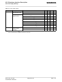
1
HC15
Siemens Cellular Engine
Version:
DocId:
01.000
HC15_HD_v01.000
Hardware Interface Description
s
s
HC15 Hardware Interface Description
Document Name:
HC15 Hardware Interface Description
Version:
01.000
Date:
2007-1-19
DocId:
HC15_HD_v01.000
Status
Confidential / Released
General Notes
Product is deemed accepted by recipient and is provided without interface to recipient’s products. The documentation and/or product are provided for testing, evaluation, integration and information purposes. The documentation and/or product are provided on an “as is” basis only and may contain deficiencies or inadequacies. The
documentation and/or product are provided without warranty of any kind, express or implied. To the maximum
extent permitted by applicable law, Siemens further disclaims all warranties, including without limitation any implied warranties of merchantability, completeness, fitness for a particular purpose and non-infringement of thirdparty rights. The entire risk arising out of the use or performance of the product and documentation remains with
recipient. This product is not intended for use in life support appliances, devices or systems where a malfunction
of the product can reasonably be expected to result in personal injury. Applications incorporating the described
product must be designed to be in accordance with the technical specifications provided in these guidelines. Failure to comply with any of the required procedures can result in malfunctions or serious discrepancies in results.
Furthermore, all safety instructions regarding the use of mobile technical systems, including GSM products,
which also apply to cellular phones must be followed. Siemens or its suppliers shall, regardless of any legal theory upon which the claim is based, not be liable for any consequential, incidental, direct, indirect, punitive or other
damages whatsoever (including, without limitation, damages for loss of business profits, business interruption,
loss of business information or data, or other pecuniary loss) arising out the use of or inability to use the documentation and/or product, even if Siemens has been advised of the possibility of such damages. The foregoing
limitations of liability shall not apply in case of mandatory liability, e.g. under the German Product Liability Act, in
case of intent, gross negligence, injury of life, body or health, or breach of a condition which goes to the root of
the contract. However, claims for damages arising from a breach of a condition, which goes to the root of the
contract, shall be limited to the foreseeable damage, which is intrinsic to the contract, unless caused by intent or
gross negligence or based on liability for injury of life, body or health. The above provision does not imply a
change on the burden of proof to the detriment of the recipient. Subject to change without notice at any time. The
interpretation of this general note shall be governed and construed according to German law without reference
to any other substantive law.
Copyright
Transmittal, reproduction, dissemination and/or editing of this document as well as utilization of its contents and
communication thereof to others without express authorization are prohibited. Offenders will be held liable for
payment of damages. All rights created by patent grant or registration of a utility model or design patent are reserved.
Copyright © Siemens AG 2007
HC15_HD_v01.000
Confidential / Released
Page 2 of 67
2007-1-19
s
HC15 Hardware Interface Description
Contents
Contents
0
Document History.................................................................................................................................... 7
1
Introduction.............................................................................................................................................. 8
1.1 Related Documents......................................................................................................................... 8
1.2 Terms and Abbreviations ................................................................................................................ 8
1.3 Regulatory and Type Approval Information................................................................................... 11
1.3.1
Directives and Standards............................................................................................... 11
1.3.2
SAR requirements specific to portable mobiles ............................................................. 12
1.3.3
SELV Requirements ...................................................................................................... 12
1.3.4
Safety Precautions......................................................................................................... 13
2
Product Concept.................................................................................................................................... 14
2.1 Key Features at a Glance.............................................................................................................. 14
2.2 HC15 System Overview ................................................................................................................ 17
2.3 Circuit Concept.............................................................................................................................. 18
3
Application Interface ............................................................................................................................. 19
3.1 Operating Modes........................................................................................................................... 20
3.2 Power Supply ................................................................................................................................ 21
3.2.1
Minimizing Power Losses .............................................................................................. 21
3.2.2
Measuring the Supply Voltage (VBATT+ ) ........................................................................ 22
3.3 Power-Up / Power-Down Scenarios.............................................................................................. 23
3.3.1
Turn On HC15 ............................................................................................................... 23
3.3.2
Turn Off HC15 Using AT Command .............................................................................. 24
3.3.3
Configuring the IGT Line for Use as ON/OFF Switch .................................................... 25
3.3.4
Automatic Shutdown...................................................................................................... 25
3.3.5
Turn Off HC15 in Case of Emergency ........................................................................... 26
3.4 Power Saving ................................................................................................................................ 27
3.5 USB Interface ................................................................................................................................ 27
3.6 UICC/SIM Interface ....................................................................................................................... 28
3.7 Analog Audio Interface .................................................................................................................. 30
3.8 PWR_IND Signal........................................................................................................................... 31
3.8.1
Network Connectivity Status Signals ............................................................................. 31
4
Antenna Interface .................................................................................................................................. 32
4.1 Antenna Installation....................................................................................................................... 32
4.2 Antenna Pad.................................................................................................................................. 33
4.3 Antenna Connector ....................................................................................................................... 33
5
Electrical, Reliability and Radio Characteristics ................................................................................ 38
5.1 Absolute Maximum Ratings........................................................................................................... 38
5.2 Operating Temperatures ............................................................................................................... 39
5.3 Storage Conditions........................................................................................................................ 40
5.4 Reliability Characteristics .............................................................................................................. 41
5.5 Pin Assignment and Signal Description ........................................................................................ 42
5.6 Power Supply Ratings ................................................................................................................... 47
5.7 Electrical Characteristics of the Voiceband Part ........................................................................... 49
5.7.1
Characteristics of Audio Modes ..................................................................................... 49
5.8 Air Interface ................................................................................................................................... 50
HC15_HD_v01.000
Confidential / Released
Page 3 of 67
2007-1-19
Contents
s
5.9
Electrostatic Discharge.................................................................................................................. 51
HC15 Hardware Interface Description
6
Mechanics .............................................................................................................................................. 52
6.1 Mechanical Dimensions of HC15 .................................................................................................. 52
6.2 Mounting HC15 to the Application Platform .................................................................................. 54
6.3 Board-to-Board Application Connector.......................................................................................... 55
7
Sample Application ............................................................................................................................... 57
8
Reference Approval............................................................................................................................... 59
8.1 Reference Equipment for Type Approval ...................................................................................... 59
9
Appendix ................................................................................................................................................ 60
9.1 List of Parts and Accessories ........................................................................................................ 60
9.2 Fasteners and Fixings for Electronic Equipment........................................................................... 62
9.2.1
Fasteners from German Supplier ETTINGER GmbH.................................................... 62
9.3 Mounting Advice Sheet ................................................................................................................. 66
HC15_HD_v01.000
Confidential / Released
Page 4 of 67
2007-1-19
s
HC15 Hardware Interface Description
List of Tables
Tables
Table 1:
Table 2:
Table 3:
Table 4:
Table 5:
Table 6:
Table 7:
Table 8:
Table 9:
Table 10:
Table 11:
Table 12:
Table 13:
Table 14:
Table 15:
Table 16:
Table 17:
Table 18:
Table 19:
Table 20:
Table 21:
Table 22:
Table 23:
Table 24:
Directives .................................................................................................................................... 11
Standards of European type approval ........................................................................................ 11
Requirements of quality .............................................................................................................. 12
Overview of operating modes ..................................................................................................... 20
Signals of the UICC/SIM interface (board-to-board connector) .................................................. 28
Return loss in the active band .................................................................................................... 32
Product specifications of U.FL-R-SMT connector....................................................................... 34
Material and finish of U.FL-R-SMT connector and recommended plugs.................................... 34
Ordering information for Hirose U.FL Series .............................................................................. 37
Absolute maximum ratings ......................................................................................................... 38
Board temperature...................................................................................................................... 39
Sample operating conditions without forced air circulation (according to IEC 60068-2)............. 39
Sample operating conditions with forced air circulation (air speed 0.9m/s)................................ 39
Storage conditions ...................................................................................................................... 40
Summary of reliability test conditions ......................................................................................... 41
Signal description ....................................................................................................................... 43
Power supply ratings .................................................................................................................. 47
Voiceband characteristics (typical) ............................................................................................. 49
Air interface GSM / UMTS .......................................................................................................... 50
Measured electrostatic values .................................................................................................... 51
Electrical and mechanical characteristics of the board-to-board connector ............................... 55
List of parts and accessories ...................................................................................................... 60
Molex sales contacts (subject to change)................................................................................... 61
Hirose sales contacts (subject to change) .................................................................................. 61
HC15_HD_v01.000
Confidential / Released
Page 5 of 67
2007-1-19
s
HC15 Hardware Interface Description
List of Figures
Figures
Figure 1:
Figure 2:
Figure 3:
Figure 4:
Figure 5:
Figure 6:
Figure 7:
Figure 8:
Figure 9:
Figure 10:
Figure 11:
Figure 12:
Figure 13:
Figure 14:
Figure 15:
Figure 16:
Figure 17:
Figure 18:
Figure 19:
Figure 20:
Figure 21:
Figure 22:
Figure 23:
Figure 24:
HC15 system overview ..............................................................................................................
HC15 block diagram ..................................................................................................................
Power supply limits during transmit burst ..................................................................................
Position of the reference points BATT+ and GND .....................................................................
Power-on with IGT held low before switching on operating voltage at BATT+ ..........................
Power-on with operating voltage at BATT+ applied before activating IGT ................................
Signal states during turn-off procedure......................................................................................
Timing of IGT if used as ON/OFF switch ...................................................................................
Shutdown by EMERG_OFF signal ............................................................................................
UICC/SIM interface....................................................................................................................
Audio block diagram ..................................................................................................................
PWR_IND signal........................................................................................................................
Status LED Circuit (example) ....................................................................................................
Restricted area around antenna pad (side and bottom view) ....................................................
Mechanical dimensions of U.FL-R-SMT connector ...................................................................
U.FL-R-SMT connector with U.FL-LP-040 plug.........................................................................
U.FL-R-SMT connector with U.FL-LP-066 plug.........................................................................
Specifications of U.FL-LP-(V)-040(01) plug...............................................................................
Pin assignment HC15 ................................................................................................................
HC15 – Top and bottom view ....................................................................................................
Dimensions of HC15 (all dimensions in mm).............................................................................
Mechanical dimensions of the board-to-board connector..........................................................
HC15 sample application...........................................................................................................
Reference equipment for Type Approval ...................................................................................
HC15_HD_v01.000
Confidential / Released
Page 6 of 67
17
18
21
22
23
23
24
25
26
29
30
31
31
32
33
35
35
36
42
52
53
56
58
59
2007-1-19
s
HC15 Hardware Interface Description
0 Document History
0
Document History
Preceding document: "HCx5 Hardware Interface Description" Version 00.050a
New document: "HC15 Hardware Interface Description" Version 01.000
Chapter
What is new
--
Separate document for HC15.
1.3
Section now comprises Regulatory and Type Approval Information including new subsection 1.3.3 with note on SELV requirements.
2
Updated key features, system overview and block diagram.
3.2.2
New subsection: Measuring the Supply Voltage (VBATT+ ).
3.3.2
Added Figure 7 showing signal states during turn-off procedure
3.3
Revised order of subsections.
3.3.3
New subsection: Configuring the IGT Line for Use as ON/OFF Switch.
3.5
Revised parts of the section.
3.6
Added description for CCIN pin and Figure 10.
3.7
Revised complete section.
3.8
Added Figure 12.
3.8.1
Revised complete section.
5.2
Updated section on operating temperatures.
5.3
New section: Storage Conditions.
5.4
New section: Reliability Characteristics.
5.5
Revised Figure 19 showing pin assignment. Table 16: Changed VImax for BATT+ from
4.3. to 4.2. Added note on automatic shutdown.
5.6
Updated power supply ratings (Table 17).
5.7
New section: Electrical Characteristics of the Voiceband Part.
6.1
Updated Figure 20 and Figure 21 (top/bottom view as well as mechanical dimensions)
6.2
New section: Mounting HC15 to the Application Platform.
6.3
Added note regarding inverse polarity protection for board-to-board connector.
7
New chapter: Sample Application
8
Added HC15/HC25-DSB75-Adapter to reference equipment.
9
New Appendix with a List of Parts and Accessories, Fasteners and Fixings for Electronic
Equipment and Mounting Advice Sheet.
Preceding document: "HC15 Hardware Interface Description" Version 00.005
New document: "HCx5 Hardware Interface Description" Version 00.050a
Chapter
What is new
Initial document setup.
HC15_HD_v01.000
Confidential / Released
Page 7 of 67
2007-1-19
s
HC15 Hardware Interface Description
1 Introduction
1
Introduction
This document describes the hardware of the Siemens HC15 module that connects to the cellular device application and the air interface. It helps you quickly retrieve interface specifications, electrical and mechanical details
and information on the requirements to be considered for integrating further components.
1.1
Related Documents
[1] HC15 AT Command Set 01.000
[2] HC15 Release Notes 01.000
1.2
Terms and Abbreviations
Abbreviation
Description
ANSI
American National Standards Institute
AMR
Adaptive Multirate
ARP
Antenna Reference Point
B2B
Board-to-board connector
BB
Baseband
BEP
Bit Error Probability
BTS
Base Transceiver Station
CB or CBM
Cell Broadcast Message
CE
Conformité Européene (European Conformity)
CS
Coding Scheme
CS
Circuit Switched
CSD
Circuit Switched Data
DAC
Digital-to-Analog Converter
dBm0
Digital level, 3.14dBm0 corresponds to full scale, see ITU G.711, A-law
DCS
Digital Cellular System
DL
Download
DRX
Discontinuous Reception
DSB
Development Support Board
DSP
Digital Signal Processor
DTMF
Dual Tone Multi Frequency
DTX
Discontinuous Transmission
EDGE
Enhanced Data rates for GSM Evolution
EFR
Enhanced Full Rate
HC15_HD_v01.000
Confidential / Released
Page 8 of 67
2007-1-19
s
HC15 Hardware Interface Description
1.2 Terms and Abbreviations
Abbreviation
Description
EGSM
Enhanced GSM
EMC
Electromagnetic Compatibility
ERP
Effective Radiated Power
ESD
Electrostatic Discharge
ETS
European Telecommunication Standard
ETSI
European Telecommunications Standards Institute
FCC
Federal Communications Commission (U.S.)
FDD
Frequency Division Duplex
FDMA
Frequency Division Multiple Access
FR
Full Rate
GPRS
General Packet Radio Service
GSM
Global Standard for Mobile Communications
HiZ
High Impedance
HSDPA
High Speed Downlink Packed Access
HR
Half Rate
I/O
Input/Output
IF
Intermediate Frequency
IMEI
International Mobile Equipment Identity
ISO
International Standards Organization
ITU
International Telecommunications Union
kbps
kbits per second
LED
Light Emitting Diode
Mbps
Mbits per second
MCS
Modulation and Coding Scheme
MO
Mobile Originated
MS
Mobile Station, also referred to as TE
MT
Mobile Terminated
NTC
Negative Temperature Coefficient
PBCCH
Packet Switched Broadcast Control Channel
PCB
Printed Circuit Board
PCL
Power Control Level
PCM
Pulse Code Modulation
PCS
Personal Communication System, also referred to as GSM 1900
PS
Packet Switched
PDU
Protocol Data Unit
PSK
Phase Shift Keying
R&TTE
Radio and Telecommunication Terminal Equipment
HC15_HD_v01.000
Confidential / Released
Page 9 of 67
2007-1-19
s
HC15 Hardware Interface Description
1.2 Terms and Abbreviations
Abbreviation
Description
RACH
Random Access Channel
RF
Radio Frequency
Rx
Receive Direction
SAR
Specific Absorption Rate
SELV
Safety Extra Low Voltage
SIM
Subscriber Identification Module
SLIC
Subscriber Line Interface Circuit
SMS
Short Message Service
SRAM
Static Random Access Memory
SRB
Signalling Radio Bearer
TA
Terminal adapter (e.g. GSM engine)
TDMA
Time Division Multiple Access
TE
Terminal Equipment
TS
Technical Specification
Tx
Transmit Direction
UL
Upload
UMTS
Universal Mobile Telecommunications System
URC
Unsolicited Result Code
USB
Universal Serial Bus
UICC
USIM Integrated Circuit Card
USIM
UMTS Subscriber Identification Module
WCDMA
Wideband Code Division Multiple Access
HC15_HD_v01.000
Confidential / Released
Page 10 of 67
2007-1-19
HC15 Hardware Interface Description
1.3 Regulatory and Type Approval Information
1.3
s
Regulatory and Type Approval Information
1.3.1
Directives and Standards
HC15 has been designed to comply with the directives and standards listed below.
Table 1: Directives
99/05/EC
Directive of the European Parliament and of the council of 9 March 1999 on radio
equipment and telecommunications terminal equipment and the mutual recognition
of their conformity (in short referred to as R&TTE Directive 1999/5/EC).
The product is labeled with the CE conformity mark
89/336/EC
Directive on electromagnetic compatibility
73/23/EC
Directive on electrical equipment designed for use within certain voltage limits (Low
Voltage Directive)
95/94/EC
Automotive EMC directive
2002/95/EC
Directive of the European Parliament and of the Council of 27 January 2003 on the restriction of the use of certain hazardous substances in electrical and electronic equipment (RoHS)
Table 2: Standards of European type approval
3GPP TS 51.010-1
Digital cellular telecommunications system (Release 5); Mobile Station (MS) conformance specification
ETSI EN 301 511 V9.0.2
Candidate Harmonized European Standard (Telecommunications series) Global
System for Mobile communications (GSM); Harmonized standard for mobile stations in the GSM 900 and DCS 1800 bands covering essential requirements under
article 3.2 of the R&TTE directive (1999/5/EC) (GSM 13.11 version 7.0.1 Release
1998)
GCF-CC V3.23.1
Global Certification Forum - Certification Criteria
ETSI EN 301 489-1
V1.4.1
Candidate Harmonized European Standard (Telecommunications series) Electro
Magnetic Compatibility and Radio spectrum Matters (ERM); Electro Magnetic
Compatibility (EMC) standard for radio equipment and services; Part 1: Common
Technical Requirements
ETSI EN 301 489-7
V1.2.1 (2000-09)
Candidate Harmonized European Standard (Telecommunications series) Electro
Magnetic Compatibility and Radio spectrum Matters (ERM); Electro Magnetic
Compatibility (EMC) standard for radio equipment and services; Part 7: Specific
conditions for mobile and portable radio and ancillary equipment of digital cellular
radio telecommunications systems (GSM and DCS)
IEC/EN 60950-1 (2001)
Safety of information technology equipment (2000)
EN 301 489-24 V1.2.1
Electromagnetic compatibility and Radio Spectrum Matters (ERM); Electromagnetic Compatibility (EMC) standard for radio equipment and services; Part 24: Specific conditions for IMT-2000 CDMA Direct Spread (UTRA) for Mobile and portable
(UE) radio and ancillary equipment
EN 301 908-01 V2.2.1
Electromagnetic compatibility and Radio spectrum Matters (ERM); Base Stations
(BS) and User Equipment (UE) for IMT-2000 Third Generation cellular networks;
Part 1: Harmonized EN for IMT-2000, introduction and common requirements of
article 3.2 of the R&TTE Directive
HC15_HD_v01.000
Confidential / Released
Page 11 of 67
2007-1-19
HC15 Hardware Interface Description
1.3 Regulatory and Type Approval Information
s
Table 2: Standards of European type approval
EN 301 908-02 V2.2.1
Electromagnetic compatibility and Radio spectrum Matters (ERM); Base Stations
(BS) and User Equipment (UE) for IMT-2000 Third Generation cellular networks;
Part 2: Harmonized EN for IMT-2000, CDMA Direct Spread (UTRA FDD) (UE) covering essential requirements of article 3.2 of the R&TTE Directive
3GPP TS 34.124
Electromagnetic Compatibility (EMC) for mobile terminals and ancillary equipment.
3GPP TS 34.121
Technical Specification Group Radio Access Network; Terminal conformance
specification; Radio transmission and reception (FDD)
3GPP TS 34.123-1
User Equipment (UE) conformance specification; Part 1: Protocol conformance
specification.
3GPP TS 34.123-3
User Equipment (UE) conformance specification; Part 3: Abstract Test Suites.
Table 3: Requirements of quality
IEC 60068
Environmental testing
DIN EN 60529
IP codes
1.3.2
SAR requirements specific to portable mobiles
Mobile phones, PDAs or other portable transmitters and receivers incorporating a GSM module must be in accordance with the guidelines for human exposure to radio frequency energy. This requires the Specific Absorption
Rate (SAR) of portable HC15 based applications to be evaluated and approved for compliance with national and/
or international regulations.
Since the SAR value varies significantly with the individual product design manufacturers are advised to submit
their product for approval if designed for portable use. For European markets the relevant directives are mentioned below. It is the responsibility of the manufacturer of the final product to verify whether or not further standards, recommendations or directives are in force outside these areas.
Products intended for sale on European markets
EN 50360
1.3.3
Product standard to demonstrate the compliance of mobile phones with the basic
restrictions related to human exposure to electromagnetic fields (300MHz - 3GHz)
SELV Requirements
The power supply connected to the HC15 module shall be in compliance with the SELV requirements defined in
EN 60950-1.
HC15_HD_v01.000
Confidential / Released
Page 12 of 67
2007-1-19
HC15 Hardware Interface Description
1.3 Regulatory and Type Approval Information
1.3.4
s
Safety Precautions
The following safety precautions must be observed during all phases of the operation, usage, service or repair
of any cellular terminal or mobile incorporating HC15. Manufacturers of the cellular terminal are advised to convey the following safety information to users and operating personnel and to incorporate these guidelines into all
manuals supplied with the product. Failure to comply with these precautions violates safety standards of design,
manufacture and intended use of the product. Siemens AG assumes no liability for customer’s failure to comply
with these precautions.
When in a hospital or other health care facility, observe the restrictions on the use of mobiles.
Switch the cellular terminal or mobile off, if instructed to do so by the guidelines posted in sensitive areas. Medical equipment may be sensitive to RF energy.
The operation of cardiac pacemakers, other implanted medical equipment and hearing aids
can be affected by interference from cellular terminals or mobiles placed close to the device.
If in doubt about potential danger, contact the physician or the manufacturer of the device to
verify that the equipment is properly shielded. Pacemaker patients are advised to keep their
hand-held mobile away from the pacemaker, while it is on.
Switch off the cellular terminal or mobile before boarding an aircraft. Make sure it cannot be
switched on inadvertently. The operation of wireless appliances in an aircraft is forbidden to
prevent interference with communications systems. Failure to observe these instructions may
lead to the suspension or denial of cellular services to the offender, legal action, or both.
Do not operate the cellular terminal or mobile in the presence of flammable gases or fumes.
Switch off the cellular terminal when you are near petrol stations, fuel depots, chemical plants
or where blasting operations are in progress. Operation of any electrical equipment in potentially explosive atmospheres can constitute a safety hazard.
Your cellular terminal or mobile receives and transmits radio frequency energy while switched
on. Remember that interference can occur if it is used close to TV sets, radios, computers or
inadequately shielded equipment. Follow any special regulations and always switch off the
cellular terminal or mobile wherever forbidden, or when you suspect that it may cause interference or danger.
Road safety comes first! Do not use a hand-held cellular terminal or mobile when driving a
vehicle, unless it is securely mounted in a holder for speakerphone operation. Before making
a call with a hand-held terminal or mobile, park the vehicle.
Speakerphones must be installed by qualified personnel. Faulty installation or operation can
constitute a safety hazard.
IMPORTANT!
Cellular terminals or mobiles operate using radio signals and cellular networks. Because of
this, connection cannot be guaranteed at all times under all conditions. Therefore, you should
never rely solely upon any wireless device for essential communications, for example emergency calls.
Remember, in order to make or receive calls, the cellular terminal or mobile must be switched
on and in a service area with adequate cellular signal strength.
Some networks do not allow for emergency calls if certain network services or phone features
are in use (e.g. lock functions, fixed dialing etc.). You may need to deactivate those features
before you can make an emergency call.
Some networks require that a valid SIM card be properly inserted in the cellular terminal or
mobile.
HC15_HD_v01.000
Confidential / Released
Page 13 of 67
2007-1-19
s
HC15 Hardware Interface Description
2 Product Concept
2
Product Concept
2.1
Key Features at a Glance
Feature
Implementation
General
Frequency bands
UMTS/HSDPA: Single band, 2100MHz
GSM/GPRS/EDGE: Dual band, 900/1800MHz
GSM class
Small MS
Output power
Class 4 (+33dBm ±2dB) for EGSM900
(according to
Release 99)
Class 1 (+30dBm ±2dB) for GSM1800
Class E2 (+27dBm ± 3dB) for GSM 900 8-PSK
Class E2 (+26dBm +3 /-4dB) for GSM 1800 8-PSK
Class 3 (+24dBm +1/-3dB) for UMTS 2100, WCDMA FDD BdI
Power supply
3.2V < VBATT+ < 4.2V
Physical
Dimensions: 50mm x 34mm x 4.5mm
Weight: approx. 10g
RoHS
All hardware components fully compliant with EU RoHS Directive
HSDPA features
3GPP Release 5
3.6 Mbps, UL 384 kbps
UE CAT. [1-6], 11, 12 supported
Compressed mode (CM) supported according to 3GPP TS25.212
UMTS features
Release 99, June 2004, W- PS data rate – 384 kbps DL / 384 kbps UL
CDMA FDD standard
CS data rate – 64 kbps DL / 64 kbps UL
HC15_HD_v01.000
Confidential / Released
Page 14 of 67
2007-1-19
s
HC15 Hardware Interface Description
2.1 Key Features at a Glance
Feature
Implementation
GSM / GPRS / EGPRS features
Data transfer
GPRS
•
•
•
•
Multislot Class 10
Full PBCCH support
Mobile Station Class B
Coding Scheme 1 – 4
EGPRS
•
•
•
•
•
•
•
•
•
•
•
•
Multislot Class 10
EDGE E2 power class for 8 PSK
Downlink coding schemes – CS 1-4, MCS 1-9
Uplink coding schemes – CS 1-4, MCS 1-9
BEP reporting
SRB loopback and test mode B
8-bit, 11-bit RACH
PBCCH support
1 phase/2 phase access procedures
Link adaptation and IR
NACC, extended UL TBF
Mobile Station Class B
CSD
•
•
SMS
V.110, RLP, non-transparent
9.6 kbps
Point-to-point MT and MO
Cell broadcast
Text and PDU mode
Audio
Audio speech codecs
GSM: AMR, EFR, FR, HR
3GPP: AMR
One ringing melody supported
CEPT supervisory tones supported
DTMF supported
2 audio modes: Approval, Router
Software
AT commands
AT-Hayes GSM 07.05 and 07.07, Siemens
Firmware update
Firmware update from host application over USB.
Interfaces
USB
Supports a USB 2.0 Full Speed (12Mbit/s) device interface.
Wakeup Control
Signal pin to wake up an inactive USB Host into an active state.
HC15_HD_v01.000
Confidential / Released
Page 15 of 67
2007-1-19
s
HC15 Hardware Interface Description
2.1 Key Features at a Glance
Feature
Implementation
Status
Signal pins to indicate network connectivity status.
Audio
1 analog interface
UICC interface
Supported chip cards: SIM / UICC 3V, 1.8V
Antenna
50Ohms. External antenna can be connected via antenna connector or
antenna pad (spring contact).
Module interface
50-pin board-to-board connector
Power on/off, Reset
Power on/off
Switch-on by hardware pin IGT
Switch-off by hardware pin IGT
Switch-off by AT command
Reset
Orderly shutdown and reset by AT command
Emergency off by hardware pin EMERG_OFF and restart with hardware
pin IGT
Emergency off
Emergency off by hardware pin EMERG_OFF
Evaluation kit
DSB
HC15_HD_v01.000
Confidential / Released
DSB75 Evaluation Board designed to test and type approve Siemens cellular engines and provide a sample configuration for application engineering. A special adapter is required to connect the module to the DSB75.
Page 16 of 67
2007-1-19
s
HC15 Hardware Interface Description
2.2 HC15 System Overview
2.2
HC15 System Overview
Figure 1: HC15 system overview
HC15_HD_v01.000
Confidential / Released
Page 17 of 67
2007-1-19
s
HC15 Hardware Interface Description
2.3 Circuit Concept
2.3
Circuit Concept
Figure 2 shows a block diagram of the HC15 module and illustrates the major functional components:
Base band block:
•
•
•
•
Digital base band processor with DSPs
Power Management
NAND Flash and SDRAM
Application interface (board-to-board connector)
RF section:
•
•
•
•
RF Transceiver
RF GSM/ WCDMA power amplifier
RF front end
Antenna connector
Figure 2: HC15 block diagram
HC15_HD_v01.000
Confidential / Released
Page 18 of 67
2007-1-19
s
HC15 Hardware Interface Description
3 Application Interface
3
Application Interface
HC15 is equipped with a 50-pin board-to-board connector that connects to the external application. The host
interface incorporates several sub-interfaces described in the following chapters:
•
•
•
•
•
•
Operation Modes - see Section 3.1
Power supply - see Section 3.2
USB interface - see Section 3.5
UICC/SIM interface - see Section 3.6
Analog audio interface - see Section 3.7
Status and control lines: IGT, EMERG_OFF, PWR_IND, STATUS1/2, HOST_WAKEUP - see Table 16.
HC15_HD_v01.000
Confidential / Released
Page 19 of 67
2007-1-19
s
HC15 Hardware Interface Description
3.1 Operating Modes
3.1
Operating Modes
The table below briefly summarizes the various operating modes referred to in the following chapters.
Table 4: Overview of operating modes
Mode
Function
Normal
GSM /
operation GPRS / UMTS /
HSDPA SLEEP
Power
Down
Power saving mode set automatically when no call is in progress and
the USB connection is suspended by host or not present.
GSM IDLE
Software is active. Once registered to the GSM network, paging with
BTS is carried out in order to achieve synchrony with the GSM network.
The repetition rate depends on the parameter BSPA_Multiframe. The
module is ready to send and receive.
GSM TALK/
GSM DATA
Connection between two subscribers is in progress. Power consumption depends on the GSM network coverage and several connection
settings (e.g. DTX off/on, FR/EFR/HR, hopping sequences and
antenna connection). The following applies when power is to be measured in TALK_GSM mode: DTX off, FR and no frequency hopping,
otherwise same as for IDLE measurements.
GPRS IDLE
Module is attached and ready for GPRS data transfer, but no data is
currently sent or received.
GPRS DATA
GPRS data transfer in progress. Power consumption depends on network settings (e.g. power control level), uplink / downlink data rates and
GPRS configuration (e.g. used multislot settings).
EGPRS DATA
EGPRS data transfer in progress. Power consumption depends on network settings (e.g. power control level), uplink / downlink data rates and
EGPRS configuration (e.g. used multislot settings).
UMTS /
HSDPA IDLE
Module is attached and ready for UMTS / HSDPA data transfer, but no
data is currently sent or received.
UMTS TALK/
UMTS DATA
UMTS data transfer in progress. Power consumption depends on network settings (e.g. TPC Pattern) and data transfer rate.
HSDPA DATA
HSDPA data transfer in progress. Power consumption depends on network settings (e.g. TPC Pattern) and data transfer rate.
The internal power section is shut down. The SW on the module is not active. The interfaces
are not accessible.
HC15_HD_v01.000
Confidential / Released
Page 20 of 67
2007-1-19
s
HC15 Hardware Interface Description
3.2 Power Supply
3.2
Power Supply
HC15 needs to be connected to a power supply at the board-to-board connector (5 pins each BATT+ and GND).
The power supply of HC15 has to be a single voltage source at BATT+. It must be able to provide the peak current during the GSM uplink transmission. For an overview of power supply ratings see Section 5.6.
All the key functions for supplying power to the device are handled by the power management section of the analog controller. This IC provides the following features:
•
•
•
•
Stabilizes the supply voltages for the GSM / UMTS baseband using voltage regulators.
Switches the module's power voltages for the power-up and -down procedures.
Delivers, across the VEXT pin, a regulated voltage for an external application. This voltage is not available in
Power-down mode.
Regulator to provide SIM power supply.
3.2.1
Minimizing Power Losses
When designing the power supply for your application please pay specific attention to power losses. Ensure that
the input voltage VBATT+ never drops below 3.2V on the HC15 board, not even in a GSM transmit burst where
current consumption can rise (for peak values see the power supply ratings listed in Section 5.6). It should be
noted that HC15 switches off when exceeding these limits. Any voltage drops that may occur in a transmit burst
should not exceed 400mV.
The module switches off if the minimum battery voltage (Vbattmin) is reached.
Example:
VImin = 3.2V
Dmax = 0.4V
Vbattmin = VImin + Dmax
Vbattmin = 3.2V + 0.4V = 3.6V
The best approach to reducing voltage drops is to use a board-to-board connection as recommended, and a low
impedance power source. The resistance of the power supply lines on the host board and of a battery pack
should also be considered.
Note: If the application design requires an adapter cable between both board-to-board connectors, use a flex
cable as short as possible in order to minimize power losses.
Example:
If the length of the flex cable reaches the maximum length of 100mm, this connection may cause, for example,
a resistance of 30mΩ in the BATT+ line and 30mΩ in the GND line. As a result, a 2A transmit burst would add
up to a total voltage drop of 120mV. Plus, if a battery pack is involved, further losses may occur due to the resistance across the battery lines and the internal resistance of the battery including its protection circuit.
Transmit
burst
Transmit
burst
BATT+
Ripple
Drop
Min. 3.2V
Figure 3: Power supply limits during transmit burst
HC15_HD_v01.000
Confidential / Released
Page 21 of 67
2007-1-19
s
HC15 Hardware Interface Description
3.2 Power Supply
3.2.2
Measuring the Supply Voltage (VBATT+ )
The reference points for measuring the supply voltage VBATT+ on the module are BATT+ and GND, both accessible at a capacitor located close to the board-to-board connector of the module.
Reference
point GND
Reference
point
BATT+
Figure 4: Position of the reference points BATT+ and GND
HC15_HD_v01.000
Confidential / Released
Page 22 of 67
2007-1-19
s
HC15 Hardware Interface Description
3.3 Power-Up / Power-Down Scenarios
3.3
Power-Up / Power-Down Scenarios
In general, be sure not to turn on HC15 while it is beyond the safety limits of voltage and temperature. HC15
would immediately switch off after having started and detected these inappropriate conditions. In extreme cases
this can cause permanent damage to the module.
3.3.1
Turn On HC15
When the HC15 module is in Power-down mode, it can be started to Normal mode by driving the IGT (ignition)
line to ground. This must be accomplished with an open drain/collector driver to avoid current flowing into this
pin. Pulling this pin low triggers a power-on sequence. To turn on HC15 IGT has to be kept active at least 300ms.
After turning on HC15 IGT should be set inactive to prevent the module from turning on again after a shut down
by AT command or EMERG_OFF.
Figure 5: Power-on with IGT held low before switching on operating voltage at BATT+
Figure 6: Power-on with operating voltage at BATT+ applied before activating IGT
HC15_HD_v01.000
Confidential / Released
Page 23 of 67
2007-1-19
s
HC15 Hardware Interface Description
3.3 Power-Up / Power-Down Scenarios
3.3.2
Turn Off HC15 Using AT Command
The best and safest approach to powering down HC15 is to issue the AT^SMSO command. This procedure lets
HC15 log off from the network and allows the software to enter into a secure state and safe data before disconnecting the power supply. The mode is referred to as Power-down mode.
After sending AT^SMSO do not enter any other AT commands. There are two ways to verify that the module
turns off:
•
•
Wait for the ”OK” – response. It indicates that data has been stored non-volatile and that the module turns off
after about 1 second.
Also, you can monitor the PWR_IND pin. A high state of the PWR_IND pin definitely indicates that the module
is switched off.
Be sure not to disconnect the supply voltage VBATT+ before the module has been switched off and the PWR_IND
signal has gone high. Otherwise you run the risk of losing data.
While HC15 is in Power-down mode the application interface is switched off and must not be fed from any other
source. Therefore, your application must be designed to avoid any current flow into any digital pins of the application interface, especially of the serial interfaces. No special care is required for the USB interface which is protected from reverse current.
Figure 7: Signal states during turn-off procedure
Note 1: Depending on capacitance load from host application
Note 2: After module shutdown by means of AT command, please allow for a time period of at least 1s before
restarting the module.
HC15_HD_v01.000
Confidential / Released
Page 24 of 67
2007-1-19
s
HC15 Hardware Interface Description
3.3 Power-Up / Power-Down Scenarios
3.3.3
Configuring the IGT Line for Use as ON/OFF Switch
The IGT line can be configured for use in two different switching modes: You can set the IGT line to switch on
the module only, or to switch it on and off. The switching mode is determined by the parameter "MEShutdown/
OnIgnition" of the AT^SCFG command. This approach is useful for application manufacturers who wish to have
an ON/OFF switch installed on the host device.
By factory default, the ON/OFF switch mode of IGT is disabled:
at^scfg=meshutdown/onignition
# Query the current status of IGT.
^SCFG: "MEShutdown/OnIgnition","off"
# IGT can be used only to switch on HC15.
IGT works as described in Section 3.3.1.
OK
To configure IGT for use as ON/OFF switch:
at^scfg=meshutdown/onignition,on
# Enable the ON/OFF switch mode of IGT.
^SCFG: "MEShutdown/OnIgnition","on"
# IGT can be used to switch on and off HC15.
OK
We strongly recommend taking great care before changing the switching mode of the IGT line. To ensure that
the IGT line works properly as ON/OFF switch it is of vital importance that the following conditions are met.
Switch-on condition:If the HC15 is off, the IGT line must be asserted for at least 300ms before being
released.
Switch-off condition:If the HC15 is on, the IGT line must be asserted for at least 2s before being released.
The module switches off after the line is released.
The switch-off routine is identical with the procedure initiated by AT^SMSO,
i.e. the software performs an orderly shutdown as described in Section 3.3.2.
Before switching off the module wait at least 5 seconds after startup.
Figure 8: Timing of IGT if used as ON/OFF switch
3.3.4
Automatic Shutdown
Automatic shutdown takes effect if:
•
•
The HC15 board is exceeding the critical limits of over-temperature or under-temperature
Under-voltage or over-voltage is detected
The automatic shutdown procedure is equivalent to the Power-down initiated with the AT^SMSO command, i.e.
HC15 logs off from the network and the software enters a secure state avoiding loss of data.
Alert messages transmitted before the device switches off are implemented as Unsolicited Result Codes
(URCs). The URC presentation mode varies with the condition. For further details on AT commands refer to [1].
HC15_HD_v01.000
Confidential / Released
Page 25 of 67
2007-1-19
s
HC15 Hardware Interface Description
3.3 Power-Up / Power-Down Scenarios
3.3.5
Turn Off HC15 in Case of Emergency
The EMERG_OFF line can be used to switch off the module in case of emergency. To switch the module off the
EMERG_OFF line must be pulled to ground and held low for at least 2.5s. Afterwards EMERG_OFF can be
released and the module shuts down.
Caution: EMERG_OFF does not cause deregistration of cellular network. Use the EMERG_OFF pin only when,
due to serious problems, the software is not responding for more than 5 seconds. Pulling the EMERG_OFF pin
causes the loss of all information stored in the volatile memory. Therefore, this procedure is intended only for use
in case of emergency, e.g., if HC15 does not respond, if reset or shutdown via AT command fails.
To control the EMERG_OFF line it is recommended to use an open drain / collector driver.
To register to the network SIM PIN authentication is necessary after restart.
Figure 9: Shutdown by EMERG_OFF signal
HC15_HD_v01.000
Confidential / Released
Page 26 of 67
2007-1-19
s
HC15 Hardware Interface Description
3.4 Power Saving
3.4
Power Saving
Intended for power saving, SLEEP mode reduces the functionality of the HC15 to a minimum and thus minimizes
the current consumption.
The implementation of the USB host interface influences the module’s power saving modes and therefore its current consumption (see Section 3.5).
3.5
USB Interface
HC15 supports a USB 2.0 Full Speed (12Mbit/s) device interface. A USB host has to support at least 6 „Message
Pipes“ (see “Universal Serial Bus Specification“1 for a definition of the term „Message Pipe“) to work with the
HC15 USB interface.
The USB I/O-pins are capable of driving the signal at min 3.0V. They are 5V I/O compliant.
To properly connect the module’s USB interface to the host a USB 2.0 compatible connector is required. Furthermore, the USB driver package for Windows XP delivered with HC15 must be installed as described in [2].
The module’s USB interface is powered by VUSB. VUSB must be supplied by the USB host in the range 4.5V to
5.25V The maximum load on VUSB is 10mA.
While the USB connection is active, the module will not change into SLEEP Mode. To enable switching into
SLEEP mode the USB host must bring its USB interface into Suspend state (see “Universal Serial Bus Specification“1 for a description of the Suspend state). On incoming calls HC15 will then generate a remote wake up
request to resume the USB connection. This can be realized by means of the HOST_WAKEUP line in addition
to the normal USB remote wakeup mechanism. If no call, data or message transfer is in progress, the
HOST_WAKEUP line is inactive. To save power, the host could then shut down its own USB interface. If a call
or other request (URC’s, messages) arrives, the host can be woken up again by activation of HOST_WAKEUP
(inactive to active low transition). For more information on the USB related pins see Table 16. For more information on how to configure the USB interface by means of AT commands see [1].
1.
The specification is ready for download on http://www.usb.org/developers/docs/
HC15_HD_v01.000
Confidential / Released
Page 27 of 67
2007-1-19
s
HC15 Hardware Interface Description
3.6 UICC/SIM Interface
3.6
UICC/SIM Interface
HC15 has an integrated UICC/SIM interface compatible with the 34.121 USIM Testing IC Card standard. This is
wired to the host interface (board-to-board connector) in order to be connected to an external SIM card holder.
Six pins on the board-to-board connector are reserved for the UICC/SIM interface.
The UICC/SIM interface supports 3V and 1.8V UICC cards. Please refer to Table 16 for electrical specifications
of the UICC/SIM interface lines depending on whether a 3V or 1.8V SIM card is used.
The CCIN pin serves to detect whether a tray (with SIM card) is present in the card holder. Using the CCIN pin
is mandatory for compliance with the GSM 11.11 recommendation, if the mechanical design of the host application allows the user to remove the SIM card during operation. To take advantage of this feature, an appropriate
SIM card detect switch is required on the card holder. For example, this is true for the model supplied by Molex,
which has been tested to operate with HC15 and is part of the Siemens reference equipment submitted for type
approval. See Section 9.1 for Molex ordering numbers.
Table 5: Signals of the UICC/SIM interface (board-to-board connector)
Signal
Description
CCGND
Separate ground connection for SIM card to improve EMC.
Be sure to use this ground line for the SIM interface rather than any other ground pin or plane on
the module.
CCCLK
Chip card clock.
CCVCC
SIM supply voltage.
CCIO
Serial data line, input and output.
CCRST
Chip card reset.
CCIN
Input on the baseband processor for detecting a SIM card tray in the holder. If the SIM is removed
during operation the SIM interface is shut down immediately to prevent destruction of the SIM. The
CCIN pin is active low.
The CCIN pin is mandatory for applications that allow the user to remove the SIM card during operation.
The CCIN pin is solely intended for use with a SIM card. It must not be used for any other purposes.
Failure to comply with this requirement may invalidate the type approval of HC15.
Note: No guarantee can be given, nor any liability accepted, if loss of data is encountered after removing the SIM
card during operation. Also, no guarantee can be given for properly initializing any SIM card that the user inserts
after having removed a SIM card during operation. In this case, the application must restart HC15.
HC15_HD_v01.000
Confidential / Released
Page 28 of 67
2007-1-19
s
HC15 Hardware Interface Description
3.6 UICC/SIM Interface
Figure 10: UICC/SIM interface
The total cable length between the board-to-board connector pins on HC15 and the pins of the external SIM card
holder must not exceed 100mm in order to meet the specifications of 3GPP TS 51.010-1 and to satisfy the
requirements of EMC compliance.
To avoid possible cross-talk from the CCCLK signal to the CCIO signal be careful that both lines are not placed
closely next to each other. A useful approach is using the CCGND line to shield the CCIO line from the CCCLK
line.
HC15_HD_v01.000
Confidential / Released
Page 29 of 67
2007-1-19
s
HC15 Hardware Interface Description
3.7 Analog Audio Interface
3.7
Analog Audio Interface
HC15 supports an analog audio interface with a balanced microphone input and a balanced loudspeaker output.
The following picture shows a simplified block diagram:
Figure 11: Audio block diagram
A power supply for electret microphones is available via VMIC at the board-to-board connector. VMIC is capable
to drive a current of 1mA at a voltage of typically 1.8V. The microphone should be fed symmetrically between
VMIC and AGND. AGND provides for an extra connection to the modules ground potential to avoid disturbing
the microphone by high power supply current ripple. Coupling capacitors have to be used before the pins MICP
and MICN.
Microphone signals are fed via the MICP and MICN pins to an analog-to-digital converter (ADC) and the DSP.
The DSP application core calculates e.g. digital gains, sidetone, echo cancellation or noise suppression depending on the current configuration of the audio path. The processed speech samples are passed to the speech
encoder.
Received samples from the speech decoder are passed to the digital-to-analog converter (DAC) after post processing (frequency response correction, adding sidetone etc.). The loudspeaker signal is routed via EPP and
EPN pins. No gain setting is available in the earphone amplifier. The volume is controlled in the digital data
stream by the DSP only.
The default audio mode (AT^SNFS=1) is optimized for the Votronic HH-SI-30.3/V1.1/0 handset and used for type
approving the Siemens reference configuration. The second audio mode (AT^SNFS=2) is intended to be used
together with a subscriber line interface circuit (SLIC) providing an analogue telephone interface in a router
device. Both audio modes have fixed parameters that cannot be modified. For further details see Section 5.7.
HC15_HD_v01.000
Confidential / Released
Page 30 of 67
2007-1-19
s
HC15 Hardware Interface Description
3.8 PWR_IND Signal
3.8
PWR_IND Signal
PWR_IND notifies the on/off state of the module. High state of PWR_IND indicates that the module is switched
off. The state of PWR_IND immediately changes to low when IGT is pulled low. For state detection an external
pull-up resistor is required.
Figure 12: PWR_IND signal
3.8.1
Network Connectivity Status Signals
Two status signals (STATUS0 and STATUS1) are provided for signaling the module’s connectivity status. Each
signal acts as a current sink and can be used to control externally connected LEDs. For electrical characteristics
see Table 16.
Additional pull up resistors or LED's are required as shown in the below sample circuit for a status LED:
Figure 13: Status LED Circuit (example)
Please ensure that the voltage applied at the status pins does not exceed BATT+.
This status function has to be activated with AT^SLED. For details see the [1].
HC15_HD_v01.000
Confidential / Released
Page 31 of 67
2007-1-19
s
HC15 Hardware Interface Description
4 Antenna Interface
4
Antenna Interface
The RF interface has an impedance of 50Ω. HC15 is capable of sustaining a total mismatch at the antenna connector or pad without any damage, even when transmitting at maximum RF power.
The external antenna must be matched properly to achieve best performance regarding radiated power, DCpower consumption, modulation accuracy and harmonic suppression. Antenna matching networks are not
included on the HC15 PCB and should be placed in the host application.
Regarding the return loss HC15 provides the following values in the active band:
Table 6: Return loss in the active band
State of module
Return loss of module
Recommended return loss of application
Receive
> 8dB
> 12dB
Transmit
not applicable
> 12dB
Idle
< 5dB
not applicable
The connection of the antenna or other equipment must be decoupled from DC voltage. This is necessary
because the antenna connector is DC coupled to ground via an inductor for ESD protection.
Note: The antenna must be isolated for ESD protection (to withstand a voltage resistance up to 8kV air discharge).
4.1
Antenna Installation
To suit the physical design of individual applications HC15 offers two alternative approaches to connecting the
antenna:
•
•
Recommended approach: U.FL-R-SMT antenna connector from Hirose assembled on the top side of the
PCB. See Section 4.3 for connector details.
Antenna pad and grounding plane placed on the bottom side. See Section 4.2.
The U.FL-R-SMT connector has been chosen as antenna reference point (ARP) for the Siemens reference
equipment submitted to type approve HC15. All RF data specified throughout this manual are related to the ARP.
IMPORTANT: Both solutions can only be applied alternatively. This means, whenever an antenna is plugged to
the Hirose connector, the pad must not be used. Vice versa, if the antenna is connected to the pad, then the
Hirose connector must be left empty.
No matter which option you choose, ensure that the antenna pad does not come into contact with the holding
device or any other components of the host application. It needs to be surrounded by a restricted area filled with
air, which must also be reserved 1.4mm in height.
Figure 14: Restricted area around antenna pad (side and bottom view)
HC15_HD_v01.000
Confidential / Released
Page 32 of 67
2007-1-19
s
HC15 Hardware Interface Description
4.2 Antenna Pad
4.2
Antenna Pad
The antenna can be attached via contact springs.
If you decide to use the antenna pad take into account that the pad has not been intended as antenna reference
point (ARP) for the Siemens HC15 type approval. The antenna pad is provided only as an alternative option
which can be used, for example, if the recommended Hirose connection does not fit into your antenna design.
Also, consider that according to the GSM recommendations TS 45.005 and TS 51.010-01 a 50Ω connector is
mandatory for type approval measurements. This requires GSM devices with an integral antenna to be temporarily equipped with a suitable connector or a low loss RF cable with adapter.
HC15 material properties:
HC15 PCB:
Antenna pad:
4.3
FR4
Gold plated pad
Antenna Connector
HC15 uses an ultra-miniature SMT antenna connector supplied from Hirose Ltd. The product name is:
•
U.FL-R-SMT
Figure 15: Mechanical dimensions of U.FL-R-SMT connector
HC15_HD_v01.000
Confidential / Released
Page 33 of 67
2007-1-19
s
HC15 Hardware Interface Description
4.3 Antenna Connector
Table 7: Product specifications of U.FL-R-SMT connector
Item
Specification
Conditions
Nominal impedance
50Ω
Operating temp:-40°C to + 90°C
Operating humidity: max. 90%
Rated frequency
DC to 3GHz
Ratings
Mechanical characteristics
Female contact holding force
0.15N min
Measured with a Ø 0.475 pin gauge
Repetitive operation
Contact resistance:
Center 25mΩ
Outside 15mΩ
30 cycles of insertion and disengagement
Vibration
No momentary disconnections of 1µs;
No damage, cracks and looseness of
parts
Frequency of 10 to 100Hz, single amplitude
of 1.5mm, acceleration of 59m/s2, for 5
cycles in the direction of each of the 3 axes
Shock
No momentary disconnections of 1µs.
No damage, cracks and looseness of
parts.
Acceleration of 735m/s2, 11ms duration for
6 cycles in the direction of each of the 3
axes
Environmental characteristics
Humidity resistance
No damage, cracks and looseness of
parts.
Insulation resistance:
100MΩ min. at high humidity
500MΩ min. when dry
Exposure to 40°C, humidity of 95% for a
total of 96 hours
Temperature cycle
No damage, cracks and looseness of
parts.
Contact resistance:
Center 25mΩ
Outside 15mΩ
Temperature: +40°C → 5 to 35°C → +90°C
→ 5 to 35°C
Time: 30min → within 5min → 30min within
5min
Salt spray test
No excessive corrosion
48 hours continuous exposure to 5% salt
water
Table 8: Material and finish of U.FL-R-SMT connector and recommended plugs
Part
Material
Finish
Shell
Phosphor bronze
Silver plating
Male center contact
Brass
Gold plating
Female center contact
Phosphor bronze
Gold plating
Insulator
Plug: PBT
Receptacle: LCP
Black
Beige
HC15_HD_v01.000
Confidential / Released
Page 34 of 67
2007-1-19
s
HC15 Hardware Interface Description
4.3 Antenna Connector
Mating plugs and cables can be chosen from the Hirose U.FL Series. Examples are shown below and listed in
Table 9. For latest product information please contact your Hirose dealer or visit the Hirose home page, for example http://www.hirose.com.
Figure 16: U.FL-R-SMT connector with U.FL-LP-040 plug
Figure 17: U.FL-R-SMT connector with U.FL-LP-066 plug
HC15_HD_v01.000
Confidential / Released
Page 35 of 67
2007-1-19
s
HC15 Hardware Interface Description
4.3 Antenna Connector
In addition to the connectors illustrated above, the U.FL-LP-(V)-040(01) version is offered as an extremely space
saving solution. This plug is intended for use with extra fine cable (up to ∅ 0.81mm) and minimizes the mating
height to 2mm. See Figure 18 which shows the Hirose datasheet.
Figure 18: Specifications of U.FL-LP-(V)-040(01) plug
HC15_HD_v01.000
Confidential / Released
Page 36 of 67
2007-1-19
s
HC15 Hardware Interface Description
4.3 Antenna Connector
Table 9: Ordering information for Hirose U.FL Series
Item
Part number
HRS number
Connector on HC15
U.FL-R-SMT
CL331-0471-0-10
Right-angle plug shell for
∅ 0.81mm cable
U.FL-LP-040
CL331-0451-2
Right-angle plug for
∅ 0.81mm cable
U.FL-LP(V)-040 (01)
CL331-053-8-01
Right-angle plug for
∅ 1.13mm cable
U.FL-LP-068
CL331-0452-5
Right-angle plug for
∅ 1.32mm cable
U.FL-LP-066
CL331-0452-5
Extraction jig
E.FL-LP-N
CL331-04441-9
HC15_HD_v01.000
Confidential / Released
Page 37 of 67
2007-1-19
s
HC15 Hardware Interface Description
5 Electrical, Reliability and Radio Characteristics
5
Electrical, Reliability and Radio Characteristics
5.1
Absolute Maximum Ratings
The absolute maximum ratings stated in Table 10 are stress ratings under any conditions. Stresses beyond any
of these limits will cause permanent damage to HC15.
Table 10: Absolute maximum ratings
Parameter
Min
Max
Unit
Supply voltage BATT+
-0.3
4.5
V
Voltage at digital pins in POWER DOWN mode
-0.3
0.3
V
Voltage at digital pins in normal operation
-0.3
2.8
V
Voltage at analog pins in POWER DOWN mode
-0.3
0.3
V
Voltage at analog pins in normal operation
-0.3
2.5
V
VUSB
-0.3
7.5
V
USB_DP, USB_DN
-0.3
7.5
V
PWR_IND
-0.3
10
V
HC15_HD_v01.000
Confidential / Released
Page 38 of 67
2007-1-19
s
HC15 Hardware Interface Description
5.2 Operating Temperatures
5.2
Operating Temperatures
The values stated below are in compliance with GSM recommendation TS 51.010-01.
Table 11: Board temperature
Parameter
Min
Typ
Max
Unit
Operating temperature range
-20
+25
+85
°C
< -30
---
>+85
°C
Automatic shutdown1
Temperature measured on HC15 board
1.
Due to temperature measurement uncertainty, a tolerance on the stated shutdown thresholds may occur.
The possible deviation is in the range of ± 3°C at the overtemperature limit and ± 5°C at the undertemperature limit.
Table 11 shows the temperatures for automatic shutdown as measured by the on-board measuring element
NTC. The maximum allowable ambient temperature that causes the module to shut down depends on various
conditions. The following tables Table 12 and Table 13 show sample lab environment conditions. Please be
aware that the operating duration and the maximum ambient temperature will vary significantly for your application.
Table 12: Sample operating conditions without forced air circulation (according to IEC 60068-2)
Mode
Ambient
Temperature
Voltage
RF Power
Operating
Duration
GSM,
GPRS/EDGE Class 8
+65°C
VBATT+ < 3.8V
Max.
∞
WCDMA
+55°C
VBATT+ < 3.4V
< 10dBm
WCDMA
+65°C
VBATT+ < 3.4V
< 0dBm
∞
∞
GRPS/EDGE Class10
+65°C
VBATT+ < 3.8V
Max.
< 2min
WCDMA
+65°C
VBATT+ < 3.8V
Max.
< 2min
Table 13: Sample operating conditions with forced air circulation (air speed 0.9m/s)
Mode
Ambient
Temperature
Voltage
RF Power
Operating
Duration
GSM,
GPRS/EDGE Class 8
+75°C
VBATT+ < 3.8V
Max.
∞
WCDMA
+60°C
VBATT+ < 3.4V
< 10dBm
WCDMA
+70°C
VBATT+ < 3.4V
< 0dBm
GRPS/EDGE Class 10
+65°C
VBATT+ < 3.8V
Max.
WCDMA
+60°C
VBATT+ < 3.4V
Max.
∞
∞
∞
∞
Note: Generally it is strongly recommended to implement additional measures to lead the heat out of the application, especially at maximum transmission power levels of WCDMA (24dBm), e.g. use of ground area for a heat
sink or convection (see Section 6.1 for the ground area that may be used for a heat sink).
HC15_HD_v01.000
Confidential / Released
Page 39 of 67
2007-1-19
s
HC15 Hardware Interface Description
5.3 Storage Conditions
5.3
Storage Conditions
The conditions stated below are only valid for modules in their original packed state in weather protected, nontemperature-controlled storage locations. Normal storage time under these conditions is 12 months maximum.
Table 14: Storage conditions
Type
Condition
Unit
Reference
Air temperature: Low
-40
°C
ETS 300 019-2-1: T1.2, IEC 68-2-1 Ab
High
+85
Humidity relative: Low
Air pressure:
ETS 300 019-2-1: T1.2, IEC 68-2-2 Bb
%
10
---
High
90 at 30°C
ETS 300 019-2-1: T1.2, IEC 68-2-56 Cb
Condens.
90-100 at 30°C
ETS 300 019-2-1: T1.2, IEC 68-2-30 Db
Low
70
High
106
kPa
IEC TR 60271-3-1: 1K4
IEC TR 60271-3-1: 1K4
Movement of surrounding air
1.0
m/s
IEC TR 60271-3-1: 1K4
Water: rain, dripping, icing and
frosting
Not allowed
---
---
Radiation:
Solar
1120
W/m2
ETS 300 019-2-1: T1.2, IEC 68-2-2 Bb
Heat
600
ETS 300 019-2-1: T1.2, IEC 68-2-2 Bb
Chemically active substances
Not recommended
IEC TR 60271-3-1: 1C1L
Mechanically active substances
Not recommended
IEC TR 60271-3-1: 1S1
Vibration sinusoidal:
IEC TR 60271-3-1: 1M2
Displacement
1.5
mm
Acceleration
5
m/s2
Frequency range
2-9 9-200
Hz
Shocks:
IEC 68-2-27 Ea
Shock spectrum
semi-sinusoidal
Duration
1
ms
Acceleration
50
m/s2
HC15_HD_v01.000
Confidential / Released
Page 40 of 67
2007-1-19
s
HC15 Hardware Interface Description
5.4 Reliability Characteristics
5.4
Reliability Characteristics
The test conditions stated below are an extract of the complete test specifications.
Table 15: Summary of reliability test conditions
Type of test
Conditions
Standard
Vibration
Frequency range: 10-20Hz; acceleration: 3.1mm
amplitude
DIN IEC 68-2-6
Frequency range: 20-500Hz; acceleration: 5g
Duration: 2h per axis = 10 cycles; 3 axes
Shock half-sinus
DIN IEC 68-2-27
Acceleration: 500g
Shock duration: 1msec
1 shock per axis
6 positions (± x, y and z)
Dry heat
EN 60068-2-2 Bb
ETS 300 019-2-7
Temperature: +70 ±2×C
Test duration: 16h
Humidity in the test chamber: < 50%
Temperature
change (shock)
Low temperature: -40×C ±2×C
DIN IEC 68-2-14 Na
High temperature: +85×C ±2×C
Changeover time: < 30s (dual chamber system)
ETS 300 019-2-7
Test duration: 1h
Number of repetitions: 100
Damp heat cyclic
High temperature: +55×C ±2×C
DIN IEC 68-2-30 Db
Low temperature: +25×C ±2×C
Humidity: 93% ±3%
ETS 300 019-2-5
Number of repetitions: 6
Test duration: 12h + 12h
Cold (constant
exposure)
Temperature: -40 ±2×C
DIN IEC 68-2-1
Test duration: 16h
HC15_HD_v01.000
Confidential / Released
Page 41 of 67
2007-1-19
s
HC15 Hardware Interface Description
5.5 Pin Assignment and Signal Description
5.5
Pin Assignment and Signal Description
The board-to-board connector on HC15 is a 50-pin double-row receptacle (see also Chapter 6). The pin assignment for HC15 is shown below:
1
CCCLK
VMIC
50
2
CCVCC
MICP
49
3
CCIO
MICN
48
4
CCRST
EPP
47
5
CCIN
EPN
46
6
CCGND
AGND
45
7
Do not use
Do not use
44
8
Do not use
Do not use
43
9
Do not use
Do not use
42
10
GND
IGT
41
11
PWR_IND
EMERG_OFF
40
12
STATUS0
Do not use
39
13
STATUS1
Do not use
38
14
VUSB
Do not use
37
15
USB_DP
Do not use
36
16
USB_DN
Do not use
35
17
Do not use
Do not use
34
18
Do not use
Do not use
33
19
Do not use
HOST_WAKEUP
32
20
Do not use
VEXT
31
21
GND
BATT+
30
22
GND
BATT+
29
23
GND
BATT+
28
24
GND
BATT+
27
25
GND
BATT+
26
Figure 19: Pin assignment HC15
HC15_HD_v01.000
Confidential / Released
Page 42 of 67
2007-1-19
s
HC15 Hardware Interface Description
5.5 Pin Assignment and Signal Description
The following table describes the signal pins available over the application interface via the board-to-board interface.
Table 16: Signal description
Function
Signal name
IO
Signal form and level
Comment
Power supply
BATT+
I
VImax = 4.2V
Pins of BATT+ and GND
must be connected in parallel for supply purposes
because higher peak currents may occur.
VInorm = 3.8V
VImin = 3.2V during Tx burst (GSM) on
board
I ≈ 2A, during Tx burst (GSM)
Power supply
GND
External supply voltage
VEXT
O
Minimum voltage must not
fall below 3.2V including
drop, ripple, spikes.
n Tx = n x 577µs peak current every
4.616ms
Overvoltage shutdown
takes effect if BATT+ =
4.3V ± 2%.
Ground
Application Ground
VOtyp = 2.6V ± 3%
IOmax = 50mA
VEXT may be used for
application circuits.
If unused keep pin open.
Not available in Powerdown mode. The external
digital logic must not cause
any spikes or glitches on
voltage VEXT.
Power indicator
PWR_IND
O
VIHmax = 10V
VOLmax = 0.4V at Imax = 2mA
PWR_IND (Power Indicator) notifies the module’s
on/off state.
PWR_IND is an open collector that needs to be connected to an external pullup resistor. Low state of
the open collector indicates that the module is
on. Vice versa, high level
notifies the power-down
mode.
Therefore, the pin may be
used to enable external
voltage regulators which
supply an external logic for
communication with the
module, e.g. level converters.
HC15_HD_v01.000
Confidential / Released
Page 43 of 67
2007-1-19
s
HC15 Hardware Interface Description
5.5 Pin Assignment and Signal Description
Table 16: Signal description
Function
Signal name
IO
Signal form and level
Comment
Ignition
IGT
I
Internal pull-up: RI ≈ 200kΩ, CI ≈ 1nF
VILmax = 0.8V at Imax = -25µA
VOHmax = 4.2V (VBATT+)
This signal switches the
module ON and OFF.
IGT as ON switch:
~~~
|____|~~~Active Low 300ms < t < 1s
This line must be driven
low by an open drain or
open collector driver.
IGT as ON/OFF switch:
ON
OFF
|________|~~~~~~~~~~~~~|________|~~~
| 300ms-1s | >5s
| > 2s |
~~~~
Emergency
off
EMERG_OFF
I
Internal pull-up: RI ≈ 6.6kΩ
VILmax = 0.6V at Imax = -0.4mA
VOHmin = 2.0V
VOHmax = 2.7V
For emergency off (power down):
Signal
Status
~~~
|______|~~~ Pull down > 2.5s
STATUS0
O
current sink
STATUS1
O
Isink= 20mA ±20%
This line must be driven
low.
This line must be driven
low by an open drain or
open collector driver.
If unused keep pin open.
Connectivity Status e.g. for
ext. LED circuits
VOHmax=VBATT+
VOLmax=0.5V
3V SIM/
UICC Interface
CCIN
CCRST
CCIO
I
O
I/O
RI ≈ 110kΩ
VILmax = 0.5V at I = -25µA
VIHmin = 2.2V at I = -5µA,
VOmax= 2.95V
VOLmax = 0.25V at I = 1mA
VOHmin = 2.6V at I = -1mA
VOHmax = 3.10V
RI ≈ 5kΩ
VILmax = 0.8V
VILmin = -0.3V
VIHmin = 2.05V
VIHmax = 3.10V
CCIN = Low, SIM card
holder closed
Maximum cable length or
copper track 200mm to
SIM card holder.
All signals of SIM interface
are protected against ESD
with a special diode array.
Usage of CCGND is mandatory.
VOLmax = 0.25V at I = 1mA
VOHmin = 2.4V at I = -0.1mA
VOHmax = 3.10V
CCCLK
O
VOLmax = 0.25V at I = 1mA
VOHmin = 2.60V at I = -1mA
VOHmax = 3.10V
CCVCC
O
VOmin = 2.90V
VOtyp = 3.00V
VOmax = 3.10V
IOmax = -50mA
CCGND
HC15_HD_v01.000
Confidential / Released
Ground
Page 44 of 67
2007-1-19
s
HC15 Hardware Interface Description
5.5 Pin Assignment and Signal Description
Table 16: Signal description
Function
Signal name
IO
Signal form and level
Comment
1.8V SIM/
UICC Interface
CCIN
I
RI ≈ 100kΩ
VILmax = 0.5V at I = -25µA
VIHmin = 2.2V at I = -5µA,
VOmax= 2.95V
CCIN = Low, SIM card
holder closed
CCRST
CCIO
O
I/O
VOLmax = 0.25V at I = 1mA
VOHmin = 1.50V at I = -1mA
VOHmax = 1.85V
RI ≈ 5kΩ
VILmax = 0.50V
VILmin = -0.3V
VIHmin = 1.20V
VIHmax = 1.85V
Maximum cable length or
copper track 200mm to
SIM card holder.
All signals of SIM interface
are protected against ESD
with a special diode array.
Usage of CCGND is mandatory.
VOLmax = 0.25V at I = 1mA
VOHmin = 1.25V at I = -0.1mA
VOHmax = 1.85V
CCCLK
O
VOLmax = 0.25V at I = 1mA
VOHmin = 1.50V at I = -1mA
VOHmax = 1.85V
CCVCC
O
VOmin = 1.75V
VOtyp = 1.80V
VOmax = 1.85V
IOmax = -50mA
CCGND
USB
Ground
VUSB
I
VINmin = 4.5V
VINmax = 5.25V
USB_DP
I/O
USB_DN
I/O
Input sensitivity (Diff),
|D+ - D-|, VIN = 0.8V to 2.5V: 0.2V min
If lines are unused keep
pins open
Common mode range (Diff),
VIN = 0.8V to 2.5V
Receiver threshold (single-end),
Vthresholdmin = 0.8V
Vthresholdmax = 2.0V
Receiver hysteresis,
Vhystyp = 200mV
Wakeup
control
HOST_WAKEUP O
VOLmax = 0.45V at I = 2mA
VOHmin = 2.05V at I = -2mA
VOHmax = 2.6V
With a signal transition
from inactive to active low
the module expects the
host to wake up into an
active state.
If unused keep pin open.
HC15_HD_v01.000
Confidential / Released
Page 45 of 67
2007-1-19
s
HC15 Hardware Interface Description
5.5 Pin Assignment and Signal Description
Table 16: Signal description
Function
Signal name
IO
Signal form and level
Comment
Analog Audio
Interface
VMIC
O
VOmin = 1.69V
VOtyp = 1.80V
VOmax = 1.91V
Microphone supply for customer feeding circuits
Imin = 1.0 mA,
Ityp = 1.07mA at 1.69k resistive load
EPP
O
EPN
O
Differential,
typ. 70mW at 32Ω load and
PCM level = +3dBm0, 1.02 kHz sine
wave
Output common mode voltage
1.25V ±0.125V
MICP
I
MICN
I
RImin = 16kΩ
RItyp = 20kΩ
RImax = 24kΩ
Input DC common mode
VIDCmin = 1.13V
VIDCtyp = 1.25V
VIDCmax = 1.38V
If unused keep pin open.
Balanced output for earphone or balance output
for line out.
If unused keep pin open.
Balanced differential
microphone with external
feeding circuit (using VMIC
and AGND) or balanced
differential line input.
Coupling capacitors
required.
If unused keep pins open.
AGND
HC15_HD_v01.000
Confidential / Released
Analog Ground
Page 46 of 67
GND level for external
audio circuits.
2007-1-19
s
HC15 Hardware Interface Description
5.6 Power Supply Ratings
5.6
Power Supply Ratings
Table 17: Power supply ratings
Parameter
Description
Conditions
Min
Typ
Max Unit
BATT+
Supply voltage
Directly measured at Module
Voltage must stay within the min/max values,
including voltage drop, ripple, spikes.
3.2
3.8
4.2
V
Maximum allowed
voltage drop during
transmit burst
Normal condition, power control level for
Pout max
400
mV
Voltage ripple
Normal condition, power control level for
Pout max
50
2
mV
mV
@ f<200kHz
@ f>200kHz
IBATT+
OFF State
supply current
POWER DOWN
50
µA
Average GSM /
GPRS supply
current1
IDLE (USB active) @DRX=2
55
mA
SLEEP (USB Suspend) @DRX=9
2.9
mA
SLEEP (USB Suspend) @DRX=5
3.4
mA
SLEEP (USB Suspend) @DRX=2
5.6
mA
Voice Call GSM900; PCL=5
350
mA
GPRS Data transfer GSM900; PCL=5;
1Tx/4Rx
375
mA
GPRS Data transfer GSM900; PCL=5;
2Tx/3Rx
540
mA
EDGE Data transfer GSM900; PCL=5;
1Tx/4Rx
315
mA
EDGE Data transfer GSM900; PCL=5;
2Tx/3Rx
410
mA
Voice Call GSM1800/1900; PCL=0
315
mA
GPRS Data transfer GSM1800; PCL=0;
1Tx/4Rx
325
mA
GPRS Data transfer GSM1800; PCL=0;
2Tx/3Rx
430
mA
EDGE Data transfer GSM1800; PCL=0;
1Tx/4Rx
290
mA
EDGE Data transfer GSM1800; PCL=0;
2Tx/3Rx
355
mA
HC15_HD_v01.000
Confidential / Released
Page 47 of 67
2007-1-19
s
HC15 Hardware Interface Description
5.6 Power Supply Ratings
Table 17: Power supply ratings
Parameter
IBATT+
IVUSB
1.
2.
Description
Conditions
Min
Typ
Max Unit
1
2.92
A
1
2
A
Peak current during
GSM transmit burst
VOICE Call GSM900; PCL=5
VOICE Call GSM1800; PCL=0
1.5
Average WCDMA
supply current
Idle (USB active) @ DRX=6
45
mA
SLEEP (USB Suspend) @DRX=9
2.6
mA
SLEEP (USB Suspend) @DRX=8
3.0
mA
SLEEP (USB Suspend) @DRX=6
5.3
mA
UMTS Data transfer Band I @+10dBm
390
mA
HSDPA Data transfer Band I @+10dBm
450
USB transceiver
supply current
(average)
1.8
2.1
mA
820
2
UMTS Data transfer Band I @+24dBm
760
HSDPA Data transfer Band I @+24dBm
795
mA
USB suspend
0.5
mA
USB active
3
mA
mA
With an impedance of ZLOAD=50Ohm at the antenna connector
Under total mismatch conditions at antenna connector
HC15_HD_v01.000
Confidential / Released
Page 48 of 67
2007-1-19
s
HC15 Hardware Interface Description
5.7 Electrical Characteristics of the Voiceband Part
5.7
Electrical Characteristics of the Voiceband Part
5.7.1
Characteristics of Audio Modes
The electrical characteristics of the voiceband part depend on the current audio mode set with the AT^SNFS
command.
Table 18: Voiceband characteristics (typical)
Audio mode no. AT^SNFS=
1
2
Name
Default Handset
Router
Purpose
DSB with Votronic handset
Analog phone interface
TX-Filters
Adjusted
Flat
RX-Filters
Adjusted to fit artificial ear
type 3.2 low leakage
Flat
Gain setting
Fix
Fix
Power supply VMIC
ON during call
ON during call
Sidetone
Fix
No
Volume control
Fix
Fix
Echo canceller
ON
ON
Non Linear Processor
ON
ON
Comfort Noise Generator
ON
ON
Noise Reduction
-15dB
OFF
MIC input signal for 0dBm0,
f = 1024Hz
16mV
582mV
EP output signal in mV rms. @
0dBm0, 1024Hz, no load (default
gain) /
@ 3.14 dBm0
516mV
516mV
2.1Vpp
2.1Vpp
Sidetone gain at default settings
25.7dB
-∞ dB
HC15_HD_v01.000
Confidential / Released
Page 49 of 67
2007-1-19
s
HC15 Hardware Interface Description
5.8 Air Interface
5.8
Air Interface
Table 19: Air interface GSM / UMTS
Parameter
Conditions
Min.
Humidity range
Typical
Max.
Unit
10
90
% relative
HSDPA / UMTS connectivity
Band I
UMTS Frequency range
Uplink (UE to Node B)
UMTS 2100 Band I
1920
1980
MHz
UMTS Frequency range
Downlink (Node B to UE)
UMTS 2100 Band I
2110
2170
MHz
Receiver Input Sensitivity @
ARP
UMTS 2100 Band I
RF Power@ ARP with
50Ohm Load
UMTS 2100 Band I
GPRS coding schemes
Class 10, CS1 to CS4
EGPRS
Class 10, MCS1 to MCS9
GSM Class
Small MS
GSM Frequency range
Uplink (MS to BTS)
E-GSM 900
-108
+25
dBm
880
915
MHz
GSM 1800
1710
1785
MHz
GSM Frequency range
Downlink (BTS to MS)
E-GSM 900
925
960
MHz
GSM 1800
1805
1880
MHz
Receiver input Sensitivity @
ARP
E-GSM 900
-102
-108
dBm
GSM 1800
-102
-107
dBm
RF Power@ ARP with
50Ohm Load
E-GSM 900
31
32
35
dBm
GSM 1800
28
29
32
dBm
HC15_HD_v01.000
Confidential / Released
Page 50 of 67
+21
+24
dBm
2007-1-19
s
HC15 Hardware Interface Description
5.9 Electrostatic Discharge
5.9
Electrostatic Discharge
The HC15 engine is not protected against Electrostatic Discharge (ESD) in general. Consequently, it is subject
to ESD handling precautions that typically apply to ESD sensitive components. Proper ESD handling and packaging procedures must be applied throughout the processing, handling and operation of any application that
incorporates a HC15 module.
Special ESD protection provided on HC15:
•
•
•
•
Antenna interface: one discharge circuit
SIM interface: clamp diodes for protection against over voltage.
USB interface: clamp diodes for protection against over voltage.
The remaining ports of HC15 are not accessible to the user of the final product (since they are installed within
the device) and therefore, are only protected according to the “Human Body Model” requirements.
HC15 has been tested according to the EN 61000-4-2 standard (as referenced in group standard ETSI EN 300
342-1 (11/2004)). The measured values can be gathered from the following table.
Table 20: Measured electrostatic values
Specification / Requirements
Contact discharge
Air discharge
ESD at SIM port
± 4kV
± 8kV
ESD at USB interface
± 4kV
± 8kV
ETSI EN 300 342-1 (11/2004)
Human Body Model (Test conditions: 1.5kΩ, 100pF)
ESD at antenna port
± 1kV
± 1kV
ESD at all other interfaces
± 1kV
± 1kV
Note: Please note that the values may vary with the individual application design. For example, it matters whether
or not the application platform is grounded over external devices like a computer or other equipment, such as the
Siemens reference application described in Section 8.1.
HC15_HD_v01.000
Confidential / Released
Page 51 of 67
2007-1-19
s
HC15 Hardware Interface Description
6 Mechanics
6
Mechanics
6.1
Mechanical Dimensions of HC15
Length: 50.00mm
Width: 34.00mm
Height: 4.5mm
Pin 1
Pin 50
Ground
Pin 26
Pin 25
Ground
Ground
(for Heat Sink)
Antenna Pad
Figure 20: HC15 – Top and bottom view
HC15_HD_v01.000
Confidential / Released
Page 52 of 67
2007-1-19
s
HC15 Hardware Interface Description
6.1 Mechanical Dimensions of HC15
Figure 21: Dimensions of HC15 (all dimensions in mm)
HC15_HD_v01.000
Confidential / Released
Page 53 of 67
2007-1-19
HC15 Hardware Interface Description
6.2 Mounting HC15 to the Application Platform
6.2
s
Mounting HC15 to the Application Platform
There are many ways to properly install HC15 in the host device. An efficient approach is to mount the HC15
PCB to a frame, plate, rack or chassis.
Fasteners can be M2 screws plus suitable washers, circuit board spacers, or customized screws, clamps, or
brackets. In addition, the board-to-board connection can also be utilized to achieve better support. To help you
find appropriate spacers a list of selected screws and distance sleeves for 3mm stacking height can be found in
Section 9.2.
When using the holes the screws can be inserted from top or bottom.
For proper grounding it is strongly recommended to use the large ground plane on the bottom of board in addition
to the five GND pins of the board-to-board connector. The ground plane may also be used to attach cooling elements, e.g. a heat sink or thermally conductive tape. Please take care that attached cooling elements do not
touch the antenna pads on the module’s bottom side, as this may lead a short-circuit.
To prevent mechanical damage, be careful not to force, bend or twist the module. Be sure it is positioned flat
against the host device (see also Section 9.3 with mounting advice sheet).
HC15_HD_v01.000
Confidential / Released
Page 54 of 67
2007-1-19
s
HC15 Hardware Interface Description
6.3 Board-to-Board Application Connector
6.3
Board-to-Board Application Connector
This section provides specifications for the 50-pin board-to-board (B2B) connector used to connect HC15 to the
host application.
For the module’s external interface the following connector series has been chosen:
Supplier:
Type:
Height:
Hirose ( www.hirose.com )
DF12C (3.0)-50DS-0.5V (SlimStack Receptacle)
3.0 mm
Table 21: Electrical and mechanical characteristics of the board-to-board connector
Parameter
Specification (50-way connector)
Number of Contacts
50
Quantity delivered
2000 Connectors per Tape & Reel
Voltage
50V
Current Rating
0.4A max per contact
Resistance
0.05 Ohm per contact
Dielectric Withstanding Voltage
150V RMS AC for 1min
Operating Temperature
-40°C...+85°C
Contact Material
phosphor bronze finish: solder plating
Insulator Material
PPS, deep brown / Polyamide, beige
FFC/FPC Thickness
0.3mm ±0.05mm (0.012" ±0.002")
Maximum connection cycles
20 (@ 50mOhm max)
Cable
FFC (Flat Flexible Cable), max. length 150mm from SIM
interface
A recommended corresponding board-to-board connector series for external applications is:
Supplier:
Type:
Height:
Hirose ( www.hirose.com )
DF12x-50DP-0.5V (SlimStack Header)
3.0 – 5.0 mm
For Hirose sales contacts see Chapter 9.
Note: There is no inverse polarity protection for the board-to-board connector. It is therefore very important that
the board-to-board connector is connected correctly to the host application, i.e., pin1 must be connected to pin1,
pin2 to pin 2, etc. Pin assignments are listed in Section 5.5, pin locations are shown in Figure 20.
HC15_HD_v01.000
Confidential / Released
Page 55 of 67
2007-1-19
s
HC15 Hardware Interface Description
6.3 Board-to-Board Application Connector
Figure 22: Mechanical dimensions of the board-to-board connector
HC15_HD_v01.000
Confidential / Released
Page 56 of 67
2007-1-19
s
HC15 Hardware Interface Description
7 Sample Application
7
Sample Application
Figure 23 shows a typical example of how to integrate a HC15 module with an application.
The audio interface demonstrates the balanced connection of microphone and earpiece. This solution is particularly well suited for internal transducers.
The PWR_IND line is an open collector that needs an external pull-up resistor which connects to the voltage supply VCC µC of the microcontroller. Low state of the open collector pulls the PWR_IND signal low and indicates
that the HC15 module is active, high level notifies the Power-down mode.
If the module is in Power-down mode avoid current flowing from any other source into the module circuit, for
example reverse current from high state external control lines. Therefore, the controlling application must be
designed to prevent reverse flow.
The EMC measures are best practice recommendations. In fact, an adequate EMC strategy for an individual
application is very much determined by the overall layout and, especially, the position of components. For example, when connecting cables to the module’s interfaces it is strongly recommended to add appropriate ferrite
beads for reducing RF radiation.
Disclaimer
No warranty, either stated or implied, is provided on the sample schematic diagram shown in Figure 23 and the
information detailed in this section. As functionality and compliance with national regulations depend to a great
amount on the used electronic components and the individual application layout manufacturers are required to
ensure adequate design and operating safeguards for their products using HC15 modules.
HC15_HD_v01.000
Confidential / Released
Page 57 of 67
2007-1-19
s
HC15 Hardware Interface Description
Figure 23: HC15 sample application
HC15_HD_v01.000
Confidential / Released
Page 58 of 67
2007-1-19
s
HC15 Hardware Interface Description
8 Reference Approval
8
Reference Approval
8.1
Reference Equipment for Type Approval
The Siemens reference setup submitted to type approve HC15 consists of the following components:
•
•
•
•
•
•
Siemens HC15 cellular engine
Development Support Box DSB75 and HC15/HC25-DSB75-Adapter for mounting the HC15 module
SIM card reader integrated on DSB75
U.FL-LP antenna cable
Handset type Votronic HH-SI-30.3/V1.1/0
PC as MMI
Figure 24: Reference equipment for Type Approval
HC15_HD_v01.000
Confidential / Released
Page 59 of 67
2007-1-19
s
HC15 Hardware Interface Description
9 Appendix
9
Appendix
9.1
List of Parts and Accessories
Table 22: List of parts and accessories
Description
Supplier
Ordering information
HC15
Siemens
Standard module (Siemens IMEI)
Siemens ordering number: L30960-N1000-A100
Customer IMEI mode:
Siemens Ordering number: L30960-N1010-A100
DSB75 Support Box
Siemens
Siemens ordering number: L36880-N8811-A100
HC15/HC25-DSB75-Adapter Siemens
Siemens ordering number: L30960-N1001-A100
Votronic Handset
Votronic HH-SI-30.3/V1.1/0
VOTRONIC
VOTRONIC
Entwicklungs- und Produktionsgesellschaft für elektronische Geräte mbH
Saarbrücker Str. 8
66386 St. Ingbert
Germany
Phone: +49-(0)6 89 4 / 92 55-0
Fax: +49-(0)6 89 4 / 92 55-88
e-mail: [email protected]
SIM card holder incl. push
button ejector and slide-in
tray
Molex
Board-to-board connector
Molex
Sales contacts are listed in Table 23.
Antenna connector
Hirose
Sales contacts are listed in Table 24.
HC15_HD_v01.000
Confidential / Released
Ordering numbers: 91228
91236
Sales contacts are listed in Table 23.
Page 60 of 67
2007-1-19
s
HC15 Hardware Interface Description
9.1 List of Parts and Accessories
Table 23: Molex sales contacts (subject to change)
Molex
Molex Deutschland GmbH
American Headquarters
For further information please click:
Felix-Wankel-Str. 11
4078 Heilbronn-Biberach
Germany
Lisle, Illinois 60532
U.S.A.
http://www.molex.com
Phone: +49-7066-9555 0
Fax: +49-7066-9555 29
Email: [email protected]
Molex China Distributors
Beijing,
Room 1319, Tower B, COFCO Plaza
No. 8, Jian Guo Men Nei Street, 100005
Beijing
P.R. China
Phone: +1-800-78MOLEX
Fax: +1-630-969-1352
Molex Singapore Pte. Ltd.
Molex Japan Co. Ltd.
Jurong, Singapore
Yamato, Kanagawa, Japan
Phone: +65-268-6868
Fax: +65-265-6044
Phone: +81-462-65-2324
Fax: +81-462-65-2366
Phone: +86-10-6526-9628
Phone: +86-10-6526-972
Phone: +86-10-6526-9731
Fax: +86-10-6526-9730
Table 24: Hirose sales contacts (subject to change)
Hirose Ltd.
Hirose Electric (U.S.A.) Inc
Hirose Electric GmbH
For further information please click:
2688 Westhills Court
Simi Valley, CA 93065
U.S.A.
Herzog-Carl-Strasse 4
73760 Ostfildern
Germany
Phone: +1-805-522-7958
Fax: +1-805-522-3217
Phone: +49-711-456002-1
Fax: +49-711-456002-299
Email [email protected]
Hirose Electric UK, Ltd
Hirose Electric Co., Ltd.
Crownhill Business Centre
22 Vincent Avenue, Crownhill
Milton Keynes, MK8 OAB
Great Britain
5-23, Osaki 5 Chome,
Shinagawa-Ku
Tokyo 141
Japan
Hirose Electric Co., Ltd.
European Branch
Phone: +44-1908-305400
Fax: +44-1908-305401
Phone: +81-03-3491-9741
Fax: +81-03-3493-2933
http://www.hirose.com
HC15_HD_v01.000
Confidential / Released
Page 61 of 67
First class Building 4F
Beechavenue 46
1119PV Schiphol-Rijk
Netherlands
Phone: +31-20-6557-460
Fax: +31-20-6557-469
2007-1-19
HC15 Hardware Interface Description
9.2 Fasteners and Fixings for Electronic Equipment
9.2
s
Fasteners and Fixings for Electronic Equipment
This section provides a list of suppliers and manufacturers offering fasteners and fixings for electronic equipment
and PCB mounting. The content of this section is designed to offer basic guidance to various mounting solutions
with no warranty on the accuracy and sufficiency of the information supplied. Please note that the list remains
preliminary although it is going to be updated in later versions of this document.
9.2.1
Fasteners from German Supplier ETTINGER GmbH
Sales contact:
ETTINGER GmbH
http://www.ettinger.de/main.cfm
Phone: +49-81-046623-0
Fax: +49-81-046623-99
The following tables contain only article numbers and basic parameters of the listed components. For further
detail and ordering information please contact Ettinger GmbH.
Please note that some of the listed screws, spacers and nuts are delivered with the DSB75 Support Board. See
comments below.
Article number: 05.71.038
Spacer - Aluminum /
Wall thickness = 0.8mm
Length
3.0mm
Material
AlMgSi-0,5
For internal diameter
M2=2.0-2.3
Internal diameter
d = 2.4mm
External diameter
4.0mm
Vogt AG No.
x40030080.10
HC15_HD_v01.000
Confidential / Released
Page 62 of 67
2007-1-19
HC15 Hardware Interface Description
9.2 Fasteners and Fixings for Electronic Equipment
Article number: 07.51.403
s
Insulating Spacer for M2
Self-gripping1
Length
3.0mm
Material
Polyamide 6.6
Surface
Black
Internal diameter
2.2mm
External diameter
4.0mm
Flammability rating
UL94-HB
1.
2 spacers are delivered with DSB75 Support Board
Article number: 05.11.209
Threaded Stud M2.5 - M2 Type E /
External thread at both ends
Length
3.0mm
Material
Stainless steel X12CrMoS17
Thread 1 / Length
M2.5 / 6.0mm
Thread 2 / Length
M2 / 8.0mm
Width across flats
5
Recess
yes
Type
External / External
HC15_HD_v01.000
Confidential / Released
Page 63 of 67
2007-1-19
HC15 Hardware Interface Description
9.2 Fasteners and Fixings for Electronic Equipment
Article number: 01.14.131
s
Screw M21
DIN 84 - ISO 1207
Length
8.0mm
Material
Steel 4.8
Surface
Zinced A2K
Thread
M2
Head diameter
D = 3.8mm
Head height
1.30mm
Type
Slotted cheese head screw
1.
2 screws are delivered with DSB75 Support Board
Article number: 01.14.141
Screw M2
DIN 84 - ISO 1207
Length
10.0mm
Material
Steel 4.8
Surface
Zinced A2K
Thread
M2
Head diameter
D = 3.8mm
Head height
1.30mm
Type
Slotted cheese head screw
HC15_HD_v01.000
Confidential / Released
Page 64 of 67
2007-1-19
HC15 Hardware Interface Description
9.2 Fasteners and Fixings for Electronic Equipment
Article number: 02.10.011
s
Hexagon Nut1
DIN 934 - ISO 4032
Material
Steel 4.8
Surface
Zinced A2K
Thread
M2
Wrench size / Ø
4
Thickness / L
1.6mm
Type
Nut DIN/UNC, DIN934
1.
2 nuts are delivered with DSB75 Support Board
HC15_HD_v01.000
Confidential / Released
Page 65 of 67
2007-1-19
s
HC15 Hardware Interface Description
9.3 Mounting Advice Sheet
9.3
Mounting Advice Sheet
To prevent mechanical damage, be careful not to force, bend or twist the module. Be sure it is positioned flat
against the host device. The advice sheet on the next page shows a number of examples for the kind of bending
that may lead to mechanical damage of the module.
HC15_HD_v01.000
Confidential / Released
Page 66 of 67
2007-1-19
s
HC15 Hardware Interface Description
9.3 Mounting Advice Sheet
HC15_HD_v01.000
Confidential / Released
Page 67 of 67
2007-1-19