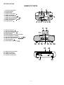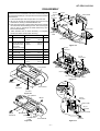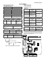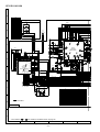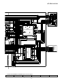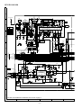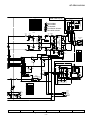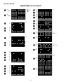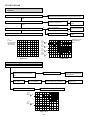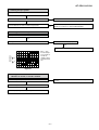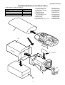
1
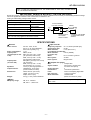
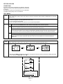
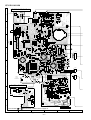
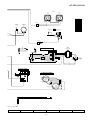
QT-CD111H/110H
SERVICE MANUAL
No. S6844QTCD111H
QT-CD111H
QT-CD110H
QT-CD110H is different from QT-CD111H in
Control Panel color.
Illustration: QT-CD111H
• In the interests of user-safety the set should be restored to its
original condition and only parts identical to those specified should
be used.
• Note for users in UK
Recording and playback of any material may require consent
which SHARP is unable to give. Please refer particularly to the
provisions of Copyright Act 1956, the Dramatic and Musical
Performers Protection Act 1956, the Performers Protection Acts
1963 and 1972 and to any subsequent statutory enactments and
orders.
CONTENTS
Page
SAFETY PRECAUTION FOR SERVICE MANUAL ........................................................................................................... 2
IMPORTANT SERVICE NOTES (111H FOR UK ONLY) .................................................................................................. 3
SPECIFICATIONS ............................................................................................................................................................. 3
NAMES OF PARTS ........................................................................................................................................................... 4
DISASSEMBLY .................................................................................................................................................................. 5
REMOVING AND REINSTALLING THE MAIN PARTS ..................................................................................................... 6
ADJUSTMENT ................................................................................................................................................................... 7
NOTES ON SCHEMATIC DIAGRAM ................................................................................................................................ 9
TYPES OF TRANSISTOR ................................................................................................................................................. 9
BLOCK DIAGRAM ........................................................................................................................................................... 10
SCHEMATIC DIAGRAM / WIRING SIDE OF P.W.BOARD ............................................................................................. 12
WAVEFORMS OF CD CIRCUIT ...................................................................................................................................... 18
TROUBLESHOOTING (CD SECTION) ........................................................................................................................... 19
FUNCTION TABLE OF IC ................................................................................................................................................ 22
PARTS GUIDE/EXPLODED VIEW
PACKING METHOD (111H FOR UK ONLY)
SHARP CORPORATION
–1–
This document has been published to be used
for after sales service only.
The contents are subject to change without notice.
QT-CD111H/110H
SAFETY PRECATION FOR
SERVICE MANUAL
Laser Diode Properties
Material:
GaAIAs
Wavelength: 780 nm
Emission Duration: continuous
Laser Output: max. 0.6 mW
Precaution to be taken when replacing and servicing the
Laser Pickup.
The ael (ACCESSIBLE EMMISSION LEVEL) of the laser
power output is less than class 1 but the laser component is
capable of emitting radiation exceeding the limit for class 1.
Therefore it is important that the following precautions are
observer during servicing to protect your eyes against exposure
to the laser beam.
(1) When the cabinet is removed, the power is turned on
without a compact disc in position and the pick-up is on the
outer edge the laser will light for several seconds to detect
a disc. Do not look into the pick-up lens.
(2) The laser power output of the pick-up unit and replacement
service parts are all factory pre-set before shipment.
Do not attempt to re-adjust the laser pick-up unit during
replacement or servicing.
(3) Under no circumstances stare into the pick-up lens at any
time.
(4) CAUTION-USE of controls or adjustments, or pereformance
of procedures other than those specified herein may result
in hazardous radiation exposure.
(111H For UK)
CAUTION-INVISIBLE LASER RADIATION WHEN OPEN. DO NOT STARE INTO
BEAM OR VIEW DIRECTLY WITH OPTICAL INSTRUMENTS.
VARNING-OSYNLIG LASERSTRALNING NAR DENNA DEL AR OPPNAD. STIRRA
EJ IN I STRALEN OCH BETRAKTA EJ STRALEN MED OPTISKA INSTRUMENT.
ADVERSEL-USYNLIG LASERSTRALING VED ABNING. SE IKKE IND I
STRALEN-HELLER IKKE MED OPTISKE INSTRUMENTER.
(111H Except for UK/110H)
VARO! AVATTAESSA OLET ALTTIINA NAKYMATON LASERSATEILYLLE.
ALA TUIJOTA SATEESEEN ALAKA KATSO SITA OPTISEN LAITTEEN LAPI.
VARNING-OSYNLIG LASERSTRALNING NAR DENNA DEL AR OPPNAD.
STIRRA EJ IN I STRALEN OCH BETRAKTA EJ STRALEN GENOM OPTISKT
INSTRUMENT.
ADVERSEL-USYNLIG LASERSTRALING NAR DEKSEL APNES. STIRR IKKE
INN I STRALEN ELLER SE DIREKTE MED OPTISKE INSTRUMENTER.
VAROITUS! LAITTEEN KÄYTTÄMINEN
MUULLA KUIN TÄSSÄ
KÄYTTÖOHJEESSA MAINITULLA
TAVALLA SAATTAA ALTISTAA
KÄYTTÄJÄN TURVALLISUUSLUOKAN 1
YLITTÄVÄLLE NÄKYMÄTTÖMÄLLE
LASERSÄTEILYLLE.
VARNING - OM APPARATEN ANVÄNDS
PÅ ANNAT SÄTT ÄN I DENNA
BRUKSANVISNING SPECIFICERAS. KAN
ANVÄNDAREN UTSÄTTAS FÖR OSYNLIG
LASERSTRÅLNING, SOM ÖVERSKRIDER
GRÄNSEN FÖR LASERKLASS 1.
LASER KLASSE 1
LUOKAN 1 LASERLAITE
KLASS 1 LASERAPPARAT
–2–
QT-CD111H/110H
FOR A COMPLETE DESCRIPTION OF THE OPERATION OF THIS UNIT, PLEASE REFER
TO THE OPERATION MANUAL.
IMPORTANT SERVICE NOTES (111H FOR UK ONLY)
Before returning the unit to the customer after completion of a repair or adjustment it is necessary for the following withstand voltage
test to be applied to ensure the unit is safe for the customer to use.
Setting of Withstanding Voltage Tester and set.
Set name
Set value
Withstanding Voltage Tester
Test voltage
WITHSTANDING
VOLTAGE TESTER
4,240 VPEAK
3,000 VRMS
6 secs
Set time
Set current (Cutoff current)
Unit
Judgment
PROBE
AC
OUT
4 mA
UNIT
SHORT-CIRCUT
AC POWER
SUPPLY CORD
OK: The “GOOD” lamp lights.
NG: The “NG” lamp lights and the buzzor sounds.
CONNECT THE PROBE
TO GND OF BATTERY
SPRING
SPECIFICATIONS
General
Power source:
Power consumption:
Output power:
(111H Except for UK/
110H)
Output power:
(111H For UK)
Speakers:
Output terminal:
Dimensions:
Weight:
Tape recorder
AC 230 - 240V, 50 Hz
DC 12 V [ "D" size (UM/SUM-1,
R20 or HP-2) battery x 8]
11 W
PMPO; 28 W
MPO; 8.4 W (4.2 W + 4.2 W)
(AC operation, DIN 45 324)
RMS; 4.6 W (2.3 W + 2.3 W)
(DC operation, DIN 45 324)
MPO (Max.); 8.4 W (4.2 W + 4.2 W)
(AC operation)
RMS; 4.6 W (2.3 W + 2.3 W)
(DC operation, 10 % T.H.D.)
10 cm (4") full-range speaker x 2
Headphones; 16-50 ohms
(recommended; 32 ohms)
Width; 480 mm (18-15/16")
Height; 153 mm (6-1/16")
Depth; 254 mm (10")
3.2 kg (7.1 Ibs.) without batteries
Frequency response: 50 - 14,000 Hz (Normal tape)
Signal/noise ratio:
50 dB
Wow and flitter:
0.3 % (DIN 45 511)
(111H Except for UK/110H)
Wow and flitter:
0.25 % (WRMS)
(111H For UK)
Motor:
DC 12 V electric governor
Bias system:
AC bias
Erase system:
Magnet erase
Compact disc player
Disc:
Signal readout:
Audio channels:
Quantization:
Filter:
D/A converter:
Wow and flutter:
Radio
Frequency range:
Compact disc
Non-contact, 3-beam semiconductor laser pickup
2
16-bit linear quantization
4-tims oversampling digital filter
1-bit D/A converter
Unmeasurable
(less than 0.001% W. peak)
Specifications for this model are subject to change without
prior notice.
FM; 87.5 - 108 MHz
AM; 526.5 - 1,606.5 kHz
–3–
QT-CD111H/110H
NAMES OF PARTS
1
1. Cassette Compartment
2. CD Compartment
3. Tuning Control
4. (TAPE) Record Button:
5. (TAPE) Play Button:
6. (TAPE) Rewind Button:
7. (TAPE) Fast Forward Button:
8. (TAPE) Stop/Eject Button: /
9. (TAPE) Pause Button:
10. CD Eject Button:
2
3
4 5 6 7 8 9 10
11 12
11. (CD) Play Indicator:
12. (CD) Track Number Indicator
13. (CD) Repeat Indicator:
14. Volume Control
15. Stand-by,On/Function Selector Switch
16. Extra Bass Button: X-BASS
17. (CD) Track Down/Review Button:
18. (CD) Track Up/Cue Button:
19. (CD) Stop Button:
20. (CD) Play/Repeat Button:
13
14 15 16 17 18 19 20
21
22
21. FM Telescopic Rod Aerial
22. Headphones Socket
23. Battery Compartment
24. AC Power Input Socket
23
–4–
24
QT-CD111H/110H
DISASSEMBLY
Caution on Disassembly
Follow the below-mentioned notes when disassembling the
unit and reassembling it, to keep it safe and ensure excellent
performance:
1. Take cassette tape and compact disc out of the unit.
2. Be sure to remove the power supply plug from the wall
outlet before starting to disassemble the unit.
3. Take off nylon bands or wire holders where they need be
removed when disassembling the unit. After servicing the
unit, be sure to rearrange the leads where they were
before disassembling.
4. Take suffcient care on static electricity of integrated
circuits and other circuits when servicing.
STEP
PROCEDURE
FIGURE
1
Rear Cabinet
REMOVAL
1. Screw ................. (A1) x10
2. Socket .................. (A2) x1
5-1
5-2
2
Top Cabinet
1. Knob ..................... (B1) x1
(with CD Mechanism/ 2. Screw ................... (B2) x3
Tape Mechanism/ 3. Socket .................. (B3) x1
Main PWB/
Headphones PWB)
5-2
3
Headphones PWB 1. Screw .................. (C1) x2
5-3
4
Main PWB/
Switch PWB
1. Screw ................... (D1) x6
2. Socket .................. (D2) x4
5-3
5-3,5-4
5
Tape Mechanism
1. Screw ................... (E1) x4
5-4
6
CD Mechanism
1. Screw ................... (F1) x3
5-4
7
Terminal PWB
1. Screw ................... (G1) x5
2. Hook ..................... (G2) x1
5-5
(D1)x5
ø3x10mm
(D2)x1
Switch PWB
(C1)x2
ø3x10mm
Main PWB
Headphones
PWB
Top Cabinet
(D1)x1
ø3x10mm
Figure 5-3
(E1)x4
ø3x10mm
(F1)x3
ø2.5x10mm
Tape
Mechanism
Front Cabinet
(D2)x2
Top Cabinet
CD Mechanism
(D2)x1
Figure 5-4
(A1)x6
ø3x20mm
(G2)x1
(A1)x3
ø3x12mm
Rear Cabinet
(A1)x1
ø3x12mm
Push
Figure 5-1
Driver
Top Cabinet
(B1)x1
(G1)x2
ø3x12mm
Spacer PWB
(G1)x1
ø3x10mm
Terminal PWB
(B2)x3
ø3x12mm
Main PWB
(A2)x1
(B3)x1
Headphones Front Cabinet
PWB
Figure 5-2
(G1)x2
ø3x14mm
Figure 5-5
–5–
QT-CD111H/110H
REMOVING AND REINSTALLING THE MAIN PARTS
CD MECHANISM SECTION
Perform steps 1, 2, 4 and 6 of the disassembly method to
remove the CD mechanism.
(A1) x2
2.6 x6mm
How to remove the pickup (See Fig. 6.)
1. Remove the screws (A1) x 2 pcs., to remove the shaft (A2)
x1 pc.
2. Remove the stop washer (A3) x1 pc., to remove the gear
(A4) x 1 pc.
3. Remove the pickup.
CD
Mechanism
Pickup
Shaft
(A2) x1
Gear
(A4) x1
Figure 6
–6–
Stop
Washer
(A3) x1
QT-CD111H/110H
ADJUSTMENT
MECHANISM SECTION
TUNER SECTION
• Driving Force Check
fL: Low-range frequency
fH: High-range frequency
Torque Meter
Specified Value
PLAY: TW-2412
• FM IF/RF
Over 120 g
Specified
Value/Adjusting
Point
Test Stage
• Torque Check
Torque Meter
Specified Value
Play: TW-2111
25 to 65 g.cm
IF
T1
Fast Forward: TW-2231
60 to 130 g.cm
Detection
T2
Rewind: TW-2231
60 to 130 g.cm
Band Coverage
fL: L2
fH: TC2
Tracking
88.0 MHz: L1
108.0 MHz: TC1
• Head Azimuth
Torque Meter
Specified Value
MTT-114
Output: Speaker Terminal
(CNP201 Load resistance: 8 ohms)
Test Stage
Adjusting
Point
MTT-111 In motor
Specified
Value
Instrument
Connection
3,000 ± 90 Hz
Output: Speaker
Teaminal
(CNP201 Load
resistance: 8 ohms)
Input: Pin 1 of IC1
Output: Pin 17 of IC2
Iuput: Antenna
Output: Speaker
Terminal (CNP201
Load resistance: 8
ohms)
• AM IF/RF
• Tape Speed
Test
Tape
Instrument
Connection
Instrument
Connection
Specified
Value/Adjusting
Point
IF
T3
Input: Antenna
Output: Pin 19 of IC2
Band Coverage
fL: L4
fH: TC4
600 kHz: L3
1,400 kHz: TC3
Input: Antenna
Output: Speaker
Terminal (CNP201
Load resistance: 8
ohms)
Tracking
TAPE SECTION
Position of each switch or control
Volume control
Function switch
X-BASS
• VCO Frequency
Max
Tape/Power Off
On
• Bias Oscillation
Adjustment Point
Specified Value
MTT-118
1.8 V ± 3 dB
Pin 13 of IC2
Pin 13, pin 21 and
ground of IC2
Note:
After preparing the test circuit shown in Fig. 7-1, connect the
Pin 13, Pin 21 and ground of the IC2 with the test circuit, and
measure the value. At this time, apply a standard unmodulated
signal input and adjust the VCO.
Pin 2 of CNP201
• Playback Amplifier Sensitivity Check
Test Tape
Instrument
Connection
76 kHz ± 200 Hz
VR1
Instrument
Connection
Specified Value
82 kHz ± 6 kHz
– 6 kHz
L301
Specified
Value
Adjusting Point
Instrument Connection
Speaker Terminal
(Load resistance: 8 ohms)
MAIN PWB
AM
TRACKING
fL
FM ROD ATENNA
Pin 21 of IC2
VR1
VCO
13
TO FREQUENCY
COUNTER
S
NA
D
TEN
G
FET : 2SK19 or 2SK54
L
AR A3
N
10 kohm
T2
17
19 IC2
T3
21
1
L4
AM IF
AM B
Figure 7-1 VCO FREQUENCY TEST CIRCUIT
FM
DETECTION
L2
IC1
TC4
T1
TC2
TC3
AM
TRACKING
fH
fL
fH
AM BAND
COVERAGE
FM IF
TC1
L1
fL
fH
FM
TRACKING
1
fL
fH
FM BAND
COVERAGE
Figure 7-2 ADJUSTMENT POINTS
–7–
QT-CD111H/110H
CD SECTION
Since this CD system incorporates the following automatic
adjustment function, when the pickup is replaced, it is necessary
to reajust it.
Since this CD unit does not need adjustment, the combination
of PWB and laser pickup unit is not restricted.
TEST MODE
Start
While holding down the "STOP" button, move the FUNCTION/POWER switch to "CD".
Then, release the "STOP" button and, within 0.5 second, connect the TEST POINT to GND (within 0.5 second).
(See Fig. 8)
Note
1. When the CD LID switch is in the OFF position, the unit will be able to enter the test mode.
However, playback cannot be performed in this mode.
2. You can only move the pickup.
3. The LCD display should be the same as it is for normal CD operations.
Operation
1
The use of the "UP/CUE" button will move the pickup to the outermost position.
The use of the "DOWN/REVIEW" button will move the pickup to the innermost position.
2
When the "PLAY" button is pressed, the laser will be lit, and when the "STOP" button is pressed, it will be
turned off. Playback will also start and stop when these buttons are pressed.
a. If the "PLAY" button is pressed while in the stop mode, the laser will simply be turned on at first.
b. If the laser is lit and the "PLAY" button is pressed again, playback will start from the current pickup position.
c. If the "STOP" button is pressed, playback will stop. When pressed again, the laser will be turned off.
3
Turning the tracking servo on or off.
a. Each time the PAUSE button is pressed during playback, the tracking servo will be turned on or off.
(Note: If the PLAY button is pressed while in the stop mode, the tracking servo will automatically be
turned on.)
LCD MODE
Start
Display
While holding down the "STOP" button, move the FUNCTION/POWER switch to "CD".
Then, release the "STOP" button and, within 0.5 second, press the REVIEW/DOWN button.
2
1
1 second
3
3
1 second
12
3
* After the number has appeared in the display, each time the "UP/CUE" button is pressed, the display will switch
in the following order: , , and then .
SWITCH PWB – A2
R771
3.9K
SW774
TRACK DOWN/
REVIEW
R772
2.7K
SW773
TRACK UP/
CUE
TEST
POINT
R773
1.8K
R774
1.5K
R776
10K
SW771
PLAY
SW7712
STOP
+B
3
1
TO CD SECTION
Figure 8
–8–
QT-CD111H/110H
NOTES ON SCHEMATIC DIAGRAM
• Resistor:
To differentiate the units of resistors, the symbol as K and M
are used: the symbol K means 1000 ohm and the symbol M
means 1000 kohm and the resistor without any symbol is an
ohm resistor. The resistor designated "Fusible" is a fuse type
resistor
• Capacitor:
To indicate the unit of capacitor, a symbol P is used: this
symbol P means micro-micro-farad and the unit of the capacitor
without such a symbol is microfarad. As to electrolytic capacitor,
the expression “capacitance/withstand voltage” is used.
(CH), (TH), (RH), (UJ): Temperature compensation
(ML): Mylar type
(P.P.): Polypropylene type
• The indicated voltage in each section is the one measured by
Digital Multimeter between such a section and the chassis
with no signal given.
REF. NO
DESCRIPTION
1. Tuner
( ): AM mode
Marking except for ( ): FM mode
2. CD
( ): Play mode
Marking except for ( ): Stop state
3. Deck section
( ): Record mode
Marking except for ( ): Playback mode
Display / Control section:
( ): Active state
Marking except for ( ): CD Function mode at stop state
• Schematic diagram and Wiring Side of P.W.Board for this
model are subject to change for improvement without prior
notice.
• Parts marked with “
”(
) are important for
maintaining the safety of the set. Be sure to replace these
parts with specified ones for maintaining the safety and
performance of the set.
POSITION
REF. NO
DESCRIPTION
POSITION
SW102
RECODE/PLAYBACK
OFF—ON
SW761
CD LID OPEN/CLOSE
OFF—ON
SW201
FUNCTION/POWER
TAPE—AM—
FM AUTO—CD/
OFF—ON
SW771
PLAY/REPEAT
OFF—ON
SW772
STOP
OFF—ON
SW773
TRACK UP/CUE
OFF—ON
SW774
TRACK DOWN/REVIEW
OFF—ON
SW203
X-BASS
OFF—ON
SW601
TAPE MAIN
OFF—ON
SW702
PICKUP IN
OFF—ON
FRONT
VIEW
E C B
(S) (G) (D)
(1) (2) (3)
2SC1815 GR
Figure 9 TYPES OF TRANSISTOR
–9–
24
27
28
30
31
34
35
36
SEG4
57
~
60
SEG1
~
9
~
14 17
~
19 21
20
SL+
SL–
+5V
(D)
PU-IN SW
13
14
38
25
VLC3
VDD
SYSTEM
MICROCOMPUTER
37
LID
23
33 22
44
IC701
IX0105AW
41
COM3
X701
4MHz
COM0
RES
PICKUP IN
SW702
Figure 10 BLOCK DIAGRAM (1/2)
– 10 –
M702
SLIDE
MOTOR
M701
SPIN
MOTOR
TRACKING COIL
FOCUS COIL
PICKUP UNIT
M
M
17
18
26
27
11
12
1
2
30
31
1
2
3
4
SL–
SL+
FIN2
FIN1
E
F
Q804
IC804
BA5914FP
10 19 23 25
JP–
44
43
40
32
9 EFMO
IC802
EFMIN
LCHO
CLV+ LC78622E
13 CLV– SERVO/SIGNAL
14 V/P
CONTROL
15 HFL
16 TES
17 TOFF
18 TGL
19 JP+
20 JP– RES. CQCK. COIN
SQOUT. RWC. WRQ
2 4 8 11
1 61 58 57 56 55 54 53
13
28
5
6
7
8
22
2
+7.4V
CONSTANT
VOLTAGE
REGULATOR
CL, DAT, SELIAL CONTROL
49 50 51 52 53 54
FOCUS/TRACKING
/SPIN/SLIDE
DRIVER
3
+5V
15 16 27 28 29
SLI
SLC
CV+
10
12
6
45
44
23 43
+5V
62
XL801
16.93MHz
64
IC801
LA9240M
SERVO AMP.
Q805
LASER +5V
DRIVER
LDO
VCC1
LCD701
CD LCD
K1
XIN
SL–
DRF
XOUT
CD
OPERATION
KEY
SW771~SW774
TO
FD
SPO
SLEO
SLD
XOUT
WRQ
RESET
XIN
~
VVDD
VDD
XVDD
THLD/DEF
CLK
CL
DAT
CE
DRF
CD LID
OPEN/CLOSE
SW761
46
39
38
33
32
37
64
63
62
51
+7.4V
(CD)
R-CH
GND (A)
L-CH
+7.4V (D)
GND (D)
6 POWER GND
7 MUTE
1
2
3
4
5
TO
MAIN
SECTION
QT-CD111H/110H
Figure 11 BLOCK DIAGRAM (2/2)
– 11 –
L-CH
ERASE
HEAD
R-CH
REC / PB
HEAD
FROM
CD
SECTION
1
L1
FM RF
2 3
9 6
FM
+B
7
SW102-H
REC / PB
SW102
REC / PB
B.D
REC / PB
SW102
C,E
P.B
P.B
MUTE
R-CH
1 (AUDIO GND)
2
CD
L-CH
3
+7.4V
4
+B2
5
(DIGITAL GND)
6
(POWER GND)
5
VCC
MIX
8
4
7
BIAS
OSC.
P. B
REC
SW102-G
REC / PB
8
6
R 12
9 R
IC101
EQULIZER
AMP.
BA331IL
L 1
REG.
23
5
REC
SW601
MAIN
+B2
STANBY
VR201
A,B
AM / FM
SELECT
+B
FM +B
14
10
5 11
6 R
2 L
8
TUNER
+B
TRIG.
VCO
7
ST.
SWIT.
FF
ST.
DRIV.
SP502
R-CH
SPEAKERS
SP501
L-CH
AC 230-240V
50Hz
AC INPUT
SO651
FF
FF
VCC
21
TUNER
+B
BATTERY
DC12V
[' D' SIZE (UM/SUM-1,
R20 or HP-2)BATTERYx8]
10
12
IC501
LA4597
POWER AMP.
9
DECODER
PHASE
DET.
PILOT
DET.
11 13 15
VR1
VCO
T651
POWER
TRANSFORMER
15
AM / FM
SELECT
+B
19 18
VOLUME
8
TU
DRIV.
SW201-C
POWER/
FUNCTION
+B1
12
MUTE
POST
AMP.
D651~D654
RECTIFIER
IC203
KIA7808P
VOLTAGE
REGULATOR
Q201
Q202
SW203
A,B
4
AGC
DET.
DET.
20 17
T2
FM DET
TAPE
6
GND
AM - IF
LEVEL - DBT.
FM - IF
2
CP
455kHz
X-BASS
SW201-D
POWER /
FUNCTION
L5
AM OSC
24
OSC
MPX
3
T3
AM IF
RADIO
M601
TAPE
MOTOR
RF
1
22
CF
10.7MHz
IC2
LA1805
FM / AM
IF MPX.
+B1
T1
FM IF
EC / PB
SW102
A,F
POWER/
FUNCTION
SW201-A,B
5 L
C201
L201
REC
REC
P.B
L2
FM OSC
OSC
IC1
LA1186N
FM FRONT END
RF AMP
L3
AM BAR ANT.
F1
B.P.F
FM ROD ANTENNA
QT-CD111H/110H
QT-CD111H/110H
IC701
VOLTAGE PIN
NO. VOLTAGE
0V
33 5V
0V
34 0V
0V
35 0V
0V
36 0V
0V
37 0.4V
0V
38 5V
3.9V
39 3.1V
0V
40 1.5V
5V
41 2.4V
4.1V
42 2.4V
4.1V
43 2.4V
0V
44 2.4V
0V
45 2.4V
0V
46 2.4V
0.4V
47 2.4V
0.4V
48 2.4V
0V
49 2.4V
0V
50 2.4V
0V
51 2.4V
0V
52 2.4V
5V
53 2.4V
54 2.4V
2.5V
55 2.4V
2.5V
0V
56 2.4V
5V
57 2.4V
5V
58 2.4V
0V
59 2.4V
0V
60 2.4V
5V
61 2.4V
4.8V
62 0V
0V
63 0V
3.8V
64 0V
SWITCH PWB-A2
SW774
TRACK DOWN/
REVIEW
Q805
S9012H
+B
SW773
TRACK UP/ CUE
R842
22
C849
0.022
C848
1/50
SW771
PLAY/
REPEAT
3
1
3
1
C837 10/16
+B
C838 0.01
R776
10K
C835 0.1/50
+B
SW761
CD LID
OPEN/CLOSE
C839 1/50
SW772
STOP
C840 0.33/50
B
PIN
NO.
1
2
3
4
5
6
7
8
9
10
11
12
13
14
15
16
17
18
19
20
21
22
23
24
25
26
27
28
29
30
31
32
R774 R773 R772 R771
1.5K 1.8K 2.7K 3.9K
A
1 2 3 4 5 6 7 8 9 10 11 12 13 14 15 16
D740
1N4148
R721 15K
R724 15K
+B
R716 10K
VCC2
FSS
CL
CLK
REFI
DEF
VR
CE
DAT
LF2
DRF
BH1
R741
3.3K
Q740
2SC1815 GR
R744
R740
10K
4.7K
R745
10K
R827
220K
R824
10K
C819
47/16
+B
PIN
NO.
1
2
3
4
5
6
7
8
9
10
11
12
13
14
15
16
17
18
19
20
21
22
C741
3.3/50
R743
100K
D741
1N4148
CD SIGNAL
G
VOLTAGE PIN
NO.
23
2.5V
2.5V
24
2.5V
25
2.5V
26
2.5V
27
28
2.5V
2.5V
29
2.5V
30
2.5V
31
2.5V
32
2.5V
33
2.5V
34
2.5V
35
2.5V
36
2.5V
37
38
2.5V
2.5V
39
40
2.5V
41
2.5V
42
2.5V
43
2.5V
44
0V
IC801
VOLTAGE PIN
NO.
2.5V
45
2.5V
46
2.5V
47
2.5V
48
2.5V
49
2.5V
50
2.5V
51
2.2V
52
2.2V
53
0V
54
0V
55
5V
56
5V
57
4.8V
58
0V
59
5V
60
0V
61
0V
62
1.5V
63
2.4V
64
2.5V
2.5V
VOLTAGE
0V
2.5V
2.5V
0V
0V
2.4V
4.1V
4.7V
0V
0V
5V
5V
2.5V
2.5V
0.9V
0.9V
2.1V
4.2V
0V
5V
PIN
NO.
1
2
3
4
5
6
7
8
9
10
11
12
13
14
15
16
17
18
19
20
21
22
IC802
PIN
VOLTAGE PIN
NO. VOLTAGE NO. VOLTAGE
23 5V
0V
45 2V
0V
24 0V
46 0V
1.5V
25 0V
47 0.1V
0V
26 0V
48 2.2V
2V
27 0V
49 0V
28 0V
5V
50 2.5V
0.3V
29 0V
51 0V
0V
30 5V
52 2.5V
2.5V
31 2.5V
53 0V
54 0V
2.5V
32 0V
55 0V
0V
33 0V
34 0V
0V
56 4.1V
35 5V
0V
57 4.1V
36 4.7V
5V
58 5V
37 2V
0V
59 0V
38
60 2.7V
4.8V
0V
39
5V
61 2.4V
0V
40 2V
5V
62 0V
41 4.7V
0V
63 0V
42 0V
0V
64 0V
43 5V
2.5V
44 2.3V
0V
MAIN PWB(2/2)
H
• The numbers 1 to 12 are waveform numbers shown in page 18.
1
2
3
4
Figure 12 SCHEMATIC DIAGRAM (1/4)
– 12 –
5
R833
5.6K
R8
47K
R832
56K
R
4
C8
220
R
8
C
5V
DIGITAL GND
PU IN
WRQ
SQOUT
DRF
SL–
SL+
RWC
CO IN
CQCK
RES
R742
1K
C8
0.1
30 31 32
+B
+B
C845
4.7/50
SL+
JP–
SLD
R822
6.8K
SL–
SPD
SLEQ
29
R715
15K
R727
1K
+B
R718 15K
R719 15K
R720 15K
R722 15K
R723 15K
R725 15K
PH1
C811
0.1
R736
1K
C740
0.01
R815 C814 R816
47K 0.01 1.5K
R840
22K
X701
4MHz
R726 1K
R728 1K
R729 1K
R731 1K
R732 1K
R733 1K
R735 1K
F
VREF
27 28
R831
1K
R713
1K
R839
22K
R817
82K
TOFF 35
34
33
C820
R826 0.0033
220K
GND
25 26
C818
1/50
C705
0.022
24
C830
2P
(CH)
CV+ 40
CV– 39
SLOF 38
HFL 37
TES 36
R825
1.2K
VSS
XOUT
XIN
18 SQOUT P21
RESET
17 DFR P20
PU-IN P23
WRQ P22
R812 C813
R828
15K 0.1
1K
R829
1K
21 22 23
C812
330P
R813
33K
+B
C816
0.001
15
16
17 18 19 20
R714
10K
C704
100/10
R730
1K
P33
COM2
COM3
VLC1
VLC2
VLC3
KIDSW AIN7
SIMUKE AIN6
AIN5
P3P40
XCOUT
VDD
32
31
30
29
28
27
26
25
24
23
22
21
20
19
18
17
R734
1K
P00
P01
P02
IC701
IX0105AW
SYSTEM
MICROCOMPUTER
VREF
AVSS
XCIN
D3 RES
D4 COCK
D5 COIN
D6 RWC
D7 SL+
D8 SL–
SEG2
SEG1
SEG0
32 P32
31 P31
30 P30
D1 MUTE
SEG7
SEG6
SEG5
SEG4
SEG3
P10
POWER IN
E
SEG10
SEG9
SEG8
SEG16
COM0
COM1
48 47 46 45 44 43 42 41 40 39 38 37 36 35 34 33
SEG12
SEG11
RFSM 41
TD
13
JP
14
C817
0.47/50
R830
1K
R811
3.3K
SLC 43
RFS– 42
34 TGL
33 JP+
SP–
C810
180P
D
49
50
51
52
53
54
55
56
57
58
59
60
61
62
63
64
15 TO
16 FD
12 TD–
R821
56K
R711
2.7K
C808
0.068
SPG
R710
10K
C809
0.047
R808
12K
10 TH
TA
11
R820
10K
R807
1K
R809
27K
R709
1K
9 SCI
R823
1.2K
1
C833
0.001
IC801
LA9241M
SERVO AMP.
8 TESI
SP
2
48 NC
TBC 47
FSC 46
GND 45
SLI 44
C815
0.0047
3
R871
4.7K
C834
0.033
A GND
4
50 49
1 FIN2
2 FIN1
NC
5
2
3 E
4 F
5 TB
FE–
6
56 55 54 53 52 51
7 TE
C806
0.033
R806
100
57
6 TE–
C805
0.033
C807
0.1/50 R805
6.8K
58
R814
10K
7
R708
1K
8
C701
0.022
C702
0.022
+B
59
R819
39K
LCD701
R802
100K
R804
2.2K
61 60
FE
C804
0.001
62
FA–
C
R803
15K
63
FA
C803
0.1/50
64
LDS
1
LDD
2
FD–
1
VCC1
FW701
6
+B
F
E
B
A
K
C802
47/16
R801
1K
1
2
3
4
5
6
7
8
TR–
TR+
FO+
FO–
GND
PD
TR+
FO+
FO–
TR+
FO+
VR
LD
FO–
TR–
TR–
PICKUP UNIT
C867
10/16
TEST3
LVDD 36
MUTEL 35
34
R873
100
C870
0.0022
R875 R876
10K 10K
C868 R874
10/16 100
LVSS 38
DOUT
1
2
3
4
5
6
7
8
+B
+B
LCHO 37
C2F
EMPH
CONT5
CONT4
CONT3
CONT2
B
F
C869
0.0022
C890
100/10
33
R880
100
24 25 26 27 28 29 30 31 32
SL+
JP–
17 18 19 20 21 22 23
K
E
A
E
A
B
F
XL801
16.93MHz
XVSS 46
XIN 45
34 NC
33 TEST4
15 HFL
16 TES
BI801
TR+
TR–
FO–
FO+
PW
FSX
SFSY
SBCK
RWC
WRQ
COIN
SQOUT
RES
CQCK
16M
TST11
4.2M
CS
12 CLV+
13 CLV–
14 V/P–
15
16
C822
220P
OFF 35
34
33
47
RVSS 39
CONT1
C831
0.0027
R835
470
Vss
VDD
R832
56K
CV+ 40
CV– 39
LOF 38
HFL 37
TES 36
48 EFLG
47 SBSY
MON
K
48
XOUT 44
EMFO
10 EMFIN
11 TEST2
R834
1K
1
2
3
4
5
6
7
8
53 52 51 50 49
XVDD 43
IC802
MUTER 42
RVDD 41
LC78623D
RCHO 40
SERVO/SIGNAL CONTROL
FSEQ
C832
27P
(CH)
55 54
VVDD
FR
PCK
FSM 41
C830
2P
(CH)
R833
5.6K
R857 27K 6
7
R856 1.2K
8
9
R837
47K
57 56
1 DEFI
2 TAI
4 VVss
5 ISET
JP–
SLC 43
FS– 42
R836
47K
62 61 60 59 58
1
C841 2
0.047
3 PDO
C842
0.047
R838
33K
C834
0.033
C833
0.001
64 63
TEST5
R858
680
JP+
C845
4.7/50
TGL
48 NC
TOFF
DEF
49
TBC 47
FSC 46
GND 45
SLI 44
+B
+B
TEST1
+B
C850
0.1
5
4
3
2
1
LD
1
VR
C
C801
0.01
R860
1K
C847
0.01
5
4
3
2
1
LD
PD
CNS801
+B
R871
4.7K
5
4
3
2
1
CNS802
BI802
QT-CD111H/110H
31 32
+B
C843
100/10
C873
0.01
TR+
TR–
FO–
FO+
+B
R849
100K
R827
220K
+B
D802
1N4148
R810
82K
L801
0.82µH
C851
0.022
CNP803
C821
1/50
2.5V
2.5V
Q804
R877
220 7.4VS8050D4.8V
+B
VOLTAGE
R878
100
2V
0V
0.1V
2.2V
0V
2.5V
0V
2.5V
0V
0V
0V
4.1V
4.1V
5V
0V
2.7V
2.4V
0V
0V
0V
+B
5.5V
-3.2V
9
VIN2'
VIN2
10 VO2+
11
VO212
0V 13 GND
14 OP OUT
C889
10/16
2.5V
7.4V
BIAS IN 23
VCC 22
30
VCC 21
+B
6
6
5
5
5
4
4
4
3
3
3
2
2
2
1
1
1
M
M701
SPINDLE
MOTOR
M
M702
SLED
MOTOR
SW702
PICKUP IN
CD MOTOR PWB-B
+B
7.4V
VIN3' 20
19
VIN3
VO3+ 18
VO3– 17
2.7V
3.8V
3.2V
OP IN + 16
OP IN - 15
ZD801
MTZJ5.6B
C887
0.022
SL–
PU-IN
VIN4' 24
6
+B
L802
0.68µH
MUTE
POWER GND
DIGITAL GND
DIGITAL +7.4V
L-CH
AUDIO GND
R-CH
N
O.
5
6
7
8
9
0
1
2
3
4
5
6
7
8
9
0
1
2
3
4
+3.8V
0V 8
GND
SL+
BI803
29
SP–
3.5V
3.5V
2.5V
CNS803
0V
C846
330/10
SP+
0V
C844
330/10
4 VIN1'
0V 5 NC
0V 6 NC
0V
7 MUTE
GND 28
VO4– 27
VO4+ 26
VIN4 25
0V
3.5V
1 VO13.5V 2 VO1+
2.5V 3 VIN1
IC804
BA5914FP
FOCUS/TRACKING/SPIN/SLIDE DRIVER
+B
7 6 5 4 3 2 1
P14 1 - E
TO MAIN SECTION
• NOTES ON SCHEMATIC DIAGRAM can be found on page 9.
7
8
9
10
Figure 13 SCHEMATIC DIAGRAM (2/4)
– 13 –
11
12
QT-CD111H/110H
A
R5
330K
2
CF2
C21
0.022
C28
0.0015
(Styrol)
C33
1/50
C34
1/50
R13
3.3K
R14
3.3K
VCO
AM/FM
SW201-A
CD
AUTO
FM
AM
TAPE
VC3
fH AM
fL TRACKING
VC4
L4
AM OSC.
fH
fL
AM BAND
COVERAGE
R456
6.8K
1
2
3
4
5
6
7
R455
6.8K
R229
10K
D202
1N4148
C105
0.0018
R103
18K
1
2
2
3
3
4
4
R107
1K
C107
820P
C111
330P
R
R
P
P
SW102-D
SW102-E
C106
0.0018
R
PRE AMP
C110 11
270P
4
GND
6 7
C114
47/16
R108
1K
R110
120
C116
0.018
(ML)
ALC T 2
OUT2
12
R116
3.9K
R114
8.2K
C121
0.01
1
OUT1 8
VCC
FILTER 10
IC101
BA3311L
REC./P.B.
EQUALIZER AMP.
9 IN2
NF2
C112
330P
C108
820P
ERASE HEAD
C118
10/16
C123
100/10
D103
1N4148
J
8
R125
680K
R118 R120
3.9K 3.3K
P
SW102-H
G
3
NF1
5 IN1
R123
10K
P
SW102-G
P
R
SW102-F
P
R
R122
1K
R106
15K
R124
10K
C351
0.0022
(ML)
R351
220
L301
47K
150
R352 R353 <
C352
220/10
H
• NOTES ON SCHEMATIC DIAGRAM can be found on page 9.
1
2
3
4
Figure 14 SCHEMATIC DIAGRAM (3/4)
– 14 –
5
6
C353
0.022
(ML)
C354
0.0056
(ML)
R-CH
1
P
C109
270P
C113
47/16
R
D101
1N4148
L-CH
R
SW102-B
R
P
R117
3.9K
R115
3.9K
D102
1N4148
CNS101
F
330
R101
SW102-C
CNP101
TAPE
RECORD/PLAYBACK
HEAD
R109
120
SW102-A
R119
3.3K
330
R102
R121
1K
C115
R113
0.018(ML) 8.2K
C122
0.01
R105
15K
C119
2.2/50
R104
18K
C120
47/16
E
C117
10/16
R-CH
AUDIO GND
L-CH
CD +7.4V
DIGITAL GND
POWER GND
MUTE
R16
10K
C36
0.022
NC
P13 7 - H
TO CD SERVO/
DISPLAY SECTION
R458 R457
1K
1K
SW201-B
CD
AUTO
FM
AM
TAPE
R15
10K
TC4
C46
2P
(CH)
C35
1/50
CF1
TC3
D
12
11
R38
1.8K
C31
0.015
2
R-CH
MO/ST
3
VCO
MPX VCO
CK 76kHz
13
10
9
8
C32
1
14
0.015
+B
6 7
T3
L3
AM BAR ANT.
220P
C11
5
C26 4
22/16
AM IF
3
C20
0.022
T1
C10 FM IF
0.022
C17
0.022
GND
AM IN
2
AGC
1 3
R9
22K
R7
390
VR1
6.8K
(B)
R29
15K
C27
3.3/50
18 17 16 15
IC2
LA1805
FM/AF IF MPX.
R17
68
C15
0.022
C23
0.01
R8
3.9K
1
19
AM
OUT
R25
120
20
FM
DET
C6
18P
(RH)
C25
3.3/50
T2
24 20 22 21
R3
47
C9
0.0047
C16
0.0047
C5
33P
(CH)
R27
33K
R11
1.2K
C24
470P
AM
IF
VC1
R1
10
C
4
AM RF
8
R2
33
C2
0.001
C4
22P
(CH) TC1
L1
FM ANT.
3 5 9 6
AM
MIX
PIN VOLTAGE
NO.
0.9V
1
1.6V
2
6.8V
3
0V
4
0V
5
6.8V
6
1.4V
7
6.2V
8
6.8V
9
FM DET
AM
FM
IF IN OSC
STB
2
FM
TRACKING
fL
fH
FM OSC.
L2
IC1
7
C38
C22 0.022
0.0039
C37
220/10
C39
0.022
FM BAND
COVERAGE
fH
fL
C29
10/16
D1
1N4148
C14
0.022
VC2
1
R6
820K
OSC
MIX
IC1
LA1186N
FM FRONT END
RF AMP.
1 2 3
B
C8
4P
(CH)
TC2
F1
B.P.F.
DET
OUT
MPX
IN
L-CH
ROD ANTENA
QT-CD111H/110H
X VCO
76kHz
IC2
PIN
NO.
1.6V
13
1.6V
14
6V (6.3V)
15
0.2V (0.7V) 16
1.6V
17
0V
18
0V
19
0V
20
2.5V
21
2.5V
22
5.1V (6.6V) 23
0.8V (1V)
24
VOLTAGE
MAIN PWB-A1(1/2)
HEADPHONES PWB-A4
VOLTAGE
R227 120
1.2V (0V)
1.9V (1.6V)
1V (1.3V)
1.7V
1.5V (1.7V)
1.5V (1.5V)
0.4V (0.4V)
6.1V (6.4V)
6.1V (6.4V)
1.6V
1.6V
1.6V
( ): AM
J201
HEADPHONES
PIN
NO.
1
2
3
4
5
6
7
8
9
10
11
12
R228
120
AM SIGNAL
FM SIGNAL
CD SIGNAL
PLAYBACK SIGNAL
RECORD SIGNAL
5
1
FW202
X-BASS
R216
2.2K
C218
0.0039
C304
0.15/50
C224
100/10
C214
0.1
7
C225
220/25
3
R222
1K
C222
0.001
9
10
5
3
L-CH
2
3
IC202
C227
3300/25
Q202
2SC1815GR
VOLTAGE
0.1V
0V
11.2V
0V
11.3V
0V
0.1V
12V
10.4V
5.8V
0V
5.8V
10.4V
R224
4.7K
R223
4.7K
+B
1
2
PIN
NO.
1
2
3
4
5
6
7
8
9
10
11
12
13
+B
Q201
2SC1815GR
1
SP502
C234
1000/10
8
D201
1N4148
CNS201
CNP201
C232
0.1
(ML)
–
+
6
C220
0.047
(ML)
11
SPEAKERS
SP501
R-CH
4
C231
0.1
(ML)
13
C230
100/10
R220
3.3K
C233
1000/10
1
C223
100/10
VOLUME
IC202
LA4597
POWER AMP.
R304
1.8K
SW203-B
12
+
–
C226
0.022
R302
1.8K
VR201-A
20K (B)
SW203-A
C215
0.039
(ML)
R219
3.3K
C216
0.039(ML)
C303
0.15/50
2
C221
0.001
C217
0.0039
R221
1K
C229
100/10
C213
0.1
VR201-B
20K(B)
R215
2.2K
5
1
C219
0.047
(ML)
TERMINAL PWB-A3
J6
82
R351
220
C352
220/10
C353
0.022
(ML)
7
C354
0.0056
(ML)
Q351
<3V> S8050D
47K
150
R352 R353 <0.7V>
<0.1V>
R354
10
C651
0.022
D652
1N4004
C652
0.022
D651
1N4004
C654
0.022
AC INPUT
+B
BATTERYS
DC12V["D"size(UM/SUM-1,
R20 or HP2)battery x 8]
PIN
VOLTAGE
NO.
1 <0V> [3.23V]
2 <0V> [0V]
3 <0.6V> [0.6V]
4 <0V> [0V]
5 <0V> [0V]
6 <0V> [0V]
7 <0V> [0V]
8 <7.43V> [7.43V]
9 <0V> [0V]
10 <7.37V> [7.37V]
11 <0.6V> [0.6V]
12 <3.3V> [3.3V]
< >: Recording
[
]: Play
SW601
(241-7)
MAIN
+B
+
+B
–
8
SO651
+B
IC101
SW102-G
P
R
1
2
D653
1N4004
1
2
D654
1N4004
CD
FM AUTO
AM
TAPE
IC203
KIA7808P
SW201-C VOLTAGE REGULATOR
11.83V
3 OUT
IN 1
C302
C301 8V
2
0V
0.022
0.022
SW201-D
+B
CD
FM AUTO
AM
TAPE
CNS602
C228
1/50
C653
0.022
R225
100K
CNP602
D309
1N4148
D308
1N4148
T601
POWER TRANSFOMER
9
10
Figure 15 SCHEMATIC DIAGRAM (4/4)
– 15 –
M
11
M601
(241-6)
TAPE
MOTOR
12
QT-CD111H/110H
HEADPHONES PWB-A4
1 2 3 4 CNP101
G
P.B
R352
R106
C106
C114
C116
R116
R114
R118
Q351
R122
D103
R120
C122
R124
1
2
CNP602
R108
C108
R110
C110
C112
B C E
C354
C219
C227
R224
J6
C221
C226
C224
OFF
C231
C223
C214
B
IC202
C232
R215
R216
R219
10 11 12 13
C230
C844
C889
ZD801
C848
R842
C849
R820
C815
R819
C811
C812
R816
C814
R815
R814
R828
R817
E
C
B
12
10
1
8
C807
R812
C809
R806
C810
C808
R807
R808
16
5
R811
R809
1
CNS802
C806
R805
BK
WH
WH
WH
WH
5
BI802
C801
C803
R803
R802
R804
C805
1
C804
R834
Q805
17
10
C839
C802
C813
20
15
IC801
64
BR
BK 1
BK 2
3
BK
4
BK
5
BK
6
BK
7
BK
8
R813
55
C840
8
BI801
25
60
CNS801
R810
R830
R840
C816
R839
R821
C822
C830
R827
R826
R833
C850
IC804
C818
R822
R823
C817
C819
R831
1
35 30
45
50
R801
C831
R871
1
R829
C846
R825
R824
C843
C873
R878
R877
C867
L802
R838
7
28
40
48
C838
R716
C845
R742
C741
22
7
8
29
33 32
49
C835
C740
R740
D740
R741
R858
1
R835
R734
R725
R726
R728
R723
R729
R722
R731
R720
R732
R719
R733
R718
R735
1
R832
C847
30
C820
5
C841
C842
R857
R856
R860
C833
R836
C834
R743
64
R849
64
Q740
E
16
5
ECB
R745
R744
D741
R730
R721
C821
60
16
17
20
15
10
55
17
10
60
C851
49
IC701
IC802
55
R727
25
40
45
50
49
20
15
C832
X701
45
50
14
21
L801
25
40
48
R724
35 30
Q804
35 30
R715
R736
B C E
R837
C704
15
C837
33 32
33 32
D802
R711
R880
R714
C705
C702
6
R873
C868
R874
R229
C890
C701
48
C303
C304
R304
R708
XL801
D
R709
R710
R713
8
7
6
5
4
3
2
1
LCD701
R456
C869
R455
R875
R457
R458
C301
C870
R876
D
C887
C
1
2
3
C302
IC203
R302
SW203
X-BASS
D201
POWER
B
C225
D202
A
ON
TAPE
C119
C234
Q202
E C B
C220
C215
1 2 3 4 5 6 7 8 9
AM
IC101
C118
R101
C121
R125
C120
R222
R223
E C B
Q201
C213
SW201
FUNCTION
R107
C107
R109
C109
C113
C117
D102
C222
FM AUTO
CD
C353
C229
VR201
C228
R225
R221
A
A
12
REC
F
C233
C218
C217
VOLUME
1 3 5 7 9
2 4 6 8 10
C123
B
B
C111
R104
R103
C115
R113
C216
R220
R115
R121
R119
R123
1
D
11
D101
5
R117
C105
R105
FW202
B
R102
A
1
R227
R351
SW102
R228
A
C
C351
H
C352
E
L301
C
R354
CNP201
FW202
5
R353
1 2 3
J201
HEADPHONES
9
D309
R17
D308
1
T1
C20
BK
R771
R772
R6
TC2
TC1
SW772
STOP
VC3
VC4
TC3
TC4
C38
R14
R38
R16
C28
C39
R29
C27
L4
L3
AM BAR ANTENNA
D1
H
MAIN PWB-A1
• The numbers 1 to 12 are waveform numbers shown in page 18.
2
C11
R774
R773
R776
C36
C46
SW771
PLAY
1
R25
L2
VC2
VCO
VC1
C16
VR1
1
FW701
C6
C35
G
3
TRACK UP/CUE
C14
C5
C4
T2
TRACK DOWN/
REVIEW
R8
C8
C9
L1
C25
F1
SW773
IC2
24 23 22 21 2019 18 17 16 15 14 13
R11
R1
SW774
CF1
R2
R5
C34
C37
2 3 4 5 6 7 8 9
C2
1
C29
1
2
C33
C31
C32
1 2 3 4 5 6 7 8 9 10 11 12
1 2 3
C15
SWITCH PWB-A2
R9
IC1
3
1
2
3
C23
R27
C17
C26
2
R3
R7
C10
3
1
2
3
4
5
6
T3
6
BI803
BK
CF2
F
R13
R15
FW701
C24
5 4
SW761
CD LID
OPEN/CLOSE
COR1
C21
11
CNS803
BR
GY
GY
GY
GY
GY
1
C22
3
1
2
3
4
5
3
4
Figure 16 WIRING OF P.W.BOARD (1/2)
– 16 –
5
6
QT-CD111H/110H
SPEKERS
SP502
R-CH
SP501
L-CH
COLOR TABLE
BR
CNS201
SW601
TAPE MAIN
(241-7)
1 WH
2 BK
3 RD
M601
TAPE MOTOR
(241-6)
BROWN
RD(R)
RED
OR
ORANGE
YL
YELLOW
GR
GREEN
BL
BLUE
VL
VIOLET
GY
TAPE
ERASE HEAD
(241-5)
WHITE
BK
BLACK
PK
PINK
RD
BK
BR
WH
YL
RECORD/PLAYBACK
HEAD(241-4)
GRAY
WH(W)
BK
CNS101
4
3
2
1
BK
WH
RD
BK
BK
(211)
T601
POWER
TRANSFORMER
TERMINAL PWB-A3
+
BATTERYS
DC12V["D"SIZE(UM/SUM-1,
R20 or HP2)battery 8]
F651
T1.25A L 250V
C653
(236)
RD
D653
D652
RD
C652
C654
2
1
D654
D651
SO651
AC SOCKET
AC 230-240V
50Hz
CNS602
C651
OR
OR
PICK UP UNIT
CD MOTOR PWB-B
-
5 4 3 2 1
+
8 7 6 5 4 3 2 1
SW702
SPENDLE MOTOR
M701
CNP803
PICKUP IN
F3895AF
SLED MOTOR
M702
6
5
4
3
2
1
-
+
FM ROD ANTENNA(213)
7
8
9
10
Figure 17 WIRING OF P.W.BOARD (2/2)
– 17 –
11
12
QT-CD111H/110H
WAVEFORMS OF CD CIRCUIT
1
2
5ms
0.50 V
IC801 20 F.E
5ms
5.0 V
IC801 54 DRF
STOP
FOCUS
PLAY
SERCH
50ms
10.0 V
JP+
7
50ms
10.0 V
JP-
8
50ms
0.50 V
JP
9
50ms
1.00 V
TE
6
0.5ms
10.0 V
JP+
7
0.5ms
10.0 V
JP-
8
0.5ms
0.50 V
JP
9
0.5ms
1.00 V
TE
10
20ms
1.00 V
SPO
11
20ms
2.00 V
CLV+
10
50ms
1.00 V
SPO
11
50ms
2.00 V
CLV+
3
1
3
6
CUE
0.5ms
1.00 V
HF
1
4
0.5ms
5.0 V
HFL
5
0.5ms
5.0 V
TES
3
0.5ms
1.00 V
H.F
4
0.5ms
5.0 V
HFL
5
0.5ms
5.0 V
TES
2
REVIEW
3
REVIEW
PLAY
NORMAL DISC
TN0=01
1
6
50ms
10.0 V
JP+
7
50ms
10.0 V
JP-
8
50ms
0.50 V
JP
9
50ms
1.00 V
TE
2
3
PLAY
TCD-712 (140mm)
TN0=01
CUE
PLAY
TCD-712
12
5s
100mV
SLD
1
6
0.5ms
10.0 V
JP+
7
0.5ms
10.0 V
JP-
8
0.5ms
0.50 V
JP
9
0.5ms
1.00 V
TE
12
0.5s
100mV
SLD
1
– 18 –
QT-CD111H/110H
TROUBLESHOOTING (CD SECTION)
When the CD does not function
When the CD section does not operate When the objective lens of the optical pickup is dirty,this section may not operate.Clean
the objective lens,and check the playback operation.When this section does not operate even after the above step is taken,check
the following items.
Remove the cabinet and follow the troubleshooting instructions.
"Track skipping and/or no TOC(Table Of Contents) may be caused by build up of dust other foreign matter on the laser pickup lens.
Before attempting any adjustment make certain that the lens is clean. If not, clean it as mentioned below."
Turn the power off.
Gently clean the lens with a lens cleaning tissue and a small amount of isopropyl alcohol.
Do not touch the lens with the bare hand.
• The CD function will not work.
The CD operating keys don't work.
Yes
Check the CD, DPS microcomputer (IC701), power supply, 4.19
MHz and 16.93 MHz clock, and reset terminal.
Yes
Check the waveform of SCK, SO (DATA) and SI (COMM).
Yes
See if the pick-up is in the pick-up in SW702 position.
Yes
If the items mentioned above are OK, check the main
microcomputer IC701.
• The CD operating keys work.
Check the Focus - HF system.
Playback can be performed without a disc.
Yes
Does the pick-up move up and down twice?
Focus search OK.
Yes
No
Does the output waveform of IC801(16)(FD) match that shown in
Fig. 19?
Check the area around IC804-BI801/CNS801.
Yes
No
Check the IC801(50)(CLK) line, 4MHz.
Check the microcomputer data on pins (51)(CL), (52)(DAT) and
(53)CE.
Focus search
is performed
two times
when play
operation is
done without
disc.
0.5s
0.50 V
IC801 16 FD
0.5s
0.50 V
IC801 15 TD
1
2
Figure 19
– 19 –
QT-CD111H/110H
• Playback can only be performed when a disc
is loaded.
No
Check the laser diode driver.
Check the area around IC801(16) - (21) (focus servo circuit).
No
If the disc is not turning, the DRF
should not change to "H".
Is the Focus servo active? (Can you hear it working?)
Yes
▼
Yes
Does the DRF signal change from "L" to "H"?
Check the spin
system.
Yes
Yes
No
Level is abnormal.
▼
Is HF waveform normal (see the Fig. 20-1, 2)?
Yes
Check the periphery
of IC801 pins 41 and
42.
Yes
Check the tracking system.
HF
0.1V/DIV
0.5µsec/DIV(DC)
(When playing
back the disc)
▼
Waveform is unstable.
Check the spin
system.
Waveform in case
of normal playback
0.5s
1.00 V
IC801 16 FD
0.5s
10.0 V
IC801 12 CLV+
2
1
3
0.5s
10.0 V
IC801 54 DRF
4
0.5s
2.00 V
IC801 7 TE
Figure 20-1
Figure 20-2
• Check the tracking system.
Check waveform of IC801 pin 7 (TE).
The waveform shown in Fig. 20-3
appears, and no-disc state appears
soon.
Play is possible in
TEST mode.
Yes
Tracking servo is inoperative.
Yes
Although IL is possible,
play is impossible.
Yes
Data cannot be read.
Yes
Yes
Normal jump is impeded, and the
program top cannot be reached.
Check the VCO-PLL system.
5ms
1.00 V
IC801 7 TE
4
5 ms
5.0 V
IC801 54 DRF
3
Figure 20-3
– 20 –
Check the periphery of IC801
pin 8 to pin 15, and IC804 to
BI801/CNS801.
Yes
Check the periphery of
IC801 pin 14.
QT-CD111H/110H
• Checking the spin system.
Play operation is performed without disc.
Yes
The spin driver circuit is normal.
The turntable rotates a little.
Yes
No
The turntable fails to rotate or rotates at high speed.
Yes
Check the periphery of IC801 pins 23 to 27, pin 39 and pin 40,
IC802 pin 12 and pin 13, IC804 to BI803/CNS803.
• Checking the VCO-PLL system
Play operation is performed when disc exits.
Yes
Although HF waveform is normal, TOC data cannot be read.
Yes
Check PDO waveform (Fig. 21).
Error
Check the IC801 pins 43 and 44, IC802 pins 3, 5, 7, 9 and 10.
0.5s
1.00 V
IC802 3 PDO
2
0.5s
1.00 V
IC801 16 FD
Stop --> Play
As VCO frequency is locked at
4.32 M Hz,
voltage of PDO
rises and stabilizes.
3
Figure 21
•
Although HF waveform is normal and the time
indication is normal, no sound is emitted.
Check IC802 pin 48 (EFLG).
No
Yes
Check IC802 pins 37and 40.
Abnomal
Check the periphery of IC803 (OPAMP).
– 21 –
Usually, the number of pulses of flawless disc is 100 pulses/sec
or less.
QT-CD111H/110H
FUNCTION TABLE OF IC
IC701 RH-iX0105AWZZ (IX0105AW): System Control Microcomputer
Pin No.
Terminal
Name
Port Name
Input/
Output
Function
1*
P03
MTCONT2
Input/Output Used to input or output 4 bits at a time. When the output latch is set to "1", the unit will be in the
input mode. The key-on wakeup function, which can be switched on or off by the software, and a
pull-up transistor, which can be turned on or off by the software, are built in.
2*-5*
P10-P13
POWER-IN,
DATA (VOL),
STB (VOL)
Input/Output Used to input or output 4 bits at a time. When the output latch is set to "1", the unit will be in the
input CK (VOL), mode.The key-on wakeup function, which can be switched on or off by the software,
and a pull-up transistor,which can be turned on or off by the software, are built in.
6*
D0
POWER-ON
Input/Output Each terminal can be used to input or output 1 bit at a time. The output section has a latch which
holds 1 bit. One of the D ports is assigned by register Y as a data point, to execute input or output.
To use the port for input, set the output latch for that bit to "1". All of the output latches on port D can
be set to "1" using the CLD command.
7
D1
MUTE
Input/Output Each terminal can be used to input or output 1 bit at a time. The output section has a latch which
holds 1 bit. One of the D ports is assigned by register Y as a data point, to execute input or output.
To use the port for input, set the output latch for that bit to "1". All of the output latches on port D can
be set to "1" using the CLD command.
8*-12
D2-D6
SYNC-OUT,
RES,CQCK,
COIN,REC
Input/Output Each terminal can be used to input or output 1 bit at a time. The output section has a latch which
holds 1 bit. One of the D ports is assigned by register Y as a data point, to execute input or output.
To use the port for input, set the output latch for that bit to "1". All of the output latches on port D can
be set to "1" using the CLD command.
13,14
D7,D8
SL+,SL-
Input/Output Each terminal can be used to input or output 1 bit at a time. The output section has a latch which
holds 1 bit. One of the D ports is assigned by register Y as a data point, to execute input or output.
To use the port for input, set the output latch for that bit to "1". All of the output latches on port D can
be set to "1" using the CLD command.
15*,16*
D9,D10
SRS2,SRS1
Input/Output Each terminal can be used to input or output 1 bit at a time. The output section has a latch which
holds 1 bit. One of the D ports is assigned by register Y as a data point, to execute input or output.
To use the port for input, set the output latch for that bit to "1". All of the output latches on port D can
be set to "1" using the CLD command.
17
P20
DRF
Input/Output Used to receive 4 bits at a time.
18
P21
SQOUT
Input/Output Used to receive 4 bits at a time.
19
P22
WRQ
Input/Output Used to receive 4 bits at a time.
20
P23
PU-IN
21
RESET
22
XIN
23
XOUT
24
VSS
—
25
VDD
—
26*
XCOUT
27
XCIN
28
AVSS
Input
GND input terminal for the A-D converter.
29
VREF
Input
Reference voltage input terminal for the A-D converter.
30
P30
REMOCONINT2
Input
Used to receive 4 bits at a time.
31
P31
TORAY1
Input
Used to receive 4 bits at a time.
32
P32
TORAY2
Input
Used to receive 4 bits at a time.
33
P33
Input
Used to receive 4 bits at a time.
34
P40
Input
Used to receive 4 bits at a time.
35-37
AIN5-AIN7
Input
Used to receive 4 bits at a time.
38-40
VLC3-VLC1
Input
LCD power input terminals. To use the internal resistor, connect VLC3 to VDD (if a brightness
control is needed, connect VLC3 to VDD through a resistor). When an external power supply is
used, applyvoltages as follows: 0<VLC1<VLC3<VLCD<VDD.
41-44
COM3-COM0
Output
LCD common output terminals.
45-61*
SEG16-SEG0
(45*-56*)
Output
LCD segment output terminals.
62*-64*
P00-P02
Input/Output Used to receive 4 bits at a time.
Input/Output Reset pulse input/output terminal. When a reset is caused by the watch dog timer, an "L" level will
be output. The output is an N channel open drain.
Input
Input/output terminals for the main clock generation circuit. Used by connecting a ceramic resonator
between the XIN and XOUT terminals. There is a built-in feedback resistor between the XIN and
XOUT terminals.
Output
Input/output terminals for the main clock generation circuit. Used by connecting a ceramic resonator
between the XIN and XOUT terminals. There is a built-in feedback resistor between the XIN and
XOUT terminals.
GND input terminal.
Positive power supply terminal.
Output
Input/output terminals for the sub clock generation circuit. Used by connecting a crystal oscillator
between the XCIN and XCOUT terminals. There is a built-in feedback resistor between the XCIN
and XCOUT terminals.
Input
Input/output terminals for the sub clock generation circuit. Used by connecting a crystal oscillator
between the XCIN and XCOUT terminals. There is a built-in feedback resistor between the XCIN
and XCOUT terminals.
Input/Output Used to input or output 4 bits at a time. When the output latch is set to "1", the unit will be in the
input mode. The key-on wakeup function, which can be switched on or off by the software, and a
pull-up transistor, which can be turned on or off by the software, are built in.
In this unit, the terminal with asterisk mark (*) is (open) terminal which is not connected to the outside.
– 22 –
QT-CD111H/110H
PACKING METHOD (111H FOR UK ONLY)
• Setting position of switches and knobs
Tape Mechanism Control
STOP STATE
TUNING
LOW
POWER/FUNCTION
OFF/TAPE
X-BASS
OFF
VOLUME
LOW
1. AC Power Supply Cord
2. Polyethylene Bag, Unit
3. Packing Add., Left/Right
4. Packing Case
5. Operation Manual
6. Polyethylene Bag,
AC Power Supply Cord
7. Warranty Card
8. Feature Label
9. Label, Bar Code
10. Polyethylene Bag, Accessories
QACCB0001SJ00
SSAKH0001SJZZ
SPAKA0001SJZZ
SPAKC0005SJZZ
TiNSE0002SJZZ
SSAKK0002SJZZ
TCADN0001SJZZ
TLABE0004SJZZ
TLABE0001SJZZ
SSAKK0001SJZZ
2
4
9
FR
ON
T
5, 7, 8, 11
FR
ON
T
6
1
3
10
––29
6 ––