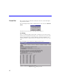
1
Activator and APS Programming System
Installation and User’s Guide
Windows ® and UNIX ® Environments
Actel Corporation, Sunnyvale, CA 94086
© 2001 Actel Corporation. All rights reserved.
Printed in the United States of America
Part Number: 5029102-5
Release: December 2001
No part of this document may be copied or reproduced in any form or by any
means without prior written consent of Actel.
Actel makes no warranties with respect to this documentation and disclaims any
implied warranties of merchantability or fitness for a particular purpose. Information in this document is subject to change without notice. Actel assumes no
responsibility for any errors that may appear in this document.
This document contains confidential proprietary information that is not to be
disclosed to any unauthorized person without prior written consent of
Actel Corporation.
Trademarks
Actel and the Actel logotype are registered trademarks of Actel Corporation.
Adobe and Acrobat Reader are registered trademarks of
Adobe Systems, Inc.
Cadence is a registered trademark of Cadence Design Systems, Inc.
Mentor Graphics is registered trademark of Mentor Graphics, Inc.
Synopsys is a registered trademark of Synopsys, Inc.
Verilog is a registered trademark of Open Verilog International.
Viewlogic, ViewSim, and ViewDraw are registered trademarks and
MOTIVE and SpeedWave are trademarks of Viewlogic Systems, Inc.
Windows is a registered trademark and Windows NT is a trademark of
Microsoft Corporation in the U.S. and other countries.
All other products or brand names mentioned are trademarks or registered
trademarks of their respective holders.
ii
Table of Contents
Introduction . . . . . . . . . . . . . . . . . . . . . . . xi
Document Organization
Document Assumptions
Document Conventions
Actel Manuals . . . . .
Online Help. . . . . .
1
.
.
.
.
.
.
.
.
.
.
.
.
.
.
.
.
.
.
.
.
.
.
.
.
.
.
.
.
.
.
.
.
.
.
.
.
.
.
.
.
3
.
.
.
.
.
.
.
.
.
.
.
.
.
.
.
.
.
.
.
.
.
.
.
.
.
.
.
.
.
.
.
.
.
.
.
.
.
.
.
.
. xi
. xii
. xii
. xiii
. xv
.
.
.
.
.
.
.
.
.
.
.
.
.
.
.
.
.
.
.
.
.1
.1
.2
.4
.4
Hardware Installation on a PC . . . . . . . . . .
Adaptec AVA-1505A AT-to-SCSI Host Adapter Installation
Installing the 1505A Card Under Windows 95/98 . . . .
Installing the 1505A Card under Windows NT 4.0 . . . .
Connecting an Adaptec SCSI Card to the Activator. . . .
Installing the Activator . . . . . . . . . . . . . . . . .
Installing and Removing an Adapter Module . . . . . .
.
.
.
.
.
.
.
.
.
.
.
.
.
.
.
.
.
.
.
.
.
.7
.7
.8
12
14
15
17
. . . .
. . . .
. . . .
. . . .
Adapter
.
.
.
.
.
.
.
.
.
.
.
.
.
.
.
Hardware Installation on a Workstation . . . . . . . . 19
Installing
Installing
Installing
Installing
4
.
.
.
.
.
Hardware Description . . . . . . . . . . . . . . . . . . . 1
Unpacking Your Activator . . . . . . .
Device Handling . . . . . . . . . . .
Activator 2 and 2s Rear Panels . . . . .
Adapter Modules . . . . . . . . . . .
PC Adaptec AVA-1505A AT-to-SCSI Host
2
.
.
.
.
.
an Activator on a SunOS Workstation .
an Activator on a Solaris Workstation .
an Activator on an HP-UX Workstation
and Removing an Adapter Module . .
.
.
.
.
.
.
.
.
.
.
.
.
.
.
.
.
.
.
.
.
.
.
.
.
.
.
.
.
19
21
24
26
Programming an Actel Device . . . . . . . . . . . . . 27
Programming Flow . . . . . . .
APSW Description . . . . . . . .
Programming a Device with APSW
Programming Security Fuses . . .
.
.
.
.
.
.
.
.
.
.
.
.
.
.
.
.
.
.
.
.
.
.
.
.
.
.
.
.
.
.
.
.
.
.
.
.
.
.
.
.
.
.
.
.
.
.
.
.
.
.
.
.
.
.
.
.
27
28
30
34
iii
Table of Contents
5
Device Programming Failure Guidelines . . . . . . . . 41
Programming Failure Guidelines . . . . . . . . . . . . . . . 41
Activator Programming Failures . . . . . . . . . . . . . . . 42
Returning Failed Devices. . . . . . . . . . . . . . . . . . . 42
6
Verifying a Device with an Activator . . . . . . . . . . 43
Functional Verification with an Activator
Running Debugger From APSW . . . .
Debugger Command-Line Commands .
Using Command Files to Verify a Device
.
.
.
.
.
.
.
.
.
.
.
.
.
.
.
.
.
.
.
.
.
.
.
.
.
.
.
.
.
.
.
.
.
.
.
.
.
.
.
.
.
.
.
.
43
44
44
48
A Troubleshooting . . . . . . . . . . . . . . . . . . . . . 55
Driver Does Not Load
Activator . . . . . .
AFM File . . . . . .
Fuse . . . . . . . .
SCSI Controller . . .
Fuse Failures . . . .
Error Messages . . .
under Windows
. . . . . . . .
. . . . . . . .
. . . . . . . .
. . . . . . . .
. . . . . . . .
. . . . . . . .
.
.
.
.
.
.
.
.
.
.
.
.
.
.
.
.
.
.
.
.
.
.
.
.
.
.
.
.
.
.
.
.
.
.
.
.
.
.
.
.
.
.
.
.
.
.
.
.
.
.
.
.
.
.
.
.
.
.
.
.
.
.
.
.
.
.
.
.
.
.
.
.
.
.
.
.
.
.
.
.
.
.
.
.
55
55
57
57
58
59
59
B AVI File Description . . . . . . . . . . . . . . . . . . . 61
C Activator 2 Test Procedures . . . . . . . . . . . . . . 63
Equipment Required . . . . . . . . . . . . . . . . . . . . . 63
Test Setup. . . . . . . . . . . . . . . . . . . . . . . . . . 63
Execute the Test Program . . . . . . . . . . . . . . . . . . 64
D Product Support . . . . . . . . . . . . . . . . . . . . . 69
Actel U.S. Toll-Free Line . . . . . .
Customer Service . . . . . . . . .
Customer Applications Center . . .
Guru Automated Technical Support
Web Site . . . . . . . . . . . . .
iv
.
.
.
.
.
.
.
.
.
.
.
.
.
.
.
.
.
.
.
.
.
.
.
.
.
.
.
.
.
.
.
.
.
.
.
.
.
.
.
.
.
.
.
.
.
.
.
.
.
.
.
.
.
.
.
.
.
.
.
.
.
.
.
.
.
69
69
70
70
70
Table of Contents
FTP Site. . . . . . . . . . . . . . . . . . . . . . . . . . . 70
Contacting the Customer Applications Center . . . . . . . . . 71
Worldwide Sales Offices . . . . . . . . . . . . . . . . . . . 72
Index . . . . . . . . . . . . . . . . . . . . . . . . . . . 73
v
List of Figures
Activator 2 Rear-Panel Connectors . . . . . .
Activator 2s Rear-Panel Connectors . . . . .
Adaptec AVA-1505A AT-to-SCSI Host Adapter
Activator 2 and 2s PC Connections . . . . . .
Power Supply Connected to Activator 2s . . .
Activator 2 and 2s Workstation Connections .
APSW Main Window . . . . . . . . . . . .
Activate Options for ACT 1 and 40MX Devices
Activate Options for all Other Devices . . . .
Test Setup . . . . . . . . . . . . . . . . .
Test Program Screen . . . . . . . . . . . .
Board Test Screen . . . . . . . . . . . . .
VPP Testing Screen . . . . . . . . . . . . .
VCC Testing Screen . . . . . . . . . . . . .
Adapter Module Test Screen . . . . . . . . .
.
.
.
.
.
.
.
.
.
.
.
.
.
.
.
.
.
.
.
.
.
.
.
.
.
.
.
.
.
.
.
.
.
.
.
.
.
.
.
.
.
.
.
.
.
.
.
.
.
.
.
.
.
.
.
.
.
.
.
.
.
.
.
.
.
.
.
.
.
.
.
.
.
.
.
.
.
.
.
.
.
.
.
.
.
.
.
.
.
.
.
.
.
.
.
.
.
.
.
.
.
.
.
.
.
.
.
.
.
.
.
.
.
.
.
.
.
.
.
.
.
.
.
.
.
.
.
.
.
.
.
.
.
.
.
.
.
.
.
.
.
.
.
.
.
.
.
.
.
.
.2
.3
.5
16
17
20
28
34
34
64
64
65
66
67
68
vii
List of Tables
ACT 1 and 40MX Security Fuse Configurations
Non-ACT 1/40MX Security Fuse Configurations
SX Security Fuse Configurations . . . . . . .
Command-Line Commands and Functions . .
.
.
.
.
.
.
.
.
.
.
.
.
.
.
.
.
.
.
.
.
.
.
.
.
.
.
.
.
.
.
.
.
.
.
.
.
.
.
.
.
35
37
39
45
ix
Introduction
The Activator and APS Programming System Installation and User’s
Guide contains information about programming Actel devices using an
Activator device programmer and the APS programming software. The
guide contains two main sections: Activator installation and setup
instructions and APS software usage. The installation and setup
instructions include information about installing the Activator device
programmers and the Adaptec AVA™-1505A AT®-to-SCSI host adapter
(1505A card). The APS software usage section contains information
about using an Activator with the APS programming software to
program and verify Actel devices.
Document Organization
The Activator and APS Programming System Installation and User’s
Guide contains the following chapters:
Chapter 1 - Hardware Description contains hardware handling
procedures and descriptions of the Activator 2, 2s, and the 1505A card.
Chapter 2 - Hardware Installation on a PC contains information for
installing an Activator on a PC.
Chapter 3 - Hardware Installation on a Workstation contains
information for installing an Activator on a UNIX workstation.
Chapter 4 - Programming an Actel Device contains information for
programming Actel devices using APS programming software.
Chapter 5 - Device Programming Failure Guidelines describes
conditions that can cause an Actel device to fail.
Chapter 6 - Verifying a Device with an Activator contains
information for verifying Actel devices using an Activator and APS
programming software.
Appendix A - Troubleshooting describes some common hardware
and software problems and solutions to those problems.
Appendix B - AVI File Description contains a description of an AVI
log file.
xi
Introduction
Appendix C - Activator 2 Test Procedures contains test procedures
for Activator 2/2S and programming adapters.
Appendix D - Product Support provides information about
contacting Actel for customer and technical support.
Document Assumptions
This document assumes the following:
1.
You have installed the Designer Series software, including APSW.
2.
You are familiar with UNIX workstations and UNIX operating
systems, or with PCs and Windows operating environments.
3.
You are familiar with FPGA architecture and FPGA design software.
Document Conventions
This document uses the following conventions:
Information input by the user follows this format:
keyboard input
The contents of a file follows this format:
file contents
Messages displayed on the screen appear as follows:
Screen Message
This document uses the following variables:
• Actel FPGA family libraries are shown as <act_fam>. Substitute the
desired Actel FPGA family ACT1, ACT2 (for ACT 2 and 1200XL
devices), ACT3, 3200DX, 40MX, 42MX, 54SX, 54SX-A, and eX as
needed. For example:
edn2vhdl fam:<act_fam> <design_name>
xii
Introduction
• Compiled VHDL libraries are shown as <vhd_fam>. Substitute
<vhd_fam> for the desired VHDL family ACT1, ACT2 (for ACT 2 and
1200XL devices), ACT3, A3200DX, A40MX, A42MX, A54SX, A54SX-A,
and eX as needed. The VHDL language requires that the library
names begin with an alpha character.
Actel Manuals
The Designer Series software includes printed and online manuals. The
online manuals are in PDF format on the CD-ROM in the
“/manuals” directory. These manuals are also installed onto your
system when you install the Designer software. To view the online
manuals, you must install Adobe® Acrobat Reader® from the CD-ROM.
The Designer Series includes the following manuals, which provide
additional information on designing Actel FPGAs:
Getting Started User’s Guide. This manual describes the design flow
and user interface for the Actel Designer Series software, including
information about using the ACTgen Macro Builder.
Designer User’s Guide. This manual provides an introduction to the
Designer series software as well as an explanation of its tools and
features.
PinEdit User’s Guide. This guide provides a detailed description of the
PinEdit tool in Designer. It includes cross-platform explanations of all
the PinEdit features.
ChipEdit User’s Guide. This guide provides a detailed description of the
ChipEdit tool in Designer. It includes a detailed explanation of the
ChipEdit functionality.
Timer User’s Guide. This guide provides a detailed description of the
Timer tool in Designer. It includes a detailed explanation of the Timer
functionality.
Actel HDL Coding Style Guide. This guide provides preferred coding
styles for the Actel architecture and information about optimizing your
HDL code for Actel devices.
xiii
Introduction
Silicon Expert User’s Guide. This guide contains information to assist in
the use of Actel’s Silicon Expert tool.
DeskTOP Interface Guide. This guide contains information about using
the integrated VeriBest® and Synplicity®CAE software tools with the
Actel Designer Series FPGA development tools to create designs for
Actel Devices.
Cadence ® Interface Guide. This guide contains information to assist in
the design of Actel devices using Cadence CAE software and the
Designer Series software.
Mentor Graphics ® Interface Guide. This guide contains information to
assist in the design of Actel devices using Mentor Graphics CAE
software and the Designer Series software.
Synopsys®Synthesis Methodology Guide. This guide contains preferred
HDL coding styles and information to assist in the design of Actel
devices using Synopsys CAE software and the Designer Series
software.
Innoveda® eProduct Designer Interface Guide. This guide contains
information to assist in the design of Actel devices using eProduct
Designer CAE software and the Designer Series software.
Viewlogic® Powerview ® Interface Guide. This guide contains
information and procedures to assist in the design of Actel devices
using Powerview CAE software and the Designer Series software.
Viewlogic® Workview Office® Interface Guide. This guide contains
information and procedures to assist in the design of Actel devices
using Workview Office CAE software and the Designer Series software.
VHDL Vital Simulation Guide. This guide contains information to assist
in simulating Actel designs using a Vital compliant VHDL simulator.
Verilog Simulation Guide. This guide contains information to assist in
simulating Actel designs using a Verilog simulator.
Activator and APS Programming System Installation and
User’s Guide. This guide contains information about how to program
and debug Actel devices, including information about using the Silicon
Explorer diagnostic tool for system verification.
xiv
Introduction
Silicon Sculptor User’s Guide. This guide contains information about
how to program Actel devices using the Silicon Sculptor software and
device programmer.
Silicon Explorer Quick Start. This guide contains information about
connecting the Silicon Explorer diagnostic tool and using it to perform
system verification.
Actel FPGA Data Book. This guide contains detailed specifications on
Actel device families. Information such as propagation delays, device
package pinout, derating factors, and power calculations are found in
this guide.
Macro Library Guide. This guide provides descriptions of Actel library
elements for Actel device families. Symbols, truth tables, and module
count are included for all macros.
A Guide to ACTgen Macros. This Guide provides descriptions of
macros that can be generated using the Actel ACTgen Macro Builder
software.
Online Help
The Designer Series software comes with online help. Online help
specific to each software tool is available in Designer, ACTgen, Silicon
Expert, Silicon Explorer, Silicon Sculptor, and APSW. Online help is
also available within the Veribest software tools and Synplicity
Synplify® software.
xv
1
Hardware Description
This chapter contains device handling guidelines and descriptions of
the Activator 2, 2s, Adaptec AVA-1505A AT-to-SCSI host adapter (1505A
card), and Adapter Modules. When programming Actel devices, use
the Activator 2 or 2s programmers, Adapter Modules, and the 1505A
card if you are using a PC.
Unpacking Your Activator
Unpack your Activator carefully and set it up in a clean, ESD-safe
operating environment. Never expose the unit to excessive heat, such
as direct sunlight or heating vents and other heat-generating devices.
Make sure you allow adequate ventilation on all four sides of the unit.
The programmer has rubber feet to raise it above the operating
surface, which allows further ventilation. Make sure you do not block
ventilation to the bottom of the unit.
Device Handling
Actel devices are CMOS devices and require proper grounding and
Electro Static Device (ESD) handling procedures. Although all Actel
parts have static discharge protection built in, you should always
follow ESD handling procedures when handling Actel devices.
You should always wear grounded wrist straps at an ESD workstation
when handling devices. Make sure a calibrated ionizer is on and
functioning properly at the workstation. Direct an ionizer air stream
over the parts at all times.
Always keep the devices in their antistatic carrying cases until you use
them. Keep the surrounding environment clean and free of dust and
debris. Periodically check the Adapter Module sockets to make sure
that they are free of dirt or other debris that would prevent good
electrical pin connections between the device and socket.
When loading a device in the Adapter Module socket, be sure to orient
that pin 1 on the device according to the diagram on the Adapter
Module. Damage can occur if you load the FPGA incorrectly.
1
Chapter 1: Hardware Description
Activator 2 and 2s Rear Panels
The Activator 2 is a four-device programmer, with interchangeable
Adapter Modules that support all of Actel’s device packages. The
Activator 2s is a single socket version of the Activator 2.
This section describes and illustrates the connectors on the rear panels
of the Activator 2 and 2s. The connectors are shown in Figure 1-1
below and Figure 1-2 on page 3.
Adapter Module
Port 1
ActionProbe Ports (4)
Port 3
SCSI Rotary Switch
Port 2
BCDE
3456
F012
789A
Port 4
Test Ports (Actel use only)
SCSI Ports
Power Switch
Figure 1-1. Activator 2 Rear-Panel Connectors
Common
Connectors
The following connectors are common to the Activator 2 and 2s.
ActionProbe Port
The ActionProbe Port supports in-circuit verification using the
ActionProbe diagnostic tool. The Activator 2s has one port. The
Activator 2 has four ports, one for each programming socket. The
Silicon Explorer, which uses a serial port, replaces the ActionProbe. If
you are using an ActionProbe, refer to the documentation included
with it for information about using the ActionProbe tool.
2
Activator 2 and 2s Rear Panels
Adapter Module
SCSI Rotary Switch
BCDE
3456
F012
789A
Power Switch
SCSI Port
DIN Power
Jack
15-Pin D-Sub
ActionProbe Port
(Designated as “Port 4”
when using the Debugger)
Figure 1-2. Activator 2s Rear-Panel Connectors
Adapter Module
Plug the Adapter Module into the Activator and use it to program Actel
devices. The Activator 2s can accept one Adapter Module. The
Activator 2 can accept four. Refer to “Adapter Modules” on page 4 for
information about Adapter Modules.
Power Switch
Use the power switch to turn the Activator on and off.
SCSI Rotary Switch
Use the SCSI rotary switch to select the SCSI bus ID. Refer to Chapter 2,
“Hardware Installation on a PC” on page 7 or Chapter 3, “Hardware
Installation on a Workstation” on page 19 for information about setting
the SCSI rotary switch.
SCSI Port
Use the SCSI port to communicate with the computer through the SCSI
interface. The Activator 2s has one SCSI port. The Activator 2 has two
ports connected in parallel.
Activator 2
Connectors
In addition to the common connectors, the Activator 2 has the
following connector.
3
Chapter 1: Hardware Description
Test Port
The two Test Ports are for factory diagnostic testing and are not
available for customer use. Do not connect any devices to these ports.
Activator 2s
Connectors
In addition to the common connectors, the Activator 2s has the
following connector:
DIN Power Jack
Use the DIN power jack to connect the power supply (supplied by
Actel) to the Activator 2s.
Adapter Modules
The Activator 2 has four sockets for Adapter Modules and can program
up to four Actel devices simultaneously. The Activator 2s has one
socket for a single Adapter Module. Each device package type has an
Adapter Module designed specifically for that device. Contact your
local sales representative for availability of Adapter Modules.
If the Adapter Module does not match the package type of the design
being programmed, the APS software displays the message “wrong
adapter type” for each incorrect socket. In each case, replace the
wrong adapter with the correct one. Refer to “Installing and Removing
an Adapter Module” on page 17 or page 26 for information about
installing and removing Adapter Modules from an Activator.
PC Adaptec AVA-1505A AT-to-SCSI Host Adapter
The 1505A card, included with the Activator, interfaces with the
Activator 2 or 2s. The 1505A card, shown in Figure 1-3, has an external
25-pin DB25 SCSI connector.
Use the jumper block (J3) on the left center of the 1505A card to
configure the I/O address, if necessary. The default I/O address is 340H35FH.
4
PC Adaptec AVA-1505A AT-to-SCSI Host Adapter
Do not confuse the external 25-pin DB25 edge connector with a
parallel port connector. Make sure you plug the Activator into the 25pin DB25 connector on the 1505A card.
J3
Jumper Block
DB25 SCSI Connector
Figure 1-3. Adaptec AVA-1505A AT-to-SCSI Host Adapter
5
2
Hardware Installation on a PC
This chapter contains information and procedures to install an
Activator 2 or 2s on a PC, including information about configuring your
1505A card, installing the appropriate software driver(s), hooking up
an Activator and installing and removing an Adapter Module. Refer to
the Adaptec AVA-1505A AT-to-SCSI Host Adapter Installation Guide
(Actel part number AVA-1505A, included with the 1505A card) for
additional information about installing and configuring the 1505A card.
Adaptec AVA-1505A AT-to-SCSI Host Adapter
Installation
This section contains background information and describes the
procedures for installing and configuring the 1505A card on a PC. If
your PC already contains an Adaptec SCSI host adapter card, you can
use it instead of installing the 1505A card provided by Actel. Go to
“Connecting an Adaptec SCSI Card to the Activator” on page 14 for
configuration information.
Background
Information
PCs use interrupt numbers (IRQs) and I/O addresses to distinguish
between different add-in cards. You must assign each add-in card a
IRQ and I/O address. If more than one card uses the same IRQ or
address, conflicts between the cards may occur. Software can configure
newer plug-and-play cards to use unique IRQs and I/O addresses.
However, software cannot configure nonplug-and-play, or legacy,
cards. When installing a legacy card, the user must determine what
IRQs and I/O addresses are in use by the other cards in the PC so that
the user can select a unique IRQ and I/O address for the legacy card.
The 1505A card is a plug-and-play card.
All PCs (486 and newer) contain an ISA (or AT) bus. Additionally,
Pentium® PCs usually include an additional bus, the PCI bus, used for
plug-and-play cards. The 1505A card uses the ISA bus, not the PCI bus.
7
Chapter 2: Hardware Installation on a PC
Installation
Steps
Regardless of which Windows operating environment you are working
under (95/98 or NT), you must perform the following steps to
successfully install the 1505A card into a PC:
1. Select a unique I/O address for the 1505A card.
2. Install the 1505A card into your PC.
3. Configure the software driver(s), with the I/O address of the
driver(s) matching the I/O address set on the 1505A card.
4. If an Activator is sharing the 1505A card with other SCSI
devices, configure the termination resistors on the 1505A
card and the other SCSI devices.
5. Connect the Activator to the 1505A card.
Installing the 1505A Card Under Windows 95/98
This section describes how to install the 1505A card under Windows
95/98.
Select a Unique
IRQ and I/O
Address
The default settings on the 1505A card should work. However, you
may have an add-in card installed on your PC with IRQ and I/O
address settings that conflict with the default settings on the 1505A
card. The conflict may affect your video, network connection, or hard
drive. If there is a conflict, you must change the IRQ and I/O address
of either the 1505A card or an installed add-in card.
To select the I/O address for the 1505A card,
1. Open the Device Manager window. Double-click the System
icon located in the Control Panel program group. The System
Properties window is displayed. Click the Device Manager tab to
display the Device Manager window.
2. Determine what IRQs and I/O addresses are in use by
installed add-in card(s). Double-click the Computer icon. The
Computer Properties window is displayed. Choose the Interrupt
request (IRQ) radio button to view the IRQs already in use. Choose
8
Installing the 1505A Card Under Windows 95/98
the Input/Output (I/O) radio button to view the I/O addresses
already in use.
3. Set the I/O address for the 1505A card. The default interrupt
number is IRQ11, but you can set it from IRQ9 to IRQ12. The
default I/O address is 340h-35Fh, but you can set it to 140h-15Fh.
Refer to the “Jumper Block Settings” section in the Adaptec AVA1505A AT-to-SCSI Host Adapter Installation Guide for information
about changing the I/O address on the 1505A card.
If all the interrupts between IRQ9 and IRQ12 are in use, you must
change the IRQ settings on another card to free up one of these
interrupts for the 1505A card.
Install the SCSI
Board into Your
PC
Turn off your computer, remove its cover, and install the 1505A card
into an ISA expansion slot in the PC. After installing the card, replace
the cover and turn the PC on. Refer to the “Inserting the Board” section
in the Adaptec AVA-1505A AT-to-SCSI Host Adapter Installation Guide
for additional information about installing the 1505A card.
Run the Add
New Hardware
Wizard
Windows 95/98 comes with an Add New Hardware wizard that detects
new add-in cards and drivers. This wizard automatically assigns an IRQ
and I/O address to the new card. These settings may not match the card’s
actual configuration. If the settings on the card do not match the settings
in the wizard, you must change the settings in the wizard or on the 1505A
card.
Note: The settings selected in the Add New Hardware wizard must
match the actual settings on the 1505A card, your BIOS, and the
settings in your config.sys. file. Refer to “Configure the Software
Driver” on page 10 for information about configuring your
software driver.
To run the Add New Hardware wizard,
1. Invoke the Add New Hardware wizard. Double-click the Add
New Hardware icon located in the Control Panel group. The Add
New Hardware wizard is displayed.
9
Chapter 2: Hardware Installation on a PC
2. Follow the instructions on the screen. Select “No” when asked
if you want Windows to search for your new hardware and “SCSI
controllers” when asked for the type of hardware you want to
install. Choose “Adaptec” and “AIC 6 x 60 ISA SCSI Controller”
when asked to select Manufacturer and Model for your hardware.
3. Note the IRQ and I/O address. If the IRQ and I/O address match
the settings you selected for the card, click Next. If the settings do
not match, then change the software settings to match the 1505A
card settings (see “Configure the Software Driver” in the following
section) or change the card settings to match the software settings
(see “Select a Unique IRQ and I/O Address” on page 8).
Configure the
Software Driver
Actel uses the driver installed by Windows 95/98 when you add the
1505A card using the Add New Hardware wizard. If the settings on your
1505A card match the setting assigned to the card by the wizard, you
do not need to configure the software driver. If the settings do not
match, use the following procedure to configure the software driver.
1. Open the Device Manager window. Double-click the System
icon located in the Control Panel program group. The System
Properties window is displayed. Click the Device Manager tab to
display the Device Manager window.
2. Open the 1505A card Properties window. Double-click the SCSI
controllers icon. Double-click the 1505A card icon (it may show up
as the “Adaptec 1505A SCSI Adapter” driver, the “Adaptec AIC-6260/
6360” driver, or as the “ISA SCSI” driver). The SCSI Controller
Properties window is displayed.
3. Change the I/O address settings. Click the Resources tab. Make
sure the Use automatic settings box is not checked. Choose
Input/Output Range in the Resource settings window and click
Change Settings. Change the I/O address to match the settings you
selected on the 1505A card. Click OK.
4. Change the IRQ settings. Choose Interrupt Request in the
Resource settings window and click Change Settings. Change the
IRQ to match the settings you selected on the 1505A card. Click OK.
10
Installing the 1505A Card Under Windows 95/98
To verify that the software driver is configured properly,
1. Open the Device Manager window. Double-click the System
icon located in the Control Panel program group. The System
Properties window is displayed. Click the Device Manager tab to
display the Device Manager window.
2. View the 1505A card properties. Double-click the SCSI
controllers icon. The 1505A card icon is displayed (it may show up
as the “Adaptec 1505A SCSI Adapter” device, the “Adaptec AIC6260/6360” device, or as the “ISA SCSI” device). If there is a yellow
dot with an exclamation point next to the name, then you have a
hardware conflict.
Review the IRQs and I/O addresses used by the other add-in cards
to determine where the conflict is occurring. If you change the
1505A card settings, remember to change the BIOS and software
settings to match, as described in the preceding sections. After each
change, check the Device Manager again until you resolve the
conflict.
Configure the
Termination
Resistors
If an Activator is sharing a 1505A card with other SCSI devices, you
must terminate the devices properly. Refer to the “Terminating the SCSI
Bus Cable” section in the Adaptec AVA-1505A AT-to-SCSI Host Adapter
Installation Guide for information about terminating SCSI devices.
If you do not have other SCSI devices connected to the 1505A card,
you do not need to change the termination resistors.
Connect the
Activator to the
1505A Card
Once you have installed the 1505A card, you must connect the
Activator to your PC through the 1505A card. Refer to “Connecting an
Adaptec SCSI Card to the Activator” on page 14.
11
Chapter 2: Hardware Installation on a PC
Installing the 1505A Card under Windows NT 4.0
This section describes how to install the 1505A card under
Windows NT.
Select a Unique
IRQ and I/O
Address
The default settings on the 1505A card should work. However, you
may have an add-in card installed on you PC with IRQ and I/O address
settings that conflict with the default settings on the 1505A card. The
conflict may affect your video, network connection, or hard drive. If there
is a conflict, you must change the IRQ and I/O address of either the
1505A card or an installed add-in card.
To select the IRQ and I/O address for the 1505A card,
1. Open the Windows NT Diagnostics Window. Choose Windows
NT Diagnostics from the Administrative Tools (Common) menu in
the Programs menu.
2. Determine what I/O addresses are in use by installed add-in
card(s). Click the Resources tab. The Resources window is
displayed. Click the IRQ to display the interrupts in use. Click I/O
Port to display the addresses in use.
3. Set the I/O address for the 1505A card. The default I/O address
is 340h-35Fh, but you can set it to 140h-15Fh. Refer to the “Jumper
Block Settings” section in the Adaptec AVA-1505A AT-to-SCSI Host
Adapter Installation Guide for information about changing the I/O
address on the 1505A card.
If all the interrupts between IRQ9 and IRQ12 are in use, you must
change the IRQ settings on another card to free up one of these
interrupts for the 1505A card.
Install the SCSI
Board into Your
PC
12
Turn off your computer, remove its cover, and install the 1505A card into
an ISA expansion slot in the PC. After installing the card, replace the
cover and turn the PC on. Refer to the “Inserting the Board” section in the
Adaptec AVA-1505A AT-to-SCSI Host Adapter Installation Guide for
additional information about installing the 1505A card.
Installing the 1505A Card under Windows NT 4.0
Install the
Windows NT
Driver
After installing and configuring the 1505A card, you must install two
drivers under Windows NT. Microsoft provides the first driver and
Actel provides the second. Go to “Install the Software Driver” on page
13 for installation instructions for the Actel driver.
To install the Windows NT driver,
1. Open the Add SCSI Adapters window. Double-click the SCSI
Adapters icon located in the Control Panel program group.
2. Add the 1505A card driver. Click the Drivers tab. The Drivers
window is displayed. Choose “Adaptec AIC-6X60 ISA Single-Chip
SCSI Controller” from the list of devices. Put the Windows NT 4.0
CD-ROM into the drive and click OK.
3. Restart the PC. You must restart for this driver to take effect.
To verify that you installed the Windows NT driver correctly,
1. Open the Add SCSI Adapters window. Double-click the SCSI
Adapters icon located in the Control Panel program group.
2. View the 1505A care properties. Click the Drivers tab. The Drivers
window is displayed. Look for the “Adaptec AIC-6X60 ISA SingleChip SCSI Controller” driver. Its status should be “Started.”
If there is a yellow dot with an exclamation point next to the driver
name, then you have a hardware conflict. Review the IRQs and I/O
addresses used by the other add-in cards to determine where the
conflict is occurring. If you change the 1505A card settings, remember
to change the BIOS and software settings to match, as described in the
preceding sections. After each change, check the Device Manager
again until you resolve the conflict.
Install the
Software Driver
In addition to the Windows NT driver, you must install the Adaptec
ASPI driver provided by Actel.
To install the Adaptec ASPI driver,
insert the Designer Series CD-ROM into the drive and execute the
following program on the CD-ROM:
13
Chapter 2: Hardware Installation on a PC
\ASPI_NT\ASPIINST.EXE
After installation your computer will restart.
To verify that the software driver is configured properly,
double-click the Devices icon in the Control Panel program group.
Look for the “Aspi32” driver. Its status should be “Started” and
“Automatic.”
Configure the
Termination
Resistors
If an Activator is sharing a 1505A card with other SCSI devices, you
must terminate the devices properly. Refer to the “Terminating the SCSI
Bus Cable” section in the Adaptec AVA-1505A AT-to-SCSI Host Adapter
Installation Guide for information about terminating SCSI devices.
If you do not have other SCSI devices connected to the 1505A card,
you do not need to change the termination resistors.
Connect the
Activator to the
1505A Card
Once you have installed the 1505A card, you must connect the
Activator to your PC through the 1505A card, as described on page 14.
Connecting an Adaptec SCSI Card to the Activator
You can only use an Adaptec SCSI card with an Activator 2 or 2s. If
you have an existing Adaptec SCSI card installed, you can use it
instead of the 1505A card to interface with an Activator.
To connect a SCSI card to an Activator,
connect the SCSI card to the Activator using the appropriate SCSI cable
for the board’s external SCSI connector and the Activator 2 or 2s
connector (female DB50 for Activator 2, DB25 for Activator 2s).
IMPORTANT:
14
Activators contain termination resistors and must be the last device in
the SCSI chain.
Installing the Activator
If SCSI ID number 5 is not available on your SCSI bus, set the rotary
switch on the back of your Activator to an available SCSI ID and
modify the “Windows Programming” icon in the Designer Series
Program Group using the following procedure:
1. Open the Designer Series program group. Right-click the Start
button and select the Open All Users command (Open command
for Windows 95/98). Double-click the Programs icon. Double-click
the Designer Series icon.
2. Modify the Windows Programming icon. Click the Windows
Programming icon. Choose the Properties command from the File
menu. Click the Shortcut tab. Type the following in the Target box:
c:\actel\bin\apsw.exe devactivator2:4
The “4” represents the SCSI ID you want to set the Activator to use.
Installing the Activator
The following procedure describes how to install an Activator 2 or 2s
on a PC.
1. Turn off the PC.
2. Verify that the Activator power switch is OFF. See Figure 1-1 on
page 2 or Figure 1-2 on page 3 for the location of the power
switches.
3. Verify that the SCSI rotary switch is set to an available ID.
Figure 1-1 on page 2, or Figure 1-2 on page 3, shows the location
of this switch. The default ID is 5. refer to “Connecting an Adaptec
SCSI Card to the Activator” on page 14 for information about
changing the SCSI ID.
4. Connect the Activator to the PC using the supplied cable.
Connect one end of the cable to the SCSI connector on the Activator
rear panel (you can use either connector on the Activator 2) and
tighten the locking screws. Connect the other end of the cable to
the 1505A card in the PC and tighten the locking screws. The
Activator is terminated internally and must be the last device on the
SCSI chain. See Figure 2-1 for the location of the SCSI connectors.
15
Chapter 2: Hardware Installation on a PC
CAUTION:
The SCSI connector on the 1505A card is a female DB25. A user can
easily confuse it with a parallel port connector. Make sure you plug
the cable into the 1505A card or you could damage the connectors.
Activator 2 Programming Unit
Activator 2s Programming Unit
BCDE
3456
F012
789A
Connect to SCSI port via
25- to 50-pin SCSI cable
Connect to SCSI port via
25- to 25-pin SCSI cable
Figure 2-1. Activator 2 and 2s PC Connections
5. Connect power to the Activator.
Activator 2
Insert the power cord into the power connector on the rear panel
and plug the other end into an AC power outlet.
Activator 2s
Insert the 8-pin DIN connector from the power supply into the DIN
power jack on the rear panel. Connect an AC power cord to the power
supply and plug the other end into an AC power outlet (Figure 2-2).
Note: The power supplies are rated for 100–240 VAC at 50 or 60 Hz.
The Activator 2s power switch will remotely power down the
power supply. Only a small voltage will remain to detect
power up.
6. Turn on the Activator power. After a brief delay, the green power
light should turn on and remain on continuously, as long as the
power is turned on.
7. Turn on the PC. You are now ready to program a device using
APSW. Refer to chapter 4, “Programming an Actel Device” on page
27 for information about programming a device.
16
Installing and Removing an Adapter Module
BCDE
3456
F012
789A
Power Switch
Power Supply
Figure 2-2. Power Supply Connected to Activator 2s
Verifying
Hardware
Installation
(NT 4.0)
Use the following procedure to verify that you installed the Activator
correctly:
1. Open the Devices window. Double-click the SCSI Adapters icon
located in the Control Panel program group. The SCSI Adapters
window is displayed. Click the Devices tab to display the Devices
window.
2. View the 1505A card. Double-click the “Adaptec AIC-6X60 ISA
Single-Chip SCSI Controller” device driver. If eight unnamed tape
drive icons appear, the Activator hardware installation was
successful. If the icons do not appear, make sure the SCSI cable
connection are correct, all cable connections are seated together
firmly, and the power is connected properly and is turned on. Also
make sure the SCSI ID rotary switch on the Activator is set to an
available ID and matches what is set in the Windows Programming
icon.
Installing and Removing an Adapter Module
The following procedure describes how to install an Adapter Module
into and remove an Adapter Module from an Activator.
17
Chapter 2: Hardware Installation on a PC
To install an Adapter Module,
1. Position the two metal guides on the Adapter Module into the
corresponding slots on the Activator.
2. Press down on the Adapter Module to seat the connector
firmly on the bottom of the module. Do not force the Adapter
Module; it should fit easily. Be sure to keep the connector area
clean.
To remove an Adapter Module,
1. Pull the top of the Adapter Module toward you until the
connector comes free. Indentations are available on the Adapter
Module to facilitate this step.
2. Slide the Adapter Module upward to free the two metal
guides.
18
3
Hardware Installation on a Workstation
This chapter contains information and procedures for installing an
Activator 2 or 2s on a workstation running SunOS®, Solaris® , or
HP-UX®. This includes information about creating a link to an
Activator.
Installing an Activator on a SunOS Workstation
The following procedure describes how to install an Activator 2 or 2s
on a SunOS workstation:
1. Shut down the workstation, then power down the
workstation. When shutting the system down, turn off power to
the workstation before turning off power to the Activator.
WARNING:
Do not connect SCSI cables to the Activator while the workstation or
other peripherals are on; data loss may result.
2. Verify that the Activator is OFF. See Figure 1-1 on page 2 or
Figure 1-2 on page 3 for the location of the power switches.
3. Set the position of the SCSI rotary switch. Figure 1-1 on page 2,
or Figure 1-2 on page 3, shows the location of this switch. If you
want to map the Activator to “rst1,” set the rotary switch to position
5. If you want to map the Activator to device “rst0,” set the rotary
switch to position 4.
4. Connect the Activator to the workstation using the supplied
SCSI cable. Connect one end of the cable to a SCSI connector on
the Activator rear panel (you can use either connector on the
Activator 2) and tighten the locking screws. Connect the other end
of the cable to the SCSI connector of the workstation and tighten
the locking screws or make sure the micro-miniature SCSI
connector has snapped into place. See Figure 3-1 on page 20 for
the location of the SCSI connectors.
The Activator is terminated internally. If several devices are daisychained to the SCSI port, it must be the last device in the chain.
Note: Daisy chaining may require a cable with a different type of
connector. The Activator SCSI cable is a standard cable with
19
Chapter 3: Hardware Installation on a Workstation
no scrambling. However, you can purchase other connector
combinations. The cable length must not exceed 6 feet.
Activator 2s Programming Unit
Activator 2 Programming Unit
Connect to SCSI port via
50- to 50-pin SCSI cable
Connect to SCSI port via
50- to 25-pin SCSI cable
Figure 3-1. Activator 2 and 2s Workstation Connections
5. Connect power to the Activator.
Activator 2
Insert the power cord into the power connector located on the rear
panel and plug the other end into an AC power outlet.
Activator 2s
Insert the 8-pin DIN connector from the power supply into the DIN
power jack located on the rear panel. Connect an AC power cord
to the power supply and plug the other end into an AC power
outlet (see Figure 2-2 on page 17).
Note: The power supplies are rated for 100–240 VAC at 50 or 60 Hz.
The Activator 2s power switch will remotely power down the
power supply. Only a small voltage will remain to detect
power up.
6. Turn on the Activator power. After a brief delay, the green power
light should turn on and remain on continuously, as long as the
power is on.
7. Power up the Workstation.
You must create a link to the Activator to complete installation. Go to
“Creating a Link to the Activator” on page 21 for the procedure.
20
Installing an Activator on a Solaris Workstation
Creating a Link
to the Activator
Once you have installed the Activator on the workstation, you must
create a symbolic link to the Activator to complete installation. Use the
following procedure to create a symbolic link:
1. Log in as ROOT.
2. Create a symbolic link to the Activator. To map the Activator to
“rst1,” verify that the Activator SCSI rotary switch is set to position
5 and type the following command at the prompt:
ln -s /dev/rst1 /dev/activator2
Note: Because “rst0” is usually used for a tape drive or another
storage unit, the Activator SCSI rotary switch is by default set
to position 5 for use with “rst1.”
To map the Activator to “rst0,” verify that the Activator SCSI rotary
switch is set to position 4 and type the following command at the
prompt:
ln -s /dev/rst0 /dev/activator2
You are now ready to program a device using APSW. Refer to chapter
4, “Programming an Actel Device” on page 27 for information about
programming a device.
Installing an Activator on a Solaris Workstation
The following procedure describes how to install an Activator 2 or 2s
on a Solaris workstation:
1. Shut down the workstation, then power down the
workstation. When shutting the system down, turn off power to
the workstation before turning off power to the Activator.
WARNING:
Do not connect SCSI cables to the Activator while the workstation
or other peripherals are turned on; data loss may result.
2. Verify that the Activator is OFF. See Figure 1-1 on page 2 or
Figure 1-2 on page 3 for the location of the power switches.
3. Set the position of the SCSI rotary switch. Figure 1-1 on page 2,
or Figure 1-2 on page 3, shows the location of this switch. The
21
Chapter 3: Hardware Installation on a Workstation
switch is set to position 5 by default, but it must be set to another
position. Actel recommends setting it to position 3 or 4. The switch
settings correspond to device files, which may require a system
administrator to create.
4. Connect the Activator to the workstation using the supplied
SCSI cable. Connect one end of the cable to a SCSI connector on
the Activator rear panel (you can use either connector on the
Activator 2) and tighten the locking screws. Connect the other end
of the cable to the SCSI connector of the workstation and tighten
the locking screws or make sure the micro-miniature SCSI
connector has snapped into place. See Figure 3-1 on page 20 for
the location of the SCSI connectors.
The Activator is terminated internally. If several devices are daisychained to the SCSI port, it must be the last device in the chain.
Note: Daisy chaining may require a cable with a different type of
connector. The Activator SCSI cable is a standard cable with
no scrambling. However, you can purchase other connector
combinations. The cable length must not exceed 6 feet.
5. Connect power to the Activator.
Activator 2
Insert the power cord into the power connector located on the rear
panel and plug the other end into an AC power outlet.
Activator 2s
Insert the 8-pin DIN connector from the power supply into the DIN
power jack located on the rear panel. Connect an AC power cord
to the power supply and plug the other end into an AC power
outlet (see Figure 2-2 on page 17).
Note: The power supplies are rated for 100–240 VAC at 50 or 60 Hz.
The Activator 2s power switch will remotely power down the
power supply. Only a small voltage will remain to detect
power up.
6. Turn on the Activator power. After a brief delay, the green power
light should turn on and remain on continuously, as long as the
power is on.
22
Installing an Activator on a Solaris Workstation
7. Power up the workstation.
8. Interrupt the boot sequence. On a Type 4 keyboard, press the
“L1” and “A” keys simultaneously. On a type 5 keyboard, press the
“Stop” and “A” keys simultaneously.
9. Initiate a reconfiguration boot. Type “boot -r” at the ok prompt.
10. Verify that the Activator driver is installed. After the system
starts, check the “/dev/rmt” directory. You should see multiple tape
devices called “0mn,” “0m,” etc.
11. Create a link to the Activator.
You must create a link to the Activator to complete installation. Go to
“Creating a Link to the Activator” below for the procedure.
Creating a Link
to the Activator
Once you have installed the Activator on the workstation, you must
create a symbolic link to the Activator to complete installation. Use the
following procedure to create a symbolic link:
1. Log in as ROOT.
2. Create a symbolic link to the Activator. Type the following
command at the prompt:
ln -s <device_file> /dev/activator2
For example, if you have set the SCSI rotary switch to position 3,
verify the device file “/dev/rmt/3mn” exists, then create a symbolic
link as follows:
ln -s /dev/rmt/3mn /dev/activator2
If “/dev/rmt/3mn” does not exist, or if you don’t know which SCSI
ID to set the rotary switch to, contact your system administrator for
help.
You are now ready to program a device using APSW. Refer to chapter
4, “Programming an Actel Device” on page 27 for information about
programming a device.
23
Chapter 3: Hardware Installation on a Workstation
Installing an Activator on an HP-UX Workstation
The following procedure describes how to install an Activator 2 or 2s
on an HP-UX workstation:
1. Shut down the workstation, then power down the
workstation. When shutting the system down, turn off power to
the workstation before turning off power to the Activator.
WARNING:
Do not connect SCSI cables to the Activator while the workstation
or other peripherals are on; data loss may result.
2. Verify that the Activator is OFF. See Figure 1-1 on page 2 or
Figure 1-2 on page 3 for the location of the power switches.
3. Set the position of the SCSI rotary switch. Figure 1-1 on page 2,
or Figure 1-2 on page 3, shows the location of this switch. The
switch is set to position 5 by default, but it must be set to another
position. Actel recommends setting it to position 3 or 4. The switch
settings correspond to device files, which may require a system
administrator to create.
4. Connect the Activator to the workstation using the supplied
SCSI cable. Connect one end of the cable to a SCSI connector on
the Activator rear panel (you can use either connector on the
Activator 2) and tighten the locking screws. Connect the other end
of the cable to the SCSI connector of the workstation and tighten
the locking screws or make sure the micro-miniature SCSI
connector has snapped into place. See Figure 3-1 on page 20 for
the location of the SCSI connectors.
The Activator is terminated internally. If several devices are daisychained to the SCSI port, it must be the last device in the chain.
Note: Daisy chaining may require a cable with a different type of
connector. The Activator SCSI cable is a standard cable with
no scrambling. However, you can purchase other connector
combinations. The cable length must not exceed 6 feet.
24
Installing an Activator on an HP-UX Workstation
5. Connect power to the Activator.
Activator 2
Insert the power cord into the power connector on the rear panel
and plug the other end into an AC power outlet.
Activator 2s
Insert the 8-pin DIN connector from the power supply into the DIN
power jack on the rear panel. Connect an AC power cord to the power
supply and plug the other end into an AC power outlet (see Figure
2-2 on page 17).
Note: The power supplies are rated for 100–240 VAC at 50 or 60 Hz.
The Activator 2s power switch will remotely power down the
power supply. Only a small voltage will remain to detect
power up.
6. Turn on the Activator power. After a brief delay, the green power
light should turn on and remain on continuously, as long as the
power is on.
7. Power up the workstation.
You must create a link to the Activator to complete installation. Go to
“Creating a Link to the Activator” below for the procedure.
Creating a Link
to the Activator
Once you have installed the Activator on the workstation, you must
create a symbolic link to the Activator to complete installation. Use the
following procedure to create a symbolic link:
1. Log in as ROOT.
2. Create a symbolic link to the Activator. Type the following
command at the prompt:
ln -s <device_file> /dev/activator2
For example, if you have set the SCSI rotary switch to position 3,
verify the device file “/dev/rmt/3mn” exists, then create a symbolic
link as follows:
ln -s /dev/rmt/3mn /dev/activator2
25
Chapter 3: Hardware Installation on a Workstation
If “/dev/rmt/3mn” does not exist, or if you don’t know which SCSI
ID to set the rotary switch to, contact your system administrator for
help.
You are now ready to program a device using APSW. Refer to chapter
4, “Programming an Actel Device” on page 27 for information about
programming a device.
Installing and Removing an Adapter Module
The following procedure describes how to install an Adapter Module
into and remove an Adapter Module from an Activator.
To install an Adapter Module,
1. Position the two metal guides on the Adapter Module into the
corresponding slots on the Activator programmer.
2. Press down on the Adapter Module to seat the connector
firmly on the bottom of the module. Do not force the Adapter
Module, it should fit easily. Be sure to keep the connector area
clean.
To remove an Adapter Module,
1. Pull the top of the Adapter Module toward you until the
connector comes free. Indentations are available on the Adapter
Module to facilitate this step.
2. Slide the Adapter Module upward to free the two metal
guides.
26
4
Programming an Actel Device
This chapter discusses the recommended programming flow and
describes the procedure for programming an Actel device using an
Activator connected to a PC or workstation and the APSW
programming software.
Programming Flow
The recommended programming flow for an Actel device has three
steps:
1.
Program a device.
2.
Perform checksum command.
3.
Save the AVI file.
The following sections descibe these steps.
Program a
Device
Use an Activator to program your device. Make sure you follow ESD
device-handling procedures when removing a device from its
packaging and when placing it into an Activator. Refer to “Device
Handling” on page 1 and “Removing a Device from the Carrying Case”
on page 31 for information about handling and unpacking Actel
devices.
Checksum
Command
After the device has finished programming, perform the checksum
command to verify the checksum, security fuse, and silicon signature
have been programmed correctly.
Save the AVI
File
Once you have programmed your device, save your AVI file. When
you program a chip, you automatically save the programming history
in the <design_name>.avi file. The AVI file contains programming data
for each antifuse programmed, including the number of programming
pulses applied and fuse current readings. This file is overwritten each
time you select the Activate command. Refer to Appendix C, “AVI File
Description” on page 61 for information about the AVI file.
27
Chapter 4: Programming an Actel Device
If your device fails to program, refer to Chapter 5, “Device
Programming Failure Guidelines” on page 41 for information about
programming failures and maximum allowed programming failure
guidelines.
APSW Description
This section describes the APSW interface including information about
using the interface to program Actel devices. Figure 4-1 shows the
main window for APSW.
Figure 4-1. APSW Main Window
Open
The Open button or menu command opens a programming file.
To open a programming file,
Click Open or choose the Open command from the File menu. The
Open dialog box is displayed. Type in the design name or browse to
28
APSW Description
the directory that contains the <design_name>.adb (or .afm) file and
select it. Click OK.
Activate
Use the Activate button or menu command to program a device. Refer
to “Programming a Device” on page 32 for detailed information about
using the Activate command to program an Actel device.
Blankcheck
The Blankcheck button or menu command executes a test to
determine if a device has already been programmed. Blankcheck
displays a report for each Activator socket that has an adapter module
plugged into it (the Activator 2S only has one socket). Blankcheck
performs automatically before the chip is programmed whenever you
use the Activate command.
The result of executing Blankcheck is either “blank” or “not blank,”
followed by the Silicon Signature, Checksum, and Security Fuse status
read from the device. Only blank devices of the correct type
(according to the design parameters) result in a blank status. A Security
Fuse status of 0 indicates that the security fuse has not been
programmed; a 1 indicates that the security fuse has been
programmed.
To run Blankcheck,
click Blankcheck or choose the Blankcheck command from the Tools
menu.
Checksum
The Checksum button or menu command verifies that the current
programming file is the same one used to program the device. The
Checksum command compares the checksum number, computed from
the programming file, to the checksum number programmed into the
chip. If the two numbers are the same, APSW displays “PASSED.” If the
two numbers are not the same, the program displays “FAILED,” with
additional comments to briefly explain why it failed.
Note: If you have already programmed the Probe fuse on an ACT 1 or
40MX device, you cannot read the Checksum from the device.
29
Chapter 4: Programming an Actel Device
To run Checksum,
click Checksum or choose the Checksum command from the Tools
menu. The checksum number is displayed in the APSW window, along
with a “Passed” or “Failed” message. If Checksum fails, a message is
displayed that describes why it failed.
Debugger
Note: Debugger does not support some of Actel’s newer families.
The Debugger button or menu command initializes the Debugger test
environment. The Debugger environment allows you to test a
programmed device before you place it in your system circuit. With
Debugger, you can probe the chips internal nodes by applying
stimulus through an Activator. Enter the Debugger commands through
the Command box at the top of the APSW window. When you use
Debugger with an Activator 2s, APSW recognizes the Adapter Module
as port 4. Refer to Chapter 7, “Verifying a Device with an Activator” on
page 43 for information about using Debugger.
To run Debugger,
click Debugger or choose the Debugger command from the Tools
menu.
Note: If you have already programmed the Probe fuse on an ACT 1 or
40MX device or the Security fuse on any other Actel device, you
cannot use the Action Probe software to verify the device.
Command Box
Use the Command box to enter Debugger command-line commands.
Refer to “Debugger Command-Line Commands” on page 44 for
information.
Programming a Device with APSW
This section contains information about programming files and
describes the procedure for programming an Actel device with APSW.
30
Programming a Device with APSW
Supported
Device Files
To program devices with APSW, you must have an Actel programming
file. APSW can read the following programming file types:
• Actel database file (ADB) for a design that has a completed layout
• Actel programming file (AFM) exported from Designer using the Fuse
command
• FUS and DEF files produced from pre-Designer 3.0 software
Note: If you have completed Layout in Designer, you do not need to
execute the Fuse command. APSW automatically extracts
programming information from the ADB file.
User-Defined
Silicon
Signature
To specify a user-defined Silicon Signature to program into a device,
enter the signature from within Designer using one of the following
methods:
1. Create an AFM file containing a Silicon Signature. Select the
Fuse command, enter the Silicon Signature, then export the .afm
file. Refer to the Design with Actel manual for information about
how to use the Fuse command to generate an AFM file.
2. Set the SIG variable. Choose Set from the Options menu and enter
the desired value.
Note: The Silicon Signature must be a hexadecimal number, no
more than 5 digits long.
Removing a
Device from
the Carrying
Case
Use the following ESD procedure to remove an Actel device from the
insulative individual carrying case before placing it in an Adapter
Module.
IMPORTANT:
Always wear a grounded wrist strap at an ESD workstation when
handling Actel devices. Have a calibrated ionizer on and functioning
properly at the workstation. Direct an ionizer air stream over the
devices at all times.
31
Chapter 4: Programming an Actel Device
1. Slowly remove the individual carrying case from the carrier
box. The individual carrying case may build a charge while being
removed from the foam in the carrier box.
2. Ionize the individual carrying case. Hold the individual carrying
case approximately three feet from the ionizer. Expose each side of
the case to the air stream for 30 to 60 seconds.
3. Remove the device from the individual carrying case. Open
the case, remove the device, and place the device on top of ESD
sensitive foam.
You can now place the device in the Adapter Module or repackage it
in a static dissipative container.
Programming
Checklist
Before executing any commands in APSW, verify the following:
1.
You have powered on the Activator and the green LED is lit.
2.
You have plugged the appropriate Adapter Module(s) into the
socket(s) on the Activator.
3.
You have inserted a device in the Adapter Module, with pin 1
oriented as indicated in the diagram printed on the Adapter Module.
Note: After you have plugged in the Module and powered up the
Activator, insert a device into the Adapter Module socket.
Programming a
Device
32
Programming typically requires from 5 to 15 minutes for commercial
and RadTolerant devices and 30 to 60 minutes for RadHard devices,
depending on design complexity, the Actel device chosen, and system
environment. During programming, the Activator dynamically verifies
that each antifuse is programmed correctly. In addition, test vectors are
applied to verify that only the selected antifuses are programmed. Due
to the unique, high-density architecture of Actel devices, you can verify
the programmed state of all antifuses only during programming, not
after. The following procedure describes how to program a device.
Programming a Device with APSW
1. Invoke APSW.
Workstation
Type the following command at the prompt:
apsw
PC
Double-click the “Windows Programming” icon in the Designer
Series program group. The APSW window is displayed (see Figure
4-1).
2. Open your design. Click Open or choose the Open command
from the File menu. The Open dialog box is displayed. Type in the
design name or browse to the directory that contains the
<design_name>.adb (or .afm) file and select it. Click OK.
3. Choose fuse programming options. Click Activate or choose the
Activate command from the Tools menu. The Activate Options
dialog box is displayed.
4. Program your device. You can program Array fuses only, the
Security fuse(s) only, or both Array fuses and the Security fuse(s).
For ACT 1 and 40MX devices, the dialog box shown in Figure 4-2
is displayed. For all other devices, the dialog box shown in Figure
4-3 is displayed. Choose the desired fuse programming options and
click OK. Refer to “Programming Security Fuses” on page 34 for a
discussion about programming security fuses.
33
Chapter 4: Programming an Actel Device
IMPORTANT:
The Program or Security fuse must be the last fuse programmed.
Figure 4-2. Activate Options for
ACT 1 and 40MX Devices
Figure 4-3. Activate Options for all
Other Devices
An Output Window is displayed on the screen and the
programming sequence begins. The status bar in the Output
Window displays the percentage complete of the programming
sequence. When the device is 100% programmed, the finished
programming status “Passed” or “Failed” is displayed in the
window.
5. Save the AVI file. Exit APSW and move or rename the AVI file for
the design. The AVI file is written to the same directory as your
programming file. Refer to Appendix C, “AVI File Description” on
page 61 for information about AVI files.
Programming Security Fuses
You can program the Security fuse(s) on an Actel device that has had
its Array fuses previously programmed. The ability to program the
Security fuse(s) after programming Array fuses allows you to verify
your device design with the Debugger or Silicon Explorer diagnostic
tool. After you verify your design, you can program the Security fuses
to secure the device from further probing.
34
Programming Security Fuses
ACT 1 and
40MX Security
Fuse
Configurations
The ACT 1 devices contain two security fuses: Probe and Program.
Programming the Probe fuse disables the Probe Circuitry, which
disables the use of the Debugger and Silicon Explorer diagnostic tools.
Programming the Program fuse prevents further programming of the
device, including programming the Probe fuse. Table 4-1 summarizes
the effects of programming the Security fuses on the PRA, PRB, SDI,
and DCLK pins.
Table 4-1. ACT 1 and 40MX Security Fuse Configurations
Mode1
Program
Probe
low
no
no
user-defined I/O
user-defined
input2
low
no
yes3
user-defined I/O
user-defined
input2
low
yes4
no
user-defined I/O
user-defined
I/O
low
yes4
yes3
user-defined I/O
user-defined
I/O
high
no
no
Probe Circuit outputs5
Probe Circuit
inputs6
high
no
yes3
Probe Circuit disabled
Probe Circuit
disabled
high
yes4
no
Probe Circuit outputs5
Probe Circuit
inputs6
high
yes4
yes3
Probe Circuit disabled
Probe Circuit
disabled
PRA, PRB
SDI, DCLK
In the normal operating mode (MODE=0), all undefined device pins in
a design are automatically configured as active LOW outputs.
Two exceptions are the SDI and DCLK pins. If the Program fuse is not
programmed and SDI and DCLK are undefined, they are configured as
inactive inputs. In this case, tie SDI and DCLK pins to a ground. If the
35
Chapter 4: Programming an Actel Device
Program fuse is programmed and SDI and DCLK are undefined, they
will become active LOW outputs.
Legend for Table 4-1
1.
The MODE pin switches the device between the normal operating
mode (MODE=0) and the Probe Circuit mode (MODE=1).
2.
You must program the Program fuse if the SDI or DCLK pins are
used as an output or a bidirectional pin.
3.
If the Probe fuse is programmed, the Probe Circuit is permanently
disabled, which disables the Debugger and Silicon Explorer
diagnostic tools.
4.
If the Program fuse is programmed, all programming of the device
is disabled, including programming the array fuses and the Probe
fuse.
5.
The PRA output and a separate I/O buffer share the use of a single
device pin. The PRA output and the output function of the I/O
buffer are multiplexed. The same is true for PRB. The Probe Mode
that is loaded into the Mode Register will determine which output
buffer is active during probing. There are three possible Probe
Modes: “PRA only,” “PRB only,” and “PRA and PRB.”
When the “PRA only” mode is selected, the PRA output becomes
active and the output function of the I/O buffer associated with the
PRA pin is inhibited. However, the input buffer portion of the I/O
buffer associated with the PRA pin is still active. Any internal signal
that appears on the PRA output is fed back through that input buffer
to the internal Logic Modules. This could interfere with the
expected function of the design during probing. Actel recommends
that you use an input latch on PRA and PRB to prevent the feedback
while probing. PRB will function as a normal I/O in the “PRA only”
mode.
The “PRB only” mode is functionally equivalent to the “PRA only”
mode. PRA also functions as a normal user I/O in the “PRB only”
mode.
When the “PRA and PRB” mode is selected, both the PRA and PRB
outputs become active and the output function of the I/O buffers
associated with both pins is inhibited. However, the input buffer of
36
Programming Security Fuses
the I/O buffers associated with both pins is still active. Any internal
signals that appear on the PRA and PRB outputs are fed back
through the input buffers to the internal Logic Modules. This could
interfere with the expected function of the design while probing.
Actel recommends that you use an input latch on PRA and PRB to
prevent the feedback during probing.
6.
The SDI input and a separate I/O buffer share the use of a single
device pin. The SDI input and the input function of the I/O buffer
are connected in parallel. When the Mode pin is high, both inputs
are active. The same is true for DCLK. External Probe Circuit control
signals sent to those pins are also sent to the internal Logic
Modules. This could interfere with the expected function of the
design while probing. Actel recommends that you use an input
latch on SDI and DCLK to prevent the external Probe Circuit control
signals from effecting the functionality of your design during
probing.
If either SDI or DCLK are configured so that the output function of
the I/O buffer is active, you must program the Program fuse. In this
configuration, the signals from your design are fed back to the Shift
Register and will interfere with the function of the Probe Circuitry.
In addition, the I/O drivers will conflict the external SDI and DCLK
drivers. Damage to both drivers could occur.
Non-ACT 1/
40MX Security
Fuse
Configurations
All Actel devices other than ACT 1 and 40MX devices contain one
Security fuse. Programming the Security fuse disables the Probe
Circuitry, which disables the use of the Debugger and Silicon Explorer
diagnostic tools. Table 4-2 summarizes the effect of programming the
security fuse on the PRA, PRB, SDI, and DCLK pins.
Table 4-2. Non-ACT 1/40MX Security Fuse Configurations
Mode1
Security
PRA, PRB
low
don't care
user-defined I/O
SDI, DCLK
user-defined I/O
3
high
no
Probe Circuit outputs
high
yes2
Probe Circuit disabled
Probe Circuit inputs4
Probe Circuit disabled
37
Chapter 4: Programming an Actel Device
In the normal operating mode (MODE=0), all undefined device pins in
a design are automatically configured as active LOW outputs. You do
not need to program the Security fuse to enable SDI and DCLK as
active LOW outputs.
Legend for Table 4-2
1.
The MODE pin switches the device between the normal operating
mode (MODE=0) and the Probe Circuit mode (MODE=1).
2.
If the Security fuse is programmed, the Probe Circuit is permanently
disabled which disables the Debugger and Silcon Explorer
diagnostic tools.
3.
The PRA output and a separate I/O buffer share the use of a single
device pin. The PRA output and the output function of the I/O
buffer are multiplexed. The same is true for PRB. The Probe Mode
that is loaded into the Mode Register will determine which output
buffer is active during probing. There are three possible Probe
Modes: “PRA only,” “PRB only,” and “PRA and PRB.”
When the “PRA only” mode is selected, the PRA output becomes
active and the output function of the I/O buffer associated with the
PRA pin is inhibited. However, the input buffer portion of the I/O
buffer associated with the PRA pin is still active. Any internal signal
that appears on the PRA output is fed back through that input buffer
to the internal Logic Modules. This could interfere with the
expected function of the design during probing. Actel recommends
that you use an input latch on PRA and PRB to prevent the feedback
while probing. PRB will function as a normal I/O in the “PRA only”
mode.
The “PRB only” mode is functionally equivalent to the “PRA only”
mode. PRA also functions as a normal user I/O in the “PRB only”
mode.
When the “PRA and PRB” mode is selected, both the PRA and PRB
outputs become active and the output function of the I/O buffers
associated with both pins is inhibited. However, the input buffer of
the I/O buffers associated with both pins is still active. Any internal
signals that appear on the PRA and PRB outputs are fed back
through the input buffers to the internal Logic Modules. This could
interfere with the expected function of the design while probing.
38
Programming Security Fuses
Actel recommends that you use an input latch on PRA and PRB to
prevent the feedback during probing. An input latch is an integral
part of the I/O buffers in the RH1280 and A1280A devices.
4.
The SDI input and a separate I/O buffer share the use of a single
device pin. The SDI input and the input function of the I/O buffer
are connected in parallel. When the Mode pin is high, both inputs
are active. The same is true for DCLK. External Probe Circuit control
signals sent to those pins are also sent to the internal Logic
Modules. This could interfere with the expected function of the
design while probing. Actel recommends that you use an input
latch on SDI and DCLK to prevent the external Probe Circuit control
signals from effecting the functionality of your design during
probing. An input latch is an integral part of the I/O buffers in the
RH1280 and A1280A devices.
The output function of the I/O buffers associated with SDI and
DCLK do not interfere with the function of the Probe Circuitry while
in the Probe Mode. When the Mode pin is driven high, these
outputs are inhibited. The I/O drivers do not interfere with the
external drivers. However, these outputs are not observable in the
Probe Mode.
SX Security
Fuse
Configurations
SX devices contain one Security fuse. Programming the Security fuse
disables the Probe Circuitry, which disables the use of the Silicon
Explorer diagnostic tools. The Debugger feature does not support SX
devices. Table 4-3 summarizes the effect of programming the security
fuse on the PRA and PRB pins.
Table 4-3. SX Security Fuse Configurations
Security
PRA, PRB
no
Probe Circuit outputs2
yes 1
Probe Circuit disabled
In the normal operating mode, all undefined device pins in a design
are automatically configured as tristate outputs.
39
Legend for Table 4-3
1.
If the Security fuse is programmed, the Probe Circuit is permanently
disabled which disables the Debugger and Silcon Explorer
diagnostic tools.
2.
The PRA output and a separate I/O buffer share the use of a single
device pin. The PRA output and the output function of the I/O
buffer are multiplexed. The same is true for PRB. The Probe Mode
that is loaded into the Mode Register will determine which output
buffer is active during probing. There are three possible Probe
Modes: “PRA only,” “PRB only,” and “PRA and PRB.”
When the “PRA only” mode is selected, the PRA output becomes
active and the output function of the I/O buffer associated with the
PRA pin is inhibited. However, the input buffer portion of the I/O
buffer associated with the PRA pin is still active. Any internal signal
that appears on the PRA output is fed back through that input buffer
to the internal Logic Modules. This could interfere with the
expected function of the design during probing. Actel recommends
that you use an input latch on PRA and PRB to prevent the feedback
while probing. PRB will function as a normal I/O in the “PRA only”
mode.
The “PRB only” mode is functionally equivalent to the “PRA only”
mode. PRA also functions as a normal user I/O in the “PRB only”
mode.
When the “PRA and PRB” mode is selected, both the PRA and PRB
outputs become active and the output function of the I/O buffers
associated with both pins is inhibited. However, the input buffer of
the I/O buffers associated with both pins is still active. Any internal
signals that appear on the PRA and PRB outputs are fed back
through the input buffers to the internal Logic Modules. This could
interfere with the expected function of the design while probing.
Actel recommends that you use an input latch on PRA and PRB to
prevent the feedback during probing.
5
Device Programming Failure Guidelines
This chapter contains programming failure guidelines, Activator failure
guidelines, information about testing an Activator, and information
about returning failed devices. Refer to Appendix A, “Troubleshooting”
on page 55 for an explanation of programming failure error messages that
may be displayed during programming of an Actel device.
Programming Failure Guidelines
Programming failures are a normal and expected result of antifusebased FPGA design. Actel performs extensive testing to measure the
characteristics of the antifuses and programs a sample of devices from
every lot to ensure high programming results. However, Actel cannot
guarantee that all devices will program successfully, and you should
expect some programming failures.
The guaranteed quality and reliability of the devices that program
successfully are unrelated to the programming yield. All devices that
pass the programming function are fully guaranteed to meet all
electrical, timing, and radiation specifications.
Device Failure
Rates
Commercial devices typically exhibit a 1-2% programming failure rate.
If programming failures exceed the guidelines listed in the following
table, contact your local sales representative or the Actel Customer
Application Center at 1-800-262-1060.
Sample Size
Maximum Failures
13
3
31
5
63
8
100
10
41
Chapter 5: Device Programming Failure Guidelines
Activator Programming Failures
Note: The Activators do not support any device <0.35µm.
The Activators are designed to program Actel ACT1/ACT2/ACT3/
1200XL/3200DX/MX/SX devices. If you are experiencing a
programming failure rate of greater than 2% for your devices, follow the
steps below before returning the devices to Actel:
1.
Check the SCSI interface and power cables to see if intermittent
connections are occurring.
2.
If you have access to another computer, try installing the Activator and
programming software onto that computer and programming devices
to see if the yield improves.
3.
If the yield problem still exists, the problem could be with the
Activator. Call Actel’s Customer Applications Center at
1-800-262-1060 for further assistance.
Returning Failed Devices
If a device fails to program, you can take the following actions:
42
1.
For normal device failure rates, return parts for replacement by
requesting an RMA number through Actel’s sales representatives,
distributors, or customer service.
2.
For device failure rates greater than those specified earlier, call the
Actel Customer Applications Center at 1-800-262-1060 with
information concerning any problems observed. If needed, Actel
can perform a failure analysis.
6
Verifying a Device with an Activator
This chapter describes how to use the Debugger tool in APSW and an
Activator to functionally verify your programmed Actel device. This
includes descriptions of available verification commands and
command file usage and examples.
Functional Verification with an Activator
You do functional Verification of a device with the Debugger tool in
APSW with a device placed in an Adapter Module and plugged into an
Activator. Functional verification is used to test a programmed device
by applying a stimulus to the input pins and observing the functional
behavior at all internal nodes or nets and output pins.
Functional verification is not the same as simulating; it requires a
programmed chip. The output results are determined from the silicon
device, not from a model stored in memory. You can perfrom
functional verification two ways: you can apply stimulus to the input
pins by executing command-line commands or by creating command
files and reading the files into APSW.
If you execute command-line commands, each command is executed
before you can enter the next command. After each command is
executed, output results are printed on the screen, or to a file if
specified. Refer to “Debugger Command-Line Commands” on page 44
for a description of the command-line commands.
If you have a large number of commands to execute, you can create a
command file. A command file contains a set of commands that are
executed on your device. A command file can also contain input test
vectors. If you provide expected outputs with a test vector file,
Debugger compares the chip output results with the expected outputs
automatically. The Debugger saves any differences it finds for further
analysis. Debugger then prints the output results on the screen or to a
file if specified in the command file. Refer to “Using Command Files to
Verify a Device” on page 48 for information about using command
files.
43
Chapter 6: Verifying a Device with an Activator
Running Debugger From APSW
Use the following procedure to initialize Debugger and verify your
device.
1. Invoke APSW.
Workstation
Type the following command at the prompt:
apsw
PC
Double-click the “Windows Programming” icon in the Designer
Series program group.
The APSW window is displayed (see Figure 4-1 on page 28).
2. Open the design to be verified. Click Open or choose the Open
command from the File menu. The Open dialog box is displayed.
Type in the design name or browse to the directory that contains
the “<design_name>.adb” (or .afm) file and select it. Click OK.
3. Verify that you have a programmed device placed in an
Adapter Module plugged into the Activator. Click Blankcheck or
choose the Blankcheck command from the Tools menu. If a “not
blank” message is displayed, the device has been programmed.
4. Verify your device. Click Debugger to initialize the tool. The
message “Debugger initialization complete” is displayed when the
Debugger is finished loading. Execute single command-line
commands or load a command file using the LoadFile command in
the Command box. Refer to page 44 for information about
command-line commands. Refer to “Using Command Files to Verify
a Device” on page 48 for information about creating command files.
Debugger Command-Line Commands
You can execute command-line commands in APSW by typing the
command in the Command box at the top of the APSW window and
44
Debugger Command-Line Commands
pressing Enter. Table 6-1 lists the command, syntax, and function of
the command.
Table 6-1. Command-Line Commands and Functions
Command
Function
assign <n> <vector_1> ... <vector_n>
Assign
Assigns the value <n> to each electrical node, or vector of nodes, the next time you execute the Step
command. Each node must be a chip I/O or no
assignment occurs. The format of <n> is as follows:
0=decimal; 0b=binary; 0h=hexadecimal; 0o=octal;
“01x2”=string. You can also assign a string-type
constant to a vector. Valid characters are 1, 0, Z, z, X,
and x. You must enclose the character in double quotation marks. For example: assign “1Zx0” IN.
comp <n> <vector_1> ... <vector_n>
Comp
Compares <n> to each node or vector and prints a
message for each node in the list whose value is not
equal to <n>.
compfile “<PATH\filename>”
CompFile
Opens the specified file used with the Fcomp command. You must enclose the argument in double
quotes.
dbg-socket <n>
Debg Socket
Chooses the socket on the Activator 2 to use during
verification. The value of <n> can be 1, 2, 3, or 4. If
only 1 Adapter Module is plugged in, you do not
need to use this command.
define <name> <command> ... <command>
Define Macro
Defines a macro. When invoked, commands specified in the macro are executed.
45
Chapter 6: Verifying a Device with an Activator
Table 6-1. Command-Line Commands and Functions (Continued)
Command
Function
emit “<example_text_string>”
Emit
Prints its argument to the screen and log file. You
must enclose the argument in double quotes.
fassign <vector_1> ... <vector_n>
Fassign
Reads the value <n> from the input file defined by
the Infile command. Assigns the value <n> to each
electrical vector the next time you use the Step
command. Each vector must be a chip I/O or no
assignment occurs.
fcomp <vector_1> ... <vector_n>
Fcomp
Compares <n> to each node or vector and prints a
message for each node in the list whose value is not
equal to <n>. The value checked is read from the
next line in the file opened with the Compfile
command.
fprint <vector_1> ... <vector_n>
Fprint
Prints the current values of all nodes in the Tablist to
the file opened with the Outfile command.
icp <internal_node_1> <internal_node_2>
ICP
Used for In-Circuit-Probing with an ActionProbe. It
brings <internal_node_1> out to the probe A pin. The
second argument is optional. If given,
<internal_node_2> is brought out to the probe B pin.
infile “<PATH/infile_name>”
Infile
46
Opens an input file used with the Fassign command.
You must enclose the argument in double quotes.
Debugger Command-Line Commands
Table 6-1. Command-Line Commands and Functions (Continued)
Command
Function
loadfile “<PATH/filename>”
LoadFile
Loads the specified command file and executes all
the commands in the file. The PATH consists of the
full path for the command file. You must enclose all
commands in the command file in parentheses.
outfile “<PATH/filename>”
OutFile
Opens the specified file used with the Fprint command. You must enclose the argument in double
quotes.
print <vector_1> ... <vector_n>
Print
Prints the values of the specified vector(s). If no
vector is specified, the current values of all nodes in
the Tablist are printed.
repeat <n> <function>
Repeat
Repeats a sequence for <n> cycles. The <function>
can be a verification command or a user-defined
macro.
step <n>
Step
Verifies for <n> cycles. If <n> is not specified, a
default of one cycle is used.
h <vector_1> ... <vector_n>
Stimulus High
Assigns the value logical 1 to each electrical node or
vector of nodes the next time you use the Step
command. Each node must be a chip I/O or no
assignment occurs.
47
Chapter 6: Verifying a Device with an Activator
Table 6-1. Command-Line Commands and Functions (Continued)
Command
Function
z <vector_1> ... <vector_n>
Stimulus High-Z
Sets all listed nodes to Z (high impedance) the next
time you use the Step command. Each node must be
a chip I/O or no assignment occurs.
l <vector_1> ... <vector_n>
Stimulus Low
Assigns the value logical 0 to each electrical node or
vector of nodes the next time you use the Step
command. Each node must be a chip I/O or no
assignment occurs.
tabadd <vector_1> ... <vector_n>
TabAdd
Adds the named nodes or vectors to the list of nodes
printed with the Print command. You can drop
names by recreating the list using the Tablist command.
tablist <vector_1> ... <vector_n>
TabList
Initializes the Tablist to the specified nodes and
vectors. If no arguments are given, prints the current
contents of the Tablist.
vector <name> <node list>
Vector
Defines a vector <name> whose elements are the
listed nodes.
Using Command Files to Verify a Device
A command file contains a series of Debugger command-line
commands that, when loaded into Debugger, are automatically
executed. Use command files to run a large number of command-line
commands on your device during verification.
48
Using Command Files to Verify a Device
To create a command file, use a text editor or a word processor and
save the file as ASCII text. You must enclose each command in the
command file in parentheses. Use the LoadFile command to load a
command file into Debugger.
The two examples below illustrate how to create and use command
files to verify a device. Refer to “Debugger Command-Line Commands”
on page 44 for information about the available command-line
commands.
Command File
Example 1
The following example shows a command file followed by an
explanation of the file, an input file, an output file, and a comparison
file.
(vector P P0 P1 P2 P3 P4 P5 P6 P7)
(vector Q Q0 Q1 Q2 Q3 Q4 Q5 Q6 Q7)
(tabadd PE CEP CET UD P CLK Q TC)
(infile “/designs/example/example.pat”)
(outfile “/designs/example/example.out”)
(compfile “/designs/example/example.cmp”)
(define (clk10)(repeat 10(1 CLK)(step)(h CLK)(step)(fprint)
(fcomp Q))
(define (up) (1 CET CEP) (h PE UD)(step)(clk10))
(define (down) (h PE) (1 CEP CET UD)(step)(clk10))
(define (load) (1PE CLK) (fassign P)(step)(h CLK)(step))
(load)
(up)
(load)
(down)
The first “vector” command defines eight parallel-load input bits as
vector P. The second vector command defines counter outputs as
vector Q.
The “tabadd” command causes the signals PE, CEP, CET, UD, P, CLK,
Q, and TC to be displayed or printed when you execute the “print” or
“fprint” command.
The “infile” command defines and opens a file containing input test
vectors (see “Example Input File” on page 50). The “outfile” command
defines and opens a file for receiving Debugger output results (see
“Example Output File” on page 51). The “compfile” command defines
and opens a file containing the expected output values to be
49
Chapter 6: Verifying a Device with an Activator
compared to the actual output values (see “Example Comparison File”
on page 50).
The “define” commands create the following user macros:
clk10. The clk10 macro provides 10 clock pulses to the CLK input,
prints all of the nodes specified in the “tabadd” command to the
outfile, and compares the status of the vector Q to the expected
results.
up. The up macro specifies the counter to count up for 10 cycles.
down. The down macro specifies the counter to count down for 10
cycles.
load. The load macro reads a load vector P from the infile and loads
the counter.
The “load,” “up,” “load,” and “down” commands execute the macros,
as follows: “load” loads [00000000] into the counter, “up” cycles the
counter up 10, “load” loads [11111111] into the counter, and “down”
cycles the counter down 10.
Example Input File
This example uses the following input file (infile).
0b00000000
0b10000000
0b01000000
0b11000000
Example Comparison File
This example uses the following comparison file (compfile).
00010001
10010001
01010001
01111111
10111111
00111111
11011111
01011111
10011111
00011111
11101111
50
Using Command Files to Verify a Device
01101111
10101111
Example Output File
The following output file (outfile) results from the command file used
in this example.
1001000000001100000010
1001000000001010000010
1001000000001110000010
1001000000001001000010
1001000000001101000010
1001000000001011000010
1001000000001111000010
1001000000001000100010
1001000000001100100010
1001000000001010100010
1000111111111011111110
1000111111111101111110
1000111111111001111110
1000111111111110111110
1000111111111010111110
1000111111111100111110
1000111111111000111110
1000111111111111011110
1000111111111011011111
1000111111111101011111
Command File
Example 2
The following example is a command file for an 8-bit counter circuit.
(define (clock) (emit “Clocking\n”) (h clock) (step) (l clock)
(step))
(define (clear) (l clr) (step) (h clr) (step)
(emit "The Counter is Cleared\n"))
(vector outputs out7 out6 out5 out4 out3 out2 out1 out0)
(vector inputs in7 in6 in5 in4 in3 in2 in1 in0)
(emit "Enabling Counter B\n")
(h cen1)
(step)
(clear)
; Set input signals
(h in1 in3 in5 in7)
(l in0 in2 in4 in6)
(step)
51
Chapter 6: Verifying a Device with an Activator
(print inputs outputs)
(repeat 5 (clock) (print outputs))
The “define” commands create the “clock” and “clear” macros.
The “vector” command defines the “inputs” and “outputs” vectors.
The “emit” command writes text out to the screen.
The “h” and “l” commands set particular signals to logic 1 (h) or logic 0
(l).
The “print” command prints the current state of “inputs” and “outputs”
vectors.
The “repeat” command prints the output vector to the screen after
every clock cycle.
Example Output File
The following output file (outfile) results from the command file used
in this example.
Enabling Counter
The Counter is Cleared
inputs= 10101010
outputs= 00000000
Clocking
outputs= 00000001
Clocking
outputs= 00000010
Clocking
outputs= 00000011
Clocking
outputs= 00000010
Clocking
outputs= 00000011
52
Using Command Files to Verify a Device
53
A
Troubleshooting
This appendix addresses some common problems you may encounter
with the Activator, Adaptec 1505A SCSI card, or APSW software. If you
are still unable to resolve your problems after reading this Appendix,
contact Actel’s Customer Applications Center.
Driver Does Not Load under Windows
Problem: The software driver does not load during start-up.
Solution: Make sure that:
• The 1505A card is installed properly.
• The IRQ and I/O address settings match between the 1505A card and
the software driver.
• The software driver is the correct one.
• There are no hardware conflicts.
Refer to Chapter 2, “Hardware Installation on a PC” on page 7 for
information.
Activator
This section addresses some common problems you may encounter with
an Activator.
Green Power
Light Is Blinking
Problem: The green power light is blinking after the power is turned
on.
Solution: A self-test has failed. Contact Actel for a replacement
Activator.
55
Appendix A: Troubleshooting
Activator
Communication
Link Down
Problem: The following error message appears:
ERROR: Activator communication link down. Exiting...
Solution: There is a problem with the connection between the
Activator and the PC, or the Activator has lost power. Check the
connections (the Activator power light should be illuminated) and try
re-invoking APSW.
Firmware Load
Failed
Problem: You cannot find a contact with the programmer and the
following error message appears:
Firmware load failed. WARNING: Could not connect with Activator.
Solution: Check that you have turned on the Activator, correctly installed
the SCSI cable, and secured the SCSI cable connection to the workstation.
The locking arms on the SCSI board can become misaligned. Also,
verify that the device driver(s) is installed correctly. Refer to Chapter 2,
“Hardware Installation on a PC” on page 7 or Chapter 3, “Hardware
Installation on a Workstation” on page 19 for information about
configuring drivers.
Wrong Adapter
Module
Problem: The incorrect Adapter Module is inserted in the Activator and
the following error message appears:
FAILED—Wrong adapter module
Solution: Remove the Adapter Module and replace it with the correct
one. The design may have also been configured with a different
package or device type.
56
AFM File
Old Revision
If the Adapter Module does not support the selected device, even if
you have selected the correct package, the following message is
displayed:
Old revision adapter module
AFM File
This section addressess problems that you may encounter when opening
an AFM file.
AFM File
Generation
Problem: Generating the AFM file is taking a long time.
AFM
Generation
Failure
Problem: AFM file generation failed.
Solution: Depending on device type, device utilization, and machine
speed, this process could take a few minutes. If 15 minutes have
passed without completion, the hard disk may be out of memory. Exit
APSW and check available disk space. If there is less than 1 megabyte,
free up some disk space and try generating the .afm file again.
Solution: The software could not find a valid FUS file. The file may not
be present or it may have been created with a release prior to ALS
1.22. You must regenerate the FUS file using Designer.
Fuse
This section addresses problems that you may encounter during
programming.
Failed Fuse
Problem: The following error message appears:
FAILED—fuse XXX integrity test 6, 7, or 8
Solution: This message often indicates that the device is bad. If you
observe a programming failure rate in excess of 5%, contact the Actel
Customer Application Center at 1-800-262-1060.
57
Appendix A: Troubleshooting
Failed
Programming
Fuse
Problem: The following error message appears:
FAILED—programming fuse XXXX
Solution: This message often indicates that the device is bad. If you
observe a programming failure rate in excess of 5%, contact the Actel
Customer Application Center at 1-800-262-1060.
When an antifuse is programmed, multiple voltage pulses are applied
to the VPP pin. While the pulses are applied, IPP current is checked. If
the antifuse is open (unprogrammed), there will be no IPP current. The
Activator can tell if the antifuse has been programmed once it detects
IPP current. Pulses are applied until IPP current is detected or the
maximum number of pulses is exceeded. If the antifuse does not
program after the maximum number of pulses are applied, a “FAILED
Programming Fuse” message is displayed on the screen and the failed
antifuse number is shown.
BAD fuse failures are often caused by a poor connection of the VPP pin
to the socket pin. This is especially true if the part fails programming
on the first antifuse. Remove the part and check for bent pins. If the
pins are not bent and the other parts continue to fail with the “FAILED
Programming Fuse” error, then the VPP pin of the socket could be
damaged. Contact Actel’s Customer Applications Group.
SCSI Controller
Problem: SCSI Controller not found.
Solution: The SCSI controller board has not been installed in the PC, or
there is an I/O address conflict. Also, verify that the device driver(s)
are installed correctly. Refer to the Hardware Installation chapter
specific to your computer for information about configuring drivers. If
you are working on a workstation, verify that no other APSW
processes are running. Only one APSW process may run at a time.
58
Fuse Failures
Fuse Failures
This section describes failure messages that appear when a fuse fails to
program.
Check 6 Failure
Once the antifuse has been programmed, the Activator addresses the
same antifuse again and checks for IPP current at a lower VPP voltage.
This is to make sure that the anitfuse was correctly addressed the first
time and that the IPP current did not come from another source. If no
current is detected with this new test, the chip fails programming and
APSW/APS2 issues the “Integrity test 6” failure for the antifuse. Once
again, the antifuse number that failed is displayed.
Check 7 and 8
Failures
This test is only performed on ACT 1 and 40MX devices. After the
Activator completes the “CHECK 6” test, it then does two additional
tests to make sure that an additional antifuse was not programmed
mistakenly. The first test checks antifuses on the same column as the
programmed antifuse, and the second test checks the same row. The
tests are done by addressing these other antifuses, applying a voltage
to VPP and making sure no IPP current is detected. If the tests fail (IPP
current is detected), a “FUSE INTEGRITY FAILURE” failure is displayed.
Error Messages
This section describes general programming error messages that might
be displayed.
Integrity Test
Incorrectly programmed fuses, like the Check 7 and 8 failures above,
appear in the following format:
Integrity test <test type>. <test number>
This message indicates that the device is a programming reject. Actel
will replace devices that fail programming.
59
Fuse Current
Sense Test
This test is not performed on ACT 1 or 40MX devices. This test ensures
that a logic module output is not inadvertently programmed to GND or
VCC. The error message’s format is the following:
Fuse <fuse number>, current sense test <test number>
Not Blank
If the device has already been programmed and programming is
attempted, the following message is displayed:
Not blank
B
AVI File Description
The AVI file is a log file generated while an Actel FPGA is
programmed. The file contains information about the number of VPP
pulses applied to each fuse to program the fuse and the programming
current sensed through each fuse. If a programming failure occurs, the
AVI file contains information about the programming failure mode.
A new AVI file is generated each time the programming sequence
begins. If you want to save an AVI file, you must rename it before
restarting the programming sequence. The following excerpt shows an
example AVI file:
*************************************************************
; FILEID AVI \example.avi
; PROGRAM Activator (tm) 2 Programming System 3.1.1
; VAR DDFDIE c:\ACTEL/data/a1200/1280/G1280.ddf
; VAR DDFPACKAGE c:\ACTEL/data/a1200/1280/qfp172.ddf
; VAR FUS \designs\mod25\mod25.fus
; VAR AFM \designs\mod25\mod25.afm: Compressed
; VAR SIG
; ACT-FUSE: Fuse 1
; SILICON-SIGN 4:
5F80000
FFE
600000
0
FD335C
; ICC-STANDBY:22--; IPP-STANDBY:0
; ESBIN: 3
; START-TIME Mon Mar 18 17:59:12 1996
;4321
1:14611-----2:1467-----3:14610-----4:1468-----5:1468-----6:1469-----7:14611-----8:1467-----9:1464-----10:1468-----11:14610-----12:14620-----13:14610-----14:1465-----15:14615-----16:14618-----17:1469-----18:14611-----*************************************************************
61
Appendix B: AVI File Description
The first thirteen lines of the file shown above contain header
information. This information is obtained from both the programming
file (.afm or .fus) and the unit being programmed. Each line of the AVI
file header is preceded by a semicolon. The header contains:
• The complete Silicon Signature (read from the device) prior to
programming.
• The ICC standby value of the device before it is programmed. In the
example, the ICC standby of 22 corresponds to a standby of 2.2mA.
• The device “esbin” number, which corresponds to the VPP used
during programming.
The remainder of the AVI file contains information about the
programming sequence. As each fuse is programmed, a new line is
added to the AVI file. The first column of numbers in the AVI file is the
fuse number. A typical RH1280 design requires approximately 15700
fuses to be programmed. The AVI file would contain over 15700 lines,
including header information.
There are 8 additional columns in the AVI file. The 8 columns are listed
in groups of 2, with each group corresponding to a socket on the
Activator 2 (sockets are numbered 1-4). If the Activator 2s is used, the
single socket is always recognized as socket 4.
The first column in a group of 2 contains the final programming
current sensed by the Activator through each fuse as it is programmed.
The programming current is listed in tenths of milliamps and no
decimal point appears in the number. For example, a programming
current listed as 146 corresponds to current of 14.6mA. It is not unusual
for different fuse types to have different programming currents.
The second column in a group of 2 contains the number of VPP pulses
that were required to program a specific fuse. The maximum number
of programming pulses reported in the AVI file is 64464 pulses. There
is an inherent variation in the number of pulses required to program a
fuse depending on the fuse type. You can expect a wide distribution of
VPP pulse counts.
After the array-fuse programming information, test results from the “end
of programming” tests executed by the Activator are stored. If any of these
tests fail, the failing test is indicated in the AVI file.
62
C
Activator 2 Test Procedures
The following are test procedures for Activator 2/2S and programming
adapters. There are no adjustable parameters on the Activator. If any
test fails, the Activator or the programming adapters should be
considered as nonfunctional. Return to Actel for replacement or credit.
Note: You must execute the Activator test procedure outlined below
from the APSW programming software, version R2-1999 or later.
Equipment Required
• Activator 2/2S
• Programming Adapter (Optional)
• PC with SCSI controller running Windows 95/98/NT4.0
• Digital Volt Meter (DVM)
• Oscilloscope
Test Setup
1. Set the vertical scale of the oscilloscope to 2V/div and the
horizontal time base to 2µs/div.
2. Connect the positive scope probe to the Digital Volt Meter
(DVM)+V and negative scope probe (ground) to DVM ground,
using BNC to banana cables.
3. Set the DVM to DC volts on the 20-volt range.
63
Appendix : Activator 2 Test Procedures
4. Connect the ground wire to pin 14 or 16 of any Activator
socket and to DVM ground and scope ground.
1
2
39
40
Scope
Activator 2
Digital
Voltmeter
Figure C-1. Test Setup
Execute the Test Program
1. To execute the test program, enter the following command
from a DOS prompt:
apsw actst:1
You need to load an .adb file to enable the test tabs. The following
screen will be displayed:
Figure C-2. Test Program Screen
64
Execute the Test Program
To select a test, hit one of the buttons, Board Test, Current Test,
Adapter Test.
Board Test
This test checks power supply voltage level and slew rate.
Figure C-3. Board Test Screen
When the test is completed, hit <OK> to stop.
65
Appendix : Activator 2 Test Procedures
Current Test
This section tests the Activator’s ability to sense the current through a
programmed antifuse.
The following window will be displayed once you select the Current
Sense.
Check the box to test VPP or clear the box to test VCC.
VPP Testing
Insert a 637 Ω (680 Ω in parallel with a 10K Ω), 2% precision resistor
between pin 14 (GND) and 32 (VPP). The currents for each of the four
slots are displayed every second. With the resistors plugged in, the
readings should be approximately 157. Repeat this for each of the four
slots.
The following screen shows the testing result on slot 1.
Figure C-4. VPP Testing Screen
66
Execute the Test Program
Note: The reading on the sockets that have resistor(s) should be
approximately 157 +/- 10.
VCC Testing
Insert a 637 Ω (680 Ω in parallel with a 10K Ω), 2% Precision resistor
between pin 14 (GND) and 26 (VCC). The currents for each of the four
slots are displayed every second. With the resistors plugged in, the
readings should be approximately 076. Repeat this for each of the four
slots.
The following screen shows the testing result on slot 1.
Figure C-5. VCC Testing Screen
Note: The reading be on the sockets that have resistor(s) should be
approximately 076+/- 5.
67
Appendix : Activator 2 Test Procedures
Adapter
Module Test
This test checks socket adapter modules. Select the Adapter Test
button.
As the test is executed, the following screen is displayed:
Figure C-6. Adapter Module Test Screen
Note: The Adapter Module will fail if you insert a device in the socket
on the Adapter module. Check that the Adapter Module socket is
empty before executing the Adapter Module Test.
68
D
Product Support
Actel backs its products with various support services including
Customer Service, a Customer Applications Center, a web site, an FTP
site, electronic mail, and worldwide sales offices. This appendix
contains information about contacting Actel and using these support
services.
Actel U.S. Toll-Free Line
Use the Actel toll-free line to contact Actel for sales information,
technical support, requests for literature about Actel and Actel
products, Customer Service, investor information, and using the Action
Facts service.
The Actel toll-free line is (888) 99-ACTEL.
Customer Service
Contact Customer Service for nontechnical product support, such as
product pricing, product upgrades, update information, order status,
and authorization.
From Northeast and North Central U.S.A., call (408) 522-4480.
From Southeast and Southwest U.S.A., call (408) 522-4480.
From South Central U.S.A., call (408) 522-4434.
From Northwest U.S.A., call (408) 522-4434.
From Canada, call (408) 522-4480.
From Europe, call (408) 522-4252 or +44 (0) 1256 305600.
From Japan, call (408) 522-4743.
From the rest of the world, call (408) 522-4743.
Fax, from anywhere in the world (408) 522-8044.
69
Appendix : Product Support
Customer Applications Center
Actel staffs its Customer Applications Center with highly skilled
engineers who can help answer your hardware, software, and design
questions. The Applications Center spends a great deal of time creating
application notes and answers to FAQs. So, before you contact us,
please visit our online resources. It is very likely we have already
answered your question(s).
Guru Automated Technical Support
Guru is a web-based automated technical support system accessible
through the Actel home page (http://www.actel.com/guru/). Guru
provides answers to technical questions about Actel products. Many
answers include diagrams, illustrations, and links to other resources on
the Actel web site. Guru is available 24 hours a day, seven days a
week.
Web Site
Actel has a World Wide Web home page where you can browse a
variety of technical and nontechnical information. Use a Net browser
(Netscape recommended) to access Actel’s home page.
The URL is http://www.actel.com. You are welcome to share the
resources provided on the Internet.
Be sure to visit the “Actel User Area” on our web site, which contains
information regarding products, technical services, current manuals,
and release notes.
FTP Site
Actel has an anonymous FTP site located at ftp://ftp.actel.com. Here
you can obtain library updates, software patches, design files, and data
sheets.
70
Contacting the Customer Applications Center
Contacting the Customer Applications Center
Highly skilled engineers staff the Customer Applications Center from
7:30 A.M. to 5:00 P.M., Pacific Time, Monday through Friday. Several
ways of contacting the Center follow:
Electronic Mail
You can communicate your technical questions to our e-mail address
and receive answers back by e-mail, fax, or phone. Also, if you have
design problems, you can e-mail your design files to receive assistance.
We constantly monitor the e-mail account throughout the day. When
sending your request to us, please be sure to include your full name,
company name, and your contact information for efficient processing
of your request.
The technical support e-mail address is [email protected].
Telephone
Our Technical Message Center answers all calls. The center retrieves
information, such as your name, company name, phone number and
your question, and then issues a case number. The Center then
forwards the information to a queue where the first available
application engineer receives the data and returns your call. The
phone hours are from 7:30 A.M. to 5:00 A.M., Pacific Time, Monday
through Friday.
The Customer Applications Center number is (800) 262-1060.
European customers can call +44 (0) 1256 305600.
71
Appendix : Product Support
Worldwide Sales Offices
Headquarters
Actel Corporation
955 East Arques Avenue
Sunnyvale, California 94086
Toll Free: 888.99.ACTEL
Tel: 408.739.1010
Fax: 408.739.1540
US Sales
Offices
International Sales
Offices
California
Illinois
Bay Area
Tel: 408.328.2200
Fax: 408.328.2358
Irvine
Tel: 949.727.0470
Fax: 949.727.0476
San Diego
Tel: 619.938.9860
Fax: 619.938.9887
Thousand Oaks
Tel: 805.375.5769
Fax: 805.375.5749
Tel: 847.259.1501
Fax: 847.259.1572
Colorado
Tel: 303.420.4335
Fax: 303.420.4336
Florida
Tel: 407.677.6661
Fax: 407.677.1030
Georgia
Tel: 770.831.9090
Fax: 770.831.0055
Maryland
Tel: 410.381.3289
Fax: 410.290.3291
Massachusetts
Tel: 978.244.3800
Fax: 978.244.3820
Minnesota
Tel: 612.854.8162
Fax: 612.854.8120
North Carolina
Canada
Suite 203
135 Michael Cowpland Dr,
Kanata, Ontario K2M 2E9
Japan
EXOS Ebisu Building 4F
1-24-14 Ebisu Shibuya-ku
Tokyo 150
Tel: 613.591.2074
Fax: 613.591.0348
Tel: +81 (0)3.3445.7671
Fax: +81 (0)3.3445.7668
France
361 Avenue General de Gaulle
92147 Clamart Cedex
Korea
135-090, 18th Floor,
Kyoung Am Building
157-27 Samsung-dong
Kangnam-ku, Seoul
Tel: +33 (0)1.40.83.11.00
Fax: +33 (0)1.40.94.11.04
Germany
Bahnhofstrasse 15
85375 Neufahrn
Tel: 919.376.5419
Fax: 919.376.5421
Tel: +49 (0)8165.9584.0
Fax: +49 (0)8165.9584.1
Pennsylvania
Hong Kong
Suite 2206,
Parkside Pacific Place,
88 Queensway
Tel: 215.830.1458
Fax: 215.706.0680
Texas
Tel: 972.235.8944
Fax: 972.235.965
Tel: +011.852.2877.6226
Fax: +011.852.2918.9693
Italy
Via Giovanni da Udine No. 34
20156 Milano
Tel: +39 (0)2.3809.3259
Fax: +39 (0)2.3809.3260
72
Tel: +82 (0)2.555.7425
Fax: +82 (0)2.555.5779
Taiwan
4F-3, No. 75, Sec. 1,
Hsin-Tai-Wu Road,
Hsi-chih, Taipei, 221
Tel: +886 (0)2.698.2525
Fax: +886 (0)2.698.2548
United Kingdom
Daneshill House,
Lutyens Close
Basingstoke,
Hampshire RG24 8AG
Tel: +44 (0)1256.305600
Fax: +44 (0)1256.355420
Index
1505A Card. See Adaptec AVA-1505A AT-toSCSI Adapter
A
Actel
FTP Site 70
Manuals xiii
Web Site 70
Web-Based Technical Support 70
ActionProbe
Port 2
Activate Command 29
Activator
ActionProbe Port 2
Activator 2 Rear Panel 2
Activator 2 Test Port Connector 4
Activator 2s DIN Power Jack 4
Activator 2s Power Supply 16, 20, 22, 25
Activator 2s Rear Panel 3
Adapter Module 3
Common Connectors 2
Connecting to an Adaptec SCSI Card 14
Power Switch 3
SCSI Port 3
SCSI Rotary Switch 3
Troubleshooting 55
Unpacking 1
Verification 43–52
Adaptec AVA-1505A AT-to-SCSI Adapter
Background Information 7
Connecting an Activator 14
I/O Address Default Setting 4
Installation 7–14
Installation Steps 8
Installing into an AT Expansion Slot 9, 12
Installing Under Windows 95 8
Installing under Windows NT 12
Adaptec SCSI Card 14
Adapter Module 3, 4
Installing 17, 26
Removing 17, 26
Troubleshooting 56
ADB File 31
Add New Hardware Wizard, Windows 95 9
AFM File 31
Troubleshooting 57
Append, Command Line 15
APSW
Activate Command 29
Blankcheck Command 29
Checksum Command 29
Command Box 30
Description 28
Invoking from a PC 33
Invoking from a Workstation 33
Opening a Design 33
Programming a Device 30
Programming Files 31
Assign Command 45
AT Bus 7
Expansion Slot 9, 12
AVI File 34, 61
Description 61–62
B
Blankcheck Command 29
Bus
AT 7
ISA 7
PCI 7
73
Index
C
Checksum Command 29
Command Box 30
Command File 48
Comparison File 50
Entering Commands 49
Input File 50
Loading 49
Output File 51, 52
Command Line
Append 15
Commands 44
Common Connectors 2
ActionProbe Port 2
Adapter Module 3
Power Switch 3
SCSI Port 3
SCSI Rotary Switch 3
Comp Command 45
CompFile Command 45
Configuring
Software Driver, Windows 95/98 10
Software Driver, Windows NT 13
Termination Resistors 11, 14
Conflict
I/O Address 7, 11, 13
IRQ 7, 13
Connecting an Adaptec SCSI Card 14
Contacting Actel
Customer Service 69
Electronic Mail 71
Technical Support 70
Toll-Free 69
Web-Based Technical Support 70
Conventions xii
Document xii
74
Creating a Link to an Activator
HP-UX 25
Solaris 23
SunOS 21
Customer Service 69
D
Debugger Command 45–47
Assign 45
Comp 45
CompFile 45
Define 45
Emit 46
Fassign 46
Fcomp 46
Fprint 46
High 47
High-Z 48
ICP 46
InFile 46
LoadFile 47
Low 48
OutFile 47
Repeat 47
Socket 45
Step 47
TabAdd 48
TabList 48
Vector 48
DEF File 31
Default I/O Address 4
Define Command 45
Device
Handling Guidelines 1
Handling Procedure 31
Programming 30
Index
DIN Power Jack 4
Document
Assumptions xii
Organization xi
Document Conventions xii, xii
E
Electronic Mail 71
Emit Command 46
Entering Commands in a Command File 49
Error Messages 59
ESD Handling Guidelines 1
Existing Adaptec SCSI Card, Setting SCSI ID 14
F
Failed Device 41
Fassign Command 46
Fcomp Command 46
Fprint Command 46
FUS File 31
Fuse Failures 59
Troubleshooting 57
H
Hardware
Activator Rear Panel 2
Adapter Module 4
Adding under Windows 95 9
Conflict 7
High Command 47
High-Z Command 48
I
I/O Address 7, 10
Conflict 11, 13
Selecting, Windows 95 8
Selecting, Windows NT 4.0 12
ICP Command 46
InFile Command 46
Installation
Activator on a PC 15
Activator on a Solaris Workstation 21
Activator on a SunOS Workstation 19
Activator on an HP-UX Workstation 24
Adaptec AVA-1505 AT-to-SCSI Adapter 7–14
Adapter Module 17, 26
ASPI Driver, Windows NT 13
Background Information, Adaptec SCSI Card 7
Windows NT Driver 13
IRQ 7, 10
Conflict 11, 13
Selecting, Windows 95 8
Selecting, Windows NT 4.0 12
ISA Bus 7
L
Legacy Card 7
Linking an Activator to a Workstation
HP-UX 25
Solaris 23
SunOS 21
LoadFile Command 47
Loading a Command File 49
Low Command 48
O
Online Help xv
OutFile Command 47
P
PCI Bus 7
Plug-and-Play Card 7
75
Index
Power Switch 3
Product Support 69–72
Customer Applications Center 70
Customer Service 69
Electronic Mail 71
FTP Site 70
Technical Support 70
Toll-Free Line 69
Web Site 70
Program Fuse Configurations 34
Programming 34
APSW 30
Checklist 32
Error Messages 59
Failure Guidelines 41
Failure Rates, RadTolerant 41
File Types, APSW 31
Fuse Configurations 34
Fuse Failures 59
Security Fuse 34
Port 3
Rotary Switch 3, 15
Troubleshooting 58
SCSI ID, Existing SCSI Card 14
Security Fuse 34
ACT 1/40MX 35
Configurations 34
Non-ACT 1/40MX 37
PROBE 35
PROGRAM 35
SX 39
Selecting IRQ and I/O Address
Windows 95 8
Windows NT 12
Silicon Signature 31
Socket Command 45
Step Command 47
T
Rear Panel 2–4
ActionProbe Port 2
Adapter Module 3
Common Connectors 2
DIN Power Jack 4
Power Switch 3
SCSI Port 3
SCSI Rotary Switch 3
Test Port 4
Related Manuals xiii
Repeat Command 47
TabAdd Command 48
TabList Command 48
Technical Support 70
Termination Resistors 11, 14
Test Port 4
Toll-Free Line 69
Troubleshooting 55–60
Activator 55
Adapter Module 56
AFM File 57
Fuse Failures 57, 59
Programming Error Messages 59
SCSI Controller 58
Software Driver 55
S
U
SCSI
Unpacking an Activator 1
R
76
Index
Using an Existing Adaptec SCSI Card 14
Setting SCSI ID 14
V
Vector Command 48
Verification 43–52
Verifying Software Driver Install
Windows 95/98
Conflict
IRQ 11
Windows NT 13, 14
W
Web-Based Technical Support 70
Windows Software Driver
95/98 10
NT 13
77