1
Digital Equipment Corporation
VAXstation 4000 Model 90
Service Information
EK-KA490-SV. A01
Digital Equipment Corporation
First Edition, August 1992
The information in this document is subject to change without notice and should not
be construed as a commitment by Digital Equipment Corporation. Digital Equipment
Corporation assumes no responsibility for any errors that may appear in this document.
The software described in this document is furnished under a license and may be used
or copied only in accordance with the terms of such license.
No responsibility is assumed for the use or reliability of software on equipment that is
not supplied by Digital Equipment Corporation or its affiliated companies.
Restricted Rights: Use, duplication, or disclosure by the U. S. Government is subject
to restrictions as set forth in subparagraph ( c ) ( 1 ) ( ii ) of the Rights in Technical
Data and Computer Software clause at DFARS 252.227–7013.
Copyright © by Digital Equipment Corporation 1992
All Rights Reserved.
Printed in U.S.A.
The following are trademarks of Digital Equipment Corporation:
DEC, DIGITAL, MicroVAX, MicroVMS, ThinWire, TURBOchannel, ULTRIX, VAX, VMS,
and the DIGITAL logo.
Contents
Preface
1
2
3
4
System Module
Introduction . . . . . . . . . . . . . . . . . . . . . . . . . . . . . . . . . . . . . . . . . . . . . . . . . . . . .
System Overview . . . . . . . . . . . . . . . . . . . . . . . . . . . . . . . . . . . . . . . . . . . . . . . . .
Central Processor Unit . . . . . . . . . . . . . . . . . . . . . . . . . . . . . . . . . . . . . . . . . . . .
Interrupts and Exceptions . . . . . . . . . . . . . . . . . . . . . . . . . . . . . . . . . . . . . . . . . .
Cache Memory . . . . . . . . . . . . . . . . . . . . . . . . . . . . . . . . . . . . . . . . . . . . . . . . . .
Main Memory System . . . . . . . . . . . . . . . . . . . . . . . . . . . . . . . . . . . . . . . . . . . . .
ROM Memory . . . . . . . . . . . . . . . . . . . . . . . . . . . . . . . . . . . . . . . . . . . . . . . . . . .
Graphics Controller . . . . . . . . . . . . . . . . . . . . . . . . . . . . . . . . . . . . . . . . . . . . . . .
Network Interface Controller . . . . . . . . . . . . . . . . . . . . . . . . . . . . . . . . . . . . . . . .
Serial Line Controller . . . . . . . . . . . . . . . . . . . . . . . . . . . . . . . . . . . . . . . . . . . . . .
Time-of-Year Clock . . . . . . . . . . . . . . . . . . . . . . . . . . . . . . . . . . . . . . . . . . . . . . .
SCSI Controller . . . . . . . . . . . . . . . . . . . . . . . . . . . . . . . . . . . . . . . . . . . . . . . . . .
DSW21 Synchronous Communications Adapter . . . . . . . . . . . . . . . . . . . . . . . .
1–1
1–2
1–5
1–14
1–20
1–24
1–25
1–26
1–28
1–29
1–30
1–31
1–33
Firmware
Overview . . . . . . . . . . . . . . . . . . . . . . . . . . . . . . . . . . . . . . . . . . . . . . . . . . . . . . .
Power-Up Initialization Code . . . . . . . . . . . . . . . . . . . . . . . . . . . . . . . . . . . . . . . .
Console Mode . . . . . . . . . . . . . . . . . . . . . . . . . . . . . . . . . . . . . . . . . . . . . . . . . . .
Extended Self-Test . . . . . . . . . . . . . . . . . . . . . . . . . . . . . . . . . . . . . . . . . . . . . . .
Utilities . . . . . . . . . . . . . . . . . . . . . . . . . . . . . . . . . . . . . . . . . . . . . . . . . . . . . . . . .
System Test . . . . . . . . . . . . . . . . . . . . . . . . . . . . . . . . . . . . . . . . . . . . . . . . . . . . .
System ROM . . . . . . . . . . . . . . . . . . . . . . . . . . . . . . . . . . . . . . . . . . . . . . . . . . . .
Option ROM . . . . . . . . . . . . . . . . . . . . . . . . . . . . . . . . . . . . . . . . . . . . . . . . . . . . .
Configuration Table . . . . . . . . . . . . . . . . . . . . . . . . . . . . . . . . . . . . . . . . . . . . . . .
Driver Descriptor . . . . . . . . . . . . . . . . . . . . . . . . . . . . . . . . . . . . . . . . . . . . . . . . .
Interfacing to Diagnostic Drivers . . . . . . . . . . . . . . . . . . . . . . . . . . . . . . . . . . . . .
Console Driver Interface . . . . . . . . . . . . . . . . . . . . . . . . . . . . . . . . . . . . . . . . . . .
2–1
2–2
2–5
2–6
2–8
2–10
2–11
2–16
2–20
2–27
2–29
2–31
System Configuration
Overview . . . . . . . . . . . . . . . . . . . . . . . . . . . . . . . . . . . . . . . . . . . . . . . . . . . . . . .
System Box . . . . . . . . . . . . . . . . . . . . . . . . . . . . . . . . . . . . . . . . . . . . . . . . . . . . .
3–1
3–2
Using the Console
Overview . . . . . . . . . . . . . . . . . . . . . . . . . . . . . . . . . . . . . . . . . . . . . . . . . . . . . . .
4–1
Contents–iii
5
6
System Console Commands . . . . . . . . . . . . . . . . . . . . . . . . . . . . . . . . . . . . . . .
Alternate Consoles . . . . . . . . . . . . . . . . . . . . . . . . . . . . . . . . . . . . . . . . . . . . . . .
4–2
4–25
Diagnostic Testing
Overview . . . . . . . . . . . . . . . . . . . . . . . . . . . . . . . . . . . . . . . . . . . . . . . . . . . . . . .
Diagnostic Functions . . . . . . . . . . . . . . . . . . . . . . . . . . . . . . . . . . . . . . . . . . . . . .
System Power-Up Test . . . . . . . . . . . . . . . . . . . . . . . . . . . . . . . . . . . . . . . . . . . .
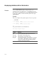
Displaying System Configuration . . . . . . . . . . . . . . . . . . . . . . . . . . . . . . . . . . . .
Displaying Additional Error Information . . . . . . . . . . . . . . . . . . . . . . . . . . . . . . .
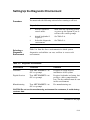
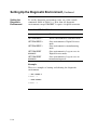
Setting Up the Diagnostic Environment . . . . . . . . . . . . . . . . . . . . . . . . . . . . . . .
Device Tests . . . . . . . . . . . . . . . . . . . . . . . . . . . . . . . . . . . . . . . . . . . . . . . . . . . .
Self-Test Descriptions . . . . . . . . . . . . . . . . . . . . . . . . . . . . . . . . . . . . . . . . . . . . .
System Test Environment Configuration . . . . . . . . . . . . . . . . . . . . . . . . . . . . . .
System Test Monitor . . . . . . . . . . . . . . . . . . . . . . . . . . . . . . . . . . . . . . . . . . . . . .
Utilities . . . . . . . . . . . . . . . . . . . . . . . . . . . . . . . . . . . . . . . . . . . . . . . . . . . . . . . . .
MIPS/REX Emulator . . . . . . . . . . . . . . . . . . . . . . . . . . . . . . . . . . . . . . . . . . . . . .
Product Fault Management . . . . . . . . . . . . . . . . . . . . . . . . . . . . . . . . . . . . . . . . .
Using MOP Ethernet Functions . . . . . . . . . . . . . . . . . . . . . . . . . . . . . . . . . . . . .
User Environmental Test Package . . . . . . . . . . . . . . . . . . . . . . . . . . . . . . . . . . .
FEPROM Firmware Update . . . . . . . . . . . . . . . . . . . . . . . . . . . . . . . . . . . . . . . .
Updating Firmware On Tape . . . . . . . . . . . . . . . . . . . . . . . . . . . . . . . . . . . . . . . .
5–1
5–3
5–4
5–8
5–12
5–13
5–15
5–19
5–31
5–32
5–43
5–53
5–56
5–84
5–88
5–91
5–98
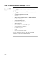
FRUs Removal and Replacement
Overview . . . . . . . . . . . . . . . . . . . . . . . . . . . . . . . . . . . . . . . . . . . . . . . . . . . . . . .
Precautions . . . . . . . . . . . . . . . . . . . . . . . . . . . . . . . . . . . . . . . . . . . . . . . . . . . . .
System FRU Removal . . . . . . . . . . . . . . . . . . . . . . . . . . . . . . . . . . . . . . . . . . . . .
System Preparation . . . . . . . . . . . . . . . . . . . . . . . . . . . . . . . . . . . . . . . . . . . . . . .
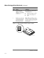
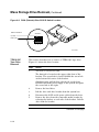
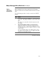
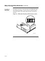
Mass Storage Drive Removal . . . . . . . . . . . . . . . . . . . . . . . . . . . . . . . . . . . . . . .
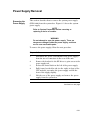
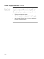
Power Supply Removal . . . . . . . . . . . . . . . . . . . . . . . . . . . . . . . . . . . . . . . . . . . .
Module Removal . . . . . . . . . . . . . . . . . . . . . . . . . . . . . . . . . . . . . . . . . . . . . . . . .
SPXg 8-Plane Option . . . . . . . . . . . . . . . . . . . . . . . . . . . . . . . . . . . . . . . . . . . . .
SPXgt 24-Plane Option . . . . . . . . . . . . . . . . . . . . . . . . . . . . . . . . . . . . . . . . . . . .
CPU Module . . . . . . . . . . . . . . . . . . . . . . . . . . . . . . . . . . . . . . . . . . . . . . . . . . . .
DSW21 Removal and Replacement . . . . . . . . . . . . . . . . . . . . . . . . . . . . . . . . . .
Bezel Removal . . . . . . . . . . . . . . . . . . . . . . . . . . . . . . . . . . . . . . . . . . . . . . . . . .
Clearing System Password . . . . . . . . . . . . . . . . . . . . . . . . . . . . . . . . . . . . . . . . .
Testing the VAXstation 4000 Model 90 System . . . . . . . . . . . . . . . . . . . . . . . . .
TURBOchannel Option . . . . . . . . . . . . . . . . . . . . . . . . . . . . . . . . . . . . . . . . . . . .
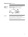
Shipping Contents . . . . . . . . . . . . . . . . . . . . . . . . . . . . . . . . . . . . . . . . . . . . . . . .
TURBOchannel Adapter and Option Modules . . . . . . . . . . . . . . . . . . . . . . . . . .
6–1
6–2
6–3
6–5
6–8
6–21
6–23
6–28
6–34
6–39
6–41
6–42
6–47
6–48
6–50
6–51
6–54
Contents–iv
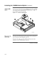
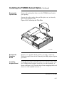
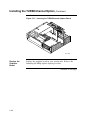
Installing the TURBOchannel Option . . . . . . . . . . . . . . . . . . . . . . . . . . . . . . . . .
TURBOchannel Specifications . . . . . . . . . . . . . . . . . . . . . . . . . . . . . . . . . . . . . .
6–55
6–63
Appendix A Diagnostic Error Codes
Overview . . . . . . . . . . . . . . . . . . . . . . . . . . . . . . . . . . . . . . . . . . . . . . . . . . . . . . .
Error Messages . . . . . . . . . . . . . . . . . . . . . . . . . . . . . . . . . . . . . . . . . . . . . . . . . .
Self-Test Error Messages . . . . . . . . . . . . . . . . . . . . . . . . . . . . . . . . . . . . . . . . . .
System Test Error Messages . . . . . . . . . . . . . . . . . . . . . . . . . . . . . . . . . . . . . . .
Utility Error Messages . . . . . . . . . . . . . . . . . . . . . . . . . . . . . . . . . . . . . . . . . . . . .
A–1
A–3
A–8
A–84
A–90
Appendix B Reading the Diagnostic LED Codes
Overview . . . . . . . . . . . . . . . . . . . . . . . . . . . . . . . . . . . . . . . . . . . . . . . . . . . . . . .
Diagnostic LED Codes . . . . . . . . . . . . . . . . . . . . . . . . . . . . . . . . . . . . . . . . . . . .
B–1
B–2
Appendix C Troubleshooting
Overview . . . . . . . . . . . . . . . . . . . . . . . . . . . . . . . . . . . . . . . . . . . . . . . . . . . . . . .
Troubleshooting . . . . . . . . . . . . . . . . . . . . . . . . . . . . . . . . . . . . . . . . . . . . . . . . . .
C–1
C–2
Appendix D FRU Part Numbers
Overview . . . . . . . . . . . . . . . . . . . . . . . . . . . . . . . . . . . . . . . . . . . . . . . . . . . . . . .
Precautions . . . . . . . . . . . . . . . . . . . . . . . . . . . . . . . . . . . . . . . . . . . . . . . . . . . . .
Model 90 System Box FRUs . . . . . . . . . . . . . . . . . . . . . . . . . . . . . . . . . . . . . . .
Expansion Box FRUs . . . . . . . . . . . . . . . . . . . . . . . . . . . . . . . . . . . . . . . . . . . . .
D–1
D–2
D–3
D–9
Index
Examples
5–1
FEPROM Update by Disk . . . . . . . . . . . . . . . . . . . . . . . . . . . . . . . . . . . . . . . . . .
5–97
Figures
1–1
KA49 CPU Module Components . . . . . . . . . . . . . . . . . . . . . . . . . . . . . . . . . . . . .
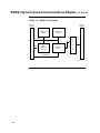
1–2
KA49 CPU Module Block Diagram . . . . . . . . . . . . . . . . . . . . . . . . . . . . . . . . . . .
1–3
KA49 Cache/Memory Hierarchy . . . . . . . . . . . . . . . . . . . . . . . . . . . . . . . . . . . . . .
1–4
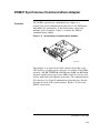
Synchronous Communications Adapter . . . . . . . . . . . . . . . . . . . . . . . . . . . . . . . .
1–5
DSW21 Connections . . . . . . . . . . . . . . . . . . . . . . . . . . . . . . . . . . . . . . . . . . . . . .
2–1
System ROM Format . . . . . . . . . . . . . . . . . . . . . . . . . . . . . . . . . . . . . . . . . . . . . .
2–2
System ROM Part Format . . . . . . . . . . . . . . . . . . . . . . . . . . . . . . . . . . . . . . . . . .
2–3
Option ROM Byte Data . . . . . . . . . . . . . . . . . . . . . . . . . . . . . . . . . . . . . . . . . . . .
2–4
Option ROM Set Data . . . . . . . . . . . . . . . . . . . . . . . . . . . . . . . . . . . . . . . . . . . . .
2–5
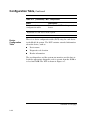
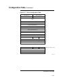
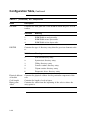
Model 90 Configuration Tables . . . . . . . . . . . . . . . . . . . . . . . . . . . . . . . . . . . . . .
1–4
1–6
1–20
1–33
1–34
2–11
2–12
2–16
2–18
2–20
Contents–v
2–6
2–7
2–8
2–9
2–10
2–11
2–12
3–1
3–2
3–3
3–4
5–1
5–2
5–3
5–4
5–5
5–6
5–7
5–8
5–9
5–10
5–11
5–12
5–13
5–14
5–15
5–16
6–1
6–2
6–3
6–4
6–5
6–6
6–7
6–8
6–9
6–10
6–11
6–12
Main Configuration Table . . . . . . . . . . . . . . . . . . . . . . . . . . . . . . . . . . . . . . . . . . .
Device Configuration Table . . . . . . . . . . . . . . . . . . . . . . . . . . . . . . . . . . . . . . . . .
Driver Descriptor Data Structure . . . . . . . . . . . . . . . . . . . . . . . . . . . . . . . . . . . . .
Diagnostic Driver Console Support . . . . . . . . . . . . . . . . . . . . . . . . . . . . . . . . . . .
Model 90 Console Structure . . . . . . . . . . . . . . . . . . . . . . . . . . . . . . . . . . . . . . . .
SCIA Data Structure . . . . . . . . . . . . . . . . . . . . . . . . . . . . . . . . . . . . . . . . . . . . . . .
Console Port Driver Function Block . . . . . . . . . . . . . . . . . . . . . . . . . . . . . . . . . . .
Model 90 System Box . . . . . . . . . . . . . . . . . . . . . . . . . . . . . . . . . . . . . . . . . . . . .
Internal Cabling . . . . . . . . . . . . . . . . . . . . . . . . . . . . . . . . . . . . . . . . . . . . . . . . . . .
System Box Control Panel . . . . . . . . . . . . . . . . . . . . . . . . . . . . . . . . . . . . . . . . . .
Model 90 I/O Panel . . . . . . . . . . . . . . . . . . . . . . . . . . . . . . . . . . . . . . . . . . . . . . . .
Successful Power-Up . . . . . . . . . . . . . . . . . . . . . . . . . . . . . . . . . . . . . . . . . . . . .
Unsuccessful Power-Up . . . . . . . . . . . . . . . . . . . . . . . . . . . . . . . . . . . . . . . . . . .
Successful and Unsuccessful Self-Test . . . . . . . . . . . . . . . . . . . . . . . . . . . . . . . .
Successful System Test . . . . . . . . . . . . . . . . . . . . . . . . . . . . . . . . . . . . . . . . . . . .
Unsuccessful System Test . . . . . . . . . . . . . . . . . . . . . . . . . . . . . . . . . . . . . . . . . .
Summary Screen . . . . . . . . . . . . . . . . . . . . . . . . . . . . . . . . . . . . . . . . . . . . . . . . .
Utilities List . . . . . . . . . . . . . . . . . . . . . . . . . . . . . . . . . . . . . . . . . . . . . . . . . . . . . .
SCSI Utility Response . . . . . . . . . . . . . . . . . . . . . . . . . . . . . . . . . . . . . . . . . . . . .
Event Log Entry Format . . . . . . . . . . . . . . . . . . . . . . . . . . . . . . . . . . . . . . . . . . . .
Machine Check Stack Frame Subpacket . . . . . . . . . . . . . . . . . . . . . . . . . . . . . .
Processor Register Subpacket . . . . . . . . . . . . . . . . . . . . . . . . . . . . . . . . . . . . . . .
Memory Subpacket for ECC Memory Errors . . . . . . . . . . . . . . . . . . . . . . . . . . . .
Memory SBE Reduction Subpacket (Correctable Memory Errors) . . . . . . . . . .
Correctable Read Data Entry Subpacket Header . . . . . . . . . . . . . . . . . . . . . . . .
Correctable Read Data Entry . . . . . . . . . . . . . . . . . . . . . . . . . . . . . . . . . . . . . . . .
Firmware Update Utility Layout . . . . . . . . . . . . . . . . . . . . . . . . . . . . . . . . . . . . . .
System FRU Locations . . . . . . . . . . . . . . . . . . . . . . . . . . . . . . . . . . . . . . . . . . . . .
Halt Button . . . . . . . . . . . . . . . . . . . . . . . . . . . . . . . . . . . . . . . . . . . . . . . . . . . . . .
RZ23L Disk Drive SCSI ID Jumper Location . . . . . . . . . . . . . . . . . . . . . . . . . . .
RZ24 Disk Drive SCSI ID Jumper Location . . . . . . . . . . . . . . . . . . . . . . . . . . . .
RZ25 Disk Drive SCSI ID Jumper Location . . . . . . . . . . . . . . . . . . . . . . . . . . . .
RRD42 CDROM Jumper Settings . . . . . . . . . . . . . . . . . . . . . . . . . . . . . . . . . . . .
RX26 Diskette Type Number . . . . . . . . . . . . . . . . . . . . . . . . . . . . . . . . . . . . . . . .
RX26 (Diskette) Drive SCSI ID Switch Location . . . . . . . . . . . . . . . . . . . . . . . . .
TZK10 (QIC) Tape Drive SCSI ID Jumper Location . . . . . . . . . . . . . . . . . . . . . .
Memory Module Identification . . . . . . . . . . . . . . . . . . . . . . . . . . . . . . . . . . . . . . .
Removing the SPXg 8-Plane Option . . . . . . . . . . . . . . . . . . . . . . . . . . . . . . . . . .
Switch 2 Position . . . . . . . . . . . . . . . . . . . . . . . . . . . . . . . . . . . . . . . . . . . . . . . . .
Contents–vi
2–21
2–23
2–27
2–29
2–31
2–33
2–34
3–2
3–7
3–8
3–10
5–5
5–6
5–17
5–33
5–34
5–36
5–45
5–51
5–61
5–62
5–63
5–64
5–65
5–66
5–66
5–92
6–4
6–5
6–10
6–11
6–12
6–15
6–17
6–18
6–20
6–25
6–29
6–31
6–13
6–14
6–15
6–16
6–17
6–18
6–19
6–20
6–21
6–22
6–23
6–24
6–25
Installation Details . . . . . . . . . . . . . . . . . . . . . . . . . . . . . . . . . . . . . . . . . . . . . . . . .
Installing the SPXg 8-plane Option . . . . . . . . . . . . . . . . . . . . . . . . . . . . . . . . . . .
Removing the SPXgt 24-Plane Option . . . . . . . . . . . . . . . . . . . . . . . . . . . . . . . .
Installing the SPXgt 24-Plane Option . . . . . . . . . . . . . . . . . . . . . . . . . . . . . . . . .
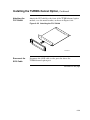
TURBOchannel Adapter Components . . . . . . . . . . . . . . . . . . . . . . . . . . . . . . . . .
TURBOchannel Option Components . . . . . . . . . . . . . . . . . . . . . . . . . . . . . . . . . .
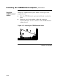
Inside the System Box . . . . . . . . . . . . . . . . . . . . . . . . . . . . . . . . . . . . . . . . . . . . .
Removing the Filler Plate . . . . . . . . . . . . . . . . . . . . . . . . . . . . . . . . . . . . . . . . . . .
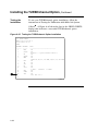
Inserting the TURBOchannel Adapter Board . . . . . . . . . . . . . . . . . . . . . . . . . . .
Attaching the FCC Shield . . . . . . . . . . . . . . . . . . . . . . . . . . . . . . . . . . . . . . . . . . .
Inserting the TURBOchannel Option . . . . . . . . . . . . . . . . . . . . . . . . . . . . . . . . . .
Screwing on the Option Plate . . . . . . . . . . . . . . . . . . . . . . . . . . . . . . . . . . . . . . .
Testing the TURBOchannel Option Installation . . . . . . . . . . . . . . . . . . . . . . . . . .
6–32
6–33
6–36
6–38
6–51
6–53
6–56
6–57
6–58
6–59
6–60
6–61
6–62
Tables
1–1
Major Components . . . . . . . . . . . . . . . . . . . . . . . . . . . . . . . . . . . . . . . . . . . . . . . .
1–2
General Purpose Register Descriptions . . . . . . . . . . . . . . . . . . . . . . . . . . . . . . .
1–3
Interrupt Priority Levels . . . . . . . . . . . . . . . . . . . . . . . . . . . . . . . . . . . . . . . . . . . .
1–4
Exception Categories . . . . . . . . . . . . . . . . . . . . . . . . . . . . . . . . . . . . . . . . . . . . . .
1–5
ROM Fixed Uses . . . . . . . . . . . . . . . . . . . . . . . . . . . . . . . . . . . . . . . . . . . . . . . . .
1–6
Diagnostic ROM/Configuration Register Bit Definitions . . . . . . . . . . . . . . . . . . .
1–7
Serial Line Usage . . . . . . . . . . . . . . . . . . . . . . . . . . . . . . . . . . . . . . . . . . . . . . . . .
1–8
SCSI Bus Signals . . . . . . . . . . . . . . . . . . . . . . . . . . . . . . . . . . . . . . . . . . . . . . . . .
2–1
Power-Up Initialization Sequence . . . . . . . . . . . . . . . . . . . . . . . . . . . . . . . . . . . .
2–2
Test Dispatcher Procedure . . . . . . . . . . . . . . . . . . . . . . . . . . . . . . . . . . . . . . . . . .
2–3
Running a Utility Process . . . . . . . . . . . . . . . . . . . . . . . . . . . . . . . . . . . . . . . . . . .
2–4
System ROM Part Formats . . . . . . . . . . . . . . . . . . . . . . . . . . . . . . . . . . . . . . . . .
2–5
System ROM Physical Addresses . . . . . . . . . . . . . . . . . . . . . . . . . . . . . . . . . . . .
2–6
MCT Components . . . . . . . . . . . . . . . . . . . . . . . . . . . . . . . . . . . . . . . . . . . . . . . . .
2–7
DCT Components . . . . . . . . . . . . . . . . . . . . . . . . . . . . . . . . . . . . . . . . . . . . . . . . .
3–1
Internal System Devices and Cables . . . . . . . . . . . . . . . . . . . . . . . . . . . . . . . . . .
3–2
External System Devices and Cables . . . . . . . . . . . . . . . . . . . . . . . . . . . . . . . . .
3–3
System Box Operating Conditions . . . . . . . . . . . . . . . . . . . . . . . . . . . . . . . . . . . .
3–4
System Box Electrical Specifications . . . . . . . . . . . . . . . . . . . . . . . . . . . . . . . . . .
4–1
SET/SHOW Parameters . . . . . . . . . . . . . . . . . . . . . . . . . . . . . . . . . . . . . . . . . . . .
4–2
Diagnostic Environments . . . . . . . . . . . . . . . . . . . . . . . . . . . . . . . . . . . . . . . . . . .
4–3
SET DIAGENV Command . . . . . . . . . . . . . . . . . . . . . . . . . . . . . . . . . . . . . . . . . .
4–4
DEPOSIT Command Qualifiers . . . . . . . . . . . . . . . . . . . . . . . . . . . . . . . . . . . . . .
4–5
EXAMINE Command Qualifiers . . . . . . . . . . . . . . . . . . . . . . . . . . . . . . . . . . . . . .
1–3
1–12
1–15
1–18
1–25
1–27
1–29
1–32
2–2
2–6
2–8
2–13
2–14
2–21
2–24
3–7
3–11
3–12
3–12
4–4
4–10
4–11
4–19
4–20
Contents–vii
4–6
4–7
5–1
5–2
5–3
5–4
5–5
5–6
5–7
5–8
5–9
5–10
5–11
6–1
6–2
6–3
6–4
6–5
6–6
6–7
6–8
6–9
A–1
A–2
A–3
A–4
A–5
A–6
A–7
A–8
A–9
A–10
A–11
A–12
A–13
A–14
A–15
A–16
A–17
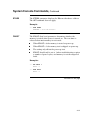
Processor Control Commands . . . . . . . . . . . . . . . . . . . . . . . . . . . . . . . . . . . . . . .
BOOT Command Syntax . . . . . . . . . . . . . . . . . . . . . . . . . . . . . . . . . . . . . . . . . . .
Diagnostic Functions . . . . . . . . . . . . . . . . . . . . . . . . . . . . . . . . . . . . . . . . . . . . . .
Diagnostic Environments . . . . . . . . . . . . . . . . . . . . . . . . . . . . . . . . . . . . . . . . . . .
SET DIAGENV Command . . . . . . . . . . . . . . . . . . . . . . . . . . . . . . . . . . . . . . . . . .
Device Test IDs and Mnemonics . . . . . . . . . . . . . . . . . . . . . . . . . . . . . . . . . . . . .
Device Test Syntax Rules . . . . . . . . . . . . . . . . . . . . . . . . . . . . . . . . . . . . . . . . . .
Multiple Device Tests . . . . . . . . . . . . . . . . . . . . . . . . . . . . . . . . . . . . . . . . . . . . . .
TURBOchannel Adapter Self-Test (13) . . . . . . . . . . . . . . . . . . . . . . . . . . . . . . . .
Running the System Test Using the Test Command . . . . . . . . . . . . . . . . . . . . .
SCSI Utilities . . . . . . . . . . . . . . . . . . . . . . . . . . . . . . . . . . . . . . . . . . . . . . . . . . . . .
Invoking SCSI Utilities . . . . . . . . . . . . . . . . . . . . . . . . . . . . . . . . . . . . . . . . . . . . .
VMS Error Handler Entry Types . . . . . . . . . . . . . . . . . . . . . . . . . . . . . . . . . . . . .
Hard Disk Drive SCSI Jumper Settings . . . . . . . . . . . . . . . . . . . . . . . . . . . . . . . .
Standard IDs for SCSI Devices . . . . . . . . . . . . . . . . . . . . . . . . . . . . . . . . . . . . . .
Synchronous Communications Adapter Cables . . . . . . . . . . . . . . . . . . . . . . . . .
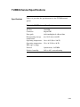
Environmental Specifications . . . . . . . . . . . . . . . . . . . . . . . . . . . . . . . . . . . . . . . .
Physical Specifications . . . . . . . . . . . . . . . . . . . . . . . . . . . . . . . . . . . . . . . . . . . . .
TURBOchannel Adapter Components . . . . . . . . . . . . . . . . . . . . . . . . . . . . . . . . .
TURBOchannel Adapter/Option Removal . . . . . . . . . . . . . . . . . . . . . . . . . . . . . .
TURBOchannel Option Installation Procedure . . . . . . . . . . . . . . . . . . . . . . . . . .
TURBOchannel Specifications . . . . . . . . . . . . . . . . . . . . . . . . . . . . . . . . . . . . . . .
FRU Codes . . . . . . . . . . . . . . . . . . . . . . . . . . . . . . . . . . . . . . . . . . . . . . . . . . . . . .
TOY/NVR Self-Test Error Messages . . . . . . . . . . . . . . . . . . . . . . . . . . . . . . . . . .
DZ Self-Test Error Codes . . . . . . . . . . . . . . . . . . . . . . . . . . . . . . . . . . . . . . . . . . .
DZ Suberror codes . . . . . . . . . . . . . . . . . . . . . . . . . . . . . . . . . . . . . . . . . . . . . . . .
SCSI DMA Self-Test Error Codes . . . . . . . . . . . . . . . . . . . . . . . . . . . . . . . . . . . .
OBIT Self-Test error codes . . . . . . . . . . . . . . . . . . . . . . . . . . . . . . . . . . . . . . . . .
CACHE Self-Test Error codes . . . . . . . . . . . . . . . . . . . . . . . . . . . . . . . . . . . . . . .
MEM Self-Test Error Codes . . . . . . . . . . . . . . . . . . . . . . . . . . . . . . . . . . . . . . . . .
MEM SIM Module FRU Values . . . . . . . . . . . . . . . . . . . . . . . . . . . . . . . . . . . . . .
FPU Self-Test Error Codes . . . . . . . . . . . . . . . . . . . . . . . . . . . . . . . . . . . . . . . . .
FP Exception Vectors . . . . . . . . . . . . . . . . . . . . . . . . . . . . . . . . . . . . . . . . . . . . . .
IT Self-Test Error Codes . . . . . . . . . . . . . . . . . . . . . . . . . . . . . . . . . . . . . . . . . . . .
SYS Self-Test error codes . . . . . . . . . . . . . . . . . . . . . . . . . . . . . . . . . . . . . . . . . .
NI Self-Test Error Codes . . . . . . . . . . . . . . . . . . . . . . . . . . . . . . . . . . . . . . . . . . .
SCSI Self-Test Error Codes . . . . . . . . . . . . . . . . . . . . . . . . . . . . . . . . . . . . . . . . .
SCSI Information Values . . . . . . . . . . . . . . . . . . . . . . . . . . . . . . . . . . . . . . . . . . .
SCSI mode values . . . . . . . . . . . . . . . . . . . . . . . . . . . . . . . . . . . . . . . . . . . . . . . .
Contents–viii
4–21
4–22
5–3
5–13
5–14
5–15
5–16
5–18
5–29
5–32
5–49
5–50
5–60
6–13
6–13
6–43
6–45
6–46
6–52
6–54
6–55
6–63
A–6
A–8
A–9
A–11
A–12
A–13
A–14
A–16
A–17
A–18
A–20
A–21
A–21
A–22
A–28
A–39
A–44
A–18
A–19
A–20
A–21
A–22
A–23
A–24
A–25
A–26
A–27
A–28
A–29
A–30
A–31
A–32
A–33
B–1
B–2
B–3
B–4
B–5
B–6
B–7
B–8
B–9
B–10
B–11
B–12
B–13
C–1
C–2
C–3
C–4
C–5
C–6
C–7
C–8
D–1
D–2
AUD Self-Test Error Codes . . . . . . . . . . . . . . . . . . . . . . . . . . . . . . . . . . . . . . . . .
Synch Comm Device Test Error Codes . . . . . . . . . . . . . . . . . . . . . . . . . . . . . . . .
TURBOchannel Adapter Self-Test Error Codes . . . . . . . . . . . . . . . . . . . . . . . . .
Synch Communications Self-Test Sequence Numbers . . . . . . . . . . . . . . . . . . .
DSW21 Communications Utilities Error Codes . . . . . . . . . . . . . . . . . . . . . . . . . .
Failing Logical Block Summary . . . . . . . . . . . . . . . . . . . . . . . . . . . . . . . . . . . . . .
Test Number Summary . . . . . . . . . . . . . . . . . . . . . . . . . . . . . . . . . . . . . . . . . . . . .
Failing Logical Block Summary . . . . . . . . . . . . . . . . . . . . . . . . . . . . . . . . . . . . . .
Test Number Summary . . . . . . . . . . . . . . . . . . . . . . . . . . . . . . . . . . . . . . . . . . . . .
SCSI System Test Error Codes . . . . . . . . . . . . . . . . . . . . . . . . . . . . . . . . . . . . . .
NI System Test Error Codes . . . . . . . . . . . . . . . . . . . . . . . . . . . . . . . . . . . . . . . .
Text Messages for SCSI Utilities . . . . . . . . . . . . . . . . . . . . . . . . . . . . . . . . . . . . .
Additional SCSI Information Values for Utilities . . . . . . . . . . . . . . . . . . . . . . . . .
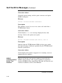
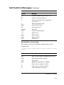
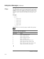
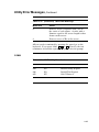
Menu Item Meanings . . . . . . . . . . . . . . . . . . . . . . . . . . . . . . . . . . . . . . . . . . . . . .
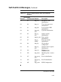
Menu Item Meanings . . . . . . . . . . . . . . . . . . . . . . . . . . . . . . . . . . . . . . . . . . . . . .
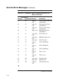
COMM Utility Error Numbers . . . . . . . . . . . . . . . . . . . . . . . . . . . . . . . . . . . . . . . .
Power-up and Initialization LED Codes (1111 XXXX) . . . . . . . . . . . . . . . . . . . . .
TOY and NVR LED Codes (0001 XXXX) . . . . . . . . . . . . . . . . . . . . . . . . . . . . . .
LCSPX LED Codes (0010 XXXX) . . . . . . . . . . . . . . . . . . . . . . . . . . . . . . . . . . . .
SPXg/gt LED Codes (0010 XXXX) . . . . . . . . . . . . . . . . . . . . . . . . . . . . . . . . . . .
DZ LED Codes (0011 XXXX) . . . . . . . . . . . . . . . . . . . . . . . . . . . . . . . . . . . . . . . .
Cache LED Codes (0100 XXXX) . . . . . . . . . . . . . . . . . . . . . . . . . . . . . . . . . . . . .
Memory FRU LED Codes (0101 XXXX) . . . . . . . . . . . . . . . . . . . . . . . . . . . . . . .
System Device LED Codes (1000 XXXX) . . . . . . . . . . . . . . . . . . . . . . . . . . . . . .
NI LED Codes (1001 XXXX) . . . . . . . . . . . . . . . . . . . . . . . . . . . . . . . . . . . . . . . .
SCSI Device LED Codes (1010 XXXX) . . . . . . . . . . . . . . . . . . . . . . . . . . . . . . . .
Audio Device LED Codes (1011 XXXX) . . . . . . . . . . . . . . . . . . . . . . . . . . . . . . .
DSW21 Communication Device LED Codes (1100 XXXX) . . . . . . . . . . . . . . . .
TURBOchannel Adapter LED Codes (1100 XXXX) . . . . . . . . . . . . . . . . . . . . . .
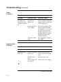
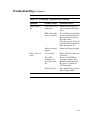
System Problems . . . . . . . . . . . . . . . . . . . . . . . . . . . . . . . . . . . . . . . . . . . . . . . . .
Monitor Problems . . . . . . . . . . . . . . . . . . . . . . . . . . . . . . . . . . . . . . . . . . . . . . . . .
Mouse/Tablet Problems . . . . . . . . . . . . . . . . . . . . . . . . . . . . . . . . . . . . . . . . . . . .
Keyboard Problems . . . . . . . . . . . . . . . . . . . . . . . . . . . . . . . . . . . . . . . . . . . . . . .
Drive Problems . . . . . . . . . . . . . . . . . . . . . . . . . . . . . . . . . . . . . . . . . . . . . . . . . . .
Network Problems . . . . . . . . . . . . . . . . . . . . . . . . . . . . . . . . . . . . . . . . . . . . . . . .
Audio Problems . . . . . . . . . . . . . . . . . . . . . . . . . . . . . . . . . . . . . . . . . . . . . . . . . .
Expansion Box Problems . . . . . . . . . . . . . . . . . . . . . . . . . . . . . . . . . . . . . . . . . . .
System Box FRUs . . . . . . . . . . . . . . . . . . . . . . . . . . . . . . . . . . . . . . . . . . . . . . . .
System Monitors . . . . . . . . . . . . . . . . . . . . . . . . . . . . . . . . . . . . . . . . . . . . . . . . . .
A–45
A–48
A–55
A–65
A–76
A–78
A–79
A–81
A–82
A–84
A–88
A–90
A–91
A–93
A–94
A–95
B–3
B–5
B–5
B–6
B–7
B–8
B–9
B–10
B–10
B–11
B–12
B–13
B–14
C–2
C–6
C–8
C–8
C–9
C–10
C–12
C–12
D–3
D–4
Contents–ix
D–3
D–4
D–5
D–6
D–7
D–8
D–9
D–10
D–11
D–12
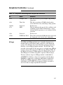
Miscellaneous Hardware . . . . . . . . . . . . . . . . . . . . . . . . . . . . . . . . . . . . . . . . . . .
Cables and Terminators . . . . . . . . . . . . . . . . . . . . . . . . . . . . . . . . . . . . . . . . . . . .
TURBOchannel Option Cables . . . . . . . . . . . . . . . . . . . . . . . . . . . . . . . . . . . . . .
Stand-Alone Tabletop Devices . . . . . . . . . . . . . . . . . . . . . . . . . . . . . . . . . . . . . . .
SZ16 Expansion Box FRUs . . . . . . . . . . . . . . . . . . . . . . . . . . . . . . . . . . . . . . . . .
SZ16 Expansion Box Miscellaneous Hardware . . . . . . . . . . . . . . . . . . . . . . . . .
SZ16 Expansion Box Cables and Terminators . . . . . . . . . . . . . . . . . . . . . . . . . .
SZ03 Sidecar . . . . . . . . . . . . . . . . . . . . . . . . . . . . . . . . . . . . . . . . . . . . . . . . . . . .
SZ03 Miscellaneous Hardware . . . . . . . . . . . . . . . . . . . . . . . . . . . . . . . . . . . . . .
SZ03 Cables and Terminators . . . . . . . . . . . . . . . . . . . . . . . . . . . . . . . . . . . . . . .
Contents–x
D–5
D–6
D–8
D–9
D–9
D–10
D–11
D–11
D–12
D–12
Preface
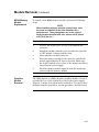
Overview
Purpose and
Audience
This manual is a support and reference document for Digital
Services personnel who perform maintenance work on the
VAXstation 4000 Model 90 workstation. It is also intended for
Digital customers who have a self-maintenance agreement with
Digital.
Organization
This manual is organized as follows:
Chapter 1, System Module, provides an overview of the
Model 90 features, main memory, network interface, and
SCSI controller.
Chapter 2, Firmware, provides information on diagnostic
firmware.
Chapter 3, System Configuration, provides configuration
information on the system box.
Chapter 4, Using the Console, describes system console
commands and using alternate consoles.
Chapter 5, Diagnostic Testing, provides information on
diagnostic testing.
Chapter 6, FRU Removal and Replacement, provides
information on how to remove and replace system field
replaceable units.
Continued on next page
xi
Overview, Continued
Organization
(continued)
Appendix A, Diagnostic Error Codes, contains tables listing
error codes, error messages, and utilities.
Appendix B, Reading the Diagnostic LED codes, describes
how to read the diagnostic LED codes.
Appendix C, Troubleshooting, contains troubleshooting
information.
Appendix D, FRU Part Numbers, contains tables that provide
part numbers for FRUs.
Related
Documentation
The following documents provide additional information about the
VAXstation 4000 Model 90 workstation:
Document
Order Number
VAXstation 4000 Quick Installation Card
EK-VAXQC-IN
VAXstation 4000 Options Installation Guide
EK-VAXOP-IN
VAXstation 4000 Model 90 Owner’s Installation
Guide
EK-VAXOG-IN
VAXstation 3D Graphics Options Maintenance
Guide
EK-SCP8P-MG
BA46 Expansion Box Service Information
EK-VBA46-SV
Continued on next page
xii
Overview, Continued
Conventions
This guide uses the following conventions:
Convention
Description
WARNING
Contains important information that
relates to personal safety.
CAUTION
Contains information to prevent damage
to the equipment.
NOTE
Contains general information.
PN
Part number
Ctrl/C
This type of key sequence means you
hold down the first key while you type
the letter of the next key.
THIS TYPEFACE
Indicates text the system displays.
THIS TYPEFACE
Indicates user input.
Return
SHOW ERROR
Text within a box means you press that
key.
Commands that you enter are shown in
all uppercase text.
A number in a circle in text corresponds
to that number in an illustration.
xiii
Chapter 1
System Module
Introduction
In this Chapter
This chapter describes the features of the VAXstation 4000 Model
90 system module. The topics covered include:
System Overview
Central Processor Unit (CPU)
Interrupts and Exceptions
Cache Memory
Main Memory System
ROM Memory
Graphics Controller
Network Interface Controller
Serial Line Controller
Time-of-Year Clock (TOY)
SCSI Controller
DSW21 Synchronous Communications Adapter
1–1
System Overview
Overview
The KA49 CPU module combines with either the 4-MB or 16-MB
(or both) SIM modules to form the CPU/memory subsystem for
the VAXstation 4000 Model 90 product. The VAXstation 4000
Model 90 system is housed in a BA46 enclosure. The subsystem
uses the SCSI-1 bus to communicate with mass storage devices,
and transceiver cable (Thickwire or ThinWire connector) to
connect with an Ethernet network. A 16-bit programmed I/O port
connection is available to attach synchronous communications
or other options. An optional bus adapter can be connected to
the module using one of the 32-bit CDAL buses. Four serial
lines are supported for a keyboard, pointing device, printer,
and asynchronous communication. Audio input and output is
supported through the sound generator interface. The KA49 CPU
module supports low cost graphics using the LCSPX module or
high performance graphics using the SPXg/gt modules.
Main Memory
The KA49 CPU module can support up to eight memory SIM
modules to provide main memory configurations of 16, 32, 64, 80,
or 128 MB.
Cache Memory
The module uses multiple levels of cache memory to maximize
performance. The NVAX CPU contains a 2-KB virtual instruction
cache (VIC) and an 8-KB write-through primary cache (Pcache).
The KA49 module contains an on board 256-KB backup write
secondary cache (Bcache).
Continued on next page
1–2
System Overview, Continued
CPU
Components
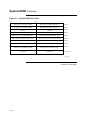
Table 1–1 lists the major hardware components found on the
KA49 CPU module.
Table 1–1 Major Components
DC246
Central processor
NVAX
Cache RAMs
256-KB Bcache
—–
DC243
NDAL to CDAL I/O bus interface chip
NCA
DC244
Main memory controller, with ownership
bit control
NMC
NCR 53C94
Advanced SCSI controller
—–
DC541
Ethernet interface
SGEC
—–
32-Byte network address ROM
socketed
AM79C30A
Sound generator
—–
XC3090
CDAL to EDAL chip
CEAC
XC4005
SCSI Quadword FIFO chip
SQWF
DC7085
Quad UART
DZQ11
DC509
Clock
CCLK
DS1287A
Time-of-Year clock
TOY
Firmware ROMs (4)
512 KB; each 128 KB by 8, FLASH
programmable
—–
Continued on next page
1–3
System Overview, Continued
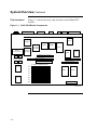
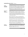
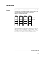
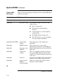
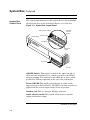
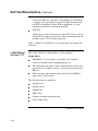
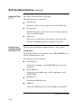
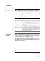
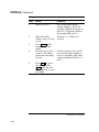
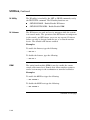
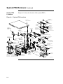
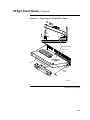
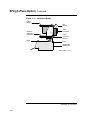
Chip Locations
Figure 1–1 shows the major chip locations on the KA49 CPU
module.
Figure 1–1 KA49 CPU Module Components
Thick Wire Ethernet
RS232
Print
KBD
Mouse
Remote KBD/Mouse
Thin Wire Ethernet
Quart
SGEC
CEAC
SQWF
Graph
44 QFP
Power
Connector
NCA
Graph
84 QFP
SCSI
Sound
TURBOchannel Connector
SPXg/gt Connector
FLASH ROMS
LCSPX Graphics Connector
SYNC COMM Apapter
SCSI Connector
8 SIMM CONNECTORS
DC7238
0A
1E
0C
NMC
NVAX
1G
IF
DC7238
0B
1H
0D
Lights & Switches
LJ-01815-TI0
1–4
Central Processor Unit
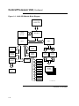
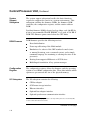
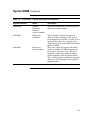
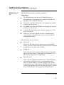
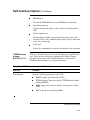
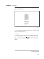
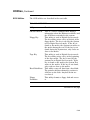
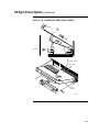
Overview
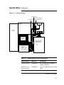
Figure 1–2 shows how, functionally, the KA49 CPU module is
divided into five major areas.
Central processing subsystem
Graphics subsystem
System support subsystem
I/O Subsystem
Memory control subsystem
Continued on next page
1–5
Central Processor Unit, Continued
Figure 1–2 KA49 CPU Module Block Diagram
G-BITS
256KB
CACHE
& TAG
NVAX
NCA
CP1
DC7238
XCVR
CEAC
SQWF
TURBO
CHANNEL
GRPHCS
ADAPT
NMC
SGEC
CP2
CONSOLE
ROMS
NDAL
LCSPX
DC7238
XCVR
DMA RAMS
QUART
SCSI
SPXG
& GT
EDAL
TOY
SYNC COM
Memory
SIMMS
16-128 MEG
LEDS
CNFG REG
SOUND
EID ROM
LJ-01816-TI0
Continued on next page
1–6
Central Processor Unit, Continued
Central
Processing
Subsystem
The NVAX CPU (DC246) chip is the heart of the KA49 CPU
module. It executes the VAX base instruction group as defined
in the VAX Architecture Reference Manual plus the optional VAX
vector instructions and the virtual machine instructions. The
NVAX processor also supports full VAX memory management with
demand paging and a 4-gigabyte virtual address space.
Three Level
Cache
Architecture
The KA49 CPU module uses a three-level cache architecture to
maximize performance. The first level of cache, referred to as
the virtual instruction cache (VIC), is 2 KB in size, and is located
on the CPU chip. This cache handles instructions only (no data
references), and deals only with virtual addresses. In this way
the CPU can obtain instruction information without the need for
virtual to physical address translation, thereby decreasing latency
and improving performance.
The second level of cache, referred to as the primary cache
(Pcache), is 8 KB in size and is located on the CPU chip. This
cache implements a write-through instruction and data cache, and
helps to reduce latency on access to data and instructions that are
not found in the VIC. The Pcache uses physical addresses.
The third level of cache, referred to as the backup write cache
(Bcache) is 256 KB. The Bcache is controlled by the Bcache
controller located in the CPU chip. The data and tag store
memory for this cache is located in SRAM chips on the KA49
CPU module. The Bcache uses physical addresses.
Graphics
Subsystem
The graphics subsystem consists of either the LCSPX for low cost
graphics support or the SPXg/gt modules, which support high
performance graphics. Two connectors are provided on the module
that provide a unique interface to each.
Continued on next page
1–7
Central Processor Unit, Continued
System
Support
Subsystem
The system support subsystem handles the basic functions
required to support the console in a system environment. This
subsystem contains the firmware ROMs, the firmware ROM
controller, the configuration register, and the station address
ROM.
Resident firmware ROM is located on four chips, each 128 KB by
8 bits of programmable FLASH EPROM1 , for a total of 512 KB of
ROM. The firmware gains control when the CPU halts.
ROM Firmware
ROM firmware provides the following services:
Board initialization
Power-up self-testing of the KA49 module
Emulation of a subset of the VAX standard console (auto
or manual bootstrap, auto or manual restart, and a simple
command language for examining or altering the state of the
processor)
Booting from supported Ethernet or SCSI devices
Multilingual translation of key system messages
Configuration
Register
The configuration register allows the firmware and the operating
system to read KA49 configuration bits. These bits indicate which
options are present and the size of the physical memory.
I/O Subsystem
The I/O subsystem contains the following:
CP-Bus adapter
SCSI mass storage interface
Ethernet interface
Optional bus adapter interface
Optional synchronous communication interface
1 A FLASH EPROM is a programmable read-only memory that uses electrical (bulk)
erasure rather than ultraviolet erasure.
Continued on next page
1–8
Central Processor Unit, Continued
Sound generator
Four asynchronous lines
Time-of-Year clock
Ethernet identification ROM
NVAX CP-Bus
Bus Adapter
To provide buffering and connection to the I/O devices, the KA49
contains a DC243, NDAL to CDAL adapter (NCA). The NCA
provides an interface between the NVAX NDAL bus and two CPBuses where the I/O device adapters reside. As a bus adapter, the
NCA controls transactions between the higher performance NDAL
bus and the lower performance CP-Buses. Each of the NCA’s
CP-Bus ports provide a CVAX compatible peripheral bus for direct
memory access (DMA) by peripheral devices.
Small
Computer
Systems
Interface
NCR 53C94 implements the small computer system interface
(SCSI) bus interface. It has a single port, connecting both to
devices within the BA46 system box and allowing for expansion
externally.
Ethernet
Interface
The Ethernet interface handles communications between the CPU
module and other nodes on the Ethernet. It is implemented with
the second generation Ethernet controller chip (SGEC) onboard
network interface. Used in connection with the module backpanel,
the SGEC allows the KA49 to connect to either a ThinWire or
standard Ethernet. It supports the Ethernet data link layer and
provides CP-Bus parity protection.
Optional
Bus Adapter
Interface
The optional bus adapter provides a translation between one of
the CP-Buses and the adapter bus. The VAXstation 4000 Model
90 has direct, transparent access to the bus adapter. The slot
appears as a region of memory in the workstation’s I/O space.
The bus adapter option can perform DMA to any location in the
memory space of the VAXstation 4000 Model 90. This DMA can be
done either directly to the physical memory of the workstation or
Continued on next page
1–9
Central Processor Unit, Continued
through a scatter/gather map that allows physically discontiguous
pages of data to appear to be contiguous to the bus adapter option.
Sound
Generator
Sound output uses the DTMF tone generation capability of
the 79C30 chip. Two tone generators may be individually
programmed for frequency and amplitude; their outputs appear
summed using either the loudspeaker integral to the system
unit, or to headphones, or an external loudspeaker if plugged
in to the jack at the front of the machine. The resolution of the
frequency generators is eight bits, giving a frequency range of 8
Hz to approximately 2 kHz.
Serial Line
Controller
The VAXstation 4000 Model 90 system board serial line controller
handles four asynchronous serial lines. The controller consists of
the DC7085 QUART and a 64 entry FIFO RAM shared by all four
receive lines.
Time-Of-Year
Clock
The time-of-year (TOY) clock consists of an MC146818BM CMOS
watch chip that keeps the date and time of day and contains 50
bytes of general purpose RAM storage. This chip includes a time
base oscillator and a lithium battery on-chip. The battery powers
the chip logic and oscillator while the system power is off.
Station
Address ROM
A 32-byte ROM on the system board contains a unique network
address for each system. This ROM is installed in a socket so it
can be moved in the event that a system’s CPU board is replaced.
Memory
Control
Subsystem
The memory control subsystem provides support for the KA49
memory subsystem. A key feature of the KA49 memory
subsystem is the use of ownership bits to maintain a sense
of ownership over each hexaword (32 bytes) of main memory.
This ownership mechanism serves the dual function of
maintaining coherency between main memory and the NVAX
Continued on next page
1–10
Central Processor Unit, Continued
cache memory, as well as providing a secure interlock mechanism
for synchronization between NVAX and the I/O devices.
The memory controller is implemented by the NVAX memory
controller chip (DC244). The NMC is an ECC protected memory
controller. The NMC controls transactions between the main
memory and the NVAX, and between main memory and any of
the I/O devices (through the NCA interface). In addition, the
NMC has a key role in maintaining main memory coherency with
the NVAX Pcache and Bcache through the use of ownership bits.
The NMC interfaces the NVAX and I/O subsystem to up to 128
MB of main memory. Main memory is comprised of one or two
sets of SIM modules. Each set contains either four 4-MB SIM
modules or four 16-MB SIM modules. The NMC controls access to
shared memory locations through the use of the ownership bits,
thereby providing a reliable interlock mechanism for memory that
is shared between the NVAX and the I/O devices.
NVAX
Data/Address
Lines
In order to maximize the bandwidth of the bus connecting the
CPU to the memory and I/O controllers, the NVAX chip set
(NVAX, NMC, NCA) communicates over a "pended" bus called the
NDAL. The main feature of this bus is that devices requesting
read data do not tie up the bus while waiting for the return data.
Rather, a device issues one of the "read" commands on the NDAL
and then relinquishes control of the bus to other devices. This is
so other transactions can be performed while the responder to the
first device prepares to send back the data associated with the
read request. Because of the pended nature of the bus, the NDAL
bus command set includes separate transactions for returning
data from an earlier read cycle.
Processor
State
The processor state consists of that portion of the state of a
process that is stored in processor registers rather than in
memory. The processor state is composed of 16 general purpose
registers (GPRs), the processor status longword (PSL), and the
internal processor registers (IPRs).
Continued on next page
1–11
Central Processor Unit, Continued
Non-privileged software can access the GPRs and the processor
status word (bits <15:00> of the PSL). The IPRs and bits <31:16>
of the PSL can only be accessed by privileged software. The
IPRs are explicitly accessible only by the move-to-processor
register (MTPR) and the move-from-processor register (MFPR)
instructions which can be executed only while running in kernel
mode.
The KA49 implements 16 GPRs, as defined in the VAX
Architecture Reference Manual. These registers are used for
temporary storage, accumulators, and base and index registers
for addressing. These registers are denoted R0 - R15. The bits
of a register are numbered from the right <0> through <31>.
Table 1–2 describes the registers.
Table 1–2 General Purpose Register Descriptions
Register Register Name
Mnemonic Description
R15
Program Counter
PC
The PC contains the address of the next
instruction byte of the program.
R14
Stack Pointer
SP
The SP contains the address of the top of
the processor defined stack.
R13
Frame Pointer
FP
The call convention builds a data structure
on the stack called a stack frame. The FP
contains the address of the base of this data
structure.
R12
Argument Pointer
AP
The call convention uses a data structure
termed an argument. The AP contains the
address of the base of this data structure.
Continued on next page
1–12
Central Processor Unit, Continued
Internal
Processor
Registers
The internal processor registers (IPRs) that are implemented by
the KA49 CPU chip, and those that are required of the system
environment, are logically divided into five groups, as follows:
Normal—Those IPRs that address individual registers in the
KA49 CPU chip or system environment
Bcache Tag IPRs—The read-write block of IPRs that allow
direct access to the Bcache tags
Bcache Deallocate IPRs—The write-only block of IPRs by
which a Bcache block may be deallocated
Pcache Tag IPRs—The read-write block of IPRs that allow
direct access to the Pcache tags
Pcache Data Parity IPRs—The read-write block of IPRs that
allow direct access to the Pcache data parity bits
1–13
Interrupts and Exceptions
Overview
Both interrupts and exceptions divert execution from the normal
flow of control. An interrupt is caused by some activity outside the
current process and typically transfers control outside the process
(for example, an interrupt from an external hardware device). An
exception is caused by the execution of the current instruction
and is typically handled by the current process (for example, an
arithmetic overflow).
Nonmaskable
Interrupts
Interrupts can be divided into two classes: nonmaskable and
maskable. Nonmaskable interrupts cause a halt by way of the
hardware halt procedure. The hardware halt procedure does the
following:
Saves the PC, PSL, MAPEN<0> and a halt code in IPRs
Raises the processor IPL to 1F
Passes control to the resident firmware
The firmware dispatches the interrupt to the appropriate service
routine based on the halt code and hardware event indicators.
Nonmaskable interrupts cannot be blocked by raising the
processor IPL.
Maskable
Interrupts
Maskable interrupts cause the following:
The PC and PSL are saved.
The processor IPL is raised to the priority level of the
interrupt.
The interrupt is dispatched to the appropriate service routine
through the system control block (SCB).
Continued on next page
1–14
Interrupts and Exceptions, Continued
Interrupt
Priority Levels
Table 1–3 lists KA49 interrupt conditions, associated priority
levels, and SCB offsets. Note that Table 1–3 is intended as a
quick reference, and may not include all possible causes of the
various interrupts.
Table 1–3 Interrupt Priority Levels
Priority Level
Interrupt Condition
SCB Offset
1F
HALT_H asserted (nonmaskable)
**
1E
Unused
1D
Bcache addressing errors
60
Bcache uncorrectable data ECC errors on
Bcache read for a write that hits valid/owned
60
NVAX read timeout or read data error
on Bread for a write after the requested
quadword has arrived
60
Illegal length write transaction to memory or
I/O
60
Reserved command detected by memory or I/O
during write transaction
60
Pending write times out waiting for disown
write
60
Disown write to unowned memory location
60
Main memory NXM errors on writes
60
NDAL parity errors on writes
60
CP-Bus NXM/TIMEOUT on a write
60
1C
Unused
1B
Performance monitoring interrupt (internally
handled by microcode)
** These conditions generate a hardware halt procedure with a halt code of 2 (external halt).
Continued on next page
1–15
Interrupts and Exceptions, Continued
Table 1–3 (Continued) Interrupt Priority Levels
Priority Level
Interrupt Condition
SCB Offset
1A
Correctable main memory errors
54
Uncorrectable main memory errors
54
Correctable O-bit memory errors
54
Pending read times out waiting for disown
write
54
No acknowledgment on returned read data
from NMC
54
NDAL Data parity errors
54
Pcache tag or data parity errors
54
VIC tag or data parity errors
54
Bcache addressing errors
54
Bcache correctable data ECC errors
54
Bcache uncorrectable data ECC errors
54
Bcache correctable tag ECC errors
54
Bcache uncorrectable data ECC errors
54
Illegal length transaction to memory or I/O
space
54
Reserved command to memory or I/O space
54
CP-Bus parity errors on I/O read transactions
54
CP-Bus ERR_L signal asserted by I/O device
during I/O read transaction
54
CP-Bus NXM/TIMEOUTS errors on I/O reads
54
19:18
Unused
17
IRQ_H[3] asserted
Unused
** These conditions generate a hardware halt procedure with a halt code of 2 (external halt).
Continued on next page
1–16
Interrupts and Exceptions, Continued
Table 1–3 (Continued) Interrupt Priority Levels
Priority Level
Interrupt Condition
SCB Offset
16
IRQ_H[2] asserted
Unused
Interval timer (IRQ_H[2] takes priority)
C0
15
IRQ_H[1] asserted
14
IRQ_H[0] asserted
Network interface
13:10
Unused
0F:01
Software interrupt requests
104
84-BC
** These conditions generate a hardware halt procedure with a halt code of 2 (external halt).
Exceptions
There are six categories of exceptions.
Arthimetic
Memory management
Operand
Instruction
Tracing
System failure
A list of exceptions, grouped by class, is shown in Table 1–4.
Continued on next page
1–17
Interrupts and Exceptions, Continued
Table 1–4 Exception Categories
Types of
Exceptions
Exception Class
Instances
Arithmetic traps/faults
Integer overflow trap
Integer divide-by-zero trap
Subscript range trap
Floating overflow fault
Floating divide-by-zero fault
Floating underflow fault
Memory management
exceptions
Access control violation fault
Translation not valid fault
M=0 fault
Operand reference
exceptions
Reserved addressing mode fault
Reserved operand fault or abort
Instruction execution
exceptions
Reserved/Privileged instruction
fault
Emulated instruction faults
XFC fault
Change-mode trap
Breakpoint fault
Vector disabled fault
Tracing exceptions
Trace fault
System failure exceptions
Kernel-Stack-Not-Valid abort
Interrupt-Stack-Not-Valid halt
Console error halt
Machine check abort
There are three types of exceptions.
Trap
Fault
Abort
Continued on next page
1–18
Interrupts and Exceptions, Continued
Trap
Exceptions
A trap is an exception that occurs at the end of the instruction
that caused the exception. Therefore, the PC saved on the stack is
the address of the next instruction that would normally have been
executed.
Fault
Exceptions
A fault is an exception that occurs during an instruction and that
leaves the registers and memory in a consistent state such that
elimination of the fault condition and restarting the instruction
will give correct results. After the instruction faults, the PC saved
on the stack points to the instruction that faulted.
Abort
Exceptions
An abort is an exception that occurs during an instruction.
An abort leaves the value of registers and memory
UNPREDICTABLE such that the instruction cannot necessarily
be correctly restarted, completed, simulated, or undone. In most
instances, the NVAX microcode attempts to convert an abort into
a fault by restoring the state that was present at the start of the
instruction that caused the abort.
1–19
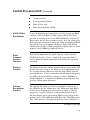
Cache Memory
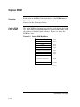
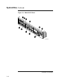
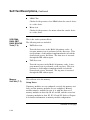
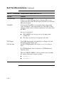
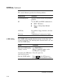
Overview
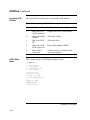
The NVAX memory subsystem follows a hierarchical structure.
The VIC, Pcache, Bcache, and finally the main memory form the
hierarchical memory subsystem of the KA49. The hierarchical
ordering of the various levels of KA49 memory is shown in
Figure 1–3. For I-stream references, the memory hierarchy
starts with the VIC, whereas for D-stream references the memory
hierarchy starts with the Pcache.
Figure 1–3 KA49 Cache/Memory Hierarchy
Mass Storage
Main Memory
Backup Cache 256 KB
Primary Cache 8KB
VIC 2KB
LJ-01817-TI0
References generated by the NVAX CPU are issued to the memory
subsystem at the first hierarchical level, as determined by the
reference type (I-stream or D-stream). The reference then passes
up through the hierarchy until it is serviced by one of the layers.
References that are serviced at lower layers take less time than
references that must pass to higher layers. For this reason, it is
the intent of the memory subsystem to service most references
within the lower layers, thus maximizing system performance.
By creating successively faster layers of memory hierarchy below
the main memory, the KA49 decreases the average amount
of time required to access information. Because each layer in
the hierarchy tends to be smaller in size than the next higher
(slower) layer, there is the problem of allocating space at each
Continued on next page
1–20
Cache Memory, Continued
layer for storing references. Furthermore, care must be taken to
ensure that the state of the system is singularly and accurately
represented by the combined contents of the caches and main
memory.
In the KA49 this issue is most critical between main memory and
the Bcache and Pcache, because main memory can be accessed
by DMA devices as well as the NVAX CPU. Furthermore, this
problem is complicated by the writeback nature of the Bcache.
This write-back mechanism, while significantly decreasing
the latency of write operations, complicates the problem of
maintaining a coherent and consistent representation of main
memory in the face of DMA traffic.
Cached
References
Any reference that can be stored by the VIC, the Pcache, or the
Bcache is called a cached reference. The Pcache and Bcache store
CPU read references to the VAX memory space (bit <29> of the
physical address = 0) only. They do not store references to the
VAX I/O space.
Whenever the CPU generates a non-cached reference, or a cached
reference not stored in any of the three caches, a single hexaword
reference of the same type is generated on the NDAL Bus.
Whenever the CPU generates a cached reference that is stored in
one of the caches, no reference is generated on the NDAL Bus.
Virtual
Instruction
Cache
Before any instruction can be executed, it must first be fetched
from memory. The NVAX CPU contains an instruction prefetcher
that fetches sequential instructions ahead of the instruction
currently being executed. This is done in an attempt to reduce
the effective access time of the instruction fetch by pipelining it
with decode and instruction execution. The instruction prefetcher
maintains an instruction prefetch queue (IPQ) of up to 16 bytes
(4 longwords) of I-stream data. In order to fill the IPQ, the
prefetcher sends I-stream read requests to the Virtual Instruction
Cache (VIC).
Continued on next page
1–21
Cache Memory, Continued
The VIC is a 2-KB, direct-mapped cache for caching I-stream
data. The VIC is located within the NVAX CPU chip. In order to
reduce the overhead associated with virtual-to-physical address
translation, the VIC caches references based on virtual addresses.
In the event that the virtual references made by the instruction
prefetcher hit in the VIC, the I-stream data is loaded from the
VIC directly to the IPQ.
If the references made by the instruction prefetcher miss in the
VIC, then the VIC issues an I-stream read request on behalf of
the instruction prefetcher to the next level of memory hierarchy,
the Pcache.
Primary Cache
The primary cache (Pcache) is a two-way set associative, read
allocate, no-write allocate, write through, physical address cache
of I-stream and D-stream data. It stores 8192 bytes (8K) of data
and 256 tags corresponding to 256 hexaword blocks (1 hexaword =
32 bytes). Each tag is 20 bits wide corresponding to bits <31:12>
of the physical address.
There are four quadword subblocks per block with a valid bit
associated with each subblock. The access size for both Pcache
reads and writes is one quadword. Byte parity is maintained
for each byte of data (32 bits per block). One bit of parity is
maintained for every tag. The Pcache has a one cycle access and
a one cycle repetition rate for both reads and writes.
The Pcache represents the first level of D-stream memory
hierarchy and the second level of I-stream memory hierarchy in
all NVAX computer systems. Pcache entries must be invalidated
in order to maintain cache coherency with higher levels of the
memory hierarchy.
The Pcache is located within the NVAX CPU chip. Unlike the
VIC, the Pcache is based on physical addresses rather than
virtual addresses. The Pcache handles I-stream requests from
the VIC, as well as D-stream requests for instruction operands.
The Pcache uses a write-through scheme for handling writes to
memory locations which are contained in the Pcache. In this
Continued on next page
1–22
Cache Memory, Continued
scheme, the write operation updates the contents of the Pcache,
and the write operation is propagated to the next level of memory
hierarchy, the Bcache. The Pcache is maintained as a strict subset
of the Bcache.
Backup Cache
The backup cache (Bcache) is direct-mapped, with quadword
access size, and a hexaword (32 bytes) block size. The Bcache
allocates on reads and writes, and uses a write-back protocol.
Bcache tags and cache data are stored in static RAMs that reside
on the CPU module. The NVAX CPU implements the control for
the Bcache tags and data.
The Bcache and Pcache communicate internally to the NVAX CPU
in such a way as to maintain the Pcache as a strict subset of the
Bcache. This is done through the use of "invalidate" commands
sent automatically from the Bcache to the Pcache whenever the
Bcache must invalidate a block. The Bcache invalidates a block in
response to DMA activity to the corresponding memory location,
or to make room in the cache for new data. In the case of Bcache
blocks that contain data for NVAX-owned memory locations, the
process of invalidating the block involves a write-back of the data
contained in the cache to the corresponding memory location. The
write-back operation simultaneously relinquishes ownership of
the hexaword.
1–23
Main Memory System
Overview
The main memory system is implemented in the NVAX memory
controller chip (NMC). The NMC communicates with SIM modules
over the NVAX memory interconnect (NMI). Up to eight SIM
modules are supported, for a maximum of 128 MB of main
memory.
The NMC serves as an interface between the NDAL and NVAX
memory interconnect. The NMI is comprised of the set of signals
leading from the NMC to the memory modules, and provides a
64-bit path to the memory modules. The arbiter for the NDAL is
also built into the NMC.
NVAX Memory
Subsystem
The NMC controls and passes data to or from, one or two sets
of SIM modules using a bank interleaved memory access. It
responds to commands from the CPU and the I/O adapter (NCA).
The NMC is never a commander on the NDAL.
Each set of memory modules can have either zero or four SIM
modules. The memory modules can be either 4 MB (1-MB
DRAMs) or 16 MB (4-MB DRAMs). The SIM modules in each
set must be homogenous (no mixing of 4-MB and 16-MB SIM
modules within a set) although the types of SIM modules can
differ between the two sets (for example, a set of 4-MB SIM
modules and a set of 16-MB SIM modules). The minimum
configuration is 16 MB. Each SIM module consists of fast page
mode 100 ns RAS access time DRAMs.
1–24
ROM Memory
Overview
The system board ROM contains processor restart, diagnostic and
console code, and the primary bootstrap program. Another small
ROM is uniquely programmed for each system with its network
address.
System Board
ROM
The system board ROM contains four 128 KB x 8 FLASH ROM
chips that collectively hold 512 KB of data. ROM data appears at
physical addresses 2004.0000 through 200B.FFFF. The data path
to this ROM is 32 bits wide. Certain physical addresses in the
ROM have fixed uses. These fixed uses are listed in Table 1–5.
Table 1–5 ROM Fixed Uses
Network
Address ROM
2004.0000
Processor restart address. The processor begins
execution at this address in non-mapped mode
when a processor restart occurs.
2004.0004
System type register SYS_TYPE. The contents of
this longword supplement the internal processor
SID register to identify the processor and system
type.
A 32-byte ROM on the system board contains a unique network
address for each system. Data from this ROM is read in the
low-order bytes of 32 consecutive longwords at physical addresses
2780.0000 through 2780.007C. The network address occupies the
first six bytes (addresses 2780.0000 through 2780.0014). The byte
at 2780.0000 is the first byte to be transmitted or received in an
address field of an Ethernet packet. Its low-order bit (bit 0) is
transmitted or received first in the serial bit stream.
This ROM is installed in a socket so it can be moved in the event
that a system board is replaced.
1–25
Graphics Controller
Overview
The VAXstation 4000 Model 90 workstation supports three
graphics options: LCSPX, SPXg, and SPXgt. The LCSPX module
is a low cost graphics module, while the SPXg/gt modules support
high performance 3D graphics. The SPXg is an 8-plane graphics
module and the SPXgt is a 24-plane graphics module. Note
that only one video option can be physically installed into the
workstation at a time. All the graphics options share a single
interrupt request signal and interrupt vector. The graphics
interrupt can be enabled/disabled by a bit in the INT_MSK
register. All of the graphics options can be reset with the graphics
reset bit in the IORESET register. Two bits in the configuration
register allow software to determine if an LCSPX or a SPXg/gt
module is installed in the system.
LCSPX
The LCSPX module is a redesign of the VXT 2000 SPX module.
This is a cost-reduced SPX module that interfaces directly to the
CP2 bus. The LCSPX module is functionally the same as the VXT
2000 SPX module except that two video oscillators are supported
using a module switch. The diagnostic ROM/Configuration
register on the LCSPX module contains information about
the oscillator currently in use. This is the only register that is
different from the VXT 2000 SPX module. Table 1–6 shows the
bit definitions associated with the diagnostic ROM configuration
register.
Continued on next page
1–26
Graphics Controller, Continued
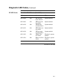
Table 1–6 Diagnostic ROM/Configuration Register Bit Definitions
Bit
Name
Definition
<31>
Scanproc Test
This bit is driven by the Scanproc chip during
diagnostics.
<30>
Time Out
This bit is set when 2 VRAM refresh pulses
occur while DS is low, indicating a hung system.
<29:18>
Reserved
Read as zero.
<17>
MSB
This bit indicates the speed of the oscillator used
as timing for the 1280 X 1024 monitor. A zero
indicates 66 Hz operation, a one indicates 72 Hz
operation.
<16>
Reserved
Read as zero.
<15:0>
ROM Data Field
These bits contain the ROM data that represents
the diagnostic code for the video subsystem.
SPXg/gt
The SPXg and SPXgt modules were originally designed to be
installed into an LCG frame buffer connector on the Model 60
system. The DC7201 chip in the Model 60 system provided the
interface to the SPXg/gt graphics module. The DC7201 chip
provided a direct path for the processor to read and write SPXg/gt
registers along with support for DMA into the SPXg/gt FIFO. In
the Model 90 system, no DMA support for SPXg/gt is provided.
The SPXg/gt is accessible using three separate address ranges.
The base address range for SPXg/gt module is 2800.0000 to
29FF.FFFF. In addition, a direct access path to the Brooktree
RAMDAC is supported at addresses 2A00.0000 to 2A00.003C.
Finally the SPXg/gt diagnostic ROM is located at addresses
2A10.0000 to 2A17.FFFF. The diagnostic ROM is accessible a
word at a time on aligned quadword boundaries.
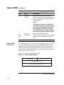
1–27
Network Interface Controller
Overview
1–28
The KA49 includes a network interface that is implemented by
the second generation Ethernet controller (SGEC). This interface
allows the KA49 module to be connected to either a ThinWire or
standard Ethernet network and supports the Ethernet data link
layer. The SGEC also supports CP-Bus parity protection.
Serial Line Controller
Overview
The serial line controller handles four asynchronous serial lines.
The DC7085 chip is used as the serial line controller. The DC7085
directly controls an external 64-entry silo shared by all four
receive lines. Access to the DC7085 by the CPU and interrupt
processing for the DC7085 are controlled by the CEAC. The four
serial lines are numbered 0 through 3, and each has a particular
primary use, as described in Table 1–7.
Table 1–7 Serial Line Usage
Line
Device
Description
0
Keyboard
Connected to a 15-pin D-sub connector1 and to a 4-pin
modular jack mounted on the system board. Data leads
only. Supports the LK401 keyboard.
1
Pointer
Connected to a 15-pin D-sub connector1 and to a miniature
DIN connector mounted on the system board. Data leads
only. Supports VSXXX-AA mouse or VSXXX-AB tablet.
2
Communications
Connected to a 25-pin D-sub connector mounted on the
system board, RS423 compatible. Data leads plus modem
control signals.
3
Printer
Connected to a 6-pin modified modular jack mounted on the
system board. DEC423, data leads only.
1 Same
connector
Line 3 is normally connected to a printer through a BC16E cable.
If a switch, accessible from the front of the system enclosure, is
set to enable, a received break condition on this line asserts the
CPU halt signal, which causes a processor restart with a restart
code of 2.
1–29
Time-of-Year Clock
Overview
The time-of-year (TOY) clock consists of an MC146818BM CMOS
watch chip that keeps the date and time of day and contains 50
bytes of general purpose RAM storage. This chip includes a time
base oscillator and a lithium battery on-chip. The battery powers
the chip with logic and oscillator while system power is off.
Battery Backup
A lithium battery within the watch chip supplies power to the
watch chip and its time base oscillator while system power is off.
The battery maintains the clock operation and the data stored in
the 50 bytes of RAM for a minimum of 10 years before it becomes
exhausted.
Watch Chip
Registers
The watch chip contains 64 8-bit registers. Ten of these contain
date and time data, four are control and status registers, and the
remaining 50 provide general purpose RAM storage. The registers
occupy 64 consecutive longwords of address space as shown in the
next table.
Each register is accessed as bits <9:2> of a longword. Bits <31:10>
and <1:0> are ignored on writing and undefined on reading.
WARNING
Because each register spans two bytes on the system
bus, only word or longword access instructions may
be used to manipulate these registers. The effects
of using byte access instructions are undefined. In
particular, instructions for modifying bits such as
BBSS, BBSC, BBCC, and BBCS cannot be used; they
generate byte-access read-modify-write cycles that will
corrupt the portion of the register that is not in the byte
being accessed.
1–30
SCSI Controller
Overview
The SCSI interface is a single-ended, bi-directional, 8-bit-wide bus
to which up to eight devices can be attached. The KA49 system
module is one of those devices, allowing the attachment of up
to seven additional devices. Devices may play one of two roles:
initiator or target. An initiator originates an operation by sending
a command to a specific target. A target performs an operation
that was requested by an initiator. The KA49 module is always
the initiator and all other SCSI devices attached to it are targets.
Connecting
Devices
Each device attached to the SCSI bus is identified by a unique
device ID number in the range 0 through 7. During the
arbitration, selection, and reselection bus phases in which an
initiator and a target establish a connection, the device IDs
of the initiator and target are both placed on the data bus by
asserting the data bits corresponding to the device ID numbers.
By convention, the ID number of the VAXstation Model 90 system
is six (this is controlled by the programs that drive the SCSI
interface; it is not fixed in Model 90 hardware).
The electrical interface consists of 18 signal lines. Some of these
lines are driven only by initiators, some only by targets, and some
by either. The SCSI bus is always terminated at each end. The
bus is permanently terminated at the controller (near end). Far
end termination can take place in one of two locations:
At the expansion connector on the rear of the system
enclosure
At the second expansion connector on a storage expansion
unit
Continued on next page
1–31
SCSI Controller, Continued
SCSI Bus
Signals
Table 1–8 describes the SCSI bus signals used by the SCSI
controller.
Table 1–8 SCSI Bus Signals
Bus Signal
Description
DB7..0 and DBP
An 8-bit parallel data bus with an associated odd parity bit. The
use of the parity bit is optional but strongly encouraged. These
lines may be driven by either an initiator or a target, depending
upon the direction of data transfer.
RST
Signals all devices on the SCSI bus to reset to their initial poweron states. Thereafter, it should be asserted only as a last resort
during error recovery since it indiscriminately affects all devices on
the bus. An RST signal generated by some other device on the bus
causes an internal reset of the 53C94 chip used in this controller
and sets the interrupt request bit (INT in register SCS_STATUS).
BSY and SEL
Used by initiators and targets during the arbitration, selection,
and reselection bus phases to establish or resume a logical
connection between an initiator and a target. Once the connection
is established, the target asserts BSY and the SEL signal is not
driven..
ATN
Used by an initiator to signal a target that it has a message ready.
The target can receive the message by entering the "message out"
phase. ATN is always driven by an initiator.
REQ and ACK
Used to synchronize information transfers over the data bus during
any of the six information transfer phases. REQ is always driven
by the target, ACK is always driven by the initiator.
C/D, I/O and MSG
Collectively indicate one of six possible information transfer phases.
These signals are always driven by the target device.
1–32
DSW21 Synchronous Communications Adapter
Overview
The DSW21 syncrhonous communications adapter is a
synchronous serial communications interface for the VAXstation
4000 Model 90 workstation. It has full modem control and
multiple protocol support. Figure 1–4 shows the DSW21
communications adapter.
Figure 1–4 Synchronous Communications Adapter
MLO-005915
The adapter is an option board that connects internally to the
CPU board by a 64-pin option connector. It consists of the EDAL
interface, 128 KB UVEPROM, 256 KB static RAM, the MC68302
integrated multi-protocol processor (IMP), and I/O receivers and
drivers with static and lightning protection. The communications
I/O connector is a 50-pin D-subminiature plug that goes directly
through the back of the system cabinet. Figure 1–5 shows the
DSW21 connections.
Continued on next page
1–33
DSW21 Synchronous Communications Adapter, Continued
Figure 1–5 DSW21 Connections
50-PIN
CONN
64-PIN
CONN
128K BYTE
PROM
256K BYTE
SRAM
EDAL
T
X
I/O
RAW
PAL
CONTROL
LOGIC
MC68302
IMP
R
X
INTERRUPT
LJ-02225-TI0
1–34
Chapter 2
Firmware
Overview
Introduction
This chapter provides an overview of the VAXstation 4000 Model
90 system firmware. The firmware is located in four EPROMs,
which hold a total of 512 KB of data. The system firmware
has five distinct areas of operation. This chapter discusses the
following topics:
Power-Up Initialization Code
Console Mode
Extended Self-Test
Utilities
System Test
System ROM
Option ROM
Configuration Table
Driver Descriptor
Interfacing to Diagnostic Drivers
Console Driver Interface
2–1
Power-Up Initialization Code
Overview
The power-up initialization code is executed when power is
applied to the VAXstation 4000 Model 90 workstation or any
time volatile console data structures are altered.
Power-Up
Initialization
Sequence
Table 2–1 describes the power-up initialization sequence.
Table 2–1 Power-Up Initialization Sequence
Stage
What the System Does
1
Tests enough memory to bring up the console for building console and device
structures.
2
Checks its configuration, identifies optional devices, and identifies the type
of monitor connected to the video slot.
3
Tests the TOY clock and the non-volatile RAM. If this test fails, the power-up
test stops.
4
Constructs the master configuration table (MCT), device configuration table
(DCT), driver descriptor, shared console interface area (SCIA), and a blank
page frame map.
Continued on next page
2–2
Power-Up Initialization Code, Continued
Table 2–1 (Continued) Power-Up Initialization Sequence
Stage
What the System Does
5
Tests the serial lines. If this test fails, the console terminal is not enabled
and the only output is the HEX display.
6
If...
And...
Then...
No video option is
present
—–
The system defaults to line
three of the serial port.
A video option is
plugged into the video
slot on the CPU and
the switch is set to
graphics
The test fails
Video drivers are loaded and
the system behaves as if a
failure occurred.
The alternate console
switch is set to
alternate console
—–
The terminal connected to line
three of the serial port is used
as the console.
Calls up the console device initialization routine. Console I/O is allowed
after this step. The system type and ROM ID are printed out at the console
device, followed by the amount of memory and the Ethernet address.
Continued on next page
2–3
Power-Up Initialization Code, Continued
Table 2–1 (Continued) Power-Up Initialization Sequence
Stage
What the System Does
7
Test dispatcher tests the functional blocks of the system. This test displays
a blank ruler on the screen. The length of the ruler is dependent on the
devices in the system. The dispatcher runs the tests in the following order:
Non-Volatile RAM (NVR)
Color graphics (LCSPX, SPXg or SPXgt)
Serial line controller (DZ)
Cache memory (SCSI DMA RAM, OBIT RAM, BCACHE)
Memory configuration (MEM)
Floating point unit (FPU)
Interval timer (IT)
Miscellaneous system board (checksums, Ethernet ID ROM) (SYS)
Network controller (NI)
SCSI controller (SCSI)
Sound chip (AUD)
Option board (COMM)
Bus adapter logic
If an error occurs during testing, the dispatcher continues to test the
remaining devices until all tests are completed.
NOTE
If halts are enabled, the console prompt >>> displays.
If not, the system is autobooted using the default
device stored in the NVR or the Ethernet if no device is
specified.
2–4
Console Mode
Overview
The VAXstation 4000 Model 90 console mode allows operation of a
console device, which can be one of the following:
A workstation video device and LK401 keyboard and mouse
A terminal connected to line three of the serial port
A remote system connected using the Ethernet
Console Mode
The console mode can be entered if:
The HALT parameter is set to halt when power is turned on.
A HALT instruction is executed with the HALT action set
to HALT or a severe processor condition occurs (such as an
invalid interrupt stack).
An external HALT is detected (pressing the halt button on
the front panel).
Input and
Output
In console mode input and output (I/O) routines are used by:
Self-Test
Extended self-test
Utilities
System test
Virtual memory boot (VMB)
2–5
Extended Self-Test
Overview
The extended self-tests are started by entering the TEST
command at the console prompt, followed by the test number
or numbers you wish to run. The test dispatcher runs the self-test
requested until an error occurs or until all tests are completed.
Test Dispatcher
The dispatcher uses the main configuration table (MCT), device
configuration table (DCT), and drive descriptor data structures
when running a self-test.
Table 2–2 shows the stages of the test dispatcher self-test
procedure.
Table 2–2 Test Dispatcher Procedure
Stage
What the Dispatcher Does
1
Uses the device number to index into the MCT.
2
Receives a pointer to the device DCT from the MCT.
3
Finds a pointer to the device directory entries in the DCT.
4
Scans all the directories for a directory type of the self-test directory (=1).
5
Reads the flags field in the DCT to determine if the self-test diagnostic needs
to be loaded into RAM.
If the diagnostic needs to be loaded into RAM, the dispatcher allocates
memory for loading the diagnostic (moving it from ROM to RAM).
Continued on next page
2–6
Extended Self-Test, Continued
Table 2–2 (Continued) Test Dispatcher Procedure
Stage
What the Dispatcher Does
6
Reads the flags field in the DCT to determine if the diagnostic uses a shared
diagnostic driver.
7
If...
Then...
The self-test diagnostic
uses a shared
diagnostic driver
The dispatcher gets the directory entry and the
pointer to the driver descriptor from the DCT.
The shared driver
needed is not already
in RAM
The dispatcher allocates temporary RAM for
the shared driver (loading the driver from ROM
to RAM) and fills in the driver descriptor data
structure to point to the RAM based shared driver.
Calls the devices self-test interface.
2–7
Utilities
Overview
A utility test is started at the console prompt by entering a
command using the following format:
TEST/UTIL dev_nbr util_nbr op1...opn
Running a
Utility
Format
Meaning
/UTIL
Instructs the test dispatcher to run a utility
dev_nbr
The device on which the utility operates
util_nbr
The utility number
op1...opn
One to n optional parameters
The console mode passes a list of parameters to the test
dispatcher. The test then uses the main configuration table
(MCT), device configuration table (DCT), and driver descriptor
data structures when running a utility. Table 2–3 describes the
dispatcher process for running a utility.
Table 2–3 Running a Utility Process
Stage
Dispatcher Process
1
Uses the device number to index into the MCT.
2
Receives a pointer to the device DCT from the MCT.
3
Finds a pointer to the device directory entries in the DCT.
4
Scans all the directories for a directory type of the utility directory (=3)
5
Reads the flags field in the DCT to determine if the utility needs to be loaded
into RAM.
If the utility needs to be loaded into RAM, the dispatcher allocates memory for
loading the utility (moving it from ROM to RAM).
Continued on next page
2–8
Utilities, Continued
Table 2–3 (Continued) Running a Utility Process
Stage
Dispatcher Process
6
Reads the flags field in the DCT to determine if the utility uses a shared
diagnostic driver.
If...
Then...
The utility uses a
shared diagnostic
driver
The dispatcher gets the directory entry and the
pointer to the driver descriptor from the DCT.
The shared driver
needed is not already
in RAM
The dispatcher allocates temporary RAM for the
shared driver (loading the driver from ROM to RAM)
and fills in the driver descriptor data structure in the
driver descriptor for the shared driver.
7
Calls the utility entry point.
8
Checks the parameters passed.
If the parameters are out of range or too many passed, the dispatcher sends
out an illegal parameter message.
9
Prompts the user if more parameters are needed.
10
Prompts the user if the utility is going to destroy any user data.
11
Starts the utility.
2–9
System Test
Overview
The system test tests the device interaction in the system by
creating maximum DMA and interrupt activity. The test consists
of:
Modified VAXELN kernel
System test monitor
System diagnostics
Shared drivers (if present)
The system test can be run in three environments, selected by the
SET DIAGENV command.
Customer - 1
Digital Services - 2
Manufacturing - 3
CAUTION
Do not use the manufacturing mode in the field.
Manufacturing mode erases customer data on hard
disks, excluding the system disk.
Refer to Table 5–8 for more detailed information on running the
system test.
2–10
System ROM
Overview
The base VAXstation 4000 Model 90 firmware contains 512 KB of
ROM split into four 128-KB wide ROMs. This provides the full
32-bit wide memory data path shown in Figure 2–1.
Figure 2–1 System ROM Format
ROM 3
ROM 2
ROM 1
ROM 0
byte 3
byte 2
byte 1
byte 0
2004.0000
byte 7
byte 6
byte 5
byte 4
2004.0004
byte B
byte A
byte 9
byte 8
2004.0008
LJ-01818-TI0
The system firmware ROMs supply some information on a per
byte basis for ease of manufacture and development. Other
information (software and tables) is supplied by the set of ROM
parts. Figure 2–2 displays the system ROM part formats.
Continued on next page
2–11
System ROM, Continued
Figure 2–2 System ROM Part Format
15..
..8
7..
..0
Reserved for ROM set Data
Reserved for ROM set Data
word 0
Reserved for ROM set Data
Reserved for ROM set Data
word 1
Version
Version
word 2
ROM Byte Number
ROM Byte Number
word 3
Manufacturing Check Data (55h)
Manufacturing Check Data (55h)
word 4
Manufacturing Check Data (AAh)
Manufacturing Check Data (AAh)
word 5
Manufacturing Check Data (33h)
Manufacturing Check Data (33h)
word 6
ROM Part Length
ROM Part Length
word 7
Reserved for ROM set data
Reserved for ROM set data
Checksum
Checksum
word 8
Last word
LJ-02219-TI0
Continued on next page
2–12
System ROM, Continued
System ROM
Part Format
Table 2–4 shows the part formats in the system ROM.
Table 2–4 System ROM Part Formats
Byte
Name
Description
Word 02h
Version
Contains the low 8 bits of
the version number of the
console code for the Model
90 system firmware.
03h
ROM byte number
Indicates the position of
the byte among the set of
ROMs used to implement
the firmware. This value is
equal to the low 2 bits of the
physical address of the first
byte in the ROM part. The
value ranges from 0 to 3.
04h to 06h
Manufacturing
check data
Used for a quick check of
the ROM. The data are 55h,
AAh, and 33h.
07h
ROM part length
Indicates the length of the
ROM part divided by the
data path width in bytes.
Last byte
Checksum
For each ROM byte contains
a simple 8-bit add and rotate
checksum. In a 16-bit ROM
the last two bytes contain
a checksum, one checksum
for each byte address in the
device.
Continued on next page
2–13
System ROM, Continued
System ROM
Set Format
Table 2–5 shows the physical addresses in the system ROM. These
addresses are fixed.
Table 2–5 System ROM Physical Addresses
Physical Address
Name
Description
2004.0000
Processor restart
The hardware begins execution at this
address when:
Power is turned on.
Kernel mode halt instruction
executes.
A break signal is received from the
console device.
The HALT button is depressed.
The CPU detects a severe corruption
of its operating environment.
2004.0004 SYS_TYPE
System Type
register
The system type value longword is
0401.0001.
2004.0008
ROM Part data
These 24 bytes are reserved for
information contained in each ROM byte.
2004.0020
Interrupt vector
numbers
These eight longwords are not used by the
Model 90.
2004.0060
Console I/O
routines
There are eight I/O routines provided in
the system ROM. Entry points for these
routines are located at longword intervals
in the area.
2004.0080
Reserved
Reserved so all ROM set data that follows
it will be in the same relative position.
2004.0088
System console
firmware
revision number
This word contains the system console
firmware revision number.
Continued on next page
2–14
System ROM, Continued
Table 2–5 (Continued) System ROM Physical Addresses
Physical Address
Name
Description
2004.008A
System
diagnostic
firmware
revision number
This word contains the system diagnostic
firmware revision number.
2004.008C
Diagnostic
descriptor
This longword contains the physical
address of the beginning of the system
level diagnostic boot block. A value of zero
indicates that there is no system level
diagnostic present in the Model 90 system
firmware ROM.
2004.0090
Pointers to
keyboard map
These two longwords point to the tables
used to translate the LK401 main array
keycodes to character codes. The first
longword contains the physical address
of the beginning of the keyboard tables.
The second longword contains the physical
address of the beginning of the keyboard
mapping tables.
2–15
Option ROM
Overview
Each option in the Model 90 system has its own ROM firmware.
The ROM memory on the option board may be implemented as
discussed in the following sections.
Option ROM
Part Format
The option ROM part format is provided for each byte in the ROM
set. This format is compatible with the system ROM format, with
the addition of the data path indicator. Figure 2–3 shows the
ROM byte data.
Figure 2–3 Option ROM Byte Data
Data Path Indicator
Byte 0
Reserved
Byte 1
Version
Byte 2
ROM Index Number
Byte 3
Manufacturing Check Data (55h)
Byte 4
Manufacturing Check Data (AAh)
Byte 5
Manufacturing Check Data (33h)
Byte 6
ROM Part Length
Byte 7
Reserved for ROM set Data
Byte 8
Checksum
Last Byte
LJ-00101-TI0
Continued on next page
2–16
Option ROM, Continued
Byte
Name
Description
00h
Data path
indicator
Indicates the size of the ROM data
path. The data path must be one of the
following:
1: One byte per longword. Bytes
in ROM occupy the low byte of
each longword.
2: Two bytes per longword. Words
in ROM occupy the low two bytes
of each longword.
4: Four bytes per longword.
Longwords in ROM correspond
to longwords in the address space.
02h
Version
Contains the low 8 bits of the version
number for the option firmware.
03h
ROM Byte
number
Indicates the position of the byte
among the set of ROMs used to
implement the firmware. This value is
equal to the low 2 bits of the physical
address of the first byte in the ROM
set. Note that this value is always less
than the data path indicator.
04h to
06h
Manufacturing Performs quick verify check of the
check data
ROM contents. The data are 55h, AAh,
and 33h.
Continued on next page
2–17
Option ROM, Continued
Byte
Name
Description
07h
ROM part
length
Indicates the length of each byte
address in the set. It is the number of
bytes associated with each byte in the
ROM in Kbytes.
NOTE
The number of bytes in the ROM set
equals the sum of the number of bytes
in each of the ROM parts divided by
the data path of each device. Each
of the ROM parts on the option board
must have the same number of bytes.
Option ROM
Set Format
8
Reserved
Reserved for ROM set data.
Last
byte
Checksum
Each byte in the ROM set has a simple
add and rotate checksum in its last
byte.
For options that have a one-byte or two-byte data path, the data
from the ROM set must be moved into RAM. Note that a device
cannot have both an 8-bit data path and a 16-bit data path. An
option with a full 32-bit data path may not have to be moved.
Devices with a 16-bit data path are treated as though each byte of
the device is a device in itself.
Figure 2–4 shows option ROM set data.
Figure 2–4 Option ROM Set Data
31
00
Option Index Value
Option Revision Number
Reserved for Expansion (32 bytes)
Device Configuration Table (DCT) Template
LJ-00102-TI0
Continued on next page
2–18
Option ROM, Continued
Name
Description
Option revision
This number controls changes
in both the option hardware and
firmware.
Option index value
An index value of the last DCT entry.
A zero in this field indicates a single
DCB for the device, a one indicates
two device control blocks for this
device. An option that occupies the
storage option slot can have the
values of zero or one. An option that
occupies the video option slot can
have the values of zero, one, or two.
Reserved for expansion
These 32 bytes are reserved.
Device configuration table
template
The device implemented by the
option must have an associated
device configuration table template.
The DCT contains static and
dynamic data and pointers to code
required for the device.
2–19
Configuration Table
Overview
Information on the VAXstation 4000 Model 90 devices is stored in
the system configuration tables during the power-up initialization.
The initialization code sizes the system by reading the ROM-based
device configuration tables (DCT) and builds a memory resident
configuration data structure. Figure 2–5 shows how the data
structures are linked together.
Figure 2–5 Model 90 Configuration Tables
Model
90
NVR
Scratch
RAM
Main
Configuration
Table
Device
Configuration
Table
Device
Configuration
Table
Device
Configuration
Table
LJ-01829-TI0
The initialization code saves the pointer to the scratch RAM in
the Model 90 NVR in four consecutive bytes. The scratch RAM
contains a pointer to the main configuration table (MCT) at its
base address. The MCT contains pointers to the DCT.
Main
Configuration
Table
The main configuration table (MCT) contains a list of the devices
in the system and a pointer to the device configuration table
(DCT) for each device. The MCT is built when power is turned on
and resides in the diagnostic area in memory. The MCT gives the
test dispatcher a single interface into the various components of
the system. The MCT is shown in Figure 2–6.
Continued on next page
2–20
Configuration Table, Continued
Figure 2–6 Main Configuration Table
Minor Version ID
Major Version ID
Number of Devices
Edit Version ID
0
Device ID
Pointer to Device Configuration Table
0
Device ID
Pointer to Device Configuration Table
0
Number of Devices *8
Device ID
Pointer to Device Configuration Table
(Number of Devices *8)+4
LJ-00104-TI0
The components of the MCT are as follows:
Table 2–6 MCT Components
Name
Description
Major version ID
Tracks major changes in the
diagnostic interface
Minor version ID
Tracks minor changes in the
diagnostic interface
Edit version ID
Reserved for use by diagnostic
developers
Number of devices
Number of entries in the MCT table
Device ID1
Device ID number
–1
Must be zero reserved for future use
1 Replicated
for each device in the system.
Continued on next page
2–21
Configuration Table, Continued
Table 2–6 (Continued) MCT Components
Name
Description
Pointer to device
configuration table1
Points to the DCT for the particular
device
1 Replicated
Device
Configuration
Table
for each device in the system.
There is a device configuration table (DCT) entry for each device
in the Model 90 system. The DCT contains extended information
about the device, such as:
Device name
Diagnostic code location
Header information
The test dispatcher and the system test monitor use this data to
fetch the appropriate diagnostic code to execute from the ROM or
to load into RAM. The DCT is shown in Figure 2–7.
Continued on next page
2–22
Configuration Table, Continued
Figure 2–7 Device Configuration Table
Minor Version ID
Major Version ID
0
Number of Devices
Edit Version ID
4
Device
Name
8
Pointer to Driver Descriptors
10
Device Status
14
Pointer to Extended Status
18
Size of Extended Status
1C
Pointer to Extended Config
20
Pointer to Permanent Memory
24
Size of Permanent Memory
28
System Test Status
2C
Pointer to Extended System Test Status
30
Size of Extended System Test Status
34
Flags
Flags
DPSIZE
DIRTYP
38
Physical Address of Module
3C
Code Length
40
Entry Point Offset
44
DPSIZE
DIRTYP
((NBR_OF_DIRS-1)*10)+2C
Physical Address of Module
Code Length
Entry Point Offset
LJ-00105-TI0
Continued on next page
2–23
Configuration Table, Continued
The components of the DCT are as follows:
Table 2–7 DCT Components
Name
Description
Minor version ID
Tracks minor changes in the device diagnostic routines
Major version ID
Tracks major changes in the devices diagnostic routines
Number of
devices
Number of directory entries for the device. A directory entry tells
the user where to find a particular component of code for the device.
Edit version ID
Device ID number
Device name
Device Name is ASCII. This is used by the show configuration utility
and the system test to display information about the device.
Pointer to driver
descriptors
Points to the drive descriptor area associated with the device.
Device status
Saved from the last time the self-test was run on the device. The
show configuration utility uses this field to display information
about the device. The device status is split into two words, the lower
word is the error field and the upper word is the field replaceable
unit (FRU) thought to be faulty.
Pointer to
extended status
Points to any extended information that is saved by the device
self-test
Size of extended
status
Length of the extended device status in bytes. The extended device
status can be up to 16 longwords of information. The extended
status displays when the user enters the SHOW ERRORS command
at the console prompt.
Pointer to
extended
configuration
Points to extended configuration information about the device. For
example, the SCSI self-test code uses this field to save a pointer
to information about the devices connected to the SCSI bus. The
information is displayed when the user enters the SHOW CONFIG
command at the console prompt.
Pointer to
permanent
memory
Points to the permanent memory that has been allocated. The field
is filled in by the diagnostic, the first time that it allocates memory.
Continued on next page
2–24
Configuration Table, Continued
Table 2–7 (Continued) DCT Components
Name
Description
Size of
permanent
memory
Amount of permanent memory (in pages) that has been allocated.
This field is filled in by the diagnostic the first time that it allocates
memory.
System test
status
Saved the last time that system test was ran on this device without
doing intervening test commands.
Pointer to
extended system
test status
Points to any extended information that is saved by the device’s selftest. The SHOW ESTAT utility uses the extended status to display
information about the device.
Size of extended
system test
status
Length in bytes of the extended system test status.
Flags
Contain flag data associated with the particular device routine.
Definition
Meaning
Bit 15=1
Code must be loaded into RAM at power-up and
memory marked as unavailable to the operating
system.
Bit 14=1
Code must be loaded into RAM to execute. The
memory is released after execution is complete.
Bit 13=1
Code has been loaded into RAM at power-up and
memory marked as unavailable to the operating
system.
Bit 0=1
Code uses shared diagnostic driver.
Continued on next page
2–25
Configuration Table, Continued
Table 2–7 (Continued) DCT Components
Name
Description
DP SIZE
Contains the data path size of the ROM in which the piece of code
resides.
DIRTYP
Definition
Meaning
1
ROM Width is one byte wide.
2
ROM Width is two bytes wide.
4
ROM Width is four bytes wide.
Contains the type of directory entry that the previous elements refer
to.
Definition
Meaning
1
Self-Test directory entry
2
System test directory entry
3
Utility directory entry
4
Console routine directory entry
5
Unjam routine directory entry
6
Diagnostic driver directory entry
Physical address
of module
Contains the physical address for the particular component of the
code.
Code length
Contains the length of code in bytes.
Entry point
offset
Contains the offset from the beginning of the code to where the
entry point is.
2–26
Driver Descriptor
Overview
Any device that provides a shared port driver or shared class
driver must provide a descriptor that supplies the Model 90 base
system firmware, system test monitor, and any other piece of
software specific information about the drive. The format for a
driver descriptor is shown in Figure 2–8.
Figure 2–8 Driver Descriptor Data Structure
Device ID
0
Address of Driver
4
Length of Driver
8
Entry Point of Driver
C
Size of Driver Data Area
10
Address of Driver Data Area
14
Address of IO Segment Table
18
LJ-00106-TI0
The fields of the driver descriptor are as follows:
Name
Description
Device ID
Ensures that the driver descriptor
ID matches the function block ID.
This allows a function the ability
to determine if it is being used
correctly.
Address of driver
Contains the address of the device
driver. This address may be ROM or
memory address.
Continued on next page
2–27
Driver Descriptor, Continued
2–28
Name
Description
Length of driver
Contains the length of the device
driver in bytes. This field is used
by both the base system ROM and
the system test monitor to determine
the amount of code that needs to be
loaded into RAM.
Entry point of driver
Contains the number of bytes from
the beginning of the device driver to
the INIT_DRIVER function.
Size of driver data area
Contains the length in bytes of the
amount of memory that a driver
needs for its parameters and local
data.
Address of driver data
area
Contains the address of the device
driver data area that is used by the
driver to store local data.
Address of I/O segment
table
Contains the address of the I/O
segment table.
Interfacing to Diagnostic Drivers
Overview
The network device contains routines to UNJAM the device and to
run self-test routines, system test routines, console routines, and
a shared diagnostic driver routine. Figure 2–9 shows how these
pieces of code relate to each other.
Figure 2–9 Diagnostic Driver Console Support
Model
90
Console
Class
(Driver Description)
NI
Self-Test
(Driver Descriptor)
NI
System Test
(Driver Descriptor)
NI
Utilities
(Driver Descriptor)
NI
Diagnostic
Driver
LJ-01820-TI0
User application performs console input/output to the network by
calling the console code, which calls the network diagnostic driver.
The console, self test, system test, and UNJAM routines interface
to the diagnostic driver in similar ways. All diagnostic routines,
utilities, and console routines do the following:
Allocate memory for the driver data area.
Allocate memory for the diagnostic function block or console
function block.
Continued on next page
2–29
Interfacing to Diagnostic Drivers, Continued
Overview
(continued)
2–30
Call the INIT_DRIVER routine with the following
parameters:
—
Pointer to the I/O segment table
—
Pointer to the driver data area
—
Pointer to the driver function block or console function
block
—
Pointer to the shared console interface area, or display
zero if this is not a console driver
—
As many as two additional device-specific parameters
Console Driver Interface
Overview
The Model 90 console code is split into a class/port driver scheme.
The class driver contains the main console functions, such as
PUTCHAR and GETCHAR. The port drivers contain the device
specific code required to support these functions. Figure 2–10
shows the division of the console function.
Figure 2–10 Model 90 Console Structure
Console Class Driver
DZ Console
Port Driver
LCSPX Console
Port Driver
NI Console
Port Driver
Input
I
Serial Line
Controller
O
O
LCSPX
Controller
I
O
Lance
Device
LJ-01821-TI0
Performing I/O
The console device can require either one channel or two channels
to perform I/O to the console device. If the console device is a
graphics terminal with a LK401 keyboard, the console program
must interface with the serial line device driver for console input
and interface with the graphics device driver for output from the
console. If the console device is a terminal connected to a serial
Continued on next page
2–31
Console Driver Interface, Continued
line, the console responds to the serial line driver for both input
and output.
The console class driver contains the generic routines that
interface to the console and user application to perform terminal
input and output transactions. The console class driver interfaces
with the port driver depending on the current console device.
If the console port driver does not support PUTCHAR or
GETCHAR functions, it must interface with the appropriate
port driver to perform the needed function.
Shared
Console
Interface Area
The shared console interface area (SCIA) consists of a console
class driver descriptor and three port driver descriptors. The
port driver descriptors can be associated with a DZ port driver, a
graphics output driver, and a network driver.
The SCIA provides an interface to the console terminal that
isolates the implementation specifics of accessing the console
terminal. It is designed so the console drivers can run in both
virtual and physical mode.
The SCIA is set up by the initialization code. After the SCIA is
set up, the software can use this area to interface with the console
class driver routine. The shared console performs the following:
Raw character I/O to console terminal
Higher level of I/O functions that handle XON/XOFF flow
(ASCII bell character and LK401 keyboard translation are
handled by the DZ driver.)
Data structures to allow system software to map all console
code and I/O space references into virtual memory as needed
Continued on next page
2–32
Console Driver Interface, Continued
The SCIA data structure is shown in Figure 2–11.
Figure 2–11 SCIA Data Structure
Console Type
LK401 Keyboard Type
Address of US Font Table
Address of MCS Font Table
Address of Keyboard Translation Table
Address of Keyboard Map Table
Console Class Device ID
Console Class Driver Driver Descriptor
DZ Device ID
DZ Port Driver Driver Descriptor
Graphics Device ID
Graphics Port Driver Driver Descriptor
NI Device ID
NI Port Driver Driver Descriptor
VMS Debug Device ID
VMS Debug Port Device Driver
XXX Device ID
XXX Port Device Driver
LJ-01822-TI0
Continued on next page
2–33
Console Driver Interface, Continued
Console Port
Driver
The fields of the console port drivers driver descriptor are the
same as the console class drivers driver descriptor, with one
exception: the port driver contains pointers to the console port
level routines. The port driver supports all functions whether
or not the device supports console output only or console input
/output. Figure 2–12 shows the function block of the port driver.
Figure 2–12 Console Port Driver Function Block
Device Id
INIT_DRIVER Pointer
GETCHAR Pointer
PUTCHAR Pointer
RESET_INPUT Pointer
INIT _INPUT Pointer
RESET_OUTPUT Pointer
INIT_OUTPUT Pointer
LJ-01823-TI0
Continued on next page
2–34
Chapter 3
System Configuration
Overview
In this Chapter
This chapter describes the system box used with the VAXstation
4000 Model 90 workstation and its components, cabling, and
specifications. The topics covered in this chapter are:
System Box
Mass Storage Device Areas
Power Supply
Internal Cabling
System Box Control Panel
I/O Panel
System Box Specifications
3–1
System Box
The BA46 enclosure is used for desktop and floorstand
installations of the VAXstation 4000 Model 90 system. Figure 3–1
shows the Model 90 system box and its components.
Overview
Figure 3–1 Model 90 System Box
5420854-02
24-PLANE
FRAME BUFFER
7028107-01
COVER ASSEMBLY
OR
5420454-01
SIMM MODULES
7445390-01
PCB E-CLIP
SPACER
1701876-01
POWER WIRE
HARNESS ASSY
4 COND
5421795-01
LCSPX
5420367-01
LIGHTS +
SWITCHES MOD
5420450-01
GSP GRAPHICS
PROCESSOR
MODULE
5420452-01
"8" PLANE
FRAME
BUFFER MOD
7443526-01
OR
7443526-02
SHIELD OPTION
7442680-02
VIDEO BD CLAMP
7442680-02
VIDEO BD CLAMP
5420377-01
SYNC-COMM
MODULE
7028115-0x
RZ2x(L) HARD DISK
DRIVE ASSY
H7819-01
POWER SUPPLY
MS44L-AA
4MB MEM OPT/
MS44-CA
16MB MEM OPT
7441473-01
RF1 SHIELD
FILLER
METAL
LATCH
7441472-01
FILLER PLATE
7029423-01
DRIVE H-BRACKET
ASSEMBLY
7028108-01
CABLE ASSY
SCSI SYSTEM
7028112-0x
REMOVABLE MEDIA
DRIVE ASSY
(STORAGE OPTIONS)
7028100-01
DRIVE ASSY
RX26/FDI
5421177-01
SYSTEM MODULE
7440430-01
RMD BRKT
7028115-0x
RZ2x(L)
HARD DISK
DRIVE ASSY
7411856-08,
-09, -10 MEDALLION
VAXSTATION 4000.90
7028099-01,
-02, OR -03
BEZEL ASSY
7028096-01
BASE ASSY
LJ-02224-TI0
Continued on next page
3–2
System Box, Continued
Mass Storage
Device Areas
The Model 90 system box can hold two half-height, fixed media
drives (8.9 cm [3.5 in]) in the H bracket (front left, Figure 3–1),
and one half-height, removable media drive (13.3 cm [5.25 in] or
8.9 cm [3.5 in]) in another bracket (front right, Figure 3–1). The
bottom drive in the H bracket is mounted upside down. The H
bracket releases by a single latch and the other bracket uses two
release points.
Power Supply
The system box has space for one power supply, the H7819-AA.
The power supply provides protection against excess voltage,
current, and temperature.
The power supply voltage connectors are located at the rear of the
unit. The input connector is used to connect to a wall outlet and
the output connector connects to the system monitor. The power
switch and power OK LED are located on the front of the unit.
Inside, is a -9.0 V LED. The supply also has two 12 V fans for
cooling the system.
The power supply has an automatic voltage select (AVS ) circuit
to automatically select the ac input for 100 Vac to 120 Vac or 220
Vac to 240 Vac mode of operation. The power supply is a 174 watt
unit.
Voltage (dc)
Ampere
+5.1
19.00
+3.3
4.89
+12.1
3.82
-12.0
0.69
-9.0
0.18
Power is supplied to the following components:
System module (which supplies power for option modules
installed in the system and mass storage devices)
Cooling fans
Continued on next page
3–3
System Box, Continued
AC power for system monitor
Power Supply
Specifications
The power supply specifications are listed in the following tables.
Input Specifications
Parameter
Specifications
Line voltage
120 V
240 V
Voltage tolerance
88 V to 132 V
176 V to 264 V
Frequency
60 Hz
50 Hz
Frequency
tolerance
47 Hz to 63 Hz
47 Hz to 63 Hz
Input current
2.9 A (max.)
power supply
only
4.0 A (max.)
AUX only
1.4 A (max.) power
supply only
2.0 A (max.) AUX only
Inrush current
45.0 A (max)
cold power
supply only
45.0 A (max) cold power
supply only
Power consumption
(max.)
286 W
286 W
Output Specifications
Parameter
Minimum
Specifications
Typical
Maximum
+5.1 V reg.
Short term
4.90 V
5.05 V
5.20 V
+5.1 V reg.
Long term
+4.85 V
+5.10 V
+5.25 V
Continued on next page
3–4
System Box, Continued
Parameter
Minimum
Specifications
Typical
Maximum
+12.1 V reg.
Short term
+11.70 V
+12.10 V
+12.50 V
+12.1 V reg.
Long term
+11.50 V
+12.10 V
+12.70 V
-12.0 V reg.
Long term
-11.40 V
-12.00 V
-12.60 V
-9.0 V (isolated)
Long term
-8.55 V
-9.00 V
-9.45 V
+3.3 V Long term
+3.13 V
+3.3 V
+3.46 V
+3.3 V
+5.1 V
+12.1 V
-12.0V
-9.0 V
3.20 A
2.8 A
0.18 A
0.26 A
0.12 A
6.39 A
19.52 A
3.82 A
0.69 A
0.17 A
+3.3 V
+5.1 V
+12.1 V
-12.0 V
-9.0 V
20.0 mV
30.0 mV
50.0 mV
30.0 mV
50.0 mV
70.0 mV
120.0 mV
50.0 mV
Load range
Ripple and noise
1 Hz to 10 Hz
Continued on next page
3–5
System Box, Continued
Parameter
Minimum
Ripple and noise
(except +5.1 V and
+3.3 V)
Ripple and noise
10 MHz to 50 MHz
10 MHz to
50 MHz
+5.1 V
+3.3 V
Specifications
Typical
Maximum
1.0%
2.0%
30 mV
20 mV
50 mV
30 mV
Physical Dimensions
Internal
Cabling
Weight
Height
Width
Depth
14.9 kg
(33 lb)
6.99 cm
(2.75 in)
11.18 cm
(4.4 in)
38.10 cm
(15.0 in)
The system box internal cabling is shown in Figure 3–2. Note
that there is one SCSI cable and one dc power harness connecting
to the drives.
NOTE
The power cable for half-height drives must be routed
above the SCSI cable, as shown in Figure 3–2.
Table 3–1 lists internal system devices and their cable part
numbers.
Continued on next page
3–6
System Box, Continued
Figure 3–2 Internal Cabling
Power Cable
SCSI Cable
To RX26 Controller
Module (Optional)
Graphics
Board
Power
Supply
Memory
Modules
Removable Drive
(RRD42, RX26,
TZK10 Drives)
TLZ06
Fixed Disk
Drives
(RZ23L, RZ24L,
RZ24, RZ25)
LJ-02218-TI0
Table 3–1 Internal System Devices and Cables
System Device
Cable PN
Description
3 SCSI Devices
17-02875-01
Four 50-pin IDC to 50-pin
champ (external)
SCSI Device dc
power harness
17-02876-01
Four 4-pin Mat-N-Loks to 4-pin
mini
Continued on next page
3–7
System Box, Continued
System Box
Control Panel
The controls and indicators for the system box are located behind
the flip-down door on the front bezel (Figure 3–3) of the box.
Figure 3–3 System Box Control Panel
Audio Selector Switch
Alternate
Console
Switch
Handset Jack
On/Off Switch
Halt Button
Diagnostic
Lights
Front Door
MLO-005090
ON/OFF Switch This switch, located on the upper left side of
the front bezel and labeled O I, controls ac power to the H7819AA power supply. The switch does not affect the ac power outlet
provided for add-on peripherals at the rear of the system box.
Power OK LED This small green indicator is visible on the
upper left side of the front bezel. The LED is on when ac power is
applied and the correct output voltage levels are present.
Handset jack This is a four-pin, MJ-type connector.
Audio selector switch This switch selects between speaker
output and headset output.
Continued on next page
3–8
System Box, Continued
Alternate console switch This switch selects either the graphics
terminal or printer/console port to be the system’s console.
Halt button When actuated, this button sends a halt signal to
the CPU module.
Diagnostic lights These lights are located on the right side of
the control panel. These lights display two binary fields, which
represent a two-digit hexadecimal diagnostic code.
I/O Panel
The I/O panel provides connectors to devices external to the
system. The system configuration determines which external
devices are connected to the panel. The external devices, shown
in Figure 3–4, are as follows:
Ethernet interface (left to right: standard port, network
switch, and ThinWire port)
RS232 communications port
Printer/console port with a DEC423 connector (MMJ)
Keyboard port
Mouse port
Remote keyboard/mouse port
SCSI Port
Option port (for the DSW21 communications device or
TURBOchannel adapter option)
Monitor video port
Monitor power socket
AC Power socket
Continued on next page
3–9
System Box, Continued
Figure 3–4 Model 90 I/O Panel
7
8
4
9
10
6
11
5
3
2
1
LJ-00639-TI0
Continued on next page
3–10
System Box, Continued
Table 3–2 lists external system devices and their cables.
Table 3–2 External System Devices and Cables
Device/Cable
Cable P/N
Description
System to monitor
BC27R-03
3 coax Dsub. to 3 BNC 39 in (99.1 cm)
Remote video
BC27R-10
3 coax Dsub. to 3 BNC 10 ft (3.0 m)
Remote LK/VSXXX
(mouse/keyboard)
17-02640-01
15-pin Dsub. to LK/VSXXX 10 ft (3.0 m)
DSW21 communications
device option
BC19x
50-pin Dsub. to x-pin1 2 ft (.61 m)
External SCSI
BC19J-03
50-pin champ to 50-pin champ 3 ft (.91
m)
AC Power input
(to power supply)
17-00606-10
IEC to 3 prong AC 6 ft (1.83 m)
AC Power output
(system to monitor)
17-00442-25
IEC to IEC, 39 in (99.1 cm)
TURBOchannel adapter
option
—–
FDDI, SCSI, NI, VME
Printer/Hardcopy cable
BC16E
—–
Printer/Hardcopy cable
adapter
H8571-A
—–
1 x=V=6,
W=12, U=16, X=22, Q=24, or 26.
Numbers are the length in feet.
Continued on next page
3–11
System Box, Continued
System Box
Specifications
The system box specifications are listed in the following tables.
Table 3–3 lists the system box operating conditions and Table 3–4
lists the electrical specifications.
NOTE
The operating clearance is 8.9 cm (3.5 in) minimum
on the sides and back of the system box. The service
clearance is 15.2 cm (6 in) minimum on all sides of the
box.
Table 3–3 System Box Operating Conditions
Temperature range
15° C to 32° C (59° F to 90° F)
Maximum rate of
temperature change
11° C (20° F) per hour
Relative humidity
20% to 80% (with disk or tape drive)
Altitude
2400 m at 36° C (8000 ft at 96° F)
Maximum wet bulb
temperature
28° C (82° F)
Minimum dew point
2° C (36° F)
Table 3–4 System Box Electrical Specifications
3–12
Input voltage
100 Vac to 120 Vac
220 Vac to 240 Vac
Frequency range
47 Hz to 63 Hz
Chapter 4
Using the Console
Overview
In this Chapter
This chapter describes the system console commands and how to
use alternate consoles. Diagnostic commands used to troubleshoot
a system are described in Chapter 5. The following topics are
covered in this chapter:
System Console Commands
Alternate Consoles
4–1
System Console Commands
Standard
Console
Commands
Standard console commands for the VAXstation 4000 Model 90
are listed by functional groups as follows:
Operator assistance commands are HELP or the question
mark (?), LOGIN, and REPEAT.
SET/SHOW commands are used to set or examine system
parameters and configuration.
Memory commands include the DEPOSIT and EXAMINE
commands.
Processor control commands are BOOT, CONTINUE,
UNJAM, START, and INITIALIZE commands.
Operator
Assistance
Commands
There are three operator assistance commands.
HELP or ?
The HELP command or question mark (?) lists the console
commands and the syntax allowed with each command.
LOGIN
The LOGIN command enables restricted console commands
when the PSE bit is set. Enter the console password on the line
following the LOGIN command.
Continued on next page
4–2
System Console Commands, Continued
Operator
Assistance
Commands
(continued)
REPEAT
The REPEAT command repeats a console command entered on
the same line following the REPEAT command.
BOOT, INIT, and UNJAM cannot be repeated.
The commands being repeated are terminated by pressing
Ctrl C .
Example:
This command repeats the memory test. Entering Ctrl/C
terminates the test.
>>> REPEAT TEST MEM
.
.
.
CTRL C
>>>
Continued on next page
4–3
System Console Commands, Continued
SET and SHOW
Commands
The SET and SHOW commands are used to set and examine
system parameters. Table 4–1 lists the SET/SHOW parameters
and their meanings.
Table 4–1 SET/SHOW Parameters
Parameter
Meaning
SET
SHOW
BFLG
Default bootflag
X
X
BOOT
Default boot device
X
X
CONFIG
System configuration
DEVICE
Ethernet and SCSI
devices information
–
X
DIAGENV
Diagnostic
environment; must
have loopback
connector installed
and mode set to 2 or 3
X
X
ETHER
Ethernet hardware
address
–
X
ERROR
Errors from the last
system or self-test
–
X
ESTAT
Status from the last
system test
–
X
FBOOT
Power-up memory test
flag
X
X
HALT
Halt recovery action
X
X
KBD
Keyboard language
X
X
MEM
Memory address range
–
X
MOP
MOP listener
X
X
PSE
Password enable
X
X
PSWD
Password
X
–
X
Continued on next page
4–4
System Console Commands, Continued
Table 4–1 (Continued) SET/SHOW Parameters
SET and SHOW
Command
Syntax
Parameter
Meaning
SET
SHOW
SCSI
System SCSI ID
X
X
TRIGGER
Enable network
console
X
X
The following is the syntax for the SET and SHOW commands
and parameters:
Syntax:
>>> SHOW parameter
>>> SET parameter value
BFLG
The BFLG parameter is the default bootflag. It is equivalent to
R5:xxxxxxxx in the boot command.
BFLG is normally set to 0.
Example:
This example sets BFLG to conversational boot.
>>> SET BFLG 00000001
BFLG = 00000001
>>> SHOW BFLG
BLFG = 00000001
Continued on next page
4–5
System Console Commands, Continued
BOOT
The BOOT parameter is the default boot device.
The boot device can be set to a bootable SCSI drive or the
network device.
To see the valid device boot names, type >>> SHOW DEVICE.
The first column of the table (VMS/VMB) lists the device
names.
Example:
>>> SET BOOT DKA200
BOOT = DKA200
>>> SHOW BOOT
BOOT = DKA200
CONFIG
The CONFIG parameter displays the system configuration and
device status.
The SET command does not apply to this parameter.
Use SHOW CONFIG for more information on SCSI devices.
Continued on next page
4–6
System Console Commands, Continued
Example:
This example shows the information the SHOW CONFIG
command displays.
>>> SHOW CONFIG
KA49-A V0.0-051-V4.0
08-00-2B-F3-31-03
16 MB
DEVNBR DEVNAM INFO
------ ------ ---1
NVR
OK
2
LCSPX OK
Highres - 8 Plane
3
4
5
6
7
8
9
10
11
12
DZ
CACHE
MEM
FPU
IT
SYS
NI
SCSI
AUD
COMM
4MPixel
FB - V1.0
OK
OK
OK
16MB 0A,0B,0C,0D = 4MB,
1E,1F,1G,1H = 0MB
OK
OK
OK
OK
OK
0-RZ24
6-INITR
1-RZ25
2-RRD42
OK
OK
Response
Meaning
KA49-A V0.0-051-V4.0
System type and firmware revision
08-00-2B-F3-31-03
Ethernet hardware address
16 MB
Total memory
1 NVR OK
Non-volatile RAM
3 DZ OK
Serial line controller
4 CACHE OK
Cache memory
5 MEM OK
Memory configuration
6 FPU OK
Floating point accelerator
7 IT OK
Interval timer
8 SYS OK
Other system functions
Continued on next page
4–7
System Console Commands, Continued
DEVICE
Response
Meaning
9 NI OK
Ethernet
10 SCSI OK
SCSI and drives
11 AUD OK
Sound
12 COMM OK
DSW21 communications device
The DEVICE parameter displays SCSI and Ethernet device
information.
The SET command does not apply to this parameter.
Example:
This example shows the information the SHOW DEVICE
command displays.
>>> SHOW DEVICE
VMS/VMB
------EZA0
DKA0
DKA100
DKA200
..HostID..
ADDR
DEVTYPE
---------08-00-2B-17-EA-FD
A/0/0
DISK
A/1/0
DISK
A/2/0
RODISK
A/6
INITR
NUMBYTES
--------
RM/FX WP
----- --
DEVNAM
------
REV
---
209.81 MB
426.25 MB
.........
FX
FX
RM
RZ24
RZ25
RRD42
211B
0700
1.1A
WP
Continued on next page
4–8
System Console Commands, Continued
Response
Meaning
VMS/VMB
The VMS device name, and console boot name for
the device.
ADDR
Ethernet hardware address or SCSI device ID. The
SCSI device ID has the format:
A/DEVICE_ID/LOGICAL_ID
The LOGICAL ID is always 0.
DEVTYPE
Device type, RODISK is a read-only disk (CDROM).
NUMBYTES
Drive capacity. Capacity is not displayed for empty
removable media drives.
RM/FX
Indicates whether the drive has removable or fixed
media.
WP
Indicates whether the drive is write protected.
DEVNAM
Device name for the drive.
REV
Firmware revision level for the drive.
Continued on next page
4–9
System Console Commands, Continued
DIAGENV
The DIAGENV parameter determines the diagnostic environment
that the diagnostics run under. Table 4–2 lists the diagnostic
environments and their use.
Table 4–2 Diagnostic Environments
Mode
Usage
Customer
No setup is required.
Default mode on power-up.
Digital Services
Provides a more thorough test than in
customer mode. Some tests require
loopback connectors for successful
completion.
Printer/communication port (TTA3)
loopback (H3103); communication
/printer port (TTA2) (RS232) loopback
(29-24795)
Manufacturing
Some tests require loopback connectors
for successful completion.
CAUTION
Do not use this mode in the field. It
can erase customer data.
Loop on error
Digital Services
The system loops on a test when an
error occurs.
Loop on error
Manufacturing
The system loops on a test when an
error occurs.
CAUTION
Do not use this mode in the field. It
can erase customer data.
Continued on next page
4–10
System Console Commands, Continued
Setting the
Diagnostic
Environment
To set the diagnostic environment, enter a console command listed
in Table 4–3. Note that all settings except DIAGENV 1 require a
loopback connector be installed.
Table 4–3 SET DIAGENV Command
Command
Result
SET DIAGENV 1
Resets environment to customer mode.
SET DIAGENV 2
Sets environment to Digital Services
mode.
SET DIAGENV 3
Sets environment to manufacturing
mode.
SET DIAGENV
80000002
Sets environment to loop on error in
Digital Services mode.
SET DIAGENV
80000003
Sets environment to loop on error in
manufacturing mode.
Example:
>>> SET DIAGENV 2
DIAGENV = 2
>>> SHOW DIAGENV
DIAGENV = 2
Continued on next page
4–11
System Console Commands, Continued
ERROR
The ERROR parameter displays extended error information about
any errors that occur during the last execution of:
Initialization (power-up) test
Extended test
System test
The SET command does not apply.
Example:
>>> SHOW ERROR
?? 150 10 SCSI 0032
150 000E 00000005 001D001D 03200000 00000024
(cont.) 00000002 00000000 00000004
ESTAT
The ESTAT parameter displays status information about the
system test at the console prompt.
The SET command does not apply.
The following example shows the information the SHOW ESTAT
command displays.
Example:
>>> SHOW ESTAT
Continued on next page
4–12
System Console Commands, Continued
ETHER
The ETHER parameter displays the Ethernet hardware address.
The SET command does not apply.
Example:
>>> SHOW ETHER
ETHERNET = 08-00-2B-1B-48-E3
FBOOT
The FBOOT (fast boot) parameter determines whether the
memory is tested when power is turned on. The test time is
reduced when main memory is not tested.
When FBOOT = 0 the memory is tested on power-up.
When FBOOT = 1 the memory test is skipped on power-up.
The setting only affects the power-up test.
FBOOT should only be set to 1 when troubleshooting requires
a number of power cycles, and memory is not the suspected
fault.
Examples:
>>> SET FBOOT 1
FBOOT = 1
>>> SHOW FBOOT
FBOOT = 1
Continued on next page
4–13
System Console Commands, Continued
HALT
The HALT parameter determines the recovery action that the
system takes after power-up, system crash, or halt. The following
table lists the HALT parameter values and their meanings:
Value
Meaning
1
System tries to restart the operating system. If restart
fails, then the system tries to reboot.
2
System tries to reboot.
3
System halts and enters console mode.
Example:
>>> SET HALT 2
HALT = 2
>>> SHOW HALT
HALT = 2
KBD
The KBD parameter determines the keyboard language.
The SHOW KBD command displays only a numeric keyboard
code.
The SET KBD command displays the language choices and
the corresponding numeric code.
Example:
>>> SHOW KBD
KBD = 4
In this next example, the keyboard language is set to 3, English.
>>> SET KBD
Continued on next page
4–14
System Console Commands, Continued
0)
1)
2)
3)
4)
5)
6)
7)
Dansk
Deutsch
Deutsch (Schweiz)
English
English (British/Irish)
Espanol
Francais
Francais (Canadian)
8)
9)
10)
11)
12)
13)
14)
15)
Francais (Suisse Romande)
Italiano
Nederlands
Norsk
Portugues
Suomi
Svenska
Vlaams
>>> 3
KBD = 3
MEM
The MEM parameter displays the memory address range and the
unavailable memory address range.
The unavailable range is memory that is used by the console,
and memory that is marked unavailable by the diagnostics.
The SET command does not apply.
Example:
>>> SHOW MEM
MEM_TOP = 01000000
MEM_BOT = 00000000
MEM_NOT_AVAIL
----------------00FBC000:00FFFFFF
Continued on next page
4–15
System Console Commands, Continued
MOP
The MOP bit enables the NI (Ethernet) listener while the system
is in console mode. The listener can send and receive messages on
the network.
The default mode is listener enabled (MOP = 1).
Examples:
>>> SET MOP 1
MOP = 00000001
>>> SHOW MOP
MOP = 00000001
PSE and PSWD
The PSE parameter is the enable console password bit. This
enables the console password to restrict access to the console.
The PSWD parameter is used to set the console password.
The following are key points to remember about passwords:
The password must be exactly 16 characters.
Valid password characters are 0 through 9 and A through F
only.
The password feature is enabled when PSE = 1.
The password feature is disabled when PSE = 0.
A console password must be set before PSE can be enabled.
The SHOW PSWD command does not apply.
Example:
>>> SET PSWD
PSDW0>>> xxxxxxxxxxxxxxxx
PSWD1>>> 1234567890ABCDEF
PSWD2>>> 1234567890ABCDEF
Continued on next page
4–16
System Console Commands, Continued
Response
Meaning
PSDW0>>> xxxxxxxxxxxxxxxx
Old password (only if
a password has been
previously set)
PSWD1>>> 1234567890ABCDEF
New password
PSWD2>>> 1234567890ABCDEF
Verify new password
Example:
>>> SET PSE 1
PSE = 1
NOTE
After PSE is set to 1, type LOGIN at the >>> prompt,
and type the password at the PSWD0>>> prompt.
SCSI
This parameter is the SCSI ID for the system.
The system SCSI ID should be set to 6.
The system SCSI ID should never be changed.
Example:
>>> SHOW SCSI
SCSI = 6
Continued on next page
4–17
System Console Commands, Continued
TRIGGER
The TRIGGER bit enables the entity-based module (EBM).
With EBM and the NI listener enabled (TRIGGER = 1, MOP
= 1) you can access the console or boot the system from a
remote system.
Examples:
>>> SHOW TRIGGER
TRIGGER = 00000000
>>> SET TRIGGER 1
TRIGGER = 00000001
Memory
Commands
The following table lists console commands that manipulate
memory and registers.
Command
Function
DEPOSIT
Enters values into memory locations or registers.
EXAMINE
Displays the contents of memory locations or
registers.
Both DEPOSIT and EXAMINE commands accept IPR names.
Examples:
>>> D ICSR 1
P 0000 00D4
1000 0001
>>> E ICSR
P 0000 00D4
1000 0001
Continued on next page
4–18
System Console Commands, Continued
Deposit
The DEPOSIT command is used to write to memory locations
from the console.
Syntax:
DEPOSIT /QUALIFIERS ADDRESS DATA
Table 4–4 lists the DEPOSIT command qualifiers and what each
one specifies.
Table 4–4 DEPOSIT Command Qualifiers
Data size
/B - Byte (8 bits)
/W - Word (16 bits)
/L - Longword (32 bits)
/Q - Quadword (64 bits)
Address type
/V - Virtual address
/P - Physical address
/I - Internal processor register
/G - General purpose register
/M - Machine register
Range of
addresses
/N:X - Specifies that the X+1 locations be
written with the value specified by DATA.
Protection
/U - Unprotects a protected memory location,
for example, the area of memory that the
console uses.
The ADDRESS specifies the address (or first address) to be
written.
DATA values must be given in hexadecimal.
Example:
This example writes the value 01234567 into six longword
locations starting at address 00100000.
Continued on next page
4–19
System Console Commands, Continued
>>> DEPOSIT/P/N:5 00100000 01234567
P
P
P
P
P
P
00100000
00100004
00100008
0010000C
00100010
00100014
01234567
01234567
01234567
01234567
01234567
01234567
EXAMINE
The EXAMINE command displays specific memory locations from
the console.
Syntax:
EXAMINE/QUALIFIERS ADDRESS
Table 4–5 lists the qualifiers and what each one specifies.
Table 4–5 EXAMINE Command Qualifiers
Data size
/B - Byte (8 bits)
/W - Word (16 bits)
/L - Longword (32 bits)
/Q - Quadword (64 bits)
Address type
/V - Virtual address
/P - Physical address
/I - Internal processor register
/G - General purpose register
/M - Machine register
Range of
addresses
/N:X - Specifies that the X+1 locations be
written.
Protection
/U - Unprotects a protected memory location,
For example, the area of memory that the
console uses.
Continued on next page
4–20
System Console Commands, Continued
The ADDRESS specifies the address (or first address) to be read.
Example:
This example reads the Ethernet hardware address.
>>> EXAMINE/P/N:5 20090000
P
P
P
P
P
P
Processor
Control
Commands
20090000
20090004
20090008
2009000C
20090010
20090014
0000FF08
0000FF00
0000FF2B
0000FF1B
0000FF48
0000FFE3
Table 4–6 lists the processor control commands and their
functions.
Table 4–6 Processor Control Commands
Command
Function
BOOT
Bootstraps the operating system.
CONTINUE
Starts the CPU running at the current program
counter (PC).
UNJAM
Sets devices to an initial state.
START
Starts the CPU at a given address.
INITIALIZE
Initializes processor registers.
Continued on next page
4–21
System Console Commands, Continued
Boot
The boot command starts the bootloader, which loads the
operating system and starts it. The boot command causes the
system to exit console mode and enter program mode. Table 4–7
lists boot commands and their meanings.
Syntax:
>>> boot/qualifier
device,
second_device
Table 4–7 BOOT Command Syntax
Term
Meaning
/qualifier
This optional qualifier sets the value for R5 for
the bootloader. It is used to select a boot on the
disk, or a conversational boot.
The qualifier can be specified in either of the
following formats:
/R5:XXXXXXXX
/XXXXXXXX
device,
This optional term is the primary boot device.
If no device is specified, the system attempts to
boot the default device. You can set the default
boot device with the SET BOOT command.
second_device
This optional term is the device the bootloader
tries to boot if the primary boot device fails.
Example:
This example shows the system performing a conversational boot
from DKA200. If the system cannot boot from DKA200, it tries a
conversational boot from DKA400.
>>> BOOT/R5:00000001 DKA200, DKA400
Continued on next page
4–22
System Console Commands, Continued
CONTINUE
The CONTINUE command switches the system from console
mode to program mode. The CPU starts running at the current
program counter (PC).
Example:
>>> CONTINUE
UNJAM and INITIALIZE
The UNJAM command resets the system devices. The
INITIALIZE command resets the processor registers. These
commands together reset the system. UNJAM should be entered
first.
Example:
>>> UNJAM
>>> INITIALIZE
After running the system exerciser the UNJAM command should
be executed before running the self tests.
If the UNJAM command is not executed, the machine may be
left in an unknown state. Running the self-test in this unknown
state may result in a machine check error, requiring that the halt
button be pressed to recover.
Continued on next page
4–23
System Console Commands, Continued
START
The START command sets the program counter (PC) and starts
the CPU. The command causes the system to exit console mode
and enter program mode.
Syntax:
>>> START ADDRESS
ADDRESS is the value loaded into the PC.
Example:
This example starts the bootloader.
>>> START 200
TEST
The TEST command invokes standard diagnostics, extended
diagnostics, and utilities. Output from the diagnostics running
from direct console commands is to the current console display
device.
To test ranges of devices, the device number must be separated
by a colon (:) or a blank space. A comma (,) or a blank space is
used to separate device numbers or ranges of device numbers. A
maximum of fifteen tests can be specified.
Either of the following command methods can be used:
>>> T 10:8,6,5:3
>>> T NI:IT,MMU,MEM:DZ
4–24
Alternate Consoles
Description
The Model 90 provides two ways to use alternate consoles if the
graphics subsystem fails. Console commands can be entered
on a terminal connected to the printer/communications port,
communications/printer (RS232) port, or from either Ethernet
(standard, ThinWire) network port. The two alternate consoles
are described in the following sections.
Printer Port
Console
To access the printer/communications port, communications
/printer port console, verify that:
The baud rate of the terminal connected to the printer port is
set at 9600 baud.
The alternate console switch (S3) located on the front panel
is in the up position.
NOTE
The state of the alternate console switch is only read
at power up. Changing the switch setting when the
system is powering up has no effect until the system
box is powered down and then powered up again.
Network
Console
The system console can be accessed from the network. The
network console allows you to remotely troubleshoot the system or
provide a console when the other consoles are not available.
Some console tests and commands cause the network connection
to be terminated because the commands use the network device,
or they cause a connection timeout at the remote node.
To access the console you need:
The hardware Ethernet address of the VAXstation computer.
Access to a VMS operating system on the same Ethernet
segment as the VAXstation 4000 computer (the systems
cannot be separated by a bridge or router).
Continued on next page
4–25
Alternate Consoles, Continued
The following VAXstation 4000 computer parameters must be
set:
—
A console password
—
MOP, TRIGGER
Once the Model 90 is set up, perform the following steps from the
other VMS operating system to connect to the console:
1.
Log in to a user account (no special privileges are required).
2.
Type the commands as shown in bold type in this next
example. An explanation of the system response is included
after the exclamation mark.
$ MC NCP
NCP>SHOW KNOWN CIRCUITS
Known Circuit Volatile Summary as of 27-MAR-1991 13:50:02
Circuit
State
Loopback
Name
Adjacent
Routing Node
ISA-0
on
25.14
NCP>CONNECT VIA ISA-0 SERVICE PASSWORD 1111111111111111 _ PHYSICAL ADDRESS AA-00-04-00-81-17
Console connected (press Ctrl/D when finished)
>>>(At the >>> prompt, type LOGIN and Return if the PSE was
set to 1. At the PSWD0>>> prompt, type the password.)
>>> SHOW CONFIG
KA49-A V0.0-051-V4.0
08-00-2B-1B-48-E3
16 MB
DEVNBR
-----1
2
3
4
5
DEVNAM
-----NVR
LCSPX
DZ
CACHE
MEM
! System type and firmware revision
! Ethernet hardware address
! Total memory
INFO
---OK
! Non-volatile RAM
OK
Highres - 8 Plane 4MPixel FB - V0.8
OK
! Serial line controller
OK
! Cache memory
OK
! Memory configuration, 4 MB in
location 0A,0B,0C,0D
16MB 0A,0B,0C,0D= 4MB,
1E,1F,1G.1H, = 0MB
Continued on next page
4–26
Alternate Consoles, Continued
6
7
8
9
10
FPU
IT
SYS
NI
SCSI
11
12
AUD
COMM
OK
OK
OK
OK
OK
0-RZ24
OK
OK
! Floating point accelerator
! Interval timer
! Other system functions
! Ethernet
! SCSI and drives
1-RZ25 2-RRD42 6-INITR
! Sound
! DSW21 communications device
Ctrl/D
NCP> EXIT
$ LO
NOTE
Do not run memory test; it causes the console to hang
and you will have to power down the system.
4–27
Chapter 5
Diagnostic Testing
Overview
In this Chapter
This chapter describes the diagnostic testing and test commands
that are used with the Model 90 system. It includes procedures
for setting up the diagnostic environments, running self-tests
and system tests, and invoking utilities. The following topics are
included in this chapter:
Diagnostic Functions
System Power-Up Test
Displaying System Configuration
Displaying Additional Error Information
Setting Up the Diagnostic Environment
Device Tests
Self-Test Descriptions
System Test Environment Configuration
System Test Monitor
Utilities
Product Fault Management
Using MOP Ethernet Functions
Using Environmental Test Package
FEPROM Update
Updating Firmware by Ethernet
Updating Firmware by Tape
Continued on next page
5–1
Overview, Continued
Updating Firmware by Disk
Troubleshooting
For the troubleshooting process, it is assumed that problems are
not caused by such things as faulty power cords or loose modules
and connectors.
Actual error codes and their meanings are provided in Appendix
A.
5–2
Diagnostic Functions
The system firmware provides the diagnostic functions listed in
Table 5–1.
Table 5–1 Diagnostic Functions
Function
Description
Power-Up test
Tests initialization and all devices.
Extended self-test
Tests devices in the system sequentially with
the TEST command.
System test
Tests all devices in the system interactively.
Utilities
Provide functions for visual screen test, mass
storage devices, and the network listener.
Error reporting
Displays error messages on the console when
errors are found during power-up tests,
self-tests, and system tests.
5–3
System Power-Up Test
Overview
The system power-up self-test sequentially tests the devices in the
system. This test takes about one minute to complete for a 16-MB
base system. When the test successfully completes, the console
prompt appears. Figure 5–1 shows the prompt.
Factors increasing the test time are:
Additional memory
Maximum memory configurations take approximately seven
minutes to complete the self-test,
Additional time is required for SCSI devices.
The time for the system power-up self-test to execute can be
reduced by setting the FBOOT parameter to 1. The system then
does not test memory on power-up.
Power-Up
Sequence
Figure 5–1 and Figure 5–2 show the console screens that display
when successful and unsuccessful power-up tests occur.
The following events summarize the power-up sequence:
If the system finds a fatal error before initializing the console,
the error can only be decoded using the eight error LEDs
located on the lights and switches board.
Refer to Appendix A. If all of the error LEDs remain on, the
ROM code did not start.
If the graphics subsystem fails self-test, the system assumes
that a console terminal is connected to the console/printer
port.
If the alternate console switch, located on the light and
switches board, is set to alternate console (switch in the
up position), the system assumes that a console terminal is
connected to the console/printer port.
Continued on next page
5–4
System Power-Up Test, Continued
At the end of the power-up sequence the system enters
console mode, as indicated by the >>> prompt, if the HALT
parameter is set to 3. If the HALT parameter is set to 1 or 2,
the system tries to boot the default boot device.
During initialization, the system is configured by creating the
main configuration table (MCT) and the device configuration
table (DCT).
Figure 5–1 Successful Power-Up
KA49-A V1.0
32MB
08-00-2b-04-03-12
OK
>>>
LJ-01824-TI0
Continued on next page
5–5
System Power-Up Test, Continued
Figure 5–2 Unsuccessful Power-Up
KA49-A V1.0
08-00-2b-04-03-12
32MB
?? 001 10 SCSI 0034
>>>
LJ-01825-TI0
Continued on next page
5–6
System Power-Up Test, Continued
Error
Information
The general format for error information is:
?? Fru
Dev_nbr
Dev_nam
Err_nbr
Format
Meaning
??
Two question marks (??) indicate a fatal error;
one question mark (?) indicates a non-fatal
error.
FRU
Identifies the field replaceable unit of the
device that failed
Dev_nbr
The device number of the failing function
Dev_nam
The device mnemonic of the failing function
Err_nbr
A decimal number that corresponds to a
specific device failure. This error code number
indicates the function or the FRU that caused
the error. Refer to Appendix A for error code
descriptions.
5–7
Displaying System Configuration
Configuration
Commands
The Model 90 firmware provides two configuration commands,
SHOW DEVICE and SHOW CONFIG.
SHOW DEVICE determines what type of mass storage devices
are included in the system.
SHOW CONFIG determines the overall system configuration.
SHOW DEVICE
The SHOW DEVICE command determines the presence of storage
devices, such as a hard disk, diskette drives, or other drives.
Syntax:
>>>
SHOW DEVICE
Return
The system displays information similar to that shown next.
Example:
>>> SHOW DEVICE
VMS/VMB
------EZA0
DKA0
DKA100
DKA200
..HostID..
ADDR
DEVTYPE
---------08-00-2B-17-EA-FD
A/0/0
DISK
A/1/0
DISK
A/2/0
RODISK
A/6
INITR
NUMBYTES
--------
RM/FX
-----
209.81 MB
426.25 MB
..........
FX
FX
RM
WP
--
DEVNAM
------
REV
---
WP
RZ24
RZ25
RRD42
211B
0700
1.1A
A/DEVICE_ID/LOGICAL_ID
The LOGICAL ID is always 0.
Column
Meaning
VMS/VMB
The operating system interpretation of what
the device is. For example, with a VMS
operating system, a fixed media drive with
SCSI is interpreted as ID of 3 DKA300.
Continued on next page
5–8
Displaying System Configuration, Continued
Column
Meaning
ADDR
If the device is an Ethernet device, the ADDR
column shows the Ethernet address. If the
device is a system device, the first character
shown is the bus (A or B); the second
character represents the device number (3,
5, 6); the third field (00) is not used.
DEVTYPE
Device type, RODISK is a read-only disk
(CDROM).
NUMBYTES
Drive capacity. Capacity is not displayed for
empty removable media drives.
RM/FX
Indicates whether the drive has removable or
fixed media.
WP
Indicates whether the drive is write protected.
DEVNAM
Device name for the drive.
REV
Firmware revision level for the drive.
To display TURBOchannel option configurations, you must use
the TURBOchannel utility T/UT TCA.
SHOW CONFIG
The SHOW CONFIG command determines the presence of storage
devices, the system type and firmware revision, the Ethernet
hardware address, and the quantity of memory in the system.
Syntax:
>>> SHOW CONFIG
Return
The system displays a configuration table similar to the one
shown next.
Continued on next page
5–9
Displaying System Configuration, Continued
Example:
>>> SHOW CONFIG
KA49-A V0.0-051-V4.0
08-00-2B-F3-31-03
16 MB
DEVNBR
-----1
2
3
4
5
DEVNAM
-----NVR
LCSPX
DZ
CACHE
MEM
INFO
---OK
OK
Highres - 8 Plane
OK
OK
OK
4MPixel
16MB 0A,0B,0C,0D = 4MB,
6
7
8
9
10
FPU
IT
SYS
NI
SCSI
11
12
AUD
COMM
OK
OK
OK
OK
OK
0-RZ24
OK
OK
1-RZ25
2-RRD42
FB - V0.8
1E,1F,1G,1H, = 0MB
6-INITR
Response
Meaning
KA49-A V0.0-051-V4.0
System type and firmware revision
08-00-2B-F3-31-03
Ethernet hardware address
16 MB
Total memory
3 DZ OK
Serial line controller
4 CACHE OK
Cache memory
5 MEM OK
Memory configuration
6 FPU OK
Floating point accelerator
7 IT OK
Interval timer
8 SYS OK
Other system functions
9 NI OK
Ethernet
10 SCSI OK
SCSI and drives
Continued on next page
5–10
Displaying System Configuration, Continued
Response
Meaning
11 AUD OK
Sound
12 COMM OK
DSW21 Communications device
To determine the quantity of memory in the system, note line 5,
the MEM line, in the example. This line shows 4 Mbytes for each
memory module in slots 0A, 0B, 0C, 0D.
TURBOchannel
Configuration
The presence of a configuration object is optional. A given
TURBOchannel option may or may not have a configuration
function. No error occurs if an option has no configuration object.
To run the configuration, at the console prompt enter:
T TC0 CNFG
Example:
The system displays information similar to that shown next.
>> t tc0 cnfg
*emul: t tc0 cnfg
DEC
PMAF-AA
T5.2P-
(fddi: 08-00-2b-27-4c-91)
>>
If, for example, you had a PMAZ SCSI controller, you could also
see a list of the devices attached to the SCSI bus. The information
provided here is option dependent.
5–11
Displaying Additional Error Information
Overview
Use the SHOW ERROR utility to obtain detailed error
information about any failing device. To determine if an error
has occurred on a particular device, type SHOW ERROR followed
by the device number. To show all of the system errors, type
SHOW ERROR.
Example:
This is an example of the system response if errors are present.
>>> SHOW ERROR
?? 001
03 DZ
001 0010
0023
00000001 00000001 00003f30 00000001
?? 001
09 NI
001 0001
0009
200e0000 00005555 00005515
>>>
The general format for error information is:
FRU
5–12
Dev_nbr
Dev_nam
Err_nbr
Format
Meaning
FRU
The field replaceable unit of the failed device
Dev_nbr
The number of the failing device
Dev_nam
The mnemonic of the failing device
Err_nbr
A hexadecimal number corresponding to a specific
device failure. This number is used to reference
various error tables when performing problem
isolation and repair procedures.
Setting Up the Diagnostic Environment
Procedure
Selecting a
Diagnostic
Environment
You must take the following actions before running a self-test:
Step
Action
Comment
1
Put the system in
console mode.
Shut down the operating system
or power up the system if you do
not have the console prompt.
2
Attach loopbacks if
required.
See Table 5–4.
3
Select the diagnostic
environment.
See Table 5–3.
Table 5–2 lists the three environments in which system
diagnostics and utilities can run, and how to access each
environment.
Table 5–2 Diagnostic Environments
Environment
To Access
Comment
Customer
Type SET DIAGENV 1 at
the >>> prompt.
Requires no setup beyond
installation of the system.
Digital Services
Type SET DIAGENV 2 at
the >>> prompt.
Requires loopbacks and setup, but
provides a more comprehensive
test. The key utilities must be run
in this environment.
Manufacturing
Type SET DIAGENV 3 at
the >>> prompt.
For manufacturing use.
CAUTION Do not use the manufacturing environment for customers; it could destroy
customer data.
Continued on next page
5–13
Setting Up the Diagnostic Environment, Continued
Setting the
Diagnostic
Environment
To set the diagnostic environment, enter one of the console
commands listed in Table 5–3. Note that all diagnostic
environments except DIAGENV 1 require a loopback connector.
Table 5–3 SET DIAGENV Command
Command
Result
SET DIAGENV 1
Resets environment to customer mode.
SET DIAGENV 2
Sets environment to Digital Services
mode.
SET DIAGENV 3
Sets environment to manufacturing
mode.
SET DIAGENV
80000001
Sets environment to loop on error in
Digital Services mode.
SET DIAGENV
80000002
Sets environment to loop on error in
manufacturing mode.
Example:
These are examples of setting and showing the diagnostic
environment.
>>>SET DIAGENV 2
DIAGENV = 2
>>>SHOW DIAGENV
DIAGENV = 2
5–14
Device Tests
Device Test
IDs and
Mnemonics
Table 5–4 lists the device tests and corresponding mnemonics,
decimal ID, binary ID, and loopback requirements.
Table 5–4 Device Test IDs and Mnemonics
Device
Mnemonic
Decimal
ID
Binary
ID
Loop
back1
Non-Volatile RAM
NVR
1
0001
Yes
2D or Other graphics
LCSPX or
xxx
2
0010
Yes
Serial line controller
DZ
3
0011
Yes
Cache system
CACHE
4
0100
Yes
Memory
MEM
5
0101
Yes
Floating point
accelerator
FPU
6
0110
Yes
Interval timer
IT
7
0111
Yes
Other system board
hardware
SYS
8
1000
Yes
Network interface
NI
9
1001
Yes
SCSI Controller
SCSI
10
1010
Yes
Sound chip
AUD
11
1011
Yes
Synchronous comm or
other option
COMM or
xxx
12
1100
Yes
1A
loopback is required when DIAGENV=2
Continued on next page
5–15
Device Tests, Continued
Running
Self-Tests
This section describes the test command interface used to run
the self-test on a device. Table 5–4 lists the device IDs and
mnemonics.
Device Test
Syntax Rules
Table 5–5 describes the syntax used to run device self-tests.
Table 5–5 Device Test Syntax Rules
If you want to...
Then...
Example
Test one device
Type T and only one
device number
T2
Test a range of
devices
Type T and the
device numbers
being tested,
separated by a
colon (:)
T 8:10
Separate individual
tests or ranges of
devices
Use a comma or a
space
T 6,5
Run a selftest sequence
continuously
Use the console
REPEAT command.
The REPEAT
command executes
a command
continuously until
you press Ctrl C at
the console or until
an error occurs.
>>> REPEAT T 1:4
Continued on next page
5–16
Device Tests, Continued
To test a range of devices, separate the device numbers being
tested by a colon (:). To separate individual tests or ranges of
devices, use a comma or a space.
Example:
This example tests devices 8 through 10 device 6, then devices 3
through 5.
T 8:10,6,3:5
Figure 5–3 is an example of what the console displays when
successful and unsuccessful self-tests have been run.
Figure 5–3 Successful and Unsuccessful Self-Test
Successful
Unsuccessful
>>> T 10:8
+--------------+
>>> T 10:8
+--------------+
OK
>>>
?? 001 09 NI 0022
>>>
LJ-01826-TI0
The format of the error message is identical to the power-up
self-test error message shown in Figure 5–3.
Continued on next page
5–17
Device Tests, Continued
Devices can be specified individually, or as a range using the
conventions listed in Table 5–5. The following table describes the
order of execution for multiple device tests:
Table 5–6 Multiple Device Tests
5–18
Example
Description
T 10:8,6,5:3
Tests devices 10 through 8, then device 6, and
then devices 5 through 3.
Self-Test Descriptions
This section describes the following self-tests. The test IDs and
mnemonics are listed in Table 5–4.
TOY/NVR
LCSPX/SPXg/gt
DZ
SCSI DMA RAM, OBIT RAM, BCACHE
Memory
Floating Point Unit
System
Network Interconnect
SCSI
Audio
Synchronous Communication
TURBOchannel
NOTE
The self-tests are described in order by the decimal ID,
contained in parentheses after the text name.
TOY/NVR
Self-Test (T 1)
This is the non-volatile RAM and time-of-year clock self-test.
Setup Notes
There are no extended error messages for the NVR test.
Non-fatal errors, identified by a single question mark (?),
indicate that the time in the NVR has not been set and is not
a hardware fault.
The following tests are included:
NVR Test
Continued on next page
5–19
Self-Test Descriptions, Continued
Checks the NVR for valid data. If the NVR is not initialized,
a register test is performed on all of the NVR locations and
the NVR is initialized. If the NVR is initialized, only the
temporary locations are tested in the NVR.
TOY Test
Checks to see if time has been set in the TOY. If not, a test of
all the TOY registers is performed. This test writes/reads all
possible values a TOY register can hold.
Refer to Table 5–5 and Table 5–6 for information on running all
self-tests.
LCSPX/SPXg/gt
Self-Test (T 2)
This is the self-test for 2D graphics or other graphics.
Setup Notes
DIAGENV = 2 and requires a 29-24795 total loopback
connector installed in the communication port.
The front panel alternate console switch must be in the down
position for the graphics console, or in the up position for the
DZ port.
This test takes approximately 20 seconds. Press HALT to
gain control of the console.
The following tests are included:
Register tests
Scanproc tests
VRAM Tests
FIFO Tests
Scanproc drawing operation tests
Video output tests
Continued on next page
5–20
Self-Test Descriptions, Continued
DZ Self-Test (T
3)
The DZ self-test tests the serial line controller.
Setup Notes
The DZ Interrupt test fails in the Digital Services or
manufacturing environments if no external loopbacks are
present on the communication port.
The mouse test fails if the mouse is not plugged in and the
console is a video device.
The LK401 test fails if the LK401 is not plugged in and the
console is a video device.
A keyboard and pointing device must be plugged in, or an
error is reported.
When you are in the Digital Services or manufacturing
environments, loopbacks must be used on the standard
communications port.
The following tests are included:
Reset test
Resets the DZ chip and sets up its lines to their default
values. An error occurs if the device does not reset or the line
parameters do not get set up correctly.
Polled test
Tests each line in the internal loopback mode by using the
chip in the polled mode. Characters are transmitted out a
line and are expected to be looped back.
Interrupt test
Tests each line running interrupt driven. If the diagnostic
environment is Digital Services or manufacturing, the
lines are tested using an external loopback device on the
communication port. Interrupts are disabled and characters
are sent out the lines that are not being used by the console
device. The characters are expected to be looped back.
Continued on next page
5–21
Self-Test Descriptions, Continued
LK401 Test
Checks for the presence of an LK401 when the console device
is a video device.
Mouse test
Checks for the presence of a mouse when the console device
is a video device.
SCSI DMA
RAM, OBIT
RAM, BCACHE
Tests (T 4)
This is the cache system self-test.
The following tests are included:
DATA Store test
Tests the data store in the Model 90 primary cache. A
two-pass memory test is performed on the data store. This
test performs a read/compare/complement/write in both the
forward and reverse directions. The data store is accessed
through the IPR address space.
TAG Store test
Tests the tag store in the Model 90 primary cache. A twopass memory test is performed on the tag store. This test
performs a read/compare/complement/write in both the
forward and reverse directions. The tag store is accessed
through the IPR address space.
Memory
Self-Test (T 5)
This self-test is for the memory.
Setup Notes
If memory modules are not configured correctly, the memory test
fails, and the memory modules are not configured. Memory
modules must be installed in sets of 4, with the first set of
memory modules in slots 0A, 0B, 0C and 0D, and the second set
of memory modules in slots 1E, 1F, 1G and 1H. Refer to Chapter
6 for further information on memory module configuration.
Continued on next page
5–22
Self-Test Descriptions, Continued
The following tests are included:
Byte Mask test
Checks the byte mask signals that are generated by the CPU.
This test is performed on each page boundary. Once the test
is complete, all free memory is filled with AAh.
Memory test (forward)
Performs a read/compare/complement/write on the memory
in the forward direction. If a page is found to be bad, the
appropriate bit in the memory bitmap is cleared.
Memory test (reverse)
Starts at the last address to be tested and performs a read
/compare/complement/write on memory. If a page is found to
be bad, the appropriate bit in the memory bitmap is cleared.
Final Parity test
Fills all of memory with a pattern of 01h (an odd bit pattern)
to verify that the parity bit can be changed. This pattern is
read and verified. A parity error occurs if the parity bit is
not changed. The pattern 01010101h is the known state of
unused memory after power-up.
Refer to Appendix A for a list of the memory test error codes and
Appendix B for a list of the memory test diagnostic LED codes.
Floating Point
Unit Self-Test
(T 6)
The following tests are included:
Instruction tests
These tests are performed on the FPU. A failure occurs if
the instruction produces unexpected results or an unexpected
exception occurs during the execution of the instruction.
Continued on next page
5–23
Self-Test Descriptions, Continued
Interval Timer
Self-Test (T 7)
The following test is included:
Interrupt test
Enables the interval timer interrupts. It lowers the IPL for
30 ms and counts the number of interrupts. If there are too
few or too many interrupts, an error occurs.
System
Self-Test (T 8)
The following test is included:
System ROM test
Checks the system ROMs one byte at a time to ensure that
they contain the correct manufacturing check data and the
correct checksum.
Network
Interconnect
Self-Test (T 9)
The NI self-test is for the network interface.
Setup Notes
You must install an external loopback connector or a network
connection (cable) at the selected network port before running a
self-test.
The following tests are included:
Network Address ROM test
Verifies the 32-byte network address ROM, which contains
the unique 6-byte network address along with the 2-byte
checksum and test data byte. It checks for a null or multicast
address, calculates/compares the checksum, and verifies the
test data bytes.
SGEC Register test
Tests the address and data paths to the SGEC register
address port (RAP) and the register data port (RDP) for each
of the four control status registers (CSRs).
SGEC Initialization test
Continued on next page
5–24
Self-Test Descriptions, Continued
Sets up the SGEC data structures and initializes the SGEC
chip, which causes the SGEC to perform a single word DMA
read to the system memory.
SGEC Internal Loopback test
Verifies the correct operation of the SGEC transmitter and
receiver during an internal loopback. It also verifies the
burst-mode DMA read and write on non-word-aligned data
buffers for packets of different lengths and data patterns.
SGEC Interrupt test
Enables, forces, and services the SGEC interrupts for
initialization, transmission, and reception using internal
loopback.
SGEC CRC test
Tests the SGEC CRC generation on transmission. It checks
for detection of a bad CRC on reception using internal
loopback.
SGEC Receive MISS/BUFF test
Checks SGEC operation for missed packets and buffer error
during reception with internal loopback.
SGEC Collision test
Verifies collision detection and retry during transmission with
internal loopback.
SGEC Address Filtering test
Tests the SGEC receiver address filtering for broadcast,
promiscuous, and null destinations during internal loopback.
Continued on next page
5–25
Self-Test Descriptions, Continued
SCSI Self-Test
(T 10)
The SCSI self-test is for the SCSI controller.
Setup Notes
CDROM devices fail in extended mode if media is not
installed in removable media drives.
If some or all devices do not show up in the configuration
display after running the test, ensure that all devices have
a unique ID number. Verify that power is supplied to all
devices and the system module. Check to ensure that the
SCSI cable is connected to the system module and devices,
and that the bus is terminated.
All expansion boxes must have power supplied before the
system box is powered up, or the expansion box devices will
not be configured.
Common causes of errors or devices missing from the
configuration include:
—
SCSI bus is not terminated.
—
All device IDs are not unique.
—
Internal cables to the drives are disconnected.
Continued on next page
5–26
Self-Test Descriptions, Continued
The following tests are included:
Register test
Verifies that the 53C94A Controller Chip registers are fully
functional. All read/write bits that can be written are written
to. It also verifies the bits.
Interrupt test
Verifies the SCSI bits in the interrupt mask register,
interrupt request register, and the interrupt clear register. A
SCSI interrupt is forced, with the SCSI bit in the interrupt
mask first set and then cleared. This is repeated for both a
high interrupt priority level and a low priority level.
Data Transfer test
Verifies SCSI bus communication between the controller
and the available peripherals and also the data path of
the controller to the memory. A series of four inquiry
commands are issued to each device. The commands are
issued in the programmed I/O mode, asynchronous mode
with DMA, asynchronous mode with the DMA starting on a
non-word-aligned boundary and crossing a page boundary,
and synchronous mode with DMA.
Continued on next page
5–27
Self-Test Descriptions, Continued
Audio Self-Test
(T 11)
The audio self-test tests the sound chip.
The following tests are included:
Register test
Performs a write/read to registers in the 79C30 DSC chip.
Interrupt test
Enables interrupts, sends and receives an 8-byte packet by
way of internal loopback.
Audio test
The tones are only heard if the switch on the front of the
system for headphone/speaker is switched to speaker.
Synchronous
Communication
Self-Test (T 12)
This tests the synchronous communications or other options.
Setup Notes
If the Digital Services environment is used (SET DIAGENV 2), an
H3199 loopback must be used.
The following tests are included:
Checksum test
Checks the checksum; read 128-KB ROM part and verify
checksum.
Static RAM test
Checks the static RAM; write, verify, complement, verify
256-KB RAM.
MC68302 test
Performs the MC68302 test.
RAM test
Checks the RAM dual access; shared RAM bus arbitration.
Continued on next page
5–28
Self-Test Descriptions, Continued
EPROM test
Checks the EPROM dual access; EPROM bus arbitration.
Host Interrupt test
Checks the host interrupt; verifies option can interrupt the
CPU.
Host Loopback test
Checks the host buffer loopback and interrupt; moves data
from the CPU to the communication option, loops it back and
waits for an interrupt.
Reset test
Resets the communication options and waits for an interrupt.
TURBOchannel
Adapter
Self-Test (T 13)
Table 5–7 describes the tests executed during power-up TCA selftest. The power-up self-test is automatically invoked during
the initial power-up of the VS4000 hardware and tests the
TURBOchannel adapter in a sequential manner.
Table 5–7 TURBOchannel Adapter Self-Test (13)
Self-Test
Function
TCA Register
Tests the following functions of the CSR:
RESET (toggle and check bit in CSR)
TURBOchannel Timeout (read the TURBOchannel while
holding RESET)
FIFO empty bit set and cleared by writing and reading
FIFO
INV by doing an invalid map DMA
Continued on next page
5–29
Self-Test Descriptions, Continued
Table 5–7 (Continued) TURBOchannel Adapter Self-Test (13)
Self-Test
Function
TCA Interrupt
Generates an interrupt.
Tests to see if the Interrupt Service Routine (ISR) can be
reached and then turns off interrupts and makes sure that the
ISR is not reached.
TCA FIFO
Loads up the TCA FIFO at longwords with an increasing
value, starting at 1 and ending with 512. The FIFO is then
emptied and the count is checked against the read values from
the FIFO.
An error is reported if:
FIFO EMPTY does not get reset to 0 (empty) after
reading 512.
The data read does not correspond to its count.
TCA Trigger
Tests DMA functionality through the Read Trigger test and
through the Write Trigger test.
TCA Size Bus
Accesses TURBOchannel Slot 0 space to see if a device is
there.
If a TURBOchannel device is present, no TURBOchannel
Timeout occurs.
When the SHOW CONFIG is entered at the console prompt,
the status of this test is stated as either:
OPT PRES V1.0
NOOPT PRES V1.0
5–30
System Test Environment Configuration
Overview
The system test is a strenuous test of the workstation. All devices
are exercised simultaneously to find system interaction problems.
The system test can be used to find faults that only occur when
the system interaction is high.
The system test can be run in three environments, which you
select with the SET DIAGENV command. Refer to Selecting
a Diagnostic Environment for information on selecting an
environment.
Important points to note about the system test are:
Runs under a modified VAXELN kernel that is loaded from
ROM.
Causes a worst case environment in terms of system
interaction, using maximum DMA and interrupts.
5–31
System Test Monitor
Running the
System Test
This section describes the test command interface to use to run
the system test on a device or on the whole system. Table 5–8
shows the general format for running the system test with the
test command.
Table 5–8 Running the System Test Using the Test Command
Command
Action
T 100
Runs system test in the customer environment for
two passes.
T 101
Runs system test in the Digital Services
environment for two passes.
T 102
Runs system test in the Digital Services
environment. Press Ctrl C to exit.
T 1031
Runs system test in the manufacturing
environment. Press Ctrl C to exit.
T 106
Runs system test for specific devices. System
prompts for specific device. 1=Yes, 0=No.
1 This
test writes over data on hard disks. Do not use in the customer
system; it erases customer data.
NOTE
Ensure that loopback connectors are installed while in
the Digital Services environment. SET DIAGENV 2 to
run in Digital Services mode. (Table 4–2 and Table 5–3
contain descriptions and commands for the diagnostic
environments.)
Examples:
The following examples show the response to system test
commands.
Continued on next page
5–32
System Test Monitor, Continued
This example runs two passes of the system test in customer
mode.
>>>T 100
This example runs the system test for specific devices. The system
prompts you for a specific device; 1 = yes; 0 = no.
>>>T 106
Display from
the System
Test
Figure 5–4 shows the response to a successful system test.
Figure 5–4 Successful System Test
KA49-A V1.0
CU
00 00:02:00.03
2 LCSPX
3 DZ
4 MEM
9 NI
10 SCSI
11 AUD
12 COMM
LJ-01827-TI0
Continued on next page
5–33
System Test Monitor, Continued
Response
Meaning
KA49-A
The system module ID.
V1.0
The ROM version number.
CU
The environment in which the test is
running.
00 00:02:00.03
The CPU time used during testing.
Figure 5–5 shows the system response when the system test is
unsuccessful.
Figure 5–5 Unsuccessful System Test
KA49-A V1.0
UE
00 00:02:00.03
2 LCSPX
3 DZ
4 MEM
9 NI
10 SCSI
000101 000125
00 00:01:56:01
11 AUD
12 COMM
LJ-01828-TI0
Continued on next page
5–34
System Test Monitor, Continued
When a device fails, the device status line in the response becomes
the error message. You can get extended error information using
the SHOW ERROR command. Interpretation of the error code is
explained in Appendix A.
System Test
Summary
Screens
You can get summary information about the most recent system
test using either of the following two methods:
Action
Result
Press Ctrl C .
Stops the system test and displays
summary screens for the devices.
The system prompts for each
summary screen. It can take a
few moments after you press Ctrl
C to view the summary screens.
This time is needed to clean up the
interrupted system test.
Type >>> SHOW ESTAT at the
console prompt.
Displays the summary from the
most recent system test since power
up. The system prompts for each
summary screen.
Continued on next page
5–35
System Test Monitor, Continued
Each system diagnostic is also able to display extended status and
error information on its own summary screen. Figure 5–6 shows
an example of the summary screen with a SCSI failure.
Figure 5–6 Summary Screen
10 SCSI 000101 000125 00 00:01:56:01
targ
devnam
rds
wrts
snddia
0
1
3
RZ24
RZ56
RRD42
123
123
123
123
0
0
35
34
35
sfterr
0
0
0
Ext_err
00000045 00301004 45670000 00004543 08003589 98001234
LJ-00120-TI0
DZ System Test
This section describes the two modes used in the DZ System test.
NOTE
Ensure that loopback connectors are installed when in
the Digital Services environment.
Functional Mode - Tests all lines other than the lines dedicated
to the console. Loopback testing is done in all legal combinations
of baud rate, parity, and character width. In Digital Services
mode, external loopback testing is performed.
Continued on next page
5–36
System Test Monitor, Continued
Burst Mode - Performs in the same way as functional mode
except the lines are tested at 19.2K baud, 8-bit characters, and
parity is odd.
The following is a example of the DZ System test error. This error
code means that not all characters were received on line 1 and
line 2.
?? 001 3 DZ 0220
The following is an example of the DZ system test summary
screen. The first column lists the serial line number that
corresponds to the following devices:
Line 0
Keyboard port
Line 1
Mouse/Pointing device port
Line 2
Communications port
Line 3
Printer/Console port
Line L_Param Chr_Xmt Chr_Rec
---- ------- ------- ------0
1fc8
25
25
1
1fc9
25
22
2
1fca
25
24
3
1fcd
0
0
Error
--------------------***** No Err ***
?? Xfr Timedout
?? Xfr Timedout
* Not Tstd - Cons
Continued on next page
5–37
System Test Monitor, Continued
Network
Interconnect
System Test
This section explains the Network Interconnect (NI) System test.
Setup Notes
The selected NI port must be connected to a network, or have
a loopback installed.
A more thorough test is done if the system is connected to a
live network and MOP is enabled.
Maximum testing of hardware occurs on a live network with
MOP enabled.
The network system test tests the network port using external
loopback packets. The packets vary in size from 1 byte of data to
32 bytes of data. The pattern for the packets comes from a set of
8 patterns: AA, 55, 34, CB, 99, 66, 43, and BC.
The following is an example of a network system test error; xxxx
is the error code.
?? 9 NI 0001 xxxx 8:15:02
Continued on next page
5–38
System Test Monitor, Continued
SCSI System
Test
This section describes the SCSI system test.
CAUTION
Do not use manufacturing mode in the field. This
erases customer data on hard disks, excluding the
system disk.
Setup Notes
If some or all devices are not in the summary screen after
running the system test, verify that all devices have unique
ID numbers.
Ensure that the power cable is connected to the devices and
the system module.
Ensure that the SCSI cable is connected to the system and
the devices, and that the SCSI bus is terminated.
When in Digital Services or manufacturing mode, media
must be present in the removable media drives, otherwise an
error occurs.
When in manufacturing mode, removable media must be
write protected when present in the drives, otherwise an
error occurs.
In order for destructive testing to be performed in Digital
Services mode, a key pattern must be on the removable
media disks and tapes.
Continued on next page
5–39
System Test Monitor, Continued
The following tests are included:
Inquiries test
Performs inquiries to find out which devices are connected to
the SCSI bus.
Size Bus test
Spins up all the hard disk drives, ensures that the drives are
ready (if not in customer mode), forces disk block sizes to 600
bytes, and obtains the capacity of the drives. This test also
verifies that removable media are write protected; that the
key pattern is present on removable media in Digital Services
mode; and that VMS boot block is present on the hard disk
drives when in manufacturing mode.
Data Transfer test
Verifies SCSI bus communication between the controller and
available peripherals. It also verifies the data path of the
controller to the memory.
Device test
Verifies the peripheral devices attached to the SCSI bus, and
the DMA data path. Interrupts are enabled.
Continued on next page
5–40
System Test Monitor, Continued
Examples:
The following is an example of a successful SCSI system test
message:
10 SCSI ################## 4
The following example shows an unsuccessful (error) SCSI system
test message. The error is on ID 5.
?? 10 SCSI 150 0076 8:18:41
The following is an example of the SCSI system test summary
message:
ADR RDS
WRTS
ERR
FRU CMD PHS INF LBNSTRT XFERSIZ
--- ---------- --- --- --- ------- ------1/0 10987
0
3/0 5643 5643
36
1378
119
4/0 28
28
160
150 28
1
-----------------------------------------------------------4/0 XX XX XX XX XX XX XX XX XX XX XX XX XX XX XX XX XX XX XX
Data is destroyed on hard disks in the manufacturing
environment, except for disks with factory installed software.
Data is not destroyed on hard disks in the Digital Services
environment.
All expansion boxes must have power supplied before the system
box is powered up, or the expansion box devices will not be
configured.
Common causes of errors or devices missing from the
configuration include:
SCSI Bus not terminated.
All device IDs are not unique.
Internal cables to the drives are disconnected.
The summary screen lists the test results by device ID.
When in the Digital Services environment, media must be present
in all removable media devices.
Continued on next page
5–41
System Test Monitor, Continued
In order for writes to occur, a key pattern must be installed on
writeable removable media (floppies and tapes). The key pattern
is put on the media by the SCSI utilities. This is described in
SCSI Utilities.
DSW21
Communication
System Test
The system test loads and runs 68302 test/scheduler.
The following shows a DSW21 communication system test error:
?? 12 COMM 020 001E 0 00:00:15.00
Example:
The following is an example of the DSW21 communication system
test summary:
COMM Test Summary Screen..........................................
-----------------------------------------------------------------SCC1 Tx:
36 Rx:
36 Err:
0 INT-NOCABLE
SCC2 Tx:
36 Rx:
36 Err:
0 EXT-H3199
SCC3 Tx:
36 Rx:
36 Err:
0 INT-NOCABLE
Status Block:
------------FRU: 14 FTY: 6
CSR: 30 STA: 1
HWV: 2 SWV: 5
CC1: F CC2: 0
MOD: 1 CNT: 1
CHN: 2 SEL: 2
PROT: 3 SCM: 9CF
5–42
Utilities
Overview
TEST commands run or display available utilities. Utilities can
either be run with all parameters input at the command line or
the utilities prompt for additional input. The format for a utility
test that runs completely from the command line is shown next.
>>> T [EST]/UT[ility] dev_nbr util_nbr opt_p1,...,opt_pn
Running a
Utility
Format
Meaning
dev_nbr
The number of the device on which you want
to run the utility. Only the graphics (2)
and SCSI (10) utilities are rerun using this
command.
util_nbr
The number of the utility you want to run.
The devices can have more than one utility.
opt_p1,...,opt_pn
The optional parameters that could be needed
by a utility. For example, a SCSI utility could
need to know the target ID of the device on
which to run the utility.
If you are not familiar with the utilities a device has available,
enter the TEST/UTILITY command followed by a device number
or utility mnemonic (such as graphics or SCSI).
The utility prompts you for additional information, if needed.
For example, to run an LCSPX (graphics) utility, follow the steps
outlined in the next table.
Continued on next page
5–43
Utilities, Continued
Step
Action
Comment
1
Enter T/UTIL 2
The LCSPX main utility
routine displays a list of the
available utilities (as shown in
Figure 5–7) and then displays
the prompt SPX_util>>>.
2
Enter the utility
number that you want
to run.
In Figure 5–7, utility 8 is
selected.
3
Press Return at the
prompt to exit the
utility.
4
Press the space bar to
return to the utility
menu after the utility
has run.
5
Press Ctrl C or press
the spacebar then
Return after the test
has completed, to exit
the utility.
Control returns to the console
if an invalid utility number is
entered. (Anything other than
a string beginning with 0-9, or
A-D).
Continued on next page
5–44
Utilities, Continued
Figure 5–7 Utilities List
>>> T/UT 2
0 - SPX-wh-scrn
1 - SPX-rd-scrn
2 - SPX-bl-scrn
3 - SPX-gn-scrn
4 - SPX-4c-cbar
5 - SPX-8c-cbar
6 - SPX-8g-gscl
7 - SPX-ee-scrn
8 - SPX-ci-xhct
9 - SPX-sc-hhhs
A - SPX-wh-half
B - SPX-rd-half
C - SPX-gn-half
D - SPX-bl-half
SPX_util>>> 8
LJ-02217-TI0
If you run a utility that will destroy the contents of a mass storage
device, the following appears:
dev_nam OK ?
dev_nam is the name of the device whose contents will be lost.
Type the letters OK then press Return to start the utility. If you
enter any other combination of keys, the control returns to the
console.
Continued on next page
5–45
Utilities, Continued
The console firmware provides the following utilities:
Utility Group
Functions
LCSPX/SPXg/gt (2)
Provides colored screens and geometric
patterns.
NI
Use the SET and SHOW commands for:
MOP - NI listener
Trigger - Entity-Based Module
(EBM)
LCSPX Utility
SCSI (10)
Key utilities, floppy formatter, and disk
eraser
TCA (13)
TURBOchannel configuration display
The LCSPX utility provides fourteen screens of color bars and
geometric programs. The following table describes how to use and
exit the LCSPX utility:
Action
Command
Enter the LCSPX utility.
>>> TEST/UTIL 2
Display a screen.
Enter a command number at the
LCSPX_util >>> prompt.
Go back to the SPX menu
and clear the screen.
Press the space bar.
Exit the LCSPX utility.
Press Return at the SPX menu or
press Ctrl Y while a pattern is active.
Continued on next page
5–46
Utilities, Continued
LCSPX Utility
Menu
The following is an example of the LCSPX utility menu. An
explanation of the items is included to the right of the menu. See
Figure 5–7.
0 - SPX-wh-scrn
1 - SPX-rd-scrn
2 - SPX-bl-scrn
3 - SPX-gr-scrn
4 - SPX-4c-cbar
5 - SPX-8c-cbar
6 - SPX-8g-gscl
7 - SPX-ee-scrn
8 - SPX-ci-xhct
9 - SPX-sc-hhhs
A - SPX-wh-half
B - SPX-rd-half
C - SPX-gn-half
D - SPX-bl-half
SPX_util >>>
SPXg/gt Utility
Menu
!White screen
!Red screen
!Blue screen
!Green screen
!4 color bars
!8 color bars
!8 gray scale bars
!Screen of Es
!Cross hatch with circle
!Screen of scrolling Hs
!SPX utility prompt
The following example shows the SPXg/gt utility menu.
>>>t/util 2
0 - SP3D-wh-scrn
1 - SP3D-rd-scrn
2 - SP3D-gn-scrn
3 - SP3D-bl-scrn
4 - SP3D-4c-cbar
5 - SP3D-8c-cbar
6 - SP3D-8g-gscl
7 - SP3D-ee-scrn
8 - SP3D-ci-scrn
9 - SP3D-sc-hhhs
SP3D_util >>>
Continued on next page
5–47
Utilities, Continued
NI Utility
The NI utility is invoked by the SET or SHOW commands, not by
the TEST/UTIL command. The NI utility functions are:
SET/SHOW MOP - Enable/Disable NI listener
SET/SHOW TRIGGER - Enable/Disable EBM
NI Listener
The NI listener can send and receive messages while the system
is in console mode. The operation of the NI listener is transparent
to the console, and NI listener errors are not reported. Listener
failure can only be detected with the use of a network monitor
device. The default is NI listener enabled.
Examples:
To enable the listener, type the following:
>>>SET MOP 1
To disable the listener, type the following:
>>>SET MOP 0
EBM
The entity-based module (EBM) is used to enable the remote
console and remote boot. Remote boot allows another system to
send a boot message to the workstation to start the bootloader.
Examples:
To enable the MOP boot type the following:
>>>SET TRIGGER 1
To disable the MOP boot type the following:
>>>SET TRIGGER 0
Continued on next page
5–48
Utilities, Continued
SCSI Utilities
The SCSI utilities are described in the next table.
Table 5–9 SCSI Utilities
Utility
Function
SHOW DEVICE
This is a console command that displays
information about the Ethernet controller and
the SCSI drives attached to the system.
Floppy Key
This utility is used in Digital Services mode.
The key utility writes a key on block 0 of the
floppy media. The key is used by the System
test in Digital Services mode. If the key is
found on the media, the System test writes to
the media during the test. If the key is not
found during the System test, only reads are
done to the media.
Tape Key
This utility is used in Digital Services mode.
The key utility writes a key at the beginning
of the tape media. The key is used by the
system test in Digital Services mode. If the
key is found on the media, the System Test
writes to the media. If the key is not found,
only reads are done to the media.
Hard Disk Erase
This utility erases all data from a hard disk.
The pattern AA (hexadecimal) is written to
all bytes on the disk. Any bad blocks are
revectored.
Floppy
Formatter
This utility formats a floppy disk and erases
it.
Continued on next page
5–49
Utilities, Continued
Invoking SCSI
Utilities
The next table describes how to invoke the SCSI utilities.
Table 5–10 Invoking SCSI Utilities
SCSI Utility
Menu
Step
Action
Result
1
Enter the T/UT
SCSI command.
Displays the SCSI Utility Menu.
2
Enter the utility
number.
Selects the utility.
3
Enter the SCSI
ID.
Selects the drive.
4
Enter the SCSI
LUN (always 0).
Logical unit number (LUN).
5
Enter OK if
requested.
Verifies action for formatter and
erases the utilities.
This section shows a SCSI Utility sample session.
>>>T/UT 10
1
2
3
4
-
SCSI-flp_key
SCSI-tp_key
SCSI-hd_dis_eras
SCSI-flp_fmt
SCSI_util>>>3
SCSI_id(0-7)>>>5
SCSI_lun(0-7)>>>0
SCSI HD_DSK_ERAS_UTIL
DKA500 OK ? ok
#############
SCSI_util_succ
Continued on next page
5–50
Utilities, Continued
Command
Comment
T/UT 10
Enter this command (or T/UT SCSI)
1 - SCSI-flp_key
Floppy key utility.
2 - SCSI-tp_key
Tape key utility.
3 - SCSI-hd_dis_eras
Hard disk erase.
4 - SCSI-flp_fmt
Floppy formatter.
SCSI_util>>> 3
Enter the utility number.
SCSI_id(0-7)>>> 5
Enter the SCSI device ID.
SCSI_lun(0-7)>>> 0
Enter the SCSI logical unit number
(always 0).
DKA500 OK ? ok
Confirm the action.
#############
Progress banner on ERASE and
FORMAT only.
SCSI_util_succ
Utility finished.
The next figure show the response to the SCSI utility.
Figure 5–8 SCSI Utility Response
>>> T/UT 10
1 - SCSI-flp_key
2 - SCSI-tp_key
3 - SCSI-hd_dsk_eras
4 - SCSI-flp_fmt
SCSI_util>>>
LJ-01469-TI0
Continued on next page
5–51
Utilities, Continued
SCSI Utility
Notes
Follow these guidelines about the SCSI utilities:
Never run a SCSI utility on the Host ID (ID = 6).
An error mnemonic of SCSI_E_type indicates you cannot
perform the utility on the specified device, for example,
running the tape key utility on a fixed disk.
On the formatter and erase utilities, you must type OK at
the DKAxxx OK prompt, or an error appears.
An error occurs if an invalid device ID and logical unit
number (always 0) are entered. Type SHOW DEVICE from
the console prompt for the correct IDs.
If a drive is not listed in the SHOW DEVICE table, verify the
SCSI and power connections, and ensure that there are no
duplicate device IDs.
See Appendix A for SCSI Utilities Error Messages.
TURBOchannel
Adapter
Utilities
The MIPS/REX emulator utility executes TURBOchannel option
firmware. The emulator functions as follows:
Each MIPS instruction that would normally be executed by
a MIPS processor passes through the emulator software and
executes.
REX callback routines that would normally be provided by
the DECstation console are either mapped one-to-one to
their VAXstation console equivalents, or support routines
are added where functions differ from those provided in the
VAXstation computer.
Allows the execution of canned tests and utilities for specific
TURBOchannel options as if the user were sitting in front of
a DECstation computer.
5–52
MIPS/REX Emulator
Invoking the
Emulator
Enter the following command to invoke the MIPS/REX emulator:
>>> T/UT TCA
The system responds with the following message:
**KA49 TURBOCHANNEL REX EMULATOR**
>>
Available
Option Script
Functions
Enter the following command for a list of available script
functions:
>>T TC0 LS
*emul: t tc0 ls
28 | boot --> code
28 | cnfg --> code
28 | init --> code
28 | t --> code
256 | pst-q
272 | pst-t
288 | pst-m
29264 | code*
Continued on next page
5–53
MIPS/REX Emulator, Continued
Option
Self-Tests
Enter the following command for self-test availability:
>>T TC0/?
flash
eprom
68K
sram
rmap
phycsr
mac
elm
cam
nirom
intlpbk
iplsaf
pmccsr
rmc
pktmem
>>>
Invoking
the Option
Self-Test
The command syntax you use to invoke an individual option
self-test is as follows:
Syntax:
>> T TC0/[Self-Test Name]
Example:
>>T TC0/FLASH
If the test runs successfully, the test returns you to the prompt.
Continued on next page
5–54
MIPS/REX Emulator, Continued
Option Error
Message
Example
The following is an example of an emulator self-test error
message.
Example:
>> t tc0 flash 10
*emul: t tc0 flash 10
ERR-MIPS - ROM OBJECT REPORTED A SEVERE ERROR
>>
NOTE
Consult the option firmware specifications if you
receive an error message that is dependent on the
device.
Exiting the
Emulator
Press Ctrl D to exit the emulator and access the Model 60 console
prompt. Ctrl D is not echoed.
Example:
>> CTRL/D
bye
>>>
5–55
Product Fault Management
Overview
This section describes how errors are handled by the microcode
and software, how the errors are logged, and how, through the
symptom-directed diagnosis (SDD) tool, VAXsimPLUS, errors are
brought to the attention of the user. This section also provides
the service theory used to interpret error logs to isolate the FRU.
Interpreting error logs to isolate the FRU is the primary method
of diagnosis.
General
Exception
and Interrupt
Handling
This section describes the first step of error notification: the
errors are first handled by the microcode and then are dispatched
to the VMS error handler.
The kernel uses the NVAX core chipset: NVAX CPU, NVAX
memory controller (NMC), and NDAL-to-CDAL adapter (NCA).
Internal errors within the NVAX CPU result in machine check
exceptions, through system control block (SCB) vector 004, or soft
error interrupts at interrupt priority level (IPL) 1A, SCB vector
054 hex.
External errors to the NVAX CPU, which are detected by the
NMC NCA, usually result in these chips posting an error
condition to the NVAX CPU. The NVAX CPU then generates a
machine check exception through SCB vector 004, hard error
interrupt, IPL 1D, through SCB vector 060 (hex), or a soft error
interrupt through SCB vector 054.
External errors to the NMC and NCA, which are detected by
chips on the CDAL busses for transactions that originated by the
NVAX CPU, are typically signaled back to the NCA adapter. The
NCA adapter posts an error signal back to the NVAX CPU, which
generates a machine check or high level interrupt.
In the case of direct memory access (DMA) transactions where the
NCA or NMC detects the error, the errors are typically signaled
back to the CDAL-Bus device, but not posted to the NVAX CPU.
In these cases the CDAL-Bus device typically posts a device level
interrupt to the NVAX CPU by way of the NCA. In almost all
cases, the error state is latched by the NMC and NCA. Although
Continued on next page
5–56
Product Fault Management, Continued
these errors do not result in a machine check exception or high
level interrupt (results in device level IPL 14–17 versus error
level IPL 1A, 1D), the VMS machine check handler has a polling
routine that searches for this state at one second intervals. This
results in the host logging a polled error entry.
These conditions cover all of the cases that eventually are handled
by the VMS error handler. The VMS error handler generates
entries that correspond to the machine check exception, hard or
soft error interrupt type, or polled error.
VMS Error
Handling
Upon detection of a machine check exception, hard error interrupt,
soft error interrupt or polled error, VMS performs the following
actions:
Snapshot the state of the kernel.
Disable the caches in most entry points.
Determine if instruction retry is possible if it is a machine
check and if the machine check is recoverable.
Instruction retry is possible if one of the following conditions
is true:
—
If PCSTS <10>PTE_ER = 0:
Verify that (ISTATE2 <07>VR = 1) or (PSL <27> FPD =
1), otherwise crash the system or process depending on
PSL <25:24> Current Mode.
—
If PCSTS <10>PTE_ER = 1:
Verify that (ISTATE2 <07>VR = 1) and (PSL <27>FPD =
0) and (PCSTS <09>PTE_ER_WR = 0), otherwise crash
the system.
ISTATE2 is a longword in the machine check stack frame at
offset (SP)+24; PSL is a longword in the machine check stack
frame at offset (SP)+32; VR is the VAX restart flag; and FPD
is the first part done flag.
Continued on next page
5–57
Product Fault Management, Continued
Determine if the threshold has been exceeded for various
errors (typically the threshold is exceeded if three errors
occur within a 10 minute interval).
If the threshold has been exceeded for a particular type of
cache error, mark a flag that signifies that this resource is to
be disabled (the cache will be disabled in most, but not all,
cases).
Update the SYSTAT software register with results of error
/fault handling.
For memory uncorrectable error correction code (ECC)
errors:
—
If machine check, mark page bad and attempt to replace
page.
—
Fill in MEMCON software register with memory
configuration and error status for use in FRU isolation.
For memory single-bit correctable ECC errors:
—
Fill in corrected read data (CRD) entry FOOTPRINT
with set, bank, and syndrome information for use in
FRU isolation.
—
Update the CRD entry for time, address range, and
count; fill the MEMCON software register with memory
configuration information.
—
Scrub memory location for first occurrence of error
within a particular footprint. If second or more
occurrence within a footprint, mark page bad in hopes
that page will be replaced later. Disable soft error
logging for 10 minutes if threshold is exceeded.
—
Signify that CRD buffer be logged for the following
events: system shutdown (operator shutdown or crash),
hard single-cell address within footprint, multiple
addresses within footprint, memory uncorrectable ECC
error, or CRD buffer full.
For ownership memory correctable ECC error, scrub location.
Log error.
Continued on next page
5–58
Product Fault Management, Continued
Crash process or system, dependent upon PSL (current mode)
with a fatal bugcheck for the following situations:
—
Retry is not possible.
—
Memory page could not be replaced for uncorrectable
ECC memory error.
—
Uncorrectable tag store ECC errors present in Bcache.
—
Uncorrectable data store ECC errors present in Bcache
for marked as OWNED.
—
Most INT60 errors.
—
Threshold is exceeded (except for cache errors).
—
A few other errors of the sort considered nonrecoverable
are present.
Disable cache(s) permanently if error threshold is exceeded.
Flush and re-enable those caches which have been marked as
good.
Clear the error flags.
Perform return from exception or interrupt (REI) to recover
and restart or continue the instruction stream for the
following situations:
—
Most INT54 errors.
—
Those INT60 and INT54 errors which result in bad ECC
written to a memory location. (These errors can provide
clues that the problem is not memory related.)
—
Machine check conditions where instruction retry is
possible.
—
Memory uncorrectable ECC error where page
replacement is possible and instruction retry is possible.
—
Threshold exceeded (for cache errors only).
—
Return from subroutine (RSB) and return from all polled
errors.
Continued on next page
5–59
Product Fault Management, Continued
NOTE
The results of the VMS error handler may be preserved
within the operating system session (for example,
disabling a cache) but not across reboots.
Although the system can recover with cache disabled,
the system performance is degraded because access
time increases as available cache decreases.
VMS Error
Logging and
Event Log
Entry Format
The VMS error handler for the kernel can generate six different
entry types, as shown in Table 5–11. All error entry types, with
the exception of correctable ECC memory errors, are logged
immediately.
Table 5–11 VMS Error Handler Entry Types
VMS Entry Type
Code
Description
EMB$C_MC
(002.)
Machine Check Exception
SCB Vector 4, IPL 1F
EMB$C_SE
(006.)
Soft Error Interrupt
Correctable ECC Memory Error
SCB Vector 54, IPL 1A
EMB$C_INT54
(026.)
Soft Error Interrupt
SCB Vector 54, IPL 1A
EMB$C_INT60
(027.)
Hard Error Interrupt 60
SCB Vector 60, IPL 1D
EMB$C_
POLLED
(044.)
Polled Errors
No exception or interrupt
generated by
hardware.
EMB$C_
BUGCHECK
Fatal bugcheck
Bugcheck Types:
MACHINECHK
ASYNCWRTER
BADMCKCOD
INCONSTATE
UNXINTEXC
Continued on next page
5–60
Product Fault Management, Continued
Each entry consists of a VMS header, a packet header, and one or
more subpackets (Figure 5–9). Entries can be of variable length
based on the number of subpackets within the entry. The FLAGS
software register in the packet header shows which subpackets
are included within a given entry.
Refer to VMS Event Record Translation in this chapter for actual
examples of the error and event logs described throughout this
section.
Figure 5–9 Event Log Entry Format
00
31
VMS Header
Packet Revision
Packet
Header
SYSTAT
Subpacket Valid Flags
Subpacket 1
.
.
.
Subpacket n
MLO-007263
Continued on next page
5–61
Product Fault Management, Continued
Machine Check
Exception
Entries
Machine check exception entries contain, at a minimum, a
machine check stack frame subpacket (Figure 5–10).
Figure 5–10 Machine Check Stack Frame Subpacket
24 23
31
08 07
16 15
00
00000018 (hex) byte count (not including this longword, PC or PSL)
AST
LVL
RN
xxxxxx
xx
Mode
Machine
Check Code
CPU ID
xxxxxxxx
0.
4. ISTATE1
INT. SYS register
8.
SAVEPC register
12.
VA register
16.
Q register
20.
Opcode
xxxxxxxx
V
R
xxxxxxxx
24. ISTATE2
PC
28.
PSL
32.
MLO-007264
Continued on next page
5–62
Product Fault Management, Continued
Processor
Register
Subpacket
INT54, INT60, polled, and some machine check entries contain a
processor register subpacket (Figure 5–11), which consists of some
40-plus hardware registers.
Figure 5–11 Processor Register Subpacket
00
31
00
31
BPCR
(IPR D4)
0.
PAMODE
(IPR E7)
MMEPTE
(IPR E9)
MMESTS
92.
MMEADR
(IPR E8)
4.
VMAR
(IPR D0)
96.
8.
TBADR
(IPR EC)
100.
(IPR EA)
12.
PCADR
(IPR F2)
104.
PCSCR
(IPR 7C)
16.
BCEDIDX
(IPR A7)
108.
ICSR
(IPR D3)
20.
BCEDECC
(IPR A8)
112.
ECR
(IPR 7D)
24.
BCETIDX
(IPR A4)
116.
TBSTS
(IPR ED)
28.
BCETAG
(IPR A5)
120.
PCCTL
(IPR F8)
32.
MEAR
(2101.8040)
124.
PCSTS
(IPR F4)
36.
MOAMR
(2101.804C)
128.
CCTL
(IPR A0)
40.
CSEAR1 (2102.0008)
132.
BCEDSTS
(IPR A6)
44.
CSEAR2
(2102.000C)
136.
BCETSTS
(IPR A3)
48.
CIOEAR1 (2102.0010)
140.
MESR
(2101.8044)
52.
CIOEAR2
(2102.0014)
144.
MMCDSR
(2101.8048)
56.
CNEAR
(2102.0018)
148.
CESR
(2102.0000)
60.
CEFDAR
(IPR AB)
152.
CMCDSR
(2102.0004)
64.
NEOADR
(IPR B0)
156.
CEFSTS
(IPR AC)
68.
NEDATHI
(IPR B4)
160.
NEDATLO
(IPR B6)
164.
NESTS
(IPR AE)
72.
NEOCMD
(IPR B2)
76.
NEICMD
(IPR B8)
80.
LJ-02222-TI0
NOTE
The byte count, although part of the stack frame, is not
included in the error log entry itself.
Continued on next page
5–63
Product Fault Management, Continued
Bugcheck
Entries
Bugcheck entries generated by the VMS kernel error handler
include the first 23 registers from the Processor register subpacket
along with the Time-of-Day register (TODR) and other software
context state.
Uncorrect ECC
Memory Error
Entries
Uncorrectable ECC memory error entries include a memory
subpacket (Figure 5–12). The memory subpacket consists of
MEMCON, which is a software register containing the memory
configuration and error status used for FRU isolation, and
MEMCONn, the hardware register that matched the error
address in MEAR.
Figure 5–12 Memory Subpacket for ECC Memory Errors
00
31
MEMCON
0.
MEMCONn (one longword from 2101.8000 - 2101.801C)
4.
MLO-007266
Continued on next page
5–64
Product Fault Management, Continued
Correctable
Memory Error
Entries
Correctable memory error entries have a memory (single-bit error)
SBE reduction subpacket (Figure 5–13). This subpacket, unlike
all others, is of variable length. It consists solely of software
registers from state maintained by the error handler, as well as
hardware state transformed into a more usable format.
Figure 5–13 Memory SBE Reduction Subpacket (Correctable
Memory Errors)
31
Memory SBE Reduction Subpacket
00
CRD Entry Subpacket Header
CRD Entry #1
CRD Entry #2
.
.
.
CRD Entry n
Max n = 16
MLO-007267
Correctable
Reset Data
Buffer
The VMS error handler maintains a correctable read data (CRD)
buffer internally within memory that is flushed asynchronously
for high-level events to the error log file. The CRD buffer and
resultant error log entry are maintained and organized as follows:
Each entry has a subpacket header (Figure 5–14) consisting
of LOGGING REASON, PAGE MAPOUT CNT, MEMCON,
VALID ENTRY CNT, and CURRENT ENTRY. MEMCON
contains memory configuration information, but no error
status as is done for the memory subpacket.
Continued on next page
5–65
Product Fault Management, Continued
Figure 5–14 Correctable Read Data Entry Subpacket Header
31
24 23
16 15
08 07
00
Logging Reason
0.
Page Mapout CNT
4.
MEMCON
8.
Valid Entry CNT
12.
Current Entry
16.
MLO-007268
Following the subpacket header are one to 16 fixed-length
memory CRD entries (Figure 5–15). The number of memory
CRD entries is shown in VALID ENTRY CNT. The entry that
caused the report to be generated is in CURRENT ENTRY.
Figure 5–15 Correctable Read Data Entry
31
24 23
16 15
08 07
00
Footprint
0.
Status
4.
CRD CNT
8.
Pages Marked Bad CNT
12.
First Event
16.
Last Event
24.
Lowest Address
32.
Highest Address
36.
MLO-007269
Continued on next page
5–66
Product Fault Management, Continued
Each memory CRD entry represents one unique DRAM
within the memory subsystem. A unique set, bank, and
syndrome are stored in footprint to construct a unique ID for
the DRAM.
Rather than logging an error for each occurrence of a single
symbol correctable ECC memory error, the VMS error
handler maintains the CRD buffer; it creates a memory CRD
entry for new footprints and updates an existing memory
CRD entry for errors that occur within the range specified
by the ID in FOOTPRINT. This reduces the amount of data
logged overall without losing important information—errors
are logged per unique failure mode rather than on a per error
basis.
Each memory CRD entry consists of a FOOTPRINT,
STATUS, CRD CNT, PAGE MAPOUT CNT, FIRST EVENT,
LAST EVENT, LOWEST ADDRESS, and HIGHEST
ADDRESS.
FIRST EVENT, LAST EVENT, LOWEST ADDRESS and
HIGHEST ADDRESS are updated to show the range of time
and addresses of errors which have occurred for a DRAM.
CRD CNT is the total count per footprint. PAGE MAPOUT
CNT is the number of pages that have been marked bad for a
particular DRAM.
STATUS contains a record of the failure mode status of
a particular DRAM over time. This in turn determines
whether the CRD buffer is logged. For the first occurrence of
an error within a particular DRAM, the memory location is
scrubbed (corrected read data is read, then written back to
the memory location) and CRD CNT is set to 1. Since most
memory single-bit errors are transient due to alpha particles,
logging of the CRD buffer is not done immediately for the
first occurrence of an error within a DRAM. The CRD buffer,
however, is logged at the time of system shutdown (operator
or crash induced), or when a more severe memory subsystem
error occurs.
Continued on next page
5–67
Product Fault Management, Continued
If the FOOTPRINT/DRAM experiences another error
(CRD CNT > 1), VMS sets HARD SINGLE ADDRESS
or MULTIPLE ADDRESSES along with SCRUBBED in
STATUS. Scrubbing is no longer performed; instead, pages
are marked bad. In this case, VMS logs the CRD buffer
immediately. The CRD Buffer is also logged immediately
if PAGE MAPOUT THRESHOLD EXCEEDED is set in
SYSTAT as a result of pages being marked bad. The
threshold is reached if more than one page per Mbyte of
system memory is marked bad.
NOTE
CURRENT ENTRY is zero in the Memory SBE
Reduction subpacket header if the CRD buffer
was logged, not as a result of a HARD SINGLE
ADDRESS or MULTIPLE ADDRESSES error in
STATUS, but as a result of a memory uncorrectable
ECC error shown as RELATED ERROR, or as
a result of CRD BUFFER FULL or SYSTEM
SHUTDOWN, all of which are shown under
LOGGING REASON.
VMS Event
Record
Translation
The kernel error log entries are translated from binary to ASCII
using the ANALYZE/ERROR command. To invoke the error log
utility, enter the DCL command ANALYZE/ERROR_LOG.
Syntax:
ANALYZE_ERROR_LOG [/qualifier(s)] [file-spec] [,...]
Example:
$ ANALYZE/ERROR_LOG/INCLUDE=(CPU,MEMORY)/SINCE=TODAY
The error log utility translates the entry into the traditional threecolumn format. The first column shows the register mnemonics,
the second column depicts the data in hex, and the last column
shows the actual English translations.
Continued on next page
5–68
Product Fault Management, Continued
As in this example, the VMS error handler also provides support
for the /INCLUDE qualifier, such that CPU and MEMORY error
entries can be selectively translated.
Since most kernel errors are bounded to either the processor
module/system board or memory modules, the individual error
flags and fields are not covered by the service theory. Although
these flags are generally not required to diagnose a system to the
FRU, this information can be useful for component isolation.
ERF bit-to-text translation highlights all error flags that are
set, and other significant state—these are displayed in capital
letters in the third column. Otherwise, nothing is shown in the
translation column. The translation rules also have qualifiers
such that if the setting of an error flag causes other registers to be
latched, the other registers are translated as well. For example,
if a memory ECC error occurs, the syndrome and error address
fields are latched as well. If such a field is valid, the translation
is shown (for example, MEMORY ERROR ADDRESS); otherwise,
no translation is provided.
Continued on next page
5–69
Product Fault Management, Continued
If the following two conditions are satisfied, the most likely FRU
Interpreting
is the CPU module.
CPU
Faults Using
No memory subpacket is listed in the third column of the
ANALYZE/ERROR
FLAGS register.
NCA_CESR register bit <09>, CP2 IO error, is equal to zero
in the KA49 register subpacket.
The example on the next page shows an abbreviated error log
with numbers to highlight the key registers.
The FLAGS register is located in the packet header, which
immediately follows the system identification header; the CESR
and DSER registers are listed under the KA49 register subpacket.
CPU errors increment a VMS global counter, which can be viewed
using the DCL command SHOW ERROR.
To determine if any resources have been disabled, for example,
if cache has been disabled for the duration of the VMS session,
examine the flags for the SYSTAT register in the packet header.
In this next example, a translation buffer data parity error
latched in the TBSTS register caused a machine check exception
error.
Continued on next page
5–70
Product Fault Management, Continued
V A X / V M S
SYSTEM ERROR REPORT
COMPILED 14-JAN-1992 18:55:52
PAGE
1.
******************************* ENTRY 1. ****************************
ERROR SEQUENCE 11.
LOGGED ON:
SID 13000202
DATE/TIME 27-SEP-1991 14:40:10.85
SYS_TYPE 01390601
SYSTEM UPTIME: 0 DAYS 00:12:12
SCS NODE: COUGAR
VAX/VMS V5.5-1
MACHINE CHECK KA49-A
REVISION
SYSTAT
CPU FW REV# 2.
00000000
00000001
CONSOLE FW REV# 3.9
ATTEMPTING RECOVERY
FLAGS
00000003
machine check stack frame
KA49 subpacket
STACK FRAME SUBPACKET
ISTATE_1
80050000
MACHINE CHECK FAULT CODE = 05(x)
Current AST level = 4(X)
ASYNCHRONOUS HARDWARE ERROR
.
.
.
PSL
04140001
c-bit
executing on interrupt stack
PSL previous mode = kernel
PSL current mode = kernel
first part done set
KA49 REGISTER SUBPACKET
BPCR
.
.
.
TBSTS
ECC80024
800001D3
LOCK SET
TRANSLATION BUFFER DATA PARITY
ERROR
em_latch invalid
s5 command = 1D(X)
valid Ibox specifier ref. error
stored
.
.
.
NCA_CSR
.
.
.
NEDATLO
.
.
.
00000000
E1000110
00000020
LOCAL MEMORY EXTERNAL ACCESS
ENABLED
Continued on next page
5–71
Product Fault Management, Continued
NOTE
Ownership (O-bit) memory correctable or fatal errors
(MESR <04> or MESR <03> of the Processor register
subpacket set equal to 1 are processor module errors,
NOT memory errors.
Next is an example showing the system respone to using the
SHOW ERROR command using VMS.
$ SHOW ERROR
Device
CPU
MEMORY
PAB0:
PAA0:
PTA0:
RTA2:
Error Count
1
1
1
1
1
1
$
If "memory subpacket" or "memory sbe reduction subpacket"
Interpreting
is listed in the third column of the FLAGS register, there is a
Memory
problem with one or more of the memory modules or CPU module.
Faults Using
ANALYZE/ERROR
The memory subpacket message indicates an uncorrectable
ECC error.
The memory SBE reduction subpacket message indicates
correctable ECC errors. Refer to Correctable ECC Errors for
instructions in isolating correctable ECC error problems.
NOTE
The memory fault interpretation procedures work only
if the memory modules have been properly installed
and configured. For example, memory modules should
be installed in slots 0A, 0B, 0C, 0D or 1E, 1F, 1G, 1H if
only one set of memory SIM modules are used, then
in the unused slots if a second set of SIM modules are
used. Also, if one set is made up of 4-MB SIM modules,
and the other set is made up of 16-MB SIM modules,
the front 16-MB SIM modules must be installed in SIM
module connectors 0A, 0B, 0C, 0D.
Continued on next page
5–72
Product Fault Management, Continued
NOTE
Although the VMS error handler has built-in features
to aid services in memory repair, good judgment is
needed by the Service Engineer. It is essential to
understand that in many, if not most cases, correctable
ECC errors are transient in nature. No amount of repair
will fix them, as generally there is nothing to be fixed.
Uncorrectable
ECC Errors
For uncorrectable ECC errors, a memory subpacket is logged as
indicated by memory subpacket listed in the third column of the
FLAGS software register ( ). Also, the hardware register MESR
<11> ( ) of the processor register subpacket is set equal to 1, and
MEAR latches the error address ( ).
Examine the MEMCON software register ( ) under the memory
subpacket. The MEMCON register provides memory configuration
information and a MEMORY ERROR STATUS buffer ( ) that
points to the memory module(s) that is the most likely FRU.
Replace the indicated memory module.
The VMS error handler marks each page bad and attempts page
replacement, indicated in SYSTAT ( ). The DCL command
SHOW MEMORY also indicates the result of VMS page
replacement.
Uncorrectable memory errors increment the VMS global counter,
which can be viewed using the DCL command SHOW ERROR.
NOTE
If register MESR <11> was set equal to 1, but MESR
<19:12> syndrome equals 07, no memory subpacket
will be logged as a result of incorrect check bits
written to memory because of an NDAL bus parity error
detected by the NMC. In short, this indicates a problem
with the CPU module, not memory. There should be a
previous entry with MESR <22>, NDAL data parity error
set equal to 1.
NOTE
An uncorrectable ECC error due to a ‘‘disown write’’
results in a CRD entry like those for correctable ECC
Continued on next page
5–73
Product Fault Management, Continued
errors. The FOOTPRINT longword for this entry
contains the message ‘‘Uncorrectable ECC errors
due to disown write’’. The failing module should be
replaced for this error.
V A X / V M S
SYSTEM ERROR REPORT
******************************* ENTRY
ERROR SEQUENCE 2.
DATE/TIME 4-OCT-1991 09:14:29.86
SYSTEM UPTIME: 0 DAYS 00:01:39
SCS NODE: COUGAR
INT54 ERROR KA49-A
REVISION
SYSTAT
CPU FW REV# 2.
00000000
00000601
COMPILED
6-NOV-1991 10:16:49
PAGE
13. *************************
LOGGED ON:
SID 13000202
SYS_TYPE 01390601
VAX/VMS V5.5-1
CONSOLE FW REV# 3.9
ATTEMPTING RECOVERY
PAGE MARKED BAD PAGE REPLACED
FLAGS
00000006
memory subpacket
KA49 subpacket
KA49 REGISTER SUBPACKET
BPCR
.
.
.
MESR
ECC80000
80006800
UNCORRECTABLE MEMORY ECC ERROR
ERROR SUMMARY
MEMORY ERROR SYNDROME
.
.
.
MEAR
= 06(X)
02FFDC00
main memory
error address =
0BFF7000
ndal commander id = 00(X)
.
.
.
IPCR0
00000020
LOCAL MEMORY EXTERNAL ACCESS
ENABLED
MEMORY SUBPACKET
Continued on next page
5–74
25.
Product Fault Management, Continued
MEMCON
00010101
MEMORY CONFIGURATION:
MS44-AA Simm Memory Module (4MB)
Loc 0A
MS44-AA Simm Memory Module (4MB)
Loc 0B
MS44-AA Simm Memory Module (4MB)
Loc 0C
MS44-AA Simm Memory Module (4MB)
Loc 0D
_Total memory = 16MB
_sets enabled = 00000001
MEMORY ERROR STATUS:
SIMM MEMORY MODULES: LOCATIONS 0A
& 0B
Set = 0(X)
Bank = B
MEMCON3
8B000003
64 bit mode
Base address valid
RAM size = 1MB
base address = 0B(X)
$ SHOW MEMORY
System Memory Resources on 21-FEB-1992 05:58:52.58
Physical Memory Usage (pages):
Main Memory (128.00Mb)
Bad Pages
Total
262144
Total
1
Slot Usage (slots):
Process Entry Slots
Balance Set Slots
Total
360
324
Fixed-Size Pool Areas
(packets):
Small Packet (SRP) List
I/O Request Packet (IRP) List
Large Packet (LRP) List
Dynamic Memory Usage (bytes):
Nonpaged Dynamic Memory
Paged Dynamic Memory
Free
224527
Dynamic
1
In Use
28759
Modified
8858
I/O Errors
0
Static
0
Free
347
313
Resident
13
11
Swapped
0
0
Total
3067
2263
87
Free
2724
2070
61
In Use
343
193
26
Size
128
176
1856
Total
1037824
1468416
Free
503920
561584
Paging File Usage (pages):
DISK$VMS054-0:[SYS0.SYSEXE]PAGEFILE.SYS
Free
300000
In Use
533904
906832
Largest
473184
560624
Reservable
Total
266070
300000
Of the physical pages in use, 24120 pages are permanently allocated
to VMS.
$
Using the VMS command ANALYZE/SYSTEM, you can associate
a page that had been replaced (bad pages in SHOW MEMORY
display) with the physical address in memory.
Continued on next page
5–75
Product Fault Management, Continued
In the next example, 5ffb8 (under the page frame number [PFN]
column) is identified as the single page that has been replaced.
The command EVAL 5ffb8 * 200 converts the PFN to a physical
page address. The result is 0bff7000. (Bits <8:0> of the addresses
may differ since the page address from EVAL always shows bits
<8:0> as 0.
$ ANALYZE/SYSTEM
VAX/VMS System analyzer
SDA> SHOW PFN /BAD
Bad page list
------------Count:
Lolimit:
High limit:
1
-1
1073741824
PFN
PTE
BAK
REFCNT FLINK
BLINK
TYPE
STATE
ADDRESS
------------ -------- ------ ------------------ -----0005FFB8 00000000 00000000 0
00000000 00000000 20 PROCESS 02
BADLIST
SDA> EVAL 5ffb8 * 200
Hex = 0BFF7000
Decimal = 201289728
SDA> EXIT
$
Correctable
ECC Errors
For correctable ECC errors, a single-bit error (SBE) memory
subpacket is logged as indicated by memory SBE reduction
subpacket listed in the third column of the FLAGS software
register.
The memory SBE reduction subpacket header contains a
CURRENT ENTRY register that displays the number of the
Memory CRD Entry that caused the error notification. If
CURRENT ENTRY > 0, examine which bits are set in the
STATUS register for this entry. GENERATE REPORT should
be set.
NOTE
If CURRENT ENTRY = 0, then the entry was logged for
something other than a single-bit memory correctable
error Footprint. You need to examine all of the memory
CRD entries and footprints to determine the likely FRU.
Continued on next page
5–76
Product Fault Management, Continued
Look for the following:
SCRUBBED
If SCRUBBED is the only bit set in the STATUS register,
memory modules should not generally be replaced.
The kernel performs memory scrubbing of DRAM memory
cells that may flip due to transient alpha particles. Scrubbing
reads the corrected data and writes it back to the memory
location.
HARD SINGLE ADDRESS
If the second occurrence of an error within a footprint is
at the same address (LOWEST ADDRESS = HIGHEST
ADDRESS then HARD SINGLE ADDRESS is set in STATUS
along with SCRUBBED. Scrubbing is not tried after the first
occurrence of any error within a particular footprint. The
page is marked bad by VMS.
Unlike uncorrectable ECC errors, the error handling code
cannot indicate if the page has been replaced. To make a
determination, use the DCL command SHOW MEMORY. If
the page mapout threshold has not been reached ("PAGE
MAPOUT THRESHOLD EXCEEDED" is not set in SYSTAT
packet header register), the system should be restarted
at a convenient time to allow the power-up self-test and
ROM-based diagnostics to map out these pages. This can
be done by entering TEST 0 at the console prompt, running
an extended script TEST A9, or by powering down then
powering up the system. In all cases, the diagnostic code
marks the page bad for hard single address errors, as well as
any uncorrectable ECC error by default.
If there are many locations affected by hard single-cell errors,
on the order of one or more pages for each megabyte of
system memory, the memory module should be replaced.
Use the console command SHOW MEMORY to indicate the
number of bad pages for each module. For example, if the
system contains 64 MB of main memory and there are 64 or
more bad pages, the affected memory should be replaced.
Continued on next page
5–77
Product Fault Management, Continued
NOTE
Under VMS, the page mapout threshold is
calculated automatically. If "PAGE MAPOUT
THRESHOLD EXCEEDED" is set in SYSTAT, the
failing memory module should be replaced.
In cases of a new memory module used for repair or as
part of system installation, you can elect to replace the
module rather than have diagnostics map them out, even if
the threshold has not been reached for hard single-address
errors.
MULTIPLE ADDRESSES
If the second occurrence of an error within a footprint is
at a different address (LOWEST ADDRESS not equal to
HIGHEST ADDRESS), MULTIPLE ADDRESSES are set in
STATUS along with SCRUBBED. Scrubbing is attempted
for this situation. In most cases, the failing memory module
should be replaced regardless of the page mapout threshold.
If CRD BUFFER FULL is set in LOGGING REASON (located
in the subpacket header) or PAGE MAPOUT THRESHOLD
EXCEEDED is set in SYSTAT, the failing memory module should
be replaced regardless of any thresholds.
For all cases (except when SCRUBBED is the only flag set
in STATUS), isolate the offending memory by examining the
translation in FOOTPRINT called MEMORY ERROR STATUS:
The memory module is identified by its backplane position.
The memory SBE reduction subpacket header translates
the MEMCON register for memory subsystem configuration
information.
Unlike uncorrectable memory and CPU errors, the VMS global
counter, as shown by the DCL command SHOW ERROR, is not
incremented for correctable ECC errors unless it results in an
error log entry for reasons other than system shutdown.
Continued on next page
5–78
Product Fault Management, Continued
NOTE
If footprints are being generated for more than one
memory module, especially if they all have the same
bit in error, the processor module, backplane, or other
component could be the cause.
NOTE
An uncorrectable ECC error due to a ‘‘disown write’’,
results in a CRD entry similar to those for correctable
ECC errors. The FOOTPRINT longword for this entry
contains the message ‘‘Uncorrectable ECC errors
due to disown write’’. The failing module should be
replaced for this error.
VAX/VMS
SYSTEM ERROR REPORT
PAGE: 1.
***************************** ENTRY
ERROR SEQUENCE 2.
DATE/TIME 1-JUL-1992 13:55:10.68
SYSTEM UPTIME: 0 DAYS 00:04:40
SCS NODE:
COMPILED 21-NOV-1991 16:55:58
4. *******************************
LOGGED ON:
SID 13000202
SYS_TYPE 04010002
VAX/VMS T5.5-1X2
CORRECTABLE MEMORY ERROR KA49 CPU Microcode Rev # 2. CONSOLE FW
REV# 0.1
Standard Microcode Patch
Patch Rev # 1.
REVISION
SYSTAT
FLAGS
00000000
00000000
00000008
memory sbe reduction subpacket
MEMORY SBE REDUCTION SUBPACKET
LOGGING REASON
00000001
NORMAL REPORT
PAGE MAPOUT CNT 00000001
MEMCON
00010101
MEMORY CONFIGURATION:
MS44-AA Simm Memory Module
(4MB) Loc 0A
MS44-AA Simm Memory Module
(4MB) Loc 0B
MS44-AA Simm Memory Module
(4MB) Loc 0C
MS44-AA Simm Memory Module
(4MB) Loc 0D
_Total memory = 16MB
_sets enabled = 00000001
MEMORY ERROR STATUS:
SIMM MEMORY MODULES: LOCATIONS
0A & 0B
Set = 0(X)
Bank = B
VALID ENTRY CNT 00000001
1.
CURRENT ENTRY
00000001
1.
Continued on next page
5–79
Product Fault Management, Continued
MEMORY CRD ENTRY 1.
FOOTPRINT
0000003D
MEMORY ERROR STATUS:
_SIMM MEMORY MODULE:
0A
_set = 0.
Bank = B
LOCATION
VALID ENTRY CNT 00000001
1.
CURRENT ENTRY
00000001
1.
MEMORY CRD ENTRY 1.
FOOTPRINT
0000003D
MEMORY ERROR STATUS:
_SIMM MEMORY MODULE: LOCATION
0A
_set = 0.
ECC SYNDROME = 3D(X)
_CORRECTED DATA BIT = 3.
STATUS
00000059
PAGE MARKED BAD
HARD SINGLE ADDRESS
scrubbed
GENERATE REPORT
CRD CNT
00000002
2.
PAGE MAPOUT CNT 00000001
1.
FIRST EVENT
54886EE0
0095CECE
LAST EVENT
5489F580
0095CECE
1-JUL-1992 13:55:10.67
1-JUL-1992 13:55:10.68
LOWEST ADDRESS 00300000
HIGHEST ADDRESS 00300000
NOTE
Ownership (O-bit) memory correctable or fatal errors
(MESR <04> or MESR <03> of the processor Register
Subpacket set equal to 1 are processor module errors,
NOT memory errors.
Interpreting
DMA Host
Transaction
Faults Using
ANALYZE/ERROR
Some kernel errors may result in two or more entries being
logged. If the SHAC DSSI adapters or the SGEC Ethernet
controller or other CDAL device (residing on the processor
module) encounter host main memory uncorrectable ECC errors,
main memory NXMs or CDAL parity errors or timeouts, more
than one entry results. Usually there is one polled error entry
Continued on next page
5–80
Product Fault Management, Continued
logged by the host, and one or more device attention and other
assorted entries logged by the device drivers.
In these cases the processor module or one of the four memory
modules are the most likely cause of the errors. Therefore, it
is essential to analyze polled error entries, since a polled entry
usually represents the source of the error versus other entries,
which are aftereffects of the original error. This example provides
an abbreviated error log for a polled error.
V A X / V M S
SYSTEM ERROR REPORT
************************** ENTRY
ERROR SEQUENCE 15.
DATE/TIME 17-FEB-1992 05:22:00.90
SYSTEM UPTIME: 0 DAYS 00:27:48
SCS NODE:
POLLED ERROR KA49-A
REVISION
SYSTAT
COMPILED 17-FEB-1992 05:32:21
PAGE
2. *******************************
LOGGED ON:
SID 13000202
SYS_TYPE 01430701
VAX/VMS V5.5-1
CPU FW REV# 2.
00000000
00000001
CONSOLE FW REV# 4.3
ATTEMPTING RECOVERY
FLAGS
00000006
memory subpacket
KA49 subpacket
KA49 REGISTER SUBPACKET
BPCR
.
.
.
MESR
ECC80024
8001B800
UNCORRECTABLE MEMORY ECC ERROR
ERROR SUMMARY
MEMORY ERROR SYNDROME = 1B(X)
.
.
.
MEAR
50000410
main memory error address =
00001040
ndal commander id = 05(X)
.
.
.
IPCR0
1.
00000020
LOCAL MEMORY EXTERNAL ACCESS ENABLED
MEMORY SUBPACKET
Continued on next page
5–81
Product Fault Management, Continued
MEMCON
00010101
MEMORY CONFIGURATION:
MS44-AA Simm Memory Module (4MB)
Loc 0A
MS44-AA Simm Memory Module (4MB)
Loc 0B
MS44-AA Simm Memory Module (4MB)
Loc 0C
MS44-AA Simm Memory Module (4MB)
Loc 0D
_Total memory = 16MB
_sets enabled = 00000001
MEMORY ERROR STATUS:
SIMM MEMORY MODULES: LOCATIONS
0A & 0B
Set = 0(X)
Bank = B
MEMCON0
80000003
64 bit mode
Base address valid
RAM size = 1MB
base address = 00(X)
ANAL/ERR/OUT=TB1 TB1.ZPD
This example provides an example of a device attention entry.
V A X / V M S
SYSTEM ERROR REPORT
************************** ENTRY
ERROR SEQUENCE 2.
DATE/TIME 8-JUL-1992 09:53:55.11
SYSTEM UPTIME: 0 DAYS 00:00:14
SCS NODE:
DEVICE ATTENTION KA49
COMPILED 17-FEB-1992 05:32:21
PAGE
1.
60. ***************************
LOGGED ON:
SID 13000202
SYS_TYPE 04010002
VAX/VMS T5.5-2X7
CPU Microcode Rev # 2. CONSOLE FW REV# 0.1
Standard Microcode Patch
Patch Rev # 1.
SCSI PORT SUB-SYSTEM, UNIT _PKA0:
ERROR TYPE
0005
PARITY ERROR DETECTED
SCSI ID
02
SCSI ID = 2.
SCSI CMD
SCSI MSG
12000000
0000
00
COMMAND COMPLETE
SCSI STATUS
00
GOOD
PORT ERROR CNT
00000000
00000000
00000000
BUS BUSY CNT = 0.
UNSOL RESET CNT = 0.
UNSOL INTRPT CNT = 0.
CONN ERROR CNT
00000000
00000000
00000000
00000000
00000000
Continued on next page
5–82
Product Fault Management, Continued
00000000
00000000
ARB FAIL CNT = 0.
SEL FAIL CNT = 0.
PARITY ERR CNT = 0.
PHASE ERR CNT = 0.
BUS RESET CNT = 0.
BUS ERROR CNT = 0.
CONTROLLER ERROR CNT = 0.
SCSI RETRY CNT
00000000
0000
ARB RETRY CNT = 0.
SEL RETRY CNT = 0.
BUSY RETRY CNT = 0.
PHASE QUEUE
0302
5–83
Using MOP Ethernet Functions
Console
Requester
The console requester can receive LOOPED_DATA messages from
the server by sending out a LOOP_DATA message using NCP to
set this up.
Examples:
Identify the Ethernet adapter address for the system under test
(system 1) and attempt to boot over the network.
***system 1 (system under test)***
>>>SHOW ETHERNET
Ethernet Adapter
-EZA0 (08-00-2B-28-18-2C)
>>>BOOT EZA0
(BOOT/R5:2 EZA0)
2..
-EZA0
Retrying network bootstrap.
Unless the system is able to boot, the ‘‘Retrying network
bootstrap’’ message displays every eight to 12 minutes.
Continued on next page
5–84
Using MOP Ethernet Functions, Continued
Identify the system’s Ethernet circuit and circuit state, enter the
SHOW KNOWN CIRCUITS command from the system conducting
the test (system 2).
***system 2 (system conducting test)***
$ MCR NCP
NCP>SHOW KNOWN CIRCUITS
Known Circuit Volatile Summary as of 14-NOV-1991 16:01:53
Circuit
ISA-0
State
Loopback
Name
on
Adjacent
Routing Node
25.1023 (LAR25)
NCP>SET CIRCUIT ISA-0 STATE OFF
NCP>SET CIRCUIT ISA-0 SERVICE ENABLED
NCP>SET CIRCUIT ISA-0 STATE ON
NCP>LOOP CIRCUIT ISA-0 PHYSICAL ADDRESS 08-00-2B-28-18-2C
WITH ZEROES
NCP>EXIT
$
If the loopback message was received successfully, the NCP
prompt reappears with no messages.
Loopback
Assist
Function
The following two examples show how to perform the loopback
assist function using another node on the network as an assistant
(system 3) and the system under test as the destination. Both the
assistant and the system under test are attempting to boot from
the network. You also need the physical address of the assistant
node.
Examples:
***system #3 (loopback assistant)***
>>>SHOW ETHERNET
Ethernet Adapter
-EZA0 (08-00-2B-1E-76-9E)
>>>b eza0
(BOOT/R5:2 EZA0)
2..
-EZA0
Retrying network bootstrap.
***system 2***
Continued on next page
5–85
Using MOP Ethernet Functions, Continued
NCP>LOOP CIRCUIT ISA-0 PHYSICAL ADDRESS 08-00-2b-28-18-2C
ASSISTANT PHYSICAL
ADDRESS 08-00-2B-1E-76-9E WITH MIXED COUNT 20 LENGTH 200 HELP FULL
NCP>
Instead of using the physical address, you could use the assistant
node’s area address. When using the area address, system 3 is
running VMS.
***system 3***
$MCR NCP
NCP>SHOW NODE KLATCH
Node Volatile Summary as of 27-FEB-1992 21:04:11
Executor node = 25.900 (KLATCH)
State
Identification
Active links
= on
= DECnet-VAX V5.4-1,
= 2
VMS V5.4-2
NCP>SHOW KNOWN LINES CHARACTERISTICS
Known Line Volatile Characteristics as of 27-FEB-1992 11:20:50
Line = ISA-0
Receive buffers
Controller
Protocol
Service timer
Hardware address
Device buffer size
= 6
= normal
= Ethernet
= 4000
= 08-00-2B-1E-76-9E
= 1498
NCP>SET CIRCUIT ISA-0 STATE OFF
NCP>SET CIRCUIT ISA-0 SERVICE ENABLED
NCP>SET CIRCUIT ISA-0 STATE ON
NCP>EXIT
$
***system 2***
$ MCR NCP
NCP>LOOP CIRCUIT ISA-0 PHYSICAL ADDRESS 08-00-2B-28-18-2C
ASSISTANT NODE 25.900
WITH MIXED COUNT 20 LENGTH 200 HELP FULL
NCP>EXIT
$
NOTE
The kernel’s Ethernet buffer is 1024 bytes deep for the
LOOP functions and does not support the maximum
1500-byte transfer length.
To verify that the address is reaching this node, a remote node
can examine the status of the periodic SYSTEM_IDs sent by
the KA49 Ethernet server. The SYSTEM_ID is sent every 8–12
minutes using NCP as in the following example:
Continued on next page
5–86
Using MOP Ethernet Functions, Continued
***system 2***
$ MCR NCP
NCP>SET MODULE CONFIGURATOR CIRCUIT ISA-0 SURVEILLANCE ENABLED
NCP>SHOW MODULE CONFIGURATOR KNOWN CIRCUITS STATUS TO ETHER.LIS
NCP>EXIT
$ TYPE ETHER.LIS
Circuit name
Surveillance flag
Elapsed time
Physical address
Time of last report
Maintenance version
Function list
Hardware address
Device type
= ISA-0
= enabled
= 00:09:37
= 08-00-2B-28-18-2C
= 27-Feb 11:50:34
= V4.0.0
= Loop, Multi-block loader, Boot, Data link
counters
= 08-00-2B-28-18-2C
= ISA
Depending on your network, the file used to receive the output
from the SHOW MODULE CONFIGURATOR command may
contain many entries, most of which do not apply to the system
you are testing. It is helpful to use an editor to search the file
for the Ethernet hardware address of the system under test.
Existence of the hardware address verifies that you are able to
receive the address from the system under test.
5–87
User Environmental Test Package
Overview
When the user environmental test package (UETP) encounters
an error, it reacts like a user program. It either returns an error
message and continues, or it reports a fatal error and terminates
the image or phase. In either case, UETP assumes the hardware
is operating properly and it does not attempt to diagnose the
error.
If the cause of an error is not readily apparent, use the following
methods to diagnose the error:
VMS Error Log Utility
Run the error log utility to obtain a detailed report of
hardware and system errors. Error log reports provide
information about the state of the hardware device and I/O
request at the time of each error.
Diagnostic facilities
Use the diagnostic facilities to test exhaustively a device or
medium to isolate the source of the error.
Interpreting
UETP Output
You can monitor the progress of UETP tests at the terminal from
which they were started. This terminal always displays status
information, such as messages that announce the beginning and
end of each phase and messages that signal an error.
The tests send other types of output to various log files, depending
on how you started the tests. The log files contain output
generated by the test procedures. Even if UETP completes
successfully, with no errors displayed at the terminal, it is good
practice to check these log files for errors. Furthermore, when
errors are displayed at the terminal, check the log files for more
information about their origin and nature.
Continued on next page
5–88
User Environmental Test Package, Continued
UETP Log Files
UETP stores all information generated by all UETP tests and
phases from its current run in one or more UETP.LOG files, and
it stores the information from the previous run in one or more
OLDUETP.LOG files. If a run of UETP involves multiple passes,
there is one UETP.LOG or one OLDUETP.LOG file for each pass.
At the beginning of a run, UETP deletes all OLDUETP.LOG files,
and renames any UETP.LOG files to OLDUETP.LOG. Then UETP
creates a new UETP.LOG file and stores the information from the
current pass in the new file. Subsequent passes of UETP create
higher versions of UETP.LOG. Thus, at the end of a run of UETP
that involves multiple passes, there is one UETP.LOG file for
each pass. In producing the files UETP.LOG and OLDUETP.LOG,
UETP provides the output from the two most recent runs.
If the run involves multiple passes, UETP.LOG contains
information from all the passes. However, only information from
the latest run is stored in this file. Information from the previous
run is stored in a file named OLDUETP.LOG. Using these two
files, UETP provides the output from its tests and phases from
the two most recent runs.
The cluster test creates a NETSERVER.LOG file in SYS$TEST
for each pass on each system included in the run. If the test is
unable to report errors (for example, if the connection to another
node is lost), the NETSERVER.LOG file on that node contains
the result of the test run on that node. UETP does not purge or
delete NETSERVER.LOG files; therefore, you must delete them
occasionally to recover disk space.
If a UETP run does not complete normally, SYS$TEST might
contain other log files. Ordinarily these log files are concatenated
and placed within UETP.LOG. You can use any log files that
appear on the system disk for error checking, but you must delete
these log files before you run any new tests. You may delete these
log files yourself or rerun the entire UETP, which checks for old
UETP.LOG files and deletes them.
Continued on next page
5–89
User Environmental Test Package, Continued
Possible UETP
Errors
This section lists some problems you might encounter while
running UETP.
The following are the most common failures encountered while
running UETP:
Wrong quotas, privileges, or account
UETINIT01 failure
Ethernet device allocated or in use by another application
Insufficient disk space
Incorrect VAXcluster setup
Problems during the load test
DECnet–VAX error
Lack of default access for the FAL object
Errors logged but not displayed
No PCB or swap slots
Hangs
Bug checks and machine checks
For more information refer to the VAX 3520, 3540 VMS
Installation and Operations (ZKS166) manual.
5–90
FEPROM Firmware Update
Overview
KA49 firmware is located on four chips, each 128 KB by 8 bits of
FLASH programmable EPROMs, for a total of 512 KB of ROM. (A
FLASH EPROM [FEPROM] is a programmable read-only memory
that uses electrical [bulk] erasure rather than ultraviolet erasure.)
FEPROMs provide nonvolatile storage of the CPU power-up
diagnostics, console interface, and operating system primary
bootstrap (VMB). An advantage of this technology is that the
entire image in the FEPROMs may be erased, reprogrammed, and
verified in place without removing the CPU module or replacing
components.
A slight disadvantage to the FEPROM technology is that the
entire part must be erased before reprogramming. Hence,
there is a small "window of vulnerability" when the CPU has
inoperable firmware. Normally, this window is less than 30
seconds. Nonetheless, an update should be allowed to execute
undisturbed.
Firmware
Update Utility
Firmware updates are provided through a package called the
firmware update utility. A firmware update utility contains a
bootable image, which can be booted from tape or Ethernet, that
performs the FEPROM update.
NOTE
The NVAX CPU chip has an area called the patchable
control store (PCS), which can be used to update the
microcode for the CPU chip.
Updates to the PCS require a new version of the
firmware. The utility may be run from either the
alternate console or the graphics console. The output
text will vary depending on the console used.
Continued on next page
5–91
FEPROM Firmware Update, Continued
A firmware update utility image consists of two parts: the update
program and the new firmware, as shown in Figure 5–16. The
update program uniformly programs, erases, reprograms, and
verifies the entire FEPROM.
Figure 5–16 Firmware Update Utility Layout
Update Program
New Firmware Image
MLO-007271
Once the update has completed successfully, normal operation of
the system may continue. The operator may then either halt or
reset the system and reboot the operating system.
Preparing the
Processor for
an FEPROM
Update
Complete the following steps to prepare the processor for an
FEPROM update:
1.
The system manager should shutdown the operating system.
2.
Enter console mode by pressing the Halt button twice: in to
halt the system, and out to enter console mode (>>>).
Continued on next page
5–92
FEPROM Firmware Update, Continued
Updating
Firmware by
Ethernet
To update firmware across the Ethernet, the ‘‘client’’ system (the
target system to be updated) and the ‘‘server’’ system (the system
that serves boot requests) must be on the same Ethernet segment.
The maintenance operation protocol (MOP) is the transport used
to copy the network image.
Use the following procedure to update firmware across the
Ethernet:
Step
Action
Comment
1
Enable the server
system’s NCP circuit.
<circuit> is the system Ethernet
circuit. Use the SHOW KNOWN
CIRCUITS command to find the
name of the circuit.
Use the following
VMS commands:
Line>
NOTE
The SET CIRCUIT STATE OFF
command brings down the
system’s network.
$ MCR NCP
NCP>SET CIRCUIT <circuit> STATE OFF
NCP>SET CIRCUIT <circuit> SERVICE ENABLED
NCP>SET CIRCUIT <circuit> STATE ON
2
Copy the file
containing the
updated code to the
MOM$LOAD area on
the server.
This procedure may require
system privileges. <filename> is
the Ethernet bootable filename
provided in the release notes.
Use the following
command:
$ COPY <filename>.SYS MOM$LOAD:*.*
Continued on next page
5–93
FEPROM Firmware Update, Continued
Step
Action
Comment
3
On the client system,
enter the command
BOOT/100 EZ at the
console prompt (>>>).
The system then prompts you for
the file name.
4
After the FEPROM
upgrade program is
loaded, press Y at the
prompt to start the
FEPROM blast.
NOTE Do not type the .SYS
file extension when entering
the Ethernet bootfile name.
The MOP load protocol only
supports 15-character filenames.
CAUTION
Once you enter the bootfile
name, do not interrupt the
FEPROM blasting program,
as this can damage the CPU
module. The program takes
several minutes to complete.
NOTE On systems with a VCB02
terminal, an abbreviated form of
the following example appears.
5
Power cycle the
machine.
Continued on next page
5–94
FEPROM Firmware Update, Continued
***** On Server System *****
$ MCR NCP
NCP>SET CIRCUIT ISA-0 STATE OFF
NCP>SET CIRCUIT ISA-0 SERVICE ENABLED
NCP>SET CIRCUIT ISA-0 STATE ON
NCP>EXIT
$
$ COPY KA680_V41_EZ.SYS MOM$LOAD:*.*
$
***** On Client System *****
>>> BOOT/100 EZA0
(BOOT/R5:100 EZA0)
2..
Bootfile: K680_V41_EZ
>>> b eza0
-EZA0
---CAUTION----- EXECUTING THIS PROGRAM WILL CHANGE YOUR CURRENT ROM --Do you really want to continue [Y/N] ? : Y
DO NOT ATTEMPT TO INTERRUPT PROGRAM EXECUTION!
DOING SO WILL RESULT IN LOSS OF OPERABLE STATE!
The program will take at most several minutes.
led codes display info
0111 0***
-
in process of programming FEPROM to 0’s
1000 0***
-
in process of programming FEPROM to 1’s
1001 0***
-
in process of programming new ROM image
DO NOT TOUCH THE HALT BUTTON, OR YOU WILL DAMAGE THE CPU MODULE!!!!
!!!! THE SYSTEM WILL THEN DO A POWERUP RESTART and HALT at the
console !!!!
FEPROM Programming successful
>>>
Continued on next page
5–95
FEPROM Firmware Update, Continued
Updating
Firmware on
Disk
This table describes how to update firmware on disk.
Step
Action
1
Create a top level directory on the disk.
CREATE/DIR
DKA100:[FIRMWARE]
2
Copy the firmware update savesets to the directory.
Use the following command:
$ COPY <filename>:[FIRMWARE]*.*
3
On the client system, enter this command at the console
prompt:
b/100 dka100
The system then prompts you for the name of the file.
Continued on next page
5–96
FEPROM Firmware Update, Continued
Example 5–1 FEPROM Update by Disk
>>> b/100 dka100
Bootfile: [firmware]bl9.sys
-DKA100
FEPROM BLASTING PROGRAM
---CAUTION--EXECUTING THIS PROGRAM WILL CHANGE YOUR CURRENT ROM --Do you really want to continue [Y/N] ? : Y
DO NOT ATTEMPT TO INTERRUPT PROGRAM EXECUTION!
DOING SO WILL RESULT IN LOSS OF OPERABLE STATE!
The program will take at most several minutes.
led codes display info
0111 0***
-
in process of programming FEPROM to 0’s
1000 0***
-
in process of programming FEPROM to 1’s
1001 0***
-
in process of programming new ROM image
DO NOT TOUCH THE HALT BUTTON, OR YOU WILL DAMAGE THE CPU MODULE!!!!
!!!! THE SYSTEM WILL THEN DO A POWERUP RESTART and HALT at the console !!!!
5–97
Updating Firmware On Tape
Overview
To update firmware on tape, the system must have a TZ30 tape
drive.
If you need to make a bootable tape, copy the bootable image file
to a tape as shown in the following example. Refer to the release
notes for the name of the file.
NOTE
There are different files for booting from tape/disk or
Ethernet.
$
$
$
$
$
INIT MIA5:"VOLUME_NAME"
MOUNT/BLOCK_SIZE = 512 MIA5:"VOLUME_NAME"
COPY/CONTIG <file_name> MIA5:<file_name>
DISMOUNT MIA5
Use the following procedure to update firmware on tape:
Step
Action
Comment
1
Enter the BOOT device
name command for the
tape device at the
console prompt (>>>)
Example:
2
BOOT/100 MKA500
Use the SHOW DEVICE
command if you are not sure
of the device name for the tape
drive.
Enter the bootfile
name when the system
prompts you.
Continued on next page
5–98
Updating Firmware On Tape, Continued
Step
Action
Comment
3
After the FEPROM
upgrade program is
loaded, press Y at the
prompt to start the
FEPROM blast.
CAUTION
Once you enter the bootfile
name, do not interrupt the
FEPROM blasting program,
as this can damage the CPU
module. The program takes
several minutes to complete.
NOTE
On systems with a VCB02
terminal, you will see an
abbreviated form.
4
At the console prompt
(>>>), enter:
T 100
5–99
Updating Firmware On Tape, Continued
>>> BOOT MKA500
2..
Bootfile: KA49_V41_EZ
-MKA500
1..0..
FEPROM BLASTING PROGRAM
blasting in V4.1...
---CAUTION--EXECUTING THIS PROGRAM WILL CHANGE YOUR CURRENT ROM --Do you really want to continue [Y/N] ? : Y
DO NOT ATTEMPT TO INTERRUPT PROGRAM EXECUTION!
DOING SO MAY RESULT IN LOSS OF OPERABLE STATE!
The program will take at most several minutes.
starting uniform_program...
byte 00070000 has
byte 00060000 has
byte 00050000 has
byte 00040000 has
byte 00030000 has
byte 00020000 has
byte 00010000 has
byte 00000000 has
starting erase...
been
been
been
been
been
been
been
been
byte 00070000 has been
byte 00060000 has been
byte 00050000 has been
byte 00040000 has been
byte 00030000 has been
byte 00020000 has been
byte 00010000 has been
byte 00000000 has been
starting program...
byte
byte
byte
byte
byte
byte
byte
byte
00070000
00060000
00050000
00040000
00030000
00020000
00010000
00000000
has
has
has
has
has
has
has
has
been
been
been
been
been
been
been
been
written
written
written
written
written
written
written
written
with
with
with
with
with
with
with
with
0’s...
0’s...
0’s...
0’s...
0’s...
0’s...
0’s...
0’s...
erased...
erased...
erased...
erased...
erased...
erased...
erased...
erased...
reprogrammed...
reprogrammed...
reprogrammed...
reprogrammed...
reprogrammed...
reprogrammed...
reprogrammed...
reprogrammed...
FEPROM Programming successful
>>>
Continued on next page
5–100
Updating Firmware On Tape, Continued
FEPROM
Update Error
Messages
The next table lists the error messages generated by the FEPROM
update program and the actions to take if the errors occur.
Message
Action
update enable jumper is
disconnected
unable to blast ROMs...
Reposition update enable jumper (Preparing the
Processor for an FEPROM Update).
ROM programming error-expected
byte: xx actual byte: xx
at address: xxxxxxxx
Replace the CPU module.
ROM uniform programming errorexpected byte: 00 actual byte: xx
at address: xxxxxxxx
Turn off the system, then turn it on. If you see the
banner message as expected, re-enter console mode
and try booting the update program again. If you
do not see the usual banner message, replace the
CPU module.
ROM erase error-expected byte: ff
actual byte: xx
at address: xxxxxxxx
Replace the CPU module.
Continued on next page
5–101
Updating Firmware On Tape, Continued
Patchable
Control Store
Loading Error
Messages
The next table lists the error messages that may appear if there
is a problem with the PCS. The PCS is loaded as part of the
power-up stream (before ROM-based diagnostics are executed).
Message
Comment
CPU is not an NVAX
CPU_TYPE as read in NVAX SID is not = 19
(decimal), as is should be for an NVAX processor.
Microcode patch/CPU rev
mismatch
Header in microcode patch does not match
MICROCODE_REV as read in NVAX SID.
PCS Diagnostic failed
Something is wrong with the PCS. Replace the
NVAX chip (or CPU module).
Unexpected SIE
SYS_TYPE as read in the ROM SIE does not
reflect that an NVAX CPU is present.
5–102
Chapter 6
FRUs Removal and Replacement
Overview
Introduction
This chapter describes how to remove and replace the field
replaceable units (FRUs) in the Model 90 system box. Appendix D
lists the Model 90 FRUs and their part numbers.
Each section describes the removal procedure for the FRU. Unless
otherwise specified, you can install a FRU by reversing the steps
in the removal procedure. The topics covered in this module are:
Precautions
System Preparation
Mass Storage Drive Removal
Power Supply Removal
Module Removal
SPXg 8-Plane Option
SPXgt 24-Plane Option
CPU Module
DSW21 Removal and Replacement
Bezel Removal
Clearing System Password
Testing the VAXstation 4000 Model 90 System
TURBOchannel Option
TURBOchannel Adapter/Option Removal and Replacement
6–1
Precautions
Removing and
Installing FRUs
Only qualified service personnel should remove or install FRUs.
NOTE
It is the customer’s responsibility to back up the
software before Digital Services personnel arrive at the
site. This is important to ensure that data is not lost
during the service process. The customer should also
shut down the workstation software. Before performing
any maintenance work, Digital Services personnel must
confirm that the customer has completed both of these
tasks.
CAUTION
Electrostatic discharge (ESD) can damage integrated
circuits. Always use a grounded wrist strap (part
number 29-11762-00) and work surface-to-earth ground
when working with the internal parts of the workstation.
6–2
System FRU Removal
Before Starting
Perform these preliminary steps before removing and replacing a
FRU.
Step
Action
1
Verify that the symptom is not caused by improper
configuration or a loose cable.
2
Confirm with the customer that data has been backed
up. If not, the data could be lost (when a hard disk is at
fault).
3
Ensure that the operating system is shut down before
turning off the system or halting the CPU.
4
Enter the SHOW CONFIG command and write down the
following information:
—
System ROM version
—
Graphics type
—
Memory configuration
Verify that the configuration agrees with the
amount and type of memory modules present. If
the configuration does not agree, verify that the
memory modules are installed correctly.
—
SCSI devices and IDs
Verify that the configuration agrees with the actual
hardware. If the configuration does not agree, ensure
that the following are true:
SCSI IDs are all unique.
Cables are correctly installed.
The expansion box power is turned on first.
5
Wait three minutes after turning off a monitor before you
move or service it.
Continued on next page
6–3
System FRU Removal, Continued
Figure 6–1 shows the location of the system FRUs.
System FRU
Locations
Figure 6–1 System FRU Locations
5420854-02
24-PLANE
FRAME BUFFER
7028107-01
COVER ASSEMBLY
OR
5420454-01
SIMM MODULES
7445390-01
PCB E-CLIP
SPACER
1701876-01
POWER WIRE
HARNESS ASSY
4 COND
5421795-01
LCSPX
5420367-01
LIGHTS +
SWITCHES MOD
5420450-01
GSP GRAPHICS
PROCESSOR
MODULE
5420452-01
"8" PLANE
FRAME
BUFFER MOD
7443526-01
OR
7443526-02
SHIELD OPTION
7442680-02
VIDEO BD CLAMP
7442680-02
VIDEO BD CLAMP
5420377-01
SYNC-COMM
MODULE
7028115-0x
RZ2x(L) HARD DISK
DRIVE ASSY
H7819-01
POWER SUPPLY
MS44L-AA
4MB MEM OPT/
MS44-CA
16MB MEM OPT
7441473-01
RF1 SHIELD
FILLER
METAL
LATCH
7441472-01
FILLER PLATE
7029423-01
DRIVE H-BRACKET
ASSEMBLY
7028108-01
CABLE ASSY
SCSI SYSTEM
7028112-0x
REMOVABLE MEDIA
DRIVE ASSY
(STORAGE OPTIONS)
7028100-01
DRIVE ASSY
RX26/FDI
5421177-01
SYSTEM MODULE
7440430-01
RMD BRKT
7028115-0x
RZ2x(L)
HARD DISK
DRIVE ASSY
7411856-08,
-09, -10 MEDALLION
VAXSTATION 4000.90
7028099-01,
-02, OR -03
BEZEL ASSY
7028096-01
BASE ASSY
LJ-02224-TI0
6–4
System Preparation
Prepare the
System
Prepare the system for removing or replacing FRUs by following
these next steps.
1.
Shut down the operating system.
2.
Enter console mode by pressing the halt button (Figure 6–2)
on the front of the system box behind the door on the lower
right. The console prompt (>>>) appears.
Figure 6–2 Halt Button
Audio Selector Switch
Alternate
Console
Switch
Handset Jack
On/Off Switch
Halt Button
Diagnostic
Lights
Front Door
MLO-005090
3.
At the console prompt, set the system to halt on future
power-ups. Self-tests are completed by typing:
>>> SET HALT 3
>>>
Return
Continued on next page
6–5
System Preparation, Continued
NOTE
After adding the new device or module, halt
the system when you first turn it on. Use
the diagnostic tests described in Chapter 5
to determine if the new device or module is
connected correctly.
4.
Before adding a new device or module, review the
current system configuration. Record the current system
configuration information for reference. After adding the new
device or module, compare the new configuration with the
previous one to help verify that all devices are present and
functioning correctly.
To determine the presence of devices, test status, and the
quantity of memory inside the system, enter the following
command:
>>> SHOW CONFIG
Return
Configuration information similar to the following appears.
An explanation of the response is provided next to each line.
KA49-A V0.0-051-V4.0
08-00-2B-F3-31-03
80 MB
DEVNBR
-----1
2
3
4
5
DEVNAM
-----NVR
LCSPX
DZ
CACHE
MEM
! System type and firmware revision
! Ethernet hardware address
! Total memory
INFO
---OK
! Non-volatile RAM
OK
Highres - 8 Plane 4MPixel FB - V0.8
OK
! Serial line controller
OK
! Cache memory
OK
! Memory configuration
80 MB 0A,0B,0C,0D = 4 MB,
6
7
8
9
10
FPU
IT
SYS
NI
SCSI
11
12
AUD
COMM
OK
OK
OK
OK
OK
0-RZ24
OK
OK
1E,1F,1G,1H = 16 MB
! Floating point accelerator
! Interval timer
! Other system functions
! Ethernet
! SCSI and drives
1-RZ25 2-RRD42 6-INITR
! Sound
! DSW21 communications device
Continued on next page
6–6
System Preparation, Continued
To determine the quantity of memory in the system, look at
the MEM line. The memory line (line 5) shows that there is
80 MB of system memory. There are 4-MB memory modules
in each of 0A, 0B, 0C, 0D and 16-MB memory modules in
each of 1E, 1F, 1G, 1H.
5.
Turn power to the system off (0).
WARNING
Turn the monitor power off for at least three
minutes before removing the power cord. Remove
the power cord before moving the monitor.
The monitor is heavy and may require two people
to lift it.
6.
Disconnect the system power cord from the wall outlet and
then from the system.
7.
Remove the monitor from the top of the system and set it
aside.
8.
Remove the system cover by gently pulling out on the tabs
on right side of the cover, and lift the cover up and off
(Figure 6–1).
6–7
Mass Storage Drive Removal
Overview
This section describes how to remove mass storage devices from
the VAXstation 4000 Model 90 workstation.
Mass storage devices installed in the system share the same SCSI
and dc power cable. Each device has its own connector on the
power cable.
NOTE
Refer to the System Preparation section before
removing or replacing a device or module.
Hard Disk Drive
Removal
This section describes how to remove a hard disk drive from its
bracket. Figure 6–1 shows the mounting areas for drives.
Step
Action
Comment
1
Pull the colored tab
on the drive bracket
toward the front of the
system.
The tab is located at the upper
left corner of the bracket.
2
Lift the drive(s) and
bracket from the
system box.
3
Disconnect both the
SCSI and dc power
cable from the drive(s).
4
Push down on the
plastic tab at the end
of the bracket.
5
Slide the drive over
the plastic tab until
the metal peg on
each side of the drive
is aligned with the
vertical slot on the
bracket.
The tab is opposite where the
SCSI and power cables connect
to the drive.
Continued on next page
6–8
Mass Storage Drive Removal, Continued
Hard Disk Drive
Replacement
Step
Action
6
Lift the drive from the
bracket.
7
Match the SCSI ID
with the error code to
verify that the failed
drive was removed.
8
Remove the drive
mounting plate.
9
Remove the second
hard disk drive from
the bracket if one is
present.
Comment
Figure 6–3 and Figure 6–4
show the disk drive ID jumper
locations. Table 6–1 contains
the SCSI jumper settings.
Use the following procedure to replace hard disk drives in the
system box:
Step
Action
Comment
1
Verify the SCSI ID
setting on the drive.
The SCSI jumpers allow you to
select a distinct ID number for
each SCSI device. It is essential
that each device have a unique
SCSI ID (0-7). Figure 6–3 shows
the location of the RZ23L hard
disk drive SCSI ID jumpers (ID
number 4 selected). Figure 6–4
shows the location of the RZ24
disk drive SCSI ID jumpers.
Continued on next page
6–9
Mass Storage Drive Removal, Continued
Step
Action
Comment
2
Set the SCSI ID
jumpers of the top
disk drive as specified
in Table 6–1.
The jumpers are used in the
following manner:
Install a new drive by
reversing the steps in
the Hard Disk Drive
Removal procedure.
Note: When installing a drive
into the bracket, you must apply
pressure on the drive for it to
seat properly.
3
Install the jumper for IN
Remove the jumper for
OUT
Figure 6–3 RZ23L Disk Drive SCSI ID Jumper Location
E1
E2
E3
E
1
2
E 3
E
MLO-005907
Continued on next page
6–10
Mass Storage Drive Removal, Continued
Figure 6–4 RZ24 Disk Drive SCSI ID Jumper Location
SCSI ID
Jumpers
Terminator
Packs
50-Pin SCSI
Signal
Connector
E2
E1 E3
Connector to
HDA Module
Power
Connector
LJ-00622-TI0
Continued on next page
6–11
Mass Storage Drive Removal, Continued
Figure 6–5 RZ25 Disk Drive SCSI ID Jumper Location
P3
P2
P1
MLO-005323
Continued on next page
6–12
Mass Storage Drive Removal, Continued
The following table lists the hard disk drive SCSI jumper
settings.
Table 6–1 Hard Disk Drive SCSI Jumper Settings
SCSI ID
P1
P2
P3
0
Out Out Out
1
In
2
Out In
Out
3
In
Out
4
Out Out In
5
In
6
Out In
In
7
In
In
Comment
Out Out
In
Out In
In
Usually reserved for SCSI controller
The following table lists the standard ID numbers for the SCSI
devices.
Table 6–2 Standard IDs for SCSI Devices
ID Number
Device Type
Example
0 to 3
Hard disk
RZ2xL, RZ2x, RZ5x
4
CDROM
RRD42
5
Tape or floppy
RX26, TLZ04, TZK10
6
Reserved for the
system
KA49 SCSI Controller
7
Any drive
Second tape or floppy
Continued on next page
6–13
Mass Storage Drive Removal, Continued
RRD42 CDROM
Drive Removal
RRD42
CDROM Drive
Replacement
This section describes how to remove an RRD42 CDROM drive.
Figure 6–1 shows the RRD42 CDROM drive.
Step
Action
1
Remove the hard disk drive.
2
Push the colored tab at the right upper front of the
bracket toward the power supply, and push the tab behind
the screw hole at the bottom left center of the bracket to
the right.
3
Lift the drive and drive bracket from the system box.
4
Disconnect the SCSI and dc power cables from the drive.
5
Remove the drive from the bracket by releasing the
latches on each side of the bracket and lifting the drive
from the bracket.
6
Match up the SCSI ID with the error code to verify that
the failed drive was removed. Refer to Figure 6–3 and
Figure 6–4 for the disk drive ID jumper locations. Refer
to Table 6–1 for the SCSI jumper settings.
7
Remove the drive mounting plate.
Before installing the new drive, verify the SCSI ID setting on the
drive.
Use the following procedure to verify or set the SCSI ID jumpers
on the drive:
Step
Action
1
Locate the set of SCSI ID jumpers 0, 1, and 2 at the rear
of the drive. The jumpers should be to the left side of the
drive as shown in Figure 6–6.
The jumpers are removable electrical connectors on the
ID settings.
Continued on next page
6–14
Mass Storage Drive Removal, Continued
Step
Action
2
The SCSI ID jumpers should be in the factory-set
positions for SCSI ID 4. This is the default SCSI ID
setting for the drive. Verify that the jumpers are set to
the following positions (left to right) for SCSI ID 4: OFF,
OFF, ON.
To set the SCSI ID jumper in the OFF position, remove
the jumper from its seating. To set a jumper in the ON
position, leave the jumper in place.
Figure 6–6 RRD42 CDROM Jumper Settings
L
GND
5V+5%
R
AUDIO OUT
MODE
0 1
GND 12V+10%
DC INPUT
2
ID SELECT
FRAME
GROUND
TAB
SCSI BUS
INTERFACE
CONNECTOR
POWER−IN
CONNECTOR
SHR−XR0064−90
NOTE
Never set two devices to the same SCSI ID; the system
cannot service devices with identical IDs.
Continued on next page
6–15
Mass Storage Drive Removal, Continued
Installing a
New Drive
To install a new drive, reverse the steps in RRD42 CDROM Drive
Removal. You do not need to push the tabs to insert the bracket.
The bracket snaps into place if positioned correctly.
RX26 (Diskette)
Drive Removal
This section describes how to remove the RX26 diskette drive.
Figure 6–1 shows the drive location.
Step
Action
1
You need to release two tabs.
The first tab is located at the upper right front of the
bracket. The second tab is located behind the screw hole
at the bottom left center of the bracket.
Simultaneously pull the first colored tab on the drive
bracket toward the power supply of the system and push
the second tab to the right.
RX26
(Diskette) Drive
Replacement
2
Remove the hard drive.
3
Lift the drive and drive bracket from the system box.
4
Disconnect the SCSI and dc power cables from the drive.
5
Remove the drive from the removable media bracket by
releasing the latches on each side of the bracket. Remove
the drive from the secondary bracket by removing the
four screws from the underside of the RX26 bracket.
Before installing the new drive, verify the drive type number
setting on the drive. The number settings are as follows:
RX26, Setting is 0
RX23, Setting is 1
RX33, Setting is 2
Figure 6–7 shows the drive type switch location for the diskette
drive. Figure 6–8 shows the diskette drive SCSI ID switch
locations.
Continued on next page
6–16
Mass Storage Drive Removal, Continued
Use the following procedure to verify or set the drive type number
switches and the SCSI ID settings.
Step
Action
1
Locate the type number switches 0, 1, and 2 on the drive,
as shown in Figure 6–7.
2
Use a pen or small pointed object to move the switches
side to side. The switch should be set to 0. Figure 6–8
shows the SCSI ID switch location for an RX26 drive.
3
The SCSI ID switches should be in the factory-set
positions for SCSI ID 5. This is the default SCSI ID
setting for the drive. Verify that the switches are set to
the following positions (left to right) for SCSI ID 5: 1 =
DOWN, 2 = UP, 3 = DOWN.
To set the SCSI ID switch in the OFF position, move
the switch to the UP position. To set a switch to the ON
position, move the switch to the DOWN position.
CAUTION Do not use a pencil. Graphite particles can
damage the switches.
Figure 6–7 RX26 Diskette Type Number
S101
2
1
0
Drive ID
Switch
SHR−XR0122−90
To install a new drive, reverse the steps in the RX26 (Diskette)
Drive Removal procedure. You do not need to push the tabs to
insert the bracket. The bracket snaps into place if positioned
correctly.
Continued on next page
6–17
Mass Storage Drive Removal, Continued
Figure 6–8 RX26 (Diskette) Drive SCSI ID Switch Location
Switches Positions:
SCSI ID 5
Up (Off)
Down (On)
1
1
2
3
2 3
MLO-002886
TZK10 QIC
Tape Drive
Removal
This section describes how to remove a TZK10 QIC tape drive.
Figure 6–1 shows the drive location.
Step
Action
1
You need to release two tabs.
The first tab is located at the upper right front of the
bracket. The second tab is located behind the screw hole
at the bottom left center of the bracket.
Simultaneously pull the first colored tab on the drive
bracket toward the power supply of the system and push
the second tab to the right.
2
Remove the hard drive.
3
Lift the drive and drive bracket from the system box.
4
Disconnect the SCSI and dc power cables from the drive.
5
Remove the drive from the removable media bracket by
releasing the latches on each side of the bracket. Lift the
drive from the bracket.
Continued on next page
6–18
Mass Storage Drive Removal, Continued
TZK10
(Tape) Drive
Replacement
Before installing the new drive, verify the drive ID setting.
Figure 6–9 shows the drive SCSI ID switch locations for the tape
drive.
Use the following procedure to verify or set the drive SCSI ID
jumpers.
Step
Action
1
Locate the set of SCSI ID jumpers 0, 1, and 2 at the rear
of the drive. The jumpers should be to the left side of the
drive.
The jumpers are removable electrical connectors on the
ID settings.
2
The SCSI ID jumpers should be in the factory-set
positions for SCSI ID 4. This is the default SCSI ID
setting for the drive. Verify that the jumpers are set to
the following positions (left to right) for SCSI ID 5: 2=ON,
1=OFF, 0=ON.
To set the SCSI ID jumper in the OFF position, remove
the jumper from its seating. To set a jumper in the ON
position, leave the jumper in place.
Continued on next page
6–19
Mass Storage Drive Removal, Continued
Installing a
New Drive
To install a new drive, reverse the steps in the TZK10 QIC Tape
Drive Removal procedure. You do not need to push the tabs to
insert the bracket. The bracket snaps into place if positioned
properly.
Figure 6–9 TZK10 (QIC) Tape Drive SCSI ID Jumper Location
Parity 2
1
0
MLO-006156
6–20
Power Supply Removal
Removing the
Power Supply
This section describes how to remove the system power supply
(H7819-AA) from the system box. Figure 6–1 shows the system
power supply.
NOTE
Refer to System Preparation before removing or
replacing a device or module.
WARNING
Do not attempt to open the power supply. There are
dangerous voltages inside the power supply, and there
are no user-serviceable parts.
To remove the power supply, follow the next procedure.
Step
Action
1
Disconnect the power cords (monitor and power supply)
from the two ac connectors at the rear of the unit.
2
Remove the bracket for the RZ drives to gain access to the
power supply tab.
3
Release the metal latch on the left of the power supply.
4
Pull forward on the blue tab (on the right, in front of the
CPU module) just under the power supply and lift the
front of the supply slightly.
5
Lift the rear of the power supply and remove the power
supply from the system box.
Continued on next page
6–21
Power Supply Removal, Continued
Power Supply
Replacement
To install a new power supply, reverse the steps in the Power
Supply Removal procedure. You do not need to pull the tab.
When replacing the power supply, ensure that you also do the
following:
Install an H7819-AA power supply.
Align the two guides (one on the right front of the supply,
and one on the right rear) with the slots on the system box.
Push the supply down into place. The power supply snaps
into place if positioned properly.
6–22
Module Removal
Overview
The following sections describe how to remove and replace the
VAXstation 4000 Model 90 system modules.
NOTE
Refer to System Preparation before removing or
replacing a device or module.
CAUTION
Wear an anti-static wrist strap and place modules on
an anti-static mat when removing and replacing system
modules.
Light and
Switches
Module
Removal
This section describes how to remove the light and switches
module from the system.
NOTE
Refer to System Preparation before removing or
replacing a device or module.
Step
Action
1
Perform the steps in the Hard Disk Drive Removal and
the RRD42 CDROM Drive Removal procedures, or the
RX26 (Diskette) Drive Removal and the TZK10 QIC Tape
Drive Removal procedures.
2
Disconnect the module connector from the system module
by lifting up on the module where it overlaps the system
module.
3
Lift the module away from the front of the system.
Continued on next page
6–23
Module Removal, Continued
Light and
Switches
Module
Replacement
Memory
Module
Identification
To replace the light and switches module, perform the following
steps:
Step
Action
1
Align the switches with their respective holes in the front
bezel.
2
Align the connector on the lower side of the module
with the connector on the system module and seat the
connector.
Three types of memory modules are available: 4 MB (MS44AA), 4 MB reduced cost (MS44L), and 16 MB (MS44-CA). The
VAXstation 4000 Model 90 can use any of the three memory
modules. Memory modules must be installed in sets of four 4-MB
modules, or four 16-MB modules.
Ensure that you have the correct memory module before
installation. To identify a memory module, locate the etch on
the left side of the memory module. The 4-MB modules have AA
or AL on the etch board, and the 16-MB modules have CA on the
etch board. Figure 6–10 shows the location of the memory module
ID number.
When installing four 4-MB memory modules and four 16-MB
memory modules, the 4-MB memory modules must be installed in
memory locations 0A, 0B, 0C, 0D.
Continued on next page
6–24
Module Removal, Continued
Figure 6–10 Memory Module Identification
AA = 4 Megabyte
Memory Board
CA
-A
AA
-A
8
8
CA = 16 Megabyte
Memory Board
LJ-00499-TI0
MS44 Memory
Module
Removal
This section describes how to remove the MS44 memory modules
from the system.
CAUTION
Memory components are easily damaged with
static electricity. An antistatic wrist strap should
always be worn when installing or removing memory
components.
CAUTION
The memory modules are keyed and can be installed
in only one direction. Excessive force applied to the
modules when they are not correctly aligned with the
connector can cause permanent damage to either the
modules or to the connector.
Continued on next page
6–25
Module Removal, Continued
NOTE
Memory modules must always be removed starting
from the front of the system. For example, to replace
the module at the rear of the system board, you must
remove any modules at the front of the board and
work toward the rear. Memory module locations are
numbered on the right edge of the memory connectors
located on the system board.
The location of the memory modules is shown in Figure 6–1.
To remove the MS44 memory modules, perform the following
steps:
Step
Action
1
Remove the hard disk drive.
2
Starting with the forward-most module, release the
two metal retainers at each end of the memory module
connector.
3
Rotate the module forward approximately 55 degrees to
the front of the unit and lift it out of the slot.
CAUTION Failure to release the two module retainers
will permanently damage the module connector located
on the system board.
Continued on next page
6–26
Module Removal, Continued
MS44 Memory
Module
Replacement
Graphics
Module
Removal
To install a new MS44 memory module, perform the following
steps.
NOTE
When installing memory modules (sets of four), each
set must be installed in the slots identified for a
particular set. These designators are to the right of
each slot and identified with a 0x (where x=A1x [where
x=E,F,G,H] for set 1.
Step
Action
1
Look for the double grove at end of the SIM module
connector.
2
Install the module with the grove towards the right side
of CPU module, looking from the front.
3
Start with the rear-most connector.
4
Place the memory module in the connector and tilt the
module approximately 55 degrees forward. Make sure
the double notched lower corner of the memory module is
away from the power supply.
5
Pivot the memory module upward until the metal tabs
connect with the memory module.
The SPXg 8-plane or SPXgt 24-plane graphics module is located
towards the rear of the system box, next to the power supply.
Figure 6–1 shows its location in the system box. To remove these
modules from the system box, use the procedures described next.
6–27
SPXg 8-Plane Option
Overview
The SPXg 8-plane option includes the following:
One graphics subsystem processor module
One 8-plane frame buffer module
Two 2-MB single in-line memory modules (SIM modules)
Video connector bracket (attached to graphics subsystem
processor module)
NOTE
The video connector is mounted upside down
compared to the LCSPX.
Radio frequency interference (RFI) gasket
Removing the
SPXg 8-plane
Option
Follow this procedure and refer to Figure 6–11 to remove the
SPXg option.
Step
Action
1
Release the board latches
2
Lift the option assembly free of the system module
connector and remove it from the system box .
3
Remove the failed FRU.
.
Continued on next page
6–28
SPXg 8-Plane Option, Continued
Figure 6–11 Removing the SPXg 8-Plane Option
2
1
Graphics Boards
RFI Gasket
2
1
Switch
Package
MR-0234-92DG
Continued on next page
6–29
SPXg 8-Plane Option, Continued
Installing the
SPXg 8-plane
Option
Reassemble the option assembly with the new FRU as follows:
Step
Action
1
If the new FRU is a SIM
module, install it on the
frame buffer module.
2
Set switch 2 towards the B
marker on the frame buffer
module. This setting is at
66 Hz. If switch 2 is set
towards the opposite side of
the frame buffer module, the
setting is at 72 Hz.
3
Align the graphics module
and system module
intermodule connectors.
4
Align and mate the frame
buffer module with the
graphics module.
5
Install the RFI gasket.
Comment
Before installing the SPXg, ensure that switch
2 of the two-switch package on the frame buffer
module is in the position shown in Figure 6–12.
The switch may be a slide switch or rocker
switch.
The switch package is located as shown in
Figure 6–14. The switch labels A and B are on
the module. Ignore any switch identifiers on the
switch package. Switch 1 is inactive and can be
in either position.
Mate the connectors by pressing down. The
module latches should snap into place to secure
the module.
See Figure 6–13. Press the RFI gasket over
the video connector on the graphics subsystem
processor module. The angled top and sides
of the gasket face away from the connector
bracket. This compresses the gasket between
the connector and system box when the option is
installed.
Continued on next page
6–30
SPXg 8-Plane Option, Continued
6
See Figure 6–14. Carefully
tilt the assembly into
position .
The two hooks on the system box subchassis slip
through the square holes in the lower curve of
the connector bracket.
7
Insert the assembly.
With the assembly in position, align the graphics
subsystem processor and system module intermodule connectors . Mate the connectors by
pressing down on the frame buffer module above
the inter-module connectors. The board latches
should snap into place to secure the 3D graphics
option assembly.
The bottom surface of the connector bracket
sits on the subchassis, held in place by the
hooks and the square ridge on the subchassis.
Figure 6–13 is a detailed side view.
Figure 6–12 Switch 2 Position
Switch 2
Position
Slide Switch
Switch 2
Position
Rocker Switch
WMO_SPXGGT_008
Continued on next page
6–31
SPXg 8-Plane Option, Continued
Figure 6–13 Installation Details
Frame
Buffer
Graphics
Subsystem
Processor
Ridge
RFI
Gasket
Video
Connector
Video
Connector
Bracket
Hook
System Box
Subchassis
WMO_SPXGGT_009
Continued on next page
6–32
SPXg 8-Plane Option, Continued
Figure 6–14 Installing the SPXg 8-plane Option
1
Tail Bracket
Frame
Buffer
Module
2
3
5
4
H-Bracket
Graphics Boards
RFI Gasket
1
2
Switch
Package
LJ-02221-TI0
6–33
SPXgt 24-Plane Option
Overview
The SPXgt 24-plane option includes the following:
One graphics subsystem processor module
One 24-plane frame buffer module
Plastic module clip (attached to graphics subsystem processor
and frame buffer modules)
Video connector bracket (attached to graphics subsystem
processor module)
NOTE
This connector is mounted upside down compared
to the LCSPX.
Frame buffer module tail bracket (attached to the frame
buffer module)
Radio frequency interference (RFI) gasket
Board latch
The modules, connector bracket, and tail bracket are preassembled.
Continued on next page
6–34
SPXgt 24-Plane Option, Continued
Removing the
SPXgt 24-Plane
Option
The shape and size of the 24-plane frame buffer module prohibits
removing the SPXgt as an assembly. See Figure 6–15 and remove
the components as follows:
Step
Action
1
Turn off the system power, move the monitor, and open
the system unit cover as described in System Preparation
.
2
Remove the plastic clip (not shown) that holds the
graphics subsystem processor module to the frame buffer
module.
NOTE
To prevent the 24-plane frame buffer from bending,
reform Step 4 by grasping the module just to the front
of in Figure 6–15.
3
Lift the frame buffer tail bracket just enough to free it
from the ridge on the disk drive H-bracket .
4
Gently work the frame buffer module loose from the
graphics subsystem processor inter-module connectors
. The graphics subsystem processor module remains
connected to the system module.
5
Pull the frame buffer free of the RFI gasket . The
gasket remains in place, held by the video connector
bracket on the graphics subsystem processor module.
6
and lift the graphics
Release the board latches
subsystem processor module free of the system module
connector .
7
Remove the graphics
subsystem processor module from
the system box .
8
Remove the failed FRU.
Continued on next page
6–35
SPXgt 24-Plane Option, Continued
Figure 6–15 Removing the SPXgt 24-Plane Option
1
Tail Bracket
Frame
Buffer
Module
2
3
6
4
5
H-Bracket
Tail Bracket
Frame
Buffer
Module
Graphics Subsystem
Processor Module
RFI Gasket
1
3
2
6
5
Board
Latches 4
MR-0218-92DG
Continued on next page
6–36
SPXgt 24-Plane Option, Continued
Installing the
SPXgt 24-Plane
Option
Reassemble the option assembly with the new FRU as follows:
Step
Action
1
Align the graphics module and system module intermodule connectors. Mate the connectors by pressing down
on the module. The module latches should snap into place
to secure the module.
2
Align and mate the frame buffer with the graphics
module. The frame buffer module tail bracket should
snap over the ridge on the disk drive H-bracket.
3
Install the RFI gasket.
See Figure 6–13. Press the RFI gasket over the video
connector on the graphics subsystem processor module.
The angled top and sides of the gasket face away from the
connector bracket. This compresses the gasket between
the connector and system box when the option is installed.
4
See Figure 6–16. Carefully tilt the assembly into position
. The two hooks on the system box subchassis slip
through the square holes in the lower curve of the
connector bracket. The bottom surface of the connector
bracket sits on the subchassis, held in place by the hooks
and the square ridge on the subchassis. Figure 6–13 is a
detailed side view.
5
With the assembly is position, align the graphics
subsystem processor and system module intermodule
connectors. Mate the connectors by pressing down on the
frame buffer module above the intermodule connectors .
The board latches should snap into place and the frame
buffer module tail bracket should snap over the ridge
on the disk drive H-bracket to secure the 3D graphics
assembly.
Continued on next page
6–37
SPXgt 24-Plane Option, Continued
Figure 6–16 Installing the SPXgt 24-Plane Option
Tail Bracket
1
2
2
H-Bracket
Graphics Boards
Tail Bracket
RFI Gasket
1
2
LJ-02220-TI0
6–38
CPU Module
System Module
(CPU) Removal
This section describes how to remove the system module.
CAUTION
Wear an antistatic wrist strap and place an antistatic
mat under the system when removing and replacing
any modules.
To remove the system module (CPU), perform the following steps:
Step
Action
1
Disconnect the cables attached to the module at the rear
of the system.
2
Remove the optional graphics module (if applicable).
Refer to the Graphics Module Removal procedure.
3
Remove the MS44 memory modules. Refer to the MS44
Memory Module Removal procedure.
4
Remove the optional synchronous communications
module (if applicable ). Refer to the DSW21 Removal
and Replacement procedure.
5
Remove the optional bus adapter module (TURBOchannel
adapter) (if applicable).
6
Remove the hard disk bracket, with drives. Refer to the
Hard Disk Drive Removal procedure.
7
Remove the removable media bracket, with drives. Refer
to the RRD42 CDROM Drive Removal or the RX26
(Diskette) Drive Removal procedures.
8
Remove the lights and switches module. Refer to the
Light and Switches Module Removal procedure.
9
Remove the power supply. Refer to the Power Supply
Removal procedure.
10
Remove the system module (CPU) by lifting the front
slightly, so that it clears the two stops at the front right
and left of the module.
11
Using the large center connector, pull the module toward
the front of the system box and lift the module out.
Continued on next page
6–39
CPU Module, Continued
NOTE
When the system module is replaced, the Ethernet
ROM must be removed and installed on the new
system module, otherwise, the Ethernet hardware
address is lost on system module replacement.
System
Module (CPU)
Replacement
6–40
To install a new system module (CPU), reverse the steps in the
System Module (CPU) Removal procedure. Ensure that the five
slots in the module are aligned with the five latches on the base
of the system box.
DSW21 Removal and Replacement
DSW21
Removal
DSW21
Replacement
To remove the DSW21 from the system box, perform the following
steps:
Step
Action
1
Remove the system box cover.
2
Disconnect the SCSI cable, located directly in front of the
DSW21.
3
Disconnect the communications cable or terminator from
the back of the system box.
4
Lift and remove the DSW21 (directly behind the SCSI
connector), front end first.
Replace the DSW21 as described in the following table.
NOTE
Before replacing the DSW21, make sure the SCSI cable
has been disconnected.
Step
Action
1
Place the DSW21 in the right rear corner of the system
box.
2
Apply pressure to the connector underneath the DSW21
and push the DSW21 down toward the rear of the system
box until it clears the SCSI cable connector and aligns
with the communications connector on the system module.
3
Reconnect the SCSI cable in the SCSI connector.
4
Reconnect the communications cable or terminator.
6–41
Bezel Removal
System Bezel
Removal
Bezel
Replacement
Use the next procedure and refer to Figure 6–1 to remove the
system bezel.
Step
Action
1
Remove the cover.
2
Remove the removable media bracket, with drives. See
the RRD42 CDROM Drive Removal or RX26 (Diskette)
Drive Removal procedures.
3
Remove the lights and switches module. See the Light
and Switches Module Removal procedure.
4
Slide the bezel up and out of its guides.
To install a new bezel, reverse the steps in the System Bezel
Removal procedure.
Continued on next page
6–42
Bezel Removal, Continued
Synchronous
Communications
Adapter Cables
Adapter cables for the synchronous communications adapter
vary according to the option. Table 6–3 lists the adapter cable
variations.
Table 6–3 Synchronous Communications Adapter Cables
DSW21 Model
Adapter Cables
DSW21-AA
1 Line sync comm
BC19V EIA-232/V.24
DSW21-AB
1 Line sync comm
BC19W EIA-449/423/V.10
DSW21-AC
1 Line sync comm
BC19U EIA-449/422/V.36
DSW21-AD
1 Line sync comm
BC19X
DSW21-AE
1 Line sync comm
BC19Q EIA-530
DSW21-AF
1 Line sync comm
BC20Q X.21
DSW21-M
1 Line sync comm controller, no adapter cable
Continued on next page
6–43
Bezel Removal, Continued
Installing the
Synchronous
Communications
Adapter
This section describes how to install the synchronous
communications adapter interface in the system unit.
NOTE
Refer to the system preparation instructions before
installing any module in the workstation.
To install the communications interface, do the following:
Step
Action
1
Remove any rear panels or shields (if applicable) from the
I/O panel.
2
Mount the adapter internally to the Model 90 using the
64-pin option connector. There are no clips or screws to
hold the option connector.
3
Attach the 50-pin data connector, which protrudes
through the rear of the enclosure and is held in place
by the metal bracket.
4
Restore the system. Test the new configuration.
Continued on next page
6–44
Bezel Removal, Continued
Environmental
Specifications
Table 6–4 lists the synchronous communications model
environmental specifications.
Table 6–4 Environmental Specifications
Operating temperature
5°C to 50° C (41°F to 122 °F)
Nonoperating
temperature
-40°C to 66° C (-40°F to 155°F)
Relative humidity
(operating)
10% to 95% (noncondensing)
Maximum wet
bulb temperature
(operating)
32 °C (90°F)
Maximum wet
bulb temperature
(nonoperating)
46 °C (115°F)
Minimum dew
point temperature
(operating)
2 °C (36°F)
Head dissipation
6.75 W to 8.10 W Btu/h
Altitude (operating)
2400 m (8000 ft)
Altitude
(nonoperating)
4900 m (16000 ft)
Continued on next page
6–45
Bezel Removal, Continued
NOTE
De-rate the maximum operating temperature by 1.82
degrees Celsius for each 1000 meters of altitude above
sea level.
This device is to operate in a non-caustic environment.
Physical
Specifications
The synchronous communications adapter is a four-layer circuit
board assembly. Table 6–5 shows its specifications.
Table 6–5 Physical Specifications
6–46
Height
4.3 cm (1.7 in)
Width
12.4 cm (4.9 in)
Depth
14 cm (5.5 in)
Weight
.45 kg (1 lb)
Clearing System Password
NOTE
Power to the system must be off to perform this
procedure.
To clear the system password, short the two triangles on the
system module with a screwdriver. The triangles are located at
the rear to the right of the CPU module, and to the right of the
large TOY IC with the alarm clock emblem on it.
6–47
Testing the VAXstation 4000 Model 90 System
Testing the
System
This section describes how to test the system after completing the
removal or replacement process.
Restoring the
System
Before you can test the system, you must restore the system to
its previous operating state. To restore the system, perform the
following steps:
Testing the
System
Step
Action
1
Replace the system cover. Align the teeth of the cover
with the teeth on the side of the system enclosure and
lower the cover until it clicks into place.
2
If you disconnected cables at the rear of the system,
reconnect them.
3
Plug the system power cord into the wall outlet.
4
Reconnect the monitor.
5
Power up the system.
Test the system to confirm that all devices and modules are
connected correctly. You can verify system operation by running
any tests or procedures that exhibited the failure symptoms. In
the course of testing the system, do the following:
Step
Action
1
Note any power-up error or status messages on the
monitor screen.
Continued on next page
6–48
Testing the VAXstation 4000 Model 90 System, Continued
Step
Action
2
Display the system device configuration by using the
SHOW CONFIG command (see the System Preparation
section). Compare the latest configuration display with
the configuration display you viewed during system
preparation. You should see the new device and the
other devices present in the system. Verify that no error
messages appear on the monitor screen.
3
Verify that all devices are interacting correctly by using
the TEST 100 command to run the system exerciser.
4
Verify that drives are set to the correct SCSI IDs using
the SHOW DEVICE command.
5
If problems occur, be sure that:
All cables inside and outside the system are
connected.
All modules are fully seated in their connectors.
SCSI IDs are set correctly. There should not be any
duplicate SCSI IDs. Refer to Table 6–2 for standard
SCSI ID settings.
Continued on next page
6–49
TURBOchannel Option
Overview
The TURBOchannel option is a high-performance input/output
interconnection that provides a data communications path. It
allows you to install additional options, such as the following, in
your system:
A second Ethernet connection
A second SCSI channel
An FDDI network
A VME adapter
A third-party TURBOchannel device
6–50
Shipping Contents
TURBOchannel
Adapter
Components
Figure 6–17 shows the components that ship with the
TURBOchannel adapter.
Figure 6–17 TURBOchannel Adapter Components
3
4
2
1
5
6
MLO-008166
Continued on next page
6–51
Shipping Contents, Continued
Adapter
Component
Descriptions
Table 6–6 describes the TURBOchannel adapter components
shown in Figure 6–17.
Table 6–6 TURBOchannel Adapter Components
Number
Component
Function
FCC Shield
Seals the opening
Metal option
plate
Helps to mount the option
TURBOchannel
adapter board
Converts bus
Four plastic
standoffs
Hold the adapter board in place
Documentation
Explains how to install the
TURBOchannel adapter and the
option
Two Phillips
screws
Secures the metal bracket on
the TURBOchannel option to
the system unit
Continued on next page
6–52
Shipping Contents, Continued
TURBOchannel
Option
Components
Figure 6–18 shows the components that ship with the
TURBOchannel option.
Figure 6–18 TURBOchannel Option Components
3
1
2
MLO-008525
Important
Use the option guide and the screws in the adapter shipping
package when installing the TURBOchannel option .
The document and the two screws that ship with this option
package are not necessary. You can discard them.
6–53
TURBOchannel Adapter and Option Modules
TURBOchannel
Adapter
and Option
Removal
6–54
Table 6–7 provides an overview of how to remove and replace the
TURBOchannel adapter and the TURBOchannel option.
Table 6–7 TURBOchannel Adapter/Option Removal
Step
Action
1
Disconnect the TURBOchannel option cable.
2
Remove the two screws that hold the option plate
over the outside of the TURBOchannel option.
3
Disconnect and remove the SCSI cable from the
system board and from the opening over the
external TURBOchannel port.
4
Remove the graphics module.
5
Pivot the TURBOchannel option upward and lift it
out.
6
Remove the TURBOchannel adapter from the four
plastic standoffs.
7
Replace in reverse order.
Installing the TURBOchannel Option
Installation
Overview
Table 6–8 provides an overview of the TURBOchannel option
installation procedure. Each step is explained in more detail in
the following sections.
Table 6–8 TURBOchannel Option Installation Procedure
Step
Action
1
Touch the TOUCH HERE space on the power
supply.
2
Disconnect the SCSI cable.
3
Remove the option plate.
4
Remove the graphics board (if applicable).
5
Insert the TURBOchannel adapter board.
6
Replace the graphics board.
7
Attach the FCC shield.
8
Reconnect the SCSI cable.
9
Install the TURBOchannel option.
10
Attach the option plate.
Continued on next page
6–55
Installing the TURBOchannel Option, Continued
TOUCH HERE
Space
As soon as you remove the cover, and before you remove anything
else, touch the space labeled TOUCH HERE (Figure 6–19 ), to
avoid damage from static discharge.
Figure 6–19 Inside the System Box
2
3
n
T
M ou
c
T as h
H oq se he
ie ue
re
r a
b q
e u
ru i
h
re
1
MLO-008167
Disconnect the
SCSI Cable
Disconnect the SCSI cable from the system unit by pushing the
two side clips out, then lifting the cable off.
Disconnect the other end of the SCSI cable that rests in the
opening over the TURBOchannel connector.
Continued on next page
6–56
Installing the TURBOchannel Option, Continued
Remove the
Option Plate
Remove the option plate that covers the TURBOchannel option
port opening.
Squeeze the tabs together, then pull the plate out, as shown by
the arrows in Figure 6–20.
n
T
M ou
c
T as h
H oq se he
ie ue
re
r a
b q
e u
ru i
h
re
Figure 6–20 Removing the Filler Plate
MLO-008524
Remove the
Graphics
Board
If there is a a graphics board present, you need to remove it.
Follow the steps shown in the Removing the SPXg 8-plane Option
procedure.
Insert the
Adapter Board
Insert the four plastic standoffs in the correct location, then align
the TURBOchannel adapter board holes over the standoffs, as
shown in Figure 6–21. Press the board down, snapping the board
down over each standoff to secure it.
Continued on next page
6–57
Installing the TURBOchannel Option, Continued
n
T
M ou
c
T as h
H oq se he
ie ue
re
r a
b q
e u
ru i
h
re
Figure 6–21 Inserting the TURBOchannel Adapter Board
MLO-008168
Replace the
Graphics
Board
Replace the graphics board in your system unit. Refer to the
Installing the SPXg 8-plane Option procedure.
Continued on next page
6–58
Installing the TURBOchannel Option, Continued
Attaching the
FCC Shield
Attach the FCC shield to the front of the TURBOchannel option
module, over the metal bracket, as shown in Figure 6–22.
Figure 6–22 Attaching the FCC Shield
MLO-008519
Reconnect the
SCSI Cable
Reconnect the SCSI cable to the port slot above the
TURBOchannel option port.
Continued on next page
6–59
Installing the TURBOchannel Option, Continued
Install the
TURBOchannel
Option
Install the TURBOchannel option module to the right of the
graphics board.
Slide the TURBOchannel option module firmly towards the
front.
Press the rear of the module so that the connector
underneath slides into the connector on the TURBOchannel
adapter board.
Figure 6–23 Inserting the TURBOchannel Option
1
2
MLO-008169
Continued on next page
6–60
Installing the TURBOchannel Option, Continued
Attach the
Option Plate
Place the metal option plate over the outside of the
TURBOchannel option, as shown in Figure 6–24.
Screw the option plate into the TURBOchannel option module
using the two Phillips screws, as shown in Figure 6–24.
Figure 6–24 Screwing on the Option Plate
MLO-008520
This completes the TURBOchannel option installation. You now
need to test the installation.
Continued on next page
6–61
Installing the TURBOchannel Option, Continued
To test your TURBOchannel option installation, follow the
instructions in Testing the VAXstation 4000 Model 90 System.
Testing the
Installation
Callout
of Figure 6–25 shows the line in the SHOW CONFIG
display that indicates a successful TURBOchannel option
installation.
Figure 6–25 Testing the TURBOchannel Option Installation
>>> SHOW CONFIG
KA49-A V0.0-051-V4.0
08-00-2B-F3-31-03
16MB
DEVNBR
-----1
2
3
4
5
1
DEVNAM
-----NVR
LCSPX
DZ
CACHE
MEM
6
7
8
9
10
FPU
IT
SYS
NI
SCSI
11
12
13
AUD
COMM
TCA
INFO
-------------------------------OK
OK
Highres - 8 plane 4mPixel FB-V0.8
OK
OK
OK
16MB=0A,0B,0C,0D=4MB,IE,IF,IG,IH=0MB
OK
OK
OK
OK
OK
1-RZ25 2-RRD42 6-INTR
OK
OK
OK
OPT PRS T0.2
>>>
LJ-02223-TI0
6–62
TURBOchannel Specifications
Specifications
Table 6–9 provides the specifications for the TURBOchannel
option.
Table 6–9 TURBOchannel Specifications
Air flow
150 LFM
Connector
96-pin DIN
Data path
32-bit multiplexed address/data
Nonoperating storage
temperature
0 to 50°C (32 to 89.6°F)
Operating temperature
10 to 40°C (50 to 104°F)
Operating temperature
With tape or floppy
15 to 32°C (59 to 90°F)
Protocol
Synchronous, 12.5 MHz
Relative humidity
10% to 90%, noncondensing
6–63
Appendix A
Diagnostic Error Codes
Overview
In this Chapter
The system firmware always tries to report any detected hardware
errors to the console device and to the LEDs located on the front
of the system box. Errors are reported as a result of failures
during the power-up tests or during user initiated tests. The error
codes identify the device and the test that failed.
The topics covered in this chapter include:
Error Messages
—
Extended Error Messages
—
FRU Codes
Self-Test Error Messages
—
TOY/NVR
—
DZ
—
SCSI DMA
—
OBIT
—
CACHE
—
Memory
—
FPU
—
SYS Device
—
Network Interface
—
SCSI
—
Audio
—
DSW21 Synch Communications
Continued on next page
A–1
Overview, Continued
—
TURBOchannel Adapter
—
LCSPX
System Test Error Messages
—
SCSI
—
DSW21 Communications Device
Utility Error Messages
A–2
—
SCSI
—
LCSPX
—
SPXg/gt
Error Messages
Overview
The system reports two kinds of self-test errors.
Errors that display on the console immediately after running
the self test
These error messages consist of one or two question marks to
indicate a nonfatal or fatal error, the failing FRU, the device
that failed, and a general error code.
Extended test errors
These error messages display more detailed information. To
view an extended error message, enter the SHOW ERROR
command at the console prompt, after the test has reported
an error.
Immediate Error Message Format
The following example shows the format for immediate error
messages:
?? 150 10 SCSI 0050
Message
Meaning
??
Indicates whether the failure is fatal or non-fatal.
150
—
A double question mark (??) indicates a fatal
error.
—
A single question mark (?) indicates a nonfatal error.
The field replaceable unit (FRU). See Table A–1.
In this case it is a SCSI drive with the device ID
set to 5.
Continued on next page
A–3
Error Messages, Continued
Extended Error
Messages
Message
Meaning
10
The device identification (decimal). This value
corresponds to the left bank of four LEDs
(hexadecimal). This ID also corresponds to the
mnemonic in the next field. Use Table 5–4 to
correlate the error code to a device.
SCSI
The mnemonic of the device ID.
50
The error code that displays following the test
is in decimal. The extended message error codes
have a hexadecimal format. When you look up an
error code in the error code tables, you must know
whether the code is in hexadecimal or decimal.
You can display the extended error messages by entering the
SHOW ERROR command at the console prompt following the
completion of a test. The extended error message has two lines.
An error line similar to the immediate error code. The error
code (last field of the first line) is in hexadecimal.
A second line with up to eight longwords of error information.
Extended Error Message Format
The extended error messages appear in the following format:
?? 150 10 SCSI 0032
150 000E 00000005 001D001D 03200000 00000024
(cont.) 00000002 00000000 00000004
Continued on next page
A–4
Error Messages, Continued
Message
Meaning
First line of error message
??
Indicates whether the failure is fatal or non-fatal.
A double question mark (??) indicates a fatal
error.
A single question mark (?) indicates a non-fatal
error.
150
Field replaceable unit (FRU). See Table A–1.
10
Device identification (Value is given in decimal.
Translates to SCSI)
SCSI
Mnemonic of failed module
32
Error Code in hexadecimal
Second line of error message
150
Field replaceable unit (FRU)
000E
Error code format. The format dictates the meaning
of the remaining longwords of error information.
This remaining information is not normally required
for service.
Continued on next page
A–5
Error Messages, Continued
FRU Codes
The FRU code identifies the field replaceable unit that failed. The
FRU codes and their names are listed in the following table.
Table A–1 FRU Codes
Code
FRU
001
System module. The mnemonic identifies the
device.
002
Keyboard
003
Mouse
004
Monitor #1
005
Monitor #2
010-019
Graphics modules
020-029
COMM options
030-039
BUS adapters
Memory Module Codes 040-049
Code
Module Location
040
0A
041
1E
042
0C
043
1G
044
1F
045
0B
046
1H
047
0D
Continued on next page
A–6
Error Messages, Continued
Table A–1 (Continued) FRU Codes
Code
FRU
SCSI Drive Codes 100-199
Code
Drive with ID
100
0
110
1
120
2
130
3
140
4
150
5
160
6
170
7
A–7
Self-Test Error Messages
TOY/NVR
Table A–2 lists the TOY/NVR self-test decimal and hexadecimal
error messages and their meanings.
Table A–2 TOY/NVR Self-Test Error Messages
Decimal
Hexadecimal Meaning
4
4
Battery faulty.
8
8
NVR Register test has failed.
12
c
Battery down and NVR Register test
has failed.
16
10
TOY Register test has failed.
32
20
Valid RAM and Time bit has failed to
set.
36
24
VRT bit failure and battery faulty.
44
2c
Battery down, VRT failure, and NVR
test has failed.
48
30
TOY Register test and VRT have
failed.
64
40
Battery Check test has failed; hard
error.
65
41
Battery Check test has failed; soft
error.
72
48
Battery Check test and NVR Register
test have failed.
96
60
VRT Bit failure and Battery Check
test has failed.
104
68
Battery Check test, VRT, and NVR
test have failed.
128
80
Update in progress has failed to clear;
hard error.
Continued on next page
A–8
Self-Test Error Messages, Continued
Table A–2 (Continued) TOY/NVR Self-Test Error Messages
DZ
Decimal
Hexadecimal Meaning
129
81
Update in progress has failed to clear;
soft error.
160
A0
Update in progress has failed and
VRT bit failure.
Table A–3 lists the error messages in decimal and hexadecimal
format that are returned by the DZ self-test.
Table A–3 DZ Self-Test Error Codes
Decimal
Hexadecimal Meaning
16
10
DZ Reset test has failed.
32
20
DZ Read LPR test has failed.
48
30
DZ Modem test has failed.
64
40
DZ Polled test has failed.
80
50
DZ Interrupt Driver Transfer test has
failed.
96
60
DZ LK401 test has failed.
112
70
DZ Mouse test has failed.
128
80
DZ INIT DRIVER has failed.
144
90
NO memory to use for data area.
The DZ self-test displays extended error information when an
error occurs. Enter the SHOW ERROR command to view the
extended error information. The extended error code format is
shown in the following examples.
This extended error code is returned by the DZ Read LPR test or
if a character comparison error occurs in the other DZ tests.
Continued on next page
A–9
Self-Test Error Messages, Continued
Extended Error Format
001 000A ssssssss cccccccc lprlprlp llllllll rrrrrrrr eeeeeeee
Format
Meaning
ssssssss
The sub-error code
cccccccc
The value of the DZ CSR
lprlprlp
The contents of the line parameter register
llllllll
The line number
rrrrrrrr
The data read back
eeeeeeee
The data expected
The extended error code messages in the following formats are
returned by polled and interrupt test when a transfer times out.
001 000B ssssssss cccccccc lprlprlp llllllll xxxxxxxx tttttttt
Format
Meaning
ssssssss
The sub-error code
cccccccc
The value of the DZ CSR
lprlprlp
The contents of the line parameter register
llllllll
The line number
xxxxxxxx
The number of characters transmitted
tttttttt
The value of the DZ transmit control register
Continued on next page
A–10
Self-Test Error Messages, Continued
The suberror codes reported by the DZ self-test are as follows:
Table A–4 DZ Suberror codes
Suberror
(hexadecimal)
Meaning
21
READ LPR Baud rate is incorrectly set
22
READ LPR Character width is incorrectly set
23
READ LPR Parity bit is incorrectly set
24
READ LPR Receiver on bit is incorrectly set
31
DZ Modem test - Failed RTS <-> CTS
loopback
32
DZ Modem test - Failed DSRS <-> DSR & CD
loopback
33
DZ Modem test - Failed LLBK <-> SPDMI
loopback
34
DZ Modem test - Failed DTR <-> RI loopback
41
DZ Polled test - transfer has timed out
42
DZ Polled test - data is not valid
43
DZ Polled test - Parity Error
44
DZ Polled test - Framing Error
45
DZ Polled test - Overrun Error
46
DZ Polled test - Character received !=
Character transmitted
51
DZ Interrupt test - transfer has timed out
52
DZ Interrupt test - data is not valid
53
DZ Interrupt test - Parity Error
54
DZ Interrupt test - Framing Error
55
DZ Interrupt test - Overrun Error
Continued on next page
A–11
Self-Test Error Messages, Continued
Table A–4 (Continued) DZ Suberror codes
Suberror
(hexadecimal)
SCSI DMA
Meaning
56
DZ Interrupt test - Character received !=
Character transmitted
61
DZ LK401 test - transfer has timed out
62
DZ LK401 test - LK401 has failed self-test
71
DZ Mouse test - transfer has timed out
72
DZ Mouse test - Mouse has failed self-test
This table lists the SCSI DMA self-test error codes.
Table A–5 SCSI DMA Self-Test Error Codes
Decimal
Error
Hexadecimal Meaning
2
2
Data and Parity test
4
4
SCSI MAP RAM Address/Shorts tests
Continued on next page
A–12
Self-Test Error Messages, Continued
OBIT
Table A–6 lists the OBIT self-test decimal and hexadecimal error
codes.
Table A–6 OBIT Self-Test error codes
Decimal
Hexadecimal Meaning
6
6
Failed floating 1s and 0s data test
8
8
Failed verify background pattern =
AAAAAA, write 555555
10
A
Failed verify second pattern = 555555,
write 0
12
C
Failed verify background pattern = 0,
then write FFFFFF
14
E
Failed verify second pattern =
FFFFFF, write 0 and good ECC
Continued on next page
A–13
Self-Test Error Messages, Continued
CACHE
Table A–7 lists the CACHE self-test decimal and hexadecimal
error codes.
Table A–7 CACHE Self-Test Error codes
Decimal
Hexadecimal Meaning
16
10
Backup Tag Store was not written
correctly
32
20
Backup Cache Data Line Test Error
48
30
Backup Cache Data RAM March Test
Error
64
40
Backup Cache Mask Write Error byte
65
41
Backup Cache Mask Write Error word
66
42
Backup Cache Mask Write Error lw
67
43
Backup Cache Mask Write Error lw
68
44
Backup Cache Mask Write Error lw,
entire subblock
69
45
Unaligned LW Write Within a Block
Error
70
46
Unaligned LW Write Within a Block
Error
71
47
Unaligned LW Write Across 2 Blocks
error
72
48
Unaligned LW Write Across 2 Blocks
error
80
50
Data store ECC syndrome does not
match
81
51
Cache tag bits, ECC bits, are incorrect
96
60
Syndrome bits do not match
97
61
Syndrome bits do not match
Continued on next page
A–14
Self-Test Error Messages, Continued
Extended errors reported by the SCSI DMA, OBIT, and BCACHE
tests are formatted as follows:
001 000a aaaaaaaa bbbbbbbb cccccccc dddddddd
Format
Meaning
aaaaaaaa
BCTAG IPR address that failed the test
bbbbbbbb
Expected value of the data pattern
cccccccc
Data that was read from the failing address
dddddddd
CCTL register contents
001 000b aaaaaaaa bbbbbbbb cccccccc dddddddd
Memory
Format
Meaning
aaaaaaaa
Address that failed the test
bbbbbbbb
Expected value of the data pattern
cccccccc
Data that was read from the failing address
dddddddd
ObitMode(NMC_CSR19) OBIT test only
This section contains information on the error codes returned by
the memory self-test. Table A–8 list the decimal and hexadecimal
error codes that can be returned by the memory self-test.
Continued on next page
A–15
Self-Test Error Messages, Continued
Table A–8 MEM Self-Test Error Codes
Decimal
Hexadecimal Meaning
64
40h
Bank 0 1 or more SIM modules
missing.
66
42h
Bank 0 SIM modules not all same
size.
68
44h
Bank 2 1 or more SIM modules
missing.
70
40h
Bank 2 SIM modules not all same
size.
256
100h
Failure has occurred in the Byte Mask
test.
260
104h
Parity error occurred during the Byte
Mask test.
514
202h
Data compare error occurred during
the forward pass.
516
204h
Parity error occurred during the
forward pass.
770
302h
Data compare error occurred during
the reverse pass.
772
304h
Parity error occurred during the
reverse pass.
1028
404h
Parity error occurred during Parity
test #1.
1288
504h
Parity error occurred during Parity
test #2.
The Memory test displays extended error information when an
error occurs. Enter the SHOW ERROR command to view the
extended error information. The extended error code format is
shown next.
Continued on next page
A–16
Self-Test Error Messages, Continued
Extended Error Format:
xxx 4 MEM yyyy
xxx 00a bbbbbbbb cccccccc dddddddd eeeeeeee
MEM SIM
Module FRU
Values
Format
Meaning
xxx
The FRU where the failure occurred
yyyy
The error code in Hexadecimal
00a
Extended error information format type
bbbbbbbb
The contents of the Memory System Error
register (MSER)
cccccccc
The failing address
dddddddd
The expected data
eeeeeeee
The data that was read
Table A–9 lists the MEM SIM module FRU values.
Table A–9 MEM SIM Module FRU Values
FRU
(decimal)
SIM
Module
BANK
040
0A
0
041
1E
1
042
0C
0
043
1G
1
044
1F
1
045
0B
0
Continued on next page
A–17
Self-Test Error Messages, Continued
Table A–9 (Continued) MEM SIM Module FRU Values
FPU
FRU
(decimal)
SIM
Module
BANK
046
1H
1
047
0D
0
Table A–10 lists the floating point diagnostic decimal and
hexadecimal error codes.
Table A–10 FPU Self-Test Error Codes
Decimal
Hexadecimal Meaning
258
102
MOVF Instruction test has failed.
260
104
Unexpected Exception has occurred
during MOVF test.
514
202
MNEGF Instruction test has failed.
516
204
Unexpected Exception has occurred
during MNEGF test.
770
302
ACBF Instruction test has failed.
772
304
Unexpected Exception has occurred
during ACBF test.
1026
402
ADDF2/ADDF3 Instruction test has
failed.
1028
404
Unexpected Exception has occurred
during ADDFx test.
1282
502
CMPF Instruction test has failed.
1284
504
Unexpected Exception has occurred
during CMPF test.
Continued on next page
A–18
Self-Test Error Messages, Continued
Table A–10 (Continued) FPU Self-Test Error Codes
Decimal
Hexadecimal Meaning
1538
602
CVTFD/CVTFG Instruction test has
failed.
1540
604
Unexpected Exception has occurred
during CVTFD/CVTFG test.
1794
702
CVTFx Instruction test has failed.
1796
704
Unexpected Exception has occurred
during CVTFx test.
2050
802
CVTxF Instruction test has failed.
2052
804
Unexpected Exception has occurred
during CVTxF test.
2306
902
DIVF2/DIVF3 Instruction test has
failed.
2308
904
Unexpected Exception has occurred
during DIVFx test.
2562
A02
EMODF Instruction test has failed.
2564
A04
Unexpected Exception has occurred
during EMODF test.
2818
B02
MULF2/MULF3 Instruction test has
failed.
2820
B04
Unexpected Exception has occurred
during MULFx test.
3074
C02
POLYF Instruction test has failed.
3076
C04
Unexpected Exception has occurred
during POLYF test.
3330
D02
SUBF2/SUBF3 Instruction test has
failed.
3332
D04
Unexpected Exception has occurred
during SUBFx test.
Continued on next page
A–19
Self-Test Error Messages, Continued
Table A–10 (Continued) FPU Self-Test Error Codes
Decimal
Hexadecimal Meaning
3586
E02
TSTF Instruction test has failed.
3588
E04
Unexpected Exception has occurred
during TSTF test.
The FPU test displays extended error information when an error
occurs. Enter the SHOW ERROR Command to view the extended
error information. The extended error formats are shown in the
following examples.
Extended Error Format:
001 000 VVVVVVVV EEEEEEEE EEEEEEEE EEEEEEEE EEEEEEEE EEEEEEEE
EEEEEEEE
Format
Meaning
VVVVVVVV
The vector of the unexpected interrupt
EEEEEEEE
Other exception data. This is only printed on
machine checks and arithmetic traps.
Table A–11 lists the vectors that the floating point test detect
unexpected interrupts.
Table A–11 FP Exception Vectors
Vector
Description
004
Machine check vector number
010
Privileged instruction vector
014
Customer reserved instruction vector
Continued on next page
A–20
Self-Test Error Messages, Continued
Table A–11 (Continued) FP Exception Vectors
Interval Timer
Vector
Description
018
Reserved operand vector
01c
Reserved Addressing mode vector
034
Arithmetic Trap vector
Table A–12 lists the interval timer self-test decimal and
hexadecimal error codes and their meanings.
Table A–12 IT Self-Test Error Codes
SYS Device
Decimal
Hexadecimal Meaning
2
2
Interval Timer is not interrupting at
the correct rate
Table A–13 lists the SYS Device error codes and their meanings
Table A–13 SYS Self-Test error codes
Decimal
Hexadecimal Meaning
2
2
System ROM Test has failed
If the invalidate filter RAM error occurs, an extended error
message displays. The extended error code format is shown in the
next example.
Continued on next page
A–21
Self-Test Error Messages, Continued
Extended Error Format:
This format displays when there is an invalidate filter RAM error.
001 0010 aaaaaaaa rrrrrrrr eeeeeeee
Network
Interface
Format
Meaning
001
The FRU number (system board)
0010
The format number
aaaaaaaa
The failing invalidate filter address
rrrrrrrr
The data read
Table A–14 lists the decimal and hexadecimal error codes
returned by the network interface (NI) self-test. If an NI error
occurs, first verify that a loopback connector is installed on the
selected network port on the back of the system box or that the
network cable is firmly connected. Re-execute the NI self-test, if
necessary.
Table A–14 NI Self-Test Error Codes
Decimal
Hexadecimal Meaning
16
10
Network Address ROM: read access
failed
18
12
Network Address ROM: null address
20
14
Network Address ROM: bad group
address
22
16
Network Address ROM: bad checksum
24
18
Network Address ROM: bad group 2
26
1A
Network Address ROM: bad group 3
Continued on next page
A–22
Self-Test Error Messages, Continued
Table A–14 (Continued) NI Self-Test Error Codes
Decimal
Hexadecimal Meaning
28
1C
Network Address ROM: bad test
patterns
30
1E
SGEC CSR0 R/W error
32
20
SGEC CSR1 R/W error
34
22
SGEC CSR2 R/W error
36
24
SGEC CSR3 R/W error
38
26
SGEC CSR4 R/W error
40
28
SGEC CSR5 R/W error
42
2A
SGEC CSR6 R/W error
44
2C
SGEC CSR7 R/W error
46
2E
SGEC CSR8 R/W error
48
30
SGEC CSR9 R/W error
50
32
SGEC CSR10 R/W error
52
34
SGEC CSR11 R/W error
54
36
SGEC CSR12 R/W error
56
38
SGEC CSR13 R/W error
58
3A
SGEC CSR14 R/W error
60
3C
SGEC CSR15 R/W error
62
3E
SGEC Chip self-test: ROM error
64
40
SGEC Chip self-test: RAM error
66
42
SGEC Chip self-test: Address filter
RAM error
68
44
SGEC Chip self-test: Transmit FIFO
error
70
46
SGEC Chip self-test: Receive FIFO
error
Continued on next page
A–23
Self-Test Error Messages, Continued
Table A–14 (Continued) NI Self-Test Error Codes
Decimal
Hexadecimal Meaning
72
48
SGEC Chip self-test: Self-Test
loopback error
74
4A
SGEC Initialization: Setup frame
send failure
76
4C
SGEC Interrupts: initialization failed
78
4E
SGEC Interrupts: transmit failed
80
50
SGEC Interrupts: receive failed
82
52
SGEC Interrupts: packet comparison
failed
84
54
SGEC Interrupts: NI ISR not entered
86
56
SGEC Interrupts: NI ISR entered
multiple times
88
58
SGEC CRC: initialization failed
90
5A
SGEC CRC: transmit failed
92
5C
SGEC CRC: receive failed
94
5E
SGEC CRC: packet comparison failed
96
60
SGEC CRC: SGEC generated bad
CRC
98
62
SGEC CRC: SGEC rejected good CRC
100
64
SGEC CRC: SGEC accepted bad CRC
102
66
SGEC CRC: Other error
104
68
SGEC Collision: initialization failed
106
6A
SGEC Collision: unknown transmit
error
108
6C
SGEC Collision: RETRY not flagged
110
6E
SGEC Collision: transmitter disabled
Continued on next page
A–24
Self-Test Error Messages, Continued
Table A–14 (Continued) NI Self-Test Error Codes
Decimal
Hexadecimal Meaning
112
70
SGEC Address filtering: initialization
failed
114
72
SGEC Address filtering: transmit
failed
116
74
SGEC Address filtering: receive failed
118
76
SGEC Address filtering: packet
comparison failed
120
78
SGEC Address filtering: broadcast
filtering failed
122
7A
SGEC Address filtering: promiscuous
mode failed
124
7C
SGEC Address filtering: null
destination accepted
126
7E
SGEC Address filtering: good logical
address rejected
128
80
SGEC External loopback:
initialization failed
130
82
SGEC External loopback: packet
comparison failed
132
84
SGEC External loopback: check NI
port connector
The NI self-test also returns extended error information when an
error occurs. This information is available by entering the SHOW
ERROR command. The first value is the FRU; the second value is
the extended error format number in hexadecimal. The remaining
values are in hexadecimal. The extended error format can be one
of several types.
Continued on next page
A–25
Self-Test Error Messages, Continued
NI EXTENDED ERROR FORMAT 1h: Register Error
0001 0001 aaaaaaaa bbbbbbbb cccccccc
Format
Meaning
aaaaaaaa
The register number
bbbbbbbb
The expected data - data written
cccccccc
The actual data - data read
NI EXTENDED ERROR FORMAT Bh: Network Address
ROM Address Group Error
0001 000B aaaaaaaa bbbbbbbb cccccccc 0000dddd
Format
Meaning
aaaaaaaa
Base address of the Network Address ROM
bbbbbbb
First four bytes of the network address
cccccccc
Next two bytes of the network address and
the two byte checksum
dddd
Calculated checksum
NI EXTENDED ERROR FORMAT Ch: Network Address
ROM Test Pattern Error
0001 000C aaaaaaaa bbbbbbbb cccccccc
Format
Meaning
aaaaaaaa
Base address of the Network Address ROM
test patterns
bbbbbbbb
First four bytes of test patterns
cccccccc
Last four bytes of test patterns
Continued on next page
A–26
Self-Test Error Messages, Continued
NI EXTENDED ERROR FORMAT Eh: Transmit Error
0001 000E aaaaaaaa bbbbbbbb cccccccc dddddddd
Format
Meaning
aaaaaaaa
Actual value of SGEC CSR5
bbbbbbbb
Physical address of current transmit
descriptor
cccccccc
First longword of the transmit descriptor
dddddddd
Second longword of transmit descriptor
NI EXTENDED ERROR FORMAT Fh: Receive Error
0001 000F aaaaaaaa bbbbbbbb cccccccc dddddddd
Format
Meaning
aaaaaaaa
Actual value of SGEC CSR5
bbbbbbbb
Physical address of current receive descriptor
cccccccc
First longword of the receive descriptor
dddddddd
Second longword of receive descriptor
NI EXTENDED ERROR FORMAT 10h: Packet Error
0001 0010 00000000 bbbbbbbb cccccccc dddddddd
Format
Meaning
bbbbbbbb
Packet length
cccccccc
Packet pattern or packet index
dddddddd
A number from 0-4
Continued on next page
A–27
Self-Test Error Messages, Continued
NI EXTENDED ERROR FORMAT 11h: Interrupt Error
0001 0011 aaaaaaaa
SCSI
Format
Meaning
aaaaaaaa
Actual value of SGEC CSR5
Table A–15 lists the decimal and hexadecimal error codes
returned by the SCSI self-test.
Table A–15 SCSI Self-Test Error Codes
Decimal
Hexadecimal Meaning
2
2
SCSI Reset Register test has failed.
4
4
SCSI Configuration Register test has
failed.
6
6
SCSI FIFO register test has failed.
8
8
SCSI Transfer Count Register test has
failed.
10
A
SCSI Interrupt, Status Registers test
has failed.
20
14
SCSI Interrupt test No Cause has
failed.
22
16
SCSI Interrupt test High Ipl, Mask
Disabled has failed.
24
18
SCSI Interrupt test High Ipl, Mask
Enabled has failed.
26
1A
SCSI Interrupt test Low Ipl, Mask
Disabled has failed.
Continued on next page
A–28
Self-Test Error Messages, Continued
Table A–15 (Continued) SCSI Self-Test Error Codes
Decimal
Hexadecimal Meaning
28
1C
SCSI Interrupt test Low Ipl, Mask
Enabled has failed.
30
1E
SCSI Data Transfer Test, Prom
Function has failed.
32
20
SCSI Data Transfer Test, DMA
Mapping has failed.
34
22
SCSI Data Transfer Test, Non-DMA
Inquiry has failed.
36
24
SCSI Data Transfer Test, Not Enough
Data Returned.
38
26
SCSI Data Transfer Test, DMA
Inquiry has failed.
40
28
SCSI Data Transfer Test, Non-DMA
/DMA Miscompare.
42
2A
SCSI Data Transfer Test, DMA
Inquiry Nonaligned has failed.
44
2C
SCSI Data Transfer Test, Non-DMA
/DMA Nonaligned Miscompare.
46
2E
SCSI Data Transfer Test,
Synchronous Inquiry has failed.
48
30
SCSI Data Transfer Test, Non-DMA
/Synchronous Miscompare.
50
32
SCSI Minimal Device test has failed.
60
3C
SCSI Map Error Test, DMA Mapping
has failed.
62
3E
SCSI Map Error Test, DMA Inquiry
has failed.
64
40
SCSI Map Error Test, Map Error Will
Not Clear.
Continued on next page
A–29
Self-Test Error Messages, Continued
Table A–15 (Continued) SCSI Self-Test Error Codes
Decimal
Hexadecimal Meaning
66
42
SCSI Map Error Test, Map Error Will
Not Set.
68
44
SCSI Map Error Test, Parity Error
Will Not Clear.
70
46
SCSI Map Error Test, Prom Function
has Failed.
80
50
SCSI Prom Function has failed.
82
52
SCSI Init Driver has failed.
The SCSI self-test also returns extended error information when
an error occurs. This information is available by entering the
SHOW ERROR command. The extended error codes can be of the
following types:
EXTENDED ERROR FORMAT 1(h):
This error format is used by the register test.
001 0001 aaaaaaaa bbbbbbbb cccccccc dddddddd
Format
Meaning
aaaaaaaa
The error code
bbbbbbbb
Address of register or location being accessed
cccccccc
Expected data or data written
dddddddd
Actual data or data read
Continued on next page
A–30
Self-Test Error Messages, Continued
EXTENDED ERROR FORMAT B(h):
This error format is used by the register test.
001 000B aaaaaaaa bbbbbbbb cccccccc
Format
Meaning
aaaaaaaa
The error code
bbbbbbbb
The address of register or location being
accessed
cccccccc
Information about the error
EXTENDED ERROR FORMAT C(h):
This error format is used by the interrupt test.
001 000C aaaaaaaa bbbbbbbb cccccccc dddddddd eeeeeeee ffffffff
Format
Meaning
aaaaaaaa
The error code
bbbbbbbb
Information about the error
cccccccc
Contents of interrupt mask register
dddddddd
Contents of interrupt request register
eeeeeeee
Contents of controller status register
ffffffff
Contents of controller interrupt register
Continued on next page
A–31
Self-Test Error Messages, Continued
EXTENDED ERROR FORMAT D(h):
This error format is used when not enough data is returned to the
self-test after a SCSI command is executed.
aaa 000D bbbbcccc ddddeeee ffffgggg hhhhhhhh
Format
Meaning
aaa
The FRU
bbbb
Logical unit number
cccc
Device ID
dddd
Actual command opcode
eeee
Current command opcode
ffff
Error code
gggg
Mode of operation
hhhhhhhh
Number of data bytes received
EXTENDED ERROR FORMAT E(h):
This error format is used when execution of a SCSI command fails
for some reason.
aaa 000E bbbbcccc ddddeeee ffffgggg hhhhiiii jjjjjjjj kkkkllll
mmmmmmmm
Format
Meaning
aaa
FRU
bbbb
Logical unit number
cccc
Device ID
dddd
Actual command opcode
eeee
Current command opcode
ffff
Error code
Continued on next page
A–32
Self-Test Error Messages, Continued
Format
Meaning
gggg
Mode of operation
hhhh
Byte 14 of the request sense packet (device
FRU)
iiii
Information about the error
jjjjjjjj
SCSI Bus phase at the time of the error
kkkk
Contents of the Controller Status register at
the time of error
llll
Contents of the Controller Interrupt register
at the time of error
mmmmmmmm
Request sense key
EXTENDED ERROR FORMAT F(h):
This error format is used when status phase returns a bad status,
or when a bad sense key is seen after a request sense.
aaa 000F bbbbcccc ddddeeee ffffgggg hhhhiiii jjjjjjjj kkkkkkkk
Format
Meaning
aaa
The FRU
bbbb
Logical unit number
cccc
Device ID
dddd
Actual command opcode
eeee
Current command opcode
ffff
Error code
gggg
Mode of operation
hhhh
Byte 14 of the request sense packet (device
FRU)
iiii
Information about the error
jjjjjjjj
Status byte returned in status phase
Continued on next page
A–33
Self-Test Error Messages, Continued
Format
Meaning
kkkkkkkk
Request sense key
EXTENDED ERROR FORMAT 10(h):
This error format is used when a request sense command is
executed, but not enough sense bytes are received.
aaa 0010 bbbbcccc ddddeeee ffffgggg hhhhiiii jjjjjjjj kkkkkkkk
Format
Meaning
aaa
FRU
bbbb
Logical unit number
cccc
Device ID
dddd
Actual command opcode
eeee
Current command opcode
ffff
Error code
gggg
Mode of operation
hhhh
Byte 14 of the request sense packet (device
FRU)
iiii
Information about the error
jjjjjjjj
Number of bytes of sense data returned from
request sense
kkkkkkkk
Request sense key
Continued on next page
A–34
Self-Test Error Messages, Continued
EXTENDED ERROR FORMAT 11(h):
This error format is used when the data out phase sends less
bytes than expected.
aaa 0011 bbbbcccc ddddeeee ffffgggg hhhhiiii jjjjkkkk llllllll
mmmmmmmm
Format
Meaning
aaa
The FRU
bbbb
The logical unit number
cccc
Device ID
dddd
Actual command opcode
eeee
Current command opcode
ffff
Error code
gggg
Mode of operation
hhhh
Byte 14 of the request sense packet (device
FRU)
iiii
Information about the error
jjjj
Contents of the Controller Status register at
the time of error
kkkk
Contents of the Controller Interrupt register
at the time of error
llllllll
Number of bytes actually sent in data in/out
phase
mmmmmmmm
Number of bytes that should have been sent
in data in/out
Continued on next page
A–35
Self-Test Error Messages, Continued
EXTENDED ERROR FORMAT 12(h):
This error format is used when an unsupported message is seen.
aaa 0012 bbbbcccc ddddeeee ffffgggg hhhhiiii jjjjjjjj kkkkllll
mmmmmmmm
Format
Meaning
aaa
FRU
bbbb
Logical unit number
cccc
Device ID
dddd
Actual command opcode
eeee
Current command opcode
ffff
Error code
gggg
Mode of operation
hhhh
Byte 14 of the request sense packet (device
FRU)
iiii
Information about the error
jjjjjjjj
First message byte of message in phase that
error occurred in
kkkk
Contents of the Controller Interrupt register
at the time of error
llll
Contents of the Controller Status register at
the time of error
mmmmmmmm
Request sense key
Continued on next page
A–36
Self-Test Error Messages, Continued
EXTENDED ERROR FORMAT 13(h):
This error format is used by the Map Error test.
aaa 0013 bbbbcccc dddddddd eeeeeeee ffffffff gggggggg hhhhhhhh
iiiiiiii
Format
Meaning
aaa
The FRU
bbbb
Logical unit number
cccc
Device ID
dddddddd
DMA Address where the SCSI command is
located
eeeeeeee
DMA Address where the SCSI data is located
ffffffff
Contents of the parity control register
gggggggg
Map register address
hhhhhhhh
Contents of the map register
iiiiiiii
Error code
Continued on next page
A–37
Self-Test Error Messages, Continued
EXTENDED ERROR FORMAT 14(h):
This error format is used by the Data Transfer test when the
number of bytes received from two transfers is different.
aaa 0014 bbbbbbbb cccccccc dddddddd
Format
Meaning
aaa
The FRU
bbbbbbbb
The first number of bytes
cccccccc
The second number of bytes
dddddddd
Error code
EXTENDED ERROR FORMAT 15(h):
This error format is used by the Data Transfer test when the data
bytes received from two transfers are compared and found to be
different.
aaa 0015 bbbbbbbb cccccccc
Format
Meaning
aaa
The FRU
bbbbbbbb
The number of the byte that failed
cccccccc
The error code
Continued on next page
A–38
Self-Test Error Messages, Continued
The FRU reported by all error formats is either 1 for the system
board FRU, or (100 + device_id*10 + logical unit number.
Table A–16 lists the information values reported by some
extended SCSI self-test errors. Hexadecimal values are used
for self-test.
Table A–16 SCSI Information Values
Information
Decimal
Hexadecimal Meaning
1
1
Valid group code bit clear in
Controller status register
2
2
Valid group code bit set in Controller
status register
3
3
Terminal count bit clear in Controller
status register
4
4
Terminal count bit set in Controller
status register
5
5
Parity error bit clear in Controller
status register
6
6
Parity error bit set in Controller
status register
7
7
Gross error bit clear in Controller
status register
8
8
Gross error bit set in Controller status
register
9
9
Interrupt bit clear in Controller status
register
10
A
Interrupt bit set in Controller status
register
11
B
Selected bit clear in Controller
Interrupt register
Continued on next page
A–39
Self-Test Error Messages, Continued
Table A–16 (Continued) SCSI Information Values
Information
Decimal
Hexadecimal Meaning
12
C
Selected bit set in Controller
Interrupt register
13
D
Select with attention bit clear in
Controller Interrupt register
14
E
Select with attention bit set in
Controller Interrupt register
15
F
Reselected bit clear in Controller
Interrupt register
16
10
Reselected bit set in Controller
Interrupt register
17
11
Function complete bit clear in
Controller Interrupt register
18
12
Function complete bit set in
Controller Interrupt register
19
13
Bus service bit clear in Controller
Interrupt register
20
14
Bus service bit set in Controller
Interrupt register
21
15
Disconnect bit clear in Controller
Interrupt register
22
16
Disconnect bit set in Controller
Interrupt register
23
17
Illegal command bit clear in
Controller Interrupt register
24
18
Illegal command bit set in Controller
Interrupt register
25
19
SCSI Reset bit clear in Controller
Interrupt register
Continued on next page
A–40
Self-Test Error Messages, Continued
Table A–16 (Continued) SCSI Information Values
Information
Decimal
Hexadecimal Meaning
26
1A
SCSI Reset bit set in Controller
Interrupt register
27
1B
Arbitration not won
28
1C
Selection timeout
29
1D
Invalid sequence in Sequence Step
register
30
1E
FIFO flags are not clear
31
1F
FIFO flags are clear
32
20
Unexpected ISR hit
33
21
SCSI Interrupt request set in system
interrupt request register
34
22
SCSI Bit set unexpectedly in
Controller status register
35
23
Interrupt service routine was not
entered
36
24
No SCSI interrupt request was seen
37
25
Interrupt bit in Controller status
register will not clear
38
26
SCSI Bit in system interrupt request
register will not clear
39
27
Bad request sense key
40
28
Bad status returned from status
phase
41
29
Not enough sense data returned from
a request sense command
42
2A
Phase did not go to command phase
43
2B
Phase did not go to message out phase
Continued on next page
A–41
Self-Test Error Messages, Continued
Table A–16 (Continued) SCSI Information Values
Information
Decimal
Hexadecimal Meaning
44
2C
Phase did not go to message in phase
45
2D
Command phase changed too soon
46
2E
Data out phase changed too soon
47
2F
Message in phase changed too soon
48
30
Message out phase changed too soon
49
31
Stuck in command phase
50
32
Stuck in message in phase
51
33
Stuck in message out phase
52
34
Stuck in data out phase
53
35
Stuck in data in phase
54
36
Should not be in message out phase
55
37
No interrupt after sending SCSI
command
56
38
No interrupt after sending command
complete
57
39
No interrupt after sending message
accepted
58
3A
No interrupt after sending transfer
information
59
3B
All data out bytes were not sent
60
3C
Command complete message was sent
but device didn’t drop off bus
Continued on next page
A–42
Self-Test Error Messages, Continued
Table A–16 (Continued) SCSI Information Values
Information
Decimal
Hexadecimal Meaning
61
3D
Unexpected message reject from
device
62
3E
FIFO flag count is wrong
63
3F
Message is unsupported
64
40
Bus device reset was sent, but device
didn’t drop off bus
65
41
Illegal phase
66
42
Should not be in data in phase
67
43
Problem with a device trying to
reconnect
68
44
Unexpected disconnect message
received
69
45
Device not seen before is trying to
reconnect
70
46
Bad identify message received on
reconnection
71
47
Out of retries for this command
72
48
Too many bytes sent in data out phase
73
49
Too many bytes received in data in
phase
74
4A
Reconnection timeout
75
4B
SCSI Parity error
76
4C
SCSI Map error
Continued on next page
A–43
Self-Test Error Messages, Continued
Mode Values
The mode values reported by some extended SCSI self-test errors
are as follows:
Table A–17 SCSI mode values
Overview
Mode
(hexadecimal)
Meaning
0
Asynchronous mode with programmed I/O
1
Asynchronous mode with DMA
2
Synchronous mode with DMA
The audio self-test (AUD) is divided into three major sections.
Register tests
Audio tests
Interrupt tests
Registers are tested by writing data then reading back the data,
or reading the READ_ONLY registers.
The audio test generates a sequence of eight tones and sends
them to the speaker. It also performs an internal digital loopback
through the MAP. This tests the three MUX channels and
corresponds to the three AUD$MAP_DIGITAL_LOOPBACK
errors.
The interrupt test generates interrupts by loading 8 bytes into
the D-channel transmit buffer and reading them back through the
receiver buffer (eight interrupts are generated).
Continued on next page
A–44
Self-Test Error Messages, Continued
Audio
Table A–18 lists the decimal and hexadecimal error codes
returned by the AUD self-test.
Table A–18 AUD Self-Test Error Codes
Decimal
Hexadecimal Meaning
2
2
AUD$LIU_LSR_SAE Register test
has failed.
4
4
AUD$LIU_LPR_SAE Register test
has failed.
6
6
AUD$LIU_LPR_NZE Register test
has failed.
8
8
AUD$LIU_LMR1_SAE Register test
has failed.
10
A
AUD$LIU_LMR2_SAE Register test
has failed.
16
10
AUD$MUX_MCR1_SAE Register test
has failed.
18
12
AUD$MUX_MCR2_SAE Register test
has failed.
20
14
AUD$MUX_MCR3_SAE Register test
has failed.
32
20
AUD$MAP_MMR1_SAE Register test
has failed.
34
22
AUD$MAP_MMR2_SAE Register test
has failed.
36
24
AUD$MAP_DIGITAL_LOOPBACK1
test has failed.
38
26
AUD$MAP_DIGITAL_LOOPBACK2
test has failed.
40
28
AUD$MAP_DIGITAL_LOOPBACK3
test has failed.
Continued on next page
A–45
Self-Test Error Messages, Continued
Table A–18 (Continued) AUD Self-Test Error Codes
Extended Error
Information
Decimal
Hexadecimal Meaning
48
30
AUD$INTR_RECEIVE_BYTE_
AVAILABLE test has failed.
50
32
AUD$INTR_BAD_DLC_LOOPBACK_
DATA Test has failed.
52
34
AUD$INTR_TIME_OUT test has
failed.
56
36
AUD$INTR_INVALID_IR_VALUE
test has failed.
58
38
AUD$INTR_NO_INT_GENERATED
test has failed.
60
3A
AUD$INTR_NOT_ALL_INTS_RCVD
test has failed.
62
3C
AUD$INTR_INT_NOT_DISABLED
TEst has failed.
The AUD test displays extended error information in decimal
when an error occurs. Enter the SHOW ERROR command to view
the extended error information in hexadecimal. The extended
error codes can be of several types as shown in the following
examples.
EXTENDED ERROR FORMAT 10(h):
This error format is used by all audio register tests.
aaa 0010 bbbbbbbb cccccccc dddddddd
Format
Meaning
aaa
The FRU
bbbbbbbb
The error number
Continued on next page
A–46
Self-Test Error Messages, Continued
Format
Meaning
cccccccc
The contents of data register (DR)
dddddddd
TBS
EXTENDED ERROR FORMAT 11(h):
This error format is used by all audio interrupt tests.
aaa 0011 bbbbbbbb cccccccc dddddddd
Format
Meaning
aaa
The FRU
bbbbbbbb
The error number
cccccccc
The contents of D channel status register 2
(DSR2)
dddddddd
TBS
EXTENDED ERROR FORMAT 12(h):
This error format is used by all audio tests.
aaa 0012 bbbbbbbb cccccccc dddddddd
Format
Meaning
aaa
The FRU
bbbbbbbb
The error number
cccccccc
0
dddddddd
TBS
Continued on next page
A–47
Self-Test Error Messages, Continued
DSW21 Synch
Communications
Test Error
Codes
Table A–19 lists the DSW21 Synch communications test error
codes.
Table A–19 Synch Comm Device Test Error Codes
Decimal
Hexadecimal Meaning
1
1
Self-Test was unsuccessful
2
2
Transmit underflow
4
4
Transmitter busy
6
6
Receiver busy
8
8
Transmitter error
10
A
Carrier detect loss
Sync Comm Receive Failures
12
C
Receive overflow
14
E
Receive CRC error
16
10
Receive abort
18
12
Receive non-octet aligned
20
14
Receive parity error
22
16
Receive frame error
24
18
Receive length too large
26
1C
Receive DLE follow
30
1E
No external loopback connector
32
20
Invalid test specified
34
22
Timeout waiting for response
36
24
Comm module timeout waiting
Continued on next page
A–48
Self-Test Error Messages, Continued
Table A–19 (Continued) Synch Comm Device Test Error
Codes
Decimal
Hexadecimal Meaning
38
26
Invalid test
Synch Comm. Device Failures
40
28
Comm option test failure
42
2A
Comm option copy to RAM failed
44
2C
Comm option RAM test failed
46
2E
Comm option dual RAM access test
48
30
Comm option interrupt test
50
32
Comm option reset test
52
34
Comm option internal loopback
54
36
Comm option external loopback
56
38
Comm option modem signal test
58
3A
Comm option H3199 failure
60
3C
Comm option H3248 failure
62
3E
Comm option H3250 failure
64
40
Comm option H3047 failure
66
42
Comm option host internal buffer
failure
68
44
Comm option external buffer loop
70
46
Data compare error
Continued on next page
A–49
Self-Test Error Messages, Continued
Table A–19 (Continued) Synch Comm Device Test Error
Codes
Decimal
Hexadecimal Meaning
Synch Comm. IMP Failures
128
80
IMP IDMA Timeout
130
82
IMP SCC Transmit timeout
132
84
IMP SCC Receive timeout
134
86
IMP Command timeout
136
88
IMP ERR Timeout
138
8A
IMP PB8 Timeout
140
8C
IMP SMC2 Timeout
142
8E
IMP SMC1 Timeout
144
90
IMP Watchdog timeout
146
92
IMP SCP Timeout
Continued on next page
A–50
Self-Test Error Messages, Continued
Table A–19 (Continued) Synch Comm Device Test Error
Codes
Decimal
Hexadecimal Meaning
Synch Comm. IMP Failures
148
94
IMP Timer 2 timeout
150
96
IMP SCC3 Timeout
152
98
IMP PB9 Timeout
154
9A
IMP Timer 1 timeout
156
9C
IMP SCC2 Timeout
158
9E
IMP IDMA Timeout
160
A0
IMP SDMA Timeout
162
A2
IMP SCC1 Timeout
164
A4
IMP PB10 Timeout
166
A6
IMP PB11 Timeout
168
A8
IMP Internal loopback system test
170
AA
IMP External loopback system test
172
AC
IMP Timer 1 timeout
Continued on next page
A–51
Self-Test Error Messages, Continued
Table A–19 (Continued) Synch Comm Device Test Error
Codes
Decimal
Hexadecimal Meaning
Synch Comm. IMP Failures
174
AE
IMP Timer 2 timeout
176
B0
IMP Transmit ready timeout
178
B2
IMP Receive ready timeout
180
B4
IMP Invalid SCC channel
182
B6
Data Compare error
184
B8
IMP Carrier detect asset timeout
186
BA
IMP Carrier detect deassert timeout
188
BC
IMP CTS Assert timeout
190
BE
IMP CTS Deassert timeout
192
C0
IMP IDL Assert timeout
194
C2
IMP IDL Deassert timeout
196
C4
IMP Invalid cable attached
198
C6
IMP No test indicator
200
C8
IMP No data set ready
202
CA
IMP No ring indicator
204
CC
IMP No speed indicator
206
CE
IMP No carrier detect
208
D0
IMP No clear to send
210
D4
IMP Power up block initialization
212
D6
IMP DSR Assert timeout
214
D6
IMP DSR Deassert timeout
216
D8
IMP Reset error
218
DA
IMP Mode initialization error
220
DC
Memory allocation error
Continued on next page
A–52
Self-Test Error Messages, Continued
Table A–19 (Continued) Synch Comm Device Test Error
Codes
Decimal
Hexadecimal Meaning
222
DE
Memory free error
224
E0
UTIL Invalid utility number
226
E2
UTIL Invalid cable code
DSW21 Comm. Timeout Failures
228
E4
Timeout comm option set response RA
230
E6
Timeout comm option clear command
CA
232
E8
Timeout comm option set scheduler
run SR
234
EA
Timeout comm option set transmit
ready TR
236
EC
Timeout comm option set receive
ready RR
238
EE
Comm option exception occurred
240
F0
Comm option command register
timeout
242
F2
Comm option transmit clear to send
lost
244
F4
Test memory allocation error
246
F6
Test memory free error
248
F8
Comm option reported invalid
configuration
Continued on next page
A–53
Self-Test Error Messages, Continued
Table A–19 (Continued) Synch Comm Device Test Error
Codes
Decimal
Hexadecimal Meaning
250
FA
ROM Test
252
FC
ROM Checksum error
254
FE
Ctrl C entered at console
256
100
Comm option receive error-CRC follow
error
258
102
Comm option MC68302 component is
not REV B
260
104
Test request sequence error
262
106
IMP Timeout waiting for host to clear
RA
264
108
IMP Timeout waiting for host to clear
SR
Continued on next page
A–54
Self-Test Error Messages, Continued
Table A–19 (Continued) Synch Comm Device Test Error
Codes
TURBOchannel
Adapter
Self-Test Error
Codes
Decimal
Hexadecimal Meaning
266
10A
ROM Test error
268
10C
FBUG Secure error-reserved
operation
270
10E
Port PB3 Signal stuck high
272
110
Timer 3 not counting
274
112
Comm option diagnostics did not
complete
276
114
Comm option SDMA bus error
occurred
278
116
Timeout waiting for IRQ assertion
280
118
Transmit restart of 10 exceeded
Table A–20 describes the TURBOchannel adapter decimal and
hexadecimal self-test error codes.
Table A–20 TURBOchannel Adapter Self-Test Error Codes
Decimal
Hexadecimal
Meaning
0002
0002
TURBOchannel Reset bit stuck at 1
0004
0004
Forced TURBOchannel Timeout not
seen
0006
0006
Timeout bit stuck at 1
0008
0008
FIFO Is empty after loading data
Continued on next page
A–55
Self-Test Error Messages, Continued
Table A–20 (Continued) TURBOchannel Adapter Self-Test
Error Codes
Decimal
Hexadecimal
Meaning
0010
000A
FIFO Not empty after retrieving
data
0012
000C
Data read from FIFO does not match
loaded data
0014
000E
Forced invalid reference error not
seen
0016
0010
Forced ERROR condition not seen
0018
0012
TCA Interrupt at VAX INT_REG not
set
0020
0014
Interrupt bit on TCA not set
0022
0016
ISR Was not entered on interrupt
0024
0018
FIFO Data was bad after DMA
TRIGGER read operation
0026
001A
FIFO Data does not match loaded
data after DMA TRIGGER write
The TURBOchannel adapter self-test does not display extended
error information when an error occurs. Enter the SHOW ERROR
command to view the extended error information.
TURBOchannel error codes appear in the following format:
?? 013 13 TCA XXXX
The XXXX refers to the error code format.
Errors reported directly from the console are in decimal
format.
Errors displayed in response to the SHOW ERROR command
are in hexadecimal format.
Continued on next page
A–56
Self-Test Error Messages, Continued
Decimal
Format
The following example shows a TCA decimal error code.
>>>T TCA
| |
?? 013 13 TCA
Hexadecimal
Format
0026
The following example shows a TCA hexadecimal error code.
>>>SHOW ERROR
?? 013 13 TCA
001A
TURBOchannel
Adapter
System Test
Error Codes
There is no system test for the TURBOchannel adapter.
TURBOchannel
Adapter
MIPS/REX
Emulator Utility
Commands
The MIPS/REX Emulator utility allows you to execute
TURBOchannel option firmware.
Help Command
The following is the syntax to use to display the commands
required to invoke the available TURBOchannel options.
Syntax:
T TC0 ?
Continued on next page
A–57
Self-Test Error Messages, Continued
Example:
>> T TC0 ?
REX CMDS:
T TC0 / <tstnam> | ?
T TC0 SCRIPT <scriptnam>
T TC0 INIT
T TC0 CNFG
T TC0 LS
T TC0 CAT <scriptnam>
>>
The examples are for the single-width DEFZA TURBOchannel
FDDI option.
ROM Object
List
ROM objects reside on the TURBOchannel option card.
Type the following to display all ROM objects for the
TURBOchannel device.
Syntax
T TC0 LS
Example:
>> T TC0 LS
*emul: t tc0 ls
28 | boot --> code
28 | cnfg --> code
28 | init --> code
28 | t --> code
256 | pst-q
272 | pst-t
288 | pst-m
29264 | code*
>>
Each line is in the format: [size_in_bytes] | [object_name]
Continued on next page
A–58
Self-Test Error Messages, Continued
ROM Object
Symbols
The following table defines the ROM object symbols.
Symbol
Meaning
-->
Symbolic link
*
Executable image
|
Separator between the two parameters
pst-q,
pst-t,
pst-m
Scripts (built-in tests to be executed one after the
other)
Use these tests with the T TC0 CAT [SCRIPTNAM] and T
TC0 SCRIPT [SCRIPTNAM] commands.
NOTE
After entering T TC0 LS, it is not always safe to run
tests which do not appear in any script. Refer to the
TURBOchannel Option User’s Guide before you run
any tests individually.
Script Contents
The following is the syntax to use to display the contents of a
script.
Syntax:
T TC0 CAT [SCRIPTNAM]
Example:
>> T TC0 CAT PST-M
*emul: t tc0 cat pst-m
pst-m:
t ${#}/flash
t ${#}/eprom
t ${#}/68K
t ${#}/sram
t ${#}/rmap
t ${#}/phycsr
t ${#}/mac
t ${#}/elm
t ${#}/cam
t ${#}/nirom
t ${#}/intlpbk
t ${#}/iplsaf
t ${#}/pmccsr
t ${#}/rmc
t ${#}/pktmem
Continued on next page
A–59
Self-Test Error Messages, Continued
t
t
t
t
t
${#}/rtostim
${#}/botim
${#}/extlpbk
${#}/extmemtst
${#}/dmatst
>>
DEFINITION
${#} is script language for "substitute the slot number
here." When the emulator executes each test in a
script, it automatically substitutes the slot number
for ${#}. The slot number is always zero (0) for the
VAXstation 4000 Model 60.
Option Tests
Type the following to display all the option tests.
Syntax:
T TC0 / ?
Example:
>> T TC0 /?
*emul: t tc0/?
flash
eprom
68K
sram
rmap
phycsr
mac
elm
cam
nirom
intlpbk
iplsaf
pmccsr
rmc
pktmem
rtostim
botim
extlpbk
extmemtst
dmatst
enablerem
disablerem
>>
Continued on next page
A–60
Self-Test Error Messages, Continued
The option test results are option dependent. TURBOchannel
options can display the tests differently. Some options show only
the <tstnam> strings. Also, some options do not have a HELP
feature, therefor the T TC0 /? command does not display (it could
even cause an error to be reported by some options).
NOTE
Read the specific TURBOchannel Option User’s Guide
to properly test the option.
Running an
Option Test
Enter the following to run an option test.
Syntax:
T TC0 / [TSTNAM]
Example:
>> T TC0/SRAM
>>
The DEFZA STATIC RAM is now tested. The SRAM option is
listed in the TURBOchannel option test display.
NOTE
If some devices have qualifiers to a particular subtest,
you can add these onto the end of the command line
as outlined in the option’s firmware specification or
user’s guide.
Executing a
Script
Enter the following to execute a script.
Syntax:
T TC0 SCRIPT [SCRIPTNAM]
Continued on next page
A–61
Self-Test Error Messages, Continued
Example:
>> T TC0 SCRIPT PST-Q
*emul: t tc0 pst-q
t 0/flash
t 0/eprom
t 0/68K
t 0/sram
t 0/rmap
t 0/phycsr
t 0/mac
t 0/elm
t 0/cam
t 0/nirom
t 0/intlpbk
t 0/iplsaf
t 0/pmccsr
t 0/rmc
t 0/pktmem
t 0/rtostim
t 0/botim
t 0/dmatst
>>
The emulator shows each test within the script as it is executed.
Also, error status is checked after each test completes and is
saved for the end of the script.
NOTE
Standard scripts pst-q, pst-t, and pst-m can be run as
single tests. SCRIPT can be omitted on the command
line for these scripts. The presence of standard scripts
is optional.
Initialization
Enter the following to run the initialization function provided by
the object ROM.
Syntax:
T TC0 INIT
Example:
>> TC0 INIT
>>
Continued on next page
A–62
Self-Test Error Messages, Continued
The initialization object is optional, therefore a TURBOchannel
option may or may not have an initialization function. No error
occurs if an option does not have an initialization object.
MIPS/REX
Emulator
Errors
The emulator’s function is to execute the tests. While an error
status code is maintained during testing, the emulator does not
diagnose TURBOchannel hardware failures. Error messages
should be printed by the option, using the format:
?TFL: #/test [message]
Emulator Error
Messages
Presently, there are only three MIPS/REX Emulator error
messages. Each message, a description, and recommended
corrective action follow.
Message
ERR-MIPS - DID NOT FIND ROM IN SLOT nn
Description
Emulator cannot read the ROM header in slot nn.
Continued on next page
A–63
Self-Test Error Messages, Continued
Corrective Action
Check the option seating, and the option connector and option
ROM for bent pins.
Message
ERR-MIPS - ROM OBJECT REPORTED A SEVERE ERROR
Description
The emulator received a severe error status code back from a
TURBOchannel object.
Corrective Action
Check whether a ?TFL error message displayed before this
message. Refer to the option user’s guide.
Message
ERR-MIPS - BAD ADDRESS DETECTED (ADDR address), CODE = mm
Description
Indicates that the TURBOchannel ROM code has gone outside
the expected range of addresses permitted by the TURBOchannel
firmware specification.
Corrective Action
Check whether the module is supported or is running a test not
supported by the emulator.
DSW21
Communications
Device Test
Numbers
Table A–21 lists the test sequence numbers reported by the
DSW21 during self-test. The sequence number is reported in
location 2C02F604 of the status block. The table also lists the test
routines in addition to those of the MC8302.
Continued on next page
A–64
Self-Test Error Messages, Continued
Table A–21 Synch Communications Self-Test Sequence
Numbers
Test Number
Decimal
Hexadecimal Routine
Description
01
01
imp_exc
Exception vector
initialization
02
02
imp_vec
User interrupt vector
initialization
03
03
imp_rdb
Local register RDB
initialization
04
04
imp_pub_
init
Up block initialization
05
05
imp_op_
init
Option register
initialization
06
06
imp_br_init
Base register
initialization
07
07
imp_cs_
switch
Power-up switch
initialization
08
08
imp_cfg
Get hardware
configuration
09
09
imp_scr_
init
System Control register
initialization
10
0A
imp_core
MC68302 Core
confidence test
11
0B
imp_dwcn
Watchdog timer counter
clear
12
0C
imp_aport_
init
Port A initialization
13
0D
imp_bport_
init
Port B initialization
14
0E
imp_cisdn
ISDN Configuration
Continued on next page
A–65
Self-Test Error Messages, Continued
Table A–21 (Continued) Synch Communications Self-Test
Sequence Numbers
Test Number
Decimal
Hexadecimal Routine
Description
15
0F
imp_loc_
init
Local scratch RAM SCR
initialization
16
10
imp_idb_
init
Interrupt data block
initialization
17
11
imp_pcb_
init
Process control block
initialization
18
12
imp_ic_init
Interrupt controller
initialization
19
13
imp_cable_
code
Read cable code
20
14
imp_dma_
test
IDMA Transfers test
21
15
imp_rings
Initialize rings
22
16
imp_s1_
inte
SCC1 ISR Enable
23
17
imp_s2_
inte
SCC2 ISR Enable
24
18
imp_s3_
inte
SCC3 ISR Enable
25
19
imp_it1_
test
Timer 1 test
26
1A
imp_it2_
test
Timer 2 test
27
1B
imp_imode
Initialize mode
28
1C
imp_reset
Initialize CP
29
1D
imp_ilb_
test
SCC Internal loop
Continued on next page
A–66
Self-Test Error Messages, Continued
Table A–21 (Continued) Synch Communications Self-Test
Sequence Numbers
Test Number
Decimal
Hexadecimal Routine
Description
30
1E
imp_
modem_
test
Modem signal test
31
1F
imp_elb_
test
SCC External loop
32
20
imp_isdn_
test
ISDN test
33
21
imp_rdb
Runtime register RDB
initialization
34
22
imp_loc_
init
Runtime SCR RAM
initialization
35
23
imp_cable_
code
Runtime read adapter
cable code
36
24
imp_ic_init
Runtime interrupt
controller initialization
37
25
imp_idb_
init
Runtime IDB
initialization
38
26
imp_pcb_
init
Runtime PCB
initialization
39
27
imp_reset
Runtime communication
processor initialization
40
28
imp_rings
Runtime initialize
transmit and receive
rings
41
29
imp_s1_
inte
Runtime SCC1 ISR
42
2A
imp_s2_
inte
Runtime SCC2 ISR
Continued on next page
A–67
Self-Test Error Messages, Continued
Table A–21 (Continued) Synch Communications Self-Test
Sequence Numbers
Test Number
Decimal
Hexadecimal Routine
Description
43
2B
imp_s3_
inte
Runtime SCC3 ISR
44
2C
imp_t1_
start
Runtime timer 1 start
45
2D
imp_t2_
start
Runtime timer 2 start
46
2E
imp_t3_
start
Runtime timer 3 start
47
2F
imp_dainit
Runtime RAM dual
access initialization
48
30
imp_xvec
Runtime transfer vector
initialization
The DSW21 Communications Device test displays extended error
information in decimal when an error occurs. Enter the SHOW
ERROR command to view the extended error information in
hexadecimal. The extended error codes can be of several types as
shown in the following example.
Extended Error Format 0001:
This format is used by the synchronous communication option
RAM test.
020 0001 aaaa0000 00000000 00000000 00000000 bbbb0000 ccccdddd
eeeeffff
Format
Meaning
020
The FRU for the communications option
0001
Format type for the RAM test
Continued on next page
A–68
Self-Test Error Messages, Continued
Format
Meaning
aaaa
Test status
bbbb
Data size (1=byte access, 2=word access,
4=long access)
cccc
Address low
dddd
Address high
eeee
Actual data
ffff
Expected data
Extended Error Format 0002:
This format is used by the DSW21 communications device selftests.
020 0002 aaaabbbb ccddeeff gghhiijj kkkkllll mmmmnnnn oooopppp
qqqqrrrr
Format
Meaning
020
FRU for the communications option
0002
Format type for the test
aaaa
Test status
bbbb
MC68302 Diagnostic test number
cc
Cable code for channel 1 SCC1
dd
Cable code for channel 2 SCC2
ee
Current hardware revision
ff
Current software revision
gg
Current channel under test (1, 2, 3)
hh
Current electrical interface
ii
Internal loopback mode (0=internal,
1=external)
jj
External channel count
Continued on next page
A–69
Self-Test Error Messages, Continued
Format
Meaning
kkkk
Current SCC mode
llll
Current protocol
mmmm
Data size
nnnn
Current channel speed
oooo
Address low
pppp
Address high
qqqq
Expected data
rrrr
Actual data
Extended Error Format 0003:
This format is used by the DSW21 communications device dual
access tests.
020 0003 aaaabbbb ccddeeff gghhiijj kkkkllll mmmmnnnn oooopppp
qqqqrrrr
Format
Meaning
020
FRU for the DSW21 communications device
0003
Format type for the test
aaaa
Test status
bbbb
MC68302 diagnostic test number
cc
Cable code for channel 1 SCC1
dd
Cable code for channel 2 SCC2
ee
Current hardware revision
ff
Current software revision
gg
Current channel under test (1, 2, 3)
hh
Current electrical interface
ii
Internal loopback mode (0=internal,
1=external)
Continued on next page
A–70
Self-Test Error Messages, Continued
Format
Meaning
jj
External channel count
kkkk
Current SCC mode
llll
Current protocol
mmmm
Data size
nnnn
Current channel speed
oooo
Address low
pppp
Address high
qqqq
Expected data
rrrr
Actual data
Extended Error Format 0004:
This format is used by the DSW21 communications device
interrupt test.
020 0004 aaaabbbb ccddeeff gghhiijj kkkkllll mmmmnnnn oooopppp
qqqqrrrr
Format
Meaning
020
The FRU for the DSW21 communications
device
0004
Format type for the self-test
aaaa
Test status
bbbb
MC68302 diagnostic test number
cc
Cable code for channel 1 SCC1
dd
Cable code for channel 2 SCC2
ee
Current hardware revision
ff
Current software revision
gg
Current channel under test (1, 2, 3)
hh
Current electrical interface
Continued on next page
A–71
Self-Test Error Messages, Continued
Format
Meaning
ii
Internal loopback mode (0=internal,
1=external)
jj
External channel count
kkkk
Current SCC mode
llll
Current protocol
mmmm
Data size
nnnn
Current channel speed
oooo
Address low
pppp
Address high
qqqq
Expected data
rrrr
Actual data
Extended Error Format 0005:
This format is used by the DSW21 communications device modem
signal tests.
020 0005 aaaabbbb ccddeeff gghhiijj kkkkllll mmmmnnnn oooopppp
qqqqrrrr
Format
Meaning
020
The FRU for the DSW21 communications
device
0005
Format type for the test
aaaa
Test status
bbbb
MC68302 diagnostic test number
cc
Cable code for channel 1 SCC1
dd
Cable code for channel 2 SCC2
ee
Current hardware revision
ff
Current software revision
Continued on next page
A–72
Self-Test Error Messages, Continued
Format
Meaning
gg
Current channel under test (1, 2, 3)
hh
Current electrical interface
ii
Internal loopback mode (0=internal,
1=external)
jj
External channel count
kkkk
Current SCC mode
llll
Current protocol
mmmm
Data size
nnnn
Current channel speed
oooo
Address low
pppp
Address high
qqqq
Expected data
rrrr
Actual data
Extended Error Format 0006:
This format is used by the DSW21 communications device
loopback tests.
020 0006 aaaabbbb ccddeeff gghhiijj kkkkllll mmmmnnnn oooopppp
qqqqrrrr
Format
Meaning
020
FRU for the DSW21 communications device
0006
Format type for the self-test
aaaa
Test status
bbbb
MC68302 diagnostic test number
cc
Cable code for channel 1 SCC1
dd
Cable code for channel 2 SCC2
ee
Current hardware revision
Continued on next page
A–73
Self-Test Error Messages, Continued
Format
Meaning
ff
Current software revision
gg
Current channel under test (1, 2, 3)
hh
Current electrical interface
ii
Internal loopback mode (0=internal,
1=external)
jj
External channel count
kkkk
Current SCC mode
llll
Current protocol
mmmm
Data size
nnnn
Current channel speed
oooo
Address low
pppp
Address high
qqqq
Expected data
rrrr
Actual data
Extended Error Format 0007:
This format is used by the DSW21 communications device reset
test. The reset test only returns a timeout status if it does not get
a posted interrupt controller.
020 0007 00070000 00000000 00000000 00000000 00000000 00000000
000000000
Format
Meaning
020
The FRU for the DSW21 communications
device
0007
The format type
00070000
The currently running reset test
Continued on next page
A–74
Self-Test Error Messages, Continued
Extended Error Format 0008:
This format is used by the synchronous communication option
null request.
020 0008 0008 0000 0000 0000 0000 0000 0000 0000 0000 0000 0000
0000 0000 0000
Format
Meaning
020
The FRU for the DSW21 communications
device
0008
Format type
0008
The currently running null request
Extended Error Format 0009:
This format is used by the DSW21 communications device when
an exception occurs.
020 0009 00EEaaaa bbbbcccc dddd0000 00000000 0000eeee ffffgggg
00000000
Format
Meaning
020
The FRU for the DSW21 communications
device
0009
Format type
aaaa
Command status register
bbbb
Stack pointer high
cccc
Exception vector
dddd
Stack pointer low
eeee
Status register
ffff
PC low
gggg
PC high
Continued on next page
A–75
Self-Test Error Messages, Continued
Extended Error Format 10:
This format is used by the DSW21 communications device when it
first executes code, and is used to verify that the 68K is executing
instructions.
020 000A 00040003 00060005 00080007 00100009 00120011 00140013
00160015
DSW21
Communications
Utilities Error
Codes
Format
Meaning
020
The FRU for the DSW21 communications
device
000A
Format type
Table A–22 lists the DSW21 utilities error codes.
Table A–22 DSW21 Communications Utilities Error Codes
224
E0
Invalid utility request
226
E2
Invalid test request
255
FF
Control C entered
Continued on next page
A–76
Self-Test Error Messages, Continued
LCSPX
The LCSPX module provides error information that can be
utilized to identify faults down to a logical block. The following is
a break down of the error information provided in the power-up
error code format by the LCSPX diagnostic ROM.
?? 001 2 LCSPX 0128
|
|
|
+------------|
|
+------------------|
+-----------------------+----------------------------
Failure Code
Option Mnemonic
Device Number
FRU
0 - NO FAILURE
1 - FAILURE
In addition to this normal error code, the diagnostic also provides
extended error information. This extended error information can
only be displayed with the system error summary command (>>>
SHOW ERROR) entered on the console keyboard. The following is
an example of a typical error report for the LCSPX module.
?? 002 2 LCSPX 0080
001 0081 FFFF0000 FF00FF00 22004400 00000000 00000000 00000000
Extended Data 6
Extended Data
Extended Data
Extended Data
Extended Data
Extended Data
Error Number
Failing Test
5
4
3
2
1
Failing Block
Continued on next page
A–77
Self-Test Error Messages, Continued
Failing Logical
Block Field
The failing logical block field points in an area that can be used
as a starting point for diagnosing the fault. This does not mean
that it is the actual fault but the error was detected at that point.
Table A–23 lists the failing logical blocks.
Table A–23 Failing Logical Block Summary
Test Numbers
Number
Logical Block Description
001
Timing Buffer Chip
002
ScanProc Chip
003
ScanProc0 Chip
004
ScanProc1 Chip
005
ScanProc2 Chip
006
ScanProc3 Chip
007
ScanProc4 Chip
008
ScanProc5 Chip
009
ScanProc6 Chip
010
ScanProc7 Chip
011
ScanProc8 Chip
012
VRAM Section of the module
013
DRAM Section of the module
014
FIFO Section of the module
015
Brooktree DAC
016-999
TBD
The following table lists all the tests provided in the LCSPX
ROM. The test number is found in the test number field of the 32
bit error code.
Continued on next page
A–78
Self-Test Error Messages, Continued
Table A–24 Test Number Summary
Test Number
Hexadecimal/Decimal
Test
01/01
TBC Register
02/02
TBC Horizontal Timing
03/03
TBC Vertical Timing
04/04
TBC LEGO Load
05/05
Brooktree Register
06/06
Brooktree Memory
07/07
ScanProc Register
08/08
ScanProc Scratch RAM
09/09
ScanProc Microcode RAM
0A/10
FIFO Direct Access
0B/11
FIFO Auto Increment Location
0C/12
FIFO Auto Increment Buffer Load
0D/13
FIFO Auto Increment Buffer Execution
0E/14
Frame Buffer Address/Data
0F/15
Frame Buffer 4Mega Pixel
10/16
Frame Buffer Write/Read Mask
11/17
ScanProc Basic Rectangle
12/18
ScanProc Clipping Rectangle
13/19
ScanProc Copy Rectangle
14/20
ScanProc Fill Rectangle Masking
15/21
ScanProc Draw Rectangle Logical OP
16/22
ScanProc Copy Rectangle Logical OP
17/23
ScanProc Copy Rectangle Masking
18/24
ScanProc Copy Stipple Rectangle
Continued on next page
A–79
Self-Test Error Messages, Continued
Table A–24 (Continued) Test Number Summary
SPXg/gt
Self-Test Error
Codes
Test Number
Hexadecimal/Decimal
Test
19/25
ScanProc Copy Opaque Rectangle
1A/26
ScanProc Basic Trapezoid
1B/27
ScanProc Basic Vector
1C/28
Frame Buffer Stream Write
1D/29
Frame Buffer Stream Read
1E/30
VRAM Serial Shift
1F/31
Brooktree LEGO Load
20/32
Brooktree Analog Compare
The SPXG module provides error information that can be utilized
to identify faults down to a logical block.
The following is a break down of the error information provided in
the power-up error code format by the SPXG diagnostic ROM.
?? 002 2 SP3D 0128
| |
|
+------| |
+-----------| +---------------+-------------------
Decimal Failure Code
Option Mnemonic
Device Number
FRU (These bits can be ored)
0 - NO FAILURE
1 - GSP MODULE
2 - FRAME BUFFER MODULE
4 - SIMM 1
8 - SIMM 2
In addition to this normal error code, the diagnostic also provides
extended error information. This extended error information can
only be displayed by enter the system error summary command
SHOW ERROR from the console keyboard. The following is an
example of a typical error report for the SPXG module.
Continued on next page
A–80
Self-Test Error Messages, Continued
?? 0022 SPXG
0080
001 0081 FFFF0000 FF00FF00 22004400 00000000 00000000 00000000
Extended Data 6
Extended Data
Extended Data
Extended Data
Extended Data
Extended Data
Error Number
Failing Test
5
4
3
2
1
Failing Block
Failing Logical
Block Field
The failing logical block field points in an area that can be used as
a starting point for diagnosing the fault. This does not mean that
it is the actual fault, but that the error was detected at that point.
The following table is a summary of the failing logical blocks.
Table A–25 Failing Logical Block Summary
Number
Logical Block Description
001
Scanproc
002
VRAM
003
SIMM1
004
SIMM2
005
JChip
006
i860
007
Cursor Generator 0
008
Cursor Generator 1
009
SRAM
010
VDAC
Continued on next page
A–81
Self-Test Error Messages, Continued
Test Numbers
The following table lists all the tests provided in the SPXG selftest ROM. The test number is found in the failing test field of the
error code.
Table A–26 Test Number Summary
Test Number
Hexadecimal
/Decimal
LED Codes
(Hexadecimal)
0010/0016
JCHIP Register
21
0020/0032
SRAM
21
0030/0048
FIFO Register
21
0040/0064
FIFO Auto Increment Location
21
0050/0080
FIFO Auto Increment Buffer
21
0060/0096
i860 Doorbell
22
0070/0112
Brooktree Register
22
0080/0128
Scanproc Register
22
0090/0144
ScanProc SRAM
22
00A0/0160
i860 ScanProc Register
22
00B0/0176
VRAM
22
00C0/0192
Scanproc Basic Rectangle
23
00D0/0208
Scanproc Clip Rectangle
23
00E0/0224
Scanproc Fill Rectangle Mask
23
00F0/0242
Scanproc Draw Logical Ops
23
0100/0256
Scanproc Copy Rectangle
23
0110/0272
Scanproc Copy Rectangle
Logical Ops
23
0120/0288
Scanproc Copy Rectangle Mask
23
0130/0304
ScanProc Copy Stipple
23
0140/0320
ScanProc Copy Opaque
23
Continued on next page
A–82
Self-Test Error Messages, Continued
Table A–26 (Continued) Test Number Summary
Test Number
Hexadecimal
/Decimal
LED Codes
(Hexadecimal)
0150/0336
ScanProc Stream Write
23
0160/0352
FIFO Transfer
24
0170/0368
ScanProc External Write
24
0180/0384
ScanProc Stream Read
24
0190/0400
LCG DMA
25
01A0/0416
LCG OTF
25
01B0/0432
DMA Stream
25
01C0/0448
OTF Stream
25
01D0/0464
Auto Increment Location
Stream
25
01E0/0480
Command FIFO OTF Stream
25
01F0/0496
Command FIFO External
Stream
25
0200/0512
Brooktree Plane Walk
26
0210/0528
Brooktree Output Signature
26
0220/0544
Brooktree Off Screen
26
0230/0560
Brooktree Input Signature
26
0240/0576
Brooktree Cursor Window
26
0250/0592
JCHIP Window
26
0260/0608
Brooktree Analog Compare
26
0270/0624
Set/Clear Interrupt
27
A–83
System Test Error Messages
SCSI
Table A–27 lists the error codes returned by the SCSI system
test.
Table A–27 SCSI System Test Error Codes
Decimal
Hexadecimal Meaning
90
5A
WST Call failed
92
5C
ELN Call failed
100
64
Inquiry failed when sizing bus
102
66
Not enough inquiry data returned
when sizing bus
104
68
Start unit failed when sizing bus
106
6A
Test unit ready failed when sizing bus
108
6C
Mode select failed when sizing bus
110
6E
Read capacity failed when sizing bus
112
70
Mode sense failed when sizing bus
114
72
Media is write protected in
manufacturing mode
116
74
Not enough mode sense data returned
when sizing bus
118
76
Read failed when sizing bus
120
78
Not enough read data when sizing bus
122
7A
Verify failed when sizing bus
130
82
Read failed when checking for key
132
84
Rewind failed when checking for key
134
86
Wrong number bytes read when
checking for key
140
8C
Read failed when checking for boot
block
Continued on next page
A–84
System Test Error Messages, Continued
Table A–27 (Continued) SCSI System Test Error Codes
SCSI System
Test Summary
Screen
Decimal
Hexadecimal Meaning
142
8E
Wrong number bytes read when
checking for boot block
150
96
Non-DMA inquiry failed in data
transfer test
152
98
Synchronous DMA inquiry failed in
data transfer test
154
9A
Number bytes miscompare in data
transfer test
156
9C
Data miscompare in data transfer test
160
A0
Device test failed
162
A2
Wrong number bytes read in device
test
164
A4
Wrong number bytes written in device
test
166
A6
Data miscompare in device test
168
A8
Reselection timeout in device test
The SCSI summary screen displays the following information:
ADR
RDS
WRTS
ERR FRU
CMD
PHS
INF
LBNSTRT
XFERSIZ
Format
Meaning
ADR
ID and logical unit number
RDS
Number of reads performed on this device
WRTS
Number of writes performed on this device
ERR
Error code (hexadecimal)
Continued on next page
A–85
System Test Error Messages, Continued
Format
Meaning
FRU
Field replaceable unit (hexadecimal if FRU
gotten from request sense packet)
CMD
SCSI command that failed (hexadecimal)
PHS
SCSI Bus phase at time or error
INF
Informational value (same as those reported
by the self-test...hexadecimal)
LBNSTRT
Starting logical block number of failed
transfer (hexadecimal)
XFERSIZ
Transfer size in blocks of failed transfer
(hexadecimal)
This information is followed by any available request sense data.
Synch
Communications
Device
Errors reported for the system test are the same as those reported
for the extended self-test, in addition to errors that may be
reported by the VAXeln kernel service.
COMM
Errors reported for the system test are the same reported for
extended test in addition to errors that may be reported by the
VAXeln kernel service.
DZ
The following is the DZ error message format.
?? 3 DZ 0
ABCD
0 00:00:00:00
ABCD are the four DZ lines. The error codes are identical for
each line.
A (line 3) printer port
B (line 2) 25 pin connector
C (line 1) Mouse
D (line 0) Keyboard
0 00:00:00:00 test run time
Continued on next page
A–86
System Test Error Messages, Continued
There are 9 error codes possible for each line:
1 - not all characters transmitted
2 - 1st character not received
3 - timeout
4 - more characters received than expected
5 - parity error
6 - framing error
7 - overrun error
8 - data compare error These errors are translated by
the summary screen.
The summary screen for the DZ module has the following format
for each line:
Line
Network
Interface
L_Param
Chr_Xmt
Chr_Rec
Error
Format
Meaning
Line
Line number
L_Param
Line parameters
Chr_Xmt
Last character transmitted
Chr_Rec
Last character received
Error
Text message for error code from main screen
for this line
The following is an example of the NI error message format.
?? 9 NI
X
00YY
0 00:00:00:00
X is the source of the error:
1 - Test
2 - System Test Monitor
3 - Device Driver
Continued on next page
A–87
System Test Error Messages, Continued
4 - VAXELN
5 - System
0 00:00:00:00 test run time
YY is the specific error code.
Table A–28 list the NI system test error codes and their
meanings.
Table A–28 NI System Test Error Codes
Error Source (X)
Error Code (YY)
Meaning
1
02
Init failed
1
04
SGEC Underflow reported
1
06
DMA Transmit failed
1
08
Unknown transmit error
1
0A
Receive failed
1
12
DMA Receive failed
1
14
Unknown receive error
1
16
Data compare error
2
02
WST$INIT Failed
4
02
Bad memory allocation
4
04
Create device failed
4
06
Create area failed
5
02
Unknown transmit error
5
04
Bad transmit status
5
06
Transmit descriptor own
bit says SGEC
5
08
Bad receive status from
SGEC
Continued on next page
A–88
System Test Error Messages, Continued
Table A–28 (Continued) NI System Test Error Codes
Error Source (X)
Error Code (YY)
Meaning
5
0A
Timeout waiting for
receive interrupt
5
0C
Memory error on init
5
0E
BABL Error on init
5
10
MISS Error on init
5
12
Parity error on init
5
14
MAP Error on init
5
16
Memory error on receive
5
18
BABL Error on receive
5
1A
MISS Error on receive
5
1C
Parity error on receive
5
1E
MAP Error on receive
5
20
Memory error on transmit
5
22
BABL Error on transmit
5
24
MISS Error on transmit
5
26
Parity error on transmit
5
28
MAP Error on transmit
A–89
Utility Error Messages
SCSI
Table A–29 describes the errors returned by a SCSI utility. All
SCSI utility errors have the format:
text_message
information_value.
Table A–29 Text Messages for SCSI Utilities
Text Message
Meaning
SCSI_E_badparam
Bad parameter entered by the user
SCSI_E_err
Generic utility error
SCSI_E_devtyp
Wrong device type for this utility
SCSI_E_media
Problem with the media
SCSI_E_lun
Logical unit is not present
SCSI_E_inq_err
Error in inquiry command
SCSI_E_modsns_err
Error in mode sense command
SCSI_E_modsel_err
Error in mode select command
SCSI_E_tur_err
Error in test unit ready command
SCSI_E_rwnd_err
Error in rewind command
SCSI_E_wrt_err
Error in write command
SCSI_E_rd_err
Error in read command
SCSI_E_rdcap_err
Error in read capacity command
SCSI_E_st_unt_err
Error in start unit command
SCSI_E_ver_err
Error in verify command
SCSI_E_fmt_unt_err
Error in format unit command
SCSI_E_reass_err
Error in reassign command
The information values are reported in decimal. These values
are the same as the information values reported by the extended
SCSI self-test errors, in addition to the following values:
Continued on next page
A–90
Utility Error Messages, Continued
Table A–30 Additional SCSI Information Values for Utilities
Information
Decimal
Meaning
176
Bad utility number received from the user
177
Bad device number received from the user
178
Bad logical unit number received from the
user
179
Wrong number of parameters entered by the
user
180
Device number entered by the user is the
same as the controller
181
Utility cannot be executed in this mode of
operation
182
Not enough data was returned from a SCSI
command
183
Device is not a disk
184
Device is not a tape
185
Media is not removable
186
Media is removable
187
Media is write protected
188
Device is not ready
189
Wrong data read back from a SCSI command
190
Logical unit is not present
191
Initialize driver failed
192
Error in format page
193
Error in flexible page
194
Prom function error
195
Disk capacity is too small
196
Error receiving character from console
Continued on next page
A–91
Utility Error Messages, Continued
Table A–30 (Continued) Additional SCSI Information Values
for Utilities
LCSPX
Information
Decimal
Meaning
197
Illegal floppy drive
198
Illegal floppy media
The LCSPX utilities provide some test patterns that can be used
to visually verify the video output and the monitor quality. Enter
T/UTIL 2 to access the utilities menu.
Example:
>>>t/util 2
0 - SP3D-wh-scrn
1 - SP3D-rd-scrn
2 - SP3D-gn-scrn
3 - SP3D-bl-scrn
4 - SP3D-4c-cbar
5 - SP3D-8c-cbar
6 - SP3D-8g-gscl
7 - SP3D-ee-scrn
8 - SP3D-ci-xhct
9 - SP3D-sc-hhhs
SP3D_util >>>
Individual tests are chosen by typing a number then pressing
Return .
Continued on next page
A–92
Utility Error Messages, Continued
Table A–31 Menu Item Meanings
Menu Item
Action
0
Draws a full white screen
1
Draws a full red screen
2
Draws a full green screen
3
Draws a full blue screen
4
Draws four color bars to the screen
5
Draws eight color bars to the screen
6
Draws eight gray scale bars to the screen
7
Draws a screen of Es
8
Draws a screen of squares with a dot in
the center of each square. A circle with a
diameter equal to the screen length is then
drawn on the screen
9
Draws a screen of Hs to the screen then
scrolls the screen until the space bar is hit
All tests can be terminated by pressing the space bar on the
keyboard. If you press either Ctrl Y or Ctrl C , the test terminates
and the system displays the chevron prompt.
Continued on next page
A–93
Utility Error Messages, Continued
SPXg/gt
The SPXg utilities provide some test patterns that can be used to
visually verify the video output and the monitor quality. Enter
T/UTIL 2 to access the utilities menu. The console device or the
alternate console connected to the Model 90 serial port can be
used.
Example:
>>>t/util 2
0 - SP3D-wh-scrn
1 - SP3D-rd-scrn
2 - SP3D-gn-scrn
3 - SP3D-bl-scrn
4 - SP3D-4c-cbar
5 - SP3D-8c-cbar
6 - SP3D-8g-gscl
7 - SP3D-ee-scrn
8 - SP3D-ci-xhct
9 - SP3D-sc-hhhs
SP3D_util >>>
Individual tests are chosen by typing a number then pressing
Return .
Table A–32 Menu Item Meanings
Menu Item
Action
0
Draws a full white screen
1
Draws a full red screen
2
Draws a full green screen
3
Draws a full blue screen
4
Draws four color bars on the screen
5
Draws eight color bars on the screen
6
Draws eight gray-scale bars on the screen
7
Draws a screen of Es on the screen
Continued on next page
A–94
Utility Error Messages, Continued
Table A–32 (Continued) Menu Item Meanings
Menu Item
Action
8
Draws a screen of squares with a dot in
the center of each square. A circle with a
diameter equal to the screen length is then
drawn on the screen
9
Draws a screen of Hs on the screen
All test can be terminated by pressing the space bar on the
keyboard. If you press either Ctrl Y or Ctrl >box>(C), the test
terminates and and the system displays the chevron prompt.
COMM
Table A–33 COMM Utility Error Numbers
224
E0
Invalid Utility Request
226
E2
Invalid Test Request
255
FF
Ctrl C Entered
A–95
Appendix B
Reading the Diagnostic LED Codes
Overview
In this
Appendix
This appendix describes how to interpret the diagnostic LEDs on
the console control panel. The LED codes covered in this module
are:
Diagnostic LED Codes
LED Error Codes
Power-Up/Initialization LED Codes
TOY/NVR LED Codes
LCSPX LED Codes
SPXg/gt LED Codes
DZ LED Codes
CACHE LED Codes
Memory LED Codes
System Device LED Codes
NI Device LED Codes
SCSI Device FRU LED Codes
Audio Device LED Codes
DSW21 Communications Device LED Codes
TURBOchannel Adapter LED Codes
B–1
Diagnostic LED Codes
Overview
The system uses the eight LEDs on the control panel to indicate
the currently executing test. When power is turned on, all the
LEDs come on (LED code is FF(h)), and then display different
codes as the devices are tested.
The LED codes are divided into two fields.
The left-most four LEDs represent the device number.
The right-most four LEDs represent a substate that the
device test is currently in. LED codes E0h - FFh are reserved
for the console.
Translating
Error Codes
The eight LEDs on the lights and switches board can be
translated into two hexadecimal or binary digits in the form:
X X X X
Y Y Y Y
X X X X is the device number (binary) currently under test.
Use Table 5–4 to match the code from the LEDs to a device.
Y Y Y Y is the subtest at which the diagnostic hung.
The LEDs can be used for troubleshooting when the console device
is inoperable.
Continued on next page
B–2
Diagnostic LED Codes, Continued
Error Code
Tables
The rest of this chapter contains tables listing the LED codes,
descriptions, and corresponding FRU.
Table B–1 Power-up and Initialization LED Codes (1111 XXXX)
LED
Depiction1
Code
Description
FRU
1111 1111
FFh
Power has been
applied but no
instruction has
been run
System module
1111 1110
FEh
ROM has been
entered and
initialization
and testing have
started
System module
1111 1101
FDh
Waiting for
memory to
initialize
System module,
memory modules
1111 1100
FCh
Sizing memory
in the system
System module,
memory modules
1111 1011
FBh
Running a byte
mask test on the
memory needed
by the console
System module,
memory modules
1111 1010
FAh
A full memory
data path test is
being performed
on the memory
needed by the
console
System module,
memory modules
1 In
this column,
1 indicates the LED is on;
0 indicates the LED is off;
X indicates either 1 or 0.
Continued on next page
B–3
Diagnostic LED Codes, Continued
Table B–1 (Continued) Power-up and Initialization LED Codes
(1111 XXXX)
LED
Depiction1
Code
Description
FRU
1111 1001
F9h
Initializing the
console data
structures
System module
1111 1000
F8h
Performing auto
configuration on
the machine
System module
1111 0111
F7h
Testing the NVR
device
System module
1111 0110
F6h
Testing the DZ
device
System module,
mouse, keyboard
1111 0101
F5h
Testing the
graphics output
device
System module,
Graphics
1111 0100
F4h
Initializing the
console device
System module,
Graphics
1111 0011
F3h
Entering the
console program
System module
1 In
this column,
1 indicates the LED is on;
0 indicates the LED is off;
X indicates either 1 or 0.
Continued on next page
B–4
Diagnostic LED Codes, Continued
TOY/NVR LED
Codes
LCSPX LED
Codes
Table B–2 TOY and NVR LED Codes (0001 XXXX)
LED Depiction
Code
Description
FRU
0001 0000
10h
TOY and NVR
clock test has
failed
System module
0001 0001
11h
TOY and NVR
test has failed
System module
Table B–3 LCSPX LED Codes (0010 XXXX)
LED Depiction
Code
Description
FRU
0010 0000
20h
LCSPX test
has been
entered
System module,
graphics
0010 0001
21h
LCSPX video
RAM test has
failed
System module,
graphics
0010 0010
22h
LCSPX
register test
has failed
System module,
graphics
0010 0011
23h
LCSPX FIFO
test has failed
System module,
graphics
0010 0100
24h
LCSPX
interrupt
test has failed
System module,
graphics
0010 0101
25h
LCSPX
address
generator
test has failed
System module,
graphics
0010 0110
26h
LCSPX virtual
test has failed
System module,
graphics
Continued on next page
B–5
Diagnostic LED Codes, Continued
If the graphics option fails, the system may not display a console
error message. In this case you must use the error LEDs on the
lights and switches module to isolate the fault.
SPXg/gt LED
Codes
Table B–4 SPXg/gt LED Codes (0010 XXXX)
LED Depiction
Code
Description
FRU
0010 0001
21h
JChip and
SRAM have
failed.
GSP
0010 0010
22h
i860,
RAMDAC,
SCANPROC,
frame buffer
have failed
GSP, Frame buffer
0010 0011
23h
SCANPROC
drawing ops
failed
Frame buffer
0010 0100
24h
Stream
transfers
failed
GSP, Frame buffer
0010 0101
25h
OTF and
normal DMA
failed
GSP
26h
Interrupts
failed
GSP
Continued on next page
B–6
Diagnostic LED Codes, Continued
DZ LED Codes
Table B–5 DZ LED Codes (0011 XXXX)
LED Depiction
Code
Description
FRU
0011 0000
30h
DZ Test has
been entered
System module
0011 0001
31h
DZ Reset test
has failed
System module
0011 0010
32h
DZ Modem
test has failed
System module
0011 0011
33h
DZ Polled test
has failed
System module
0011 0010
34h
DZ Interrupt
test has failed
System module
0011 0101
35h
LK401 Test
has failed
Keyboard, system
module
0011 0110
36h
Mouse test has
failed
Keyboard, system
module
Continued on next page
B–7
Diagnostic LED Codes, Continued
CACHE LED
Codes
Table B–6 Cache LED Codes (0100 XXXX)
LED Depiction
Code
Description
FRU
0100 0001
41h
Error in the
data store read
/write
System module
0100 0010
42h
Error in the
read/write to
the tag area
System module
0100 0011
43h
The cache did
not contain the
correct state of
the valid bit
System module
0100 0100
44h
Error during
the cache tag
validation
System module
0100 0101
45h
Unexpected
TAG parity
error
System module
0100 0110
46h
Cache did not
provide the
expected data
during cache
hit testing
System module
Continued on next page
B–8
Diagnostic LED Codes, Continued
Memory LED
Codes
Table B–7 Memory FRU LED Codes (0101 XXXX)
LED Depiction
Code
Description
FRU
0101 0000
50h
Memory byte
mask test has
failed
System module or
memory modules
0101 0001
51h
Memory error
occurred in the
forward pass
System module or
memory modules
0101 0010
52h
Memory error
occurred in the
reverse pass
System module or
memory modules
0101 0011
53h
Memory error
in parity test 1
System module or
memory modules
0101 0100
54h
Memory error
in parity test 2
System module or
memory modules
Continued on next page
B–9
Diagnostic LED Codes, Continued
System Device
LED Codes
NI Device LED
Codes
Table B–8 System Device LED Codes (1000 XXXX)
LED Depiction
Code
Description
FRU
1000 0000
80h
ROM Verify
test has failed
System module
1000 0001
81h
Interrupt
controller test
has failed
System module
Table B–9 NI LED Codes (1001 XXXX)
LED Depiction
Code
Description
FRU
1001 0000
90h
NI Test has
been entered
System module
1001 0001
91h
Network
address test
has failed
System module
1001 0010
92h
NI Register
test has failed
System module
1001 0011
93h
NI
Initialization
test has failed
System module
1001 0100
94h
NI Internal
loopback/DMA
test has failed
System module
1001 0101
95h
NI Interrupt
test has failed
System module
1001 0110
96h
NI CRC Test
has failed
System module
Continued on next page
B–10
Diagnostic LED Codes, Continued
Table B–9 (Continued) NI LED Codes (1001 XXXX)
SCSI Device
FRU LED
Codes
LED Depiction
Code
Description
FRU
1001 0111
97h
NI Receive
MISS
/BUFFER
test has failed
System module
1001 1000
98h
NI Collision
test has failed
System module
1001 1001
99h
NI Address
filtering test
has failed
System module
1001 1010
9Ah
NI External
loopback test
has failed
Network, loopback,
system module
1001 1011
9Bh
NI Transmit
buffer test has
failed
System module
Table B–10 SCSI Device LED Codes (1010 XXXX)
LED Depiction
Code
Description
FRU
1010 0000
A0h
SCSI Test has
been entered
System module
1010 0001
A1h
SCSI Register
test has failed
System module
1010 0010
A2h
SCSI Interrupt
test has failed
System module
1010 0011
A3h
SCSI Data
transfer test
has failed
System module
Continued on next page
B–11
Diagnostic LED Codes, Continued
Table B–10 (Continued) SCSI Device LED Codes (1010 XXXX)
Audio Device
LED Codes
LED Depiction
Code
Description
FRU
1010 0100
A4h
SCSI Map
error test has
failed
System module
1010 0101
A5h
SCSI Minimal
device test has
failed
Device, System
module
Table B–11 Audio Device LED Codes (1011 XXXX)
LED Depiction
Code
Description
1011 0000
B0h
Audio test has been entered
1011 0001
B1h
Audio LIU test has failed
1011 0010
B2h
Audio MU1 Register test has failed
1011 0011
B3h
Audio MAP register test has failed
1011 0100
B4h
Audio DLC Register test has failed
1011 0101
B5h
Audio test generating an interrupt
1011 0110
B6h
Audio test verifying interrupts
1011 0111
B7h
Audio test disabling interrupts
1011 1000
B8h
Audio Internal loopback test has
failed
1011 1001
B9h
Audio test is sending out an audio
signal
1011 1010
BAh
Audio test is evaluating audio input
Continued on next page
B–12
Diagnostic LED Codes, Continued
DSW21
Communications
Device LED
Codes
Table B–12 DSW21 Communication Device LED Codes (1100
XXXX)
LED Depiction
Code
Description
FRU
1100 0000
C0h
Comm option
code entered
DSW21, System
module
1100 0001
C1h
Comm option
ROM test has
failed
DSW21, System
module
1100 0010
C2h
Comm option
RAM test has
failed
DSW21, System
module
1100 0011
C3h
Comm option
self-test has
failed
DSW21, System
module
1100 0100
C4h
Comm option
Dual RAM
access test has
failed
DSW21, System
module
1100 0101
C5h
Comm option
Dual ROM_
RAM access
test has failed
DSW21, System
module
1100 0110
C6h
Comm option
Interrupt test
has failed
DSW21, System
module
1100 0111
C7h
Comm option
Integrated
loopback test
has failed
DSW21, System
module
1100 1000
C8h
Comm option
Reset test has
failed
DSW21, System
module
Continued on next page
B–13
Diagnostic LED Codes, Continued
TURBOchannel
Adapter LED
Codes
Table B–13 lists the TURBOchannel adapter LED codes.
Table B–13 TURBOchannel Adapter LED Codes (1100 XXXX)
LED
Depiction1
Code Description
FRU
1101 0000
D0h
Entry into test
TCA module, TCA
option
1101.0001
D1h
TCA Register test
TCA module, TCA
option
1101.0010
D2h
TCA Interrupt test
TCA module, TCA
option
1101.0011
D3h
TCA FIFO Test
TCA module, TCA
option
1101.0100
D4h
TCA DMA Trigger
test
TCA module, TCA
option
1101.0110
D5h
TCA Size Bus test
TCA module, TCA
option
1 In
B–14
this column, 1 indicates the LED is on; 0 indicates the LED is off.
Appendix C
Troubleshooting
Overview
In this
Appendix
The tables in this appendix contain information to help you
diagnose problems. The tables list the symptoms, possible causes,
and suggest corrective action, as follows:
Table C–1, System Problems
Table C–2, Monitor Problems
Table C–3, Mouse/Tablet Problems
Table C–4, Keyboard Problems
Table C–5, Drive Problems
Table C–6, Network Problems
Table C–7, Audio Problems
Table C–8, Expansion Box Problems
C–1
Troubleshooting
Overview
Troubleshooting is the process of isolating and diagnosing
problems with the system. When the system does not operate
as described in the VAXstation 4000 Model 90 Owner’s Guide (EKPVAX2-OM), use the information in this section to help diagnose
the problem.
If the power-up tests complete, you can use the console error
messages to identify the failed FRU, or you can run the selftest, system test, and utility tests in Digital Services mode to
help isolate the failing FRU. The console error messages are
interpreted in Appendix A.
Use the diagnostic LEDs (listed in Appendix B) on the front of the
system to help diagnose problems when the system is unable to
set up the console.
The troubleshooting techniques described in Table C–1 do
not identify all possible problems with the system, nor do the
suggested corrective actions remedy all problems.
System
Problems
Table C–1 System Problems
Symptom
Possible Cause
Corrective Action
System fan is off
Power cord is not
connected.
Check the power cord
connections at both ends.
Faulty power
cord.
Replace power cord.
Power supply fan
has failed.
Replace the power supply.
Power cord is not
connected.
Check the power cord
connections at both ends.
Power light is
off.
Continued on next page
C–2
Troubleshooting, Continued
Table C–1 (Continued) System Problems
Symptom
Possible Cause
Corrective Action
Wall socket may
not be operative.
Try a different wall socket,
or try an electrical device
that you know works in
the wall socket.
Turn the system off for
10 seconds. Then turn
the system on and then
off again. Disconnect the
video, communication,
and printer cables from
the power source, then
reconnect securely at both
ends and turn the power
on to the system.
Power-up
display does
not show after
two minutes.
Defective power
supply.
Replace the power supply.
Monitor is not
turned on.
Turn on the monitor.
Monitor
brightness
and contrast
controls are set
incorrectly.
Adjust the monitor
brightness and contrast
controls. Verify that the
monitor power switch is
on (1).
Monitor cable or
video cable is not
connected.
Ensure that the monitor
cable and video cable are
securely connected at both
ends.
Continued on next page
C–3
Troubleshooting, Continued
Table C–1 (Continued) System Problems
Symptom
Possible Cause
Corrective Action
Alternate console
switch is in
wrong position.
Turn the power off. Move
the alternate console
switch to the down (off)
position. Use a small
pointed object. Do NOT
use a pencil to set the
switch. Turn the power
back on.
Monitor fuse is
blown.
See the monitor guide
for fuse replacement
instructions.
Wall socket may
not be operative.
Try a different wall socket,
or try an electrical device
that you know works in
the wall socket.
Check the diagnostic LED
code. Compare the code
to the LED error code
tables in the VAXstation
4000 Service Information
Kit Model 90 Base System
manual. Replace the
monitor failed FRU. Refer
to the monitor service
manual for instructions on
how to replace the FRU.
Color monitor is
installed, but the
color graphics
board is not
installed.
Verify the graphic module
part number, and that
the monitor is designed to
work with that graphics
module.
Continued on next page
C–4
Troubleshooting, Continued
Table C–1 (Continued) System Problems
Symptom
Power-up display
contains an error
message.
Possible Cause
Corrective Action
Power supply
connector to
system module
is not seated
correctly.
Correctly connect power
source to CPU module.
Possible system
error.
Enter the SHOW ERROR
command. Refer to the
error code tables in the
VAXstation 4000 Service
Information Kit Model 90
Base System to interpret
the error code.
Interpret the diagnostic
LEDs at the front of the
system. Refer to the
LED error code tables in
VAXstation 4000 Service
Information Kit Model
90 Base System for the
diagnostic LED error code
meanings.
System does
not boot on
power-up.
Software is not
installed.
Install the system
software. Refer to the
software documentation
for installation
instructions.
Default recovery
action is set to
halt.
Change the default
recovery action to boot the
system from the system
disk.
Continued on next page
C–5
Troubleshooting, Continued
Table C–1 (Continued) System Problems
Symptom
Possible Cause
Corrective Action
Incorrect boot
device was
specified.
Change the default
recovery action to boot the
system from the system
disk.
Expansion
boxes were not
powered on first.
Turn the system box off,
make sure the expansion
boxes are on, and then
turn on the system box.
Boot device is
not properly
configured.
Enter the SHOW DEVICE
command and ensure that
all devices are configured
correctly. If not, check
SCSI IDs and SCSI cables
Faulty boot
device.
Run system exerciser,
replace drive if defective.
Unable to boot
from the network
(EZA0).
Refer to Table C–6.
Monitor
Problems
Table C–2 Monitor Problems
Symptom
Possible Cause
Corrective Action
Screen is blank.
Monitor is not
turned on.
Turn the monitor on.
Ensure that the switch is
working correctly and that
the monitor power cord is
connected at both ends.
Continued on next page
C–6
Troubleshooting, Continued
Table C–2 (Continued) Monitor Problems
Symptom
Possible Cause
Corrective Action
Contrast and
brightness
controls are
set incorrectly.
Adjust the contrast and
brightness controls. Refer
to the monitor guide for
more information.
Alternate console
switch is not set
correctly.
Turn off the system.
Change the alternate
console switch to the
down (off) position. Use
a small pointed object.
Do NOT use a pencil to
set the switch. Turn on
the system. Turn on the
system box last.
System board or
graphics board
failure.
Use the diagnostics LEDs
on the front to interpret
the error code and identify
the failed FRU.
Continued on next page
C–7
Troubleshooting, Continued
Mouse/Tablet
Problems
Table C–3 Mouse/Tablet Problems
Symptom
Possible Cause
Corrective Action
System boots
but mouse or
optional tablet
pointer does
not appear on
the screen, or
monitor does
not respond to
pointing device
commands.
Pointing device
cable is installed
incorrectly or is
loose.
Turn off the system.
Disconnect then reconnect
the cable to rest the
device. Turn on the
system.
The system
is halted; no
pointer appears
on the screen.
Reboot the system.
Pointing device
is faulty.
Replace the pointing
device.
Keyboard
Problems
Table C–4 Keyboard Problems
Symptom
Possible Cause
Corrective Action
Keys do not
work.
Hold Screen key
is active. Hold
screen light is
on.
Press the Hold Screen key
to release hold on screen.
Keyboard cable
is loose or not
connected.
Ensure that the keyboard
cable is securely connected
at both ends.
Continued on next page
C–8
Troubleshooting, Continued
Table C–4 (Continued) Keyboard Problems
Symptom
Possible Cause
Corrective Action
Keyboard strokes
are inconsistent.
–
Disconnect then reconnect
in the keyboard.
Keyboard has
failed.
Replace the keyboard.
Drive problems
Table C–5 Drive Problems
Symptom
Possible Cause
Corrective Action
Software does
not work from
the diskette
drive, or
a diskette
read or write
error message
displays.
No diskette is
in the diskette
drive.
Insert a diskette with
software. Use the
instruction in the software
documentation.
Diskette
was inserted
incorrectly.
Check that the writeprotect notch on the
diskette is to your left
when you insert the
diskette and that the
label is up.
Diskette is
damaged or
does not contain
software.
Try another diskette that
contains software.
Continued on next page
C–9
Troubleshooting, Continued
Table C–5 (Continued) Drive Problems
Symptom
Drive does not
work.
Possible Cause
Corrective Action
Two SCSI
identifiers are
set to the same
ID number.
Reset each SCSI ID to a
unique number.
Loose cables.
Verify that all cables are
securely connected.
Defective drive.
Run diagnostics to isolate
fault. Replace FRU.
Two SCSI
identifiers are
set to the same
ID number.
Reset each SCSI ID to a
unique number.
Loose cables.
Verify that all cables are
securely connected.
Defective drive.
Run diagnostics to isolate
fault. Replace FRU.
Network
Problems
Table C–6 Network Problems
Symptom
Possible Cause
Corrective Action
NI Error
message displays
when verifying
Ethernet.
No ThinWire
or Thickwire
terminator
or cable was
installed.
Attach a ThinWire
or standard Ethernet
terminator.
Continued on next page
C–10
Troubleshooting, Continued
Table C–6 (Continued) Network Problems
Symptom
Possible Cause
Corrective Action
Network switch
is not set
correctly.
If Ethernet is not being
used, move the network
switch to the left, toward
standard Ethernet.
Terminator is
missing from
network.
Determine if a ThinWire
cable was removed. If so,
replace the cable with a
terminator.
Cable connection
is loose.
Verify that all connections
on the Ethernet segment
are secure.
Power supply
failure.
Replace the power supply.
Lights 7, 4, 3,
and 0 on the
front of the
system are on.
The T-connector
is disconnected.
Ensure that the Tconnector is connected
to an operating ThinWire
Ethernet segment.
Cannot boot from
the network.
Local network
problem.
Problem is most likely
caused by the customer
server system or the
network.
Defective NI
interface.
Run diagnostics (TEST
NI command) with
terminators attached.
Replace faulty FRU if test
fails.
Continued on next page
C–11
Troubleshooting, Continued
Audio
Problems
Table C–7 Audio Problems
Symptom
Possible Cause
Corrective Action
No audio tone
(beep) when the
system is turned
on.
Speaker is
turned off.
Turn on speaker using the
switch located on the front
of the system box.
Audio speaker is
not working.
Turn off the system. Plug
in the headset and turn
the system on. If you hear
an audio tone from the
headset, then there is a
problem with the speaker.
Replace the lights and
switches module.
Defective sound
chip.
Run diagnostics. Replace
failed FRU.
Expansion Box
Problems
Table C–8 Expansion Box Problems
Symptom
Possible Cause
Corrective Action
Expansion box
fan is off.
Power cord is not
connected.
Ensure that the power
cord is connected at both
ends.
Faulty power
cord.
Replace power cord.
Power supply fan
has failed.
Replace the power supply.
Continued on next page
C–12
Troubleshooting, Continued
Table C–8 (Continued) Expansion Box Problems
Symptom
Possible Cause
Corrective Action
Power light is
off.
Power cord is not
connected.
Ensure that the power
cord is connected at both
ends.
Wall socket may
not be operative.
Try a different wall socket,
or try an electrical device
that you know works in
the wall socket.
Turn the system off for 10
seconds and then back on.
Turn the system off.
Drive does not
work.
Defective power
supply.
Replace the power supply.
Loose cables.
Ensure that all cables are
connected.
Two SCSI
identifiers are
set to the same
ID.
Reset each SCSI ID to
a unique number. (See
BA46 Storage Expansion
Box Owner’s Guide for
SCSI settings.)
Defective drive.
Run diagnostics to isolate
fault. Replace FRU.
C–13
Appendix D
FRU Part Numbers
Overview
In this
Appendix
The tables in this chapter provide the names and part numbers
for the field replaceable units (FRUs) for the Model 90 system box.
The tables in this chapter are organized as follows:
Table D-1, System Box FRUs
Table D-2, System Monitors
Table D-3, Miscellaneous Hardware
Table D-4, Cables and Terminators
Table D-5, TURBOchannel Option Cables
Table D-6, Stand Alone Tabletop Devices
Table D-7, SZ16 Expansion Box FRUs
Table D-8, SZ16 Expansion Box Miscellaneous Hardware
Table D-9, SZ16 Expansion Box Cables and Terminators
Table D-10, SZ03 Sidecar
Table D-11, SZ03 Miscellaneous Hardware
Table D-12, SZ03 Cables and Terminators
Refer to Chapter 6 for instructions on removing and replacing
FRUs.
D–1
Precautions
Overview
Only qualified service personnel should remove or install FRUs.
Electrostatic discharge (ESD) can damage integrated circuits.
Always use a grounded wrist strap (part number 29-11762-00)
and grounded work surface when working with the internal parts
of the workstation.
NOTE
It is the customer’s responsibility to back up the
software before Digital Services personnel arrive at the
site. This is important to ensure that data is not lost
during the service process. The customer should also
shut down the workstation software. Before performing
any maintenance work, Digital Services personnel must
confirm that the customer has completed both of these
tasks.
Refer to Figure 6–1 for the location of the system FRUs.
D–2
Model 90 System Box FRUs
Table D–1 contains the part numbers for the Model 90 FRUs.
Table D–1 System Box FRUs
Part Number
Description
Modules
54-21177-01
KA49 System board
54-20377-01
Lights and switches module
54-20377-01
DSW21 Communications module
PV21X-DA
54-20430-01
TURBOchannel Adapter DWCTX-BX
54-20764-02
SCSI-FDI Control module (forRX26)
PMAD-AB
Thickwire Ethernet TURBOchannel
option
PMAZ-AB
SCSI Controller TURBOchannel option
DEFZA-AA
FDDI Fiber TURBOchannel option
Graphics Modules
54-20450-01
SPXg/gt GSP Module
54-20452-01
(PV71G-BA) SPXg Frame Buffer (8plane)
54-20454-01
2 MB Video SIM Module (for SPXg
8-plane graphics)
54-20854-01
SPXgt Frame buffer (24-plane 66 Hz)
54-20854-02
SPXgt Frame buffer (24-plane 72 Hz)
54-21795-01
LCSPX (66/72 Hz)
Continued on next page
D–3
Model 90 System Box FRUs, Continued
Table D–1 (Continued) System Box FRUs
Part Number
Description
Memory Modules
54-19145-AA
(MS44L-AA) 4-MB cost-reduced SIM
module
54-19103-AA
(MS44-AA) 4-MB SIM module
54-19103-CA
(MS44-CA) 16-MB SIM module
Internal Storage
*RZ23-E
RZ23 104-MB Drive with logic module
RZ23L-E
RZ23L 121-MB Drive (70-28115-01)
RZ24-E
RZ24 Disk 209-MB Drive
RZ24L-E
RZ24L Disk 245-MB drive
RZ25-E
RZ25 420-MB drive
TZK10-AA
TZK10 QIC Tape drive
RRD42-AA
RRD42 CD ROM reader
RX26-AA
RX26 FLOPPY @ 5% D.C.
TLZ06-AA
TLZ06 Half-Height RDAT 5 1/4 inch
drive
Table D–2 System Monitors
Part Number
Description
VRT16-(DA,D4),HA,H4
16" Color
VR319-DA,D4,CA,C4
19" Monochrome
VRM20-HA,H4
20" Monochrome
VR320-CA,C4,DA,D4
19" Color
Continued on next page
D–4
Model 90 System Box FRUs, Continued
Table D–2 (Continued) System Monitors
Part Number
Description
VRT19(DA,*D3,D4),HA,H4
19" Color
VRM17HA,H4,(AA,A4)
17" Color
*VR297-DA,D3,D4
19" Color
*VR299-DA,D3,D4
19" Color
*VR319-CA/C4
19" Monochrome
Table D–3 Miscellaneous Hardware
Part Number
Description
BC13M-10
Remote keyboard and mouse kit
LK401-AA
Keyboard
VSXXA-DA
3-D Graphics dial box
VSXXA-KA
Lighted programmable keyboard
VSXXX-AB
Tablet
VSXXX-EA
Gray mouse pad
VSXXX-GA
Three-Button Logitec mouse
VSXXX-JA
Audio headset
BA46X-AA
Vertical stand
H9855-AA
Multiple box stand
70-28099-01
Front bezel, blank
70-28099-03
Front bezel opening for 3 1/2 in drive
70-28096-01
Base plastic assembly
70-29423-01
Plastic H-bracket for mounting halfheight 3 1/2 in drives
Continued on next page
D–5
Model 90 System Box FRUs, Continued
Table D–3 (Continued) Miscellaneous Hardware
Part Number
Description
70-28107-01
Top plastic cover
74-40430-01
Bracket for mounting 5 1/4 in halfheight drives
74-41127-01
Bracket for mounting RX26 half-height
removable media and FDI module
74-41128-01
Bracket for mounting half-height 3 1/2
in drives
74-41128-02
Bracket for mounting RZ25 only 3 1/2 in
drive mounting bracket
74-41472-01
Rear opening filler
74-41473-01
Rear opening RFI shield filler
74-41734-01
Mounting plate, removable media drives
74-42419-01
Cover, diagnostic ports
74-42497-01
Power supply metal wire form
74-42662-01
Plastic handle for half-height hard disk
drive bracket
74-42680-02
Clamp, LCG and SPXg/gt video board
74-43526-01
Shield, option
74-43526-02
Shield, option
74-45390-01
PCB Spacer clip
*LK201
Keyboard
Table D–4 Cables and Terminators
Part Number
Description
12-30552-01
SCSI Terminator
Continued on next page
D–6
Model 90 System Box FRUs, Continued
Table D–4 (Continued) Cables and Terminators
Part Number
Description
17-02876-01
Internal wire harness power cable
17-02906-01
Cable assembly, high res 10 ft monitor
cable (BC29G-09)
17-03345-01
External audio adapter cable
17-00285-00
SCSI Signal cable (from FDI to RX26)
70-28108-01
Internal SCSI Data Cable Assembly
70-26209-01
Thickwire and ThinWire Ethernet Kit
BC16M-xx
ThinWire Ethernet cable
xx = 6, 15, 30 refers to length in feet
BNE3H-xx
Thickwire transceiver cable with
straight connector (PVC)
xx = 5, 10, 20, 40 refers to length in
meters
BNE3K-xx
Thickwire transceiver cable with rightangle connector (PVC)
xx = 5, 10, 20, 40 refers to length in
meters
BNE3L-xx
Thick wire transceiver cable with
straight connector (Teflon)
xx = 5, 10, 20, 40 refers to length in
meters
BNE3M-xx
Thickwire transceiver cable with rightangle connector (Teflon)
xx = 5, 10, 20, 40 refers to length in
meters
BNE4C-xx
Ethernet cable
BC19x
DSW21 Synch communications option
cable
x = V, W, U, X, Q
BC20Q
DSW21 Communication option cable
Continued on next page
D–7
Model 90 System Box FRUs, Continued
Table D–4 (Continued) Cables and Terminators
Part Number
Description
17-00606-10
System power cable (IEC to 3-prong ac
6-ft cable)
17-00365-19
System power cable for Europe
17-00442-25
System-to-monitor power cable (IEC to
IEC 39-inch cable)
17-02446-02
External SCSI cable
Table D–5 TURBOchannel Option Cables
Part Number
Description
BZOD-03, 06, 12
D–8
H8578-AA
Terminator
H4082-AA
10BaseT Terminator
Expansion Box FRUs
Table D–6 contains the part numbers for the expansion box.
Table D–6 Stand-Alone Tabletop Devices
Part Number
Description
RWZ01-AA
Optical disk
RRD42-DA
RRD42 CD ROM Reader
Table D–7 SZ16 Expansion Box FRUs
Part Number
Description
29-27889-01
RZ56 PCB
29-27890-01
RZ56 HDA
RZ57-E
RZ57 (70-28158-01 + 29-28159-01)
36-34745-01
Label for metal bracket screw hole
locations
54-19325-02
Expansion box SCSI ID select switch
module
54-20422-01
Expansion box load board
H7819-AA
(30-34690-01) power supply
RRD42-AA
RRD42 CD ROM Reader
*RZ55-E
RZ55 Whole drive
RZ58-E
RZ58 Whole option swap
TLZ04-GG
RDAT Drive @ 12% D.C.
TZ30-AX
TZ30 Tape drive
TZK10-AA
TZK10 QIC Tape drive
TLZ06-AA
TLZ06 Half-Height RDAT 3 1/2 inch
drive
Continued on next page
D–9
Expansion Box FRUs, Continued
Table D–8 SZ16 Expansion Box Miscellaneous Hardware
Part Number
Description
BA46X-AA
(70-28107-01) Vertical stand
BA46X-AB
Double removable media drive bracket
kit
H9855-AA
Multiple box stand
70-28097-01
SCSI Bracket Assembly
70-28099-01
Front bezel, blank
70-28099-02
Front bezel opening for 5 1/4 in drive
70-28099-03
Front bezel opening for 3 1/2 in drive
70-28096-01
Base plastic assembly
70-28106-01
Enclosure assembly
70-28107-01
Top plastic cover
74-40966-01
Middle RFI shield between half-height
removable media drives
74-40967-01
Bottom RFI shield when TZ30 installed
74-41948-01
Plastic handle for half-height removable
media drive bracket
74-42497-01
Power supply metal wire form
74-40430-01
Half-Height drive mounting bracket for
single 5 1/4 inch drives
74-41175-01
Half-Height metal mounting bracket for
dual or single 5 1/4 inch drive
74-41472-01
Rear opening filler
74-41473-01
Rear opening RFI shield filler
74-41939-01
Bezel, RDAT/DUAL half-height
74-42419-01
Cover, diagnostic ports
Continued on next page
D–10
Expansion Box FRUs, Continued
Table D–9 SZ16 Expansion Box Cables and Terminators
Part Number
Description
12-30552-01
SCSI Terminator
17-00606-10
Power cable (IEC to 3-prong ac 6-ft
cable)
17-02445-01
Internal SCSI ID select cable
17-02446-02
External SCSI cable
17-02876-02
Internal wire harness power cable
17-00365-19
Power Cable for Europe
70-28109-01
Internal SCSI data cable Assembly
70-28109-01
Internal SCSI data cable
Table D–10 SZ03 Sidecar
Part Number
Description
30-36532-01
Chassis and PS (W/open bezel)
54-20764-03
SCSI-FDI Control module
RX26-AA
RX26 Floppy @ 5% D.C.
RZ23L-E
RZ23L 121-MB Drive
RZ24-E
RZ24 209-MB Drive
RZ24L-E
RZ24L 245-MB Drive
RZ25 -E
RZ25 425-MB Drive
Continued on next page
D–11
Expansion Box FRUs, Continued
Table D–11 SZ03 Miscellaneous Hardware
Part Number
Description
12-30934-01
Screw, sems 6-32 PAN .250 TORX
74-43972-01
Bracket, RX26 drive
90-00001-49
Standoff, male/female for mounting disk
drives
90-00049-47 B
Screw,sems 6-32 pan
90-07801-00
Washer, helical split SST
90-11187-01 C
Screw, sems, drive position
Table D–12 SZ03 Cables and Terminators
D–12
Part Number
Description
12-30552-01
SCSI Terminator
17-02446-02
External SCSI cable
70-29498-01
Switch harness, ID, SCSI, RZ23L
70-29499-01
Switch harness, ID, SCSI, RZ24, RX24L
70-29500-01
Switch harness, ID, SCSI, RZ25
17-00606-10
System power cable (IEC to 3-prong ac
6-ft cable)
17-00365-19
System power cable for Europe
Index
A
Adapter board
inserting TURBOchannel (fig.), 6–58
Adapter Component Descriptions, 6–52
Alternate consoles
during power-up, 2–3
Network console, 4–25
example, 4–26
printer port, 4–25
Alternate Consoles
description, 4–25
Alternate console switch, 3–9
ANALYZE/ERROR, 5–68
interpreting CPU errors using, 5–70
interpreting DMA to host transaction
faults using, 5–80
interpreting memory errors using, 5–72
ANALYZE/SYSTEM, 5–75
Attaching the FCC Shield, 6–59
Attaching the Option Plate, 6–61
Audio selector switch, 3–8
Audio Self-Test, 5–28
Audio Self-test Error Messages, A–44
AVS
See Voltage select
B
Batter Backup, 1–30
Bezel replacement, 6–42
Bugcheck Entries, 5–64
C
Cabling
external, 3–11
internal, 3–6 to 3–7
Cache
backup, 1–7
primary, 1–7
virtual instruction, 1–7
Cache Memory, 1–2
CACHE Self-Test Error Codes, A–14
Central Processing Subsystem, 1–7
Chip Locations, 1–4
COMM System Test Error Messages, A–86
COMM Utilities, A–95
Configuration
displaying, 5–8 to 5–10
TURBOchannel, 5–11
Configuration Register, 1–8
Configuration table
device, 2–26
main, 2–20
overview, 2–20
Connecting Devices, 1–31
Console
error codes
FRU, A–6
password, 4–16
Console commands, 4–2
additional commands, 4–2
HELP or ?, 4–2
LOGIN, 4–2
REPEAT, 4–3
memory, 4–2
Memory, 4–18
DEPOSIT, 4–19
EXAMINE, 4–20
processor control, 4–2
Processor control, 4–21
BOOT, 4–22
CONTINUE, 4–23
INITIALIZE and UNJAM, 4–23
START, 4–24
TEST, 4–24
SET/SHOW, 4–2, 4–4
BFLG, 4–5
BOOT, 4–6
CONFIG, 4–6
DEVICE, 4–8
DIAGENV, 4–10
ERROR, 4–12
ESTAT, 4–12
ETHER, 4–13
FBOOT, 4–13
HALT, 4–14
KBD, 4–14
MEM, 4–15
MOP, 4–16
PSE and PWSD, 4–16
Index–1
Console commands
SET/SHOW (cont’d)
SCSI, 4–17
TRIGGER, 4–18
Console devices, 2–5
Console driver interface, 2–31
Console mode, 2–5
Console Mode
Input and Output, 2–5
Console Port Driver, 2–34
Console Requester, 5–84
Control panel, 3–8
Correctable ECC Errors, 5–76
Correctable Memory Error Entries, 5–65
Correctable Reset Data Buffer, 5–65
CPU Components, 1–3
CPU module
removal, 6–39
replacement, 6–40
Driver descriptor (cont’d)
overview, 2–27
Drive removal, 6–8
DSW21
removal, 6–41
replacement, 6–41
DSW21 communications device
error codes, A–48 to A–86
removal, 6–41
utilities error codes, A–76
DSW21 Communications Device Test
Numbers, A–64
DSW21 communication system test, 5–42
DSW21 Synchronous Communications
Adapter, 1–33
DZ Error Messages, A–9
DZ Self-Test, 5–21
DZ system test, 5–36
DZ System Test Error Messages, A–86
D
E
Data path size definitions, 2–25
DC244, 1–11
DC541, 1–9
Device tests, 5–15
Setup required for, 5–13
Diagnostic drivers
interfacing to, 2–29
Diagnostic environments, 4–10, 5–13
DIAGENV command, 5–14
Diagnostic functions, 5–3
Diagnostic LED codes, B–2
Audio device, B–12
CACHE, B–8
DSW21 communications device, B–13
DZ, B–7
LCSPX, B–5
Memory, B–9
NI, B–10
Power-up/initialization, B–3
SCSI device, B–11
SPXg/gt, B–6
System device, B–10
TOY and NVR, B–5
TURBOchannel adapter, B–14
Diagnostic lights
location, 3–9
Diagnostics
relationship to UETP, 5–88
Directory type definitions, 2–26
Driver descriptor
fields, 2–27
Entity-Based Module
EBM, 5–48
Error codes
DSW21 communications device, A–48 to
A–86
LCSPX self-test, A–77
LED error codes, B–2
SPXg/gt Self-Test, A–80
SYS test extended code, A–21
TURBOchannel adapter, A–55
Error Codes
CACHE, A–14
OBIT, A–13
SCSI DMA, A–12
Error during UETP, 5–90
diagnosing, 5–88
Error Information, 5–7
Error Log Utility
relationship to UETP, 5–88
Error messages
displaying, 5–12
format, A–3
Error Messages
AUD, A–44
DZ, A–9
DZ System Test, A–86
FPU, A–18
interval timer, A–21
Memory, A–15
network interface, A–22
SCSI, A–28
Index–2
Error Messages (cont’d)
SYS Device, A–21
TOY/NVR, A–8
Error reporting
console error codes
FRU, A–6
Errors
Correctable ECC, 5–76
uncorrectable ECC, 5–73
Ethernet Interface, 1–9
Exceptions, 1–17
Extended Error Information, A–46
Extended Error Messages
SHOW ERROR, A–4
Extended self-test
sequence, 2–6
F
Failing Logical Block Field
LCSPX, A–78
SPXg/gt, A–81
Fault isolation, C–2 to C–13
FCC shield
attaching (fig.), 6–59
function of, 6–52
FEPROM Update, 5–92
FEPROM Update Error Messages, 5–101
Field replaceable units
codes, A–6
Field Replaceable Units
part numbers, D–1
removal and replacement, 6–1
Filler plate
attaching (fig.), 6–61
removing (fig.), 6–57
Firmware
KA49, 2–1
ROM, 1–8
updating, 5–91
Firmware ROMs, 1–8
Firmware Update Utility, 5–91
Floating point unit test (FPU), 5–23
FPU Error Messages, A–18
FRUs
see Field Replaceable Units
G
General Exception and Interrupt Handling,
5–56
Graphics Controller, 1–26
Graphics module
removal, 6–27
Graphics Subsystem, 1–7
LCSPX, 1–7
SPXgt, 1–7
H
Halt, 2–5
Halt button, 3–9
Handset jack, 3–8
Hard disk drive
removal, 6–8
replacement, 6–9
Hardware specifications
TURBOchannel option (tab.), 6–63
I
I/O panel, 3–9, 3–10
I/O Subsystem, 1–8
Initialization, 2–2
Inserting the Adapter Board, 6–57
Installation
testing, 6–62
Installing
SPXg, 6–30
SPXgt, 6–37
Internal cabling, 3–7
Internal Processor Registers
IPRs, 1–13
Interpreting UETP Output, 5–88
Interrupt Priority Levels
IPL, 1–15
Interrupts
Maskable, 1–14
Nonmaskable, 1–14
Priority Level, 1–15
Interrupts and Exceptions, 1–14
Interval Timer Error Messages, A–21
Interval Timer Self-Test, 5–24
iSYS$TEST logical name, 5–89
Index–3
K
KA49
system module, 1–5
KA49 CPU Module, 1–1
L
LCSPX Module, 1–26
LCSPX Self-test
error codes, A–77
LCSPX Self-Test, 5–20
LCSPX utilities, 5–46
Menu, 5–47
LCSPX Utilities, A–92
LED error codes, B–2
Light and switches module
removal, 6–23
replacement, 6–24
Log file generated by UETP
OLDUETP.LOG, 5–89
Loopback Assist Function, 5–85
Loopback connectors, 4–10
M
Machine Check Exception Entries, 5–62
Main Memory, 1–2
Maskable Interrupts, 1–14
Mass storage devices
mounting areas, 3–3
Memory
commands, 4–2, 4–18
MEMORY, 1–24
Backup Cache
Overview, 1–23
Cached References, 1–21
Primary Cache
Overview, 1–22
Virtual Instruction Cache, 1–21
Memory Control, 1–11
Memory Control Subsystem, 1–10
Memory Error Messages, A–15
Memory module
identification, 6–24
removal, 6–25
replacement, 6–27
Memory Self-Test, 5–22
Memory Subsystem
NVAX, 1–24
Index–4
MEM SIM module FRU Values, A–17
Metal filler plate
function of, 6–52
MIPS/REX emulator, 5–53
error messages, A–63
Module removal
CPU module, 6–39
graphics module, 6–27
light and switches module, 6–23
memory module, 6–25
Module replacement
CPU module, 6–40
light and switches module, 6–24
memory module, 6–27
MOP
functions, 5–84
N
NVAX CP-Bus Bus Adapter, 1–9
Network Address ROM, 1–25
Network console, 4–25
example, 4–26
Network Error Messages, A–22
Network Interconnect Self-Test, 5–24
Network interconnect system test, 5–38
Network Interface, 1–28
NI system test
Network interconnect system test, 5–38
NI test
see Network Interconnect Test
NI utility, 5–48
Nonmaskable Interrupts, 1–14
NVAX
D246, 1–5
NVAX Data/Address Lines
NDAL, 1–11
NVAX Memory Subsystem, 1–24
NVR Self-Test, 5–19
O
OBIT Self-Test Error Codes, A–13
OLDUETP.LOG file, 5–89
ON/OFF switch, 3–8
Optional Bus Adapter Interface, 1–9
Option Plate
attaching, 6–61
Option ROM
overview, 2–16
part format, 2–16
set format, 2–18
P
Password
console, 4–16
features, 4–16
system
clearing, 6–47
Patchable Control Store
Error messages, 5–102
Performing I/O, 2–31
Physical addresses
system ROM, 2–14
Plastic standoffs
for TURBOchannel adapter board, 6–52
Power LED, 3–8
Power supply
overview, 3–3
physical dimensions, 3–6
removal, 6–21
replacement, 6–22
specifications, 3–4 to 3–6
voltage, 3–3
Power-up initialization code
scratch RAM, 2–20
Power-up Initialization Code, 2–2
Power-up sequence, 2–2, 5–4
Power-up test, 5–4
Printer port console, 4–25
Processor control
commands, 4–2, 4–21
Processor Register Subpacket, 5–63
Processor State, 1–11
Product Fault Management, 5–56
R
Removal and replacement
CPU module, 6–40
mass storage drives, 6–8
precautions, 6–2
system modules, 6–23 to 6–40
system preparation, 6–5
system testing, 6–48
Removing
SPXgt, 6–35
SPXgt 24-plane, 6–35
Removing the Existing Graphics Board,
6–57
Removing the Filler Plate, 6–57
Replacing the Graphics Board, 6–58
Restoring the System, 6–48
RFI gasket position, 6–32
ROM Firmware, 1–8
ROM Overview, 1–25
RRD42 (CDROM) drive
replacement, 6–14
RRD42 CDROM drive
removal, 6–14
Running a Utility, 2–8, 5–43
RX26 (diskette) drive
removal, 6–16
replacement, 6–16
S
SGEC, see Second Generation Ethernet
Controller
SCIA
See Shared console interface area
SCSI Bus Signals, 1–32
SCSI Controller, 1–31
SCSI DMA Self-Test Error Codes, A–12
SCSI Error Messages, A–28
SCSI Self-Test, 5–26
SCSI system test, 5–39
SCSI System Test Error Messages, A–84
SCSI System Test Summary Screen, A–85
SCSI utilities, 5–49
invoking, 5–50
menu example, 5–50
SCSI Utilities Messages, A–90
SCSI Utility Notes, 5–52
Second Generation Ethernet Controller,
1–28
Self-test
commands, 5–16
device test syntax rules, 5–16
list of devices, 5–15
Self-Test
BCACHE, 5–22
COMM, 5–28
DZ, 5–21
LCSPX, 5–20
MEM, 5–22
NVR, 5–19
OBITRAM, 5–22
SCSI, 5–26
SCSI DMA RAM, 5–22
TCA, 5–29
Serial Line Controller, 1–10, 1–29
Setting the Diagnostic Environment, 4–11,
5–14
Index–5
SGEC, 1–9
Shared console interface area
overview, 2–32
SHOW
ERROR, A–4
SHOW CONFIG, 4–7, 5–9
SHOW DEVICE, 5–8
SIM module (Single in-line memory
module), 6–28
Small Computer Systems Interface
SCSI, 1–9
Sound Generator, 1–10
Specifications
power supply, 3–4 to 3–6
TURBOchannel, 6–63
TURBOchannel option (tab.), 6–63
SPXg 8-plane Option
removing, 6–28
SPXg 8-Plane Option, 6–28
SPXg/gt Module, 1–27
SPXg/gt Self-test
error codes, A–80
SPXg/gt utilities
Menu, 5–47
SPXg/gt Utilities, A–94
SPXgt 24-Plane Option, 6–34
Static discharge
where to touch to avoid (fig.), 6–56
Station Address ROM, 1–10
Switch B position, 6–31
Sync comm test
see Synchronous communication selftest, 5–28
Synch communications device
system test
error codes, A–86
Synchronous communications adapter
cables, 6–43
environmental specifications, 6–45
installation, 6–44
specifications, 6–46
Synchronous communication self-test, 5–28
SYS Device Error Messages, A–21
System Bezel
removal, 6–42
System Board ROM, 1–25
System box
control panel, 3–8
external cabling, 3–11
I/O panel, 3–9
internal cabling, 3–6 to 3–7
mass storage device areas, 3–3
overview, 3–2
Index–6
System box (cont’d)
specifications, 3–12
System console commands
see Console commands
System cover
removal, 6–7
replacement, 6–48
System devices
external, 3–11
internal, 3–7
System Error Messages
SCSI, A–84
System exerciser
command, 6–49
System firmware, 2–1
System FRU Locations, 6–4
System FRU Removal
before starting, 6–3
System hang, 5–90
System Module
KA49, 1–1
System Overview
system box, 1–2
System power-up sequence, 5–4
System ROM
overview, 2–11
Part Format, 2–13
physical addresses, 2–14
set format, 2–14
System Self-Test, 5–24
System Support Subsystem, 1–8
System test, 5–31
commands, 5–32
display of, 5–33
environments, 2–10, 5–31
overview, 2–10
Running
example, 5–32
summary screens, 5–35
System Test Error Messages
COMM, A–86
System testing
after removal and replacement, 6–48
System Test Summary Screen
SCSI, A–85
SYS test
see System Self-Test, 5–24
T
Test Dispatcher, 2–6
Testing
TURBOchannel installation, 6–62
Testing the Installation, 6–62
Testing the System, 6–48
Test Numbers
LCSPX, A–78
SPXG/gt, A–82
Three Level Cache Architecture, 1–7
Time-of-Year Clock
TOY, 1–10, 1–30
TOY/NVR Error Messages, A–8
TOY Self-Test, 5–19
TRIGGER, 5–48
Troubleshooting, C–2 to C–13
diagnostic testing, 5–1
UETP, 5–90
TURBOchannel adapter
component descriptions (tab.), 6–52
diagnostic LED codes, B–14
error codes, A–55
function of, 6–52
inserting (fig.), 6–58
shipping contents, 6–51
system test error codes, A–57
TURBOchannel Adapter Components,
6–51
TURBOchannel adapter self-test, 5–29
TURBOchannel adapter utilities, 5–52,
A–57
MIPS/REX emulator, 5–53
error message example, 5–55
error messages, A–63
HELP command, A–57
initialization, A–62
invoking, 5–53
invoking option self-tests, 5–54
option tests, A–60
ROM object, A–58
script contents, A–59
script execution, A–61
script functions, 5–53
self-tests, 5–54
TURBOchannel configuration, 5–11
TURBOchannel option
attaching the FCC shield (fig.), 6–59
attaching the filler plate (fig.), 6–61
inserting (fig.), 6–60
installation overview, 6–55
removal overview (tab.), 6–54
TURBOchannel option (cont’d)
removing the filler plate (fig.), 6–57
shipping contents, 6–53
SHOW CONFIG display for (fig.), 6–62
specifications (tab.), 6–63
TURBOchannel Option, 6–50
inserting, 6–60
TURBOchannel Option Components, 6–53
TURBOchannel Option Removal, 6–54
TURBOchannel Specifications, 6–63
TZK10 (QIC) tape drive
removal, 6–18
replacement, 6–19
SCSI ID setting, 6–19
U
UETINIT01.EXE image, 5–90
UETP
interpreting VMS failures with, 5–88
UETP.LOG file, 5–89
Uncorrectable ECC Errors, 5–73
Uncorrect ECC Memory Error Entries,
5–64
UNJAM, 2–29
Updating Firmware by Disk, 5–96
Updating Firmware by Ethernet, 5–93
Updating Firmware on Tape, 5–98
User Environmental Test Package, 5–88
User Environment Test Package (UETP)
interpreting output of, 5–88
running multiple passes of, 5–89
typical failures reported by, 5–90
Utilities, 5–45
COMM, A–95
LCSPX, 5–46, 5–47, A–92
overview, 2–8
SCSI, 5–49, 5–50
SPXg/gt, 5–47, A–94
TURBOchannel adapter, 5–52
Utilities Messages
SCSI, A–90
Utilities test, 5–43
Utility
NI, 5–48
NI Listener, 5–48
Index–7
V
VAXsimPLUS, 5–56
VMS
error handling, 5–57
event record translation, 5–68
Index–8
VMS Error Logging and Event Log Entry,
5–60
Voltage select, 3–3
W
Watch Chip Registers, 1–30
Wrist strap, 6–2