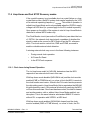
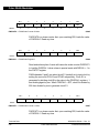
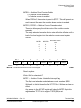
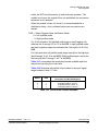
1
MC68Hc912D60A
MC68HC912D60C
MC68HC912D60P
Technical Data
HC12
Microcontrollers
MC68HC912D60A/D
Rev. 3.1
08/2005
freescale.com
MC68HC912D60A
MC68HC912D60C
MC68HC912D60P
Technical Data — Rev. 3.1
Freescale reserves the right to make changes without further notice to any products
herein. Freescale makes no warranty, representation or guarantee regarding the
suitability of its products for any particular purpose, nor does Freescale assume any
liability arising out of the application or use of any product or circuit, and specifically
disclaims any and all liability, including without limitation consequential or incidental
damages. "Typical" parameters which may be provided in Freescale data sheets
and/or specifications can and do vary in different applications and actual performance
may vary over time. All operating parameters, including "Typicals" must be validated
for each customer application by customer's technical experts. Freescale does not
convey any license under its patent rights nor the rights of others. Freescale products
are not designed, intended, or authorized for use as components in systems intended
for surgical implant into the body, or other applications intended to support or sustain
life, or for any other application in which the failure of the Freescale product could
create a situation where personal injury or death may occur. Should Buyer purchase or
use Freescale products for any such unintended or unauthorized application, Buyer
shall indemnify and hold Freescale and its officers, employees, subsidiaries, affiliates,
and distributors harmless against all claims, costs, damages, and expenses, and
reasonable attorney fees arising out of, directly or indirectly, any claim of personal
injury or death associated with such unintended or unauthorized use, even if such claim
alleges that Freescale was negligent regarding the design or manufacture of the part.
Freescale, Inc. is an Equal Opportunity/Affirmative Action Employer.
© Freescale, Inc., 2005
MC68HC912D60A — Rev. 3.1
Freescale Semiconductor
Technical Data
3
Technical Data
4
MC68HC912D60A — Rev. 3.1
Freescale Semiconductor
Technical Data — MC68HC912D60A
List of Paragraphs
List of Paragraphs. . . . . . . . . . . . . . . . . . . . . . . . . . . . . . . . 5
Table of Contents . . . . . . . . . . . . . . . . . . . . . . . . . . . . . . . . 7
List of Figures . . . . . . . . . . . . . . . . . . . . . . . . . . . . . . . . . . 15
List of Tables . . . . . . . . . . . . . . . . . . . . . . . . . . . . . . . . . . . 19
Section 1. General Description . . . . . . . . . . . . . . . . . . . . 23
Section 2. Central Processing Unit . . . . . . . . . . . . . . . . . 31
Section 3. Pinout and Signal Descriptions . . . . . . . . . . . 37
Section 4. Registers . . . . . . . . . . . . . . . . . . . . . . . . . . . . . 61
Section 5. Operating Modes and Resource Mapping . . 71
Section 6. Bus Control and Input/Output . . . . . . . . . . . . 85
Section 7. Flash Memory . . . . . . . . . . . . . . . . . . . . . . . . . 97
Section 8. EEPROM Memory . . . . . . . . . . . . . . . . . . . . . 105
Section 9. Resets and Interrupts . . . . . . . . . . . . . . . . . . 119
Section 10. I/O Ports with Key Wake-up . . . . . . . . . . . . 129
Section 11. Clock Functions . . . . . . . . . . . . . . . . . . . . . 137
Section 12. Oscillator . . . . . . . . . . . . . . . . . . . . . . . . . . . 175
Section 13. Pulse Width Modulator . . . . . . . . . . . . . . . . 207
Section 14. Enhanced Capture Timer . . . . . . . . . . . . . . 223
Section 15. Multiple Serial Interface . . . . . . . . . . . . . . . 263
Section 16. Freescale Interconnect Bus . . . . . . . . . . . . 289
MC68HC912D60A — Rev. 3.1
Freescale Semiconductor
Technical Data
List of Paragraphs
5
List of Paragraphs
Section 17. MSCAN Controller . . . . . . . . . . . . . . . . . . . . 303
Section 18. Analog-to-Digital Converter . . . . . . . . . . . . 349
Section 19. Development Support. . . . . . . . . . . . . . . . . 377
Section 20. Electrical Specifications. . . . . . . . . . . . . . . 405
Section 21. Appendix: CGM Practical Aspects . . . . . . 427
Section 22. Appendix: Changes from MC68HC912D60437
Section 23. Appendix: Information on MC68HC912D60A
Mask Set Changes . . . . . . . . . . . . . . . . . . . . . . . . . . . . . 443
Glossary. . . . . . . . . . . . . . . . . . . . . . . . . . . . . . . . . . . . . . 447
Revision History . . . . . . . . . . . . . . . . . . . . . . . . . . . . . . . 457
Technical Data
6
MC68HC912D60A — Rev. 3.1
List of Paragraphs
Freescale Semiconductor
Technical Data — MC68HC912D60A
Table of Contents
Technical Data — List of Paragraphs
Technical Data — Table of Contents
Technical Data — List of Figures
Technical Data — List of Tables
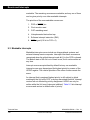
Section 1. General Description
1.1
Contents . . . . . . . . . . . . . . . . . . . . . . . . . . . . . . . . . . . . . . . . . .23
1.2
Introduction . . . . . . . . . . . . . . . . . . . . . . . . . . . . . . . . . . . . . . . . 23
1.3
Devices Covered in this Document. . . . . . . . . . . . . . . . . . . . . . 24
1.4
Features . . . . . . . . . . . . . . . . . . . . . . . . . . . . . . . . . . . . . . . . . . 24
1.5
Ordering Information. . . . . . . . . . . . . . . . . . . . . . . . . . . . . . . . . 27
1.6
Block Diagrams. . . . . . . . . . . . . . . . . . . . . . . . . . . . . . . . . . . . . 29
Section 2. Central Processing Unit
2.1
Contents . . . . . . . . . . . . . . . . . . . . . . . . . . . . . . . . . . . . . . . . . .31
2.2
Introduction . . . . . . . . . . . . . . . . . . . . . . . . . . . . . . . . . . . . . . . . 31
2.3
Programming Model . . . . . . . . . . . . . . . . . . . . . . . . . . . . . . . . . 31
2.4
Data Types . . . . . . . . . . . . . . . . . . . . . . . . . . . . . . . . . . . . . . . . 33
2.5
Addressing Modes . . . . . . . . . . . . . . . . . . . . . . . . . . . . . . . . . . 33
2.6
Indexed Addressing Modes . . . . . . . . . . . . . . . . . . . . . . . . . . . 35
2.7
Opcodes and Operands . . . . . . . . . . . . . . . . . . . . . . . . . . . . . . 36
MC68HC912D60A — Rev. 3.1
Freescale Semiconductor
Technical Data
Table of Contents
7
Table of Contents
Section 3. Pinout and Signal Descriptions
3.1
Contents . . . . . . . . . . . . . . . . . . . . . . . . . . . . . . . . . . . . . . . . . .37
3.2
MC68HC912D60A Pin Assignments in 112-pin QFP . . . . . . . . 38
3.3
MC68HC912D60A Pin Assignments in 80-pin QFP . . . . . . . . . 40
3.4
Power Supply Pins . . . . . . . . . . . . . . . . . . . . . . . . . . . . . . . . . . 42
3.5
Signal Descriptions . . . . . . . . . . . . . . . . . . . . . . . . . . . . . . . . . . 44
3.6
Port Signals . . . . . . . . . . . . . . . . . . . . . . . . . . . . . . . . . . . . . . . 52
Section 4. Registers
4.1
Contents . . . . . . . . . . . . . . . . . . . . . . . . . . . . . . . . . . . . . . . . . .61
4.2
Register Block. . . . . . . . . . . . . . . . . . . . . . . . . . . . . . . . . . . . . . 61
Section 5. Operating Modes and Resource Mapping
5.1
Contents . . . . . . . . . . . . . . . . . . . . . . . . . . . . . . . . . . . . . . . . . .71
5.2
Introduction . . . . . . . . . . . . . . . . . . . . . . . . . . . . . . . . . . . . . . . . 71
5.3
Operating Modes . . . . . . . . . . . . . . . . . . . . . . . . . . . . . . . . . . . 71
5.4
Background Debug Mode . . . . . . . . . . . . . . . . . . . . . . . . . . . . . 74
5.5
Internal Resource Mapping. . . . . . . . . . . . . . . . . . . . . . . . . . . .77
5.6
Memory Maps . . . . . . . . . . . . . . . . . . . . . . . . . . . . . . . . . . . . . . 83
Section 6. Bus Control and Input/Output
6.1
Contents . . . . . . . . . . . . . . . . . . . . . . . . . . . . . . . . . . . . . . . . . .85
6.2
Introduction . . . . . . . . . . . . . . . . . . . . . . . . . . . . . . . . . . . . . . . . 85
6.3
Detecting Access Type from External Signals . . . . . . . . . . . . . 85
6.4
Registers. . . . . . . . . . . . . . . . . . . . . . . . . . . . . . . . . . . . . . . . . .86
Section 7. Flash Memory
7.1
Contents . . . . . . . . . . . . . . . . . . . . . . . . . . . . . . . . . . . . . . . . . .97
Technical Data
8
MC68HC912D60A — Rev. 3.1
Table of Contents
Freescale Semiconductor
Table of Contents
7.2
Introduction . . . . . . . . . . . . . . . . . . . . . . . . . . . . . . . . . . . . . . . . 97
7.3
Overview. . . . . . . . . . . . . . . . . . . . . . . . . . . . . . . . . . . . . . . . . .98
7.4
Flash EEPROM Control Block . . . . . . . . . . . . . . . . . . . . . . . . . 98
7.5
Flash EEPROM Arrays . . . . . . . . . . . . . . . . . . . . . . . . . . . . . . . 98
7.6
Flash EEPROM Registers . . . . . . . . . . . . . . . . . . . . . . . . . . . . 99
7.7
Operation . . . . . . . . . . . . . . . . . . . . . . . . . . . . . . . . . . . . . . . . 100
7.8
Programming the Flash EEPROM . . . . . . . . . . . . . . . . . . . . . 101
7.9
Erasing the Flash EEPROM . . . . . . . . . . . . . . . . . . . . . . . . . . 103
7.10
Stop or Wait Mode . . . . . . . . . . . . . . . . . . . . . . . . . . . . . . . . . 103
7.11
Flash protection bit FPOPEN . . . . . . . . . . . . . . . . . . . . . . . . . 104
Section 8. EEPROM Memory
8.1
Contents . . . . . . . . . . . . . . . . . . . . . . . . . . . . . . . . . . . . . . . . .105
8.2
Introduction . . . . . . . . . . . . . . . . . . . . . . . . . . . . . . . . . . . . . . . 105
8.3
EEPROM Selective Write More Zeros . . . . . . . . . . . . . . . . . . 106
8.4
EEPROM Programmer’s Model . . . . . . . . . . . . . . . . . . . . . . .107
8.5
EEPROM Control Registers . . . . . . . . . . . . . . . . . . . . . . . . . . 108
8.6
Program/Erase Operation. . . . . . . . . . . . . . . . . . . . . . . . . . . . 115
8.7
Shadow Word Mapping . . . . . . . . . . . . . . . . . . . . . . . . . . . . . 115
8.8
Programming EEDIVH and EEDIVL Registers. . . . . . . . . . . . 116
Section 9. Resets and Interrupts
9.1
Contents . . . . . . . . . . . . . . . . . . . . . . . . . . . . . . . . . . . . . . . . .119
9.2
Introduction . . . . . . . . . . . . . . . . . . . . . . . . . . . . . . . . . . . . . . . 119
9.3
Maskable interrupts . . . . . . . . . . . . . . . . . . . . . . . . . . . . . . . . 120
9.4
Latching of Interrupts . . . . . . . . . . . . . . . . . . . . . . . . . . . . . . . 121
9.5
Interrupt Control and Priority Registers . . . . . . . . . . . . . . . . . 123
MC68HC912D60A — Rev. 3.1
Freescale Semiconductor
Technical Data
Table of Contents
9
Table of Contents
9.6
Resets. . . . . . . . . . . . . . . . . . . . . . . . . . . . . . . . . . . . . . . . . . . 124
9.7
Effects of Reset . . . . . . . . . . . . . . . . . . . . . . . . . . . . . . . . . . . 126
9.8
Register Stacking . . . . . . . . . . . . . . . . . . . . . . . . . . . . . . . . . . 127
9.9
Customer Information . . . . . . . . . . . . . . . . . . . . . . . . . . . . . . . 128
Section 10. I/O Ports with Key Wake-up
10.1
Contents . . . . . . . . . . . . . . . . . . . . . . . . . . . . . . . . . . . . . . . . .129
10.2
Introduction . . . . . . . . . . . . . . . . . . . . . . . . . . . . . . . . . . . . . . . 129
10.3
Key Wake-up and Port Registers . . . . . . . . . . . . . . . . . . . . . . 130
10.4
Key Wake-Up Input Filter . . . . . . . . . . . . . . . . . . . . . . . . . . . . 134
Section 11. Clock Functions
11.1
Contents . . . . . . . . . . . . . . . . . . . . . . . . . . . . . . . . . . . . . . . . .137
11.2
Introduction . . . . . . . . . . . . . . . . . . . . . . . . . . . . . . . . . . . . . . . 137
11.3
Clock Sources. . . . . . . . . . . . . . . . . . . . . . . . . . . . . . . . . . . . . 138
11.4
Phase-Locked Loop (PLL) . . . . . . . . . . . . . . . . . . . . . . . . . . . 139
11.5
Acquisition and Tracking Modes. . . . . . . . . . . . . . . . . . . . . . . 141
11.6
Limp-Home and Fast STOP Recovery modes . . . . . . . . . . . . 143
11.7
System Clock Frequency formulas . . . . . . . . . . . . . . . . . . . . . 162
11.8
Clock Divider Chains . . . . . . . . . . . . . . . . . . . . . . . . . . . . . . . 162
11.9
Computer Operating Properly (COP) . . . . . . . . . . . . . . . . . . . 166
11.10 Real-Time Interrupt. . . . . . . . . . . . . . . . . . . . . . . . . . . . . . . . . 167
11.11 Clock Monitor . . . . . . . . . . . . . . . . . . . . . . . . . . . . . . . . . . . . .167
11.12 Clock Function Registers . . . . . . . . . . . . . . . . . . . . . . . . . . . . 168
Section 12. Oscillator
12.1
Contents . . . . . . . . . . . . . . . . . . . . . . . . . . . . . . . . . . . . . . . . .175
Technical Data
10
MC68HC912D60A — Rev. 3.1
Table of Contents
Freescale Semiconductor
Table of Contents
12.2
Introduction . . . . . . . . . . . . . . . . . . . . . . . . . . . . . . . . . . . . . . . 175
12.3
MC68HC912D60A Oscillator Specification. . . . . . . . . . . . . . . 176
12.4
MC68HC912D60C Colpitts Oscillator Specification . . . . . . . . 179
12.5
MC68HC912D60P Pierce Oscillator Specification . . . . . . . . . 194
Section 13. Pulse Width Modulator
13.1
Contents . . . . . . . . . . . . . . . . . . . . . . . . . . . . . . . . . . . . . . . . .207
13.2
Introduction . . . . . . . . . . . . . . . . . . . . . . . . . . . . . . . . . . . . . . . 207
13.3
PWM Register Description . . . . . . . . . . . . . . . . . . . . . . . . . . . 210
13.4
PWM Boundary Cases . . . . . . . . . . . . . . . . . . . . . . . . . . . . . . 222
Section 14. Enhanced Capture Timer
14.1
Contents . . . . . . . . . . . . . . . . . . . . . . . . . . . . . . . . . . . . . . . . .223
14.2
Introduction . . . . . . . . . . . . . . . . . . . . . . . . . . . . . . . . . . . . . . . 223
14.3
Enhanced Capture Timer Modes of Operation . . . . . . . . . . . . 230
14.4
Timer Registers . . . . . . . . . . . . . . . . . . . . . . . . . . . . . . . . . . . 233
14.5
Timer and Modulus Counter Operation in Different Modes . . 261
Section 15. Multiple Serial Interface
15.1
Contents . . . . . . . . . . . . . . . . . . . . . . . . . . . . . . . . . . . . . . . . .263
15.2
Introduction . . . . . . . . . . . . . . . . . . . . . . . . . . . . . . . . . . . . . . . 263
15.3
Block diagram . . . . . . . . . . . . . . . . . . . . . . . . . . . . . . . . . . . . . 264
15.4
Serial Communication Interface (SCI) . . . . . . . . . . . . . . . . . . 264
15.5
Serial Peripheral Interface (SPI) . . . . . . . . . . . . . . . . . . . . . . . 276
15.6
Port S . . . . . . . . . . . . . . . . . . . . . . . . . . . . . . . . . . . . . . . . . . . 285
Section 16. Freescale Interconnect Bus
16.1
Contents . . . . . . . . . . . . . . . . . . . . . . . . . . . . . . . . . . . . . . . . .289
MC68HC912D60A — Rev. 3.1
Freescale Semiconductor
Technical Data
Table of Contents
11
Table of Contents
16.2
Introduction . . . . . . . . . . . . . . . . . . . . . . . . . . . . . . . . . . . . . . . 289
16.3
Push-pull sequence . . . . . . . . . . . . . . . . . . . . . . . . . . . . . . . . 290
16.4
Biphase coding . . . . . . . . . . . . . . . . . . . . . . . . . . . . . . . . . . . . 291
16.5
Message validation . . . . . . . . . . . . . . . . . . . . . . . . . . . . . . . . . 292
16.6
Interfacing to MI Bus. . . . . . . . . . . . . . . . . . . . . . . . . . . . . . . . 294
16.7
MI Bus clock rate . . . . . . . . . . . . . . . . . . . . . . . . . . . . . . . . . . 296
16.8
SCI0/MI Bus registers. . . . . . . . . . . . . . . . . . . . . . . . . . . . . . . 296
Section 17. MSCAN Controller
17.1
Contents . . . . . . . . . . . . . . . . . . . . . . . . . . . . . . . . . . . . . . . . .303
17.2
Introduction . . . . . . . . . . . . . . . . . . . . . . . . . . . . . . . . . . . . . . . 303
17.3
External Pins. . . . . . . . . . . . . . . . . . . . . . . . . . . . . . . . . . . . . . 304
17.4
Message Storage . . . . . . . . . . . . . . . . . . . . . . . . . . . . . . . . . . 305
17.5
Identifier Acceptance Filter . . . . . . . . . . . . . . . . . . . . . . . . . . .310
17.6
Interrupts. . . . . . . . . . . . . . . . . . . . . . . . . . . . . . . . . . . . . . . . .314
17.7
Protocol Violation Protection. . . . . . . . . . . . . . . . . . . . . . . . . . 316
17.8
Low Power Modes . . . . . . . . . . . . . . . . . . . . . . . . . . . . . . . . . 316
17.9
Timer Link . . . . . . . . . . . . . . . . . . . . . . . . . . . . . . . . . . . . . . . . 320
17.10 Clock System . . . . . . . . . . . . . . . . . . . . . . . . . . . . . . . . . . . . .321
17.11 Memory Map. . . . . . . . . . . . . . . . . . . . . . . . . . . . . . . . . . . . . . 324
17.12 Programmer’s Model of Message Storage . . . . . . . . . . . . . . . 325
17.13 Programmer’s Model of Control Registers . . . . . . . . . . . . . . . 330
Section 18. Analog-to-Digital Converter
18.1
Contents . . . . . . . . . . . . . . . . . . . . . . . . . . . . . . . . . . . . . . . . .349
18.2
Introduction . . . . . . . . . . . . . . . . . . . . . . . . . . . . . . . . . . . . . . . 349
18.3
Modes of Operation . . . . . . . . . . . . . . . . . . . . . . . . . . . . . . . . 351
Technical Data
12
MC68HC912D60A — Rev. 3.1
Table of Contents
Freescale Semiconductor
Table of Contents
18.4
Functional Description . . . . . . . . . . . . . . . . . . . . . . . . . . . . . .352
18.5
ATD Operational Modes . . . . . . . . . . . . . . . . . . . . . . . . . . . . . 354
18.6
ATD Operation In Different MCU Modes . . . . . . . . . . . . . . . . 355
18.7
General Purpose Digital Input Port Operation . . . . . . . . . . . . 357
18.8
Application Considerations . . . . . . . . . . . . . . . . . . . . . . . . . . .358
18.9
ATD Registers . . . . . . . . . . . . . . . . . . . . . . . . . . . . . . . . . . . . 358
Section 19. Development Support
19.1
Contents . . . . . . . . . . . . . . . . . . . . . . . . . . . . . . . . . . . . . . . . .377
19.2
Introduction . . . . . . . . . . . . . . . . . . . . . . . . . . . . . . . . . . . . . . . 377
19.3
Instruction Queue . . . . . . . . . . . . . . . . . . . . . . . . . . . . . . . . . .377
19.4
Background Debug Mode . . . . . . . . . . . . . . . . . . . . . . . . . . . . 379
19.5
Breakpoints. . . . . . . . . . . . . . . . . . . . . . . . . . . . . . . . . . . . . . . 395
19.6
Instruction Tagging . . . . . . . . . . . . . . . . . . . . . . . . . . . . . . . . . 402
Section 20. Electrical Specifications
20.1
Contents . . . . . . . . . . . . . . . . . . . . . . . . . . . . . . . . . . . . . . . . .405
20.2
Introduction . . . . . . . . . . . . . . . . . . . . . . . . . . . . . . . . . . . . . . . 405
20.3
Tables of Data . . . . . . . . . . . . . . . . . . . . . . . . . . . . . . . . . . . . 406
Section 21. Appendix: CGM Practical Aspects
21.1
Contents . . . . . . . . . . . . . . . . . . . . . . . . . . . . . . . . . . . . . . . . .427
21.2
Introduction . . . . . . . . . . . . . . . . . . . . . . . . . . . . . . . . . . . . . . . 427
21.3
Practical Aspects For The PLL Usage . . . . . . . . . . . . . . . . . . 427
21.4
Printed Circuit Board Guidelines. . . . . . . . . . . . . . . . . . . . . . . 433
Section 22. Appendix: Changes from MC68HC912D60
22.1
Contents . . . . . . . . . . . . . . . . . . . . . . . . . . . . . . . . . . . . . . . . .437
MC68HC912D60A — Rev. 3.1
Freescale Semiconductor
Technical Data
Table of Contents
13
Table of Contents
22.2
Significant changes from the MC68HC912D60
(non-suffix device) . . . . . . . . . . . . . . . . . . . . . . . . . . . . . . . . . 437
Section 23. Appendix: Information on MC68HC912D60A
Mask Set Changes
23.1
Contents . . . . . . . . . . . . . . . . . . . . . . . . . . . . . . . . . . . . . . . . .443
23.2
Introduction . . . . . . . . . . . . . . . . . . . . . . . . . . . . . . . . . . . . . . . 443
23.3
Flash Protection Feature . . . . . . . . . . . . . . . . . . . . . . . . . . . . 443
23.4
Clock Circuitry. . . . . . . . . . . . . . . . . . . . . . . . . . . . . . . . . . . . . 444
23.5
Pseudo Stop Mode . . . . . . . . . . . . . . . . . . . . . . . . . . . . . . . . . 444
23.6
Oscillator. . . . . . . . . . . . . . . . . . . . . . . . . . . . . . . . . . . . . . . . .444
23.7
PLL . . . . . . . . . . . . . . . . . . . . . . . . . . . . . . . . . . . . . . . . . . . . . 445
Technical Data — Glossary
Technical Data — Revision History
23.8
Contents . . . . . . . . . . . . . . . . . . . . . . . . . . . . . . . . . . . . . . . . .457
23.9
Changes from Rev 2.0 to Rev 3.0 . . . . . . . . . . . . . . . . . . . . . 457
23.10 Major Changes From Rev 1.0 to Rev 2.0 . . . . . . . . . . . . . . . . 457
23.11 Major Changes From Rev 0.0 to Rev 1.0 . . . . . . . . . . . . . . . . 458
Technical Data
14
MC68HC912D60A — Rev. 3.1
Table of Contents
Freescale Semiconductor
Technical Data — MC68HC912D60A
List of Figures
Figure
1-1
1-2
2-1
3-1
3-2
3-3
3-4
3-5
3-6
5-1
6-1
10-1
11-1
11-2
11-3
11-4
11-5
11-6
11-7
11-8
11-9
12-1
12-2
12-3
12-4
13-1
13-2
13-3
14-1
14-2
Title
MC68HC912D60A 112-pin QFP Block Diagram . . . . . . . . . . . 29
MC68HC912D60A 80-pin QFP Block Diagram . . . . . . . . . . . . 30
Programming Model . . . . . . . . . . . . . . . . . . . . . . . . . . . . . . . . . 32
Pin Assignments in 112-pin TQFP for MC68HC912D60A . . . . 38
112-pin TQFP Mechanical Dimensions (case no987) . . . . . . . 39
Pin Assignments in 80-pin QFP for MC68HC912D60A . . . . . . 40
80-pin QFP Mechanical Dimensions (case no841B) . . . . . . . . 41
PLL Loop FIlter Connections . . . . . . . . . . . . . . . . . . . . . . . . . . 43
External Oscillator Connections . . . . . . . . . . . . . . . . . . . . . . . .45
MC68HC912D60A Memory Map . . . . . . . . . . . . . . . . . . . . . . . 83
Access Type vsBus Control Pins . . . . . . . . . . . . . . . . . . . . . . . 86
STOP Key Wake-up Filter (falling edge trigger) timing. . . . . . 135
Internal Clock Relationships . . . . . . . . . . . . . . . . . . . . . . . . . . 139
PLL Functional Diagram . . . . . . . . . . . . . . . . . . . . . . . . . . . . . 140
Clock Loss during Normal Operation . . . . . . . . . . . . . . . . . . . 144
No Clock at Power-On Reset . . . . . . . . . . . . . . . . . . . . . . . . . 146
STOP Exit and Fast STOP Recovery . . . . . . . . . . . . . . . . . . . 149
Clock Generation Chain . . . . . . . . . . . . . . . . . . . . . . . . . . . . . 163
Clock Chain for SCI0, SCI1, RTI, COP. . . . . . . . . . . . . . . . . . 164
Clock Chain for ECT . . . . . . . . . . . . . . . . . . . . . . . . . . . . . . . . 165
Clock Chain for MSCAN, SPI, ATD0, ATD1 and BDM . . . . . . 166
MC68HC912D60A Colpitts Oscillator Architecture. . . . . . . . . 177
MC68HC912D60C Colpitts Oscillator Architecture. . . . . . . . . 180
MC68HC912D60C Crystal with DC Blocking Capacitor . . . . . 192
MC68HC912D60P Pierce Oscillator Architecture. . . . . . . . . . 195
Block Diagram of PWM Left-Aligned Output Channel . . . . . . 208
Block Diagram of PWM Center-Aligned Output Channel . . . . 209
PWM Clock Sources. . . . . . . . . . . . . . . . . . . . . . . . . . . . . . . . 210
Timer Block Diagram in Latch Mode. . . . . . . . . . . . . . . . . . . .225
Timer Block Diagram in Queue Mode. . . . . . . . . . . . . . . . . . . 226
MC68HC912D60A — Rev. 3.1
Freescale Semiconductor
Page
Technical Data
List of Figures
15
List of Figures
14-3 8-Bit Pulse Accumulators Block Diagram . . . . . . . . . . . . . . . . 227
14-4 16-Bit Pulse Accumulators Block Diagram . . . . . . . . . . . . . . . 228
14-5 Block Diagram for Port7 with Output compare /
Pulse Accumulator A . . . . . . . . . . . . . . . . . . . . . . . . . . . . . . . 229
14-6 C3F-C0F Interrupt Flag Setting . . . . . . . . . . . . . . . . . . . . . . .229
15-1 Multiple Serial Interface Block Diagram . . . . . . . . . . . . . . . . . 264
15-2 Serial Communications Interface Block Diagram . . . . . . . . . . 265
15-3 Serial Peripheral Interface Block Diagram . . . . . . . . . . . . . . . 277
15-4 SPI Clock Format 0 (CPHA = 0) . . . . . . . . . . . . . . . . . . . . . . . 278
15-5 SPI Clock Format 1 (CPHA = 1) . . . . . . . . . . . . . . . . . . . . . . . 279
15-6 Normal Mode and Bidirectional Mode. . . . . . . . . . . . . . . . . . . 280
16-1 MI Bus timing . . . . . . . . . . . . . . . . . . . . . . . . . . . . . . . . . . . . .290
16-2 Biphase coding and error detection . . . . . . . . . . . . . . . . . . . . 292
16-3 MI BUS Block Diagram . . . . . . . . . . . . . . . . . . . . . . . . . . . . . . 293
16-4 A typical MI Bus interface . . . . . . . . . . . . . . . . . . . . . . . . . . . . 295
17-1 The CAN System . . . . . . . . . . . . . . . . . . . . . . . . . . . . . . . . . . 305
17-2 User Model for Message Buffer Organization. . . . . . . . . . . . . 308
17-3 32-bit Maskable Identifier Acceptance Filters . . . . . . . . . . . . . 312
17-4 16-bit Maskable Acceptance Filters . . . . . . . . . . . . . . . . . . . . 312
17-5 8-bit Maskable Acceptance Filters . . . . . . . . . . . . . . . . . . . . . 313
17-6 SLEEP Request / Acknowledge Cycle . . . . . . . . . . . . . . . . . . 319
17-7 Clocking Scheme . . . . . . . . . . . . . . . . . . . . . . . . . . . . . . . . . . 321
17-8 Segments within the Bit Time . . . . . . . . . . . . . . . . . . . . . . . . . 323
17-9 msCAN12 Memory Map . . . . . . . . . . . . . . . . . . . . . . . . . . . . . 324
17-10 Message Buffer Organization . . . . . . . . . . . . . . . . . . . . . . . . . 325
17-11 . . . . . . . . . . . . . . . . . . . . . . . . . . . . . . . . . . . . . . . . . . . . . . . . 326
17-12 . . . . . . . . . . . . . . . . . . . . . . . . . . . . . . . . . . . . . . . . . . . . . . . . 327
18-1 Analog-to-Digital Converter Block Diagram . . . . . . . . . . . . . . 350
19-1 BDM Host to Target Serial Bit Timing. . . . . . . . . . . . . . . . . . . 381
19-2 BDM Target to Host Serial Bit Timing (Logic 1) . . . . . . . . . . . 381
19-3 BDM Target to Host Serial Bit Timing (Logic 0) . . . . . . . . . . . 382
20-1 Timer Inputs . . . . . . . . . . . . . . . . . . . . . . . . . . . . . . . . . . . . . . 414
20-2 POR and External Reset Timing Diagram . . . . . . . . . . . . . . . 415
20-3 STOP Recovery Timing Diagram . . . . . . . . . . . . . . . . . . . . . . 416
20-4 WAIT Recovery Timing Diagram . . . . . . . . . . . . . . . . . . . . . . 417
20-5 Interrupt Timing Diagram . . . . . . . . . . . . . . . . . . . . . . . . . . . . 418
20-6 Port Read Timing Diagram . . . . . . . . . . . . . . . . . . . . . . . . . . .419
20-7 Port Write Timing Diagram . . . . . . . . . . . . . . . . . . . . . . . . . . .419
Technical Data
16
MC68HC912D60A — Rev. 3.1
List of Figures
Freescale Semiconductor
List of Figures
20-8 Multiplexed Expansion Bus Timing Diagram . . . . . . . . . . . . . 421
20-9 SPI Timing Diagram (1 of 2) . . . . . . . . . . . . . . . . . . . . . . . . . . 423
20-10 SPI Timing Diagram (2 of 2) . . . . . . . . . . . . . . . . . . . . . . . . . . 424
MC68HC912D60A — Rev. 3.1
Freescale Semiconductor
Technical Data
List of Figures
17
List of Figures
Technical Data
18
MC68HC912D60A — Rev. 3.1
List of Figures
Freescale Semiconductor
Technical Data — MC68HC912D60A
List of Tables
Table
1-1
1-2
2-1
2-2
3-1
3-2
3-3
3-4
4-1
5-1
5-2
5-3
5-4
8-1
8-2
8-3
8-4
9-1
9-2
11-1
11-2
11-3
11-4
11-5
13-1
13-2
13-3
14-1
14-2
Title
Device Ordering Information. . . . . . . . . . . . . . . . . . . . . . . . . . . 27
Development Tools Ordering Information. . . . . . . . . . . . . . . . . 28
M68HC12 Addressing Mode Summary . . . . . . . . . . . . . . . . . . 34
Summary of Indexed Operations . . . . . . . . . . . . . . . . . . . . . . . 35
MC68HC912D60A Power and Ground Connection Summary . 44
MC68HC912D60A Signal Description Summary . . . . . . . . . . . 50
MC68HC912D60A Port Description Summary . . . . . . . . . . . . . 59
Port Pull-Up, Pull-Down and Reduced Drive Summary . . . . . . 60
MC68HC912D60A Register Map . . . . . . . . . . . . . . . . . . . . . . . 62
Mode Selection . . . . . . . . . . . . . . . . . . . . . . . . . . . . . . . . . . . . . 72
Mapping Precedence . . . . . . . . . . . . . . . . . . . . . . . . . . . . . . . . 78
RFSTR Stretch Bit Definition . . . . . . . . . . . . . . . . . . . . . . . . . . 82
EXSTR Stretch Bit Definition . . . . . . . . . . . . . . . . . . . . . . . . . . 82
EEDIV Selection . . . . . . . . . . . . . . . . . . . . . . . . . . . . . . . . . . . 109
1K byte EEPROM Block Protection . . . . . . . . . . . . . . . . . . . . 112
Erase Selection. . . . . . . . . . . . . . . . . . . . . . . . . . . . . . . . . . . . 113
Shadow word mapping . . . . . . . . . . . . . . . . . . . . . . . . . . . . . . 115
Interrupt Vector Map . . . . . . . . . . . . . . . . . . . . . . . . . . . . . . . . 122
Stacking Order on Entry to Interrupts . . . . . . . . . . . . . . . . . . . 128
Summary of STOP Mode Exit Conditions. . . . . . . . . . . . . . . . 155
Summary of Pseudo STOP Mode Exit Conditions . . . . . . . . . 155
Clock Monitor Time-Outs . . . . . . . . . . . . . . . . . . . . . . . . . . . . 167
Real Time Interrupt Rates. . . . . . . . . . . . . . . . . . . . . . . . . . . . 169
COP Watchdog Rates . . . . . . . . . . . . . . . . . . . . . . . . . . . . . .172
Clock A and Clock B Prescaler. . . . . . . . . . . . . . . . . . . . . . . . 212
PWM Left-Aligned Boundary Conditions . . . . . . . . . . . . . . . . 222
PWM Center-Aligned Boundary Conditions . . . . . . . . . . . . . . 222
Compare Result Output Action . . . . . . . . . . . . . . . . . . . . . . . . 238
Edge Detector Circuit Configuration . . . . . . . . . . . . . . . . . . . .238
MC68HC912D60A — Rev. 3.1
Freescale Semiconductor
Page
Technical Data
List of Tables
19
List of Tables
14-3
15-1
15-2
15-3
15-4
16-1
17-1
17-2
17-3
17-4
17-5
17-6
17-7
17-8
17-9
17-10
18-1
18-2
18-3
18-4
18-5
18-6
18-7
18-8
18-9
18-10
19-1
19-2
19-3
19-4
19-5
19-6
19-7
19-8
19-9
19-10
19-11
Prescaler Selection. . . . . . . . . . . . . . . . . . . . . . . . . . . . . . . . . 240
Baud Rate Generation . . . . . . . . . . . . . . . . . . . . . . . . . . . . . .266
Loop Mode Functions . . . . . . . . . . . . . . . . . . . . . . . . . . . . . . . 269
SS Output Selection . . . . . . . . . . . . . . . . . . . . . . . . . . . . . . . . 279
SPI Clock Rate Selection . . . . . . . . . . . . . . . . . . . . . . . . . . . . 283
MI Bus Delay . . . . . . . . . . . . . . . . . . . . . . . . . . . . . . . . . . . . .301
msCAN12 Interrupt Vectors . . . . . . . . . . . . . . . . . . . . . . . . . . 315
msCAN12 vsCPU operating modes . . . . . . . . . . . . . . . . . . . .317
CAN Standard Compliant Bit Time Segment Settings . . . . . . 323
Data length codes. . . . . . . . . . . . . . . . . . . . . . . . . . . . . . . . . .328
Synchronization jump width . . . . . . . . . . . . . . . . . . . . . . . . . . 333
Baud rate prescaler . . . . . . . . . . . . . . . . . . . . . . . . . . . . . . . . 333
Time segment syntax . . . . . . . . . . . . . . . . . . . . . . . . . . . . . . . 334
Time segment values . . . . . . . . . . . . . . . . . . . . . . . . . . . . . . . 335
Identifier Acceptance Mode Settings . . . . . . . . . . . . . . . . . . . 341
Identifier Acceptance Hit Indication . . . . . . . . . . . . . . . . . . . . 342
Result Data Formats Available . . . . . . . . . . . . . . . . . . . . . . . . 361
Left Justified ATD Output Codes . . . . . . . . . . . . . . . . . . . . . . 362
ATD Response to Background Debug Enable . . . . . . . . . . . . 364
Final Sample Time Selection . . . . . . . . . . . . . . . . . . . . . . . . . 365
Clock Prescaler Values. . . . . . . . . . . . . . . . . . . . . . . . . . . . . . 366
Conversion Sequence Length Coding . . . . . . . . . . . . . . . . . . 367
Result Register Assignment for Different Conversion
Sequences . . . . . . . . . . . . . . . . . . . . . . . . . . . . . . . . . . . . . . . 367
Special Channel Conversion Select Coding . . . . . . . . . . . . . . 368
Analog Input Channel Select Coding . . . . . . . . . . . . . . . . . . . 369
Multichannel Mode Result Register Assignment (MULT=1) . . 370
IPIPE Decoding . . . . . . . . . . . . . . . . . . . . . . . . . . . . . . . . . . . 378
Hardware Commands. . . . . . . . . . . . . . . . . . . . . . . . . . . . . . . 384
BDM Firmware Commands . . . . . . . . . . . . . . . . . . . . . . . . . . 385
BDM registers . . . . . . . . . . . . . . . . . . . . . . . . . . . . . . . . . . . . . 387
TTAGO Decoding . . . . . . . . . . . . . . . . . . . . . . . . . . . . . . . . . .392
TTAGO Value . . . . . . . . . . . . . . . . . . . . . . . . . . . . . . . . . . . . . 392
Instruction . . . . . . . . . . . . . . . . . . . . . . . . . . . . . . . . . . . . . . . . 392
REGN Decoding . . . . . . . . . . . . . . . . . . . . . . . . . . . . . . . . . . . 392
Breakpoint Mode Control . . . . . . . . . . . . . . . . . . . . . . . . . . . . 398
Breakpoint Address Range Control . . . . . . . . . . . . . . . . . . . . 399
Breakpoint Read/Write Control . . . . . . . . . . . . . . . . . . . . . . . . 401
Technical Data
20
MC68HC912D60A — Rev. 3.1
List of Tables
Freescale Semiconductor
List of Tables
19-12
20-1
20-2
20-3
20-4
20-5
20-6
20-7
20-8
20-9
20-10
20-11
20-12
20-13
20-14
20-15
20-16
20-17
20-18
20-19
21-1
Tag Pin Function. . . . . . . . . . . . . . . . . . . . . . . . . . . . . . . . . . . 403
Maximum Ratings . . . . . . . . . . . . . . . . . . . . . . . . . . . . . . . . . .406
Thermal Characteristics . . . . . . . . . . . . . . . . . . . . . . . . . . . . . 407
DC Electrical Characteristics . . . . . . . . . . . . . . . . . . . . . . . . . 408
Supply Current . . . . . . . . . . . . . . . . . . . . . . . . . . . . . . . . . . . . 409
ATD DC Electrical Characteristics . . . . . . . . . . . . . . . . . . . . . 409
Analog Converter Characteristics (Operating) . . . . . . . . . . . . 410
ATD AC Characteristics (Operating). . . . . . . . . . . . . . . . . . . .410
ATD Maximum Ratings. . . . . . . . . . . . . . . . . . . . . . . . . . . . . . 411
EEPROM Characteristics . . . . . . . . . . . . . . . . . . . . . . . . . . . . 411
Flash EEPROM Characteristics . . . . . . . . . . . . . . . . . . . . . . .412
Pulse Width Modulator Characteristics. . . . . . . . . . . . . . . . . . 412
Control Timing . . . . . . . . . . . . . . . . . . . . . . . . . . . . . . . . . . . . 413
Peripheral Port Timing . . . . . . . . . . . . . . . . . . . . . . . . . . . . . .419
Multiplexed Expansion Bus Timing. . . . . . . . . . . . . . . . . . . . . 420
SPI Timing . . . . . . . . . . . . . . . . . . . . . . . . . . . . . . . . . . . . . . . 422
CGM Characteristics. . . . . . . . . . . . . . . . . . . . . . . . . . . . . . . . 425
Oscillator Characteristics . . . . . . . . . . . . . . . . . . . . . . . . . . . . 425
Key Wake-up . . . . . . . . . . . . . . . . . . . . . . . . . . . . . . . . . . . . .426
msCAN12 Wake-up Time from Sleep Mode. . . . . . . . . . . . . . 426
Suggested 8MHz Synthesis PLL Filter Elements
(Tracking Mode) . . . . . . . . . . . . . . . . . . . . . . . . . . . . . . . . . . . 431
21-2 Suggested 8MHz Synthesis PLL Filter Elements
(Acquisition Mode) . . . . . . . . . . . . . . . . . . . . . . . . . . . . . . . . . 432
MC68HC912D60A — Rev. 3.1
Freescale Semiconductor
Technical Data
List of Tables
21
List of Tables
Technical Data
22
MC68HC912D60A — Rev. 3.1
List of Tables
Freescale Semiconductor
Technical Data — MC68HC912D60A
Section 1. General Description
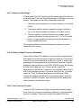
1.1 Contents
1.2
Introduction . . . . . . . . . . . . . . . . . . . . . . . . . . . . . . . . . . . . . . . . 23
1.3
Devices Covered in this Document. . . . . . . . . . . . . . . . . . . . . . 24
1.4
Features . . . . . . . . . . . . . . . . . . . . . . . . . . . . . . . . . . . . . . . . . . 24
1.5
Ordering Information. . . . . . . . . . . . . . . . . . . . . . . . . . . . . . . . . 27
1.6
Block Diagrams. . . . . . . . . . . . . . . . . . . . . . . . . . . . . . . . . . . . . 29
1.2 Introduction
The MC68HC912D60A microcontroller unit (MCU) is a 16-bit device
available in two package options, 80-pin QFP and 112-pin TQFP. Onchip peripherals include a 16-bit central processing unit (CPU12), 60K
bytes of flash EEPROM, 2K bytes of RAM, 1K bytes of EEPROM, two
asynchronous serial communication interfaces (SCI), a serial peripheral
interface (SPI), an enhanced capture timer (ECT), two (one on 80QFP)
8-channel,10-bit analog-to-digital converters (ATD), a four-channel
pulse-width modulator (PWM), and a CAN 2.0 A, B software compatible
module (MSCAN12). System resource mapping, clock generation,
interrupt control and bus interfacing are managed by the lite integration
module (LIM). The MC68HC912D60A has full 16-bit data paths
throughout, however, the external bus can operate in an 8-bit narrow
mode so single 8-bit wide memory can be interfaced for lower cost
systems. The inclusion of a PLL circuit allows power consumption and
performance to be adjusted to suit operational requirements. In addition
to the I/O ports available in each module, 16 (2 on 80QFP) I/O port pins
are available with Key-Wake-Up capability from STOP or WAIT mode.
MC68HC912D60A — Rev. 3.1
Freescale Semiconductor
Technical Data
General Description
23
General Description
1.3 Devices Covered in this Document
The MC68HC912D60C and MC68HC912D60P are devices similar to
the MC68HC912D60A, but with different oscillator configurations. Refer
to Section 12. Oscillator for more details.
The generic term MC68HC912D60A is used throughout this document
to mean all derivatives mentioned above, except in Section 12.
Oscillator, where it refers only to the MC68HC912D60A device.
1.4 Features
•
16-bit CPU12
– Upward compatible with M68HC11 instruction set
– Interrupt stacking and programmer’s model identical to
M68HC11
– 20-bit ALU
– Instruction queue
– Enhanced indexed addressing
•
Multiplexed bus
– Single chip or expanded
– 16 address/16 data wide or 16 address/8 data narrow mode
•
Two 8-bit ports with key wake-up interrupt (2 pins only are
available on 80QFP) and one I2C start bit detector (112TQFP
only)
•
Memory
– 60K byte flash EEPROM, made of a 28K module and a 32K
module with 8K bytes protected BOOT section in each module
(MC68HC912D60A)
– 1K byte EEPROM
– 2K byte RAM
Technical Data
24
MC68HC912D60A — Rev. 3.1
General Description
Freescale Semiconductor
General Description
Features
•
Analog-to-digital converters
– 2 x 8-channels, 10-bit resolution in 112TQFP
– 1 x 8-channels, 8-bit resolution in 80QFP
•
1M bit per second, CAN 2.0 A, B software compatible module
– Two receive and three transmit buffers
– Flexible identifier filter programmable as 2 x 32 bit, 4 x 16 bit or
8 x 8 bit
– Four separate interrupt channels for Rx, Tx, error and wake-up
– Low-pass filter wake-up function
– In 80QFP, only TxCAN and RxCAN pins are available
– Loop-back for self test operation
– Programmable link to a timer input capture channel, for timestamping and network synchronization.
•
Enhanced capture timer (ECT)
– 16-bit main counter with 7-bit prescaler
– 8 programmable input capture or output compare channels; 4
of the 8 input captures with buffer
– Input capture filters and buffers, three successive captures on
four channels, or two captures on four channels with a
capture/compare selectable on the remaining four
– Four 8-bit or two 16-bit pulse accumulators
– 16-bit modulus down-counter with 4-bit prescaler
– Four user-selectable delay counters for signal filtering
•
4 PWM channels with programmable period and duty cycle
– 8-bit 4-channel or 16-bit 2-channel
– Separate control for each pulse width and duty cycle
– Center- or left-aligned outputs
– Programmable clock select logic with a wide range of
frequencies
MC68HC912D60A — Rev. 3.1
Freescale Semiconductor
Technical Data
General Description
25
General Description
•
Serial interfaces
– Two asynchronous serial communications interfaces (SCI)
– MI-Bus implemented on final devices
– Synchronous serial peripheral interface (SPI)
•
LIM (light integration module)
– WCR (windowed COP watchdog, real time interrupt, clock
monitor)
– ROC (reset and clocks)
– MEBI (multiplexed external bus interface)
– MBI (internal bus interface and map)
– INT (interrupt control)
•
Clock generation
– Phase-locked loop clock frequency multiplier
– Limp home mode in absence of external clock
– Slow mode divider
– Low power 0.5 to 16 MHz crystal oscillator reference clock
– Option of a Pierce or Colpitts oscillator
•
112-Pin TQFP package or 80-pin QFP package
– Up to 68 general-purpose I/O lines, plus up to 18 input-only
lines in 112TQFP
or
Up to 48 general-purpose I/O lines, plus up to 10 input-only
lines in 80QFP
•
8MHz operation at 5V
•
Development support
– Single-wire background debug™ mode (BDM)
– On-chip hardware breakpoints
Technical Data
26
MC68HC912D60A — Rev. 3.1
General Description
Freescale Semiconductor
General Description
Ordering Information
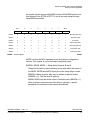
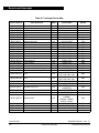
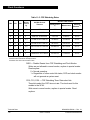
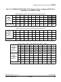
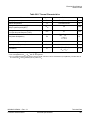
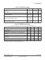
1.5 Ordering Information
Table 1-1. Device Ordering Information
Ambient Temperature
Package
112-Pin TQFP
Single Tray
60 Pcs
80-Pin TQFP
Single Tray
84 Pcs
112-Pin TQFP
Single Tray
60 Pcs
80-Pin TQFP
Single Tray
84 Pcs
112-Pin TQFP
Single Tray
60 Pcs
80-Pin TQFP
Single Tray
84 Pcs
Order Number
Range
Designator
–40 to +85°C
C
MC912D60ACPV8
–40 to +105°C
V
MC912D60AVPV8
–40 to +125°C
M*
MC912D60AMPV8
–40 to +85°C
C
MC912D60ACFU8
–40 to +105°C
V
MC912D60AVFU8
–40 to +125°C
M*
MC912D60AMFU8
–40 to +85°C
C
MC912D60CCPV8
–40 to +105°C
V
MC912D60CVPV8
–40 to +125°C
M*
MC912D60CMPV8
–40 to +85°C
C
MC912D60CCFU8
–40 to +105°C
V
MC912D60CVFU8
–40 to +125°C
M*
MC912D60CMFU8
–40 to +85°C
C
MC912D60PCPV8
–40 to +105°C
V
MC912D60PVPV8
–40 to +125°C
M*
MC912D60PMPV8
–40 to +85°C
C
MC912D60PCFU8
–40 to +105°C
V
MC912D60PVFU8
–40 to +125°C
M*
MC912D60PMFU8
* Important: M temperature operation is available only for single chip
modes
MC68HC912D60A — Rev. 3.1
Freescale Semiconductor
Technical Data
General Description
27
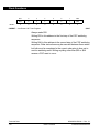
General Description
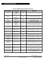
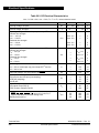
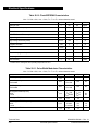
Table 1-2. Development Tools Ordering Information
Description
Name
MCUez
Order Number
Free from World Wide Web
Serial Debug Interface
SDI
M68SDIL (3–5V), M68DIL12 (SDIL + MCUez +
SDBUG12)
Evaluation board
EVB
M68EVB912D60 (EVB only)
M68KIT912D60 (EVB + SDIL12)
NOTE:
SDBUG12 is a P & E Micro Product. It can be obtained from P & E from
their web site (http://www.pemicro.com) for approximately $100.
Third party tools: http://www.mcu.motsps.com/dev_tools/3rd/index.html
Technical Data
28
MC68HC912D60A — Rev. 3.1
General Description
Freescale Semiconductor
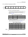
General Description
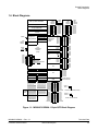
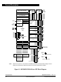
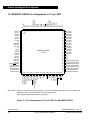
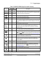
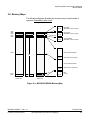
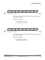
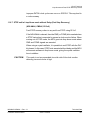
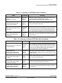
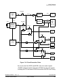
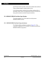
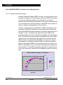
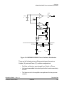
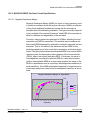
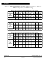
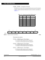
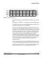
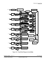
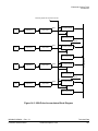
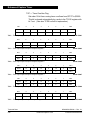
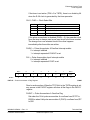
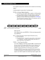
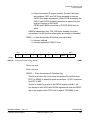
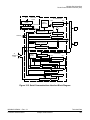
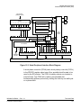
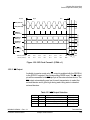
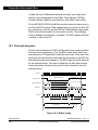
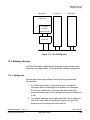
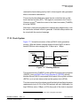
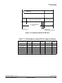
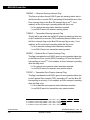
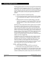
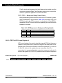
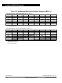
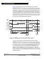
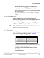
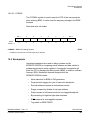
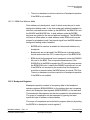
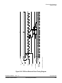
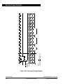
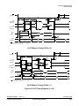
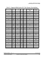
Block Diagrams
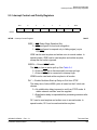
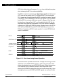
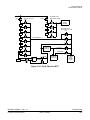
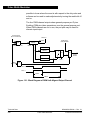
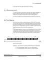
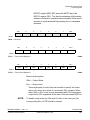
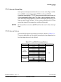
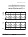
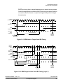
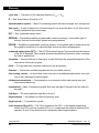
1.6 Block Diagrams
VRH0
ATD0 VRL0
60K byte flash EEPROM
VRH0
VRL0
ATD1
PAD00
PAD01
PAD02
PAD03
PAD04
PAD05
PAD06
PAD07
AN10
AN11
AN12
AN13
AN14
AN15
AN16
AN17
VDDAD
VSSAD
VRH1
VRL1
VDDAD
VSSAD
VRH1
VRL1
VDDAD
VSSAD
PLL
SPI
XIRQ
IRQ
R/W
LSTRB/TAGLO
ECLK
MODA/IPIPE0
MODB/IPIPE1/CGMTST
DBE/CAL/ECLK
PORT E
PE0
PE1
PE2
PE3
PE4
PE5
PE6
PE7
RxD1
TxD1
SCI1
SISO/MISO
MOMI/MOSI
SCK
SS
PW0
PW1
PW2
PW3
PWM
DDRS
SCI0 (MI BUS) RxD0
TxD0
Lite
integration
module
(LIM)
EXTAL
XTAL
RESET
IOC0
IOC1
IOC2
IOC3
IOC4
IOC5
IOC6
IOC7
Enhanced
capture
timer
PORT S
XFC
VDDPLL
VSSPLL
Periodic interrupt
COP watchdog
Clock monitor
Breakpoints
DDRP
Single-wire
background
debug module
PORT P
BKGD
DDRT
I/O
Multiplexed Address/Data Bus
DDRG
PS4
PS5
PS6
PS7
PP0
PP1
PP2
PP3
PP4
PP5
PP6
PP7
PORTG
DDRH
PB7
PB6
PB5
PB4
PB3
PB2
PB1
PB0
ADDR7
ADDR6
ADDR5
ADDR4
ADDR3
ADDR2
ADDR1
ADDR0
DATA7
DATA6
DATA5
DATA4
DATA3
DATA2
DATA1
DATA0
Narrow bus
PS0
PS1
PS2
PS3
TxCAN PCAN1
RxCAN PCAN0
CAN
KWH7
KWH6
KWH5
KWH4
KWH3
KWH2
KWH1
KWH0
PHUPD
PT0
PT1
PT2
PT3
PT4
PT5
PT6
PT7
PCAN7
PCAN6
PCAN5
PCAN4
PCAN3
PCAN2
I/O
PG7
KWG6
KWG5
KWG4
KWG3
KWG2
KWG1
KWG0
PGUPD
PAD10
PAD11
PAD12
PAD13
PAD14
PAD15
PAD16
PAD17
PG7
PG6
PG5
PG4
VDD ×2
PG3
VSS ×2
PG2
PG1
PG0
Power for internal circuitry
PGUPD
PORTH
PA7
PA6
PA5
PA4
PA3
PA2
PA1
PA0
ADDR15
ADDR14
ADDR13
ADDR12
ADDR11
ADDR10
ADDR9
ADDR8
DDRB
PORT B
DATA7 DATA15
DATA6 DATA14
DATA5 DATA13
DATA4 DATA12
DATA3 DATA11
DATA2 DATA10
DATA1 DATA9
DATA0 DATA8
Wide
bus
DDRA
PORT A
PORT AD1
CPU12
PORT T
AN00
AN01
AN02
AN03
AN04
AN05
AN06
AN07
1K byte EEPROM
PORT AD0
2K byte RAM
PH7
VDDX ×2
PH6
VSSX ×2
PH5
PH4
PH3
Power for I/O drivers
PH2
PH1
PH0
PHUPD
Figure 1-1. MC68HC912D60A 112-pin QFP Block Diagram
MC68HC912D60A — Rev. 3.1
Freescale Semiconductor
Technical Data
General Description
29
General Description
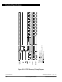
PLL
Enhanced
capture
timer
PW0
PW1
PW2
PW3
PWM
PORT S
PORT P
PORT E
XIRQ
IRQ
R/W
LSTRB/TAGLO
ECLK
MODA/IPIPE0
MODB/IPIPE1/CGMTST
DBE/CAL/ECLK
SISO/MISO
MOMI/MOSI
SCK
SS
PORT CAN
SCI1
SPI
PE0
PE1
PE2
PE3
PE4
PE5
PE6
PE7
RxD1
TxD1
DDRS
SCI0 (MI BUS) RxD0
TxD0
Lite
integration
module
(LIM)
EXTAL
XTAL
RESET
IOC0
IOC1
IOC2
IOC3
IOC4
IOC5
IOC6
IOC7
DDRP
XFC
VDDPLL
VSSPLL
AN00
AN01
AN02
AN03
AN04
AN05
AN06
AN07
DDRCAN
BKGD
Periodic interrupt
COP watchdog
Clock monitor
Breakpoints
VRH0
VRL0
VDDAD
VSSAD
PORT AD0
CPU12
ATD0
PORT AD1
AN10
AN11
AN12
AN13
AN14
AN15
AN16
AN17
1K byte EEPROM
Single-wire
background
debug module
VRH1
VRL1
VDDAD
VSSAD
DDRT
2K byte RAM
ATD1
PORT T
60K byte flash EEPROM
I/O
PCAN7
PCAN6
PCAN5
PCAN4
PCAN3
PCAN2
Multiplexed Address/Data Bus
Note:
DDRG
KWH7
KWH6
KWH5
KWH4
KWH3
KWH2
KWH1
KWH0
PHUPD(VSS)
PORTG
PG7
KWG6
KWG5
KWG4
KWG3
KWG2
KWG1
KWG0
PGUPD(VDD)
PAD00
PAD01
PAD02
PAD03
PAD04
PAD05
PAD06
PAD07
PT0
PT1
PT2
PT3
PT4
PT5
PT6
PT7
PS0
PS1
PS2
PS3
PS4
PS5
PS6
PS7
PP0
PP1
PP2
PP3
PP4
PP5
PP6
PP7
TxCAN PCAN1
RxCAN PCAN0
PG4
VDD ×2
VSS ×2
Power for internal circuitry
PORTH
ADDR7
ADDR6
ADDR5
ADDR4
ADDR3
ADDR2
ADDR1
ADDR0
DATA7
DATA6
DATA5
DATA4
DATA3
DATA2
DATA1
DATA0
Narrow bus
CAN
DDRH
ADDR15
ADDR14
ADDR13
ADDR12
ADDR11
ADDR10
ADDR9
ADDR8
DATA7 DATA15
DATA6 DATA14
DATA5 DATA13
DATA4 DATA12
DATA3 DATA11
DATA2 DATA10
DATA1 DATA9
DATA0 DATA8
Wide
bus
PB7
PB6
PB5
PB4
PB3
PB2
PB1
PB0
DDRB
PORT B
PA7
PA6
PA5
PA4
PA3
PA2
PA1
PA0
DDRA
PORT A
VRH0
VRL0
VDDAD
VSSAD
PH4
VDDX ×2
VSSX ×2
Power for I/O drivers
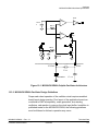
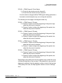
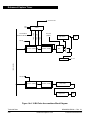
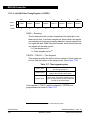
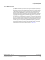
Several I/O on ports G, H and CAN are unavailable externally on the 80-pin QFP package. These internal pins should either be defined as outputs or have their pull-ups/downs enabled.
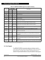
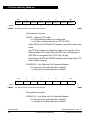
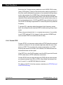
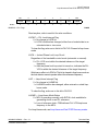
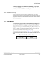
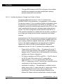
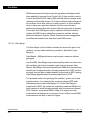
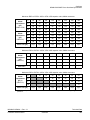
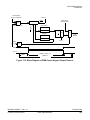
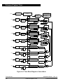
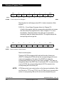
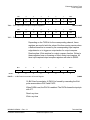
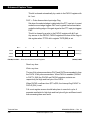
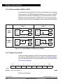
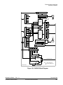
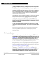
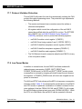
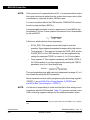
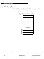
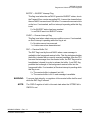
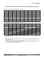
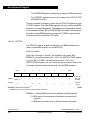
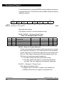
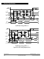
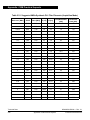
Figure 1-2. MC68HC912D60A 80-pin QFP Block Diagram
Technical Data
30
MC68HC912D60A — Rev. 3.1
General Description
Freescale Semiconductor
Technical Data — MC68HC912D60A
Section 2. Central Processing Unit
2.1 Contents
2.2
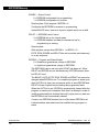
Introduction . . . . . . . . . . . . . . . . . . . . . . . . . . . . . . . . . . . . . . . . 31
2.3
Programming Model . . . . . . . . . . . . . . . . . . . . . . . . . . . . . . . . . 31
2.4
Data Types . . . . . . . . . . . . . . . . . . . . . . . . . . . . . . . . . . . . . . . . 33
2.5
Addressing Modes . . . . . . . . . . . . . . . . . . . . . . . . . . . . . . . . . . 33
2.6
Indexed Addressing Modes . . . . . . . . . . . . . . . . . . . . . . . . . . . 35
2.7
Opcodes and Operands . . . . . . . . . . . . . . . . . . . . . . . . . . . . . . 36
2.2 Introduction
The CPU12 is a high-speed, 16-bit processing unit. It has full 16-bit data
paths and wider internal registers (up to 20 bits) for high-speed extended
math instructions. The instruction set is a proper superset of the
M68HC11instruction set. The CPU12 allows instructions with odd byte
counts, including many single-byte instructions. This provides efficient
use of ROM space. An instruction queue buffers program information so
the CPU always has immediate access to at least three bytes of machine
code at the start of every instruction. The CPU12 also offers an
extensive set of indexed addressing capabilities.
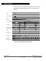
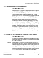
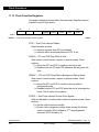
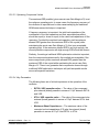
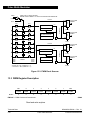
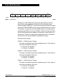
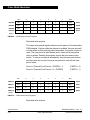
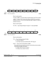
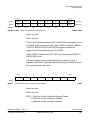
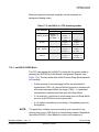
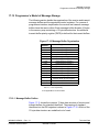
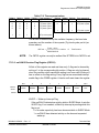
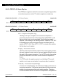
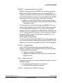
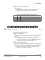
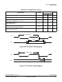
2.3 Programming Model
CPU12 registers are an integral part of the CPU and are not addressed
as if they were memory locations.
MC68HC912D60A — Rev. 3.1
Freescale Semiconductor
Technical Data
Central Processing Unit
31
Central Processing Unit
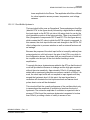
7
A
0 7
B
0
8-BIT ACCUMULATORS A & B
OR
15
D
0
16-BIT DOUBLE ACCUMULATOR D
15
IX
0
INDEX REGISTER X
15
IY
0
INDEX REGISTER Y
15
SP
0
STACK POINTER
15
PC
0
PROGRAM COUNTER
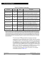
S X H I N Z V C
CONDITION CODE REGISTER
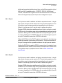
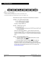
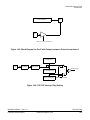
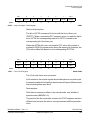
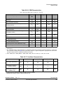
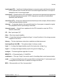
Figure 2-1. Programming Model
Accumulators A and B are general-purpose 8-bit accumulators used to
hold operands and results of arithmetic calculations or data
manipulations. Some instructions treat the combination of these two 8bit accumulators as a 16-bit double accumulator (accumulator D).
Index registers X and Y are used for indexed addressing mode. In the
indexed addressing mode, the contents of a 16-bit index register are
added to 5-bit, 9-bit, or 16-bit constants or the content of an accumulator
to form the effective address of the operand to be used in the instruction.
Stack pointer (SP) points to the last stack location used. The CPU12
supports an automatic program stack that is used to save system
context during subroutine calls and interrupts, and can also be used for
temporary storage of data. The stack pointer can also be used in all
indexed addressing modes.
Program counter is a 16-bit register that holds the address of the next
instruction to be executed. The program counter can be used in all
indexed addressing modes except autoincrement/decrement.
Technical Data
32
MC68HC912D60A — Rev. 3.1
Central Processing Unit
Freescale Semiconductor
Central Processing Unit
Data Types
Condition Code Register (CCR) contains five status indicators, two
interrupt masking bits, and a STOP disable bit. The five flags are half
carry (H), negative (N), zero (Z), overflow (V), and carry/borrow (C). The
half-carry flag is used only for BCD arithmetic operations. The N, Z, V,
and C status bits allow for branching based on the results of a previous
operation.
After a reset, the CPU fetches a vector from the appropriate address and
begins executing instructions. The X and I interrupt mask bits are set to
mask any interrupt requests. The S bit is also set to inhibit the STOP
instruction.
2.4 Data Types
The CPU12 supports the following data types:
•
Bit data
•
8-bit and 16-bit signed and unsigned integers
•
16-bit unsigned fractions
•
16-bit addresses
A byte is eight bits wide and can be accessed at any byte location. A
word is composed of two consecutive bytes with the most significant
byte at the lower value address. There are no special requirements for
alignment of instructions or operands.
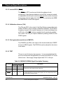
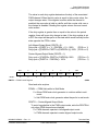
2.5 Addressing Modes
Addressing modes determine how the CPU accesses memory locations
to be operated upon. The CPU12 includes all of the addressing modes
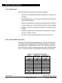
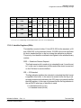
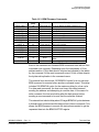
of the M68HC11 CPU as well as several new forms of indexed
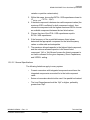
addressing. Table 2-1 is a summary of the available addressing modes.
MC68HC912D60A — Rev. 3.1
Freescale Semiconductor
Technical Data
Central Processing Unit
33
Central Processing Unit
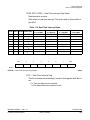
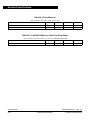
Table 2-1. M68HC12 Addressing Mode Summary
Addressing Mode
Source Format
Abbreviation
Description
Inherent
INST
(no externally
supplied operands)
INH
Operands (if any) are in CPU registers
Immediate
INST #opr8i
or
INST #opr16i
IMM
Operand is included in instruction stream
8- or 16-bit size implied by context
Direct
INST opr8a
DIR
Operand is the lower 8-bits of an address in
the range $0000 – $00FF
Extended
INST opr16a
EXT
Operand is a 16-bit address
Relative
INST rel8
or
INST rel16
REL
An 8-bit or 16-bit relative offset from the
current pc is supplied in the instruction
Indexed
(5-bit offset)
INST oprx5,xysp
IDX
5-bit signed constant offset from x, y, sp, or
pc
Indexed
(auto pre-decrement)
INST oprx3,–xys
IDX
Auto pre-decrement x, y, or sp by 1 ~ 8
Indexed
(auto pre-increment)
INST oprx3,+xys
IDX
Auto pre-increment x, y, or sp by 1 ~ 8
Indexed
(auto post-decrement)
INST oprx3,xys–
IDX
Auto post-decrement x, y, or sp by 1 ~ 8
Indexed
(auto post-increment)
INST oprx3,xys+
IDX
Auto post-increment x, y, or sp by 1 ~ 8
Indexed
(accumulator offset)
INST abd,xysp
IDX
Indexed with 8-bit (A or B) or 16-bit (D)
accumulator offset from x, y, sp, or pc
Indexed
(9-bit offset)
INST oprx9,xysp
IDX1
9-bit signed constant offset from x, y, sp, or
pc
(lower 8-bits of offset in one extension byte)
Indexed
(16-bit offset)
INST oprx16,xysp
IDX2
16-bit constant offset from x, y, sp, or pc
(16-bit offset in two extension bytes)
Indexed-Indirect
(16-bit offset)
INST [oprx16,xysp]
[IDX2]
Pointer to operand is found at...
16-bit constant offset from x, y, sp, or pc
(16-bit offset in two extension bytes)
Indexed-Indirect
(D accumulator offset)
INST [D,xysp]
[D,IDX]
Pointer to operand is found at...
x, y, sp, or pc plus the value in D
Technical Data
34
MC68HC912D60A — Rev. 3.1
Central Processing Unit
Freescale Semiconductor
Central Processing Unit
Indexed Addressing Modes
2.6 Indexed Addressing Modes
The CPU12 indexed modes reduce execution time and eliminate code
size penalties for using the Y index register. CPU12 indexed addressing
uses a postbyte plus zero, one, or two extension bytes after the
instruction opcode. The postbyte and extensions do the following tasks:
•
Specify which index register is used.
•
Determine whether a value in an accumulator is used as an offset.
•
Enable automatic pre- or post-increment or decrement
•
Specify use of 5-bit, 9-bit, or 16-bit signed offsets.
Table 2-2. Summary of Indexed Operations
Source
Code
Syntax
Postbyte
Code (xb)
,r
rr0nnnnn
n,r
–n,r
Comments
5-bit constant offset n = –16 to +15
rr can specify X, Y, SP, or PC
111rr0zs
n,r
–n,r
Constant offset (9- or 16-bit signed)
z-0 = 9-bit with sign in LSB of postbyte(s)
1 = 16-bit
if z = s = 1, 16-bit offset indexed-indirect (see below)
rr can specify X, Y, SP, or PC
111rr011
[n,r]
16-bit offset indexed-indirect
rr can specify X, Y, SP, or PC
rr1pnnnn
n,–r n,+r
n,r– n,r+
Auto pre-decrement/increment or Auto postdecrement/increment;
p = pre-(0) or post-(1), n = –8 to –1, +1 to +8
rr can specify X, Y, or SP (PC not a valid choice)
111rr1aa
A,r
B,r
D,r
Accumulator offset (unsigned 8-bit or 16-bit)
aa-00 = A
01 = B
10 = D (16-bit)
11 = see accumulator D offset indexed-indirect
rr can specify X, Y, SP, or PC
111rr111
[D,r]
Accumulator D offset indexed-indirect
rr can specify X, Y, SP, or PC
MC68HC912D60A — Rev. 3.1
Freescale Semiconductor
Technical Data
Central Processing Unit
35
Central Processing Unit
2.7 Opcodes and Operands
The CPU12 uses 8-bit opcodes. Each opcode identifies a particular
instruction and associated addressing mode to the CPU. Several
opcodes are required to provide each instruction with a range of
addressing capabilities.
Only 256 opcodes would be available if the range of values were
restricted to the number that can be represented by 8-bit binary
numbers. To expand the number of opcodes, a second page is added to
the opcode map. Opcodes on the second page are preceded by an
additional byte with the value $18.
To provide additional addressing flexibility, opcodes can also be
followed by a postbyte or extension bytes. Postbytes implement certain
forms of indexed addressing, transfers, exchanges, and loop primitives.
Extension bytes contain additional program information such as
addresses, offsets, and immediate data.
Technical Data
36
MC68HC912D60A — Rev. 3.1
Central Processing Unit
Freescale Semiconductor
Technical Data — MC68HC912D60A
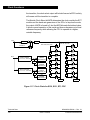
Section 3. Pinout and Signal Descriptions
3.1 Contents
3.2
MC68HC912D60A Pin Assignments in 112-pin QFP . . . . . . . . 38
3.3
MC68HC912D60A Pin Assignments in 80-pin QFP . . . . . . . . . 40
3.4
Power Supply Pins . . . . . . . . . . . . . . . . . . . . . . . . . . . . . . . . . . 42
3.5
Signal Descriptions . . . . . . . . . . . . . . . . . . . . . . . . . . . . . . . . . . 44
3.6
Port Signals . . . . . . . . . . . . . . . . . . . . . . . . . . . . . . . . . . . . . . . 52
MC68HC912D60A — Rev. 3.1
Freescale Semiconductor
Technical Data
Pinout and Signal Descriptions
37
Pinout and Signal Descriptions
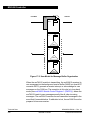
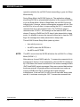
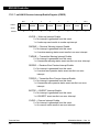
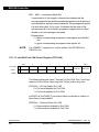
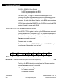
1
2
3
4
5
6
7
8
9
10
11
12
13
14
15
16
17
18
19
20
21
22
23
24
25
26
27
28
MC68HC912D60A
112TQFP
84
83
82
81
80
79
78
77
76
75
74
73
72
71
70
69
68
67
66
65
64
63
62
61
60
59
58
57
PAD17/AN17
PAD07/AN07
PAD16/AN16
PAD06/AN06
PAD15/AN15
PAD05/AN05
PAD14/AN14
PAD04/AN04
PAD13/AN13
PAD03/AN03
PAD12/AN12
PAD02/AN02
PAD11/AN11
PAD01/AN01
PAD10/AN10
PAD00/AN00
VRL0
VRH0
VSS
VDD
PA7/ADDR15/DATA15/DATA7
PA6/ADDR14/DATA14/DATA6
PA5/ADDR13/DATA13/DATA5
PA4/ADDR12/DATA12/DATA4
PA3/ADDR11/DATA11/DATA3
PA2/ADDR10/DATA10/DATA2
PA1/ADDR9/DATA9/DATA1
PA0/ADDR8/DATA8/DATA0
ADDR5/DATA5/PB5
ADDR6/DATA6/PB6
ADDR7/DATA7/PB7
KWH7/PH7
KWH6/PH6
KWH5/PH5
KWH4/PH4
ECLK/DBE/CAL/PE7
CGMTST/MODB/IPIPE1/PE6
MODA/IPIPE0/PE5
ECLK/PE4
VSSX
PHUPD
VDDX
VDDPLL
XFC
VSSPLL
RESET
EXTAL
XTAL
KWH3/PH3
KWH2/PH2
KWH1/PH1
KWH0/PH0
LSTRB/TAGLO/PE3
R/W/PE2
IRQ/PE1
XIRQ/PE0
29
30
31
32
33
34
35
36
37
38
39
40
41
42
43
44
45
46
47
48
49
50
51
52
53
54
55
56
PW2/PP2
PW1/PP1
PW0/PP0
IOC0/PT0
IOC1/PT1
IOC2/PT2
IOC3/PT3
PG7
KWG6/PG6
KWG5/PG5
KWG4/PG4
VDD
PGUPD
VSS
IOC4/PT4
IOC5/PT5
IOC6/PT6
IOC7/PT7
KWG3/PG3
KWG2/PG2
KWG1/PG1
KWG0/PG0
SMODN/TAGHI/BKGD
ADDR0/DATA0/PB0
ADDR1/DATA1/PB1
ADDR2/DATA2/PB2
ADDR3/DATA3/PB3
ADDR4/DATA4/PB4
112
111
110
109
108
107
106
105
104
103
102
101
100
99
98
97
96
95
94
93
92
91
90
89
88
87
86
85
PP3/PW3
PP4
PP5
PP6
PP7
VDDX
VSSX
PCAN0/RxCAN
PCAN1/TxCAN
PCAN2
PCAN3
PCAN4
PCAN5
PCAN6
PCAN7
TEST
PS7/SS
PS6/SCK
PS5/SDO/MOSI
PS4/SDI/MISO
PS3/TxD1
PS2/RxD1
PS1/TxD0
PS0/RxD0
VSSA
VRL1
VRH1
VDDA
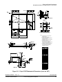
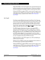
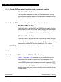
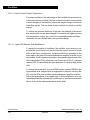
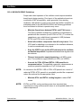
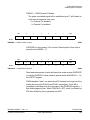
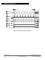
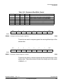
3.2 MC68HC912D60A Pin Assignments in 112-pin QFP
Note: TEST = This pin is used for factory test purposes. It is recommended that this pin is not connected in the
application, but it may be bonded to 5.5 V max without issue.
Never apply voltage higher than 5.5 V to this pin.
Figure 3-1. Pin Assignments in 112-pin TQFP for MC68HC912D60A
Technical Data
38
MC68HC912D60A — Rev. 3.1
Pinout and Signal Descriptions
Freescale Semiconductor
Pinout and Signal Descriptions
MC68HC912D60A Pin Assignments in 112-pin QFP
0.20 T L-M N
4X
PIN 1
IDENT
0.20 T L-M N
4X 28 TIPS
112
J1
85
4X
P
J1
1
CL
84
VIEW Y
108X
G
X
X=L, M OR N
VIEW Y
B
L
V
M
B1
28
AA
J
V1
57
29
F
D
56
0.13
N
M
BASE
METAL
T L-M N
SECTION J1-J1
ROTATED 90 ° COUNTERCLOCKWISE
A1
S1
A
S
C2
VIEW AB
θ2
0.050
C
0.10 T
112X
SEATING
PLANE
NOTES:
1. DIMENSIONING AND TOLERANCING PER
ASME Y14.5M, 1994.
2. DIMENSIONS IN MILLIMETERS.
3. DATUMS L, M AND N TO BE DETERMINED AT
SEATING PLANE, DATUM T.
4. DIMENSIONS S AND V TO BE DETERMINED AT
SEATING PLANE, DATUM T.
5. DIMENSIONS A AND B DO NOT INCLUDE
MOLD PROTRUSION. ALLOWABLE
PROTRUSION IS 0.25 PER SIDE. DIMENSIONS
A AND B INCLUDE MOLD MISMATCH.
6. DIMENSION D DOES NOT INCLUDE DAMBAR
PROTRUSION. ALLOWABLE DAMBAR
PROTRUSION SHALL NOT CAUSE THE D
DIMENSION TO EXCEED 0.46.
θ3
T
θ
R
R2
R
0.25
R1
GAGE PLANE
(K)
C1
θ1
E
(Y)
(Z)
VIEW AB
DIM
A
A1
B
B1
C
C1
C2
D
E
F
G
J
K
P
R1
R2
S
S1
V
V1
Y
Z
AA
θ
θ1
θ2
θ3
MILLIMETERS
MIN
MAX
20.000 BSC
10.000 BSC
20.000 BSC
10.000 BSC
--1.600
0.050
0.150
1.350
1.450
0.270
0.370
0.450
0.750
0.270
0.330
0.650 BSC
0.090
0.170
0.500 REF
0.325 BSC
0.100
0.200
0.100
0.200
22.000 BSC
11.000 BSC
22.000 BSC
11.000 BSC
0.250 REF
1.000 REF
0.090
0.160
8 °
0°
7 °
3 °
13
°
11 °
11 °
13 °
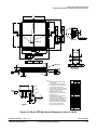
Figure 3-2. 112-pin TQFP Mechanical Dimensions (case no. 987)
MC68HC912D60A — Rev. 3.1
Freescale Semiconductor
Technical Data
Pinout and Signal Descriptions
39
Pinout and Signal Descriptions
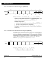
80
79
78
77
76
75
74
73
72
71
70
69
68
67
66
65
64
63
62
61
PP3/PW3
PP4
PP5
PP6
PP7
VDDX
VSSX
PCAN0/RxCAN
PCAN1/TxCAN
TEST
PS7/SS
PS6/SCK
PS5/SDO/MOSI
PS4/SDI/MISO
PS3/TxD1
PS2/RxD1
PS1/TxD0
PS0/RxD0
VSSAD
VDDAD
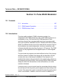
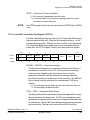
3.3 MC68HC912D60A Pin Assignments in 80-pin QFP
MC68HC912D60A
80 QFP
60
59
58
57
56
55
54
53
52
51
50
49
48
47
46
45
44
43
42
41
PAD07/AN07
PAD06/AN06
PAD05/AN05
PAD04/AN04
PAD03/AN03
PAD02/AN02
PAD01/AN01
PAD00/AN00
VRL0
VRH0
VSS
VDD
PA7/ADDR15/DATA15/DATA7
PA6/ADDR14/DATA14/DATA6
PA5/ADDR13/DATA13/DATA5
PA4/ADDR12/DATA12/DATA4
PA3/ADDR11/DATA11/DATA3
PA2/ADDR10/DATA10/DATA2
PA1/ADDR9/DATA9/DATA1
PA0/ADDR8/DATA8/DATA0
21
22
23
24
25
26
27
28
29
30
31
32
33
34
35
36
37
38
39
40
1
2
3
4
5
6
7
8
9
10
11
12
13
14
15
16
17
18
19
20
ADDR5/DATA5/PB5
ADDR6/DATA6/PB6
ADDR7/DATA7/PB7
KWH4/PH4
ECLK/DBE/CAL/PE7
CGMTST/MODB/IPIPE1/PE6
MODA/IPIPE0/PE5
ECLK/PE4
VSSX
VDDX
VDDPLL
XFC
VSSPLL
RESET
EXTAL
XTAL
LSTRB/TAGLO/PE3
R/W/PE2
IRQ/PE1
XIRQ/PE0
PW2/PP2
PW1/PP1
PW0/PP0
IOC0/PT0
IOC1/PT1
IOC2/PT2
IOC3/PT3
KWG4/PG4
VDD
VSS
IOC4/PT4
IOC5/PT5
IOC6/PT6
IOC7/PT7
SMODN/TAGHI/BKGD
ADDR0/DATA0/PB0
ADDR1/DATA1/PB1
ADDR2/DATA2/PB2
ADDR3/DATA3/PB3
ADDR4/DATA4/PB4
Note: TEST = This pin is used for factory test purposes. It is recommended that this pin is not connected in the
application, but it may be bonded to 5.5 V max without issue.
Never apply voltage higher than 5.5 V to this pin.
Figure 3-3. Pin Assignments in 80-pin QFP for MC68HC912D60A
Technical Data
40
MC68HC912D60A — Rev. 3.1
Pinout and Signal Descriptions
Freescale Semiconductor
Pinout and Signal Descriptions
MC68HC912D60A Pin Assignments in 80-pin QFP
L
60
41
61
D
S
M
V
P
B
C A-B
D
0.20
M
B
B
-A-,-B-,-D-
0.20
L
H A-B
-B-
0.05 D
-A-
S
S
S
40
DETAIL A
DETAIL A
21
80
1
0.20
A
H A-B
M
S
F
20
-DD
S
0.05 A-B
J
S
0.20
C A-B
M
S
D
S
D
M
E
DETAIL C
C
-H-
DATUM
PLANE
0.20
M
C A-B
S
D
S
SECTION B-B
VIEW ROTATED 90 °
0.10
-CH
SEATING
PLANE
N
M
G
U
T
DATUM
PLANE
-H-
R
K
W
X
DETAIL C
Q
NOTES:
1. DIMENSIONING AND TOLERANCING PER
ANSI Y14.5M, 1982.
2. CONTROLLING DIMENSION: MILLIMETER.
3. DATUM PLANE -H- IS LOCATED AT BOTTOM OF
LEAD AND IS COINCIDENT WITH THE
LEAD WHERE THE LEAD EXITS THE PLASTIC
BODY AT THE BOTTOM OF THE PARTING LINE.
4. DATUMS -A-, -B- AND -D- TO BE
DETERMINED AT DATUM PLANE -H-.
5. DIMENSIONS S AND V TO BE DETERMINED
AT SEATING PLANE -C-.
6. DIMENSIONS A AND B DO NOT INCLUDE
MOLD PROTRUSION. ALLOWABLE
PROTRUSION IS 0.25 PER SIDE. DIMENSIONS
A AND B DO INCLUDE MOLD MISMATCH
AND ARE DETERMINED AT DATUM PLANE -H-.
7. DIMENSION D DOES NOT INCLUDE DAMBAR
PROTRUSION. ALLOWABLE DAMBAR
PROTRUSION SHALL BE 0.08 TOTAL IN
DIM
A
B
C
D
E
F
G
H
J
K
L
M
N
P
Q
R
S
T
U
V
W
X
MILLIMETERS
MIN
MAX
13.90
14.10
13.90
14.10
2.15
2.45
0.22
0.38
2.00
2.40
0.22
0.33
0.65 BSC
--0.25
0.13
0.23
0.65
0.95
12.35 REF
5°
10 °
0.13
0.17
0.325 BSC
0°
7°
0.13
0.30
16.95
17.45
0.13
--0°
--16.95
17.45
0.35
0.45
1.6 REF
Figure 3-4. 80-pin QFP Mechanical Dimensions (case no. 841B)
MC68HC912D60A — Rev. 3.1
Freescale Semiconductor
Technical Data
Pinout and Signal Descriptions
41
Pinout and Signal Descriptions
3.4 Power Supply Pins
MC68HC912D60A power and ground pins are described below and
summarized in Table 3-1.
All power supply pins must be connected to appropriate supplies.
On no account must any pins be left floating.
3.4.1 Internal Power (VDD) and Ground (VSS)
Power is supplied to the MCU through VDD and VSS. Because fast signal
transitions place high, short-duration current demands on the power
supply, use bypass capacitors with high-frequency characteristics and
place them as close to the MCU as possible. Bypass requirements
depend on how heavily the MCU pins are loaded.
3.4.2 External Power (VDDX) and Ground (VSSX)
External power and ground for I/O drivers. Because fast signal
transitions place high, short-duration current demands on the power
supply, use bypass capacitors with high-frequency characteristics and
place them as close to the MCU as possible. Bypass requirements
depend on how heavily the MCU pins are loaded.
3.4.3 VDDA, VSSA
Provides operating voltage and ground for the analog-to-digital
converter. This allows the supply voltage to the ATD to be bypassed
independently. Connecting VDDA to VDD if the ATD modules are not
used will not result in an increase of power consumption.
3.4.4 Analog to Digital Reference Voltages (VRH, VRL)
VRH0, VRL0: reference voltage high and low for ATD converter 0.
VRH1, VRL1: reference voltage high and low for ATD converter 1.
If the ATD modules are not used, leaving VRH connected to VDD will not
result in an increase of power consumption.
Technical Data
42
MC68HC912D60A — Rev. 3.1
Pinout and Signal Descriptions
Freescale Semiconductor
Pinout and Signal Descriptions
Power Supply Pins
3.4.5 VDDPLL, VSSPLL
Provides operating voltage and ground for the Phased-Locked Loop.
This allows the supply voltage to the PLL to be bypassed independently.
NOTE:
The VSSPLL pin should always be grounded even if the PLL is not used.
The VDDPLL pin should not be left floating. It is recommended to
connect the VDDPLL pin to ground if the PLL is not used.
3.4.6 XFC
PLL loop filter. Please see Appendix: CGM Practical Aspects for
information on how to calculate PLL loop filter elements. Any current
leakage on this pin must be avoided.
VDDPLL
C0
MCU
R0
Ca
XFC
Figure 3-5. PLL Loop FIlter Connections
If VDDPLL is connected to VSS (this is normal case), then the XFC pin
should either be left floating or connected to VSS (never to VDD). If
VDDPLL is tied to VDD but the PLL is switched off (PLLON bit cleared),
then the XFC pin should be connected preferably to VDDPLL (i.e. ready
for VCO minimum frequency).
MC68HC912D60A — Rev. 3.1
Freescale Semiconductor
Technical Data
Pinout and Signal Descriptions
43
Pinout and Signal Descriptions
Table 3-1. MC68HC912D60A Power and Ground Connection Summary
Pin Number
Mnemonic
80-pin
QFP
112-pin
QFP
VDD
9, 49
12, 65
VSS
10, 50
14, 66
VDDX
30, 75
42, 107
VSSX
29, 74
40, 106
VDDA
61
85
VSSA
62
88
VRH1
—
86
VRL1
—
87
VRH0
51
67
VRL0
52
68
VDDPLL
31
43
VSSPLL
33
45
Description
Internal power and ground.
External power and ground, supply to pin drivers.
Operating voltage and ground for the analog-to-digital
converter, allows the supply voltage to the A/D to be
bypassed independently.
Reference voltages for the analog-to-digital converter 1
Reference voltages for the analog-to-digital converter 0.
Provides operating voltage and ground for the Phased-Locked
Loop. This allows the supply voltage to the PLL to be
bypassed independently.
3.5 Signal Descriptions
3.5.1 Crystal Driver and External Clock Input (XTAL, EXTAL)
These pins provide the interface for either a crystal or a CMOS
compatible clock to control the internal clock generator circuitry. Out of
reset the frequency applied to EXTAL is twice the desired E–clock rate.
All the device clocks are derived from the EXTAL input frequency.
3.5.1.1 Crystal Connections
Refer to Section 12. Oscillator for details of crystal connections.
Technical Data
44
MC68HC912D60A — Rev. 3.1
Pinout and Signal Descriptions
Freescale Semiconductor
Pinout and Signal Descriptions
Signal Descriptions
NOTE:
When selecting a crystal, it is recommended to use one with the lowest
possible frequency in order to minimise EMC emissions.
3.5.1.2 External Oscillator Connections
XTAL is the crystal output. The XTAL pin must be left unterminated when
an external CMOS compatible clock input is connected to the EXTAL
pin. The XTAL output is normally intended to drive only a crystal. The
XTAL output can be buffered with a high-impedance buffer to drive the
EXTAL input of another device.
2 xE
CMOS-COMPATIBLE
EXTERNAL OSCILLATOR
EXTAL
MCU
XTAL
NC
Figure 3-6. External Oscillator Connections
3.5.2 E-Clock Output (ECLK)
ECLK is the output connection for the internal bus clock and is used to
demultiplex the address and data and is used as a timing reference.
ECLK frequency is equal to 1/2 the crystal frequency out of reset. The
ECLK output is turned off in single chip user mode to reduce the effects
of RFI. It can be turned on if necessary. In single-chip special mode, the
ECLK is turned ON at reset and can be turned OFF. In special peripheral
mode the ECLK is an input to the MCU. All clocks, including the ECLK,
are halted when the MCU is in STOP mode. It is possible to configure
the MCU to interface to slow external memory. ECLK can be stretched
for such accesses.
3.5.3 Reset (RESET)
An active low bidirectional control signal, RESET, acts as an input to
initialize the MCU to a known start-up state. It also acts as an open-drain
MC68HC912D60A — Rev. 3.1
Freescale Semiconductor
Technical Data
Pinout and Signal Descriptions
45
Pinout and Signal Descriptions
output to indicate that an internal failure has been detected in either the
clock monitor or COP watchdog circuit. The MCU goes into reset
asynchronously and comes out of reset synchronously. This allows the
part to reach a proper reset state even if the clocks have failed, while
allowing synchronized operation when starting out of reset.
It is important to use an external low-voltage reset circuit (such as
MC34064 or MC34164) to prevent corruption of RAM or EEPROM due
to power transitions.
The reset sequence is initiated by any of the following events:
•
Power-on-reset (POR)
•
COP watchdog enabled and watchdog timer times out
•
Clock monitor enabled and Clock monitor detects slow or stopped
clock
•
User applies a low level to the reset pin
External circuitry connected to the reset pin should not include a large
capacitance that would interfere with the ability of this signal to rise to a
valid logic one within nine bus cycles after the low drive is released.
Upon detection of any reset, an internal circuit drives the reset pin low
and a clocked reset sequence controls when the MCU can begin normal
processing. In the case of POR or a clock monitor error, a 4096 cycle
oscillator startup delay is imposed before the reset recovery sequence
starts (reset is driven low throughout this 4096 cycle delay). The internal
reset recovery sequence then drives reset low for 16 to 17 cycles and
releases the drive to allow reset to rise. Nine cycles later this circuit
samples the reset pin to see if it has risen to a logic one level. If reset is
low at this point, the reset is assumed to be coming from an external
request and the internally latched states of the COP timeout and clock
monitor failure are cleared so the normal reset vector ($FFFE:FFFF) is
taken when reset is finally released. If reset is high after this nine cycle
delay, the reset source is tentatively assumed to be either a COP failure
or a clock monitor fail. If the internally latched state of the clock monitor
fail circuit is true, processing begins by fetching the clock monitor vector
($FFFC:FFFD). If no clock monitor failure is indicated, and the latched
state of the COP timeout is true, processing begins by fetching the COP
Technical Data
46
MC68HC912D60A — Rev. 3.1
Pinout and Signal Descriptions
Freescale Semiconductor
Pinout and Signal Descriptions
Signal Descriptions
vector ($FFFA:FFFB). If neither clock monitor fail nor COP timeout are
pending, processing begins by fetching the normal reset vector
($FFFE:FFFF).
3.5.4 Maskable Interrupt Request (IRQ)
The IRQ input provides a means of applying asynchronous interrupt
requests to the MCU. Either falling edge-sensitive triggering or levelsensitive triggering is program selectable (INTCR register). IRQ is
always enabled and configured to level-sensitive triggering at reset. It
can be disabled by clearing the IRQEN bit (INTCR register). When the
MCU is reset the IRQ function is masked in the condition code register.
This pin is always an input and can always be read. There is an active
pull-up on this pin while in reset and immediately out of reset. The pullup can be turned off by clearing PUPE in the PUCR register.
3.5.5 Nonmaskable Interrupt (XIRQ)
The XIRQ input provides a means of requesting a nonmaskable interrupt
after reset initialization. During reset, the X bit in the condition code
register (CCR) is set and any interrupt is masked until MCU software
enables it. Because the XIRQ input is level sensitive, it can be connected
to a multiple-source wired-OR network. This pin is always an input and
can always be read. There is an active pull-up on this pin while in reset
and immediately out of reset. The pull-up can be turned off by clearing
PUPE in the PUCR register. XIRQ is often used as a power loss detect
interrupt.
Whenever XIRQ or IRQ are used with multiple interrupt sources (IRQ
must be configured for level-sensitive operation if there is more than one
source of IRQ interrupt), each source must drive the interrupt input with
an open-drain type of driver to avoid contention between outputs. There
must also be an interlock mechanism at each interrupt source so that the
source holds the interrupt line low until the MCU recognizes and
acknowledges the interrupt request. If the interrupt line is held low, the
MCU will recognize another interrupt as soon as the interrupt mask bit in
the MCU is cleared (normally upon return from an interrupt).
MC68HC912D60A — Rev. 3.1
Freescale Semiconductor
Technical Data
Pinout and Signal Descriptions
47
Pinout and Signal Descriptions
3.5.6 Mode Select (SMODN, MODA, and MODB)
The state of these pins during reset determine the MCU operating mode.
After reset, MODA and MODB can be configured as instruction queue
tracking signals IPIPE0 and IPIPE1. MODA and MODB have active pulldowns during reset.
The SMODN pin has an active pull-up when configured as input. This pin
can be used as BKGD or TAGHI after reset.
3.5.7 Single-Wire Background Mode Pin (BKGD)
The BKGD pin receives and transmits serial background debugging
commands. A special self-timing protocol is used. The BKGD pin has an
active pull-up when configured as input; BKGD has no pull-up control.
Refer to Development Support.
3.5.8 External Address and Data Buses (ADDR[15:0] and DATA[15:0])
External bus pins share function with general-purpose I/O ports A and B.
In single-chip operating modes, the pins can be used for I/O; in
expanded modes, the pins are used for the external buses.
In expanded wide mode, ports A and B are used for multiplexed 16-bit
data and address buses. PA[7:0] correspond to
ADDR[15:8]/DATA[15:8]; PB[7:0] correspond to ADDR[7:0]/DATA[7:0].
In expanded narrow mode, ports A and B are used for the16-bit address
bus, and an 8-bit data bus is multiplexed with the most significant half of
the address bus on port A. In this mode, 16-bit data is handled as two
back-to-back bus cycles, one for the high byte followed by one for the
low byte. PA[7:0] correspond to ADDR[15:8] and to DATA[15:8] or
DATA[7:0], depending on the bus cycle. The state of the address pin
should be latched at the rising edge of E. To allow for maximum address
setup time at external devices, a transparent latch should be used.
Technical Data
48
MC68HC912D60A — Rev. 3.1
Pinout and Signal Descriptions
Freescale Semiconductor
Pinout and Signal Descriptions
Signal Descriptions
3.5.9 Read/Write (R/W)
In all modes this pin can be used as general-purpose I/O and is an input
with an active pull-up out of reset. If the read/write function is required it
should be enabled by setting the RDWE bit in the PEAR register.
External writes will not be possible until enabled.
3.5.10 Low-Byte Strobe (LSTRB)
In all modes this pin can be used as general-purpose I/O and is an input
with an active pull-up out of reset. If the strobe function is required, it
should be enabled by setting the LSTRE bit in the PEAR register. This
signal is used in write operations and so external low byte writes will not
be possible until this function is enabled. This pin is also used as TAGLO
in Special Expanded modes and is multiplexed with the LSTRB function.
3.5.11 Instruction Queue Tracking Signals (IPIPE1 and IPIPE0)
These signals are used to track the state of the internal instruction
execution queue. Execution state is time-multiplexed on the two signals.
Refer to Development Support.
3.5.12 Data Bus Enable (DBE)
The DBE pin (PE7) is an active low signal that will be asserted low during
ECLK high time. DBE provides separation between output of a
multiplexed address and the input of data. When an external address is
stretched, DBE is asserted during what would be the last quarter cycle
of the last ECLK cycle of stretch. In expanded modes this pin is used to
enable the drive control of external buses during external reads. Use of
the DBE is controlled by the NDBE bit in the PEAR register.DBE is
enabled out of reset in expanded modes. This pin has an active pull-up
during and after reset in single chip modes.
MC68HC912D60A — Rev. 3.1
Freescale Semiconductor
Technical Data
Pinout and Signal Descriptions
49
Pinout and Signal Descriptions
3.5.13 Inverted ECLK (ECLK)
The ECLK pin (PE7) can be used to latch the address for demultiplexing. It has the same behavior as the ECLK, except is inverted.
In expanded modes this pin is used to enable the drive control of external
buses during external reads. Use of the ECLK is controlled by the NDBE
and DBENE bits in the PEAR register.
3.5.14 Calibration reference (CAL)
The CAL pin (PE7) is the output of the Slow Mode programmable clock
divider, SLWCLK, and is used as a calibration reference. The SLWCLK
frequency is equal to the crystal frequency out of reset and always has
a 50% duty. If the DBE function is enabled it will override the enabled
CAL output. The CAL pin output is disabled by clearing CALE bit in the
PEAR register.
3.5.15 Clock generation module test (CGMTST)
The CGMTST pin (PE6) is the output of the clocks tested when CGMTE
bit is set in PEAR register. The PIPOE bit must be cleared for the clocks
to be tested.
3.5.16 TEST
This pin is used for factory test purposes. It is recommended that this
pin is not connected in the application, but it may be bonded to 5.5 V max
without issue. Never apply voltage higher than 5.5 V to this pin.
Table 3-2. MC68HC912D60A Signal Description Summary
Pin Name
Pin Number
80-pin
112-pin
EXTAL
35
47
XTAL
36
48
RESET
34
46
Description
Crystal driver and external clock input pins.
An active low bidirectional control signal, RESET acts as an input to
initialize the MCU to a known start-up state, and an output when COP or
clock monitor causes a reset.
Technical Data
50
MC68HC912D60A — Rev. 3.1
Pinout and Signal Descriptions
Freescale Semiconductor
Pinout and Signal Descriptions
Signal Descriptions
Table 3-2. MC68HC912D60A Signal Description Summary
Pin Name
Pin Number
Description
80-pin
112-pin
ADDR[7:0]
DATA[7:0]
23–16
31–24
ADDR[15:8]
DATA[15:8]
48–41
64–57
DBE
25
36
Data bus control and, in expanded mode, enables the drive control of
external buses during external reads.
ECLK
25
36
Inverted ECLK used to latch the address.
External bus pins share function with general-purpose I/O ports A and B.
In single chip modes, the pins can be used for I/O. In expanded modes,
the pins are used for the external buses.
CAL
25
36
CAL is the output of the Slow Mode programmable clock divider, SLWCLK,
and is used as a calibration reference for functions such as time of day. It
is overridden when DBE function is enabled. It always has a 50% duty
cycle.
CGMTST
26
37
Clock generation module test output.
MODB/
IPIPE1,
MODA/
IPIPE0
26, 27
37, 38
State of mode select pins during reset determine the initial operating mode
of the MCU. After reset, MODB and MODA can be configured as
instruction queue tracking signals IPIPE1 and IPIPE0 or as generalpurpose I/O pins.
ECLK
28
39
E Clock is the output connection for the external bus clock. ECLK is used
as a timing reference and for address demultiplexing.
LSTRB/
TAGLO
37
53
Low byte strobe (0 = low byte valid), in all modes this pin can be used as
I/O. The low strobe function is the exclusive-NOR of A0 and the internal
SZ8 signal. (The SZ8 internal signal indicates the size 16/8 access.) Pin
function TAGLO used in instruction tagging. See Development Support.
R/W
38
54
Indicates direction of data on expansion bus. Shares function with generalpurpose I/O. Read/write in expanded modes.
IRQ
39
55
Maskable interrupt request input provides a means of applying
asynchronous interrupt requests to the MCU. Either falling edgesensitive triggering or level-sensitive triggering is program selectable
(INTCR register).
XIRQ
40
56
Provides a means of requesting asynchronous nonmaskable interrupt
requests after reset initialization
Single-wire background interface pin is dedicated to the background
debug function. During reset, this pin determines special or normal
operating mode. Pin function TAGHI used in instruction tagging. See
Development Support.
SMODN/BK
GD/TAGHI
15
23
PW[3:0]
80, 1–3
112, 1–3
SS
70
96
Slave select output for SPI master mode, input for slave mode or master
mode.
SCK
69
95
Serial clock for SPI system.
Pulse Width Modulator channel outputs.
MC68HC912D60A — Rev. 3.1
Freescale Semiconductor
Technical Data
Pinout and Signal Descriptions
51
Pinout and Signal Descriptions
Table 3-2. MC68HC912D60A Signal Description Summary
Pin Number
Pin Name
Description
80-pin
112-pin
SDO/MOSI
68
94
Master out/slave in pin for serial peripheral interface
SDI/MISO
67
93
Master in/slave out pin for serial peripheral interface
TxD1
66
92
SCI1 transmit pin
RxD1
65
91
SCI1 receive pin
TxD0
64
90
SCI0 transmit pin
RxD0
63
89
SCI0 receive pin
IOC[7:0]
14–11,
7–4
18–15, 7–4
AN1[7:0]
N/A
84/82/80/78/
Analog inputs for the analog-to-digital conversion module 1
76/74/72/70
AN0[7:0]
60–53
83/81/79/77/
Analog inputs for the analog-to-digital conversion module 0
75/73/71/69
TEST
71
97
Used for factory test purposes. Do not connect in the application; may be
bonded to 5.5 V max.
TxCAN
72
104
MSCAN transmit pin. Leave unconnected if MSCAN is not used.
RxCAN
73
105
MSCAN receive pin. Pin has internal pull-up; where msCAN module is not
used, do not tie to VSS.
8 (KWG4
9–11, 19–22
only)
KWG[6:0]
PGUPD
(1)
13
KWH[7:0]
24 (KWH4
only)
32–35,
49–52
PHUPD
(2)
41
Pins used for input capture and output compare in the timer and pulse
accumulator subsystem.
Key wake-up and general purpose I/O; can cause an interrupt when an
input transitions from high to low. On 80-pin QFP all 8 I/O should be
initialised.
Defines if I/O port resistive load is a pull-up or a pull-down, when enabled.
Key wake-up and general purpose I/O; can cause an interrupt when an
input transitions from high to low. On 80-pin QFP all 8 I/O should be
initialised.
Defines if I/O port resistive load is a pull-up or a pull-down, when enabled.
1. In the 80-pin version PGUPD is connected internally to VDD
2. In the 80-pin version PHUPD is connected internally to VSS
3.6 Port Signals
The MC68HC912D60A incorporates eight ports which are used to
control and access the various device subsystems. When not used for
these purposes, port pins may be used for general-purpose I/O. In
addition to the pins described below, each port consists of a data register
Technical Data
52
MC68HC912D60A — Rev. 3.1
Pinout and Signal Descriptions
Freescale Semiconductor
Pinout and Signal Descriptions
Port Signals
which can be read and written at any time, and, with the exception of port
AD0, port AD1 (available only in 112TQFP), PE[1:0], RxCAN and
TxCAN, a data direction register which controls the direction of each pin.
After reset all general purpose I/O pins are configured as input.
3.6.1 Port A
Port A pins are used for address and data in expanded modes. In single
chip modes, the pins can be used as I/O. The port data register is not in
the address map during expanded and peripheral mode operation.
When it is in the map, port A can be read or written at anytime.
Register DDRA determines whether each port A pin is an input or output.
DDRA is not in the address map during expanded and peripheral mode
operation. Setting a bit in DDRA makes the corresponding bit in port A
an output; clearing a bit in DDRA makes the corresponding bit in port A
an input. The default reset state of DDRA is all zeros.
When the PUPA bit in the PUCR register is set, all port A input pins are
pulled-up internally by an active pull-up device. This bit has no effect if
the port is being used in expanded modes as the pull-ups are inactive.
Setting the RDPA bit in register RDRIV causes all port A outputs to have
reduced drive level. RDRIV can be written once after reset. RDRIV is not
in the address map in peripheral mode. Refer to Bus Control and
Input/Output.
3.6.2 Port B
Port B pins are used for address and data in expanded modes. In single
chip modes, the pins can be used as I/O. The port data register is not in
the address map during expanded and peripheral mode operation.
When it is in the map, port B can be read or written at anytime.
Register DDRB determines whether each port B pin is an input or output.
DDRB is not in the address map during expanded and peripheral mode
operation. Setting a bit in DDRB makes the corresponding bit in port B
an output; clearing a bit in DDRB makes the corresponding bit in port B
an input. The default reset state of DDRB is all zeros.
MC68HC912D60A — Rev. 3.1
Freescale Semiconductor
Technical Data
Pinout and Signal Descriptions
53
Pinout and Signal Descriptions
When the PUPB bit in the PUCR register is set, all port B input pins are
pulled-up internally by an active pull-up device. This bit has no effect if
the port is being used in expanded modes as the pull-ups are inactive.
Setting the RDPB bit in register RDRIV causes all port B outputs to have
reduced drive level. RDRIV can be written once after reset. RDRIV is not
in the address map in peripheral mode. Refer to Bus Control and
Input/Output.
3.6.3 Port E
Port E pins operate differently from port A and B pins. Port E pins are
used for bus control signals and interrupt service request signals. When
a pin is not used for one of these specific functions, it can be used as
general-purpose I/O. However, two of the pins (PE[1:0]) can only be
used for input, and the states of these pins can be read in the port data
register even when they are used for IRQ and XIRQ.
The PEAR register determines pin function, and register DDRE
determines whether each pin is an input or output when it is used for
general-purpose I/O. PEAR settings override DDRE settings. Because
PE[1:0] are input-only pins, only DDRE[7:2] have effect. Setting a bit in
the DDRE register makes the corresponding bit in port E an output;
clearing a bit in the DDRE register makes the corresponding bit in port E
an input. The default reset state of DDRE is all zeros.
When the PUPE bit in the PUCR register is set, PE7 and PE[3:0] are
pulled up by active devices.
Neither port E nor DDRE is in the map in peripheral mode; neither is in
the internal map in expanded modes with EME set.
Setting the RDPE bit in register RDRIV causes all port E outputs to have
reduced drive level. RDRIV can be written once after reset. RDRIV is not
in the address map in peripheral mode. Refer to Bus Control and
Input/Output.
Technical Data
54
MC68HC912D60A — Rev. 3.1
Pinout and Signal Descriptions
Freescale Semiconductor
Pinout and Signal Descriptions
Port Signals
3.6.4 Port G
Port G pins are used for key wake-ups that can be used with the pins
configured as inputs or outputs. The key wake-ups are triggered with a
falling edge signal (KWPG). An interrupt is generated if the
corresponding bit is enabled (KWIEG). If any of the interrupts is not
enabled, the corresponding pin can be used as a general purpose I/O
pin. Refer to I/O Ports with Key Wake-up.
Register DDRG determines pin direction of port G when used for
general-purpose I/O. When DDRG bits are set, the corresponding pin is
configured for output. On reset the DDRG bits are cleared and the
corresponding pin is configured for input.
Port PGUPD determines what type of resistive load is used for port G
input pins when PUPG bit is set in the PUCR register. When PGUPD pin
is low, it loads a pull-down in all port G input pins. When PGUPD pin is
high, it loads a pull-up in all port G input pins.
In 80-pin version, the PGUPD is connected internally to VDD. The PG4
will have a pull-up. All port G pins should either be defined as outputs or
have their pull-ups enabled.
Setting the RDPG bit in register RDRIV causes all port G outputs to have
reduced drive level. RDRIV can be written once after reset. RDRIV is not
in the address map in peripheral mode. Refer to Bus Control and
Input/Output.
3.6.5 Port H
Port H pins are used for key wake-ups that can be used with the pins
configured as inputs or outputs. The key wake-ups are triggered with a
falling edge signal (KWPH). An interrupt is generated if the
corresponding bit is enabled (KWIEH). If any of the interrupts is not
enabled, the corresponding pin can be used as a general purpose I/O
pin. Refer to I/O Ports with Key Wake-up.
Register DDRH determines pin direction of Port H when used for
general-purpose I/O. When DDRH bits are set, the corresponding pin is
MC68HC912D60A — Rev. 3.1
Freescale Semiconductor
Technical Data
Pinout and Signal Descriptions
55
Pinout and Signal Descriptions
configured for output. On reset the DDRH bits are cleared and the
corresponding pin is configured for input.
Port PHUPD determines what type of resistive load is used for Port H
input pins when PUPH bit is set in the PUCR register. When PHUPD pin
is low, it loads a pull-down in all Port H input pins. When PHUPD pin is
high, it loads a pull-up in all Port H input pins.
In 80-pin version, the PHUPD is connected internally to VSS. The PH4
will have a pull-down. All port H pins should either be defined as outputs
or have their pull-downs enabled.
Setting the RDPH bit in register RDRIV causes all Port H outputs to have
reduced drive level. RDRIV can be written once after reset. RDRIV is not
in the address map in peripheral mode. Refer to Bus Control and
Input/Output.
3.6.6 Port CAN
The MSCAN12 uses two external pins, one input (RxCAN) and one
output (TxCAN). The TxCAN output pin represents the logic level on the
CAN: ‘0’ is for a dominant state, and ‘1’ is for a recessive state. If the
MSCAN is not used, TxCAN should be left unconnected and, due to an
internal pull-up, the RxCAN pin should not be tied to VSS.
RxCAN is on bit 0 of Port CAN, TxCAN is on bit 1. The remaining six pins
of Port CAN, available only in the 112-pin package, are controlled by
registers in the MSCAN12 address space.
In 80QFP all PortCAN[2:7] pins should either be defined as outputs or
have their pull-ups enabled.
3.6.7 Port AD1
Input to the analog-to-digital subsystem and general-purpose input.
When analog-to-digital functions are not enabled, the port has eight
general-purpose input pins, PAD1[7:0]. The ADPU bit in the ATD1CTL2
register enables the A/D function.
Technical Data
56
MC68HC912D60A — Rev. 3.1
Pinout and Signal Descriptions
Freescale Semiconductor
Pinout and Signal Descriptions
Port Signals
Port AD1 pins are inputs; no data direction register is associated with this
port. The port has no resistive input loads and no reduced drive controls.
Refer to Analog-to-Digital Converter.
Port AD1 is not available in the 80-pin package.
3.6.8 Port AD0
Input to the analog-to-digital subsystem and general-purpose input.
When analog-to-digital functions are not enabled, the port has eight
general-purpose input pins, PAD0[7:0]. The ADPU bit in the ATD0CTL2
register enables the A/D function.
Port AD0 pins are inputs; no data direction register is associated with this
port. The port has no resistive input loads and no reduced drive controls.
Refer to Analog-to-Digital Converter.
3.6.9 Port P
The four pulse-width modulation channel outputs share general-purpose
port P pins. The PWM function is enabled with the PWEN register.
Enabling PWM pins takes precedence over the general-purpose port.
When pulse-width modulation is not in use, the port pins may be used for
general-purpose I/O.
Register DDRP determines pin direction of port P when used for
general-purpose I/O. When DDRP bits are set, the corresponding pin is
configured for output. On reset the DDRP bits are cleared and the
corresponding pin is configured for input.
When the PUPP bit in the PWCTL register is set, all input pins are pulled
up internally by an active pull-up device. Pull-ups are disabled after
reset.
Setting the RDPP bit in the PWCTL register configures all port P outputs
to have reduced drive levels. Levels are at normal drive capability after
reset. The PWCTL register can be read or written anytime after reset.
Refer to Pulse Width Modulator.
MC68HC912D60A — Rev. 3.1
Freescale Semiconductor
Technical Data
Pinout and Signal Descriptions
57
Pinout and Signal Descriptions
3.6.10 Port S
Port S is the 8-bit interface to the standard serial interface consisting of
the two serial communications interfaces (SCI1 and SCI0) and the serial
peripheral interface (SPI) subsystems. Port S pins are available for
general-purpose parallel I/O when standard serial functions are not
enabled.
Port S pins serve several functions depending on the various internal
control registers. If WOMS bit in the SC0CR1register is set, the Pchannel drivers of the output buffers are disabled for bits 0 through 1 for
the SCSI1 (2 through 3 for the SCI0). If SWOM bit in the SP0CR1
register is set, the P-channel drivers of the output buffers are disabled
for bits 4 through 7 (wire-ORed mode). The open drain control effects to
both the serial and the general-purpose outputs. If the RDPSx bits in the
PURDS register are set, the appropriate Port S pin drive capabilities are
reduced. If PUPSx bits in the PURDS register are set, the appropriate
pull-up device is connected to each port S pin which is programmed as
a general-purpose input. If the pin is programmed as a general-purpose
output, the pull-up is disconnected from the pin regardless of the state of
the individual PUPSx bits. See Multiple Serial Interface.
3.6.11 Port T
This port provides eight general-purpose I/O pins when not enabled for
input capture and output compare in the timer and pulse accumulator
subsystem. The TEN bit in the TSCR register enables the timer function.
The pulse accumulator subsystem is enabled with the PAEN bit in the
PACTL register.
Register DDRT determines pin direction of port T when used for generalpurpose I/O. When DDRT bits are set, the corresponding pin is
configured for output. On reset the DDRT bits are cleared and the
corresponding pin is configured for input.
When the PUPT bit in the TMSK2 register is set, all input pins are pulled
up internally by an active pull-up device. Pull-ups are disabled after
reset.
Technical Data
58
MC68HC912D60A — Rev. 3.1
Pinout and Signal Descriptions
Freescale Semiconductor
Pinout and Signal Descriptions
Port Signals
Setting the RDPT bit in the TMSK2 register configures all port T outputs
to have reduced drive levels. Levels are at normal drive capability after
reset. The TMSK2 register can be read or written anytime after reset
Refer to Enhanced Capture Timer.
Table 3-3. MC68HC912D60A Port Description Summary
Pin Numbers
Port Name
80-pin
112-pin
Port A
PA[7:0]
48–41
64–57
Port B
PB[7:0]
23–16
31–24
Data Direction
Register
(Address)
In/Out
DDRA ($0002)
In/Out
DDRB ($0003)
Description
Port A and port B pins are used for address and data in
expanded modes. The port data registers are not in the
address map during expanded and peripheral mode
operation. When in the map, port A and port B can be
read or written any time.
DDRA and DDRB are not in the address map in expanded
or peripheral modes.
Port AD1
PAD1[7:0]
Port AD0
PAD0[7:0]
Port CAN
PCAN[7:0]
84/82/80
/78/76/7
4/72/70
83/81/79
60–53 /77/75/7
3/71/69
N/A
72, 73(1) 98–105
In
Analog-to-digital converter 1 and general-purpose I/O.
In
Analog-to-digital converter 0 and general-purpose I/O.
In/Out
General purpose I/O. PCAN[1:0] are used with the
MSCAN12 module and cannot be used as I/O.
Port E
PE[7:0]
25–28,
37–40
36–39,
53–56
PE[1:0] In
PE[7:2] In/Out
DDRE ($0009)
Mode selection, bus control signals and interrupt service
request signals; or general-purpose I/O.
Port P
PP[7:0]
76–80,
1–3
108–112
,
1–3
In/Out
DDRP ($0057)
General-purpose I/O. PP[3:0] are used with the pulse-width
modulator when enabled.
Port S
PS[7:0]
70–63
96–89
In/Out
DDRS ($00D7)
Port T
PT[7:0]
14–11,
7–4
18–15,
7–4
In/Out
DDRT ($00AF)
Serial communications interfaces 1 and 0 and serial
peripheral interface subsystems and general-purpose I/O.
General-purpose I/O when not enabled for input capture
and output compare in the timer and pulse accumulator
subsystem.
1. In 80-pin QFP package only TxCAN and RxCAN are available. PortCAN[2:7] pins should either be defined as outputs or
have their pull-ups enabled.
MC68HC912D60A — Rev. 3.1
Freescale Semiconductor
Technical Data
Pinout and Signal Descriptions
59
Pinout and Signal Descriptions
3.6.12 Port Pull-Up Pull-Down and Reduced Drive
MCU ports can be configured for internal pull-up. To reduce power
consumption and RFI, the pin output drivers can be configured to
operate at a reduced drive level. Reduced drive causes a slight increase
in transition time depending on loading and should be used only for ports
which have a light loading. Table 3-4 summarizes the port pull-up/pulldown default status and controls.
Table 3-4. Port Pull-Up, Pull-Down and Reduced Drive Summary
Enable Bit
Port
Name
Port A
Port B
Port E:
PE7,
PE[3:2]
PE[1:0]
PE[6:4]
Port G
Port H
Port P
PS[1:0]
PS[3:2]
PS[7:4]
Port T
PortCAN[1]:
TxCAN
PortCAN[0]:
RxCAN
Port
CAN[7:2]
Port AD0
Port AD1
Resistive
Register
Input Loads
(Address)
Pull-up
PUCR ($000C)
Pull-up
PUCR ($000C)
Reset
Bit Name
State
PUPA
Disabled
PUPB
Disabled
Reduced Drive Control Bit
Register
Reset
Bit Name
(Address)
State
RDRIV ($000D)
RDPA
Full drive
RDRIV ($000D)
RDPB
Full drive
Pull-up
PUCR ($000C)
PUPE
Enabled
RDRIV ($000D)
RDPE
Full drive
Pull-up
None
Pull-up or
Pulldown(1)
Pull-up or
Pulldown(2)
Pull-up
Pull-up
Pull-up
Pull-up
Pull-up
PUCR ($000C)
—
PUPE
Enabled
—
RDRIV ($000D)
RDPE
Full drive
PUCR ($000C)
PUPG
Enabled
RDRIV ($000D)
RDPG
Full drive
PUCR ($000C)
PUPH
Enabled
RDRIV ($000D)
RDPH
Full drive
PWCONT ($0054)
PURDS ($00D9)
PURDS ($00D9)
PURDS ($00D9)
TMSK2 ($008D)
PUPP
PUPS0
PUPS1
PUPS2
PUPT
Disabled
Disabled
Disabled
Disabled
Disabled
PWCONT ($0054) RDPP
PURDS ($00DB)
RDPS0
PURDS ($00DB)
RDPS1
PURDS ($00DB)
RDPS2
TMSK2 ($008D)
TDRB
None
—
—
Pull-up
Always enabled
—
Pull-up
None
None
PCTLCAN
($013D)
—
—
PUPCAN Disabled
Full drive
Full drive
Full drive
Full drive
Full drive
PCTLCAN ($013D) RDPCAN Full drive
—
—
1. Pull-Up when PGUPD input pin is high, Pull-down when PGUPD input pin is low.
In the 80-pin version, PGUPD is internally tied to VDD, hence PG4 is pulled up.
2. Pull-Up when PHUPD input pin is high, Pull-down when PHUPD input pin is low.
In the 80-pin version, PHUPD is internally tied to VSS, hence PH4 is pulled down.
Technical Data
60
MC68HC912D60A — Rev. 3.1
Pinout and Signal Descriptions
Freescale Semiconductor
Technical Data — MC68HC912D60A
Section 4. Registers
4.1 Contents
4.2
Register Block. . . . . . . . . . . . . . . . . . . . . . . . . . . . . . . . . . . . . . 61
4.2 Register Block
The register block can be mapped to any 2K byte boundary within the
standard 64K byte address space by manipulating bits REG[15:11] in
the INITRG register. INITRG establishes the upper five bits of the
register block’s 16-bit address. The register block occupies the first 512
bytes of the 2K byte block. Default addressing (after reset) is indicated
in Table 4-1. For additional information refer to Operating Modes and
Resource Mapping.
MC68HC912D60A — Rev. 3.1
Freescale Semiconductor
Technical Data
Registers
61
Registers
Address
Bit 7
6
5
4
3
2
1
Bit 0
Name
$0000
PA7
PA6
PA5
PA4
PA3
PA2
PA1
PA0
PORTA(1)
$0001
PB7
PB6
PB5
PB4
PB3
PB2
PB1
PB0
PORTB(1)
$0002
DDA7
DDA6
DDA5
DDA4
DDA3
DDA2
DDA1
DDA0
DDRA(1)
$0003
DDB7
DDB6
DDB5
DDB4
DDB3
DDB2
DDB1
DDB0
DDRB(1)
$0004
0
0
0
0
0
0
0
0
Reserved(3)
$0005
0
0
0
0
0
0
0
0
Reserved(3)
$0006
0
0
0
0
0
0
0
0
Reserved(3)
$0007
0
0
0
0
0
0
0
0
Reserved(3)
$0008
PE7
PE6
PE5
PE4
PE3
PE2
PE1
PE0
PORTE(2)
$0009
DDE7
DDE6
DDE5
DDE4
DDE3
DDE2
0
0
DDRE(2)
$000A
NDBE
CGMTE
PIPOE
NECLK
LSTRE
RDWE
CALE
DBENE
PEAR(3)
$000B
SMODN
MODB
MODA
ESTR
IVIS
EBSWAI
0
EME
MODE(3)
$000C
PUPH
PUPG
0
PUPE
0
0
PUPB
PUPA
PUCR(3)
$000D
0
RDPH
RDPG
0
RDPE
0
RDPB
RDPA
RDRIV(3)
$000E
0
0
0
0
0
0
0
0
Reserved(3)
$000F
0
0
0
0
0
0
0
0
Reserved(3)
$0010
RAM15
RAM14
RAM13
RAM12
RAM11
0
0
0
INITRM
$0011
REG15
REG14
REG13
REG12
REG11
0
0
MMSWAI
INITRG
$0012
EE15
EE14
EE13
EE12
0
0
0
EEON
INITEE
$0013
MAPROM
NDRF
RFSTR1
RFSTR0
EXSTR1
$0014
RTIE
RSWAI
RSBCK
Reserved
RTBYP
RTR2
RTR1
RTR0
RTICTL
$0015
RTIF
0
0
0
0
0
0
0
RTIFLG
$0016
CME
FCME
FCMCOP
WCOP
DISR
CR2
CR1
CR0
COPCTL
$0017
Bit 7
6
5
4
3
2
1
Bit 0
COPRST
$0018
0
0
0
0
0
0
0
0
Reserved
$0019
0
0
0
0
0
0
0
0
Reserved
$001A
0
0
0
0
0
0
0
0
Reserved
EXSTR0 ROMON28ROMON32
MISC
$001B
0
0
0
0
0
0
0
0
Reserved
$001C
0
0
0
0
0
0
0
0
Reserved
$001D
0
0
0
0
0
0
0
0
Reserved
$001E
IRQE
IRQEN
DLY
0
0
0
0
0
INTCR
$001F
1
1
PSEL5
PSEL4
PSEL3
PSEL2
PSEL1
0
HPRIO
$0020
BKEN1
BKEN0
BKPM
0
BK1ALE
BK0ALE
0
0
BRKCT0
= Reserved or unimplemented bits.
Table 4-1. MC68HC912D60A Register Map (Sheet 1 of 9)
Technical Data
62
MC68HC912D60A — Rev. 3.1
Registers
Freescale Semiconductor
Registers
Register Block
Address
Bit 7
6
5
4
3
2
1
Bit 0
Name
$0021
0
BKDBE
BKMBH
BKMBL
BK1RWE
BK1RW
BK0RWE
BK0RW
BRKCT1
$0022
Bit 15
14
13
12
11
10
9
Bit 8
BRKAH
$0023
Bit 7
6
5
4
3
2
1
Bit 0
BRKAL
$0024
Bit 15
14
13
12
11
10
9
Bit 8
BRKDH
$0025
Bit 7
6
5
4
3
2
1
Bit 0
BRKDL
$0026
0
0
0
0
0
0
0
0
reserved
$0027
0
0
0
0
0
0
0
0
reserved
$0028
PG7
PG6
PG5
PG4
PG3
PG2
PG1
PG0
PORTG
$0029
PH7
PH6
PH5
PH4
PH3
PH2
PH1
PH0
PORTH
$002A
DDG7
DDG6
DDG5
DDG4
DDG3
DDG2
DDG1
DDG0
DDRG
$002B
DDH7
DDH6
DDH5
DDH4
DDH3
DDH2
DDH1
DDH0
DDRH
$002C
WI2CE
KWIEG6
KWIEG5
KWIEG4
KWIEG3
KWIEG2
KWIEG1
KWIEG0
KWIEG
$002D
KWIEH7
KWIEH6
KWIEH5
KWIEH4
KWIEH3
KWIEH2
KWIEH1
KWIEH0
KWIEH
$002E
0
KWIFG6
KWIFG5
KWIFG4
KWIFG3
KWIFG2
KWIFG1
KWIFG0
KWIFG
$002F
KWIFH7
KWIFH6
KWIFH5
KWIFH4
KWIFH3
KWIFH2
KWIFH1
KWIFH0
KWIFH
$0030–$
0037
Unimplemented(4)
Reserved
$0038
0
0
SYN5
SYN4
SYN3
SYN2
SYN1
SYN0
SYNR
$0039
0
0
0
0
0
REFDV2
REFDV1
REFDV0
REFDV
$003A
0
0
0
0
0
0
0
0
Reserved
$003B
LOCKIF
LOCK
0
0
0
0
LHIF
LHOME
PLLFLG
$003C
LOCKIE
PLLON
AUTO
ACQ
0
PSTP
LHIE
NOLHM
PLLCR
$003D
0
BCSP
BCSS
0
0
MCS
0
0
CLKSEL
$003E
0
0
SLDV5
SLDV4
SLDV3
SLDV2
SLDV1
SLDV0
SLOW
$003F
0
0
0
0
0
0
0
0
Reserved
$0040
CON23
CON01
PCKA2
PCKA1
PCKA0
PCKB2
PCKB1
PCKB0
PWCLK
$0041
PCLK3
PCLK2
PCLK1
PCLK0
PPOL3
PPOL2
PPOL1
PPOL0
PWPOL
$0042
0
0
0
0
PWEN3
PWEN2
PWEN1
PWEN0
PWEN
$0043
0
Bit 6
5
4
3
2
1
Bit 0
PWPRES
$0044
Bit 7
6
5
4
3
2
1
Bit 0
PWSCAL0
$0045
Bit 7
6
5
4
3
2
1
Bit 0
PWSCNT0
$0046
Bit 7
6
5
4
3
2
1
Bit 0
PWSCAL1
$0047
Bit 7
6
5
4
3
2
1
Bit 0
PWSCNT1
$0048
Bit 7
6
5
4
3
2
1
Bit 0
PWCNT0
$0049
Bit 7
6
5
4
3
2
1
Bit 0
PWCNT1
$004A
Bit 7
6
5
4
3
2
1
Bit 0
PWCNT2
= Reserved or unimplemented bits.
Table 4-1. MC68HC912D60A Register Map (Sheet 2 of 9)
MC68HC912D60A — Rev. 3.1
Freescale Semiconductor
Technical Data
Registers
63
Registers
Address
Bit 7
6
5
4
3
2
1
Bit 0
Name
$004B
Bit 7
6
5
4
3
2
1
Bit 0
PWCNT3
$004C
Bit 7
6
5
4
3
2
1
Bit 0
PWPER0
$004D
Bit 7
6
5
4
3
2
1
Bit 0
PWPER1
$004E
Bit 7
6
5
4
3
2
1
Bit 0
PWPER2
$004F
Bit 7
6
5
4
3
2
1
Bit 0
PWPER3
$0050
Bit 7
6
5
4
3
2
1
Bit 0
PWDTY0
$0051
Bit 7
6
5
4
3
2
1
Bit 0
PWDTY1
$0052
Bit 7
6
5
4
3
2
1
Bit 0
PWDTY2
$0053
Bit 7
6
5
4
3
2
1
Bit 0
PWDTY3
$0054
0
0
0
PSWAI
CENTR
RDPP
PUPP
PSBCK
PWCTL
$0055
DISCR
DISCP
DISCAL
0
0
0
0
0
PWTST
$0056
PP7
PP6
PP5
PP4
PP3
PP2
PP1
PP0
PORTP
$0057
DDP7
DDP6
DDP5
DDP4
DDP3
DDP2
DDP1
DDP0
DDRP
$0058
0
0
0
0
0
0
0
0
Reserved
$0059
0
0
0
0
0
0
0
0
Reserved
$005A
0
0
0
0
0
0
0
0
Reserved
$005B
0
0
0
0
0
0
0
0
Reserved
$005C
0
0
0
0
0
0
0
0
Reserved
$005D
0
0
0
0
0
0
0
0
Reserved
$005E
0
0
0
0
0
0
0
0
Reserved
$005F
0
0
0
0
0
0
0
0
Reserved
$0060
ATD0CTL0
Reserved
$0061
ATD0CTL1
$0062
ADPU
AFFC
ASWAI
DJM
R
R
ASCIE
ASCIF
ATD0CTL2
$0063
0
0
0
0
S1C
FIFO
FRZ1
FRZ0
ATD0CTL3
$0064
RES10
SMP1
SMP0
PRS4
PRS3
PRS2
PRS1
PRS0
ATD0CTL4
$0065
0
S8C
SCAN
MULT
SC
CC
CB
CA
ATD0CTL5
$0066
SCF
0
0
0
0
CC2
CC1
CC0
ATD0STAT0
$0067
CCF7
CCF6
CCF5
CCF4
CCF3
CCF2
CCF1
CCF0
ATD0STAT1
$0068
SAR9
SAR8
SAR7
SAR6
SAR5
SAR4
SAR3
SAR2
ATD0TESTH
$0069
SAR1
SAR0
RST
TSTOUT
TST3
TST2
TST1
TST0
ATD0TESTL
$006A–$
006E
0
0
0
0
0
0
0
0
Reserved
$006F
PAD07
PAD06
PAD05
PAD04
PAD03
PAD02
PAD01
PAD00
PORTAD0
$0070
Bit 15
14
13
12
11
10
9
Bit 8
ADR00H
$0071
Bit 7
Bit 6
0
0
0
0
0
0
ADR00L
= Reserved or unimplemented bits.
Table 4-1. MC68HC912D60A Register Map (Sheet 3 of 9)
Technical Data
64
MC68HC912D60A — Rev. 3.1
Registers
Freescale Semiconductor
Registers
Register Block
Address
Bit 7
6
5
4
3
2
1
Bit 0
Name
$0072
$0073
Bit 15
14
13
12
11
10
9
Bit 8
ADR01H
Bit 7
Bit 6
0
0
0
0
0
0
ADR01L
$0074
Bit 15
14
13
12
11
10
9
Bit 8
ADR02H
$0075
Bit 7
Bit 6
0
0
0
0
0
0
ADR02L
$0076
Bit 15
14
13
12
11
10
9
Bit 8
ADR03H
$0077
Bit 7
Bit 6
0
0
0
0
0
0
ADR03L
$0078
Bit 15
14
13
12
11
10
9
Bit 8
ADR04H
$0079
Bit 7
Bit 6
0
0
0
0
0
0
ADR04L
$007A
Bit 15
14
13
12
11
10
9
Bit 8
ADR05H
$007B
Bit 7
Bit 6
0
0
0
0
0
0
ADR05L
$007C
Bit 15
14
13
12
11
10
9
Bit 8
ADR06H
$007D
Bit 7
Bit 6
0
0
0
0
0
0
ADR06L
$007E
Bit 15
14
13
12
11
10
9
Bit 8
ADR07H
$007F
Bit 7
Bit 6
0
0
0
0
0
0
ADR07L
$0080
IOS7
IOS6
IOS5
IOS4
IOS3
IOS2
IOS1
IOS0
TIOS
$0081
FOC7
FOC6
FOC5
FOC4
FOC3
FOC2
FOC1
FOC0
CFORC
$0082
OC7M7
OC7M6
OC7M5
OC7M4
OC7M3
OC7M2
OC7M1
OC7M0
OC7M
$0083
OC7D7
OC7D6
OC7D5
OC7D4
OC7D3
OC7D2
OC7D1
OC7D0
OC7D
$0084
Bit 15
14
13
12
11
10
9
Bit 8
TCNT
$0085
Bit 7
6
5
4
3
2
1
Bit 0
TCNT
$0086
TEN
TSWAI
TSBCK
TFFCA
$0087
Reserved
TSCR
Reserved
TQCR
$0088
OM7
OL7
OM6
OL6
OM5
OL5
OM4
OL4
TCTL1
$0089
OM3
OL3
OM2
OL2
OM1
OL1
OM0
OL0
TCTL2
$008A
EDG7B
EDG7A
EDG6B
EDG6A
EDG5B
EDG5A
EDG4B
EDG4A
TCTL3
$008B
EDG3B
EDG3A
EDG2B
EDG2A
EDG1B
EDG1A
EDG0B
EDG0A
TCTL4
$008C
C7I
C6I
C5I
C4I
C3I
C2I
C1I
C0I
TMSK1
$008D
TOI
0
PUPT
RDPT
TCRE
PR2
PR1
PR0
TMSK2
$008E
C7F
C6F
C5F
C4F
C3F
C2F
C1F
C0F
TFLG1
$008F
TOF
0
0
0
0
0
0
0
TFLG2
$0090
Bit 15
14
13
12
11
10
9
Bit 8
TC0
$0091
Bit 7
6
5
4
3
2
1
Bit 0
TC0
$0092
Bit 15
14
13
12
11
10
9
Bit 8
TC1
$0093
Bit 7
6
5
4
3
2
1
Bit 0
TC1
$0094
Bit 15
14
13
12
11
10
9
Bit 8
TC2
$0095
Bit 7
6
5
4
3
2
1
Bit 0
TC2
= Reserved or unimplemented bits.
Table 4-1. MC68HC912D60A Register Map (Sheet 4 of 9)
MC68HC912D60A — Rev. 3.1
Freescale Semiconductor
Technical Data
Registers
65
Registers
Address
Bit 7
6
5
4
3
2
1
Bit 0
Name
$0096
Bit 15
14
13
12
11
10
9
Bit 8
TC3
$0097
Bit 7
6
5
4
3
2
1
Bit 0
TC3
$0098
Bit 15
14
13
12
11
10
9
Bit 8
TC4
$0099
Bit 7
6
5
4
3
2
1
Bit 0
TC4
$009A
Bit 15
14
13
12
11
10
9
Bit 8
TC5
$009B
Bit 7
6
5
4
3
2
1
Bit 0
TC5
$009C
Bit 15
14
13
12
11
10
9
Bit 8
TC6
$009D
Bit 7
6
5
4
3
2
1
Bit 0
TC6
$009E
Bit 15
14
13
12
11
10
9
Bit 8
TC7
$009F
Bit 7
6
5
4
3
2
1
Bit 0
TC7
$00A0
0
PAEN
PAMOD
PEDGE
CLK1
CLK0
PAOVI
PAI
PACTL
$00A1
0
0
0
0
0
0
PAOVF
PAIF
PAFLG
$00A2
Bit 7
6
5
4
3
2
1
Bit 0
PACN3
$00A3
Bit 7
6
5
4
3
2
1
Bit 0
PACN2
$00A4
Bit 7
6
5
4
3
2
1
Bit 0
PACN1
$00A5
Bit 7
6
5
4
3
2
1
Bit 0
PACN0
$00A6
MCZI
MODMC
RDMCL
ICLAT
FLMC
MCEN
MCPR1
MCPR0
MCCTL
$00A7
MCZF
0
0
0
POLF3
POLF2
POLF1
POLF0
MCFLG
$00A8
0
0
0
0
PA3EN
PA2EN
PA1EN
PA0EN
ICPACR
$00A9
0
0
0
0
0
0
DLY1
DLY0
DLYCT
$00AA
NOVW7
NOVW6
NOVW5
NOVW4
NOVW3
NOVW2
NOVW1
NOVW0
ICOVW
$00AB
SH37
SH26
SH15
SH04
TFMOD
PACMX
BUFEN
LATQ
ICSYS
$00AC
0
0
0
0
0
0
0
0
Reserved
$00AD
0
0
0
0
0
0
TCBYP
0
TIMTST
$00AE
PT7
PT6
PT5
PT4
PT3
PT2
PT1
PT0
PORTT
$00AF
DDT7
DDT6
DDT5
DDT4
DDT3
DDT2
DDT1
DDT0
DDRT
$00B0
0
PBEN
0
0
0
0
PBOVI
0
PBCTL
$00B1
0
0
0
0
0
0
PBOVF
0
PBFLG
$00B2
Bit 7
6
5
4
3
2
1
Bit 0
PA3H
$00B3
Bit 7
6
5
4
3
2
1
Bit 0
PA2H
$00B4
Bit 7
6
5
4
3
2
1
Bit 0
PA1H
$00B5
Bit 7
6
5
4
3
2
1
Bit 0
PA0H
$00B6
Bit 15
14
13
12
11
10
9
Bit 8
MCCNTH
$00B7
Bit 7
6
5
4
3
2
1
Bit 0
MCCNTL
$00B8
Bit 15
14
13
12
11
10
9
Bit 8
TC0H
$00B9
Bit 7
6
5
4
3
2
1
Bit 0
TC0H
= Reserved or unimplemented bits.
Table 4-1. MC68HC912D60A Register Map (Sheet 5 of 9)
Technical Data
66
MC68HC912D60A — Rev. 3.1
Registers
Freescale Semiconductor
Registers
Register Block
Address
Bit 7
6
5
4
3
2
1
Bit 0
Name
$00BA
Bit 15
14
13
12
11
10
9
Bit 8
TC1H
$00BB
Bit 7
6
5
4
3
2
1
Bit 0
TC1H
$00BC
Bit 15
14
13
12
11
10
9
Bit 8
TC2H
$00BD
Bit 7
6
5
4
3
2
1
Bit 0
TC2H
$00BE
Bit 15
14
13
12
11
10
9
Bit 8
TC3H
$00BF
Bit 7
6
5
4
3
2
1
Bit 0
TC3H
$00C0
BTST
BSPL
BRLD
SBR12
SBR11
SBR10
SBR9
SBR8
SC0BDH
$00C1
SBR7
SBR6
SBR5
SBR4
SBR3
SBR2
SBR1
SBR0
SC0BDL
$00C2
LOOPS
WOMS
RSRC
M
WAKE
ILT
PE
PT
SC0CR1
$00C3
TIE
TCIE
RIE
ILIE
TE
RE
RWU
SBK
SC0CR2
$00C4
TDRE
TC
RDRF
IDLE
OR
NF
FE
PF
SC0SR1
$00C5
SCSWAI
MIE
MDL1
MDL0
0
0
0
RAF
SC0SR2
$00C6
R8
T8
0
0
0
0
0
0
SC0DRH
$00C7
R7/T7
R6/T6
R5/T5
R4/T4
R3/T3
R2/T2
R1/T1
R0/T0
SC0DRL
$00C8
BTST
BSPL
BRLD
SBR12
SBR11
SBR10
SBR9
SBR8
SC1BDH
$00C9
SBR7
SBR6
SBR5
SBR4
SBR3
SBR2
SBR1
SBR0
SC1BDL
$00CA
LOOPS
WOMS
RSRC
M
WAKE
ILT
PE
PT
SC1CR1
$00CB
TIE
TCIE
RIE
ILIE
TE
RE
RWU
SBK
SC1CR2
$00CC
TDRE
TC
RDRF
IDLE
OR
NF
FE
PF
SC1SR1
$00CD
SCSWAI
0
0
0
0
0
0
RAF
SC1SR2
$00CE
R8
T8
0
0
0
0
0
0
SC1DRH
$00CF
R7/T7
R6/T6
R5/T5
R4/T4
R3/T3
R2/T2
R1/T1
R0/T0
SC1DRL
$00D0
SPIE
SPE
SWOM
MSTR
CPOL
CPHA
SSOE
LSBF
SP0CR1
$00D1
0
0
0
0
0
0
SPSWAI
SPC0
SP0CR2
$00D2
0
0
0
0
0
SPR2
SPR1
SPR0
SP0BR
$00D3
SPIF
WCOL
0
MODF
0
0
0
0
SP0SR
$00D4
0
0
0
0
0
0
0
0
Reserved
$00D5
Bit 7
6
5
4
3
2
1
Bit 0
SP0DR
$00D6
PS7
PS6
PS5
PS4
PS3
PS2
PS1
PS0
PORTS
$00D7
DDS7
DDS6
DDS5
DDS4
DDS3
DDS2
DDS1
DDS0
DDRS
$00D8
0
0
0
0
0
0
0
0
Reserved
$00D9
0
RDPS2
RDPS1
RDPS0
0
PUPS2
PUPS1
PUPS0
PURDS
$00DA–
$00DF
0
0
0
0
0
0
0
0
Reserved
$00E0–
$00ED
$00EE
Unimplemented(4)
0
0
0
0
0
Reserved
0
EEDIV9
EEDIV8
EEDIVH
= Reserved or unimplemented bits.
Table 4-1. MC68HC912D60A Register Map (Sheet 6 of 9)
MC68HC912D60A — Rev. 3.1
Freescale Semiconductor
Technical Data
Registers
67
Registers
Address
Bit 7
6
5
4
$00EF
EEDIV7
EEDIV6
EEDIV5
EEDIV4
NOSHB
(5)
3
2
1
Bit 0
Name
EEDIV3
EEDIV2
EEDIV1
EEDIV0
EEDIVL
DMY
EEMCR
$00F0
NOBDML
$00F1
SHPROT
1
1
BPROT4
BPROT3
BPROT2
BPROT1
BPROT0
EEPROT
$00F2
0
0
0
0
0
0
0
0
Reserved
$00F3
BULKP
0
AUTO
BYTE
ROW
ERASE
EELAT
EEPGM
EEPROG
$00F4
0
0
0
0
0
0
0
LOCK
FEE32LCK
$00F5
0
0
0
0
0
0
0
BOOTP
FEE32MCR
$00F6
0
0
0
0
0
0
0
0
Reserved
$00F7
0
0
0
FEESWAI
HVEN
0
ERAS
PGM
FEE32CTL
$00F8
0
0
0
0
0
0
0
LOCK
FEE28LCK
Reserved FPOPEN
1
EESWAI PROTLCK
$00F9
0
0
0
0
0
0
0
BOOTP
FEE28MCR
$00FA
0
0
0
0
0
0
0
0
Reserved
$00FB
0
0
0
FEESWAI
HVEN
0
ERAS
PGM
FEE28CTL
$00FC–
$00FF
Unimplemented(4)
Reserved
$0100
0
0
CSWAI
SYNCH
TLNKEN
SLPAK
SLPRQ
SFTRES
CMCR0
$0101
0
0
0
0
0
LOOPB
WUPM
CLKSRC
CMCR1
$0102
SJW1
SJW0
BRP5
BRP4
BRP3
BRP2
BRP1
BRP0
CBTR0
$0103
SAMP
TSEG22
TSEG21
TSEG20
TSEG13
TSEG12
TSEG11
TSEG10
CBTR1
$0104
WUPIF
RWRNIF
TWRNIF
RERRIF
TERRIF
BOFFIF
OVRIF
RXF
CRFLG
$0105
WUPIE
RWRNIE
TWRNIE
RERRIE
TERRIE
BOFFIE
OVRIE
RXFIE
CRIER
$0106
0
ABTAK2
ABTAK1
ABTAK0
0
TXE2
TXE1
TXE0
CTFLG
$0107
0
ABTRQ2
ABTRQ1
ABTRQ0
0
TXEIE2
TXEIE1
TXEIE0
CTCR
$0108
0
0
IDAM1
IDAM0
0
IDHIT2
IDHIT1
IDHIT0
CIDAC
$0109–
$010D
Unimplemented(4)
Reserved
$010E
RXERR7 RXERR6 RXERR5 RXERR4 RXERR3 RXERR2 RXERR1 RXERR0
CRXERR
$010F
TXERR7
TXERR6
TXERR5
TXERR4
TXERR3
TXERR2
TXERR1
TXERR0
CTXERR
$0110
AC7
AC6
AC5
AC4
AC3
AC2
AC1
AC0
CIDAR0
$0111
AC7
AC6
AC5
AC4
AC3
AC2
AC1
AC0
CIDAR1
$0112
AC7
AC6
AC5
AC4
AC3
AC2
AC1
AC0
CIDAR2
$0113
AC7
AC6
AC5
AC4
AC3
AC2
AC1
AC0
CIDAR3
$0114
AM7
AM6
AM5
AM4
AM3
AM2
AM1
AM0
CIDMR0
$0115
AM7
AM6
AM5
AM4
AM3
AM2
AM1
AM0
CIDMR1
$0116
AM7
AM6
AM5
AM4
AM3
AM2
AM1
AM0
CIDMR2
$0117
AM7
AM6
AM5
AM4
AM3
AM2
AM1
AM0
CIDMR3
$0118
AC7
AC6
AC5
AC4
AC3
AC2
AC1
AC0
CIDAR4
= Reserved or unimplemented bits.
Table 4-1. MC68HC912D60A Register Map (Sheet 7 of 9)
Technical Data
68
MC68HC912D60A — Rev. 3.1
Registers
Freescale Semiconductor
Registers
Register Block
Address
Bit 7
6
5
4
3
2
1
Bit 0
Name
$0119
AC7
AC6
AC5
AC4
AC3
AC2
AC1
AC0
CIDAR5
$011A
AC7
AC6
AC5
AC4
AC3
AC2
AC1
AC0
CIDAR6
$011B
AC7
AC6
AC5
AC4
AC3
AC2
AC1
AC0
CIDAR7
$011C
AM7
AM6
AM5
AM4
AM3
AM2
AM1
AM0
CIDMR4
$011D
AM7
AM6
AM5
AM4
AM3
AM2
AM1
AM0
CIDMR5
$011E
AM7
AM6
AM5
AM4
AM3
AM2
AM1
AM0
CIDMR6
$011F
AM7
AM6
AM5
AM4
AM3
AM2
AM1
AM0
CIDMR7
$0120–
$013C
Unimplemented(4)
Reserved
$013D
0
0
0
0
0
0
$013E
PCAN7
PCAN6
PCAN5
PCAN4
PCAN3
PCAN2
$013F
DDCAN7 DDCAN6 DDCAN5 DDCAN4 DDCAN3 DDCAN2
PUPCAN RDPCAN
PCTLCAN
TxCAN
RxCAN
PORTCAN
0
0
DDRCAN
$0140–
$014F
RECEIVE BUFFER
RxFG
$0150–
$015F
TRANSMIT BUFFER 0
Tx0
$0160–
$016F
TRANSMIT BUFFER 1
Tx1
$0170–
$017F
TRANSMIT BUFFER 2
Tx2
$0180–
$01DF
Unimplemented(4)
Reserved
$01E0
Reserved
ATD1CTL0
$01E1
Reserved
ATD1CTL1
$01E2
ADPU
AFFC
ASWAI
DJM
R
R
ASCIE
ASCIF
ATD1CTL2
$01E3
0
0
0
0
S1C
FIFO
FRZ1
FRZ0
ATD1CTL3
$01E4
RES10
SMP1
SMP0
PRS4
PRS3
PRS2
PRS1
PRS0
ATD1CTL4
$01E5
0
S8C
SCAN
MULT
SC
CC
CB
CA
ATD1CTL5
$01E6
SCF
0
0
0
0
CC2
CC1
CC0
ATD1STAT0
$01E7
CCF7
CCF6
CCF5
CCF4
CCF3
CCF2
CCF1
CCF0
ATD1STAT1
$01E8
SAR9
SAR8
SAR7
SAR6
SAR5
SAR4
SAR3
SAR2
ATD1TESTH
$01E9
SAR1
SAR0
RST
TSTOUT
TST3
TST2
TST1
TST0
ATD1TESTL
$01EA–$
01EE
0
0
0
0
0
0
0
0
Reserved
$01EF
PAD17
PAD16
PAD15
PAD14
PAD13
PAD12
PAD11
PAD10
PORTAD1
= Reserved or unimplemented bits.
Table 4-1. MC68HC912D60A Register Map (Sheet 8 of 9)
MC68HC912D60A — Rev. 3.1
Freescale Semiconductor
Technical Data
Registers
69
Registers
Address
Bit 7
6
5
4
3
2
1
Bit 0
Name
$01F0
Bit 15
14
13
12
11
10
9
Bit 8
ADR10H
$01F1
Bit 7
Bit 6
0
0
0
0
0
0
ADR10L
$01F2
Bit 15
14
13
12
11
10
9
Bit 8
ADR11H
$01F3
Bit 7
Bit 6
0
0
0
0
0
0
ADR11L
$01F4
Bit 15
14
13
12
11
10
9
Bit 8
ADR12H
$01F5
Bit 7
Bit 6
0
0
0
0
0
0
ADR12L
$01F6
Bit 15
14
13
12
11
10
9
Bit 8
ADR13H
$01F7
Bit 7
Bit 6
0
0
0
0
0
0
ADR13L
$01F8
Bit 15
14
13
12
11
10
9
Bit 8
ADR14H
$01F9
Bit 7
Bit 6
0
0
0
0
0
0
ADR14L
$01FA
Bit 15
14
13
12
11
10
9
Bit 8
ADR15H
$01FB
Bit 7
Bit 6
0
0
0
0
0
0
ADR15L
$01FC
Bit 15
14
13
12
11
10
9
Bit 8
ADR16H
$01FD
Bit 7
Bit 6
0
0
0
0
0
0
ADR16L
$01FE
Bit 15
14
13
12
11
10
9
Bit 8
ADR17H
$01FF
Bit 7
Bit 6
0
0
0
0
0
0
ADR17L
= Reserved or unimplemented bits.
Table 4-1. MC68HC912D60A Register Map (Sheet 9 of 9)
1. Port A, port B and data direction registers DDRA, DDRB are not in map in expanded and peripheral modes.
2. Port E and DDRE not in map in peripheral mode; also not in map in expanded modes with EME set.
3. Registers also not in map in peripheral mode.
4. Data read at these locations is undefined.
5. The FPOPEN bit is available only on the 1L02H and later mask sets. For previous masks, this bit is reserved.
Technical Data
70
MC68HC912D60A — Rev. 3.1
Registers
Freescale Semiconductor
Technical Data — MC68HC912D60A
Section 5. Operating Modes and Resource Mapping
5.1 Contents
5.2
Introduction . . . . . . . . . . . . . . . . . . . . . . . . . . . . . . . . . . . . . . . . 71
5.3
Operating Modes . . . . . . . . . . . . . . . . . . . . . . . . . . . . . . . . . . . 71
5.4
Background Debug Mode . . . . . . . . . . . . . . . . . . . . . . . . . . . . . 74
5.5
Internal Resource Mapping. . . . . . . . . . . . . . . . . . . . . . . . . . . .77
5.6
Memory Maps . . . . . . . . . . . . . . . . . . . . . . . . . . . . . . . . . . . . . . 83
5.2 Introduction
Eight possible operating modes determine the operating configuration of
the MC68HC912D60A. Each mode has an associated default memory
map and external bus configuration. After reset, most system resources
can be mapped to other addresses by writing to the appropriate control
registers.
5.3 Operating Modes
The operating mode out of reset is determined by the states of the
BKGD, MODB, and MODA pins during reset.
The SMODN, MODB, and MODA bits in the MODE register show current
operating mode and provide limited mode switching during operation.
MC68HC912D60A — Rev. 3.1
Freescale Semiconductor
Technical Data
Operating Modes and Resource Mapping
71
Operating Modes and Resource Mapping
The states of the BKGD, MODB, and MODA pins are latched into these
bits on the rising edge of the reset signal.
Table 5-1. Mode Selection
BKGD
MODB
MODA
Mode
Port A
Port B
1
0
0
Normal Single Chip
G.P. I/O
G.P. I/O
1
0
1
Normal Expanded Narrow
ADDR/DATA
ADDR
1
1
0
Reserved (Forced to
Peripheral)
—
—
1
1
1
Normal Expanded Wide
ADDR/DATA
ADDR/DATA
0
0
0
Special Single Chip
G.P. I/O
G.P. I/O
0
0
1
Special Expanded Narrow
ADDR/DATA
ADDR
0
1
0
Special Peripheral
ADDR/DATA
ADDR/DATA
0
1
1
Special Expanded Wide
ADDR/DATA
ADDR/DATA
There are two basic types of operating modes:
Normal modes — some registers and bits are protected
against accidental changes.
Special modes — allow greater access to protected control
registers and bits for special purposes such as testing and
emulation.
For operation above 105°C, the MC68HC912D60A (M temperature
range product only) is limited to single chip modes of operation.
A system development and debug feature, background debug mode
(BDM), is available in all modes. In special single-chip mode, BDM is
active immediately after reset.
5.3.1 Normal Operating Modes
These modes provide three operating configurations. Background
debugging is available in all three modes, but must first be enabled for
some operations by means of a BDM background command, then
activated.
Technical Data
72
MC68HC912D60A — Rev. 3.1
Operating Modes and Resource Mapping
Freescale Semiconductor
Operating Modes and Resource Mapping
Operating Modes
Normal Single-Chip Mode — There are no external address
and data buses in this mode. The MCU operates as a standalone device and all program and data resources are on-chip.
External port pins normally associated with address and data
buses can be used for general-purpose I/O.
Normal Expanded Wide Mode — This is a normal mode of
operation in which the expanded bus is present with a 16-bit
data bus. Ports A and B are used for the 16-bit multiplexed
address/data bus.
Normal Expanded Narrow Mode — This is a normal mode of
operation in which the expanded bus is present with an 8-bit
data bus. Ports A and B are used for the16-bit address bus.
Port A is used as the data bus, multiplexed with addresses. In
this mode, 16-bit data is presented one byte at a time, the high
byte followed by the low byte. The address is automatically
incremented on the second cycle.
5.3.2 Special Operating Modes
There are three special operating modes that correspond to normal
operating modes. These operating modes are commonly used in factory
testing and system development. In addition, there is a special
peripheral mode, in which an external master, such as an I.C. tester, can
control the on-chip peripherals.
Special Single-Chip Mode — This mode can be used to force
the MCU to active BDM mode to allow system debug through
the BKGD pin. There are no external address and data buses
in this mode. The MCU operates as a stand-alone device and
all program and data space are on-chip. External port pins can
be used for general-purpose I/O.
Special Expanded Wide Mode — This mode can be used for
emulation of normal expanded wide mode and emulation of
normal single-chip mode. Ports A and B are used for the 16-bit
multiplexed address/data bus.
MC68HC912D60A — Rev. 3.1
Freescale Semiconductor
Technical Data
Operating Modes and Resource Mapping
73
Operating Modes and Resource Mapping
Special Expanded Narrow Mode — This mode can be used
for emulation of normal expanded narrow mode. Ports A and B
are used for the16-bit address bus. Port A is used as the data
bus, multiplexed with addresses. In this mode, 16-bit data is
presented one byte at a time, the high byte followed by the low
byte. The address is automatically incremented on the second
cycle.
Special Peripheral Mode — The CPU is not active in this
mode. An external master can control on-chip peripherals for
testing purposes. It is not possible to change to or from this
mode without going through reset. Background debugging
should not be used while the MCU is in special peripheral
mode as internal bus conflicts between BDM and the external
master can cause improper operation of both modes.
5.4 Background Debug Mode
Background debug mode (BDM) is an auxiliary operating mode that is
used for system development. BDM is implemented in on-chip hardware
and provides a full set of debug operations. Some BDM commands can
be executed while the CPU is operating normally. Other BDM
commands are firmware based, and require the BDM firmware to be
enabled and active for execution.
In special single-chip mode, BDM is enabled and active immediately out
of reset. BDM is available in all other operating modes, but must be
enabled before it can be activated. BDM should not be used in special
peripheral mode because of potential bus conflicts.
Once enabled, background mode can be made active by a serial
command sent via the BKGD pin or execution of a CPU12 BGND
instruction. While background mode is active, the CPU can interpret
special debugging commands, and read and write CPU registers,
peripheral registers, and locations in memory.
While BDM is active, the CPU executes code located in a small on-chip
ROM mapped to addresses $FF20 to $FFFF, and BDM control registers
are accessible at addresses $FF00 to $FF06. The BDM ROM replaces
Technical Data
74
MC68HC912D60A — Rev. 3.1
Operating Modes and Resource Mapping
Freescale Semiconductor
Operating Modes and Resource Mapping
Background Debug Mode
the regular system vectors while BDM is active. While BDM is active, the
user memory from $FF00 to $FFFF is not in the map except through
serial BDM commands.
Bit 7
6
5
4
3
2
1
Bit 0
SMODN
MODB
MODA
ESTR
IVIS
EBSWAI
0
EME
RESET:
0
0
0
1
1
0
0
1
Special Single Chip
RESET:
0
0
1
1
1
0
0
1
Special Exp Nar
RESET:
0
1
0
1
1
0
0
1
Peripheral
RESET:
0
1
1
1
1
0
0
1
Special Exp Wide
RESET:
1
0
0
1
0
0
0
0
Normal Single Chip
RESET:
1
0
1
1
0
0
0
0
Normal Exp Nar
RESET:
1
1
1
1
0
0
0
0
Normal Exp Wide
MODE — Mode Register
$000B
MODE controls the MCU operating mode and various configuration
options. This register is not in the map in peripheral mode
SMODN, MODB, MODA — Mode Select Special, B and A
These bits show the current operating mode and reflect the status of
the BKGD, MODB and MODA input pins at the rising edge of reset.
SMODN is Read anytime. May only be written in special modes
(SMODN = 0). The first write is ignored;
MODB, MODA may be written once in Normal modes (SMODN = 1).
Write anytime in special modes (first write is ignored) – special
peripheral and reserved modes cannot be selected.
MC68HC912D60A — Rev. 3.1
Freescale Semiconductor
Technical Data
Operating Modes and Resource Mapping
75
Operating Modes and Resource Mapping
ESTR — E Clock Stretch Enable
Determines if the E Clock behaves as a simple free-running clock or
as a bus control signal that is active only for external bus cycles.
ESTR is always 1 in expanded modes since it is required for address
and data bus de-multiplexing and must follow stretched cycles.
0 = E never stretches (always free running).
1 = E stretches high during external access cycles and low during
non-visible internal accesses (IVIS=0).
Normal modes: write once; Special modes: write anytime. Read
anytime.
IVIS — Internal Visibility
This bit determines whether internal ADDR, DATA, R/W and LSTRB
signals can be seen on the external bus during accesses to internal
locations. In Special Narrow Mode if this bit is set and an internal
access occurs the data will appear wide on Ports A and B. This serves
the same function as the EMD bit of the non-multiplexed versions of
the HC12 and allows for emulation. Visibility is not available when the
part is operating in a single-chip mode.
0 = No visibility of internal bus operations on external bus.
1 = Internal bus operations are visible on external bus.
Normal modes: write once; Special modes: write anytime EXCEPT
the first time. Read anytime.
EBSWAI — External Bus Module Stop in Wait Control
This bit controls access to the external bus interface when in wait
mode. The module will delay before shutting down in wait mode to
allow for final bus activity to complete.
0 = External bus and registers continue functioning during wait mode.
1 = External bus is shut down during wait mode.
Normal modes: write anytime; Special modes: write never. Read
anytime.
Technical Data
76
MC68HC912D60A — Rev. 3.1
Operating Modes and Resource Mapping
Freescale Semiconductor
Operating Modes and Resource Mapping
Internal Resource Mapping
EME — Emulate Port E
In single-chip mode PORTE and DDRE are always in the map
regardless of the state of this bit.
0 = PORTE and DDRE are in the memory map.
1 = If in an expanded mode, PORTE and DDRE are removed from the
internal memory map. Removing the registers from the map allows
the user to emulate the function of these registers externally.
Normal modes: write once; special modes: write anytime EXCEPT
the first time. Read anytime.
5.5 Internal Resource Mapping
The internal register block, RAM, and EEPROM have default locations
within the 64K byte standard address space but may be reassigned to
other locations during program execution by setting bits in mapping
registers INITRG, INITRM, and INITEE. During normal operating modes
these registers can be written once. It is advisable to explicitly establish
these resource locations during the initialization phase of program
execution, even if default values are chosen, in order to protect the
registers from inadvertent modification later.
Writes to the mapping registers go into effect between the cycle that
follows the write and the cycle after that. To assure that there are no
unintended operations, a write to one of these registers should be
followed with a NOP instruction.
If conflicts occur when mapping resources, the register block will take
precedence over the other resources; RAM or EEPROM addresses
occupied by the register block will not be available for storage. When
active, BDM ROM takes precedence over other resources, although a
conflict between BDM ROM and register space is not possible. The
following table shows resource mapping precedence.
In expanded modes, all address space not used by internal resources is
by default external memory.
The MC68HC912D60A contains 60K bytes of Flash EEPROM
nonvolatile memory which can be used to store program code or static
MC68HC912D60A — Rev. 3.1
Freescale Semiconductor
Technical Data
Operating Modes and Resource Mapping
77
Operating Modes and Resource Mapping
data. It is made of the 28K byte FEE28 array mapped from $1000 to
$7FFF at reset and of the 32 K byte FEE32 array mapped from $8000 to
$FFFF at reset. MAPROM bit in the MISC register allows the swapping
of the two flash arrays.
Table 5-2. Mapping Precedence
Precedence
Resource
1
BDM ROM (if active)
2
Register Space
3
RAM
4
EEPROM
5
On-Chip Flash EEPROM (MC68HC912D60A)
6
External Memory
5.5.1 Register Block Mapping
After reset the 512 byte register block resides at location $0000 but can
be reassigned to any 2K byte boundary within the standard 64K byte
address space. Mapping of internal registers is controlled by five bits in
the INITRG register. The register block occupies the first 512 bytes of the
2K byte block.
Bit 7
6
5
4
3
2
1
Bit 0
REG15
REG14
REG13
REG12
REG11
0
0
MMSWAI
0
0
0
0
0
0
0
0
RESET:
INITRG — Initialization of Internal Register Position Register
$0011
REG[15:11] — Internal register map position
These bits specify the upper five bits of the 16-bit registers address.
Normal modes: write once; special modes: write anytime. Read
anytime.
Technical Data
78
MC68HC912D60A — Rev. 3.1
Operating Modes and Resource Mapping
Freescale Semiconductor
Operating Modes and Resource Mapping
Internal Resource Mapping
MMSWAI — Memory Mapping Interface Stop in Wait Control
This bit controls access to the memory mapping interface when in
Wait mode.
Normal modes: write anytime; special modes: write never. Read
anytime.
0 = Memory mapping interface continues to function during Wait
mode.
1 = Memory mapping interface access is shut down during Wait
mode.
5.5.2 RAM Mapping
The MC68HC912D60A has 2K byte of fully static RAM that is used for
storing instructions, variables, and temporary data during program
execution. After reset, RAM addressing begins at location $0000 but can
be assigned to any 2K byte boundary within the standard 64K byte
address space. Mapping of internal RAM is controlled by five bits in the
INITRM register.
After reset, the first 512 bytes of RAM have their access inhibited by the
presence of the register address space. After initial MCU configuration,
it is recommended to map the register space at location $0800.
RESET:
Bit 7
6
5
4
3
2
1
Bit 0
RAM15
RAM14
RAM13
RAM12
RAM11
0
0
0
0
0
0
0
0
0
0
0
INITRM — Initialization of Internal RAM Position Register
$0010
RAM[15:11] — Internal RAM map position
These bits specify the upper five bits of the 16-bit RAM address.
Normal modes: write once; special modes: write anytime. Read
anytime.
MC68HC912D60A — Rev. 3.1
Freescale Semiconductor
Technical Data
Operating Modes and Resource Mapping
79
Operating Modes and Resource Mapping
5.5.3 EEPROM Mapping
The MC68HC912D60A has 1K bytes of EEPROM which is activated by
the EEON bit in the INITEE register. Mapping of internal EEPROM is
controlled by four bits in the INITEE register. After reset EEPROM
address space begins at location $0C00 but can be mapped to any 4K
byte boundary within the standard 64K byte address space.
Bit 7
6
5
4
3
2
1
Bit 0
EE15
EE14
EE13
EE12
0
0
0
EEON
0
0
0
0
0
0
0
1
RESET:
INITEE— Initialization of Internal EEPROM Position Register
$0012
EE[15:12] — Internal EEPROM map position
These bits specify the upper four bits of the 16-bit EEPROM address.
Normal modes: write once; special modes: write anytime. Read
anytime.
EEON — internal EEPROM On (Enabled)
This bit is forced to one in single-chip modes.
Read or write anytime.
0 = Removes the EEPROM from the map.
1 = Places the on-chip EEPROM in the memory map at the address
selected by EE[15:12].
Technical Data
80
MC68HC912D60A — Rev. 3.1
Operating Modes and Resource Mapping
Freescale Semiconductor
Operating Modes and Resource Mapping
Internal Resource Mapping
5.5.4 Miscellaneous System Control Register
Additional mapping and external resource controls are available. To use
external resources the part must be operated in one of the expanded
modes.
Bit 7
6
5
4
3
2
1
Bit 0
MAPROM
NDRF
RFSTR1
RFSTR0
EXSTR1
EXSTR0
RESET:
0
0
0
0
1
1
0
0
Exp Modes
RESET:
0
0
0
0
1
1
1
1
SC Modes
ROMON28 ROMON32
MISC — Miscellaneous Mapping Control Register
$0013
Normal modes: write once; Special modes: write anytime. Read
anytime.
MAPROM — Map Location of ROM
This bit is used to swap the location of the on-chip Flash EEPROM.
0 = 28K byte array is mapped from $1000 to $7FFF, 32K byte array
is mapped from $8000 to $FFFF.
1 = 28K byte is mapped from $9000 to $FFFF, 32K byte array is
mapped from $0000 to $7FFF.
NDRF — Narrow Data Bus for Register-Following Map Space
This bit enables a narrow bus feature for the 512 byte RegisterFollowing Map. This is useful for accessing 8-bit peripherals and
allows 8-bit and 16-bit external memory devices to be mixed in a
system. In Expanded Narrow (eight bit) modes, Single Chip Modes,
and Peripheral mode, this bit has no effect.
0 = Makes Register-Following MAP space act as a full 16 bit data bus.
1 = Makes the Register-Following MAP space act the same as an 8
bit only external data bus (data only goes through port A externally).
The Register-Following space is mapped from $0200 to $03FF after
reset, which is next to the register map. If the registers are moved this
space follows.
MC68HC912D60A — Rev. 3.1
Freescale Semiconductor
Technical Data
Operating Modes and Resource Mapping
81
Operating Modes and Resource Mapping
RFSTR1, RFSTR0 — Register Following Stretch
This two bit field determines the amount of clock stretch on accesses
to the 512 byte Register Following Map. It is valid regardless of the
state of the NDRF bit. In Single Chip and Peripheral Modes this bit
has no meaning or effect.
Table 5-3. RFSTR Stretch Bit Definition
RFSTR1
RFSTR0
Number of E Clocks
Stretched
0
0
0
0
1
1
1
0
2
1
1
3
EXSTR1, EXSTR0 — External Access Stretch
This two bit field determines the amount of clock stretch on accesses
to the External Address Space. In Single Chip and Peripheral Modes
this bit has no meaning or effect.
Table 5-4. EXSTR Stretch Bit Definition
EXSTR1
EXSTR0
Number of E Clocks
Stretched
0
0
0
0
1
1
1
0
2
1
1
3
ROMON28, ROMON32 — Enable bits for ROM
These bits are used to enable the Flash EEPROM arrays FEE28 and
FEE32 respectively.
0 = Corresponding Flash EEPROM array disabled from the memory
map.
1 = Corresponding Flash EEPROM array enabled in the memory
map.
Technical Data
82
MC68HC912D60A — Rev. 3.1
Operating Modes and Resource Mapping
Freescale Semiconductor
Operating Modes and Resource Mapping
Memory Maps
5.6 Memory Maps
The following diagrams illustrate the memory map for each mode of
operation immediately after reset.
$0000
$01FF
$0000
$0200
$0800
$0C00
$1000
$0000
$07FF
$0C00
$0FFF
REGISTERS
(MAPPABLE TO ANY 2K SPACE)
2K bytes RAM
(MAPPABLE TO ANY 2K SPACE)
1K bytes EEPROM
(MAPPABLE TO ANY 4K SPACE)
$1000
28K Flash EEPROM (FEE28)
$8000
EXT
$7FFF
$6000 - $7FFF Protected BOOT
$8000
32K Flash EEPROM (FEE32)
$FFFF
$FF00
$FF00
$FFFF
VECTORS
VECTORS
VECTORS
NORMAL
SINGLE CHIP
EXPANDED
SPECIAL
SINGLE CHIP
$FFFF
$E000 –$FFFF Protected BOOT
BDM
(if active)
Figure 5-1. MC68HC912D60A Memory Map
MC68HC912D60A — Rev. 3.1
Freescale Semiconductor
Technical Data
Operating Modes and Resource Mapping
83
Operating Modes and Resource Mapping
Technical Data
84
MC68HC912D60A — Rev. 3.1
Operating Modes and Resource Mapping
Freescale Semiconductor
Technical Data — MC68HC912D60A
Section 6. Bus Control and Input/Output
6.1 Contents
6.2
Introduction . . . . . . . . . . . . . . . . . . . . . . . . . . . . . . . . . . . . . . . . 85
6.3
Detecting Access Type from External Signals . . . . . . . . . . . . . 85
6.4
Registers. . . . . . . . . . . . . . . . . . . . . . . . . . . . . . . . . . . . . . . . . .86
6.2 Introduction
Internally the MC68HC912D60A has full 16-bit data paths, but
depending upon the operating mode and control registers, the external
multiplexed bus may be 8 or 16 bits. There are cases where 8-bit and
16-bit accesses can appear on adjacent cycles using the LSTRB signal
to indicate 8- or 16-bit data.
It is possible to have a mix of 8 and 16 bit peripherals attached to the
external multiplexed bus, using the NDRF bit in the MISC register while
in expanded wide modes.
6.3 Detecting Access Type from External Signals
The external signals LSTRB, R/W, and A0 can be used to determine the
type of bus access that is taking place. Accesses to the internal RAM
module are the only type of access that produce LSTRB = A0 = 1,
because the internal RAM is specifically designed to allow misaligned
16-bit accesses in a single cycle. In these cases the data for the address
MC68HC912D60A — Rev. 3.1
Freescale Semiconductor
Technical Data
Bus Control and Input/Output
85
Bus Control and Input/Output
that was accessed is on the low half of the data bus and the data for
address + 1 is on the high half of the data bus.
Figure 6-1. Access Type vs. Bus Control Pins
LSTRB
1
0
1
0
0
A0
0
1
0
1
0
R/W
1
1
0
0
1
1
1
1
0
0
0
1
1
0
Type of Access
8-bit read of an even address
8-bit read of an odd address
8-bit write of an even address
8-bit write of an odd address
16-bit read of an even address
16-bit read of an odd address
(low/high data swapped)
16-bit write to an even address
16-bit write to an even address
(low/high data swapped)
6.4 Registers
Not all registers are visible in the MC68HC912D60A memory map under
certain conditions. In special peripheral mode the first 16 registers
associated with bus expansion are removed from the memory map.
In expanded modes, some or all of port A, port B, and port E are used
for expansion buses and control signals. In order to allow emulation of
the single-chip functions of these ports, some of these registers must be
rebuilt in an external port replacement unit. In any expanded mode, port
A, and port B, are used for address and data lines so registers for these
ports, as well as the data direction registers for these ports, are removed
from the on-chip memory map and become external accesses.
In any expanded mode, port E pins may be needed for bus control (e.g.,
ECLK, R/W). To regain the single-chip functions of port E, the emulate
port E (EME) control bit in the MODE register may be set. In this special
case of expanded mode and EME set, PORTE and DDRE registers are
removed from the on-chip memory map and become external accesses
so port E may be rebuilt externally.
Technical Data
86
MC68HC912D60A — Rev. 3.1
Bus Control and Input/Output
Freescale Semiconductor
Bus Control and Input/Output
Registers
Bit 7
6
5
4
3
2
1
Bit 0
Single Chip
PA7
PA6
PA5
PA4
PA3
PA2
PA1
PA0
RESET:
—
—
—
—
—
—
—
—
Expanded
& Periph:
ADDR15/
DATA15
ADDR14/
DATA14
ADDR13/
DATA13
ADDR12/
DATA12
ADDR11/
DATA11
ADDR10/
DATA10
ADDR9/
DATA9
ADDR8/
DATA8
Expanded
narrow
ADDR15/
DATA15/
DATA7
ADDR14/
DATA14/
DATA6
ADDR13/
DATA13/
DATA5
ADDR12/
DATA12/
DATA4
ADDR11/
DATA11/
DATA3
ADDR10/
DATA10/
DATA2
ADDR9/
DATA9/
DATA1
ADDR8/
DATA8/
DATA0
PORTA — Port A Register
$0000
Bits PA[7:0] are associated respectively with addresses ADDR[15:8],
DATA[15:8] and DATA[7:0], in narrow mode. When this port is not used
for external addresses such as in single-chip mode, these pins can be
used as general-purpose I/O. DDRA determines the primary direction of
each pin. This register is not in the on-chip map in expanded and
peripheral modes. Read and write anytime.
RESET:
Bit 7
6
5
4
3
2
1
Bit 0
DDA7
DDA6
DDA5
DDA4
DDA3
DDA2
DDA1
DDA0
0
0
0
0
0
0
0
0
DDRA — Port A Data Direction Register
$0002
This register determines the primary direction for each port A pin when
functioning as a general-purpose I/O port. DDRA is not in the on-chip
map in expanded and peripheral modes. Read and write anytime.
0 = Associated pin is a high-impedance input
1 = Associated pin is an output
MC68HC912D60A — Rev. 3.1
Freescale Semiconductor
Technical Data
Bus Control and Input/Output
87
Bus Control and Input/Output
Bit 7
6
5
4
3
2
1
Bit 0
Single Chip
PB7
PB6
PB5
PB4
PB3
PB2
PB1
PB0
RESET:
—
—
—
—
—
—
—
—
Expanded
& Periph:
ADDR7/
DATA7
ADDR6/
DATA6
ADDR5/
DATA5
ADDR4/
DATA4
ADDR3/
DATA3
ADDR2/
DATA2
ADDR1/
DATA1
ADDR0/
DATA0
Expanded
narrow
ADDR7
ADDR6
ADDR5
ADDR4
ADDR3
ADDR2
ADDR1
ADDR0
PORTB — Port B Register
$0001
Bits PB[7:0] are associated with addresses ADDR[7:0] and DATA[7:0]
(except in narrow mode) respectively. When this port is not used for
external addresses such as in single-chip mode, these pins can be used
as general-purpose I/O. DDRB determines the primary direction of each
pin. This register is not in the on-chip map in expanded and peripheral
modes. Read and write anytime.
Bit 7
6
5
4
3
2
1
Bit 0
DDB7
DDB6
DDB5
DDB4
DDB3
DDB2
DDB1
DDB0
0
0
0
0
0
0
0
0
RESET:
DDRB — Port B Data Direction Register
$0003
This register determines the primary direction for each port B pin when
functioning as a general-purpose I/O port. DDRB is not in the on-chip
map in expanded and peripheral modes. Read and write anytime.
0 = Associated pin is a high-impedance input
1 = Associated pin is an output
Technical Data
88
MC68HC912D60A — Rev. 3.1
Bus Control and Input/Output
Freescale Semiconductor
Bus Control and Input/Output
Registers
BIT 7
6
5
4
3
2
1
BIT 0
PE7
PE6
PE5
PE4
PE3
PE2
PE1
PE0
RESET:
—
—
—
—
—
—
—
—
Alt. Pin
Function
DBE or
ECLK or
CAL
MODB or
IPIPE1 or
CGMTST
MODA or
IPIPE0
ECLK
LSTRB or
BDTAGL or
TAGLO
R/W
IRQ
XIRQ
PORTE — Port E Register
$0008
This register is associated with external bus control signals and interrupt
inputs, including data bus enable (DBE), mode select (MODB/IPIPE1,
MODA/IPIPE0), ECLK, size (LSTRB), read/write (R/W), IRQ, and XIRQ.
When the associated pin is not used for one of these specific functions,
the pin can be used as general-purpose I/O. The port E assignment
register (PEAR) selects the function of each pin. DDRE determines the
primary direction of each port E pin when configured to be generalpurpose I/O.
Some of these pins have software selectable pull-ups (DBE, LSTRB,
R/W, IRQ, and XIRQ). A single control bit enables the pull-ups for all
these pins which are configured as inputs.
This register is not in the map in peripheral mode or expanded modes
when the EME bit is set.
Read and write anytime.
RESET:
Bit 7
6
5
4
3
2
1
Bit 0
DDE7
DDE6
DDE5
DDE4
DDE3
DDE2
0
0
0
0
0
0
0
0
0
0
DDRE — Port E Data Direction Register
$0009
This register determines the primary direction for each port E pin
configured as general-purpose I/O.
MC68HC912D60A — Rev. 3.1
Freescale Semiconductor
Technical Data
Bus Control and Input/Output
89
Bus Control and Input/Output
0 = Associated pin is a high-impedance input
1 = Associated pin is an output
PE[1:0] are associated with XIRQ and IRQ and cannot be configured as
outputs. These pins can be read regardless of whether the alternate
interrupt functions are enabled.
This register is not in the map in peripheral mode and expanded modes
while the EME control bit is set.
Read and write anytime.
BIT 7
6
5
4
3
2
1
BIT 0
NDBE
CGMTE
PIPOE
NECLK
LSTRE
RDWE
CALE
DBENE
RESET:
0
0
0
0
0
0
0
0
Normal
Expanded
RESET:
0
0
1
0
1
1
0
0
Special
Expanded
RESET:
1
1
0
1
0
0
0
0
Peripheral
RESET:
1
0
0
1
0
0
0
0
Normal
single chip
RESET:
0
0
1
0
1
1
0
0
Special
single chip
PEAR — Port E Assignment Register
$000A
The PEAR register is used to choose between the general-purpose I/O
functions and the alternate bus control functions of port E. When an
alternate control function is selected, the associated DDRE bits are
overridden.
The reset condition of this register depends on the mode of operation
because bus-control signals are needed immediately after reset in some
modes.
In normal single-chip mode, no external bus control signals are needed
so all of port E is configured for general-purpose I/O.
Technical Data
90
MC68HC912D60A — Rev. 3.1
Bus Control and Input/Output
Freescale Semiconductor
Bus Control and Input/Output
Registers
In normal expanded modes, the reset vector is located in external
memory. The DBE and ECLK are required for de-multiplexing address
and data, but LSTRB and R/W are only needed by the system when
there are external writable resources. Therefore in normal expanded
modes, only the DBE and ECLK are configured for their alternate bus
control functions and the other bits of port E are configured for generalpurpose I/O. If the normal expanded system needs any other bus-control
signals, PEAR would need to be written before any access that needed
the additional signals.
In special expanded modes, DBE, IPIPE1, IPIPE0, E, LSTRB, and R/W
are configured as bus-control signals.
In peripheral mode, the PEAR register is not accessible for reads or
writes. However, the CGMTE control bit is reset to one to configure PE6
as a test output from the PLL module.
NDBE — No Data Bus Enable
Normal: write once; Special: write anytime EXCEPT the first. Read
anytime.
0 = PE7 is used for DBE, external control of data enable on
memories, or inverted ECLK.
1 = PE7 is the CAL function if CALE bit is set in PEAR register or
general-purpose I/O.
NDBE controls the use of the DBE pin of Port E. The NDBE bit has no
effect in Single Chip or Peripheral Modes. The associated pin will
default to the CAL function if the CALE bit is set in PEAR register or
otherwise to an I/O.
CGMTE — Clock Generator Module Testing Enable
Normal: write never; Special: write anytime EXCEPT the first. Read
anytime.
0 = PE6 is general-purpose I/O or pipe output.
1 = PE6 is a test signal output from the CGM module (no effect in
single chip or normal expanded modes). PIPOE = 1 overrides
this function and forces PE6 to be a pipe status output signal.
MC68HC912D60A — Rev. 3.1
Freescale Semiconductor
Technical Data
Bus Control and Input/Output
91
Bus Control and Input/Output
PIPOE — Pipe Status Signal Output Enable
Normal: write once; Special: write anytime EXCEPT the first time.
Read anytime.
0 = PE[6:5] are general-purpose I/O (if CGMTE = 1, PE6 is a test
output signal from the CGM module).
1 = PE[6:5] are outputs and indicate the state of the instruction
queue (only effective in expanded modes).
NECLK — No External E Clock
Normal single chip: write once; special single chip: write anytime; all
other modes: write never. Read anytime. In peripheral mode, E is an
input and in all other modes, E is an output.
0 = PE4 is the external ECLK pin subject to the following limitation:
In single-chip modes, to get an ECLK output signal, it is
necessary to have ESTR = 0 in addition to NECLK = 0.
1 = PE4 is a general-purpose I/O pin.
LSTRE — Low Strobe (LSTRB) Enable
Normal: write once; Special: write anytime EXCEPT the first time.
Read anytime. This bit has no effect in single-chip modes or normal
expanded narrow mode.
0 = PE3 is a general-purpose I/O pin.
1 = PE3 is configured as the LSTRB bus-control output, provided
the MCU is not in single chip or normal expanded narrow
modes.
LSTRB is used during external writes. After reset in normal expanded
mode, LSTRB is disabled. If needed, it should be enabled before
external writes. External reads do not normally need LSTRB because
all 16 data bits can be driven even if the MCU only needs 8 bits of
data.
In normal expanded narrow mode this pin is reset to an output driving
high allowing the pin to be an output while in and immediately after
reset.
TAGLO is a shared function of the PE3/LSTRB pin. In special
expanded modes with LSTRE set and the BDM tagging on, a zero at
the falling edge of E tags the instruction word low byte being read into
the instruction queue.
Technical Data
92
MC68HC912D60A — Rev. 3.1
Bus Control and Input/Output
Freescale Semiconductor
Bus Control and Input/Output
Registers
RDWE — Read/Write Enable
Normal: write once; Special: write anytime EXCEPT the first time.
Read anytime. This bit has no effect in single-chip modes.
0 = PE2 is a general-purpose I/O pin.
1 = PE2 is configured as the R/W pin. In single chip modes, RDWE
has no effect and PE2 is a general-purpose I/O pin.
R/W is used for external writes. After reset in normal expanded mode,
it is disabled. If needed it should be enabled before any external
writes.
CALE — Calibration Reference Enable
Read and write anytime.
0 = Calibration reference is disabled and PE7 is general-purpose
I/O in single chip or peripheral modes or if the NDBE bit is set.
1 = Calibration reference is enabled on PE7 in single chip and
peripheral modes or if the NDBE bit is set.
DBENE — DBE or Inverted E Clock on Port E[7]
Normal modes: write once. Special modes: write anytime EXCEPT
the first; read anytime.
DBENE controls which signal is output on PE7 when NDBE control bit
is cleared. The inverted ECLK output can be used to latch the address
for demultiplexing. It has the same behaviour as the ECLK, except it
is inverted. Please note that in the case of idle expansion bus, the ‘not
ECLK’ signal could stay high for many cycles.
The DBNE bit has no effect in single chip or peripheral modes and
PE7 is defaulted to the CAL function if the CALE bit is set in the PEAR
register or to an I/O otherwise.
0 = PE7 pin used for DBE external control of data enable on
memories in expanded modes when NDBE = 0
1 = PE7 pin used for inverted ECLK output in expanded modes
when NDBE = 0
MC68HC912D60A — Rev. 3.1
Freescale Semiconductor
Technical Data
Bus Control and Input/Output
93
Bus Control and Input/Output
Bit 7
6
5
4
3
2
1
Bit 0
PUPH
PUPG
0
PUPE
0
0
PUPB
PUPA
1
1
0
1
0
0
0
0
RESET:
PUCR — Pull-Up Control Register
$000C
These bits select pull-up resistors for any pin in the corresponding port
that is currently configured as an input. This register is not in the map in
peripheral mode.
Read and write anytime.
PUPH — Pull-Up or Pull-Down Port H Enable
0 = Port H pull-ups are disabled.
1 = Enable pull-up/down devices for all port H input pins.
PUPG — Pull-Up or Pull-Down Port G Enable
0 = Port G pull-ups are disabled.
1 = Enable pull-up/down devices for all port G input pins.
PUPE — Pull-Up Port E Enable
0 = Port E pull-ups on PE7 and PE[3:0] are disabled.
1 = Enable pull-up devices for port E input pins PE7 and PE[3:0].
PUPB — Pull-Up Port B Enable
0 = Port B pull-ups are disabled.
1 = Enable pull-up devices for all port B input pins.
This bit has no effect if port B is being used as part of the address/data
bus (the pull-ups are inactive).
PUPA — Pull-Up Port A Enable
0 = Port A pull-ups are disabled.
1 = Enable pull-up devices for all port A input pins.
This bit has no effect if port A is being used as part of the address/data
bus (the pull-ups are inactive).
Technical Data
94
MC68HC912D60A — Rev. 3.1
Bus Control and Input/Output
Freescale Semiconductor
Bus Control and Input/Output
Registers
RESET:
Bit 7
6
5
4
3
2
1
Bit 0
0
RDPH
RDPG
0
RDPE
0
RDPB
RDPA
0
0
0
0
0
0
0
0
RDRIV — Reduced Drive of I/O Lines
$000D
These bits select reduced drive for the associated port pins. This gives
reduced power consumption and reduced RFI with a slight increase in
transition time (depending on loading). The reduced drive function is
independent of which function is being used on a particular port.
This register is not in the map in peripheral mode.
Normal: write once; Special: write anytime EXCEPT the first time. Read
anytime.
RDPH — Reduced Drive of Port H
0 = All port H output pins have full drive enabled.
1 = All port H output pins have reduced drive capability.
RDPG — Reduced Drive of Port G
0 = All port G output pins have full drive enabled.
1 = All port G output pins have reduced drive capability.
RDPE — Reduced Drive of Port E
0 = All port E output pins have full drive enabled.
1 = All port E output pins have reduced drive capability.
RDPB — Reduced Drive of Port B
0 = All port B output pins have full drive enabled.
1 = All port B output pins have reduced drive capability.
RDPA — Reduced Drive of Port A
0 = All port A output pins have full drive enabled.
1 = All port A output pins have reduced drive capability.
MC68HC912D60A — Rev. 3.1
Freescale Semiconductor
Technical Data
Bus Control and Input/Output
95
Bus Control and Input/Output
Technical Data
96
MC68HC912D60A — Rev. 3.1
Bus Control and Input/Output
Freescale Semiconductor
Technical Data — MC68HC912D60A
Section 7. Flash Memory
7.1 Contents
7.2
Introduction . . . . . . . . . . . . . . . . . . . . . . . . . . . . . . . . . . . . . . . . 97
7.3
Overview. . . . . . . . . . . . . . . . . . . . . . . . . . . . . . . . . . . . . . . . . .98
7.4
Flash EEPROM Control Block . . . . . . . . . . . . . . . . . . . . . . . . . 98
7.5
Flash EEPROM Arrays . . . . . . . . . . . . . . . . . . . . . . . . . . . . . . . 98
7.6
Flash EEPROM Registers . . . . . . . . . . . . . . . . . . . . . . . . . . . . 99
7.7
Operation . . . . . . . . . . . . . . . . . . . . . . . . . . . . . . . . . . . . . . . . 100
7.8
Programming the Flash EEPROM . . . . . . . . . . . . . . . . . . . . . 101
7.9
Erasing the Flash EEPROM . . . . . . . . . . . . . . . . . . . . . . . . . . 103
7.10
Stop or Wait Mode . . . . . . . . . . . . . . . . . . . . . . . . . . . . . . . . . 103
7.11
Flash protection bit FPOPEN . . . . . . . . . . . . . . . . . . . . . . . . . 104
7.2 Introduction
The two Flash EEPROM modules (32-Kbyte and 28-Kbyte) for the
MC68HC912D60A serve as electrically erasable and programmable,
non-volatile ROM emulation memory. The modules can be used for
program code that must either execute at high speed or is frequently
executed, such as operating system kernels and standard subroutines,
or they can be used for static data which is read frequently. The Flash
EEPROM is ideal for program storage for single-chip applications
allowing for field reprogramming.
MC68HC912D60A — Rev. 3.1
Freescale Semiconductor
Technical Data
Flash Memory
97
Flash Memory
7.3 Overview
The Flash EEPROM array is arranged in a 16-bit configuration and may
be read as either bytes, aligned words or misaligned words. Access time
is one bus cycle for byte and aligned word access and two bus cycles for
misaligned word operations.
The Flash EEPROM module supports bulk erase only.
Each Flash EEPROM module has hardware interlocks which protect
stored data from accidental corruption. An erase- and programprotected 8-Kbyte block for boot routines is located at $6000–$7FFF or
$E000–$FFFF depending upon the mapped location of the Flash
EEPROM arrays.
On 1L02H and later mask sets, an optional protection scheme is
supported to protect the entire two Flash EEPROM modules (32-Kbyte
and 28-Kbyte) against accident program or erase. This is achieved using
the protection bit FPOPEN in EEPROM EEMCR (see 7.11 Flash
protection bit FPOPEN).
7.4 Flash EEPROM Control Block
A 4-byte register block for each module controls the Flash EEPROM
operation. Configuration information is specified and programmed
independently from the contents of the Flash EEPROM array.
After reset, the control register block for the 32K Flash EEPROM array
(FEE32) is located from addresses $00F4 to $00F7 and for the 28K
Flash EEPROM array (FEE28) from $00F8 to $00FB.
7.5 Flash EEPROM Arrays
After reset, the 32K Flash EEPROM array is located from addresses
$8000 to $FFFF and the 28K Flash EEPROM array is from $1000 to
$7FFF. In expanded modes, the Flash EEPROM arrays are turned off.
The Flash EEPROM can be mapped to an alternate address range. See
Operating Modes and Resource Mapping.
Technical Data
98
MC68HC912D60A — Rev. 3.1
Flash Memory
Freescale Semiconductor
Flash Memory
Flash EEPROM Registers
7.6 Flash EEPROM Registers
FEE32LCK/FEE28LCK — Flash EEPROM Lock Control Register
RESET:
$00F4/$00F8
Bit 7
6
5
4
3
2
1
Bit 0
0
0
0
0
0
0
0
LOCK
0
0
0
0
0
0
0
0
In normal modes the LOCK bit can only be written once after reset.
LOCK — Lock Register Bit
0 = Enable write to FEEMCR register
1 = Disable write to FEEMCR register
FEE32MCR/FEE28MCR — Flash EEPROM Module Configuration Register
RESET:
$00F5/$00F9
Bit 7
6
5
4
3
2
1
Bit 0
0
0
0
0
0
0
0
BOOTP
0
0
0
0
0
0
0
1
This register controls the operation of the Flash EEPROM array. BOOTP
cannot be changed when the LOCK control bit in the FEELCK register is
set or if HVEN or PGM or ERAS in the FEECTL register is set .
BOOTP — Boot Protect
The boot blocks are located at $6000–$7FFF and $E000–$FFFF for
each Flash EEPROM module.
0 = Enable erase and program of 8K byte boot block
1 = Disable erase and program of 8K byte boot block
FEE32CTL/FEE28CTL — Flash EEPROM Control Register
RESET:
$00F7/$00FB
Bit 7
6
5
4
3
2
1
Bit 0
0
0
0
FEESWAI
HVEN
0
ERAS
PGM
0
0
0
0
0
0
0
0
This register controls the programming and erasure of the Flash
EEPROM.
MC68HC912D60A — Rev. 3.1
Freescale Semiconductor
Technical Data
Flash Memory
99
Flash Memory
FEESWAI — Flash EEPROM Stop in Wait Control
0 = Do not halt Flash EEPROM clock when the part is in wait mode.
0 = Halt Flash EEPROM clock when the part is in wait mode.
HVEN — High-Voltage Enable
This bit enables the charge pump to supply high voltages for program
and erase operations in the array. HVEN can only be set if either PGM
or ERAS are set and the proper sequence for program or erase is
followed.
0 = Disables high voltage to array and charge pump off
1 = Enables high voltage to array and charge pump on
ERAS — Erase Control
This bit configures the memory for erase operation. ERAS is
interlocked with the PGM bit such that both bits cannot be equal to 1
or set to1 at the same time.
0 = Erase operation is not selected.
1 = Erase operation selected.
PGM — Program Control
This bit configures the memory for program operation. PGM is
interlocked with the ERAS bit such that both bits cannot be equal to 1
or set to1 at the same time.
0 = Program operation is not selected.
1 = Program operation selected.
7.7 Operation
The Flash EEPROM can contain program and data. On reset, it can
operate as a bootstrap memory to provide the CPU with internal
initialization information during the reset sequence.
7.7.1 Bootstrap Operation Single-Chip Mode
After reset, the CPU controlling the system will begin booting up by
fetching the first program address from address $FFFE.
Technical Data
100
MC68HC912D60A — Rev. 3.1
Flash Memory
Freescale Semiconductor
Flash Memory
Programming the Flash EEPROM
7.7.2 Normal Operation
The Flash EEPROM allows a byte or aligned word read in one bus cycle.
A misaligned word read requires an additional bus cycle. The Flash
EEPROM array responds to read operations only. Write operations are
ignored.
7.7.3 Program/Erase Operation
An unprogrammed Flash EEPROM bit has a logic state of one. A bit
must be programmed to change its state from one to zero. Erasing a bit
returns it to a logic one. The Flash EEPROM has a minimum
program/erase life of 100 cycles. Programming or erasing the Flash
EEPROM is accomplished by a series of control register writes.
The Flash EEPROM must be completely erased prior to programming
final data values.
Programming and erasing of Flash locations cannot be performed by
code being executed from the Flash memory. While these operations
must be performed in the order shown, other unrelated operations may
occur between the steps. Do not exceed tFPGM maximum (40µs).
7.8 Programming the Flash EEPROM
Programming the Flash EEPROM is done on a row basis. A row consists
of 32 consecutive words (64 bytes) with rows starting from addresses
$XX00, $XX40, $XX80 and $XXC0. When writing a row care should be
taken not to write data to addresses outside of the row. Programming is
restricted to aligned word i.e. data writes to select rows/blocks for
programming/erase should be to even adresses and writes to any row
for programming should be to aligned words.
MC68HC912D60A — Rev. 3.1
Freescale Semiconductor
Technical Data
Flash Memory
101
Flash Memory
Use this step-by-step procedure to program a row of Flash memory.
1. Set the PGM bit. This configures the memory for program
operation and enables the latching of address and data for
programming.
2. Write to any aligned word Flash address within the row address
range desired (with any data) to select the row.
3. Wait for a time, tNVS (min. 10µs).
4. Set the HVEN bit.
5. Wait for a time, tPGS (min. 5µs).
6. Write one data word (two bytes) to the next aligned word Flash
address to be programmed. If BOOTP is asserted, an attempt to
program an address in the boot block will be ignored.
7. Wait for a time, tFPGM (min. 30µs – max. 40µs).
8. Repeat steps 6 and 7 until all the words within the row are
programmed.
9. Clear the PGM bit.
10. Wait for a time, tNVH (min. 5µs).
11. Clear the HVEN bit.
12. After time, tRCV (min 1µs), the memory can be accessed in read
mode again.
This program sequence is repeated throughout the memory until all data
is programmed. For minimum overall programming time and least
program disturb effect, the sequence should be part of an intelligent
operation which iterates per row.
Technical Data
102
MC68HC912D60A — Rev. 3.1
Flash Memory
Freescale Semiconductor
Flash Memory
7.9 Erasing the Flash EEPROM
The following sequence demonstrates the recommended procedure for
erasing any of the Flash EEPROM array.
1. Set the ERAS bit.
2. Write to any valid aligned word address in the Flash array. The
data written and the address written are not important. The boot
block will be erased only if the control bit BOOTP is negated.
3. Wait for a time, tNVS (min. 10µs).
4. Set the HVEN bit.
5. Wait for a time, tERAS (8ms).
6. Clear the ERAS bit.
7. Wait for a time, tNVHL (min. 100µs).
8. Clear the HVEN bit.
9. After time, tRCV (min 1µs), the memory can be accessed in read
mode again.
7.10 Stop or Wait Mode
When stop or wait commands are executed, the MCU puts the Flash
EEPROM in stop or wait mode. In these modes the Flash module will
cease erasure or programming immediately.
CAUTION:
It is advised not to enter stop or wait modes when program or erase
operation of the Flash array is in progress.
Technical Data
103
MC68HC912D60A — Rev. 3.1
Flash Memory
Freescale Semiconductor
Flash Memory
7.11 Flash protection bit FPOPEN
The FPOPEN bit is located in EEMCR – EEPROM Module Configuration
Register, bit 4.
FPOPEN – Opens the Flash array for program or erase
0 = The whole Flash array (32-Kbyte and 28-Kbyte) is protected.
1 = The whole Flash array (32-Kbyte and 28-Kbyte) is enabled for
program or erase
FPOPEN can be read at anytime.
FPOPEN can be written only to ’0’ for protection but not to ’1’ for unprotect in normal mode.
FPOPEN can be written ’0’ and ’1’ in special mode only.
FPOPEN is loaded at reset from EEPROM SHADOW word bit 4.
When FPOPEN is cleared to ’0’, the Flash array cannot be
reprogrammed in normal modes.
CAUTION:
Programming the NVM FPOPEN bit in the SHADOW word ($_FC0, bit
4) means that the FPOPEN bit in the EEMCR register will always be ’0’
in normal modes. The flash array can no longer be modified in normal
modes.
Technical Data
104
MC68HC912D60A — Rev. 3.1
Flash Memory
Freescale Semiconductor
Technical Data — MC68HC912D60A
Section 8. EEPROM Memory
8.1 Contents
8.2
Introduction . . . . . . . . . . . . . . . . . . . . . . . . . . . . . . . . . . . . . . . 105
8.3
EEPROM Selective Write More Zeros . . . . . . . . . . . . . . . . . . 106
8.4
EEPROM Programmer’s Model . . . . . . . . . . . . . . . . . . . . . . .107
8.5
EEPROM Control Registers . . . . . . . . . . . . . . . . . . . . . . . . . . 108
8.6
Program/Erase Operation. . . . . . . . . . . . . . . . . . . . . . . . . . . . 115
8.7
Shadow Word Mapping . . . . . . . . . . . . . . . . . . . . . . . . . . . . . 115
8.8
Programming EEDIVH and EEDIVL Registers. . . . . . . . . . . . 116
8.2 Introduction
The MC68HC912D60A EEPROM nonvolatile memory is arranged in a
16-bit configuration. The EEPROM array may be read as either bytes,
aligned words or misaligned words. Access times are one bus cycle for
byte and aligned word access and two bus cycles for misaligned word
operations.
Programming is by byte or aligned word. Attempts to program or erase
misaligned words will fail. Only the lower byte will be latched and
programmed or erased. Programming and erasing of the user EEPROM
can be done in normal modes.
Each EEPROM byte or aligned word must be erased before
programming. The EEPROM module supports byte, aligned word, row
(32 bytes) or bulk erase, all using the internal charge pump. The erased
state is $FF. The EEPROM module has hardware interlocks which
protect stored data from corruption by accidentally enabling the
MC68HC912D60A — Rev. 3.1
Freescale Semiconductor
Technical Data
EEPROM Memory
105
EEPROM Memory
program/erase voltage. Programming voltage is derived from the
internal VDD supply with an internal charge pump.
8.3 EEPROM Selective Write More Zeros
The EEPROM can be programmed such that one or multiple bits are
programmed (written to a logic “0”) at a time. However, the user should
never program any bit more than once before erasing the entire byte. In
other words, the user is not allowed to over write a logic “0” with another
“0’.
For some applications it may be advantageous to track more than 10k
events with a single byte of EEPROM by programming one bit at a time.
For that purpose, a special selective bit programming technique is
available. An example is shown here.
Original state of byte = binary 1111:1111 (erased)
First event is recorded by programming bit position 0
Program write = binary 1111:1110;
Result = binary 1111:1110
Second event is recorded by programming bit position 1
Program write = binary 1111:1101;
Result = binary 1111:1100
Third event is recorded by programming bit position 2
Program write = binary 1111:1011;
Result = binary 1111:1000
Fourth event is recorded by programming bit position 3
Program write = binary 1111:0111;
Result = binary 1111:0000
Events five through eight are recorded in a similar fashion.
Note that none of the bit locations are actually programmed more than
once although the byte was programmed eight times.
When this technique is utilized, a program / erase cycle is defined as
multiple writes (up to eight) to a unique location followed by a single
erase sequence.
Technical Data
106
MC68HC912D60A — Rev. 3.1
EEPROM Memory
Freescale Semiconductor
EEPROM Memory
EEPROM Programmer’s Model
8.4 EEPROM Programmer’s Model
The EEPROM module consists of two separately addressable sections.
The first is an eight-byte memory mapped control register block used for
control, testing and configuration of the EEPROM array. The second
section is the EEPROM array itself.
At reset, the eight-byte register section starts at address $00EC and the
EEPROM array is located from addresses $0C00 to $0FFF. Registers
$00EC-$00ED are reserved.
Read/write access to the memory array section can be enabled or
disabled by the EEON control bit in the INITEE register ($0012). This
feature allows the access of memory mapped resources that have lower
priority than the EEPROM memory array. EEPROM control registers can
be accessed regardless of the state of EEON. For information on remapping the register block and EEPROM address space, refer to
Operating Modes and Resource Mapping.
CAUTION:
It is strongly recommended to discontinue program/erase operations
during WAIT (when EESWAI=1) or STOP modes since all
program/erase activities will be terminated abruptly and considered
unsuccessful.
For lowest power consumption during WAIT mode, it is advised to turn
off EEPGM.
The EEPROM module contains an extra word called SHADOW word
which is loaded at reset into the EEMCR, EEDIVH and EEDIVL
registers. To program the SHADOW word, when in special modes
(SMODN=0), the NOSHW bit in EEMCR register must be cleared.
Normal programming routines are used to program the SHADOW word
which becomes accessible at address $0FC0-$0FC1 when NOSHW is
cleared. At the next reset the SHADOW word data is loaded into the
EEMCR, EEDIVH and EEDIVL registers. The SHADOW word can be
protected from being programmed or erased by setting the SHPROT bit
of EEPROT register.
MC68HC912D60A — Rev. 3.1
Freescale Semiconductor
Technical Data
EEPROM Memory
107
EEPROM Memory
A steady internal self-time clock is required to provide accurate counts
to meet EEPROM program/erase requirements. This clock is generated
via a programmable 10-bit prescaler register. Automatic program/erase
termination is also provided.
In ordinary situations, with crystal operating properly, the steady internal
self-time clock is derived from the input clock source (EXTALi). The
divider value is as in EEDIVH:EEDIVL. In limp-home mode, where the
oscillator clock has malfunctioned or is unavailable, the self-time clock is
derived from the PLL at a nominal fVCOMIN using a predefined divider
value of $0023. Program/erase operation is not guaranteed in limphome mode.
CAUTION:
It is strongly recommended that program/erase operation is terminated
in the event of loss of crystal, either by the application software (clearing
EEPGM & EELAT bits) when entering limp home mode or by enabling
the clock monitor to generate a clock monitor reset. This will prevent
unnecessary stress on the emulated EEPROM during oscillator failure.
8.5 EEPROM Control Registers
EEDIVH — EEPROM Modulus Divider
RESET:
Bit 7
0
0
6
0
0
$00EE
5
0
0
4
0
0
3
0
0
2
0
0
1
EEDIV9
—(1)
Bit 0
EEDIV8
—(1)
1. Loaded from SHADOW word.
EEDIVL — EEPROM Modulus Divider
RESET:
Bit 7
EEDIV7
—(1)
6
EEDIV6
—(1)
5
EEDIV5
—(1)
$00EF
4
EEDIV4
—(1)
3
EEDIV3
—(1)
2
EEDIV2
—(1)
1
EEDIV1
—(1)
Bit 0
EEDIV0
—(1)
1. Loaded from SHADOW word.
Technical Data
108
MC68HC912D60A — Rev. 3.1
EEPROM Memory
Freescale Semiconductor
EEPROM Memory
EEPROM Control Registers
EEDIV[9:0] — Prescaler divider
Loaded from SHADOW word at reset.
Read anytime. Write once in normal modes (SMODN =1) if EELAT =
0 and anytime in special modes (SMODN =0) if EELAT = 0.
The prescaler divider is required to produce a self-time clock with a
fixed frequency around 28.6 Khz for the range of oscillator
frequencies. The divider is set so that the oscillator frequency can be
divided by a divide factor that can produce a 35 µs +/- 2µs pulse.
CAUTION:
An incorrect or uninitialized value on EEDIV can result in overstress of
EEPROM array during program/erase operation. It is also strongly
recommend not to program EEPROM with oscillator frequencies less
than 250 Khz.
The EEDIV value is determined by the following formula:
–6
EEDIV = INT [ EXTALi (hz) x 35 ×10 + 0.5 ]
NOTE:
INT[A] denotes the round down integer value of A. Program/erase cycles
will not be activated when EEDIV = 0.
Table 8-1. EEDIV Selection
Osc Freq.
16 Mhz
8 Mhz
4 Mhz
2 Mhz
1 Mhz
500 Khz
250 Khz
Osc Period
62.5ns
125ns
250ns
500ns
1µs
2µs
4µs
MC68HC912D60A — Rev. 3.1
Freescale Semiconductor
Divide Factor
560
280
140
70
35
18
9
EEDIV
$0230
$0118
$008C
$0046
$0023
$0012
$0009
Technical Data
EEPROM Memory
109
EEPROM Memory
EEMCR — EEPROM Module Configuration
Bit 7
NOBDML
RESET:
6
5
NOSHW
(3)
—
—
$00F0
Reserved
—
4
(1)
(2)
FPOPEN
—
3
2
1
Bit 0
1
EESWAI
PROTLCK
DMY
1
1
0
0
1. Bit 5 has a test function and should not be programmed.
2. The FPOPEN bit is available only on the 1L02H and later mask sets. For previous masks, this bit is reserved.
3. Loaded from SHADOW word.
Bits[7:4] are loaded at reset from the EEPROM SHADOW word.
NOTE:
Bit 5 is reserved for test purposes. This location in SHADOW word
should not be programmed otherwise some locations of regular
EEPROM array will not be visible.
NOBDML — Background Debug Mode Lockout Disable
0 = The BDM lockout is enabled.
1 = The BDM lockout is disabled.
Loaded from SHADOW word at reset.
Read anytime. Write anytime in special modes (SMODN=0).
NOSHW — SHADOW Word Disable
0 = The SHADOW word is enabled and accessible at address
$0FC0-$0FC1.
1 = Regular EEPROM array at address $0FC0-$0FC1.
Loaded from SHADOW word at reset.
Read anytime. Write anytime in special modes (SMODN=0).
When NOSHW is cleared, the regular EEPROM array bytes at
address $0FC0 and $0FC1 are not visible. The SHADOW word is
accessed instead for both read and program/erase operations.
Bits[7:4] from the high byte of the SHADOW word, $0FC0, are loaded
to EEMCR[7:4]. Bits[1:0] from the high byte of the SHADOW word,
$0FC0,are loaded to EEDIVH[1:0]. Bits[7:0] from the low byte of the
SHADOW word, $0FC1,are loaded to EEDIVL[7:0]. BULK
program/erase only applies if SHADOW word is enabled.
NOTE:
Bit 6 from high byte of SHADOW word should not be cleared (set to '0')
in order to have the full EEPROM array visible. If Bit 6 from the high byte
of the SHADOW word is cleared then the following thirty bytes
$0FC2–$0FFF have no meaning and are reserved by Freescale.
Technical Data
110
MC68HC912D60A — Rev. 3.1
EEPROM Memory
Freescale Semiconductor
EEPROM Memory
EEPROM Control Registers
FPOPEN — Opens the Flash Block for Program or Erase
0 = The whole Flash array (32-Kbyte and 28-Kbyte) is protected.
1 = The whole Flash array (32-Kbyte and 28-Kbyte) is enable for
program or erase.
Loaded from SHADOW word at reset. Read anytime. Write anytime
in special modes (SMODN=0). Write once ’0’ is allowed in normal
mode.
EESWAI — EEPROM Stops in Wait Mode
0 = The module is not affected during WAIT mode
1 = The module ceases to be clocked during WAIT mode
Read and write anytime.
NOTE:
The EESWAI bit should be cleared if the WAIT mode vectors are
mapped in the EEPROM array.
PROTLCK — Block Protect Write Lock
0 = Block protect bits and bulk erase protection bit can be written
1 = Block protect bits are locked
Read anytime. Write once in normal modes (SMODN = 1), set and
clear any time in special modes (SMODN = 0).
DMY— Dummy bit
Read and write anytime.
MC68HC912D60A — Rev. 3.1
Freescale Semiconductor
Technical Data
EEPROM Memory
111
EEPROM Memory
EEPROT — EEPROM Block Protect
RESET:
Bit 7
SHPROT
1
6
1
1
$00F1
5
1
1
4
BPROT4
1
3
BPROT3
1
2
BPROT2
1
1
BPROT1
1
Bit 0
BPROT0
1
Prevents accidental writes to EEPROM. Read anytime. Write anytime if
EEPGM = 0 and PROTLCK = 0.
SHPROT — SHADOW Word Protection
0 = The SHADOW word can be programmed and erased.
1 = The SHADOW word is protected from being programmed and
erased.
BPROT[4:0] — EEPROM Block Protection
0 = Associated EEPROM block can be programmed and erased.
1 = Associated EEPROM block is protected from being
programmed and erased.
Table 8-2. 1K byte EEPROM Block Protection
Bit Name
BPROT4
BPROT3
BPROT2
BPROT1
BPROT0
Block Protected
$0C00 to $0DFF
$0E00 to $0EFF
$0F00 to $0F7F
$0F80 to $0FBF
$0FC0 to $0FFF
Technical Data
112
Block Size
512 Bytes
256 Bytes
128 Bytes
64 Bytes
64 Bytes
MC68HC912D60A — Rev. 3.1
EEPROM Memory
Freescale Semiconductor
EEPROM Memory
EEPROM Control Registers
.
EEPROG — EEPROM Control
RESET:
Bit 7
BULKP
1
6
0
0
$00F3
5
AUTO
0
4
BYTE
0
3
ROW
0
2
ERASE
0
1
EELAT
0
Bit 0
EEPGM
0
BULKP — Bulk Erase Protection
0 = EEPROM can be bulk erased.
1 = EEPROM is protected from being bulk or row erased.
Read anytime. Write anytime if EEPGM = 0 and PROTLCK = 0.
AUTO — Automatic shutdown of program/erase operation.
EEPGM is cleared automatically after the program/erase cycles are
finished when AUTO is set.
0 = Automatic clear of EEPGM is disabled.
1 = Automatic clear of EEPGM is enabled.
Read anytime. Write anytime if EEPGM = 0.
BYTE — Byte and Aligned Word Erase
0 = Bulk or row erase is enabled.
1 = One byte or one aligned word erase only.
Read anytime. Write anytime if EEPGM = 0.
ROW — Row or Bulk Erase (when BYTE = 0)
0 = Erase entire EEPROM array.
1 = Erase only one 32-byte row.
Read anytime. Write anytime if EEPGM = 0.
BYTE and ROW have no effect when ERASE = 0
Table 8-3. Erase Selection
BYTE
0
0
1
1
ROW
0
1
0
1
Block size
Bulk erase entire EEPROM array
Row erase 32 bytes
Byte or aligned word erase
Byte or aligned word erase
If BYTE = 1 only the location specified by the address written to the
programming latches will be erased. The operation will be a byte or
an aligned word erase depending on the size of written data.
MC68HC912D60A — Rev. 3.1
Freescale Semiconductor
Technical Data
EEPROM Memory
113
EEPROM Memory
ERASE — Erase Control
0 = EEPROM configuration for programming.
1 = EEPROM configuration for erasure.
Read anytime. Write anytime if EEPGM = 0.
Configures the EEPROM for erasure or programming.
Unless BULKP is set, erasure is by byte, aligned word, row or bulk.
EELAT — EEPROM Latch Control
0 = EEPROM set up for normal reads.
1 = EEPROM address and data bus latches set up for
programming or erasing.
Read anytime.
Write anytime except when EEPGM = 1 or EEDIV = 0.
BYTE, ROW, ERASE and EELAT bits can be written simultaneously
or in any sequence.
EEPGM — Program and Erase Enable
0 = Disables program/erase voltage to EEPROM.
1 = Applies program/erase voltage to EEPROM.
The EEPGM bit can be set only after EELAT has been set. When
EELAT and EEPGM are set simultaneously, EEPGM remains clear
but EELAT is set.
The BULKP, AUTO, BYTE, ROW, ERASE and EELAT bits cannot be
changed when EEPGM is set. To complete a program or erase cycle
when AUTO bit is clear, two successive writes to clear EEPGM and
EELAT bits are required before reading the programmed data.
When the AUTO bit is set, EEPGM is automatically cleared after the
program or erase cycle completes. Note that if an attempt is made to
modify a protected block location the modify cycle does not start and
the EEPGM bit isn’t automatically cleared.
A write to an EEPROM location has no effect when EEPGM is set.
Latched address and data cannot be modified during program or
erase.
Technical Data
114
MC68HC912D60A — Rev. 3.1
EEPROM Memory
Freescale Semiconductor
EEPROM Memory
Program/Erase Operation
8.6 Program/Erase Operation
A program or erase operation should follow the sequence below if AUTO
bit is clear:
1. Write BYTE, ROW and ERASE to desired value, write EELAT = 1
2. Write a byte or an aligned word to an EEPROM address
3. Write EEPGM = 1
4. Wait for programming, tPROG or erase, tERASE delay time (10ms)
5. Write EEPGM = 0
6. Write EELAT = 0
If the AUTO bit is set, steps 4 and 5 can be replaced by a step to poll the
EEPGM bit until it is cleared.
It is possible to program/erase more bytes or words without intermediate
EEPROM reads, by jumping from step 5 to step 2.
8.7 Shadow Word Mapping
The shadow word is mapped to location $_FC0 and $_FC1 when the
NOSHW bit in EEMCR register is zero. The value in the shadow word is
loaded to the EEMCR, EEDIVH and EEDIVL after reset. Table 8-4
shows the mapping of each bit from shadow word to the registers
Table 8-4. Shadow word mapping
Shadow word location
Register / Bit
$_FC0 bit 7
EEMCR / NOBDML
$_FC0, bit 6
EEMCR / NOSHW
$_FC0, bit 5
EEMCR / bit 5(1)
$_FC0, bit 4
EEMCR / FPOPEN
$_FC0, bit 3:2
not mapped(2)
$_FC0, bit 1:0
EEDIVH / bit 1:0
$_FC1, bit 7:0
EEDIVCLK / bit 7:0
1. Reserved for testing. Must be set to one in user application.
2. Reserved. Must be set to one in user application for future compatibility.
MC68HC912D60A — Rev. 3.1
Freescale Semiconductor
Technical Data
EEPROM Memory
115
EEPROM Memory
8.8 Programming EEDIVH and EEDIVL Registers
The EEDIVH and EEDIVL registers must be correctly set according to
the oscillator frequency before any EEPROM location can be
programmed or erased.
8.8.1 Normal mode
The EEDIVH and EEDIVL registers are write once in normal mode.
Upon system reset, the application program is required to write the
correct divider value to EEDIVH and EEDIVL registers based on the
oscillator frequency. After the first write, the value in the EEDIVH and
EEDIVL registers is locked from being overwritten until the next reset.
The EEPROM is then ready for standard program/erase routines.
CAUTION:
Runaway code can possibly corrupt the EEDIVH and EEDIVL registers
if they are not initialized for the write once.
8.8.2 Special mode
If an existing application code with EEPROM program/erase routines is
already fixed and the system is already operating at a known oscillator
frequency, it is recommended to initialize the shadow word with the
corresponding EEDIVH and EEDIVL values in special mode. The
shadow word initializes EEDIVH and EEDIVL registers upon system
reset to ensure software compatibility with existing code. Initializing the
EEDIVH and EEDIVL registers in special modes (SMODN=0) is
accomplished by the following steps.
1. Write correct divider value to EEDIVH and EEDIVL registers
based on the oscillator frequency as per Table17.
2. Remove the SHADOW word protection by clearing SHPROT bit in
EEPROT register.
3. Clear NOSHW bit in EEMCR register to make the SHADOW word
visible at $0FC0-$0FC1.
4. Program bits 1 and 0 of the high byte of the SHADOW word and
bits 7 to 0 of the low byte of the SHADOW word like a regular
Technical Data
116
MC68HC912D60A — Rev. 3.1
EEPROM Memory
Freescale Semiconductor
EEPROM Memory
Programming EEDIVH and EEDIVL Registers
EEPROM location at address $0FC0 and $0FC1. Do not program
other bits of the high byte of the SHADOW word (location $0FC0);
otherwise some regular EEPROM array locations will not be
visible. At the next reset, the SHADOW values are loaded into the
EEDIVH and EEDIVL registers. They do not require further
initialization as long as the oscillator frequency of the target
application is not changed.
5. Protect the SHADOW word by setting SHPROT bit in EEPROT
register.
MC68HC912D60A — Rev. 3.1
Freescale Semiconductor
Technical Data
EEPROM Memory
117
EEPROM Memory
Technical Data
118
MC68HC912D60A — Rev. 3.1
EEPROM Memory
Freescale Semiconductor
Technical Data — MC68HC912D60A
Section 9. Resets and Interrupts
9.1 Contents
9.2
Introduction . . . . . . . . . . . . . . . . . . . . . . . . . . . . . . . . . . . . . . . 119
9.3
Maskable interrupts . . . . . . . . . . . . . . . . . . . . . . . . . . . . . . . . 120
9.4
Latching of Interrupts . . . . . . . . . . . . . . . . . . . . . . . . . . . . . . . 121
9.5
Interrupt Control and Priority Registers . . . . . . . . . . . . . . . . . 123
9.6
Resets. . . . . . . . . . . . . . . . . . . . . . . . . . . . . . . . . . . . . . . . . . . 124
9.7
Effects of Reset . . . . . . . . . . . . . . . . . . . . . . . . . . . . . . . . . . . 126
9.8
Register Stacking . . . . . . . . . . . . . . . . . . . . . . . . . . . . . . . . . . 127
9.9
Customer Information . . . . . . . . . . . . . . . . . . . . . . . . . . . . . . . 128
9.2 Introduction
CPU12 exceptions include resets and interrupts. Each exception has an
associated 16-bit vector, which points to the memory location where the
routine that handles the exception is located. Vectors are stored in the
upper 128 bytes of the standard 64K byte address map.
The six highest vector addresses are used for resets and non-maskable
interrupt sources. The remainder of the vectors are used for maskable
interrupts, and all must be initialized to point to the address of the
appropriate service routine.
9.2.1 Exception Priority
A hardware priority hierarchy determines which reset or interrupt is
serviced first when simultaneous requests are made. Six sources are not
MC68HC912D60A — Rev. 3.1
Freescale Semiconductor
Technical Data
Resets and Interrupts
119
Resets and Interrupts
maskable. The remaining sources are maskable, and any one of them
can be given priority over other maskable interrupts.
The priorities of the non-maskable sources are:
1. POR or RESET pin
2. Clock monitor reset
3. COP watchdog reset
4. Unimplemented instruction trap
5. Software interrupt instruction (SWI)
6. XIRQ signal (if X bit in CCR = 0)
9.3 Maskable interrupts
Maskable interrupt sources include on-chip peripheral systems and
external interrupt service requests. Interrupts from these sources are
recognized when the global interrupt mask bit (I) in the CCR is cleared.
The default state of the I bit out of reset is one, but it can be written at
any time.
Interrupt sources are prioritized by default but any one maskable
interrupt source may be assigned the highest priority by means of the
HPRIO register. The relative priorities of the other sources remain the
same.
An interrupt that is assigned highest priority is still subject to global
masking by the I bit in the CCR, or by any associated local bits. Interrupt
vectors are not affected by priority assignment. HPRIO can only be
written while the I bit is set (interrupts inhibited). Table 9-1 lists interrupt
sources and vectors in default order of priority.
Technical Data
120
MC68HC912D60A — Rev. 3.1
Resets and Interrupts
Freescale Semiconductor
Resets and Interrupts
Latching of Interrupts
9.4 Latching of Interrupts
XIRQ is always level triggered and IRQ can be selected as a level
triggered interrupt. These level triggered interrupt pins should only be
released during the appropriate interrupt service routine. Generally the
interrupt service routine will handshake with the interrupting logic to
release the pin. In this way, the MCU will start the interrupt service
sequence only to determine that there is no longer an interrupt source.
In the event that this does not occur, the trap vector will be taken.
If IRQ is selected as an edge triggered interrupt, the hold time of the level
after the active edge is independent of when the interrupt is serviced. As
long as the minimum hold time is met, the interrupt will be latched inside
the MCU. In this case the IRQ edge interrupt latch is cleared
automatically when the interrupt is serviced.
All of the remaining interrupts are latched by the MCU with a flag bit.
These interrupt flags should be cleared during an interrupt service
routine or when interrupts are masked by the I bit. By doing this, the
MCU will never get an unknown interrupt source and take the trap vector.
MC68HC912D60A — Rev. 3.1
Freescale Semiconductor
Technical Data
Resets and Interrupts
121
Resets and Interrupts
Table 9-1. Interrupt Vector Map
Vector Address
Interrupt Source
CCR
Mask
None
None
None
None
None
X bit
I bit
I bit
I bit
I bit
I bit
I bit
I bit
I bit
I bit
I bit
I bit
I bit
I bit
I bit
$FFFE, $FFFF
$FFFC, $FFFD
$FFFA, $FFFB
$FFF8, $FFF9
$FFF6, $FFF7
$FFF4, $FFF5
$FFF2, $FFF3
$FFF0, $FFF1
$FFEE, $FFEF
$FFEC, $FFED
$FFEA, $FFEB
$FFE8, $FFE9
$FFE6, $FFE7
$FFE4, $FFE5
$FFE2, $FFE3
$FFE0, $FFE1
$FFDE, $FFDF
$FFDC, $FFDD
$FFDA, $FFDB
$FFD8, $FFD9
Reset
Clock monitor fail reset
COP failure reset
Unimplemented instruction trap
SWI
XIRQ
IRQ
Real time interrupt
Timer channel 0
Timer channel 1
Timer channel 2
Timer channel 3
Timer channel 4
Timer channel 5
Timer channel 6
Timer channel 7
Timer overflow
Pulse accumulator overflow
Pulse accumulator input edge
SPI serial transfer complete
$FFD6, $FFD7
SCI 0
I bit
$FFD4, $FFD5
SCI 1
I bit
$FFD2, $FFD3
$FFD0, $FFD1
ATD0 or ATD1
MSCAN wake-up
I bit
I bit
$FFCE, $FFCF
Key wake-up G or H
I bit
$FFCC, $FFCD
$FFCA, $FFCB
Modulus down counter underflow
Pulse Accumulator B Overflow
I bit
I bit
$FFC8, $FFC9
MSCAN errors
I bit
$FFC6, $FFC7
$FFC4, $FFC5
$FFC2, $FFC3
$FF80–$FFC1
MSCAN receive
MSCAN transmit
CGM lock and limp home
Reserved
I bit
I bit
I bit
I bit
Technical Data
122
Local Enable
None
COPCTL (CME, FCME)
COP rate selected
None
None
None
INTCR (IRQEN)
RTICTL (RTIE)
TMSK1 (C0I)
TMSK1 (C1I)
TMSK1 (C2I)
TMSK1 (C3I)
TMSK1 (C4I)
TMSK1 (C5I)
TMSK1 (C6I)
TMSK1 (C7I)
TMSK2 (TOI)
PACTL (PAOVI)
PACTL (PAI)
SP0CR1 (SPIE)
SC0CR2
(TIE, TCIE, RIE, ILIE)
SC1CR2
(TIE, TCIE, RIE, ILIE)
ATDxCTL2 (ASCIE)
CRIER (WUPIE)
KWIEG[6:0] and
KWIEH[7:0]
MCCTL (MCZI)
PBCTL (PBOVI)
CRIER (RWRNIE,
TWRNIE,
RERRIE, TERRIE,
BOFFIE, OVRIE)
CRIER (RXFIE)
CTCR (TXEIE[2:0])
PLLCR (LOCKIE, LHIE)
HPRIO Value to
Elevate
–
–
–
–
–
–
$F2
$F0
$EE
$EC
$EA
$E8
$E6
$E4
$E2
$E0
$DE
$DC
$DA
$D8
$D6
$D4
$D2
$D0
$CE
$CC
$CA
$C8
$C6
$C4
$C2
$80–$C0
MC68HC912D60A — Rev. 3.1
Resets and Interrupts
Freescale Semiconductor
Resets and Interrupts
Interrupt Control and Priority Registers
9.5 Interrupt Control and Priority Registers
RESET:
Bit 7
6
5
4
3
2
1
Bit 0
IRQE
IRQEN
DLY
0
0
0
0
0
0
1
1
0
0
0
0
0
INTCR — Interrupt Control Register
$001E
IRQE — IRQ Select Edge Sensitive Only
0 = IRQ configured for low-level recognition.
1 = IRQ configured to respond only to falling edges (on pin
PE1/IRQ).
IRQE can be read anytime and written once in normal modes. In
special modes, IRQE can be read anytime and written anytime,
except the first write is ignored.
IRQEN — External IRQ Enable
The IRQ pin has an active pull-up. See Table 3-4.
0 = External IRQ pin is disconnected from interrupt logic.
1 = External IRQ pin is connected to interrupt logic.
IRQEN can be read and written anytime in all modes.
DLY — Enable Oscillator Start-up Delay on Exit from STOP
The delay time of about 4096 cycles is based on the X clock rate
chosen.
0 = No stabilization delay imposed on exit from STOP mode. A
stable external oscillator must be supplied.
1 = Stabilization delay is imposed before processing resumes after
STOP.
DLY can be read anytime and written once in normal modes. In
special modes, DLY can be read and written anytime.
MC68HC912D60A — Rev. 3.1
Freescale Semiconductor
Technical Data
Resets and Interrupts
123
Resets and Interrupts
Bit 7
6
5
4
3
2
1
Bit 0
1
1
PSEL5
PSEL4
PSEL3
PSEL2
PSEL1
0
1
1
1
1
0
0
1
0
RESET:
HPRIO — Highest Priority I Interrupt
$001F
Write only if I mask in CCR = 1 (interrupts inhibited). Read anytime.
To give a maskable interrupt source highest priority, write the low byte of
the vector address to the HPRIO register. For example, writing $F0 to
HPRIO would assign highest maskable interrupt priority to the real-time
interrupt timer ($FFF0). If an un-implemented vector address or a non-Imasked vector address (value higher than $F2) is written, then IRQ will
be the default highest priority interrupt.
9.6 Resets
There are four possible sources of reset. Power-on reset (POR), and
external reset on the RESET pin share the normal reset vector. The
computer operating properly (COP) reset and the clock monitor reset
each has a vector. Entry into reset is asynchronous and does not require
a clock but the MCU cannot sequence out of reset without a system
clock.
9.6.1 Power-On Reset
A positive transition on VDD causes a power-on reset (POR). An external
voltage level detector, or other external reset circuits, are the usual
source of reset in a system. The POR circuit only initializes internal
circuitry during cold starts and cannot be used to force a reset as system
voltage drops.
It is important to use an external low voltage reset circuit (for example:
MC34064 or MC33464) to prevent power transitions or corruption of
RAM or EEPROM.
Technical Data
124
MC68HC912D60A — Rev. 3.1
Resets and Interrupts
Freescale Semiconductor
Resets and Interrupts
Resets
9.6.2 External Reset
The CPU distinguishes between internal and external reset conditions
by sensing whether the reset pin rises to a logic one in less than eight
ECLK cycles after an internal device releases reset. When a reset
condition is sensed, the RESET pin is driven low by an internal device
for about 16 ECLK cycles, then released. Eight ECLK cycles later it is
sampled. If the pin is still held low, the CPU assumes that an external
reset has occurred. If the pin is high, it indicates that the reset was
initiated internally by either the COP system or the clock monitor.
To prevent a COP or clock monitor reset from being detected during an
external reset, hold the reset pin low for at least 32 cycles. An external
RC power-up delay circuit on the reset pin is not recommended as circuit
charge time can cause the MCU to misinterpret the type of reset that has
occurred.
9.6.3 COP Reset
The MCU includes a computer operating properly (COP) system to help
protect against software failures. When COP is enabled, software must
write $55 and $AA (in this order) to the COPRST register in order to keep
a watchdog timer from timing out. Other instructions may be executed
between these writes. A write of any value other than $55 or $AA or
software failing to execute the sequence properly causes a COP reset to
occur. In addition, windowed COP operation can be selected. In this
mode, a write to the COPRST register must occur in the last 25% of the
selected period. A premature write will also reset the part.
9.6.4 Clock Monitor Reset
If clock frequency falls below a predetermined limit when the clock
monitor is enabled, a reset occurs.
MC68HC912D60A — Rev. 3.1
Freescale Semiconductor
Technical Data
Resets and Interrupts
125
Resets and Interrupts
9.7 Effects of Reset
When a reset occurs, MCU registers and control bits are changed to
known start-up states, as follows.
9.7.1 Operating Mode and Memory Map
Operating mode and default memory mapping are determined by the
states of the BKGD, MODA, and MODB pins during reset. The SMODN,
MODA, and MODB bits in the MODE register reflect the status of the
mode-select inputs at the rising edge of reset. Operating mode and
default maps can subsequently be changed according to strictly defined
rules.
9.7.2 Clock and Watchdog Control Logic
The COP watchdog system is enabled, with the CR[2:0] bits set for the
longest duration time-out. The clock monitor is disabled. The RTIF flag
is cleared and automatic hardware interrupts are masked. The rate
control bits are cleared, and must be initialized before the RTI system is
used. The DLY control bit is set to specify an oscillator start-up delay
upon recovery from STOP mode.
9.7.3 Interrupts
PSEL is initialized in the HPRIO register with the value $F2, causing the
external IRQ pin to have the highest I-bit interrupt priority. The IRQ pin
is configured for level-sensitive operation (for wired-OR systems).
However, the interrupt mask bits in the CPU12 CCR are set to mask Xand I-related interrupt requests.
9.7.4 Parallel I/O
If the MCU comes out of reset in a single-chip mode, all ports are
configured as general-purpose high-impedance inputs.
Technical Data
126
MC68HC912D60A — Rev. 3.1
Resets and Interrupts
Freescale Semiconductor
Resets and Interrupts
Register Stacking
If the MCU comes out of reset in an expanded mode, port A and port B
are used for the address/data bus, and port E pins are normally used to
control the external bus (operation of port E pins can be affected by the
PEAR register). Out of reset, port G, port H, port P, port S, port T, port
CAN[7:2], port AD0 and port AD1 are all configured as general-purpose
inputs.
9.7.5 Central Processing Unit
After reset, the CPU fetches a vector from the appropriate address, then
begins executing instructions. The stack pointer and other CPU registers
are indeterminate immediately after reset. The CCR X and I interrupt
mask bits are set to mask any interrupt requests. The S bit is also set to
inhibit the STOP instruction.
9.7.6 Memory
After reset, the internal register block is located from $0000 to $01FF,
RAM is at $0000 to $07FF, and EEPROM is located at $0C00 to $0FFF.
In single chip mode the two Flash EEPROM modules are located from
$1000 to $7FFF and $8000 to $FFFF.
9.7.7 Other Resources
The enhanced capture timer (ECT), pulse width modulation timer
(PWM), serial communications interfaces (SCI0 and SCI1), serial
peripheral interface (SPI), Scalable CAN (MSCAN) and analog-to-digital
converters (ATD0 and ATD1) are off after reset.
9.8 Register Stacking
Once enabled, an interrupt request can be recognized at any time after
the I bit in the CCR is cleared. When an interrupt service request is
recognized, the CPU responds at the completion of the instruction being
executed. Interrupt latency varies according to the number of cycles
MC68HC912D60A — Rev. 3.1
Freescale Semiconductor
Technical Data
Resets and Interrupts
127
Resets and Interrupts
required to complete the instruction. Some of the longer instructions can
be interrupted and will resume normally after servicing the interrupt.
When the CPU begins to service an interrupt, the instruction queue is
cleared, the return address is calculated, and then it and the contents of
the CPU registers are stacked as shown in Table 9-2.
Table 9-2. Stacking Order on Entry to Interrupts
Memory Location
SP – 2
CPU Registers
RTNH : RTNL
SP – 4
Y H : YL
SP – 6
SP – 8
SP – 9
X H : XL
B:A
CCR
After the CCR is stacked, the I bit (and the X bit, if an XIRQ interrupt
service request is pending) is set to prevent other interrupts from
disrupting the interrupt service routine. The interrupt vector for the
highest priority source that was pending at the beginning of the interrupt
sequence is fetched, and execution continues at the referenced location.
At the end of the interrupt service routine, an RTI instruction restores the
content of all registers from information on the stack, and normal
program execution resumes.
If another interrupt is pending at the end of an interrupt service routine,
the register unstacking and restacking is bypassed and the vector of the
interrupt is fetched.
9.9 Customer Information
Before disabling an interrupt using a local interrupt control bit, set the I
mask bit in the CCR. Failing to do so may cause an SWI interrupt to be
fetched instead of the vector for the interrupt source that was disabled.
Technical Data
128
MC68HC912D60A — Rev. 3.1
Resets and Interrupts
Freescale Semiconductor
Technical Data — MC68HC912D60A
Section 10. I/O Ports with Key Wake-up
10.1 Contents
10.2
Introduction . . . . . . . . . . . . . . . . . . . . . . . . . . . . . . . . . . . . . . . 129
10.3
Key Wake-up and Port Registers . . . . . . . . . . . . . . . . . . . . . . 130
10.4
Key Wake-Up Input Filter . . . . . . . . . . . . . . . . . . . . . . . . . . . . 134
10.2 Introduction
The 112QFP MC68HC912D60A offers 16 additional I/O port pins with
key wake-up capability on 15 of them (KWG7 is used for I2C start
detect). Only two (KWG4 and KWH4) are available on the 80QFP
package. All Port G and Port H pins should either be defined as outputs
or have their pull-ups/downs enabled.
The key wake-up feature of the MC68HC912D60A issues an interrupt
that will wake up the CPU when it is in the STOP or WAIT mode. Two
ports are associated with the key wake-up function: port G and port H.
Port G and port H wake-ups are triggered with a falling signal edge. For
each pin which has an interrupt enabled, there is a path to the interrupt
request signal which has no clocked devices when the part is in stop
mode. This allows an active edge to bring the part out of stop.
Digital filtering is included to prevent pulses shorter than a specified
value from waking the part from STOP.
An interrupt is generated when a bit in the KWIFG or KWIFH register and
its corresponding KWIEG or KWIEH bit are both set. All 15 bits/pins
share the same interrupt vector. Key wake-ups can be used with the pins
configured as inputs or outputs.
MC68HC912D60A — Rev. 3.1
Freescale Semiconductor
Technical Data
I/O Ports with Key Wake-up
129
I/O Ports with Key Wake-up
Pull-up/down status is selected by PGUPD and PHUPD input pins: pullup when PxUPD pin is high, pull-down when PxUPD pin is low. On
80QFP these pins are tied internally so that KWG4 is pull-up and KWH4
is pull-down.
Default register addresses, as established after reset, are indicated in
the following descriptions. For information on re-mapping the register
block, refer to Operating Modes and Resource Mapping.
10.3 Key Wake-up and Port Registers
Bit 7
6
5
4
3
2
1
Bit 0
PG7
PG6
PG5
PG4
PG3
PG2
PG1
PG0
RESET:
—
—
—
—
—
—
—
—
Alt. Pin
Function
—
KWG6
KWG5
KWG4
KWG3
KWG2
KWG1
KWG0
PORTG — Port G Register
$0028
Read and write anytime.
Bit 7
6
5
4
3
2
1
Bit 0
PH7
PH6
PH5
PH4
PH3
PH2
PH1
PH0
RESET:
—
—
—
—
—
—
—
—
Alt. Pin
Function
KWH7
KWH6
KWH5
KWH4
KWH3
KWH2
KWH1
KWH0
PORTH — Port H Register
$0029
Read and write anytime.
Technical Data
130
MC68HC912D60A — Rev. 3.1
I/O Ports with Key Wake-up
Freescale Semiconductor
I/O Ports with Key Wake-up
Key Wake-up and Port Registers
RESET:
Bit 7
6
5
4
3
2
1
Bit 0
DDG7
DDG6
DDG5
DDG4
DDG3
DDG2
DDG1
DDG0
0
0
0
0
0
0
0
0
DDRG — Port G Data Direction Register
$002A
Data direction register G is associated with port G and designates each
pin as an input or output.
Read and write anytime
0 = Associated pin is an input
1 = Associated pin is an output
RESET:
Bit 7
6
5
4
3
2
1
Bit 0
DDH7
DDH6
DDH5
DDH4
DDH3
DDH2
DDH1
DDH0
0
0
0
0
0
0
0
0
DDRH — Port H Data Direction Register
$002B
Data direction register H is associated with port H and designates each
pin as an input or output.
Read and write anytime.
0 = Associated pin is an input
1 = Associated pin is an output
MC68HC912D60A — Rev. 3.1
Freescale Semiconductor
Technical Data
I/O Ports with Key Wake-up
131
I/O Ports with Key Wake-up
Bit 7
6
5
4
3
2
1
Bit 0
WI2CE
KWIEG6
KWIEG5
KWIEG4
KWIEG3
KWIEG2
KWIEG1
KWIEG0
0
0
0
0
0
0
0
0
RESET:
KWIEG — Key Wake-up Port G Interrupt Enable Register
$002C
Read and write anytime.
WI2CE — Wake-up I2C Enable
0 = PG6 default key wake-up on falling edge
1 = I2C Start condition detection on PG7 and PG6
When WI2CE is set, PG6 and PG7 operate in wired-OR or open-drain
mode.
The I2C Start condition is defined as a high to low transition of the
SDA line when SCL is high. When WI2CE is set, a falling edge on
PG6 (SDA) is recognized only if PG7 (SCL) is high.
Depending on WI2CE bit, KWIEG6 enables either falling edge or I2C
Start condition interrupt.
KWIEG[6:0] — Key Wake-up Port G Interrupt Enables
0 = Interrupt for the associated bit is disabled
1 = Interrupt for the associated bit is enabled
Bit 7
6
5
4
3
2
1
Bit 0
KWIEH7
KWIEH6
KWIEH5
KWIEH4
KWIEH3
KWIEH2
KWIEH1
KWIEH0
0
0
0
0
0
0
0
0
RESET:
KWIEH — Key Wake-up Port H Interrupt Enable Register
$002D
Read and write anytime.
KWIEH[7:0] — Key Wake-up Port H Interrupt Enables
0 = Interrupt for the associated bit is disabled
1 = Interrupt for the associated bit is enabled
Technical Data
132
MC68HC912D60A — Rev. 3.1
I/O Ports with Key Wake-up
Freescale Semiconductor
I/O Ports with Key Wake-up
Key Wake-up and Port Registers
RESET:
Bit 7
6
5
4
3
2
1
Bit 0
0
KWIFG6
KWIFG5
KWIFG4
KWIFG3
KWIFG2
KWIFG1
KWIFG0
0
0
0
0
0
0
0
0
KWIFG — Key Wake-up Port G Flag Register
$002E
Each flag, except bit 6, is set by a falling edge on its associated input pin.
To clear the flag, write one to the corresponding bit in KWIFG.
Read and write anytime
Bit 7 always reads zero.
KWIFG6 — Key Wake-up Port G Flag 6
0 = Falling edge on the associated bit or I2C Start condition has not
occurred
1 = Falling edge on the associated bit or I2C Start condition has
occurred (an interrupt will occur if the associated enable bit is set)
Depending on WI2CE bit in KWIEG register, KWIFG6 flags either
falling edge or I2C Start condition.
KWIFG[5:0] — Key Wake-up Port G Flags
0 = Falling edge on the associated bit has not occurred
1 = Falling edge on the associated bit has occurred (an interrupt
will occur if the associated enable bit is set).
MC68HC912D60A — Rev. 3.1
Freescale Semiconductor
Technical Data
I/O Ports with Key Wake-up
133
I/O Ports with Key Wake-up
Bit 7
6
5
4
3
2
1
Bit 0
KWIFH7
KWIFH6
KWIFH5
KWIFH4
KWIFH3
KWIFH2
KWIFH1
KWIFH0
0
0
0
0
0
0
0
0
RESET:
KWIFH — Key Wake-up Port H Flag Register
$002F
Read and write anytime.
Each flag is set by a falling edge on its associated input pin. To clear the
flag, write one to the corresponding bit in KWIFH.
KWIFH[7:0] — Key Wake-up Port H Flags
0 = Falling edge on the associated bit has not occurred
1 = Falling edge on the associated bit has occurred (an interrupt
will occur if the associated enable bit is set)
10.4 Key Wake-Up Input Filter
The KWU input signals are filtered by a digital filter which is active only
during STOP mode. The purpose of the filter is to prevent single pulses
shorter than a specified value from waking the part from STOP.
The filter is composed of an internal oscillator and a majority voting logic.
The filter oscillator starts the oscillation by detecting a triggering edge on
an input if the corresponding interrupt enable bit is set. The majority
voting logic takes three samples of an asserted input pin at each filter
oscillator period and if two samples are taken at the triggering level, the
filter recognizes a valid triggering level and sets the corresponding
interrupt flag. In this way the majority voting logic rejects the short nontriggering state between two incoming triggering pulses. As the filter is
shared with all KWU inputs, the filter considers any pulse coming from
any input pin for which the corresponding interrupt enable bit is set.
The timing specification is given for a single pulse. The time interval
between the triggering edges of two following pulses should be greater
than the tKWSP in order to be considered as a single pulse by the filter. If
Technical Data
134
MC68HC912D60A — Rev. 3.1
I/O Ports with Key Wake-up
Freescale Semiconductor
I/O Ports with Key Wake-up
Key Wake-Up Input Filter
this time interval is shorter than tKWSP, the majority voting logic may treat
the two consecutive pulses as a single valid pulse.
The filter is shared by all the KWU pins. Hence any valid triggering level
on any KWU pin is seen by the filter. The timing specification applies to
the input of the filter.
Glitch, filtered out, no STOP wake-up
Valid STOP Wake-Up pulse
tKWSTP min.
tKWSTP max.
Minimum time interval between pulses to be recognized as single pulses
tKWSP
Figure 10-1. STOP Key Wake-up Filter (falling edge trigger) timing
MC68HC912D60A — Rev. 3.1
Freescale Semiconductor
Technical Data
I/O Ports with Key Wake-up
135
I/O Ports with Key Wake-up
Technical Data
136
MC68HC912D60A — Rev. 3.1
I/O Ports with Key Wake-up
Freescale Semiconductor
Technical Data — MC68HC912D60A
Section 11. Clock Functions
11.1 Contents
11.2
Introduction . . . . . . . . . . . . . . . . . . . . . . . . . . . . . . . . . . . . . . . 137
11.3
Clock Sources. . . . . . . . . . . . . . . . . . . . . . . . . . . . . . . . . . . . . 138
11.4
Phase-Locked Loop (PLL) . . . . . . . . . . . . . . . . . . . . . . . . . . . 139
11.5
Acquisition and Tracking Modes. . . . . . . . . . . . . . . . . . . . . . . 141
11.6
Limp-Home and Fast STOP Recovery modes . . . . . . . . . . . . 143
11.7
System Clock Frequency formulas . . . . . . . . . . . . . . . . . . . . . 162
11.8
Clock Divider Chains . . . . . . . . . . . . . . . . . . . . . . . . . . . . . . . 162
11.9
Computer Operating Properly (COP) . . . . . . . . . . . . . . . . . . . 166
11.10 Real-Time Interrupt. . . . . . . . . . . . . . . . . . . . . . . . . . . . . . . . . 167
11.11 Clock Monitor . . . . . . . . . . . . . . . . . . . . . . . . . . . . . . . . . . . . .167
11.12 Clock Function Registers . . . . . . . . . . . . . . . . . . . . . . . . . . . . 168
11.2 Introduction
Clock generation circuitry generates the internal and external ECLK
signals as well as internal clock signals used by the CPU and on-chip
peripherals. A clock monitor circuit, a computer operating properly
(COP) watchdog circuit, and a periodic interrupt circuit are also
incorporated into the MC68HC912D60A.
MC68HC912D60A — Rev. 3.1
Freescale Semiconductor
Technical Data
Clock Functions
137
Clock Functions
11.3 Clock Sources
A compatible external clock signal can be applied to the EXTAL pin or
the MCU can generate a clock signal using an on-chip oscillator circuit
and an external crystal or ceramic resonator. The MCU uses several
types of internal clock signals derived from the primary clock signal:
TxCLK clocks are used by the CPU.
ECLK and PCLK are used by the bus interfaces, SPI, PWM, ATD0 and
ATD1.
MCLK is either PCLK or XCLK, and drives on-chip modules such as
SCI0, SCI1 and ECT.
XCLK drives on-chip modules such as RTI, COP and restart-from-stop
delay time.
SLWCLK is used as a calibration output signal.
The MSCAN module is clocked by EXTALi or SYSCLK, under control of
an MSCAN bit.
The clock monitor is clocked by EXTALi.
The BDM system is clocked by BCLK or ECLK, under control of a BDM
bit.
A slow mode clock divider is included to deliver a lower clock frequency
for the SCI baud rate generators, the ECT timer module, and the RTI and
COP clocks. The slow clock bus frequencies divide the crystal frequency
in a programmable range of 4 to 252, with steps of 4.
Figure 11-1 shows some of the timing relationships. See the Clock
Divider Chains section for further details.
Technical Data
138
MC68HC912D60A — Rev. 3.1
Clock Functions
Freescale Semiconductor
Clock Functions
Phase-Locked Loop (PLL)
T1CLK
T2CLK
T3CLK
T4CLK
INT ECLK
PCLK
XCLK
CANCLK
Figure 11-1. Internal Clock Relationships
11.4 Phase-Locked Loop (PLL)
The phase-locked loop (PLL) of the MC68HC912D60A is designed for
robust operation in an Automotive environment. The allowed PLL crystal
or ceramic resonator reference of 0.5 to 8MHz is selected for the wide
availability of components with good stability over the automotive
temperature range. Please refer to Figure 11-6 in section Clock Divider
Chains for an overview of system clocks.
NOTE:
When selecting a crystal, it is recommended to use one with the lowest
possible frequency in order to minimise EMC emissions.
An oscillator design with reduced power consumption allows for slow
wait operation with a typical power supply current less than a milliampere. The PLL circuitry can be bypassed when the VDDPLL supply is
at VSS level. In this case, the PLL module is powered down and the
oscillator output transistor has a stronger transconductance for improved
drive of higher frequency resonators (as the crystal frequency needs to
be twice the maximum bus frequency). Refer to Figure 3-5 in Pinout and
Signal Descriptions.
MC68HC912D60A — Rev. 3.1
Freescale Semiconductor
Technical Data
Clock Functions
139
Clock Functions
EXTAL
REDUCED
CONSUMPTION
OSCILLATOR
REFERENCE
PROGRAMMABLE
DIVIDER
LOCK
LOCK
DETECTOR
REFDV <2:0>
REFCLK
XTAL
EXTALi
DIVCLK
PDET
PHASE
DETECTOR
UP
DOWN
CPUMP
VCO
VDDPLL
SLOW MODE
PROGRAMMABLE
CLOCK DIVIDER
SLDV <5:0>
EXTALi
SLWCLK
÷2
LOOP
PROGRAMMABLE
DIVIDER
LOOP
FILTER
SYN <5:0>
XFC
PAD
×2
PLLCLK
XCLK
Figure 11-2. PLL Functional Diagram
The PLL may be used to run the MCU from a different time base than the
incoming crystal value. It creates an integer multiple of a reference
frequency. For increased flexibility, the crystal clock can be divided by
values in a range of 1 – 8 (in unit steps) to generate the reference
frequency. The PLL can multiply this reference clock in a range of 1 to
64. Although it is possible to set the divider to command a very high clock
frequency, do not exceed the specified bus frequency limit for the MCU.
If the PLL is selected, it will continue to run when in WAIT mode resulting
in more power consumption than normal. To take full advantage of the
reduced power consumption of WAIT mode, turn off the PLL before
going into WAIT. Please note that in this case the PLL stabilization time
applies.
The PLL operation is suspended in STOP mode. After STOP exit
followed by the stabilization time, it resumes operation at the same
frequency, provided the AUTO bit is set.
A passive external loop filter must be placed on the control line (XFC
pad). The filter is a second-order, low-pass filter to eliminate the VCO
input ripple. Values of components in the diagram are dependent upon
the desired VCO operation. See XFC description.
Technical Data
140
MC68HC912D60A — Rev. 3.1
Clock Functions
Freescale Semiconductor
Clock Functions
Acquisition and Tracking Modes
11.5 Acquisition and Tracking Modes
The lock detector compares the frequencies of the VCO feedback clock,
DIVCLK, and the final reference clock, REFCLK. Therefore, the speed
of the lock detector is directly proportional to the final reference
frequency. The circuit determines the mode of the PLL and the lock
condition based on this comparison.
The PLL filter is manually or automatically configurable into one of two
operating modes:
•
Acquisition mode — In acquisition mode, the filter can make large
frequency corrections to the VCO. This mode is used at PLL startup or when the PLL has suffered a severe noise hit and the VCO
frequency is far off the desired frequency. This mode can also be
desired in harsh environments when the leakage levels on the
filter pin (XFC) can overcome the tracking currents of the PLL
charge pump. When in acquisition mode, the ACQ bit in the PLL
control register is clear.
•
Tracking mode — In tracking mode, the filter makes only small
corrections to the frequency of the VCO. The PLL enters tracking
mode when the VCO frequency is nearly correct. The PLL is
automatically in tracking mode when not in acquisition mode or
when the ACQ bit is set.
The PLL can change the bandwidth or operational mode of the loop filter
manually or automatically. With an identical filtering time constant, the
PLL bandwidth is larger in acquisition mode than in tracking by a ratio of
about 3.
In automatic bandwidth control mode (AUTO = 1), the lock detector
automatically switches between acquisition and tracking modes.
Automatic bandwidth control mode also is used to determine when the
VCO clock, PLLCLK, is safe to use as the source for the base clock,
SYSCLK. If PLL LOCK interrupt requests are enabled, the software can
wait for an interrupt request and then check the LOCK bit. If CPU
interrupts are disabled, software can poll the LOCK bit continuously
(during PLL start-up, usually) or at periodic intervals. In either case,
when the LOCK bit is set, the PLLCLK clock is safe to use as the source
MC68HC912D60A — Rev. 3.1
Freescale Semiconductor
Technical Data
Clock Functions
141
Clock Functions
for the base clock. See Clock Divider Chains. If the VCO is selected as
the source for the base clock and the LOCK bit is clear, the PLL has
suffered a severe noise hit and the software must take appropriate
action, depending on the application.
The following conditions apply when the PLL is in automatic bandwidth
control mode:
•
The ACQ bit is a read-only indicator of the mode of the filter.
•
The ACQ bit is set when the VCO frequency is within a certain
tolerance, ∆trk, and is cleared when the VCO frequency is out of a
certain tolerance, ∆unt. See 19 Electrical Characteristics.
•
The LOCK bit is a read-only indicator of the locked state of the PLL.
•
The LOCK bit is set when the VCO frequency is within a certain
tolerance, ∆Lock, and is cleared when the VCO frequency is out of
a certain tolerance, ∆unl. See 19 Electrical Characteristics.
•
CPU interrupts can occur if enabled (LOCKIE = 1) when the lock
condition changes, toggling the LOCK bit.
The PLL also can operate in manual mode (AUTO = 0). All LOCK
features described above are active in this mode, only the bandwidth
control is disabled. Manual mode is used mainly for systems operating
under harsh conditions (e.g.uncoated PCBs in automotive
environments). When this is the case, the PLL is likely to remain in
acquisition mode. The following conditions apply when in manual mode:
•
ACQ is a writable control bit that controls the mode of the filter.
Before turning on the PLL in manual mode, the ACQ bit must be
clear.
•
In case tracking is desired (ACQ = 1), the software must wait a
given time, tacq, after turning on the PLL by setting PLLON in the
PLL control register. This is to avoid switching to tracking mode
too early while the XFC voltage level is still too far away from its
quiescent value corresponding to the target frequency. This
operation would be very detrimental to the stabilization time.
Technical Data
142
MC68HC912D60A — Rev. 3.1
Clock Functions
Freescale Semiconductor
Clock Functions
Limp-Home and Fast STOP Recovery modes
11.6 Limp-Home and Fast STOP Recovery modes
If the crystal frequency is not available due to a crystal failure or a long
crystal start-up time, the MCU system clock can be supplied by the VCO
at its minimum operating frequency, f VCOMIN. This mode of operation is
called Limp-Home Mode and is only available when the VDDPLL supply
voltage is at VDD level (i.e. power supply for the PLL module is present).
Upon power-up, the ability of the system to start in Limp-Home Mode is
restricted to normal MCU modes only.
The Clock Monitor circuit (see section Clock Monitor) can detect the loss
of EXTALi, the external clock input signal, regardless of whether this
signal is used as the source for MCU clocks or as the PLL reference
clock. The clock monitor control bits, CME and FCME, are used to
enable or disable external clock detection.
A missing external clock may occur in the three following instances:
•
During normal clock operation.
•
At Power-On Reset.
•
In the STOP exit sequence
11.6.1 Clock Loss during Normal Operation
The ‘no limp-home mode’ bit, NOLHM, determines how the MCU
responds to an external clock loss in this case.
With limp home mode disabled (NOLHM bit set) and the clock monitor
enabled (CME or FCME bits set), on a loss of clock the MCU is reset via
the clock monitor reset vector. A latch in the PLL control section prevents
the chip exiting reset in Limp Home Mode (this is required as the NOLHM
bit gets cleared by reset). Only external clock activity can bring the MCU
out from this reset state. Once reset has been exited, the latch is cleared
and another session, with or without Limp Home Mode enabled, can
take place. This is the same behavior as standard M68HC12 circuits
without PLL or operation with VDDPLL at VSS level.
With limp home mode enabled (NOLHM bit cleared) and the clock
monitor enabled (CME or FCME bits set), on a loss of clock, the PLL
MC68HC912D60A — Rev. 3.1
Freescale Semiconductor
Technical Data
Clock Functions
143
Clock Functions
VCO clock at its minimum frequency, f VCOMIN, is provided as the system
clock, allowing the MCU to continue operating.
The MCU is said to be operating in “limp-home” mode with the forced
VCO clock as the system clock. PLLON and BCSP (‘bus clock select
PLL’) signals are forced high and the MCS (‘module clock select’) signal
is forced low. The LHOME flag in the PLLFLG register is set to indicate
that the MCU is running in limp-home mode. A change of this flag sets
the limp-home interrupt flag, LHIF, and if enabled by the LHIE bit, the
limp-home mode interrupt is requested. The Clock Monitor is enabled
irrespective of CME and FCME bit settings. Module clocks to the RTI &
COP (XCLK), BDM (BCLK) and ECT & SCI (MCLK) are forced to be
PCLK (at f VCOMIN) and ECLK is also equal to f VCOMIN. MSCAN clock
select is unaffected.
EXTALi
A
B
Clock Monitor Fail
0 --> 4096
0 --> 4096
13-stage counter
(Clocked by XCLK)
Limp-Home
BCSP
SYSCLK
Restore BCSP
PLLCLK (Limp-Home)
Restore PLLCLK or EXTALi
Figure 11-3. Clock Loss during Normal Operation
The clock monitor is polled each time the 13-stage free running counter
reaches a count of 4096 XCLK cycles i.e. mid-count, hence the clock
status gets checked once every 8192 XCLK cycles. When the presence
of an external clock is detected, the MCU exits limp-home mode,
clearing the LHOME flag and setting the limp-home interrupt flag. Upon
leaving limp-home mode, BCSP and MCS signals are restored to their
Technical Data
144
MC68HC912D60A — Rev. 3.1
Clock Functions
Freescale Semiconductor
Clock Functions
Limp-Home and Fast STOP Recovery modes
values before the clock loss. All clocks return to their normal settings and
Clock Monitor control is returned to the CME & FCME bits. If AUTO and
BCSP bits were set before the clock loss (selecting the PLL to provide a
system clock) the SYSCLK ramps-up and the PLL locks at the previously
selected frequency. To prevent PLL operation when the external clock
frequency comes back, software should clear the BCSP bit while running
in limp-home mode.
The two shaded regions A and B in Figure 11-3 present a of code run
away due to incorrect clocks on SYSCLK if the MCU is clocked by
EXTALi and the PLL is not used.
In region A, there is a delay between the loss of clock and its detection
by the clock monitor. When the EXTALi clock signal is disturbed, the
clock generation circuitry may receive an out of spec signal and drive the
CPU with irregular clocks. This may lead to code runaway.
In region B, as the 13-stage counter is free running, the count of 4096
may be reached when the amplitude of the EXTALi clock has not
stabilized. In this case, an improper EXTALi is sent to the clock
generation circuitry when limp-home mode is exited. This may also
cause code runaway.
If the MCU is clocked by the PLL, the risk of code runaway is very
low, but it can still occur under certain conditions due to irregular
clocks from the clock source appearing on the SYSCLK.
CAUTION:
NOTE:
The COP watch dog should always be enabled in order to reset the MCU
in case of a code runaway situation.
It is always advisable to take additional precautions within the
application software to trap such situations.
11.6.2 No Clock at Power-On Reset
The voltage level on VDDPLL determines how the MCU responds to an
external clock loss in this case.
With the VDDPLL supply voltage at VDD level, any reset sets the Clock
Monitor Enable bit (CME) and the PLLON bit and clears the NOLHM bit.
MC68HC912D60A — Rev. 3.1
Freescale Semiconductor
Technical Data
Clock Functions
145
Clock Functions
Therefore, if the MCU is powered up without an external clock, limphome mode is entered provided the MCU is in a normal mode of
operation.
VDD
Power-On Detector
EXTALi
(Slow EXTALi)
Clock Monitor Fail
Limp-Home
13-stage counter
(Clocked by XCLK)
0 --> 4096
0 --> 4096
BCSP
Reset: BCSP = 0
Internal reset
SYSCLK
SYSCLK
(Slow EXTALi)
PLLCLK (L.H.)
EXTALi
PLLCLK (Software check of Limp-Home Flag)
EXTALi
Figure 11-4. No Clock at Power-On Reset
Technical Data
146
MC68HC912D60A — Rev. 3.1
Clock Functions
Freescale Semiconductor
Clock Functions
Limp-Home and Fast STOP Recovery modes
During this power up sequence, after the POR pulse falling edge, the
VCO supplies the limp-home clock frequency to the 13-stage counter, as
the BCSP output is forced high and MCS is forced low. XCLK, BCLK and
MCLK are forced to be PCLK, which is supplied by the VCO at fVCOMIN.
The initial period taken for the 13-stage counter to reach 4096 defines
the internal reset period.
If the clock monitor indicates the presence of an external clock during the
internal reset period, limp-home mode is de-asserted and the 13-stage
counter is then driven by EXTALi clock. After the 13-stage counter
reaches a count of 4096 XCLK cycles, the internal reset is released, the
13-stage counter is reset and the MCU exits reset normally using
EXTALi clock.
However, if the crystal start-up time is longer than the initial count of
4096 XCLK cycles, or in the absence of an external clock, the MCU will
leave the reset state in limp-home mode. The LHOME flag is set and
LHIF limp-home interrupt request is set, to indicate it is not operating at
the desired frequency. Then after yet another 4096 XCLK cycles
followed regularly by 8192 XCLK cycles (corresponding to the 13-stage
counter timing out), a check of the clock monitor status is performed.
When the presence of an external clock is detected limp-home mode is
exited generating a limp-home interrupt if enabled.
CAUTION:
The clock monitor circuit can be misled by the EXTALi clock into
reporting a good signal before it has fully stabilised. Under these
conditions improper EXTALi clock cycles can occur on SYSCLK. This
may lead to a code runaway. To ensure that this situation does not
occur, the external Reset period should be longer than the oscillator
stabilisation time - this is an application dependent parameter.
With the VDDPLL supply voltage at VSS level, the PLL module and
hence limp-home mode are disabled, the device will remain effectively
in a static state whilst there is no activity on EXTALi. The internal reset
period and MCU operation will execute only on EXTALi clock.
NOTE:
The external clock signal must stabilise within the initial 4096 reset
counter cycles.
MC68HC912D60A — Rev. 3.1
Freescale Semiconductor
Technical Data
Clock Functions
147
Clock Functions
11.6.3 STOP Exit and Fast STOP Recovery
Stop mode is entered when a STOP instruction is executed. Recovery
from STOP depends primarily on the state of the three status bits
NOLHM, CME & DLY.
The DLY bit controls the duration of the waiting period between the
actual exit for some key blocks (e.g. clock monitor, clock generators) and
the effective exit from stop for all the rest of the MCU. DLY=1 enables
the 13-stage counter to generate a 4096 count delay. DLY=0 selects no
delay. As the XCLK is derived from the slow mode divider, the value in
the SLOW register modifies the actual delay time.
NOTE:
DLY=0 is only recommended when there is a good signal available
at the EXTAL pin (e.g. an external square wave source).
STOP mode is exited with an external reset, an external interrupt from
IRQ or XIRQ, a Key Wake-Up interrupt from port J or port H, or an
MSCAN Wake-Up interrupt.
Technical Data
148
MC68HC912D60A — Rev. 3.1
Clock Functions
Freescale Semiconductor
Clock Functions
Limp-Home and Fast STOP Recovery modes
EXTALi
Clock Monitor Fail
Limp-Home
0 --> 4096
13-stage counter
(Clocked by XCLK)
BCSP
Restore BCSP
STOP (DLY = 1)
STOP (DLY = 0)
SYSCLK
PLLCLK (L.H.)
Restore PLLCLK or EXTALi
Figure 11-5. STOP Exit and Fast STOP Recovery
11.6.4 STOP exit without Limp Home mode, clock monitor disabled
(NOLHM=1, CME=0, DLY=X)
If Limp home mode is disabled (VDDPLL=VSS or NOLHM bit set) and the
CME (or FCME) bit is cleared, the MCU goes into STOP mode when a
STOP instruction is executed.
If EXTALi clock is present then exit from STOP will occur normally using
this clock. Under this condition, DLY should always be set to allow the
crystal to stabilise and minimise the risk of code runaway. With DLY=1
execution resumes after a delay of 4096 XCLK cycles.
NOTE:
The external clock signal should stabilise within the 4096 reset counter
cycles. Use of DLY=0 is not recommended due to this requirement.
MC68HC912D60A — Rev. 3.1
Freescale Semiconductor
Technical Data
Clock Functions
149
Clock Functions
11.6.5 Executing the STOP instruction without Limp Home mode, clock monitor enabled
(NOLHM=1, CME=1, DLY=X)
If the NOLHM bit and the CME (or FCME) bits are set, a clock monitor
failure is detected when a STOP instruction is executed and the MCU
resets via the clock monitor reset vector.
11.6.6 STOP exit in Limp Home mode with Delay
(NOLHM=0, CME=X, DLY=1)
If the NOLHM bit is cleared, then the CME (or FCME) bit is masked when
a STOP instruction is executed to prevent a clock monitor failure. When
coming out of STOP mode, the MCU goes into limp-home mode where
CME and FCME signals are asserted.
When using a crystal oscillator, a normal STOP exit sequence requires
the DLY bit to be set to allow for the crystal stabilization period.
With the 13-stage counter clocked by the VCO (at fVCOMIN), following a
delay of 4096 XCLK cycles at the limp-home frequency, if the clock
monitor indicates the presence of an external clock, the limp-home mode
is de-asserted and the MCU exits STOP normally using EXTALi clock.
Where the crystal start-up time is longer than the initial count of 4096
XCLK cycles, or in the absence of an external clock, the MCU recovers
from STOP following the 4096 count in limp-home mode with both the
LHOME flag set and the LHIF limp-home interrupt request set to indicate
it is not operating at the desired frequency. Each time the 13-stage
counter reaches a count of 4096 XCLK cycles, a check of the clock
monitor status is performed.
When the presence of an external clock is detected, limp-home mode is
exited and the LHOME flag is cleared. This sets the limp-home interrupt
flag and if enabled by the LHIE bit, the limp-home mode interrupt is
requested.
CAUTION:
The clock monitor circuit can be misled by EXTALi clock into reporting a
good signal before it has fully stabilised. Under these conditions,
Technical Data
150
MC68HC912D60A — Rev. 3.1
Clock Functions
Freescale Semiconductor
Clock Functions
Limp-Home and Fast STOP Recovery modes
improper EXTALi clock cycles can occur on SYSCLK. This may lead to
a code runaway.
11.6.7 STOP exit in Limp Home mode without Delay (Fast Stop Recovery)
(NOLHM=0, CME=X, DLY=0)
Fast STOP recovery refers to any exit from STOP using DLY=0.
If the NOLHM bit is cleared, then the CME (or FCME) bit is masked when
a STOP instruction is executed to prevent a clock monitor failure. When
coming out of STOP mode, the MCU goes into limp-home mode where
CME and FCME signals are asserted.
When using a crystal oscillator, it is possible to exit STOP with the DLY
bit cleared. In this case, STOP is de-asserted without delay and the MCU
will execute software in limp-home mode, giving the crystal oscillator
time to stablise.
CAUTION:
This mode is not recommended since the risk of the clock monitor
detecting incorrect clocks is high.
MC68HC912D60A — Rev. 3.1
Freescale Semiconductor
Technical Data
Clock Functions
151
Clock Functions
Each time the 13-stage counter reaches a count of 4096 XCLK cycles
(every 8192 cycles), a check of the clock monitor status is performed. If
the clock monitor indicates the presence of an external clock limp-home
mode is de-asserted, the LHOME flag is cleared and the limp-home
interrupt flag is set. Upon leaving limp-home mode, BCSP and MCS are
restored to their values before the loss of clock, and all clocks return to
their previous frequencies. If AUTO and BCSP were set before the clock
loss, the SYSCLK ramps-up and the PLL locks at the previously selected
frequency.
To prevent PLL operation when the external clock frequency comes
back, the software should clear the BCSP bit while running in limp-home
mode.
When using an external clock, i.e. a square wave source, it is possible
to exit STOP with the DLY bit cleared. In this case the LHOME flag is
never set and STOP is de-asserted without delay.
11.6.8 Pseudo-STOP
Pseudo-STOP is a low power mode similar to STOP where the external
oscillator is allowed to run (at reduced amplitude) whilst the rest of the
part is in STOP. This increases the current consumption over STOP
mode by the amount of current in the oscillator, but reduces wear and
mechanical stress on the crystal.
If the PSTP bit in the PLLCR register is set, the MCU goes into PseudoSTOP mode when a STOP instruction is executed.
Pseudo-STOP mode is exited the same as STOP with an external reset,
an external interrupt from IRQ or XIRQ, a Key Wake-Up interrupt from
port J or port H, or an MSCAN Wake-Up interrupt.
The effect of the DLY bit is the same as noted above in STOP Exit and
Fast STOP Recovery.
Technical Data
152
MC68HC912D60A — Rev. 3.1
Clock Functions
Freescale Semiconductor
Clock Functions
Limp-Home and Fast STOP Recovery modes
11.6.9 Pseudo-STOP exit in Limp Home mode with Delay
(NOLHM=0, CME=X, DLY=1)
When coming out of Pseudo-STOP mode with the NOLHM bit cleared
and the DLY bit set, the MCU goes into limp-home mode (regardless of
the state of the CME or FCME bits).
The VCO supplies the limp-home clock frequency to the 13-stage
counter (XCLK). The BCSP output is forced high and MCS is forced low.
After the 13-stage counter reaches a count of 4096 XCLK cycles, a
check of the clock monitor is performed and as the crystal oscillator was
kept running due to the Pseudo-stop mode, the MCU exits STOP
normally, using the EXTALi clock. In the case where a crystal failure
occurred during pseudo-stop, then the MCU exits STOP using the limp
home clock (fVCOMIN) with both the LHOME flag set and the LHIF limphome interrupt request set to indicate it is not operating at the desired
frequency. Each time the 13-stage counter reaches a count of 4096
XCLK cycles, a check of the clock monitor is performed. If the clock
monitor indicates the presence of an external clock, limp-home mode is
de-asserted, the LHOME flag is cleared and the LHIF limp-home
interrupt request is set to indicate a return to normal operation using
EXTALi clock.
11.6.10 Pseudo-STOP exit in Limp Home mode without Delay (Fast Stop Recovery)
(NOLHM=0, CME=X, DLY=0)
If Pseudo-STOP is exited with the NOLHM bit set to 0 and the DLY bit is
cleared then the exit from Pseudo-STOP is accomplished without delay
as in Fast STOP recovery.
CAUTION:
Where Pseudo-STOP recovers using the Limp Home Clock the VCO which has been held in STOP - must be restarted in order to supply the
limp home frequency. This restart, which occurs at a high frequency and
ramps toward the limp home frequency, is almost immediately supplied
to the CPU before it may have reached the steady state frequency. It is
possible that the initial clock frequency may be high enough to cause the
CPU to function incorrectly with a resultant risk of code runaway.
MC68HC912D60A — Rev. 3.1
Freescale Semiconductor
Technical Data
Clock Functions
153
Clock Functions
11.6.11 Pseudo-STOP exit without Limp Home mode, clock monitor enabled
(NOLHM=1, CME=1, DLY=X)
If the NOLHM bit is set and the CME (or FCME) bits are set, a clock
monitor failure is detected when a STOP instruction is executed and the
MCU resets via the clock monitor reset vector.
11.6.12 Pseudo-STOP exit without Limp Home mode, clock monitor disabled
(NOLHM=1, CME=0, DLY=1)
If NOLHM is set to 1 and the CME and FCME bits are cleared, the limp
home clock is not used. In this mode, crystal activity is the only method
by which the device may recover from Pseudo-STOP. The device will
start execution with the EXTALi clock following 4096 XCLK cycles.
(NOLHM=1, CME=0, DLY=0)
If NOLHM is set to 1 and the CME and FCME bits are cleared, the limp
home clock is not used. In this mode, crystal activity is the only method
by which the device may recover from Pseudo-STOP. The device will
start execution with the EXTALi clock following 16 XCLK cycles.
CAUTION:
Due to switching of the clock this configuration is not recommended.
11.6.13
11.6.14 Summary of STOP and pseudo-STOP Mode Exit Conditions
Table 11-1 and Table 11-2 summarise the exit conditions from STOP
and pseudo-STOP modes using Interrupt, Key-interrupt and XIRQ.
A short RESET pulse should not be used to exit stop or pseudo-STOP
mode because Limp Home mode is automatically entered after RESET
(when VDDPLL=VDD). The RESET wakeup pulse must be longer than the
oscillator startup time (as in power on reset) in order to remove the risk
of code runaway.
Technical Data
154
MC68HC912D60A — Rev. 3.1
Clock Functions
Freescale Semiconductor
Clock Functions
Limp-Home and Fast STOP Recovery modes
. .
Table 11-1. Summary of STOP Mode Exit Conditions
Mode
Conditions
Summary
STOP exit without Limp Home
mode,
clock monitor disabled
NOLHM=1
CME=0
DLY=X
Oscillator must be stable within 4096 XCLK cycles. XCLK
can be modified by SLOW divider register.
Use of DLY=0 only recommended with external clock.
Executing the STOP instruction
without Limp Home mode,
clock monitor enabled
NOLHM=1
CME=1
DLY=X
When a STOP instruction is executed the MCU resets via
the clock monitor reset vector.
STOP exit in Limp Home mode
with Delay
NOLHM=0
CME=X
DLY=1
Oscillator must be stable within 4096
fVCOMIN cycles or there is a possibility of code runaway as
the clock monitor circuit can be misled by EXTALi clock
into reporting a good signal before it has fully stabilised
STOP exit in Limp Home mode
without Delay (Fast Stop
Recovery)
NOLHM=0
CME=X
DLY=0
This mode is only recommended for use with an external
clock source.
Table 11-2. Summary of Pseudo STOP Mode Exit Conditions
Mode
Conditions
Summary
Pseudo-STOP exit in Limp Home
mode with Delay
NOLHM=0
CME=X
DLY=1
CPU exits stop in limp home mode and oscillator running. If
the oscillator fails during pseudo-STOP and then recovers
there is a possibility of code runaway as the clock monitor
circuit can be misled by EXTALi clock into reporting a
good signal before it has fully stabilised
Pseudo-STOP exit
in Limp Home mode without
Delay (Fast Stop Recovery)
NOLHM=0
CME=X
DLY=0
This mode is not recommended as it is possible that the
initial VCO clock frequency may be high enough to cause
code runaway.
Pseudo-STOP exit without Limp
Home mode, clock monitor
enabled
NOLHM=1
CME=1
DLY=X
When a STOP instruction is executed the MCU resets via
the clock monitor reset vector.
Pseudo-STOP exit without Limp
Home mode, clock monitor
disabled, with Delay
NOLHM=1
CME=0
DLY=1
Oscillator starts operation following 4096 XCLK cycles
(actual controlled by SLOW mode divider).
Pseudo-STOP exit without Limp
Home mode, clock monitor
disabled, without Delay
NOLHM=1
CME=0
DLY=0
This mode is only recommended for use with an external
clock source.
MC68HC912D60A — Rev. 3.1
Freescale Semiconductor
Technical Data
Clock Functions
155
Clock Functions
11.6.15 PLL Register Descriptions
Bit 7
6
5
4
3
2
1
Bit 0
0
0
SYN5
SYN4
SYN3
SYN2
SYN1
SYN0
0
0
0
0
0
0
0
0
RESET:
SYNR — Synthesizer Register
$0038
Read anytime, write anytime, except when BCSP = 1 (PLL selected as
bus clock).
If the PLL is on, the count in the loop divider (SYNR) register effectively
multiplies up the bus frequency from the PLL reference frequency by
SYNR + 1. Internally, SYSCLK runs at twice the bus frequency. Caution
should be used not to exceed the maximum rated operating frequency
for the CPU.
Bit 7
6
5
4
3
2
1
Bit 0
0
0
0
0
0
REFDV2
REFDV1
REFDV0
0
0
0
0
0
0
0
0
RESET:
REFDV — Reference Divider Register
$0039
Read anytime, write anytime, except when BCSP = 1.
The reference divider bits provides a finer granularity for the PLL
multiplier steps. The reference frequency is divided by REFDV + 1.
Bit 7
6
5
4
3
2
1
Bit 0
TSTOUT7
TSTOUT6
TSTOUT5
TSTOUT4
TSTOUT3
TSTOUT2
TSTOUT1
TSTOUT0
0
0
0
0
0
0
0
0
RESET:
CGTFLG — Clock Generator Test Register
$003A
Always reads zero, except in test modes.
Technical Data
156
MC68HC912D60A — Rev. 3.1
Clock Functions
Freescale Semiconductor
Clock Functions
Limp-Home and Fast STOP Recovery modes
RESET:
Bit 7
6
5
4
3
2
1
Bit 0
LOCKIF
LOCK
0
0
0
0
LHIF
LHOME
0
0
0
0
0
0
0
0
PLLFLG — PLL Flags
$003B
Read anytime, refer to each bit for write conditions.
LOCKIF — PLL Lock Interrupt Flag
0 = No change in LOCK bit.
1 = LOCK condition has changed, either from a locked state to an
unlocked state or vice versa.
To clear the flag, write one to this bit in PLLFLG. Cleared in limp-home
mode.
LOCK — Locked Phase Lock Loop Circuit
Regardless of the bandwidth control mode (automatic or manual):
0 = PLL VCO is not within the desired tolerance of the target
frequency.
1 = After the phase lock loop circuit is turned on, indicates the PLL
VCO is within the desired tolerance of the target frequency.
Write has no effect on LOCK bit. This bit is cleared in limp-home mode as
the lock detector cannot operate without the reference frequency.
LHIF — Limp-Home Interrupt Flag
0 = No change in LHOME bit.
1 = LHOME condition has changed, either entered or exited limphome mode.
To clear the flag, write one to this bit in PLLFLG.
LHOME — Limp-Home Mode Status
0 = MCU is operating normally, with EXTALi clock available for
generating clocks or as PLL reference.
1 = Loss of reference clock. CGM delivers PLL VCO limp-home
frequency to the MCU.
For Limp-Home mode, see Limp-Home and Fast STOP Recovery modes.
MC68HC912D60A — Rev. 3.1
Freescale Semiconductor
Technical Data
Clock Functions
157
Clock Functions
Bit 7
6
5
4
3
2
1
Bit 0
LOCKIE
PLLON
AUTO
ACQ
0
PSTP
LHIE
NOLHM
0
—(1)
1
0
0
0
0
—(2)
RESET:
PLLCR — PLL Control Register
$003C
1. Set when VDDPLL power supply is high. Forced to 0 when VDDPLL is low.
2. Cleared when VDDPLL power supply is high. Forced to 1 when VDDPLL is low.
Read and write anytime. Exceptions are listed below for each bit.
LOCKIE — PLL LOCK Interrupt Enable
0 = PLL LOCK interrupt is disabled
1 = PLL LOCK interrupt is enabled
Forced to 0 when VDDPLL=0.
PLLON — Phase Lock Loop On
0 = Turns the PLL off.
1 = Turns on the phase lock loop circuit. If AUTO is set, the PLL will
lock automatically.
Cannot be cleared when BCSP = 1 (PLL selected as bus clock).
Forced to 0 when VDDPLL is at VSS level. In limp-home mode, the
output of PLLON is forced to 1, but the PLLON bit reads the latched
value.
AUTO — Automatic Bandwidth Control
0 = Automatic Mode Control is disabled and the PLL is under
software control, using ACQ bit.
1 = Automatic Mode Control is enabled. ACQ bit is read only.
Automatic bandwidth control selects either the high bandwidth
(acquisition) mode or the low bandwidth (tracking) mode depending
on how close to the desired frequency the VCO is running. See
Electrical Specifications.
Technical Data
158
MC68HC912D60A — Rev. 3.1
Clock Functions
Freescale Semiconductor
Clock Functions
Limp-Home and Fast STOP Recovery modes
ACQ — Not in Acquisition
If AUTO = 1 (ACQ is Read Only)
0 = PLL VCO is not within the desired tolerance of the target
frequency. The loop filter is in high bandwidth, acquisition
mode.
1 = After the phase lock loop circuit is turned on, indicates the PLL
VCO is within the desired tolerance of the target frequency.
The loop filter is in low bandwidth, tracking mode.
If AUTO = 0
0 = High bandwidth PLL loop selected
1 = Low bandwidth PLL loop selected
PSTP — Pseudo-STOP Enable
0 = Pseudo-STOP oscillator mode is disabled
1 = Pseudo-STOP oscillator mode is enabled
In Pseudo-STOP mode, the oscillator is still running while the MCU is
maintained in STOP mode. This allows for a faster STOP recovery
and reduces the mechanical stress and aging of the resonator in case
frequent STOP conditions at the expense of a slightly increased
power consumption.
LHIE — Limp-Home Interrupt Enable
0 = Limp-Home interrupt is disabled
1 = Limp-Home interrupt is enabled
Forced to 0 when VDDPLL is at VSS level.
NOLHM —No Limp-Home Mode
0 = Loss of reference clock forces the MCU in limp-home mode.
1 = Loss of reference clock causes standard Clock Monitor reset.
Read anytime; Normal modes: write once; Special modes: write
anytime. Forced to 1 when VDDPLL is at VSS level.
MC68HC912D60A — Rev. 3.1
Freescale Semiconductor
Technical Data
Clock Functions
159
Clock Functions
Bit 7
6
5
4
3
2
1
Bit 0
0
BCSP
BCSS
0
0
MCS
0
0
0
0
0
0
0
0
0
0
RESET:
CLKSEL — Clock Generator Clock select Register
$003D
Read and write anytime. Exceptions are listed below for each bit.
BCSP and BCSS bits determine the clock used by the main system
including the CPU and buses.
BCSP — Bus Clock Select PLL
0 = SYSCLK is derived from the crystal clock or from SLWCLK.
1 = SYSCLK source is the PLL.
Cannot be set when PLLON = 0. In limp-home mode, the output of
BCSP is forced to 1, but the BCSP bit reads the latched value.
BCSS — Bus Clock Select Slow
0 = SYSCLK is derived from the crystal clock EXTALi.
1 = SYSCLK source is the Slow clock SLWCLK.
This bit has no effect when BCSP is set.
MCS — Module Clock Select
0 = M clock is the same as PCLK.
1 = M clock is derived from Slow clock SLWCLK.
This bit determines the clock used by the ECT module and the baud
rate generators of the SCIs. In limp-home mode, the output of MCS is
forced to 0, but the MCS bit reads the latched value.
Technical Data
160
MC68HC912D60A — Rev. 3.1
Clock Functions
Freescale Semiconductor
Clock Functions
Limp-Home and Fast STOP Recovery modes
RESET:
Bit 7
6
5
4
3
2
1
Bit 0
0
0
SLDV5
SLDV4
SLDV3
SLDV2
SLDV1
SLDV0
0
0
0
0
0
0
0
0
SLOW — Slow mode Divider Register
$003E
Read and write anytime.
A write to this register changes the SLWCLK frequency with minimum
delay (less than one SLWCLK cycle), thus allowing immediate tuneup of the performance versus power consumption for the modules
using this clock. The frequency divide ratio is 2 times (SLOW), hence
the divide range is 2 to 126 (not on first pass products). When
SLOW = 0, the divider is bypassed. The generation of E, P and
M clocks further divides SLWCLK by 2. Hence, the final ratio of Bus
to EXTALi Frequency is programmable to 2, 4, 8, 12, 16, 20, ..., 252,
by steps of 4. SLWCLK is a 50% duty cycle signal.
MC68HC912D60A — Rev. 3.1
Freescale Semiconductor
Technical Data
Clock Functions
161
Clock Functions
11.7 System Clock Frequency formulas
See Figure 11-6:
SLWCLK = EXTALi / ( 2 x SLOW )
SLOW = 1,2,..63
SLWCLK = EXTALi
SLOW = 0
PLLCLK = 2 x EXTALi x (SYNR + 1) / (REFDV + 1)
ECLK = SYSCLK / 2
XCLK = SLWCLK / 2
PCLK = SYSCLK / 2
BCLK(1) = EXTALi / 2
Boolean equations:
SYSCLK = (BCSP & PLLCLK) | (BCSP & BCSS & EXTALi) | (BCSP &
BCSS & SLWCLK)
MCLK = (PCLK & MCS) | (XCLK & MCS)
MSCAN system = (EXTALi & CLKSRC) | (SYSCLK & CLKSRC)
BDM system = (BCLK & CLKSW) | (ECLK & CLKSW)
NOTE:
During limp-home mode PCLK, ECLK, BCLK, MCLK and XCLK are
supplied by VCO (PLLCLK).
11.8 Clock Divider Chains
Figure 11-6, Figure 11-7, Figure 11-8, and Figure 11-9 summarize the
clock divider chains for the various peripherals on the
MC68HC912D60A.
1. If SYSCLK is slower than EXTALi (BCSS=1, BCSP=0, SLOW>0), BCLK becomes ECLK.
Technical Data
162
MC68HC912D60A — Rev. 3.1
Clock Functions
Freescale Semiconductor
Clock Functions
Clock Divider Chains
BCSP BCSS
1:x
PHASE
LOCK
LOOP
EXTAL
SYSCLK
PLLCLK
÷2
EXTALi
BCSP BCSS
0:0
REDUCED
CONSUMPTION
OSCILLATOR
T CLOCK
GENERATOR
TCLKs
E AND P
CLOCK
GENERATOR
ECLK
TO CPU
TO
BUSES,
SPI,
PWM,
ATD0, ATD1
PCLK
EXTALi
CLKSRC = 1
BCSP BCSS
0:1
XTAL
EXTALi
TO
MSCAN
CLKSRC = 0
MCS = 0
MCLK
SLOW MODE
CLOCK
DIVIDER
MCS = 1
SLWCLK
÷2
TO
SCI0, SCI1,
ECT
SYNC
XCLK
TO
RTI, COP
TO CAL
CLKSW = 0
÷2
SYNC
BDMCLK
CLKSW = 1
TO BDM
TO CLOCK
MONITOR
Figure 11-6. Clock Generation Chain
Bus clock select bits BCSP and BCSS in the clock select register
(CLKSEL) determine which clock drives SYSCLK for the main system
including the CPU and buses. BCSS has no effect if BCSP is set. During
MC68HC912D60A — Rev. 3.1
Freescale Semiconductor
Technical Data
Clock Functions
163
Clock Functions
the transition, the clock select output will be held low and all CPU activity
will cease until the transition is complete.
The Module Clock Select bit MCS determines the clock used by the ECT
module and the baud rate generators of the SCIs. In limp-home mode,
the output of MCS is forced to 0, but the MCS bit reads the latched value.
It allows normal operation of the serial and timer subsystems at a fixed
reference frequency while allowing the CPU to operate at a higher,
variable frequency.
XCLK
÷ 2048
÷4
REGISTER: RTICTL
BIT:RTBYP
REGISTER: RTICTL
BITS: RTR2, RTR1, RTR0
0:0:0
REGISTER: COPCTL
BITS: CR2, CR1, CR0
0:0:1
MCLK
SC0BD
MODULUS DIVIDER:
÷ 1, 2, 3, 4, 5, 6,...,8190, 8191
SCI0
RECEIVE
BAUD RATE (16x)
÷ 16
SC1BD
MODULUS DIVIDER:
÷ 1, 2, 3, 4, 5, 6,...,8190, 8191
SCI0
TRANSMIT
BAUD RATE (1x)
SCI1
RECEIVE
BAUD RATE (16x)
÷ 16
SCI1
TRANSMIT
BAUD RATE (1x)
0:0:0
0:0:1
÷2
0:1:0
÷4
0:1:0
÷2
0:1:1
÷4
0:1:1
÷2
1:0:0
÷4
1:0:0
÷2
1:0:1
÷4
1:0:1
÷2
1:1:0
÷2
1:1:0
÷2
1:1:1
÷2
1:1:1
TO RTI
TO COP
Figure 11-7. Clock Chain for SCI0, SCI1, RTI, COP
Technical Data
164
MC68HC912D60A — Rev. 3.1
Clock Functions
Freescale Semiconductor
Clock Functions
Clock Divider Chains
MCLK
REGISTER: TMSK2
BITS: PR2, PR1, PR0
0:0:0
TEN
REGISTER: MCCTL
BITS: MCPR1, MCPR0
0:0
MCEN
÷2
0:0:1
÷4
0:1
÷2
0:1:0
÷2
1:0
÷2
0:1:1
÷2
1:1
MODULUS
DOWN
COUNTER
REGISTER: PACTL
BITS: PAEN, CLK1, CLK0
0:x:x
1:0:0
÷2
1:0:0
Prescaled MCLK
1:0:1
÷2
1:0:1
1:1:0
÷2
÷2
PULSE ACC
LOW BYTE
1:1:0
PACLK/256
1:1:1
PACLK/65536
(PAOV)
1:1:1
GATE
LOGIC
PORT T7
PACLK
PAMOD
PULSE ACC
HIGH BYTE
TO TIMER
MAIN
COUNTER
(TCNT)
PAEN
Figure 11-8. Clock Chain for ECT
MC68HC912D60A — Rev. 3.1
Freescale Semiconductor
Technical Data
Clock Functions
165
Clock Functions
PCLK
5-BIT MODULUS
COUNTER (PR0-PR4)
÷2
÷2
TO ATD0
and ATD1
÷2
REGISTER: SP0BR
BITS: SPR2, SPR1, SPR0
0:0:0
SPI
BIT RATE
0:0:1
MSCAN
CLOCK
EXTALi
÷2
0:1:0
÷2
0:1:1
÷2
1:0:0
÷2
1:0:1
÷2
1:1:0
÷2
1:1:1
CLKSRC
SYSCLK
ECLK
CLKSW
BDM BIT CLOCK:
BCLK
SYNCHRONIZER
BKGD IN
BKGD DIRECTION
BKGD
PIN
LOGIC
BKGD OUT
Receive: Detect falling edge,
count 12 ECLKs, Sample input
Transmit 1: Detect falling edge,
count 6 ECLKs while output is
high impedance, Drive out 1 E
cycle pulse high, high impedance output again
Transmit 0: Detect falling edge,
Drive out low, count 9 ECLKs,
Drive out 1 E cycle pulse high,
high impedance output
Figure 11-9. Clock Chain for MSCAN, SPI, ATD0, ATD1 and BDM
11.9 Computer Operating Properly (COP)
The COP or watchdog timer is an added check that a program is running
and sequencing properly. When the COP is being used, software is
responsible for keeping a free running watchdog timer from timing out. If
the watchdog timer times out it is an indication that the software is no
longer being executed in the intended sequence; thus a system reset is
initiated. Three control bits allow selection of seven COP time-out
periods. When COP is enabled, sometime during the selected period the
program must write $55 and $AA (in this order) to the COPRST register.
If the program fails to do this the part will reset. If any value other than
$55 or $AA is written, the part is reset.
Technical Data
166
MC68HC912D60A — Rev. 3.1
Clock Functions
Freescale Semiconductor
Clock Functions
Real-Time Interrupt
In addition, windowed COP operation can be selected. In this mode,
writes to the COPRST register must occur in the last 25% of the selected
period. A premature write will also reset the part.
11.10 Real-Time Interrupt
There is a real time (periodic) interrupt available to the user. This
interrupt will occur at one of seven selected rates. An interrupt flag and
an interrupt enable bit are associated with this function. There are three
bits for the rate select.
11.11 Clock Monitor
The clock monitor circuit is based on an internal resistor-capacitor (RC)
time delay. If no EXTALi clock edges are detected within this RC time
delay, the clock monitor can optionally generate a system reset. The
clock monitor function is enabled/disabled by the CME control bit in the
COPCTL register. This time-out is based on an RC delay so that the
clock monitor can operate without any EXTALi clock.
Clock monitor time-outs are shown in Table 11-3. The corresponding
EXTALi clock period with an ideal 50% duty cycle is twice this time-out
value.
Table 11-3. Clock Monitor Time-Outs
Supply
5 V +/– 10%
MC68HC912D60A — Rev. 3.1
Freescale Semiconductor
Range
2–20 µS
Technical Data
Clock Functions
167
Clock Functions
11.12 Clock Function Registers
All register addresses shown reflect the reset state. Registers may be
mapped to any 2K byte space.
Bit 7
6
5
4
3
2
1
Bit 0
RTIE
RSWAI
RSBCK
Reserved
RTBYP
RTR2
RTR1
RTR0
0
0
0
0
0
0
0
0
RESET:
RTICTL — Real-Time Interrupt Control Register
$0014
RTIE — Real Time Interrupt Enable
Read and write anytime.
0 = Interrupt requests from RTI are disabled.
1 = Interrupt will be requested whenever RTIF is set.
RSWAI — RTI and COP Stop While in Wait
Write once in normal modes, anytime in special modes. Read
anytime.
0 = Allows the RTI and COP to continue running in wait.
1 = Disables both the RTI and COP whenever the part goes into
Wait.
RSBCK — RTI and COP Stop While in Background Debug Mode
Write once in normal modes, anytime in special modes. Read
anytime.
0 = Allows the RTI and COP to continue running while in
background mode.
1 = Disables both the RTI and COP when the part is in background
mode. This is useful for emulation.
RTBYP — Real Time Interrupt Divider Chain Bypass
Write not allowed in normal modes, anytime in special modes. Read
anytime.
0 = Divider chain functions normally.
1 = Divider chain is bypassed, allows faster testing (the divider
chain is normally XCLK divided by 213, when bypassed
becomes XCLK divided by 4).
Technical Data
168
MC68HC912D60A — Rev. 3.1
Clock Functions
Freescale Semiconductor
Clock Functions
Clock Function Registers
RTR2, RTR1, RTR0 — Real-Time Interrupt Rate Select
Read and write anytime.
Rate select for real-time interrupt. The clock used for this module is
the XCLK.
Table 11-4. Real Time Interrupt Rates
RTR2 RTR1 RTR0 Divide X By:
Time-Out Period Time-Out Period Time-Out Period Time-Out Period
X = 125 KHz
X = 500 KHz
X = 2.0 MHz
X = 8.0 MHz
OFF
OFF
OFF
OFF
0
0
0
OFF
0
0
1
213
65.536 ms
16.384 ms
4.096 ms
1.024 ms
0
2
14
131.72 ms
32.768 ms
8.196 ms
2.048 ms
15
263.44 ms
65.536 ms
16.384 ms
4.096 ms
0
1
0
1
1
2
1
0
0
216
526.88 ms
131.72 ms
32.768 ms
8.196 ms
1
0
1
217
1.05 s
263.44 ms
65.536 ms
16.384 ms
1
1
0
218
2.11 s
526.88 ms
131.72 ms
32.768 ms
1
19
4.22 s
1.05 s
263.44 ms
65.536 ms
1
RESET:
1
2
Bit 7
6
5
4
3
2
1
Bit 0
RTIF
0
0
0
0
0
0
0
0
0
0
0
0
0
0
0
RTIFLG — Real Time Interrupt Flag Register
$0015
RTIF — Real Time Interrupt Flag
This bit is cleared automatically by a write to this register with this bit
set.
0 = Time-out has not yet occurred.
1 = Set when the time-out period is met.
MC68HC912D60A — Rev. 3.1
Freescale Semiconductor
Technical Data
Clock Functions
169
Clock Functions
Bit 7
6
5
4
3
2
1
Bit 0
CME
FCME
FCMCOP
WCOP
DISR
CR2
CR1
CR0
RESET:
0/1
0
0
0
0
1
1
1
Normal
RESET:
0/1
0
0
0
1
1
1
1
Special
COPCTL — COP Control Register
$0016
CME — Clock Monitor Enable
Read and write anytime.
If FCME is set, this bit has no meaning nor effect.
0 = Clock monitor is disabled. Slow clocks and stop instruction may
be used.
1 = Slow or stopped clocks (including the stop instruction) will
cause a clock reset sequence or limp-home mode. See LimpHome and Fast STOP Recovery modes.
On reset
CME is 1 if VDDPLL is high
CME is 0 if VDDPLL is low.
NOTE:
The VDDPLL-dependent reset operation is not implemented on first
pass products.
In this case the state of CME on reset is 0.
FCME — Force Clock Monitor Enable
Write once in normal modes, anytime in special modes. Read
anytime.
In normal modes, when this bit is set, the clock monitor function
cannot be disabled until a reset occurs.
0 = Clock monitor follows the state of the CME bit.
1 = Slow or stopped clocks will cause a clock reset sequence or
limp-home mode.
See Limp-Home and Fast STOP Recovery modes.
Technical Data
170
MC68HC912D60A — Rev. 3.1
Clock Functions
Freescale Semiconductor
Clock Functions
Clock Function Registers
FCMCOP — Force Clock Monitor Reset or COP Watchdog Reset
Writes are not allowed in normal modes, anytime in special modes.
Read anytime.
If DISR is set, this bit has no effect.
0 = Normal operation.
1 = A clock monitor failure reset or a COP failure reset is forced
depending on the state of CME and if COP is enabled.
CME
COP enabled
Forced reset
0
0
none
0
1
COP failure
1
0
Clock monitor failure
1
1
Both(1)
1. Highest priority interrupt vector is serviced.
WCOP — Window COP mode
Write once in normal modes, anytime in special modes. Read
anytime.
0 = Normal COP operation
1 = Window COP operation
When set, a write to the COPRST register must occur in the last 25%
of the selected period. A premature write will also reset the part. As
long as all writes occur during this window, $55 can be written as often
as desired. Once $AA is written the time-out logic restarts and the
user must wait until the next window before writing to COPRST.
Please note, there is a fixed time uncertainty about the exact COP
counter state when reset, as the initial prescale clock divider in the
RTI section is not cleared when the COP counter is cleared. This
means the effective window is reduced by this uncertainty. Table 115 below shows the exact duration of this window for the seven
available COP rates.
MC68HC912D60A — Rev. 3.1
Freescale Semiconductor
Technical Data
Clock Functions
171
Clock Functions
Table 11-5. COP Watchdog Rates
CR2
CR1
CR0
Window COP enabled:
Divide
X clock
by
8.0 MHz X clock.
Time-out
Window start
(1)
Window end
Effective
Window (2)
0
0
0
OFF
OFF
OFF
OFF
OFF
0
0
1
2 13
1.024 ms -0/+0.256 ms
0.768 ms
0.768 ms
0 % (3)
0
1
0
2 15
4.096 ms -0/+0.256 ms
3.072 ms
3.840 ms
18.8 %
0
1
1
2 17
16.384 ms -0/+0.256 ms
12.288 ms
16.128 ms
23.4 %
1
0
0
2 19
65.536 ms -0/+1.024 ms
49.152 ms
64.512 ms
23.4 %
1
0
1
2 21
262.144 ms -0/+1.024 ms
196.608 ms
261.120 ms
24.6 %
1
1
0
2 22
524.288 ms -0/+1.024 ms
393.216 ms
523.264 ms
24.8 %
1
1
1
2 23
1.048576 ms -0/+1.024 ms
786.432 ms
1.047552 s
24.9 %
1. Time for writing $55 following previous COP restart of time-out logic due to writing $AA.
2. Please refer to WCOP bit description above.
3. Window COP cannot be used at this rate.
DISR — Disable Resets from COP Watchdog and Clock Monitor
Writes are not allowed in normal modes, anytime in special modes.
Read anytime.
0 = Normal operation.
1 = Regardless of other control bit states, COP and clock monitor
will not generate a system reset.
CR2, CR1, CR0 — COP Watchdog Timer Rate select bits
These bits select the COP time-out rate. The clock used for this
module is the XCLK.
Write once in normal modes, anytime in special modes. Read
anytime.
Technical Data
172
MC68HC912D60A — Rev. 3.1
Clock Functions
Freescale Semiconductor
Clock Functions
Bit 7
6
5
4
3
2
1
Bit 0
Bit 7
6
5
4
3
2
1
Bit 0
0
0
0
0
0
0
0
0
RESET:
COPRST — Arm/Reset COP Timer Register
$0017
Always reads $00.
Writing $55 to this address is the first step of the COP watchdog
sequence.
Writing $AA to this address is the second step of the COP watchdog
sequence. Other instructions may be executed between these writes
but both must be completed in the correct order prior to time-out to
avoid a watchdog reset. Writing anything other than $55 or $AA
causes a COP reset to occur.
Technical Data
173
MC68HC912D60A — Rev. 3.1
Clock Functions
Freescale Semiconductor
Clock Functions
Technical Data
174
MC68HC912D60A — Rev. 3.1
Clock Functions
Freescale Semiconductor
Oscillator
Contents
Technical Data — MC68HC912D60A
Section 12. Oscillator
12.1 Contents
12.2
Introduction . . . . . . . . . . . . . . . . . . . . . . . . . . . . . . . . . . . . . . . 175
12.3
MC68HC912D60A Oscillator Specification. . . . . . . . . . . . . . . 176
12.4
MC68HC912D60C Colpitts Oscillator Specification . . . . . . . . 179
12.5
MC68HC912D60P Pierce Oscillator Specification . . . . . . . . . 194
12.2 Introduction
The oscillator implementation on the original 0.65µ (non-suffix) HC12 Dfamily is a ‘Colpitts Oscillator with Translated Ground’. This design was
carried over to the first 0.5µ devices (A-suffix), up to the 1L02H mask set,
and is described in Section 12.3 MC68HC912D60A Oscillator
Specification. In this section of the document, the term
MC68HC912D60A refers only to the MC68HC912D60A device.
On mask set 2L02H, the Colpitts oscillator was updated, primarily to
improve its performance. To maximise the benefit of this change,
different external component values are required. However, the
oscillator will perform at least as well as the MC68HC912D60A version
with the same components. This implementation and the changes are
described in section 12.4 MC68HC912D60C Colpitts Oscillator
Specification.
In order to make the HC12 D-family oscillator options more flexible, a
Pierce oscillator configuration has been implemented on the 3L02H
mask set. This implementation, described in section 12.5
MC68HC912D60P Pierce Oscillator Specification, utilises the Automatic
MC68HC912D60A — Rev. 3.1
Freescale Semiconductor
Technical Data
Oscillator
175
Oscillator
Level Control circuit to provide a lower power oscillator than traditional
Pierce oscillators based on simple inverter circuits.
In the following sections, each particular oscillator implementation is
described in detail. Refer to the appropriate sections for the mask set
being used and optimum external component selection.
12.3 MC68HC912D60A Oscillator Specification
This section applies to the 1L02H mask set and all previous
MC68HC912D60A versions.
12.3.1 MC68HC912D60A Oscillator Design Architecture
The Colpitts oscillator architecture is shown in Figure 12-1. The
component configuration for this oscillator is the same as all previous
MC68HC912D60A configurations.
Technical Data
176
MC68HC912D60A — Rev. 3.1
Oscillator
Freescale Semiconductor
Oscillator
MC68HC912D60A Oscillator Specification
BUF
-
CFLT
2
OTA
+
RFLT
ALC
+
BIAS
EN
RFLT
CFLT
GM
RESD
EXTAL
XTAL
CX-EX
Resonator
CX-VSS
Figure 12-1. MC68HC912D60A Colpitts Oscillator Architecture
12.3.2 MC68HC912D60A Oscillator Design Guidelines
Proper and robust operation of the oscillator circuit requires excellent
board layout design practice. Poor layout of the application board can
contribute to EMC susceptibility, noise generation, slow starting
oscillators, and reaction to noise on the clock input buffer. In addition to
published errata for the MC68HC912D60A, the following guidelines
must be followed or failure in operation may occur.
MC68HC912D60A — Rev. 3.1
Freescale Semiconductor
Technical Data
Oscillator
177
Oscillator
•
Minimize Capacitance to VSS on EXTAL pin — The Colpitts
oscillator architecture is sensitive to capacitance in parallel with
the resonator (from EXTAL to VSS). Follow these techniques:
i. Remove ground plane from all layers around resonator
and EXTAL route
ii. Observe a minimum spacing from the EXTAL trace to all
other traces of at least three times the design rule
minimum (until the microcontroller’s pin pitch prohibits
this guideline)
iii. Where possible, use XTAL as a shield between EXTAL
and VSS
iv. Keep EXTAL capacitance to less than 1pF (2pF
absolute maximum)
NOTE:
•
Shield all oscillator components from all noisy traces (while
observing above guideline).
•
Keep the VSSPLL pin and the VSS reference to the oscillator
as identical as possible. Impedance between these signals must
be minimum.
•
Observe best practice supply bypassing on all MCU power
pins. The oscillator’s supply reference is VDD, not VDDPLL.
•
Account for XTAL–VSS and EXTAL–XTAL parasitics in
component values.
An increase in the EXTAL–XTAL parasitic as a result of reducing
EXTAL–VSS parasitic is acceptable provided component value is
reduced by the appropriate value.
•
NOTE:
Minimize XTAL and EXTAL routing lengths to reduce EMC
issues.
EXTAL and XTAL routing resistances are less important than
capacitances. Using minimum width traces is an acceptable trade-off to
reduce capacitance.
Technical Data
178
MC68HC912D60A — Rev. 3.1
Oscillator
Freescale Semiconductor
Oscillator
MC68HC912D60C Colpitts Oscillator Specification
12.4 MC68HC912D60C Colpitts Oscillator Specification
This section applies to the 2L02H mask set, which refers to the newest
set of CGM improvements (to the MC68HC912D60A) with the Colpitts
oscillator configuration enabled. The name for these devices is
MC68HC912D60C.
12.4.1 MC68HC912D60C Oscillator Design Architecture
The Colpitts oscillator architecture is shown in Figure 12-2. The
component configuration for this oscillator is the same as all previous
MC68HC912D60A configurations.
MC68HC912D60A — Rev. 3.1
Freescale Semiconductor
Technical Data
Oscillator
179
Oscillator
BUF
-
CFLT
2
OTA
+
RFLT
ALC
+
BIAS
EN
RFLT
CFLT
GM
RESD
EXTAL
XTAL
CX-EX
Resonator
CX-VSS
Figure 12-2. MC68HC912D60C Colpitts Oscillator Architecture
There are the following primary differences between the previous (’A’)
and new (’C’) Colpitts oscillator configurations:
•
Hysteresis was added to the clock input buffer to reduce sensitivity
to noise
•
Internal parasitics were reduced from EXTAL to VSS to increase
oscillator gain margin.
Technical Data
180
MC68HC912D60A — Rev. 3.1
Oscillator
Freescale Semiconductor
Oscillator
MC68HC912D60C Colpitts Oscillator Specification
•
The bias current to the amplifier was optimized for less variation
over process.
•
The input ESD resistor from EXTAL to the gate of the oscillator
amplifier was changed to provide a parallel path, reducing
parasitic phase shift in the oscillator.
12.4.1.1 Clock Buffer Hysteresis
The input clock buffer uses an Operational Transconductance Amplifier
(labeled ‘OTA’ in the figure above) followed by a digital buffer to amplify
the input signal on the EXTAL pin into a full-swing clock for use by the
clock generation section of the microcontroller. There is an internal R-C
filter (composed of components RFLT2 and CFLT2 in the figure above),
which creates the DC value to which the EXTAL signal is compared. In
this manner, the clock input buffer can track changes in the EXTAL bias
voltage due to process variation as well as external factors such as
leakage.
Because the purpose of the clock input buffer is to amplify relatively lowswing signals into a full-rail output, the gain of the OTA is very high. In
the configuration shown, this means that very small levels of noise can
be coupled onto the input of the clock buffer resulting in noise
amplification.
To remedy this issue, hysteresis was added to the OTA so that the circuit
could still provide the tolerance to leakage and the high gain required
without the noise sensitivity. Approximately 150mV of hysteresis was
added with a maximum hysteresis over process variation of 350mV. As
such, the clock input buffer will not respond to input signals until they
exceed the hysteresis level. At this point, the input signal due to
oscillation will dominate the total input waveform and narrow clock
pulses due to noise will be eliminated.
This circuit will limit the overall performance of the oscillator block only
in cases where the amplitude of oscillation is less than the level of
hysteresis. The minimum amplitude of oscillation is expected to be in
excess of 750mV and the maximum hysteresis is expected to be less
than 350mV, providing a factor of safety in excess of two.
MC68HC912D60A — Rev. 3.1
Freescale Semiconductor
Technical Data
Oscillator
181
Oscillator
12.4.1.2 Internal Parasitic Reduction
Any oscillator circuit’s gain margin is reduced when a low AC-impedance
(low resistance or high capacitance) is placed in parallel with the
resonator. In the Colpitts oscillator configuration, this impedance is
dominated by the parasitic capacitance from the EXTAL pin to VSS.
Since this capacitance is large compared to the shunt capacitance of the
resonator, the gain margin in a Colpitts configuration is less than in other
configurations.
To remedy this issue, the internal circuits were optimized for lower
capacitance. This should increase the gain margin and allow more
robust operation over process, temperature and voltage variation. To
maximize the benefit of this change, different external component values
are required. However, the oscillator will function at least as well as the
MC68HC912D60A version with the same components.
12.4.1.3 Bias Current Process Optimization
For proper oscillation, the gain margin of the oscillator must exceed one
or the circuit will not oscillate. Due to the sensitive gain margin of the
Colpitts configuration, process variance in the bias current (which
controls the gain of the amplifier) can cause the gain margin to be much
lower than typical. This can be as a result of either too much or too little
current.
To reduce the process sensitivity of the gain, the material of the device
that sets the bias current was changed to a material with tighter process
and temperature control. As a result, the transconductance and Ibias
variances are more limited than in the previous design.
Technical Data
182
MC68HC912D60A — Rev. 3.1
Oscillator
Freescale Semiconductor
Oscillator
MC68HC912D60C Colpitts Oscillator Specification
12.4.1.4 Input ESD Resistor Path Modification
To satisfy the condition of oscillation, the oscillator circuit must not only
provide the correct amount of gain but also the correct amount of phase
shift. In the Colpitts configuration, the phase shift due to parasitics in the
input path to the gate of the transconductance amplifier must be as low
as possible. In the original configuration, the parasitic capacitance of the
clock input buffer (OTA), automatic Loop Control circuit (ALC), and input
resistors (RFLT and RFLT2) reacted with the input resistance to cause
a large phase shift.
To reduce the phase shift, the input ESD resistor (marked RESD in the
figure above) was changed from a single path to the input circuitry (the
ALC and the OTA) and oscillator transconductance amplifier (marked
GM in the figure above) to a parallel path. In this configuration, the only
capacitance causing a phase shift on the input to the transconductance
device is due to the transconductance device itself.
MC68HC912D60A — Rev. 3.1
Freescale Semiconductor
Technical Data
Oscillator
183
Oscillator
12.4.2 MC68HC912D60C Oscillator Circuit Specifications
12.4.2.1 Negative Resistance Margin
Negative Resistance Margin (NRM) is a figure of merit commonly used
to qualify an oscillator circuit with a given resonator. NRM is an indicator
of how much additional resistance in series with the resonator is
tolerable while still maintaining oscillation. This figure is usually expected
to be a multiple of the nominal "maximum" rated ESR of the resonator to
allow for variation and degradation of the resonator.
Currently, many systems are optimized for NRM by adjusting the load
capacitors until NRM is maximized. This method may not achieve the
best overall NRM because the optimization method is empirical and not
analytical. That is, the method only achieves the best NRM for the
particular sample set of microcontrollers, resonators, and board values
tested. The figure below shows the anticipated NRM for a nominal 4MHz
resonator given the expected process variance of the microcontroller
(D60A), board, and crystal (excluding ESR). In this case, the value of
load capacitors providing the optimum NRM for a best-case situation
yield an unacceptable NRM for a worst-case situation (the slope of the
NRM vs. capacitance curve is very steep, indicating severe sensitivity to
small variations). If the NRM optimization happened to be performed on
a best-case sample set, there could be unexpected sensitivity at worstcase.
Negative Resistance Margin vs. Capacitance
100
Negative Resistance Margin
1000
WCS
TYP
TYP
BCS
10
8
10 13 15 18 22 27 33 39 47 56 68
Capacitance
Technical Data
184
MC68HC912D60A — Rev. 3.1
Oscillator
Freescale Semiconductor
Oscillator
MC68HC912D60C Colpitts Oscillator Specification
NRM measurement techniques can also generate misleading results
when applied to Automatic Level Control (ALC) style oscillator circuits
such as the D60x/Dx128x. Many NRM methods slowly increase series
resistance until oscillation stops. ALC-style oscillators reduce the gain of
the oscillator circuit after start-up to reduce current, so if the oscillator
tends to have more gain than optimum it will be more tolerant of
additional resistance after start-up than it will during the start-up process.
This means that NRM figures may be optimistic unless the method
verifies the NRM value by attempting to start the oscillator with the
additional resistance in-place. Worse, this phenomenon exaggerates
the difference between best- and worst-case NRM curves.
12.4.2.2 Gain Margin
The Gain Margin of the oscillator indicates the amount the gain of the
oscillator can vary while maintaining oscillation. Specifically, Gain
Margin is:
Gain Margin = MIN(gain/minimum required gain, maximum allowed
gain/gain)
Just like NRM, Gain Margin may be dominated by either too much or too
little oscillator gain and an increase in gain may not increase Gain
Margin. Gain Margin is theoretically related to NRM since the maximum
allowed gain is (approximately) inversely proportional to ESR, and the
minimum required gain is (approximately) proportional to ESR, leaving
Gain Margin (approximately) inversely proportional to ESR.
The preferred method for specifying the oscillator, given a set of load
capacitor values, is to determine the maximum allowed ESR while
maintaining a worst-case Gain Margin of 2. Since Gain Margin is
proportional to ESR, this means the empirically measured NRM at the
worst-case point would be approximately twice the maximum allowed
ESR. However, since typical NRM is likely to be higher and most
measurement techniques do not account for ALC effects, actual NRM
measurements are likely to be much higher.
MC68HC912D60A — Rev. 3.1
Freescale Semiconductor
Technical Data
Oscillator
185
Oscillator
12.4.2.3 Optimizing Component Values
The maximum ESR possible (given a worst-case Gain Margin of 2) is not
the optimum operating point. In some cases, the frequency accuracy of
the oscillator is important and in other cases satisfying the traditional
NRM measurement technique is important.
If frequency accuracy is important, the total load capacitance (the
combination of the load capacitors and their associated parasitics)
should be equal (or close to equal) to the rated load capacitance of the
resonator. Provided the resultant load capacitors yield a maximum
allowed ESR greater than the maximum ESR of the crystal (while
maintaining the worst case Gain Margin of 2), this is an acceptable
operating point. If the maximum allowed ESR is not high enough, the
closest possible components with high enough ESR should be chosen.
Similarly, if meeting a traditional NRM optimization criteria is important,
then the components determined by this method are acceptable if the
same components yield a maximum allowed ESR greater than the
maximum ESR of the crystal while maintaining the worst case Gain
Margin of 2. There is no guarantee that components chosen through
traditional NRM optimization techniques will yield acceptable results
across all expected variations.
12.4.2.4 Key Parameters
The following items are of critical importance to the operation of the
oscillator:
•
EXTAL–XTAL capacitor value — The value of the component
plus external (board) parasitic in excess of 0.1pF between EXTAL
and XTAL.
•
XTAL–VSS capacitor value — The value of the component plus
external (board) parasitic in excess of 1.0pF between XTAL and
VSS.
•
Maximum Shunt Capacitance — The maximum value of the
resonator’s shunt capacitance (C0) plus the external (board)
parasitics in excess of 1pF from EXTAL to VSS.
Technical Data
186
MC68HC912D60A — Rev. 3.1
Oscillator
Freescale Semiconductor
Oscillator
MC68HC912D60C Colpitts Oscillator Specification
•
VDDPLL Setting — The Voltage applied to the VDDPLL pin
(Logic 1 means VDDPLL is tied to the same potential as VDD).
•
Resonator Frequency — The frequency of oscillation of the
resonator.
•
Maximum ESR — The maximum effective series resistance
(ESR) of the resonator. This figure must include any increases
due to ageing, power dissipation, temperature, process variation
or particle contamination.
12.4.3 Important Information For Calculating Component Values
Before attempting to apply the information in section 12.4.2.4 Key
Parameters, the following data from the resonator vendor is required:
•
Resonator Frequency (f)
•
Maximum ESR (R, ESR, or R1)
•
Maximum Shunt Capacitance (C0)
•
Load Capacitance (CL) — this is not the external component
values but rather the capacitance applied in parallel with the
resonator during the tuning procedure.
12.4.3.1 How to Use This Information
The following tables provide Maximum ESR vs. component value for
various frequencies. This table should be used in the following manner:
1. Choose the set of component values corresponding to the correct
maximum shunt capacitance (equal to the sum of EXTAL–VSS
parasitics in excess of 1pF, plus the C0 of the resonator) and
VDDPLL setting.
2. Determine the range of components for which the Maximum ESR
is greater than the absolute maximum ESR of the resonator
(including ageing, power dissipation, temperature, process
MC68HC912D60A — Rev. 3.1
Freescale Semiconductor
Technical Data
Oscillator
187
Oscillator
variation or particle contamination).
3. Within this range, choose the EXTAL–XTAL capacitance closest
to (CEXTAL–XTAL = 2*CL – 1pF).
4. If the ideal component is between two valid component values (the
maximum ESR is sufficient for both component values), then
choose the component with the highest maximum ESR or choose
an available component between the two listed values.
5. Choose the size of the XTAL–VSS capacitance equal to the
closest available size to (CXTAL–VSS = 0.82*CEXTAL–XTAL).
6. If the frequency of the crystal falls between listed values,
determine the appropriate component for the listed frequency
values on either side and extrapolate.
7. The maximum allowed capacitor is the highest listed component,
and the minimum allowed capacitor is the lowest listed
component. ‘NA’ or ‘Not Allowed’ means the listed component is
not valid or allowed for the given frequency, Shunt Capacitance,
and VDDPLL setting.
12.4.3.2 General Specifications
The following limitations apply to every system:
•
Ceramic resonators with integrated components should not be
used, as they are designed for Pierce-configured oscillators.
•
Series cut resonators should not be used. Use parallel cut instead.
•
The Load Capacitance should be 12pF or higher, preferably
greater than 15pF.
Technical Data
188
MC68HC912D60A — Rev. 3.1
Oscillator
Freescale Semiconductor
Oscillator
MC68HC912D60C Colpitts Oscillator Specification
Table 12-1. MC68HC912D60C EXTAL–XTAL Capacitor Values vs. Maximum ESR, Shunt
Capacitance, and VDDPLL setting
Maximum ESR vs. EXTAL–XTAL capacitor value, 1MHz resonators
Shunt
Capacitance
(pF)
(VDDPLL=VDD)
3
1570
2080
2620
2700
1870
1140
630
170
5
1460
1890
2340
2010
1370
830
460
120
7
1350
1730
2100
1550
1050
630
350
90
10
1210
1520
1600
1100
740
440
240
60
100pF
82pF
68pF
56pF
47pF
39pF
33pF
27pF
CEXTAL-XTAL (pF)
22pF
18pF
Maximum ESR vs. EXTAL–XTAL capacitor value, 2MHz resonators
Shunt
Capacitance
(pF)
(VDDPLL=VDD)
3
360
480
620
780
940
1100
1080
730
440
240
5
340
450
570
700
830
950
800
530
320
170
7
320
410
520
630
740
830
620
410
250
130
10
290
370
450
550
620
600
440
290
170
90
100pF
82pF
68pF
56pF
47pF
39pF
33pF
27pF
22pF
18pF
CEXTAL-XTAL (pF)
Maximum ESR vs. EXTAL–XTAL capacitor value, 4MHz resonators
Shunt
Capacitance
(pF)
(VDDPLL=VDD)
Shunt
Capacitance
(pF)
(VDDPLL=0)
3
210
255
290
335
370
340
175
80
5
190
225
254
290
310
255
130
60
7
170
200
227
250
270
200
100
45
10
145
170
190
205
205
140
70
25
3
250
300
350
400
440
325
165
75
5
225
265
305
340
345
245
120
55
7
200
235
265
295
270
190
90
40
10
175
200
220
240
195
135
65
20
47pF
39pF
33pF
27pF
22pF
18pF
13pF
10pF
CEXTAL-XTAL (pF)
MC68HC912D60A — Rev. 3.1
Freescale Semiconductor
Technical Data
Oscillator
189
Oscillator
Maximum ESR vs. EXTAL–XTAL capacitor value, 8MHz resonators
Shunt
Capacitance
(pF)
(VDDPLL=VDD)
Shunt
Capacitance
(pF)
(VDDPLL=0)
3
40
50
60
70
80
90
95
90
5
35
45
50
60
70
75
80
70
7
30
40
45
50
60
65
65
10
25
30
35
40
45
50
3
50
60
70
85
95
105
115
104
5
40
50
60
70
80
90
95
75
7
35
45
55
60
70
75
80
60
10
35
40
45
50
55
60
47pF
39pF
33pF
27pF
22pF
18pF
13pF
10pF
70
CEXTAL-XTAL (pF)
Maximum ESR vs. EXTAL–XTAL capacitor value, 10MHz resonators
Shunt
Capacitance
(pF)
(VDDPLL=0)
3
25
35
40
50
55
65
70
5
25
30
35
40
50
55
60
7
20
25
30
35
40
45
10
15
20
25
30
35
47pF
39pF
33pF
27pF
22pF
CEXTAL-XTAL (pF)
18pF
13pF
10pF
13pF
10pF
Maximum ESR vs. EXTAL–XTAL capacitor value, 16MHz resonators
3
Shunt
Capacitance
(pF) (1)
(VDDPLL=0)
5
7
10
CEXTAL-XTAL (pF)
47pF
39pF
33pF
27pF
22pF
18pF
= Not allowed
1. Please refer to point 1 in 12.4.3.1 How to Use This Information for important information regarding shunt capacitance.
Technical Data
190
MC68HC912D60A — Rev. 3.1
Oscillator
Freescale Semiconductor
Oscillator
MC68HC912D60C Colpitts Oscillator Specification
12.4.4 MC68HC912D60C DC Blocking Capacitor Guidelines
Due to the placement of the resonator from EXTAL to VSS and the
nature of the microcontroller’s inputs, there will be a DC bias voltage of
approximately (VDD–2V) across the pins of the resonator. For some
resonators, this can have long-term reliability issues. To remedy this
situation, a DC-blocking capacitor can be placed in series with the
crystal, as shown in Figure 12-3.
The value of the DC-blocking capacitor should be between 0.1 and
10nF, with a preferred value of 1nF. This capacitor must be connected
as shown in Figure 12-3. If connected thus, all other oscillator
specifications and guidelines continue to apply.
MC68HC912D60A — Rev. 3.1
Freescale Semiconductor
Technical Data
Oscillator
191
Oscillator
BUF
-
CFLT
2
OTA
+
RFLT
ALC
+
BIAS
EN
RFLT
CFLT
GM
RESD
EXTAL
XTAL
CX-EX
1nF
DC-blocking
capacitor
Resonator
CX-VSS
CDC
Figure 12-3. MC68HC912D60C Crystal with DC Blocking Capacitor
Technical Data
192
MC68HC912D60A — Rev. 3.1
Oscillator
Freescale Semiconductor
Oscillator
MC68HC912D60C Colpitts Oscillator Specification
12.4.5 MC68HC912D60C Oscillator Design Guidelines
Proper and robust operation of the oscillator circuit requires excellent
board layout design practice. Poor layout of the application board can
contribute to EMC susceptibility, noise generation, slow starting
oscillators, and reaction to noise on the clock input buffer. In addition to
published errata for the MC68HC912D60A, the following guidelines
must be followed or failure in operation may occur.
•
Minimize Capacitance to VSS on EXTAL pin — The Colpitts
oscillator architecture is sensitive to capacitance in parallel with
the resonator (from EXTAL to VSS). Follow these techniques:
i. Remove ground plane from all layers around resonator
and EXTAL route
ii. Observe a minimum spacing from the EXTAL trace to all
other traces of at least three times the design rule
minimum (until the microcontroller’s pin pitch prohibits
this guideline)
iii. Where possible, use XTAL as a shield between EXTAL
and VSS
iv. Keep EXTAL capacitance to less than 1pF (2pF
absolute maximum)
NOTE:
•
Shield all oscillator components from all noisy traces (while
observing above guideline).
•
Keep the VSSPLL pin and the VSS reference to the oscillator
as identical as possible. Impedance between these signals must
be minimum.
•
Observe best practice supply bypassing on all MCU power
pins. The oscillator’s supply reference is VDD, not VDDPLL.
•
Account for XTAL–VSS and EXTAL–XTAL parasitics in
component values. The specified component values assume a
maximum parasitic capacitance of 1pF and 0.1pF, respectively.
An increase in the EXTAL–XTAL parasitic as a result of reducing
EXTAL–VSS parasitic is acceptable provided component value is
reduced by the appropriate value.
MC68HC912D60A — Rev. 3.1
Freescale Semiconductor
Technical Data
Oscillator
193
Oscillator
•
NOTE:
Minimize XTAL and EXTAL routing lengths to reduce EMC
issues.
EXTAL and XTAL routing resistances are less important than
capacitances. Using minimum width traces is an acceptable trade-off to
reduce capacitance.
12.5 MC68HC912D60P Pierce Oscillator Specification
This section applies to the 3L02H mask set, which refers to the newest
set of CGM improvements (to the MC68HC912D60A) with the Pierce
oscillator configuration enabled. The name for these devices is
MC68HC912D60P.
12.5.1 MC68HC912D60P Oscillator Design Architecture
The Pierce oscillator architecture is shown in Figure 12-4. The
component configuration for this oscillator is different to all previous
MC68HC912D60A configurations and the recommended components
may be different.
Please note carefully the connection of external capacitors and the
resonator in this diagram.
Technical Data
194
MC68HC912D60A — Rev. 3.1
Oscillator
Freescale Semiconductor
Oscillator
MC68HC912D60P Pierce Oscillator Specification
BUF
-
CFLT
2
OTA
+
RFLT
ALC
+
BIAS
RFEEDBACK
EN
GM
RESD
EXTAL
XTAL
Resonator
CEX-VSS
CX-VSS
Figure 12-4. MC68HC912D60P Pierce Oscillator Architecture
There are the following primary differences between the previous
Colpitts (‘A’) and new Pierce (‘P’) oscillator configurations:
•
Oscillator architecture was changed from Colpitts to Pierce.
•
Hysteresis was added to the clock input buffer to reduce sensitivity
to noise.
•
The bias current to the amplifier was optimized for less process
variation.
MC68HC912D60A — Rev. 3.1
Freescale Semiconductor
Technical Data
Oscillator
195
Oscillator
•
The input ESD resistor from EXTAL to the gate of the oscillator
amplifier was changed to provide a parallel path, reducing
parasitic phase shift in the oscillator.
12.5.1.1 Oscillator Architecture Change from Colpitts to Pierce
The primary difference from the ‘A’ to the ‘P’ versions of the
MC68HC912D60 is the architecture, or configuration, of the oscillator.
The previous version (‘A’) is connected in Colpitts configuration, where
the resonator is connected between the EXTAL pin and VSS. This
configuration causes the relatively large parasitics from EXTAL to VSS
react in parallel with the resonator, decreasing gain margin in some
corners. The Pierce configuration places the much-lower EXTAL to
XTAL parasitic capacitances in parallel with the resonator, providing a
much larger gain margin across process, temperature and voltage
variance.
Implementation of the Pierce architecture required the replacement of
the previous P-type, non-inverting source-follower amplifier with an Ntype, inverting, traditional amplifier. Additionally, the EXTAL biasing
circuit on the Colpitts configurations was replaced with a feedback
resistor from XTAL to EXTAL to achieve self-bias. Parametric
differences from the ‘A’ to the ‘P’ versions of the oscillator include:
•
Phase shift from EXTAL to XTAL — The phase shift on the ‘P’
version will be approximately 180 degrees (vs. approximately 0
degrees on the ‘A’ version) due to the requirement of an inverting
amplifier in the Pierce configuration).
•
DC offset of oscillation on EXTAL and XTAL — The DC offset of
the EXTAL and XTAL nodes on the ‘P’ version will be
approximately 0.7–1.0V (vs. approximately VDD–2V and
VDD–1V, respectively, on the ‘A’ version) due to the different bias
requirements of the N-type inverting amplifier.
•
Amplitude of oscillation — The amplitude of oscillation may be
slightly lower on the ‘P’ version than the ‘A’ version due to using
the same Amplitude Level Control (ALC) circuit for both
architectures. The circuit responds slightly differently to the
different DC offsets in the two architectures, resulting in slightly
Technical Data
196
MC68HC912D60A — Rev. 3.1
Oscillator
Freescale Semiconductor
Oscillator
MC68HC912D60P Pierce Oscillator Specification
lower amplitude for the Pierce. The amplitude will still be sufficient
for robust operation across process, temperature, and voltage
variance.
12.5.1.2 Clock Buffer Hysteresis
The input clock buffer uses an Operational Transconductance Amplifier
(labeled ‘OTA’ in the figure above) followed by a digital buffer to amplify
the input signal on the EXTAL pin into a full-swing clock for use by the
clock generation section of the microcontroller. There is an internal R-C
filter (composed of components RFLT2 and CFLT2 in the figure above),
which creates the DC value to which the EXTAL signal is compared. In
this manner, the clock input buffer can track changes in the EXTAL DC
offset voltage due to process variation as well as external factors such
as leakage.
Because the purpose of the clock input buffer is to amplify relatively lowswing signals into a full-rail output, the gain of the OTA is very high. In
the configuration shown, this means that very small levels of noise can
be coupled onto the input of the clock buffer resulting in noise
amplification.
To remedy this issue, hysteresis was added to the OTA so that the circuit
could still provide the tolerance to leakage and the high gain required
without the noise sensitivity. Approximately 150mV of hysteresis was
added with a maximum hysteresis over process variation of 350mV. As
such, the clock input buffer will not respond to input signals until they
exceed the hysteresis level. At this point, the input signal due to
oscillation will dominate the total input waveform and narrow clock
pulses due to noise will be eliminated.
This circuit will limit the overall performance of the oscillator block only
in cases where the amplitude of oscillation is less than the level of
hysteresis. The minimum amplitude of oscillation is expected to be in
excess of 750mV and the maximum hysteresis is expected to be less
than 350mV, providing a factor of safety in excess of two.
MC68HC912D60A — Rev. 3.1
Freescale Semiconductor
Technical Data
Oscillator
197
Oscillator
12.5.1.3 Bias Current Process Optimization
For proper oscillation, the gain margin of the oscillator must exceed one
or the circuit will not oscillate. Process variance in the bias current (which
controls the gain of the amplifier) can cause the gain margin to be much
lower than typical. This can be as a result of either too much or too little
current.
To reduce the process sensitivity of the gain, the material of the device
that sets the bias current was changed to a material with tighter process
and temperature control. As a result, the transconductance and Ibias
variances are more limited than in the previous design.
12.5.1.4 Input ESD Resistor Path Modification
To satisfy the condition of oscillation, the oscillator circuit must not only
provide the correct amount of gain but also the correct amount of phase
shift. In the Pierce configuration, the phase shift due to parasitics in the
input path to the gate of the transconductance amplifier must be as low
as possible. In the original configuration, the parasitic capacitance of the
clock input buffer (OTA), automatic Loop Control circuit (ALC), and input
resistor (RFLT) reacted with the input resistance to cause a large phase
shift.
To reduce the phase shift, the input ESD resistor (marked RESD in the
figure above) was changed from a single path to the input circuitry (the
ALC and the OTA) and oscillator transconductance amplifier (marked
GM in the figure above) to a parallel path. In this configuration, the only
capacitance causing a phase shift on the input to the transconductance
device is due to the transconductance device itself.
Technical Data
198
MC68HC912D60A — Rev. 3.1
Oscillator
Freescale Semiconductor
Oscillator
MC68HC912D60P Pierce Oscillator Specification
12.5.2 MC68HC912D60P Oscillator Circuit Specifications
12.5.2.1 Negative Resistance Margin
Negative Resistance Margin (NRM) is a figure of merit commonly used
to qualify an oscillator circuit with a given resonator. NRM is an indicator
of how much additional resistance in series with the resonator is
tolerable while still maintaining oscillation. This figure is usually expected
to be a multiple of the nominal "maximum" rated ESR of the resonator to
allow for variation and degradation of the resonator.
Currently, many systems are optimized for NRM by adjusting the load
capacitors until NRM is maximized. This method may not achieve the
best overall NRM because the optimization method is empirical and not
analytical. That is, the method only achieves the best NRM for the
particular sample set of microcontrollers, resonators, and board values
tested. The figure below shows the anticipated NRM for a nominal 4MHz
resonator given the expected process variance of the microcontroller
(D60A), board, and crystal (excluding ESR). In this case, the value of
load capacitors providing the optimum NRM for a best-case situation
yield an unacceptable NRM for a worst-case situation (the slope of the
NRM vs. capacitance curve is very steep, indicating severe sensitivity to
small variations). If the NRM optimization happened to be performed on
a best-case sample set, there could be unexpected sensitivity at worstcase.
Negative Resistance Margin vs. Capacitance
100
Negative Resistance Margin
1000
WCS
TYP
TYP
BCS
10
8
10 13 15 18 22 27 33 39 47 56 68
Capacitance
MC68HC912D60A — Rev. 3.1
Freescale Semiconductor
Technical Data
Oscillator
199
Oscillator
NRM measurement techniques can also generate misleading results
when applied to Automatic Level Control (ALC) style oscillator circuits
such as the D60x/Dx128x. Many NRM methods slowly increase series
resistance until oscillation stops. ALC-style oscillators reduce the gain of
the oscillator circuit after start-up to reduce current, so if the oscillator
tends to have more gain than optimum it will be more tolerant of
additional resistance after start-up than it will during the start-up process.
This means that NRM figures may be optimistic unless the method
verifies the NRM value by attempting to start the oscillator with the
additional resistance in-place. Worse, this phenomenon exaggerates
the difference between best- and worst-case NRM curves.
12.5.2.2 Gain Margin
The Gain Margin of the oscillator indicates the amount the gain of the
oscillator can vary while maintaining oscillation. Specifically, Gain
Margin is:
Gain Margin = MIN(gain/minimum required gain, maximum allowed
gain/gain)
Just like NRM, Gain Margin may be dominated by either too much or too
little oscillator gain and an increase in gain may not increase Gain
Margin. Gain Margin is theoretically related to NRM since the maximum
allowed gain is (approximately) inversely proportional to ESR, and the
minimum required gain is (approximately) proportional to ESR, leaving
Gain Margin (approximately) inversely proportional to ESR.
The preferred method for specifying the oscillator, given a set of load
capacitor values, is to determine the maximum allowed ESR while
maintaining a worst-case Gain Margin of 2. Since Gain Margin is
proportional to ESR, this means the empirically measured NRM at the
worst-case point would be approximately twice the maximum allowed
ESR. However, since typical NRM is likely to be higher and most
measurement techniques do not account for ALC effects, actual NRM
measurements are likely to be much higher.
Technical Data
200
MC68HC912D60A — Rev. 3.1
Oscillator
Freescale Semiconductor
Oscillator
MC68HC912D60P Pierce Oscillator Specification
12.5.2.3 Optimizing Component Values
The maximum ESR possible (given a worst-case Gain Margin of 2) is not
the optimum operating point. In some cases, the frequency accuracy of
the oscillator is important and in other cases satisfying the traditional
NRM measurement technique is important.
If frequency accuracy is important, the total load capacitance (the
combination of the load capacitors and their associated parasitics)
should be equal (or close to equal) to the rated load capacitance of the
resonator. Provided the resultant load capacitors yield a maximum
allowed ESR greater than the maximum ESR of the crystal (while
maintaining the worst case Gain Margin of 2), this is an acceptable
operating point. If the maximum allowed ESR is not high enough, the
closest possible components with high enough ESR should be chosen.
Similarly, if meeting a traditional NRM optimization criteria is important,
then the components determined by this method are acceptable if the
same components yield a maximum allowed ESR greater than the
maximum ESR of the crystal while maintaining the worst case Gain
Margin of 2. There is no guarantee that components chosen through
traditional NRM optimization techniques will yield acceptable results
across all expected variations.
12.5.2.4 Key Parameters
The following items are of critical importance to the operation of the
oscillator:
•
EXTAL–VSS capacitor value — The value of the component
plus external (board) parasitic in excess of 1.0pF between EXTAL
and VSS.
•
XTAL–VSS capacitor value — The value of the component plus
external (board) parasitic in excess of 1.0pF between XTAL and
VSS.
•
Maximum Shunt Capacitance — The maximum value of the
resonator’s shunt capacitance (C0) plus the external (board)
parasitics in excess of 0.1pF from EXTAL to XTAL.
MC68HC912D60A — Rev. 3.1
Freescale Semiconductor
Technical Data
Oscillator
201
Oscillator
•
VDDPLL Setting — The Voltage applied to the VDDPLL pin
(Logic 1 means VDDPLL is tied to the same potential as VDD).
•
Resonator Frequency — The frequency of oscillation of the
resonator.
•
Maximum ESR — The maximum effective series resistance
(ESR) of the resonator. This figure must include any increases
due to ageing, power dissipation, temperature, process variation
or particle contamination.
12.5.3 Important Information For Calculating Component Values
Before attempting to apply the information in section 12.5.2.4 Key
Parameters, the following data from the resonator vendor is required:
•
Resonator Frequency (f)
•
Maximum ESR (R, ESR, or R1)
•
Maximum Shunt Capacitance (C0)
•
Load Capacitance (CL) — this is not the external component
values but rather the capacitance applied in parallel with the
resonator during the tuning procedure.
12.5.3.1 How to Use This Information
The following tables provide Maximum ESR vs. component value for
various frequencies. This table should be used in the following manner:
1. Choose the set of component values corresponding to the correct
maximum shunt capacitance (equal to the sum of EXTAL–XTAL
parasitics in excess of 0.1pF, plus the C0 of the resonator) and
VDDPLL setting.
2. Determine the range of components for which the Maximum ESR
is greater than the absolute maximum ESR of the resonator
(including ageing, power dissipation, temperature, process
Technical Data
202
MC68HC912D60A — Rev. 3.1
Oscillator
Freescale Semiconductor
Oscillator
MC68HC912D60P Pierce Oscillator Specification
variation or particle contamination).
3. Within this range, choose the EXTAL–VSS capacitance closest to
(CEXTAL–VSS = 2*CL – 10pF).
4. If the ideal component is between two valid component values (the
maximum ESR is sufficient for both component values), then
choose the component with the highest maximum ESR or choose
an available component between the two listed values.
5. Choose the size of the XTAL–VSS capacitance equal to
EXTAL–VSS capacitance.
6. If the frequency of the crystal falls between listed values,
determine the appropriate component for the listed frequency
values on either side and extrapolate.
7. The maximum allowed capacitor is the highest listed component,
and the minimum allowed capacitor is the lowest listed
component. ‘NA’ or ‘Not Allowed’ means the listed component is
not valid or allowed for the given frequency, Shunt Capacitance,
and VDDPLL setting.
12.5.3.2 General Specifications
The following limitations apply to every system:
•
Ceramic resonators with integrated components must have the
integrated components accounted for in the total component
value.
•
Series cut resonators should not be used. Use parallel cut instead.
•
The Load Capacitance should be 12pF or higher, preferably
greater than 15pF.
MC68HC912D60A — Rev. 3.1
Freescale Semiconductor
Technical Data
Oscillator
203
Oscillator
Table 12-2. MC68HC912D60P EXTAL–VSS, XTAL–VSS Capacitor Values vs. Maximum
ESR, Shunt Capacitance, and VDDPLL setting
Maximum ESR vs. EXTAL–VSS or XTAL–VSS capacitor value, 1MHz resonators
Shunt
Capacitance
(pF)
(VDDPLL=0)
3
4400
5500
6700
8100
8500
6350
3700
2250
5
3800
4650
5400
5350
4000
2900
1650
1000
7
3300
3950
4150
3100
2300
1650
950
550
10
2700
2900
2300
1700
1200
850
500
300
47pF
39pF
33pF
27pF
22pF
18pF
13pF
10pF
CEXTAL-VSS (pF)
Maximum ESR vs. EXTAL–VSS or XTAL–VSS capacitor value, 2MHz resonators
Shunt
Capacitance
(pF)
(VDDPLL=0)
3
1100
1425
1750
2200
2700
3200
3975
3925
5
975
1225
1500
1825
2150
2475
2350
1825
7
850
1050
1275
1525
1750
1925
1375
1050
10
725
875
1025
1175
1325
1050
725
550
47pF
39pF
33pF
27pF
22pF
18pF
13pF
10pF
CEXTAL-VSS (pF)
Maximum ESR vs. EXTAL–VSS or XTAL–VSS capacitor value, 4MHz resonators
Shunt
Capacitance
(pF)
(VDDPLL=VDD)
Shunt
Capacitance
(pF)
(VDDPLL=0)
3
270
350
440
560
700
850
1100
1310
5
240
310
380
470
570
680
850
970
7
210
270
320
400
480
550
670
740
10
180
220
260
320
370
420
490
520
3
250
330
410
520
660
800
1040
1230
5
230
290
350
440
540
640
800
910
7
200
250
300
370
450
520
630
700
10
170
210
250
300
350
400
450
500
47pF
39pF
33pF
27pF
22pF
18pF
13pF
10pF
CEXTAL-VSS (pF)
Technical Data
204
MC68HC912D60A — Rev. 3.1
Oscillator
Freescale Semiconductor
Oscillator
MC68HC912D60P Pierce Oscillator Specification
Maximum ESR vs. EXTAL–VSS or XTAL–VSS capacitor value, 8MHz resonators
Shunt
Capacitance
(pF)
(VDDPLL=VDD)
Shunt
Capacitance
(pF)
(VDDPLL=0)
3
60
80
100
130
165
200
270
325
5
55
70
85
110
135
165
210
250
7
50
60
75
95
115
135
170
195
10
40
50
60
75
90
105
125
145
3
60
75
95
125
155
190
255
305
5
50
65
80
105
130
155
200
235
7
45
55
70
90
105
125
160
185
10
40
45
55
70
85
95
120
130
47pF
39pF
33pF
27pF
22pF
18pF
13pF
10pF
CEXTAL-VSS (pF)
Maximum ESR vs. EXTAL–VSS or XTAL–VSS capacitor value,10MHz resonators
Shunt
Capacitance
(pF)
(VDDPLL=0)
3
35
45
60
80
100
120
165
200
5
30
40
50
65
80
100
125
150
7
25
35
45
55
65
80
100
120
10
20
30
35
40
50
60
70
80
47pF
39pF
33pF
27pF
22pF
18pF
13pF
10pF
CEXTAL-VSS (pF)
Maximum ESR vs. EXTAL–VSS or XTAL–VSS capacitor value,16MHz resonators
10
3
Shunt
Capacitance
(pF) (1)
(VDDPLL=0)
5
15
20
30
35
50
60
10
15
20
25
30
45
10
15
20
30
35
7
10
CEXTAL-VSS (pF)
20
47pF
39pF
33pF
27pF
22pF
18pF
13pF
10pF
1. Please refer to point 1 in 12.5.3.1 How to Use This Information for important information regarding shunt capacitance.
MC68HC912D60A — Rev. 3.1
Freescale Semiconductor
Technical Data
Oscillator
205
Oscillator
12.5.4 MC68HC912D60P Guidelines
Proper and robust operation of the oscillator circuit requires excellent
board layout design practice. Poor layout of the application board can
contribute to EMC susceptibility, noise generation, slow starting
oscillators, and reaction to noise on the clock input buffer. In addition to
published errata for the MC68HC912D60A, the following guidelines
must be followed or failure in operation may occur.
NOTE:
•
Minimize Capacitance between EXTAL and XTAL traces —
The Pierce oscillator architecture is sensitive to capacitance in
parallel with the resonator (from EXTAL to XTAL). To reduce this
capacitance, run a shield trace (connected to VSS) between
EXTAL and XTAL as far as possible.
•
Shield all oscillator components from all noisy traces. If the
VSS used for shielding is not identical to the oscillator reference,
it must be considered a noisy signal.
•
Keep the VSSPLL pin and the VSS reference to the oscillator
as identical as possible. Impedance between these signals must
be minimum.
•
Observe best practice supply bypassing on all MCU power
pins. The oscillator’s supply reference is VDD, not VDDPLL.
•
Account for XTAL–VSS and EXTAL–VSS parasitics in
component values. The specified component values assume a
maximum parasitic capacitance of 1pF for these pins.
An increase in the EXTAL–VSS or XTAL–VSS parasitic as a result of
reducing EXTAL–XTAL parasitic is acceptable provided the component
values are reduced by the appropriate value.
•
NOTE:
Minimize XTAL and EXTAL routing lengths to reduce EMC
issues.
EXTAL and XTAL routing resistances are less important than
capacitances. Using minimum width traces is an acceptable trade-off to
reduce capacitance.
Technical Data
206
MC68HC912D60A — Rev. 3.1
Oscillator
Freescale Semiconductor
Technical Data — MC68HC912D60A
Section 13. Pulse Width Modulator
13.1 Contents
13.2
Introduction . . . . . . . . . . . . . . . . . . . . . . . . . . . . . . . . . . . . . . . 207
13.3
PWM Register Description . . . . . . . . . . . . . . . . . . . . . . . . . . . 210
13.4
PWM Boundary Cases . . . . . . . . . . . . . . . . . . . . . . . . . . . . . . 222
13.2 Introduction
The pulse-width modulator (PWM) subsystem provides four
independent 8-bit PWM waveforms or two 16-bit PWM waveforms or a
combination of one 16-bit and two 8-bit PWM waveforms. Each
waveform channel has a programmable period and a programmable
duty-cycle as well as a dedicated counter. A flexible clock select scheme
allows four different clock sources to be used with the counters. Each of
the modulators can create independent, continuous waveforms with
software-selectable duty rates from 0 percent to 100 percent. The PWM
outputs can be programmed as left-aligned outputs or center-aligned
outputs.
The period and duty registers are double buffered so that if they change
while the channel is enabled, the change will not take effect until the
counter rolls over or the channel is disabled. If the channel is not
enabled, then writes to the period and/or duty register will go directly to
the latches as well as the buffer, thus ensuring that the PWM output will
always be either the old waveform or the new waveform, not some
variation in between.
A change in duty or period can be forced into immediate effect by writing
the new value to the duty and/or period registers and then writing to the
counter. This causes the counter to reset and the new duty and/or period
values to be latched. In addition, since the counter is readable it is
MC68HC912D60A — Rev. 3.1
Freescale Semiconductor
Technical Data
Pulse Width Modulator
207
Pulse Width Modulator
possible to know where the count is with respect to the duty value and
software can be used to make adjustments by turning the enable bit off
and on.
The four PWM channel outputs share general-purpose port P pins.
Enabling PWM pins takes precedence over the general-purpose port.
When PWM channels are not in use, the port pins may be used for
discrete input/output.
CLOCK SOURCE
(ECLK or Scaled ECLK)
CENTR = 0
FROM PORT P
DATA REGISTER
UP/DOWN
PWCNTx
GATE
(CLOCK EDGE SYNC)
RESET
8-BIT COMPARE =
PWDTYx
S
Q
8-BIT COMPARE =
PWPERx
PWENx
R
Q
MUX
MUX
TO PIN
DRIVER
PPOLx
SYNC
PPOL = 0
PPOL = 1
PWDTY
PWPER
Figure 13-1. Block Diagram of PWM Left-Aligned Output Channel
Technical Data
208
MC68HC912D60A — Rev. 3.1
Pulse Width Modulator
Freescale Semiconductor
Pulse Width Modulator
Introduction
CLOCK SOURCE
(ECLK or Scaled ECLK)
CENTR = 1
PWCNTx
GATE
(CLOCK EDGE SYNC)
FROM PORT P
DATA REGISTER
RESET
UP/DOWN
(DUTY CYCLE)
8-BIT COMPARE =
PWDTYx
T
Q
(PERIOD)
Q
MUX
MUX
TO PIN
DRIVER
8-BIT COMPARE =
PWPERx
PPOLx
PWENx
SYNC
PPOL = 1
PPOL = 0
PWDTY
(PWPER − PWDTY) × 2
PWPER × 2
PWDTY
Figure 13-2. Block Diagram of PWM Center-Aligned Output Channel
MC68HC912D60A — Rev. 3.1
Freescale Semiconductor
Technical Data
Pulse Width Modulator
209
Pulse Width Modulator
PSBCK
PSBCK IS BIT 0 OF PWCTL REGISTER.
INTERNAL SIGNAL LIMBDM IS ‘1’ IF THE MCU IS IN BACKGROUND DEBUG MODE.
LIMBDM
CLOCK A
CLOCK TO PWM
CHANNEL 0
MUX
ECLK
0:0:0
8-BIT DOWN COUNTER
÷2
0:0:1
0:0:1
÷2
0:1:0
=0
PWSCNT0
CLOCK S0*
0:0:0
0:1:0
0:1:1
÷2
0:1:1
1:0:0
÷2
1:0:0
CLOCK TO PWM
CHANNEL 1
MUX
8-BIT SCALE REGISTER
PCLK0
PWSCAL0
÷2
PCLK1
CLOCK B
÷2
1:0:1
1:1:0
÷2
1:1:0
1:1:1
÷2
1:1:1
8-BIT DOWN COUNTER
=0
BITS:
PCKA2,
PCKA1,
PCKA0
8-BIT SCALE REGISTER
PWSCAL1
PCLK2
CLOCK TO PWM
CHANNEL 3
MUX
REGISTER:
PWPRES
CLOCK S1**
PWSCNT1
BITS:
PCKB2,
PCKB1,
PCKB0
CLOCK TO PWM
CHANNEL 2
MUX
1:0:1
÷2
PCLK3
*CLOCK S0 = A/2 * (PWSCAL0 + 1)
**CLOCK S1 = B/2 * (PWSCAL1 + 1)
Figure 13-3. PWM Clock Sources
13.3 PWM Register Description
Bit 7
6
5
4
3
2
1
Bit 0
CON23
CON01
PCKA2
PCKA1
PCKA0
PCKB2
PCKB1
PCKB0
0
0
0
0
0
0
0
0
RESET:
PWCLK — PWM Clocks and Concatenate
$0040
Read and write anytime.
Technical Data
210
MC68HC912D60A — Rev. 3.1
Pulse Width Modulator
Freescale Semiconductor
Pulse Width Modulator
PWM Register Description
CON23 — Concatenate PWM Channels 2 and 3
When concatenated, channel 2 becomes the high-order byte and
channel 3 becomes the low-order byte. Channel 2 output pin is used
as the output for this 16-bit PWM (bit 2 of port P). Channel 3 clockselect control bits determines the clock source. Channel 3 output pin
becomes a general purpose I/O.
0 = Channels 2 and 3 are separate 8-bit PWMs.
1 = Channels 2 and 3 are concatenated to create one 16-bit PWM
channel.
CON01 — Concatenate PWM Channels 0 and 1
When concatenated, channel 0 becomes the high-order byte and
channel 1 becomes the low-order byte. Channel 0 output pin is used
as the output for this 16-bit PWM (bit 0 of port P). Channel 1 clockselect control bits determine the clock source. Channel 1 output pin
becomes a general purpose I/O.
0 = Channels 0 and 1 are separate 8-bit PWMs.
1 = Channels 0 and 1 are concatenated to create one 16-bit PWM
channel.
PCKA2 – PCKA0 — Prescaler for Clock A
Clock A is one of two clock sources which may be used for channels
0 and 1. These three bits determine the rate of clock A, as shown in
Table 13-1.
MC68HC912D60A — Rev. 3.1
Freescale Semiconductor
Technical Data
Pulse Width Modulator
211
Pulse Width Modulator
PCKB2 – PCKB0 — Prescaler for Clock B
Clock B is one of two clock sources which may be used for channels
2 and 3. These three bits determine the rate of clock B, as shown in
Table 13-1.
Table 13-1. Clock A and Clock B Prescaler
PCKA2 PCKA1 PCKA0
(PCKB2) (PCKB1) (PCKB0)
0
0
0
0
0
1
0
1
0
0
1
1
1
0
0
1
0
1
1
1
0
1
1
1
Value of
Clock A (B)
P
P÷2
P÷4
P÷8
P ÷ 16
P ÷ 32
P ÷ 64
P ÷ 128
Bit 7
6
5
4
3
2
1
Bit 0
PCLK3
PCLK2
PCLK1
PCLK0
PPOL3
PPOL2
PPOL1
PPOL0
0
0
0
0
0
0
0
0
RESET:
PWPOL — PWM Clock Select and Polarity
$0041
Read and write anytime.
PCLK3 — PWM Channel 3 Clock Select
0 = Clock B is the clock source for channel 3.
1 = Clock S1 is the clock source for channel 3.
PCLK2 — PWM Channel 2 Clock Select
0 = Clock B is the clock source for channel 2.
1 = Clock S1 is the clock source for channel 2.
PCLK1 — PWM Channel 1 Clock Select
0 = Clock A is the clock source for channel 1.
1 = Clock S0 is the clock source for channel 1.
Technical Data
212
MC68HC912D60A — Rev. 3.1
Pulse Width Modulator
Freescale Semiconductor
Pulse Width Modulator
PWM Register Description
PCLK0 — PWM Channel 0 Clock Select
0 = Clock A is the clock source for channel 0.
1 = Clock S0 is the clock source for channel 0.
If a clock select is changed while a PWM signal is being generated, a
truncated or stretched pulse may occur during the transition.
The following four bits apply in left-aligned mode only:
PPOL3 — PWM Channel 3 Polarity
0 = Channel 3 output is low at the beginning of the period; high
when the duty count is reached.
1 = Channel 3 output is high at the beginning of the period; low
when the duty count is reached.
PPOL2 — PWM Channel 2 Polarity
0 = Channel 2 output is low at the beginning of the period; high
when the duty count is reached.
1 = Channel 2 output is high at the beginning of the period; low
when the duty count is reached.
PPOL1 — PWM Channel 1 Polarity
0 = Channel 1 output is low at the beginning of the period; high
when the duty count is reached.
1 = Channel 1 output is high at the beginning of the period; low
when the duty count is reached.
PPOL0 — PWM Channel 0 Polarity
0 = Channel 0 output is low at the beginning of the period; high
when the duty count is reached.
1 = Channel 0 output is high at the beginning of the period; low
when the duty count is reached.
Depending on the polarity bit, the duty registers may contain the count
of either the high time or the low time. If the polarity bit is zero and left
alignment is selected, the duty registers contain a count of the low time.
If the polarity bit is one, the duty registers contain a count of the high
time.
MC68HC912D60A — Rev. 3.1
Freescale Semiconductor
Technical Data
Pulse Width Modulator
213
Pulse Width Modulator
Bit 7
6
5
4
3
2
1
Bit 0
0
0
0
0
PWEN3
PWEN2
PWEN1
PWEN0
0
0
0
0
0
0
0
0
RESET:
PWEN — PWM Enable
$0042
Setting any of the PWENx bits causes the associated port P line to
become an output regardless of the state of the associated data
direction register (DDRP) bit. This does not change the state of the data
direction bit. When PWENx returns to zero, the data direction bit controls
I/O direction. On the front end of the PWM channel, the scaler clock is
enabled to the PWM circuit by the PWENx enable bit being high. When
all four PWM channels are disabled, the prescaler counter shuts off to
save power. There is an edge-synchronizing gate circuit to guarantee
that the clock will only be enabled or disabled at an edge.
Read and write anytime.
PWEN3 — PWM Channel 3 Enable
The pulse modulated signal will be available at port P, bit 3 when its
clock source begins its next cycle.
0 = Channel 3 is disabled.
1 = Channel 3 is enabled.
PWEN2 — PWM Channel 2 Enable
The pulse modulated signal will be available at port P, bit 2 when its
clock source begins its next cycle.
0 = Channel 2 is disabled.
1 = Channel 2 is enabled.
PWEN1 — PWM Channel 1 Enable
The pulse modulated signal will be available at port P, bit 1 when its
clock source begins its next cycle.
0 = Channel 1 is disabled.
1 = Channel 1 is enabled.
Technical Data
214
MC68HC912D60A — Rev. 3.1
Pulse Width Modulator
Freescale Semiconductor
Pulse Width Modulator
PWM Register Description
PWEN0 — PWM Channel 0 Enable
The pulse modulated signal will be available at port P, bit 0 when its
clock source begins its next cycle.
0 = Channel 0 is disabled.
1 = Channel 0 is enabled.
RESET:
Bit 7
6
5
4
3
2
1
Bit 0
0
Bit 6
5
4
3
2
1
Bit 0
0
0
0
0
0
0
0
0
PWPRES — PWM Prescale Counter
$0043
PWPRES is a free-running 7-bit counter. Read anytime. Write only in
special mode (SMOD = 1).
RESET:
Bit 7
6
5
4
3
2
1
Bit 0
Bit 7
6
5
4
3
2
1
Bit 0
0
0
0
0
0
0
0
0
PWSCAL0 — PWM Scale Register 0
$0044
Read and write anytime. A write will cause the scaler counter PWSCNT0
to load the PWSCAL0 value unless in special mode with DISCAL = 1 in
the PWTST register.
PWM channels 0 and 1 can select clock S0 (scaled) as its input clock by
setting the control bit PCLK0 and PCLK1 respectively. Clock S0 is
generated by dividing clock A by the value in the PWSCAL0 register + 1
and dividing again by two. When PWSCAL0 = $FF, clock A is divided by
256 then divided by two to generate clock S0.
MC68HC912D60A — Rev. 3.1
Freescale Semiconductor
Technical Data
Pulse Width Modulator
215
Pulse Width Modulator
Bit 7
6
5
4
3
2
1
Bit 0
Bit 7
6
5
4
3
2
1
Bit 0
0
0
0
0
0
0
0
0
RESET:
PWSCNT0 — PWM Scale Counter 0 Value
$0045
PWSCNT0 is a down-counter that, upon reaching $00, loads the value
of PWSCAL0. Read any time.
Bit 7
6
5
4
3
2
1
Bit 0
Bit 7
6
5
4
3
2
1
Bit 0
0
0
0
0
0
0
0
0
RESET:
PWSCAL1 — PWM Scale Register 1
$0046
Read and write anytime. A write will cause the scaler counter PWSCNT1
to load the PWSCAL1 value unless in special mode with DISCAL = 1 in
the PWTST register.
PWM channels 2 and 3 can select clock S1 (scaled) as its input clock by
setting the control bit PCLK2 and PCLK3 respectively. Clock S1 is
generated by dividing clock B by the value in the PWSCAL1 register + 1
and dividing again by two. When PWSCAL1 = $FF, clock B is divided by
256 then divided by two to generate clock S1.
Bit 7
6
5
4
3
2
1
Bit 0
Bit 7
6
5
4
3
2
1
Bit 0
0
0
0
0
0
0
0
0
RESET:
PWSCNT1 — PWM Scale Counter 1 Value
$0047
PWSCNT1 is a down-counter that, upon reaching $00, loads the value
of PWSCAL1. Read any time.
Technical Data
216
MC68HC912D60A — Rev. 3.1
Pulse Width Modulator
Freescale Semiconductor
Pulse Width Modulator
PWM Register Description
Bit 7
6
5
4
3
2
1
Bit 0
PWCNT0
Bit 7
6
5
4
3
2
1
Bit 0
$0048
PWCNT1
Bit 7
6
5
4
3
2
1
Bit 0
$0049
PWCNT2
Bit 7
6
5
4
3
2
1
Bit 0
$004A
PWCNT3
Bit 7
6
5
4
3
2
1
Bit 0
$004B
RESET:
0
0
0
0
0
0
0
0
PWCNTx — PWM Channel Counters
Read and write anytime. A write will cause the PWM counter to reset to
$00.
In special mode, if DISCR = 1, a write does not reset the PWM counter.
The PWM counters are not reset when PWM channels are disabled. The
counters must be reset prior to a new enable.
Each counter may be read any time without affecting the count or the
operation of the corresponding PWM channel. Writes to a counter cause
the counter to be reset to $00 and force an immediate load of both duty
and period registers with new values. To avoid a truncated PWM period,
write to a counter while the counter is disabled. In left-aligned output
mode, resetting the counter and starting the waveform output is
controlled by a match between the period register and the value in the
counter. In center-aligned output mode the counters operate as up/down
counters, where a match in period changes the counter direction. The
duty register changes the state of the output during the period to
determine the duty.
When a channel is enabled, the associated PWM counter starts at the
count in the PWCNTx register using the clock selected for that channel.
In special mode, when DISCP = 1 and configured for left-aligned output,
a match of period does not reset the associated PWM counter.
MC68HC912D60A — Rev. 3.1
Freescale Semiconductor
Technical Data
Pulse Width Modulator
217
Pulse Width Modulator
Bit 7
6
5
4
3
2
1
Bit 0
PWPER0
Bit 7
6
5
4
3
2
1
Bit 0
$004C
PWPER1
Bit 7
6
5
4
3
2
1
Bit 0
$004D
PWPER2
Bit 7
6
5
4
3
2
1
Bit 0
$004E
PWPER3
Bit 7
6
5
4
3
2
1
Bit 0
$004F
RESET:
1
1
1
1
1
1
1
1
PWPERx — PWM Channel Period Registers
Read and write anytime.
The value in the period register determines the period of the associated
PWM channel. If written while the channel is enabled, the new value will
not take effect until the existing period terminates, forcing the counter to
reset. The new period is then latched and is used until a new period
value is written. Reading this register returns the most recent value
written. To start a new period immediately, write the new period value
and then write the counter forcing a new period to start with the new
period value.
Period = Channel-Clock-Period × (PWPER + 1)
Period = Channel-Clock-Period × (2 × PWPER)
(CENTR = 0)
(CENTR = 1)
Bit 7
6
5
4
3
2
1
Bit 0
PWDTY0
Bit 7
6
5
4
3
2
1
Bit 0
$0050
PWDTY1
Bit 7
6
5
4
3
2
1
Bit 0
$0051
PWDTY2
Bit 7
6
5
4
3
2
1
Bit 0
$0052
PWDTY3
Bit 7
6
5
4
3
2
1
Bit 0
$0053
RESET:
1
1
1
1
1
1
1
1
PWDTYx — PWM Channel Duty Registers
Read and write anytime.
Technical Data
218
MC68HC912D60A — Rev. 3.1
Pulse Width Modulator
Freescale Semiconductor
Pulse Width Modulator
PWM Register Description
The value in each duty register determines the duty of the associated
PWM channel. When the duty value is equal to the counter value, the
output changes state. If the register is written while the channel is
enabled, the new value is held in a buffer until the counter rolls over or
the channel is disabled. Reading this register returns the most recent
value written.
If the duty register is greater than or equal to the value in the period
register, there will be no duty change in state. If the duty register is set
to $FF the output will always be in the state which would normally be the
state opposite the PPOLx value.
Left-Aligned-Output Mode (CENTR = 0):
Duty cycle = [(PWDTYx + 1) / (PWPERx + 1)] × 100%
(PPOLx = 1)
Duty cycle = [(PWPERx−PWDTYx)/(PWPERx+1)]×100% (PPOLx = 0)
Center-Aligned-Output Mode (CENTR = 1):
Duty cycle = [(PWPERx−PWDTYx)/PWPERx]×100%
Duty cycle = [PWDTYx / PWPERx] × 100%
RESET:
(PPOLx = 0)
(PPOLx = 1)
Bit 7
6
5
4
3
2
1
Bit 0
0
0
0
PSWAI
CENTR
RDPP
PUPP
PSBCK
0
0
0
0
0
0
0
0
PWCTL — PWM Control Register
$0054
Read and write anytime.
PSWAI — PWM Halts while in Wait Mode
0 = Allows PWM main clock generator to continue while in wait
mode.
1 = Halt PWM main clock generator when the part is in wait mode.
CENTR — Center-Aligned Output Mode
To avoid irregularities in the PWM output mode, write the CENTR bit
only when PWM channels are disabled.
0 = PWM channels operate in left-aligned output mode
1 = PWM channels operate in center-aligned output mode
MC68HC912D60A — Rev. 3.1
Freescale Semiconductor
Technical Data
Pulse Width Modulator
219
Pulse Width Modulator
RDPP — Reduced Drive of Port P
0 = All port P output pins have normal drive capability.
1 = All port P output pins have reduced drive capability.
PUPP — Pull-Up Port P Enable
0 = All port P pins have an active pull-up device disabled.
1 = All port P pins have an active pull-up device enabled.
PSBCK — PWM Stops while in Background Mode
0 = Allows PWM to continue while in background mode.
1 = Disable PWM input clock when the part is in background mode.
Bit 7
6
5
4
3
2
1
Bit 0
DISCR
DISCP
DISCAL
0
0
0
0
0
0
0
0
0
0
0
0
0
RESET:
PWTST — PWM Special Mode Register (“Test”)
$0055
Read anytime but write only in special mode (SMODN = 0). These bits
are available only in special mode and are reset in normal mode.
DISCR — Disable Reset of Channel Counter on Write to Channel
Counter
0 = Normal operation. Write to PWM channel counter will reset
channel counter.
1 = Write to PWM channel counter does not reset channel counter.
DISCP — Disable Compare Count Period
0 = Normal operation
1 = In left-aligned output mode, match of period does not reset the
associated PWM counter register.
DISCAL — Disable Load of Scale-Counters on Write to the Associated
Scale-Registers
0 = Normal operation
1 = Write to PWSCAL0 and PWSCAL1 does not load scale
counters
Technical Data
220
MC68HC912D60A — Rev. 3.1
Pulse Width Modulator
Freescale Semiconductor
Pulse Width Modulator
PWM Register Description
Bit 7
6
5
4
3
2
1
Bit 0
PP7
PP6
PP5
PP4
PP3
PP2
PP1
PP0
PWM
–
–
–
–
PWM3
PWM2
PWM1
PWM0
RESET:
–
–
–
–
–
–
–
–
PORTP — Port P Data Register
$0056
PORTP can be read anytime.
PWM functions share port P pins 3 to 0 and take precedence over the
general-purpose port when enabled.
When configured as input, a read will return the pin level.
When configured as output, a read will return the latched output data.
A write will drive associated pins only if configured for output and the
corresponding PWM channel is not enabled.
After reset, all pins are general-purpose, high-impedance inputs.
RESET:
Bit 7
6
5
4
3
2
1
Bit 0
DDP7
DDP6
DDP5
DDP4
DDP3
DDP2
DDP1
DDP0
0
0
0
0
0
0
0
0
DDRP — Port P Data Direction Register
$0057
DDRP determines pin direction of port P when used for general-purpose
I/O.
Read and write anytime.
DDRP[7:0] — Data Direction Port P pin 7-0
0 = I/O pin configured as high impedance input
1 = I/O pin configured for output.
MC68HC912D60A — Rev. 3.1
Freescale Semiconductor
Technical Data
Pulse Width Modulator
221
Pulse Width Modulator
13.4 PWM Boundary Cases
The boundary conditions for the PWM channel duty registers and the
PWM channel period registers cause these results:
Table 13-2. PWM Left-Aligned Boundary Conditions
PWDTYx
$FF
$FF
≥PWPERx
≥PWPERx
–
–
PWPERx
>$00
>$00
–
–
$00
$00
PPOLx
1
0
1
0
1
0
Output
Low
High
High
Low
High
Low
Table 13-3. PWM Center-Aligned Boundary Conditions
PWDTYx
$00
$00
≥PWPERx
≥PWPERx
–
–
PWPERx
>$00
>$00
–
–
$00
$00
Technical Data
222
PPOLx
1
0
1
0
1
0
Output
Low
High
High
Low
High
Low
MC68HC912D60A — Rev. 3.1
Pulse Width Modulator
Freescale Semiconductor
Technical Data — MC68HC912D60A
Section 14. Enhanced Capture Timer
14.1 Contents
14.2
Introduction . . . . . . . . . . . . . . . . . . . . . . . . . . . . . . . . . . . . . . . 223
14.3
Enhanced Capture Timer Modes of Operation . . . . . . . . . . . . 230
14.4
Timer Registers . . . . . . . . . . . . . . . . . . . . . . . . . . . . . . . . . . . 233
14.5
Timer and Modulus Counter Operation in Different Modes . . 261
14.2 Introduction
The HC12 Enhanced Capture Timer module has the features of the
HC12 Standard Timer module enhanced by additional features in order
to enlarge the field of applications, in particular for automotive ABS
applications.
The additional features permit the operation of this timer module in a
mode similar to the Input Control Timer implemented on
MC68HC11NB4.
These additional features are:
•
16-Bit Buffer Register for four Input Capture (IC) channels.
•
Four 8-Bit Pulse Accumulators with 8-bit buffer registers
associated with the four buffered IC channels. Configurable also
as two 16-Bit Pulse Accumulators.
•
16-Bit Modulus Down-Counter with 4-bit Prescaler.
•
Four user selectable Delay Counters for input noise immunity
increase.
•
Main Timer Prescaler extended to 7-bit.
MC68HC912D60A — Rev. 3.1
Freescale Semiconductor
Technical Data
Enhanced Capture Timer
223
Enhanced Capture Timer
This design specification describes the standard timer as well as the
additional features.
The basic timer consists of a 16-bit, software-programmable counter
driven by a prescaler. This timer can be used for many purposes,
including input waveform measurements while simultaneously
generating an output waveform. Pulse widths can vary from
microseconds to many seconds.
A full access for the counter registers or the input capture/output
compare registers should take place in one clock cycle. Accessing high
byte and low byte separately for all of these registers may not yield the
same result as accessing them in one word.
Technical Data
224
MC68HC912D60A — Rev. 3.1
Enhanced Capture Timer
Freescale Semiconductor
Enhanced Capture Timer
Introduction
÷ 1, 2, ..., 128
M clock
16-bit Free-running
16 BIT MAIN
TIMER
main
timer
Prescaler
16-bit load register
÷ 1, 4, 8, 16
M clock
16-bit modulus
down counter
Prescaler
RESET
0
Pin logic
Delay counter
EDG0
Underflow
PT0
Comparator
TC0 capture/compare register
PAC0
TC0H hold register
PA0H hold register
RESET
0
PT1
Comparator
Pin logic
Delay counter
EDG1
TC1 capture/compare register
TC1H hold register
PAC1
PA1H hold register
RESET
0
PT2
Comparator
Pin logic
Delay counter
EDG2
TC2 capture/compare register
TC2H hold register
PAC2
PA2H hold register
RESET
0
Pin logic
Delay counter
EDG3
TC3 capture/compare register
TC3H hold register
PT4
EDG4
EDG5
TC4 capture/compare register
ICLAT, LATQ, BUFEN
(force latch)
MUX
TC5 capture/compare register
Comparator
Pin logic
EDG6
EDG2
PT7
MUX
Comparator
Pin logic
EDG1
PT6
PA3H hold register
Comparator
Pin logic
EDG0
PT5
PAC3
LATCH
PT3
Comparator
MUX
TC6 capture/compare register
Write $0000
to modulus counter
LATQ
(MDC latch enable)
Comparator
Pin logic
EDG7
EDG3
MUX
TC7 capture/compare register
Figure 14-1. Timer Block Diagram in Latch Mode
MC68HC912D60A — Rev. 3.1
Freescale Semiconductor
Technical Data
Enhanced Capture Timer
225
Enhanced Capture Timer
÷1, 2, ..., 128
16-bit Free-running
16 BIT MAIN
TIMER
main
timer
16-bit load register
÷ 1, 4, 8, 16
M clock
16-bit modulus
down counter
Prescaler
RESET
0
Delay counter
EDG0
TC0 capture/compare register
PAC0
TC0H hold register
PA0H hold register
RESET
0
Comparator
Pin logic
Delay counter
EDG1
TC1 capture/compare register
TC1H hold register
PAC1
PA1H hold register
RESET
0
PT2
Comparator
Pin logic
Delay counter
EDG2
TC2 capture/compare register
TC2H hold register
PAC2
PA2H hold register
RESET
0
PT3
Comparator
Pin logic
Delay counter
EDG3
TC3 capture/compare register
TC3H hold register
PT4
Pin logic
Comparator
EDG4
EDG0
PT5
Pin logic
LATCH1
PT1
LATCH0
Pin logic
LATCH2
PT0
Comparator
MUX
TC4 capture/compare register
Comparator
EDG5
EDG1
MUX
PAC3
PA3H hold register
LATCH3
M clock
Prescaler
LATQ, BUFEN
(queue mode)
Read TC3H
hold register
TC5 capture/compare register
Read TC2H
hold register
PT6
Pin logic
Comparator
EDG6
EDG2
PT7
Pin logic
MUX
TC6 capture/compare register
Read TC1H
hold register
Comparator
EDG7
EDG3
MUX
TC7 capture/compare register
Read TC0H
hold register
Figure 14-2. Timer Block Diagram in Queue Mode
Technical Data
226
MC68HC912D60A — Rev. 3.1
Enhanced Capture Timer
Freescale Semiconductor
Enhanced Capture Timer
Introduction
Load holding register and reset pulse accumulator
0
PT0
Edge detector
Delay counter
EDG0
8-bit PAC0 (PACN0)
PA0H holding register
Interrupt
0
EDG1
PT1
Edge detector
8-bit PAC1 (PACN1)
Delay counter
Host CPU data bus
PA1H holding register
0
EDG2
PT2
Edge detector
8-bit PAC2 (PACN2)
Delay counter
PA2H holding register
Interrupt
0
EDG3
PT3
Edge detector
Delay counter
8-bit PAC3 (PACN3)
PA3H holding register
Figure 14-3. 8-Bit Pulse Accumulators Block Diagram
MC68HC912D60A — Rev. 3.1
Freescale Semiconductor
Technical Data
Enhanced Capture Timer
227
Enhanced Capture Timer
To TCNT Counter
CLK1
CLK0
Clock select
(PAMOD)
Edge detector
PT7
PACLK
PACLK / 256
Interrupt
PACLK / 65536
Prescaled MCLK
(TMSK2 bits PR2-PR0)
4:1 MUX
8-bit PAC3 (PACN3)
8-bit PAC2 (PACN2)
MUX
PACA
M clock
Intermodule Bus
Divide by 64
Interrupt
8-bit PAC1 (PACN1)
8-bit PAC0 (PACN0)
Delay counter
PACB
Edge detector
PT0
Figure 14-4. 16-Bit Pulse Accumulators Block Diagram
Technical Data
228
MC68HC912D60A — Rev. 3.1
Enhanced Capture Timer
Freescale Semiconductor
Enhanced Capture Timer
Introduction
Pulse accumulator A
PAD
OC7
(OM7=1 or OL7=1) or (OC7M7 = 1)
Figure 14-5. Block Diagram for Port7 with Output compare / Pulse Accumulator A
16-bit Main Timer
PTn
Edge detector
Delay counter
Set CnF Interrupt
TCn Input Capture Reg.
TCnH I.C. Holding Reg.
BUFEN • LATQ • TFMOD
Figure 14-6. C3F-C0F Interrupt Flag Setting
MC68HC912D60A — Rev. 3.1
Freescale Semiconductor
Technical Data
Enhanced Capture Timer
229
Enhanced Capture Timer
14.3 Enhanced Capture Timer Modes of Operation
The Enhanced Capture Timer has 8 Input Capture, Output Compare
(IC/OC) channels same as on the HC12 standard timer (timer channels
TC0 to TC7). When channels are selected as input capture by selecting
the IOSx bit in TIOS register, they are called Input Capture (IC)
channels.
Four IC channels are the same as on the standard timer with one capture
register which memorizes the timer value captured by an action on the
associated input pin.
Four other IC channels, in addition to the capture register, have also one
buffer called holding register. This permits to memorize two different
timer values without generation of any interrupt.
Four 8-bit pulse accumulators are associated with the four buffered IC
channels. Each pulse accumulator has a holding register to memorize
their value by an action on its external input. Each pair of pulse
accumulators can be used as a 16-bit pulse accumulator.
The 16-bit modulus down-counter can control the transfer of the IC
registers contents and the pulse accumulators to the respective holding
registers for a given period, every time the count reaches zero.
The modulus down-counter can also be used as a stand-alone time base
with periodic interrupt capability.
14.3.1 IC Channels
The IC channels are composed of four standard IC registers and four
buffered IC channels.
An IC register is empty when it has been read or latched into the
holding register.
A holding register is empty when it has been read.
Technical Data
230
MC68HC912D60A — Rev. 3.1
Enhanced Capture Timer
Freescale Semiconductor
Enhanced Capture Timer
Enhanced Capture Timer Modes of Operation
14.3.1.1 Non-Buffered IC Channels
The main timer value is memorized in the IC register by a valid input pin
transition. If the corresponding NOVWx bit of the ICOVW register is
cleared, with a new occurrence of a capture, the contents of IC register
are overwritten by the new value.
If the corresponding NOVWx bit of the ICOVW register is set, the capture
register cannot be written unless it is empty.
This will prevent the captured value to be overwritten until it is read.
14.3.1.2 Buffered IC Channels
There are two modes of operations for the buffered IC channels.
•
IC Latch Mode:
When enabled (LATQ=1), the main timer value is memorized in the IC
register by a valid input pin transition.
The value of the buffered IC register is latched to its holding register by
the Modulus counter for a given period when the count reaches zero, by
a write $0000 to the modulus counter or by a write to ICLAT in the
MCCTL register.
If the corresponding NOVWx bit of the ICOVW register is cleared, with a
new occurrence of a capture, the contents of IC register are overwritten
by the new value. In case of latching, the contents of its holding register
are overwritten.
If the corresponding NOVWx bit of the ICOVW register is set, the capture
register or its holding register cannot be written by an event unless they
are empty (see IC Channels). This will prevent the captured value to be
overwritten until it is read or latched in the holding register.
•
IC Queue Mode:
When enabled (LATQ=0), the main timer value is memorized in the IC
register by a valid input pin transition.
MC68HC912D60A — Rev. 3.1
Freescale Semiconductor
Technical Data
Enhanced Capture Timer
231
Enhanced Capture Timer
If the corresponding NOVWx bit of the ICOVW register is cleared, with a
new occurrence of a capture, the value of the IC register will be
transferred to its holding register and the IC register memorizes the new
timer value.
If the corresponding NOVWx bit of the ICOVW register is set, the capture
register or its holding register cannot be written by an event unless they
are empty (see IC Channels).
In queue mode, reads of holding register will latch the corresponding
pulse accumulator value to its holding register.
14.3.2 Pulse Accumulators
There are four 8-bit pulse accumulators with four 8-bit holding registers
associated with the four IC buffered channels. A pulse accumulator
counts the number of active edges at the input of its channel.
The user can prevent 8-bit pulse accumulators counting further than $FF
by PACMX control bit in ICSYS ($AB). In this case a value of $FF means
that 255 counts or more have occurred.
Each pair of pulse accumulators can be used as a 16-bit pulse
accumulator.
There are two modes of operation for the pulse accumulators.
14.3.2.1 Pulse Accumulator latch mode
The value of the pulse accumulator is transferred to its holding register
when the modulus down-counter reaches zero, a write $0000 to the
modulus counter or when the force latch control bit ICLAT is written.
At the same time the pulse accumulator is cleared.
14.3.2.2 Pulse Accumulator queue mode
When queue mode is enabled, reads of an input capture holding register
will transfer the contents of the associated pulse accumulator to its
holding register.
Technical Data
232
MC68HC912D60A — Rev. 3.1
Enhanced Capture Timer
Freescale Semiconductor
Enhanced Capture Timer
Timer Registers
At the same time the pulse accumulator is cleared.
14.3.3 Modulus Down-Counter
The modulus down-counter can be used as a time base to generate a
periodic interrupt. It can also be used to latch the values of the IC
registers and the pulse accumulators to their holding registers.
The action of latching can be programmed to be periodic or only once.
14.4 Timer Registers
Input/output pins default to general-purpose I/O lines until an internal
function which uses that pin is specifically enabled. The timer overrides
the state of the DDR to force the I/O state of each associated port line
when an output compare using a port line is enabled. In these cases the
data direction bits will have no affect on these lines.
When a pin is assigned to output an on-chip peripheral function, writing
to this PORTT bit does not affect the pin but the data is stored in an
internal latch such that if the pin becomes available for general-purpose
output the driven level will be the last value written to the PORTT bit.
RESET:
Bit 7
6
5
4
3
2
1
Bit 0
IOS7
IOS6
IOS5
IOS4
IOS3
IOS2
IOS1
IOS0
0
0
0
0
0
0
0
0
TIOS — Timer Input Capture/Output Compare Select
$0080
Read or write anytime.
IOS[7:0] — Input Capture or Output Compare Channel Configuration
0 = The corresponding channel acts as an input capture
1 = The corresponding channel acts as an output compare.
MC68HC912D60A — Rev. 3.1
Freescale Semiconductor
Technical Data
Enhanced Capture Timer
233
Enhanced Capture Timer
Bit 7
6
5
4
3
2
1
Bit 0
FOC7
FOC6
FOC5
FOC4
FOC3
FOC2
FOC1
FOC0
0
0
0
0
0
0
0
0
RESET:
CFORC — Timer Compare Force Register
$0081
Read anytime but will always return $00 (1 state is transient). Write
anytime.
FOC[7:0] — Force Output Compare Action for Channel 7-0
A write to this register with the corresponding data bit(s) set causes
the action which is programmed for output compare “n” to occur
immediately. The action taken is the same as if a successful
comparison had just taken place with the TCn register except the
interrupt flag does not get set.
Bit 7
6
5
4
3
2
1
Bit 0
OC7M7
OC7M6
OC7M5
OC7M4
OC7M3
OC7M2
OC7M1
OC7M0
0
0
0
0
0
0
0
0
RESET:
OC7M — Output Compare 7 Mask Register
$0082
Read or write anytime.
The bits of OC7M correspond bit-for-bit with the bits of timer port
(PORTT). Setting the OC7Mn will set the corresponding port to be an
output port regardless of the state of the DDRTn bit when the
corresponding IOSn bit is set to be an output compare. This does not
change the state of the DDRT bits. At successful OC7, for each bit that
is set in OC7M, the corresponding data bit OC7D is stored to the
corresponding bit of the timer port.
NOTE:
OC7M has priority over output action on the timer port enabled by OMn
and OLn bits in TCTL1 and TCTL2. If an OC7M bit is set, it prevents the
action of corresponding OM and OL bits on the selected timer port.
Technical Data
234
MC68HC912D60A — Rev. 3.1
Enhanced Capture Timer
Freescale Semiconductor
Enhanced Capture Timer
Timer Registers
RESET:
Bit 7
6
5
4
3
2
1
Bit 0
OC7D7
OC7D6
OC7D5
OC7D4
OC7D3
OC7D2
OC7D1
OC7D0
0
0
0
0
0
0
0
0
OC7D — Output Compare 7 Data Register
$0083
Read or write anytime.
The bits of OC7D correspond bit-for-bit with the bits of timer port
(PORTT). When a successful OC7 compare occurs, for each bit that is
set in OC7M, the corresponding data bit in OC7D is stored to the
corresponding bit of the timer port.
When the OC7Mn bit is set, a successful OC7 action will override a
successful OC[6:0] compare action during the same cycle; therefore, the
OCn action taken will depend on the corresponding OC7D bit.
RESET:
Bit 7
6
5
4
3
2
1
Bit 0
Bit 15
14
13
12
11
10
9
Bit 8
Bit 7
6
5
4
3
2
1
Bit 0
0
0
0
0
0
0
0
0
TCNT — Timer Count Register
$0084–$0085
The 16-bit main timer is an up counter.
A full access for the counter register should take place in one clock cycle.
A separate read/write for high byte and low byte will give a different result
than accessing them as a word.
Read anytime.
Write has no meaning or effect in the normal mode; only writable in
special modes (SMODN = 0).
The period of the first count after a write to the TCNT registers may be a
different size because the write is not synchronized with the prescaler
clock.
MC68HC912D60A — Rev. 3.1
Freescale Semiconductor
Technical Data
Enhanced Capture Timer
235
Enhanced Capture Timer
Bit 7
6
5
4
TEN
TSWAI
TSBCK
TFFCA
0
0
0
0
RESET:
3
2
1
Bit 0
0
0
0
0
TSCR — Timer System Control Register
$0086
Read or write anytime.
TEN — Timer Enable
0 = Disables the main timer, including the counter. Can be used for
reducing power consumption.
1 = Allows the timer to function normally.
If for any reason the timer is not active, there is no ÷64 clock for the
pulse accumulator since the E÷64 is generated by the timer prescaler.
TSWAI — Timer Module Stops While in Wait
0 = Allows the timer module to continue running during wait.
1 = Disables the timer module when the MCU is in the wait mode.
Timer interrupts cannot be used to get the MCU out of wait.
TSWAI also affects pulse accumulators and modulus down counters.
TSBCK — Timer and Modulus Counter Stop While in Background Mode
0 = Allows the timer and modulus counter to continue running while
in background mode.
1 = Disables the timer and modulus counter whenever the MCU is
in background mode. This is useful for emulation.
TBSCK does not stop the pulse accumulator.
TFFCA — Timer Fast Flag Clear All
0 = Allows the timer flag clearing to function normally.
1 = For TFLG1($8E), a read from an input capture or a write to the
output compare channel ($90–$9F) causes the corresponding
channel flag, CnF, to be cleared. For TFLG2 ($8F), any access
to the TCNT register ($84, $85) clears the TOF flag. Any
access to the PACN3 and PACN2 registers ($A2, $A3) clears
the PAOVF and PAIF flags in the PAFLG register ($A1). Any
access to the PACN1 and PACN0 registers ($A4, $A5) clears
the PBOVF flag in the PBFLG register ($B1). Any access to the
Technical Data
236
MC68HC912D60A — Rev. 3.1
Enhanced Capture Timer
Freescale Semiconductor
Enhanced Capture Timer
Timer Registers
MCCNT register ($B6, $B7) clears the MCZF flag in the
MCFLG register ($A7). This has the advantage of eliminating
software overhead in a separate clear sequence. Extra care is
required to avoid accidental flag clearing due to unintended
accesses.
RESET:
Bit 7
6
5
4
3
2
1
Bit 0
0
0
0
0
0
0
0
0
TQCR — Reserved
RESET:
$0087
Bit 7
6
5
4
3
2
1
Bit 0
OM7
OL7
OM6
OL6
OM5
OL5
OM4
OL4
0
0
0
0
0
0
0
0
TCTL1 — Timer Control Register 1
RESET:
$0088
Bit 7
6
5
4
3
2
1
Bit 0
OM3
OL3
OM2
OL2
OM1
OL1
OM0
OL0
0
0
0
0
0
0
0
0
TCTL2 — Timer Control Register 2
$0089
Read or write anytime.
OMn — Output Mode
OLn — Output Level
These eight pairs of control bits are encoded to specify the output
action to be taken as a result of a successful OCn compare. When
either OMn or OLn is one, the pin associated with OCn becomes an
output tied to OCn regardless of the state of the associated DDRT bit.
NOTE:
To enable output action by OMn and OLn bits on the timer port, the
corresponding bit in OC7M should be cleared.
MC68HC912D60A — Rev. 3.1
Freescale Semiconductor
Technical Data
Enhanced Capture Timer
237
Enhanced Capture Timer
Table 14-1. Compare Result Output Action
OMn
0
0
1
1
OLn
0
1
0
1
Action
Timer disconnected from output pin logic
Toggle OCn output line
Clear OCn output line to zero
Set OCn output line to one
To operate the 16-bit pulse accumulators A and B (PACA and PACB)
independently of input capture or output compare 7 and 0 respectively
the user must set the corresponding bits IOSn = 1, OMn = 0 and OLn
= 0. OC7M7 or OC7M0 in the OC7M register must also be cleared.
Bit 7
6
5
4
3
2
1
Bit 0
EDG7B
EDG7A
EDG6B
EDG6A
EDG5B
EDG5A
EDG4B
EDG4A
0
0
0
0
0
0
0
0
RESET:
TCTL3 — Timer Control Register 3
$008A
Bit 7
6
5
4
3
2
1
Bit 0
EDG3B
EDG3A
EDG2B
EDG2A
EDG1B
EDG1A
EDG0B
EDG0A
0
0
0
0
0
0
0
0
RESET:
TCTL4 — Timer Control Register 4
$008B
Read or write anytime.
EDGnB, EDGnA — Input Capture Edge Control
These eight pairs of control bits configure the input capture edge
detector circuits.
Table 14-2. Edge Detector Circuit Configuration
EDGnB
0
0
1
1
EDGnA
0
1
0
1
Configuration
Capture disabled
Capture on rising edges only
Capture on falling edges only
Capture on any edge (rising or falling)
Technical Data
238
MC68HC912D60A — Rev. 3.1
Enhanced Capture Timer
Freescale Semiconductor
Enhanced Capture Timer
Timer Registers
RESET:
Bit 7
6
5
4
3
2
1
Bit 0
C7I
C6I
C5I
C4I
C3I
C2I
C1I
C0I
0
0
0
0
0
0
0
0
TMSK1 — Timer Interrupt Mask 1
$008C
Read or write anytime.
The bits in TMSK1 correspond bit-for-bit with the bits in the TFLG1 status
register. If cleared, the corresponding flag is disabled from causing a
hardware interrupt. If set, the corresponding flag is enabled to cause a
hardware interrupt.
Read or write anytime.
C7I–C0I — Input Capture/Output Compare “x” Interrupt Enable.
RESET:
Bit 7
6
5
4
3
2
1
Bit 0
TOI
0
PUPT
RDPT
TCRE
PR2
PR1
PR0
0
0
0
0
0
0
0
0
TMSK2 — Timer Interrupt Mask 2
$008D
Read or write anytime.
TOI — Timer Overflow Interrupt Enable
0 = Interrupt inhibited
1 = Hardware interrupt requested when TOF flag set
PUPT — Timer Port Pull-Up Resistor Enable
This enable bit controls pull-up resistors on the timer port pins when
the pins are configured as inputs.
0 = Disable pull-up resistor function
1 = Enable pull-up resistor function
MC68HC912D60A — Rev. 3.1
Freescale Semiconductor
Technical Data
Enhanced Capture Timer
239
Enhanced Capture Timer
RDPT — Timer Port Drive Reduction
This bit reduces the effective output driver size which can reduce
power supply current and generated noise depending upon pin
loading.
0 = Normal output drive capability
1 = Enable output drive reduction function
TCRE — Timer Counter Reset Enable
This bit allows the timer counter to be reset by a successful output
compare 7 event. This mode of operation is similar to an up-counting
modulus counter.
0 = Counter reset inhibited and counter free runs
1 = Counter reset by a successful output compare 7
If TC7 = $0000 and TCRE = 1, TCNT will stay at $0000 continuously.
If TC7 = $FFFF and TCRE = 1, TOF will never be set when TCNT is
reset from $FFFF to $0000.
PR2, PR1, PR0 — Timer Prescaler Select
These three bits specify the number of ÷2 stages that are to be
inserted between the module clock and the main timer counter.
Table 14-3. Prescaler Selection
PR2
PR1
PR0
0
0
0
0
1
1
1
1
0
0
1
1
0
0
1
1
0
1
0
1
0
1
0
1
Prescale
Factor
1
2
4
8
16
32
64
128
The newly selected prescale factor will not take effect until the next
synchronized edge where all prescale counter stages equal zero.
Technical Data
240
MC68HC912D60A — Rev. 3.1
Enhanced Capture Timer
Freescale Semiconductor
Enhanced Capture Timer
Timer Registers
RESET:
Bit 7
6
5
4
3
2
1
Bit 0
C7F
C6F
C5F
C4F
C3F
C2F
C1F
C0F
0
0
0
0
0
0
0
0
TFLG1 — Main Timer Interrupt Flag 1
$008E
TFLG1 indicates when interrupt conditions have occurred. To clear a bit
in the flag register, write a one to the bit.
Use of the TFMOD bit in the ICSYS register ($AB) in conjunction with the
use of the ICOVW register ($AA) allows a timer interrupt to be generated
after capturing two values in the capture and holding registers instead of
generating an interrupt for every capture.
Read anytime. Write used in the clearing mechanism (set bits cause
corresponding bits to be cleared). Writing a zero will not affect current
status of the bit.
When TFFCA bit in TSCR register is set, a read from an input capture or
a write into an output compare channel ($90–$9F) will cause the
corresponding channel flag CnF to be cleared.
C7F–C0F — Input Capture/Output Compare Channel “n” Flag.
RESET:
Bit 7
6
5
4
3
2
1
Bit 0
TOF
0
0
0
0
0
0
0
0
0
0
0
0
0
0
0
TFLG2 — Main Timer Interrupt Flag 2
$008F
TFLG2 indicates when interrupt conditions have occurred. To clear a bit
in the flag register, set the bit to one.
Read anytime. Write used in clearing mechanism (set bits cause
corresponding bits to be cleared).
Any access to TCNT will clear TFLG2 register if the TFFCA bit in TSCR
register is set.
MC68HC912D60A — Rev. 3.1
Freescale Semiconductor
Technical Data
Enhanced Capture Timer
241
Enhanced Capture Timer
TOF — Timer Overflow Flag
Set when 16-bit free-running timer overflows from $FFFF to $0000.
This bit is cleared automatically by a write to the TFLG2 register with
bit 7 set. (See also TCRE control bit explanation.)
Bit 7
6
5
4
3
2
1
Bit 0
Bit 15
14
13
12
11
10
9
Bit 8
Bit 7
6
5
4
3
2
1
Bit 0
TC0 — Timer Input Capture/Output Compare Register 0
$0090–$0091
Bit 7
6
5
4
3
2
1
Bit 0
Bit 15
14
13
12
11
10
9
Bit 8
Bit 7
6
5
4
3
2
1
Bit 0
TC1 — Timer Input Capture/Output Compare Register 1
$0092–$0093
Bit 7
6
5
4
3
2
1
Bit 0
Bit 15
14
13
12
11
10
9
Bit 8
Bit 7
6
5
4
3
2
1
Bit 0
TC2 — Timer Input Capture/Output Compare Register 2
$0094–$0095
Bit 7
6
5
4
3
2
1
Bit 0
Bit 15
14
13
12
11
10
9
Bit 8
Bit 7
6
5
4
3
2
1
Bit 0
TC3 — Timer Input Capture/Output Compare Register 3
$0096–$0097
Bit 7
6
5
4
3
2
1
Bit 0
Bit 15
14
13
12
11
10
9
Bit 8
Bit 7
6
5
4
3
2
1
Bit 0
TC4 — Timer Input Capture/Output Compare Register 4
$0098–$0099
Bit 7
6
5
4
3
2
1
Bit 0
Bit 15
14
13
12
11
10
9
Bit 8
Bit 7
6
5
4
3
2
1
Bit 0
TC5 — Timer Input Capture/Output Compare Register 5
Technical Data
242
$009A–$009B
MC68HC912D60A — Rev. 3.1
Enhanced Capture Timer
Freescale Semiconductor
Enhanced Capture Timer
Timer Registers
Bit 7
6
5
4
3
2
1
Bit 0
Bit 15
14
13
12
11
10
9
Bit 8
Bit 7
6
5
4
3
2
1
Bit 0
TC6 — Timer Input Capture/Output Compare Register 6
$009C–$009D
Bit 7
6
5
4
3
2
1
Bit 0
Bit 15
14
13
12
11
10
9
Bit 8
Bit 7
6
5
4
3
2
1
Bit 0
TC7 — Timer Input Capture/Output Compare Register 7
$009E–$009F
Depending on the TIOS bit for the corresponding channel, these
registers are used to latch the value of the free-running counter when
a defined transition is sensed by the corresponding input capture
edge detector or to trigger an output action for output compare.
Read anytime. Write anytime for output compare function. Writes to
these registers have no meaning or effect during input capture. All
timer input capture/output compare registers are reset to $0000.
RESET:
BIT 7
6
5
4
3
2
1
BIT 0
0
PAEN
PAMOD
PEDGE
CLK1
CLK0
PAOVI
PAI
0
0
0
0
0
0
0
0
PACTL — 16-Bit Pulse Accumulator A Control Register
$00A0
16-Bit Pulse Accumulator A (PACA) is formed by cascading the 8-bit
pulse accumulators PAC3 and PAC2.
When PAEN is set, the PACA is enabled. The PACA shares the input pin
with IC7.
Read: any time
Write: any time
MC68HC912D60A — Rev. 3.1
Freescale Semiconductor
Technical Data
Enhanced Capture Timer
243
Enhanced Capture Timer
PAEN — Pulse Accumulator A System Enable
0 = 16-Bit Pulse Accumulator A system disabled. 8-bit PAC3 and
PAC2 can be enabled when their related enable bits in
ICPACR ($A8) are set.
Pulse Accumulator Input Edge Flag (PAIF) function is
disabled.
1 = Pulse Accumulator A system enabled. The two 8-bit pulse
accumulators PAC3 and PAC2 are cascaded to form the
PACA 16-bit pulse accumulator. When PACA in enabled, the
PACN3 and PACN2 registers contents are respectively the
high and low byte of the PACA.
PA3EN and PA2EN control bits in ICPACR ($A8) have no
effect.
Pulse Accumulator Input Edge Flag (PAIF) function is enabled.
PAEN is independent from TEN. With timer disabled, the pulse
accumulator can still function unless pulse accumulator is disabled.
PAMOD — Pulse Accumulator Mode
0 = event counter mode
1 = gated time accumulation mode
PEDGE — Pulse Accumulator Edge Control
For PAMOD bit = 0 (event counter mode).
0 = falling edges on PT7 pin cause the count to be incremented
1 = rising edges on PT7 pin cause the count to be incremented
For PAMOD bit = 1 (gated time accumulation mode).
0 = PT7 input pin high enables M divided by 64 clock to Pulse
Accumulator and the trailing falling edge on PT7 sets the PAIF
flag.
1 = PT7 input pin low enables M divided by 64 clock to Pulse
Accumulator and the trailing rising edge on PT7 sets the PAIF
flag.
PAMOD
PEDGE
Pin Action
0
0
Falling edge
0
1
Rising edge
1
0
Div. by 64 clock enabled with pin high level
1
1
Div. by 64 clock enabled with pin low level
Technical Data
244
MC68HC912D60A — Rev. 3.1
Enhanced Capture Timer
Freescale Semiconductor
Enhanced Capture Timer
Timer Registers
If the timer is not active (TEN = 0 in TSCR), there is no divide-by-64
since the E÷64 clock is generated by the timer prescaler.
CLK1, CLK0 — Clock Select Bits
CLK1
CLK0
Clock Source
0
0
Use timer prescaler clock as timer counter clock
0
1
Use PACLK as input to timer counter clock
1
0
Use PACLK/256 as timer counter clock frequency
1
1
Use PACLK/65536 as timer counter clock frequency
If the pulse accumulator is disabled (PAEN = 0), the prescaler clock
from the timer is always used as an input clock to the timer counter.
The change from one selected clock to the other happens
immediately after these bits are written.
PAOVI — Pulse Accumulator A Overflow Interrupt enable
0 = interrupt inhibited
1 = interrupt requested if PAOVF is set
PAI — Pulse Accumulator Input Interrupt enable
0 = interrupt inhibited
1 = interrupt requested if PAIF is set
RESET:
BIT 7
6
5
4
3
2
1
BIT 0
0
0
0
0
0
0
PAOVF
PAIF
0
0
0
0
0
0
0
0
PAFLG — Pulse Accumulator A Flag Register
$00A1
Read or write anytime. When the TFFCA bit in the TSCR register is set,
any access to the PACNT register will clear all the flags in the PAFLG
register.
PAOVF — Pulse Accumulator A Overflow Flag
Set when the 16-bit pulse accumulator A overflows from $FFFF to
$0000,or when 8-bit pulse accumulator 3 (PAC3) overflows from $FF
to $00.
MC68HC912D60A — Rev. 3.1
Freescale Semiconductor
Technical Data
Enhanced Capture Timer
245
Enhanced Capture Timer
This bit is cleared automatically by a write to the PAFLG register with
bit 1 set.
PAIF — Pulse Accumulator Input edge Flag
Set when the selected edge is detected at the PT7 input pin. In event
mode the event edge triggers PAIF and in gated time accumulation
mode the trailing edge of the gate signal at the PT7 input pin triggers
PAIF.
This bit is cleared by a write to the PAFLG register with bit 0 set.
Any access to the PACN3, PACN2 registers will clear all the flags in
this register when TFFCA bit in register TSCR($86) is set.
BIT 7
6
5
4
3
2
1
BIT 0
$00A2
BIt 7
6
5
4
3
2
1
Bit 0
PACN3 (hi)
$00A3
Bit 7
6
5
4
3
2
1
Bit 0
PACN2 (lo)
RESET:
0
0
0
0
0
0
0
0
PACN3, PACN2 — Pulse Accumulators Count Registers
$00A2, $00A3
Read: any time
Write: any time
The two 8-bit pulse accumulators PAC3 and PAC2 are cascaded to form
the PACA 16-bit pulse accumulator. When PACA in enabled (PAEN=1
in PACTL, $A0) the PACN3 and PACN2 registers contents are
respectively the high and low byte of the PACA.
When PACN3 overflows from $FF to $00, the Interrupt flag PAOVF in
PAFLG ($A1) is set.
Full count register access should take place in one clock cycle. A
separate read/write for high byte and low byte will give a different result
than accessing them as a word.
Technical Data
246
MC68HC912D60A — Rev. 3.1
Enhanced Capture Timer
Freescale Semiconductor
Enhanced Capture Timer
Timer Registers
BIT 7
6
5
4
3
2
1
BIT 0
$00A4
BIt 7
6
5
4
3
2
1
Bit 0
PACN1 (hi)
$00A5
Bit 7
6
5
4
3
2
1
Bit 0
PACN0 (lo)
RESET:
0
0
0
0
0
0
0
0
PACN1, PACN0 — Pulse Accumulators Count Registers
$00A4, $00A5
Read: any time
Write: any time
The two 8-bit pulse accumulators PAC1 and PAC0 are cascaded to form
the PACB 16-bit pulse accumulator. When PACB in enabled, (PBEN=1
in PBCTL, $B0) the PACN1 and PACN0 registers contents are
respectively the high and low byte of the PACB.
When PACN1 overflows from $FF to $00, the Interrupt flag PBOVF in
PBFLG ($B1) is set.
Full count register access should take place in one clock cycle. A
separate read/write for high byte and low byte will give a different result
than accessing them as a word.
RESET:
BIT 7
6
5
4
3
2
1
BIT 0
MCZI
MODMC
RDMCL
ICLAT
FLMC
MCEN
MCPR1
MCPR0
0
0
0
0
0
0
0
0
MCCTL — 16-Bit Modulus Down-Counter Control Register
$00A6
Read: any time
Write: any time
MCZI — Modulus Counter Underflow Interrupt Enable
0 = Modulus counter interrupt is disabled.
1 = Modulus counter interrupt is enabled.
MC68HC912D60A — Rev. 3.1
Freescale Semiconductor
Technical Data
Enhanced Capture Timer
247
Enhanced Capture Timer
MODMC — Modulus Mode Enable
0 = The counter counts once from the value written to it and will
stop at $0000.
1 = Modulus mode is enabled. When the counter reaches $0000,
the counter is loaded with the latest value written to the
modulus count register.
NOTE:
For proper operation, the MCEN bit should be cleared before modifying
the MODMC bit in order to reset the modulus counter to $FF.
RDMCL — Read Modulus Down-Counter Load
0 = Reads of the modulus count register will return the present
value of the count register.
1 = Reads of the modulus count register will return the contents of
the load register.
ICLAT — Input Capture Force Latch Action
When input capture latch mode is enabled (LATQ and BUFEN bit in
ICSYS ($AB) are set), a write one to this bit immediately forces the
contents of the input capture registers TC0 to TC3 and their
corresponding 8-bit pulse accumulators to be latched into the
associated holding registers. The pulse accumulators will be
automatically cleared when the latch action occurs.
Writing zero to this bit has no effect. Read of this bit will return always
zero.
FLMC — Force Load Register into the Modulus Counter Count Register
This bit is active only when the modulus down-counter is enabled
(MCEN=1).
A write one into this bit loads the load register into the modulus
counter count register. This also resets the modulus counter
prescaler.
Write zero to this bit has no effect.
When MODMC=0, counter starts counting and stops at $0000.
Read of this bit will return always zero.
Technical Data
248
MC68HC912D60A — Rev. 3.1
Enhanced Capture Timer
Freescale Semiconductor
Enhanced Capture Timer
Timer Registers
MCEN — Modulus Down-Counter Enable
0 = Modulus counter disabled.
1 = Modulus counter is enabled.
When MCEN=0, the counter is preset to $FFFF. This will prevent an
early interrupt flag when the modulus down-counter is enabled.
MCPR1, MCPR0 — Modulus Counter Prescaler select
These two bits specify the division rate of the modulus counter
prescaler.
The newly selected prescaler division rate will not be effective until a
load of the load register into the modulus counter count register
occurs.
RESET:
MCPR1
MCPR0
Prescaler division
rate
0
0
1
0
1
4
1
0
8
1
1
16
BIT 7
6
5
4
3
2
1
BIT 0
MCZF
0
0
0
POLF3
POLF2
POLF1
POLF0
0
0
0
0
0
0
0
0
MCFLG — 16-Bit Modulus Down-Counter FLAG Register
$00A7
Read: any time
Write: Only for clearing bit 7
MCZF — Modulus Counter Underflow Interrupt Flag
The flag is set when the modulus down-counter reaches $0000.
Writing a1 to this bit clears the flag (if TFFCA=0). Writing zero has no
effect.
Any access to the MCCNT register will clear the MCZF flag in this
register when TFFCA bit in register TSCR($86) is set.
MC68HC912D60A — Rev. 3.1
Freescale Semiconductor
Technical Data
Enhanced Capture Timer
249
Enhanced Capture Timer
POLF3 – POLF0 — First Input Capture Polarity Status
These are read only bits. Write to these bits has no effect.
Each status bit gives the polarity of the first edge which has caused
an input capture to occur after capture latch has been read.
Each POLFx corresponds to a timer PORTx input.
0 = The first input capture has been caused by a falling edge.
1 = The first input capture has been caused by a rising edge.
BIT 7
6
5
4
3
2
1
BIT 0
0
0
0
0
PA3EN
PA2EN
PA1EN
PA0EN
0
0
0
0
0
0
0
0
RESET:
ICPACR — Input Control Pulse Accumulators Control Register
$00A8
The 8-bit pulse accumulators PAC3 and PAC2 can be enabled only if
PAEN in PATCL ($A0) is cleared. If PAEN is set, PA3EN and PA2EN
have no effect.
The 8-bit pulse accumulators PAC1 and PAC0 can be enabled only if
PBEN in PBTCL ($B0) is cleared. If PBEN is set, PA1EN and PA0EN
have no effect.
Read: any time
Write: any time
PAxEN — 8-Bit Pulse Accumulator ‘x’ Enable
0 = 8-Bit Pulse Accumulator is disabled.
1 = 8-Bit Pulse Accumulator is enabled.
Technical Data
250
MC68HC912D60A — Rev. 3.1
Enhanced Capture Timer
Freescale Semiconductor
Enhanced Capture Timer
Timer Registers
RESET:
BIT 7
6
5
4
3
2
1
BIT 0
0
0
0
0
0
0
DLY1
DLY0
0
0
0
0
0
0
0
0
DLYCT — Delay Counter Control Register
$00A9
Read: any time
Write: any time
If enabled, after detection of a valid edge on input capture pin, the delay
counter counts the pre-selected number of M clock (module clock)
cycles, then it will generate a pulse on its output. The pulse is generated
only if the level of input signal, after the preset delay, is the opposite of
the level before the transition.This will avoid reaction to narrow input
pulses.
After counting, the counter will be cleared automatically.
Delay between two active edges of the input signal period should be
longer than the selected counter delay.
DLYx — Delay Counter Select
RESET:
DLY1
DLY0
Delay
0
0
Disabled (bypassed)
0
1
256 M clock cycles
1
0
512 M clock cycles
1
1
1024 M clock cycles
BIT 7
6
5
4
3
2
1
BIT 0
NOVW7
NOVW6
NOVW5
NOVW4
NOVW3
NOVW2
NOVW1
NOVW0
0
0
0
0
0
0
0
0
ICOVW — Input Control Overwrite Register
$00AA
Read: any time
Write: any time
MC68HC912D60A — Rev. 3.1
Freescale Semiconductor
Technical Data
Enhanced Capture Timer
251
Enhanced Capture Timer
An IC register is empty when it has been read or latched into the holding
register.
A holding register is empty when it has been read.
NOVWx — No Input Capture Overwrite
0 = The contents of the related capture register or holding register
can be overwritten when a new input capture or latch occurs.
1 = The related capture register or holding register cannot be
written by an event unless they are empty (see IC Channels).
This will prevent the captured value to be overwritten until it is
read or latched in the holding register.
BIT 7
6
5
4
3
2
1
BIT 0
SH37
SH26
SH15
SH04
TFMOD
PACMX
BUFEN
LATQ
0
0
0
0
0
0
0
0
RESET:
ICSYS — Input Control System Control Register
$00AB
Read: any time
Write: May be written once (SMODN=1). Writes are always permitted
when SMODN=0.
SHxy — Share Input action of Input Capture Channels x and y
0 = Normal operation
1 = The channel input ‘x’ causes the same action on the channel
‘y’. The port pin ‘x’ and the corresponding edge detector is
used to be active on the channel ‘y’.
TFMOD — Timer Flag-setting Mode
Use of the TFMOD bit in the ICSYS register ($AB) in conjunction with
the use of the ICOVW register ($AA) allows a timer interrupt to be
generated after capturing two values in the capture and holding
registers instead of generating an interrupt for every capture.
By setting TFMOD in queue mode, when NOVW bit is set and the
corresponding capture and holding registers are emptied, an input
capture event will first update the related input capture register with
Technical Data
252
MC68HC912D60A — Rev. 3.1
Enhanced Capture Timer
Freescale Semiconductor
Enhanced Capture Timer
Timer Registers
the main timer contents. At the next event the TCn data is transferred
to the TCnH register, The TCn is updated and the CnF interrupt flag
is set. See Figure 14-6.
In all other input capture cases the interrupt flag is set by a valid
external event on PTn.
0 = The timer flags C3F–C0F in TFLG1 ($8E) are set when a valid
input capture transition on the corresponding port pin occurs.
1 = If in queue mode (BUFEN=1 and LATQ=0), the timer flags
C3F–C0F in TFLG1 ($8E) are set only when a latch on the
corresponding holding register occurs.
If the queue mode is not engaged, the timer flags C3F–C0F are
set the same way as for TFMOD=0.
PACMX — 8-Bit Pulse Accumulators Maximum Count
0 = Normal operation. When the 8-bit pulse accumulator has
reached the value $FF, with the next active edge, it will be
incremented to $00.
1 = When the 8-bit pulse accumulator has reached the value $FF,
it will not be incremented further. The value $FF indicates a
count of 255 or more.
BUFEN — IC Buffer Enable
0 = Input Capture and pulse accumulator holding registers are
disabled.
1 = Input Capture and pulse accumulator holding registers are
enabled. The latching mode is defined by LATQ control bit.
Write one into ICLAT bit in MCCTL ($A6), when LATQ is set
will produce latching of input capture and pulse accumulators
registers into their holding registers.
LATQ — Input Control Latch or Queue Mode Enable
The BUFEN control bit should be set in order to enable the IC and
pulse accumulators holding registers. Otherwise LATQ latching
modes are disabled.
Write one into ICLAT bit in MCCTL ($A6), when LATQ and BUFEN
are set will produce latching of input capture and pulse accumulators
registers into their holding registers.
MC68HC912D60A — Rev. 3.1
Freescale Semiconductor
Technical Data
Enhanced Capture Timer
253
Enhanced Capture Timer
0 = Queue Mode of Input Capture is enabled.
The main timer value is memorized in the IC register by a valid
input pin transition.
With a new occurrence of a capture, the value of the IC register
will be transferred to its holding register and the IC register
memorizes the new timer value.
1 = Latch Mode is enabled. Latching function occurs when
modulus down-counter reaches zero or a zero is written into
the count register MCCNT (see Buffered IC Channels).
With a latching event the contents of IC registers and 8-bit
pulse accumulators are transferred to their holding registers.
8-bit pulse accumulators are cleared.
BIT 7
6
5
4
3
2
1
BIT 0
0
0
0
0
0
0
TCBYP
0
0
0
0
0
0
0
0
0
RESET:
TIMTST — Timer Test Register
$00AD
Read: any time
Write: only in special mode (SMOD = 1).
TCBYP — Main Timer Divider Chain Bypass
0 = Normal operation
1 = For testing only. The 16-bit free-running timer counter is divided
into two 8-bit halves and the prescaler is bypassed. The clock
drives both halves directly.
When the high byte of timer counter TCNT ($84) overflows
from $FF to $00, the TOF flag in TFLG2 ($8F) will be set.
Technical Data
254
MC68HC912D60A — Rev. 3.1
Enhanced Capture Timer
Freescale Semiconductor
Enhanced Capture Timer
Timer Registers
BIT 7
6
5
4
3
2
1
BIT 0
PORT
PT7
PT6
PT5
PT4
PT3
PT2
PT1
PT0
TIMER
I/OC7
I/OC6
I/OC5
I/OC4
I/OC3
I/OC2
I/OC1
I/OC0
RESET:
0
0
0
0
0
0
0
0
PORTT — Timer Port Data Register
$00AE
Read: any time (inputs return pin level; outputs return data register
contents)
Write: data stored in an internal latch (drives pins only if configured for
output)
Since the Output Compare 7 shares the pin with Pulse Accumulator
input, the only way for Pulse accumulator to receive an independent
input from Output Compare 7 is setting both OM7 & OL7 to be zero, and
also OC7M7 in OC7M register to be zero.
OC7 is still able to reset the counter if enabled while PT7 is used as input
to Pulse Accumulator.
PORTT can be read anytime. When configured as an input, a read will
return the pin level. When configured as an output, a read will return the
latched output data.
NOTE:
Writes do not change pin state when the pin is configured for timer
output. The minimum pulse width for pulse accumulator input should
always be greater than the width of two module clocks due to input
synchronizer circuitry. The minimum pulse width for the input capture
should always be greater than the width of two module clocks due to
input synchronizer circuitry.
MC68HC912D60A — Rev. 3.1
Freescale Semiconductor
Technical Data
Enhanced Capture Timer
255
Enhanced Capture Timer
BIT 7
6
5
4
3
2
1
BIT 0
DDT7
DDT6
DDT5
DDT4
DDT3
DDT2
DDT1
DDT0
0
0
0
0
0
0
0
0
RESET:
DDRT — Data Direction Register for Timer Port
$00AF
Read or write any time.
0 = Configures the corresponding I/O pin for input only
1 = Configures the corresponding I/O pin for output.
The timer forces the I/O state to be an output for each timer port line
associated with an enabled output compare. In these cases the data
direction bits will not be changed, but have no effect on the direction
of these pins. The DDRT will revert to controlling the I/O direction of
a pin when the associated timer output compare is disabled. Input
captures do not override the DDRT settings.
BIT 7
6
5
4
3
2
1
BIT 0
0
PBEN
0
0
0
0
PBOVI
0
0
0
0
0
0
0
0
0
RESET:
PBCTL — 16-Bit Pulse Accumulator B Control Register
$00B0
Read: any time
Write: any time
16-Bit Pulse Accumulator B (PACB) is formed by cascading the 8-bit
pulse accumulators PAC1 and PAC0.
When PBEN is set, the PACB is enabled. The PACB shares the input
pin with IC0.
PBEN — Pulse Accumulator B System Enable
0 = 16-bit Pulse Accumulator system disabled. 8-bit PAC1 and
PAC0 can be enabled when their related enable bits in
ICPACR ($A8) are set.
Technical Data
256
MC68HC912D60A — Rev. 3.1
Enhanced Capture Timer
Freescale Semiconductor
Enhanced Capture Timer
Timer Registers
1 = Pulse Accumulator B system enabled. The two 8-bit pulse
accumulators PAC1 and PAC0 are cascaded to form the
PACB 16-bit pulse accumulator. When PACB in enabled, the
PACN1 and PACN0 registers contents are respectively the
high and low byte of the PACB.
PA1EN and PA0EN control bits in ICPACR ($A8) have no
effect.
PBEN is independent from TEN. With timer disabled, the pulse
accumulator can still function unless pulse accumulator is disabled.
PBOVI — Pulse Accumulator B Overflow Interrupt enable
0 = interrupt inhibited
1 = interrupt requested if PBOVF is set
RESET:
BIT 7
6
5
4
3
2
1
BIT 0
0
0
0
0
0
0
PBOVF
0
0
0
0
0
0
0
0
0
PBFLG — Pulse Accumulator B Flag Register
$00B1
Read: any time
Write: any time
PBOVF — Pulse Accumulator B Overflow Flag
This bit is set when the 16-bit pulse accumulator B overflows from
$FFFF to $0000, or when 8-bit pulse accumulator 1 (PAC1) overflows
from $FF to $00.
This bit is cleared by a write to the PBFLG register with bit 1 set.
Any access to the PACN1 and PACN0 registers will clear the PBOVF
flag in this register when TFFCA bit in register TSCR($86) is set.
MC68HC912D60A — Rev. 3.1
Freescale Semiconductor
Technical Data
Enhanced Capture Timer
257
Enhanced Capture Timer
BIT 7
6
5
4
3
2
1
BIT 0
$00B2
BIt 7
6
5
4
3
2
1
Bit 0
PA3H
$00B3
Bit 7
6
5
4
3
2
1
Bit 0
PA2H
$00B4
BIt 7
6
5
4
3
2
1
Bit 0
PA1H
$00B5
Bit 7
6
5
4
3
2
1
Bit 0
PA0H
RESET:
0
0
0
0
0
0
0
0
PA3H–PA0H — 8-Bit Pulse Accumulators Holding Registers
$00B2–$00B5
Read: any time
Write: has no effect.
These registers are used to latch the value of the corresponding pulse
accumulator when the related bits in register ICPACR ($A8) are enabled
(see Pulse Accumulators).
BIT 7
6
5
4
3
2
1
BIT 0
$00B6
BIt 15
14
13
12
11
10
9
Bit 8
MCCNTH
$00B7
Bit 7
6
5
4
3
2
1
Bit 0
MCCNTL
RESET:
1
1
1
1
1
1
1
1
MCCNTH/L — Modulus Down-Counter Count Register
$00B6, $00B7
Read: any time
Write: any time
A full access for the counter register should take place in one clock cycle.
A separate read/write for high byte and low byte will give different result
than accessing them as a word.
If the RDMCL bit in MCCTL register is cleared, reads of the MCCNT
register will return the present value of the count register. If the RDMCL
bit is set, reads of the MCCNT will return the contents of the load
register.
Technical Data
258
MC68HC912D60A — Rev. 3.1
Enhanced Capture Timer
Freescale Semiconductor
Enhanced Capture Timer
Timer Registers
If a $0000 is written into MCCNT and modulus counter while LATQ and
BUFEN in ICSYS ($AB) register are set, the input capture and pulse
accumulator registers will be latched.
With a $0000 write to the MCCNT, the modulus counter will stay at zero
and does not set the MCZF flag in MCFLG register.
If modulus mode is enabled (MODMC=1), a write to this address will
update the load register with the value written to it. The count register will
not be updated with the new value until the next counter underflow.
The FLMC bit in MCCTL ($A6) can be used to immediately update the
count register with the new value if an immediate load is desired.
If modulus mode is not enabled (MODMC=0), a write to this address will
clear the prescaler and will immediately update the counter register with
the value written to it and down-counts once to $0000.
MC68HC912D60A — Rev. 3.1
Freescale Semiconductor
Technical Data
Enhanced Capture Timer
259
Enhanced Capture Timer
Bit 7
6
5
4
3
2
1
Bit 0
Bit 15
14
13
12
11
10
9
Bit 8
Bit 7
6
5
4
3
2
1
Bit 0
TC0H — Timer Input Capture Holding Register 0
$00B8–$00B9
Bit 7
6
5
4
3
2
1
Bit 0
Bit 15
14
13
12
11
10
9
Bit 8
Bit 7
6
5
4
3
2
1
Bit 0
TC1H — Timer Input Capture Holding Register 1
$00BA–$00BB
Bit 7
6
5
4
3
2
1
Bit 0
Bit 15
14
13
12
11
10
9
Bit 8
Bit 7
6
5
4
3
2
1
Bit 0
TC2H — Timer Input Capture Holding Register 2
$00BC–$00BD
Bit 7
6
5
4
3
2
1
Bit 0
Bit 15
14
13
12
11
10
9
Bit 8
Bit 7
6
5
4
3
2
1
Bit 0
TC3H — Timer Input Capture Holding Register 3
$00BE–$00BF
Read: any time
Write: has no effect.
These registers are used to latch the value of the input capture registers
TC0 – TC3. The corresponding IOSx bits in TIOS ($80) should be
cleared (see IC Channels).
Technical Data
260
MC68HC912D60A — Rev. 3.1
Enhanced Capture Timer
Freescale Semiconductor
Enhanced Capture Timer
Timer and Modulus Counter Operation in Different Modes
14.5 Timer and Modulus Counter Operation in Different Modes
STOP:
Timer and modulus counter are off since clocks are stopped.
BGDM:
Timer and modulus counter keep on running, unless TSBCK
(REG$86, bit5) is set to one.
WAIT:
Counters keep on running, unless TSWAI in TSCR ($86) is
set to one.
NORMAL: Timer and modulus counter keep on running, unless TEN in
TSCR($86) respectively MCEN in MCCTL ($A6) are
cleared.
TEN=0:
All 16-bit timer operations are stopped, can only access the
registers.
MCEN=0: Modulus counter is stopped.
PAEN=1:
16-bit Pulse Accumulator A is active.
PAEN=0:
8-Bit Pulse Accumulators 3 and 2 can be enabled. (see
ICPACR)
PBEN=1:
16-bit Pulse Accumulator B is active.
PBEN=0:
8-Bit Pulse Accumulators 1 and 0 can be enabled. (see
ICPACR)
MC68HC912D60A — Rev. 3.1
Freescale Semiconductor
Technical Data
Enhanced Capture Timer
261
Enhanced Capture Timer
Technical Data
262
MC68HC912D60A — Rev. 3.1
Enhanced Capture Timer
Freescale Semiconductor
Technical Data — MC68HC912D60A
Section 15. Multiple Serial Interface
15.1 Contents
15.2
Introduction . . . . . . . . . . . . . . . . . . . . . . . . . . . . . . . . . . . . . . . 263
15.3
Block diagram . . . . . . . . . . . . . . . . . . . . . . . . . . . . . . . . . . . . . 264
15.4
Serial Communication Interface (SCI) . . . . . . . . . . . . . . . . . . 264
15.5
Serial Peripheral Interface (SPI) . . . . . . . . . . . . . . . . . . . . . . . 276
15.6
Port S . . . . . . . . . . . . . . . . . . . . . . . . . . . . . . . . . . . . . . . . . . . 285
15.2 Introduction
The multiple serial interface (MSI) module consists of three independent
serial I/O sub-systems: two serial communication interfaces (SCI0 and
SCI1) and the serial peripheral interface (SPI). Each serial pin shares
function with the general-purpose port pins of port S. The SCI
subsystems are NRZ type systems that are compatible with standard
RS-232 systems. These SCI systems have a new single wire operation
mode which allows the unused pin to be available as general-purpose
I/O. The SPI subsystem, which is compatible with the M68HC11 SPI,
includes new features such as SS output and bidirectional mode.
MC68HC912D60A — Rev. 3.1
Freescale Semiconductor
Technical Data
Multiple Serial Interface
263
Multiple Serial Interface
15.3 Block diagram
SCI1
RxD0
PS0
TxD0
PS1
RxD1
TxD1
MISO/SISO
SPI
MOSI/MOMI
PORT S I/O DRIVERS
SCI0
DDRS/IOCTLR
MSI
PS2
PS3
PS4
PS5
SCK
PS6
CS/SS
PS7
Figure 15-1. Multiple Serial Interface Block Diagram
15.4 Serial Communication Interface (SCI)
Two serial communication interfaces are available on the
MC68HC912D60A. These are NRZ format (one start, eight or nine data,
and one stop bit) asynchronous communication systems with
independent internal baud rate generation circuitry and SCI transmitters
and receivers. They can be configured for eight or nine data bits (one of
which may be designated as a parity bit, odd or even). If enabled, parity
is generated in hardware for transmitted and received data. Receiver
parity errors are flagged in hardware. The baud rate generator is based
on a modulus counter, allowing flexibility in choosing baud rates. There
is a receiver wake-up feature, an idle line detect feature, a loop-back
mode, and various error detection features. Two port pins for each SCI
provide the external interface for the transmitted data (TXD) and the
received data (RXD).
For a faster wake-up out of WAIT mode by a received SCI message,
both SCI have the capability of sending a receiver interrupt, if enabled,
when RAF (receiver active flag) is set. For compatibility with other
M68HC12 products, this feature is active only in WAIT mode and is
disabled when VDDPLL supply is at VSS level.
Technical Data
264
MC68HC912D60A — Rev. 3.1
Multiple Serial Interface
Freescale Semiconductor
Multiple Serial Interface
Serial Communication Interface (SCI)
MCLK
BAUD RATE
CLOCK
SCI TRANSMITTER
MSB
DIVIDER
Rx Baud Rate
PARITY
GENERATOR
LSB
10-11 Bit SHIFT REG
TxD BUFFER/SCxDRL
PIN CONTROL / DDRS / PORT S
SCxBD/SELECT
Tx Baud Rate
SCxCR1/SCI CTL 1
TxMTR CONTROL
DATA BUS
SCxCR2/SCI CTL 2
SCxSR1/INT STATUS
TxD
RxD
INT REQUEST LOGIC
TO
INTERNAL
LOGIC
PARITY
DETECT
DATA RECOVERY
SCI RECEIVER
MSB
LSB
10-11 BIT SHIFT REG
TxD BUFFER/SCxDRL
SCxCR1/SCI CTL 1
WAKE-UP LOGIC
SCxSR1/INT STATUS
SCxCR2/SCI CTL 2
INT REQUEST LOGIC
Figure 15-2. Serial Communications Interface Block Diagram
MC68HC912D60A — Rev. 3.1
Freescale Semiconductor
Technical Data
Multiple Serial Interface
265
Multiple Serial Interface
15.4.1 Data Format
The serial data format requires the following conditions:
•
An idle-line in the high state before transmission or reception of a
message.
•
A start bit (logic zero), transmitted or received, that indicates the
start of each character.
•
Data that is transmitted or received least significant bit (LSB) first.
•
A stop bit (logic one), used to indicate the end of a frame. (A frame
consists of a start bit, a character of eight or nine data bits and a
stop bit.)
•
A BREAK is defined as the transmission or reception of a logic
zero for one frame or more.
•
This SCI supports hardware parity for transmit and receive.
15.4.2 SCI Baud Rate Generation
The basis of the SCI baud rate generator is a 13-bit modulus counter.
This counter gives the generator the flexibility necessary to achieve a
reasonable level of independence from the CPU operating frequency
and still be able to produce standard baud rates with a minimal amount
of error. The clock source for the generator comes from the M Clock.
Table 15-1. Baud Rate Generation
Desired
SCI Baud Rate
110
300
600
1200
2400
4800
9600
14400
19200
38400
BR Divisor for
M = 4.0 MHz
2273
833
417
208
104
52
26
17
13
—
Technical Data
266
BR Divisor for
M = 8.0 MHz
4545
2273
833
417
208
104
52
35
26
13
MC68HC912D60A — Rev. 3.1
Multiple Serial Interface
Freescale Semiconductor
Multiple Serial Interface
Serial Communication Interface (SCI)
15.4.3 SCI Register Descriptions
Control and data registers for the SCI subsystem are described below.
The memory address indicated for each register is the default address
that is in use after reset. Both SCI have identical control registers
mapped in two blocks of eight bytes.
RESET:
Bit 7
6
5
4
3
2
1
Bit 0
BTST
BSPL
BRLD
SBR12
SBR11
SBR10
SBR9
SBR8
0
0
0
0
0
0
0
0
SC0BDH/SC1BDH — SCI Baud Rate Control Register
RESET:
High
$00C0/$00C8
Bit 7
6
5
4
3
2
1
Bit 0
SBR7
SBR6
SBR5
SBR4
SBR3
SBR2
SBR1
SBR0
0
0
0
0
0
1
0
0
SC0BDL/SC1BDL — SCI Baud Rate Control Register
Low
$00C1/$00C9
SCxBDH and SCxBDL are considered together as a 16-bit baud rate
control register.
Read any time. Write SBR[12:0] anytime. Low order byte must be written
for change to take effect. Write SBR[15:13] only in special modes. The
value in SBR[12:0] determines the baud rate of the SCI. The desired
baud rate is determined by the following formula:
MCLK
SCI Baud Rate = -------------------16 × BR
which is equivalent to:
MCLK
BR = -----------------------------------------------16 × SCI Baud Rate
BR is the value written to bits SBR[12:0] to establish baud rate.
NOTE:
The baud rate generator is disabled until TE or RE bit in SCxCR2
register is set for the first time after reset, and/or the baud rate generator
is disabled when SBR[12:0] = 0.
MC68HC912D60A — Rev. 3.1
Freescale Semiconductor
Technical Data
Multiple Serial Interface
267
Multiple Serial Interface
BTST — Reserved for test function
BSPL — Reserved for test function
BRLD — Reserved for test function
Bit 7
6
5
4
3
2
1
Bit 0
LOOPS
WOMS
RSRC
M
WAKE
ILT
PE
PT
0
0
0
0
0
0
0
0
RESET:
SC0CR1/SC1CR1 — SCI Control Register 1
$00C2/$00CA
Read or write anytime.
LOOPS — SCI LOOP Mode/Single Wire Mode Enable
0 = SCI transmit and receive sections operate normally.
1 = SCI receive section is disconnected from the RXD pin and the
RXD pin is available as general purpose I/O. The receiver input is
determined by the RSRC bit. The transmitter output is controlled
by the associated DDRS bit. Both the transmitter and the receiver
must be enabled to use the LOOP or the single wire mode.
If the DDRS bit associated with the TXD pin is set during the LOOPS
= 1, the TXD pin outputs the SCI waveform. If the DDRS bit
associated with the TXD pin is clear during the LOOPS = 1, the TXD
pin becomes high (IDLE line state) for RSRC = 0 and high impedance
for RSRC = 1. Refer to Table 15-2.
WOMS — Wired-Or Mode for Serial Pins
This bit controls the two pins (TXD and RXD) associated with the SCIx
section.
0 = Pins operate in a normal mode with both high and low drive
capability. To affect the RXD bit, that bit would have to be
configured as an output (via DDS0/2) which is the single wire
case when using the SCI. WOMS bit still affects general purpose
output on TXD and RXD pins when SCIx is not using these pins.
1 = Each pin operates in an open drain fashion if that pin is
declared as an output.
Technical Data
268
MC68HC912D60A — Rev. 3.1
Multiple Serial Interface
Freescale Semiconductor
Multiple Serial Interface
Serial Communication Interface (SCI)
RSRC — Receiver Source
When LOOPS = 1, the RSRC bit determines the internal feedback
path for the receiver.
0 = Receiver input is connected to the transmitter internally (not
TXD pin)
1 = Receiver input is connected to the TXD pin
Table 15-2. Loop Mode Functions
LOOPS RSRC
0
x
1
0
1
0
1
0
DDSI(3)
x
0
1
1
1
1
0
1
1
1
1
1
1
WOMS
Function of Port S Bit 1/3
x
Normal Operations
0/1
LOOP mode without TXD output(TXD = High Impedance)
1
LOOP mode with TXD output (CMOS)
1
LOOP mode with TXD output (open-drain)
Single wire mode without TXD output
x
(the pin is used as receiver input only, TXD = High Impedance)
Single wire mode with TXD output
0
(the output is also fed back to receiver input, CMOS)
1
Single wire mode for the receiving and transmitting(open-drain)
M — Mode (select character format)
0 = One start, eight data, one stop bit
1 = One start, eight data, ninth data, one stop bit
WAKE — Wake-up by Address Mark/Idle
0 = Wake up by IDLE line recognition
1 = Wake up by address mark (last data bit set)
ILT — Idle Line Type
Determines which of two types of idle line detection will be used by
the SCI receiver.
0 = Short idle line mode is enabled.
1 = Long idle line mode is detected.
In the short mode, the SCI circuitry begins counting ones in the search
for the idle line condition immediately after the start bit. This means
that the stop bit and any bits that were ones before the stop bit could
be counted in that string of ones, resulting in earlier recognition of an
idle line.
MC68HC912D60A — Rev. 3.1
Freescale Semiconductor
Technical Data
Multiple Serial Interface
269
Multiple Serial Interface
In the long mode, the SCI circuitry does not begin counting ones in the
search for the idle line condition until a stop bit is received. Therefore,
the last byte’s stop bit and preceding “1” bits do not affect how quickly
an idle line condition can be detected.
PE — Parity Enable
0 = Parity is disabled.
1 = Parity is enabled.
PT — Parity Type
If parity is enabled, this bit determines even or odd parity for both the
receiver and the transmitter.
0 = Even parity is selected. An even number of ones in the data
character causes the parity bit to be zero and an odd number
of ones causes the parity bit to be one.
1 = Odd parity is selected. An odd number of ones in the data
character causes the parity bit to be zero and an even number
of ones causes the parity bit to be one.
Bit 7
6
5
4
3
2
1
Bit 0
TIE
TCIE
RIE
ILIE
TE
RE
RWU
SBK
0
0
0
0
0
0
0
0
RESET:
SC0CR2/SC1CR2 — SCI Control Register 2
$00C3/$00CB
Read or write anytime.
TIE — Transmit Interrupt Enable
0 = TDRE interrupts disabled
1 = SCI interrupt will be requested whenever the TDRE status flag
is set.
TCIE — Transmit Complete Interrupt Enable
0 = TC interrupts disabled
1 = SCI interrupt will be requested whenever the TC status flag is
set.
Technical Data
270
MC68HC912D60A — Rev. 3.1
Multiple Serial Interface
Freescale Semiconductor
Multiple Serial Interface
Serial Communication Interface (SCI)
RIE — Receiver Interrupt Enable
0 = RDRF and OR interrupts disabled, RAF interrupt in WAIT mode
disabled
1 = SCI interrupt will be requested whenever the RDRF or OR
status flag is set, or when RAF is set while in WAIT mode with
VDDPLL high.
ILIE — Idle Line Interrupt Enable
0 = IDLE interrupts disabled
1 = SCI interrupt will be requested whenever the IDLE status flag
is set.
TE — Transmitter Enable
0 = Transmitter disabled
1 = SCI transmit logic is enabled and the TXD pin (Port S bit 1/bit
3) is dedicated to the transmitter. The TE bit can be used to
queue an idle preamble.
RE — Receiver Enable
0 = Receiver disabled
1 = Enables the SCI receive circuitry.
RWU — Receiver Wake-Up Control
0 = Normal SCI Receiver
1 = Enables the wake-up function and inhibits further receiver
interrupts. Normally hardware wakes the receiver by
automatically clearing this bit.
SBK — Send Break
0 = Break generator off
1 = Generate a break code (at least 10 or 11 contiguous zeros).
As long as SBK remains set the transmitter will send zeros. When
SBK is changed to zero, the current frame of all zeros is finished
before the TxD line goes to the idle state. If SBK is toggled on and off,
the transmitter will send only 10 (or 11) zeros and then revert to mark
idle or sending data.
MC68HC912D60A — Rev. 3.1
Freescale Semiconductor
Technical Data
Multiple Serial Interface
271
Multiple Serial Interface
Bit 7
6
5
4
3
2
1
Bit 0
TDRE
TC
RDRF
IDLE
OR
NF
FE
PF
1
1
0
0
0
0
0
0
RESET:
SC0SR1/SC1SR1 — SCI Status Register 1
$00C4/$00CC
The bits in these registers are set by various conditions in the SCI
hardware and are automatically cleared by special acknowledge
sequences. The receive related flag bits in SCxSR1 (RDRF, IDLE, OR,
NF, FE, and PF) are all cleared by a read of the SCxSR1 register
followed by a read of the transmit/receive data register low byte.
However, only those bits which were set when SCxSR1 was read will be
cleared by the subsequent read of the transmit/receive data register low
byte. The transmit related bits in SCxSR1 (TDRE and TC) are cleared by
a read of the SCxSR1 register followed by a write to the transmit/receive
data registerl low byte.
Read anytime (used in auto clearing mechanism). Write has no meaning
or effect.
TDRE — Transmit Data Register Empty Flag
New data will not be transmitted unless SCxSR1 is read before writing
to the transmit data register. Reset sets this bit.
0 = SCxDR busy
1 = Any byte in the transmit data register is transferred to the serial
shift register so new data may now be written to the transmit
data register.
TC — Transmit Complete Flag
Flag is set when the transmitter is idle (no data, preamble, or break
transmission in progress). Clear by reading SCxSR1 with TC set and
then writing to SCxDR.
0 = Transmitter busy
1 = Transmitter is idle
Technical Data
272
MC68HC912D60A — Rev. 3.1
Multiple Serial Interface
Freescale Semiconductor
Multiple Serial Interface
Serial Communication Interface (SCI)
RDRF — Receive Data Register Full Flag
Once cleared, IDLE is not set again until the RxD line has been active
and becomes idle again. RDRF is set if a received character is ready
to be read from SCxDR. Clear the RDRF flag by reading SCxSR1 with
RDRF set and then reading SCxDR.
0 = SCxDR empty
1 = SCxDR full
IDLE — Idle Line Detected Flag
Receiver idle line is detected (the receipt of a minimum of 10/11
consecutive ones). This bit will not be set by the idle line condition
when the RWU bit is set. Once cleared, IDLE will not be set again until
after RDRF has been set (after the line has been active and becomes
idle again).
0 = RxD line is idle
1 = RxD line is active
OR — Overrun Error Flag
New byte is ready to be transferred from the receive shift register to
the receive data register and the receive data register is already full
(RDRF bit is set). Data transfer is inhibited until this bit is cleared.
0 = No overrun
1 = Overrun detected
NF — Noise Error Flag
Set during the same cycle as the RDRF bit but not set in the case of
an overrun (OR).
0 = Unanimous decision
1 = Noise on a valid start bit, any of the data bits, or on the stop bit
FE — Framing Error Flag
Set when a zero is detected where a stop bit was expected. Clear the
FE flag by reading SCxSR1 with FE set and then reading SCxDR.
0 = Stop bit detected
1 = Zero detected rather than a stop bit
MC68HC912D60A — Rev. 3.1
Freescale Semiconductor
Technical Data
Multiple Serial Interface
273
Multiple Serial Interface
PF — Parity Error Flag
Indicates if received data’s parity matches parity bit. This feature is
active only when parity is enabled. The type of parity tested for is
determined by the PT (parity type) bit in SCxCR1.
0 = Parity correct
1 = Incorrect parity detected
Bit 7
6
5
4
3
2
1
Bit 0
SCSWAI
MIE(1)
MDL1(1)
MDL0(1)
0
0
0
RAF
0
0
0
0
0
0
0
0
RESET:
SC0SR2 — SCI Status Register 2
$00C5/$00CD
1. See Freescale Interconnect Bus for descriptions of these bits.
Read anytime. Write has no meaning or effect.
SCSWAI — Serial Communications Interface Stop in WAIT Mode
0 = SCI clock operates normally.
1 = Halt SCI clock generation when in WAIT mode.
RAF — Receiver Active Flag
This bit is controlled by the receiver front end. It is set during the RT1
time period of the start bit search. It is cleared when an idle state is
detected or when the receiver circuitry detects a false start bit
(generally due to noise or baud rate mismatch).
0 = A character is not being received
1 = A character is being received
If enabled with RIE = 1, RAF set generates an interrupt when
VDDPLL is high.
Technical Data
274
MC68HC912D60A — Rev. 3.1
Multiple Serial Interface
Freescale Semiconductor
Multiple Serial Interface
Serial Communication Interface (SCI)
RESET:
Bit 7
6
5
4
3
2
1
Bit 0
R8
T8
0
0
0
0
0
0
—
—
—
—
—
—
—
—
SC0DRH/SC1DRH — SCI Data Register High
RESET:
$00C6/$00CE
Bit 7
6
5
4
3
2
1
Bit 0
R7/T7
R6/T6
R5/T5
R4/T4
R3/T3
R2/T2
R1/T1
R0/T0
—
—
—
—
—
—
—
—
SC0DRL/SC1DRL — SCI Data Register Low
$00C7/$00CF
R8 — Receive Bit 8
Read anytime. Write has no meaning or affect.
This bit is the ninth serial data bit received when the SCI system is
configured for nine-data-bit operation.
T8 — Transmit Bit 8
Read or write anytime.
This bit is the ninth serial data bit transmitted when the SCI system is
configured for nine-data-bit operation. When using 9-bit data format
this bit does not have to be written for each data word. The same
value will be transmitted as the ninth bit until this bit is rewritten.
R7/T7–R0/T0 — Receive/Transmit Data Bits 7 to 0
Reads access the eight bits of the read-only SCI receive data register
(RDR). Writes access the eight bits of the write-only SCI transmit data
register (TDR). SCxDRL:SCxDRH form the 9-bit data word for the
SCI. If the SCI is being used with a 7- or 8-bit data word, only SCxDRL
needs to be accessed. If a 9-bit format is used, the upper register
should be written first to ensure that it is transferred to the transmitter
shift register with the lower register.
MC68HC912D60A — Rev. 3.1
Freescale Semiconductor
Technical Data
Multiple Serial Interface
275
Multiple Serial Interface
15.5 Serial Peripheral Interface (SPI)
The serial peripheral interface allows the MC68HC912D60A to
communicate synchronously with peripheral devices and other
microprocessors. The SPI system in the MC68HC912D60A can operate
as a master or as a slave. The SPI is also capable of interprocessor
communications in a multiple master system.
When the SPI is enabled, all pins that are defined by the configuration
as inputs will be inputs regardless of the state of the DDRS bits for those
pins. All pins that are defined as SPI outputs will be outputs only if the
DDRS bits for those pins are set. Any SPI output whose corresponding
DDRS bit is cleared can be used as a general-purpose input.
A bidirectional serial pin is possible using the DDRS as the direction
control.
15.5.1 SPI Baud Rate Generation
The E Clock is input to a divider series and the resulting SPI clock rate
may be selected to be E divided by 2, 4, 8, 16, 32, 64, 128 or 256. Three
bits in the SP0BR register control the SPI clock rate. This baud rate
generator is activated only when SPI is in the master mode and serial
transfer is taking place. Otherwise this divider is disabled to save power.
15.5.2 SPI Operation
In the SPI system the 8-bit data register in the master and the 8-bit data
register in the slave are linked to form a distributed 16-bit register. When
a data transfer operation is performed, this 16-bit register is serially
shifted eight bit positions by the SCK clock from the master so the data
is effectively exchanged between the master and the slave. Data written
to the SP0DR register of the master becomes the output data for the
slave and data read from the SP0DR register of the master after a
transfer operation is the input data from the slave.
Technical Data
276
MC68HC912D60A — Rev. 3.1
Multiple Serial Interface
Freescale Semiconductor
Multiple Serial Interface
Serial Peripheral Interface (SPI)
MCU P CLOCK
(SAME AS E RATE)
DIVIDER
÷2 ÷4 ÷8 ÷16 ÷32 ÷64 ÷128 ÷256
8-BIT SHIFT REGISTER
S
M
MISO
PS4
M
S
MOSI
PS5
READ DATA BUFFER
SP0DR SPI DATA REGISTER
LSBF
SPR0
SP0SR SPI STATUS REGISTER
M
SS
PS7
MSTR
SPE
SP0CR1 SPI CONTROL REGISTER 1
SPC0
RDS
PUPS
SSOE
CPHA
MSTR
SWOM
SPE
SWOM
SPIE
MODF
WCOL
SPIF
SPI
INTERRUPT
REQUEST
SCK
PS6
S
CLOCK
LOGIC
SP0BR SPI BAUD RATE REGISTER
SPI CONTROL
PIN
CONTROL
LOGIC
CLOCK
CPOL
SPR1
SPR2
SHIFT CONTROL LOGIC
LSBF
SELECT
SP0CR2 SPI CONTROL REGISTER 2
INTERNAL BUS
Figure 15-3. Serial Peripheral Interface Block Diagram
A clock phase control bit (CPHA) and a clock polarity control bit (CPOL)
in the SP0CR1 register select one of four possible clock formats to be
used by the SPI system. The CPOL bit simply selects non-inverted or
inverted clock. The CPHA bit is used to accommodate two
fundamentally different protocols by shifting the clock by one half cycle
or no phase shift.
MC68HC912D60A — Rev. 3.1
Freescale Semiconductor
Technical Data
Multiple Serial Interface
277
Multiple Serial Interface
Begin
Transfer
End
SCK (CPOL=0)
SCK (CPOL=1)
If next transfer begins here
SAMPLE I
(MOSI/MISO)
CHANGE O
(MOSI pin)
CHANGE O
(MISO pin)
SEL SS (O)
(Master only)
SEL SS (I)
MSB first (LSBF=0):
LSB first (LSBF=1):
tL
MSB
LSB
Bit 6
Bit 1
Bit 5
Bit 2
Bit 4
Bit 3
Bit 3
Bit 4
Bit 2
Bit 5
Bit 1
Bit 6
LSB
MSB
tT
tL
tI
Minimum 1/2 SCK
for tT, tl, tL
Figure 15-4. SPI Clock Format 0 (CPHA = 0)
Technical Data
278
MC68HC912D60A — Rev. 3.1
Multiple Serial Interface
Freescale Semiconductor
Multiple Serial Interface
Serial Peripheral Interface (SPI)
Transfer
Begin
End
SCK (CPOL=0)
SCK (CPOL=1)
If next transfer begins here
SAMPLE I
(MOSI/MISO)
CHANGE O
(MOSI pin)
CHANGE O
(MISO pin)
SEL SS (O)
(Master only)
SEL SS (I)
tL
MSB first (LSBF=0):
LSB first (LSBF=1):
MSB
LSB
Bit 6
Bit 1
Bit 5
Bit 2
Bit 4
Bit 3
Bit 3
Bit 4
Bit 2
Bit 5
Bit 1
Bit 6
tT
tL
tI
LSB Minimum 1/2 SCK
for tT, tl, tL
MSB
Figure 15-5. SPI Clock Format 1 (CPHA = 1)
15.5.3 SS Output
Available in master mode only, SS output is enabled with the SSOE bit
in the SP0CR1 register if the corresponding DDRS is set. The SS output
pin will be connected to the SS input pin of the external slave device. The
SS output automatically goes low for each transmission to select the
external device and it goes high during each idling state to deselect
external devices.
Table 15-3. SS Output Selection
DDS7
0
0
1
1
SSOE
0
1
0
1
Master Mode
SS Input with MODF Feature
Reserved
General-Purpose Output
SS Output
MC68HC912D60A — Rev. 3.1
Freescale Semiconductor
Slave Mode
SS Input
SS Input
SS Input
SS Input
Technical Data
Multiple Serial Interface
279
Multiple Serial Interface
15.5.4 Bidirectional Mode (MOMI or SISO)
In bidirectional mode, the SPI uses only one serial data pin for external
device interface. The MSTR bit decides which pin to be used. The MOSI
pin becomes serial data I/O (MOMI) pin for the master mode, and the
MISO pin becomes serial data I/O (SISO) pin for the slave mode. The
direction of each serial I/O pin depends on the corresponding DDRS bit.
When SPE=1
Master Mode
MSTR=1
Slave Mode
MSTR=0
MO
Serial Out
Normal
Mode
SPC0=0
SPI
MI
SPI
SWOM enables open drain output.
MOMI
Serial Out
PS5
Serial In
DDS4
SPI
DDS5
PS4
Serial In
SO
Serial Out
SWOM enables open drain output.
Bidirectional
Mode
SPC0=1
DDS4
SPI
DDS5
Serial In
SI
Serial In
SISO
Serial Out
SWOM enables open drain output. PS4 becomes GPIO.
SWOM enables open drain output. PS5 becomes GPIO.
Figure 15-6. Normal Mode and Bidirectional Mode
15.5.5 Register Descriptions
Control and data registers for the SPI subsystem are described below.
The memory address indicated for each register is the default address
that is in use after reset. For more information refer to Operating Modes
and Resource Mapping.
Bit 7
6
5
4
3
2
1
Bit 0
SPIE
SPE
SWOM
MSTR
CPOL
CPHA
SSOE
LSBF
0
0
0
0
0
1
0
0
RESET:
SP0CR1 — SPI Control Register 1
$00D0
Read or write anytime.
Technical Data
280
MC68HC912D60A — Rev. 3.1
Multiple Serial Interface
Freescale Semiconductor
Multiple Serial Interface
Serial Peripheral Interface (SPI)
SPIE — SPI Interrupt Enable
0 = SPI interrupts are inhibited
1 = Hardware interrupt sequence is requested each time the SPIF
or MODF status flag is set
SPE — SPI System Enable
0 = SPI internal hardware is initialized and SPI system is in a lowpower disabled state.
1 = PS[4:7] are dedicated to the SPI function
When MODF is set, SPE always reads zero. SP0CR1 must be written
as part of a mode fault recovery sequence.
SWOM — Port S Wired-OR Mode
Controls not only SPI output pins but also the general-purpose output
pins (PS[4:7]) which are not used by SPI.
0 = SPI and/or PS[4:7] output buffers operate normally
1 = SPI and/or PS[4:7] output buffers behave as open-drain
outputs
MSTR — SPI Master/Slave Mode Select
0 = Slave mode
1 = Master mode
CPOL, CPHA — SPI Clock Polarity, Clock Phase
These two bits are used to specify the clock format to be used in SPI
operations. When the clock polarity bit is cleared and data is not being
transferred, the SCK pin of the master device is low. When CPOL is
set, SCK idles high. See Figure 15-4 and Figure 15-5.
SSOE — Slave Select Output Enable
The SS output feature is enabled only in the master mode by
asserting the SSOE and DDS7.
LSBF — SPI LSB First enable
0 = Data is transferred most significant bit first
1 = Data is transferred least significant bit first
MC68HC912D60A — Rev. 3.1
Freescale Semiconductor
Technical Data
Multiple Serial Interface
281
Multiple Serial Interface
Normally data is transferred most significant bit first.This bit does not
affect the position of the MSB and LSB in the data register. Reads and
writes of the data register will always have MSB in bit 7.
Bit 7
6
5
4
3
2
1
Bit 0
0
0
0
0
0
0
SPSWAI
SPC0
0
0
0
0
0
0
0
0
RESET:
SP0CR2 — SPI Control Register 2
$00D1
Read or write anytime.
SPSWAI — Serial Interface Stop in WAIT mode
0 = Serial interface clock operates normally
1 = Halt serial interface clock generation in WAIT mode
SPC0 — Serial Pin Control 0
This bit decides serial pin configurations with MSTR control bit.
Pin Mode
SPC0(1)
#1
Normal
#3
#4
MISO(2)
MOSI(3)
SCK(4)
SS(5)
0
Slave Out
Slave In
SCK In
SS In
1
Master In
Master Out
SCK Out
SS I/O
0
Slave I/O
GPI/O
SCK In
SS In
1
GPI/O
Master I/O
SCK Out
SS I/O
0
#2
Bidirectional
MSTR
1
1. The serial pin control 0 bit enables bidirectional configurations.
2. Slave output is enabled if DDS4 = 1, SS = 0 and MSTR = 0. (#1, #3)
3. Master output is enabled if DDS5 = 1 and MSTR = 1. (#2, #4)
4. SCK output is enabled if DDS6 = 1 and MSTR = 1. (#2, #4)
5. SS output is enabled if DDS7 = 1, SSOE = 1 and MSTR = 1. (#2, #4)
Technical Data
282
MC68HC912D60A — Rev. 3.1
Multiple Serial Interface
Freescale Semiconductor
Multiple Serial Interface
Serial Peripheral Interface (SPI)
RESET:
Bit 7
6
5
4
3
2
1
Bit 0
0
0
0
0
0
SPR2
SPR1
SPR0
0
0
0
0
0
0
0
0
SP0BR — SPI Baud Rate Register
$00D2
Read anytime. Write anytime.
At reset, E Clock divided by 2 is selected.
SPR[2:0] — SPI Clock (SCK) Rate Select Bits
These bits are used to specify the SPI clock rate.
Table 15-4. SPI Clock Rate Selection
RESET:
SPR2
SPR1
SPR0
0
0
0
0
1
1
1
1
0
0
1
1
0
0
1
1
0
1
0
1
0
1
0
1
E Clock
Divisor
2
4
8
16
32
64
128
256
Frequency at
Frequency at
E Clock = 4 MHz E Clock = 8 MHz
2.0 MHz
4.0 MHz
1.0 MHz
2.0 MHz
500 kHz
1.0 MHz
250 kHz
500 KHz
125 kHz
250 KHz
62.5 kHz
125 KHz
31.3 kHz
62.5 KHz
15.6 kHz
31.3 KHz
Bit 7
6
5
4
3
2
1
Bit 0
SPIF
WCOL
0
MODF
0
0
0
0
0
0
0
0
0
0
0
0
SP0SR — SPI Status Register
$00D3
Read anytime. Write has no meaning or effect.
SPIF — SPI Interrupt Request
SPIF is set after the eighth SCK cycle in a data transfer and it is
cleared by reading the SP0SR register (with SPIF set) followed by an
access (read or write) to the SPI data register.
MC68HC912D60A — Rev. 3.1
Freescale Semiconductor
Technical Data
Multiple Serial Interface
283
Multiple Serial Interface
WCOL — Write Collision Status Flag
The MCU write is disabled to avoid writing over the data being
transferred. No interrupt is generated because the error status flag
can be read upon completion of the transfer that was in progress at
the time of the error. Automatically cleared by a read of the SP0SR
(with WCOL set) followed by an access (read or write) to the SP0DR
register.
0 = No write collision
1 = Indicates that a serial transfer was in progress when the MCU
tried to write new data into the SP0DR data register.
MODF — SPI Mode Error Interrupt Status Flag
This bit is set automatically by SPI hardware if the MSTR control bit is
set and the slave select input pin becomes zero. This condition is not
permitted in normal operation. In the case where DDRS bit 7 is set,
the PS7 pin is a general-purpose output pin or SS output pin rather
than being dedicated as the SS input for the SPI system. In this
special case the mode fault function is inhibited and MODF remains
cleared. This flag is automatically cleared by a read of the SP0SR
(with MODF set) followed by a write to the SP0CR1 register.
Bit 7
6
5
4
3
2
1
Bit 0
Bit 7
6
5
4
3
2
1
Bit 0
SP0DR — SPI Data Register
$00D5
Read anytime (normally only after SPIF flag set). Write anytime (see
WCOL write collision flag).
Reset does not affect this address.
This 8-bit register is both the input and output register for SPI data.
Reads of this register are double buffered but writes cause data to be
written directly into the serial shifter. In the SPI system the 8-bit data
register in the master and the 8-bit data register in the slave are linked
by the MOSI and MISO wires to form a distributed 16-bit register. When
a data transfer operation is performed, this 16-bit register is serially
shifted eight bit positions by the SCK clock from the master so the data
is effectively exchanged between the master and the slave. Note that
Technical Data
284
MC68HC912D60A — Rev. 3.1
Multiple Serial Interface
Freescale Semiconductor
Multiple Serial Interface
Port S
some slave devices are very simple and either accept data from the
master without returning data to the master or pass data to the master
without requiring data from the master.
15.6 Port S
In all modes, port S bits PS[7:0] can be used for either general-purpose
I/O, or with the SCI and SPI subsystems. During reset, port S pins are
configured as high-impedance inputs (DDRS is cleared).
PORTS — Port S Data Register
Pin
Function
$00D6
Bit 7
6
5
4
3
2
1
PS7
PS6
PS5
PS4
PS3
PS2
PS1
Bit 0
PS0
SS
CS
SCK
MOSI
MOMI
MISO
SISO
TXD1
RXD1
TXD0
RXD0
Read anytime (inputs return pin level; outputs return pin driver input
level). Write data stored in internal latch (drives pins only if configured for
output). Writes do not change pin state when pin configured for SPI or
SCI output.
After reset all bits are configured as general-purpose inputs.
Port S shares function with the on-chip serial systems (SPI and SCI0/1).
RESET:
Bit 7
6
5
4
3
2
1
Bit 0
DDS7
DDS6
DDS5
DDS4
DDS3
DDS2
DDS1
DDS0
0
0
0
0
0
0
0
0
DDRS — Data Direction Register for Port S
$00D7
Read or write anytime.
After reset, all general-purpose I/O are configured for input only.
0 = Configure the corresponding I/O pin for input only
1 = Configure the corresponding I/O pin for output
MC68HC912D60A — Rev. 3.1
Freescale Semiconductor
Technical Data
Multiple Serial Interface
285
Multiple Serial Interface
DDS2, DDS0 — Data Direction for Port S Bit 2 and Bit 0
If the SCI receiver is configured for two-wire SCI operation,
corresponding port S pins will be input regardless of the state of these
bits.
DDS3, DDS1 — Data Direction for Port S Bit 3 and Bit 1
If the SCI transmitter is configured for two-wire SCI operation,
corresponding port S pins will be output regardless of the state of
these bits.
DDS[6:4] — Data Direction for Port S Bits 6 through 4
If the SPI is enabled and expects the corresponding port S pin to be
an input, it will be an input regardless of the state of the DDRS bit. If
the SPI is enabled and expects the bit to be an output, it will be an
output ONLY if the DDRS bit is set.
DDS7 — Data Direction for Port S Bit 7
In SPI slave mode, DDRS7 has no meaning or effect; the PS7 pin is
dedicated as the SS input. In SPI master mode, DDRS7 determines
whether PS7 is an error detect input to the SPI or a general-purpose
or slave select output line.
NOTE:
If mode fault error occurs, bits 5, 6 and 7 are forced to zero.
Technical Data
286
MC68HC912D60A — Rev. 3.1
Multiple Serial Interface
Freescale Semiconductor
Multiple Serial Interface
Port S
RESET:
Bit 7
6
5
4
3
2
1
Bit 0
0
RDPS2
RDPS1
RDPS0
0
PUPS2
PUPS1
PUPS0
0
0
0
0
0
0
0
0
PURDS — Pull-Up Register for Port S
$00D9
RDPS2 — Reduce Drive of Port S[7:4]
0 = Port S[7:4] output drivers operate normally
1 = Port S[7:4] output pins have reduced drive capability for lower
power and less noise
RDPS1 — Reduce Drive of Port S[3:2]
0 = Port S[3:2] output drivers operate normally
1 = Port S[3:2] output pins have reduced drive capability for lower
power and less noise
RDPS0 — Reduce Drive of Port S[1:0]
0 = Port S[1:0] output drivers operate normally
1 = Port S[1:0] output pins have reduced drive capability for lower
power and less noise
PUPS2 — Pull-up Port S[7:4] Enable
0 = No internal pull-ups on port S[7:4]
1 = Port S[7:4] input pins have an active pull-up device. If a pin is
programmed as output, the pull-up device becomes inactive.
PUPS1 — Pull-up Port S[3:2] Enable
0 = No internal pull-ups on port S[3:2]
1 = Port S[3:2] input pins have an active pull-up device. If a pin is
programmed as output, the pull-up device becomes inactive.
PUPS0 — Pull-up Port S[1:0] Enable
0 = No internal pull-ups on port S[1:0]
1 = Port S[1:0] input pins have an active pull-up device. If a pin is
programmed as output, the pull-up device becomes inactive.
MC68HC912D60A — Rev. 3.1
Freescale Semiconductor
Technical Data
Multiple Serial Interface
287
Multiple Serial Interface
Technical Data
288
MC68HC912D60A — Rev. 3.1
Multiple Serial Interface
Freescale Semiconductor
Technical Data — MC68HC912D60A
Section 16. Freescale Interconnect Bus
16.1 Contents
16.2
Introduction . . . . . . . . . . . . . . . . . . . . . . . . . . . . . . . . . . . . . . . 289
16.3
Push-pull sequence . . . . . . . . . . . . . . . . . . . . . . . . . . . . . . . . 290
16.4
Biphase coding . . . . . . . . . . . . . . . . . . . . . . . . . . . . . . . . . . . . 291
16.5
Message validation . . . . . . . . . . . . . . . . . . . . . . . . . . . . . . . . . 292
16.6
Interfacing to MI Bus. . . . . . . . . . . . . . . . . . . . . . . . . . . . . . . . 294
16.7
MI Bus clock rate . . . . . . . . . . . . . . . . . . . . . . . . . . . . . . . . . . 296
16.8
SCI0/MI Bus registers. . . . . . . . . . . . . . . . . . . . . . . . . . . . . . . 296
16.2 Introduction
The Freescale Interconnect Bus (MI Bus) is a serial communications
protocol which supports distributed real-time control efficiently and with a
high degree of noise immunity, at a typical data transfer bit rate of 20kHz.
The MI Bus is suitable for medium speed networks requiring very low cost
multiplex wiring; only one wire is required to connect to slave devices.(1)
The MI Bus uses a push-pull sequence to transfer data. The master
device, which in this case is the MC68HC912D60A, sends a push field to
the slave devices connected to the bus. The push field contains data plus
an address that is recognized by one of the slaves. The slave addressed
returns data which the master pulls from the MI Bus over the same wire.
Specific details of the message format are covered later in this section.
The MCU (master) can take the bus at any time, with a start bit that
1. Related information on Freescale’s MI Bus is contained in the following Freescale publications:
EB409/D — The MI Bus and Product family for Multiplexing Systems
AN475/D — Single Wire MI Bus Controlling Stepper Motors
BR477/D — Smart Mover – Stepper Motors with Integrated Serial Bus Controller
MC68HC912D60A — Rev. 3.1
Freescale Semiconductor
Technical Data
Freescale Interconnect Bus
289
Freescale Interconnect Bus
violates the rules of Manchester biphase encoding. Up to eight slave
devices may be addressed by the MI Bus. Other features of MI Bus
include message validation, error detection, and default value setting.
On the MC68HC912D60A the MI Bus module shares the same pins on
port S as the SCI0 module. Data is transmitted (or ‘pushed’) via the TxD0
pin, and received (‘pulled’) via the RxD0 pin. While data is being pushed,
RxD0 will be disconnected from the receiver circuitry. The message
frame is handled automatically in hardware. The MCU register interface
is similar to that for the SCI.
16.3 Push-pull sequence
Communication between the MCU and the slave device always utilizes
the same frame organization. First, the MCU sends serial data to the
selected device. This data field is called the ‘push field’. At the end of the
push field, the selected device automatically sends back to the MCU the
data held during the push sequence. The MCU reads the serial data sent
by the selected device. This data is called the ‘pull field’ and contains
status information followed by the end-of-frame information from the
selected device.
Time slots
Push (biphase coded)
Push-pull function
Pull (NRZ coded)
TxD0 pin (true data)
1 0
0 1
MI Bus wire
0 1 2 3 4 5 6 7
Push
Start sync D0 D1 D2 D3 D4
A0
Data
A1
Address
Pull
A2 sync
NRZ
Data
Push field
(driven by MCU)
End of frame
Pull field
(driven by slave)
New frame
Bit fields
Stop
S3
S2
S1
Start
Message frame
Figure 16-1. MI Bus timing
Technical Data
290
MC68HC912D60A — Rev. 3.1
Freescale Interconnect Bus
Freescale Semiconductor
Freescale Interconnect Bus
Biphase coding
16.3.1 The push field
The push field consists of a start bit, a push synchronization bit, a push
data field and a push address field. The start consists of three time slots
having the dominant logical state ‘0’. The start marks the beginning of
the message frame by violation of the rule of the Manchester code. The
push synchronization bit consists of a biphase coded ‘0’. Biphase coding
will be discussed later. The push data field consists of five bits of biphase
coded data. The push address consists of three bits of biphase coded
data. Data and address are written to the lower byte of the SCI data
register (SC0DRL). The push data occupies the lower five bits and the
push address occupies the upper three bits of the register.
16.3.2 The pull field
The pull field consists of a pull synchronization bit, a pull data field and
an end of frame. The pull synchronization bit is a biphase coded ‘1’ and
is initiated by the MCU during the time slot after the last address bit of
the push field. The pull data field consists of an NRZ coded transmission,
each bit taking one time slot. Once shifted in, the pull data is stored in
the lower byte of the SCI data register (SC0DRL). The end-of-frame field
is a square wave signal having a typical frequency of 20kHz ± 1%
tolerance (i.e. the bit rate of the push field) when the data sent to the
selected device is valid.
16.4 Biphase coding
Manchester biphase L coding is used for the push field bits. Each bit
requires two time slots to encode the logic value of the bit. This encoding
allows the detection of a single error at the time slot level. Bits are
encoded as follows:
0 = In the first time slot, the logic level is set to one, followed by a
logic level zero in the second time slot.
1 = In the first time slot, the logic level is set to zero, followed by a
logic level one in the second time slot.
MC68HC912D60A — Rev. 3.1
Freescale Semiconductor
Technical Data
Freescale Interconnect Bus
291
Freescale Interconnect Bus
‘0’
‘1’
Biphase coded signal
0
1
2
3
4
5
a
6
7
0
1
b
2
3
4
5
a
6
7
t
b
Biphase detection
a’
a
b’
b
a’
a
b’
b
Noise detection
Figure 16-2. Biphase coding and error detection
16.5 Message validation
The communication between the MCU and the selected device is valid
when the MCU reads a pull data field having correct codes (excluding
the codes ‘111’ and ‘000’) followed by a square wave signal, having a
frequency of 20kHz, contained in the end-of-frame information.
An MI Bus error is detected when the pull field contains the code ‘111’
followed by the end-of-frame permanently tied to logical state ‘1’. This
means that the communication between the MCU and the selected
device was not accomplished.
Technical Data
292
MC68HC912D60A — Rev. 3.1
Freescale Interconnect Bus
Freescale Semiconductor
Freescale Interconnect Bus
Message validation
Transmit buffer
T8
LOOPS
10/11-bit TX shift register
H 8 7
RSRC
M
TxD0
0 L
WAKE
MCLK
clock
ILT
PE
MIE
PT
PT
Transmitter
control
TE
SBK
TIE
Rate generator
Flag control
TCIE
ILIE
MIE
RE
RE
SC0BDL
SC0CR2
RIE
TE
Receiver
RWU
control
SBK
WOMS
SC0BDH
SC0CR1
WOMS
WOMS
SCSWAI
MIE
SC0SR2
MDL1
10/11-bit RX shift register
MDL0
8 7
RxD0
START
R8
RAF
Data
recovery
0
STOP
Receive buffer
†
†
NF
OR
†
TC
RDRF
TDRE
SC0SR1
IDLE
ILIE
&
RDRF
RIE
&
+
SCI interrupt request
TC
TCIE
TDRE
Internal data bus
TIE
&
&
Note: † = always reads as zero
= not used in MI Bus mode
Figure 16-3. MI BUS Block Diagram
MC68HC912D60A — Rev. 3.1
Freescale Semiconductor
Technical Data
Freescale Interconnect Bus
293
Freescale Interconnect Bus
16.5.1 Controller detected errors
There are three different MI Bus error types which are detected by the
selected slave device and are not mutually exclusive. The MCU cannot
determine which error occurred.
Noise error — Slave devices take two samples in each time slot of
the biphase encoded push field. An error occurs when the two
samples for each time slot are not the same logical level.
Biphase error — Slave devices receiving the push field detect the
biphase code. An error occurs when the two time slots of the biphase
code do not yield a logical exclusive-OR function.
Field error — A field error is detected when the fixed-form of the push
field is violated.
16.5.2 MCU detected errors
There is a fourth error that can be detected by the MCU. This error
causes the noise flag (NF) to be asserted in the SC0SR1 register during
the push field sequence.
Bit error — A bit error can be detected by the MCU during the push
field. The MI Bus serial system monitors the bus via on-chip hardware
at the RxD0 pin at the same time as sending data. A bit error is
detected at that bit time when the value monitored is different from the
bit value sent.
16.6 Interfacing to MI Bus
Physically the MI Bus consists of only a single wire. In the example
shown in Figure 16-4, only a single transistor and a few passive
components are required to connect up the MC68HC912D60A for full
MI Bus operation.
Technical Data
294
MC68HC912D60A — Rev. 3.1
Freescale Interconnect Bus
Freescale Semiconductor
Freescale Interconnect Bus
Interfacing to MI Bus
VDD
+12V
4.7kΩ
1.2kΩ
18V
MI Bus
VDD
T1
TX
3.9kΩ
VDD
10kΩ
MCU
10kΩ
22kΩ
RX
VSS
Figure 16-4. A typical MI Bus interface
The transistor serves both to drive the MI Bus during the push field and
to protect the MCU TX pin from voltage transients generated in the
wiring. Without the transistor, EMI could damage the TX pin. Similarly,
the input pin (RX) is protected from EMI by clamping it to the MCU supply
rails with two diodes. When a load dump occurs, the zener diode (18V)
is switched on and hence turns the transistor on; this generates the logic
‘0’ state on the MI Bus. After eight time slots (200ms) of continuous ‘0’
state, all devices on the MI Bus will have their outputs disabled.
The MI Bus line can take two states, recessive or dominant. The
dominant state (‘0’) is represented by a maximum 0.3V (VCESAT of the
transistor, T1). The recessive state (‘1’) is represented by 5V, through a
pull-up resistor of 10kΩ.
The bus load depends on the number of devices on the bus. Each device
has a pull-up resistor of 10kΩ. An external termination resistor is used
to stabilize the load resistance of the bus at 600Ω.
MC68HC912D60A — Rev. 3.1
Freescale Semiconductor
Technical Data
Freescale Interconnect Bus
295
Freescale Interconnect Bus
16.7 MI Bus clock rate
The MI Bus clock rate is set via the SCI baud registers. To use the
MI Bus, the MCLK clock frequency that drives the SCI clock generator
must be selected to match the minimum resolution of the MI Bus logic.
This is expressed by the following formula:
MCLK = 16 • n • (2 • Push_field_bit_rate) = 16 • n • 40kHz = n • 640kHz
where ‘n’ is an integer and 20kHz is the minimum Push field bit rate for
the MI Bus. Values for MCLK could be 640kHz,1280kHz, 1920kHz, …,
n • 640kHz. The value ‘n’ is the modulus for the MI Bus baud register.
MCLK may be the output of the PLL circuit or it may be the EXTAL/2
input of the MCU. Refer to Clock Divider Chains.
16.8 SCI0/MI Bus registers
MI Bus operation is controlled by the same group of registers as is used
for the SCI. However the functions of some of the bits are modified when
in MI Bus mode. A description of the registers, as applicable to the
MI Bus function, is given here.
In MI Bus mode, bits that have no meaning are reserved by Freescale,
and are not described.
Bit 7
6
5
4
3
2
1
Bit 0
BTST
BSPL
BRLD
SBR12
SBR11
SBR10
SBR9
SBR8
0
0
0
0
0
0
0
0
RESET:
SC0BDH — MI Bus Clock Rate Control Register
$00C0
Bit 7
6
5
4
3
2
1
Bit 0
SBR7
SBR6
SBR5
SBR4
SBR3
SBR2
SBR1
SBR0
0
0
0
0
0
1
0
0
RESET:
SC0BDL — MI Bus Clock Rate Control Register
Technical Data
296
High
Low
$00C1
MC68HC912D60A — Rev. 3.1
Freescale Interconnect Bus
Freescale Semiconductor
Freescale Interconnect Bus
SCI0/MI Bus registers
SC0BDH and SC0BDL are considered together as a 16-bit baud rate
control register.
Read any time. Write SBR[12:0] anytime. Low order byte must be written
for change to take effect. Write SBR[15:13] only in special modes.
The value in SBR[12:0] determines the clock rate of the MI Bus. The
desired baud rate is determined by the following formula:
MCLK
MI BUS Clock Rate = -------------------16 × BR
BR is the value written to bits SBR[12:0] to establish baud rate.
NOTE:
The baud rate generator is disabled until TE or RE bit in SC0CR2
register is set for the first time after reset, and/or the baud rate generator
is disabled when SBR[12:0] = 0.
BTST — Reserved for test function
BSPL — Reserved for test function
BRLD — Reserved for test function
RESET:
Bit 7
6
5
4
3
2
1
Bit 0
—
WOMS
—
—
—
—
—
PT
0
0
0
0
0
0
0
0
SC0CR1 — MI Bus Control Register 1
$00C2
Read or write anytime.
WOMS — Wired-Or Mode for Serial Pins
This bit controls the two pins (TxD0 and RxD0) associated with the
SC0 section.
0 = Pins operate in a normal mode with both high and low drive
capability.
1 = Each pin operates in an open drain fashion if that pin is
declared as an output.
MC68HC912D60A — Rev. 3.1
Freescale Semiconductor
Technical Data
Freescale Interconnect Bus
297
Freescale Interconnect Bus
PT — MI Bus TxD0 polarity
If parity is enabled, this bit determines even or odd parity for both the
receiver and the transmitter.
0 = MI Bus transmit pin functions normally.
1 = MI Bus transmit pin will send inverted data.
Bit 7
6
5
4
3
2
1
Bit 0
—
—
RIE
—
TE
RE
—
SBK
0
0
0
0
0
0
0
0
RESET:
SC0CR2 — MI Bus Control Register 2
$00C3
Read or write anytime.
RIE — Receiver Interrupt Enable
0 = RDRF interrupt disabled.
1 = MI Bus interrupt will be requested whenever the RDRF status
flag is set.
OR does not generate an interrupt request in MI Bus mode.
TE — Transmitter Enable
0 = Transmitter disabled.
1 = MI Bus transmit logic is enabled and the TxD0 pin (Port S bit 1)
is dedicated to the transmitter.
RE — Receiver Enable
0 = Receiver disabled.
1 = Port pin dedicated to the MI Bus; the receiver is enabled by a
pull sync and is inhibited during a push field.
SBK — Send Break
0 = No action.
1 = MI transmit line is set low for 20 time slots.
When an MI Bus wire is held low for eight or more time slots an
internal circuit on any slave device connected to the bus may reset or
preset the device with default values.
Technical Data
298
MC68HC912D60A — Rev. 3.1
Freescale Interconnect Bus
Freescale Semiconductor
Freescale Interconnect Bus
SCI0/MI Bus registers
RESET:
Bit 7
6
5
4
3
2
1
Bit 0
—
—
RDRF
—
OR
NF
—
—
1
1
0
0
0
0
0
0
SC0SR1 — MI Bus Status Register 1
$00C4
The bits in these registers are set by various conditions in the MI Bus
hardware and are automatically cleared by special acknowledge
sequences. The receive related flag bits in SC0SR1 (RDRF, OR and
NF) are all cleared by a read of this register followed by a read of the
transmit/receive data register low byte. However, only those bits
which were set when SC0SR1 was read will be cleared by the
subsequent read of the transmit/receive data register low byte.
Read anytime (used in auto clearing mechanism). Write has no
meaning or effect.
RDRF — Receive Data Register Full Flag
0 = Contents of the receiver shift register have not been transferred
to the receiver data register.
1 = Contents of the receiver serial shift register have been
transferred to the receiver data register.
The EOF (end-of-frame) during an MI Bus pull-field is a continuous
square wave, which will result in multiple RDRFs. This may be dealt
with in any of the following ways:
– By clearing the RIE mask, ignoring unneeded RDRFs, initiating
a push field, waiting for TDRE(1) and then clearing the RDRF
– By clearing the RE bit when a pull field is complete, followed by
setting the RE bit after the TDRE1 flag associated with the next
push field is asserted.
– By disabling the MI Bus.
1. Note that TDRE and TC will both behave in the same way as during normal SCI transmissions.
The MI Bus will still be receiving when the TC bit becomes set, hence any queued transmission
will not start until the current pull field has finished. See also Register Descriptions.
MC68HC912D60A — Rev. 3.1
Freescale Semiconductor
Technical Data
Freescale Interconnect Bus
299
Freescale Interconnect Bus
OR — Bit Error Flag
0 = No bit error has been detected.
1 = A bit error has been detected.
This bit is set when a push field bit value on the MI Bus does not
match the bit value that was sent. This is known as an MI Bus bit
error. OR does not generate an interrupt request in MI Bus mode.
NF — Noise Error Flag
0 = No noise detected.
1 = Noise detected.
This bit is set when noise is detected on the receive line during an
MI Bus pull field.
Bit 7
6
5
4
3
2
1
Bit 0
SCSWAI
MIE
MDL1
MDL0
0
0
0
RAF
0
0
0
0
0
0
0
0
RESET:
SC0SR2 — MI Bus Status Register 2
$00C5
Read anytime. Write has no meaning or effect.
SCSWAI — Serial Communications Interface Stop in WAIT Mode
0 = SCI clock operates normally.
1 = Halt SCI clock generation when in WAIT mode.
MIE — Freescale Interface Bus (MI Bus) Enable
0 = The SCI functions normally.
1 = MI Bus is enabled for this subsystem.
When MIE is set, the SCI0 registers, bits and pins assume the
functionality required for MI Bus.
MDL1, MDL0 — MI Bus delay select
These bits are used to set up the delay for the start of the NRZ receive
for MI Bus operation as shown (for a 20kHz bit rate) in the following
table.
Technical Data
300
MC68HC912D60A — Rev. 3.1
Freescale Interconnect Bus
Freescale Semiconductor
Freescale Interconnect Bus
SCI0/MI Bus registers
Table 16-1. MI Bus Delay
Delay factor Delay time(1)
MDL1
MDL0
0
0
1
0
1
1
1
0
1
2
3
4
1.5625 µs(2)
3.125 µs
4.6875 µs
6.25 µs
1. 20kHz bit rate requires 25µs (40kHz) time slots.
2. 25µs ÷ 16
RAF — Receiver Active Flag
0 = A character is not being received
1 = A character is being received
Bit 7
6
5
4
3
2
1
Bit 0
R7/T7
R6/T6
R5/T5
R4/T4
R3/T3
R2/T2
R1/T1
R0/T0
Pull field
0
1
0
1
S1
S2
S3
1
Push field
A2
A1
A0
D4
D3
D2
D1
D0
RESET:
—
—
—
—
—
—
—
—
SC0DRL— MI Bus Data Register Low
$00C7
This register forms the 8-bit data/address word for the MI push field
and contains the 3-bit data word received as the MI pull field.
R7T7–R0T0 — Receive/Transmit Data Bits 7 to 0
READ: Reads access the three bits of pull field data (stored in bits
3–1) of the read-only MI Bus receive data register. Bits [7:4, 0] are a
fixed data pattern when a valid status and end-of-frame is returned. A
valid status is represented by the following data pattern: 0101 xxx1
(bits 7–0), where ‘xxx’ is the status. All ones in the receive data
register indicate that an error occurred on the MI Bus. Bits are
received LSB first by the MCU, and the status bits map as shown in
the above table.
MC68HC912D60A — Rev. 3.1
Freescale Semiconductor
Technical Data
Freescale Interconnect Bus
301
Freescale Interconnect Bus
WRITE: Writes access the eight bits of the write-only MI Bus transmit
data register. MI Bus devices require a 5-bit data pattern followed by
a 3-bit address pattern to be sent during the push field. The data
pattern is mapped to the lowest five bits of the data register and the
address to the highest three bits, as shown in the above table. Thus
MI-data[4:0] is written to SC0DRL[4:0] and MI-address[2:0] is written
to SC0DRL[7:5].
Technical Data
302
MC68HC912D60A — Rev. 3.1
Freescale Interconnect Bus
Freescale Semiconductor
Technical Data — MC68HC912D60A
Section 17. MSCAN Controller
17.1 Contents
17.2
Introduction . . . . . . . . . . . . . . . . . . . . . . . . . . . . . . . . . . . . . . . 303
17.3
External Pins. . . . . . . . . . . . . . . . . . . . . . . . . . . . . . . . . . . . . . 304
17.4
Message Storage . . . . . . . . . . . . . . . . . . . . . . . . . . . . . . . . . . 305
17.5
Identifier Acceptance Filter . . . . . . . . . . . . . . . . . . . . . . . . . . .310
17.6
Interrupts. . . . . . . . . . . . . . . . . . . . . . . . . . . . . . . . . . . . . . . . .314
17.7
Protocol Violation Protection. . . . . . . . . . . . . . . . . . . . . . . . . . 316
17.8
Low Power Modes . . . . . . . . . . . . . . . . . . . . . . . . . . . . . . . . . 316
17.9
Timer Link . . . . . . . . . . . . . . . . . . . . . . . . . . . . . . . . . . . . . . . . 320
17.10 Clock System . . . . . . . . . . . . . . . . . . . . . . . . . . . . . . . . . . . . .321
17.11 Memory Map. . . . . . . . . . . . . . . . . . . . . . . . . . . . . . . . . . . . . . 324
17.12 Programmer’s Model of Message Storage . . . . . . . . . . . . . . . 325
17.13 Programmer’s Model of Control Registers . . . . . . . . . . . . . . . 330
17.2 Introduction
The msCAN12 is the specific implementation of the Scalable CAN
(msCAN) concept targeted for the Freescale M68HC12 microcontroller
family.
The module is a communication controller implementing the CAN 2.0 A/B
protocol as defined in the BOSCH specification dated September 1991.
The CAN protocol was primarily, but not only, designed to be used as a
vehicle serial data bus, meeting the specific requirements of this field:
MC68HC912D60A — Rev. 3.1
Freescale Semiconductor
Technical Data
MSCAN Controller
303
MSCAN Controller
real-time processing, reliable operation in the EMI environment of a
vehicle, cost-effectiveness and required bandwidth.
msCAN12 utilises an advanced buffer arrangement resulting in a
predictable real-time behaviour and simplifies the application software.
17.3 External Pins
The msCAN12 uses 2 external pins, 1 input (RxCAN) and 1 output
(TxCAN). The TxCAN output pin represents the logic level on the CAN:
0 is for a dominant state, and 1 is for a recessive state.
RxCAN is on bit 0 of Port CAN, TxCAN is on bit 1. The remaining six pins
of Port CAN (112TQFP version only) are controlled by registers in the
msCAN12 address space (see msCAN12 Port CAN Control Register
(PCTLCAN) and msCAN12 Port CAN Data Direction Register
(DDRCAN)).
A typical CAN system with msCAN12 is shown in Figure 17-1.
Each CAN station is connected physically to the CAN bus lines through
a transceiver chip. The transceiver is capable of driving the large current
needed for the CAN and has current protection, against defective CAN
or defective stations.
Technical Data
304
MC68HC912D60A — Rev. 3.1
MSCAN Controller
Freescale Semiconductor
MSCAN Controller
Message Storage
CAN station 1
CAN station 2
.....
CAN station n
CAN system
msCAN12
Controller
TxCAN RxCAN
Transceiver
CAN
Figure 17-1. The CAN System
17.4 Message Storage
msCAN12 facilitates a sophisticated message storage system which
addresses the requirements of a broad range of network applications.
17.4.1 Background
Modern application layer software is built upon two fundamental
assumptions:
1. Any CAN node is able to send out a stream of scheduled
messages without releasing the bus between two messages.
Such nodes will arbitrate for the bus right after sending the
previous message and will only release the bus when arbitration
is lost.
2. The internal message queue within any CAN node is organized
such that if more than one message is ready to be sent, the
highest priority message will be sent out first.
MC68HC912D60A — Rev. 3.1
Freescale Semiconductor
Technical Data
MSCAN Controller
305
MSCAN Controller
The above behaviour cannot be achieved with a single transmit buffer.
That buffer must be reloaded right after the previous message has been
sent. This loading process lasts a definite amount of time and has to be
completed within the inter-frame sequence (IFS) in order to be able to
send an uninterrupted stream of messages. Even if this is feasible for
limited CAN bus speeds it requires that the CPU reacts with short
latencies to the transmit interrupt.
A double buffer scheme would de-couple the re-loading of the transmit
buffers from the actual message sending and as such reduces the
reactiveness requirements on the CPU. Problems may arise if the
sending of a message would be finished just while the CPU re-loads the
second buffer, no buffer would then be ready for transmission and the
bus would be released.
At least three transmit buffers are required to meet the first of above
requirements under all circumstances. The msCAN12 has three transmit
buffers.
The second requirement calls for some sort of internal prioritisation
which the msCAN12 implements with the local priority concept
described below.
17.4.2 Receive Structures
The received messages are stored in a two stage input FIFO. The two
message buffers are alternately mapped into a single memory area (see
Figure 17-2). While the background receive buffer (RxBG) is exclusively
associated to the msCAN12, the foreground receive buffer (RxFG) is
addressable by the CPU12. This scheme simplifies the handler software
as only one address area is applicable for the receive process.
Both buffers have a size of 13 bytes to store the CAN control bits, the
identifier (standard or extended) and the data contents (for details see
Programmer’s Model of Message Storage).
The receiver full flag (RXF) in the msCAN12 receiver flag register
(CRFLG) (see msCAN12 Receiver Flag Register (CRFLG)) signals the
status of the foreground receive buffer. When the buffer contains a
correctly received message with matching identifier this flag is set.
Technical Data
306
MC68HC912D60A — Rev. 3.1
MSCAN Controller
Freescale Semiconductor
MSCAN Controller
Message Storage
On reception, each message is checked to see if it passes the filter (for
details see Identifier Acceptance Filter) and in parallel is written into
RxBG. The msCAN12 copies the content of RxBG into RxFG(1), sets the
RXF flag, and generates a receive interrupt to the CPU(2). The user’s
receive handler has to read the received message from RxFG and then
reset the RXF flag in order to acknowledge the interrupt and to release
the foreground buffer. A new message, which can follow immediately
after the IFS field of the CAN frame, is received into RxBG. The overwriting of the background buffer is independent of the identifier filter
function.
1. Only if the RXF flag is not set.
2. The receive interrupt is generated only if not masked. A polling scheme can be applied on RXF
also.
MC68HC912D60A — Rev. 3.1
Freescale Semiconductor
Technical Data
MSCAN Controller
307
MSCAN Controller
msCAN12
CPU bus
RxBG
RxFG
RXF
Tx0
TXE
PRIO
Tx1
TXE
PRIO
Tx2
TXE
PRIO
Figure 17-2. User Model for Message Buffer Organization
When the msCAN12 module is transmitting, the msCAN12 receives its
own messages into the background receive buffer, RxBG, but does NOT
overwrite RxFG, generate a receive interrupt or acknowledge its own
messages on the CAN bus. The exception to this rule is in loop-back
mode (see msCAN12 Module Control Register 1 (CMCR1).) where the
msCAN12 treats its own messages exactly like all other incoming
messages. The msCAN12 receives its own transmitted messages in the
event that it loses arbitration. If arbitration is lost, the msCAN12 must be
prepared to become receiver.
Technical Data
308
MC68HC912D60A — Rev. 3.1
MSCAN Controller
Freescale Semiconductor
MSCAN Controller
Message Storage
An overrun condition occurs when both the foreground and the
background receive message buffers are filled with correctly received
messages with accepted identifiers and another message is correctly
received from the bus with an accepted identifier. The latter message is
discarded and an error interrupt with overrun indication is generated if
enabled. The msCAN12 is still able to transmit messages with both
receive message buffers filled, but all incoming messages are
discarded.
17.4.3 Transmit Structures
The msCAN12 has a triple transmit buffer scheme in order to allow
multiple messages to be set up in advance and to achieve an optimized
real-time performance. The three buffers are arranged as shown in
Figure 17-2.
All three buffers have a 13 byte data structure similar to the outline of the
receive buffers (see Programmer’s Model of Message Storage). An
additional transmit buffer priority register (TBPR) contains an 8-bit so
called local priority field (PRIO) (see Transmit Buffer Priority Registers
(TBPR)).
In order to transmit a message, the CPU12 has to identify an available
transmit buffer which is indicated by a set transmit buffer empty (TXE)
flag in the msCAN12 transmitter flag register (CTFLG) (see msCAN12
Transmitter Flag Register (CTFLG)).
The CPU12 then stores the identifier, the control bits and the data
content into one of the transmit buffers. Finally, the buffer has to be
flagged as being ready for transmission by clearing the TXE flag.
The msCAN12 will then schedule the message for transmission and will
signal the successful transmission of the buffer by setting the TXE flag.
A transmit interrupt will be emitted(1) when TXE is set and this can be
used to drive the application software to re-load the buffer.
1. The transmit interrupt is generated only if not masked. A polling scheme can be applied on
TXE also.
MC68HC912D60A — Rev. 3.1
Freescale Semiconductor
Technical Data
MSCAN Controller
309
MSCAN Controller
If more than one buffer is scheduled for transmission when the CAN bus
becomes available for arbitration, the msCAN12 uses the local priority
setting of the three buffers for prioritisation. For this purpose every
transmit buffer has an 8-bit local priority field (PRIO). The application
software sets this field when the message is set up. The local priority
reflects the priority of this particular message relative to the set of
messages being emitted from this node. The lowest binary value of the
PRIO field is defined to be the highest priority.
The internal scheduling process takes places whenever the msCAN12
arbitrates for the bus. This is also the case after the occurrence of a
transmission error.
When a high priority message is scheduled by the application software
it may become necessary to abort a lower priority message being set up
in one of the three transmit buffers. As messages that are already under
transmission cannot be aborted, the user has to request the abort by
setting the corresponding abort request flag (ABTRQ) in the
transmission control register (CTCR). The msCAN12 grants the request,
if possible, by setting the corresponding abort request acknowledge
(ABTAK) and the TXE flag in order to release the buffer and by
generating a transmit interrupt. The transmit interrupt handler software
can tell from the setting of the ABTAK flag whether the message was
aborted (ABTAK=1) or sent in the meantime (ABTAK=0).
17.5 Identifier Acceptance Filter
The identifier acceptance registers (CIDAR0–7) define the acceptable
patterns of the standard or extended identifier (ID10–ID0 or ID28–ID0).
Any of these bits can be marked don’t care in the identifier mask
registers (CIDMR0–7).
A filter hit is indicated to the application software by a set RXF (receive
buffer full flag, see msCAN12 Receiver Flag Register (CRFLG)) and
three bits in the identifier acceptance control register (see msCAN12
Identifier Acceptance Control Register (CIDAC)). These identifier hit
flags (IDHIT2–0) clearly identify the filter section that caused the
acceptance. They simplify the application software’s task to identify the
Technical Data
310
MC68HC912D60A — Rev. 3.1
MSCAN Controller
Freescale Semiconductor
MSCAN Controller
Identifier Acceptance Filter
cause of the receiver interrupt. When more than one hit occurs (two or
more filters match) the lower hit has priority.
A very flexible programmable generic identifier acceptance filter has
been introduced in order to reduce the CPU interrupt loading. The filter
is programmable to operate in four different modes:
•
Two identifier acceptance filters, each to be applied to a) the full
29 bits of the extended identifier and to the following bits of the
CAN frame: RTR, IDE, SRR or b) the 11 bits of the standard
identifier, the RTR and IDE bits of CAN 2.0A/B messages. This
mode implements two filters for a full length CAN 2.0B compliant
extended identifier. Figure 17-3 shows how the first 32-bit filter
bank (CIDAR0–3, CIDMR0–3) produces a filter 0 hit. Similarly, the
second filter bank (CIDAR4–7, CIDMR4–7) produces a filter 1 hit.
•
Four identifier acceptance filters, each to be applied to a) the 14
most significant bits of the extended identifier plus the SRR and
IDE bits of CAN 2.0B messages or b) the 11 bits of the standard
identifier, the RTR and IDE bits of CAN 2.0A/B mesages. Figure
17-4 shows how the first 32-bit filter bank (CIDAR0–3, CIDMR0–3)
produces filter 0 and 1 hits. Similarly, the second filter bank
(CIDAR4–7, CIDMR4–7) produces filter 2 and 3 hits.
•
Eight identifier acceptance filters, each to be applied to the first 8
bits of the identifier. This mode implements eight independent
filters for the first 8 bits of a CAN 2.0A/B compliant standard
identifier or of a CAN 2.0B compliant extended identifier. Figure
17-5 shows how the first 32-bit filter bank (CIDAR0–3, CIDMR0–3)
produces filter 0 to 3 hits. Similarly, the second filter bank
(CIDAR4–7, CIDMR4–7) produces filter 4 to 7 hits.
•
Closed filter. No CAN message will be copied into the foreground
buffer RxFG, and the RXF flag will never be set.
MC68HC912D60A — Rev. 3.1
Freescale Semiconductor
Technical Data
MSCAN Controller
311
MSCAN Controller
ID28 IDR0
ID10 IDR0
ID21 ID20 IDR1
ID3 ID2
ID15
ID14 IDR2
ID7
ID6
IDR3 RTR
IDR1 IDE
AC7 CIDMRO AC0 AC7 CIDMR1 AC0
AC7 CIDMR2 AC0
AC7 CIDMR3 AC0
AC7 CIDARO AC0 AC7 CIDAR1 AC0
AC7 CIDAR2 AC0
AC7 CIDAR3 AC0
ID accepted (Filter 0 hit)
Figure 17-3. 32-bit Maskable Identifier Acceptance Filters
ID28 IDR0
ID10 IDR0
ID21 ID20 IDR1
ID3 ID2
ID15
ID14 IDR2
ID7
ID6
IDR3 RTR
IDR1 IDE
AC7 CIDMRO AC0 AC7 CIDMR1 AC0
AC7 CIDARO AC0 AC7 CIDAR1 AC0
ID accepted (Filter 0 hit)
AC7 CIDMR2 AC0 AC7 CIDMR3 AC0
AC7 CIDAR2 AC0 AC7 CIDAR3 AC0
ID accepted (Filter 1 hit)
Figure 17-4. 16-bit Maskable Acceptance Filters
Technical Data
312
MC68HC912D60A — Rev. 3.1
MSCAN Controller
Freescale Semiconductor
MSCAN Controller
Identifier Acceptance Filter
ID28
IDR0
ID21 ID20
ID10
IDR0
ID3 ID2
IDR1
ID15
ID14 IDR2
ID7
ID6
IDR3
RTR
IDR1 IDE
AC7 CIDMRO AC0
AC7 CIDARO AC0
ID accepted (Filter 0 hit)
AC7 CIDMR1 AC0
AC7 CIDAR1 AC0
ID accepted (Filter 1 hit)
AC7 CIDMR2 AC0
AC7 CIDAR2 AC0
ID accepted (Filter 2 hit)
AC7 CIDMR3 AC0
AC7 CIDAR3 AC0
Figure 17-5. 8-bit Maskable Acceptance Filters
MC68HC912D60A — Rev. 3.1
Freescale Semiconductor
Technical Data
MSCAN Controller
313
MSCAN Controller
17.6 Interrupts
The msCAN12 supports four interrupt vectors mapped onto eleven
different interrupt sources, any of which can be individually masked (for
details see msCAN12 Receiver Flag Register (CRFLG) to msCAN12
Transmitter Control Register (CTCR)):
•
Transmit interrupt: At least one of the three transmit buffers is
empty (not scheduled) and can be loaded to schedule a message
for transmission. The TXE flags of the empty message buffers are
set.
•
Receive interrupt: A message has been successfully received and
loaded into the foreground receive buffer. This interrupt is
generated immediately after receiving the EOF symbol. The RXF
flag is set.
•
Wake-up interrupt: An activity on the CAN bus occurred during
msCAN12 internal SLEEP mode.
•
Error interrupt: An overrun, error or warning condition occurred.
The receiver flag register (CRFLG) indicates one of the following
conditions:
– Overrun: an overrun condition as described in Receive
Structures has occurred.
– Receiver warning: the receive error counter has reached the
CPU warning limit of 96.
– Transmitter warning: the transmit error counter has reached
the CPU warning limit of 96.
– Receiver error passive: the receive error counter has
exceeded the error passive limit of 127 and msCAN12 has
gone to error passive state.
– Transmitter error passive: the transmit error counter has
exceeded the error passive limit of 127 and msCAN12 has
gone to error passive state.
– Bus off: the transmit error counter has exceeded 255 and
msCAN12 has gone to BUSOFF state.
Technical Data
314
MC68HC912D60A — Rev. 3.1
MSCAN Controller
Freescale Semiconductor
MSCAN Controller
Interrupts
17.6.1 Interrupt Acknowledge
Interrupts are directly associated with one or more status flags in either
the msCAN12 receiver flag register (CRFLG) or the msCAN12
transmitter flag register (CTFLG). Interrupts are pending as long as one
of the corresponding flags is set. The flags in above registers must be
reset within the interrupt handler in order to handshake the interrupt. The
flags are reset through writing a 1 to the corresponding bit position. A flag
cannot be cleared if the respective condition still prevails.
NOTE:
Bit manipulation instructions (BSET) shall not be used to clear interrupt
flags.
17.6.2 Interrupt Vectors
The msCAN12 supports four interrupt vectors as shown in Table 17-1.
The vector addresses and the relative interrupt priority are dependent on
the chip integration and to be defined.
Table 17-1. msCAN12 Interrupt Vectors
Function
Wake-Up
Error
Interrupts
Receive
Transmit
Source
WUPIF
RWRNIF
TWRNIF
RERRIF
TERRIF
BOFFIF
OVRIF
RXF
TXE0
TXE1
TXE2
MC68HC912D60A — Rev. 3.1
Freescale Semiconductor
Local Mask
WUPIE
RWRNIE
TWRNIE
RERRIE
TERRIE
BOFFIE
OVRIE
RXFIE
TXEIE0
TXEIE1
TXEIE2
Global Mask
I Bit
Technical Data
MSCAN Controller
315
MSCAN Controller
17.7 Protocol Violation Protection
The msCAN12 will protect the user from accidentally violating the CAN
protocol through programming errors. The protection logic implements
the following features:
•
The receive and transmit error counters cannot be written or
otherwise manipulated.
•
All registers which control the configuration of the msCAN12
cannot be modified while the msCAN12 is on-line. The SFTRES
bit in CMCR0 (see msCAN12 Module Control Register 0
(CMCR0)) serves as a lock to protect the following registers:
– msCAN12 module control register 1 (CMCR1)
– msCAN12 bus timing register 0 and 1 (CBTR0, CBTR1)
– msCAN12 identifier acceptance control register (CIDAC)
– msCAN12 identifier acceptance registers (CIDAR0–7)
– msCAN12 identifier mask registers (CIDMR0–7)
•
The TxCAN pin is forced to recessive when the msCAN12 is in any
of the low power modes.
17.8 Low Power Modes
In addition to normal mode, the msCAN12 has three modes with
reduced power consumption: SLEEP, SOFT_RESET and
POWER_DOWN mode. In SLEEP and SOFT_RESET modes, power
consumption is reduced by stopping all clocks except those to access
the registers. In POWER_DOWN mode, all clocks are stopped and no
power is consumed.
The WAI and STOP instructions put the MCU in low power consumption
stand-by modes. Table 17-2 summarizes the combinations of msCAN12
and CPU modes. A particular combination of modes is entered for the
given settings of the bits CSWAI, SLPAK, and SFTRES. For all modes,
an msCAN wake-up interrupt can occur only if SLPAK=WUPIE=1. While
the CPU is in Wait Mode, the msCAN12 can be operated in Normal
Technical Data
316
MC68HC912D60A — Rev. 3.1
MSCAN Controller
Freescale Semiconductor
MSCAN Controller
Low Power Modes
Mode and generate interrupts (registers can be accessed via
background debug mode).
Table 17-2. msCAN12 vs. CPU operating modes
msCAN Mode
CPU Mode
WAIT
STOP
(1)
POWER_DOWN
CSWAI = X
SLPAK = X
SFTRES = X
SLEEP
SOFT_RESET
Normal
RUN
CSWAI = 1
SLPAK = X
SFTRES = X
CSWAI = 0
SLPAK = 1
SFTRES = 0
CSWAI = 0
SLPAK = 0
SFTRES = 1
CSWAI = 0
SLPAK = 0
SFTRES = 0
CSWAI = X
SLPAK = 1
SFTRES = 0
CSWAI = X
SLPAK = 0
SFTRES = 1
CSWAI = X
SLPAK = 0
SFTRES = 0
1. X means don’t care.
17.8.1 msCAN12 SLEEP Mode
The CPU can request the msCAN12 to enter this low-power mode by
asserting the SLPRQ bit in the Module Configuration Register (see
Figure 17-6). The time when the msCAN12 enters Sleep Mode depends
on its activity:
NOTE:
•
If there are one or more message buffers are scheduled for
transmission (TXEx = 0), the msCAN will continue to transmit until
all transmit message buffers are empty (TXEx = 1, transmitted
successfully or aborted) and then goes into Sleep Mode.
•
If it is receiving, it continues to receive and goes into Sleep Mode
as soon as the CAN bus next becomes idle.
•
If it is neither transmitting nor receiving, it immediately goes into
Sleep Mode.
The application software must avoid setting up a transmission (by
clearing one or more TXE flag(s)) and immediately request Sleep Mode
(by setting SLPRQ). It then depends on the exact sequence of
MC68HC912D60A — Rev. 3.1
Freescale Semiconductor
Technical Data
MSCAN Controller
317
MSCAN Controller
operations whether the msCAN12 starts transmitting or goes into Sleep
Mode directly.
During Sleep Mode, the SLPAK flag is set. The application software
should use SLPAK as a handshake indication for the request (SLPRQ)
to go into Sleep Mode. When in Sleep Mode, the msCAN12 stops its
internal clocks. However, clocks to allow register accesses still run. If the
msCAN12 is in bus-off state, it stops counting the 128*11 consecutive
recessive bits due to the stopped clocks. The TxCAN pin stays in
recessive state. If RXF=1, the message can be read and RXF can be
cleared. Copying of RxBG into RxFG doesn’t take place while in sleep
mode. It is possible to access the transmit buffers and to clear the TXE
flags. No message abort takes place while in sleep mode.
The msCAN12 leaves Sleep Mode (wake-up) when
NOTE:
•
bus activity occurs or
•
the MCU clears the SLPRQ bit or
•
the MCU sets SFTRES.
The MCU cannot clear the SLPRQ bit before the msCAN12 is in Sleep
Mode (SLPAK = 1).
After wake-up, the msCAN12 waits for 11 consecutive recessive bits to
synchronize to the bus. As a consequence, if the msCAN12 is woken-up
by a CAN frame, this frame is not received. The receive message buffers
(RxFG and RxBG) contain messages if they were received before sleep
mode was entered. All pending actions are executed upon wake-up:
copying of RxBG into RxFG, message aborts and message
transmissions. If the msCAN12 is still in bus-off state after sleep mode
was left, it continues counting the 128*11 consecutive recessive bits.
Technical Data
318
MC68HC912D60A — Rev. 3.1
MSCAN Controller
Freescale Semiconductor
MSCAN Controller
Low Power Modes
msCAN12 Running
SLPRQ = 0
SLPAK = 0
MCU
MCU
or msCAN12
msCAN12 Sleeping
SLEEP Request
SLPRQ = 1
SLPAK = 1
SLPRQ = 1
SLPAK = 0
msCAN12
Figure 17-6. SLEEP Request / Acknowledge Cycle
17.8.2 msCAN12 SOFT_RESET Mode
In SOFT_RESET mode, the msCAN12 is stopped. Registers can still be
accessed. This mode is used to initialize the module configuration, bit
timing, and the CAN message filter. See msCAN12 Module Control
Register 0 (CMCR0) for a complete description of the SOFT_RESET
mode.
When setting the SFTRES bit, the msCAN12 immediately stops all
ongoing transmissions and receptions, potentially causing the CAN
protocol violations.
NOTE:
The user is responsible for ensuring that the msCAN12 is not active
when SOFT_RESET mode is entered. The recommended procedure is
to bring the msCAN12 into SLEEP mode before the SFTRES bit is set.
MC68HC912D60A — Rev. 3.1
Freescale Semiconductor
Technical Data
MSCAN Controller
319
MSCAN Controller
17.8.3 msCAN12 POWER_DOWN Mode
The msCAN12 is in POWER_DOWN mode when
•
the CPU is in STOP mode or
•
the CPU is in WAIT mode and the CSWAI bit is set (see msCAN12
Module Control Register 0 (CMCR0)).
When entering the POWER_DOWN mode, the msCAN12 immediately
stops all ongoing transmissions and receptions, potentially causing CAN
protocol violations.
NOTE:
The user is responsible for ensuring that the msCAN12 is not active
when POWER_DOWN mode is entered. The recommended procedure
is to bring the msCAN12 into SLEEP mode before the STOP instruction
(or the WAI instruction, if CSWAI is set) is executed.
To protect the CAN bus system from fatal consequences of violations to
the above rule, the msCAN12 drives the TxCAN pin into recessive state.
In POWER_DOWN mode no registers can be accessed.
17.8.4 Programmable Wake-Up Function
The msCAN12 can be programmed to apply a low-pass filter function to
the RxCAN input line while in SLEEP mode (see control bit WUPM in the
module control register, msCAN12 Module Control Register 1
(CMCR1).). This feature can be used to protect the msCAN12 from
wake-up due to short glitches on the CAN bus lines. Such glitches can
result from electromagnetic interference within noisy environments.
17.9 Timer Link
The msCAN12 generates a timer signal whenever a valid frame has
been received. Because the CAN specification defines a frame to be
valid if no errors occurred before the EOF field has been transmitted
successfully, the timer signal is generated right after the EOF. A pulse of
one bit time is generated. As the msCAN12 receiver engine also
Technical Data
320
MC68HC912D60A — Rev. 3.1
MSCAN Controller
Freescale Semiconductor
MSCAN Controller
Clock System
receives the frames being sent by itself, a timer signal is also generated
after a successful transmission.
The previously described timer signal can be routed into the on-chip
timer interface module (ECT). This signal is connected to the Timer n
Channel m input(1) under the control of the timer link enable (TLNKEN)
bit in the CMCR0.
After timer n has been programmed to capture rising edge events, it can
be used under software control to generate 16-bit time stamps which can
be stored with the received message.
17.10 Clock System
Figure 17-7 shows the structure of the msCAN12 clock generation
circuitry. With this flexible clocking scheme the msCAN12 is able to
handle CAN bus rates ranging from 10 kbps up to 1 Mbps.
CGM
msCAN12
SYSCLK
CGMCANCLK
CLKSRC
EXTALi
Prescaler
(1...64)
Time quanta
clock
CLKSRC
Figure 17-7. Clocking Scheme
The clock source bit (CLKSRC) in the msCAN12 module control register
(CMCR1) (see msCAN12 Bus Timing Register 0 (CBTR0)) defines
whether the msCAN12 is connected to the output of the crystal oscillator
(EXTALi) or to a clock twice as fast as the system clock (ECLK).
The clock source has to be chosen such that the tight oscillator tolerance
requirements (up to 0.4%) of the CAN protocol are met. Additionally, for
high CAN bus rates (1 Mbps), a 50% duty cycle of the clock is required.
1. The timer channel being used for the timer link is integration dependent.
MC68HC912D60A — Rev. 3.1
Freescale Semiconductor
Technical Data
MSCAN Controller
321
MSCAN Controller
NOTE:
If the system clock is generated from a PLL, it is recommended to select
the crystal clock source rather than the system clock source due to jitter
considerations, especially at faster CAN bus rates.
For microcontrollers without the CGM module, CGMCANCLK is driven
from the crystal oscillator (EXTALi).
A programmable prescaler is used to generate out of msCANCLK the
time quanta (Tq) clock. A time quantum is the atomic unit of time handled
by the msCAN12.
A bit time is subdivided
f CGMCANCLK
f Tq = ------------------------------------------Presc ⋅ value
into three segments(1):
•
SYNC_SEG: This segment has a fixed length of one time
quantum. Signal edges are expected to happen within this section.
•
Time segment 1: This segment includes the PROP_SEG and the
PHASE_SEG1 of the CAN standard. It can be programmed by
setting the parameter TSEG1 to consist of 4 to 16 time quanta.
•
Time segment 2: This segment represents the PHASE_SEG2 of
the CAN standard. It can be programmed by setting the TSEG2
parameter to be 2 to 8 time quanta long.
f Tq
BitRate = -----------------------------------------------------------------------number ⋅ of ⋅ TimeQuanta
The synchronisation jump width can be programmed in a range of 1 to 4
time quanta by setting the SJW parameter.
Above parameters can be set by programming the bus timing registers
(CBTR0–1, see msCAN12 Bus Timing Register 0 (CBTR0) and
msCAN12 Bus Timing Register 1 (CBTR1).).
NOTE:
It is the user’s responsibility to make sure that his bit time settings are in
compliance with the CAN standard. Table 17-3 gives an overview on the
CAN conforming segment settings and the related parameter values.
1. For further explanation of the under-lying concepts please refer to ISO/DIS 11519-1, Section
10.3.
Technical Data
322
MC68HC912D60A — Rev. 3.1
MSCAN Controller
Freescale Semiconductor
MSCAN Controller
Clock System
NRZ Signal
SYNC
_SEG
Time segment 1
(PROP_SEG + PHASE_SEG1)
Time Seg. 2
(PHASE_SEG2)
1
4 ... 16
2 ... 8
8... 25 Time Quanta
= 1 Bit Time
Transmit point
Sample point
(single or triple sampling)
Figure 17-8. Segments within the Bit Time
Table 17-3. CAN Standard Compliant Bit Time Segment Settings
Time Segment 1
TSEG1
5 .. 10
4 .. 11
5 .. 12
6 .. 13
7 .. 14
8 .. 15
9 .. 16
4 .. 9
3 .. 10
4 .. 11
5 .. 12
6 .. 13
7 .. 14
8 .. 15
Time Segment 2 TSEG2
MC68HC912D60A — Rev. 3.1
Freescale Semiconductor
2
3
4
5
6
7
8
1
2
3
4
5
6
7
Synchron.
Jump Width
1 .. 2
1 .. 3
1 .. 4
1 .. 4
1 .. 4
1 .. 4
1 .. 4
SJW
0 .. 1
0 .. 2
0 .. 3
0 .. 3
0 .. 3
0 .. 3
0 .. 3
Technical Data
MSCAN Controller
323
MSCAN Controller
17.11 Memory Map
The msCAN12 occupies 128 bytes in the CPU12 memory space. The
background receive buffer can only be read in test mode.
Figure 17-9. msCAN12 Memory Map
$0100
$0108
$0109
$010D
$010E
$010F
$0110
$011F
$0120
$013C
$013D
$013F
$0140
$014F
$0150
$015F
$0160
$016F
$0170
$017F
Technical Data
324
Control registers
9 bytes
Reserved
5 bytes
Error counters
2 bytes
Identifier filter
16 bytes
Reserved
29 bytes
Port CAN registers
3 bytes
Receive buffer
Transmit buffer 0
Transmit buffer 1
Transmit buffer 2
MC68HC912D60A — Rev. 3.1
MSCAN Controller
Freescale Semiconductor
MSCAN Controller
Programmer’s Model of Message Storage
17.12 Programmer’s Model of Message Storage
The following section details the organisation of the receive and transmit
message buffers and the associated control registers. For reasons of
programmer interface simplification the receive and transmit message
buffers have the same outline. Each message buffer allocates 16 bytes
in the memory map containing a 13 byte data structure. An additional
transmit buffer priority register (TBPR) is defined for the transmit buffers.
Figure 17-10. Message Buffer Organization
Address(1)
01x0
01x1
01x2
01x3
01x4
01x5
01x6
01x7
01x8
01x9
01xA
01xB
01xC
01xD
01xE
01xF
Register name
Identifier register 0
Identifier register 1
Identifier register 2
Identifier register 3
Data segment register 0
Data segment register 1
Data segment register 2
Data segment register 3
Data segment register 4
Data segment register 5
Data segment register 6
Data segment register 7
Data length register
Transmit buffer priority register(2)
Unused
Unused
1. x is 4, 5, 6, or 7 depending on which buffer RxFG,
Tx0, Tx1, or Tx2 respectively.
2. Not applicable for receive buffers
17.12.1 Message Buffer Outline
Figure 17-11 shows the common 13 byte data structure of receive and
transmit buffers for extended identifiers. The mapping of standard
identifiers into the IDR registers is shown in Figure 17-12. All bits of the
13 byte data structure are undefined out of reset.
MC68HC912D60A — Rev. 3.1
Freescale Semiconductor
Technical Data
MSCAN Controller
325
MSCAN Controller
NOTE:
ADDR(1)
REGISTER
$01x0
IDR0
$01x1
IDR1
$01x2
IDR2
$01x3
IDR3
$01x4
DSR0
$01x5
DSR1
$01x6
DSR2
$01x7
DSR3
$01x8
DSR4
$01x9
DSR5
$01xA
DSR6
$01xB
DSR7
$01xC
DLR
The foreground receive buffer can be read anytime but cannot be
written.
The transmit buffers can be read or written anytime.
R/W
R
W
R
W
R
W
R
W
R
W
R
W
R
W
R
W
R
W
R
W
R
W
R
W
BIT 7
6
5
4
3
2
1
BIT 0
ID28
ID27
ID26
ID25
ID24
ID23
ID22
ID21
ID20
ID19
ID18
SRR
(1)
IDE (1)
ID17
ID16
ID15
ID14
ID13
ID12
ID11
ID10
ID9
ID8
ID7
ID6
ID5
ID4
ID3
ID2
ID1
ID0
RTR
DB7
DB6
DB5
DB4
DB3
DB2
DB1
DB0
DB7
DB6
DB5
DB4
DB3
DB2
DB1
DB0
DB7
DB6
DB5
DB4
DB3
DB2
DB1
DB0
DB7
DB6
DB5
DB4
DB3
DB2
DB1
DB0
DB7
DB6
DB5
DB4
DB3
DB2
DB1
DB0
DB7
DB6
DB5
DB4
DB3
DB2
DB1
DB0
DB7
DB6
DB5
DB4
DB3
DB2
DB1
DB0
DB7
DB6
DB5
DB4
DB3
DB2
DB1
DB0
DLC3
DLC2
DLC1
DLC0
R
W
Figure 17-11
1. x is 4, 5, 6, or 7 depending on which buffer RxFG, Tx0, Tx1, or Tx2 respectively.
Technical Data
326
MC68HC912D60A — Rev. 3.1
MSCAN Controller
Freescale Semiconductor
MSCAN Controller
Programmer’s Model of Message Storage
ADDR(1)
REGISTER
$01x0
IDR0
$01x1
IDR1
$01x2
IDR2
$01x3
IDR3
R/W
R
W
R
W
BIT 7
6
5
4
3
2
1
BIT 0
ID10
ID9
ID8
ID7
ID6
ID5
ID4
ID3
ID2
ID1
ID0
RTR
IDE(0)
R
W
R
W
Figure 17-12
1. x is 4, 5, 6, or 7 depending on which buffer RxFG, Tx0, Tx1, or Tx2 respectively.
17.12.2 Identifier Registers (IDRn)
The identifiers consist of either 11 bits (ID10–ID0) for the standard, or 29
bits (ID28–ID0) for the extended format. ID10/28 is the most significant
bit and is transmitted first on the bus during the arbitration procedure.
The priority of an identifier is defined to be highest for the smallest binary
number.
SRR — Substitute Remote Request
This fixed recessive bit is used only in extended format. It must be set
to 1 by the user for transmission buffers and will be stored as received
on the CAN bus for receive buffers.
IDE — ID Extended
This flag indicates whether the extended or standard identifier format
is applied in this buffer. In the case of a receive buffer the flag is set
as being received and indicates to the CPU how to process the buffer
identifier registers. In the case of a transmit buffer the flag indicates to
the msCAN12 what type of identifier to send.
0 = Standard format (11-bit)
1 = Extended format (29-bit)
MC68HC912D60A — Rev. 3.1
Freescale Semiconductor
Technical Data
MSCAN Controller
327
MSCAN Controller
RTR — Remote transmission request
This flag reflects the status of the Remote Transmission Request bit
in the CAN frame. In the case of a receive buffer it indicates the status
of the received frame and supports the transmission of an answering
frame in software. In the case of a transmit buffer this flag defines the
setting of the RTR bit to be sent.
0 = Data frame
1 = Remote frame
17.12.3 Data Length Register (DLR)
This register keeps the data length field of the CAN frame.
DLC3 – DLC0 — Data length code bits
The data length code contains the number of bytes (data byte count)
of the respective message. At the transmission of a remote frame, the
data length code is transmitted as programmed while the number of
transmitted data bytes is always 0. The data byte count ranges from
0 to 8 for a data frame. Table 17-4 shows the effect of setting the DLC
bits.
Table 17-4. Data length codes
Data length code
DLC3
DLC2
DLC1
DLC0
0
0
0
0
0
0
0
0
1
0
0
0
0
1
1
1
1
0
0
0
1
1
0
0
1
1
0
0
1
0
1
0
1
0
1
0
Technical Data
328
Data
byte
count
0
1
2
3
4
5
6
7
8
MC68HC912D60A — Rev. 3.1
MSCAN Controller
Freescale Semiconductor
MSCAN Controller
Programmer’s Model of Message Storage
17.12.4 Data Segment Registers (DSRn)
The eight data segment registers contain the data to be transmitted or
being received. The number of bytes to be transmitted or being received
is determined by the data length code in the corresponding DLR.
17.12.5 Transmit Buffer Priority Registers (TBPR)
TBPR(1)
R
$01xD
W
RESET
BIT 7
BIT 6
BIT 5
BIT 4
BIT 3
BIT 2
BIT 1
BIT 0
PRIO7
PRIO6
PRIO5
PRIO4
PRIO3
PRIO2
PRIO1
PRIO0
–
–
–
–
–
–
–
–
1. x is 5, 6, or 7 depending on which buffer Tx0, Tx1, or Tx2 respectively.
PRIO7 – PRIO0 — Local Priority
This field defines the local priority of the associated message buffer.
The local priority is used for the internal prioritisation process of the
msCAN12 and is defined to be highest for the smallest binary number.
The msCAN12 implements the following internal prioritisation
mechanism:
•
All transmission buffers with a cleared TXE flag participate in the
prioritisation immediately before the SOF (Start of Frame) is sent.
•
The transmission buffer with the lowest local priority field wins the
prioritisation.
•
In cases of more than one buffer having the same lowest priority,
the message buffer with the lower index number wins.
MC68HC912D60A — Rev. 3.1
Freescale Semiconductor
Technical Data
MSCAN Controller
329
MSCAN Controller
17.13 Programmer’s Model of Control Registers
17.13.1 Overview
The programmer’s model has been laid out for maximum simplicity and
efficiency.
17.13.2 msCAN12 Module Control Register 0 (CMCR0)
CMCR0
R
Bit 7
6
0
0
5
4
SYNCH
CSWAI
$0100
3
2
1
Bit 0
SLPRQ
SFTRES
0
1
SLPAK
TLNKEN
W
RESET
0
0
1
0
0
0
CSWAI — CAN Stops in Wait Mode
0 = The module is not affected during WAIT mode.
1 = The module ceases to be clocked during WAIT mode.
SYNCH — Synchronized Status
This bit indicates whether the msCAN12 is synchronized to the CAN
bus and as such can participate in the communication process.
0 = msCAN12 is not synchronized to the CAN bus
1 = msCAN12 is synchronized to the CAN bus
TLNKEN — Timer Enable
This flag is used to establish a link between the msCAN12 and the onchip timer (see Timer Link).
0 = The port is connected to the timer input.
1 = The msCAN12 timer signal output is connected to the timer
input.
Technical Data
330
MC68HC912D60A — Rev. 3.1
MSCAN Controller
Freescale Semiconductor
MSCAN Controller
Programmer’s Model of Control Registers
SLPAK — SLEEP Mode Acknowledge
This flag indicates whether the msCAN12 is in module internal
SLEEP Mode. It shall be used as a handshake for the SLEEP Mode
request (see msCAN12 SLEEP Mode).
0 = Wake-up – The msCAN12 is not in SLEEP Mode.
1 = SLEEP – The msCAN12 is in SLEEP Mode.
SLPRQ — SLEEP request
This flag allows to request the msCAN12 to go into an internal powersaving mode (see msCAN12 SLEEP Mode).
0 = Wake-up – The msCAN12 will function normally.
1 = SLEEP request – The msCAN12 will go into SLEEP Mode
when the CAN bus is idle, i.e. the module is not receiving a
message and all transmit buffers are empty.
SFTRES— SOFT_RESET
When this bit is set by the CPU, the msCAN12 immediately enters the
SOFT_RESET state. Any ongoing transmission or reception is
aborted and synchronisation to the bus is lost.
The following registers will go into and stay in the same state as out
of hard reset: CMCR0, CRFLG, CRIER, CTFLG, CTCR.
The registers CMCR1, CBTR0, CBTR1, CIDAC, CIDAR0–3,
CIDMR0–3 can only be written by the CPU when the msCAN12 is in
SOFT_RESET state. The values of the error counters are not affected
by SOFT_RESET.
When this bit is cleared by the CPU, the msCAN12 will try to
synchronize to the CAN bus: If the msCAN12 is not in BUSOFF state
it will be synchronized after 11 recessive bits on the bus; if the
msCAN12 is in BUSOFF state it continues to wait for 128 occurrences
of 11 recessive bits.
Clearing SFTRES and writing to other bits in CMCR0 must be in
separate instructions.
0 = Normal operation
1 = msCAN12 in SOFT_RESET state.
MC68HC912D60A — Rev. 3.1
Freescale Semiconductor
Technical Data
MSCAN Controller
331
MSCAN Controller
17.13.3 msCAN12 Module Control Register 1 (CMCR1).
CMCR1
R
$0101
W
RESET
Bit 7
6
5
4
3
0
0
0
0
0
0
0
0
0
0
2
1
Bit 0
LOOPB
WUPM
CLKSRC
0
0
0
LOOPB — Loop Back Self Test Mode
When this bit is set the msCAN12 performs an internal loop back
which can be used for self test operation: the bit stream output of the
transmitter is fed back to the receiver internally. The RxCAN input pin
is ignored and the TxCAN output goes to the recessive state (1). The
msCAN12 behaves as it does normally when transmitting and treats
its own transmitted message as a message received from a remote
node. In this state the msCAN12 ignores the bit sent during the ACK
slot of the CAN frame acknowledge field to insure proper reception of
its own message. Both transmit and receive interrupts are generated.
0 = Normal operation
1 = Activate loop back self test mode
WUPM — Wake-Up Mode
This flag defines whether the integrated low-pass filter is applied to
protect the msCAN12 from spurious wake-ups (see Programmable
Wake-Up Function).
0 = msCAN12 will wake up the CPU after any recessive to
dominant edge on the CAN bus.
1 = msCAN12 will wake up the CPU only in the case of dominant pulse
on the bus which has a length of at least approximately Twup.
CLKSRC — msCAN12 Clock Source
This flag defines which clock source the msCAN12 module is driven from
(only for system with CGM module; see Clock System, Figure 17-7).
0 = The msCAN12 clock source is EXTALi.
1 = The msCAN12 clock source is SYSCLK, twice the frequency of
ECLK.
NOTE:
The CMCR1 register can be written only if the SFTRES bit in CMCR0 is
set.
Technical Data
332
MC68HC912D60A — Rev. 3.1
MSCAN Controller
Freescale Semiconductor
MSCAN Controller
Programmer’s Model of Control Registers
17.13.4 msCAN12 Bus Timing Register 0 (CBTR0)
CBTR0
R
$0102
W
RESET
Bit 7
6
5
4
3
2
1
Bit 0
SJW1
SJW0
BRP5
BRP4
BRP3
BRP2
BRP1
BRP0
0
0
0
0
0
0
0
0
SJW1, SJW0 — Synchronization Jump Width
The synchronization jump width defines the maximum number of time
quanta (Tq) clock cycles by which a bit may be shortened, or
lengthened, to achieve resynchronization on data transitions on the
bus (see Table 17-5).
Table 17-5. Synchronization jump width
SJW1
0
0
1
1
SJW0
0
1
0
1
Synchronization jump width
1 Tq clock cycle
2 Tq clock cycles
3 Tq clock cycles
4 Tq clock cycles
BRP5 – BRP0 — Baud Rate Prescaler
These bits determine the time quanta (Tq) clock, which is used to
build up the individual bit timing, according to Table 17-6.
Table 17-6. Baud rate prescaler
NOTE:
BRP5
BRP4
BRP3
BRP2
BRP1
BRP0
0
0
0
0
:
:
1
0
0
0
0
:
:
1
0
0
0
0
:
:
1
0
0
0
0
:
:
1
0
0
1
1
:
:
1
0
1
0
1
:
:
1
The CBTR0 register can only be written if the SFTRES bit in CMCR0 is
set.
MC68HC912D60A — Rev. 3.1
Freescale Semiconductor
Prescaler value
(P)
1
2
3
4
:
:
64
Technical Data
MSCAN Controller
333
MSCAN Controller
17.13.5 msCAN12 Bus Timing Register 1 (CBTR1).
CBTR1
R
$0103
W
RESET
Bit 7
6
5
4
3
2
1
Bit 0
SAMP
TSEG22
TSEG21
TSEG20
TSEG13
TSEG12
TSEG11
TSEG10
0
0
0
0
0
0
0
0
SAMP — Sampling
This bit determines the number of samples of the serial bus to be
taken per bit time. If set three samples per bit are taken, the regular
one (sample point) and two preceding samples, using a majority rule.
For higher bit rates SAMP should be cleared, which means that only
one sample will be taken per bit.
0 = One sample per bit.
1 = Three samples per bit.(1)
TSEG22 – TSEG10 — Time Segment
Time segments within the bit time fix the number of clock cycles per
bit time, and the location of the sample point. (See Figure 17-8)
Table 17-7. Time segment syntax
SYNC_SEG
Transmit point
Sample point
System expects transitions to occur on the
bus during this period.
A node in transmit mode will transfer a new
value to the CAN bus at this point.
A node in receive mode will sample the bus
at this point. If the three samples per bit
option is selected then this point marks the
position of the third sample.
Time segment 1 (TSEG1) and time segment 2 (TSEG2) are
programmable as shown in Table 17-8.
1. In this case, PHASE_SEG1 must be at least two time quanta.
Technical Data
334
MC68HC912D60A — Rev. 3.1
MSCAN Controller
Freescale Semiconductor
MSCAN Controller
Programmer’s Model of Control Registers
Table 17-8. Time segment values
TSEG13 TSEG12 TSEG11 TSEG10 Time segment 1
0
0
0
0
1 Tq clock cycle
0
0
0
1
2 Tq clock cycles
0
0
1
0
3 Tq clock cycles
0
0
1
1
4 Tq clock cycles
.
.
.
.
.
.
.
.
.
.
1
1
1
1
16 Tq clock cycles
TSEG22 TSEG21 TSEG20
0
0
0
0
0
1
.
.
.
.
.
.
1
1
1
Time segment 2
1 Tq clock cycle
2 Tq clock cycles
.
.
8 Tq clock cycles
The bit time is determined by the oscillator frequency, the baud rate
prescaler, and the number of time quanta (Tq) clock cycles per bit (as
shown above).
Presc ⋅ value
BitTime = ------------------------------------------- • number Þ of Þ TimeQuanta
f CGMCANCLK
NOTE:
The CBTR1 register can only be written if the SFTRES bit in CMCR0 is set
17.13.6 msCAN12 Receiver Flag Register (CRFLG)
All bits of this register are read and clear only. A flag can be cleared by
writing a 1 to the corresponding bit position. A flag can only be cleared
when the condition which caused the setting is no more valid. Writing a 0
has no effect on the flag setting. Every flag has an associated interrupt
enable flag in the CRIER register. A hard or soft reset clears the register.
CRFLG
R
$0104
W
RESET
Bit 7
6
5
4
3
2
1
Bit 0
WUPIF
RWRNIF
TWRNIF
RERRIF
TERRIF
BOFFIF
OVRIF
RXF
0
0
0
0
0
0
0
0
WUPIF — Wake-up Interrupt Flag
If the msCAN12 detects bus activity while in SLEEP Mode, it sets the
WUPIF flag. If not masked, a Wake-Up interrupt is pending while this
flag is set.
0 = No wake-up activity has been observed while in SLEEP Mode.
1 = msCAN12 has detected activity on the bus and requested
wake-up.
MC68HC912D60A — Rev. 3.1
Freescale Semiconductor
Technical Data
MSCAN Controller
335
MSCAN Controller
RWRNIF — Receiver Warning Interrupt Flag
This flag is set when the msCAN12 goes into warning status due to
the Receive Error counter (REC) exceeding 96 and neither one of the
Error interrupt flags or the Bus-Off interrupt flag is set(1). If not
masked, an Error interrupt is pending while this flag is set.
0 = No receiver warning status has been reached.
1 = msCAN12 went into receiver warning status.
TWRNIF — Transmitter Warning Interrupt Flag
This bit will be set when the msCAN12 goes into warning status due
to the Transmit Error counter (TEC) exceeding 96 and neither one of
the Error interrupt flags or the Bus-Off interrupt flag is set(2). If not
masked, an Error interrupt is pending while this flag is set.
0 = No transmitter warning status has been reached.
1 = msCAN12 went into transmitter warning status.
RERRIF — Receiver Error Passive Interrupt Flag
This flag is set when the msCAN12 goes into error passive status due
to the Receive Error counter (REC) exceeding 127 and the Bus-Off
interrupt flag is not set(3). If not masked, an Error interrupt is pending
while this flag is set.
0 = No receiver error passive status has been reached.
1 = msCAN12 went into receiver error passive status.
TERRIF — Transmitter Error Passive Interrupt Flag
This flag is set when the msCAN12 goes into error passive status due
to the Transmit Error counter (TEC) exceeding 127 and the Bus-Off
interrupt flag is not set(4). If not masked, an Error interrupt is pending
while this flag is set.
0 = No transmitter error passive status has been reached.
1 = msCAN12 went into transmitter error passive status.
1. Condition to set the flag: RWRNIF = (96 ≤ REC ≤ 127) & RERRIF & TERRIF & BOFFIF
2. Condition to set the flag: TWRNIF = (96 ≤ TEC ≤ 127) & RERRIF & TERRIF & BOFFIF
3. Condition to set the flag: RERRIF = (128 ≤ REC ≤ 255) & BOFFIF
4. Condition to set the flag: TERRIF = (128 ≤ TEC ≤ 255) & BOFFIF
Technical Data
336
MC68HC912D60A — Rev. 3.1
MSCAN Controller
Freescale Semiconductor
MSCAN Controller
Programmer’s Model of Control Registers
BOFFIF — BUSOFF Interrupt Flag
This flag is set when the msCAN12 goes into BUSOFF status, due to
the Transmit Error counter exceeding 255. It cannot be cleared before
the msCAN12 has monitored 128 times 11 consecutive recessive bits
on the bus. If not masked, an Error interrupt is pending while this flag
is set.
0 = No BUSOFF status has been reached.
1 = msCAN12 went into BUSOFF status.
OVRIF — Overrun Interrupt Flag
This flag is set when a data overrun condition occurrs. If not masked,
an Error interrupt is pending while this flag is set.
0 = No data overrun has occurred.
1 = A data overrun has been detected.
RXF — Receive Buffer Full
The RXF flag is set by the msCAN12 when a new message is
available in the foreground receive buffer. This flag indicates whether
the buffer is loaded with a correctly received message. After the CPU
has read that message from the receive buffer, the RXF flag must be
handshaken (cleared) in order to release the buffer. A set RXF flag
prohibits the exchange of the background receive buffer into the
foreground buffer. If not masked, a Receive interrupt is pending while
this flag is set.
0 = The receive buffer is released (not full).
1 = The receive buffer is full. A new message is available.
WARNING:
NOTE:
To ensure data integrity, no registers of the receive buffer shall be read
while the RXF flag is cleared.
The CRFLG register is held in the reset state when the SFTRES bit in
CMCR0 is set.
MC68HC912D60A — Rev. 3.1
Freescale Semiconductor
Technical Data
MSCAN Controller
337
MSCAN Controller
17.13.7 msCAN12 Receiver Interrupt Enable Register (CRIER)
CRIER
R
$0105
W
RESET
Bit 7
6
5
4
3
2
1
Bit 0
WUPIE
RWRNIE
TWRNIE
RERRIE
TERRIE
BOFFIE
OVRIE
RXFIE
0
0
0
0
0
0
0
0
WUPIE — Wake-up Interrupt Enable
0 = No interrupt is generated from this event.
1 = A wake-up event results in a wake-up interrupt.
RWRNIE — Receiver Warning Interrupt Enable
0 = No interrupt is generated from this event.
1 = A receiver warning status event results in an error interrupt.
TWRNIE — Transmitter Warning Interrupt Enable
0 = No interrupt is generated from this event.
1 = A transmitter warning status event results in an error interrupt.
RERRIE — Receiver Error Passive Interrupt Enable
0 = No interrupt is generated from this event.
1 = A receiver error passive status event results in an error
interrupt.
TERRIE — Transmitter Error Passive Interrupt Enable
0 = No interrupt is generated from this event.
1 = A transmitter error passive status event results in an error
interrupt.
BOFFIE — BUSOFF Interrupt Enable
0 = No interrupt is generated from this event.
1 = A BUSOFF event results in an error interrupt.
OVRIE — Overrun Interrupt Enable
0 = No interrupt is generated from this event.
1 = An overrun event results in an error interrupt.
Technical Data
338
MC68HC912D60A — Rev. 3.1
MSCAN Controller
Freescale Semiconductor
MSCAN Controller
Programmer’s Model of Control Registers
RXFIE — Receiver Full Interrupt Enable
0 = No interrupt is generated from this event.
1 = A receive buffer full (successful message reception) event
results in a receive interrupt.
NOTE:
The CRIER register is held in the reset state when the SFTRES bit in CMCR0
is set.
17.13.8 msCAN12 Transmitter Flag Register (CTFLG)
The Abort Acknowledge flags are read only. The Transmitter Buffer Empty
flags are read and clear only. A flag can be cleared by writing a 1 to the
corresponding bit position. Writing a zero has no effect on the flag setting.
The Transmitter Buffer Empty flags each have an associated interrupt
enable bit in the CTCR register. A hard or soft reset resets the register.
CTFLG
R
$0106
W
RESET
Bit 7
6
5
4
3
0
ABTAK2
ABTAK1
ABTAK0
0
0
0
0
0
0
2
1
Bit 0
TXE2
TXE1
TXE0
1
1
1
ABTAK2 – ABTAK0 — Abort Acknowledge
This flag acknowledges that a message has been aborted due to a
pending abort request from the CPU. After a particular message
buffer has been flagged empty, this flag can be used by the
application software to identify whether the message has been
aborted successfully or has been sent in the meantime. The ABTAKx
flag is cleared implicitly whenever the corresponding TXE flag is
cleared.
0 = The massage has not been aborted, thus has been sent out.
1 = The message has been aborted.
TXE2 – TXE0 —Transmitter Buffer Empty
This flag indicates that the associated transmit message buffer is empty,
thus not scheduled for transmission. The CPU must handshake (clear)
the flag after a message has been set up in the transmit buffer and is due
for transmission. The msCAN12 sets the flag after the message has been
sent successfully. The flag is also set by the msCAN12 when the
MC68HC912D60A — Rev. 3.1
Freescale Semiconductor
Technical Data
MSCAN Controller
339
MSCAN Controller
transmission request was successfully aborted due to a pending abort
request (msCAN12 Transmitter Control Register (CTCR)). If not masked,
a transmit interrupt is pending while this flag is set.
Clearing a TXEx flag also clears the corresponding ABTAKx flag (see
above). When a TXEx flag is set, the corresponding ABTRQx bit is
cleared (see msCAN12 Transmitter Control Register (CTCR)).
0 = The associated message buffer is full (loaded with a message
due for transmission).
1 = The associated message buffer is empty (not scheduled).
WARNING:
To ensure data integrity, no registers of the transmit buffers should be written
to while the associated TXE flag is cleared.
NOTE:
The CTFLG register is held in the reset state if the SFTRES bit CMCR0 is set.
17.13.9 msCAN12 Transmitter Control Register (CTCR)
Bit 7
CTCR
$0107
R
6
5
4
ABTRQ2
ABTRQ1
ABTRQ0
0
0
0
0
3
2
1
Bit 0
TXEIE2
TXEIE1
TXEIE0
0
0
0
0
W
RESET
0
0
ABTRQ2 – ABTRQ0 — Abort Request
The CPU sets an ABTRQx bit to request that a scheduled message
buffer (TXEx = 0) shall be aborted. The msCAN12 grants the request
if the message has not already started transmission, or if the
transmission is not successful (lost arbitration or error). When a
message is aborted the associated TXE and the Abort Acknowledge
flag (ABTAK, see msCAN12 Transmitter Flag Register (CTFLG)) are
set and an TXE interrupt is generated if enabled. The CPU cannot
reset ABTRQx. ABTRQx is cleared implicitly whenever the
associated TXE flag is set.
0 = No abort request.
1 = Abort request pending.
NOTE:
The software must not clear one or more of the TXE flags in CTFGL and
simultaneously set the respective ABTRQ bit(s).
Technical Data
340
MC68HC912D60A — Rev. 3.1
MSCAN Controller
Freescale Semiconductor
MSCAN Controller
Programmer’s Model of Control Registers
TXEIE2 – TXEIE0 — Transmitter Empty Interrupt Enable
0 = No interrupt will be generated from this event.
1 = A transmitter empty (transmit buffer available for transmission)
event will result in a transmitter empty interrupt.
NOTE:
The CTCR register is held in the reset state when the SFTRES bit in
CMCR0 is set.
17.13.10 msCAN12 Identifier Acceptance Control Register (CIDAC)
CIDAC
$0108
RESET
R
Bit 7
6
0
0
5
4
IDAM1
IDAM0
0
0
3
2
1
Bit 0
0
IDHIT2
IDHIT1
IDHIT0
0
0
0
0
W
0
0
IDAM1 – IDAM0 — Identifier Acceptance Mode
The CPU sets these flags to define the identifier acceptance filter
organisation (see Identifier Acceptance Filter). Table 17-8
summarizes the different settings. In Filter Closed mode no
messages are accepted such that the foreground buffer is never
reloaded.
Table 17-9. Identifier Acceptance Mode Settings
IDAM1
0
0
1
1
IDAM0
0
1
0
1
MC68HC912D60A — Rev. 3.1
Freescale Semiconductor
Identifier Acceptance Mode
Two 32 bit Acceptance Filters
Four 16 bit Acceptance Filters
Eight 8 bit Acceptance Filters
Filter Closed
Technical Data
MSCAN Controller
341
MSCAN Controller
IDHIT2 – IDHIT0 — Identifier Acceptance Hit Indicator
The msCAN12 sets these flags to indicate an identifier acceptance hit
(see Identifier Acceptance Filter). Table 17-8 summarizes the
different settings.
Table 17-10. Identifier Acceptance Hit Indication
IDHIT2
0
0
0
0
1
1
1
1
IDHIT1
0
0
1
1
0
0
1
1
IDHIT0
0
1
0
1
0
1
0
1
Identifier Acceptance Hit
Filter 0 Hit
Filter 1 Hit
Filter 2 Hit
Filter 3 Hit
Filter 4 Hit
Filter 5 Hit
Filter 6 Hit
Filter 7 Hit
The IDHIT indicators are always related to the message in the
foreground buffer. When a message gets copied from the background to
the foreground buffer the indicators are updated as well.
NOTE:
The CIDAC register can only be written if the SFTRES bit in CMCR0 is
set.
17.13.11 msCAN12 Receive Error Counter (CRXERR)
CRXERR
R
$010E
W
RESET
Bit 7
6
5
4
3
2
1
Bit 0
RXERR7
RXERR6
RXERR5
RXERR4
RXERR3
RXERR2
RXERR1
RXERR0
0
0
0
0
0
0
0
0
This register reflects the status of the msCAN12 receive error counter.
The register is read only.
Technical Data
342
MC68HC912D60A — Rev. 3.1
MSCAN Controller
Freescale Semiconductor
MSCAN Controller
Programmer’s Model of Control Registers
17.13.12 msCAN12 Transmit Error Counter (CTXERR)
CTXERR
R
$010F
W
RESET
Bit 7
6
5
4
3
2
1
Bit 0
TXERR7
TXERR6
TXERR5
TXERR4
TXERR3
TXERR2
TXERR1
TXERR0
0
0
0
0
0
0
0
0
This register reflects the status of the msCAN12 transmit error counter.
The register is read only.
NOTE:
Both error counters must only be read when in SLEEP or SOFT_RESET
mode.
17.13.13 msCAN12 Identifier Acceptance Registers (CIDAR0–7)
On reception each message is written into the background receive
buffer. The CPU is only signalled to read the message however, if it
passes the criteria in the identifier acceptance and identifier mask
registers (accepted); otherwise, the message is overwritten by the next
message (dropped).
The acceptance registers of the msCAN12 are applied on the IDR0 to
IDR3 registers of incoming messages in a bit by bit manner.
For extended identifiers all four acceptance and mask registers are
applied. For standard identifiers only the first two (CIDMR0/1 and
CIDAR0/1) are applied.
MC68HC912D60A — Rev. 3.1
Freescale Semiconductor
Technical Data
MSCAN Controller
343
MSCAN Controller
CIDAR0
R
$0110
W
CIDAR1
R
$0111
W
CIDAR2
R
$0112
W
CIDAR3
R
$0113
W
RESET
CIDAR4
R
$0118
W
CIDAR5
R
$0119
W
CIDAR6
R
$011A
W
CIDAR7
R
$011B
W
RESET
Bit 7
6
5
4
3
2
1
Bit 0
AC7
AC6
AC5
AC4
AC3
AC2
AC1
AC0
AC7
AC6
AC5
AC4
AC3
AC2
AC1
AC0
AC7
AC6
AC5
AC4
AC3
AC2
AC1
AC0
AC7
AC6
AC5
AC4
AC3
AC2
AC1
AC0
–
–
–
–
–
–
–
–
Bit 7
6
5
4
3
2
1
Bit 0
AC7
AC6
AC5
AC4
AC3
AC2
AC1
AC0
AC7
AC6
AC5
AC4
AC3
AC2
AC1
AC0
AC7
AC6
AC5
AC4
AC3
AC2
AC1
AC0
AC7
AC6
AC5
AC4
AC3
AC2
AC1
AC0
–
–
–
–
–
–
–
–
AC7 – AC0 — Acceptance Code Bits
AC7 – AC0 comprise a user defined sequence of bits with which the
corresponding bits of the related identifier register (IDRn) of the
receive message buffer are compared. The result of this comparison
is then masked with the corresponding identifier mask register.
NOTE:
The CIDAR0–7 registers can only be written if the SFTRES bit in
CMCR0 is set.
Technical Data
344
MC68HC912D60A — Rev. 3.1
MSCAN Controller
Freescale Semiconductor
MSCAN Controller
Programmer’s Model of Control Registers
17.13.14 msCAN12 Identifier Mask Registers (CIDMR0–7)
The identifier mask register specifies which of the corresponding bits in
the identifier acceptance register are relevant for acceptance filtering. To
receive standard identifiers in 32 bit filter mode it is required to program
the last three bits (AM2–AM0) in the mask registers CIDMR1 and
CIDMR5 to ‘don’t care’. To receive standard identifiers in 16 bit filter
mode it is required to program the last three bits (AM2–AM0) in the mask
registers CIDMR1, CIDMR3, CIDMR5 and CIDMR7 to ‘don’t care’.
CIDMR0
R
$0114
W
CIDMR1
R
$0115
W
CIDMR2
R
$0116
W
CIDMR3
R
$0117
W
RESET
CIDMR4
R
$011C
W
CIDMR5
R
$011D
W
CIDMR6
R
$011E
W
CIDMR7
R
$011F
W
RESET
Bit 7
6
5
4
3
2
1
Bit 0
AM7
AM6
AM5
AM4
AM3
AM2
AM1
AM0
AM7
AM6
AM5
AM4
AM3
AM2
AM1
AM0
AM7
AM6
AM5
AM4
AM3
AM2
AM1
AM0
AM7
AM6
AM5
AM4
AM3
AM2
AM1
AM0
–
–
–
–
–
–
–
–
Bit 7
6
5
4
3
2
1
Bit 0
AM7
AM6
AM5
AM4
AM3
AM2
AM1
AM0
AM7
AM6
AM5
AM4
AM3
AM2
AM1
AM0
AM7
AM6
AM5
AM4
AM3
AM2
AM1
AM0
AM7
AM6
AM5
AM4
AM3
AM2
AM1
AM0
–
–
–
–
–
–
–
–
MC68HC912D60A — Rev. 3.1
Freescale Semiconductor
Technical Data
MSCAN Controller
345
MSCAN Controller
AM7 – AM0 — Acceptance Mask Bits
If a particular bit in this register is cleared this indicates that the
corresponding bit in the identifier acceptance register must be the same
as its identifier bit, before a match is detected. The messageis accepted
if all such bits match. If a bit is set, it indicates that the state of the
corresponding bit in the identifier acceptance register does not affect
whether or not the message is accepted.
Bit description:
0 = Match corresponding acceptance code register and identifier
bits.
1 = Ignore corresponding acceptance code register bit.
NOTE:
The CIDMR0–7 registers can only be written if the SFTRES bit in
CMCR0 is set.
17.13.15 msCAN12 Port CAN Control Register (PCTLCAN)
PCTLCAN
R
$013D
W
RESET
Bit 7
6
5
4
3
2
0
0
0
0
0
0
0
0
0
0
0
0
1
Bit 0
PUPCAN
RDPCAN
0
0
The following bits control pins 7 through 2 of Port CAN. Pins 1 and 0 are
reserved for the RxCan (input only) and TxCan (output only) pins.
PUPCAN — Pull-Up Enable Port CAN
0 = Pull mode disabled for Port CAN.
1 = Pull mode enabled for Port CAN.
In 80QFP all PortCAN[2:7] pins should either be defined as outputs or
have their pull-ups enabled.
RDPCAN — Reduced Drive Port CAN
0 = Reduced drive disabled for Port CAN.
1 = Reduced drive enabled for Port CAN.
Technical Data
346
MC68HC912D60A — Rev. 3.1
MSCAN Controller
Freescale Semiconductor
MSCAN Controller
17.13.16 msCAN12 Port CAN Data Register (PORTCAN)
Bit 7
6
5
4
3
2
PCAN7
PCAN6
PCAN5
PCAN4
PCAN3
PCAN2
0
0
0
0
0
0
PORTCAN R
$013E
1
Bit 0
TxCAN
RxCAN
0
0
W
RESET
PCAN7 – PCAN2 — Port CAN Data Bits (not available in 80QFP)
Writing to PCANx stores the bit value in an internal bit memory. This
value is driven to the respective pin only if DDCANx = 1.
Reading PCANx returns
•
the value of the internal bit memory driven to the pin, if DDCANx = 1
•
the value of the respective pin, if DDCANx = 0
Reading bits 1 and 0 returns the value of the TxCAN and RxCAN pins,
respectively.
17.13.17 msCAN12 Port CAN Data Direction Register (DDRCAN)
DDRCAN register determines the primary direction for the Port CAN pins
which are available as general purpose I/O. The value in the DDRCAN
also affects the source of data for reads of the corresponding Port CAN
register. When the DDCANx = 0 (input), the pin is read. When the
DDCANx =1 (output), the internal bit memory is read.
DDRCAN
$013F
Bit 7
6
5
4
3
2
DDCAN7
DDCAN6
DDCAN5
DDCAN4
DDCAN3
DDCAN2
0
0
0
0
0
0
R
1
Bit 0
0
0
0
0
W
RESET
DDCAN7 – DDCAN2 — Data Direction Port CAN Bits
0 = Respective I/O pin is configured for input.
1 = Respective I/O pin is configured for output.
Technical Data
347
MC68HC912D60A — Rev. 3.1
MSCAN Controller
Freescale Semiconductor
MSCAN Controller
Technical Data
348
MC68HC912D60A — Rev. 3.1
MSCAN Controller
Freescale Semiconductor
Technical Data — MC68HC912D60A
Section 18. Analog-to-Digital Converter
18.1 Contents
18.2
Introduction . . . . . . . . . . . . . . . . . . . . . . . . . . . . . . . . . . . . . . . 349
18.3
Modes of Operation . . . . . . . . . . . . . . . . . . . . . . . . . . . . . . . . 351
18.4
Functional Description . . . . . . . . . . . . . . . . . . . . . . . . . . . . . .352
18.5
ATD Operational Modes . . . . . . . . . . . . . . . . . . . . . . . . . . . . . 354
18.6
ATD Operation In Different MCU Modes . . . . . . . . . . . . . . . . 355
18.7
General Purpose Digital Input Port Operation . . . . . . . . . . . . 357
18.8
Application Considerations . . . . . . . . . . . . . . . . . . . . . . . . . . .358
18.9
ATD Registers . . . . . . . . . . . . . . . . . . . . . . . . . . . . . . . . . . . . 358
18.2 Introduction
The 112TQFP version of the MC68HC912D60A has two identical ATD
modules identified as ATD0 and ATD1. Except for the VDDA and VSSA
Analog supply voltage, all pins are duplicated and indexed with ‘0’ or ‘1’
in the following description. An ‘x’ indicates either ‘0’ or ‘1’.
The 80QFP version has only one ATD available, ATD0. ATD1 is not
bonded out. As this module defaults to disabled on reset and it's I/O are
inputs by default it requires no configuration.
The ATD module is an 8-channel, 10-bit or 8-bit, multiplexed-input,
successive-approximation analog-to-digital converter. It does not
require external sample and hold circuits because of the type of charge
redistribution technique used. The ATD converter timing can be
synchronized to the system PCLK. The ATD module consists of a 16word (32-byte) memory-mapped control register block used for control,
testing and configuration.
MC68HC912D60A — Rev. 3.1
Freescale Semiconductor
Technical Data
Analog-to-Digital Converter
349
Analog-to-Digital Converter
18.2.1 Features
•
8/10 Bit Resolution
•
10 µs, 10-Bit Single Conversion Time
•
Sample and Transfer Buffer Amplifier
•
Programmable Sample Time
•
Left/Right Justified Result Data
•
Conversion Completion Interrupt
•
Analog Input Multiplexer for 8 Analog Input Channels
•
Analog/Digital Input Pin Multiplexing
•
1, 4, 8 Conversion Sequence Lengths
•
Continuous Conversion Mode
•
Multiple Channel Scans
VRHx
RC DAC ARRAY
AND COMPARATOR
VRLx
REFERENCE
MODE AND TIMING CONTROLS
VDDA
SUPPLY
VSSA
SAR
ATD 0
ANALOG MUX
AND
SAMPLE BUFFER AMP
ATD 1
ATD 2
ATD 3
ATD 4
PORT AD
DATA INPUT REGISTER
ATD 5
ANx7/PADx7
ANx6/PADx6
ANx5/PADx5
ANx4/PADx4
ANx3/PADx3
ANx2/PADx2
ANx1/PADx1
ANx0/PADx0
ATD 6
ATD 7
CLOCK
SELECT/PRESCALE
INTERNAL BUS
HC12 ATD BLOCK
Figure 18-1. Analog-to-Digital Converter Block Diagram
Technical Data
350
MC68HC912D60A — Rev. 3.1
Analog-to-Digital Converter
Freescale Semiconductor
Analog-to-Digital Converter
Modes of Operation
18.3 Modes of Operation
Analog to digital conversions are performed in a variety of different
programmable sequences referred to as conversion modes. Each
conversion mode is defined by:
•
How many A/D conversions (one, four or eight) are performed in
a sequence
•
Which analog input channels are examined during a sequence
•
The sample time length
•
Whether sequences are performed continuously or not
•
Result register assignments
The modes are defined by the settings of three control bits (in ATDCTL5)
•
MULT controls whether the sequence examines a single analog
input channel or scans a number of different channels
•
SCAN determines if sequences are performed continuously
•
SC determines if we are performing a special conversion i.e.
converting VRL, VRH, (VRL+VRH)/2 (usually used for test purposes).
and three control values
•
CC/CB/CA (in ATDCTL5) define the input channel(s) to be
examined
•
S8C/S1C (in ATDCTL3/5) define the number of conversions in a
sequence
•
SMP0/SMP1 (in ATDCTL4) define the length of the sample time.
Sequences are initiated or halted by writing to control registers
ATDCTL4 and ATDCTL5.
For the continuous sequence modes, conversions will not stop until
•
Another non-continuous conversion sequence is initiated and
finishes
•
The ATD is powered down (ADPU control bit)
•
The ATD is reset
MC68HC912D60A — Rev. 3.1
Freescale Semiconductor
Technical Data
Analog-to-Digital Converter
351
Analog-to-Digital Converter
•
WAIT is executed (if the ASWAI bit is activated)
•
STOP is executed.
The MCU can discover when result data is available in the result
registers with an interrupt on sequence complete or by polling the
conversion complete flags
NOTE:
•
The SCF bit is set after the completion of each sequence.
•
The CCF bit associated with each result register is set when that
register is loaded with result data.
ATD conversion modes should not be confused with MCU operating
modes such as STOP, WAIT, IDLE, RUN, DEBUG, and SPECIAL (test)
modes or with module defined operating modes such as power down,
fast flag clear, 8-bit resolution, 10-bit resolution, interrupt enable, clock
prescaler setting, and freeze modes; and finally do not confuse with
module result data formats such as right justify mode and left justify
mode.
18.4 Functional Description
18.4.1 Analog Input Multiplexer
The analog input multiplexer selects one of the 8 external analog input
channels to generate an analog sample. The input analog signals are
unipolar and must fall within the potential range of VSSA to VDDA
(analog electronics supply potentials).
18.4.2 Sample Buffer Amplifier
A sample amplifier is used to buffer the input analog signal so that a
storage node can be quickly charged to the sample potential.
Technical Data
352
MC68HC912D60A — Rev. 3.1
Analog-to-Digital Converter
Freescale Semiconductor
Analog-to-Digital Converter
Functional Description
18.4.3 Sample and Hold Stage
A Sample and Hold (S/H) stage accepts the analog signal from the input
multiplexer and stores it as a capacitor charge on a storage node in the
module. The sample process uses a three stage approach:
1. The input signal is sampled onto a sample capacitor (for 2 module
clocks).
2. The sample amplifier quickly charges the storage node with a
copy of the sample capacitor potential (for 4 module clocks).
3. The input signal is connected directly to the storage node to
complete the sample for high accuracy (for 2, 4, 8 or 16 module
clocks). Longer sample times allow accurate measurement of
higher impedance sources.
This charge redistribution method eliminates the need for external
sample-and-hold circuitry.
18.4.4 Analog-to-Digital Converter Submodule
The Analog-to-Digital (A/D) Machine uses a successive approximation
A/D architecture to perform analog to digital conversions. The resolution
of the A/D converter is selectable at either 8 or 10 bits. It functions by
comparing the stored analog sample potential with a series of digitally
generated analog potentials (using CDAC & RDAC arrays). By following
a binary search algorithm, the converter quickly locates the
approximating potential that is nearest to the sampled potential. At the
end of the conversion process (10 module clocks for 8-bit, 12 module
clocks for 10-bit), the Successive Approximation Register (SAR)
contains the nearest approximation to the sampled signal, given the
resolution of the A/D converter, and is transferred to the appropriate
results register in the selected format.
18.4.5 Clock Prescaler Function
To keep the ATD module clock within the specified frequency range
(note: there is a minimum and maximum frequency), a clock prescaler
function is available. This function divides the system PCLK by a
MC68HC912D60A — Rev. 3.1
Freescale Semiconductor
Technical Data
Analog-to-Digital Converter
353
Analog-to-Digital Converter
programmable constant in order to generate the ATD module’s internal
clock. One additional benefit of the prescaled clock feature is that it
allows the user further control over the sample period (note that
changing the module clock also affects conversion time).
The prescaler is based on a 5 bit modulus counter and divides the PCLK
by an integer value between 1 and 32. The final clock frequency is
obtained with a further division by 2.
The internal ATD module clock and the system PCLK have a direct
phase relationship, however the ATD module operates as if it is
effectively asynchronous to MCU bus clock cycles.
18.5 ATD Operational Modes
18.5.1 Power Down Mode
The ATD module can be powered down under program control. This is
done by turning the clock signals off to the digital electronics of the
module and eliminating the quiescent current draw of the analog
electronics.
Power down control is implemented in one of three ways.
1. Using the ADPU bit in control register ATDCTL2.
2. When STOP instruction is executed, the module will power down
for the duration of the STOP function.
3. If the module WAIT enable bit (ASWAI) is set and a WAIT
instruction is executed, the module will power down for the
duration of the WAIT function.
Note that the reset default for the ADPU bit is zero. Therefore, when this
module is reset, it is reset into the power down state.
Once the command to power down has been received, the ATD module
aborts any conversion sequence in progress and enters lower power
mode. When the module is powered up again, the bias settings in the
analog electronics must be given time to stabilize before conversions
Technical Data
354
MC68HC912D60A — Rev. 3.1
Analog-to-Digital Converter
Freescale Semiconductor
Analog-to-Digital Converter
ATD Operation In Different MCU Modes
can be performed. Note that powering up the module does not reset the
module since the register file is not initialized.
In power down mode, the control and result registers are still accessible.
18.5.2 IDLE Mode
IDLE mode for the ATD module is defined as the state where the ATD
module is powered up and ready to perform an A/D conversion, but not
actually performing a conversion at the present time. Access to all
control, status, and result registers is available. The module is
consuming near maximum power.
NOTE:
When not active, the sample-and-hold and analog-to-digital submodules disable the clocks at their inputs to conserve power. The analog
electronics still draw quiescent current.
18.5.3 RUN Mode
RUN mode for the ATD module is defined as the state where the ATD
module is powered up and currently performing an A/D conversion.
Complete assess to all control, status and result registers is available.
The module is consuming maximum power.
18.6 ATD Operation In Different MCU Modes
18.6.1 STOP Mode
Asserting Stop causes the ATD module to power down. The digital clocks
are disabled and the analog quiescent current draw is turned off; this
places the module into its power down state and is equivalent to clearing
the ADPU control bit in ATDCTL2.
MC68HC912D60A — Rev. 3.1
Freescale Semiconductor
Technical Data
Analog-to-Digital Converter
355
Analog-to-Digital Converter
18.6.2 WAIT Mode
If the ASWAI control bit in ATDCTL2 is set, then the ATD responds to
WAIT mode. If the ASWAI control bit is clear, then the ATD ignores the
WAIT signal. The ATD response to the wait mode is to power down the
module. In this mode, the MCU does not have access to the control,
status or result registers.
18.6.3 Background Debug (ATD FREEZE) Mode
When debugging an application, it is useful to have the ATD pause when
a breakpoint is encountered. To accommodate this, there are two
FREEZE bits in the ATDCTL3 register used to select one of three
responses:
1. The ATD module may ignore the freeze request.
2. It may respond to the freeze request by finishing the current
conversion and ‘freezing’ before starting the next sample period.
3. It may respond by immediately ‘freezing’.
Control and timing logic is static allowing the register contents and timing
position to be remembered indefinitely. The analog electronics remains
powered up; however, internal leakage may compromise the accuracy
of a frozen conversion depending on the length of the freeze period.
When the BDM signal is negated clock activity resumes.
Access to the ATD register file is possible during the ‘frozen’ period.
18.6.4 Module Reset
The ATD module is reset on two different events.
1. In the case of a system reset.
2. If the RST bit in the ATDTEST register is activated.
The single difference between the two events is that the RST bit event
does not reset the ADPU bit to its reset state value - i.e. the module is
not reset into a powered down state and will be returned to an idle state.
Technical Data
356
MC68HC912D60A — Rev. 3.1
Analog-to-Digital Converter
Freescale Semiconductor
Analog-to-Digital Converter
General Purpose Digital Input Port Operation
The ATD module reset function places the module back into an
initialized state. If the module is performing a conversion sequence, both
the current conversion and the sequence are terminated. The
conversion complete flags are cleared and any pending interrupts are
cancelled. Note that the control, test, and status registers are initialized
on reset; the initialized register state is defined in the register description
section of this specification.
Note that when the module powers up via a WAIT signal that the ATD is
not reset; ATD operation proceeds as it was prior to entering the wait.
Freezing the module does not cause it to be reset. If a freeze mode is
entered and defines that the current conversion be terminated, then this
is done and the module will be idle after exiting the freeze state, but the
module is not initialized.
Powering the module up (using the ADPU bit) does not cause the
module to reset since the register file is not initialized. Finally, writing to
control register ATDCTL4/5 does not cause the module to be reset; the
current conversion and sequence will be terminated and new ones
started; the conversion complete flags and pending interrupts will be
cleared. This is a restart operation rather than a reset operation because
the register file is not reinitialized.
18.7 General Purpose Digital Input Port Operation
There is one digital, 8-bit, input-only port associated with the ATD
module. It is accessed through the 8-bit Port Data Register (PORTADx).
Since the port pins are used only as inputs, in normal operating modes,
no data direction register is available for this port.
The input channel pins can be used to read analog and digital data. As
analog inputs, they are multiplexed and sampled to supply signals to the
A/D converter. As digital inputs, they supply input data buffers that can
be accessed through the digital port registers. Analog signals present on
the input pins at the digital sampling time that don’t meet the VIL or VIH
specification will return unknown digital values.
A read of PORTADx may affect the accuracy of an in progress sample
period but will not affect an in progress A/D conversion.
MC68HC912D60A — Rev. 3.1
Freescale Semiconductor
Technical Data
Analog-to-Digital Converter
357
Analog-to-Digital Converter
18.8 Application Considerations
Note that the A/D converter’s accuracy is limited by the accuracy of the
reference potentials. Noise on the reference potentials will result in noise
on the digital output data stream: the reference potential lines do not
reject reference noise.
The reference potential pins must have a low AC impedance path back
to the source. A large bypass capacitor (100nF or larger) will suffice in
most cases. In extreme cases, inductors and/or ferrite beads may be
necessary if high frequency noise is present. Series resistance is not
advisable since the ATD module draws current from the reference. A
potential drop across any series resistance would result in gain and
offset errors in the digital data output stream unless the reference
potential was sensed at the reference input pin and any potential drop
compensated for.
For best performance, the analog inputs should have a low AC
impedance at the input pins to shunt noise current coupled onto the input
node away from the A/D input. This can be accomplished by placing a
capacitor with good high frequency characteristics between the input pin
and VSSA. The size of this capacitor is application dependent; larger
capacitors will lower the AC impedance and be more effective at
shunting away noise current. However, the input analog signal has its
own dynamic characteristics which the A/D converter is being used to
track. These, along with the source impedance of the signal driver, must
also be considered when choosing the capacitor size to avoid rolling off
any high frequency components of interest.
If the input signal contains excessive high frequency conducted noise,
then a series resistance may be used with the capacitor to generate a
one pole, low pass anti-aliasing filter.
18.9 ATD Registers
Control and data registers for the ATD modules are described below.
Both ATDs have identical control registers mapped in two blocks of 16
bytes.
Technical Data
358
MC68HC912D60A — Rev. 3.1
Analog-to-Digital Converter
Freescale Semiconductor
Analog-to-Digital Converter
ATD Registers
18.9.1 ATD Control Registers 0 &1 (ATDCTL0, ATDCTL1)
ATD0CTL0/ATD1CTL0 — Reserved
RESET:
$0060/$01E0
Bit 7
6
5
4
3
2
1
Bit 0
0
0
0
0
0
0
0
0
Writes to this register will abort current conversion sequence.
Read or write any time.
ATD0CTL1/ATD1CTL1 — Reserved
RESET:
$0061/$01E1
Bit 7
6
5
4
3
2
1
Bit 0
0
0
0
0
0
0
0
0
WRITE: Write to this register has no meaning.
READ: Special Mode only.
18.9.2 ATD Control Registers 2 & 3 (ATDCTL2, ATDCTL3)
The ATD control registers 2 & 3 are used to select the power up mode,
fast flag clear mode, wait mode, 16 channel mode, interrupt control, and
freeze control. Writes to these registers will not abort the current
conversion sequence nor start a new sequence.
ATD0CTL2/ATD1CTL2 — ATD Control Register 2
RESET:
Bit 7
ADPU
0
6
AFFC
0
5
ASWAI
0
4
DJM
0
$0062/$01E2
3
Reserved
0
2
Reserved
0
1
ASCIE
0
Bit 0
ASCIF
0
READ: any time
WRITE: any time
(except for Bit 0 – ASCIF, READ: any time, WRITE: not allowed)
ADPU — ATD Disable / Power Down
0 = Disable and power down the ATD
1 = Normal ATD functionality
MC68HC912D60A — Rev. 3.1
Freescale Semiconductor
Technical Data
Analog-to-Digital Converter
359
Analog-to-Digital Converter
This bit provides program on/off control over the ATD module allowing
reduced MCU power consumption when the ATD is not being used.
When reset to zero, the ADPU bit aborts any conversion sequence in
progress. Because the analog electronics is turned off when powered
down, the ATD requires a recovery time period when ADPU bit is
enabled.
AFFC — ATD Fast Conversion Complete Flag Clear
0 = ATD flag clearing operates normally (read the status register
before reading the result register to clear the associated CCF
bit).
1 = Changes all ATD conversion complete flags to a fast clear
sequence. Any access to a result register (ATD0–7) will cause
the associated CCF flag to clear automatically if it was set at
the time.
Operating normally means that the status register must be read after
the conversion complete flag has been set before that flag can be
reset. After the status register read, a read to the associated result
register causes its conversion complete flag in the status register to be
cleared. The SCF flag is cleared when a new conversion sequence is
begun by writing to control register ATDCTL4/5. In applications where
the ATD module is polled to determine if an ATD conversion is
complete, this feature provides a convenient way of clearing the status
register conversion complete flag.
In applications where ATD interrupts are used to signal conversion
completion, the precondition of reading the status register can be
eliminated using fast conversion complete flag clear mode. In this
mode, any access to a result register will cause its associated
conversion complete flag in the status register to be cleared. The SCF
flag is cleared after the first (any) result register is read.
ASWAI — ATD Stop In Wait Mode
0 = ATD continues to run when the MCU is in wait mode
1 = ATD stops to save power when the MCU is in wait mode
The wait function allows the MCU to selectively halt and power down
the ATD module. If the ASWAI bit is set and the MCU, then the ATD
module immediately halts operation and powers down. When WAIT is
Technical Data
360
MC68HC912D60A — Rev. 3.1
Analog-to-Digital Converter
Freescale Semiconductor
Analog-to-Digital Converter
ATD Registers
exited, the ATD module powers up and continues operation. The
module is not reset; the register file is not reinitialized; the conversion
sequence is not restarted.
When the module comes out of wait, it is recommended that a
stabilization delay ( tSR) is allowed before new conversions are
started.
DJM — Result Register Data Justification Mode
0 = Left justified mode
1 = Right justified mode
For 10-bit resolution, left justified mode maps a result register into
data bus bits 6 through 15; bit 15 is the MSB. In right justified mode,
the result registers maps onto data bus bits 0 through 9; bit 9 is the
MSB.
For 8-bit resolution, left justified mode maps a result into the high byte
(bits 8 though 15; bit 15 is the MSB). Right justified maps a result into
the low byte (bits 0 through 7; bit 7 is the MSB).
Table 18-1 summarizes the result data formats available and how
they are set up using the control bits.
Table 18-2 illustrates left justified output codes for an input signal
range between 0 and 5.1 Volts.
RES10
DJM
0
0
1
1
0
1
0
1
Result Data Formats
Description and Bus Bit Mapping
8-bit/left justified - bits 8-15
8-bit/right justified - bits 0-7
10-bit/left justified - bits 6-15
10-bit/right justified - bits 0-9
Table 18-1. Result Data Formats Available
MC68HC912D60A — Rev. 3.1
Freescale Semiconductor
Technical Data
Analog-to-Digital Converter
361
Analog-to-Digital Converter
Input Signal
Vrl = 0 Volts
Vrh = 5.12 Volts
5.120 Volts
5.100
5.080
8-Bit
Codes
10-Bit
Codes
FF
FF
FE
FFC0
FF00
FE00
2.580
2.560
2.540
81
80
7F
8100
8000
7F00
0.020
0.000
01
00
0100
0000
Table 18-2. Left Justified ATD Output Codes
ASCIE — ATD Sequence Complete Interrupt Enable
0 = Disables ATD interrupt
1 = Enables ATD interrupt on Sequence Complete
The sequence complete interrupt function signals the MCU when a
conversion sequence is complete. At this time, the result registers
contain the result data generated by the conversion sequence. If this
interrupt function is disabled, then the conversion complete flags must
be polled to determine when a conversion or a conversion sequence
is complete. Note that reset clears pending interrupts.
ASCIF — ATD Sequence Complete Interrupt Flag
0 = No ATD sequence complete interrupt occurred
1 = ATD sequence complete interrupt occurred
The sequence complete interrupt flag. This flag is not cleared until the
interrupt is serviced (by reading the result data in such a way that the
conversion complete flag is cleared), a new conversion sequence is
initiated, or the module is reset. This bit is not writable in any mode.
Technical Data
362
MC68HC912D60A — Rev. 3.1
Analog-to-Digital Converter
Freescale Semiconductor
Analog-to-Digital Converter
ATD Registers
ATD0CTL3/ATD1CTL3 — ATD Control Register 3
RESET:
Bit 7
0
0
6
0
0
5
0
0
$0063/$01E3
4
0
0
3
S1C
0
2
FIFO
0
1
FRZ1
0
Bit 0
FRZ0
0
READ: any time
WRITE: any time
S1C — Conversion Sequence Length (Least Significant Bit)
This control bit works with control bit S8C in ATDCTL5 in determining
how many conversion are performed per sequence.
When the S1C bit is set, a sequence length of 1 is defined. However,
if the S8C bit is also set, the S8C bit takes precedence. For sequence
length coding information see the description for S8C bit in ATDCTL5.
FIFO — Result Register FIFO Mode
0 = Result registers maps to the conversion sequence
1 = Result registers do not map to the conversion sequence
In normal operation, the A/D conversion results map into the result
registers based on the conversion sequence; the result of the first
conversion appears in the first result register, the second result in the
second result register, and so on. In FIFO mode the result register
counter is not reset at the beginning or ending of a conversion
sequence; conversion results are placed in consecutive result
registers between sequences. The result register counter wraps
around when it reaches the end of the result register file. The
conversion counter value in ATDSTAT0 can be used to determine
where in the result register file, the next conversion result will be
placed.
The results register counter is initialized to zero on three events: on
reset, the beginning of a normal (non-FIFO) conversion sequence,
and the end of a normal (non-FIFO) conversion sequence. Therefore,
the reset bit in register ATDTEST1 can be toggled to zero the result
register counter; any sequence allowed to complete normally will zero
the result register counter; a new sequence (non-FIFO) initiated with
a write to ATDCTL4/5 followed by a write to ATDCTL3 to set the FIFO
bit will start a FIFO sequence with the result register initialized.
MC68HC912D60A — Rev. 3.1
Freescale Semiconductor
Technical Data
Analog-to-Digital Converter
363
Analog-to-Digital Converter
Finally, which result registers hold valid data can be tracked using the
conversion complete flags. Fast flag clear mode may or may not be
useful in a particular application to track valid data.
FRZ1, FRZ0 — Background Debug Freeze Enable
Background debug freeze function allows the ATD module to pause
when a breakpoint is encountered. Table 18-3 shows how FRZ1 and
FRZ0 determine the ATD’s response to a breakpoint. When BDM is
deasserted, the ATD module continues operating as it was before the
breakpoint occurred.
Table 18-3. ATD Response to Background Debug Enable
FRZ1
0
0
1
1
FRZ0
0
1
0
1
ATD Response
Continue conversions in active background mode
Reserved
Finish current conversion, then freeze
Freeze when BDM is active
18.9.3 ATDCTL4 ATD Control Register 4
ATD control register 4 is used to select the internal ATD clock frequency
(based on the system clock), select the length of the third phase of the
sample period, and set the resolution of the A/D conversion (i.e. 8-bits or
10-bits). All writes to this register have an immediate effect. If a
conversion is in progress, the entire conversion sequence is aborted. A
write to this register (or ATDCTL5) initiates a new conversion sequence.
ATD0CTL4/ATD1CTL4 — ATD Control Register 4
RESET:
Bit 7
RES10
0
6
SMP1
0
5
SMP0
0
4
PRS4
0
$0064/$01E4
3
PRS3
0
Technical Data
364
2
PRS2
0
1
PRS1
0
Bit 0
PRS0
1
MC68HC912D60A — Rev. 3.1
Analog-to-Digital Converter
Freescale Semiconductor
Analog-to-Digital Converter
ATD Registers
RES10 — A/D Resolution Select
0 = 8-bit resolution selected
1 = 10-bit resolution selected
This bit determines the resolution of the A/D converter: 8-bits or 10bits. The A/D converter has the accuracy of a 10-bit converter.
However, if low resolution is adequate, the conversion can be
speeded up by selecting 8-bit resolution.
SMP[1:0] — Sample Time Select
These two bits select the length of the third phase of the sample
period (in internal ATD clock cycles) which occurs after the buffered
sample and transfer. During this phase, the external analog signal is
connected directly to the storage node for final charging and improved
accuracy. Note that the ATD clock period is itself a function of the
prescaler value (bits PRS0–4). Table 18-4 lists the lengths available
for the third sample phase.
Table 18-4. Final Sample Time Selection
SMP1
0
0
1
1
SMP0
0
1
0
1
Final Sample Time
2 A/D clock periods
4 A/D clock periods
8 A/D clock periods
16 A/D clock periods
PRS[4:0] — ATD Clock Prescaler
The binary prescaler value (0 to 31) plus one (1 to 32) becomes the
divide-by-factor for a modulus counter used to prescale the system
PCLK frequency. The resulting scaled clock is further divided by 2
before the ATD internal clock is generated. This clock is used to drive
the S/H and A/D machines.
Note that the maximum ATD clock frequency is half of the system
clock. The default prescaler value is 00001 which results in a default
ATD clock frequency that is quarter of the system clock i.e. with 8MHz
bus the ATD module clock is 2MHz. Table 18-5 illustrates the divideby operation and the appropriate range of system clock frequencies.
MC68HC912D60A — Rev. 3.1
Freescale Semiconductor
Technical Data
Analog-to-Digital Converter
365
Analog-to-Digital Converter
Table 18-5. Clock Prescaler Values
Prescale
Value
00000
00001
00010
00011
00100
00101
00110
00111
01xxx
1xxxx
Total Divisor
Max PCLK(1)
Min PCLK(2)
÷2
÷4
÷6
÷8
÷10
÷12
÷14
÷16
4 MHz
8 MHz
8 MHz
8 MHz
8 MHz
8 MHz
8 MHz
8 MHz
1 MHz
2 MHz
3 MHz
4 MHz
5 MHz
6 MHz
7 MHz
8 MHz
Do Not Use
1. Maximum conversion frequency is 2 MHz. Maximum PCLK divisor value will become
maximum conversion rate that can be used on this ATD module.
2. Minimum conversion frequency is 500 kHz. Minimum PCLK divisor value will become
minimum conversion rate that this ATD can perform.
18.9.4 ATDCTL5 ATD Control Register 5
ATD control register 5 determines the type of conversion sequence and
the analog input channels sampled. All writes to this register have an
immediate effect. If a conversion is in progress, the entire conversion
sequence is aborted. A write to this register (or ATDCTL4) initiates a new
conversion sequence (SCF and CCF bits are reset).
ATD0CTL5/ATD1CTL5 — ATD Control Register 5
RESET:
Bit 7
0
0
6
S8C
0
5
SCAN
0
4
MULT
0
$0065/$01E5
3
SC
0
2
CC
0
1
CB
0
Bit 0
CA
0
S8C / S1C — Conversion Sequence Length
S8C: Bit Position: 6, ATDCTL5
S1C: Bit Position: 3, ATDCTL3
The S8C/S1C bits define the length of a conversion sequence. Table
18-6 lists the coding combinations.
Technical Data
366
MC68HC912D60A — Rev. 3.1
Analog-to-Digital Converter
Freescale Semiconductor
Analog-to-Digital Converter
ATD Registers
S8C
S1C
0
0
1
0
1
X
Number of Conversions per
Sequence
4
1
8
Table 18-6. Conversion Sequence Length Coding
The result register assignments made to a conversion sequence follow
a few simple rules. Normally, the first result is placed in the first register;
the second result is placed in the second register, and so on. Table 187 presents the result register assignments for the various conversion
lengths that are normally made. If FIFO mode is used, the result
register assignments differ. The results are placed in consecutive
registers between conversion sequences; the result register mapping
wraps around when the end of the register file is reached.
Number of Conversions per Sequence
1
4
8
Result Register Assignment
ADR0
ADR0 through ADR3
ADR0 through ADR7
Table 18-7. Result Register Assignment for Different Conversion Sequences
SCAN — Continuous Conversion Sequence Mode
0 = Perform a conversion sequence and return to idle mode
1 = Perform conversion sequences continuously (scan mode)
The scan mode bit controls whether or not conversion sequences are
performed continuously or not. If this control bit is 0, a write to control
register 4 or 5 will initiate a conversion sequence; the conversion
sequence will be executed; the sequence complete flag (SCF) will be
set, and the module will return to idle mode. In this mode, the module
remains powered up but no conversions are performed; the module
waits for the next conversion sequence to be initiated.
If this control bit is 1, a single conversion sequence initiation will result
in a continuously executed conversion sequence. When a conversion
sequence completes, the sequence complete flag (SCF) is set and a
new sequence is immediately begun. The conversion mode
characteristics of each sequence are identical. If a new conversion
MC68HC912D60A — Rev. 3.1
Freescale Semiconductor
Technical Data
Analog-to-Digital Converter
367
Analog-to-Digital Converter
mode is required, the existing continuous sequence must be
interrupted, the control registers modified, and a new conversion
sequence initiated.
MULT — Multi-Channel Sample Mode
0 = Sample only the specified channel
1 = Sample across many channels
When MULT is 0, the ATD sequence controller samples only from the
specified analog input channel for an entire conversion sequence.
The analog channel is selected by channel selection code (control
bits CC/CB/CA located in ATDCTL5).
When MULT is 1, the ATD sequence controller samples across
channels. The number of channels sampled is determined by the
sequence length value (S8C, S1C control bits). The first analog
channel examined is determined by channel selection code (CC, CB,
CA control bits); subsequent channels sampled in the sequence are
determined by incrementing the channel selection code.
SC — Special Channel Conversion Mode
0 = Perform A/D conversion on an analog input channel
1 = Perform special channel A/D conversion
SC determines if the ATD module performs A/D conversions on any
of the analog input channels (normal operation) or whether it performs
a conversion on one of the defined, special channels. The special
channels are normally used to test the A/D machine and include
converting the high and low reference potentials for the module. The
control bits CC/CB/CA are used to indicate which special channel is
to be converted.
Table 18-8. Special Channel Conversion Select Coding
CC
CB
CA
0
1
1
1
1
X
0
0
1
1
X
0
1
0
1
Special
Channel
reserved
VRH
VRL
(VRH + VRL)/2
reserved
Technical Data
368
Expected
Digital Result Code
–
$FF
$00
$7F
–
MC68HC912D60A — Rev. 3.1
Analog-to-Digital Converter
Freescale Semiconductor
Analog-to-Digital Converter
ATD Registers
Table 18-8 lists the special channels. The last column in the table
denote the expected digital code that should be generated by the
special conversion for 8-bit resolution.
CC, CB, CA — Analog Input Channel Select Code
These bits select the analog input channel(s). Table 18-9 lists the
coding used to select the various analog input channels. In the case
of single channel scans (MULT=0), this selection code specifies the
channel for conversion. In the case of multi-channel scans (MULT=1),
this selection code represents the first channel to be examined in the
conversion sequence. Subsequent channels are determined by
incrementing the channel selection code; selection codes that reach
the maximum value wrap around to the minimum value.
Note that for special conversion mode, bits CC/CB/CA have a
different function. Instead of specifying the analog input channel, they
identify which special channel conversion is to take place. (See Table
18-8.) A summart of the channels converted and the associated result
locations for multiple channel scans can be found in Table 18-10.
Table 18-9. Analog Input Channel Select Coding
CC
CB
CA
0
0
0
0
1
1
1
1
0
0
1
1
0
0
1
1
0
1
0
1
0
1
0
1
MC68HC912D60A — Rev. 3.1
Freescale Semiconductor
Analog Input
Channel
AD0
AD1
AD2
AD3
AD4
AD5
AD6
AD7
Technical Data
Analog-to-Digital Converter
369
Analog-to-Digital Converter
Table 18-10. Multichannel Mode Result Register Assignment (MULT=1)
4 channel conversion, External channels (S8C = 0, SC = 0)
CC
0
0
0
0
CB
0
0
1
1
CA
0
1
0
1
ADR0
AN0
AN1
AN2
AN3
ADR1
AN1
AN2
AN3
AN4
ADR2
AN2
AN3
AN4
AN5
ADR3
AN3
AN4
AN5
AN6
1
0
0
AN4
AN5
AN6
AN7
1
0
1
AN5
AN6
AN7
AN0
1
1
0
AN6
AN7
AN0
AN1
1
1
1
AN7
AN0
AN1
AN2
1
0
0
VRH
VRL
MID
1
0
1
VRL
MID
1
1
0
MID
1
1
1
S1C bit must be clear.
4 channel conversion, Internal sources (S8C = 0, SC = 1)
CC
0
0
0
0
CB
0
0
1
1
CA
0
1
0
1
ADR0
ADR1
VRH
ADR2
VRH
VRL
ADR3
VRH
VRL
MID
Shaded cells are reserved
MID = (VRH + VRL) / 2
S1C bit must be clear.
Technical Data
370
MC68HC912D60A — Rev. 3.1
Analog-to-Digital Converter
Freescale Semiconductor
Analog-to-Digital Converter
ATD Registers
Table 18-10. Multichannel Mode Result Register Assignment (MULT=1) (Continued)
8 channel conversion, External channels (S8C = 1, SC = 0)
CC
0
0
0
0
CB
0
0
1
1
CA
0
1
0
1
ADR0
AN0
AN1
AN2
AN3
ADR1
AN1
AN2
AN3
AN4
ADR2
AN2
AN3
AN4
AN5
ADR3
AN3
AN4
AN5
AN6
ADR4
AN4
AN5
AN6
AN7
ADR5
AN5
AN6
AN7
AN0
ADR6
AN6
AN7
AN0
AN1
ADR7
AN7
AN0
AN1
AN2
8 channel conversion, Internal Sources (S8C = 1, SC = 1)
CC
0
0
0
0
CB
0
0
1
1
CA
0
1
0
1
ADR0
ADR1
VRH
ADR2
VRH
VRL
ADR3
VRH
VRL
MID
ADR4
VRH
VRL
MID
ADR5
VRL
MID
ADR6
MID
ADR7
1
0
0
AN4
AN5
AN6
AN7
AN0
AN1
AN2
AN3
1
0
1
AN5
AN6
AN7
AN0
AN1
AN2
AN3
AN4
1
1
0
AN6
AN7
AN0
AN1
AN2
AN3
AN4
AN5
1
1
1
AN7
AN0
AN1
AN2
AN3
AN4
AN5
AN6
1
0
0
VRH
VRL
MID
1
0
1
VRL
MID
1
1
0
MID
1
1
1
VRH
VRH
VRL
VRH
VRL
MID
Shaded cells are reserved
MID = (VRH + VRL) / 2
NOTES:
1) For compatibility with the 68HC912D60, CA, CB, CC bits must be ‘0’ where masked on the 68HC912D60. This is
shown above in bold text.
2) When MULT = 0, all four bits (SC, CC, CB, and CA) must be specified and a conversion sequence consists of four
or eight consecutive conversions of the single specified channel.
3) When S8C = 0 and S1C = 1, all four bits (SC, CC, CB, and CA) must be specified and a conversion sequence consists
of one conversion of the single specified channel.
MC68HC912D60A — Rev. 3.1
Freescale Semiconductor
Technical Data
Analog-to-Digital Converter
371
Analog-to-Digital Converter
18.9.5 ATDSTAT A/D Status Register
The ATD Status registers contain the conversion complete flags and the
conversion sequence counter. The status registers are read-only.
ATD0STAT0/ATD1STAT0 — ATD Status Register
RESET:
Bit 7
SCF
0
6
0
0
5
0
0
$0066/$01E6
4
0
0
3
0
0
2
CC2
0
1
CC1
0
Bit 0
CC0
0
ATD0STAT1/ATD1STAT1 — ATD Status Register
RESET:
Bit 7
CCF7
0
6
CCF6
0
5
CCF5
0
4
CCF4
0
$0067/$01E7
3
CCF3
0
2
CCF2
0
1
CCF1
0
Bit 0
CCF0
0
SCF — Sequence Complete Flag
This flag is set upon completion of a conversion sequence. If
conversion sequences are continuously performed (SCAN=1), the
flag is set after each one is completed. How this flag is cleared
depends on the setting of the fast flag clear bit. When AFFC=0, SCF
is cleared when a new conversion sequence is initiated (write to
register ATDCTL4/5). When AFFC=1, SCF is cleared after reading
the first (any) result register.
CC[2:0] — Conversion Counter
This 3-bit value represents the contents of the result register counter;
the result register counter points to the result register that will receive
the result of the current conversion. If not in FIFO mode, the register
counter is initialized to zero when a new conversion sequence is
begun.
If in FIFO mode, the register counter is not initialized. The result
register count wraps around when its maximum value is reached.
CCF[7:0] — Conversion Complete Flags
A conversion complete flag is set at the end of each conversion in a
conversion sequence. The flags are associated with the conversion
position in a sequence and the result register number. Therefore,
CCF0 is set when the first conversion in a sequence is complete and
Technical Data
372
MC68HC912D60A — Rev. 3.1
Analog-to-Digital Converter
Freescale Semiconductor
Analog-to-Digital Converter
ATD Registers
the result is available in result register ADR0; CCF1 is set when the
second conversion in a sequence is complete and the result is
available in ADR1, and so forth.
The conversion complete flags are cleared depending on the setting
of the fast flag clear bit (AFFC in ATDCTL2). When AFFC=0, the
status register containing the conversion complete flag must be read
as a precondition before the flag can be cleared. The flag is actually
cleared during a subsequent access to the result register. This
provides a convenient method for clearing the conversion complete
flag when the user is polling the ATD module; it ensures the user is
signaled as to the availability of new data and avoids having to have
the user clear the flag explicitly.
When AFFC=1, the conversion complete flags are cleared when their
associated result registers are read; reading the status register is not
a necessary condition in order to clear them. This is the easiest
method for clearing the conversion complete flags which is useful
when the ATD module signals conversion completion with an
interrupt.
The conversion complete flags are normally read only; in special (test)
mode they can be written.
NOTE:
When ATDCTL4/5 register is written, the SCF flags and all CCFx flags
are cleared; any pending interrupt request is canceled.
MC68HC912D60A — Rev. 3.1
Freescale Semiconductor
Technical Data
Analog-to-Digital Converter
373
Analog-to-Digital Converter
18.9.6 ATDTEST Module Test Register (ATDTEST)
The test registers implement various special (test) modes used to test
the ATD module. The reset bit in ATDTEST1 is always read/write. The
SAR (successive approximation register) can always be read but only
written in special (test) mode.
The functions implemented by the test registers are reserved for factory
test.
ATD0TESTH/ATD1TESTH — ATD Test Register
RESET:
Bit 7
SAR9
0
6
SAR8
0
5
SAR7
0
$0068/$01E8
4
SAR6
0
3
SAR5
0
2
SAR4
0
1
SAR3
0
Bit 0
SAR2
0
ATD0TESTL/ATD1TESTL — ATD Test Register
RESET:
Bit 7
SAR1
0
6
SAR0
0
5
RST
0
$0069/$01E9
4
0
0
3
0
0
2
0
0
1
0
0
Bit 0
0
0
SAR[9:0] — Successive Approximation Register
This ten bit value represents the contents of the AD machine’s
successive approximation register. This value can always be read. It
can only be written in special (test) mode. Note that ATDTEST0 acts
as a ten bit register since the entire SAR is read/written when
accessing this address.
RST — Test Mode Reset Bit
0 = No reset
1 = Reset the ATD module
When set, this bit causes the ATD module to reset itself. This sets all
registers to their reset state (note the reset state of the reset bit is
zero), the current conversion and conversion sequence are aborted,
pending interrupts are cleared, and the module is placed in an idle
mode.
Technical Data
374
MC68HC912D60A — Rev. 3.1
Analog-to-Digital Converter
Freescale Semiconductor
Analog-to-Digital Converter
ATD Registers
Resetting to idle mode defines the only exception of the reset control
bit condition to the system reset condition. The reset control bit does
not initialize the ADPU bit to its reset condition and therefore does not
power down the module. This except allows the module to remain
active for other test operations.
18.9.7 PORTAD Port Data Register
The input data port associated with the ATD module is input-only. The
port pins are shared with the analog A/D inputs.
PORTAD0/PORTAD1 — Port AD Data Input Register
RESET:
Bit 7
PADx7
-
6
PADx6
-
5
PADx5
-
4
PADx4
-
$006F/$01EF
3
PADx3
-
2
PADx2
-
1
PADx1
-
Bit 0
PADx0
-
PADx[7:0] — Port AD Data Input Bits
Reset: These pins reflect the state of the input pins.
The ATD input ports may be used for general purpose digital input.
When the port data registers are read, they contain the digital levels
appearing on the input pins at the time of the read. Input pins with signal
potentials not meeting V IL or V IH specifications will have an
indeterminate value.
Use of any Port pin for digital input does not preclude the use of any
other Port pin for analog input.
Writes to this register have no meaning at any time.
MC68HC912D60A — Rev. 3.1
Freescale Semiconductor
Technical Data
Analog-to-Digital Converter
375
Analog-to-Digital Converter
18.9.8 ADRx A/D Conversion Result Registers (ADR0-15)
ADRx0H — A/D Converter Result Register 0
ADRx0L — A/D Converter Result Register 0
ADRx1H — A/D Converter Result Register 1
ADRx1L — A/D Converter Result Register 1
ADRx2H — A/D Converter Result Register 2
ADRx2L — A/D Converter Result Register 2
ADRx3H — A/D Converter Result Register 3
ADRx3L — A/D Converter Result Register 3
ADRx4H — A/D Converter Result Register 4
ADRx4L — A/D Converter Result Register 4
ADRx5H — A/D Converter Result Register 5
ADRx5L — A/D Converter Result Register 5
ADRx6H — A/D Converter Result Register 6
ADRx6L — A/D Converter Result Register 6
ADRx7H — A/D Converter Result Register 7
ADRx7L — A/D Converter Result Register 7
ADRxxH
ADRxxL
RESET:
$0070/$01F0
$0071/$01F1
$0072/$01F2
$0073/$01F3
$0074/$01F4
$0075/$01F5
$0076/$01F6
$0077/$01F7
$0078/$01F8
$0079/$01F9
$007A/$01FA
$007B/$01FB
$007C/$01FC
$007D/$01FD
$007E/$01FE
$007F/$01FF
Bit 15
6
5
4
3
2
1
Bit 8
Bit 7
0
Bit 6
0
0
0
0
0
0
0
0
0
0
0
0
0
The A/D conversion results are stored in 8 result registers. These
registers are designated ADR0 through ADR7.
The result data is formatted using the DJM control bit in ATDCTL2. For
8-bit result data, the result data maps between the high (left justified) and
low (right justified) order bytes of the result register. For 10-bit result
data, the result data maps between bits 6-15 (left justified) and bits 0-9
(right justified) of the result register.
These registers are normally read-only.
Technical Data
376
MC68HC912D60A — Rev. 3.1
Analog-to-Digital Converter
Freescale Semiconductor
Technical Data — MC68HC912D60A
Section 19. Development Support
19.1 Contents
19.2
Introduction . . . . . . . . . . . . . . . . . . . . . . . . . . . . . . . . . . . . . . . 377
19.3
Instruction Queue . . . . . . . . . . . . . . . . . . . . . . . . . . . . . . . . . .377
19.4
Background Debug Mode . . . . . . . . . . . . . . . . . . . . . . . . . . . . 379
19.5
Breakpoints. . . . . . . . . . . . . . . . . . . . . . . . . . . . . . . . . . . . . . . 395
19.6
Instruction Tagging . . . . . . . . . . . . . . . . . . . . . . . . . . . . . . . . . 402
19.2 Introduction
Development support involves complex interactions between
MC68HC912D60A resources and external development systems. The
following section concerns instruction queue and queue tracking signals,
background debug mode, and instruction tagging.
19.3 Instruction Queue
The CPU12 instruction queue provides at least three bytes of program
information to the CPU when instruction execution begins. The CPU12
always completely finishes executing an instruction before beginning to
execute the next instruction. Status signals IPIPE[1:0] provide
information about data movement in the queue and indicate when the
CPU begins to execute instructions. This makes it possible to monitor
CPU activity on a cycle-by-cycle basis for debugging. Information
available on the IPIPE[1:0] pins is time multiplexed. External circuitry
can latch data movement information on rising edges of the ECLK
signal; execution start information can be latched on falling edges. Table
19-1 shows the meaning of data on the pins.
MC68HC912D60A — Rev. 3.1
Freescale Semiconductor
Technical Data
Development Support
377
Development Support
Table 19-1. IPIPE Decoding
Data Movement — IPIPE[1:0] Captured at Rising Edge of E Clock(1)
IPIPE[1:0]
Mnemonic
Meaning
0:0
—
No Movement
0:1
LAT
Latch Data From Bus
1:0
ALD
Advance Queue and Load From Bus
1:1
ALL
Advance Queue and Load From Latch
Execution Start — IPIPE[1:0] Captured at Falling Edge of E Clock(2)
IPIPE[1:0]
Mnemonic
Meaning
0:0
—
No Start
0:1
INT
Start Interrupt Sequence
1:0
SEV
Start Even Instruction
1:1
SOD
Start Odd Instruction
1. Refers to data that was on the bus at the previous E falling edge.
2. Refers to bus cycle starting at this E falling edge.
Program information is fetched a few cycles before it is used by the CPU.
In order to monitor cycle-by-cycle CPU activity, it is necessary to
externally reconstruct what is happening in the instruction queue.
Internally the MCU only needs to buffer the data from program fetches.
For system debug it is necessary to keep the data and its associated
address in the reconstructed instruction queue. The raw signals required
for reconstruction of the queue are ADDR, DATA, R/W, ECLK, and
status signals IPIPE[1:0].
The instruction queue consists of two 16-bit queue stages and a holding
latch on the input of the first stage. To advance the queue means to
move the word in the first stage to the second stage and move the word
from either the holding latch or the data bus input buffer into the first
stage. To start even (or odd) instruction means to execute the opcode in
the high-order (or low-order) byte of the second stage of the instruction
queue.
Technical Data
378
MC68HC912D60A — Rev. 3.1
Development Support
Freescale Semiconductor
Development Support
Background Debug Mode
19.4 Background Debug Mode
Background debug mode (BDM) is used for system development, incircuit testing, field testing, and programming. BDM is implemented in
on-chip hardware and provides a full set of debug options.
Because BDM control logic does not reside in the CPU, BDM hardware
commands can be executed while the CPU is operating normally. The
control logic generally uses free CPU cycles to execute these
commands, but can steal cycles from the CPU when necessary. Other
BDM commands are firmware based, and require the CPU to be in active
background mode for execution. While BDM is active, the CPU executes
a firmware program located in a small on-chip ROM that is available in
the standard 64-Kbyte memory map only while BDM is active.
The BDM control logic communicates with an external host development
system serially, via the BKGD pin. This single-wire approach minimizes
the number of pins needed for development support.
19.4.1 Enabling BDM Firmware Commands
BDM is available in all operating modes, but must be made active before
firmware commands can be executed. BDM is enabled by setting the
ENBDM bit in the BDM STATUS register via the single wire interface
(using a hardware command; WRITE_BD_BYTE at $FF01). BDM must
then be activated to map BDM registers and ROM to addresses $FF00
to $FFFF and to put the MCU in active background mode.
After the firmware is enabled, BDM can be activated by the hardware
BACKGROUND command, by the BDM tagging mechanism, or by the
CPU BGND instruction. An attempt to activate BDM before firmware has
been enabled causes the MCU to resume normal instruction execution
after a brief delay.
BDM becomes active at the next instruction boundary following
execution of the BDM BACKGROUND command, but tags activate BDM
before a tagged instruction is executed.
MC68HC912D60A — Rev. 3.1
Freescale Semiconductor
Technical Data
Development Support
379
Development Support
In special single-chip mode, background operation is enabled and active
immediately out of reset. This active case replaces the M68HC11 boot
function, and allows programming a system with blank memory.
While BDM is active, a set of BDM control registers are mapped to
addresses $FF00 to $FF06. The BDM control logic uses these registers
which can be read anytime by BDM logic, not user programs. Refer to
BDM Registers for detailed descriptions.
Some on-chip peripherals have a BDM control bit which allows
suspending the peripheral function during BDM. For example, if the timer
control is enabled, the timer counter is stopped while in BDM. Once
normal program flow is continued, the timer counter is re-enabled to
simulate real-time operations.
19.4.2 BDM Serial Interface
The BDM serial interface requires the external controller to generate a
falling edge on the BKGD pin to indicate the start of each bit time. The
external controller provides this falling edge whether data is transmitted
or received.
BKGD is a pseudo-open-drain pin that can be driven either by an
external controller or by the MCU. Data is transferred MSB first at 16
BDMCLK cycles per bit (nominal speed). The interface times out if 512
BDMCLK cycles occur between falling edges from the host. The
hardware clears the command register when a time-out occurs.
The BKGD pin can receive a high or low level or transmit a high or low
level. The following diagrams show timing for each of these cases.
Interface timing is synchronous to MCU clocks but asynchronous to the
external host. The internal clock signal is shown for reference in counting
cycles.
Figure 19-1 shows an external host transmitting a logic one or zero to the
BKGD pin of a target MC68HC912D60A MCU. The host is
asynchronous to the target so there is a 0-to-1 cycle delay from the hostgenerated falling edge to where the target perceives the beginning of the
bit time. Ten target B cycles later, the target senses the bit level on the
BKGD pin. Typically the host actively drives the pseudo-open-drain
Technical Data
380
MC68HC912D60A — Rev. 3.1
Development Support
Freescale Semiconductor
Development Support
Background Debug Mode
BKGD pin during host-to-target transmissions to speed up rising edges.
Since the target does not drive the BKGD pin during this period, there is
no need to treat the line as an open-drain signal during host-to-target
transmissions.
BDMCLK
(TARGET MCU)
HOST
TRANSMIT 1
HOST
TRANSMIT 0
PERCEIVED
START
OF BIT TIME
TARGET SENSES BIT
EARLIEST
START OF
NEXT BIT
10 CYCLES
SYNCHRONIZATION
UNCERTAINTY
Figure 19-1. BDM Host to Target Serial Bit Timing
BDMCLK
(TARGET
MCU)
HOST
DRIVE TO
BKGD PIN
HIGH-IMPEDANCE
TARGET MCU
SPEEDUP PULSE
PERCEIVED
START OF BIT
TIME
HIGH-IMPEDANCE
HIGH-IMPEDANCE
R-C RISE
BKGD PIN
10 CYCLES
10 CYCLES
HOST SAMPLES
BKGD PIN
EARLIEST
START OF
NEXT BIT
Figure 19-2. BDM Target to Host Serial Bit Timing (Logic 1)
MC68HC912D60A — Rev. 3.1
Freescale Semiconductor
Technical Data
Development Support
381
Development Support
Figure 19-2 shows the host receiving a logic one from the target
MC68HC912D60A MCU. Since the host is asynchronous to the target
MCU, there is a 0-to-1 cycle delay from the host-generated falling edge
on BKGD to the perceived start of the bit time in the target MCU. The
host holds the BKGD pin low long enough for the target to recognize it
(at least two target B cycles). The host must release the low drive before
the target MCU drives a brief active-high speed-up pulse seven cycles
after the perceived start of the bit time. The host should sample the bit
level about ten cycles after it started the bit time.
BDMCLK
(TARGET
MCU)
HOST
DRIVE TO
BKGD PIN
HIGH-IMPEDANCE
SPEEDUP PULSE
TARGET MCU
DRIVE AND
SPEEDUP PULSE
PERCEIVED
START OF BIT TIME
BKGD PIN
10 CYCLES
10 CYCLES
EARLIEST
START OF
NEXT BIT
HOST SAMPLES
BKGD PIN
Figure 19-3. BDM Target to Host Serial Bit Timing (Logic 0)
Figure 19-3 shows the host receiving a logic zero from the target
MC68HC912D60A MCU. Since the host is asynchronous to the target
MCU, there is a 0-to-1 cycle delay from the host-generated falling edge
on BKGD to the start of the bit time as perceived by the target MCU. The
host initiates the bit time but the target MC68HC912D60A finishes it.
Since the target wants the host to receive a logic zero, it drives the
BKGD pin low for 13 BDMCLK cycles, then briefly drives it high to speed
up the rising edge. The host samples the bit level about ten cycles after
starting the bit time.
Technical Data
382
MC68HC912D60A — Rev. 3.1
Development Support
Freescale Semiconductor
Development Support
Background Debug Mode
19.4.3 BDM Commands
The BDM command set consists of two types: hardware and firmware.
Hardware commands allow target system memory to be read or written.
Target system memory includes all memory that is accessible by the
CPU12 including EEPROM, on-chip I/O and control registers, and
external memory that is connected to the target HC12 MCU. Hardware
commands are implemented in hardware logic and do not require the
HC12 MCU to be in BDM mode for execution. The control logic watches
the CPU12 buses to find a free bus cycle to execute the command so the
background access does not disturb the running application programs.
If a free cycle is not found within 128 BDMCLK cycles, the CPU12 is
momentarily frozen so the control logic can steal a cycle. Commands
implemented in BDM control logic are listed in Table 19-2.
MC68HC912D60A — Rev. 3.1
Freescale Semiconductor
Technical Data
Development Support
383
Development Support
Table 19-2. Hardware Commands(1)
BACKGROUND
Opcode
(Hex)
90
READ_BD_BYTE(1)
E4
16-bit address
16-bit data out
READ_BD_WORD(1)
EC
16-bit address
16-bit data out
READ_BYTE
E0
16-bit address
16-bit data out
READ_WORD
E8
16-bit address
16-bit data out
WRITE_BD_BYTE(1)
C4
16-bit address
16-bit data in
WRITE_BD_WORD(1)
CC
16-bit address
16-bit data in
WRITE_BYTE
C0
16-bit address
16-bit data in
WRITE_WORD
C8
16-bit address
16-bit data in
Command
Data
Description
None
Enter background mode if firmware enabled.
Read from memory with BDM in map (may steal
cycles if external access) data for odd address on
low byte, data for even address on high byte.
Read from memory with BDM in map (may steal
cycles if external access). Must be aligned access.
Read from memory with BDM out of map (may steal
cycles if external access) data for odd address on
low byte, data for even address on high byte.
Read from memory with BDM out of map (may steal
cycles if external access). Must be aligned access.
Write to memory with BDM in map (may steal cycles
if external access) data for odd address on low
byte, data for even address on high byte.
Write to memory with BDM in map (may steal cycles
if external access). Must be aligned access.
Write to memory with BDM out of map (may steal
cycles if external access) data for odd address on
low byte, data for even address on high byte.
Write to memory with BDM out of map (may steal
cycles if external access). Must be aligned access.
1. Use these commands only for reading/writing to BDM locations.The BDM firmware ROM and BDM registers are not normally in the HC12 MCU memory map.Since these locations have the same addresses as some of the normal application
memory map, there needs to be a way to decide which physical locations are being accessed by the hardware BDM
commands.This gives rise to needing separate memory access commands for the BDM locations as opposed to the
normal application locations.In logic, this is accomplished by momentarily enabling the BDM memory resources, just for
the access cycles of the READ_BD and WRITE_BD commands.This logic allows the debugging system to unobtrusively
access the BDM locations even if the application program is running out of the same memory area in the normal application memory map.
The second type of BDM commands are firmware commands
implemented in a small ROM within the HC12 MCU. The CPU must be
in background mode to execute firmware commands. The usual way to
get to background mode is by the hardware command BACKGROUND.
The BDM ROM is located at $FF20 to $FFFF while BDM is active. There
are also seven bytes of BDM registers located at $FF00 to $FF06 when
BDM is active. The CPU executes code in the BDM firmware to perform
the requested operation. The BDM firmware watches for serial
commands and executes them as they are received. The firmware
commands are shown in Table 19-3.
Technical Data
384
MC68HC912D60A — Rev. 3.1
Development Support
Freescale Semiconductor
Development Support
Background Debug Mode
Table 19-3. BDM Firmware Commands
READ_NEXT
READ_PC
READ_D
READ_X
READ_Y
READ_SP
WRITE_NEXT
WRITE_PC
WRITE_D
WRITE_X
WRITE_Y
WRITE_SP
GO
Opcode
(Hex)
62
63
64
65
66
67
42
43
44
45
46
47
08
16-bit data out
16-bit data out
16-bit data out
16-bit data out
16-bit data out
16-bit data out
16-bit data in
16-bit data in
16-bit data in
16-bit data in
16-bit data in
16-bit data in
None
TRACE1
10
None
TAGGO
18
None
Command
Data
Description
X = X + 2; Read next word pointed to by X
Read program counter
Read D accumulator
Read X index register
Read Y index register
Read stack pointer
X = X + 2; Write next word pointed to by X
Write program counter
Write D accumulator
Write X index register
Write Y index register
Write stack pointer
Go to user program
Execute one user instruction then return to
BDM
Enable tagging and go to user program
Each of the hardware and firmware BDM commands start with an 8-bit
command code (opcode). Depending upon the commands, a 16-bit
address and/or a 16-bit data word is required as indicated in the tables
by the command. All the read commands output 16-bits of data despite
the byte/word implication in the command name.
The external host should wait 150 BDMCLK cycles for a non-intrusive
BDM command to execute before another command is sent. This delay
includes 128 BDMCLK cycles for the maximum delay for a free cycle.
For data read commands, the host must insert this delay between
sending the address and attempting to read the data. In the case of a
write command, the host must delay after the data portion before
sending a new command to be sure that the write has finished.
The external host should delay about 32 target BDMCLK cycles between
a firmware read command and the data portion of these commands. This
allows the BDM firmware to execute the instructions needed to get the
requested data into the BDM SHIFTER register.
MC68HC912D60A — Rev. 3.1
Freescale Semiconductor
Technical Data
Development Support
385
Development Support
The external host should delay about 32 target BDMCLK cycles after the
data portion of firmware write commands to allow BDM firmware to
complete the requested write operation before a new serial command
disturbs the BDM SHIFTER register.
The external host should delay about 64 target BDMCLK cycles after a
TRACE1 or GO command before starting any new serial command. This
delay is needed because the BDM SHIFTER register is used as a
temporary data holding register during the exit sequence to user code.
BDM logic retains control of the internal buses until a read or write is
completed. If an operation can be completed in a single cycle, it does not
intrude on normal CPU12 operation. However, if an operation requires
multiple cycles, CPU12 clocks are frozen until the operation is complete.
19.4.4 BDM Lockout
The access to the MCU resources by BDM may be prevented by
enabling the BDM lockout feature. When enabled, the BDM lockout
mechanism prevents the BDM from being active. In this case the BDM
ROM is disabled and does not appear in the MCU memory map.
BDM lockout is enabled by clearing NOBDML bit of EEMCR register.
The NOBDML bit is loaded at reset from the SHADOW byte of EEPROM
module. Modifying the state of the NOBDML and corresponding
EEPROM SHADOW bit is only possible in special modes.
Please refer to EEPROM Memory for NOBDML information.
19.4.4.1 Enabling BDM lockout
Enabling the BDM lockout feature is only possible in special modes
(SMODN=0) and is accomplished by the following steps.
1. Remove the SHADOW byte protection by clearing SHPROT bit in
EEPROT register.
2. Clear NOSHB bit in EEMCR register to make the SHADOW byte
visible at $0FC0.
3. Program bit 7 of the SHADOW byte like a regular EEPROM
location at address $0FC0 (write $7F into address $0FC0). Do not
Technical Data
386
MC68HC912D60A — Rev. 3.1
Development Support
Freescale Semiconductor
Development Support
Background Debug Mode
program other bits of the SHADOW byte (location $0FC0);
otherwise some regular EEPROM array locations will not be
visible. At the next reset, the SHADOW byte is loaded into the
EEMCR register. NOBDML bit in EEMCR will be cleared and BDM
will not be operational.
4. Protect the SHADOW byte by setting SHPROT bit in EEPROT
register.
19.4.4.2 Disabling BDM lockout
Disabling the BDM lockout is only possible in special modes
(SMODN=0) except in special single chip mode. Follow the same steps
as for enabling the BDM lockout, but erase the SHADOW byte.
At the next reset, the SHADOW byte is loaded into the EEMCR register.
NOBDML bit in EEMCR will be set and BDM becomes operational.
NOTE:
When the BDM lockout is enabled it is not possible to run code from the
reset vector in special single chip mode.
19.4.5 BDM Registers
Seven BDM registers are mapped into the standard 64-Kbyte address
space when BDM is active. Mapping is shown in Table 19-4.
Table 19-4. BDM registers
Address
Register
$FF00
BDM Instruction Register
$FF01
BDM Status Register
$FF02 - $FF03
BDM Shift Register
$FF04 - $FF05
BDM Address Register
$FF06
BDM CCR Holding Register
•
The INSTRUCTION register content is determined by the type of
background command being executed.
•
The STATUS register indicates BDM operating conditions.
•
The SHIFT register contains data being received or transmitted
via the serial interface.
MC68HC912D60A — Rev. 3.1
Freescale Semiconductor
Technical Data
Development Support
387
Development Support
•
The ADDRESS register is temporary storage for BDM commands.
•
The CCRSAV register preserves the content of the CPU12 CCR
while BDM is active.
The only registers of interest to users are the STATUS register and the
CCRSAV register. The other BDM registers are only used by the BDM
firmware to execute commands. The registers are accessed by means
of the hardware READ_BD and WRITE_BD commands, but should not
be written during BDM operation (except the CCRSAV register which
could be written to modify the CCR value).
19.4.5.1 STATUS
The STATUS register is read and written by the BDM hardware as a
result of serial data shifted in on the BKGD pin.
Read: all modes.
Write: Bits 3 through 5, and bit 7 are writable in all modes. Bit 6,
BDMACT, can only be written if bit 7 H/F in the INSTRUCTION register
is a zero. Bit 2, CLKSW, can only be written if bit 7 H/F in the
INSTRUCTION register is a one. A user would never write ones to bits
3 through 5 because these bits are only used by BDM firmware.
RESET:
RESET:
BIT 7
6
5
4
3
2
1
BIT 0
ENBDM
BDMACT
ENTAG
SDV
TRACE
CLKSW
-
-
0
(NOTE 1)
1
0
0
0
0
0
0
Special Single Chip
& Periph
0
0
0
0
0
0
0
0
All other
modes
STATUS— BDM Status Register(1)
$FF01
1. ENBDM is set to 1 by the firmware in Special Single Chip mode.
ENBDM — Enable BDM (permit active background debug mode)
0 = BDM cannot be made active (hardware commands still
allowed).
1 = BDM can be made active to allow firmware commands.
Technical Data
388
MC68HC912D60A — Rev. 3.1
Development Support
Freescale Semiconductor
Development Support
Background Debug Mode
BDMACT — Background Mode Active Status
BDMACT becomes set as active BDM mode is entered so that the
BDM firmware ROM is enabled and put into the map. BDMACT is
cleared by a carefully timed store instruction in the BDM firmware as
part of the exit sequence to return to user code and remove the BDM
memory from the map. This bit has 4 clock cycles write delay.
0 = BDM is not active. BDM ROM and registers are not in map.
1 = BDM is active and waiting for serial commands. BDM ROM and
registers are in map
The user should be careful that the state of the BDMACT bit is not
unintentionally changed with the WRITE_NEXT firmware command.
If it is unintentionally changed from 1 to 0, it will cause a system
runaway because it would disable the BDM firmware ROM while the
CPU12 was executing BDM firmware. The following two commands
show how BDMACT may unintentionally get changed from 1 to 0.
WRITE_X with data $FEFE
WRITE_NEXT with data $C400
The first command writes the data $FEFE to the X index register. The
second command writes the data $C4 to the $FF00 INSTRUCTION
register and also writes the data $00 to the $FF01 STATUS register.
ENTAG — Tagging Enable
Set by the TAGGO command and cleared when BDM mode is
entered. The serial system is disabled and the tag function enabled
16 cycles after this bit is written.
0 = Tagging not enabled, or BDM active.
1 = Tagging active. BDM cannot process serial commands while
tagging is active.
SDV — Shifter Data Valid
Shows that valid data is in the serial interface shift register. Used by
the BDM firmware.
0 = No valid data. Shift operation is not complete.
1 = Valid Data. Shift operation is complete.
TRACE — Asserted by the TRACE1 command
MC68HC912D60A — Rev. 3.1
Freescale Semiconductor
Technical Data
Development Support
389
Development Support
CLKSW — BDMCLK Clock Switch
0 = BDM system operates with BCLK.
1 = BDM system operates with ECLK.
The WRITE_BD_BYTE@FF01 command that changes CLKSW
including 150 cycles after the data portion of the command should be
timed at the old speed. Beginning with the start of the next BDM
command, the new clock can be used for timing BDM communications.
If ECLK rate is slower than BDMCLK rate, CLKSW is ignored and BDM
system is forced to operate with ECLK.
19.4.5.2 INSTRUCTION - Hardware Instruction Decode
The INSTRUCTION register is written by the BDM hardware as a result
of serial data shifted in on the BKGD pin. It is readable and writable in
Special Peripheral mode on the parallel bus. It is discussed here for two
conditions: when a hardware command is executed and when a
firmware command is executed.
Read and write: all modes
The hardware clears the INSTRUCTION register if 512 BDMCLK cycles
occur between falling edges from the host.
BIT 7
6
5
4
3
2
1
BIT 0
H/F
DATA
R/W
BKGND
W/B
BD/U
0
0
0
0
0
0
0
0
0
0
RESET:
INSTRUCTION — BDM Instruction Register (hardware command explanation)
$FF00
The bits in the BDM instruction register have the following meanings
when a hardware command is executed.
H/F — Hardware/Firmware Flag
0 = Firmware command
1 = Hardware command
Technical Data
390
MC68HC912D60A — Rev. 3.1
Development Support
Freescale Semiconductor
Development Support
Background Debug Mode
DATA — Data Flag - Shows that data accompanies the command.
0 = No data
1 = Data follows the command
R/W — Read/Write Flag
0 = Write
1 = Read
BKGND — Hardware request to enter active background mode
0 = Not a hardware background command
1 = Hardware background command (INSTRUCTION = $90)
W/B — Word/Byte Transfer Flag
0 = Byte transfer
1 = Word transfer
BD/U — BDM Map/User Map Flag
Indicates whether BDM registers and ROM are mapped to addresses
$FF00 to $FFFF in the standard 64-Kbyte address space. Used only
by hardware read/write commands.
0 = BDM resources not in map
1 = BDM ROM and registers in map
Bit 7
6
5
H/F
DATA
R/W
4
3
2
TTAGO
INSTRUCTION — BDM Instruction Register (firmware command bit explanation)
1
Bit 0
REGN
$FF00
The bits in the BDM instruction register have the following meanings
when a firmware command is executed.
H/F — Hardware/Firmware Flag
0 = Firmware command
1 = Hardware command
DATA — Data Flag - Shows that data accompanies the command.
0 = No data
1 = Data follows the command
MC68HC912D60A — Rev. 3.1
Freescale Semiconductor
Technical Data
Development Support
391
Development Support
R/W — Read/Write Flag
0 = Write
1 = Read
TTAGO — Trace, Tag, Go Field
Table 19-5. TTAGO Decoding
Table 19-6TTAGO Value
Table 19-7Instruction
00
—
01
GO
10
TRACE1
11
TAGGO
REGN — Register/Next Field
Indicates which register is being affected by a command. In the case
of a READ_NEXT or WRITE_NEXT command, index register X is
pre-incriminated by 2 and the word pointed to by X is then read or
written.
Table 19-8. REGN Decoding
REGN Value
Instruction
000
—
001
—
010
READ/WRITE NEXT
011
PC
100
D
101
X
110
Y
111
SP
Technical Data
392
MC68HC912D60A — Rev. 3.1
Development Support
Freescale Semiconductor
Development Support
Background Debug Mode
19.4.5.3 SHIFTER
This 16-bit shift register contains data being received or transmitted via
the serial interface. It is also used by the BDM firmware for temporary
storage.
Read: all modes (but not normally accessed by users)
Write: all modes (but not normally accessed by users)
RESET:
BIT 15
14
13
12
11
10
9
BIT 8
S15
S14
S13
S12
S11
S10
S9
S8
X
X
X
X
X
X
X
X
SHIFTER— BDM Shift Register - High Byte
RESET:
$FF02
BIT 7
6
5
4
3
2
1
BIT 0
S7
S6
S5
S4
S3
S2
S1
S0
X
X
X
X
X
X
X
X
SHIFTER— BDM Shift Register - Low Byte
$FF03
MC68HC912D60A — Rev. 3.1
Freescale Semiconductor
Technical Data
Development Support
393
Development Support
19.4.5.4 ADDRESS
This 16-bit address register is temporary storage for BDM hardware and
firmware commands.
Read: all modes (but not normally accessed by users)
Write: only by BDM hardware (state machine)
BIT 15
14
13
12
11
10
9
BIT 8
A15
A14
A13
A12
A11
A10
A9
A8
X
X
X
X
X
X
X
X
RESET:
ADDRESS— BDM Address Register - High Byte
$FF04
BIT 7
6
5
4
3
2
1
BIT 0
A7
A6
A5
A4
A3
A2
A1
A0
X
X
X
X
X
X
X
X
RESET:
ADDRESS— BDM Address Register - Low Byte
Technical Data
394
$FF05
MC68HC912D60A — Rev. 3.1
Development Support
Freescale Semiconductor
Development Support
Breakpoints
19.4.5.5 CCRSAV
The CCRSAV register is used to save the CCR of the users program
when entering BDM. It is also used for temporary storage in the BDM
firmware.
Read and write: all modes
RESET:
NOTE 1 (1)
BIT 7
6
5
4
3
2
1
BIT 0
CCR7
CCR6
CCR5
CCR4
CCR3
CCR2
CCR1
CCR0
X
X
X
X
X
X
X
X
CCRSAV— BDM CCR Holding Register
$FF06
1. Initialized to equal the CPU12 CCR register by the firmware.
19.5 Breakpoints
Hardware breakpoints are used to debug software on the
MC68HC912D60A by comparing actual address and data values to
predetermined data in setup registers. A successful comparison will
place the CPU in background debug mode (BDM) or initiate a software
interrupt (SWI). Breakpoint features designed into the
MC68HC912D60A include:
•
Mode selection for BDM or SWI generation
•
Program fetch tagging for cycle of execution breakpoint
•
Second address compare in dual address modes
•
Range compare by disable of low byte address
•
Data compare in full feature mode for non-tagged breakpoint
•
Byte masking for high/low byte data compares
•
R/W compare for non-tagged compares
•
Tag inhibit on BDM TRACE
MC68HC912D60A — Rev. 3.1
Freescale Semiconductor
Technical Data
Development Support
395
Development Support
19.5.1 Breakpoint Modes
Three modes of operation determine the type of breakpoint in effect.
•
Dual address-only breakpoints, each of which will cause a
software interrupt (SWI)
•
Single full-feature breakpoint which will cause the part to enter
background debug mode (BDM)
•
Dual address-only breakpoints, each of which will cause the part
to enter BDM
Breakpoints will not occur when BDM is active.
19.5.1.1 SWI Dual Address Mode
In this mode, dual address-only breakpoints can be set, each of which
cause a software interrupt. This is the only breakpoint mode which can
force the CPU to execute a SWI. Program fetch tagging is the default in
this mode; data breakpoints are not possible. In the dual mode each
address breakpoint is affected by the BKPM bit and the BKALE bit. The
BKxRW and BKxRWE bits are ignored. In dual address mode the
BKDBE becomes an enable for the second address breakpoint. The
BKSZ8 bit will have no effect when in a dual address mode.
19.5.1.2 BDM Full Breakpoint Mode
A single full feature breakpoint which causes the part to enter
background debug mode. BDM mode may be entered by a breakpoint
only if an internal signal from the BDM indicates background debug
mode is enabled.
•
Breakpoints are not allowed if the BDM mode is already active.
Active mode means the CPU is executing out of the BDM ROM.
•
BDM should not be entered from a breakpoint unless the ENABLE
bit is set in the BDM. This is important because even if the
ENABLE bit in the BDM is negated the CPU actually does execute
the BDM ROM code. It checks the ENABLE and returns if not set.
If the BDM is not serviced by the monitor then the breakpoint
would be re-asserted when the BDM returns to normal CPU flow.
Technical Data
396
MC68HC912D60A — Rev. 3.1
Development Support
Freescale Semiconductor
Development Support
Breakpoints
•
There is no hardware to enforce restriction of breakpoint operation
if the BDM is not enabled.
19.5.1.3 BDM Dual Address Mode
Dual address-only breakpoints, each of which cause the part to enter
background debug mode. In the dual mode each address breakpoint is
affected, consistent across modes, by the BKPM bit, the BKALE bit, and
the BKxRW and BKxRWE bits. In dual address mode the BKDBE
becomes an enable for the second address breakpoint. The BKSZ8 bit
will have no effect when in a dual address mode. BDM mode may be
entered by a breakpoint only if an internal signal from the BDM indicates
background debug mode is enabled.
•
BKDBE will be used as an enable for the second address only
breakpoint.
•
Breakpoints are not allowed if the BDM mode is already active.
Active mode means the CPU is executing out of the BDM ROM.
•
BDM should not be entered from a breakpoint unless the ENABLE
bit is set in the BDM. This is important because even if the
ENABLE bit in the BDM is negated the CPU actually does execute
the BDM ROM code. It checks the ENABLE and returns if not set.
If the BDM is not serviced by the monitor then the breakpoint
would be re-asserted when the BDM returns to normal CPU flow.
There is no hardware to enforce restriction of breakpoint operation
if the BDM is not enabled.
19.5.2 Breakpoint Registers
Breakpoint operation consists of comparing data in the breakpoint
address registers (BRKAH/BRKAL) to the address bus and comparing
data in the breakpoint data registers (BRKDH/BRKDL) to the data bus.
The breakpoint data registers can also be compared to the address bus.
The scope of comparison can be expanded by ignoring the least
significant byte of address or data matches.
The scope of comparison can be limited to program data only by setting
the BKPM bit in breakpoint control register 0.
MC68HC912D60A — Rev. 3.1
Freescale Semiconductor
Technical Data
Development Support
397
Development Support
To trace program flow, setting the BKPM bit causes address comparison
of program data only. Control bits are also available that allow checking
read/write matches.
Bit 7
6
5
4
3
2
1
Bit 0
BKEN1
BKEN0
BKPM
0
BK1ALE
BK0ALE
0
0
0
0
0
0
0
0
0
0
RESET:
BRKCT0 — Breakpoint Control Register 0
$0020
Read and write anytime.
This register is used to control the breakpoint logic.
BKEN1, BKEN0 — Breakpoint Mode Enable
Table 19-9. Breakpoint Mode Control
BKEN1 BKEN0
Mode Selected
0
0
Breakpoints Off
0
1
SWI — Dual Address Mode
1
0
BDM — Full Breakpoint Mode
1
1
BDM — Dual Address Mode
BRKAH/L Usage BRKDH/L Usage
—
—
Address Match
Address Match
Address Match
Data Match
Address Match
Address Match
R/W
—
No
Yes
Yes
Range
—
Yes
Yes
Yes
BKPM — Break on Program Addresses
This bit controls whether the breakpoint will cause a break on a match
(next instruction boundary) or on a match that will be an executable
opcode. Data and non-executed opcodes cannot cause a break if this
bit is set. This bit has no meaning in SWI dual address mode. The
SWI mode only performs program breakpoints.
0 = On match, break at the next instruction boundary
1 = On match, break if the match is an instruction that will be
executed. This uses tagging as its breakpoint mechanism.
BK1ALE — Breakpoint 1 Range Control
Only valid in dual address mode.
0 = BRKDL will not be used to compare to the address bus.
1 = BRKDL will be used to compare to the address bus.
Technical Data
398
MC68HC912D60A — Rev. 3.1
Development Support
Freescale Semiconductor
Development Support
Breakpoints
BK0ALE — Breakpoint 0 Range Control
Valid in all modes.
0 = BRKAL will not be used to compare to the address bus.
1 = BRKAL will be used to compare to the address bus.
Table 19-10. Breakpoint Address Range Control
BK1ALE BK0ALE
Address Range Selected
–
0
Upper 8-bit address only for full mode or dual mode BKP0
–
1
Full 16-bit address for full mode or dual mode BKP0
0
–
Upper 8-bit address only for dual mode BKP1
1
–
Full 16-bit address for dual mode BKP1
RESET:
Bit 7
6
5
4
3
2
1
Bit 0
0
BKDBE
BKMBH
BKMBL
BK1RWE
BK1RW
BK0RWE
BK0RW
0
0
0
0
0
0
0
0
BRKCT1 — Breakpoint Control Register 1
$0021
This register is read/write in all modes.
BKDBE — Enable Data Bus
Enables comparing of address or data bus values using the BRKDH/L
registers.
0 = The BRKDH/L registers are not used in any comparison
1 = The BRKDH/L registers are used to compare address or data
(depending upon the mode selections BKEN1,0)
BKMBH — Breakpoint Mask High
Disables the comparing of the high byte of data when in full breakpoint
mode. Used in conjunction with the BKDBE bit (which should be set)
0 = High byte of data bus (bits 15:8) are compared to BRKDH
1 = High byte is not used in comparisons
MC68HC912D60A — Rev. 3.1
Freescale Semiconductor
Technical Data
Development Support
399
Development Support
BKMBL — Breakpoint Mask Low
Disables the matching of the low byte of data when in full breakpoint
mode. Used in conjunction with the BKDBE bit (which should be set)
0 = Low byte of data bus (bits 7:0) are compared to BRKDL
1 = Low byte is not used in comparisons.
BK1RWE — R/W Compare Enable
Enables the comparison of the R/W signal to further specify what
causes a match. This bit is NOT useful in program breakpoints or in
full breakpoint mode. This bit is used in conjunction with a second
address in dual address mode when BKDBE=1.
0 = R/W is not used in comparisons
1 = R/W is used in comparisons
BK1RW — R/W Compare Value
When BK1RWE = 1, this bit determines the type of bus cycle to
match.
0 = A write cycle will be matched
1 = A read cycle will be matched
BK0RWE — R/W Compare Enable
Enables the comparison of the R/W signal to further specify what
causes a match. This bit is not useful in program breakpoints.
0 = R/W is not used in the comparisons
1 = R/W is used in comparisons
BK0RW — R/W Compare Value
When BK0RWE = 1, this bit determines the type of bus cycle to match
on.
0 = Write cycle will be matched
1 = Read cycle will be matched
Technical Data
400
MC68HC912D60A — Rev. 3.1
Development Support
Freescale Semiconductor
Development Support
Breakpoints
Table 19-11. Breakpoint Read/Write Control
BK1RWE BK1RW BK0RWE BK0RW
Read/Write Selected
–
–
0
X
R/W is don’t care for full mode or dual mode BKP0
–
–
1
0
R/W is write for full mode or dual mode BKP0
–
–
1
1
R/W is read for full mode or dual mode BKP0
0
X
–
–
R/W is don’t care for dual mode BKP1
1
0
–
–
R/W is write for dual mode BKP1
1
1
–
–
R/W is read for dual mode BKP1
RESET:
Bit 7
6
5
4
3
2
1
Bit 0
Bit 15
14
13
12
11
10
9
Bit 8
0
0
0
0
0
0
0
0
BRKAH — Breakpoint Address Register, High Byte
$0022
These bits are used to compare against the most significant byte of the
address bus.
RESET:
Bit 7
6
5
4
3
2
1
Bit 0
Bit 7
6
5
4
3
2
1
Bit 0
0
0
0
0
0
0
0
0
BRKAL — Breakpoint Address Register, Low Byte
$0023
These bits are used to compare against the least significant byte of the
address bus. These bits may be excluded from being used in the match
if BK0ALE = 0.
MC68HC912D60A — Rev. 3.1
Freescale Semiconductor
Technical Data
Development Support
401
Development Support
Bit 7
6
5
4
3
2
1
Bit 0
Bit 15
14
13
12
11
10
9
Bit 8
0
0
0
0
0
0
0
0
RESET:
BRKDH — Breakpoint Data Register, High Byte
$0024
These bits are compared to the most significant byte of the data bus or
the most significant byte of the address bus in dual address modes.
BKEN[1:0], BKDBE, and BKMBH control how this byte will be used in the
breakpoint comparison.
Bit 7
6
5
4
3
2
1
Bit 0
Bit 7
6
5
4
3
2
1
Bit 0
0
0
0
0
0
0
0
0
RESET:
BRKDL — Breakpoint Data Register, Low Byte
$0025
These bits are compared to the least significant byte of the data bus or
the least significant byte of the address bus in dual address modes.
BKEN[1:0], BKDBE, BK1ALE, and BKMBL control how this byte will be
used in the breakpoint comparison.
19.6 Instruction Tagging
The instruction queue and cycle-by-cycle CPU activity can be
reconstructed in real time or from trace history that was captured by a
logic analyzer. However, the reconstructed queue cannot be used to
stop the CPU at a specific instruction, because execution has already
begun by the time an operation is visible outside the MCU. A separate
instruction tagging mechanism is provided for this purpose.
Executing the BDM TAGGO command configures two MCU pins for
tagging. The TAGLO signal shares a pin with the LSTRB signal, and the
Technical Data
402
MC68HC912D60A — Rev. 3.1
Development Support
Freescale Semiconductor
Development Support
TAGHI signal shares a pin with the BKGD signal. Tagging information is
latched on the falling edge of ECLK.
Table 19-12 shows the functions of the two tagging pins. The pins
operate independently - the state of one pin does not affect the function
of the other. The presence of logic level zero on either pin at the fall of
ECLK performs the indicated function. Tagging is allowed in all modes.
Tagging is disabled when BDM becomes active and BDM serial
commands are not processed while tagging is active.
Table 19-12. Tag Pin Function
TAGHI
TAGLO
Tag
1
1
no tag
1
0
low byte
0
1
high byte
0
0
both bytes
The tag follows program information as it advances through the queue.
When a tagged instruction reaches the head of the queue, the CPU
enters active background debugging mode rather than execute the
instruction.
Technical Data
403
MC68HC912D60A — Rev. 3.1
Development Support
Freescale Semiconductor
Development Support
Technical Data
404
MC68HC912D60A — Rev. 3.1
Development Support
Freescale Semiconductor
Technical Data — MC68HC912D60A
Section 20. Electrical Specifications
20.1 Contents
20.2
Introduction . . . . . . . . . . . . . . . . . . . . . . . . . . . . . . . . . . . . . . . 405
20.3
Tables of Data . . . . . . . . . . . . . . . . . . . . . . . . . . . . . . . . . . . . 406
20.2 Introduction
This section contains the most accurate electrical information for the
MC68HC912D60A microcontroller. This is a 16-bit device available in
two package options, 80-pin QFP and 112-pin TQFP. On-chip
peripherals include a 16-bit central processing unit (CPU12), 60K bytes
of flash EEPROM, 2K bytes of RAM, 1K bytes of EEPROM, two
asynchronous serial communication interfaces (SCI), a serial peripheral
interface (SPI), an enhanced capture timer (ECT), two (one on 80QFP)
8-channel,10-bit analog-to-digital converters (ATD), a four-channel
pulse-width modulator (PWM), and a CAN 2.0 A, B software compatible
module (MSCAN12).
MC68HC912D60A — Rev. 3.1
Freescale Semiconductor
Technical Data
Electrical Specifications
405
Electrical Specifications
20.3 Tables of Data
Table 20-1. Maximum Ratings(1)
Rating
Supply voltage
Input voltage
Operating temperature range
MC912D60xCPV8
MC912D60xVPV8
MC912D60xMPV8 (single chip mode only)
Operating temperature range
MC912D60xCFU8
MC912D60xVFU8
MC912D60xMFU8 (single chip mode only)
Storage temperature range
Current drain per pin(2)
Excluding VDD and VSS
VDD differential voltage
Symbol
Value
Unit
VDD, VDDA, VDDX, VDDPLL
−0.3 to +6.5
V
VIN
−0.3 to +6.5
V
TA
TL to TH
−40 to +85
–40 to +105
–40 to +125
°C
TA
TL to TH
−40 to +85
–40 to +105
–40 to +125
°C
Tstg
−55 to +150
°C
IIN
±25
mA
VDD−VDDX
6.5
V
1. Permanent damage can occur if maximum ratings are exceeded. Exposures to voltages or currents in excess of recommended values affects device reliability. Device modules may not operate normally while being exposed to electrical extremes.
2. One pin at a time, observing maximum power dissipation limits. Internal circuitry protects the inputs against damage caused
by high static voltages or electric fields; however, normal precautions are necessary to avoid application of any voltage
higher than maximum-rated voltages to this high-impedance circuit. Extended operation at the maximum ratings can adversely affect device reliability. Tying unused inputs to an appropriate logic voltage level (either GND or VDD) enhances
reliability of operation.
Technical Data
406
MC68HC912D60A — Rev. 3.1
Electrical Specifications
Freescale Semiconductor
Electrical Specifications
Tables of Data
Table 20-2. Thermal Characteristics
Characteristic
Symbol
Value
Unit
Average junction temperature
TJ
TA + (PD × ΘJA)
°C
Ambient temperature
TA
User-determined
°C
Package thermal resistance (junction-to-ambient)
80-pin quad flat pack (QFP)
ΘJA
50
°C/W
Package thermal resistance (junction-to-ambient)
112-pin thin quad flat pack (TQFP)
ΘJA
51
°C/W
PINT + PI/O
dissipation(1)
or
PD
K
-------------------------T J + 273°C
W
Device internal power dissipation
PINT
IDD × VDD
W
I/O pin power dissipation(2)
PI/O
User-determined
W
Total power
A constant(3)
K
PD × (TA + 273°C) +
ΘJA × PD2
W · °C
1. This is an approximate value, neglecting PI/O.
2. For most applications PI/O « PINT and can be neglected.
3. K is a constant pertaining to the device. Solve for K with a known TA and a measured PD (at equilibrium). Use this value of
K to solve for PD and TJ iteratively for any value of TA.
MC68HC912D60A — Rev. 3.1
Freescale Semiconductor
Technical Data
Electrical Specifications
407
Electrical Specifications
Table 20-3. DC Electrical Characteristics
VDD = 5.0 Vdc ±10%, VSS = 0 Vdc, TA = TL to TH, unless otherwise noted
Characteristic
Symbol
Min
Max
Unit
Input high voltage, all inputs
VIH
0.7 × VDD
VDD + 0.3
V
Input low voltage, all inputs
VIL
VSS−0.3
0.2 × VDD
V
Output high voltage, all I/O and output pins except XTAL
Normal drive strength
IOH = −10.0 µA
IOH = −0.8 mA
Reduced drive strength
IOH = −4.0 µA
IOH = −0.3 mA
VOH
VDD − 0.2
VDD − 0.8
—
—
V
V
VDD − 0.2
VDD − 0.8
—
—
V
V
Output low voltage, all I/O and output pins except XTAL
Normal drive strength
IOL = 10.0 µA
IOL = 1.6 mA
Reduced drive strength
IOL = 3.6 µA
IOL = 0.6 mA
VOL
—
—
VSS+0.2
VSS+0.4
V
V
—
—
VSS+0.2
VSS+0.4
V
V
Input leakage current
Vin = VDD or VSSAll input only pins except ATD(1) and VFP
Vin = VDD or VSS
Iin
—
—
±2.5
±10
µA
µA
Three-state leakage, I/O ports, BKGD, and RESET
IOZ
—
±2.5
µA
Input capacitance
All input pins and ATD pins (non-sampling)
ATD pins (sampling)
All I/O pins
Cin
—
—
—
10
15
20
pF
pF
pF
Output load capacitance
All outputs except PS[7:4]
PS[7:4] when configured as SPI
CL
—
—
90
200
pF
pF
50
50
50
500
500
500
µA
µA
µA
Programmable active pull-up current
XIRQ, IRQ, DBE, LSTRB, R/W, ports A, B, CAN, P,S, T
MODA, MODB active pull down during reset
BKGD passive pull up
IAPU
1. See Table 20-5.
Technical Data
408
MC68HC912D60A — Rev. 3.1
Electrical Specifications
Freescale Semiconductor
Electrical Specifications
Tables of Data
Table 20-4. Supply Current
VDD = 5.0 Vdc ±10%, VSS = 0 Vdc, TA = TL to TH, unless otherwise noted
Characteristic
Maximum total supply current
RUN:
Single-chip mode
Expanded mode
Symbol
Frequency of Operation (E-clock)
Unit
2 MHz(1)
4 MHz(1)
8 MHz
18
30
30
50
50
85
mA
IDD
WAIT: (All peripheral functions shut down)(2)
Single-chip mode
Expanded mode
WIDD
4
5
6
9
8
12
mA
STOP:(2)
Single-chip mode, no clocks
−40 to +85
+85 to +105
+105 to +125
SIDD
10
50
50
10
50
50
10
50
50
µA
µA
µA
Maximum power dissipation(3)
Single-chip mode
Expanded mode
PD
100
165
165
275
275
467
mW
1. For information only. Supply current guaranteed at 8MHz only.
2. On the 80 QFP package option, unbonded pins must be made outputs or have pullups enabled.
3. Includes IDD and IDDA.
Table 20-5. ATD DC Electrical Characteristics
VDD = 5.0 Vdc ±10%, VSS = 0 Vdc, TA = TL to TH, ATD Clock = 2 MHz, unless otherwise noted
Characteristic
Analog supply voltage
Analog supply current, normal
operation(1)
Symbol
Min
Max
Unit
VDDA
4.5
5.5
V
1.0
mA
IDDA
Reference voltage, low
VRL
VSSA
VDDA/2
V
Reference voltage, high
VRH
VDDA/2
VDDA
V
VRH−VRL
4.5
5.5
V
(2)
VINDC
VSSA
VDDA
V
Input current, off channel(3)
IOFF
100
nA
Reference supply current
IREF
250
µA
Input capacitanceNot Sampling
Sampling
CINN
CINS
10
15
pF
pF
VREF differential reference voltage
Input voltage
1. For each ATD module.
2. To obtain full-scale, full-range results, VSSA ≤ VRL ≤ VINDC ≤ VRH ≤ VDDA.
3. Maximum leakage occurs at maximum operating temperature. Current decreases by approximately one-half for each 10°C
decrease from maximum temperature.
MC68HC912D60A — Rev. 3.1
Freescale Semiconductor
Technical Data
Electrical Specifications
409
Electrical Specifications
Table 20-6. Analog Converter Characteristics (Operating)
VDD = 5.0 Vdc ±10%, VSS = 0 Vdc, TA = TL to TH, ATD Clock = 2 MHz, unless otherwise noted
Characteristic
Symbol
8-bit resolution(1)
Min
Typical
1 count
8-bit absolute error,(2)2, 4, 8, and 16 ATD sample clocks
10-bit resolution(1)
Unit
20
mV
−1
AE
+1
1 count
10-bit absolute error(2) 2, 4, 8, and 16 ATD sample clocks
Max
count
5
AE
mV
–2.5
2.5
count
1. At VRH – VRL = 5.12V, one 8-bit count = 20 mV, and one 10-bit count = 5mV.
2. These values include quantization error which is inherently 1/2 count for any A/D converter.
Absolute errors only guaranteed when VRL=VSS, VRH=VDD and when external source impedence is close to zero.
Table 20-7. ATD AC Characteristics (Operating)
VDD = 5.0 Vdc ±10%, VSS = 0 Vdc, TA = TL to TH, ATD Clock = 2 MHz, unless otherwise noted
Characteristic
Symbol
Min
Max
Unit
MCU clock frequency (p-clock)
fPCLK
2.0
8.0
MHz
ATD operating clock frequency
fATDCLK
0.5
2.0
MHz
ATD 8-Bit conversion period
clock cycles(1)
conversion time(2)
nCONV8
tCONV8
18
9
32
16
cycles
µs
ATD 10-Bit conversion period
clock cycles(1)
conversion time(2)
nCONV10
tCONV10
20
10
34
17
cycles
µs
10
µs
Stop and ATD power up recovery time(3)
VDDA = 5.0V
tSR
1. The minimum time assumes a final sample period of 2 ATD clock cycles while the maximum time assumes a final sample
period of 16ATD clocks.
2. This assumes an ATD clock frequency of 2.0MHz.
3. From the time ADPU is asserted until the time an ATD conversion can begin.
Technical Data
410
MC68HC912D60A — Rev. 3.1
Electrical Specifications
Freescale Semiconductor
Electrical Specifications
Tables of Data
Table 20-8. ATD Maximum Ratings
Characteristic
Symbol
Value
Units
ATD reference voltage
VRH ≤ VDDA
VRL ≥ VSSA
VRH
VRL
−0.3 to +6.5
−0.3 to +6.5
V
V
VSS differential voltage
|VSS−VSSA|
0.1
V
VDD differential voltage
VDD−VDDA
VDDA−VDD
6.5
0.3
V
V
Reference to supply differential voltage
VDDA−VRH
VRH−VDDA
VDDA−VRL
VRL−VDDA
6.5
0.3
6.5
0.3
V
VDDA−VINDC
VINDC−VDDA
6.5
0.3
V
Analog input differential voltage
.
Table 20-9. EEPROM Characteristics
VDD = 5.0 Vdc ±10%, VSS = 0 Vdc, TA = TL to TH, unless otherwise noted
Characteristic
Symbol
Min
Minimum programming clock frequency
fPROG
250K
Programming time
tPROG
10
ms
Clock recovery time, following STOP, to continue programming
tCRSTOP
tPROG+ 1
ms
Erase time
tERASE
10
ms
Write/erase endurance
Data retention
Max
Unit
hz
10,000
cycles
10(1)
years
EEPROM Programming Maximum Time to ‘AUTO’ Bit Set
—
—
500
µs
EEPROM Erasing Maximum Time to ‘AUTO’ Bit Set
—
—
10
ms
1. Based on the average life time operating temperature of 70°C.
MC68HC912D60A — Rev. 3.1
Freescale Semiconductor
Technical Data
Electrical Specifications
411
Electrical Specifications
Table 20-10. Flash EEPROM Characteristics
VDD = 5.0 Vdc ±10%, VSS = 0 Vdc, TA = TL to TH, unless otherwise noted
Characteristic
Symbol
Min
Max
Units
—
64
64
Bytes
Read bus clock frequency
fREAD
32K
8M
Hz
Erase time
tERAS
8
8
ms
PGM/ERAS to HVEN set up time
tNVS
10
—
µs
High voltage hold time
tNVL
5
—
µs
High voltage hold time (erase)
tNVHL
100
—
µs
Program hold time
tPGS
5
—
µs
tFPGM
30
40
µs
Return to read time
tRCV
1
—
µs
Cumulative program hv period
tHV
—
8
ms
Row program/erase endurance
—
100
cycles
Data retention
—
10(1)
years
Bytes per row
Program time
1. Based on the average life time operating temperature of 70°C.
Table 20-11. Pulse Width Modulator Characteristics
VDD = 5.0 Vdc ±10%, VSS = 0 Vdc, TA = TL to TH, unless otherwise noted
Characteristic
Symbol
Min
Max
Unit
ECLK frequency
feclk
0.004
8.0
MHz
A-clock frequency
Selectable
faclk
feclk
Hz
BCLK frequency
Selectable
fbclk
feclk
Hz
Left-aligned PWM frequency
8-bit
16-bit
flpwm
feclk/1M
feclk/256M
feclk/2
feclk/2
Hz
Hz
Left-aligned PWM resolution
rlpwm
feclk/4K
feclk
Hz
Center-aligned PWM frequency
8-bit
16-bit
fcpwm
feclk/2M
feclk/512M
feclk
feclk
Hz
Hz
Center-aligned PWM resolution
rcpwm
feclk/4K
feclk
Hz
Technical Data
412
feclk/128
feclk/128
MC68HC912D60A — Rev. 3.1
Electrical Specifications
Freescale Semiconductor
Electrical Specifications
Tables of Data
Table 20-12. Control Timing
Characteristic
Symbol
8.0 MHz
Unit
Min
Max
fo
0.004
8.0
MHz
ECLK period
tcyc
0.125
250
µs
External oscillator frequency
feo
0.5
16.0(1)
MHz
Processor control setup time
tPCSU = tcyc/2 + 20
tPCSU
82.5
—
PWRSTL
32
2
—
—
tcyc
tcyc
Mode programming setup time
tMPS
4
—
tcyc
Mode programming hold time
tMPH
10
—
ns
PWIRQ
270
—
ns
tWRS
—
4
tcyc
PWTIM
270
—
ns
Frequency of operation
Reset input pulse width
To guarantee external reset vector
Minimum input time (can be preempted by internal reset)
Interrupt pulse width, IRQ edge-sensitive mode
PWIRQ = 2tcyc + 20
Wait recovery startup time
Timer input capture pulse width
PWTIM = 2tcyc + 20
ns
1. When using a quartz crystal, see Table 20-17 for allowable values.
NOTE:
RESET is recognized during the first clock cycle it is held low. Internal
circuitry then drives the pin low for 16 clock cycles, releases the pin, and
samples the pin level 9 cycles later to determine the source of the
interrupt.
MC68HC912D60A — Rev. 3.1
Freescale Semiconductor
Technical Data
Electrical Specifications
413
Electrical Specifications
PT[7:0]1
PWTIM
PT[7:0]
2
PT71
PWPA
PT72
NOTES:
1. Rising edge sensitive input
2. Falling edge sensitive input
Figure 20-1. Timer Inputs
Technical Data
414
MC68HC912D60A — Rev. 3.1
Electrical Specifications
Freescale Semiconductor
Freescale Semiconductor
MC68HC912D60A — Rev. 3.1
Electrical Specifications
FFFE
4098 tcyc
NOTE: Reset timing is subject to change.
INTERNAL
ADDRESS
MODA, MODB
RESET
ECLK
EXTAL
VDD
FFFE
FREE
1ST
PIPE
2ND
PIPE
3RD
PIPE
tPCSU
1ST
EXEC
FFFE
FFFE
tMPS
PWRSTL
FFFE
FREE
tMPH
1ST
PIPE
2ND
PIPE
3RD
PIPE
1ST
EXEC
Electrical Specifications
Tables of Data
Figure 20-2. POR and External Reset Timing Diagram
Technical Data
415
416
Technical Data
Electrical Specifications
SP-8
SP-8
SP-6
SP-6
SP-9
SP-9
PWIRQ
tSTOPDELAY3
NOTES:
1. Edge Sensitive IRQ pin (IRQE bit = 1)
2. Level sensitive IRQ pin (IRQE bit = 0)
3. tSTOPDELAY = 4098 tcyc if DLY bit = 1 or 2 tcyc if DLY = 0.
4. XIRQ with X bit in CCR = 1.
5. IRQ or (XIRQ with X bit in CCR = 0).
ADDRESS5
ADDRESS4
ECLK
IRQ
or XIRQ
IRQ1
INTERNAL
CLOCKS
FREE
FREE
OPT
FETCH
1ST
EXEC
VECTOR
FREE
1ST
PIPE
2ND
PIPE
3RD
PIPE
1ST
EXEC
Resume program with instruction which follows the STOP instruction.
FREE
Electrical Specifications
Figure 20-3. STOP Recovery Timing Diagram
MC68HC912D60A — Rev. 3.1
Freescale Semiconductor
Freescale Semiconductor
MC68HC912D60A — Rev. 3.1
Electrical Specifications
SP – 2
NOTE: RESET also causes recovery from WAIT.
R/W
ADDRESS
IRQ, XIRQ,
OR INTERNAL
INTERRUPTS
ECLK
SP – 6 . . . SP – 9
PC, IY, IX, B:A, , CCR
STACK REGISTERS
SP – 4
SP – 9
SP – 9 . . . SP – 9
SP – 9
tPCSU
VECTOR
ADDRESS
tWRS
FREE
1ST
PIPE
2ND
PIPE
3RD
PIPE
1ST
EXEC
Electrical Specifications
Tables of Data
Figure 20-4. WAIT Recovery Timing Diagram
Technical Data
417
418
VECT
DATA
Technical Data
Electrical Specifications
NOTES:
1. Edge sensitive IRQ pin (IRQE bit = 1)
2. Level sensitive IRQ pin (IRQE bit = 0)
R/W
VECTOR
ADDR
PWIRQ
tPCSU
ADDRESS
IRQ2, XIRQ,
OR INTERNAL
INTERRUPT
IRQ1
ECLK
PC
SP – 2
PROG
FETCH
1ST
PIPE
IY
SP – 4
IX
SP – 6
PROG
FETCH
2ND
PIPE
B:A
SP – 8
CCR
SP – 9
PROG
FETCH
3RD
PIPE
1ST
EXEC
Electrical Specifications
Figure 20-5. Interrupt Timing Diagram
MC68HC912D60A — Rev. 3.1
Freescale Semiconductor
Electrical Specifications
Tables of Data
Table 20-13. Peripheral Port Timing
Characteristic
Symbol
8.0 MHz
Unit
Min
Max
fo
0.004
8.0
MHz
tcyc
0.125
250
µs
Peripheral data setup time
MCU read of portstPDSU = tcyc/2 + 40
tPDSU
102
—
ns
Peripheral data hold time
MCU read of ports
tPDH
0
—
ns
Delay time, peripheral data write
MCU write to ports except Port CAN
tPWD
—
40
ns
Delay time, peripheral data write
MCU write to Port CAN
tPWD
—
71
ns
Frequency of operation (ECLK frequency)
ECLK period
MCU READ OF PORT
ECLK
tPDSU
tPDH
PORTS
Figure 20-6. Port Read Timing Diagram
MCU WRITE TO PORT
ECLK
tPWD
PORT A
PREVIOUS PORT DATA
NEW DATA VALID
Figure 20-7. Port Write Timing Diagram
MC68HC912D60A — Rev. 3.1
Freescale Semiconductor
Technical Data
Electrical Specifications
419
Electrical Specifications
Table 20-14. Multiplexed Expansion Bus Timing
VDD = 5.0 Vdc ± 10%, VSS = 0 Vdc, TA = TL to TH, unless otherwise noted
Characteristic(1), (2), (3), (4)
Num
Delay Symbol
Frequency of operation (ECLK frequency)
8 MHz
Min
Max
Unit
fo
0.004 8.0
MHz
0.125 250
µs
1
Cycle timetcyc = 1/fo
—
tcyc
2
Pulse width, E lowPWEL = tcyc/2 + delay
−4
PWEL
58
ns
3
−2
PWEH
60
ns
5
Pulse width, E high PWEH = tcyc/2 + delay
Address delay timetAD = tcyc/4 + delay
27
tAD
7
Address valid time to ECLK risetAV = PWEL − tAD
—
tAV
8
ns
8
Multiplexed address hold timetMAH = tcyc/4 + delay
−18
tMAH
13
ns
9
Address Hold to Data Valid
—
tAHDS
20
ns
10
Data Hold to High ZtDHZ = tAD − 20
—
tDHZ
25
ns
0
ns
(5)
50
30
ns
ns
11
Read data setup time
—
tDSR
12
Read data hold time
—
tDHR
13
Write data delay time
—
tDDW
14
Write data hold time
—
tDHW
20
ns
15
Write data setup time(5)tDSW = PWEH − tDDW
—
tDSW
13
ns
16
Read/write delay timetRWD = tcyc/4 + delay
18
tRWD
17
Read/write valid time to E risetRWV = PWEL − tRWD
—
tRWV
9
ns
18
Read/write hold time
—
tRWH
20
ns
19
Low strobe(6) delay timetLSD = tcyc/4 + delay
18
tLSD
20
Low strobe(6) valid time to E risetLSV = PWEL − tLSD
—
tLSV
9
ns
21
Low strobe(6) hold time
—
tLSH
20
ns
22
Address access time(5)tACCA = tcyc − tAD − tDSR
—
tACCA
50
ns
23
Access time from E rise(5)tACCE = PWEH − tDSR
—
tACCE
35
ns
24
DBE delay from ECLK rise(5)tDBED = tcyc/4 + delay
8
tDBED
39
ns
25
DBE valid timetDBE = PWEH − tDBED
—
tDBE
21
26
DBE hold time from ECLK fall
tDBEH
0
47
49
49
ns
ns
ns
ns
10
ns
1. All timings are calculated for normal port drives.
2. Crystal input is required to be within 45% to 55% duty.
3. Reduced drive must be off to meet these timings.
4. Unequalled loading of pins will affect relative timing numbers.
5. This characteristic is affected by clock stretch.
Add N × tcyc where N = 0, 1, 2, or 3, depending on the number of clock stretches.
6. Without TAG enabled.
Technical Data
420
MC68HC912D60A — Rev. 3.1
Electrical Specifications
Freescale Semiconductor
Electrical Specifications
Tables of Data
1
2
3
ECLK
16
17
18
19
20
21
R/W
LSTRB
(W/O TAG ENABLED)
5
23
7
11
22
10
12
ADDRESS
READ
ADDRESS/DATA
MULTIPLEXED
DATA
9
8
13
ADDRESS
WRITE
15
14
DATA
24
25
26
DBE
NOTE: Measurement points shown are 20% and 70% of VDD
Figure 20-8. Multiplexed Expansion Bus Timing Diagram
MC68HC912D60A — Rev. 3.1
Freescale Semiconductor
Technical Data
Electrical Specifications
421
Electrical Specifications
Table 20-15. SPI Timing
(VDD = 5.0 Vdc ±10%, VSS = 0 Vdc, TA = TL to TH , 200 pF load on all SPI pins)(1)
Num
Function
Symbol
Min
Max
Unit
Operating Frequency
Master
Slave
fop
feclk/256
feclk/256
4
4
MHz
1
SCK Period
Master
Slave
tsck
2
2
256
—
tcyc
tcyc
2
Enable Lead Time
Master
Slave
tlead
1/2
1
—
—
tsck
tcyc
3
Enable Lag Time
Master
Slave
tlag
1/2
1
—
—
tsck
tcyc
4
Clock (SCK) High or Low Time
Master
Slave
twsck
tcyc − 30
tcyc − 30
128 tcyc
—
ns
ns
5
Sequential Transfer Delay
Master
Slave
ttd
1/2
1
—
—
tsck
tcyc
6
Data Setup Time (Inputs)
Master
Slave
tsu
30
30
—
—
ns
ns
7
Data Hold Time (Inputs)
Master
Slave
thi
0
30
—
—
ns
ns
8
Slave Access Time
ta
—
1
tcyc
9
Slave MISO Disable Time
tdis
—
1
tcyc
10
Data Valid (after SCK Edge)
Master
Slave
tv
—
—
50
50
ns
ns
11
Data Hold Time (Outputs)
Master
Slave
tho
0
0
—
—
ns
ns
12
Rise Time
Input
Output
tri
tro
—
—
tcyc − 30
30
ns
ns
13
Fall Time
Input
Output
tfi
tfo
—
—
tcyc − 30
30
ns
ns
1. All AC timing is shown with respect to 20% VDD and 70% VDD levels unless otherwise noted.
Technical Data
422
MC68HC912D60A — Rev. 3.1
Electrical Specifications
Freescale Semiconductor
Electrical Specifications
Tables of Data
SS1
(OUTPUT)
5
2
1
SCK
(CPOL = 0)
(OUTPUT)
3
12
4
4
13
SCK
(CPOL = 1)
(OUTPUT)
6
7
MISO
(INPUT)
MSB IN2
BIT 6 .
10
. .
1
LSB IN
10
MOSI
(OUTPUT)
11
BIT 6 .
MSB OUT2
. .
1
LSB OUT
1.
SS output mode (DDS7 = 1, SSOE = 1).
2. LSBF = 0. For LSBF = 1, bit order is LSB, bit 1, ..., bit 6, MSB.
A) SPI Master Timing (CPHA = 0)
SS1
(OUTPUT)
5
1
2
13
12
12
13
3
SCK
(CPOL = 0)
(OUTPUT)
4
SCK
(CPOL = 1)
(OUTPUT)
4
6
MISO
(INPUT)
7
MSB IN2
. .
1
LSB IN
11
10
MOSI
(OUTPUT) PORT DATA
BIT 6 .
MASTER MSB OUT2
BIT 6 .
. .
1
MASTER LSB OUT
PORT DATA
1. SS output mode (DDS7 = 1, SSOE = 1).
2. LSBF = 0. For LSBF = 1, bit order is LSB, bit 1, ..., bit 6, MSB.
B) SPI Master Timing (CPHA = 1)
Figure 20-9. SPI Timing Diagram (1 of 2)
MC68HC912D60A — Rev. 3.1
Freescale Semiconductor
Technical Data
Electrical Specifications
423
Electrical Specifications
SS
(INPUT)
5
1
13
12
12
13
3
SCK
(CPOL = 0)
(INPUT)
4
2
4
SCK
(CPOL = 1)
(INPUT)
9
8
MISO
(OUTPUT)
10
6
MOSI
(INPUT)
11
BIT 6 .
MSB OUT
SLAVE
11
. .
1
. .
1
SEE
NOTE
SLAVE LSB OUT
7
BIT 6 .
MSB IN
LSB IN
NOTE: Not defined but normally MSB of character just received.
A) SPI Slave Timing (CPHA = 0)
SS
(INPUT)
5
3
1
2
13
12
12
13
SCK
(CPOL = 0)
(INPUT)
4
SCK
(CPOL = 1)
(INPUT)
4
SEE
NOTE
8
MOSI
(INPUT)
SLAVE
6
9
11
10
MISO
(OUTPUT)
MSB OUT
BIT 6 .
. .
1
SLAVE LSB OUT
7
MSB IN
BIT 6 .
. .
1
LSB IN
NOTE: Not defined but normally LSB of character just received.
B) SPI Slave Timing (CPHA = 1)
Figure 20-10. SPI Timing Diagram (2 of 2)
Technical Data
424
MC68HC912D60A — Rev. 3.1
Electrical Specifications
Freescale Semiconductor
Electrical Specifications
Tables of Data
Table 20-16. CGM Characteristics
VDD = 5.0 V dc ±10%, VSS = 0 V dc, TA = TL to TH
Characteristic
Symbol
Min.
PLL reference frequency
fREF
Bus frequency
VCO range
Max.
Unit
0.5
8
MHz
fBUS
0.004
8
MHz
fVCO
2.5
8
MHz
fVCOMIN
0.5
2.5(1)
MHz
∆trk
3%
4%
—
∆Lock
0%
1.5%
—
Un-Lock Detection
∆unl
0.5%
2.5%
—
Lock Detector transition from Tracking to
Acquisition mode(2)
∆unt
6%
8%
—
Minimum leakage resistance on crystal oscillator
pins
rleak
1
VCO Limp-Home frequency
Lock Detector transition from Acquisition to
Tracking mode(2)
Lock Detection
Typ.
1
MΩ
On the K38K mask set
PLL Stabilization delay(3)
PLL Total Stabilization Delay(4)
tstab
3
ms
PLLON Acquisition mode stabilization delay.(4)
tacq
1
ms
tal
2
ms
PLLON tracking mode stabilization delay.(4)
1. On the K38K mask set, the limp home mode frequency is higher than the specified maximum limit.
2. AUTO bit set
3. PLL stabilization delay is highly dependent on operational requirement and external component values (i.e. crystal, XFC
filter component values|). Note (4) shows typical delay values for a typical configuration. Appropriate XFC filter values
should be chosen based on operational requirement of system.
4. fREF = 4MHz, fBUS = 8MHz (REFDV = #$00, SYNR = #$01), XFC:Cs = 33nF, Cp = 3.3nF, Rs = 2.7KΩ.
Table 20-17. Oscillator Characteristics
MC68HC912D60A
MC68HC912D60C
MC68HC912D60P
Unit
Input buffer hysteresis(1)
Min
Max
0
50
75
350
75
350
mV
Resonator Frequency(2)
(VDDPLL=VDD)
Min
Max
0.5
8
0.5
8
0.5
8
MHz
Resonator Frequency(2)
(VDDPLL=0V)
Min
Max
4
10
4
10
0.5
16
MHz
1. These values are dervied from design simulation and are not tested
2. Specifications apply to quartz or ceramic resonators only
MC68HC912D60A — Rev. 3.1
Freescale Semiconductor
Technical Data
Electrical Specifications
425
Electrical Specifications
Table 20-18. Key Wake-up
VDD = 5.0V dc ± 10%, VSS = 0 Vdc, TA = TL to TH
Characteristic
STOP Key Wake-Up Filter time
Key Wake-Up Single Pulse Time Interval
Symbol
tKWSTP
Min.
2
tKWSP
20
Max.
10
Unit
µs
µs
Table 20-19. msCAN12 Wake-up Time from Sleep Mode
VDD = 5.0V dc ± 10%, VSS = 0 Vdc, TA = TL to TH, unless otherwise noted
Characteristic
Wake-Up time
Symbol
twup
Technical Data
426
Min.
2
Max.
5
Unit
µs
MC68HC912D60A — Rev. 3.1
Electrical Specifications
Freescale Semiconductor
Technical Data — MC68HC912D60A
Section 21. Appendix: CGM Practical Aspects
21.1 Contents
21.2
Introduction . . . . . . . . . . . . . . . . . . . . . . . . . . . . . . . . . . . . . . . 427
21.3
Practical Aspects For The PLL Usage . . . . . . . . . . . . . . . . . . 427
21.4
Printed Circuit Board Guidelines. . . . . . . . . . . . . . . . . . . . . . . 433
21.2 Introduction
This sections provides useful and practical pieces of information
concerning the implementation of the CGM module.
21.3 Practical Aspects For The PLL Usage
21.3.1 Synthesized Bus Frequency
Starting from a ceramic resonator or quartz crystal frequency FXTAL, if
‘refdv’ and ‘synr’ are the decimal content of the REFDV and SYNR
registers respectively, then the MCU bus frequency will simply be:
F XTAL ⋅ ( synr + 1 )
F BUS = F VCO = -----------------------------------------------( refdv + 1 )
synr ∈ { 0,1,2,3...63}
refdv ∈ { 0,1,2,3...7}
NOTE:
It is not allowed to synthesize a bus frequency that is lower than the
crystal frequency, as the correct functioning of some internal
MC68HC912D60A — Rev. 3.1
Freescale Semiconductor
Technical Data
Appendix: CGM Practical Aspects
427
Appendix: CGM Practical Aspects
synchronizers would be jeopardized (e.g. the MCLK and XCLK clock
generators).
21.3.2 Operation Under Adverse Environmental Conditions
The normal operation for the PLL is the so-called ‘automatic bandwidth
selection mode’ which is obtained by having the AUTO bit set in the
PLLCR register. When this mode is selected and as the VCO frequency
approaches its target, the charge pump current level will automatically
switch from a relatively high value of around 40 µA to a lower value of
about 3 µA. It can happen that this low level of charge pump current is
not enough to overcome leakages present at the XFC pin due to adverse
environmental conditions. These conditions are frequently encountered
for uncoated PCBs in automotive applications. The main symptom for
this failure is an unstable characteristic of the PLL which in fact ‘hunts’
between acquisition and tracking modes. It is then advised for the
running software to place the PLL in manual, forced acquisition mode by
clearing both the AUTO and the ACQ bits in the PLLCR register. Doing
so will maintain the high current level in the charge pump constantly and
will permit to sustain higher levels of leakages at the XFC pin. This latest
revision of the Clock Generator Module maintains the lock detection
feature even in manual bandwidth control, offering then to the
application software the same flexibility for the clocking control as the
automatic mode.
21.3.3 Filter Components Selection Guide
21.3.3.1 Equations Set
These equations can be used to select a set of filter components. Two
cases are considered:
1. The ‘tracking’ mode. This situation is reached normally when the
PLL operates in automatic bandwidth selection mode (AUTO=1 in
the PLLCR register).
2. The ‘acquisition’ mode. This situation is reached when the PLL
operates in manual bandwidth selection mode and forced
Technical Data
428
MC68HC912D60A — Rev. 3.1
Appendix: CGM Practical Aspects
Freescale Semiconductor
Appendix: CGM Practical Aspects
Practical Aspects For The PLL Usage
acquisition (AUTO=0, ACQ=0 in the PLLCR register).
In both equations, the power supply should be 5V. Start with the target
loop bandwidth as a function of the other parameters, but obviously,
nothing prevents the user from starting with the capacitor value for
example. Also, remember that the smoothing capacitor is always
assumed to be one tenth of the series capacitance value.
So with:
m:
R:
C:
Fbus:
ζ:
Fc:
the multiplying factor for the reference frequency (i.e. (synr+1))
the series resistance of the low pass filter in Ω
the series capacitance of the low pass filter in nF
the target bus frequency expressed in MHz
the desired damping factor
the desired loop bandwidth expressed in Hz
for the ‘tracking’ mode:
9
2
– F bus
1.675
--------------------------- 10.795
2 ⋅ 10 ⋅ ζ
37.78 ⋅ e
⋅R
F c = ------------------------- = -----------------------------------------------------π⋅R⋅C
2⋅π⋅m
and for the ‘acquisition’ mode:
9
2
– F bus
1.675
-----------------------------
10.795
2 ⋅ 10 ⋅ ζ
415.61 ⋅ e
⋅R
F c = ------------------------- = --------------------------------------------------------π⋅R⋅C
2⋅π⋅m
21.3.3.2 Particular Case of an 8MHz Synthesis
Assume that a desired value for the damping factor of the second order
system is close to 0.9 as this leads to a satisfactory transient response.
Then, derived from the equations above, Table 21-1 and Table 21-2
suggest sets of values corresponding to several loop bandwidth
possibilities in the case of an 8MHz synthesis for the two cases
mentioned above.
MC68HC912D60A — Rev. 3.1
Freescale Semiconductor
Technical Data
Appendix: CGM Practical Aspects
429
Appendix: CGM Practical Aspects
The filter components values are chosen from standard series (e.g. E12
for resistors). The operating voltage is assumed to be 5V (although there
is only a minor difference between 3V and 5V operation). The smoothing
capacitor Cp in parallel with R and C is set to be 1/10 of the value of C.
The reference frequencies mentioned in this table correspond to the
output of the fine granularity divider controlled by the REFDV register.
This means that the calculations are irrespective of the way the
reference frequency is generated (directly for the crystal oscillator or
after division). The target frequency value also has an influence on the
calculations of the filter components because the VCO gain is NOT
constant over its operating range.
The bandwidth limit corresponds to the so-called Gardner’s criteria. It
corresponds to the maximum value that can be chosen before the
continuous time approximation ceases to be justified. It is of course
advisable to stay far away from this limit.
Technical Data
430
MC68HC912D60A — Rev. 3.1
Appendix: CGM Practical Aspects
Freescale Semiconductor
Appendix: CGM Practical Aspects
Practical Aspects For The PLL Usage
Table 21-1. Suggested 8MHz Synthesis PLL Filter Elements (Tracking Mode)
Reference [MHz]
SYNR
Fbus [MHz]
C [nF]
R [kΩ]
Loop Bandwidth
[kHz]
Bandwidth
Limit [kHz]
0.614
$0C
7.98
100
4.3
1.1
157
0.614
$0C
7.98
4.7
20
5.3
157
0.614
$0C
7.98
1
43
11.5
157
0.614
$0C
7.98
0.33
75
20
157
0.8
$09
8.00
220
2.7
0.9
201
0.8
$09
8.00
10
12
4.2
201
0.8
$09
8.00
2.2
27
8.6
201
0.8
$09
8.00
0.47
56
19.2
201
1
$07
8.00
220
2.4
1
251
1
$07
8.00
10
11
4.7
251
1
$07
8.00
2.2
24
9.9
251
1
$07
8.00
0.47
51
21.4
251
1.6
$05
8.00
330
1.5
1
402
1.6
$05
8.00
10
9.1
5.9
402
1.6
$05
8.00
3.3
15
10.2
402
1.6
$05
8.00
1
27
18.6
402
2
$03
8.00
470
1.1
0.96
502
2
$03
8.00
22
5.1
4.4
502
2
$03
8.00
4.7
11
9.6
502
2
$03
8.00
1
24
20.8
502
2.66
$02
8.00
220
1.5
1.6
668
2.66
$02
8.00
22
4.7
5.1
668
2.66
$02
8.00
4.7
10
11
668
2.66
$02
8.00
1
22
24
668
4
$01
8.00
220
1.2
1.98
1005
4
$01
8.00
33
3
5.1
1005
4
$01
8.00
10
5.6
9.3
1005
4
$01
8.00
2.2
12
19.8
1005
MC68HC912D60A — Rev. 3.1
Freescale Semiconductor
Technical Data
Appendix: CGM Practical Aspects
431
Appendix: CGM Practical Aspects
Table 21-2. Suggested 8MHz Synthesis PLL Filter Elements (Acquisition Mode)
Reference [MHz]
SYNR
Fbus [MHz]
C [nF]
R [kΩ]
Loop Bandwidth
[kHz]
Bandwidth
Limit [kHz]
0.614
$0C
7.98
1000
0.43
1.2
157
0.614
$0C
7.98
47
2
5.5
157
0.614
$0C
7.98
10
4.3
12
157
0.614
$0C
7.98
3.3
7.5
21
157
0.8
$09
8.00
2200
0.27
0.9
201
0.8
$09
8.00
100
1.2
4.4
201
0.8
$09
8.00
22
2.4
9.3
201
0.8
$09
8.00
4.7
5.6
20.1
201
1
$07
8.00
2200
0.22
1
251
1
$07
8.00
100
1
4.8
251
1
$07
8.00
2.
2.2
10.4
251
1
$07
8.00
4.7
4.7
22.5
251
1.6
$05
8.00
3300
0.15
1.1
402
1.6
$05
8.00
100
0.82
6.2
402
1.6
$05
8.00
33
1.5
10.7
402
1.6
$05
8.00
10
2.7
19.5
402
2
$03
8.00
4700
0.1
1
502
2
$03
8.00
220
0.51
4.6
502
2
$03
8.00
47
1
10
502
2
$03
8.00
10
2.4
21.8
502
2.66
$02
8.00
2200
0.12
1.7
668
2.66
$02
8.00
220
0.43
5.3
668
2.66
$02
8.00
47
1
11.6
668
2.66
$02
8.00
10
2
25.1
668
4
$01
8.00
2200
0.1
2.1
1005
4
$01
8.00
330
0.27
5.4
1005
4
$01
8.00
100
0.51
9.7
1005
4
$01
8.00
22
1
20.8
1005
Technical Data
432
MC68HC912D60A — Rev. 3.1
Appendix: CGM Practical Aspects
Freescale Semiconductor
Appendix: CGM Practical Aspects
Printed Circuit Board Guidelines
21.4 Printed Circuit Board Guidelines
Printed Circuit Boards (PCBs) are the board of choice for volume
applications. If designed correctly, a very low noise system can be built
on a PCB with consequently good EMI/EMC performances. If designed
incorrectly, PCBs can be extremely noisy and sensitive modules, and
the CGM could be disrupted. Some common sense rules can be used to
prevent such problems.
•
Use a ‘star’ style power routing plan as opposed to a ‘daisy chain’.
Route power and ground from a central location to each chip
individually, and use the widest trace practical (the more the chip
draws current, the wider the trace). NEVER place the MCU at the
end of a long string of serially connected chips.
•
When using PCB layout software, first direct the routing of the
power supply lines as well as the CGM wires (crystal oscillator and
PLL). Layout constraints must be then reported on the other
signals and not on these ‘hot’ nodes. Optimizing the ‘hot’ nodes at
the end of the routing process usually gives bad results.
•
Avoid notches in power traces. These notches not only add
resistance (and are not usually accounted for in simulations), but
they can also add unnecessary transmission line effects.
•
Avoid ground and power loops. This has been one of the most
violated guidelines of PCB layout. Loops are excellent noise
transmitters and can be easily avoided. When using multiple layer
PCBs, the power and ground plane concept works well but only
when strictly adhered to (do not compromise the ground plane by
cutting a hole in it and running signals on the ground plane layer).
Keep the spacing around via holes to a minimum (but not so small
as to add capacitive effects).
•
Be aware of the three dimensional capacitive effects of multilayered PCBs.
•
Bypass (decouple) the power supplies of all chips as close to the
chip as possible. Use one decoupling capacitor per power supply
pair (VDD/VSS, VDDX/VSSX...). Two capacitors with a ratio of
about 100 sometimes offer better performances over a broader
MC68HC912D60A — Rev. 3.1
Freescale Semiconductor
Technical Data
Appendix: CGM Practical Aspects
433
Appendix: CGM Practical Aspects
spectrum. This is especially the case for the power supply pins
close to the E port, when the ECLK and/or the calibration clock are
used.
•
On the general VDD power supply input, a ‘T’ low pass filter LCL
can be used (e.g. 10µH-47µF-10µH). The ‘T’ is preferable to the
‘Π’ version as the exhibited impedance is more constant with
respect to the VDD current. Like many modular micro controllers,
HC12 devices have a power consumption which not only varies
with clock edges but also with the functioning modes.
•
Keep high speed clock and bus trace length to a minimum. The
higher the clock speed, the shorter the trace length. If noisy
signals are sent over long tracks, impedance adjustments should
be considered at both ends of the line (generally, simple resistors
suffice).
•
Bus drivers like the CAN physical interface should be installed
close to their connector, with dedicated filtering on their power
supply.
•
Mount components as close to the board as possible. Snip excess
lead length as close to the board as possible. Preferably use
Surface Mount Devices (SMDs).
•
Mount discrete components as close to the chip that uses them as
possible.
•
Do not cross sensitive signals ON ANY LAYER. If a sensitive
signal must be crossed by another signal, do it as many layers
away as possible and at right angles.
•
Always keep PCBs clean. Solder flux, oils from fingerprints,
humidity and general dirt can conduct electricity. Sensitive circuits
can easily be disrupted by small amounts of leakage.
•
Choose PCB coatings with care. Certain epoxies, paints, gelatins,
plastics and waxes can conduct electricity. If the manufacturer
cannot provide the electrical characteristics of the substance, do
not use it.
Technical Data
434
MC68HC912D60A — Rev. 3.1
Appendix: CGM Practical Aspects
Freescale Semiconductor
Appendix: CGM Practical Aspects
Printed Circuit Board Guidelines
In addition to the above general pieces of advice, the following
guidelines should be followed for the CGM pins (but also more generally
for any sensitive analog circuitry):
•
Parasitic capacitance on EXTAL is absolutely critical – probably
the most critical layout consideration. The XTAL pin is not as
sensitive. All routing from the EXTAL pin through the resonator
and the blocking cap to the actual connection to VSS must be
considered.
•
For minimum capacitance there should ideally be no ground /
power plane around the EXTAL pin and associated routing.
However, practical EMC considerations obviously should be taken
into consideration for each application.
•
The clock input circuitry is sensitive to noise so excellent supply
routing and decoupling is mandatory. Connect the ground point of
the oscillator circuit directly to the VSSPLL pin.
•
Good isolation of PLL / Oscillator Power supply is critical. Use
1nF+ 100nF and keep tracks as low impedance as possible
•
Load capacitors should be low leakage and stable across
temperature – use NPO or C0G types.
•
The load capacitors may ‘pull’ the target frequency by a few ppm.
Crystal manufacturer specs show symmetrical values but the
series device capacitance on EXTAL and XTAL are not
symmetrical. It may be possible to adjust this by changing the
values of the load capacitors – start-up conditions should be
evaluated.
•
Keep the adjacent Port H / Port E and RESET signals noise free.
Don’t connect these to external signals and / or add series filtering
– a series resistor is probably adequate.
•
Any DC-blocking capacitor should be as low ESR as possible – for
the range of crystals we are looking at anything over 1 Ohm is too
much.
•
Mount oscillator components on MCU side of board – avoid using
vias in the oscillator circuitry.
MC68HC912D60A — Rev. 3.1
Freescale Semiconductor
Technical Data
Appendix: CGM Practical Aspects
435
Appendix: CGM Practical Aspects
•
Mount the PLL filter and oscillator components as close to the
MCU as possible.
•
Do not allow the EXTAL and XTAL signals to interfere with the
XFC node. Keep these tracks as short as possible.
•
Do not cross the CGM signals with any other signal on any level.
•
Remember that the reference voltage for the XFC filter is
VDDPLL.
•
As the return path for the oscillator circuitry is VSSPLL, it is
extremely important to CONNECT VSSPLL to VSS even if the
PLL is not to be powered. Surface mount components reduce the
susceptibility of signal contamination.
Technical Data
436
MC68HC912D60A — Rev. 3.1
Appendix: CGM Practical Aspects
Freescale Semiconductor
Technical Data — MC68HC912D60A
Section 22. Appendix: Changes from MC68HC912D60
22.1 Contents
22.2
Significant changes from the MC68HC912D60 (non-suffix
device) . . . . . . . . . . . . . . . . . . . . . . . . . . . . . . . . . . . . . . . . . . 437
22.2.1 Flash. . . . . . . . . . . . . . . . . . . . . . . . . . . . . . . . . . . . . . . . . . 437
22.2.2 EEPROM . . . . . . . . . . . . . . . . . . . . . . . . . . . . . . . . . . . . . . 439
22.2.3 STOP mode . . . . . . . . . . . . . . . . . . . . . . . . . . . . . . . . . . . . 439
22.2.4 WAIT mode . . . . . . . . . . . . . . . . . . . . . . . . . . . . . . . . . . . . 440
22.2.5 KWU Filter . . . . . . . . . . . . . . . . . . . . . . . . . . . . . . . . . . . . .440
22.2.6 Port ADx . . . . . . . . . . . . . . . . . . . . . . . . . . . . . . . . . . . . . . . 440
22.2.7 ATD . . . . . . . . . . . . . . . . . . . . . . . . . . . . . . . . . . . . . . . . . . 440
22.2 Significant changes from the MC68HC912D60 (non-suffix device)
22.2.1 Flash
22.2.1.1 Flash Architecture
The flash arrays are made from a new non-volatile memory (NVM)
technology. An external VFP is no longer used. Programming is now
carried out on a whole row (64 bytes) at a time. Erasing is still a bulk
erase of the entire array.
22.2.1.2 Flash Control Register
The Flash Control Register (FEECTL) is in the same location. However,
the individual bit functions have changed significantly to support the new
technology.
MC68HC912D60A — Rev. 3.1
Freescale Semiconductor
Technical Data
Appendix: Changes from MC68HC912D60
437
Appendix: Changes from MC68HC912D60
22.2.1.3 Flash Programming Procedure
Programming of the flash is greatly simplified over previous HC12s. The
read / verify / re-pulse programming algorithm is replaced by a much
simpler method.
22.2.1.4 Flash Programming Time
The most significant change resulting from the new flash technology is
that the bulk erase and program times are now fixed. The erase time is
at least twice as fast while the word programming time is at least 20%
faster.
22.2.1.5 Flash External Programming Voltage
The new flash does not require an external high voltage supply. All
voltages required for programming and erase are now generated
internally. Pin 97 (112 QFP) or pin 71 (80 QFP) is now a test pin for the
flash arrays. Applying 12V to this pin can damage the device. On early
production devices it is recommended that this pin is not connected
within the application, but it may be connected to VSS or 5.5V max
without issue.
22.2.2 EEPROM
22.2.2.1 EEPROM Architecture
Like the flash, the EEPROM is also made from this new NVM
technology. The architecture and basic programming and erase
operations are unchanged. However, there is a new optional
programming method that allows faster programming of the EEPROM.
22.2.2.2 EEPROM Clock Source and Pre-scaler
The first major difference on the new EEPROM is that it requires a
constant time base source to ensure secure programming and erase
operations. The clock source that is going to drive the clock divider input
is the external clock input, EXTALi. The divide ratio from this source has
Technical Data
438
MC68HC912D60A — Rev. 3.1
Appendix: Changes from MC68HC912D60
Freescale Semiconductor
Appendix: Changes from MC68HC912D60
Significant changes from the MC68HC912D60 (non-suffix device)
to be set by programming an 10-bit time base pre-scalar into bits spread
over two new registers, EEDIVH and EEDIVL.
The EEDIVH and EEDIVL registers are volatile. However, they are
loaded upon reset by the contents of the non-volatile SHADOW word
much in the same way as the EEPROM module control register
(EEMCR) bits interact with the SHADOW word for configuration control
on the existing revision.
22.2.2.3 EEPROM AUTO programming & erasing
The second major change to the EEPROM is the inclusion in the
EEPROM control register (EEPROG) of an AUTO function using the
previously unused bit 5 of this register.
The AUTO function enables the logic of the MCU to automatically use
the optimum programming or erasing time for the EEPROM. If using
AUTO, the user does not need to wait for the normal minimum specified
programming or erasing time. After setting the EEPGM bit as normal the
user just has to poll that bit again, waiting for the MCU to clear it
indicating that programming or erasing is complete.
22.2.2.4 EEPROM Selective Write More Zeros
For some applications it may be advantageous to track more than 10k
events with a single byte of EEPROM by programming one bit at a time.
For that purpose, a special selective bit programming technique is
available.
When this technique is utilized, a program / erase cycle is defined as
multiple writes (up to eight) to a unique location followed by a single
erase sequence.
22.2.3 STOP mode
This new version will correctly exit STOP mode without having to
synchronize the start of STOP with the RTI clock.
MC68HC912D60A — Rev. 3.1
Freescale Semiconductor
Technical Data
Appendix: Changes from MC68HC912D60
439
Appendix: Changes from MC68HC912D60
22.2.4 WAIT mode
This new version will correctly exit WAIT mode using short XIRQ or IRQ
inputs.
22.2.5 KWU Filter
The KWU filter will now ignore pulses shorter than 2 microseconds.
22.2.6 Port ADx
Power must be applied to VDDA at all times even if the ADC is not being
used. This is necessary for port AD0 and port AD1 to function correctly
as digital inputs. This is also valid for MC68HC912D60.
22.2.7 ATD
22.2.7.1 Channel Selection
Any channel can be selected for the first conversion of a multiple channel
conversion. Bits CA, CB & CC in ATDxCTL5 do not get masked but are
used to select which channel is used to start the sequential conversion
sequence. For compatibilty, ensure that the appropriate bits are
cleared in the software. See Table 18-8.
22.2.7.2 CD bit
Bit CD in ATDxCTL5 is renamed SC to differentiate it from extended
functionality of bits CA, CB & CC. Functionality is unchanged as it still
selects conversion from the internal reference sources but when doing a
multiple channel scan, bits CA, CB & CC must be cleared as appropriate
for compatible reference selection.
Technical Data
440
MC68HC912D60A — Rev. 3.1
Appendix: Changes from MC68HC912D60
Freescale Semiconductor
Appendix: Changes from MC68HC912D60
Significant changes from the MC68HC912D60 (non-suffix device)
22.2.7.3 Additional Features
ATD flexibility has been increased with additional signed result, data
justification, single conversion selection and results location FIFO
features.
The DJM bit has been added to ATDxCTL2 register. Default values are
compatible with MC68HC912D60 functionality.
FIFO & S1C bits have been added to ATDxCTL3 register. Default values
are compatible with MC68HC912D60 functionality.
22.2.7.4 S8CM bit
Bit S8CM in ATDxCTL5 is renamed S8C. Functionality is compatible
with S8CM but can now be modified by the new S1C bit in ATDxCTL3.
The default is compatible with MC68HC912D60 functionality.
22.2.7.5 AWAI bit
Bit AWAI in ATDxCTL2 is renamed ASWAI, compatible with
M68HC912DT128A. Functionality is unchanged.
22.2.7.6 Writing to ATDxCTL4
Writing to ATDxCTL4 aborts any ongoing conversion sequence and
initiates a new conversion sequence. Previously it only aborted ongoing
sequences leaving the ATD in idle mode (no conversion sequences
being processed). Writing to ATDxCTL2 or ADTxCTL3 also does not
abort an ongoing conversion sequence. Previously writing these
registers also aborted any ongoing sequence leaving the ATD in idle
mode .
This is unlikely to be a compatibility issue as applications mostly write
these registers to configure the ATD, closely followed by a write to
ATDxCTL5 to initiate a new conversion sequence which does abort any
ongoing conversion sequence and resets the appropriate flags.
MC68HC912D60A — Rev. 3.1
Freescale Semiconductor
Technical Data
Appendix: Changes from MC68HC912D60
441
Appendix: Changes from MC68HC912D60
To ensure compatibility, the application should not rely on ongoing
conversions being aborted. Also any interrupts from the completion of an
ongoing sequence should be masked and/or handled correctly.
22.2.7.7 SCF bit
In SCAN mode (SCAN bit = 1 in ATDxCTL5) the Sequence Complete
Flag (SCF bit in ATDSTATx) is set after completion of each conversion
sequence. Previously it was only set at the end of the first conversion
sequence.
To ensure compatibility the application should not rely on this flag being
set only once per SCAN mode.
22.2.7.8 ATDTESTx
Reading the ATDTESTx register in nornal modes returns the value of the
Successive Approximation Register (SAR). Previously it always read as
zero.
The RST bit in the ATDTESTx register can be written in normal modes
(in order to reset the ATD). Previously it was read only.
To ensure compatibility this register should not be read or written to.
Technical Data
442
MC68HC912D60A — Rev. 3.1
Appendix: Changes from MC68HC912D60
Freescale Semiconductor
Technical Data — MC68HC912D60A
Section 23. Appendix: Information on MC68HC912D60A
Mask Set Changes
23.1 Contents
23.2
Introduction . . . . . . . . . . . . . . . . . . . . . . . . . . . . . . . . . . . . . . . 443
23.3
Flash Protection Feature . . . . . . . . . . . . . . . . . . . . . . . . . . . . 443
23.4
Clock Circuitry. . . . . . . . . . . . . . . . . . . . . . . . . . . . . . . . . . . . . 444
23.5
Pseudo Stop Mode . . . . . . . . . . . . . . . . . . . . . . . . . . . . . . . . . 444
23.6
Oscillator. . . . . . . . . . . . . . . . . . . . . . . . . . . . . . . . . . . . . . . . .444
23.7
PLL . . . . . . . . . . . . . . . . . . . . . . . . . . . . . . . . . . . . . . . . . . . . . 445
23.2 Introduction
The following changes have been made on the MC68HC912D60A from
the 2K38K mask set to the 1L02H mask set.
Further improvements were made to the oscillator circuit to create the
2L02H mask set (MC68HC912D60C) and the 3L02H mask set
(MC68HC912D60P). These are described in detail in the oscillator
section of this document.
23.3 Flash Protection Feature
A flash protection bit has been added to the EEMCR register to protect
the Flash memory from accidental program or erasure. This bit is loaded
from the EEPROM Shadow word at reset, so that the flash can be
protected before any software is executed.
See EEPROM and Flash sections for more details.
MC68HC912D60A — Rev. 3.1
Freescale SemiconductorAppendix: Information on MC68HC912D60A Mask Set Changes
Technical Data
443
Appendix: Information on MC68HC912D60A Mask
23.4 Clock Circuitry
The crystal oscillator output is now frozen when Limp Home (LH) mode
is entered to prevent rapid switching between crystal and LH clocks.
Improvements have been made to the bus clock switching circuitry to
eliminate the potential for glitches to appear on the internal clock line.
The duration of the clock monitor pulses was increased to reduce
sensitivity of the clock monitor circuit to short clock pulses.
23.5 Pseudo Stop Mode
Oscillator amplifier drive is now not reduced in Pseudo Stop mode.
When exiting Pseudo Stop mode, the device will now not go into Limp
Home Mode since the crystal is already running.
23.6 Oscillator
The Automatic Level Control (ALC) capacitor reference was changed
from VDD to VSS in the crystal oscillator circuit to improve noise
immunity.
Parasitic capacitance on internal signal lines has been decreased, thus
decreasing sensitivity to external capacitance changes.
NOTE:
For best oscillator performance, it is recommended that the load
capacitor selection is verified on changing to the 1L02H mask.
A reduction was made to the gain of the Operational Transconductance
Amplifier (OTA) to reduce the amplification of any noise on the EXTAL
pin. This is a small incremental improvement.
Technical Data
444
MC68HC912D60A — Rev. 3.1
Appendix: Information on MC68HC912D60A Mask Set Changes Freescale Semiconduc-
Appendix: Information on MC68HC912D60A Mask Set Changes
PLL
23.7 PLL
The limp Home clock frequency has been re-alligned to the specification
values to reduce sensitivity to system noise and hence reduce PLL jitter.
Note: It is advisable to verify the XFC filter components and PLL lock
time due to the above changes.
VCO start-up will now be at the minimum frequency whilst the power up
sequence of the current controlled oscillator has been improved.
The XFC pin is now preconditioned to VDDPLL when PLL is deselected
so XFC doesn’t float. This ensures the PLL starts up at low frequency
and ramps up to the desired frequency.
MC68HC912D60A — Rev. 3.1
Freescale SemiconductorAppendix: Information on MC68HC912D60A Mask Set Changes
Technical Data
445
Appendix: Information on MC68HC912D60A Mask
Technical Data
446
MC68HC912D60A — Rev. 3.1
Appendix: Information on MC68HC912D60A Mask Set Changes Freescale Semiconduc-
Technical Data — MC68HC912D60A
Glossary
A — See “accumulators (A and B or D).”
accumulators (A and B or D) — Two 8-bit (A and B) or one 16-bit (D) general-purpose registers
in the CPU. The CPU uses the accumulators to hold operands and results of arithmetic
and logic operations.
acquisition mode — A mode of PLL operation with large loop bandwidth. Also see ’tracking
mode’.
address bus — The set of wires that the CPU or DMA uses to read and write memory locations.
addressing mode — The way that the CPU determines the operand address for an instruction.
The M68HC12 CPU has 15 addressing modes.
ALU — See “arithmetic logic unit (ALU).”
analogue-to-digital converter (ATD) — The ATD module is an 8-channel, multiplexed-input
successive-approximation analog-to-digital converter.
arithmetic logic unit (ALU) — The portion of the CPU that contains the logic circuitry to perform
arithmetic, logic, and manipulation operations on operands.
asynchronous — Refers to logic circuits and operations that are not synchronized by a common
reference signal.
ATD — See “analogue-to-digital converter”.
B — See “accumulators (A and B or D).”
baud rate — The total number of bits transmitted per unit of time.
BCD — See “binary-coded decimal (BCD).”
binary — Relating to the base 2 number system.
binary number system — The base 2 number system, having two digits, 0 and 1. Binary
arithmetic is convenient in digital circuit design because digital circuits have two
permissible voltage levels, low and high. The binary digits 0 and 1 can be interpreted to
correspond to the two digital voltage levels.
MC68HC912D60A — Rev. 3.1
Freescale Semiconductor
Technical Data
Glossary
447
Glossary
binary-coded decimal (BCD) — A notation that uses 4-bit binary numbers to represent the 10
decimal digits and that retains the same positional structure of a decimal number. For
example,
234 (decimal) = 0010 0011 0100 (BCD)
bit — A binary digit. A bit has a value of either logic 0 or logic 1.
branch instruction — An instruction that causes the CPU to continue processing at a memory
location other than the next sequential address.
break module — The break module allows software to halt program execution at a
programmable point in order to enter a background routine.
breakpoint — A number written into the break address registers of the break module. When a
number appears on the internal address bus that is the same as the number in the break
address registers, the CPU executes the software interrupt instruction (SWI).
break interrupt — A software interrupt caused by the appearance on the internal address bus
of the same value that is written in the break address registers.
bus — A set of wires that transfers logic signals.
bus clock — See "CPU clock".
byte — A set of eight bits.
CAN — See "Scalable CAN."
CCR — See “condition code register.”
central processor unit (CPU) — The primary functioning unit of any computer system. The
CPU controls the execution of instructions.
CGM — See “clock generator module (CGM).”
clear — To change a bit from logic 1 to logic 0; the opposite of set.
clock — A square wave signal used to synchronize events in a computer.
clock generator module (CGM) — The CGM module generates a base clock signal from which
the system clocks are derived. The CGM may include a crystal oscillator circuit and/or
phase-locked loop (PLL) circuit.
comparator — A device that compares the magnitude of two inputs. A digital comparator defines
the equality or relative differences between two binary numbers.
Technical Data
448
MC68HC912D60A — Rev. 3.1
Glossary
Freescale Semiconductor
Glossary
computer operating properly module (COP) — A counter module that resets the MCU if
allowed to overflow.
condition code register (CCR) — An 8-bit register in the CPU that contains the interrupt mask
bit and five bits that indicate the results of the instruction just executed.
control bit — One bit of a register manipulated by software to control the operation of the
module.
control unit — One of two major units of the CPU. The control unit contains logic functions that
synchronize the machine and direct various operations. The control unit decodes
instructions and generates the internal control signals that perform the requested
operations. The outputs of the control unit drive the execution unit, which contains the
arithmetic logic unit (ALU), CPU registers, and bus interface.
COP — See "computer operating properly module (COP)."
CPU — See “central processor unit (CPU).”
CPU12 — The CPU of the MC68HC12 Family.
CPU clock — Bus clock select bits BCSP and BCSS in the clock select register (CLKSEL)
determine which clock drives SYSCLK for the main system, including the CPU and buses.
When EXTALi drives the SYSCLK, the CPU or bus clock frequency (fo) is equal to the
EXTALi frequency divided by 2.
CPU cycles — A CPU cycle is one period of the internal bus clock, normally derived by dividing
a crystal oscillator source by two or more so the high and low times will be equal. The
length of time required to execute an instruction is measured in CPU clock cycles.
CPU registers — Memory locations that are wired directly into the CPU logic instead of being
part of the addressable memory map. The CPU always has direct access to the
information in these registers. The CPU registers in an M68HC12 are:
•
A (8-bit accumulator)
•
B (8-bit accumulator)
–
D (16-bit accumulator formed by concatenation of accumulators A and B)
•
IX (16-bit index register)
•
IY (16-bit index register)
•
SP (16-bit stack pointer)
•
PC (16-bit program counter)
•
CCR (8-bit condition code register)
MC68HC912D60A — Rev. 3.1
Freescale Semiconductor
Technical Data
Glossary
449
Glossary
cycle time — The period of the operating frequency: tCYC = 1/fOP.
D — See “accumulators (A and B or D).”
decimal number system — Base 10 numbering system that uses the digits zero through nine.
duty cycle — A ratio of the amount of time the signal is on versus the time it is off. Duty cycle is
usually represented by a percentage.
ECT — See “enhanced capture timer.”
EEPROM — Electrically erasable, programmable, read-only memory. A nonvolatile type of
memory that can be electrically erased and reprogrammed.
EPROM — Erasable, programmable, read-only memory. A nonvolatile type of memory that can
be erased by exposure to an ultraviolet light source and then reprogrammed.
enhanced capture timer (ECT) — The HC12 Enhanced Capture Timer module has the features
of the HC12 Standard Timer module enhanced by additional features in order to enlarge
the field of applications.
exception — An event such as an interrupt or a reset that stops the sequential execution of the
instructions in the main program.
fetch — To copy data from a memory location into the accumulator.
firmware — Instructions and data programmed into nonvolatile memory.
free-running counter — A device that counts from zero to a predetermined number, then rolls
over to zero and begins counting again.
full-duplex transmission — Communication on a channel in which data can be sent and
received simultaneously.
hexadecimal — Base 16 numbering system that uses the digits 0 through 9 and the letters A
through F.
high byte — The most significant eight bits of a word.
illegal address — An address not within the memory map
illegal opcode — A nonexistent opcode.
index registers (IX and IY) — Two 16-bit registers in the CPU. In the indexed addressing
modes, the CPU uses the contents of IX or IY to determine the effective address of the
operand. IX and IY can also serve as a temporary data storage locations.
Technical Data
450
MC68HC912D60A — Rev. 3.1
Glossary
Freescale Semiconductor
Glossary
input/output (I/O) — Input/output interfaces between a computer system and the external world.
A CPU reads an input to sense the level of an external signal and writes to an output to
change the level on an external signal.
instructions — Operations that a CPU can perform. Instructions are expressed by programmers
as assembly language mnemonics. A CPU interprets an opcode and its associated
operand(s) and instruction.
inter-IC bus (I2C) — A two-wire, bidirectional serial bus that provides a simple, efficient method
of data exchange between devices.
interrupt — A temporary break in the sequential execution of a program to respond to signals
from peripheral devices by executing a subroutine.
interrupt request — A signal from a peripheral to the CPU intended to cause the CPU to
execute a subroutine.
I/O — See “input/output (I/0).”
jitter — Short-term signal instability.
latch — A circuit that retains the voltage level (logic 1 or logic 0) written to it for as long as power
is applied to the circuit.
latency — The time lag between instruction completion and data movement.
least significant bit (LSB) — The rightmost digit of a binary number.
logic 1 — A voltage level approximately equal to the input power voltage (VDD).
logic 0 — A voltage level approximately equal to the ground voltage (VSS).
low byte — The least significant eight bits of a word.
M68HC12 — A Freescale family of 16-bit MCUs.
mark/space — The logic 1/logic 0 convention used in formatting data in serial communication.
mask — 1. A logic circuit that forces a bit or group of bits to a desired state. 2. A photomask used
in integrated circuit fabrication to transfer an image onto silicon.
MCU — Microcontroller unit. See “microcontroller.”
MC68HC912D60A — Rev. 3.1
Freescale Semiconductor
Technical Data
Glossary
451
Glossary
memory location — Each M68HC12 memory location holds one byte of data and has a unique
address. To store information in a memory location, the CPU places the address of the
location on the address bus, the data information on the data bus, and asserts the write
signal. To read information from a memory location, the CPU places the address of the
location on the address bus and asserts the read signal. In response to the read signal,
the selected memory location places its data onto the data bus.
memory map — A pictorial representation of all memory locations in a computer system.
MI-Bus — See "Freescale interconnect bus".
microcontroller — Microcontroller unit (MCU). A complete computer system, including a CPU,
memory, a clock oscillator, and input/output (I/O) on a single integrated circuit.
modulo counter — A counter that can be programmed to count to any number from zero to its
maximum possible modulus.
most significant bit (MSB) — The leftmost digit of a binary number.
Freescale interconnect bus (MI-Bus) — The Freescale Interconnect Bus (MI Bus) is a serial
communications protocol which supports distributed real-time control efficiently and with
a high degree of noise immunity.
Freescale scalable CAN (msCAN) — The Scalable controller area network is a serial
communications protocol that efficiently supports distributed real-time control with a very
high level of data integrity.
msCAN — See "Scalable CAN".
MSI — See "multiple serial interface".
multiple serial interface — A module consisting of multiple independent serial I/O sub-systems,
e.g. two SCI and one SPI.
multiplexer — A device that can select one of a number of inputs and pass the logic level of that
input on to the output.
nibble — A set of four bits (half of a byte).
object code — The output from an assembler or compiler that is itself executable machine code,
or is suitable for processing to produce executable machine code.
opcode — A binary code that instructs the CPU to perform an operation.
open-drain — An output that has no pullup transistor. An external pullup device can be
connected to the power supply to provide the logic 1 output voltage.
Technical Data
452
MC68HC912D60A — Rev. 3.1
Glossary
Freescale Semiconductor
Glossary
operand — Data on which an operation is performed. Usually a statement consists of an
operator and an operand. For example, the operator may be an add instruction, and the
operand may be the quantity to be added.
oscillator — A circuit that produces a constant frequency square wave that is used by the
computer as a timing and sequencing reference.
OTPROM — One-time programmable read-only memory. A nonvolatile type of memory that
cannot be reprogrammed.
overflow — A quantity that is too large to be contained in one byte or one word.
page zero — The first 256 bytes of memory (addresses $0000–$00FF).
parity — An error-checking scheme that counts the number of logic 1s in each byte transmitted.
In a system that uses odd parity, every byte is expected to have an odd number of logic
1s. In an even parity system, every byte should have an even number of logic 1s. In the
transmitter, a parity generator appends an extra bit to each byte to make the number of
logic 1s odd for odd parity or even for even parity. A parity checker in the receiver counts
the number of logic 1s in each byte. The parity checker generates an error signal if it finds
a byte with an incorrect number of logic 1s.
PC — See “program counter (PC).”
peripheral — A circuit not under direct CPU control.
phase-locked loop (PLL) — A clock generator circuit in which a voltage controlled oscillator
produces an oscillation which is synchronized to a reference signal.
PLL — See "phase-locked loop (PLL)."
pointer — Pointer register. An index register is sometimes called a pointer register because its
contents are used in the calculation of the address of an operand, and therefore points to
the operand.
polarity — The two opposite logic levels, logic 1 and logic 0, which correspond to two different
voltage levels, VDD and VSS.
polling — Periodically reading a status bit to monitor the condition of a peripheral device.
port — A set of wires for communicating with off-chip devices.
prescaler — A circuit that generates an output signal related to the input signal by a fractional
scale factor such as 1/2, 1/8, 1/10 etc.
program — A set of computer instructions that cause a computer to perform a desired operation
or operations.
MC68HC912D60A — Rev. 3.1
Freescale Semiconductor
Technical Data
Glossary
453
Glossary
program counter (PC) — A 16-bit register in the CPU. The PC register holds the address of the
next instruction or operand that the CPU will use.
pull — An instruction that copies into the accumulator the contents of a stack RAM location. The
stack RAM address is in the stack pointer.
pullup — A transistor in the output of a logic gate that connects the output to the logic 1 voltage
of the power supply.
pulse-width — The amount of time a signal is on as opposed to being in its off state.
pulse-width modulation (PWM) — Controlled variation (modulation) of the pulse width of a
signal with a constant frequency.
push — An instruction that copies the contents of the accumulator to the stack RAM. The stack
RAM address is in the stack pointer.
PWM period — The time required for one complete cycle of a PWM waveform.
RAM — Random access memory. All RAM locations can be read or written by the CPU. The
contents of a RAM memory location remain valid until the CPU writes a different value or
until power is turned off.
RC circuit — A circuit consisting of capacitors and resistors having a defined time constant.
read — To copy the contents of a memory location to the accumulator.
register — A circuit that stores a group of bits.
reserved memory location — A memory location that is used only in special factory test modes.
Writing to a reserved location has no effect. Reading a reserved location returns an
unpredictable value.
reset — To force a device to a known condition.
SCI — See "serial communication interface module (SCI)."
serial — Pertaining to sequential transmission over a single line.
serial communications interface module (SCI) — A module that supports asynchronous
communication.
serial peripheral interface module (SPI) — A module that supports synchronous
communication.
set — To change a bit from logic 0 to logic 1; opposite of clear.
Technical Data
454
MC68HC912D60A — Rev. 3.1
Glossary
Freescale Semiconductor
Glossary
shift register — A chain of circuits that can retain the logic levels (logic 1 or logic 0) written to
them and that can shift the logic levels to the right or left through adjacent circuits in the
chain.
signed — A binary number notation that accommodates both positive and negative numbers.
The most significant bit is used to indicate whether the number is positive or negative,
normally logic 0 for positive and logic 1 for negative. The other seven bits indicate the
magnitude of the number.
software — Instructions and data that control the operation of a microcontroller.
software interrupt (SWI) — An instruction that causes an interrupt and its associated vector
fetch.
SPI — See "serial peripheral interface module (SPI)."
stack — A portion of RAM reserved for storage of CPU register contents and subroutine return
addresses.
stack pointer (SP) — A 16-bit register in the CPU containing the address of the next available
storage location on the stack.
start bit — A bit that signals the beginning of an asynchronous serial transmission.
status bit — A register bit that indicates the condition of a device.
stop bit — A bit that signals the end of an asynchronous serial transmission.
subroutine — A sequence of instructions to be used more than once in the course of a program.
The last instruction in a subroutine is a return from subroutine (RTS) instruction. At each
place in the main program where the subroutine instructions are needed, a jump or branch
to subroutine (JSR or BSR) instruction is used to call the subroutine. The CPU leaves the
flow of the main program to execute the instructions in the subroutine. When the RTS
instruction is executed, the CPU returns to the main program where it left off.
synchronous — Refers to logic circuits and operations that are synchronized by a common
reference signal.
timer — A module used to relate events in a system to a point in time.
toggle — To change the state of an output from a logic 0 to a logic 1 or from a logic 1 to a logic 0.
tracking mode — A mode of PLL operation with narrow loop bandwidth. Also see ‘acquisition
mode.’
MC68HC912D60A — Rev. 3.1
Freescale Semiconductor
Technical Data
Glossary
455
Glossary
two’s complement — A means of performing binary subtraction using addition techniques. The
most significant bit of a two’s complement number indicates the sign of the number (1
indicates negative). The two’s complement negative of a number is obtained by inverting
each bit in the number and then adding 1 to the result.
unbuffered — Utilizes only one register for data; new data overwrites current data.
unimplemented memory location — A memory location that is not used. Writing to an
unimplemented location has no effect. Reading an unimplemented location returns an
unpredictable value.
variable — A value that changes during the course of program execution.
VCO — See "voltage-controlled oscillator."
vector — A memory location that contains the address of the beginning of a subroutine written
to service an interrupt or reset.
voltage-controlled oscillator (VCO) — A circuit that produces an oscillating output signal of a
frequency that is controlled by a dc voltage applied to a control input.
waveform — A graphical representation in which the amplitude of a wave is plotted against time.
wired-OR — Connection of circuit outputs so that if any output is high, the connection point is
high.
word — A set of two bytes (16 bits).
write — The transfer of a byte of data from the CPU to a memory location.
Technical Data
456
MC68HC912D60A — Rev. 3.1
Glossary
Freescale Semiconductor
Technical Data — MC68HC912D60A
Revision History
23.8 Contents
23.9
Changes from Rev 2.0 to Rev 3.0 . . . . . . . . . . . . . . . . . . . . . 457
23.10 Major Changes From Rev 1.0 to Rev 2.0 . . . . . . . . . . . . . . . . 457
23.11 Major Changes From Rev 0.0 to Rev 1.0 . . . . . . . . . . . . . . . . 458
23.9 Changes from Rev 2.0 to Rev 3.0
Section
Page (in Rev 3.0)
EEPROM
110
Description of change
Note referring to bit 6 of SHADOW word has been modified.
23.10 Major Changes From Rev 1.0 to Rev 2.0
Section
Page (in Rev 2.0)
Description of change
MC68HC912D60C and MC68HC912D60P devices added to document.
General Description
Pinout and Signal
Descriptions
Registers
27
38, 40
45
50
64, 69
68
Order numbers added for MC68HC912D60C and
MC68HC912D60P devices
Note about TEST pin updated
Note added about consideration of crystal selection due to EMC
emissions
Description of TEST pin added as new section and to Table 3-2
Description of EXTAL and XTAL modified in Table 3-2.
DSGN bit removed from ATD0CTL2/ATD1CTL2 registers
FPOPEN bit added to EEMCR register
98
New paragraph added to overview about flash protection via
FPOPEN bit
104
New section 7.11 Flash protection bit FPOPEN added
Flash Memory
MC68HC912D60A — Rev. 3.1
Freescale Semiconductor
Technical Data
Revision History
457
Revision History
Section
Page (in Rev 2.0)
EEPROM Memory
110, 111
Clock Functions
139
Description of change
FPOPEN bit added to EEMCR register
Note added about consideration of crystal selection due to EMC
emissions
Oscillator
New section
317
First two bullets of sleep mode description updated
331
SLPRQ = 1 description updated
350
signed/unsigned removed from result data bullet
352
signed/unsigned reference removed from note
MSCAN Controller
Analog-to-Digital
Converter
359, 361
DSGN bit removed from ATD0CTL2/ATD1CTL2 register diagram
and bit descriptions. Table 18-1 and Table 18-2 updated
accordingly
376
DSGN bit references removed from ADR0-15 description
411
Reference to supply differential voltage values updated.
VREF differential voltage row removed
Analog input differential voltage row added
413
fXTAL removed
413
Footnote added restricting external oscillator operating frequency
to 8MHz when using a quartz crystal
425
Table footnote removed from Table 20-16 regarding VDDPLL
Appendix: Changes
from
MC68HC912D60
438
Sentence removed from end of paragraph in Flash External
Programming Voltage.
441
DSGN reference removed from Additional Features.
Appendix: CGM
Practical Aspects
427
Section 21.3 A Few Hints For The CGM Crystal Oscillator
Application removed. All points are covered in new Oscillator
section.
435
Extra bullets added
Electrical
Specifications
Appendix: Information
on MC68HC912D60A
Mask Set Changes
New Section
23.11 Major Changes From Rev 0.0 to Rev 1.0
The Advance Information data book was converted to Technical Data
book status. This constituted only a change of cover.
Technical Data
458
MC68HC912D60A — Rev. 3.1
Revision History
Freescale Semiconductor
How to Reach Us:
Home Page:
www.freescale.com
RoHS-compliant and/or Pb- free versions of Freescale products have the functionality
and electrical characteristics of their non-RoHS-compliant and/or non-Pb- free
counterparts. For further information, see http://www.freescale.com or contact your
Freescale sales representative.
E-mail:
[email protected]
For information on Freescale.s Environmental Products program, go to
http://www.freescale.com/epp.
USA/Europe or Locations Not Listed:
Freescale Semiconductor
Technical Information Center, CH370
1300 N. Alma School Road
Chandler, Arizona 85224
+1-800-521-6274 or +1-480-768-2130
[email protected]
Europe, Middle East, and Africa:
Freescale Halbleiter Deutschland GmbH
Technical Information Center
Schatzbogen 7
81829 Muenchen, Germany
+44 1296 380 456 (English)
+46 8 52200080 (English)
+49 89 92103 559 (German)
+33 1 69 35 48 48 (French)
[email protected]
Japan:
Freescale Semiconductor Japan Ltd.
Headquarters
ARCO Tower 15F
1-8-1, Shimo-Meguro, Meguro-ku,
Tokyo 153-0064
Japan
0120 191014 or +81 3 5437 9125
[email protected]
Asia/Pacific:
Freescale Semiconductor Hong Kong Ltd.
Technical Information Center
2 Dai King Street
Tai Po Industrial Estate
Tai Po, N.T., Hong Kong
+800 2666 8080
[email protected]
For Literature Requests Only:
Freescale Semiconductor Literature Distribution Center
P.O. Box 5405
Denver, Colorado 80217
1-800-441-2447 or 303-675-2140
Fax: 303-675-2150
[email protected]
Rev. 3.1
MC68HC912D60A/D
August 17, 2005
Information in this document is provided solely to enable system and software
implementers to use Freescale Semiconductor products. There are no express or
implied copyright licenses granted hereunder to design or fabricate any integrated
circuits or integrated circuits based on the information in this document.
Freescale Semiconductor reserves the right to make changes without further notice to
any products herein. Freescale Semiconductor makes no warranty, representation or
guarantee regarding the suitability of its products for any particular purpose, nor does
Freescale Semiconductor assume any liability arising out of the application or use of any
product or circuit, and specifically disclaims any and all liability, including without
limitation consequential or incidental damages. “Typical” parameters that may be
provided in Freescale Semiconductor data sheets and/or specifications can and do vary
in different applications and actual performance may vary over time. All operating
parameters, including “Typicals”, must be validated for each customer application by
customer’s technical experts. Freescale Semiconductor does not convey any license
under its patent rights nor the rights of others. Freescale Semiconductor products are
not designed, intended, or authorized for use as components in systems intended for
surgical implant into the body, or other applications intended to support or sustain life,
or for any other application in which the failure of the Freescale Semiconductor product
could create a situation where personal injury or death may occur. Should Buyer
purchase or use Freescale Semiconductor products for any such unintended or
unauthorized application, Buyer shall indemnify and hold Freescale Semiconductor and
its officers, employees, subsidiaries, affiliates, and distributors harmless against all
claims, costs, damages, and expenses, and reasonable attorney fees arising out of,
directly or indirectly, any claim of personal injury or death associated with such
unintended or unauthorized use, even if such claim alleges that Freescale
Semiconductor was negligent regarding the design or manufacture of the part.
Freescale™ and the Freescale logo are trademarks of Freescale Semiconductor, Inc.
All other product or service names are the property of their respective owners. The ARM
POWERED logo is a registered trademark of ARM Limited. ARM7TDMI-S is a
trademark of ARM Limited. Java and all other Java-based marks are trademarks or
registered trademarks of Sun Microsystems, Inc. in the U.S. and other countries. The
Bluetooth trademarks are owned by their proprietor and used by Freescale
Semiconductor, Inc. under license.
© Freescale Semiconductor, Inc. 2005. All rights reserved.