1
Reference
COMPUTE PROCESSING MODULE
ATCA-4616
ATCA-4618
ATCA-4648
March 2012
007-03446-0000
Revision history
Version
-0000
Date
March 2012
Description
First edition.
© 2012 by RadiSys Corporation. All rights reserved.
Radisys is a registered trademark of RadiSys Corporation. AdvancedTCA, ATCA, and PICMG are registered trademarks of PCI Industrial Computer Manufacturers Group. All other trademarks, registered trademarks, service marks, and trade names are the property of their respective owners.
Table of Contents
Preface ................................................................................................................................................ 7
About this manual........................................................................................................................................7
Where to get more product information .......................................................................................................7
About related Radisys products...................................................................................................................8
Standards information .................................................................................................................................8
Related documents......................................................................................................................................8
Electrostatic discharge ..............................................................................................................................10
Notational conventions ..............................................................................................................................10
Chapter 1: Product Overview .......................................................................................................... 11
Introduction................................................................................................................................................11
Major features...........................................................................................................................................11
Supported external interfaces....................................................................................................................12
Specification compliance ...........................................................................................................................13
Product options..........................................................................................................................................14
Chapter 2: Hardware Description.................................................................................................... 15
Introduction................................................................................................................................................15
Functional block diagram...........................................................................................................................16
ATCA-46xx front panel components..........................................................................................................17
Front panel connectors .........................................................................................................................18
Front panel LEDs..................................................................................................................................19
Reset and hot swap switches ...............................................................................................................20
Headers and jumpers ...........................................................................................................................20
Rear panel connectors ..............................................................................................................................21
Alignment keys .....................................................................................................................................21
Zone 1 connector..................................................................................................................................21
Zone 2 connectors ................................................................................................................................21
Zone 3 connectors ................................................................................................................................22
ATCA-46xx board components..................................................................................................................23
Heatsinks..............................................................................................................................................24
Major components ................................................................................................................................24
Intel® Xeon® E5-2400 family processor...............................................................................................25
Memory.................................................................................................................................................27
3
Table of Contents
Intel C600 series Platform Controller Hub (PCH) .................................................................................29
IPMI controller.......................................................................................................................................33
CPU Complex (CC) FPGA....................................................................................................................34
IPMI FPGA............................................................................................................................................36
Intel I350 quad GbE Ethernet controller................................................................................................36
Mellanox dual 40GbE controller............................................................................................................36
Clock synthesizer subsystem ...............................................................................................................37
Reset subsystems ................................................................................................................................37
Watchdog timers...................................................................................................................................39
Power subsystems................................................................................................................................40
Trusted Platform Module (TPM)............................................................................................................42
MXM type A video module (optional) ....................................................................................................43
1.8” Solid State Drive (SSD) module (optional) ....................................................................................43
eUSB Embedded Flash module (optional)............................................................................................44
Chapter 3: Software/Firmware Description.................................................................................... 45
Introduction................................................................................................................................................45
System BIOS .............................................................................................................................................45
System BIOS features ..........................................................................................................................45
BIOS setup menus................................................................................................................................45
RAS support .........................................................................................................................................58
IPMC functions ..........................................................................................................................................61
Software/Firmware Update Support ..........................................................................................................61
Operating System Support ........................................................................................................................62
Chapter 4: Operation and Maintenance.......................................................................................... 63
Introduction................................................................................................................................................63
Hot Swap of the CPM ................................................................................................................................63
IPMI-Over-LAN ..........................................................................................................................................63
Configuring IPMI-over-LAN access.......................................................................................................63
Serial-Over-LAN ........................................................................................................................................65
Establishing a SOL session ..................................................................................................................66
Firmware and software upgrade................................................................................................................67
Overview of firmware updates ...................................................................................................................68
4
Table of Contents
Chapter 5: Troubleshooting and Repair ......................................................................................... 69
Introduction................................................................................................................................................69
Field Replaceable Units (FRUs) ................................................................................................................69
FRU information areas used.................................................................................................................69
CPM and FRU device IDs.....................................................................................................................70
CPM replacement procedures...................................................................................................................71
Removing the CPM...............................................................................................................................71
Removing the CPM board cover...........................................................................................................72
Installing the CPM board cover.............................................................................................................72
Installing the CPM.................................................................................................................................72
Memory module replacement procedures .................................................................................................73
Adding or replacing memory modules ..................................................................................................73
MXM module installation/replacement procedures....................................................................................75
Installing an MXM module ....................................................................................................................75
Removing an MXM module ..................................................................................................................76
eUSB module installation/replacement procedures...................................................................................76
Installing an eUSB module ...................................................................................................................77
Removing an eUSB module .................................................................................................................77
Troubleshooting Topics .............................................................................................................................77
General troubleshooting tips.................................................................................................................77
Symptoms and recommended actions..................................................................................................78
Sensor alarm troubleshooting...............................................................................................................79
Appendix A: Specifications ............................................................................................................. 80
Standards and interfaces...........................................................................................................................80
Environmental specifications .....................................................................................................................81
Safety specifications..................................................................................................................................82
Mechanical dimensions .............................................................................................................................82
Electromagnetic compatibility (EMC).........................................................................................................83
Network Equipment Building Standard (NEBS).........................................................................................84
Additional compliance................................................................................................................................84
Mean time between failures (MTBF)..........................................................................................................85
Environmental assumptions..................................................................................................................85
General assumptions............................................................................................................................85
General notes .......................................................................................................................................85
5
Table of Contents
Appendix B: IPMI Commands and Managed Sensors .................................................................. 86
IPMI command interfaces..........................................................................................................................86
IPMI commands.........................................................................................................................................86
OEM command descriptions.................................................................................................................89
Managed sensors ......................................................................................................................................95
Types of sensors ..................................................................................................................................95
IPMI Sensors ........................................................................................................................................96
Appendix C: Pinouts and Mapping .............................................................................................. 108
Front panel connectors............................................................................................................................108
COM serial connector .........................................................................................................................108
Dual USB connectors .........................................................................................................................108
Dual Ethernet connectors ...................................................................................................................109
Mini-DisplayPort connector.................................................................................................................109
Backplane interfaces ...............................................................................................................................110
Backplane connectivity summary........................................................................................................110
Zone 1 P10 connector pinout..............................................................................................................111
Zone 2 J20 connector pinout ..............................................................................................................112
Zone 2 J23 connector pinout ..............................................................................................................112
RTM interface pinout ...............................................................................................................................113
Zone 3 J30 connector pinout ..............................................................................................................113
Zone 3 J31 connector pinout ..............................................................................................................113
Onboard switches, headers, and connectors ..........................................................................................114
Onboard switches ...............................................................................................................................114
Onboard headers................................................................................................................................114
Onboard connectors ...........................................................................................................................115
6
Preface
About this manual
This manual describes the ATCA‐46xx, a compute processing module (CPM), which is fully compliant with AdvancedTCA® (ATCA®). The CPM is designed to be incorporated into High Availability (HA) systems such as the Radisys platforms SYS‐6006 and SYS‐6010. Use this manual as a hardware reference for the operation and maintenance of the ATCA‐46xx CPM. The manual also provides information on the electrical, the mechanical, and the environmental aspects of the ATCA‐46xx CPM. The material presented here is not introductory; it is assumed that you are already familiar with the intended use of the ATCA‐
46xx CPM in your organization’s ATCA platform. The simplified names “CPM” and “module” will be used in place of “ATCA‐46xx CPM” for the body text in the remainder of this manual. Note: The software material since software release 3.2.0 now resides in the Software Guide for Management Processors and General Computing Processors and the Command Line Interface Reference. These manuals consolidate the software information for the ATCA modules.
Where to get more product information
Visit the Radisys web site at www.radisys.com for product information and other resources. Downloads (manuals, release notes, software, etc.) are available at www.radisys.com/downloads.
See the following resources for information on the CPM not described in this manual:
• Installation and initial setup instructions. The ATCA‐4xxx Compute Processing Module Installation Guide provides the steps for installing the CPM into a shelf and completing the initial configuration.
• Platform hardware information. The CPM is incorporated into platform systems such as the Radisys platforms SYS‐6002,SYS‐6014, and SYS‐6016. For information about the platforms and their shelf hardware, see the appropriate Platform Hardware Installation Guide and the Platform Hardware Reference. Each Installation Guide provides the steps for installing and setting up the platform’s shelf and each Reference describes the platform’s features and operation.
• Command line interface (CLI) reference information. The Command Line Interface Reference describes the master CLI and its command modes and serves as a reference for command syntax and options. When referenced in this manual, the simplified name of CLI Reference will be used.
7
Preface
•
•
•
Software reference information. The Software Guide for Management Processors and General Computing Processors describes software concepts and serves as a reference for procedural and usage information. When referenced in this manual, the simplified name of Software Guide will be used. Shelf Manager information. The Shelf Management Software Reference describes the architecture and the operation of the Shelf Manager. The Shelf Manager typically runs on the SCM and controls and monitors operations on the shelf. Update information. Firmware and software updates may be available for the CPM components from time to time. For information on updating components on the CPM and other modules, see the Firmware and Software Update Instructions.
About related Radisys products
The ATCA‐46xx CPM is part of the following Radisys platforms: SYS‐6002 and SYS‐6014/6016. For information on the ATCA product family and other Radisys products, see the Radisys Web site at www.radisys.com. Standards information
For information about the PCI Industrial Computer Manufacturers Group (PICMG®) and the AdvancedTCA standard, consult the PICMG Web site http://www.picmg.org).
Related documents
Advanced Switching Core Architecture Specification Revision 1.0, Advanced Switching Interconnect Special Interest Group, December 2003.
IEC 60950‐1:2005 (Second Edition), International Electrotechnical Commission (www.iec.ch)
Additionally evaluated to EN 60950‐1:2006/A11:2009; National. Differences specified in the CB Test Report.
Information Technology ‐ Serial Attached SCSI ‐ 1.1 (SAS‐1.1), ANSI/INCITS 417‐2006
UL 60950‐1:2007, 2nd Edition, (Information Technology Equipment ‐ Safety ‐ Part 1: General Requirements) CSA C22.2 No. 60950:2007, 2nd Edition, (Information Technology Equipment ‐ Safety ‐ Part 1: General Requirements)
DDR3 SDRAM VLP RDIMM MT36JBZS51272PY – 4GB, Micron.
GR‐1244‐CORE Clocks for the Synchronized Network: Common Generic Criteria, Issue 2, Telcordia, December 2000.
The I2C Bus Specification Version 2.1, Philips Semiconductor, January 2000.
IEEE Std 1149.1‐2001 Test Access Port and Boundary‐Scan Architecture, IEEE Computer Society, June 23, 2001. 8
Preface
IEEE Std 802.3‐2002 Telecommunications and information exchange between systems — Local and metropolitan area networks — Specific requirements, Part 3: Carrier sense multiple access with collision detection (CSMA/CD) access method and physical layer specifications, IEEE Computer Society, March 8, 2002. Intelligent Platform Management Interface Specification v1.5, Revision 2.0, Intel Corporation; Hewlett Packard Company, NEC Corporation, and Dell Computer Corporation.
Linux PAM Modules web site. http://www.kernel.org/pub/linux/libs/pam/modules.html
MSP20B01B Backplane External Product Specification Revision 1.0, Intel, August 31, 2001.
PICMG 3.0 Advanced Telecommunications Computing Architecture R3.0, PCI Industrial Computer Manufacturers Group, March 24, 2008
PICMG 3.1 R1.0 Specification, Ethernet/Fibre Channel for AdvancedTCA Systems, PICMG, January 22, 2003
PICMG AMC.0 R2.0 Advanced Mezzanine Card Base Specification, PCI Industrial Computer Manufacturers Group, November 15, 2006
PM8380 QuadSMX 3G Quad SATA/SAS Mux/Demux for 3G, PMC‐2031101, Issue 8, PMC‐
Sierra, April 2005
Serial ATA Revision 2.5, Serial ATA International Organization, October 27, 2005
Platform Management FRU Information Storage Definition v1.0, Revision 1.13.
Integrated RAID for SAS User’s Guide, http://www.lsi.com/DistributionSystem/AssetDocument/files/docs/techdocs/storage_stand_
prod/sas/ir_sas_ug.pdf from LSI Logic Corporation.
9
Preface
Electrostatic discharge
WARNING! This product contains static‐sensitive components and should be handled with care. Failure to employ adequate anti‐static measures can cause irreparable damage to components.
Electrostatic discharge (ESD) damage can result in partial or complete device failure, performance degradation, or reduced operating life. To avoid ESD damage, the following precautions are strongly recommended. • Keep each carrier in its ESD shielding bag until you are ready to install it.
• Before touching a carrier, attach an ESD wrist strap to your wrist and connect its other end to a known ground. • Handle the carrier only in an area that has its working surfaces, floor coverings, and chairs connected to a known ground.
• Hold carrier only by its edge and mounting hardware. Avoid touching PCB components and connector pins.
For further information on ESD, visit www.esda.org.
Notational conventions
This manual uses the following conventions
BoldText
A keyword.
ItalicText
File, function, and utility names.
MonoText
Screen text and syntax strings.
BoldMonoText
A command to enter.
ItalicMonoText
Variable parameters.
Brackets [ ]
Command options.
Curly braces { }
A grouped list of parameters. Vertical line |
An “OR” in the syntax. Indicates a choice of parameters. All numbers are decimal unless otherwise stated. 10
Chapter
1
Product Overview
Introduction
The ATCA‐46xx Compute Processing Module (CPM) is a high‐end, general‐purpose computing module that provides multi‐core processing power and multiple data‐storage options within a single Advanced Telecommunications Computing Architecture (ATCA) slot.
The remaining sections in this chapter present the major features, specifications compliance, and product options that apply to the ATCA‐46xx CPM.
Major features
The following major features apply to the ATCA‐46xx CPM:
•
•
•
•
•
•
•
•
•
•
•
Dual Intel® Xeon® E5‐2400 family 64‐bit multi‐core processors using 32‐nm process technology
Intel C600 series Platform Controller Hub (PCH) Multiple GbE interfaces
Fabric interface supporting 40 GbE connections
Intelligent Platform Management Controller (IPMC)
CPU Complex FPGA (CC FPGA)
Redundant 64 Mb SPI Boot Flash devices
eUSB Flash Memory modules (optional)
Trusted Platform Module (TPM)
MXM graphics module (optional)
Onboard SATA SSD drives (optional)
11
1
Product Overview
Supported external interfaces
The ATCA‐46xx CPM supports both internal and external interfaces. Internal interfaces include the buses and communication protocols that are fully contained within the CPM blade or are included within the front panel, backplane, or RTM external interfaces. The following external interfaces are supported for the ATCA‐46xx CPM:
• Front panel interfaces:
• Dual USB connectors (Type A)
• RJ‐45 serial port connector (RS‐232, COM1)
• Dual RJ‐45 GbE connectors
• Mini DisplayPort connector (when optional MXM video module is installed)
• Reset push button
• Hot Swap extraction switch (part of ejector handle)
• LED indicators
•Blue hot swap LED
•Red or amber out of service (OOS) LED
•Green/amber user‐defined (APP) LED
•Green HDD activity LED
•Green/amber Link/Speed/Activity LEDs (each Base/Fabric interface)
• Backplane interfaces (ATCA Zone 2 connectors)
• RTM interface (ATCA Zone 3 connectors)
12
1
Product Overview
Specification compliance
The ATCA‐46xx CPM complies with the following specifications:
• PCI Industrial Computers Manufacturers Group (PICMG) 3.0 R2.0 ECN0002 Advanced Telecommunications Computing Architecture (ATCA) specification
• PICMG 3.1 R2.0 Ethernet over ATCA (Options 1 and 9) specification
• European requirements for hazardous materials (ROHS 6/6)
• Mechanical and environmental specifications:
• CE
• FCC Class A
• VCCI‐A
• cUL
• NEBS Level 3 (designed to meet)
• Safety specifications:
• USA ‐ UL 60950‐1
• Canada ‐ CSA 22.2 #60950‐1
• EU ‐ EN 60950‐1
• Other ‐ IEC 60950‐1
• Electromagnetic Compatibility (EMC) specifications:
• Emissions; radiated/conducted (FCC Part 15 and EN 55022:2006)
• Immunity; ESD (EN 61000‐4‐2), radiated (EN 61000‐4‐3), fast transient/burst (EN 61000‐4‐4), surge voltages (EN 61000‐4‐5), conducted (EN 61000‐4‐6), magnetic field (EN 61000‐4‐8)
13
1
Product Overview
Product options
The ATCA‐46xx CPM has the following product options:
• A4616‐CPU‐Base ‐ The basic low‐power CPM with 10G Fabric interface, dual Intel Xeon six core processors, and no installed memory.
• A4618‐CPU‐Base ‐ The basic high‐power CPM with 10G Fabric interface, dual Intel Xeon eight core processors, and no installed memory.
• A4648‐CPU‐Base ‐ The basic high‐power CPM with 40G Fabric interface, dual Intel Xeon eight core processors and no installed memory.
• A4600‐MEM‐xxGB ‐ A memory kit consisting of twelve yGB DDR3 VLP registered DIMM (RDIMM) modules that provides a total of xxGB of RDIMM memory for the CPM.
• A4600‐eUSB‐32GB ‐ A memory expansion option with two eUSB NAND Flash modules with a capacity of 16GB per module.
• A4600‐DSSDMXM‐M ‐ A mass storage option with two 1.8“ Solid State Disk (MLC SSD) modules of 64GB capacity each. The SSD modules mount on a dual drive carrier that connects through the MXM connector to the onboard SATA ports of the CPM.
For a current listing of product options, visit the ATCA‐46xx product page at www.radisys.com.
14
Chapter
2
Hardware Description
Introduction
The ATCA‐46xx Compute Processing Module (CPM) uses a number of hardware components to implement the functions required of an ATCA node. The major hardware components in the ATCA‐46xx CPM are as follow:
• Dual E5‐2400 family processors mounted in FCLGA1356 sockets
• Intel C600 series Platform Controller Hub (PCH) chip that supports the major I/O functionality on the CPM.
• Sockets for six registered DIMM (RDIMM) or Load Reduced DIMM (LRDIMM) memory modules per processor or twelve modules total. Supported RDIMMs and LRDIMMs include 800, 1066, or 1333 MHz DDR3 modules of 1, 2, 4, 8, or 16 GB capacity for a total of up to 96 GB per processor or 192 GB total for the module.
• Intel I350 quad Gigabit Ethernet controller that supports two GbE Ethernet ports connected to the Base Interface channels and GbE Ethernet ports routed to the CPM front panel or the RTM interface.
• A Mellanox dual 40 GbE controller that provides two 40 Gb Ethernet ports for the CPM fabric interface.
• Heat sinks to dissipate heat generated by the E5‐2400 family processors, the PCH, and the 40 GbE controller.
• Front panel connectors for serial, video, USB, and Ethernet.
• Front panel LEDs that indicate CPM condition and status information.
• Zone 1 (P10), Zone 2 (J20 and J23), and Zone 3 (J30 and J31) connectors to the backplane and RTM.
• (Optional) MXM 3.0 type A video module
• (Optional) One or two 1.8” microSATA SSD drives mounted in an MXM DSSD module tray
• (Optional) One or two eUSB Flash modules
15
2
Hardware Description
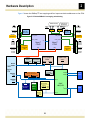
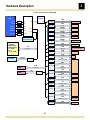
Functional block diagram
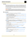
Figure 1 is a functional block diagram that indicates major hardware components of the CPM.
Figure 1. ATCA-46xx Functional Block Diagram
DDR3 VLP RDIMMs
DDR3 VLP RDIMMs
CPU0
CPU1
CH. A
Xeon®
E5-2400
Family CPU
PCIe Gen 3
Xeon®
E5-2400
Family CPU
QPI
Mini
Display
Port
CH. B
CH. A
PCIe Gen 3
DMI2
x16 (Gen 3)
MXM 3.0
Digital
Video
DDR3
CH. B
CH. C
DDR3
CH. C
Front
Panel
x16 PCIe to RTM
Type A Module
x4 (Gen 2)
x16 (Gen 2)
Intel I350
Optional Video MXM Module
1.8"
SSD
M
X
M
Quad GbE
1000Base-T
1.8"
SSD
SMGII/SerDes to RTM
DMI2
SATA
(6G)
Optional Dual SSD MXM Module
Dual
RJ45
1000Base-T to
Base Interface
Optional Modules
eUSB
eUSB
Flash
Flash
x8 (Gen 3)
C600 Series
Platform
Controller (SASG)
Hub (PCH)
USB 2.0
SPI
Mellanox
CX3 – Dual 40G
40G-KR4,10G-KR,
10G-KX4,1000Base-KX to
Fabric Interface
3G SAS to RTM
LPC
Dual
USB
USB 2.0 to RTM
COM1
RJ45
Reset
SPI
Reset
Button
BIOS
Flash
ME Flash
CPU
Complex
COM2
FPGA
RTM-Link
Port 80
Debug
Header
BIOS
Flash
SOL
IPMC
Debug
IPMC
16
Serial to RTM
TPM
CPM
ATCA-46xx
2
Hardware Description
ATCA-46xx front panel components
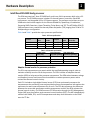
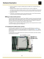
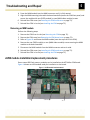
The following sections use text, figures, and lists to identify the physical features of the CPM. Figure 2 shows the CPM front panel and calls out the major features.
Figure 2. Front Panel Components
Thumbscrew
Ejector Latch
Video (MiniDP)
Connector
HDD LED
Serial (COM)
Port
OOS LED
PWR LED
Ethernet Ports A,B
(1000Base-T)
APP LED
USB Ports 0 & 1
Reset Button
Base/Fabric Channel
Status LEDs
H/S LED
Ejector Latch
Thumbscrew
17
2
Hardware Description
Front panel connectors
There are connectors for four separate interfaces on the front panel. Plugging into the connectors is straightforward, but the underlying interfaces need some explanation.
The serial (COM) RJ45 connector is an RS232 serial interface with the pinout listed in Table 39 on page 108. The USB0 and USB1 connectors support USB 2.0 transactions. A USB cable connected to a single device up to 5 meters away can be used with the front panel USB connectors. Transfers at up to 480 Mbps and continuous load currents up to 500 mA are supported with these USB ports. Refer to Table 40 on page 108 for the USB connector pinout.
The miniDisplayPort connector can be connected to a digital monitor if the MXM port has a video module installed. Refer to the video module documentation for operation details for this option. Refer to Table 42 on page 109 for the connector figure and pinout listing of the miniDisplayPort connector. During normal operation there is no need to attach a monitor to this connector. The two front panel Ethernet connectors provide interfaces to GbE ports with a peak available bandwidth of 100Mbps or 1Gbps. Figure 3 shows one of the front panel Ethernet connectors and calls out the Port Status and Link Status LEDs that are part of the connector.
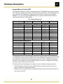
Figure 3. Front Panel Ethernet Connectors
Link Status LED
Port Status LED
Table 1 lists the meanings assigned to the light color/activity of each LED on the Ethernet connector. Table 1. Front Panel Ethernet Connector LEDs
LED Designation
Port Status LED
Link Status LED
Indication
████ Steady Green
████ Steady Amber
No light
████ Steady Green
████ Blinking Green
████ Steady Amber
████ Blinking Amber
██
LED off
18
Meaning
Port enabled
Port in standby mode
Port disabled
Linked at 1 Gbps peak bandwidth
Activity at 1 Gbps peak bandwidth
Linked at 10/100 Mbps peak bandwidth
Activity at 10/100 Mbps peak bandwidth
No link
2
Hardware Description
Front panel LEDs
The front panel LEDs can be separated into two major groups; the edge LEDs along the left (bottom) edge of the front panel and the Base/Fabric channel status LEDs.
Table 2 describes the status and activity LEDs along the left (bottom) edge of the front panel. Table 2. Front Panel Edge Activity/Status LEDs
LED Designation
HDD (Hard Disk
Drive) LED
████
████
OOS
████
(Out-of-Service) ████
████
LED
PWR
████
(Health)
████
LED
████
APP
████
(Customer-defined ████
application) LED ████
Indication
Short Green blink
LED off
Steady Amber LED
Steady Red LED
LED off
Meaning
HDD being accessed
No HDD activity, or not installed
LED color and On/Off state controlled by the
IPMC and user-defined application.
Steady Green LED
Steady Amber LED
LED off
Steady Green LED
Steady Amber LED
LED off
Power ON, health good
Power ON, health not good
Power OFF
Controlled by the IPMC, with functionality
defined by the system implementera
████ Short Blue blink
H/S
(Hot Swap Status)
LEDb
████ Steady Blue LED
████| Long Blue blink
████
LED off
a
b
Normal operation
M5, FRU deactivation request or
M6, FRU deactivation in process
M1, FRU inactive; ready for hot swap
M2, FRU activation request
M0, FRU not installed, or
M3, FRU activation in process, or
M4, FRU active
The user application can control LED color and illumination using the Set FRU LED State IPMI
command. LED illumination can be turned on or off, the LED can be configured to blink, or the
lamp test function can be enabled. To use the command, specify the FRU ID, LED ID (which is
“1” for the OOS LED), LED function, LED on duration, and illumination color. Command usage is
described in the PICMG specification, FRU LED Control commands, section 3.2.5.6.
LED state and blink frequency controlled by the IPMC.
The IPMC uses GPIO pins to control the hot swap and power LEDs. The IPMC supplies default states for the LEDs and responds to sensor readings, GPIO inputs, and IPMI commands from other entities to change LED states.
19
2
Hardware Description
Table 3 lists the meanings assigned to the light color/activity of each Base/Fabric LED. Table 3. Base/Fabric Channel LEDs
Channel
Base Channel 1
or
Base Channel 2
Fabric Channel 1
or
Fabric Channel 2
Indication
████ Steady Green
████ Blinking Green
████ Steady Amber
████ Blinking Amber
██ LEDs off
████ Steady Green
████ Blinking Green
████ Steady Amber
████ Blinking Amber
██ LEDs off
Meaning
Linked at 1 Gbps peak bandwidth
Activity at 1 Gbps peak bandwidth
Linked at 10/100 Mbps peak bandwidth
Activity at 10/100 Mbps peak bandwidth
Channel not configured or not in use
Linked at 10/40 Gbps peak bandwidth
Activity at 10/40 Gbps peak bandwidth
Linked at 1/10 Gbps peak bandwidth
Activity at 1/10 Gbps peak bandwidth
Channel not configured or not in use
Note: The Fabric channel LEDs can be either green or amber when linked or indicating activity at 10 Gbps. This is because in one configuration 10 Gbps is the low range output from the controller while in another configuration it is the high range output. The LED indicates the low/high range output, not the actual link speed.
Reset and hot swap switches
The CPM front panel Reset button (switch) is recessed and can normally be pressed only with a thin, pointed object such as a pencil or stylus. A callout in Figure 2 points out the Reset button on the CPM front panel. The Reset button performs a platform reset of the CPM. A platform reset returns all registers and devices (except the IPMC) to their default state. The ejector latches and thumbscrews are considered hot swap hardware components. Both thumbscrews must be unscrewed in order to remove the CPM from its slot. The bottom lock and ejector switch must be disengaged in order to signal to the IPMC that a CPM hot swap is desired. The IPMC then controls the hot swap LED and monitors the process. Headers and jumpers
Refer to Appendix C, Onboard switches, headers, and connectors, on page 114 for tables detailing the header and jumper callouts.
20
2
Hardware Description
Rear panel connectors
The CPM supports E‐Key control by describing its backplane interfaces to the Shelf Manager.
Alignment keys
The CPM implements the K1 and K2 alignment blocks at the top of Zone 2 and Zone 3, as required by the PICMG 3.0 specification. The Zone 2 alignment block (K1) is assigned a keying value of 11. The Zone 3 alignment block (K2) is set to allow insertion of ATCA‐46xx‐compatible RTMs.
Zone 1 connector
The connectors in Zone 1 provide redundant ‐48VDC power and Shelf Management signals to the boards. The power control interface to the IPMC is through the backplane connector P10 (Zone 1 power distribution connector). Refer to Table 44 on page 111 for details.
Zone 2 connectors
The connectors in Zone 2 provide the connections to the Base Interface and Fabric Interface. All Fabric connections use point‐to‐point 100 Ω differential signals. Zone 2 is called "Fabric Agnostic" which means that any Fabric that can use 100 Ω differential signals can be used with an AdvancedTCA backplane.
Backplane connector J20 provides Zone 2 connections to the synchronization clocks and to the AMC update channels. For detailed information about the connector itself, refer to Table 45 on page 112.
Backplane connector J23 is the ATCA data transport connector, which provides Zone 2 connections for two 10/100/1000BASE‐T Ethernet Base channels and two 10GBASE‐BX4 Ethernet Fabric channels. For more information about the J23 backplane connector, refer to Table 46 on page 112.
21
2
Hardware Description
Zone 3 connectors
The CPM includes the standard Zone 3 backplane interface to provide connectivity to an optional RTM, such as the ATCA‐5400. This interface consists of two connectors: J30 for common and maintenance signals, and J31 for SerDes (serialization/deserialization connectivity). For details, refer to Table 47 on page 113 and Table 48 on page 113.
The electrical connections between the CPM and the associated RTM include:
• Switched +3.3V and +12V power, under the control of the IPMC
• One configurable PCI Express port
• One USB 2.0 Port
•
•
•
•
•
IPMB‐L I2C Bus for an MMC on an RTM
IPMC Hot Swap control signals
RTM‐Link interface to CPU Complex FPGA
Serial Port (3.3V signals)
Two 1Gbps SerDes/SGMII ports
•
•
•
•
Two SFP I2C ports for SGMII support
System reset signal
JTAG interface
PCH SMBus connection
22
2
Hardware Description
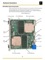
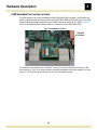
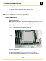
ATCA-46xx board components
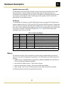
During normal operation the CPM board components are covered by the CPM cooling shroud sheet metal (side panel). This sheet metal must be removed to see and gain access to removable board components, jumper blocks, or headers. Figure 4 shows the CPM board layout and calls out the major components and other features.
Figure 4. CPM Board Layout
Customer header
CPU1 RDIMM bank
CPU1 (under heatsink)
J30
MXM
connector
J31
J20
Front
panel
eUSB
connectors
PCH
Mellanox
CX3
RTC
SuperCAP
J23
P10
CPU0 (under heatsink)
CPU0 RDIMM bank
23
2
Hardware Description
Heatsinks
The CPU heatsinks are called out in Figure 4. In addition to the CPU heatsinks, the Intel C600 series PCH, and the Mellanox CX3 10/40 GbE controller each have individual heatsinks. The CPM incorporates a large heatsink covering each processor plus the additional heatsinks for other onboard high power devices to support a maximum CPM subsystem power dissipation of up to 50W. In addition, the installed RDIMM modules might also have their own heatsinks or other thermal solution. WARNING! All heatsinks on the CPM are critical for proper board operation. Make sure all heatsinks have adequate mechanical and thermal contact with their associated components and ensure the sheet metal cooling shroud is secured in place before installing the CPM in its slot.
Major components
Figure 4 calls out the following major components on the CPM board:
• Two Intel Xeon E5‐2400 family processors. Refer to Intel® Xeon® E5‐2400 family processor on page 25 for detailed information.
• Sockets for twelve registered DIMM memory modules (six for each CPU). Refer to DIMM memory on page 28 for detailed information.
• The C600 series PCH component. Refer to Intel C600 series Platform Controller Hub (PCH) on page 29 for detailed information.
• Mellanox CX3 dual 10/40 GbE Ethernet controller. Refer to Mellanox dual 40GbE controller on page 36.
In addition to the components called out in Figure 4, the following components (indicated in the Figure 1 block diagram) control significant portions of CPM operation:
• The H8S/2400 series IPMI controller. Refer to IPMI controller on page 33 for more detailed information.
• CPU Complex FPGA (CPU Complex (CC) FPGA on page 34) and IPMC FPGA (IPMI controller on page 33) modules.
• The Intel I350 quad GbE Ethernet controller. Refer to Intel I350 quad GbE Ethernet controller on page 36.
• Clock synthesizer subsystem. Refer to Clock synthesizer subsystem on page 37.
• Reset subsystems. Refer to Reset subsystems on page 37.
• Trusted Platform Module (TPM). Refer to Trusted Platform Module (TPM) on page 42.
• Optional MXM Type A video module. Refer to MXM type A video module (optional) on page 43.
• Optional 1.8” Solid State Drive (SSD) module(s). Refer to 1.8” Solid State Drive (SSD) module (optional) on page 43.
• Optional eUSB Embedded Flash module(s). Refer to eUSB Embedded Flash module (optional) on page 44.
24
2
Hardware Description
Intel® Xeon® E5-2400 family processor
The CPM uses two Intel® Xeon E5‐2400 family multi‐core, 64‐bit processors built using a 32‐
nm process. The E5‐2400 processor includes a 3‐channel memory controller, QuickPath interconnect, and integrated I/O for PCI Express support. The processor cores share an up to 20MB cache and include support for the Execute Disable Bit, Speed‐Step, Virtualization, Streaming SIMD Extensions, Hyper‐Threading, Turbo Boost, and TXT. The ATCA‐46xx CPM E5‐
2400 processors have a maximum thermal power dissipation (TPD) ranging from 50 W to 70 W depending on configuration.
Table 4 and Table 5 provide the major processor specifications. Table 4. CPU bus specifications
Processor
LV70W-8C
LV60W-6C
LV50W-4C
Number of
Cores
8
6
4
Number of
Threads
16
12
8
QPI Speed
8.0 GT/s
7.2 GT/s
6.4 GT/s
DDR3
Last Level
Speed
Cache Size
1333 MHz
20 MB
1333 MHz
15 MB
1333 MHz
10 MB
Table 5. CPU thermal specifications
Thermal Design
Case temperature
Case temperature
Power (TDP)
(long term operating) (short term* operating)
LV70W-8C
70W
78.1°C
93.2°C
LV60W-6C
60W
73.4°C
88.4°C
LV50W-4C
50W
77.4°C
92.4°C
* Note: Short term operating = 360 hours per year (or less)
Processor
Adaptive thermal monitor for processor protection
The CPU case temperature must remain within the specified operating range in order to maintain reliability over the life of the processor. The CPU includes an adaptive thermal monitor (ATM) to help control the processor temperature. The ATM selects between voltage and frequency control and internal clock modulation to reduce processor power and to activate the thermal control circuitry. Each CPU includes a single digital thermal sensor (DTS) that continuously measures the temperature at the processing cores and provides processor die temperature information that represents the worst case temperature for all cores. The DTS data represents the difference between the current die temperature and the temperature at which the ATM activates the thermal control circuitry. The IPMC accesses DTS information through the PCH Management Engine (ME) over the platform environmental control interface (PECI). The ME independently monitors the DIMM, CPU, and PCH temperatures and relays that information to the IPMC over the I2C Bus.
25
2
Hardware Description
Integrated Memory Controller (IMC)
The integrated memory controller incorporated into each E5‐2400 family processor supports three channels of DDR3, each channel with 64 data bits and 8 ECC bits. The CPM supports up to six registered VLP RDIMMs per socket (two per channel) for a system total of twelve RDIMMs. Table 6 lists the supported RDIMM memory types of the CPM and provides the required specifications for the modules.
Table 6. Supported Memory Types
Mem Rank x Data Width
Operating Voltage
Registered DIMM (RDIMM) with ECC
Single rank x 8 bits
1.5 v
Single rank x 8 bits
LV - 1.35 v
Dual rank x 8 bits
1.5 v
Dual rank x 8 bits
LV - 1.35 v
Quad rank x 8 bits
1.5 v or LV - 1.35 v
Single rank x 4 bits
1.5 v
Single rank x 4 bits
LV - 1.35 v
Dual rank x 4 bits
1.5 v
Dual rank x 4 bits
LV - 1.35 v
Quad rank x 4 bits
1.5 v or 1.35 v
Load Reduced DIMM (LRDIMM) with ECC
Quad rank x 8 bits
LV - 1.35 v
Quad rank x 8 bits
LV - 1.35 v
Quad rank x 8 bits
1.5 v
Quad rank x 8 bits
1.5 v
Quad rank x 4 bits
LV - 1.35 v
Quad rank x 4 bits
LV - 1.35 v
Quad rank x 4 bits
1.5 v
Quad rank x 4 bits
1.5 v
DIMMs per Channel Memory per DIMM Speed (MT/s)
One or Two
Two
One or Two
Two
One or Two
One or Two
Two
One or Two
Two
One or Two
1, 2, 4 GB
1, 2, 4 GB
2, 4, 8 GB
2, 4, 8 GB
4, 8, 16 GB
2, 4, 8 GB
2, 4, 8 GB
4, 8, 16 GB
4, 8, 16 GB
8, 16, 32 GB
1066/1333 MHz
1066 MHz
1066/1333 MHz
1066 MHz
800 MHz
1066/1333 MHz
1066 MHz
1066/1333 MHz
1066 MHz
800 MHz
One
Two
One
Two
One
Two
One
Two
8, 16 GB
8, 16 GB
8, 16 GB
8, 16 GB
16, 32 GB
16, 32 GB
16, 32 GB
16, 32 GB
1066 MHz
800 MHz
1066/1333 MHz
1066 MHz
1066 MHz
800 MHz
1066/1333 MHz
1066 MHz
The integrated memory controller supports up to four memory modes, but the CPM uses only the Independent mode (highest performance) in which RDIMMs can be placed in any of the three channels and there are no matching requirements for rank or DIMM speed between channels. A burst‐length of 8 is used, and the memory controller is configured to interleave the memory map across the three channels.
The IMC provides the following tools to support memory reliability and peak operation:
• SDDC (Single Device Data Correction) algorithm that can detect and correct any error within a x4 device in independent mode.
• DRAM thermal management either by DRAM throttling or by performing a 2X refresh to the memory channels.
26
2
Hardware Description
QuickPath Interconnect (QPI)
The Quickpath interconnect (QPI) provides a point‐to‐point contact between the E5‐2400 family processors. The QPI interface is 20 lanes wide under full operation and is the communication path between the CPUs. Data of any width is converted to packets and then sent serially over the QPI link. The E5‐2400 supports QPI speeds of 6.4 GT/s to 8.0 GT/s depending on the installed processor.
PCI Express
The integrated I/O module on each E5‐2400 family processor provides 24 PCI Express lanes that are capable of Gen1 (2.5 GT/s), Gen2 (5.0 GT/s) and Gen3 (8.0 GT/s) speeds. The lanes are split into a x16 and a x8 port and both can be divided into x8, x4, x2 and x1 ports. CPU0 also uses a Gen 2 Direct Media Interface (DMI) port that can be configured for either DMI for PCH connectivity or used as a Gen2 x4 PCI Express port. Table 7 shows the PCI Express port mapping for each CPU on the CPM.
Table 7. PCI Express Port Mapping
CPU
Port#
Port Width
PCI Express Peripheral
CPU0
PE1(A,B)
x8
Fabric Ethernet Controller
CPU0
PE3(A,B,C,D)
x16
MXM
CPU0
DMI2
x4
Patsburg DMI2 interface
CPU1
PE1A
x4
I350 Base/Front/RTM GbE controller
CPU1
PE1B
x4
Update Channel
CPU1
PE3A*
x4
RTM PCI Express port 0
CPU1
PE3B*
x4
RTM PCI Express port 1
CPU1
PE3CD*
x8
RTM PCI Express port 2
* Note: As with the CPU0 mapping, CPU1 Ports PE3(A,B,C,D) can alternately be combined to form a single x16
interface.
Memory
The CPM uses memory such as the built‐in processor cache, standard RAM, and memory external to any of the existing board components. The CPM supports the following types of memory:
• DIMM memory ‐ Registered Dual In‐line Memory Modules (RDIMM) and Load Reduced Dual In‐line Memory Modules (LRDIMM)
• Non‐volatile on‐board memory ‐ Flash memory devices.
• Optional on‐board user memory ‐ One or two eUSB Flash modules.
• Mass storage ‐ One or two 1.8” SSD modules and any RTM hard disk drives (HDDs).
The following sections provide more detailed information.
27
2
Hardware Description
DIMM memory
This memory is directly addressed by the internal memory controller of each E5‐2400 family processor. Due to the board height limitations posed by the ATCA PICMG specifications, only Very Low Profile (VLP) Dual In‐line Memory Module (DIMM) modules are supported with the CPM. The Registered DIMM (RDIMM) memory used on the CPM is buffered by integral registers and has built‐in Error Correcting Code (ECC) bits to support more reliable operation. As part of the installation process for the CPM, up to twelve RDIMM modules (six per processor, from 1GB to 16GB each) must be installed in the CPM DIMM sockets. Refer to Adding or replacing memory modules on page 73 for the installation procedures.
Non-volatile on-board memory
The CPM non‐volatile memory is mainly comprised of the following elements:
• The two 64‐Mbit Flash BIOS boot and redundant boot devices.
• The 64‐Mbit ME Flash holding the redundant ME firmware.
• IPMI non‐volatile memory stores IPMC private data and board FRU information. • The optional eUSB NAND Flash memory modules are available for user applications and data.
External memory options
The following external memory options are available for the CPM:
• Embedded NAND Flash modules. One or two eUSB NAND Flash modules.
• 1.8” micro Solid State Disk (SSD) drives. One or two μSATA SSD modules. This option requires the Radisys Dual SSD (DSSD) MXM module for mounting the SSD modules.
• RTM‐installed hard disk drives (HDDs). Number and capacity dependent on the RTM.
28
2
Hardware Description
Intel C600 series Platform Controller Hub (PCH)
The Intel C600 series Platform Controller Hub (PCH) provides a connection point between various I/O components and the E5‐2400 family Xeon processors used on the CPM. The PCH provides controllers for the following interfaces:
• Direct Media Interface
• Universal Serial Bus
• Serial Addressed SCSI (SAS)
• Serial ATA (SATA)
• Low Pin Count (LPC) Bridge
• Serial Peripheral Interface (SPI)
• Real‐Time Clock (RTC)
•
•
SMBus/I2C bus
Management Engine
Refer to Figure 1 to identify the interfaces and the devices controlled by the PCH. The following sections provide details on the interfaces and associated controllers of the PCH.
Direct Media Interface (DMI)
There is a Direct Media Interface Gen 2 (DMI2) 4x link between the PCH and CPU0 that is capable of PCI Express Gen2 transfer rates (5 Gb/s) for a theoretical bandwidth of 20 Gb/s in each direction. This link is used to pass I/O from the SATA, SAS, LPC, and USB peripherals to the CPU or memory, along with interrupts and SMI, SCI, and SERR notification.
Universal Serial Bus (USB)
The PCH contains two Enhanced Controller Host Interface (EHCI) controllers, providing up to fourteen USB 2.0 ports. Each port allows data transfers up to 480 Mb/s. On the CPM, the following USB ports are provided:
• Port 0 – Front Panel USB0
• Port 1 – Front Panel USB1
• Port 2 – eUSB Flash 0 (Bottom Flash Module)
• Port 3 – eUSB Flash 0 (Top Flash Module)
• Port 4 – RTM Rear Panel USB
• Port 5 – H8S/2472 USB Port
The PCH provides two USB debug ports. These ports support debugger software interaction with devices on a USB 2.0 port. The USB debug port is on the front panel, USB port 1.
Serial Addressed SCSI (SAS)
The PCH provides two SAS 3G ports that are routed to the RTM for future use. The RTM must buffer the SAS signals for signal integrity.
29
2
Hardware Description
Serial ATA (SATA)
The PCH includes two SATA host controllers that provide six SATA 3.0 ports. These ports support data transfer rates of 3.0 Gb/s. The CPM connects two SATA ports (0 and 1) for use with the optional 1.8 inch micro SATA SSD drives that can be installed in an optional Radisys DSSD MXM module.
Low Pin Count (LPC) Bridge
The Low Pin Count (LPC) bridge of the PCH provides read/write cycles for memory, I/O, DMA, and Buss Master devices. The PCH implements the LPC Interface Specification, revision 1.1. The devices contacted over this LPC bridge include the IPMI controller, the port 80 debug header, the CPU complex FPGA, and the TPM. Serial Peripheral Interface (SPI)
The PCH provides a 4‐pin SPI interface for connecting to and controlling the BIOS and ME Flash devices on the CPM. There are two 64MB Flash devices connected to the SPI bus that store BIOS boot and redundant BIOS boot code. Another 64MB Flash device contains redundant ME firmware images. On CPM power‐up, the primary BIOS Flash device is selected and used. If a corrupt BIOS is detected during operation, the IPMC forces a reboot and loads the redundant BIOS Flash image.
The SPI bus allows the PCH to read and also program the primary and redundant BIOS boot Flash devices as well as the ME firmware Flash device. Controlling software as well as on‐
board jumpers provide Flash device write protection.
Real-Time Clock (RTC)
The PCH implements the CPM real‐time clock (RTC). Rather than a battery backup, the CPM uses a 1F “SuperCapacitor” to store and supply the minimum 2V backup RTC power. As a consequence, RTC power is available for at least two hours after a system power loss.
The RTC is derived from a 32.768KHz crystal with the following specifications:
• Frequency tolerance @ 25°C: ± 20 ppm
•
•
•
Frequency stability: maximum of ‐0.04 ppm/( °C)2
Aging F/f (first year @ 25 °C): ± 3 ppm
± 20 ppm from 0‐55 °C and aging 1 ppm/year
The RTC’s capacitor‐backed RAM supports two 8‐byte ranges that can be locked during power loss (i.e., no read/write) when the locking bits are set. Once a range is locked, the range can be unlocked only a by a powergood reset.
30
2
Hardware Description
SMBus/I2C bus
The PCH provides an SMBus host controller (SMBus 2.0 compliant) as well as an SMBus secondary interface. The host controller provides a mechanism for the CPU to initiate communications with SMBus peripherals (master/slave interface). The PCH also can operate in a mode that supports communication with I2C compatible devices.
The slave interface allows an external master to read from or write to the PCH. Write cycles can be used to cause certain events or pass messages and the read cycles can be used to determine the state of various status bits. The PCH internal Host Controller cannot access the internal slave Interface. Table 8 lists the SMBus and I2C device addresses on the CPM. Table 8. SMBus and I2C bus device addresses
Device
IPMC FPGA
CPU Complex FPGA
M41T82RM6E RTC IC
PCH SMLink0
PCH SMLink1
ADM1066
ADM1066
T0808P
MXM (possible address per spec)
MXM (possible address per spec)
MXM (possible address per spec)
MXM (possible address per spec)
I350(Base) LAN0
I350(Base) LAN1
I350(Front/RTM) LAN2
I350(Front/RTM) LAN3
CX3 (Fabric)
RTM MMC
CK420BQ
DB1900Z
CPU Complex FPGA
Bus Number
IPMC I2C bus 2
IPMC I2C bus 2
IPMC I2C bus 2
IPMC I2C bus 5
IPMC I2C bus 3
IPMC I2C bus 3
IPMC I2C bus 3
IPMC I2C bus 3
IPMC I2C bus 3
IPMC I2C bus 3
IPMC I2C bus 3
IPMC I2C bus 3
IPMC I2C bus 4
IPMC I2C bus 4
IPMC I2C bus 4
IPMC I2C bus 4
IPMC I2C bus 4
IPMC I2C bus 5
PCH Master SMBus
PCH Master SMBus
PCH Master SMBus
31
Read Address
C1h
B1h
D1h
45h
4Dh
69h
6Bh
C3h
33h
57h
99h
9Fh
21h
23h
71h
73h
49h
GA[2:0] = GPU;
D3h
D9h
D1h
Write Address
C0h
B0h
D0h
44h
4Ch
68h
6Ah
C2h
32h
56h
98h
9Eh
20h
22h
70h
72h
48h
D2h
D8h
D0h
2
Hardware Description
Figure 5 shows the SMBus/I2C bus mapping and lists important device addresses on the CPM.
Figure 5. ATCA-46xx SMBus/I2C bus mapping and addressing
RTM PCIe Hotswap
SPD
A0: 0xA8
A1: 0xAA
Temp Sensor
A0: 0x38
A1: 0x3A
Address
0x40
Temp Sensor
B0: 0x30
B1: 0x32
C0: 0x38
C1: 0x3A
QPI
Xeon®
CPU1
PECI
PECI
System
Clocks
PCIe
Clock ƵīĞƌ
Address: 0xD2
Address: 0xD8
Address
0x4C
Address
0xD0
Address
0x44
Address
0xC0
Address
0xB0
I2C Bus 2
I2C Bus 0
Address: 0xD0
I2C Bus 1
Address: 0x68
SMLink0
Temp Sensor
B0: 0x30
B1: 0x32
C0: 0x38
C1: 0x3A
IPMC FPGA
Serial RTC
Circutry
Supply Sequencing
Monitors with ADC/DAC
Address: 0x6A
RDIMM
Channels
B/C
CPU Complex
FPGA
Temp Sensor
A0: 0x38
A1: 0x3A
SPD
B0: 0xA0
B1: 0xA2
C0: 0xA8
C1: 0xAA
QPI
Xeon®
CPU0
SPD
A0: 0xA8
A1: 0xAA
RDIMM
Channel A
DDR23_SMBus
DDR23_SMBus
Master
SMBus
SMLink1
Prog.
Ref. POT
DDR1_SMBus
DDR1_SMBus
RDIMM
Channels
B/C
Address
0x42
Address: 0x7C
PECI
C600
Series
PCH
16-bit
I/O port
Address: 0x7C
RDIMM
Channel A
SPD
B0: 0xA0
B1: 0xA2
C0: 0xA8
C1: 0xAA
16-bit
I/O port
Prog.
Ref. POT
Update Channel
PCIe Hotswap
Back
plane
I2C Bus 3
Address
0xC2
PCIe Signal
ZĞƟmer
PCIe ZĞƟmer
Addresses
0x9E, 0x98,
0x56, 0x32
MXM
Port
I350 GbE
Controller
Base/Front/RTM Ethernet
Addresses
LAN0 – 0x20 LAN2 – 0x70
LAN1 – 0x22 LAN3 – 0x72
Mellanox
CX2/CX3
IPMC
H8S/2472
I2C Bus 5
I2C Bus 4
Fabric Ethernet
Address: 0x48
32
RTM
2
Hardware Description
Management Engine (ME)
The CPM Management Engine (ME) uses Node Manager 2.0 firmware to perform power monitoring & alert, power limiting policies, thermal monitoring & alert, and power reduction tasks during boot. As described in Serial Peripheral Interface (SPI) on page 30 a redundant firmware image is stored in the ME Flash in case the ME firmware needs to be recovered.
As shown in Figure 5, the IPMC I2C Bus 5 is connected to SMLink0 on the PCH to allow the IPMC access to CPU and DIMM temperature information, PCH temperature information, CPU power information and other statistics. IPMI controller
The IPMI controller (the IPMC) supports an “intelligent” hardware management system, based on the Intelligent Platform Management Interface Specification. The hardware management system can manage the power, cooling, and interconnect needs of intelligent devices, monitor events, and log events to a central repository.
The IPMC is a Radisys‐designed reusable entity based on the Renesas H8S/2472 microcontroller and Lattice XP2 FPGA. The IPMC provides the following features:
• An external 16‐bit address/data bus with internal 32‐bit configuration
• Internal ROM (512KB of Flash ROM) and RAM (40KB)
• 2 MB external SPIBus‐based Flash ROM
• Control of front panel LEDs (H/S, OSS, PWR, and APP) • Monitoring of front panel Reset, and Hot Swap switching
• Control of three backplane interfaces (redundant IPMB‐A/B buses and an x8 hardware address bus)
•
•
•
•
•
•
•
•
Controller for six I2C buses (I2C Bus 0 ‐ I2C Bus 5)
Eight analog inputs
8‐bit parallel data bus
Six KCS LPC address/data plus KCS LPC reset and clock interfaces
Three serial ports (SCI‐1/3/F)
SPI bus controlled by SSC for additional Flash and FPGA support
Eight general purpose, eight retained state, and 90 FPGA general purpose GPIO ports
One Ethernet and one USB interface
Refer to Appendix B, IPMI Commands and Managed Sensors, on page 86 for more detailed information on the IPMI sensors, data, and commands.
33
2
Hardware Description
CPU Complex (CC) FPGA
The CC FPGA module performs a number of significant monitoring and interface functions on the CPM. Many of these functions are indicated in Figure 1 on page 16. The following sections provide more details on the CC FPGA functions.
Power management and monitoring
Most of the CPM payload power supplies are monitored by two ADM1066 power sequencers, but the CC FPGA controls the power sequencing for the CPM. On power‐up, it looks at the payload power enable from the IPMC to begin the power up sequence. When both power sequencers have indicated “powergood” and the external comparators indicate in‐tolerance, the CC FPGA asserts PWR_OK to the PCH. The CC FPGA de‐asserts PWR_OK and asserts fault signals when any monitored condition falls out‐of‐tolerance.
System Reset monitoring
The CC FPGA monitors the source of all Powergood, Platform, and MR‐Resets and provides a 16‐bit register for reset source monitoring. When the CC FPGA detects any monitored reset, it asserts an interrupt to the IPMC. The IPMC can read the reset source register and then clear the interrupt. Refer to Reset subsystems on page 37 for more information.
Dual UARTs, COM port, and SPI mux
Two 16550‐compatible UARTs are instantiated in the CC FPGA. COM1 and COM2 ports can operate up to a 115200 baud rate (default of 115,200 baud, 8‐bit, no parity, 1 stop bit). The CC FPGA is a bridge between the SPI flash programming header, the PCH and the redundant 64Mb flash devices.
The FPGA includes functionality to multiplex the internal UART connections between the front/RTM external ports and the Serial over LAN (SOL) and debug console ports from the IPMC. Refer to Serial‐Over‐LAN on page 65 for more information.
The CC FPGA is a bridge between the SPI flash programming header, the PCH and the redundant 64‐Mb flash devices. Refer to Serial Peripheral Interface (SPI) on page 30 for more information.
LPC/I2C interfaces
The CC FPGA uses an LPC interface to provide byte‐wide read/write access to the internal FPGA. I/O port 80h is used to transmit BIOS POST progress codes during boot. The CC FPGA decodes port 80 writes from the BIOS and stores the last four codes in I/O registers. The codes are shifted through the registers FIFO‐style, so that the oldest code is pushed out when a new code is stored.
The CC FPGA supports dual‐access to its internal I/O registers between the SMBus interface to the PCH and to IPMC I2C Bus 3. An arbiter prevents data loss or corruption.
34
2
Hardware Description
CC FPGA RTM-link
The RTM‐Link relays the state of various control and status signals from a compatible programmable device on an RTM. The following signals are sent to the RTM for Ethernet LED control:
• Front Ethernet port 0 status green
• Front Ethernet port 0 status yellow
• Front Ethernet port 1 status green
• Front Ethernet port 1 status yellow
The following signals are read in from the RTM:
• RTM USB over‐current (sent to the PCH)
• SFP0 RXLOS (Sent to I350 port 2)
• SFP0 TX_FAULT (Sent to I350 port 2)
• SFP0 MOD_DEF0 (Sent to I350 port 2)
• SFP1 RXLOS (Sent to I350 port 3)
• SFP1 TX_FAULT (Sent to I350 port 3)
• SFP1 MOD_DEF0 (Sent to I350 port 3)
Customer header configuration
All control signals configured on the customer and debug headers are routed to the CC FPGA. When any signal is in a non‐default (i.e. LOW) state, a general flag bit and a state bit are set to indicate this condition. The IPMC then reads the state of these register bits as part of a normal sensor scan. The signals associated with the Customer header (P2) are:
•
•
•
•
•
•
•
CLEAR_NVRAM* SPI_WP* BIOS_RCVR_BOOT* EUSB_WP* UNR_DIS* ME Firmware Recovery FORCE BACKUP BIOS BOOT
35
2
Hardware Description
IPMI FPGA
The Intelligent Platform Management Interface (IPMI) Field Programmable Gate Array (FPGA) provides the specialized interfaces and glue logic needed between the H8 IPMC and rest of the CPM. The IPMC and the IPMI FPGA provide watchdog timers to help prevent the CPM from entering an unrecoverable state.
Watchdog timer 2 on the IPMI FPGA is enabled by default and starts running as soon as +3_3V_SUS power is present and the FPGA has loaded its internal flash image into its internal SRAM. If a firmware or hardware problem on the IPMC causes it to stop strobing the watchdog timer in the IPMC FPGA, it isolates the IPMC from the IPMB‐A, IPMB‐B, and IPMB‐L buses so that they remain functional for the remaining blades in the chassis. Watchdog timer 2 then resets the IPMC.
The interfaces supported by the IPMC FPGA include the SPI bus, the I2C bus 2, and the JTAG chain. The IPMI FPGA is programmed via the same JTAG chain as is used for the CC FPGA and any programmable devices on the RTM.
Intel I350 quad GbE Ethernet controller
The I350 has four independent network interfaces that support SerDes/SGMII or MDI (copper) protocols. The I350 has a x4 PCI Express Gen2 host interface that operates at 5.0 GT/s and is capable of negotiating to x2 and x1 link widths. The I350 provides virtualization support including PCI‐SIG Single‐Root I/O Virtualization, VMDq2 support for up to eight virtual machines and eight TX and RX queues per port. The I350 has NC‐SI and SMBus interfaces that support pass‐through traffic for Serial‐Over‐LAN (SOL) support from the IPMC. The CPM has both interfaces connected to allow flexibility for the IPMI code development. Initial configuration information for the controller (including management setup and SMBus addresses) is provided via a 256Kb SPI EEPROM, which is read upon power‐up.
Mellanox dual 40GbE controller
The CPM provides two 40GbE ports using a Mellanox ConnectX‐3 (CX3) controller. The CX3 is connected to a x8 Gen 3 PCI Express port that provides a peak data bandwidth of 64Gb/s in each direction. The CX3 has two integrated Gigabit Ethernet MAC/PHY ports that support the following standard Ethernet interfaces for CPM:
• 40GBASE‐KX4 (IEEE 802.3ba)
• 10GBASE‐KX4 (IEEE 802.3ap)
• 1000BASE‐KX (IEEE 802.3ap)
The CX3 has a flash boot interface and the CPM uses a 32Mb flash device to store boot firmware and configuration options for the controller. The CX3 supports PCI‐SIG SR‐IOV, providing up to 128 virtual machines.
The CX3 controller is used to connect to Fabric Channels 1 and 2 on the Zone 2 connector. The TX pairs connect directly to the connector while the RX pairs have DC blocking caps between the controller and the connector.
36
2
Hardware Description
The CX3 has iSCSI and PXE boot support enabled in the SPI flash firmware. iSCSI and PXE cannot be enabled at the same time; the desired function must be selected in the BIOS setup menu.
Clock synthesizer subsystem
CPM uses two major components, a CK420BQ and a DB1900Z to generate the clock signals used by the CPUs, by the PCH, and by other peripheral components. The CK420BQ clock generator provides host, chipset, PCI and LPC peripheral clocks on the CPM. The device uses a 25.0000 MHz reference crystal and receives control input from the BIOS over the SMBus. The clock signals are supplied to the CPUs, the PCH, the TPM, the IPMC, and the CC FPGA.
The DB1900Z differential buffer distributes 100MHz clocks to the PCI Express and QPI devices. The clocks output by this device are based on a reference clock from the CK420BQ clock generator. In addition to the PCIe and QPI clocks, this device supplies reference clocks for the Mellanox CX2/CX3 and Intel I350 GbE controllers, the RTM PCIe interfaces, and the MXM connector.
In addition to the above reference clocks, the following oscillators or crystals are provided on the CPM:
• A 40.000 MHz 100ppm oscillator is provided for the CC FPGA.
• The CC FPGA provides a 6.6 MHz clock for the RTM‐L interface to the RTM.
• A 32.768 kHz crystal is provided for the PCH RTC.
• A 32.768 kHz crystal is provided for the IPMC RTC.
• A 32.768 kHz crystal is provided for the Trusted Platform Module.
• A 25.000 MHz 30ppm crystal is provided for the CK420BQ
• A 25.000 MHz 30ppm crystal is provided for the I350 quad GbE controller
• A 32.000 MHz 50ppm oscillator is provided for the IPMC FPGA
• A 156.25 MHz 50ppm oscillator is provided for the Mellanox CX3 40G Ethernet controller
Reset subsystems
CPM9 supports three types of reset: platform reset, powergood reset, and memory‐retained (MR) reset.
Platform reset
A platform reset (the PLTRST* signal) is defined as a total system board reset (except for IPMI circuitry). All devices and registers are reset to their default state. After a platform reset all data in DRAM may be invalid due to the CPU memory controller discontinuing refresh cycles. Memory is then cleared during the system BIOS initialization.
37
2
Hardware Description
The platform reset signal originates in the PCH. The potential sources or triggers of a platform reset include:
• The front panel Reset button
• A reset assertion generated over the board debug header during a troubleshooting session
• An IPMC reset command generated due to one of the following events:
• Watchdog timer expiration
• An MR reset is asserted (by either the PCH or the IPMC) but they are disabled in the CC FPGA. In this case it reverts to a platform reset.
Powergood reset
A powergood reset is similar to a platform reset, except that all sticky bits in the CPU and PCH are cleared. For the CPUs, a powergood reset will result in reset of all the states in the processor, including the sticky state that is preserved on the other resets.
There is a “Powergood Reset” enable bit in the reset control register of the CC FPGA. When this bit is set, all platform resets are converted to Powergood resets. In other words, when this bit is set, any of the sources or triggers that would otherwise cause a platform reset will instead cause a powergood reset.
There is a second enable bit in the CC FPGA, that when set also asserts Powergood Reset, normally from the BIOS. Memory-Retained (MR) reset
A memory‐retained reset will preserve the contents of main memory while the rest of the system experiences a Platform Reset. The intended usage for MR‐Reset is to provide an operating system kernel crash dump location, so that debug information can be recovered after an OS crash.
When an MR‐Reset is initiated from one of the sources, the result is an INIT* virtual legacy wire (VLW) message sent to the CPUs from the PCH. INIT* triggers the BIOS to run from the reset vector in the shadowed F000 segment, where the MR‐Reset code is stored. If a valid signature exists in this location (i.e. MR‐Reset has been enabled in the BIOS setup menu) then the MR‐Reset code is executed. The INIT* sequence has PCH drive the INIT* VLW message to the CPUs and the INIT_3_3V* signal to the CC FPGA.
The MR‐Reset BIOS code puts the system into the S3 sleep state. In S3, the internal memory controller for each CPU places all the DIMMs on the associated memory channels into self‐
refresh and the PCH asserts the PLTRST* signal. The RTC alarm in the PCH is used to wake the system up from S3, causing the PCH to de‐assert PLTRST*. The BIOS uses the S3 resume path and skips over memory initialization. This method allows the contents of the DIMMs to remain valid while the system is reset. 38
2
Hardware Description
Table 9 lists the potential sources/triggers for the MR‐Reset. Though similar, these sources are slightly different from those for a platform or powergood reset. Table 9. Memory-Retained Reset Sources
Platform Reset Source
Front panel Reset button
(FP_RESET*)
RTM reset push button
Description
Pushing the button triggers an RCIN* assertion to the PCH, thus beginning the INIT*
sequence.
The RTM MMC sends OEM command to IPMC. Upon receiving the “warm reset” OEM
command, the IPMC asserts IPMC_MR_RESET*
IPMC warm reset command One of the following two triggers are detected by the IPMC:
(IPMC_COLD_RESET*)
• Watchdog timer 1 is configured for warm reset and times out.
• The IPMC warm reset command is recognized.
Once one of the above triggers are detected, the IPMC_MR_RESET* signal is asserted
to the CC FPGA which triggers an RCIN* assertion to the PCH, thus beginning the INIT*
sequence.
Watchdog timers
The CPM uses a number of watchdog timers to prevent the board from entering an unrecoverable state. The IPMC and the IPMC FPGA provide the following watchdog timers:
• Corrupt Flash detection watchdog
• OS watchdog timer (Watchdog 1)
• IPMC watchdog timer (Watchdog 2)
The following sections describe the operations performed by each watchdog.
Corrupt Flash detection watchdog
The Corrupt Flash Detection (CFD) Watchdog is a SW‐based watchdog that allows the CPM to recover when the primary SPI flash is either blank or the boot block is corrupted. The CFD watchdog timer is started any time that a reset is asserted to the payload processor (for example, platform reset, push button reset, and so on). Responsibility is then passed to the system BIOS to disable the timer. If the timer is not disabled before it expires, the IPMC firmware: 1. Disables payload power, 2. Selects the secondary boot flash using the Boot Flash Select Control, and then 3. Re‐enables payload power to boot from the secondary SPI flash.
OS watchdog timer (Watchdog 1)
This programmable watchdog is used with the BIOS and the Linux OS. It can be used by any OS.
39
2
Hardware Description
IPMC watchdog timer (Watchdog 2)
The IPMC FPGA includes a hardware watchdog timer, Watchdog 2. This watchdog is enabled by default and will start running as soon as +3_3V_SUS power is present and the FPGA has loaded its internal flash image into its internal SRAM. The default timeout on power‐up is 10 seconds. After the IPMC boot‐loader is finished, the IPMC reprograms the timeout for 6 seconds and will continue to strobe every 2 seconds. If a firmware or hardware problem on the IPMC causes it to stop strobing the watchdog timer in the IPMC FPGA:
1. The IPMC is automatically isolated from the IPMB‐A, IPMB‐B and IPMB‐L buses so that they remain functional for the remaining blades in the chassis,
2. Watchdog 2 forces a reset of the IPMC.
Power subsystems
All CPM power is supplied through the P10 backplane connector as ‐48VDC, as specified by the PICMG 3.0 specification. The use of DC power minimizes the possibility of RFI and EMI interference for the on‐board and board‐to‐board signals in ATCA components. Figure 6 shows the power architecture and distribution for the CPM.
Input protection and monitoring
Each of the main power feeds (‐48 A/B) and return feeds (VRTN A/B) of the CPM is protected by a 10A fast‐blow fuse. This protects the CPM circuitry in the event power draw exceeds the rated 350W power by a significant amount. In addition, the ENABLE_A/B inputs to the power input module (PIM) are each protected by 100 mA fuses.
The CPM does not monitor input voltage directly, but the IPMC does detect input voltage presence at the Zone 1 connector and compares it with the PIM_STATUS signal. Any status difference indicates one or more input fuses have blown.
40
2
Hardware Description
Figure 6. ATCA-46xx Power Subsystem
ATCA Zone 1
(P10)
PIM
-48V A
10A Fuse
-48V A
-48V B
10A Fuse
-48V B
VRTN A
10A Fuse
VRTN A
VRTN B
10A Fuse
VRTN B
EARLY A
0.1A Fuse
EARLY A
EARLY B
0.1A Fuse
EARLY B
-48V to
12V Brick
-48V
-48V
TPS54620
12V
TPS54620
TPS7A8001
+5V_SUS
TPS7A8001
TPS7A8001
TPS7A8001
IPMC FPGA
CC FPGA
TPS54620
2A
+3_3V_SUS
TPS54620
TPS54620
ISL6341A
400mA
+1_2V_SUS
+5V
4.5A
+3_3V
500mA
+3_3V_SUS
H/S LED
Temp Sensors
H8 IPMC
IPMC FPGA
IPMC Buffers
CC FPGA
RTC
+3_3V_RTM
3.5A
+2_5V_FE
240mA
+1_5V
150mA
+1_8V_FR
890mA
+1_8V
3.4A
+1V
2.5A
+VDD_FE
1.83A
+1_2V
9.4A
+1_1V
2A
TPS7A8001
TPS54620
+VCCPLL0 (1.8V)
USB, MXM, PCH
Misc
CX2
PCH
I350
CX2/3, T0808P
T0808P, I350
CX2 (1.2V), CX3 (0.9V)
CX2/3
PCH
CPU0
90A
+VCCP0 (0.6V – 1.35V)
3.5A
MXM
RTM
NCP6151
+12V_RTM
2.1A
+12V_RTM
20A
+VSA0 (0.85V)
16A
+VTT0 (1.05V)
TPS2458
NCP6151
50A
+VDDQ0 (1.5V / 1.35V)
2.5A
TPS51100
+VTT_DDR0 (0.75V / 0.675V)
TPS54620
+VCCPLL1 (1.8V)
2A
DDR, CPU0
DDR
CPU1
90A
+VCCP1 (0.6V – 1.35V)
NCP6151
20A
+VSA1 (0.85V)
16A
+VTT1 (1.05V)
NCP6151
50A
+VDDQ1 (1.5V / 1.35V)
TPS51100
41
2.5A
+VTT_DDR1 (0.75V / 0.675V)
DDR, CPU1
DDR
2
Hardware Description
Power Input Module (PIM)
A power input module (PIM) between the input fuses and main power brick (‐48V to 12V supply) provides input power conditioning and the following additional features:
• Current handling up to 300W
• Inrush current limit protection
• Integrated filter designed to meet CISPR class B EMI limits
• 11.88W of isolated auxiliary 3.3V power for IPMI circuitry.
• 750mW of isolated auxiliary 5V power for IPMI circuitry.
• ORing FETs on A and B –48V feeds
• A/B feed loss alarm
• Hot‐swap control
• Glitch hold‐up circuit based on external capacitor and 72V charging circuit
• Input under voltage and over voltage protection
• Over current and thermal protection
In addition to the above features, the PIM incorporates circuitry to charge external voltage‐
hold capacitors. These external capacitors (1100uF/100V) charge to a nominal 72V and provide short‐term transient and power loss protection in support of PICMG 3.0 requirements.
Two internal PIM regulators (a 3.3V switching supply and a 5V linear supply) send power to IPMC components, the FPGAs, RTC circuitry, the RTM, H/S LEDs, and temperature sensors.
Payload power supplies
The main power supply (an isolated quarter brick DC‐DC convertor; the brick) is a ‐48V to 12V convertor. It supplies all of the +12VDC power for the CPM. With the exception of the +3.3V and +5V output from the PIM, all other voltages on the CPM and RTM either come directly from or are converted from the +12V outputs of this brick. Refer to Figure 6 for detailed information on the DC‐DC convertors that connect to the brick output, the voltages/current developed, and the CPM devices that individual payload power supplies feed.
Trusted Platform Module (TPM)
The CPM uses an Infineon SLB9635TT1.2 Trusted Platform Module (TPM) to implement version 1.2 of the Trusted Computing Group specification. The TPM sits on the LPC bus and has the ability to assert an interrupt through the PCH Serial IRQ interface.
The TPM is a secure key generator and key cache management device that supports industry standard cryptographic APIs. The TPM contains sufficient cryptographic functionality to generate, store, and manage cryptographic keys in hardware while leveraging the resources of the rest of the system platform.
The five major functions of the TPM are:
• Public key functions for on‐chip key pair generation using a hardware RNG
42
2
Hardware Description
•
•
•
•
Public key signature, encryption, and decryption to enable secure storage of data and digital secrets
Storage of hashes (unique numbers calculated from pre‐runtime configuration information) that enable verifiable attestation of the machine configuration when booted
An endorsement key that can be used to anonymously establish that an identity key was generated in a TPM.
Initialization and management functions that allow the owner to turn TPM functionality on and off, reset the chip, and take ownership of its functions
MXM type A video module (optional)
The CPM includes support for an optional Type A MXM 3.0 module. Due to the limited board height available with ATCA CPM boards, the fan or heat sink for standard MXM video modules cannot be used with the ATCA‐46xx CPM. Contact Radisys Technical Support for help with a heat sink solution for any selected Type A MXM 3.0 video module.
The MXM site supports DisplayPort digital video signaling to the front panel and also connects to the x16 PCI Express port from CPU0 (port 3).
1.8” Solid State Drive (SSD) module (optional)
The CPM supports installation of one or two 6 Gbps microSATA SSD drives installed in an optional carrier module that mounts and connects to the board MXM port. Figure 7 shows the ATCA‐46xx CPM with a mounted DSSD MXM carrier module that has two microSATA SSD drives installed.
The DSSD MXM carrier module usually ships separately, and includes a sheet with assembly and installation instructions.
Figure 7. DSSD MXM carrier module
DSSD MXM Carrier
with 2 SSD modules
43
2
Hardware Description
eUSB Embedded Flash module (optional)
The CPM supports up to two embedded USB (eUSB) NAND Flash modules. The modules are USB 2.0 compliant and currently provide sizes from 1GB to 32GB of SLC NAND Flash. The eUSB modules have read speed support of up to 35MB/s and write speed up to 17MB/s. Figure 8 shows an eUSB NAND Flash module ready for installation on the ATCA‐46xx CPM.
Figure 8. eUSB NAND Flash module
eUSB NAND
Flash Module
The modules are stackable with a “Bottom” version form factor that passes through a USB connection to a “Top” form factor module, providing redundant flash drive support in a small footprint. The CPM uses PCH USB ports 2 and 3 for the eUSB modules.
44
Chapter
3
Software/Firmware Description
Introduction
The CPM has the following software and firmware associated with it:
• The system BIOS • The IPMI firmware
• Software/firmware update support software
• Operating system support software
The following sections provide more information.
System BIOS
The system BIOS is designed on a base source code licensed from American MegaTrends Inc. (AMIBIOS) and is adapted to meet the requirements of the ATCA‐46xx CPM. The system BIOS is an implementation of the Unified Extensible Firmware Interface (UEFI) specification 2.1 as published by the UEFI forum (www.uefi.com). System BIOS features
The CPM system BIOS has the following features:
• CPM boot time in less than 30 seconds excluding extended memory and option ROM initialization requirements
• Source code based on UEFI specification
• Support for the processor and PCH features of the CPM as well as all major board features
• User configurable through the BIOS Setup utility
BIOS setup menus
The system BIOS contains a setup utility for modifying the system configuration. The system configuration information is maintained in the redundant boot flash devices and is used by the system BIOS to initialize the hardware. Access to the setup menus is available for only a short time during the boot process. Pressing F2 during boot enables access to the setup utility. The Delete key is an alternative that works in some situations when F2 does not.
The BIOS setup menus include standard menus and additional custom menus from Radisys. A legend on the right side of each menu provides navigation and selection information.
Table 10 gives a general overview of the BIOS setup menu hierarchy.
45
3
Software/Firmware Description
Table 10. BIOS setup menu hierarchy.
Top-Level Menu Information Items and Sub-Menus
Main, Table 11
• BIOS Information
on page 46
• System Language
Advanced,
• PCI Subsystem Settings
Table 12 on
• Trusted Computing
page 47
• CPU Configuration
Chipset,
Table 13 on
page 53
IPMI, Table 14
on page 56
Boot (Table 15
on page 57)
Security
(Table 15)
Save & Exit
(Table 15)
• Memory Information
• Access Level
• ACPI Settings
• WHEA Configuration
• Runtime Error Logging
• Legacy OpROM Control
• SATA Configuration
• SAS Configuration
• Thermal Configuration
• USB Configuration
• Super I/O Configuration
• Serial Port Console Redirection
• North Bridge Settings
• South Bridge Settings
• ME Subsystem Settings
• System Event Log Settings
• View System Information
• Boot Configuration
• Boot Option Priorities
• Security password (Administrator)
• Security password (User)
• Save and Exit options
• Save options
• Restore Defaults
• Boot Override
Table 11 lists the Radisys default settings for the Main menu of the CPM BIOS setup.
Table 11. Radisys default BIOS Main menu setup options
Main menu
Submenu
Setup Item
Values [Default]
BIOS Vendor
[Dynamic update]
Core Version
[Dynamic update]
BIOS Information
Compliancy
[Dynamic update]
Project Version
[Dynamic update]
Build Date and Time
[Dynamic update]
Total Memory
[Dynamic update]
System Language
[English]
Memory Information
Engineering Mode
Enabled [Disabled]
Access Level User
User defined
Access Level Administrator
User defined
Note:
The Radisys default setting for each of the above BIOS setup options is indicated with square brackets ([ ])
surrounding the option or the required entry. If multiple choices are available for a menu item, each choice is
indicated in italics. If there are no required settings for a menu item, that item does not appear in this table.
46
3
Software/Firmware Description
Table 12 lists the Radisys default settings for the Advanced menu of the CPM BIOS setup.
Table 12. Radisys default BIOS Advanced menu setup options
Submenu
Top level:
Advanced Menu
PCI Subsystem Settings:
Top Level
Advanced Menu
Setup Item
Front/Rear Ethernet
Spread Spectrum
SOL Priority port
PCI Bus Driver Version
PCI Option ROM Handling:
PCI ROM Priority
PCI 64bit Resources Handling:
Above 4G Decoding
PCI Common Settings:
PCI Latency Timer
PCI Common Settings:
VGA Palette Snoop
PCI Common Settings:
PERR# Generation
PCI Common Settings:
SERR# Generation
PCI Express Device Register Settings:
Relaxed Ordering
PCI Express Device Register Settings:
Extended Tag
PCI Express Device Register Settings:
No Snoop
PCI Express Device Register Settings:
Maximum Payload
PCI Subsystem Settings:
PCI Express Settings
PCI Express Device Register Settings:
Maximum Read Request
PCI Express Link Register Settings
ASPM Support
PCI Express Link Register Settings
Extended Synch
PCI Express Link Register Settings
Link Training Retry
PCI Express Link Register Settings
Link Training Timeout (uS)
PCI Express Link Register Settings
Unpopulated Links
47
Values [Default]
[EEPROM Setting] Front/Copper
Rear/SGMII Rear/SERDES
[Enabled] Disabled
[FRONT/Serial Port 0] REAR/Serial Port 1
[Dynamic update]
Legacy ROM [EFI Compatible ROM]
Enabled [Disabled]
[32 PCI Bus Clocks] 64 PCI Bus Clocks
96 PCI Bus Clocks 128 PCI Bus Clocks
160 PCI Bus Clocks 192 PCI Bus Clocks
224 PCI Bus Clocks 248 PCI Bus Clocks
Enabled [Disabled]
Enabled [Disabled]
Enabled [Disabled]
Enabled [Disabled]
Enabled [Disabled]
[Enabled] Disabled
[Auto] 128 Bytes 256 Bytes
512 Bytes 1024 Bytes
2048 Bytes 4096 Bytes
[Auto] 128 Bytes 256 Bytes
512 Bytes 1024 Bytes
2048 Bytes 4096 Bytes
[Disabled] Auto Force L0s
Enabled [Disabled]
Disabled 2 3 [5]
[100]
[Keep Link ON] Disable Link
3
Software/Firmware Description
Table 12. Radisys default BIOS Advanced menu setup options (continued)
Submenu
PCI Subsystem Settings:
PCI Express GEN2 Settings
PCI Subsystem Settings:
PCI Hot-Plug Settings
Advanced Menu
Setup Item
PCI Express GEN2 Device Register Settings
Completion Timeout
PCI Express GEN2 Device Register Settings
ARI Forwarding
PCI Express GEN2 Device Register Settings
AtomicOp Req Enable
PCI Express GEN2 Device Register Settings
AtomicOp Egress Block
PCI Express GEN2 Device Register Settings
IDO Request Enable
PCI Express GEN2 Device Register Settings
IDO Completion Enable
PCI Express GEN2 Device Register Settings
LTR Mechanism Enable
PCI Express GEN2 Device Register Settings
E2E TLP Prefix Block
PCI Express GEN2 Link Register Settings
Target Link Speed
PCI Express GEN2 Link Register Settings
Clock Power Management
PCI Express GEN2 Link Register Settings
Compliance SOS
PCI Express GEN2 Link Register Settings
HW Autonomous Width
PCI Express GEN2 Link Register Settings
HW Autonomous Speed
BIOS Hot-Plug Support
PCI Buses Padding
I/O Res Padding
MMIO32 Res Padding
PFMMIO32 Res Padding
MMIO64 Res Padding
PFMMIO64 Res Padding
ACPI Settings
ACPI Auto Config
Enable Hibernation
Lock Legacy Resources
48
Values [Default]
[Default] Shorter Longer Disabled
Enabled [Disabled]
Enabled [Disabled]
Enabled [Disabled]
Enabled [Disabled]
Enabled [Disabled]
Enabled [Disabled]
Enabled [Disabled]
[Auto] Force to 2.5 GT/s
Force to 5.0 GT/s
Enabled [Disabled]
Enabled [Disabled]
[Enabled] Disabled
[Enabled] Disabled
[Enabled] Disabled
Disabled [1] 2 3 4 5
Disabled [4 K] 8 K 16 K 32 K
Disabled 1 M 2 M 4 M 8 M
[16 M] 32 M 64 M 128 M
Disabled 1 M 2 M 4 M 8 M
[16 M] 32 M 64 M 128 M
[Disabled] 1 M 2 M 4 M 8 M 16 M
32 M 64 M 128 M 256 M 512 M 1 G
[Disabled] 1 M 2 M 4 M 8 M 16 M
32 M 64 M 128 M 256 M 512 M 1 G
Enabled [Disabled]
[Enabled] Disabled
Enabled [Disabled]
3
Software/Firmware Description
Table 12. Radisys default BIOS Advanced menu setup options (continued)
Submenu
Trusted Computing Settings:
Configuration
Trusted Computing Settings:
Current Status Information
WHEA Configuration
CPU Configuration
CPU Configuration:
Socket 0/1 CPU Information
Advanced Menu
Setup Item
Security Device Support
TPM State
Pending operation
Security Device Support
TCM State
Pending operation
TPM Enabled Status:
TPM Active Status:
TPM Owner Status:
TPM Enabled Status:
TPM Active Status:
TPM Owner Status:
WHEA Support
Socket 0
Socket 1
CPU Speed
64-bit
Mismatch CPU
Hyper-threading
Active Processor Cores
Limit CPUID Maximum
Execute Disable Bit
Hardware Prefetcher
Adj CacheLine Prefetch
DCU Streamer Prefetcher
DCU IP Prefetcher
Data Reuse Optimization
Intel Virtualization Technology
Local APIC Mode
CPU Signature
Microcode Patch
Max CPU Speed
Min CPU Speed
Processor Cores
Intel HT Technology
Intel VT-x Technology
L1 Data Cache
L1 Code Cache
L2 Cache
L3 Cache
49
Values [Default]
Enabled [Disabled]
Enabled [Disabled]
[None] Enable Take Ownership
Disable Take Ownership TPM Clear
Enabled [Disabled]
Enabled [Disabled]
[None] Enable Take Ownership
Disable Take Ownership TPM Clear
Enabled [Disabled]
[Deactivated] Activated
Owned [Unowned]
Enabled [Disabled]
[Deactivated] Activated
Owned [Unowned]
[Enabled] Disabled
[Dynamic update]
[Dynamic update]
[Dynamic update]
[Dynamic update]
[Dynamic update]
[Enabled] Disabled
[All] 1 2 3 4 5 6 7 8 9
Enabled [Disabled]
[Enabled] Disabled
[Enabled] Disabled
[Enabled] Disabled
[Enabled] Disabled
[Enabled] Disabled
[Enabled] Disabled
[Enabled] Disabled
[Auto] x2APIC xAPIC
[Dynamic update]
[Dynamic update]
[Dynamic update]
[Dynamic update]
[Dynamic update]
[Dynamic update]
[Dynamic update]
[Dynamic update]
[Dynamic update]
[Dynamic update]
[Dynamic update]
3
Software/Firmware Description
Table 12. Radisys default BIOS Advanced menu setup options (continued)
Submenu
CPU Configuration:
CPU Power Management
Configuration
Runtime Error Logging
Legacy OpROM Control
Advanced Menu
Setup Item
Power Technology
EIST
Turbo Mode
P-STATE Coordination
CPU C3 Report
CPU C6 report
CPU C7 report
Package C State limit
Energy Performance
Factory long duration power limit
Long duration power limit
Factory long duration maintained
Long duration maintained
Recommended short duration power limit
Short duration power limit
Base Frequency
[1 2 3 4 5 6 7 8]-Core Ratio Limit
Runtime Error Logging Support
Mem Err Threshold
Max Mem Err Events
PCI Error Logging
Poison Support
Poison Support in IOH
DMI Error Logging
Launch Network OpROM
Fabric 10/40G OpROM
Front/Rear GbE OpROM
Base GbE OpROM
Launch Storage OpROM
Onboard SAS OpRom
Onboard SATA RAID OpRom
Launch RTM OpROM
50
Values [Default]
[Disable] Energy Efficient Custom
Enabled [Disabled]
Enabled [Disabled]
[HW_ALL] SW_ALL SW_ANY
Enabled [Disabled]
Enabled [Disabled]
Enabled [Disabled]
C0 C1 C2 C3 C6 C7 [No Limit]
Performance [Balanced Performance]
Balanced Energy Energy Efficient
[Dynamic update] (Watts)
[0]
[Dynamic update] (Time)
[0]
[1.2 * Long Duration] (Watts)
[0]
[Dynamic update] (MHz)
[0] 0 uses the factory-configured value for the
n-Core Ratio Limit value.
[Enabled] Disabled
[10]
[10]
Enabled [Disabled]
Enabled [Disabled]
Enabled [Disabled]
Enabled [Disabled]
[Enabled] Disabled
[Enabled] Disabled
Disabled [PXE] iSCSI
Disabled [PXE] iSCSI
[Enabled] Disabled
Enabled [Disabled]
[Enabled] Disabled
[Enabled] Disabled
3
Software/Firmware Description
Table 12. Radisys default BIOS Advanced menu setup options (continued)
Advanced Menu
Setup Item
Submenu
SATA Port[0 1]
SATA Mode
SATA Configuration
SAS Configuration
Thermal Configuration
USB Configuration:
USB Devices:
USB Configuration:
USB hardware delays and timeouts:
Super IO Configuration:
Serial Port 0/1 Configuration
Serial-ATA Controller 0
Serial-ATA Controller 1
Aggressive Link Power Management
Port [0 1 2 3 4 5] Hot Plug
External SATA Port [0 1 2 3 4 5]
Staggered Spin-up (SATA Port [0 1 2 3 4 5])
SAS Port [0 1 2 3 4 5 6 7]
Thermal Management
ME SMBus Therm Report
PCH Temp Read
CPU Energy Read
CPU Temp Read
Alert Enable Lock
PCH Alert
DIMM Alert
USB Devices:
Values [Default]
[Dynamic update]
Disabled IDE Mode
[ACHI Mode] RAID Mode
Disabled Enhanced [Compatible]
[Disabled] Enhanced
Enabled [Disabled]
Enabled [Disabled]
Enabled [Disabled]
Enabled [Disabled]
[Dynamic update] Based on detected SAS
devices.
[Enabled] Disabled
[Enabled] Disabled
[Enabled] Disabled
[Enabled] Disabled
[Enabled] Disabled
Enabled [Disabled]
Enabled [Disabled]
Enabled [Disabled]
[Dynamic update] Based on detected USB
devices.
[Enabled] Disabled
[Enabled] Disabled Auto
Enabled [Disabled]
[Enabled] Disabled
1 sec 5 sec 10 sec [20 sec]
10 sec [20 sec] 30 sec 40 sec
[Auto] Manual
[5] 1 - 40 second range
[Auto] Floppy Forced FDD
Hard Disk CD-ROM
Radisys FPGA
USB Support
Legacy USB Support
EHCI Hand-off
Port 60/64 Emulation
USB transfer time-out
Device reset time-out
Device power-up delay
Device power-up delay in seconds
Mass Storage Devices:
(The text is updated dynamically)
Serial Ports
(The text is updated dynamically) System Serial
Port Parameters.
Serial Port
[Enabled] Disabled
Device Settings
[Dynamic update] Reset required.
Change Settings
[Auto]
IO=3F8h; IRQ=4;
IO=3F8h; IRQ=3,4,5,6,7,10,11,12;
IO=2F8h; IRQ=3,4,5,6,7,10,11,12;
IO=3E8h; IRQ=3,4,5,6,7,10,11,12;
IO=2E8h; IRQ=3,4,5,6,7,10,11,12;
51
3
Software/Firmware Description
Table 12. Radisys default BIOS Advanced menu setup options (continued)
Submenu
Serial Port Console Redirection
Serial Port Console Redirection:
Redirection Via AMI Debugger
Advanced Menu
Setup Item
COM0:
Console Redirection
COM1:
Console Redirection
Console Redirection
Engineering mode.
Terminal Type
Serial Port for Out-of-Band Management
Windows Emergency Management Services
(EMS)
Out-of-Band Mgmt Port
Terminal Type
Bits per second
Flow Control
Values [Default]
[Enabled] Disabled
[Dynamic update] if port is disabled.
Enabled [Disabled]
[Dynamic update] if port is disabled.
[Enabled] Disabled
VT100 [VT100+] VT-UTF8 ANSI
Engineering mode
[COM0] COM1
VT100 [VT100+a] [VT-UTF8b] ANSI
9600 19200 38400 57600 [115200]
[None] Hardware RTS/CTS Software
Xon/Xoff
7 [8]
Serial Port Console Redirection: Data Bits
Parity
[None] Even Odd Mark Space
COM 0/1 Console Redirection
Settings
Stop Bits
[1] 2
Flow Control
[None] Hardware RTS/CTS
VT-UTF8 Combo Key Support
[Enabled] Disabled
Recorder Mode
Enabled [Disabled]
Resolution 100x31
Enabled [Disabled]
Legacy OS Redirection Resolution
[80x24] 80x25
Putty KeyPad
[VT100] LINUX XTERMR6
SCO ESCN VT400
Note:
The Radisys default setting for each of the above BIOS setup options is indicated with square brackets ([ ]) surrounding
the option or the required entry. If multiple choices are available for a menu item, each choice is indicated in italics. If
there are no required settings for a menu item, that item does not appear in this table.
a
Default for COM0/COM1.
b
Default for out-of-band management port.
Some configuration settings can result in hardware conflicts. It is important to understand the hardware configuration and resource needs to prevent conflicts.
52
3
Software/Firmware Description
Table 13 lists the Radisys default settings for the Chipset menu of the CPM BIOS setup..
Table 13. Radisys default BIOS Chipset menu setup options
Submenu
North Bridge,
Memory Configuration
Chipset Menu
Setup Item
Total Memory
Current Memory Mode
Current Memory Speed
Mirroring
Sparing
Spare Err Threshold
DRAM RAPL BWLIMIT
Perfmon and DFX devices
DRAM RAPL MODE
Numa
DDR3 Refresh Policy
Mem bandwidth throttling
Memory ECC
Memory VDD
Oppor. CKE Power-Down
Self-Refresh
MPST Support
DDR Speed Limit
Channel Interleaving
Rank Interleaving
Patrol Scrub
Demand Scrub
Data Scrambling
Rank Margin
Thermal Throttling
OLTT Peak BW %
Altitude
Serial Message Debug Level
53
Values [Default]
[Dynamic update]
[Dynamic update]
[Dynamic update]
[Dynamic update]
[Dynamic update]
[15]
0 [1] 8 16
[HIDE] UNHIDE
Disabled DRAM RAPL MODE0
[DRAM RAPL MODE1]
[Enabled] Disabled
1X Refresh [2X Refresh]
Enabled [Disabled]
[Enabled] Disabled
Energy Saving [Max Performance]
[Disabled] APD ON, PPD OFF
APD OFF, PPD Fast APD OFF, PPD Slow
APD ON, PPD Fast APD ON, PPD Slow
Enabled [Disabled]
Enabled [Disabled]
Auto Force DDR3 800 Force DDR3 1066
Force DDR3 1333 [Force DDR3 1600]
Force DDR3 1866
[Auto] 1 Way 2 Way 3 Way 4 Way
[Auto] 1 Way 2 Way 4 Way 8 Way
[Enabled] Disabled
[Enabled] Disabled
Enabled [Disabled]
Enabled [Disabled]
Disabled OLTT [CLTT]
25 ... [50] ...100
Auto [300 M] 900 M 1500 M 3000 M
[Minimum] Maximum Trace Memory Training
3
Software/Firmware Description
Table 13. Radisys default BIOS Chipset menu setup options (continued)
Chipset Menu
Submenu
Setup Item
Intel(R) I/OAT
DCA Support
VGA Priority
TargetVGA
Gen3 Equalization WA's
Gen3 Equalization Fail WA
Gen3 Equalization Phase 2/3 WA
North Bridge,
IOH Configuration
Equalization Phase 2/3 Supported
Gen3 Equalization Redoing WA
IOH Res Selection Type
MMIOH Size
MMCFG BASE
Io Ratio Skt0
Io Ratio Skt1
Mmio Ratio Skt0
Mmio Ratio Skt1
PORT 1A/B Link Speed
PORT 2A/B/C/D Link Speed
North Bridge,
PORT 3A/B/C/D Link Speed
IOH Configuration
CPU 1 PORT 3A/B Link Speed
CPU 0/1 PCIe port Bifurcation Control
MXM PCIe Port
CPU1 - IOU2 PCIe Port
RTM PCIe Port
Intel(R) VT-d
North Bridge,
IOH Configuration
Coherency Support
Intel(R) VT for Directed I/O
ATS Support
Configuration
Current QPI Link Speed
Current QPI Link Freq
Isoc
North Bridge,
QPI Link Speed Mode
QPI Link
QPI Link Frequency Select
QPI Link0s
QPI Link0p
QPI Link1
North Bridge,
CPU 0/1
CPU 0/1 DIMM Information
Channel 1/2/3
DIMM 0/1
South Bridge
Name
PCH Information
Stepping
54
Values [Default]
Enabled [Disabled]
[Enabled] Disabled
Onboard / [Offboard*]
CPU 0 [Dynamic update]
Enabled [Disabled]
Enabled [Disabled]
Enabled [Disabled]
Enabled [Disabled]
Enabled [Disabled]
[Auto] Manual
1G 2G 4G 8G 16G 32G [64G] 128G
[0x80000000] 0xA0000000 0xC0000000
1 ... [3] ... 8
1 ... [2] ... 8
1 ... [6] ... 8
1 ... [2] ... 8
GEN1 [GEN2] GEN3
GEN1 [GEN2] GEN3
GEN1 [GEN2] GEN3
[GEN1] GEN2 GEN3
x4x4x4x4 x4x4x8 x8x4x4 x8x8 [x16]
x4x4x4x4 x4x4x8 x8x4x4 [x8x8] x16
x4x4x4x4 x4x4x8 [x8x4x4] x8x8 x16
Enabled [Disabled]
Enabled [Disabled]
[Enabled] Disabled
[Dynamic update]
[Dynamic update]
[Enabled] Disabled
Slow [Fast]
[Auto] 6.4 GT/s 7.2 GT/s 8.0 GT/s
Enabled [Disabled]
Enabled [Disabled]
Enabled [Disabled]
[Dynamic update]
[Dynamic update]
[Dynamic update]
3
Software/Firmware Description
Table 13. Radisys default BIOS Chipset menu setup options (continued)
Submenu
South Bridge
SB Chipset Configuration
Chipset Menu
Setup Item
PCH Compatibility RID
SMBus Controller
Periodic SMI
Wake on Lan from S5
SLP_S4 Assertion Stretch Enable
SLP_S4 Assertion Width
Deep Sx
Values [Default]
Enabled [Disabled]
[Enabled] Disabled
[Enabled] Disabled
[Enabled] Disabled
[Enabled] Disabled
1-2 Seconds 2-3 Seconds
3-4 Seconds [4-5 Seconds]
[Disabled] Enabled in S5(Battery)
Enabled in S5 Enabled in S4 and S5(Battery)
Enabled in S4 and S5
Enabled [Disabled]
Engineering Mode
Enabled [Disabled]
[Enabled] Disabled
Disable SCU devices
Audio Configuration
Azalia internal HDMI codec
High Precision Event Timer
Configuration
High Precision Timer
All USB Devices
[Enabled] Disabled
South Bridge
EHCI Controller 1
[Enabled] Disabled
USB Configuration
EHCI Controller 2
Enabled [Disabled]
USB Port 0 - 4
[Enabled] Disabled
USB Port 5 - 13
Enabled [Disabled]
DMI Vc1 Control
[Enabled] Disabled
PCI Express Ports Configuration
DMI Vcp Control
[Enabled] Disabled
DMI Vcm Control
[Enabled] Disabled
ME Subsystem (Help)
[Enabled] Disabled
ME BIOS Interface Version
[Dynamic update]
ME Version
[Dynamic update]
ME FW Status Value :
[Dynamic update]
South Bridge,
ME FW State :
[Dynamic update]
ME Subsystem,
ME
FW
Operation
State
:
[Dynamic
update]
Intel ME Subsystem Configuration
ME FW Error Code :
[Dynamic update]
ME Ext FW Status Value :
[Dynamic update]
BIOS Booting Mode :
[Dynamic update]
Cores Disabled :
[Dynamic update]
ME FW SKU Information :
[Dynamic update]
Note:
The Radisys default setting for each of the above BIOS setup options is indicated with square brackets ([ ]) surrounding
the option or the required entry. If multiple choices are available for a menu item, each choice is indicated in italics. If
there are no required settings for a menu item, that item does not appear in this table.
55
3
Software/Firmware Description
Table 14 lists the Radisys default settings for the IPMI menu of the CPM BIOS setup..
Table 14. Radisys default BIOS IPMI menu setup options
Submenu
Top level:
IPMI Menu
IPMI menu
Setup Item
BMC Self Test Status
POST Watchdog
POST Watchdog Timeout
POST Watchdog Policy
O/S Watchdog Timer
O/S WDT Timer Timeout
Values [Default]
[Dynamic update]
[Enabled] Disabled
30 ... [150] ... 600
Do Nothing [Reset] Power Cycle
[Enabled] Disabled
5 minutes [10 minutes]
15 minutes 20 minutes
Do Nothing [Reset] Power Cycle
[Enabled] Disabled
O/S WDT Timer Policy
Enabling/Disabling Options:
SEL Components
Erasing Settings:
[No] Yes, On next reset Yes, On every reset
IPMI Menu:
Erase SEL
System Event Log
Erasing Settings:
[Do Nothing] Erase Immediately
When SEL is Full
Custom EFI Logging Options:
Disabled [Both] Error code Progress code
Log EFI Status Codes
Product Manufacturer
[Dynamic update]
Product Name
[Dynamic update]
Product Part Number
[Dynamic update]
IPMI Menu:
Product Version
[Dynamic update]
System Information
Product Serial Number
[Dynamic update]
Board Manufacturer
[Dynamic update]
Board Product Name
[Dynamic update]
Board Version
[Dynamic update]
Board Serial Number
[Dynamic update]
Note:
The Radisys default setting for each of the above BIOS setup options is indicated with square brackets ([ ])
surrounding the option or the required entry. If multiple choices are available for a menu item, each choice is
indicated in italics. If there are no required settings for a menu item, that item does not appear in this table.
56
3
Software/Firmware Description
Table 15 lists the Radisys default settings for the remaining (Security, Boot, and Exit menus) of the CPM BIOS setup..
Table 15. Radisys default BIOS Security, Boot, and Exit menu setup options
Submenu
Security, Boot, and Exit Menus
Setup Item
Values [Default]
Security Page
Security
Password Description
Enabled [Disabled]
Setup Prompt Timeout
Bootup NumLock State
Quiet Boot
MR-Reset
Persistent Memory Size
CSM16 Module Verison
GateA20 Active
Option ROM Messages
Interrupt 19 Capture
Boot Option #xxxx
[10]
[On] Off
Enabled [Disabled]
Enabled [Disabled]
[0]
[Dynamic update]
[Upon Request] Always
[Force BIOS] Keep Current
Enabled [Disabled]
[Dynamic update]
Boot Page
Boot Configuration
Boot Option Priorities
Save & Exit Page
Save & Exit options
Note:
Save Changes and Exit
Discard Changes and Exit
Save Changes and Reset
Discard Changes and Reset
Save options
Save Changes
Discard Changes
Restore Defaults
Save as User Defaults
Restore User Defaults
Boot Override
The Radisys default setting for each of the above BIOS setup options is indicated with square brackets ([ ])
surrounding the option or the required entry. If multiple choices are available for a menu item, each choice is
indicated in italics. If there are no required settings for a menu item, that item does not appear in this table.
57
Software/Firmware Description
3
RAS support
The CPM uses Reliability, Availability and Serviceability (RAS) features to support enhanced boot reliability and reduce system downtime. The following features promote RAS support:
• BIOS protection and redundancy
• Memory error handling
• PCIe error handling
• Processor and integrated memory controller error handling
• POST error handling
• Watchdog support
• BIOS crisis recovery
The system BIOS monitors errors and manages pre‐boot and boot events to enhance system uptime. These BIOS actions assist with the management activities performed by the IPMI subsystem and system OS to affect overall system RAS.
BIOS protection and redundancy
Prior to OS boot the BIOS checks the primary boot image checksum and notifies the IPMC if there is a problem. If there is a problem with the primary boot image, the IPMC switches to the standby version and resets the system. After boot and during normal operation, the IPMC Corrupt Flash Watchdog forces a switch to the secondary boot image by the IPMC if a corrupt boot image is detected that could prevent validation or cause a system hang.
During normal operation, the BIOS program maintains an active write protection on the primary boot image stored in Flash. A jumper is also available at the Customer header to add a physical write protection for the BIOS image.
Memory error handling
Memory error detection and much of the memory error handling is performed by the integrated memory controllers (iMCs) in the CPUs, but the BIOS supports only a subset of the memory RAS features detected by the iMC. At POST, the system BIOS uses SPD data on each memory module to allow the iMC to find its optimal operating point, or “train” the module and set the optimal operating point for that module. If a module cannot be “trained” or there are any errors detected during the memory training process, the error is reported to the IPMC.
58
Software/Firmware Description
3
At runtime, the CPU triggers a System Management Interrupt (SMI) when memory errors reach a preset threshold. If the runtime error logging is enabled. then SMI determines the cause, clears the error status, and reports the memory error to IPMC. Memory errors can be either correctable or uncorrectable. If the count of correctable memory errors goes above the BIOS "Max Mem Err Events" value, the SMI handler reports that the correctable error limit has been exceeded and disables further correctable error reporting (thus preventing performance degradation). Uncorrectable memory errors are also reported to IPMC, but error handling is determined by BIOS and OS settings.
PCIe error handling
The BIOS uses both legacy PCI error signaling (PERR/SERR) and PCI Express Advanced Error Reporting (AER). The AER mapping reports the error severity (correctable, uncorrectable/non‐
fatal, or uncorrectable/fatal) in addition to reporting the error.
If the BIOS has been set up to enable PCI error logging support, the BIOS enumerates all PCI devices detected on the system at POST time, and enables the error reporting – PERR/SERR for legacy devices and AER reporting if the device supports it. The BIOS applies an error mask to all AER‐supported devices when errors are reported, and may trigger critical error action for detected AER errors of the proper severity.
As with memory errors, at runtime PCI errors are signaled to SMI. The PCI device causing the error is next determined. The SMI routine then clears the error status and reports a platform event to IPMC. The SMI handler may then trigger critical error action depending on BIOS setup options.
Processor and integrated controller error handling
The CPUs as well as the integrated QuickPath Interconnect (QPI) and Integrated I/O (IIO) controllers implement various types of error detection, correction, containment, and reporting features.
Processor core and uncore error reporting is performed via Machine Check Architecture (MCA). At startup or after a power‐good reset, BIOS initializes the machine check registers, clears the status registers by writing zeros into the registers, and writes all ones into the control registers to enable all MCA features. If the system is not coming up from a power‐good reset, it retains any error information by preserving the content of machine check status registers. The QPI protocol uses a CRC mechanism to ensure the data integrity of a serial stream. Unless a “corrupt data containment” mechanism is enabled, the processor generates a QPI error signal on error detection, which in turn generates an SMI for the BIOS to report a platform event.
The IIO module uses an AER mechanism, similar to PCI error handling, to trigger different system error severity responses depending on the type of detected error.
59
Software/Firmware Description
3
POST error handling
The Power On Self Test (POST) carried out by BIOS after startup examines the functionality of the modules present on the system. It reports any errors to IPMC in the form of platform event messages. The BIOS continues the boot process as long as no errors are detected that might be essential to proper BIOS operation. Errors that might affect BIOS or system operation can cause the BIOS to halt the boot process.
Due to the CPM’s design complexity, the initialize time of discovered sub‐FRUs can vary significantly from product to product. The BIOS cannot predict sub‐FRU initialization time, and some boot devices could be missed if allowance is not made for this variable initialization time.
A BIOS setup option allows user specification of a sub‐FRU initialization time so the BIOS waits a specified amount of time before it proceeds with the boot device discovery. Optimization routines shorten the wait time if all the FRUs are either not installed, inactive, or become active before the specified initialization time expires. If communication with the IPMC fails, the BIOS unconditionally waits for the time configured. If any sub‐FRU is unable to reach a required FRU state within the time limit, the BIOS reports a system event to the IPMC.
A progressive boot feature causes the BIOS to re‐attempt booting the boot devices even if it fails. The “round robin progressive boot” causes the BIOS to attempt booting from the next device in the device list until all boot order entries are tried. The process repeats indefinitely until a boot attempt succeeds, or the system is reset. Watchdog support
In addition to the RAS features supporting CPM boot, the following watchdog timers support the CPM in the pre‐boot and OS runtime environments:
• Corrupt Flash Detection (CFD) watchdog timer
• IPMI Baseboard Management Controller (BMC) watchdog timer
The Corrupt Flash Detection (CFD) watchdog timer is a software‐based watchdog implemented in the IPMC to recover the system at boot when the primary BIOS flash is either blank or corrupted. The IPMC starts the CFD watchdog timer at payload reset, and it will force a switch to the secondary boot Flash if it is not stopped within a specified time period.
The Baseboard Management Controller (BMC) watchdog timer is a programmable watchdog timer controlled by the IPMC. The BMC watchdog timer triggers a configurable action (the default action is reset) if some fault condition in the system prevents a stop/strobe of the BMC watchdog. The BMC watchdog timer implementation is based on the IPMI specification and can be configured or disabled by standard IPMI v1.5 commands. Its programmable range is from10 ms to 6,553,600 ms (6553.5 sec) in100 ms (0.1 sec) intervals. By default, BIOS enables the BMC watchdog timer. The IPMC by default disables the BMC watchdog timer after a system reset.
60
Software/Firmware Description
3
BIOS recovery
Refer to the Firmware and Software Update Instructions for the full BIOS image upload procedure. If the CPM BIOS fails boot due to Flash corruption of both the primary and secondary boot Flash images, the user can recover the Flash BIOS image using a BIOS crisis recovery procedure. When the “BIOS Force Recovery” jumper (pins 5‐6) is installed in the customer header (P2), the BIOS images can be reloaded. Refer to Onboard headers on page 114 for the full pinout of the CPM customer header.
Once the recovery mode is entered, the system BIOS tries to find and load a BIOS image from either the front panel USB port or the front panel serial port. Once the BIOS image is loaded successfully, the system BIOS continues the subsequent boot phases from the loaded BIOS image until the BIOS image in the flash device is re‐programmed. The main and NVRAM BIOS blocks are updated, but not the boot block. Contact Radisys Technical Support for assistance or if the entire BIOS image (including the boot block) needs to be reloaded.
IPMC functions
The IPMC controls the hardware management subsystem by enabling payload power and ports, detecting component hardware states, initiating resets, and monitoring managed sensors.
The CPM’s hardware management system complies with the PICMG 3.0 R3.0 base specification, the HPM.1 R1.0 firmware upgrade specification, and the Intelligent Platform Management Interface (IPMI) 1.5 specification, which defines a set of common interfaces for managing the system and for monitoring system health. Using serial‐over‐LAN and IPMI‐over‐LAN communications, the IPMC provides a remote user with access to the CPU serial console through the base interface. For more information, see Chapter 4, IPMI‐Over‐LAN, on page 63 and Serial‐Over‐LAN on page 65.
The CPM's CPU communicates with the IPMC through a keyboard controller style (KCS) interface, which provides access to IPMI functions. This allows the CPU to send messages to the CPM's IPMC or to any other management controller in the shelf. For a list of the IPMI commands and details on the sensors used on the CPM, refer to Appendix B, IPMI Commands and Managed Sensors, on page 86.
Software/Firmware Update Support
Software or firmware update instructions are included in each update package. In the case of a downloaded update package, any update instructions are included as a separate document in the package.
When the software/firmware update is provided on an update CD ROM (ISO) image, the update instructions are included as a separate document on the image along with any other documents associated with the update package.
61
Software/Firmware Description
3
All upgrades can be performed from the CPM’s local CPU:
• Through a serial console that is directly connected to the CPM or RTM serial port.
• Through a remote serial console as described in Serial‐Over‐LAN on page 65.
• By a remote login to the CPM over Ethernet. The session is lost when the CPM reboots. The BIOS setup menus cannot be accessed and the bootup messages cannot be viewed.
Upgrades of the IPMC and IPMC EEPROM can alternatively be performed from a remote computer’s CPU:
• By specifying the Shelf Manager IP address and the CPM’s IPMB address in the upgrade commands.
• By specifying the CPM’s Base interface IP address in the upgrade commands. This method is available when access to the IPMC has been configured as described in IPMI‐Over‐LAN on page 63.
Instructions for upgrading all of the components are included with the upgrade image that is available from the Radisys Web site or from Radisys Technical Support. In all cases, a link in the Release Notes points to a separate Firmware and Software Update Instructions manual that provides general update instructions.
Contact Radisys Technical Support if there are problems or if you have questions about the update process.
Operating System Support
The following Linux operating systems are supported for the CPM:
• Red Hat Enterprise Linux, 64‐bit • Monta Vista Carrier Grade Edition Linux, 64‐bit • Wind River Platform for Network Equipment, Linux Edition, version 4.0, 64‐bit Instructions for installing the supported operating systems are included in ATCA‐4xxx CPM Installation Instructions. Refer to Software Guide for Management Processors and General Purpose Computing Processors for more detailed information about installing OS packages. The distribution packages for each supported operating system include detailed installation and configuration instructions.
Contact Radisys Technical Support if there are problems with the initial installation of a supported operating system software package. Contact the operating system manufacturer for technical problems with the OS itself.
62
Chapter
4
Operation and Maintenance
Introduction
This chapter presents the following operation and maintenance topics:
• Hot swap process • IPMI over LAN
• Serial over LAN
• Firmware and software upgrades.
Hot Swap of the CPM
The CPM is hot swap capable and meets the hot swap requirements defined in the PICMG 3.0 Revision 2.0 AdvancedTCA Base Specification. The Shelf Manager controls the hot swap process, and the IPMC enables and disables payload power to the CPM when instructed by the Shelf Manager. Refer to Removing the CPM on page 71 and/or Installing the CPM on page 72 for detailed procedures on performing a hot swap of the CPM.
IPMI-Over-LAN
A remote management application can establish an IPMI‐over‐LAN session with the IPMC. The IPMC is remotely accessible through the Base Ethernet ports. The CPM implements IPMI‐
over‐LAN using RMCP and RMCP+ as described in the IPMI 2.0 specification. The IPMI‐over‐
LAN session can be used to enable the functionality described in Serial‐Over‐LAN on page 65.
Configuring IPMI-over-LAN access
The CPM must be initially configured to make IPMI‐over‐LAN access available. The IPMC saves the configuration changes in non‐volatile RAM so they are not lost during reboots, hot‐swaps, or firmware updates.
Before you begin
1. Gather the following resources:
• A remote computer with network access to the Shelf Manager in the shelf with the CPM.
•
Note: The initial steps can be run directly on the CPM’s CPU as an alternative.
An rsys‐ipmitool utility (available on the software installation CD).
63
4
Operation and Maintenance
2. Be prepared to fill in values for these variables:
<ShMgr_IP>
<IPMB>
<channel>
<IP>
<protocol>
The IP address of the Shelf Manager.
The IPMB address of the CPM in the shelf.
The IPMI channel number representing the CPM Base interface channel. Channel 5 is base interface channel 2, and channel 6 is base interface channel 1.
The static IP address to assign to each CPM Base interface channel.
The protocol to use (lan for RMCP or lanplus for RMCP+). The configuration steps are done only once and apply to both protocols.
IPMI-over-LAN basic configuration steps
From the Linux prompt:
1. Set the IP address for a Base interface channel:
rsys‐ipmitool ‐I lan ‐H <ShMgr_IP> ‐A none ‐t <IPMB> lan set <channel> ipaddr <IP>
The ‐I option specifies the IPMI interface to use (lan), and the ‐A option specifies an authentication type to use during session activation (none). The other command options are defined in Step 2 on the previous page.
Tip: The previous command assumes rsys‐ipmitool is executed from a remote Linux computer connected to the Shelf Manager over the IP network. To run the commands directly on the CPM’s CPU, omit the ‐I, ‐H, ‐A, and ‐t options. This shortens the above command to:
rsys‐ipmitool lan set <channel> ipaddr <IP>
2. Repeat Step 1 to set the IP addresses for any other channels.
3. View the current settings for each channel:
rsys‐ipmitool ‐I lan ‐H <ShMgr_IP> ‐A none ‐t <IPMB> lan print <channel>
IPMI-over-LAN additional configuration steps
If IPMI‐over‐LAN does not work after performing the basic steps: 1. Set the user privileges for both channels:
rsys‐ipmitool ‐I lan ‐H <ShMgr_IP> ‐A none ‐t <IPMB> user priv 1 4 2
rsys‐ipmitool ‐I lan ‐H <ShMgr_IP> ‐A none ‐t <IPMB> user priv 2 4 2
2. Set the channel and administrator access for a channel:
rsys‐ipmitool ‐I lan ‐H <ShMgr_IP> ‐A none ‐t <IPMB> raw 06 0x40 <channel> 0x42 0x44
rsys‐ipmitool ‐I lan ‐H <ShMgr_IP> ‐A none ‐t <IPMB> raw 06 0x40 <channel> 0x82 0x84
rsys‐ipmitool ‐I lan ‐H <ShMgr_IP> ‐A none ‐t <IPMB> channel getaccess <channel> 01
64
4
Operation and Maintenance
rsys‐ipmitool ‐I lan ‐H <ShMgr_IP> ‐A none ‐t <IPMB> channel setaccess <channel> 01 ipmi=on link=on privilege=4
3. Repeat Step 2 to set access to the other channel.
IPMI-over-LAN troubleshooting steps
1. View the current settings for a channel:
rsys‐ipmitool ‐I <protocol> ‐H <ShMgr_IP> ‐A none ‐t <IPMB> lan print <channel>
2. Verify that the IP address is correct.
3. Verify that a non‐zero MAC address is set.
A MAC address of 00:00:00:00:00:00 indicates the Ethernet controller is not responding to queries. This can occur if the Ethernet controller does not have the correct EEPROM file. Upgrade the Base EEPROM image and the front/rear Ethernet EEPROM image using the image files and instructions from the Radisys software distribution.
4. Repeat steps 1–3 to check the settings for the other channel.
Serial-Over-LAN
Serial‐over‐LAN (SOL) is the specification of packet formats and protocols for transmitting serial data over a LAN using IPMI‐over‐LAN packets. SOL operation is conceptually straightforward. A remote management application can establish an IPMI‐over‐LAN session with the IPMC. Once the session is established, the remote console can request SOL session activation.
In SOL mode, any outgoing characters from the PCH are assembled into packets by the IPMC and sent to the remote console over one of the Base LAN interfaces. Conversely, inbound LAN packets carrying characters for the system serial controller have their character data extracted by the IPMC and delivered to the baseboard serial controller.
The SOL character data is contained in SOL messages carried in UDP datagrams. The packet format is “IPMI v2.0 RMCP+” with the payload type set to “SOL”.
Note: The CPM supports one SOL session at a time. The session must be closed before another session can be opened (through the other Base interface channel).
65
4
Operation and Maintenance
Establishing a SOL session
Prerequisite: This procedure assumes that the required setup for IPMI‐over‐LAN has been done once for this CPM. For details, see Configuring IPMI‐over‐LAN access on page 63.
One-time SOL configuration steps
The following two steps configure the CPM for SOL:
1. In the CPM BIOS Setup, change the active serial port to COM1, as follows:
Advanced Settings > Serial Port 1 Configuration > Serial port: Enabled
2. Set the Linux console parameters to COM1 (ttyS1) to support SOL.
To configure retry settings from a remote computer:
Important: For these one‐time steps, use the Radisys‐supplied rsys‐ipmitool utility.
3. Configure the retries to keep SOL sessions open for a Base interface IP address.
rsys‐ipmitool ‐I <protocol> ‐H <IP> ‐A none ‐C 0 sol set retry‐interval 0xF0
rsys‐ipmitool ‐I <protocol> ‐H <IP> ‐A none ‐C 0 sol set retry‐count 7
For an explanation of <protocol> and <IP>, see Before you begin on page 63.
4. Repeat Step to configure retries for the other Base interface IP address.
5. View the retry settings for a Base interface IP address.
rsys‐ipmitool ‐I <protocol> ‐H <IP> ‐A none ‐C 0 sol info
The retry count should be 7, and the retry interval should be 2400 ms.
6. Repeat Step 5 to verify access to the remaining interface IP addresses.
7. The SOL payload is disabled by default. Enter the following command to enable it:
rsys‐ipmitool ‐I lanplus ‐H <IP> ‐A none ‐C 0 sol payload enable
Note: For proper SOL operation during BIOS POST and at OS runtime, the BIOS console, OS console, and SOL baud rates must all agree. The default SOL parameters include a 38400 baud rate instead of the default BIOS console redirection baud rate of 115200. The 38400 baud rate might be better at avoiding character drops during a SOL session.
8. Both the volatile and non‐volatile bit rates must be set to the same value. Enter the following commands to set the baud rate to 115200:
rsys‐ipmitool ‐I lanplus ‐H <IP> ‐A none ‐C 0 sol set non‐volatile‐bit‐rate 115.2
rsys‐ipmitool ‐I lanplus ‐H <IP> ‐A none ‐C 0 sol set volatile‐bit‐rate 115.2
66
4
Operation and Maintenance
SOL session open steps
To open a SOL session from a remote computer:
1. Activate the SOL console window:
rsys‐ipmitool ‐I <protocol> ‐H <IP> ‐A none ‐C 0 sol activate
The SOL session is established. 2. Perform an action (such as pressing Enter) from the SOL console window. The SOL console window should respond.
SOL session close step
Note: Only one SOL session can be open at a time to a single CPM. To terminate a SOL session directly from the active SOL window, enter these characters:
~.
To terminate a SOL session from another window, enter:
rsys‐ipmitool ‐I <protocol> ‐H <IP> ‐A none ‐C 0 sol deactivate
Firmware and software upgrade
The processes of updating onboard CPM firmware and associated software are covered in separate documents. Overall upgrade instructions for onboard firmware and software using rsys_update tools are covered in detail in the ATCA Firmware and Software Update Instructions document. If using Firmware Upgrade Management Instruments (FUMI) tools to perform the upgrade, refer to the ATCA Firmware and Software Update Instructions Using the Radisys Software Management Framework document for update instructions. If you have special update requirements, contact Radisys Technical Support for assistance.
67
4
Operation and Maintenance
Overview of firmware updates
Table 16 summarizes the CPM’s programmable devices and the content that can be updated. Table 16. Programmable devices and upgradeable content
Programmable device
SPI flash
SPI flash
IPMC
IPMC EEPROM
SAS EEPROM
Base NIC
Fabric NIC
Upgradeable content
BIOS
ME
IPMI code
FRU records
LSI SAS EEPROM
EEPROM image
Firmware
Copies to update
2
1
2
1
1
1
1
Run update commands on
CPM’s CPU
CPM’s CPU
CPM’s CPU or remote CPU
CPM's CPU or remote CPU
CPM’s CPU
CPM’s CPU
CPM’s CPU
All updates can be performed from the CPM’s local CPU:
• Through a serial console that is directly connected to the CPM or RTM serial port.
• Through a remote serial console as described in Chapter 4, Serial‐Over‐LAN, on page 65.
• By a remote login to the CPM over Ethernet. The session is lost when the CPM reboots. The BIOS setup menus cannot be accessed and the bootup messages cannot be viewed.
Updates of the IPMC and IPMC EEPROM can alternatively be performed from a remote computer’s CPU:
• By specifying the Shelf Manager IP address and the CPM’s IPMB address in the update commands.
• By specifying the CPM’s Base interface IP address in the update commands. This method is available when access to the IPMC has been configured as described in Chapter 4, IPMI‐
Over‐LAN, on page 63.
Instructions for upgrading all necessary components are included with the update image, which is available from Radisys Technical Support.
68
Chapter
5
Troubleshooting and Repair
Introduction
The procedures presented or referenced in this chapter detail removal and replacement of CPM Field Replaceable Units (FRUs) and provide troubleshooting procedures that can be used to discover FRU’s that need to be repaired or replaced. The following CPM‐related items can be installed or replaced:
• The CPM itself. For installation instructions, see the ATCA‐4xxx Compute Processing Module Installation Guide. For replacement instructions, see CPM replacement procedures on page 71.
• The DIMMs. For placement information and installation and removal instructions, see Memory module replacement procedures on page 73.
• An MXM module. For installation or removal procedures, see MXM module installation/replacement procedures on page 75.
• The eUSB modules. For installation or removal procedures, see eUSB module installation/replacement procedures on page 76.
• A compatible RTM. For installation and removal instructions, see the Rear Transition Module Installation Guide. Refer to Troubleshooting Topics on page 77 for troubleshooting procedures to use on the CPM.
Field Replaceable Units (FRUs)
FRU information is stored in non‐volatile memory and is used by the IPMC to locate and communicate with the available FRUs. The CPM stores its FRU information in compliance with these specifications:
• IPMI Platform Management FRU Information Storage Definition, v1.0, Revision 1.1
• PICMG 3.0 Revision 2.0 AdvancedTCA Base Specification The rsys‐ipmitool utility can retrieve all FRU information, including backplane E‐Keying and on‐board E‐Keying information.
FRU information areas used
The CPM provides this FRU information:
• Common header
• Internal use area
• Board information area
• Product information area
• Multirecord area
69
5
Troubleshooting and Repair
Some of the multirecord area records used are:
• Carrier information record
• Carrier activation and current management record
• Board point‐to‐point connectivity record
• Carrier point‐to‐point connectivity record
• Carrier clock point‐to‐point connectivity record
CPM and FRU device IDs
The CPM IPMC contains unique identification information. Table 17 describes those identifiers.
Table 17. CPM ID information
Field
Device Name
Device ID
Firmware Version
IPMI Version
IPM Support
Product ID
Manufacturing ID
CPM main board FRU ID
Value
ATCA-46xx
012h
<Current Firmware Version in format XX.YY>
1.5
029h
01715h
0010F1h
0
70
5
Troubleshooting and Repair
CPM replacement procedures
Removing the CPM
The following steps explain the hot‐swap procedure for replacing the CPM:
1. Read Electrostatic discharge on page 10 and make sure you are adequately grounded before handling any of the modules. 2. Before replacing the CPM, disconnect all cables from the front panel. 3. Loosen the two thumbscrews securing the CPM.
4. Release the module locking ejector latch that contains the hot‐swap switch. This will be either the right or the Locking latch
bottom ejector latch, depending on whether the module Lock
is oriented vertically or horizontally.
To release the locking ejector latch, first disengage the latch lock by sliding the lock toward the handle to release the catch from the shelf latch rail, then pull the handle out. Refer to the illustration.
Slide lock toward
handle, then pull
handle out
Do not release the other latch at this time.
When the handle or ejector latch is opened, a signal is sent to the IPMC which causes the blue hot‐swap LED to begin blinking.
WARNING! •
•
Never force open a locking ejector latch. The locking mechanism must be disengaged to release the latch or damage to the latch could occur.
Do not remove a CPM before its hot‐swap LED turns solid blue. Removing it prematurely can cause unpredictable results in other parts of the system.
5. When it is safe to remove the module, the hot‐swap LED stops blinking and remains on. WARNING! Be careful not to touch any heatsinks when removing the CPM because they might be hot to the touch. If possible, wait 3 to 5 minutes after the hot‐swap LED turns solid blue to give the air flow in the system time to cool the board.
To remove the CPM, release the other locking ejector latch (the non‐hot swap latch), using the same release process described in step 4. Simultaneously pull both ejector latches to disengage the module from the backplane and remove it from the chassis.
6. Place the CPM on a flat, static‐free surface.
7. Important: If the removed CPM will not be replaced with another module, install an airflow management filler designed for the slot to maintain proper cooling and airflow through the shelf for the remaining modules.
71
5
Troubleshooting and Repair
Removing the CPM board cover
The CPM cooling shroud consists of the main board cover. The entire cover is attached to the board with a number of flat Phillips head screws. Perform the following steps to remove the CPM main board cover:
1. Power down the CPM or activate the hot swap switch so it can safely be uninstalled.
2. Remove the CPM from its slot and set it on an ESD‐safe work surface as described in Removing the CPM on page 71.
3. Remove the six screws securing the board cover to the board standoffs and set them aside.
4. Remove the board cover and set it aside.
Installing the CPM board cover
Perform the following steps to install the CPM main board cover:
1. Align the board cover so the countersunk screw holes are aligned with the board standoffs.
2. Attach the board cover using six flat‐head Phillips screws.
Installing the CPM
The replacement CPM should already be on a static‐free surface. Perform the following steps to install the replacement RTM or CPM. 1. Read Electrostatic discharge on page 10 and make sure you are adequately grounded before handling any of the modules.
2. Pick up the CPM.
3. Hold the ejector latches in the open position and slide the module all the way into the shelf, making sure it makes a solid connection with the backplane and the EMC gasket forms a tight seal. 4. When the ejector latches reach the latch rail on the shelf, close both ejector latches and tighten the thumbscrews. 5. When a CPM is installed in a shelf with power applied, the blue hot swap LED flashes until the module is active, then turns off. 6. For more information on installing a CPM, see the ATCA‐4xxx Compute Processing Module Installation Guide.
7. Remove the grounding wrist strap when you are done handling the module. 72
5
Troubleshooting and Repair
Memory module replacement procedures
Note: While the ATCA‐46xx CPM can operate using a wide range of DIMM memory combinations, at least one DIMM module should be installed in each CPU DIMM bank to ensure there are not boot initialization errors.
Adding or replacing memory modules
Replacing DIMMs consists of removing the CPM from the shelf, removing the main board cover, removing any DIMMs to be replaced, installing the new DIMMs, replacing the main board cover, and re‐installing the CPM in the shelf. The following sections detail these procedures. WARNING! Observe appropriate ESD precautions when performing the procedures in this chapter (see Electrostatic discharge on page 10).
Supported DIMM combinations
The CPM normally uses registered DIMMs (RDIMMs) in full sets of twelve identical modules. The supported module kits are as follows:
• A4600‐MEM‐48GB: This is a set of twelve modules of 4GB DDR3 VLP RDIMMs.
• A4600‐MEM‐96GB: This is a set of twelve modules of 8GB DDR3 VLP RDIMMs.
Note: The CPM can support memory module sets of DDR3 VLP RDIMMs in capacities of 1GB, 2GB, 4GB, 8GB, 16GB and 32GB per module as long as maximum memory temperature for the modules is not exceeded.
Removing DIMMs
These instructions assume the CPM has been removed from the shelf and the main board cover has been removed.
1. Determine which DIMMs to remove (see previous discussion under Supported DIMM combinations).
2. Press outward on the ejector latches to pop out a DIMM, as indicated for the front DIMM socket in Figure 9.
73
5
Troubleshooting and Repair
Figure 9. DIMM insertion/removal
3. Hold the DIMM by the edges and remove it.
4. Remove the other DIMMs in the same manner. To replace the DIMM with a new card, follow the steps under Installing DIMMs.
5. Screw the main board cover back into place.
6. Power up the CPM and check the BIOS screens to make sure all memory is detected.
Installing DIMMs
These instructions assume that the CPM has been removed from the shelf and the main board cover has been removed.
1. Open the DIMM ejector latches by pushing them outward, as shown in Figure 9.
2. The DIMMs are keyed so they can be inserted in only one way. Hold the DIMM by the edges, align the slot (keyway) of the DIMM with the tab molded in the base of the socket, and push the card down firmly into the socket. The ejector latches close and click into place when the DIMM is firmly seated.
3. Insert the other DIMMs in the same manner.
4. Screw the main board cover back into place.
5. Power up the CPM and check the BIOS screens to make sure all memory is working.
After the DIMMs are installed, verify that the expected memory is available and the memory is valid as described in the following sections.
Verifying DIMM operation
Verify that the BIOS detects and enables all installed memory. The total detected and enabled memory size is reported in the BIOS setup menu (Main > Memory Information).
If the total amount of detected memory is less than the total physical DIMM memory that is installed, one of the following conditions might be the cause:
74
5
Troubleshooting and Repair
•
•
•
The DIMM is incorrectly installed
The DIMM is faulty
The DIMM installation violates the memory population rules A DIMM that is not detected or enabled properly can be identified through the BIOS setup menu (Chipset > CPU Socket 0/1 DIMM Information). MXM module installation/replacement procedures
Installing an MXM module
There are two types of MXM module supported for the CPM – an MXM video module or the Radisys DSSD MXM module.
Note: Although any video module complying with the MXM specification will install in the CPM’s MXM footprint and connector, the constraints imposed by the ATCA board height requires a custom heatsink solution. Only Radisys‐qualified MXM video modules (with the Radisys‐designed heat sink solution) can be installed in the CPM. Contact Radisys Technical Support if MXM video is necessary.
Figure 10 shows an MXM module being installed in the CPM.
Figure 10. MXM module insertion/removal
MXM
Connector
DSSD MXM
Module
SSD Module
Module
mounting
screw location
Perform the following steps:
1. Remove the CPM from its slot (see Removing the CPM on page 71).
2. Remove the CPM cover (see Removing the CPM board cover on page 72).
3. Align the MXM module with the MXM connector near the top front of the CPM.
75
5
Troubleshooting and Repair
4. Press the MXM module into the MXM connector until it is fully seated.
5. Align the MXM mounting holes with the board standoffs (nearer the CPM front panel) and secure the module with one (DSSD module) or two (MXM video module) screws.
6. Reinstall the CPM cover (see Installing the CPM board cover on page 72).
7. Reinstall the CPM in its slot (see Installing the CPM on page 72).
Removing an MXM module
Perform the following steps:
1. Remove the CPM from its slot (see Removing the CPM on page 71).
2. Remove the CPM cover (see Removing the CPM board cover on page 72).
3. Refer to Figure 10 and locate the MXM module (near the top front of the CPM).
4. Remove the one (DSSD module) or two (MXM video module) screws securing the MXM module to the board standoffs.
5. Disconnect the MXM module from the MXM connector and set it aside.
6. Reinstall the CPM cover (see Installing the CPM board cover on page 72).
7. Reinstall the CPM in its slot (see Installing the CPM on page 72).
eUSB module installation/replacement procedures
One or two eUSB Flash memory modules can be installed on the ATCA‐46xx CPM board. Figure 11shows an eUSB module ready for installation on the board.
Figure 11. eUSB module insertion/removal
J23
eUSB Module
76
J20
5
Troubleshooting and Repair
Installing an eUSB module
Perform the following steps:
1. Remove the CPM from its slot (see Removing the CPM on page 71).
2. Remove the CPM cover (see Removing the CPM board cover on page 72).
3. Align the first the eUSB module (between the J20 and J23 connectors at the back of the CPM) over the connectors.
4. Press the first the eUSB module into its connectors until it is fully seated.
5. If there is a second eUSB module, align it over its connectors, then press it in until it is fully seated.
6. Reinstall the CPM cover (see Installing the CPM board cover on page 72).
7. Reinstall the CPM in its slot (see Installing the CPM on page 72).
Removing an eUSB module
Perform the following steps:
1. Remove the CPM from its slot (see Removing the CPM on page 71).
2. Remove the CPM cover (see Removing the CPM board cover on page 72).
3. Locate the eUSB module(s) (between the J20 and J23 connectors at the back of the CPM).
4. Disconnect the top eUSB module and set it aside. If there is a bottom eUSB module, disconnect it also and set it aside.
5. Reinstall the CPM cover (see Installing the CPM board cover on page 72).
6. Reinstall the CPM in its slot (see Installing the CPM on page 72).
Troubleshooting Topics
General troubleshooting tips
When the CPM does not perform as expected, look for symptoms that might point to the cause. Performing the following actions can help diagnose the problem:
• Check the state of the LEDs on the CPM and other modules in the platform, especially the power and out of service LEDs.
• Check temperatures on the CPM. If the Radisys Shelf Manager is used, see the troubleshooting information in the Shelf Management Software Reference for details on how to perform these queries. • Verify the IP address and the subnet mask assignment. See the Software Guide for Management Processors and General Purpose Computing Processors for details on verifying these assignments. 77
5
Troubleshooting and Repair
Symptoms and recommended actions
Table 18 lists possible troubleshooting scenarios. Look through the listed symptoms to see if any apply to your situation and follow the recommended actions for the applicable symptoms. When an action reveals the cause of the problem, resolve the problem as indicated.
Table 18. Troubleshooting actions based on symptoms
Symptom
Recommendation
The power LED on the CPM is not lit. • Make sure the CPM is completely inserted and the hot swap latch is engaged.
• Verify that other modules in the shelf are powered. If not, check the power to the shelf.
• Inspect the rear connectors for damage. If they show no sign of damage, try the following:
• carefully insert the CPM into a different slot
• carefully insert a different CPM in the original slot
WARNING! Do not force the insertion of the CPM. If insertion is not easy, the pins on the backplane connector might be damaged, which could potentially damage the rear connectors on the CPM.
• Verify the CPM is in the M4 hot swap state (active state). (See the Shelf Management Software Reference for more information on hot swap states.)
The CPM or another module
overheats.
• Check to see if the software installed on the CPM is communicating with the platform’s Shelf Manager or whether the CPM is waiting for an external Shelf Manager to enable it.
• Verify that a generic front panel is not installed in the shelf. Instead, empty slots must have air management filler panels designed for the shelf’s slots installed to properly maintain airflow and emissions.
• Check temperatures at the air intake on the overheating module and at the platform’s air exhaust.
Use the information to determine whether the overheating might be caused by warm facility air, a
module failure, or a failed fan module. If the Radisys Shelf Manager is used, see the troubleshooting
information in the Shelf Management Software Reference for details on how to perform these queries.
• Try moving the module to a different slot to see if that resolves the overheating.
• Verify there is clearance of at least two inches between the side of the shelf and the side of the rack
cabinet.
Sensors generate alarms or events
The CPM does not work correctly.
Intermittently, the CPM experiences
random data errors.
• Check the shelf’s air filter for obstructions and dirt.
See the troubleshooting suggestions under Sensor alarm troubleshooting on page 79.
Check the Shelf Manager’s system event log for significant events related to the CPM. In particular,
verify that the CPM worked correctly when it was installed, and look for any events since then that
would explain the changes. If the log information does not reveal useful events, remove the CPM and
install it in a different slot. If possible, install another CPM of the same kind in the original slot to help
determine whether the CPM is defective.
Verify that the platform’s frame-ground connection is properly connected to a high-quality earth-ground
connection. Check for electrical noise at the backplane power connections and at the power entry
module power inputs. Consider the possibility of a malfunctioning CPM causing electrical noise on
backplane connections.
78
5
Troubleshooting and Repair
Table 18. Troubleshooting actions based on symptoms (continued)
Symptom
The login prompt does not appear
after BIOS has booted.
Recommendation
• Verify the serial cable is plugged into both the CPM and the system with the serial connection.
• Verify the CPM is inserted into one of the shelf’s node slots.
• Verify the terminal emulation application is set to 115200 bps, no parity, 8 data bits, 1 stop bit, with
no flow control.
Message: Operating system not
found.
• Verify the default Linux port speed has not been changed in the /boot/grub/grub.conf or /etc/inittab
file.
• Make sure an operating system is present on the selected boot media.
• Verify the correct device is first in the list in the BIOS boot menu.
• Verify that an appropriate network link is available between the CPM and the network boot device.
Sensor alarm troubleshooting
Table 38 on page 96 lists the IPMI managed sensors for the CPM. The table also provides sensor
descriptions and threshold values, discrete values, or reported states that might cause the IPMC to
generate an alarm or perform some other action. You can use a reported value or state of a managed
sensor to troubleshoot problems in the CPM. The managed sensor name, address, and description
provide a starting point for isolating a board problem.
79
Appendix
A
Specifications
The Radisys ATCA‐46xx CPM complies with or meets the standards and specifications presented in the following sections.
Standards and interfaces
Table 19 lists the standards and interfaces that apply to the CPM.
Table 19. CPM Standards and Interfaces
Standards/Interfaces
Standards
Description
• PICMG 3.0 R3.0.1 AdvancedTCA
• PICMG 3.1 R2.0 AdvancedTCA Ethernet option 1/9
Networking
• European requirements for hazardous materials, ROHS 6/6
• Intel® I350 Quad Gigabit Ethernet controller
• Four 10/100/1000BASE-T ports (two on front panel and two on Base
Interface channels 1-2)
• Two SMGII/SerDes ports on Zone 3 connector to the RTM
Serial interface
Mass and Non-Volatile Storage
• Dual 40GBASE-KX4 Fabric Interface Channels controlled by
Mellanox CX3 dual 40GbE controller
Five Serial ATA II ports from PCH, one onboard, four to RTM
Three SAS ports from LSISAS1064E to RTM
•
Two USB 2.0 ports on front panel, two ports available on-board, four
ports to RTM
One front panel RJ-45 RS-232 port
• On-board 4GB USB NAND Flash
Front Panel I/O
• Four SATA and three SAS ports on RTM
• 1x VGA port (DB-15)
Serial ATA (SATA)
Serial Attached SCSI (SAS)
Video interface
USB interface
• 3x USB 2.0 port (Type-A)
• 1x RS-232 port (RJ45)
• 2x GbE ports (RJ45)
• LEDs: OOS, Media, User, Hot Swap, and Base/Fabric status
Rear I/O (to RTM)
• Recessed reset button
• PCI-E x4 from Intel C600 series PCH
• 1x COM port
• 4x USB 2.0 ports
• 4x SATA ports from ICH10R
• 3x SAS/SATA ports from LSISAS1064E
• 2x SerDes ports
80
A
Specifications
Environmental specifications
Radisys does not provide environmental certification testing because any meaningful emissions agency certification must include the entire system. Thus, the CPM is designed and tested to pass the environmental specifications noted below, but it is not certified. WARNING! This product contains static‐sensitive components and should be handled with care. Failure to employ adequate anti‐static measures can cause irreparable damage to components.
The operating environment must provide sufficient airflow across the CPM to keep it within its temperature specification. Table 20. Environmental specifications
Characteristic
State
Operating
Value
+5° C to +40° C
30° C/hr rate of change
Temperature
Short term operatinga
–5°C to +55°C
(ambient)
30° C/hr Rate of Change
Storage
–40° C to +70° C
Relative humidity Operating
5% to 85% RH non-condensing
Short term operatinga
5% to 90%, RH non-condensing at +30°C but not to exceed
0.024 kg water per kg dry air.
Storage
5% to 90%, RH non-condensing at +40°C but not to exceed
0.024 kg water per kg dry air.
Short term storagea
5% to 95%, RH non-condensing at +40°C but not to exceed
0.024 kg water per kg dry air.
Altitude
Operating
Up to 1800 meters (5,905 feet), +55°C > 1800 meters up to
4000 meters (13,123 feet), derated linearly to +45°C
Shock (drop)
Unpacked
0 to < 10 kg = 100 mm drop
Free fall, corners and edges
10 to < 25 kg = 75 mm drop
Packaged (Unpalletized)
0 to < 10 kg = 750 mm drop
Free fall, corners and edges
10 to < 25 kg = 600 mm drop
Palletized
300 mm free fall drop
Vibrationb
Non-operating
0.1g rms, 5 to 100 Hz and back, each axis, 0.1 octave/min
sine sweepb
Transportation (packaged)
0.5g, 5 to 50 Hz and back, 0.1 octave/min sine sweep
3.0g, 50 to 500 Hz and back, 0.25 octave/min sine sweep
Seismic
Operating
Per Table 6: Telecommunications Specifications (NEBS)
a
“Short term” is defined as 96 hours maximum with no more than 15 events or 360 hours within one year.
b
In each direction, for each of three mutually perpendicular axes
81
A
Specifications
Safety specifications
The safety specifications are measured under laboratory ambient temperature and humidity (approximately 55C and humidity between 30% and 50%). Testing was performed in partnership with a Nationally Recognized Testing Laboratory (NRTL) accredited to provide the required certifications.
Table 21. Safety specifications
Characteristic
Product Safety–US
Product Safety–Canada
Product Safety–EU
Product Safety–Other
Certification
Accessory Listing
Approval
Standard and test criteria
UL 60950-1 “Safety for Information Technology Equipment”
CSA 22.2 #60950-1-03 “Safety for Information Technology
Equipment”
Conformance with the Low EN 60950-1 “Safety for Information Technology
Voltage Directive
Equipment”
CB Report
IEC 60950-1 “Safety for Information Technology
Equipment”
Mechanical dimensions
Table 22. Mechanical dimensions
Characteristic
PCB board
Dimensions
Board thickness
CPM with covers Thickness
Weight
Value
322.25 mm x 280.0 mm +0, –0.3 mm (12.687” x 11.023” +0.0, –0.012”)
2.156 mm ±0.2 mm (0.0849” ± 0.008”)
30.48 mm (1.5”)
6.6 lbs (3 kg)
82
A
Specifications
Electromagnetic compatibility (EMC)
The ESD, EMC, and Immunity specifications are measured with ambient temperature between 20C and 30C and relative humidity between 30% and 50%.
Table 23. Electromagnetic compatibility (EMC)
Characteristic
Radiated emissions
State
Operating
Standard and criteria
FCC Part 15,
Class A requirement for chassis/system level,
Class A objective for blade (See Note 1)
EN 55022: 2006,
Emissions
Class A requirement for chassis/system level,
Class A objective for blade (See Note 1)
Conducted emissions
Operating
FCC Part 15, Class A (See Note 1)
EN 55022: 2006, Class A (See Note 1)
ESD
Operating
EN 61000-4-2
8 KV direct contact, performance criteria B
15 KV air discharge, performance criteria C
Radiated
Operating
EN 61000-4-3
10 V/m, 30 MHz–10 GHz, 80% AM
Performance criteria A
Fast transient/burst
Operating
EN 61000-4-4
Immunity
0.5 kV, 5/50 ns, 5 kHz repetition frequency
Performance criteria B
Surge voltages
Operating
EN 61000-4-5
Data ports: 1 kV, 1.2/50 s or 8/20 s
DC power port: 0.5 kV, 1.2/50 s or 8/20 s
Performance criteria B
Conducted immunity
Operating
EN 61000-4-6
0.15–80 MHz, 3 V, 80% AM
Performance criteria A
Magnetic field immunity Operating
EN 61000-4-8
50 Hz / 1 A/m
Performance criteria A
Note: The requirement for the complete system into which the card is installed is to comply with the requirements for
Class A equipment. To achieve this objective the individual board/module/card shall comply with all relevant
requirements for Class A equipment when installed in a representative host system. As an objective, to
provide confidence that the host system shall comply with Class A requirements when configured with multiple
boards, the objective is set for board-level emissions to comply with Class A – 6dB radiated emissions
requirements and conducted emissions requirements.
83
A
Specifications
Network Equipment Building Standard (NEBS)
The CPM is designed to meet the NEBS requirements listed in Table 24. Telecommunication specification (NEBS) requirements
Standard
GR-63-CORE, Issue 3
GR-1089-CORE, Issue 4
SR-3580
Description
NEBS Requirements: Physical Protection
Electromagnetic Compatibility and Electrical Safety
Network Equipment – Building Systems (NEBS) Criteria Levels
Level 3, indoor contaminants levels
Note: Verification to be performed at system level by Customer
Additional compliance
In addition to the standards cited that the ATCA‐46xx has been designed to meet, the CPM also complies with the following requirements and standards:
• ETS‐300‐132 Power supply interface at the input to telecommunications equipment
• EN 300 019‐2‐1, Storage
• EN 300 019‐2‐2, T2.3 Transportation
• EN 300 019‐2‐3, T3.1‐T3.5 Earthquake zone
• UL60950‐1, 2nd Edition
• AS/NZS CISPR22 C‐Tick compliance
• CNS 13438 compliance (Taiwan)
• VCCI Class A compliance (Japan)
• GB 9254 compliance (China)
• GB 4943 compliance (China)
• RRL compliance
• China RoHS in regards to EFUP markings on the blade and packaging
84
A
Specifications
Mean time between failures (MTBF)
The board MTBF is designed to meet or exceed 150,000 hours @ +35C per Telcordia SR332 Issue 2, Method 1, Case 3. The calculation results in Table 25 were generated using the references and assumptions listed. This specification and its associated calculations supersede all other released mean time between failures (MTBF), annual failure rate (AFR), early return index (ERI), and dead‐on‐arrival (DOA) calculations with earlier dates. The reported failure rates do not represent catastrophic failure.
Table 25. Reliability estimate data
Product
MTBF
AFR
ERI
ATCA-4616
220,000
4.0%
19,992 PPM
ATCA-4618
218,000
4.0%
20,105 PPM
ATCA-4648
218,000
4.0%
20,105 PPM
Note: Calculations based on the CPM only; does not include DIMMs, on-board modules, or RTM.
MTBF - predicted/modeled mean time before failure rate
AFR - predicted/modeled annual failure rate at 35°C assuming 100% duty cycle
ERI - expected Early Return Index defined as failures in the first 6 months
DOA - expected Dead on Arrival rate defined as failures in first 30 days
DOA
3,320 PPM
3,351 PPM
3,351 PPM
Environmental assumptions
•
•
•
Failure rates are based on a 55° C ambient temperature.
Applied component stress levels are 50% (voltage, current, and/or power).
Ground, fixed, controlled environment with an environmental adjustment factor equal to 1.0.
General assumptions
•
•
•
•
•
•
Calculation Type: MTBF/FIT rate
Standard: Telcordia Standard SR‐332 Issue 2
Methods: Method I, Case III, Quality Level II
Component failure rates are constant.
Board‐to‐system interconnects are included within estimates.
Non‐electrical components (screws, mechanical latches, labels, covers, etc.) are not included in estimates.
General notes
•
•
Method I, Case I = Based on parts count. Equipment failure is estimated by totaling device failures rates and quantities used.
Quality Level II = Devices purchased to specifications, qualified devices, vendor lot‐to‐lot controls for QLs and DPMs.
Where available, direct component supplier predictions or rates have been used. 85
Appendix
B
IPMI Commands and Managed Sensors
IPMI command interfaces
The following interfaces use IPMI command support: • I2C bus connections with the following links:
•
I2C bus 0 ‐ IPMB0‐A
•
I2C bus 1 ‐ IPMB0‐B
•
I2C bus 2 ‐ access to IPMC FPGA, CC FPGA, and RTC circuitry
•
I2C bus 3‐ access to voltage monitoring, MXM, and PCIe retimer
•
I2C bus 4 ‐ SOL access to GbE controller and base/front panel Ethernet
• I2C bus 5 ‐ access to PCH (thermal monitoring), IPMB‐L, and RTM
• Serial connections using the SCI interface, as follow:
• SCI1 ‐ link to an external debug board via an onboard debug header
• SCIF ‐ SOL interface via front panel serial (COM) port
• SCI3 ‐ provides link to IPMC console while/if SCI1 link connected
• Payload processor link implemented as a KCS port
IPMI commands
Table 26 presents the commands supported by the CPM in different interfaces. These commands are compatible with IPMI v1.5 and PICMG 3.0 R2.0 ECN001. Table 26. Supported IPMI Commands
IPMI Command name
Get Device ID
Cold Reset
Warm Reset
Get Self Test Results
Set ACPI Power State
Broadcast “Get Device ID”
Reset Watchdog Timer
Set Watchdog Timer
Get Watchdog Timer
Set BMC Global Enables
Get BMC Global Enables
Clear Message Flags
Get Message Flags
Get Message
NetFn Code
App (06h)
App (06h)
App (06h)
App (06h)
App (06h)
App (06h)
App (06h)
App (06h)
App (06h)
App (06h)
App (06h)
App (06h)
App (06h)
App (06h)
86
Command Code
01h
02h
03h
04h
06h
01h
22h
24h
25h
2Eh
2Fh
30h
31h
33h
B
IPMI Commands and Managed Sensors
Table 26. Supported IPMI Commands (continued)
IPMI Command name
Send Message
Get Channel Authentication Capabilities
Get Session Challenge
Activate Session
Set Session Privilege Level
Close Session
Get Session Info
Get AuthCode
Set Channel Access
Get Channel Access
Get Channel Info
Set User Access
Get User Access
Set User Name
Get User Name
Set User Password
Activate Payload
Deactivate Payload
Get Channel Payload Support
Set Event Receiver
Get Event Receiver
Platform Event (aka “Event Message”)
Get Device SDR Info
Get Device SDR
Reserve Device SDR Repository
Set Sensor Hysteresis
Get Sensor Hysteresis
Set Sensor Threshold
Get Sensor Threshold
Set Sensor Event Enable
Get Sensor Event Enable
Get Sensor Reading
Get FRU Inventory Area Info
Read FRU Data
Write FRU Data
Get SDR Repository Info
Reserve SDR Repository
Get SDR
Get SEL Info
Get SEL Entry
NetFn Code
App (06h)
App (06h)
App (06h)
App (06h)
App (06h)
App (06h)
App (06h)
App (06h)
App (06h)
App (06h)
App (06h)
App (06h)
App (06h)
App (06h)
App (06h)
App (06h)
App (06h)
App (06h)
App (06h)
S/E (04h)
S/E (04h)
S/E (04h)
S/E (04h)
S/E (04h)
S/E (04h)
S/E (04h)
S/E (04h)
S/E (04h)
S/E (04h)
S/E (04h)
S/E (04h)
S/E (04h)
Storage (0Ah)
Storage (0Ah)
Storage (0Ah)
Storage (0Ah)
Storage (0Ah)
Storage (0Ah)
Storage (0Ah)
Storage (0Ah)
87
Command Code
34h
38h
39h
3Ah
3Bh
3Ch
3Dh
3Fh
40h
41h
42h
43h
44h
45h
46h
47h
48h
49h
4Eh
00h
01h
02h
20h
21h
22h
24h
25h
26h
27h
28h
29h
2Dh
10h
11h
12h
20h
22h
23h
40h
43h
B
IPMI Commands and Managed Sensors
Table 26. Supported IPMI Commands (continued)
IPMI Command name
Add SEL Entry
Partial Add SEL Entry
Clear SEL
Get SEL Time
Set SEL Time
Set LAN Configuration Parameters
Get LAN Configuration Parameters
Get Address Info
Get PICMG Properties
FRU Control
Get FRU LED Properties
Get LED Color Capabilities
Set FRU LED State
Get FRU LED State
Set IPMB State
Set FRU Activation Policy
Get FRU Activation Policy
Set FRU Activation
Get Device Locator Record ID
Set Port State
Get Port State
Compute Power Properties
Set Power Level
Get Power Level
Bused Resource
Set AMC Port State
Get AMC Port State
Set Clock State
Get Clock State
Get Target Upgrade Capabilities
Get Component Properties
Abort Firmware Upgrade
Initiate Upgrade Action
Upload Firmware Block
Finish Firmware Upload
Get Upgrade Status
Activate Firmware
Query Self Test Results
Query Rollback Status
Initiate Manual Rollback
NetFn Code
Storage (0Ah)
Storage (0Ah)
Storage (0Ah)
Storage (0Ah)
Storage (0Ah)
Transport (0Ch)
Transport (0Ch)
PICMG (2Ch)
PICMG (2Ch)
PICMG (2Ch)
PICMG (2Ch)
PICMG (2Ch)
PICMG (2Ch)
PICMG (2Ch)
PICMG (2Ch)
PICMG (2Ch)
PICMG (2Ch)
PICMG (2Ch)
PICMG (2Ch)
PICMG (2Ch)
PICMG (2Ch)
PICMG (2Ch)
PICMG (2Ch)
PICMG (2Ch)
PICMG (2Ch)
PICMG (2Ch)
PICMG (2Ch)
PICMG (2Ch)
PICMG (2Ch)
PICMG (2Ch)
PICMG (2Ch)
PICMG (2Ch)
PICMG (2Ch)
PICMG (2Ch)
PICMG (2Ch)
PICMG (2Ch)
PICMG (2Ch)
PICMG (2Ch)
PICMG (2Ch)
PICMG (2Ch)
88
Command Code
44h
45h
47h
48h
49h
01h
02h
01h
00h
04h
05h
06h
07h
08h
09h
0Ah
0Bh
0Ch
0Dh
0Eh
0Fh
10h
11h
12h
17h
19h
1Ah
2Ch
2Dh
2Eh
2Fh
30h
31h
32h
33h
34h
35h
36h
37h
38h
B
IPMI Commands and Managed Sensors
Table 26. Supported IPMI Commands (continued)
IPMI Command name
NetFn Code
*Restore Factory Defaults
OEM Group (2Eh) OEM 1(30h)
*Disable CFD
OEM Group (2Eh) OEM 1(30h)
*Set WDT Reset Type
OEM Group (2Eh) OEM 1(30h)
*Switch Active Boot Flash
OEM Group (2Eh) OEM 1(30h)
*Get Active Boot Flash
OEM Group (2Eh) OEM 1(30h)
*Set Control State (for debug only)
OEM Group (2Eh) OEM 1(30h)
*Get Control State(for debug only)
OEM Group (2Eh) OEM 1(30h)
* Refer to OEM command descriptions on page 89
Command Code
05h
E7h
A8h
A9h
AAh
20h
21h
OEM command descriptions
Special commands are available to facilitate CPM‐specific functionality. The following sections describe the CPM OEM commands.
Restore Factory Defaults command
This command restores the factory default configuration and threshold parameters for onboard sensors. Table 27 is the command description of the Restore Factory Defaults command.
Table 27. Restore Factory Defaults OEM command
Data Type
Data Field
Response Field
Byte
NetFn
Command
N/A
1
Data Field
0x30
0x05
Completion Code
Set Control State command (for debug only)
This command overrides the current firmware setting of the control pin and should therefore only be used in debug situations and never for production coding. Table 28 is the command description of the Set Control State command.
Table 28. Set Control State OEM command
Data Type
Byte
Data Field
1
2
3
Response Field
1
89
Data Field
FRU ID
Control number
Control State
00h = de-assert
01h = assert
02h = pulse de-assert
03h = pulse assert
Completion Code
B
IPMI Commands and Managed Sensors
Get Control State command (for debug only)
This command returns the current state of a control pin. Table 29 is the command description of the Get Control State command.
Table 29. Get Control State OEM command
Data Type
Data Field
Response Field
Byte
1
2
1
2
Data Field
FRU ID
Control number
Completion Code
Control State
00h = de-asserted
01h = asserted
Disable CFD command
This command indicates to the IPMC that the CFD Watchdog Timer needs to be disabled. No data byte is required. Table 30 is the command description of the Disable CFD command.
Table 30. Disable CFD OEM command
Data Type
Data Field
Response Field
Byte
N/A
1
Data Field
N/A
Completion Code
Set WDT Reset Type command
This command allows a BMC Watchdog timeout configured for "Hard Reset" to cause a Warm Reset or a Cold Reset. Table 31 is the command description of the Restore Factory Defaults command.
Table 31. Set WDT Reset Type OEM command
Data Type
Data Field
1
Byte
Response Field
1
90
Data Field
Reset Type Configuration:
1 = Warm Reset,
0 = Cold Reset
Completion Code
B
IPMI Commands and Managed Sensors
Switch Active Boot Flash command
This command sets the current Boot Flash and can cause a cold reset to the x86 Processor Complex portion of the board if the appropriate bits in the command data are set. The command can also set the primary Boot Flash, which is selected during a power‐on reset of the blade. Table 32 is the command description of the Switch Active Boot Flash command.
Table 32. Switch Active Boot Flash OEM command
Data Type
Data Field
1
Byte
Response Field
1
Data Field
Bit 7 = Sets the primary boot flash
0b (Do not set)
1b (Set primary flash to Flash
selected by Bit 0)
Bit 6 = Selects whether or not a reset will occur
as a result of calling this command
0b (Causes reset),
1b (Does not cause reset)
Bits 5:1 = reserved
Bit 0 (Boot Flash) =
0b (Boot Flash 0),
1b (Boot Flash 1)
Completion Code
When bit 7 is set, the Boot Flash selected in Bit 0 is set as the primary boot flash and the other boot flash becomes the secondary. This setting is persistently stored by the IPMC and the primary boot flash designation is maintained over board power cycles and resets.
Get Active Boot Flash command
This command gets the current Boot Flash and the primary Boot Flash from the H8 IPMI firmware. Table 33 is the command description of the Get Active Boot Flash command.
Table 33. Get Active Boot Flash OEM command
Data Type
Data Field
Response Field
Byte
1
1
2
3
91
Data Field
FRU ID
Completion Code
Currently selected Boot Flash
Primary Boot Flash
B
IPMI Commands and Managed Sensors
RTM Reset Button command
This command instructs the H8 IPMI Firmware to perform a COLD reset. Table 34 is the command description of the Get Active Boot Flash command.
Table 34. RTM Reset Button OEM command
Data Type
Data Field
Response Field
Byte
1
2
3
1
2
3
4
92
Data Field
Radisys IANA PEN0: F1h
Radisys IANA PEN0: 10h
Radisys IANA PEN0: 00h
Completion Code
Radisys IANA PEN0: F1h
Radisys IANA PEN0: 10h
Radisys IANA PEN0: 00h
IPMI Commands and Managed Sensors
B
Set Payload Status command
This command informs the H8 IPMI Firmware the current payload processor status. The IPMI firmware may use the reported information to initiate its internal processes which are dependent on resources controllable by the onboard x86 processor complex.
In the CPM, the boot phases 1 and 4 specified in status byte 1 are used to report the commencement and completion of the onboard x86 processor complex boot‐up processes. The remaining boot phases are optionally used to report other milestones in the payload boot‐up process.
At boot phase 1, the IPMI firmware initializes all appropriate control signals to get all hardware shared resources of the onboard x86 processor complex. At boot phase 4, the IPMI firmware reconfigures the appropriate control signals to get access to all hardware shared resources and begin the applicable management functions. Table 35 is the command description of the Get Active Boot Flash command.
Table 35. Set Payload Status OEM command
Data Type
Data Field
Byte
1
2
3
4
5
6
Response Field
1
2
3
93
Data Field
Radisys IANA PEN0: F1h
Radisys IANA PEN0: 10h
Radisys IANA PEN0: 00h
Command Version: hard coded to 0x00
Status Byte 1
Bits 7:4 = Reserved
Bit 3 (Boot Phase 4) = 0b (Not Complete) 1b (Complete)
Bit 2 (Boot Phase 3) = 0b (Not Complete) 1b (Complete)
Bit 1 (Boot Phase 2) = 0b (Not Complete) 1b (Complete)
Bit 0 (Boot Phase 1) = 0b (Not Complete) 1b (Complete)
Status Byte 2
Bits 7:0 = Reserved
Completion Code
Radisys IANA PEN0: F1h
Radisys IANA PEN0: 10h
Radisys IANA PEN0: 00h
IPMI Commands and Managed Sensors
B
Get Payload Status (for debug only) command
This command returns the H8 IPMI Firmware acknowledgement of the payload processor status. The BIOS/OS may use this command to check if the IPMI firmware has finished the internal processes for the onboard x86 Processor Complex boot phase specified in a (previously sent) Set Payload status command.
In the CPM9, after the IPMI firmware has initialized all appropriate control signals to yield access of all hardware shared resources to the onboard x86 Processor Complex, it shall report the completion of boot phase 1. After having reconfigured the appropriate control signals to regain access of all hardware shared resources and commenced the applicable management functions, it shall report the completion of boot phase 4. Table 36 is the command description of the Get Active Boot Flash command.
Table 36. Get Payload Status OEM command
Data Type
Data Field
Response Field
Byte
1
2
3
4
1
2
3
4
5
6
7
Data Field
Radisys IANA PEN0: F1h
Radisys IANA PEN0: 10h
Radisys IANA PEN0: 00h
Command Version: hard coded to 0x00
Completion Code
Radisys IANA PEN0: F1h
Radisys IANA PEN0: 10h
Radisys IANA PEN0: 00h
Command Version
Status Byte 1
Bits 7:4 = Reserved
Bit 3 (Boot Phase 4) = 0b (Not Complete) 1b (Complete)
Bit 2 (Boot Phase 3) = 0b (Not Complete) 1b (Complete)
Bit 1 (Boot Phase 2) = 0b (Not Complete) 1b (Complete)
Bit 0 (Boot Phase 1) = 0b (Not Complete) 1b (Complete)
Status Byte 2
Bits 7:0 = Reserved
94
IPMI Commands and Managed Sensors
B
Managed sensors
On the CPM, the IPMC sensors monitor voltages, temperatures, control signals, and status events. For functional information, refer to IPMI controller on page 33. The sensors are described in Table 38. Types of sensors
The CPM implements the following types of sensors. • Discrete — A discrete sensor can have up to 16 bitmapped states, with one state as true.
• Digital — A digital sensor has two possible states, only one of which can be active at any given time. For example, a digital sensor monitoring the power may indicate whether the power is good or not good. • OEM — An OEM sensor has its states defined by the manufacturer. The reading types of these sensors are sometimes defined as “sensor‐specific.”
• Threshold — A threshold sensor has a range of 256 values, which represent measurements on the CPM and its FRUs. Temperature, voltage, current, and fan speed sensors are examples of threshold sensors. Table 37 lists the possible threshold types for the managed sensors.
Table 37. Threshold types
Threshold type
UNR
UC
UNC
LNC
LC
LNR
Description
Upper non-recoverable thresholds generate a critical alarm on the high side.
Upper critical thresholds generate a major alarm on the high side.
Upper non-critical thresholds generate a minor alarm on the high side.
Lower non-critical thresholds generate a minor alarm on the low side.
Lower critical thresholds generate a major alarm on the low side.
Lower non-recoverable thresholds typically generate a critical alarm on the low side.
Note: If the CPM exceeds one of the UNR thresholds, the Shelf Manager generates a critical alarm and shuts down the CPM. See the Software Guide for details.
95
B
IPMI Commands and Managed Sensors
IPMI Sensors
The CPM supports a variety of sensors, each with entries in the Sensor Data Records (SDR). Table 38 lists the IPMI sensors supported by the CPM.
Table 38. ATCA-46xx IPMI Managed Sensors
Sensor
Name
Type
#
0
ATCA FRU Hot
ATCA FRU Hot
swap
swap
1
RTM FRU Hot swap ATCA FRU Hot
swap
2
Version Change
Version Change
(IPMI 2.0)
3
OEM Payload Reset Other Sensor
(0xD4)
4
OEM ActBootFlash Other Sensor
(0x0B
Reading
Type
Sensorspecific
Sensorspecific
Sensorspecific
Sensorspecific
Sensorspecific
5
BMC Watchdog
Watchdog 2
Sensorspecific
6
IPMC Watchdog
OEM (0xED for
IPMC FPGA
WDT)
Digital
7
EventLogDisabled
Event Logging
Disabled
Sensorspecific
8
ATCA Phys IPMB
ATCA Physical
IPMB-0
Sensorspecific
9
ATCA Phys IPMB-L ATCA Physical
IPMB-0
Sensorspecific
10
Ejector Closed
Slot or
Connector
Digital
11
RTM Present
Slot or
Connector
Digital
12
ENET Link 0
Slot or
Connector
Digital
Normal
Reading
0x00 -0x07
0x00 -0x07
Notes
This sensor returns the ATCA M0 through M7 hot swap states
for the front blade
This sensor returns the ATCA M0 through M7 hot swap states
for the RTM
0x00 -0x07
0x00-0xFF
0 or 1
Used to indicate the cause of payload resets that occur during
standard operation of the CPM.
Indicates which boot Flash bank the IPMC has currently
selected. If the flash select signal changes state, indicates the
reason.
N/A
OffsetWatchdog action
0Timer Expired, status only (no action, no interrupt)
1Payload Cold Reset
2Payload Power Down
3Payload Power Cycle
4-7Reserved
8Pre-Timer interrupt
N/A
Sensor SDR states that this sensor does not return any analog
readings (a Get Sensor Reading command directed at this
sensor always returns '0' for a reading); however, an "assert"
event is logged to the SEL once the IPMC is reset due to the
Watchdog.
0x00 - 0x20 Contains hex value from 0 to 100 decimal (00h to 64h)
representing the SEL filled (%) at the time the event was
generated. 00h is 0% full (SEL is empty), 64h is 100% full, etc.
0x00-0xFF Bit [7] = IPMB B Override State
Bit [6:4] = IPMB B Local Status
Bit [3] = IPMB A Override State
Bit [2:0] = IPMB A Local Status
0x00-0xFF Bit [7:4] = Reserved
Bit [3] = IPMB-L Override State
Bit [2:0] = IPMB-L Local Status
1
0 = Eject latch is open. Fault Status asserted
1 = Eject latch is closed. Identify Status asserted
0 or 1
0 = RTM is not present
1 = RTM is present
0 or 1
0 = E0_LINK* not asserted
1 = E0_LINK* asserted
96
B
IPMI Commands and Managed Sensors
Table 38. ATCA-46xx IPMI Managed Sensors (continued)
Sensor
Name
#
13
ENET Link 1
Type
Slot or
Connector
Reading
Type
Digital
Normal
Reading
0 or 1
14
ENET Link 2
Slot or
Connector
Digital
0 or 1
15
ENET Link 3
Slot or
Connector
Digital
0 or 1
16
ENET Link 4
Slot or
Connector
Digital
0 or 1
17
ENET Link 5
Slot or
Connector
Digital
0 or 1
18
-48V Absent A
Power Supply
Digital
0 or 1
19
-48V Absent B
Power Supply
Digital
0 or 1
20
-48V Fuse Fault
Power Supply
Digital
0 or 1
21
System PwrFail
Power Supply
Digital
0 or 1
22
+12V RTM PwrFail
Power Supply
Digital
0 or 1
23
+3.3V RTM Fail
Power Supply
Digital
0 or 1
24
RTM PwrFault
Power Supply
Digital
0 or 1
25
RTM PCIe PwrEn
Power Supply
Digital
0 or 1
26
RTM PCIe2 PwrEn
Power Supply
Digital
0 or 1
27
CPU0 ThermTrip
Processor
Digital
0 or 1
28
CPU1 ThermTrip
Processor
Digital
0 or 1
29
CPU MCERR
Processor
Digital
0 or 1
30
CPU0 ProcHot
Processor
Digital
0 or 1
31
CPU1 ProcHot
Processor
Digital
0 or 1
32
CPU IERR
Processor
Digital
0 or 1
97
Notes
0 = E1_LINK* not asserted
1 = E1_LINK* asserted
0 = E2_LINK* not asserted
1 = E2_LINK* asserted
0 = E3_LINK* not asserted
1 = E3_LINK* asserted
0 = E4_LINK* not asserted
1 = E4_LINK* asserted
0 = E5_LINK* not asserted
1 = E5_LINK* asserted
0 = Power Supply A. Presence detected
1 = Power Supply A. Failure detected
0 = Power Supply B. Presence detected
1 = Power Supply B. Failure detected
0 = Both A & B fuses OK and both supplies detected
1 = Either A or B fuse blown or only single supply detected
0 = Power is good
1 = Power fail detected
0 = De-Asserted
1 = Asserted
0 = De-Asserted
1 = Asserted
0 = RTM PwrFault not asserted
1 = RTM PwrFault asserted
0 = RTM PCIe PwrEn not asserted
1 = RTM PCIe PwrEn asserted
0 = RTM PCIe2 PwrEn not asserted
1 = RTM PCIe2 PwrEn asserted
0 = CPU ThermTrip not asserted
1 = CPU ThermTrip asserted
0 = CPU ThermTrip not asserted
1 = CPU ThermTrip asserted
0 = CPU MCERR not asserted
1 = CPU MCERR asserted
0 = CPU ProHot not asserted
1 = CPU ProHot asserted
0 = CPU ProHot not asserted
1 = CPU ProHot asserted
0 = CPU IERR not asserted
1 = CPU IERR asserted
B
IPMI Commands and Managed Sensors
Table 38. ATCA-46xx IPMI Managed Sensors (continued)
Sensor
Name
#
33
+12V
Voltage
Reading
Type
Threshold
Normal
Reading
12.00
34
+5V
Voltage
Threshold
5.00
35
+5V Standby
Voltage
Threshold
5.00
36
+3.3V IPMI
Voltage
Threshold
3.30
37
+3.3V
Voltage
Threshold
3.30
38
+1.8V
Voltage
Threshold
1.80
39
+1.8V FR
Voltage
Threshold
1.80
Type
98
Notes
LNR = 0.00
LC = 10.8
LNC = 11.4
UNC = 12.6
UC = 13.2
UNR = 13.8
LNR = 0.00
LC = 4.5
LNC = 4.75
UNC = 5.25
UC = 5.49
UNR = 5.74
LNR = 0.00
LC = 4.5
LNC = 4.75
UNC = 5.25
UC = 5.49
UNR = 5.74
LNR = 0.00
LC = 2.97
LNC = 3.15
UNC = 3.47
UC = 3.64
UNR = 3.8
LNR = 0.00
LC = 2.97
LNC = 3.15
UNC = 3.47
UC = 3.64
UNR = 3.8
LNR = 0.00
LC = 1.62
LNC = 1.71
UNC = 1.89
UC = 1.98
UNR = 2.04
LNR = 0.00
LC = 1.62
LNC = 1.71
UNC = 1.89
UC = 1.98
UNR = 2.04
B
IPMI Commands and Managed Sensors
Table 38. ATCA-46xx IPMI Managed Sensors (continued)
Sensor
Name
#
40
+1.5V PCH
Voltage
Reading
Type
Threshold
Normal
Reading
1.50
41
+1.2V
Voltage
Threshold
1.20
42
+1.1V
Voltage
Threshold
1.10
43
+1V
Voltage
Threshold
1.00
44
VCCP0
Voltage
Threshold
1.04
VID = 0.75
~1.35
45
VCCP1
Voltage
Threshold
1.04
VID = 0.75
~1.35
46
+VDDQ0
Voltage
Threshold
1.50
Type
99
Notes
LNR = 0.00
LC = 1.35
LNC = 1.43
UNC = 1.58
UC = 1.65
UNR = 1.73
LNR = 0.00
LC = 1.08
LNC = 1.14
UNC = 1.26
UC = 1.32
UNR = 1.38
LNR = 0.00
LC = 0.99
LNC = 1.05
UNC = 1.17
UC = 1.23
UNR = 1.29
LNR = 0.00
LC = 0.90
LNC = 0.95
UNC = 1.05
UC = 1.10
UNR = 1.15
LNR = 0.00
LC = 0.72
LNC = 0.76
UNC = 1.31
UC = 1.38
UNR = 1.44
LNR = 0.00
LC = 0.72
LNC = 0.76
UNC = 1.31
UC = 1.38
UNR = 1.44
LNR = 0.51
LC = 1.4
LNC = 1.46
UNC = 1.56
UC = 1.61
UNR = 1.66
B
IPMI Commands and Managed Sensors
Table 38. ATCA-46xx IPMI Managed Sensors (continued)
Sensor
Name
#
47
+VDDQ1
Voltage
Reading
Type
Threshold
48
+VTT0
Voltage
Threshold
49
+VTT1
Voltage
Threshold
50
+VTT DDR0
Voltage
Threshold
51
+VTT DDR1
Voltage
Threshold
52
+2.5V FE
Voltage
Threshold
53
+VDD FE
Voltage
Threshold
Type
Normal
Reading
1.50
LNR = 0.51
LC = 1.4
LNC = 1.46
UNC = 1.56
UC = 1.61
UNR = 1.66
1.05
LNR = 0.50
(SNB)/1.0(I LC = 0.96
VB)
LNC = 1.00
UNC = 1.10
UC = 1.12
UNR = 1.16
1.05
LNR = 0.50
(SNB)/1.0(I LC = 0.96
VB)
LNC = 1.00
UNC = 1.10
UC = 1.12
UNR = 1.16
0.75
LNR = 0.50
LC = 0.68
LNC = 0.71
UNC = 0.79
UC = 0.83
UNR = 0.87
0.75
LNR = 0.50
LC = 0.68
LNC = 0.71
UNC = 0.79
UC = 0.83
UNR = 0.87
2.5
LNR = 0.00
LC = 2.34
LNC = 2.37
UNC = 2.63
UC = 2.69
UNR = 2.76
1.2(CX2)/0. LNR = 0.00
9(CX3)
LC = 1.12
LNC = 1.16
UNC = 1.25
UC = 1.28
UNR = 1.32
100
Notes
B
IPMI Commands and Managed Sensors
Table 38. ATCA-46xx IPMI Managed Sensors (continued)
Sensor
Name
#
54
+VCCPLL0
Voltage
Reading
Type
Threshold
55
+VCCPLL1
Voltage
Threshold
56
+VSA0
Voltage
Threshold
57
+VSA1
Voltage
Threshold
58
+1.2V Standby
Voltage
Threshold
59
+LVDDQ0
Voltage
Threshold
60
+LVDDQ1
Voltage
Threshold
Type
Normal
Reading
1.8(SNB)/1. LNR = 0.00
7(IVB)
LC = 1.68
LNC = 1.74
UNC = 1.89
UC = 1.95
UNR = 1.99
1.8(SNB)/1. LNR = 0.00
7(IVB)
LC = 1.68
LNC = 1.74
UNC = 1.89
UC = 1.95
UNR = 1.99
0.85
LNR = 0.00
LC = 0..56
LNC = 0.60
UNC = 1.16
UC = 1.20
UNR = 1.25
0.85
LNR = 0.00
LC = 0..56
LNC = 0.60
UNC = 1.16
UC = 1.20
UNR = 1.25
1.20
LNR = 0.00
LC = 1.08
LNC = 1.14
UNC = 1.26
UC = 1.32
UNR = 1.38
1.35(LV
LNR = 0.51
DIMM)
LC = 1.26
LNC = 1.30
UNC = 1.41
UC = 1.45
UNR = 1.49
1.35(LV
LNR = 0.51
DIMM)
LC = 1.26
LNC = 1.30
UNC = 1.41
UC = 1.45
UNR = 1.49
101
Notes
B
IPMI Commands and Managed Sensors
Table 38. ATCA-46xx IPMI Managed Sensors (continued)
Sensor
Name
#
61
+LVTT DDR0
Voltage
Reading
Type
Threshold
Normal
Reading
0.675
(LVDIMM)
62
+LVTT DDR1
Voltage
Threshold
0.675
(LVDIMM)
63
Inlet Temp 1
Temperature
Threshold
25
64
Inlet Temp 2
Temperature
Threshold
25
65
CPU0 DIMM Temp Temperature
Threshold
25
66
CPU1 DIMM Temp Temperature
Threshold
25
67
PCH Die Temp
Threshold
25
Type
Temperature
102
Notes
LNR = 0.50
LC = 0.63
LNC = 0.65
UNC = 0.70
UC = 0.73
UNR = 0.75
LNR = 0.50
LC = 0.63
LNC = 0.65
UNC = 0.70
UC = 0.73
UNR = 0.75
LNR = -10
LC = - 5
LNC = 0
UNC = 80
UC = 90
UNR = 100
LNR = -10
LC = - 5
LNC = 0
UNC = 80
UC = 90
UNR = 100
LNR = N/A
LC = N/A
LNC = N/A
UNC = 72
UC = 80
UNR = 95
LNR = N/A
LC = N/A
LNC = N/A
UNC = 72
UC = 80
UNR = 95
LNR = N/A
LC = N/A
LNC = N/A
UNC = 111
UC = 116
UNR = 121
B
IPMI Commands and Managed Sensors
Table 38. ATCA-46xx IPMI Managed Sensors (continued)
Sensor
Name
#
68
CPU0 Core DTS
Temperature
Reading
Type
Threshold
Normal
Reading
25
69
Temperature
Threshold
25
Event-only Sensors
90
Memory
Memory
Sensorspecific
N/A
91
Critical Interrupt
Sensorspecific
N/A
CPU1 Core DTS
Critical Interrupt
Type
Notes
LNR = N/A
LC = N/A
LNC = N/A
UNC = -20
UC = -13
UNR = -1
LNR = N/A
LC = N/A
LNC = N/A
UNC = -20
UC = -13
UNR = -1
Offset
00h =
01h =
04h =
05h =
Description
Correctable ECC / other correctable memory error
Uncorrectable ECC / other correctable memory error
Memory Device Disabled
Correctable ECC / other correctable memory error
logging limit reached
07h = Configuration error
Event Data 2 (for both event offsets 4h, 7h):
OEM - DIMM location
[7:6] - Reserved
[5:3] - Channel
00 - Channel 'A' on silkscreen
01 - Channel 'B' on silkscreen
10 - Channel 'C' on silkscreen
11 - Unspecified
[2:0] - DIMM
00 ~ 10 - According to the label on silkscreen
11 - Unspecified
Event Data 3 (for both event offsets 0h, 1h):
[7:6] - Reserved
[5:4] - Channel number
[3:0] - DIMM number
Event Data 3 (for both event offsets 4h, 7h): OEM data
04h - PCI PERR
05h - PCI SERR
Event Data 2 (for both event offsets 4h, 5h):
PCI bus number for failed device
Event Data 3 (for both event offsets 4h, 5h):
[7:3] - PCI device number for failed device
[2:0] - PCI function number for failed device
103
B
IPMI Commands and Managed Sensors
Table 38. ATCA-46xx IPMI Managed Sensors (continued)
Sensor
Name
#
92
Processor
93
System Firmware
Progress
Type
Processor
System
Firmware
Progress
Reading
Type
Sensorspecific
Normal
Reading
N/A
Sensorspecific
N/A
104
Notes
Offset
03h =
Description
FRB2/ Hang in POST failure (used hang is believed
to be due or related to a processor failure. Use
System Firmware Progress sensor for other BIOS
hangs.)
Offset
Description
00h = System Firmware Error (POST error)
01h = System Firmware Hang
Event Data 2 (for both 00h and 01h):
00h - Unspecified.
01h - No system memory is physically installed in
the system.
02h - No usable system memory, all installed
memory has experienced an unrecoverable failure.
03h - Unrecoverable hard-disk/ATAPI/IDE device
failure.
04h - Unrecoverable system-board failure.
05h - Unrecoverable diskette subsystem failure.
06h - Unrecoverable hard-disk controller failure.
07h - Unrecoverable PS/2 or USB keyboard failure.
08h - Removable boot media not found
09h - Unrecoverable video controller failure
0Ah - No video device detected
0Bh - Firmware (BIOS) ROM corruption detected
0Ch - CPU voltage mismatch (processors that share
same supply have mismatched voltage
requirements)
0Dh - CPU speed matching failure
B
IPMI Commands and Managed Sensors
Table 38. ATCA-46xx IPMI Managed Sensors (continued)
Sensor
Name
#
93
System Firmware
(cont.) Progress (cont.)
Type
Reading
Type
Normal
Reading
Notes
02h
= System Firmware Progress
Event Data 2:
00h - Unspecified.
01h - Memory initialization.
02h - Hard-disk initialization
03h - Secondary processor(s) initialization
04h - User authentication
05h - User-initiated system setup
06h - USB resource configuration
07h - PCI resource configuration
08h - Option ROM initialization
09h - Video initialization
0Ah - Cache initialization
0Bh - SM Bus initialization
0Ch - Keyboard controller initialization
0Dh - Embedded controller/management controller
initialization
0Eh - Docking station attachment
0Fh - Enabling docking station
10h - Docking station ejection
11h - Disabling docking station
12h - Calling operating system wake-up vector
13h - Starting operating system boot process, e.g.
calling INT 19h
14h - Baseboard or motherboard initialization
15h - reserved
16h - Floppy initialization
17h - Keyboard test
18h - Pointing device test
19h - Primary processor initialization
105
B
IPMI Commands and Managed Sensors
Table 38. ATCA-46xx IPMI Managed Sensors (continued)
Sensor
Name
#
94
Boot Error
Type
Boot Error
Reading
Type
Sensorspecific
Normal
Reading
N/A
Notes
Offset
00h =
01h
02h
95
System Event
System Event
Sensorspecific
N/A
96
OEM HPM Event
OEM (0xEF)
Sensorspecific
N/A
97
OEM CFD
Watchdog
Watchdog 2
Sensorspecific
N/A
98
Arbitration
OEM SHMC HA
State
Sensorspecific
N/A
=
=
Offset
01h =
05h =
Offset
00h =
Offset
03h =
Offset
00h =
106
Description
Boot Record Corruption
eventData1: 0xA0 - Boot record corruption
eventData2: 0x00 - Currently executing Application
image does not match non-volatile storage
designation
eventData3: 0x00 - Currently executing Application
image does not match non-volatile storage
designation (i.e., running != active)
Boot Failure (IPMC Boot Error)
eventData1: 0xA1 - Boot failure error
eventData2: 0x00 - Currently executing Application
image does not match non-volatile storage
designation
eventData3:
Bits 7:4 == Currently executing Application image
number
0x1 - Bank 1
0x2 - Bank 2
Bits 3:0 == Image number specified in non-volatile
boot record (active)
0x1 - Bank 1
0x2 - Bank 2
Application Image Corruption (IPMI-FW Application
Image Corruption)
eventData1: 0xA2 - Application Image Corrupt
eventData2: Currently executing Application Image#
0x11 - Bank 1
0x22 - Bank 2
eventData3: Corrupted Application image#
0x11 - Bank 1
0x22 - Bank 2
Description
OEM System Boot Event
Timestamp Clock Synch
Description
No bootable media)
Description
Power Cycle
Description
IPMC Redundancy State (Only applicable if CPM is
in IPMB Addr 0x82 and acts as shelf manager)
eventData1: 0
eventData2: Current State (10 = active)
eventData3: Previous State (03 = standby)
B
IPMI Commands and Managed Sensors
Table 38. ATCA-46xx IPMI Managed Sensors (continued)
Sensor
Name
#
99
Failover
Type
OEM Failover
Reading
Type
Sensorspecific
Normal
Reading
N/A
Notes
Description
OEM Failover (Only applicable if redundancy is
available.)
eventData1: 0
eventData2: 0 & eventData3: 4' Failover Start
eventData2: 1 & eventData3: FF' Failover Complete
100
HPI Event
OEM HPI
OEM
N/A
Offset
Description
01h = OEM HPI (Only applicable if Radisys Shelf Manager
application is installed.)
eventData1: 1
eventData2: 3:0 = channel 7:4 = LUN
eventData3: 0
120-254 Open for statically added sensors from MXM and dynamically added sensors from RTM.
107
Offset
00h =
Appendix
C
Pinouts and Mapping
The ATCA‐46xx CPM pinout listings apply to front panel connectors and the Zone 1 and 2 backplane connectors. The onboard header pinouts apply to user‐accessible areas of the CPM board.
Front panel connectors
The following sections describe the pinouts for the front panel connectors.
COM serial connector
Table 39 lists the pinout for the front panel COM serial connector.
Table 39. COM Serial Connector (J6)
Pin 1
Pin 2
Pin 3
Pin 6
Pin#
Signal
1
2
3
4
5
6
7
8
RTS
DTR
TXD
GND
GND
RXD
DSR
CTS
Function
Request to Send
Data Terminal Ready
Transmit Data
Ground
Ground
Receive Data
Data Set Ready
Clear to Send
Dual USB connectors
Table 40 lists the pinout for each of the front panel dual USB connectors. Note that several unlabeled connection points (near pins 1 and 4) on each connector are connection points between the plug and connector shields.
Table 40. Dual USB Connectors (J10)
108
Pin#
Signal
1
2
3
4
Vcc
DataData+
GND
C
Pinouts and Mapping
Dual Ethernet connectors
Table 41 lists the pinout for each of the front panel RJ45 Ethernet GbE connectors. Note that power, ground, and the LED control signals are fed from the PCB and are not accessible at the connector pins. Refer to Table 1 on page 18 for detailed information on the connector LEDs.
Table 41. Dual Ethernet GbE Connectors (J8)
1
8
Pin#
Signal
1
2
3
4
5
6
7
8
Channel 0 Data +
Channel 0 Data Channel 1 Data +
Channel 2Data +
Channel 2 Data Channel 1 Data Channel 3Data +
Channel 3Data -
Mini-DisplayPort connector
Table 42 lists the pinout for the front panel Mini‐DisplayPort connector.
Table 42. Mini-DisplayPort connector (J5)
Pin#
1
2
3
4
5
6
7
8
9
10
11
12
13
14
15
16
17
18
19
20
109
Signal
GND
Hot Plug Detect
ML_Lane 0 (p)
CONFIG1
ML_Lane 0 (n)
CONFIG2
GND
GND
ML_Lane 1 (p)
ML_Lane 3 (p)
ML_Lane 1 (n)
ML_Lane 3 (n)
GND
GND
ML_Lane 2 (p)
AUX_CH (p)
ML_Lane 2 (n)
AUX_CH (n)
GND
DP_PWR
C
Pinouts and Mapping
Backplane interfaces
Backplane connectivity summary
This section describes the backplane interface connectivity. Table 43 lists the backplane connectors and summarizes their usage.
Table 43. Backplane connectivity summary
Connector
P10
J23
Channel
48V
IPMB
Base 1
Base 2
Fabric 1
Port
A/B
A/B
–
–
0
1
2
Fabric 2
3
0
1
2
J20
Update
Update
Clock
3
0
4
1A/1B
2A/2B
3A/3B
Board usage
Power
IPMB
10/100/1000Base-T Port A
10/100/1000Base-T Port B
10G BASE-BX4/KX4 Port A lane 0 or
1000BASE-BX/KX Port A
10G BASE-BX4/KX4 Port A lane 1 or
1000BASE-BX/KX AMC Port 0
10G BASE-BX4/KX4 Port A lane 2 or
1000BASE-BX/KX AMC Port 8
10G BASE-BX4/KX4 Port A lane 3
10G BASE-BX4/KX4 Port B lane 0 or
1000BASE-BX/KX Port B
10G BASE-BX4/KX4 Port B lane 1 or
1000BASE-BX/KX AMC Port 1
10G BASE-BX4/KX4 Port B lane 2 or
1000BASE-BX/KX AMC Port 9
10G BASE-BX4/KX4 Port B lane 3
AMC Site “Fastpath” update channel
port 12
AMC Site “Slowpath”
Input: 8 kHz
Input: 19.44 MHz
Output
110
PICMG definition
3.0
3.0
3.0
3.0
3.1 Option 1 or 9
Comments
Dual 48V DC power
Dual IPMB
Dual star Base interface
Dual star Ethernet Fabric
interface
3.1 Option 2 or 9
3.1 Option 9 or Undefined
Option
3.1 Option 9 or unused
3.1 Option 9, Option 1 or
Option 2
3.1 Option 9 or Option 2
3.1 Option 9 or Undefined
Option
3.1 Option 9 or unused
3.0
3.0
3.0
3.0
3.0
Dual star Ethernet Fabric
interface
For AMC APS
For AMC APS
Multiplexed to AMC bay
TCLKA, TCLKC
Multiplexed from AMC bay
TCLKB, TCLKD
C
Pinouts and Mapping
Zone 1 P10 connector pinout
Table 44 lists the P10 connector pinout.
Table 44. Zone 1 contact assignments, P10
Contact
1
2
3
4
5
6
7
8
9
10
11
12
13
14
15
16
17
18
19
20
21
22
23
24
25
26
27
28
29
30
31
32
33
34
Designation
Reserved
Reserved
Reserved
Reserved
HA0
HA1
HA2
HA3
HA4
HA5
HA6
HA7/P
SCL_A
SDA_A
SCL_B
SDA_B
Description
Reserved
Reserved
Reserved
Reserved
Hardware Address Bit 0
Hardware Address Bit 1
Hardware Address Bit 2
Hardware Address Bit 3
Hardware Address Bit 4
Hardware Address Bit 5
Hardware Address Bit 6
Hardware Address Bit 7 (Odd Parity Bit)
IPMB Clock, Port A
IPMB Data, Port A
IPMB Clock, Port B
IPMB Data, Port B
Mating sequence
not applicable
not applicable
not applicable
not applicable
Third
Third
Third
Third
Third
Third
Third
Third
Third
Third
Third
Third
SHELF_GND
Shelf Ground (Connection to Shelf Ground and safety ground)
LOGIC_GND
Logic Ground (Ground reference and return for front blade-to-front blade logic signals)
ENABLE_B
Enable B (Short pin for power sequencing, Feed B, tied to VRTN_B on Backplane)
VRTN_A
Voltage Return A (–48 Volt return, Feed A)
VRTN_B
Voltage Return B (–48 Volt return, Feed B)
EARLY_A
–48 Volt Early A (–48 Volt input, Feed A precharge)
EARLY_B
–48 Volt Early B (–48 Volt input, Feed B precharge)
ENABLE_A
Enable A (Short pin for power sequencing, Feed A, tied to VRTN_A on Backplane)
–48V_A
–48 Volt A (–48 Volt input, Feed A, uses ENABLE_A to enable converters)
–48V_B
–48 Volt B (–48 Volt input, Feed B, uses ENABLE_B to enable converters)
Gray indicates unused pins
111
First
First
Fourth
First
First
First
First
Fourth
Second
Third
C
Pinouts and Mapping
Zone 2 J20 connector pinout
Table 45 lists the J20 connector pinout. Table 45. Backplane connector J20 signals
Row
Interface designation
AB
CD
1
Clks
CLK1A+
CLK1A–
CLK1B+
CLK1B–
2
Update Channel and Clks Tx4(UP)+ Tx4(UP)– Rx4(UP)+ Rx4(UP)–
3
4
Tx0(UP)+ Tx0(UP)– Rx0(UP)+ Rx0(UP)–
5
Fabric Channel 15
6
7
Fabric Channel 14
8
9
Fabric Channel 13
10
Note: Each differential pair has an individual L-shaped ground contact (not shown).
Gray indicates unused pins
EF
CLK2A+
CLK3A+
CLK2A–
CLK3A–
GH
CLK2B+
CLK3B+
CLK2B–
CLK3B–
Tx3[2]–
Tx1[2]–
Tx3[1]–
Tx1[1]–
BI_DC1–
BI_DC2–
GH
Rx3[2]+
Rx1[2]+
Rx3[1]+
Rx1[1]+
BI_DD1+
BI_DD2+
Rx3[2]–
Rx1[2]–
Rx3[1]–
Rx1[1]–
BI_DD1–
BI_DD2–
Zone 2 J23 connector pinout
Table 46 lists the J23 connector pinout.
Table 46. Backplane connector J23 signals
Row Interface designation
AB
CD
1
Fabric Channel 2
Tx2[2]+
Tx2[2]–
Rx2[2]+
Rx2[2]–
2
Tx0[2]+
Tx0[2]–
Rx0[2]+
Rx0[2]–
3
Fabric Channel 1
Tx2[1]+
Tx2[1]–
Rx2[1]+
Rx2[1]–
4
Tx0[1]+
Tx0[1]–
Rx0[1]+
Rx0[1]–
5
Base Channel 1
BI_DA1+
BI_DA1–
BI_DB1+
BI_DB1–
6
Base Channel 2
BI_DA2+
BI_DA2–
BI_DB2+
BI_DB2–
7
Base Channel 3
8
Base Channel 4
9
Base Channel 5
10
Base Channel 6
Note: Each differential pair has an individual L-shaped ground contact (not shown).
Gray indicates unused pins
112
EF
Tx3[2]+
Tx1[2]+
Tx3[1]+
Tx1[1]+
BI_DC1+
BI_DC2+
C
Pinouts and Mapping
RTM interface pinout
Zone 3 J30 connector pinout
Table 47 lists the Zone 3 J30 connector pinout.
Table 47. RTM connector J30 signals
Row AB
CD
EF
1
+12V_RTM
+12V_RTM
+12V_RTM
+3.3V_IPMC
2
+12V_RTM
+12V_RTM
+12V_RTM
IPMC_I2C_CLK
3
SERIAL_0_TX SERIAL_0_RX JTAG_TDI
JTAG_TDO
JTAG_TMS
4
INT_0
INT_1
RTML_TX
5
6
7
8
9
SAS0_TX+
SAS0_TX–
SAS0_RX+
SAS0_RX–
SAS1_TX+
10 GE1_TX+
GE1_TX–
GE1_RX+
GE1_RX–
GE0_TX+
Note: Each differential pair has an individual L-shaped ground contact (not listed).
Gray indicates unused pins
GH
RTM_PRSNT* RTM_HS_LED RTM_EN*
IPMC_I2C_DAT USB_D+
USB_D–
JTAG_TCK
JTAG_TRST
RTML_RX
RTML_CLK
RTM_RESET
SAS1_TX–
GE0_TX–
UC_SCL
UC_SDA
SAS1_RX+
GE0_RX+
SAS1_RX–
GE0_RX–
Zone 3 J31 connector pinout
Table 48 lists the Zone 3 J31 connector pinout.
Table 48. RTM connector J31 signals
Row
1
2
3
4
5
6
7
AB
PCIE_RX14+
PCIE_RX12+
PCIE_RX10+
PCIE_RX8+
PCIE_RX6+
PCIE_RX4+
PCIE_
REFCLK2+
PCIE_RX2+
CD
EF
PCIE_TX14+ PCIE_TX14PCIE_RX15+
PCIE_TX12+ PCIE_TX12PCIE_RX13+
PCIE_TX10+ PCIE_TX10PCIE_RX11+
PCIE_TX8+
PCIE_TX8PCIE_RX9+
PCIE_TX6+
PCIE_TX6PCIE_RX7+
PCIE_TX4+
PCIE_TX4PCIE_RX5+
PCIE_
PCIE_
REFCLK1+
REFCLK18
PCIE_TX2+
PCIE_TX2PCIE_RX3+
9
SFP1_SCL
SFP1_SDA
SFP0_SCL
10
PCIE_RX0+
PCIE_RX0PCIE_TX0+
PCIE_TX0PCIE_RX1+
Note: Each differential pair has an individual L-shaped ground contact (not listed).
Gray indicates unused pins
PCIE_RX14PCIE_RX12PCIE_RX10PCIE_RX8PCIE_RX6PCIE_RX4PCIE_
REFCLK2PCIE_RX2-
113
PCIE_RX15PCIE_RX13PCIE_RX11PCIE_RX9PCIE_RX7PCIE_RX5-
PCIE_RX3–
SFP0_SDA
PCIE_RX1-
GH
PCIE_TX15+
PCIE_TX13+
PCIE_TX11+
PCIE_TX9+
PCIE_TX7+
PCIE_TX5+
PCIE_
REFCLK0+
PCIE_TX3+
PCIE_TX15PCIE_TX13PCIE_TX11PCIE_TX9PCIE_TX7PCIE_TX5PCIE_
REFCLK0PCIE_TX3-
PCIE_TX1+
PCIE_TX1-
C
Pinouts and Mapping
Onboard switches, headers, and connectors
Onboard switches
There are two switches on the CPM, both on the front panel, as follow:
• The reset switch
• The hot swap eject switch
The recessed reset push button (SW1) is located in the lower half of the front panel, just above the Base/Fabric channel Status LEDs (see Figure 2 on page 17). The hot swap eject switch is connected to the lower blade latch assembly. When the latch is opened, it causes the switch to signal to the IPMC that a hot swap of the blade is desired. The IPMC monitors the process and controls the front panel H/S LED status. When the H/S LED turns steady blue, the top and bottom latches can then be used to eject the blade so it can be replaced. Refer to Table 2 on page 19 for details on the H/S LED status.
Onboard headers
There are several CPM onboard headers, but only the Customer header (P2) is available during normal operation. Refer to Figure 3 on page 18 for the location of the Customer header. In order to gain access to the Customer header, you will first need to remove the CPM from its slot (see Removing the CPM on page 71), and then remove the CPM cover (see Removing the CPM board cover on page 72). Table 49 lists the header pin pairs and the actions associated with an installed jumper.
Table 49. Customer header (P2)
Pin Pair
2
Board
1
4
6
8 10
12
14
13
1-2
3-4
5-6
7-8
9-10
11-12
13-14
No Jumper
Jumper Installed
N/C
Assert Clear NVRAM
Enable Boot Block
Boot Block Write
Write
Protect
N/C
BIOS Force Recovery
Enable eUSB Flash
eUSB Flash Write
Write
Protect
Enable UNR Shutdown Disable UNR Shutdown
ME Firmware Recovery
N/C
Mode
N/C
N/C
When installed, each jumper causes the following actions:
1‐2 Assert Clear NVRAM The BIOS restores the NVRAM defaults on every boot when this jumper is installed.
3‐4 Boot Block Write Protect Asserts the WP* signal to the flash to prevent any changes to the boot block region after the BIOS has set the appropriate lock bits.
114
C
Pinouts and Mapping
5‐6BIOS Force Recovery The BIOS force recovery routine will execute on every boot when this jumper is installed.
7‐8eUSB Flash Write Protect The write protect input to installed eUSB devices is asserted when this jumper is in place.
9‐10Disable UNR Shutdown Prevents the IPMC from shutting down a blade when an upper non‐recoverable (UNR) threshold is exceeded.
11‐12ME Firmware Recovery Mode Causes the ME firmware to stay in the recovery boot loader.
Onboard connectors
The CPM has a number of onboard connectors and other components that are used to expand onboard capabilities. The debug connectors along with the onboard power supply LED indicators are normally used only by development, manufacturing, and troubleshooting personnel. The remaining onboard connectors are useful to expand onboard memory and communications.The following onboard connectors are covered in more detail:
• MXM connector
• Dual micro SAS connector
• eUSB connector
• SATA connector
The following sections provide more detail on these connectors.
115
C
Pinouts and Mapping
MXM connector
The onboard MXM connector is used by two types of Mobile PCI eXpress Module (MXM) devices; a supported Type A MXM 3.0 video module or the Radisys Dual Solid State Drive (DSSD) MXM module. Both types of supported modules derive all input, output, and power resources from the MXM connector. The pinout for the MXM connector is defined in the MXM 3.0 specification and is also listed in Table 50.
Table 50. MXM 3.0 connector pinout
Pin
E1
E3
1
3
5
7
9
11
13
15
17
19
21
23
25
27
29
31
33
35
37
39
41
43
45
47
49
51
53
55
57
59
61
63
65
67
69
Signal
+12V
GND
+5V_MXM
+5V_MXM
+5V_MXM
+5V_MXM
+5V_MXM
GND
GND
GND
GND
MXM_STD_SW*
NC
NC
NC
NC
HDMI_CEC
NC
NC
NC
GND
NC
NC
NC
MXM_CUSTOM_ID1
GND
PE3_CPU0_RX_C_DN<15>
PE3_CPU0_RX_C_DP<15>
GND
PE3_CPU0_RX_C_DN<14>
PE3_CPU0_RX_C_DP<14>
GND
PE3_CPU0_RX_C_DN<13>
PE3_CPU0_RX_C_DP<13>
GND
PE3_CPU0_RX_C_DN<12>
PE3_CPU0_RX_C_DP<12>
Pin
E2
E4
2
4
6
8
10
12
14
16
18
20
22
24
26
28
30
32
34
36
38
40
42
44
46
48
50
52
54
56
58
60
62
64
66
68
70
Signal
Pin
+12V
GND
MXM_PRSNT_R*
NC
MXM_PWR_GOOD
MXM_PWR_EN
NC (Reserved)
NC (Reserved)
NC (Reserved)
NC (Reserved)
MXM_PWR_LEVEL
MXM_TH_OVERT*
MXM_TH_ALERT*
NC
NC
NC
NC
I2C3_PLOAD_SDA
I2C3_PLOAD_SCL
GND
NC
NC
NC
MXM_CUSTOM_ID0
GND
PE3_CPU0_TX_DN<15>
PE3_CPU0_TX_DP<15>
GND
PE3_CPU0_TX_DN<14>
PE3_CPU0_TX_DP<14>
GND
PE3_CPU0_TX_DN<13>
PE3_CPU0_TX_DP<13>
GND
PE3_CPU0_TX_DN<12>
PE3_CPU0_TX_DP<12>
GND
141
143
145
147
149
151
153
155
157
159
161
163
165
167
169
171
173
175
177
179
181
183
185
187
189
191
193
195
197
199
201
203
205
207
209
211
213
116
Signal
PE3_CPU0_RX_C_DN<1>
PE3_CPU0_RX_C_DP<1>
GND
PE3_CPU0_RX_C_DN<0>
PE3_CPU0_RX_C_DP<0>
GND
CLK100M_MXM_PCIE_N
CLK100M_MXM_PCIE_P
GND
NC (Reserved)
NC (Reserved)
NC (Reserved)
NC (Reserved)
NC (Reserved)
NC
NC
GND
NC
NC
GND
NC
NC
GND
NC
NC
GND
NC
NC
GND
NC
NC
GND
NC
NC
GND
NC
NC
Pin
Signal
142
144
146
148
150
152
154
156
158
160
162
164
166
168
170
172
174
176
178
180
182
184
186
188
190
192
194
196
198
200
202
204
206
208
210
212
214
PE3_CPU0_TX_DN<1>
PE3_CPU0_TX_DP<1>
GND
PE3_CPU0_TX_DN<0>
PE3_CPU0_TX_DP<0>
GND
MXM_CLK_EN_R*
MXM_PERST*
NC
NC
NC
NC
GND
NC
NC
NC
GND
NC
NC
GND
NC
NC
GND
NC
NC
GND
NC
NC
GND
NC
NC
GND
NC
NC
GND
NC
NC
C
Pinouts and Mapping
Table 50. MXM 3.0 connector pinout (continued)
Pin
71
73
75
77
79
81
83
85
87
89
91
93
95
97
99
101
103
105
107
109
111
113
115
117
119
121
123
125
127
129
131
133
135
137
139
Note: Signal
Pin
Signal
Pin
Signal
GND
72 PE3_CPU0_TX_DN<11>
215 GND
PE3_CPU0_RX_C_DN<11>
74 PE3_CPU0_TX_DP<11>
217 NC
PE3_CPU0_RX_C_DP<11>
76 GND
219 NC
GND
78 PE3_CPU0_TX_DN<10>
221 GND
PE3_CPU0_RX_C_DN<10>
80 PE3_CPU0_TX_DP<10>
223 NC
PE3_CPU0_RX_C_DP<10>
82 GND
225 NC
GND
84 PE3_CPU0_TX_DN<9>
227 NC (Reserved)
PE3_CPU0_RX_C_DN<9>
86 PE3_CPU0_TX_DP<9>
229 NC (Reserved)
PE3_CPU0_RX_C_DP<9>
88 GND
231 NC (Reserved)
GND
90 PE3_CPU0_TX_DN<8>
233 NC (Reserved)
PE3_CPU0_RX_C_DN<8>
92 PE3_CPU0_TX_DP<8>
235 NC (Reserved)
PE3_CPU0_RX_C_DP<8>
94 GND
237 NC (Reserved)
GND
96 PE3_CPU0_TX_DN<7>
239 NC (Reserved)
PE3_CPU0_RX_C_DN<7>
98 PE3_CPU0_TX_DP<7>
241 NC (Reserved)
PE3_CPU0_RX_C_DP<7>
100 GND
243 NC (Reserved)
GND
102 PE3_CPU0_TX_DN<6>
245 NC (Reserved)
PE3_CPU0_RX_C_DN<6>
104 PE3_CPU0_TX_DP<6>
247 NC (Reserved)
PE3_CPU0_RX_C_DP<6>
106 GND
249 NC (Reserved)
GND
108 PE3_CPU0_TX_DN<5>
251 GND
PE3_CPU0_RX_C_DN<5>
110 PE3_CPU0_TX_DP<5>
253 DP_A_L0_N_MXM
PE3_CPU0_RX_C_DP<5>
112 GND
255 DP_A_L0_P_MXM
GND
114 PE3_CPU0_TX_DN<4>
257 GND
PE3_CPU0_RX_C_DN<4>
116 PE3_CPU0_TX_DP<4>
259 DP_A_L1_N_MXM
PE3_CPU0_RX_C_DP<4>
118 GND
261 DP_A_L1_P_MXM
GND
120 PE3_CPU0_TX_DN<3>
263 GND
PE3_CPU0_RX_C_DN<3>
122 PE3_CPU0_TX_DP<3>
265 DP_A_L2_N_MXM
PE3_CPU0_RX_C_DP<3>
124 GND
267 DP_A_L2_P_MXM
GND
126 KEY
269 GND
KEY
128 KEY
271 DP_A_L3_N_MXM
KEY
130 KEY
273 DP_A_L3_P_MXM
KEY
132 KEY
275 GND
GND
134 GND
277 DP_A_AUX_N_DDC_CLK
PE3_CPU0_RX_C_DN<2>
136 PE3_CPU0_TX_DN<2>
279 DP_A_AUX_P_DDC_DAT
PE3_CPU0_RX_C_DP<2>
138 PE3_CPU0_TX_DP<2>
281 MXM_PRSNT_L*
GND
140 GND
Signal names followed with * indicate that the signal is active low.
Pins listed as “NC (Reserved)” must be kept unconnected to allow for future use.
Pin
216
218
220
222
224
226
228
230
232
234
236
238
240
242
244
246
248
250
252
254
256
258
260
262
264
266
268
270
272
274
276
278
280
Signal
GND
NC
NC
GND
NC
NC
GND
NC
NC
NC
NC
NC (Reserved)
NC (Reserved)
NC (Reserved)
GND
NC
NC
GND
NC
NC
GND
NC
NC
GND
NC
NC
GND
NC
NC
NC
DP_A_HPD
+3_3V_MXM
+3_3V_MXM
The DSSD MXM module uses available power and other signals on the MXM connector that do not interfere with any video modules that might also supported on the connector. 117
C
Pinouts and Mapping
Dual micro SAS connector
A dual stacked micro‐SAS connector is included on the SDDS MXM module to support the installation of two 1.8" micro SATA SSD drives. Table 51 lists the pinout for the dual micro SAS connectors.
Table 51. Dual micro SAS connector pinout
Lower Pins
P1A
P2A
P3A
P4A
P5A
P6A
P7A
P8A
P9A
S1A
S2A
S3A
S4A
S5A
S6A
S7A
S8A
S9A
S10A
S11A
S12A
S13A
S14A
A1A
A2A
Signal
+3_3V
+3_3V
GND
GND
+5V (Stuffing option)
+5V (Stuffing option)
NC
NC
NC
GND
SATA_RX0+
SATA_RX0GND
SATA_TX0SATA_TX0+
GND
GND
NC
NC
GND
NC
NC
GND
NC
NC
118
Upper Pins
P1B
P2B
P3B
P4B
P5B
P6B
P7B
P8B
P9B
S1B
S2B
S3B
S4B
S5B
S6B
S7B
S8B
S9B
S10B
S11B
S12B
S13B
S14B
A2A
A2B
Signal
+3_3V
+3_3V
GND
GND
+5V (Stuffing option)
+5V (Stuffing option)
NC
NC
NC
GND
SATA_RX1+
SATA_RX1GND
SATA_TX1SATA_TX1+
GND
GND
NC
NC
GND
NC
NC
GND
NC
NC
C
Pinouts and Mapping
eUSB connector
There are two Embedded Universal Serial Bus (eUSB) connectors located between the J20 and J23 backplane connectors at the back edge of the CPM. These connectors can accept one or two dual stackable eUSB flash modules. Table 52 lists the pinout for each of the eUSB connectors.
Table 52. eUSB connector pinout
Pin
1
2
3
4
5
Signal
EUSB_RST*
EUSB_WP*
NC
NC
+3.3V
Pin
6
7
8
9
Signal
GND
USB+
USBGND
SATA connector
The onboard SATA connector makes it possible to connect an external SATA device to the CPM and control it using the PCH SATA controller. The external SATA device will need to receive power externally as well. The onboard SATA connector is located near the upper front panel of the CPM between any installed MXM module and the front panel. Table 53 lists the pinout for the onboard SATA connector.
Table 53. SATA connector pinout
Pin
1
2
3
4
Signal
GND
SATA_TXP
SATA_TXN
GND
Pin
5
6
7
119
Signal
SATA_RXN
SATA_RXP
GND