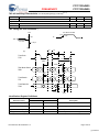
1
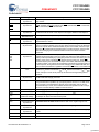
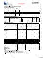
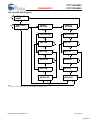
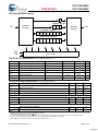
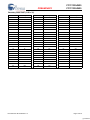
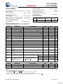
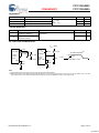
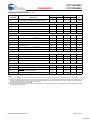
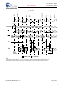
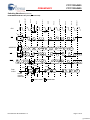
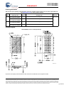
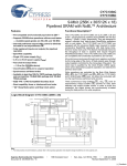
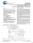
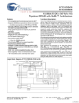
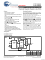
CY7C1330AV25
CY7C1332AV25
PRELIMINARY
18-Mbit (512K x 36/1Mbit x 18)
Pipelined Register-Register Late Write
Features
Functional Description
• Fast clock speed: 250, 200 MHz
• Fast access time: 2.0, 2.25 ns
• Synchronous Pipelined Operation with Self-timed Late
Write
• Internally synchronized registered outputs eliminate
the need to control OE
The CY7C1330AV25 and CY7C1332AV25 are high performance, Synchronous Pipelined SRAMs designed with late
write operation. These SRAMs can achieve speeds up to 250
MHz. Each memory cell consists of six transistors.
Late write feature avoids an idle cycle required during the
turnaround of the bus from a read to a write.
• Single WE (READ/WRITE) control pin
All synchronous inputs are gated by registers controlled by a
positive-edge-triggered Clock Input (K). The synchronous
inputs include all addresses (A), all data inputs (DQ[a:d]), Chip
Enable (CE), Byte Write Selects (BWS[a:d]), and read-write
control (WE). Read or Write Operations can be initiated with
the chip enable pin (CE). This signal allows the user to
select/deselect the device when desired.
• Individual byte write (BWS[a:d]) control (may be tied
LOW)
Power down feature is accomplished by pulling the
Synchronous signal ZZ HIGH.
• Common I/O
Output Enable (OE) is an asynchronous input signal. OE can
be used to disable the outputs at any given time.
• 2.5V core supply voltage
• 1.4–1.9V VDDQ supply with VREF of 0.68–0.95V
— Wide range HSTL I/O Levels
• Single Differential HSTL clock Input K and K
• Asynchronous Output Enable Input
• Programmable Impedance Output Drivers
• JTAG boundary scan for BGA packaging version
• Available in a 119-ball BGA package (CY7C1330AV25
and CY7C1332AV25)
Four pins are used to implement JTAG test capabilities. The
JTAG circuitry is used to serially shift data to and from the
device. JTAG inputs use LVTTL/LVCMOS levels to shift data
during this testing mode of operation.
Configuration
CY7C1330AV25 – 512K x 36
CY7C1332AV25 – 1M x 18
Logic Block Diagram
Clock
Buffer
D Data-In REG.
CE Q (2stage)
OUTOUT
REGISTERS
and LOGIC
K,K
Ax
CE
512Kx36
1Mx18
CONTROL
and WRITE
LOGIC
DQx
MEMORY
ARRAY
WE
BWSx
ZZ
OE
AX
DQX
BWSX
512Kx36 X = 18:0 X = a, b, c, d X = a, b, c, d
1Mx18
Cypress Semiconductor Corporation
Document No: 001-07844 Rev. *A
•
198 Champion Court
•
X = 19:0
X = a, b
X = a, b
San Jose, CA 95134-1709
•
408-943-2600
Revised September 20, 2006
[+] Feedback
CY7C1330AV25
CY7C1332AV25
PRELIMINARY
Selection Guide
CY7C1330AV25-250
CY7C1332AV25-250
CY7C1330AV25-200
CY7C1332AV25- 200
Unit
2.0
2.25
ns
Maximum Access Time
Maximum Operating Current
600
550
mA
Maximum CMOS Standby Current
280
260
mA
Pin Configurations
119-Ball BGA (14 x 22 x 2.4 mm)
CY7C1330AV25 (512K x 36)
1
2
3
4
5
6
7
A
VDDQ
A
A
NC
A
A
VDDQ
B
C
D
E
F
G
H
J
K
L
M
N
P
NC
NC
DQc
A
A
DQc
A
A
VSS
NC
VDD
ZQ
A
A
VSS
A
A
DQb
NC
NC
DQb
R
T
U
DQc
DQc
VSS
CE
VSS
DQb
DQb
VDDQ
DQc
VSS
OE
VSS
DQb
VDDQ
DQc
DQc
BWSc
NC
BWSb
DQb
DQb
DQc
VDDQ
DQc
VDD
VSS
VREF
NC
VDD
VSS
VREF
DQb
VDD
DQb
VDDQ
DQd
DQd
DQd
DQd
VSS
BWSd
K
K
VSS
BWSa
DQa
DQa
DQa
DQa
VSS
WE
VSS
DQa
VDDQ
VDDQ
DQd
DQd
DQd
VSS
A0
VSS
DQa
DQa
DQd
DQd
VSS
A1
VSS
DQa
DQa
NC
A
M1
VDD
M2
A
NC
NC
NC
A
A
A
ZZ
VDDQ
TMS
TDI
TCK
TDO
NC
NC
VDDQ
CY7C1332AV25 (1M x 18)
1
2
3
4
5
6
7
A
VDDQ
A
A
NC
A
A
VDDQ
B
C
D
E
F
G
H
J
K
L
M
N
P
NC
NC
DQb
A
A
NC
A
A
VSS
NC
VDD
ZQ
A
A
VSS
A
A
DQa
NC
NC
NC
R
T
U
Document No: 001-07844 Rev. *A
NC
DQb
VSS
CE
VSS
NC
DQa
VDDQ
NC
VSS
OE
VSS
DQa
VDDQ
NC
DQb
BWSb
NC
NC
NC
DQa
DQb
VDDQ
NC
VDD
VSS
VREF
NC
VDD
VSS
VREF
DQa
VDD
NC
VDDQ
NC
DQb
DQb
NC
VSS
NC
K
K
VSS
BWSa
NC
DQa
DQa
NC
VDDQ
DQb
VSS
WE
VSS
NC
VDDQ
DQb
NC
VSS
A0
VSS
DQa
NC
NC
DQb
VSS
A1
VSS
NC
DQa
NC
A
M1
VDD
M2
A
NC
NC
A
A
NC
A
A
ZZ
VDDQ
TMS
TDI
TCK
TDO
NC
VDDQ
Page 2 of 19
[+] Feedback
CY7C1330AV25
CY7C1332AV25
PRELIMINARY
Pin Definitions
I/O Type
Description
A
Name
InputSynchronous
Address Inputs used to select one of the address locations. Sampled at the rising
edge of the K.
BWSa
BWSb
BWSc
BWSd
InputSynchronous
Byte Write Select Inputs, active LOW. Qualified with WE to conduct writes to the
SRAM. Sampled on the rising edge of CLK. BWSa controls DQa, BWSb controls DQb,
BWSc controls DQc, BWSd controls DQd.
WE
InputSynchronous
Write Enable Input, active LOW. Sampled on the rising edge of CLK. This signal must
be asserted LOW to initiate a write sequence and high to initiate a read sequence.
K,K
InputDifferential Clock
CE
InputSynchronous
Chip Enable Input, active LOW. Sampled on the rising edge of CLK. Used to
select/deselect the device.
OE
InputAsynchronous
Output Enable, active LOW. Combined with the synchronous logic block inside the
device to control the direction of the I/O pins. When LOW, the I/O pins are allowed to
behave as outputs. When deasserted HIGH, I/O pins are tri-stated, and act as input
data pins. OE is masked during the data portion of a write sequence, during the first
clock when emerging from a deselected state and when the device has been
deselected.
DQa
DQb
DQc
DQd
I/OSynchronous
Bidirectional Data I/O lines. As inputs, they feed into an on-chip data register that is
triggered by the rising edge of CLK. As outputs, they deliver the data contained in the
memory location specified by A[x:0] during the previous clock rise of the read cycle. The
direction of the pins is controlled by OE and the internal control logic. When OE is
asserted LOW, the pins can behave as outputs. When HIGH, DQa–DQd are placed in
a tri-state condition. The outputs are automatically tri-stated during the data portion of
a write sequence, during the first clock when emerging from a deselected state, and
when the device is deselected, regardless of the state of OE. DQ a,b,c,d are 9 bits wide
Read Protocol Mode
Pins
Mode control pins, used to set the proper read protocol. For specified device
operation, M1 must be connected to VSS, and M2 must be connected to VDD or VDDQ.
These mode pins must be set at power-up and cannot be changed during device
operation.
ZZ
InputAsynchronous
ZZ “sleep” Input. This active HIGH input places the device in a non-time critical “sleep”
condition with data integrity preserved.
ZQ
Input
Output Impedance Matching Input. This input is used to tune the device outputs to
the system data bus impedance. Q[x:0] output impedance are set to 0.2 x RQ, where
RQ is a resistor connected between ZQ and ground. Alternately, this pin can be
connected directly to VDDQ, which enables the minimum impedance mode. This pin
cannot be connected directly to GND or left unconnected.
VDD
Power Supply
M1, M2
Clock Inputs. Used to capture all synchronous inputs to the device.
Power supply inputs to the core of the device. For this device, the VDD is 2.5V.
VDDQ
I/O Power Supply
Power supply for the I/O circuitry. For this device, the VDDQ is 1.5V.
VREF
InputReference Voltage
Reference Voltage Input. Static input used to set the reference level for HSTL inputs
and Outputs as well as AC measurement points.
VSS
Ground
TDO
JTAG serial output
Synchronous
TDI
JTAG serial input
Synchronous
Serial data-in to the JTAG circuit. Sampled on the rising edge of TCK.
TMS
Test Mode Select
Synchronous
This pin controls the Test Access Port state machine. Sampled on the rising edge
of TCK.
TCK
JTAG serial clock
NC
–
Document No: 001-07844 Rev. *A
Ground for the device. Should be connected to ground of the system.
Serial data-out to the JTAG circuit. Delivers data on the negative edge of TCK.
Serial clock to the JTAG circuit.
No connects.
Page 3 of 19
[+] Feedback
PRELIMINARY
CY7C1330AV25
CY7C1332AV25
Introduction
Ax is loaded into the Address Register. The write signals are
latched into the Control Logic block.
Functional Overview
The data lines are automatically tri-stated regardless of the
state of the OE input signal when a write is detected. This
allows the external logic to present the data on DQ and DQP
(DQ[a:b] for CY7C1332AV25 and DQ[a:d] for CY7C1330AV25).
In addition, the address for the subsequent access
(Read/Write/Deselect) is latched into the Address Register
(provided the appropriate control signals are asserted).
The CY7C1330AV25 and CY7C1332AV25 are synchronouspipelined Late Write SRAMs running at speeds up to 250 MHz.
All synchronous inputs pass through input registers controlled
by the rising edge of the clock. All data outputs pass through
output registers controlled by the rising edge of the clock.
Maximum access delay from the clock rise (tCO) is 2.0 ns
(250-MHz device).
Accesses can be initiated by asserting Chip Enable (CE) on
the rising edge of the clock. The address presented to the
device will be latched on this edge of the clock. The access
can either be a read or write operation, depending on the
status of the Write Enable (WE). BWS[d:a] can be used to
conduct individual byte write operations.
Write operations are qualified by the Write Enable (WE). All
writes are simplified with on-chip synchronous self-timed late
write circuitry.
All operations (Reads, Writes, and Deselects) are pipelined.
Pipelined Read Accesses
A read access is initiated when the following conditions are
satisfied at clock rise: (1) Chip Enable (CE) is asserted active
and (2) the Write Enable input signal (WE) is asserted HIGH.
The address presented to the address inputs is latched into
the Address Register and presented to the memory core and
control logic. The control logic determines that a read access
is in progress and allows the requested data to propagate to
the input of the output register. At the rising edge of the next
clock the requested data is allowed to propagate through the
output register and onto the data bus within 2.0 ns (250-MHz
device) provided OE is active LOW. After the first clock of the
read access the output buffers are controlled by OE and the
internal control logic. OE must be driven LOW in order for the
device to drive out the requested data. During the second
clock, a subsequent operation (Read/Write/Deselect) can be
initiated. Deselecting the device is also pipelined. Therefore,
when the SRAM is deselected at clock rise by one of the chip
enable signals, its output will tri-state following the next clock
rise.
Bypass Read Operation
Bypass read operation occurs when the last write operation is
followed by a read operation where write and read addresses
are identical. The data outputs are provided from the data in
registers rather than the memory array. This operation occurs
on a byte to byte basis. If only one byte is written during a write
operation and a read operation is performed on the same
address; then a partial bypass read operation is performed
since the new byte data will be from the datain registers while
the remaining bytes are from the memory array.
Late Write Accesses
The Late Write feature allows for the write data to be presented
one cycle later after the access is started. This feature eliminates one bus-turnaround cycle which is necessary when
going from a read to a write in an ordinary pipelined
Synchronous Burst SRAM.
Write access is initiated when the following conditions are
satisfied at clock rise: (1) CE is asserted active and (2) the
write signal WE is asserted LOW. The address presented to
Document No: 001-07844 Rev. *A
On the next clock rise the data presented to DQ (or a subset
for byte write operations, see Write Cycle Description table for
details) inputs is latched into the device and the write is
complete.
The data written during the Write operation is controlled by
BWS (BWS[a:d] for CY7C1330AV25 and BWS[a:b] for
CY7C1332AV25) signals. The CY7C1330AV25 and
CY7C1332AV25 provide byte write capability that is described
in the Write Cycle Description table. Asserting the Write
Enable input (WE) with the selected Byte Write Select (BWS)
input will selectively write to only the desired bytes. Bytes not
selected during a byte write operation will remain unaltered. A
Synchronous self-timed write mechanism has been provided
to simplify the write operations. Byte write capability has been
included in order to greatly simplify Read/Modify/Write
sequences, which can be reduced to simple byte write operations.
Because the CY7C1330AV25/CY7C1332AV25 is a common
I/O device, data should not be driven into the device while the
outputs are active. The Output Enable (OE) can be deasserted
HIGH before presenting data to the DQ inputs. Doing so will
tri-state the output drivers. As a safety precaution, DQ is
automatically tri-stated during the data portion of a write cycle,
regardless of the state of OE.
Power-up/Power-down Supply Voltage Sequencing
The power-up and power-down supply voltage application
recommendations are as follows:
Power-up: VSS, VDD, VDDQ, VREF, VIN.
Power-down: VIN, VREF, VDDQ, VDD, VSS.
VDDQ can be applied/removed simultaneously with VDD as
long as VDDQ does not exceed VDD by more than 0.5V.
Programmable Impedance
An external resistor, RQ, must be connected between the ZQ
pin on the SRAM and VSS to allow the SRAM to adjust its
output driver impedance. The value of RQ must be 5X the
value of the intended line impedance driven by the SRAM, The
allowable range of RQ to guarantee impedance matching with
a tolerance of ±10% is between 175Ω and 350Ω, with
VDDQ=1.5V. The output impedance is adjusted every 1024
cycles to adjust for drifts in supply voltage and temperature.The output buffers can also be programmed in a
minimum impedance configuration by connecting ZQ to VDD.
Sleep Mode
The ZZ input pin is an asynchronous input. Asserting ZZ
places the SRAM in a power conservation “sleep” mode. Two
clock cycles are required to enter into or exit from this “sleep”
mode. While in this mode, data integrity is guaranteed.
Accesses pending when entering the “sleep” mode are not
considered valid nor is the completion of the operation
Page 4 of 19
[+] Feedback
CY7C1330AV25
CY7C1332AV25
PRELIMINARY
guaranteed. The device must be deselected prior to entering
the “sleep” mode. CE must remain inactive for the duration of
tZZREC after the ZZ input returns LOW.
Cycle Description Truth Table[1, 2, 3, 4, 5]
Operation Address Used CE
WE BWSx CLK ZZ
Deselected External
1
X
Begin Read External
0
Begin Write External
0
Sleep Mode
X
-
Comments
X
L-H
0
I/Os tri-state following next recognized clock.
1
X
L-H
0
Address latched. Data driven out on the next rising edge of the clock.
0
Valid
L-H
0
Address latched, data presented to the SRAM on the next rising
edge of the clock.
X
X
X
1
Power down mode.
ZZ Mode Electrical Characteristics
Parameter
Description
Test Conditions
IDDZZ
Snooze mode standby current
ZZ > VIH
tZZS
Device operation to ZZ
ZZ > VIH
tZZREC
ZZ recovery time
ZZ < VIL
Min.
Max.
Unit
128
mA
2tCYC
ns
2tCYC
ns
Write Cycle Descriptions[1, 2]
Function (CY7C1330AV25)
WE
BWd
BWc
BWb
BWa
Read
1
X
X
X
X
Write Byte 0 – DQa
0
1
1
1
0
Write Byte 1 – DQb
0
1
1
0
1
Write Bytes 1, 0
0
1
1
0
0
Write Byte 2 – DQc
0
1
0
1
1
Write Bytes 2, 0
0
1
0
1
0
Write Bytes 2, 1
0
1
0
0
1
Write Bytes 2, 1, 0
0
1
0
0
0
Write Byte 3 – DQd
0
0
1
1
1
Write Bytes 3, 0
0
0
1
1
0
Write Bytes 3, 1
0
0
1
0
1
Write Bytes 3, 1, 0
0
0
1
0
0
Write Bytes 3, 2
0
0
0
1
1
Write Bytes 3, 2, 0
0
0
0
1
0
Write Bytes 3, 2, 1
0
0
0
0
1
Write All Bytes
0
0
0
0
0
Abort Write All Bytes
0
1
1
1
1
Write Cycle Descriptions[1, 2]
Function (CY7C1332AV25)
Read
Write Byte 0 – DQa
Write Byte 1 – DQb
Write All Bytes
Abort Write All Bytes
WE
1
0
0
0
0
BWb
X
1
0
0
1
BWa
X
0
1
0
1
Notes:
1. X = “Don't Care,” 1 = Logic HIGH, 0 = Logic LOW. BWSx = 0 signifies at least one Byte Write Select is active, BWSx = Valid signifies that the desired byte write
selects are asserted, see Write Cycle Description table for details.
2. Write is defined by WE and BWSx. See Write Cycle Description table for details.
3. The DQ pins are controlled by the current cycle and the OE signal.
4. Device will power-up deselected and the I/Os in a tri-state condition, regardless of OE.
5. OE assumed LOW.
Document No: 001-07844 Rev. *A
Page 5 of 19
[+] Feedback
PRELIMINARY
CY7C1330AV25
CY7C1332AV25
IEEE 1149.1 Serial Boundary Scan (JTAG)
Instruction Register
These SRAMs incorporate a serial boundary scan test access
port (TAP) in the FBGA package. This port operates in accordance with IEEE Standard 1149.1-1900 but does not have the
set of functions required for full 1149.1 compliance. The TAP
operates using JEDEC standard 1.8V I/O logic levels.
Three-bit instructions can be serially loaded into the instruction
register. This register is loaded when it is placed between the
TDI and TDO pins as shown in TAP Controller Block Diagram.
Upon power-up, the instruction register is loaded with the
IDCODE instruction. It is also loaded with the IDCODE
instruction if the controller is placed in a reset state as
described in the previous section.
Disabling the JTAG Feature
It is possible to operate the SRAM without using the JTAG
feature. To disable the TAP controller, TCK must be tied LOW
(VSS) to prevent clocking of the device. TDI and TMS are internally pulled up and may be unconnected. They may alternately
be connected to VDD through a pull-up resistor. TDO should
be left unconnected. Upon power-up, the device will come up
in a reset state which will not interfere with the operation of the
device.
Test Access Port—Test Clock
The test clock is used only with the TAP controller. All inputs
are captured on the rising edge of TCK. All outputs are driven
from the falling edge of TCK.
Test Mode Select
The TMS input is used to give commands to the TAP controller
and is sampled on the rising edge of TCK. It is allowable to
leave this pin unconnected if the TAP is not used. The pin is
pulled up internally, resulting in a logic HIGH level.
Test Data-In (TDI)
The TDI pin is used to serially input information into the
registers and can be connected to the input of any of the
registers. The register between TDI and TDO is chosen by the
instruction that is loaded into the TAP instruction register. For
information on loading the instruction register, see the TAP
Controller State Diagram. TDI is internally pulled up and can
be unconnected if the TAP is unused in an application. TDI is
connected to the most significant bit (MSB) on any register.
Test Data-Out (TDO)
The TDO output pin is used to serially clock data-out from the
registers. The output is active depending upon the current
state of the TAP state machine (see Instruction codes). The
output changes on the falling edge of TCK. TDO is connected
to the least significant bit (LSB) of any register.
Performing a TAP Reset
A Reset is performed by forcing TMS HIGH (VDD) for five
rising edges of TCK. This RESET does not affect the operation
of the SRAM and may be performed while the SRAM is
operating. At power-up, the TAP is reset internally to ensure
that TDO comes up in a high-Z state.
TAP Registers
Registers are connected between the TDI and TDO pins and
allow data to be scanned into and out of the SRAM test
circuitry. Only one register can be selected at a time through
the instruction registers. Data is serially loaded into the TDI pin
on the rising edge of TCK. Data is output on the TDO pin on
the falling edge of TCK.
Document No: 001-07844 Rev. *A
When the TAP controller is in the Capture IR state, the two
least significant bits are loaded with a binary “01” pattern to
allow for fault isolation of the board level serial test path.
Bypass Register
To save time when serially shifting data through registers, it is
sometimes advantageous to skip certain chips. The bypass
register is a single-bit register that can be placed between TDI
and TDO pins. This allows data to be shifted through the
SRAM with minimal delay. The bypass register is set LOW
(VSS) when the BYPASS instruction is executed.
Boundary Scan Register
The boundary scan register is connected to all of the input and
output pins on the SRAM. Several no connect (NC) pins are
also included in the scan register to reserve pins for higher
density devices.
The boundary scan register is loaded with the contents of the
RAM Input and Output ring when the TAP controller is in the
Capture-DR state and is then placed between the TDI and
TDO pins when the controller is moved to the Shift-DR state.
The EXTEST, SAMPLE/PRELOAD and SAMPLE Z instructions can be used to capture the contents of the Input and
Output ring.
The Boundary Scan Order tables show the order in which the
bits are connected. Each bit corresponds to one of the bumps
on the SRAM package. The MSB of the register is connected
to TDI, and the LSB is connected to TDO.
Identification (ID) Register
The ID register is loaded with a vendor-specific, 32-bit code
during the Capture-DR state when the IDCODE command is
loaded in the instruction register. The IDCODE is hardwired
into the SRAM and can be shifted out when the TAP controller
is in the Shift-DR state. The ID register has a vendor code and
other information described in the Identification Register
Definitions table.
TAP Instruction Set
Eight different instructions are possible with the three-bit
instruction register. All combinations are listed in the
Instruction Code table. Three of these instructions are listed
as RESERVED and should not be used. The other five instructions are described in detail below.
Instructions are loaded into the TAP controller during the
Shift-IR state when the instruction register is placed between
TDI and TDO. During this state, instructions are shifted
through the instruction register through the TDI and TDO pins.
To execute the instruction once it is shifted in, the TAP
controller needs to be moved into the Update-IR state.
Page 6 of 19
[+] Feedback
PRELIMINARY
EXTEST
EXTEST is a mandatory 1149.1 instruction which is to be
executed whenever the instruction register is loaded with all
0s. EXTEST is not implemented in this SRAM TAP controller,
and therefore this device is not compliant to 1149.1. The TAP
controller does recognize an all-0 instruction.
When an EXTEST instruction is loaded into the instruction
register, the SRAM responds as if a SAMPLE/PRELOAD
instruction has been loaded. There is one difference between
the two instructions. Unlike the SAMPLE/PRELOAD
instruction, EXTEST places the SRAM outputs in a High-Z
state.
IDCODE
The IDCODE instruction causes a vendor-specific, 32-bit code
to be loaded into the instruction register. It also places the
instruction register between the TDI and TDO pins and allows
the IDCODE to be shifted out of the device when the TAP
controller enters the Shift-DR state. The IDCODE instruction
is loaded into the instruction register upon power-up or
whenever the TAP controller is given a test logic reset state.
SAMPLE Z
The SAMPLE Z instruction causes the boundary scan register
to be connected between the TDI and TDO pins when the TAP
controller is in a Shift-DR state. The SAMPLE Z command puts
the output bus into a High-Z state until the next command is
given during the “Update IR” state.
SAMPLE/PRELOAD
SAMPLE/PRELOAD is a 1149.1 mandatory instruction. When
the SAMPLE/PRELOAD instructions are loaded into the
instruction register and the TAP controller is in the Capture-DR
state, a snapshot of data on the inputs and output pins is
captured in the boundary scan register.
The user must be aware that the TAP controller clock can only
operate at a frequency up to 20 MHz, while the SRAM clock
operates more than an order of magnitude faster. Because
Document No: 001-07844 Rev. *A
CY7C1330AV25
CY7C1332AV25
there is a large difference in the clock frequencies, it is
possible that during the Capture-DR state, an input or output
will undergo a transition. The TAP may then try to capture a
signal while in transition (metastable state). This will not harm
the device, but there is no guarantee as to the value that will
be captured. Repeatable results may not be possible.
To guarantee that the boundary scan register will capture the
correct value of a signal, the SRAM signal must be stabilized
long enough to meet the TAP controller's capture set-up plus
hold times (tCS and tCH). The SRAM clock input might not be
captured correctly if there is no way in a design to stop (or
slow) the clock during a SAMPLE/PRELOAD instruction. If this
is an issue, it is still possible to capture all other signals and
simply ignore the value of the CK and CK captured in the
boundary scan register.
Once the data is captured, it is possible to shift out the data by
putting the TAP into the Shift-DR state. This places the
boundary scan register between the TDI and TDO pins.
PRELOAD allows an initial data pattern to be placed at the
latched parallel outputs of the boundary scan register cells
prior to the selection of another boundary scan test operation.
The shifting of data for the SAMPLE and PRELOAD phases
can occur concurrently when required—that is, while data
captured is shifted out, the preloaded data can be shifted in.
BYPASS
When the BYPASS instruction is loaded in the instruction
register and the TAP is placed in a Shift-DR state, the bypass
register is placed between the TDI and TDO pins. The
advantage of the BYPASS instruction is that it shortens the
boundary scan path when multiple devices are connected
together on a board.
Reserved
These instructions are not implemented but are reserved for
future use. Do not use these instructions.
Page 7 of 19
[+] Feedback
CY7C1330AV25
CY7C1332AV25
PRELIMINARY
TAP Controller State Diagram[6]
1
TEST-LOGIC
RESET
0
0
TEST-LOGIC/
IDLE
1
1
1
SELECT
DR-SCAN
SELECT
IR-SCAN
0
0
1
1
CAPTURE-DR
CAPTURE-IR
0
0
SHIFT-DR
SHIFT-IR
0
1
0
1
1
EXIT1-DR
1
EXIT1-IR
0
0
PAUSE-DR
0
0
PAUSE-IR
1
1
0
0
EXIT2-DR
EXIT2-IR
1
1
UPDATE-DR
1
0
UPDATE-IR
1
0
Note:
6. The 0/1 next to each state represents the value at TMS at the rising edge of TCK.
Document No: 001-07844 Rev. *A
Page 8 of 19
[+] Feedback
CY7C1330AV25
CY7C1332AV25
PRELIMINARY
TAP Controller Block Diagram
0
Bypass Register
Selection
Circuitry
TDI
2
1
0
1
0
Selection
Circuitry
Instruction Register
31 30 29
.
.
2
TDO
Identification Register
106 .
.
.
.
2
1
0
Boundary Scan Register
TCK
TMS
TAP Controller
TAP Electrical Characteristics Over the Operating Range[7, 8, 9]
Parameter
Description
Test Conditions
Min.
VOH1
Output HIGH Voltage
IOH = −2.0 mA
1.7
2.1
VOH2
Output HIGH Voltage
IOH = −100 µA
VOL1
Output LOW Voltage
IOL = 2.0 mA
IOL = 100 µA
VOL2
Output LOW Voltage
VIH
Input HIGH Voltage
VIL
Input LOW Voltage
IX
Input and Output Load Current
GND ≤ VI ≤ VDD
Max.
Unit
V
V
0.7
V
0.2
V
1.7
VDD + 0.3
V
–0.3
0.7
V
–5
5
µA
TAP AC Switching Characteristics Over the Operating Range [10, 11]
Parameter
Description
Min.
Max.
Unit
tTCYC
TCK Clock Cycle Time
tTF
TCK Clock Frequency
tTH
TCK Clock HIGH
20
ns
tTL
TCK Clock LOW
20
ns
tTMSS
TMS Set-up to TCK Clock Rise
5
ns
tTDIS
TDI Set-up to TCK Clock Rise
5
ns
tCS
Capture Set-up to TCK Rise
5
ns
tTMSH
TMS Hold after TCK Clock Rise
5
ns
tTDIH
TDI Hold after Clock Rise
5
ns
50
ns
20
MHz
Set-up Times
Hold Times
Notes:
7. Minimum voltage equals –2.0V for pulse durations of less than 20 ns.
8. Input waveform should have a slew rate of > 1 V/ns.
9. These characteristics pertain to the TAP inputs (TMS, TCK, TDI and TDO). Parallel load levels are specified in the Electrical Characteristics Table.
10. tCS and tCH refer to the set-up and hold time requirements of latching data from the boundary scan register.
11. Test conditions are specified using the load in TAP AC test conditions. tR/tF = 1 ns.
Document No: 001-07844 Rev. *A
Page 9 of 19
[+] Feedback
CY7C1330AV25
CY7C1332AV25
PRELIMINARY
TAP AC Switching Characteristics Over the Operating Range (continued)[10, 11]
Parameter
Description
tCH
Min.
Capture Hold after Clock Rise
Max.
Unit
5
ns
Output Times
tTDOV
TCK Clock LOW to TDO Valid
tTDOX
TCK Clock LOW to TDO Invalid
10
ns
0
ns
TAP Timing and Test Conditions[11]
ALL INPUT PULSES
1.25V
2.5V
1.25V
50Ω
0V
TDO
Z0 = 50Ω
CL = 20 pF
GND
tTH
(a)
tTL
Test Clock
TCK
tTCYC
tTMSS
tTMSH
Test Mode Select
TMS
tTDIS
tTDIH
Test Data-In
TDI
Test Data-Out
TDO
tTDOV
tTDOX
Identification Register Definitions
Value
Instruction Field
CY7C1330AV25
CY7C1332AV25
000
000
Revision Number (31:29)
Cypress Device ID (28:12)
Description
Version number.
01011110101100101 01011110101010101 Defines the type of SRAM.
Cypress JEDEC ID (11:1)
00000110100
00000110100
ID Register Presence (0)
1
1
Document No: 001-07844 Rev. *A
Allows unique identification of SRAM vendor.
Indicates the presence of an ID register.
Page 10 of 19
[+] Feedback
CY7C1330AV25
CY7C1332AV25
PRELIMINARY
Scan Register Sizes
Register Name
Bit Size—CY7C1330AV25
Bit Size—CY7C1332AV25
Instruction
3
3
Bypass
1
1
ID
32
32
Boundary Scan
70
51
Instruction Codes
Instruction
Code
Description
EXTEST
000
Captures the Input/Output ring contents.
IDCODE
001
Loads the ID register with the vendor ID code and places the register between TDI
and TDO. This operation does not affect SRAM operation.
SAMPLE Z
010
Captures the Input/Output contents. Places the boundary scan register between
TDI and TDO. Forces all SRAM output drivers to a High-Z state.
RESERVED
011
Do Not Use: This instruction is reserved for future use.
SAMPLE/PRELOAD
100
Captures the Input/Output ring contents. Places the boundary scan register
between TDI and TDO. Does not affect the SRAM operation.
RESERVED
101
Do Not Use: This instruction is reserved for future use.
RESERVED
110
Do Not Use: This instruction is reserved for future use.
BYPASS
111
Places the bypass register between TDI and TDO. This operation does not affect
SRAM operation.
Boundary Scan Order (1 Mbit x 18)
Bit #
Bump ID
Bit #
Bump ID
Bit #
1
5R
2
6T
Bump ID
18
7E
35
1H
19
6D
36
3G
3
4P
20
6A
37
4D
4
6R
21
6C
38
4E
5
5T
22
5C
39
4G
6
7T
23
5A
40
4H
7
7P
24
6B
41
4M
8
6N
25
5B
42
2K
9
6L
26
3B
43
1L
10
7K
27
2B
44
2M
11
5L
28
3A
45
1N
12
4L
29
3C
46
2P
13
4K
30
2C
47
3T
14
4F
31
2A
48
2R
15
6H
32
1D
49
4N
16
7G
33
2E
50
2T
17
6F
34
2G
51
3R
Document No: 001-07844 Rev. *A
Page 11 of 19
[+] Feedback
CY7C1330AV25
CY7C1332AV25
PRELIMINARY
Boundary Scan Order (512K x 36)
Bit #
Bump ID
Bit #
Bump ID
Bit #
Bump ID
1
5R
25
6F
49
2H
2
4P
26
7E
50
1H
3
4T
27
6E
51
3G
4
6R
28
7D
52
4D
5
5T
29
6D
53
4E
6
7T
30
6A
54
4G
7
6P
31
6C
55
4H
8
7P
32
5C
56
4M
9
6N
33
5A
57
3L
10
7N
34
6B
58
1K
11
6M
35
5B
59
2K
12
6L
36
3B
60
1L
13
7L
37
2B
61
2L
14
6K
38
3A
62
2M
15
7K
39
3C
63
1N
16
5L
40
2C
64
2N
17
4L
41
2A
65
1P
18
4K
42
2D
66
2P
19
4F
43
1D
67
3T
20
5G
44
2E
68
2R
21
7H
45
1E
69
4N
22
6H
46
2F
70
3R
23
7G
47
2G
24
6G
48
1G
Document No: 001-07844 Rev. *A
Page 12 of 19
[+] Feedback
CY7C1330AV25
CY7C1332AV25
PRELIMINARY
DC Input Voltage[7] ................................ –0.5V to VDD + 0.5V
Maximum Ratings
(Above which the useful life may be impaired. For user guidelines, not tested.)
Storage Temperature ................................. –65°C to +150°C
Ambient Temperature with
Power Applied........................................... –55°C to +125°°C
Current into Outputs (LOW)......................................... 20 mA
Static Discharge Voltage........................................... > 1500V
(per MIL-STD-883, Method 3015)
Latch-up Current..................................................... > 200 mA
Operating Range
Supply Voltage on VDD Relative to GND........ –0.5V to +2.9V
Supply Voltage on VDDQ Relative to GND ...... –0.5V to +VDD
Range
Ambient
Temperature
VDD
VDDQ
DC Voltage Applied to Outputs
in High-Z State[7] ................................. –0.5V to VDDQ + 0.5V
Com’l
0°C to +70°C
2.37V to 2.63V
1.4V to 1.9V
Electrical Characteristics Over the Operating Range
DC Electrical Characteristics Over the Operating Range
Parameter
Description
Test Conditions
VDD
Power Supply Voltage
VDDQ
I/O Supply Voltage
VOH1
Output HIGH Voltage[12]
Programmable Impedance Mode[14]
VOL1
Output LOW Voltage[13]
Programmable Impedance Mode[14]
VOH2
Output HIGH Voltage
IOH = –0.1 mA, Minimum Impedance Mode[15]
VOL2
Output LOW Voltage
IOL = 0.1 mA, Minimum Impedance Mode[15]
VOH3
Output HIGH Voltage
IOH = –6.0 mA, Minimum Impedance Mode[15]
VOL3
Output LOW Voltage
VIH
Input HIGH Voltage
IOL = 6.0 mA, Minimum Impedance
Input LOW
IX
Input Leakage Current
GND ≤ VI ≤ VDDQ
IOZ
Output Leakage Current
GND ≤ VI ≤ VDDQ, Output Disabled
VREF
Input Reference Voltage
Typical value = 0.75V
VIN–CLK
Max.
Unit
2.37
2.63
V
1.4
1.9
V
VDDQ/2
VDD
V
VSS
VDDQ/2
V
VDDQ – 0.2
VDDQ
V
VSS
0.2
V
VDDQ – 0.4
VDDQ
V
Mode[15]
VSS
0.4
V
VREF + 0.1
VDDQ + 0.3
V
–0.3
VREF – 0.1
V
–1
1
mA
Voltage[7]
VIL
Min.
–1
1
mA
0.68
0.95
V
Clock Input Reference
Voltage
–0.3
VDDQ + 0.3
V
VDIF–CLK
Clock Input Differential
Voltage
0.1
VDDQ + 0.3
V
VCM–CLK
Clock Common Mode
Voltage
Typical Value =0.75V
0.55
0.95
V
IDD
VDD Operating Supply
VDD = Max., IOUT = 0 mA,
f = fMAX = 1/tCYC
250 MHz
600
mA
200 MHz
550
mA
Max. VDD, Device Deselected,
VIN > VIH or VIN < VIL
f = fMAX = 1/tCYC
250 MHz
280
mA
200 MHz
260
mA
Max.
Unit
ISB1
Automatic CE
Power-Down
Current—TTL Inputs
AC Electrical Characteristics Over the Operating Range
Parameter
Description
Test Conditions
Min.
VIH
Input HIGH Voltage
VREF + 0.2
–
V
VIL
Input LOW Voltage
–
VREF – 0.2
V
Notes:
12. IOH = (VDDQ/2)/(RQ/5)+15% for 175Ω < RQ < 350Ω.
13. IOL = (VDDQ/2)/(RQ/5)+15% for 175Ω < RQ < 350Ω.
14. Programmable Impedance Output Buffer Mode. The ZQ pin is connected to VSS through RQ.
15. Minimum Impedance Output Buffer Mode: The ZQ pin is connected directly to VSS or VDD.
16. TPower-up: Assumes a linear ramp from 0V to VDD (min.) within 200 ms. During this time VIH < VDD and VDDQ < VDD.
Document No: 001-07844 Rev. *A
Page 13 of 19
[+] Feedback
CY7C1330AV25
CY7C1332AV25
PRELIMINARY
Capacitance[17]
Parameter
Description
CIN
Input Capacitance
CCLK
Clock Input Capacitance
CI/O
Input/Output Capacitance
Test Conditions
TA = 25°C, f = 1 MHz,
VDD = 2.5V
VDDQ = 1.5V
Max.
Unit
5
pF
6
pF
7
pF
Thermal Resistance[17]
Parameter
Description
ΘJA
Thermal Resistance
(Junction to Ambient)
ΘJC
Thermal Resistance
(Junction to Case)
Test Conditions
BGA Typ.
Unit
Still Air, soldered on a 4.25 x 1.125 inch, 4-layer printed
circuit board
19.7
°C/W
6.0
°C/W
AC Test Loads and Waveforms
VREF = 0.75V
VREF
0.75V
VREF
OUTPUT
Z0 = 50Ω
Device
Under
Test
RL = 50Ω
VREF = 0.75V
ZQ
RQ =
250Ω
0.75V
R = 50Ω
ALL INPUT PULSES
1.25V
0.75V
OUTPUT
Device
Under
Test ZQ
5 pF
[18]
0.25V
Slew Rate = 2 V/ns
RQ =
250Ω
(a)
(b)
Notes:
17. Tested initially and after any design or process change that may affect these parameters.
18. Unless otherwise noted, test conditions assume signal transition time of 2 V/ns, timing reference levels of 0.75V, VREF = 0.75V, RQ = 250Ω, VDDQ = 1.5V, input
pulse levels of 0.25V to 1.25V, and output loading of the specified IOL/IOH and load capacitance shown in (a) of AC Test Loads.
Document No: 001-07844 Rev. *A
Page 14 of 19
[+] Feedback
CY7C1330AV25
CY7C1332AV25
PRELIMINARY
Switching Characteristics[18, 19, 20, 21]
250
Parameter
tPower
Description
VCC (typical) to the First Access Read or Write
Min.
[22]
200
Max.
1
Min.
Max.
1
Unit
ms
Clock
tCYC
Clock Cycle Time
FMAX
Maximum Operating Frequency
4.0
5.0
tCH
Clock HIGH
1.5
1.5
ns
tCL
Clock LOW
1.5
1.5
ns
250
ns
200
MHz
Output Times
tCO
Data Output Valid After CLK Rise
2.0
2.25
ns
Valid[17, 19, 21]
2.0
2.25
ns
tEOV
OE LOW to Output
tDOH
Data Output Hold After CLK Rise
tCHZ
Clock to
tCLZ
Clock to Low-Z[17, 18, 19, 20, 21]
tEOHZ
OE HIGH to Output High-Z[18, 19, 21]
tEOLZ
0.5
High-Z[17, 18, 19, 20, 21]
OE LOW to Output
Low-Z[18, 19, 21]
0.5
2.0
0.5
ns
2.25
0.5
2.0
ns
ns
2.25
ns
0.5
0.5
ns
Set-Up Times
tAS
Address Set-Up Before CLK Rise
0.3
0.3
ns
tDS
Data Input Set-Up Before CLK Rise
0.3
0.3
ns
tWES
WE, BWSx Set-Up Before CLK Rise
0.3
0.3
ns
tCES
Chip Select Set-Up
0.3
0.3
ns
tAH
Address Hold After CLK Rise
0.6
0.6
ns
tDH
Data Input Hold After CLK Rise
0.6
0.6
ns
tWEH
WE, BWx Hold After CLK Rise
0.6
0.6
ns
tCEH
Chip Select Hold After CLK Rise
0.6
0.6
ns
Hold Times
Notes:
19. tCHZ, tCLZ, are specified with a load capacitance of 5 pF as in part (b) of AC Test Loads. Transition is measured ± 100 mV from steady-state voltage.
20. At any given voltage and temperature, tEOHZ is less than tEOLZ and tCHZ is less than tCLZ to eliminate bus contention between SRAMs when sharing the same
data bus. These specifications do not imply a bus contention condition, but reflect parameters guaranteed over worst case user conditions. Device is designed
to achieve High-Z prior to Low-Z under the same system conditions.
21. This parameter is sampled and not 100% tested.
22. This part has a voltage regulator that steps down the voltage internally; tPower is the time power needs to be supplied above VDD minimum initially before a read
or write operation can be initiated.
Document No: 001-07844 Rev. *A
Page 15 of 19
[+] Feedback
CY7C1330AV25
CY7C1332AV25
PRELIMINARY
Switching Waveforms
DESELECT
WRITE
RA6
WRITE
READ
WA5
DESELECT
WRITE
READ
READ
WRITE
READ
DESELECT
READ/WRITE/DESELECT Sequence (OE Controlled)[23, 24, 25, 26]
WA7
WA8
K
tCH tCL
tAS tAH
ADDRESS
RA3
WA2
RA1
tCYC
WE
tWES tWEH
BWSx
tWES tWEH
OE/
tEOHZ
tDS tDH
tDOH
tCLZ
Data
In/Out
Q1
Out
Device
originally
deselected
tCO
tEOLZ
tEOV
D2
In
tDOH
Q3
Out
tEOHZ
D5
In
Q6
Out
D7
In
tCHZ
D8
In
tDH
tDS
= DON’T CARE
= UNDEFINED
Notes:
23. The combination of WE and BWSx (x = a, b, c, d for x36 and x = a, b for x18) define a write cycle (see Write Cycle Description table).
24. All chip enables need to be active in order to select the device. Any chip enable can deselect the device.
25. RAx stands for Read Address X, WAx Write Address X, Dx stands for Data-in for location X, Qx stands for Data-out for location X.
26. CE held LOW.
Document No: 001-07844 Rev. *A
Page 16 of 19
[+] Feedback
CY7C1330AV25
CY7C1332AV25
PRELIMINARY
Switching Waveforms (continued)
WA7
WA8
DESELECT
WRITE
RA6
WRITE
READ
WA5
DESELECT
WRITE
Deselect
READ
WRITE
READ
DESELECT
READ/WRITE/DESELECT Sequence (CE Controlled)
CLK
tCES
tCH tCL
tCEH
tCYC
CE
tAS tAH
ADDRESS
RA1
RA3
WA2
WE
tWES tWEH
BWSx
tWES tWEH
tDS tDH
tDOH
tCLZ
Data
In/Out
Q1
Out
Device
originally
deselected
tCO
D2
In
Q3
Out
D5
In
Q6
Out
D7
In
D8
In
tCHZ
= DON’T CARE
Document No: 001-07844 Rev. *A
tDOH
= UNDEFINED
Page 17 of 19
[+] Feedback
PRELIMINARY
CY7C1330AV25
CY7C1332AV25
Ordering Information
Not all of the speed, package and temperature ranges are available. Please contact your local sales representative or
visit www.cypress.com for actual products offered.
Speed
(MHz)
250
Ordering Code
CY7C1330AV25-250BGC
CY7C1332AV25-250BGC
Package
Diagram
Operating
Range
Package Type
51-85115 119-ball Fine-Pitch Ball Grid Array (14 x 22 x 2.4 mm)
Commercial
CY7C1330AV25-250BGXC 51-85115 119-ball Fine-Pitch Ball Grid Array (14 x 22 x 2.4 mm) Lead-Free
CY7C1332AV25-250BGXC
200
CY7C1330AV25-200BGC
CY7C1332AV25-200BGC
51-85115 119-ball Fine-Pitch Ball Grid Array (14 x 22 x 2.4 mm)
CY7C1330AV25-200BGXC 51-85115 119-ball Fine-Pitch Ball Grid Array (14 x 22 x 2.4 mm) Lead-Free
CY7C1332AV25-200BGXC
Package Diagram
119-ball PBGA (14 x 22 x 2.4 mm) (51-85115)
51-85115-*B
All product and company names mentioned in this document are trademarks of their respective holders.
Document No: 001-07844 Rev. *A
Page 18 of 19
© Cypress Semiconductor Corporation, 2006. The information contained herein is subject to change without notice. Cypress Semiconductor Corporation assumes no responsibility for the use
of any circuitry other than circuitry embodied in a Cypress product. Nor does it convey or imply any license under patent or other rights. Cypress products are not warranted nor intended to be
used for medical, life support, life saving, critical control or safety applications, unless pursuant to an express written agreement with Cypress. Furthermore, Cypress does not authorize its
products for use as critical components in life-support systems where a malfunction or failure may reasonably be expected to result in significant injury to the user. The inclusion of Cypress
products in life-support systems application implies that the manufacturer assumes all risk of such use and in doing so indemnifies Cypress against all charges.
[+] Feedback
PRELIMINARY
CY7C1330AV25
CY7C1332AV25
Document History Page
Document Title: CY7C1330AV25/CY7C1332AV25 18-Mbit (512K x 36/1Mbit x 18)
Pipelined Register-Register Late Write SRAM
Document Number: 001-07844
REV.
Orig. of
ECN No. Issue Date Change
Description of Change
**
469811
See ECN
NXR
New data sheet
*A
503690
See ECN
VKN
Minor change: Moved data sheet to web
Document No: 001-07844 Rev. *A
Page 19 of 19
[+] Feedback