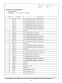
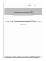
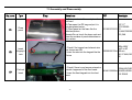
1
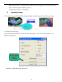
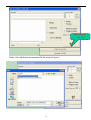
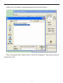
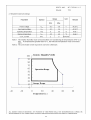
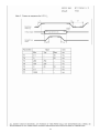
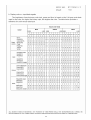
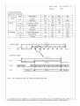
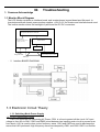
Service Manual LCD Monitor Acer V173 -0- 1 Table of Contents Important Safety Notice .........................................................................................01 01 Product Specification ..........................................................................................03 02 Flat Panel Specification .......................................................................................20 03 Exploded Diagram ..............................................................................................37 04 Troubleshooting ....................................................................................................41 05 Spare Parts List ...................................................................................................50 06 Schematics and Layouts.......................................................................................51 07 Assembly and Disassembly ................................................................................57 Appendix : User’s manual Copyright Copyright 2008 Acer Incorprated All Rights Reserved This manual may not, in whole or in part, be copied, Photocopied, reproduced, translated, or converted to any electronic or machine readable form without prior written permission of Acer Incorporated. Acer V173 Service Manual 1 Important Safety Notice 1. Safety precautions This monitor is manufactured and tested on a ground principle that a user’s safety comes first. However, improper used or installation may cause damage to the monitor as well as to the user. Warning: This monitor should be operated only at the correct power sources indicated on the label on the rear of the monitor. If you’re unsure of the power supply in you residence, consult your local dealer or Power Company. Do not try to repair the monitor by yourself, as it contains no user-serviceable parts. This monitor should only be repaired by a qualified technician. Do not remove the monitor cabinet. There are high-voltage parts inside that may cause electric shock to human bodies. Stop using the monitor if the cabinet is damaged. Have it checked by a service technician. Put your monitor only in a lean, cool, dry environment. If it gets wet, unplug the power cable immediately and consult your closed dealer. Always unplug the monitor before cleaning it. Clean the cabinet with a clean, dry cloth. Apply non-ammonia based cleaner onto the cloth, not directly onto the class screen. Do not place heavy objects on the monitor or power cord. z z z z z z z 2. Product safety notice Many electrical and mechanical parts in this chassis have special safety visual inspections and the protection afforded by them cannot necessarily be obtained by using replacement components rated for higher voltage, wattage, etc. Before replacing any of these components read the parts list in this manual carefully. The use of substitute replacement parts, which do not have the same safety characteristics as specified in the parts list, may create shock, fire, or other hazards. 3. Service notes z When replacing parts or circuit boards, clamp the lead wires around terminals before soldering. z Keep wires away from high voltage, high temperature components and sharp edges. z Keep wires in their original position so as to reduce interference. z Adjustment of this product please refers to the user’ manual. 2 01 Product Specification 1. General: ACER BV173 is designed with LVDS interface and dual (VGA&DVI) input, it featured with embedded universal AC power supplies. It’s a green product and meets all ROHS standard. The power button and display control buttons are on the front of the monitor. The monitors shall automatically display lower resolution video modes into 1280x1024 full screen display .The image can be adjusted through OSD control. 1.1 Features Features Specifications Maximum resolution 1280 x 1024 @ 75Hz Back light system 4 CCFL Actual Resolution display SXGA Resolution (1280x1024) Pixel pitch 0.264(H) x 0.264(V) Display area 337.920(H)x270.336(V) (17.0-inch diagonal) Contrast ratio based on the following panel source in the table below 5 ms (Typ); 10 ms (max) Response time (Tr +Tf ) 10%-90% @ Ta=25°C based on the following panel source in the table below Dual (VGA&DVI) Viewing angle (H/V) Input interface Audio amplifier Without Audio Power management Compatible with Energy Star Plug & Play VESA DDC 2B University AC power supply 100V – 240V AC, 50Hz – 60Hz OSD language English(US), French, Italian, Spanish, Dutch, Japanese (Factory Presetting Mode is Japanese) Attached table of Panel source: Brightness(cd/m²) Min. Typ. Panel Source MT170EN01_VC 250 Contrast Ratio Min. Typ. 300 700 View Angle Hor. Ver. 1000 80°/80° 80°/80° Remark INL 1.2 Checking contents Items VGA cable Description 2. DVI cable User’s manual 1.8 1.8 ● ● Multi m Warranty card Quick-start Guide Installation Guide English ● ● Operation Specifications The unit should suffer no visible cosmetic damage and should operate with no degradation in display quality during exposure to the operating conditions and after exposure to the non-operating conditions, in any sequence. 2.1 Environmental conditions Operating Specification Temperature range 5°C to 35°C Relative humidity 20% to 80% Altitude 0 to 3048M (10000 ft) 3 Storage Temperature range -20°C to 60°C Relative humidity 5% to 80% Altitude 0 to 9144M (30000 ft) 2.2 Safety, EMC, Ergonomics and Compatibility Requirements Items Description Safety EMC Ergonomics UL/ C CCC Other ● TUV/ ● G ● ● ● FC CE CCC VCC ● ● ● ● TC TC MPR ● O ● O Windows ●/ / Compatibility ● Windows 2000 Windows XP ● ● Energy Star Power Management ● Note: TCO99 is for black model; TCO03 is for white model 2.3 Electrostatic Discharge Requirements Item Condition Spec Contact discharge : 4KV Electrostatic Discharge IEC61000-4-2(EN55024) Contact discharge : 8KV ● Air discharge : 8KV Air discharge : 15KV ● 2.4 Reliability Items Condition Spec Note ≧ 50,000 Hours Excluding the LCD, CCFL ≧ 40,000 Hours(min) Note1 MTBF CCFL Life time Luminance becomes 50% Note1. Display an all WHITE field at mid Brightness and Contrast settings. 3. Electrical Characteristics and Performance 3.1 Main Power Supply The power supply unit built in the cabinet of a liquid crystal display monitor. Items Condition Spec Universal input full range 100~240VAC /50~60Hz AC Input Current 100Vac 240Vac 1.2A(max) 0.6A(max) AC Frequency Range 100Vac 240Vac 47Hz – 63Hz Inrush Current 100Vac,cold star,25°C 240Vac,cold star,25°C 40A (max) 60A(max) Regulator Efficiency DC output full loading ≥80% +14V output <300mV AC Input Voltage Range Ripple and Noise 4 Note Notes: 1. 2. +5V output <150mv DC Output Voltage and Current 13.5V-15.6V 4.9V-5.3V 1.4A(typ.),1.8A(max) 1.1A(typ.),1.4A(max) Power consumption without Audio ≤35W Protection See Table-1 Power management See Table-2 Notes: 1. Before each test, the buck capacitor need to be discharged. 2. Before each test, it must be 10 minutes at least after the latest test. Table-1 Protection Condition Spec SCP(short circuit protection) with auto-recovery function OPP(Over power protection) nominal AC input ≧42W Table-2 Status H-sync Power On Power Saving Power Off 3.2 V-sync Video Power LED on on active < 35W Blue off on blanked < 2W Amber on off blanked < 2W Amber off off blanked < 2W Amber -- -- -- < 1W Off Backlight Power Supply Items Specification Panel INL MT170EN01_VC, Lamp 4 CCFL Input Voltage 13.5V-15.6V Input current 1.4A(typ.),1.8A(max) On/Off switch level 5.5V≧Von≧ 2.0 V -0.3v ≤ Voff ≤ 0.8 V Brightness PWM duty 35%~100% *PWM:High=3.3V(3.00~3.60V),Low=0.0V,Frequency=4.0*V-Freq(Hz) CCFL operating Voltage See Attached Table-2 CCFL Current See Attached Table-2 CCFL startup voltage See Attached Table-1 Operating frequency Protect delay time 40~60KHz Efficiency 75% (with dummy load) >1 second Table-1 No Load Voltage: Item Symbol Min. Typ. Max. Unit No Load Voltage Vs 1700 --- --- Vrms Symbol Min. Typ. Max. Unit Remark INL MT170EN01_VC Table-2 On Load Function: Item 5 Remark Frequency F 40.0 50 60 kHz @Brightness=3.3V Output Current for One Lamp IL 3.0 7.0 8.0 mArms Operating Voltage Vo --- 610 --- Vrms INL MT170EN01_VC Kick Off Voltage Hold Up Time T 1.0 1.5 --- S @Vin=13.5V Brightness=3.3V INL MT170EN01_VC 3.3 Brightness output The test to verify specifications in this section shall be performed under the following standard conditions unless otherwise noted. The test standard conditions are: Temperature : 25 ± 5°C AC line input voltage : 110Vac / 60Hz or 220Vac / 50Hz. Warm-up time : 30 minutes minimum Video Resolution : 1280x1024@60Hz Video input signal : 700mV ± 2% LCD Module BL MT170EN01_VC (InnoLux) >=250cd/m*m Set brightness control and also contrast control at maximum, to measure the screen center, the light output shall ≥ BL cd/m2 (as panel spec) 3.4 White balance adjustment The test standard conditions refer to Sec 4.3. Chromaticity Coordinate Mode 3.5 x y Cool 9300K 0.283 ± 0.030 0.298 ± 0.030 User Default Default Default Warm 6500K 0.313 ± 0.030 0.329 ± 0.030 Brightness uniformity The test standard conditions refer to Sec 4.3. Set contrast control and brightness at the maximum, apply pattern as Fig.1, it should meet the following requirement: Min. luminance of nine points (backlight) ≥75% Max. luminance of nine points (backlight) 6 4. Input / Output Signal Specifications 4.1 Signal Interface Items Condition 15 pin D-Sub Signal Cable DVI Signal type Analog Level Impedance Signal type Sync Level Impedance Spec OK Color: Gray Length: 1800 +/- 20 mm NA Separate analog R,G,B 700 mV +/- 5% (peak to peak) 75 Ohms +/- 2% Ohms Separate H/V-sync (Positive/Negative) Logic High: 2.0V ~ 5.5V Logic Low: 0V ~ 0.8V (TTL level) ≧1.0K Ohm ● Note ● For 15 pin D-sub ● ● ● For 15 pin D-sub ● Refer to VESA VSIS Standard V1R1 ● 1.0KΩ for application 4.2 Signal Timing Through D-SUB connectors, this unit can support FH= 31.5 ~ 80 KHz, Fv=56 ~ 75Hz and SXGA display modes as below: Resolution 640 x 480 800 x 600 1024 x 768 H-Freq. (kHz) V-Freq. (Hz) Dot Clock (MHz) 31.5 60.0 25.175 37.9 72.0 31.500 37.5 75.0 31.500 35.1 56.0 36.000 37.9 60.0 40.000 48.1 72.0 50.000 46.9 75.0 49.500 48.4 60.0 65.000 56.5 70.0 75.000 60.0 75.0 78.750 64.0 60.0 108.000 80.0 75.0 135.000 640 x 350 31.5 70.0 25.175 720 x 400 31.5 70.0 28.322 1280 x 1024 832 x 624 1024 x 768 49.7 74.6 57.283 60.2 75.0 80.000 48.8 60.0 64.000 Mode VESA IBM-AT Compatible machine PC-9800 series US/IBM Text Power Macintosh series 4.3 Timing Requirements Item Horizontal Vertical Condition Sync polarity: (+) or (-) Sync polarity: (+) or (-) Specification 31.5 ~ 80 KHz. 56-75Hz Out of range Excluding Horizontal 31.5~80 KHz or Vertical 56-75 Hz Message “Input Not Supported” on screen Cable not connect No VGA cable Message ‘’No Signal’’ on screen 4.4 DDC Data 7 EDID Standard Compliance EDID File Format: VESA’s EDID Standard Version #3, Revision #0, EDID Structure : Version #1, Revision #3. EDID Data Table : See the attached table (for example) EDID Table For InnoLux MT170EN01_VC Pane 4.1.1 V173 VGA EDID table (INL VC 17’ Panel) 0 1 2 3 4 5 6 7 8 9 A B C D E F 0 00 FF FF FF FF FF FF 00 04 72 19 00 00 00 00 00 1 00 00 01 03 08 22 1B 78 EA DC 55 A3 59 48 9E 24 2 11 50 54 BF EF 00 01 01 01 01 01 01 01 01 01 01 3 01 01 01 01 01 01 30 2A 00 98 51 00 2A 40 30 70 4 13 00 52 0E 11 00 00 1E 00 00 00 FD 00 38 4B 1E 5 53 0E 00 0A 20 20 20 20 20 20 00 00 00 FF 00 30 6 30 30 30 30 30 30 30 30 30 30 30 0A 00 00 00 FC 7 00 56 31 37 33 0A 20 20 20 20 20 20 20 20 00 CS 4.1.2 5. V173 DVI EDID table (INL VC 17’ Panel) 0 1 2 3 4 5 6 7 8 9 A B C D E F 0 00 FF FF FF FF FF FF 00 04 72 19 00 00 00 00 00 1 00 00 01 03 80 22 1B 78 EA DC 55 A3 59 48 9E 24 2 11 50 54 BF EF 00 01 01 01 01 01 01 01 01 01 01 3 01 01 01 01 01 01 30 2A 00 98 51 00 2A 40 30 70 4 13 00 52 0E 11 00 00 1E 00 00 00 FD 00 38 4B 1E 5 53 0E 00 0A 20 20 20 20 20 20 00 00 00 FF 00 30 6 30 30 30 30 30 30 30 30 30 30 30 0A 00 00 00 FC 7 00 56 31 37 33 0A 20 20 20 20 20 20 20 20 00 CS Function Specifications 5.1 Panel General Specifications All the tests to verify specifications in this section shall be performed under the following standard conditions unless otherwise noted. The standard conditions are: Temperature AC line input voltage Warm-up time Checking display modes : 25 ± 5°C : 110Vac / 60Hz or 220Vac / 50Hz. : 30 minutes minimum : All the specified modes 5.1.1 General Specifications Panel Source INNOLUX` Model name MT170EN01_VC Display Area 337.9(H) X 270.3(V) Pixel Pitch 0.264x0.264 Display Colors 16.2 Million (each 6-bit + 2-bit FRC) 8 Number of Pixel Pixel Arrangement 1280x1024 pixels RGB vertical stripe Brightness 300cd/m2 (Typ.) 250cd/m2 (Min.) Contrast Ratio 800:1(Typ.) 600:1(Min.) Viewing Angle Hor:160°, Ver: 160°(Typ., CR>=10) Display Mode Normally White Frame rate 75Hz Response Time Tr + Tf = 5ms Typical Surface Treatment Hard coating (3H), Anti-glare treatment x4 Lamp Outline Dimension 358.5(W)x296.5(H)x17.0(D) 5.1.2 LCD Module Defects LCD module defects check follow to the IIS. 5.2 Keypad Function 5.2.1 Control buttons on the front bezel CONTROL KEY [AUTO] [MENU] [►], [◄] [e Color ] [POWER] KEYS FUNCTION A. When OSD un-displays, press [AUTO] to perform auto-adjustment B. When OSD displays, press [AUTO] to return to previous level menu C. When “e Color OSD” OSD displays, press [AUTO] to exit the OSD A. When OSD isn’t shown on screen, press [MENU] to enter OSD interface. The OSD interface uses “ACER e Color Management” and “User” to instead “Contrast” and “Brightness” separately. When press “ACER e Color Management” to show “e Color OSD”, and press “User” to show OSD interface before. The translations of “ACER e Color Management” and “User” are always English. B. When OSD displays, press [MENU] to perform function of menu icon that is highlight or enter next level menu A. When “MENU OSD” displays, press these keys to change the contents of an adjustment item, or change an adjustment value B. When “MENU OSD” un-displays, if it is with audio, press [►] to show “Audio” OSD and increase the volume, press [◄] to show “Audio” OSD and decrease the volume; else it has no use to press these keys. A. When OSD un-displays, press [e Color] to show “e Color OSD”, and press again the OSD can not disappear, but the time of “e Color OSD” disappearing is reset 10 second again. B. When OSD disappear not including “e Color OSD”, press [e Color] to show “e Color OSD” OSD, the OSD before disappears, but the parameters of it should be saved Power on or power off the monitor 9 5.2.2 Hot Key Operation FUNCTION FACTORY MODE HOT KEY OPERATION e-Color AUTO ◄ ► MENU ● ● DESCRIPTION POWER Press [E-Color] & [MENU] at the same time, and then press [POWER] for DC power on. OSD menu will be shown with “F” on the left top. Select “F” for entering factory mode. ON 5.3 OSD Structure The On-Screen Display (OSD) shall be an easy to use icon based menu through keypad OSD buttons or remote control unit. The unit shall leave the factory with all OSD controls set to their default values. First Second ACER e COLOR Management Third Control Range Default Value Empowering Technology Contrast Brightness User Brightness User mode 50 Text mode 50 Standard mode 50 Graphics mode 60 Movie mode User mode 56 77 Text mode 44 Standard mode 77 Graphics mode 97 Movie mode 77 ACM Image Position Focus Clock Horizontal Vertical Warm (6500K) Cool (9300K) Color User Language NO-EMEA EMEA English English Deutsch Deutsch Español Español 简体中文 Hollands 繁體中文 Русский Français Français Italiano Italiano OFF ------------- 0 ~ 100 Depend on each timing 0 ~ 100 50 ○1 0 ~ 100 50 0 ~ 100 Depend on each timing Red 0 ~ 100 80 Green 0 ~ 100 80 Blue 0 ~ 100 80 --------------- --------------- English ----- 10 日本語 Hor. Position OSD Suomalain en 50 0 ~ 100 50 10~ 120 20 ----- DDCCI ON/OFF ----ON DDCCI ON/OFF ON OSD Timeout Analog Input (Analg only) Digital Resolution H. Freq Info --0 ~ 100 Ver. Position Input (Dual) ------------- V. Freq ------- ------- ----- ----- S/N ----- Reset Exit ------ETL000….0000(22) ----- Notes: 1. Clock default 50 is for Visa timing. Others depend on timing. 5.3.1 OSD Function Test 3.1.1 Test mode: 1280x1024 @ 60 Hz 3.1.2 Test pattern: pattern #1 of crosshatch (GENERAL-1) 3.1.3 Check single key function and hot key function about key “Power”, “Menu”,” ►”, “◄ “, “Exit/Auto”, “[e Color ]” it should operate normally 5.3.2 Screen Picture Check 5.3.3 Test mode: 1280x1024 @ 60 Hz 5.3.4 Test pattern: pattern #1 of crosshatch (GENERAL-1) 5.3.5 Select OSD menu to execute ‘Auto’ function, screen picture shouldn’t appear abnormal phenomenon and picture on screen should fit in with active display screen. 5.4 Auto Color Balance 5.4.1 Test mode: 640X480 @ 60 Hz 5.4.2 Test pattern: pattern #42 of 5 mosaic pattern 5.4.3 Enter "Factory Mode" pressing "MENU" key, execute "AUTO". 5.4.4 When Color Balance finished, Must push “POWER” key to exit “Factory mode”, and restart. 5.5 Timing Check 5.5.1 Test mode: Refer to preset timing table and power saving mode 5.5.2 Test pattern: pattern #1 of crosshatch (GENERAL-1) 5.5.3 After change above timing and execute “Auto” function automatically, picture should fit in with active display screen. 5.5.4 Under power saving mode, LED lamp on the key board should be orange 5.6 Power Consumption Function Test 5.6.1 Test mode: 1280x1024 @ 60 Hz 5.6.2 Test pattern: pattern #41 of “WHITE” 5.6.3 Adjusting both brightness value to maximum, 5.6.4 Measure power consumption as the following Status Power Consumption LED Display Normal < 35W Green 11 Standby (No H/V sync) < 1W Orange Power off < 1W No display 5.7 VGA Cable Detect Test If VGA cable of LCD monitor isn’t connected to video pattern generator or PC, “NO SIGNAL” should be shown on screen. 5.8 Hi-Pot test Test condition: a. high voltage 2.3KV(DC) b. leakage current 10mA c. rising time 1 sec. d. test time 3 sec. 5.9 Grounding Test Test condition: a. test current b. impedance 5.10 30A / 2 sec < 0.1Ω Bumping Test 5.10.1 Test mode: 1280x1024 @ 60 Hz; 5.10.2 Test pattern: pattern #1 of crosshatch (GENERAL-1) 5.10.3 To shock LCD monitor lightly at the center of rear cover and edges with 1~2kg/cm2 force for three times, no abnormal phenomenon is found on panel screen. 6. DISPLAY CHECK 6.1 Panel Flicker Check Connect LCD monitor to PC, set LCD monitor to be timing of 1280x1024@60 Hz, adjust brightness to be default value (brightness at maximum), execute “Auto” function, and then check picture of shut down under windows operating system, or flicker-pattern of pixel on-off. It should be that no flicker be found on panel screen. 6.2 Panel Defect Inspection 6.2.1 Test mode: 1280 x 1024@60Hz 6.2.2 Test pattern: Crosshatch/Full white/Red/Green/Blue/Black/16 color bar/64 gray bars 6.2.3 Display quality must be (according to DIN 13406-2 pixel fault class II) Specification Defect Type Bright Dots Dark Dots Major Minor N≤2 ( For AMLCD ) ● N ≤ 3 ( For LPL and INL) ● N≤4 (green=0) (For CPT) ● N≤5 ( For AMLCD ) ● N ≤ 4 ( For CPT & LPL & INL ) N≤5 ( For AMLCD, LPL & INL ) ● N ≤ 4 (For CPT) ● N ≤ 1 pair ( For LPL & INL ) ● N ≤ 2 pair (For AMLCD & CPT) ● Bright Dots – 3 or more Adjacent N ≤ 0 pair ● Dark Dots – 2 Adjacent N ≤ 2 pair ● N ≤ 1 pair ( For AMLCD ) ● Total Bright and Dark Dots Bright Dots – 2 Adjacent Dark Dots – 3 or more Adjacent N ≤ 0 pair ( For AMLCD, LPL & INL ) 12 Distance between Bright dots L ≥ 15 mm ● Distance between Dark dots L ≥ 15 mm ● Note 1: Dot defect is defined as the defective area is not larger than 50% of the dot area. Bright Dot is defined 5% transmission ND filter. Note 2: Light Leakage: There shall not be visible light around the customer’s bezel after assembly in normal View angle. Defect Type Dot Shape (Particle、Scratch and Bubbles in Display area or on The Polarizer) Specification Size Scratch Dirt Bezel Major 0.1 ≤ D ≤ 0.7 mm (AMLCD) 0.15 ≤ D ≤ 0.5 mm (CPT & LPL) 0.05 ≤ D ≤ 0.15 mm (INL) N≤4 N≤4 N≤3 0.3mm ≤ L ≤ 5.0mm 0.01≤W≤0.1mm N ≤3 (for Sam) 1mm ≤ L ≤ 10mm 0.01≤W≤0.05mm N ≤4 (for LPL) L ≤3mm W ≤ 0.1 mm N ≤4 (for CPT) 0.3mm ≤ L ≤ 10mm 0.05mm ≤ W ≤ 0.15 mm N ≤4 (For INL) There should be non-uniformity through 5% transparency of filter or judge by limit sample if necessary. ● ● ● ● ● No harm ● Wrap No harm ● Sunken No harm ● No label Invert label ● No ● Broken Dirt Label Minor Black spots which appear when B/L operating Line Shape (Particles, Scratch, Fiber and Bubbles in display area or on The Polarizer) Display non-uniformity Count (N) ● Word can be read. ● Not clear ● Word out of shape ● Mistake No ● Position Be attached on right position ● Not enough No ● Limp No ● Connector Connection status No bend on pins and damage ● FPC/FFC Broken No ● Screw 7. SOP of firmware upgrade (Manufacturer of Scaler is RealTek) 7.1 Operational condition: 13 Equipment: PC, ISP card, signal cable and power cable. ESD requirements: antistatic wrists, antistatic gloves (fingers), and connecting cable Name of ISP program: RTDTool_4.6.exe Manufacture of FW IC:RTD 2525L 7.2 Operational steps: 1. Connection: connect PC to PCBA with signal cable, and then keep AC and DC in open state 2. Adjust ISP programming Firstly, double click RTDTool_4.6.exe and open ISP program, then select “25XXV/2525L”, and RTD 2120 ISP button. Click ISP button Secondly﹐select Bank2 size which is 30. 14 Select Bank2 size: 30 Thirdly, click “64K”button and download FW file as below Figure 3. 15 Fourthly, click “64~96”button, and download extern FW file as below Figure 4 . Fifthly, click“program”button as below, then you will see ISP will going on. There will be prompting if programming is OK. 16 Program button Note: Please see the configure as below Figure 6. Configure Inform Programming speed 17 After connecting, AC ON, DC ON ◆Flowing chart OK Open ISP program OK Choose manufacturer and model of FW IC OK LOAD FW files OK Click program button OK Beginning programming Choose Config and adjust programming NG OK Turn off power if programming is OK 7.3 Factory Mode HOT KEY OPERATION FUNCTION AUTO FACTORY MODE e Color ● ◄ ► MENU ● 18 POWER ON Press [e Color ] & [MENU] at the same time, and then press [POWER] for DC power on. OSD menu will be shown with “F” on the left top. Select “F” for entering factory mode. 02. Flat Panel Specification 19 20 21 22 23 24 25 26 27 28 29 30 31 32 33 34 35 03 Exploded 3.1. LCD Exploded drawing (All) 36 Diagram 3.2 Assy Bezel Exploded drawing 37 3.3Assy BACK COVER Exploded drawing For VC panel 38 3.4 Assy BACK COVER Exploded drawing for AUO panel 39 04 Troubleshooting 1. Common Acknowledge 1.1 Monitor Block Diagram The LCD Monitor contains an interface board, and inverter/power keypad board and flat panel. In Inverter/power/Audio board, power section supplies +14V & +5V for Inverter and Interface board used. The inverter section drives the backlight of panel and the DC-DC conversion. Flat panel (LVDS interface) and CCFL Inverter/Power (Including AC/DC Power Supply , Inverter ) Interface Board Keypad BD AC input Range 100V~240V Host computer (VGA/DVI signal input and DDC) Audio input - 2 Interface BOARD DIAGRAM 1.3 Electronic Circuit Theory 1.3.1 Switching Mode Power Supply 1.3.1.1 AC Current Input Circuit P801 is a connector for connecting AC Power. F801 is a fuse to protect all the circuit. AC input voltage is from 90v to 264V. R801 and R802 joined between two inputting main circuit to prevent man from shock. L801 is used to clear up low frequency wave. C801 and C802 are used to discharge the waves that L801 produced. High frequency waves are damped by C801 and C802. D801 is a rectifier 40 which composed of 4 build-in diodes, it inverts AC to DC. 1.3.1.2 High Voltage to Low Voltage Control Circuit C804 is used to smooth the wave from rectifier. IC802 is a highly integrated PWM controller. When rectified DC high voltage is applied to the Vcc pin during start-up, the MOSFET Q804 is initially off, and the Vcc pin capacitor is charged. When the Vcc pin voltage reaches approximately 10V, the control circuitry is activated and the soft-start begins. The soft-start circuit gradually increases the duty cycle of the MOSFET from zero to the maximum value over approximately 4ms. If no external feedback/supply current is fed into the CS pin by the end of the soft-start, the current Setpoint will be above the fault level, FAULT flag is raised, if the FAULT duration exceeds 80ms, the output controller disable Resistor R808, R809, R810, R811 are for line over voltage shutdown(OVP) When PWM is turned off, the main current flow will be consumed through R804 and D802, This will prevent MOSFET Q804 from being damaged under large current impulse and voltage spike. D804 and C807 to provide internal Auxiliary voltage to Vcc pin during normal operation. Otherwise, error amplifier and feedback current input the CS pin for duty cycle control. 1.3.1.3 DC_5V and DC_14V Output Circuit For DC 5V, D805 is used to rectify the inducted current. R828 and C814 are used to store energy when current is reversed. The parts including C818, C822, C820,L803 are used to smooth the current waves. For DC 14V, D803 is used to rectify the inducted current. R827 and C813 are used to store energy when current is reversed. The parts including C815, C817 and L802 are used to smooth the current waves. 1.3.1.4 Feedback and OVP Protect Circuit Pin R of IC803 is supplied 2.5-v stable voltage. It connects to 5V and 14V output through R822, R823 and R824. R822, R823 and R824 are output sampling resistor. When the sampling voltage more than 2.5V or less than 2.5V, current of FB IC802 will change, this can change the voltage from T801. OVP Protect Circuit: When output is overvoltage, the auxiliary winding voltage will be increased, when it reaches about 14V. Q803 is triggered . It makes the IC802 Pin 1 exceed 5V, then the IC802 output will be disabled. Q801, R816, R817 and ZD803 make up of dummy loading circuit. For start-up sequence, during 5V output take place high loading first, this dummy loading circuit operated to insure 14V not be increased. I/F Board Circuit 1.3.2.1 RGB CAPTURE - Signal RED,GREEN,BLUE input through CN103 #1,#2,#3, Stop DC via C123, C124 and C125, and then enter into U104 (scaler) analog input terminal #16,#14,#12, and then scaler deals with signal internally. EP102, EP103 EP104 are ESD protector to prevent U104 from ESD. - Signal DDC_SCL (series clock) inputs via CN103#15, and then passes through EP109 for ESD protection, goes into U102 (MCU) #5. - Signal DDC_SDA (series data) inputs via CN103#12, and then passes through EP108 for ESD protection, goes into U102 (MCU) #8. - Signal TTL vertical sync. (Vsync) inputs via CN103 #14, and then clamped by EP107, passes through R162, and then goes into IC U104 (scaler) #8. - Signal TTL horizontal sync. (Hsync) inputs via CN103 #13, and then clamped by EP106, passes through FB104, R163, and then goes into IC U104 (scaler) #9. - CN103#5 is defined as cable detect pin, this detector realize passes through D101, D102, Q105 or through D101, D102, Q105, R107,Q106 change to MCU_VCC. - U103 power is supplied by MCU_VCC. - U103 is an EEPROM IC which is memory and EDID data saved in it. 1.3.2.2 Buttons Control - Button “Power” on right side bezel connects to U102 (MCU) #9 through R134, via CN901#1. - Button “E-Color” “AUTO”“MENU” “UP” “DOWN “on right side bezel connects to U102 (MCU) 41 #14,#22,#10,#21 through R141,R138,R135,R140,via CN901 #5, #6, #8, #7. - LED Indicator on Front Bezel 1 When press button “power”, U102 (MCU) #1 sends out a low potential, via R130, flow to CN901 #2 on keypad, LED Blue ON. 2 When in “Suspend” mode, U102 (MCU) #48 sends out a low potential, via R129, flows to CN901 #4 on keypad, LED Amber ON. 1.3.2.3 Realtk CHIP U104 (scaler)&U102 (MCU) - U104 (RTD2025L) #21~#28 output 8 bit even LVDS digital data to panel control circuit through CN104. - U104 (RTD2025L) #29~#36 output 8 bit odd LVDS digital data to panel control circuit through CN104. - U102 (RTD2120) #44 outputs Brightness “PWM” signals to control CCFL brightness. - U102 (RTD2120) #39 output PPWR ”H” potential to make Q104 conducted, and then make Q101 conducted, +5V flow to CN104#1~#3 as Panel VDD . - U102 (RTD2120) #46 output CCFL_ON/OFF ”H” potential to control Inverter on/off. - TCLK by Crystal 24.000MHz input to U102 (RTD2120) #15, #16. Please refer to RTD2120&RTD2025L Pin Assignments table in page. 1.3.2.4 Regulator Circuit - +5V is from switching mode power supply for Panel used. - +3.3V generates from +5V through C101 and C102 filtering and U101 which is output +3.3V LDO to generate MCU_VCC for U102, U103 and TMDS_VDD for U104. - +1.8V generates from +3.3V through Q110 and C134, C133, C135, C136, C137 for U104 used. Inverter circuit 14VDC provides the power for IC501; the control signals Brightness and ON/OFF come from I/F board. ON/OFF signal connect to pin8 of IC501 and makes IC501 enable. Brightness signal connect to pin7 of IC501 and regulates the panel brightness, R510 , R511, C507 make up a network of delaying time circuit . The striking frequency is determined by the external Resistor R505 pin5 of IC505and r516. The operation frequency is determined by the external Resistor R505 pin5 of IC505. the capacitor and resistrer connected to pin4 to set striking time and shunt down delay time. BURST MODE dimming pulse frequency and duty is regulated by I/F board. The output drives, include square pulses output of pin14,12,11 to drive MOSFET U501, U502, and U501, U502 are N channel MOSFETs. U501 and U502 work as harf-bridge topology.Two transformers are connected in parallel with each transformer driving two lamps in series. Turning each N-Channel MOSFET “on/off” complementarily, produces an alternating current through the transformer primary and secondary. The “on” duration of the switches determines the amount of energy delivered to the CCFLs. The current flowing through CCFL is sensed and regulated through sense resistor R502, R543. The feedback voltage connected to Pin2 (ISEN), then compared with a interal reference voltage ,resulting in PWM signal outputs to adjust output voltage. Over Voltage Protection and over-current protection are monitored by the voltage on OV(Pin 1) and LI (Pin2) During normal operation , if a CCFL is damaged or removed ,the voltage at OV (Pin6) increases .Once the voltage at OV Pin exceeds 1.2V (OVPT Setting) the driver output duty cycle is regulated and the shutdown delay timer is activated. Once over the delay time the IC will shut down 42 1. No Power & Power LED Off No power Check primary rectifier voltage Check circuit if short Check F801, P801, D801 Check pin7 of IC802 voltage about 13V Check R806, R807, R808, Check R808, R819, Check pin8 of IC802 voltage about 2.5V Check IC801 and secondry feedback Check pin2 of IC802 voltage is low END 43 Check IC802, C804, T801 2. DC output voltage is unstable Output voltage unstable Check Vbe of Q801below 0.3V Check circuit if short Check ZD801, D803, D805 Check Q801,Q802 Check reference voltage Check Pin R of IC803 voltage about 2.5V Check R832,, IC801, Check R822, R823 Check feedback circuit Check vpin2-4of IC801 about1V Check Vpin6 of IC801 have output Change IC END 44 Check R815, c814, R816 4. No Raster No raster? Yes LED Blue? Yes Backlight can’t be turned on. Yes Is there 14Vdc voltage on pin9 of IC501? No Check power supply Yes Is there high-level voltage on pin8 of IC501? No Is Ok R510? Yes Check I/F board No Yes Are connected rightly CN501, CN502, CN503 and CN504? R501 open Connecting the output connector again No Yes Is there instantaneously pulse wave on pin14, pin11 of IC501 at the moment of restart? No Is Ok IC501? Yes No U501, U502 fail IC501 fail Yes Is T501, T502 ok? No T501, T502 fail Yes END Check feedback circuit Isen,Vsen.(pin 1.2) 45 5. Black Screen 46 6. Bad Screen 47 7. White Screen 48 05 Spare parts List 8171J061A020R OEM PART NO DESCRIPTION 8171J071A020R MOQ N/A N/A 50 1 0 50 1 1 50 1 1 50 0 1 50 1 1 50 1 1 50 1 1 50 1 1 50 1 1 50 1 1 50 1 1 791421300600R PCBA,I/F BOARD(VC,EMEA),LE17J0-610 ROHS 791401500000R PCBA,KEYPAD BOARD,LE9D0-612 ROHS 791421400600R PCBA,P/I BOARD,W/O SPK,LE17J0-622 ROHS 791421300700R PCBA,I/F BOARD(EMEA,W/O),LE17J0-710 ROHS 430300801670R HRN ASSY 2x4P 55mm UL1571#28,ROHS 430300801760R HRN ASSY 2x4P to 8P 160mm UL1571#28,ROHS 430303001520R HRN LVDS FFC 30P 231mm W/MYLAR&Core ROHS 453070800210R PWR CORD 16A/250V BLK 6FT VDE H05VV-F 3G 453010100380R CABLE,D-SUB 15P MALE 6FT BLACK/BLUE, ROH 714030015900R ASSY, BEZEL,V,GRAY SILVER,LE17J0 714011202300R ASSY,STAND,BLACK,LE19D1 714020013200R ASSY,BASE,BLACK,LE17J0 50 1 1 501020220110R BACK COVER,V,W/O DVI,LE17J0 50 1 1 501240209800R BASE,COVER,V,BLACK,LE17J0 50 1 1 501020220020R COVER HINGE,BLACK RIGHT,LE19D1 50 1 1 501020220021R COVER HINGE,BLACK LEFT,LE19D1 50 1 1 701000007201R ASSY,CHASSIS,V,W/O DVI, LE17J0(VC) 50 1 0 701000007204R ASSY,CHASSIS,V,W/O DVI, LE17J0(AUO-B) 50 0 1 631102072741R LCP 17" MT170EN01-VC-G1,AM1700005C21(INN 10 1 0 631102072472R LCP 17"M170EG01-VD-0B(AUO)ROHS 10 0 1 49 06 Schematics and Layouts 5DVCC ADJ 1 0 0 u /1 6 V C141 Shoule be canceled for the brightness is not so good C 103 5DVCC C 104 + C 102 C 101 VBRI 2 VOLUMN 2 MUTE 2 2 1 + VLCD C C C C C 3.3VCC 51 100K R 101 3 Q101 AP2305GN R103 4K7 0 .1 /1 6 V BKLT-EN R104 4K7 + C 108 2 LEFT/Left&Auto 3 4 AUTO/GND 5 6 7 8 C 144 C 145 C 109 C 110 0 .1 /1 6 V 0 .1 /1 6 V 0 .1 /1 6 V 0 .1 /1 6 V 2 LED_G INVON 2 Q103 PMBT3904 2 1 2 LED_A 1 2 RIGHT/Memu&Right ADC_Key1 2 Key2 2 POWER Key3 2 2x4P 2.0mm 0 .1 /1 6 V 0 .1 /1 6 V 0 .1 /1 6 V 2 ADC_Key2 CN102 MENU/GND InnoLux BV173 C 146 C 147 C 148 2 Key1 Q104 PMBT3904 C 107 2 1 10K 20K R 106 R105 1 u /1 6 V 2 PANELPOWER_ON/OFF C 106 3 3 Q102 2N7002 1 3 R 102 1 0 .1 /1 6 V C 105 2 1 5 0 u /1 6 V 139 140 141 142 143 VIN VOUT 0 .1 /1 6 V 1 0 0 u /1 6 V BKLT-EN 0 .1 /1 6 V 0 .1 /1 6 V 0 .1 /1 6 V /N C 0 .1 /1 6 V 0 .1 /1 6 V F rom P ow er & In v e r te r 8P 2.0mm 3 0 .1 /1 6 V 5DVCC CN101 1 2 3 4 5 6 7 8 3.3VCC U101 LD1117AL-3.3V Document Number : Add C139~C148 SIZE : ??? APPRO BY : A4 TITLE : CHECK BY : DC to DC 2007-10-09 DATE : SHEET 50 2 OF 8 DRAWN BY : Rev : V01 MCU_VCC MCU_VCC 3.3VCC MCU_VCC D102 SN4148 2 3 DSUB_5V 3 Q105 PMBT3906 4K7 4K7 1K 4K7 4K7 4K7 4K 4K 4K 4K 4K 4K 4K 4K 4K 4K 4K 4K 4K 4K 7 7 7 7 7 7 7 7 7 7 7 7 7 7 1 MCU_VCC D101 SN4148 + C111 C112 10u/25V 0.1/16V 100 100 R134 R135 100 100 R141 R136 R137 R139 100 100 100 100 9 10 11 12 13 14 40 39 38 37 36 35 34 33 R ST VC C VSYNC P3.2/INT0 RTD2120_LQFP48 P3.3/INT1 P3.4/T0 P3.5/T1 P7.6/CLKO2 P7.7 3.3VCC 27 26 25 24 23 22 21 20 R170 100 CRYSTAR_OUT 4 DSUB_CONNECT 3 R138 R140 100 LEFT (AUTO) ADC_key2 1 100 RIGHT (MENU) ADC_key1 1 R142 10K C138 10p/50V 2 U102 RTD2120 P6.7 P6.6/CLKO1 P6.5 P6.4 P6.3/ADC3 P6.2/ADC2 P6.1/ADC1 P6.0/ADC0 Add R170/C138 28 C C C C C C Power Key/LED IICSCL IICSDA WP AUTO 5 8 ASCL/P3.0/RXD ASDA/P3.1/TXD N N N N N N 1 Key2 R131 R133 32 NC 31 NC 30 NC 29 NC XO XI VSS 1 Key3 100 100 6 7 18 19 42 43 3 DDC1_SCL 3 DDC1_SDA R129 R130 P5.0/PWM0 P5.1/PWM1 P5.2/PWM2 P5.3/PWM3 P5.4/PWM4 P5.5/PWM5 DSCL/P5.6 DSDA/P5.7 R128 4K7 P 1 .0 /T 2 P 1 .1 P 1 .2 P 1 .3 P 1 .4 P 1 .5 P 1 .6 P 1 .7 4 41 LED2 LED1 44 45 46 47 48 1 2 3 1 PANELPOWER_ON/OFF 1 RTD_SD3/SDI 4 RTD_SCLK 4 15 16 17 VBRI VOLUMN INVON MUTE 3 Q106 PMBT3906 R 125 R 126 R 127 R 122 R 123 R 124 R R R R R R R R R R R R R R 108 109 110 111 112 113 114 115 116 117 118 119 120 121 2 MCU_RESET 1 1 1 1 R107 4K7 3.3VCC LED2 1 2 Q107 PMBT3906 Q108 100 PMBT3906 R145 100 1 Key1 2 MENU R146 Q109 1 Key/LED PMBT3906/NC 220 R147 3 1 LED_A 3 1 LED_G LED1 1 3 R143 0 X101 24.000MHz MCU_VCC InnoLux BV173 MCU_VCC Document Number : C113 10p/50V U103 1 2 A0 3 A1 4 A2 GND C114 10p/50V + C115 10u/25V C116 0.1/16V 8 VCC 7 WP 6 SCL 5 SDA ??? MCU_RESET WP IICSCL IICSDA Closed to MCU SIZE : APPRO BY : A4 TITLE : CHECK BY : MCU R148 10K 2007-10-09 DATE : AT24C04N SHEET 51 3 OF 8 DRAWN BY : Rev : V01 DSUB_5V 60Ω FB103 60Ω R155 R157 C R C R C R E E E E 16 17 15 FB102 R149 R150 R151 R152 R153 R154 0 0/NC R156 R158 0 .1 /1 6 V /N C 0 .1 /1 6 V /N C 0 .1 /1 6 V /N C 5P20V 14 60Ω C 126 C 127 C 128 EP105 13 FB101 5P20V 5P20V 5P20V 5P20V 0 .1 /1 6 V /N C 75 1% 0 .1 /1 6 V /N C 75 1% 0 .1 /1 6 V /N C 75 1% 12 DSUB_5V 2 P101 P102 P103 P104 123 159 124 160 125 161 11 CN103 DZ11AA1-H5W6-4F 1 R 6 2 G 7 3 B 8 4 9 5 10 100 100 100 100 100 100 C117 C118 C119 C120 C121 C122 3.3VCC 0.047u/16V 0.047u/16V 0.047u/16V 0.047u/16V 0.047u/16V 0.047u/16V 10K 100 RTD_R+ 4 RTD_R- 4 RTD_G+ 4 RTD_G- 4 RTD_B+ 4 RTD_B- 4 DSUB_CONNECT 2 Note: Components of 5P20V may be cancelled if ESD test result is OK. DDC1_SCL 2 VSync E E E E P P P P 20V 20V 20V 20V 3 3 p /5 0 V 2 2 0 p /5 0 V RTD_H 4 C 129 C 130 100 2K2 2K2 R163 R 164 R 165 120Ω 5P 5P 5P 5P FB104 100 106 107 108 109 HSync R162 DDC1_SDA 2 DSUB_V 2 RTD_V 4 InnoLux BV173 Document Number : ??? APPRO BY : SIZE : A4 TITLE : CHECK BY : Input 2007-10-09 DATE : SHEET 52 4 OF 8 DRAWN BY : Rev : V01 3.3VCC FB105 BJT _B TMDS_VDD 60Ω C131 0.1/16V 3.3VCC C132 0.1/16V R144 470 R132 470 R1.8DVCC 3 2 R T D _SC LK 2 R T D _ S D 3 /S D I 2 Q110 PMBT2907A C133 C135 10u/25V 0.1/16V C136 0.1/16V C137 0.1/16V CN104 FFC-CON 3 2 1 + C134 0.1/16V Q111 PMBT2907A R 1 .8 D V C C DGND R XO 0R XO 0+ T M D S_VD D C R YST AR _O U T 2 1 R1.8DVCC TMDS_VDD V 0 /R X 2 N V C L K /R X 2 P T M D S_VD D X IN D D C S C L /P W M 0 D D C S D A /P W M 1 /IR Q SCL SDA VCCK PGND T XO 0T XO 0+ R167 1K/NC 4 5 6 7 3 RTD_V 3 RTD_H 8 9 10 3 RTD_B3 RTD_B+ 11 12 V2/RX1P TXO1+ V3/RX1N TXO2- V4/RX0P TXO2+ V5/RX0N TXOC- V6/RXCP TXOC+ V7/RXCN RTD2025L TXO3- AVS TXO3+ AHS TXE0- ADC_GND TXE0+ B- TXE1- B+ GG+ RR+ AD C _VD D BJT _B VCCK PGND T XE3+ T XE3T XE2+ T XE2- 3 TXO1- TXE1+ 36 RXO1- 35 RXO1+ 34 RXO2- 33 RXO2+ 32 RXOC- 31 RXOC+ 30 RXO3- 29 RXO3+ 28 RXE0- 27 RXE0+ 26 RXE1- 25 RXE1+ RXE1RXE1+ RXE1RXE1+ RXE2RXE2+ RXECRXEC+ RXE3RXE3+ RXE2RXE2+ RXECRXEC+ RXE3RXE3+ R168 R169 VLCD 0 0 30 29 28 27 26 25 24 23 22 21 20 19 18 17 16 15 14 13 12 11 10 9 8 7 6 5 4 3 2 1 InnoLux BV173 Document Number : 13 14 15 16 17 18 19 20 21 22 23 24 2 V1/REXT SIZE : ??? APPRO BY : A4 TITLE : R T D _G R T D _G + R T D _ R3 R T D _ R 3+ 3R 1 . 8 D V C C 3B J T _ B R 1 .8 D V C C DGND R XE3+ R XE3R XE2+ R XE2- 1 RXOCRXOC+ RXO3RXO3+ RXE0RXE0+ RXOCRXOC+ RXO3RXO3+ RXE0RXE0+ 48 47 46 45 44 43 42 41 40 39 38 37 U104 RXO0RXO0+ RXO1RXO1+ RXO2RXO2+ RXO0RXO0+ RXO1RXO1+ RXO2RXO2+ CHECK BY : Scaler 2007-10-09 DATE : SHEET 53 5 OF 8 DRAWN BY : Rev : V01 R805 0R2 1W C807 10u/25V R803 330K 1 7 LD7522 IC802 6 OUT 4 CS RMS RT801 NTC 5R F801 2A/250V C801 1000p/400V SW801 SW DPST C802 1000p/400V 3 R819 120K 1% C812 100P/50V + C820 1000u/10V 9 C828 2200p/400V R832 270 1% LTV817M IC801 C813 R833 1000p/50V 4K7 1 R822 5K1 1% R823 0 1% 10 6 C808 100p/1KV R816 1K C814 100p/50V 0.1/50V C822 F803 4A/32V R821 1K 1% R814 R815 10K 0R49 2W 4 1 3 2 R820 3K 1% C826 NC C821 0.022/100V R826 NC C IC803 R TLV431ALP A R824 3K3 1% CN801 1 2 3 4 5 6 +5V ON/OFF BRIGHTNESS 100mm 6P TO SCALER BD CN101 C827 0.1/50V InnoLux ACER17" Document Number : APPRO BY : SIZE : A4 TITLE : CHECK BY : POWER SUPPLY N 2 L 1 (-)LATCH GND COMP R812 330K 1% AC 264V AC 264V RMS 3 5 2 BNO 8 5 C824 47u/25V + 3 RMS 4 AC 264V AC 264V OVP C811 2.2u/50V Q804 AP2761I 1 R813 10R VCC 330K C803 0.47/275V DC 650V Max R818 1M 1% FB801 120Ω 3A Q801 2PC1815GR +5V D805 SR540PT 10K + R811 3M R802 3 3 R830 200 5uH L803 8 1N4007 D804 C810 0.1/50V ZD801 9V1 C819 470u/25V 7 DC 650V Max R809 3M R810 3M C817 R828 C816 1000p/500V 1000u/25V 10 D802 MUR1100ERL R808 150K + 51K 1% 3 L801 12mH 2 + R 829 1 R801 330K R806 150K +14V R831 100Ω 1W R 825 4 R807 150K 5uH L802 12 C806 2 4700p/400V 3 RMS 2 SR5150PT D803 2 + 1 BL4-06 + C804 82u/450V 11 R834 R835 68 68 R804 68K 2W D801 1 T801 SPW-0xx C815 1000p/500V 2 C805 2200p/400V DC 380V Max. R827 10 P801 AC_SKT 2007-10-09 DATE : SHEET 54 6 OF 8 DRAWN BY : Rev : V01 55 7.0 Assembly and Disassembly Sequence S1 S2 S3 Item Photo Procedures P/N Description Place panel (1).Take panel out of box and place it on the foam. (2).Tear open the PE bag and put it in LCP 17" the designated carton. MT170EN01(3).Place panel on the foam like the 631102072741R VCattached picture. G1,AM1700005 Remark:Do not touch the lamp cord and C21(INN place the surface of panel downsides on the cushion. Insert Keypay's wrie HRN ASSY 1.Check if the keypad and relevent wire 2x4P to 8P you choose are OK. 430300801760R 160mm 2.Insert the wire into the keypad like the UL1571#28,RO Picture HS Fix front bezel 1.Check if there is any lacquer missed or PCBA,KEYPAD sctratch happened to the front bezel. 791401500000R BOARD,LE9D02.Insert the fixed keypad into the front 612 ROHS bezel. 56 Assembly and Disassembly continue) S4 Assemble front bezel S5 Fix mainboard S6 Fix chassis &poweboard 1.Reverse the panel by 180 degree,put the surface of panel upsides and insert front bezel in the panel. 2.Reverse the panel by 180 degree using both hands,put the surface of panel downsides and make sure FFC interface is closer to operator. ASSY, BEZEL,V,GRAY 714030015900RSILVER,LE17J0 3.Paste tinfoil on the position which refers to attached picture,in order to cover the gap in the panel completely. Remark:Make sure the fixed job is finished properly and lamp wire is closer to right hand;Make the tinfoil smooth in the corner of panel. (1).Insert FFC wire into its relevant interface of mainboard properly like attached picture1. (2).Insert the short keypad into its relevant interface like picture1. (2).Put the fixed mainboard in the right position. 791421300610RBOARD(VC,EMEA),LE17 Place the chassis on the cushion after check,like the attached Picture1. 701000007400R 57 PCBA,I/F J0-622 ROHS ASSY,CHASSIS,B,W/ DVI , LE17K0(VC) S7 Fix chassis &poweboard Insert powerboard into the designated location of chassis ,like the attached Picture 791421401600RSPK,LE17K0-622 ROHS S8 Connect mainboard&power board Connent powerboard with the relevant PIN in the mainboard like the attached Picture HRN LVDS FFC 30P 284mm 430303001520R W/MYLAR&Core ROHS S9 Connect mainboard&powerb oard Insert the powerboard wire into the clasp like the attached Picture S10 Twist PCBA screw Handle electric opener and one pcs of M3*6 screw 58 PCBA,P/I BOARD,W /O 3 S11 4 Fix 3 pcs of screws separately on the poweboard and mainboard like the attached Picture1 Twist PCBA screw 2 S12 Twist screw for ground-wire Tear adhensive film out of adhensive film like attached Picture S13 Twist screw for ground-wire Paste FFC wire on the disignated location like the attached Picture 59 S14 Twist Hexagonal screws 4 S15 S16 S17 Fix chassis Insert FFC cable Insert keypad Cable 3 2 1 (1). Handle hexagonal screws and electric opener (2). Twist screw in the interface like the attached Picture1. (3). Place cushion on the designated location after iron frame is taken away. Thread lamp wire into the relevant hole of chassis like the attached Picture 1.Tear off the adhensive tape of FFC wire; 2.Insert FFC wire into the interface of panel 3.Put FFC wire in order and paste them on the panel 4.Fix chassis on the back of panel 1)Insert keypad wire into the relevant PIN in the keypad ( 2)Fix button on the relevant position of assemble ( 3)Confirm if keypad is inserted properly 60 S18 Fix back cover S19 Fix stand S20 Fix hinge cover&base S21 Packing Check if back cover is fixed properly Fix stand on the back of assemble like attached Picture Check if base is qualified and insert it into the relevant location properly like the attached Picture (1)Release monitor to the packing line (2)Put monitor into carton like the attached picture 61