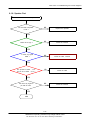
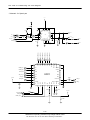
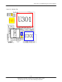
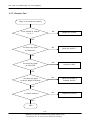
1
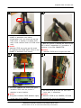
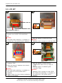
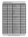
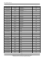
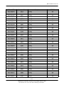
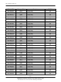
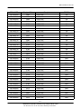
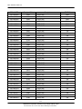
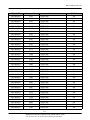
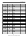
UMTS TELEPHONE
SGH-Z630
UMTS TELEPHONE
CONTENTS
1.
Safety Precautions
2.
Specification
3.
Product Function
4.
Array course control
5.
Exploded View and Parts list
6.
MAIN Electrical Parts List
7.
Block Diagrams
8.
PCB Diagrams
9.
Flow Chart of Troubleshooting
10. Reference data
Contents
1. Safety Precautions
1-1. Repair Precaution ......................................................................................................1-1
1-2. ESD(Electrostatically Sensitive Devices) Precaution ...............................................1-2
2. Specification
2-1. GSM General Specification .......................................................................................2-1
2-2. GSM TX power Level ...............................................................................................2-2
3. Product Function
4. Array course control
4-1. Downloading Binary Files ......................................................................................4-2
4-2. Pre-requsite for Downloading ................................................................................4-2
4-3. S/W Downloader Program .....................................................................................4-3
5. Exploded View and Parts list
5-1. Cellular phone Exploded View ..............................................................................5-1
5-2. Cellular phone Parts list ........................................................................................5-2
5-3. Disassembly ............................................................................................................5-4
5-4. Assembly .................................................................................................................5-6
6. MAIN Electrical Parts List
7. Block Diagrams
8. PCB Diagrams
Contents
9. Flow Chart of Troubleshooting
9-1. Baseband ............................................................................................................9-1
9-1-1. Power ON .....................................................................................................9-1
9-1-2. Initial .............................................................................................................9-4
9-1-3. SIM Part .........................................................................................................9-6
9-1-4. Microphone Part ...........................................................................................9-7
9-1-5. Speaker Part_1(MP3, SPEAKER PHONE) ................................................9-8
9-1-6. Speaker Part_2(RECEIVER) .....................................................................9-10
9-1-7. Charging Part .............................................................................................9-11
9-2. RF ......................................................................................................................9-13
9-2-1. EGSM RX ...................................................................................................9-13
9-2-2. DCS RX ......................................................................................................9-15
9-2-3. PCS RX ......................................................................................................9-16
9-2-4. EGSM TX ...................................................................................................9-17
9-2-5. DCS TX ......................................................................................................9-18
9-2-6. PCS TX ......................................................................................................9-19
10. Reference data
1. Safety Precautions
1-1. Repair Precaution
● Repair in Shield Box, during detailed tuning.
Take specially care of tuning or test, because specipicty of cellular phone is sensitive for surrounding
interference(RF noise).
● Be careful to use a kind of magnetic object or tool,
because performance of parts is damaged by the influence of manetic force.
● Surely use a standard screwdriver when you disassemble this product,
otherwise screw will be worn away.
● Use a thicken twisted wire when you measure level.
A thicken twisted wire has low resistance, therefore error of measurement is few.
● Repair after separate Test Pack and Set because for short danger (for example an
overcurrent and furious flames of parts etc) when you repair board in condition of
connecting Test Pack and tuning on.
● Take specially care of soldering, because Land of PCB is small and weak in heat.
● Surely tune on/off while using AC power plug, because a repair of battery charger is
dangerous when tuning ON/OFF PBA and Connector after disassembing charger.
● Don't use as you pleases after change other material than replacement registered on SEC System.
Otherwise engineer in charge isn't charged with problem that you don't keep this rules.
1-1
SAMSUNG Proprietary-Contents may change without notice
This Document can not be used without Samsung's authorization
Safety Precautions
1-2. ESD(Electrostatically Sensitive Devices) Precaution
Several semiconductor may be damaged easilly by static electricity. Such parts are called by ESD
(Electrostatically Sensitive Devices), for example IC,BGA chip etc. Read Precaution below.
You can prevent from ESD damage by static electricity.
● Remove static electricity remained your body before you touch semiconductor or parts with
semiconductor. There are ways that you touch an earthed place or wear static electricity
prevention string on wrist.
● Use earthed soldering steel when you connect or disconnect ESD.
● Use soldering removing tool to break static electricity. , otherwise ESD will be damaged by
static electricity.
● Don't unpack until you set up ESD on product. Because most of ESD are packed by box and
aluminum plate to have conductive power,they are prevented from static electricity.
● You must maintain electric contact between ESD and place due to be set up until ESD is connected
completely to the proper place or a circuit board.
1-2
SAMSUNG Proprietary-Contents may change without notice
This Document can not be used without Samsung's authorization
2. Specification
2-1. GSM/WCDMA General Specification
EG SM 900
Phase 2
DCS18 00
Ph ase 1
PCS1900
WCDM A
Fr eq. Band[ MHz]
Uplink/Downlink
880~915
925~960
1710~1785
1805~1880
1850~1910
1930~1990
1920~1980
2110~2170
ARFCN r ange
0~124 &
975~1023
512~885
512~810
10562~10838
Tx/ Rx sp acing
45 MHz
95 MHz
80 MHz
190 MHz
Mod. Bit rat e/
Bit Per iod
270.833 kbps
3.692 us
270.833 kbps
3.692 us
270.833 kbps
3.692 us
3.84 Mcps/s
T im e S lot
Per iod/ Fra me
Period
576.9 us
4.615 ms
576.9 us
4.615 ms
576.9 us
4.615 ms
10 ms
Modu lation
0.3 GMSK
0.3 GMSK
0.3 GMSK
UL:2BPSk
DL:QPSK
M S Power
33 dBm~5 dBm
30 dBm~0 dBm
30 dBm~0 dBm
MAX:24(+1,-3) dBm
MIN:<-50 dBm
Power Cl ass
5 pcl ~ 19 pcl
0 pcl ~ 15 pcl
0 pcl ~ 15 pcl
CLASS3
Sensi tivi ty
-102 dBm
-100 dBm
-100 dBm
-106.7 dBm
T DM A M u x
8
8
8
-
Cell Radius
35 Km
2 Km
-
-
2-1
SAMSUNG Proprietary-Contents may change without notice
This Document can not be used without Samsung's authorization
Specification
2-2. GSM TX power class
TX Power
control level
EGSM900
TX Power
control level
DCS1800
TX Power
control level
PCS1900
5
33±2 dBm
0
30±3 dBm
0
30±3 dBm
6
31±2 dBm
1
28±3 dBm
1
28±3 dBm
7
29±2 dBm
2
26±3 dBm
2
26±3 dBm
8
27±2 dBm
3
24±3 dBm
3
24±3 dBm
9
25±2 dBm
4
22±3 dBm
4
22±3 dBm
10
23±2 dBm
5
20±3 dBm
5
20±3 dBm
11
21±2 dBm
6
18±3 dBm
6
18±3 dBm
12
19±2 dBm
7
16±3 dBm
7
16±3 dBm
13
17±2 dBm
8
14±3 dBm
8
14±3 dBm
14
15±2 dBm
9
12±4 dBm
9
12±4 dBm
15
13±2 dBm
10
10±4 dBm
10
10±4 dBm
16
11±3 dBm
11
8±4 dBm
11
8±4 dBm
17
9± 3dBm
12
6±4 dBm
12
6±4 dBm
18
7±3 dBm
13
4±4 dBm
13
4±4 dBm
19
5±3 dBm
14
2±5 dBm
14
2±5 dBm
15
0±5 dBm
15
0±5 dBm
2-2
SAMSUNG Proprietary-Contents may change without notice
This Document can not be used without Samsung's authorization
3. Product Function
3-1. Main Function
-Camera and camcorder
-Image editor
-Music player
-File viewer
-Bluetooth
-Photo printing
-i-mode browser
-Get personal with photo/vIDEO caller ID
-Name card
-Multimedia Message Service (i-MMS)
-Email (i-mail)
-Java
-Voice recorder
3-1
SAMSUNG Proprietary-Contents may change without notice
This Document can not be used without Samsung's authorization
4. Array course control
Test JIG (GH80-03308A)
IF Test Cable (GH39-00478A)
RF Test Cable (GH39-00397A)
4-1
SAMSUNG Proprietary-Contents may change without notice
This Document can not be used without Samsung's authorization
Array course control
4.1 Downloading Binaries.
Start the Downloader application.
You can get the downloader program from binary zip file. Unzip the file and move to the \tools\downloa
der directory. You will see below if run the [M6275]U-Medic v1.3_SVC.exe file.
Please follow the order. The detailed fact is explained below. (store the user data using PC-Studio3 if ne
cessary)
1.
Load the Z630.mdc file.
2.
Connect the Mobile Handset to the PC via USB port.
3.
Download.
First, click the 'Load' button to select “Z630.mdc” file. The mdc file is located in the \tools\downloader dir
ectory. And then Connect the Mobile Handset to the PC via USB port. Press power button with red color
and button captioned 4 to put the mobile into download mode. To verify that the mobile is put into down
load mode, just check the front LCD screen of the mobile. (USB DOWNLOAD SAMSUNG UMTS)
Once the mobile is detected/sensed by the Downloader Application, the appropriate Mobile Entry will be
enabled in the application screen.Optionally Port Search button could be pressed to detect/sense the mob
ile.
4-2
SAMSUNG Proprietary-Contents may change without notice
This Document can not be used without Samsung's authorization
Array course control
Press 'Download' Button to proceed. After successful completion of download, a message saying Downloa
d Completed will be flashed.
Please try to download again if you will see the "ERROR : Download Fail" popup. We need to download
twice when the Boot and Resource code is changed. This is for preventing a wrong operation.
Warning:Incorrect download of binary file may lead to incorrect operation of the mobile, or the mobile may not op
erate at all.
4-3
SAMSUNG Proprietary-Contents may change without notice
This Document can not be used without Samsung's authorization
5. Exploded View and Parts List
5-1. Cellular phone Exploded View
QSP05
QMW01
QFU01
QCA00
QME03
QHI01
QKP02
QFR01
QLC01
QCK01
QBR03
QME01
QVO01
QCA01
QCR12
QMI03
QFL01
QCA02
QMP01
QPC01
QVK01
QSH01
QCB01
QCR17
QAN02
QCR32
QSD01
QRE01
QIF01
QCW01
QRF01
QCR56
QBA01
QBA00
5-1
SAMSUNG Proprietary-Contents may change without notice
This Document can not be used without Samsung's authorization
Exploded View and Parts List
5-2. Cellular phone Parts list
Design LOC
QAN02
Discription
SEC CODE
INTENNA-SGHZ630
GH42-00911A
QBA00
ASSY CASE-BATTERY
GH98-02392A
QBA01
BATTERY-880MAH,BLK,MAIN
GH43-02253A
QBR03
IPR-BRACKET SUB KEY V2
GH70-01675A
QCA00
UNIT-VGA CAMERA(SELF)
GH59-03204A
QCA01
UNIT-2M CAMERA(REC)
GH59-03190A
QCA02
UNIT-CAMERAKEY
GH59-03237A
QCB01
CBF COAXIAL CABLE-SGHZ630 ANTE
GH39-00598A
QCK01
ASSY KEY-CAMERA
GH98-02751A
QCR06
SCREW-MACHINE
6001-001155
QCR12
SCREW-MACHINE
6001-001530
QCR17
SCREW-MACHINE
6001-001460
QCR32
SCREW-MACHINE
6001-001700
QCW01
PMO-COVER WINDOW CAMERA
GH72-34702A
QFL01
ASSY MEC-HINGE S/L F/C
GH75-09403A
QFR01
MEA-FRONT KIT(CL/GRY)
GH97-06739A
QFU01
ASSY MEC-UPPER SLIDE
GH75-09381A
QHI01
ASSY ACCE-PUSH ROD
GH98-01237A
QKP02
ASSY KEYPAD-SUB(TIM/CA)
GH75-09400A
QLC01
MEA-LCD MODULE KIT
GH97-06604A
QME01
UNIT-EL KEY PBA(NAVI)
GH59-03233A
QME03
UNIT-SPK_MOT FPCB
GH59-03205A
QMI03
PMO-MIC HOLDER
GH72-34159A
QMP01
PBA MAIN-SGH-Z630
GH92-02568A
QMW01
ASSY MEC-COVER MAIN WINDOW
GH75-09396A
QPC01
MEA-SLIDE FPCB KIT
GH97-06605A
QRF01
MPR-TAPE RF SHEET
GH74-27744A
QSH01
ASSY COVER-SHIELD CAN
GH98-02614A
QSP05
ASSY DECO-SPK
GH98-01405A
QVK01
UNIT-VOLUME KEY
GH59-03239A
QVO01
PMO-KEY VOLUME
GH72-35859A
QRE01
ASSY MEC-COEVER REAR
GH75-09397A
QIF01
PMO-COVER EAR IF
GH72-29654A
QSD01
PMO-COVER MICRO SD
GH72-29655A
5-2
SAMSUNG Proprietary-Contents may change without notice
This Document can not be used without Samsung's authorization
Exploded View and Parts List
Discription
BAG PE
CBF INTERFACE-DATA LINK CABLE
ADAPTOR-SGHE690,BLK,EU,A_TYPE
S/W CD-SAMSUNG PC STUDIO 3.0,Z
UNIT-EARPHONE(BLK)
LABEL(P)-WATER SOAK
LABEL(R)-MASTER TIM
MANUAL USERS-TIM ITALIAN
LABEL(R)-MAIN(TIM)
CUSHION-CASE TA2
BOX(P)-UNIT MAIN(TIM)
RMO-HINGE DAMPER A
MPR-TAPE LCD PCB GOLD
MPR-TAPE LCD CONN A
MPR-VINYL BOHO MAIN WINDOW
MPR-VINYL BOHO REAR UPPER
MPR-VINYL BOHO REAR CAMERA
MPR-INSU TAPE
MPR-INSU TAPE
MPR-SPONGE SLIDE FPCB NOISE
MPR-TAPE SLIDE CON SHIELD
MPR-TAPE BATT MASKING
MPR-TAPE
MPR-TAPE
MPR-GASKET TAPE
MPR-TAPE MAIN KEY FPCB SHIELD
MPR-TAPE LCD MASKING A
MPR-TAPE LCD MASKING B
MPR-TAPE LCD DONG
MPR-TAPE 2M CAMERA CON
MPR-INSU TAPE
MPR-TAPE MAIN CON
MPR-TAPE SHEET SLIDE SCREW
MPR-INSU TAPE
MPR-SPONGE REAR BGA ABS A
MPR-SPONGE REAR BGA ABS B
MPR-SPONGE T FLASH
MPR-INSU TAPE
MPR-VINYL BOHO MAIN WINDOW
MPR-TAPE MAIN WINDOW WATER
AS-IC-MCP UMTS
SEC CODE
6902-000297
GH39-00444A
GH44-01361A
GH46-00327A
GH59-02499A
GH68-02026A
GH68-11408D
GH68-12568A
GH68-12832A
GH69-04602A
GH69-04636E
GH73-08414A
GH74-17771A
GH74-18637A
GH74-26869A
GH74-26872A
GH74-26874A
GH74-26989A
GH74-26990A
GH74-26997A
GH74-27005A
GH74-27006A
GH74-27010A
GH74-27010A
GH74-27014A
GH74-27283A
GH74-27284A
GH74-27285A
GH74-27287A
GH74-27422A
GH74-27424A
GH74-27435A
GH74-27743A
GH74-27774A
GH74-28042A
GH74-28043A
GH74-28055A
GH74-28186A
GH74-28397A
GH74-28420A
GH81-05913A
5-3
SAMSUNG Proprietary-Contents may change without notice
This Document can not be used without Samsung's authorization
Exploded View and Parts List
5-3. Disassembly
1
2
Unscrew 4 places of the Rear.
※ caution
1) Attention, Avoid scratching
2) using the star driver
3
1) Open the lower part of Rear using stick for
disassembly. And With the picture it
disassemble in same order (And
disassemble in order such as the picture)
※ caution
1) Attention, Avoid scratching
②
①
③
⑤
④
1) After remove the green tape, disassemble the 3*4 connector
2) After disassemble the CAM KEY FPCB using tweezers,
3*4 key FPCB is located in CAM KEY FPCB behind.
3) Disassemble VOL KEY FPCB using tweezers.
4) Disassemble INTENNA WIRE using tweezers.
5) Softly lift the CAMERA using tweezers.
※ caution
1) When moving the position of the 3*4 KEY CONNECTOR FPCB and CAM KEY FPCB,
attention for the FPCB not to be damaged,
2) When disassembling INTENA WIRE, attention for the end of the WIRE not to be bend.
5-4
SAMSUNG Proprietary-Contents may change without notice
This Document can not be used without Samsung's authorization
Exploded View and Parts List
4
5
1) Remove a green insulation Tape on the
FPCB Connector using tweezers.
1) Remove the Screw Cap
2) Unscrew 4 places of Front
2) Open the cover of the Connector and pull
out the Slide FPCB carefully in the PBA.
※ caution
※ caution
1) Attention, SET does not occur scratch
1) Attention not to be get the crack
2) Using the a screwdriver
6
7
1) Softly remove tape using tweezers, FPCB
and in tape internal it pulls out Extract
FPCB to TAPE inside after lift TAPE using
2) Remove bronze cover tape, FPCB take off
in lower such as the picture
tweezers
※ caution
※ caution
1) When pulling out the FPCB on LCD, not to
be bend.
1) When pulling out the FPCB on LCD, not to
be bend.
5-5
SAMSUNG Proprietary-Contents may change without notice
This Document can not be used without Samsung's authorization
Exploded View and Parts List
9
①
⑤
②
③
④
1),2) Remove VGA CAM such as pictures using tweezers, disassemble connector of the
bottom
3) Remove tape in FPCB connector using tweezers
3),4) After lift connector pin, disassemble FPCB using tweezers
5) Remove SPK,MOT ASS'Y using tweezers
※ caution
1) When disassemble VGA CAMERA using tweezers, attention not to be get the crack
2) Attention not to be get the damage
3) When disassemble LCD FPCB, using tweezers not to be get the crack
10
11
1) With right hand thumb it hands down the
LOWER in the lower part and the FRONT
and it disjoints.
※ caution
1)Downing lower such as picture
※ caution
1) Attention, Avoid scratching.
1) With the picture together it catches the
portion which is to the dotted line which is
a blue
2) Attention, Avoid scratching.
5-6
SAMSUNG Proprietary-Contents may change without notice
This Document can not be used without Samsung's authorization
Exploded View and Parts List
5-4. Assembly
1
2
①
②
1) The SPK arriving safely first it arrives
safely the MOT after. It follows the line
which is coming to carve the FPCB in the
LCD and it arrives safely.
2) It inserts the FPCB in CONNECTOR portion
1) With the picture 3*4 key arrives
safely
the UPPER
※ caution
1) 3*4 KEY`s hole in lower to be in contact
in the UPPER, arrives safely.
※ caution
1) The MOT&SPK the ASS'Y should have
arrived safely completely in shooting out, it
is confirmed.
2) In order for the FPCB not to be the crack
the branch, it arrives safely.
3
4
①
②
1) VGA CAMERA arrives like picture
2) LCD FPCB insult connector
1) Line in the lower part in standard, it raises
the FPCB
2) With the picture Bronze cover TAPE
attatches onthe black line that is standard
※ caution
1) Attention, SET does not occur scratch
2) Attention LCD FPCB not to be get the
※ caution
1) Attention LCD FPCB not to be get the
crack
crack
5-7
SAMSUNG Proprietary-Contents may change without notice
This Document can not be used without Samsung's authorization
Exploded View and Parts List
5
6
1) The PUSH LOADER with the picture it
arrives safely to the FRONT.
1) With the picture the LOWER inserts in
PUSH LOADER.
※ caution
※ caution
1) Attention, SET does not occur scratch
1) Attention, SET does not occur scratch
7
8
1) With the picture it hands down the FRONT
left side side together by the left hand and
1) With the picture together right side insult
it inserts the LOWER.
in FRONT shooting out.
※ caution
※ caution
1) Attention, SET does not occur scratch
1) Attention, SET does not occur scratch
5-8
SAMSUNG Proprietary-Contents may change without notice
This Document can not be used without Samsung's authorization
Exploded View and Parts List
9
10
1) It combines the UPPER ASS'Y which in the
LOWER it assembles rom before.
(Combination hour you must put out the
TAPE which is sticking in 3*4KEY FPCB
and it must combine and LCD FPCB enters 1) With the picture it catches the FPCB of the
well).
ASS'Y which it assembles in 5 procedure, it
※ caution
1) Attention FPCB not to be get the crack
It combines the UPPER ASS'Y which in the
LOWER it assembles from before
combines in the PBA CONNECTOR
11
12
※ caution
1)
Attention FPCB not to be get the crack
1) The FPCB CONNECTOR closes and green
insulation TAPE with the picture it
1) The CAM FPCB go to the 3*4 KEY FPCB
attaches in same location.
※ caution
1) The green insulation TAPE attaches rightly
lower part, it assembles.
※ caution
1) Attention FPCB of the CAMERA, LCD and
in top part of the PORON.
VOLUME KEY not to be damage
5-9
SAMSUNG Proprietary-Contents may change without notice
This Document can not be used without Samsung's authorization
Exploded View and Parts List
13
14
1) Confirm whether have attached GOLD GASKET
TAPE with picture on SHIELD CAN HOOK
wealth side.
1)Confirm SHIELD CAN whether GOLD GASKET
TAPE, gray challenge TAPE with picture has
attached over.
※ caution
※ caution
1)Confirmation work
1)Confirmation work
15
16
①
②
1) After arriving safely the right lower part
1) The CAM KEY arrives safely
first, board upper direction some it bends
2) The VOL KEY arrives safely
with the right and it arrives safely with the
※ caution
left side
1) The CAM, VOL KEY arrives safely. in order
※ caution
for the to be only caught the FRONT
1) The PBA arrives safely from the condition
which slide is ascending.
upper
5-10
SAMSUNG Proprietary-Contents may change without notice
This Document can not be used without Samsung's authorization
Exploded View and Parts List
17
18
1) INTENNA arrives safely using tweezers
※ caution
1) When insert, INTENNA is located in the
1) First, lock the top portion Hook.
center so that INTENNA CABLE don't touch ※ caution
1) ttention, SET does not occur scratch
BAT CONNECTOR of bottom
19
1) Screw the 4 star screws.
※ caution
1) Use the star-driver.
5-11
SAMSUNG Proprietary-Contents may change without notice
This Document can not be used without Samsung's authorization
Exploded View and Parts List
5-5. LCD KIT
1
2
<LCD MASKING TAPE B>
<SLIDE FPCB MASKING TAPE>
<LCD MASKING TAPE A>
1) Attach the MASKING TAPE A,B on LDI
2) Attach the SLIDE FPCB MASKING
TAPE
※ caution
1) With the picture it inserts the FPCB
1) The TAPE when attaching, it considers to
※ caution
the guide line of the picture and it attaches.
3
1) Attention. Don't crumple or crack the FPCB
4
< Attach closely >
1) With the picture it attaches green
insulation TAPE
2) With the picture it attaches siver electric
1) With the picture it inserts FPCB in
CONNECTOR after fold up edge of
FPCB.
2) With the picture it attaches green
insulation Tape.
conduction TAPE.
※ caution
1) The TAPE when attaching, it considers to
the guide line of the picture and it
attaches.
2) Attach closely the siver electric conduction
TAPE on the bottom.
※ caution
1) Attention. Don't crumple or crack FPCB
2) The TAPE when attaching, it considers to
the guide line of the picture and it
attaches.
5-12
SAMSUNG Proprietary-Contents may change without notice
This Document can not be used without Samsung's authorization
Exploded View and Parts List
5
6
<GUIDE HOLE>
<GUIDE HOLE>
1)Insert the FPCB of MIC in front right side
lowwer hole and Attach the 3*4 KEY PCB In
3*4 KEY safe arrival surface of FRONT
※ caution
1) The TAPE when attaching, it considers to
the guide line of the picture and it
attaches.
1) With the picture it attaches 3*4 KEY PAD
※ caution
1) Attach the 3*4 KEY PAD according to
GUIDE HOLE.
7
①
②
1) With the picture it assembles FRONT
BRACKET .
2) With the picture which attach a green
insulation 3*4 KEY NOISE Tape in same
location.
※ caution
1) The TAPE when attaching, it considers to
the guide line of the picture and it
attaches.
5-13
SAMSUNG Proprietary-Contents may change without notice
This Document can not be used without Samsung's authorization
6. MAIN Electrical Parts List
SEC CODE
Design LOC
Discription
0403-001511
ZD540
DIODE-ZENER
SA
0403-001547
ZD204
DIODE-ZENER
SA
0404-001172
D100
DIODE-SCHOTTKY
SA
0404-001172
D101
DIODE-SCHOTTKY
SA
0404-001172
D102
DIODE-SCHOTTKY
SA
0406-001190
ZD201
DIODE-TVS
SA
0406-001190
ZD202
DIODE-TVS
SA
0406-001190
ZD203
DIODE-TVS
SA
0407-001002
D500
DIODE-ARRAY
SA
0504-001113
TR101
TR-DIGITAL
SA
0504-001113
TR502
TR-DIGITAL
SA
0504-001151
U701
TR-DIGITAL
SA
0505-001889
U502
FET-SILICON
SA
0601-001909
LED400
LED
SA
0801-002995
U406
IC-CMOS LOGIC
SA
1001-001414
U304
IC-ANALOG SWITCH
SA
1001-001414
U305
IC-ANALOG SWITCH
SA
1003-001716
U504
IC-EL DRIVER
SA
1006-001322
U102
IC-LINE TRANSCEIVER
SA
1108-000071
UME400
IC-MCP
SA
1201-002195
U303
IC-AUDIO AMP
SA
1201-002240
U302
IC-AUDIO AMP
SA
1201-002288
PAM600
IC-POWER AMP
SA
1201-002347
PAM700
IC-POWER AMP
SA
1203-003046
U403
IC-BATTERY
SA
1203-003523
U200
IC-POSI.FIXED REG.
SA
1203-003531
U505
IC-POSI.FIXED REG.
SA
1203-003728
U501
IC-VOL. DETECTOR
SA
1203-003742
U405
IC-BATTERY
SA
1203-003754
U508
IC-POSI.FIXED REG.
SA
1203-004102
U503
IC-POWER SUPERVISOR
SA
1203-004394
U404
IC-MULTI REG.
SA
1203-004473
U401
IC-POSI.FIXED REG.
SA
1204-002138
U301
IC-MELODY
SA
1205-002568
U507
IC-SWITCH
SA
1205-002645
U601
IC-TRANSCEIVER
SA
1205-002781
U700
IC-RECEIVER
SA
6-1
SAMSUNG Proprietary-Contents may change without notice
This Document can not be used without Samsung's authorization
STATUS
Main Electrical Parts List
SEC CODE
Design LOC
1205-002790
UCP101
1209-001577
Discription
STATUS
IC-MODEM
SA
U702
IC-DETECTOR
SA
1209-001615
U103
IC-SENSOR
SA
1404-001224
VR100
THERMISTOR-NTC
SA
1405-001108
VR101
VARISTOR
SA
1405-001108
VR201
VARISTOR
SA
1405-001108
VR202
VARISTOR
SA
1405-001108
VR203
VARISTOR
SA
1405-001108
VR204
VARISTOR
SA
1405-001108
VR205
VARISTOR
SA
1405-001108
VR206
VARISTOR
SA
1405-001108
VR207
VARISTOR
SA
1405-001108
VR215
VARISTOR
SA
1405-001108
VR217
VARISTOR
SA
1405-001108
VR400
VARISTOR
SA
1405-001108
VR401
VARISTOR
SA
2007-000140
R203
R-CHIP
SA
2007-000145
R616
R-CHIP
SA
2007-000148
R511
R-CHIP
SA
2007-000151
R578
R-CHIP
SA
2007-000156
R413
R-CHIP
SA
2007-000157
R538
R-CHIP
SA
2007-000162
R412
R-CHIP
SA
2007-000171
R200
R-CHIP
SA
2007-000171
R232
R-CHIP
SA
2007-000171
R442
R-CHIP
SA
2007-000171
R702
R-CHIP
SA
2007-000242
R371
R-CHIP
SA
2007-000242
R372
R-CHIP
SA
2007-000690
R569
R-CHIP
SA
2007-000758
R501
R-CHIP
SA
2007-001119
R376
R-CHIP
SA
2007-001292
R612
R-CHIP
SA
2007-001313
R607
R-CHIP
SA
2007-001329
R201
R-CHIP
SA
2007-003022
R436
R-CHIP
SA
2007-003022
R437
R-CHIP
SA
6-2
SAMSUNG Proprietary-Contents may change without notice
This Document can not be used without Samsung's authorization
Main Electrical Parts List
SEC CODE
Design LOC
Discription
2007-003030
R374
R-CHIP
SA
2007-007014
R872
R-CHIP
SA
2007-007142
R510
R-CHIP
SA
2007-007306
R701
R-CHIP
SA
2007-007306
R870
R-CHIP
SA
2007-007313
R119
R-CHIP
SA
2007-007318
R104
R-CHIP
SA
2007-007318
R606
R-CHIP
SA
2007-007318
R700
R-CHIP
SA
2007-007468
R513
R-CHIP
SA
2007-007491
R603
R-CHIP
SA
2007-007491
R704
R-CHIP
SA
2007-007798
R610
R-CHIP
SA
2007-008045
R233
R-CHIP
SA
2007-008045
R604
R-CHIP
SA
2007-008045
R611
R-CHIP
SA
2007-008045
R617
R-CHIP
SA
2007-008045
R619
R-CHIP
SA
2007-008045
R703
R-CHIP
SA
2007-008049
R105
R-CHIP
SA
2007-008051
R308
R-CHIP
SA
2007-008051
R613
R-CHIP
SA
2007-008052
R215
R-CHIP
SA
2007-008052
R602
R-CHIP
SA
2007-008053
R326
R-CHIP
SA
2007-008053
R327
R-CHIP
SA
2007-008053
R332
R-CHIP
SA
2007-008053
R333
R-CHIP
SA
2007-008054
R213
R-CHIP
SA
2007-008054
R214
R-CHIP
SA
2007-008055
R212
R-CHIP
SA
2007-008055
R217
R-CHIP
SA
2007-008055
R223
R-CHIP
SA
2007-008055
R873
R-CHIP
SA
2007-008161
R609
R-CHIP
SA
2007-008213
R605
R-CHIP
SA
2007-008297
R120
R-CHIP
SA
6-3
SAMSUNG Proprietary-Contents may change without notice
This Document can not be used without Samsung's authorization
STATUS
Main Electrical Parts List
SEC CODE
Design LOC
Discription
2007-008419
R202
R-CHIP
SA
2007-008419
R227
R-CHIP
SA
2007-008419
R228
R-CHIP
SA
2007-008483
R130
R-CHIP
SA
2007-008483
R136
R-CHIP
SA
2007-008483
R805
R-CHIP
SA
2007-008516
R107
R-CHIP
SA
2007-008516
R108
R-CHIP
SA
2007-008516
R113
R-CHIP
SA
2007-008516
R204
R-CHIP
SA
2007-008516
R205
R-CHIP
SA
2007-008516
R206
R-CHIP
SA
2007-008516
R207
R-CHIP
SA
2007-008516
R210
R-CHIP
SA
2007-008516
R231
R-CHIP
SA
2007-008516
R378
R-CHIP
SA
2007-008516
R379
R-CHIP
SA
2007-008516
R404
R-CHIP
SA
2007-008531
R346
R-CHIP
SA
2007-008531
R347
R-CHIP
SA
2007-008531
R620
R-CHIP
SA
2007-008531
R706
R-CHIP
SA
2007-008531
R707
R-CHIP
SA
2007-008542
R101
R-CHIP
SA
2007-008542
R302
R-CHIP
SA
2007-008542
R303
R-CHIP
SA
2007-008542
R309
R-CHIP
SA
2007-008542
R579
R-CHIP
SA
2007-008542
R601
R-CHIP
SA
2007-008542
R621
R-CHIP
SA
2007-008579
R614
R-CHIP
SA
2007-008579
R615
R-CHIP
SA
2007-008581
R608
R-CHIP
SNA
2007-008587
R307
R-CHIP
SA
2007-008587
R339
R-CHIP
SA
2007-008588
R125
R-CHIP
SA
2007-008588
R126
R-CHIP
SA
6-4
SAMSUNG Proprietary-Contents may change without notice
This Document can not be used without Samsung's authorization
STATUS
Main Electrical Parts List
SEC CODE
Design LOC
Discription
2007-008588
R600
R-CHIP
SA
2007-008648
R411
R-CHIP
SA
2007-008648
R439
R-CHIP
SA
2007-008648
R443
R-CHIP
SA
2007-008648
R871
R-CHIP
SA
2007-008806
R512
R-CHIP
SA
2007-008806
R618
R-CHIP
SA
2007-008808
R580
R-CHIP
SA
2007-009157
R109
R-CHIP
SA
2007-009157
R133
R-CHIP
SA
2007-009170
R106
R-CHIP
SA
2007-009170
R111
R-CHIP
SA
2007-009170
R211
R-CHIP
SA
2007-009223
R208
R-CHIP
SA
2007-009233
R401
R-CHIP
SA
2007-009233
R410
R-CHIP
SA
2007-009233
R438
R-CHIP
SA
2007-009314
R400
R-CHIP
SA
2007-009314
R440
R-CHIP
SA
2007-009314
R441
R-CHIP
SA
2203-000233
C507
C-CER,CHIP
SA
2203-000233
C734
C-CER,CHIP
SA
2203-000254
C702
C-CER,CHIP
SA
2203-000254
C870
C-CER,CHIP
SA
2203-000438
C201
C-CER,CHIP
SA
2203-000489
C125
C-CER,CHIP
SA
2203-000627
C525
C-CER,CHIP
SNA
2203-000627
C526
C-CER,CHIP
SNA
2203-000812
C200
C-CER,CHIP
SA
2203-000812
C373
C-CER,CHIP
SA
2203-000812
C573
C-CER,CHIP
SA
2203-000812
C646
C-CER,CHIP
SA
2203-000812
C703
C-CER,CHIP
SA
2203-000812
C708
C-CER,CHIP
SA
2203-000812
C800
C-CER,CHIP
SA
2203-000995
C139
C-CER,CHIP
SA
2203-000995
C377
C-CER,CHIP
SA
6-5
SAMSUNG Proprietary-Contents may change without notice
This Document can not be used without Samsung's authorization
STATUS
Main Electrical Parts List
SEC CODE
Design LOC
Discription
2203-000995
C378
C-CER,CHIP
SA
2203-000995
C705
C-CER,CHIP
SA
2203-001072
C598
C-CER,CHIP
SA
2203-001153
C544
C-CER,CHIP
SA
2203-001259
C721
C-CER,CHIP
SA
2203-001383
C877
C-CER,CHIP
SA
2203-001405
C207
C-CER,CHIP
SA
2203-001405
C233
C-CER,CHIP
SA
2203-001405
C234
C-CER,CHIP
SA
2203-001405
C375
C-CER,CHIP
SA
2203-001405
C376
C-CER,CHIP
SA
2203-002443
C635
C-CER,CHIP
SA
2203-002668
C647
C-CER,CHIP
SA
2203-002709
C358
C-CER,CHIP
SA
2203-002709
C359
C-CER,CHIP
SA
2203-002709
C388
C-CER,CHIP
SA
2203-002709
C542
C-CER,CHIP
SA
2203-002709
C556
C-CER,CHIP
SA
2203-002709
C717
C-CER,CHIP
SA
2203-003019
C597
C-CER,CHIP
SA
2203-005053
C609
C-CER,CHIP
SA
2203-005053
C715
C-CER,CHIP
SA
2203-005053
C722
C-CER,CHIP
SA
2203-005390
C706
C-CER,CHIP
SA
2203-005395
C704
C-CER,CHIP
SA
2203-005450
C602
C-CER,CHIP
SA
2203-005682
C235
C-CER,CHIP
SA
2203-005682
C552
C-CER,CHIP
SA
2203-005682
C571
C-CER,CHIP
SA
2203-005682
C600
C-CER,CHIP
SA
2203-005682
C605
C-CER,CHIP
SA
2203-005682
C615
C-CER,CHIP
SA
2203-005682
C631
C-CER,CHIP
SA
2203-005682
C729
C-CER,CHIP
SA
2203-005682
C730
C-CER,CHIP
SA
2203-005682
C731
C-CER,CHIP
SA
2203-005682
C804
C-CER,CHIP
SA
6-6
SAMSUNG Proprietary-Contents may change without notice
This Document can not be used without Samsung's authorization
STATUS
Main Electrical Parts List
SEC CODE
Design LOC
Discription
2203-005682
C806
C-CER,CHIP
SA
2203-005682
C808
C-CER,CHIP
SA
2203-005682
C809
C-CER,CHIP
SA
2203-005717
C381
C-CER,CHIP
SA
2203-005717
C382
C-CER,CHIP
SA
2203-005729
C122
C-CER,CHIP
SA
2203-005729
C123
C-CER,CHIP
SA
2203-005729
C642
C-CER,CHIP
SA
2203-005729
C643
C-CER,CHIP
SA
2203-005732
C610
C-CER,CHIP
SA
2203-005736
C629
C-CER,CHIP
SA
2203-005736
C640
C-CER,CHIP
SA
2203-005736
C711
C-CER,CHIP
SA
2203-005736
C716
C-CER,CHIP
SA
2203-005736
C718
C-CER,CHIP
SA
2203-005736
C726
C-CER,CHIP
SA
2203-005736
C728
C-CER,CHIP
SA
2203-005777
C818
C-CER,CHIP
SA
2203-005789
C819
C-CER,CHIP
SA
2203-005806
C102
C-CER,CHIP
SNA
2203-005806
C103
C-CER,CHIP
SNA
2203-005806
C105
C-CER,CHIP
SNA
2203-005806
C106
C-CER,CHIP
SNA
2203-005806
C107
C-CER,CHIP
SNA
2203-005806
C108
C-CER,CHIP
SNA
2203-005806
C113
C-CER,CHIP
SNA
2203-005806
C114
C-CER,CHIP
SNA
2203-005806
C118
C-CER,CHIP
SNA
2203-005806
C119
C-CER,CHIP
SNA
2203-005806
C144
C-CER,CHIP
SNA
2203-005806
C192
C-CER,CHIP
SNA
2203-005806
C193
C-CER,CHIP
SNA
2203-005806
C311
C-CER,CHIP
SNA
2203-005806
C402
C-CER,CHIP
SNA
2203-005806
C403
C-CER,CHIP
SNA
2203-005806
C511
C-CER,CHIP
SNA
2203-005806
C512
C-CER,CHIP
SNA
6-7
SAMSUNG Proprietary-Contents may change without notice
This Document can not be used without Samsung's authorization
STATUS
Main Electrical Parts List
SEC CODE
Design LOC
Discription
2203-005806
C523
C-CER,CHIP
SNA
2203-005806
C626
C-CER,CHIP
SNA
2203-005806
C630
C-CER,CHIP
SNA
2203-005806
C641
C-CER,CHIP
SNA
2203-005806
C714
C-CER,CHIP
SNA
2203-005806
C872
C-CER,CHIP
SNA
2203-005808
C400
C-CER,CHIP
SA
2203-005808
C401
C-CER,CHIP
SA
2203-005808
C407
C-CER,CHIP
SA
2203-005808
C608
C-CER,CHIP
SA
2203-005808
C614
C-CER,CHIP
SA
2203-005808
C710
C-CER,CHIP
SA
2203-006048
C211
C-CER,CHIP
SA
2203-006048
C500
C-CER,CHIP
SA
2203-006048
C509
C-CER,CHIP
SA
2203-006048
C510
C-CER,CHIP
SA
2203-006048
C524
C-CER,CHIP
SA
2203-006048
C527
C-CER,CHIP
SA
2203-006048
C536
C-CER,CHIP
SA
2203-006048
C538
C-CER,CHIP
SA
2203-006048
C555
C-CER,CHIP
SA
2203-006194
C130
C-CER,CHIP
SA
2203-006194
C148
C-CER,CHIP
SA
2203-006194
C205
C-CER,CHIP
SA
2203-006194
C611
C-CER,CHIP
SA
2203-006194
C613
C-CER,CHIP
SA
2203-006194
C616
C-CER,CHIP
SA
2203-006194
C633
C-CER,CHIP
SA
2203-006194
C733
C-CER,CHIP
SA
2203-006260
C449
C-CER,CHIP
SA
2203-006305
C617
C-CER,CHIP
SA
2203-006305
C619
C-CER,CHIP
SA
2203-006324
C648
C-CER,CHIP
SA
2203-006324
C701
C-CER,CHIP
SA
2203-006361
C540
C-CER,CHIP
SA
2203-006379
C621
C-CER,CHIP
SA
2203-006423
C100
C-CER,CHIP
SA
6-8
SAMSUNG Proprietary-Contents may change without notice
This Document can not be used without Samsung's authorization
STATUS
Main Electrical Parts List
SEC CODE
Design LOC
Discription
2203-006423
C101
C-CER,CHIP
SA
2203-006423
C109
C-CER,CHIP
SA
2203-006423
C110
C-CER,CHIP
SA
2203-006423
C111
C-CER,CHIP
SA
2203-006423
C115
C-CER,CHIP
SA
2203-006423
C117
C-CER,CHIP
SA
2203-006423
C120
C-CER,CHIP
SA
2203-006423
C133
C-CER,CHIP
SA
2203-006423
C138
C-CER,CHIP
SA
2203-006423
C141
C-CER,CHIP
SA
2203-006423
C142
C-CER,CHIP
SA
2203-006423
C147
C-CER,CHIP
SA
2203-006423
C158
C-CER,CHIP
SA
2203-006423
C177
C-CER,CHIP
SA
2203-006423
C190
C-CER,CHIP
SA
2203-006423
C194
C-CER,CHIP
SA
2203-006423
C197
C-CER,CHIP
SA
2203-006423
C198
C-CER,CHIP
SA
2203-006423
C303
C-CER,CHIP
SA
2203-006423
C306
C-CER,CHIP
SA
2203-006423
C310
C-CER,CHIP
SA
2203-006423
C312
C-CER,CHIP
SA
2203-006423
C332
C-CER,CHIP
SA
2203-006423
C389
C-CER,CHIP
SA
2203-006423
C448
C-CER,CHIP
SA
2203-006423
C469
C-CER,CHIP
SA
2203-006423
C541
C-CER,CHIP
SA
2203-006423
C620
C-CER,CHIP
SA
2203-006423
C625
C-CER,CHIP
SA
2203-006423
C628
C-CER,CHIP
SA
2203-006423
C712
C-CER,CHIP
SA
2203-006423
C713
C-CER,CHIP
SA
2203-006423
C719
C-CER,CHIP
SA
2203-006423
C720
C-CER,CHIP
SA
2203-006423
C803
C-CER,CHIP
SA
2203-006426
C724
C-CER,CHIP
SNA
2203-006462
C129
C-CER,CHIP
SA
6-9
SAMSUNG Proprietary-Contents may change without notice
This Document can not be used without Samsung's authorization
STATUS
Main Electrical Parts List
SEC CODE
Design LOC
Discription
2203-006556
C208
C-CER,CHIP
SA
2203-006556
C209
C-CER,CHIP
SA
2203-006556
C623
C-CER,CHIP
SA
2203-006556
C624
C-CER,CHIP
SA
2203-006562
C112
C-CER,CHIP
SA
2203-006562
C116
C-CER,CHIP
SA
2203-006562
C159
C-CER,CHIP
SA
2203-006562
C196
C-CER,CHIP
SA
2203-006562
C323
C-CER,CHIP
SA
2203-006562
C324
C-CER,CHIP
SA
2203-006562
C333
C-CER,CHIP
SA
2203-006562
C346
C-CER,CHIP
SA
2203-006562
C348
C-CER,CHIP
SA
2203-006562
C349
C-CER,CHIP
SA
2203-006562
C350
C-CER,CHIP
SA
2203-006562
C356
C-CER,CHIP
SA
2203-006562
C357
C-CER,CHIP
SA
2203-006562
C371
C-CER,CHIP
SA
2203-006562
C383
C-CER,CHIP
SA
2203-006562
C387
C-CER,CHIP
SA
2203-006562
C406
C-CER,CHIP
SA
2203-006562
C408
C-CER,CHIP
SA
2203-006562
C465
C-CER,CHIP
SA
2203-006562
C466
C-CER,CHIP
SA
2203-006562
C467
C-CER,CHIP
SA
2203-006562
C470
C-CER,CHIP
SA
2203-006562
C505
C-CER,CHIP
SA
2203-006562
C518
C-CER,CHIP
SA
2203-006562
C521
C-CER,CHIP
SA
2203-006562
C522
C-CER,CHIP
SA
2203-006562
C529
C-CER,CHIP
SA
2203-006562
C531
C-CER,CHIP
SA
2203-006562
C533
C-CER,CHIP
SA
2203-006562
C537
C-CER,CHIP
SA
2203-006562
C539
C-CER,CHIP
SA
2203-006562
C551
C-CER,CHIP
SA
2203-006562
C586
C-CER,CHIP
SA
6-10
SAMSUNG Proprietary-Contents may change without notice
This Document can not be used without Samsung's authorization
STATUS
Main Electrical Parts List
SEC CODE
Design LOC
Discription
2203-006562
C592
C-CER,CHIP
SA
2203-006562
C632
C-CER,CHIP
SA
2203-006562
C639
C-CER,CHIP
SA
2203-006562
C645
C-CER,CHIP
SA
2203-006562
C725
C-CER,CHIP
SA
2203-006562
C727
C-CER,CHIP
SA
2203-006617
C137
C-CER,CHIP
SA
2203-006617
C140
C-CER,CHIP
SA
2203-006648
C347
C-CER,CHIP
SA
2203-006648
C386
C-CER,CHIP
SA
2203-006681
C735
C-CER,CHIP
SA
2203-006824
C301
C-CER,CHIP
SA
2203-006824
C302
C-CER,CHIP
SA
2203-006824
C513
C-CER,CHIP
SA
2203-006824
C514
C-CER,CHIP
SA
2203-006824
C515
C-CER,CHIP
SA
2203-006824
C516
C-CER,CHIP
SA
2203-006824
C534
C-CER,CHIP
SA
2203-006824
C817
C-CER,CHIP
SA
2203-006838
C222
C-CER,CHIP
SA
2203-006838
C390
C-CER,CHIP
SA
2203-006838
C404
C-CER,CHIP
SA
2203-006838
C445
C-CER,CHIP
SA
2203-006838
C446
C-CER,CHIP
SA
2203-006838
C447
C-CER,CHIP
SA
2203-006838
C530
C-CER,CHIP
SA
2203-006838
C532
C-CER,CHIP
SA
2203-006838
C535
C-CER,CHIP
SA
2203-006838
C543
C-CER,CHIP
SA
2203-006838
C553
C-CER,CHIP
SA
2203-006838
C566
C-CER,CHIP
SA
2203-006838
C871
C-CER,CHIP
SA
2203-006847
C638
C-CER,CHIP
SA
2203-006872
C816
C-CER,CHIP
SA
2203-006872
C876
C-CER,CHIP
SA
2203-006896
C634
C-CER,CHIP
SA
2301-001200
C636
C-FILM,SMD-PPS
SA
6-11
SAMSUNG Proprietary-Contents may change without notice
This Document can not be used without Samsung's authorization
STATUS
Main Electrical Parts List
SEC CODE
Design LOC
Discription
2301-001213
C604
C-FILM,SMD-PPS
SA
2301-001735
C603
C-FILM,SMD
SA
2301-001807
C637
C-FILM,SMD
SA
2404-001339
TA400
C-TA,CHIP
SA
2404-001339
TA501
C-TA,CHIP
SA
2404-001352
TA372
C-TA,CHIP
SA
2404-001377
TA202
C-TA,CHIP
SA
2404-001381
TA385
C-TA,CHIP
SA
2404-001381
TA503
C-TA,CHIP
SA
2404-001406
TA201
C-TA,CHIP
SA
2404-001406
TA508
C-TA,CHIP
SA
2404-001406
TA600
C-TA,CHIP
SA
2703-001734
L707
INDUCTOR-SMD
SA
2703-001749
L300
INDUCTOR-SMD
SA
2703-001749
L301
INDUCTOR-SMD
SA
2703-001750
L703
INDUCTOR-SMD
SA
2703-002155
L817
INDUCTOR-SMD
SA
2703-002207
L706
INDUCTOR-SMD
SA
2703-002597
L709
INDUCTOR-SMD
SA
2703-002709
L504
INDUCTOR-SMD
SA
2703-002782
L500
INDUCTOR-SMD
SA
2703-002782
L501
INDUCTOR-SMD
SA
2703-002794
L702
INDUCTOR-SMD
SA
2703-002795
L708
INDUCTOR-SMD
SNA
2703-002798
L807
INDUCTOR-SMD
SNA
2703-002798
L811
INDUCTOR-SMD
SNA
2703-002798
L812
INDUCTOR-SMD
SNA
2703-002798
L816
INDUCTOR-SMD
SNA
2703-002819
L604
INDUCTOR-SMD
SA
2703-002819
L605
INDUCTOR-SMD
SA
2703-002819
L606
INDUCTOR-SMD
SA
2703-002819
L607
INDUCTOR-SMD
SA
2703-002858
L705
INDUCTOR-SMD
SA
2703-002870
L600
INDUCTOR-SMD
SA
2703-002870
L602
INDUCTOR-SMD
SA
2703-002870
L603
INDUCTOR-SMD
SA
2703-002901
L609
INDUCTOR-SMD
SNA
6-12
SAMSUNG Proprietary-Contents may change without notice
This Document can not be used without Samsung's authorization
STATUS
Main Electrical Parts List
SEC CODE
Design LOC
Discription
2703-002903
L601
INDUCTOR-SMD
SA
2703-002906
L701
INDUCTOR-SMD
SA
2703-002906
L704
INDUCTOR-SMD
SA
2703-002907
L802
INDUCTOR-SMD
SNA
2703-002907
L805
INDUCTOR-SMD
SNA
2703-002958
L201
INDUCTOR-SMD
SA
2703-002958
L202
INDUCTOR-SMD
SA
2801-004373
OSC501
CRYSTAL-SMD
SA
2802-001182
OSC101
RESONATOR-CERAMIC
SA
2806-001377
VCO600
OSCILLATOR-VCO
SA
2809-001312
TCX800
OSCILLATOR-VCTCXO
SA
2901-001308
F201
FILTER-EMI SMD
SA
2901-001308
F202
FILTER-EMI SMD
SA
2901-001308
F203
FILTER-EMI SMD
SA
2901-001308
F204
FILTER-EMI SMD
SA
2901-001308
F205
FILTER-EMI SMD
SA
2901-001348
F301
FILTER-EMI/ESD
SA
2904-001622
F702
FILTER-SAW
SA
2904-001704
F701
FILTER-SAW
SA
2910-000010
DUF700
DUPLEXER-SAW
SA
2911-000048
DUF800
DUPLEXER-FEM
SA
3301-001342
L103
BEAD-SMD
SA
3705-001339
RFS801
CONNECTOR-COAXIAL
SNA
3705-001358
RFS800
CONNECTOR-COAXIAL
SA
3708-002170
SLC202
CONNECTOR-FPC/FFC/PIC
SA
3708-002211
SLC200
CONNECTOR-FPC/FFC/PIC
SA
3708-002211
SLC301
CONNECTOR-FPC/FFC/PIC
SA
3709-001344
CD200
CONNECTOR-CARD EDGE
SA
3709-001391
SIM502
CONNECTOR-CARD EDGE
SA
3710-002442
IFC201
SOCKET-INTERFACE
SA
3711-006003
BTC220
CONNECTOR-BATTERY
SA
4202-001173
ANT_BT
ANTENNA-CHIP
SA
4302-001130
BAT501
BATTERY-LI(2ND)
SA
4709-001398
MOD800
BLUETOOTH MODULE
SA
6-13
SAMSUNG Proprietary-Contents may change without notice
This Document can not be used without Samsung's authorization
STATUS
7. Block Diagrams
- RF Block Diagram
7-1
SAMSUNG Proprietary-Contents may change without notice
This Document can not be used without Samsung's authorization
8. PCB Diagrams
ANT_BT
VR401
ZD202
LED400
TA501
U406
U200
U 5 07
TR502
TR101
IFC201
ZD201
CD200
BOSS102
TCX800
U601
VR202
VR205
VR100
VR201
U405
USB_VCC_J
JIG_ON_IF_J
TXD_1_J
D+_J
RXD_1_J
D
GND_J
VCO600
TA600
TA503
DUF700
SIM502
DUF800
PAM600
RFS801
RFS800
CN111
F701
U701
VBAT_J
PAM700
U702
F702
VR206
VR207
CAM_KEY_PAD VR217
SLC200
U700
D500
TP102TP101
VR204
TA372
ZD203
U508
VR203
ANT_J
8-1
SAMSUNG Proprietary-Contents may change without notice
This Document can not be used without Samsung's authorization
TP201
PCB Diagrams
VR400
U302
U503
U303
8-2
SAMSUNG Proprietary-Contents may change without notice
This Document can not be used without Samsung's authorization
U 304
ZD540
TA385
U 305
F201
F202F203
U504
BTC220
F205
SLC202
U505
U103
U301
PAD1
F204
TA201
PAD2
ZD204
U502TA508
TA202
TP100
VR101
U501
VR215
BAT501
BOSS100
UCP101
D 102
SIDE_KEY_PAD
UME400
F301
OSC501
D 100
OSC101
D101
TA400
SLC301
U403
MOD800
U102
U401U404
BOSS101
9. Flow Chart of Troubleshooting and Circuit Diagrams
9-1.Baseband
9-1-1. Power ON
'Power ON' Does not work
Check the current consumption
Current consumption
NO
Download again
≥ 100mA ?
YES
NO
Check Voltage > 3.3V
Charge the Battery
YES
NO
Check R579 is High
Check R579
YES
The pin #3,5,6 of U503
Check the path of
NO
≥ 3.3V ?
R579 and U503
YES
Check U503
pin #32 ≒ 1.375 ?
NO
pin #36 ≒ 1.8V ?
Check the U503
pin #50,56 ≒ 2.6V ?
pin #84 ≒ 2.85V ?
YES
U503 Check
Pin #53 ≒ 19.2MHz?
Vpp ≥ 500mV?
NO
check the TCX800
YES
Check the initial operation
9-1
SAMSUNG Proprietary-Contents may change without notice
This Document can not be used without Samsung's authorization
END
POS
JIG_ON
NEG
BAT501
R511
1
TR502
2
3
ON_SW
PS_HOLD
C522
R501
RESET_IN
R579
V_IN
C524
C541
C525
C526
OSC501
C523
R512
USIM_M_DATA
USIM_DATA
USIM_M_CLK
USIM_CLK
USIM_M_RESET
USIM_RESET
PM_SBDT
PM_SBCK
PM_SBST
PM_INT_N
D+
D-
USB_OE_N
USB_VPO
USB_VMO
AMUX_OUT
PMIC3_REF
SLEEP_XTAL_IN
TCXO
TCXO_EN
TCXO_OUT
VF
V_IN
R510
ADC_BYP
XTAL_IN
XTAL_OUT
SLEEP_CLK
TCXO_IN
TCXO_EN
TCXO_OUT
AMUX_IN1
AMUX_IN2
AMUX_OUT
REF_OUT
USB_OE_N
USB_DAT
USB_SE0
USB_ID
USB_D_P
USB_D_M
KPDPWR_N
PS_HOLD
CBL1PWR_N
CBL0PWR_N
PON_RESET_N
RUIM_M_IO
RUIM_IO
RUIM_M_CLK
RUIM_CLK
RUIM_M_RST
RUIM_RST
SBDT
SBCK
SBST
MSM_INT_N
13
17
19
11
18
20
24
57
66
68
9
30
26
34
38
40
43
47
49
51
59
VCHG
USB_VBUS
ISNS_P
ISNS_M
CHG_CTL_N
USB_CTL_N
VBAT
VCOIN
BAT_FET_N
VBACKUP
VIN
4
5
6
U503
14
12
27
28
31
32
37
36
10
39
42
50
56
64
67
69
73
81
84
61
63
62
8
21
22
23
25
76
78
75
79
74
77
29
33
35
41
52
54
65
71
83
VSW_5V
VREG_5V
VSW_PA
VREG_PA
VSW_MSMC
VREG_MSMC
VSW_MSME
VREG_MSME
VREG_USB
VREG_MMC
VREG_RUIM
VREG_MSMP
VREG_MSMA
VREG_WLAN
VREG_RFRX2
VREG_RFRX1
VREG_RFTX
VREG_SYNT
VREG_TCXO
REF_ISET
REF_BYP
REF_GND
FLSH_DRV_N
GP1_DRV_N
LCD_DRV_N
KPD_DRV_N
VIB_DRV_N
SPKR_IN_P
SPKR_IN_M
SPKR_OUT_P
SPKR_OUT_M
SPKR_BYP
VDD_SPKR
VDD_PA
VDD_MSMC
VDD_MSME
VDD_RUIM
VDD_MSM
VDD_ANA
VDD_WLAN
VDD_RF
VDD_MAIN
RESET_IN
GND
3 EN
NC
2 GND
1
44
46
45
58
55
53
70
72
82
80
2
16
3
5
4
15
6
60
7
48
U507
NC
NC
R538
1 VOUT
GND
85
This Document can not be used without Samsung's authorization
86
87
C500
C540
TA501
C536
R513
C521
USB_VCC
C537
C538
C527
C512
C539
V_IN
C534
C511
C551
L501
L500
C514
V_1.375C
C513
V_1.8E
C530
V_2.85RX1
C553
MICBIAS
C531
V_2.85RX
C518
V_2.85USIM
C515
C532
V_2.85TX
V_2.7P
C533
V_2.85OSC
C516
V_2.6A
C529
V_2.85TCXO
C543
V_BT
Flow Chart of Troubleshooting and Circuit Diagrams
- Schematic for Power on
9-2
SAMSUNG Proprietary-Contents may change without notice
Flow Chart of Troubleshooting and Circuit Diagrams
- Layout for Power on
9-3
SAMSUNG Proprietary-Contents may change without notice
This Document can not be used without Samsung's authorization
Flow Chart of Troubleshooting and Circuit Diagrams
9-1-2. System Initial
Initial Failure
NO
The pin #9 of U503
Check the U503
" Low --> High" ?
YES
NO
Check the Sleep X-tal signal's
Check the OSC501
at C525
YES
NO
Check the clock signal's
at R512
Check the clock generation
circuit (related to U503 and
TCX800)
YES
NO
LCD Display OK ?
Check the LCD part
YES
NO
Sound operation OK ?
Check the Audio part
YES
END
9-4
SAMSUNG Proprietary-Contents may change without notice
This Document can not be used without Samsung's authorization
Flow Chart of Troubleshooting and Circuit Diagrams
9-1-3. SIM Part
"Please insert SIM card "
NO
Check the SIM502's
Connection to SIM card
Resolder or change SIM502
YES
NO
Check the voltage
at SIM502 pin #1 ≒ 2.85
Check the U503
YES
There is any signal
NO
pin#2,#3,#4 of SIM502
Check the U503 & UCP101
YES
Check the SIM Card
END
** Check SIM's signal
when you see SIM checking display
9-5
SAMSUNG Proprietary-Contents may change without notice
This Document can not be used without Samsung's authorization
Flow Chart of Troubleshooting and Circuit Diagrams
V_2.85USIM
C552
C571
R578
C542
C573
6 6
1
5 5
2
4 4
3
G G G G
7 8 9 10
1
2
3
USIM_CLK
USIM_RESET
SIM502
USIM_DATA
C544
9-6
SAMSUNG Proprietary-Contents may change without notice
This Document can not be used without Samsung's authorization
Flow Chart of Troubleshooting and Circuit Diagrams
9-1-4. Charging Part
Abnormal charging operation
Check IFC201's pin #19,20
NO
is around 5V when charging
Check the TA
YES
Check U406's pin#4
NO
is "HIGH" when charging
Check the U406
YES
Check U405's Pin #3
NO
is "LOW" when charging
Check the U405
YES
NO
Check U405's Pin #4
is "LOW" when charging
Check the U405
YES
END
9-7
SAMSUNG Proprietary-Contents may change without notice
This Document can not be used without Samsung's authorization
Flow Chart of Troubleshooting and Circuit Diagrams
- Schematic for Charging
V_IN
U406
R438
1
TA_VEXT
A
2 GND
3 B
JIG_ON_IF
R401
C 6
USB_VCC
VCC 5
Y
4
JIG_ON
C449
R400
R440
VBAT
U405
1
TA_VEXT
USB_VCC
CHG_DET
END_CHG
BAT 10
CRDL
2 USB
ICDL 9
3 _PPR
GND 8
4 _CHG
USBON 7
5 _EN
CHG_ON
R411
R441
ICHRG
R410
USB_VCC
IMIN 6
GND
11
C406
R413
9-8
SAMSUNG Proprietary-Contents may change without notice
This Document can not be used without Samsung's authorization
R412
Flow Chart of Troubleshooting and Circuit Diagrams
9-9
SAMSUNG Proprietary-Contents may change without notice
This Document can not be used without Samsung's authorization
Flow Chart of Troubleshooting and Circuit Diagrams
9-1-5. Microphone Part
Micro-phone does not work
Is the assembled status of
NO
Microphone O.K?
Reassemble the microphone
YES
Check the DC bias voltage on Mic path.
YES
The voltage of C381 is
NO
Check the path around MIC
about 2.4V ?
Bias circuit
YES
NO
The microphone is OK
Check UCP101
YES
END
9-10
SAMSUNG Proprietary-Contents may change without notice
This Document can not be used without Samsung's authorization
Flow Chart of Troubleshooting and Circuit Diagrams
- Schematic for Microphone
MICBIAS
R376
C371
C381
R371
MIC1P
MIC1N
TA372
L300
MAIN_MIC_P
C375
C376
C373
R372
C377
L301
C378
MAIN_MIC_N
R374
C382
9-11
SAMSUNG Proprietary-Contents may change without notice
This Document can not be used without Samsung's authorization
Flow Chart of Troubleshooting and Circuit Diagrams
9-1-6. Speaker Part
There is no sound from speaker
The terminal of Speaker
NO
is OK ?
Replace the Speaker
YES
U302's #4 is high ?
NO
Check the UCP101
YES
Is there any signal
NO
C386 ?
Check the U301, UCP101
YES
The pin #32 of U301
The pin #7 of U301
≒
=
2.7V
NO
2.7V ?
Check the U501
YES
Are there any signal in
NO
pin #29 of U301
Check the UCP101
YES
END
9-12
SAMSUNG Proprietary-Contents may change without notice
This Document can not be used without Samsung's authorization
Flow Chart of Troubleshooting and Circuit Diagrams
- Schematic for Speak part
V_IN
C347
3
R326
C333
R339
R327
4
VDD
VDD
VDD
GND
VIM
U302
VSS 10
VIP
VOP 9
EN
EARPHONE_L
5
AMP_EN
6
LSPK+
R346
VDD
C386
LSPK-
VSS 11
VDD
C332
13
14
VOM 12
VSS
2
15
16
VSS
YMU_L
MSM_L
18 NC
19 NC
1
VREF
VDD
17
R343
8
7
C301
R379
RCV-
R378
C383
C302
34
SPOUT1
SPOUT2
D7
D6
D5
/WR
EQ3
U301
/CS
EQ2
EQ1
A0
HPOUT-R
/RD
IOVDD
G
2
3
4
5
6
R308
RESET_OUT
MTR
NA ND_D(6)
NA ND_D(5)
NA ND_D(4)
NA ND_D(3)
D3
D2
SPVDD
D0
1
TCXO_OUT
YMU_IRQ
G
SPVSS
HPOUT-L/MONO
7
VREF
C306
17
VSS
32
D1
VDD
31
NAND_RE
18
19
PL L C
30
YMU_A0
20
NC
V_2.7P
21
/RST
29
YMU_CS_N
22
/IRQ
28
NAND_WE
23
L ED
27
NAND_D(0)
24
D4
NA ND_D(2)
26
NAND_D(1)
25
G
CL K I
33
R347
RCV+
NA ND_D(7)
TA385
8
G
36
16
15
14
13
12
C303
11
YMU_R
10
YMU_L
35
9
C310
V_2.7P
R309
C311
C312
9-13
SAMSUNG Proprietary-Contents may change without notice
This Document can not be used without Samsung's authorization
Flow Chart of Troubleshooting and Circuit Diagrams
- Layout for Speaker Part
9-14
SAMSUNG Proprietary-Contents may change without notice
This Document can not be used without Samsung's authorization
Flow Chart of Troubleshooting and Circuit Diagrams
9-1-7. Receiver Part
There is no sound from receiver
Is the terminal of receiver
NO
Replace the receiver
is ok ?
YES
NO
Are there any signal
Check the UCP101
at U305's #1,6
YES
NO
Are there any signal
Check the U305
at C301,C302
YES
NO
Are there any signal
Check the SLC202 &
at the pin #4,#5 of SLC202?
Resolder SLC202
YES
NO
Is receiver working ?
Replace the receiver
YES
END
9-15
SAMSUNG Proprietary-Contents may change without notice
This Document can not be used without Samsung's authorization
Flow Chart of Troubleshooting and Circuit Diagrams
- Schematic for Receiver part
VBAT
VBAT
CAM_1.8V
SLC202
60
58
56
54
52
50
48
46
44
42
40
38
36
34
32
30
28
26
24
22
20
18
16
14
12
10
8
8
6
6
4
4
2
2
60
58
56
54
52
50
48
46
44
42
40
38
36
34
32
30
28
26
24
22
20
18
16
14
12
10
ON_SW
KEY_3
KEY_1
SCAN_1
RESET_OUT
V_2.7P
ELCD_RS1
ENAND_D(15)
ENAND_D(13)
ENAND_D(11)
ENAND_D(9)
ENAND_D(7)
ENAND_D(5)
ENAND_D(3)
ENAND_D(1)
CAM_CS_VGA
VSYNC
MCLK
YUV(7)
YUV(5)
YUV(3)
YUV(1)
CAM_SDA
LSPK-
59
57
55
53
51
49
47
45
43
41
39
37
35
33
31
29
27
25
23
21
19
17
15
13
11
9
7
5
3
1
59
57
55
53
51
49
47
45
43
41
39
37
35
33
31
29
27
25
23
21
19
17
15
13
11
9
7
5
3
1
KEY_0
EL_VA
KEY_2
SCAN_2
SCAN_0
BL_DIM
ENAND_WE
ENLCD_CS
ENAND_D(14)
ENAND_D(12)
ENAND_D(10)
ENAND_D(8)
ENAND_D(6)
ENAND_D(4)
ENAND_D(2)
ENAND_D(0)
CAM_RESET_N
LCD_TE
HSYNC
PCLK
YUV(6)
YUV(4)
YUV(2)
YUV(0)
CAM_SCL
LSPK+
VMOT
CAM_2.8V
9-16
SAMSUNG Proprietary-Contents may change without notice
This Document can not be used without Samsung's authorization
Flow Chart of Troubleshooting and Circuit Diagrams
9-1-8. Headset Part
Headset function does not work
Check R227 is LOW ?
NO
Check the headset device,
or R227 crack
YES
Mic is not operational?
NO
1. Check the mic path from earjack
to MIC2P & MIC2N
2. Check the bias circuit
YES
Earphone is not operational?
NO
Check the ear path from earjack
to EAR_R & EAR_L
YES
END
9-17
SAMSUNG Proprietary-Contents may change without notice
This Document can not be used without Samsung's authorization
Flow Chart of Troubleshooting and Circuit Diagrams
- Schmatic for Headset
MICBIAS
R200
R201
C200
TA202
L201
MIC2P
C207
C233
L202
MIC2N
C234
C208
C209
VR205
VR202
R203
EAR_R
R232
EAR_L
VR203 VR204
V_2.7P
IFC201
VBAT
1
R217
R212
R211
R210
R227
R228
EAR_SW
JACK_IN
ADC_BOOTSW
TP201
R213
R214
TXD_1
RXD_1
R215
JIG_ON_IF
D+
DUSB_VCC
4
6
5
TA_VEXT
TXD_1_JTAG
RXD_1_JTAG
JIG_ON_JTAG
4
5
6
V_2.85TCXO
C201
R231
ZD201
8
3
1
7
2
1
7
2
8
3
ZD202
BTC220
1
2
3
4
5
6
7
VF
R202
C205
VR201
R223
ZD204
TA201
9-18
SAMSUNG Proprietary-Contents may change without notice
This Document can not be used without Samsung's authorization
1
2
3
NC
NC
NC
NC
Flow Chart of Troubleshooting and Circuit Diagrams
9-19
SAMSUNG Proprietary-Contents may change without notice
This Document can not be used without Samsung's authorization
Flow Chart of Troubleshooting and Circuit Diagrams
9-1-9. Camera Part (Mega and VGA)
Camera function does not work
Check the connect SLC202
NO
Re-connect the SLC202
YES
Check connection of
NO
Connect the U4,J5
U4,J5 (LCD PART)
YES
U404's Pin #7,#8 is
1.8V, 2.8V
NO
Check the U404
YES
Are SLC301's #19,20
NO
has any signal?
Check the UCP101
YES
Replace the New Camera & END
9-20
SAMSUNG Proprietary-Contents may change without notice
This Document can not be used without Samsung's authorization
Flow Chart of Troubleshooting and Circuit Diagrams
- Schmatic for CAMERA
CAM_2.8V
CAM_2.8VD
CAM_1.8V
V_IN
R442
U404
1 VIN
VOUT1 8
2 GND
7
NC 6
4 EN2
EN1 5
GND
BYP
3
CAM_EN
VOUT2
9
C445
C446
C448
R443
CAM_1.5V
U401
1 EN
BYP
2 GND
TA400
NC 5
VOUT 4
GND
3 VIN
6
7
C469
C447
- Layout for CAMERA
9-21
SAMSUNG Proprietary-Contents may change without notice
This Document can not be used without Samsung's authorization
Flow Chart of Troubleshooting and Circuit Diagrams
9-2.RF
9-2-1. EGSM Receiver
Continuous RX ON
RF Input : 62 CH
AMP : -50dBm
NO
NORMAL CONDITION
Catch the channel ?
Check antenna contact
YES
NO
DUF800 Check
Pin #12 ≥ -55dBm ?
DUF800 Resolder or Change
YES
NO
DUF800 Check
Pin #13 ≥ -55dBm ?
DUF800 Resolder or Change
YES
U601 Check
Pin#37,38 ≥ -55dBm ?
NO
Check the path of DUF800
and U601
YES
THE END
9-22
SAMSUNG Proprietary-Contents may change without notice
This Document can not be used without Samsung's authorization
Flow Chart of Troubleshooting and Circuit Diagrams
9-2-2. EGSM Transmitter
Tx ON
(Level : 5)
battery voltage : 3.8V
NO
U601 Check
Pin#40 ≤ 2.3V ?
Check the U601
YES
VCO600 Check
Pin #1 ≒ 6dBm ?
NO
VCO600 Resolder
YES
PAM600 Check
Pin #9 ≥ 30dBm ?
NO
VCO600 Resolder or Change or
Check the path of VCO600 &
PAM600
NO
DUF800 Resolder or Change or
Check the path of DUF800 &
PAM600
YES
DUF800 Check
Pin #22 ≥ 30dBm ?
YES
DUF800 Check
Pin#6 ≥30dBm?
NO
DUF800 Resolder or Change
YES
THE END
9-23
SAMSUNG Proprietary-Contents may change without notice
This Document can not be used without Samsung's authorization
Flow Chart of Troubleshooting and Circuit Diagrams
9-2-3. DCS Receiver
Continuous RX ON
RF Input : 698 CH
AMP : -50dBm
NO
NORMAL CONDITION
Catch the channel ?
Check antenna contact
YES
DUF800 Check
Pin #14≥ -55dBm ?
NO
DUF800
Resolder or Change
YES
DUF800 Check
Pin #15 ≥ -55dBm ?
NO
DUF800 Resolder or
Change
YES
U601 Check
Pin#34,35 ≥ -55dBm ?
Check the path of
DUF800 and U601
NO
YES
THE END
9-24
SAMSUNG Proprietary-Contents may change without notice
This Document can not be used without Samsung's authorization
Flow Chart of Troubleshooting and Circuit Diagrams
9-2-4. DCS Transmitter
Tx ON
(Level : 0)
battery voltage : 3.8V
NO
U601 Check
Pin#40 ≤ 2.3V ?
Check the U601
YES
VCO600 Check
Pin #5 ≒ 6dBm ?
NO
VCO600 Resolder
YES
PAM600 Check
Pin #15 ≥ 27dBm ?
NO
VCO600 Resolder or Change or
Check the path of VCO600 & PAM600
NO
DUF800 Resolder or Change or
Check the path of DUF800 & PAM600
YES
DUF800 Check
Pin #20 ≥ 27dBm?
YES
DUF800 Check
Pin#6 ≥ 27dBm?
NO
Check the DUF800
YES
THE END
9-25
SAMSUNG Proprietary-Contents may change without notice
This Document can not be used without Samsung's authorization
Flow Chart of Troubleshooting and Circuit Diagrams
9-2-5. PCS Receiver
Continuous RX ON
RF Input : 698 CH
AMP : -50dBm
NO
NORMAL CONDITION
Catch the channel?
Check antenna contact
YES
DUF800 Check
Pin #16 ≥ -55dBm?
NO
DUF800 Resolder or Change
YES
DUF800 Check
Pin #17 ≥ -55dBm?
NO
DUF800 Resolder or Change
YES
U601 Check
Pin#24,25 ≥ -55dBm?
NO
Check the path of DUF800
& U601
YES
THE END
9-26
SAMSUNG Proprietary-Contents may change without notice
This Document can not be used without Samsung's authorization
Flow Chart of Troubleshooting and Circuit Diagrams
9-2-6. PCS Transmitter
Tx ON
(Level : 0)
battery voltage : 3.8V
NO
U601 Check
Pin#40 ≤ 2.3V ?
Check the U600
YES
VCO600 Check
Pin #5 ≒ 6dBm ?
NO
VCO600 Resolder
YES
PAM600 Check
Pin #15 ≥ 27dBm ?
NO
VCO600 Resolder or Change or
Check the path of VCO600 & PAM600
NO
DUF800 Resolder or Change or
Check the path of DUF800 & PAM600
YES
DUF800 Check
Pin #20 ≥ 27dBm ?
YES
DUF800 Check
Pin#6 ≥ 27dBm?
NO
Check the DUF800
YES
THE END
9-27
SAMSUNG Proprietary-Contents may change without notice
This Document can not be used without Samsung's authorization
Flow Chart of Troubleshooting and Circuit Diagrams
C602
GSM_TX
C600
C647
17
10 G
11
12
C644
13
DCS_TX
C605
14
R601
15
C606
16
L609
G
G
GSM_OUT
9
8
G
L601
VRAMP
GND
VCC
PAM600
G
GSMTX_IN
GSM_IN 7
VBATT
G
GSM_PA_PWR_CTL
6
R600
5
4
TX_EN
TXEN 3
DCS|PCS_OUT
BS
G
BAND_SEL
2
DCSTX_IN
DCS|PCS_IN 1
R621
VBAT
C613
C617
TA600
C611
C610
C619
GSMTX_IN
V_2.85TX
DCSTX_IN
R607
C629
3
VCC
R611
10
R612
C634
11
VSW1
VCO600
C636
HIOUT
1
5
VSW2
G
G
G
G
G
9
LOWOUT
VCTL
G
C635
G
MOD_CP
C628
G
C648
R609
R610
R608
14 1312 8 7 6 4 2
R615
R614
Qualcomm recommend
C634 : COG type(30ppm)
C635 : COG type(30ppm)
C636 : CPPS type
TXVCO
C640
R617
R618
TX_VCO_0_EN
C642
R619
TX_VCO_1_EN
C643
9-28
SAMSUNG Proprietary-Contents may change without notice
This Document can not be used without Samsung's authorization
ANT_SEL0_N
ANT_SEL1_N
ANT_SEL2_N
C806
C803
C808
C809
C804
GSM_TX
DCS_TX
UMTS_ANT
UMTS2100
4
6
1 2 5 7 18 19 21 23 24
13
14
15
16
17
12
NC 3
EGSM_RX
EGSM_RX
DCS_RX
DCS_RX
PCS_RX
PCS_RX
DUF800
G G G G G G G G G
22
EGSM_TX
20
DCS|PCS_TX
VDD
V1
V2
V3
8
9
10
11
A NT
V_2.85RX
C802
C800
L817
This Document can not be used without Samsung's authorization
9-29
SAMSUNG Proprietary-Contents may change without notice
L816
L812
L811
L807
L805
L802
L813
*
C819
C818
RFS801
1
G
4
C
3
A
2
G
1
RFS800
RFIN
4
G
G
G
3
PCS_RXN
PCS_RXP
DCS_RXN
DCS_RXP
GSM_RXP
GSM_RXN
2
ANT
Flow Chart of Troubleshooting and Circuit Diagrams
Flow Chart of Troubleshooting and Circuit Diagrams
R870
TRK_LO_ADJ
1
2
VCON GND
C870
TCX800
VCC OUT
V_2.85TCXO
4
3
TCXO
C872
C871
ANT_BT
3
2
1
V_2.7P
V_BT
C877
C874
C873
R805
BT_CTS
TXD_1
RXD_1
BT_RFR
BT_WAKE
HOST_WAKE
BT_RST
SLEEP_XTAL_IN
AUX_PCM_SYNC
AUX_PCM_DIN
AUX_PCM_DOUT
AUX_PCM_CLK
R873
C816
C876
C817
C875
9-30
SAMSUNG Proprietary-Contents may change without notice
This Document can not be used without Samsung's authorization
R872
Flow Chart of Troubleshooting and Circuit Diagrams
UMTS_RX_TUNE
UMTS_RX_VCO_IN
C603
R602
V_2.85TX
C609
V_2.85OSC
R605
L600
R603
DCS_RXP
DCS_RXN
GSM_RXP
MOD_CP
TXVCO
C608
V_2.7P
GSM_RXN
C604
R604
C615
C646
57
C625
C626
58
59
CP2
CP_HOL D2
VDDA 9
R_B IA S
RX_VCO_IN
GSM1800_INP
GSM1800_INN
VDDA 10
GSM900_INP
GSM900_INN
(0603)
GSM1900_INN
U601
VDDA14
VDDA6
UMTS2100_OUT
GSM850_INP
VDDA15
GSM850_INN
UMTS1900_OUT
DAC_REF
VDDA16
TX_IN
UMTS800_OUT
TX_IP
VDDA17
TX_QN
GND
TX_QP
NC1
NC2
V_2.85OSC
1
2
3
4
5
6
7
8
9
28
V_2.85TX
27
26
25
PCS_RXP
24
PCS_RXN
23
21
20
C631
18
L605
17
L606
16
L607
10
11
12
13
14
15
C630
V_2.85TX
RX_IM
RX_IP
RX_QM
C637
C638
RX_QP
VCO_TUNE
VCO_TUNE
C623
TX_IP
TX_QM
C624
TX_QP
C633
R613
TX_IM
DAC_REF
L604
19
L603
C632
C620
22
VDDA 5
55
56
VCONTROL
RX_IN
54
C616
10nF
6.3V
VDDA7
RX_IP
53
29
GSM1900_INP
RX_QN
52
C621
30
RF_ON
TCXO
V_2.85TX
31
VDDA13
RX_QP
50
32
FAQ2
VDDA 4
51
33
VDDA8
VCO_TUNE
UMTS_TXRF
34
VTUNE_REF
49
35
VDDA 3
TX_AGC_ADJ
36
SBST
TCXO
48
R606
37
SBDT
VDDA 2
47
RF_ON_TX_ON
38
VDDA 11
46
39
TX_MOD_CP
SBST
SBCK
FA Q1
45
40
VDDA 1
SBDT
CP_HOL D1
SBCK
44
41
TX_VCO_FB
VDDM
42
VDDA 12
43
CP1
C614
L602
R616
C641
C645
R620
C639
9-31
SAMSUNG Proprietary-Contents may change without notice
This Document can not be used without Samsung's authorization
Flow Chart of Troubleshooting and Circuit Diagrams
**If you check the tx chain,
Check the not only RF Device but also resistor, inductor and capacitor.
9-32
SAMSUNG Proprietary-Contents may change without notice
This Document can not be used without Samsung's authorization
Flow Chart of Troubleshooting and Circuit Diagrams
9-2-7. UMTS Receiver
Continuous RX ON
RF Input : 10700 CH
AMP : -40dBm
NORMAL
CONDITION
Catch the channel ?
NO
Check antenna contack
YES
DUF800 Check
Pin #6 ≥ -45dBm ?
NO
DUF800 Resolder or Change
YES
DUF800 Check
Pin #4 ≥ -45dBm ?
NO
DUF800 Resolder or Change
YES
DUF700 Check
Pin #5 ≥ -45dBm ?
NO
DUF700 Resolder or change
YES
U700 Check
Pin#18 ≥ -65dBm ?
NO
U700 Resolder or change
YES
F702 check
NO
pin#1 ≥ -65dBm?
F702 Resolder or change
YES
U700 check
Change the path of F702
NO
pin#8,9 ≥ -65dBm
and U700
YES
THE END
9-33
SAMSUNG Proprietary-Contents may change without notice
This Document can not be used without Samsung's authorization
UMTS_TXRF
C705
L707
1
2
4
GND2
L706
PA_ON0
PA_RANGE0
C730
C729
C731
1 E1
2 B1
3 C2
B2 5
C1 6
E2
4
GND 6
5 VREF
GND
11
U701
GND 7
4 VMODE
RFOUT 8
3 GND
VCC 10
GND 9
VCC
2 RFIN
V_2.85TX
R700
C707
C734
C706
R701
1
L710
V_2.85TX
SREF
U702
VPOS
8
2 IREF
VRMS 7
3
6
RFIN
FLTR
4
5
PWDN COMM
GND
9
1
TX
DUF700
8
ANT
RX
L709
G8
G7
1 2 3 4 6 7 910 1213
11
G1
C704
G2
GND1
3
G5
OUT
G3
PAM700
G6
C703
G4
F701
C701
C733
G9
IN
C702
C735
G10
VBAT
5
HDET
UMTS_ANT
C709
C708
R702
UMTS_LNAIN
Flow Chart of Troubleshooting and Circuit Diagrams
9-34
SAMSUNG Proprietary-Contents may change without notice
This Document can not be used without Samsung's authorization
Flow Chart of Troubleshooting and Circuit Diagrams
SB DT
SB ST
SB CK
V_2.7P
V_2.85TCXO
V_2.85TCXO
R703
R704
C710
C711
V_2.85TCXO
GRX_IM 39
GRX_QP 38
GRX_IP 40
V DDM 4 1
S B S T 44
S B DT 4 3
S B CK 4 2
V DDA 8 4 5
R_B IA S 46
TCXO 33
U700
5 GMIXM
6 GMIXP
FAQ 31
8 IMIXM
CP_DUMP 29
9 IMIXP
LO_OUT 28
VDDA3 26
UMTS_RX_TUNE
24 VDDA 2
23 RX_QM
22 RX_QP
21 RX_IM
UMTS_TUNE 25
20 RX_IP
19 VDDRF2
1 8 IL NA _ IN
1 7 IL NA _ B IA S
16 PL NA _IN
15 PL NA _B IA S
1 4 IL NA _ O UT
13 PL NA _OUT
11 PMIXP
V_2.85RX1
UMTS_RX_VCO_IN
VDDA4 27
10 PMIXM
12 VDDRF3
C714
VDDA5 32
CP_OUT 30
7 VDDA1
UMTS_RXP
C726
VDDA7 36
GPS_TUNE 35
VDDA6 34
3 VDDRF1
4 GND1
UMTS_RXM
GRX_QM 37
2 BLANK
GL NA _IN 47
1 GLNA_OUT
GL NA _B IA S 48
NC2 5 1
NC1 5 0
C712
C713
GND2 49
R706
V_2.85TCXO
C719
C715
UMTS_RXP
C716
R707
L701
L708
3
OUT
C720
L702
1
F702
4
L704
OUT G
5
C721
IN
L703
G
2
C727
C723
C728
C722
RX_QM
RX_QP
RX_IM
L705
RX _ IP
C724
UMTS_L NA IN
UMTS_RXM
C717
9-35
SAMSUNG Proprietary-Contents may change without notice
This Document can not be used without Samsung's authorization
C718
TCXO
C725
Flow Chart of Troubleshooting and Circuit Diagrams
**If you check the RF chain,
Check the not only RF Device but also resistor, inductor and capacitor.
9-36
SAMSUNG Proprietary-Contents may change without notice
This Document can not be used without Samsung's authorization
Flow Chart of Troubleshooting and Circuit Diagrams
9-2-8. UMTS Transmitter
Tx ON
RF output : 9750 CH
OUT PWR : 22dBm
U601 check
NO
U601 Resolder or change
pin#51 ≥ -10dBm
YES
F701 check
F701 Resolder or change
NO
pin#3 ≥ -10dBm ?
or Check the C621>1.5V
YES
PAM700 Check
Pin#8 ≥ 24dBm ?
NO
PAM700 Resolder or change
YES
DUF700 Check
Pin #8 ≥ 22dBm ?
NO
DUF700 Resolder or Change
YES
DUF800 Check
Pin #6 ≥ 22dBm ?
NO
DUF800 Resolder or Change
YES
RFS800 Check
Pin #2 ≥ 22dBm ?
NO
RFS800 Resolder or Change
YES
THE END
9-37
SAMSUNG Proprietary-Contents may change without notice
This Document can not be used without Samsung's authorization
Flow Chart of Troubleshooting and Circuit Diagrams
**If you check the RF chain,
Check the not only RF Device but also resistor, inductor and capacitor.
9-38
SAMSUNG Proprietary-Contents may change without notice
This Document can not be used without Samsung's authorization
Flow Chart of Troubleshooting and Circuit Diagrams
9-2-9. BLUETOOTH
Bluetooth Activation
NO
Has the BT Ant
no crack?
BT Ant
Resolder or Change
YES
Check MOD800
Pin#20 ≒ 2.7V ?
Pin#16 ≒ 3.0V ?
NO
Check the U503
YES
Check MOD800's
Pin #23 has any signal?
NO
Check UCP101
YES
Check MOD800's
Pin #13 output >-6dBm
NO
Change the new BT
module
YES
THE END
9-39
SAMSUNG Proprietary-Contents may change without notice
This Document can not be used without Samsung's authorization
Flow Chart of Troubleshooting and Circuit Diagrams
9-40
SAMSUNG Proprietary-Contents may change without notice
This Document can not be used without Samsung's authorization
10. Reference data
10-1. Reference Abbreviate
AAC: Advanced Audio Coding.
AVC : Advanced Video Coding.
BER : Bit Error Rate
BPSK: Binary Phase Shift Keying
CA : Conditional Access
CDM : Code Division Multiplexing
C/I : Carrier to Interference
DMB : Digital Multimedia Broadcasting
EN : European Standard
ES : Elementary Stream
ETSI: European Telecommunications Standards Institute
MPEG: Moving Picture Experts Group
PN : Pseudo-random Noise
PS : Pilot Symbol
QPSK: Quadrature Phase Shift Keying
RS : Reed-Solomon
SI : Service Information
TDM : Time Division Multiplexing
TS : Transport Stream
10-1
SAMSUNG Proprietary-Contents may change without notice
This Document can not be used without Samsung's authorization
UMTS TELEPHONE
SGH-Z630
UMTS TELEPHONE
CONTENTS
1.
Safety Precautions
2.
Specification
3.
Product Function
4.
Array course control
5.
Exploded View and Parts list
6.
MAIN Electrical Parts List
7.
Block Diagrams
8.
PCB Diagrams
9.
Flow Chart of Troubleshooting
10. Reference data
Contents
1. Safety Precautions
1-1. Repair Precaution ......................................................................................................1-1
1-2. ESD(Electrostatically Sensitive Devices) Precaution ...............................................1-2
2. Specification
2-1. GSM General Specification .......................................................................................2-1
2-2. GSM TX power Level ...............................................................................................2-2
3. Product Function
4. Array course control
4-1. Downloading Binary Files ......................................................................................4-2
4-2. Pre-requsite for Downloading ................................................................................4-2
4-3. S/W Downloader Program .....................................................................................4-3
5. Exploded View and Parts list
5-1. Cellular phone Exploded View ..............................................................................5-1
5-2. Cellular phone Parts list ........................................................................................5-2
5-3. Disassembly ............................................................................................................5-4
5-4. Assembly .................................................................................................................5-6
6. MAIN Electrical Parts List
7. Block Diagrams
8. PCB Diagrams
Contents
9. Flow Chart of Troubleshooting
9-1. Baseband ............................................................................................................9-1
9-1-1. Power ON .....................................................................................................9-1
9-1-2. Initial .............................................................................................................9-4
9-1-3. SIM Part .........................................................................................................9-6
9-1-4. Microphone Part ...........................................................................................9-7
9-1-5. Speaker Part_1(MP3, SPEAKER PHONE) ................................................9-8
9-1-6. Speaker Part_2(RECEIVER) .....................................................................9-10
9-1-7. Charging Part .............................................................................................9-11
9-2. RF ......................................................................................................................9-13
9-2-1. EGSM RX ...................................................................................................9-13
9-2-2. DCS RX ......................................................................................................9-15
9-2-3. PCS RX ......................................................................................................9-16
9-2-4. EGSM TX ...................................................................................................9-17
9-2-5. DCS TX ......................................................................................................9-18
9-2-6. PCS TX ......................................................................................................9-19
10. Reference data