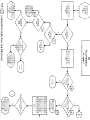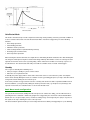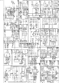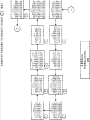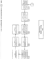
1
Philips Consumer Electronics
Manual 7603
Model no.:
no.: 29LL
29LL600121
LL600121
First Publish:
Publish: 5-1010-2001
Rev.
Rev. Date:
Date: 9-1010-2001
Print Date:
Date: 11/
11/21/
21/2005
Technical Service Data
Service and Quality
Service Publications Dept.
One Philips Drive
P.O. Box 14810
Knoxville, TN 37914
Pg. SCHEMATIC DIAGRAMS AND PC BOARDS
1. Chassis Overview
2. Power Supply (Diagram A1)
3. Line Deflection (Diagram A2)
4. Frame Deflection (Diagram A3)
5. Tuner IF (Diagram A4)
6. Video IF And Sound IF (Diagram A5)
7. Synchronization (Diagram A6)
8. Control (Diagram A7)
9. Audio Amplifier (Diagram A8)
10. BTSC (Stereo/SAP) Decoder (Diagram A9)
11. Audio/Video Source Switching (Diagram A10)
12. BTSC - NDBX Stereo Decoder (Diagram A11)
13. Front I/O + Control, Headphone(Diagram A12)
14. Rear I/O Cinch (Diagram A13)
15. PIP Interface (Diagram A16)
16. CRT Panel (Diagram B1)
17. Side AV + Headphone Panel (Diagram C)
18.
19.
20.
21.
22.
23.
24.
25.
26.
27.
28.
29.
30.
31.
32.
33.
Side AV + Headphone Panel (Diagram E1)
PIP Panel (Diagram P)
Top Control Panel (Diagram T)
SCAVEM (Diagram B2)
PCB Large Signal panel (component side)
PCB Large Signal panel (copper side)
PCB CRT panel (component side)
PCB CRT panel (copper side)
PCB Side AV Panel (component side)
PCB Side AV +Headphone Panel (component side)
PCB PIP Panel (component side)
PCB PIP panel (copper side)
PCB Top control- round(component side)
PCB Top control- round (copper side)
PCB Top control- oval (component side)
PCB Top control- oval (copper side)
REFER TO SAFETY GUIDELINES
SAFETY NOTICE:
NOTICE: ANY PERSON ATTEMPTING TO SERVICE THIS CHASSIS MUST FAMILIARIZE
HIMSELF WITH THE CHASSIS AND BE AWARE OF THE NECESSARY SAFETY PRECAUTIONS
VOLTAGES..
TO BE USED WHEN SERVICING ELECTRONIC EQUIPMENT CONTAINING HIGH VOLTAGES
CAUTION:
CAUTION: USE A SEPARATE ISOLATION TRANSFORMER FOR THIS UNIT WHEN SERVICING
© Philips Electronics North America Corporation
Visit our World Wide Web Site at http://www.forceonline.com
Philips Consumer Electronics
Manual 7603
Model no.:
no.: 29LL
29LL600121
LL600121
First Publish:
Publish: 5-1010-2001
Rev.
Rev. Date:
Date: 9-1010-2001
Print Date:
Date: 11/
11/21/
21/2005
Technical Service Data
Service and Quality
Service Publications Dept.
One Philips Drive
P.O. Box 14810
Knoxville, TN 37914
Safety Notes
REFER TO SAFETY GUIDELINES
SAFETY NOTICE:
NOTICE: ANY PERSON ATTEMPTING TO SERVICE THIS CHASSIS MUST FAMILIARIZE
HIMSELF WITH THE CHASSIS AND BE AWARE OF THE NECESSARY SAFETY PRECAUTIONS
VOLTAGES..
TO BE USED WHEN SERVICING ELECTRONIC EQUIPMENT CONTAINING HIGH VOLTAGES
CAUTION:
CAUTION: USE A SEPARATE ISOLATION TRANSFORMER FOR THIS UNIT WHEN SERVICING
© Philips Electronics North America Corporation
Visit our World Wide Web Site at http://www.forceonline.com
GENERAL SAFETY NOTES
IMPORTANT SAFETY NOTICE
Proper service and repair is important to the safe, reliable operation of all Philips Consumer Electronics
Company** equipment. The service procedures recommended by Philips and described in this service
manual are effective methods of performing service operations. Some of these service operations require
the use of tools specially designed for the purpose. The special tools should be used when and as
recommended.
It is important to note that this manual contains various CAUTIONS and NOTICES which should be
carefully read in order to minimize the risk of personal injury to service personnel. The possibility exists
that improper service methods may damage the equipment. It also is important to understand that these
CAUTIONS and NOTICES ARE NOT EXHAUSTIVE. Philips could not possibly know, evaluate and
advise the service trade of all conceivable ways in which service might be done or of the possible
hazardous consequences of each way. Consequently, Philips has not undertaken any such broad
evaluation. Accordingly, a servicer who uses a service procedure or tool which is not recommended by
Philips must first satisfy himself thoroughly that neither his safety nor the safe operation of the equipment
will be jeopardized by the service method selected.
** Hereafter throughout this manual, Philips Consumer Electronics Company will be referred to as
Philips.
WARNING
Critical components having special safety characteristics are identified with a
or "S" by the Ref. No.
in the parts list and enclosed within a broken line* (where several critical components are grouped in one
area) along with the safety symbol
on the schematics or exploded views. Use of substitute
replacement parts which do not have the same specified safety characteristics may create shock, fire, or
other hazards. Under no circumstances should the original design be modified or altered without written
permission from Philips. Philips assumes no liability, express or implied, arising out of any unauthorized
modification of design. Servicer assumes all liability.
• Broken Line ____ _ ____ _ ____ _ ____
SAFETY CHECKS
After the original service problem has been corrected, a complete safety check should be made. Be sure
to check over the entire set, not just the areas where you have worked. Some previous servicer may
have left an unsafe condition, which could be unknowingly passed on to Your customer. Be sure to check
all of the following:
FIRE AND SHOCK HAZARD
IMPLOSION
X-RADIATION
LEAKAGE CURRENT COLD CHECK
LEAKAGE CURRENT HOT CHECK
PICTURE TUBE REPLACEMENT
PARTS REPLACEMENT
FIRE AND SHOCK HAZARD
1. Be sure all components are positioned in such a way as to avoid the possibility of adjacent component
shorts. This is especially important on those chassis which are transported to and from the service shop.
2. Never release a repaired unit unless all protective devices such as insulators, barriers, covers, strain
reliefs, and other hardware have been installed in accordance with the original design.
3. Soldering and wiring must be inspected to locate possible cold solder joints, solder splashes, sharp
solder points, frayed leads, pinched leads, or damaged insulation (including the ac cord). Be certain to
remove loose solder balls and all other loose foreign particles.
4. Check across-the-line components and other components for physical evidence of damage or
deterioration and replace if necessary. Follow original layout, lead length, and dress.
5. No lead or component should touch a receiving tube or a resistor rated at 1 watt or more. Lead
tension around protruding metal surfaces or edges must be avoided.
6. Critical components having special safety characteristics are identified with an 'S' by the Ref. No. in
the parts list and enclosed within a broken line* (where several critical components are grouped in one
area) along with the safety symbol
on the schematic diagrams and /or exploded views.
7. When servicing any unit, always use a separate isolation transformer for the chassis. Failure to use a
separate isolation transformer may expose you to possible shock hazard, and may cause damage to
servicing instruments.
8. Many electronic products use a polarized ac line cord (one wide pin on the plug). Defeating this
safety feature may create a potential hazard to the servicer and the user. Extension cords which do not
incorporate the polarizing feature should never be used.
9. After reassembly of the unit, always perform an ac leakage test or resistance test from the line cord
to all exposed metal parts of the cabinet. Also, check all metal control shafts (with knobs removed),
antenna terminals, handles, screws, etc., to be sure the unit may be safely operated without danger of
electrical shock.
* Broken line ____ _ ____ _ ____ _ ____
IMPLOSION
1. All picture tubes used in current model receivers are equipped with an integral implosion system.
Care should always be used, and safety glasses worn, whenever handling any picture tube. Avoid
scratching or otherwise damaging the picture tube during installation.
2. Use only replacement tubes specified by the manufacturer.
X-RADIATION
1. Be sure procedures and instructions to all your service personnel cover the subject of X-radiation.
Potential sources of X-rays in TV receivers are the picture tube and the high voltage circuits. The basic
precaution which must be exercised is to keep the high voltage at the factory recommended level.
2. To avoid possible exposure to X-radiation and electrical shock, only the manufacturer's specified
anode connectors must be used.
3. It is essential that the service technician has an accurate HV meter available at all times. The
calibration of this meter should be checked periodically against a reference standard.
4. When the HV circuitry is operating properly there is no possibility of an X-radiation problem. High
voltage should always be kept at the manufacturer's rated value - no higher - for optimum performance.
Every time a color set is serviced, the brightness should be run up and down while monitoring the HV
with a meter to be certain that the HV is regulated correctly and does not exceed the specified value. We
suggest that you and your technicians review test procedures so that HV and HV regulation are always
checked as a standard servicing procedure, and the reason for this prudent routine is clearly understood
by everyone. It is important to use an accurate and reliable HV meter. It is recommended that the HV
reading be recorded on each customer's invoice, which will demonstrate a proper concern for the
customer's safety.
5. When troubleshooting and making test measurements in a receiver with a problem of excessive high
voltage, reduce the line voltage by means of a Variac to bring the HV into acceptable limits while
troubleshooting. Do not operate the chassis longer than necessary to locate the cause of the excessive
HV.
6. New picture tubes are specifically designed to withstand higher operating voltages without creating
undesirable X-radiation. It is strongly recommended that any shop test fixture which is to be used with
the new higher voltage chassis be equipped with one of the new type tubes designed for this service.
Addition of a permanently connected HV meter to the shop test fixture is advisable. The CRT types used
in these new sets should never be replaced with any other types, as this may result in excessive
X-radiation.
7. It is essential to use the specified picture tube to avoid a possible X-radiation problem.
8. Most TV receivers contain some type of emergency "Hold Down" circuit to prevent HV from rising to
excessive levels in the presence of a failure mode. These various circuits should be understood by all
technicians servicing them, especially since many hold down circuits are inoperative as long as the
receiver performs normally.
LEAKAGE CURRENT COLD CHECK
1. Unplug the ac line cord and connect a jumper between the two prongs of the plug.
2. Turn on the power switch.
3. Measure the resistance value between the jumpered ac plug and all exposed cabinet parts of the
receiver, such as screw heads, antennas, and control shafts. When the exposed metallic part has a
return path to the chassis, the reading should be between 1 megohm and 5.2 megohms. When the
exposed metal does not have a return path to the chassis, the reading must be infinity. Remove the
jumper from the ac line cord.
LEAKAGE CURRENT HOT CHECK
1. Do not use an isolation transformer for this test. Plug the completely reassembled receiver directly
into the ac outlet.
2. Connect a 1.5k, 1OW resistor paralleled by a 0.15uF. capacitor between each exposed
metallic cabinet part and a good earth ground such as a water pipe, as shown below.
3. Use an ac voltmeter with at least 5000 ohms/volt sensitivity to measure the potential across the
resistor.
4. The potential at any point should not exceed 0.75 volts. A leakage current tester may be
used to make this test; leakage current must not exceed 0.5milliamp. If a measurement is outside of the
specified limits, there is a possibility of shock hazard. The receiver should be repaired and rechecked
before returning it to the customer.
5. Repeat the above procedure with the ac plug reversed. (Note: An ac adapter is
necessary when a polarized plug is used. Do not defeat the polarizing feature of the plug.)
OR
With the instrument completely reassembled, plug the AC line cord directly into a 120V AC outlet. (Do
not use an isolation transformer during this test.) Use a leakage current tester or a
metering system that complies with American National Standards Institute (ANSI) C101.1 Leakage
Current for Appliances and Underwriters Laboratories (UL) 1410, (50.7). With the instrument
AC switch first in the on position and then in the off position, measure from a
known earth ground (metal water pipe, conduit, etc.) to all exposed metal
parts of the instrument (antennas, handle brackets, metal cabinet, screw
heads, metallic overlays, control shafts, etc.), especially any exposed metal
parts that offer an electrical return path to the chassis. Any current
measured must not exceed 0.5 milliamp. Reverse the instrument power cord
plug in the outlet and repeat the test. See graphic below.
PICTURE TUBE REPLACEMENT
The primary source of X-radiation in this television receiver is the picture tube. The picture tube utilized
in this chassis is specially constructed to limit X-radiation emissions. For continued X-radiation protection,
the replacement tube must be the same type as the original, including suffix letter, or a Philips approved
type.
PARTS REPLACEMENT
Many electrical and mechanical parts in Philips television sets have special safety related characteristics.
These characteristics are often not evident from visual inspection nor can the protection afforded by them
necessarily be obtained by using replacement components rated for higher voltage, wattage, etc. The
use of a substitute part which does not have the same safety characteristics as the Philips recommended
replacement part shown in this service manual may create shock, fire, or other hazards
TV SAFETY NOTES
SAFETY CHECKS
IMPLOSION
X-RADIATION
PICTURE TUBE REPLACEMENT
PARTS REPLACEMENT
WARNING
Before removing the CRT anode cap, turn the unit OFF and short the HIGH VOLTAGE to the CRT DAG
ground.
SERVICE NOTE: The CRT DAG is not at chassis ground.
TV-VCR COMBI SAFETY NOTES
IMPORTANT SAFETY PRECAUTIONS
Prior to shipment from the factory, our products are strictly inspected for recognized product safety and
electrical codes of the countries in which they are to be sold. However, in order to maintain such
compliance, it is equally important to implement the following precautions when a set is being serviced.
SAFETY PRECAUTIONS FOR TV CIRCUITS
1. Before returning an instrument to the customer, always make a safety check of the entire instrument,
including, but not limited to, the following items:
a. Be sure that no built-in protective devices are defective or have been defeated during servicing. (1)
Protective shields are provided on this chassis to protect both the technician and the customer.
Correctly replace all missing protective shields, including any removed for servicing convenience. (2)
When reinstalling the chassis and/or other assembly in the cabinet, be sure to put back in place all
protective devices, including but not limited to, nonmetallic control knobs, insulating fishpapers,
adjustment and compartment covers/shields, and isolation resistor/capacitor networks. Do not
operate this instrument or permit it to be operated without all protective devices correctly installed and
functioning. Servicers who defeat safety features or fail to perform safety checks may be liable for any
resulting damage.
b. Be sure that there are no cabinet openings through which an adult or child might be able to insert
their fingers and contact a hazardous voltage. Such openings include, but are not limited to, (1)
spacing between the picture tube and the cabinet mask, (2) excessively wide cabinet ventilation slots,
and (3) an improperly fitted and/or incorrectly secured cabinet back cover.
c. Do a
LEAKAGE CURRENT CHECK
ANY MEASUREMENTS NOT WITHIN THE LIMITS SPECIFIED HEREIN INDICATE A POTENTIAL SHOCK
HAZARD THAT MUST BE ELIMINATED BEFORE RETURNING THE INSTRUMENT TO THE CUSTOMER OR
BEFORE CONNECTING THE ANTENNA OR ACCESSORIES.
d. X-Radiation and High Voltage Limits - Because the picture tube is the primary potential source
of X-radiation in solid-state TV receivers, it is specially constructed to prohibit X-radiation emissions.
For continued X-radiation protection, the replacement picture tube must be the same type as the
original. Also, because the picture tube shields and mounting hardware perform an X-radiation
protection function, they must be correctly in place. High voltage must be measured each time
servicing is performed that involves B+, horizontal deflection or high voltage. Correct operation of the
X-radiation protection circuits also must be reconfirmed each time they are serviced. (X-radiation
protection circuits also may be called "horizontal disable" or "hold down.") Read and apply the high
voltage limits and, if the chassis is so equipped, the X-radiation protection circuit specifications given
on instrument labels and in the Product Safety & X-Radiation Warning note on the service data
chassis schematic. High voltage is maintained within specified limits by close tolerance safety-related
components/adjustments in the high-voltage circuit. If high voltage exceeds specified limits, check
each component specified on the chassis schematic and take corrective action.
2. Read and comply with all caution and safety-related notes on or inside the receiver cabinet, on the
receiver chassis, or on the picture tube.
3. Design Alteration Warning - Do not alter or add to the mechanical or electrical design of this TV
receiver. Design alterations and additions, including, but not limited to circuit modifications and the
addition of items such as auxiliary audio and/or video output connections, might alter the safety
characteristics of this receiver and create a hazard to the user. Any design alterations or additions will
void the manufacturer's warranty and may make you, the servicer, responsible for personal injury or
property damage resulting therefrom.
4. Picture Tube Implosion Protection Warning - The picture tube in this receiver employs integral
implosion protection. For continued implosion protection, replace the picture tube only with one of the
same type number. Do not remove, install, or otherwise handle the picture tube in any manner without
first putting on shatterproof goggles equipped with side shields. People not so equipped must be kept
safely away while picture tubes are handled. Keep the picture tube away from your body. Do not handle
the picture tube by its neck. Some "in-line" picture tubes are equipped with a permanently attached
deflection yoke; because of potential hazard, do not try to remove such "permanently attached" yokes
from the picture tube.
5. Hot Chassis Warning
a. Some TV receiver chassis are electrically connected directly to one conductor of the ac power cord
and may be serviced safely without an isolation transformer only if the ac power plug is inserted so
that the chassis is connected to the ground side of the ac power source. To confirm that the ac
power plug is inserted correctly, with an ac voltmeter, measure between the chassis and a known
earth ground. If a voltage reading in excess of 1.OV is obtained, remove and reinsert the ac power
plug in the opposite polarity and again measure the voltage potential between the chassis and a
known earth ground.
b. Some TV receiver chassis normally have 85Vac (RMS) between chassis and earth ground
regardless of the ac plug polarity. This chassis can be safety-serviced only with an isolation
transformer inserted in the power line between the receiver and the ac power source, for both
personnel and test equipment protection. Some TV receiver chassis have a secondary ground system
in addition to the main chassis ground. This secondary ground system is not isolated from the ac
power line. The two ground systems are electrically separated by insulation material that must not
be defeated or altered.
6. Observe original lead dress. Take extra care to assure correct lead dress in the following areas: a.
near sharp edges, b. near thermally hot parts - be sure that leads and components do not touch
thermally hot parts, c. the ac supply, d. high voltage, and e. antenna wiring. Always inspect in all areas
for pinched, out of place, or frayed wiring. Check ac power cord for damage.
7. Components, parts, and/or wiring that appear to have overheated or are otherwise damaged should be
replaced with components, parts, or wiring that meet original specifications. Additionally, determine the
cause of overheating and/or damage and, if necessary, take corrective action to remove any potential
safety hazard.
PRECAUTIONS DURING SERVICE
A. Parts identified by the
symbol are critical for safety. Replace only with part number specified.
B. In addition to safety, other parts and assemblies are specified for conformance with regulations
applying to spurious radiation. These must also be replaced only with specified replacements.
Examples: RF converters, RF cables, noise blocking capacitors, and noise blocking filters, etc.
C. Use specified internal wiring. Note especially:
1) Wires covered with PVC tubing
2) Double insulated wires
3) High voltage leads
D. Use specified insulating materials for hazardous
live parts. Note especially:
1) Insulation Tape
2) PVC tubing
3) Spacers
4) Insulators for transistors
E. When replacing ac primary side components (transformers, power cord, etc.), wrap ends of wires
securely about the terminals before soldering.
F. Observe that the wires do not contact heat producing parts (heatsinks, oxide metal film resistors,
fusible resistors, etc.)
G. Check that replaced wires do not contact sharp edged or pointed parts.
H. When a power cord has been replaced, check that 10-15 kg of force in any direction will not
loosen it.
I. Also check areas surrounding repaired locations.
J. Use care that foreign objects (screws, solder droplets, etc.) do not remain inside the set.
K. Crimp type wire connector
When replacing the power transformer in sets where the connections between the power cord and power
transformer primary lead wires are performed using crimp type connectors, in order to prevent shock
hazards, perform carefully and precisely the following steps.
Replacement procedure
1) Remove the old connector by cutting the wires at a point close to the connector. Important: Do
not re-use a connector (discard it).
2) Strip about 15 mm of the insulation from the ends of the wires. If the wires are stranded, twist
the strands to avoid frayed conductors.
3) Align the lengths of the wires to be connected. Insert the wires fully into the connector.
4) Use the crimping tool to crimp the metal sleeve at the center position. Be sure to crimp fully to
the complete closure of the tool.
L. When connecting or disconnecting the VCR connectors, first, disconnect the ac plug from the ac supply
socket.
SAFETY CHECK AFTER SERVICING
Examine the area surrounding the repaired location for damage or deterioration. Observe that screws,
parts and wires have been returned to original positions. Afterwards, perform the following tests and
confirm the specified values in order to verify compliance with safety standards.
1. Clearance Distance
When replacing primary circuit components, confirm specified clearance distance (d) and (d') between
soldered terminals, and between terminals and surrounding metallic parts. (See graphic bllow)
Table 1 : Ratings for selected area
AC Line Voltage
Region
110 to 130 V
USA or
CANADA
Clearance Distance
(d) (d')
> 3.2 mm
(0.126 inches)
Note: This table is unofficial and for reference only. Be sure to confirm the precise values.
2.
LEAKAGE CURRENT CHECKS
VCR SAFETY NOTES
FIRE & SHOCK HAZARD (VCR)
1. Be sure that all components are positioned in such a way to avoid possibility of shorts to adjacent
components. This is especially important on those chassis which are transported to and from the repair
shop.
2. Always replace all protective devices such as insulators and barriers after working on a set.
3. Check for damaged insulation on wires including the ac cord.
4. Check across-the-line components for damage and replace if necessary.
5. After re-assembly of the unit, always perform an ac leakage test on the exposed metallic parts of the
cabinet such as the knobs, antenna terminals, etc. to be sure the set is safe to operate without danger of
electrical shock. Do not use a line isolation transformer during this test. Use an ac voltmeter
having 5000 ohms per volt or more sensitivity in the following manner: Connect a 1500 ohm 10 wan
resistor, paralleled by 0.15 MFD ac type capacitor, between a known good earth ground (water pipe,
conduit, etc.) and the exposed metallic parts, one at a time. Measure the ac voltage across the
combination 1500 ohm resistor and 0.15 MFD capacitor. Reverse the ac plug on the set and repeat ac
voltage measurements again for each exposed metallic part. Voltage measured must not exceed O.6 volts
R.M.S. This corresponds to 0.4 milliamp ac. Any value exceeding this limit constitutes a potential shock
hazard and must be corrected immediately.
GENERAL
Power Supply-This receiver is designed for operation on 120 Volts, 6OHz alternating current (ac) only.
Never connect to a supply having a different frequency or voltage.
IMPORTANT NOTICE
This device employs many circuits, components, and mechanical parts designed for protection against
fire, shock and RF interference. For continued safety any servicing should be performed by qualified
personnel and exact replacement parts should be used. Under no circumstances should the original
design be altered.
PRODUCT SAFETY GUIDELINES FOR ALL PRODUCTS
CAUTION: Do not modify any circuit. Service work should be performed only after you are thoroughly
familiar with all of the following safety checks. Risk of potential hazards and injury to the user increases if
safety checks are not adhered to.
USE A SEPARATE ISOLATION TRANSFORMER FOR THIS UNIT WHEN SERVICING.
PREVENTION OF ELECTROSTATIC DISCHARGE (ESD)
Some semiconductor solid state devices can be damaged easily by static electricity. Such components
commonly are called Electrostatically Sensitive (ES) Devices, Examples of typical ES devices are
integrated circuits and some field-effect transistors and semiconductor "chip" components. The following
techniques should be used to help reduce the incidence of component damage caused by electrostatic
discharge (ESD).
1. Immediately before handling any semiconductor component or semiconductor-equipped assembly,
drain off any ESD on your body by touching a known earth ground. Alternatively, obtain and wear a
commercially available discharging ESD wrist strap, which should be removed for potential shock reasons
prior to applying power to the unit under test.
2. After removing an electrical assembly equipped with ES devices, place the assembly on a conductive
surface such as aluminum foil, to prevent electrostatic charge buildup or exposure of the assembly.
3. Use only a grounded-tip soldering iron to solder or unsolder ES devices.
4. Use only an anti-static solder removal device. Some solder removal devices not classified as "antistatic
(ESD protected)" can generate an electrical charge sufficient to damage ES devices.
5. Do not use freon·propelled chemicals. These can generate electrical charges sufficient to damage ES
devices.
6. Do not remove a replacement ES device from its protective package until immediately before you are
ready to install it (Most replacement ES devices are packaged with leads electrically shorted together by
conductive foam, aluminum foil or comparable conductive material).
7. Immediately before removing the protective material from the leads of a replacement ES device, touch
the protective material to the chassis or circuit assembly into which the device will be installed.
CAUTION : Be sure no power is applied to the chassis or circuit and observe all other safety precautions.
8. Minimize bodily motions when handling unpackaged replacement ES devices. (Otherwise harmless
motion such as the brushing together of your clothes fabric or the lifting of your feet from a carpeted
floor can generate static electricity (ESD) sufficient to damage an ES device.)
NOTE to CATV system Installer:
This reminder is provided to call the CATV system installer's attention to article 820-22 of the NEC that
provides guidelines for proper grounding and, in particular, specifies that the cable ground shall be
connected to the grounding system of the building, as close to the point of cable entry as practical.
Philips Consumer Electronics
Manual 7603
Model no.:
no.: 29LL
29LL600121
LL600121
First Publish:
Publish: 5-1010-2001
Rev.
Rev. Date:
Date: 9-1010-2001
Print Date:
Date: 11/
11/21/
21/2005
Technical Service Data
Service and Quality
Service Publications Dept.
One Philips Drive
P.O. Box 14810
Knoxville, TN 37914
Mechanical Diagrams
REFER TO SAFETY GUIDELINES
SAFETY NOTICE:
NOTICE: ANY PERSON ATTEMPTING TO SERVICE THIS CHASSIS MUST FAMILIARIZE
HIMSELF WITH THE CHASSIS AND BE AWARE OF THE NECESSARY SAFETY PRECAUTIONS
VOLTAGES..
TO BE USED WHEN SERVICING ELECTRONIC EQUIPMENT CONTAINING HIGH VOLTAGES
CAUTION:
CAUTION: USE A SEPARATE ISOLATION TRANSFORMER FOR THIS UNIT WHEN SERVICING
© Philips Electronics North America Corporation
Visit our World Wide Web Site at http://www.forceonline.com
MAIN CABINET EXPLODED VIEW
Page: 1 of 1
Manual 7603
Philips Consumer Electronics
Model no.:
no.: 29LL
29LL600121
LL600121
First Publish:
Publish: 5-1010-2001
Rev.
Rev. Date:
Date: 9-1010-2001
Print Date:
Date: 11/
11/21/
21/2005
Technical Service Data
Service and Quality
Service Publications Dept.
One Philips Drive
P.O. Box 14810
Knoxville, TN 37914
Troubleshooting
REFER TO SAFETY GUIDELINES
SAFETY NOTICE:
NOTICE: ANY PERSON ATTEMPTING TO SERVICE THIS CHASSIS MUST FAMILIARIZE
HIMSELF WITH THE CHASSIS AND BE AWARE OF THE NECESSARY SAFETY PRECAUTIONS
VOLTAGES..
TO BE USED WHEN SERVICING ELECTRONIC EQUIPMENT CONTAINING HIGH VOLTAGES
CAUTION:
CAUTION: USE A SEPARATE ISOLATION TRANSFORMER FOR THIS UNIT WHEN SERVICING
© Philips Electronics North America Corporation
Visit our World Wide Web Site at http://www.forceonline.com
Service Modes, Error Codes And Fault Finding
Test Points
The chassis is equipped with test points printed on the circuit board assemblies. These test points refer to the
functional blocks:
The numbering is in a logical sequence for diagnostics.
Always start diagnosing within a functional block in the sequence of the relevant test points for that block.
Perform measurements under the following conditions:
•
•
•
•
Service Default Mode (when this mode is not present, set all controls to 50% and volume select channel 3).
Service Default Mode.
Video: color bar signal.
Audio: 3 kHz left, 1 kHz right.
Service Modes
Service Default Mode (SDM) and Service Alignment Mode (SAM) offer several features for the service technician,
while the Customer Service Mode (CSM) is used for communication between dealer and customer.
Note: Some L8 and M8 chassis sets use a software version that does not contain the Service Modes (see table). In
this case, use the special Factory Mode Remote Control. This can be ordered by service code 4835 310 57511.
Complete instructions are included. This remote control will place the TV in the Factory Mode and allow access to all
adjustments that a normal Service Mode contains (including setting Option Bytes). Error codes will not be available.
There is also the option of using ComPair, a hardware interface between a computer (see requirements) and the TV
chassis. It offers the ability of structured trouble shooting, error code reading and software version readout for all L8
and M8 chassis.
Requirements: To run ComPair on a computer (laptop or desktop) requires, as a minimum, a 486 processor,
Windows 3.1 and a CD-ROM drive. A Pentium Processor and Windows 95/98 are also acceptable (see also
ComPair
Service Default Mode (SDM)
Purpose
•
•
•
To create a predefined setting to get the same measurement results as given in this manual.
To override SW protections.
To start the blinking LED procedure.
Specifications
•
•
•
•
•
Tuning frequency: 61.25 MHz (channel 3).
Color system: NTSC.
All picture settings at 50 % (brightness, color contrast, hue).
Bass, treble and balance at 50 %; volume at 25 %.
All service-unfriendly modes (if present) are disabled, like:
− (sleep) timer,
− child/parental lock,
− blue mute,
− hotel/hospitality mode
− auto switch-off (when no 'IDENT' video signal is received for 15 minutes),
− skip / blank of non-favorite presets / channels,
− auto store of personal presets,
− auto user menu time-out.
How to enter SDM
•
•
Use a standard customer RC-transmitter and key in the code 062596 directly followed by the MENU button, or
Short wires 9631 and 9641 on the mono carrier and switch the set ON apply AC power. Then press the power
button (remove short after start-up).
Caution: Entering SDM by shorten wires 9631 and 9641 will override the +8V-protection. Do this only for a short
period. When doing this, the service-technician must know exactly what he is doing, as it could lead to damaging
the set.
•
Or via ComPair
After entering SDM, the following screen is visible, with SDM at the upper right side for recognition.
How to navigate
•
When you press the MENU button on the remote control, the set will switch between the SDM and the normal
user menu (with the SDM mode still active in the background). Return to the SDM screen with the OSD / STATUS
button.
•
When you press the OSD / STATUS button on the remote control, the menu will show or hide the error buffer.
This feature is available to prevent interference during waveform measurements.
•
On the TV press and hold the 'VOLUME down' and press the 'CHANNEL down' for a few from SDM to SAM and
reverse.
How to exit
Switch the set to STANDBY by pressing the power button on the remote control transmitter (if you switch the set OFF
by removing the AC power, the set will return in SDM when AC power is re-applied). The error buffer is cleared.
Service Alignment Mode (SAM)
Purpose
•
•
•
To perform alignments.
To change option settings.
To display / clear the error code buffer.
Specifications
•
•
•
•
•
Operation hours counter.
Software version.
Option settings.
Error buffer reading and erasing.
Software alignments.
How to enter
•
Use a standard customer RC-transmitter and key in the code 062596 directly followed by the OSD / STATUS
button or
•
Via ComPair.
The following screen is visible, with SAM at the upper right side for recognition.
1. LLLL This is the operation hours counter. It counts the normal operation hours, not the standby hours.
2. AAABCD-X.Y This is the software identification of the main micro controller
• A = the project name (L01).
• B = the region: E = Europe, A = Asia Pacific, U = NAFTA, L = LATAM.
• C = the software diversity: N = stereo non-DBX, S = stereo DBX, M = mono, D = DVD.
• D = the language cluster number.
• E = UOC diversity.
• X = the main software version number.
• Y = the sub software version number.
3. SAM Indication of the actual mode.
4. Errors buffer Five errors possible.
5. Option bytes Seven codes possible.
6. Clear Erase the contents of the error buffer. Select the CLEAR menu item and press the CURSOR RIGHT key.
The content of the error buffer is cleared.
7. Options To set the Option Bytes. See chapter 8.3.1 for a detailed description.
8. AKB Disable (0) or enable (1) the 'black current loop' (AKB = Auto Kine Bias).
9. Tuner To align the Tuner. See chapter 8.3.2 for a detailed description.
10. White Tone To align the White Tone. See White tone for a detailed description.
11. Geometry To align the set geometry. See Geometry for a detailed description.
12. Audio No audio alignment is used for NTSC.
How to navigate
•
In SAM, select menu items with the CURSOR UP/DOWN key on the remote control transmitter. The selected
item will be highlighted. When not all menu items fit on the screen, move the CURSOR UP/DOWN key to display
the next / previous menu items.
•
With the CURSOR LEFT/RIGHT keys, it is possible to:
− (De)activate the selected menu item.
− Change the value of the selected menu item.
− Activate the selected submenu.
When you press the MENU button twice, the set will switch to the normal user menus (with the SAM mode still
active in the background). To return to the SAM menu press the OSD / STATUS button [ i+ ].
•
•
When you press the MENU key in a submenu, you will return to the previous menu.
How to exit
Switch the set to STANDBY by pressing the power button on the remote control transmitter (if you switch the set OFF
by removing the AC power, the set will return in SAM when AC power is re-applied). The error buffer is not cleared.
Customer Service Mode (CSM)
Purpose
The Customer Service Mode is (de-)activated by the customer upon request of the service technician during a
telephone conversation, in order to identify the status of the set. This CSM is a read only mode, therefore
modifications in this mode are not possible.
How to enter
The CSM will be turned on after pressing the MUTE key on the remote control transmitter and any of the control
buttons on the TV for at least 4 seconds simultaneously. This activation only works if there is no menu on the screen.
After switching ON the Customer Service Mode, the following screen will appear:
1. Software identification of the main micro controller (see Service Alignment Mode (SAM)for an explanation).
2. Error code buffer (see Error Codes for more details). Displays the last seven errors of the error code buffer.
3. In this line, the Option Bytes (OB) are visible. Each Option Byte is displayed as a decimal number between 0 and
255. The set may not work correctly when an incorrect option code is set. See Options for more information on the
option settings.
4. Indicates which color and sound system is installed for the selected pre-set.
5. Indicates if the set is not receiving an 'IDENT' signal on the selected source. It will display 'Not Tuned'.
6. Indicates if the sleep timer is enabled.
7. Indicates if the V-chip feature is enabled.
8. Value indicates parameter levels at CSM entry.
CO = CONTRAST, CL = COLOR, BR = BRIGHTNESS,
HU = HUE, SH = SHARPNESS
9. Value indicates parameter levels at CSM entry.
VL = VOLUME LEVEL, BL = BALANCE LEVEL, AVL LIM
= AUTO VOLUME LEVEL LIMITER
10. Value indicates parameter levels at CSM entry.
DV = DELTA VOLUME, BS = BASS LEVEL, TR = TREBLE LEVEL
How to exit
You can turn the Customer Service Mode off:
•
•
After you press 'any' key of the remote control transmitter with exception of the CHANNEL and VOLUME keys.
After you switch-off the TV set with the AC power switch.
Problems And Solving Tips (Related To CSM)
Picture Problems
No colors / noise in picture
Check CSM line 4. Wrong color system installed. To change the setting:
1. Select the MANUAL STORE sub menu.
2. Select and change the SYSTEM setting until picture and sound are correct.
3. Select the STORE menu item.
Colors not correct / unstable picture
Check CSM line 4. Wrong color system installed. To change the setting:
1. Press the MENU button on the remote control.
2. Select the INSTALL sub menu.
3. Select the MANUAL STORE sub menu.
4. Select and change the SYSTEM setting until picture and sound are correct.
5. Select the STORE menu item.
TV switches off or changes channel without any user action
The TV set switches off after TV SWITCHING OFF was displayed.
Auto standby switched the set off because:
• There was no 'ident' signal for more than 15 minutes or
• There was no remote control signal received or local key pressed for > 2 hours.
See Alignments for a description of the options to enable / disable auto standby
Picture too dark or too bright
Increase / decrease the BRIGHTNESS and / or the CONTRAST value when:
• The picture improves after you have pressed the 'Smart Picture' button on the remote control.
• The picture improves after you have switched on the Customer Service Mode
The new 'Personal' preference value is automatically stored.
White line around picture elements and text
Decrease the SHARPNESS value when:
• The picture improves after you have pressed the 'Smart Picture' button on the remote control.
• The picture improves after you have switched on the Customer Service Mode
The new 'Personal' preference value is automatically stored.
Snowy picture
Check CSM line 5. If this line indicates 'Not Tuned', check the following:
•
•
•
No or bad antenna signal. Connect a proper antenna signal.
Antenna not connected. Connect the antenna.
No channel / preset is stored at this program number. Go to the INSTALL menu and store a proper channel at
this program number.
•
The tuner is faulty (in this case the CODES line will contain error number 10). Check the tuner and replace /
repair if necessary.
Snowy picture and/or unstable picture
•
A scrambled or decoded signal is received.
Black and white picture
Increase the COLOR value when:
• The picture improves after you have pressed the 'Smart Picture' button on the remote control.
• The picture improves after you have switched on the Customer Service Mode
The new 'Personal' preference value is automatically stored.
Menu text not sharp enough
Decrease the CONTRAST value when:
• The picture improves after you have pressed the 'Smart Picture' button on the remote control.
• The picture improves after you have switched on the Customer Service Mode
The new 'Personal' preference value is automatically stored.
Sound Problems
No sound or sound too loud (after channel change / switching on)
Increase / decrease the VOLUME level when the volume is OK after you switched on the CSM. The new 'Personal'
preference value is automatically stored.
ComPair
Introduction
ComPair (Computer Aided Repair) is a service tool for Philips Consumer Electronics products. ComPair is a further
development on the European DST (service remote control), which allows faster and more accurate diagnostics.
Compare has three big advantages:
•
ComPair helps you to quickly get an understanding on how to repair the chassis in a short time by guiding you
systematically through the repair procedures.
•
ComPair allows very detailed diagnostics (on I2C level) and is therefore capable of accurately indicating problem
areas. You do not have to know anything about I 2 C commands yourself because ComPair takes care of this.
ComPair speeds up the repair time since it can automatically communicate with the chassis (when the
microprocessor is working) and all repair information is directly available. When ComPair is installed together with
the SearchMan electronic manual of the defective chassis, schematics and PWBs are only a mouse click away.
•
Specifications
ComPair consists of a Windows based faultfinding program and an interface box between PC and the (defective)
product. The ComPair interface box is connected to the PC via a serial or RS232 cable.
In case of the L8/M8 chassis, the ComPair interface box and the TV communicate via a bi-directional service cable
via the service connector (located on the Main panel, see Hardware alignments suffix D).
The ComPair faultfinding program is able to determine the problem of the defective television. ComPair can gather
diagnostic information in two ways:
1. Automatic (by communication with the television)
ComPair can automatically read out the contents of the entire error buffer. Diagnosis is done on I 2 C level.
ComPair can access the I 2 C bus of the television. ComPair can send and receive I 2 C commands to the micro
controller of the television. In this way, it is possible for ComPair to communicate (read and write) to devices on
the I 2 C busses of the TV-set.
2. Manually (by asking questions to you)
Automatic diagnosis is only possible if the micro controller of the television is working correctly and only to a
certain extend. When this is not the case, ComPair will guide you through the faultfinding tree by asking you
questions (e.g. Does the screen gives a picture? Click on the correct answer: YES / NO) and showing you
examples (e.g. Measure test-point I7 and click on the correct oscillogram you see on the oscilloscope). You can
answer by clicking on a link (e.g. text or a waveform picture) that will bring you to the next step in the faultfinding
process.
By a combination of automatic diagnostics and an interactive question / answer procedure, ComPair will enable you
to find most problems in a fast and effective way.
Beside fault finding, ComPair provides some additional features like:
• Up- or downloading of presets.
• Managing of preset lists.
• Emulation of the (European) Dealer Service Tool (DST).
• If both ComPair and SearchMan (Electronic Service Manual) are installed, all the schematics and the PWBs of
the set are available by clicking on the appropriate hyperlink.
Example: Measure the DC-voltage on capacitor C2568 (Schematic/Panel) at the Monocarrier.
Click on the 'Panel' hyperlink to automatically show the PWB with a highlighted capacitor C2568.
Click on the 'Schematic' hyperlink to automatically show the position of the highlighted capacitor.
How To Connect
1. First install the ComPair Browser software (see the Quick Reference Card for installation instructions).
2. Connect the RS232 interface cable between a free serial (COM) port of your PC and the PC connector (marked
with 'PC') of the ComPair interface.
3. Connect the AC power adapter to the supply connector (marked with 'POWER 9V DC') on the compare interface.
4. Switch the ComPair interface OFF.
5. Switch the television set OFF, remove the AC power.
6. Connect the ComPair interface cable between the connector on the rear side of the ComPair interface (marked
with 'I 2 C') and the ComPair connector on the mono carrier (see Hardware alignments suffix D).
7. Plug the AC power adapter in the AC power outlet and switch on the interface. The green and red LEDs light up
together. The red LED extinguishes after approx. 1 second while the green LED remains lit.
8. Start the ComPair program and read the introduction chapter.
How To Order
ComPair order codes:
•
•
•
•
•
•
•
Starter kit ComPair + SearchMan software + compare interface (excluding transformer): 4822 727 21629
ComPair interface (excluding transformer): 4822 727 21631
Starter kit ComPair software (registration version): 4822 727 21634
Starter kit SearchMan software: 4822 727 21635
ComPair CD (update): 4822 727 21637
SearchMan CD (update): 4822 727 21638
ComPair interface cable: 3122 785 90004
Error Codes
Introduction
The error code buffer contains all errors detected since the last time the buffer was erased. The buffer is written from
left to right. When an error occurs that is not yet in the error code buffer, it is written at the left side and all other
errors shift one position to the right.
The error code buffer is cleared in the following cases:
•
•
By activation of the CLEAR command in the SAM menu:
When you exit SDM / SAM with the STANDBY command on the remote control (when leaving SDM / SAM, by
disconnecting the set from AC power, the error buffer is not reset).
•
•
When you transmit the command DIAGNOSE-99-OK with ComPair.
If the content of the error buffer has not changed for 50 hours, it resets automatically.
Examples:
ERROR: 0 0 0 0 0: No errors detected.
ERROR: 6 0 0 0 0: Error code 6 is the most recent and only detected error.
ERROR: 9 6 0 0 0: Error code 6 was first detected and error code 9 is the most recent detected error.
You can also make the contents of the error buffer visible via the blinking LED procedure (see The Blinking LED
Procedure). This is especially useful when there is no picture.
Error Codes
In case of non-intermittent faults, clear the error buffer before you begin the repair. These to ensure that old error
codes are no longer present.
If possible, check the entire contents of the error buffer. In some situations an error code is only the result of another
error code and not the actual cause (e.g., a fault in the protection detection circuitry can also lead to a protection).
The Blinking LED Procedure
Via this procedure you can make the contents of the error buffer visible via the front LED. This is especially useful
when there is no picture.
When the SDM is entered, the LED will blink the contents of the error-buffer.
Error-codes ≥ 10 are shown as follows:
− a long blink of 750 ms (which is an indication of the decimal digit),
− a pause of 1.5 s,
− n short blinks (n = 1 - 9),
− when all the error-codes are displayed, the sequence finishes with a LED blink of 3 s,
− the sequence starts again.
Example of error buffer: 12 9 6 0 0
After entering SDM:
−
−
−
−
−
−
1 long blink of 750 ms followed by a pause of 1.5 s,
2 short blinks followed by a pause of 3 s,
9 short blinks followed by a pause of 3 s,
6 short blinks followed by a pause of 3 s,
1 long blink of 3 s to finish the sequence,
the sequence starts again.
Protections
If a fault situation is detected an error code will be generated and if necessary the set will be put in the protection
mode.
Blinking of the red LED at a frequency of 3 Hz indicates the protection mode. In some error cases the microprocessor
does not put the set in the protection mode. The error codes of the error buffer can be read via the service menu
(SAM), the blinking LED procedure or via ComPair. The DST diagnose functionality will force the set into the
Service-standby, which is similar to the usual standby mode, however the microprocessor has to remain in normal
operation completely.
To get a quick diagnosis the chassis has three service modes implemented:
•
•
•
The Customer Service Mode (CSM).
The Service Default Mode (SDM). Start-up of the set in a predefined way.
The Service Alignment Mode (SAM). Adjustment of the set via a menu and with the help of test patterns.
See for a detailed description Circuit description
Repair Tips
Below some failure symptoms are given, followed by a repair tip.
•
•
•
•
•
•
Set is dead and makes hiccuping sound
'MainSupply' is available. Hiccupping stops when de-soldering L5561, meaning that problem is in the
'MainSupply' line. No output voltages at LOT, no horizontal deflection. Reason: line transistor 7460 is defective.
Set is dead, and makes no sound
Check power supply IC 7520. Result: voltage at pins 1, 3, 4, 5 and 6 are about 180 V and pin 8 is 0 V. The
reason why the voltage on these pins is so high is because the output driver (pin 6) has an open load. That is
why MOSFET 7521 is not able to switch. Reason: feedback resistor 3523 is defective. Caution: be careful
measuring on the gate of 7521; circuitry is very high ohmic and can easily be damaged!
Set is in hiccup mode and shuts down after 8 s.
Blinking LED (set in SDM mode) indicates error 5. As it is unlikely that ?P 'POR' and '+8V protection' happen at
the same time, measure the '+8V'. If this voltage is missing, check transistor 7480.
Set is non-stop in hiccup mode
Set is in over current mode; check the secondary sensing (opto coupler 7515) and the 'MainSupply' voltage.
Signal 'Stdby_con' must be logic low under normal operation conditions and goes to high (3.3 V) under standby
and fault conditions.
Set turns on, but without picture and sound
The screen shows snow, but OSD and other menus are okay. Blinking LED procedure indicates error 11, so
problem is expected in the tuner (pos. 1000). Check presence of supply voltages. As 'Vlotaux+5V' at pin 5 and 7
are okay, 'VT_supply' at pin 9 is missing.
Conclusion: resistor 3460 is defective.
Set turns on, but with a half screen at the bottom.
Sound is okay
Blinking LED (set in SDM mode) indicates error 3. Check 'Vlotaux+11V' and '+50V'. If they are okay, problem is
expected in the vertical amplifier IC 7471. Measure with a scope the waveform on pin 17 of the UOC. Measure
also at pin 1 of IC 7471. If here the signal is missing, a defective resistor R3244 causes the problem.
TROUBLESHOOTING FLOW CHARTS
DEAD SET PAGE 1
DEAD SET PAGE 2
DEAD SET PAGE 3
SHUTDOWN
POWER SUPPLY CHECK PAGE 1
POWER SUPPLY CHECK PAGE 2
NO AUDIO PAGE 1
NO AUDIO PAGE 2
Philips Consumer Electronics
Manual 7603
Model no.:
no.: 29LL
29LL600121
LL600121
First Publish:
Publish: 5-1010-2001
Rev.
Rev. Date:
Date: 9-1010-2001
Print Date:
Date: 11/
11/21/
21/2005
Technical Service Data
Service and Quality
Service Publications Dept.
One Philips Drive
P.O. Box 14810
Knoxville, TN 37914
General Information
REFER TO SAFETY GUIDELINES
SAFETY NOTICE:
NOTICE: ANY PERSON ATTEMPTING TO SERVICE THIS CHASSIS MUST FAMILIARIZE
HIMSELF WITH THE CHASSIS AND BE AWARE OF THE NECESSARY SAFETY PRECAUTIONS
VOLTAGES..
TO BE USED WHEN SERVICING ELECTRONIC EQUIPMENT CONTAINING HIGH VOLTAGES
CAUTION:
CAUTION: USE A SEPARATE ISOLATION TRANSFORMER FOR THIS UNIT WHEN SERVICING
© Philips Electronics North America Corporation
Visit our World Wide Web Site at http://www.forceonline.com
Technical Specifications, Connections And
Chassis Overview
Technical Specifications
Audio ratings
1 W mono
2 x 1 W non-DBX stereo (LC stereo)
2 x 3 W DBX stereo (with SAP)
Reception
Tuning system
Color systems
Sound systems
A/V connections
Channel selections
IF frequency
: PLL
: NTSC
: FM-mono
: BTSC non-DBX
BTSC DBX
: NTSC M
: 181 channels, full cable
: 45.75 MHz
Aerial input
: 75 Ω, Coax
Miscellaneous
AC voltage
AC frequency
Ambient temperature
Maximum humidity
Power consumption
: 90 - 140 V (±10 %)
: 60 Hz (±5 %)
: + 5 to + 45 deg. C
: 90 %
: 36 W (14")
100 W (32")
Standby Power consumption : < 3 W
Connections
Front Or Top Control, Front Or Side Connections
Audio / Video In
1 - Video 1 Vpp / 75 Ω
2 - Audio L (0.2 Vrms / 10 kΩ)
3 - Audio R (0.2 Vrms / 10 kΩ)
4 - Headphone (3.5 mm) 8 - 600 Ω/ 4 mW
Rear Connections
Monitor Out
1 - Video
2 - Audio
3 - Audio
1 Vpp / 75 Ω
L (0.5 Vrms / 1 kΩ)
R (0.5 Vrms / 1 kΩ)
YUV In
1-Y
2-U
0.7 Vpp / 75 Ω
0.7 Vpp / 75 Ω
3-V
0.7 Vpp / 75 Ω
AV1 In
4 - Video
5 - Audio
6 - Audio
1 Vpp / 75 Ω
L (0.5 Vrms / 10 kΩ)
R (0.5 Vrms / 10 kΩ)
AV2 In
1 - Video
2 - Audio
3 - Audio
1 Vpp / 75 Ω
L (0.5 Vrms / 10 kΩ)
R (0.5 Vrms / 10 kΩ)
AV2 In (SVHS)
12-
gnd
gnd
3-Y
4-C
1 Vpp / 75 Ω
0.3 Vpp / 75 Ω
Safety & Maintenance Instructions, Warnings, And
Notes
Safety Instructions For Repairs
Safety regulations require that during a repair:
•
Due to the 'hot' parts of this chassis, the set must be connected to the AC power via an isolation transformer.
•
Safety components, indicated by the symbol
ones.
•
When replacing the CRT, safety goggles must be worn.
should be replaced by components identical to the original
Safety regulations require that after a repair, the set must be returned in its original condition. Pay particular attention
to the following points:
•
General repair instruction: as a strict precaution, we advise you to re-solder the solder connections through which
the horizontal deflection current is flowing, in particular:
− all pins of the line output transformer (LOT)
− fly-back capacitor(s)
− S-correction capacitor(s)
− line output transistor
− pins of the connector with wires to the deflection coil
− other components through which the deflection current flows.
Note: This re-soldering is advised to prevent bad connections due to metal fatigue in solder connections and is
therefore only necessary for television sets more than two years old.
•
•
•
Route the wire trees and EHT cable correctly and secure them with the mounted cable clamps.
Check the insulation of the AC power cord for external damage.
Check the strain relief of the AC power cord for proper function, to prevent the cord from touching the CRT, hot
components, or heat sinks.
•
Check the electrical DC resistance between the AC plug and the secondary side (only for sets that have an
isolated power supply). Do this as follows:
1. Unplug the AC power cord and connect a wire between the two pins of the AC plug.
2. Turn on the main power switch (keep the AC power cord unplugged!).
3. Measure the resistance value between the pins of the AC plug and the metal shielding of the tuner or the
aerial connection of the set. The reading should be between 4.5 M??and 12 M?.
4. Switch the TV OFF and remove the wire between the two pins of the AC plug.
•
Check the cabinet for defects, to prevent the possibility of the customer touching any internal parts.
Maintenance Instructions
It is recommended to have a maintenance inspection carried out by qualified service personnel. The interval depends
on the usage conditions:
•
When the set is used under normal circumstances, for example in a living room, the recommended interval is
three to five years.
•
When the set is used in an environment with higher dust, grease or moisture levels, for example in a kitchen, the
recommended interval is one year.
•
1.
2.
3.
The maintenance inspection includes the following actions:
Perform the 'general repair instruction' noted above.
Clean the power supply and deflection circuitry on the chassis.
Clean the picture tube panel and the neck of the picture tube.
Warnings
•
In order to prevent damage to ICs and transistors, avoid all high voltage flashovers. In order to prevent damage
to the picture tube, use the method shown in figure below, to discharge the picture tube. Use a high voltage
probe and a multi-meter (position VDC). Discharge until the meter reading is 0 V (after approx. 30 s).
}
•
All ICs and many other semiconductors are susceptible to electrostatic discharges (ESD). Careless handling
during repair can reduce life drastically. When repairing, make sure that you are connected with the same
potential as the mass of the set by a wristband with resistance. Keep components and tools also at this potential.
Available ESD protection equipment:
− Complete kit ESD3 (small tablemat, wristband, connection box, extension cable, and ground cable) 4822 310
10671.
•
•
•
•
− Wristband tester 4822 344 13999.
Together with the deflection unit and any multi-pole unit, flat square picture tubes form an integrated unit. The
deflection and the multi-pole units are set optimally at the factory. Adjustment of this unit during repair is therefore
not recommended.
Be careful during measurements in the high voltage section and on the picture tube.
Never replace modules or other components while the unit is switched ON.
When you align the set, use plastic rather than metal tools. This will prevent any short circuits and the danger of a
circuit becoming unstable.
Notes
•
Measure the voltages and waveforms with regard to the chassis (= tuner) ground
depending on the area of circuitry being tested.
, or hot ground (
),
•
The voltages and waveforms shown in the diagrams are indicative. Measure them in the Service Default Mode
with a color bar signal and stereo sound (L: 3 kHz, R: 1 kHz unless stated otherwise) and picture carrier at 475.25
MHz (PAL) or 61.25 MHz (NTSC, channel 3).
•
Where necessary, measure the waveforms and voltages with ( ) and without ( ) aerial signal. Measure the
voltages in the power supply section both in normal operation ( ) and in standby ( ). These values are indicated
by means of the appropriate symbols.
•
The picture tube panel has printed spark gaps. Each spark gap is connected between an electrode of the picture
tube and the Aquadag coating.
•
The semiconductors indicated in the circuit diagram and in the parts lists are completely interchangeable per
position with the semiconductors in the unit, irrespective of the type indication on these semiconductors.
Abbreviation list
2CS
ACI
ADC
AFC
AFT
AGC
AM
AP
AR
ATS
AV
AVL
BC-PROT
BCL
B/G
BLC-
2 Carrier (or Channel) Stereo
Automatic Channel Installation: algorithm that installs TV sets directly from cable network by
means of a predefined TXT page
Analogue to Digital Converter
Automatic Frequency Control: control signal used to tune to the correct frequency
Automatic Fine Tuning
Automatic Gain Control: algorithm that controls the video input of the featurebox
Amplitude Modulation
Asia Pacific
Aspect Ratio: 4 by 3 or 16 by 9
Automatic Tuning System
External Audio Video
Automatic Volume Level
Beam Current Protection
Beam Current Limitation
Monochrome TV system. Sound carrier distance is 5.5 MHz
INFORMATION
BTSC
B-TXT
CC
ComPair
CRT
CSM
CTI
CVBS
DAC
DBE
DBX
D/K
DFU
DNR
DSP
DST
DVD
EEPROM
EHT
EHTINFORMATION
EU
EW
EXT
FBL
FILAMENT
FLASH
FM
FM
HA
HFB
HP
Hue
I
I2C
IF
IIC
Interlaced
ITV
LATAM
LED
L/L'
LNA
LS
LS
Black current informationrmation
Broadcast Television Standard Committee. Multiplex FM stereo sound system, originating
from the USA and used e.g. in LATAM and AP-NTSC countries
Blue teletext
Closed Caption
Computer aided rePair
Cathode Ray Tube or picture tube
Customer Service Mode
Colour Transient Improvement: manipulates steepness of chroma transients
Composite Video Blanking and
Synchronisation
Digital to Analogue Converter
Dynamic Bass Enhancement: extra low frequency amplification
Dynamic Bass Expander
Monochrome TV system. Sound carrier distance is 6.5 MHz
Direction For Use: description for the end user
Dynamic Noise Reduction
Digital Signal Processing
Dealer Service Tool: special remote control designed for dealers to enter e.g. service mode
Digital Versatile Disc
Electrically Erasable and Programmable Read Only Memory
Extra High Tension
Extra High Tensioninformationrmation
Europe
East West, related to horizontal deflection of the set
External (source), entering the set via SCART or Cinch
Fast Blanking: DC signal accompanying RGB signals
Filament of CRT
Flash memory
Field Memory
Frequency Modulation
Horizontal Acquisition: horizontal sync pulse coming out of the HIP
Horizontal Flyback Pulse: horizontal sync pulse from large signal deflection
Headphone
Colour phase control for NTSC (not the same as 'Tint')
Monochrome TV system. Sound carrier distance is 6.0 MHz
Integrated IC bus
Intermediate Frequency
Integrated IC bus
Scan mode where two fields are used to form one frame. Each field contains half the
number of the total amount of lines. The fields are written in "pairs", causing line flicker.
Institutional TV
Latin America
Light Emitting Diode
Monochrome TV system. Sound carrier distance is 6.5 MHz. L' is Band I, L is all bands
except for Band I
Low Noise Amplifier
Large Screen
Loudspeaker
LSP
M/N
MSP
MUTE
NC
NICAM
NTSC
NVM
OB
OC
OSD
PAL
PCB
PIP
PLL
POR
Progressive Scan
PTP
RAM
RC
RC5
RGB
ROM
SAM
SAP
SC
S/C
SCAVEM
SCL
SDA
SDM
SECAM
SIF
SS
STBY
SVHS
SW
THD
TXT
µP
UOC
Large signal panel
Monochrome TV system. Sound carrier distance is 4.5 MHz
Multistandard Sound Processor: ITT sound decoder
Mute-Line
Not Connected
Near Instantaneous Compounded Audio Multiplexing. This is a digital sound system, mainly
used in Europe.
National Television Standard Committee. Colour system mainly used in North America and
Japan. Colour carrier NTSC M/N = 3.579545 MHz, NTSC 4.43 = 4.433619 MHz (this is a
VCR norm, it is not transmitted off-air)
Non Volatile Memory: IC containing TV related data e.g. alignments
Option Byte
Open Circuit
On Screen Display
Phase Alternating Line. Colour system mainly used in West Europe (colour carrier =
4.433619 MHz) and South America (colour carrier PAL M = 3.575612 MHz and PAL N =
3.582056 MHz)
Printed Circuit board
Picture In Picture
Phase Locked Loop. Used for e.g. FST tuning systems. The customer can give directly the
desired frequency
Power-On Reset
Scan mode where all scan lines are displayed in one frame at the same time, creating a
double vertical resolution.
Picture Tube Panel (or CRT-panel)
Random Access Memory
Remote Control handset
Remote Control system 5, signal from the remote control receiver
Red Green Blue
Read Only Memory
Service Alignment Mode
Second Audio Program
Sandcastle: pulse derived from sync signals
Short Circuit
Scan Velocity Modulation
Serial Clock
Serial Data
Service Default Mode
SEequence Couleur Avec Memoire. Colour system mainly used in France and East Europe.
Colour carriers = 4.406250 MHz and 4.250000 MHz
Sound Intermediate Frequency
Small Screen
Standby
Super Video Home System
Software
Total Harmonic Distortion
Teletext
Microprocessor
Ultimate One Chip
VA
VBAT
V-chip
VCR
WYSIWYR
XTAL
YC
Vertical Acquisition
Main supply voltage for the deflection stage (mostly 141 V)
Violence Chip
Video Cassette Recorder
What You See Is What You Record: record selection that follows main picture and sound
Quartz crystal
Luminance (Y) and Chrominance (C) signal
Schematic notes
Philips Consumer Electronics
Manual 7603
Model no.:
no.: 29LL
29LL600121
LL600121
First Publish:
Publish: 5-1010-2001
Rev.
Rev. Date:
Date: 9-1010-2001
Print Date:
Date: 11/
11/21/
21/2005
Technical Service Data
Service and Quality
Service Publications Dept.
One Philips Drive
P.O. Box 14810
Knoxville, TN 37914
Electrical Adjustments
REFER TO SAFETY GUIDELINES
SAFETY NOTICE:
NOTICE: ANY PERSON ATTEMPTING TO SERVICE THIS CHASSIS MUST FAMILIARIZE
HIMSELF WITH THE CHASSIS AND BE AWARE OF THE NECESSARY SAFETY PRECAUTIONS
VOLTAGES..
TO BE USED WHEN SERVICING ELECTRONIC EQUIPMENT CONTAINING HIGH VOLTAGES
CAUTION:
CAUTION: USE A SEPARATE ISOLATION TRANSFORMER FOR THIS UNIT WHEN SERVICING
© Philips Electronics North America Corporation
Visit our World Wide Web Site at http://www.forceonline.com
Alignments
Note: The Service Default Mode (SDM) and Service Alignment Mode (SAM) are described in chapter 5. Menu
navigation is done with the 'CURSOR UP, DOWN, LEFT or RIGHT' keys of the remote control transmitter.
General Alignment Conditions
Perform all electrical adjustments under the following conditions:
•
•
•
•
AC voltage and frequency: 110 V (± 10 %), 60 Hz (± 5 %).
Connect the set to the AC power via an isolation transformer.
Allow the set to warm up for approximately 20 minutes.
Measure the voltages and waveforms in relation to chassis ground (with the exception of the voltages on the
primary side of the power supply). Never use the cooling fins / plates as ground.
•
•
Test probe: Ri > 10 MΩ; Ci < 2.5 pF.
Use an isolated trimmer / screwdriver to perform the alignments.
Hardware Alignments
Fig. 1
Vg2 Adjustment
1.
2.
3.
4.
5.
6.
7.
8.
Activate the SAM.
Go to the WHITE TONE sub menu.
Set the values of NORMAL RED, GREEN and BLUE to 40.
Go, via the MENU key, to the normal user menu and set
- CONTRAST to zero.
- BRIGHTNESS to minimum (OSD just visible in a dark room).
Return to the SAM via the MENU key.
Connect the RF output of a pattern generator to the antenna input. Test pattern is a 'black' picture (blank screen
on CRT without any OSD info).
Set the channel of the oscilloscope to 50 V/div and the time base to 0.2 ms (external triggering on the vertical
pulse).
Ground the scope at the CRT panel and connect a 10:1 probe to one of the cathodes of the picture tube socket
(see diagram B).
9. Measure the cut off pulse during first full line after the frame blanking (see Fig. 2). You will see two pulses, one
being the cut off pulse and the other being the white drive pulse. Choose the one with the lowest value, this is the
cut off pulse.
10. Select the cathode with the highest VDC value for the alignment. Adjust the Vcutoff of this gun with the SCREEN
potentiometer (see Fig. 1) on the LOT to the correct value (see table below).
11. Restore BRIGHTNESS and CONTRAST to normal (= 31).
Fig. 2
Focusing
1. Tune the set to a circle or crosshatch test pattern (use an external video pattern generator).
2. Choose picture mode NATURAL (or MOVIES) with the 'SMART PICTURE' button on the remote control
transmitter.
3. Adjust the FOCUS potentiometer (see Fig. 1) until the vertical lines at 2/3 from east and west, at the height of the
centerline, are of minimum width without visible haze.
Software Alignments And Settings
Enter the Service Alignment Mode (see Service Modes, Error Codes and Faultfinding). The SAM menu will now
appear on the screen.
Select one of the following alignments:
Options
Display Option Byte Chart
Options are used to control the presence / absence of certain
features and hardware.
How to change an Option Byte
An Option Byte represents a number of different options.
Changing these bytes directly makes it possible to set all options very fast. All options are controlled via seven option
bytes. Select the option byte (OB1.. OB7) with the MENU UP/DOWN keys, and enter the new value.
Leaving the OPTION submenu saves changes in the Option Byte settings. Some changes will only take effect after
the set has been switched OFF and ON with the AC power switch (cold start).
How to calculate the value of an Option Byte
Calculate an Option Byte value (OB1 .. OB7) in the following way:
1. Check the status of the single option bits (OP): are they enabled (1) or disabled (0).
2. When an option bit is enabled (1) it represents a certain value (see column 'Dec. value' in table below). When an
option bit is disabled, its value is 0.
3. The total value of an Option Byte is formed by the sum of its eight option bits.
Option Bit Assignment
Following are the option bit assignments for all L01 software
clusters.
•
Option Byte 1 (OB1)
− OP10: CHINA
− OP11: VIRGIN_MODE
− OP12: UK_PNP
− OP13: ACI
•
•
•
•
•
− OP14: ATS
− OP15: LNA
− OP16: FM_RADIO
− OP17: PHILIPS_TUNER
Option Byte 2 (OB2)
− OP20: HUE
− OP21: COLOR_TEMP
− OP22: CONTRAST_PLUS
− OP23: TILT
− OP24: NOISE_REDUCTION
− OP25: CHANNEL_NAMING
− OP26: SMART_PICTURE
− OP27: SMART_SOUND
Option Byte 3 (OB3)
− OP30: AVL
− OP31: WSSB
− OP32: WIDE_SCREEN
− OP33: SHIFT_HEADER_SUBTITLE
− OP34: CONTINUOUS_ZOOM
− OP35: COMPRESS_16_9
− OP36: EXPAND_4_3
− OP37: EW_FUNCTION
Option Byte 4 (OB4)
− OP40: STEREO_NON_DBX
− OP41: STEREO_DBX
− OP42: STEREO_PB
− OP43: STEREO_NICAM_2CS
− OP44: DELTA_VOLUME
− OP45: ULTRA_BASS
− OP46: VOLUME_LIMITER
− OP47: INCR_SUR
Option Byte 5 (OB5)
− OP50: PIP
− OP51: HOTEL_MODE
− OP52: SVHS
− OP53: CVI
− OP54: AV3
− OP55: AV2
− OP56: AV1
− OP57: NTSC_PLAYBACK
Option Byte 6 (OB6)
− OP60: Reserved (value = 0)
− OP61: SMART_TEXT
− OP62: SMART_LOCK
− OP63: VCHIP
− OP64: WAKEUP_CLOCK
− OP65: SMART_CLOCK
− OP66: SMART_SURF
− OP67: PERSONAL_ZAPPING
•
Option Byte 7 (OB7)
− OP70: SOUND_SYSTEM_AP_3 /MULTI_STANDARD_EUR / SYSTEM_LT_2
− OP71: SOUND_SYSTEM_AP_2 / WEST_EU/ SYSTEM_LT_1
− OP72: SOUND_SYSTEM_AP_1
− OP73: COLOR_SYSTEM_AP
− OP74: Reserved (value = 0)
− OP75: Reserved (value = 0)
− OP76: TIME_WIN2
− OP77: TIME_WIN1
Option bit definition
•
OP10: CHINA
0 : Tuning is not for China set, or this option bit is not applicable,
1 : Tuning is for China set,
Default setting : 0.
•
OP11: VIRGIN_MODE 0 :
Virgin mode is disabled or not applicable,
1 : Virgin mode is enabled. Plug and Play menu item will be displayed to perform installation at the initial startup
of the TV when VIRGIN_MODE is set to 1. After installation is finished, this option bit will be automatically set to
0,
Default setting : 0.
•
OP12: UK_PNP
0 : UK's default Plug and Play setting is not available or not applicable, 1 : UK's default Plug and Play setting is
available. When UK_PNP and VIRGIN_MODE are set to 1 at the initial setup, LANGUAGE = ENGLISH,
COUNTRY = GREAT BRITAIN and after exiting from menu, VIRGIN_MODE will be set automatically to 0 while
UK_PNP remains 1,
Default setting : 0.
•
OP13: ACI
0 : ACI feature is disabled or not applicable,
1 : ACI feature is enabled,
Default setting : 0.
•
OP14: ATS
0 : ATS feature is disabled or not applicable, 1 : ATS feature is enabled. When ATS is enabled, it sorts the
program in an ascending order starting from program 1,
Default setting : 0.
•
OP15: LNA
0 :Auto Picture Booster is not available or not applicable,
1: Auto Picture Booster is available,
Default setting : 0.
•
OP16: FM_RADIO
0 : FM radio feature is disabled or not applicable,
1 : FM radio feature is enabled,
Default setting : 0.
•
OP17: PHILIPS_TUNER
0 : ALPS / MASCO compatible tuner is in use,
1 : Philips compatible tuner is in use,
Default setting : 0.
•
OP20: HUE
0 : Hue/Tint Level is disabled or not applicable,
1 : Hue/Tint Level is enabled,
Default setting : 0.
•
OP21: COLOR_TEMP
0 : Color Temperature is disabled or not applicable,
1 : Color Temperature is enabled,
Default setting : 0.
•
OP22: CONTRAST_PLUS
0 : Contrast+ is disabled or not applicable,
1 : Contrast+ is enabled,
Default setting : 0.
•
OP23: TILT
0 : Rotate Picture is disabled or not applicable,
1 : Rotate Picture is enabled,
Default setting : 0.
•
OP24: NOISE_REDUCTION
0 : Noise Reduction (NR) is disabled or not applicable,
1 : Noise Reduction (NR) is enabled,
Default setting : 0.
•
OP25: CHANNEL_NAMING
0 : Name FM Channel is disabled or not applicable,
1 : Name FM Channel is enabled,
Default setting : 0.
Note : Name FM channel can be enabled only when FM_RADIO = 1.
•
OP26: SMART_PICTURE
0 : Smart Picture is disabled or not applicable,
1 : Smart Picture is enabled,
Default setting : 1
•
OP27: SMART_SOUND
0 : Smart Sound is disabled or not applicable,
1 : Smart Sound is enabled,
Default setting : 1
•
AP30: AVL
0 : AVL is disabled or not applicable,
1 : AVL is enabled,
Default setting : 0.
•
OP31: WSSB
0 : WSSB is disabled or not applicable,
1 : WSSB is enabled,
Default setting : 0.
Note : This option bit can be set to 1 only when WIDE_SCREEN = 1.
•
OP32: WIDE_SCREEN
0 : Software is used for 4:3 set or not applicable,
1 : Software is used for 16:9 set,
Default setting : 0.
•
OP33: SHIFT_HEADER_SUBTITLE
0 : Shift Header / Subtitle is disabled or not applicable,
1 : Shift Header / Subtitle is enabled,
Default setting : 0.
Note : This option bit can be set to 1 only when WIDE_SCREEN = 1.
•
OP34: CONTINUOUS_ZOOM
0 : Continuous Zoom is disabled or not applicable,
1 : Continuous Zoom is enabled,
Default setting : 0.
Note : This option bit can be set to 1 only when WIDE_SCREEN = 1.
•
OP35: COMPRESS_16_9
0 : COMPRESS 16:9 selection is not applicable. Item should not be in the FORMAT menu list,
1 : COMPRESS 16:9 selection is applicable. Item should not be in the FORMAT menu list,
Default setting : 0.
•
OP36: EXPAND_4_3
0 : Expand 4:3 selection is not applicable. Item should not be in the FORMAT menu list,
1 : Expand 4:3 selection is applicable. Item should be in the FORMAT menu list,
Default setting : 0.
•
OP37: EW_FUNCTION
0 : EW function is disabled. In this case, only Expand 4:3 is allowed, Compress 16:9 is not applicable.
1 : EW function is enabled. In this case, both Expand 4:3 and Compress 16:9 are applicable.
Default setting : 0.
•
OP40: STEREO_NON_DBX
0 : For AP_NTSC, chip TDA 9853 is not present,
1 : For AP_NTSC, chip TDA 9853 is present,
Default setting : 0.
•
OP41: STEREO_DBX
0 : For AP_NTSC, chip MSP 3445 is not present,
1 : For AP_NTSC, chip MSP 3445 is present, Default setting : 0.
•
OP42: STEREO_PB
0 : For AP_PAL, chip MSP3465 is not present,
1 : For AP_PAL, chip MSP3465 is present,
Default setting : 0.
•
OP43: STEREO_NICAM_2CS
0 : For EU and AP_PAL, chip MSP 3415 is not present,
1 : For EU and AP_PAL, chip MSP 3415 is present,
Default setting : 0.
•
OP44: DELTA_VOLUME
0 : Delta Volume Level is disabled or not applicable,
1 : Delta Volume Level is enabled,
Default setting : 0.
•
OP45: ULTRA_BASS
0 : Ultra Bass is disabled or not applicable,
1 : Ultra Bass is enabled,
Default setting : 0.
•
OP46: VOLUME_LIMITER
0 : Volume Limiter Level is disabled or not applicable,
1 : Volume Limiter Level is enabled,
Default setting : 0.
•
OP47: INCR_SUR
0 : Incredible Surround feature is disabled,
1 : Incredible Surround feature is enabled,
Default setting : 1
•
OP50: PIP
0 : PIP is disabled or not applicable,
1 : PIP is enabled,
Default setting : 0.
•
OP51: HOTEL_MODE
0 : Hotel mode is disabled or not applicable,
1 : Hotel mode is enabled,
Default setting : 0.
•
OP52: SVHS
0 : SVHS source is not available,
1 : SVHS source is available,
Default setting : 0.
Note : This option bit is not applicable for EU.
•
OP53: CVI
0 : CVI source is not available,
1 : CVI source is available,
Default setting : 0.
•
OP54: AV3
0 : Side/Front AV3 source is not present,
1 : Side/Front AV3 source is present,
Default setting : 0.
•
OP55: AV2
0 : AV2 source is not present,
1 : AV2 source is present,
Default setting : 0.
Note : For EU, when AV2=1, both EXT2 and SVHS2 should be included in the OSD loop.
•
OP56: AV1
0 : AV1 source is not present,
1 : AV1 source is present,
Default setting : 0.
•
OP57: NTSC_PLAYBACK
0 : NTSC playback feature is not available,
1 : NTSC playback feature is available,
Default setting : 0.
•
OP60: Reserved
Default setting : 0.
•
OP61: SMART_TEXT
0 : Smart Text Mode and Favorite Page are disabled or not applicable,
1 : Smart Text Mode and Favorite Page are enabled,
Default setting : 1.
•
OP62: SMART_LOCK
0 : Child Lock and Lock Channel are disabled or not applicable for EU,
1 : Child Lock and Lock Channel are enabled for EU,
Default setting : 1.
•
OP63: VCHIP
0 : VCHIP feature is disabled,
1 : VCHIP feature is enabled,
Default setting : 1.
•
OP64: WAKEUP_CLOCK
0 : Wake up clock feature is disabled or not applicable,
1 : Wake up clock feature is enabled,
Default setting : 1.
•
OP65: SMART_CLOCK
0 : Smart Clock Using Teletext and Smart Clock Using PBS is disabled or not applicable,
1 : Smart Clock Using Teletext and Smart Clock Using PBS is enabled. For NAFTA, menu item AUTOCHRON is
present in the INSTALL submenu,
Default setting : 0.
•
OP66: SMART_SURF
0 : Smart Surf feature is disabled or not applicable,
1 : Smart Surf feature is enabled,
Default setting : 0.
•
OP67: PERSONAL_ZAPPING
0 : Personal Zapping feature is disabled or not applicable,
1 : Personal Zapping feature is enabled,
Default setting : 0.
•
OP70: MULTI_STANDARD_EUR
0 : Not for Europe multi standard set, or this option bit is not applicable,
1 : For Europe multi standard set.
Default setting : 0.
Note : This option bit is used to control the SYSTEM selection in Manual Store : If MULTI_STANDARD_EUR = 1
then SYSTEM = Europe, West Europe, East Europe, UK, France otherwise SYSTEM = 'Europe, West Europe,
UK for West Europe' (WEST_EU=1) or SYSTEM = 'Europe, West Europe, East Europe for East Europe'
(WEST_EU=0)
•
OP71: WEST_EU
0 : For East Europe set, or this option bit is not applicable,
1 : For West Europe set,
Default setting : 0.
•
OP71 and 70: SYSTEM_LT_1, SYSTEM_LT_2
These two option bits are allocated for LATAM system selection.
00 : NTSC-M
01 : NTSC-M, PAL-M
10 : NTSC-M, PAL-M, PAL-N
11 : NTSC-M, PAL-M, PAL-N, PAL-BG
Default setting : 00
•
OP70, 71 and 72: SOUND_SYSTEM_AP_1, SOUND_SYSTEM_AP_2, SOUND_SYSTEM_AP_3
These three option bits are allocated for AP_PAL sound system selection.
000 : BG
001 : BG / DK
010 : I / DK
011 : BG / I / DK
100 : BG / I / DK / M
Default setting : 00
•
OP73: COLOR_SYSTEM_AP
This option bit is allocated for AP-PAL color system selection.
0 : Auto, PAL 4.43, NTSC 4.43, NTSC 3.58
1 : Auto, PAL 4.43, NTSC 4.43, NTSC 3.58, SECAM
Default setting : 0
•
OP74: Reserved
Default setting : 0.
•
OP75: Reserved
Default setting : 0.
•
OP77 and 76: TIME_WIN1, TIME_WIN2
00 :The time window is set to 1.2s
01 : The time window is set to 2s
10 : The time window is set to 5s
11 : not in use
Default setting : 01
Note :The time-out for all digit entries depend on this setting.
Tuner
Note: Described alignments are only necessary when the NVM (item 7602) is replaced.
IF PLL
This adjustment is auto-aligned. Therefore, no action is required.
AFW (AFC window)
Fixed value is OFF.
AGC (AGC take over point)
Set the external pattern generator to a color bar video signal and connect the RF output to aerial input. Set amplitude
to 10 mV and set frequency to 61.25 MHz (channel 3).
Connect a DC multimeter to pin 1 of the tuner (item 1000 on the main panel).
1. Activate the SAM.
2. Go to the TUNER sub menu.
3. Select AFW with the UP/DOWN cursor keys and set to ON.
4. Select AGC with the UP/DOWN cursor keys.
5. Adjust the AGC-value (default value is 27) with the LEFT/RIGHT cursor keys until the voltage at pin 1 of the
tuner lies between 3.8 and 2.3 V.
6. Select AFW with the UP/DOWN cursor keys and set to OFF.
7. Switch the set to STANDBY.
YD (Y-delay adjustment)
Always set to 3.
CL (Cathode drive level)
Always set to 4.
AFA
Read only bit, for monitoring purpose only.
AFB
Read only bit, for monitoring purpose only.
White Tone
In the WHITE TONE sub menu, the values of the black cut off level can be adjusted. Normally, no alignment is
needed for the WHITE TONE. You can use the given default values.
The color temperature mode (NORMAL, COOL and WARM) and the color (R, G, and B) can be selected with the
UP/DOWN RIGHT/LEFT cursor keys. The value can be changed with the LEFT/RIGHT cursor keys. First, select the
values for the NORMAL color temperature. Then select the values for the COOL and WARM mode. After alignment,
switch the set to standby, in order to store the alignments.
Default settings:
1. NORMAL (color temperature = 10500 K):
− NORMAL R = 40
− NORMAL G = 40
− NORMAL B = 40
2. COOL (color temperature = 14000 K):
− DELTA COOL R = -2
− DELTA COOL G = 0
− DELTA COOL B = 6
3. WARM (color temperature = 8200 K):
− DELTA WARM R = 2
− DELTA WARM G = 0
− DELTA WARM B = -7
Geometry
The geometry alignments menu contains several items to align the set, in order to obtain a correct picture geometry.
Connect an external video pattern generator to the aerial input of the TV-set and input a crosshatch test pattern. Set
the generator amplitude to at least 1 mV and set frequency to 61.25 MHz (channel 3).
1. Set 'Smart Picture' to NATURAL (or MOVIES).
2. Activate the SAM menu (see Service Modes, Error Codes and Faultfinding).
3. Go to the GEOMETRY sub menu.
4. Choose HORIZONTAL or VERTICAL alignment
Now the following alignments can be performed:
Horizontal:
•
Horizontal Parallelogram (HP) Align straight vertical lines in the top and the bottom; vertical rotation around the
center.
•
Horizontal Bow (HB) Align straight horizontal lines in the top and the bottom; horizontal rotation around the
center.
•
•
•
•
•
•
•
Horizontal Shift (HSH) Align the horizontal center of the picture to the horizontal center of the CRT.
East West Width (EWW) Align the picture width until the complete test pattern is visible.
East West Parabola (EWP) Align straight vertical lines at the sides of the screen.
Upper Corner Parabola (UCP) Align straight vertical lines in the upper corners of the screen.
Lower Corner Parabola (LCP) Align straight vertical lines in the lower corners of the screen.
East West Trapezium (EWT) Align straight vertical lines in the middle of the screen.
H60 Align straight horizontal lines if NTSC system is used (60 Hz) i.s.o. PAL (50 Hz).
Vertical:
•
Vertical slope (VSL) Align the vertical center of the picture to the vertical center of the CRT. This is the first of
the vertical alignments to perform. For an easy alignment, set SBL to ON.
•
•
Vertical Amplitude (VAM) Align the vertical amplitude so that the complete test pattern is visible.
Vertical S-Correction (VSC) Align the vertical linearity, meaning that vertical intervals of a grid pattern must be
equal over the entire screen height.
•
Vertical Shift (VSH) Align the vertical centering so that the test pattern is located vertically in the middle. Repeat
the 'vertical amplitude' alignment if necessary.
•
Vertical Zoom (VX) The vertical zoom is added in for the purpose of development. It helps the designer to set a
proper values for the movie expand or movie(16x9) compress. Default value is 25.
•
•
V60 Align straight vertical lines if NTSC system (60 Hz) is used i.s.o. PAL (50 Hz).
Service blanking (SBL) Switch the blanking of the lower half of the screen ON or OFF (to be used in
combination with the vertical slope alignment).
In the table below, you will find the GEOMETRY default values for the different sets.
Audio
No alignments are needed for the audio sub menu. Use the
given default values.
AT
Default value is 8.
CMT
Default value is 42.
QSS
OFF for mono sets, ON for stereo sets.
FMI
OFF for mono sets, ON for stereo sets.
Philips Consumer Electronics
Manual 7603
Model no.:
no.: 29LL
29LL600121
LL600121
First Publish:
Publish: 5-1010-2001
Rev.
Rev. Date:
Date: 9-1010-2001
Print Date:
Date: 11/
11/21/
21/2005
Technical Service Data
Service and Quality
Service Publications Dept.
One Philips Drive
P.O. Box 14810
Knoxville, TN 37914
Training Information
REFER TO SAFETY GUIDELINES
SAFETY NOTICE:
NOTICE: ANY PERSON ATTEMPTING TO SERVICE THIS CHASSIS MUST FAMILIARIZE
HIMSELF WITH THE CHASSIS AND BE AWARE OF THE NECESSARY SAFETY PRECAUTIONS
VOLTAGES..
TO BE USED WHEN SERVICING ELECTRONIC EQUIPMENT CONTAINING HIGH VOLTAGES
CAUTION:
CAUTION: USE A SEPARATE ISOLATION TRANSFORMER FOR THIS UNIT WHEN SERVICING
© Philips Electronics North America Corporation
Visit our World Wide Web Site at http://www.forceonline.com
Circuit Description
Block Diagram
Test point overview Main Panel
Test point overview CRT Panel
I2C and Supply Voltage Diagram
Note: For a good understanding of the following circuit descriptions, please use the block diagram or the electrical
diagrams. Where necessary, you will find a separate drawing for clarification.
Introduction
The L8/M8 chassis is a global TV chassis for the model year 2001 and is used for TV sets with screen sizes from 25"
- 36" (large screen), in Super Flat, Real Flat and Wide Screen executions.
The standard architecture consists of a Main panel, a Picture Tube panel, a Side I/O panel and a Top Control panel.
In some executions, a Picture In Picture (PIP) panel is used.
The Main panel consists primarily of conventional components with hardly any surface mounted devices.
The functions for video processing, microprocessor (µP) and teletext (TXT) decoder are combined in one IC
(TDA958xH), the so-called Ultimate One Chip (UOC). This chip is (surface) mounted on the copper side of the LSP.
The L8/M8 is divided into 2 basic systems, i.e. mono and stereo sound. While the audio processing for the mono
sound is done in the audio block of the UOC, an external audio processing IC is used for stereo sets. The tuning
system features 181 channels with on-screen display. The main tuning system uses a tuner, a microcomputer, and a
memory IC mounted on the main panel.
The microcomputer communicates with the memory IC, the customer keyboard, remote receiver, tuner, signal
processor IC and the audio output IC via the I2C bus. The memory IC retains the settings for favorite stations,
customer-preferred settings, and service / factory data. The on-screen graphics and closed caption decoding are
done within the microprocessor, and then sent to the signal processor IC to be added to the main signal.
The chassis utilizes a Switching Mode Power Supply (SMPS) for the main voltage source. The chassis has a 'hot'
ground reference on the primary side and a cold ground reference on the secondary side of the power supply and
the rest of the chassis.
Audio Signal Processing
Stereo
In stereo sets, the signal goes via the SAW filter (position 1002), to the audio demodulator part of the UOC IC 7200.
The audio output on pin 48 goes to the stereo decoder 7831 or 7861. The switch inside this IC selects either the
internal decoder or an external source.
There are two stereo decoders used:
1. a BTSC DBX stereo/SAP decoder (MSP34X5 at position 7831) for the highest specified sets and
2. a BTSC non-DBX stereo decoder (TDA 9853 at position 7861) for BTSC Economic.
The output is fed to the to the audio amplifier (AN7522 at position 7901). The volume level is controlled at this IC (pin
9) by a control line (VolumeMute) from the microprocessor. The audio signal from 7901 is then sent to the speaker /
headphone output panel.
Audio signal processing
Mono
In mono sets, the signal goes via the SAW filter (position 1002), to the audio demodulator part of the UOC IC 7200.
The audio output on pin 48 goes, via the smart sound circuit (7941 for Bass and 7942 for Treble) and buffer 7943, to
the audio amplifier (AN7523 at position 7902).
The volume level is controlled at this IC (pin 9) by a 'VolumeMute' control line from the microprocessor.
The audio signal from IC 7902 is then sent to the speaker / headphone output panel.
Mono set
Video Signal Processing
The processing circuits listed above are all integrated in the UOC TV processor. The surrounding components are for
the adaptation of the selected application. The I2C bus is for defining and controlling the signals.
RF signal processing
The incoming RF signal goes to the tuner (pos. 1000), where the 45.75 MHz IF signal is developed and amplified.
The IF signals then exits the tuner from pin 11 to pass through the SAW filters (pos. 1002). The shaped signal is then
applied to the IF processor part of the UOC (pos. 7200).
Tuner AGC (Automatic Gain Control) will reduce the tuner gain and thus the tuner output voltage when receiving
strong RF signals. Adjust the AGC takeover point via the Service Alignment Mode (SAM). The tuner AGC starts
working when the video-IF input reaches a certain input level. Adjust this level via the I2C bus. The tuner AGC signal
goes to the tuner (pin 1) via the open collector output (pin 22) of the UOC.
The IC also generates an Automatic Frequency Control (AFC) signal that goes to the tuning system via the I2C bus,
to provide frequency correction when needed. The demodulated composite video signal is available at pin 38 and
then buffered by transistor 7201.
Video source selection
The Composite Video Blanking Signal (CVBS) from buffer 7201 goes to the audio carrier trap filters (1200, 1201, or
1202 depending on the system used) to remove the audio signal. The signal then goes to pin 40 of IC 7200. The
internal input switch selects the following input signals:
•
•
•
Pin 40: terrestrial CVBS input
Pin 42: external AV1 CVBS input
Pin 44: external Side I/O CVBS or AV2 Luminance (Y) input
Once the signal source is selected, a chroma filter calibration is performed. The received color burst sub-carrier
frequency is used for this. Correspondingly, the chroma band pass filter for PAL/NTSC processing or the cloche filter
for SECAM processing is switched on. The selected luminance (Y) signal is supplied to the horizontal and vertical
synchronization processing circuit and to the luminance processing circuit. In the luminance-processing block, the
luminance signal goes to the chroma trap filter. This trap is switched 'on' or 'off' depending on the color burst
detection of the chroma calibration circuit.
The group delay correction part can be switched between the BG and a flat group delay characteristic. This has the
advantage that in multi-standard receivers no compromise has to be made for the choice of the SAW filter.
Figure 1
Video demodulation
The color decoder circuit detects whether the signal is a PAL, NTSC or SECAM signal. The result is made known to
the auto system manager. The PAL/NTSC decoder has an internal clock generator, which is stabilized to the
required frequency by using the 12 MHz clock signal from the reference oscillator of the microcontroller / teletext
decoder.
The base-band delay line is used to obtain a good suppression of cross color effects.
The Y signal and the delay line outputs U and V are applied to the luminance / chroma signal processing part of the
TV processor.
Luminance / Chrominance signal processing
The output of the YUV separator is fed to the internal YUV switch, which switches between the output of the YUV
separator or the external YUV (for DVD or PIP) on pins 51-53. Pin 50 is the input for the insertion control signal
called 'FBL-1'. When this signal level becomes higher than 0.9 V (but less than 3 V), the RGB signals at pins 51, 52
and 53 are inserted into the picture by using the internal switches.
Also some picture improvement features are implemented in this part:
•
Black stretch This function corrects the black level of incoming signals, which have a difference between the
black level and the blanking level. The amount of extension depends upon the difference between actual black
level and the darkest part of the incoming video signal level. It is detected by means of an internal capacitor.
•
White stretch This function adapts the transfer characteristic of the luminance amplifier in a non-linear way
depending on the average picture content of the luminance signal. It operates in such a way that maximum
stretching is obtained when signals with a low video level are received. For bright pictures, stretching is not
active.
•
Dynamic skin tone correctionThis circuit corrects (instantaneously and locally) the hue of those colors which
are located in the area in the UV plane that matches the skin tone. The correction is dependent on the luminance,
saturation and distance to the preferred axis.
The YUV signal is then fed to the color matrix circuit, which converts it to R, G and B signals. The OSD/TXT signal
from the microprocessor is mixed with the main signal at this point, before being output to the CRT board (pins 56,
57 and 58).
Picture in picture (if present)
The PIP controller M65669FP is an NTSC video processor for TV applications. It contains all of the analog signal
processing, control logic and memory, necessary to provide sub-picture insertion from a second, non-synchronized,
video source into the main picture of the TV. This can be an external source (via the rear I/O inputs) or the video
signal of the tuner.
Sync signals are derived from the sandcastle signal and separated by circuit 7171-7174 on the PIP-interface, and
then fed to pins 32 and 33 of the PIP processor 7803.
RGB control
The RGB control circuit enables the picture parameters contrast, brightness and saturation to be adjusted, by using a
combination of the user menus and the remote control.
Additionally automatic gain control for the RGB signals via cut-off stabilization is achieved in this functional block to
obtain an accurate biasing of the picture tube. Therefor this block inserts the cut-off point measuring pulses into the
RGB signals during the vertical retrace period.
The following additional controls are used:
•
Black current calibration loop Because of the 2-point black current stabilization circuit, both the black level and
the amplitude of the RGB output signals depend on the drive characteristics of the picture tube. The system
checks whether the returning measuring currents meet the requirements, and adapt the output level and gain of
the circuit when necessary. After stabilization of the loop, the RGB drive signals are switched on. The 2-point
black level system adapts the drive voltage for each cathode in such a way that the two measuring currents have
the right value. This is done with the measurement pulses during the frame flyback. During the first frame, three
pulses with a current of 8 µA are generated to adjust the cut off voltage. During the second frame, three pulses
with a current of 20 µA are generated to adjust the 'white drive'. This has as a consequence, that a change in the
gain of the output stage will be compensated by a gain change of the RGB control circuit. Pin 55 (BLKIN) of the
UOC is used as the feedback input from the CRT base panel.
•
Blue stretch This function increases the color temperature of the bright scenes (amplitudes which exceed a
value of 80% of the nominal amplitude). This effect is obtained by decreasing the small signal gain of the red and
green channel signals, which exceed this 80% level.
•
Beam current limiting A beam current limiting circuit inside the UOC handles the contrast and brightness control
for the RGB signals. This prevents the CRT from being overdriven, which could otherwise cause serious damage
in the line output stage. The reference used for this purpose is the DC voltage on pin 54 (BLCIN) of the TV
processor. Contrast and brightness reduction of the RGB output signals is therefore proportional to the voltage
present on this pin. Contrast reduction starts when the voltage on pin 54 is lower than 2.8 V. Brightness reduction
starts when the voltage on pin 54 is less than 1.7 V. The voltage on pin 54 is normally 3.3 V (limiter not active).
During set switch-off, the black current control circuit generates a fixed beam current of 1 mA. This current
ensures that the picture tube capacitance is discharged. During the switch-off period, the vertical deflection is
placed in an over-scan position, so that the discharge is not visible on the screen.
RGB amplifier
From outputs 56, 57 and 58 of IC 7200 the RGB signals are applied to the integrated output amplifier (7330) on the
CRT panel. Via the outputs 7, 8 and 9 the picture tube cathodes are driven.
The supply voltage for the amplifier is +200 V and is derived from the line output stage.
Synchronization
Inside IC 7200 part D the vertical and horizontal sync pulses are separated. These 'H' and 'V' signals are
synchronised with the incoming CVBS signal. They are then fed to the H-and V-drive circuits and to the OSD/TXT
circuit for synchronization of the On Screen Display and Teletext (CC) information.
Deflection
Horizontal drive
The horizontal drive signal is obtained from an internal VCO, which is running at twice the line frequency. This
frequency is divided by two, to lock the first control loop to the incoming signal.
When the IC is switched 'on', the 'Hdrive' signal is suppressed until the frequency is correct.
The 'Hdrive' signal is available at pin 30. The 'Hflybk' signal is fed to pin 31 to phase lock the horizontal oscillator, so
that Q7462 cannot switch 'on' during the flyback time.
The 'EWdrive' signal for the E/W circuit (if present) is available on pin 15, where it drives transistor 7400 to make
linearity corrections in the horizontal drive.
When the set is switched on, the '+8V' voltage goes to pin 9 of IC 7200. The horizontal drive starts up in a soft start
mode.
It starts with a very short TON time of the horizontal output transistor. The TOFF of the transistor is identical to the
time in normal operation. The starting frequency during switch on is therefore about 2 times higher than the normal
value. The 'on' time is slowly increased to the nominal value in 1175 ms.
When the nominal value is reached, the PLL is closed in such a way that only very small phase corrections are
necessary. The 'EHTinformation' line on pin 11 is intended to be used as a 'X-ray' protection. When this protection is
activated (when the voltage exceeds 6 V), the horizontal drive (pin 30) is switched 'off' immediately. If the 'H-drive' is
stopped, pin 11 will become low again. Now the horizontal drive is again
switched on via the slow start procedure.
The 'EHTinformation' line (Aquadag) is also fed back to the UOC IC 7200 pin 54, to adjust the picture level in order to
compensate for changes in the beam current.
The 'filament' voltage is monitored for 'no voltage' or 'excessive voltage'. This voltage is rectified by diode 6447 and
fed to the emitter of transistor 7443. If this voltage goes above 6.8 V, transistor 7443 will conduct, making the 'EHT0'
line 'high'. This will immediately switch off the horizontal drive (pin 30) via the slow stop procedure.
The horizontal drive signal exits IC 7200 at pin 30 and goes to 7462, the horizontal driver transistor. The signal is
amplified and coupled to the base circuit of 7460, the horizontal output transistor. This will drive the line output
transformer (LOT) and associated circuit. The LOT provides the extra high voltage (EHT), the VG2 voltage and the
focus and filament voltages for the CRT, while the line output circuit drives the horizontal deflection coil.
Vertical drive
A divider circuit performs the vertical synchronization. The vertical ramp generator needs an external resistor (R3245,
pin 20) and capacitor (C2244, pin 21). A differential output is available at pins 16 and 17, which are DC-coupled with
the vertical output stage. During the insertion of RGB signals, the maximum vertical frequency is increased to 72 Hz
so that the circuit can also synchronize on signals with a higher vertical frequency like VGA.
To avoid damage of the picture tube when the vertical deflection fails, the guard output is fed to the beam current
limiting input. When a failure is detected the RGB-outputs are blanked. When no vertical deflection output stage is
connected this guard circuit will also blank the output signals.
These 'V_DRIVE+' and 'V_DRIVE-' signals are applied to the input pins 1 and 2 of IC 7471 (full bridge vertical
deflection amplifier). These are voltage driven differential inputs. As the driver device (IC 7200) delivers output
currents, R3474 and R3475 convert them to voltage. The differential input voltage is compared with the voltage
across measuring resistor R3471 that provides internal feedback information. The voltage across this measuring
resistor is proportional to the output current, which is available at pins 4 and 7 where they drive the vertical deflection
coil (connector 0222) in phase opposition.
IC 7471 is supplied by +13 V. The vertical flyback voltage is determined by an external supply voltage at pin 6
(VlotAux+50V). This voltage is almost totally available as flyback voltage across the coil, this being possible due to
the absence of a coupling capacitor (which is not necessary, due to the 'bridge' configuration).
Deflection corrections
The linearity correction
A constant voltage on the horizontal deflection coil should result in a sawtooth current. This however is not the case
as the resistance of the coil is not negligible. In order to compensate for this resistance, a pre-magnetised coil L5457
is used. R3485 and C2459 ensure that L5457 does not excite, because of its own parasite capacitance. This L5457
is called the 'linearity coil'.
The Mannheim effect
When clear white lines are displayed, the high-voltage circuit is heavily loaded. During the first half of the flyback, the
high voltage capacitors are considerable charged. At that point in time, the deflection coil excites through C2465.
This current peak, through the high-voltage capacitor, distorts the flyback pulse. This causes synchronisation errors,
causing an oscillation under the white line.
During t3 - t5, C2490//2458 is charged via R3459. At the moment of the flyback, C2490//2458 is subjected to the
negative voltage pulses of the parabola as a result of which D6465 and D6466 are conducting and C2490//2458 is
switched in parallel with C2456//2457. This is the moment the high-voltage diodes are conducting. Now extra energy
is available for excitation through C2465 and the line deflection.
As a consequence the flyback pulse is less distorted.
The S-Correction
Since the sides of the picture are further away from the point of deflection than from the centre, a linear sawtooth
current would result in a non-linear image being scanned (the center would be scanned slower than the sides). For
the center-horizontal line, the difference in relation of the distances is larger then those for the top and bottom lines.
An S-shaped current will have to be superimposed onto the sawtooth current. This correction is called finger-length
correction or S-correction.
C2456//2457 is relatively small, as a result of which the sawtooth current will generate a parabolic voltage with
negative voltage peaks. Left and right, the voltage across the deflection coil decreases, and the deflection will slow
down; in the center, the voltage increases and deflection is faster.
The larger the picture width, the higher the deflection current through C2456//2457. The current also results in a
parabolic voltage across C2484//2469, resulting in the fingerlength correction proportionally increasing with the
picture width.
The east/west drive signal will ensure the largest picture width in the center of the frame. Here the largest correction
is applied.
East/West correction
In the M8, there are three types of CRTs, namely the 100º, 110º and wide screen CRTs. The 100º CRT is
raster-correction-free and does not need East/West correction.
The 110º4:3 CRT comes with East/West correction and East/West protection.
The wide screen TV sets have all the correction of the 110 4:3 CRT and also have additional picture format like the
4:3 format, 16:9, 14:9, 16:9 zoom, subtitle zoom and the Super- Wide picture format A line, written at the upper- or
lower side of the screen, will be larger at the screen center when a fixed deflection current is used. Therefore the
amplitude of the defelection current must be increased when the spot approaches the center of the screen. This is
called the East/West or pincushion correction.
The 'Ewdrive' signal from pin 15 of IC 7200 takes care for the correct correction. It drives FET 7400. It also corrects
breathing of the picture, due to beam current variations (the EHT varies dependent of the beam current). This
correction is derived from the 'EHTinformation' line.
Two protections are built-in for the E/W circuit: over-current and over-voltage protection. See Luminance /
Chrominance signal processing.
Panorama
The panorama function is only used in 16:9 sets. This is a function to enable the 4:3 and Super-Wide feature. It
drives the 'Bass_panorama' line, to activate relay 1400. When this relay is switched on, the capacitors 2453//2454
are added in parallel to the default S-correction capacitors 2456//2457.
This results in an increased capacitance, a lower resonance frequency of the line deflection coil and the S-correction
capacitors and therefore a less steep S-corrected line deflection current.
Power Supply
Figure 1
Figure 2
Introduction
The supply is a Switching Mode Power Supply (SMPS). The frequency of operation varies with the circuit load. This
'Quasi-Resonant Flyback' behavior has some important benefits compared to a 'hard switching' fixed frequency
Flyback converter. The efficiency can be improved up to 90%, which results in lower power consumption. Moreover
the supply runs cooler and safety is enhanced.
The power supply starts operating when a DC voltage goes from the rectifier bridge via T5520, R3532 to pin 8. The
operating voltage for the driver circuit is also taken from the 'hot' side of this transformer.
The switching regulator IC 7520 starts switching the FET 'on' and 'off', to control the current flow through the primary
winding of transformer 5520. The energy stored in the primary winding during the 'on' time is delivered to the
secondary windings during the 'off' time.
The 'MainSupply' line is the reference voltage for the power supply. It is sampled by resistors 3543 and 3544 and fed
to the input of the regulator 7540 / 6540. This regulator drives the feedback optocoupler 7515 to set the feedback
control voltage on pin 3 of 7520.
The power supply in the set is 'on' any time AC power goes to the set.
Derived Voltages
The voltages supplied by the secondary windings of T5520 are:
•
•
•
'MainAux' for the audio circuit (voltage depends on set execution, see table below),
3.3 V and 3.9 V for the microprocessor and
'MainSupply' for the horizontal output (voltage depends on set execution, see table below).
Other supply voltages are provided by the LOT. It supplies +50 V (only for large screen sets), +13 V, +8 V, +5 V and
a +200 V source for the video drive. The secondary voltages of the LOT are monitored by the 'EHTinformation' lines.
These lines are fed to the video processor part of the UOC IC 7200
on pins 11 and 34.
This circuit will shut 'off' the horizontal drive in case of over- voltage or excessive beam current.
Figure 3
Degaussing
When the set is switched on, the degaussing relay 1515 is immediately activated as transistor 7580 is conducting.
Due to the RC-time of R3580 and C2580, it will last about 3 to 4 seconds before transistor 7580 is switched off.
Basic IC Functionality
For a clear understanding of the Quasi-Resonant behavior, it is possible to explain it by a simplified circuit diagram
(see Figure below). In this circuit diagram, the secondary side is transferred to the primary side and the transformer
is replaced by an inductance LP. CD is the total drain capacitance including the resonance capacitor CR, parasitic
output capacitor COSS of the MOSFET and the winding capacitance CW of the transformer. The turns ratio of the
transformer is represented by n (NP/NS).
In the Quasi-Resonant mode each period can be divided into four different time intervals, in chronological order:
•
Interval 1: t0 < t < t1 primary stroke At the beginning of the first interval, the MOSFET is switched 'on' and
energy is stored in the primary inductance (magnetization). At the end, the MOSFET is switched 'off' and the
second interval starts.
•
Interval 2: t1 < t < t2 commutation time In the second interval, the drain voltage will rise from almost zero to
VIN+n•(VOUT +VF). VF is the forward voltage drop of de diode that will be omitted from the equations from now
on. The current will change its positive derivative, corresponding to VIN/LP, to a negative derivative,
corresponding to -n•VOUT /LP.
•
Interval 3: t2 < t < t3 secondary stroke In the third interval, the stored energy is transferred to the output, so the
diode starts to conduct and the inductive current IL will decrease. In other words, the transformer will be
demagnetized. When the inductive current has become zero the next interval begins.
•
Interval 4: t3 < t < t00 resonance time In the fourth interval, the energy stored in the drain capacitor CD will start
to resonate with the inductance LP. The voltage and current waveforms are sinusoidal waveforms. The drain
voltage will drop from VIN+n•VOUT to VIN-n•VOUT.
Frequency Behavior
The frequency in the QR-mode is determined by the power stage and is not influenced by the controller (important
parameters are LP and CD). The frequency varies with the input voltage VIN and the output power POUT. If the
required output power increases, more energy has to be stored in the transformer. This leads to longer magnetizing
tPRIM and demagnetizing tSEC times, which will decrease the frequency.
See the frequency versus output power characteristics below. The frequency characteristic is not only output power-,
but also input voltage dependent. The higher the input voltage, the smaller tPRIM, so the higher the frequency will
be.
Point P1 is the minimum frequency fMIN that occurs at the specified minimum input voltage and maximum output
power required by the application. Of course the minimum frequency has to be chosen above the audible limit (>20
kHz).
Start-Up Sequence
When the rectified AC voltage VIN (via the center tap connected to pin 8) reaches the Mains dependent operation
level (Mlevel: between 60 and 100 V), the internal 'Mlevel switch' will be opened and the start-up current source is
enabled to charge capacitor C2521 at the VCC pin as shown below.
The 'soft start' switch is closed when the VCC reaches a level of 7 V and the 'soft start' capacitor CSS (C2522,
between pin 5 and the sense resistor R3526), is charged to 0.5 V.
Once the VCC capacitor is charged to the start-up voltage VCC-start (11 V), the IC starts driving the MOSFET. Both
internal current sources are switched 'off' after reaching this start-up voltage. Resistor RSS (3524) will discharge the
'soft start' capacitor, such that the peak current will slowly increase. This to prevent 'transformer rattle'.
During start-up, the VCC capacitor will be discharged until the moment that the primary auxiliary winding takes over
this voltage.
The moment that the voltage on pin 1 drops below the 'under voltage lock out' level (UVLO = ±9 V), the IC will stop
switching and will enter a safe restart from the rectified mains voltage.
Operation
The supply can run in three different modes depending on the output power:
•
Quasi-Resonant mode (QR) The QR mode, described above, is used during normal operation. This will give a
high efficiency.
•
Frequency Reduction mode (FR) The FR mode (also called VCO mode) is implemented to decrease the
switching losses at low output loads. In this way the efficiency at low output powers is increased, which enables
power consumption smaller than 3 W during stand-by. The voltage at the pin 3 (Ctrl) determines where the
frequency reduction starts. An external Ctrl voltage of 1.425 V corresponds with an internal VCO level of 75 mV.
This fixed VCO level is called VVCO,start .
The frequency will be reduced in relation to the VCO voltage between 75 mV and 50 mV (at levels larger than 75
mV, Ctrl voltage < 1.425V, the oscillator will run on maximum frequency foscH = 175 kHz typically). At 50 mV
(VVCO,max) the frequency is reduced to the minimum level of 6 kHz. Valley switching is still active in this mode.
•
Minimum Frequency mode (MinF) At VCO levels below 50 mV, the minimum frequency will remain on 6 kHz,
which is called the MinF mode. Because of this low frequency, it is possible to run at very low loads without
having any output regulation problems.
Safe-Restart Mode
This mode is introduced to prevent the components from being destroyed during eventual system fault conditions. It
is also used for the Burst mode. The Safe-Restart mode will be entered if it is triggered by one of the following
functions:
•
•
•
•
•
•
Over voltage protection,
Short winding protection,
Maximum 'on time' protection,
VCC reaching UVLO level (fold back during overload),
Detecting a pulse for Burst mode,
Over temperature protection.
When entering the Safe-Restart mode, the output driver is immediately disabled and latched. The VCC winding will
not charge the VCC capacitor anymore and the VCC voltage will drop until UVLO is reached. To recharge the VCC
capacitor, the internal current source (I(restart)(VCC) ) will be switched 'on' to initiate a new start-up sequence as
described before. This Safe-Restart mode will persist until the controller detects no faults or burst triggers.
Standby
The set goes to Standby in the following cases:
• After pressing the 'standby' key on the remote control.
• When the set is in protection mode.
In Standby, the power supply works in 'burst mode'. Burst mode can be used to reduce the power consumption
below 1 W at stand-by. During this mode, the controller is active (generating gate pulses) for only a short time and for
a longer time inactive waiting for the next burst cycle.
In the active period the energy is transferred to the secondary and stored in the buffer capacitor CSTAB in front of
the linear stabilizer (see Figure below). During the inactive period, the load (e.g. microprocessor) discharges this
capacitor. In this mode, the controller makes use of the Safe-Restart mode.
Basic Burst mode configuration
The system enters burst mode standby when the microprocessor activates the 'Stdby_con' line. When this line is
pulled high, the base of Q7541 is allowed to go high. This is triggered by the current from collector Q7542. When
Q7541 turns 'on', the opto-coupler (7515) is activated, sending a large current signal to pin 3 (Ctrl). In response to
this signal, the IC stops switching and enters a 'hiccup' mode.
This burst activation signal should be present for longer than the 'burst blank' period (typically 30 ?s): the blanking
time prevents false burst triggering due to spikes.
Burst mode standby operation continues until the microcontroller pulls the 'Stdby_con' signal low again. The base of
Q7541 is unable to go high, thus cannot turn 'on'.
This will disable the burst mode. The system then enters the start-up sequence and begins normal switching
behavior.
For a more detailed description of one burst cycle, three time intervals are defined:
•
•
•
t1: Discharge of VCC when gate drive is active During the first interval, energy is transferred, which result in a
ramp-up of the output voltage (VSTAB) in front of the stabilizer. When enough energy is stored in the capacitor,
the IC will be switched 'off' by a current pulse generated at the secondary side. This pulse is transferred to the
primary side via the opto coupler. The controller will disable the output driver (safe restart mode) when the current
pulse reaches a threshold level of 16 mA into the Ctrl pin. A resistor R1 (R3519) is placed in series with the opto
coupler, to limit the current going into the Ctrl pin. Meanwhile the VCC capacitor is discharged but has to stay
above VUVLO .
t2: Discharge of VCC when gate drive is inactive
During the second interval, the VCC is discharged to VUVLO. The output voltage will decrease depending on the
load.
t3: Charge of VCC when gate drive is inactive The third interval starts when the UVLO is reached. The internal
current source charges the VCC capacitor (also the soft start capacitor is recharged). Once the VCC capacitor is
charged to the start-up voltage, the driver is activated and a new burst cycle is started.
Protection Events
The SMPS IC 7520 has the following protection features:
Demagnetization sense
This feature guarantees discontinuous conduction mode operation in every situation. The oscillator will not start a
new primary stroke until the secondary stroke has ended. This is to ensure that FET 7521 will not turn on until the
demagnetization of transformer 5520 is complete.The function is an additional protection feature against:
• saturation of the transformer,
• damage of the components during initial start-up,
• an overload of the output.
The demag(netization) sense is realized by an internal circuit that guards the voltage (Vdemag) at pin 4 that is
connected to VCC winding by resistor R1 (R3522). The Figure below shows the circuit and the idealized waveforms
across this winding.
Over Voltage Protection
The Over Voltage Protection ensures that the output voltage will remain below an adjustable level. This works by
sensing the auxiliary voltage via the current flowing into pin 4 (DEM) during the secondary stroke. This voltage is a
well-defined replica of the output voltage. Any voltage spikes are averaged by an internal filter.
If the output voltage exceeds the OVP trip level, the OVP circuit switches the power MOSFET 'off'.
Next, the controller waits until the 'under voltage lock out' level (UVLO = ±9 V) is reached on pin 1 (VCC). This is
followed by a safe restart cycle, after which switching starts again. This process is repeated as long as the OVP
condition exists. The output voltage at which the OVP function trips, is set by the demagnetization resistor R3522.
Over Current Protection
The internal OCP protection circuit limits the 'sense' voltage
on pin 5 to an internal level.
Over Power Protection
During the primary stroke, the rectified AC input voltage is measured by sensing the current drawn from pin 4 (DEM).
This current is dependent on the voltage on pin 9 of transformer 5520 and the value of R3522. The current
information is used to adjust the peak drain current, which is measured via pin ISENSE.
Short Winding Protection
If the 'sense' voltage on pin 5 exceeds the short winding protection voltage (0.75 V), the converter will stop switching.
Once VCC drops below the UVLO level, capacitor C2521 will be recharged and the supply will start again. This cycle
will be repeated until the short circuit is removed (safe restart mode). The short winding protection will also protect in
case of a secondary diode short circuit. This protection circuit is activated after the leading edge blanking time (LEB).
LEB time
The LEB (Leading Edge Blanking) time is an internally fixed delay, preventing false triggering of the comparator due
to current spikes. This delay determines the minimum 'on' time of the controller.
Over Temperature protection
When the junction temperature exceeds the thermal shutdown temperature (typ. 140º C), the IC will disable the
driver. When the VCC voltage drops to UVLO, the VCC capacitor will be recharged to the V(start) level. If the
temperature is still too high, the VCC voltage will drop again to the UVLO level (Safe-Restart mode). This mode will
persist until the junction temperature drops 8 degrees typically below the shutdown temperature.
Mains dependent operation enabling level
To prevent the supply from starting at a low input voltage, which could cause audible noise, a mains detection is
implemented (Mlevel). This detection is provided via pin 8, that detects the minimum start-up voltage between 60 and
100 V. As previous mentioned, the controller is enabled between 60 and 100 V.
An additional advantage of this function is the protection against a disconnected buffer capacitor (CIN). In this case,
the supply will not be able to start-up because the VCC capacitor will not be charged to the start-up voltage.
Control
Introduction
The microprocessor part of the UOC, has the complete control and teletext on board. User menu, Service Default
Mode, Service Alignment Mode and Customer Service Mode are generated by the µP. Communication to other ICs is
done via the I2C-bus.
I 2 C-Bus
The main control system, which consists of the microprocessor part of the UOC (7200), is linked to the external
devices (tuner, NVM, MSP, etc) by means of the I2C- bus. An internal I2C-bus is used to control other signal
processing functions, like video processing, sound IF, vision IF, synchronization, etc.
User Interface
The L8/M8 uses a remote control with RC5 protocol. The incoming signal is connected to pin 67 of the UOC. The
'Top Control' keyboard, connected to UOC pin 80, can also control the set. Button recognition is done via a voltage
divider.
The front LED (6691) is connected to an output control line of the microprocessor (pin 5). It is activated to provide the
user information about whether or not the set is working correctly (e.g., responding to the remote control, normal
operation (USA only) or fault condition).
In- And Output Selection
For the control of the input and output selections, there are three lines:
•
STATUS1 This signal provides information to the microprocessor on whether a video signal is available on the
SCART1 AV input and output port (only for Europe). This signal is not connected in NAFTA sets.
•
STATUS2 This signal provides information to the microprocessor on whether a video signal is available on the
SCART2 AV input and output port (only for Europe). For sets with an SVHS input it provides the additional
information if a Y/C or CVBS source is present. The presence of an external Y/C source makes this line 'high'
while a CVBS source makes the line 'low'.
•
SEL-MAIN-FRNT-RR This is the source select control signal from the microprocessor. This control line is under
user control or can be activated by the other two control lines.
Power Supply Control
The microprocessor part is supplied with 3.3 V and 3.9 V both derived from the 'MainAux' voltage via a 3V3 stabilizer
(7560) and a diode.
Two signals are used to control the power supply:
•
Stdby_con This signal is generated by the microprocessor when over-current takes place at the 'MainAux' line.
This is done to enable the power supply into standby burst mode, and to enable this mode during a protection.
This signal is 'low' under normal operation conditions and goes to 'high' (3.3 V) under 'standby' and 'fault'
conditions.
•
POWER_DOWN This signal is generated by the power supply. Under normal operating conditions this signal is
'high' (3.3 V). During 'standby' mode, this signal is a pulse train of approx. 10 Hz and a 'high' duration of 5 ms. It is
used to give information to the UOC about the fault condition in the Audio amplifier supply circuit. This information
is generated by sensing the current on the 'MainAux' line (using voltage drop across R3564 to trigger Q7562).
This signal goes 'low' when the DC-current on the 'MainAux' line exceeds 1.6 - 2.0 A. It is also used to give an
early warning to the UOC about a power failure. Then the information is used to mute the sound amplifier to
prevent a switch off noise and to solve the switch-off spot.
Protection Events
Several protection events are controlled by the UOC:
•
BC protection, to protect the picture tube from a too high beam current. The UOC has the capability of
measuring the normal back level current during the vertical flyback. So if for some reason the CRT circuit is
malfunctioning (i.e. high beam current), the normal black current will be out of the 75 µA range, and the UOC will
trigger the power supply to shut down. However, this is a high beam-current situation, the TV screen will be bright
white before the set is shut down.
•
•
E/W protection, two protection mechanisms are built in, over-current and over-voltage.
− In case of over-current due to defective parts in the line deflection output stage, a high current will flow
through resistors 3405//3406. If this current is large enough to create a voltage drop of 0.7 V across
3405//3406, transistor Q7606 (in A7 diagram) will conduct and pin 80 of the UOC will be pulled down.
Thereafter, the UOC will shut down the power supply. In case of further current increase, the fused resistor
3411 is built-in for double protection.
− In case of a high voltage appearing across capacitor 2401 (dependent of the tube size), which is high enough
to trigger zener diode 6401 into conduction, transistor Q7606 (in A7 diagram) will conduct and UOC is
triggered to shut down the power supply.
2
I C protection, to check whether all I2C IC's are functioning.
In case one of these protections is activated, the set will go into 'standby'.
The 'on' and 'standby' LEDs are controlled via the UOC.
SCHEDMATIC BLOCK BY BLOCK CIRCUIT
DESCRIPTION
POWER SUPPLY PAGE 1
POWER SUPPLY PAGE 2
VIDEO PATHS PAGE 1
VIDEO PATHS PAGE 2
AUDIO PATHS PAGE 1
AUDIO PATHS PAGE 2
AUDIO PATHS PAGE 3
HORIZONTAL PAGE 1
HORIZONTAL PAGE 2
HORIZONTAL PAGE 3
Block
Test point overview Main Panel
Test point overview CRT Panel
I2C and Supply Voltage Diagram
Audio signal processing
Mono set
Figure 1
Figure 1
Figure 2
Figure 3
Basic Burst mode configuration
Philips Consumer Electronics
Manual 7603
Model no.:
no.: 29LL
29LL600121
LL600121
First Publish:
Publish: 5-1010-2001
Rev.
Rev. Date:
Date: 9-1010-2001
Print Date:
Date: 11/
11/21/
21/2005
Technical Service Data
Service and Quality
Service Publications Dept.
One Philips Drive
P.O. Box 14810
Knoxville, TN 37914
Parts List
REFER TO SAFETY GUIDELINES
SAFETY NOTICE:
NOTICE: ANY PERSON ATTEMPTING TO SERVICE THIS CHASSIS MUST FAMILIARIZE
HIMSELF WITH THE CHASSIS AND BE AWARE OF THE NECESSARY SAFETY PRECAUTIONS
VOLTAGES..
TO BE USED WHEN SERVICING ELECTRONIC EQUIPMENT CONTAINING HIGH VOLTAGES
CAUTION:
CAUTION: USE A SEPARATE ISOLATION TRANSFORMER FOR THIS UNIT WHEN SERVICING
© Philips Electronics North America Corporation
Visit our World Wide Web Site at http://www.forceonline.com
29LL600121 - Manual no. 7603
Main Chassis
Main Chassis
0127
2 Pin Fuse Socket. . . . . . . . . . .
0136
IC-Spring, For Item 7901 (IC AN7522N).
0137
Spring For Item 7400 . . . . . . . . .
0138
IC-Sprting, For Item 7401. . . . . . .
0140
Spring For Item 7460 . . . . . . . . .
0141
IC-Spring For Item7330 . . . . . . . .
0211
2 Pin Connector (AC Input Plug). . . .
0212
2 Pin Connector (Degaussing Plug (RED)
0219
6 Pin Connector. . . . . . . . . . . .
0220
5 Pin Connector. . . . . . . . . . . .
0221
4 Pin Connector. . . . . . . . . . . .
0222
2 Pin Connector (Vertical Deflection).
0223
9 Pin Connector. . . . . . . . . . . .
0225
10 Pin Connector . . . . . . . . . . .
0243
6 Pin Connector. . . . . . . . . . . .
0244
5 Pin Connector. . . . . . . . . . . .
0245
6 Pin Connector. . . . . . . . . . . .
0246
5 pin Connector. . . . . . . . . . . .
0254
9 Pin CRT Socket (N-Neck). . . . . . .
0267
3 Pin Connector. . . . . . . . . . . .
0269
3 Pin Connector. . . . . . . . . . . .
1000
Tuner V+U PLL F
MN
ENV56D98G3. .
1002
45.75MHz Saw Filter, . . . . . . . . .
1200
4.5MHz Ceramic Filter, . . . . . . . .
1500
4 Amp, 250V, Fuse (5X20) . . . . . . .
1515
5 Amp, 12V, 1 Pin Relay, . . . . . . .
1600
Tact Switch. . . . . . . . . . . . . .
1601
Tact Switch. . . . . . . . . . . . . .
1602
Tact Switch. . . . . . . . . . . . . .
1603
Tact Switch. . . . . . . . . . . . . .
1606
Tact Switch. . . . . . . . . . . . . .
1660
12MHz Crystal Resonator, HC49/U A. . .
1831
18.432MHz Crystal Resonator, HC49/U A.
2004
0.047uF.,25V, Ceramic. . . . . . . . .
2005
10uF., 20%, 50V, Electrolytic. . . . .
2006
470uF., 20%, 16V, Electrolytic . . . .
2007
0.1uF., 25V, Ceramic . . . . . . . . .
2008
100uF., 20%, 25V, Electrolytic. . . .
2009
0.022uF., 50V, Ceramic . . . . . . . .
2101
0.47uF., 16V, Ceramic. . . . . . . . .
2102
22pF., 50V, Ceramic. . . . . . . . . .
2103
330pF., 50V, Ceramic . . . . . . . . .
2104
330pF., 50V, Ceramic . . . . . . . . .
2105
10uF., 20%, 50V, Electrolytic. . . . .
2106
10uF., 20%, 50V, Electrolytic. . . . .
2111
22pF., 50V, Ceramic. . . . . . . . . .
2112
22pF., 50V, Ceramic. . . . . . . . . .
2113
22pF., 50V, Ceramic. . . . . . . . . .
2121
22pF., 50V, Ceramic. . . . . . . . . .
2122
330pF., 50V, Ceramic . . . . . . . . .
2123
2.2uF., 10V, Ceramic . . . . . . . . .
2124
330pF., 50V, Ceramic . . . . . . . . .
2125
2.2uF., 10V, Ceramic . . . . . . . . .
2131
330pF., 50V, Ceramic . . . . . . . . .
2132
2.2uF., 10V, Ceramic . . . . . . . . .
2133
330pF., 50V, Ceramic . . . . . . . . .
2134
2.2uF., 10V, Ceramic . . . . . . . . .
2135
22pF., 50V, Ceramic. . . . . . . . . .
2136
22pF., 50V, Ceramic. . . . . . . . . .
2141
330pF., 50V, Ceramic . . . . . . . . .
2142
2.2uF., 20%, 50V, Electrolytic . . . .
2143
0.1uF., 50V, Ceramic . . . . . . . . .
2181
22pF., 50V, Ceramic. . . . . . . . . .
2184
2.2uF., 10V, Ceramic . . . . . . . . .
2201
0.1uF., 25V, Ceramic . . . . . . . . .
2202
0.1uF., 25V, Ceramic . . . . . . . . .
2203
0.1uF., 25V, Ceramic . . . . . . . . .
2204
0.1uF., 25V, Ceramic . . . . . . . . .
2205
0.22uF., 25V, Ceramic. . . . . . . . .
2208
0.1uF., 25V, Ceramic . . . . . . . . .
2209
4.7uF., 20%, 50V, Electrolytic . . . .
2210
1uF., 20%, 50V, Electrolytic . . . . .
2211
0.47uF., 16V, Ceramic. . . . . . . . .
2213
0.022uF., 50V, Ceramic . . . . . . . .
2214
0.022uF., 50V, Ceramic . . . . . . . .
2215
0.022uF., 50V, Ceramic . . . . . . . .
2216
1000uF., 20%, 16V, Electrolytic. . . .
2217
0.022uF., 50V, Ceramic . . . . . . . .
2219
0.22uF., 25V, Ceramic. . . . . . . . .
2220
0.47uF., 10%, 50V, Metalized Polyester
2221
0.022uF., 50V, Ceramic . . . . . . . .
2241
4700pF., 50V, Ceramic. . . . . . . . .
2242
1uF., 16V, Ceramic . . . . . . . . . .
2243
2200pF., 50V, Ceramic. . . . . . . . .
2244
0.1uF., 10%, 50V, Metalized Polyester.
2245
0.22uF., 25V, Ceramic. . . . . . . . .
2247
1000uF., 20%, 16V, Electrolytic. . . .
2248
0.022uF., 50V, Ceramic . . . . . . . .
2249
0.022uF., 50V, Ceramic . . . . . . . .
2250
2.2uF., 20%, 50V, Electrolytic . . . .
S = Safety Part
Page: 1
3122
3104
3139
3104
3139
3104
2422
2422
2422
2422
2422
2422
2422
2422
2422
2422
2422
2422
2422
2412
2422
2422
2422
2422
2422
2422
2422
2422
2422
2422
2422
2422
2422
3198
3198
3198
3198
3198
3198
3198
3198
3198
3198
3198
3198
3198
3198
3198
3198
3198
3198
3198
3198
3198
3198
3198
3198
3198
3198
3198
3198
3198
3198
3198
3198
3198
3198
3198
3198
3198
3198
3198
3198
3198
3198
3198
3198
3198
3198
3198
3198
3198
3198
3198
3198
3198
3198
3198
3198
3198
358
301
121
301
121
301
025
025
025
025
025
025
026
026
025
025
025
025
500
020
026
542
549
549
086
132
128
128
128
128
128
543
543
023
025
025
023
025
017
017
016
016
016
025
025
016
016
016
016
016
017
016
017
016
017
016
017
016
016
016
025
017
016
017
023
023
023
023
023
023
025
025
017
017
017
017
026
017
023
014
017
017
017
017
014
023
026
017
017
025
71251
22081
24581
22081
24581
22081
16269
16375
12482
04853
15503
10646
05186
04926
04854
04853
04854
12481
80067
00725
05182
90108
44327
40807
10905
07444
02742
02742
02742
02742
02742
01203
00842
04730
51090
24710
21040
31010
02230
24740
02290
03310
03310
51090
51090
02290
02290
02290
02290
03310
22250
03310
22250
03310
22250
03310
22250
02290
02290
03310
52280
21040
02290
22250
21040
21040
21040
21040
22240
21040
54780
51080
24740
02230
02230
02230
21020
02230
22240
04740
02230
04720
21050
02220
01040
22240
21020
02230
02230
52280
Be sure to use exact replacement part.
2252
2253
2254
2330
2340
2341
2342
2343
2344
2345
2405
2441
2443
2444
2450
2451
2455
2457
2458
2459
2460
2462
2463
2465
2471
2472
2473
2474
2475
2476
2480
2481
2482
2485
2486
2487
2488
2489
2491
2500
2501
2502
2503
2504
2505
2507
2508
2515
2520
2521
2522
2523
2525
2527
2528
2540
2560
2561
2562
2563
2564
2566
2567
2568
2580
2581
2601
2602
2606
2607
2608
2609
2611
2612
2613
2615
2618
2619
2691
2801
2802
2804
2805
2806
2831
2832
2833
2834
2835
1000pF., 50V, Ceramic. . . . . . . . .
1000pF., 50V, Ceramic. . . . . . . . .
Zero ohm "Chip" Jumper . . . . . . . .
0.1uF., 10%, 250V, Metalized Polyester
10uF., 20%, 250V, Electrolytic . . . .
3300pF., 500V, Ceramic . . . . . . . .
0.001uF., 50V, Ceramic . . . . . . . .
3300pF., 2kV, 10%, Ceramic . . . . . .
0.1uF., 25V, Ceramic . . . . . . . . .
1000pF., 500V, Ceramic . . . . . . . .
1000pF., 50V, Ceramic. . . . . . . . .
1uF., 20%, 50V, Electrolytic . . . . .
0.047uF., 50V, Ceramic . . . . . . . .
1uF., 20%, 50V, Electrolytic . . . . .
47uF., 20%, 160V, Electrolytic . . . .
0.015uF., 10%, 50V, Metalized Polyeste
47uF., 20%, 25V, Electrolytic. . . . .
0.39uF., 5%, 250V, Metalized Polypropy
lene . . . . . . . . . . . . . . . . .
2.2uF, 20%, 100V, Electrolytic . . . .
680pF., 500V, Ceramic. . . . . . . . .
100pF., 50V, Ceramic . . . . . . . . .
0.33uF., 10%, 50V, Metalized Polyester
680pF., 2kV, 10%, Ceramic. . . . . . .
0.011uF., 5%, 1.6kV, Metalized Polypro
pylene . . . . . . . . . . . . . . . .
0.1uF., 10%, 50V, Metalized Polyester.
0.15uF., 10%, 50V, Metalized Polyester
0.1uF., 10%, 50V, Metalized Polyester.
2200pF., 50V, Ceramic. . . . . . . . .
2200pF., 50V, Ceramic. . . . . . . . .
4700pF., 50V, Ceramic. . . . . . . . .
47uF., 20%, 25V, Electrolytic. . . . .
470pF., 500V, Ceramic. . . . . . . . .
0.068uF., 10%, 250V, Polypropylene . .
4.7uF., 20%, 250V, Electrolytic. . . .
470uF., 20%, 16V, Electrolytic . . . .
47uF., 20%, 50V, Electrolytic. . . . .
1000uF., 20%, 16V, Electrolytic. . . .
470uF., 20%, 16V, Electrolytic . . . .
1000pF., 500V, Ceramic . . . . . . . .
0.47uF, 20%, 275V, Metalized Polypropy
lene . . . . . . . . . . . . . . . . .
2200pF., 1kV, Ceramic. . . . . . . . .
2200pF., 1kV, Ceramic. . . . . . . . .
470uF., 20%, 200V, Electrolytic. . . .
2200pF., 1kV, Ceramic. . . . . . . . .
2200pF., 1kV, Ceramic. . . . . . . . .
470pF., 50V, Ceramic . . . . . . . . .
470pF., 1kV, 10%, Ceramic. . . . . . .
1500pF., 250V, 20%, Ceramic. . . . . .
0.1uF., 16V, Ceramic . . . . . . . . .
22uF., 20%, 50V, Electrolytic. . . . .
0.1uF., 16V, Ceramic . . . . . . . . .
1500pF., 2kV, 10%, Ceramic . . . . . .
470pF., 50V, Ceramic . . . . . . . . .
2200pF., 50V, Ceramic. . . . . . . . .
0.001uF., 50V, Ceramic . . . . . . . .
0.01uF., 50V. Ceramic. . . . . . . . .
680pF., 1kV, 10%, Ceramic. . . . . . .
100uF., 20%, 160V, Electrolytic. . . .
1000pF., 50V, Ceramic. . . . . . . . .
0.1uF., 10%, 50V, Metalized Polyester.
2200uF., 20%, 16V, Electrolytic. . . .
470uF., 20%, 6.3V, Electrolytic. . . .
47uF., 20%, 25V, Electrolytic. . . . .
1uF., 20%, 50V, Electrolytic . . . . .
47uF., 20%, 25V, Electrolytic. . . . .
22uF., 20%, 50V, Electrolytic. . . . .
0.22uF., 25V, Ceramic. . . . . . . . .
100pF., 50V, Ceramic . . . . . . . . .
1000pF., 50V, Ceramic. . . . . . . . .
33pF., 50V, Ceramic. . . . . . . . . .
0.1uF., 25V, Ceramic . . . . . . . . .
33pF., 50V, Ceramic. . . . . . . . . .
0.1uF., 25V, Ceramic . . . . . . . . .
22pF., 50V, Ceramic. . . . . . . . . .
22pF., 50V, Ceramic. . . . . . . . . .
1000pF., 50V, Ceramic. . . . . . . . .
0.01uF., 50V. Ceramic. . . . . . . . .
1uF., 16V, Ceramic . . . . . . . . . .
10uF., 20%, 50V, Electrolytic. . . . .
22uF., 20%, 50V, Electrolytic. . . . .
0.22uF., 25V, Ceramic. . . . . . . . .
2.2uF., 10V, Ceramic . . . . . . . . .
2.2uF., 10V, Ceramic . . . . . . . . .
2.2uF., 10V, Ceramic . . . . . . . . .
1pF., 50V, Ceramic . . . . . . . . . .
1pF., 50V, Ceramic . . . . . . . . . .
47pF., 50V, Ceramic. . . . . . . . . .
470pF., 50V, Ceramic . . . . . . . . .
220pF., 50V, Ceramic . . . . . . . . .
3198
3198
3198
2222
2020
3198
3198
2020
3198
3198
3198
3198
3198
3198
2020
3198
3198
016
016
021
368
012
019
017
558
023
019
016
025
017
025
021
014
025
01020
01020
90020
90177
93495
43320
01020
90529
21040
41020
01020
51080
24730
51080
91139
01530
34790
2022
2020
3198
3198
3198
2020
333
021
019
016
014
558
00085
91331
46810
01010
03340
90485
2020
3198
3198
3198
3198
3198
3198
2020
3198
2222
2020
2020
2020
2020
2020
3198
301
014
014
014
017
017
017
021
019
347
021
021
021
021
021
019
90251
01040
01540
01040
02220
02220
04720
90586
44710
90234
90856
91577
90854
91049
91577
41020
2022
3198
3198
2020
3198
3198
3198
3198
2020
3198
3198
3198
2020
3198
3198
3198
3198
2020
2020
3198
3198
2020
2020
3198
3198
3198
3198
3198
3198
3198
3198
3198
3198
3198
3198
3198
3198
3198
3198
3198
3198
3198
3198
3198
3198
3198
3198
3198
3198
3198
330
019
019
024
019
019
017
019
554
017
025
017
558
017
017
017
017
558
021
019
014
012
012
025
025
025
025
023
016
016
016
023
016
023
016
016
016
017
017
025
025
023
017
017
017
016
016
016
016
016
00018
52220
52220
90647
52220
52220
04710
64710
90172
01040
52290
01040
90489
04710
02220
01020
01030
90472
91654
11020
01040
93057
93185
34790
51080
34790
52290
22240
01010
01020
03390
21040
03390
21040
02290
02290
01020
01030
21050
51090
52290
22240
22250
22250
22250
01080
01080
04790
04710
02210
29LL600121 (continued)
2836
2837
2840
2841
2842
2843
2844
2845
2846
2849
2850
2851
2852
2853
2854
2855
2856
2857
2860
2894
2895
2897
2898
2902
2903
2904
2905
2906
2907
2908
2910
2911
3000
3001
3002
3003
3004
3005
3101
3102
3103
3104
3105
3106
3111
3112
3113
3114
3115
3116
3121
3122
3123
3124
3125
3126
3131
3132
3133
3134
3135
3136
3137
3138
3141
3154
3155
3156
3157
3158
3159
3200
3201
3202
3203
3204
3205
3206
3207
3208
3209
3212
3213
3217
3218
3219
3220
3221
3222
3226
3235
3241
1500pF., 50V, Ceramic. . . . . .
4.7uF., 20%, 50V, Electrolytic .
0.1uF., 25V, Ceramic . . . . . .
10uF., 20%, 50V, Electrolytic. .
0.1uF., 25V, Ceramic . . . . . .
10uF., 20%, 50V, Electrolytic. .
10uF., 20%, 50V, Electrolytic. .
0.1uF., 25V, Ceramic . . . . . .
100uF., 20%, 25V, Electrolytic.
1000pF., 50V, Ceramic. . . . . .
1000pF., 50V, Ceramic. . . . . .
4.7uF., 10V, Ceramic . . . . . .
1000pF., 50V, Ceramic. . . . . .
4.7uF., 10V, Ceramic . . . . . .
1000pF., 50V, Ceramic. . . . . .
33pF., 50V, Ceramic. . . . . . .
47pF., 50V, Ceramic. . . . . . .
150pF., 50V, Ceramic . . . . . .
180pF., 50V, Ceramic . . . . . .
220pF., 50V, Ceramic . . . . . .
560pF., 50V, Ceramic . . . . . .
390pF., 50V, Ceramic . . . . . .
0.01uF., 50V. Ceramic. . . . . .
470uF., 20%, 25V, Electrolytic .
1uF., 20%, 50V, Electrolytic . .
0.47uF., 16V, Ceramic. . . . . .
0.001uF., 50V, Ceramic . . . . .
0.47uF., 16V, Ceramic. . . . . .
0.001uF., 50V, Ceramic . . . . .
10uF., 20%, 50V, Electrolytic. .
3300pF., 50V, Ceramic. . . . . .
3300pF., 50V, Ceramic. . . . . .
100 ohm, 5%, 1/6W, Carbon. . . .
100 ohm, 5%, 1/6W, Carbon. . . .
Zero ohm "Chip" Jumper . . . . .
1.5k, 5% . . . . . . . . . . . .
8.2k, 5% . . . . . . . . . . . .
100 ohm, 5%, 1/6W, Carbon. . . .
68 ohm, 5%, 1/6W, Carbon . . . .
1k, 5% . . . . . . . . . . . . .
150 ohm, 5%, 1/6W, Carbon. . . .
220k, 5% . . . . . . . . . . . .
150 ohm, 5%, 1/6W, Carbon. . . .
220k, 5% . . . . . . . . . . . .
75 ohm, 5%, 1/6W, Carbon . . . .
100 ohm, 5%, 1/6W, Carbon. . . .
75 ohm, 5%, 1/6W, Carbon . . . .
100 ohm, 5%, 1/6W, Carbon. . . .
75 ohm, 5%, 1/6W, Carbon . . . .
100 ohm, 5%, 1/6W, Carbon. . . .
75 ohm, 5%, 1/6W, Carbon . . . .
100 ohm, 5%, 1/6W, Carbon. . . .
150 ohm, 5%, 1/6W, Carbon. . . .
47k, 5%. . . . . . . . . . . . .
150 ohm, 5%, 1/6W, Carbon. . . .
47k, 5%. . . . . . . . . . . . .
150 ohm, 5%, 1/6W, Carbon. . . .
47k, 5%. . . . . . . . . . . . .
150 ohm, 5%, 1/6W, Carbon. . . .
47k, 5%. . . . . . . . . . . . .
75 ohm, 5%, 1/6W, Carbon . . . .
100 ohm, 5%, 1/6W, Carbon. . . .
75 ohm, 5%, 1/6W, Carbon . . . .
100 ohm, 5%, 1/6W, Carbon. . . .
1k, 5%, 1/6W, Carbon . . . . . .
100 ohm, 5%, 1/6W, Carbon. . . .
75 ohm, 5%, 1/6W, Carbon . . . .
10k, 5%, 1/6W, Carbon. . . . . .
100 ohm, 5%. . . . . . . . . . .
10k, 5%. . . . . . . . . . . . .
820 ohm, 5%. . . . . . . . . . .
390 ohm, 5%, 1/6W, Carbon. . . .
100 ohm, 5%, 1/6W, Carbon. . . .
100 ohm, 5%, 1/6W, Carbon. . . .
100 ohm, 5%, 1/6W, Carbon. . . .
10k, 5%, 1/6W, Carbon. . . . . .
1k, 5% . . . . . . . . . . . . .
33k, 5%. . . . . . . . . . . . .
1k, 5%, 1/6W, Carbon . . . . . .
220 ohm, 5%. . . . . . . . . . .
68 ohm, 5% . . . . . . . . . . .
470 ohm, 5%. . . . . . . . . . .
560 ohm, 5%, 1/6W, Carbon. . . .
330k, 5% . . . . . . . . . . . .
82k, 5%. . . . . . . . . . . . .
2.2k, 5% . . . . . . . . . . . .
100 ohm, 5%, 1/6W, Carbon. . . .
560 ohm, 5%, 1/6W, Carbon. . . .
100 ohm, 5%, 1/6W, Carbon. . . .
560 ohm, 5%. . . . . . . . . . .
100 ohm, 5%, 1/6W, Carbon. . . .
22k, 5%. . . . . . . . . . . . .
S = Safety Part
Page: 2
.
.
.
.
.
.
.
.
.
.
.
.
.
.
.
.
.
.
.
.
.
.
.
.
.
.
.
.
.
.
.
.
.
.
.
.
.
.
.
.
.
.
.
.
.
.
.
.
.
.
.
.
.
.
.
.
.
.
.
.
.
.
.
.
.
.
.
.
.
.
.
.
.
.
.
.
.
.
.
.
.
.
.
.
.
.
.
.
.
.
.
.
.
.
.
.
.
.
.
.
.
.
.
.
.
.
.
.
.
.
.
.
.
.
.
.
.
.
.
.
.
.
.
.
.
.
.
.
.
.
.
.
.
.
.
.
.
.
.
.
.
.
.
.
.
.
.
.
.
.
.
.
.
.
.
.
.
.
.
.
.
.
.
.
.
.
.
.
.
.
.
.
.
.
.
.
.
.
.
.
.
.
.
.
.
.
.
.
.
.
.
.
.
.
.
.
.
.
.
.
.
.
.
.
.
.
.
.
.
.
.
.
.
.
.
.
.
.
.
.
.
.
.
.
.
.
.
.
.
.
.
.
.
.
.
.
.
.
.
.
.
.
.
.
.
.
.
.
.
.
.
.
.
.
.
.
.
.
.
.
.
.
.
.
.
.
.
.
.
.
.
.
.
.
.
.
3198
3198
3198
3198
3198
3198
3198
3198
3198
3198
3198
2020
3198
2020
3198
3198
3198
3198
3198
3198
3198
3198
3198
3198
3198
3198
3198
3198
3198
3198
3198
3198
3198
3198
3198
3198
3198
3198
3198
3198
3198
3198
3198
3198
3198
3198
3198
3198
3198
3198
3198
3198
3198
3198
3198
3198
3198
3198
3198
3198
3198
3198
3198
3198
3198
3198
3198
3198
3198
3198
3198
3198
3198
3198
3198
3198
3198
3198
3198
3198
3198
3198
3198
3198
3198
3198
3198
3198
3198
3198
3198
3198
017
025
023
025
023
025
025
023
025
016
016
552
016
552
016
016
016
016
016
016
016
016
017
026
025
017
017
017
017
025
017
017
011
011
021
021
021
011
011
021
011
021
011
021
011
011
011
011
011
011
011
011
011
021
011
021
011
021
011
021
011
011
011
011
011
011
011
011
021
021
021
011
011
011
011
011
021
021
011
021
021
021
011
021
021
021
011
011
011
021
011
021
01520
54780
21040
51090
21040
51090
51090
21040
31010
01020
01020
96305
01020
96305
01020
03390
04790
01510
01810
02210
05610
03910
01030
34710
51080
24740
01020
24740
01020
51090
03320
03320
01010
01010
90020
51520
58220
01010
06890
51020
01510
52240
01510
52240
07590
01010
07590
01010
07590
01010
07590
01010
01510
54730
01510
54730
01510
54730
01510
54730
07590
01010
07590
01010
01020
01010
07590
01030
51010
51030
58210
03910
01010
01010
01010
01030
51020
53330
01020
52210
56890
54710
05610
53340
58230
52220
01010
05610
01010
55610
01010
52230
Be sure to use exact replacement part.
3242
3244
3245
3246
3247
3248
3249
3250
3251
3256
3257
3258
3259
3331
3332
3333
3334
3335
3336
3340
3341
3342
3343
3344
3345
3346
3347
3350
3353
3441
3442
3443
3445
3446
3447
3448
3449
3450
3451
3452
3453
3454
3455
3456
3457
3458
3459
3460
3463
3465
3468
3469
3470
3471
3472
3473
3474
3475
3477
3478
3479
3480
3481
3482
3484
3486
3488
3490
3491
3492
3493
3494
3495
3496
3497
3498
3500
3501
3504
3506
3507
3510
3519
3520
3521
3522
3523
3524
3525
3526
27k, 5%. . . . . . . . . . . . . . . .
820 ohm, 5%, 1/6W, Carbon. . . . . . .
39k, 5%. . . . . . . . . . . . . . . .
10k, 5%. . . . . . . . . . . . . . . .
680k, 5% . . . . . . . . . . . . . . .
33k, 5%. . . . . . . . . . . . . . . .
820 ohm, 5%, 1/6W, Carbon. . . . . . .
8.2k, 5%, 1/6W, Carbon . . . . . . . .
100 ohm, 5%, 1/6W, Carbon. . . . . . .
1k, 5% . . . . . . . . . . . . . . . .
10Meg, 5%. . . . . . . . . . . . . . .
100k, 5% . . . . . . . . . . . . . . .
470k, 5% . . . . . . . . . . . . . . .
100 ohm, 5%, 1/6W, Carbon. . . . . . .
1k, 20%, 1/2W, Carbon. . . . . . . . .
100 ohm, 5%, 1/6W, Carbon. . . . . . .
1k, 20%, 1/2W, Carbon. . . . . . . . .
100 ohm, 5%, 1/6W, Carbon. . . . . . .
1k, 20%, 1/2W, Carbon. . . . . . . . .
10 ohm, 5%, Fusible Resistor, NFR25. .
1 ohm, 5%, Fusible Resistor, NFR25 . .
1 ohm, 5%, Fusible Resistor, NFR25 . .
1.5k, 20%, 1/2W, Carbon. . . . . . . .
22 ohm, 5%, 1/6W, Carbon . . . . . . .
Voltage Dependent Resistor, 1mA/50V. .
22 ohm, 5%, 1/6W, Carbon . . . . . . .
Zero ohm "Chip" Jumper . . . . . . . .
Zero ohm "Chip" Jumper . . . . . . . .
Zero ohm "Chip" Jumper . . . . . . . .
100 ohm, 5%. . . . . . . . . . . . . .
6.8k, 5% . . . . . . . . . . . . . . .
1Meg, 5% . . . . . . . . . . . . . . .
15k, 5%, 1/6W, Carbon. . . . . . . . .
5.6k, 5%, 1/6W, Carbon . . . . . . . .
180 ohm, 5%, 1/6W, Carbon. . . . . . .
820 ohm, 5%, 1/6W, Carbon. . . . . . .
100 ohm, 5%, 1/6W, Carbon. . . . . . .
100 ohm, 5%, 1/6W, Carbon. . . . . . .
10 ohm, 5%, Fusible Resistor, NFR25. .
35.7k, 1%, Metal Film. . . . . . . . .
1k, 5%, 1/6W, Carbon . . . . . . . . .
24k, 1%, Metal Film. . . . . . . . . .
6.8 ohm, 5%, 2W, Power Resistor. . . .
1k, 5% . . . . . . . . . . . . . . . .
10k, 5%. . . . . . . . . . . . . . . .
1k, 5%, 1/6W, Carbon . . . . . . . . .
15k, 5%, 2W, Power Resistor. . . . . .
3.9k, 5%, 1/6W, Carbon . . . . . . . .
34 ohm, 5%, 1/6W, Carbon . . . . . . .
27k, 1%, Metal Film. . . . . . . . . .
220 ohm, 5%, 1/6W, Carbon. . . . . . .
3.3k, 5%, 1/6W, Carbon . . . . . . . .
330k, 5% . . . . . . . . . . . . . . .
3.3 ohm, 1%, Metal Film. . . . . . . .
3.3 ohm, 1%, Metal Film. . . . . . . .
3.3 ohm, 1%, Metal Film. . . . . . . .
2.2k, 1%, Metal Film . . . . . . . . .
2.2k, 1%, Metal Film . . . . . . . . .
150 ohm, 5%, 1/6W, Carbon. . . . . . .
150 ohm, 5%, 1/6W, Carbon. . . . . . .
2.7k, 5% . . . . . . . . . . . . . . .
1.5 ohm, 5%, Carbon. . . . . . . . . .
12k, 1%, Metal Film. . . . . . . . . .
12k, 1%, Metal Film. . . . . . . . . .
3.9k, 5%, 1/6W, Carbon . . . . . . . .
33 ohm, 5%, 3W, Power Resistor . . . .
4.7 ohm, 5%, Fusible Resistor, NFR25H.
8.2k, 5%, 1/6W, Carbon . . . . . . . .
10k, 5%, 1/6W, Carbon. . . . . . . . .
1k, 5%, 1/6W, Carbon . . . . . . . . .
6.8 ohm, 5%, Fusible Resistor, NFR25 .
4.7 ohm, 5%, Fusible Resistor, NFR25H.
22k, 5%. . . . . . . . . . . . . . . .
100k, 5% . . . . . . . . . . . . . . .
100k, 5% . . . . . . . . . . . . . . .
12k, 5%. . . . . . . . . . . . . . . .
Jumper Wire. . . . . . . . . . . . . .
3.3Meg, 5% . . . . . . . . . . . . . .
3 ohm, 120V, Positive Temperature Coef
ficient. . . . . . . . . . . . . . . .
1.5Meg, 5% . . . . . . . . . . . . . .
Surge Protector DSP-301N-A21F A . . .
4.7 ohm, 20%, 3.1W, Negative Temperatu
re C . . . . . . . . . . . . . . . . .
270 ohm, 5%, 1/6W, Carbon. . . . . . .
1.2k, 5% . . . . . . . . . . . . . . .
4.7 ohm, 5%, 1/6W, Carbon. . . . . . .
330k, 5% . . . . . . . . . . . . . . .
100 ohm, 5%, Fusible Resistor, NFR25 .
56k, 5%. . . . . . . . . . . . . . . .
1k, 5% . . . . . . . . . . . . . . . .
0.1 ohm, 5%, 1W, Power Resistor. . . .
3198
3198
3198
3198
3198
3198
3198
3198
3198
3198
3198
3198
3198
3198
3198
3198
3198
3198
3198
2306
2306
2306
3198
3198
2122
3198
3198
3198
3198
3198
3198
3198
3198
3198
3198
3198
3198
3198
2306
2322
3198
2322
3198
3198
3198
3198
3198
3198
3198
2322
3198
3198
3198
2322
2322
2322
2322
2322
3198
3198
3198
2120
2322
2322
3198
3198
2306
3198
3198
3198
2306
2306
3198
3198
3198
3198
0322
2322
021
011
021
021
021
021
011
011
011
021
021
021
021
011
013
011
013
011
013
204
204
204
013
011
550
011
021
021
021
021
021
021
011
011
011
011
011
011
204
156
011
156
012
021
021
011
012
011
011
156
011
011
021
156
156
156
156
156
011
011
021
101
156
156
011
012
207
011
011
011
204
207
021
021
021
021
179
242
52730
08210
53930
51030
56840
53330
08210
08220
01010
51020
51060
51040
54740
01010
01020
01010
01020
01010
01020
03109
03108
03108
01520
02290
00152
02290
90020
90020
90020
51010
56820
51050
01530
05620
01810
08210
01010
01010
03109
23573
01020
22403
26880
51020
51030
01020
21530
03920
03390
22703
02210
03320
53340
23308
23308
23308
22202
22202
01510
01510
52720
74158
21203
21203
03920
33390
03478
08220
01030
01020
03688
03478
52230
51040
51040
51230
00003
13335
2120 661 00025
2322 242 13155
2422 549 43073
2122
3198
3198
3198
3198
2306
3198
3198
3198
612
011
021
011
021
204
021
021
012
00056
02710
51220
04780
53340
03101
55630
51020
11070
29LL600121 (continued)
3527
3528
3529
3530
3531
3532
3541
3542
3543
3544
3545
3548
3549
3552
3557
3560
3561
3562
3563
3564
3565
3566
3567
3568
3569
3580
3601
3603
3604
3605
3606
3607
3608
3609
3610
3611
3618
3622
3623
3624
3625
3626
3627
3628
3630
3632
3634
3635
3636
3681
3682
3683
3684
3685
3686
3691
3693
3694
3801
3802
3831
3832
3833
3836
3837
3838
3839
3843
3901
3902
3903
3904
3905
3906
3907
4001
4002
4181
4209
4216
4217
4401
4402
4613
4614
4615
4617
4619
4622
4623
4691
4692
0.33 ohm, 5%, 1W, Power Resistor .
Zero ohm "Chip" Jumper . . . . . .
47k, 5%. . . . . . . . . . . . . .
10k, 5%. . . . . . . . . . . . . .
4.7k, 5% . . . . . . . . . . . . .
2.2k, 5%, Fusible Resistor, NFR25.
470 ohm, 5%. . . . . . . . . . . .
1.5k, 5% . . . . . . . . . . . . .
82k, 1%, Metal Film. . . . . . . .
4.7k, 1% . . . . . . . . . . . . .
270k, 5% . . . . . . . . . . . . .
15k, 5%. . . . . . . . . . . . . .
470 ohm, 5%, 1/6W, Carbon. . . . .
10k, 5%. . . . . . . . . . . . . .
1k, 5% . . . . . . . . . . . . . .
47 ohm, 5%, 1/6W, Carbon . . . . .
220 ohm, 5%, 1/6W, Carbon. . . . .
12k, 5%. . . . . . . . . . . . . .
5.6k, 5% . . . . . . . . . . . . .
0.1 ohm, 5%, 2W, Power Resistor. .
330 ohm, 5%, 1W, Power Resistor. .
2.2k, 5% . . . . . . . . . . . . .
1.8k, 5% . . . . . . . . . . . . .
8.2k, 5% . . . . . . . . . . . . .
5.6k, 5% . . . . . . . . . . . . .
47k, 5%. . . . . . . . . . . . . .
8.2k, 5%, 1/6W, Carbon . . . . . .
100 ohm, 5%, 1/6W, Carbon. . . . .
100 ohm, 5%, 1/6W, Carbon. . . . .
4.7k, 5% . . . . . . . . . . . . .
2.2k, 5%, 1/6W, Carbon . . . . . .
2.2k, 5%, 1/6W, Carbon . . . . . .
100 ohm, 5%, 1/6W, Carbon. . . . .
1k, 5%, 1/6W, Carbon . . . . . . .
8.2k, 5%, 1/6W, Carbon . . . . . .
100 ohm, 5%. . . . . . . . . . . .
6.8k, 5%, 1/6W, Carbon . . . . . .
100 ohm, 5%. . . . . . . . . . . .
4.7k, 5% . . . . . . . . . . . . .
100 ohm, 5%, 1/6W, Carbon. . . . .
100 ohm, 5%, 1/6W, Carbon. . . . .
4.7k, 5% . . . . . . . . . . . . .
4.7k, 5% . . . . . . . . . . . . .
10k, 5%. . . . . . . . . . . . . .
2.2k, 5% . . . . . . . . . . . . .
Zero ohm "Chip" Jumper . . . . . .
100 ohm, 5%, 1/6W, Carbon. . . . .
100 ohm, 5%, 1/6W, Carbon. . . . .
100 ohm, 5%. . . . . . . . . . . .
390 ohm, 5%. . . . . . . . . . . .
3.3k, 5% . . . . . . . . . . . . .
390 ohm, 5%. . . . . . . . . . . .
560 ohm, 5%. . . . . . . . . . . .
560 ohm, 5%. . . . . . . . . . . .
1.5k, 5% . . . . . . . . . . . . .
330 ohm, 5%. . . . . . . . . . . .
220 ohm, 5%. . . . . . . . . . . .
4.7k, 5% . . . . . . . . . . . . .
220 ohm, 5%, 1/6W, Carbon. . . . .
1k, 5%, 1/6W, Carbon . . . . . . .
47k, 5%. . . . . . . . . . . . . .
100 ohm, 5%, 1/6W, Carbon. . . . .
100 ohm, 5%, 1/6W, Carbon. . . . .
1k, 5% . . . . . . . . . . . . . .
100 ohm, 5%, 1/6W, Carbon. . . . .
1k, 5% . . . . . . . . . . . . . .
100 ohm, 5%, 1/6W, Carbon. . . . .
2.2k, 5% . . . . . . . . . . . . .
1k, 5% . . . . . . . . . . . . . .
3.3k, 5% . . . . . . . . . . . . .
18k, 5%. . . . . . . . . . . . . .
10k, 5%. . . . . . . . . . . . . .
3.3k, 5% . . . . . . . . . . . . .
10k, 5%. . . . . . . . . . . . . .
8.2k, 5% . . . . . . . . . . . . .
Zero ohm "Chip" Jumper . . . . . .
Zero ohm "Chip" Jumper . . . . . .
Zero ohm "Chip" Jumper . . . . . .
Zero ohm "Chip" Jumper . . . . . .
Zero ohm "Chip" Jumper . . . . . .
Zero ohm "Chip" Jumper . . . . . .
Zero ohm "Chip" Jumper . . . . . .
Zero ohm "Chip" Jumper . . . . . .
Zero ohm "Chip" Jumper . . . . . .
Zero ohm "Chip" Jumper . . . . . .
Zero ohm "Chip" Jumper . . . . . .
Zero ohm "Chip" Jumper . . . . . .
Zero ohm "Chip" Jumper . . . . . .
Zero ohm "Chip" Jumper . . . . . .
Zero ohm "Chip" Jumper . . . . . .
Zero ohm "Chip" Jumper . . . . . .
Zero ohm "Chip" Jumper . . . . . .
S = Safety Part
Page: 3
.
.
.
.
.
.
.
.
.
.
.
.
.
.
.
.
.
.
.
.
.
.
.
.
.
.
.
.
.
.
.
.
.
.
.
.
.
.
.
.
.
.
.
.
.
.
.
.
.
.
.
.
.
.
.
.
.
.
.
.
.
.
.
.
.
.
.
.
.
.
.
.
.
.
.
.
.
.
.
.
.
.
.
.
.
.
.
.
.
.
.
.
.
.
.
.
.
.
.
.
.
.
.
.
.
.
.
.
.
.
.
.
.
.
.
.
.
.
.
.
.
.
.
.
.
.
.
.
.
.
.
.
.
.
.
.
.
.
.
.
.
.
.
.
.
.
.
.
.
.
.
.
.
.
.
.
.
.
.
.
.
.
.
.
.
.
.
.
.
.
.
.
.
.
.
.
.
.
.
.
.
.
.
.
3198
3198
3198
3198
3198
2306
3198
3198
2322
2120
2322
3198
3198
3198
3198
3198
3198
3198
3198
3198
3198
3198
3198
3198
3198
3198
3198
3198
3198
3198
3198
3198
3198
3198
3198
3198
3198
3198
3198
3198
3198
3198
3198
3198
3198
3198
3198
3198
3198
3198
3198
3198
3198
3198
3198
3198
3198
3198
3198
3198
3198
3198
3198
3198
3198
3198
3198
3198
3198
3198
3198
3198
3198
3198
3198
3198
3198
3198
3198
3198
3198
3198
3198
3198
3198
3198
3198
3198
3198
3198
3198
3198
012
021
021
021
021
204
021
021
156
108
730
021
011
021
021
011
011
021
021
012
012
021
021
021
021
021
011
011
011
021
011
011
011
011
011
021
011
021
021
011
011
021
021
021
021
021
011
011
021
021
021
021
021
021
021
021
021
021
011
011
021
011
011
021
011
021
011
021
021
021
021
021
021
021
021
021
021
021
021
021
021
021
021
021
021
021
021
021
021
021
021
021
13370
90020
54730
51030
54720
03222
54710
51520
28203
92624
61274
51530
04710
51030
51020
04790
02210
51230
55620
21070
13310
52220
51820
58220
55620
54730
08220
01010
01010
54720
02220
02220
01010
01020
08220
51010
06820
51010
54720
01010
01010
54720
54720
51030
52220
90020
01010
01010
51010
53910
53320
53910
55610
55610
51520
53310
52210
54720
02210
01020
54730
01010
01010
51020
01010
51020
01010
52220
51020
53320
51830
51030
53320
51030
58220
90020
90020
90020
90020
90020
90020
90020
90020
90020
90020
90020
90020
90020
90020
90020
90020
90020
Be sure to use exact replacement part.
4693
4801
4821
4831
4833
4835
4901
4903
4982
5001
5002
5201
5202
5204
5205
5206
5241
5242
5342
5445
5450
5451
5452
5457
5461
5471
5472
5480
5501
5520
5521
5560
5561
5562
5564
5602
5603
5604
5831
5832
5833
5835
6001
6201
6202
6206
6331
6332
6333
6335
6444
6447
6448
6449
6453
6460
6461
6462
6465
6466
6467
6468
6470
6476
6481
6482
6483
6485
6486
6487
6488
6500
6520
6523
6525
6540
6541
6560
6562
6563
6565
6566
6569
6570
6580
6581
6681
6691
6692
6831
Zero ohm "Chip" Jumper . . . . . . . .
Zero ohm "Chip" Jumper . . . . . . . .
Zero ohm "Chip" Jumper . . . . . . . .
Zero ohm "Chip" Jumper . . . . . . . .
Zero ohm "Chip" Jumper . . . . . . . .
Zero ohm "Chip" Jumper . . . . . . . .
Zero ohm "Chip" Jumper . . . . . . . .
Zero ohm "Chip" Jumper . . . . . . . .
Zero ohm "Chip" Jumper . . . . . . . .
Fixed Inductor, 5.6uH, 10% . . . . . .
Fixed Inductor, 820nH, 10% . . . . . .
Fixed Inductor, 6.8uH, 5%. . . . . . .
Fixed Inductor, 10uH, 10%. . . . . . .
Fixed Inductor Bead, 100MHz . . . . .
Fixed Inductor Bead, 100MHz . . . . .
Fixed Inductor Bead, 100MHz . . . . .
Fixed Inductor, 10uH, 10%. . . . . . .
Fixed Inductor, 10uH, 5% . . . . . . .
Fixed Inductor, 22uH, 10%, LAL04. . .
Transformer, USLOT+U AT2078 3128 138 2
Fixed Inductor, 100MHZ . . . . . . . .
Fixed Inductor, 33uH, 10%. . . . . . .
Fixed Inductor Bead, 100MHz . . . . .
Linear Correction Coil, 42uH . . . . .
Signal Driver Transformer
SC10015-00
B. . . . . . . . . . . . . . . . . . .
Fixed Inductor, 3.3uH, 20% . . . . . .
Fixed Inductor, 3.3uH, 10% . . . . . .
Fixed Inductor, 39uH, 10%, LAL04 . . .
AC Filter, DMF2405H60. . . . . . . . .
Transformer SS39009-04. . . . . . . .
Fixed Inductor Bead, 100MHz . . . . .
Fixed Inductor Bead, 100MHz . . . . .
Fixed Inductor, 27uH, 10%. . . . . . .
Fixed Inductor Bead, 100MHz . . . . .
Fixed Inductor Bead, 100MHz . . . . .
Fixed Inductor, 5.6uH, 5%. . . . . . .
Fixed Inductor, 5.6uH, 5%. . . . . . .
Fixed Inductor, 5.6uH, 5%. . . . . . .
Fixed Inductor, 6.8uH, 5%. . . . . . .
Fixed Inductor, 6.8uH, 5%. . . . . . .
Fixed Inductor, 6.8uH, 5%. . . . . . .
Fixed Inductor, 12uH, 10%. . . . . . .
Diode Regulator, BZX79-C33 (33 Volt) .
Diode, BAS316. . . . . . . . . . . . .
Diode, BAS316. . . . . . . . . . . . .
Diode Regulator, BZX384-C6V8 (6.8 Volt
Diode, BAV21 . . . . . . . . . . . . .
Diode, BAS316. . . . . . . . . . . . .
Diode, BAV21 . . . . . . . . . . . . .
Diode, BAV21 . . . . . . . . . . . . .
Diode, 1N4148. . . . . . . . . . . . .
Diode, 1N4148. . . . . . . . . . . . .
Diode Regulator, BZX79-B6V2 (6.2 Volt)
Diode, BAV99 . . . . . . . . . . . . .
Diode Regulator, BZX384-C6V8 (6.8 Volt
Diode Rectifier, BY228/24. . . . . . .
Diode Rectifier, RGP30J-L7004. . . . .
Diode Regulator, BZX79-C9V1 (9.1 Volt)
Diode, BAV21 . . . . . . . . . . . . .
Diode, BAV21 . . . . . . . . . . . . .
Diode, BAV70 . . . . . . . . . . . . .
Diode, BAS316. . . . . . . . . . . . .
Diode, BAV99 . . . . . . . . . . . . .
Diode Regulator, BZX79-C15 (15 Volt) .
Diode Regulator, BZX79-C5V6 (5.6 Volt)
Diode Regulator, BZX79-C9V1 (9.1 Volt)
Diode Regulator, BZX79-C33 (33 Volt) .
Diode Rectifier, BYD33J. . . . . . . .
Diode Rectifier, EGP20DL-5100. . . . .
Diode Rectifier, BYD33D. . . . . . . .
Diode Rectifier, EGP20DL-5100. . . . .
Bridge Rectifier GBU6JL-7002 . . . . .
Diode Rectifier, BYD33D. . . . . . . .
Diode, 1N4148. . . . . . . . . . . . .
Diode Rectifier, 1N5062. . . . . . . .
Diode Regulator, BZX79-B6V2 (6.2 Volt)
Diode Regulator, BZX384-C10 (10 Volt).
Diode Rectifier, BYV29X-500. . . . . .
Diode Rectifier, EGP20DL-5100. . . . .
Diode, BAS316. . . . . . . . . . . . .
Diode, BAV70 . . . . . . . . . . . . .
Diode, 1N4148. . . . . . . . . . . . .
Diode, BAS316. . . . . . . . . . . . .
Diode Regulator, BZX384-C6V8 (6.8 Volt
s) . . . . . . . . . . . . . . . . . .
Diode, BAS316. . . . . . . . . . . . .
Diode, BAS316. . . . . . . . . . . . .
Diode, BAT85 . . . . . . . . . . . . .
LED, LTL-10224WHCR (LITO) . . . . . .
IR Receiver, TSOP1836UH3V(TEG)L. . . .
Diode, 1N4148. . . . . . . . . . . . .
3198
3198
3198
3198
3198
3198
3198
3198
3198
3198
3198
3198
3198
3198
3198
3198
3198
3198
2422
3128
2422
3198
3198
2422
021
021
021
021
021
021
021
021
021
018
018
018
018
018
018
018
018
018
535
138
535
018
018
535
90020
90020
90020
90020
90020
90020
90020
90020
90020
25680
18270
16880
21090
90020
90020
90020
21090
11090
97333
21401
95427
73390
90020
94865
2422
3198
3198
2422
2422
2422
3198
3198
3198
3198
3198
3198
3198
3198
3198
3198
3198
3198
3198
3198
3198
3198
3198
3198
3198
3198
3198
3198
9331
3198
3198
9340
9338
9331
3198
3198
9331
3198
3198
3198
3198
9331
3198
9337
9322
9337
9322
9322
9337
3198
3198
9331
3198
9340
9322
3198
9331
3198
3198
531
018
018
535
549
531
018
018
018
018
018
018
018
018
018
018
018
018
010
010
010
020
010
010
010
010
010
010
668
010
020
559
617
177
010
010
849
010
010
010
010
177
010
234
164
234
164
138
234
010
010
668
020
555
164
010
849
010
010
02465
73380
23380
97336
43432
02459
90010
90010
22790
90010
90010
15680
15680
15680
16880
16880
16880
31290
23390
10630
10630
56880
10070
10630
10070
10070
10010
10010
30133
10620
56880
50112
60682
80133
10070
10070
10215
10630
10620
21590
25680
80133
23390
20133
42682
00133
42682
08667
00133
10010
10120
30133
51090
59127
42682
10630
10215
10010
10630
3198
3198
3198
9336
9322
9322
3198
020
010
010
247
050
127
010
56880
10630
10630
60133
99682
54667
10010
29LL600121 (continued)
6901
7101
7102
7103
7200
7201
7204
7205
7330
7441
7443
7450
7460
7461
7462
7463
7471
7480
7482
7515
7520
7521
7522
7540
7541
7542
7560
7561
7562
7564
7580
7602
7801
7802
7831
7901
9101
9102
9103
9181
9424
9696
9849
9903
CBA
Page: 4
Diode, BAS316. . . . . . . . . . . . .
Transistor BC847B. . . . . . . . . . .
Transistor BC857B. . . . . . . . . . .
Transistor BC847B. . . . . . . . . . .
IC, TDA9587H/N1/3, 1US1 Software Clust
er . . . . . . . . . . . . . . . . . .
Transistor BC847B. . . . . . . . . . .
Transistor BC857B. . . . . . . . . . .
Transistor BC857B. . . . . . . . . . .
IC, TDA6107Q/N2. . . . . . . . . . . .
Transistor BC857B. . . . . . . . . . .
Transistor BC557B. . . . . . . . . . .
Transistor PDTA114ET . . . . . . . . .
Power Transistor BU4508DX-clip 0140. .
Transistor BC337-25. . . . . . . . . .
Transistor PDTC143ZT . . . . . . . . .
Transistor BC327-25. . . . . . . . . .
IC, TDA8359J . . . . . . . . . . . . .
Power Transistor BD135-16. . . . . . .
Power Transistor BD135-16. . . . . . .
Opto-Coupler, TCET1103(G). . . . . . .
IC, TEA1507P/N1. . . . . . . . . . . .
Power FET, STP8NC50FP. . . . . . . . .
Transistor BC847B. . . . . . . . . . .
Transistor BC547B. . . . . . . . . . .
Transistor PDTC114ET . . . . . . . . .
Transistor BC857B. . . . . . . . . . .
IC, L78L33ACZ. . . . . . . . . . . . .
Transistor PDTC143ZT . . . . . . . . .
Transistor BC857B. . . . . . . . . . .
Transistor BC857B. . . . . . . . . . .
Transistor BC857B. . . . . . . . . . .
IC, M24C16-WBN6. . . . . . . . . . . .
IC, HEF4052BT. . . . . . . . . . . . .
IC, HEF4053BT. . . . . . . . . . . . .
IC, MSP3445G-PO-B8 . . . . . . . . . .
IC, AN7522N. . . . . . . . . . . . . .
Jumper Wire. . . . . . . . . . . . . .
Jumper Wire. . . . . . . . . . . . . .
Jumper Wire. . . . . . . . . . . . . .
Jumper Wire. . . . . . . . . . . . . .
Jumper Wire. . . . . . . . . . . . . .
Jumper Wire. . . . . . . . . . . . . .
Jumper Wire. . . . . . . . . . . . . .
Jumper Wire. . . . . . . . . . . . . .
Main Chassis . . . . . . . . . . . . .
3198
3198
3198
3198
010
010
010
010
10630
42030
42150
42030
9352
3198
3198
3198
9352
3198
3198
3198
9340
3198
9340
3198
9352
3198
3198
9322
9352
9322
3198
3198
9340
3198
9322
9340
3198
3198
3198
9322
9333
9333
9322
9322
0322
0322
0322
0322
0322
0322
0322
0322
3139
699
010
010
010
576
010
020
010
550
020
547
020
635
020
020
140
673
160
010
020
310
010
134
547
010
010
010
147
729
729
160
158
179
179
179
179
179
179
179
179
127
87557
42030
42150
42150
50112
42150
40110
44010
92127
43530
00215
43430
76112
41190
41190
14667
56112
72687
42030
40030
10215
42150
92676
00215
42150
42150
42150
25682
50653
60653
81682
65667
00003
00003
00003
00003
00003
00003
00003
00003
23141
2422
2422
2412
2422
2422
2422
3198
3198
3198
3198
3198
3198
3198
3198
3198
3198
3198
3198
3198
3198
3198
3198
0322
026
026
020
025
025
025
019
019
019
019
019
025
019
025
011
011
011
011
011
011
011
010
179
04747
04815
00725
16382
12481
12479
14710
14710
14710
14710
14710
31010
14710
31010
04730
01510
04730
01510
07590
01210
01210
26880
00003
Front I/O, Control, Headphone Panel
Front I/O, Control, Headphone Panel
PIP Panel
PIP Panel
Side A/V, Headphone Panel
Side A/V, Headphone Panel
0232
Headphone Socket . . . . . . . .
0250
3 Pin Socket . . . . . . . . . .
0251
3 Pin Connector. . . . . . . . .
0253
3 Pin Connector. . . . . . . . .
0254
5 Pin Connector. . . . . . . . .
0255
4 Pin Connector. . . . . . . . .
2171
470pF., 50V, Ceramic . . . . . .
2172
470pF., 50V, Ceramic . . . . . .
2173
470pF., 50V, Ceramic . . . . . .
2174
470pF., 50V, Ceramic . . . . . .
2176
470pF., 50V, Ceramic . . . . . .
2177
100uF., 20%, 25V, Electrolytic .
2178
470pF., 50V, Ceramic . . . . . .
2179
100uF., 20%, 25V, Electrolytic .
3150
47k, 5%, 1/6W, Carbon. . . . . .
3151
150 ohm, 5%, 1/6W, Carbon. . . .
3152
47k, 5%, 1/6W, Carbon. . . . . .
3153
150 ohm, 5%, 1/6W, Carbon. . . .
3155
75 ohm, 5%, 1/6W, Carbon . . . .
3156
120 ohm, 5%, 1/6W, Carbon. . . .
3157
120 ohm, 5%, 1/6W, Carbon. . . .
6161
Diode Regulator, BZX79-C6V8 (6.8
9155
Jumper Wire. . . . . . . . . . .
. . .
. . .
. . .
. . .
. . .
. . .
. . .
. . .
. . .
. . .
. . .
. . .
. . .
. . .
. . .
. . .
. . .
. . .
. . .
. . .
. . .
Volt)
. . .
CRT Panel
CRT Panel
Top Control Panel
Top Control Panel
Model 29LL600/121 Cabinet Parts
Model 29LL600/121 Cabinet Parts
S AC01
AC Power Cord. . . . . . . . . . . . . 3135 010 04731
AC02
Anode Clip . . . . . . . . . . . . . . 3135 014 04471
AC03
Cabinet Back . . . . . . . . . . . . . 3139 124 40512
AC04
Cabinet, Front Assembly. . . . . . . . 3121 237 52521
AC04A
Cabinet Front (Included in Front Assy) 3139 138 12621
S = Safety Part
Be sure to use exact replacement part.
AC05
AC06
S AC07
S AC08
S AC09
AC10
AC11
AC12
AC13
REMOTE
AC16
S AC18
AC19
AC21
AC24
AC32
AC04
AC12
Chassis Guide. . . . . . . . . . . . .
Control Buttons. . . . . . . . . . . .
Convergence and Purity Assembly. . . .
CRT A68AJB82X. . . . . . . . . . . . .
Degaussing Coil. . . . . . . . . . . .
Degaussing Coil Holder (4 used). . . .
Light Guide. . . . . . . . . . . . . .
Nameplate (Not Shown). . . . . . . . .
Owner's Manual, Spanish. . . . . . . .
Remote Transmitter . . . . . . . . . .
Speaker, 5W, 16 ohm (2 used) (Included
in Front Assy) . . . . . . . . . . . .
Yoke . . . . . . . . . . . . . . . . .
Yoke Wedge (3 used). . . . . . . . . .
Batteries f Remote Transmitter . . . .
Degaussing Coil Spring . . . . . . . .
Assembly Braid . . . . . . . . . . . .
Cabinet Front Assembly . . . . . . . .
Nameplate (Not Shown) (Included in Fro
nt Assy) . . . . . . . . . . . . . . .
3139
3139
2422
9301
2422
3135
3139
3111
3135
3139
124
124
549
787
549
013
124
250
015
228
31323
32701
43385
60472
43967
01651
32671
00571
17941
86491
2422
3313
3135
9299
3139
3135
3121
264
203
013
000
121
010
237
00371
01242
00311
65263
26231
07311
51841
3139 120 01301
MODEL 29LL600/121 CBA'S
MODEL 29LL600/121 CBA'S
CBA
Side A/V-Head Phone Panel. . . . . . . 3139 127 27471
CBA
Main Chassis . . . . . . . . . . . . . 3139 127 23141
Model 32PS60B/129 Cabinet Parts
Model 32PS60B/129 Cabinet Parts